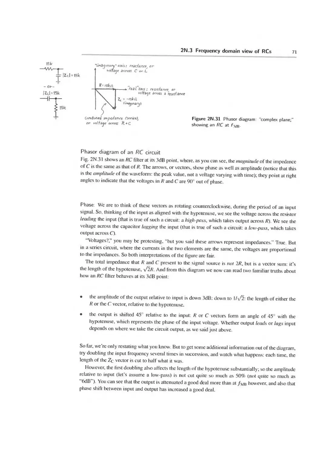
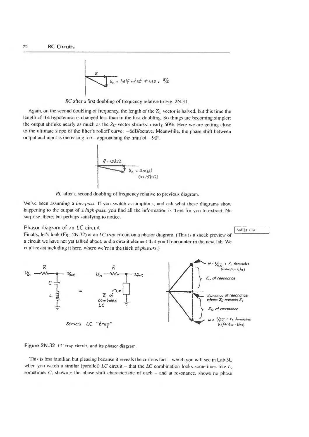
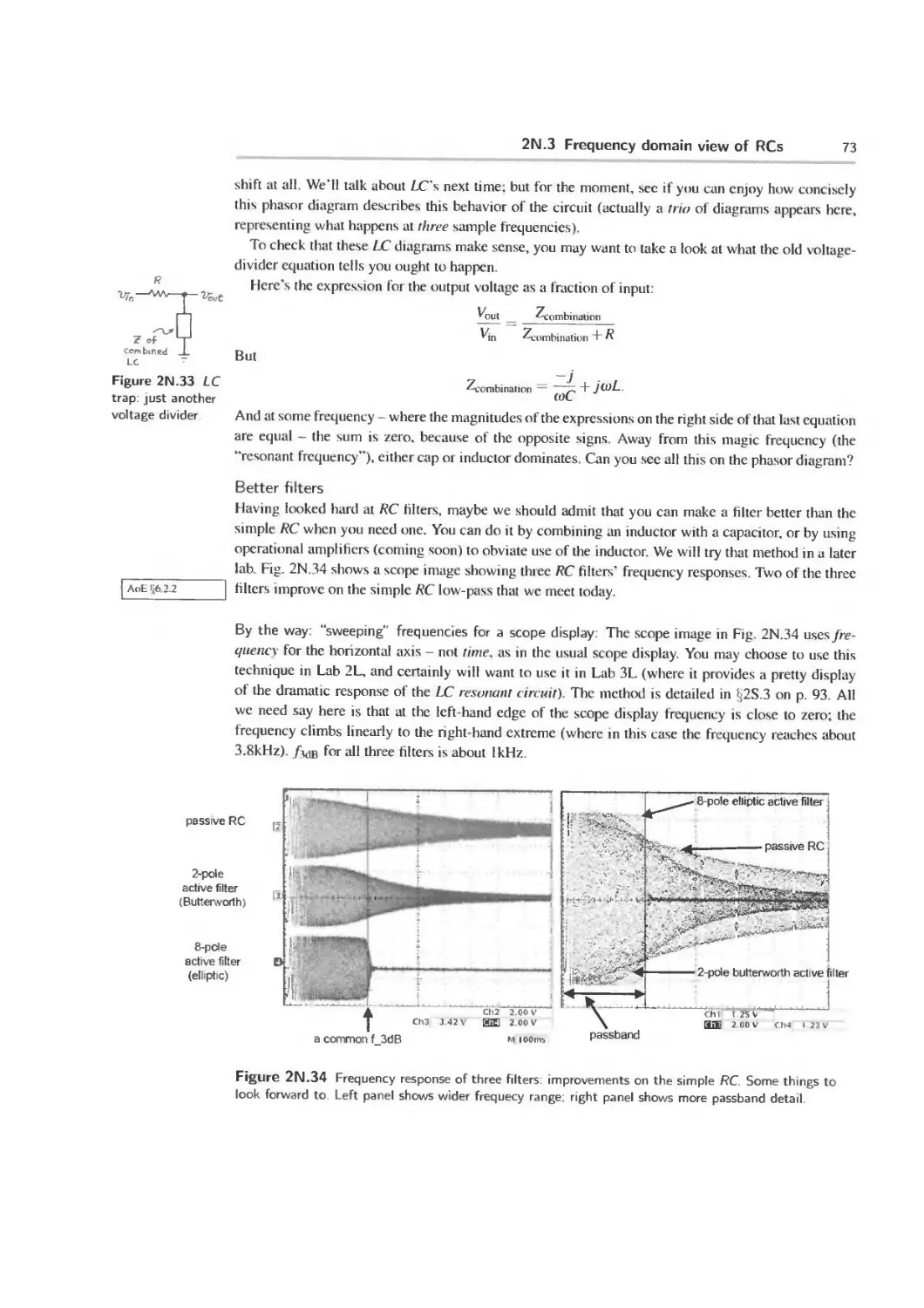
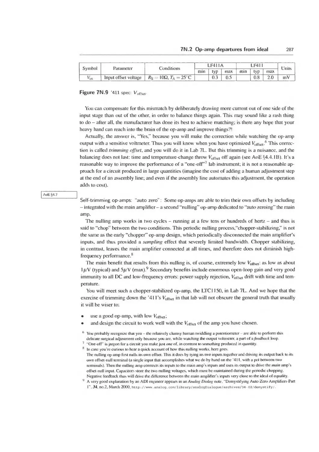
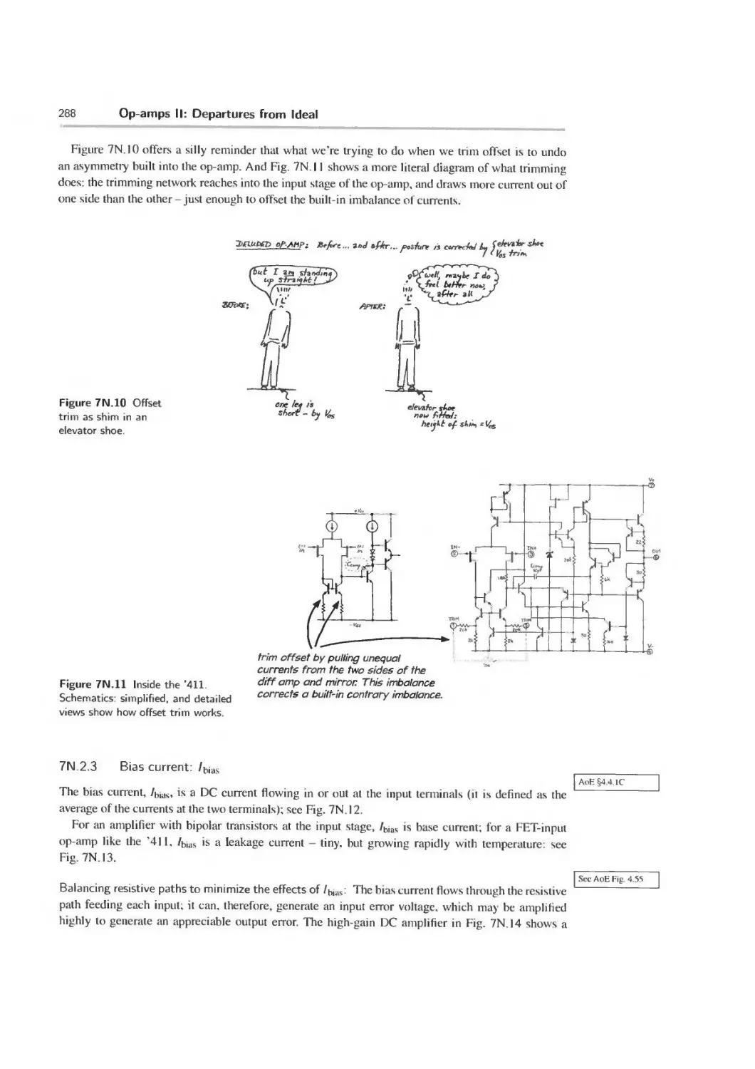
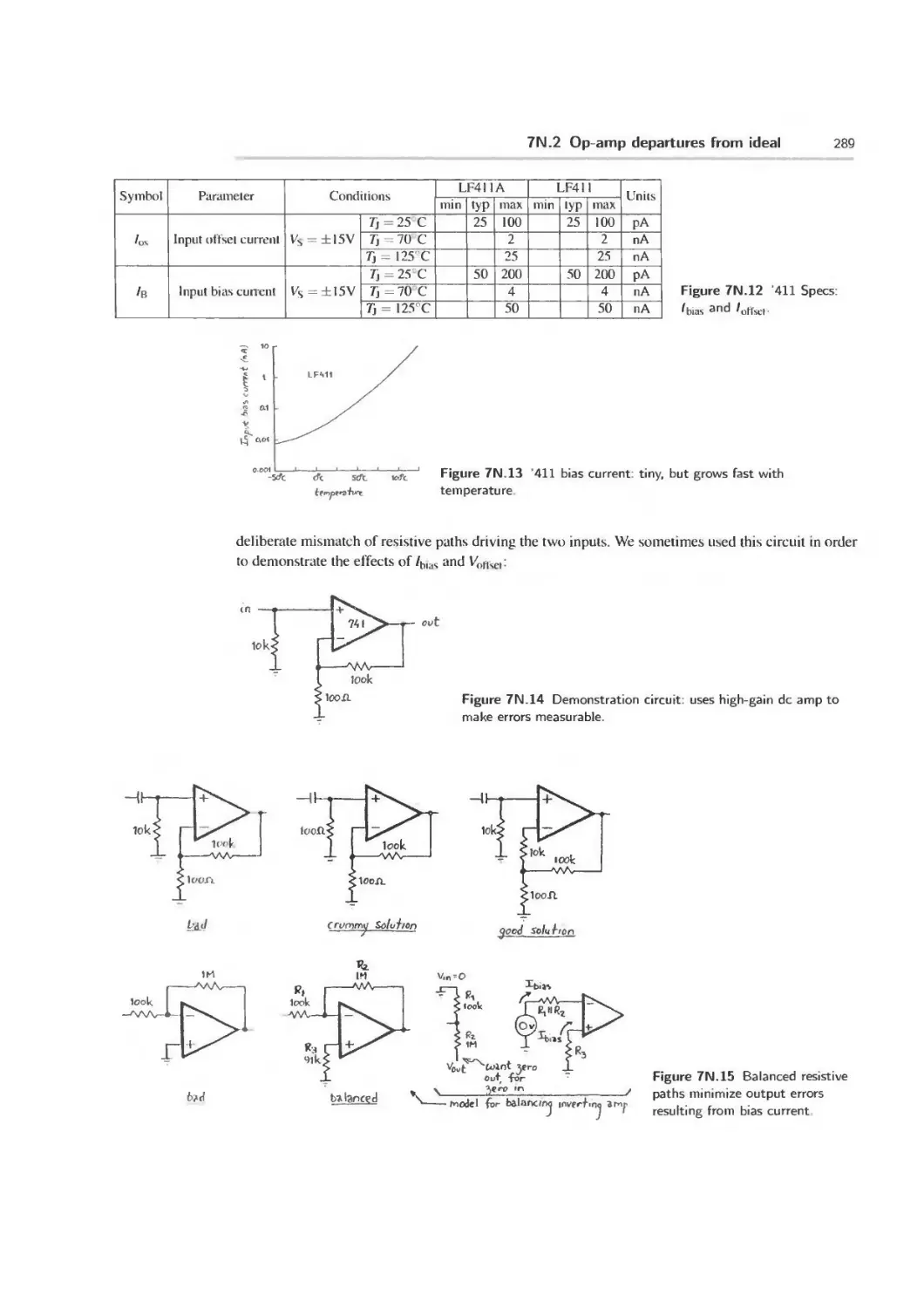
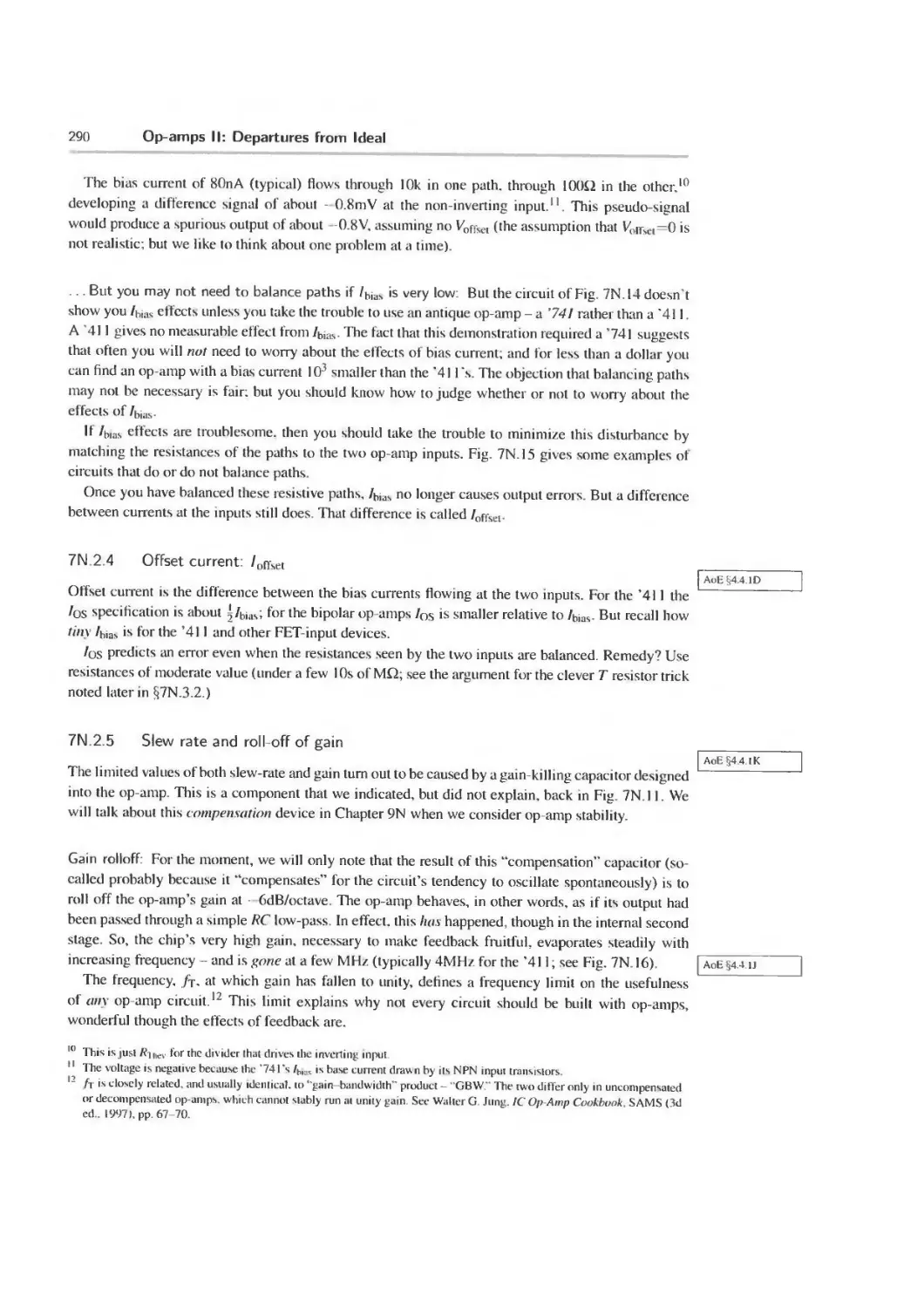
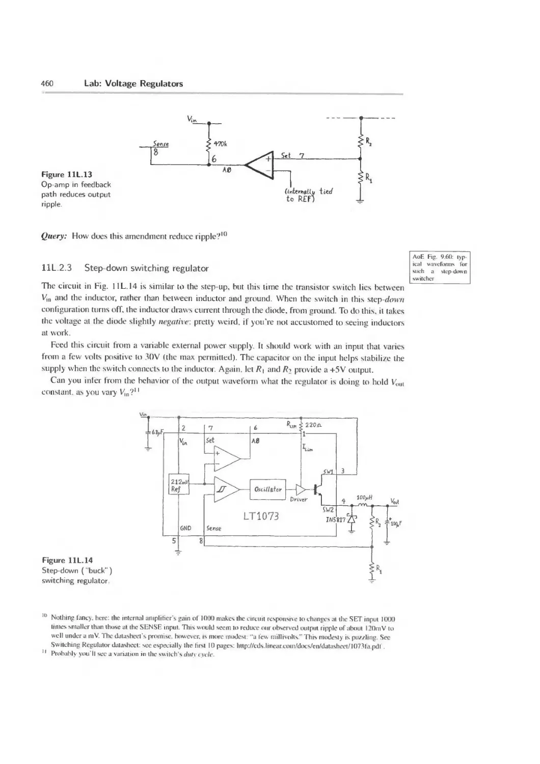
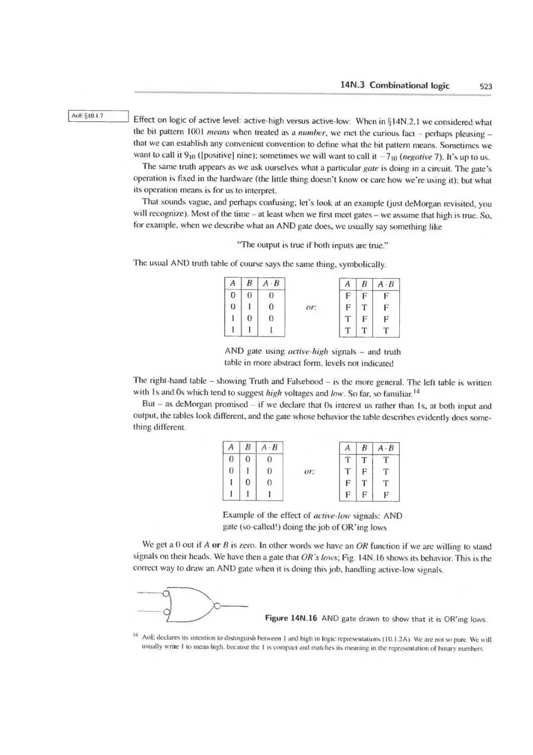
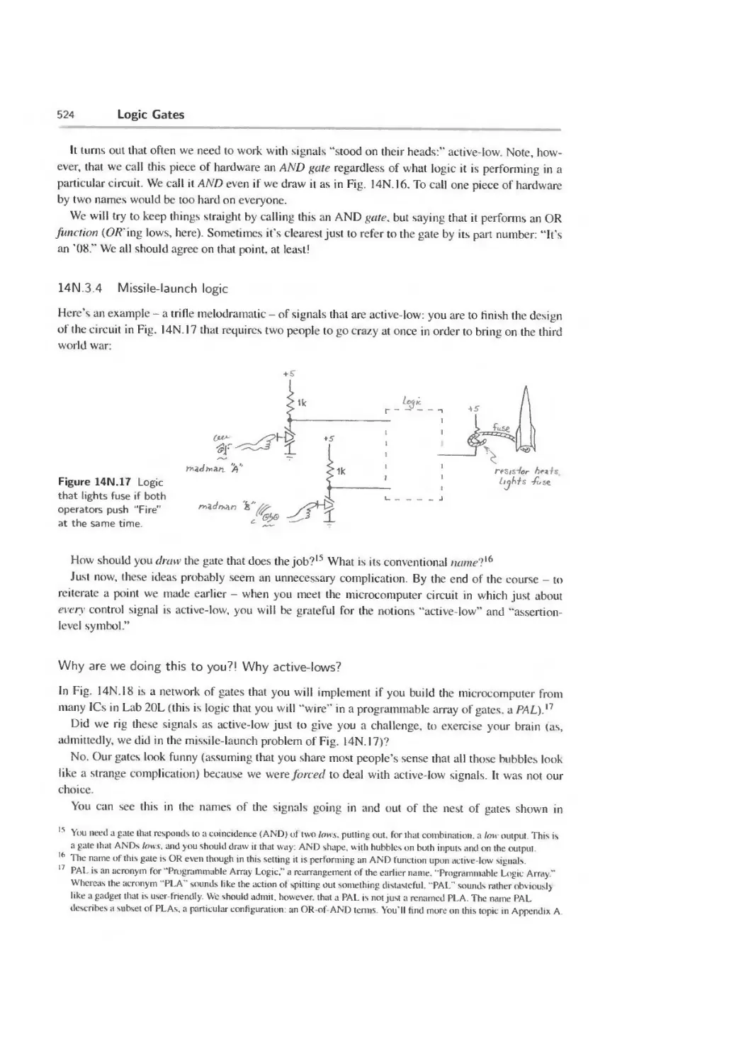
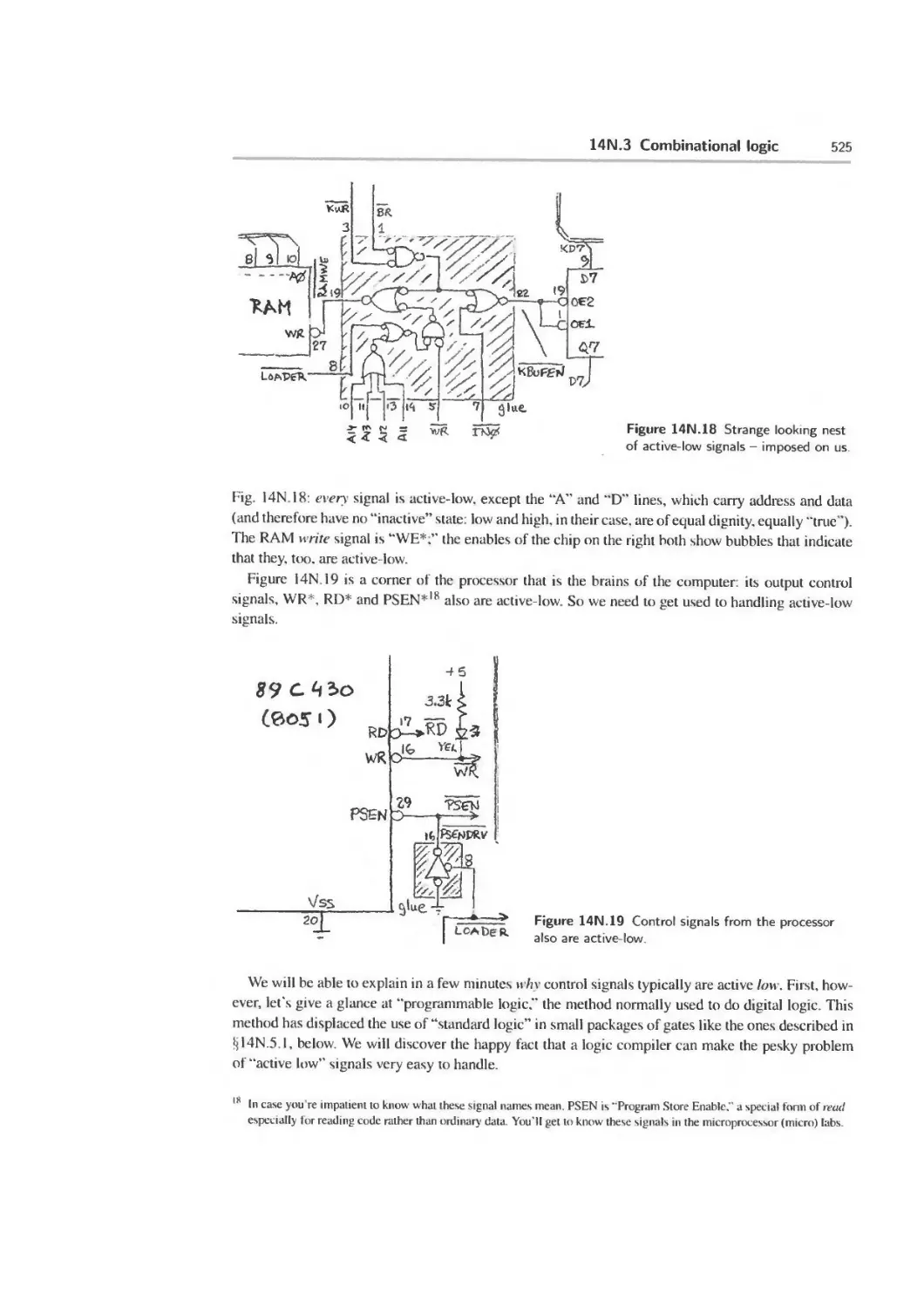
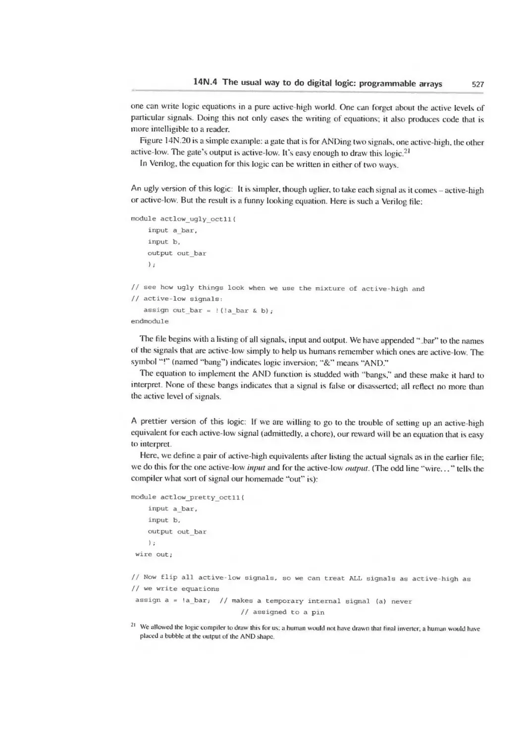
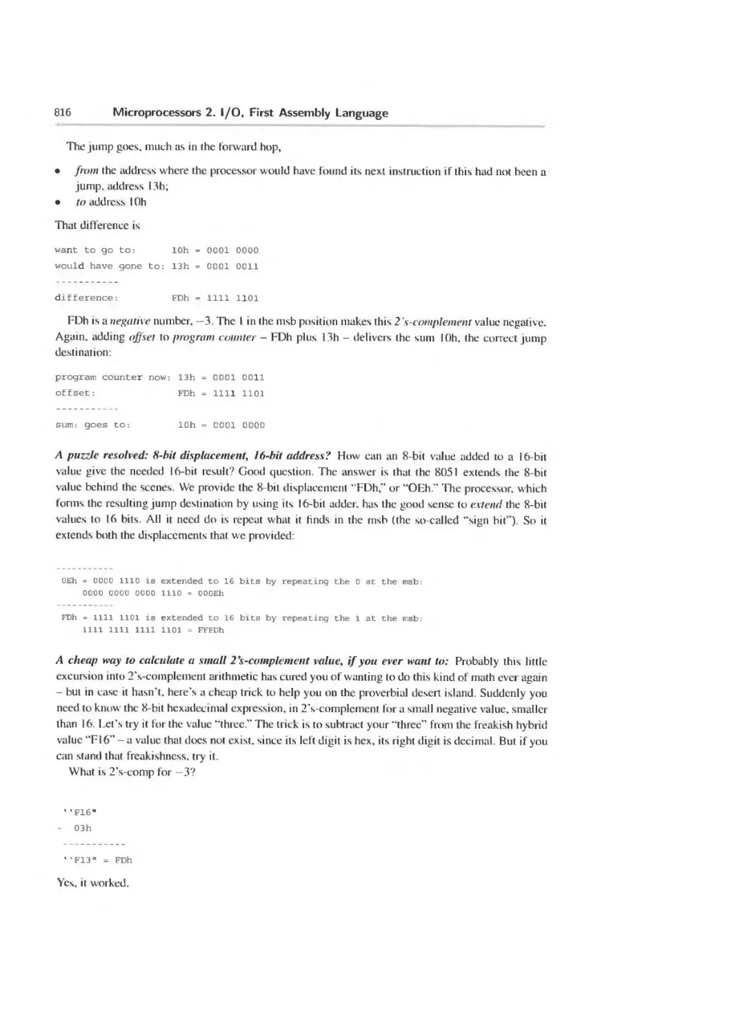
/


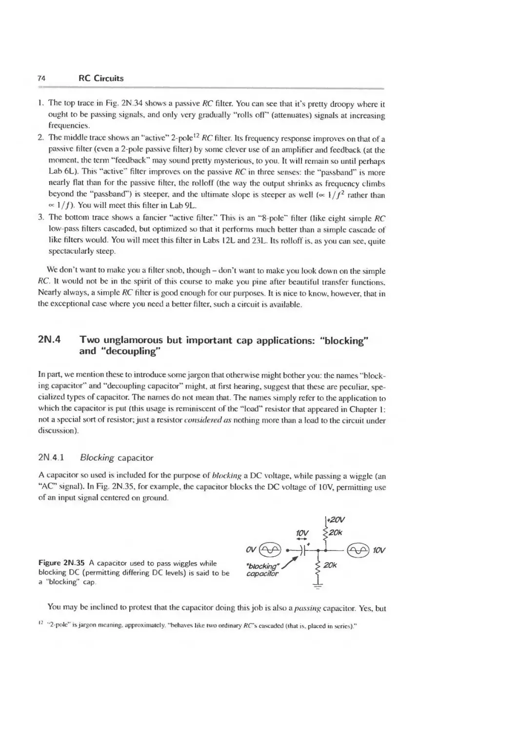


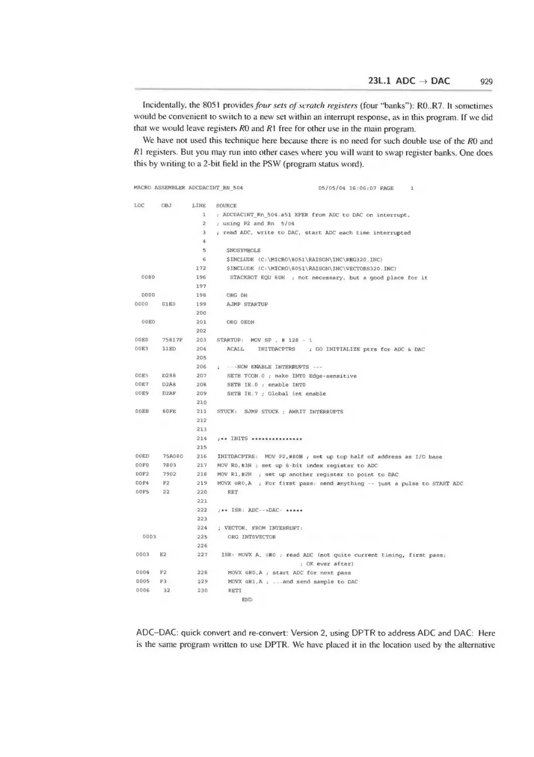


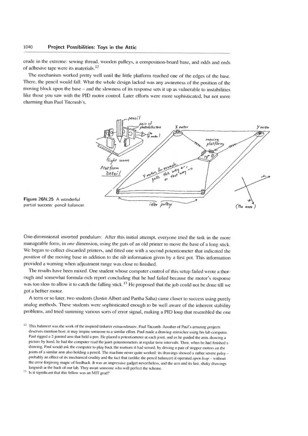


Text
Learning the Art of Electronics
This introduction to circuit design is unusual in several respects.
First, it offers not just explanations, but a full lab course. Each of the 25 daily sessions begins with a
discussion of a particular sort of circuit followed by the chance to try it out and see how it actually
behaves. Accordingly, students understand the circuit’s operation in a way that is deeper and much
more satisfying than the manipulation of formulas.
Second, it describes circuits that more traditional engineering introductions would postpone: thus,
on the third day, we build a radio receiver; on the fifth day, we build an operational amplifier from
an array of transistors. The digital half of the course centers on applying microcontrollers, but gives
exposure to Verilog, a powerful Hardware Description Language.
Third, it proceeds at a rapid pace but requires no prior knowledge of electronics. Students gain intuitive
understanding through immersion in good circuit design.
• Each session is divided into several parts, including Notes, Labs; many also have Worked Exam-
ples and Supplementary Notes
• An appendix introducing Verilog
• Further appendices giving background facts on oscilloscopes. Xilinx, transmission lines, pinouts,
programs etc. plus advice on parts and equipment
• Very little math: focus is on intuition and practical skills
• A final chapter showcasing some projects built by students taking the course over the years
Thomas C. Hayes reached electronics via a circuitous route that started in law school and eventually
found him teaching Laboratory Electronics at Harvard, which he has done for thirty-five years. He
has also taught electronics for the Harvard Summer School, the Harvard Extension School, and for
seventeen years in Boston University’s Department of Physics. He shares authorship of one patent,
for a device that logs exposure to therapeutic bright light. He and his colleagues are trying to launch
this device with a startup company named Goodlux Technologies. Tom designs circuits as the need
for them arises in the electronics course. One such design is a versatile display, serial interface and
programmer for use with the microcomputer that students build in the course.
Paul Horowitz is a Research Professor of Physics and of Electrical Engineering at Harvard Univer-
sity, where in 1974 he originated the Laboratory Electronics course from which emerged The Art of
Electronics.
Learning the Art of Electronics
A Hands-On Lab Course
Thomas C. Hayes
with the assistance of Paul Horowitz
gg Cambridge
gj? UNIVERSITY PRESS
Cambridge
UNIVERSITY PRESS
University Printing House. Cambridge CB2 8BS, United Kingdom
Cambridge University Press is part of the University of Cambridge.
It furthers the University's mission by disseminating knowledge in the pursuit of
education, learning, and research al the highest international levels of excellence.
www.cambridge.org
Information on this title: www.cambridge.org/978O521177238
© Cambridge University Press 2016
This publication is in copyright. Subject to statutory exception
and to the provisions of relevant collective licensing agreements,
no reproduction of any part may take place without the written
permission of Cambridge University Press
First published 2016
Reprinted with corrections 2016
Printed in the United Kingdom by TJ International Ltd. Padstow Cornwall
A catalogue record for this publication is available from the British Library.
Library of Congress Cataloguing in Public ation Data
ISBN 978 0 521 17723-8 Paperback
Cambridge University Press has no responsibility for the persistence or accuracy
of URLs for external or third party Internet Web sites referred to in this publication
and docs not guarantee that any content on such Web sites is, or will remain,
accurate or appropriate.
Q5q^0
For Debbie. Tessa. Turner and Jamie
And in memory of my beloved friend, Jonathan
Contents
Preface
Overview, as the Course begins
page xx
xxv
Part I Analog: Passive Devices 1
IN DC Circuits 3
1N.1 Overview 3
IN.2 Three laws 5
1N.3 First application: voltage divider II
1 N.4 Loading, and “output impedance” 14
1 N.5 Readings in AoE 24
IL Lab: DC Circuits 25
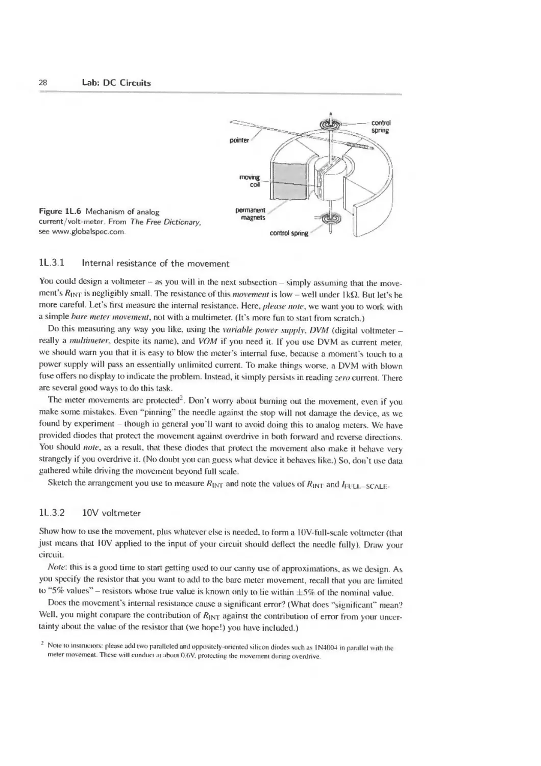
1L. I Ohm’s law 25
1 L.2 Voltage divider 26
1L.3 Converting a meter movement into a voltmeter and ammeter 27
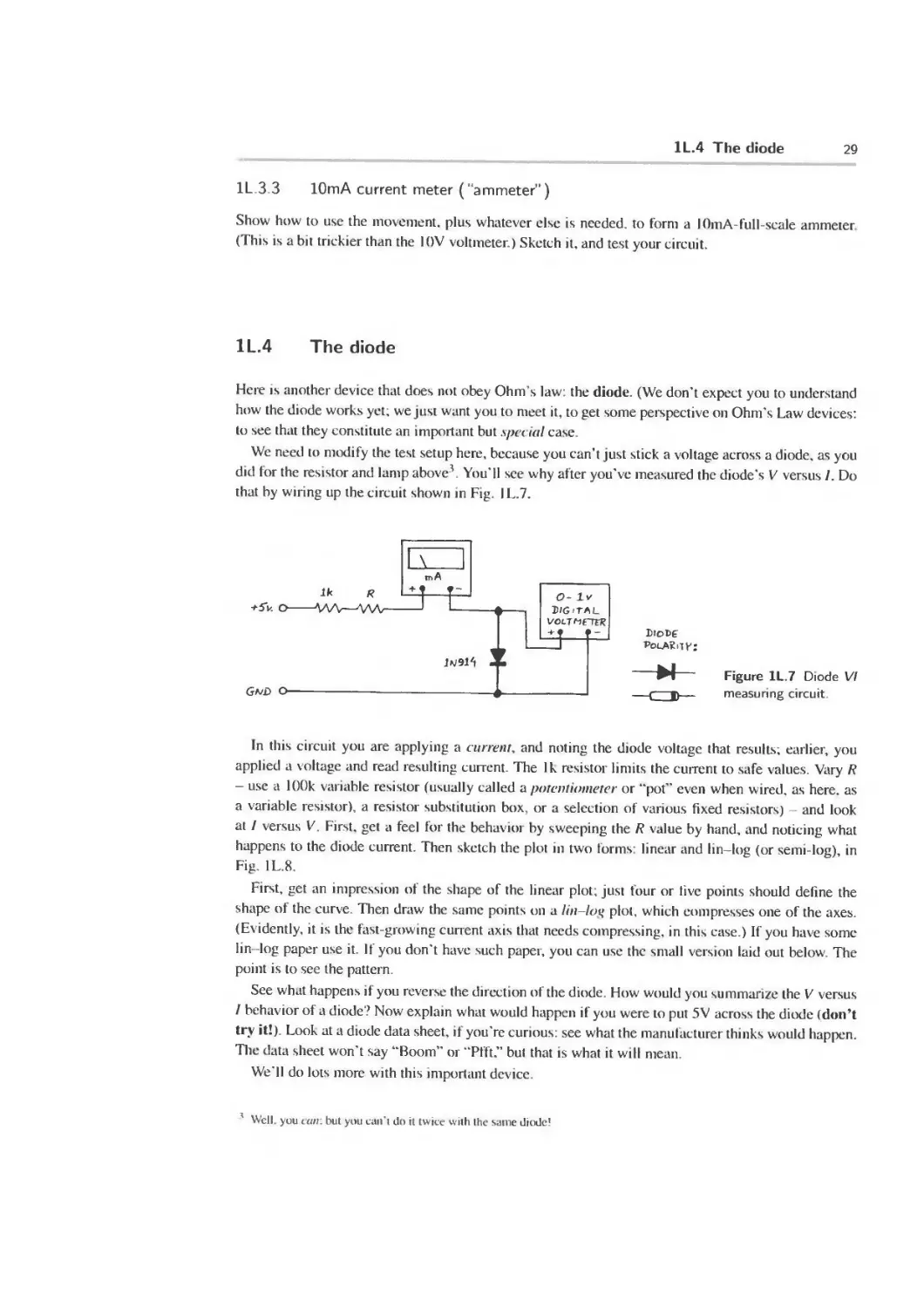
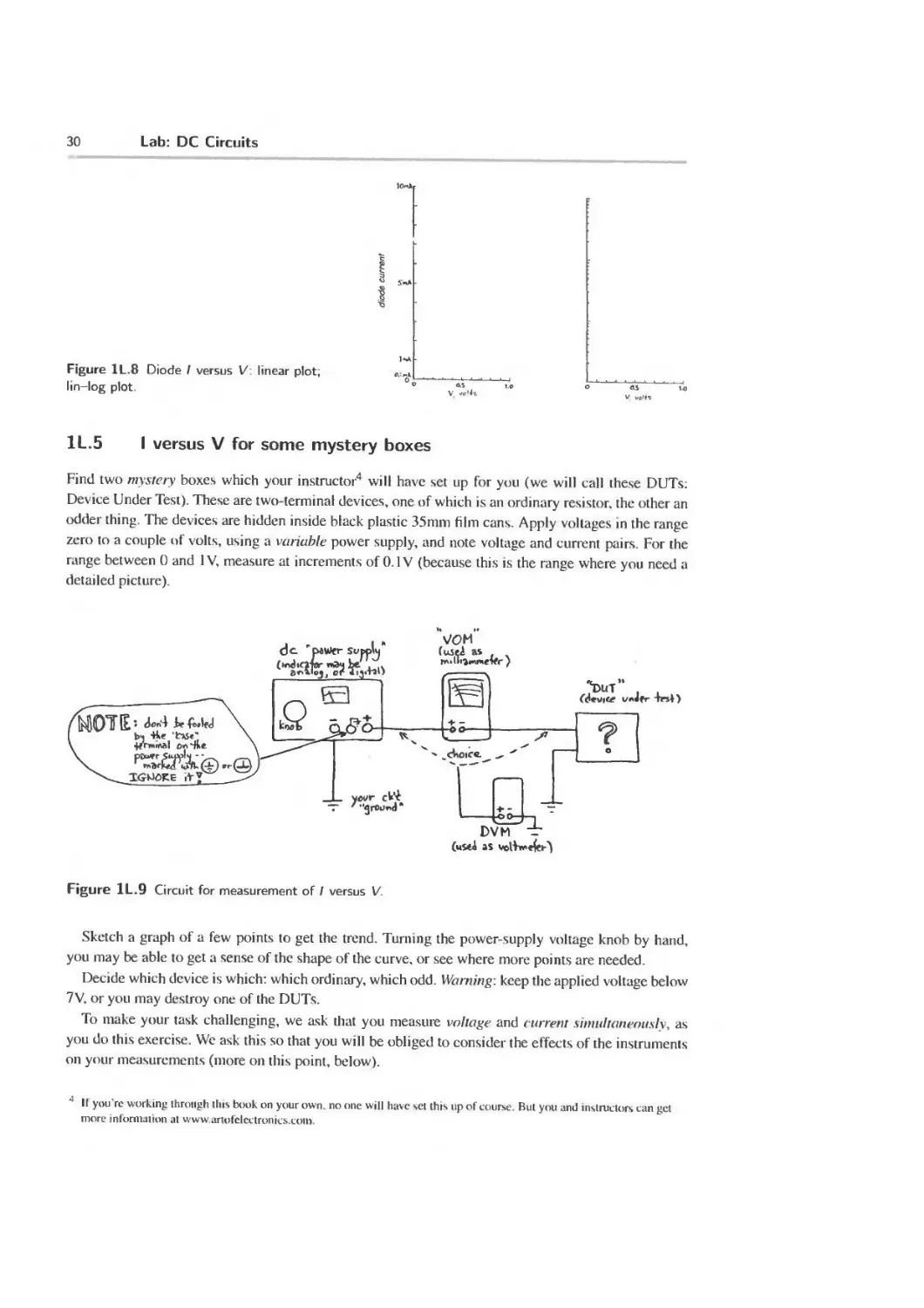
1 L.4 The diode 29
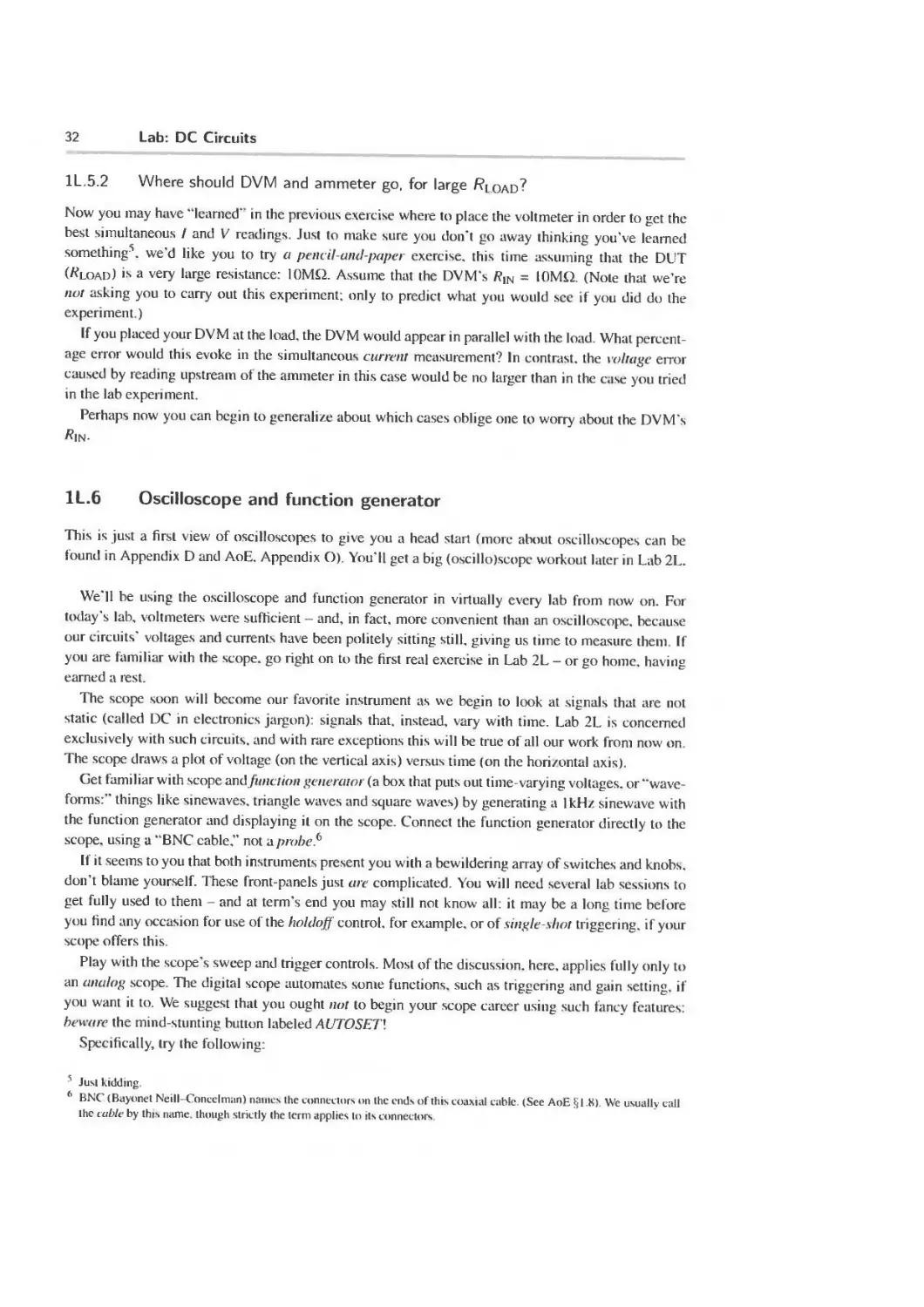
1 L.5 I versus V for some mystery boxes 30
1L.6 Oscilloscope and function generator 32
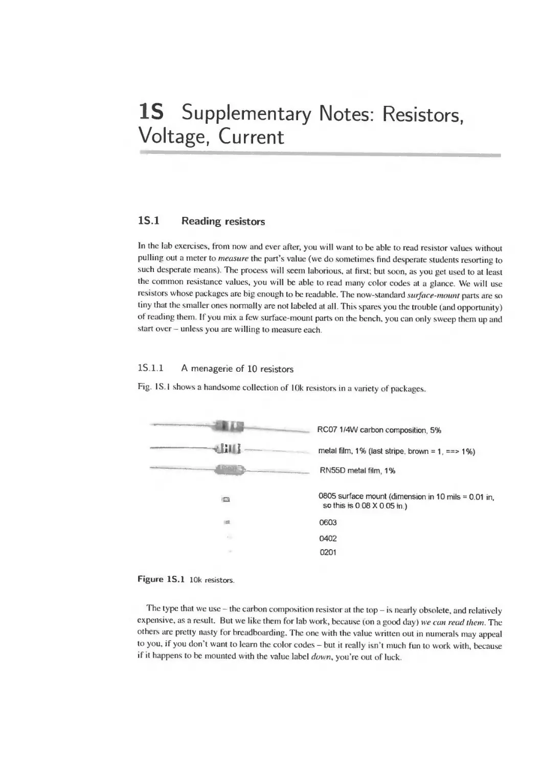
IS Supplementary Notes: Resistors, Voltage, Current 35
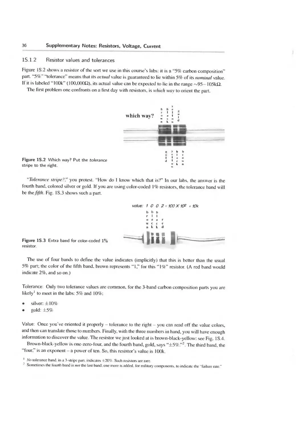
1S. 1 Reading resistors 35
1S .2 Voltage versus current 38
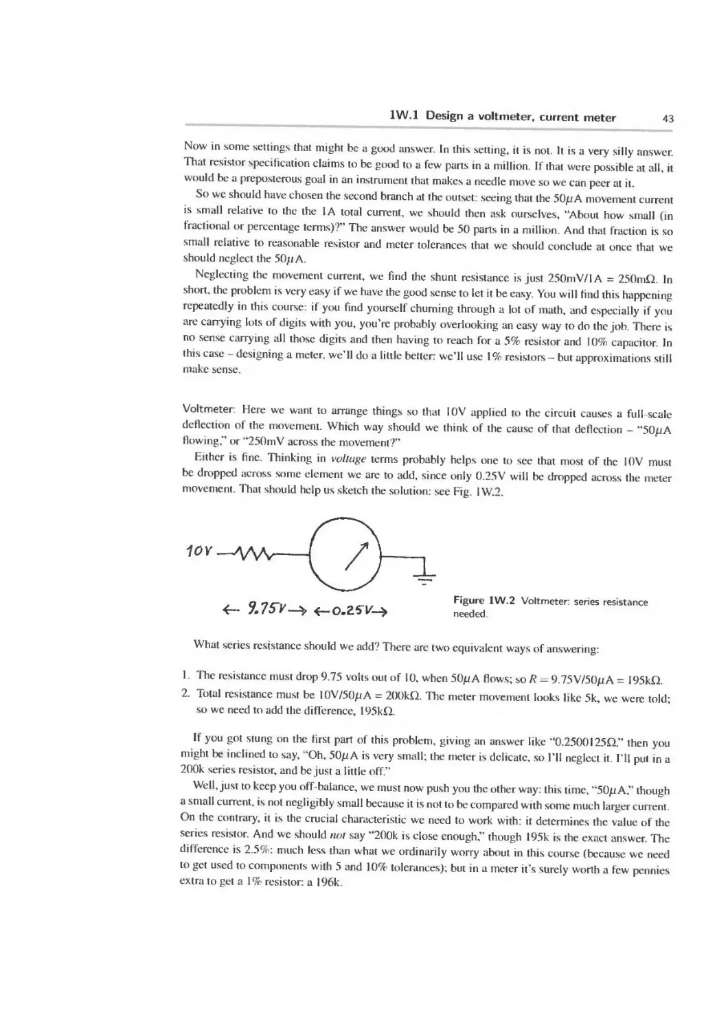
1W Worked Examples: DC circuits 42
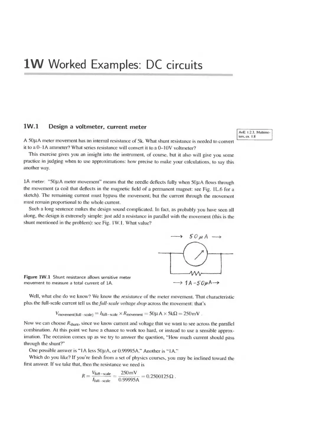
1W 1 Design a voltmeter, current meter 42
1 W.2 Resistor power dissipation 44
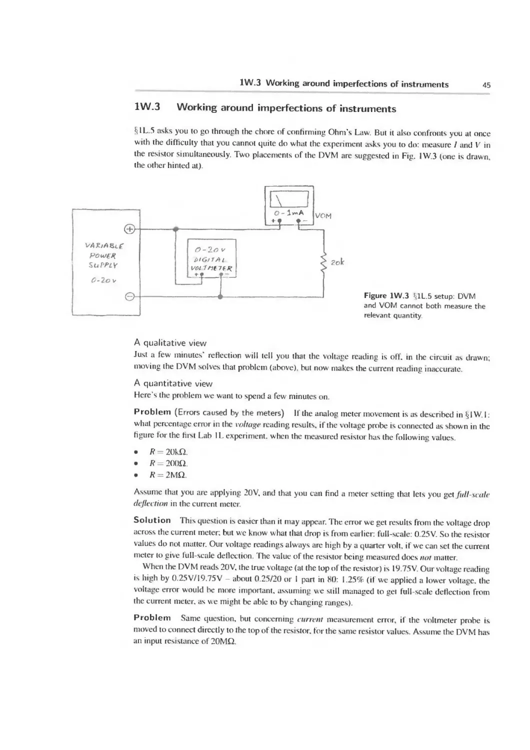
1W 3 Working around imperfections of instruments 45
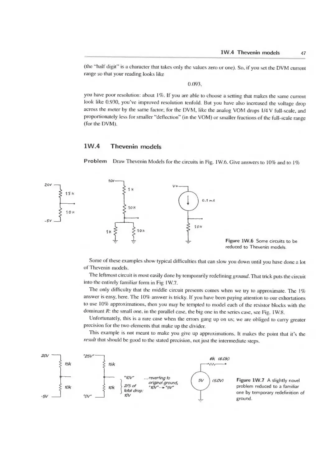
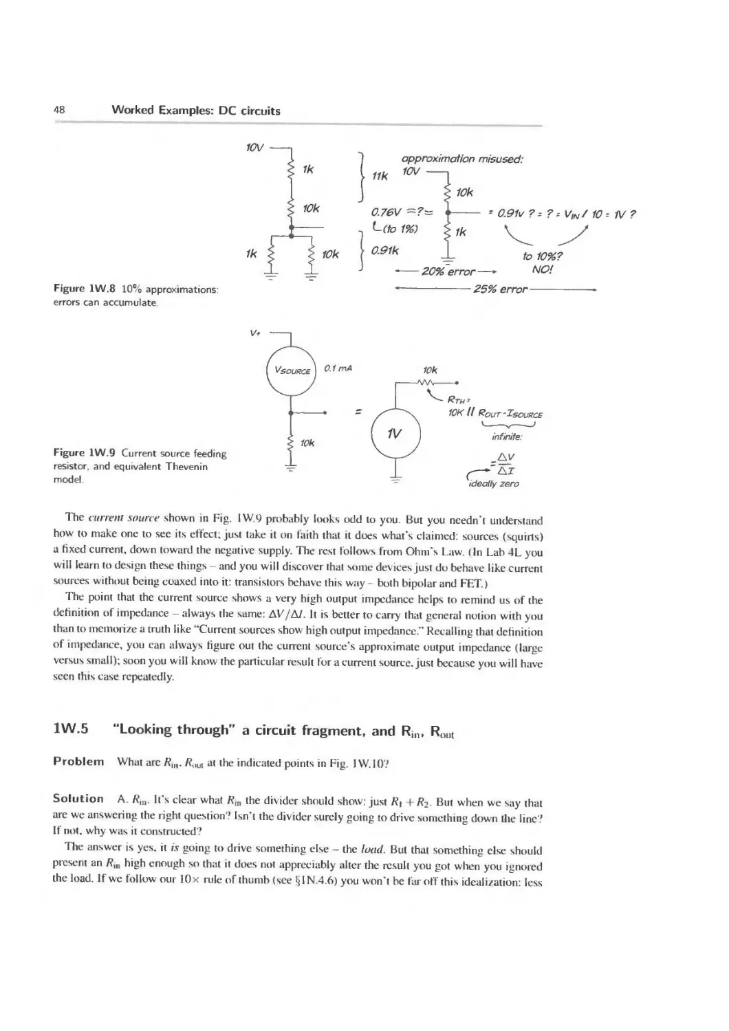
1W.4 Thevenin models 47
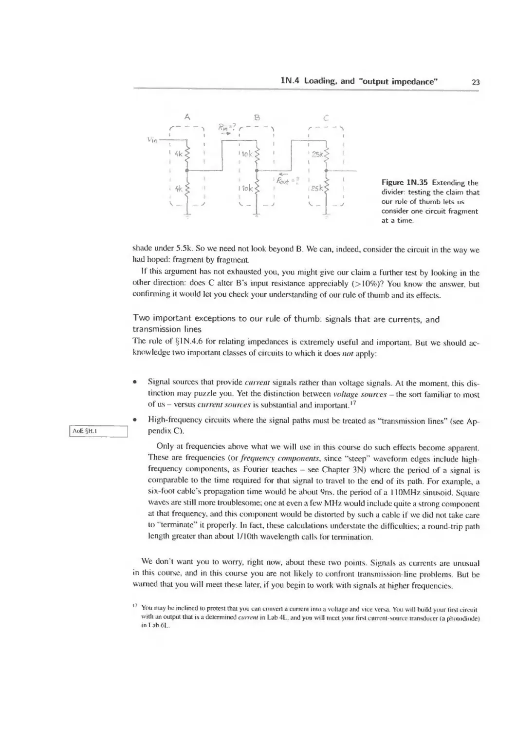
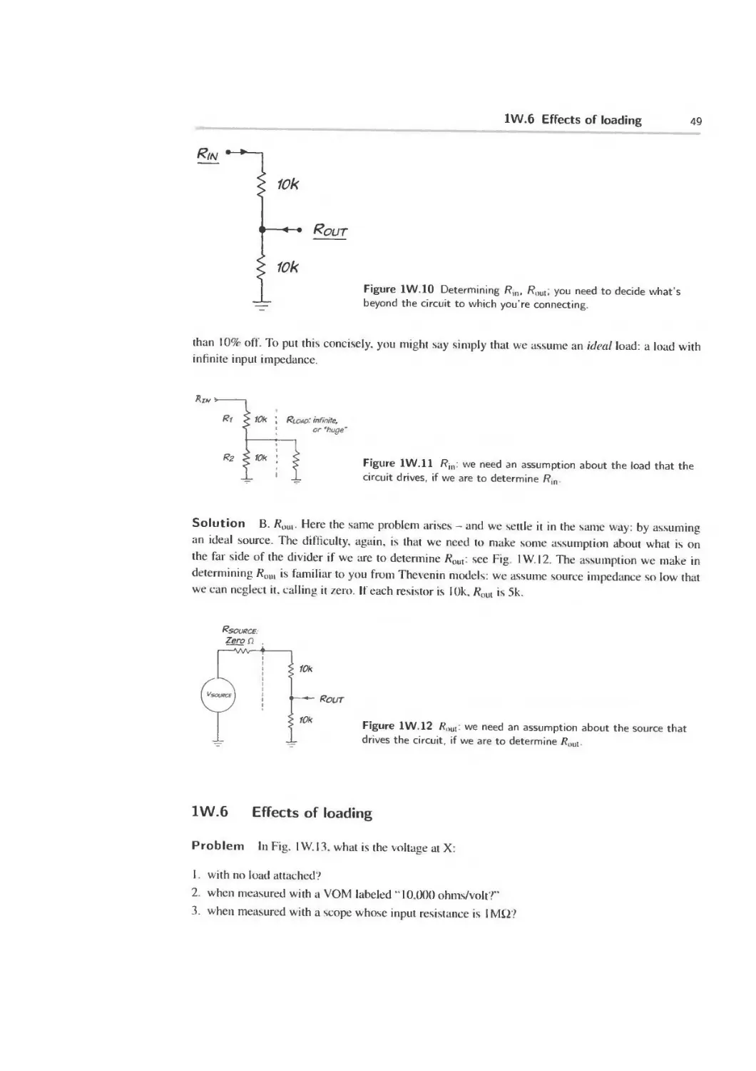
1 W.5 “Looking through” a circuit fragment, and Rjn, /?out 48
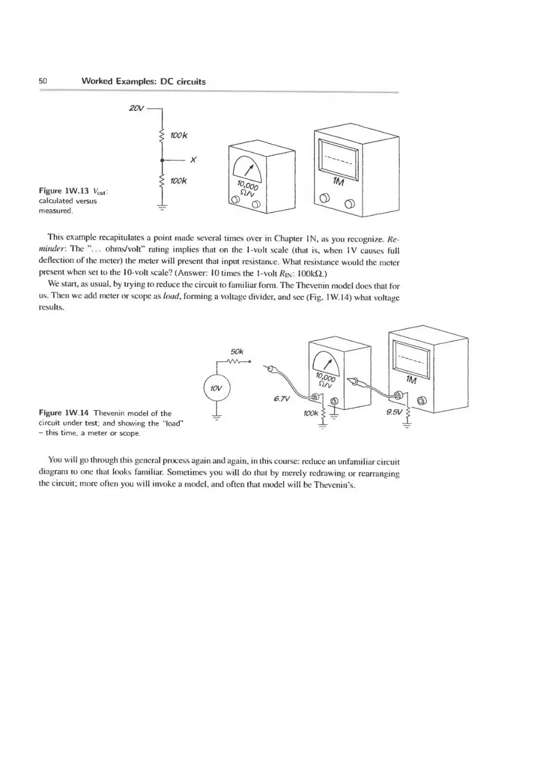
J W.6 Effects of loading 49
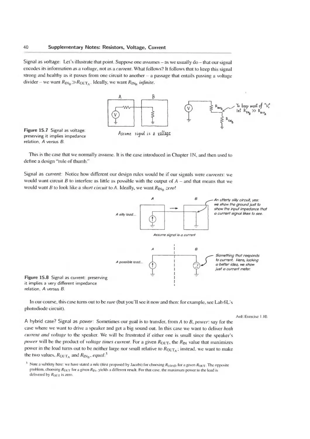
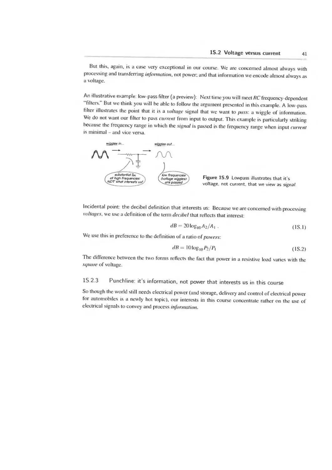
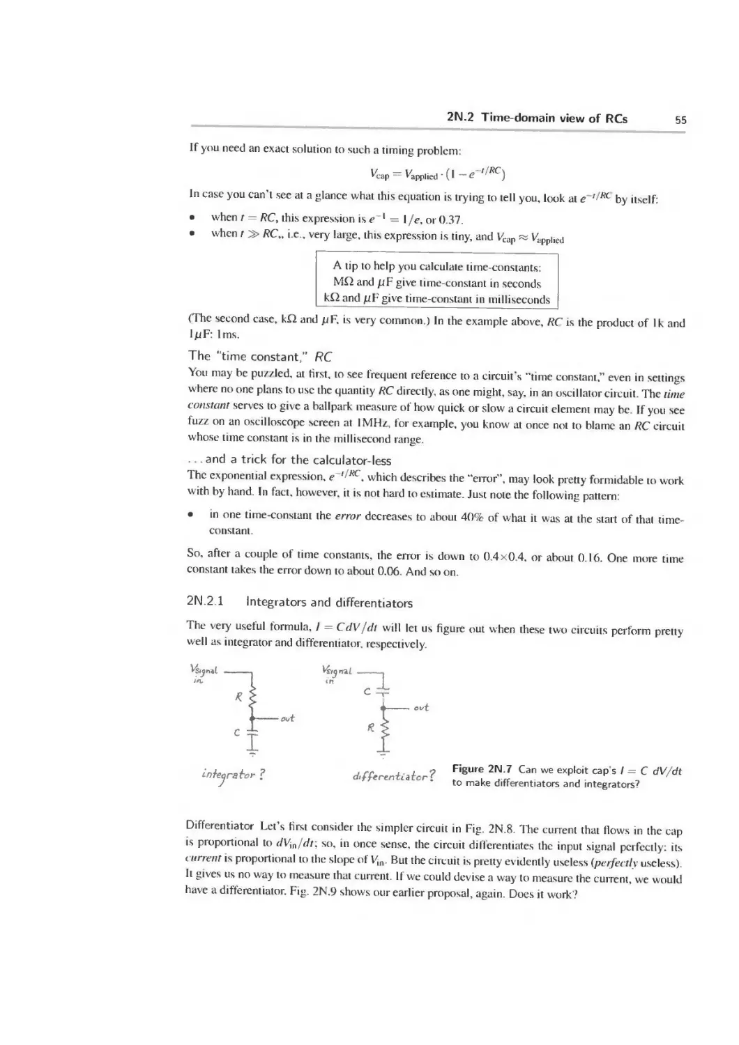
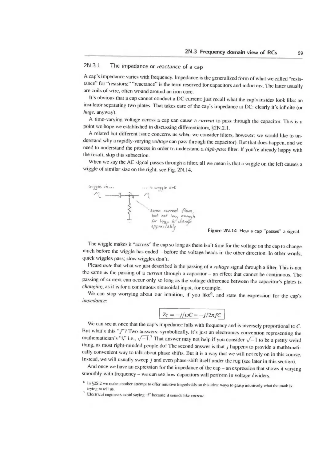
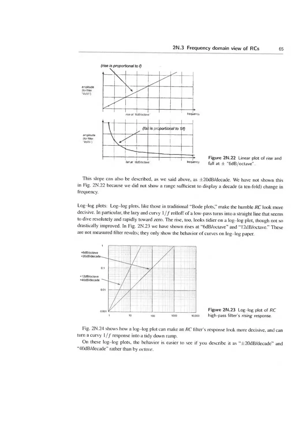
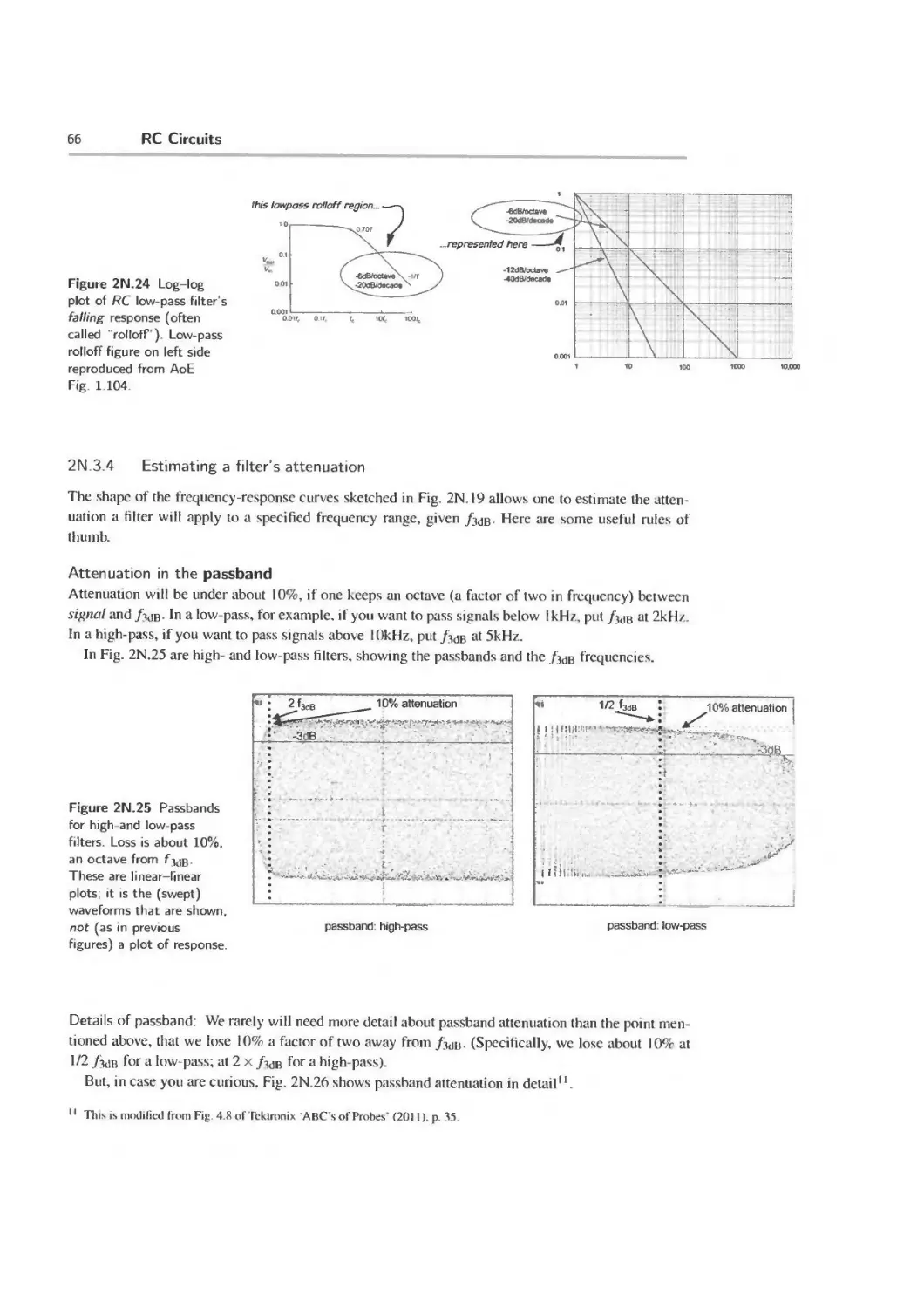
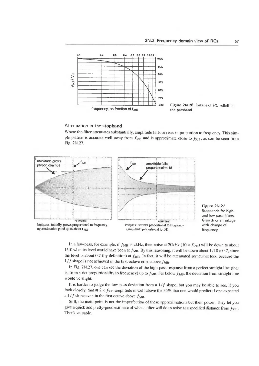
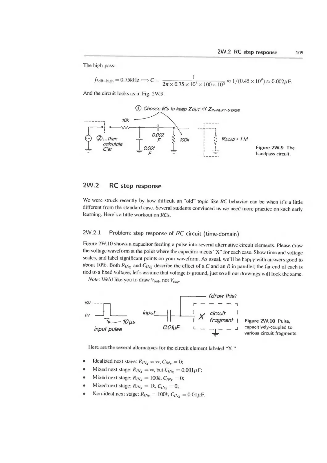
2N RC Circuits 51
2N. 1 Capacitors 51
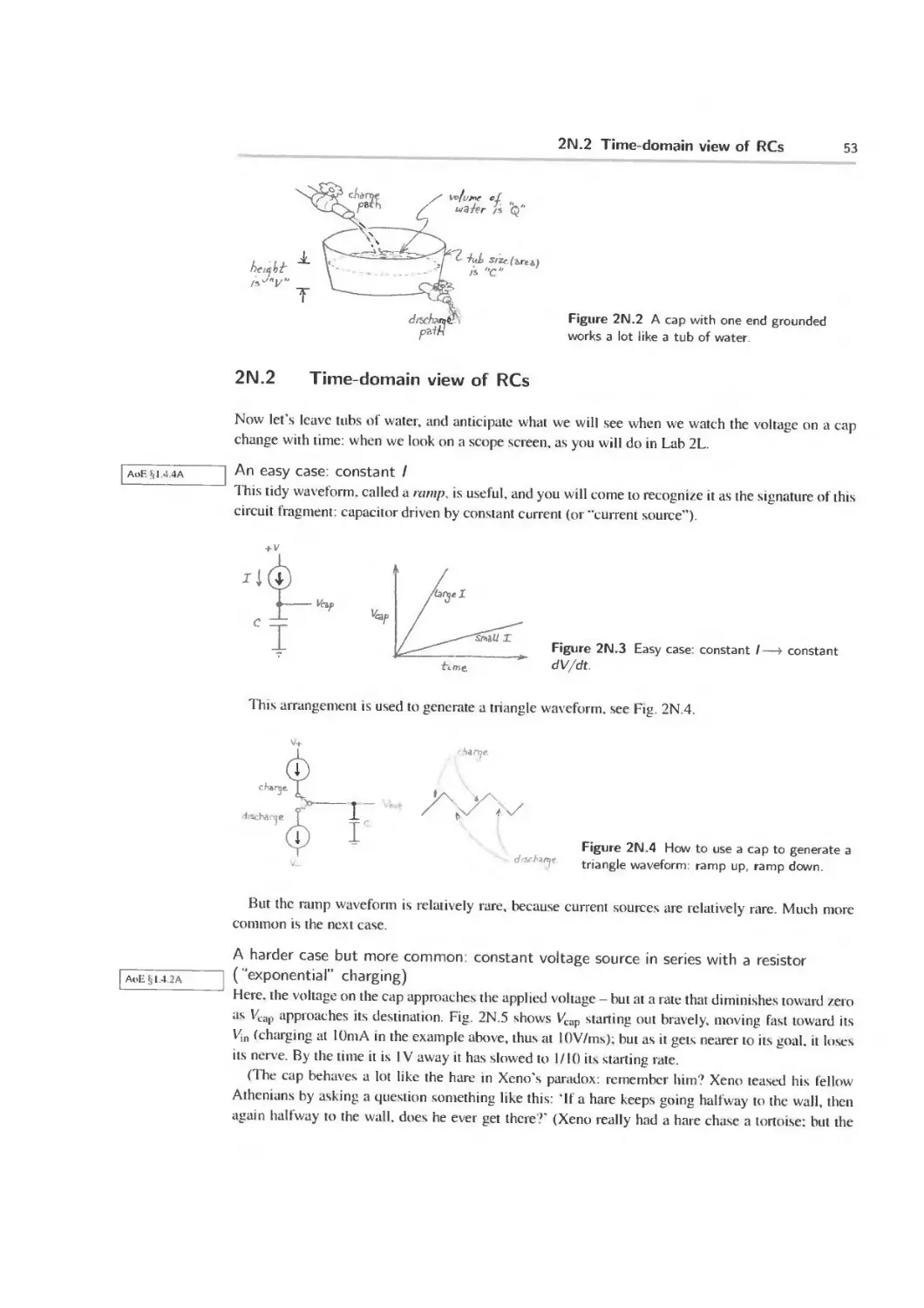
2N 2 Time-domain view of RCs 53
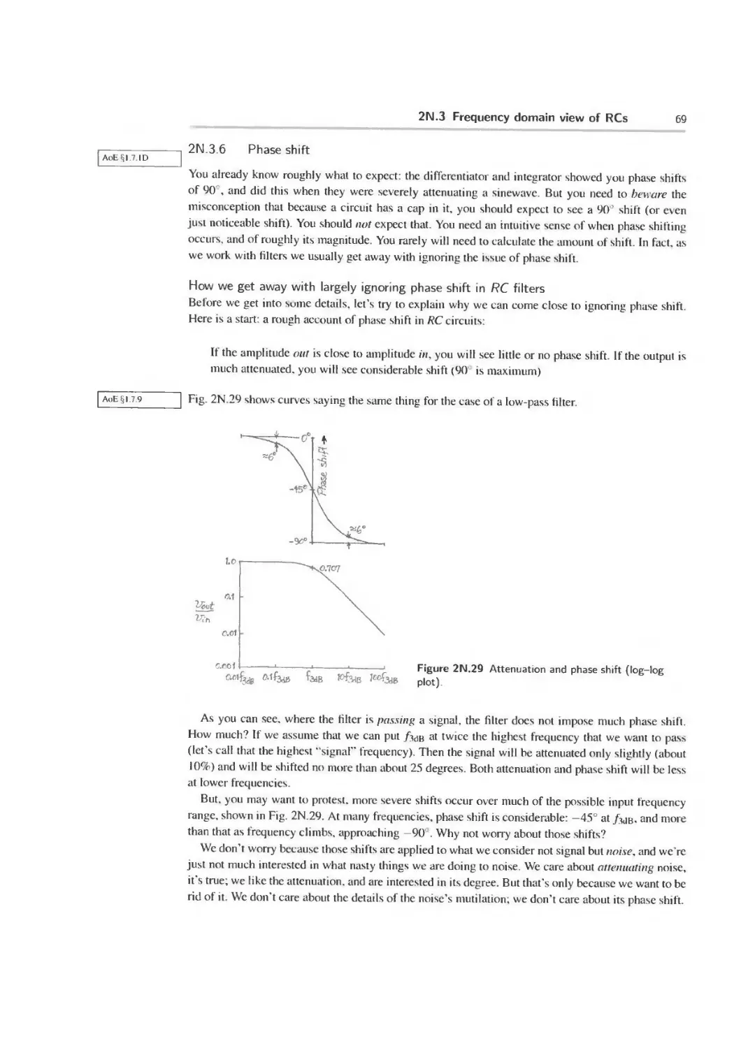
2N.3 Frequency domain view of RCs 58
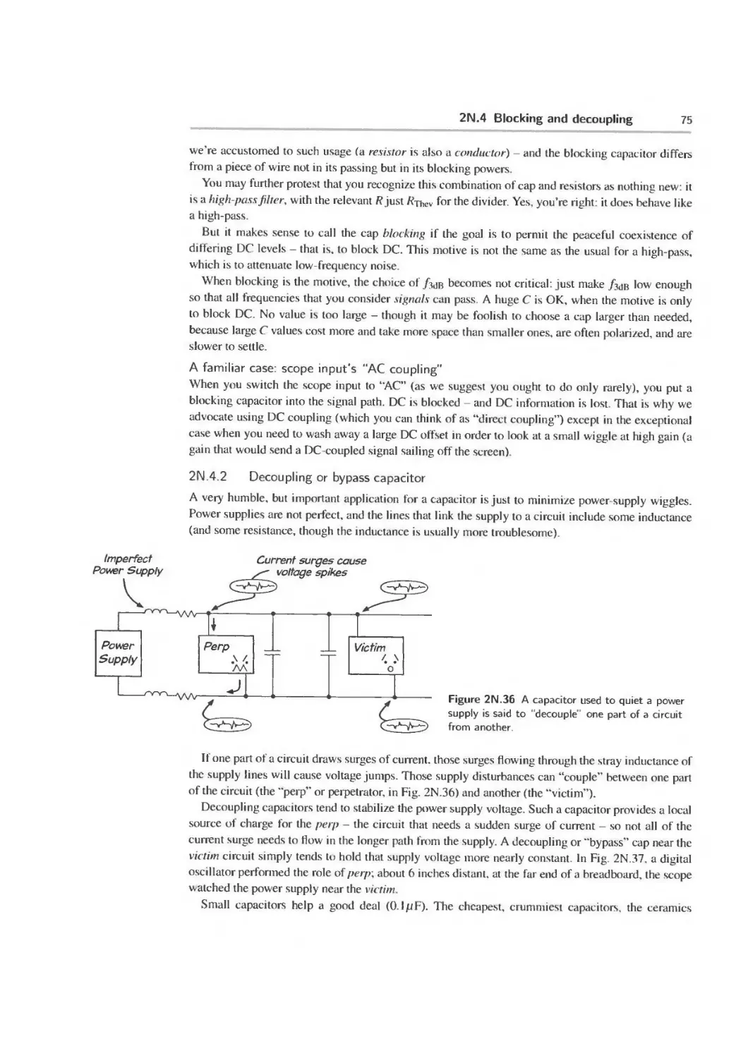
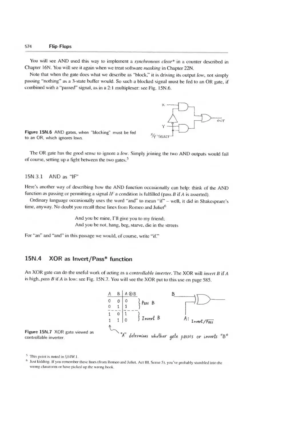
2N .4 Blocking and decoupling 74
viii Contents
2N.5 A somewhat mathy view of RC filters 76
2N.6 Readings in AoE 77
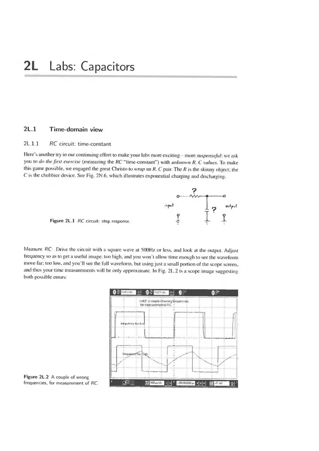
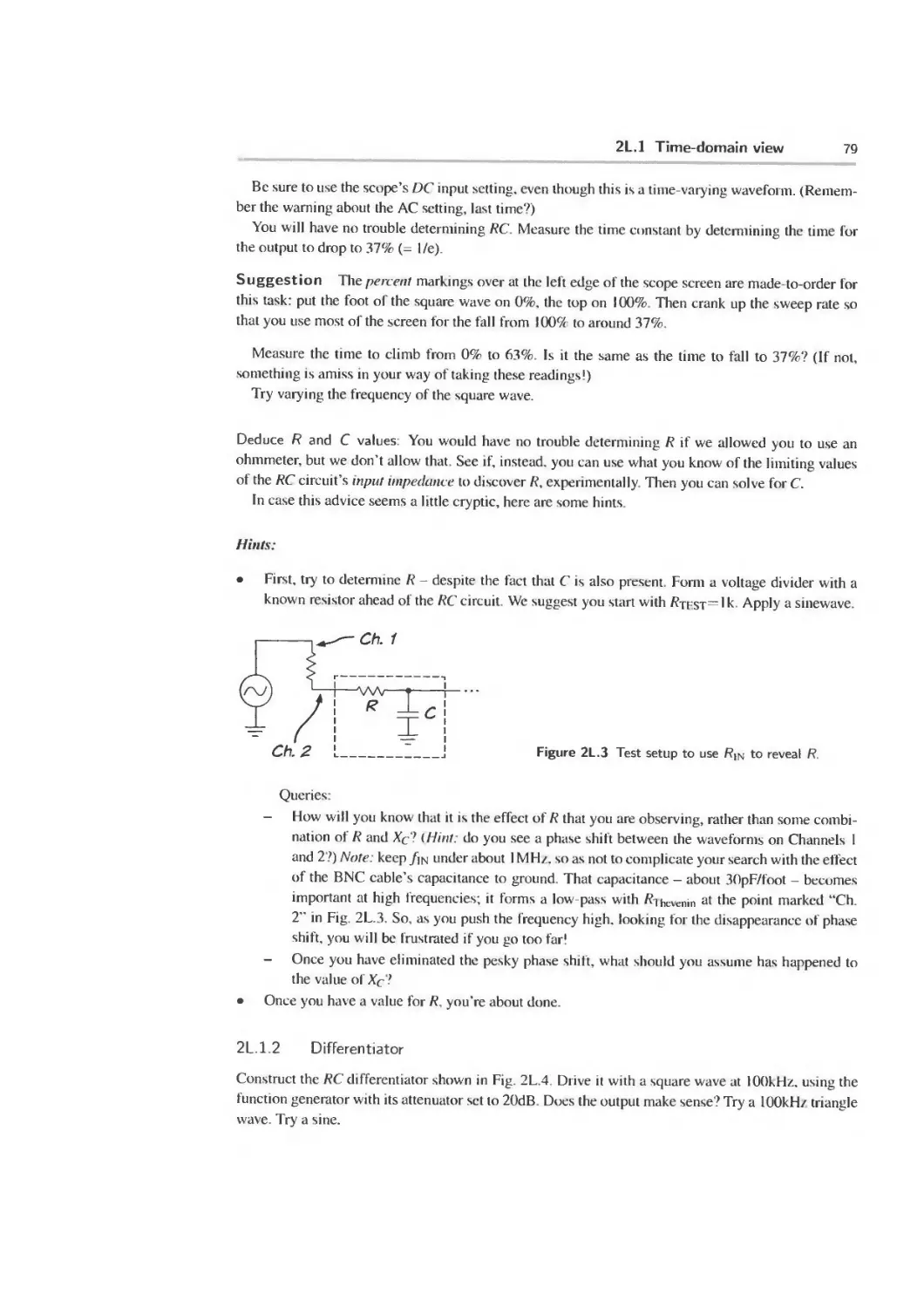
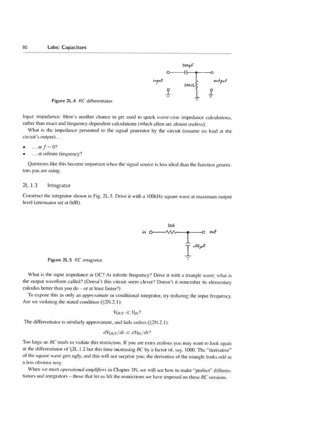
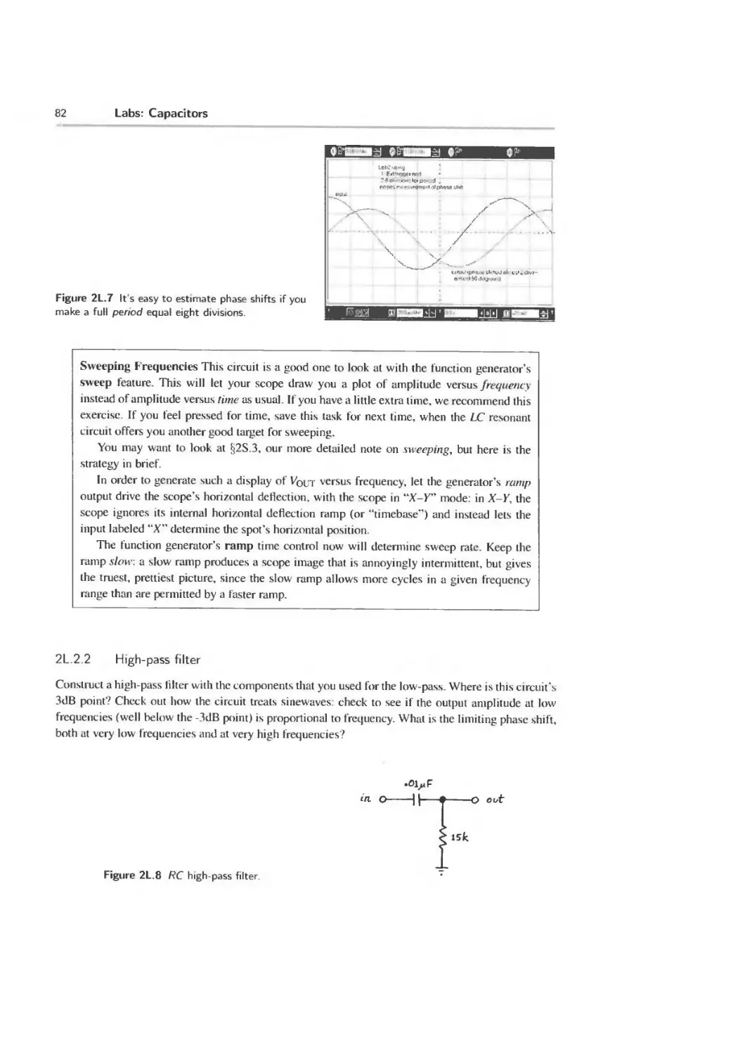
2L Labs: Capacitors 78
2L. 1 Time-domain view 78
2L.2 Frequency domain view 81
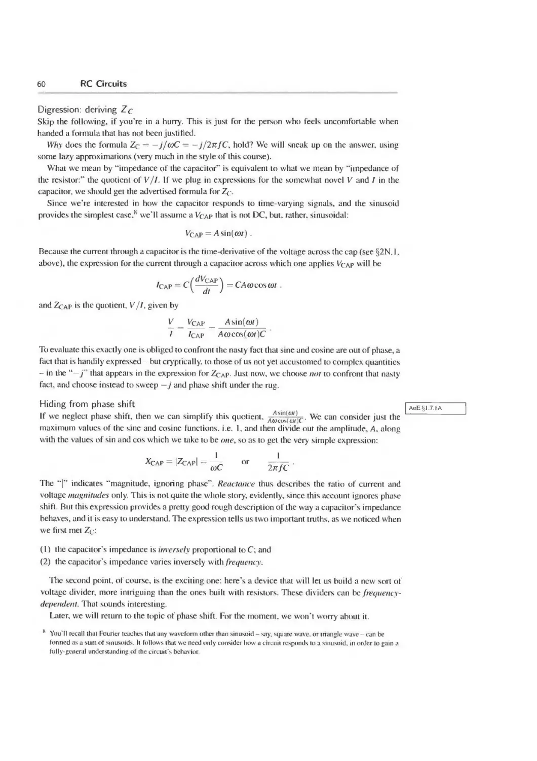
2S Supplementary Notes: RC Circuits 85
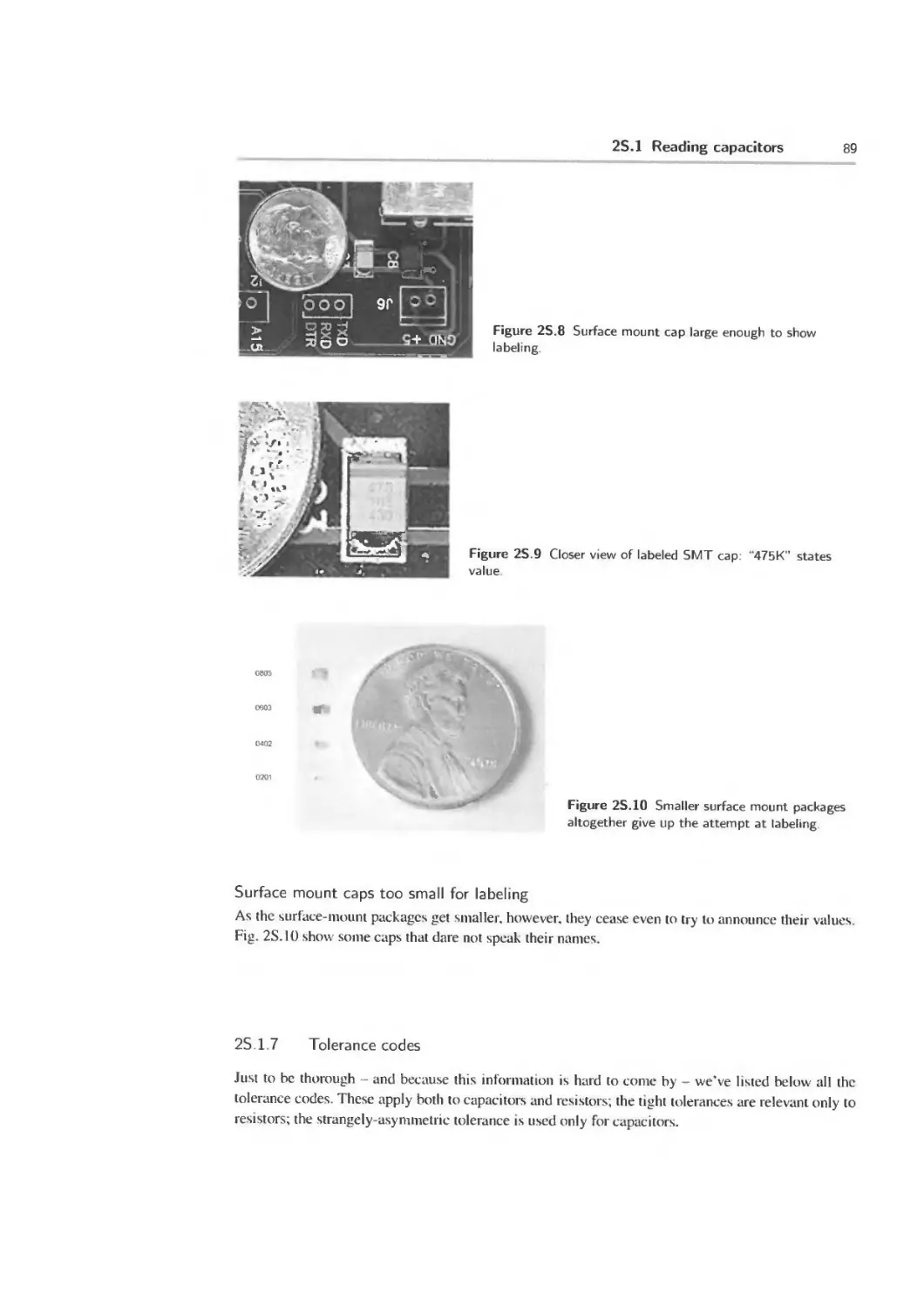
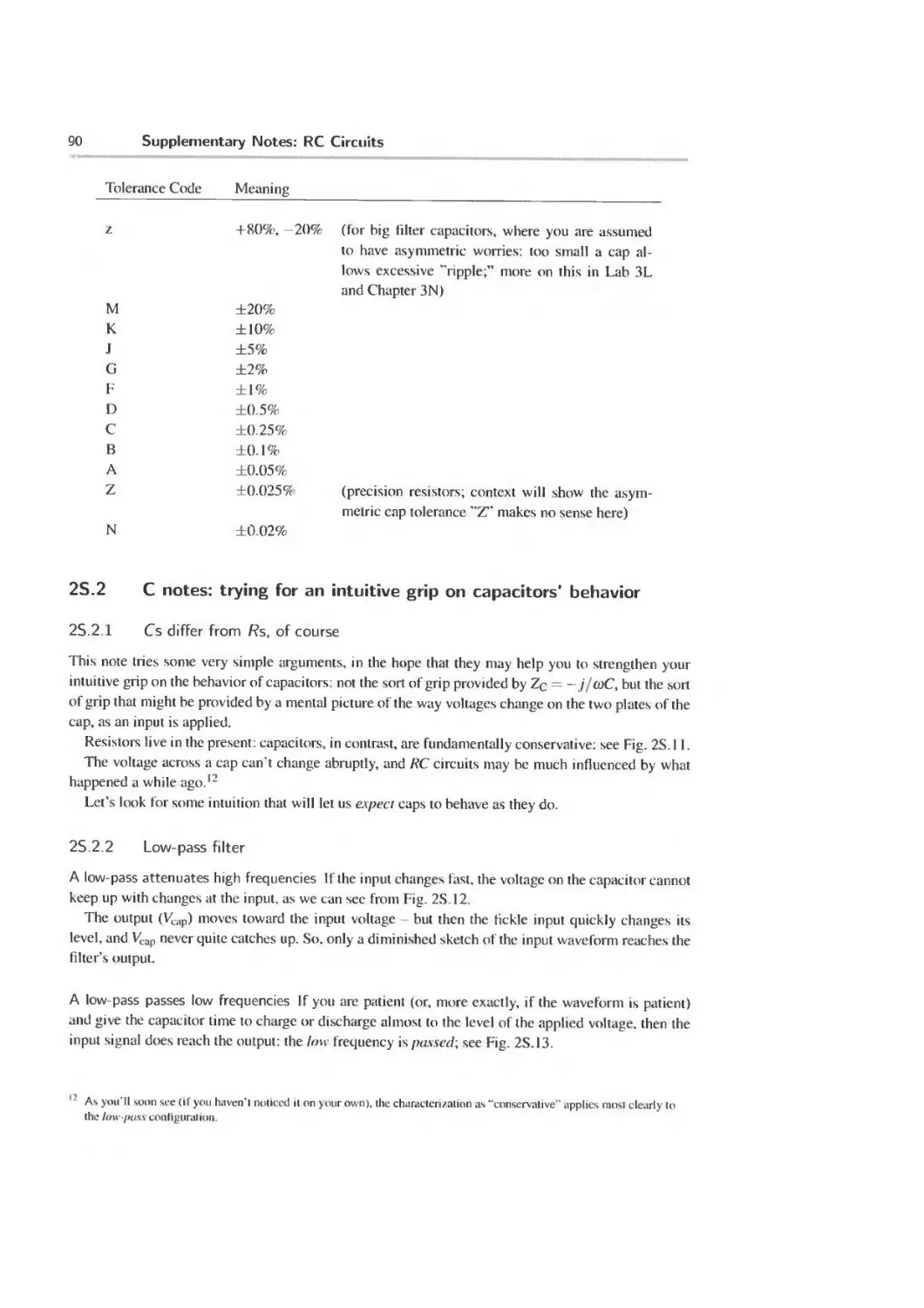
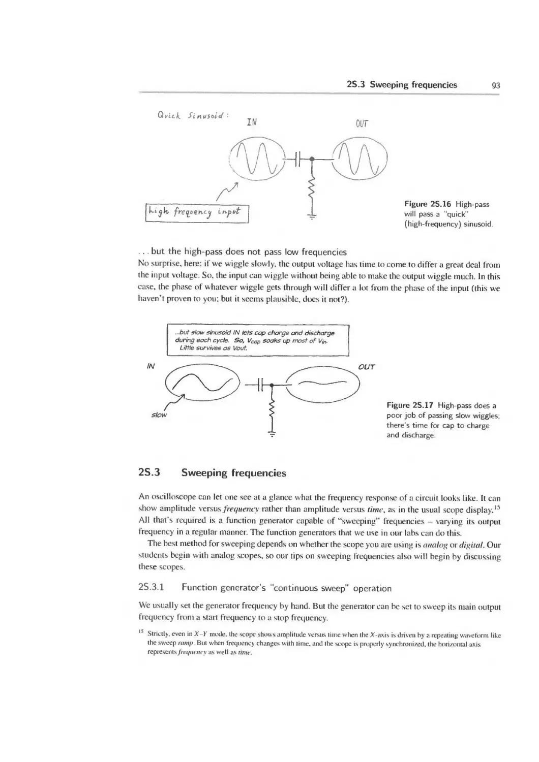
2S. 1 Reading capacitors 85
2S. 2 C notes: trying for an intuitive grip on capacitors' behavior 90
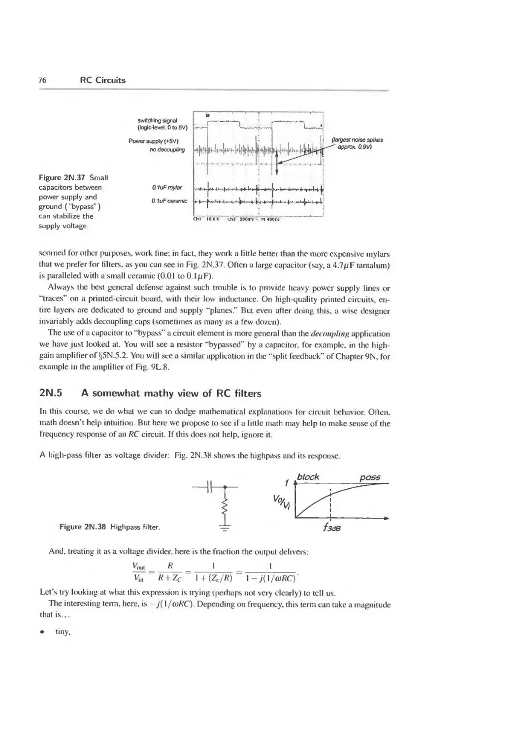
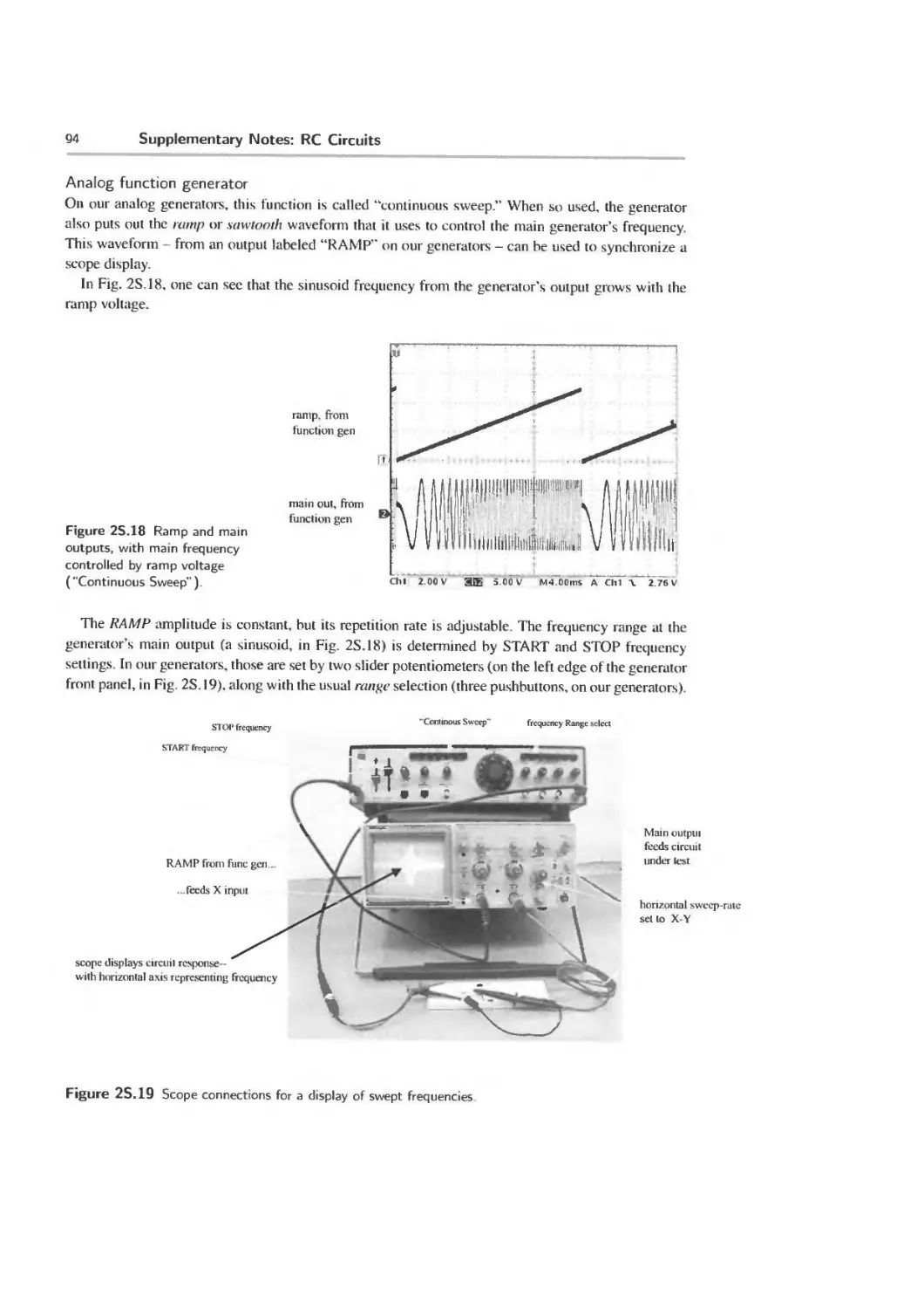
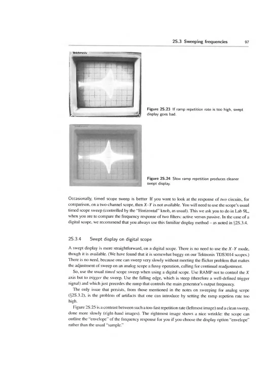
2S. 3 Sweeping frequencies 93
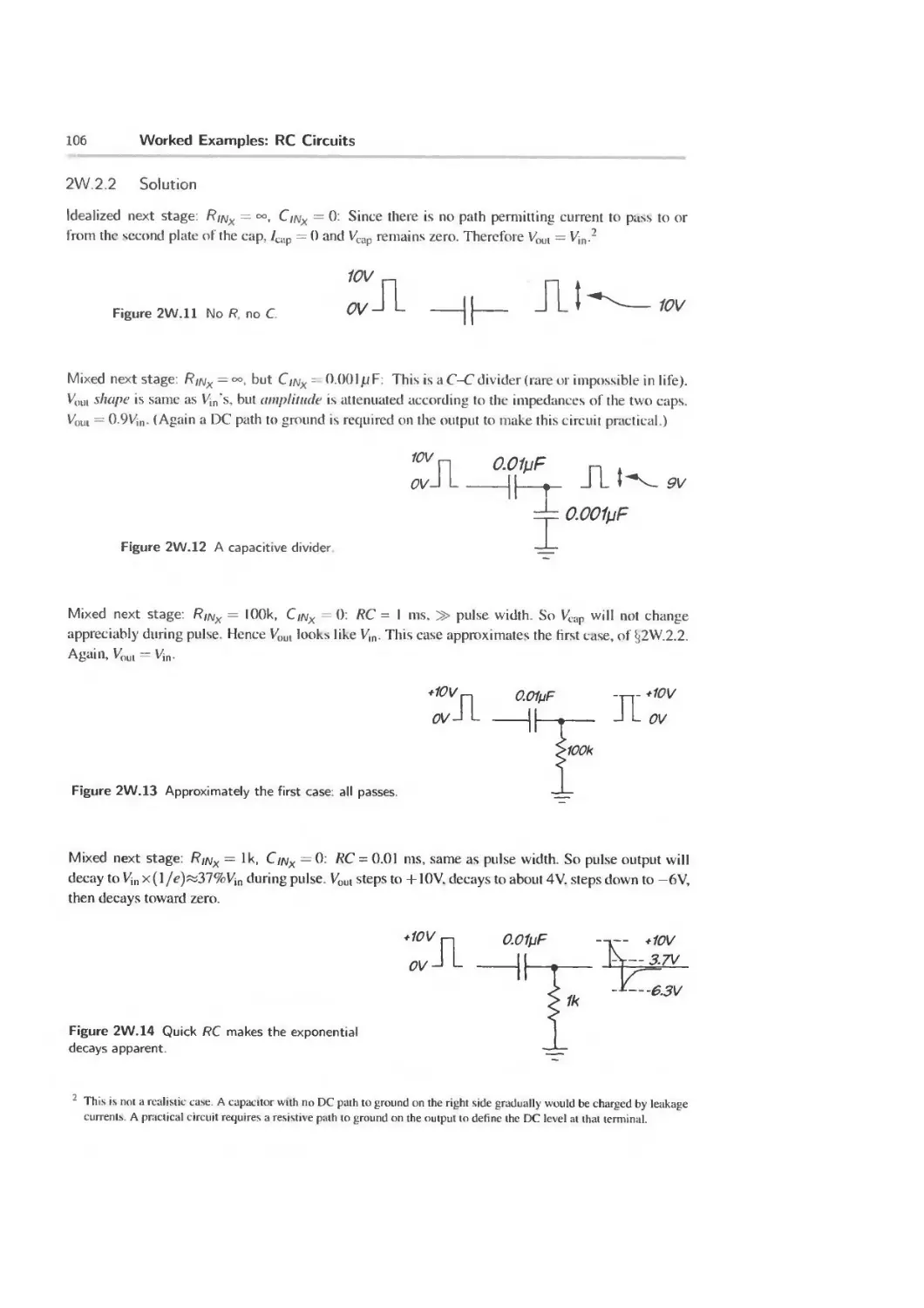
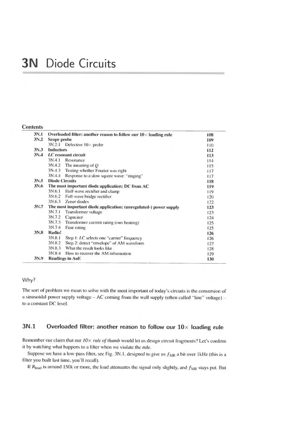
2W Worked Examples: RC Circuits 100
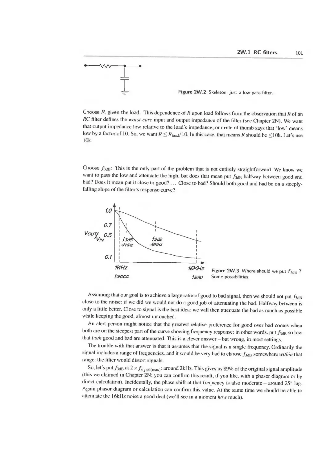
2W.1 RC filters 100
2W.2 RC step response 105
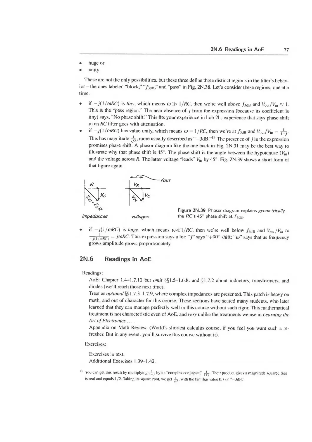
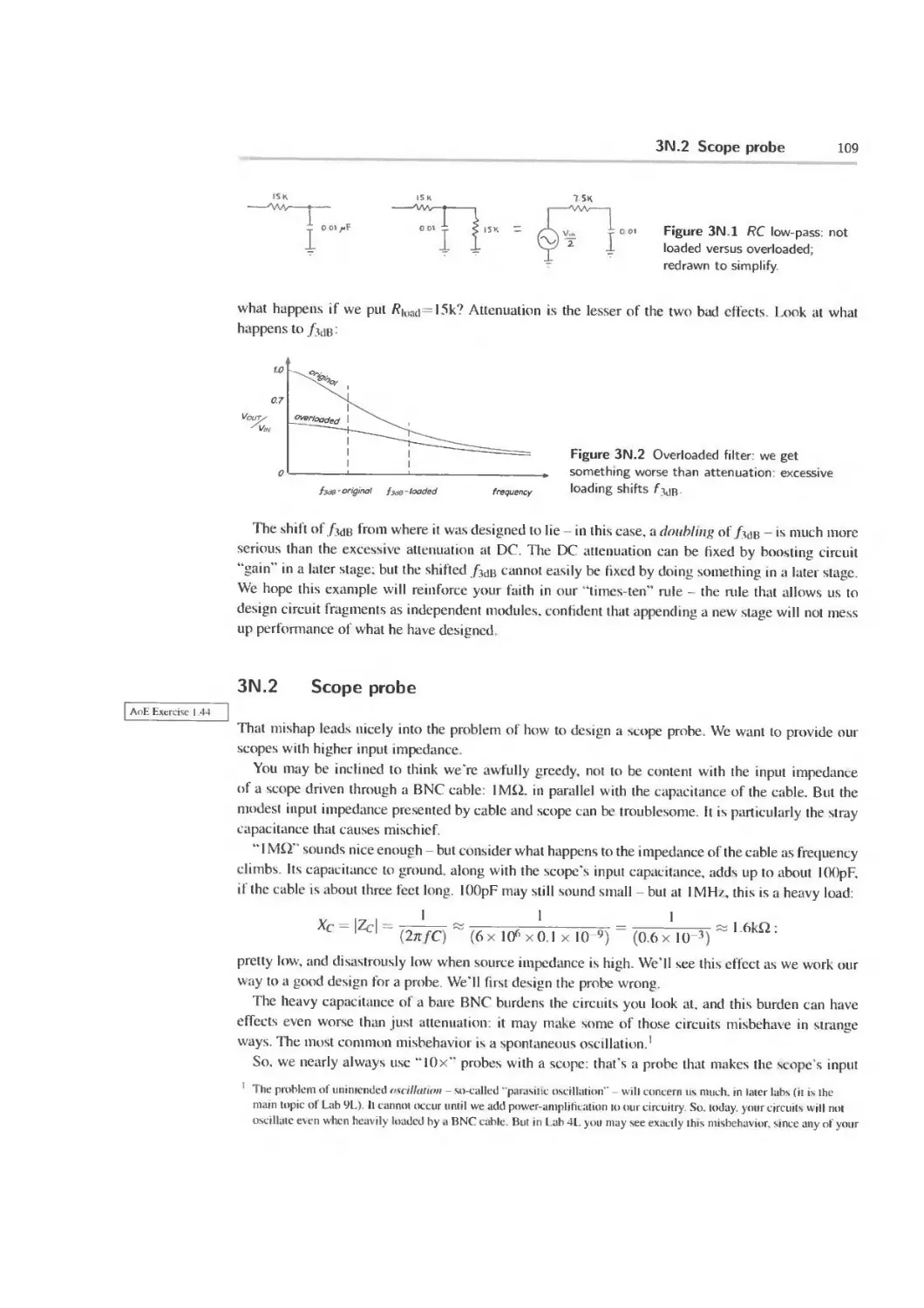
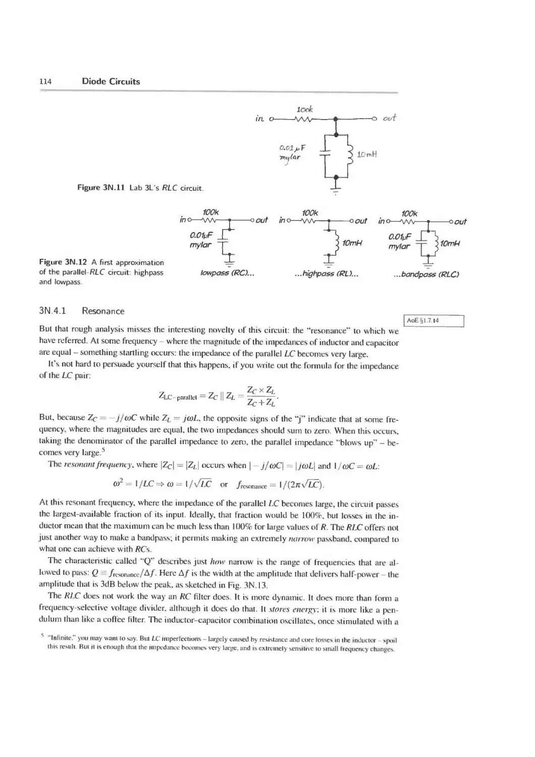
3N Diode Circuits 108
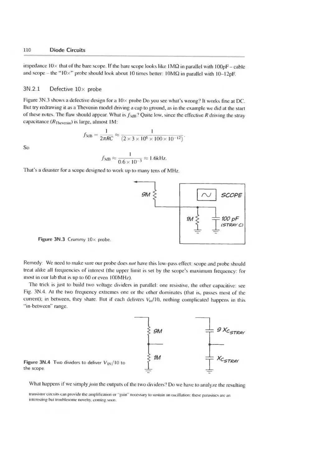
3N.1 Overloaded filter: another reason to follow our lOx loading rule 108
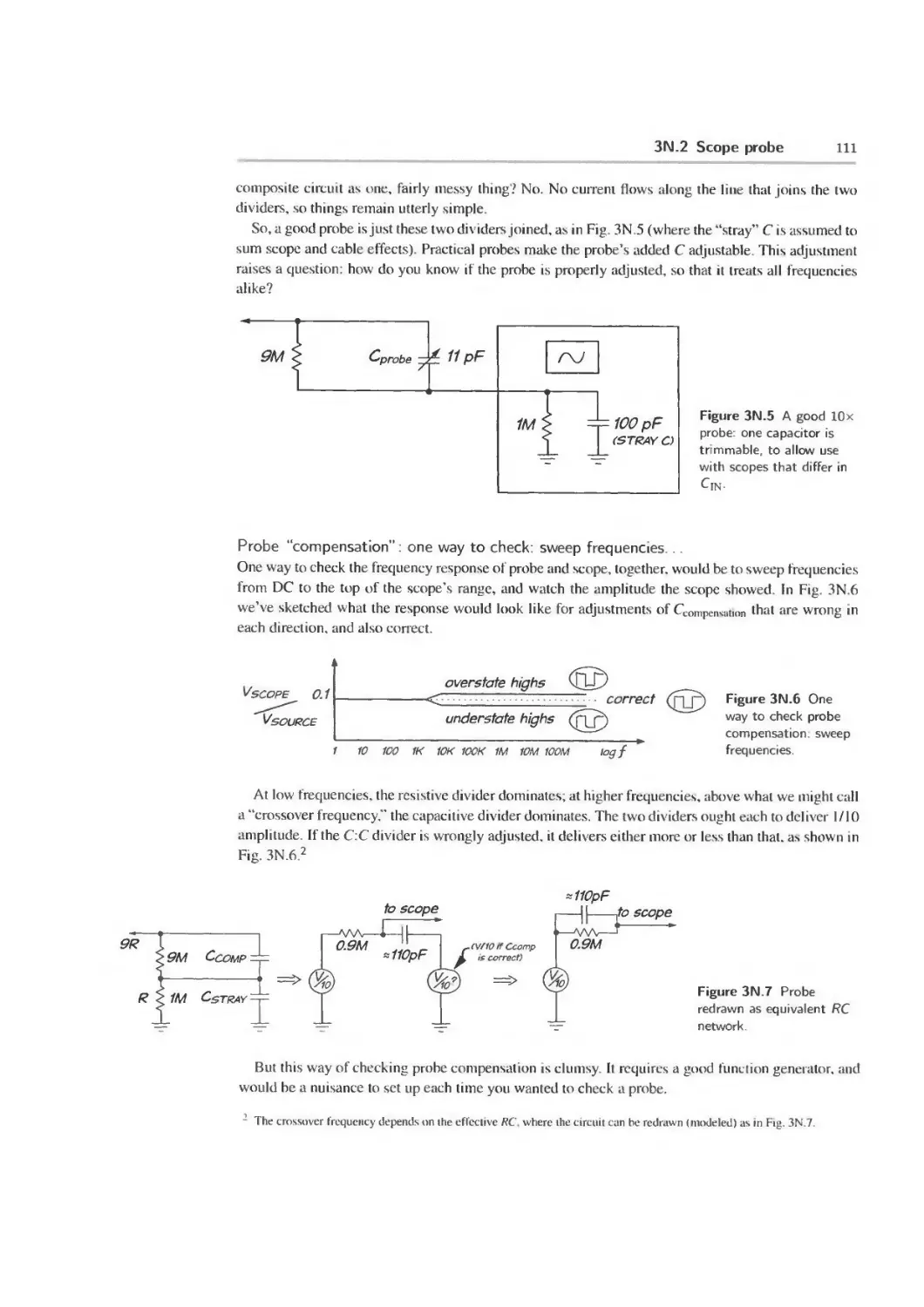
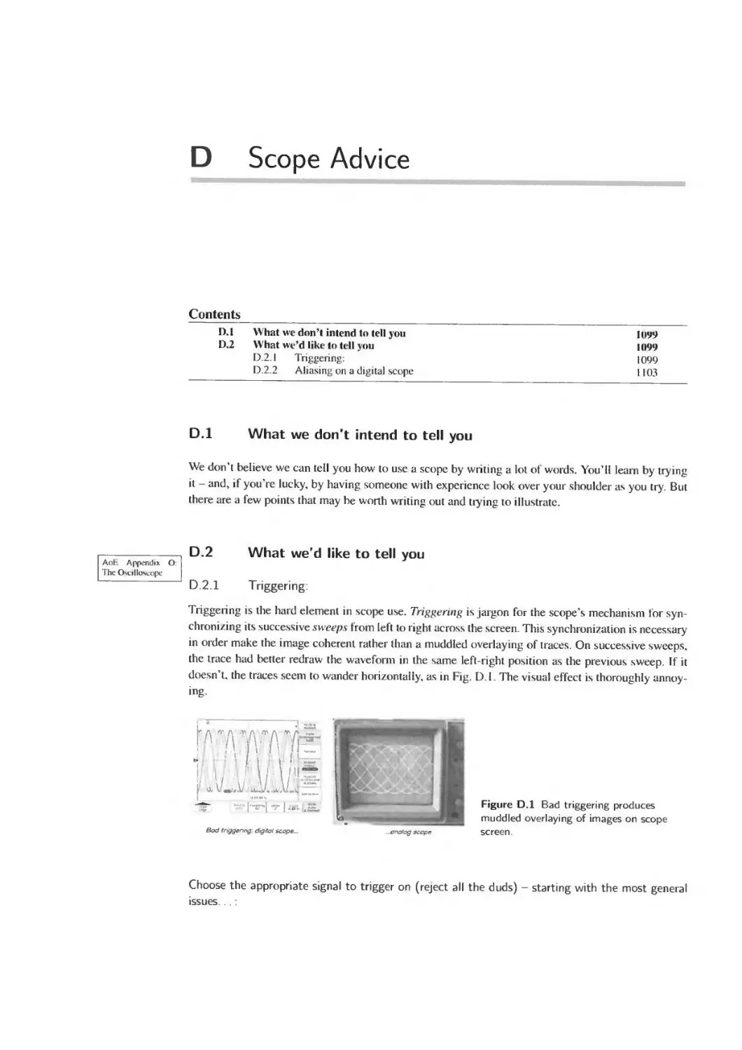
3N.2 Scope probe 109
3N.3 Inductors 112
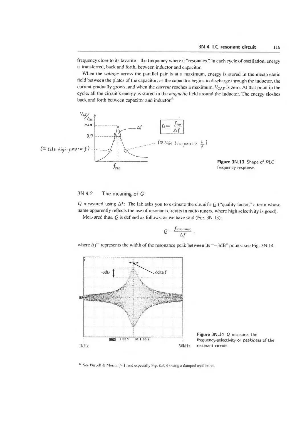
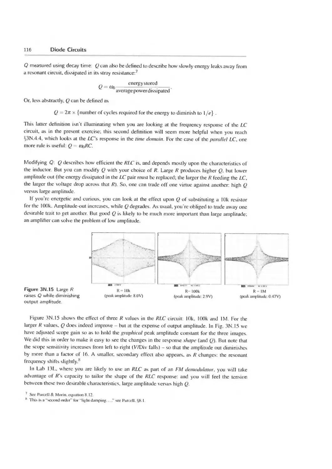
3N.4 LC resonant circuit 113
3N.5 Diode Circuits 118
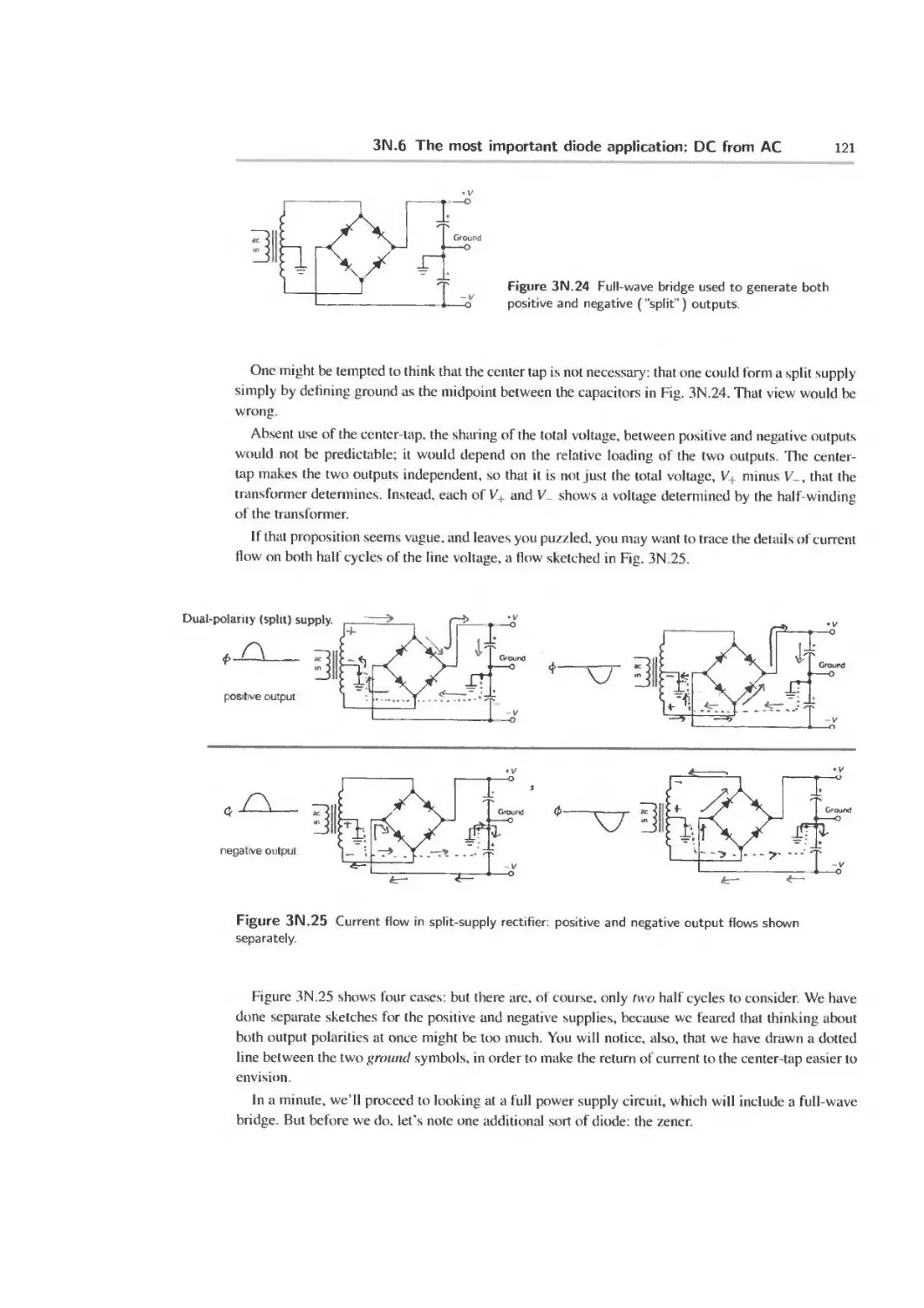
3N.6 The most important diode application: DC from AC 119
3N.7 The most important diode application: (unregulated-) power supply 123
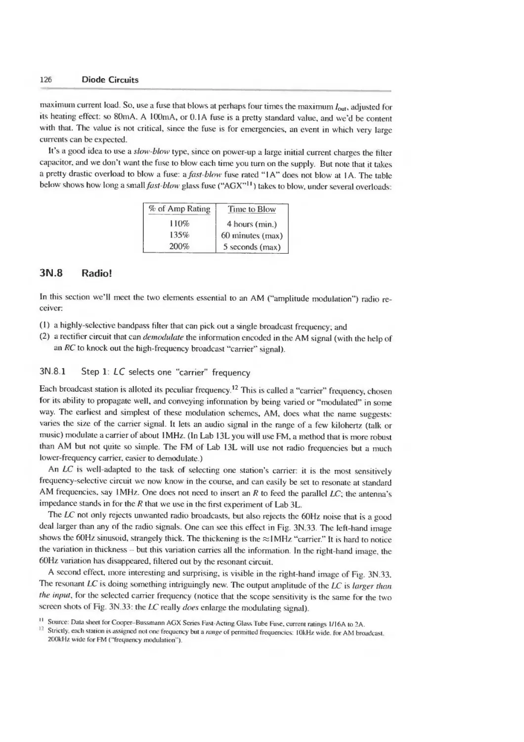
3N.8 Radio! 126
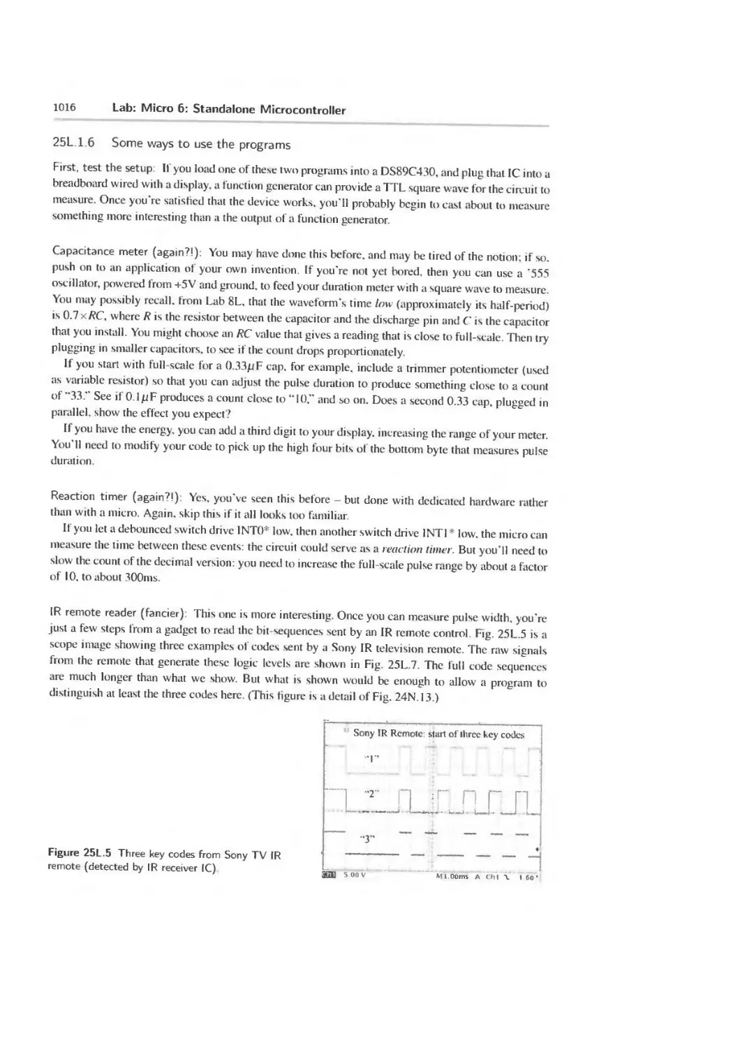
3N.9 Readings in AoE 130
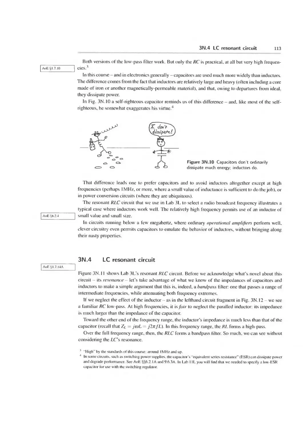
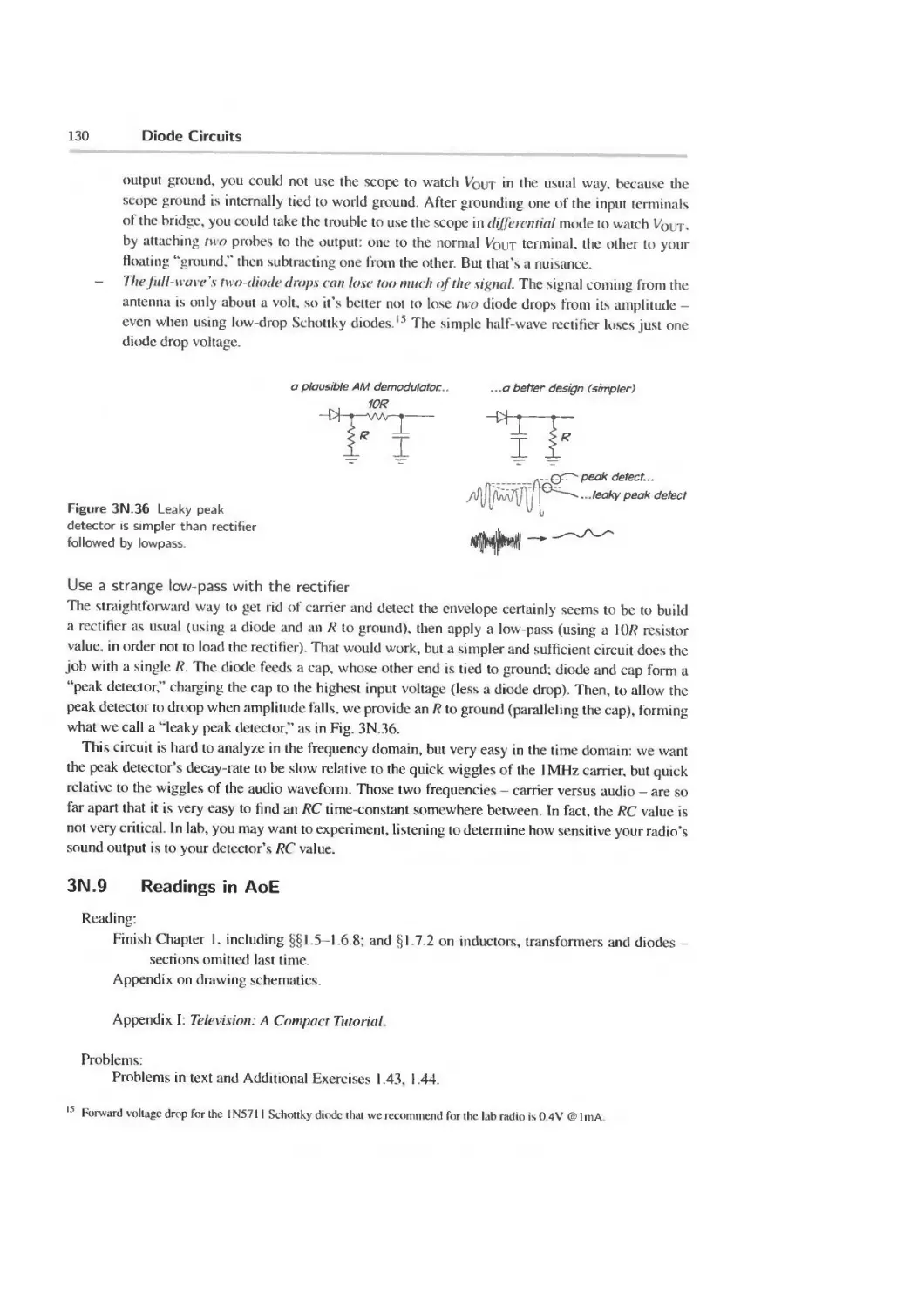
3L Lab: Diode Circuits 131
3L. 1 LC resonant circuit 131
3L.2 Half-wave rectifier 133
3L.3 Full-wave bridge rectifier 134
3L.4 Design exercise: AM radio receiver (fun!) 135
3L.5 Signal diodes 136
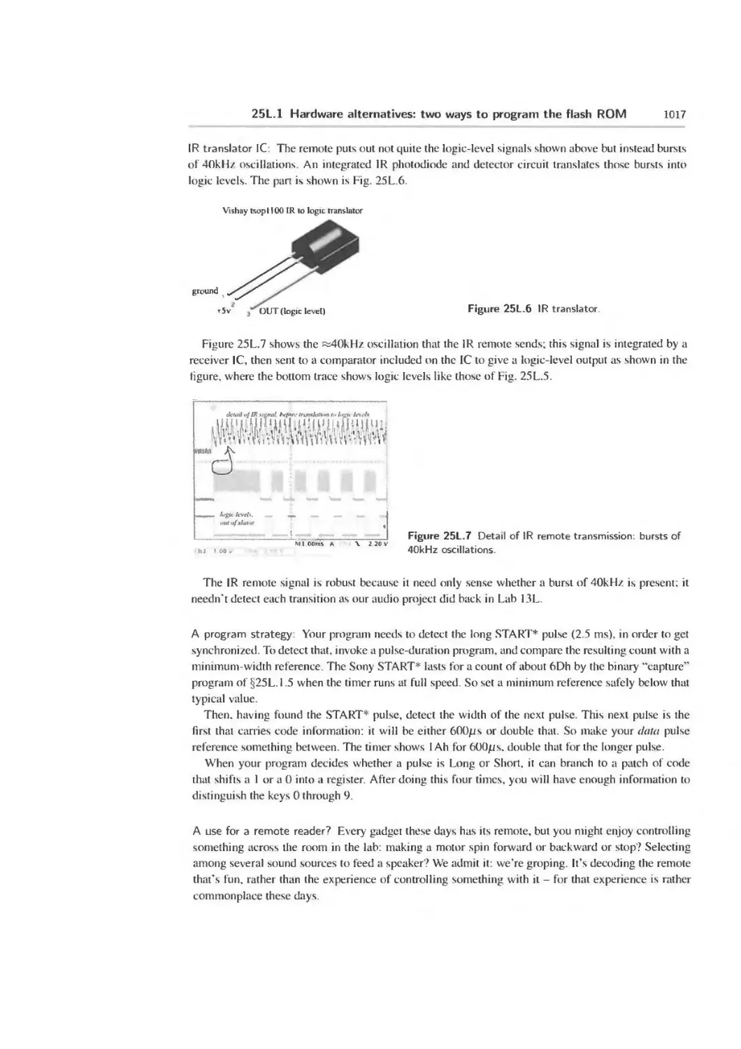
3S Supplementary Notes and Jargon: Diode Circuits 138
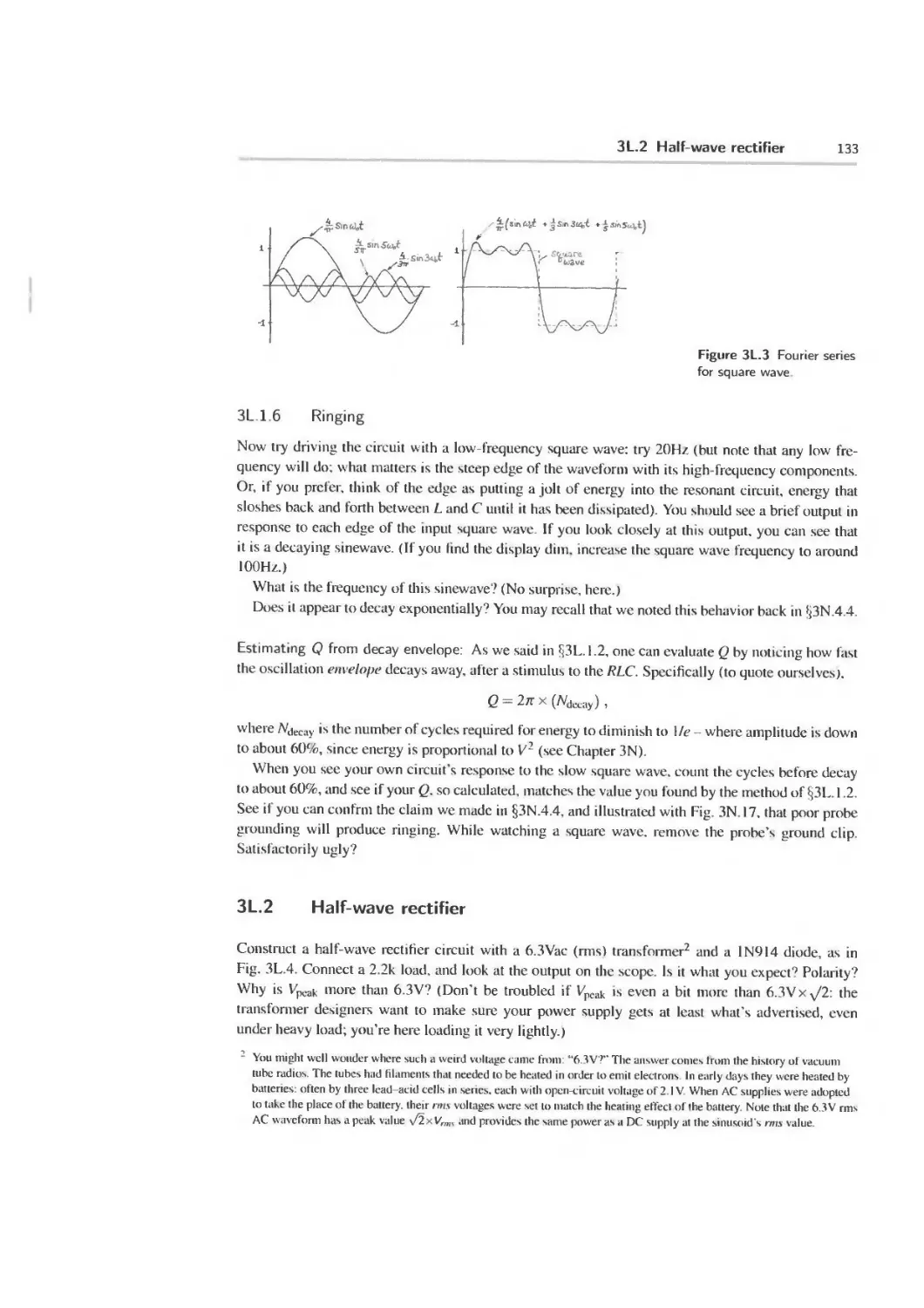
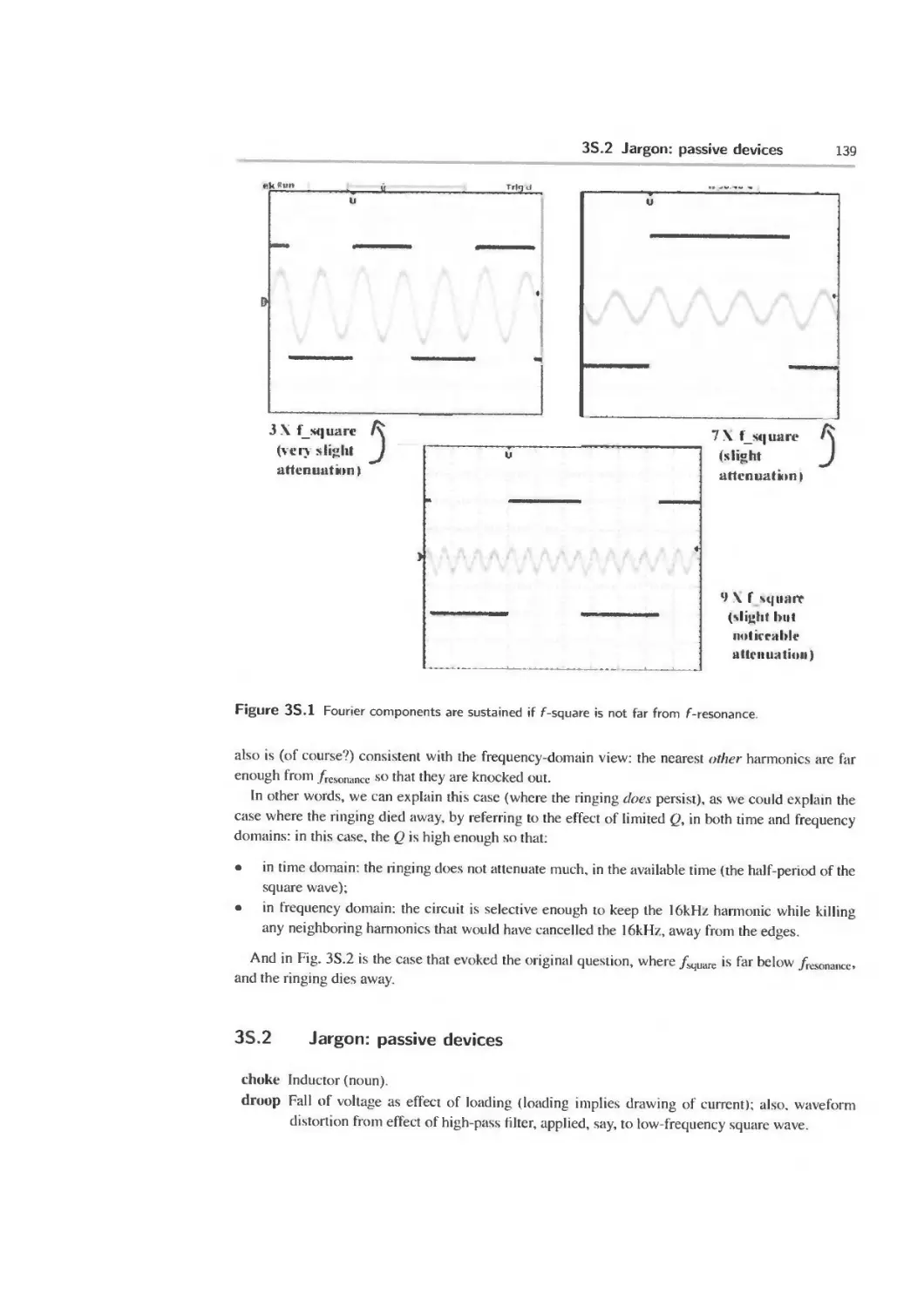
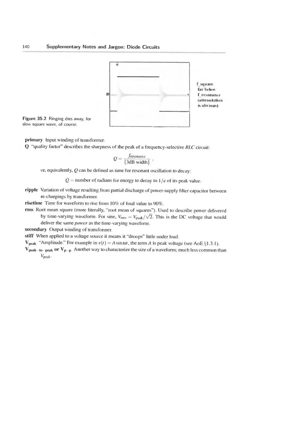
3S. 1 A puzzle: why LC’s ringing dies away despite Fourier 138
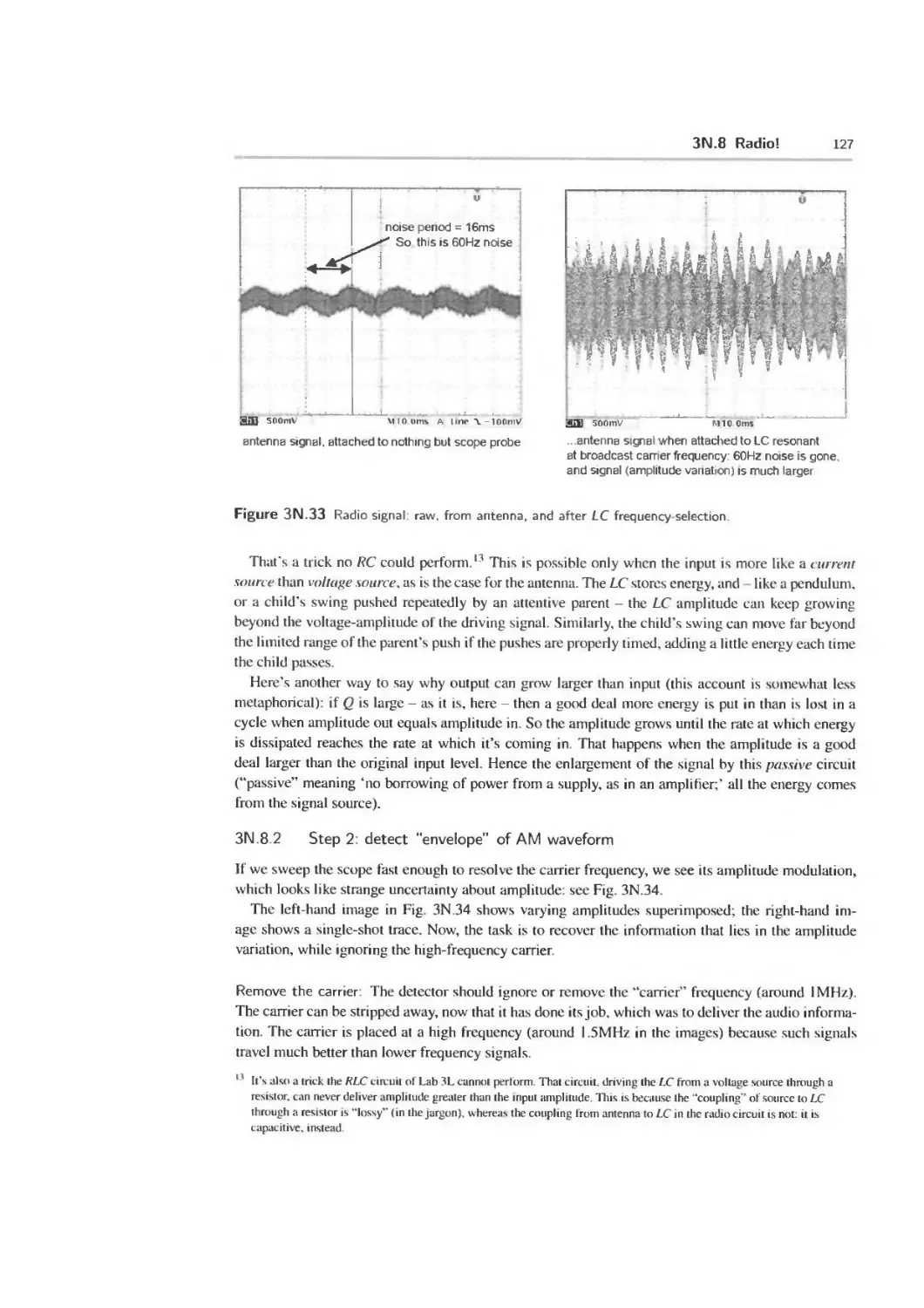
3S. 2 Jargon: passive devices 139
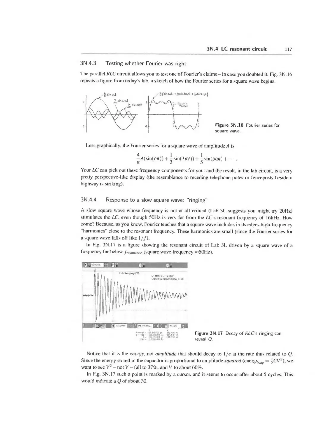
3W Worked Examples: Diode Circuits 141
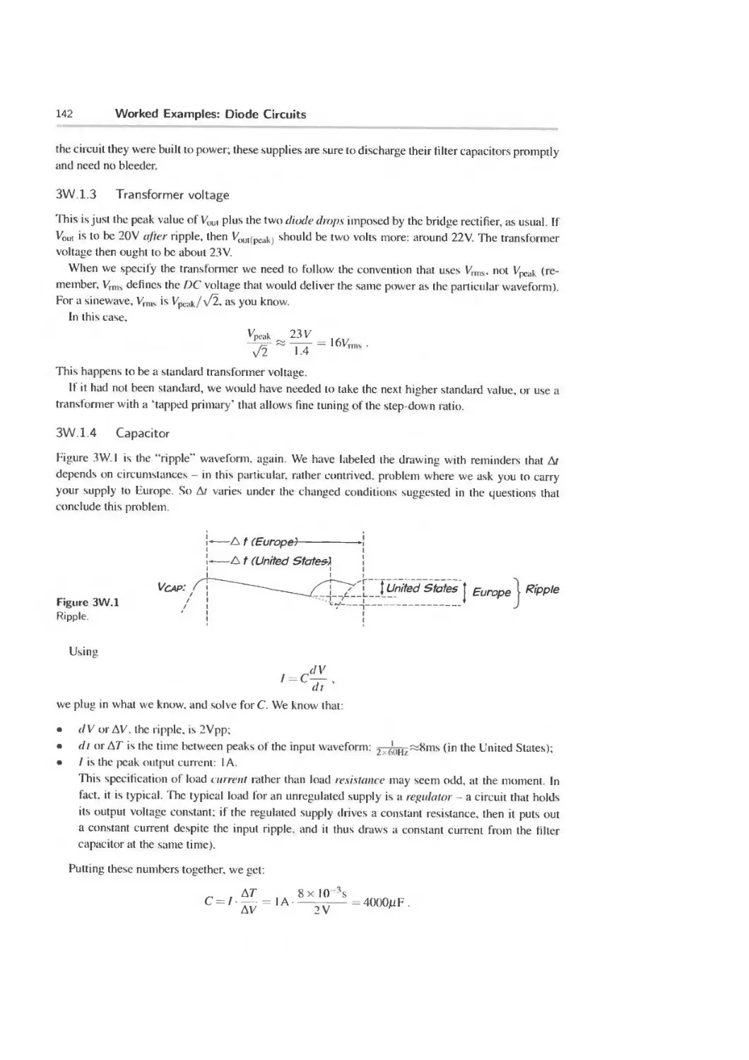
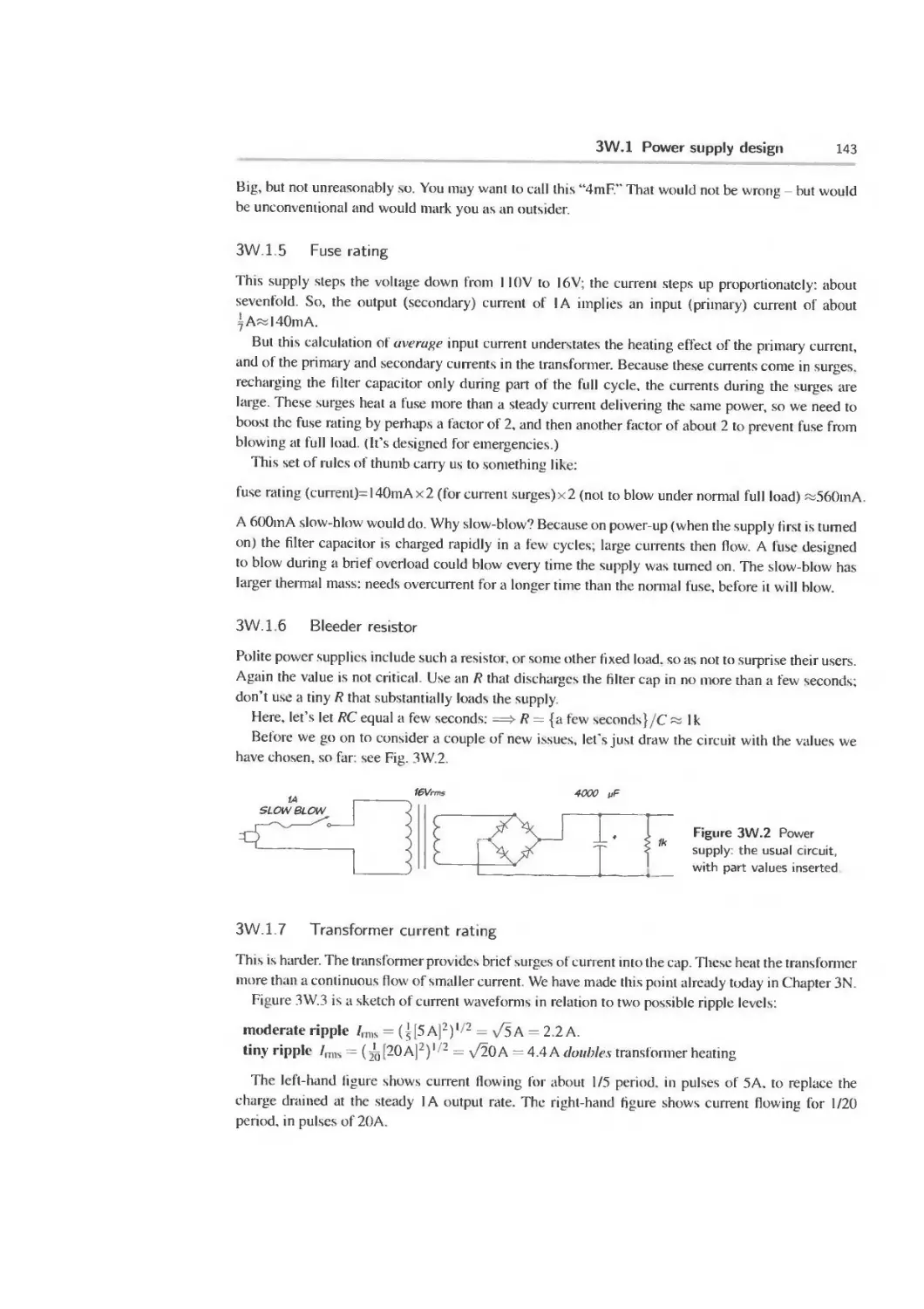
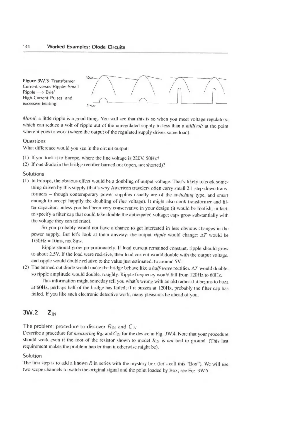
3W. 1 Power supply design 141
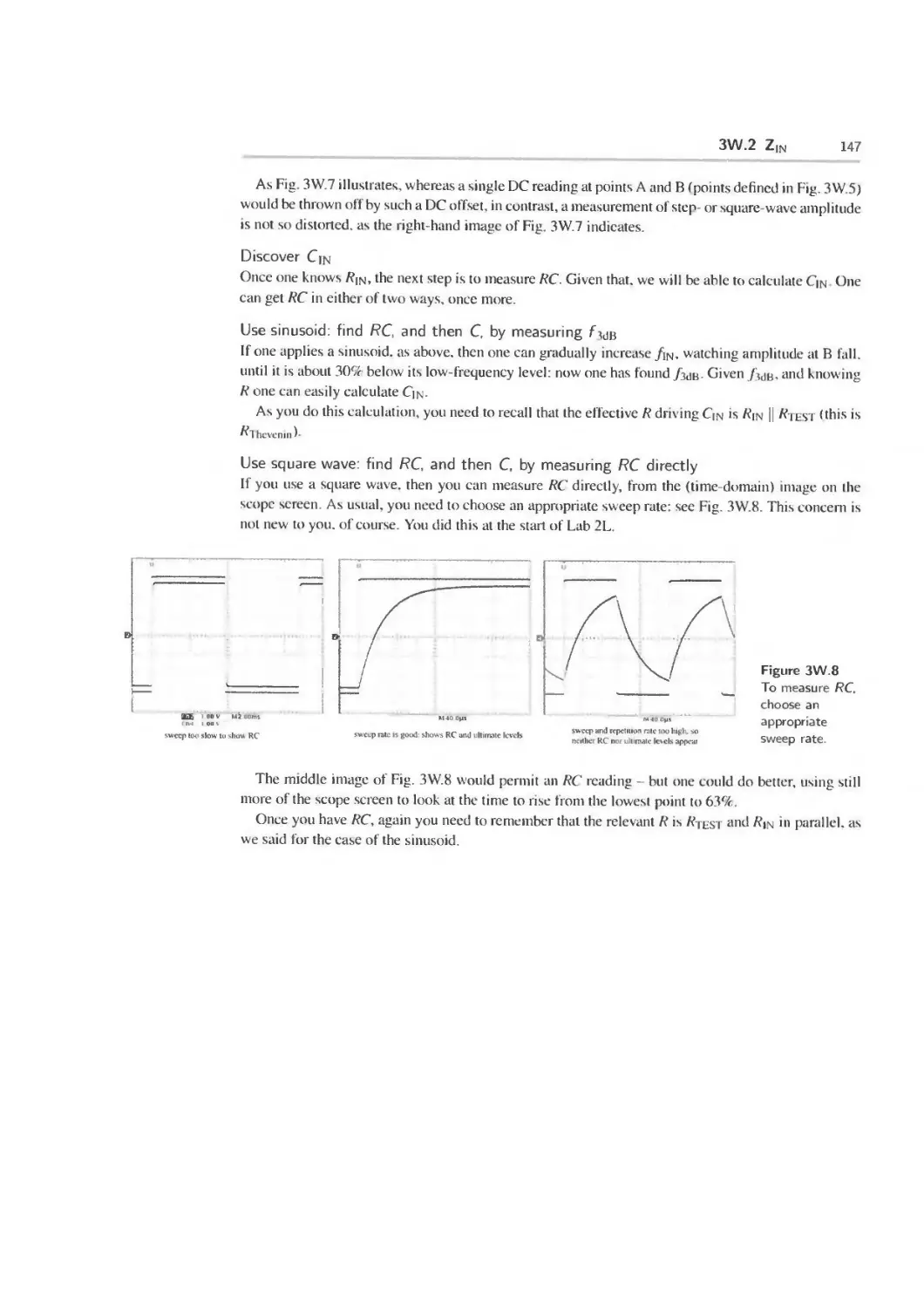
3W.2 Zin 144
Part II Analog: Discrete Transistors 149
4N Transistors I 151
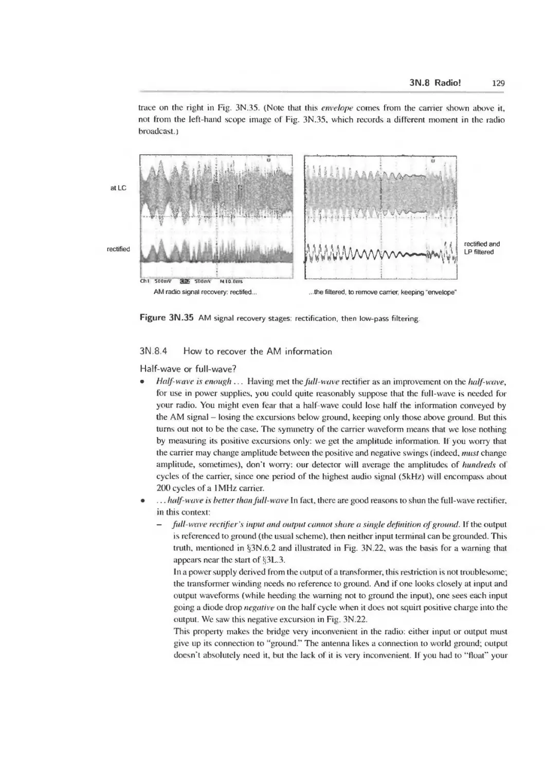
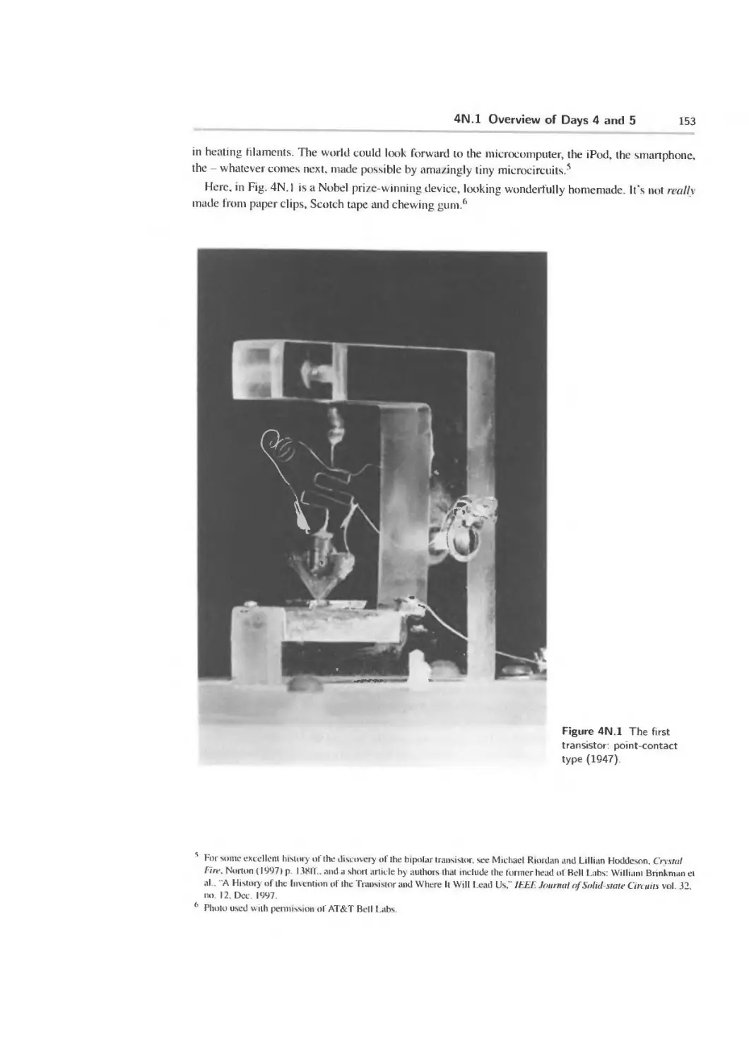
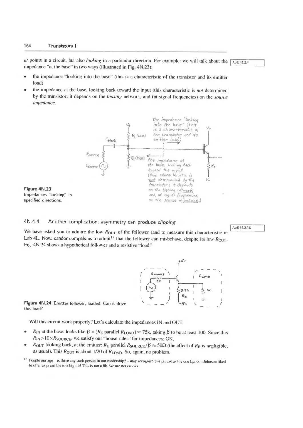
4N. 1 Overview of Days 4 and 5 151
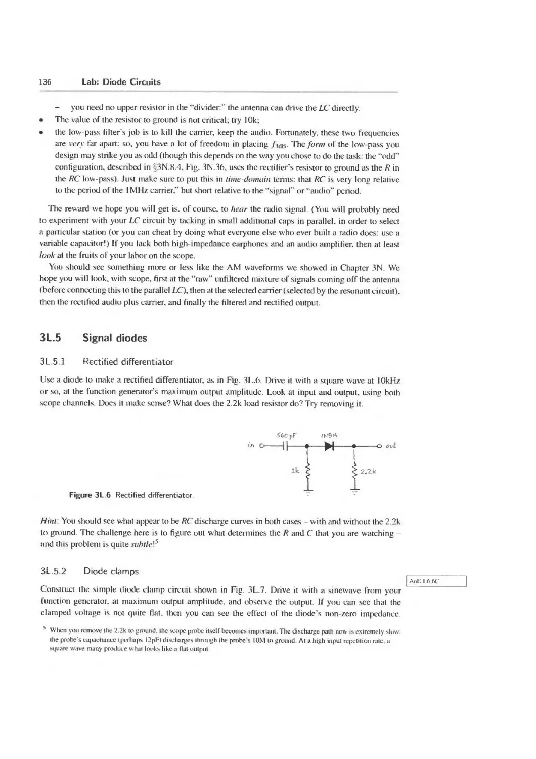
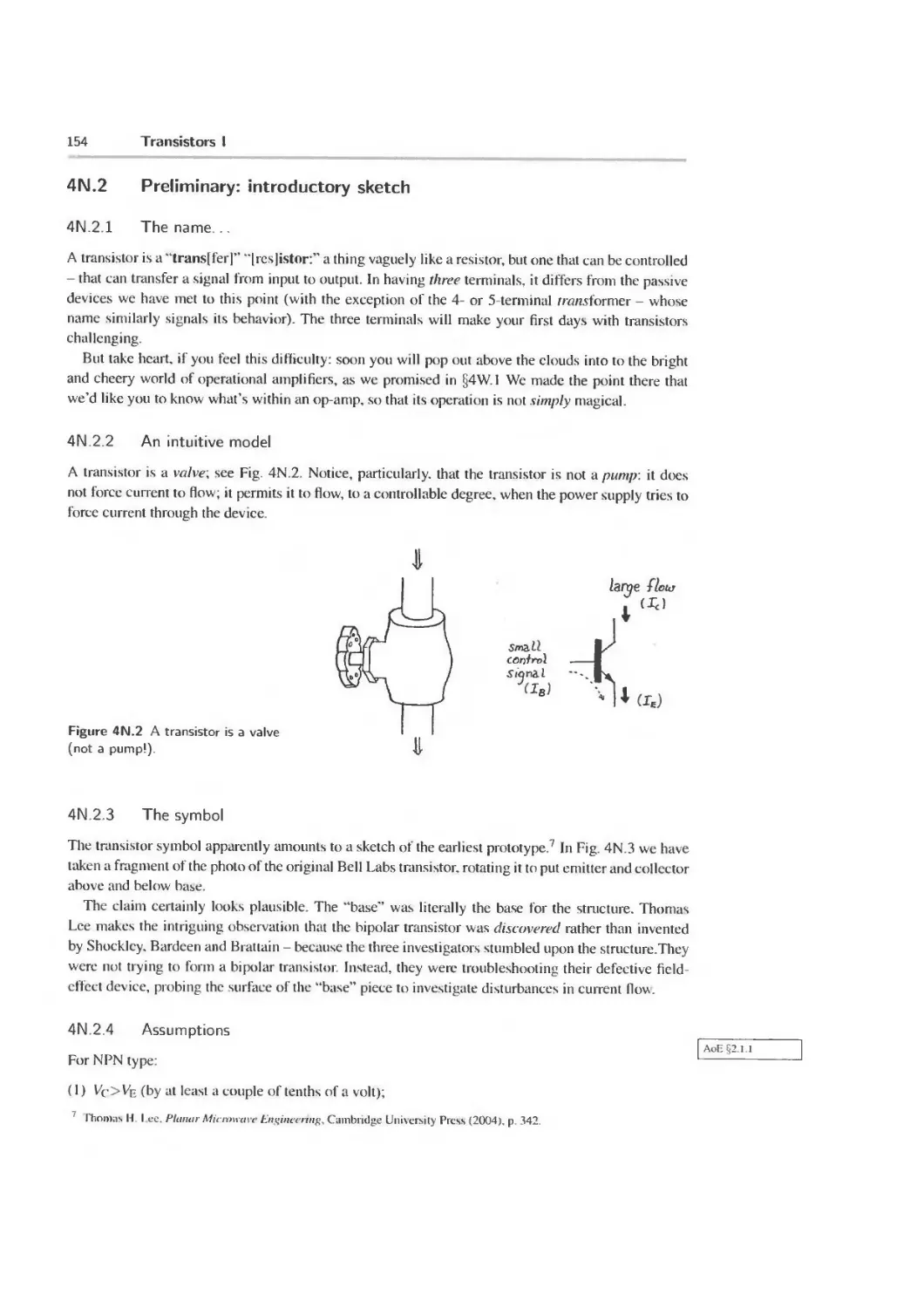
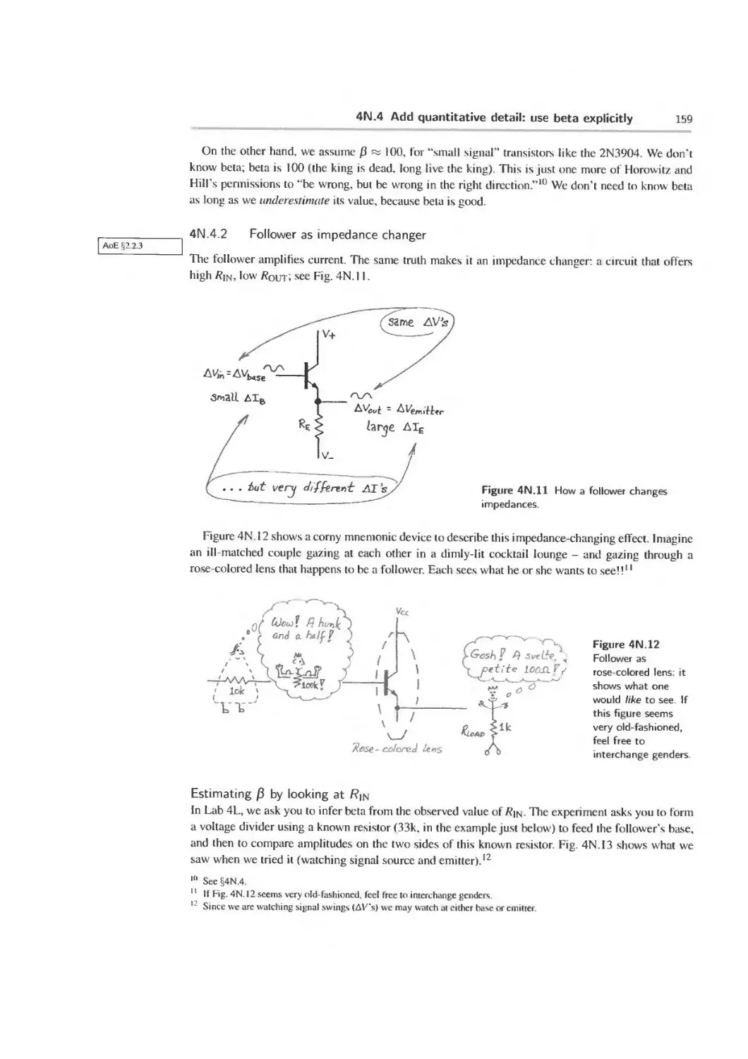
4N.2 Preliminary: introductory sketch 154
Contents
ix
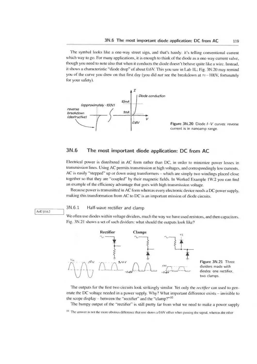
4N.3 The simplest view: forgetting beta 155
4N.4 Add quantitative detail: use beta explicitly 158
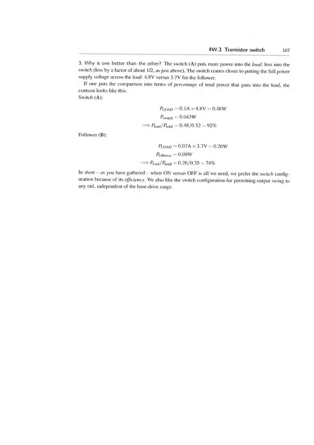
4N.5 A strikingly different transistor circuit: the switch 166
4N.6 Recapitulation: the important transistor circuits at a glance 167
4N.7 AoE Reading 168
4L Lab: Transistors 1 169
4L.1 Transistor preliminaries: look at devices out of circuit 169
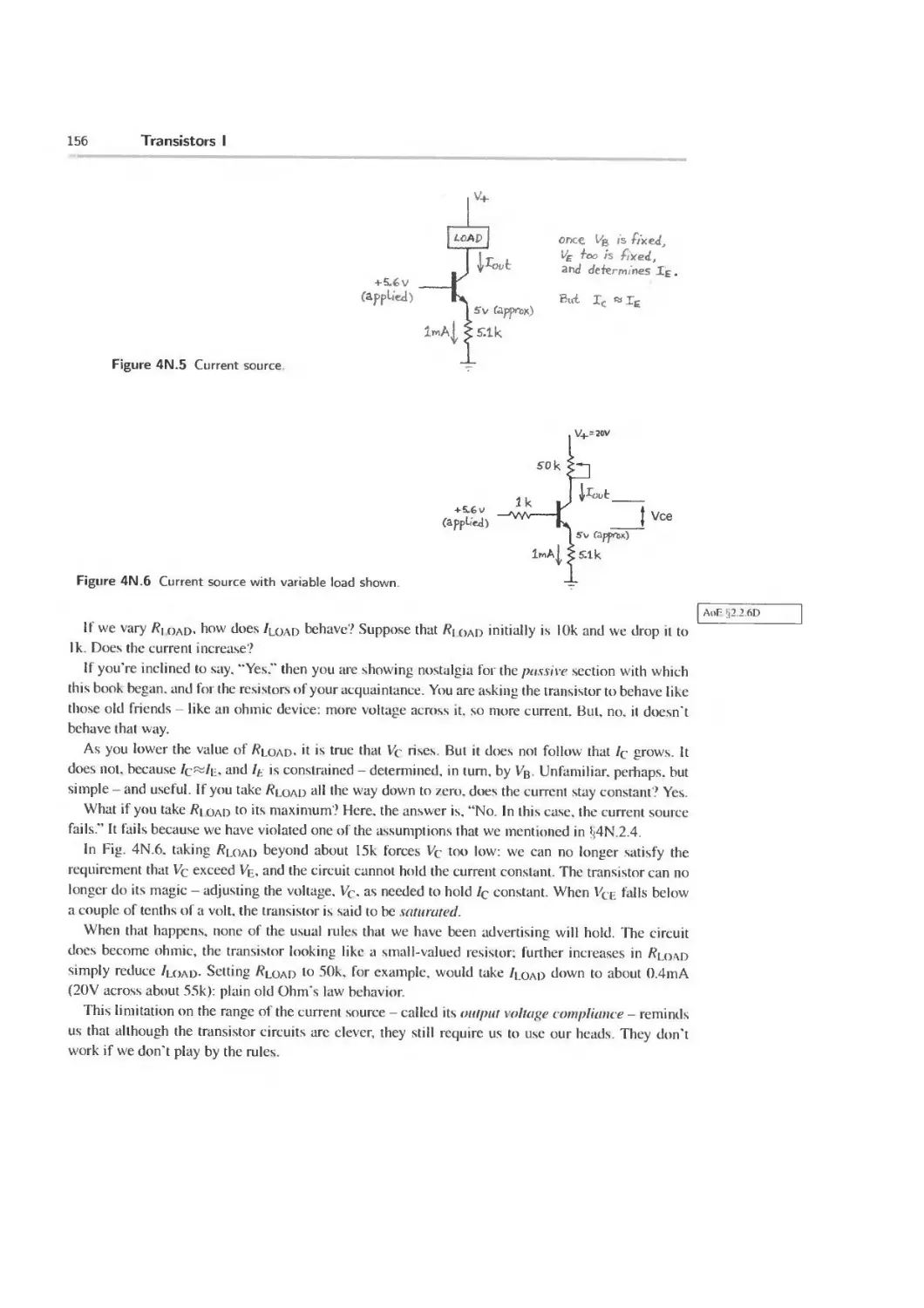
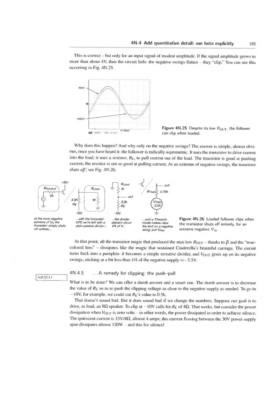
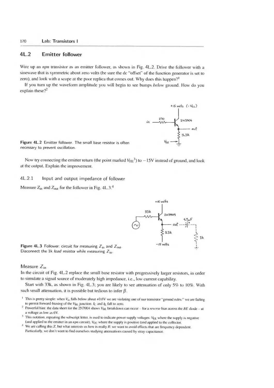
4L.2 Emitter follower 170
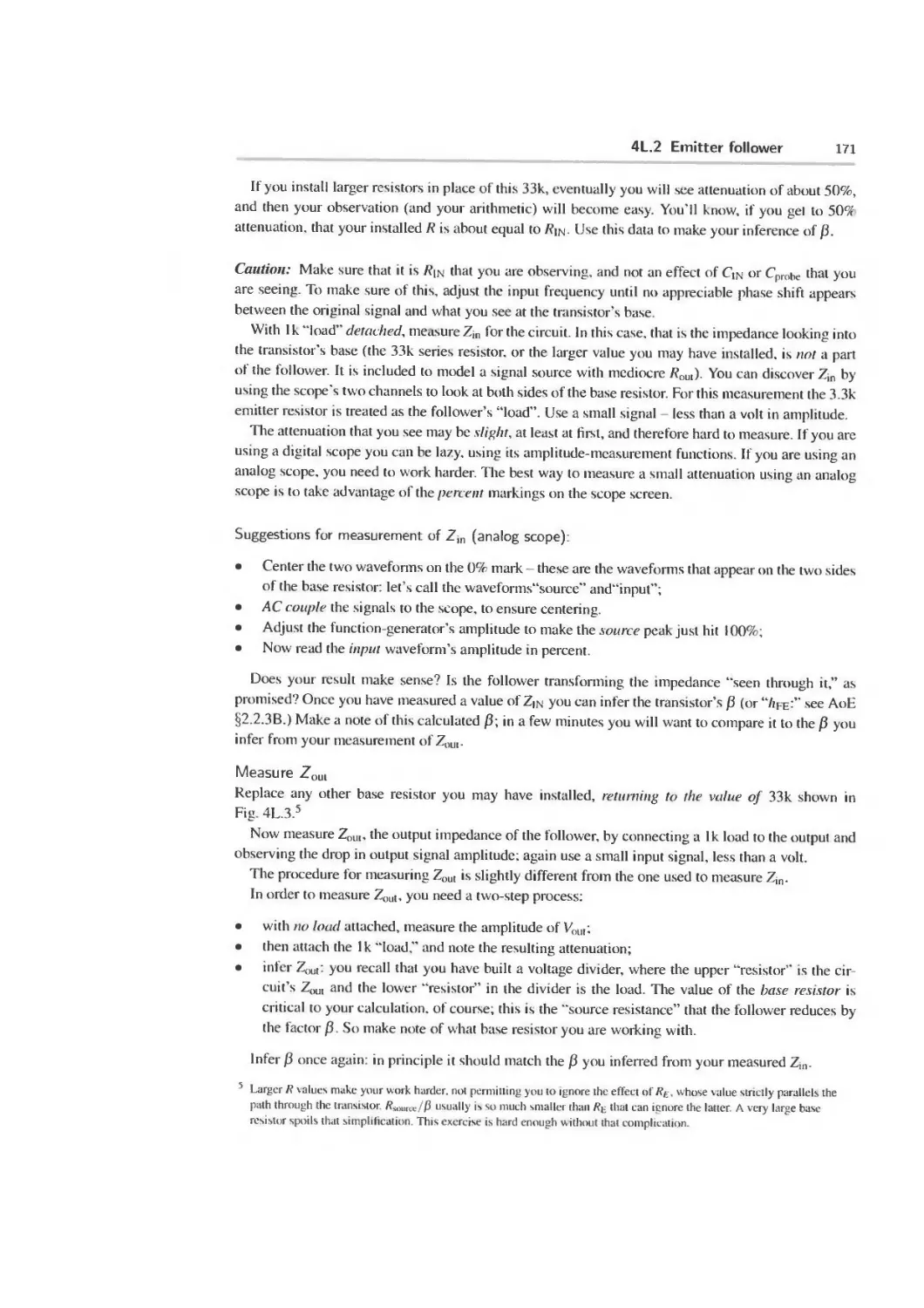
4L.3 Current source 172
4L.4 Common-emitter amplifier 172
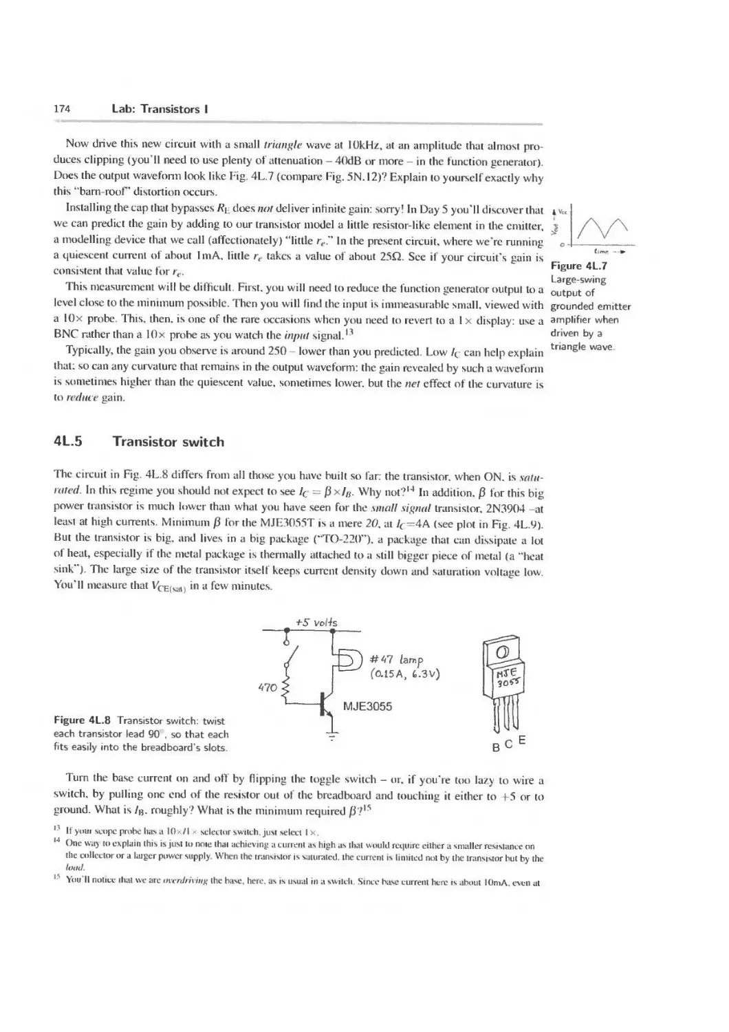
4L.5 Transistor switch 174
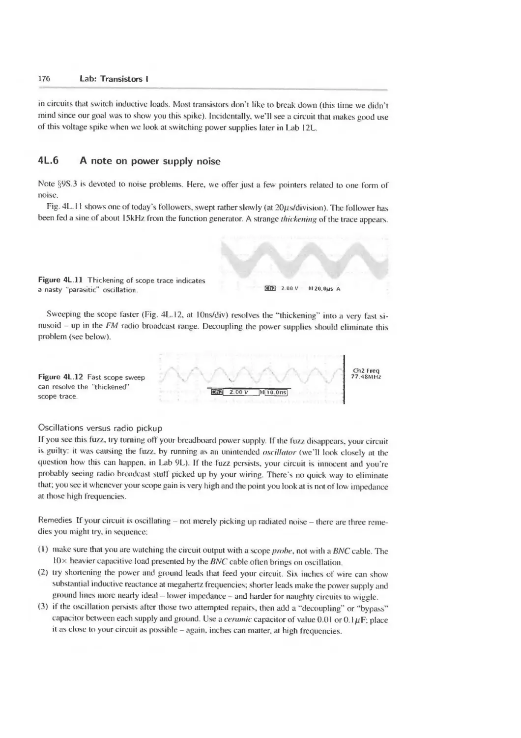
4L.6 A note on power supply noise 176
4W Worked Examples: Transistors 1 178
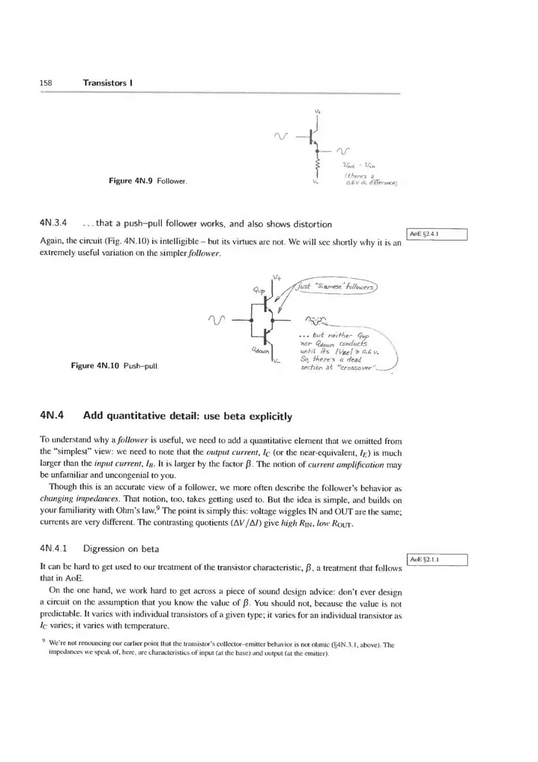
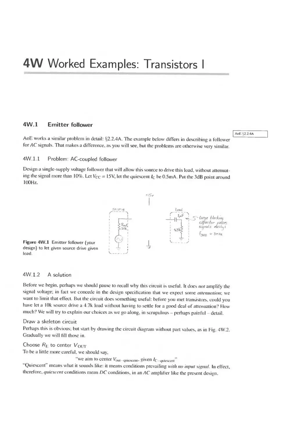
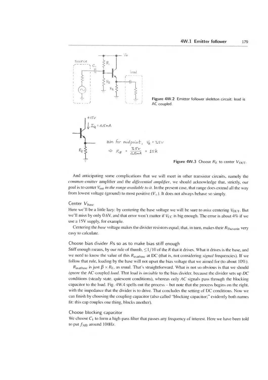
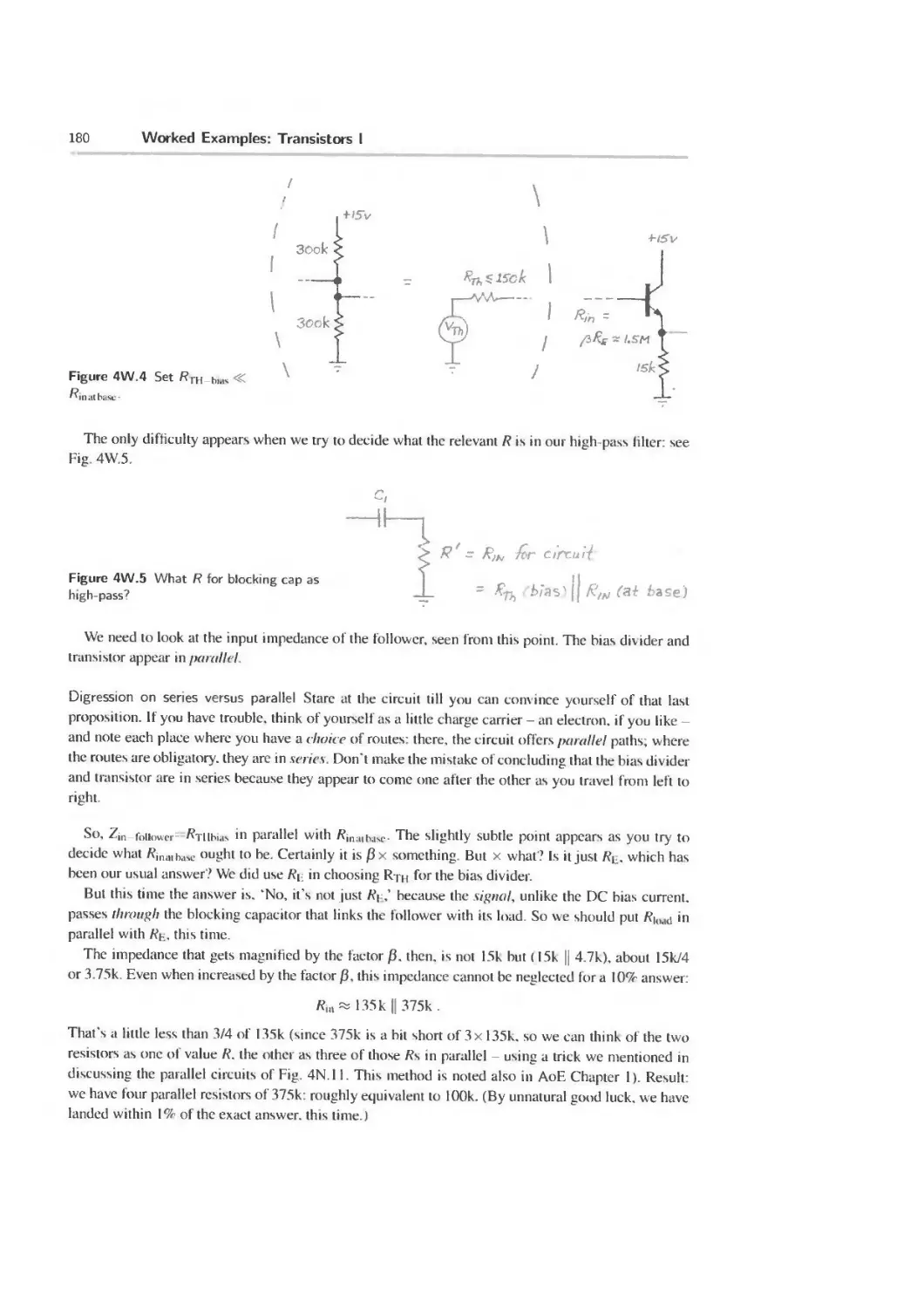
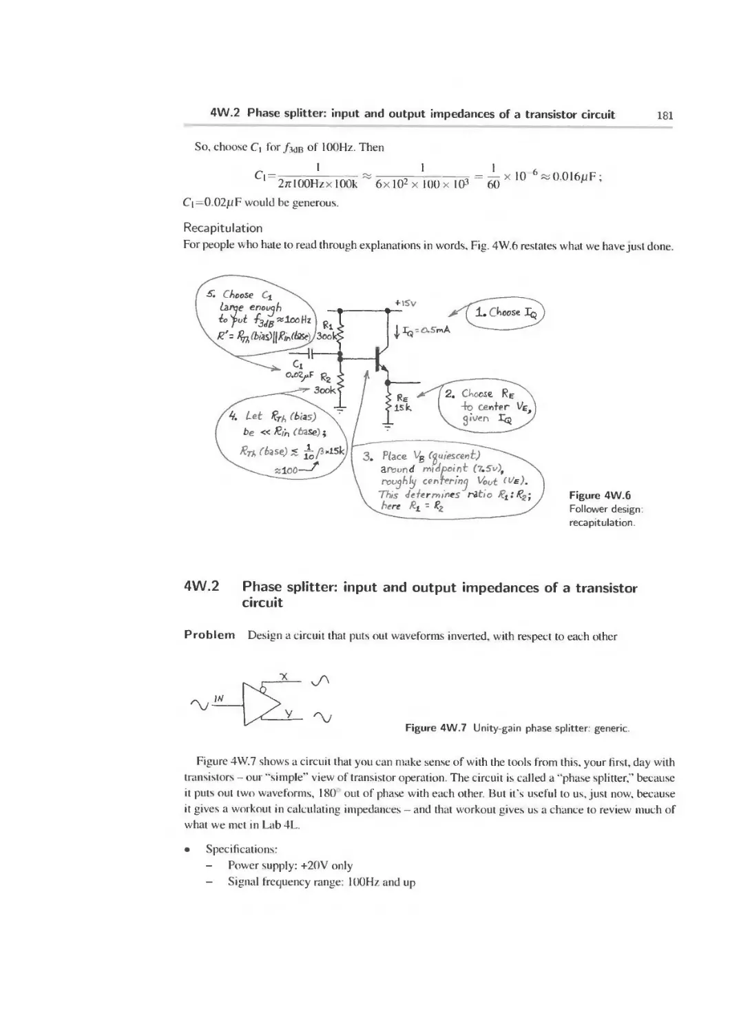
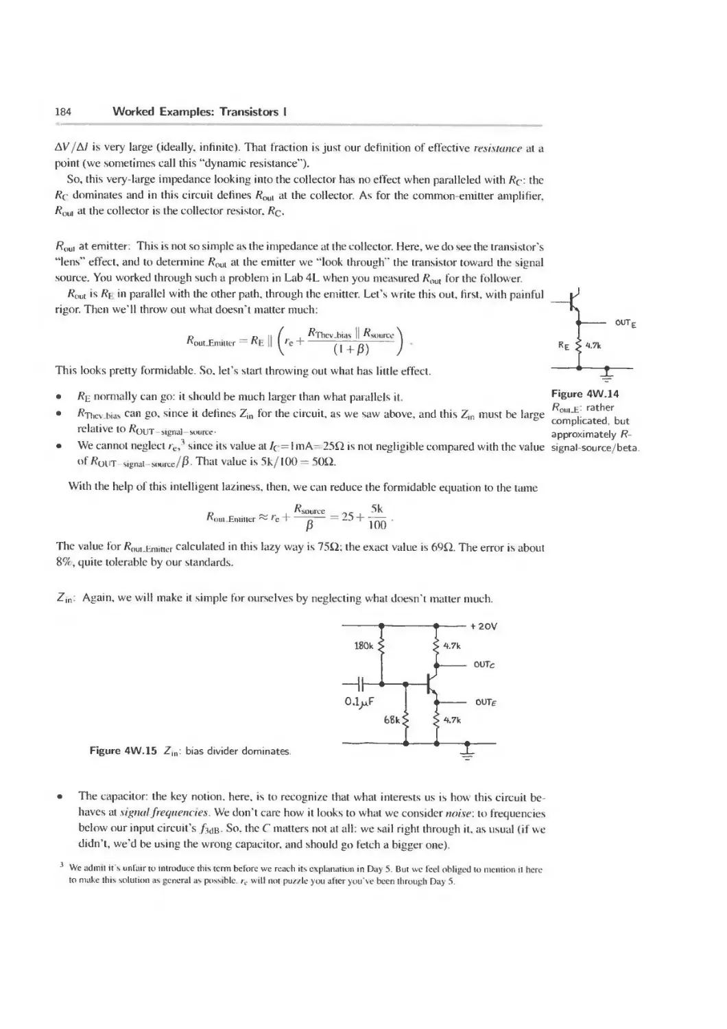
4W 1 Emitter follower 178
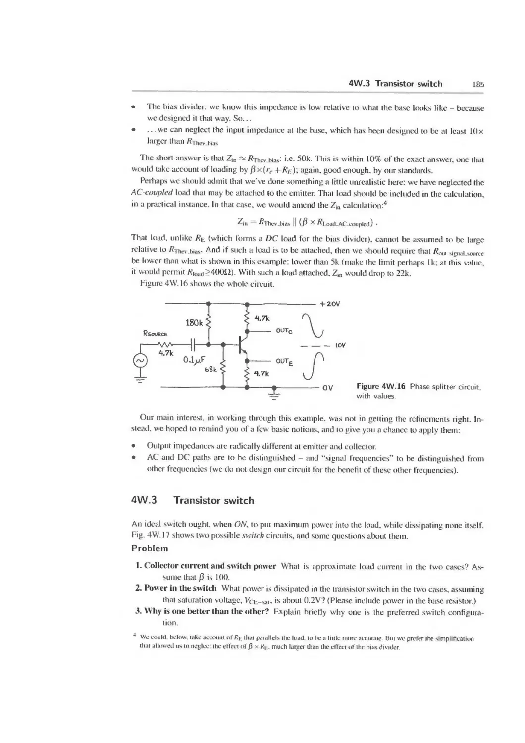
4W.2 Phase splitter: input and output impedances of a transistor circuit 181
4W.3 Transistor switch 185
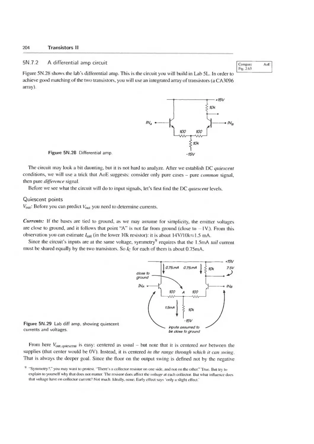
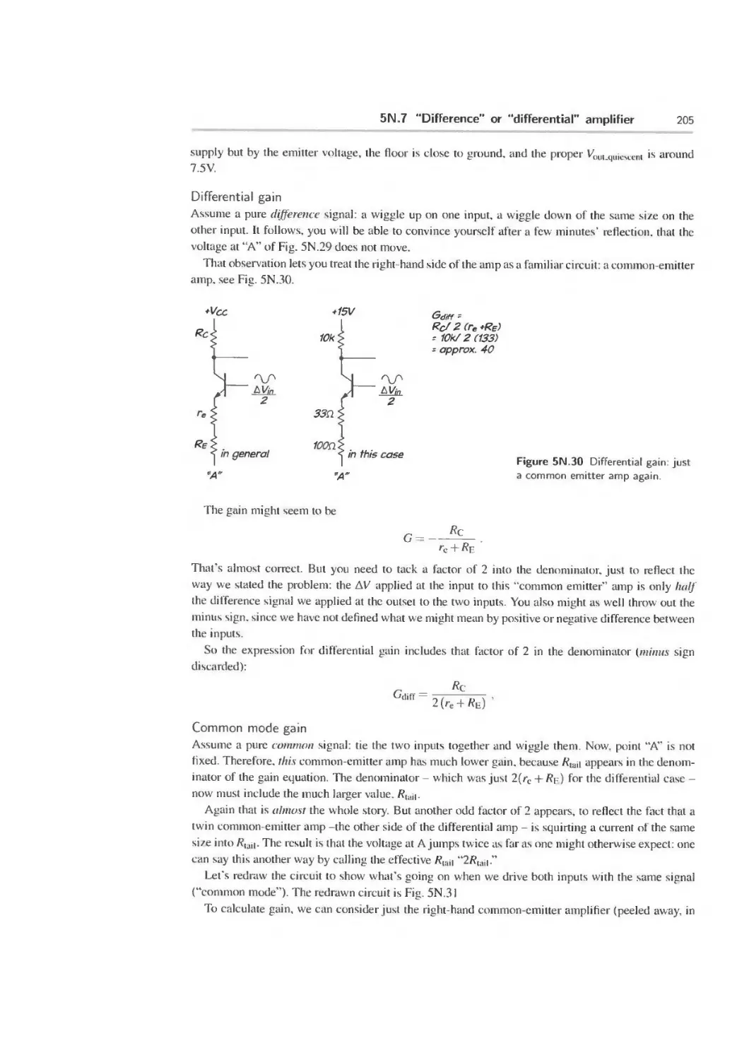
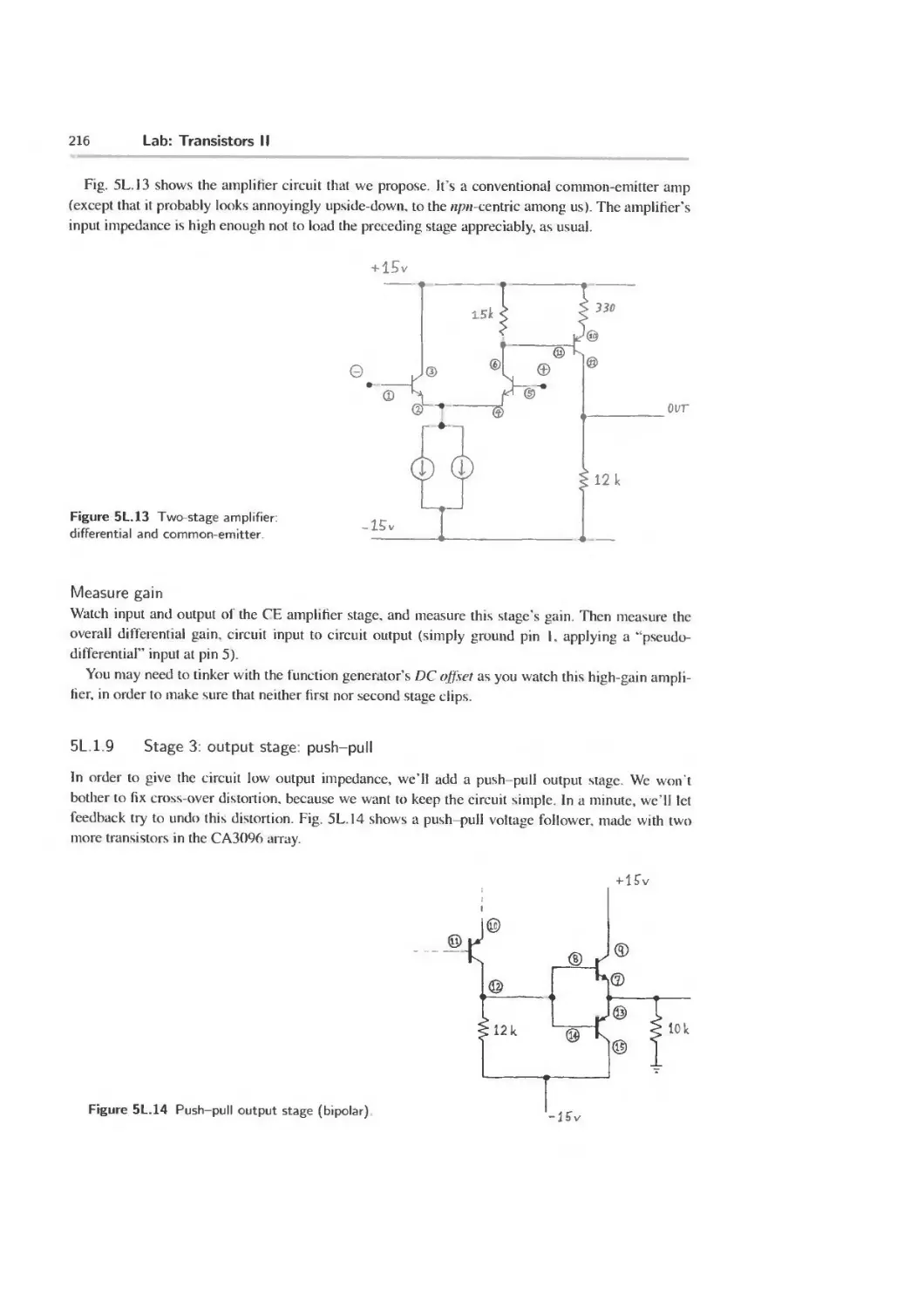
5N Transistors II 188
5N. 1 Some novelty, but the earlier view of transistors still holds 188
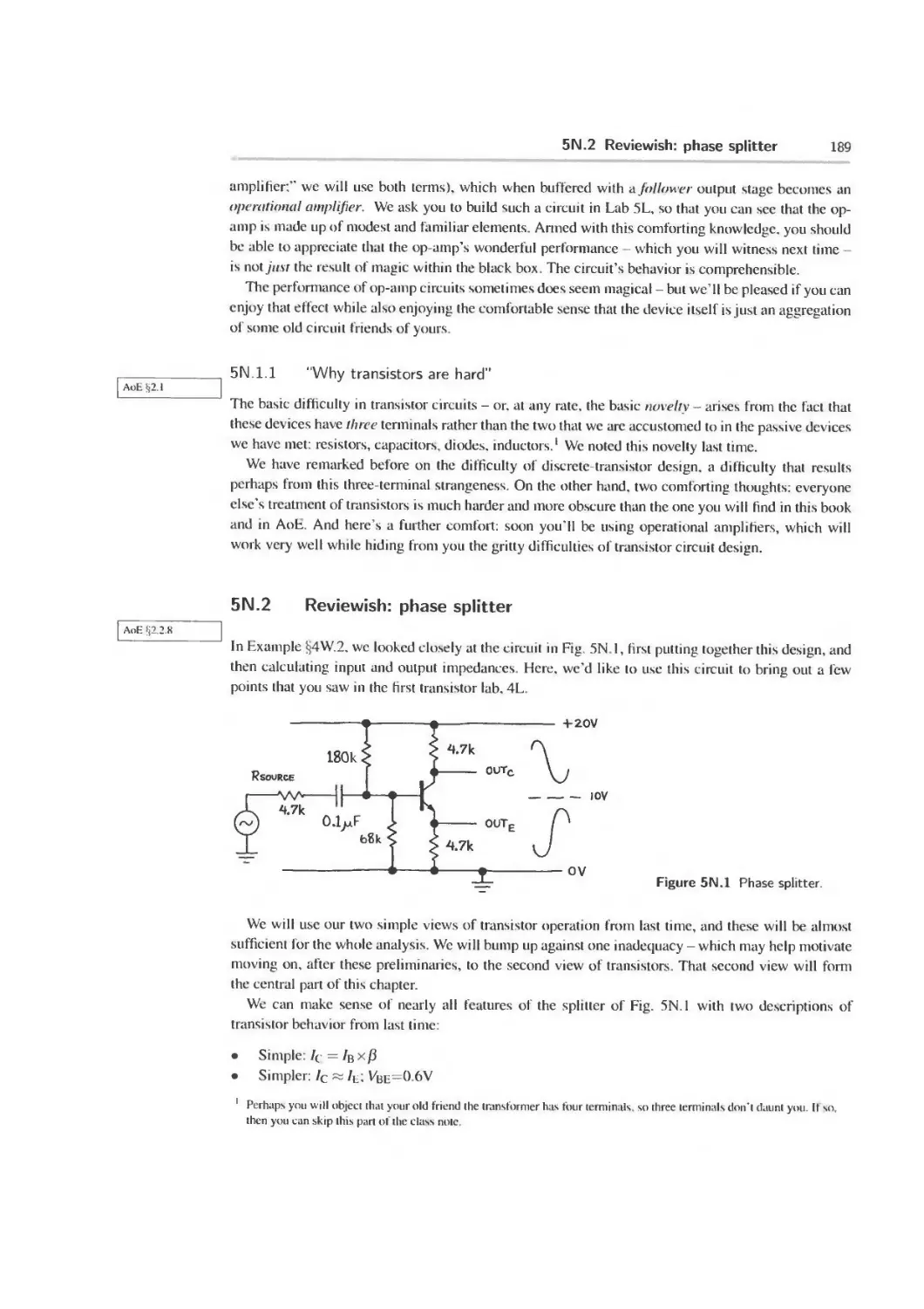
5N.2 Reviewish: phase splitter 189
5N.3 Another view of transistor behavior: Ebers Moll 190
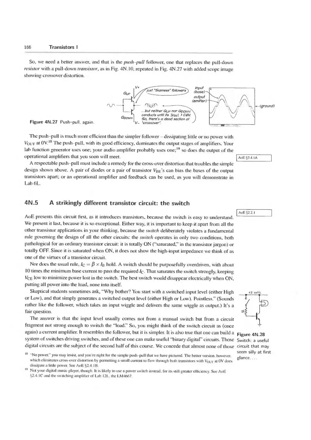
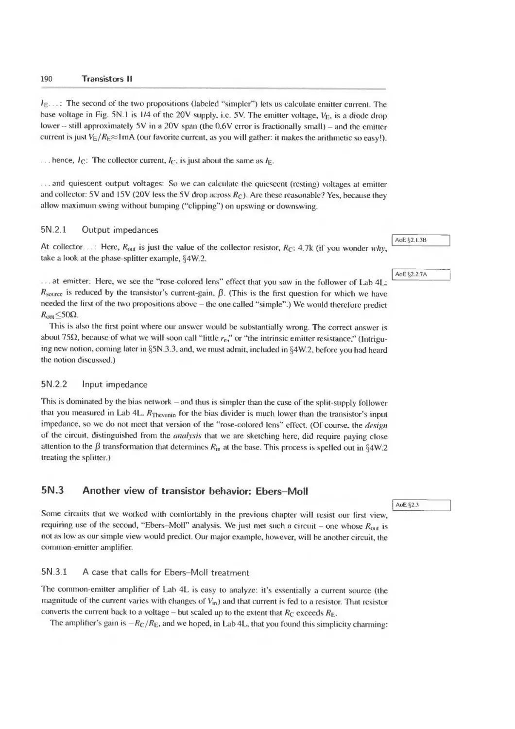
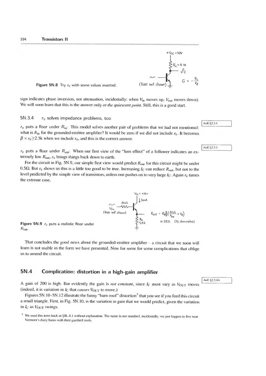
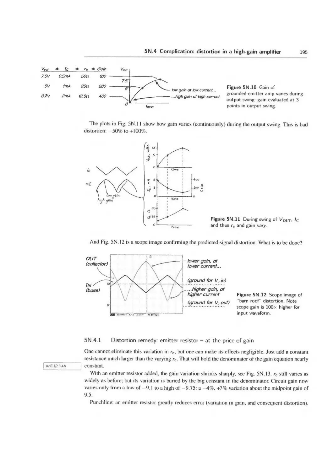
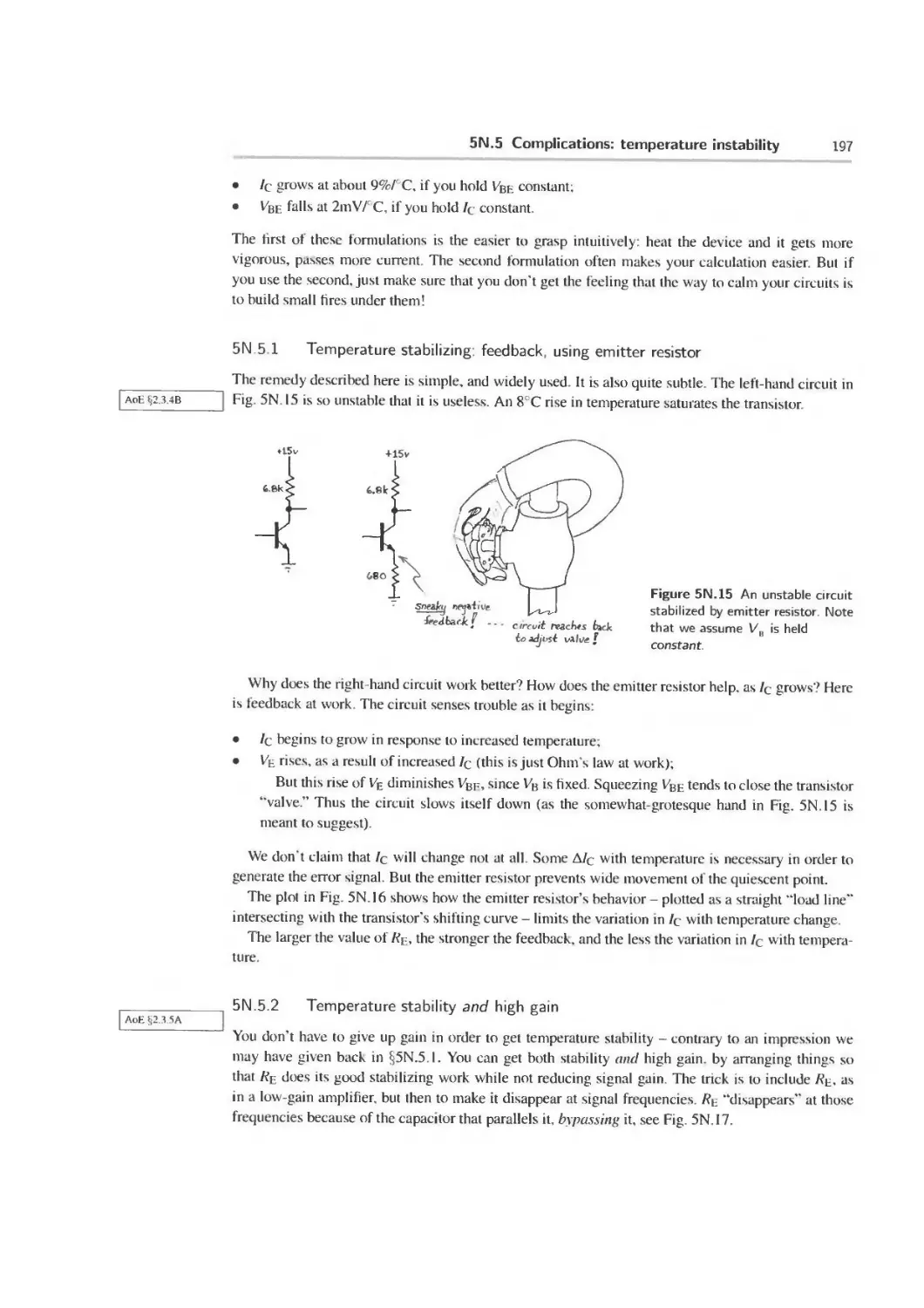
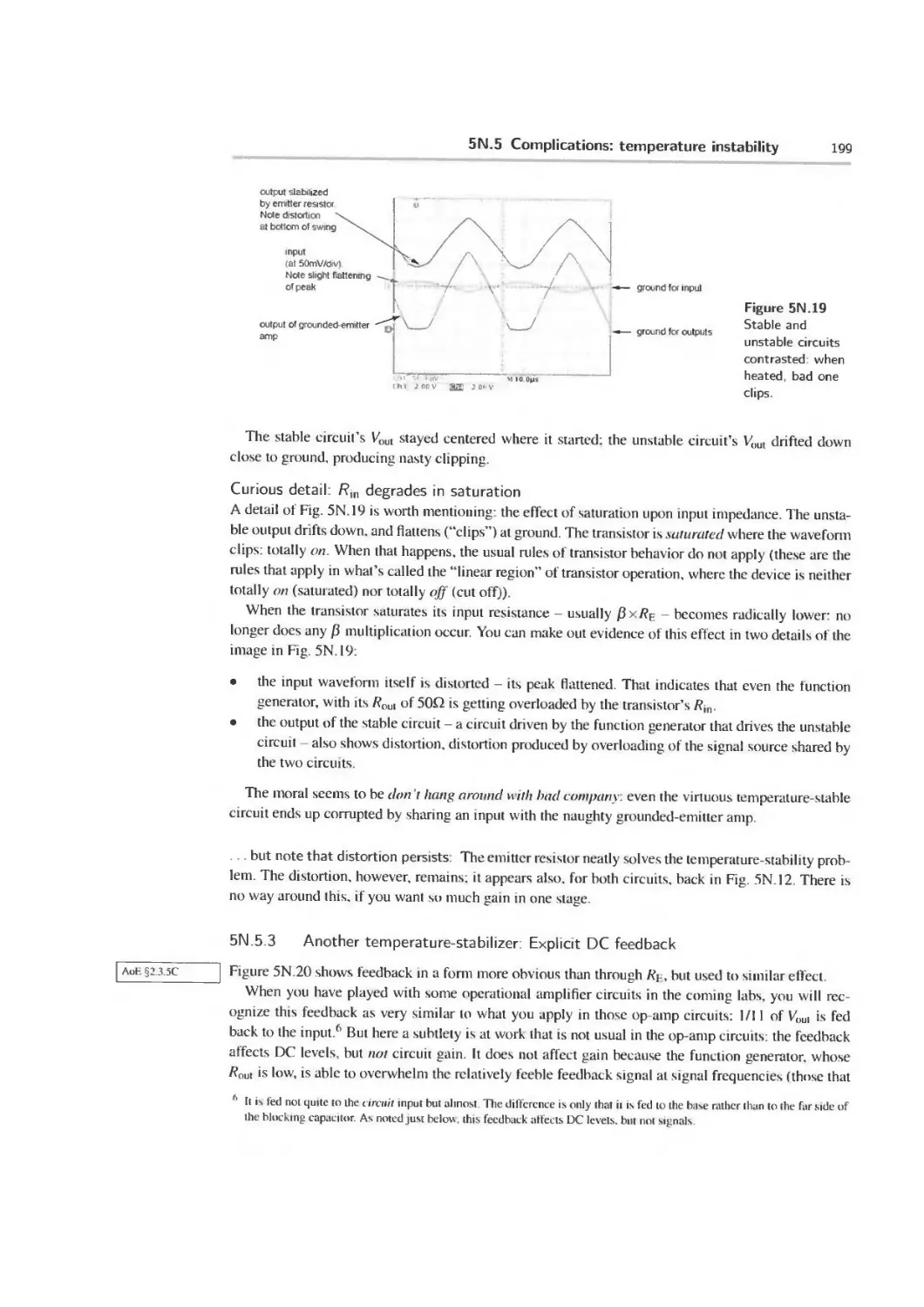
5N.4 Complication: distortion in a high-gain amplifier 194
5N.5 Complications temperature instability 196
5N.6 Reconciling the two views: Ebers-Moll meets Iq — [i x/b 201
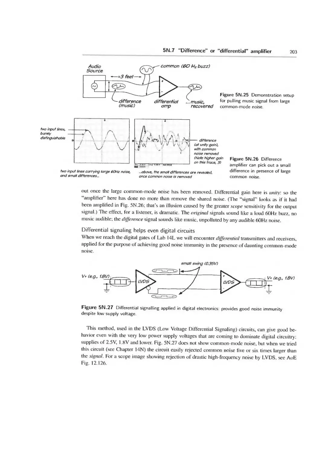
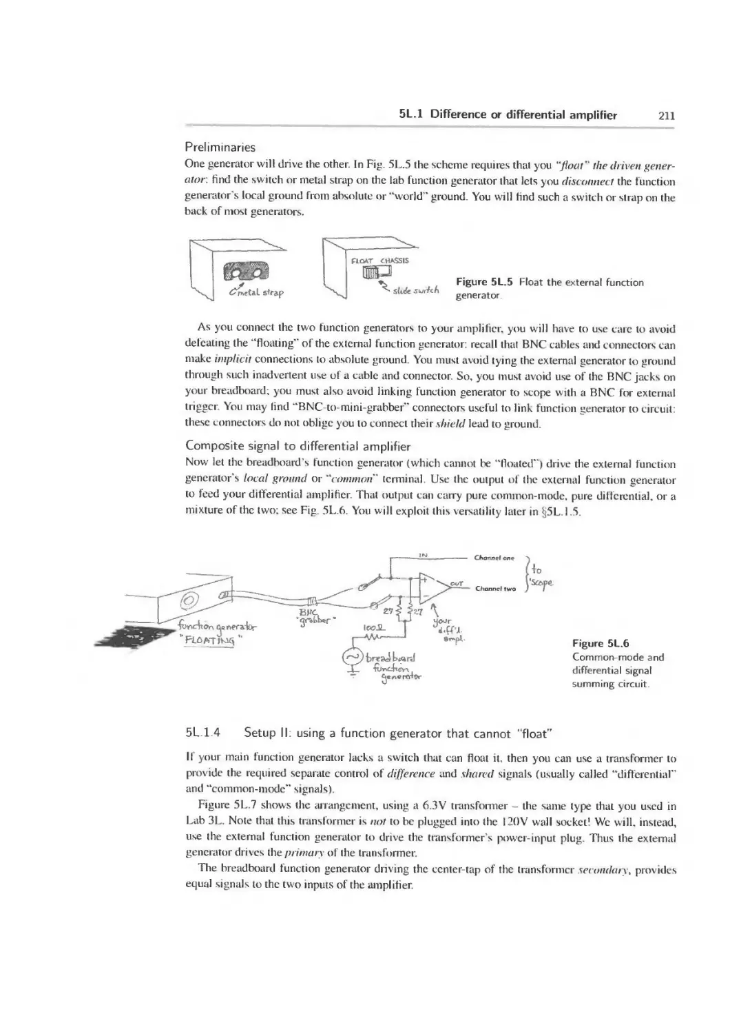
5N.7 "Difference” or “differential” amplifier 201
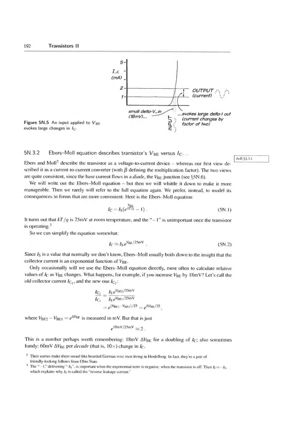
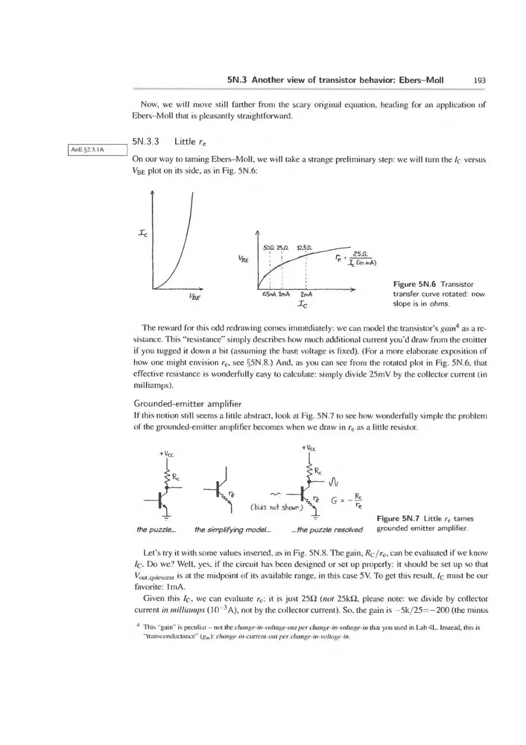
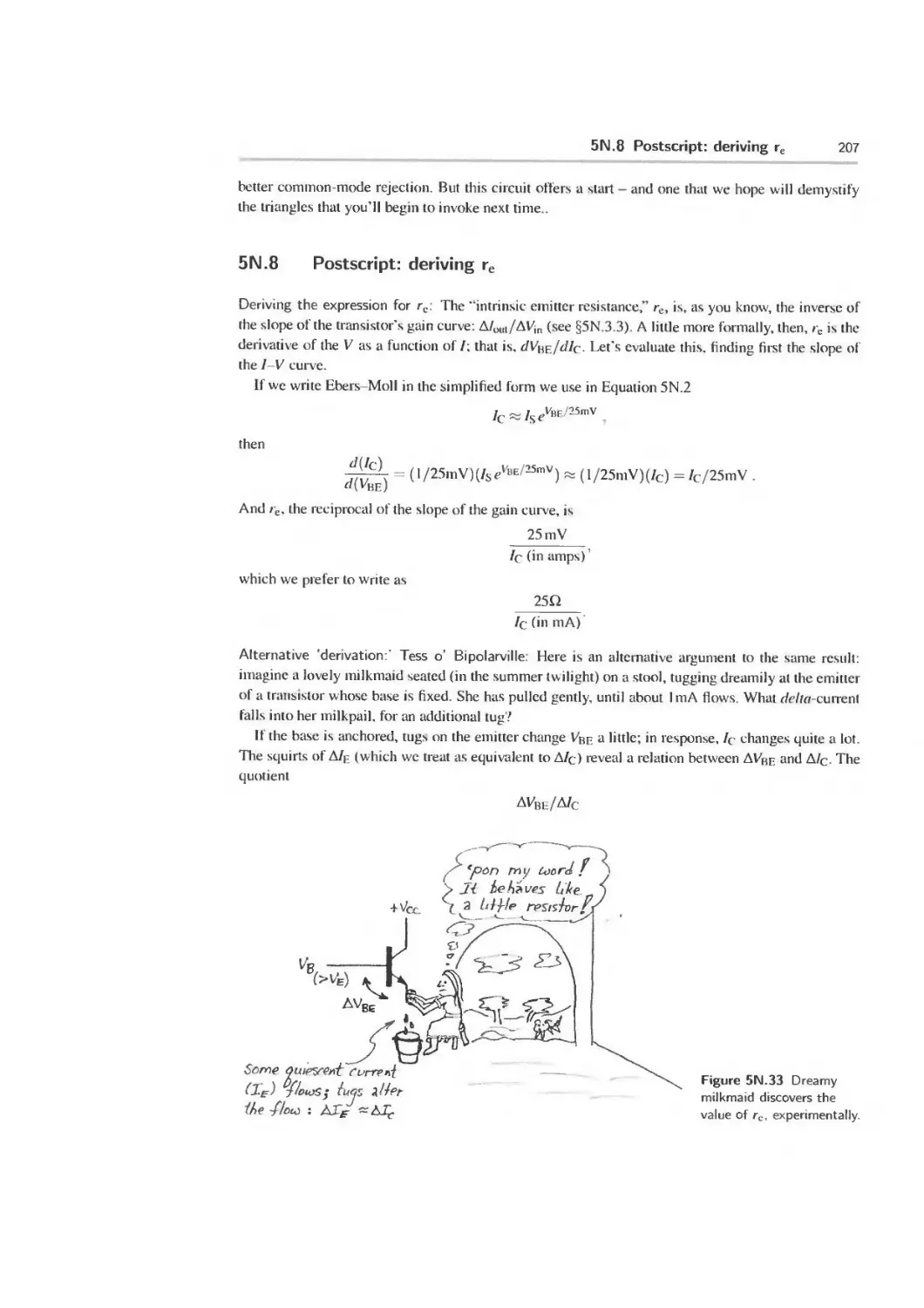
5N.8 Postscript: deriving re 207
5N.9 AoE Reading 208
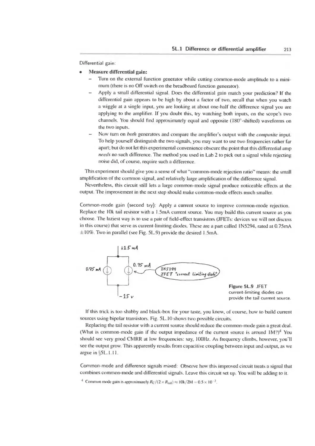
5L Lab: Transistors II 209
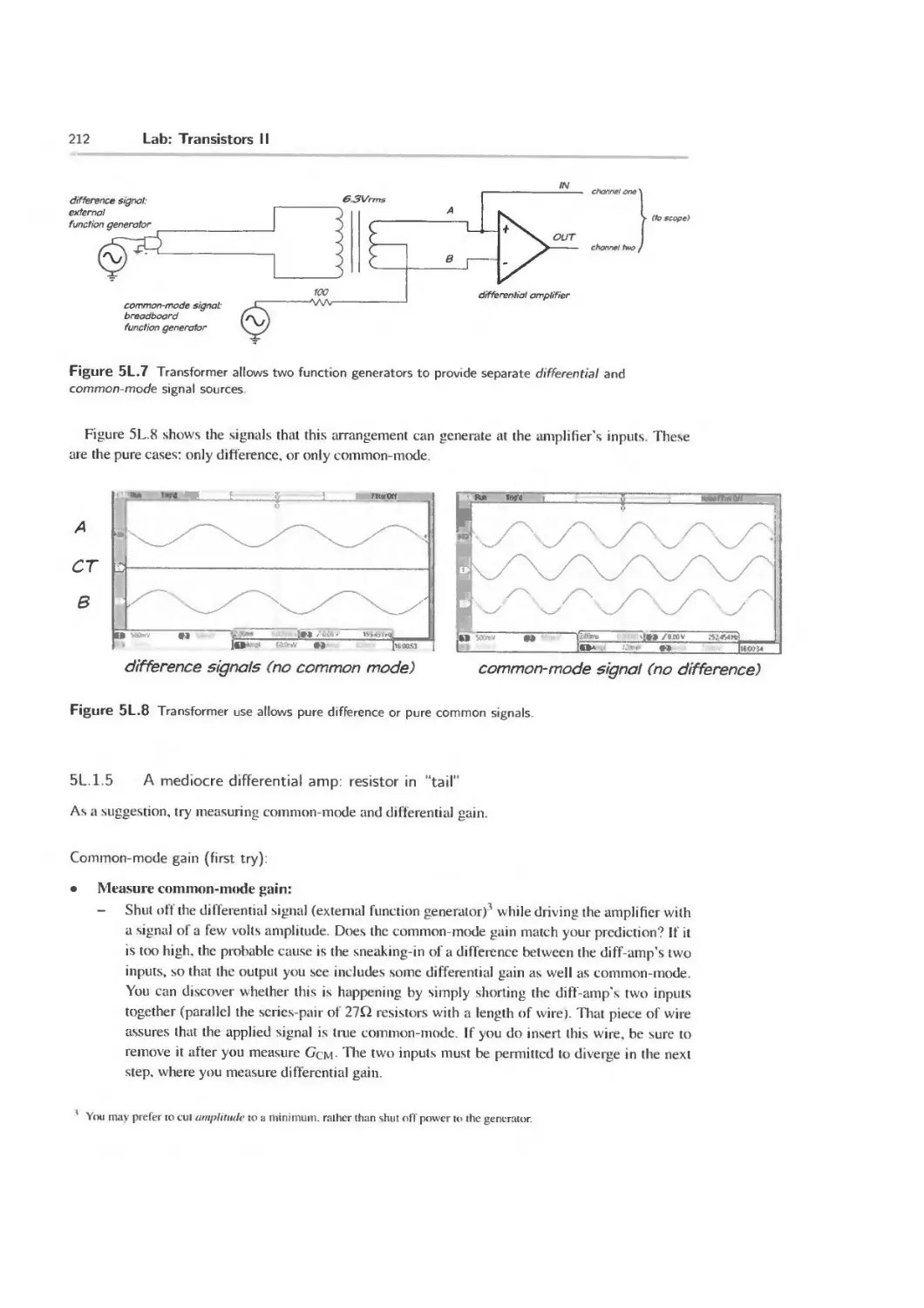
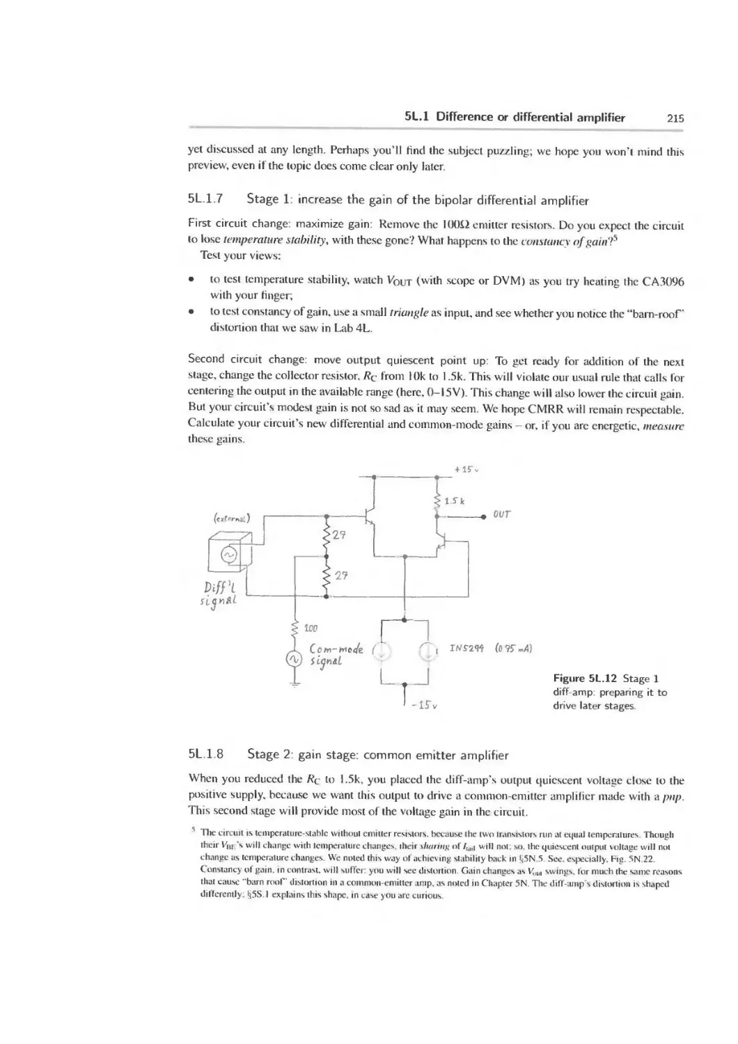
5L. 1 Difference or differential amplifier 209
5S Supplementary Notes and Jargon: Transistors II 220
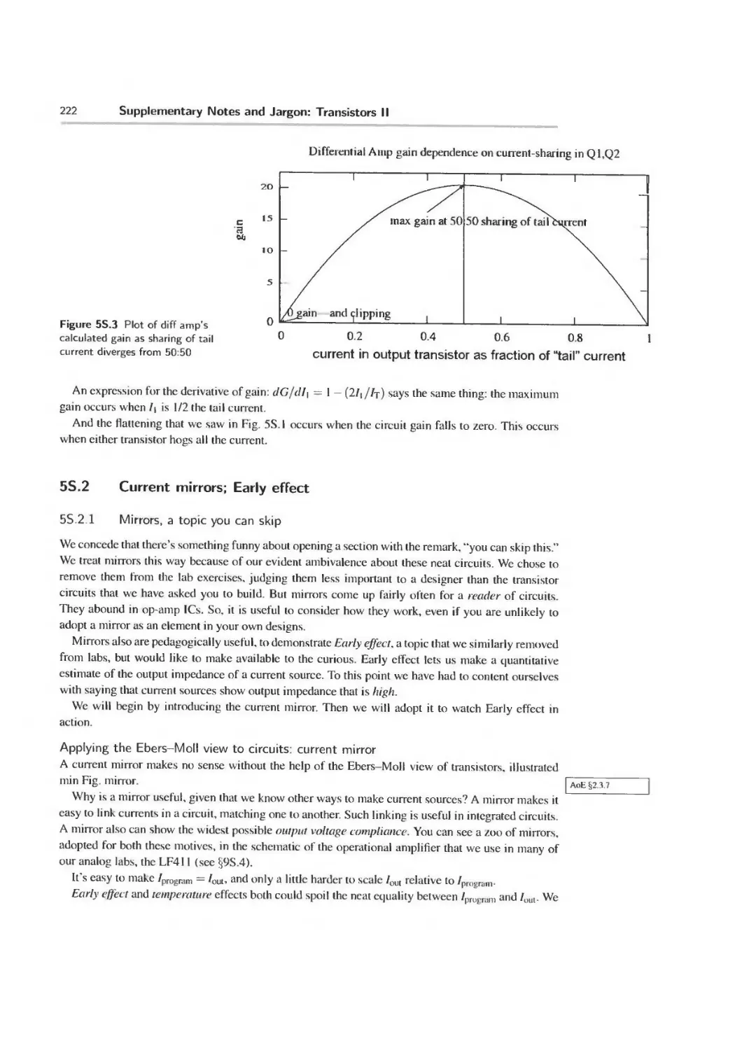
5S. 1 Two surprises, perhaps, in behavior of differential amp 220
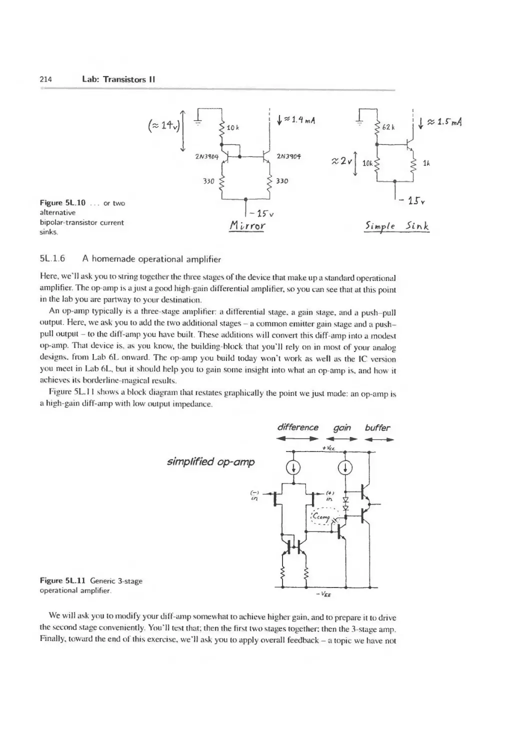
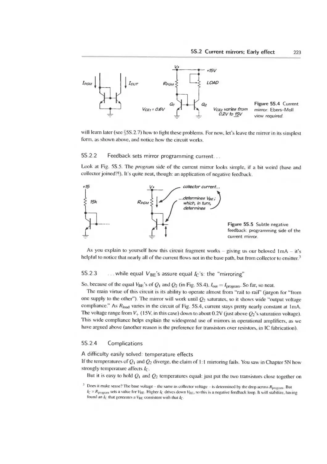
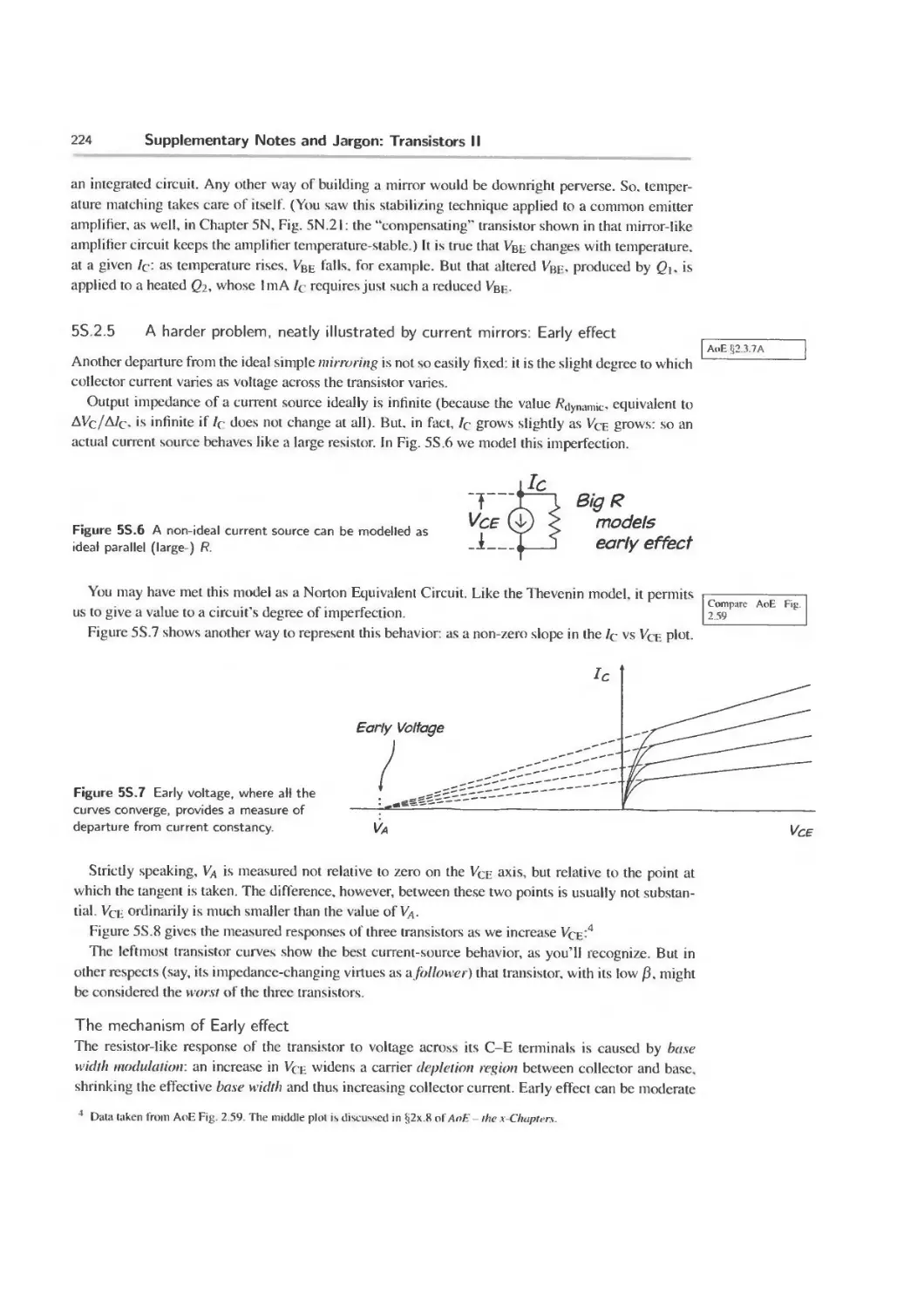
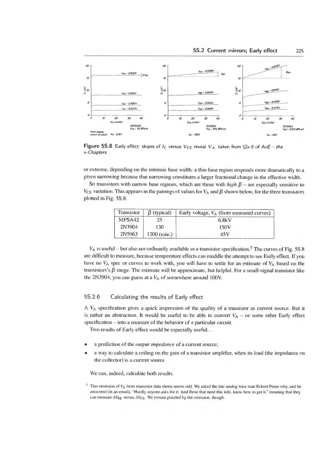
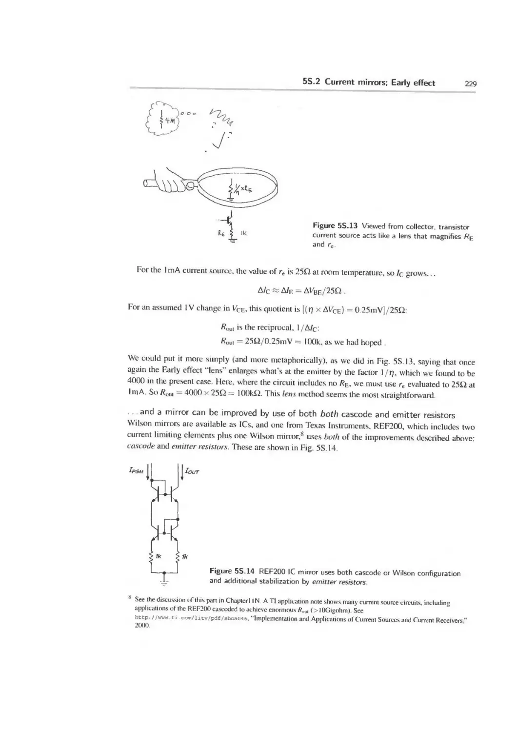
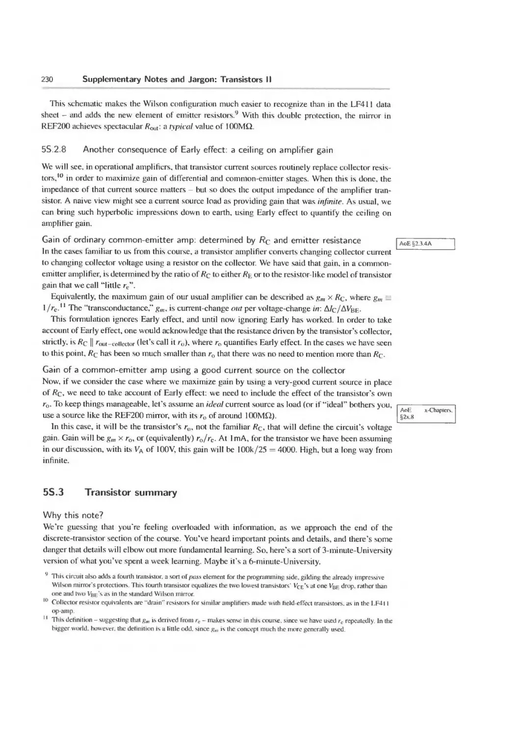
5S 2 Current mirrors; Early effect 222
5S.3 Transistor summary 230
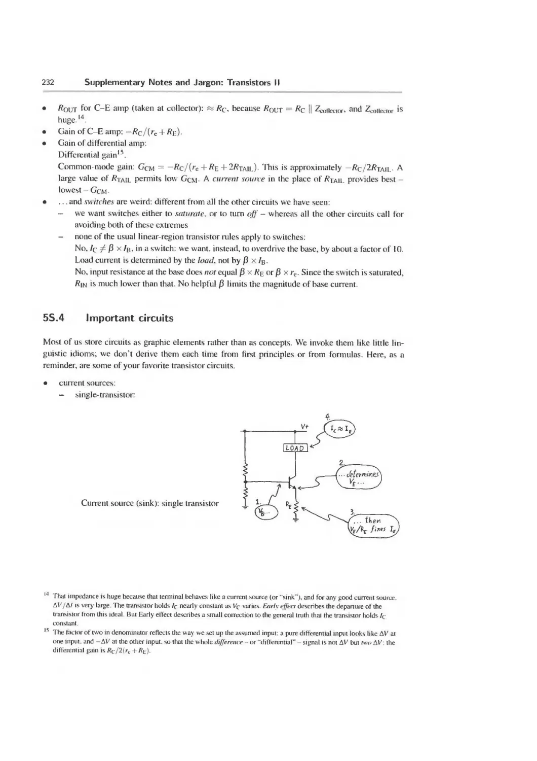
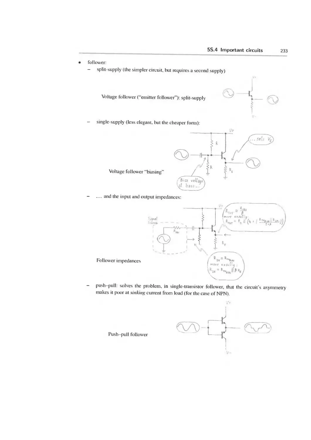
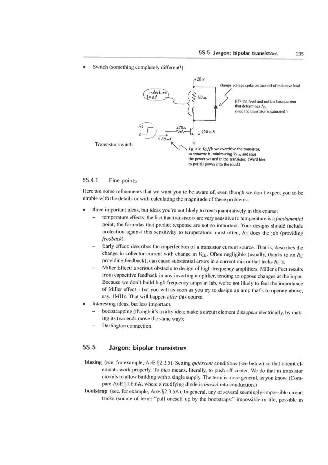
5S 4 important circuits 232
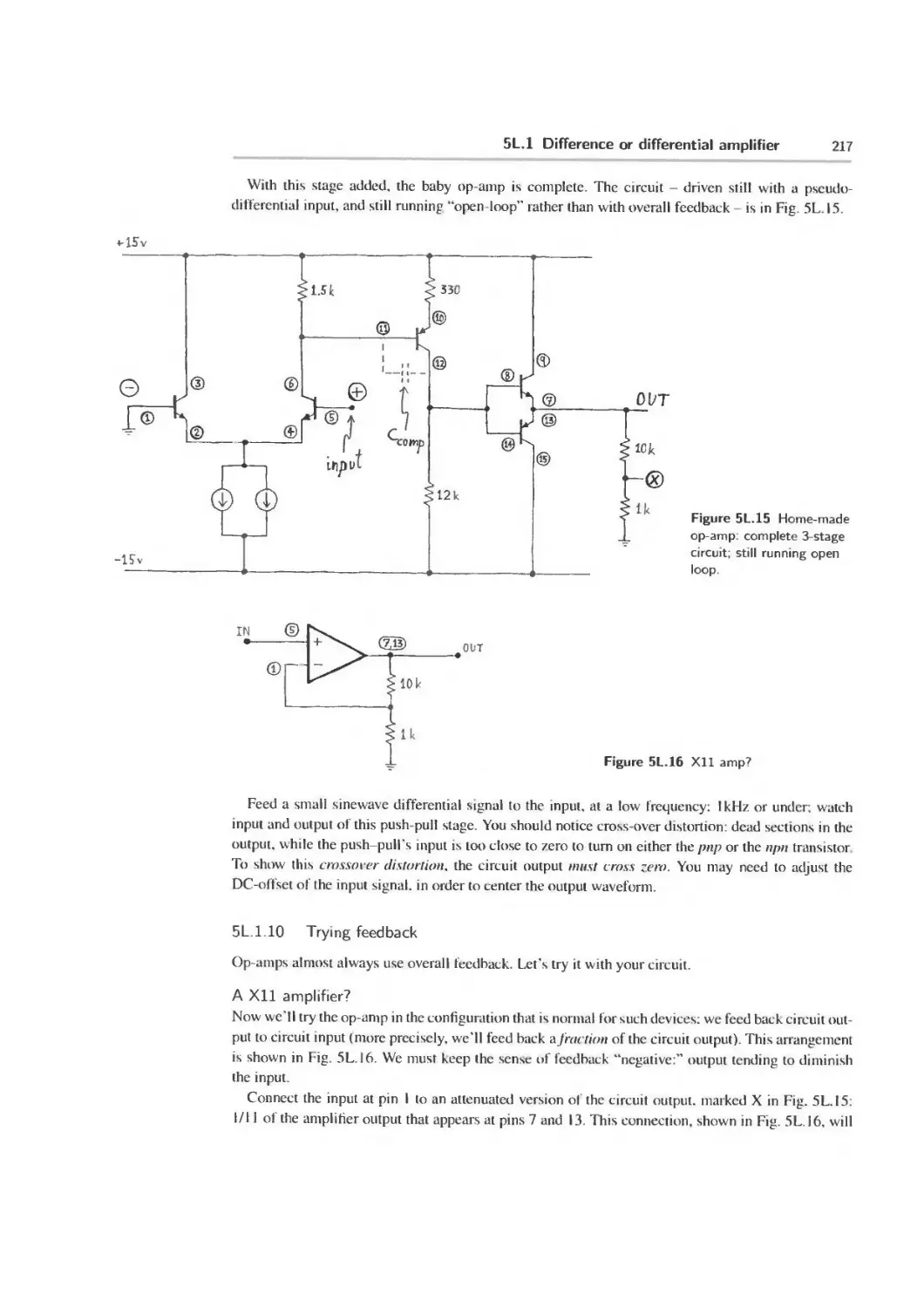
5S.5 Jargon: bipolar transistors 235
5W Worked Examples: Transistors II 237
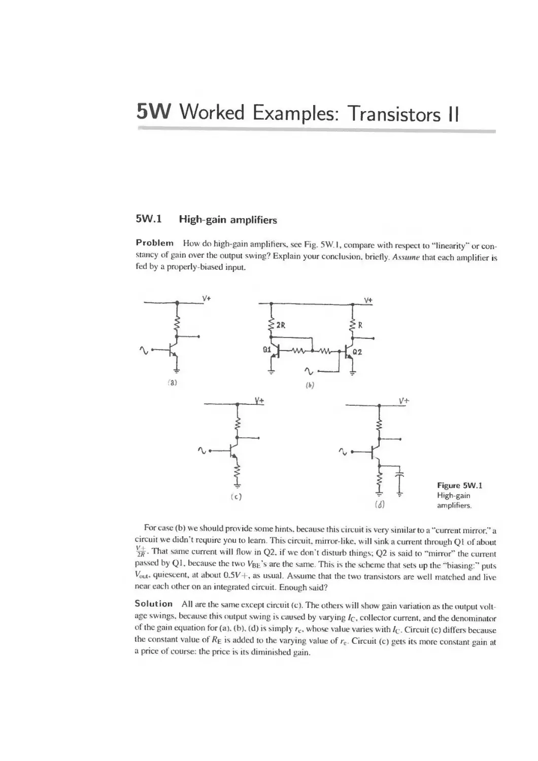
5W 1 High-gain amplifiers 237
5W.2 Differential amplifier 238
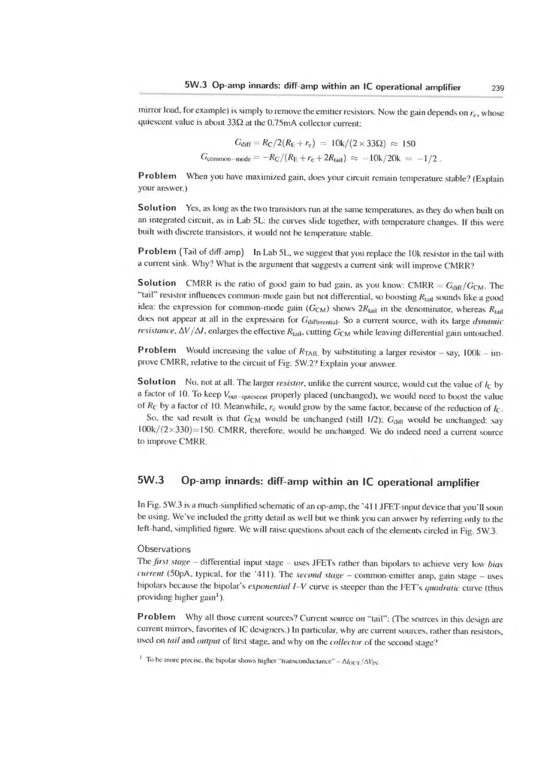
5W.3 Op-amp innards: diff-amp within an 1C operational amplifier 239
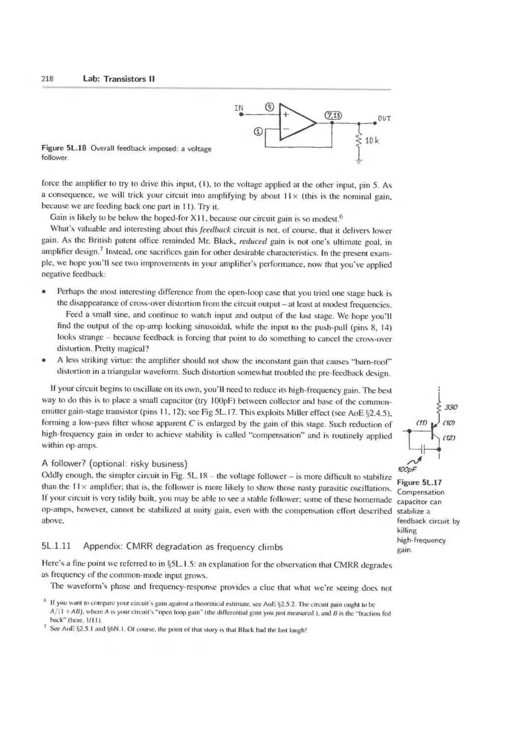
X
Contents
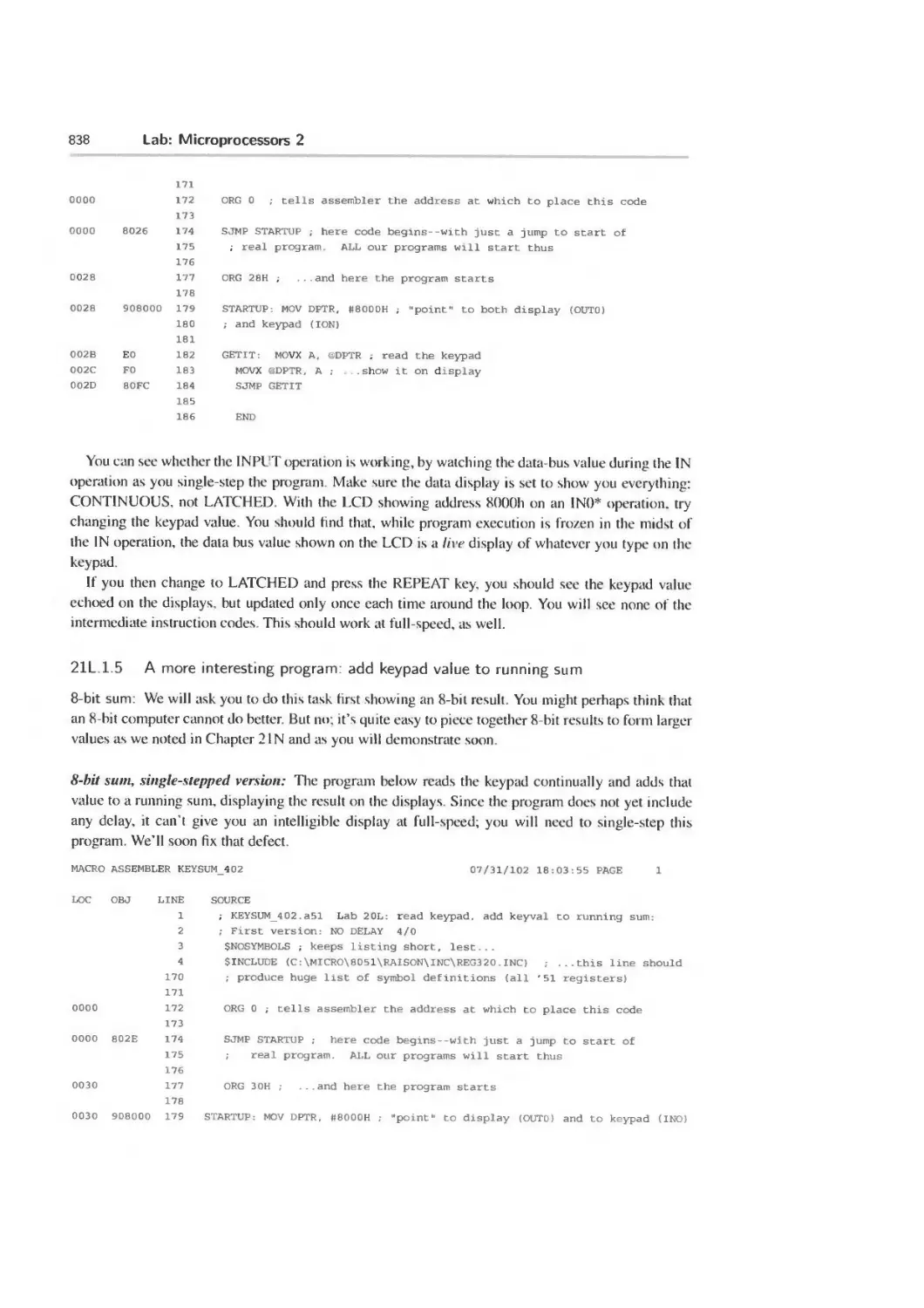
Part III Analog: Operational Amplifiers and their Applications 243
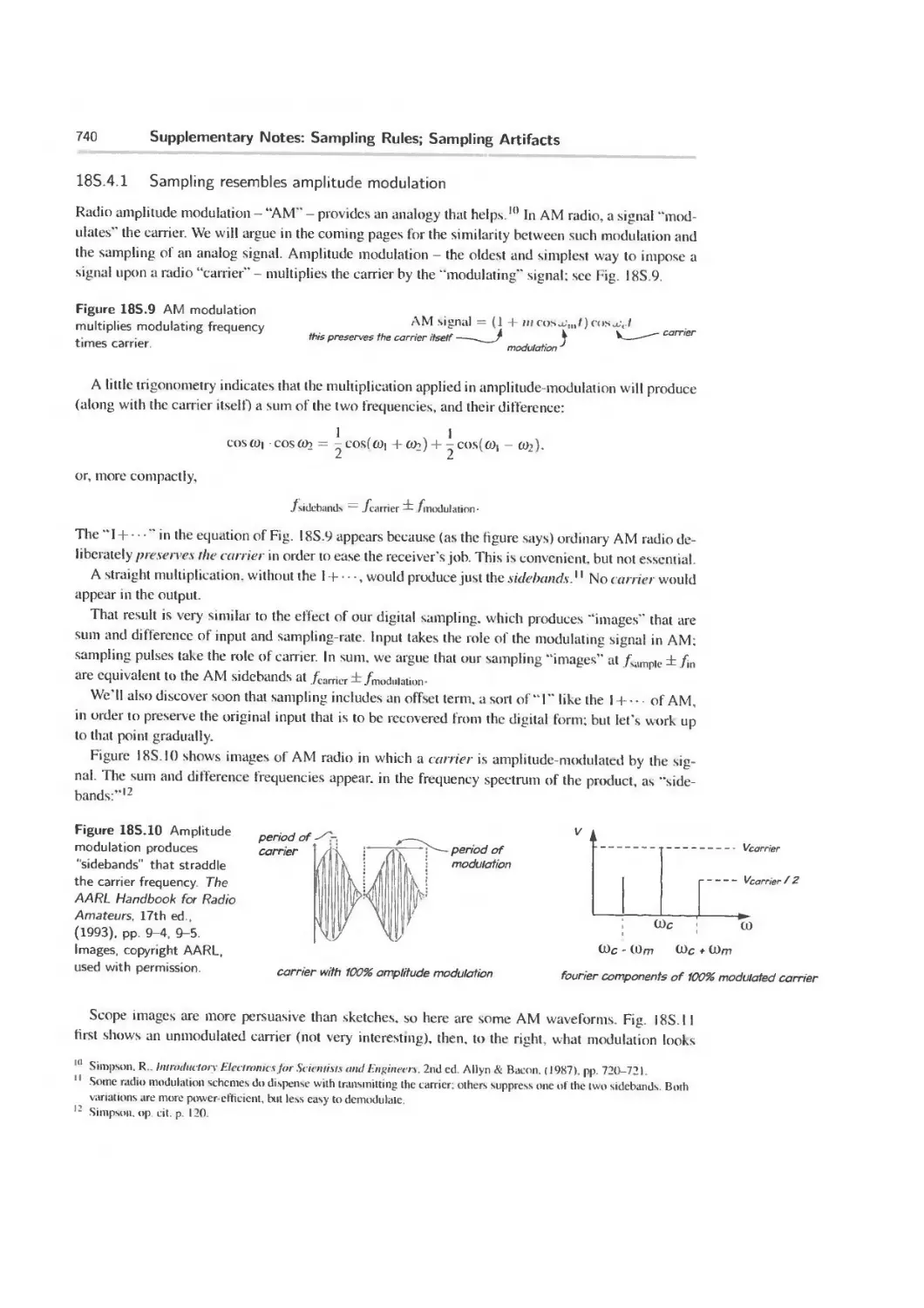
6N Op-amps I 245
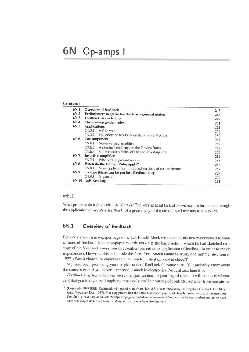
6N.1 Overview of feedback 245
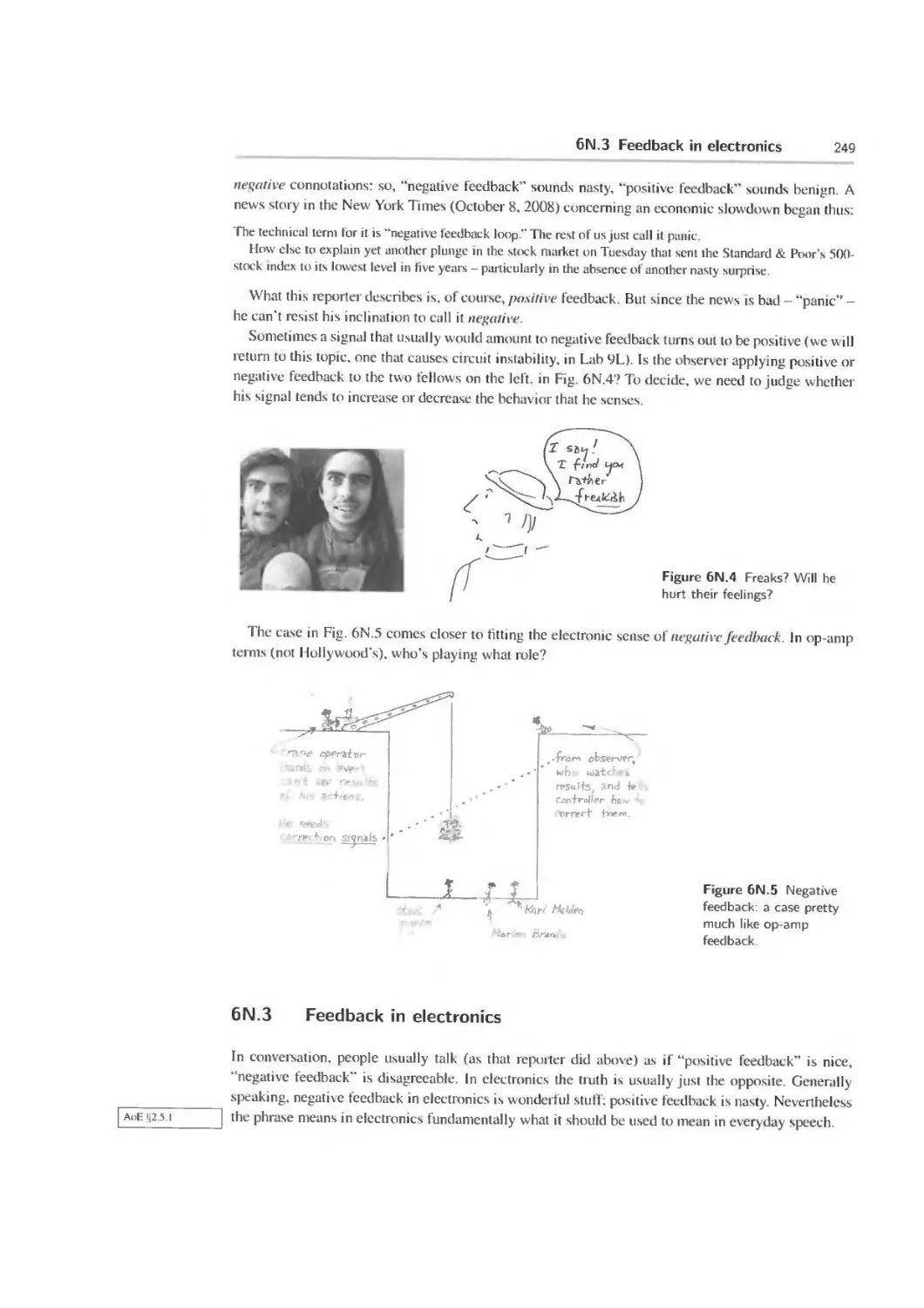
6N.2 Preliminary: negative feedback as a general notion 248
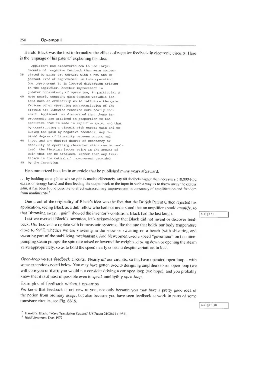
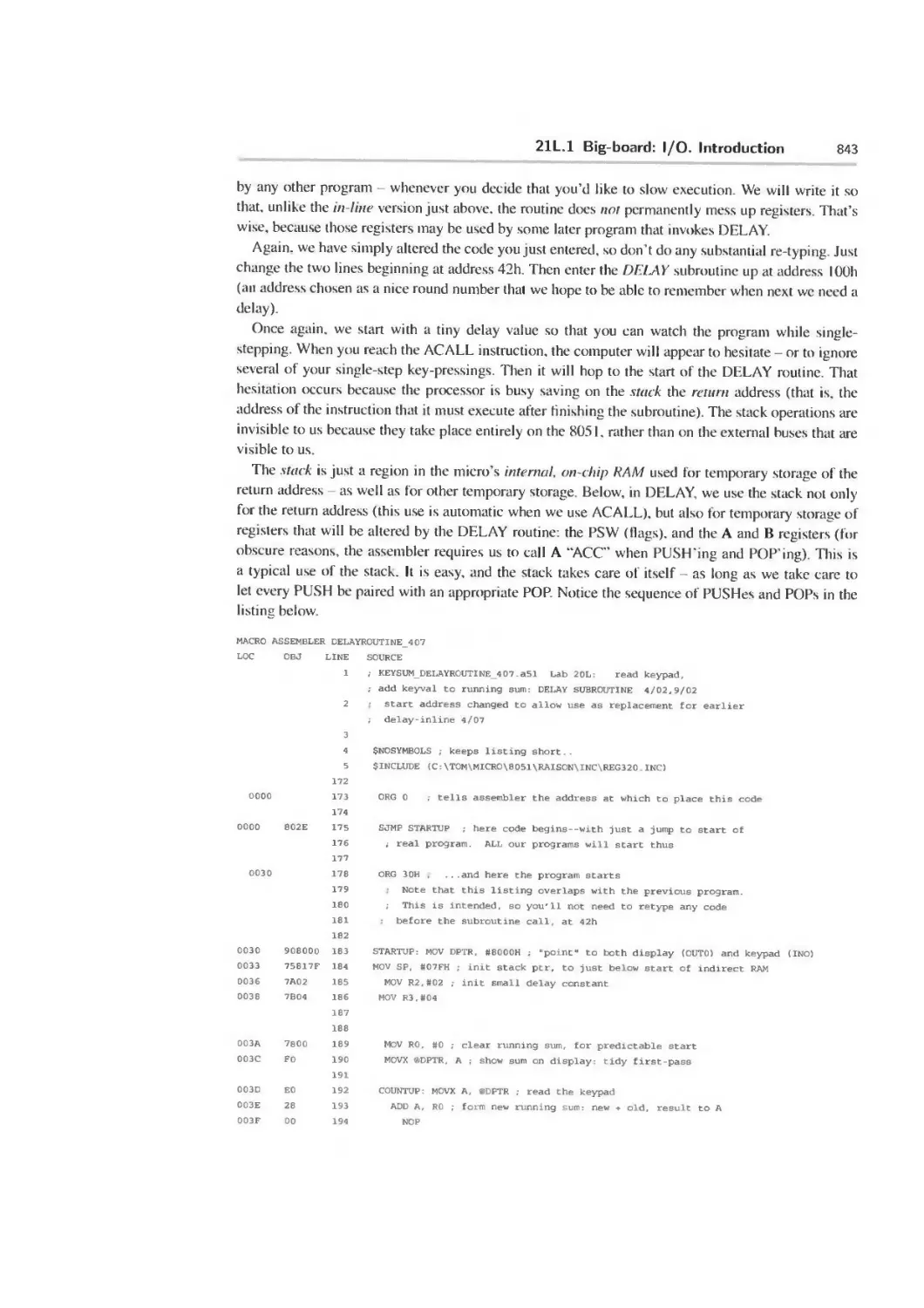
6N.3 Feedback in electronics 249
6N.4 The op-amp golden rules 251
6N.5 Applications 252
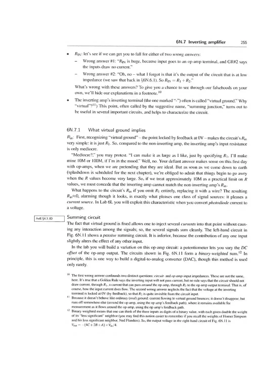
6N.6 Two amplifiers 252
6N.7 inverting amplifier 254
6N.8 When do the Golden Rules apply? 256
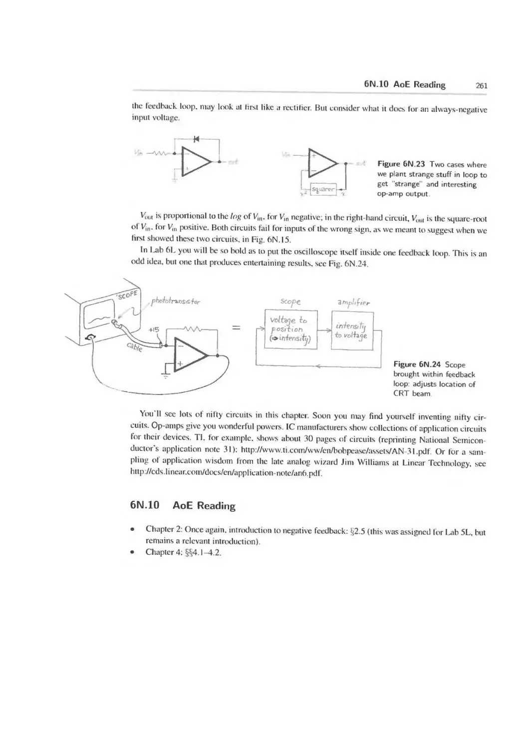
6N.9 Strange things can be put into feedback loop 259
6N. 10 AoE Reading 261
6L Lab: Op-Amps I 262
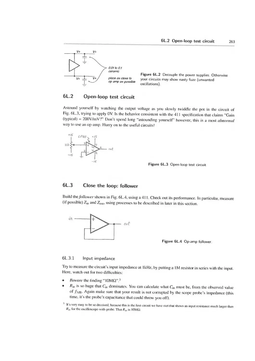
6L.1 A few preliminaries 262
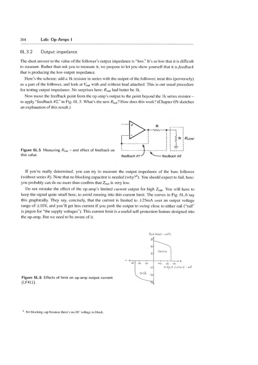
6L.2 Open-loop test circuit 263
6L.3 Close the loop: follower 263
6L.4 Non-inverting amplifier 265
6L.5 Inverting amplifier 265
6L.6 Summing amplifier 266
6L.7 Design exercise: unity-gain phase shifter 266
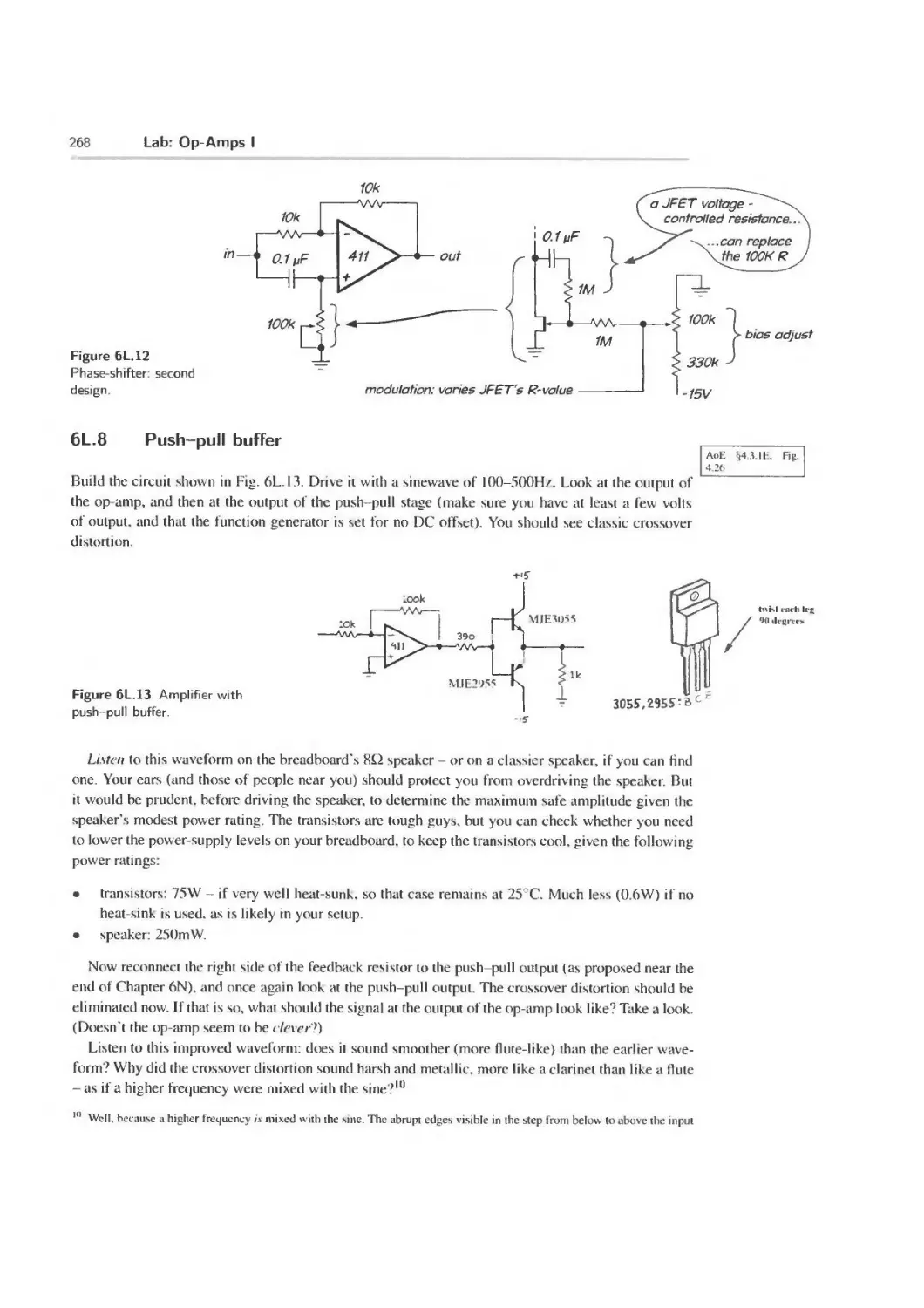
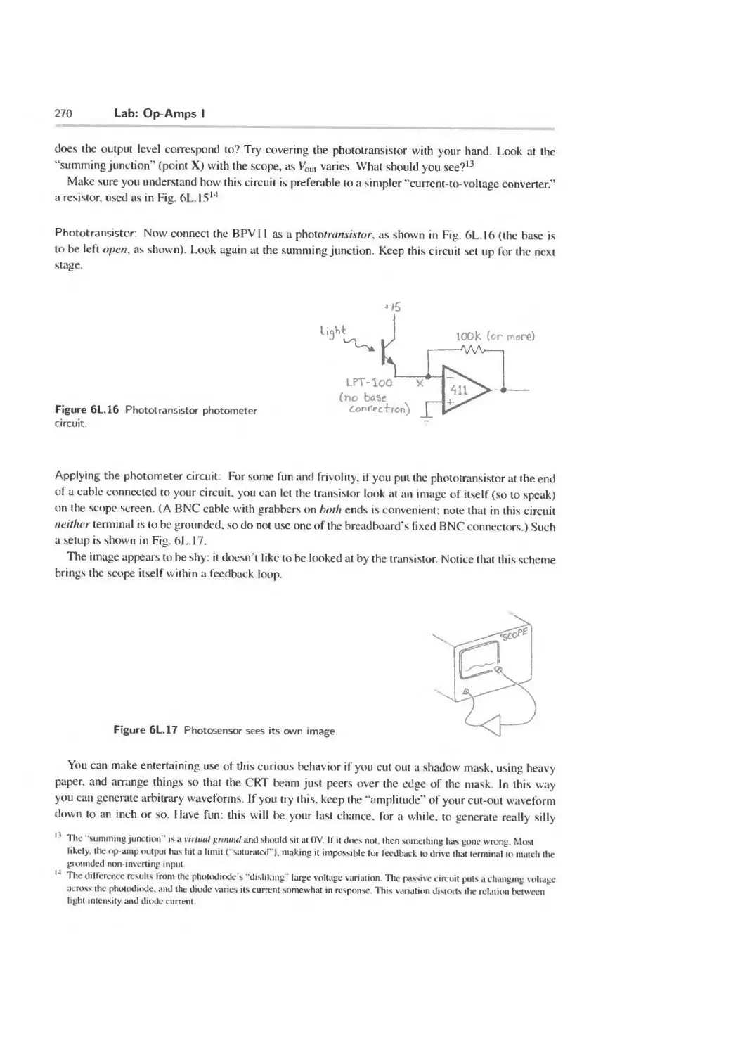
6L.8 Push-pull buffer 268
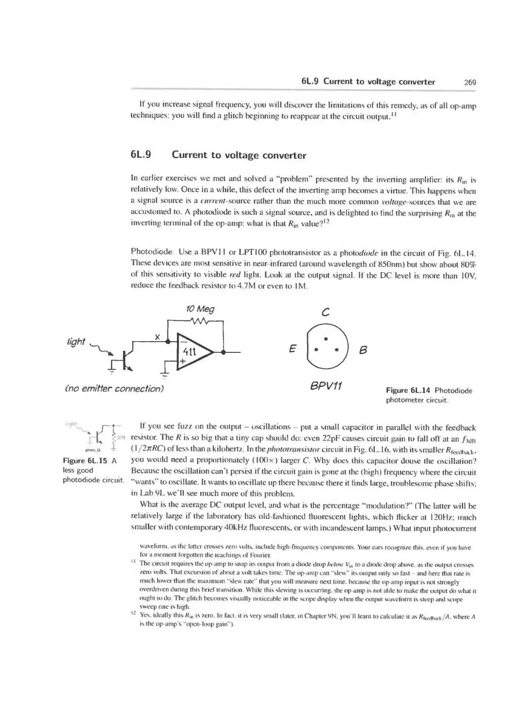
6L.9 Current to voltage converter 269
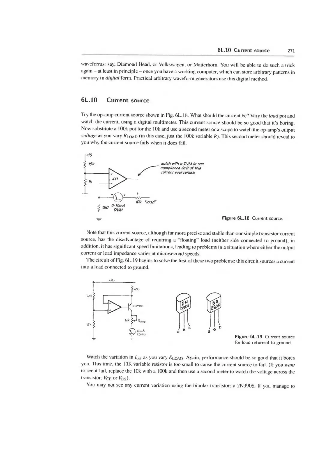
6L. 10 Current source 271
6W Worked Examples: Op-Amps I 273
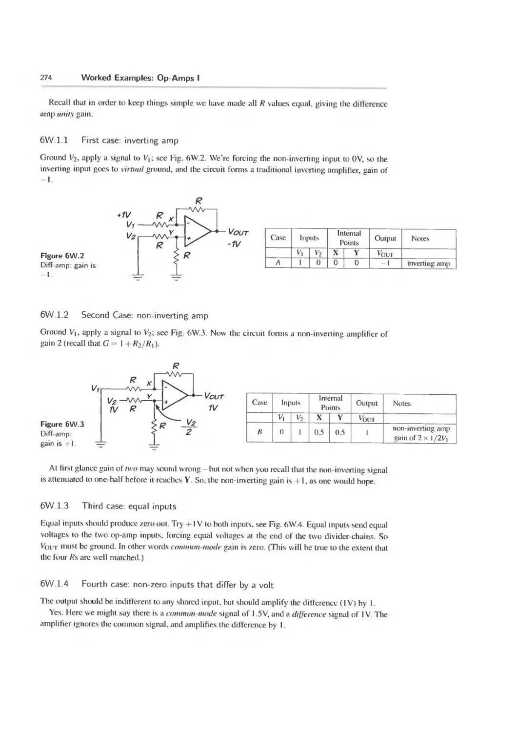
6W. 1 Basic difference amp made with an op-amp 273
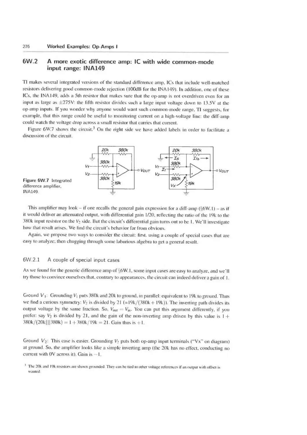
6W.2 A more exotic difference amp 276
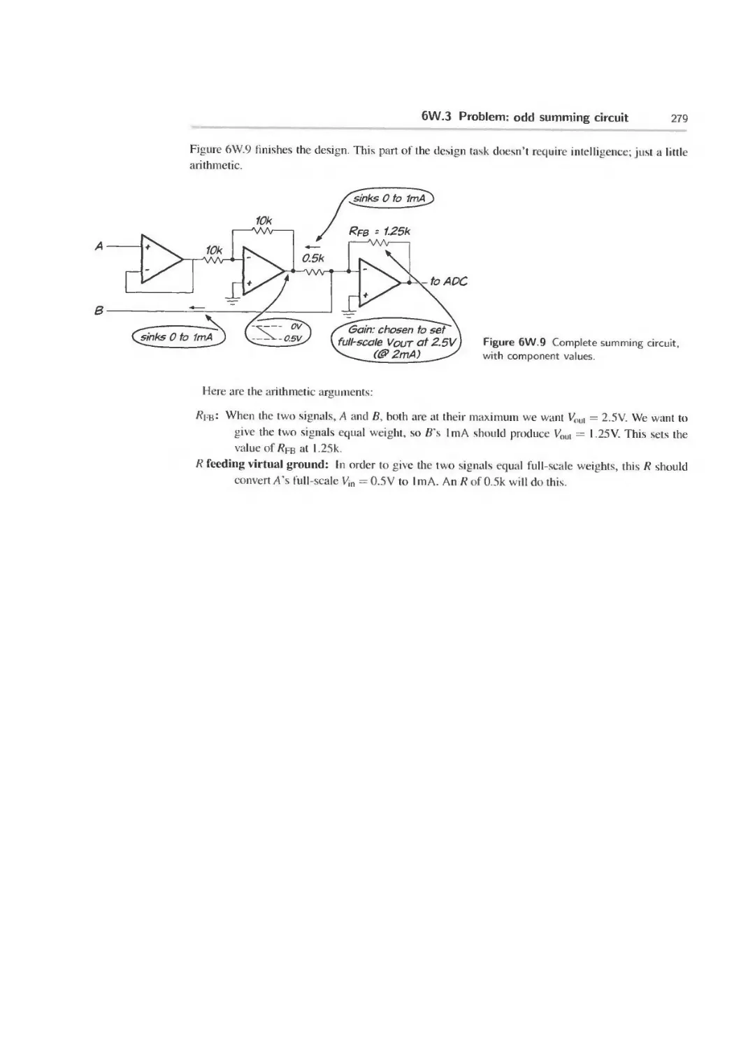
6W.3 Problem: odd summing circuit 277
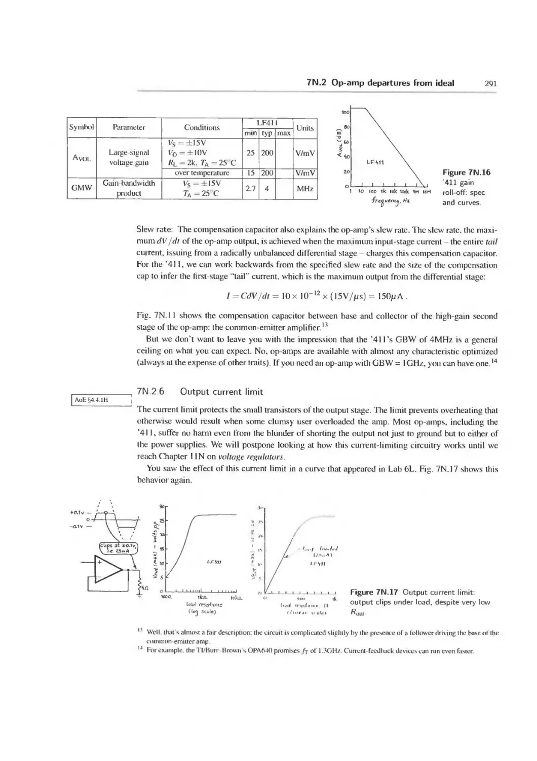
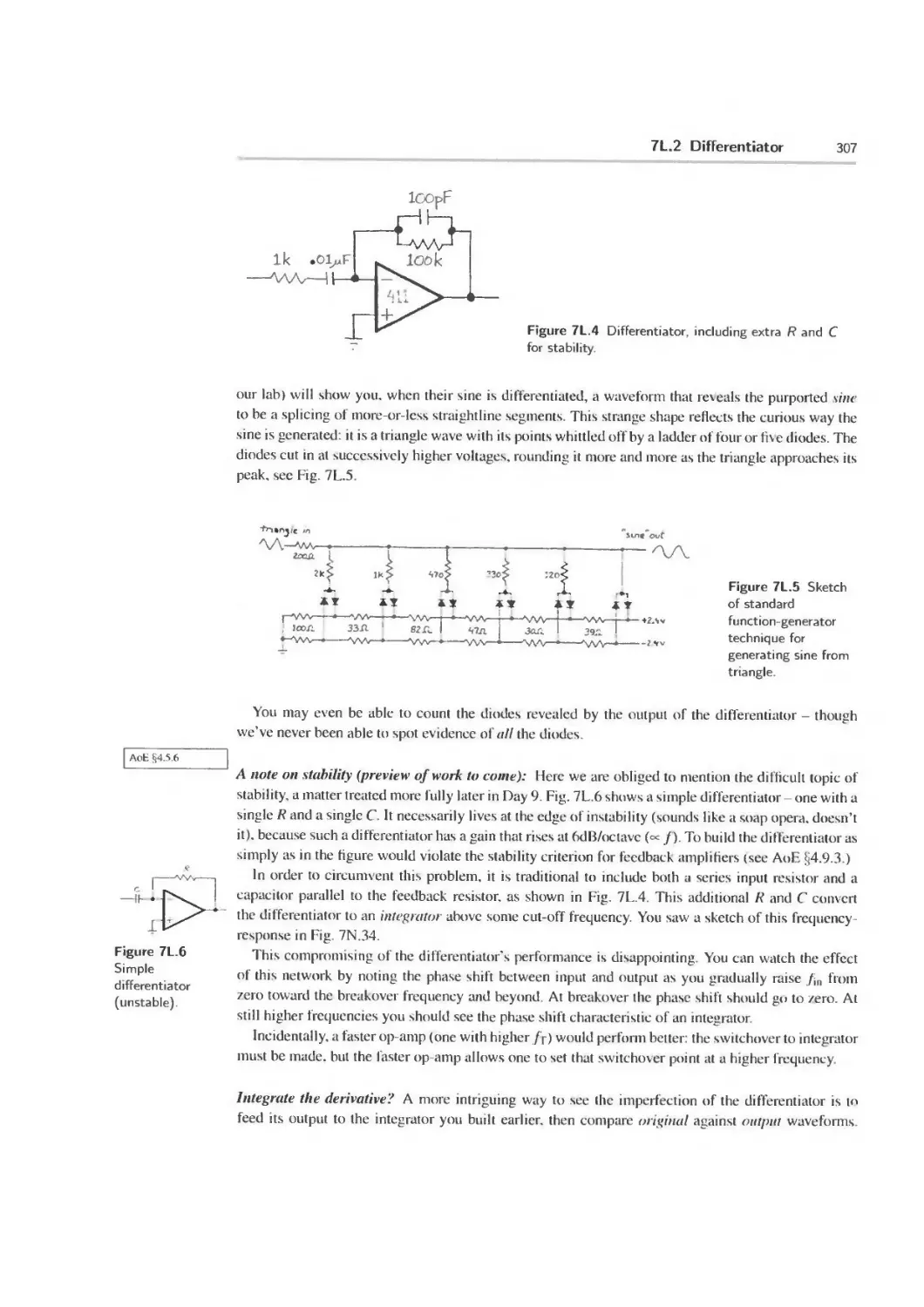
7N Op-amps II: Departures from Ideal 280
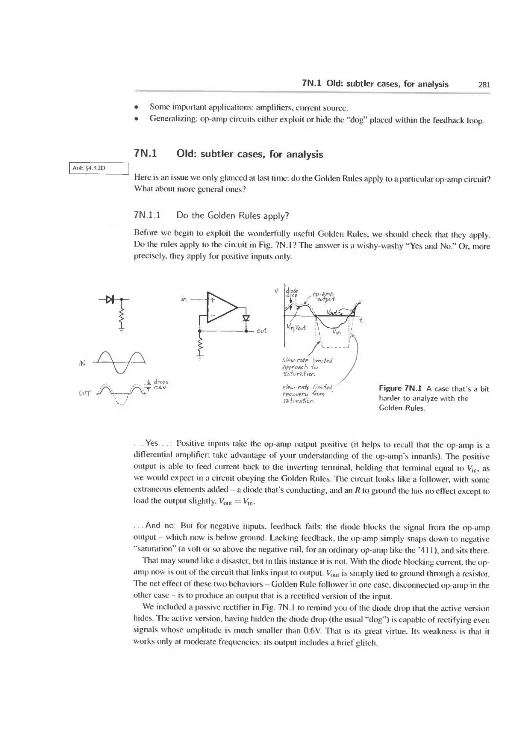
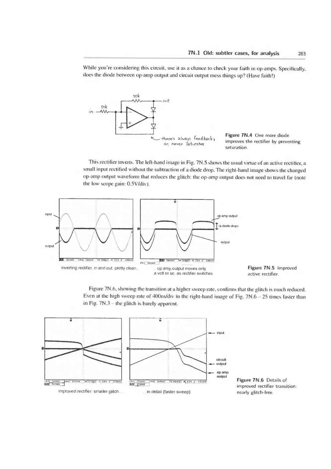
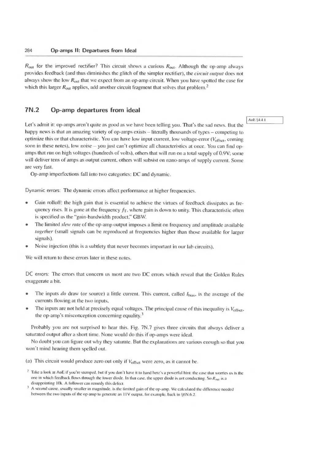
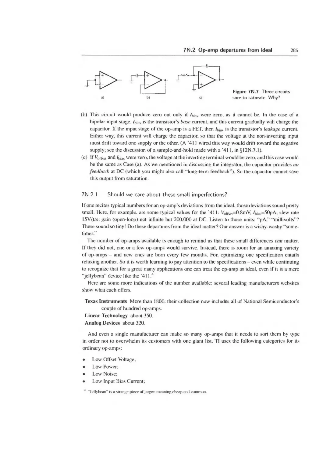
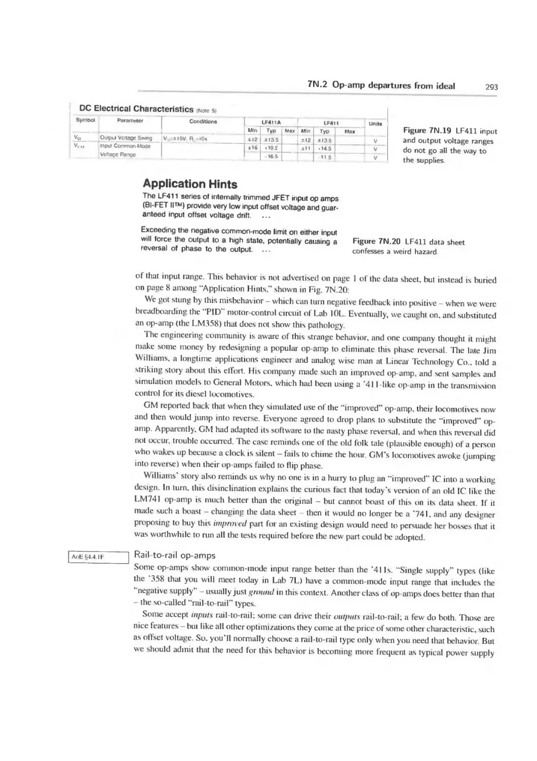
7N.1 Old: subtler cases, for analysis 281
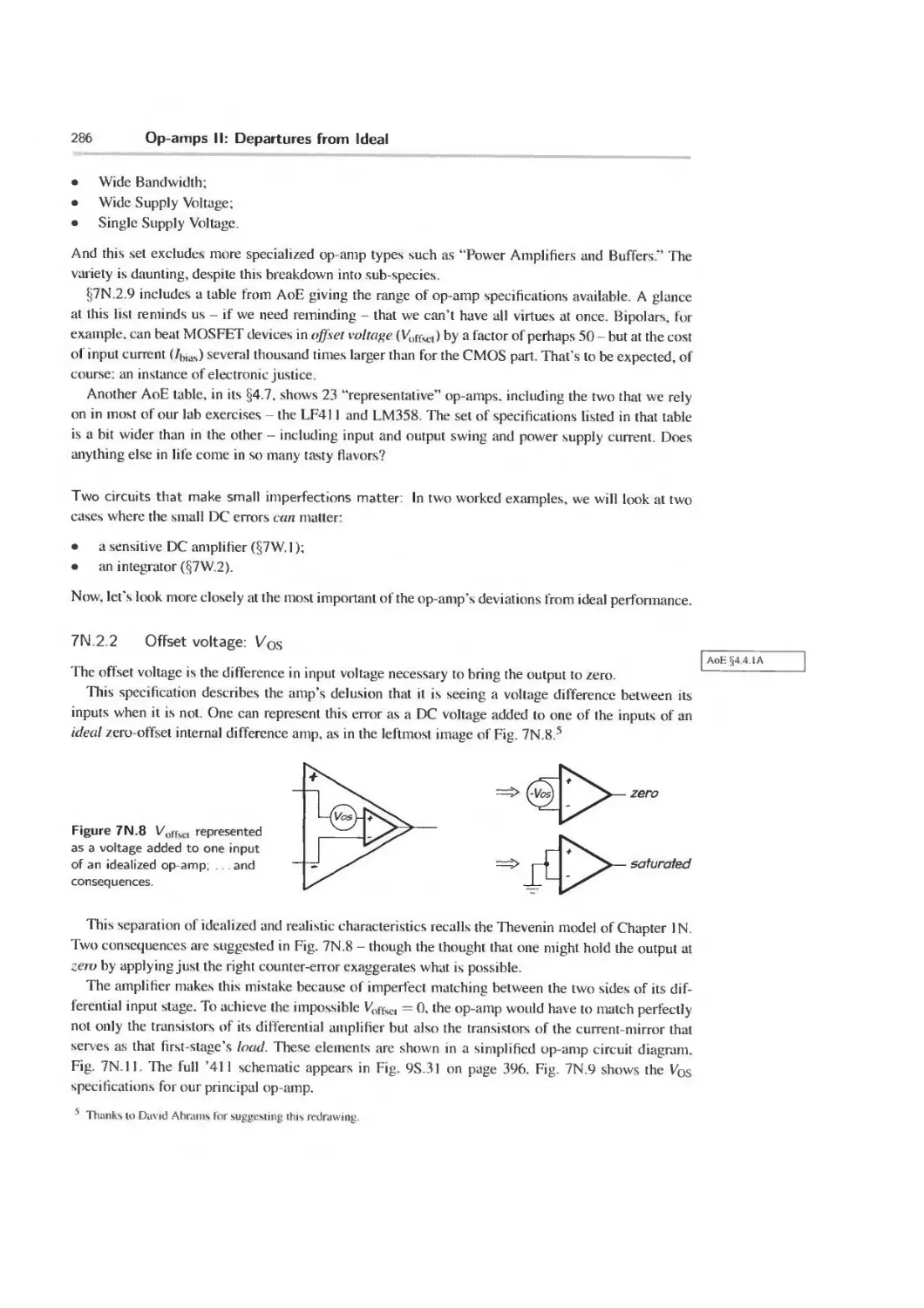
7N .2 Op-amp departures from ideal 284
7N.3 Four more applications 294
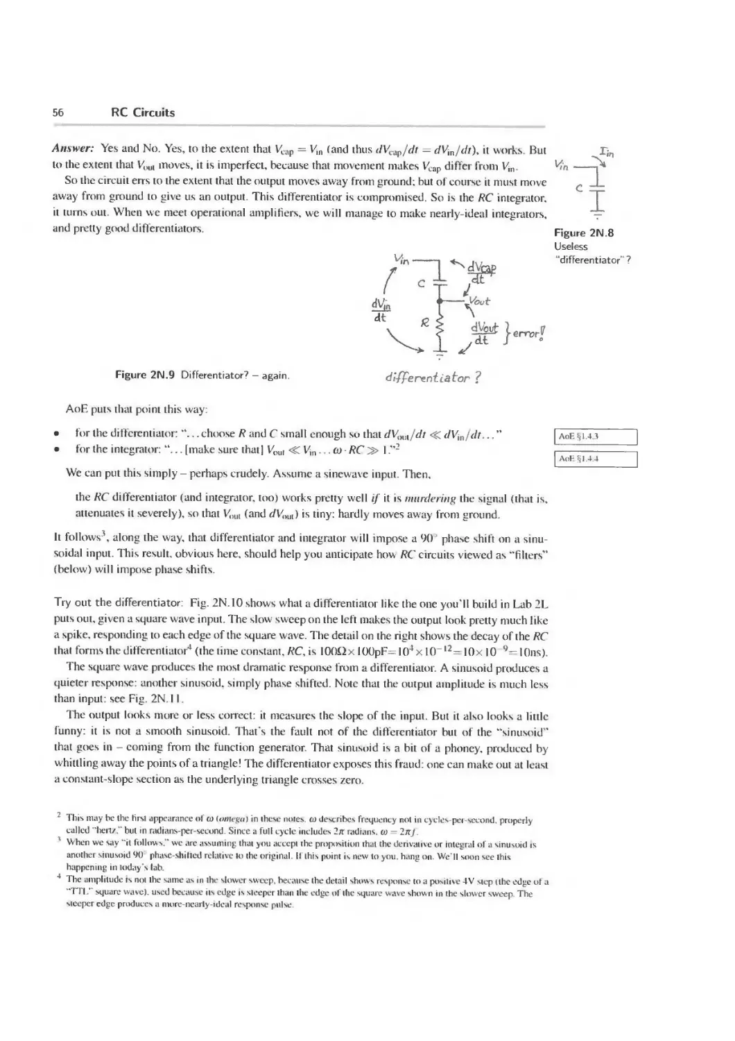
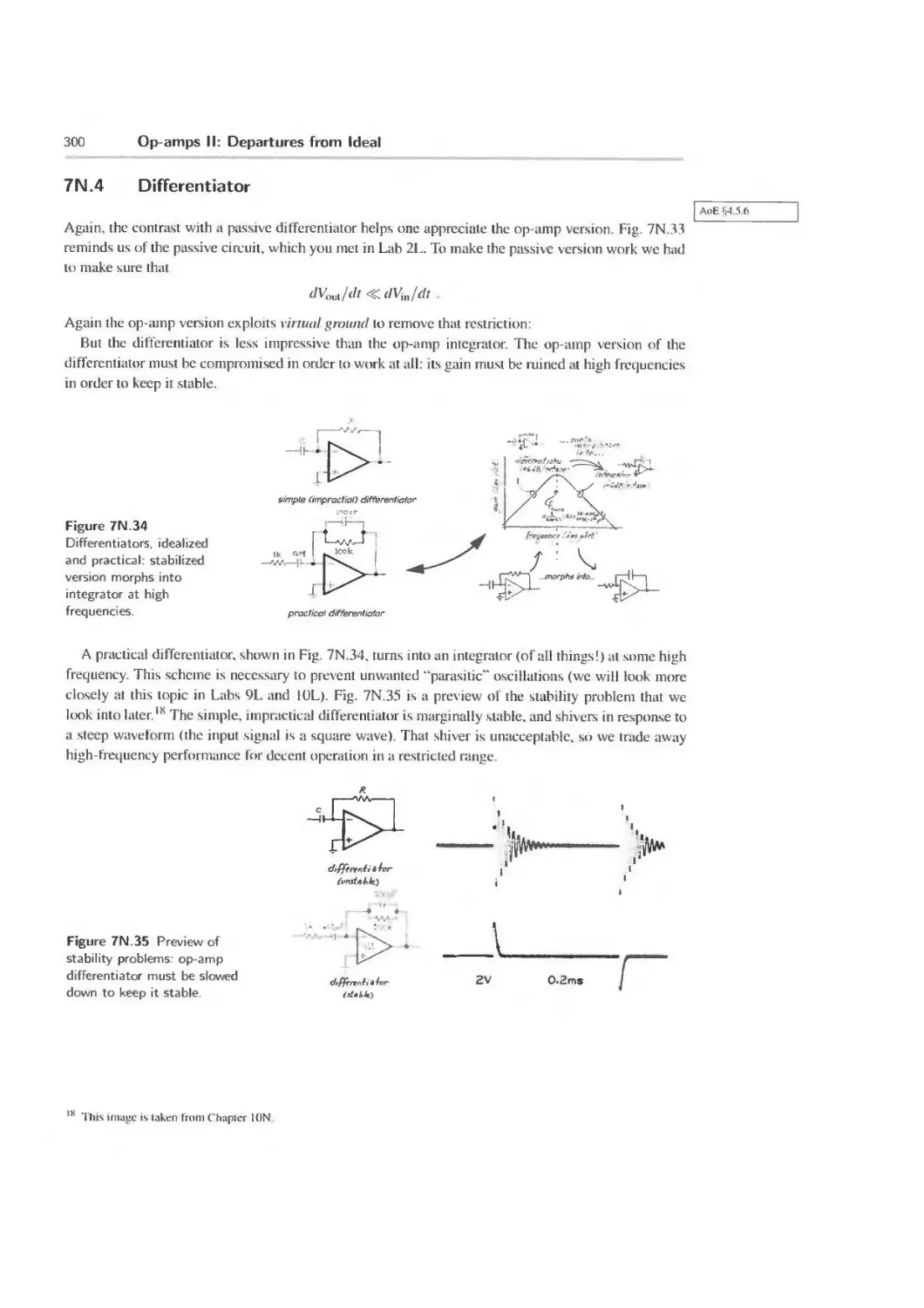
7N.4 Differentiator 300
7N.5 Op amp Difference Amplifier 301
7N.6 AC amplifier: an elegant way to minimize effects of op-amp DC errors 301
7N.7 AoE Reading 302
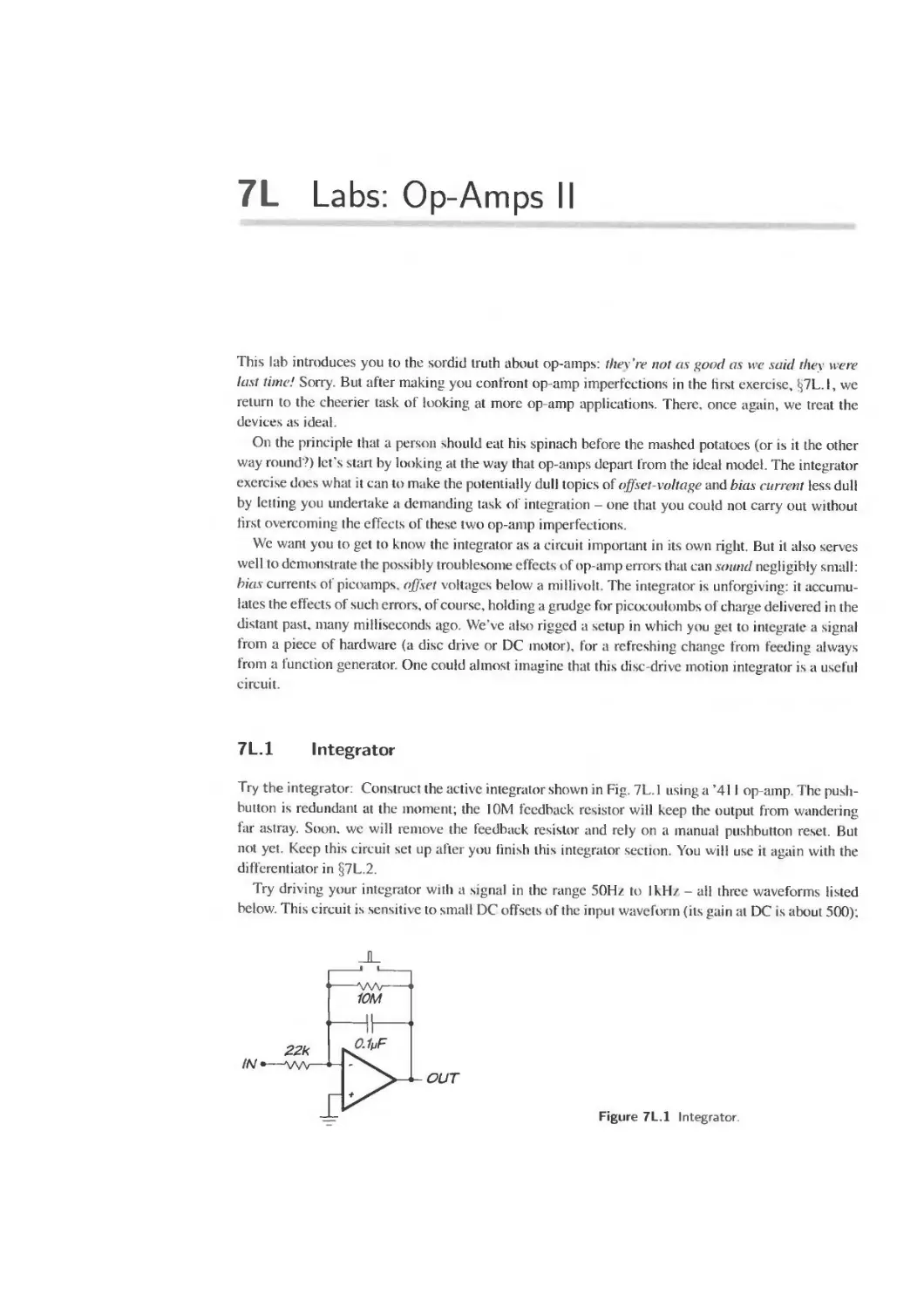
7L Labs: Op-Amps II 303
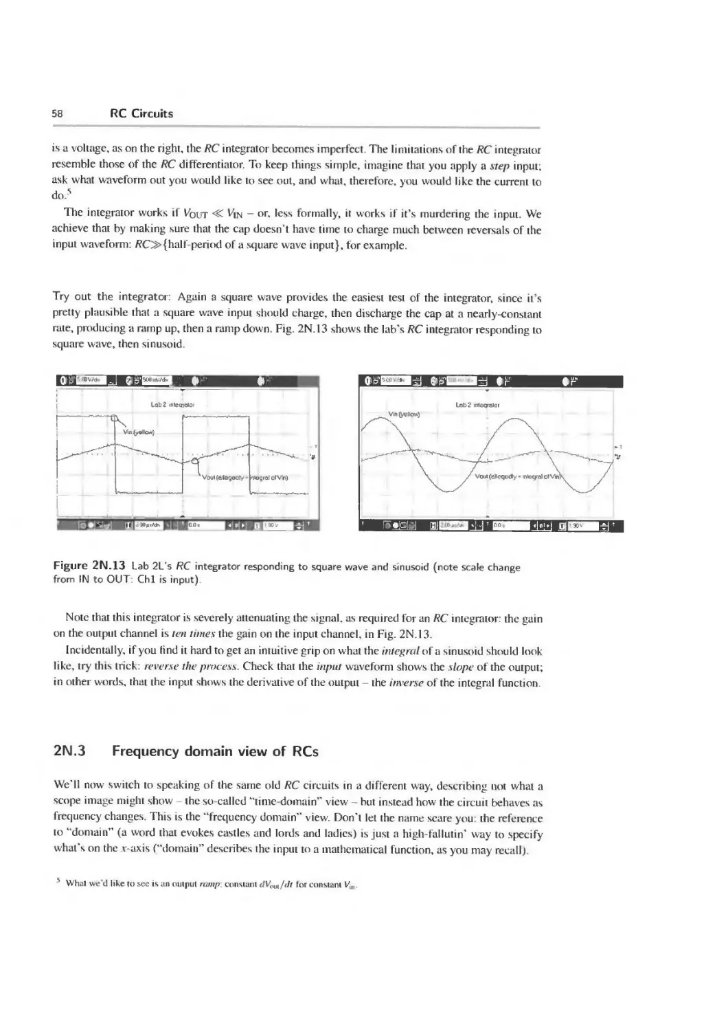
7L. 1 Integrator 303
7L.2 Differentiator 306
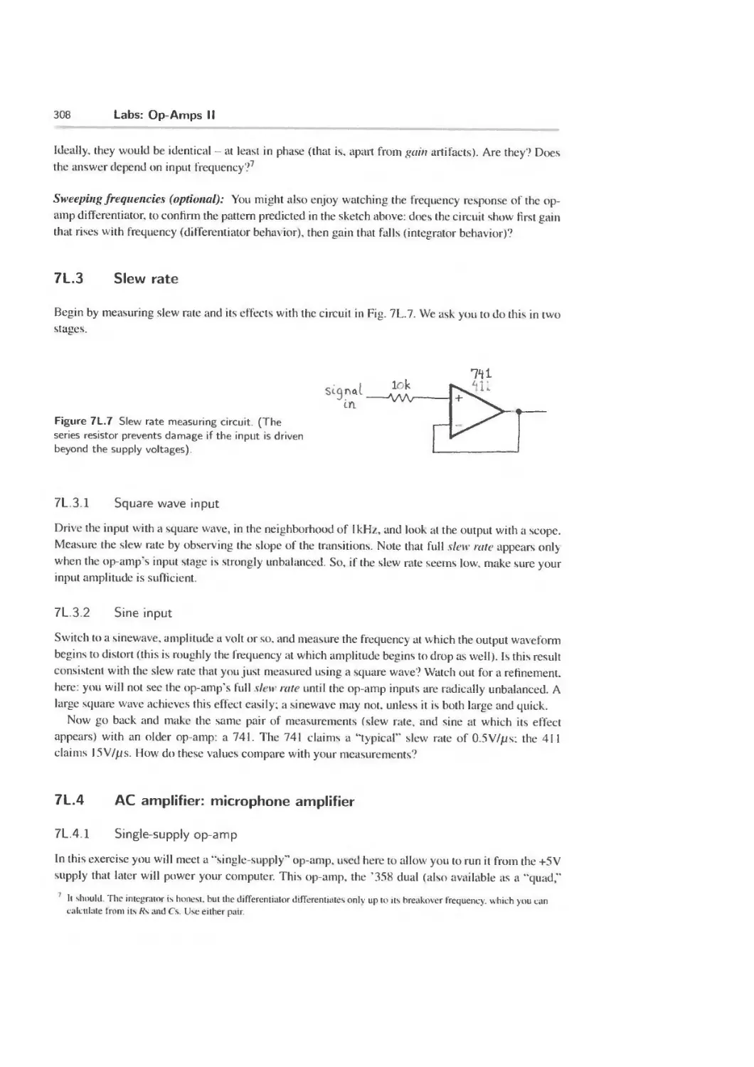
7L.3 Slew rate 308
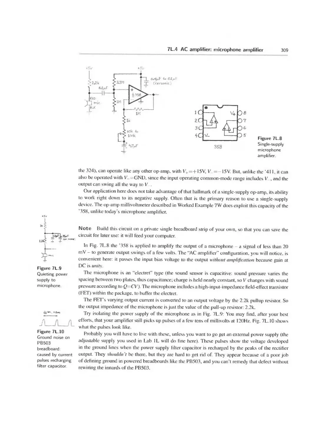
7L.4 AC amplifier: microphone amplifier 308
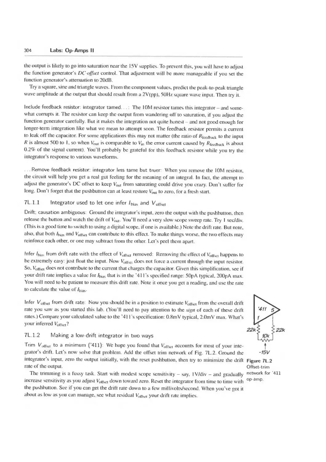
7S Supplementary Notes: Op-Amp Jargon 310
Contents
xi
7W Worked Examples: Op-Amps II 311
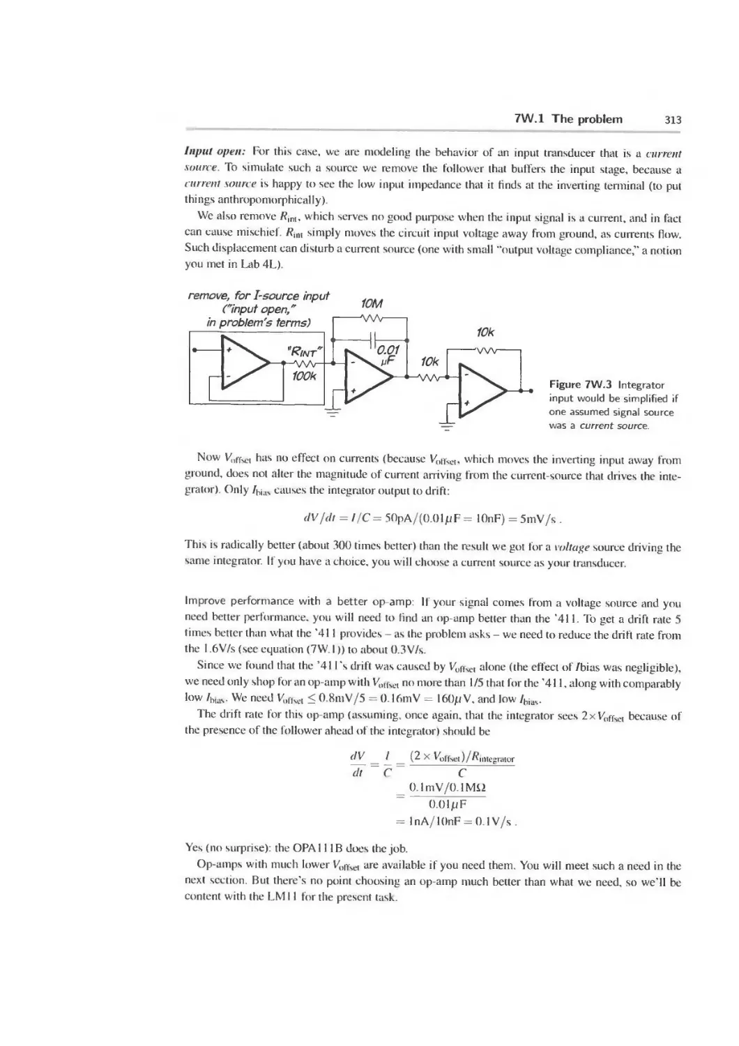
7W. 1 The problem 311
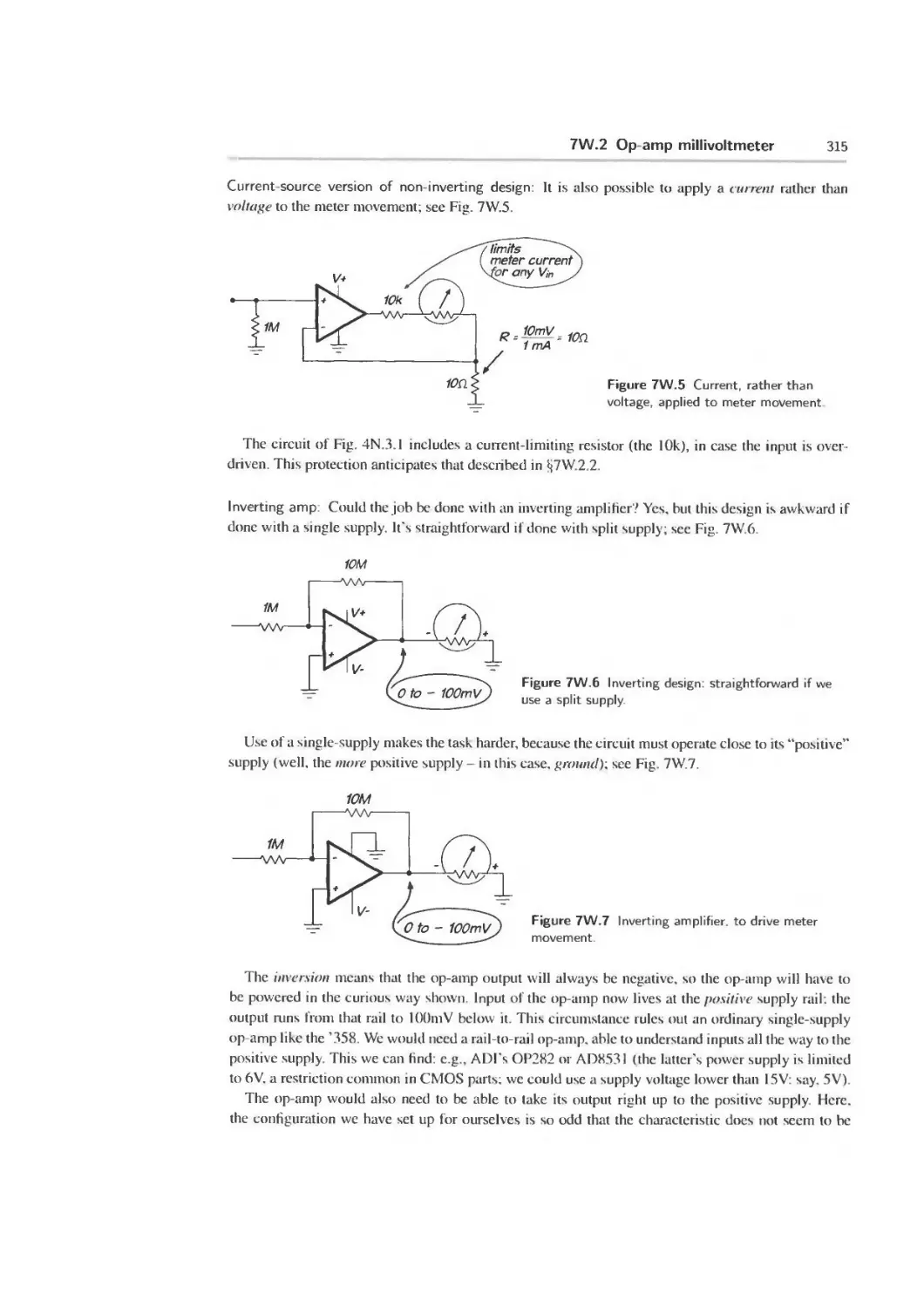
7W.2 Op-amp millivoltmeter 314
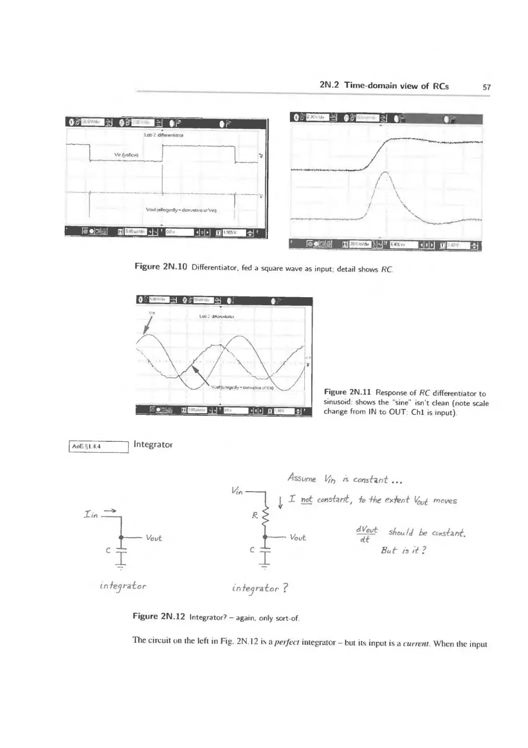
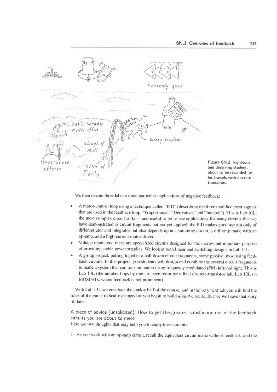
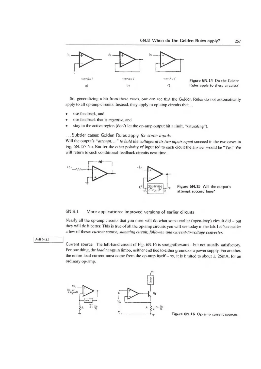
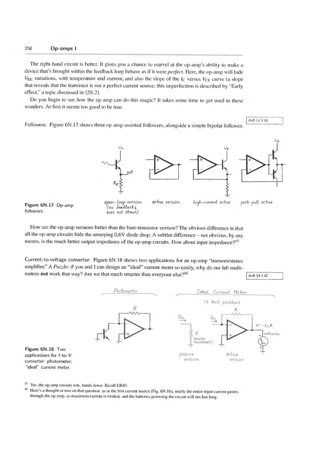
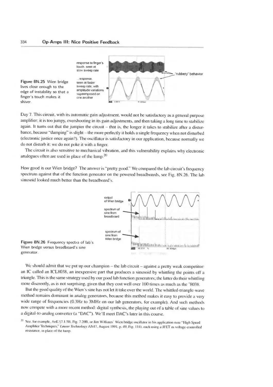
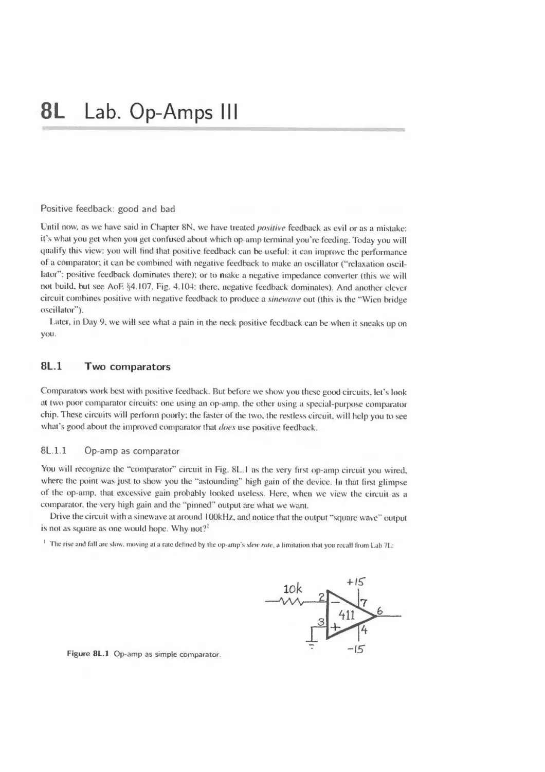
8M Op-Amps III: Nice Positive Feedback 319
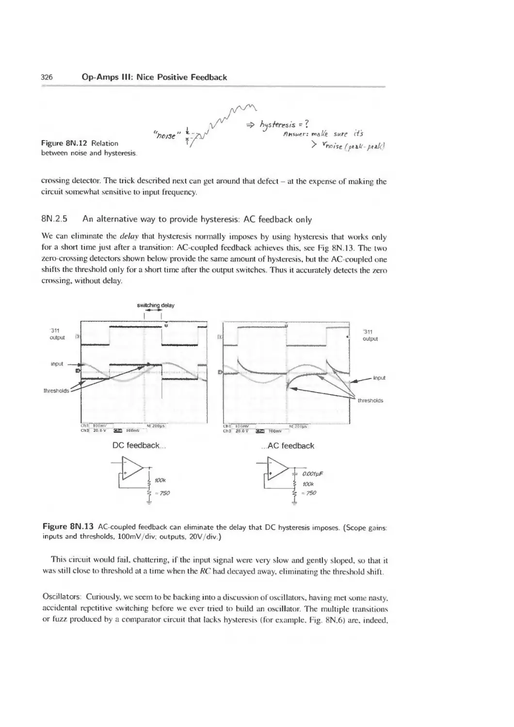
8N.1 Useful positive feedback 319
8N.2 Comparators 320
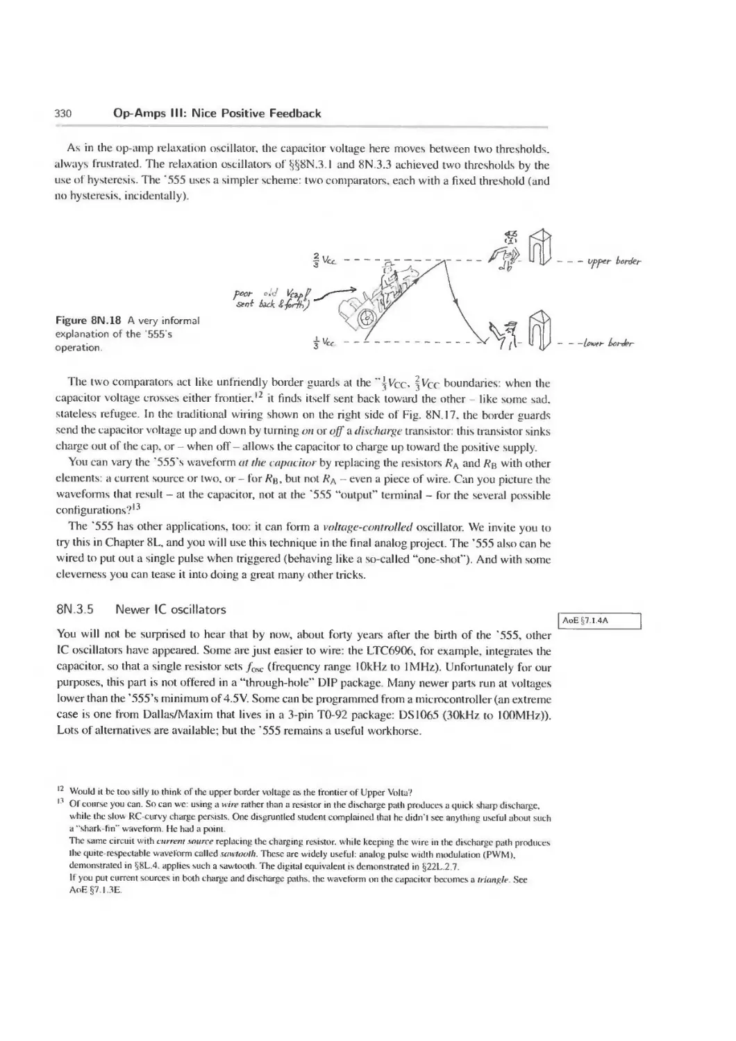
8N.3 RC relaxation oscillator 327
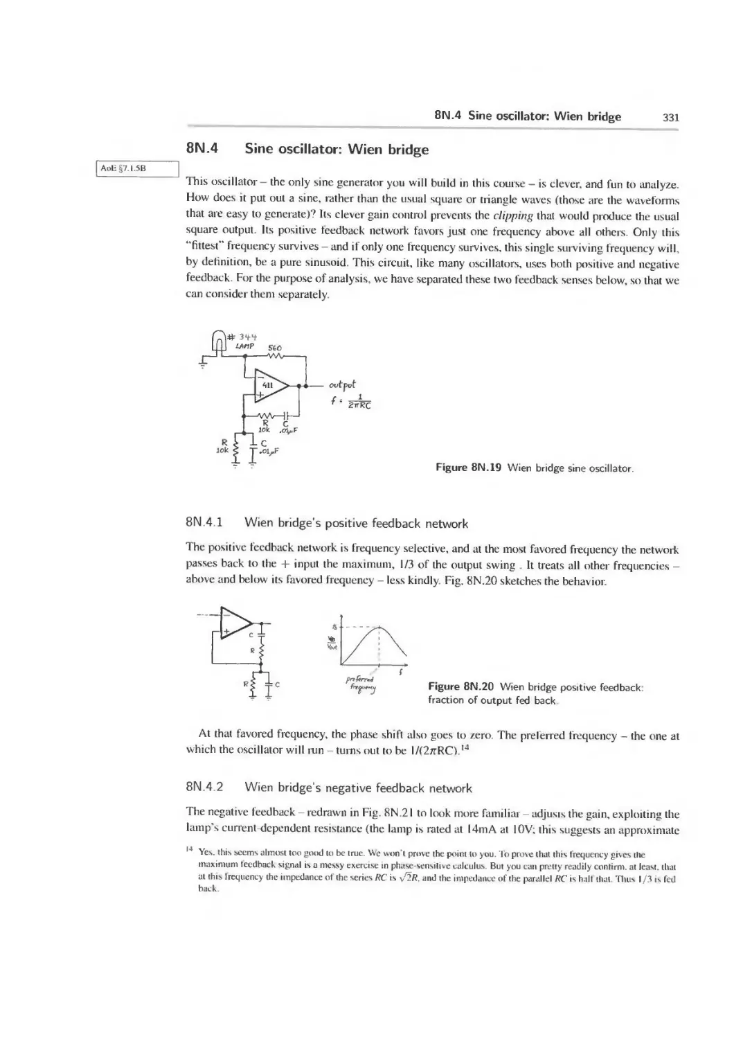
8N.4 Sine oscillator: Wien bridge 331
8N.5 AoE Reading 335
8L Lab. Op-Amps 111 336
8L. 1 Two comparators 336
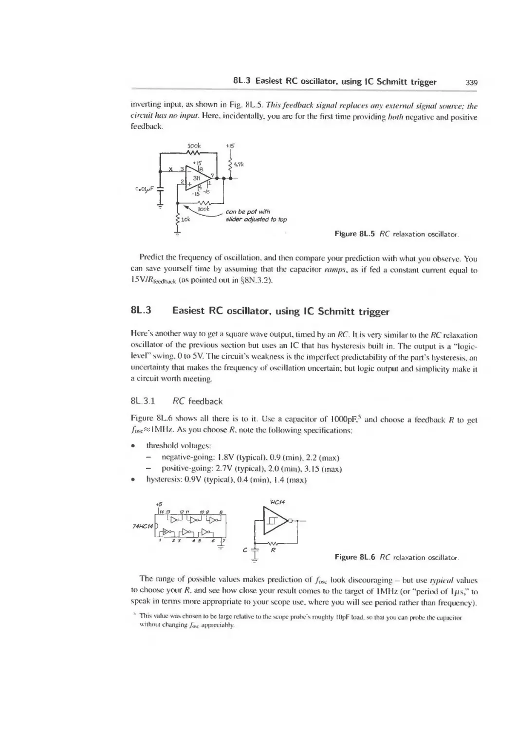
8L.2 Op-amp RC relaxation oscillator 338
8L.3 Easiest RC oscillator, using IC Schmitt trigger 339
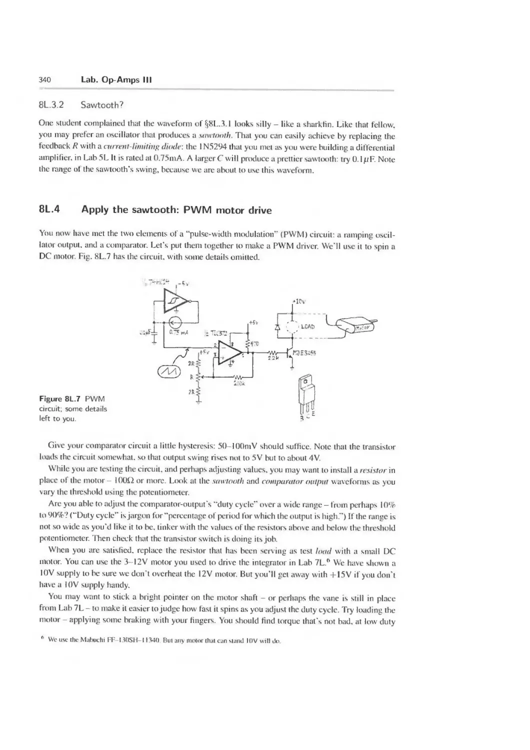
8L.4 Apply the sawtooth: PWM motor drive 340
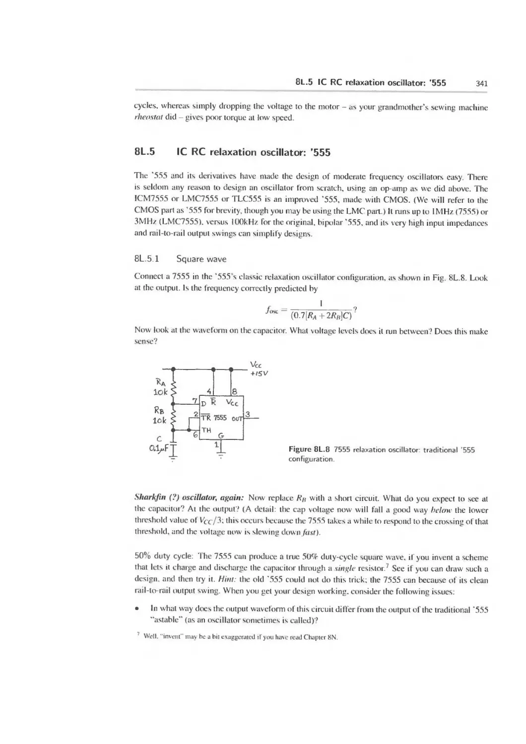
8L.5 IC RC relaxation oscillator: ’555 341
8L.6 ’555 for low-frequency frequency modulation (“FM”) 342
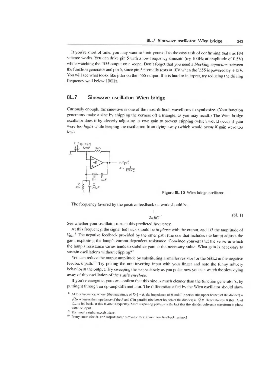
8L.7 Sinewave oscillator: Wien bridge 343
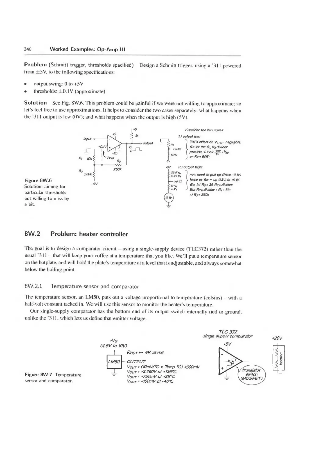
8W Worked Examples: Op-Amp HI 345
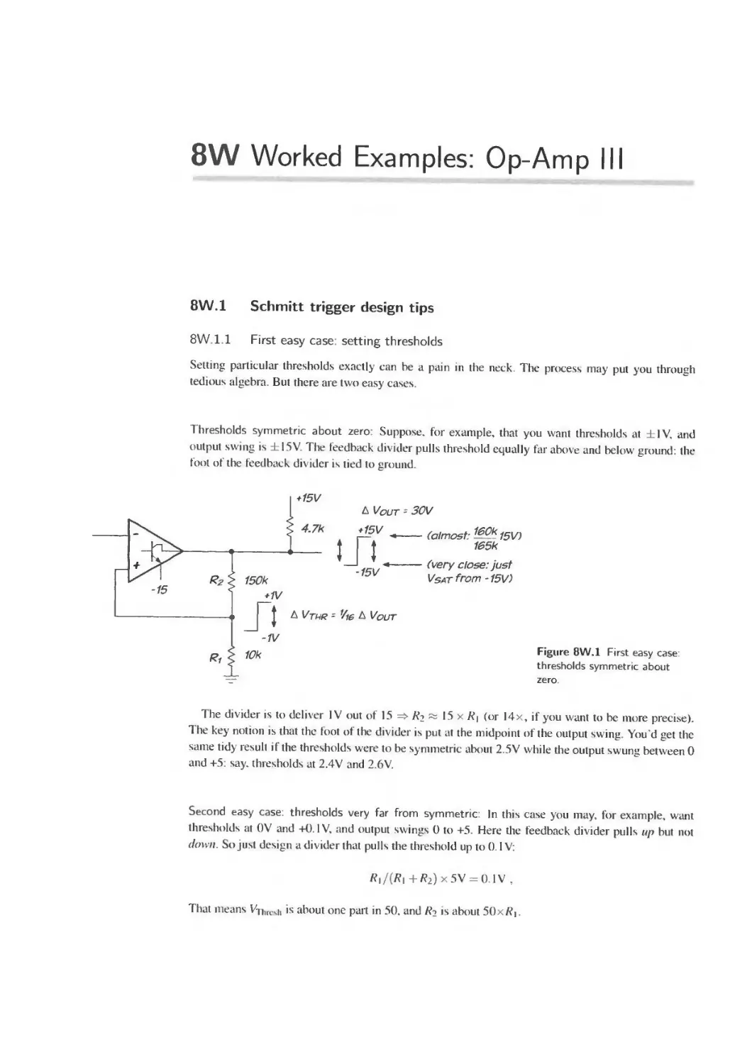
8W. 1 Schmitt trigger design tips 345
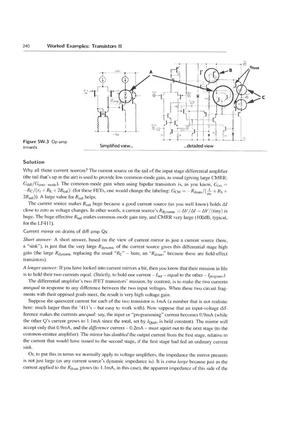
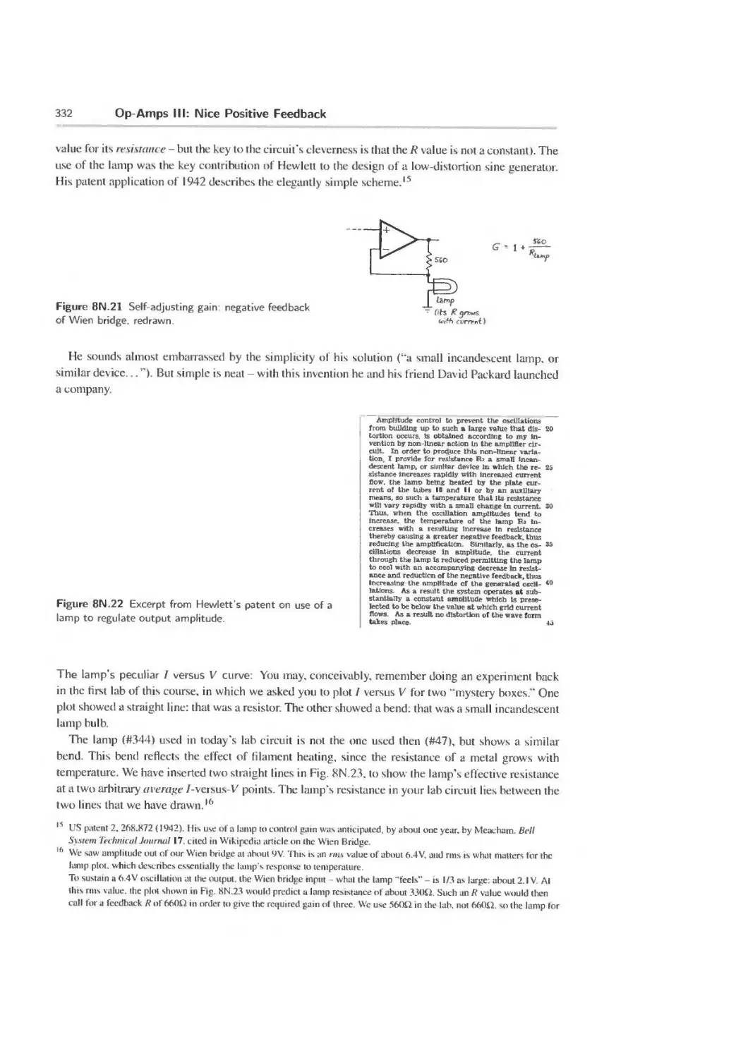
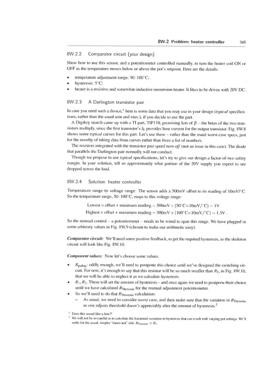
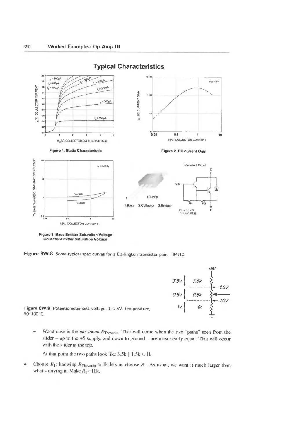
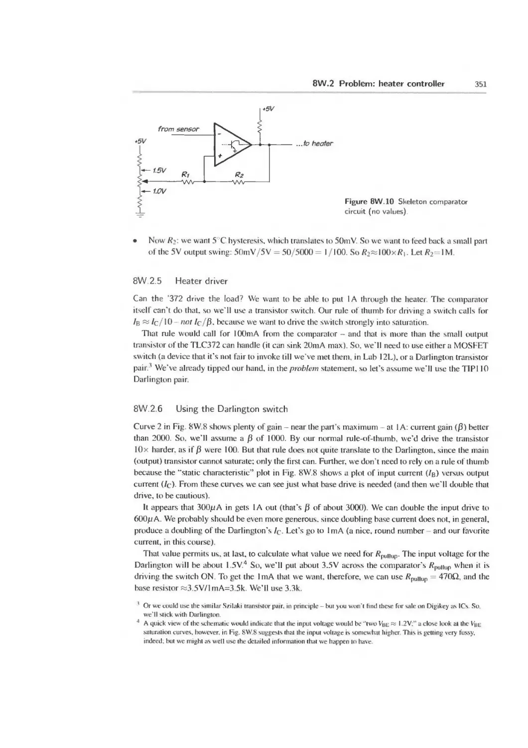
8W.2 Problem: heater controller 348
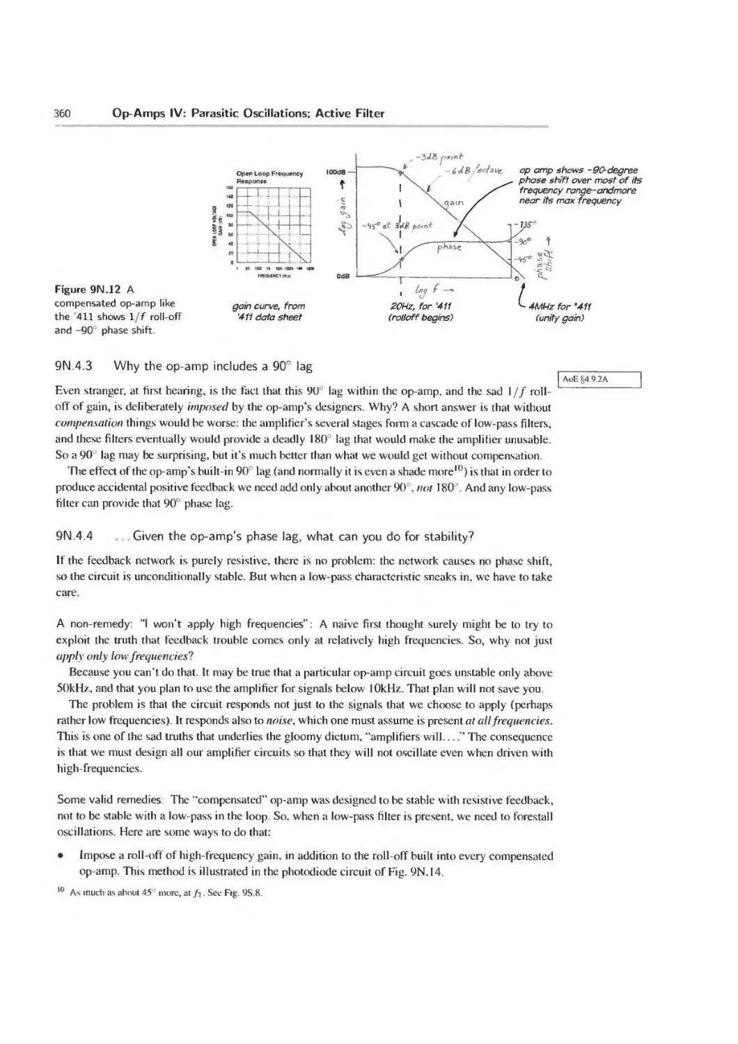
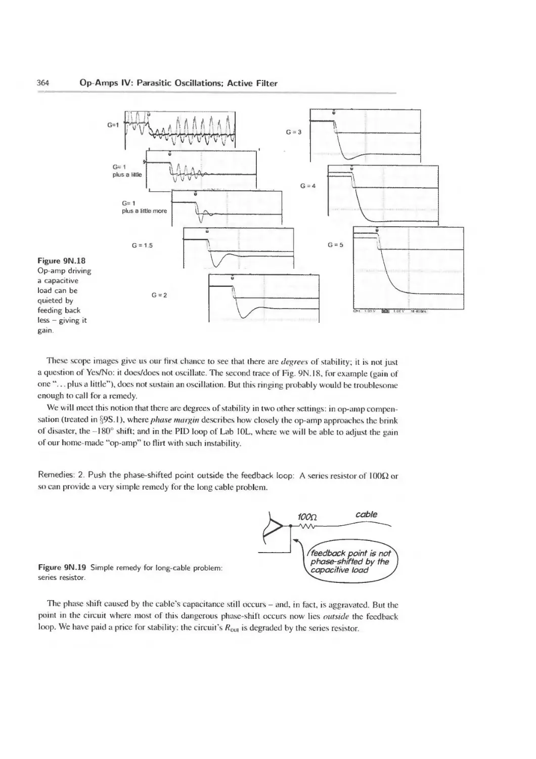
9N Op-Amps IV: Parasitic Oscillations; Active Filter 353
9N.1 Introduction 353
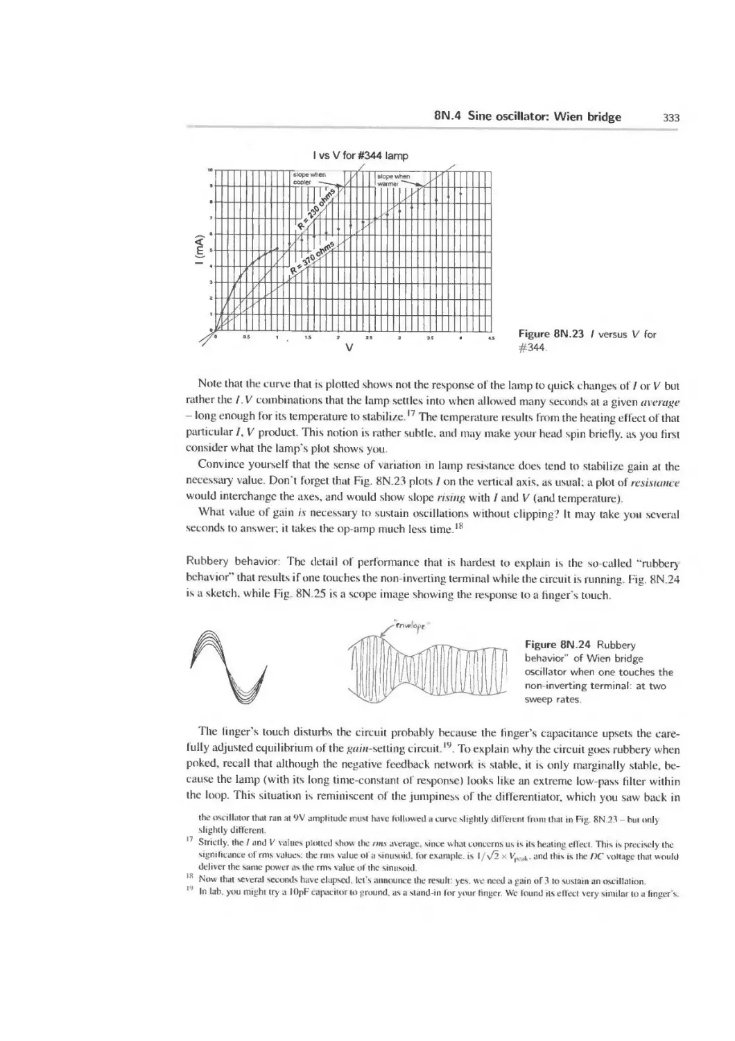
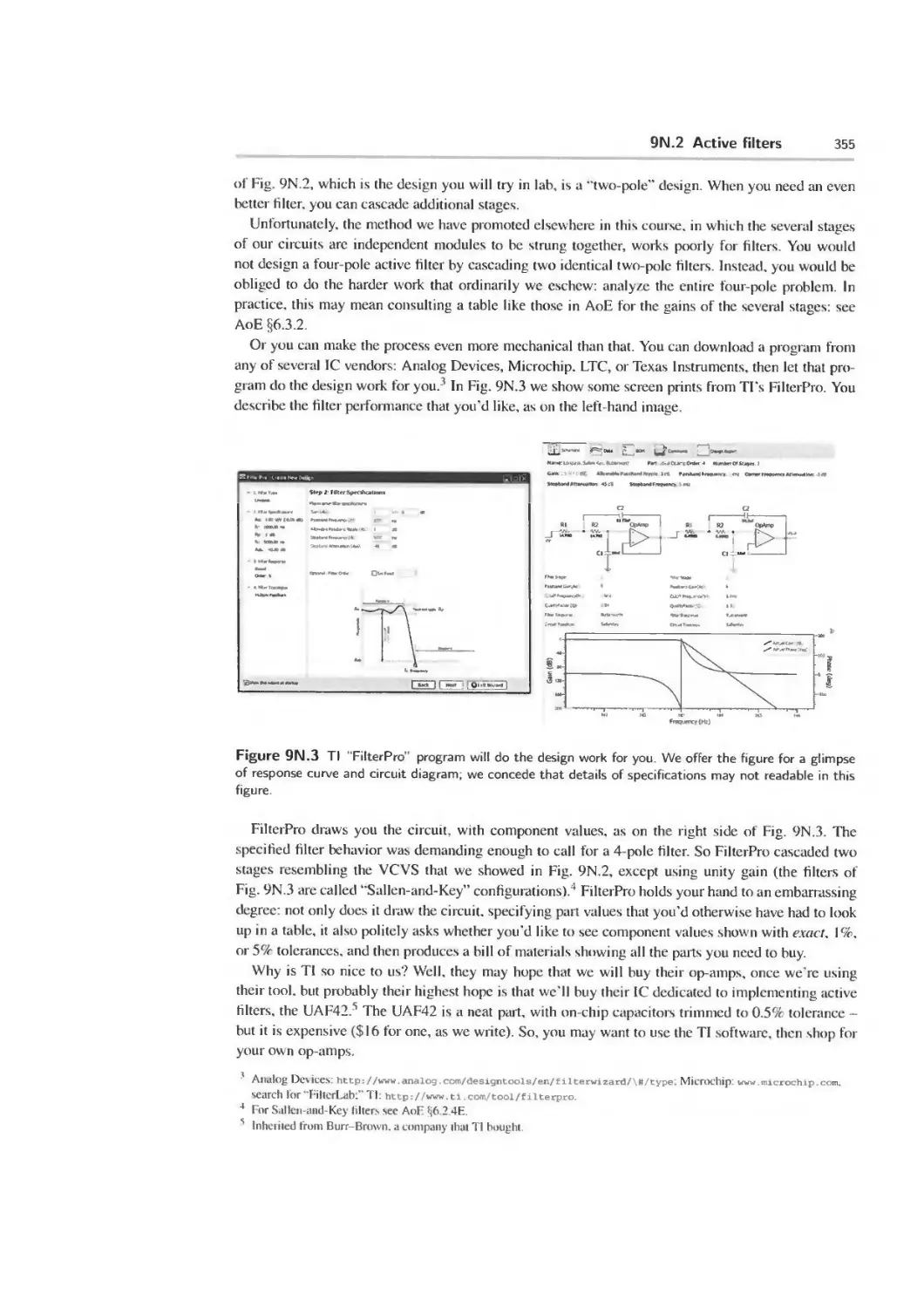
9N.2 Active filters 354
9N.3 Nasty “parasitic” oscillations: the problem, generally 356
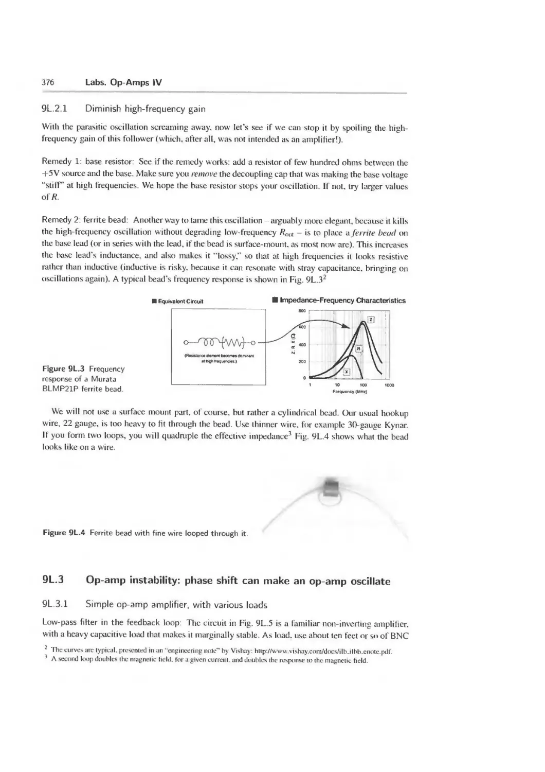
9N.4 Parasitic oscillations in op-amp circuits 356
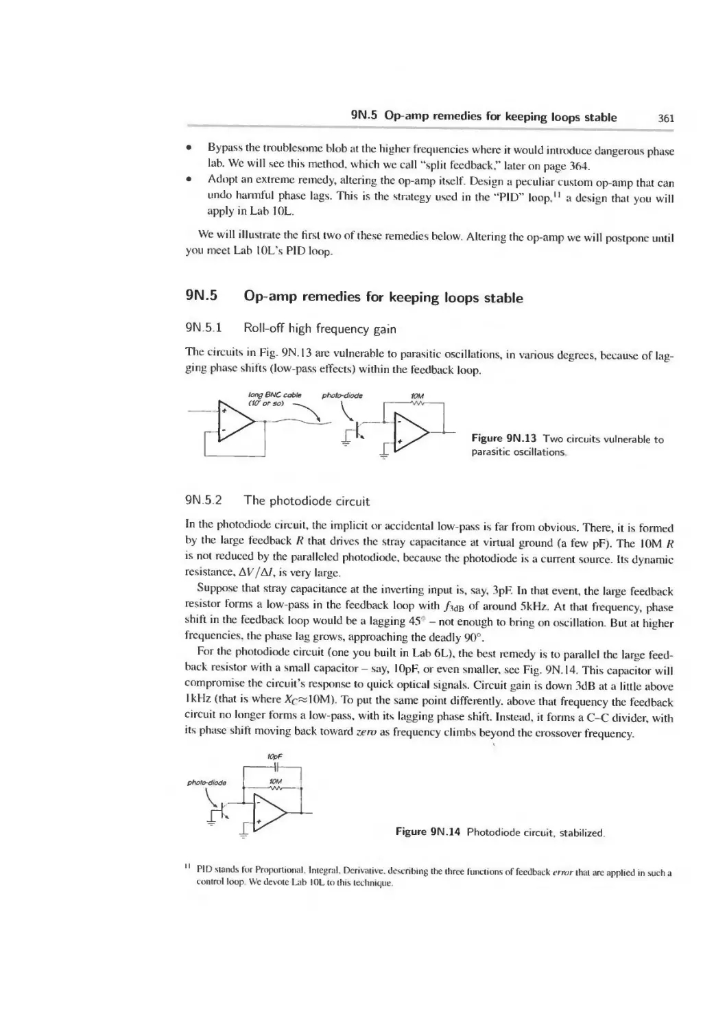
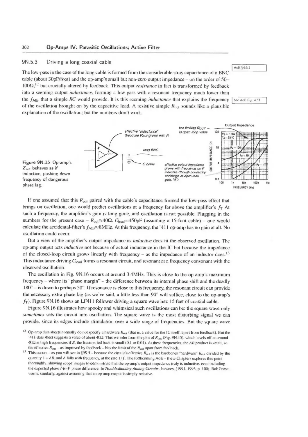
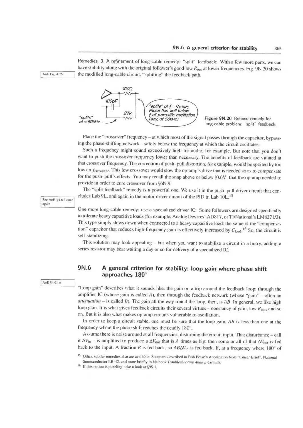
9N.5 Op-amp remedies for keeping loops stable 361
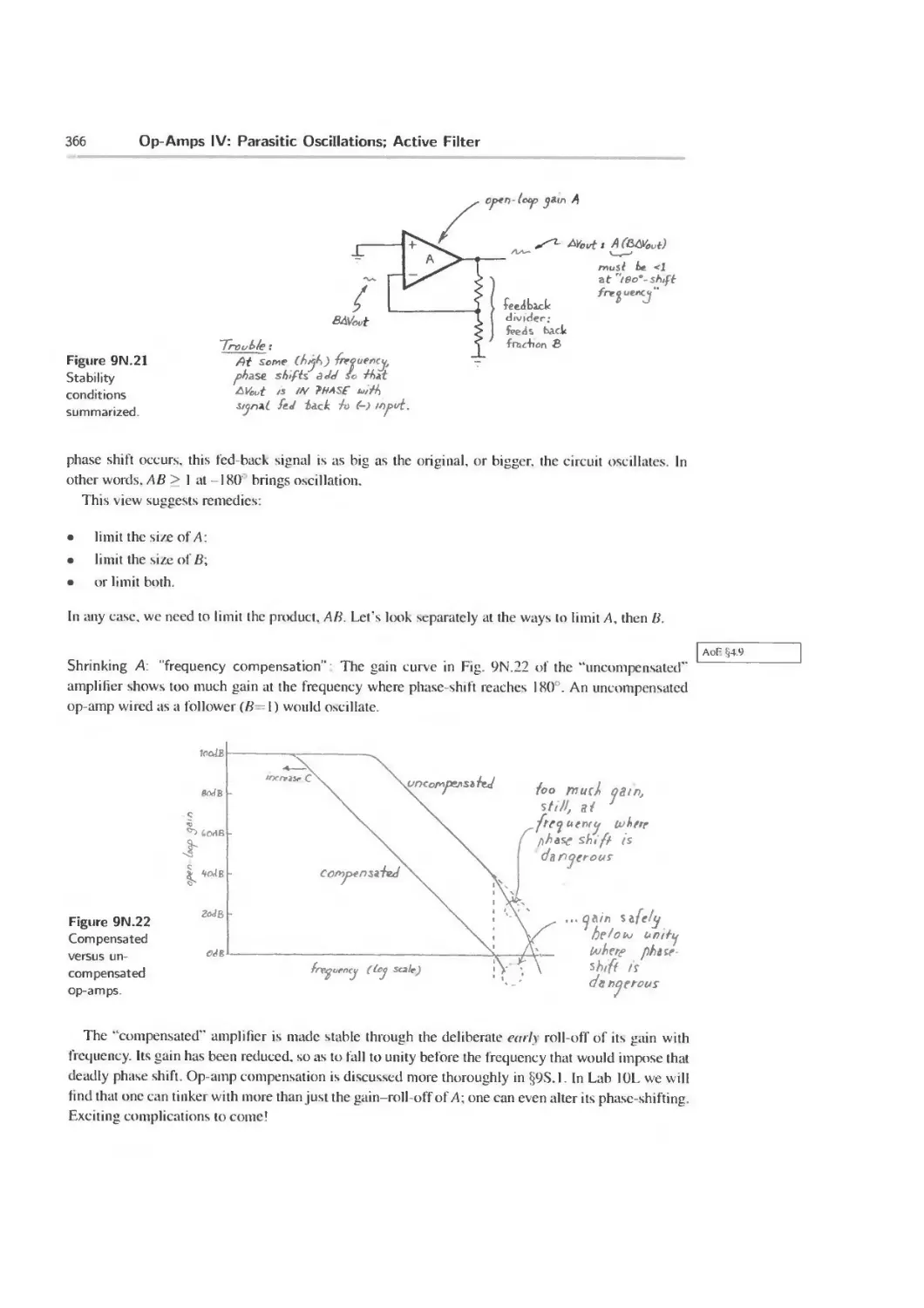
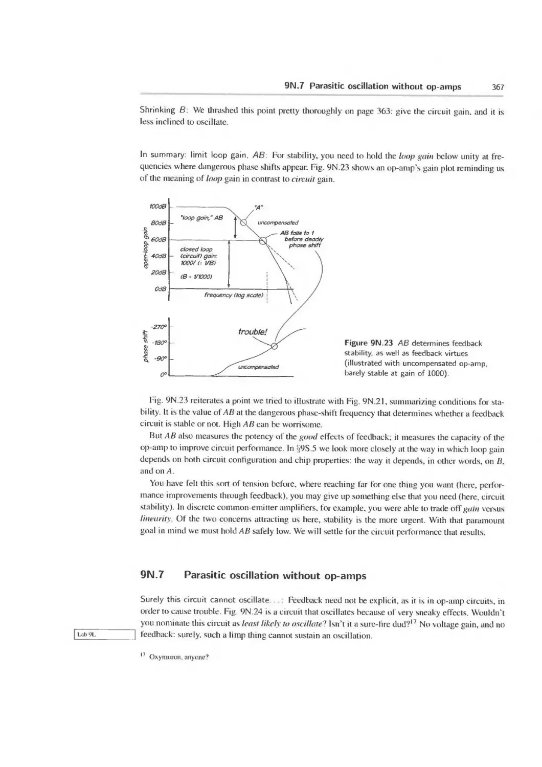
9N.6 A general criterion for stability 365
9N.7 Parasitic oscillation without op-amps 367
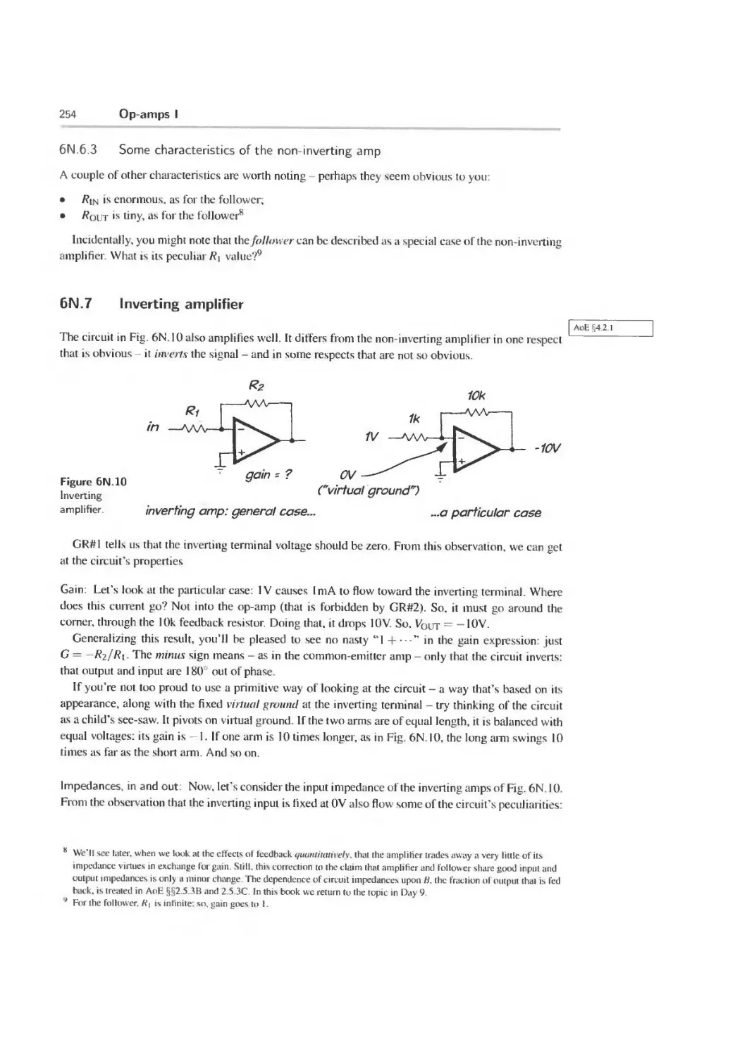
9N.8 Remedies for parasitic oscillation 370
9N.9 Recapitulation: to keep circuits quiet... 372
9N.10 AoE Reading 372
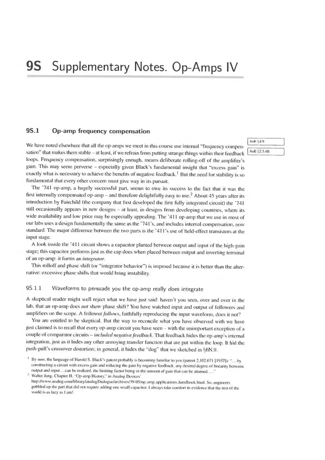
9L Labs. Op-Amps IV 373
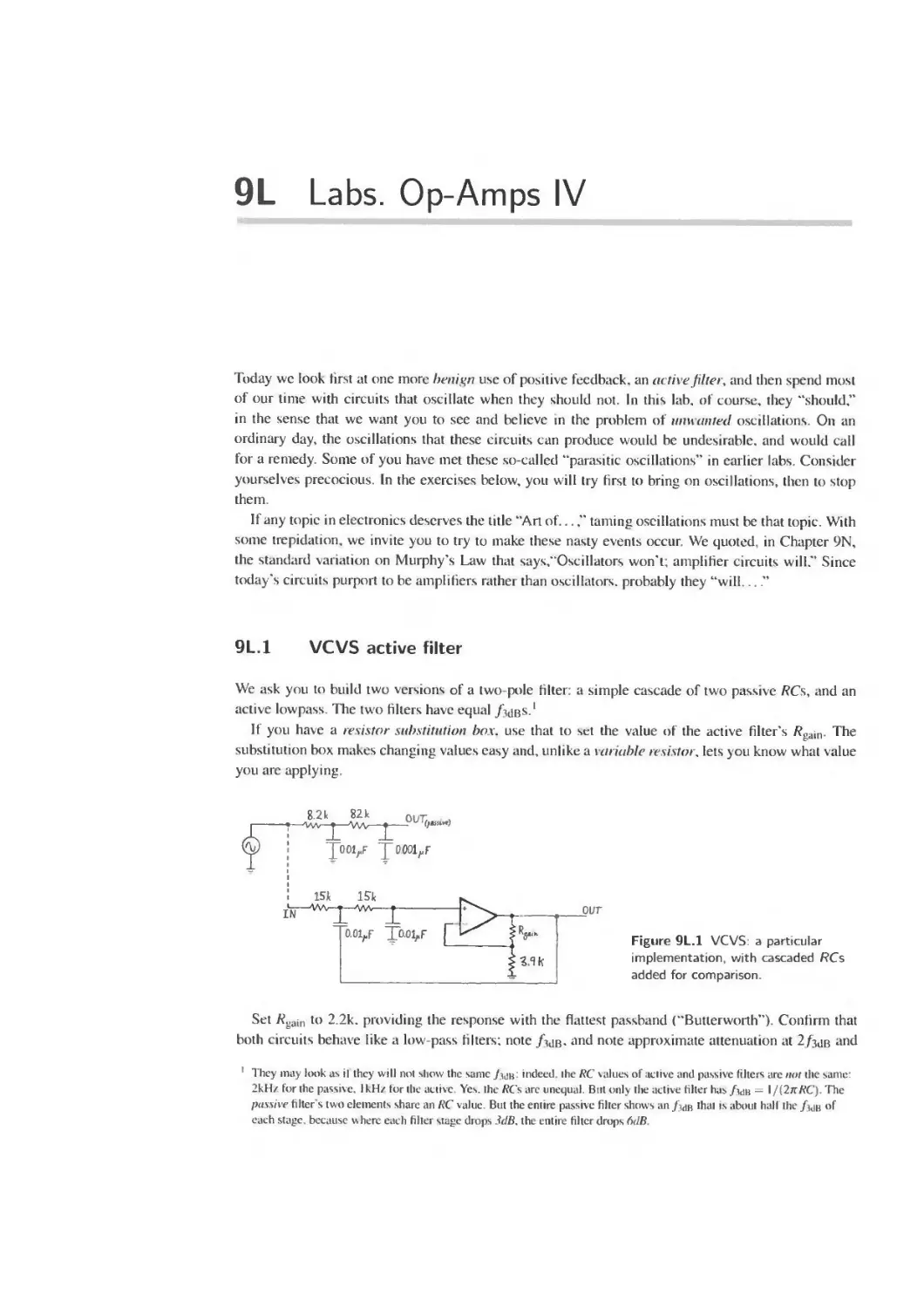
9L.1 VCVS active filter 373
9L.2 Discrete transistor follower 374
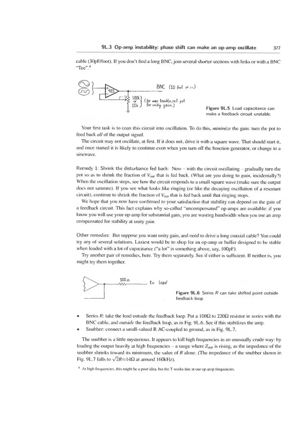
9L.3 Op-amp instability: phase shift can make an op-amp oscillate 376
9L.4 Op-amp with buffer in feedback loop 378
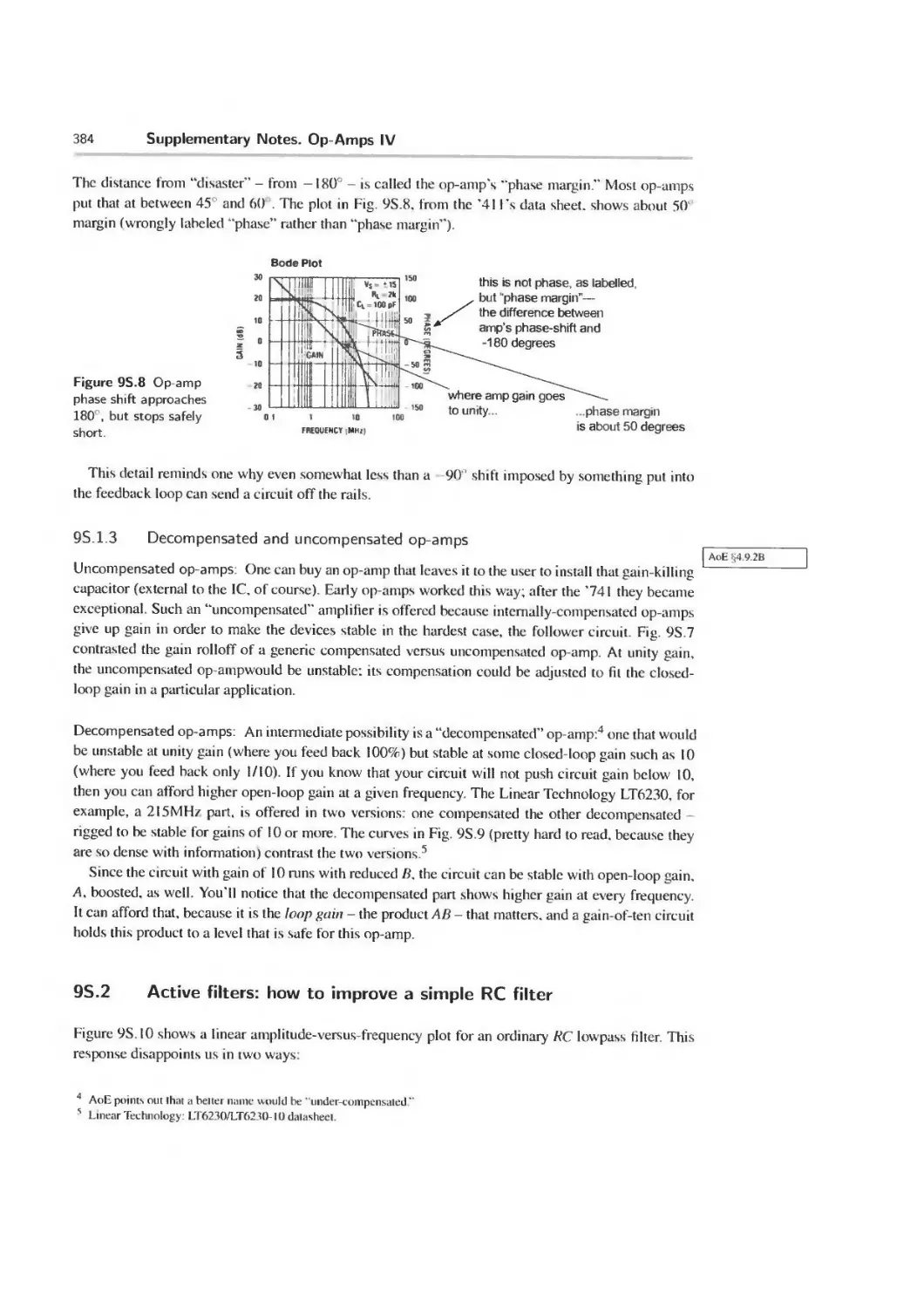
9S Supplementary Notes. Op-Amps IV 380
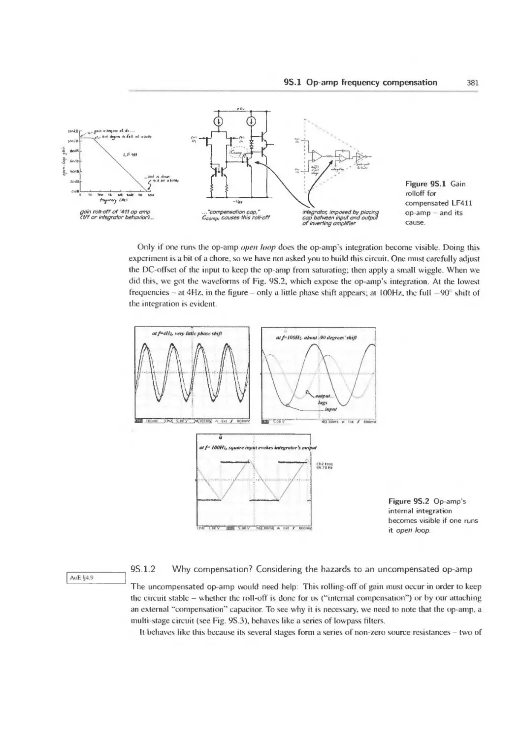
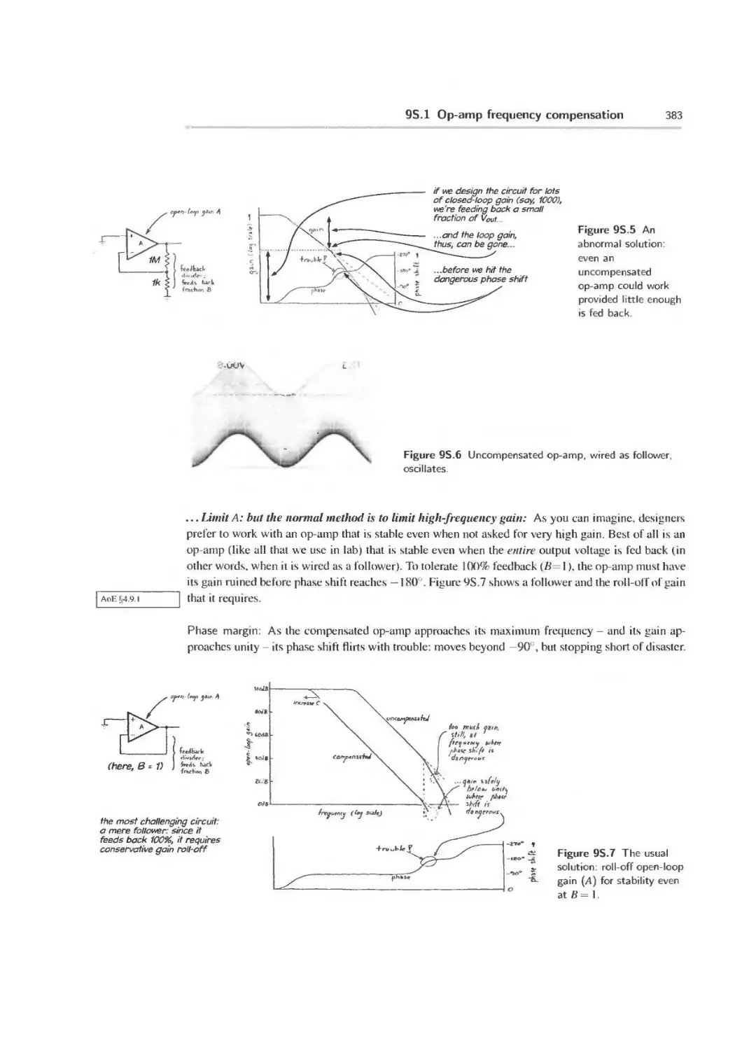
9S. 1 Op-amp frequency compensation 380
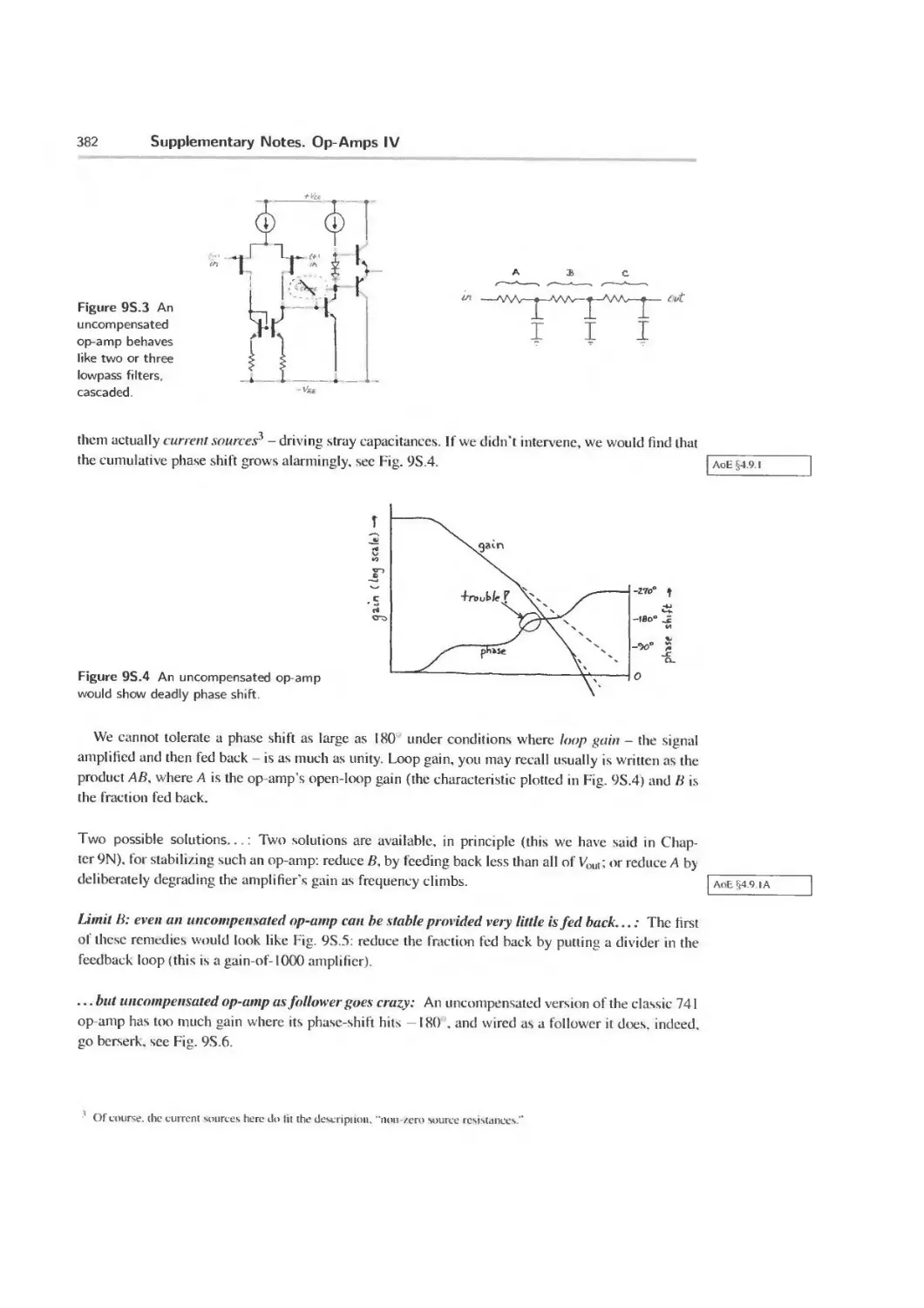
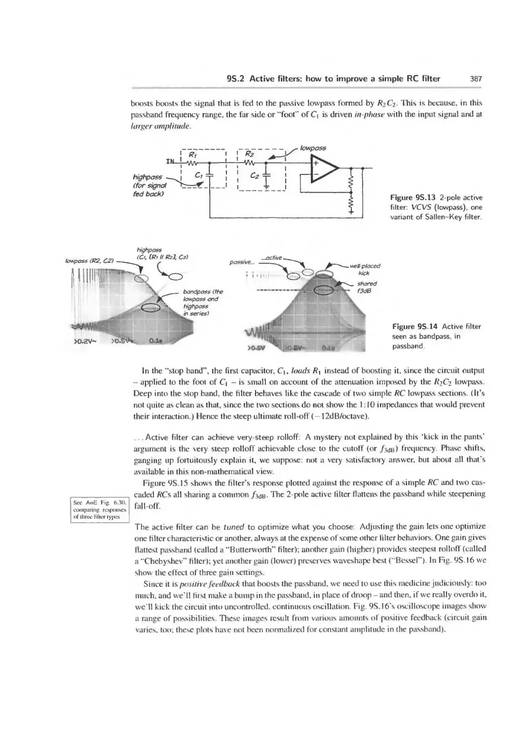
9S.2 Active filters: how to improve a simple RC filter 384
9S.3 Noise: diagnosing fuzz 389
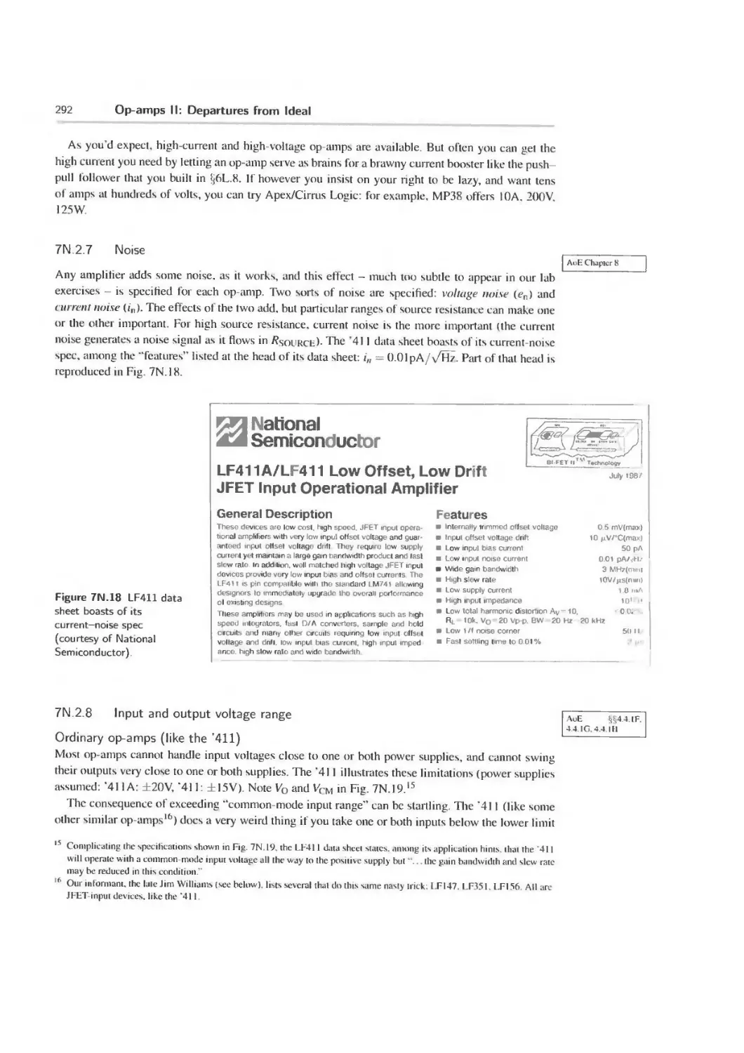
9S.4 Annotated LF411 op-amp schematic 395
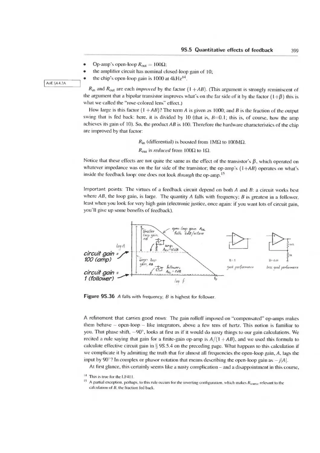
9S.5 Quantitative effects of feedback 396
xii Contents
9W Worked Examples: Op-Amps IV 401
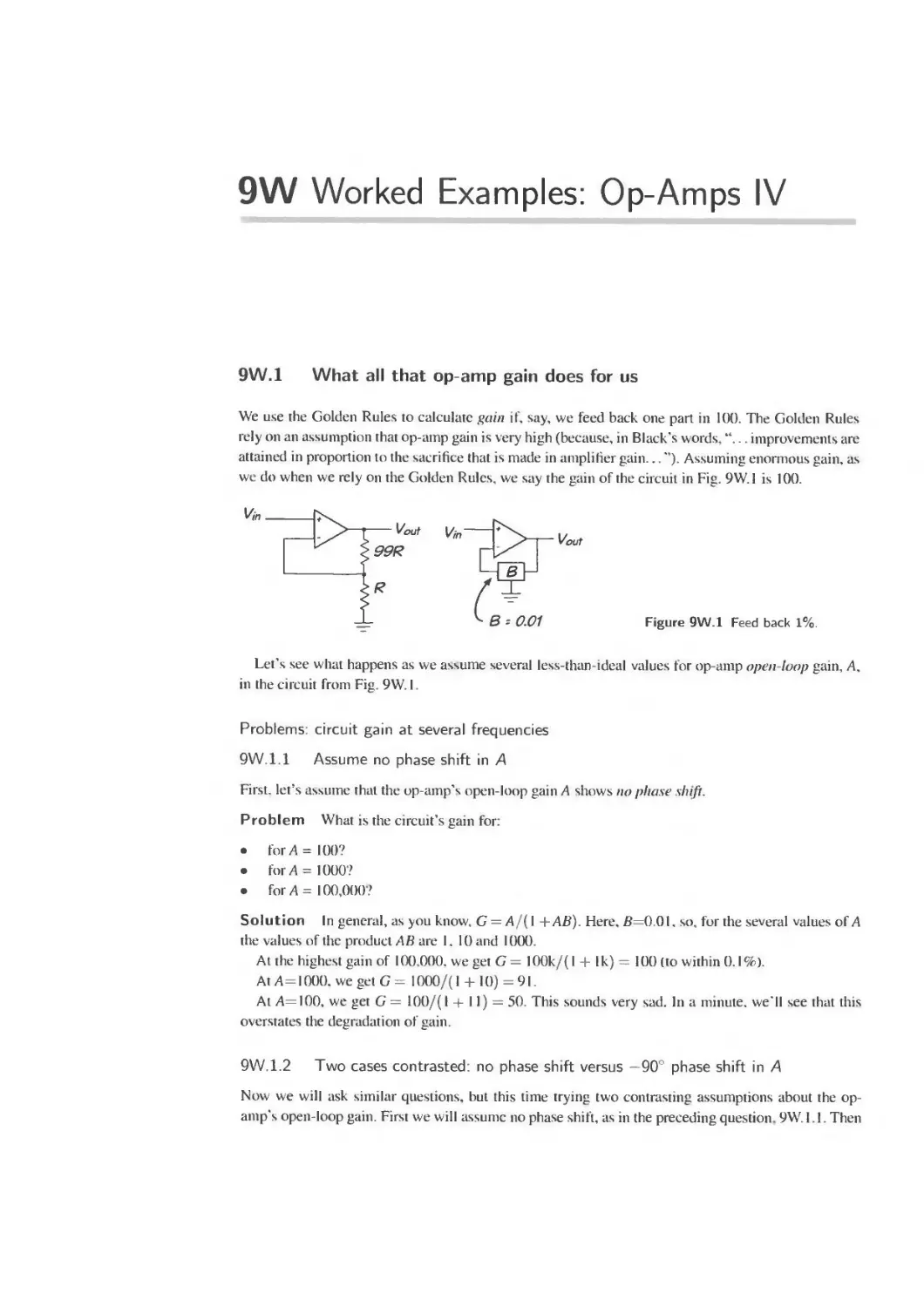
9W. 1 What all that op-ainp gain does for us 401
9W.2 Stability questions 402
ION Op-Amps V: PID Motor Control Loop 407
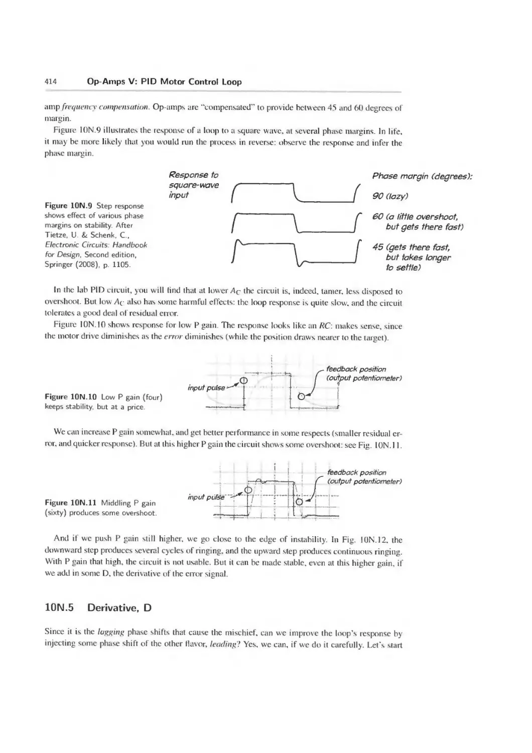
ION 1 Examples of real problems that call for this remedy 408
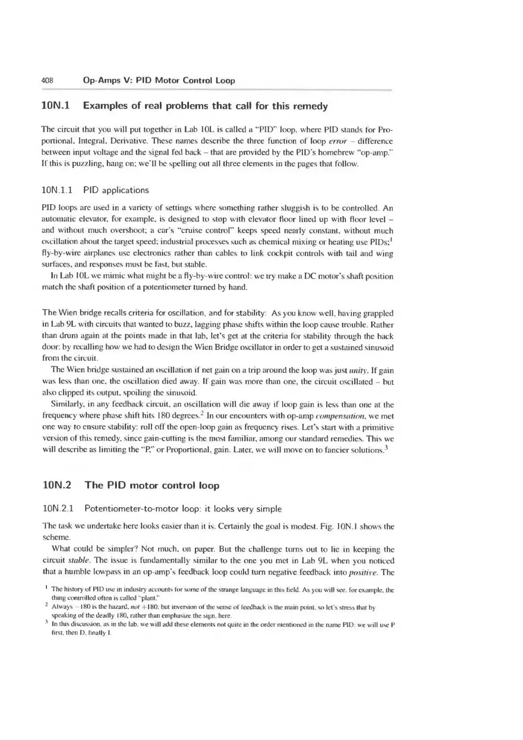
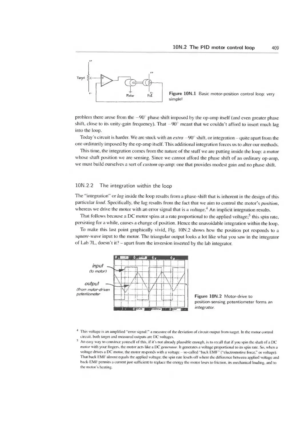
10N.2 The PID motor control loop 408
10N.3 Designing the controller (custom op-amp) 410
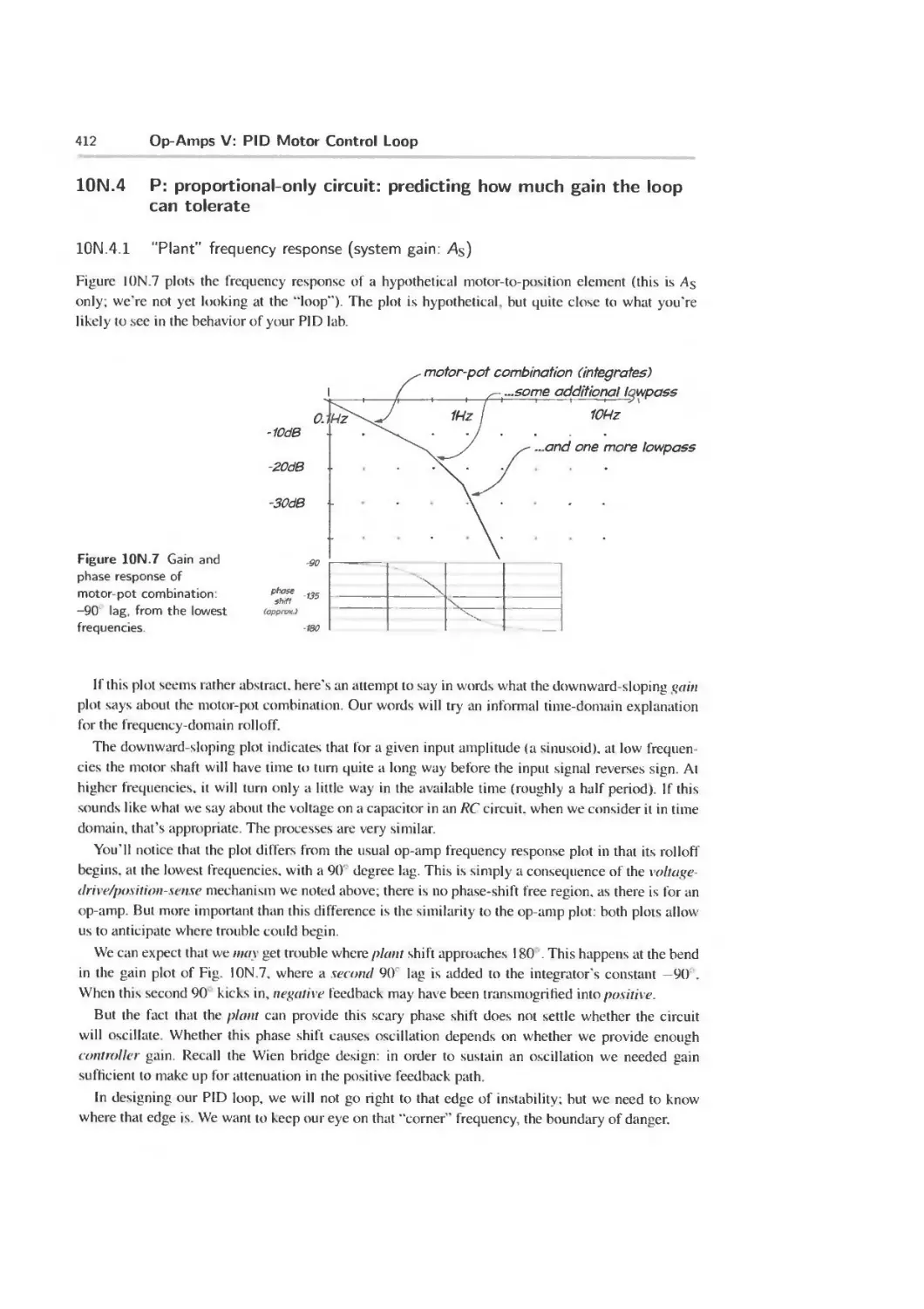
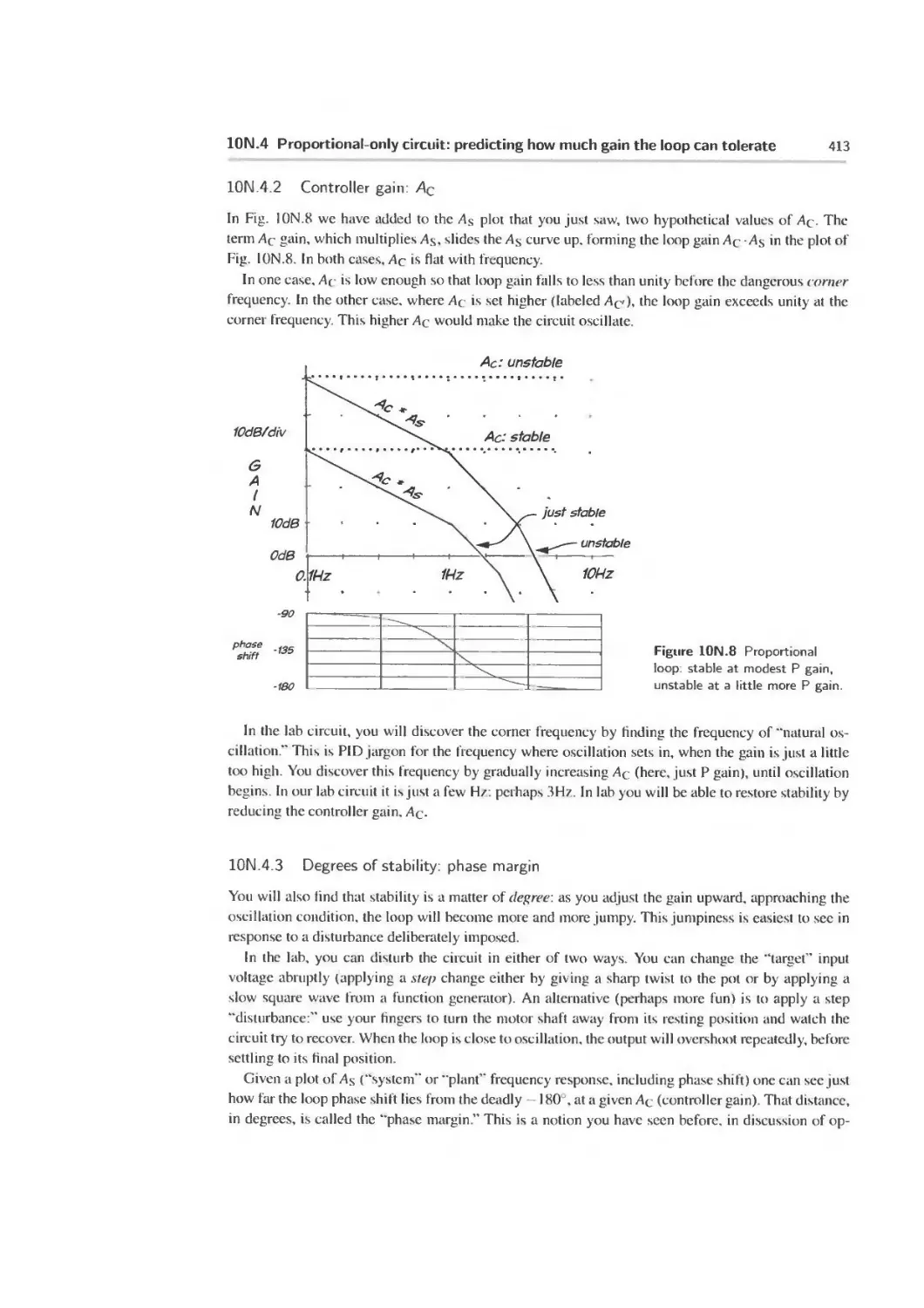
10N.4 Proportional-only circuit: predicting how much gain the loop can tolerate 412
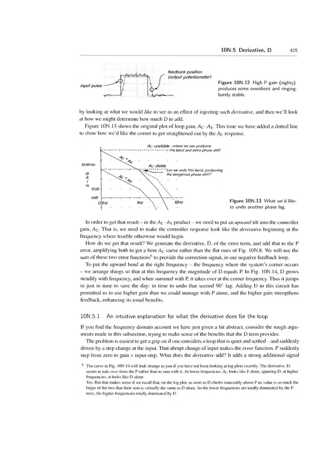
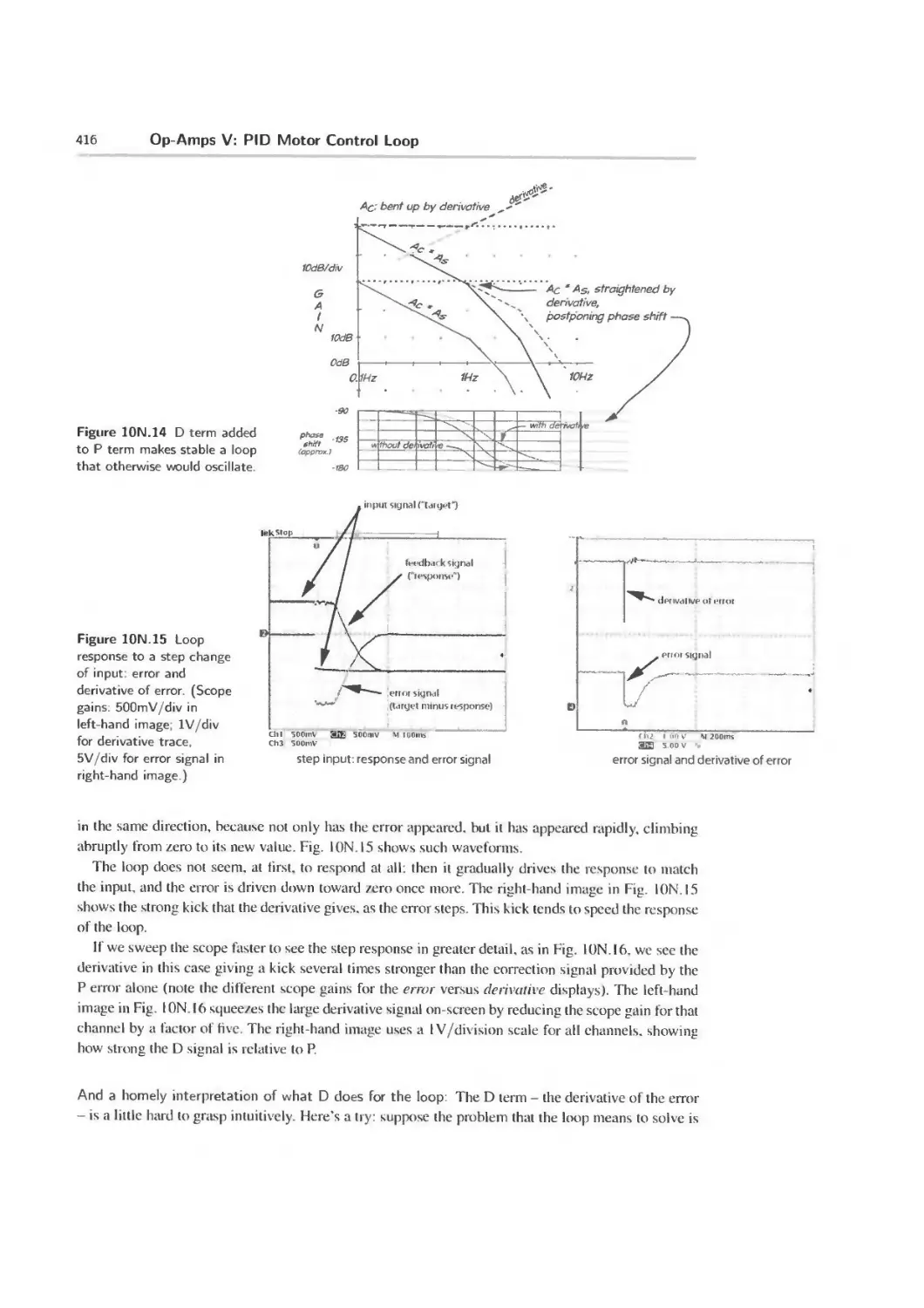
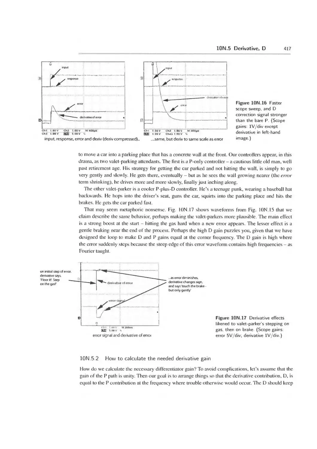
10N 5 Derivative. D 414
10N.6 AoE Reading 420
10L Lab. Op-Amps V 421
10L. 1 Introduction'why bother with the PID loop? 421
10L.2 PID motor control 422
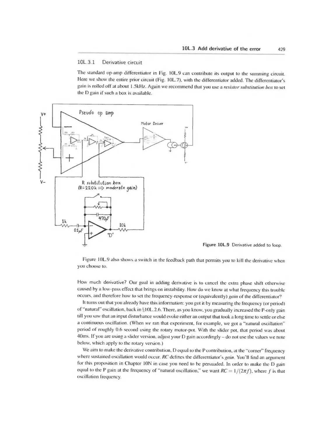
10L.3 Add derivative of the error 428
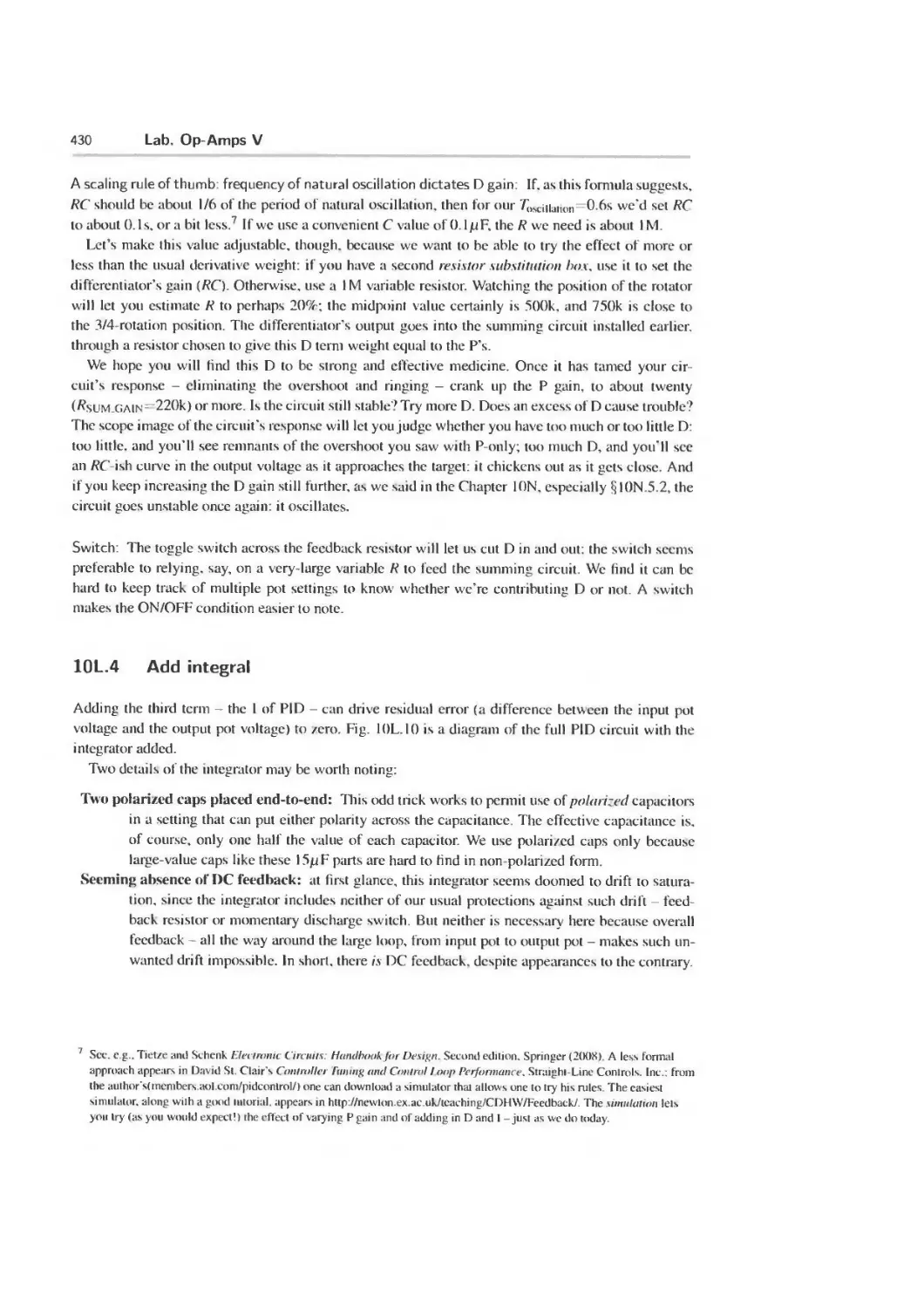
10L.4 Add integral 430
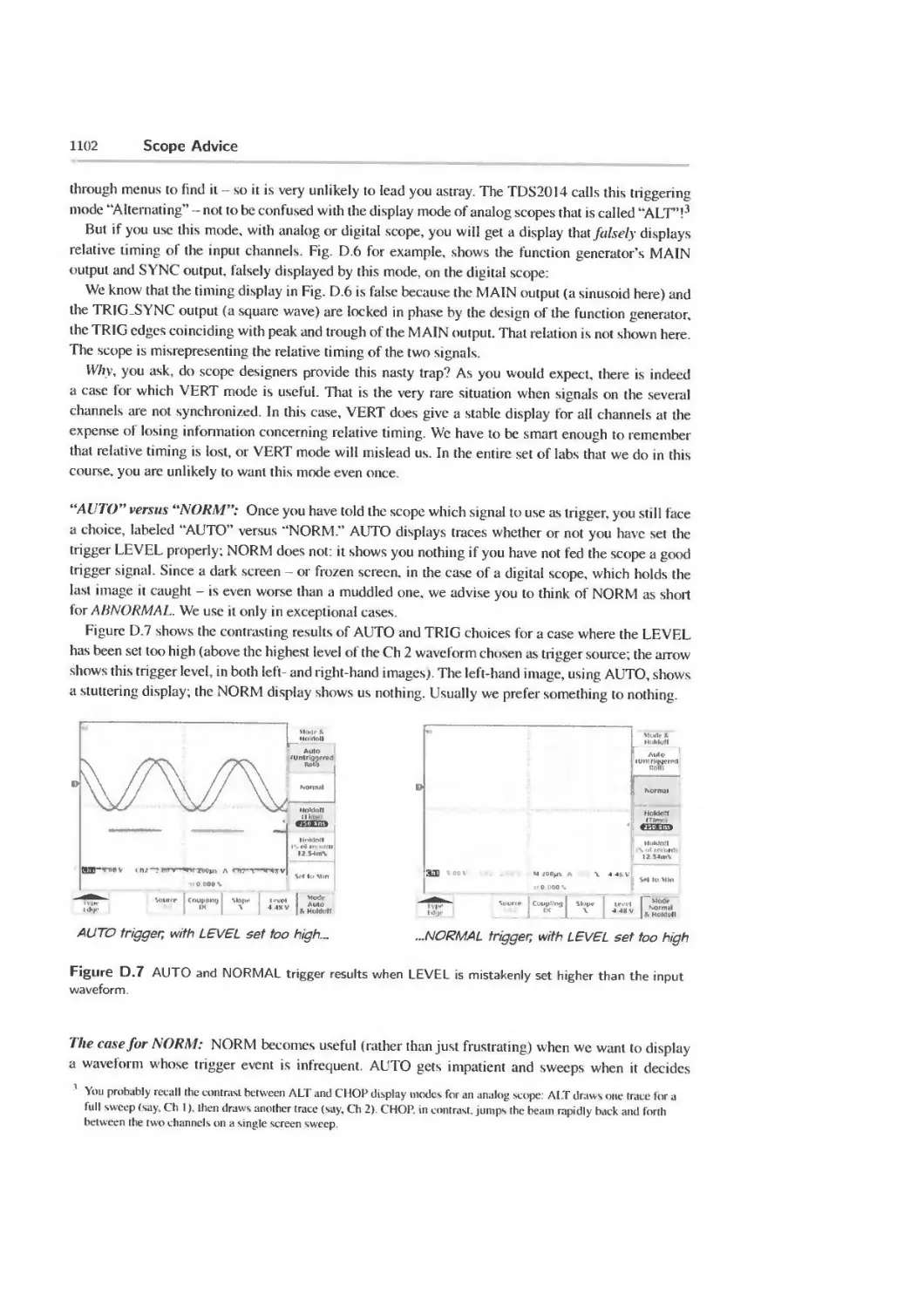
10L 5 Scope images effect of increasing gain, in P-only loop 432
UN Voltage Regulators 433
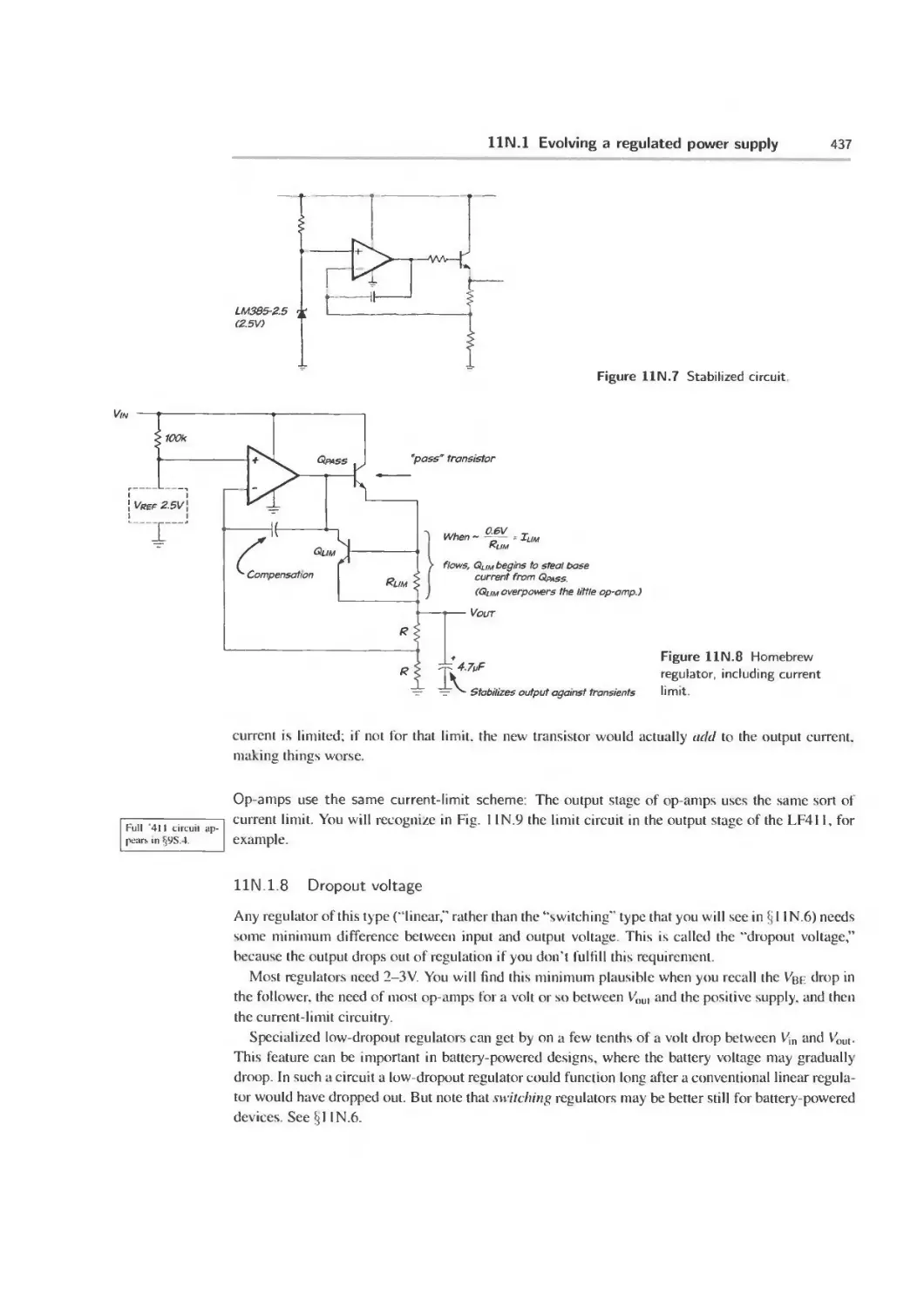
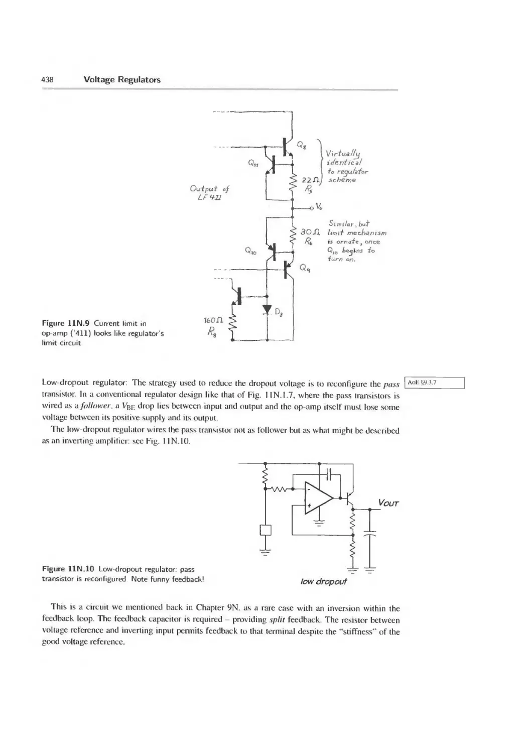
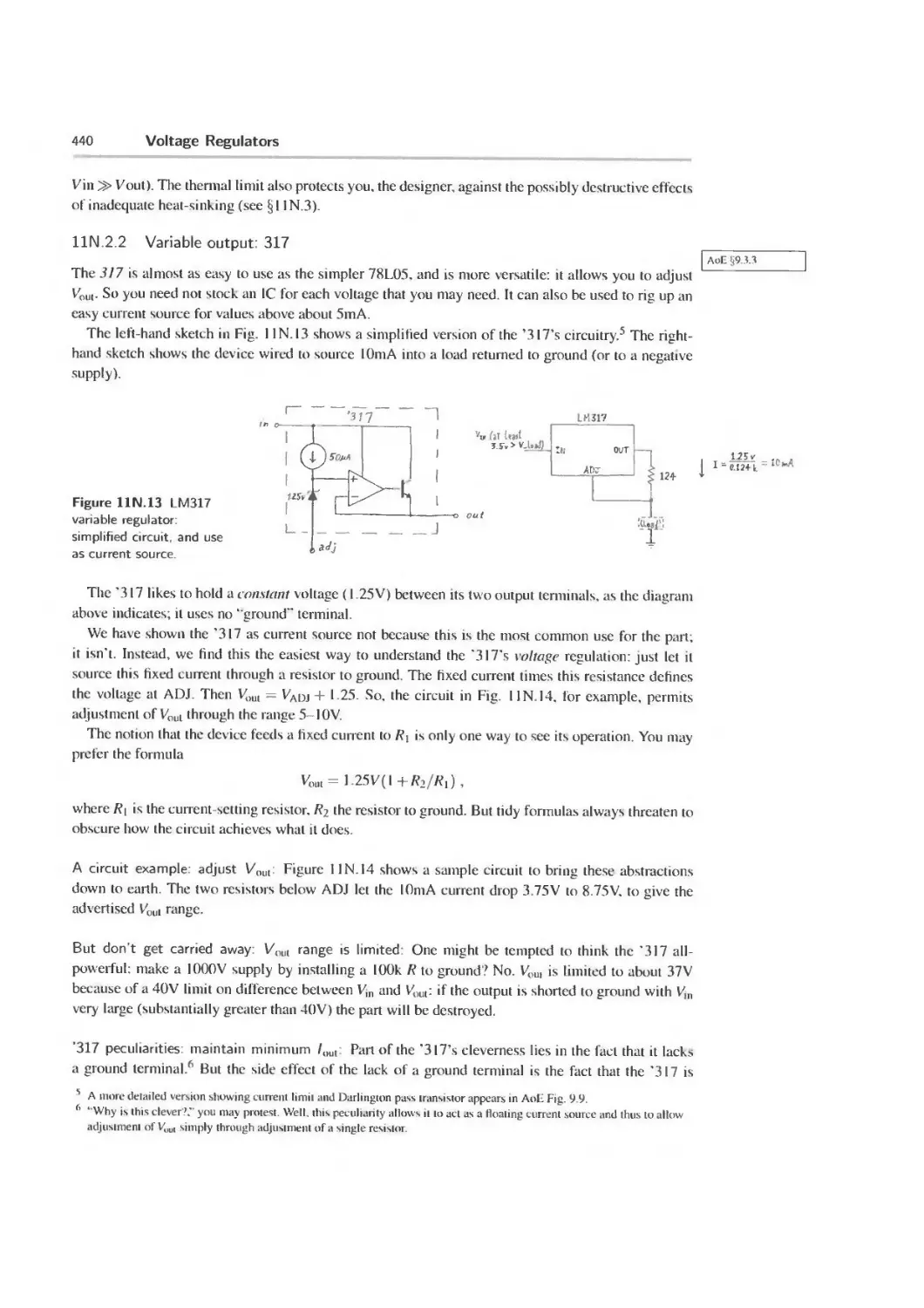
11N.1 Evolving a regulated power supply 434
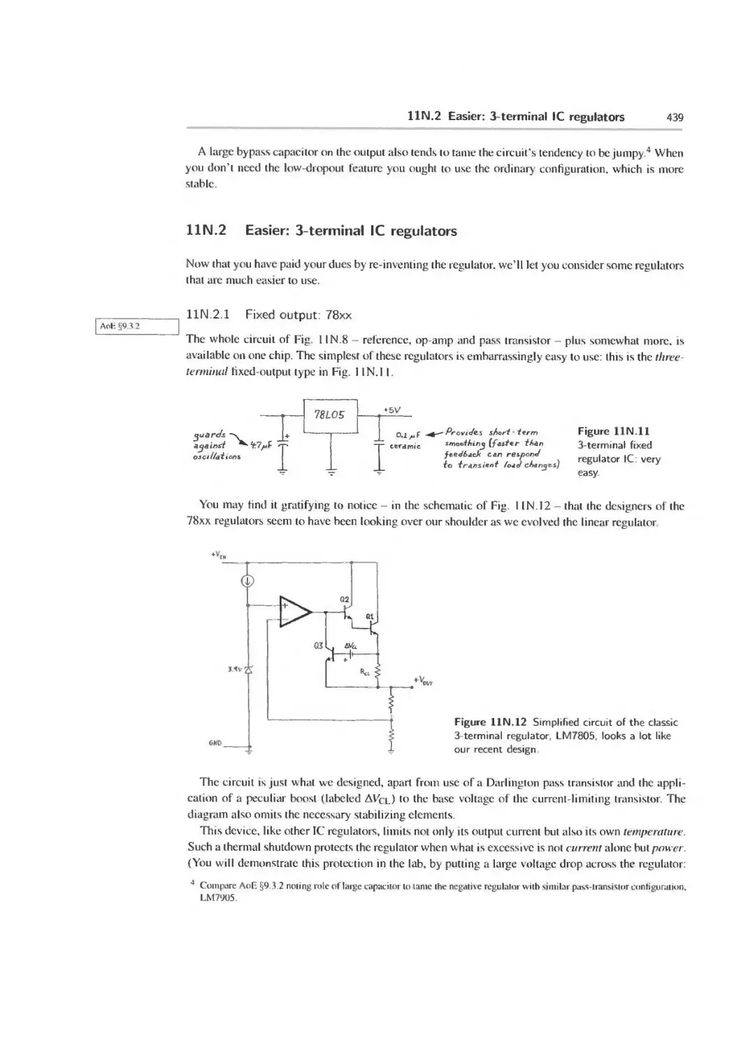
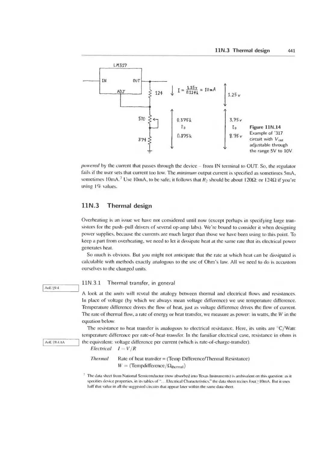
11N2 Easier: 3-terminal/С regulators 439
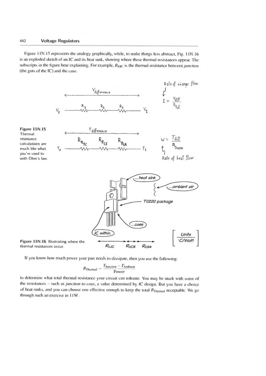
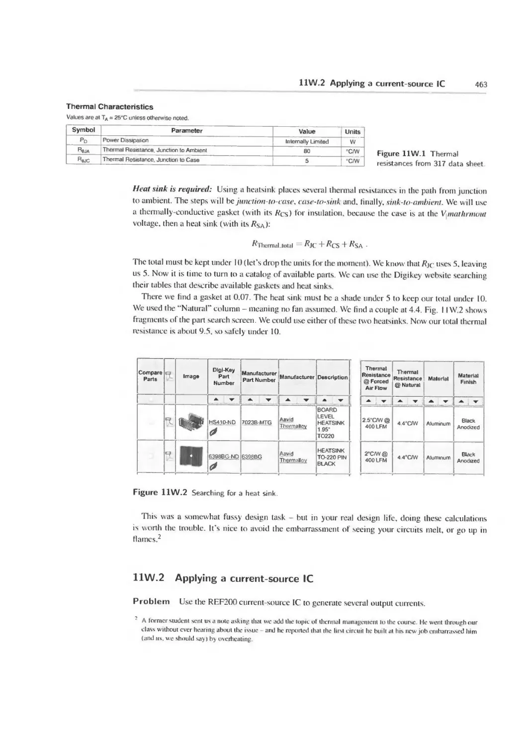
11N.3 Thermal design 441
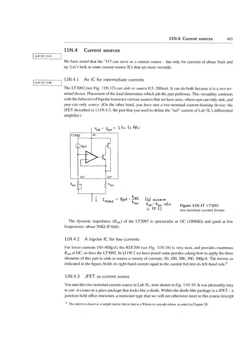
11N.4 Current sources 443
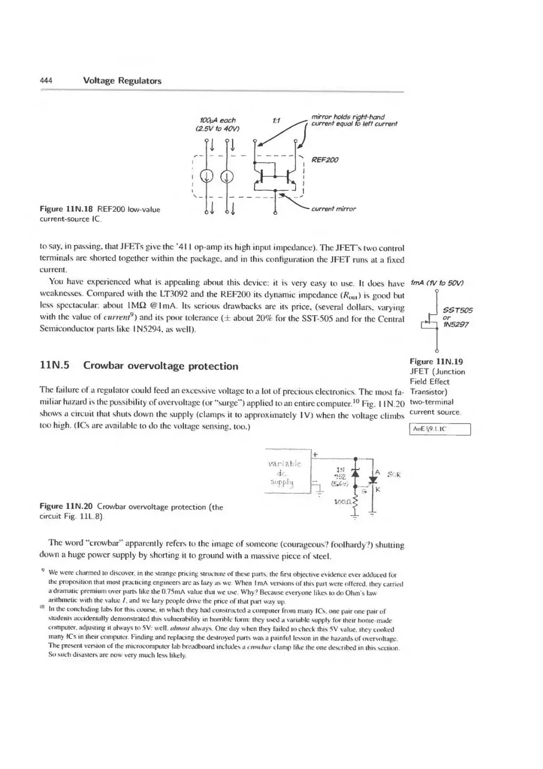
11N.5 Crowbar overvoltage protection 444
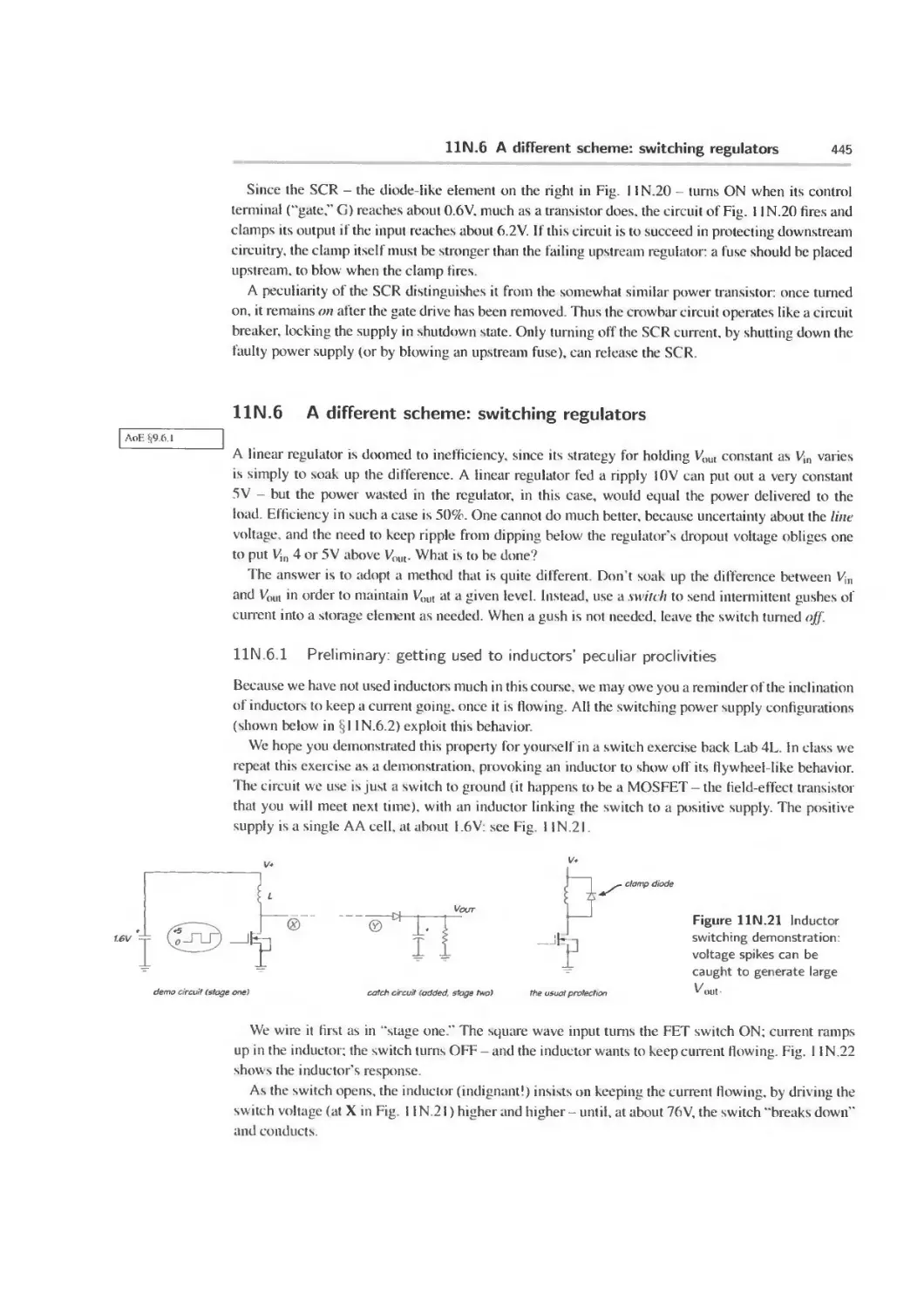
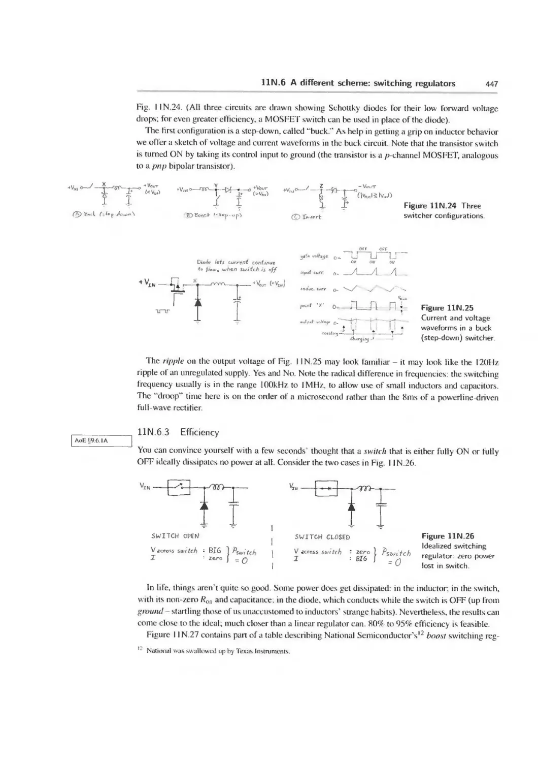
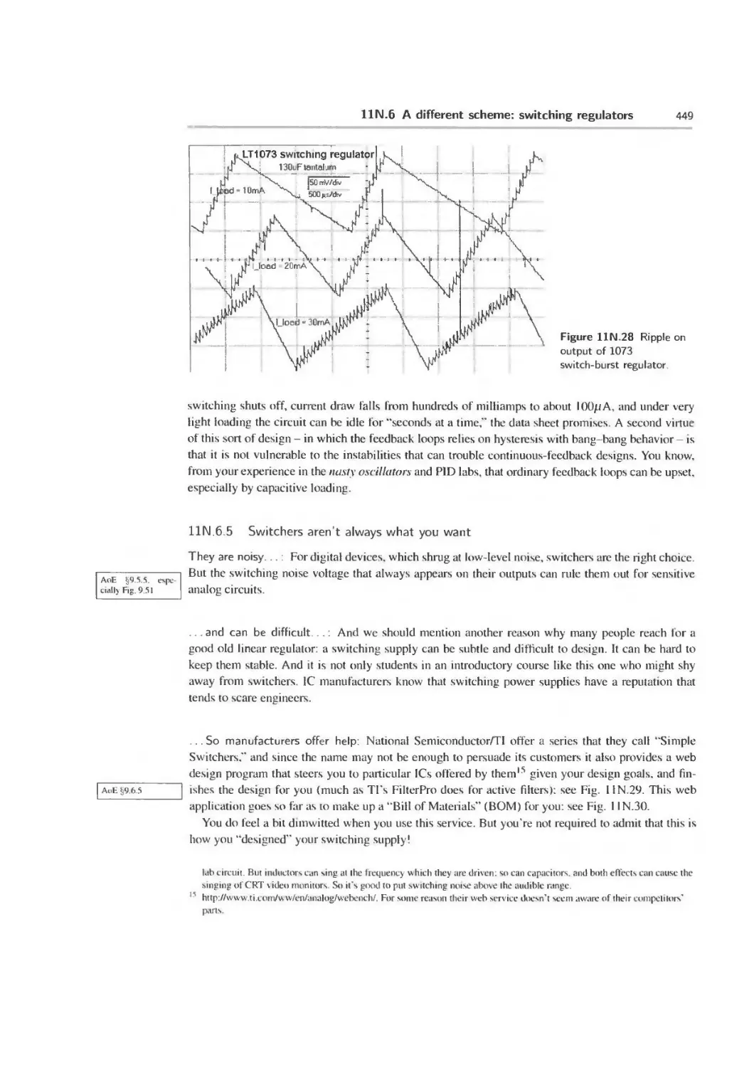
11N.6 A different scheme: switching regulators 445
1 IN 7 AoE Readings 450
11L Lab: Voltage Regulators 451
11L. 1 Linear voltage regulators 451
11L.2 A switching voltage regulator 457
11W Worked Examples: Voltage Regulators 462
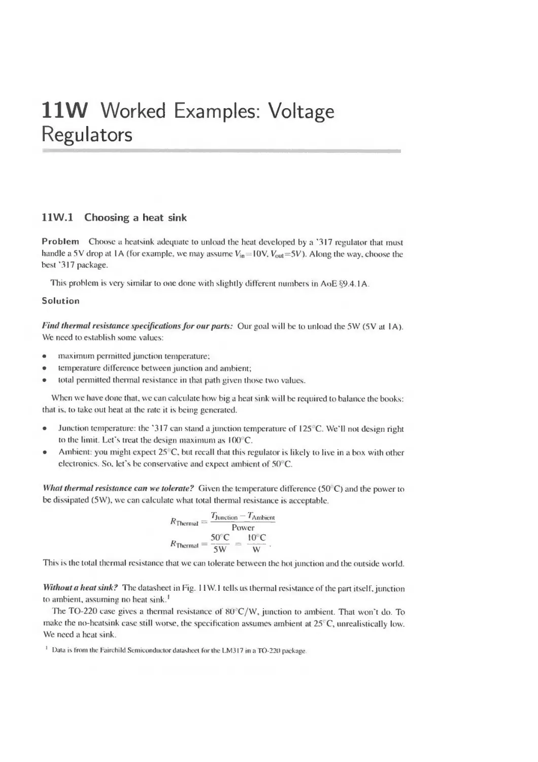
11W. 1 Choosing a heat sink 462
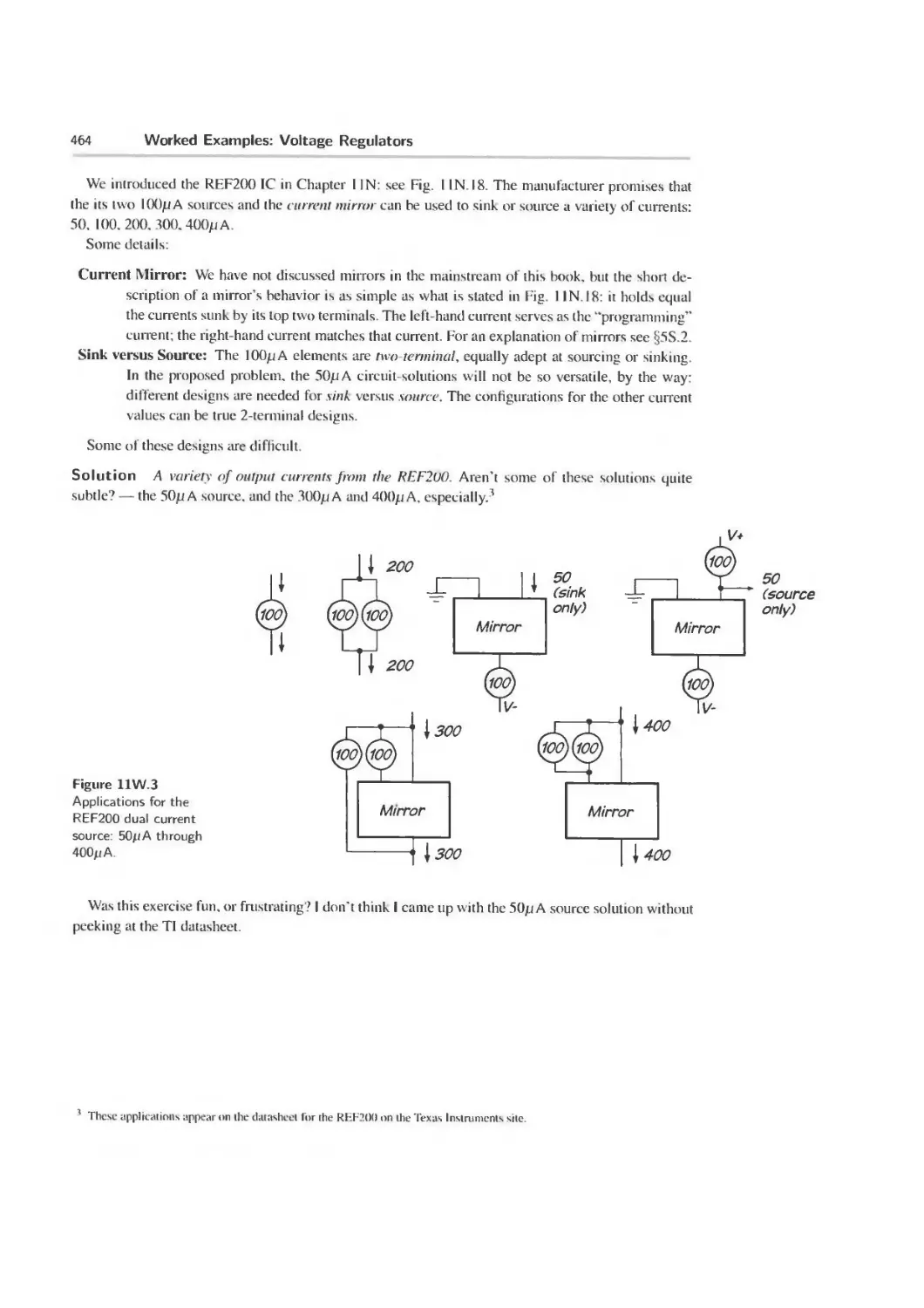
11W.2 Applying a current-source 1C 463
12N MOSFET Switches 465
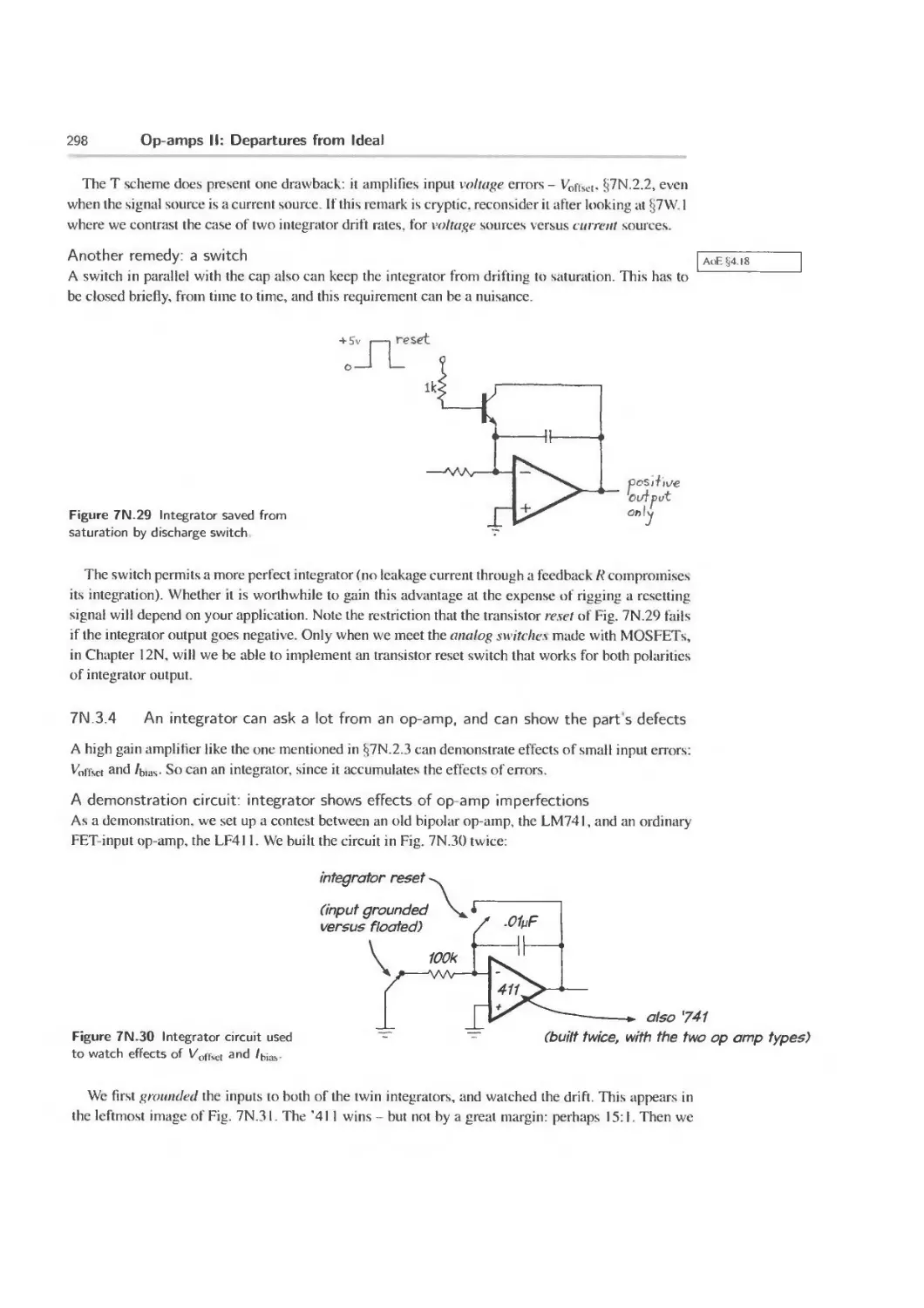
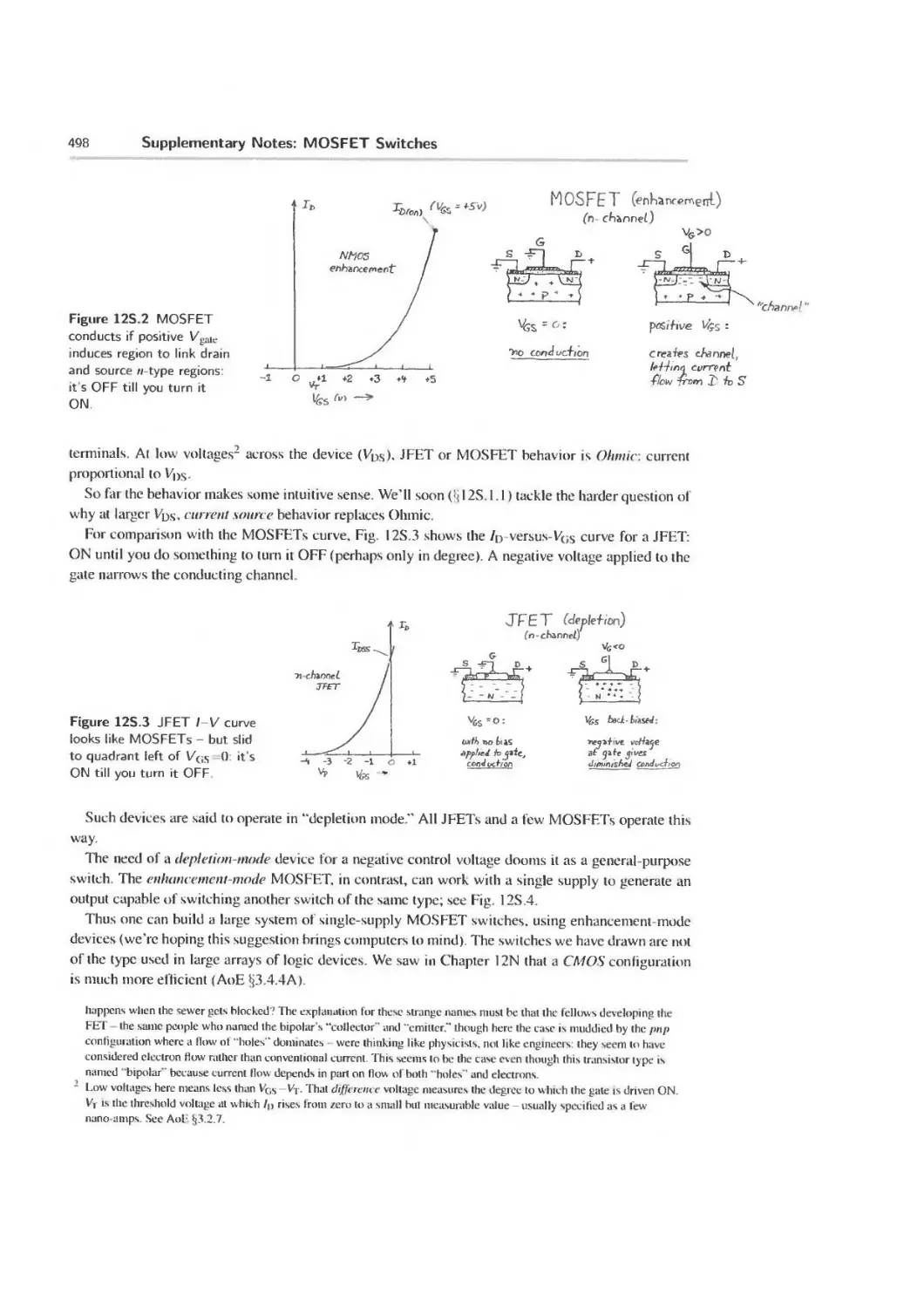
12N. 1 Why we treat FETs as we do 465
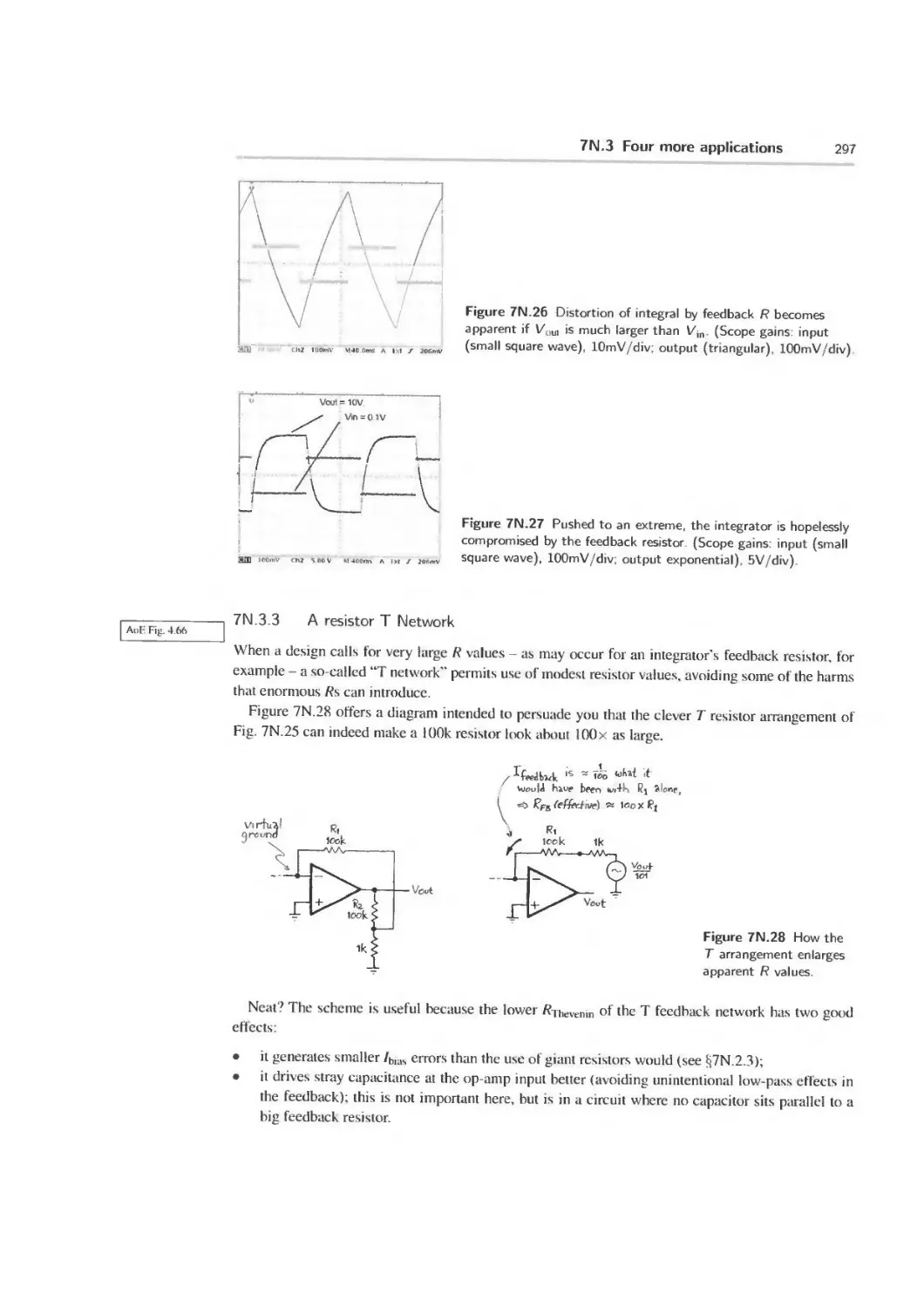
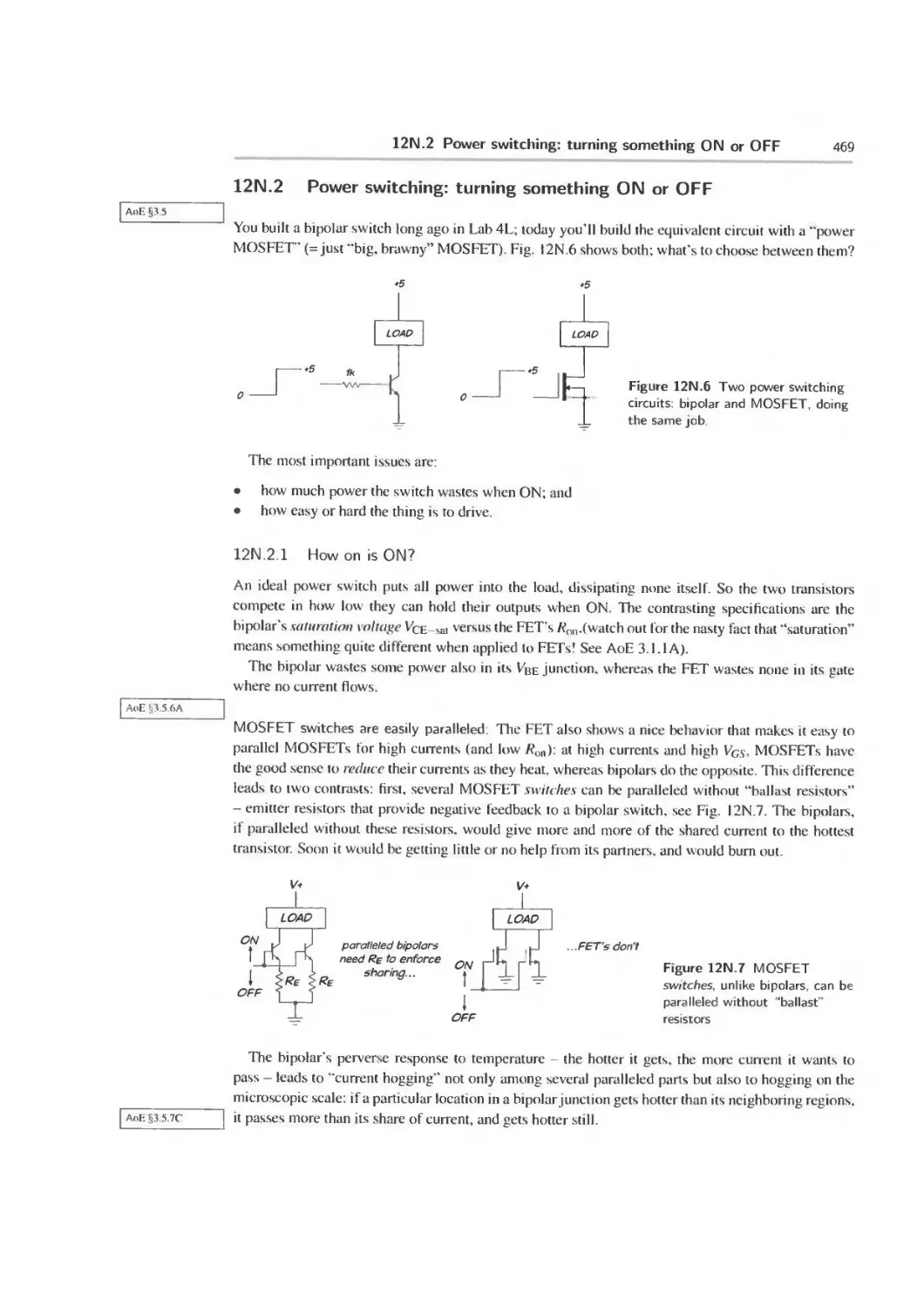
12N.2 Power switching: turning something ON or OFF 469
12N 3 A power switch application audio amplifier 471
12N.4 Logic gates 473
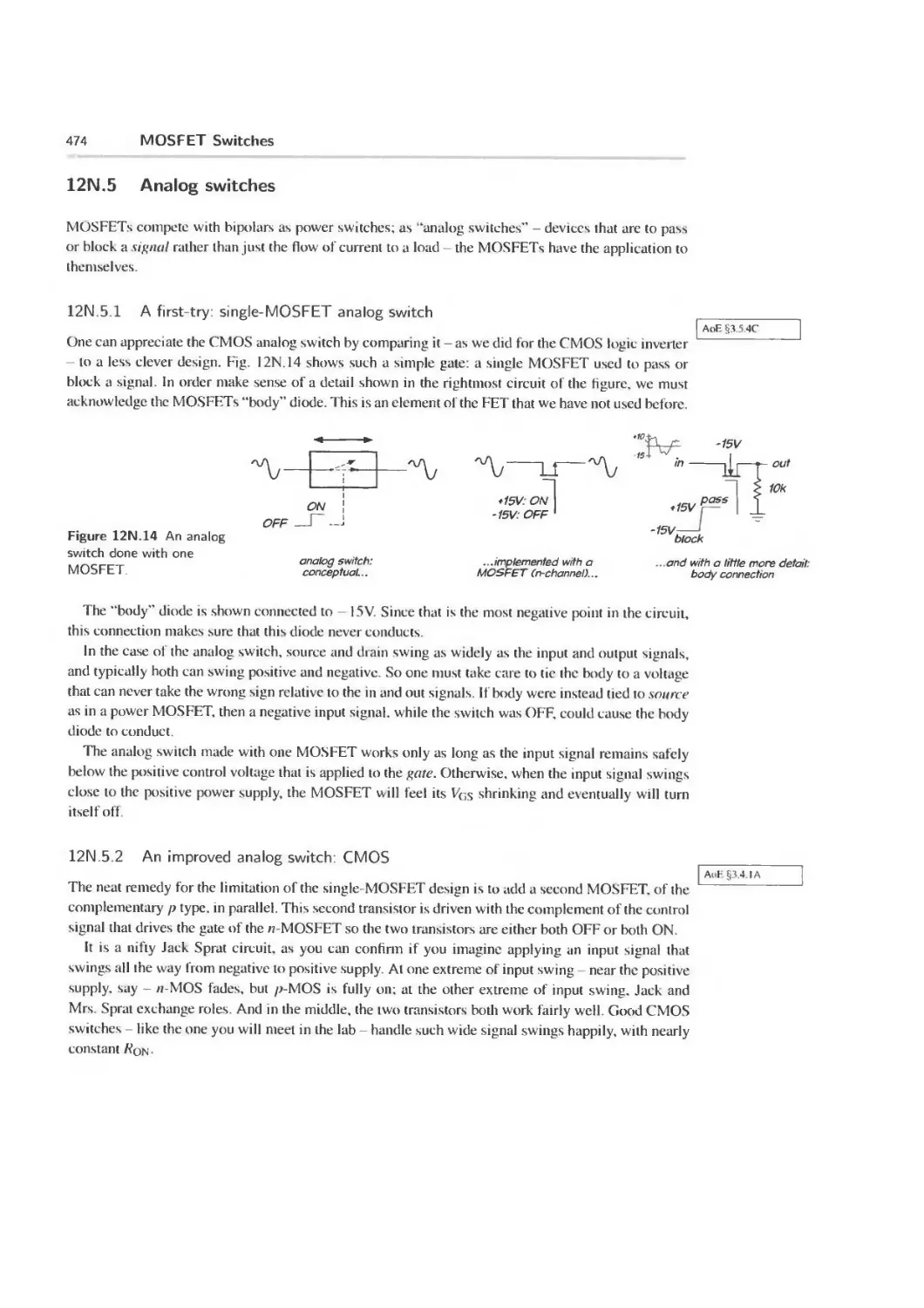
12N.5 Analog switches 474
12N.6 Applications 475
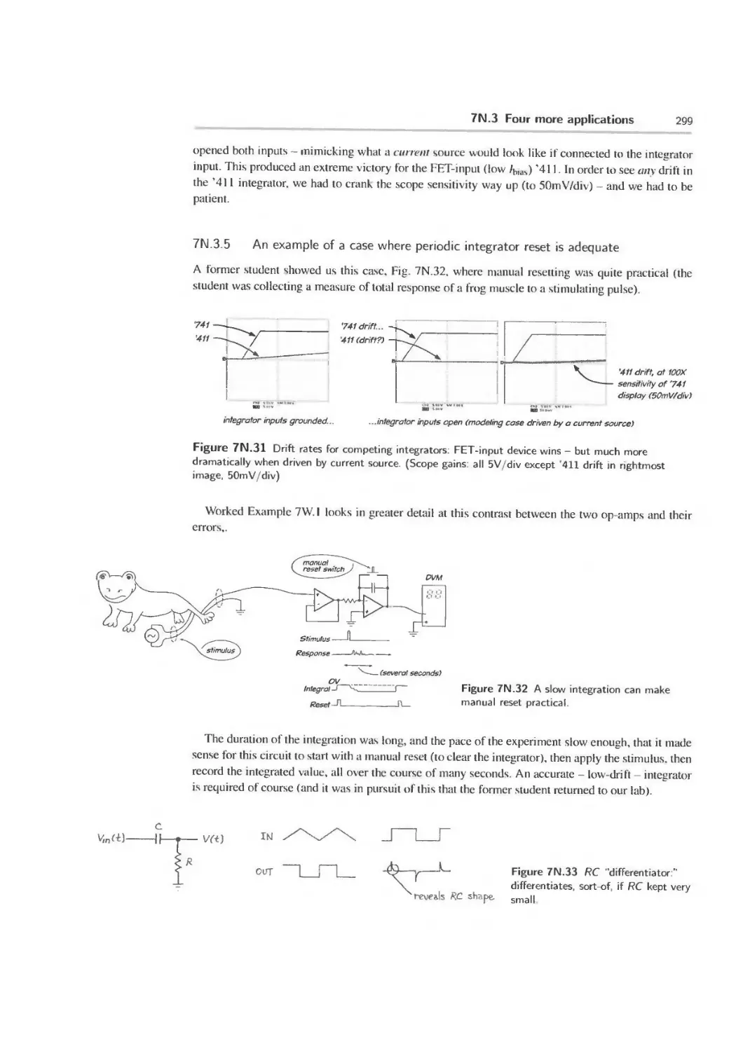
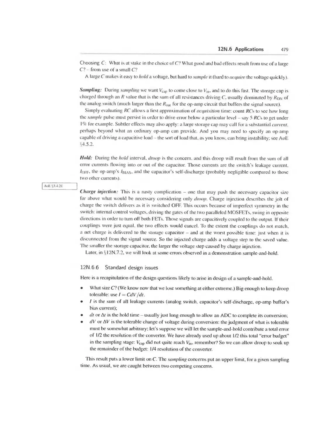
12N.7 Testing a sample and-hold circuit 480
12N.8 AoE Reading 485
Contents xiii
12L Lab: MOSFET Switches 12L.1 Power MOSFET 12L.2 Analog switches 12L.3 Switching audio amplifier 486 486 489 495
12S Supplementary Notes: MOSFET Switches 497
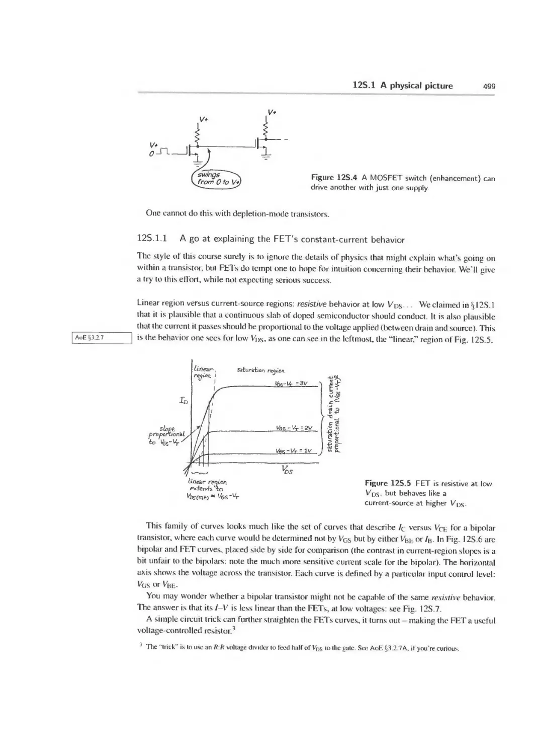
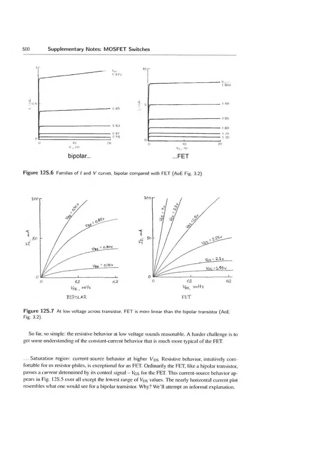
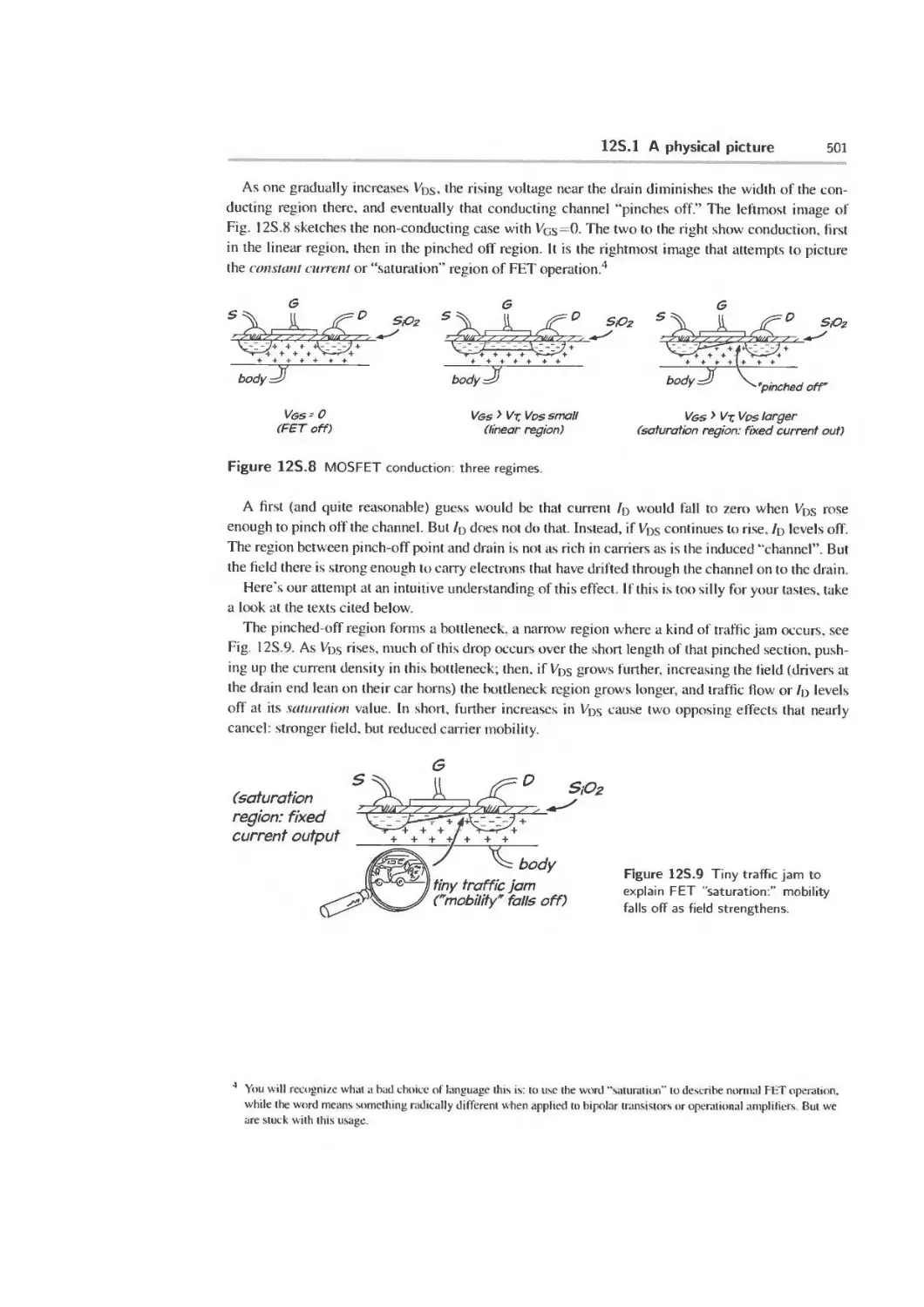
12S. 1 A physical picture 497
13N Group Audio Project 503
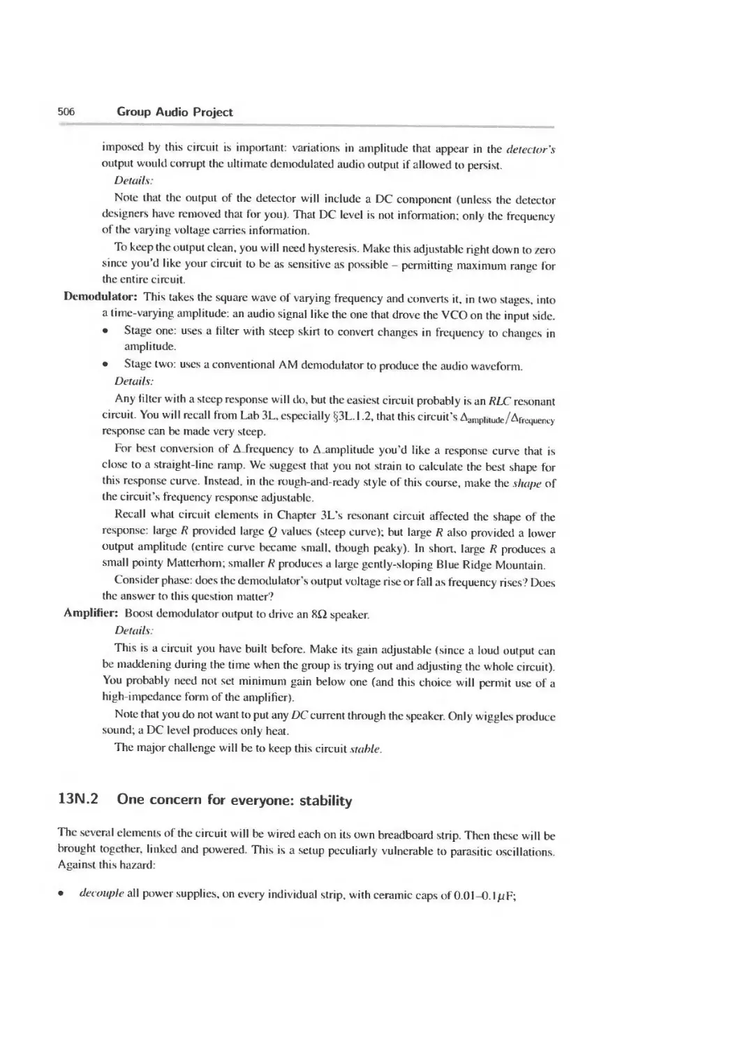
13N. 1 Overview: a day of group effort 503
13N.2 One concern for everyone: stability 506
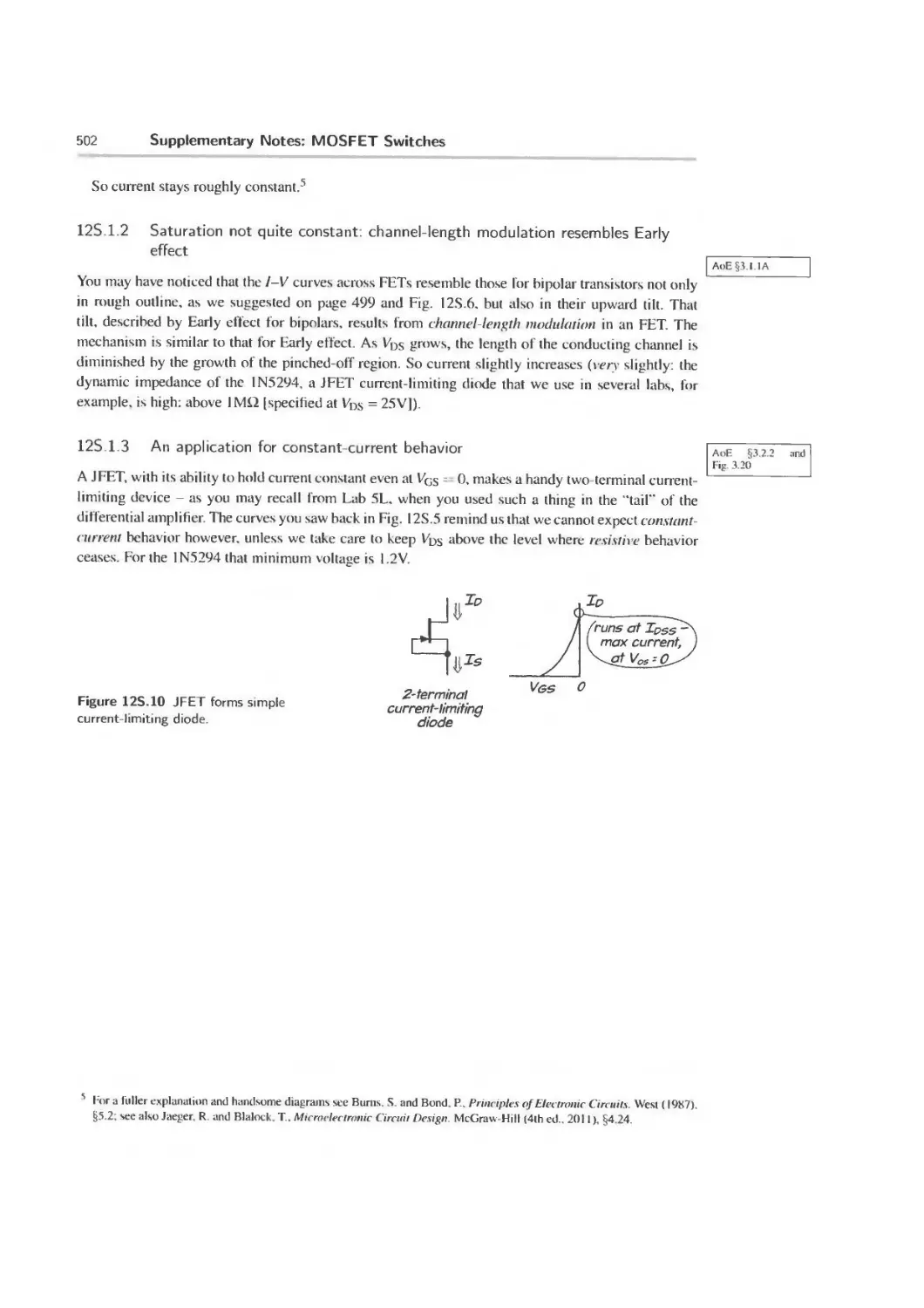
13N 3 Sketchy datasheets for LED and phototransistor 507
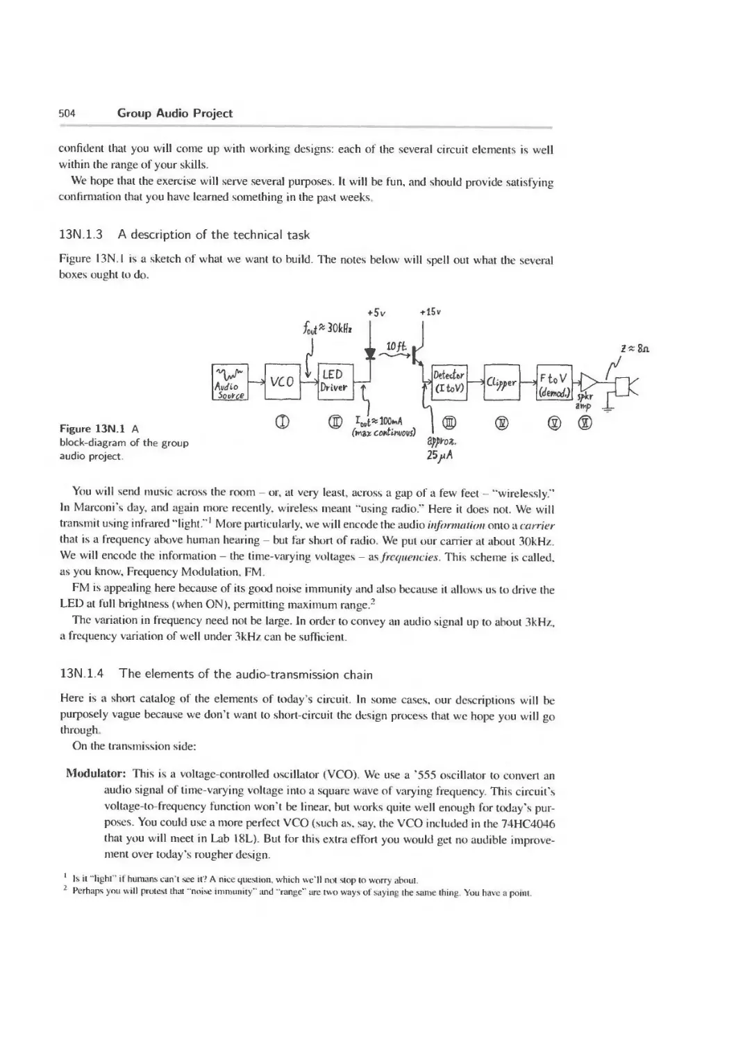
13L Lab: Group Audio Project 508
13L.1 Typical waveforms 508
13L.2 Debugging strategies 509
Part IV Digital: Gates, Flip-Flops, Counters, PLD, Memory 511
14N Logic Gates 513
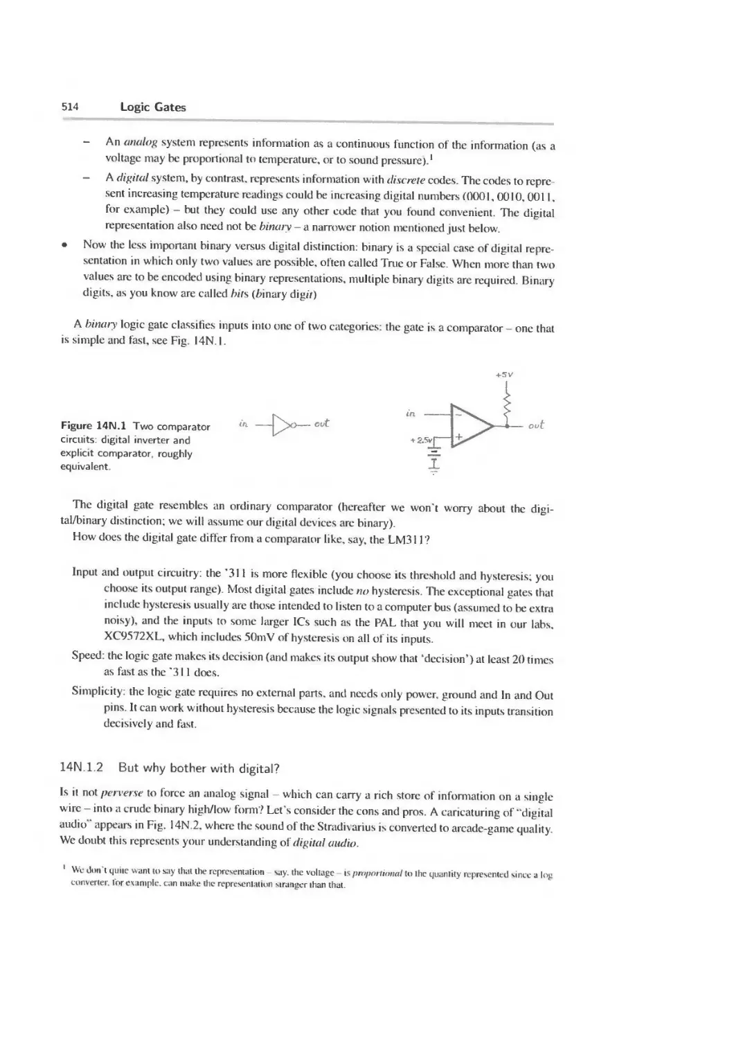
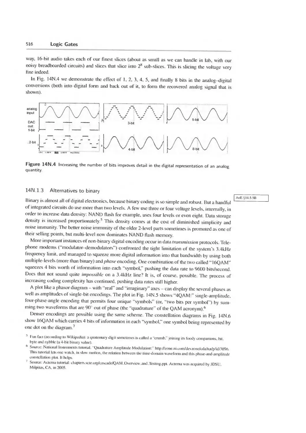
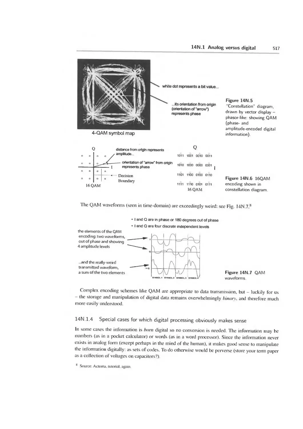
14N. 1 Analog versus digital 513
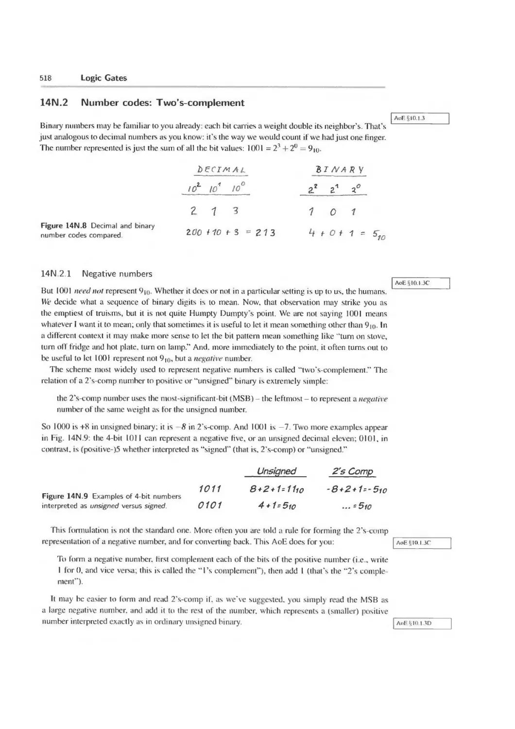
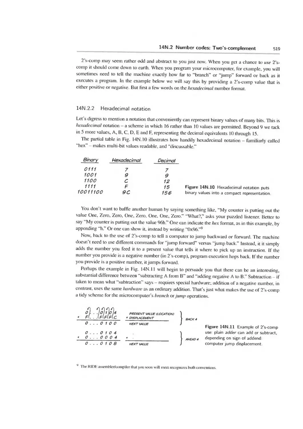
14N.2 Number codes: Two’s-complement 518
14N.3 Combinational logic 520
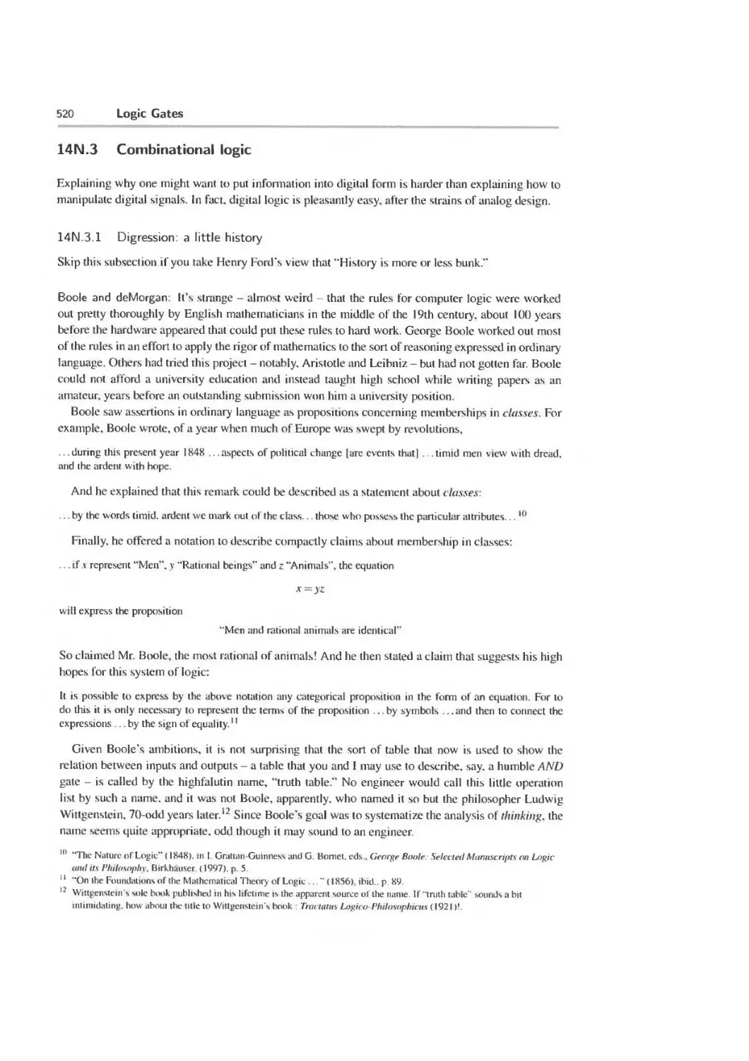
14N.4 The usual way to do digital logic: programmable arrays 526
14N.5 Gate types: TTL and CMOS 528
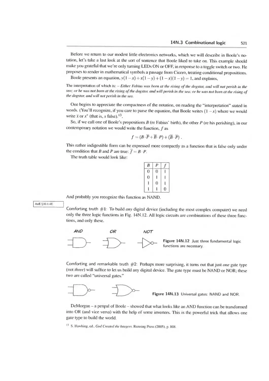
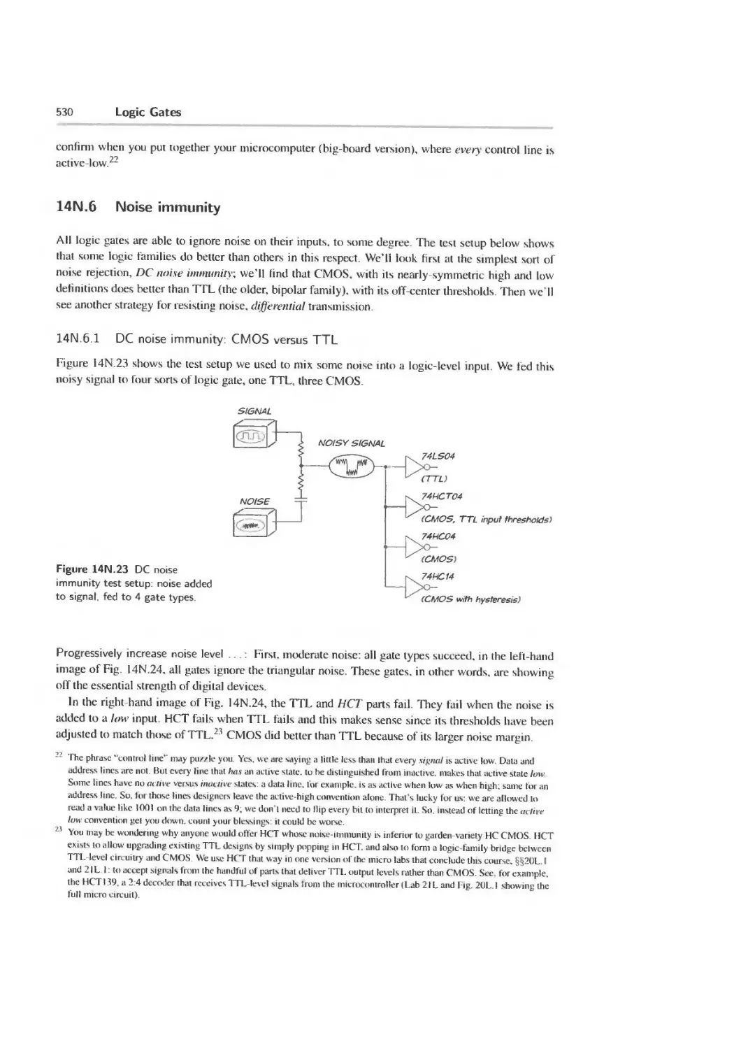
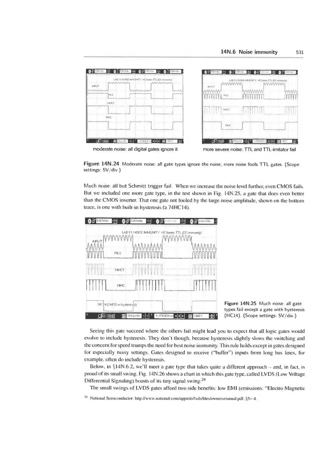
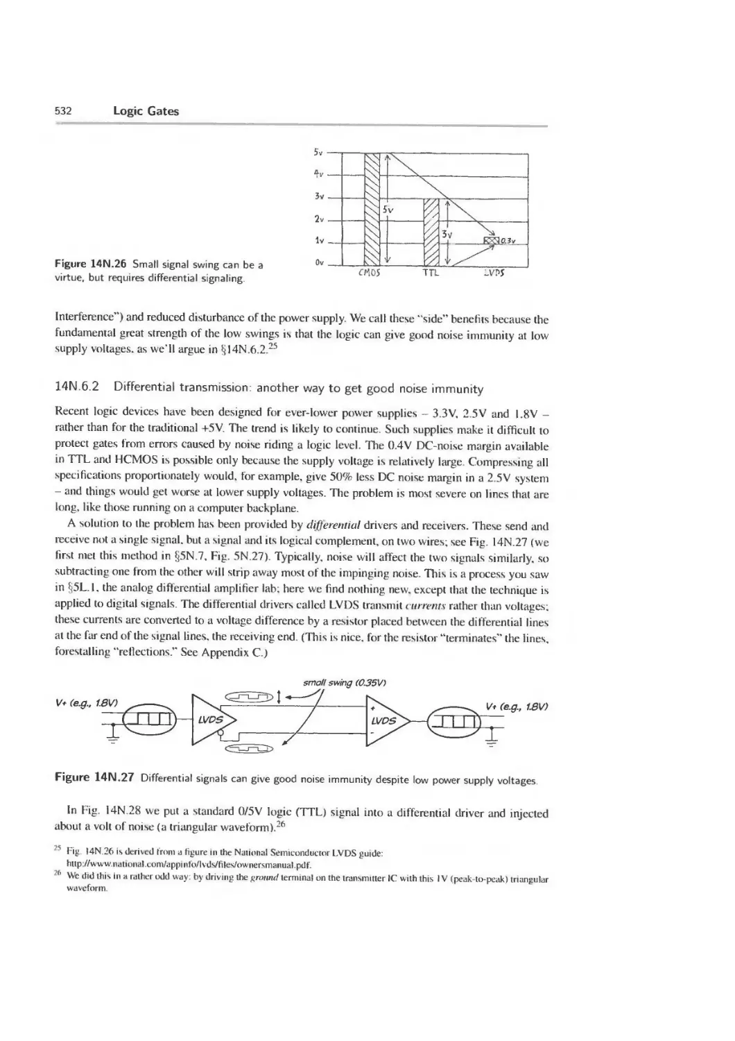
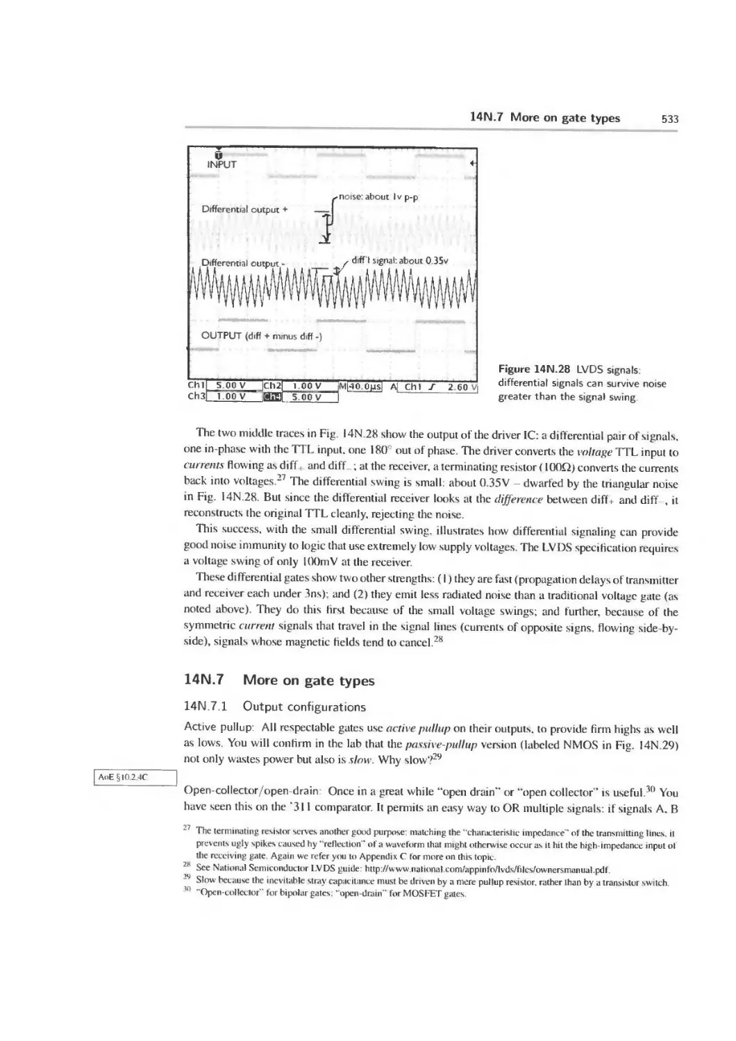
14N.6 Noise immunity 530
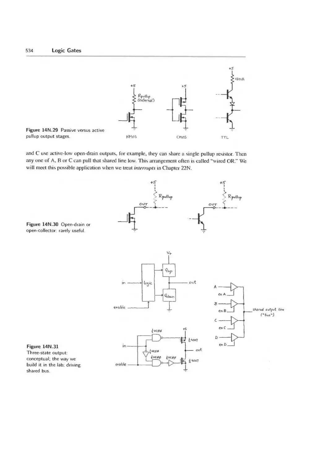
14N.7 More on gate types 533
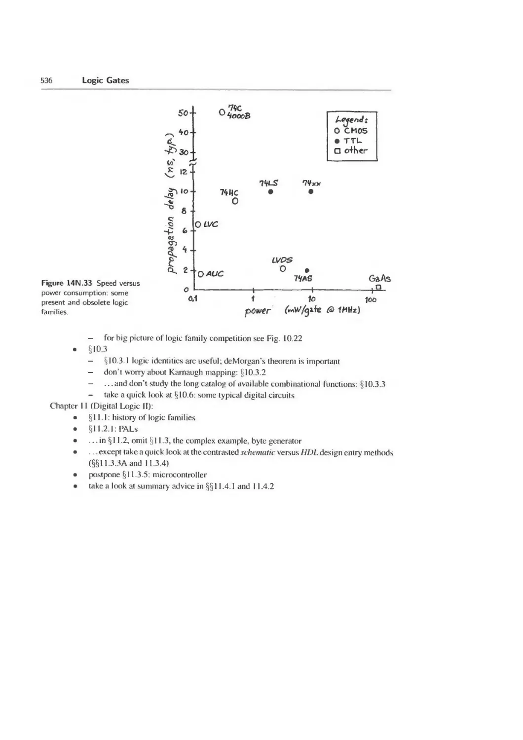
14N.8 AoE Reading 535
14L Lab: Logic Gates 537
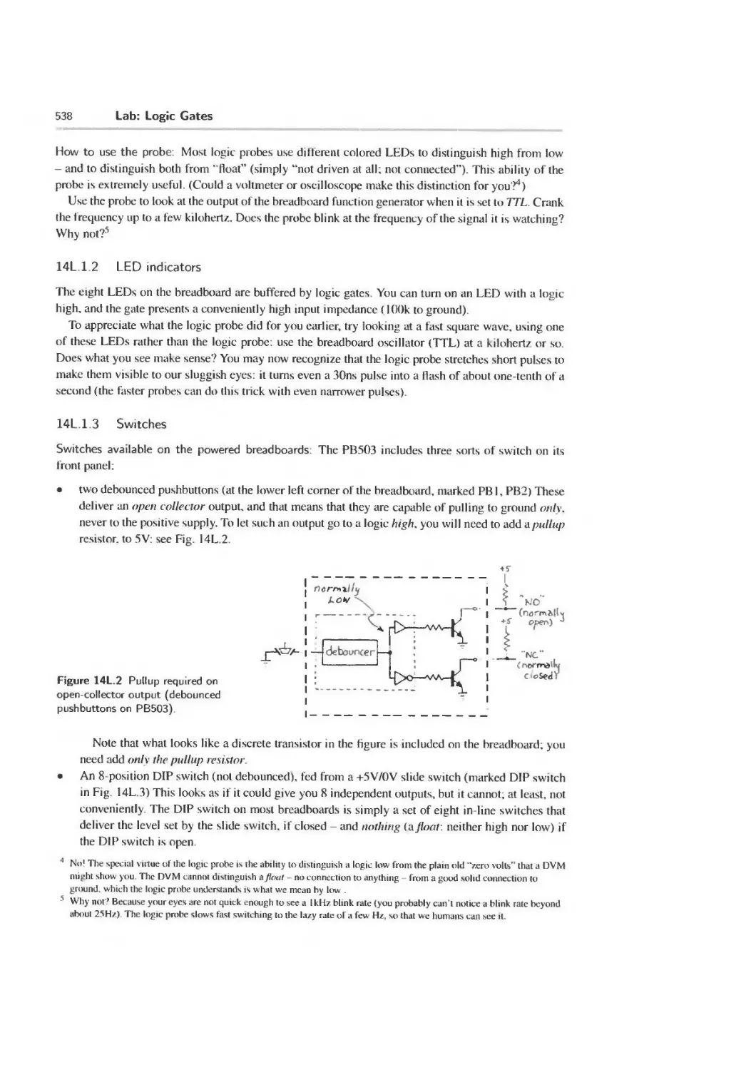
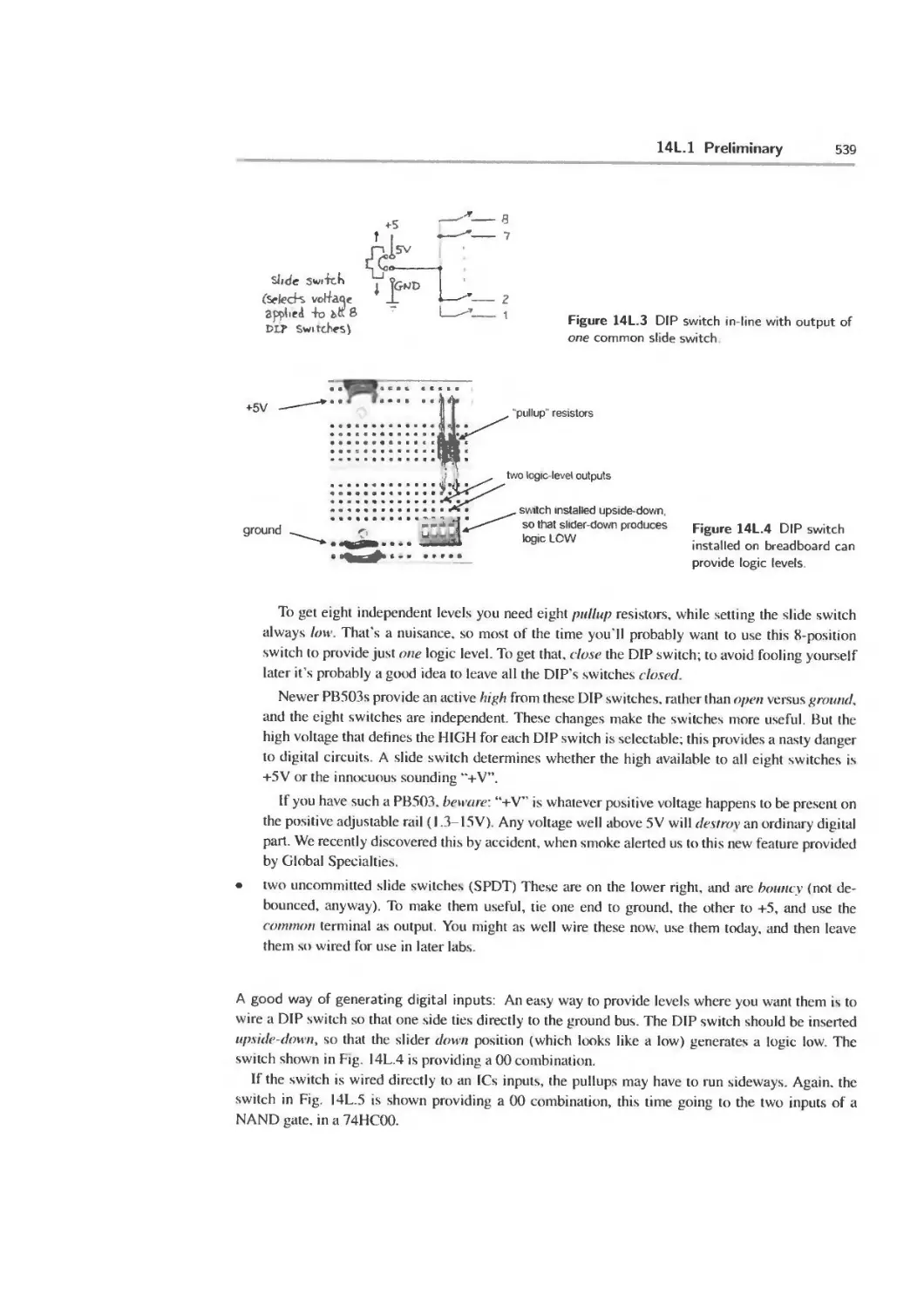
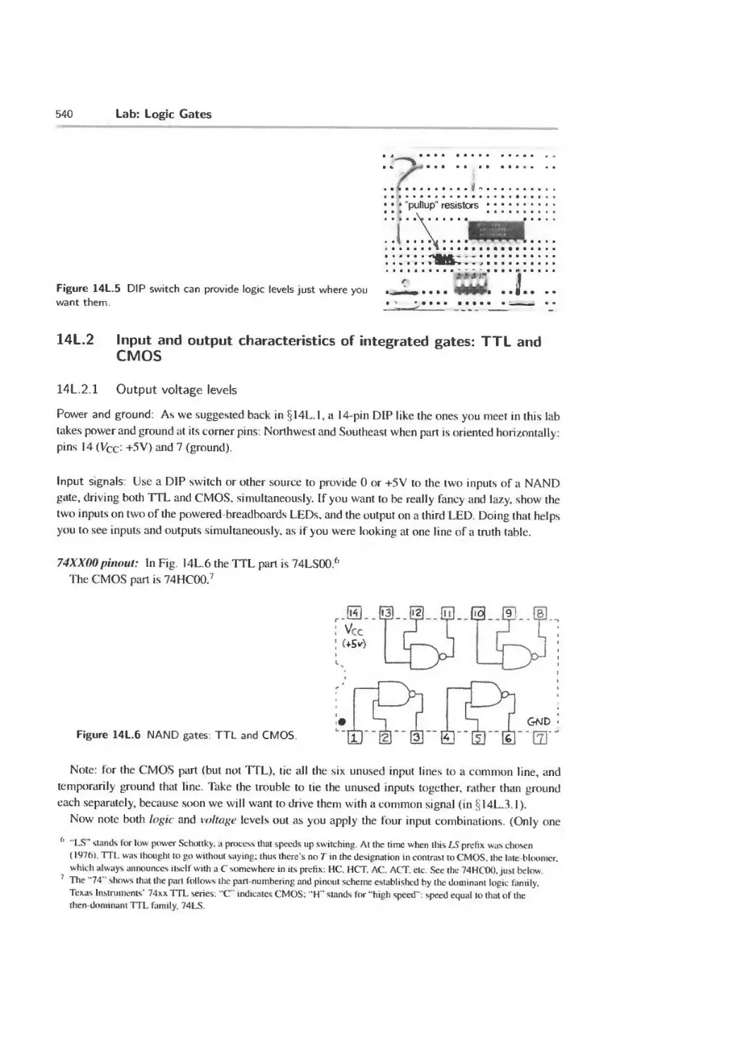
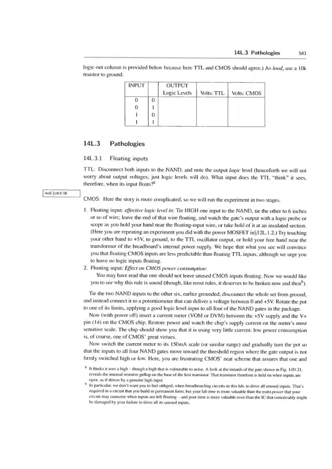
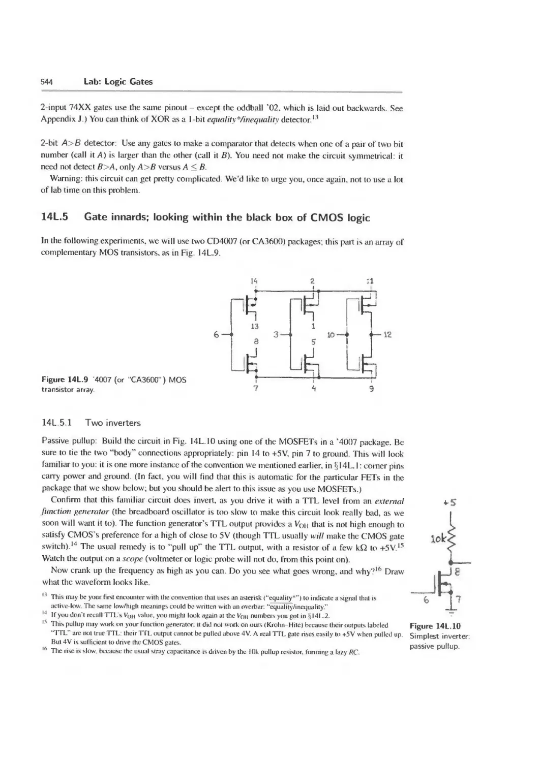
14L. 1 Preliminary 537
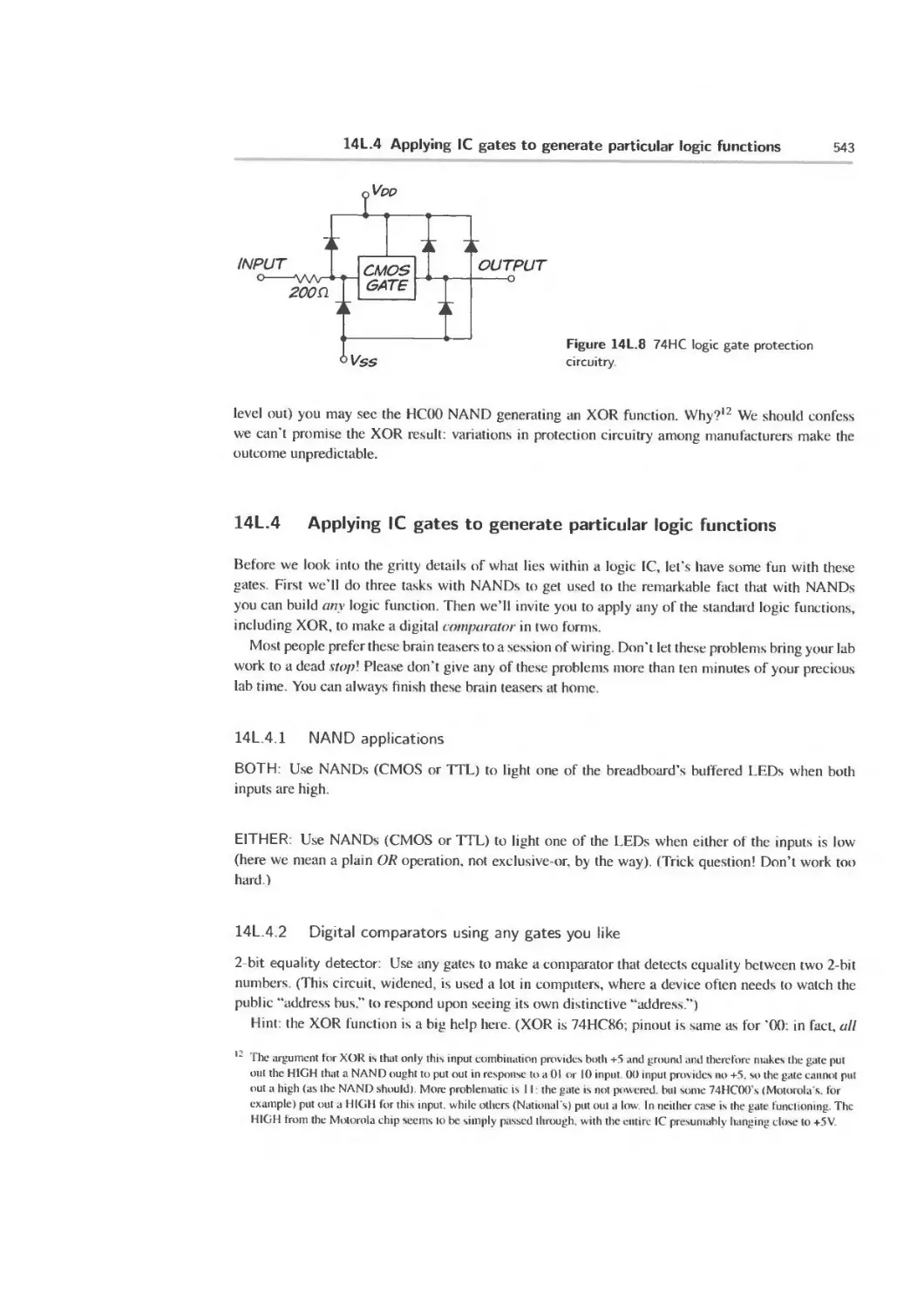
14L.2 Input and output characteristics of integrated gates: TTL and CMOS 540
14L.3 Pathologies 541
14L.4 Applying IC gates to generate particular logic functions 543
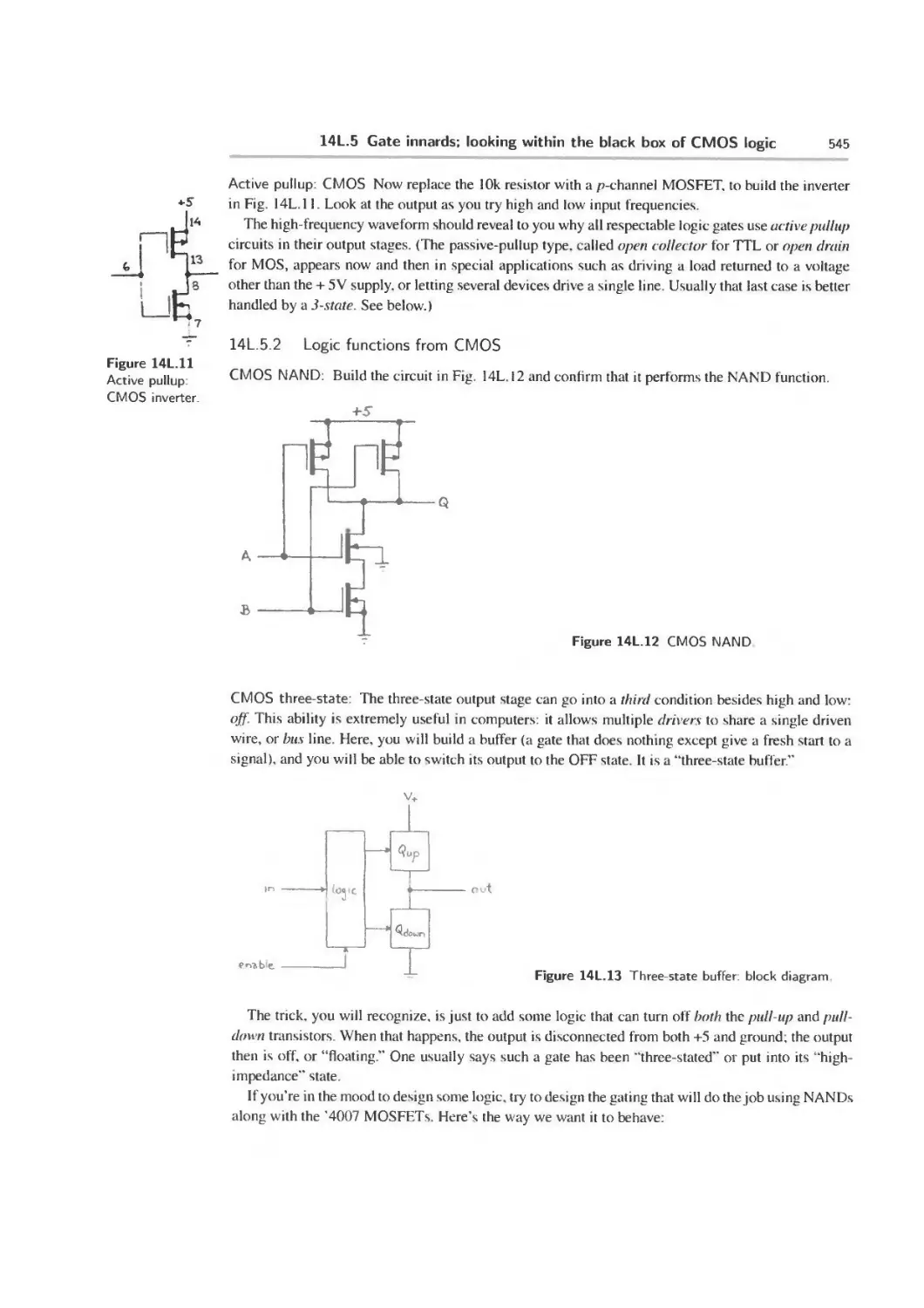
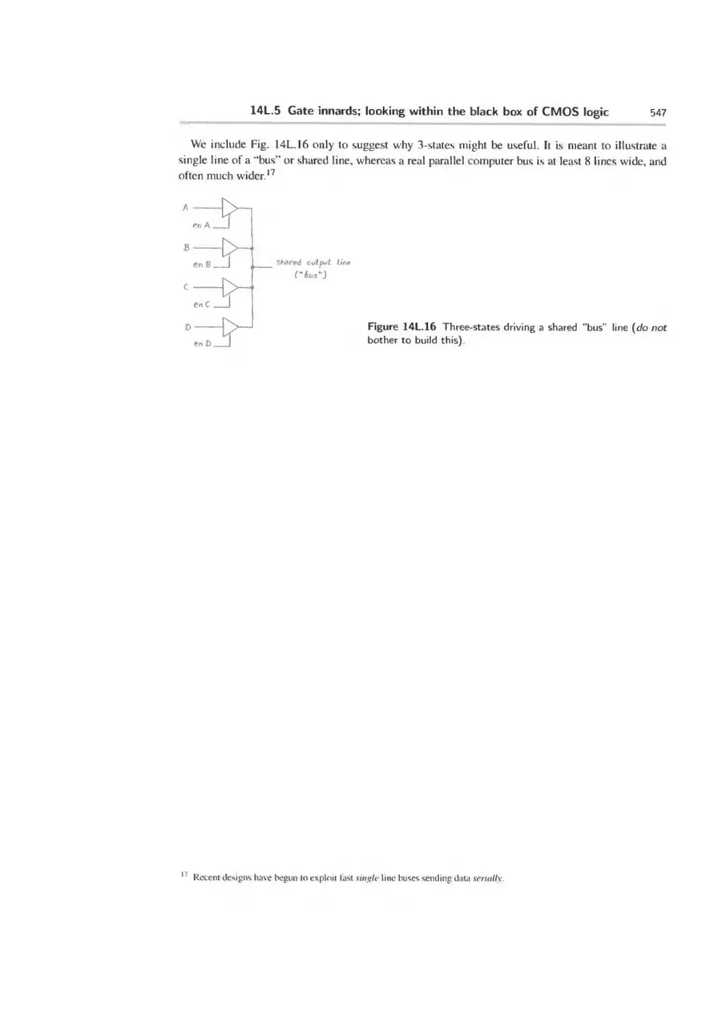
14L.5 Gate innards; looking within the black box of CMOS logic 544
14S Supplementary Notes: Digital Jargon 548
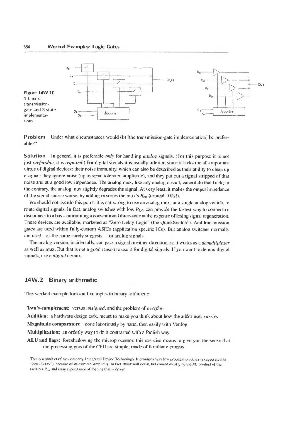
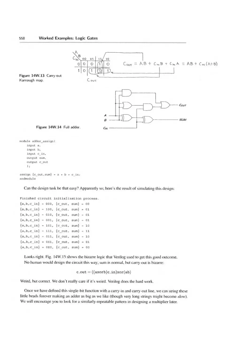
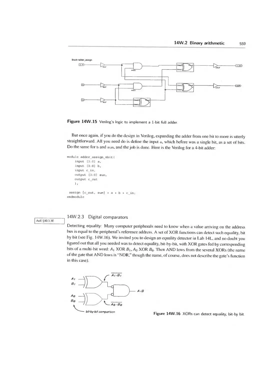
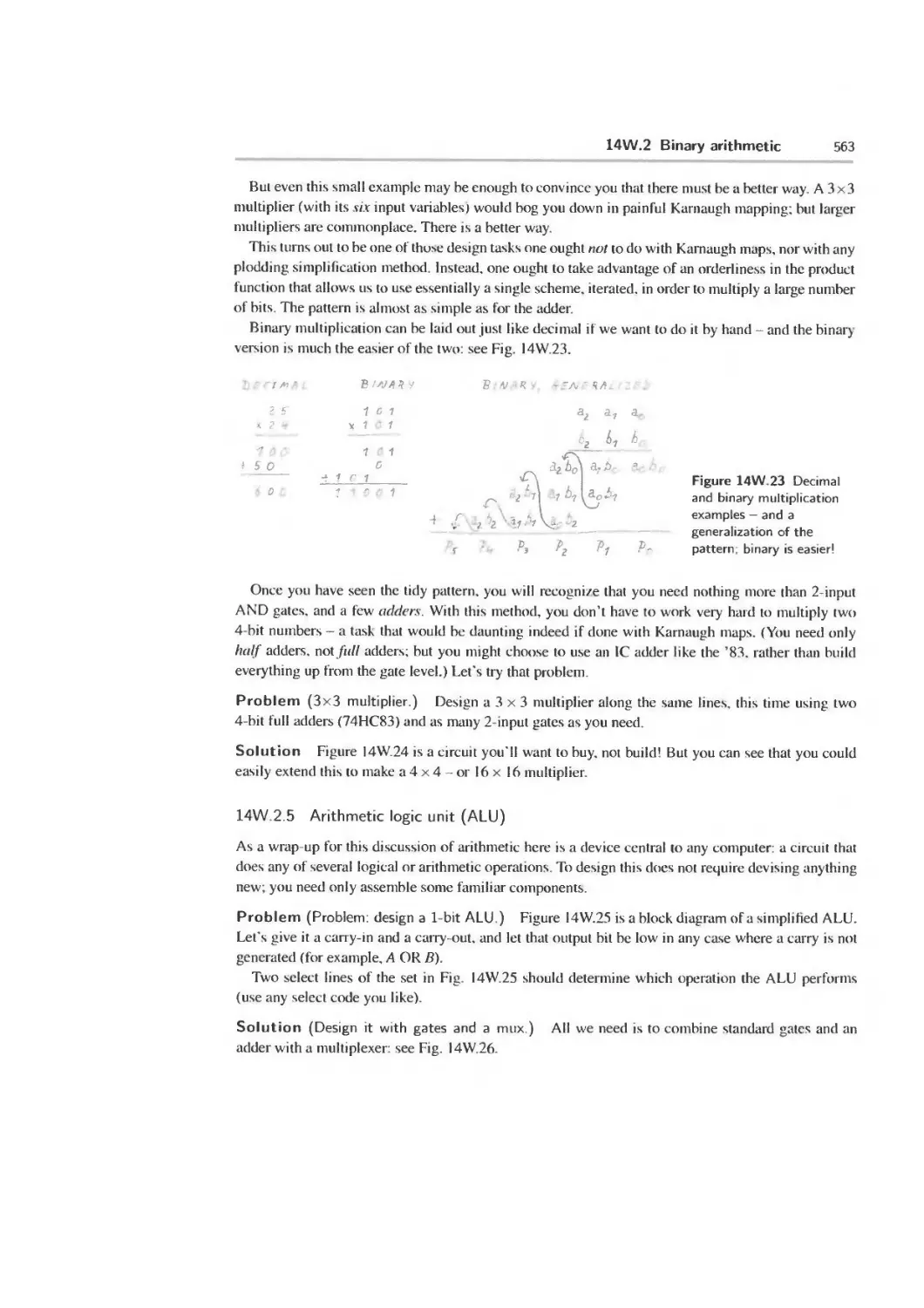
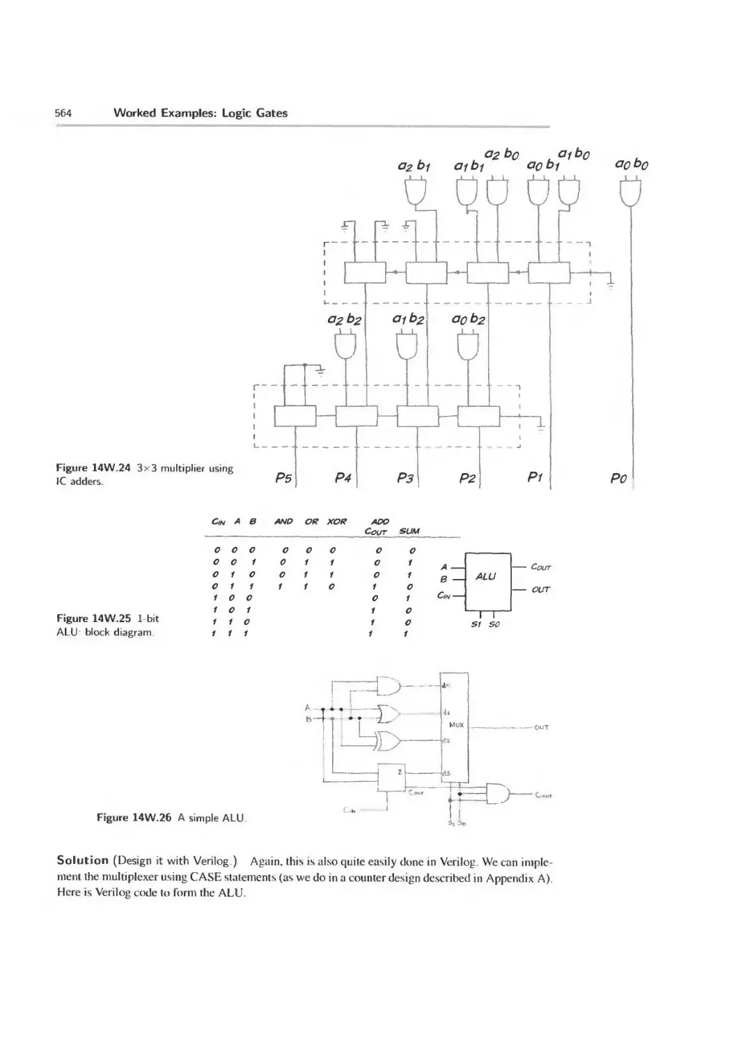
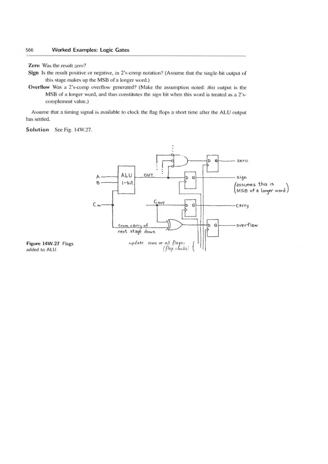
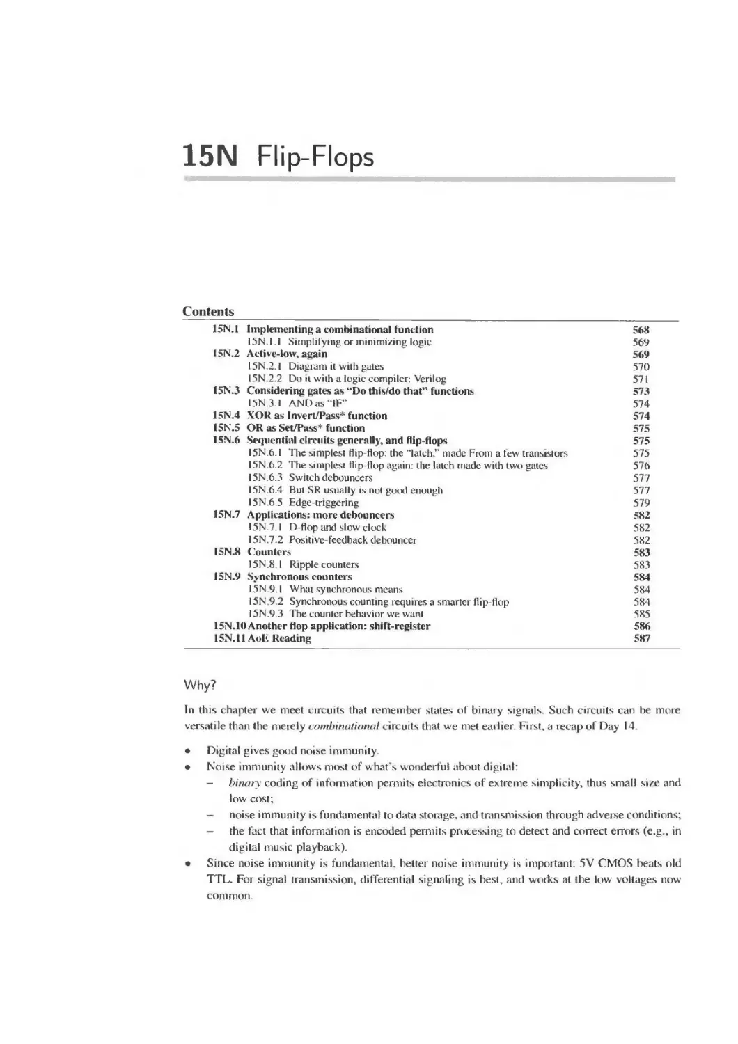
14W Worked Examples: Logic Gates 550
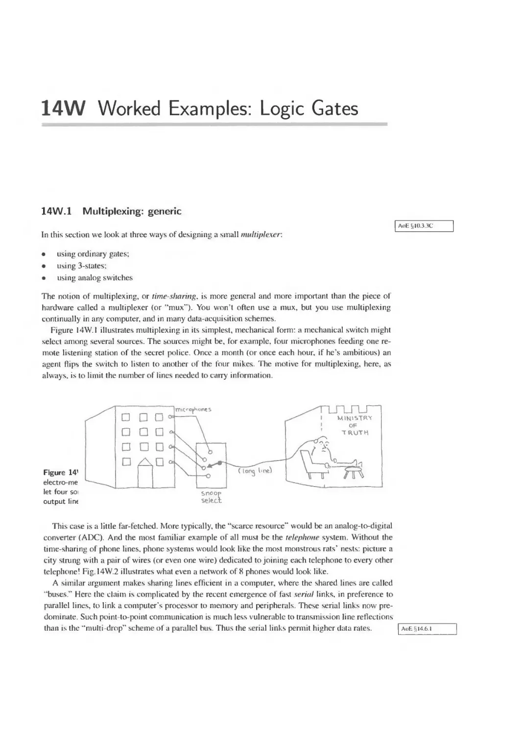
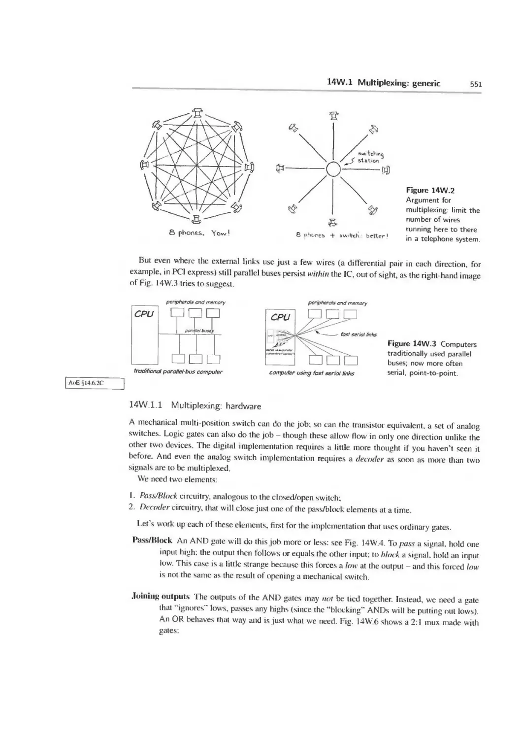
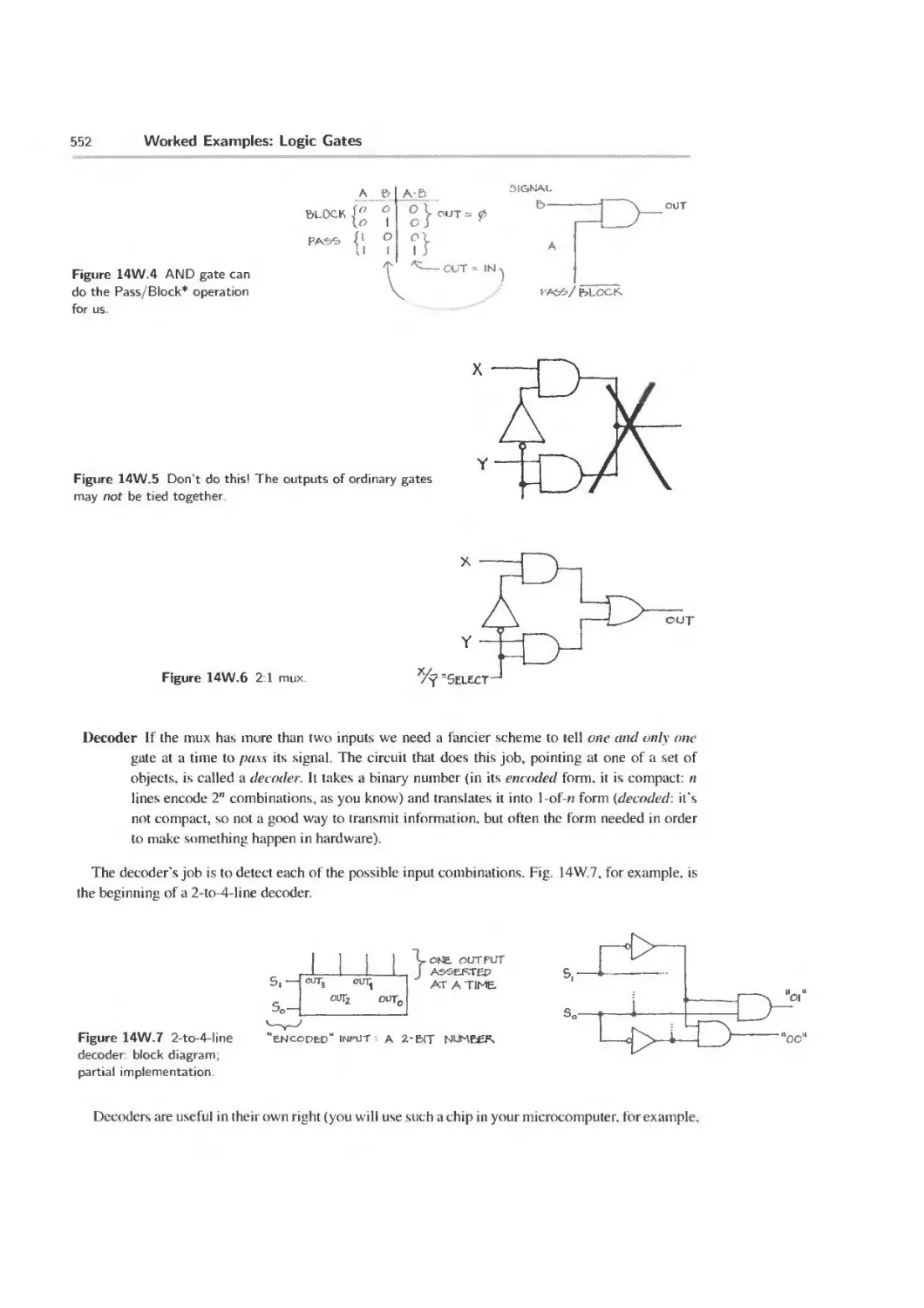
14W. 1 Multiplexing: generic 550
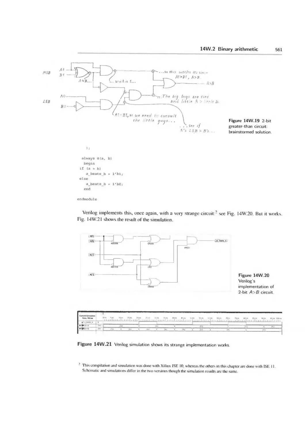
14W.2 Binary arithmetic 554
15N Flip-Flops 567
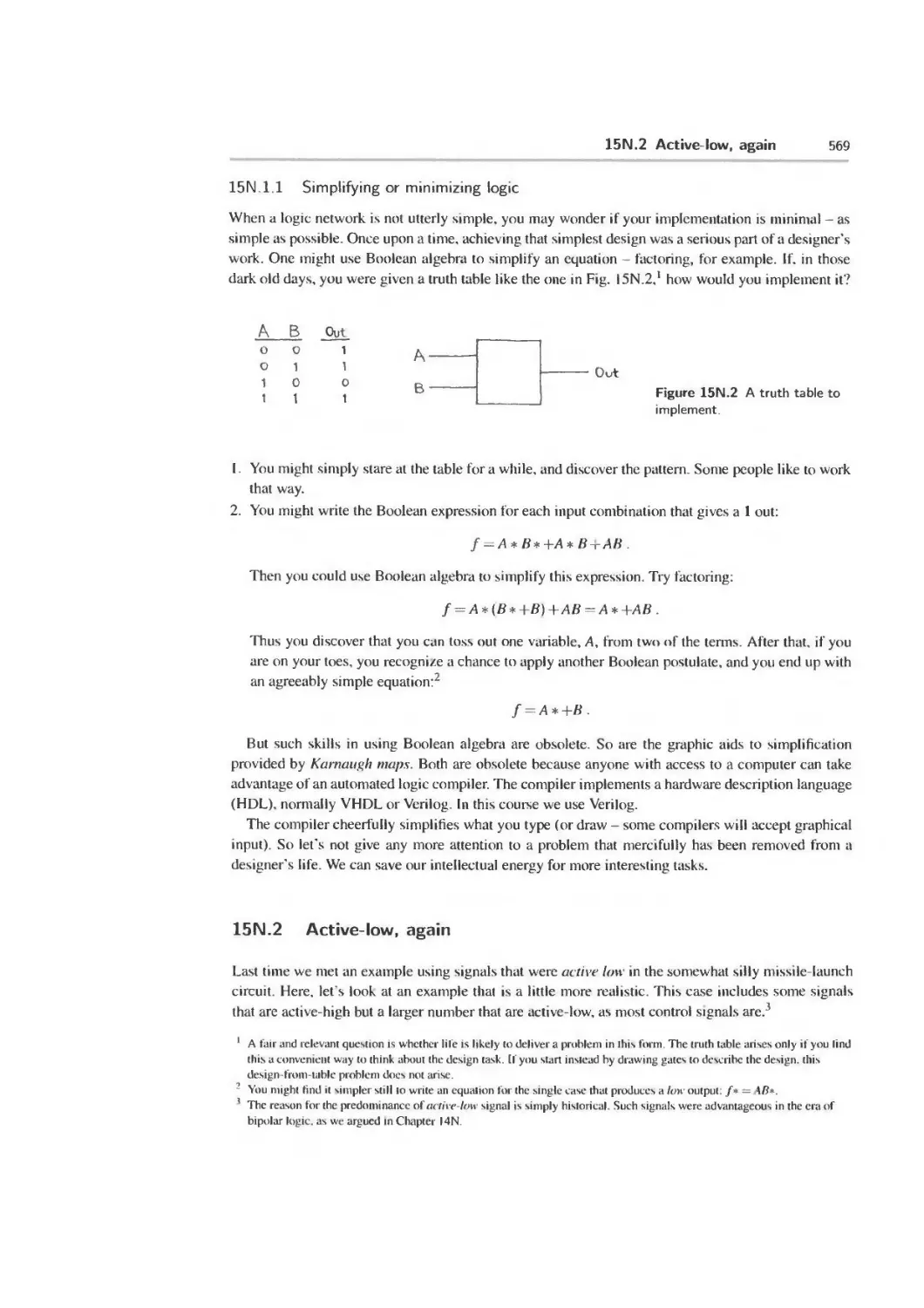
15N. 1 Implementing a combinational function 568
15N.2 Active-low, again 569
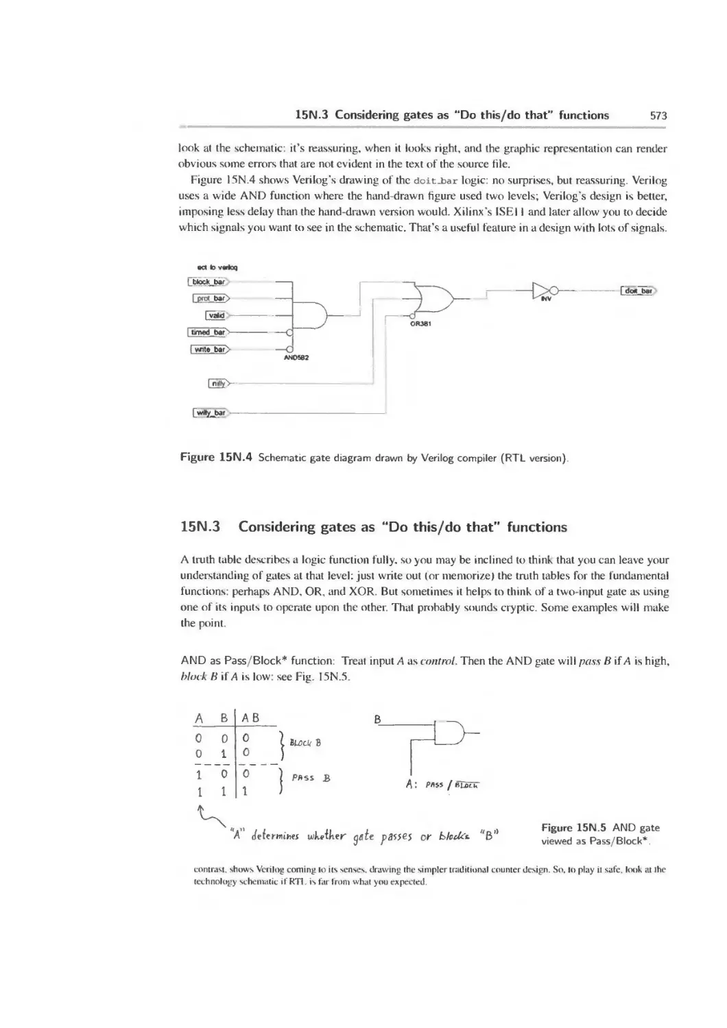
15N.3 Considering gates as “Do this/do that” functions 573
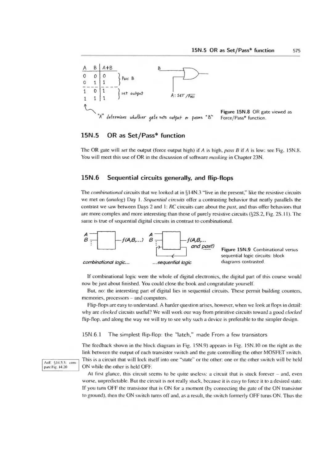
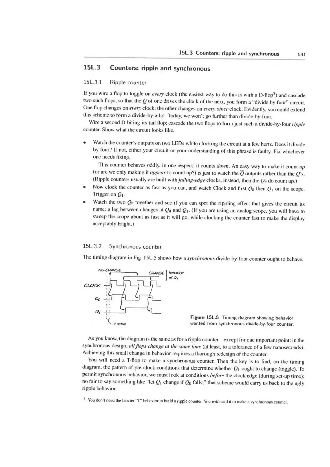
15N.4 XOR as Invert/Pass* function 574
xiv Contents
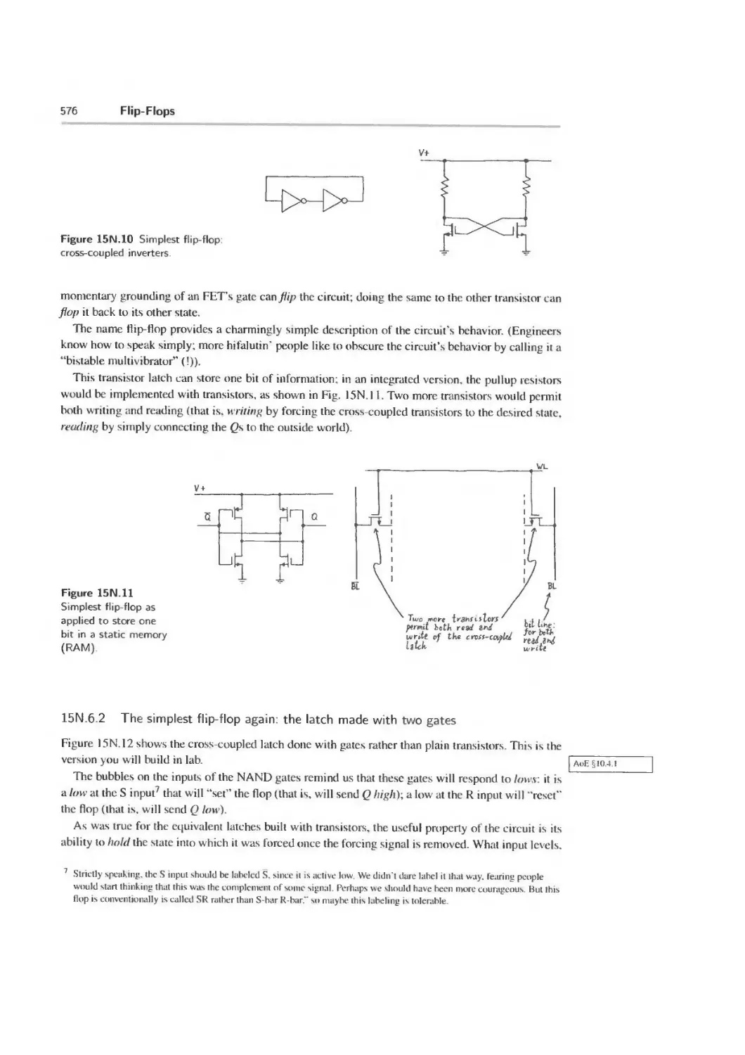
15N.5 OR as Set/Pass* function 575
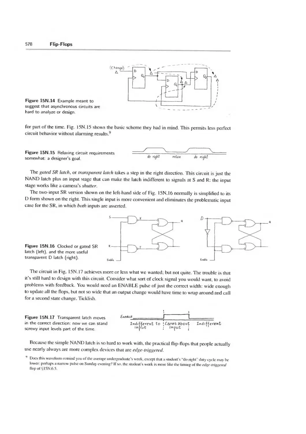
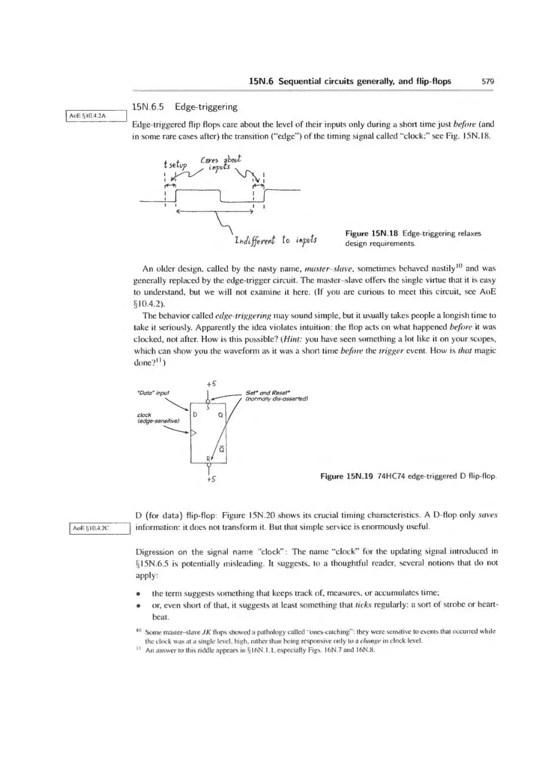
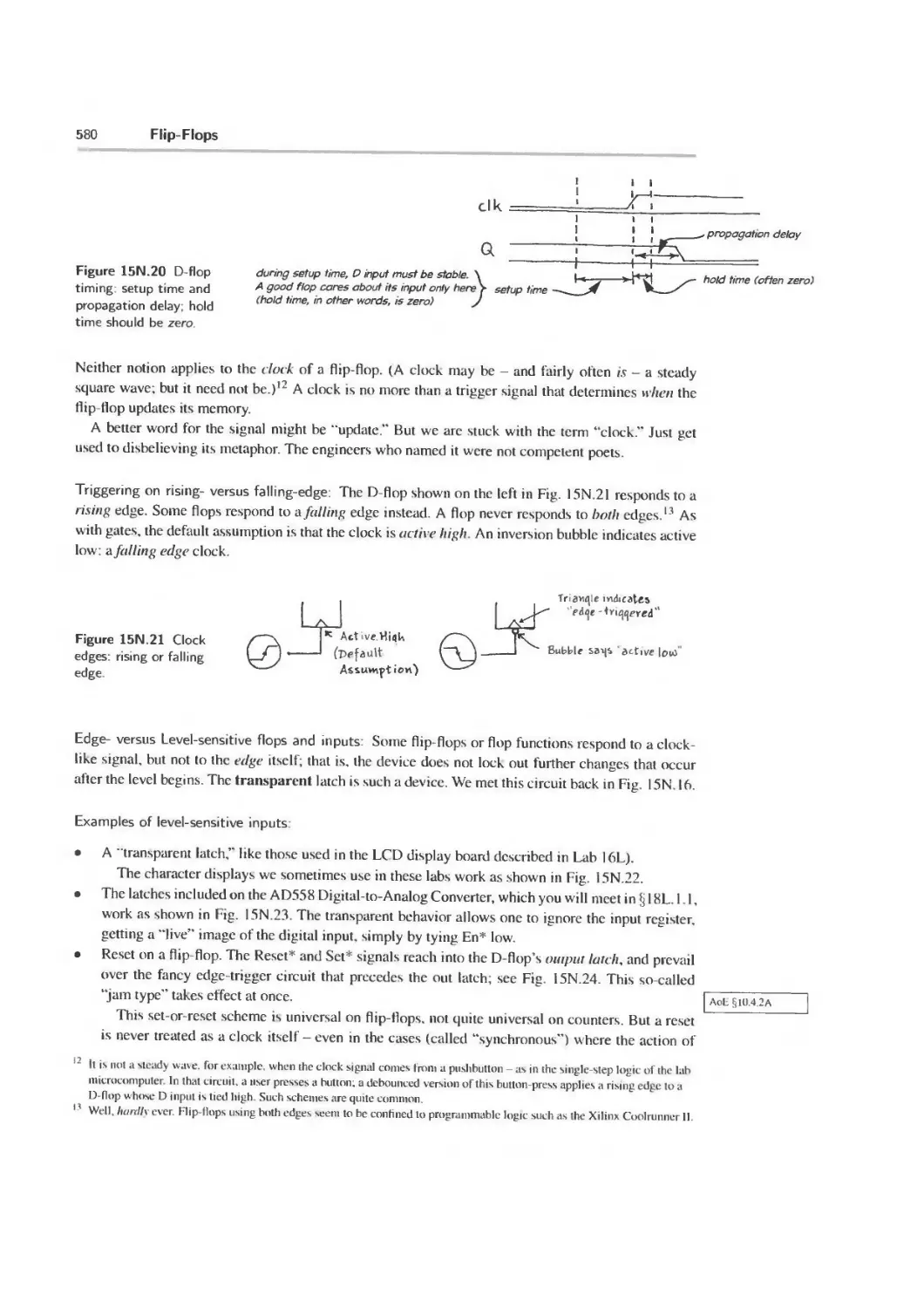
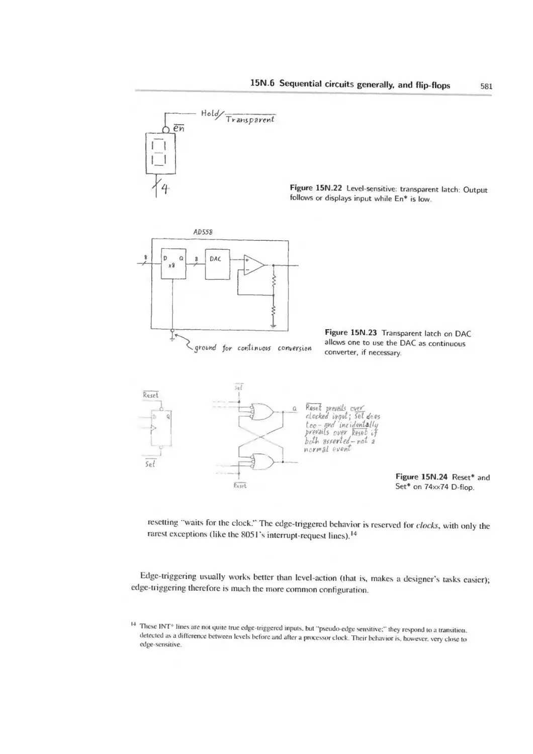
15N.6 Sequential circuits generally, and flip-flops 575
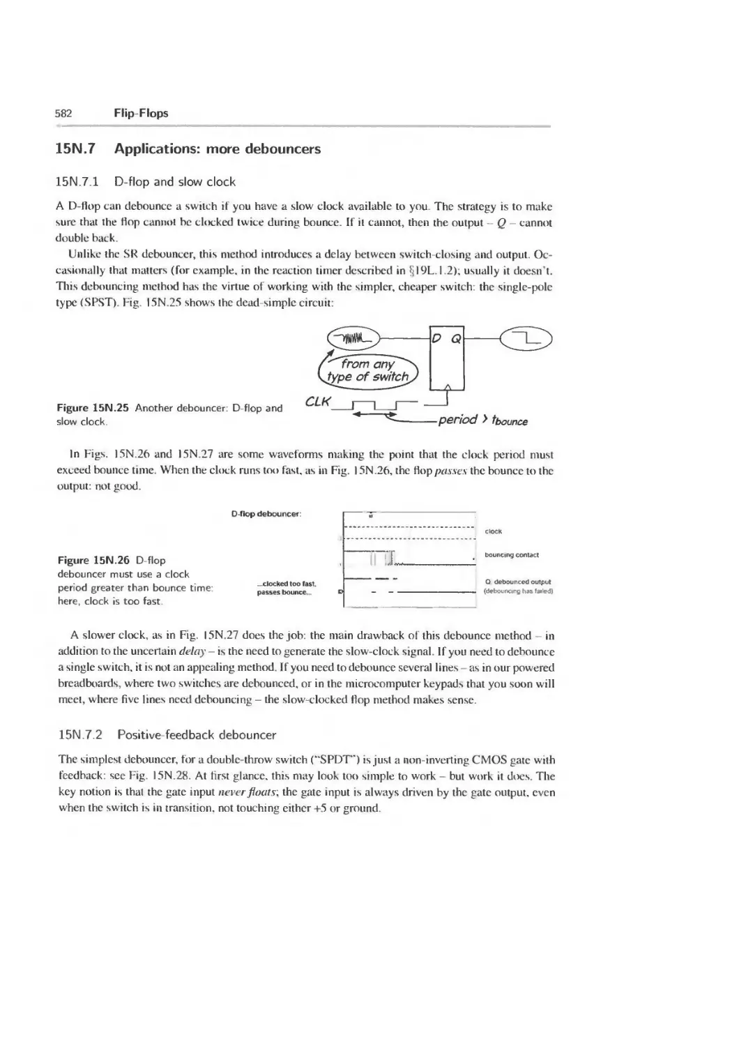
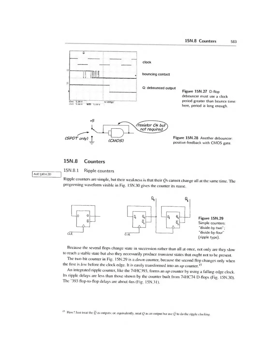
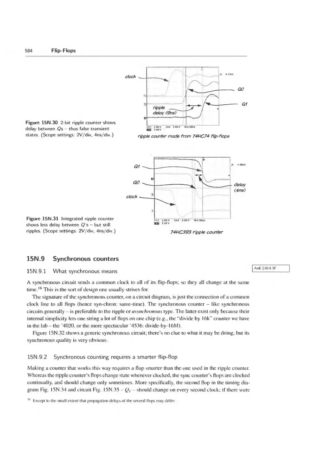
15N.7 Applications: more debouncers 582
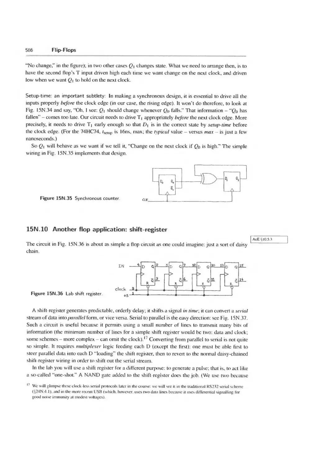
15N.8 Counters 583
15N.9 Synchronous counters 584
15N.I0 Another flop application: shift-register 586
15N.11 AoE Reading 587
15L Lab: Flip-Flops 588
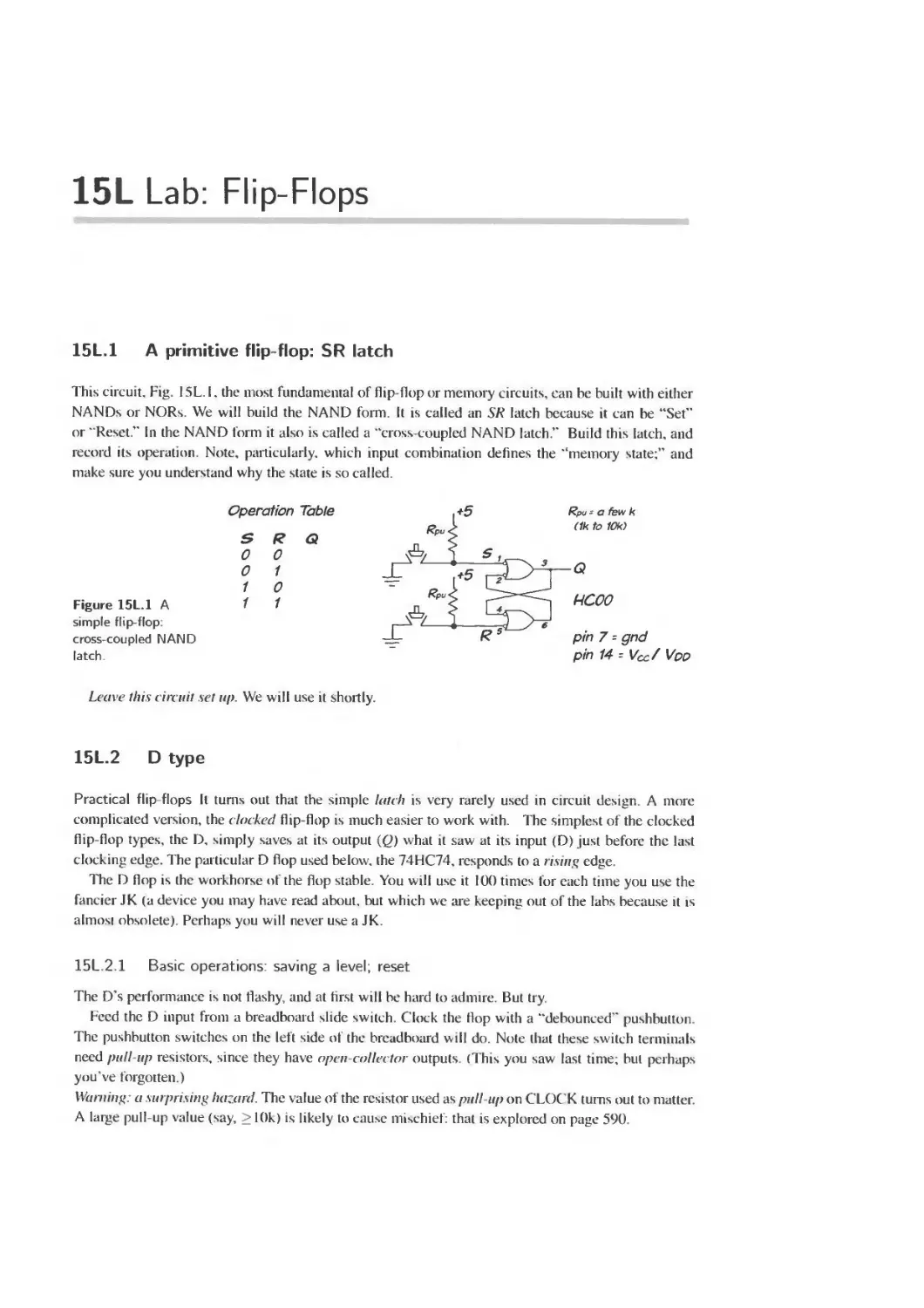
15L.1 A primitive flip-flop: SR latch 588
15L.2 ©type 588
15L.3 Counters: ripple and synchronous 591
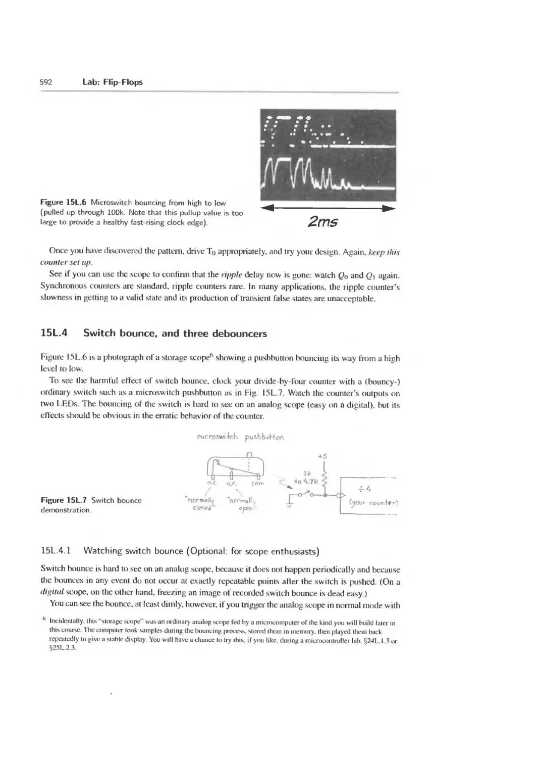
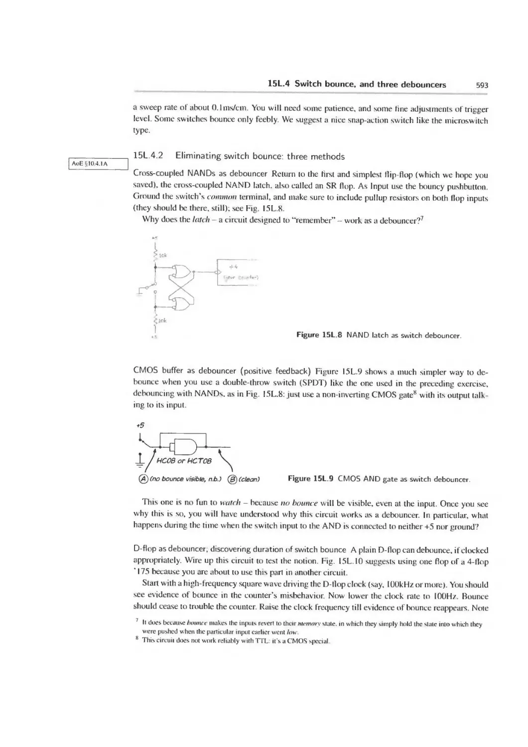
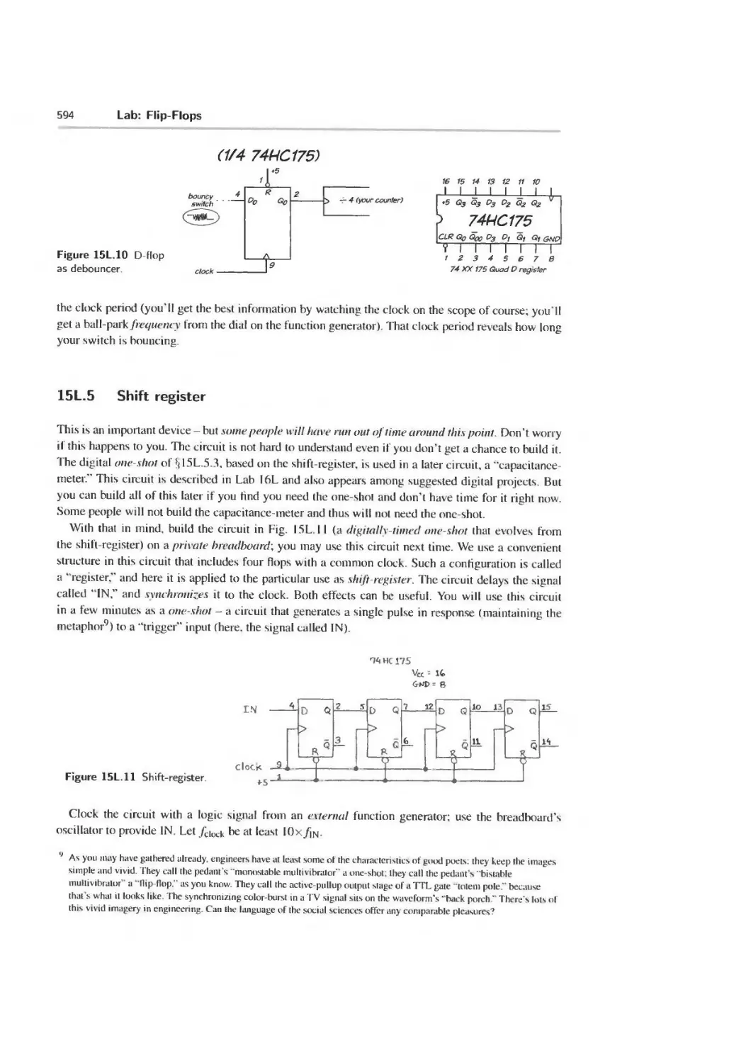
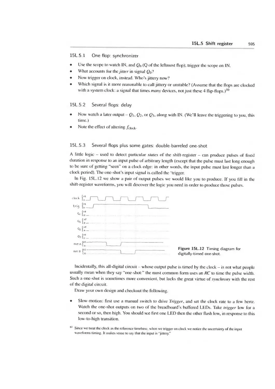
15L.4 Switch bounce, and three debouncers 592
I5L.5 Shift register 594
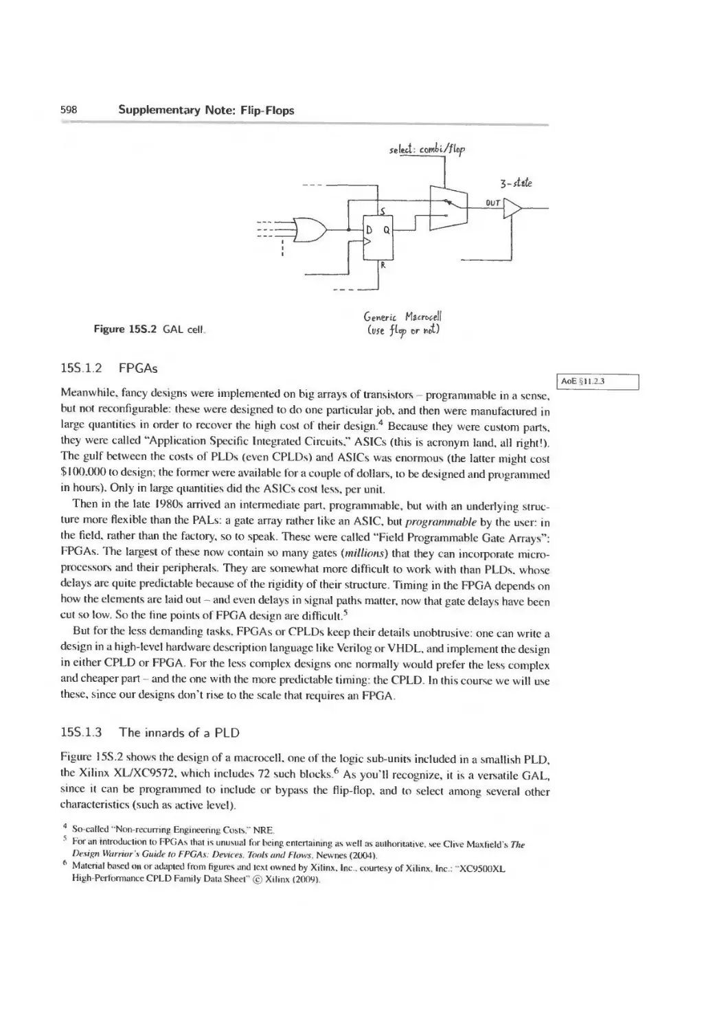
15S Supplementary Note: Flip-Flops 597
15S. 1 Programmable logic devices 597
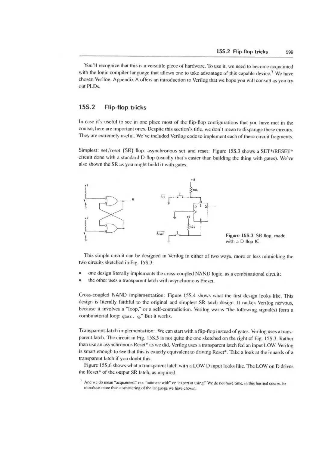
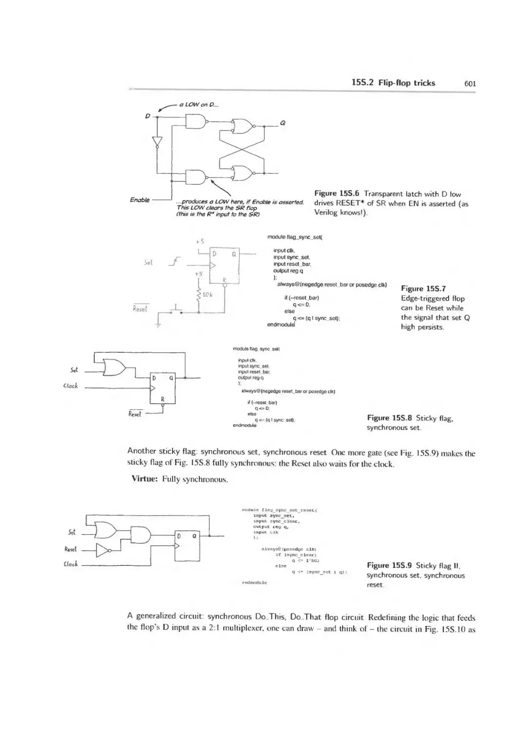
15S.2 Flip-flop tricks 599
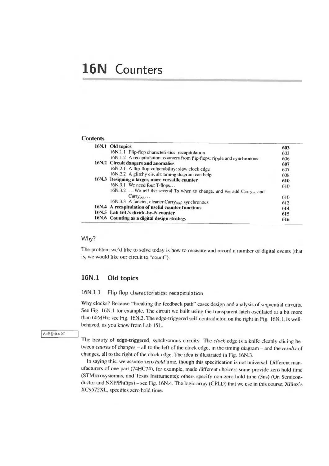
16N Counters 603
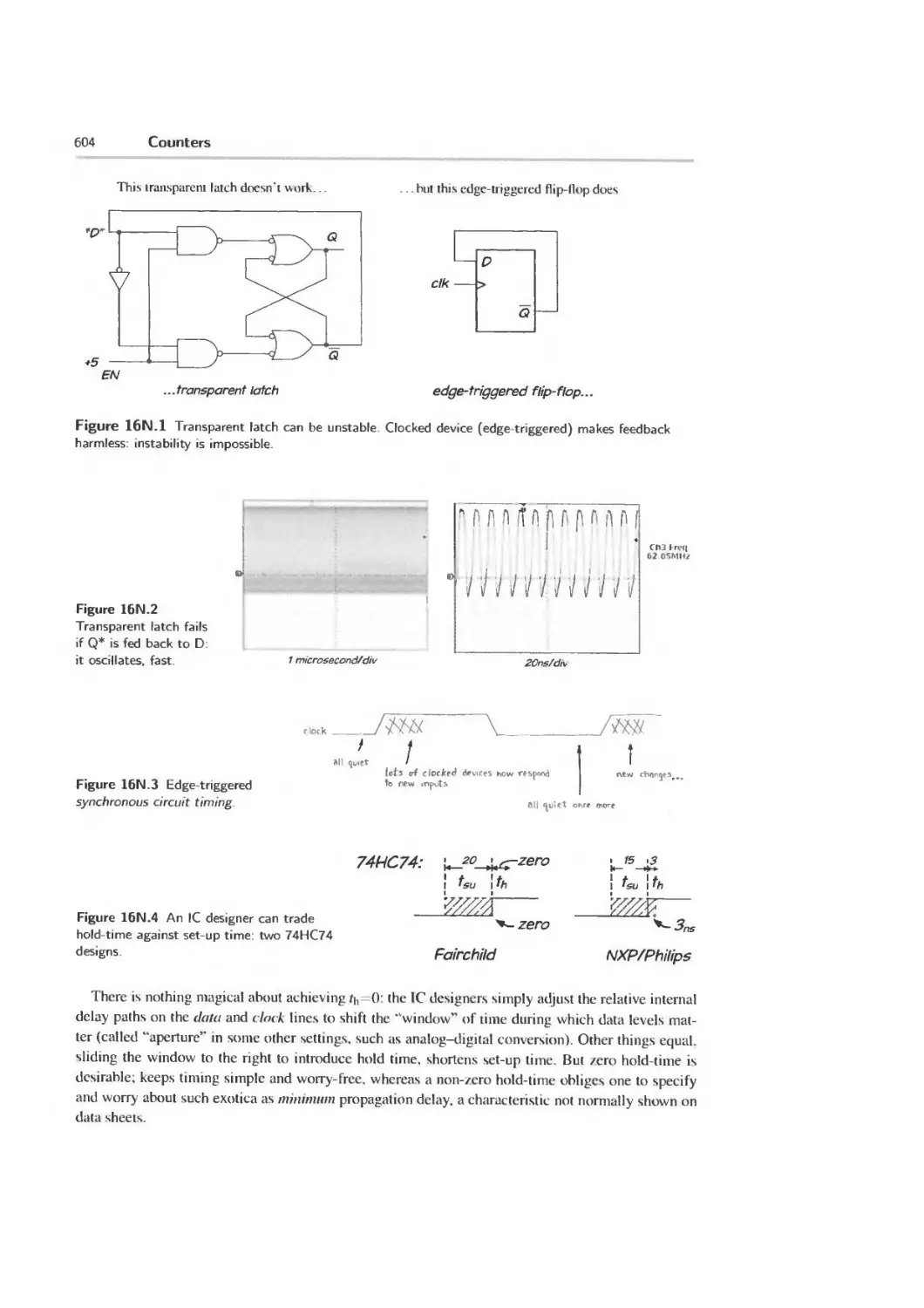
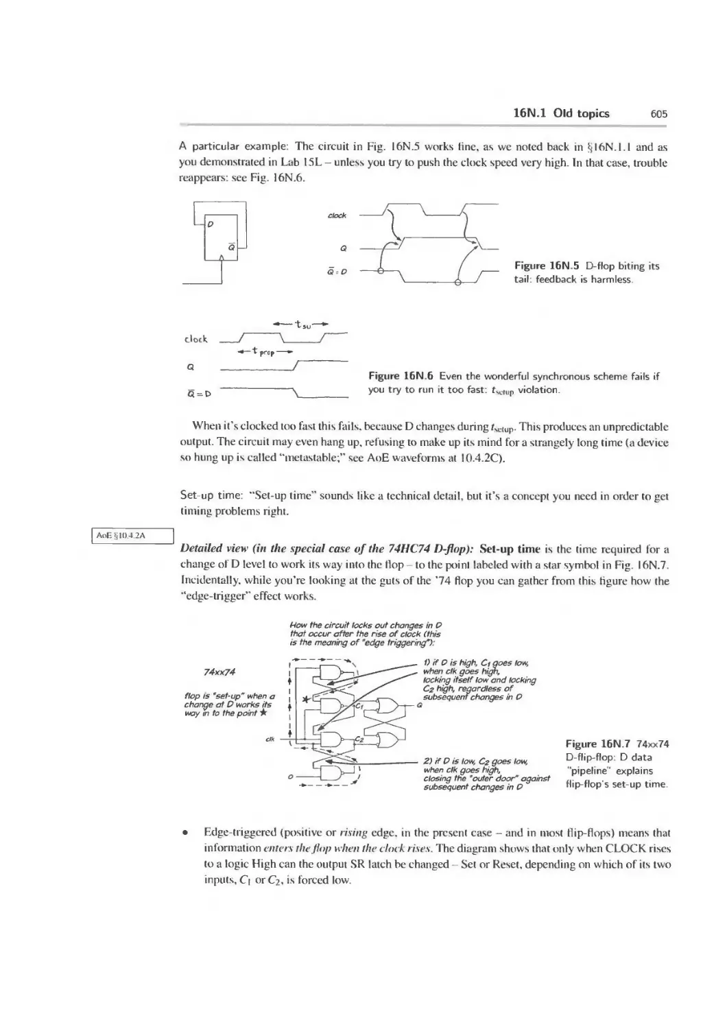
16N. 1 Old topics 603
16N.2 Circuit dangers and anomalies 607
16N.3 Designing a larger, more versatile counter 610
I6N.4 A recapitulation of useful counter functions 614
16N.5 Lab 16L’s divide-by-ЛГ counter 615
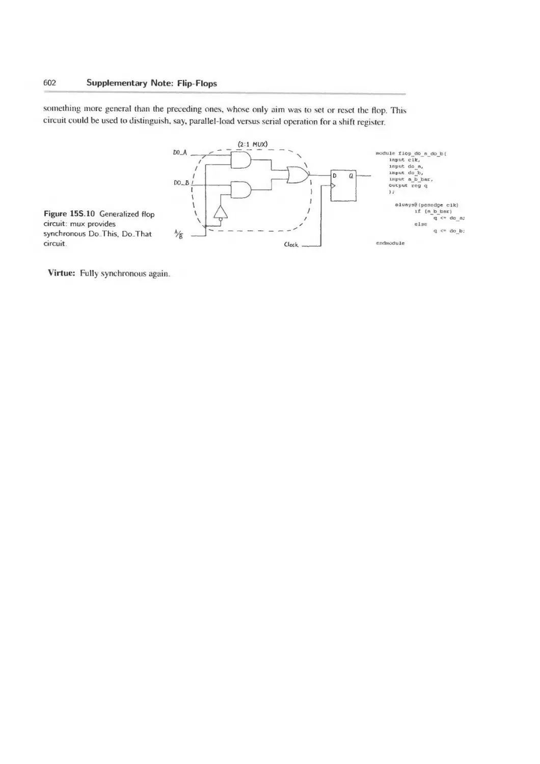
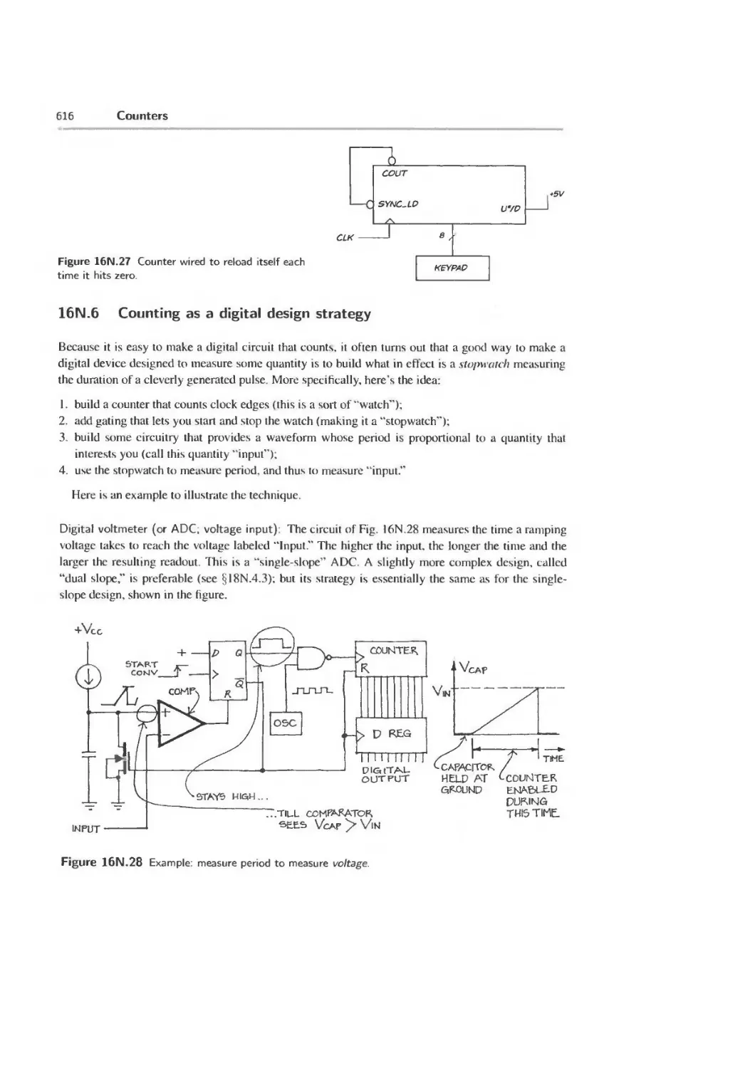
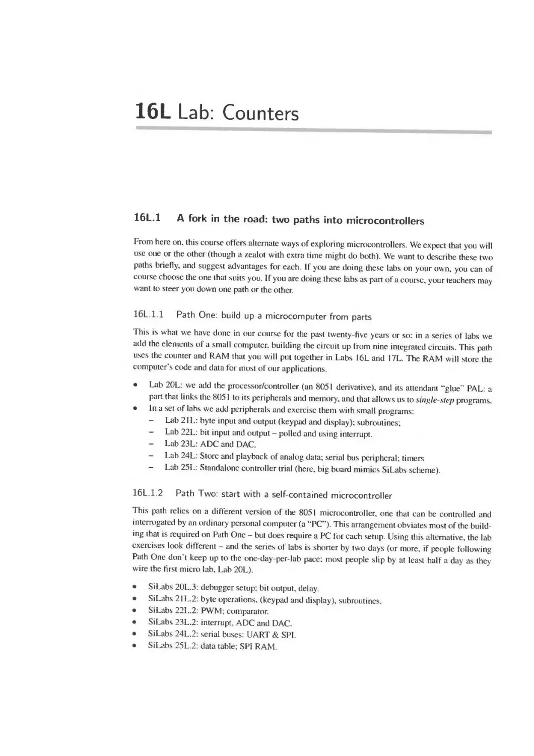
16N.6 Counting as a digital design strategy 616
16L Lab: Counters 617
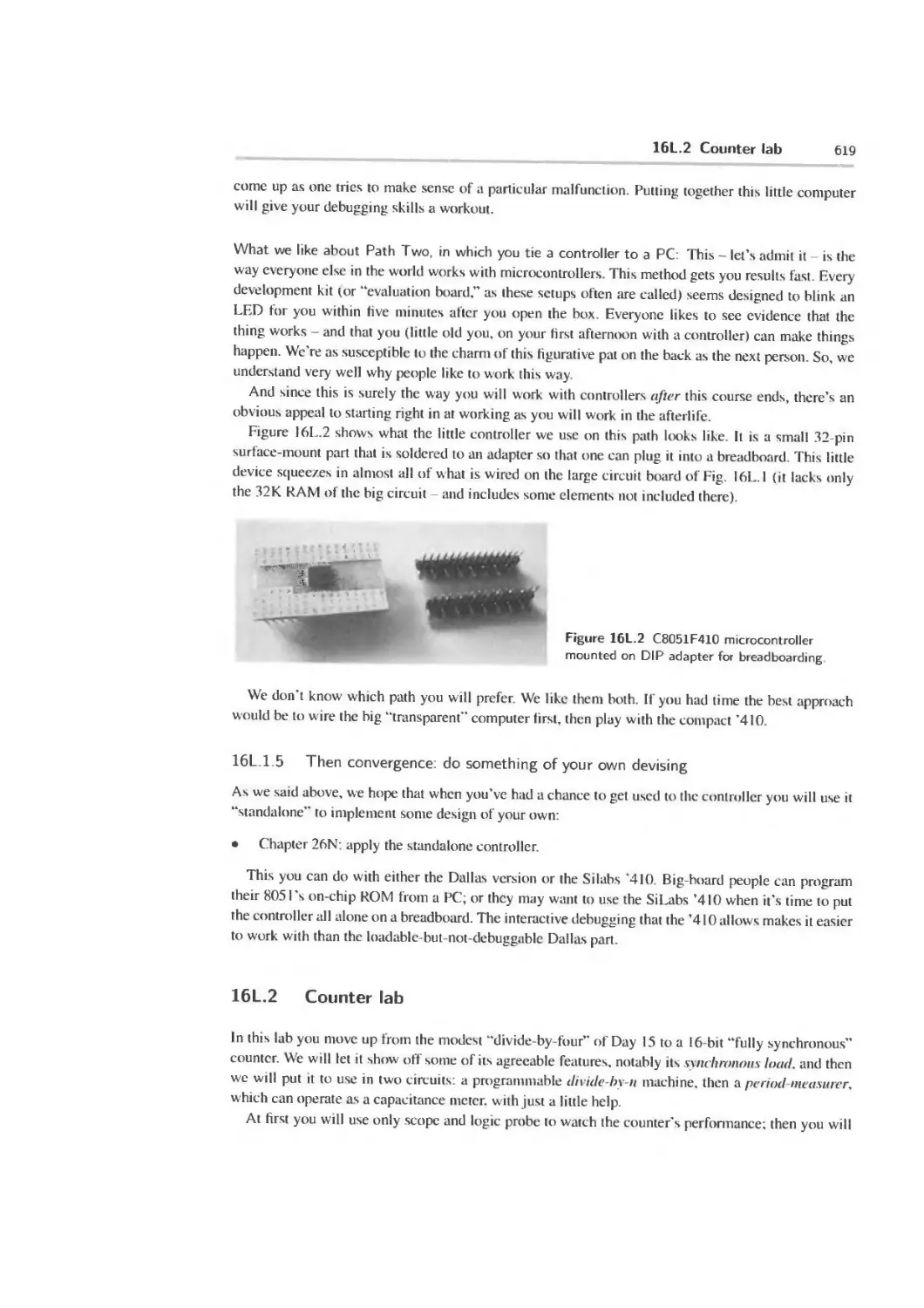
16L.1 A fork in the road: two paths into microcontrollers 617
16L2 Counter lab 619
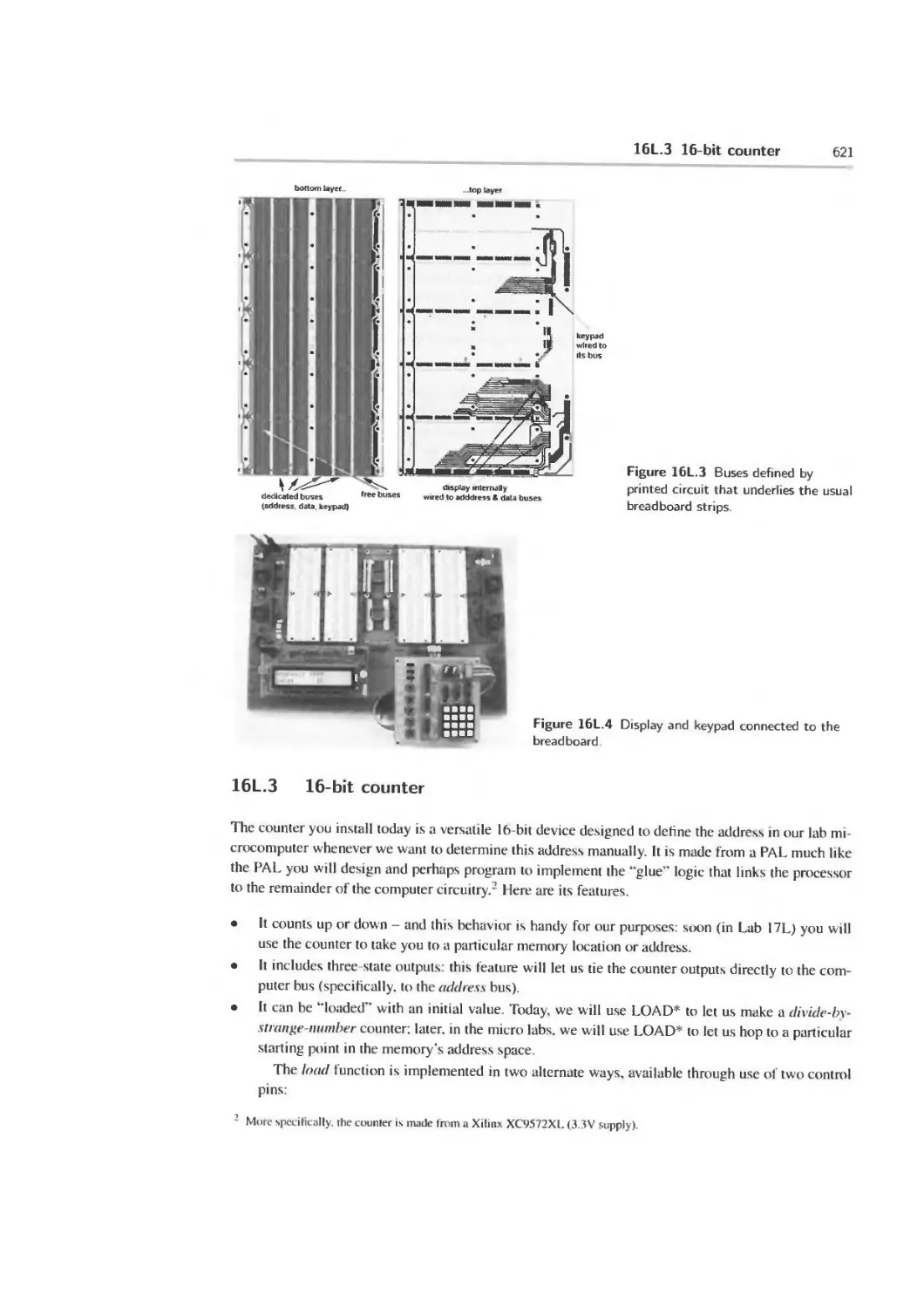
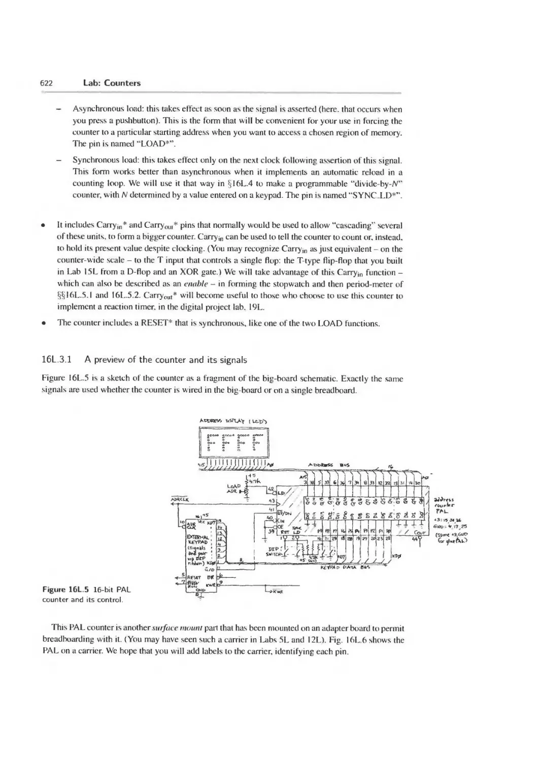
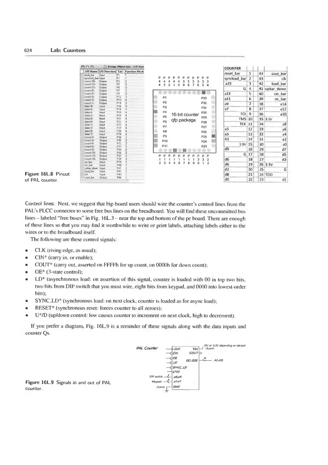
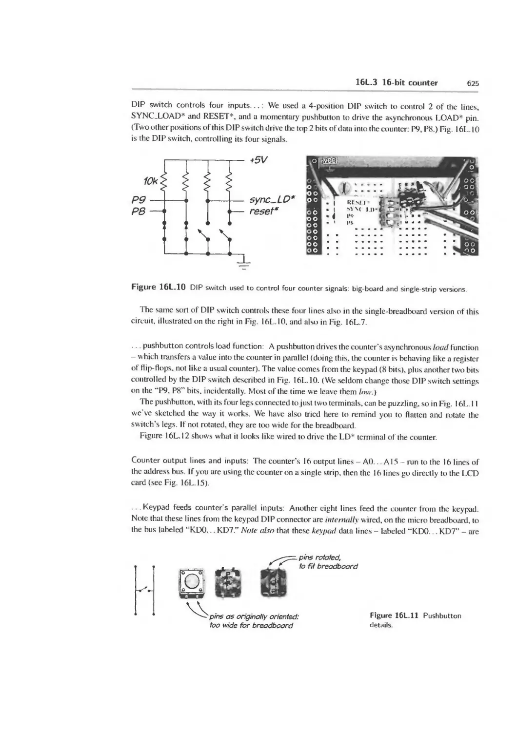
16L.3 16-bit counter 621
16L.4 Make horrible music 629
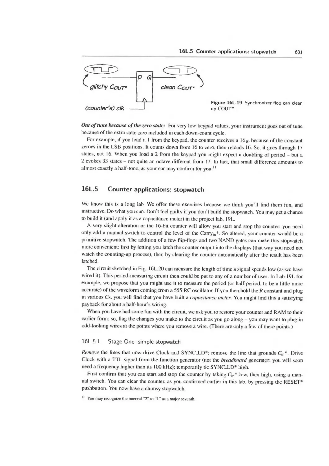
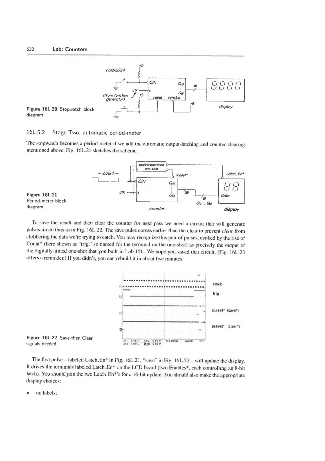
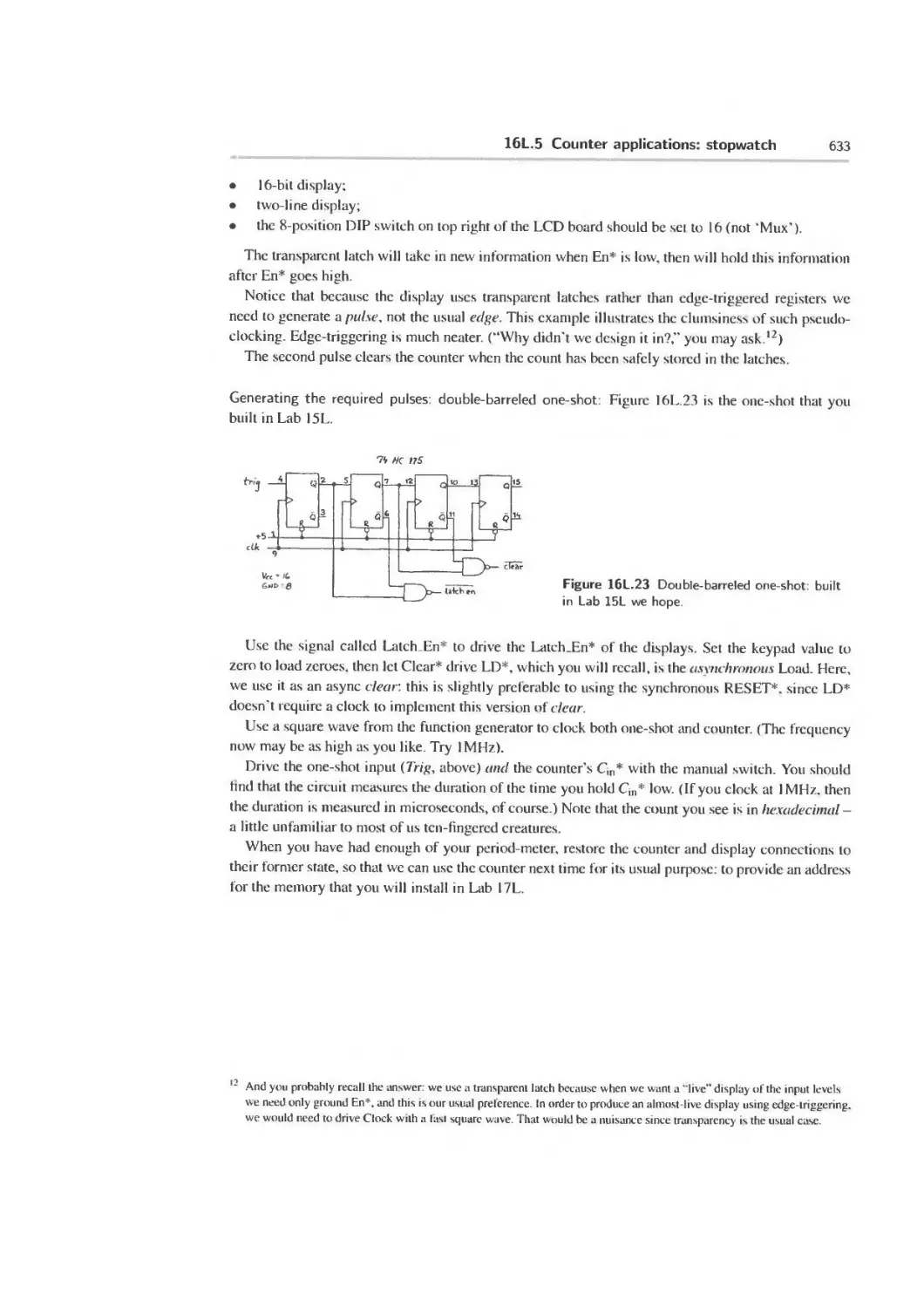
16L.5 Counter applications: stopwatch 631
16W Worked Examples: Applications of Counters 634
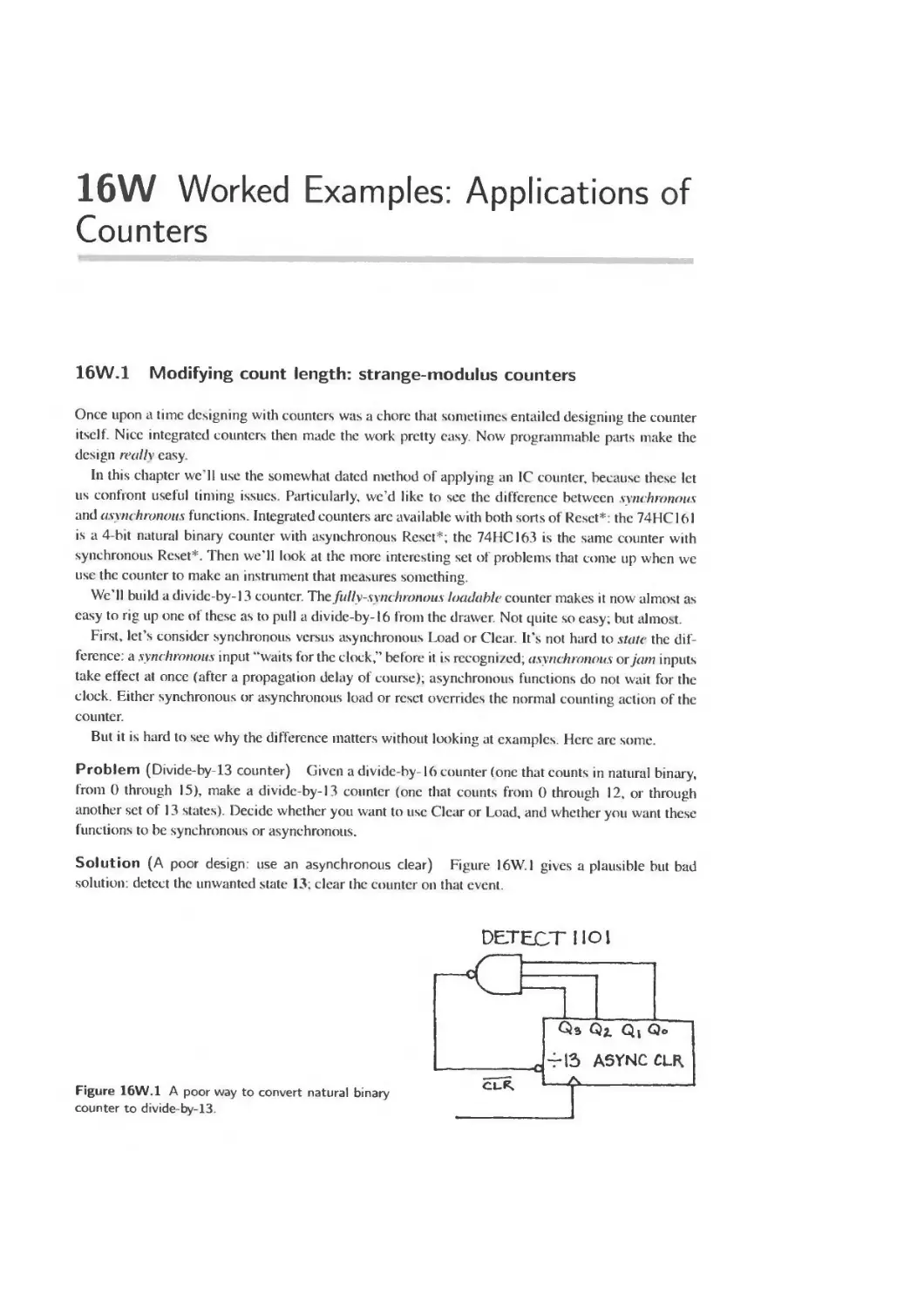
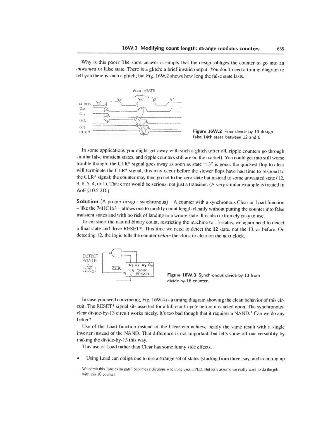
16W. 1 Modifying count length: strange-modulus counters 634
16W.2 Using a counter to measure period, thus many possible input quantities 636
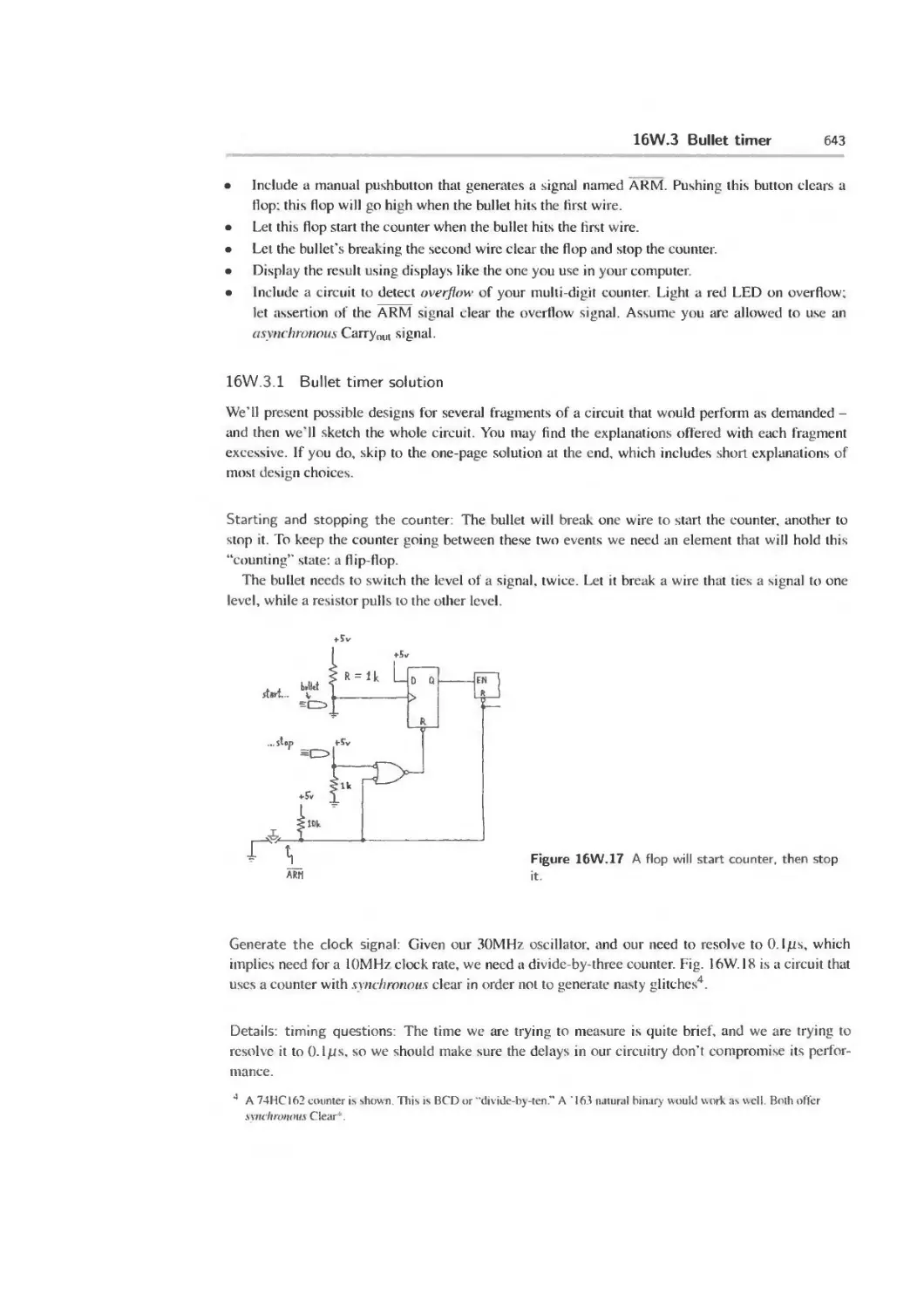
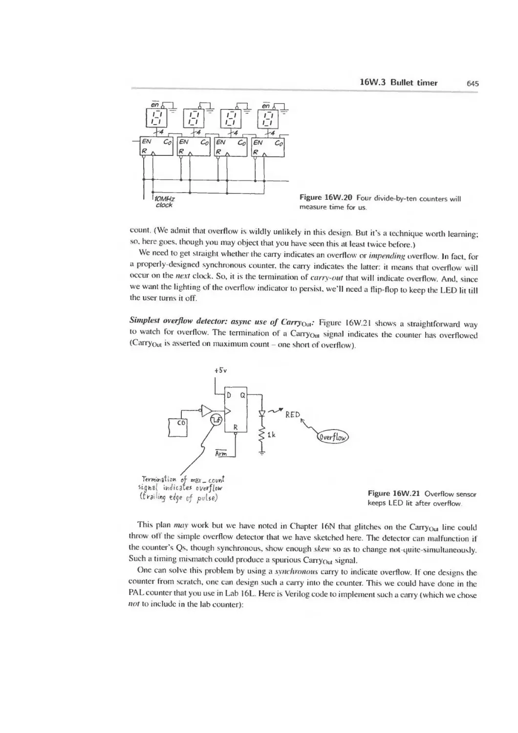
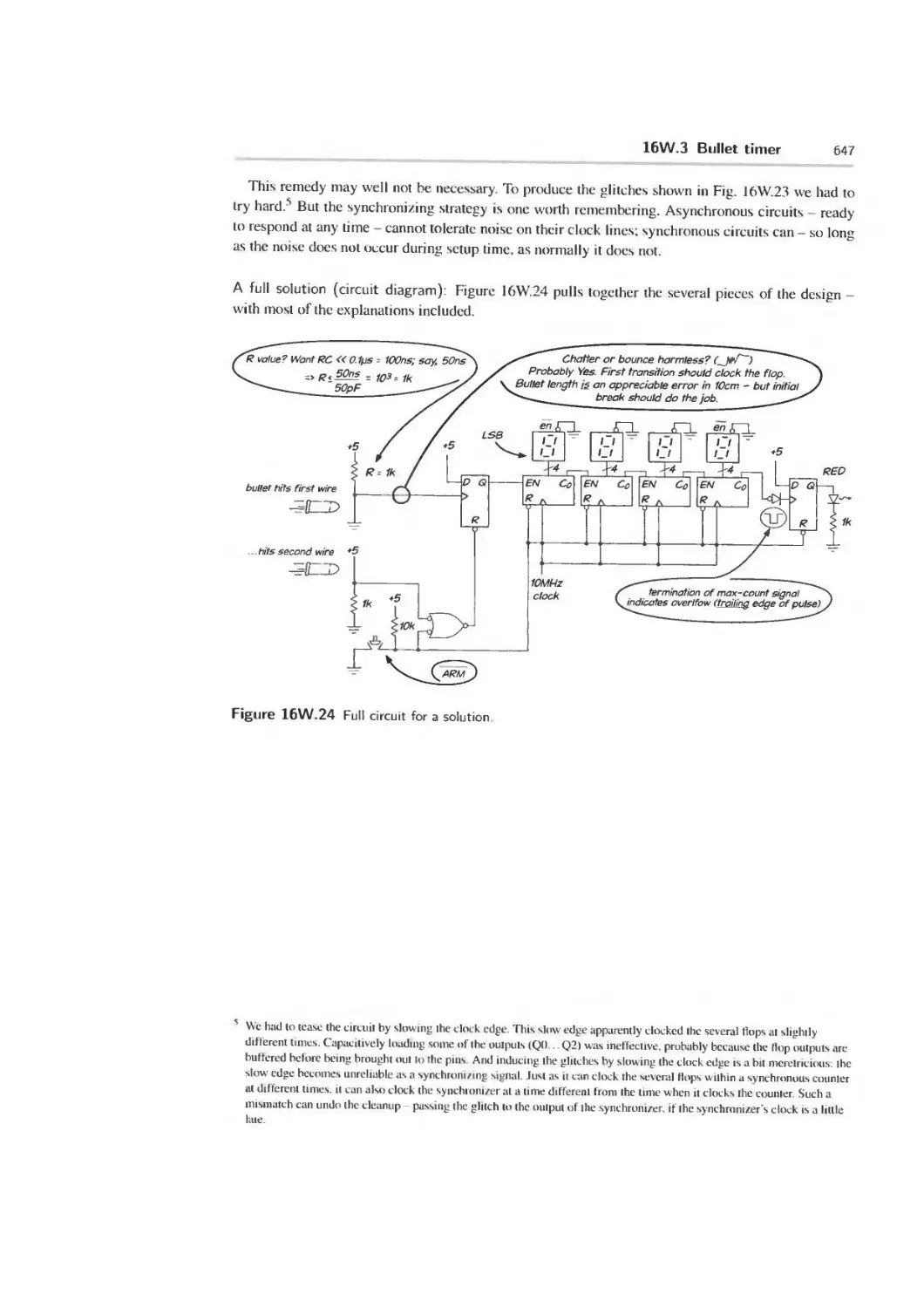
16W.3 Bullet timer 642
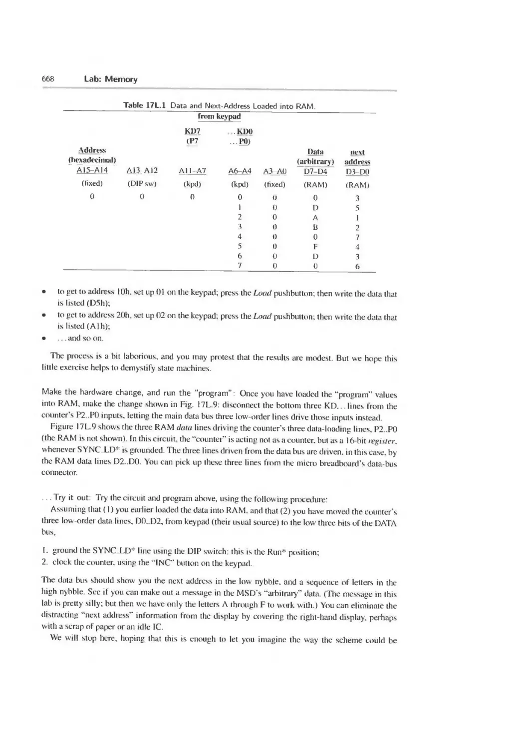
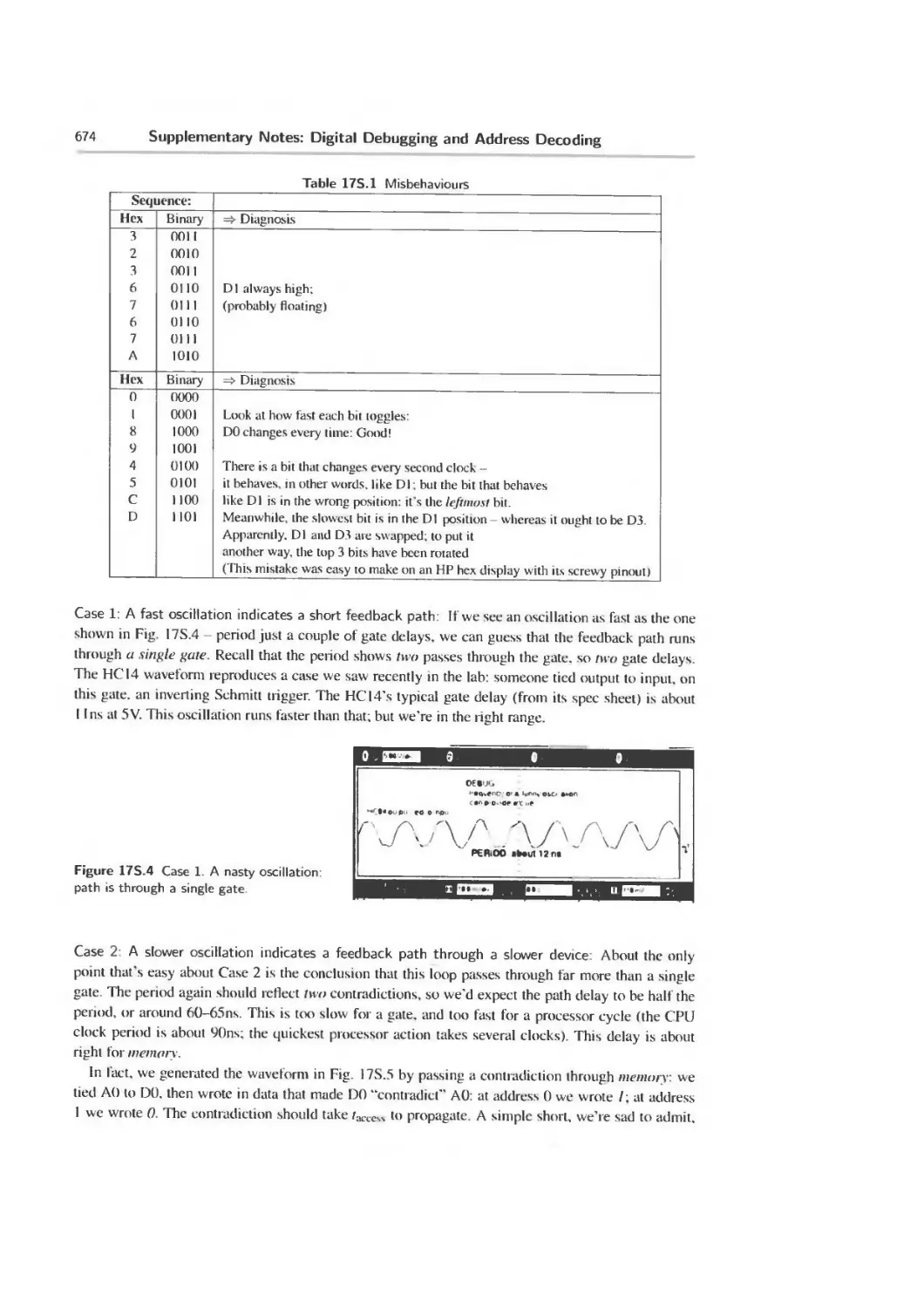
17N Memory 648
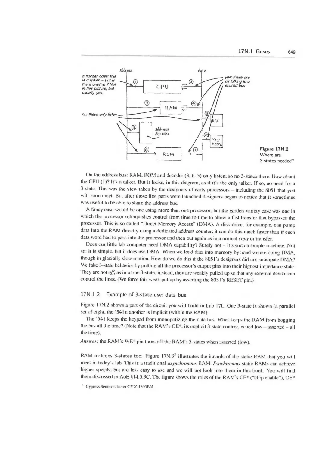
17N.1 Buses 648
17N.2 Memory 651
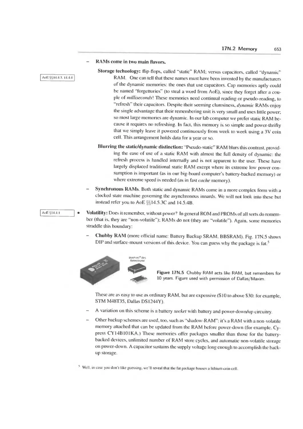
17N.3 State machine- new name for old notion 655
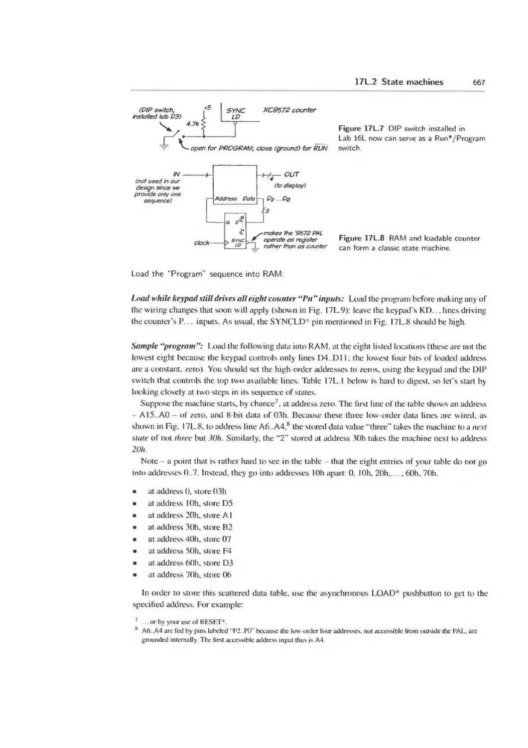
17L Lab: Memory 661
17L.1 RAM 661
17L.2 State machines 663
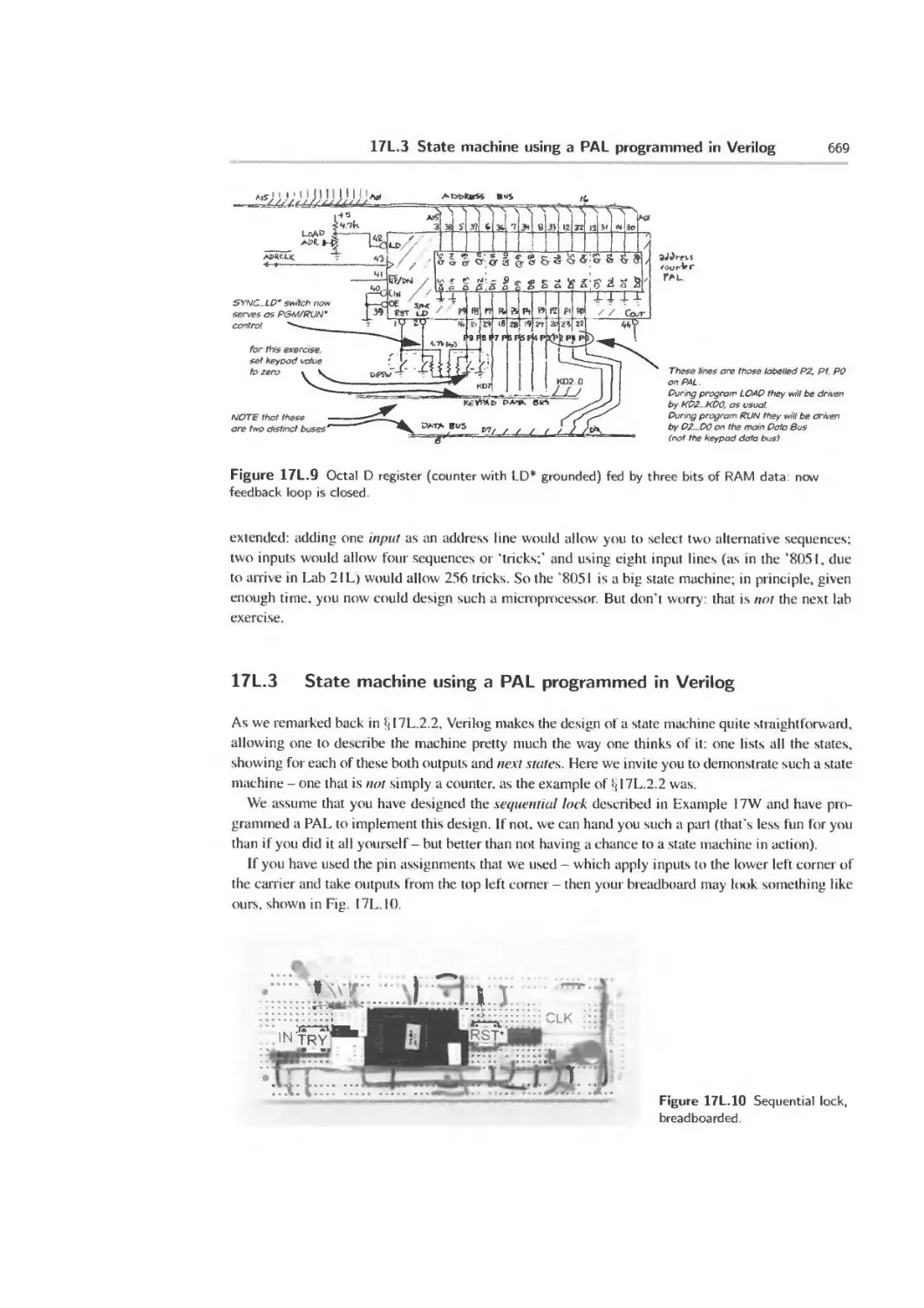
17L.3 State machine using a PAL programmed in Verilog 669
Contents
XV
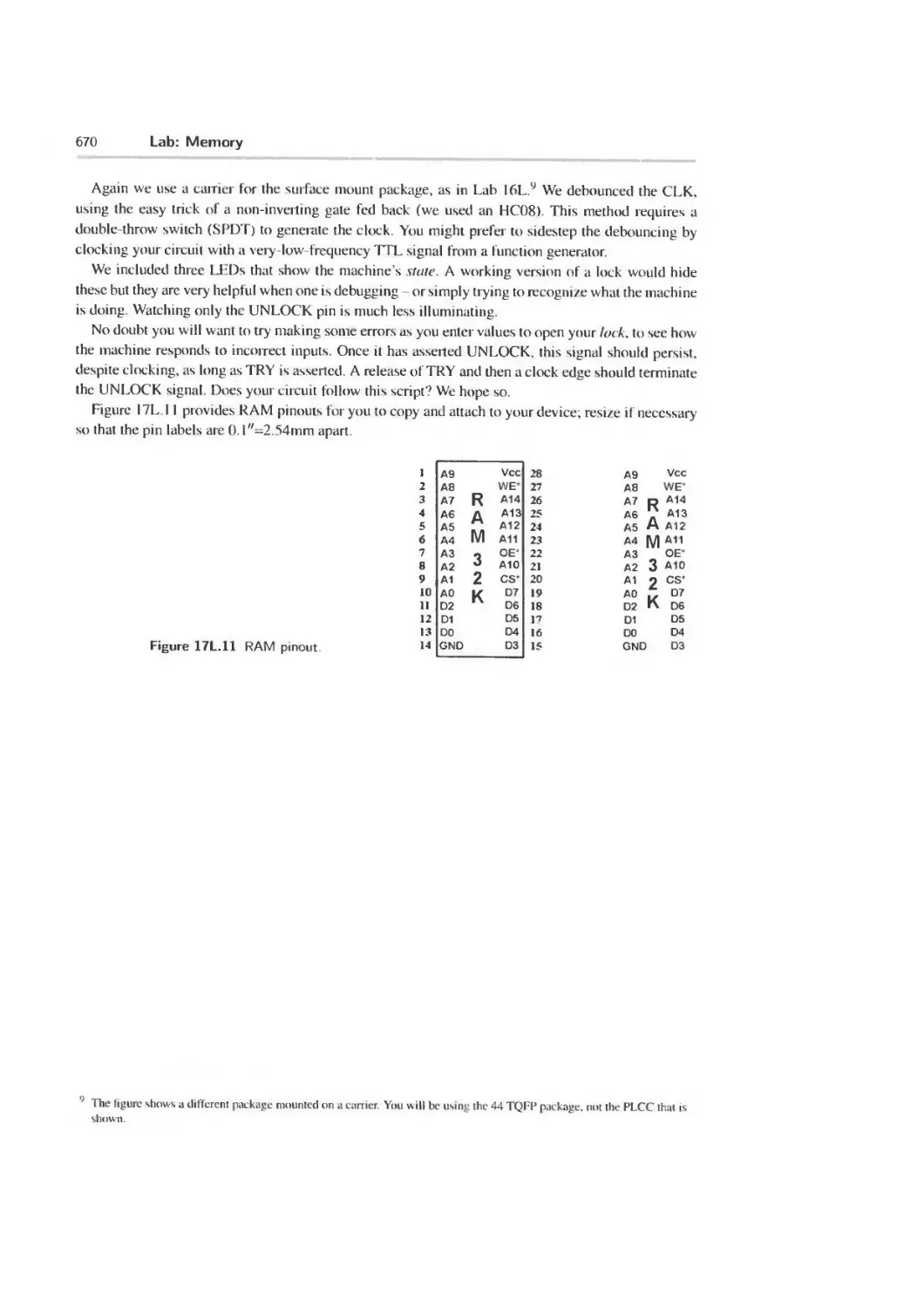
17S Supplementary Notes: Digital Debugging and Address Decoding 671
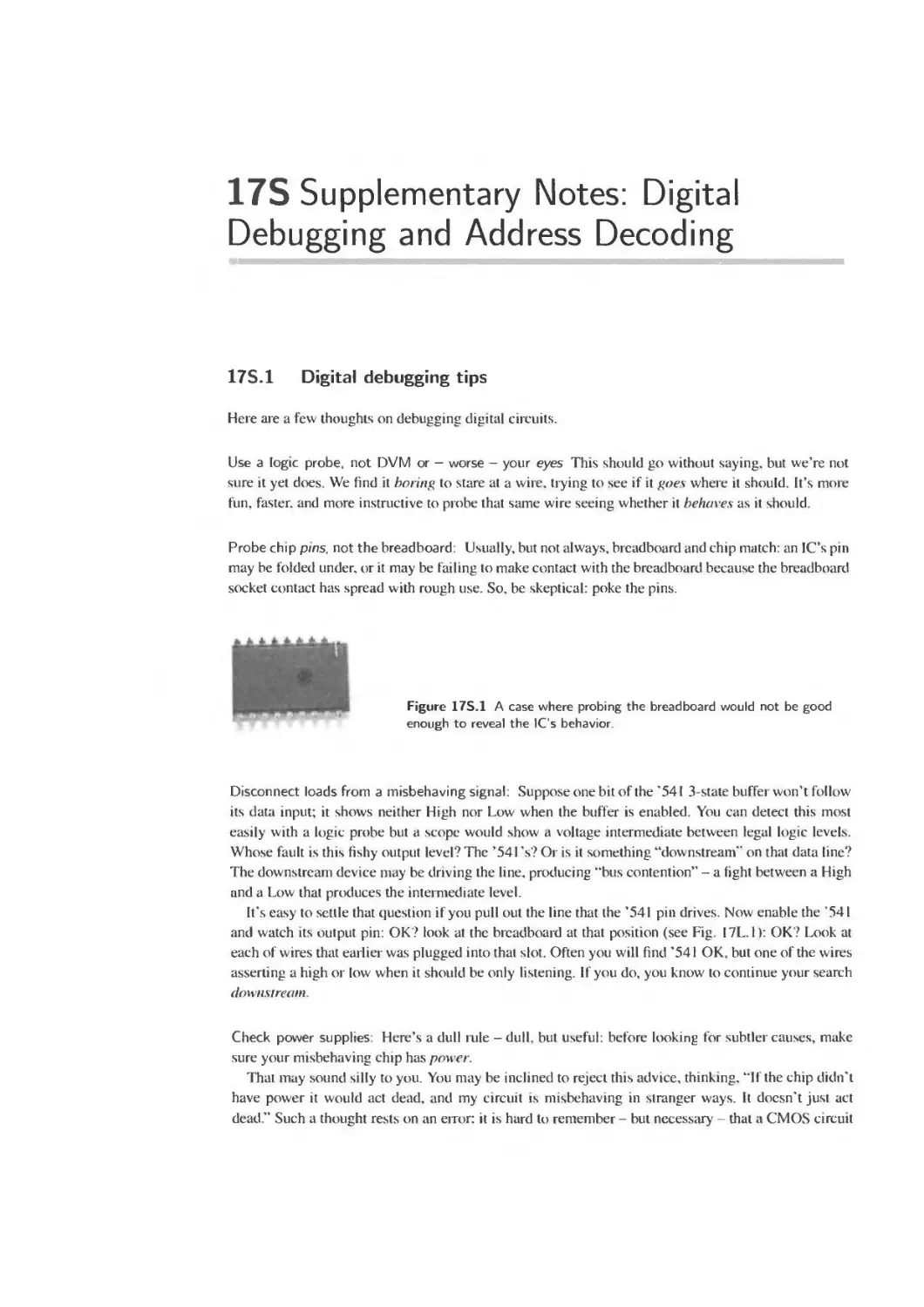
17S.1 Digital debugging tips 671
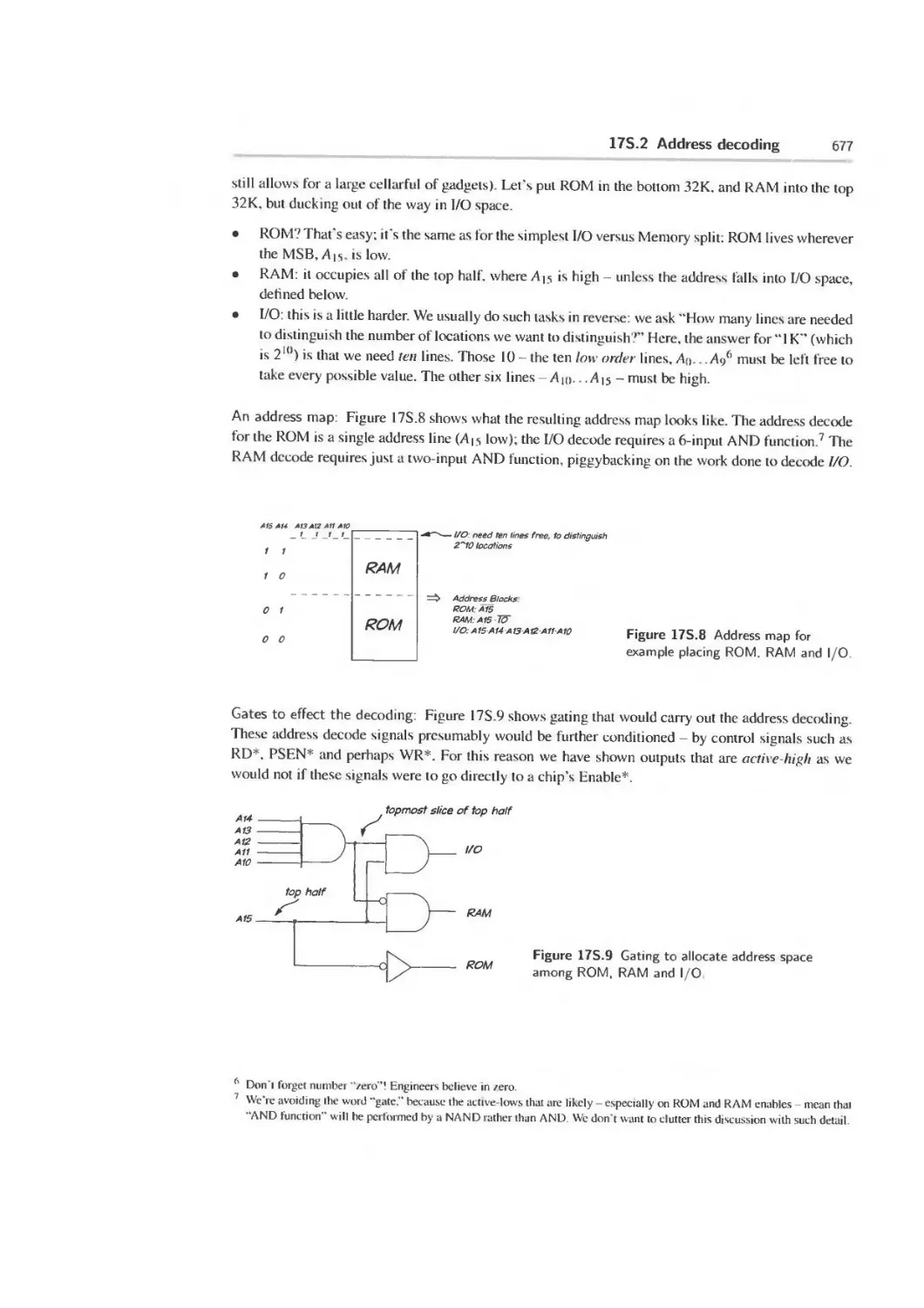
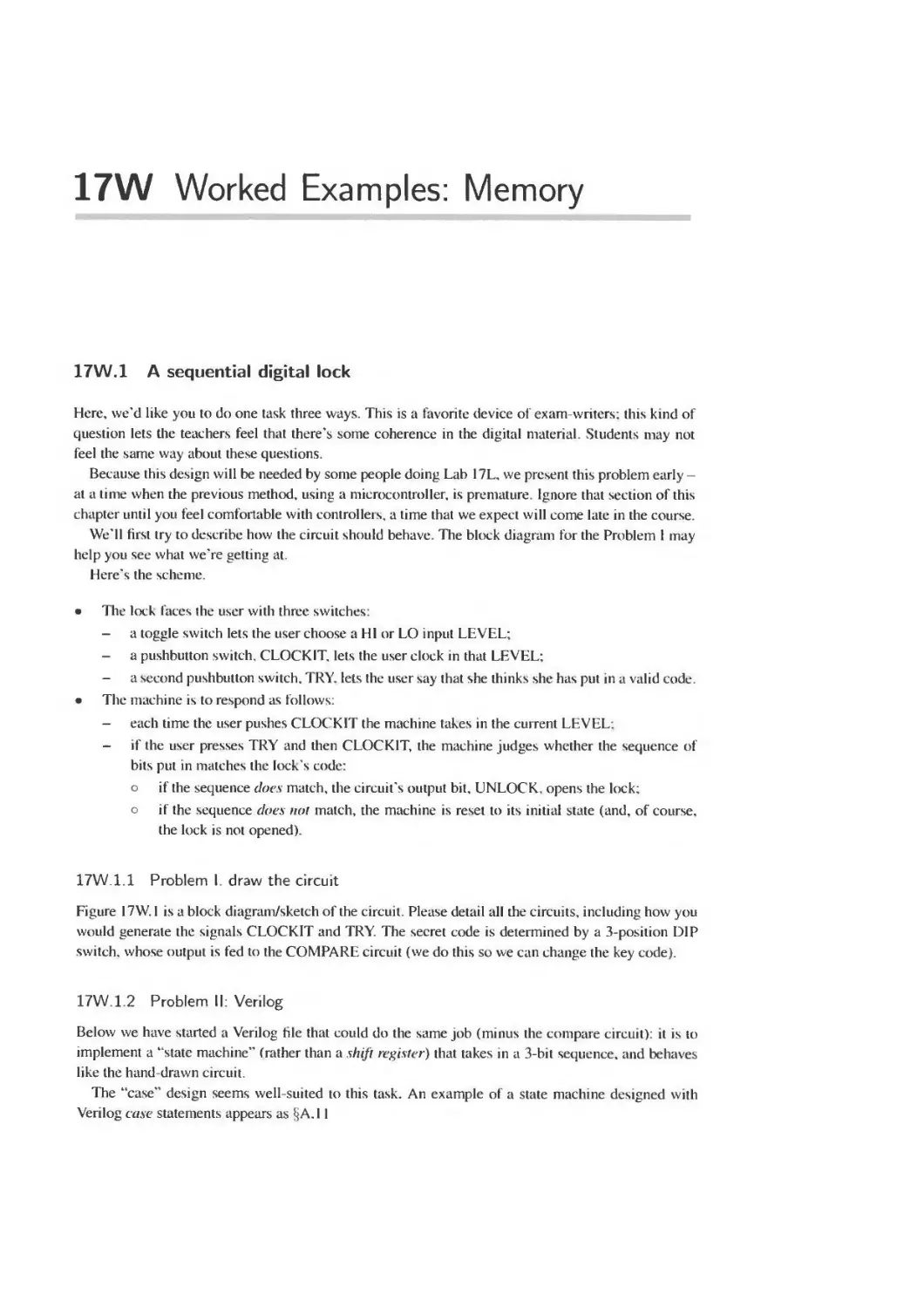
17S.2 Address decoding 675
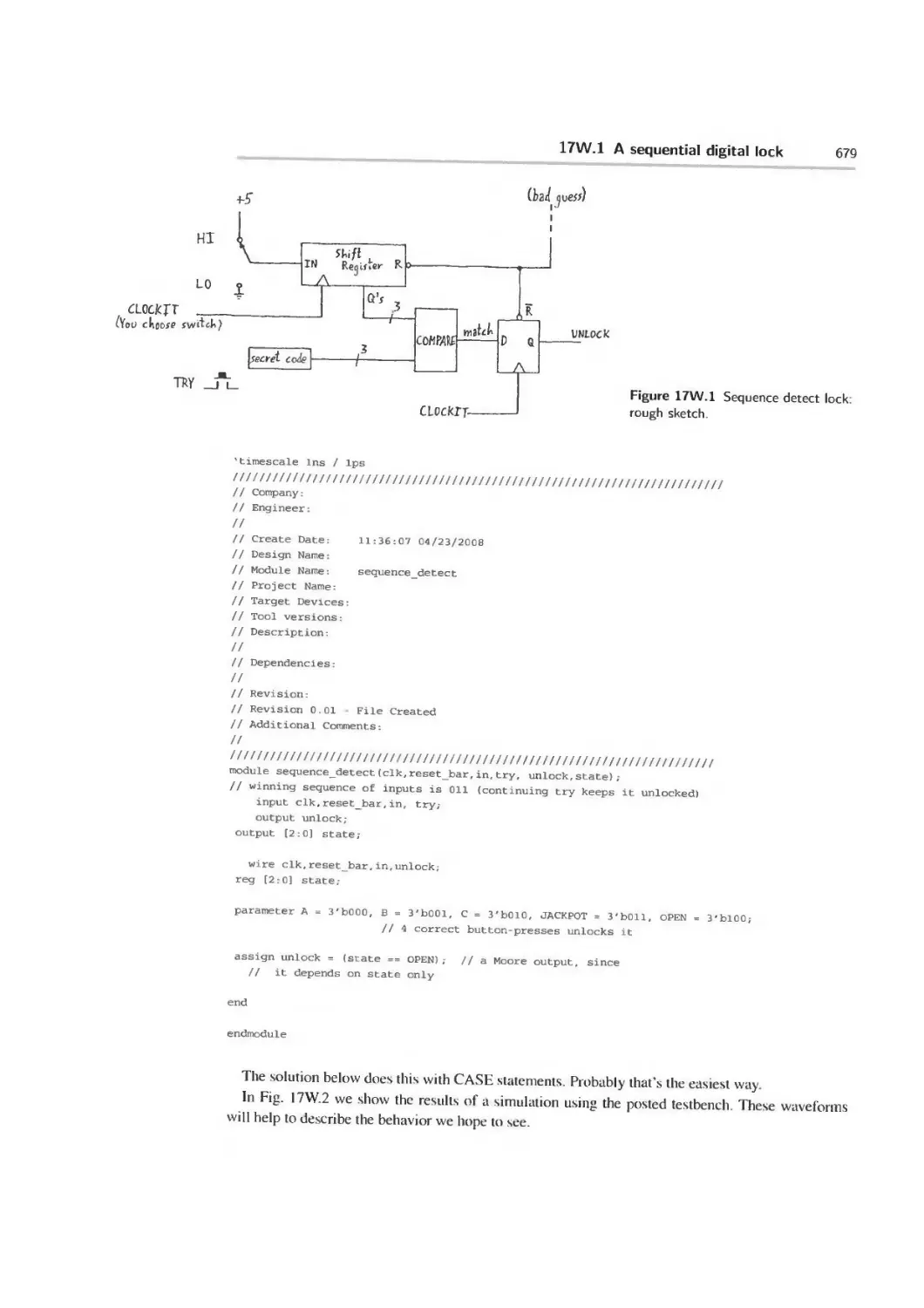
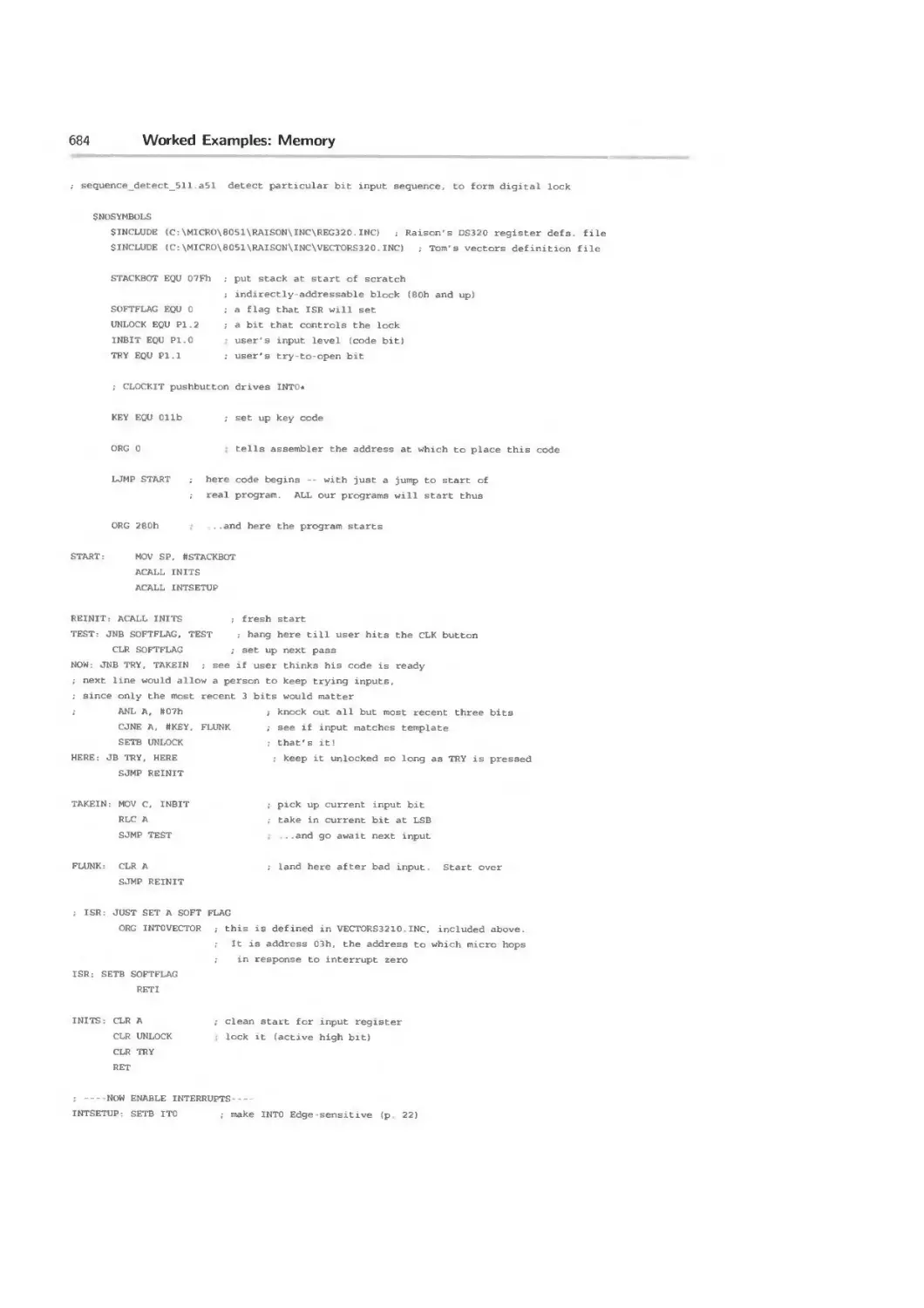
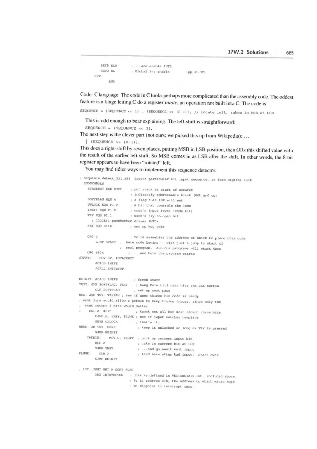
17W Worked Examples: Memory 678
17W.1 A sequential digital lock 678
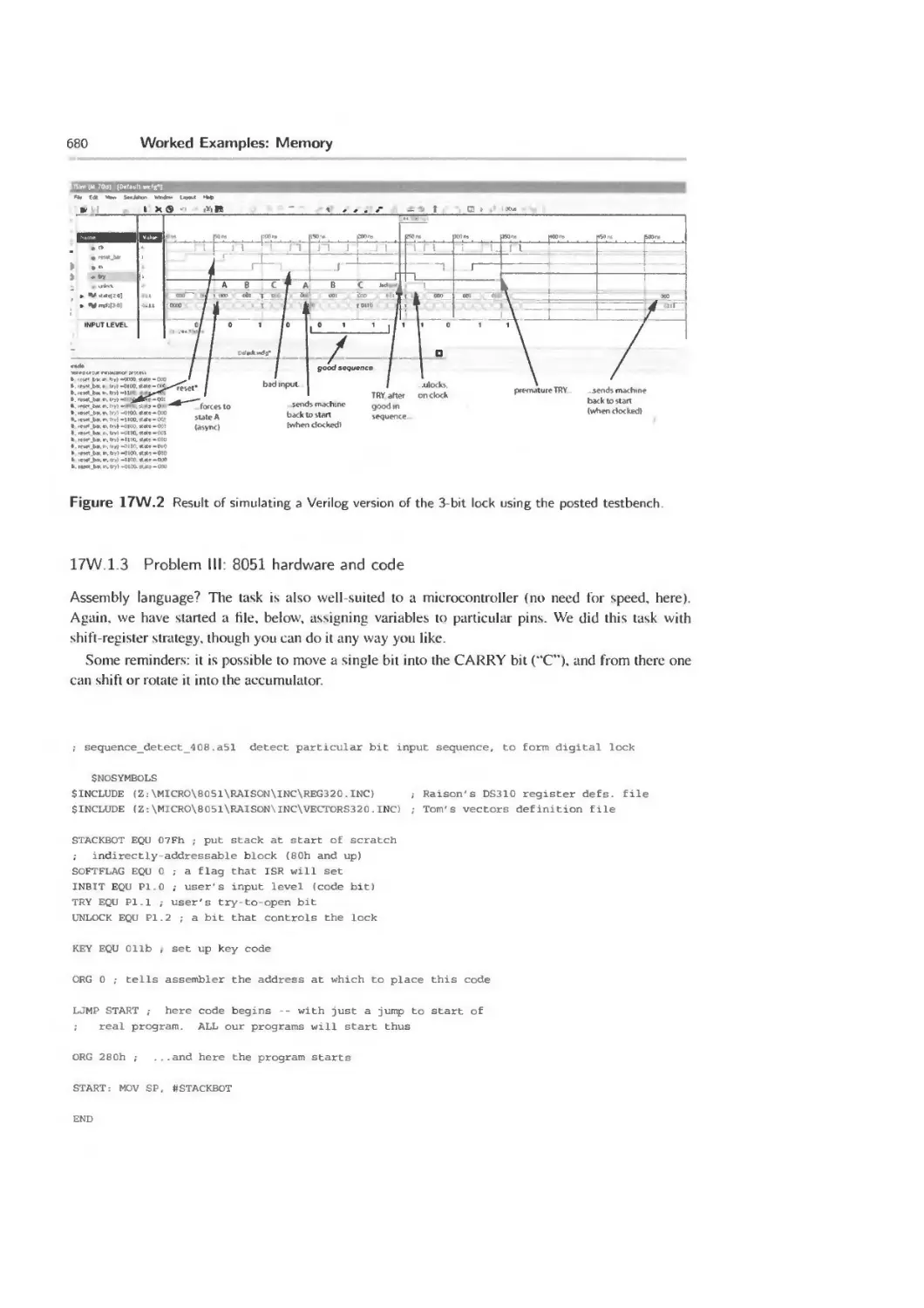
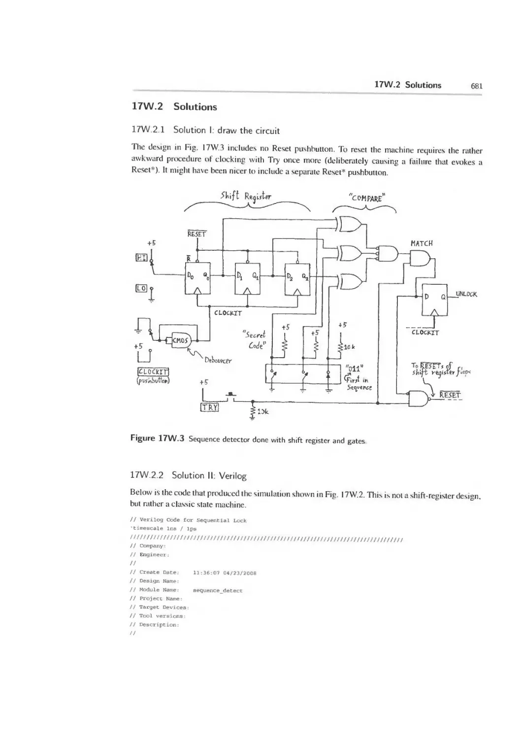
17W.2 Solutions 681
Part V Digital: Analog-Digital, PLL, Digital Project Lab 687
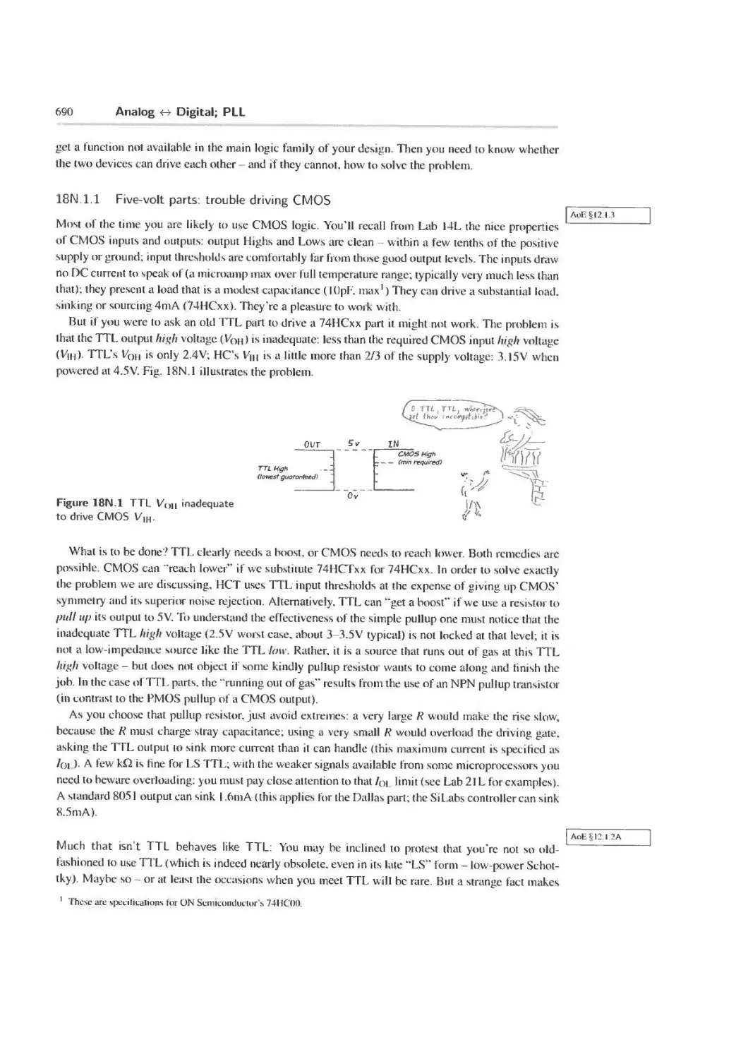
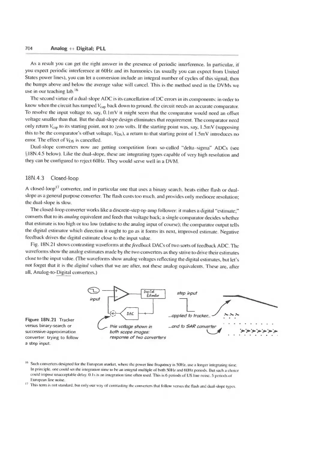
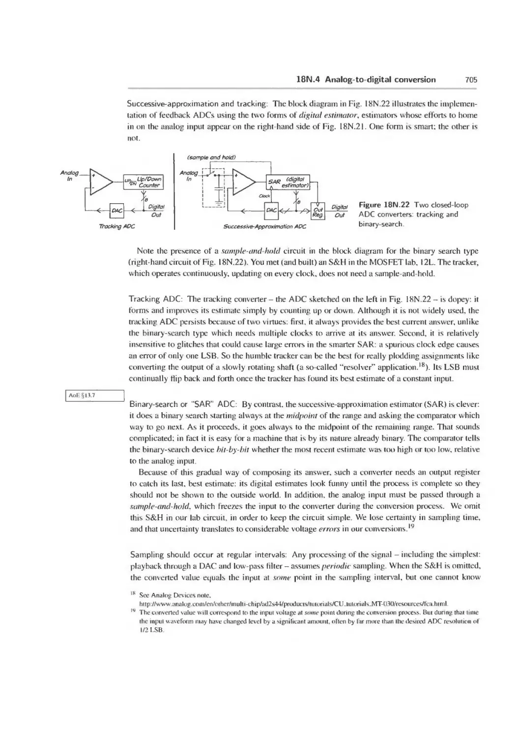
18N Analog <-> Digital; PLL 689
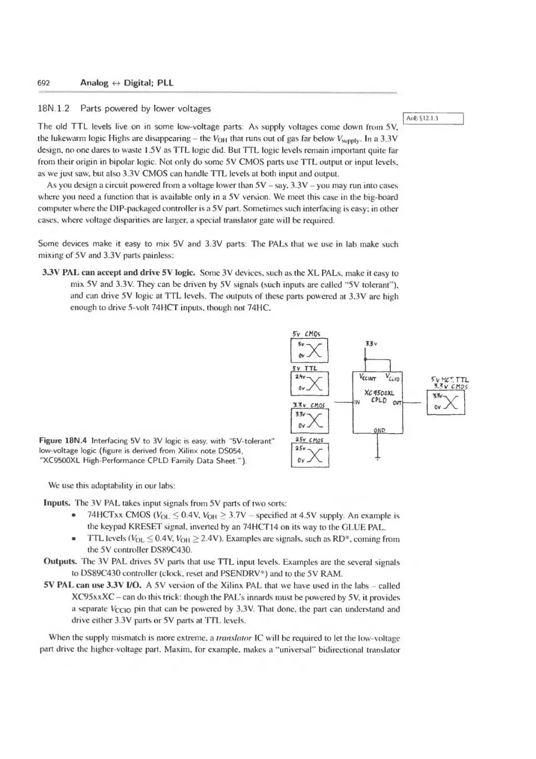
18N.1 Interfacing among logic families 689
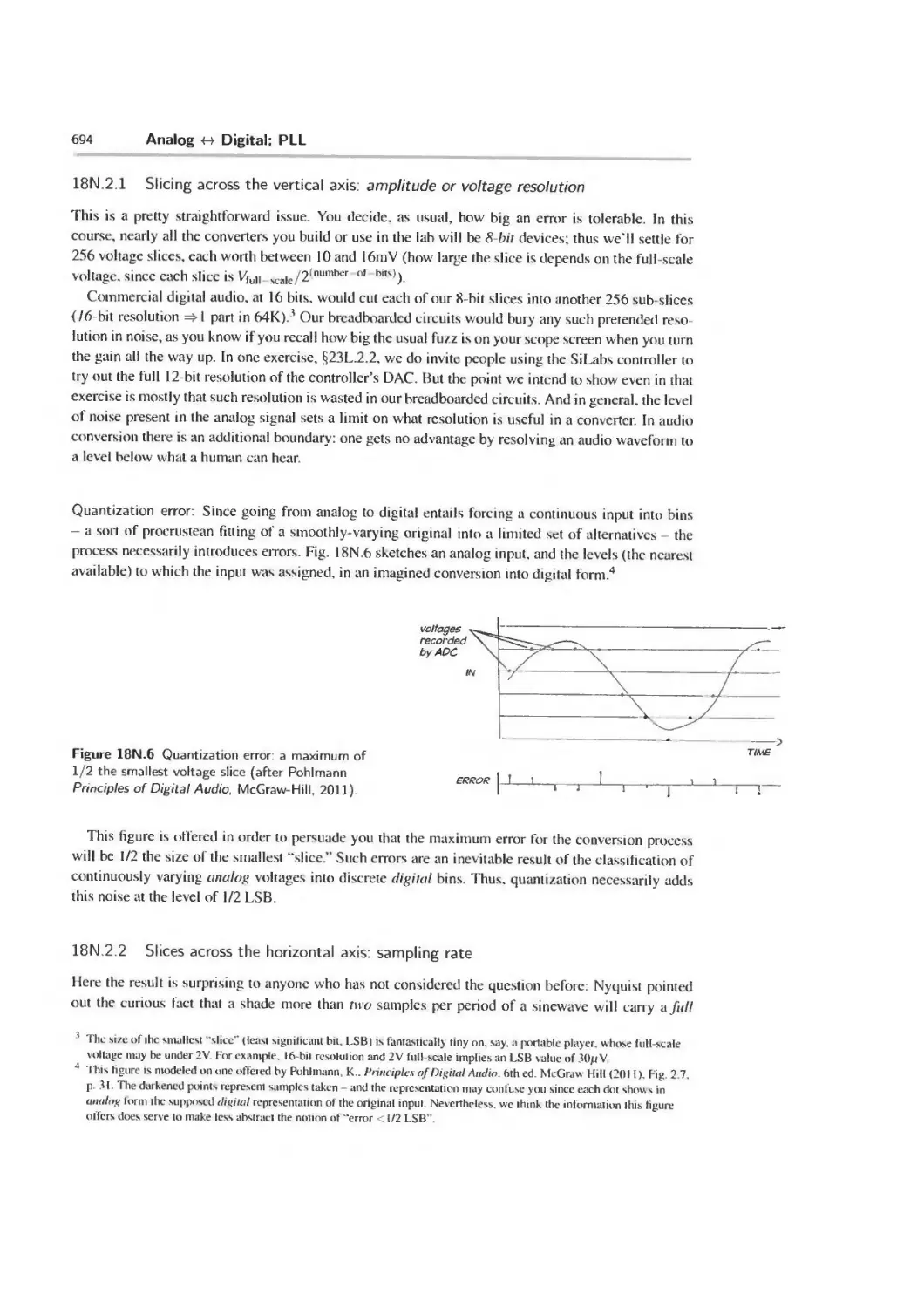
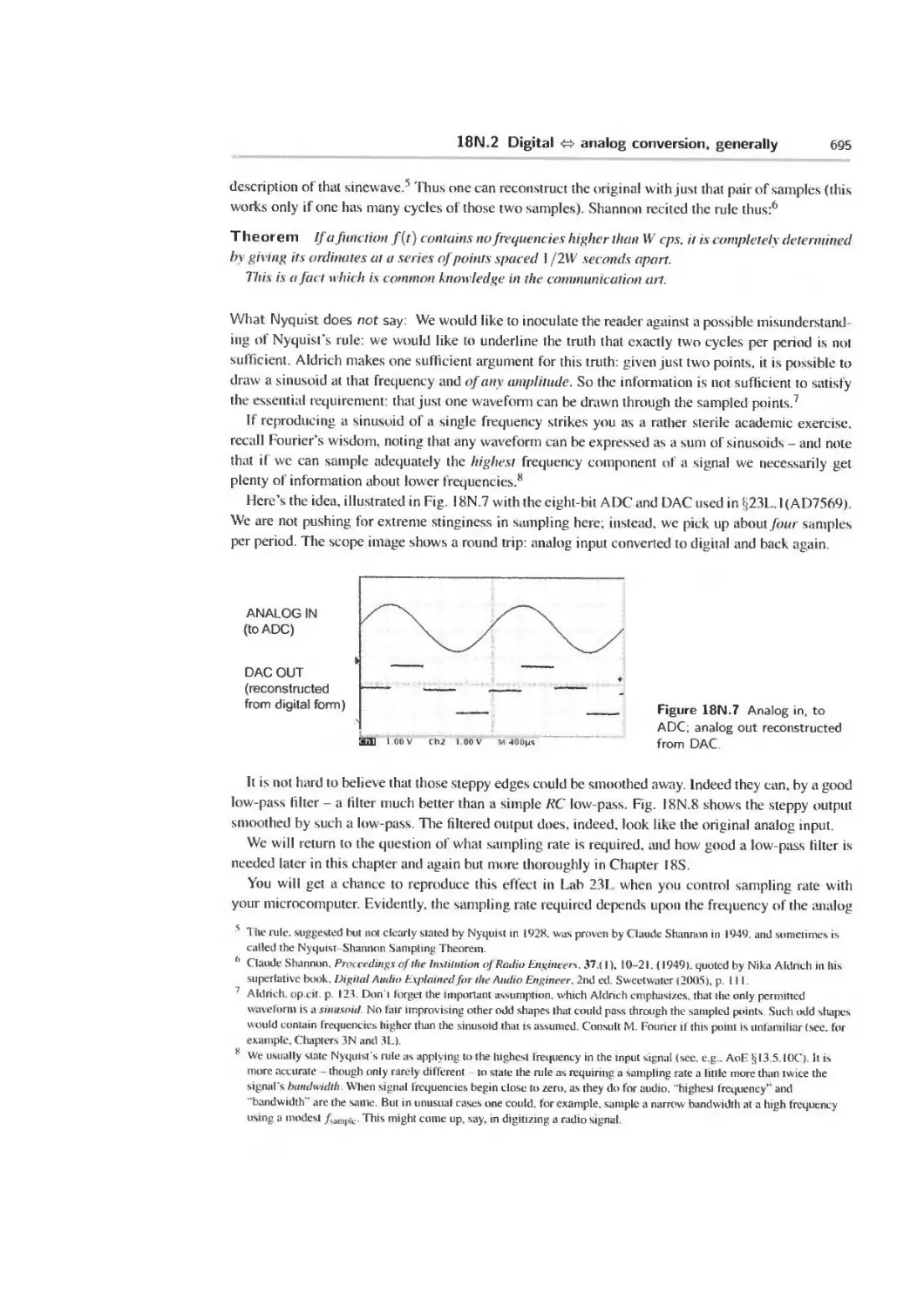
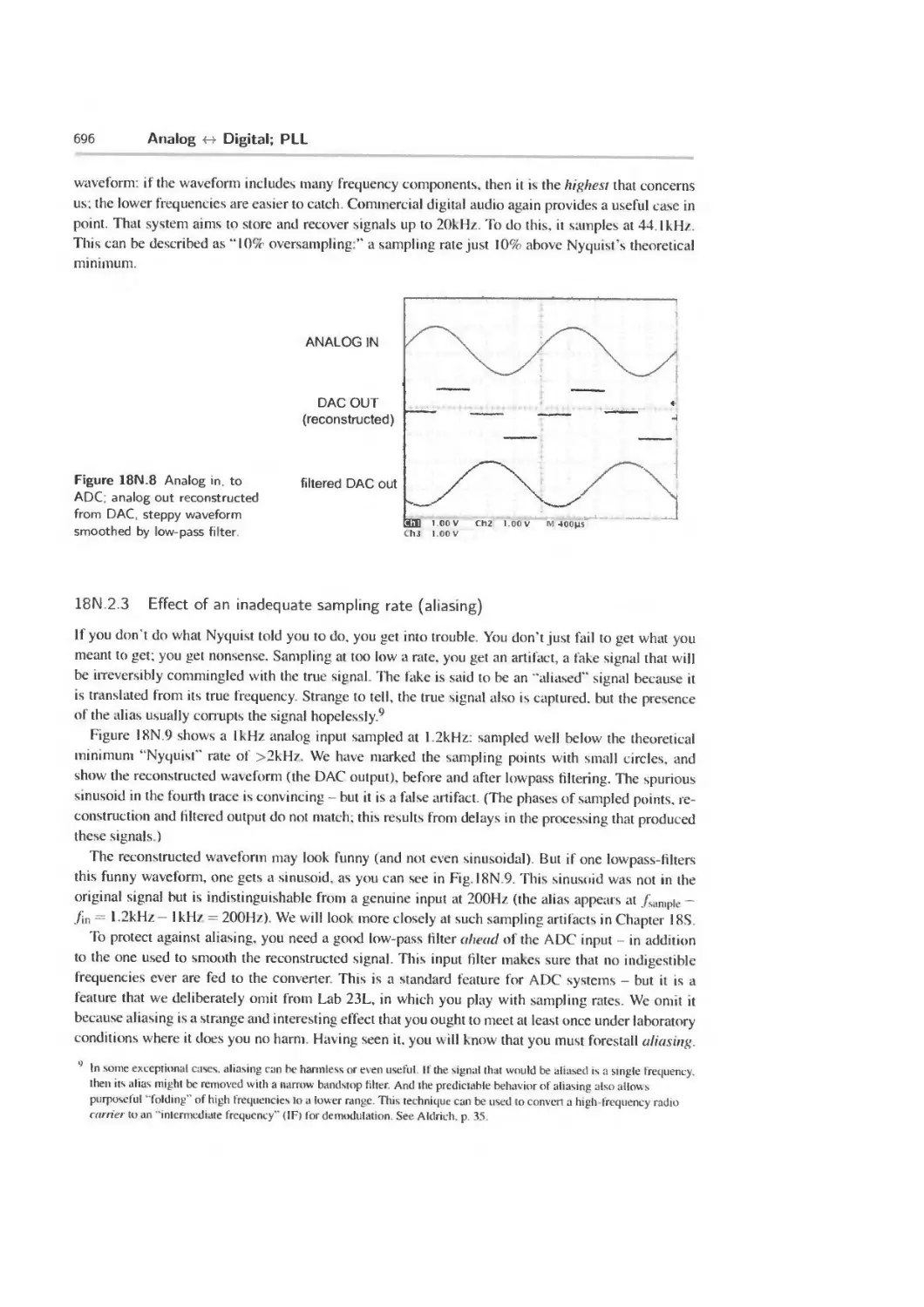
18N.2 Digital analog conversion, generally 693
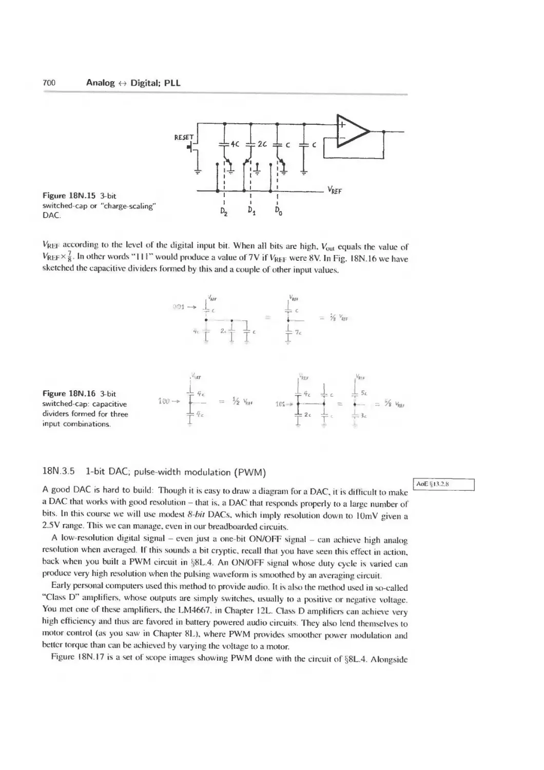
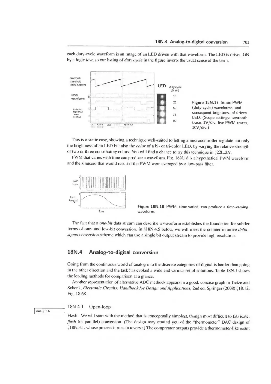
18N.3 Digital to analog (DAC) methods 697
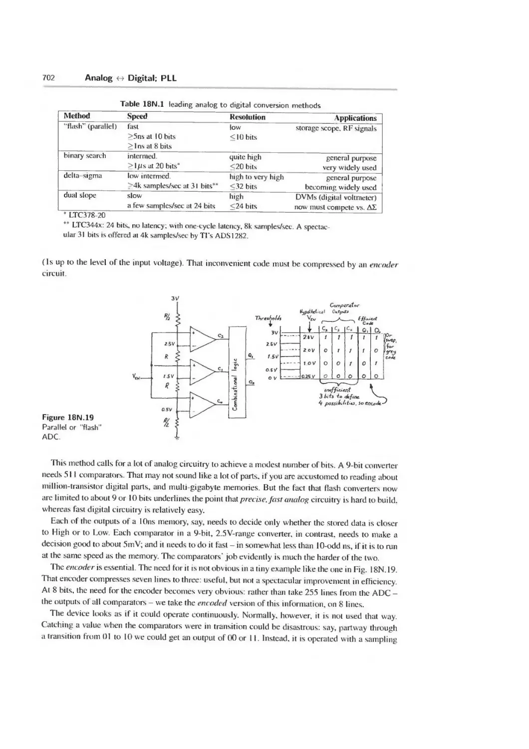
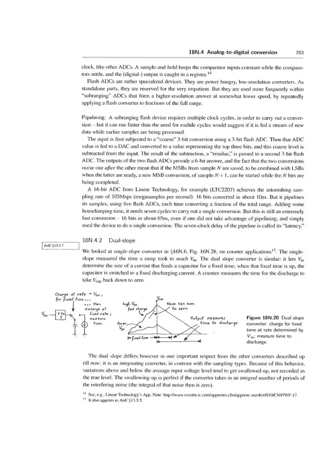
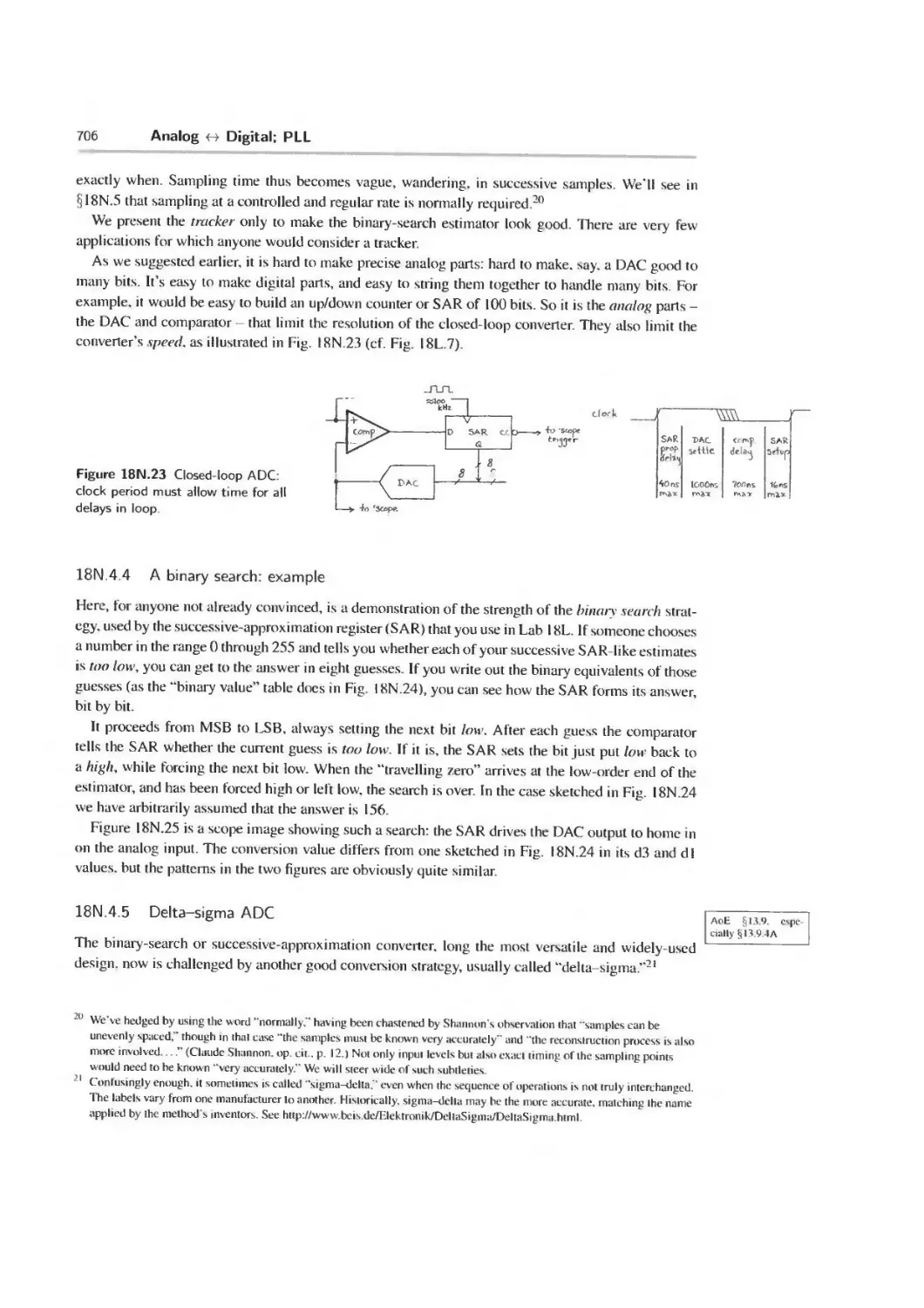
18N.4 Analog-to digital conversion 701
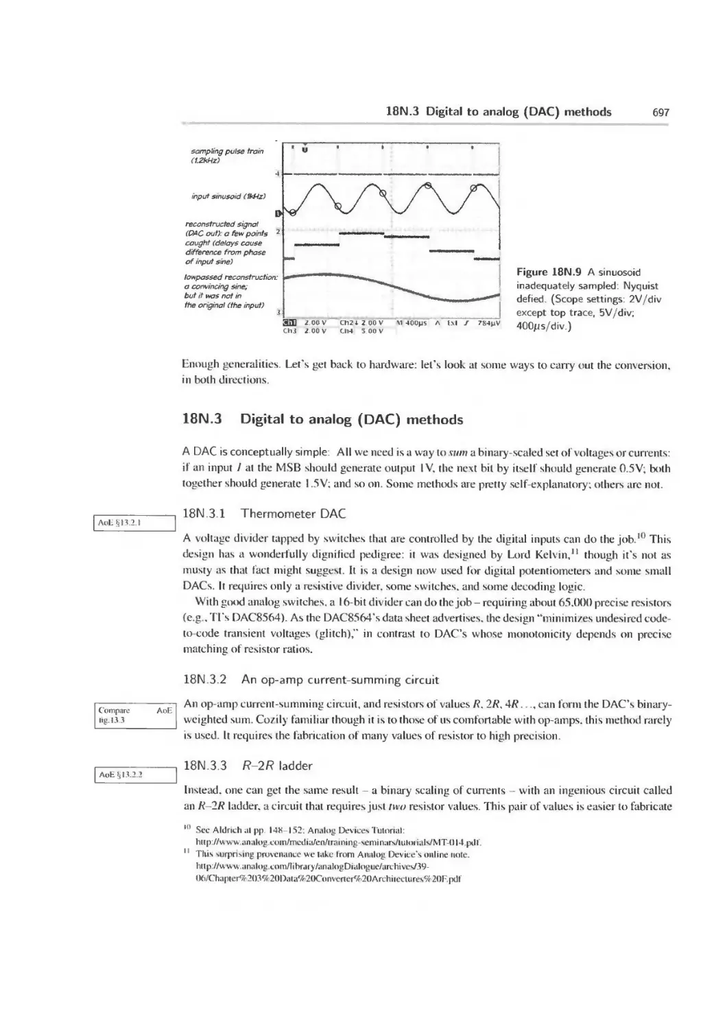
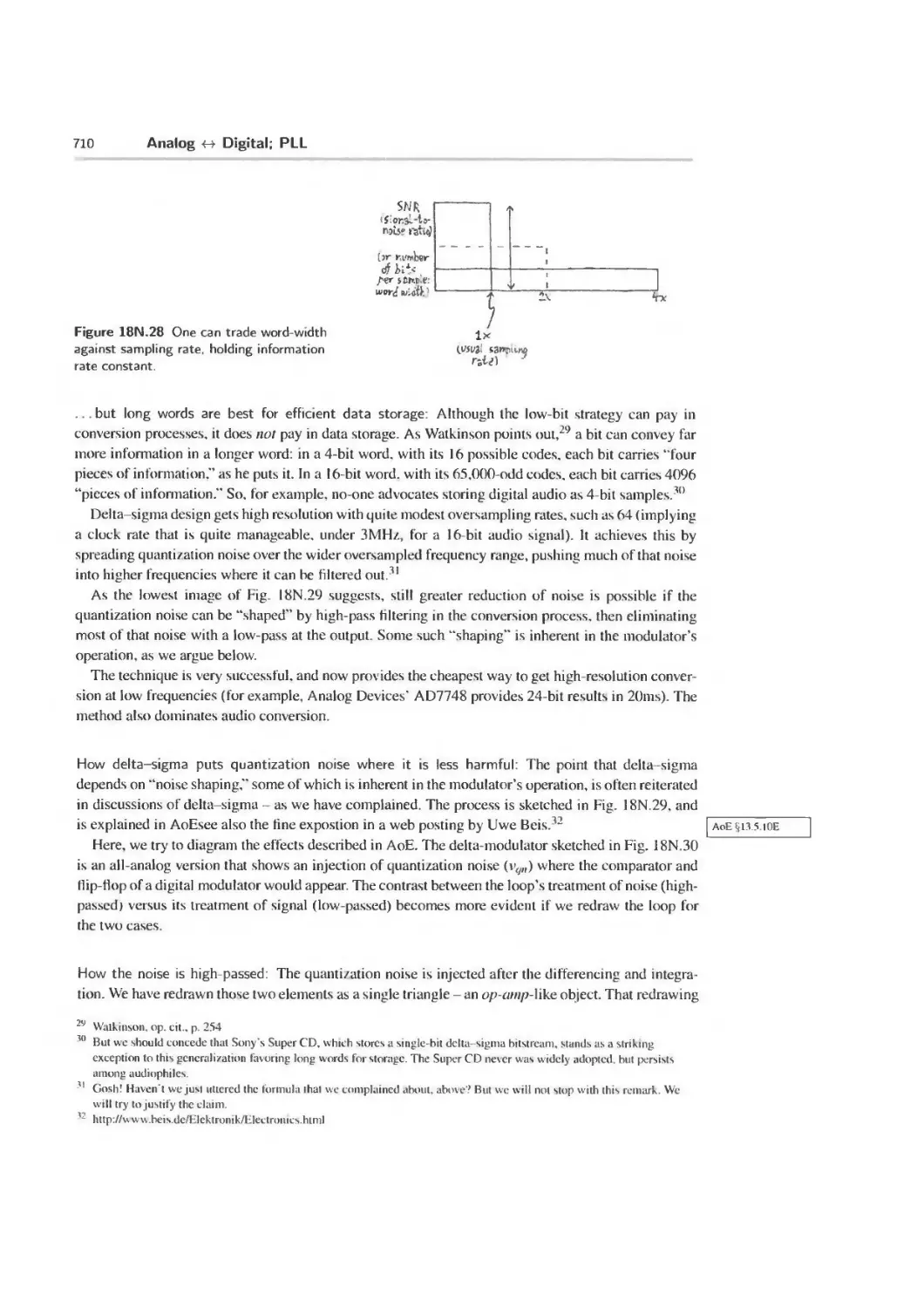
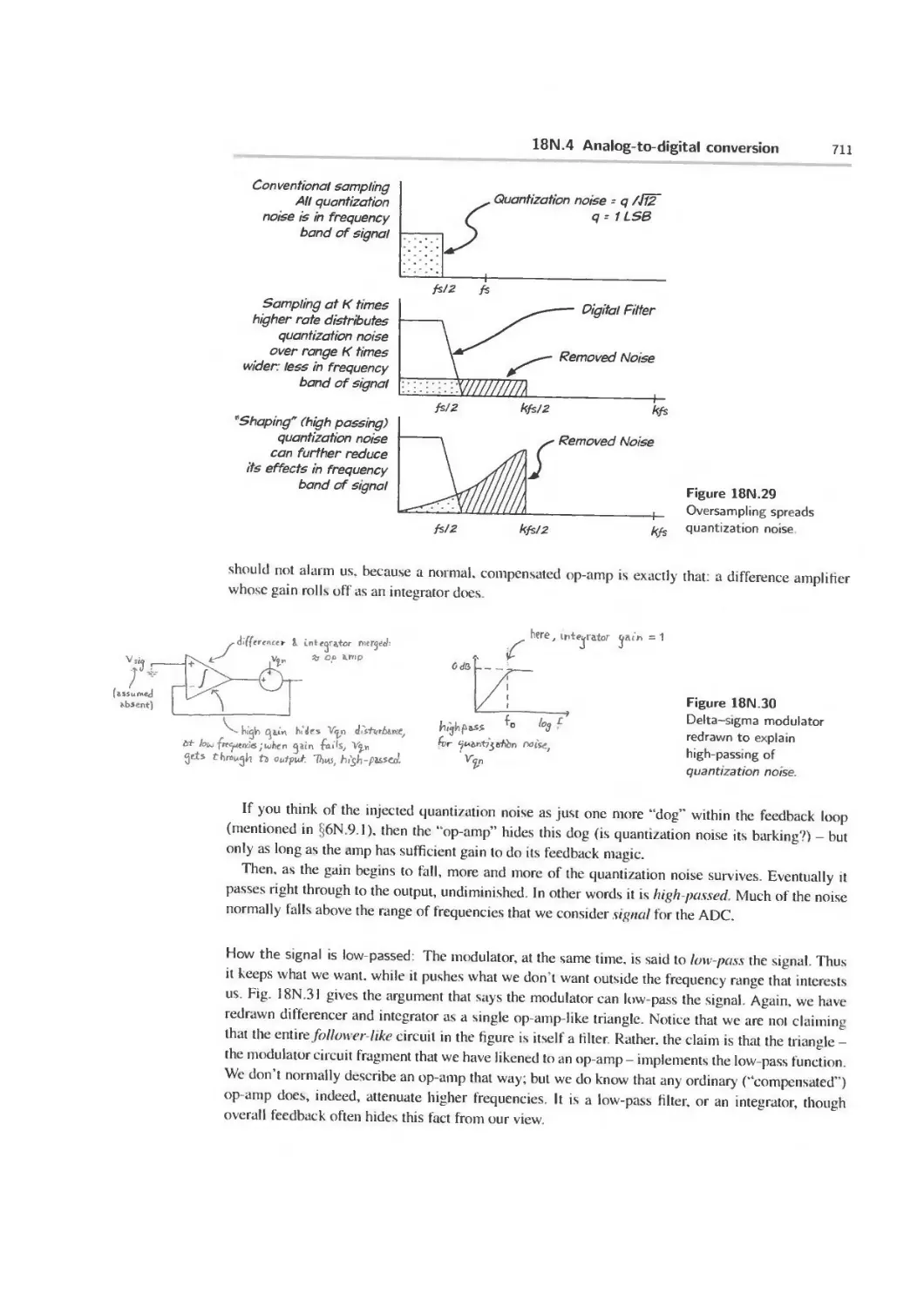
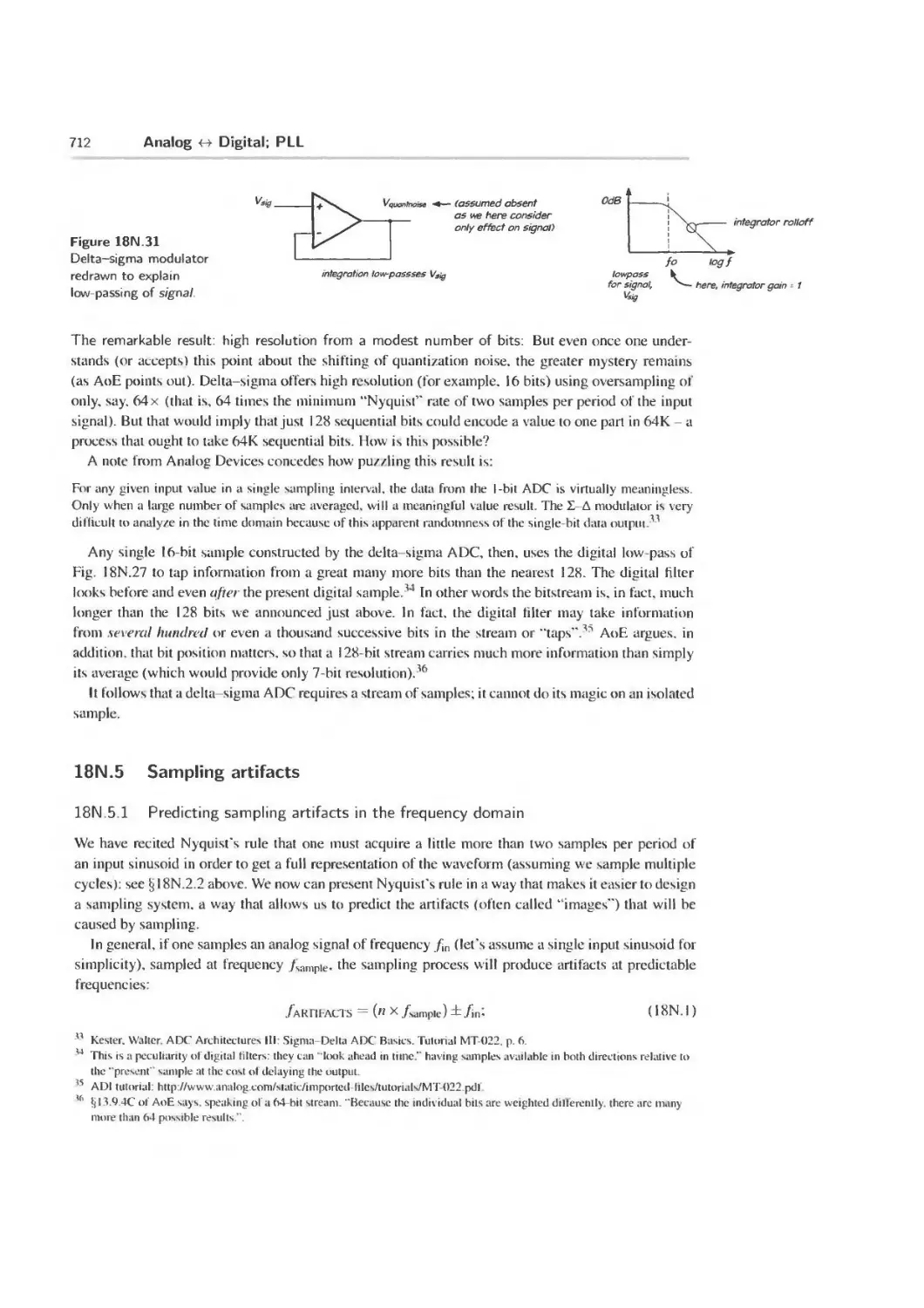
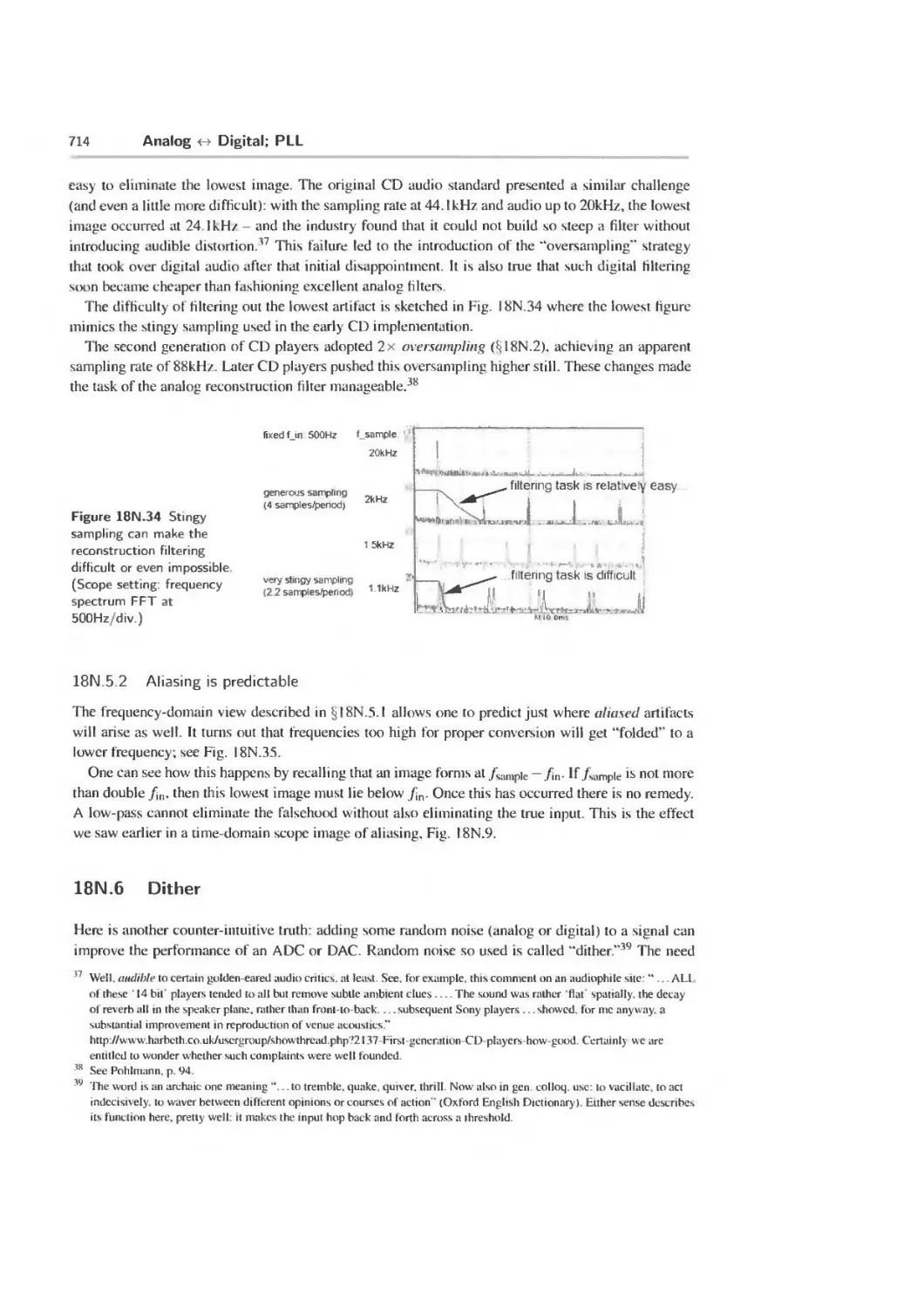
18N.5 Sampling artifacts 712
18N.6 Dither 714
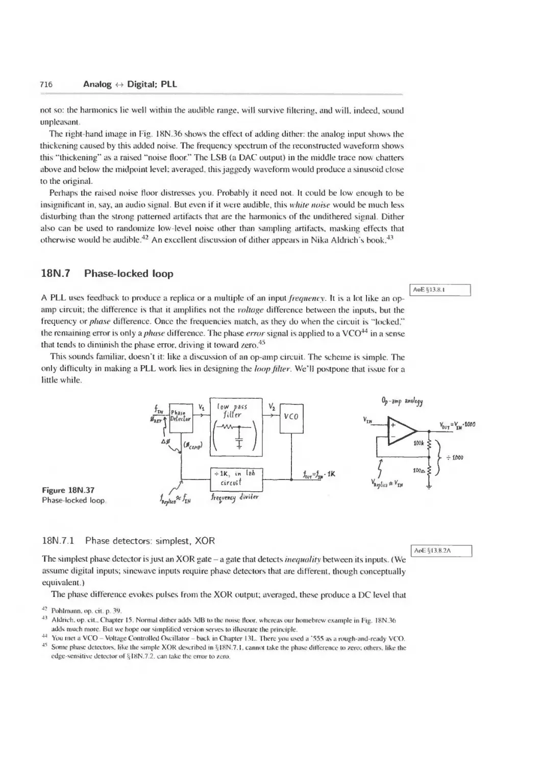
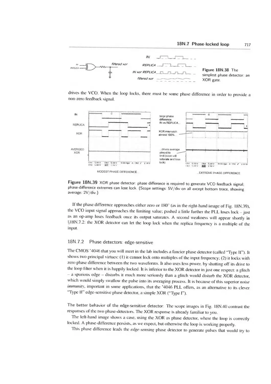
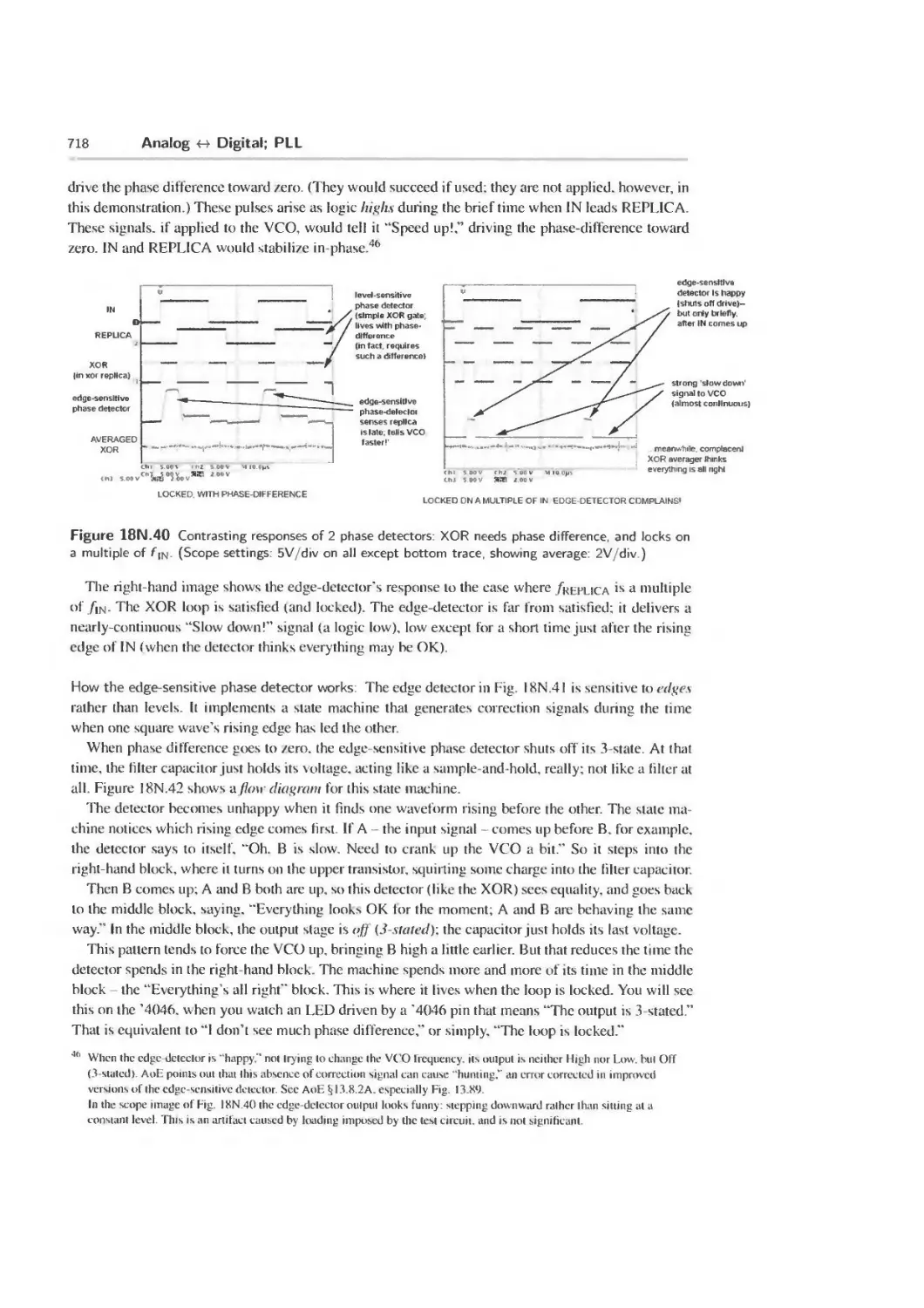
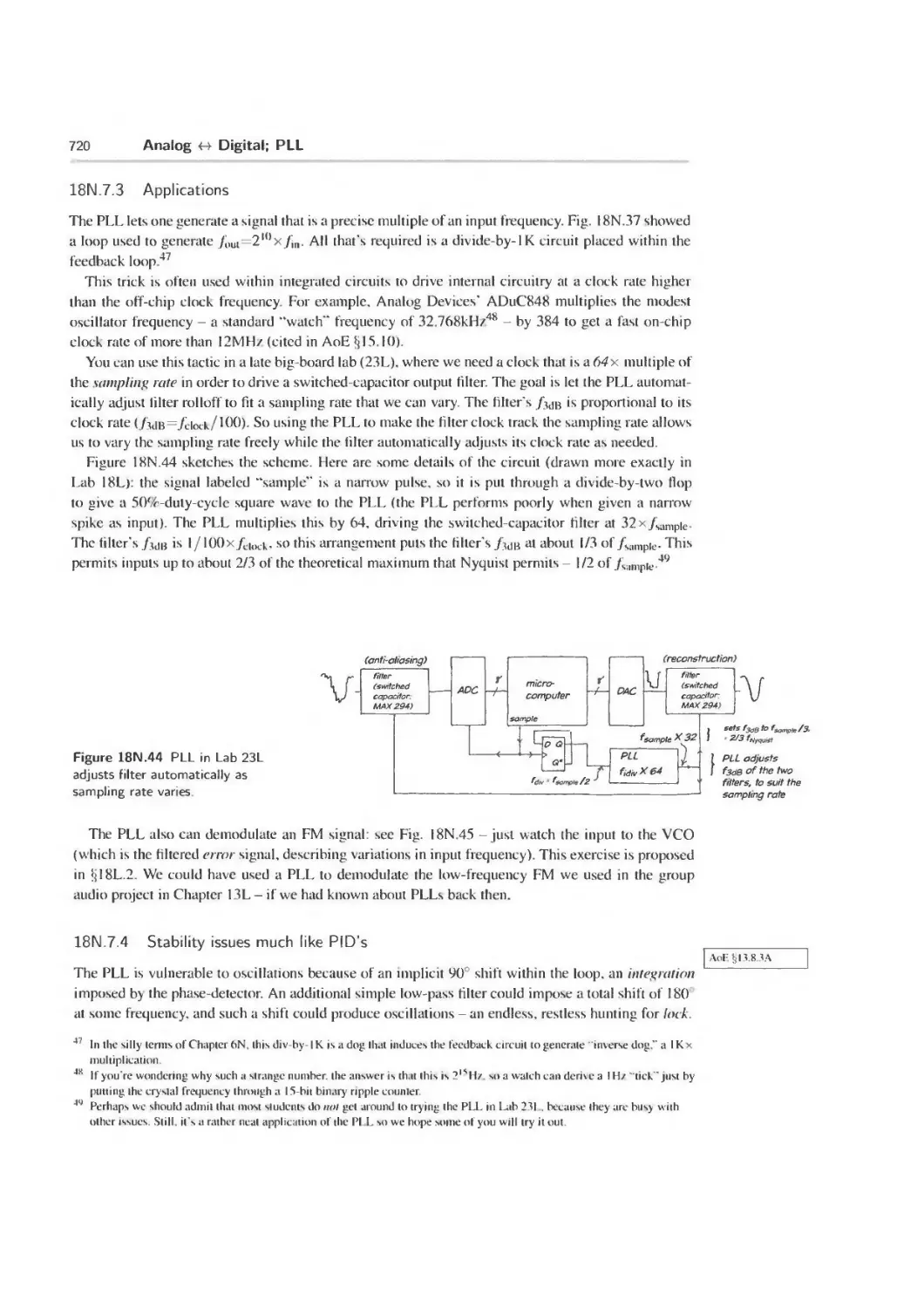
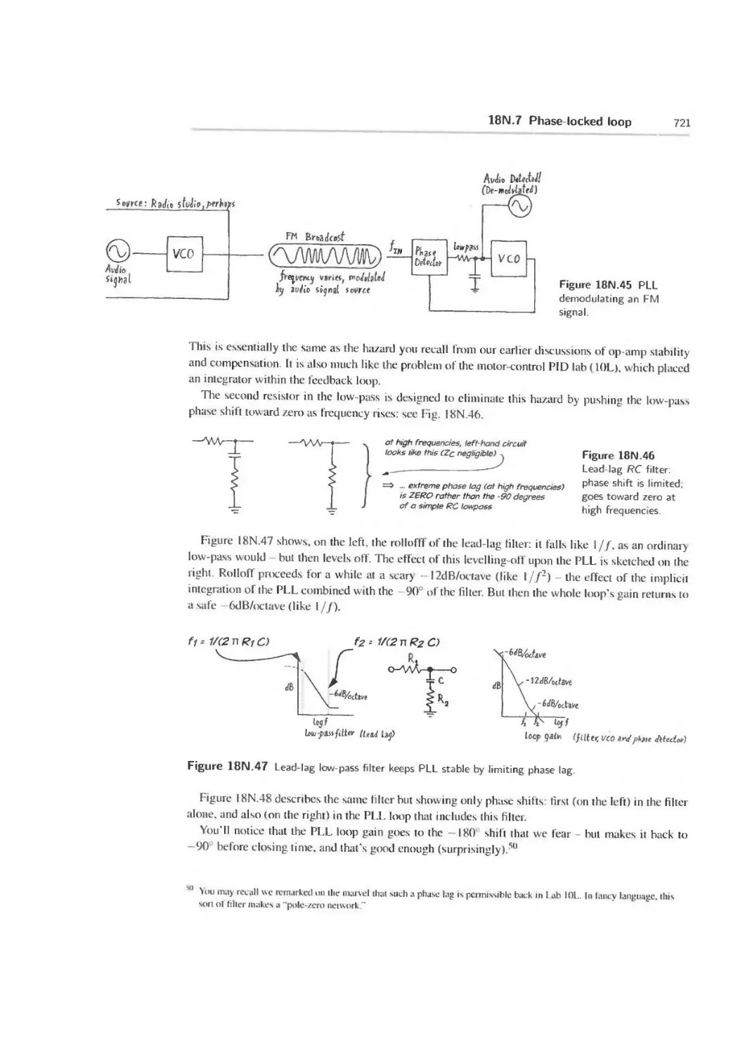
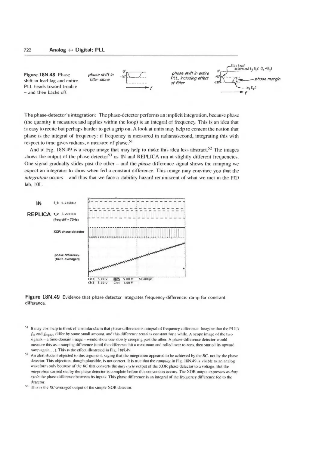
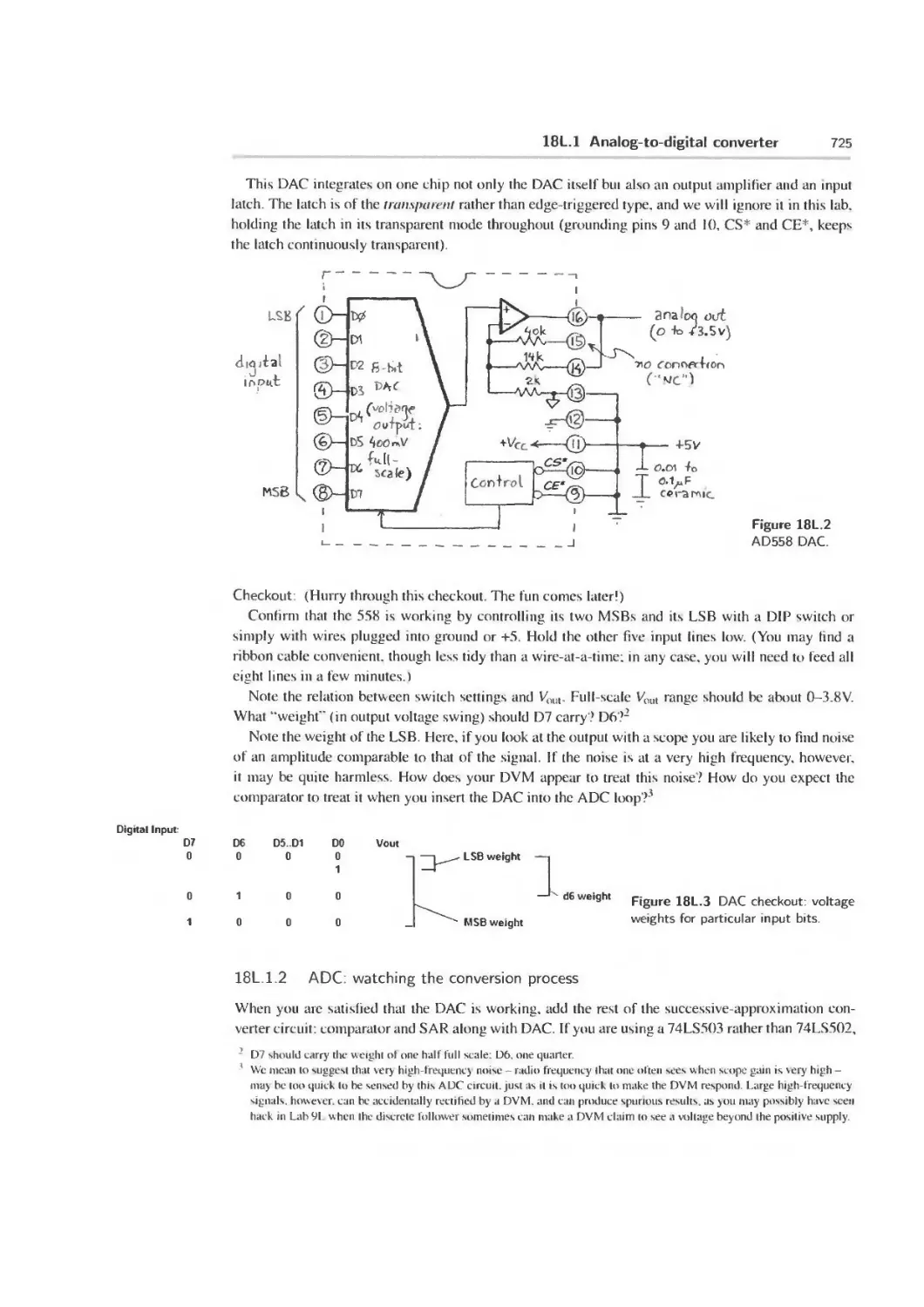
18N.7 Phase-locked loop 716
18N.8 AoE Reading 723
18L Lab: Analog о Digital; PLL 724
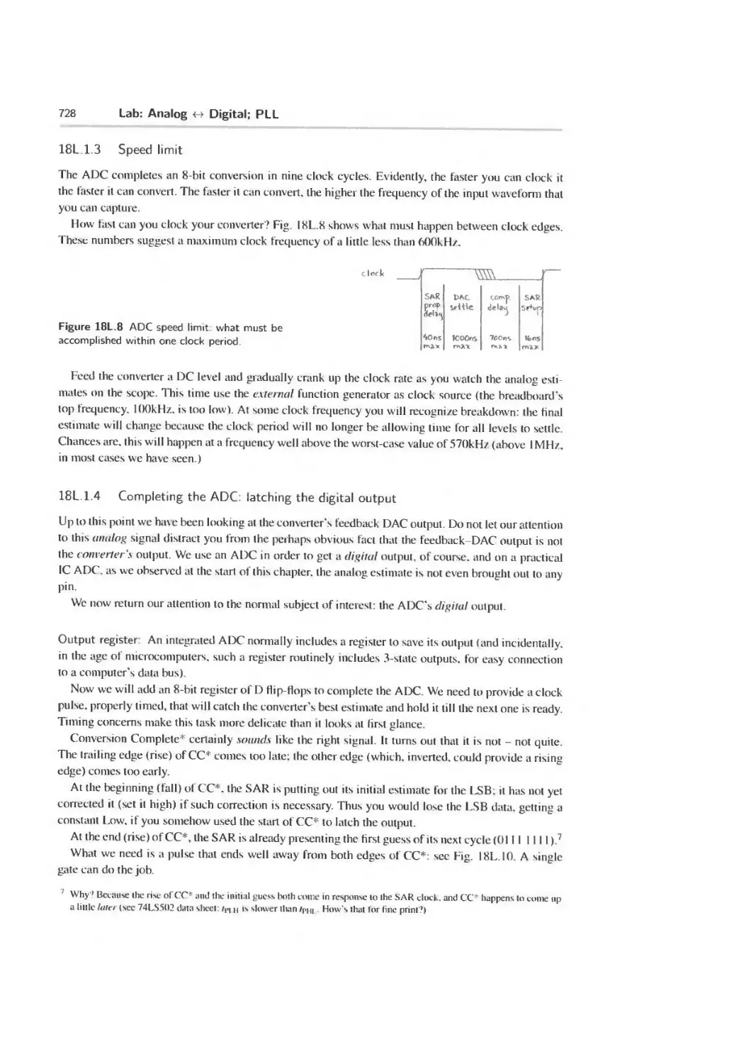
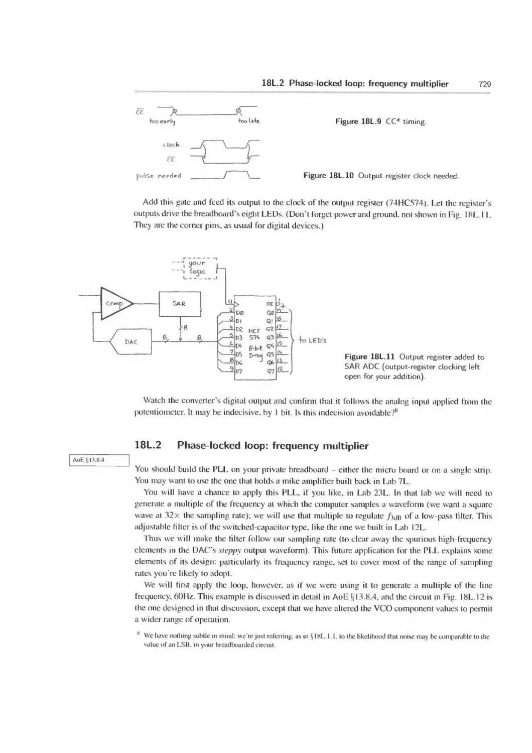
18L. 1 Analog-to-digital converter 724
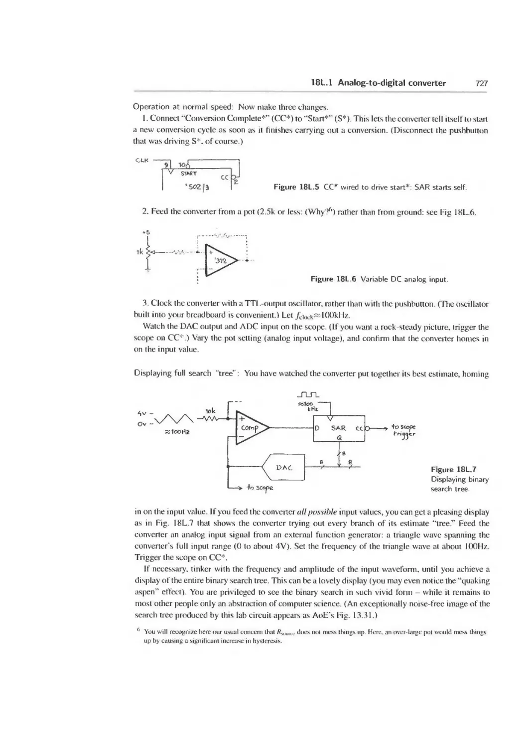
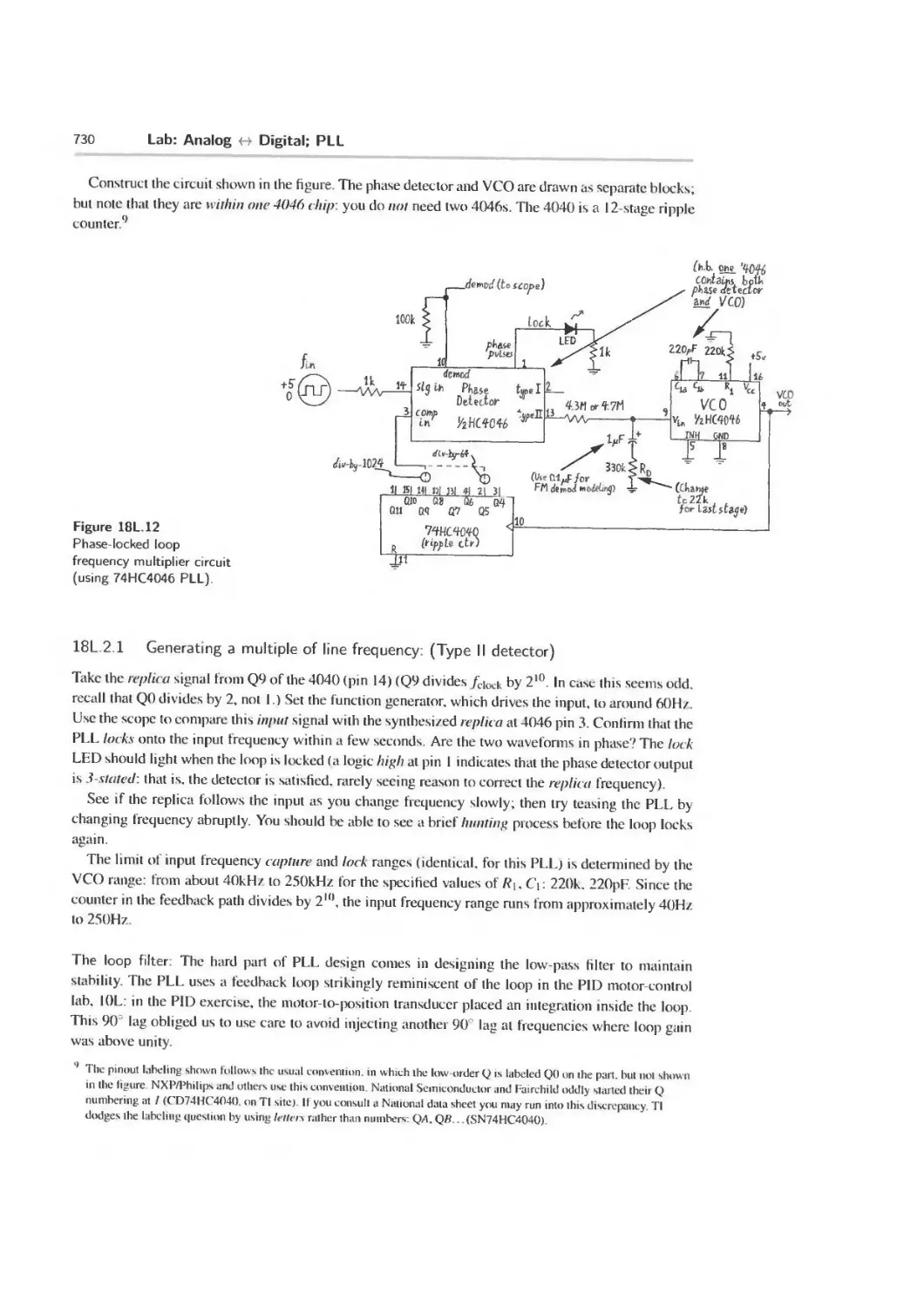
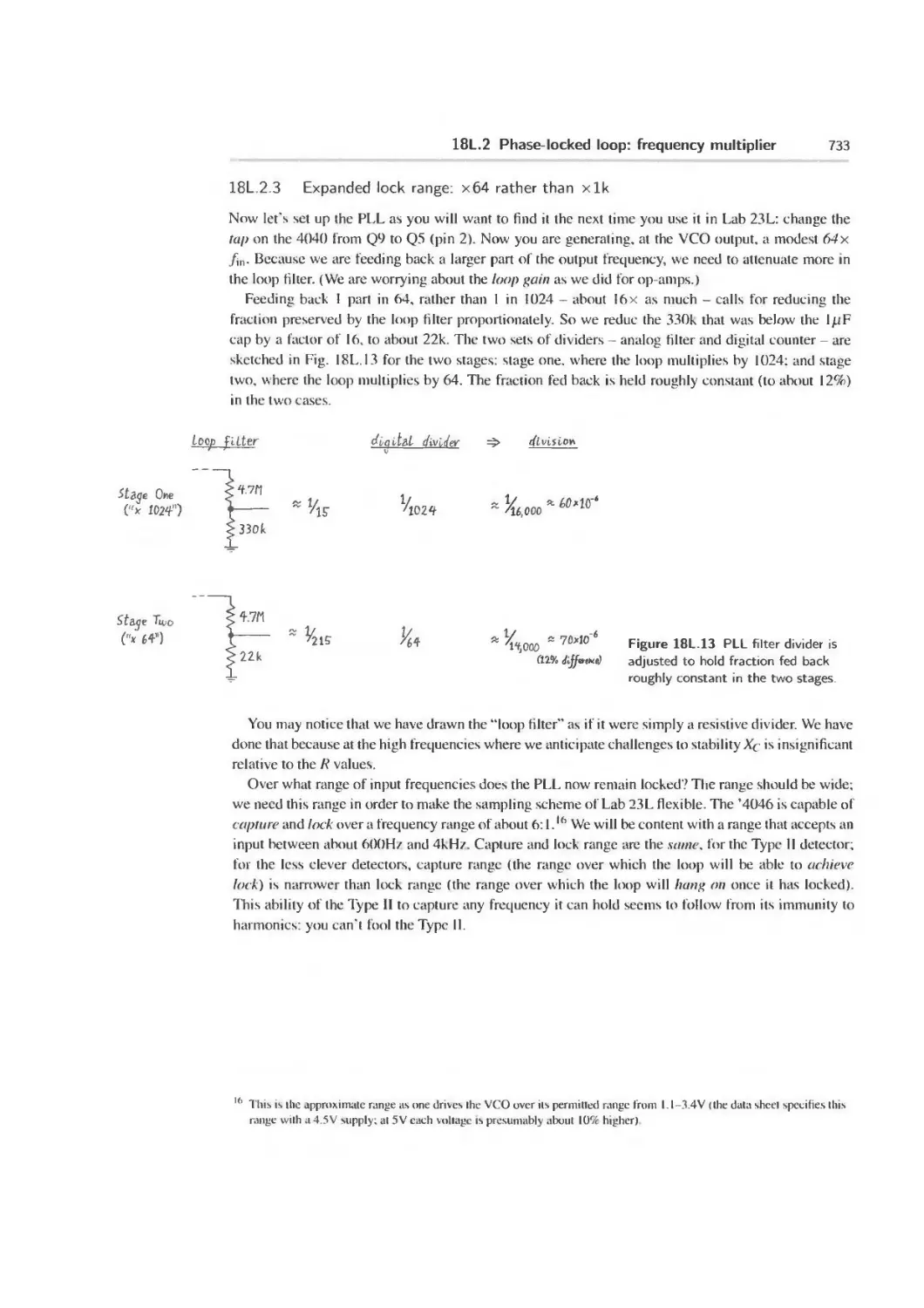
I8L.2 Phase-locked loop: frequency multiplier 729
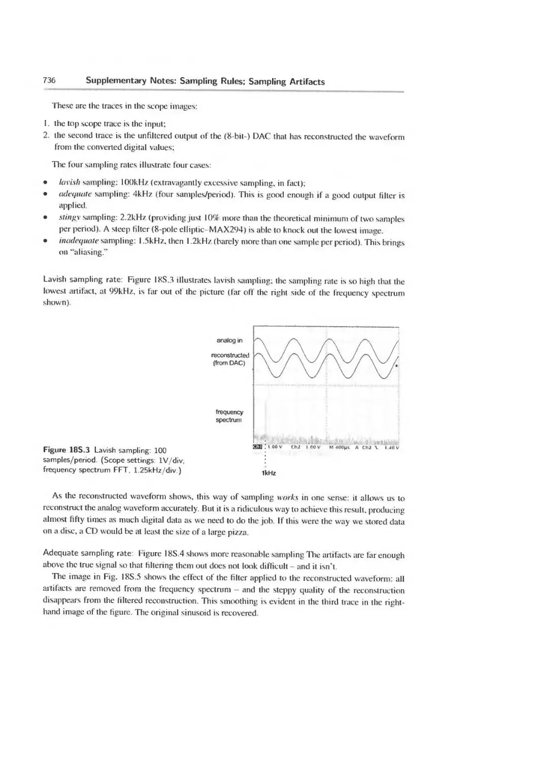
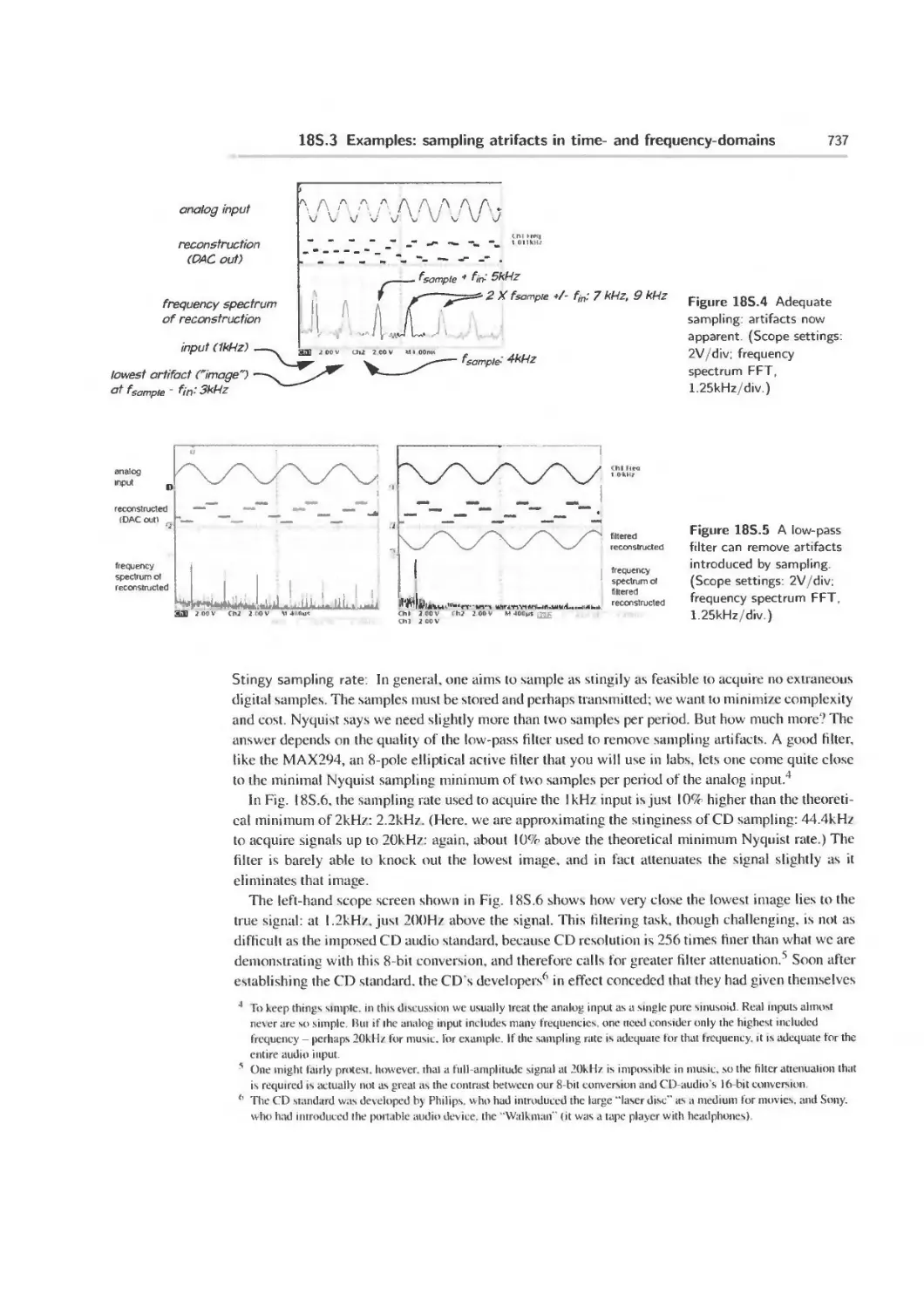
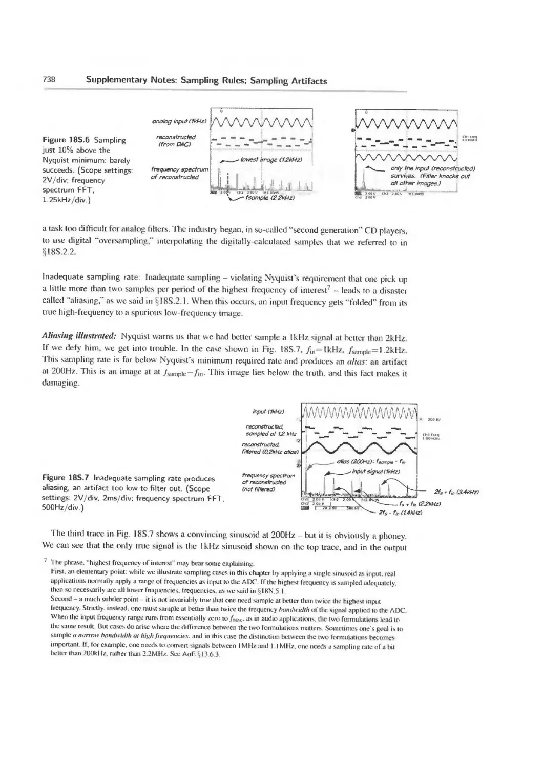
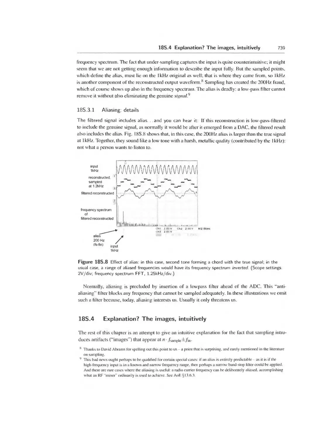
IBS Supplementary Notes: Sampling Rules; Sampling Artifacts 734
18S.1 What’s in this chapter? 734
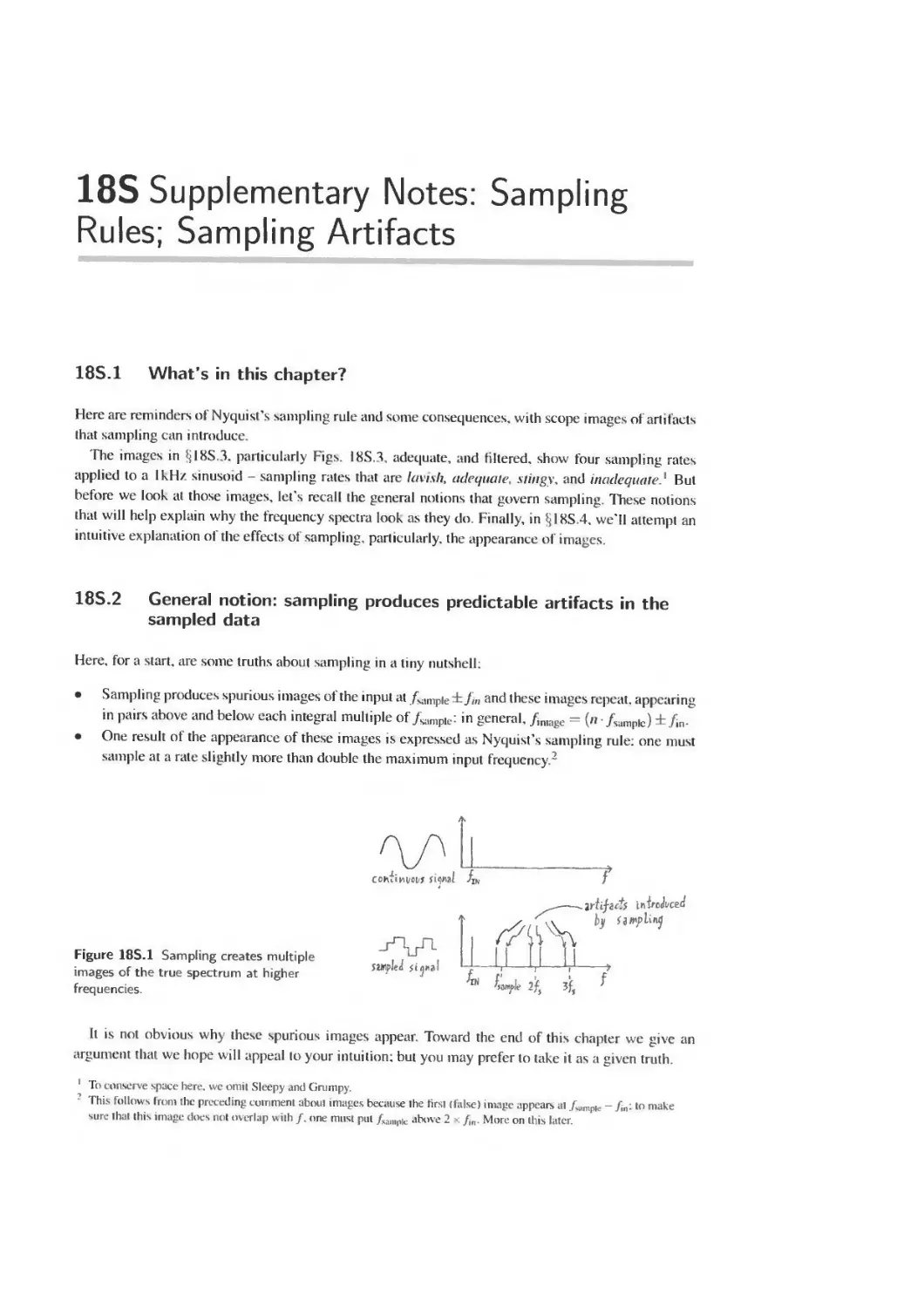
18S.2 General notion: sampling produces predictable artifacts in the sampled data 734
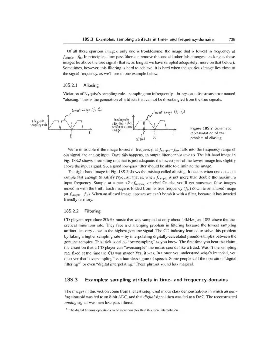
18S.3 Examples: sampling atrifacts in time- and frequency-domains 735
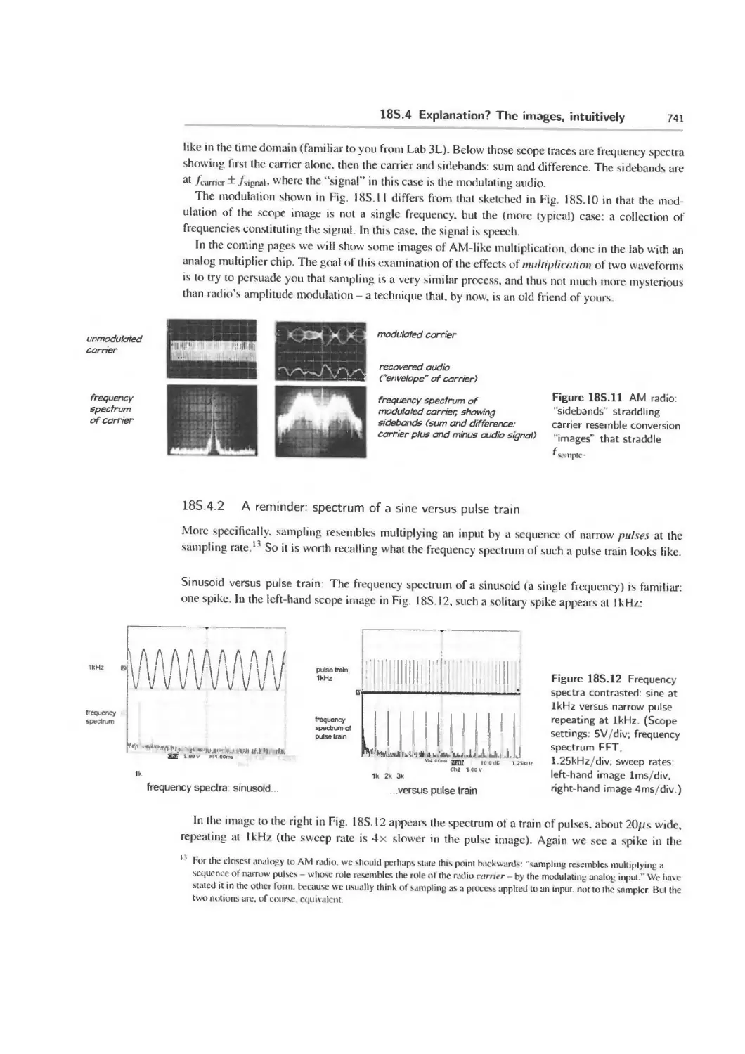
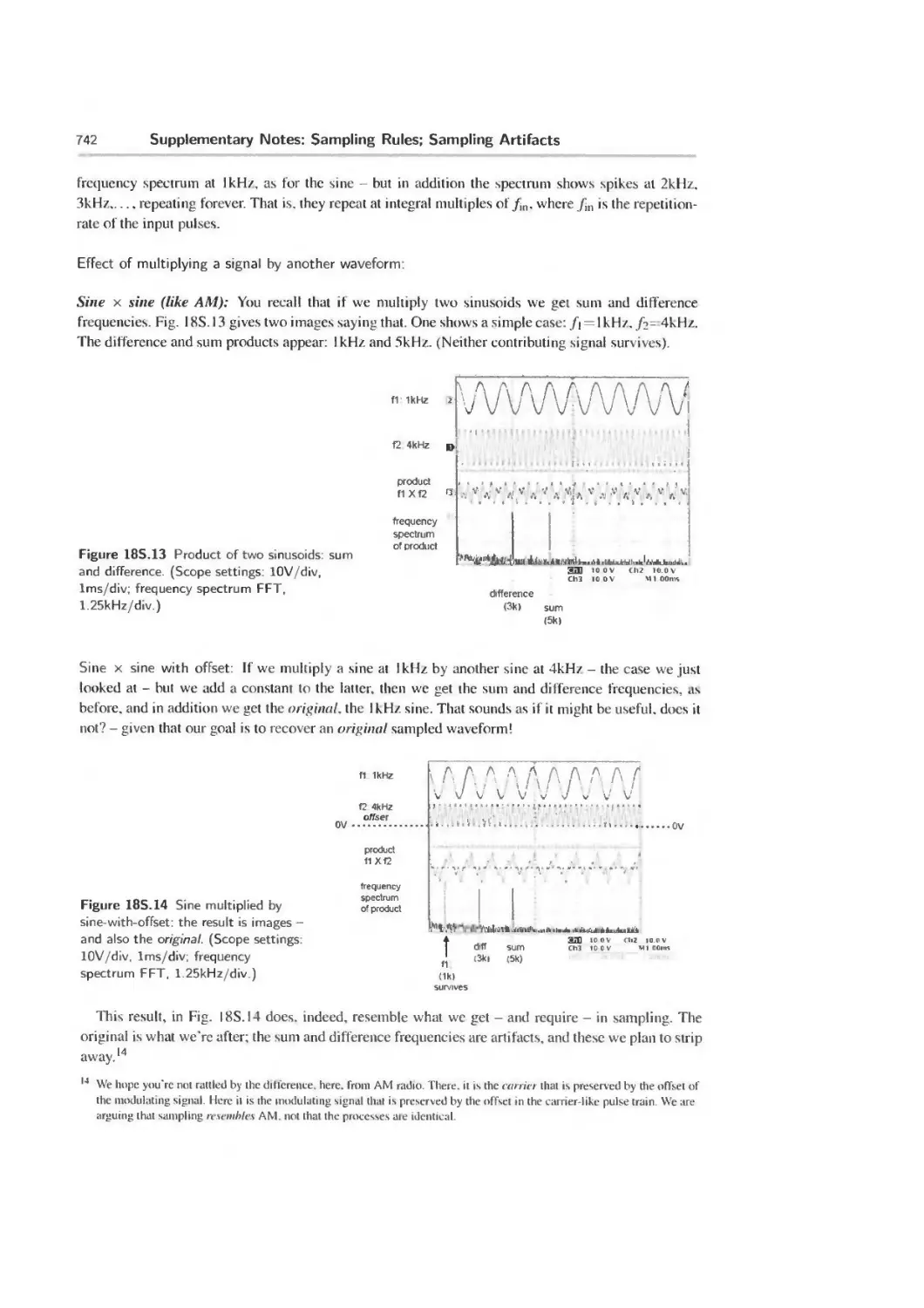
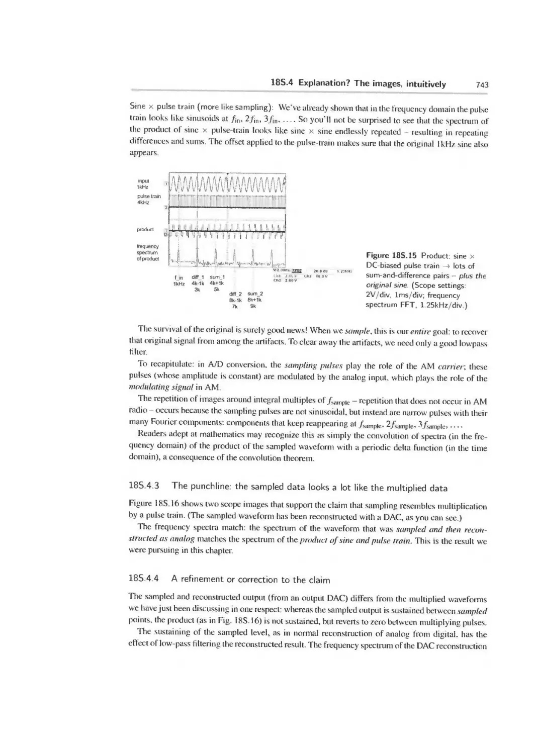
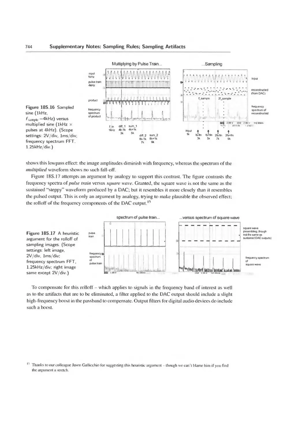
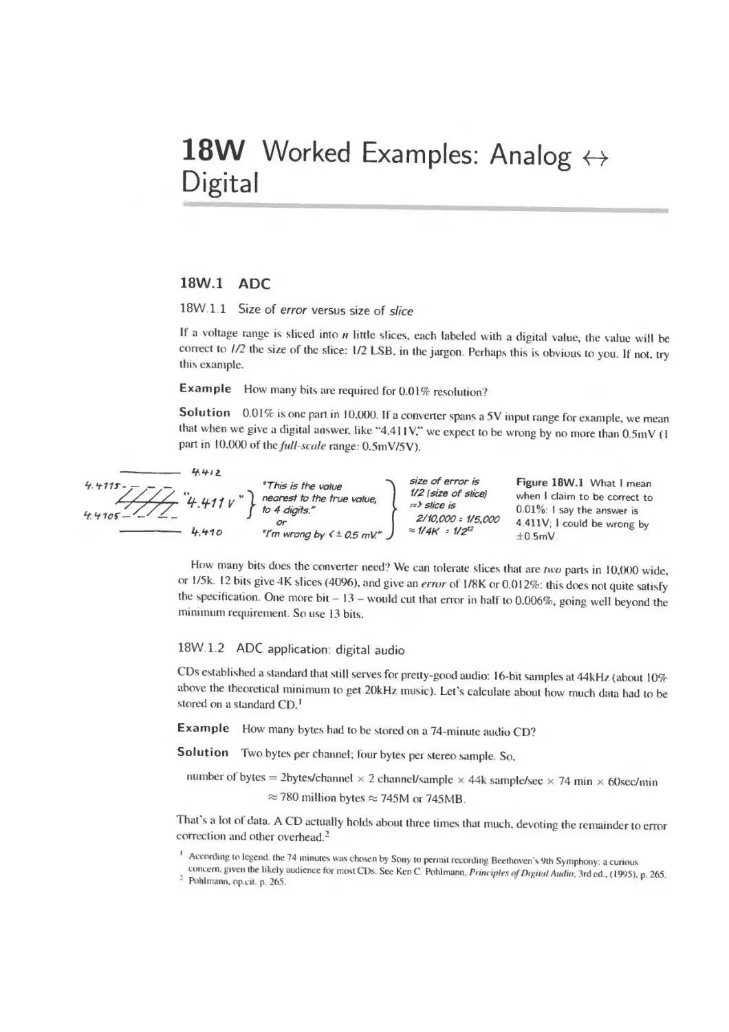
18S.4 Explanation? The images, intuitively 739
18W Worked Examples: Analog о Digital 745
18W 1 ADC 745
18W.2 Level translator 748
19L Digital Project Lab 749
19L. 1 A digital project 749
Part VI Microcontrollers 755
20 N Microprocessors 1 757
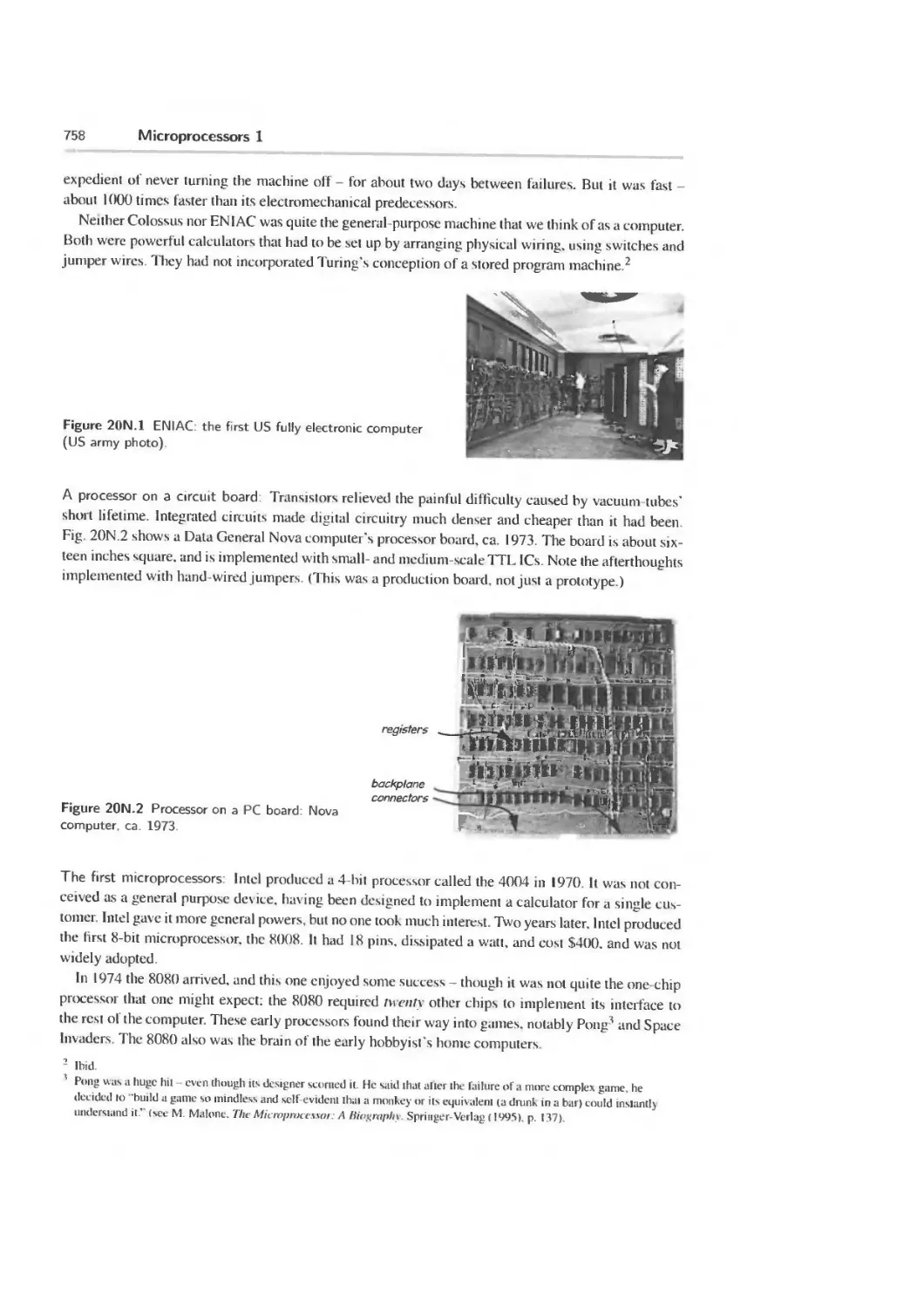
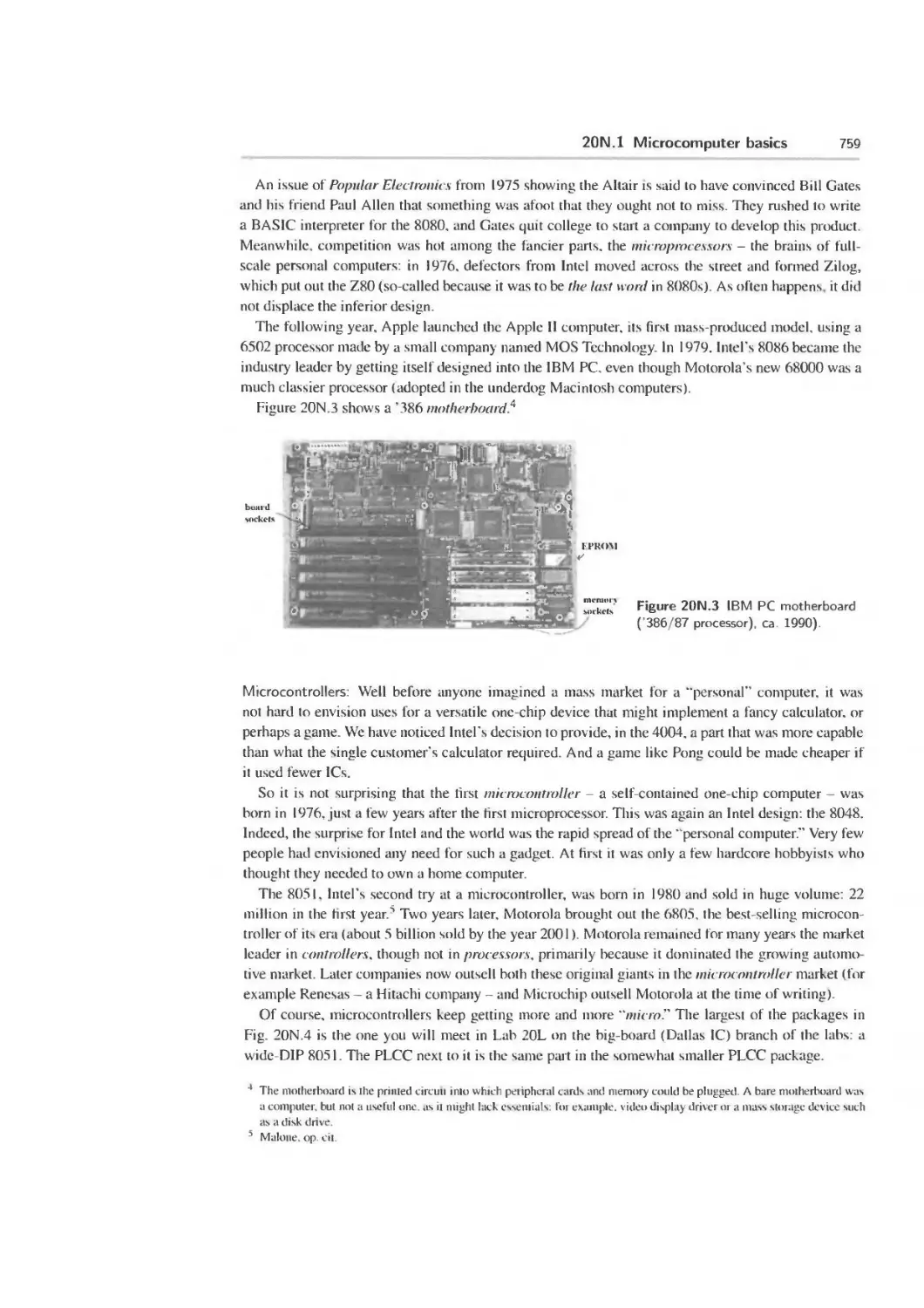
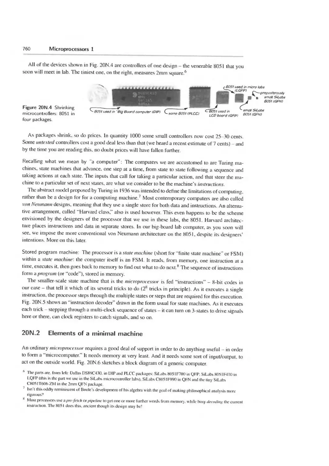
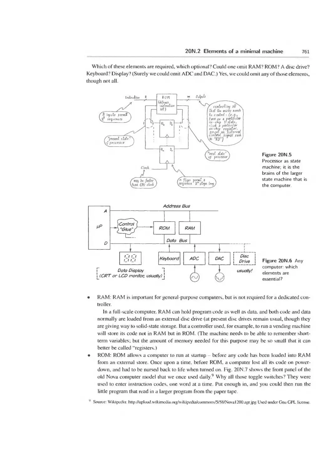
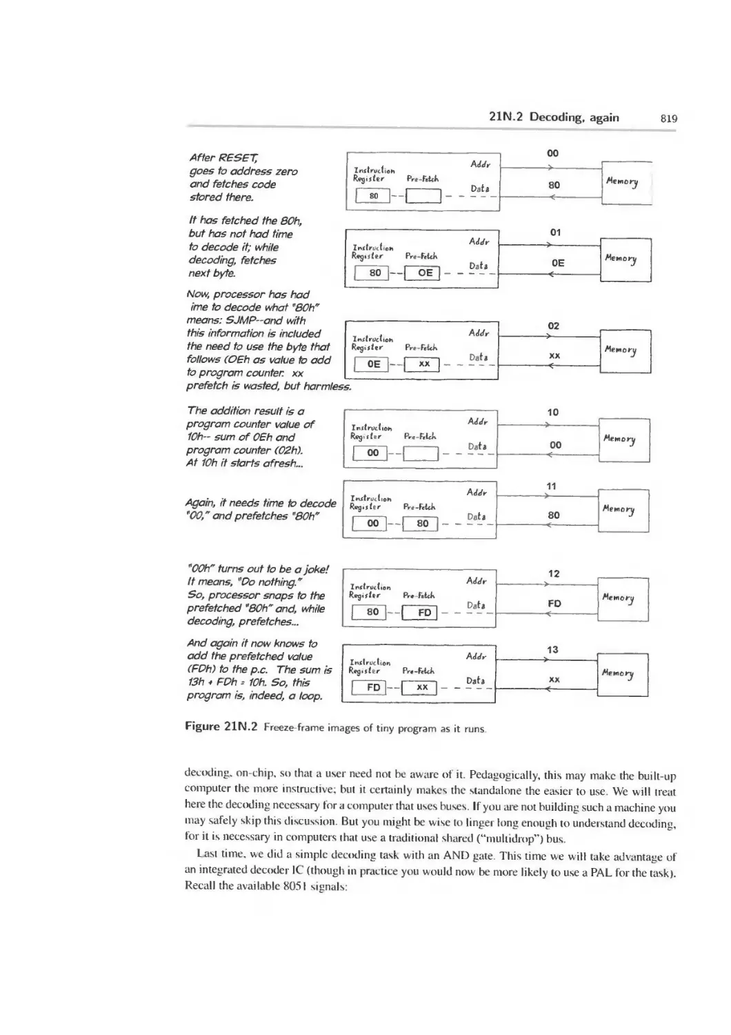
20N.1 Microcomputer basics 757
20N .2 Elements of a minimal machine 760
20N.3 Which controller to use? 762
20N.4 Some possible justifications for the hard work of the big-board path 764
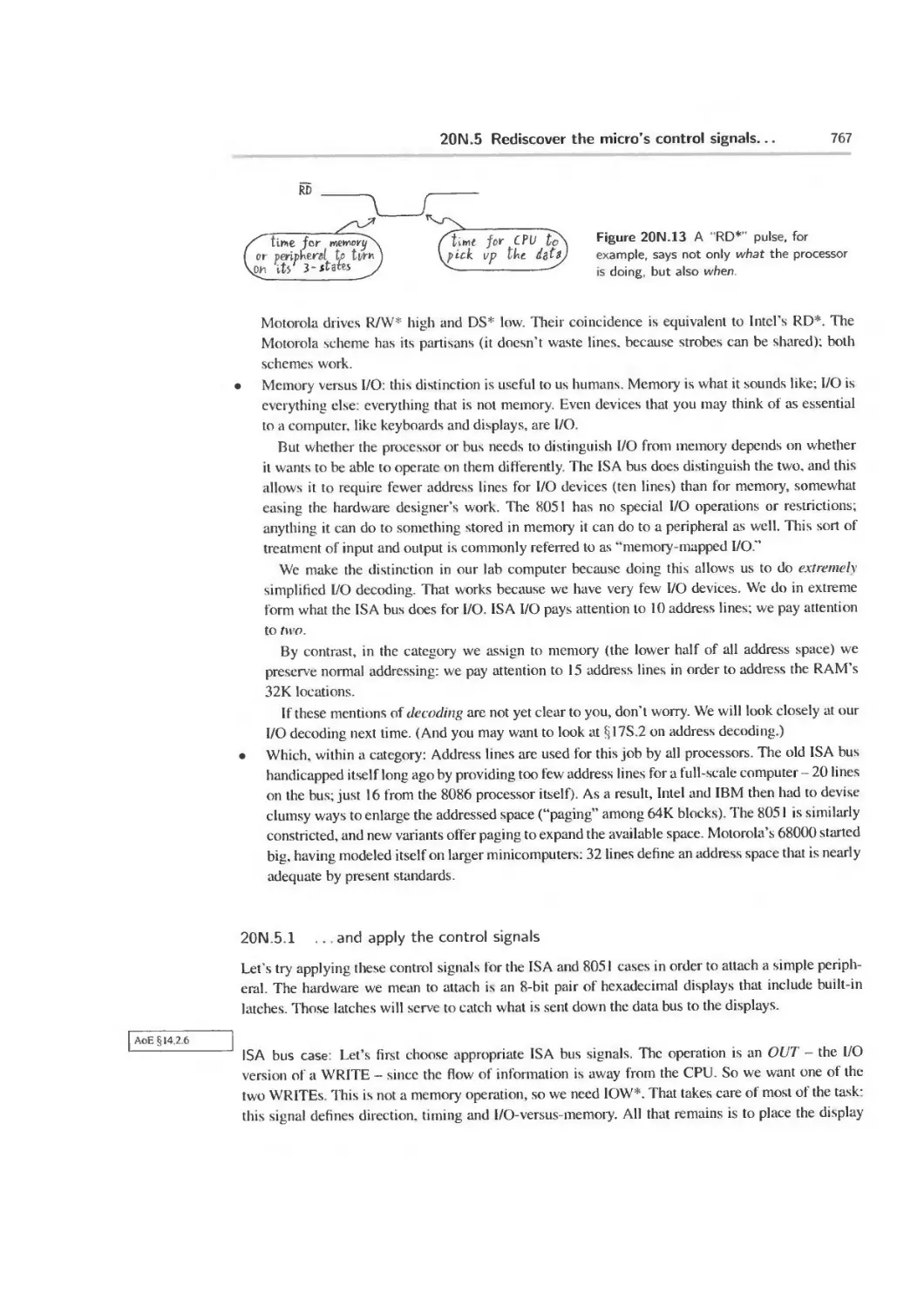
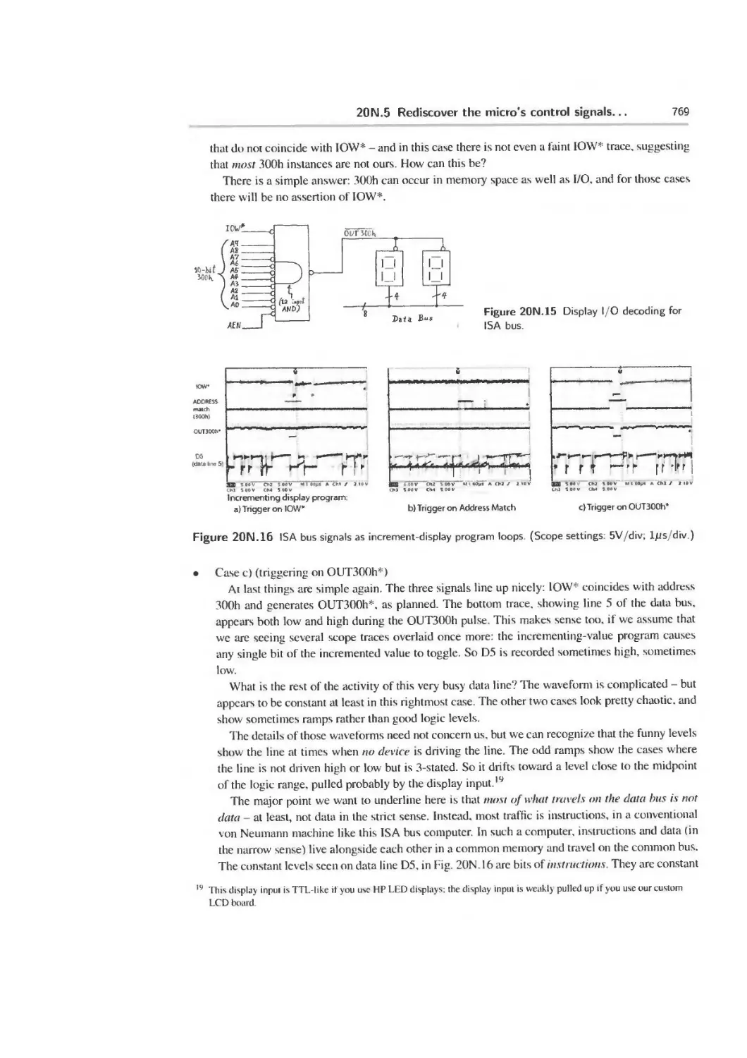
20N 5 Rediscover the micro’s control signals... 765
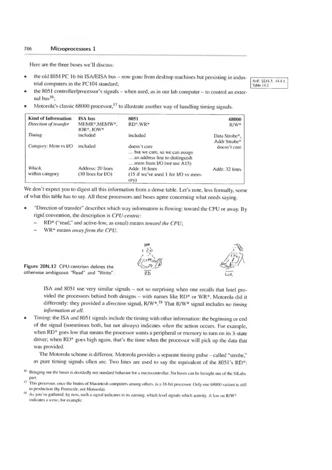
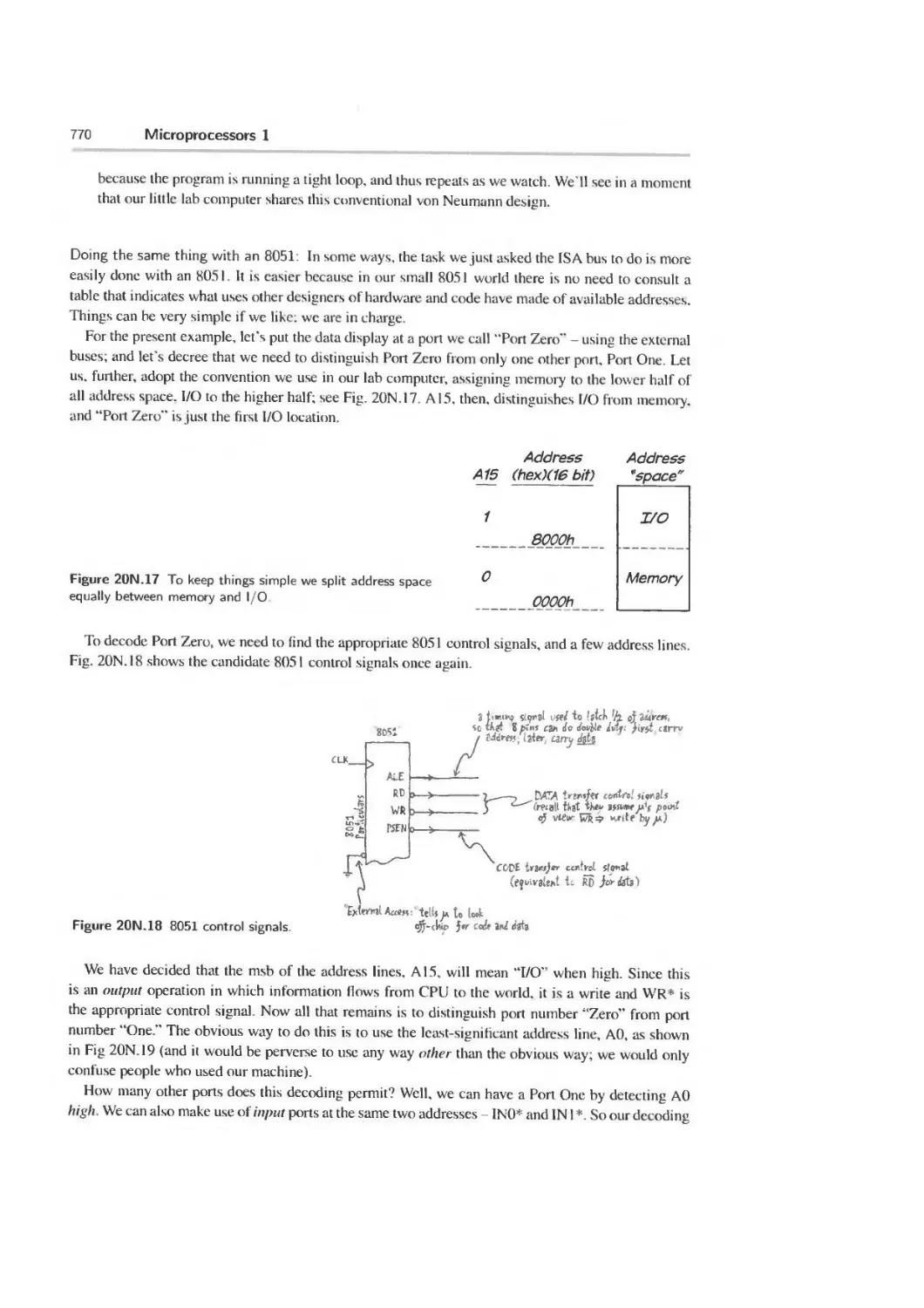
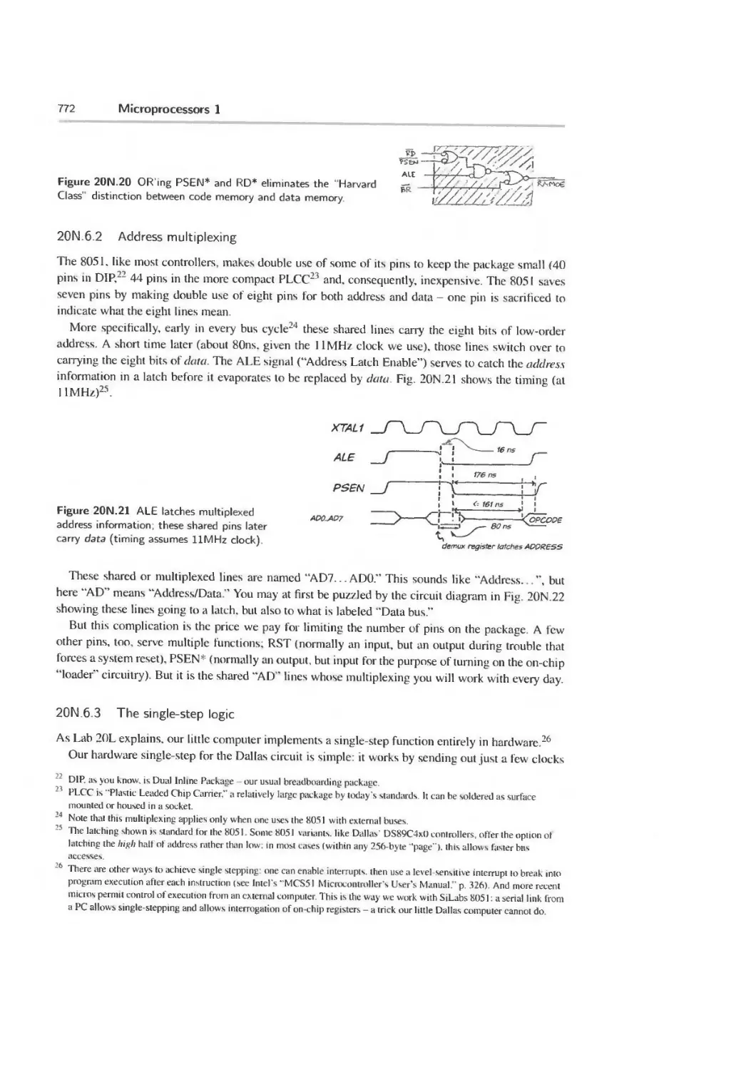
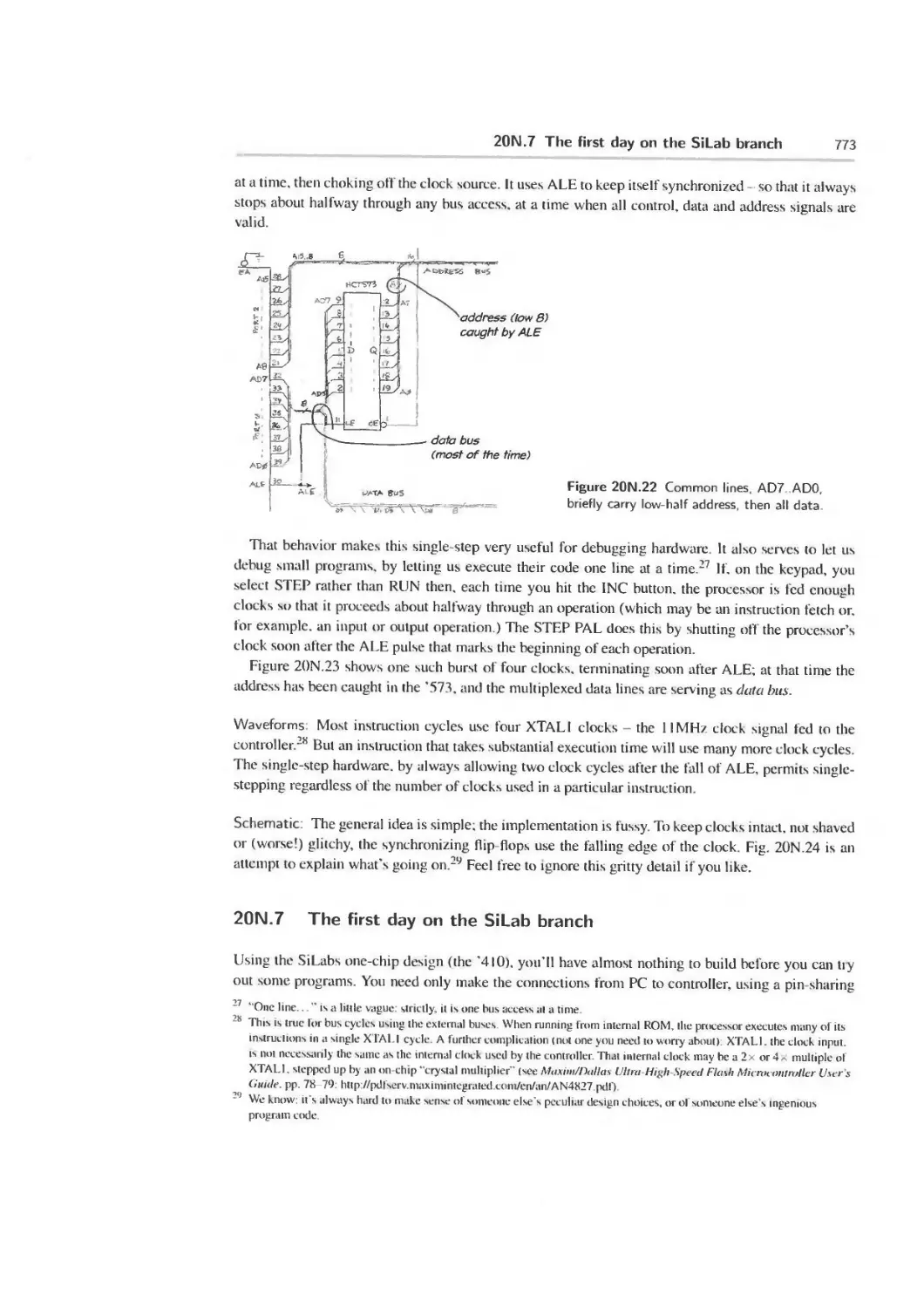
20N.6 Some specifics of our lab computer: big-board branch 771
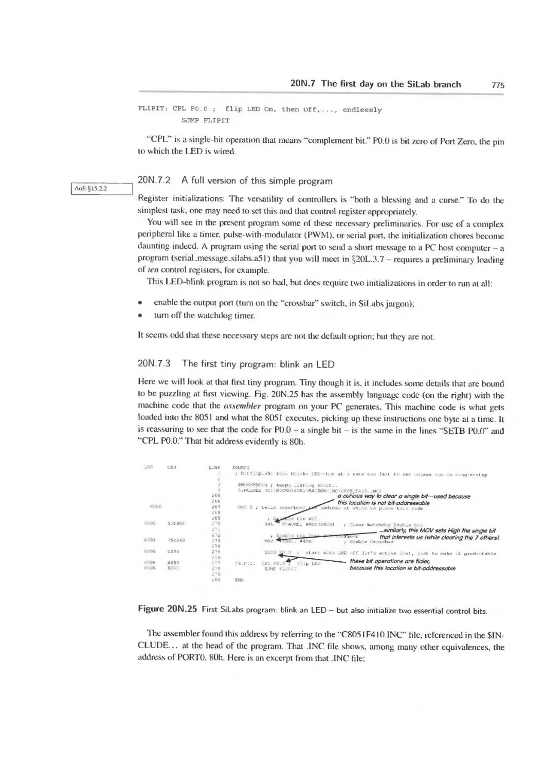
20N.7 The first day on the SiLab branch 773
20N.8 AoE Reading 778
XVI
Contents
20L Lab: Microprocessors 1 780
20L. I Big board Dallas microcomputer 780
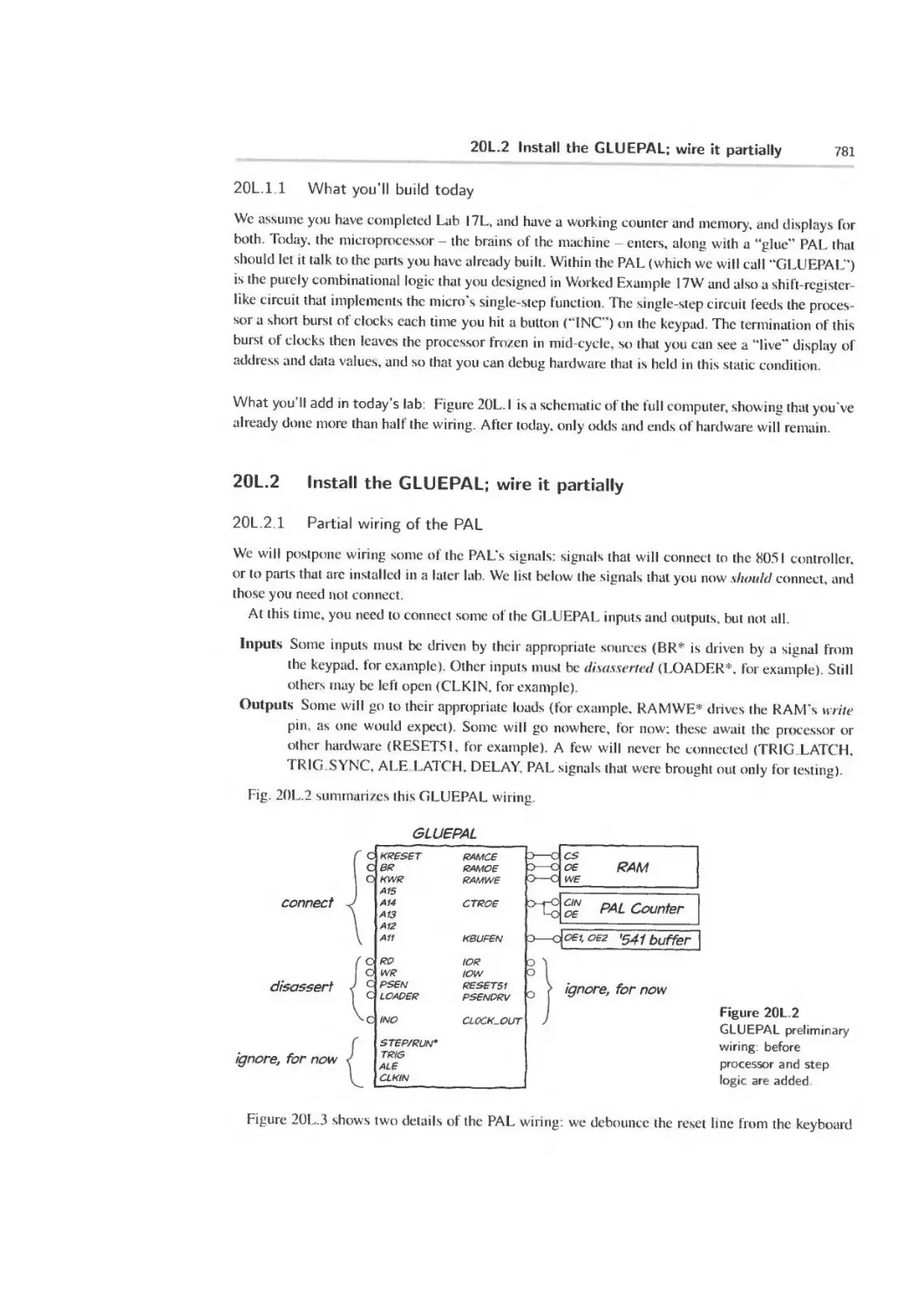
20L.2 Install the GLUEPAL; wire it partially 781
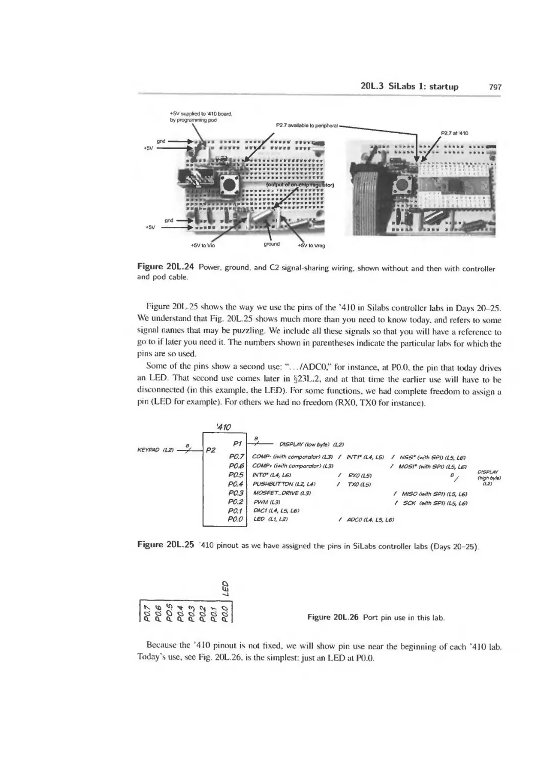
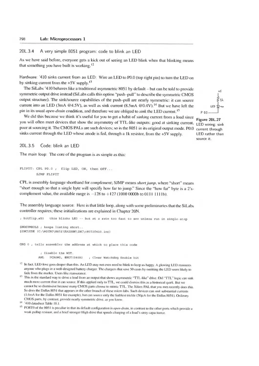
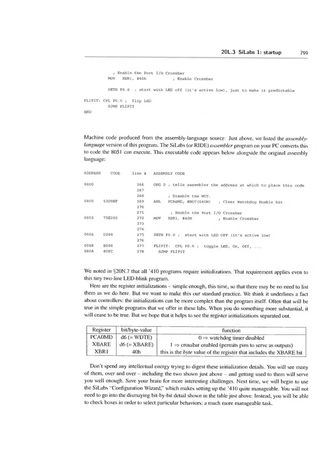
20L.3 SiLabs 1: startup 792
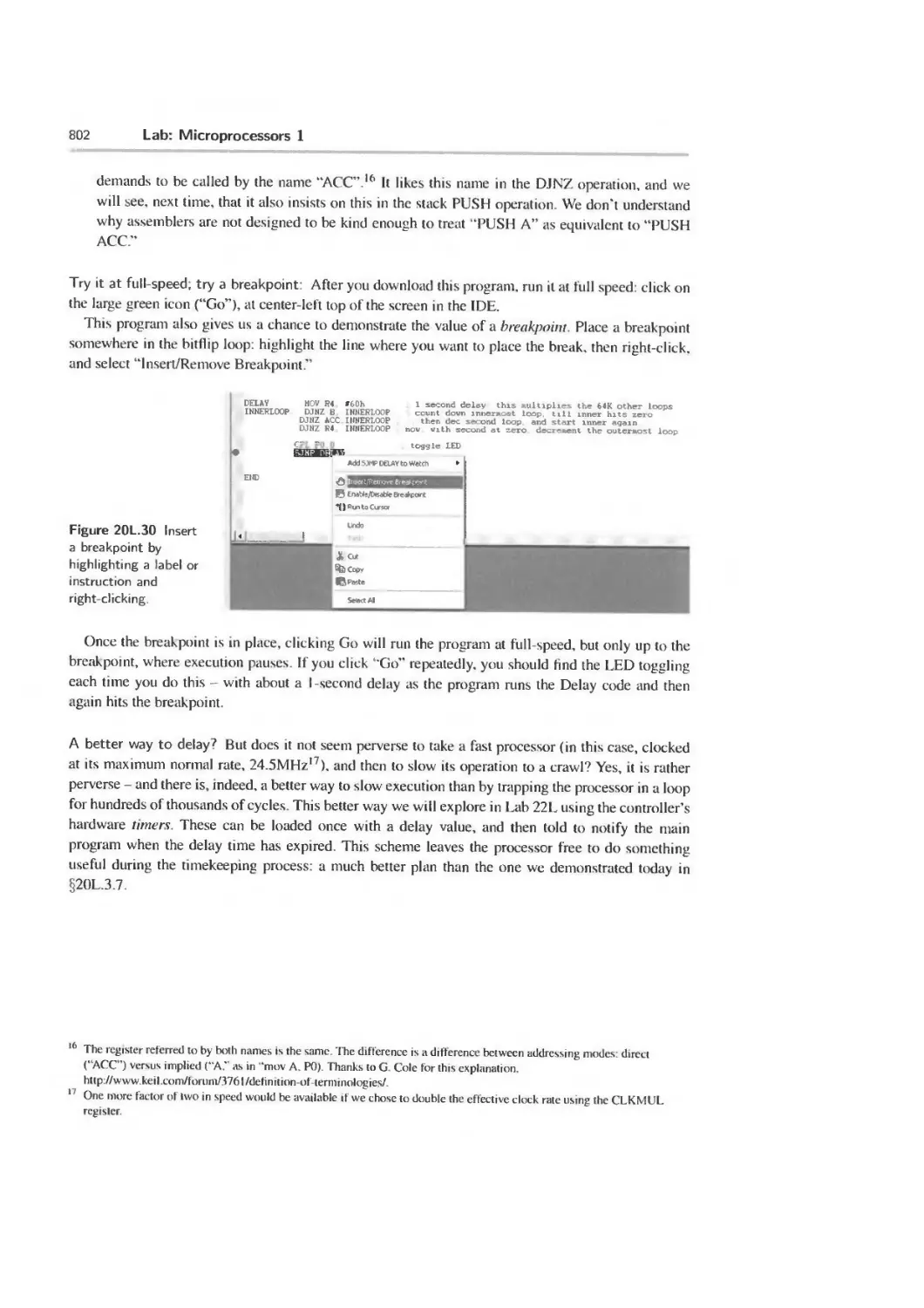
20S Supplementary Notes: Microprocessors 1 803
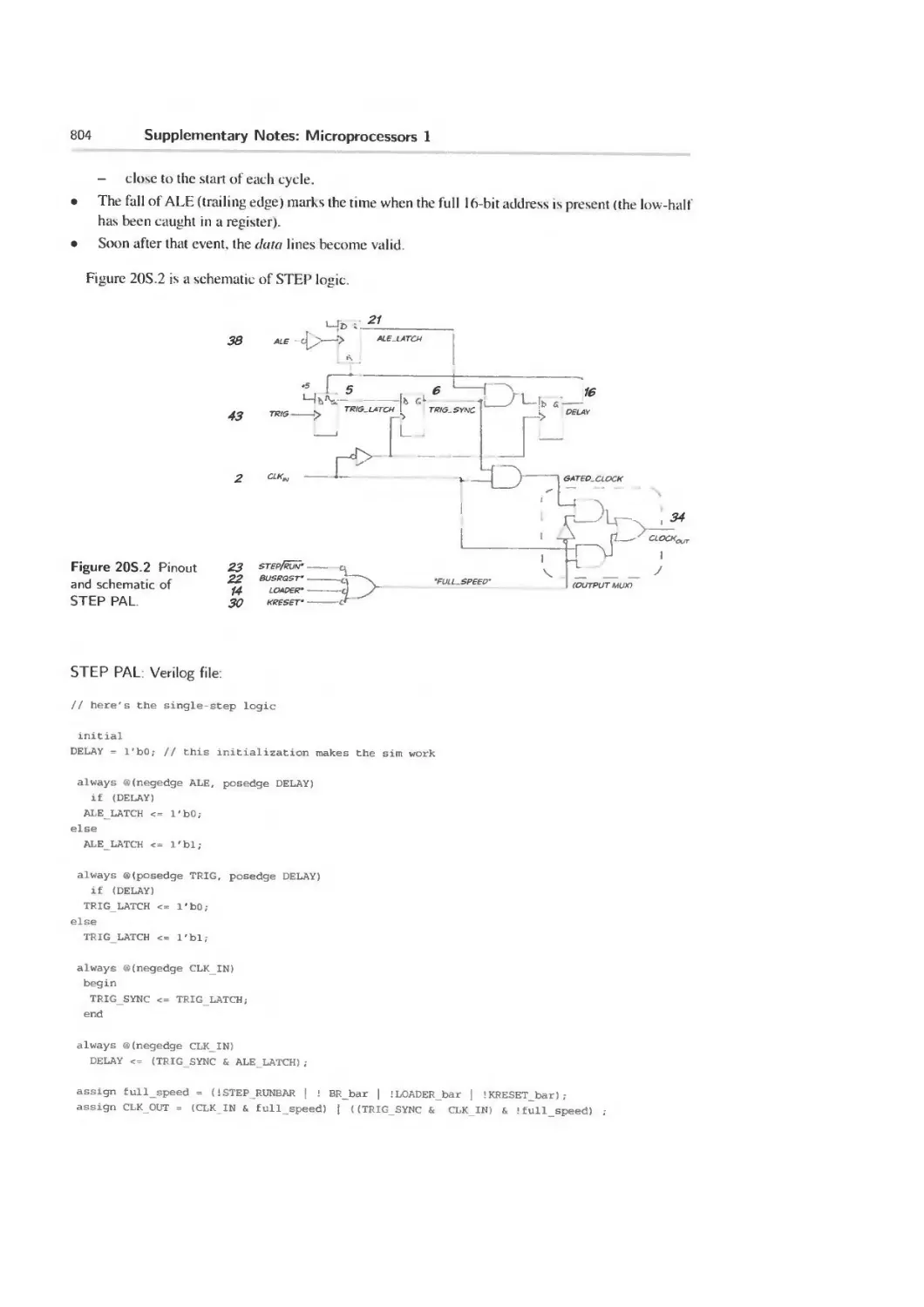
20S.1 PAL for microcomputers 803
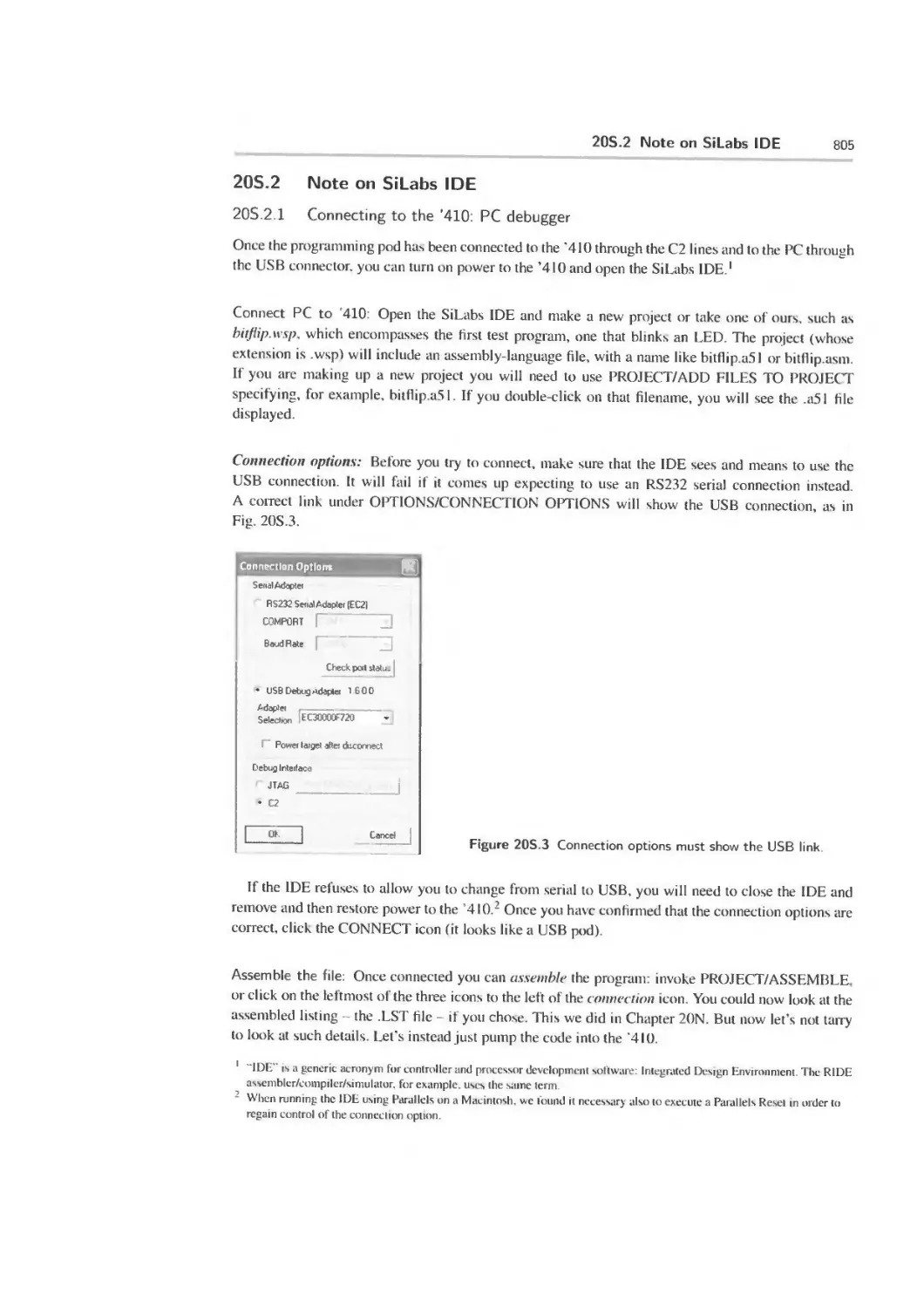
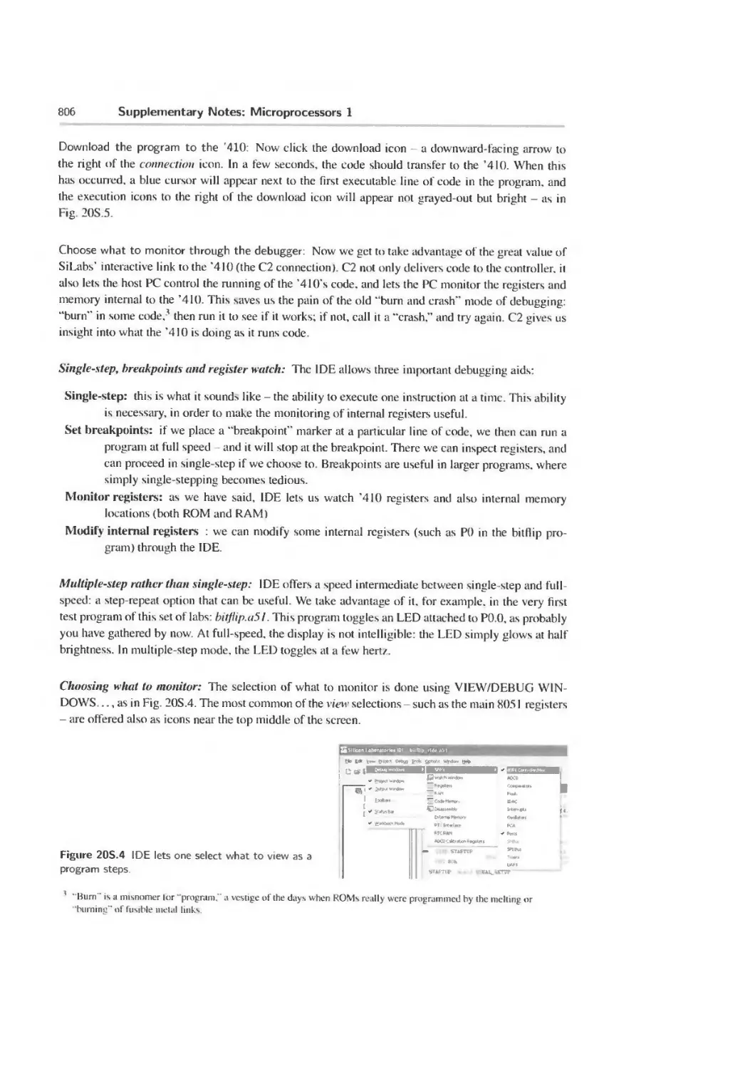
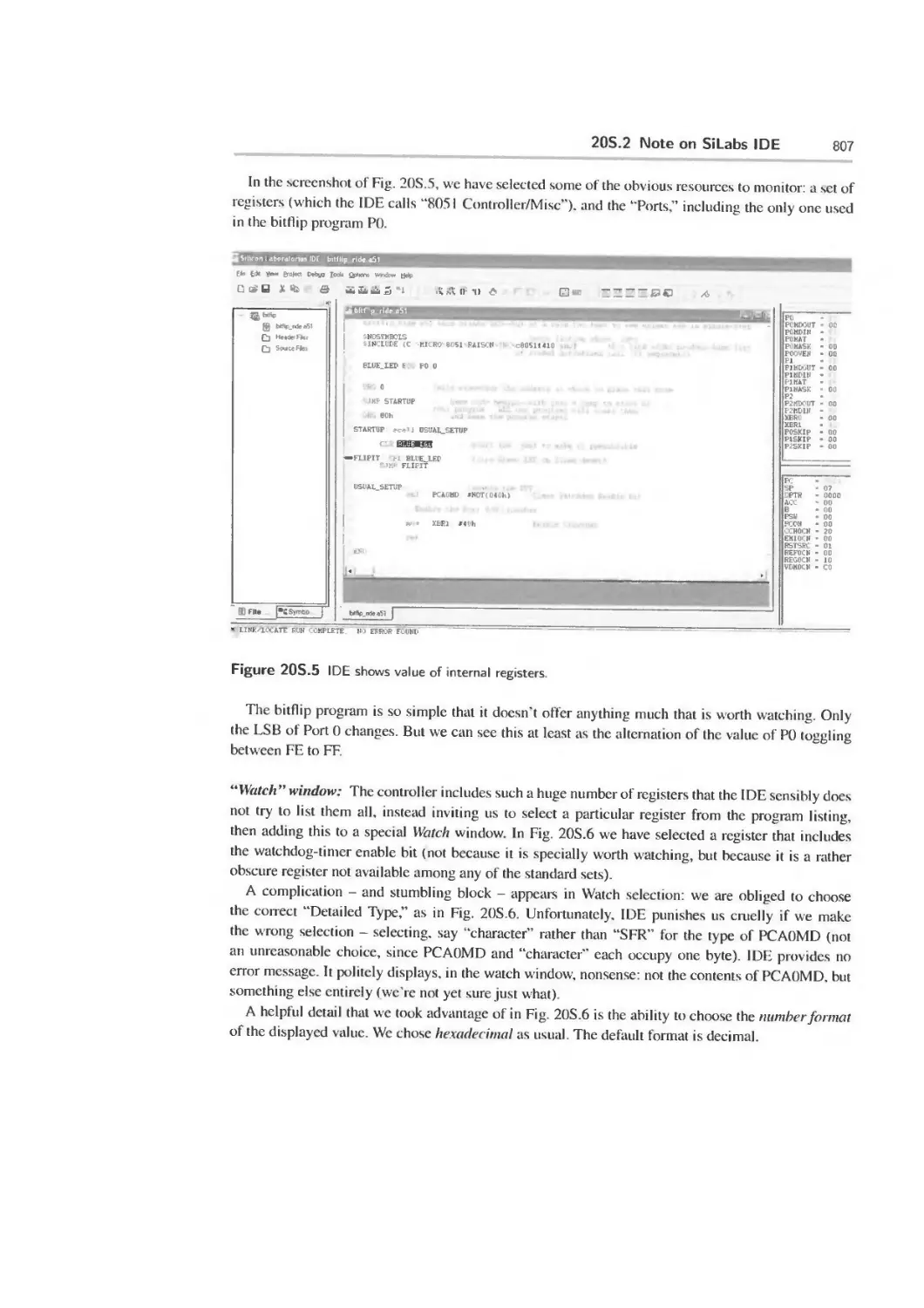
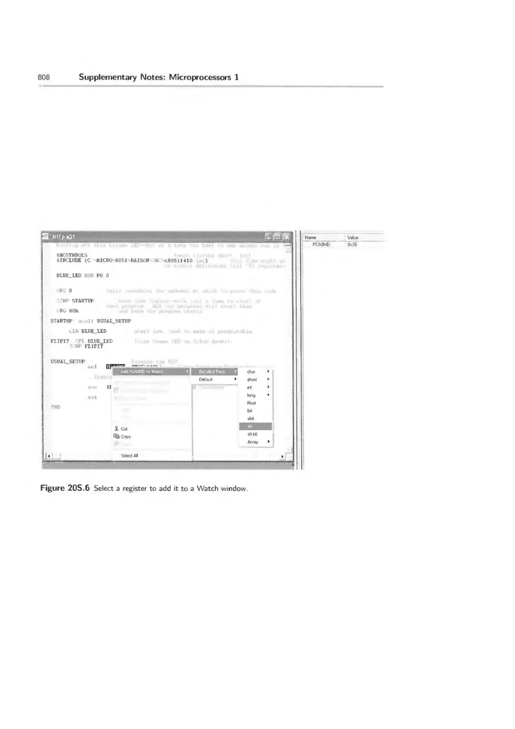
20S.2 Note on SiLabs IDE 805
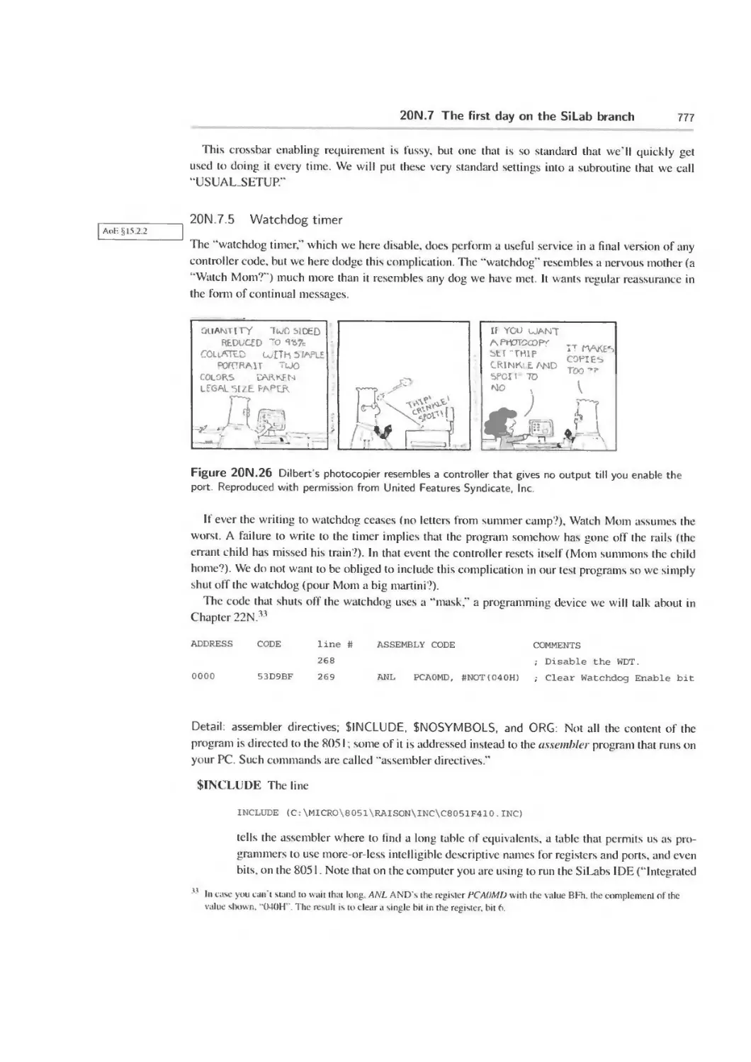
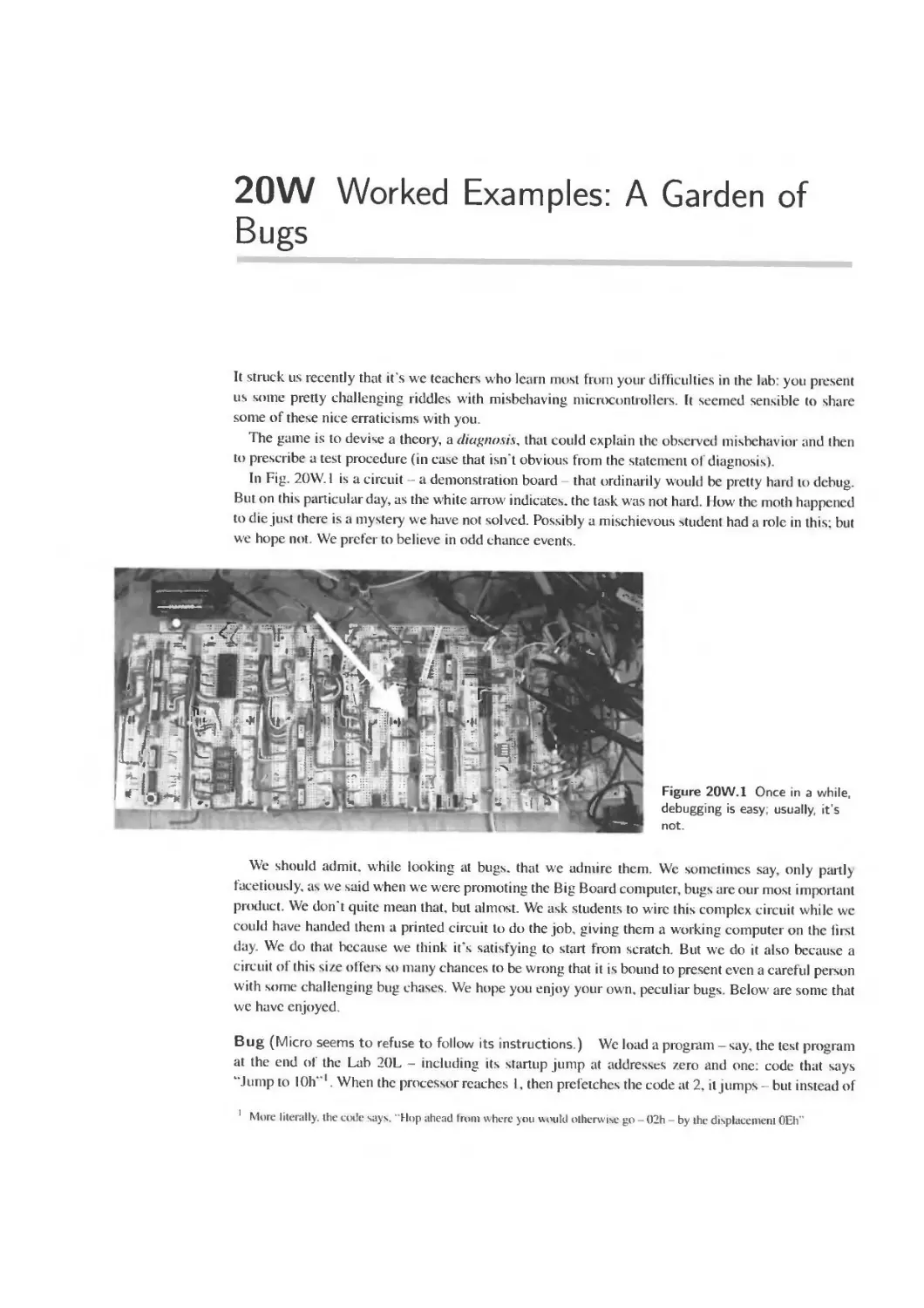
20W Worked Examples: A Garden of Bugs 809
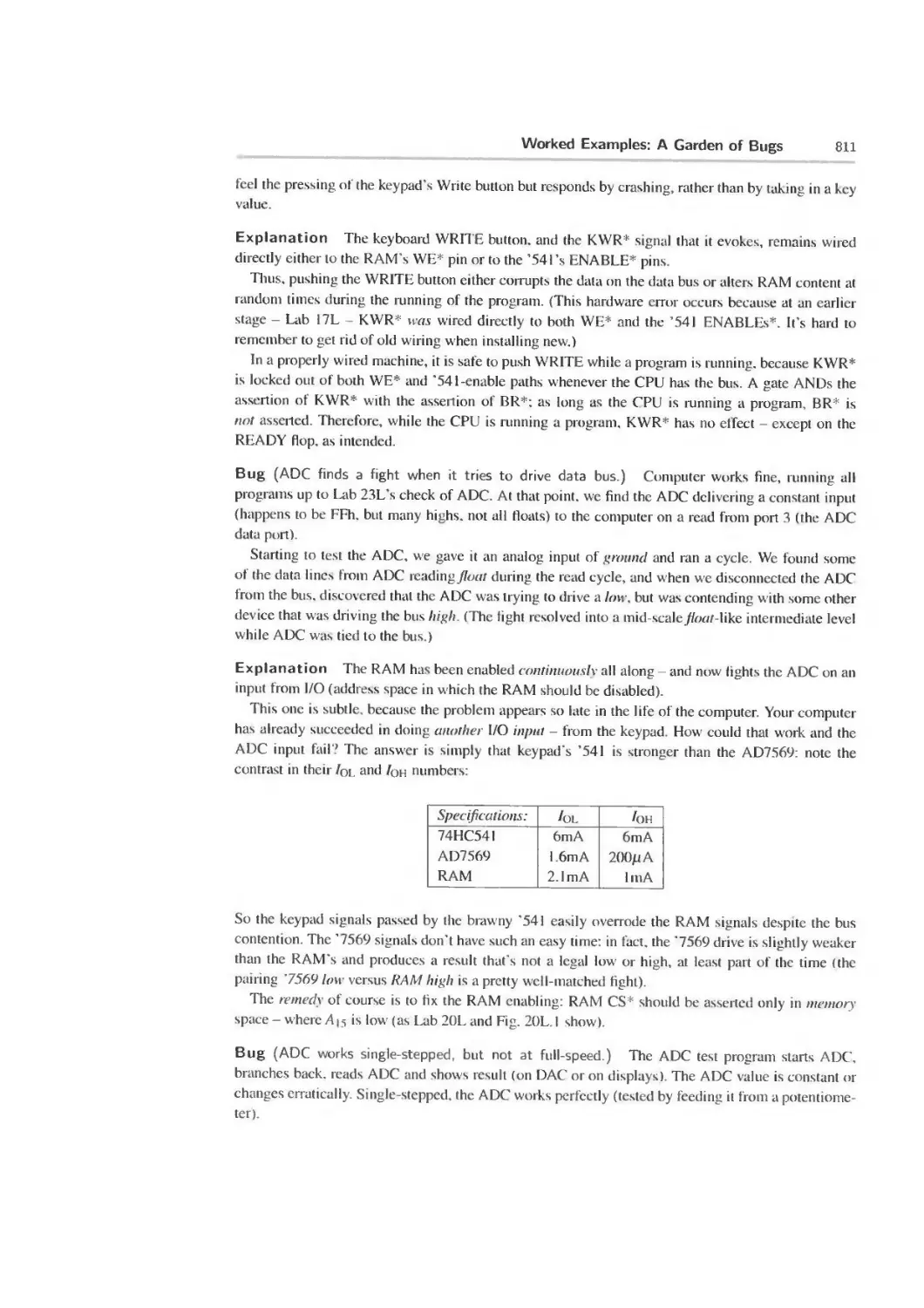
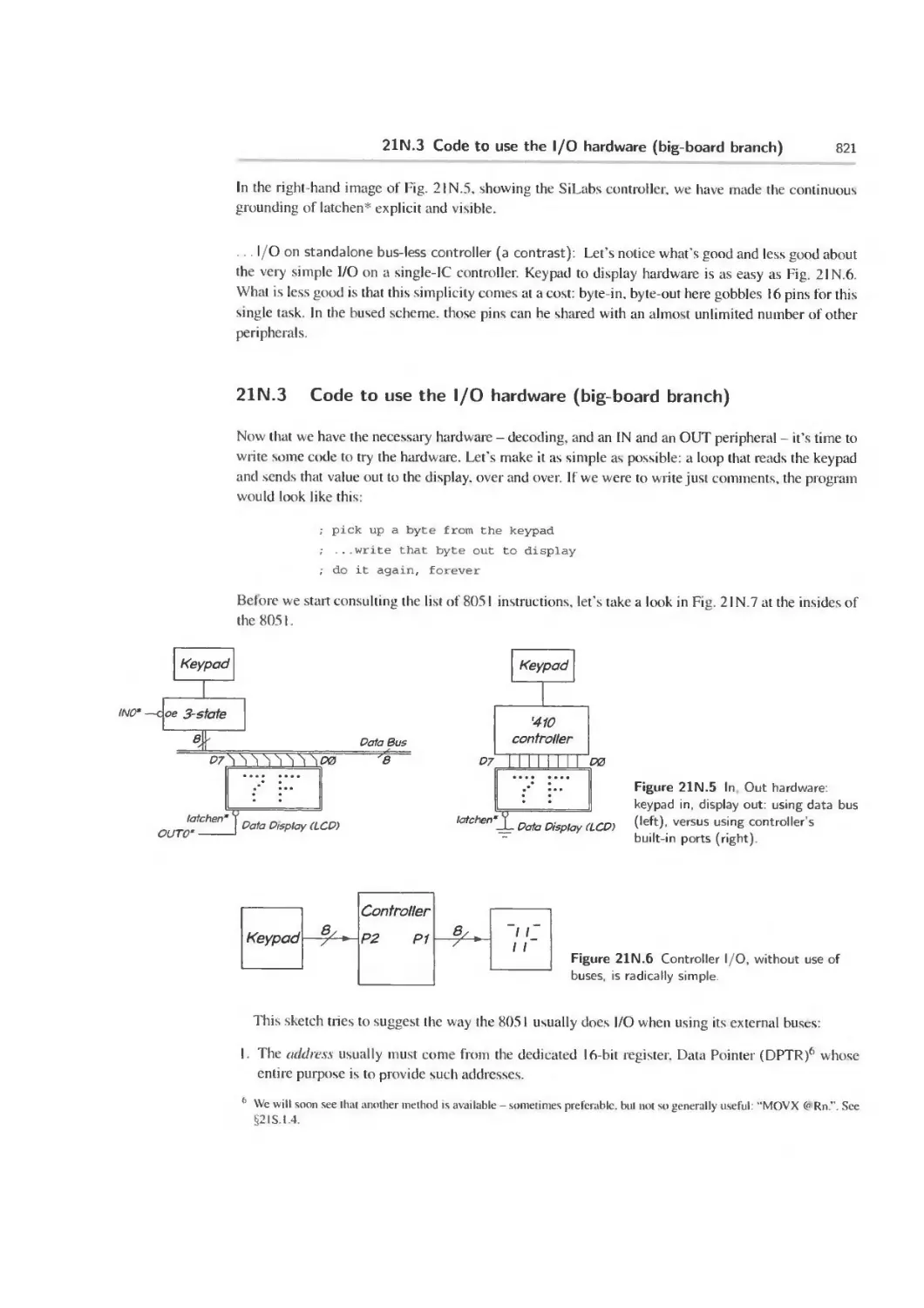
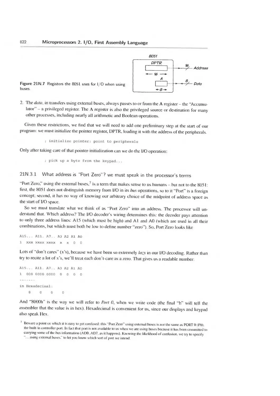
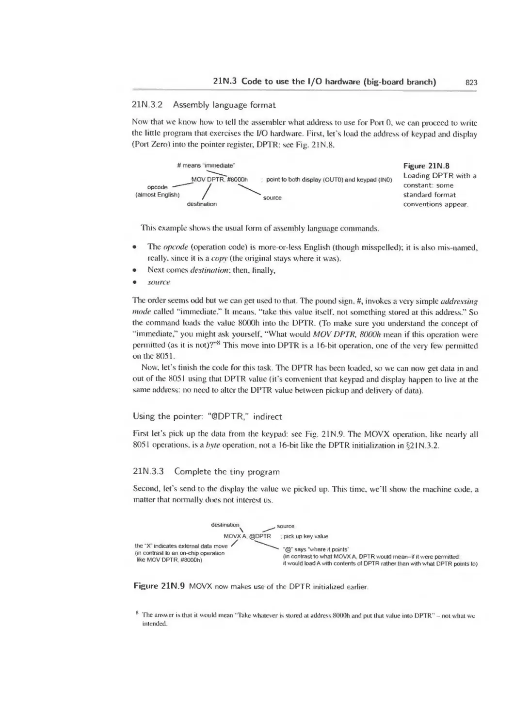
21N Microprocessors 2. I/O, First Assembly Language 813
21N 1 What is assembly language? Why bother with it? 813
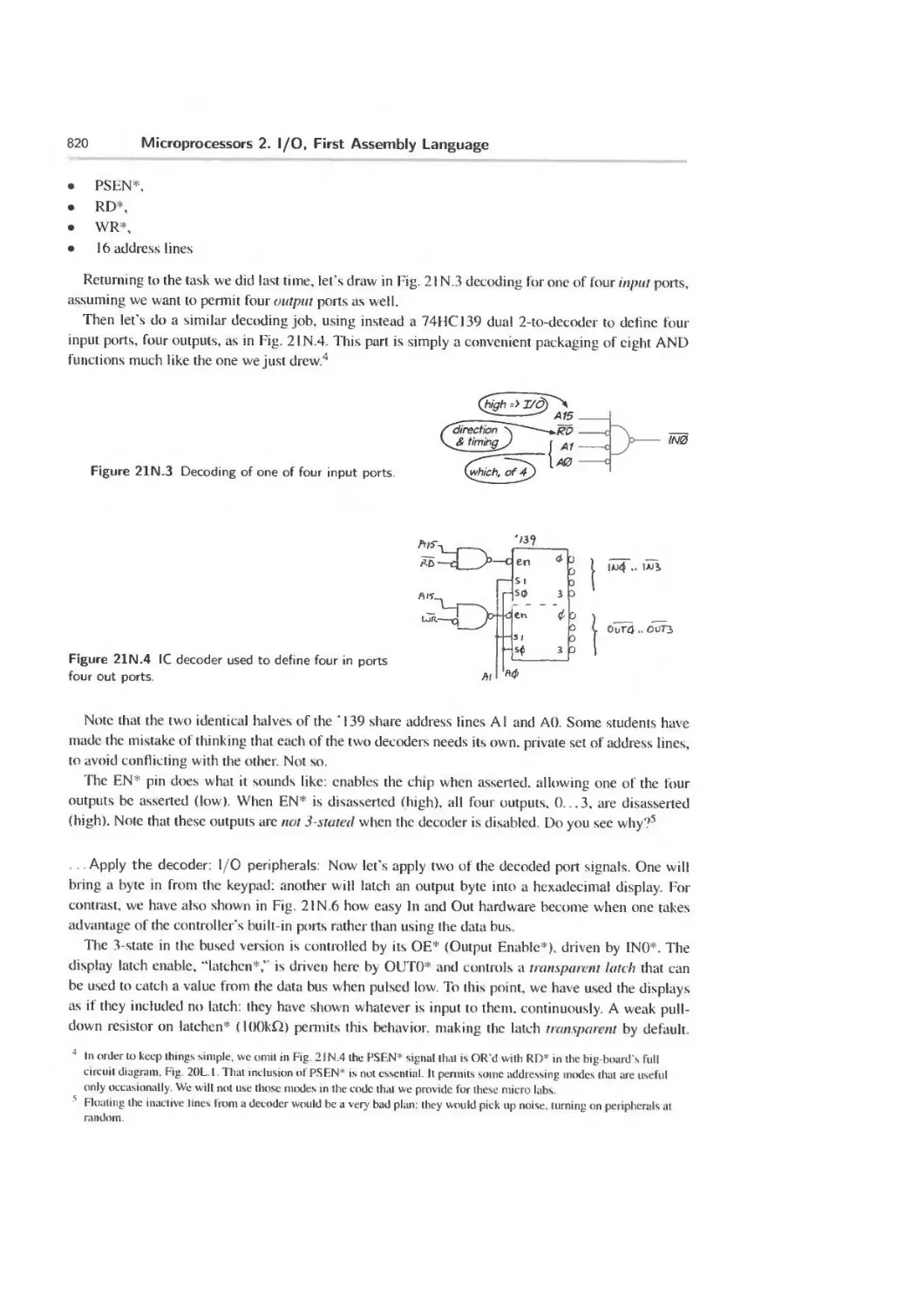
21 N.2 Decoding, again 818
21 N.3 Code to use the I/O hardware (big-board branch) 821
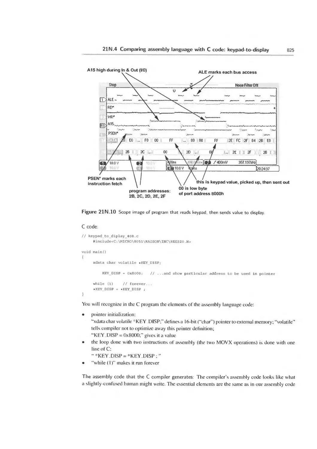
2IN.4 Comparing assembly language withC code: keypad-to-display 824
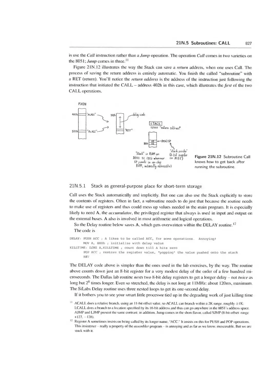
21N.5 Subroutines: CALL 826
21 N.6 Stretching operations to 16 bits 830
21N 7 AoE Reading 831
21L Lab: Microprocessors 2 832
2IL. 1 Big-board: I/O. Introduction 832
21 L.2 SiLabs 2 input; byte operations 844
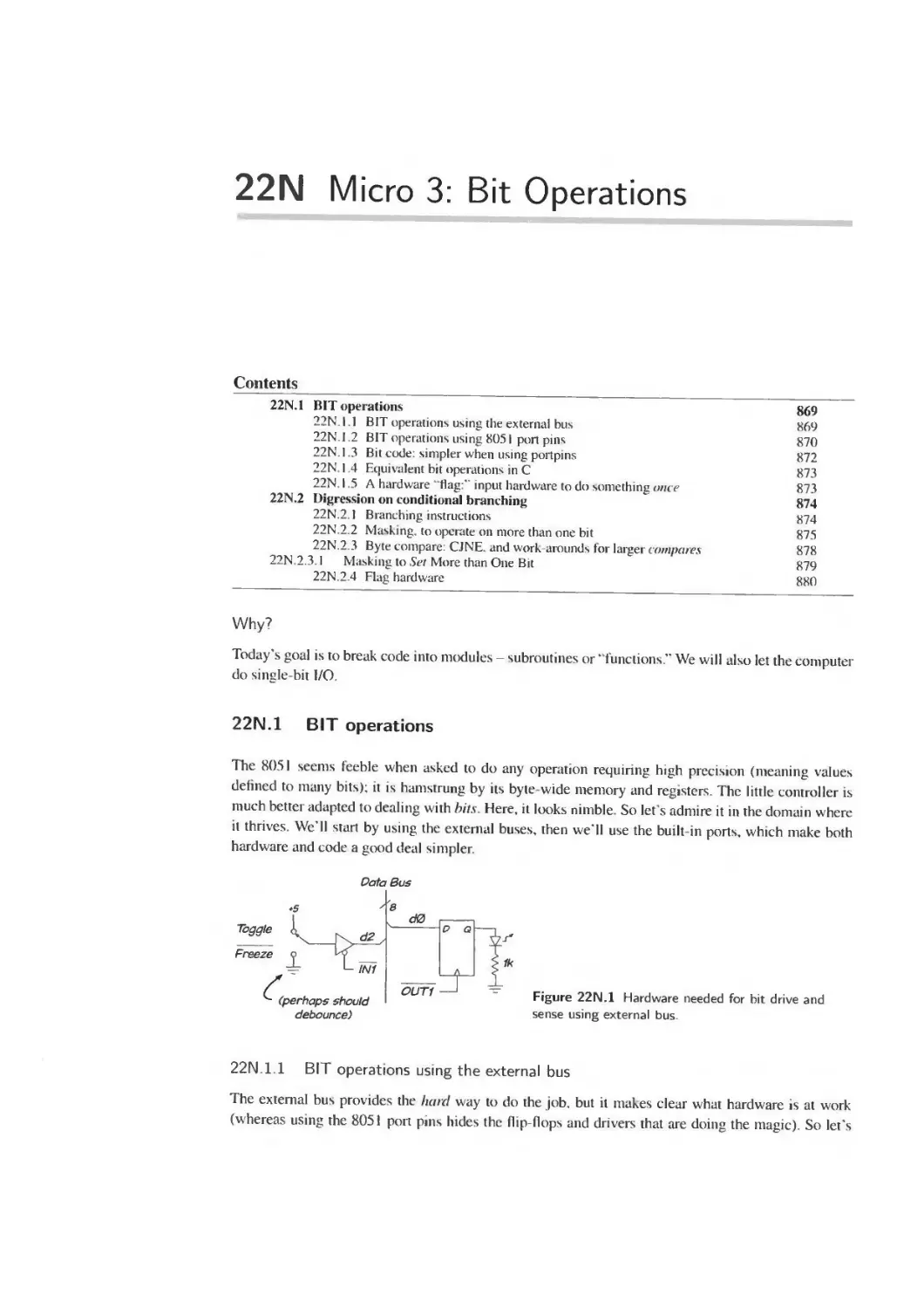
21S Supplementary Notes: 8051 Addressing Modes 857
21S.1 Getting familiar with the 805l‘s addressing modes 857
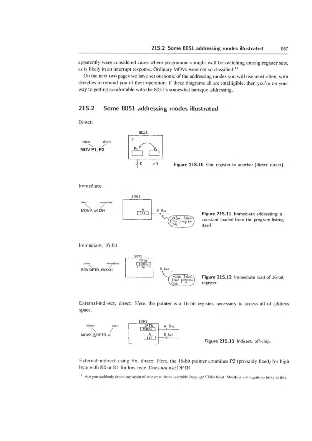
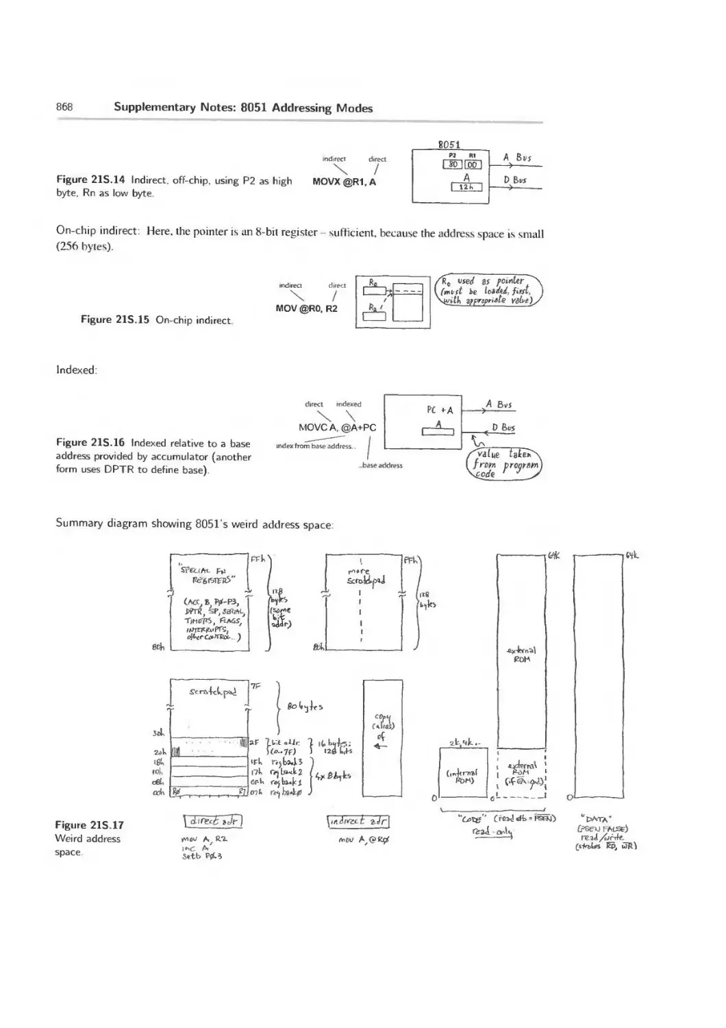
2IS.2 Some 8051 addressing modes illustrated 867
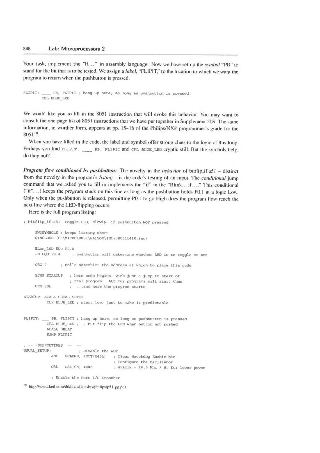
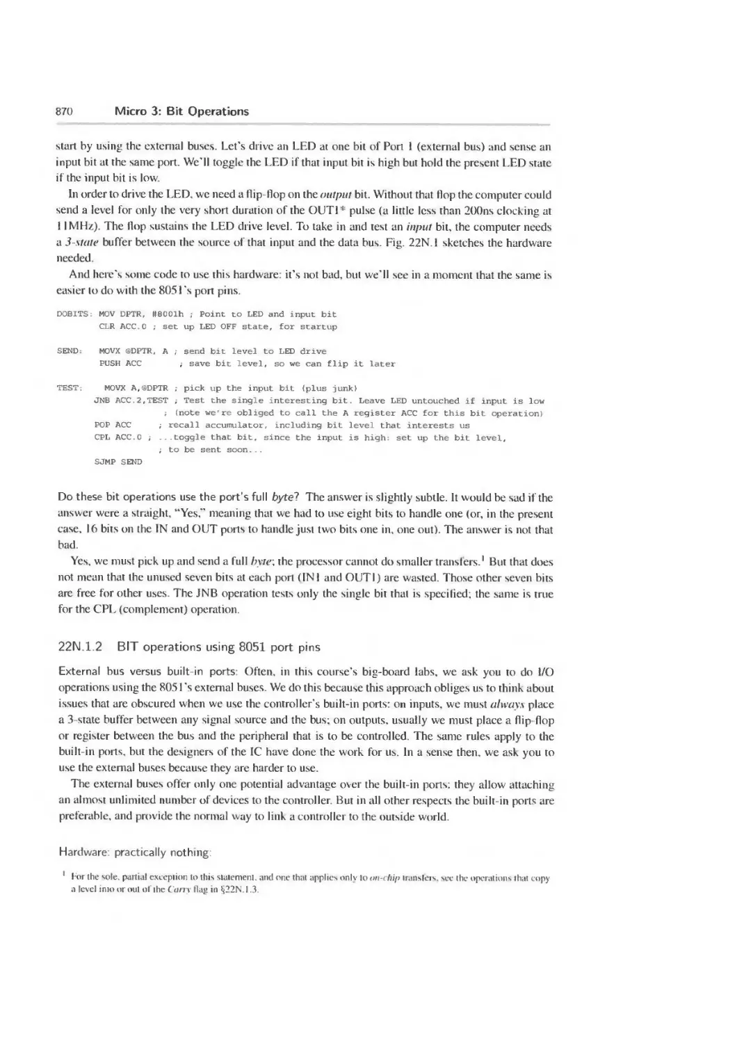
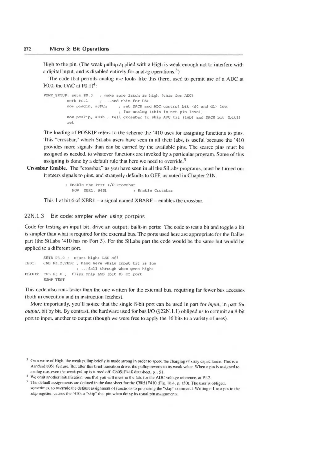
22N Micro 3: Bit Operations 869
22N.1 BIToperations 869
22N.2 Digression on conditional branching 874
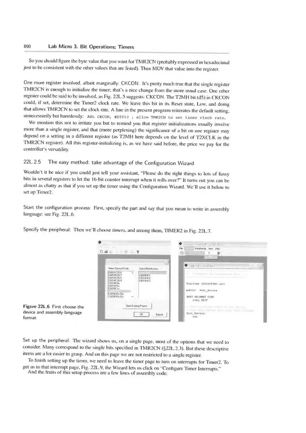
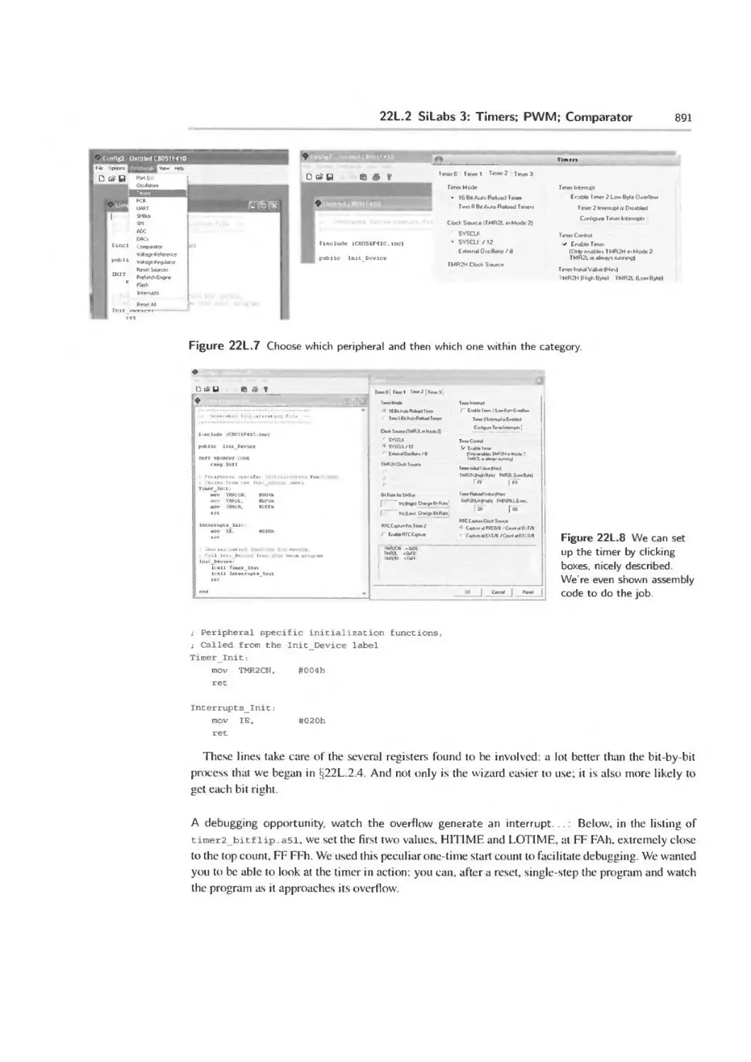
22L Lab Micro 3. Bit Operations; Timers 881
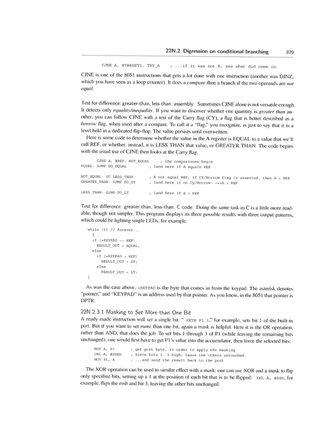
22L. 1 Big board lab. Bit operations interrupt 881
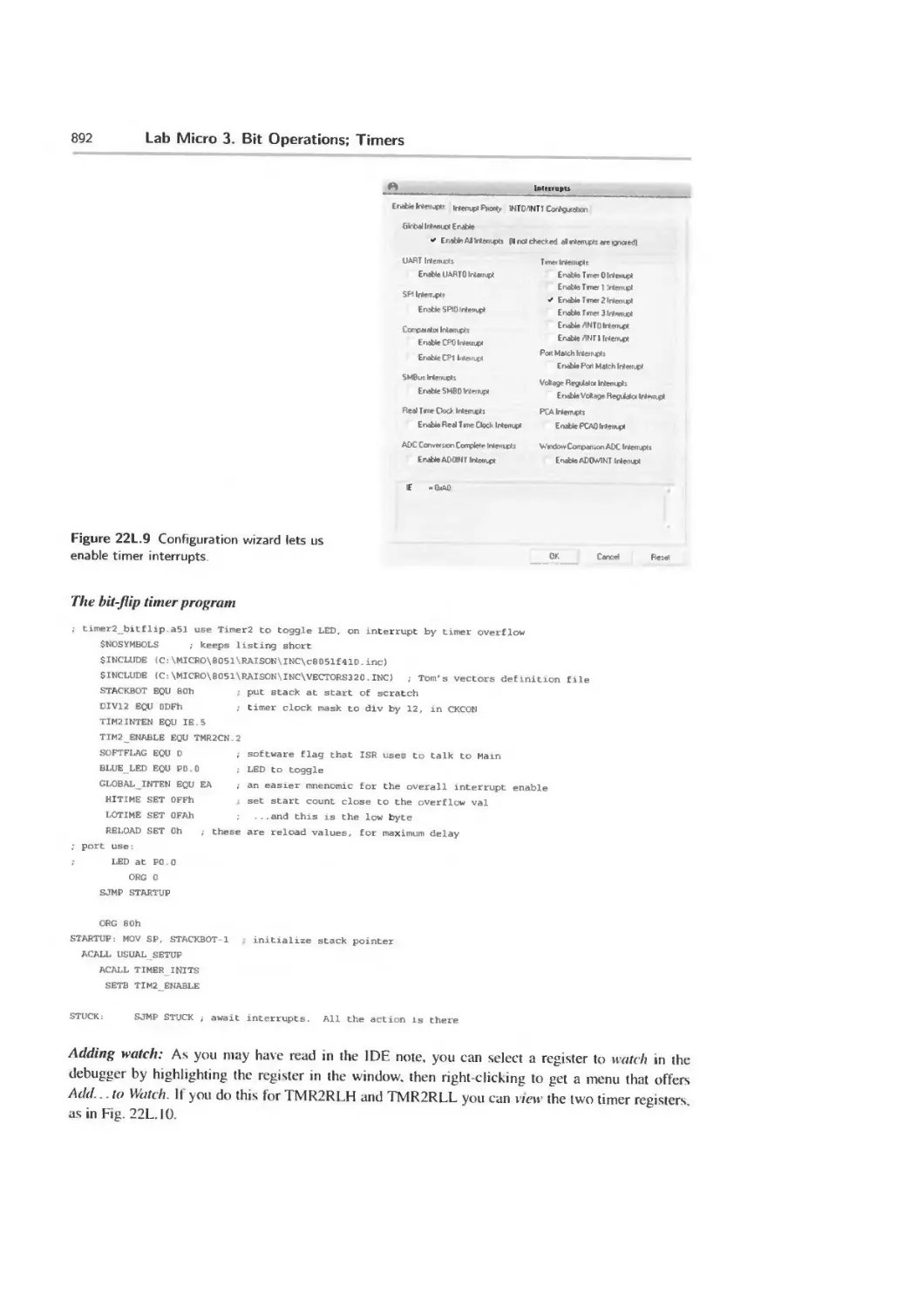
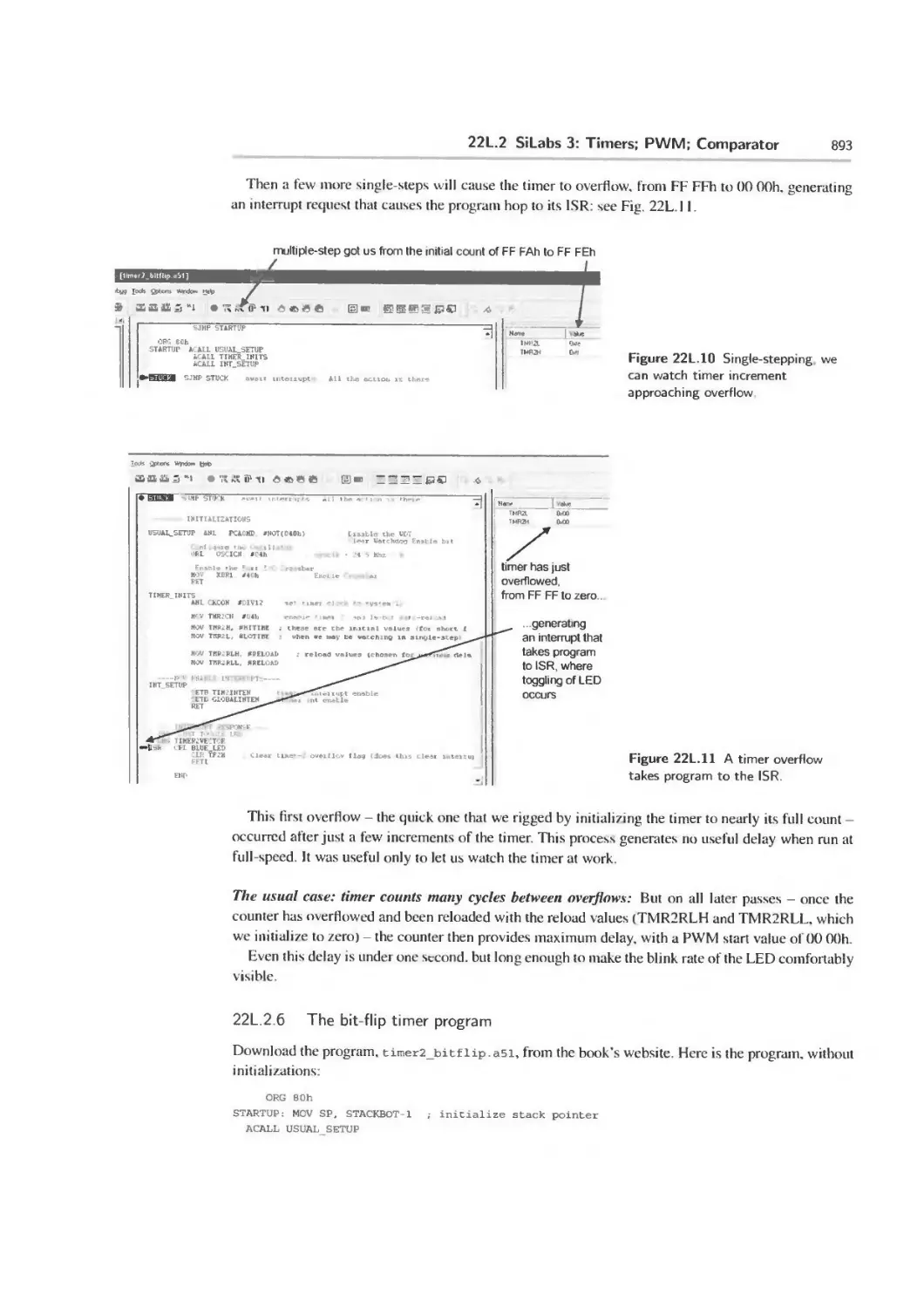
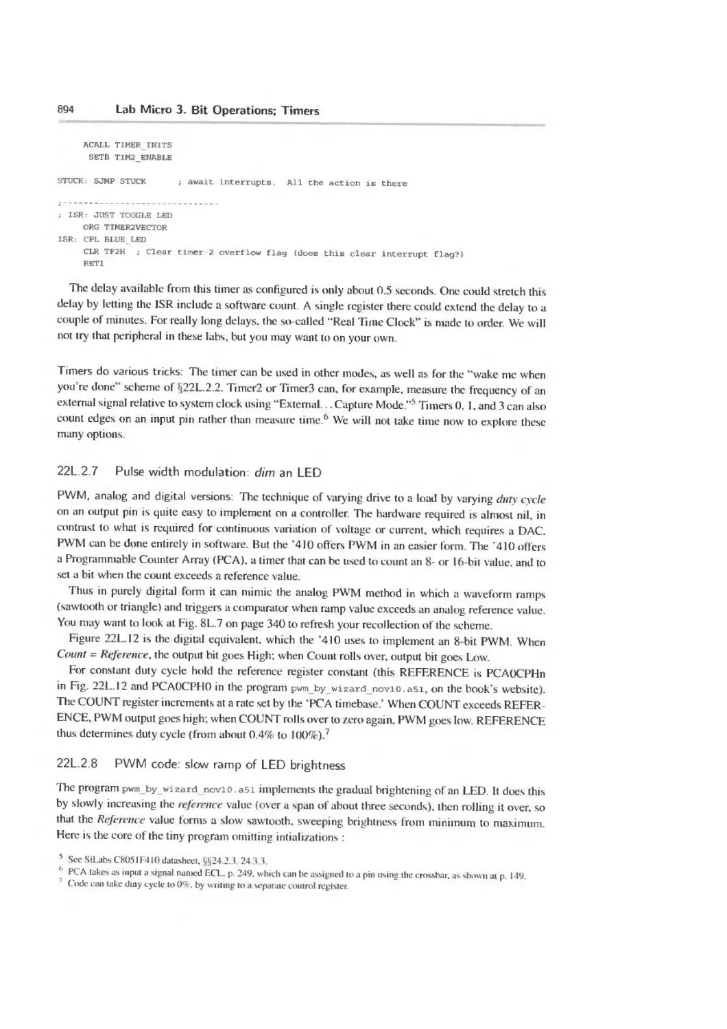
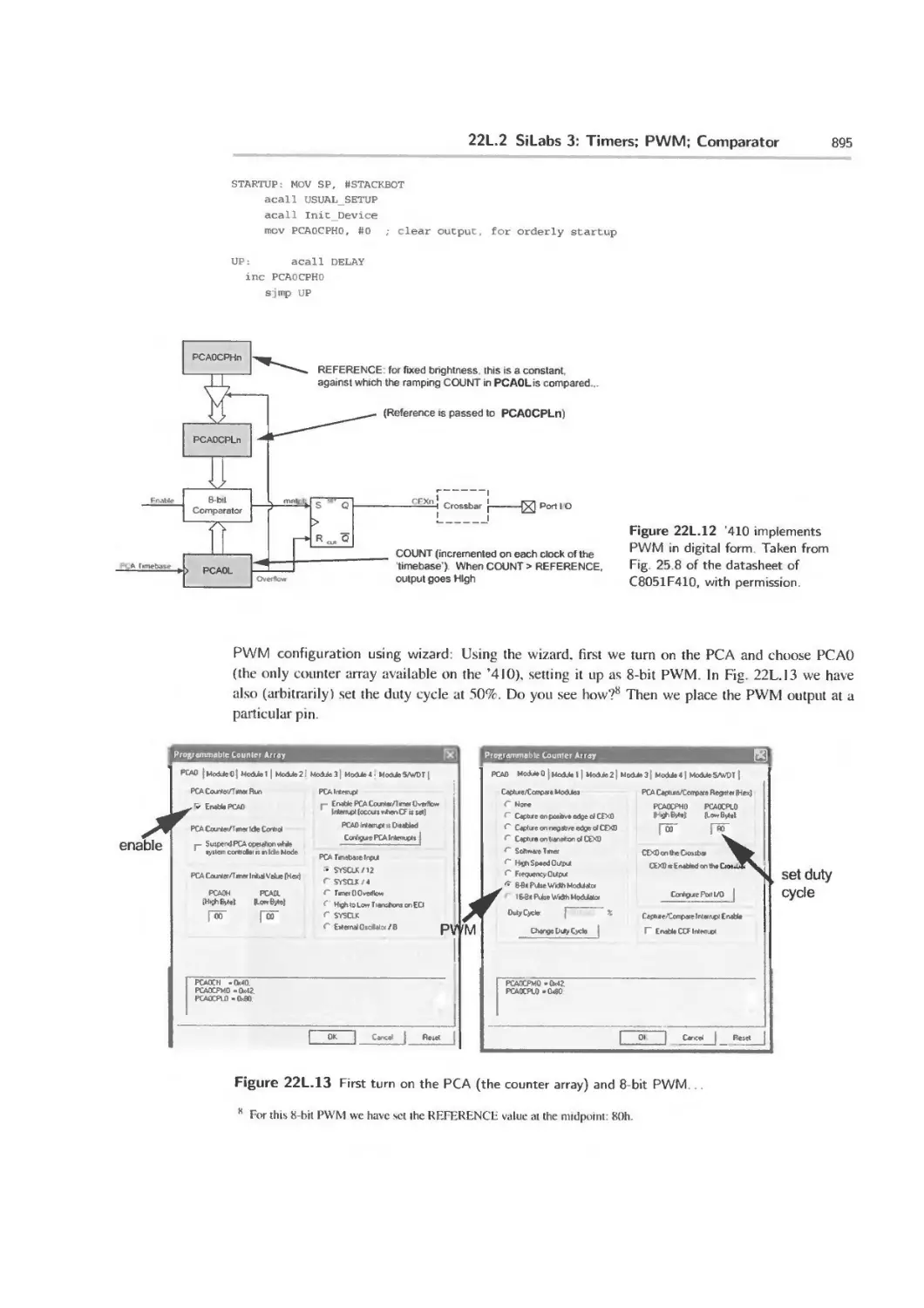
22L.2 SiLabs 3: Timers; PWM; Comparator 886
22W Worked Examples. Bit Operations: An Orgy of Error 901
22W. 1 The problem 901
22W.2 Lots of poor, and one good solutions 901
22W.3 Another way to implement this “Ready” key 904
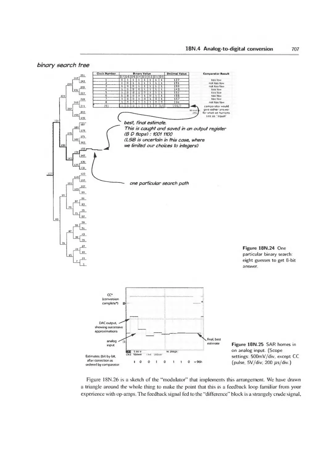
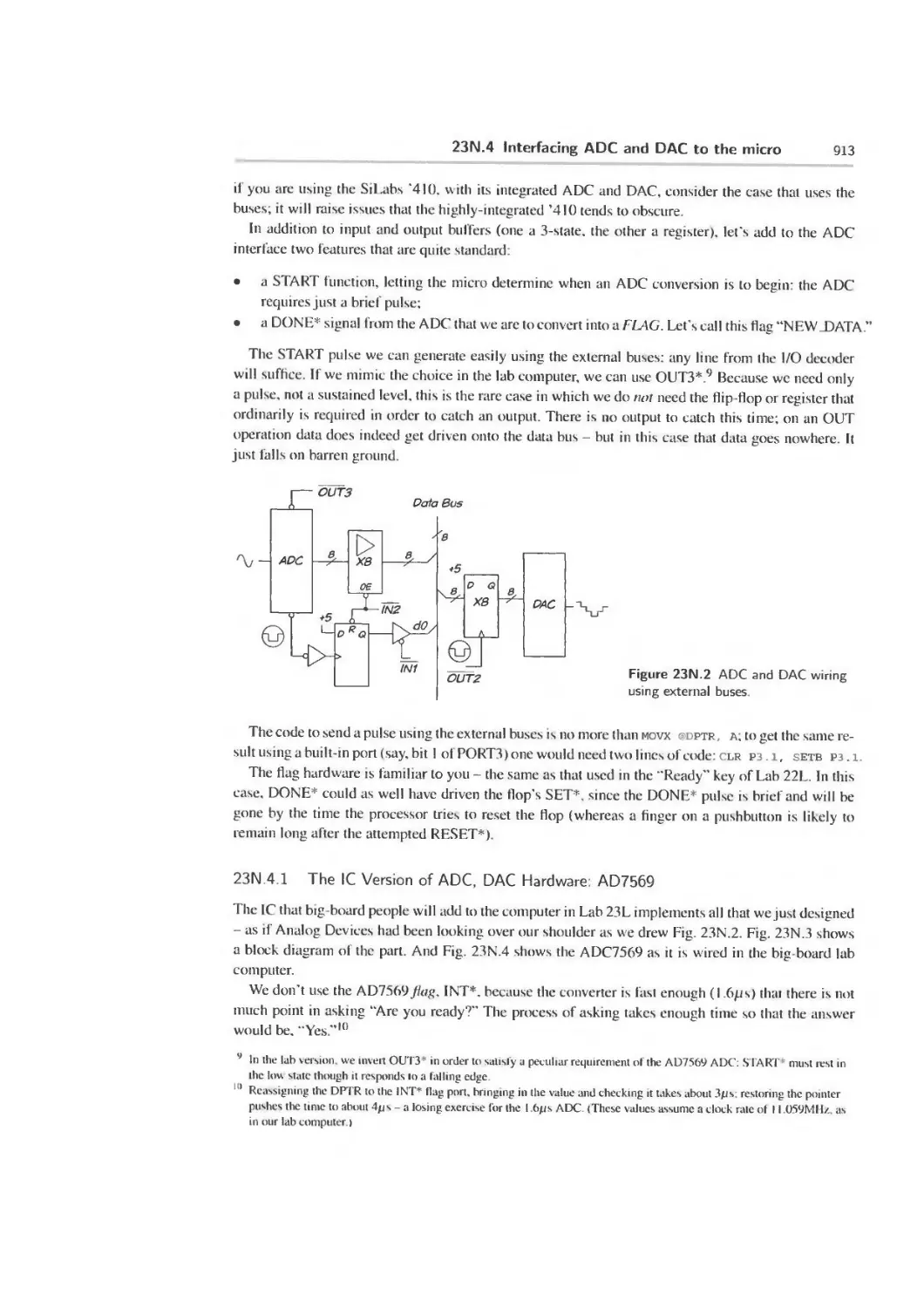
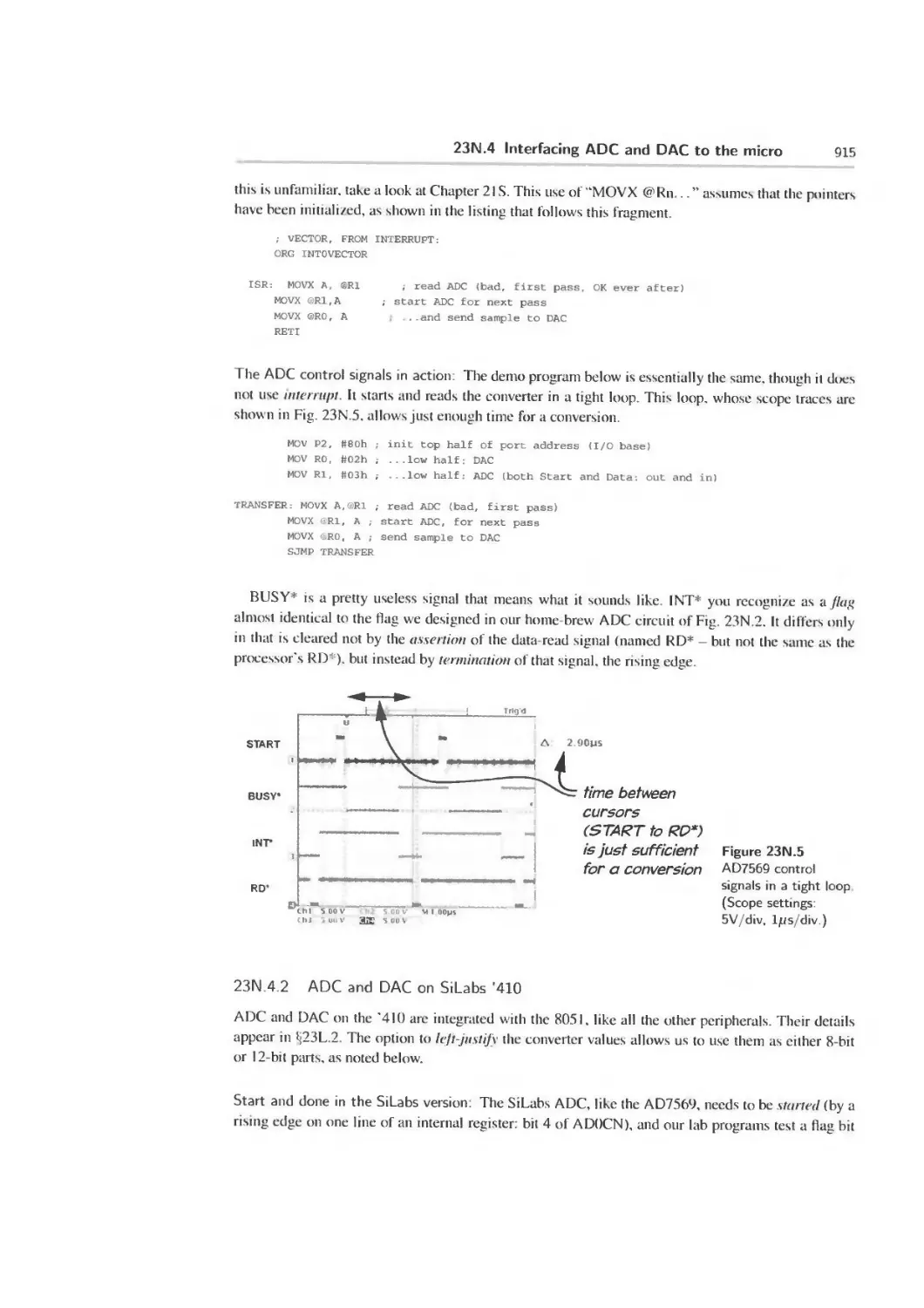
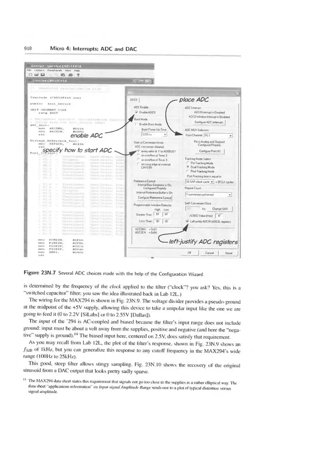
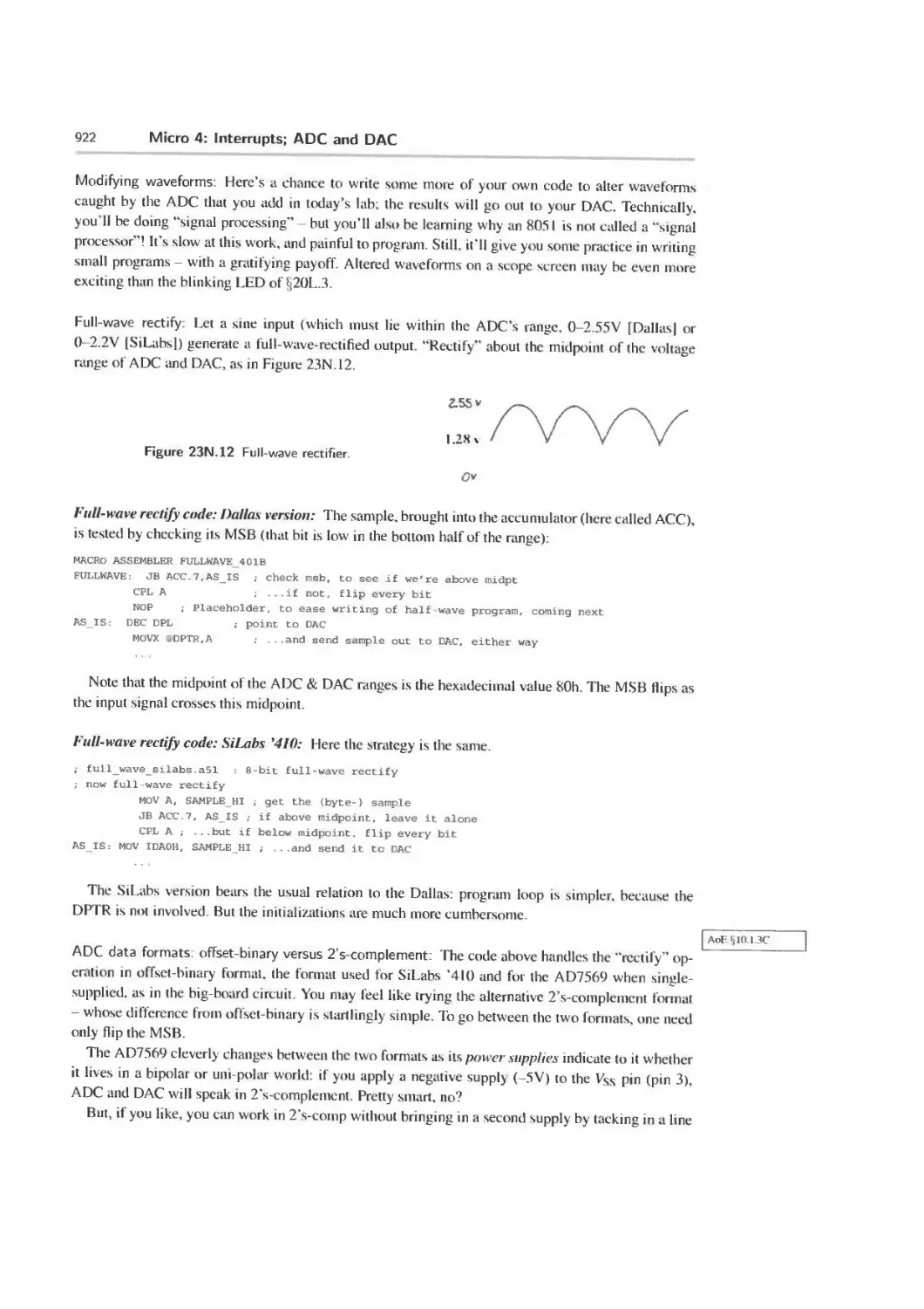
23N Micro 4: Interrupts; ADC and DAC 905
23N. 1 Big ideas from last time 905
23N.2 Interrupts 906
23N.3 Interrupt handling in C 911
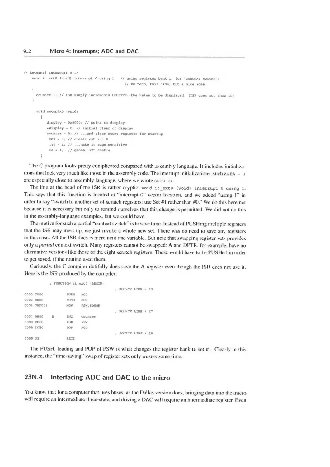
23N.4 Interfacing ADC and DAC to the micro 912
Contents xvii
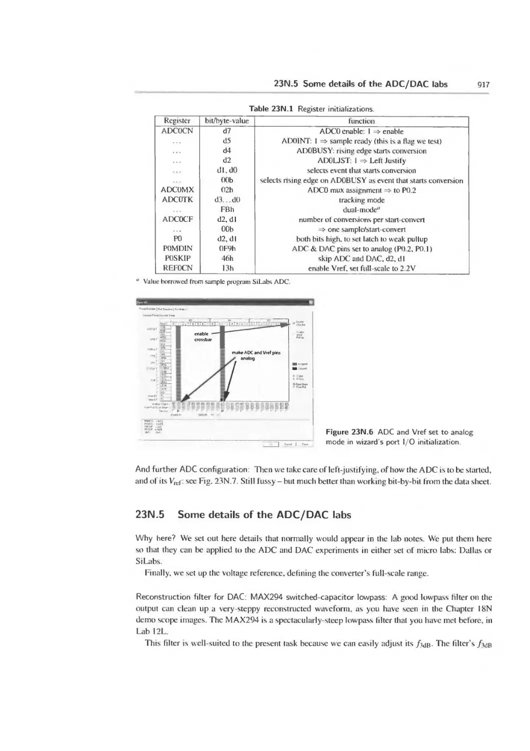
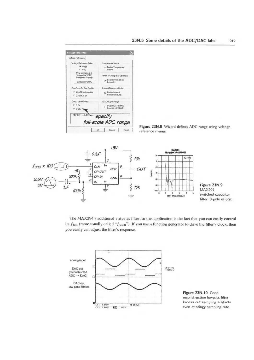
23N.5 Some details of the ADC/DAC labs 917
23N.6 Some suggested lab exercises, playing with ADC and DAC 921
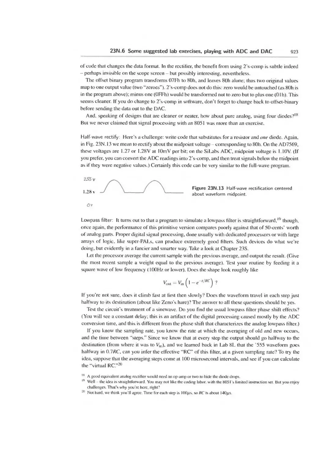
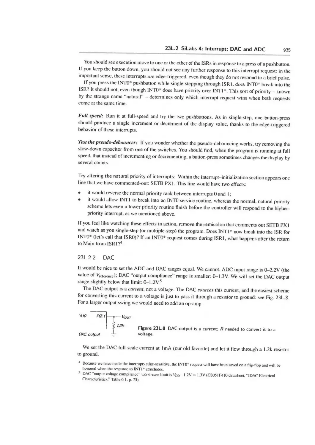
23L Lab Micro 4. Interrupts; ADC and DAC 926
23L.1 ADC—> DAC 926
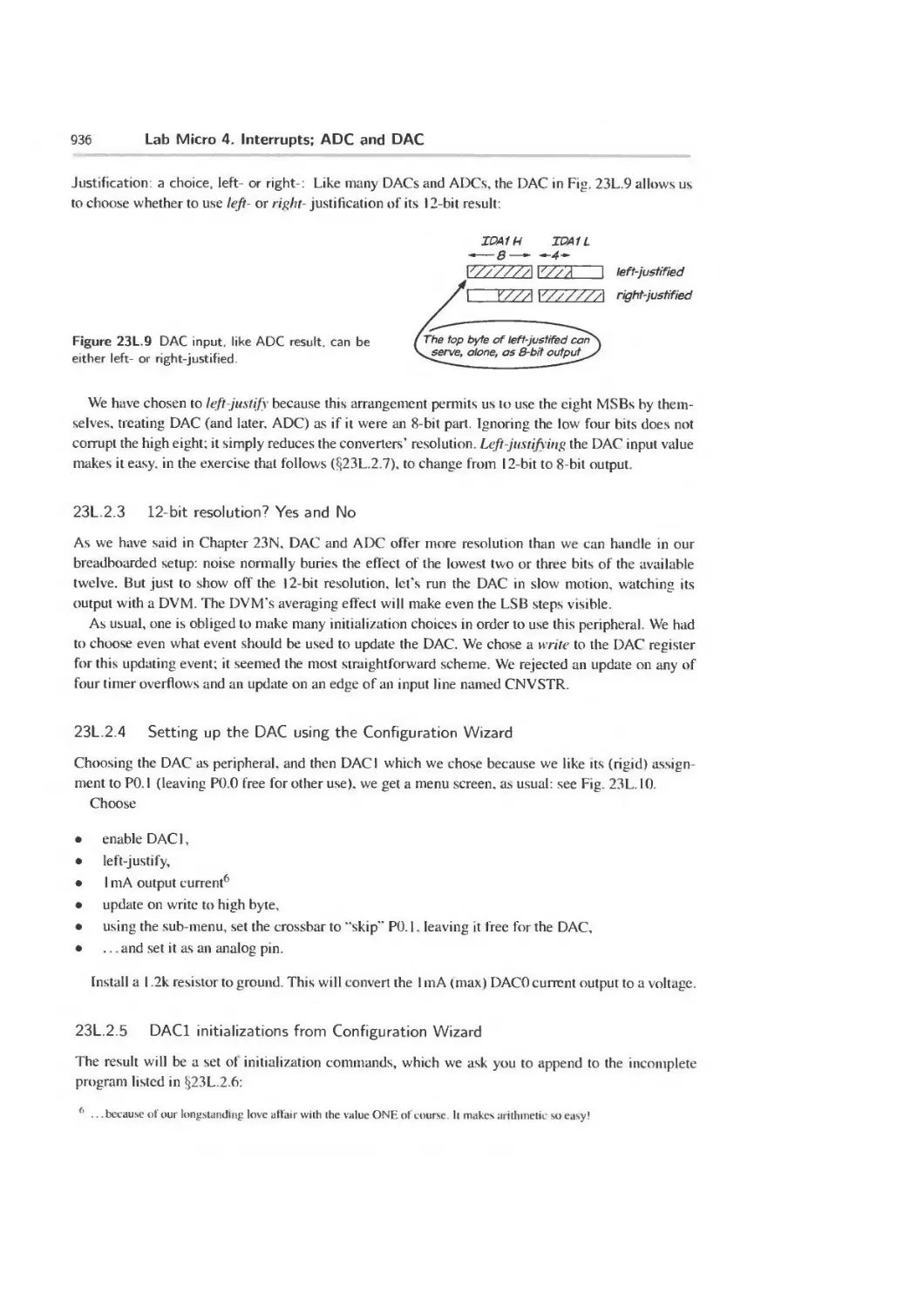
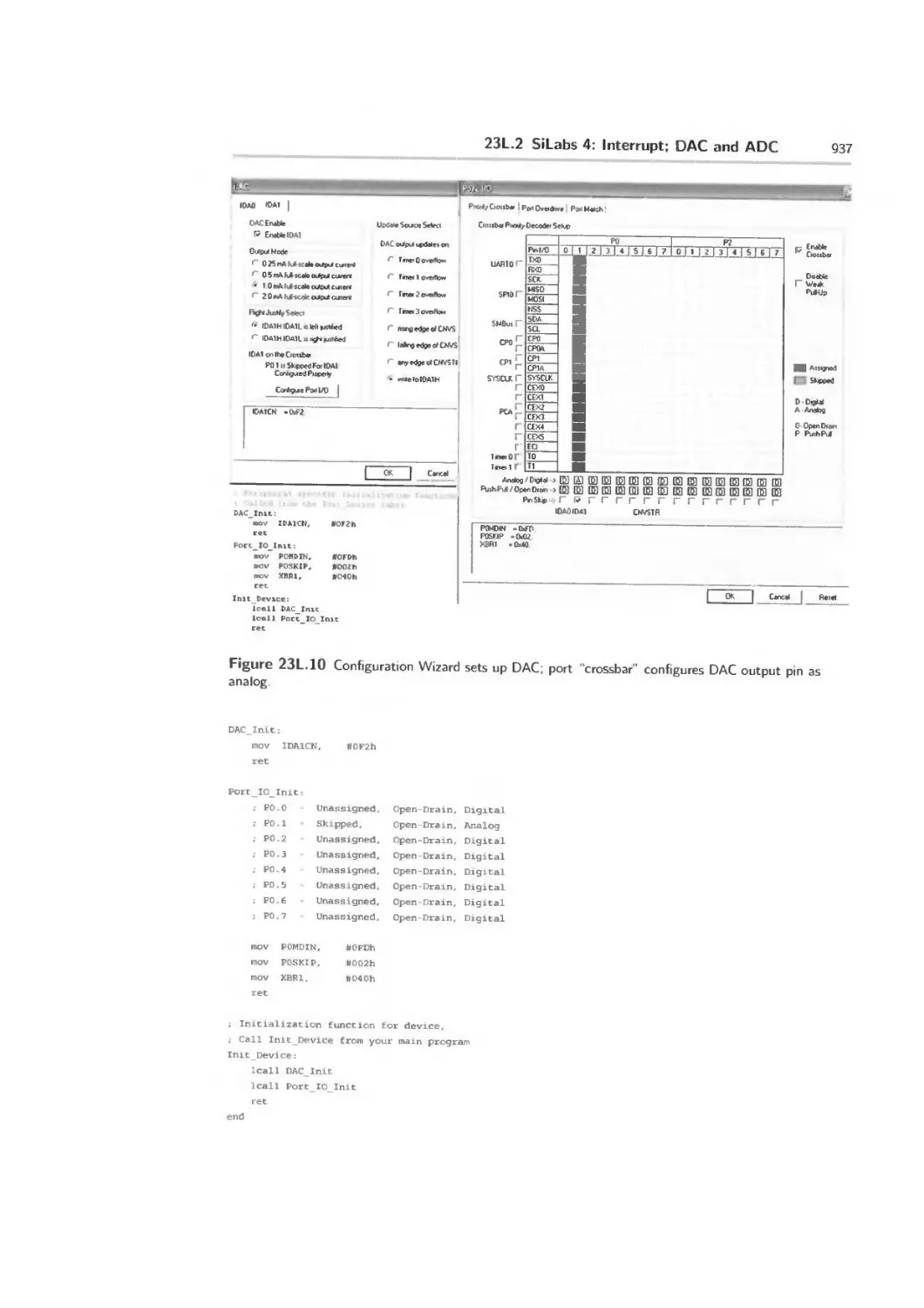
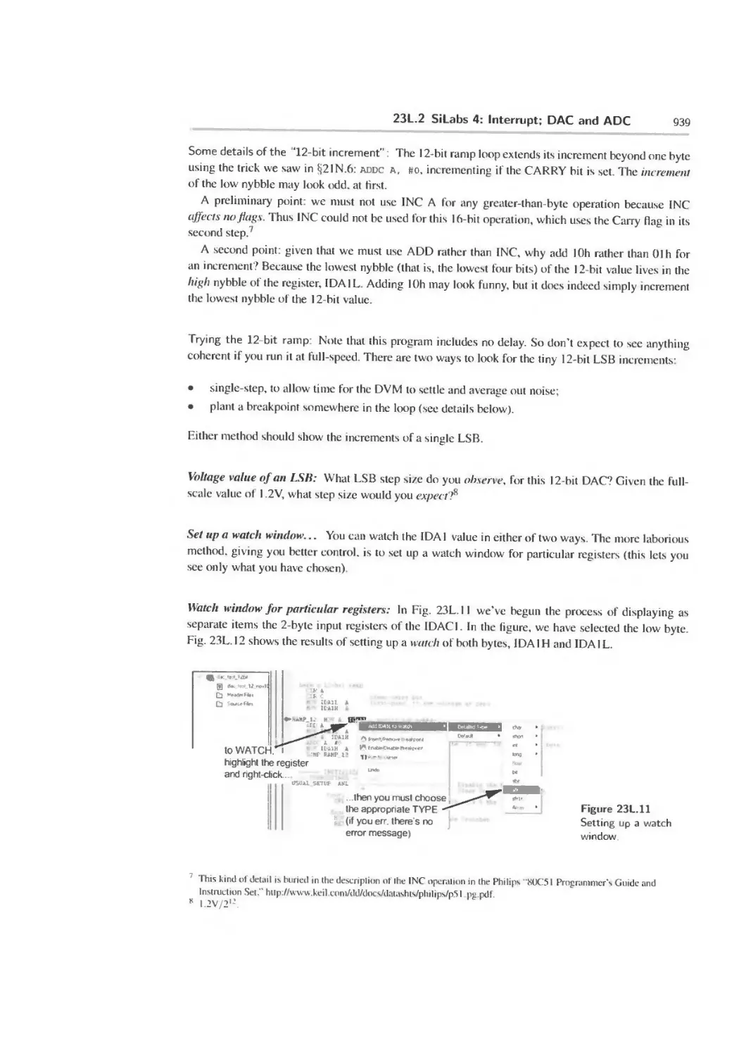
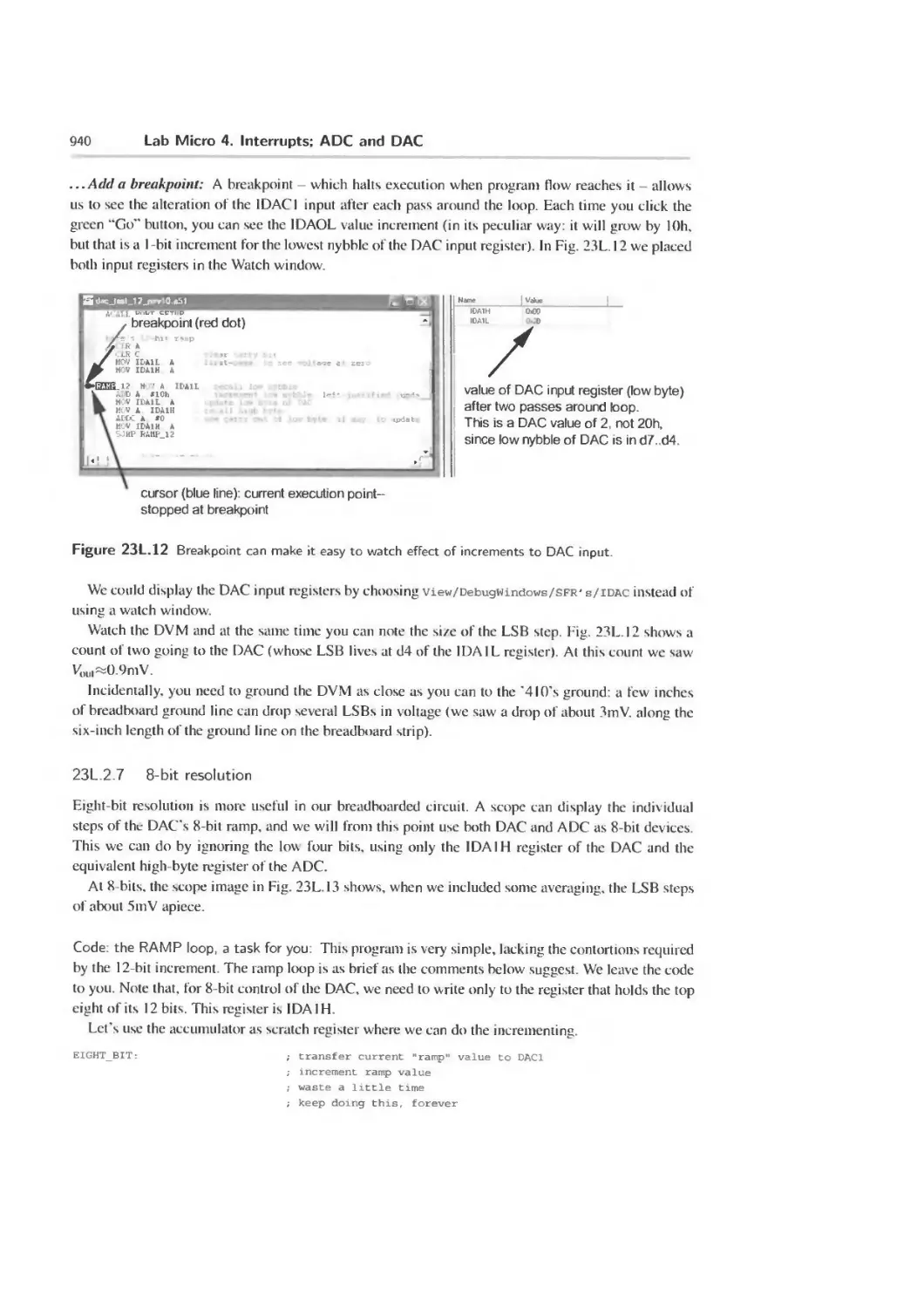
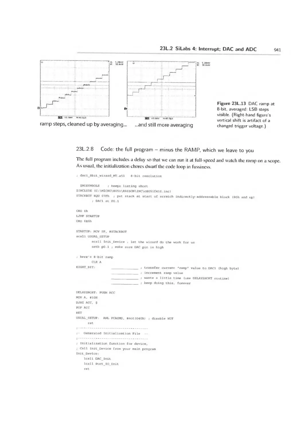
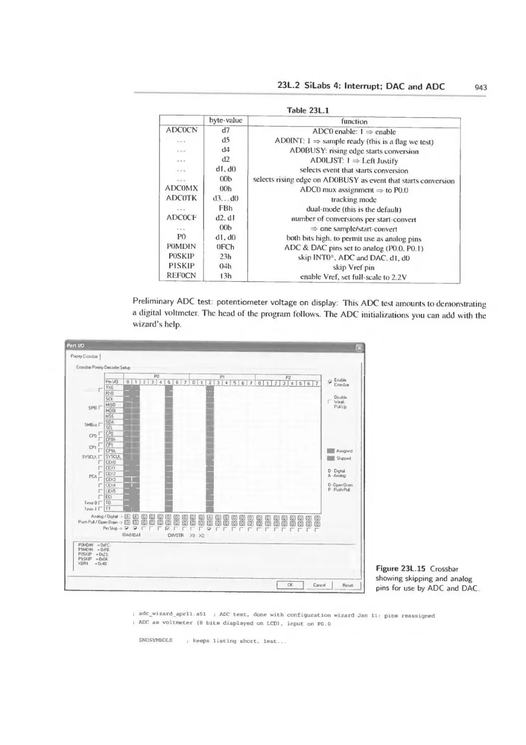
23L.2 SiLabs 4: Interrupt; DAC and ADC 931
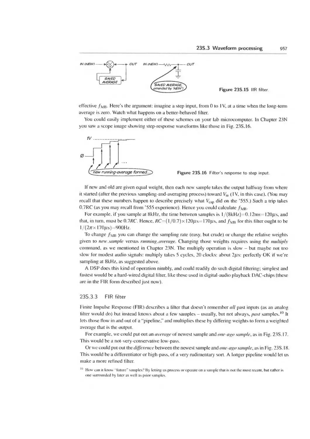
23S Supplementary Notes: Micro 4 946
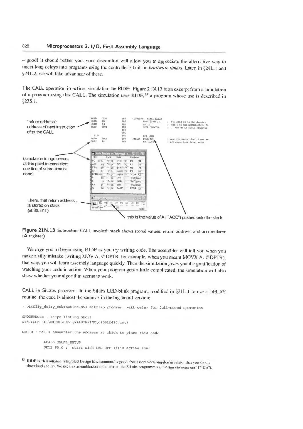
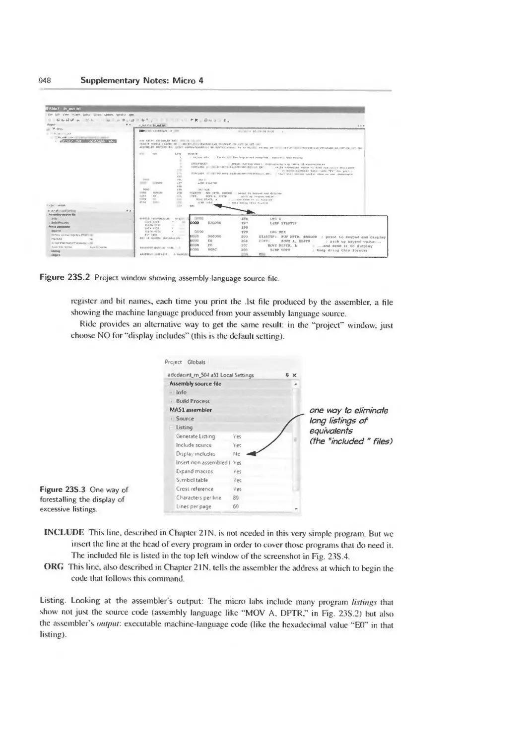
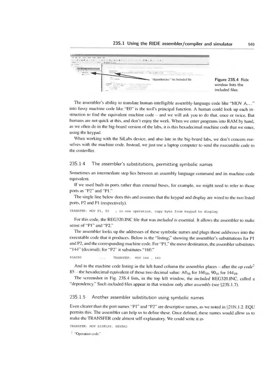
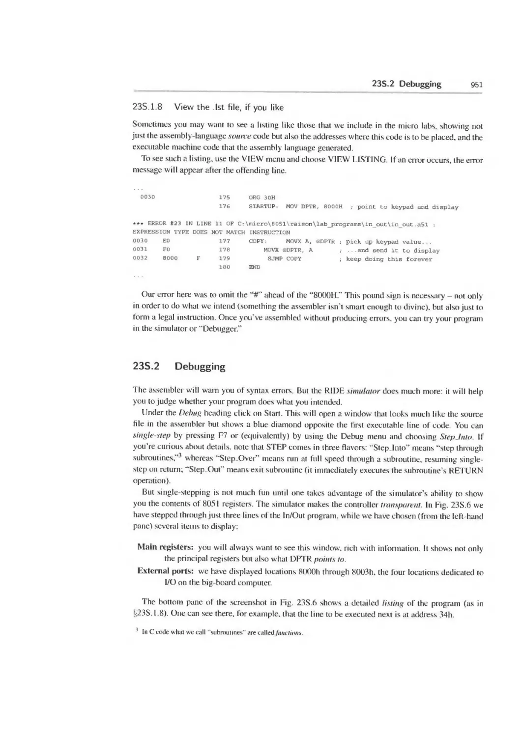
23S. 1 Using the RIDE assembler/compiler and simulator 946
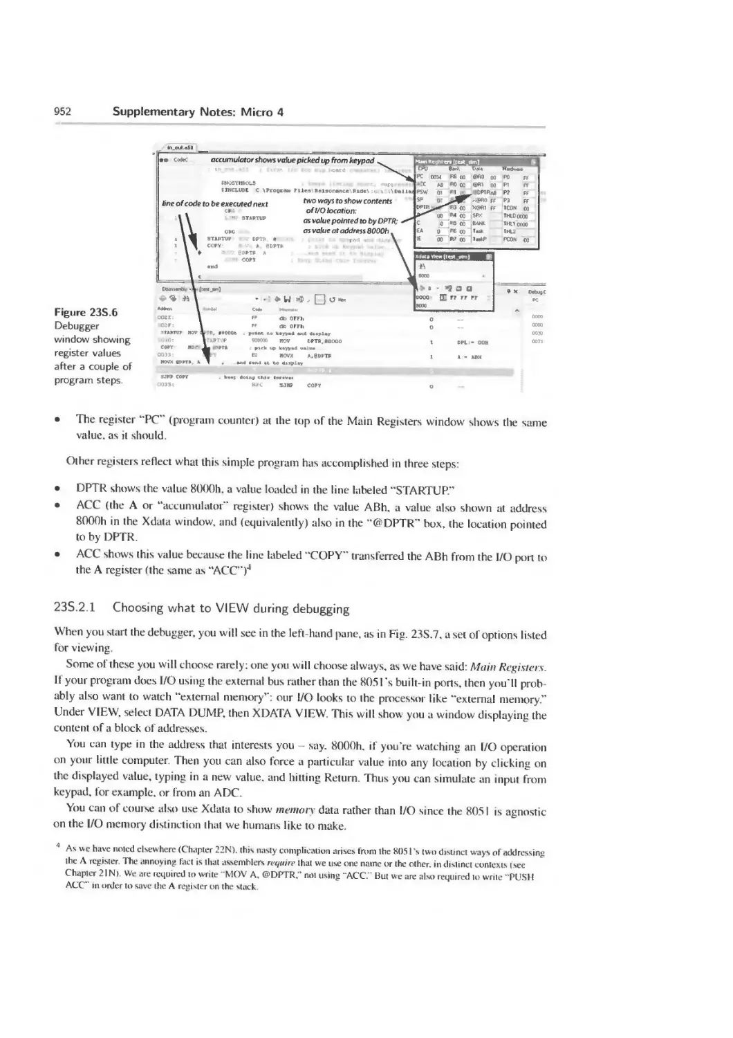
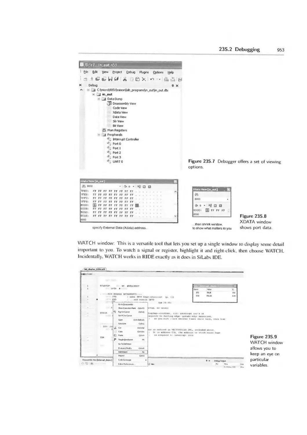
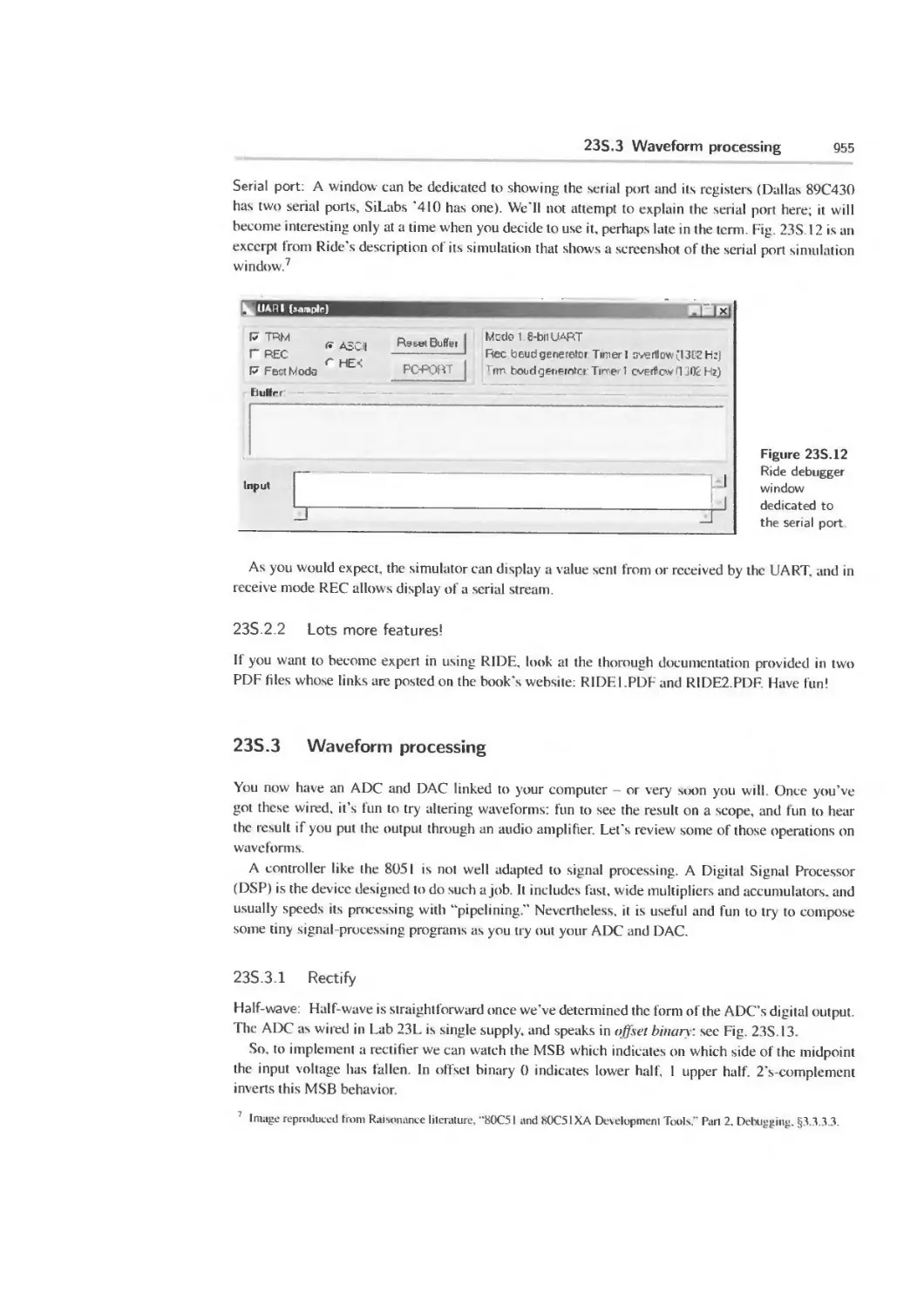
23S.2 Debugging 951
23S.3 Waveform processing 955
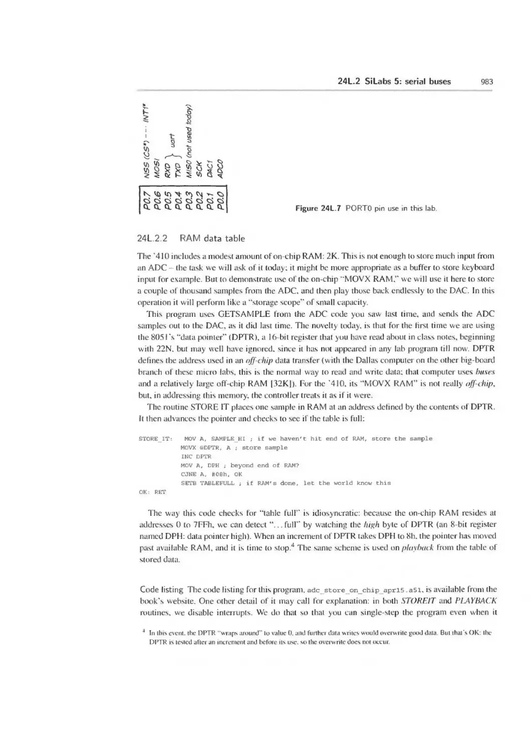
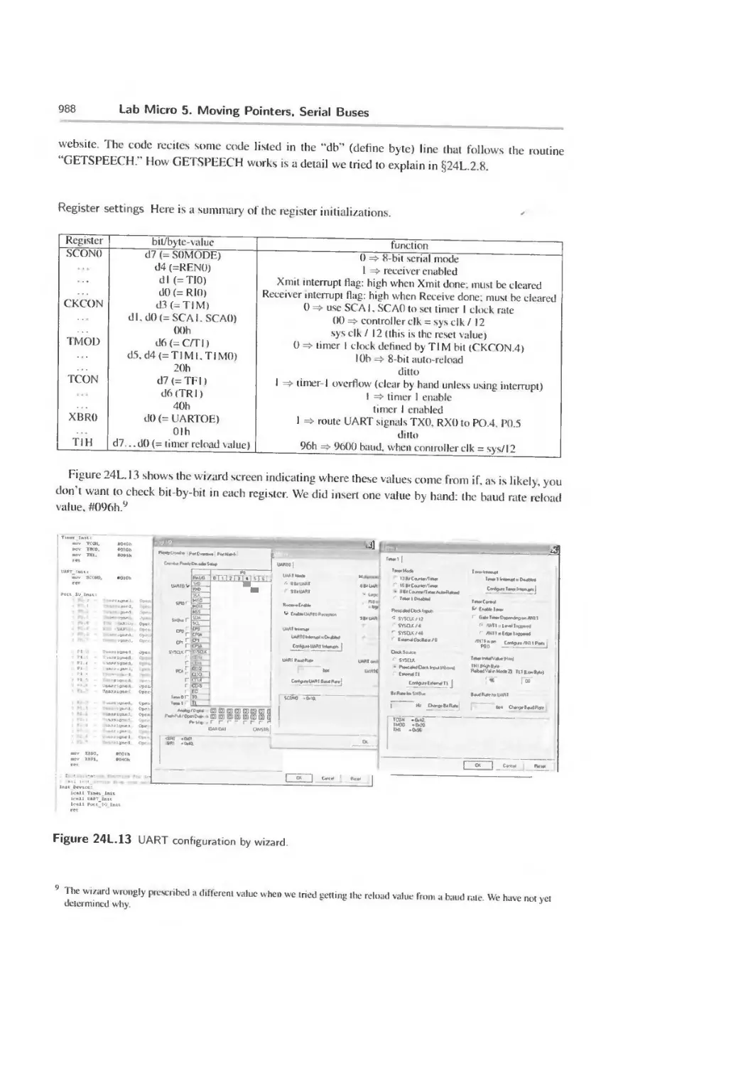
24N Micro 5. Moving Pointers, Serial Buses 959
24N, 1 Moving pointers 959
24N.2 DPTR can be useful for SiLabs "410, too: tables 964
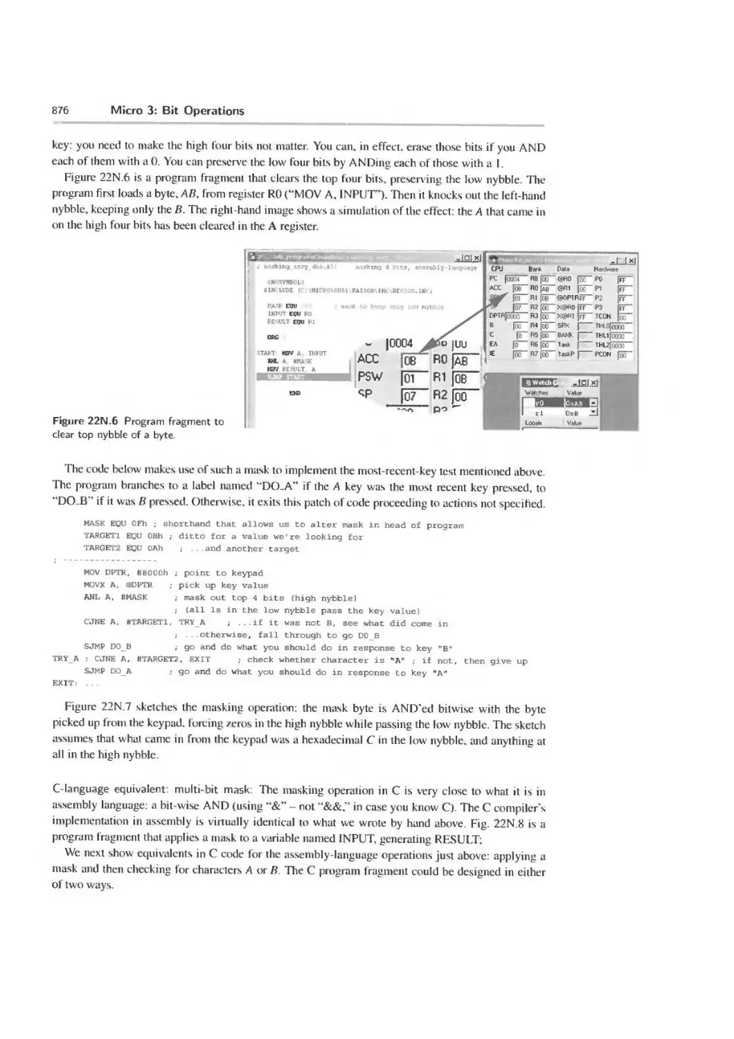
24N.3 End tests in table eperations 964
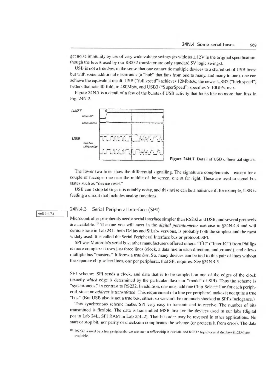
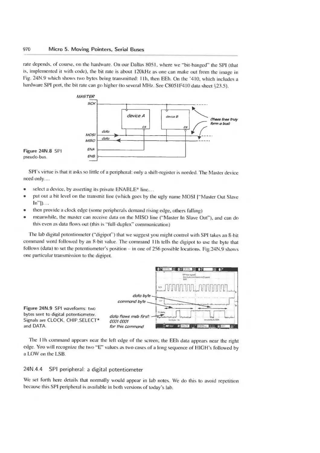
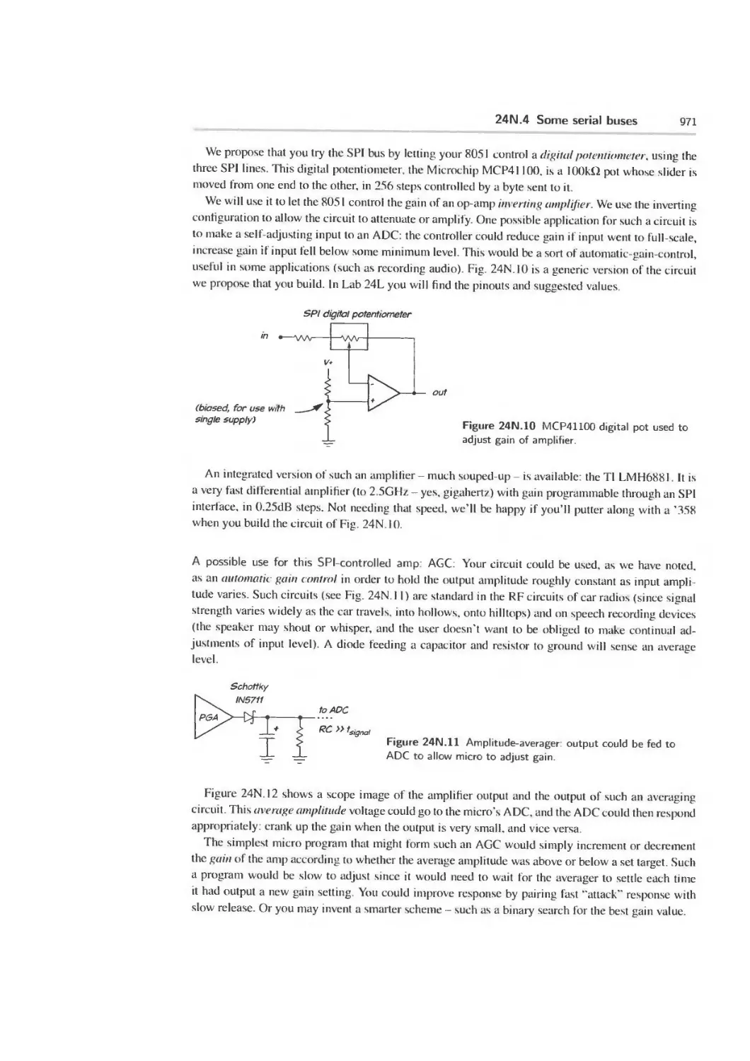
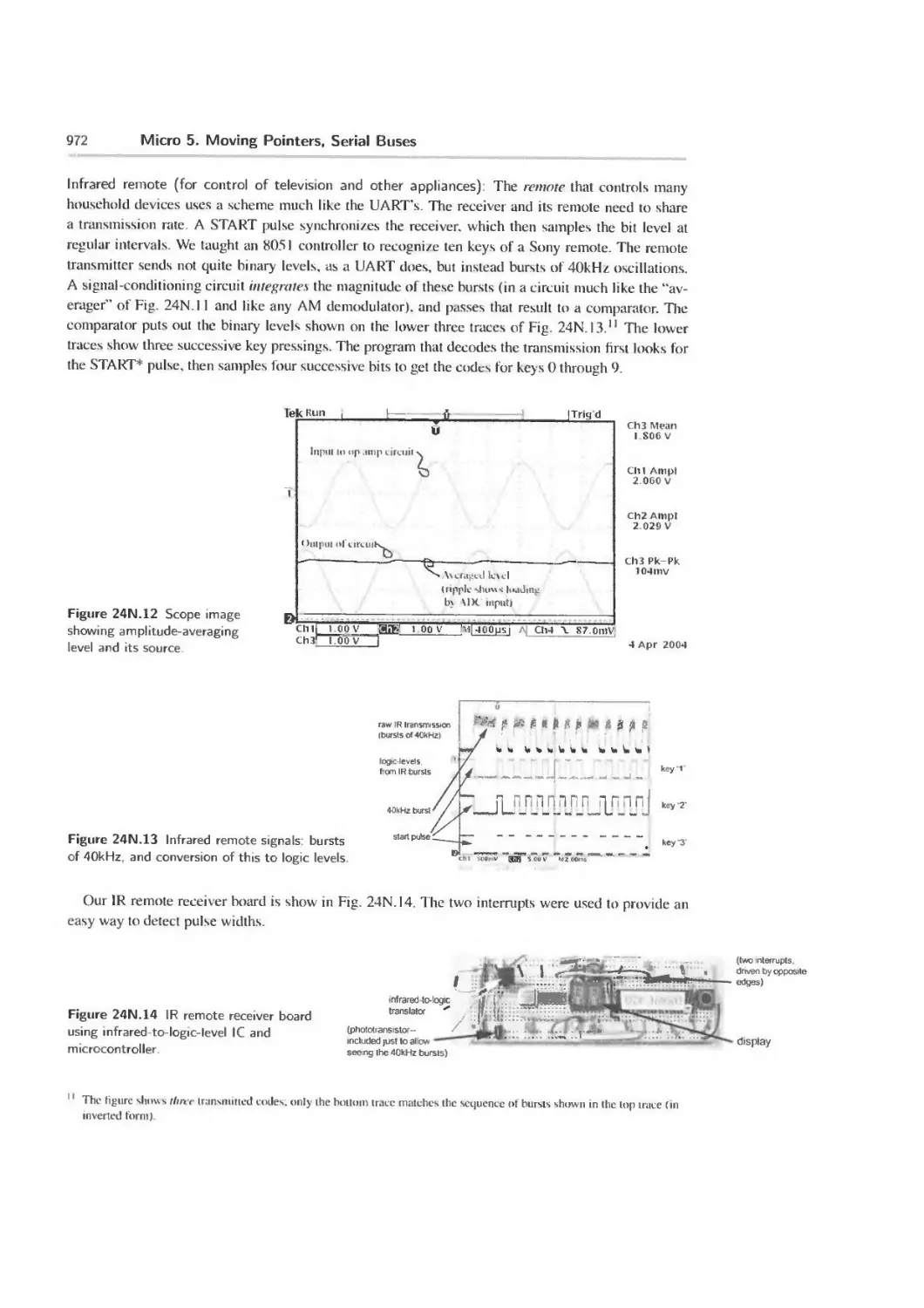
24N.4 Some serial buses 966
24N.5 Readings 974
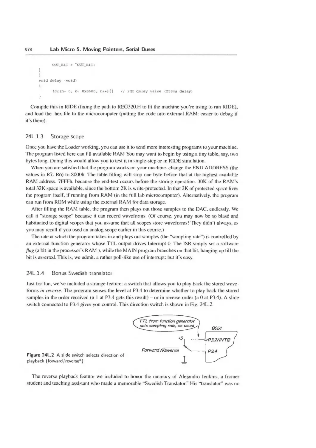
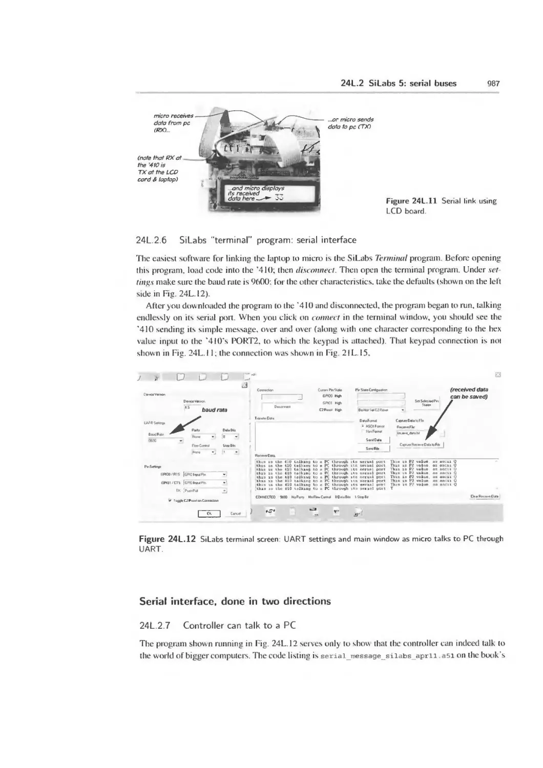
24L Lab Micro 5. Moving Pointers, Serial Buses 975
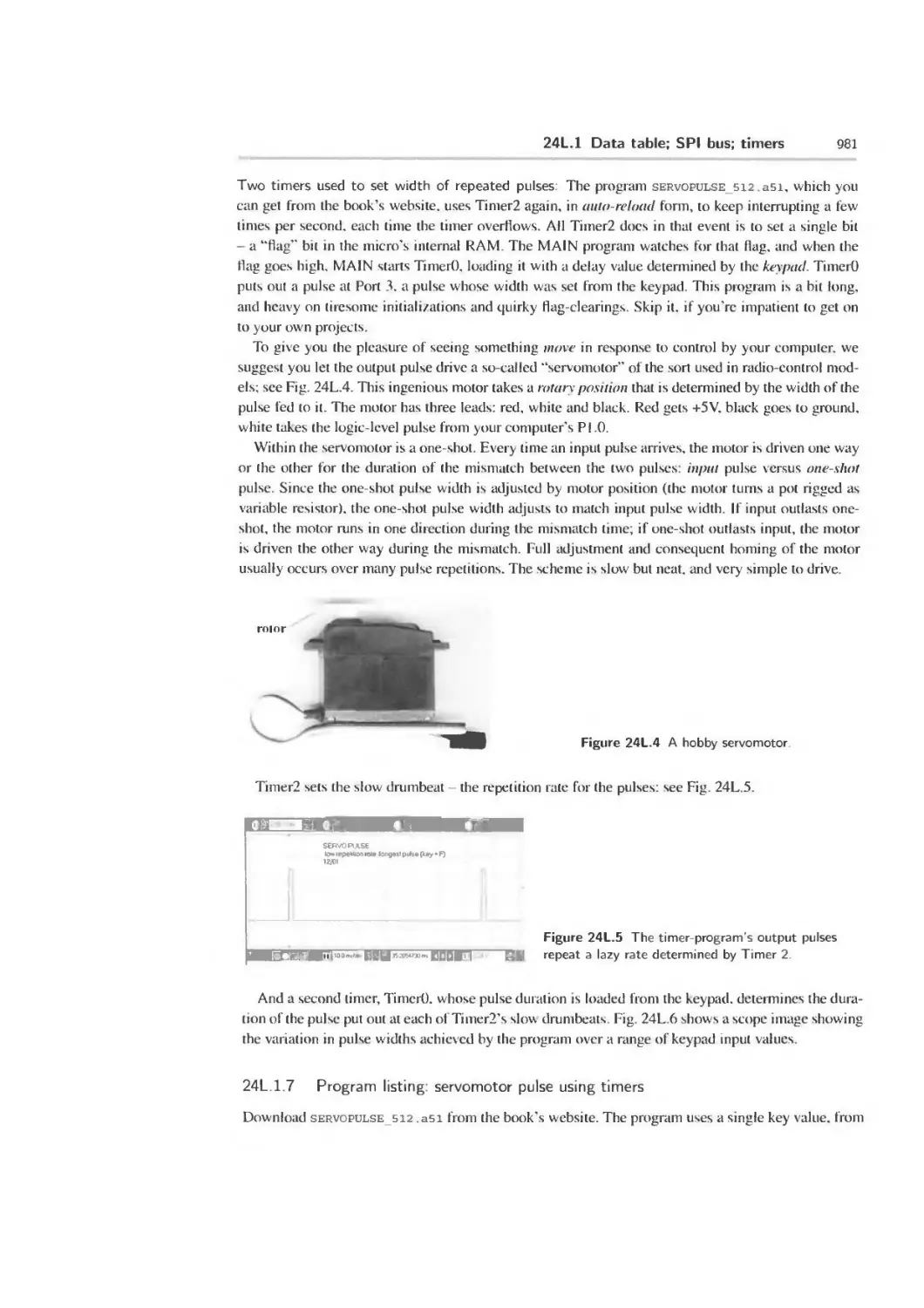
24L. 1 Data table; SPI bus; timers 976
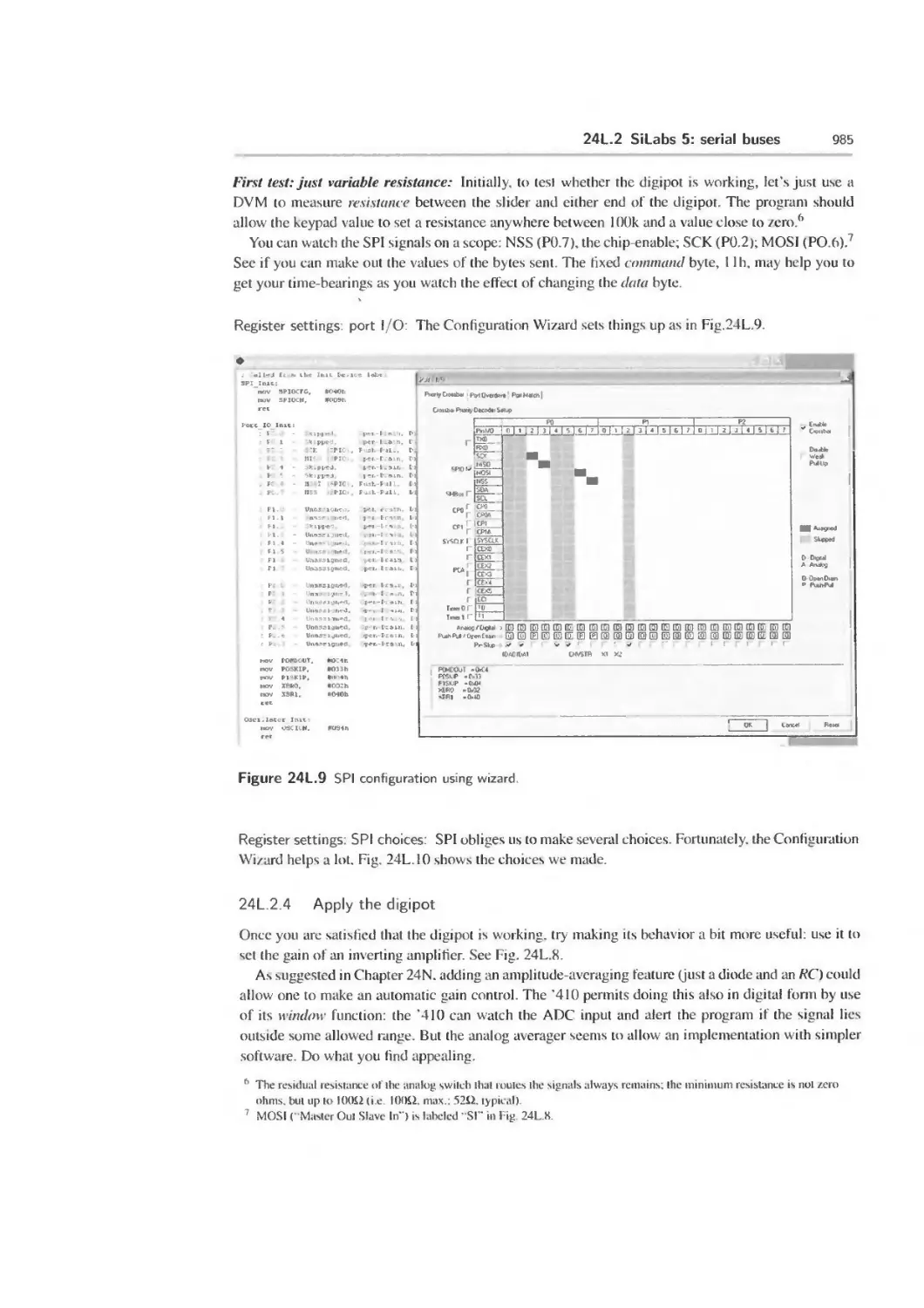
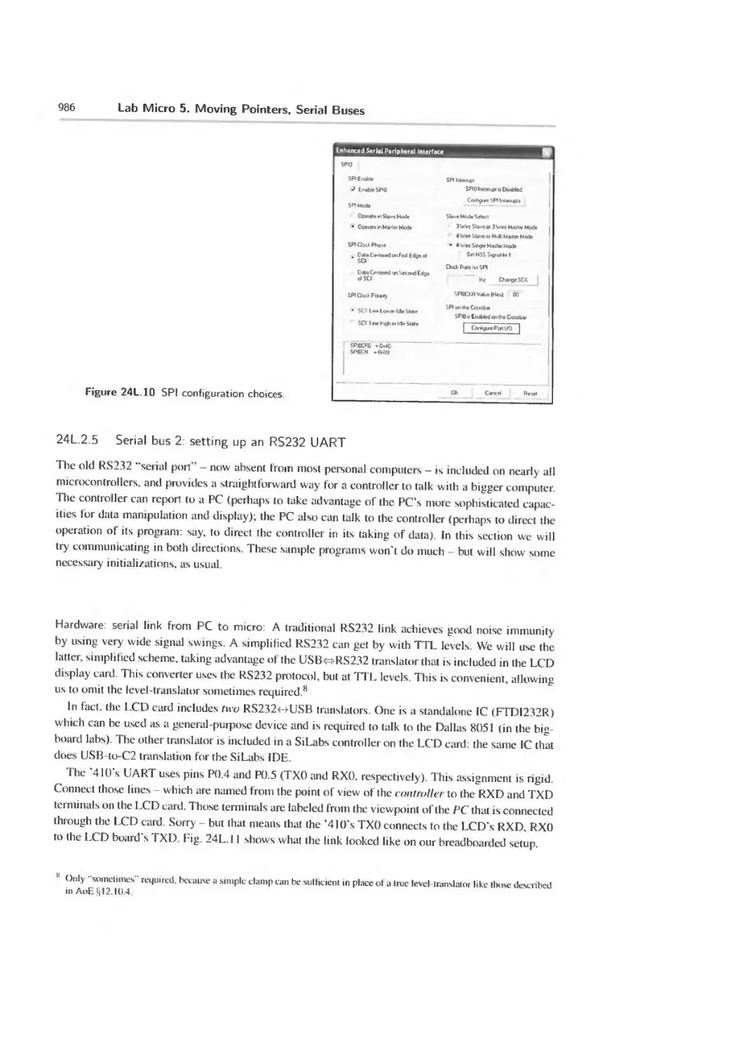
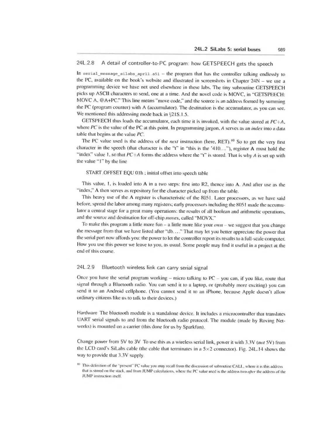
24L.2 SiLabs 5: serial buses 982
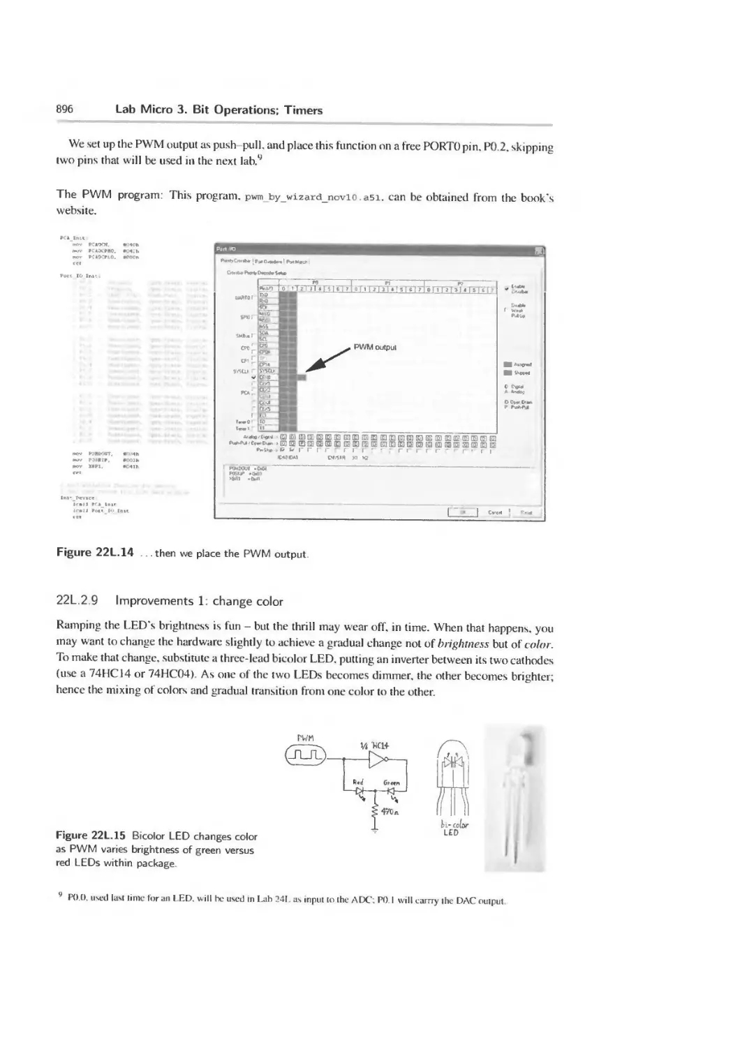
24S Supplementary Note: Dallas Program Loader 993
24S . 1 Dallas downloader 993
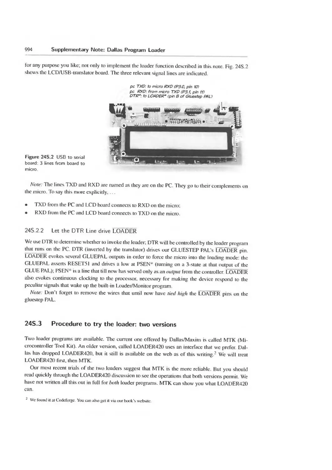
24S.2 Hardware required 993
24S.3 Procedure to try the loader: two versions 994
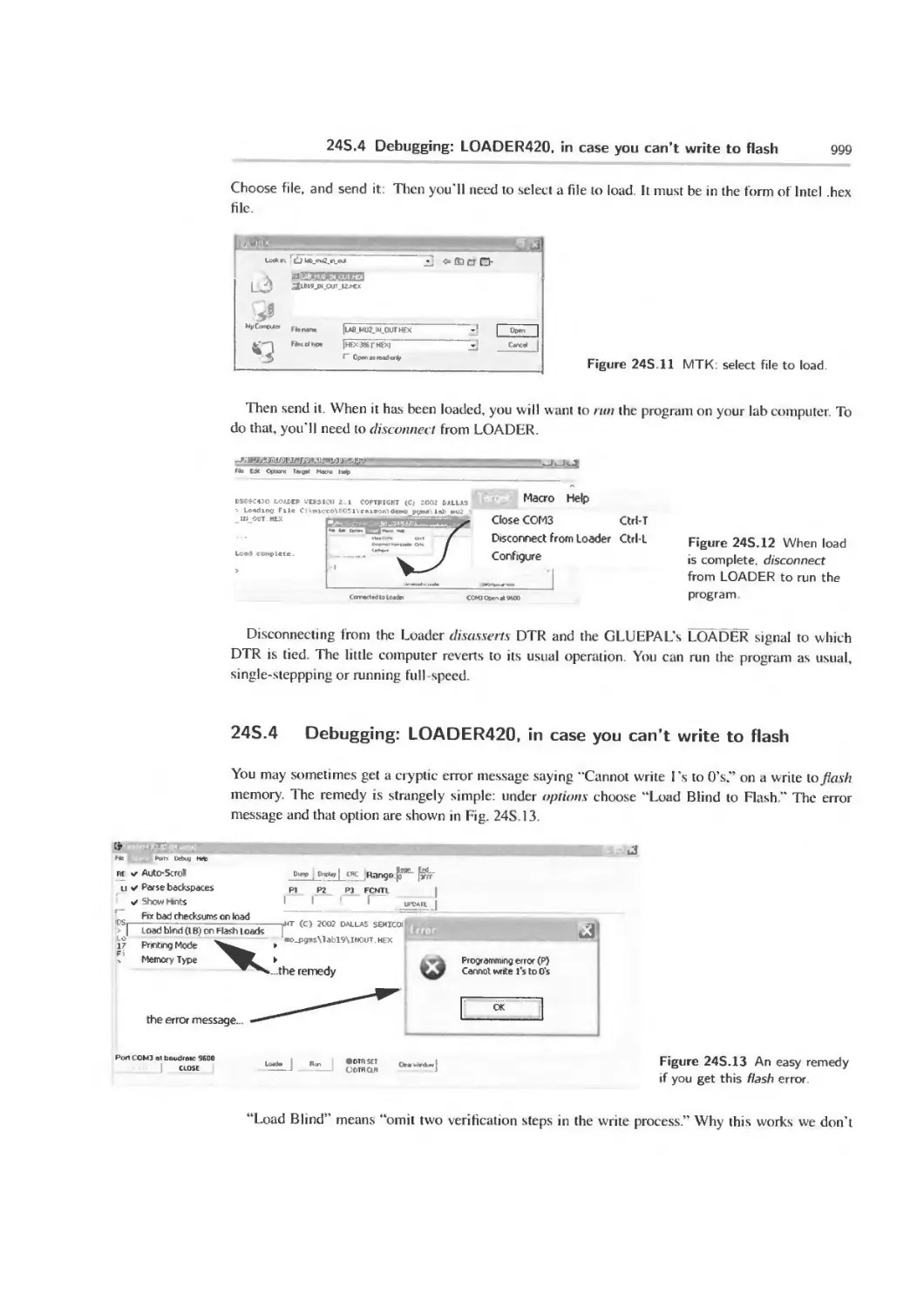
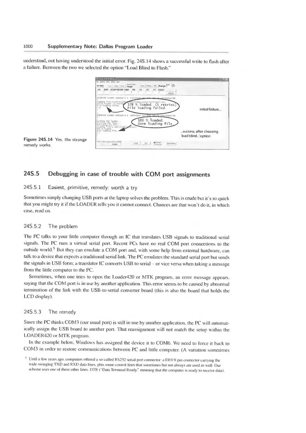
24S.4 Debugging: LOADER420 in case you can’t write to flash 999
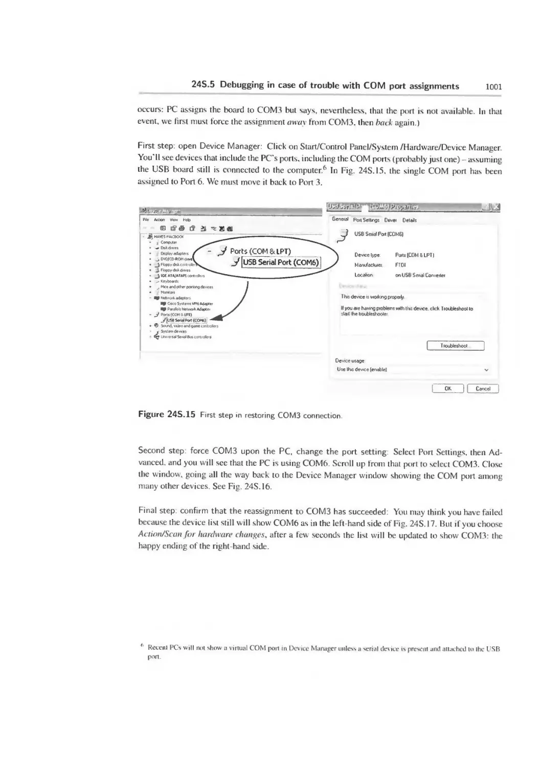
24S.5 Debugging in case of trouble with COM port assignments 1000
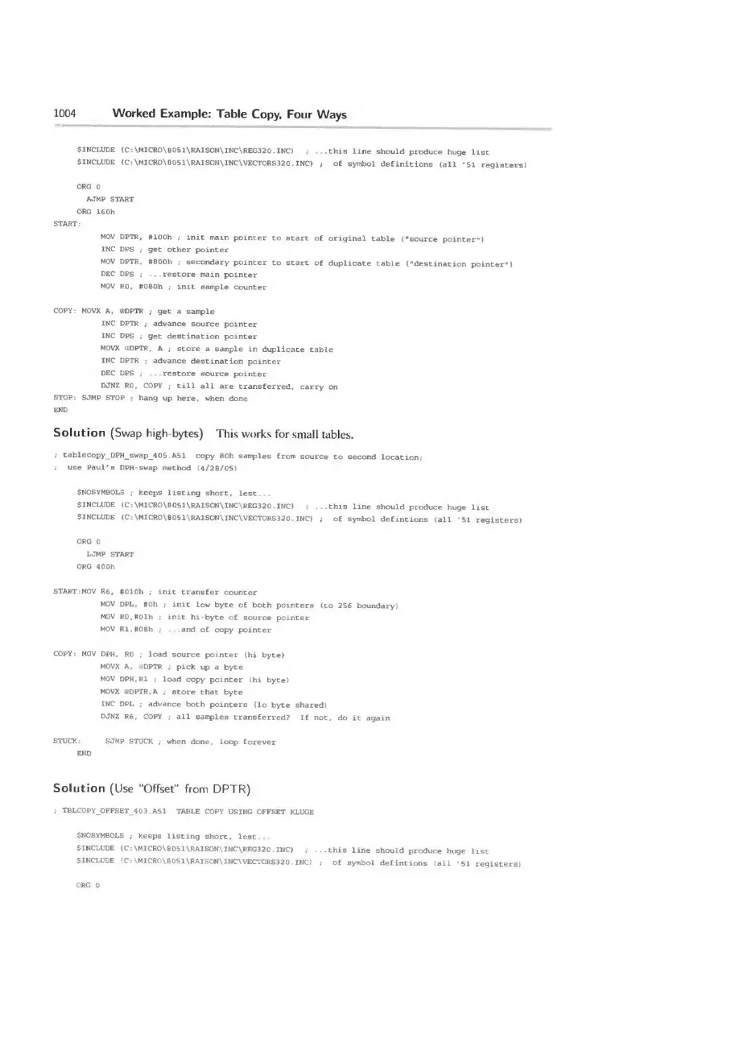
24W Worked Example: Table Copy, Four Ways 1003
24W. 1 Several ways to copy a table 1003
25N Micro 6: Data Tables 1006
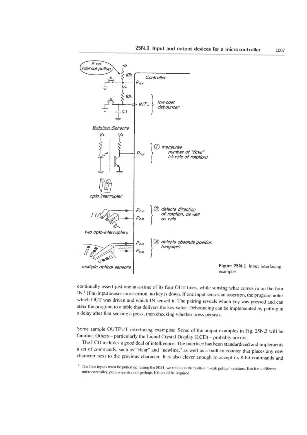
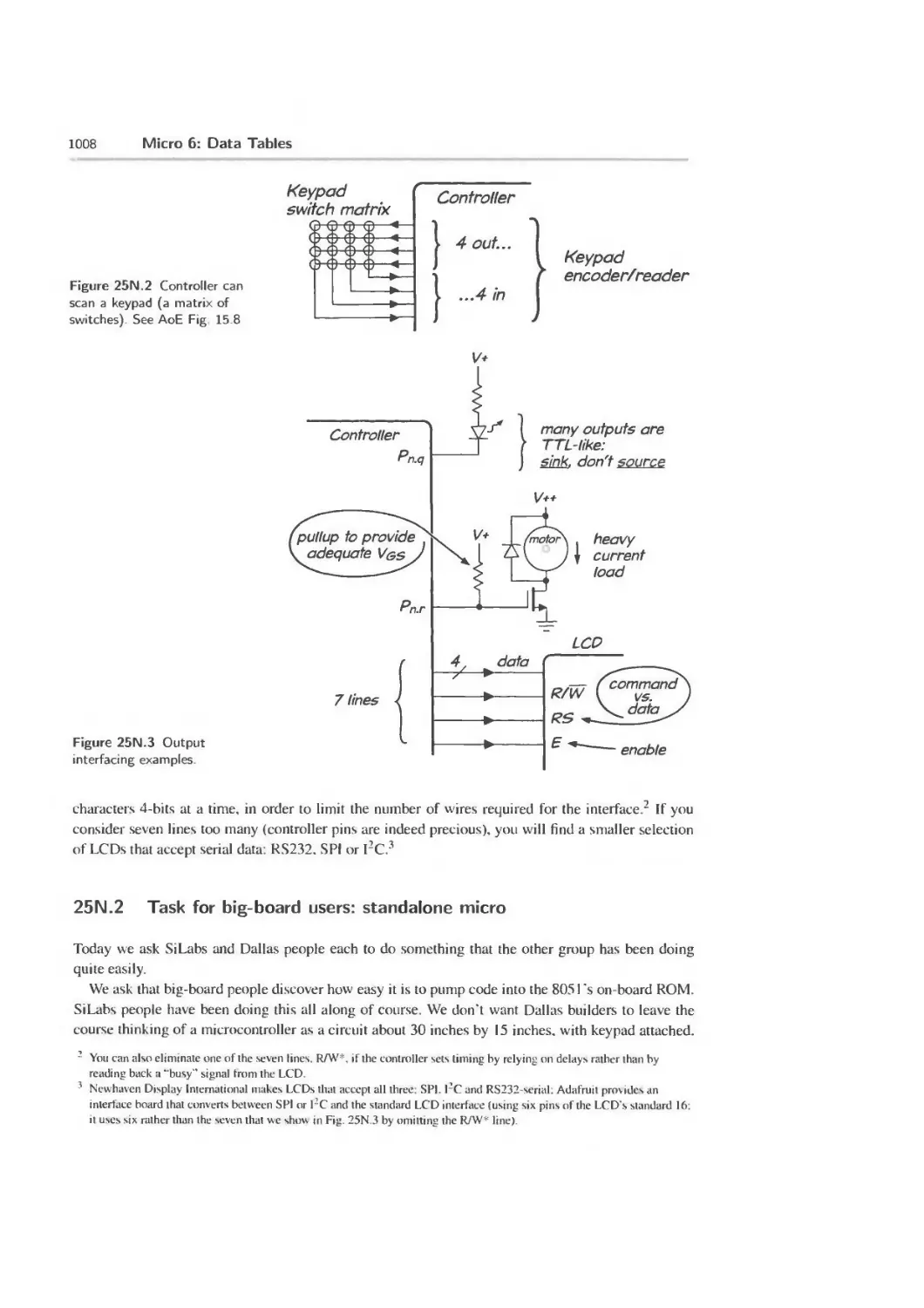
25N.1 Input and output devices for a microcontroller 1006
25N.2 Task for big-board users: standalone micro 1008
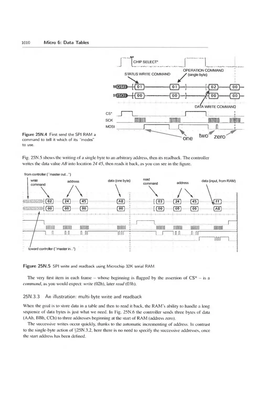
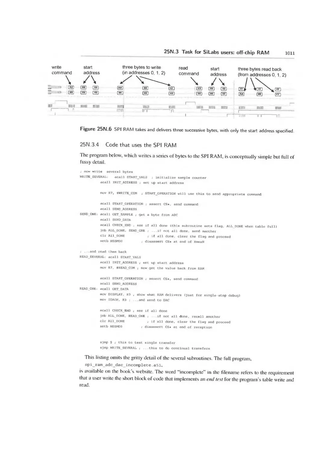
25N.3 Task for SiLabs users: off-chip RAM 1009
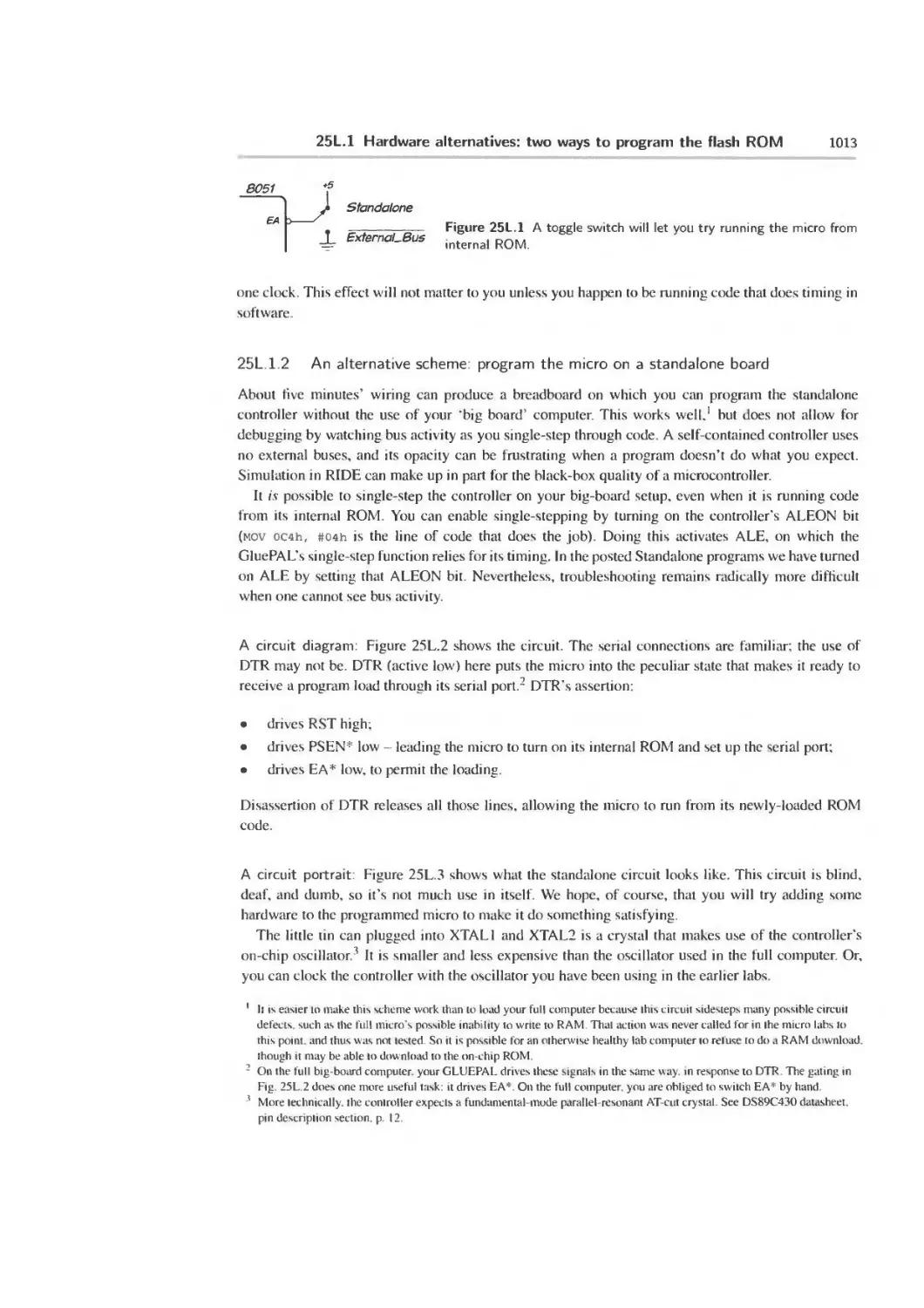
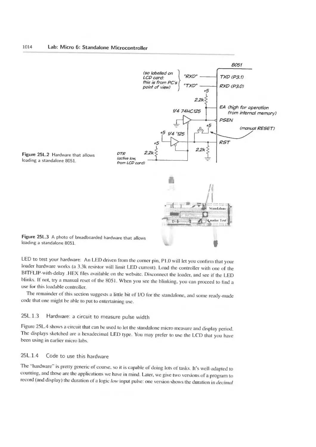
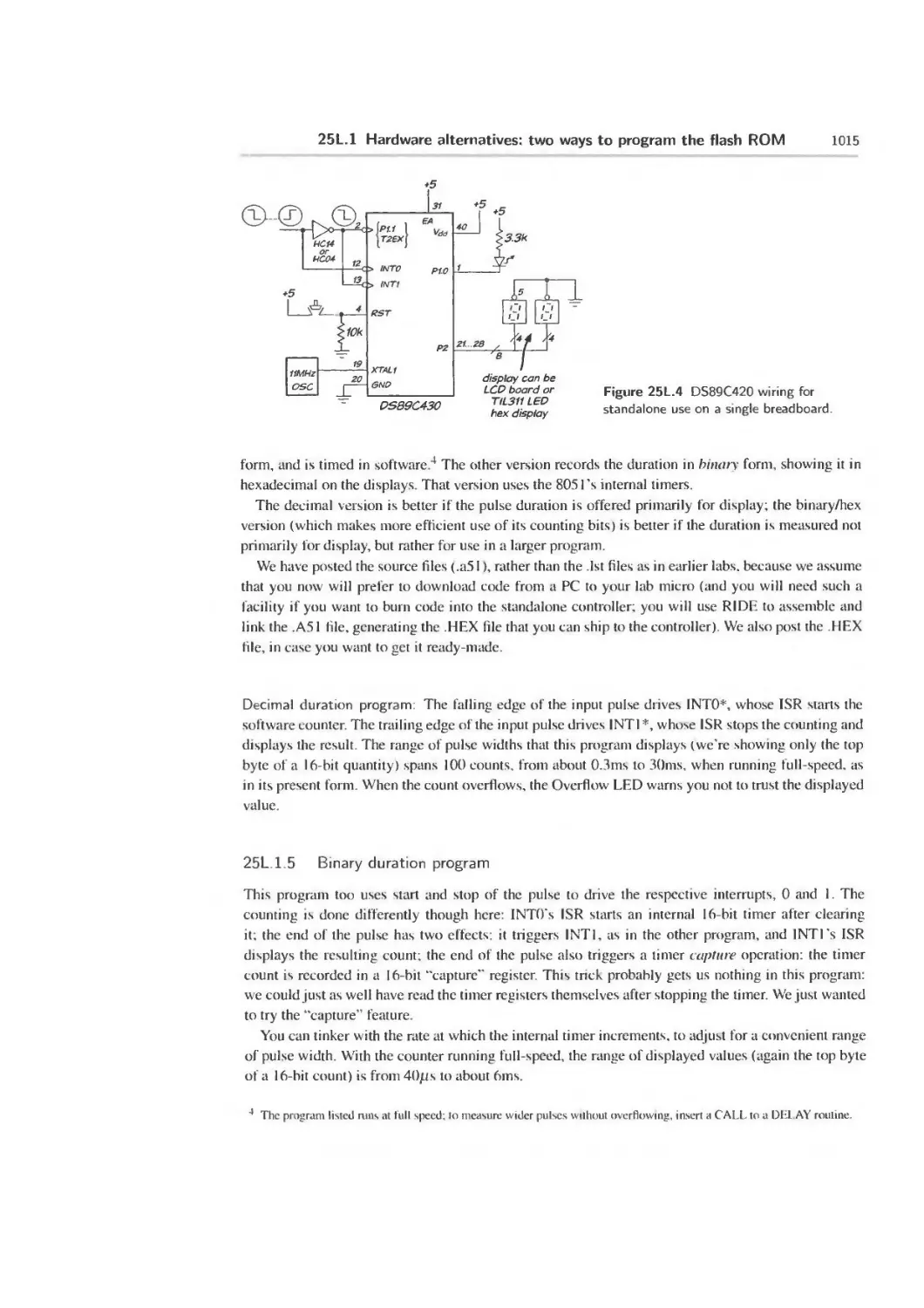
25L Lab: Micro 6: Standalone Microcontroller 1012
25L. 1 Hardware alternatives: two ways to program the flash ROM 1012
25L.2 SiLabs 6: SPI RAM 1018
25L.3 Appendix: Program Listings 1021
26N Project Possibilities: Toys in the Attic 1022
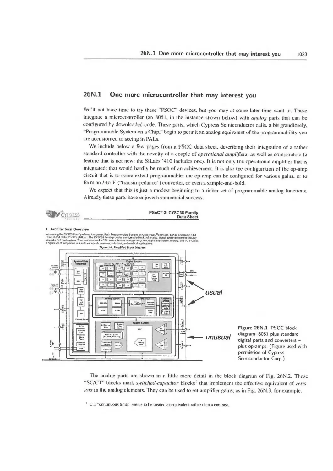
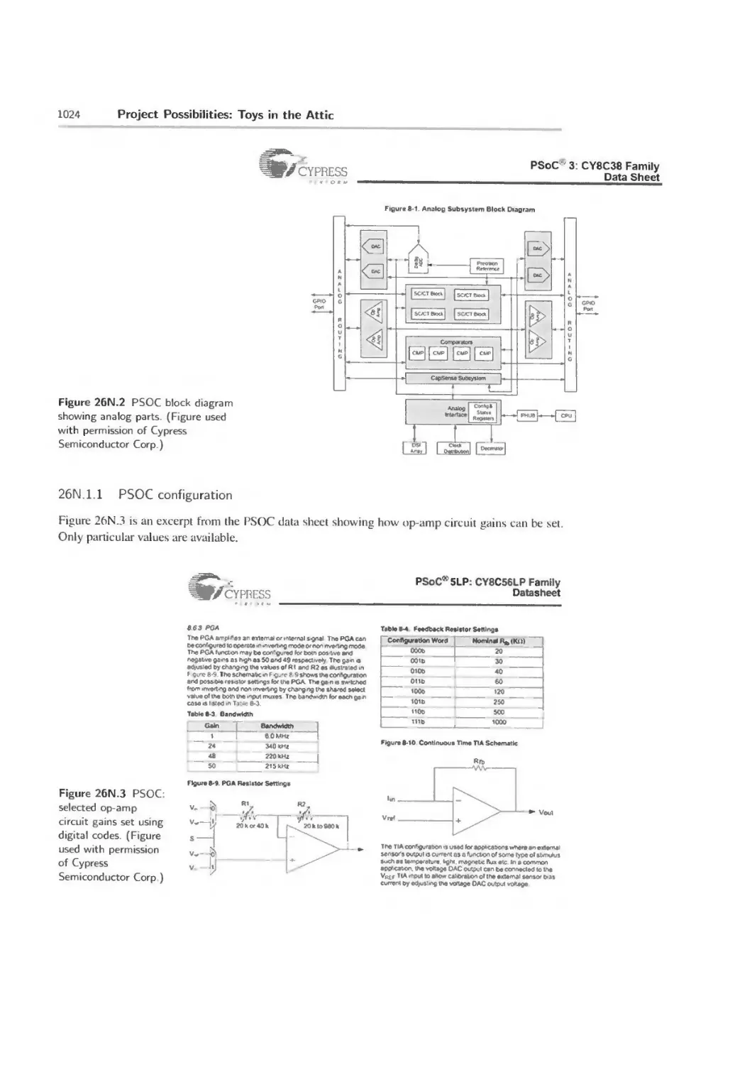
26N.1 One more microcontroller that may interest you 1023
26N.2 Projects: an invitation and a caution 1025
26N.3 Some pretty projects 1025
xviii Contents
26N.4 Some other memorable projects 1030
26N.5 Games 1041
26N.6 Sensors, actuators, gadgets 1043
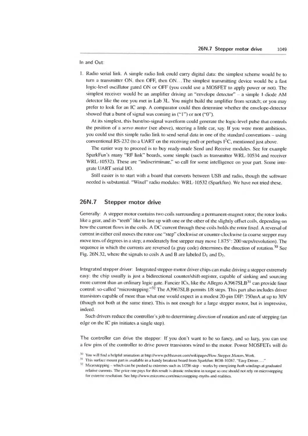
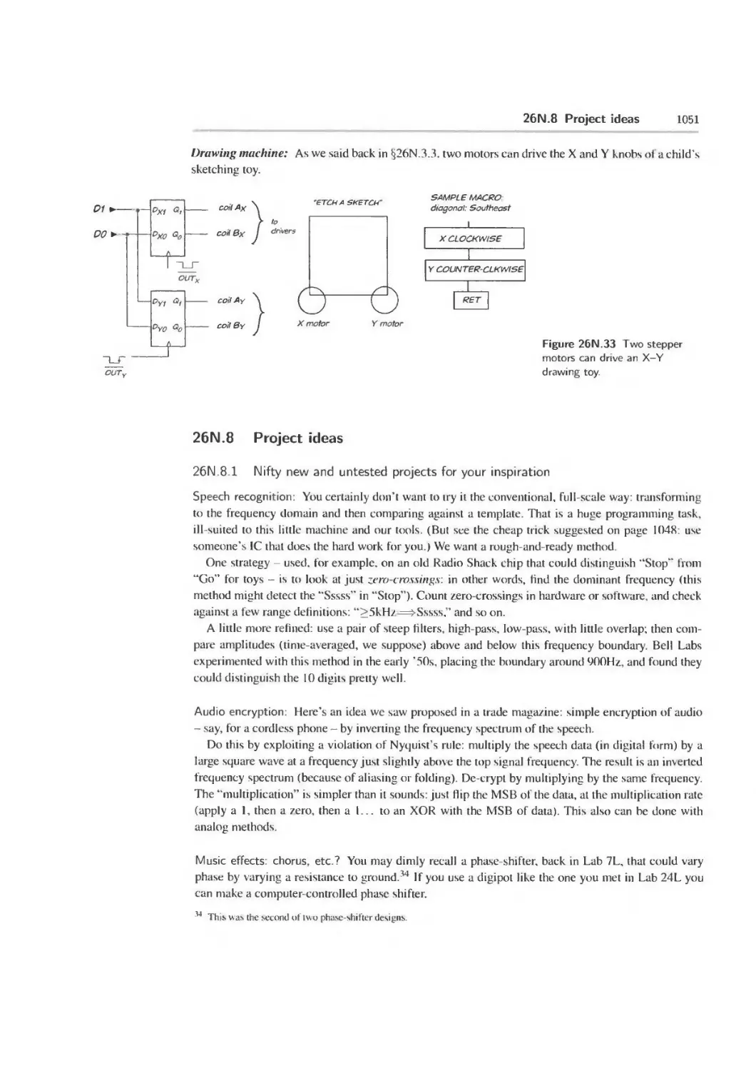
26N.7 Stepper motor drive 1049
26N.8 Project ideas 1051
26N.9 Two programs that could be useful: LCD.Keypad 1052
26N. 10 And many examples aie shown in AoE 1052
26N. 11 Now go forth 1052
A A Logic Compiler or HDL: Verilog 1053
A. 1 The form of a Verilog file: design file 1053
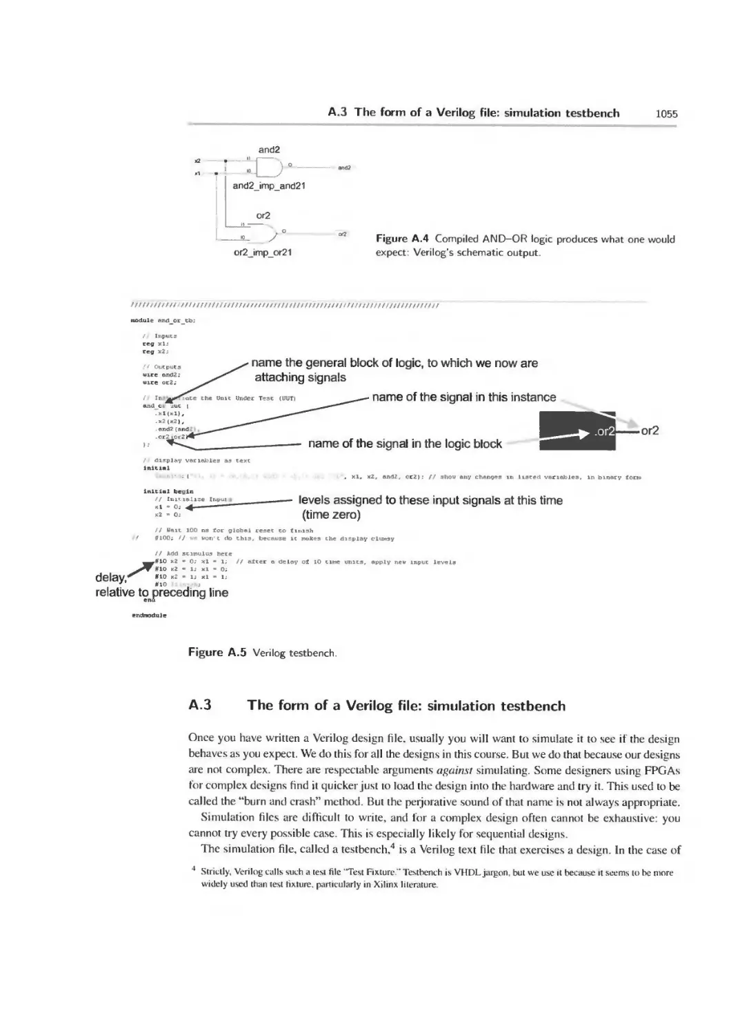
A.2 Schematics can help one to debug 1054
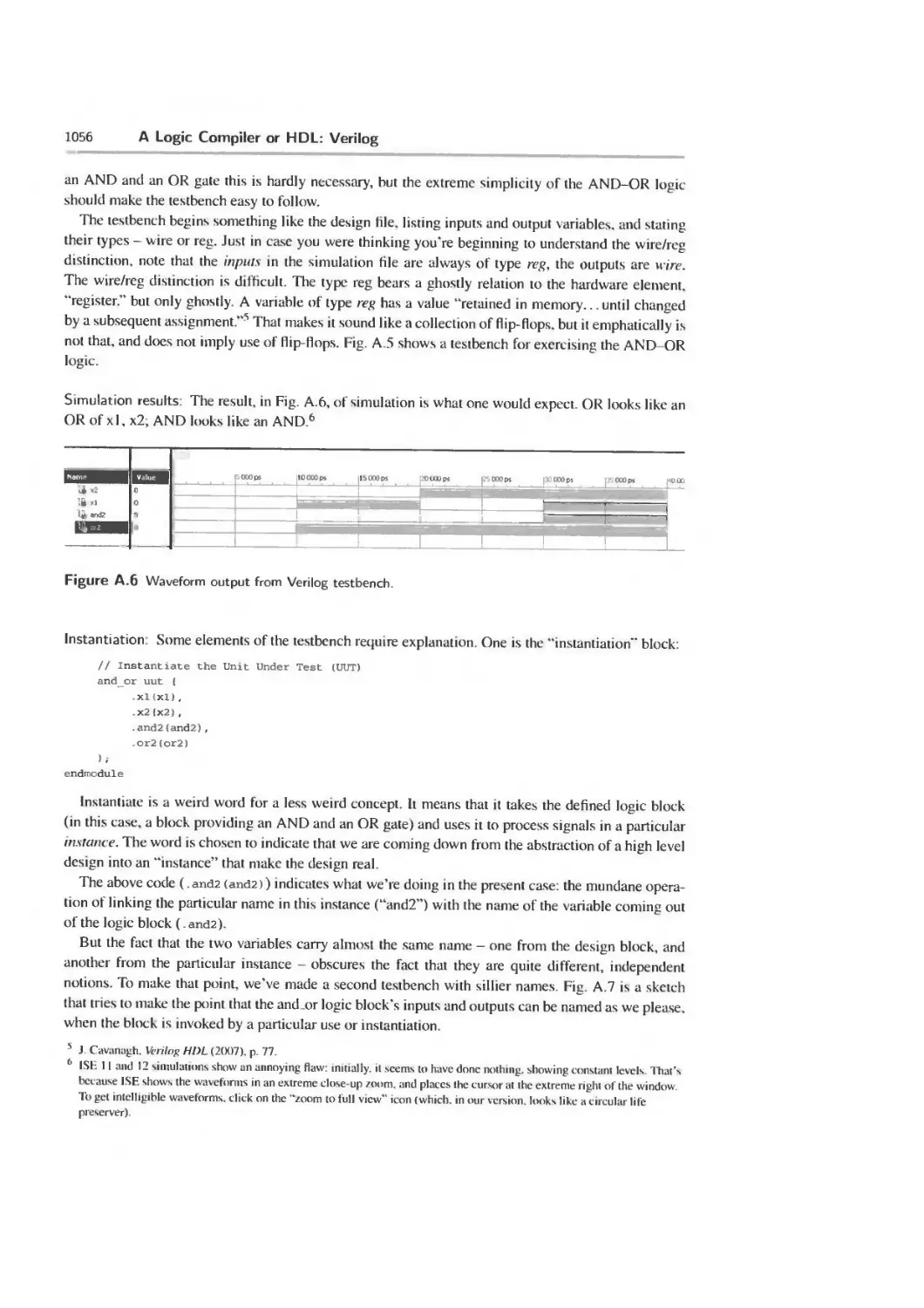
A.3 The form of a Verilog file: simulation testbench 1055
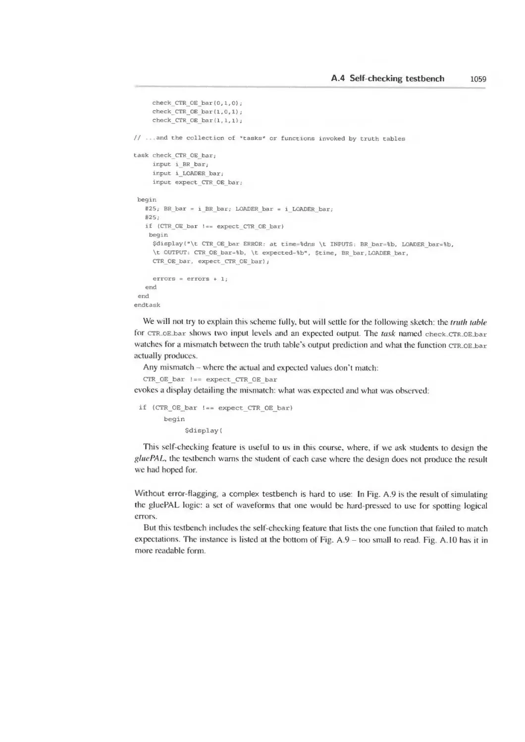
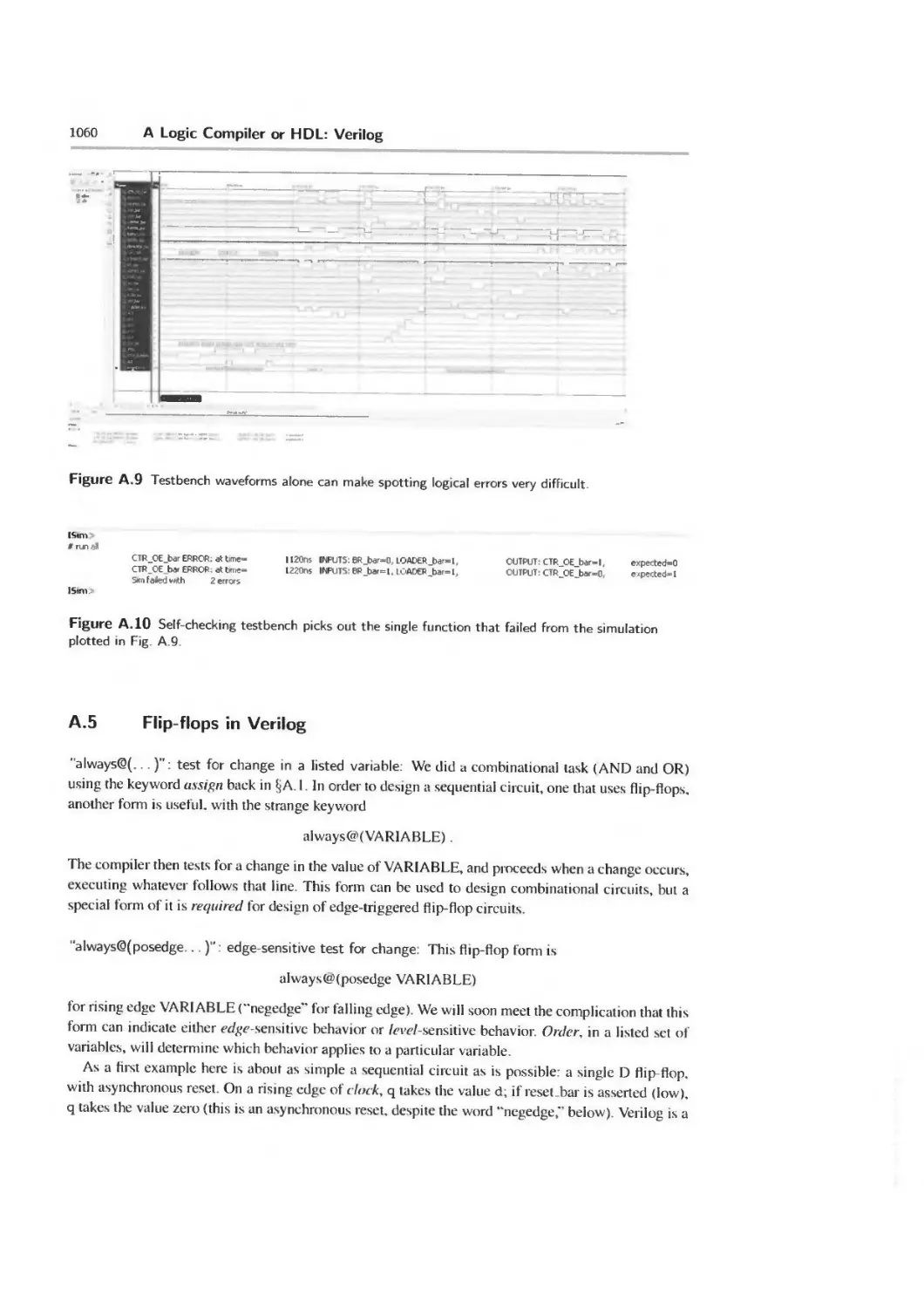
A.4 Sclf-checkmg testbench 1058
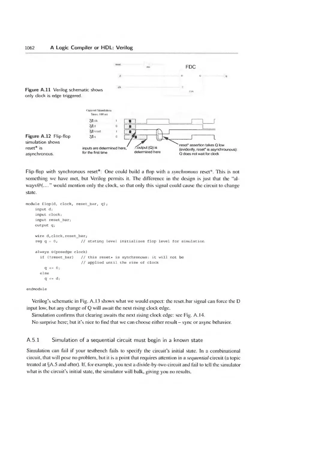
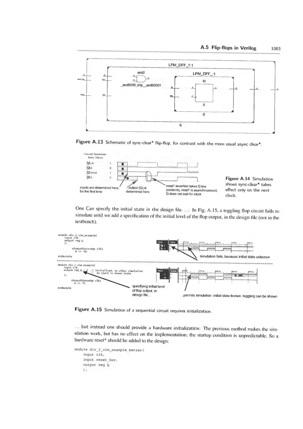
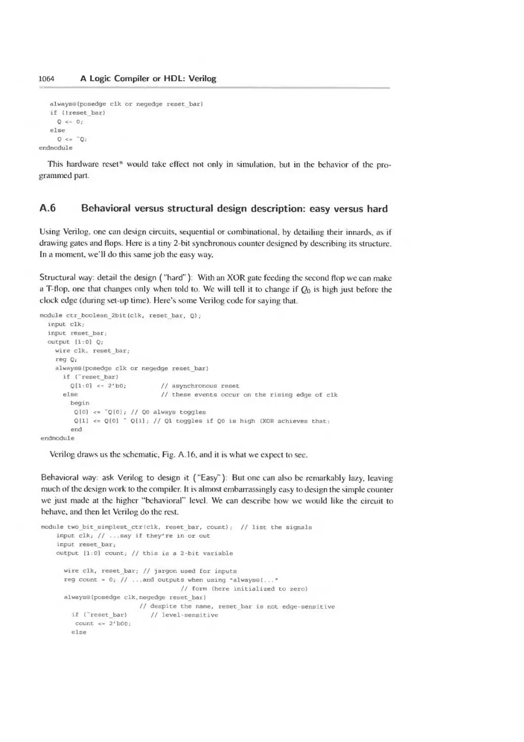
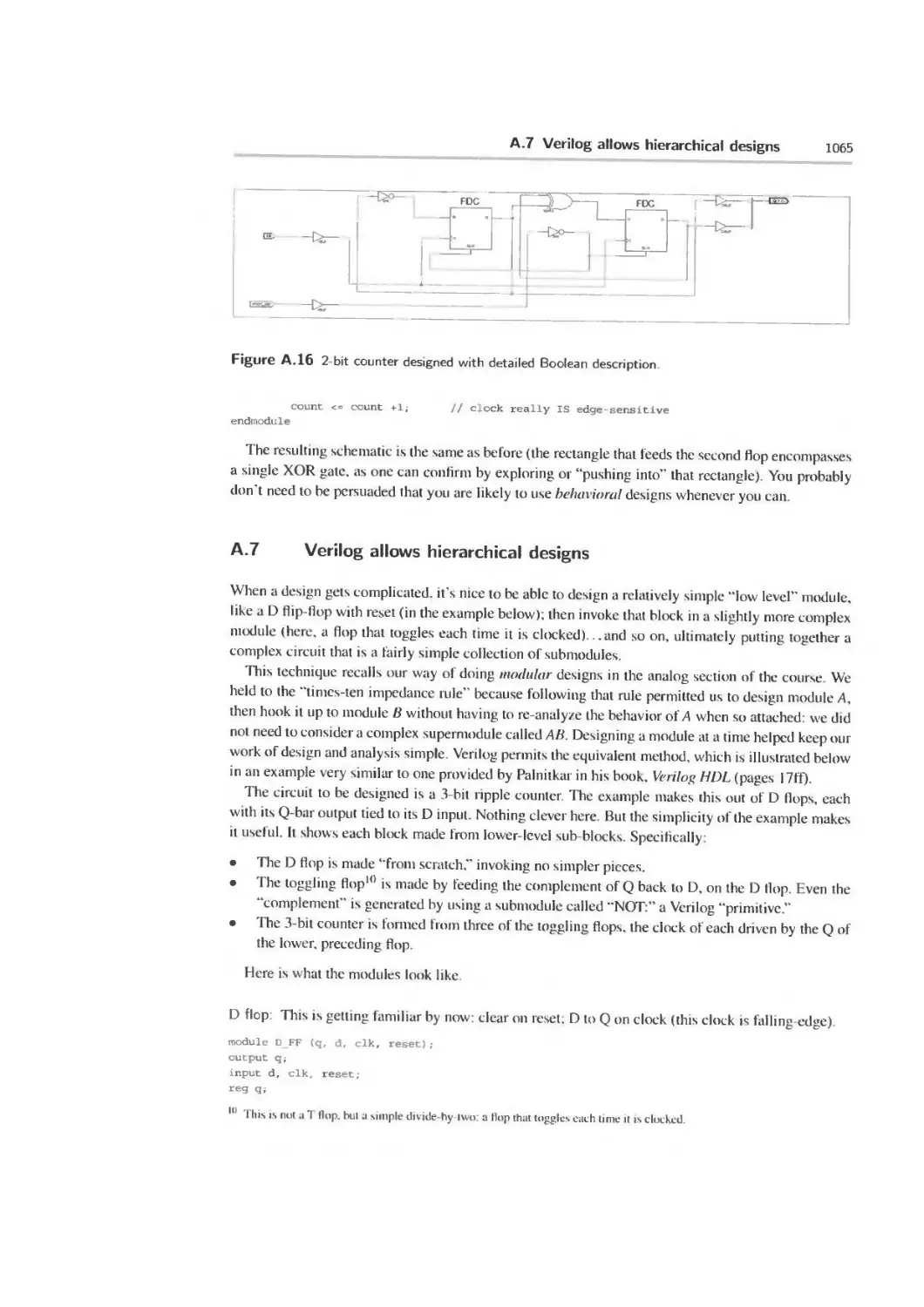
A.5 Flip-flops in Verilog 1060
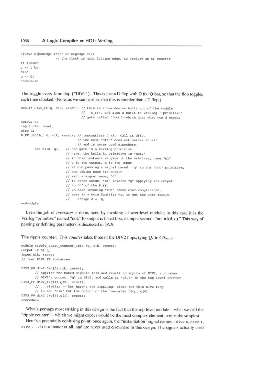
A.6 Behavioral versus structural design description: easy versus hard 1064
A.7 Verilog allows hierarchical designs 1065
A.8 A BCD counter 1068
A.9 Two alternative ways to instantiate a sub-module 1070
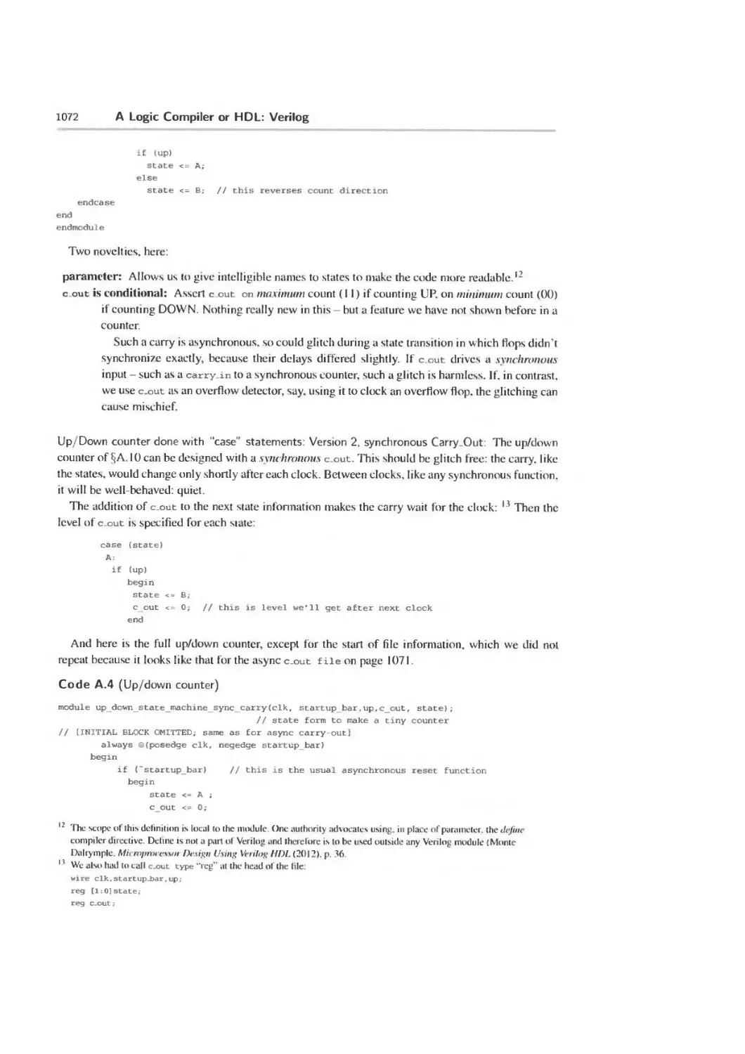
A 10 State machines 107]
All An instance more appropriate to state form: a bus arbiter 1073
A. 12 Xilinx ISE offers to lead you by the hand 1076
A.13 Blocking versus non-blocking assignments 1077
В Using the Xilinx Logic Compiler 1080
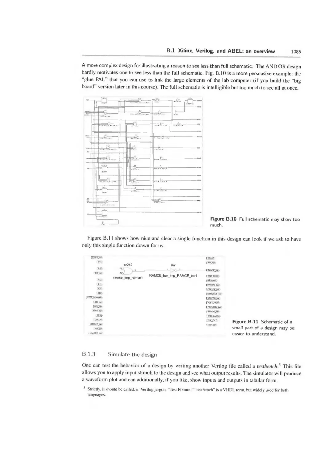
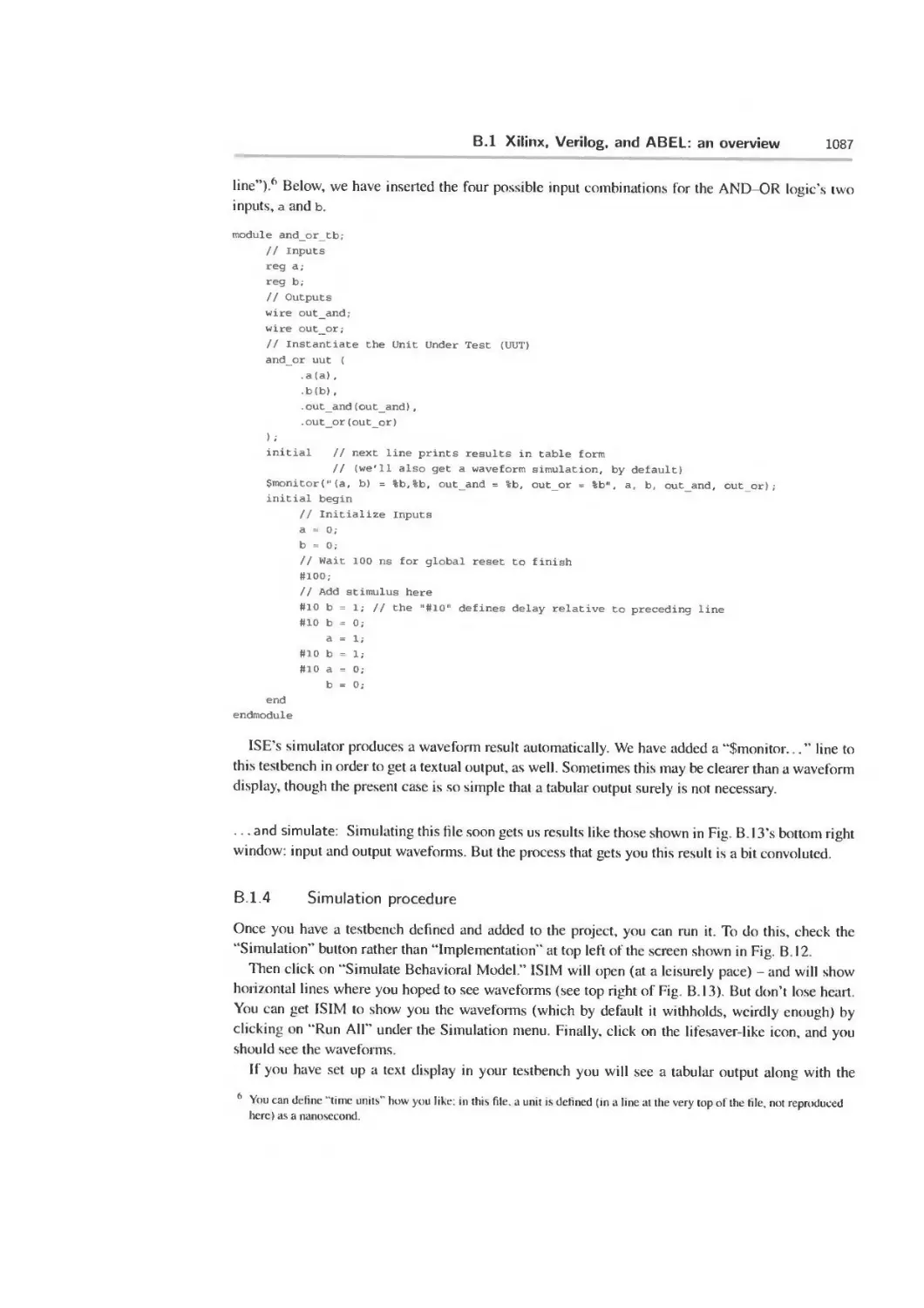
Bl Xilinx. Venlog. and ABEL: an overview 1080
C Transmission Lines 1089
C.l A topic we have dodged till now 1089
C.2 A new case: transmission line 1090
C.3 Reflections 1092
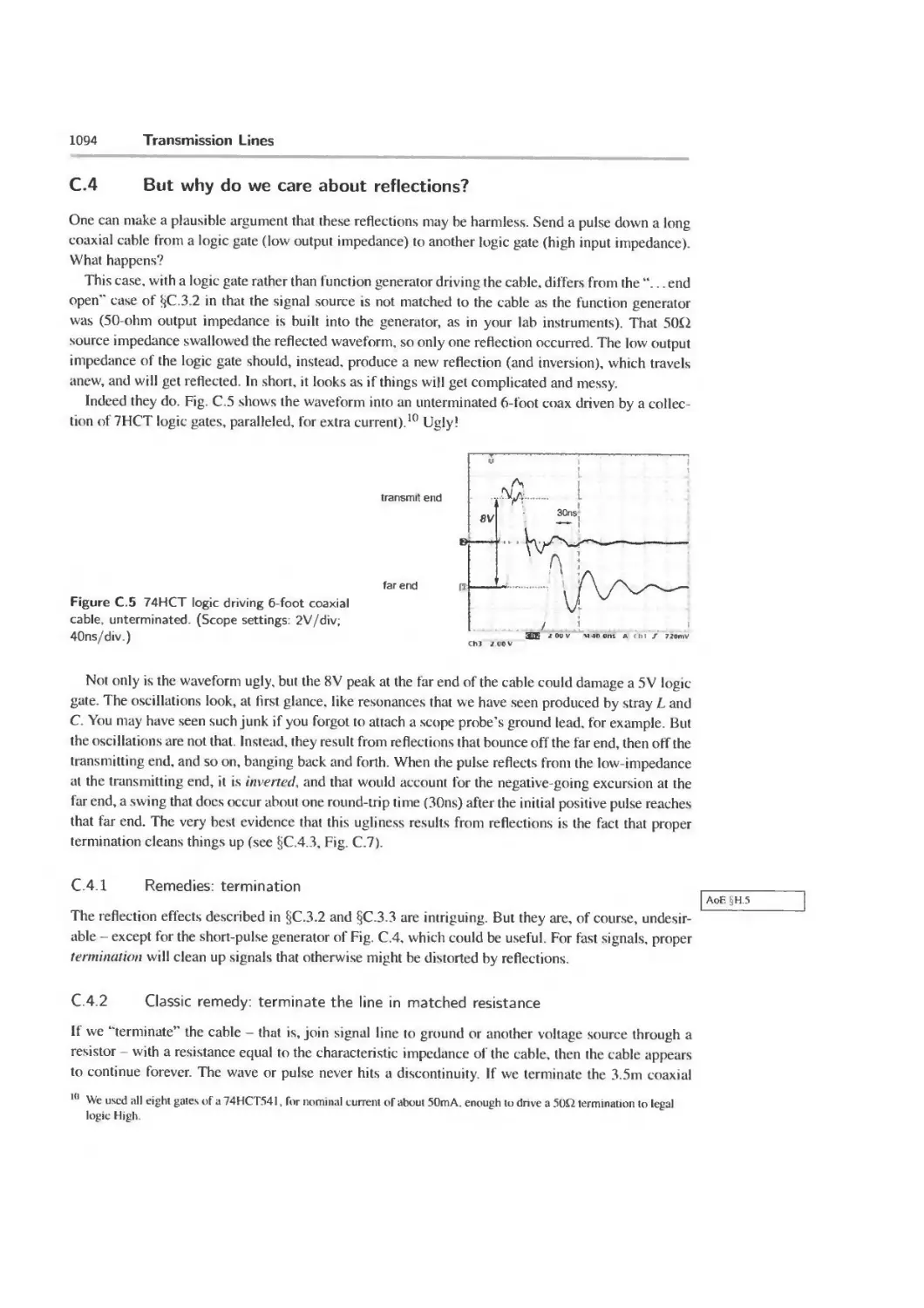
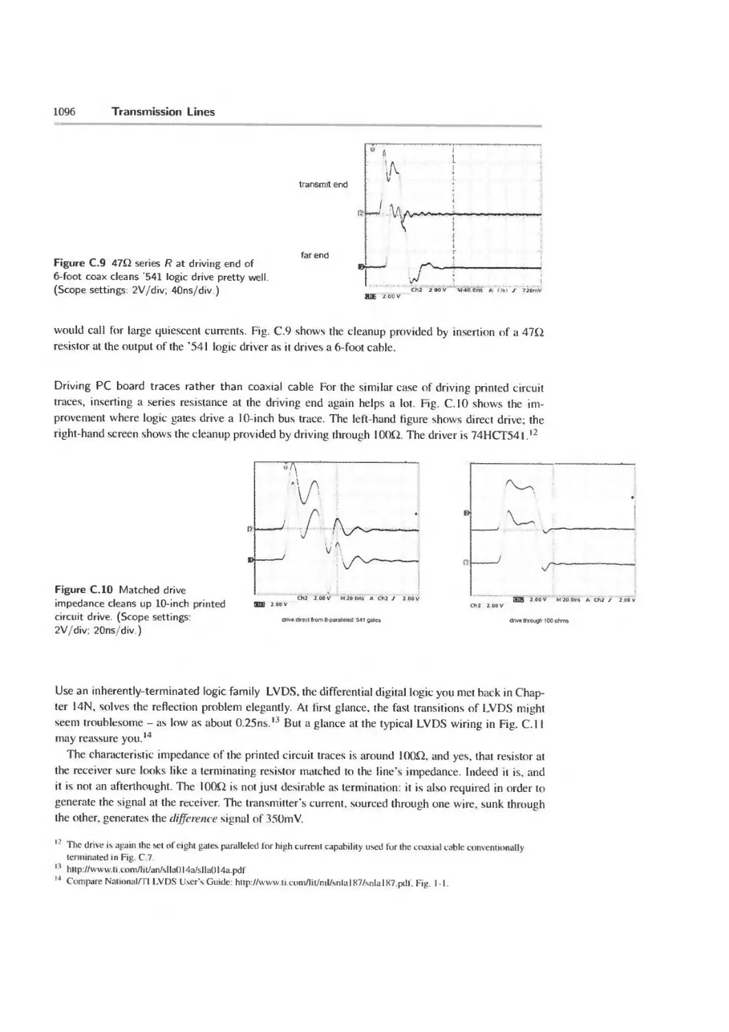
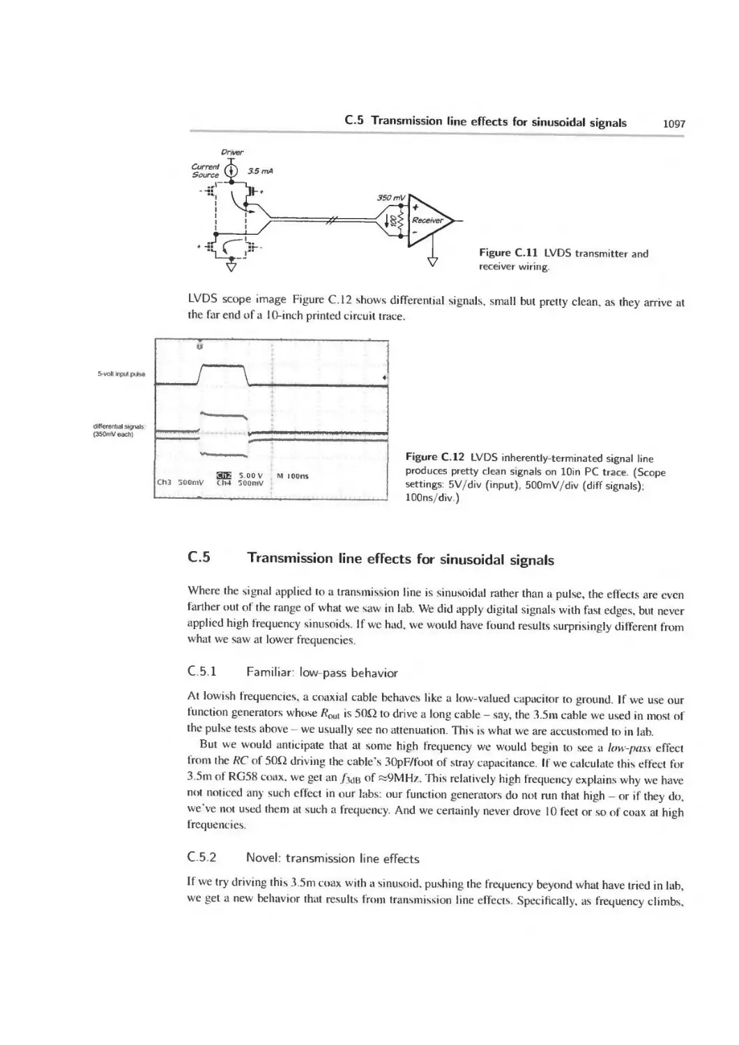
C.4 But why do we care about reflections? 1094
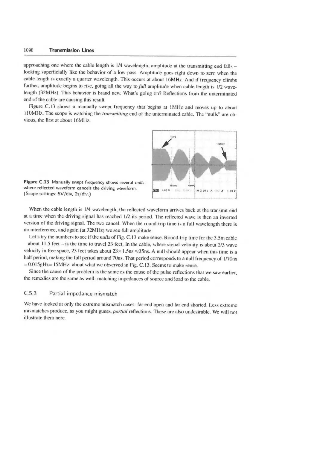
C.5 Transmission line effects for sinusoidal signals 1097
D Scope Advice 1099
D.l What we don't intend to tell you 1099
D.2 What we’d like to tell you 1099
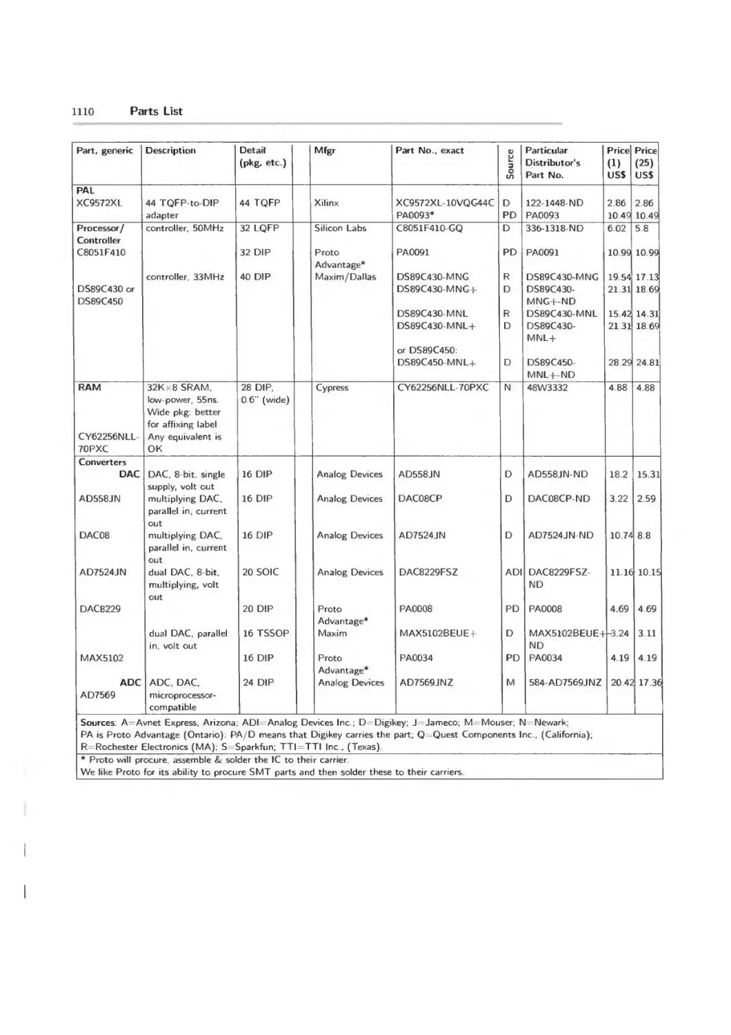
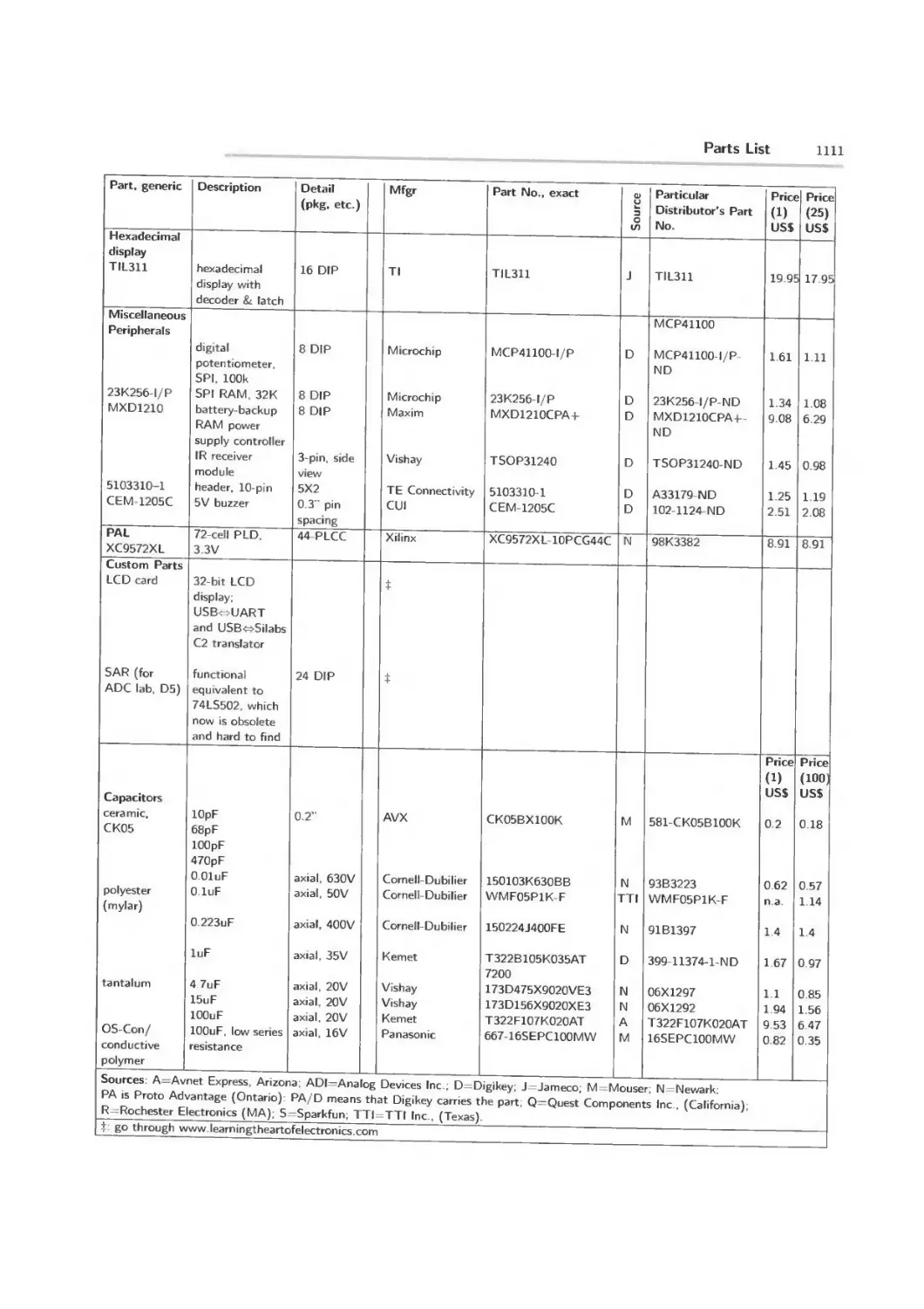
E Parts List 1105
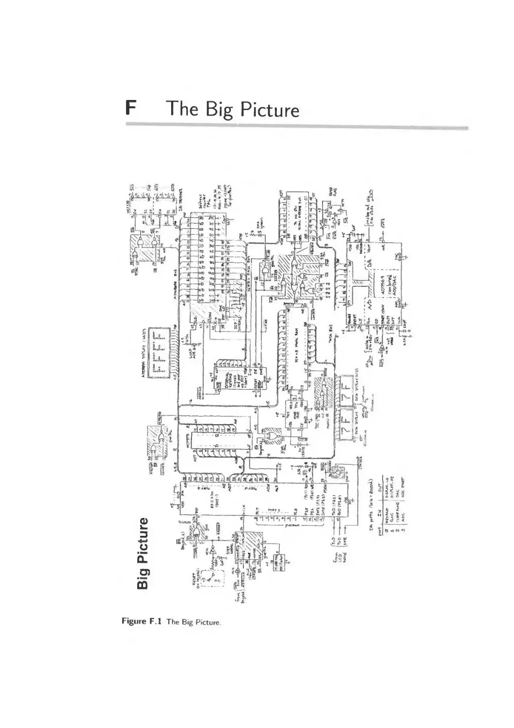
F The Big Picture 1113
G "Where Do I Go to Buy Electronic Goodies?” 1114
H Programs Available on Website 1116
Contents
XIX
Index
Equipment 1119
1.1 Uses for This List 1119
1.2 Oscilloscope 1119
1.3 Function generator 1120
1 4 Powered breadboard 1120
1.5 Meters, VOM and DVM 1121
I 6 Power supply 1121
1.7 Logic probe 1121
1.8 Resistor substitution box 1121
I 9 PLD/FPGA programming pod 1122
1.10 Handtools 1122
1.11 Wire 1122
Pinouts 1123
J.l Analog 1123
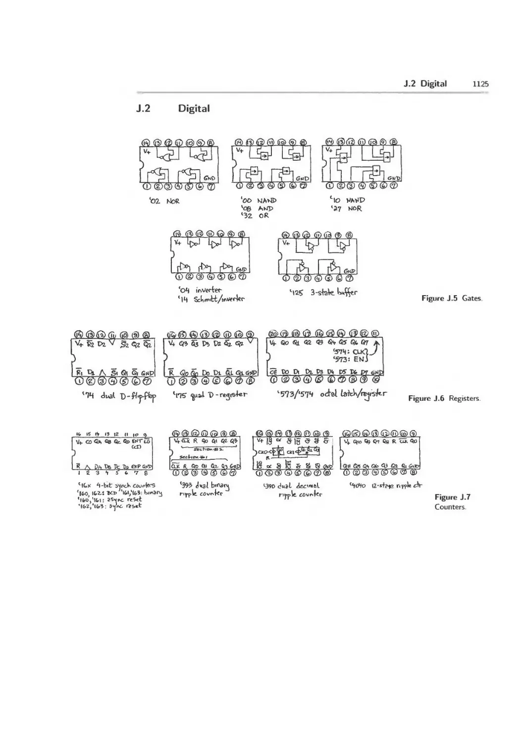
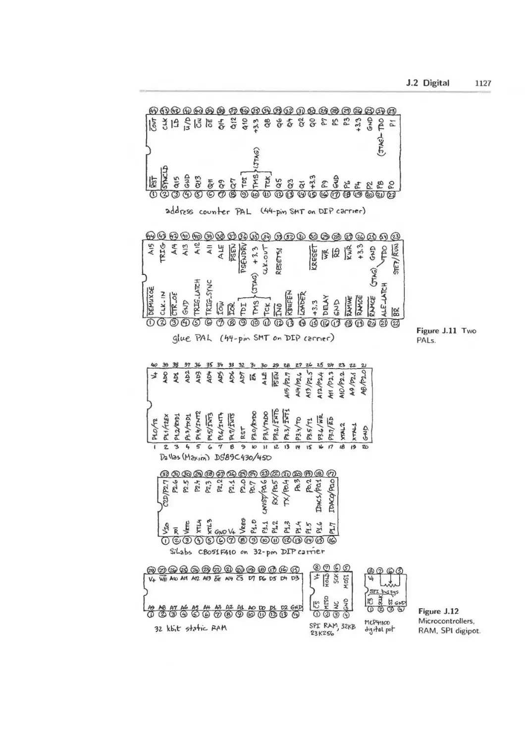
J 2 Digital 1125
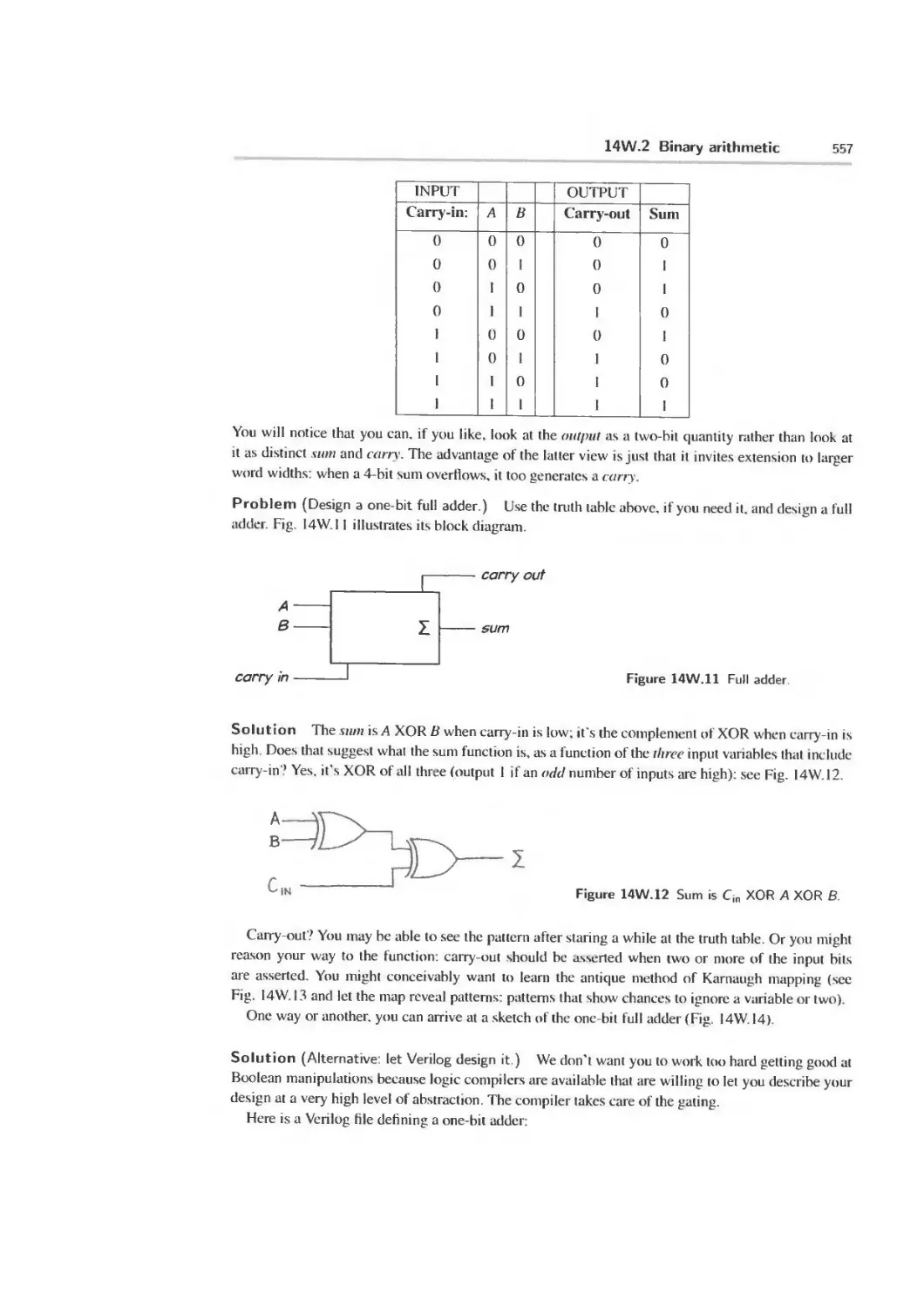
1128
Preface
A book and a course
This is a book for the impatient. It’s for a person who’s eager to get at the fun and fascination of
putting electronics to work The course squeezes what we facetiously call "all of electronics" into
about twenty-five days of class. Of course, it is nowhere near all, but we hope it is enough to get an
eager person launched and able to design circuits that do their tasks well.
Our title claims that this volume, which obviously is a hook, is also a course. It is that, because
it embodies a class that Paul Horowitz and I taught together at Harvard for more than 25 years. It
embodies that course with great specificity, providing what are intended as day-at-a-time doses.
A day at a time: Notes, Lab, Problems, Supplements
Each day’s dose includes not only the usual contents of a hook on electronics - notes describing and
explaining new circuits - but also a lab exercise, a chance to try out the day’s new notions by building
circuits that apply these ideas. We think that building the circuits will let you understand them in a
way that reading about them cannot.
In addition, nearly every day includes a worked example and many days include what we call
“supplementary notes.” These - for example, early notes on how to read resistors and capacitors
- are not for every reader Some people don't need the note because they already understand the
topic. Others will skip the note because they don't u’ant to invest the time on a first pass through the
book. That’s fine. That’s just what we mean by "supplementary:’’ it’s something (like a supplementary
vitamin) that may be useful, but that you can quite safely live without.
What's new?
If any reader is acquainted with the Student Manual..., published in 1989 to accompany the second
edition of The Art of Electronics, it may be worth noting principal differences between this book and
that one. First, this book means to be self-sufficient, whereas the earlier book was meant to be read
alongside the larger work. Second, the most important changes in content are these
• Analog;
- we lievote a day primarily to the intriguing and difficult topic of parasitu oscillations and
their cures;
- we give a day to building a “P1D” circuit, stabilizing a feedback loop that controls a motor’s
position. We apply signals that form three functions of an error signal, the difference between
target voltage and output voltage: “Proportional” (P), "Integral" (I), and "Derivative" (D)
functions of that difference.
Preface
xxi
• Digital:
- application of Programmable Logic Devices (PLDs or “PALs”), programmed with the high
level hardware description language (HDL), Verilog;
- a shift from use of a microprocessor to a microcontroller, in the computer section that con-
cludes the course. This microcontroller, unlike a microprocessor, can operate with little or
no additional circuitry, so it is well-suited to the construction of useful devices rather than
computers.
• Website: The book's website learningtheartofeiectronics.com has a lot more things, in par-
ticular code in machine readable form. Appendix H lists these.
.. And the style of this book
A reader will gather early on that this book, like the Student Manual is strikingly informal. Many
figures are hand drawn, notation may vary; explanations aim to help intuition rather than to offer a
mathematical view of circuits. We emphasize design rather than analysis. And we try hard to devise
applications for circuits that are fun; we like it when our designs make sounds (on a good day they
emit music), and we like to see motors spin.
Who’s likely to enjoy this book and course
You need not resemble the students who take our course at the university, but you may be interested to
know who they are, since the course evolved with them in mind. We teach the course in three distinct
forms. Most of our students take it during fall and spring daytime classes at the College. There, about
half are undergraduates in the sciences and engineering; the other half are graduate students, including
a few cross-registered from MIT who need an introduction quicker (and. admittedly, less deep) than
electronics courses offered down there. (We don't get EE majors from there; we get people who want
a less formal introduction to the subject.)
In the night version of the course, we get mostly older students, many of whom work with tech
nology and who have become curious about what’s in the “box” that they work with. Most often the
mysterious “box” is simply a computer, and the student is a programmer. Sometimes the “box” is a
lab setup (we get students from medical labs, across the river), or an industrial control apparatus that
the student would like to demystify.
In the summer version of the course, about half our students are rising high school seniors - and
the ablest of these prove a point we've seen repeatedly: to learn circuit design you don’t need to know
any substantial amount of physics or sophisticated math. We see this in the College course, too. where
some of our outstanding students have been Freshmen (though most students are at least two or three
years older).
And we can’t help boasting, as we did in the preface to the 1989 Student Manual, that once in a
great while a professor takes our course, or at least sits in One of these buttonholed one of us recently
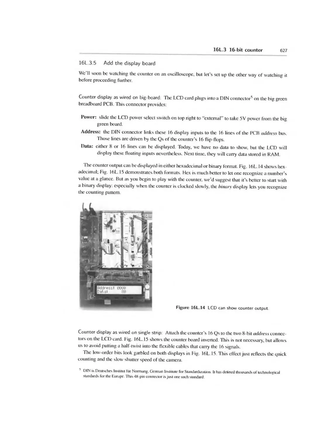
in a hallway, on a visit to the University where he was to give a talk. "Well, Tom,” he said, “one of
your students finally made good,” He was modestly referring to the fact that he’d recently won a Nobel
Prize. We wish we could claim that we helped him get it. We can't. But we're happy to have him as
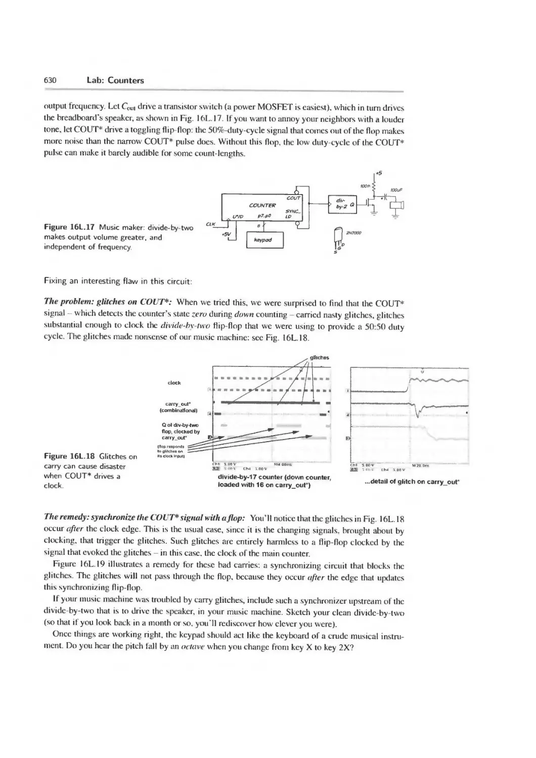
an alumnus.1
We expect that some of these notes will strike you as elementary, some as excessively dense: your
1 This was Frank Wilc/ek. He did sit quietly al the back of our class tor a while, hoping for some insights into a simulation
that he envisioned. If those insights came, they probably didn't come from us.
xxii
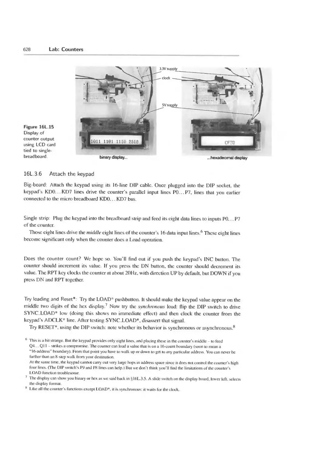
Preface
reaction naturally will reflect the uneven experience you have had with the topics we treat. Some of
you are sophisticated programmers, and will sail through the assembly-language programming near
the course’s end; others will find it heavy going. That’s all right. The course out of which this book
grew has a reputation as fun, and not difficult in one sense, but difficult in another: the concepts
are straightforward; abstractions are few. But we do pass a lot of information to our students m a
short time; we do expect them to achieve literacy rather fast. This course is a lot like an introductory
language course, and we hope to teach by the method sometimes called immersion. It is the laboratory
exercises that do the best teaching, we hope this book will help to make those exercises instructive. 1
have to add though, in the spirit of modern jurisprudence, a reminder to read the legal notice appended
to this Preface.
The mother ship: Horowitz & Hill's The Art of Electronics
Paul Horowitz launched this course, 40-odd years ago, and he and Winfield Hill wrote the book that,
in its various editions, has served as textbook for this course. That book, now in its third edition and
which we will refer to as “AoE," remains the reference work on which we rely. We no longer require
that students buy it as they take our course. It is so rich and dense that it might cause intellectual
indigestion in a student just beginning his study of electronics But we know that some of our students
and readers will want to look more deeply into topics treated in this book, and to help those people we
provide cross-references to AoE throughout this book. The fortunate student who has access to AoE
can get more than this book by itself can offer.
Analog and digital: a possible split
In our College course we go through all the book’s material m one term of about thirteen weeks. In
the night course, which meets just once each week, we do the same material in two terms. The first
term treats analog (Days 1 13), the second treats digital (Days 14—26). We know that some other
universities use the same split, analog versus digital. It is quite possible to do the digital half before
the analog. Only on the first day of digital - when we ask that people build a logic gate from MOSFET
switches - would a person without analog training need a little extra guidance For the most part, the
digital half treats its devices as black boxes that one need not crack open and understand. We do need
to be aware of input and output properties, but these do not raise any subtle analog questions
It is also possible to pare the course somewhat, if necessary. We don’t like to see any of our labs
missed, but we know that the summer version of the class, which compresses it all into a bit more than
six weeks, makes the tenth lab optional (Day 10 presents a “P1D"’ motor controller). And the summer
course omits the gratifying but not-essential digital project lab, 20L, in which students build a device
of their own design.
Who helped especially with this book
First, and most obviously, comes Paul Horowitz, my teacher long ago, my co-teacher for so many
years, and all along a demanding and invaluable critic of the book as it evolved. Most of the book’s
hand drawn figures, as well, still arc his handiwork Without Paul and his support, this book would
not exist.
Second, I want to acknowledge the several friends and colleagues who have looked closely at parts
ol the book and have improved and corrected these parts. Two are friends with whom I once taught.
Preface xxiii
and who thus not only are expert in electronics but also know the course well. These are Steve Morss
and Jason Gallicchio. Steve and I taught together nearly thirty years ago. Back then, he helped me to
try out and to understand new circuits. He then went off to found a company, but we stayed in touch,
and when we began to use a logic compiler in the course (Verilog) I took advantage of his experience.
Steve was generous with his advice and then with a close reading of our notes on the subject. As
1 first met Verilog’s daunting range of powers it was very good to be able to consult a patient and
experienced practitioner.
Jason helped especially with the notes on sampling. He has the appealing but also intimidating
quality of being unable to give half-power, light criticism. 1 was looking for pointers on details. The
draft of my notes came back glowing red with his astute markups. 1 got more help than I’d hoped for
- but, of course, that was good for the notes.
A happy benefit of working where 1 do is to be able to draw on the extremely knowledgeable
people about me, when I’m stumped. Jim MacArthur runs the electronics shop, here, and is always
overworked. I could count on finding him in his lab on most weekends, and. if I did, he would accept
an interruption for questions either practical or deep. David Abrams is a similarly knowledgeable
colleague who twice has helped me to explain to students results that I and the rest of us could not
understand. With experience in industry as well as in teaching our course, David is another specially
valuable resource.
Curtis Mead, one of Pau) Horowitz’s graduate students, gave generously of his skill in circuit layout,
to help us make the LCD board that we use in the digital parts of this course. Jake Connors, who had
served as our teaching assistant, also helped to produce the LCD boards that Curtis had laid out.
Randall Briggs, another of our former TAs. helped by giving a keen, close reading.
It probably goes without saying, but let’s say it: whatever is wrong in this book, despite the help
1 ve had. is my own responsibility, my own contribution, not that of any wise advisor.
In the laborious process of producing readable versions of the book's thousand-odd diagrams, two
people gave essential help My son, Jamie Hayes, helped first by drawing, and then by improving the
digital images of scanned drawings. Ray Craighead, a skilled illustrator whom we found online,2 made
up intelligently rendered computer images from our raggedy hand-drawn originals. He was able to do
this in a style that does not jar too strikingly when placed alongside our many hand-drawn figures. We
found no one else able to do what Ray did.
Then, when the pieces were approximately assembled, but still very ragged, the dreadfully hard job
of putting the pieces together, finding inconsistencies and repetitions, cutting references to figures that
had been cut, attempting to impose some consistency. ("Carry Out" rather than “CarryOUT” or “Coll|”
- at least on the same page - and so on), in 1000 pages or so, fell to my editor, David Tranah. He put
up not only with the initial raggedness, but also with continual small changes, right to the end. and he
did this soon after he had completed a similarly exhausting editing of AoE. For this unflagging effort
1 am both admiring and grateful.
And, finally, I should thank my wife. Debbie Mills, for tolerating the tiresome sight of me sitting,
distracted, in many settings - on back porch, vacation terrace in Italy, fireside chair - poking away at
revisions. She will be glad that the book, at last, is done.
2
See craighead.com.
XXIV
Preface
Legal notice
In this book we have attempted to teach the techniques of electronic design, using circuit exam-
ples and data that we believe to be accurate. However, the examples, data, and other information
are intended solely as teaching aids and should not be used in any particular application without
independent testing and verification by the person making the application. Independent testing
and verification are especially important in any application in which incorrect functioning could
result in personal injury or damage to property.
For these reasons, we make no warranties, express or implied, that the examples, data, or
other information in this volume are free of error, that they are consistent with industry stan-
dards, or that they will meet the requirements for any particular application. THE AUTHORS
AND PUBLISHER EXPRESSLY DISCLAIM THE IMPLIED WARRANTIES OF MERCH-
ANTABILITY AND OF FITNESS FOR ANY PARTICULAR PURPOSE, even if the authors
have been advised of a particular purpose, and even if a particular purpose is indicated in the
book. The authors and publisher also disclaim all liability for direct, indirect, incidental, or con-
sequential damages that result from any use of the examples, data, or other information in this
book.
In addition, we make no representation regarding whether use of the examples, data, or other
information in this volume might infringe others’ intellectual property rights, including US and
foreign patents. It is the reader’s sole responsibility to ensure that he or she is not infringing any
intellectual property rights, even for use which is considered to be experimental in nature. By
using any ot the examples, data, or other information in this volume, the reader has agreed to
assume all liability for any damages arising from or relating to such use, regardless of whether
such liability is based on intellectual property or any other cause of action, and regardless of
whether the damages are direct, indirect, incidental, consequential, or any other type of damage.
The authors and publisher disclaim any such liability.
Overview, as the Course begins
The circuits of the first three days in this course are humbler than what you will see later, and the
devices you meet here are probably more familiar to you than, say, transistors, operational amplifiers
- or microprocessors: Ohm’s Law will surprise none of you; / — CdV/dt probably sounds at least
vaguely familiar.
But the circuit elements that this section treats - passive devices - appear over and over in later
active circuits. So, if a student happens to tell us, “I'm going to be away on the day you're doing
Lab 2,” we tell her she will have to make up the lab somehow. We tell her that the second lab, on RC
circuits, is the most important in the course. If you do not use that lab to cement your understanding
of RC circuits - especially filters - then you will be haunted by muddled thinking for at least the
remainder of the analog part of the course.
Resistors will give you no trouble; diodes will seem simple enough, at least in the view that we
settle for: they are one-way conductors. Capacitors and inductors behave more strangely. We will see
very few circuits that use inductors, but a great many that use capacitors. You are likely to need a
good deal of practice before you get comfortable with the central facts of capacitors’ behavior - easy
to state, hard to get an intuitive grip on: they pass AC, block DC. and only rarely cause large phase
shifts.
We should also restate a word of reassurance: you can manage this course perfectly even if the j”
in the expression for the capacitor’s impedance is completely unfamiliar to you. If you consult AoE,
and after reading about complex impedances in AoE’s spectacularly dense Math Review (Appendix
A) you feel that you must be spectacularly dense, don’t worry. That is the place in the course where
the squeamish may begin to wonder if they ought to retreat to some slower-paced treatment of the
subject. Do not give up at this point; hang on until you have seen transistors, at least. One of the most
striking qualities of this book is its cheerful evasion of complexity whenever a simpler account can
carry you to a good design. The treatment of transistors offers a good example, and you ought to stay
with the course long enough to see that: the transistor chapter is difficult, but wonderfully simpler than
most other treatments of the subject. You will begin designing useful transistor circuits on your first
day with the subject.
It is also in the first three labs that you will get used to the lab instruments - and especially to the
most important of these, the oscilloscope. It is a complex machine; only practice will teach you to
use it well. Do not make the common mistake of thinking that the person next to you who is turning
knobs so confidently, flipping switches and adjusting trigger level - all on the first or second day of
the course is smarter than you are. No, that person has done it before. In two weeks, you too will
be making the scope do your bidding - assuming that you don't leave the work to that person next to
you. who knew it all from the start.
The images on the scope screen make silent and invisible events visible, though strangely abstracted
as well; these scope traces will become your mental images of what happens in your circuits. The
scope will serve as a time microscope that will let you see events that last a handful of nanoseconds;
xxvi Overview, as the Course begins
the length of time light takes to get from you to the person sitting a little way down the lab bench.
You may even find yourself reacting emotionally to shapes on the screen, feeling good when you see
a smooth, handsome sinewave, disturbed when you see the peaks of the sine clipped, or its shape
warped; annoyed when fuzz grows on your waveforms.
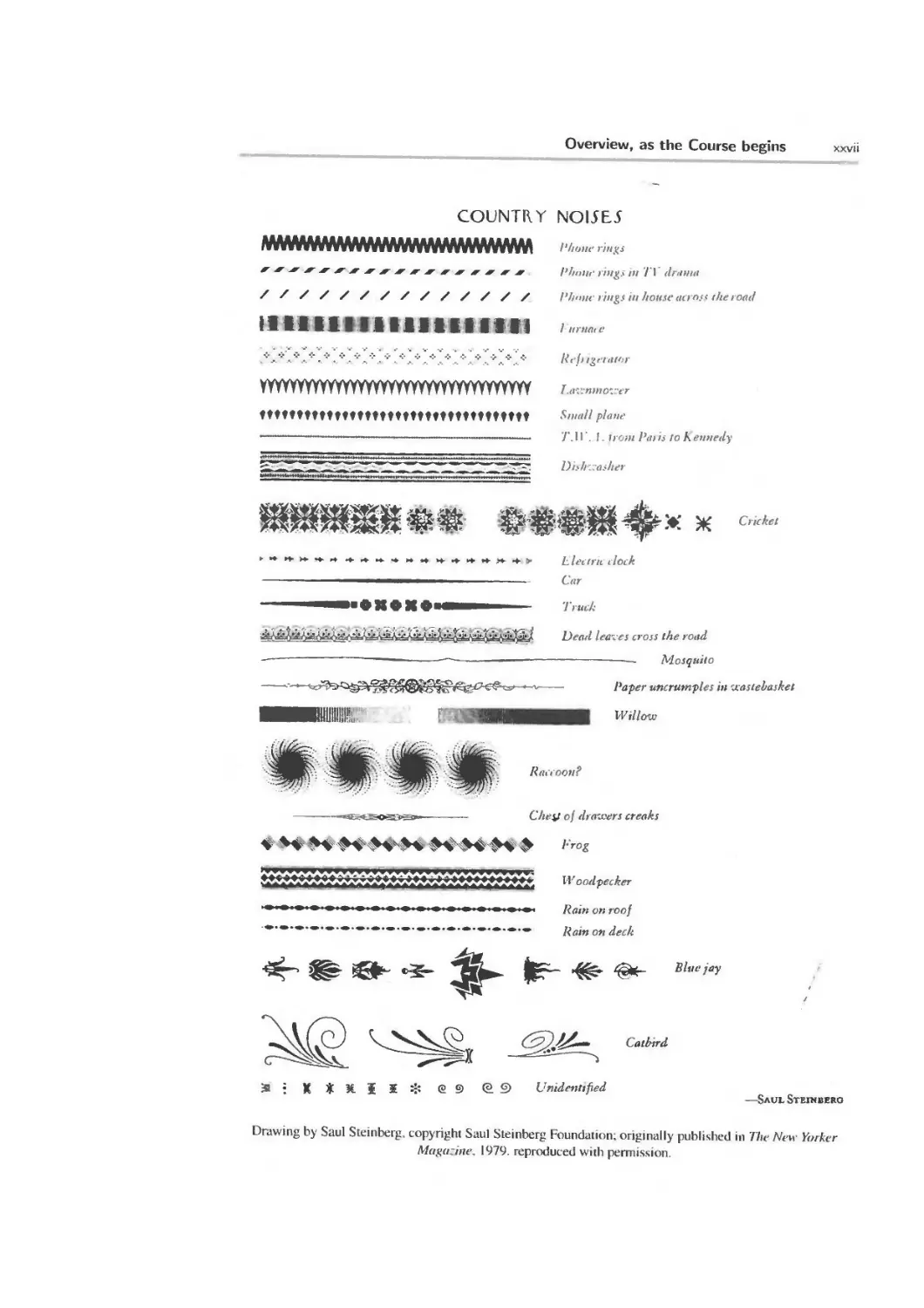
Anticipating some of these experiences, and to get you in the mood to enjoy the coming weeks in
which small events will paint their self-portraits on your screen, we offer you a view of some scope
traces that never quite occurred, and that nevertheless seem just about right: just what a scope would
show if it could. This drawing was posted on my door for years, and students who happened by would
pause, peer, hesitate - evidently working a bit to put a mental frame around these not-quite possible
pictures. Sometimes a person would ask if these are scope traces. They are not, of course; the leap
beyond what a scope can show was the artist’s; Saul Steinberg’s. Graciously, he has allowed us to
show his drawing here. We hope you enjoy it. Perhaps it will help you to look on your less exotic
scope displays with a little of the respect and wonder with which we have to look on the traces below.
Overview, as the Course begins
xxvii
COUNTRY
/Г ST JT
IltlKIfItBillKIIff I
YYYVYYYVYYYYYYyyYVVYYYVVYYYYYYYYYYYY
ttttttftfifffttiifttttftffttfitfffii
NOI5E5
Phone rings
Phone rings in 1 1 drama
Phone rings in house across the i oad
I urtuii e
Reft igeramr
Lawnmower
Small plane
T. 11 . I. Iront Pai is to К ennedy
Dish'washer
* CM“
L lectric clock
Car
• К О X • II —III Truck
Deed leas es cross the road
Mosquito
МНЮ111К
Paper uncrumples in wastebasket
Willow
/?«• coon?
Che^t of drawers creaks
< HMHM ННФ I,ros
Woodpecker
Rain on roof
Ram on deck
Catbird
Я ; @9 Q. S> Unidentified
—Saul Steinberg
Drawing by Saul Steinberg, copyright Saul Steinberg Foundation; originally published in The New Yorker
Magazine. 1979. reproduced with permission.
Part I
Analog: Passive Devices
IN DC Circuits
Contents
1N.1 Overview 3
IN.1.1 Why? 3
1N. 1.2 What is “the art of electronics?” 4
1N 1.3 What the course is not about 4
IN. 1.4 What the course is about: processing information 5
1N.2 Three laws 5
IN.2.1 Ohm’s law; V=/R 5
I N.2.2 Kirchhoff’s laws; V, / 9
1N.3 First application: voltage divider 11
1 N.3 1 A voltage divider to analyze 13
1N.4 Loading, and “output impedance” 14
1 N.4.1 Two possible methods 14
1 N.4.2 Justifying the Thevenin shortcut 15
1 N.4 3 Applying the Thevenin model 17
1 N.4 4 VOM versus DVM a conclusion? 20
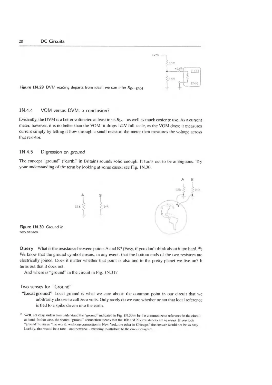
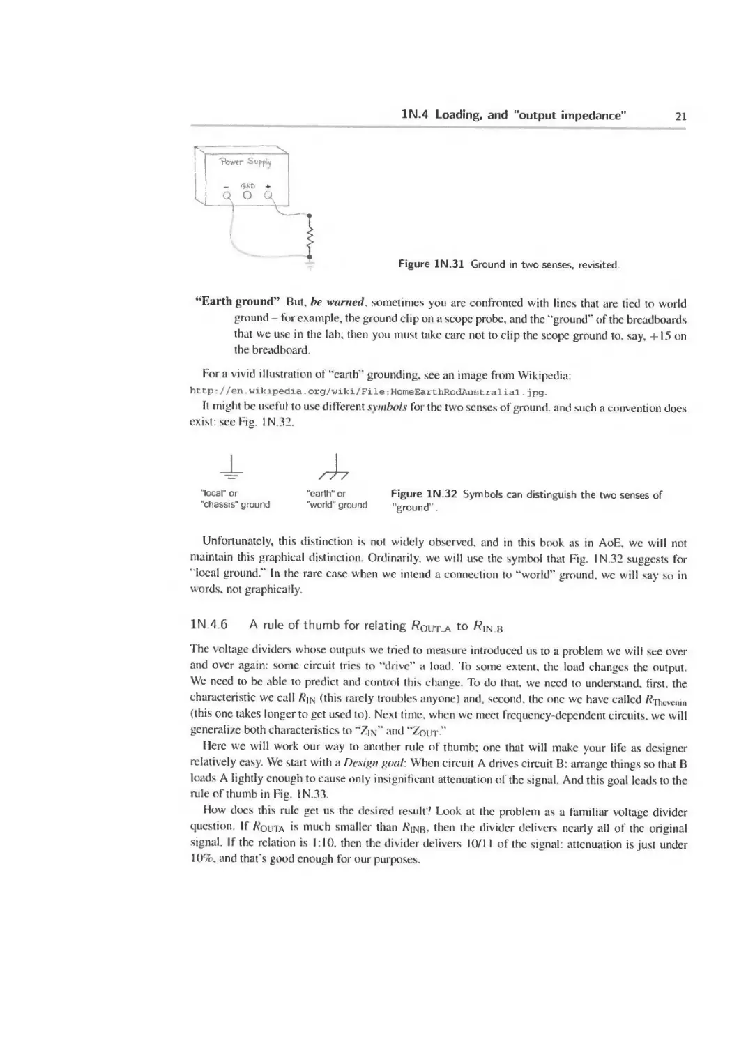
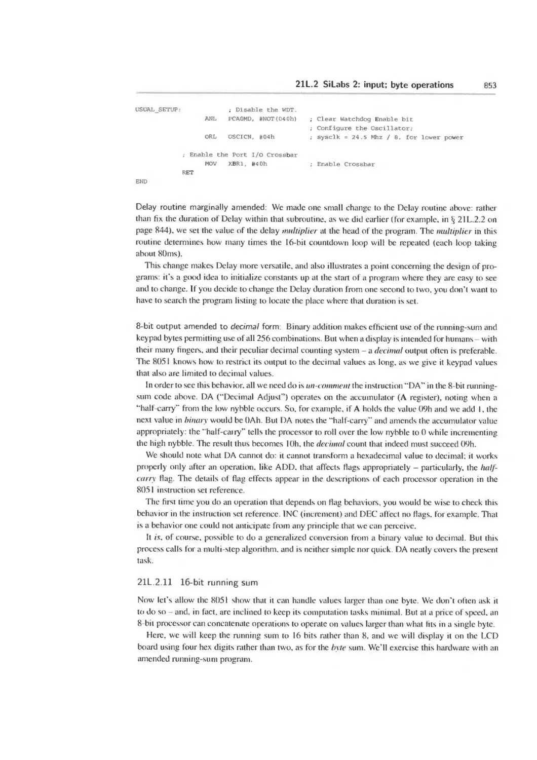
1 N.4.5 Digression on ground 20
1 N.4.6 A rule of thumb for relating /?out_a to Rjn в 21
1N.5 Readings in AoE 24
1N.1 Overview
We will start by looking at circuits made up entirely of
• DC voltage sources (things whose output voltage is constant over time; things like a battery, or a
lab power supply); and ...
• resistors.
Sounds simple, and it is. We will try to point out quick ways to handle these familiar circuit elements.
We will concentrate on one circuit fragment, the voltage divider.
1N.1 1 Why7
In each day’s class notes we will sketch the sort of task that the day’s material might let us accomplish.
We do this to try to head off a challenge likely to occur to any skeptical reader; OK, this is a something-
or-other circuit, but what’s it for? Why do I need a something-or-other? This is an integrator - but why
do I want an integrator? Here is our first try at providing such a sample application;
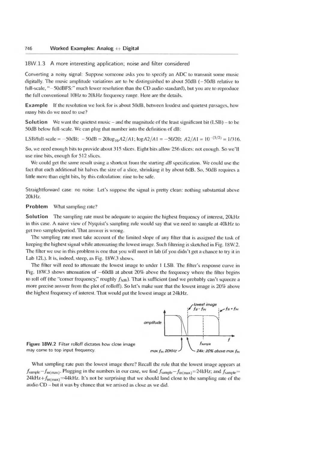
Problem Given a constant ("DC’’) voltage source, design a lower voltage source, strong enough to
“drive" a particular “load” resistance.
4
DC Circuits
Shorthand version of the problem. Make a voltage divider to deliver a specified voltage. Arrange
things so that increasing load current to a maximum causes Voul to vary by no more than a specified
percentage.
1N.1 2 What is "the art of electronics?”
Not art that you’re likely to find in a museum,1 but art in an older sense: a craft.2 No doubt the title of
The Art of Electronics (hereafter referred to as "AoE”) was chosen with an awareness of the suggestion
that there’s something borderline-magical available here: perhaps a hint of “black art”? | AoEtji.i
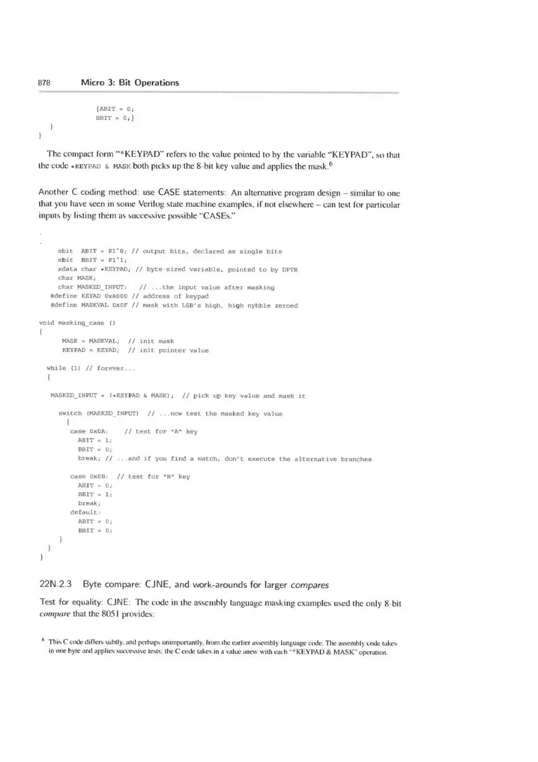
Here is AoE’s formulation of the subject of this course:
the laws, rules of thumb, and tricks that constitute the art of electronics as иг see it.
As you may have gathered, if you have looked at the text, this course differs from an engineering
electronics course in concentrating on the “rules of thumb” and the bag of “tricks.” You will learn to
use rules of thumb and reliable "tricks” without apology. With their help you will be able to leave the
calculator-bound novice engineer in the dust!
IN.1.3 What the course is not about
Wire my basement? Fix my TV?
Alumni of this course sometimes are asked for help that is beyond their capacities, and sometimes
below - or beside - what they know. “So, now you can wire some outlets in my basement?” No.
This course won’t help much with that task, which is easy in a sense but difficult in another, in that
it requires a detailed knowledge of electrical codes (required wire gauges; types of jacketing; where
ground-fault-interrupters are required). And when your friend’s TV quits, you’re probably not going
to want to fix it: much of the set’s circuitry will be embodied in mysterious proprietary integrated
circuits, an effective repair - it it were economically worthwhile - would likely amount to ordering
a replacement for a substantial module, rather than replacing a burned-out resistor or transistor, as in
the good old days of big and fixable devices.
Delivering power
A subtler point is worth making as well: only now and then, in this course, do we undertake to deliver
power to something (the “something" is conventionally called a “load”). Occasionally, we are inter-
ested in doing that: when we want to make a loud sound from a speaker, or want to spin a motor. But
much more often, we would like to minimize the flow of power; we are concerned, instead, with the
flow of information.
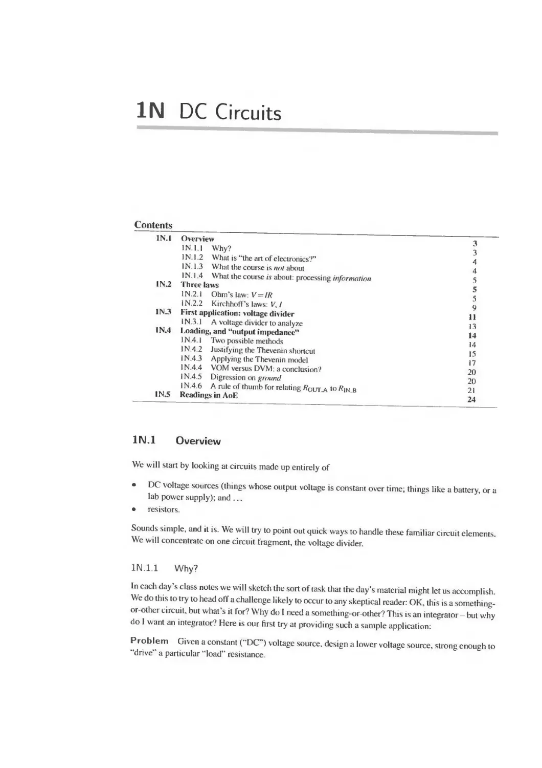
On the wall of the lobby of MIT’s Electrical Engineering building is a huge blowup of a photo of
some MIT engineers standing among what look like large generators or motors, each about the size
of a small cow. The photo in Fig. 1N.1 seems to date from the 1930s.
The "Electricals,” back then, were concerned mostly with those big machines: with delivering
power. It was the power companies that were hiring, when one of our uncles finished at MIT. around
1936 Hoover Dam, finished in 1935, was the engineering wonder of the day. Big was beautiful
(Even now. Hoover Dam's website boasts of the dam’s weight1. - 6.6 million tons, in case you were
wondering.)
1 But see. if you find yourself in Munich, a spectacular exception: lhe world’s greatesi museum of science and technology,
the Deutsches Museum. There you will find wonderful machines deinonstraling such arcana as the history of lhe
manufacture of threaded fasteners.
* “An indusirial pursuit... of a skilled nature; a erafl. business, profession.” Oxford English Dictionary (1989).
IN.2 Three laws
5
Figure 1N.1 Electronics ca 1935
[used with permission of MIT ]
IN 1.4 What the course is about, processing information
Times have changed, as you may have noticed. Small is beautiful; nano is extra beautiful - and elec-
tronics, these days, is concerned mostly with processing information.3 So, we like circuits that pass
and process signals while generating very little heat - using very little power. We like, for example,
digital circuits made out of field-effect transistors that form switches; they offer low output impedance,
gargantuan input impedance, and quiescent current of approximately zero. To a good approximation,
they’re not transferring power, not using it. not delivering it. They’re dealing in information. That's
almost always what we'll be doing in this course.
Obvious, perhaps? Perhaps.
We will postpone till next time - not to overload you, on the first day - discussion of a related topic:
just what form the information is likely to lake, in our circuits: voltage versus current. The answer
may surprise you; or you may be inclined to reject the question as empty, since you know that long
ago Ohm taught us that current and voltage in a device can be intimately related. Next time, we’ll
try to persuade you that you ought not to reject the question; that it’s worth considering whether the
signal is represented as a voltage or as a current (and see Note IS on this topic).
Now on to less abstract topics, and our first useful circuit: a voltage divider.
IN.2 Three laws
| AoE §1.2.1 |
A glance at three laws'. Ohm’s law, and Kirchhoff’s laws (Voltage - “KVL,” and current - “KCL”).
We rely on these rules continually, in electronics. Nevertheless, we rarely will mention Kirchhoff
again. We use his observations implicitly. By contrast, we will see and use Ohm’s law a lot: no one has
gotten around to doing what’s demanded by the bumper sticker one sees around MIT: Repeal Ohm’s
Law!
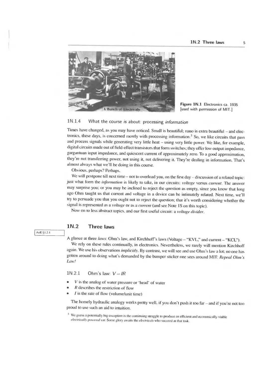
IN.2.1 Ohm’s law. V = IR
• V is the analog of water pressure or ‘head’ of water
• R describes the restriction of flow
• I is the rate of flow (volume/unit time)
The homely hydraulic analogy works pretty well, if you don’t push it too far - and if you’re not too
proud to use such an aid to intuition.
1 We guess a potential!) big exception is the continuing struggle to produce an efficient and economically-viable
electrically-powered car. Some glory awaits the electricals who succeed ai that lask.
б
DC Circuits
Figure IN.2 Hydraulic analogy voltage as head of water,
etc. Use it if it helps your intuition
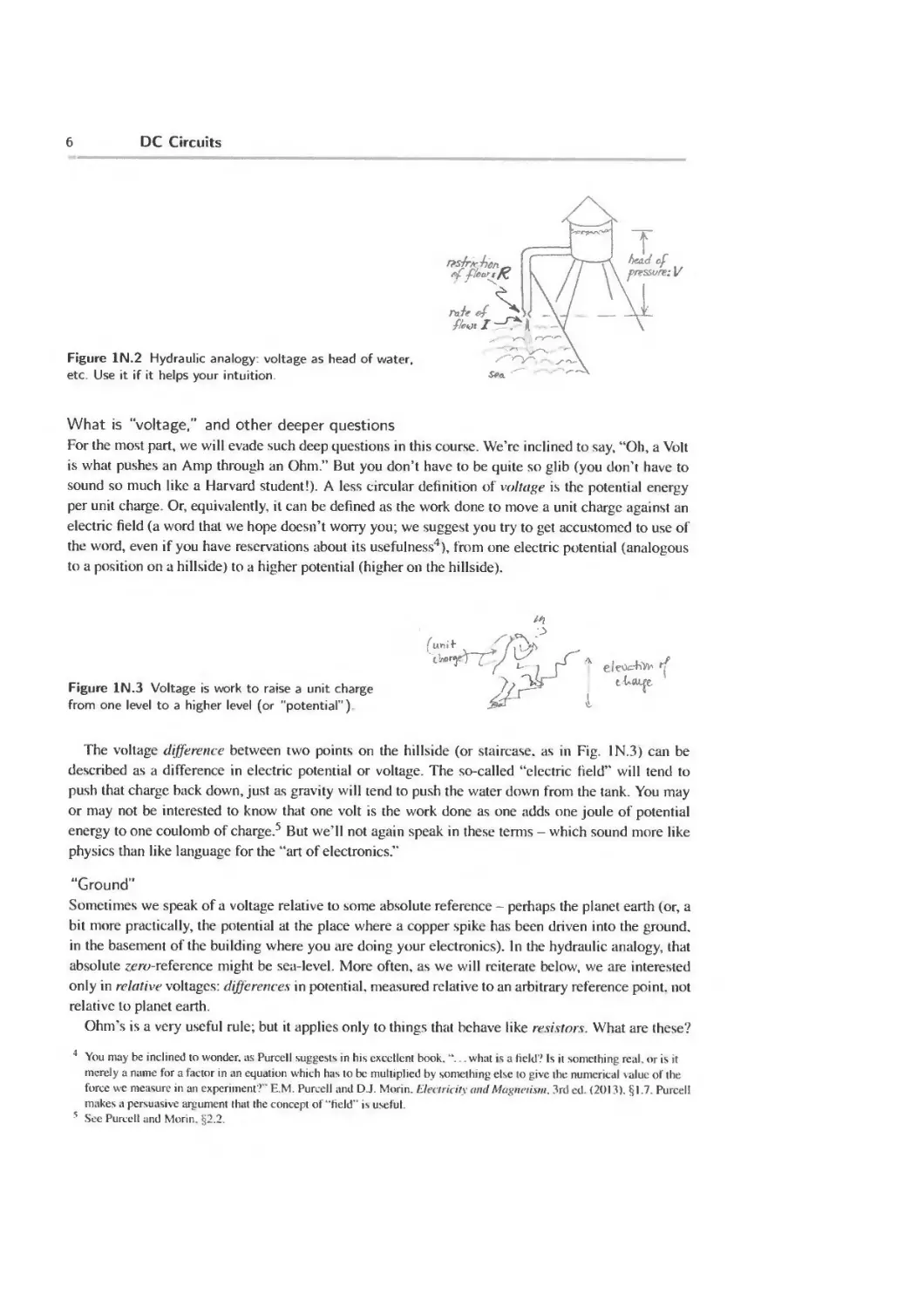
What is “voltage,” and other deeper questions
For the most part, we will evade such deep questions in this course. We’re inclined to say, “Oh, a Volt
is what pushes an Amp through an Ohm.” But you don’t have to be quite so glib (you don’t have to
sound so much like a Harvard student!). A less circular definition of voltage is the potential energy
per unit charge Or, equivalently, it can be defined as the work done to move a unit charge against an
electric field (a word that we hope doesn’t worry you; we suggest you try to get accustomed to use of
the word, even if you have reservations about its usefulness4), from one electric potential (analogous
to a position on a hillside) to a higher potential (higher on the hillside).
Figure 1N.3 Voltage is work to raise a unit charge
from one level to a higher level (or "potential")
t. Vw.p
The voltage difference between two points on the hillside (or staircase, as in Fig. 1N.3) can be
described as a difference in electric potential or voltage. The so-called “electric field” will tend to
push that charge back down, just as gravity will tend to push the water down from the tank. You may
or may not be interested to know that one volt is the work done as one adds one joule of potential
energy to one coulomb of charge.5 But we’ll not again speak in these terms - which sound more like
physics than like language for the “art of electronics.”
“Ground"
Sometimes we speak of a voltage relative to some absolute reference - perhaps the planet earth (or, a
bit more practically, the potential at the place where a copper spike has been driven into the ground,
in the basement of the building where you are doing your electronics). In the hydraulic analogy, that
absolute zero-reference might be sea-level. More often, as we will reiterate below, we are interested
only in relative voltages: differences in potential, measured relative to an arbitrary reference point, not
relative to planet earth.
Ohm's is a very useful rule; but it applies only to things that behave like resistors. What are these?
4 You may be inclined to wonder, as Purcell suggests in his cxcellenl book. "... what is a held? Is it something real, or is it
merely a name for a factor in an equation which has to be multiplied by something else to give the numerical value of the
force we measure in an experiment?" E.M. Purcell and D.J. Morin. Electricity and Magnetism. 3rd ed. (2013). §1 7 Purcell
makes a persuasive argument that the concept of "held" is useful.
5 See Purcell and Morin, §2.2.
IN.2 Three laws
7
They are things that obey Ohm’s Law! (Sorry folks: that’s us deeply as we’ll look at this question, in
this course.6)
Why does Ohm’s law hold?
The restriction of current flow that we call “resistance" - which we might contrast with the very-easy
flow of current in a piece of wire7 - occurs because the charge-carrying electrons, accelerated by an
electric field, bump into obstacles (vibrations of the atomic lattice) after a short free flight, and then
have to be re-accelerated in the direction of the field. Materials that arc good conductors - metals -
have a substantial population of electrons that are not tightly bound, and consequently are free to travel
when pushed. The conductivity of a metal depends on the density of the population of charge carriers
(usually, un bound electrons), and it's kind of reassuring to find that conductivity degrades with rising
temperature the free flights become shorter, as electrons bump into the jumpier atoms of the hotter
material. This effect you will see confirmed in Lab IL if things come out right in your experiment
(you’ll have to do a little reasoning to see this effect confirmed; the notes to Lab IL do not point
out where this occurs). The stronger the field, the faster the drift of the electrons. Field strength goes
with voltage difference between two points on the conductor; rate of drift of the electrons measures
current. So, Ohm’s Law is pretty plausible.
| aoe §c.4 [ What determines the value of a resistor?
A "resistor" is also, of course, a “conductor”; it may seem a bit perverse to call this thing that is
inserted in a circuit to permit current flow a “resistor.” But the name comes from the assumption that
the resistor is inserted where an excellent conductor - a piece of wire - might have stood, instead. To
make a resistor, one can use either of two strategies: to make a “carbon composition” resistor (the sort
that we’H use in lab because their values are relatively easy to read), one mixes up a batch of powdered
insulator and powdered conductor (carbon), adjusting the proportions to give the material a particular
resistivity. To make a “metal film” resistor (much the more common type, these days), one “deposits"
a thin film of metal on a ceramic substrate, and then partially cuts away the thin conducting film.
How generally does Ohm’s law apply? We begin almost at once to meet devices that do not obey
Ohm’s Law (see Lab IL: a lamp; a diode). Ohm’s Law describes one possible relation between V and
/ in a component, but there are others. As AoE says,
Crudely speaking, the name of the game is to make and use gadgets that have interesting and useful / versus V
characteristics.
In a resistor, current and voltage are proportional in a nice, linear way: double the voltage and you
get double the current. Ohm’s Law holds. Don’t expect to use it where it doesn’t fit. Even the lamp -
whose filament is just a piece of metal that one might expect would behave like a resistor - doesn’t
follow Ohm’s Law, as you'll see in Lab IL. Why not?s
... But we can extend the reach of Ohm's law? Dynamic resistance: After today, we rarely will
limit outselves to devices that show simply resistance - and as we have said, even the resistor-like
|aoESi.2.6 I lamp that you meet in Lab IL. along with the diode, defy Ohm's-Law treatment. But an extended
version of Ohm’s Law that we’ll call dynamic resistance will allow us to apply the familiar rule in
6 It this remark frustrates you see an ordinary E&M book; for example, see the good discussion of the topic in E.M. Purcell
and D.J. Morin. Electricity <4 Magnetism, 3rd ed. (2013), or in S. Burns and P Bond. Principles of Electronic Circuits
(1987).
You may prefer the contrast with a superconductor whose resistance is not just small but is rem
8 Here’s a powerful clue: it would follow Ohm’s Law if you could hold the filament’s temperature constant.
8
DC Circuits
settings where otherwise it would not work. The idea is just to define a local resistance - the tangent
to the slope of the device's V-I curve:
^dynamic = /А/.
This redefinition allows us to talk about the effective resistance of a diode, a transistor, or a current
source (a circuit that holds current constant). Here is a sketch of a diode’s V-l curve - oriented so
that V is the vertical axis. This orientation puts the curves’ slopes into the familiar units. Ohms (rather
than into 1 /Ohms,9 as in the more standard 1-V plot).
Figure IN.4 Dynamic resistance
illustrated: local slope can be defined
for devices that are not Ohmic.
f^dyn ~ 150 Г7
1 t(mA)
DETAILS OF
DIODE CURVE
You may like the resistor's well-behaved straight line, because it is familiar. But the nice thing
about the notion of ^dynamic is that is so broad-minded: it is happy to describe the V-l curve (or 7 V
curve,” as it is more often called) for any device. It will happily fit a transistor, an exotic current source
- anything The nearly-vertical plot of the current source, implying enormous /?dynam » will become
important to your understanding of transistors.
I AoE § 1.2.2c"
Power in a resistor: Power is the rate of doing work, as you may recall from a course on mechanics.
The concept comes up most often, in electronics, when one tries to specify a component that can
safely handle the power that it is likely to have to dissipate. High power produces high heat, and
calls for a component capable of unloading or dissipating that heat. The three resistors shown below
illustrate the rough relation between power rating and size - because large size usually offers large
area in contact with the surroundings or “ambient.”
The indicated power ratings show the maximum that each can dissipate without damage. The tiny
“surface-mount” on the left (“’0805 size,” large by surface-mount standards) dissipates more than one
might expect if one compares its size to that the of the 1/4W carbon-comp (the sort we use in the lab);
it does better than one might expect because it is soldered directly to a circuit board, whose copper
traces help to draw off and dissipate its heat.
In the coming labs you will sometimes run into the question whether your components can handle
the powei that is expected. Our usual resistors are rated at 1/4W You can confirm that such a resistor
can handle 15V (our usual maximum supply voltage) if the resistor’s value is at least IkQ. Let’s try
that calculation. P = 1 x V.
Thanks to Ohm's Law, the formula for power can be written in any of three ways:
• P = I x V (as we just said); but since V = IR,
• P = l2R; and since 1 — V/R.
9
-.. or Siemens, the official name for inverse Ohms.
IN.2 Three laws
9
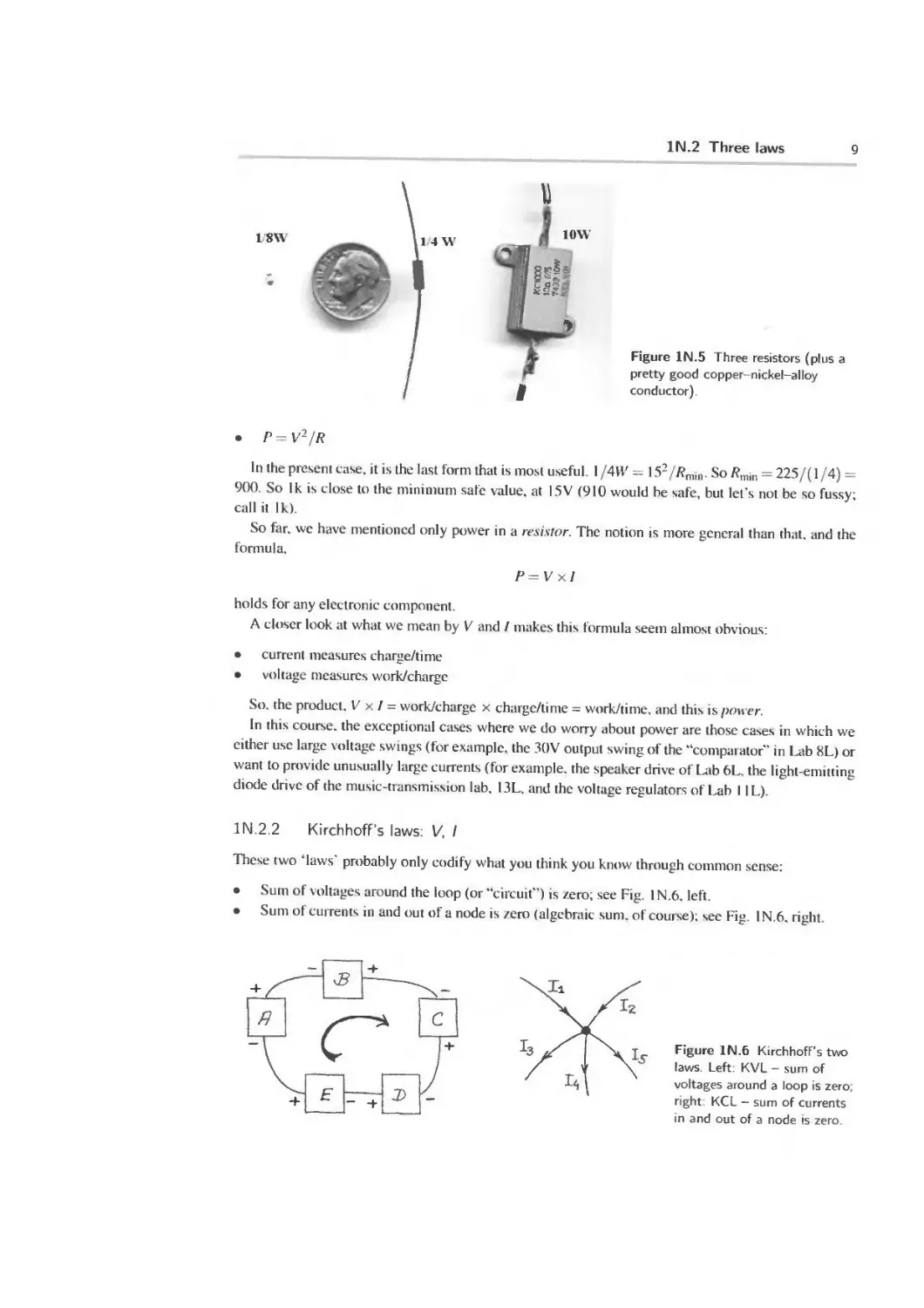
1/8W
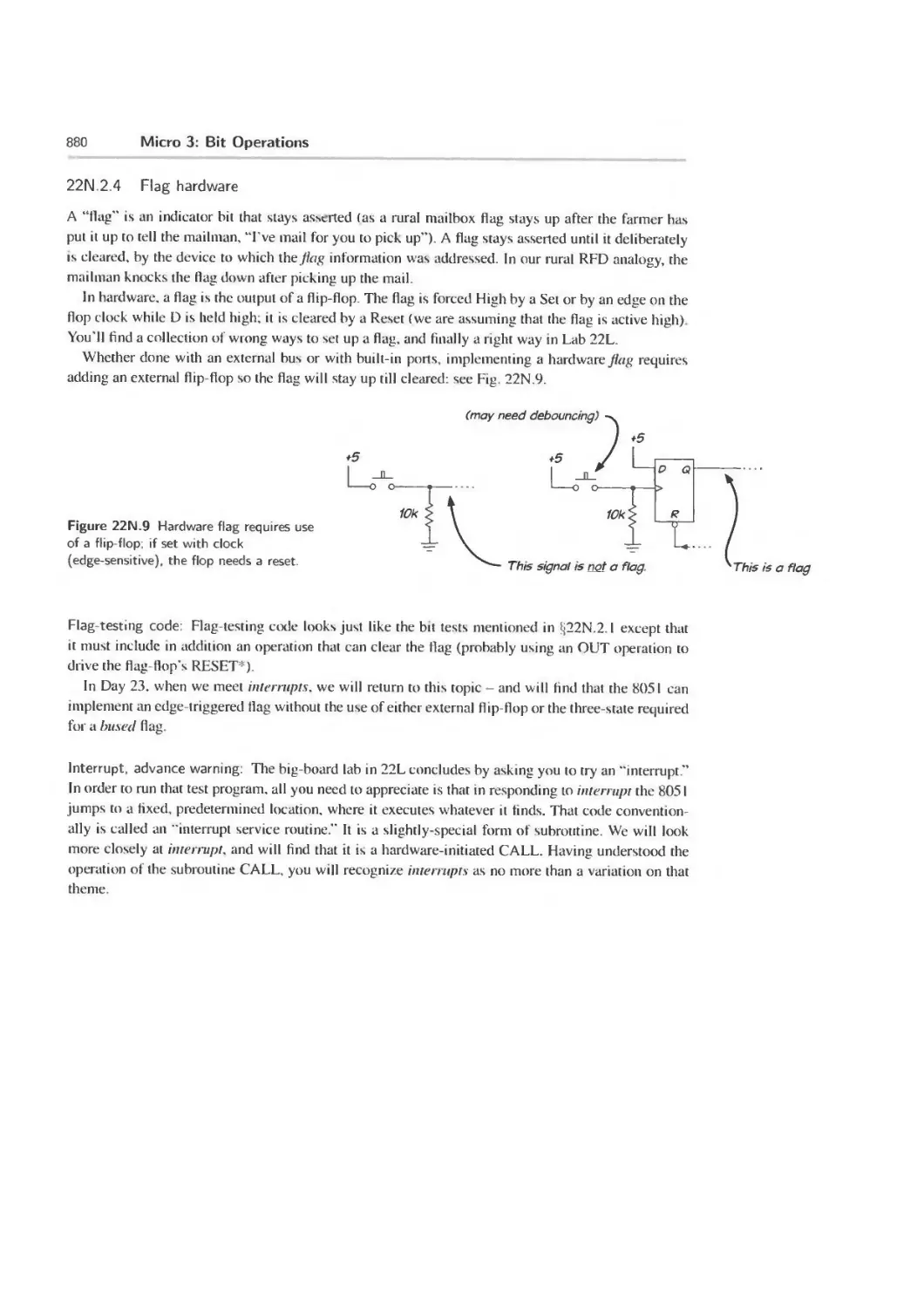
Figure IN.5 Three resistors (plus a
pretty good copper-nickel-alloy
conductor)
• P = V2/R
In the present case, it is the last form that is most useful. 1 /4И' — 152//?min. So/?min = 225/(l/4) =
900. So Ik is close to the minimum safe value, at 15V (910 would be safe, but let’s not be so fussy;
call it Ik).
So far, we have mentioned only power in a resistor. The notion is more general than that, and the
formula,
P = Vxl
holds for any electronic component.
A closer look at what we mean by V and / makes this formula seem almost obvious:
current measures charge/time
voltage measures work/charge
So. the product. V'x/ = work/charge x charge/time - work/time, and this is power.
In this course, the exceptional cases where we do worry about power are those cases in which we
either use large voltage swings (for example, the 30V output swing of the "comparator" in Lab 8L) or
want to provide unusually large currents (for example, the speaker drive of Lab 6L, the light-emitting
diode drive of the music-transmission lab, 13L, and the voltage regulators of Lab I IL).
IN.2.2 Kirchhoff’s laws: V, /
These two ‘laws’ probably only codify what you think you know through common sense:
• Sum of voltages around the loop (or “circuit") is zero; see Fig. I N.6, left.
• Sum of currents in and out of a node is zero (algebraic sum. of course); see Fig 1N 6. right.
Figure IN.6 Kirchhoff’s two
laws. Left KVL - sum of
voltages around a loop is zero;
right KCL - sum of currents
in and out of a node is zero.
10
DC Circuits
Applications of these laws series and parallel circuits:
Series /lola| = /, = h
Parallel /totai = h + h
Series Vtotai = V, + V2
Parallel Vtotal = V, = V2
Figure IN.7 Applications of Kirchhoff's laws: series
and parallel circuits: a couple of truisms, probably
familiar to you already
Query Incidentally, where is the “loop" that Kirchhoff's law refers to7 Answer: the “loop” (or
“circuit,” a near synonym) is apparent if one draws the voltage source as a circuit element, and ties its
foot to the foot of the R: see Fig. 1 N.8.
+ JOv
Tfctr /cfOJr' t (ro._
Figure IN.8 Voltage divider redrawn to
look more like a "loop' or "circuit'’
... ukemc th-u Aej;
but tbcyre electrically
eqinvalcid-.
Usually we don't bother to draw the voltage source that way; we label points with voltage values,
and assume that you can picture the circuit path for yourself, if you choose to.
This is kind of boring. So, let’s hurry on to less abstract circuits: to applications - and tricks. First,
some labor-saving tricks.
Parallel resistances calculating equivalent R
The conductances add:
Conductance^ — Conductance] + Conductance! = 1 //?i + 1 //?2
This is the easy notion to remember, but not usually convenient to apply, for one rarely speaks of
conductances. The notion “resistance” is so generally used that you will sometimes want to use the
formula for the effective resistance of two parallel resistors:
i
Figure IN.9
Parallel resistors
the conductances
add; unfortunately,
the resistances
Believe it or not, even this formula is messier than what we like to ask you to work with in this
1N.3 First application: voltage divider
11
course. So we proceed immediately to some tricks that let you do most work in your head. Consider
the easy cases in Fig. IN. 10. The first two are especially important, because they help one to estimate
the effect of a circuit one can liken to either case. Labor-saving tricks that give you an estimate are not
to be scorned: if you see an easy way to an estimate, you’re likely to make the estimate. If you have to
work too hard to get the answer, you may find yourself simply not making the estimate. A deadly trap
for the student doing a lab is the thought, “Oh, I’ll calculate this later - some time this evening, when
AoE § 1.2.2B | I’m comfortable in front of a spreadsheet.” This student won’t get to that calculation! The leftmost
case in Fig. IN. 10 surely doesn’t call for pulling out a formula: two equal 7?s paralleled behave like
R/2. The middle case is easier still, given that we’re willing to ignore errors under 10%. (On the other
hand, when you do want to trim an R value by 10% this is an easy way to do just that.) The rightmost
calls for slightly more imagination think of the lone R as a paralleling of two resistors of equal value
1/7? = 2/2/?. Then the whole looks like three paralleled resistors, each of value 2/?. The result then is
2/?/3.
Figure IN. 10
Parallel Rs:
Some easy cases.
In this course we usually are content with answers good to 10%. So, if two parallel resistors differ
by a factor of ten or more, then we can ignore the larger of the two.
Let’s elevate this observation to a rule of thumb (our first). While we’re at it, we can state the
equivalent rule for resistors in series.
Small
large К
Small R.
FigurelN.il Resistor calculation
shortcut: parallel, series. In a parallel
circuit, a resistor much smaller than
others dominates. In a series circuit, the
larger resistor dominates
1N.3 First application: voltage divider
| AoE §1.2.3 |
Why dividers7 Are dividers necessary? Why not start with the right voltage? The answer, as you
know, is just that a typical circuit needs several voltages, and building a “power supply” to deliver
each voltage is impractical (meaning, mostly, expensive). You’ll soon be designing power supplies,
and certainly at that time will appreciate how much simpler a voltage divider is, compared to a full
power supply.
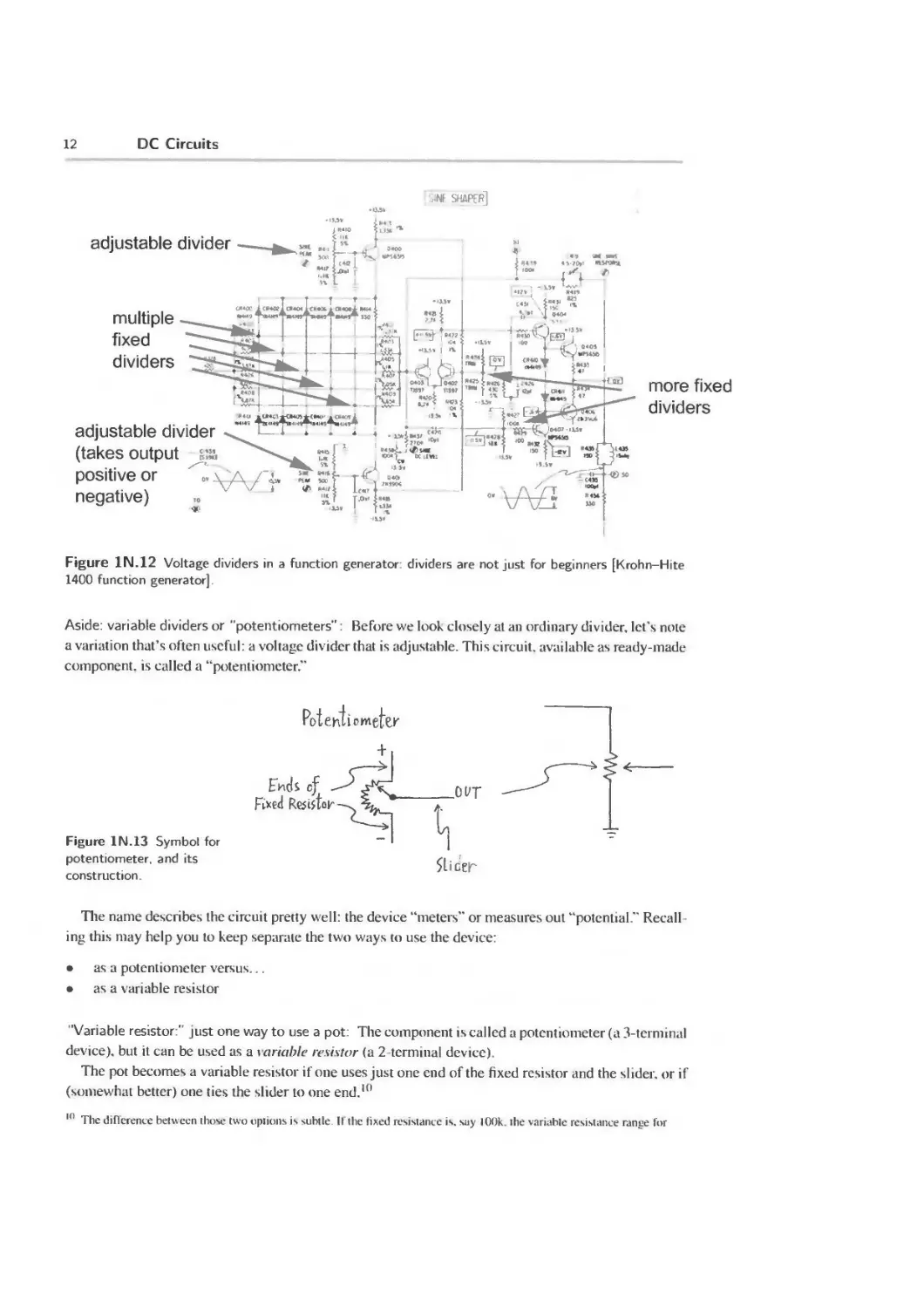
To illustrate the point that voltage dividers are useful, and not just an academic device used to
provide an easy introduction to circuitry, we offer here a piece of a fairly complex device, a “function
generator” - the box that soon will be providing waveforms to the circuits that you build in Lab 2L.
Fig. IN. 12 shows pail of the circuitry that converts a triangular waveform into a sinusoidal shape.
12
DC Circuits
,1NF SHAPERj
• 13.5b
adjustable divider
multiple
fixed
dividers
adjustable divider
(takes output
positive or
negative)
UM
0«05
«К466
-IK5V
j R4I0
4 5?0»f Я1МТЖЗ.
MM
t* J3C
4
> i«*
*' 4 04<и
___* u- a*»
~ T 4. ««sw
С4Й {
я«о«
a«ot
Z*59O€
more fixed
dividers
Figure IN.12 Voltage dividers in a function generator dividers are not just for beginners [Krohn-Hite
1400 function generator).
Aside: variable dividers or "potentiometers”: Before we look closely at an ordinary divider, let’s note
a variation that’s often useful: a voltage divider that is adjustable. This circuit, available as ready-made
component, is called a “potentiometer.”
Figure IN. 13 Symbol for
potentiometer, and its
construction
Slicer
.OUT
The name describes the circuit pretty well: the device “meters” or measures out “potential ” Recall
ing this may help you to keep separate the two ways to use the device:
• as a potentiometer versus...
• as a variable resistor
"Variable resistor:" just one way to use a pot: The component is called a potentiometer (a 3-terminal
device), but it can be used as a variable resistor (a 2 terminal device).
The pot becomes a variable resistor if one uses just one end of the fixed resistor and the slider, or if
(somewhat better) one ties the slider to one end.10
io
The difference between those two options is subtle II the fixed resistance is. say IO()k. the variable resistance range for
1N.3 First application: voltage divider
13
УйпзИе Rwiffw
Figure IN.14 A "pot" can be wired to operate as a
variable resistor.
How the potentiometer is constructed: It helps to see how the thing is constructed. In Fig. IN. 15
are photos of two potentiometers. It is not hard to recognize how the large one on the left works. A
(fixed) wire-wound resistor, not insulated, follows most of the way around a circle. A sliding contact
presses against this wire-wound resistor. It can be rotated to either extreme.
fixed resistor (uninsulated) slider
end
terminals
slider
terminal
big old (high power) potentiometer
(top view; 0 5" dia) . f ...
guts of small tnm pot
Figure IN.15
Potentiometer
construction
details
JOv-------- Al the position shown, the contact seems to be about 70% of the way between lower and upper
I terminals. If the upper terminal were at 10V and the lower one at ground, the output at the slider
< lok terminal would be about 7 V
The smaller pot shown in middle and right of Fig. IN. 15 (and shown enlarged, relative to the left-
<>----- hand device) is fundamentally the same, but constructed in a way that makes it compact. Its fixed
, k resistor - of value 1 kQ is made not of wound wire but of “cermet."11
< lok
IN.3.1 A voltage divider to analyze
Figure IN.16
Voltage divider.
Figure IN 16 is a simple example of the more common fixed voltage divider. At last we have reached
a circuit that does something useful. It delivers a voltage of the designer's choice; a voltage less than
the original or “source” voltage.
First, a note on labeling: we label the resistors “10k”; we omit “Q.” It goes without saying. The “k”
means kilo- or IO\ as you probably know.
One can calculate Уои( in several ways. We will try to push you toward the way that makes it easy
to get an answer in your head.
cither arrangement is 0 to 100k. The difference - and the reason to prefer lying slider to an end - appears if lhe pot
becomes dirty with age If lhe slider should momentarily lose contact with the fixed resistor, the lied arrangement takes the
effective R value Io l()0k. In contrast, the lazier arrangement takes R to open (call it “infinite resislance." if you prefer)
when the slider loses contact.
The difference often is not important. But since it costs you nothing to use the "tied" configuration, you might as well make
that your habit.
11 “Cermet" is a composite material formed of ceramic and metal
14
DC Circuits
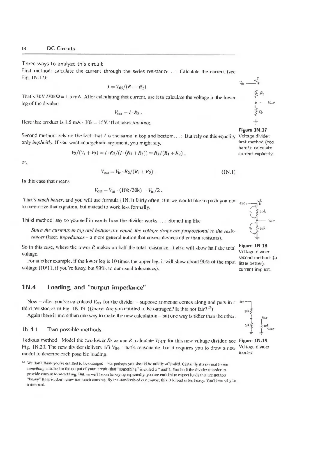
Three ways to analyze this circuit
First method calculate the current through the series resistance.. Calculate the current (see
Fig IN.17): I
Ио----->
I = VlN/(/?i + /?т) . I
That’s 30V /20k£2 = 1.5 mA. After calculating that current, use it to calculate the voltage in the lower
leg of the divider:
Vou, = //?2. i**
Here that product is 1.5 mA I Ok = 15 V. That takes too long.
Second method: rely on the fact that I is the same in top and bottom. . But rely on this equality
only implicitly. If you want an algebraic argument, you might say.
V2/(V| + V2) = / • R2/(l (Ki + «?)) = «2/(^1 + K2)
or.
Voul = Vin-/?2/(Ri+W2).
(INI)
In this case that means
Voul = Vin-(l0k/20k)-Vin/2.
That's much better, and you will use formula (IN. 1) fairly often. But we would like to push you not
to memorize that equation, but instead to work less formally.
Third method: say to yourself in words how the divider works. .: Something like
Since the currents in top and bottom are equal, the voltage drops are proportional to the resis-
tances (later, impedances - a more general notion that covers devices other than resistors)
So in this case, where the lower R makes up half the total resistance, it also will show half the total
voltage.
For another example, if the lower leg is 10 times the upper leg. it will show about 90% of the input
voltage (10/11, if you’re fussy, but 90%, to our usual tolerances).
Figure IN.17
Voltage divider:
first method (too
hard!), calculate
current explicitly
Figure IN.18
Voltage divider:
second method, (a
little better)
current implicit
IN.4 Loading, and “output impedance”
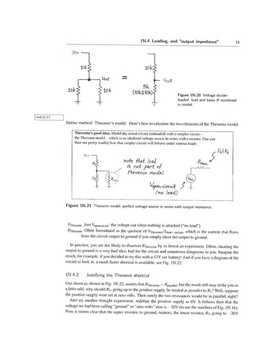
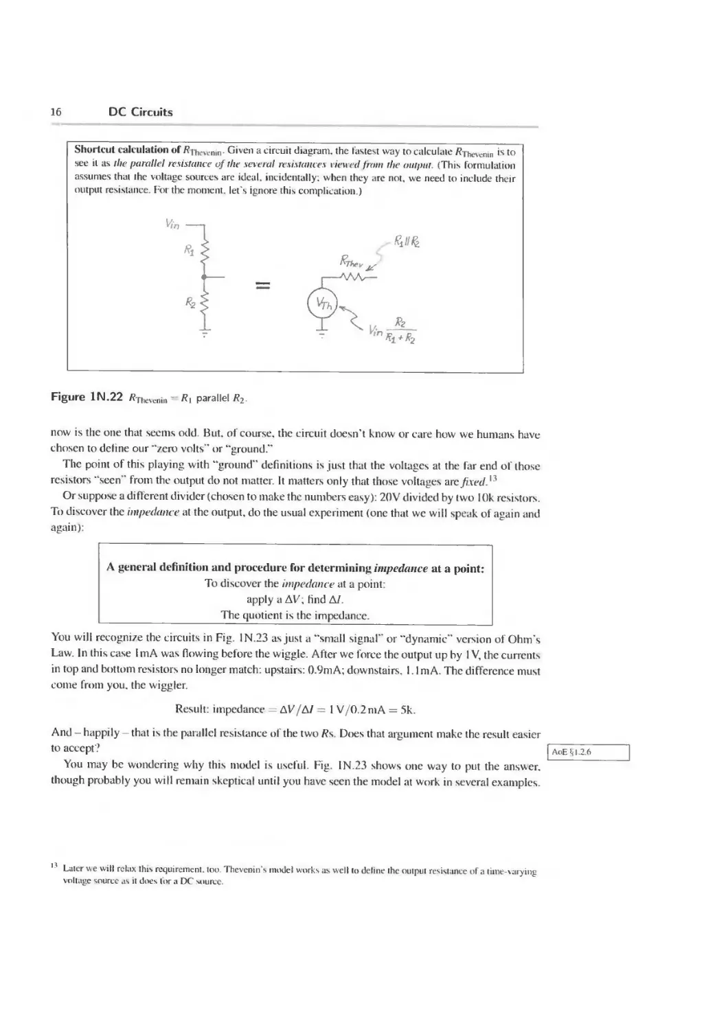
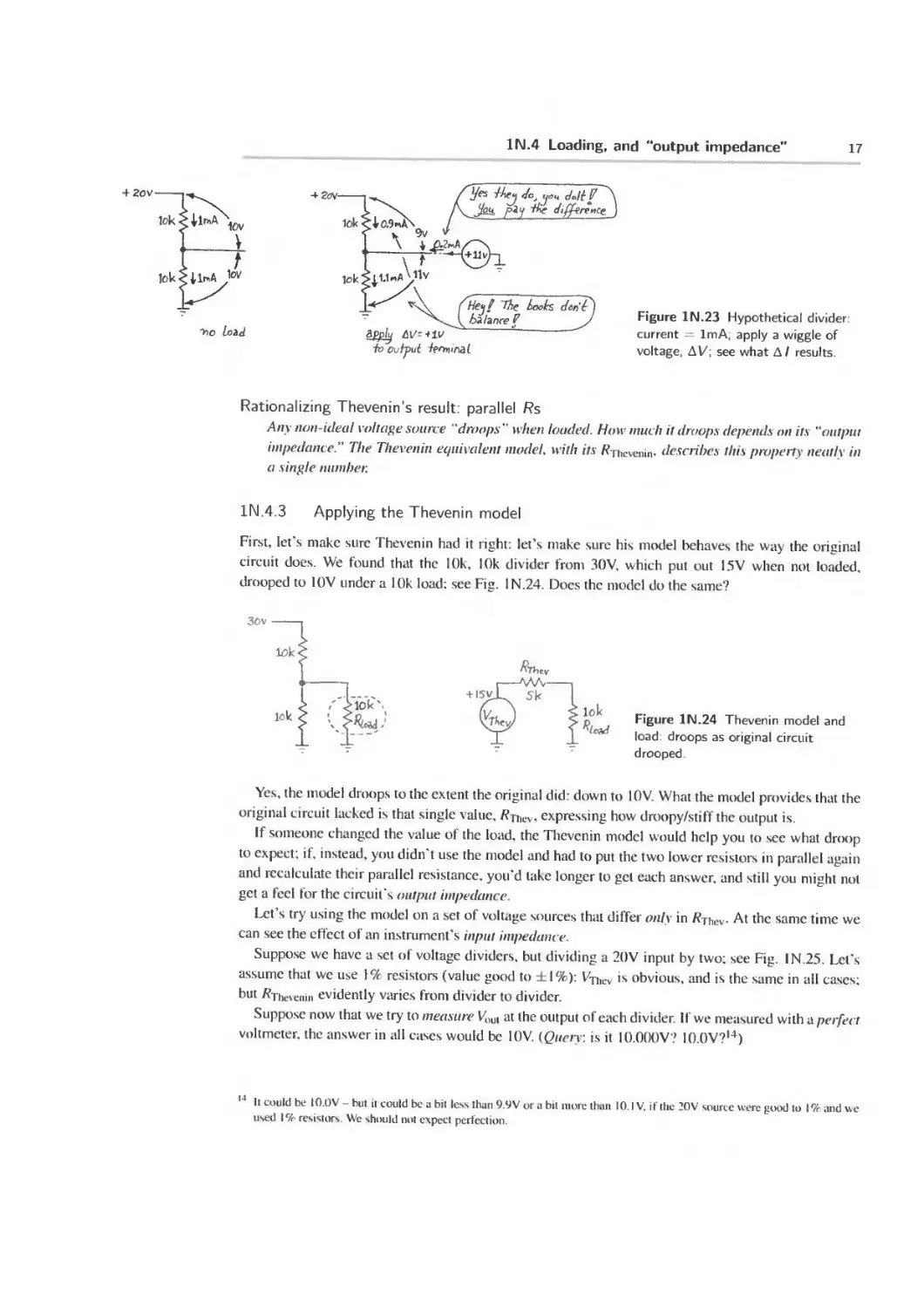
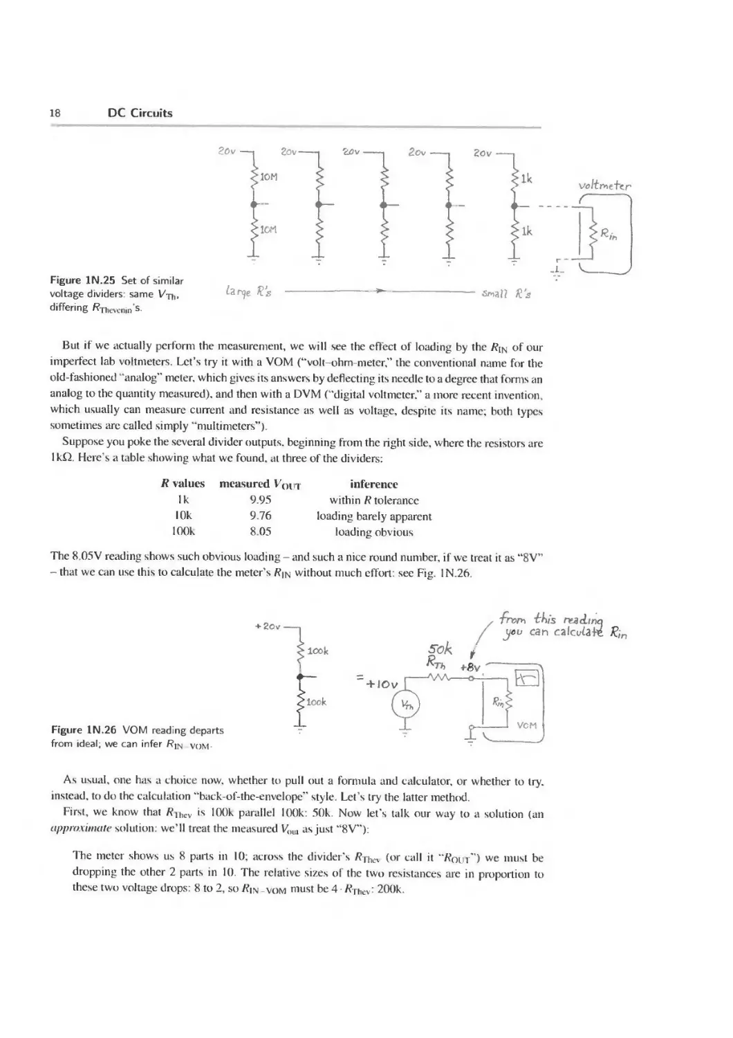
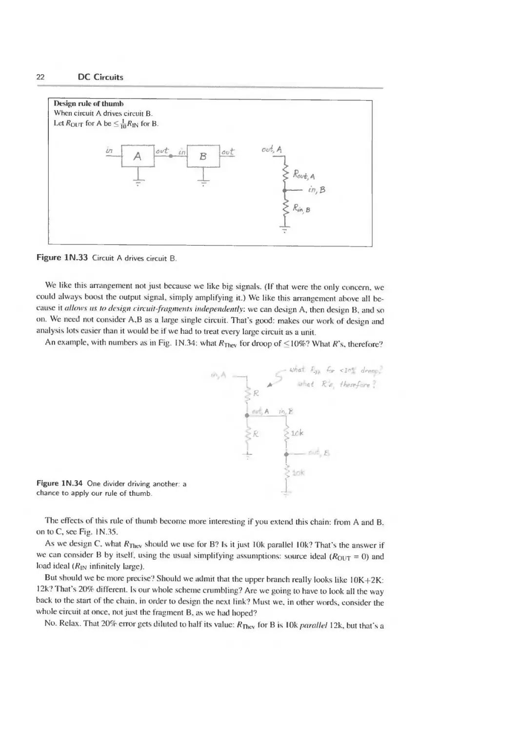
Now - after you’ve calculated Volll for the divider suppose someone comes along and puts in a **—i
third resistor, as in Fig. IN. 19. (Query: Are you entitled to be outraged? Is this not fair?12) ldt<
Again there is more than one way to make the new calculation - but one way is tidier than the other. 1 u,„t
10kS g lolt
IN.4.1 Two possible methods 1 1 "b
Tedious method: Model the two lower Rs as one R; calculate Vqut for this new voltage divider: see Figure IN.19
Fig. IN.20. The new- divider delivers 1/3 V|N That’s reasonable, but it requires you to draw a new Voltage divider
model to describe each possible loading. loaded
12 We don't think you're entitled to be outraged - but perhaps you should be mildly offended. Certainly it's normal lo see
somethin); attached to the output of your circuit (that "something” is called a “load"). You built the divider in order to
provide current to something But. as we ll soon be saying repeatedly, you are entitled lo expect loads that are not too
“heavy” (that is. don’t draw too much current). By the standards of our course, this Klk load is too heavy. You'll see why in
и moment.
IN.4 Loading, and “output impedance”
15
Figure IN.20 Voltage divider
loaded: load and lower R combined
in model.
| AoE §1.2.5 |
Better method Thevenin s model Here’s how to calculate the two elements of the Thevenin model:
Thevenin’s good idea. Model the actual circuit (unloaded) wtlh a simpler circuit -
the Thevenin model - which is an idealized voltage source in series with a resistor. One can
then see pretty readdy how that simpler circuit will behave under various loads.
7s not part of
Thevenin model
Kofe load
Figure IN.21 Thevenin model: perfect voltage source in series with output resistance
^Thevenin Just Kipencircuit: the voltage out when nothing is attached ("no load”)
^Thevenin Often formulated as the quotient of Vrhevenin/fshort circuit, which is the current that flows
from the circuit output to ground if you simply short the output to ground.
In practice, you are not likely to discover ftrhewnin by so brutal an experiment. Often, shorting the
output to ground is a very had idea: bad for the circuit and sometimes dangerous to you. Imagine the
result, for example, if you decided to try this with a 12 V car battery! And if you have a diagram of the
circuit to look at, a much faster shortcut is available: sec Fig 1 N.22.
IN.4 2 Justifying the Thevenin shortcut
Our shortcut, shown in Fig. 1 N.22, asserts that /?n,Cvcnin — ^parallel, but the result still may strike you as
a little odd why should Rt, going up to the positive supply, be treated as parallel to RTI Well, suppose
the positive supply were set at zero volts. Then surely the two resistances would be in parallel, right?
And try another thought experiment redefine the positive supply as 0V. It follows then that the
voltage we had been calling “ground” or “zero volts” now is 30V (to use the numbers of Fig. IN. 16).
Now it seems clear that the upper resistor, to ground, matters; the lower resistor, Ri, going to —30V
16
DC Circuits
Shortcut calculation of Rihevemn- Given a circuit diagram, the fastest way to calculate 7?Thevenui >s to
see it as the parallel resistance of the several resistances viewed from the output. (This formulation
assumes that lhe voltage sources are ideal, incidentally; when they are not, we need to include their
output resistance. For the moment, let's ignore this complication.)
Figure IN.22 flyhevenin Ri parallel /А
now is the one that seems odd. But, of course, the circuit doesn’t know or care how we humans have
chosen to define our "zero volts" or “ground."
The point of this playing with “ground” definitions is just that the voltages at the far end of those
resistors “seen" from the output do not matter. It matters only that those voltages are fixed.13
Or suppose a different divider (chosen to make the numbers easy): 20V divided by two 10k resistors.
To discover the impedance at the output, do the usual experiment (one that we will speak of again and
again)
A general definition and procedure for determining impedance at a point:
To discover the impedance at a point:
apply a AV; find А/.
The quotient is the impedance.
You will recognize the circuits in Fig. IN.23 as just a “small signal" or "dynamic" version of Ohm’s
Law. In this case 1mA was flowing before the wiggle. After we force the output up by 1V, the currents
in top and bottom resistors no longer match: upstairs: 0.9mA; downstairs, 1.1 ni A. The difference must
come from you, the wiggler.
Result: impedance AV/А/ = 1 V/0.2niA = 5k.
And - happily - that is the parallel resistance of the two Rs. Does that argument make the result easier
to accept? | AoFJii-2.fi
You may be wondering why this model is useful. Fig IN.23 shows one way to put the answer,
though probably you will remain skeptical until you have seen the model at work in several examples
1' Later we will relax this requirement, too. Thevenin’s model works as well to define the output resistance of a time-varying
voltage source as il does Гог a DC source.
IN.4 Loading, and “output impedance”
17
yes /'кем do. иоч doh
Чаи, piy dke diffei
Heyf The hooks derif:
balance V_________y
apply bV-Hv
to output tonmnaL
Figure IN.23 Hypothetical divider
current = 1mA; apply a wiggle of
voltage, AV; see what Д/ results
Rationalizing Thevenin's result parallel Rs
Any поп-ideal voltage source “droops" when loaded. How much it droops depends on its “output
impedance.” The Thevenin equivalent model, with its Rjhevemn’ describes this property neatly in
a single number.
IN.4.3 Applying the Thevenin model
First, let's make sure Thevenin had it right: let’s make sure his model behaves the way the original
circuit does. We found that the 10k, 10k divider from 30V, which put out 15V when not loaded,
drooped to 10V under a 10k load; see Fig. IN.24. Does the model do the same?
lok
Figure IN.24 Thevenin model and
load droops as original circuit
drooped.
Yes, the model droops to the extent the original did: down to 10V. What the model provides that the
original circuit lacked is that single value, 7?rhev> expressing how droopy/stiff the output is
If someone changed the value of the load, the Thevenin model would help you to see what droop
to expect; if, instead, you didn't use the model and had to put the two lower resistors in parallel again
and recalculate their parallel resistance, you'd take longer to get each answer, and still you might not
get a feel for the circuit's output impedance.
Let’s try using the model on a set of voltage sources that differ only in Rnev At the same time we
can see the effect of an instrument’s input impedance.
Suppose we have a set of voltage dividers, but dividing a 20V input by two; see Fig. IN.25. Let's
assume that we use 1% resistors (value good to ±1%); Vtucv is obvious, and is the same in all cases;
but /?The'cnin evidently varies from divider to divider.
Suppose now that we try to measure Vuul at the output of each divider. If we measured with a perfect
voltmeter, the answer in all cases would be 10V. (Query: is it 10.000V? 10.0V?14)
14 It could be 10.0V - but it could be a bit less than 9.9V or a bit more than 10. IV. if the 20V source were good to I % and we
used I % resistors. We should not expect perfection.
18
DC Circuits
Figure IN.25 Set of similar
voltage dividers: same Уть,
differing f^Thevcnin S.
iar^e K’s '— Sma!? H's
But if we actually perform the measurement, we will see the effect of loading by the /?in of our
imperfect lab voltmeters. Let’s try it with a VOM (“volt -ohm meter,” the conventional name for the
old-fashioned “analog” meter, which gives its answers by deflecting its needle to a degree that forms an
analog to the quantity measured), and then with a DVM (“digital voltmeter.” a more recent invention,
which usually can measure current and resistance as well as voltage, despite its name; both types
sometimes are called simply “multimeters”)
Suppose you poke the several divider outputs, beginning from the right side, where the resistors are
IkQ. Here’s a table showing what we found, at three of the dividers:
R values measured Vout
Ik 9.95
I Ok 9.76
100k 8.05
inference
within R tolerance
loading barely apparent
loading obvious
The 8.05V reading shows such obvious loading - and such a nice round number, if we tieat it as “8V”
- that we can use this to calculate the meter’s without much effort: see Fig. 1N.26.
Figure IN.26 VOM reading departs
from ideal, we can infer R^ vom
took
As usual, one has a choice now, whether to pull out a formula and calculator, or whether to try.
instead, to do the calculation “back-of-the-envelope” style. Let’s try the latter method.
First, we know that /?lhev is 100k parallel 100k: 50k Now let’s talk our way to a solution (an
approximate solution: we’ll treat the measured V()ul as just “8V"):
The meter shows us 8 parts in 10; across the divider’s /?rhe» (or call it "/four”) we must be
dropping the other 2 parts in 10. The relative sizes of the two resistances are in proportion to
these two voltage drops 8 to 2, so vom must be 4 Я-j-hew 200k
IN.4 Loading, and "output impedance'
19
If we look closely at the front of the VOM, we'll find a little notation,
20,000 ohms/volt.
That specification means that if we used the meter on its IV scale (that is, if we set things so that an
input of IV would deflect the needle fully), then the meter would show an input resistance of 20k. In
fact, it's showing us 200k. Does that make sense? It will when you've figured out what must be inside
a VOM to allow it to change voltage ranges: a set of big series resistors.15 Our answer, 200k, is correct
when we have the meter set to the 10V scale, as we do for this measurement.
This is probably a good time to take a quick look at what’s inside a multimeter - VOM or DVM:
How a meter works: some meter types fundamentally sense current, others sense voltage, see
Figs. IN.27 and IN.28. Both meter mechanisms, however, can be rigged to measure both quantities,
operating as a “multimeter.’’
Sensor
(very hiyh Я1П)
readout
circuit
Figure IN.27 An analog meter senses current in its
guts.
Figure IN.28 A digital meter senses voltage in its
innards
The VOM specification. 20,000 ohms/volt, describes the sensitivity of the meter movement - the
guts of the instrument. This movement puts a fairly low ceiling on the VOM's input resistance at a
given range setting.
Let's try the same experiment with a DVM. and let's suppose we get the following readings;
R values Measured Inference
I0()k 9.92 within R tolerance
IM 9.55 loading apparent
10M 6.69 loading obvious
Again let's use the case where the droop is obvious; again let’s talk our way to an answer:
This time ftp, is 5M; we’re dropping 2/3 of the voltage across -dvm- 1/3 across /?Th. So,
//in dvm must be 2 x Rrh, or 10M.
If we check the data sheet for this particular DVM we find that its /?in is specified to be "10M, all
ranges.” Again our readings make sense.
15
You'll understand this fully when you have done AoF Problem 1.8; for now. take our word lor it.
20
DC Circuits
Figure IN.29 DVM reading departs from ideal we can infer dvm
IN.4.4 VOM versus DVM: a conclusion?
Evidently, the DVM is a better voltmeter, at least in its /?jN - as well as much easier to use. As a current
meter, however, it is no better than the VOM: it drops 1/4V full scale, as the VOM does; it measures
current simply by letting it flow through a small resistor; the meter then measures the voltage across
that resistor.
IN 4 5 Digression on ground
The concept "ground" (“earth." in Britain) sounds solid enough. It turns out to be ambiguous. Try
your understanding of the term by looking at some cases: see Fig. 1 N.30.
A В
Figure IN.30 Ground in
two senses.
Query What is the resistance between points A and B? (Easy, if you don’t think about it too hard.16)
We know that the ground symbol means, in any event, that the bottom ends of the two resistors are
electrically joined. Does it matter whether that point is also tied to the pretty planet we live on'’ It
turns out that it does not.
And where is “ground” in the circuit in Fig. IN.31?
Two senses for Ground
“Local ground” Local ground is what we care about: the common point in our circuit that we
arbitrarily choose to call zero volts Only rarely do we care whether or not that local reference
is tied to a spike driven into the earth.
16 Well, not easy, unless you understand lhe "ground" indicated in Fig. IN 30 to be the common zero reference in the circuit
at hand In that case, the shared "ground"' connection means that the I Ok and 22k resistances are in series. If you took
ground " to mean "the world, with one connection in New York, the other in Chicago." the answer would not be so easy
Luckily, that would be a rare and perverse - meaning to attribute to the circuit diagram.
IN.4 Loading, and “output impedance'
21
Figure IN.31 Ground in two senses, revisited.
‘"Earth ground” But, he warned, sometimes you are confronted with lines that are tied to world
ground - for example, the ground clip on a scope probe, and the "ground" of the breadboards
that we use in the lab; then you must take care not to clip the scope ground to. say, +15 on
the breadboard
For a vivid illustration of “earth" grounding, see an image from Wikipedia:
http://en.Wikipedia.org/wiki/File:HomeEarthRodAustralial.jpg.
It might be useful to use different symbols for the two senses of ground, and such a convention does
exist: see Fig. 1 N.32.
"local" or
"chassis" ground
"earth" or
"world" ground
Figure IN.32 Symbols can distinguish the two senses of
"ground".
Unfortunately, this distinction is not widely observed, and in this book as m AoE, we will not
maintain this graphical distinction. Ordinarily, we will use the symbol that Fig. 1N.32 suggests for
"local ground." In the rare case when we intend a connection to "world” ground, we will say so in
words, not graphically.
IN.4 6 A rule of thumb for relating /?out_a to /?in_b
The voltage dividers whose outputs we tried to measure introduced us to a problem we will see over
and over again: some circuit tries to "drive” a load. To some extent, the load changes the output.
We need to be able to predict and control this change. To do that, we need to understand, first, the
characteristic we call /?]n (this rarely troubles anyone) and, second, the one we have called /?Thcvenin
(this one takes longer to get used to). Next time, when we meet frequency-dependent circuits, we will
generalize both characteristics to "Zin” and “Zout”
Here we will work our way to another rule of thumb; one that will make your life as designer
relatively easy. We start with a Design goal When circuit A drives circuit B: arrange things so that В
loads A lightly enough to cause only insignificant attenuation of the signal. And this goal leads to the
rule of thumb in Fig. 1 N.33.
How does this rule get us the desired result? Look at the problem as a familiar voltage divider
question. If /folJTA >s much smaller than Kinb, then the divider delivers nearly all of the original
signal. If the relation is 1:10, then the divider delivers 10/11 of the signal: attenuation is just under
10%, and that's good enough for our puiposes.
22
DC Circuits
We like this arrangement not just because we like big signals. (If that were the only concern, we
could always boost the output signal simply amplifying it.) We like this arrangement above all be-
cause tt allows us to design circuit-fragments independently: we can design A, then design B, and so
on. We need not consider A,В as a large single circuit. That’s good: makes our work of design and
analysis lots easier than it would be if we had to treat every large circuit as a unit.
An example, with numbers as in Fig. 1 N.34: what Rrhev for droop of <10%? What R\. therefore?
> "at R л therefore
. A mF
I
ft
I H *-1
Figure 1N.34 One divider driving another: a
chance to apply our rule of thumb
The effects of this rule of thumb become more interesting if you extend this chain: from A and B.
on to C, see Fig. I N.35.
As we design C, what ftyiiev should we use for B? Is it just 10k parallel 10k? That's the answer if
we can consider В by itself, using the usual simplifying assumptions: source ideal (Rout = 0) and
load ideal (Rin infinitely large).
But should we be more precise? Should we admit that the upper branch really looks like 10K.+2K:
12k? That’s 20% different. Is our whole scheme crumbling? Are we going to have to look all the way
back to the start of the chain, in order to design the next link? Must we, in other words, consider the
whole circuit at once, not just the fragment B. as we had hoped?
No. Relax. That 20% error gets diluted to half its value: Rrhev for Bis I Ok parallel 12k, but that’s a
IN.4 Loading, and "output impedance’
23
Figure IN.35 Extending the
divider testing the claim that
our rule of thumb lets us
consider one circuit fragment
at a time.
shade under 5.5k. So we need not look beyond B. We can, indeed, consider the circuit in the way we
had hoped: fragment by fragment.
If this argument has not exhausted you, you might give our claim a further test by looking in the
other direction: does C alter B’s input resistance appreciably (>10%)? You know the answer, but
confirming it would let you check your understanding of our rule of thumb and its effects.
Two important exceptions to our rule of thumb: signals that are currents, and
transmission lines
The rule of §1N 4.6 for relating impedances is extremely useful and important. But we should ac-
knowledge two important classes of circuits to which it does nor apply
| AoEgH.l
Signal sources that provide current signals rather than voltage signals. At the moment, this dis-
tinction may puzzle you. Yet the distinction between volrage sources - the sort familiar to most
of us - versus current sources is substantial and important.17
High-frequency circuits where the signal paths must be treated as “transmission lines” (see Ap-
pendix C).
Only at frequencies above what we will use in this course do such effects become apparent.
These are frequencies (or frequency components, since “steep” waveform edges include high
frequency components, as Fourier teaches - see Chapter 3N) where the period of a signal is
comparable to the time required for that signal to travel to the end of its path. For example, a
six-foot cable's propagation time would be about 9ns the period of a 110MHz sinusoid. Square
waves are still more troublesome, one at even a few MHz would include quite a strong component
at that frequency, and this component would be distorted by such a cable if we did not take care
to “terminate” it properly. In fact, these calculations understate the difficulties; a round-trip path
length greater than about l/10th wavelength calls for termination
We don’t want you to worry, right now, about these two points. Signals as currents are unusual
m this course, and in this course you are not likely to confront transmission line problems. But be
warned that you will meet these later, if you begin to work with signals at higher frequencies.
You may be inclined io protest that you can convert a curreni into a voltage and vice versa. You will build your first circuit
with an output that is a delermined current in Lab 4L. and you will meet your first current source transducer (a photodiode)
in Lab 6L.
24
DC Circuits
IN.5 Readings in AoE
This is the first instance in which we've tried to steer you toward particular sections of The Art of
Electronics. That book is, of course a sibling (or is it the mother?) of the book you are reading You
should not consider the readings listed below to be required But it you are proceeding by using the
two books in parallel, these are the sections we consider most relevant.
Readings:
Chapter 1. §§ 1.1-1.2.7.
Appendix C on resistor types: resistor color code and precision resistors.
Appendix H on transmission lines.
Problems:
Problems in text.
Exercises 1.37, 1.38.
IL Lab: DC Circuits
1L.1 Ohm’s law
A preliminary note on procedure
The principal challenge here is simply to get used to the breadboard and the way to connect instru-
ments to it. We do not expect you to find Ohm's law surprising Try to build your circuit on the
breadboard, not in the air. Novices often begin by suspending a resistor between the jaws of alligator
clips that run to power supply and meters. Try to do better: plug the two leads of the DUT (“Device
Under Test") into the plastic breadboard strip. Bring power supply and meters to the breadboard using
banana-to-wire leads, if you have these, to go direct from banana jack on the source right into the
breadboard. In Fig. IL. I is a sketch of the poor way and better way to build a circuit.
Figure 1L.1 Bad and good
breadboarding technique Left labor
intensive, mid-air method; Right: tidy
method, circuit wired in place.
Color coding, and making the circuit look like its diagram
This is also the right time to begin to establish some conventions that will help you keep your circuits
intelligible: in Fig. I L.2 is a photo of one of our powered breadboard boxes, showing the usual power
supply connections. The individual breadboard strips make connections by joining inserted wires in
small spring-metal troughs: see Fig. 1L.3. Use a variable regulated DC supply, and the hookup shown
in the Fig. 1L.9.
Caution! You must not connect the external supply to the colored banana jacks on the powered bread-
board (Red, Yellow, Blue): these are the outputs of the internal supplies of the breadboard, and even
when the breadboard power is off, these connectors tie to internal electronics that can be damaged by
an attempt to drive it. The same warning applies to the three white horizontal power supply “buses” at
the top of the board, strips that are internally tied to those three internal power supplies. (In case you
are curious. Red is +5, while Yellow and Blue are adjustable, and normally are set to about ± 15V.)
Note by the way, that voltages arc measured between points in the circuit, while currents are mea-
sured through a part of a circuit. Therefore you usually have to “break" or interrupt the circuit in order
to measure a current.
26
Lab: DC Circuits
three fixed supplies (though +-15V are adjustable)
These are color coded +15 yellow. +5 red. ground black -15 blue
Keep this code as you wire individua breadboards and your circuit supplies
m dpoints of horizontal strips bridged with jumper wire
we have connected
V+ vertical supply bus
to horizontal supply bus
of individual breadboard
R:R voltage divider
top connected to V+
supply bus bottom
connected to
ground bus
we have connecte
two fixed supplies
vertical two-lme
supply buses
input lead of DVM
meter reads midpoint of voltage divider
(voltage relative to its ground lead.
which is tied to breadboard s ground)
we have connected vertical supply
buses to horizontal supply buses
of individual breadboards
fixed supplies are internally connected
to horizontal supply buses we have
connected these horizontal buses to
vert cal two-lme supply buses
measures voltage
ground reference for DVM
at midpoint of R R
voltage div der
Figure IL.2 Breadboard power bus connections, again.
TOP VIEW
connection troughs
join five vertical holes,
in one column
UNDERSIDE VIEW
break at midpoint of
horizontal buses
, - horizontal power buses
trench separates vertical
connection troughs at
midpoint
Figure 1L.3 Single breadboard strip a look at underside reveals the pattern of connecting metal
troughs
IL.2 Voltage divider
Construct the voltage divider shown in Fig IL.4 Apply Vjn=15V(use the DC voltages on the bread-
board) Measure the (open circuit) output voltage. Then attach a 7.5k load and see what happens.
1L.3 Converting a meter movement into a voltmeter and ammeter
27
Figure IL.4
Voltage divider.
Now measure the short circuit current. (That means “short the output to ground, but make the
current flow through your current meter.” Don't let the scary word "short” throw you: the current in
this case will be very modest. You may have grown up thinking “a short blows a fuse ” That’s a good
generalization around the house, but it often does not hold in electronics.)
From /shortCircuit an<J hopenCircuii you can calculate the Thevenin equivalent circuit.
Now build the Thevenin equivalent circuit, using the variable regulated DC supply as the voltage
source, and check that its open circuit voltage and short circuit current match those of the circuit that
it models. Then attach a 7.5k load, just as you did with the original voltage divider, to see if it behaves
identically.
A Note on Practical Use of Thevenin Models
You will rarely do again what you just did: short the output of a circuit to ground in order
to discover its Rjhevemn (or “output impedance,” as we soon will begin to call this charac-
teristic). This method is too brutal in the lab. and too slow when you want to calculate Л-щ
on paper.
In the lab, Isc could be too large for the health of your circuit (as in your fuse-blowing
experience). You will soon learn a gentler way to get the same information.
On paper, if you are given the circuit diagram the fastest way to get RTh for a divider is
always to take the parallel resistance of the several resistances that make up the divider
- again assuming /?S()urce ideal: /его ohms. (A hard point to get used to. here: look at all
paths in parallel, going to any fixed voltage, not just to ground. See the attempt to rationalize
this result in Fig. IN.23 on p 17.) The case you just examined is illustrated in Fig. IL.5.
Figure IL.5 R-j-h = parallel
resistances as seen from the circuit’s
output.
1L.3 Ohm’s law applied to convert a meter movement into a
voltmeter and ammeter
A Thevenin model is extremely useful as a concept; but you'll not again build such a model. The
circuit you just put together is useful only as a device to help you get a grip on the concept. Now
comes, instead, a chance to apply Ohm’s law to make something almost useful! - a voltmeter, and
then a current meter (“ammeter”).
You will start with a bare-bones "meter movement” - a device that lets a current deflect a needle.
This mechanism is basically a current-measuring device: the needle’s deflection is proportional to the
torque developed by a coil that sits in the field of a permanent magnet, and this torque is proportional
to the current through lhe coil. See the sketch1 in Fig. 1L.6.
An analog “multimeter” or VOM (volt-ohm-milliammeter) is just such a movement, with .switch-
able resistor networks attached. We would now like you to re invent the multimeter.
1 After Google images file: “analog meter movement." Source unknown.
28
Lab: DC Circuits
Figure IL.6 Mechanism of analog
current/volt-meter From The Free Dictionary,
see www.globalspec.com
IL.3.1 Internal resistance of the movement
You could design a voltmeter - as you will in the next subsection - simply assuming that the move-
ment's /?int is negligibly small. The resistance of this movement is low - well under 1 kQ. But let's be
more careful. Let’s first measure the internal resistance. Here, please note, we want you to work with
a simple bare meter movement, not with a multimeter. (It’s more fun to stait from scratch.)
Do this measuring any way you like, using the variable power supply, DVM (digital voltmeter -
really a multimeter, despite its name), and VOM if you need it. If you use DVM as current meter,
we should warn you that it is easy to blow the meter’s internal fuse, because a moment's touch to a
power supply will pass an essentially unlimited current. To make things worse, a DVM with blown
fuse offers no display to indicate the problem. Instead, it simply persists in reading zero current. There
are several good ways to do this task.
The meter movements are protected". Don't worry about burning out the movement, even if you
make some mistakes. Even "pinning" the needle against the stop will not damage the device, as we
found by experiment though in general you'll want to avoid doing this to analog meters. We have
provided diodes that protect the movement against overdrive in both forward and reverse directions
You should note, as a result, that these diodes that protect the movement also make it behave very
strangely if you overdrive it. (No doubt you can guess what device it behaves like.) So, don't use data
gathered while driving the movement beyond full scale.
Sketch the arrangement you use to measure and note the values of f?INr and A l li scale •
IL.3.2 10V voltmeter
Show how to use the movement, plus whatever else is needed, to form a l()V-full-scale voltmeter (that
just means that 10V applied to the input of your circuit should deflect the needle fully). Draw your
circuit.
Note', this is a good time to start getting used to our canny use of approximations, as we design. As
you specify the resistor that you want to add to the bare meter movement, recall that you are limited
to “5% values" - resistors whose true value is known only to lie within ±5% of the nominal value.
Does the movement's internal resistance cause a significant error? (What does "significant" mean?
Well, you might compare the contribution of f?iN1 against the contribution of error from your uncer-
tainty about the value of the resistor that (we hope!) you have included.)
2 Note to instructors: please add two paralleled and oppositcly-onented silicon diodes such as 1N4004 in parallel with lhe
meter movement. These will conduct ai about 0.6V. protecting the movement during oxerdrive.
IL.4 The diode
29
1L.3.3 10mA current meter (“ammeter”)
Show how to use the movement, plus whatever else is needed, to form a I OmA-full-scale ammeter
(This is a bit trickier than the 10V voltmeter.) Sketch it, and test your circuit.
IL.4 The diode
Here is another device that does not obey Ohm’s law: the diode. (We don’t expect you to understand
how the diode works yet; we just want you to meet it, to get some perspective on Ohm's Law devices:
to see that they constitute an important but special case.
We need to modify the test setup here, because you can’t just stick a voltage across a diode, as you
did for the resistor and lamp above’. You'll see why after you’ve measured the diode's V versus I. Do
that by wiring up the circuit shown in Fig. 1L.7.
Figure IL.7 Diode VI
measuring circuit
In this circuit you are applying a current, and noting the diode voltage that results; earlier, you
applied a voltage and read resulting current. The Ik resistor limits the current to safe values. Vary R
- use a 100k variable resistor (usually called a potentiometer or “pot” even when wired, as here, as
a variable resistor), a resistor substitution box, or a selection of various fixed resistors) and look
at I versus V. First, get a feel for the behavior by sweeping the R value by hand, and noticing what
happens to the diode current. Then sketch the plot in two forms linear and Im -log (or semi-log), in
Fig. IL.8.
First, get an impression of the shape of the linear plot; just four or five points should define the
shape of the curve Then draw the same points on a lin-lot> plot, which compresses one of the axes.
(Esidently, it is the fast-growing current axis that needs compressing, in this case.) If you have some
lin-log paper use it. If you don't have such paper, you can use the small version laid out below. The
point is to see the pattern.
See what happens if you reverse the direction of the diode. How would you summarize the V versus
I behavior of a diode? Now explain what would happen if you were to put 5V across the diode (don’t
try it!). Look at a diode data sheet, if you're curious see what the manufacturer thinks would happen.
The data sheet won’t say “Boom” or “Pfft.” but that is what it will mean.
We'll do lots more with this important device
4 Well, you can: but you can’t do it twice with the same diode’
Lab: DC Circuits
30
Figure IL.8 Diode I versus V linear plot;
lin-log plot
IL.5 I versus V for some mystery boxes
Find two mystery boxes which your instructor4 will have set up for you (we will call these DUTs.
Device Under Test). These are two-terminal devices, one of which is an ordinary resistor, the other an
odder thing. The devices are hidden inside black plastic 35mm film cans. Apply voltages in the range
zero to a couple of volts, using a variable power supply, and note voltage and current pairs. For the
range between 0 and IV, measure at increments of 0.1V (because this is the range where you need a
detailed picture).
Figure IL.9 Circuit for measurement of I versus V
Sketch a graph of a few points to get the trend. Turning the power-supply voltage knob by hand,
you may be able to get a sense of the shape of the curve, or see where more points are needed.
Decide which device is which: which ordinary, which odd. Warning', keep the applied voltage below
7V, or you may destroy one of the DUT.s.
To make your task challenging, we ask that you measure voltage and current simultaneously, as
you do this exercise. We ask this so that you will be obliged to consider the effects of the instruments
on your measurements (more on this point, below).
4 If you’re working through this book on your own no one will have set this up of course. But you and instructors can get
more information at www.anofelectronics.coin.
IL.5 I versus V for some mystery boxes
31
Effects of the instruments on your readings: Consider a couple of practical questions that arise in
even this simplest of “experiments.”
A qualitative view: Is the voltmeter measuring the voltage at the place you want, namely across the
object under test? Or does the voltage reading include the effect of the ammeter, in your arrangement9
Does that matter? If you are measuring the object’s voltage precisely, then are you reading its current
or are you measuring the current in object plus the current passing through the DVM as well? If you
can’t have it both ways (as you can't), and must live with one of the two errors, which experimental
setup gives you the smaller error?
Figure IL. 10 shows two sketches of the two possible placements of the voltmeter.
Figure IL.10 Measuring I and V simultaneously: only one instrument gets a true reading at DUT.
If you know (and we’ll now reveal this fact to you) that the LOAD resistance is under Ik (“resis-
tance” or some near-equivalent: we’re not promising you Ohmic behavior), then you can judge which
of the two setups illustrated above gives the truer pair of / and V readings. Use that preferred setup to
get a set of / and V readings, and try to infer an R value, if you can.
IL 5.1 Estimate % error caused by the instruments
Once you have your best estimate of R in hand, estimate the errors that the instruments cause. Specif-
ically, when the ammeter is on the IOmA full-scale range, what percentage error in inferred R results
from the presence of...
• ammeter, when you measure V where the ammeter causes an error?
• voltmeter, when you measure V where the ammeter causes no error?
After getting answers to these questions, probably you can say what an ideal voltmeter (or ammeter)
should do to the circuit under test? What does that say about its “internal resistance”? (Perhaps you
caught on to this theme, pages earlier)
Now sketch the curves described by your data points. Don’t work too hard: it’s the shapes that
we’re after. The resistor isn t very interesting (what’s its value?): the mystery device is a little more
intriguing.
What do you suppose the mystery gadget is? We hope you saw its curve. In fact, it’s made of
material much like what forms the resistor. Why does its IV curve look different? The bend can be
useful, much later, in Lab 8L. we will exploit this curvature to make a circuit regulate its own gain.
Now you have earned the right to open up the film canister and discover what’s inside.
32
Lab: DC Circuits
1L.5 2 Where should DVM and ammeter go, for large /?load?
Now you may have “learned" in the previous exercise where to place the voltmeter in order to get the
best simultaneous I and V readings. Just to make sure you don't go away thinking you’ve learned
something5, we’d like you to try a pencil-and-paper exercise, this time assuming that the DUT
(Kload) is a very large resistance: 10MQ. Assume that the DVM’s /?1N = IOMQ. (Note that we’re
not asking you to carry out this experiment, only to predict what you would see if you did do the
experiment.)
If you placed your DVM at the load, the DVM would appear in parallel with the load. What percent
age error would this evoke in the simultaneous current measurement? In contrast, the voltage error
caused by reading upstream of the ammeter in this case would be no larger than in the case you tried
in the lab experiment.
Perhaps now you can begin to generalize about which cases oblige one to worry about the DVM’s
^IN-
IL.6 Oscilloscope and function generator
This is just a first view of oscilloscopes to give you a head start (more about oscilloscopes can be
found in Appendix D and AoE. Appendix O). You'll get a big (oscillo)scope workout later in Lab 2L.
We’ll be using the oscilloscope and function generator in virtually every lab from now on. For
today's lab, voltmeters were sufficient - and, in fact, more convenient than an oscilloscope, because
our circuits' voltages and currents have been politely sitting still, giving us time to measure them If
you are familiar with the scope, go right on to the first real exercise in Lab 2L - or go home, having
earned a rest.
The scope soon will become our favorite instrument as we begin to look at signals that are not
static (called DC in electronics jaigon): signals that, instead, vary with time. Lab 2L is concerned
exclusively with such circuits, and with rare exceptions this will be true of all our work from now on.
The scope draws a plot of voltage (on the vertical axis) versus time (on the horizontal axis).
Get familiar with scope and function generator (a box that puts out time-varying voltages, or “wave-
forms:" things like sinewaves, triangle waves and square waves) by generating a 1kHz sinewave with
the function generator and displaying it on the scope. Connect the function generator directly to the
scope, using a “BNC cable,” not a probe.6
If it seems to you that both instruments present you with a bewildering array of switches and knobs,
don’t blame yourself. These front-panels just are complicated. You will need several lab sessions to
get fully used to them - and at term's end you may still not know all: it may be a long time before
you find any occasion for use of the holdoff control, for example, or of single-shot triggering, if your
scope offers this.
Play with the scope's sweep and trigger controls. Most of the discussion, here, applies fully only to
an analog scope. The digital scope automates some functions, such as triggering and gain setting, if
you want it to. We suggest that you ought not to begin your scope career using such fancy features:
beware the mind-stunting button labeled AUTOSET'.
Specifically, try the following:
5 Jusl kidding.
6 BNC (Bayonet Neill-Concelman) names the connectors on the ends of this coaxial cable. (See AoE §1 S). We usually call
lhe cable by this name, though strictly the term applies to its connectors
IL.6 Oscilloscope and function generator
33
• The vertical gain switch. This controls “volts/div”: note that “div” or "division" refers to the
centimeter marks, not to the tiny 0.2cm marks);
• The horizontal sweep speed selector: time per division.
On this knob as on the vertical gain knob, make sure the switch is in its CAL position, not
VAR or “variable.” Usually that means that you should turn a small center knob clockwise
till you feel the switch detent click into place. If you don't do this, you can't trust any reading
you take.)
• The trigger controls. Don’t feel dumb if you have a hard time getting the scope to trigger properly.
Triggering is by far the subtlest part of scope operation. “Trigger” circuits tell the scope when to
begin moving the trace across the screen: when to begin drawing a waveform. When you think
you have triggering under control, invite your partner to prove to you that you don’t: have your
partner randomize some of the scope controls, then see if you can regain a sensible display (don’t
let your partner overdo it, here).
Beware the tempting so-called “normal” settings (usually labeled “NORM”). They rarely
help, and instead cause much misery when misapplied. Think of “normal” here as short for
abnormal! Save it for the rare occasion when you know you need it. “AUTO” is almost
always the better choice.
The scope waits around till triggered. In AUTO mode, it sweeps either when triggered,
or when it has waited so long that it loses patience. Thus you always get at least a trace,
in AUTO mode.
NORMAL, in contrast, makes the scope infinitely patient: it will wait forever, drawing
nothing on the screen, until it sees a valid trigger signal. Meanwhile, you look at a dark
screen; usually, that is not helpful!
Trigger “source”: here’s another way to go wrong: trigger can be set to look at either
of the scope’s two input “channels” (CH 1 or CH2), or at the external BNC connector
called EXT.
Switch the function generator to square waves and use the scope to measure the “risetime" of the
square wave (defined as time to pass from 10% to 90% of its full amplitude).
At first you may be inclined to despair, saying “Risetime? The square wave rises instantaneously.”
The scope, properly applied, will show you this is not so.
A suggestion on triggering
It's a good idea to watch the waveform edge that triggers the scope, rather than trigger on
one event and watch another. If you watch the trigger event, you will find that you can
sweep the scope fast without losing the display off the right side of the screen.
So, to measure risetime of a signal connected to Channel One, trigger on Ch I, rising-edge.
What comes out of the function generator’s SYNC OUT or TTL7 connector?
Look at this on one channel while you watch a triangle or square wave on the other scope channel.
To see how SYNC or TTL can be useful, try to trigger the scope on the peak of a sinewave without
using these aids; then notice how entirely easy it is to trigger so when you do use SYNC or TTL to
trigger the scope.
Triggering on a well-defined point in a waveform is especially useful when you become interested
in measuring a difference in phase between two waveforms; this you will do several times in the next
TTL stands for lhe equally cryptic phrase. Transistor-Transistor Logic, which is a kind of digital logic gate that you will
find described in Chapter I4N In the present context. TTL should be understood to mean simply Logic-Level square wave
a square wave that swings between ground and approximately four volts.
34
Lab: DC Circuits
lab. You can use a zero-crossing (where the waveform crosses the midpoint of its excursion), or, when
using SYNC OUT, you can use the peak or trough of the waveform.
How about the terminal marked CALIBRATOR (or CAL) on the scope’s front panel? (We won't
ask you to use this signal yet; not until Lab 3L do we explain how a scope probe works, and how you
“calibrate” it with this signal. For now, just note that this signal is available to you). Postpone using
scope probes until you understand what is within one of these gadgets. A “lOx” scope probe is not
just a piece of coaxial cable with a grabber on the end.
Put an “offset” onto the signal, if your function generator permits, then see what the AC/DC switch
(located near the scope inputs) does.
Note on AC/DC switch
Common sense may seem to invite you to use the AC position most of the time: after
all, are these time-varying signals that you’re looking at not “AC” - alternating current (in
some sense)9 Eschew this plausible error The AC setting on the scope puts a capacitor in
series with the scope input, and this can produce startling distortions of waveforms if you
forget it is there. (See what a 50Hz square wave looks like on AC, if you need convincing.)
Furthermore, the AC setting washes away DC information, as you have seen: it hides from
you the fact that a sinewave is sitting on a DC offset, for example. You don’t want to wash
away information except when you choose to do so knowingly and purposefully. Once in a
while you will want to look at a little sine with its DC level stripped away, but always you
will want to know that this DC information has been made invisible.
Figure 1L.11 AC/DC scope
input select.
Set the function generator to some frequency in the middle of its range, then try to make an accurate
frequency measurement with the scope. (Directly, you are obliged to measure period, of course, not
frequency8.) You will do this operation hundreds of times during this course. Soon you will be good
at it.
Trust the scope period readings; distrust the analog function generator frequency markings; these
are useful only for very approximate guidance.
s Well, if you’re using a digital scope you could resort to the shabby trick of asking it to measure frequency for you Bui
don’t start that way today.
IS Supplementary Notes: Resistors,
Voltage, Current
1S.1 Reading resistors
In the lab exercises, from now and ever after, you will want to be able to read resistor values without
pulling out a meter to measure the part’s value (we do sometimes find desperate students resorting to
such desperate means). The process will seem laborious, at first; but soon, as you get used to at least
the common resistance values, you will be able to read many color codes at a glance. We will use
resistors whose packages are big enough to be readable. The now-standard surface-mount parts are so
tiny that the smaller ones normally are not labeled at all This spares you the trouble Land opportunity )
of reading them. If you mix a few surface-mount parts on the bench, you can only sweep them up and
start over - unless you are willing to measure each.
IS 1 1 A menagerie of 10 resistors
Fig. IS. 1 shows a handsome collection of 10k resistors in a variety of packages.
RC07 1/4W carbon composition 5%
<Iili 1------------------- metal film, 1 % (last stripe, brown = 1, ==> 1 %)
RN55D metal film, 1%
0805 surface mount (dimension in 10 mils = 0.01 in, so this is 0 08 X 0 05 in )
n 0603 0402 0201
Figure 1S .1 10k resistors.
The type that we use - the carbon composition resistor at the top - is nearly obsolete, and relatively
expensive, as a result. But we like them for lab work, because (on a good day) we can read them. The
others are pretty nasty for breadboarding. The one with the value written out in numerals may appeal
to you. if you don’t want to learn the color codes - but it really isn’t much fun to work with, because
if it happens to be mounted with the value label down, you’re out of luck.
36 Supplementary Notes: Resistors, Voltage, Current
IS 1.2 Resistor values and tolerances
Figure IS 2 shows a resistor of the sort we use in this course's labs: it is a “5% carbon composition”
part. “5%” “tolerance” means that its actual value is guaranteed to lie w ithin 5% of its nominal value.
If it is labeled "100k” (lOO.(M)OQ), its actual value can be expected to lie in the range ~95— 105kQ
The first problem one confronts on a first day with resistors, is и hich wax to orient the part.
Figure IS .2 Which way? Put the tolerance
stripe to the right.
“Tolerance stripe?'' you protest. “How do 1 know which that is?” In our labs, the answer is the
fourth band, colored silver or gold If you are using color-coded 1% resistors, the tolerance band will
be the fifth Fig. 1S.3 shows such a part.
Figure 1S .3 Extra band for color-coded 1%
resistor.
value: 1 О 0 2--100 X 10? = 10k
The use of four bands to define the value indicates (implicitly) that this is better than the usual
5% part; the color of the fifth band, brown represents “1,” for this ‘‘I%” resistor. (A red band would
indicate 2%, and so on )
Tolerance: Only two tolerance values are common, for the 3-band carbon composition parts you are
likely1 to meet in the labs 5% and 10%:
• silver: ±109!
• gold: ±5%
Value: Once you've oriented it properly - tolerance to the right - you can read off the value colors,
and then can translate those to numbers. Finally, with the three numbers in hand, you will have enough
information to discover the value The resistor we just looked at is brown-black-yellow: see Fig. 1S.4.
Brown-black-yellow is one-zero-four, and the fourth band, gold, says “±5%.”2 The third band, the
“four.” is an exponent - a power of ten. So, this resistor's value is 100k.
1 No tolerance band, in a 3 stripe pan i idicates ±20% Such resistors are rare.
- Sometimes the fourth band is mil the last band; one more is added, for military components, to indicate the "failure rate ”
1S.1 Reading resistors
37
value: 1 0 4 = 10 X 1O* - 1& -- 100k
(+ 5% resistor.
carbon composition)
Figure IS.4 Value stripes reveal
what this resistor is.
The color code The colors represent numbers, as set out below. A variety of mnemonics have arisen,
most of them more-or less offensive, in order to help engineers to memorize this code. One of the
blander mnemonics is ‘‘Big Boys Race Our Young Girls. But Violet Generally Wins.” This mnemonic
is not very clever. It fails to distinguish the trio Black, Brown and Blue and also between the pair Green
and Gray. Black is a plausible representation of the value zero, since black represents the absence of
color; the color Brown is close to the color Black; perhaps one might remember Gray’s position as
“next to White.” None of this is very satisfactory. We keep charts of the color codes up on the walls
of our own teaching lab.
Here are the colors and the values they represent;
• black: zero
• brown: one
• red: two
• orange three
• yellow: four
• green: five
• blue: six
• violet: seven
• gray: eight
• white: nine
the next two are used as multipliers only, and are rarely seen:
• gold: 0.1
• silver: 0.01
IS 1.3 The set of 10% values’
It is hard to get used to the strange set of values that are “standard” in the lab. They are not the nice,
round values that one might expect. They seem weird and arbitrary at first. But their strangeness does
make sense. Because of our uncertainty about the actual value of a resistor, it doesn’t make sense to
specify distinct nominal values that are too close together; if we specify nominal values that are too
close, their actual values are likely to overlap. To avoid this, the nominal values are placed far enough
apart so as to make overlap slight.
A “10%” resistor of nominal value “10Q,” for example, could be as large as 1 IQ. A “12Q" resistor
could be 10% smaller - a bit under 1 IQ. So, 12 is about as close as it makes sense to place the next
10% value after “10.” And so on - the steps growing proportionally as the values rise, producing such
unfamiliar numbers as 27, 39, 47, and so on. Here is the 10% set (known as “El2,” twelve values per
decade. See Appendix C in AoE). Most of our laboratory circuits will use these 10% values (with
38
Supplementary Notes: Resistors, Voltage, Current
appropriate multipliers: we rarely use 10 ohm resistors, but often use 1 OkQ parts, for example). This
is so even though our lab resistors are better than 10% parts - normally they are good to ±5%:
10, 12. 15. 18. 22. 27. 33. 39. 47, 56. 68. 82, 100
IS 1.4 Power
Only now and then are we obliged to consider power ratings of the components we use in the labs.
That is true because our signal voltages are modest (under ±10V) and our currents are small (a few
tens of milliamps). Power in our components, therefore, is modest as well, since power is the product
of the two: Voltage times Cunent. 10V x 10mA, for example, dissipates 1 OOmW - one tenth of a watt.
But our standard resistors cannot handle much power: 1/4 watt is the most they can stand, sustained.
So, recall this limitation - or you may be reminded by burned fingertips.
Incidentally, you may need to remind yourself, until your intuition catches up with your book
knowledge, that it is low-valued resistors that are likely to overheat. 10V across Ik is no problem;
10V across 100Q will hurt, if you touch that quarter-watt resistor.
IS.2 Voltage versus current
Two points to make here:
1. What is it that “flows” in most of our circuits? Current versus voltage.
2. It’s usually information, not power, that interests us in this course.
IS.2.1 Is this note necessary?
I hope you don’t feel insulted by this note - by its suggestion that you could get current and voltage
muddled. Lest you should feel so insulted, let’s adopt the device that we often find useful in this
course: assume that we’re talking not to you but to your slightly confused lab partner. We're trying to
provide you with some arguments that will help you straighten out that intelligent but slightly-addled
fellow.
Figure IS.5 is a piece of evidence to support our claim that intelligent students can find it hard to
keep I and V in their places. This is a drawing from a very good answer to a recent exam question.
The answer was good - but includes a startling error that shows the student thinking current while
handling voltage.
Do you see a place where the student seems to have interchanged the two concepts? (We don’t
think you need to understand this circuit fully to see the problem: you do need to understand that two
circuits are included to provide a voltage gam of 2; we have indicated those.) We think this drawing
shows that a smart student with quite a good grasp of electronics can still get this fundamental point
wrong.
The evidence for the misunderstanding is just the presence of the two 2x amplifiers, with the
slightly cryptic explanatory note at the left side, “ 1 /2 of Vt takes path 2 x amplify.” Notice that ‘Vi ”
appears again at the output of the upper 2 x amplifier. Apparently, the author thought that coming
from the 10k potentiometer would be cut in half because it goes two places - horizontally to the upper
part of the circuit, and vertically to the lower part of the circuit.
This view is wrong: both destinations are very high-impedance inputs (input to triangle labeled
“311”, and input to lower triangle’s “+” input). This voltage can go to many high-impedance in-
puts without suffering attenuation. The thought that “two similar destinations implies it’s cut in half
IS.2 Voltage versus current
39
here's the (mistaken) rationale:
*1/2 of
Figure IS.5 Exam drawing:
current and voltage confounded?
sounds like a correct view of how a current would behave. Fig. IS.6 sketches what we guess the
student imagined.
Figure IS .6 Currents, in contrast to voltages, do split 50-50 when
given two equal resistive paths.
Well, perhaps this example has convinced you that the question can puzzle a good student; perhaps
we have not convinced you. Either way, let's carry on with the argument.
IS 2.2 What is it that "flows” in most of our circuits?
Your intuition may be inclined to say, “current flows,” so the signals that we process and pass through
our circuits probably are currents. That argument is plausible - but misleading at best, and usually just
wrong.
It is true that current flows, whereas voltage emphatically does not. That's an important point - and
many students need to correct themselves during the first weeks of the course as they find themselves
referring to voltages flowing through a resistor.
Hut - and here is the subtler point - though voltages don't flow, we often speak of signals flowing
through a circuit; indeed, all our circuits serve to process signals - and nearly always the signals that
we process are voltages, not currents.
How can we reconcile these two truths: (I) currents, not voltages, flow; but (2) the signals that
interest us as we design and analyze circuits nearly always are voltages, not currents? We can, as we
hope some illustrations will persuade you.
And here is a preliminary question that we ought to get out of the way; is this a question we
need worry about? Aren’t voltages and current proportional, one lo the other, in any case? So isn't it
unimportant which we choose to describe - since one needs only to multiply by a constant in order
to convert one into the other? Not a bad question, or challenge, but flawed: the deep flaw is not that
some devices are not ohmic (though certainly this is true it is a minor point); the deep flaw is that
circuit design strategy will head off in opposite directions, depending upon whether the signals that
one intends to pass are voltages or currents.
40
Supplementary Notes: Resistors, Voltage, Current
Signal as voltage Let's illustrate that point. Suppose one assumes - as we usually do - that our signal
encodes its information as a i oltuge. not as a current. What follows? It follows that to keep this signal
strong and healthy as it passes from one circuit to another - a passage that entails passing a voltage
divider-we want /?inb»^oita Ideally, we want /?inb infinite.
Figure IS .7 Signal as voltage
preserving it implies impedance
relation, A versus В
Ajsime ядм! is a
To Leep twit of V,f
% »
This is the case that we normally assume, it is the case introduced in Chapter 1N. and then used to
define a design “rule of thumb.”
Signal as current: Notice how different our design rules would be if our signals were currents: we
would want circuit В to interfere as little as possible with the output of A - and that means that we
would want В to look like a short circuit to A. Ideally, we want A’inb zero'
A silly load
An utterly silly circuit, yes:
ms show the ground just to
show the input impedance that
a current signal likes to see
Assume signal is a current
Figure IS .8 Signal as current preserving
it implies a very different impedance
relation, A versus B.
A possible toad...
Something that responds
to current. Here, lacking
a better idea, we show
just a current meter.
In our course, this case turns out to be rare (but you" 11 see it now and then: for example, see Lab 6L s
photodiode circuit).
AoE Exercise I 10
A hybrid case7 Signal as power Sometimes our goal is to transfer, from A to B. power: say for the
case where we want to drive a speaker and get a big sound out. In this case we want to deliver both
current and voltage to the speaker. We will be frustrated if either one is small since the speaker's
power will be the product of voltage times current For a given /?оит, the /?in value that maximizes
power in the load turns out to be neither large nor small relative to /?оитА; instead, we want to make
the two values. /?ourA and /?(Nb. equal.'
1 Note a subtlely here: we have stated a rule (first proposed by Jacobi) for choosing /?, OAD tor a given /?оут- The opposite
problem, choosing Rout for a given R1N, yields a different result. For that case, the maximum power lo the load is
delivered by R<>t r is zero.
IS.2 Voltage versus current
41
But this, again, is a case very exceptional in our course. We are concerned almost always with
processing and transferring information, not power; and that information we encode almost always as
a voltage.
An illustrative example low-pass filter (a preview). Next time you will meet RC frequency dependent
“filters.” But we think you will be able to follow the argument presented in this example. A low-pass
filter illustrates lhe point that it is a voltage signal that we want to pass: a wiggle of information.
We do not want our filter to pass current from input to output This example is particularly striking
because the frequency range in which the signal is passed is the frequency range when input current
is minimal - and vice versa.
wiggles in...
wiggles out..
Figure IS.9 Lowpass illustrates that it's
voltage, not current, that we view as signal
Incidental point: the decibel definition that interests us: Because we are concerned with processing
voltages, we use a definition of the term decibel that reflects that interest:
dB= 201ogl0A2/Ai .
We use this in preference to the definition of a ratio of powers:
</» = 101og1(,P>/P|
(IS 1)
(1S.2)
The difference between the two forms reflects the fact that power in a resistive load varies with the
square of voltage.
IS 2.3 Punchline: it's information, not power that interests us in this course
So though the world still needs electrical power (and storage, delivery and control of electrical power
for automobiles is a newly hot topic), our interests in this course concentrate rather on the use of
electrical signals to convey and process information.
1W Worked Examples: DC circuits
1W.1 Design a voltmeter, current meter
A 50/fA meter movement has an internal resistance of 5k. What shunt resistance is needed to convert
it to aO-IA ammeter? What series resistance will convert it to a 0-1OV voltmeter?
AoE 1.2.3, Muliime-
ters.cx. 1.8
This exercise gives you an insight into the instrument, of course, but it also will give you some
practice in judging when to use approximations: how precise to make your calculations, to say this
another way.
1A meter: “50p A meter movement" means that the needle deflects fully when 50/1A flows through
the movement (a coil that deflects in the magnetic field of a permanent magnet: see Fig. 1L.6 for a
sketch). The remaining current must bypass the movement; but the current through the movement
must remain proportional to the whole current.
Such a long sentence makes the design sound complicated. In fact, as probably you have seen all
along, the design is extremely simple: just add a resistance in parallel with the movement (this is the
shunt mentioned in the problem): see Fig. 1W. 1. What value?
Figure 1W.1 Shunt resistance allows sensitive meter
movement to measure a total current of 1A.
Well, what else do we know? We know the resistance of the meter movement. That characteristic
plus the full-scale current tell us the full-scale voltage drop across the movement: that’s
^'rnovemenidull -scale) = /full-scale x /^movement = 50jf A X 5k£2 = 250mV
Now we can choose /(shuno since we know current and voltage that we want to see across the parallel
combination. At this point we have a chance to work too hard, or instead to use a sensible approx-
imation. The occasion comes up as we try to answer the question, “How much current should pass
through the shunt?"
One possible answer is “ 1A less 50p A, or 0.99995A.” Another is “ 1A ”
Which do you like? If you're fresh from a set of physics courses, you may be inclined toward the
first answer. If we take that, then the resistance we need is
^full-scale
/lull scale
250mV
0.99995A
= 0.25001250 .
1W.1 Design a voltmeter, current meter
43
Now in some settings that might be a good answer. In this setting, it is not. It is a very silly answer.
That resistor specification claims to be good to a few parts in a million. If that were possible at all, it
would be a preposterous goal in an instrument that makes a needle move so we can peer at it.
So we should have chosen the second branch at the outset: seeing that the 50p A movement current
is small relative to the the 1A total current, we should then ask ourselves, “About how small (in
fractional or percentage terms)?” The answer would be 50 parts in a million. And that fraction is so
small relative to reasonable resistor and meter tolerances that we should conclude at once that we
should neglect the 50)1 A.
Neglecting the movement current, we find the shunt resistance is just 250mV/1 A = 250mQ. In
short, the problem is very easy if we have the good sense to let it be easy. You will find this happening
repeatedly in this course: if you find yourself churning through a lot of math, and especially if you
are carrying lots of digits with you, you’re probably overlooking an easy way to do the job There is
no sense carrying all those digits and then having to reach for a 5% resistor and 10% capacitor. In
this case - designing a meter, we’ll do a little better: we’ll use 1 % resistors - but approximations still
make sense.
Voltmeter: Here we want to arrange things so that 10V applied to the circuit causes a full-scale
deflection of the movement. Which way should we think of the cause of that deflection - “50)tA
flowing,” or “250mV across the movement?”
Either is fine. Thinking in voltage terms probably helps one to see that most of the 10V must
be dropped across some element we are to add, since only 0.25V will be dropped across the meter
movement. That should help us sketch the solution: see Fig. 1 W.2.
Figure 1W.2 Voltmeter: series resistance
needed.
What series resistance should we add? There are two equivalent ways of answering:
1. The resistance must drop 9.75 volts out of 10, when 50/./A flows; so R — 9.75V/50pA = 195kQ.
2. Total resistance must be 10V/50/tA — 200kQ. The meter movement looks like 5k, we were told;
so we need to add the difference, 195kQ.
If you got stung on the first part of this problem, giving an answer like “0.2500125Q.” then you
might be inclined to say, “Oh, 50//A is very small; the meter is delicate, so 1’11 neglect it. I’ll put in a
200k series resistor, and be just a little off.”
Well, just to keep you off-balance, we must now push you the other way: this time, "50//A," though
a small cunent, is not negligibly small because it is not to be compared with some much larger current.
On the contrary, it is the crucial characteristic we need to work with: it determines the value of the
series resistor. And we should not say “200k is close enough,” though 195k is the exact answer. The
difference is 2.5%: much less than what we ordinarily worry about in this course (because we need
to get used to components with 5 and 10% tolerances); but in a meter it’s surely worth a few pennies
extra to get a 1% resistor: a 196k.
44
Worked Examples: DC circuits
1W.2 Resistor power dissipation
Problem (Power dissipation in a lab circuit's resistors) Power dissipation in a lab circuit’s resis-
tors. Please specify a 10% value (of power) in each case. Here are the 10% values (of resistance), as a | AoE§i.2.2C~
reminder:
10; 12; 15; 18; 22; 27; 33; 39; 47; 56; 68; 82; 100.
Problem What is the smallest 1/4W resistor one should put across a 5 V supply?
Solution
P = V2//?; R = 25V2/0.25W = 100Q.
Problem What is the lowest value surface-mount 1/8W resistor one should put between - 15V and
+ 15V?
Solution
P = V2/R- R = 900V2/0.125W = 7200Q w 7.5k.
8.2k is the nearest 10% value that would not overheat. _________
I AoE^I.2 2C
Problem What is the maximum voltage one ought to put across a 10W, 10Q power resistor?
Solution
P = V2/R; V = v pVR = \/l0Wx 10Q - 10V
Problem (Power transmission Effect of voltage step-up ) Electric power is transmitted at very
high voltages to minimize power losses in the transmission cables. By what factor are long-distance
power line losses reduced if the power company manages to raise its transmission voltage from
100,000 volts to 1 million volts ? ( We assume the power company is obliged to deliver a given amount
of power to the customer, unchanged between the two cases.)
Solution Power losses in the lines are proportional to V x I in the line, or, equivalently, to I2 x R.
where R is the resistance of a unit length of the line (a fat cable, no doubt; but its resistance is not
zero1)
Stepping up the voltage by a factor of 10 steps down the current by the same factor (while transmit-
ting a given level of power). Since power loss is proportional to the square of the current, the power
dissipated will fall by (1 /IO)2 = I/100. A big reward. The change sounds worthwhile - though ex-
treme high voltages are troublesome to insulate; so, 1MV is about the practical limit.
Problem (Why AC?) Why does high-voltage transmission militate strongly against Thomas Edi-
son's program ot DC power transmission?
Solution AC transmission is favored, for most purposes, because stepping AC voltages up and
down is easy, requiring only transformers. Stepping DC voltages up and down requires more complex
processes. High-voltage DC transmission is, in fact, used for special cases, where AC losses caused by
inductance and capacitance are unusually high, as in undersea cables. For the most part, however, AC
transmission still prevails because of its simplicity and the low losses that are achieved in the stepping
up/down process.
. not. at least, unlit all power line are replaced by superconductors
1W.3 Working around imperfections of instruments
45
1W.3 Working around imperfections of instruments
§1L.5 asks you to go through the chore of confirming Ohm’s Law But it also confronts you at once
with the difficulty that you cannot quite do what the experiment asks you to do: measure I and V in
the resistor simultaneously. Two placements of the DVM are suggested in Fig. 1W.3 (one is drawn,
the other hinted at)
Figure 1W.3 fjlL.5 setup: DVM
and VOM cannot both measure the
relevant quantity.
A qualitative view
Just a few minutes' reflection will tell you that the voltage reading is off, in the circuit as drawn;
moving the DVM solves that problem (above), but now makes the cunent reading inaccurate.
A quantitative view
Here’s the problem we want to spend a few minutes on.
Problem (Errors caused by the meters) If the analog meter movement is as described m §1W 1
what percentage error in the voltage reading results, if the voltage probe is connected as shown in the
figure for the hist Lab IL experiment, when the measured resistor has the following values
• R = 20Ш.
• /? = 200Q.
• R = 2MQ.
Assume that you are applying 20V, and that you can find a meter setting that lets you get full-scale
deflection in the current meter.
Solution This question is easier than it may appear. The error we get results from the voltage drop
across the current meter: but we know what that drop is from earlier: full-scale: 0.25V. So the resistor
values do not matter. Our voltage readings always are high by a quarter volt, if we can set the current
meter to give full-scale deflection. The value of the resistor being measured docs not matter.
When the DVM reads 20V, the true voltage (at the top of the resistor) is 19.75V. Our voltage reading
is high by 0.25V/19.75V about 0.25/20 or 1 part in 80: 1.25% (if we applied a lower voltage, the
voltage error would be more important, assuming we still managed to get full scale deflection from
the current meter, as we might be able to by changing ranges).
Problem Same question, but concerning current measurement error, if the voltmeter probe is
moved to connect directly to the top of the resistor, for the same resistor values. Assume the DVM has
an input resistance of 20MQ.
46
Worked Examples: DC circuits
Solution If we move the DVM to the top of the resistor, then the voltage reading becomes correct:
we are measuring what we meant to measure. But now the current meter is reading a little high: it
measures not only the resistor current but also the DVM current, which flows parallel to the current in
K.
The size of this error depends directly on the size of R we are measuring. You don’t even need a
pencil and paper to calculate how large the errors are:
• If R is 20kQ - and the DVM looks like 20M - then one part in a thousand of the total current
flows through the DVM: the current reading will be high by 0.1 %.
• If R is 200Q, then the current error is minute I part in 100,000: 0 001%.
• If R is 2MQ. then the error is large: 1 part in ten.
Figure 1W.4 DVM causes current reading error: how large7
% error same as ratio of R to F?dvm
----»
Conclusion7 There is no general answer to the question "Which is the better way to place the DVM in
this circuit?” The answer depends on R. on the applied voltage and on the consequent ammeter range
setting.
And before we leave this question. let’s notice the implication of that last phrase: the error depends
on the VOM range setting. Why? Well, this is our first encounter with lhe concept we like to call
Electronic Justice, or the principle that The Greedy Will Be Punished. No doubt these names mystify
you, so we’ll be specific: the thought ts that if you want good resolution from lhe VOM, you will pay
a price: lhe meter will alter results more than if you looked for less resolution, see Fig. 1 W.5.
Figure 1W.5 Tradeoffs, or Electronic
Justice I VOM or DVM as ammeter the
larger the reading, the larger the voltage
error introduced, VOM as voltmeter the
larger the deflection at a given Vin, the
lower the input impedance.
If you want the current meter needle to swing nearly all the way across the dial (giving best res-
olution: small changes in current cause relatively large needle movement), then you'll get nearly the
full-scale I/4-volt drop across the ammeter. The same goes for the DVM as ammeter, if you under-
stand that ‘full scale’ for the DVM means filling its digital range “3 1/2 digits,” as the jargon goes
1W.4 Thevenin models
47
(the “half digit” is a character that takes only the values zero or one). So, if you set the DVM current
range so that your reading looks like
0.093.
you have poor resolution: about 1%. If you are able to choose a setting that makes the same current
look like 0.930, you’ve improved resolution tenfold. But you have also increased the voltage drop
across the meter by the same factor; for the DVM, like the analog VOM drops 1/4 V full-scale, and
proportionately less for smaller “deflection” (in the VOM) or smaller fractions of the full-scale range
(for the DVM).
1W.4 Thevenin models
Problem Draw Thevenin Models for the circuits in Fig. 1 W.6. Give answers to 10% and to 1%
Figure 1W.6 Some circuits to be
reduced to Thevenin models.
Some of these examples show typical difficulties that can slow you down until you have done a lot
of Thevenin models.
The leftmost circuit is most easily done by temporarily redefining ground. That trick puts the circuit
into the entirely familiar form in Fig 1W.7.
The only difficulty that the middle circuit presents comes when we try to approximate. The 1%
answer is easy, here. The 10% answer is tricky. If you have been paying attention to our exhortations
to use 10% approximations, then you may be tempted to model each of the resistor blocks with the
dominant R: the small one, in the parallel case, the big one in the series case, see Fig. I W.8.
Unfortunately, this is a rare case when the errors gang up on us; we are obliged to carry greater
precision for the two elements that make up the divider.
This example is not meant to make you give up approximations. It makes the point that it’s the
result that should be good to the stated precision, not just the intermediate steps.
’1OV" ... reverting to
original ground,
2/5 of n „ ’5V"
total drop
10V
Figure 1W.7 A slightly novel
problem reduced to a familiar
one by temporary redefinition of
ground.
48
Worked Examples: DC circuits
approximation misused:
----20% error —► NO!
25% error
Figure 1W.8 10% approximations
errors can accumulate
Figure 1W.9 Current source feeding
resistor, and equivalent Thevenin
model.
The current source shown in Fig. 1W.9 probably looks odd to you. But you needn't understand
how to make one to see its effect; just take it on faith that tt does what's claimed: sources (squirts)
a fixed current, down toward the negative supply. The rest follows from Ohm's Law. (In Lab 4L you
will learn to design these things - and you will discover that some devices just do behave like current
sources without being coaxed into it: transistors behave this way - both bipolar and FET.)
The point that the current source shows a very high output impedance helps to remind us of the
definition of impedance - always the same: AV/Д/. It is better to carry that general notion with you
than to memorize a truth like “Current sources show high output impedance.” Recalling that definition
of impedance, you can always figure out the current source’s approximate output impedance (large
versus small); soon you will know the particular result for a current source, just because you will have
seen this ease repeatedly.
1W.5 “Looking through” a circuit fragment, and Rin, Rout
Problem What are KH1. /?„ut at the indicated points in Fig. 1W. 1(P
Solution A. /?,„ It’s clear what Rm the divider should show: just R\ R->. But when we say that
are we answering the right question? Isn’t the divider surely going to drive something down the line?
If not, why was it constructed?
The answer is yes, it is going to drive something else - the load. But that something else should
present an Rln high enough so that it does not appreciably alter the result you got when you ignored
the load. If we follow our lOx rule of thumb (see § 1 N.4.6) you won't be far off this idealization: less
1W.6 Effects of loading
49
Figure 1W.10 Determining Rm, R,)ut; you need to decide what's
beyond the circuit to which you’re connecting
than 10% off. To put this concisely, you might say simply that we assume an ideal load: a load with
infinite input impedance.
Figure 1W.11 Rln: we need an assumption about the load that the
circuit drives, if we are to determine R,n
Solution B. Rolll. Here the same problem arises - and we settle it in the same way: by assuming
an ideal source. The difficulty, again, is that we need to make some assumption about what is on
the far side of the divider if we are to determine R0UI. see Fig. 1W. 12. The assumption we make in
determining Roul is familiar to you from Thevenin models: we assume source impedance so low that
we can neglect it, calling it zero. If each resistor is 10k, Roul is 5k
Figure 1W 12 R„UI we need an assumption about the source that
drives the circuit, if we are to determine ROut-
1W.6 Effects of loading
Problem In Fig. 1W. 13. what is the voltage at X:
I. with no load attached?
2. when measured with a VOM labeled "10,000 ohms/volt?”
3. when measured with a scope whose input resistance is 1 ML 1?
50
Worked Examples: DC circuits
Figure 1W.13 V0U|
calculated versus
measured.
20V----
| юок
<>--- X
г юок
This example recapitulates a point made several times over in Chapter IN, as you recognize. Re-
minder. The ”... ohms/volt” rating implies that on the I-volt scale (that is, when IV causes full
deflection of the meter) the meter will present that input resistance. What resistance would the meter
present when set to the Ю-volt scale? (Answer: 10 times the l-volt /?in: lOOkQ.)
We start, as usual, by trying to reduce the circuit to familiar form. The Thevenin model does that for
us. Then we add meter or scope as load, forming a voltage divider, and see (Fig. IW 14) what voltage
results.
Figure 1W.14 Thevenin model of the
circuit under test, and showing the load"
- this time, a meter or scope
You will go through this general process again and again, in this course: reduce an unfamiliar circuit
diagram to one that looks familiar. Sometimes you will do that by merely redrawing or rearranging
the circuit; more often you will invoke a model, and often that model will be Thevenin’s.
2N RC Circuits
Contents
2N.1 Capacitors 51
2N.I.I Why? 52
2N 1.2 Capacitor structure 52
2N.2 Time-domain view of RCs 53
2N 2.1 Integrators and differentiators 55
2N.3 Frequency domain view of RCs 58
2N.3.1 The impedance or reactance of a cap 59
2N.3.2 RC filters 61
2N.3.3 Decibels 64
2N 3.4 Estimating a filter’s attenuation 66
2N.3.5 Input and output impedance of an RC circuit 68
2N.3.6 Phase shift 69
2N.3.7 Phasor diagrams 70
2N.4 Blocking and decoupling 74
2N.4.1 Blocking capacitor 74
2N.4.2 Decoupling or bypass capacitor 75
2N.5 Л somewhat inathv view of RC filters 76
2N.6 Readings in AoE 77
2 N.I Capacitors
Now things get a little more complicated, and more interesting, as we meet frequency-dependent
circuits. We rely on the capacitor to implement this new trick, which depends on the capacitor’s
ability to “remember" its recent history.
That ability allows us to make timing circuits (circuits that let something happen a predetermined
time after something else occurs): the most important of such circuits are oscillators - circuits that do
this timing operation over and over, endlessly, in order to set the frequency of an output waveform.
The capacitor's memory also lets us make circuits that respond mostly to changes (differentiators) or
mostly to averages (integrators). And the capacitor’s memory implements the RC circuit that is by far
the most important to us: a circuit that favors one frequency range over another (a filter).1
All of these circuit fragments will be useful within later, more complicated circuits. The filters,
above all others, will be with us constantly as we meet other analog circuits. They arc nearly as
ubiquitous as the (resistive-) voltage divider that we met in the first class.
1 Incidentally, in case you need to be persuaded thai remembering is the essence of lhe service that capacitors provide, note
ihat much later in this course, partway into lhe digital material, we will meei large arrays of capacitors used simply and
explicitly to remember: several sons of digital memory (dynamic RAM. Flash. F.EPROM and EPROM) use millions to
billions of tiny capacitors to store lheir information, holding that data in some cases for many years.
52
RC Circuits
2N.1.1 Why?
Wc have suggested a collection of applications for RC circuits. Here is a shorter answer to what we
mean to do with the circuits we meet today:
• generate an output voltage transition that occurs a particular delay time after an input voltage
transition;
• design a circuit that will treat inputs of different frequencies differently it will pass more in one
range of frequencies than in another (this circuit we call a “filter”).
2N.1.2 Capacitor structure
The capacitor in Fig 2N. 1 is drawn to look like a ham sandwich metal plates are the bread, some
dielectric is lhe ham (ceramic capacitors really are about as simple as this). More often, capacitors
achieve large area (thus large capacitance) by doing something tricky, such as putting the dielectric
between two thin layers of metal foil, then rolling the whole thing up like a roll of paper towel (mylar
capacitors are built this way).
Figure 2N.1 The simplest capacitor
configuration: sandwich.
insufator. can be vtc.unnyj hut is
usually Ba msulatma '“dielectric"
material such as Cerim'ic^ plcsh'c,
et- а теЫ oxide ihai gives greater
~ capacitance per unit area
conducting plates.
A static description of cap behavior...
A static description of the way a capacitor behaves would say
| AoE §1.4.1
Q CV
where Q is total charge, C is the measure of how big the cap is (how much charge it can store at a
given voltage: C - QIV). and V is the voltage across the cap.
This statement just defines the notion of capacitance It is the way a physicist might describe how a
cap behaves, and rarely will we use it again.
...A dynamic description of cap behavior
Instead, we use a dynamic description - a statement of how things change with time:
/ = C^ (2N.I)
dt
This is just the time derivative of the “static” description C is constant with time; 1 is defined as the
rate at which charge flows. This equation isn’t hard to grasp. It says “The bigger the current, the faster
the cap's voltage changes.”
A hydraulic analogy: Again, flowing water helps intuition: think of the cap (with one end grounded)
as a tub that can hold charge: see Fig. 2N.2.
A tub of large diameter (cap) holds a lot of water (charge), for a given height or depth (V). If you
fill the tub through a thin straw (small /), the water level - V - will rise slowly; if you fill or drain
through a fire hose (big /) the tub will fill (“charge") or drain (“discharge”) quickly. A tub of large
diameter (large capacitor) takes longer to fill or drain than a small tub. Self-evident isn’t it?
2N.2 Time-domain view of RCs
53
i^V"
Figure 2N.2 A cap with one end grounded
works a lot like a tub of water
2N.2 Time-domain view of RCs
Now let’s leave tubs of water, and anticipate what we will see when we watch the voltage on a cap
change with time: when we look on a scope screen, as you will do in Lab 2L.
aoe si 44a An easy case constant I
This tidy waveform, called a ramp, is useful, and you will come to recognize it as the signature of this
circuit fragment capacitor driven by constant current (or “current source”)
Figure 2N.3 Easy case: constant I—> constant
dV/dt.
This arrangement is used to generate a triangle waveform, see Fig. 2N 4
Figure 2N.4 How to use a cap to generate a
triangle waveform: ramp up ramp down
But the ramp waveform is relatively rare, because current sources are relatively rare. Much more
common is the next case.
I AoE § I 4.2A
A harder case but more common: constant voltage source in series with a resistor
(“exponential” charging)
Here, the voltage on the cap approaches the applied voltage - but at a rate that diminishes toward zero
as Vtap approaches its destination. Fig. 2N.5 shows 1/сар starting out bravely, moving fast toward its
Vln (charging at 10mA in the example above, thus at lOV/ms); but as it gets nearer to its goal, it loses
its nerve. By the time it is IV away it has slowed to 1/10 its starting rate.
(The cap behaves a lot like the hare in Xeno's paradox: remember him? Xeno teased his fellow
Athenians by asking a question something like this: ‘If a hare keeps going halfway to the wall, then
again halfway to the wall, does he ever get there?’ (Xeno really had a hare chase a tortoise: but the
54
RC Circuits
Figure 2N.5
The more usual
case: cap
charged and
discharged from
a voltage
source, through
a series resistor.
electronic analog to the tortoise escapes us. so we'll simplify his problem.) Hares do bump their noses;
capacitors don't: Усар never does reach Applied- in an RC circuit. But it will come as close as you want.
Exponential charge and discharge
The behavior of RC charging and discharging is called “exponential" because it shows the quality
common lo members of that large class of functions. A function whose slope is proportional to its
value is called exponential: the function e' behaves as the charging RC circuit does. Its slope is equal
to its value.
Familiar exponential functions are those describing population growth (the more bacteria, the faster
the colony grows) and a draining bathtub (the shallower the water, the more slowly it drains) The
capacitor’s discharge curve follows this rule more obviously than the charging curve, so let’s consider
that case: as the capacitor discharges, the voltage across the R diminishes, reducing the rate at which
it discharges. This is evident in the discharge curve of Fig. 2N.6. The RC discharges the way a bathtub
drains.
Figure 2H.6 RC charge, discharge
curves.
Two numbers in the plot of Fig. 2N.6 are worth remembering:
• in one RC (called “one time-constant”) Vtap goes 63% of the way toward its destination,
• in five RCs, 99% of the way
2N.2 Time-domain view of RCs
55
If you need an exact solution to such a timing problem:
Vcap = Vapplied-(l-^'//fC)
In case you can’t see at a glance what this equation is trying to tell you, look at by itself:
• when t = RC, this expression is e l = 1 /e, or 0.37.
• when t RC„ i.e., very large, this expression is tiny, and Vcap ~ VLppiied
A tip to help you calculate time-constants:
MQ and pF give time-constant in seconds
kQ and pF give time-constant tn milliseconds
(The second case, k£2 and pF, is very common.) In the example above, RC is the product of Ik and
IpF: 1ms.
The “time constant ” RC
You may be puzzled, at first, to see frequent reference to a circuit's "time constant,” even in settings
where no one plans to use the quantity RC directly, as one might, say, in an oscillator circuit. The time
constant serves to give a ballpark measure of how quick or slow a circuit element may be. If you see
fuzz on an oscilloscope screen at 1 MHz, for example, you know at once not to blame an RC circuit
whose time constant is in the millisecond range.
and a trick for the calculator-less
The exponential expression, e l/RC, which describes the “error”, may look pretty formidable to work
with by hand. In fact, however, it is not hard to estimate. Just note the following pattern:
• in one time-constant the error decreases to about 40% of what it was at the start of that time-
constant.
So, after a couple of time constants, the error is down to 0.4x0.4, or about 0.16. One more time
constant takes the error down to about 0.06. And so on.
2N.2.1 Integrators and differentiators
The very useful formula, I = CdV/dt will let us figure out when these two circuits perform pretty
well as integrator and differentiator, respectively.
Vsijnd
i-nteqrafor ,
differenti a tor"?
Figure 2N.7 Can we exploit cap's I = C dV/dt
to make differentiators and integrators?
Differentiator Let’s first consider the simpler circuit in Fig. 2N 8. The current that flows in the cap
is proportional to dVm/df, so, in once sense, the circuit differentiates the input signal perfectly: its
current is proportional to the slope of Vm. But the circuit is pretty evidently useless (perfectly useless).
It gives us no way to measure that current. If we could devise a way to measure the current, we would
have a differentiator. Fig. 2N.9 shows our earlier proposal, again. Does it work?
56
RC Circuits
Answer: Yes and No. Yes, to the extent that Veap = Ип (and thus dVKap/dt — dVm/dt), it works. But
to the extent that Voul moves, it is imperfect, because that movement makes Vcap differ from Vzltl.
So the circuit errs to the extent that the output moves away from ground; but of course it must move
away from ground to give us an output. This differentiator is compromised. So is the RC integrator,
it turns out. When we meet operational amplifiers, we will manage to make nearly-ideal integrators,
and pretty good differentiators.
Figure 2N.8
Useless
“differentiator" ?
differentiator ?
Figure 2N.9 Differentiator? - again.
AoE puts that point this way:
• for the differentiator: "... choose R and C small enough so that dVMA/dt </Vin/dt... ”
• for the integrator: “... [make sure that| Уо|1| С Цп... to • RC 2> 1 .”2
We can put this simply - perhaps crudely. Assume a sinewave input Then,
| AoE § 1.43
I AoF 1.4 4
the RC differentiator (and integrator, too) works pretty well if it is murdering the signal (that is.
attenuates it severely), so that У1)и( (and </V<>ul) is tiny: hardly moves away from ground.
It follows3, along the way, that differentiator and integrator will impose a 90 phase shift on a sinu-
soidal input. This result obvious here, should help you anticipate how RC circuits viewed as "filters”
(below) will impose phase shifts.
Try out the differentiator: Fig. 2N. 10 shows what a differentiator like the one you'll build in Lab 2L
puts out, given a square wave input. The slow sweep on the left makes the output look pretty much like
a spike, responding to each edge of the square wave. The detail on the right shows the decay of the RC
that forms the differentiator4 (the time constant, RC, is lOOQx lOOpF— 104x 10-l2= 10x10 9— 10ns).
The square wave produces the most dramatic response from a differentiator. A sinusoid produces a
quieter response: another sinusoid, simply phase shifted. Note that the output amplitude is much less
than input: see Fig. 2N.11.
The output looks more or less correct: it measures the slope of the input. But it also looks a little
funny: it is not a smooth sinusoid. That's the fault not of the differentiator but of the "sinusoid”
that goes in - coming from the function generator. That sinusoid is a bit of a phoney, produced by
whittling away the points of a triangle! The differentiator exposes this fraud: one can make out at least
a constant-slope section as the underlying triangle crosses zero.
This may be the first appearance of cd (o/ticga) in these notes, cd describes frequency not in cycles per second, properly
called "hert/.” but in radians-per-second. Since a full cycle includes 2л radians, w = 2xf.
4 When we say "it follows." we are assuming that you accept the proposition that the derivative or integral of a sinusoid is
another sinusoid 90 phase-shifted relative to the original. If this point is new to you. hang on. We* 11 soon see this
happening in today’s lab
4 The amplitude is not lhe same as in lhe slower sw'eep, because the detail shows response to a positive 4V step (the edge of a
"TTL” square wave), used because its edge is sleeper than lhe edge of lhe square wave shown in lhe slower sweep. The
sleeper edge produces a more-nearty-ideal response pulse.
2N.2 Time-domain view of RCs
57
[б 40C n?‘'~ЦВДЕ1-~' gl
Figure 2N.10 Differentiator, fed a square wave as input; detail shows RC
Figure 2N.11 Response of RC differentiator to
sinusoid shows the “sine" isn’t clean (note scale
change from IN to OUT Chi is input).
|aoE§i.4.4 ~~| Integrator
Zlssome t/h /s constant ...
Vout
I. not consist'd, to the. Patent moves
shout J be constant,
dt
Bu t is it ?
integrator ?
Figure 2N.12 Integrator? - again, only sort-of
The circuit on the left in Fig. 2N. 12 is a perfect integrator - but its input is a current. When the input
58
RC Circuits
is a voltage, as on the right, the RC integrator becomes imperfect. The limitations of the RC integrator
resemble those of the RC differentiator. To keep things simple, imagine that you apply a step input;
ask what waveform out you would like to see out, and what, therefore, you would like the current to
do?
The integrator works if VbuT 4n - or, less formally, it works if it’s murdering the input. We
achieve that by making sure that the cap doesn’t have time to charge much between reversals of the
input waveform: /?O {half-period of a square wave input}, for example.
Try out the integrator: Again a square wave provides the easiest test of the integrator, since it’s
pretty plausible that a square wave input should charge, then discharge the cap at a nearly-constant
rate, producing a ramp up, then a ramp down. Fig. 2N.13 shows the lab’s RC integrator responding to
square wave, then sinusoid.
Figure 2N.13 Lab 2L's RC integrator responding to square wave and sinusoid (note scale change
from IN to OUT Chi is input).
Note that this integrator is severely attenuating the signal, as required for an RC integrator: the gain
on the output channel is ten times the gain on the input channel, in Fig. 2N.13.
Incidentally, if you find it hard to get an intuitive grip on what the integral of a sinusoid should look
like, try this trick: reverse the process. Check that the input waveform shows the slope of the output;
in other words, that the input shows the derivative of the output the inverse of the integral function.
2N.3 Frequency domain view of RCs
We’ll now switch to speaking of the same old RC circuits in a different way, describing not what a
scope image might show - lhe so-called “time-domain” view - but instead how the circuit behaves as
frequency changes. This is the “frequency domain" view. Don’t let the name scare you: the reference
to “domain” (a word that evokes castles and lords and ladies) is just a high-fallutin’ way to specify
what’s on the r axis (“domain” describes the input to a mathematical function, as you may recall).
5 Whal we’d like to see is an output ramp: constant dVM/dt tor constant Vm
2N.3 Frequency domain view of RCs
59
2N.3.1 The impedance or reactance of a cap
A cap’s impedance varies with frequency. Impedance is the generalized form of what we called “resis-
tance” for “resistors;” “reactance” is lhe term reserved for capacitors and inductors. The latter usually
are coils of wire, often wound around an iron core.
It's obvious that a cap cannot conduct a DC current: just recall what the cap’s insides look like: an
insulator separating two plates. That takes care of the cap’s impedance at DC: clearly it’s infinite (or
huge, anyway).
A time-varying voltage across a cap can cause a current to pass through the capacitor. This is a
point we hope we established in discussing differentiators, §2N 2.1.
A related but different issue concerns us when we consider filters, however: we would like to un-
derstand why a rapidly-varying voltage can pass through the capacitor). But that does happen, and we
need to understand the process in order to understand a high-pass filter. If you’re already happy with
the result, skip this subsection.
When we say the AC signal passes through a filter, all we mean is that a wiggle on the left causes a
wiggle of similar size on the right: see Fig. 2N. 14.
U’lyjfe fn... ... ~ fe
” Some cjmd k
but (bnq ЛНОцуГ)
far fc'chbnfe
spprtc i'a.Llu
Figure 2M.14 How a cap "passes" a signal
The wiggle makes it “across” the cap so long as there isn’t time for the voltage on the cap to change
much before the wiggle has ended before the voltage heads in the other direction In other words,
quick wiggles pass; slow wiggles don’t.
Please note that what we just described is the passing of a voltage signal through a filter. This is not
the same as the passing of a current through a capacitor - an effect that cannot be continuous. The
passing of current can occur only so long as the voltage dif ference between the capacitor’s plates is
changing, as it is for a continuous sinusoidal input, for example.
We can stop worrying about our intuition, if you like6, and state the expression for the cap's
impedance:
Zc = -j/atC=-j/2nfC
We can see at once that the cap’s impedance falls with frequency and is inversely proportional to C
But what's this “/’? Two answers: symbolically, it's just an electronics convention representing the
mathematician’s “(,'' i.e., y/~T-7 That answer may not help if you consider \Г~I to be a pretty weird
thing, as most right minded people do1 The second answer is that j happens to provide a mathemati-
cally convenient way to talk about phase shifts. But it is a way that we will not rely on in this course.
Instead, we will usually sweep j and even phase-shift itself under the rug (see later in this section).
And once we have an expression for the impedance of the cap - an expression that shows it varying
smoothly with frequency - we can see how capacitors will perform in voltage dividers.
6 In §2S.2 we make another attempt lo offer intuitive fingerholds on this idea: ways to grasp intuitively what the math is
trying to lell us.
1 Electrical engineers avoid saying "Г because it sounds like current.
60
RC Circuits
Digression: deriving Zf
Skip the following, if you re in a hurry. This is just for the person who feels uncomfortable when
handed a formula that has not been justified.
IV/tv does the formula Z< — —j/(oC — ~j/2nfC, hold? We will sneak up on the answer, using
some lazy approximations (very much in the style of this course).
What we mean by “impedance of the capacitor” is equivalent to what we mean by “impedance of
the resistor:” the quotient of V/l. If we plug in expressions for the somewhat novel V and / in the
capacitor, we should get the advertised formula for Z<.
Since we’re interested in how the capacitor responds to time-varying signals, and the sinusoid
provides the simplest case? we’ll assume a Vcap that is not DC, but, rather, sinusoidal:
Vcap = ^sin(<wr).
Because the current through a capacitor is the time-derivative of the voltage across the cap (see §2N. 1,
above), the expression for the current through a capacitor across which one applies Vcap will be
, „/r/Vc-APX
/cap = —-—) — CAtocos tor
and Zcap is the quotient, V//, given by
V Vcap Asin(cot)
/ /cap A(ocm(o)t)C
To evaluate this exactly one is obliged to confront the nasty fact that sine and cosine are out of phase, a
fact that is handily expressed - but cryptically, to those of us not yet accustomed to complex quantities
- in the j that appears in the expression for ZcaP- Just now, we choose not to confront that nasty
fact, and choose instead to sweep — j and phase shift under the rug
Hiding from phase shift
If we neglect phase shift, then we can simplify this quotient, We can consider just the
maximum values of the sine and cosine functions, i.e. 1, and then divide out the amplitude, A. along
with the values of sin and cos which we take to be one, so as to gel the very simple expression:
I AoEtjl.7.IA
I I 1 1
Zcap = Zcap = —p, or z—77.
toC 2лfC
The “I” indicates “magnitude, ignoring phase". Reactance thus describes the ratio of current and
voltage magnitudes only This is not quite the whole story, evidently, since this account ignores phase
shift. But this expression provides a pretty good rough description of the way a capacitor's impedance
behaves, and it is easy to understand The expression tells us two important truths, as we noticed when
we first met Zq:
(1) the capacitor’s impedance is inversely proportional to C; and
(2) the capacitor’s impedance varies inversely with frequency.
The second point, of course, is the exciting one: here’s a device that will let us build a new sort of
voltage divider, more intriguing than the ones built with resistors. These dividers can be frequency-
dependent. That sounds interesting.
Later, we will return to the topic of phase shift. For the moment, we won't worry about it.
* You’ll recall lhal Fourier teaches that any waveform other than sinusoid - say, square wave, or triangle wave can be
formed as a sum of sinusoids. It follows that we need only consider how a circuit responds to a sinusoid, in order 10 gam a
fully-gciieral understanding of lhe circuit’s behas ior
2N.3 Frequency domain view of RCs
61
2N.3 2 RC filters
These are the most important applications of capacitors. These circuits are just voltage dividers, es-
sentially like the resistive dividers you have met already. The resistive dividers treated DC and time-
varying signals alike. To some of you that seemed obvious and inevitable (and maybe you felt insulted
by the exercise at the end of Lab IL that asked you to confirm that AC was like DC to the divider).
Resistive dividers treat AC and DC alike because resistors can’t remember what happened even an
instant ago. They’re little existentialists, living in the present. (We’re talking about ideal resistors, of
course.)
Kt- S cs fil+ers
—(HeliH-i. "f. l4e*j
Figure 2N.15 RCs are most
important as filters — more or less like
coffee filters
A rare but simple case: C.C divider
You know how a resistive divider works on a sine. How would you expect a divider made of capacitors
to treat a time-varying signal? The C:C divider is not quite a realistic circuit, since we’re normally
stuck with substantial stray R values that complicate it. But it is useful to gel us started in considering
phase shifts.
sine in
Sine in
Figure 2N.16 Two dividers that deliver
1/2 of Vin - with no phase shift.
If this case worries you. good: you’re probably worrying about phase shifts. Turns out they cause
no trouble here: output is in phase with input. (If you can handle the complex notation, write Zc =
—j/hiC, and you’ll see the js wash out.)
But what happens in the combined case, where the divider is made up of both R and C? This turns
out to be the case that usually concerns us. This problem is harder, but still fits the voltage-divider
model. Let’s generalize that model a bit in Fig. 2N.17.
A qualitative view of the filter's frequency response
The behavior of these voltage dividers - which we call filters when we speak of them in frequency
terms, because each favors either high or low frequencies - is easy to analyze, at least roughly:
64
RC Circuits
2N.3.3 Decibels .---------
AoE S I .3.2A
A “decibel”10 is a unitless measure of a ratio between two values. Since it uses a logarithm of the
ratio, it can help to describe values whose range is very large.
Since a decibel measures a ratio, it must always rely on a reference level. In the application most
familiar to most of us, outside of electronics, sound level or loudness is measured relative to a level
approximating the quietest audible sound. Sound measurement makes good use of the decibel because
the range it needs to measure is enormous: the ratio of loudest sound to the quietest that is audible to
a human ear can be as large as about three million to one (this is a ratio of sound pressure levels). This
large quantity, awkward to express directly, shrinks to manageable form when expressed in decibels.
130dB. “OdB” is the reference level for audibility.
In electronics usage, decibel describes a ratio, as always - but sometimes the magnitudes that
are compared represent power, sometimes voltage or amplitude Since power varies as the square of
voltage, the two definitions of decibel look different:
dB = lOlog.oPi/Pi = 201oglwA2/41 (2N.2)
- where P represents power, A amplitude It is the amplitude definition that will be useful to us.
Sometimes a label indicates the reference value to which a quantity is compared. dBm. for example,
uses 1 milliwatt as its reference (with some assumed load impedance). In this course, however, we
use dB most often to describe the attenuations achieved by a filter, and in this context a few ratios
continually recur.
Some dB values we often encounter:
• —3dB = amplitude ratio of 1 /s/2. This one comes up all the time, most often in the formula for the
frequency where a filter attenuates enough so that we say it has "turned the corner” (but a “corner”
that is so gentle that it hardly deserves the name, as you can see for example in Fig. 2N.27).
• —6dB = amplitude ratio of I /2. This comes up in the description of the slope of RC filters. “- 6dB
per octave” describes the rolloff of a low-pass filter, in jargon that could be translated to “halving
amplitude for each doubling of frequency.”
• +3dB and +6dB of course describe growth rather than attenuation: by amplitude factors factor of
2 or 2, respectively.
• 20dB = amplitude ratio of 10. This comes up in the alternative description of the slope of an RC
filter: a low-pass, for example, falls at 20dB per decade,” meaning “cutting amplitude by a
factor often for each 10-fold multiplication of frequency."
Rise and fall on linear and log plots
Linear plots: In lab, when we watch filter attenuations on a scope, we see and perhaps draw linear
relations of amplitude to frequency. (Some function generators can be set to sweep frequencies using
a logarithmic sweep that compresses the horizontal axis. But we don’t ordinarily use such generators,
and such a semi-log plot does not look like the usual textbook and datasheet plot, which is log -log.)
We see the low-pass roll off rather gently with its 1 / f shape. On a log log plot (standard in electronics
references that describe filters) this lazy and curvy rolloff is displayed as a straight line, as you can
confirm with a look at Fig. 2N 24.
First, in Fig. 2N 22, is a reminder of what a plot rising or falling at ±6dB/octave looks like We
have labeled the axes "Vo/Vi” and “frequency,” as for a filter.
IU A decibel is one tenth of a Bel - a unit defined by Bell Labs to measure signal attenuation in telephone cables, and named
to honor Alexander Graham Bell The Bel turned out (like Farad) to be impractically large, and is not used You can find
more lore on the decibel, if you like, in Watkinson's ГИе Ari of Digital Audio (3d ed.. 2001). §2.18.
2N.3 Frequency domain view of RCs
65
amplitude
(for filter
‘Vo/Vi’J
amplitude
(tor filter
VoM )
Figure 2N.22 Linear plot of rise and
fall at ± ’'6dB/octave"
This slope can also be described, as we said above, as ±20dB/decade. We have not shown this
in Fig 2N.22 because we did not show a range sufficient to display a decade (a ten-fold) change in
frequency.
Log-log plots Log-log plots, like those in traditional “Bode plots," make the humble RC look more
decisive. In particular, the lazy and curvy 1 /f rolloff of a low-pass turns into a straight line that seems
to dive resolutely and rapidly toward zero. The rise, too, looks tidier on a log-log plot, though not so
drastically improved. In Fig. 2N.23 we have shown rises at “6dB/octave” and “12dB/octave." These
are not measured filter results; they only show the behavior of curves on log-log paper.
Fig. 2N.24 shows how a log-log plot can make an RC filter's response look more decisive, and can
turn a curvy 1 /f response into a tidy down ramp.
On these log-log plots, the behavior is easier to see if you describe it as “±20dB/decade" and
“40dB/decade” rather than by octave.
Figure 2N.23 Log-log plot of RC
high-pass filter's rising response.
бб
RC Circuits
Figure 2N.24 Log-log
plot of RC low-pass filter's
falling response (often
called "rolloff”). Low-pass
rolloff figure on left side
reproduced from AoE
Fig. 1.104
2N.3.4 Estimating a filter’s attenuation
The shape of the frequency-response curves sketched in Fig. 2N.19 allows one to estimate the atten-
uation a filter will apply to a specified frequency range, given /зав Here are some useful rules of
thumb.
Attenuation in the passband
Attenuation will be under about 10%, if one keeps an octave (a factor of two in frequency) between
signal and /зав In a low-pass, for example, if you want to pass signals below 1 kHz, put /зав at 2kHz.
In a high-pass, if you want to pass signals above 10kHz, put /зав at 5kHz.
In Fig. 2N.25 are high- and low-pass filters, showing the passbands and the /зав frequencies.
Figure 2N.25 Passbands
for high-and low-pass
filters. Loss is about 10%,
an octave from /зав
These are linear-linear
plots it is the (swept)
waveforms that are shown,
not (as in previous
figures) a plot of response.
Details of passband: We rarely will need more detail about passband attenuation than the point men-
tioned above, that we lose 10% a factor of two away from /зав (Specifically, we lose about 10% at
1/2 /зав for a low-pass; at 2 x /зав for a high-pass).
But, in case you are curious. Fig 2N 26 shows passband attenuation in detail1 *.
и
This is modified from Fig. 4.8 of Teklronix ABC’s of Probes’ (2011). p. 35.
2N.3 Frequency domain view of RCs
67
frequency, as fraction of fsde
Figure 2N.26 Details of RC rolloff in
the passband
Attenuation in the stopband
Where the filter attenuates substantially, amplitude falls or rises in proportion to frequency. This sim-
ple pattern is accurate well away from /з^в and is approximate close to /зЙВ, as can be seen from
Fig. 2N.27.
highpass: initially grows proportional to frequency lowpass: shrinks proportional to frequency
approxnnaiiou good up io about f зав (amplitude proportional to l/f)
Figure 2N.27
Stopbands for high
and low-pass filters.
Growth or shrinkage
with change of
frequency.
In a low-pass, for example, it /шв is 2kHz, then noise at 20kHz (10 x /з<зв) will be down to about
1/10 what its level would have been at By this reasoning, it will be down about 1 /10 x 0.7, since
the level is about 0.7 (by definition) at In fact, it will be attenuated somewhat less, because the
1 /f shape is not achieved in the first octave or so above /зав-
In Fig. 2N.27, one can see the deviation of the high-pass response from a perfect straight line (that
is, from strict proportionality to frequency) up to /зав- Far below /зав. the deviation from straight line
would be slight.
It is harder to judge the low-pass deviation from a 1 // shape, but you may be able to see, if you
look closely, that at 2 x /jjb amplitude is well above the 35% that one would predict if one expected
al// slope even in the first octave above /ув
Still, the main point is not the imperfection of these approximations but their power. They let you
give a quick and pretty-good estimate of what a filter will do to noise at a specified distance from /зав-
That’s valuable.
68
RC Circuits
2N.3.5 Input and output impedance of an RC circuit
[ AoE §1.7 ID
If filter A is to drive filter В - or anything else, in fact it must conform to our lOx rule of thumb,
which we discussed earlier when we were considering only resistive circuits. The same reasons pre-
vail, but here they are more urgent if we don’t follow this rule, not only will signals get attenuated;
frequency response also is likely to be altered.
But to enforce our rule of thumb, we need to know Zjn and Z()U1 for the filters. At first glance, the
problem looks nasty. What is Zoul for the low-pass filter, for example? A novice would give you an
answer that’s correct but much more complicated than necessary. He might say.
Zout = Zc || R =
R(-j/vC)
R—j/(oC
Yow! And then this expression doesn’t really give an answer: it tells us that the answer is frequency-
dependent.
"Worst case” impedances
We cheerfully sidestep this hard work, by considering only worst case values. We ask, “How bad can
things get?”
We ask. "How bad can Z,n get?" And that means, “How low can it get?”
We ask, "How bad can Zout get?” And that means, “How high can it get?”
This trick delivers a stunningly easy answer: the answer is always just /?! Here’s the argument for a
low-pass for example (see Fig. 2N.28):
worst Zjn: cap looks like a short: Zin = R (this happens at highest frequencies).
worst Zout: cap doesn’t help at all; we look through to the source, and see only /?: Zoul = R (this
happens at lowest frequencies).
Figure 2N.28 Worst-case Zin and
Zoul for RC filter reduces to just R
Having an easy way to handle the filter’s input and output impedances allows you to string together
RC circuits just as you could string together voltage dividers, without worrying about interaction
among them.
2N.3 Frequency domain view of RCs
69
A0ES1.7.ID
You already know roughly what to expect the differentiator and integrator showed you phase shifts
of 90 , and did this when they were severely attenuating a sinewave. But you need to beware the
misconception that because a circuit has a cap in it, you should expect to see a 90’ shift (or even
just noticeable shift). You should not expect that. You need an intuitive sense of when phase shifting
occurs, and of roughly its magnitude. You rarely will need to calculate the amount of shift. In fact, as
we work with filters we usually get away with ignoring the issue of phase shift.
How we get away with largely ignoring phase shift in RC filters
Before we get into some details, let’s try to explain why we can come close to ignoring phase shift.
Here is a start: a rough account of phase shift in RC circuits:
If the amplitude out is close to amplitude in, you will see little or no phase shift. If the output is
much attenuated, you will see considerable shift (90 is maximum)
I AoE § 1 7 9 j Fig. 2N 29 shows curves saying the same thing for the case of a low-pass filter
Figure 2N.29 Attenuation and phase shift (log-log
Plot)
As you can see. where the filter is passing a signal, the filter does not impose much phase shift.
How much? If we assume that we can put fan at twice the highest frequency that we want to pass
(let’s call that the highest “signal” frequency). Then the signal will be attenuated only slightly (about
10%) and will be shifted no more than about 25 degrees. Both attenuation and phase shift will be less
at lower frequencies.
But, you may want to protest, more severe shifts occur over much of the possible input frequency
range, shown in Fig. 2N.29. At many frequencies, phase shift is considerable' —45° at fan. and more
than that as frequency climbs, approaching 90 . Why not worry about those shifts?
We don’t worry because those shifts are applied to what we consider not signal but noise, and we’re
just not much interested in what nasty things we are doing to noise. We care about attenuating noise,
it's true; we like the attenuation, and are interested in its degree. But that’s only because we want to be
rid of it. We don’t care about the details of the noise’s mutilation; we don’t care about its phase shift.
70 RC Circuits
Why phase shift occurs
Why does this happen9 Here’s an attempt to rationalize the result:
• in an RC series circuit, the voltages across the R and the C are 90 out of phase, as you know;
• the voltages across R and C must sum to Vln, at every instant;
• the voltage out of the filter, Voul, is the voltage across either R or C alone (R for a high-pass, C for
a low-pass);
• as frequency changes, R and C share the total Vltl differently, and Vout thus can look much like Vlrl
or can look very different. In other words, the phase difference between Vjn and Voul varies with
frequency.
Consider, for example, a low-pass filter. If much of the total voltage Vin appears across the cap, then
the phase of the input voltage (which appears across the RC series combination) will be close to the
phase of the output voltage, Vcap. In other words, R plays a small part, and Vout is about the same as
V)n in both amplitude and phase. Have we merely restated our earlier proposition? It almost seems so.
But let’s try a drawing.
tat high frequencies
(well above f_3(IB)
(o! fow frequencies
(well below f idBi
Figure 2N.30 R and C sharing
input voltage differently at two
different frequencies
The sketch in Fig. 2N.3O shows what one would expect: little phase shift where the filter is passing,
lots of phase shift where it is largely attenuating. Now let’s try another aid to an intuitive understanding
of phase shift: phasors.
2N.3.7 Phasor diagrams
| AoE §1.7,12
These diagrams let you compare phase and amplitude of input and output of circuits that shift phases
(circuits including C’s and L’s). They make the performance graphic, and allow you to get approximate
results by use of geometry rather than by explicit manipulation of complex quantities.
The diagram uses axes that represent resistor-like (“real”) impedances on the horizontal axis, and
capacitor- or inductor-like impedances (“imaginary” - but don’t let that strange name scare you; for
our purposes it only means that voltages across such elements are 90r out of phase with voltages
across the resistors). This plot is known by the extra-frightening name, “complex plane” (with nasty
overtones, to the untrained ear, of ‘tuo-complicatcd-for-you plane’!). But don't lose heart. It’s all very
easy to understand and use. Even better, you don't need to understand phasors if you don’t want to.
We use them rarely in the course, and always could use direct manipulation of the complex quantities
instead. Phasors are meant to make you feel better If they don’t, forget them
2N.3 Frequency domain view of RCs
71
“imaginary" axis: reactance^ er
voltage across C L
?= нкл
----* real axis: resis-tanre or
voltage arrvss a res,stance
= -tskO.
Ordinary)
Combined impedance Cseneslj
er voltage oeross Я + С
Figure 2N.31 Phasor diagram “complex plane;"
showing an RC at fjdB-
Phasor diagram of an RC circuit
Fig. 2N.31 shows an RC filter at its 3dB point, where, as you can see, the magnitude of the impedance
of C is the same as that of R. The arrows, or vectors, show phase as well as amplitude (notice that this
is the amplitude of the waveform: the peak value, not a voltage varying with time); they point at right
angles to indicate that the voltages in R and C are 90° out of phase
Phase We are to think of these vectors as rotating counterclockwise, during the period of an input
signal. So, thinking of the input as aligned with the hypotenuse, we see the voltage across the resistor
leading the input (that is true of such a circuit: a high pass, which takes output across /?). We see the
voltage across the capacitor lagging the input (that is true of such a circuit: a low-pass, which takes
output across C)
“Voltages?,” you may be protesting, “but you said these arrows represent impedances.” True. But
in a series circuit, where the currents in the two elements are the same, the voltages are proportional
to the impedances. So both interpretations of the figure are fair.
The total impedance that R and C present to the signal source is not 2R, but is a vector sum: it’s
the length of the hypotenuse, \/2R. And from this diagram we now can read two familiar tniths about
how an RC filter behaves at its 3dB point:
• the amplitude of the output relative to input is down 3dB. down to l/\/2: the length of either the
R or the C vector, relative to the hypotenuse,
• the output is shifted 45° relative to the input: R or C vectors form an angle of 45 with the
hypotenuse, which represents the phase of the input voltage. Whether output leads or lags input
depends on where we take the circuit output, as we said just above.
So far, we’re only restating what you know. But to get some additional information out of the diagram,
try doubling the input frequency several times in succession, and watch what happens: each time, the
length of the Zc vector is cut to half what it was.
However, the first doubling also affects the length of the hypotenuse substantially ; so the amplitude
relative to input (let's assume a low-pass) is not cut quite so much as 50% (not quite so much as
“6dB”). You can see that the output is attenuated a good deal more than at /адв however, and also that
phase shift between input and output has increased a good deal.
72
RC Circuits
RC after a first doubling of frequency relative to Fig. 2N.31.
Again, on the second doubling of frequency, the length of the Zc vector is halved, but this time the
length of the hypotenuse is changed less than in the first doubling. So things are becoming simpler:
the output shrinks nearly as much as the Zc vector shrinks: nearly 50%. Here we are getting close
to the ultimate slope of the filter’s rolloff curve: —6dB/octave. Meanwhile, the phase shift between
output and input is increasing too - approaching the limit of —90 .
RC after a second doubling of frequency relative to previous diagram
We’ve been assuming a low-pass. If you switch assumptions, and ask what these diagrams show
happening to the output of a high-pass, you hnd all the information is there for you to extract. No
surprise, there; but perhaps satisfying to notice.
Phasor diagram of an LC circuit | A„E§1.7.14
Finally, let’s look (Fig 2N.32) at an LC trap circuit on a phasor diagram. (This is a sneak preview of
a circuit we have not yet talked about, and a circuit element that you'll encounter in the next lab. We
can’t resist including it here, where we’re in the thick of phasors.)
Series LC "trap"
to » dorniriitts
(inductor- likz)
Zb at resonance
^senes LCj at resonance,
where Zc cancels ZL
Zc, at resonance
to < '• dominates
(apscitor -
Figure 2N.32 LC trap circuit, and its phasor diagram
This is less familiar, but pleasing because it reveals the curious fact - which you will see in Lab 3L
when you watch a similar (parallel) LC circuit that the LC combination looks sometimes like L,
sometimes C, showing the phase shift characteristic of each - and at resonance, shows no phase
2N.3 Frequency domain view of RCs
73
R
LC
Figure 2N.33 LC
trap just another
voltage divider
shift at all. We'll talk about FC's next time; but for the moment, sec if you can enjoy how concisely
this phasor diagram describes this behavior of the circuit (actually a trio of diagrams appears here,
representing what happens at three sample frequencies).
To check that these LC diagrams make sense, you may want to take a look at what the old voltage-
divider equation tells you ought to happen
Here's the expression for the output voltage as a fraction of input
Ц>ш __ Combination
kjn Combination T R
But
Combination — + JWL.
And at some frequency - where the magnitudes of the expressions on the right side of that last equation
are equal - the sum is zero, because of the opposite signs Away from this magic frequency (the
“resonant frequency”), either cap or inductor dominates. Can you see all this on the phasor diagram?
Better filters
Having looked hard at RC filters, maybe we should admit that you can make a filter better than the
simple RC when you need one. You can do it by combining an inductor with a capacitor, or by using
operational amplifiers (coming soon) to obviate use of the inductor We will try that method m a later
lab. Fig. 2N.34 shows a scope image showing three RC filters' frequency responses. Two of the three
| AoE §6.2.2 | filters improve on the simple RC low-pass that we meet today.
By the way: “sweeping" frequencies for a scope display: The scope image in Fig. 2N.34 uses fre-
quency for the horizontal axis - not time, as in the usual scope display. You may choose to use this
technique in Lab 2L, and certainly will want to use it in Lab 3L (where it provides a pretty display
of the dramatic response of the LC resonant circuit). The method is detailed in §2S.3 on p 93. All
we need say here is that at the left-hand edge of the scope display frequency is close to zero; the
frequency climbs linearly to the right-hand extreme (where in this case the frequency reaches about
3.8kHz) /jdB for all three filters is about 1kHz.
passive RC
2-pole
active filter
(Butterworth)
8-pde
active filter
(ellipt c)
Figure 2N.34 Frequency response of three filters improvements on the simple RC Some things to
look forward to Left panel shows wider frequecy range right panel shows more passband detail
74
RC Circuits
1. The top trace in Fig. 2N.34 shows a passive RC filter. You can see that it’s pretty droopy where it
ought to be passing signals, and only very gradually “rolls off (attenuates) signals at increasing
frequencies.
2 The middle trace shows an “active” 2-polet2 RC filter Its frequency response improves on that of a
passive filter (even a 2-pole passive filter) by some clever use of an amplifier and feedback (at the
moment, the term “feedback” may sound pretty mysterious, to you It will remain so until perhaps
Lab 6L). This “active” filter improves on the passive RC in three senses: the “passband” is more
nearly flat than for the passive filter, the rolloff (the way the output shrinks as frequency climbs
beyond the “passband”) is steeper, and the ultimate slope is steeper as well (°° I//2 rather than
1//). You will meet this filter in Lab 9L.
3. The bottom trace shows a fancier “active filter.” This is an “8 pole” filter (like eight simple RC
low-pass filters cascaded, but optimized so that it performs much better than a simple cascade of
like filters would You will meet this filter in Labs 12L and 23L. Its rolloff is, as you can see, quite
spectacularly steep.
We don’t want to make you a filter snob, though - don’t want to make you look down on the simple
RC. It would not be in the spirit of this course to make you pine after beautiful transfer functions.
Nearly always, a simple RC filter is good enough for our purposes. It is nice to know, however, that in
the exceptional case where you need a better filter, such a circuit is available.
2N.4 Two unglamorous but important cap applications: “blocking”
and "decoupling"
In part, we mention these to introduce some jargon that otherwise might bother you: the names “block-
ing capacitor” and “decoupling capacitor” might, at first hearing, suggest that these are peculiar, spe-
cialized types of capacitor. The names do not mean that The names simply refer to the application to
which the capacitor is put (this usage is reminiscent of the “load” resistor that appeared in Chapter 1:
not a special sort of resistor; just a resistor considered as nothing more than a load to the circuit under
discussion).
2N.4.1 Blocking capacitor
A capacitor so used is included for the purpose of blocking a DC voltage, while passing a wiggle (an
“AC” signal). In Fig. 2N.35, for example, the capacitor blocks the DC voltage of 10V, permitting use
of an input signal centered on ground.
Figure 2N.35 A capacitor used to pass wiggles while
blocking DC (permitting differing DC levels) is said to be
a "blocking" cap.
You may be inclined to protest that the capacitor doing this job is also a passing capacitor. Yes, but
•* ‘’2-pole” is jargon meaning, approximately, “behaves like iwo ordinary RC's cascaded (that is. placed in senes) "
2N.4 Blocking and decoupling
75
we’re accustomed to such usage fa resistor is also a conductor') - and the blocking capacitor differs
from a piece of wire not in its passing but in its blocking powers.
You may further protest that you recognize this combination of cap and resistors as nothing new it
is a high-pass filter, with the relevant R just 7?Thev for the divider. Yes, you’re right: it does behave like
a high-pass.
But it makes sense to call the cap blocking if the goal is to permit the peaceful coexistence of
differing DC levels - that is, to block DC. This motive is not the same as the usual for a high-pass,
which is to attenuate low frequency noise.
When blocking is the motive, the choice of /vib becomes not critical: just make /зав l°w enough
so that all frequencies that you consider signals can pass. A huge C is OK, when the motive is only
to block DC No value is too large - though it may be foolish to choose a cap larger than needed,
because large C values cost more and take more space than smaller ones, are often polarized, and are
slower to settle.
A familiar case’ scope input's “AC coupling"
When you switch the scope input to “AC” (as we suggest you ought to do only rarely), you put a
blocking capacitor into the signal path. DC is blocked - and DC information is lost That is why we
advocate using DC coupling (which you can think of as “direct coupling”) except in the exceptional
case when you need to wash away a large DC offset in order to look at a small wiggle at high gain (a
gain that would send a DC-coupled signal sailing off the screen)
2N.4.2 Decoupling or bypass capacitor
A very humble, but important application for a capacitor is just to minimize power supply wiggles.
Power supplies are not perfect, and the lines that link the supply to a circuit include some inductance
(and some resistance, though the inductance is usually more troublesome).
Figure 2N.36 A capacitor used to quiet a power
supply is said to "decouple" one part of a circuit
from another.
If one part of a circuit draws surges of current, those surges flowing through the stray inductance of
the supply lines will cause voltage jumps. Those supply disturbances can “couple” between one part
of the circuit (the "perp” or perpetrator, in Fig. 2N.36) and another (the “victim”).
Decoupling capacitors tend to stabilize the power supply voltage. Such a capacitor provides a local
source of charge for the perp - the circuit that needs a sudden surge of current - so not all of the
current surge needs to flow in the longer path from the supply. A decoupling or "bypass” cap near the
victim circuit simply tends to hold that supply voltage more nearly constant. In Fig. 2N.37, a digital
oscillator performed the role of perp-, about 6 inches distant, at the far end of a breadboard, the scope
watched the power supply near the victim.
Small capacitors help a good deal (0.IpF). The cheapest, crummiest capacitors, the ceramics
76
RC Circuits
Figure 2N.37 Small
capacitors between
power supply and
ground ("bypass")
can stabilize the
supply voltage.
switching signal
(logic-level 0 to 5V)
Power supply (+SV):
no decoupling
0.1uF mylar
0.1uF ceramic
Chi 10. OV Ch2 SOOir.V M 400ns
14 (largest noise spikes
approx 0.9V)
scorned tor other purposes, work fine; in fact, they work a little better than the more expensive mylars
that we prefer for filters, as you can see in Fig. 2N.37. Often a large capacitor (say, a 4.7pF tantalum)
is paralleled with a small ceramic (0.01 to 0 I pF).
Always the best general defense against such trouble is to provide heavy power supply lines or
“traces” on a printed-circuit board, with their low inductance. On high-quality printed circuits, en-
tire layers are dedicated to ground and supply “planes.” But even after doing this, a wise designer
invariably adds decoupling caps (sometimes as many as a few dozen).
The use of a capacitor to “bypass" a circuit element is more general than the decoupling application
we have just looked at. You will see a resistor “bypassed" by a capacitor, for example, in the high-
gain amplifier of §5N.5.2. You will see a similar application in the “split feedback" of Chapter 9N, for
example in the amplifier of Fig. 9L.8.
2N.5 A somewhat mathy view of RC filters
In this course, we do what we can to dodge mathematical explanations for circuit behavior. Often,
math doesn’t help intuition. But here we propose to see if a little math may help to make sense of the
frequency response of an RC circuit. If this does not help, ignore it.
A high-pass filter as voltage divider: Fig. 2N.38 shows the highpass and its response
Figure 21X1.38 Highpass filter.
And, treating it as a voltage divider, here is the fraction the output delivers:
Уош = R = 1 = I
Vin R + Zc \+(Zc/R) \-j(\/ioRC)
Let’s try looking at what this expression is trying (perhaps not very clearly) to tell us
The interesting term, here, is — J( 1 /<j)RC] Depending on frequency, this term can take a magnitude
that is...
• tiny.
2N.6 Readings in AoE 77
• huge or
• unity
These are not the only possibilities, but these three define three distinct regions in the filter's behav-
ior- the ones labeled "block,” “/зов,” and “pass” in Fig. 2N.38. Let’s consider these regions, one at a
time.
• if — j(l/b)RC) is tiny. which means co 3> \/RC. then we’re well above /зов and Vout/Ип ~ '
This is the "pass region.” The near absence of j from lhe expression (because its coefficient is
liny) says, “No phase shift ” This fits your experience in Lab 2L, experience that says phase shift
in an RC filter goes with attenuation.
• if —/( 1 /(i)RC) has value unity, which means co = 1 /RC. then we’re at /jjb and Vout/Vin = .
This has magnitude more usually described as 3dB.”13 The presence of j in the expression
promises phase shift. A phasor diagram like the one back in Fig. 2N 31 may be the best way to
illustrate why that phase shift is 45 . The phase shift is the angle between the hypotenuse (Цп)
and lhe voltage across R. The latter voltage "leads” Цп by 45 . Fig. 2N.39 shows a short form of
that figure again.
impedances voltages
Figure 2N.39 Phasor diagram explains geometrically
the RC s 45 phase shift at //je
• if —j(l/a)RC) is huge, which means IO<^\/RC. then we’re well below /jjb and V„ul/Vi„ ~
ji I /гож?) = This expression says a lot: “/’ says “4-90 shift: “co” says that as frequency
grows amplitude grows proportionately.
2IM.6 Readings in AoE
Readings.
AoE: Chapter 1.4-1.7.12 but omit §§L5-L6.8. and §1.7.2 about inductors, transformers, and
diodes (we’ll reach those next time).
Treat as optional §§ 1.7.3-1.7.9, where complex impedances are presented. This patch is heavy on
math, and out of character for this course. These sections have scared many students, who later
learned that they can manage perfectly well in this course without such rigor. This mathematical
treatment is not characteristic even of AoE. and very unlike the treatments we use in Learning the
Art of Electronics....
Appendix on Math Review. (World's shortest calculus course, if you feel you want such a re
fresher But in any event, you’ll survive this course without it).
Exercises:
Exercises in text.
Additional Exercises 1.39-1.42 11 *
11 You can get this result by multiplying yL by its "complex conjugate." Their product gives a magnitude squared that
is real and equals 1 /2. Taking its square rool. we get - with the familiar value 0.7 or “ 3dB "
2L Labs: Capacitors
2L.1 Time-domain view
2L.1.1 RC circuit: time-constant
Here’s another try in our continuing effort to make your labs more exciting - more suspenseful: we ask
you to do the first exercise (measuring the RC “time-constant”) with unknown R, C values. To make
this game possible, we engaged the great Christo to wrap an R. C pair. The R is the skinny object; lhe
C is the chubbier device. Sec Fig 2N.6, which illustrates exponential charging and discharging.
Figure 2L.1 RC circuit: step response.
Measure RC Drive the circuit with a square wave at 500Н/ or less, and look at the output Ad|ust
frequency so as to get a useful image: too high, and you won't allow time enough to see the waveform
move far; too low, and you'll see the full waveform, but using just a small portion of the scope screen,
and thus your time measurements will be only approximate. In Fig. 2L.2 is a scope image suggesting
both possible errors'
Figure 2L.2 A couple of wrong
frequencies, for measurement of RC
2L.1 Time-domain view
79
Be sure to use the scope’s DC input setting, even though this is a time-varying waveform. (Remem-
ber the warning about lhe AC setting, last time7)
You will have no trouble determining RC Measure the time constant by determining the time for
the output to drop to 37% (= l/e).
Suggestion The percent markings over at the left edge of the scope screen are made-to-order for
this task: put the foot of the square wave on 0%. the top on 100%. Then crank up the sweep rate so
that you use most of the screen for the fall from 100% to around 37%.
Measure the time to climb from 0% to 63% Is it the same as the time to fall to 37%7 (If not,
something is amiss in your way of taking these readings!)
Try varying the frequency of the square wave.
Deduce R and C values: You would have no trouble determining R if we allowed you to use an
ohmmeter, but we don’t allow that. See if, instead, you can use what you know of the limiting values
of the RC circuit’s input impedance to discover R, experimentally. Then you can solve for C.
In case this advice seems a little cryptic, here are some hints.
Hints:
First, try to determine R - despite the fact that C is also present. Form a voltage divider with a
known resistor ahead of the RC circuit. We suggest you start with 7?tfst= 1 к Apply a sinewave.
Figure 2L.3 Test setup to use R1N to reveal R
Queries:
- How will you know that it is the effect of R that you are observing, rather than some combi-
nation of R and Xc'i (Hint, do you see a phase shift between the waveforms on Channels 1
and 2?) Note: keep /in under about 1 MHz. so as not to complicate your search with the effect
of the BNC cable’s capacitance to ground That capacitance - about 30pF/foot - becomes
important at high frequencies; it forms a low pass with /^Thevenin at the point marked “Ch.
2" in Fig. 2L.3. So, as you push the frequency high, looking for the disappearance of phase
shift, you will be frustrated if you go too far!
- Once you have eliminated the pesky phase shift, what should you assume has happened to
the value of Xf?
• Once you have a value for R. you're about done.
2L.1.2 Differentiator
Construct the RC differentiator shown in Fig. 2L 4 Dnve it with a square wave at 100kHz. using the
function generator with its attenuator set to 20dB Does the output make sense? Try a 100kHz triangle
wave. Try a sine.
80
Labs: Capacitors
loon.
о-----H
I
Figure 2L.4 RC differentiator
Input impedance: Here's another chance to get used to quick worst-case impedance calculations,
rather than exact and frequency-dependent calculations (which often are almost useless).
What is the impedance presented to the signal generator by the circuit (assume no load at the
circuit's output)...
• ...atf = 0?
• ... at infinite frequency?
Questions like this become important when the signal source is less ideal than the function genera
tors you are using.
2L.1.3 Integrator
Construct the integrator shown in Fig. 2L.5. Drive it with a 100kHz square wave at maximum output
level (attenuator set at OdB).
lok
in О '^A/'v
---О out
.01^
Figure 2L.5 RC integrator.
What is the input impedance at DC ? At infinite frequency? Drive it with a triangle wave; what is
the output waveform called? (Doesn’t this circuit seem clever? Doesn’t it remember its elementary
calculus better than you do - or at least faster?)
To expose this as only an approximate or conditional integrator, try reducing the input frequency.
Are we violating the stated condition (§2N 2.1):
Vout < 4n ?
The differentiator is similarly approximate, and fails unless (§2N 2.1):
dV^j/dt dV^/ di'l
Too large an RC tends to violate this restriction. If you are extra zealous you may want to look again
at the differentiator of §2L. 1.2 but this time increasing RC by a factor of, say, 1000. The "derivative”
of the square wave gets ugly, and this will not surprise you; the derivative of the triangle looks odd in
a less obvious way.
When we meet operational amplifiers in Chapter 3N, we will see how to make "perfect” differen-
tiators and integrators - those that let us lift the restrictions we have imposed on these RC versions.
2L.2 Frequency domain view
81
2L.2
Frequency domain view
2L.2.1
Low-pass filter
Construct the low-pass filter* shown in Fig, 2L.6.
in o-
15k
ЛАЛ? О ovt
Figure 2L.6 RC low-pass filter.
What do you calculate to be the filter’s —3dB frequency? Drive the circuit with a sinewave, sweep-
ing over a large frequency range, to observe its low-pass property; the 1 kHz and 10kHz ranges should
be most useful.
Find /ив experimentally measure the frequency at which the filter attenuates by 3dB (Vbur down
to 70.7% of full amplitude).
N ote Henceforth we will refer to "the 3dB point" and "/ивnot to the minus 3dB point, nor / ив.
This usage is confusing but conventional; you might as well start getting used to it.
What is the limiting phase shift, both at very low frequencies and at very high frequencies?
Suggestion As you measure phase shift, use the function generator’s SYNC or TTL output to
drive the scope’s External Trigger. That will define the input phase cleanly. Then if you are using an
analog oscilloscope, use its continuously-variable sweep rate2 so as to make a full period of the input
waveform use exactly eight major divisions (or eight centimeters). The output signal, viewed at the
same time, should reveal its phase shift readily; sec Fig. 2L.7.
Check to see if the low-pass filter attenuates 6dB/octave for frequencies well above the —3dB point;
in particular, measure the output at 10 and 20 times /ив- While you’re at it, look at phase shift versus
frequency: what is the phase shift for
f </wb-
/ = /зав-
/ 3> /ив?
Finally, measure the attenuation at / = 2/ив and write down the attenuation figures at / = 2/пв
/ = 4/мв and / = Ю/ив-
1 Aside: Integrator versus Low-pass Filter. “Wait a minute!.” you may be protesting, “Didn't 1 just build this circlin'.’” Yes.
you did. Then why do it again? We expect that you will gradually divine the answer to that question as you work your way
through this experiment. One of the two experiments might be called a special case of the other. When you finish, try io
determine which is which.
- On most scopes you’ll invoke this by turning a little red knob on the larger sweep rale knob: when lhe red knob is turned
counter-clockwise, it conies out of a clicked "detent" position, usually labeled ‘’CAL." Once you've done that, the scope
screen no longer is usable to read futie. So. don’t leave it that way when you finish your phase shift measurement!
82
Labs: Capacitors
Figure 2L.7 It s easy to estimate phase shifts if you
make a full period equal eight divisions.
Sweeping Frequencies This circuit is a good one to look at with the function generator’s
sweep feature. This will let your scope draw you a plot of amplitude versus frequency
instead of amplitude versus time as usual. If you have a little extra time, we recommend this
exercise. If you feel pressed for time, save this task for next time, when the LC resonant
circuit offers you another good target for sweeping.
You may want to look at §2S.3, our more detailed note on sweeping, but here is the
strategy in brief.
In order to generate such a display of Vqut versus frequency, let the generator’s ramp
output drive the scope’s horizontal deflection, with the scope in “X-Y” mode: in X-Y, the
scope ignores its internal horizontal deflection ramp (or “timebase") and instead lets the
input labeled “X” determine the spot’s horizontal position.
The function generator’s ramp time control now will determine sweep rate. Keep lhe
ramp slow. a slow ramp produces a scope image that is annoyingly intermittent, but gives
the truest, prettiest picture, since the slow ramp allows more cycles in a given frequency
range than are permitted by a faster ramp.
2L.2.2 High-pass filter
Construct a high-pass filter with the components that you used for the low-pass Where is this circuit's
3dB point? Check out how the circuit treats sinewaves: check to see if the output amplitude at low
frequencies (well below the -3dB point) is proportional to frequency. What is the limiting phase shift,
both at very low frequencies and at very high frequencies?
иг o-
Figure 2L.8 RC high-pass filter.
2L.2 Frequency domain view
83
2L.2.3 Filter application I: garbage detector
The circuit in Fig. 2L.9 will let you see the “garbage” on lhe 1 10V power line First look at the
output of the transfomier, at A. It should look more or less like a classical sinewave. (The transformer,
incidentally, serves two purposes - it reduces the 11OV AC to a more reasonable 6.3V. and it “isolates”
the circuit we’re working on from the potentially lethal power line voltage)
Figure 2L.9 High-pass filter applied to the
60Hz AC power
To sec glitches and wiggles, look at B, the output of the high-pass filter. All kinds of interesting
stuff should appear, some of it curiously time-dependent. What is the filter's attenuation at 60Hz? (No
complex arithmetic necessary. Hint- count octaves, or use the fact - which you confirmed just above
- that amplitude grows linearly with frequency, well below /jjb)
2L.2.4 Design: filter application II: selecting signal from signal-plus-noise
Now we will try using high-pass and then low-pass filters to prefer one frequency range or the other
in a composite signal, formed as shown in Fig 2L. 10. The transformer adds a large 60Hz sinewave
(peak value about 10V) to the output of the function generator. Set the function generator frequency,
initially, to around 10kHz.
Figure 2L.10 Composite signal consisting of
two sinewaves.
In order to choose the R value for your filter, you will need to determine the value of1 Zou r for the
signal source you have constructed (function generator phis transformer). The function generator’s
/?оит is 50Q; the scries impedance of the transformer winding is negligible at the frequencies of
interest to us; the Ik resistor is included, incidentally, to protect the function generator in case the
composite output accidentally is shorted to ground.
First design high-pass Design a high-pass hlter that will keep most of the “signal” and get rid
of most of the 60Hz “noise." Assume that the frequency of what you consider “signals" may range
between about 2kHz and 20kHz. As you design, consider:
We are calling it "Zout.” a name Ihnt certainly is not wrong - hut this characteristic is not frequency-dependent, so it
would he just as correct to call it "Л<>ит."
84
Labs: Capacitors
• what is an appropriate/адв ?
• what Zin is appropriate for your filter?
Run the composite waveform (“signal" plus “noise”) through your high-pass filter.
High-pass filter (your design): Do you hke the output of your filter ? Is the attenuation of the 60Hz
waveform about what you would expect? (As you will gather gradually, the 60Hz power lines are the
most common and troublesome source of noise in the lab. This junk is often called “line noise.")
Second design: low-pass: Now let’s change assumptions: let’s suppose that we consider the 60Hz
“signal,” and the function generator's 10kHz “noise "
Design a low-pass filter that wdl keep most of the “signal" and get rid of most of the “noise."
Low-pass filter (your design): Now run the composite signal through your low-pass filter, and see if
you like the result. If not, fix your design!
2S Supplementary Notes: RC Circuits
AoE § I I
Figure 2S.1 A big
cap is labeled
intelligibly
2S.1 Reading capacitors
2S 1.1 Why you may need this note
Most students learn pretty quickly to read resistor values. They tend to have more trouble finding, say.
a I OOpF capacitor.
That’s not their fault. They have trouble, as you will agree when you have finished reading this note,
because the cap1 manufacturers don’t want them to be ahle to read cap values. The cap markings have
been designed by an international committee to be nearly unintelligible. With a few hints, however,
you can learn to read cap markings, despite the manufacturers’ efforts. Here are our hints.
2S.1.2 Big caps: electrolytics
These are easy to read, because there is room to write the value on the cap. including units. “16V’’ is
the maximum voltage one can safely put across the capacitor without damaging the part. The minus
sign and arrow indicate which is the negative terminal for this polarized capacitor.
Caps of 1/tF and above usually are polarized
All of these big caps are polarized (“big,” in our world, means I pF or more). That means the ca-
pacitor’s innards are not symmetrical, and that you may destroy the cap if you apply the wrong DC
polarity to the terminals1 2 *: the terminal marked + (or the one not marked “—as in the capacitor
of Fig. 2S.1) must be at least as positive as the other terminal1. (Sometimes, violating this rule will
generate gas that makes the cap blow up; more often, you will find the cap internally shorted, after a
while. Often, you could get away with violating this rule, at low voltages. But don’t try.)
One of our students brought a trophy to class after inadvertently wiring a polarized cap backwards:4
If caps wired backwards always reacted so spectacularly, they would never have a chance to subvert
our circuits. Unfortunately, a reversed cap usually turns quietly into a short circuit, making your circuit
behave weirdly while offering no clue to what is wrong. (The goo that looks like spilled guts of the
cap in Fig. 2S.2, incidentally, is not guts, but only glue that was used to fix the cap's remains to a piece
of paper, for display.)
1 "Cap" is shoithand for “capacitor." as you probably know.
This is a rule for DC. sustained levels; a short term swing, noi long enough to develop a substantial reverse voltage across
the capacitor, is harmless.
1 They are not symmetrical because lhe dielectric is a linn oxide layer on the surface of one metal electrode, the other
terminal of the capacitor is immersed in goo that forms the second electrode in case lhal primitive explanation is of any
help.
4 Image thanks to Rick Monlesanti, who told us proudly that the cap announced the error with a Ьапц and fired junk twenty
feel.
86
Supplementary Notes: RC Circuits
Figure 2S.2 Polarized cap that was hooked up
with reversed DC voltage
25 1.3 Pretty big caps: tantalum
As the caps get smaller, the difficulty in reading their markings begins. Tantalums, which can provide
quite large capacitance, often are physically large enough to be easy to read
The tantalums often are silver colored cylinders. They are polarized, like the big electrolytics A ±
marks the positive end, on the tantalum cap pictured.5 The tantalum cap in Fig. 2S.3 uses the relatively
ample surface area of its packages to state its value twice.
The “4R7” means pretty much what it says, if you know that the "R” (radix point) marks the decimal
place: it’s a 4.7pF cap. and it can stand 50V without damage.
The second marking,“475M", under “CS13B" (which is the capacitor type), states lhe value in
exponential form, as if this were a resistor: 47x 10sM What's M”? Microfarads? (Surely we’re not
to take the capital seriously: Megafarads?!)
But we must resist the plausible assumption that "M” is a unit. It is not. It indicates tolerance.
instead: (±20%). (Wasn’t that nasty of the labelers to choose “M?" Guess what’s another favorite
letter for tolerance. That’s right K, which looks like “kilo," but instead means ±10%. Pretty mean!)
What units? If “M” is not a unit but a tolerance marking, what are the units? 105 what'? 105 of
something small. You will meet this question repeatedly, and you must resolve it by relying on a tew
observations. The only units commonly used in the US in capacitor labeling are
• microfarads: 10 6 Farad,
• picofarads: 10 12 Farad
An intermediate unit, the nanofarad, nF- 10 9 Farad, is respectable in circuit diagrams, but for-
tunately not used to label capacitors. We say “fortunately” because we rely on the huge difference
between "nF" and “pF” that allows us to guess which unit is intended, in a capacitor label.
“mF’ (10 3 Farad) looks reasonable but is not used; instead, capacitors in this size range are mea-
sured in thousands of microfarads For example, a cap will be described as “4,000pF” rather than
“4mF." Strange, but dictated by tradition.
A Farad is a huge unit. The biggest cap you will use in this course is a few hundred pF. Such a cap
is physically large. (We do keep a 1 Farad cap around, but only for our freak show.)6
So. if you find a little cap labeled “680," you know it’s 680 pF
5 For this particular series of caps, a nielal nipple also marks the positive end. The nipple is much easier io spot than lhe
small “+" mark, which is quite invisible if lhe cap is nol rotated jusl righl - bul unfortunately there seems lo be no general
consistency linking nipple and posilive end.
*’ These giant caps are used as replacements for rechargeable balleries in calculators, portable computers, even flashing bike
lights. Their advantage over balicrics is long life: since lheir charge and discharge involve no chemical reactions, they
should tolerate a greal number of charge/dixcharge cycles.
7 Except, of course, when il's not - that is, when lhe Libeling scheme is exponential: see §2S I 5
Figure 2S.3
Tantalum cap.
2S.1 Reading capacitors
87
A picofarad is a tiny unit. You will not see a cap as small as 1 pF in this course8 So. if you find a
cap claiming that it is a fraction of some unstated unit - say “.01" - the unit is pFs: here “ 01" means
0.01 pF.
Beware the wrong assumption that a picofarad is only a bit smaller than a microfarad. A pF is not
10 9F (i.e. 10 3pF); instead, it is 10~l2F: a million times smaller than a microfarad.
So, we conclude, this cap labeled “475” must be 4.7x 10⁶ picofarads. That, you will recognize, is a
roundabout way to say
4.7x10 6F
We knew that was the answer, before we started this last decoding effort. This way of labeling is
indeed roundabout, but at least it is unambiguous. It would be nice to see it used more widely. You
will see another example of this exponential labeling in the case of the CK05 ceramics in §2S.1.5.
WMF
O’.KHSV
— COST—
Figure 2S.4
Mylar: still big
enough to be
labeled clearly.
Figure 2S.5 Mylar
("polyester") cap.
unrolled, reveals
that it's a
metal-foil coil
layers separated by
mylar film.
2S 1.4 A little smaller polyester (mylar)
These are yellow cylinders, pretty clearly marked; see Fig. 2S.4.
“ .01k" is just O.OlpF, of course; by now you are sophisticated enough to know that “k” does not
mean “kilo.” Instead, it is another tolerance label, like “M” on the lOOpF cap above, “k” means
± 10%. These caps are not polarized; the black band marks the outer end of the foil winding. We don’t
worry about that fine point. Orient them at random in your circuits.
Ceramics (see next section) do better in this respect, though they are poor in other characteristics.
25 1.5 Small enough to be ambiguous' ceramic
Ceramics are the proletarians of the cap world: hard workers, not refined, not predictable, not precise,
but good workers in difficult conditions.9 They are used most often to “decouple” power supplies -
that is. to stabilize the supplies with respect to ground These ceramics are little rectangular boxes, or
(the older style) little orange pancakes, and are used by the electronics industry in colossal numbers.10
They act like capacitors even at high frequencies. The trick, in reading these, is to reject the markings
that can’t be units. As we’ll see in a minute, we also need to be aware of the possibility of a non
standard labeling scheme.
CK05: These are little boxes, with their leads 0.2 inches apart. They are handy, therefore, for insertion
into a printed circuit (or were handy, before the tiny surface mount paits took over). Fig. 2S.6 shows
the two sides of a CK05-packaged part.
Let's find the value, throwing out what doesn't interest us, along the way:
• 200V: just what it sounds like: the maximum voltage one can safely put across the cap;
• K: this time not a tolerance but indicating the manufacturer (Kernel).
• 9902: not the value, but the week of the part’s birthday: week 2 of 119|99*1
So far, no value information. That must lie on the other side. There we see:
s There's good reason for that: stray capacitance in our breadboarded circuits is on this same scale The stray capacitance
between two adjacent columns on our plastic breadboards is about 2pF The input capacitance of a “lOx” oscilloscope
probe (a device you will meet tn Lab 3L) is about lOpF The capacitance of three feel of BNC cable is about 9()pF
° As AoE teaches, some ceramics perform well: the COG (class I) type.
1,1 Wikipedia, http: //er. Wikipedia .org/wiki/Ceramic\_capacitor, estimates annual production at around one trillion.
11 Important for sentimental engineers who celebrate u ith all their components.
88
Supplementary Notes: RC Circuits
Figure 2S.6 CKO5 capacitor markings
200V
•j<_-
• CKO5, and on the next line...
• ... BX. These simply name the type of package
• 680k here is the value, at last: 680 is in exponential notation, К is the tolerance, once more
So. this is a cap of 68pF (68 x 10(l of something small, picofarads)
Possible ambiguity old-style disc capacitors
Occasionally, you may tun into a ceramic capacitor labeled acordmg to an older convention. Such disk
capacitors come in relatively-large packages. In Fig. 2S.7 we show one of these, alongside a CK05
part.
5b0
2Q7.
Figure 2S .7 Some old disk caps are labeled using a
non-exponential convention
Having met and understood the CK05 labeling, one would assume that both these caps were 56pF
parts. The one on the right is a 56pF cap. But the one on the left - in the older disc package - is a
560pF part. Nasty, but true. The comforting thought, though, is that this disc package and its labeling
scheme are nearly obsolete
25 1.6 Caps too small to label intelligibly the coming thing!
We have shown examples of cap markings you are likely to run into as you do labs in this course. But
when you start building printed circuits, you are likely to use the smaller surface mount packages.
Only lhe largest of these even attempt labeling. The smaller ones are blank; it’s up to you to recall
which bin you took each from If you get confused, all you can do is reach for another, from a properly-
labeled package or drawer
Surface mount cap: large enough for labeling
The cap in Fig 2S.8 is of large enough value (4 7gF) that it needs a package that is large by surface-
mount standards. So, though it is small, it does show labeling.
The enlarged view in Fig. 2S.9 shows the “475K” that we would expect for a 4.7pF cap.
2S.1 Reading capacitors
89
Figure 2S .8 Surface mount cap large enough to show
labeling
value
Figure 2S .9 Closer view of labeled SMT cap: "475K" states
0805
0603
0402
0201
Figure 2S. 10 Smaller surface mount packages
altogether give up the attempt at labeling.
Surface mount caps too small for labeling
As the surface-mount packages get smaller, however, they cease even to try to announce their values.
Fig. 2S.10 show some caps that dare not speak their names.
2S.1.7 Tolerance codes
Just to be thorough - and because this information is hard to come by - we’ve listed below all the
tolerance codes. These apply both to capacitors and resistors; the tight tolerances are relevant only to
resistors; the strangely-asymmetric tolerance is used only for capacitors.
90
Supplementary Notes: RC Circuits
Tolerance Code Meaning
z +80%, 20% (for big filter capacitors, where you are assumed
M ±20% to have asymmetric worries: too small a cap al- lows excessive "ripple;” more on this in Lab 3L and Chapter 3N)
К ±10%
J ±5%
G ±2%
F ±1%
D ±0 5%
C ±0 25%
В ±0.1%
A ±0.05%
Z ±0 025$ (precision resistors; context will show the asym-
N ±0.02% metric cap tolerance ”Z” makes no sense here)
2S.2 C notes: trying for an intuitive grip on capacitors’ behavior
2S.2 1 Cs differ from Rs, of course
This note tries some very simple arguments, in the hope that they may help you to strengthen your
intuitive grip on the behavior of capacitors, not the sort of grip provided by Zc = — j/u>C, but the sort
of grip that might be provided by a mental picture of the way voltages change on the two plates of the
cap, as an input is applied.
Resistors live in the present: capacitors, in contrast, are fundamentally conservative, see Fig. 2S.11
The voltage across a cap can't change abruptly, and RC circuits may be much influenced by what
happened a while ago.12
Let’s look for some intuition that will let us expect caps to behave as they do.
2S.2.2 Low-pass filter
A low-pass attenuates high frequencies If the input changes fast, the voltage on the capacitor cannot
keep up with changes at the input, as we can sec from Fig. 2S.12.
The output (Vtap) moves toward the input voltage but then the tickle input quickly changes its
level, and Vcap never quite catches up. So, only a diminished sketch of the input waveform reaches the
filter’s output.
A low-pass passes low frequencies If you are patient (or, more exactly, if the waveform is patient)
and give the capacitor time to charge or discharge almost to the level of the applied voltage, then the
input signal does reach the output: the low frequency is passed; see Fig. 2S.13.
2 As you’ll soon see (if yon haven’l noticed it on your own), lhe characterization as “conservalive” applies niosi clearly to
the low-pass configuralion.
2S.2 C notes: trying for an intuitive grip on capacitors' behavior
91
Figure 2S.11 Top: Hippy Resistor: no sense of time. Bottom: Proustian Capacitor: .. . believes that
the past does matter.
Moi, je pense toujours au temps perdu—
! dwell on events of mini- and
micro-seconds past...
IN
OUT
’towpass" attenuates
but then input reverses direction.
Result is that Vout « Vjn
Figure 2S.12 A low pass
attenuates quick wiggles; output
cannot keep up with input
changes
‘towpass" passes low frequencies
Figure 2S.13 A low pass passes
slow wiggles output has time to
catch up with input changes
2S 2.3 High-pass
High-pass does transfer quick changes, from input to output
A quick edge passes: The high-pass behavior is a little bit harder to get a grip on. I find that it helps
to begin by thinking about the circuit in time domain (that is, by considering what you might see on
an oscilloscope screen, at input and output) rather than in the more abstract frequency domain view.
Set up the RC in the so-called high-pass configuration, and imagine applying a voltage step at the
input, as in Fig. 2S.I4.
92
Supplementary Notes: RC Circuits
start with time-domain picture:
Figure 2S.14 High-pass must
pass a step input, initially: only
after the lapse of some time can
output diverge from input
A quick square wave passes: Repeat those quick edges, up, down, up ..and you are applying a
square wave; see Fig. 2S.15. Such a waveform, like the quick edge, passes, too so long as you don’t
allow tt to sit still long. If you do allow it to sit high or low for a while, then you’ll see the output look
droopy.
Figure 2S.15 High-pass
can pass a quick square
wave, too - if we don’t let
the input sit still for long.
Ovid \JAVr:
OUT
A quick sinusoid also passes A quick sinusoid1' passes, too14, and for the same reasons: if we don't
let the input sit anywhere for long, then the output voltage doesn’t have time to move far from the
input voltage. So, most of the input wiggle appears at the output (and, again, if the output amplitude
looks like the input amplitude, then the output phase looks like the input phase). In other words, when
you don’t see attenuation, you'll not see phase shift (the same was true for the low-pass).
1 Usually we don't speak so fancity - we call it a sinewave."
14 Fourier tells us lhat this isn't really a new point what we called a "quick edge." says Fourier, can be described as a
collection of sinusoids including some at high-frequencies. So. to say. "lhe sleep edge passes” is equivalent to saying, "the
high-frequency sinusoids lhat form lhe edge pass.” More on this in Lab 3L.
2S.3 Sweeping frequencies
93
Figure 2S.16 High-pass
will pass a "quick"
(high-frequency) sinusoid.
,. but the high-pass does not pass low frequencies
No surprise, here: if we wiggle slowly, the output voltage has time to come to differ a great deal from
the input voltage. So, the input can wiggle without being able to make the output wiggle much. In this
case, the phase of whatever wiggle gets through will differ a lot from the phase of the input (this we
haven’t proven to you; but it seems plausible, does it not?).
...but slow sinusoid IN lets cap charge and discharge
during each cycle. So, VCap soaks up most of V,n.
Little survives as Vout.
Figure 2S.17 High-pass does a
poor job of passing slow wiggles;
there s time for cap to charge
and discharge.
2S.3 Sweeping frequencies
An oscilloscope can let one see at a glance what the frequency response of a circuit looks like. It can
show amplitude versus frequency rather than amplitude versus time, as in the usual scope display.1’’
All that’s required is a function generator capable of “sweeping” frequencies - varying its output
frequency in a regular manner. The function generators that we use in our labs can do this.
The best method for sweeping depends on whether the scope you are using is analog or digital. Our
students begin with analog scopes, so our tips on sweeping frequencies also will begin by discussing
these scopes.
2S.3.1 Function generator's “continuous sweep" operation
We usually set the generator frequency by hand. But the generator can be set to sweep its main output
frequency from a start frequency to a stop frequency.
11 Strictly, even in X Y mode, the scope shows amplitude versus lime when the X-axis is driven by a repeating waveform tike
the sweep ramp But when frequency changes with lime, and lhe scope is properly synchronized, lhe horizontal axis
represents frequency as well as time.
94
Supplementary Notes: RC Circuits
Analog function generator
On our analog generators, this function is called “continuous sweep.” When so used, the generator
also puts out the ramp or sawtooth waveform that it uses to control the main generator’s frequency.
This waveform - from an output labeled “RAMP" on our generators - can be used to synchronize a
scope display.
In Fig. 2S 18, one can see that the sinusoid frequency from the generator’s output grows with the
ramp voltage.
Figure 2S.18 Ramp and main
outputs, with main frequency
controlled by ramp voltage
(‘Continuous Sweep").
The RAMP amplitude is constant, but its repetition rate is adjustable. The frequency range at the
generator’s main output (a sinusoid, in Fig. 2S.18) is determined by START and STOP frequency
settings. In our generators, those are set by two slider potentiometers (on the left edge of the generator
front panel, in Fig 2S. 19). along with the usual range selection (three pushbuttons, on our generators)
Figure 2S.19 Scope connections for a display of swept frequencies
2S.3 Sweeping frequencies
95
2S.3 2 Swept display on analog scope analog generator
The best way to sweep differs for analog and digital scopes, in our experience. The analog sweep is
best done in so-called “X Y” mode. The digital is best done in the usual timed-sweep mode.
X-Y display
The best method for an analog scope takes advantage of the scope’s ability to substitute the Channel
One input for its usual horizontal sweep timebase. Channel One is called the “X" input, when this
display mode is selected, because it controls the horizontal position of the scope’s beam, and X is the
traditional name for the horizontal axis of a 2-variable plot.
We illustrate the connections twice (perhaps overdoing it): first, Fig. 2S.19 showed what the setup
looked like on our lab bench. Fig. 2S 20 gives it as a sketch.
Figure 2S.20 Scope
connections, for a display of
swept frequencies
The signal that one applies to X is the sawtooth waveform available at the function-generator ter-
minal labeled “RAMP” The left edge of the screen shows response at the START frequency, the right
edge shows response at the END frequency, and the screen plots the variation between these extremes,
as was evident in Fig. 2S.18
Scope settings First, set up the scope-
• Set the horizontal sweep to X-Y. On the analog scopes, this is the extreme counterclockwise
position for the sweep rate knob.
• Set the Y channel (channel 2. on a 2-channel scope) to GND - temporarily.
• While feeding RAMP into the X channel, note the width of the trace: adjust X gain so that the
trace just fills the screen. You need to be careful not to overfill the screen: too much gain will try
to send the beam off the right-hand edge of the screen, where it will disappear or even double
back So reduce the X gam till the trace fills just half the screen (as on left, in Fig. 2S.22):
• Then double the gain, just filling the screen (as on the right in Fig. 2S.22).
• Now you can take the Y channel off GND, to DC. The scope now should show you amplitude out
versus frequency
2S 3 3 Function generator settings
Adjust the START and STOP frequencies until you see a response that looks reasonable:
96
Supplementary Notes: RC Circuits
Figure 2S.22 Adjust X
gain to use full screen
width.
X gain eorrect: fills screen
Figure 2S.21 For analog scope X-Y display, set horizontal sweep to
select that display.
X gain (Ch I) too low: just half screen
- For a low-pass or high-pass filter, START should be zero frequency (or the lowest that is
available). STOP you can adjust to get the display you want. At least. STOP should be well
above /mb -
- For the RLC resonant circuit of Lab 3L. you may want to START close to /resonance rather
than at zero, to get a detailed view of the narrow passband STOP must, of course, lie above
/resonance*
• Repetition rate:
- in X-Y mode, you can freely vary the repetition rate (the ramp frequency) without disturbing
the display’s placement on the scope screen. That is why we recommend X-Y mode, rather
than timed-sweep
- But the repetition rate does matter. If you set it too high, you will get a crude display, with too
few cycles of stimulation reaching your circuit. In the case of the RLC, an excessive ramp
frequency has even worse effects: it produces strange artifacts in the display. You will see
bumps and depressions in the response, after /resonance-
- These occur because the resonant circuit continues to "ring” for a while, alter it is stimulated.
This ringing - persistent oscillation at /resonance - then interacts with the gradually changing
input frequency.
The two frequencies “beat:” sometimes the two add reinforcing each other In that case, a
bump appears. At other times, the two frequencies subtract - oppose each other in phase. In
that case, a depression appears in the response.
- Therefore, you should use as low a ramp frequency as you can stand to watch: a low fre-
quency repetition produces noticeable flicker on an analog scope.
Low repetition rate does not produce flicker on a digital scope (which stores the waveform),
but may try your patience by taking a long time to update the display. (At 1 s/div. for example,
a screen update takes 10 seconds.) Find a comfortable compromise for the ramp rate.
2S.3 Sweeping frequencies
97
Figure 2S.23 If ramp repetition rate is too high, swept
display goes bad
Figure 2S.24 Slow ramp repetition produces cleaner
swept display
Occasionally, timed scope sweep is better If you want to look at the response of nw> circuits, for
comparison, on a two-channel scope, then X-Y is not available. You will need to use the scope’s usual
timed scope sweep (controlled by the “Horizontal” knob, as usual). This we ask you to do in Lab 9L,
when you are to compare the frequency response of two filters: active versus passive. In the case of a
digital scope, we recommend that you always use this familiar display method - as noted in §2S.3.4.
2S.3 4 Swept display on digital scope
A swept display is more straightforward, on a digital scope. There is no need to use the X-Y mode,
though it is available. (We have found that it is somewhat buggy on our Tektronix TDS3014 scopes.)
There is no need, because one can sweep very slowly without meeting the flicker problem that makes
the adjustment of sweep on an analog scope a fussy operation, calling for continual readjustment
So, use the usual timed scope sweep when using a digital scope. Use RAMP not to control the X
axis but to trigger the sweep. Use the falling edge, which is steep (therefore a well-defined trigger
signal) and which just precedes the ramp that controls the main generator’s output frequency.
The only issue that persists, from those mentioned in the notes on sweeping for analog scope
(§2S.3.2), is the problem of artifacts that one can introduce by setting the ramp repetion rate too
high.
Figure 2S.25 is a contrast between such a too-fast repetition rate (leftmost image) and a clean sweep,
done more slowly (right hand images). The rightmost image shows a nice wrinkle the scope can
outline the “envelope" of the frequency response for you if you choose the display option "envelope”
rather than the usual "sample."
98
Supplementary Notes: RC Circuits
Figure 2S.25 Repetition rate must be low, for clean digital display; "envelope" display suits sweep
well.
2S.3.5 Swept display on digital scope, digital generator
No X-Y display, with digital function generator timed sweep only
A digital function generator is in some ways better than analog: it allows great precision in its sweep.
But it is in some ways worse: it offers no ramp output that can be used to drive an X Y display. So,
one is obliged to use a timed display. As a result, any change in function generator timing requires
readjustment of the scope.
In Fig. 2S.26 we show the settings on an Agilent 33210A generator, and the resulting display, as
we sweep the RLC circuit of Lab 3L. That circuit is resonant at about 16kHz, and we have set up the
generator to sweep a narrow range of frequencies, between 15.5kHz and 16.5kHz.
The generator includes a feature it calls “marker,” generating a falling edge at a designated fre-
quency. We have used that feature to find (visually) the peak of the RLC's response, in Fig. 2S.26.
Once that falling edge is lined up with the response peak, which occurs at the resonant frequency,
then we can read that resonance value as the marker frequency. This frequency - about 16.09kHz - is
displayed in the lower-right corner of the figure.
This marker lets one find /resonant approximately. But to get this value exactly one should use the
method suggested in Lab 3L: watch input and output waveforms. Get close to resonance, then finely
adjust /in until phases of input and output match. When they do, you have found /resonant-
Slow sweep works best
With a digital scope, since we don’t need to worry about flicker, it is wise to use a slow sweep. The
slow sweep prevents the ugly complication - visible in the right-hand image of Fig. 2S.27, a problem
we saw back in §§2S.3.3 and 2S.3.4.
The one-second sweep provides a pretty clean display (there are hints of artifacts, even here).
The 30ms sweep includes obvious beating between /m and /resonant» as we saw also in §2S.3,3 and
Fig. 2S 23.
A stranger corruption appears as well: the seeming /resonant is shifted when the circuit is swept fast.
This is an illusion caused by the time required to drive the RLC into resonance, hi the right-hand
image of Fig. 2S.23 a delay of almost 1 ms appears between the time when the resonant frequency is
applied (indicated by the falling edge of the timing signal) and the time when the RLC shows its peak
VOui- So, to get an honest display, be patient: wait a second or so for your swept image.
2S.3 Sweeping frequencies
99
RLC output; signal swept from 15.5kHz
to 16.5kHz
stop frequency
marker frequency
Figure 2S.26 Digital function generator permits precise sweep - but does not permit X-Y display.
slow sweep (sweep time: 1 second)
Figure 2S.27 Slow sweep provide an honest output; fast sweep corrupts the result with interactions
between fin and fresonant-
3jE 200mv Ml.ooms А Cha Z 1.00 V
fast sweep (sweep time 30 ms)
2\N Worked Examples: RC Circuits
2W.1 RC filters
2W.1.1 Filter to keep '‘signal" and reject "noise'
Problem: filter to remove fuzz
Suppose you are faced with a signal that looks like that in Fig. 2W I: a signal of moderate frequency,
polluted with some fuzz.
Figure 2W.1 Signal with fuzz added
1 ms
(I) Draw a skeleton circuit (no parts values, yet) that will keep most of the good signal, clearing away
the fuzz.
(2) Now choose some values:
(a) If the load has value > 100k, choose R for your circuit.
(b) Choose /зав, explaining your choice briefly.
(e) Choose C to achieve the /зав that you chose
(d) By about how much does your filter attenuate the noise “fuzz”?
What is the circuit’s input impedance:
(a) at very low frequencies?
(b) at very high frequencies?
(c) at/зав?
(3) What happens to the circuit output if the load has resistance 10k rather than 100k?
A solution
Skeleton circuit: You need to decide whether you want a low-pass or high-pass, since the signal and
noise are distinguishable by their frequencies (and are far enough apart so that you can hope to get
one without the other, using the simple filters we have just learned about). Since we have called the
lower frequency “good” or “signal,” we need a low-pass: see Fig. 2W.2.
2W.1 RC filters
101
Figure 2W.2 Skeleton just a low-pass filter.
Choose R, given the load: This dependence of R upon load follows from the observation that R of an
RC filter defines the worst-case input and output impedance of the filter (see Chaptei 2N). We want
that output impedance low relative to the load's impedance; our rule of thumb says that ‘low" means
low by a factor of 10. So. we want R < Z?|Oaci/10. In this case, that means R should be < 10k. Let’s use
10k.
Choose ,/'vib: This is the only part of the problem that is not entirely straightforward. We know we
want to pass the low and attenuate the high, but docs that mean put /зав halfway between good and
bad? Does it mean put it close to good9 .. Close to bad? Should both good and bad be on a steeply-
falling slope of the filter’s response curve?
Figure 2W.3 Where should we put f\lB 7
Some possibilities.
Assuming that our goal is to achieve a large ratio of good to bad signal, then we should not put
close to the noise' if we did we would not do a good job of attenuating the bad. Halfway between is
only a little better. Close to signal is the best idea: we will then attenuate the bad as much as possible
while keeping the good, almost untouched.
An alert person might notice that the greatest relative preference for good over bad comes when
both are on the steepest part of the curve showing frequency response: tn other words, put /зав so low
that both good and bad are attenuated. This is a clever answer - but wrong, in most settings.
The trouble with that answer is that it assumes that the signal is a single frequency. Ordinarily the
signal includes a range of frequencies, and it would be very bad to choose /зав somewhere within that
range: the filter would distort signals
So, let’s put /адв at - X /signai(max); around 2kHz. This gives us 89% of the original signal amplitude
(this we claimed in Chapter 2N. you can confirm this result, if you like with a phasor diagram or by
direct calculation). Incidentally, the phase shift at that frequency is also moderate around 25° lag.
Again phasor diagram or calculation can confirm this value. At the same time we should be able to
attenuate the 16kHz. noise a good deal (we’ll see in a moment how much).
102
Worked Examples: RC Circuits
Choose C to achieve the //ав that you want: This calls for no more than plugging values into the
formula for the 3dB point'
/,dB (2л7?С)
(2тг/завЯ) ~ 6(2 x 10³)(l0x IO3) (120 x IO6)
We might as well use a O.OlpF cap. It will put our /зав about 25% low — 1,6kHz; but our choice was
a rough estimate anyway.1
By about how much does your filter attenuate the noise (“fuzz")? There are two quick ways to
get this answer
• Look at the ratio of /noise to /зав- Attenuation will be roughly proportional, since amplitude falls
off as I /f (or, equivalently “ 6dB/octave").
Here, /noise//зав = 16kHz/2kHz = 8:1. So, amplitude should bedown to about 1/8 what it was
at /зав- So the result is m 0.125 x 0.7 — 0.08. Amplitude will be a bit more, though, since the
slope does not reach the full 1 //' shape till a few octaves above /зав-
• Count octaves we could also say that the frequency is doubled three times (= 23) between /зав
and the noise frequency. Roughly, that means that the fuzz amplitude is cut in half the same
number of times: down to (1 /2)3 : 1/8 Again, this is relative to the amplitude at /зав. where
amplitude was already down to 70%.
What happens to the circuit output if the load has resistance 10k rather than 100k? Fig. 2W.4 is
a picture of such loading.
10k •---Zout : worst case:
0.01 F
Rload - 10k
Figure 2W.4 Overloaded filter. — | —
If you have gotten used to Thevenin models, then you can see in Fig. 2W.5 how to make this circuit
look more familiar:
effective f? cut in half
0.01 F
Figure 2W.5 Loaded circuit, redrawn.
The amplitude is down; bin, worse, /зав has changed: it has doubled. Fig. 3N.2 is a plot showing
this effect.
1 To gel exactly our targel /idB we can readjust R We have fewer choices of capacitor value but can choose any R (Ihough it
doesn’t make sense, given a "10%" cap. to do better than specify R to 10%)
2W.1 RC filters
103
What is the circuit’s input impedance7
(1) at very low frequencies? Answer: very large: the cap shows a high impedance; the signal source
sees onlj the load - which is assumed very high impedance (high enough so we can neglect it as
we think about the filter’s performance)
(2) at very high frequencies ? Answer: R- The cap impedance falls toward zero - but R puts a lower
limit on the input impedance.
(3) at /illB?
This is easy if you are willing to use phasors, a nuisance to calculate, otherwise. If you recall that
the magnitude of Xc R at Лав- and if you accept the notion that the voltages across R and C are 90
out of phase so that they can be drawn at right angles to each other on a phasor diagram, then you get
the phasor diagram of Fig. 2N.31. and can use a geometric argument to show that the hypotenuse -
proportional to Zin - is Rx/2.
2\N 1.2 Bandpass
Problem- bandpass filter Design a bandpass filter to pass signals between about 1.5kHz and 8kHz
To do this, put the two /^ц a factor of 2 from the nearest frequency. (Doing this will limit attenuation
to about 10%, as you know from §2W. 1.1.)
Assume that the next stage that your bandpass filter is to drive has an input impedance > 1MQ.
A solution Roughly. Fig. 2W 6 shows the shape of the frequency response that we want.
Figure 2W.6 Bandpass frequency response.
To get this frequency response from the filter we need to put high-pass and low-pass in series, /зав
for the high-pass should be about halt the lowest frequency of interest, so put it at about 750Hz.. /зав
for the low-pass should be double the highest frequency of interest, so put it at about 16kHz.
Viewed separately, the high-pass and low-pass responses are shown in Fig. 2W.7. The horizontal
axis is frequency, and runs from close to zero up to 30kHz.
If the two filters are “cascaded" - placed in series, so that the poor old input has to pass through this
double gauntlet - the result will be attenuation at the frequency extremes, and a bump in the middle,
see Fig. 2W.8.
The linear frequency plot shows that the bandpass is pretty far from the ideal - a filter that blocks
all of the bad and lets through all of the good. Instead of being shaped like a steep-walled mesa, it’s
more like a gentle foothill of a mountain range. The log frequency plot makes the response look a little
more respectable - more as if there is a flat passband region; but of course the changed plot doesn't
change the facts. Using simple RCs, we’ll have to settle for this imperfect, slopey passband
104
Worked Examples: RC Circuits
Figure 2W.7 High pass and
low-pass ^vib's at 750Hz and
16kHz, respectively.
Figure 2W.8 Bandpass
response that we want linear
and log frequency plots.
high-pass (f_3dB = 750Hz)
swept, 0 to 30kHz
low-pass (f_3dB = 16kHz)
swept, 0 to 30kHz
Bandpass linear frequency plot
(her zonte ex s Is frequency, from 0 Io 30kHz)
Bandpass log frequency plot
(honzonlal axis is log frequency from 0 Io 30kHz)
Choose Rs: Now we need to choose R values, because these will determine worst-case impedances
for the two filter stages. The later filter must show Z()ut low relative to the load, which is IMQ; the
earlier filter must show Z()lll low relative to Z,n of the second filter stage.
So, let the second-stage R be 1 00k: the first-stage R is 10k:
... then calculate Cs: Here the only hard part is to get the filters right: it’s hard to say to oneself, “The
high-pass filter has the lower /jdB-” hut that is correct Here are the calculations’ notice that we try to
keep things in engineering notation - writing “10 x 103” rather than “104.” This form looks clumsy,
but rewards you by delivering answers in standard units. It also helps you scan for nonsense in your
formulation of the problem: it is easier to see that “10 x 103” is a good translation for “10k“ than it is
to see that, say, “105" is not a good translation.
Calculating the two C values is a purely mechanical process.
The low pass:
A1B low “ 16kHz => C = --------- ' ~ I /109 — 0 001 p F.
2л x 16 x 10’x 10 x 10’
2\N.2 RC step response
105
The high-pass:
hl,h = 0.75lH,^C = -.-75 -'°, x7oox-|ff, * 1/(045 x .0»)"0 002pF
And the circuit looks as in Fig. 2W.9.
Figure 2W.9 The
bandpass circuit.
2W.2 RC step response
We were struck recently by how difficult an “old” topic like RC behavior can be when it's a little
different from the standard case. Several students convinced us we need more practice on such early
learning. Here’s a little workout on RCs.
2W 2 1 Problem: step response of RC circuit (time-domain)
Figure 2W 10 shows a capacitor feeding a pulse into several alternative circuit elements. Please draw
the voltage waveform at the point where the capacitor meets “X” for each case. Show time and voltage
scales, and label significant points on your waveform. As usual, we’ll be happy with answers good to
about 10%. Both Rin* and C/nx describe the effect of a C and an R in parallel; the tar end of each is
tied to a fixed voltage; let’s assume that voltage is ground, just so all our drawings will look the same.
Note: We’d like you to draw not Vcap.
(draw this)
~ — — n
circuit ।
fragment |
Figure 2W.10 Pulse,
capacitively-coupled to
various circuit fragments
Here are the several alternatives for the circuit element labeled “X:”
• Idealized next stage: — <=<=, С/д<л. = 0;
• Mixed next stage: — «>. but C//vx = O.OOlpF;
• Mixed next stage: = 100A. C//vx — 0;
• Mixed next stage: R/hx = 1A. C/nx — 0;
• Non-idea) next stage: R/nx = I00A, C//yv = O.OlpF.
106
Worked Examples: RC Circuits
2W.2.2 Solution
Idealized next stage: Rinx — C//vx — 0: Since there is no path permitting current to pass to or
from the second plate of the cap, /cap — 0 and Vcap remains zero. Therefore Voill = Цп.2
Figure 2W.11 No R, no C.
_TL I — iov
Mixed next stage: R//vx = °°, but C//vx = O.OOlp F This is a C-C divider (rare or impossible in life).
Voul shape is same as Vjn's, but amplitude is attenuated according to the impedances of the two caps.
Voul = 0.9Vin. (Again a DC path to ground is required on the output to make this circuit practical.)
Figure 2W.12 A capacitive divider
Mixed next stage: R//vx = ЮОк, C//vx 0: RC = I ms. pulse width. So Vcap will not change
appreciably during pulse Hence V0lJ, looks like Vin This case approximates the first case, of §2W 2.2
Again, = Vjn.
Figure 2W.13 Approximately the first case: all passes.
Mixed next stage: Rinx = Ik, С/л/х = 0: RC = 0.01 ms, same as pulse width. So pulse output will
decay to V'ln х(1/е)л37%Цп during pulse. Ц,и( steps to 4-10V. decays to about 4V. steps down to —6V,
then decays toward zero.
Figure 2W.14 Quick RC makes the exponential
decays apparent
+10V
0V-
This is not a realistic case. A capacitor with no DC path to ground on the right side gradually would be charged by leakage
currenls. A practical circuit requires a resistive path to ground on the output to define the DC level at that terminal.
2\N.2 RC step response 107
Non-ideal next stage: Rinx = 100k, С/л/х = 0.01/1F: Redraw as C-C divider driving R (this echoes
our old Thevenin model, the R-R divider). As in the Thevenin model, the effective driving C is the
two C values in parallel: 0.02/tF. So RC=2ms. Again pulse width RC, so pulse survives - but at
half amplitude.
0.01yF 5V
ov J L--1|-^—pj L
1OOk> ^O.OtyF
O.OZuF
Figure 2W.15 A capacitive
divider driving R. attenuates,
but passes pulse
3N Diode Circuits
Contents
3N.1 Overloaded filter: another reason to follow our 10 loading rule 108
3N.2 Scope probe 109
3N.2.1 Defective lOx probe 110
3N.3 Inductors 112
3N.4 LC resonant circuit 113
3N.4.I Resonance 114
3N.4.2 The meaning of Q 115
3N.4.3 Testing whether Fourier was right 117
3N.4 4 Response to a slow square wave: "ringing” 117
3N.5 Diode Circuits 118
3N.6 The most important diode application: DC from AC 119
3N.6.1 Half-wave rectifier and clamp 119
3N.6.2 Full-wave bridge rectifier 120
3N.6.3 Zener diodes 122
3N.7 The most important diode application: (unregulated-) power supply 123
3N 7 1 Transformer voltage 123
3N.7 2 Capacitor 124
3N 7 3 Transformer current rating (inis heating) 125
3N.7.4 Fuse rating 125
3N.8 Radio! 126
3N.8.1 Step 1: LC selects one “carrier" frequency 126
3N.8 2 Step 2: detect “envelope" of AM waveform 127
3N.8 3 What the result looks like 128
3N.8 4 How to recover the AM information 129
3N.9 Readings in AoF, 130
Why?
The sort ot problem we mean to solve with the most important of today’s circuits is the conversion of
a sinusoidal power supply voltage - AC coming from the wall supply (often called "line” voltage)
to a constant DC level.
3N.1 Overloaded filter: another reason to follow our lOx loading rule
Remember our claim that our /Ox rule of thumb would let us design circuit fragments? Let's confirm
it by watching what happens to a filter when we violate the rule.
Suppose we have a low-pass filter, see Fig. 3N. 1, designed to give us /яав a bit over 1 kHz (this is a
filter you built last time, you’ll recall).
•f R|oad is around 150k or more, the load attenuates the signal only slightly, and Лав stays put. But
3N.2 Scope probe
109
ISK T5K
Figure 3N.1 RC low-pass not
loaded versus overloaded;
redrawn to simplify.
what happens if we put /?|иа<1— 15k? Attenuation is the lesser of the two bad effects. Look at what
happens to ftdB:
Figure 3N.2 Overloaded filter: we get
something worse than attenuation: excessive
loading shifts <мв
The shift of /mb from where it was designed to lie - in this case, a doubling of /mb - *s much more
serious than the excessive attenuation at DC. The DC attenuation can be fixed by boosting circuit
“gain" in a later stage; but the shitted /mb cannot easily be fixed by doing something in a latei stage.
We hope this example will reinforce your faith in our “times-ten” rule - the rule that allows us to
design circuit fragments as independent modules, confident that appending a new stage will not mess
up performance of what he have designed
3N.2 Scope probe
AoE Exercise 1.44
That mishap leads nicely into the problem of how to design a scope probe. We want to provide our
scopes with higher input impedance.
You may be inclined to think we're awfully greedy, not to be content with the input impedance
of a scope driven through a BNC cable: 1MQ. in parallel with the capacitance of the cable. But the
modest input impedance presented by cable and scope can be troublesome It is particularly the stray
capacitance that causes mischief.
“ 1 Mil" sounds nice enough - but consider what happens to the impedance of the cable as frequency
climbs. Its capacitance to ground, along with the scope’s input capacitance, adds up to about lOOpF,
if the cable is about three feet long. lOOpF may still sound small - but at 1МН/, this is a heavy load:
Xc “ “ (2nfC) ~ (6 x 10й x 0.1 x 10-”) = (0.6 x 10⁻³) ~ 1 6kU '
pretty low, and disastrously low when source impedance is high. We’ll see this effect as we work our
way to a good design for a probe. We'll fust design the probe wrong.
The heavy capacitance of a bare BNC burdens the circuits you look at, and this burden can have
effects even worse than just attenuation: it may make some of those circuits misbehave in strange
ways. The most common misbehavior is a spontaneous oscillation.1
So, we nearly always use “lOx" probes with a scope: that's a probe that makes the scope’s input
1 The problem of unintended nscillatum - so-called "parasitic oscillation” - will concern us much, in later labs (it is lhe
main topic of Lab 9L). 11 cannot occur until we add power-amplification to our circuitry. So, loday. your circuits will not
oscillate even when heavily loaded by a BNC cable. But in Lab 4L you may see exactly this misbehavior, since any of your
110 Diode Circuits
impedance lOx that ot the bare scope. If the bare scope looks like 1MQ in parallel with lOOpF - cable
and scope - the “lOx” probe should look about 10 times better: 10MQ in parallel with 10-12pF.
3N 2.1 Defective 10x probe
Figure 3N.3 shows a defective design for a lOx probe Do you see what’s wrong? It works fine at DC.
But try redrawing it as a Thevenin model driving a cap to ground, as in the example we did at the start
of these notes. The flaw should appear. What is Quite low. since the effective R driving the stray
capacitance f/?Thcvenui) >s large, almost IM-
f =_L_____________________________
2nRC~ (2x3xl06x 100x IO12)
So
/мв ~ n, -n.3 ~ 1 -6kHz.
0.6 x 10
That’s a disaster for a scope designed to work up to many tens of MHz
Figure 3N.3 Crummy lOx probe.
Remedy We need to make sure our probe does not have this low-pass effect scope and probe should
treat alike all frequencies of interest (the upper limit is set by the scope’s maximum frequency: for
most in our lab that is up to 60 or even 100MHz).
The trick is just to build two voltage dividers in parallel one resistive, the other capacitive: see
Fig. 3N 4. At the two frequency extremes one or the other dominates (that is. passes most of the
cunent); in between, they share But if each delivers Цп/1(). nothing complicated happens in this
“in-between” range.
9M
STRAY
Figure 3N.4 Two dividers to deliver V|n/I0 to
the scope
T *CSTRAY
What happens if we simply join the outputs of the two dividers? Do we have to analyze the resulting
transistor circuits can provide lhe amplification or “gain" necessary to susiain an oscillation: these parasitic* are an
interesting bin troublesome novelty, coming soon.
3N.2 Scope probe
111
composite circuit as one, fairly messy thing? No. No current flows along the line that joins the two
dividers, so things remain utterly simple.
So, a good probe is just these two dividers joined, as in Fig. 3N.5 (where the “stray” C is assumed to
sum scope and cable effects). Practical probes make the probe’s added C adjustable. This adjustment
raises a question: how do you know if the probe is properly adjusted, so that it treats all frequencies
alike?
Probe “compensation”: one way to check: sweep frequencies. ..
One way to check the frequency response of probe and scope, together, would be to sweep frequencies
from DC to the top of the scope’s range, and watch the amplitude the scope showed. In Fig. 3N.6
we’ve sketched what the response would look like for adjustments of CCOnipen»atlon that are wrong in
each direction, and also correct.
VSCOPE 0.1
VsOURCE
overstate highs
understate highs
10 1O0 IK 10K ЮОК 1M ЮМ 100M log f
Figure 3N.6 One
way to check probe
compensation: sweep
frequencies.
At low frequencies, the resistive divider dominates; at higher frequencies, above what we might call
a “crossover frequency.' the capacitive divider dominates. The two dividers ought each to deliver 1/10
amplitude. If the С C divider is wrongly adjusted, it delivers either more or less than that, as shown in
Fig. 3N.6.2
Ccomp
CsTRAY -r-
*110pF
Figure 3N.7 Probe
redrawn as equivalent RC
network
But this way of checking probe compensation is clumsy. It requires a good function generator, and
would be a nuisance to set up each time you wanted to check a probe.
The crossover frequency depends on the effcclive RC where lhe circuit can be redrawn (modeled) as in Fig. 3N.7.
112
Diode Circuits
Probe "compensation" .. .an easier way to check: Fourier, again
The easier way to do the same task is just to feed scope and probe а square wave, and then look to see
whether the waveform looks square on the scope screen. If it does, good: all frequencies are treated
alike. If it does not look square, just adjust the trimmable C in the probe until the waveform does look
square.
overstates high frequencies.. ...understates high frequencies ...treats high and lows alike (keeps 10%)
Figure 3N.8 Using square wave to check frequency response of probe and scope
Neat? This is so clearly the efficient way to check probe compensation (as the adjustment of the
probe s C is called) that every respectable scope offers a square wave on its front panel. It’s labeled
something like probe comp or probe adjust. It's a small wave (of fixed amplitude) at around I kHz.
3N.3 Inductors
In a physics course, inductors are treated with the same respect accorded capacitors, and the comple-
mentary behaviors of the two devices seem to support this view
Here are the impedances of the two devices:
impedance of capacitor Z<- — — j/(2nfC) = — j/(wC)
impedance of inductor Zt. — j(2nfL) = jcoL
The impedances of the two devices are complementary in two senses:
• the impedance of one device falls with frequency (true of Ze), while the other rises with frequency
(true of Z/);
• the phase shifts between current and voltage are opposite for the two devices, as is indicated
by the opposed signs of —j and j. Current leads voltage in the capacitor, it lags voltage in the
inductor.
It looks as if you could use L or C equally well to make a filter. Below, for example, are two versions
oi a low-pass.
VA
Figure 3N.9 In principle one can use RL or RC
to form a filter. ..
RC lowpass
RL lowpass
3N.4 LC resonant circuit
113
Both versions of the low-pass filter work But only the RC is practical, at all but very high frequen-
|aoE§i7iq I cies.3
In this course - and in electronics generally - capacitors are used much more widely than inductors.
The difference comes from the fact that inductors are relatively large and heavy (often including a core
made of iron or another magnetically-permeable material), and that, owing to departures from ideal,
they dissipate power.
In Fig. 3N.10 a self-righteous capacitor reminds us of this difference - and, like most of the self-
righteous, he somewhat exaggerates his virtue.4
Figure 3N.10 Capacitors don't ordinarily
dissipate much energy; inductors do.
That difference leads one to prefer capacitors and to avoid inductors altogether except at high
frequencies (perhaps 1МН/, or more, where a small value of inductance is sufficient to do the job), or
in power conversion circuits (where they are ubiquitous)
The resonant RLC circuit that we use in Lab 3L to select a radio broadcast frequency illustrates a
typical case where inductors work well. The relatively high frequency permits use of an inductor of
| AoE §6.2.4 | small value and small size.
In circuits running below a few megahertz, where ordinary operational amplifiers perform well,
clever circuitry even permits capacitors to emulate the behavior of inductors, without bringing along
their nasty properties
3N.4 LC resonant circuit
[AoE§I.7.I4A I
Figure 3N. 11 shows Lab 3L's resonant RLC circuit. Before we acknowledge what’s novel about this
circuit - its resonance - let’s take advantage of what we know of the impedances of capacitors and
inductors to make a simple argument that this is, indeed, a bandpass filter: one that passes a range of
intermediate frequencies, while attenuating both frequency extremes.
If we neglect the effect of the inductor - as in the lefthand circuit fragment in Fig. 3N. 12 we see
a familiar RC low pass At high frequencies, it is fair to neglect the paralied inductor: its impedance
is much larger than the impedance of the capacitor.
Toward the other end of the frequency range, the inductor's impedance is much less than that of the
capacitor (recall that Z/ = jioL = j2nfL). In this frequency range, the RL forms a high-pass.
Over the full frequency range, then, the RLC forms a bandpass filter. So much, we can sec without
considering the LC's resonance.
1 "High" by the standards of this course: around I MHz and up.
4 tn some circuits, such as switching power supplies, the capacitor's 'equivalent series resistance” (FSR) can dissipate power
and degrade performance. See AoE §§6.2.1A and 9.6.3a In Lab 1 IL you will find lhat we needed to specify a low-ESR
capacitor lor use wnh the switching regulator.
114
Diode Circuits
Figure 3N.11 Lab 3L's RLC circuit.
100k
in о—vw-
0.0 LF _
mylar
Figure 3N.12 A first approximation
of the parallel-RLC circuit highpass
and lowpass
...highpass (RD...
100k
O.OIpF J_
mylar “Г
—о out
10mF
lowpass (RO...
...bandpass (RLO
3N.4.1 Resonance .---------
AoE §1.7.14
But that rough analysis misses the interesting novelty of this circuit: the “resonance” to which we
have referred. At some frequency - where the magnitude of the impedances of inductor and capacitor
are equal - something startling occurs: the impedance of the parallel LC becomes very large.
It’s not hard to persuade yourself that this happens, if you write out the formula for the impedance
of the LC pair:
ZbC-parallel = Zc Z/_ =
Zc x Zc
Zc + Zc
But, because Zc — j/o>C while Z; = jb)L. the opposite signs of the “j” indicate that at some fre-
quency, where the magnitudes are equal, the two impedances should sum to zero. When this occurs,
taking the denominator of lhe parallel impedance to zero, the parallel impedance “blows up” - be-
comes very large.5
The resonant frequency, where Zc| = \Zf occurs when | — j/coC\ = jcoL and I/toC = <x>L:
to2 =I/LC=><y I / s/Tc or /resonance = 1/(2л:\/Ес).
At this resonant frequency, where the impedance of the parallel LC becomes large, the circuit passes
the largest-available fraction of its input. Ideally, that fraction would be 100%, but losses in the in-
ductor mean that the maximum can be much less than 100% for large values of R. The RLC offers not
just another way to make a bandpass; it permits making an extremely narrow passband, compared to
what one can achieve with RCs.
The characteristic called ”Q" describes just how narrow is the range of frequencies that are al-
lowed to pass: Q = /resonance/A/- Here Д/ is the width at the amplitude that delivers half-power - the
amplitude that is 3dB below the peak, as sketched in Fig. 3N. 13.
The R1C does not work the way an RC filter does. It is more dynamic. It does more than form a
frequency-selective voltage divider, although it does do that. It stores energy. it is more like a pen-
dulum than like a coffee filter The inductor-capacitor combination oscillates, once stimulated with a
5 '‘Infinite.” you may want to say. Bui LC imperfections - largely caused by resistance and core losses in the inductor - spoil
this result. But it is enough that the impedance becomes very large, and is extremely sensitive to small frequency changes.
3N.4 LC resonant circuit
115
frequency close to its favorite - the frequency where it “resonates.” In each cycle of oscillation, energy
is transferred, back and forth, between inductor and capacitor.
When lhe voltage across the parallel pair is at a maximum, energy is stored in the electrostatic
field between the plates of the capacitor; as the capacitor begins to discharge through the inductor, the
current gradually grows, and when the current reaches a maximum, Vcap is /его. At that point in the
cycle, all the circuit's energy is stored in the magnetic field around the inductor. The energy sloshes
back and forth between capacitor and inductor.6
like
Figure 3N.13 Shape of RLC
frequency response.
3N.4.2 The meaning of Q
Q measured using Af: The lab asks you to estimate the circuit’s Q ("quality factor," a term whose
name apparently reflects the use of resonant circuits in radio tuners, where high selectivity is good).
Measured thus. Q is defined as follows, as we have said (Fig. 3N 13):
___ /resonance
Л/
where Af" represents the width of the resonance peak between its ‘ —3dB” points see Fig. 3N. 14
1kHz 30kHz
Figure 3N.14 Q measures the
frequency-selectivity or peakiness of the
resonant circuit
6
See Purcell & Morin §8 I. and especially Fig 8.3, showing a damped oscillation
116
Diode Circuits
Q measured using decay time Q can also be defined to describe how slowly energy leaks away from
a resonant circuit, dissipated in its stray resistance:7
energy stored
Q = «*)----------------
average powerdissipated
Or, less abstractly, Q can be defined as
Q = 2 л: x {number of cycles required for the energy to diminish to \/e] .
This latter definition isn’t illuminating when you are looking at lhe frequency response of the LC
circuit, as in the present exercise; this second definition will seem more helpful when you reach
Ij3N.4.4, which looks at the LC's response in the time domain. For the case of the parallel LC. one
more rule is useful: Q = (t^RC.
Modifying Q Q describes how efficient the RLC is, and depends mostly upon the characteristics of
the inductor. But you can modify Q with your choice of R. Large R produces higher Q. but lower
amplitude out (the energy dissipated in the LC pair must be replaced; the larger the R feeding the LC,
the larger the voltage drop across that /?) So, one can trade off one virtue against another: high Q
versus large amplitude.
If you’re energetic and curious, you can look at the effect upon Q of substituting a 10k resistor
for the I (Юк, Amplitude-out increases, while Q degrades. As usual, you're obliged to trade away one
desirable trait to get another. But good Q is hkely to be much more important than large amplitude,
an amplifier can solve the problem of low amplitude.
Figure 3N.15 Large R
raises Q while diminishing
output amplitude
R = 10k
(peak amplitude: 8.0V)
R= 100k
(peak amplitude: 2.9V)
R= IM
(peak amplitude: 0.47V)
Figure IN. 15 shows the effect of three R values m the RLC circuit 10k. 100k and IM. For the
larger R values. Q does indeed improve - but at the expense of output amplitude. In Fig. 3N.15 we
have adjusted scope gain so as to hold the graphical peak amplitude constant for the three images.
We did this in order to make it easy to see the changes in the response shape (and (?) But note that
the scope sensitivity increases from left to right (V/Div falls) - so that the amplitude out diminishes
by more than a factor of 16. A smaller, secondary effect also appears, as R changes: the resonant
frequency shifts slightly.8
In Lab 13L, where you are likely to use an RLC as part of an FM demodulator, you will take
advantage of R ; capacity to tailor the shape of the RLC response and you will feel the tension
between these two desirable characteristics, large amplitude versus high Q.
7 See Purcell & Morin, equalion 8.12.
K This is a "second order" lor "light damping...." see Purcell. §8.1
3IM.4 LC resonant circuit
117
3N.4.3 Testing whether Fourier was right
The parallel RLC circuit allows you to test one of Fourier’s claims - in case you doubted it. Fig. 3N 16
repeats a figure from today’s lab, a sketch of how the Fourier series for a square wave begins
Figure 3N.16 Fourier series for
square wave.
Less graphically, the Fourier series for a square wave of amplitude A is
4 1 1
A(sin(cor)) + - sin(3mr)) + - sin(5ow) 4----
я 3 5
Your LC can pick out these frequency components for you: and the result, in the lab circuit, is a very
pretty perspectivedike display (lhe resemblance to receding telephone poles or fenceposts beside a
highway is striking).
3N.4.4 Response to a slow square wave: "ringing”
A slow square wave whose frequency is not at all critical (Lab 3L suggests you might try 20Hz)
stimulates the LC, even though 50Н/ is very far from the LC'a resonant frequency of 16kHz How
come? Because, as you know, Fourier teaches that a square wave includes m its edges high-frequency
“harmonics'' close to the resonant frequency. These harmonics are small (since the Fourier series for
a square wave falls off like 1 //).
In Fig. 3N.17 is a figure showing the resonant circuit of Lab 3L driven by a square wave of a
frequency far below /resonance (square wave frequency =a50Hz).
Ц/s.iiuirp rn
й—til - -14.545АИ >t 18J.4W f»7
B- -fli • .c .» 972 j «V
t - ’ Cl l -35.5S7 nV
«4 . • Hz
Figure 3N.17 Decay of RLC's ringing can
reveal Q.
Notice that it is the energy. not amplitude that should decay to 1 /e at the rate thus related to Q
Since the energy stored in the capacitor is proportional to amplitude squared (energytap = -,CV ), we
want to see V2 - not V - fall to 37%, and I' to about 60%.
In Fig. 3N.17 such a point is marked by a cursor, and it seems to occur after about 5 cycles This
would indicate a Q of about 30.
118
Diode Circuits
Why does it decay? A student recently asked “Why does it decay exponentially?” - a good question.
The short answer is “because the rate at which it loses energy is proportional to its amplitude." A
slightly longer version of that answer would note:
• energy in the LC circuit is proportional to V2 (if you consider the time in a cycle when all the
energy is in the capacitor, for example at that time energycap = jCV2: here V is Vrms: we are not
interested in the sign of V or in its instantaneous value);
• energy is dissipated in series resistance. /?t|rive- proportional to V2/A7. (this is the power dissipated
in the resistance).
Thus energy and rate of energy loss both are proportional to amplitude-squared The squared factor
only changes the time-constant, not the exponential shape of the decay.9
Poor grounding can evoke LC resonant waveforms
You will see such a response of an LC circuit to a step input whenever you happen to look at a square
wave with an improperly grounded scope probe: when you fail to ground the probe close to the point
you are probing, you force a ground current to flow through a long (inductive) path. Stray inductance
and capacitance form a resonant circuit that produces ugly ringing. You might look for this effect now,
f you are curious, or you might just wait for the day (almost sure to come) when you run into this
effect inadvertently.
The scope images in Fig. 3N.18 show how shortening the ground return of a scope probe reduces
ringing. The shorter ground return has less inductance, and pushes /resonant higher while storing less
energy, as well
Figure 3N.18 Scope probe poorly grounded, shows resonance of stray L and C. Left no probe ground
(except through scope power supply) Middle probe grounded about 10" from point probed Right
probe grounded about 1/2" from point probed
3N.5 Diode Circuits
j AnE §1.6.1
Diodes do a new and useful trick for us: they allow current to flow in one direction only: see Fig. 3N. 19
Figure 3N.19 Diode as one-way current gate
yas)
See RE. Simpson lntnnliKlt>ry Eleclmiiics. (2d ed 1984). pp. 98-100
3N.6 The most important diode application: DC from AC
119
The symbol looks like a one-way street sign, and that’s handy it’s telling conventional current
which way to go. For many applications, it is enough to think of the diode as a one-way current valve,
though you need to note also that when it conducts the diode doesn’t behave quite like a wire. Instead,
it shows a characteristic “diode drop” of about 0.6V. This you saw in Lab 1L; Fig. 3N 20 may remind
you of the curve you drew on that first day (you did not see the breakdown at rj— 100V. fortunately
for your safety).
10mA
(approximately -100V)
reverse
breakdown
(destructive)
1mA
Diode conduction
V
0.6V
Figure 3N.20 Diode l-V curves: reverse
current is in nanoamp range
3N.6 The most important diode application: DC from AC
Electrical power is distributed in AC form rather than DC, in order to minimize power losses in
transmission lines. Using AC permits transmission at high voltages, and correspondingly low currents.
AC is easily “stepped” up or down using transformers - which are simply two windings placed close
together so that they are “coupled” by their magnetic fields. In Worked Example 1 W.2 you can find
an example of the efficiency advantage that goes with high transmission voltage.
Because power is transmitted tn AC form whereas every electronic device needs a DC power supply,
making this transformation from AC to DC is an important mission of diode circuits.
I AoEtj 1.6.2
3N.6.1 Half-wave rectifier and clamp
We often use diodes within voltage dividers, much the way we have used resistors, and then capacitors
Fig. 3N.21 shows a set of such dividers: what should the outputs look like9
Figure 3N.21 Three
dividers made with
diodes one rectifier,
two clamps.
The outputs for the first two circuits look strikingly similar. Yet only the rectifier can used to gen
erate the DC voltage needed in a power supply. Why? What important difference exists - invisible to
the scope display - between the “rectifier” and the “clamp?”10
The bumpy output of the "rectifier" is still pretty far from what we need to make a power supply
io
The answer is not the more obvious difference thal one shows a 0 6V offset when passing the signal, whereas lhe other
120
Diode Circuits
- a circuit that converts the AC voltage that conies from the wall or “line” to a DC level. A capacitor
will smooth the rectifier's output for us. But. first, let's look at a better version of the rectifier.
3N.6.2 Full-wave bridge rectifier
I AoE § 1.6.2
This clever circuit in Fig. 3N.22 gives a second bump out. on the negative swing of the input voltage.
Figure 3N 22 Full wave bridge.
Neat, isn’t it? Once you have seen the circuit's output, you can see why the simpler rectifier is called
half-wave.
Figure 3N.23 shows some details of the output of the full wave rectifier, including the non-obvious
fact that the bridge input drops below ground, on one half cycle
Figure 3N.23 Full wave bridge rectifier
Because of this wandering of the budge input, the full-wave bridge can be used only with a "float-
ing” source such as a transformer secondary. Neither of its inputs may be tied to ground, assuming
that one of the two output terminals is to be defined as ground.
Rarely is there an excuse for using anything other than a full-wave bridge in a power supply, these
days Once upon a time, “diode” meant a $5 vacuum tube, and then designers tried to limit the number
of these that they used. Now you just buy the bridge: a little epoxy package with four diodes and four
legs; a big one may cost you a dollar.
Full-wave bridge in a “split supply”
A full-wave bridge can be used to generate a dual output: both positive and negative with respect to
ground. Fig. 3N.24 shows such a circuit
Evidently, the only difference from the single-supply of Fig. 3N 22 arises from use of the center tap
on the transformer secondary, tying it to the point that we define as the ground of the split output. (We
omit the load resistors from Fig. 3N.24; a load is, of course, assumed - if not, why build the supply?)
does nor. that difference would seem lo favor the second circuit, lhe “clamp." No. what's important is ihc difference
between the two output impedances. (Remember? We promised you that impedances would be a theme, in the analog part
of this course.) The left-hand circuit - ihc rectifier - places only a conducting diode between source and load (the source
usually is a power transformer). The clamp places a resistor between source and load. As a result, the rectifier provides the
efficient way to build a power supply; the clamp does not
3IM.6 The most important diode application: DC from AC
121
Figure 3N.24 Full-wave bridge used to generate both
positive and negative ("split") outputs.
One might be tempted to think that the center tap is not necessary: that one could form a split supply
simply by defining ground as the midpoint between the capacitors in Fig. 3N.24, That view would be
wrong.
Absent use of the center lap, the sharing of the total voltage, between positive and negative outputs
would not be predictable; it would depend on the relative loading of the two outputs. The center-
tap makes the two outputs independent, so that it is not just the total voltage, V+ minus V_, that the
transformer determines. Instead, each of V+ and V shows a voltage determined by the half-winding
of the transformer.
If that proposition seems vague, and leaves you puzzled, you may want to trace the details of current
flow on both half cycles of the line voltage, a flow sketched in Fig. 3N.25.
Figure 3N.25 Current flow in split-supply rectifier: positive and negative output flows shown
separately
Figure 3N 25 shows four cases: but there are, of course, only nvo half cycles to consider. We have
done separate sketches for the positive and negative supplies, because we feared that thinking about
both output polarities at once might be too much. You will notice, also, that we have drawn a dotted
line between the two ground symbols, in order to make the return of current to the center-tap easier to
envision.
In a minute, we’ll proceed to looking at a full power supply circuit, which will include a full-wave
bridge. But before we do, let’s note one additional sort of diode: the zener.
Diode Circuits
122
3N.6.3 Zener diodes
You will not apply a simple z.ener in our labs (though you will meet a fancier voltage reference in
Lab 1 IL) But we would like to mention the zener here alongside the other diodes that we’ll meet in
today’s lab, 3L: the standard silicon diode (like the 1N9I4 we use repeatedly today) and the Schottky
diode, a low-forward-drop device that you are likely to choose as you build the AM radio detector late
in 3L AoE§1.2 6A
The zener diode conducts at some low reverse voltage, and likes to\ If you put it into a voltage
divider “backwards” - that is, “back-biased,” with the current running the wrong way down the one-
way street - you can form a circuit whose output voltage is pretty nearly constant despite variation at
the input, and despite variation in loading
Figure 3N.26 Zener voltage source
( unrt ijulal ed
with some ripplf )
The plot of Fig. 3N.26 shows that the reverse conduction is not ideal: the curve is not vertical. The
shape shows us why we need to follow AoE’s rule of thumb that says “keep at least 10 mA flowing in
the zener, even when the circuit is loaded.”
Figure 3N.27 Zener diode
l-V curve: turned on its side
it reveals impedances.
rentr
veaw
V-'d>3“ Sou n r- I
f/iSK cue over run
b«nl ‘/alfaje грим ;e
KtSl’.'ll ЛпАжЙ! 1,0V oAfvt
Irpfo'jKCt) <r гщ Ttv.fk with
,. , 3d tfn-.Z
conventional I-vs-V plot..
...I-vs-V plot rotated to let slope show impedance
Rotating the curve as in Fig. 3N.27 let's us sec the curve’s slope as a value in Ohms. The slope
reveals AV/А/ the device’s dynamic resistance That value describes how good a voltage reference
the zener is: how much the output voltage will vary as current varies. (Here, current varies because of
two effects: variation of input voltage, and variation in output current, or loading.) You can see how
badly lhe diode would perform if you wandered up into the region of the curve where l,cusr was very
small.
A practical voltage source would never (well, hardly ever1) use a naked zener like the one we
just showed you; it would always include a transistor or op-amp circuit after the zener, to limit the
variation in output current (see AoE §2.2.4). The voltage regulators discussed on Day 11 (and in AoE
Chapter 9) use such a scheme, though integrated references are used in preference to zeners At least
you should understand those circuits the better for having glimpsed a zener today. Now on to the diode
application that you will see most often.
3N.7 The most important diode application: (unregulated-) power supply
123
3N.7 The most important diode application: (unregulated-) power
supply
Figure 3N.28 shows a standard unregulated power supply circuit. We’ll learn later just what "unreg-
ulated” means: we can’t understand fully until we meet regulated supplies, supplies that use negative
aoe §95I feedback to hold Voul constant despite variations in both Цп and output current.
Figure 3N.28
AC line-to-DC power
supply circuit.
Now we'll look at a way to choose component values. In these notes, we will do the job incom-
pletely. as if we were just sketching a supply. In Worked Example 3W you will find a similar case
done more thoroughly. Assume we aim for the following specifications.
• УоиТ about 12 volts
• Ripple: about 1 volt
• f?load: I20Q
We must choose the following values:
• C size (;tF)
• transformer voltage (Vrms)
• fuse rating
We will postpone until Worked Example 3W two less fundamental tasks (because often a ball park
guess will do). Those elements that we will omit here are:
• transformer current rating
• "bleeder” resistor value
Let’s do this in stages. Surely you should begin by drawing the circuit without component values, as
wc did above.
________________ 3N.7.1 Transformer voltage
I AoE §9.5.2
This is just Volt plus the voltage lost across the rectifier bridge. The bridge always puts two diodes in
the path. Specify as mts voltage: for a sinewave, that means Vp]AK/\/2. Here, that gives Vpeak at the
transformer of about 14V « 10Vrms: see Fig- 3N.29
prak-to-peak. ripple
oijlpct ujithout cap
undec loAd
Figure 3N.29 Transformer
voltage given VOLiT Pcak.
Figure 3N.30 shows the surges of current that accompany the ripple. Current (labeled /x former *n the
figure) is measured on lhe ground line. (Note the high scope sensitivity on that trace: 50mV/div.)
124
Diode Circuits
Figure 3N.30 Ripple on power supply /load=1A
C=3300pF
3N.7.2 Capacitor
| AoE §1,6.3 A
This is the interesting part. This task could be hard, but we’ll make it pretty easy by using two simpli- -----
tying assumptions Fig. 3N.31 shows what the “ripple” waveform will look like LO
Figure 3N.31 Time details of ripple
waveform
—At approx—»
exact -slope
(ехросегЗ i«t
deca.j curve')
We can estimate the ripple (or choose a C for a specified ripple, as in this problem) by using the
general equation
cl V or AV is ripple; clt or AT is the time during which the cap discharges; / is the current taken out of
the supply. To specify exactly the C that will allow a specified amount of ripple at the stated maximum
load requires some thought. Specifically,
• What is /out? If the load is resistive, the current out is not constant, but decays exponentially each
half-cycle.
• What is AT? That is. for how long does the cap discharge (before the transformer voltage comes
up again to charge it)?
We will, as usual, coolly sidestep these difficulties with some worst-case approximations;
• We assume /„ul is constant at its maximum value;
• We assume the cap is discharged for the full time between peaks.
Both these approximations tend to overstate the ripple we will get. Since ripple is not a good thing,
we don’t mind building a circuit that delivers a bit less ripple than called for.
Try those approximations here;
• Anil is just /O(JI max- i-C-, 100mA
• AT is half the period of the 60Hz input waveform, i.e.. 1/120Hz 8ms.
What cap size does this imply?
C = /x — »0.1 x8x — %0.8x 10 3F = 800pF.
3N.7 The most important diode application: (unregulated-) power supply
125
That may sound big but it isn’t for a power supply storage capacitor.
3N.7.3 Transformer current rating (rms heating)
Supplement 3S
---------------- Because the current that recharges the capacitor comes in surges, rather than continuously, the trans-
AoE §9.5--------1 forrner heats more than one would assume if its current flowed steadily, as the loud current does. (See
Worked Example 3W on power supplies for more on this topic.) The extra heating can be calculated
using the root-mean-square (“rms”) value of the transformer current. Doing that is straightforward
if you know the percentage of each cycle the transformer spends delivering current. That fraction is
difficult to predict, but easy to observe.
Figure 3N.3O shows the ripple we saw on one of the lab’s powered breadboards when we drew a
steady 1A from the supply (here, we’re digressing for a moment from the present design task, where
the current is lower, at 100mA).
During the time when the transformer feeds the storage capacitor, all the charge that is removed
during a cycle by the load must be replaced. So. the magnitude of the current that flows during the
recharge portion of the full cycle - roughly 3/8 in Fig. 3N.30 - must be proportionately larger than
the steady load current. In this case, it must be 8/3 the steady 1A output current. Such a current spike
heats more than a steady current that would deliver the same charge, so we must use this rms current
value to determine how large a transformer we need.
If, as in the scope image in Fig. 3N.30, the current flows during about 3/8 of the full cycle, the rms
value is
/rm, — yj(fraction of cycle during which current flows) x (current)2)
= у/з/8 x (8//3)2) = у/з/8 x 7.1 /2 = V2.ll2 « 1.6/ .
So, for a load current of 100mA, you should specify a transformer that can handle at least 160mA.
You’d not want to put your specification right at the edge, so you might specify 200mA.
3N.7.4 Fuse rating
The current in the primary is smaller than the current in the secondary, by about the same ratio as the
primary voltage is larger. (This occurs because the transformer dissipates little power: /)n ~ Pout)-
Pin
Pout
=> I/n • Vin m Tout " Vout
11OV
& 0.09A
1OV
& 1A
if voltage steps down,
current steps up.
Figure 3N.32 Transformer preserves power, roughly; so, a ‘step down'
transformer draws less current than it puts out.
In the present case, where the voltage is stepped down about Их, the primary current is lower
than the secondary current by about the same factor. So, for 100mA out, about 9mA must flow in the
primary.
In fact, the spikes of current that heated the transformer also heat the fuse, so the fuse feels its
“9mA” as somewhat more (see §3N.7.3): call it 20mA. And we don’t want the fuse to blow under the
126
Diode Circuits
maximum current load. So, use a fuse that blows at perhaps four times the maximum /out, adjusted for
its heating effect: so 80mA, A 100mA, or 0.1 A fuse is a pretty standard value, and we’d be content
with that. The value is not critical, since the fuse is for emergencies, an event m which very large
currents can be expected.
It’s a good idea to use a slow-blow type, since on power-up a large initial current charges the filter
capacitor, and we don’t want the fuse to blow each time you turn on the supply. But note that it takes
a pretty drastic overload to blow a fuse: a fast-blow fuse rated “1 A” does not blow at 1 A. The table
below shows how long a smallglass fuse (“AGX”11) takes to blow, under several overloads:
% of Amp Rating Time to Blow
110% 4 hours (mm.)
135% 60 minutes (max)
200% 5 seconds (max)
3N.8 Radio!
In this section we’ll meet the two elements essential to an AM (“amplitude modulation”) radio re-
ceiver.
(1) a highly-selective bandpass filter that can pick out a single broadcast frequency; and
(2) a rectifier circuit that can demodulate the information encoded in the AM signal (with the help of
an RC to knock out the high-frequency broadcast “carrier” signal).
3N.8.1 Step 1: LC selects one "carrier" frequency
Each broadcast station is alloted its peculiar frequency 12 This is called a “carrier” frequency, chosen
for its ability to propagate well, and conveying information by being varied or “modulated” in some
way. The earliest and simplest of these modulation schemes, AM, does what the name suggests:
varies the size of the earner signal. It lets an audio signal in the range of a few kilohertz (talk or
music) modulate a carrier of about 1MHz. (In Lab 13L you will use FM, a method that is more robust
than AM but not quite so simple. The FM of Lab 13L will use not radio frequencies but a much
lower-frequency carrier, easier to demodulate.)
An LC is well-adapted to the task of selecting one station’s carrier: it is the most sensitively
frequency-selective circuit we now know in the course, and can easily be set to resonate at standard
AM frequencies, say 1MHz. One does not need to insert an R to feed the parallel LC; the antenna’s
impedance stands in for the R that we use in the first experiment of Lab 3L.
The LC not only rejects unwanted radio broadcasts, but also rejects the 60Hz noise that is a good
deal larger than any of the radio signals. One can see this effect in Fig. 3N.33. The left-hand image
shows the 60Hz sinusoid, strangely thick. The thickening is the ~1MH/ “carrier.” It is hard to notice
the variation in thickness - but this variation carries all the information In the right-hand image, the
60Hz variation has disappeared, filtered out by the resonant circuit.
A second effect, more interesting and surprising, is visible in the right-hand image of Fig 3N 33.
The resonant LC is doing something mtriguingly new. The output amplitude of the LC is larger than
the input, for the selected carrier frequency (notice that the scope sensitivity is the same for the two
screen shots of Fig. 3N.33: the LC really does enlarge the modulating signal).
11 Source: Dala sheet for Cooper-Bussmann AGX Series Fast Acting Glass lube Fuse, current ratings l/16Ato2A.
12 Strictly, each station is assigned nol one frequency but a range of permitted frequencies: 10kHz wide, for AM broadcast.
200kHz wide for FM (“frequency modulation”).
3N.8 Radio!
127
antenna signal, attached to nothing but scope probe
u
antenna signal when attached to LC resonant
at broadcast carrier frequency 60Hz noise is gone
and signal (amplitude variation) is much larger
Figure 3N.33 Radio signal: raw, from antenna, and after LC frequency-selection.
That's a trick no RC could perform.13 This is possible only when the input is more like a current
source than voltage source, as is the case for the antenna. The LC stores energy, and - like a pendulum,
or a child’s swing pushed repeatedly by an attentive parent - the LC amplitude can keep growing
beyond the voltage-amplitude of the driving signal. Similarly, the child’s swing can move far beyond
the limited range of the parent’s push if the pushes are properly timed, adding a little energy each time
the child passes.
Here’s another way to say why output can grow larger than input (this account is somewhat less
metaphorical): if Q is large - as it is, here - then a good deal more energy is put in than is lost m a
cycle when amplitude out equals amplitude in. So the amplitude grows until the rate at which energy
is dissipated reaches the late at which it’s coming in That happens when the amplitude is a good
deal larger than the original input level. Hence the enlargement of the signal by this passive circuit
(“passive” meaning ‘no borrowing of power from a supply, as in an amplifier;’ all the energy comes
from the signal source).
3N 8 2 Step 2: detect "envelope” of AM waveform
If we sweep the scope fast enough to resolve the carrier frequency, we see its amplitude modulation,
which looks like strange uncertainty about amplitude see Fig. 3N 34
The left-hand image in Fig. 3N.34 shows varying amplitudes superimposed; the right-hand im-
age shows a single-shot trace. Now, the task is to recover the information that lies in the amplitude
variation, while ignoring the high-frequency carrier.
Remove the carrier: The detector should ignore or remove the “carrier" frequency (around 1MHz).
The carrier can be stripped away, now that it has done its job, which was to deliver the audio informa-
tion. The carrier is placed at a high frequency (around 1,5MHz in the images) because such signals
travel much better than lower frequency signals.
11 It’s also a trick the RLC circuit of Lab 3L cannot perform. That circuit, driving the LC from a voltage source through a
resistor, can never deliver amplitude greater than the input amplitude. This is because lhe ‘coupling” of source to LC
through a resistor is “lossy” (in the jargon), whereas the coupling from antenna to LC in the radio circuit is not it is
capacitive, instead.
128
Diode Circuits
AM radio signal swept to show single cycles of carrier...
...and the same, but single-shot image
Chi Freq
1.491MHz
Figure 3N.34 Radio carrier resolved, showing its amplitude variation
Two concerns call for use of a radio carrier. One strong reason to use a carrier, rather than try
to transmit the audio itself as a radio signal, is the antenna size that audio frequency signals would
require. The 1 MHz AM signal is most efficiently received by an antenna a half-wavelength long: about
500 feet; we get by with a less-efficient antenna about 1/5 that long in our lab; if we were to transmit
IkHz audio as a radio signal, an optimal antenna (half-wavelength) would be about 150 kilometers
long! Cellphones, incidentally, can use very small antennas, thanks to their high carrier frequencies:
most GSM phones, for example (TMobtle and AT&T) use about 2GHz. calling for an antenna about
three inches long.14
Another powerful reason for using a carrier is the need to permit multiple broadcasts in a locality
without mutual interference. That would not be possible if one simply transmitted audio frequencies
without a carrier.
Removing the carrier sounds like a task for a lowpass filter. Well, it is and it isn’t. A simple low-pass
- meant to keep the “audio” signal (no more than 5kHz, under the AM standard) while knocking out
the carrier - would unfortunately get rid of everything: baby would exit with bathwater. So, before we
apply a lowpass. we need another of Lab 3L’s circuits ....
Detect the envelope A lowpass alone would fail: if applied to the signal arriving from the LC, a
lowpass would get rid of the carrier - and with it, all its amplitude variations - since the voltage
swings of the carrier are symmetric. The integrating effect of the lowpass delivers a nicely-centered
zero as output! What’s needed, to prevent this sad result, is a way to spoil the symmetry of the LC’s
output If we rectify the LC output before applying the lowpass, we find that the shape of the envelope
survives.
3N.8.3 What the result looks like
Conceptually, the rectification of the modulated carrier, and then the lowpass elimination of the carrier
are successive steps The envelope, embodying the audio information, appears at last in the bottom
14 A very good article on antennas (not very mathematical, published 2002). appears on the website of EDN Magazine:
http://rn.eet.com/media/1141963/21352-82250.pdf.
3N.8 Radio!
129
trace on the right in Fig. 3N.35. (Note that this envelope comes from the carrier shown above it,
not from the left-hand scope image of Fig. 3N.35, which records a different moment in the radio
broadcast.)
atLC
rectified
AM radio signal recovery: rectifed...
Figure 3N.35 AM signal recovery stages: rectification, then low-pass filtering.
rectified and
LP filtered
...the filtered, to remove carrier, keeping ‘envelope"
3N.8.4 How to recover the AM information
Half-wave or full-wave?
• Half-wave is enough ... Having met the full-wave rectifier as an improvement on the half-wave,
for use in power supplies, you could quite reasonably suppose that the full-wave is needed for
your radio. You might even fear that a half-wave could lose half the information conveyed by
the AM signal - losing the excursions below ground, keeping only those above ground. But this
turns out not to be the case. The symmetry of the carrier waveform means that we lose nothing
by measuring its positive excursions only: we get the amplitude information. If you worry that
the carrier may change amplitude between the positive and negative swings (indeed, must change
amplitude, sometimes), don’t worry: our detector will average the amplitudes of hundreds of
cycles of the carrier, since one period of the highest audio signal (5kH/) will encompass about
200 cycles of a 1 MHz carrier.
• ... half-wave is better than full-wave In fact, there are good reasons to shun the full-wave rectifier,
in this context:
— full-wave rectifier's input and output cannot share a single definition of ground. If the output
is referenced to ground (the usual scheme), then neither input terminal can be grounded. This
truth, mentioned in §3N.6.2 and illustrated in Fig. 3N.22, was the basis for a warning that
appears near the start of §3L.3.
In a power supply derived from the output of a transformer, this restriction is not troublesome;
the transformer winding needs no reference to ground. And if one looks closely at input and
output waveforms (while heeding the warning not to ground the input), one sees each input
going a diode drop negative on the half cycle when it does not squirt positive charge into the
output. We saw this negative excursion in Fig. 3N.22.
This property makes the bridge very inconvenient in the radio: either input or output must
give up its connection to “ground.” The antenna likes a connection to world ground; output
doesn't absolutely need it, but the lack of it is very inconvenient. If you had to “float” your
130
Diode Circuits
output ground, you could not use the scope to watch Vout in the usual way. because the
scope ground is internally tied to world ground. After grounding one of the input terminals
of the bridge, you could take the trouble to use the scope in differential mode to watch Vout-
by attaching two probes to the output: one to the normal Vout terminal, the other to your
floating “ground." then subtracting one from the other. But that’s a nuisance.
The full-wave's two-diode drops can lose too much of the signal. The signal coming from the
antenna is only about a volt, so it’s better not to lose two diode drops from its amplitude -
even when using low-drop Schottky diodes.15 The simple half-wave rectifier loses just one
diode drop voltage.
Figure 3N 36 Leaky peak
detector is simpler than rectifier
followed by lowpass.
a better design (simpler)
..Q^-peak detect...
—. leaky peak defect
Use a strange low-pass with the rectifier
The straightforward way to get rid of carrier and detect the envelope certainly seems to be to build
a rectifier as usual (using a diode and an R to ground), then apply a low-pass (using a 10/? resistor
value, in order not to load the rectifier). That would work, but a simpler and sufficient circuit does the
job with a single R. The diode feeds a cap, whose other end is tied to ground, diode and cap form a
“peak detector,” charging the cap to the highest input voltage (less a diode drop). Then, to allow the
peak detector to droop when amplitude falls, we provide an R to ground (paralleling the cap), forming
what we call a “leaky peak detector,” as in Fig. 3N.36.
This circuit is hard to analyze in the frequency domain, but very easy in the time domain we want
the peak detector’s decay-rate to be slow relative to the quick wiggles of the 1MHz carrier, but quick
relative to the wiggles of the audio waveform. Those two frequencies - carrier versus audio - are so
far apart that it is very easy to find an RC time-constant somewhere between. In fact, the RC value is
not very critical. In lab, you may want to experiment, listening to determine how sensitive your radio’s
sound output is to your detector’s RC value.
3N.9 Readings in AoE
Reading-
Finish Chapter 1. including §§1.5-1.6 8; and §1 7 2 on inductors, transformers and diodes -
sections omitted last time.
Appendix on drawing schematics
Appendix I: Television: A Compact Tutorial
Problems.
Problems in text and Additional Exercises 1.43, 1.44.
15
Forward voltage drop for the IN571I Schottky diode that we recommend for the lab radio is 0 4V @lmA
3L Lab: Diode Circuits
3L.1 LC resonant circuit
3L.1.1 Response to sinusoid
Construct the parallel resonant circuit shown in Fig. 3L.1 Drive it with a sinewave, varying the fre-
quency through a range that includes what you calculate to be the circuit’s resonant frequency. Com-
pare the resonant frequency that you observe with the one you calculated. (The circuit attenuates the
signal considerably, even at its resonant frequency; the L is not perfectly efficient, but instead includes
some series resistance.) As you watch for /resonance watch not for the frequency that delivers maximum
amplitude out (this is difficult to determine), but instead watch for the other signature of resonance:
the frequency where output is in phase with input.
Figure 3L.1 LC parallel resonant circuit
3L.1.2 Q: quality factor
Estimate the circuit’s Q (“quality factor,” a term whose name apparently reflects the use of resonant
circuits in radio tuners, where high selectivity is good): Q is defined as
„___ /resonance
У= Д/ ’
where “A/” represents the width of the resonance peak between its “half-power” or —3dB points. The
skinnier the peak, the higher the Q\ see Fig. 3L.2.
You can make a very good measurement of Q if you use a frequency counter1 to reveal the small
change in frequency between the points, below and above /resonance, where output amplitude is down
3dB. Note that this is "down 3dB” relative not to amplitude in but relative to the maximum amplitude
our amplitude at resonance. Amplitude out never equals amlitude in, which it would if our compo-
nents were perfect.
1 Your DVM may include such a frequency counter. This will be necessary for those using analog oscilloscopes. Or. if you
are using a digital scope, il will measure the frequency for you.
132
Lab: Diode Circuits
Figure 3L.2 You can measure Q getting a precise &f measure with a DVM
If you’re energetic and curious, you can look at the effect on Q of substituting a 10k resistor for the
100k. You'll notice that the amplitude out increases, with this reduced R. The fraction that survives,
Vout/Vin, grows. But as amplitude out grows, Q degrades. As usual, you’re obliged to trade away
one desirable trait to get another. Good Q, however, is likely to be much more important than large
amplitude; an amplifier can solve the problem of low amplitude.
3L.1.3 A pretty sweep
Use the function-generator’s sweep feature to show you a scope display of amplitude-out versus fre-
quency. (See §2S 3 if you need some advice on how to do this trick.)
When you succeed in getting such a display of frequency response, try to explain why the display
grows funny wiggles on one side of resonance as you increase the sweep rate Clue; the funny wiggles
appear on the side after the circuit has already been driven into resonant oscillation; the function
generator there is driving an oscillating circuit.
3L.1.4 Finding Fourier components of a square wave
This resonant circuit can serve as a “Fourier Analyzer:’’ the circuit’s response measures the amount of
16kHz (approx.) present in an input waveform.
Try driving the circuit with a square wave at the resonant frequency; note the amplitude of the
(sinewave) response. Now gradually lower the driving frequency until you get another peak response
(it should occur at 1/3 the resonant frequency) and check the amplitude (it should be 1/3 the amplitude
of the fundamental response). With some care you can verify the amplitude and frequency of the first
five or six terms of the Fourier series.
Figure 3L.3 shows the first few frequencies in the Fourier series for a square wave You met this
series earlier today as Fig. 3N.16.
3L.1.5 Classier: frequency spectrum display
If you sweep the square wave input to your 16kHz detector, you get a sort of inverse frequency
spectrum: you should see a big bump at /fcs()nalicc. a smaller bump at ^/resonance, and so on.
3L.2 Half-wave rectifier
133
Figure 3L.3 Fourier series
for square wave
3L 1.6 Ringing
Now try driving the circuit with a low frequency square wave: try 20Hz. (but note that any low fre-
quency will do; what matters is the steep edge of the waveform with its high-frequency components.
Or, if you prefer, think of the edge as putting a jolt of energy into the resonant circuit, energy that
sloshes back and forth between L and C until it has been dissipated). You should see a brief output in
response to each edge of the input square wave. If you look closely at this output, you can see that
it is a decaying sinewave. (If you find the display dim, increase the square wave frequency to around
100Hz.)
What is the frequency of this sinewave? (No surprise, here.)
Does it appear to decay exponentially? You may recall that we noted this behavior back in §3N.4.4.
Estimating Q from decay envelope: As we said in §3L.1.2, one can evaluate Q by noticing how fast
the oscillation envelope decays away, after a stimulus to the RLC. Specifically (to quote ourselves),
Q = 2л- x (A/dccay),
where Adecay's the number of cycles required for energy to diminish to Me - where amplitude is down
to about 60%, since energy is proportional to V2 (see Chapter 3N).
When you see your own circuit’s response to the slow square wave, count the cycles before decay
to about 60%, and see if your Q. so calculated, matches the value you found by the method of §3L. 1 2
See if you can confrm the claim we made in §3N.4.4, and illustrated with Fig. 3N.17, that poor probe
grounding will produce ringing. While watching a square wave, remove the probe’s ground clip.
Satisfactorily ugly7
3L.2 Half-wave rectifier
Construct a half-wave rectifier circuit with a 6.3Vac (rms) transformer2 and a 1N914 diode, as in
Fig. 3L.4. Connect a 2.2k load, and look at the output on the scope. Is it what you expect? Polarity?
Why is Vpcak more than 6.3V? (Don't be troubled if Срсак is even a bit more than 6.3V x ^/2: the
transformer designers want to make sure your power supply gets at least what’s advertised, even
under heavy load; you’re here loading it very lightly.)
You might well wonder where such a weird voltage came from: “6.3V?’* The answer comes from the history of vacuum
tube radios. The tubes had filaments that needed to be heated in order to emit electrons. In early days they were heated by
batteries: often by three lead-acid cells in series, each with open-circuit voltage of 2 1V. When AC supplies were adopted
to take the place of the battery, their rms voltages were set to match the heating eftecl of the battery. Note that the 6.3 V rms
AC waveform has a peak value \/2x Vrms and provides the same power as a DC supply at the sinusoid's rms value.
134
Lab: Diode Circuits
Figure 3L.4 Half-wave
rectifier
3L.3 Full-wave bridge rectifier
Now construct a full-wave bridge circuit, as in Fig. 3L.5. Be careful about polarities: the band on
the diode indicates cathode, as in the figure Look at the output waveform (but don’t attempt to look
at the input - the signal across the transformer’s secondary - with the scope’s other channel at the
same time; this would require connecting the second “ground” lead of the scope to one side of the
secondary. What disaster would that cause?3). Does it make sense? Why is the peak amplitude less
than in the last circuit? How much should it be? What would happen if you were to reverse any one
of the four diodes? (Don’t try it!).
Don’t be too gravely alarmed if you find yourself burning out diodes m this experiment. When a
diode fails, does it usually fail open or closed? Do you see why diodes in this circuit usually fail in
pairs - in a touching sort of suicide pact?4
Look at the region of the output waveform that is near zero volts. Why are there flat regions?
Measure their duration, and explain.
Figure 3L.5 Full-wave bridge.
3L.3.1 Ripple
Observe ripple, given C and load: Now connect a 15gF filter capacitor across the output (Important,
observe polarity). Does the output make sense? Calculate what the “ripple” amplitude should be, then
measure it. Does it agree? (If not, have you assumed the wrong discharge time, by a factor of 2?)
3L.3.2 Design exercise: choose C for acceptable ripple
Now suppose you want to let your power supply provide a current of up to 20mA with ripple of about
IV peak-to-peak. Your design task is to do the following:
1 The disaster results from the consequent shorting oul of one ol lhe diodes. (Scrutinize Fig 3L.5 lo see why.) As a result,
nothing limits the current in a second diode which is guaranteed to burn out
This suicide pact makes troubleshooting the full-wave bridge interesting, in the case the output waveform looks wrong.
Disconnect the transformer so that you can test the diodes (using a DVM’s “diode test” function) and don’t stop on
detecting a single bad diode. If you find one dead diode, expect to find one more as well.
3L.4 Design exercise: AM radio receiver (fun!)
135
• choose /?ioad so as to draw about 20mA (peak)
• choose C so as to allow ripple of about 1V
Draw your design and try your circuit. Is the ripple about right? (Explain, to your own satisfaction,
any deviation from what you expected.) This circuit is now a respectable voltage source, for loads of
low current. To make a "power supply” of higher current capability, you’d use heftier diodes (e.g.,
1N4002) and a larger capacitor. (In practice you would always follow the power supply with an active
regulator, a circuit you will meet in Lab 1 IL.)
3L.4 Design exercise: AM radio receiver (fun!)
To make this exercise fun, you’ll need a strong source of radio signals: that requires a pretty good
antenna (or a poor antenna whose signal has been amplified for you by someone who knows how to
make a high-frequency amplifier).
We get a strong signal in our teaching lab by running about 30 feet of wire from the window of
the lab to a fire escape on the next building. The antenna is nothing fancy: just an old piece of wire,
insulated from the fire escape by a piece of string. It gives us almost a volt in amplitude.
If you looked (with a scope) at the signal coming from the antenna, it would look something like
the image on the left in Fig. 3N.33 on page 127. After selection with a resonant circuit, the signal
would look like the scope image on the right side of that figure. The 60Hz noise is gone; that much
is apparent. You cannot see a second benefit: the "carriers” of other radio stations also have been
eliminated from the muddle of frequencies that came in on the antenna.
3L.4.1 A small but remarkable point
As we noticed in §3N 8 I, the resonant circuit not only selects a carrier frequency from among many;
in addition, it makes the amplitude of the carrier that is selected much larger than in the original signal
that came in the window
3L.4.2 Detecting the AM signal
In order to detect an AM radio signal, you need to do two tasks - and you already know how to do
them:
(1) rectify the signal (use a Schottky diode: 1N5711 or similar; its low forward-voltage will let it
rectify a signal of just a few tenths of a volt;
(2) then low-pass filter this rectified signa).
The output of your circuit will be a small audio signal (much less than a volt). It may be audible on
old-fashioned high impedance earphones; it can be made audible on an ordinary 8-ohm speaker if
someone provides you with an audio amplifier with a gain of 20 or so (an LM386 audio amplifier
works fine) You will recognize that we have offered you only a strategy, not part values. We said
"select the carrier,” but didn’t say how. We said "rectify,” but did not suggest a value for the R to
ground. We said “low-pass filter,” but did not suggest f^R- So, we have left to you some hard - and
interesting - parts of the job. Here are some suggestions:
• to detect the carrier, use an LC circuit like the one you built at the start of this lab, but showing
the following differences:
the resonant frequency should be around 1 MHz;
136
Lab: Diode Circuits
- you need no upper resistor in the "divider:” the antenna can drive the LC directly.
• The value of the resistor to ground is not critical; try 10k;
• the low-pass filter's job is to kill the carrier, keep the audio. Fortunately, these two frequencies
are very far apart; so, you have a lot of freedom in placing f^R- The form of the low pass you
design may strike you as odd (though this depends on the way you chose to do the task: the “odd”
configuration, described in §3N.8.4, Fig. 3N.36, uses the rectifier's resistor to ground as the R in
the RC low pass). Just make sure to put this in time-domain terms: that RC is very long relative
to the period of the I MHz. carrier.” but short relative to the “signal” or “audio” period.
The reward we hope you will get is. of course, to hear the radio signal. (You will probably need
to experiment with your LC circuit by tacking in small additional caps in parallel, in order to select
a particular station (or you can cheat by doing what everyone else who ever built a radio does: use a
variable capacitor!) If you lack both high-impedance earphones and an audio amplifier, then at least
look at the fruits of your labor on the scope
You should see something more or less like the AM waveforms we showed in Chapter 3N. We
hope you will look, with scope, first at the “raw” unfiltered mixture of signals coining off the antenna
(before connecting this to the parallel LC), then at the selected carrier (selected by the resonant circuit),
then the rectified audio plus carrier, and finally the filtered and rectified output.
3L.5 Signal diodes
3L.5.1 Rectified differentiator
Use a diode to make a rectified differentiator, as in Fig. 3L.6. Drive it with a square wave at 10kHz
or so, at the function generator's maximum output amplitude. Look at input and output, using both
scope channels Does it make sense? What does the 2.2k load resistor do? Try removing it
Figure 3L 6 Rectified differentiator
Hint'. You should see what appear to be RC discharge curves in both cases - with and without the 2.2k
to ground The challenge here is to figure out what determines the R and C that you are watching -
and this problem is quite subtle'.5
3L.5.2 Diode clamps
| AoE I.66C
Construct the simple diode clamp circuit shown in Fig. 3L7 Drive it with a sinewave from your
function generator, at maximum output amplitude, and observe the output. If you can see that the
clamped voltage is not quite flat, then you can see the effect of the diode's non zero impedance.
5 When you remove lhe 2.2k to ground. Ihc scope probe itself becomes important. The discharge path now is extremely slow:
lhe probe's capacitance (perhaps !2pF) discharges through the probe's I0M to ground. At a high input repetition rate, a
square wave many produce whai looks like a flat output.
3L.5 Signal diodes
137
Perhaps you can estimate a value for this dynamic resistance (see §3N.6.3); try a triangle waveform if
you attempt this estimate.
Ik
tn о-----—•---------о out
/5 ю/А
Figure 3L.7 Diode clamp.
Figure 3L.8 Clamp with voltage divider reference.
I AoE §1,6.6. Fig. I 76 |
Now try using a voltage divider as the clamping voltage, as shown in Fig. 3L.8. Drive the circuit
with a large sinewave, and examine the peak of the output waveform. Why is it rounded so much?
(Hint What is the impedance of the “voltage source” provided by the voltage divider? If you are
puzzled, try drawing a Thevenin model for the whole circuit. Incidentally, this circuit is probably best
analyzed in the time domain.) To check your explanation, drive the circuit with a triangle wave.
As a remedy, try adding a 15p F capacitor, as shown with dotted lines (note polarity). Try it out.
Explain to your satisfaction why it works. (Here, you might use either a time- or frequency-domain
argument.) This case illustrates well the concept of a bypass capacitor What is it bypassing, and why?
3S Supplementary Notes and Jargon:
Diode Circuits
3S.1 A puzzle: why LC’s ringing dies away despite Fourier
A student asked a good, hard question, recently I was stumped, till the answer struck me - more or
less the way the apple is said to have bonked Newton on the head - next morning as I was pedalling
to work.
3S 1 1 The puzzle
A low-frequency square wave (say, 50Hz) evokes a brief shiver from an LC circuit resonant at 16kHz
(the circuit we budt in Lab 3L). We explain this response by noticing that the square wave has a
harmonic at 16kHz, though its amplitude is small. Our student put the puzzle this way: “Fourier says
the 16kHz. component is present not just at the edges, but throughout the waveform Why, then, is the
resonant circuit not stimulated continuously? Why only at the edges?”
A good question.
3S.1.2 The solution
The key point is this: the resonant circuit is responsive to a range of frequencies, not just to 16kHz.
A first (and wrong-) inference might be, ‘Oh: then we should see still more activity between the
edges, stimulated by several harmonics.' That inference is wrong because it’s only at the edges that
the phases of all the several harmonics coincide, reinforcing one another. Away from the edges, they
tend to cancel: and that is why (of course? well, none of this seems obvious to me) the square wave
is flat between its edges: the several harmonics conspire to cancel one another, once the edge-step has
occurred
The resonant circuit passes a set of harmonics, not just one; the members of this set cancel one
another, away from the edges. This happens because the circuit’s Q is wide enough to let through this
set of frequencies.
The limited Q explanation finds confirmation in the time domain, as well. The ringing after a
square-wave’s edge decays at a rate described by Q: high Q implies slow decay (Q, in this view,
measures energy loss per cycle of oscillation).
And you saw something like this earlier in the Lab 3L exercise When lhe square wave frequency
is not very far below /resonance (say, at 1/3 or 1/5 of /resonance), lhe “ringing” - the 16kHz harmonic
- does persist all the way through, as the square wave sits high or low. In Fig. 3S.1 are images from
Lab 3L showing the expected components of a square wave at 3, 7 and 9 times the frequency of the
square wave. In all these cases, the fourier component persists across the “flat” section of the square
wave. Why does it persist?
In the time domain the answer seems obvious: it hasn't had time to die away. But this persistence
3S.2 Jargon: passive devices
139
Figure 3S.1 Fourier components are sustained if f-square is not far from f-resonance.
also is (of course?) consistent with the frequency-domain view: the nearest other harmonics are far
enough from /resonance so that they are knocked out.
In other words, we can explain this case (where the ringing does persist), as we could explain the
case where the ringing died away, by referring to the effect of limited Q, in both time and frequency
domains: in this case, the Q is high enough so that.
• in time domain: the ringing does not attenuate much, in the available time (the half-period of the
square wave);
• in frequency domain: the circuit is selective enough to keep the 16kHz harmonic while killing
any neighboring harmonics that would have cancelled the 16kHz, away from the edges.
And in Fig. 3S.2 is the case that evoked the original question, where /S4Uare is far below /resonance,
and the ringing dies away.
3S.2 Jargon: passive devices
choke Inductor (noun).
droop Fall of voltage as effect of loading (loading implies drawing of current); also, waveform
distortion from effect of high-pass filter, applied, say, to low-frequency square wave.
140
Supplementary Notes and Jargon: Diode Circuits
Figure 3S 2 Ringing dies away, for
slow square wave, of course.
f square
far below
f resonance
(attriiiilaliun
is oln ions)
primary Input winding of transformer.
Q "'quality factor” describes the sharpness of the peak of a frequency-selective RLC circuit
__ /resonance
L - {3dB width}
or, equivalently, Q can be defined as time for resonant oscillation to decay:
Q — number of radians for energy to decay to 1 /e of its peak value.
ripple Variation of voltage resulting from partial discharge of power-supply hlter capacitor between
re-chargings by transformer.
risetime Time for waveform to rise from 10% of final value to 90%.
rms Root mean square (more literally, “root mean of squares”). Used to describe power delivered
by time-varying waveform For sine, Vnns — V^k/s/^. This is the DC voltage that would
deliver the same power as the time-varying waveform.
secondary Output winding of transformer.
stiff When applied to a voltage source it means it "droops” little under load.
Vpcak “Amplitude.” For example in v(z) = A sin coz, the term A is peak voltage (see AoE §1.3.1).
Vpeak to peak or Vp p Another way to characterize the size of a waveform; much less common than
Vpeak
3W Worked Examples: Diode Circuits
3W.1 Power supply design
3W.1.1 Another power supply
Here we will do a problem much like the one we did more .sketchily in Chapter 3N. If you are com
fortable with the design process, skip to §§3W. 1.6 and 3W. 1.7, where we meet some new issues.
We are to design a standard unregulated power supply circuit. In this example wc will look a
little more closely than we did in class at the way to choose component values. Here's the particular
problem.
Problem (Unregulated power supply) Design a power supply to convert 110VAC ‘line’ voltage
to DC. Aim for the following specifications:
• Voul: no less than 20Vpp;
• Ripple: about 2V;
• f|oad: 1A (maximum).
Choose:
• C size (pF);
• transformer voltage (Vrms);
• fuse rating (/);
• “bleeder” resistor value;
• transformer current rating (current in secondary of transformer).
Questions: What difference would you sec in the circuit output:
• If you took the circuit to Europe and plugged it into a wall outlet ? There, the line voltage is 220V,
50Hz.
• If one diode in the bridge rectifier burned out (open, not shorted)?
3W.1 2 Skeleton circuit
First, as usual, we would draw the circuit without component values; see Fig. 3N.2X. Fuse goes on
primary side, to protect against as many mishaps as possible - including failures of the transformer
and switch. Always use a full wave rectifier (a bridge); most of the half-wax e rectifier circuits you see
in textbooks are relics of the days when "diode" meant an expensive vacuum tube. Now that diode
means a little hunk of silicon, and they come as an integrated bridge package, there's rarely an excuse
for anything but a bridge. A “bleeder” resistor is useful in a lab power supply, which might have no
load: you want to be able to count on finding close to 0V a few seconds after you shut power off. The
bleeder achieves that. Many power supplies arc always loaded, at least by a regulator and perhaps by
142
Worked Examples: Diode Circuits
the circuit they were built to power; these supplies are sure to discharge their filter capacitors promptly
and need no bleeder.
3W.1.3 Transformer voltage
This is just the peak value of Voll| plus the two diode drops imposed by the bridge rectifier, as usual. If
VOui is to be 20V after ripple, then Voul(peak) should be two volts more: around 22V. The transformer
voltage then ought to be about 23V.
When we specify the transformer we need to follow the convention that uses Vrms, not Vp^ (re-
member, Vrrn4 defines the DC voltage that would deliver the same power as the particular waveform).
For a sinewave, Vrms is Vpc;1k/\/2. as you know
In this case.
This happens to be a standard transformer voltage.
If it had not been standard, we would have needed to take the next higher standard value, or use a
transformer with a ‘tapped primary’ that allows fine tuning of the step-down ratio.
3W.1.4 Capacitor
Figure 3W 1 is the “ripple" waveform, again We have labeled the drawing with reminders that Ar
depends on circumstances - in this particular, rather contrived, problem where we ask you to carry
your supply to Europe. So Д/ varies under the changed conditions suggested in the questions that
conclude this problem.
-—A t (Europe)--------
-—A t (United States)
Vcap:
Г | United States
Ripple
Europe
Figure 3W.1 / J -------------------♦ J
Ripple. |
Using
dt
we plug in what we know, and solve forC. We know that:
• dV or AV. the ripple, is 2Vpp;
• dt or AT is the time between peaks of the input waveform: 2 ^1Нг~Итх (in the United States);
• / is the peak output current: 1A.
This specification of load current rather than load resistance may scent odd, at the moment. In
fact, it is typical. The typical load for an unregulated supply is a regulator - a circuit that holds
its output voltage constant; if the regulated supply drives a constant resistance, then it puts out
a constant current despite the input ripple and it thus draws a constant current from the filter
capacitor at the same time).
Putting these numbers together, we get:
3W.1 Power supply design
143
Big, but not unreasonably so. You may want to call this “4mF.” That would not be wrong - but would
be unconventional and would mark you as an outsider.
3W.1.5 Fuse rating
This supply steps the voltage down from 110V to 16V; the current steps up proportionately: about
sevenfold. So, the output (secondary) current of IA implies an input (primary) current of about
| A« 140mA.
But this calculation of average input current understates the heating effect of the primary current,
and of the primary and secondary currents in the transformer. Because these currents come in surges,
recharging the filter capacitor only during part of the full cycle, the currents during the surges are
large. These surges heat a fuse more than a steady current delivering the same power, so we need to
boost the fuse rating by perhaps a factor of 2, and then another factor of about 2 to prevent fuse from
blowing at full load. (It’s designed for emergencies.)
This set of rules of thumb carry us to something like:
fuse rating (current)^ 140mA x 2 (for current surges)x2 (not to blow under normal full load) ~560inA
A 600mA slow-hlow would do. Why slow-blow? Because on power up (when the supply first is turned
on) the filter capacitor is charged rapidly in a few cycles; large currents then flow. A fuse designed
to blow during a brief overload could blow every time the supply was turned on. The slow-blow has
larger thermal mass: needs overcurrent for a longer time than the normal fuse, before it will blow.
3W.1 6 Bleeder resistor
Polite power supplies include such a resistor, or some other fixed load, so as not to surprise their users.
Again the value is not critical Use an R that discharges the filter cap in no more than a few seconds;
don’t use a tiny R that substantially loads the supply.
Here, let’s let RC equal a few seconds: => R — {a few seconds}/С » 1 к
Before we go on to consider a couple of new issues, let's just draw the circuit with the values we
have chosen, so far: see Fig. 3W.2.
1€Vrms 4000 uF
Figure 3W.2 Power
supply: the usual circuit,
with part values inserted
3W.1.7 Transformer current rating
This is harder. The transformer provides brief surges of current into the cap. These heat the transformer
more than a continuous flow of smaller current. We have made this point already today in Chapter 3N.
Figure 3W.3 is a sketch of current waveforms in relation to two possible ripple levels:
moderate ripple /rms = (|[5A]2)’ 2 — v3 A = 2.2 A
tiny ripple /mls = (y()[20A 2)*'2 = \/20A = 4.4 A doubles transformer heating
The left-hand figure shows current flowing for about I/5 period, in pulses of 5A. to replace the
charge drained at the steady IA output rate. The right-hand figure shows current flowing for l/20
period, in pulses of 20A.
144
Worked Examples: Diode Circuits
Figure 3W.3 Transformer
Current versus Ripple Small
Ripple => Brief
High-Current Pulses, and
excessive heating
Vcap-
Itfmi?
Moral: a little ripple is a good thing. You will see that this is so when you meet voltage regulators,
which can reduce a volt of ripple out of the unregulated supply to less than a millivolt at the point
where it goes to work (where the output of the regulated supply drives some load).
Questions
What difference would you see in the circuit output:
(I) If you took it to Europe, where the line voltage is 220V, 50Hz?
(2) If one diode in the bridge rectifier burned out (open, not shorted)?
Solutions
(1) In Europe, the obvious effect would be a doubling of output voltage. That's likely to cook some-
thing driven by this supply (that's why American travelers often carry small 2:1 step-down trans
formers - though contemporary power supplies usually are of the лиггс/шц» type, and smart
enough to accept happily the doubling of line voltage). It might also cook transformer and fil-
ter capacitor, unless you had been very conservative in your design (it would be foolish, in fact,
to specify a filter cap that could take double the anticipated voltage; caps grow substantially with
the voltage they can tolerate).
So you probably would not have a chance to get interested in less obvious changes in the
power supply. But let’s look at them anyway: the output ripple would change: AT would be
1/50Н/. = 10ms, not 8ms.
Ripple should grow proportionately. If load cunent remained constant, ripple should grow
to about 2.5 V. If the load were resistive, then load current would double with the output voltage,
and ripple would double relative to the value just estimated: to around 5V.
(2) The burned out diode would make the bridge behave like a half-wave rectifier. AT would double,
so ripple amplitude would double, roughly. Ripple frequency would fall from 120Н/ to 6()Hz.
This information might someday tell you what's wrong with an old radio: if it begins to buzz
at 60Hz, perhaps half of the bridge has failed; if it buzzes at 120Hz. probably the filter cap has
failed. If you like such electronic detective work, many pleasures he ahead of you.
3W.2 ZrN
The problem: procedure to discover and Cin
Describe a procedure for measuring /?in and Cin f or the device in Fig. 3W.4. Note that your procedure
should work even if the foot of the resistor shown to model Rin is not tied to ground. (This last
requirement makes the problem harder than it otherwise might be).
Solution
The first step is to add a known R in series with the mystery box (let’s call this "Box"). We will use
two scope channels to watch the original signal and the point loaded by Box; see Fig. 3W.5
3W.2 Zin 145
Figure 3W.4 Input impedance problem
square wave
first method: second method:
apply a sine apply a step or
Figure 3W.5 Step 1 install known resistance in
series with "Box”.
Measure /?in
The challenge is essentially the same as the one presented by the exercise in lj2L. 1.1 that asks you to
infer R and C once you have determined the RC product. You need to peel apart the effects of R versus
C.
To measure our strategy will be to test the circuit at a frequency low enough so that the
impedance of the capacitor is unimportant relative to that of the resistor: R This will occur
at a low frequency. But the point that calls for a little thought is how to determine when we have
arrived at such a frequency. Here, we propose three alternative methods.
Measure /?in using DC
We can observe the open-circuit input voltage. That reveals the internal V. Then use /?test> as nl
Fig. 3W.5, to form the usual voltage divider. If the internal V is zero, then we need an external DC
source as input.
Measure /?in using a sinusoid
If we apply a sine to the input and watch points A and B, we need to make sure that whatever attenua-
tion we see is caused by lhe R, not by Xc as well. An R : R divider will show no phase shift; a divider
with R on top and R parallel C will show phase shift, unless Xc is very large relative to the Box’s R.
So, we apply a low-frequency sinusoid, and watch for phase shift. If we see none, our measurement
of /?in is not being corrupted by the effect of Cin. The scope images in Fig. 3W.6 show results with
the scope inputs AC coupled.
Two possible hazards:
• At a very low frequency, if you АС-couple the signals, you may see a phase shift that is a pure
scope artifact. АС-coupling the scope input is a good idea, if you use the method of centering
the scope display on the 0% mark: since the lower pail of the waveform goes off-screen, a DC
offset in the signal can deceive you. But when you use АС-coupling you can see the blocking-
capacitor's effect, at extreme low frequencies: below about 10H/.1 This effect is visible in the
leftmost image of Fig. 3W.6.
JviU for both our analog and digital scopes is about 7Н/ (high-pass) when ЛС-coupled and fed by a BNC cable C' t x").
When led by a IO> probe. lhe scope shows an /,jh so low il is not hkely io Inruble you about 0 7Н/
146
Worked Examples: Diode Circuits
5Hz, AC-coupled: below f 3dB of high-pass
at scope input, so phase-shift appears
I kHz; SOk: I Ok divider observed with 3 feet
of BNC: phase shift rc-appears, this time a
tow-pass effect caused by capacitance of cable
50Hz, AC-coupted: no phase shift. This is an
honest reading of input resistance
Figure 3W.6 Using sinusoid look for zero phase-shift to be sure you are reading Rjn
• At higher frequencies, you may see phase shift (lag, this time) caused by a low-pass filter formed
by the combination of the test resistor and the stray capacitance of the BNC cable and scope
channel with which you are watching point B. This effect is visible in the rightmost image of
Fig. 3W.6.
In order to be sure that neither effect is fooling you, make sure you see no phase shift between the
two channels, when you watch points A and В - as in the center image of Fig. 3W.6. The attenuation
that you see there is caused by the circuit’s /?jN alone, not complicated by the effect of the capacitance
to ground.
Measure Rin using a square wave
A square wave can reveal /?jn, too. In Fig. 3W.7 the right-hand image shows the effect of a DC voltage
at the foot of the unknown R of the box that we are measuring. We imposed this DC offset to remind
ourselves of why we don’t want to 117 to measure /?in by applying a DC voltage to the test setup. The
DC voltage at the foot of R would throw us off, if we tried to infer for this case. But the step input,
like the sinusoid above, allows a measurement that is not thrown off by that DC voltage.
To infer Airs, compare input step amplitude to the amplitude that appears at the input of Box
Figure 3W.7 Square wave, like sinusoid, can allow one to measure
,,foot of R goes to +L5V: this would throw off
u DC remhng-but not в measurement of square
or step amplitude
_ comparing
step amplitudes
gives correct R in.
despite DC offset
3W.2 Z1N 147
As Fig. 3W.7 illustrates, whereas a single DC reading at points A and В (points defined in Fig. 3W.5)
would be thrown off by such a DC offset, in contrast, a measurement of step- or square-wave amplitude
is not so distorted, as the right hand image of Fig. 3W 7 indicates.
Discover Cin
Once one knows AjN, the next step is to measure RC Given that, we will be able to calculate Сцч One
can get RC in either of two ways, once more.
Use sinusoid: find RC, and then C, by measuring fun
If one applies a sinusoid, as above, then one can gradually increase /in, watching amplitude at В fall,
until it is about 30% below its low-frequency level- now one has found /зав- Given /зав- and knowing
R one can easily calculate Cin.
As you do this calculation, you need to recall that the effective R driving Qn is A’in || ^test (this is
f^thcvenni)
Use square wave: find RC, and then C, by measuring RC directly
If you use a square wave, then you can measure RC directly, from the (time-domain) image on the
scope screen. As usual, you need to choose an appropriate sweep rate: see Fig. 3W.8. This concern is
not new to you. of course. You did this at the start of Lab 2L.
Figure 3W.8
To measure RC,
choose an
appropriate
sweep rate.
The middle image of Fig. 3W.8 would permit an RC reading - but one could do better, using still
more of the scope screen to look at the time to rise from the lowest point to 63%.
Once you have RC, again you need to remember that the relevant R is Ktest and A’in in parallel, as
we said for the case of the sinusoid.
Part II
Analog: Discrete Transistors
4N Transistors
Contents
4N.1 Overview of Days 4 and 5 151
4N.2 Preliminary: introductory sketch 154
4N.2.1 The name... 154
4N.2.2 An intuitive model 154
4N.2.3 The symbol 154
4N.2.4 Assumptions 154
4N.2.5 Starting simple: two views of transistor behavior 155
4N.3 The simplest view: forgetting beta 155
4N.3.1 ... that a current source provides a constant output current 155
4N.3.2 .. that a common-emitter amplifier shows voltage gain as advertised 157
4N.3.3 ... that a follower follows 157
4N.3.4 . that a push pull follower works, and also shows distortion 158
4N.4 Add quantitative detail: use beta explicitly 158
4N.4.1 Digression on beta 158
4N.4.2 Follower as impedance changer 159
4N.4.3 Complication: biasing 161
4N.4.4 Another complication: asymmetry can produce clipping 164
4N.4.5 . .A remedy for clipping: the pushpull 165
4N.5 A strikingly different transistor circuit: the switch 166
4N.6 Recapitulation: the important transistor circuits at a glance 167
4N.6.1 Impedance at the collector, by the way 167
4N.6.2 ... and the switch stands apart 167
4N.7 AoE Reading 168
Why?
What problems do today’s circuits solve? They can modify signals in any of the following ways:
improve the apparent impedance of a circuit element (boost /?„, reduce /?ou));
hold current constant as voltage varies (make a “current source”);
• amplify a voltage signal (a AV);
• let a voltage signal switch current to a load On or Off.
4N.1 Overview of Days 4 and 5
A novel and powerful new sort of circuit performance appears today and tomorrow: a circuit that can
amplify. Sometimes the circuit will amplify voltage; that’s what most people think of as an amplifier’s
job. Sometimes the circuit will amplify only current; in that event one can describe its amplification
as a transformation of impedances. As you know from your work in the earlier labs, that can be a
valuable trick.
152
Transistors I
The transistors introduced in AoE Chapter 2 are called bipolar (because the charge carrying mech-
anism uses carriers of both polarities - but that is a story for another course). Only at the very end
of the analog section of this course will you meet the other sort of transistor, which is called field
effect (FET) rather than “unipolar" (though they were called “unipolar” at first). The FET type was
developed after bipolar, though, as noted later, the discoverers of the bipolar transistor stumbled upon
it while trying to develop a FET. But the FET, in a form called MOSFET1 has turned out to be more
important than bipolar in digital devices. You will see much of these FET logic circuits later in this
course. In analog circuits, bipolar transistors still dominate, but even there FETs are gaining.
You will sometimes apply transistors singly - as discrete parts 1 2 More often, you will pair the
brawn of a discrete transistor with the brains of an operational amplifier (op-amp)3 in order to get
high-current or high-power that is beyond the capacity of an ordinary op-amp. But an understanding
of transistor circuits is important in this course not so much for this reason as because an introduction
to discrete transistor design will help you to understand the innards of the integrated circuits that you
are certain to rely on.
After toiling through this section, you will find that you can recognize in the schematic of an
otherwise mysterious 1C a collection of familiar transistor circuits. In an effort to de mystify the op-
amp, we conclude Lab 5L by asking you to build yourself an op-amp from an array of transistors.
Recognizing familiar circuits in the schematic of an op amp, you will consequently recognize the
op-amp's shortcomings as shortcomings of those familiar transistor circuit elements.
This section on transistors is difficult. It requires that you get used to a new device and at the same
time apply techniques you learned in the section on passive devices. You will find yourself worrying
about impedances once again, arranging things so that circuit fragment A can drive circuit-fragment В
without undue loading; you will design and build lots of RC circuits. Often you will need a Thevenin
model to help you determine an effective R. We hope, of course, that you will find this chance to apply
new skills gratifying; but you are likely to find it taxing as well.
We say this not to discourage you, but, on the contrary, to let you know that if you have trouble
digesting the rules for design with transistors, that’s not a sign that there’s something wrong with you.
This is a rich section of the course perhaps the most difficult.
With Lab 6L, op-amps arrive, and suddenly your life as a circuit designer becomes radically easier.
Operational amplifiers, used with feedback, will make the design of very good circuits very easy. At
that point you may wonder why you evei labored with those difficult discrete-transistor problems.
But we won't reveal to you now that op-amps are easy - because we don’t want to sap your present
enthusiasm for transistors. In return for your close attention to their demands, transistors will perform
some pretty impressive work for you.
Instead of yearning for op amps, let's try to put ourselves into a state of mind approaching that of
the transistor’s three inventors, who found to their delight, two days before Christmas 1947. that they
had constructed a tiny amplifier on a chunk of germanium. Probably they could not yet envision a time
when there would be no moie vacuum tubes4; no more high-voltage supplies; no more power wasted
1 MOSFET is Melal Oxide Field Fffecl Transistor: a strange way lo say that its inpul lemiinal is insulated - by lhe "oxide."
SiOs. More on MOSFETs appears in Chapter 12N.
- "Discrete" doesn't mean “polite, and able lo keep a secret.’’ The origins of lhe words discrete and discreet happen to lhe be
same. But discrete, in Ibis context means “used singly," rather than as one of many elements in an integrated circuit.
Operational amplifiers are high gain amplifiers used Io implement circuits that exploit negative feedback Op-amps become
our principal analog circuit elements, beginning on Day 6.
4 Well, almost no vacuum lubes. Rock'll roll guitarists and some mad audiophiles prefer lhe sound of tubes. The guitarists
like lhe way the lubes sound when lhe amplifier is overdriven The audiophiles like to spend money.
4N.1 Overview of Days 4 and 5
153
in heating filaments. The world could look forward to the microcomputer, the iPod, the smartphone,
the whatever comes next, made possible by amazingly tiny microcircuits.5
Here, in Fig. 4N.1 is a Nobel prize-winning device, looking wonderfully homemade. It's not really
made from paper clips, Scotch tape and chewing gum.6
Figure 4N.1 The first
transistor point contact
type (1947).
5 For some excellent history of the discovery of lhe bipolar transistor, see Michael Riordan and Lillian Hoddcson. Crystal
f ire. Norton (19971 p 138IT.. and a short article by authors that include the former head of Bell Labs: William Brinkman et
al.. “A History of the Invention of lhe Transistor and Where It Will Lead Us," IEEE Journal of Solid stale Circuits vol J2.
no. 12. Dec. 1997.
6 Photo used with permission of AT&T Bell Labs.
154
Transistors I
4N.2 Preliminary: introductory sketch
4N.2 1 The name...
A transistor is a “trans[fer|” “[resjistor:” a thing vaguely like a resistor, but one that can be controlled
— that can transfer a signal from input to output. In having three terminals, it differs from the passive
devices we have met to this point (with the exception of the 4- or 5-terminal transformer - whose
name similarly signals its behavior). The three terminals will make your first days with transistors
challenging.
But take heart, if you feel this difficulty: soon you will pop out above the clouds into to the bright
and cheery world of operational amplifiers, as we promised in §4W. 1 We made the point there that
we’d like you to know what’s within an op-amp, so that its operation is not simply magical.
4N.2.2 An intuitive model
A transistor is a valve; see Fig. 4N.2. Notice, particularly, that the transistor is not a pump: it does
not force current to flow; it permits it to flow, to a controllable degree, when the power supply tries to
force current through the device.
lame flour
Smatl
control
Slants I
Figure 4N.2 A transistor is a valve • I
(not a pump!) !>
4N 2 3 The symbol
The transistor symbol apparently amounts to a sketch of the earliest prototype.7 In Fig. 4N.3 we have
taken a fragment of the photo of the original Bell Labs transistor, rotating it to put emitter and collector
above and below base.
The claim certainly looks plausible. The “base” was literally the base for the structure. Thomas
Lee makes the intriguing observation that the bipolar transistor was discovered rather than invented
by Shockley, Bardeen and Brattain - because the three investigators stumbled upon the structure.They
were not trying to form a bipolar transistor Instead, they were troubleshooting their defective field-
effect device, probing the surface of the “base” piece to investigate disturbances in current flow
4N.2.4 Assumptions
For NPN type:
| AoE §2.1.1
(1) Vc>4- (by at least a couple of tenths of a volt);
7
fhomas H. I ec. Planar Microwave Engineering, Cambridge University Press (2004), p. 342.
4N.3 The simplest view: forgetting beta
155
collector
Bell labs transistor of 1947...
...turned on its side...
...and looking
a good deal
like its symbol
Figure 4N.3 Transistor
symbol seems to sketch the
original transistor.
(2) “things are arranged'’ so that Vb ~is about 0.6V (Vbf is a diode junction, and must be forward
biased)
4N.2.5 Starting simple: two views of transistor behavior
We begin with rw о views of the transistor: one simple, the other vet v simple (Later, we will complicate
things.)
• Pretty simple: current amplifier: /с ft x/K; see Fig. 4N.4.
• Very simple: say nothing of beta (though assume it’s at work): Say only:
Vbf = 0.6V;
/с ~ 4-
Jpc=/3Tfl
" 4 \ I₽ ГС4ХВ :(Ue)IB
Figure 4N.4 Transistor as current-controlled valve or
amplifier.
4N.3 The simplest view: forgetting beta
We can understand - and even design - many circuits without thinking explicitly about beta (also
called "Лрв”). the ratio of current out to current in: /3 = Iq/Ir. The simplest view will let you under-
stand the following circuits. You can understand...
__________________ 4N.3.1 .. that a current source provides a constant output current
| AoE §2.2.5B
See Fig. 4N.5: pretty charmingly simple, eh? It is nothing more than Ohm's Law that determines the
magnitude of the output current, thanks to the predictability of the Vbe drop. Now turn to Fig. 4N 6 to
see what happens if we vary the resistor on the collector - /?load- We’ll also tack in a base resistor
which will make no difference except in an extreme case that well consider in a minute, a case when
the current source fails.
156
Transistors I
Figure 4N.5 Current source
once VB is fixed,
VE doo is fixed,
and determines IB.
But Xc » T6
Figure 4N.6 Current source with variable load shown
I AoF 52.2-fiD
If we vary Aj oad- how does /load behave? Suppose that Aj oad initially is 10k and we drop it to
Ik. Does the current increase?
If you're inclined to say, "Yes," then you are showing nostalgia for the passive section with which
this book began, and for the resistors of your acquaintance. You are asking the transistor to behave like
those old friends like an ohmic device: more voltage across it, so more current. But, no, it doesn't
behave that way.
As you lower the value of /?load. it is true that Vc rises. But it does not follow that /с grows. It
does not, because /c~/l- anti //•; is constrained - determined, in turn, by Vg Unfamiliar, perhaps, but
simple - and useful. If you take /(load all the way down to zero, does the current stay constant? Yes.
What if you take /(1 oad to its maximum? Here, the answer is, “No. In this case, the current source
fails.” It fails because we have violated one of the assumptions that w;e mentioned in >;4N 2.4.
In Fig. 4N 6. taking /(load beyond about 15k forces Vc too low': we can no longer satisfy the
requirement that Vc exceed Vg, and the circuit cannot hold the current constant. The transistor can no
longer do its magic - adjusting the voltage, Vc. as needed to hold ?c constant. When VCe falls below
a couple of tenths of a volt, the transistor is said to be saturated
When that happens, none of the usual rules that w'e have been advertising will hold. The circuit
does become ohmic, the transistor looking like a small-valued resistor; further increases in /(load
simply reduce /load- Setting /(load Ю 50k, for example, would take /load down to about 0.4mA
(20V across about 55k): plain old Ohm's law' behavior.
This limitation on the range of the current source - called its output voltage compliance - reminds
us that although the transistor circuits are clever, they still require us to use our heads. They don't
w'ork if w'e don't play by the rules.
4N.3 The simplest view: forgetting beta
157
| AoE §2.2-7
4N.3.2 ,.. that a common-emitter amplifier shows voltage gain as advertised
Adding a collector resistor to the current source (as in Fig 4N.7) is about all that’s required to turn
the source into a voltage amplifier.
AoE §2.2.3
1 '/щ: TiVg
Figure 4N.7 Common-emitter amp
One can regard the common-emitter amp as a two-stage circuit: see Fig. 4N.8. The first stage is a
current source (with current controlled by Vjn); this is a V-to-/ block. The second is a resistor that
converts that output current, and its variations, into a voltage: this is an /-to-V block.
© —
V- to -I
w
Rb
© Vour
I-to-v
Figure 4N.8 Common-emitter amp, described as V to-/ block
feeding an I to-V block.
You may object that we’re being a bit pompous in using the name /-to-V block for the humble
resistor. Maybe so, but that is, indeed, the resistor’s function in this circuit.8
4N.3.3 .. . that a follower follows
The circuit in Fig. 4N.9 may look, at first glance, totally pointless: you start with a voltage wiggle; at
the output you get the same voltage wiggle. Clearly it is not a voltage amplifier
But it turns out that it amplifies current or, equivalently changes impedances. We’ll appreciate
how this works when we add one more element to our description of transistor behavior, the current-
multiplication factor. /3 (see §4N.4). With the present, very simple view we can only confirm that the
follower follows.
8 And if you think we're giving a pretentious name to the resistor, consider a more spectacular instance: some bored
engineers, apparently envious of their bosses’ opportunities to go oft and talk at conferences, got together to propose a
paper. Their abstract described a new circuit element they had discovered: a very useful device that performs a bidirectional
transformation between cun ent and voltage, and one that - as an added benefit - kept the transformation linear' This novel
device they named the Linistor. To their delight, they soon got lhe good news from the sponsors of the conference they
were invited to present the paper describing then invention. At lhat point, we are sad to report, the lost their nerve The
electronics world at large never got to hear aboul the linistor. The late Bob Pease tells this slory in ‘Whal’s All this Hoax
Stuff?." Electronic Design. April 4, 1994.
158
Transistors I
Figure 4IM.9 Follower
v+
I (€ here's a
V-. O.G v da d'$*t~ence)
4N.3.4 .. that a push-pull follower works, and also shows distortion
| AoE §2.4.1
Again, the circuit (Fig. 4N.10) is intelligible - but its virtues are not We will see shortly why it is an
extremely useful variation on the simpler follower.
^dcwn
"•Saz^ese fcUouitrs
Figure 4N.10 Push-pull
•.• but neither
not- tyown conducts
until its IVbcI ' v.
5q Mere s a dr ad
section at "crossover L.
4N.4 Add quantitative detail: use beta explicitly
To understand why a follower is useful, we need to add a quantitative element that we omitted from
the “simplest” view: we need to note that the output current, lc (or the near-equivalent, //) is much
larger than the input current. Ir. It is larger by the factor J3. The notion of current amplification may
be unfamiliar and uncongenial to you
Though this is an accurate view of a follower, we more often describe the follower’s behavior as
changing impedances. That notion, too, takes getting used to. But the idea is simple, and builds on
your familiarity with Ohm’s law.9 The point is simply this: voltage wiggles IN and OUT are the same;
currents are very different. The contrasting quotients (AV/A/) give high R\n, low /(out-
4N.4.1 Digression on beta _________
I AoE§2 I i
It can be hard to get used to our treatment of the transistor characteristic, Д, a treatment that follows
that in AoE.
On the one hand, we work hard to get across a piece of sound design advice: don’t ever design
a circuit on the assumption that you know the value of /3. You should not, because the value is not
predictable. It varies with individual transistors of a given type; it varies for an individual transistor as
lc varies; it varies with temperature.
9 We’re not renouncing our earlier point that the transistor’s collector-emitter behavior is not ohmic (§4N.3.1, above) The
impedances we speak of, here, are characteristics of input (at the base) and output (at the emitter).
4N.4 Add quantitative detail: use beta explicitly
159
On the other hand, we assume /3 ~ 100, for “small signal” transistors like the 2N3904. We don't
know beta; beta is 100 (the king is dead, long live the king). This is just one more of Horowitz and
Hill’s permissions to “be wrong, but be wrong in the right direction.”10 * We don’t need to know beta
as long as we underestimate its value, because beta is good.
________________ 4N 4.2 Follower as impedance changer
| AoE §2.2.3
The follower amplifies current. The same truth makes it an impedance changer: a circuit that offers
high /?in, low /?оит; see Fig. 4N. 11.
Figure 4N.11 How a follower changes
impedances.
Figure 4N. 12 shows a corny mnemonic device to describe this impedance-changing effect. Imagine
an ill matched couple gazing at each other in a dimly-lit cocktail lounge - and gazing through a
rose-colored lens that happens to be a follower. Each sees what he or she wants to see!’11
Figure 4N.12
Follower as
rose-colored lens: it
shows what one
would like to see. If
this figure seems
very old-fashioned,
feel free to
interchange genders
Estimating /3 by looking at /?in
In Lab 4L, we ask you to infer beta from the observed value of Rin- The experiment asks you to form
a voltage divider using a known resistor (33k, in the example just below) to feed the follower’s base,
and then to compare amplitudes on the two sides of this known resistor. Fig. 4N.I3 shows what we
saw when we tried it (watching signal source and emitter).12
1,1 See §4N.4.
11 If Fig. 4N 12 seems very old-fashioned, feel free to interchange genders.
Since we are watching signal swings (AV's) we may watch at either base or emitter.
160
Transistors I
Figure 4N.13 Slight
attenuation caused by
follower's R1N can reveal /3
at work
The left-hand image shows the considerable DC offset between input and emitter - about 1.5V.
Why does this appear?13
We get a clearer picture of Rin when we strip away this DC difference by AC-coupling the two
signals, as in the right-hand image of Fig 4N. 13 (Usually, we urge you not to use AC coupling in the
lab. because it knocks out interesting information; here, we’re happy to strip away the not-interesting
DC difference.) АС-coupling helps one do a visual comparison - though the difference here is so
slight that it would be hard to measure by eye. This oscilloscope helps us out by measuring the peak-
to-peak amplitudes for us. We find we’re keeping 93% to 94% of the original signal. Let's use that to
get j3.
If we take 93% as the truer reading (because it uses more of the scope screen, the AC image should
give the better resolution), then we lose 7%, keep 93%. We keep about 13 parts while losing one. That
means Rin is about 13 times as large as the known resistance of 33k.
We could now calculate Rjn, and from this value infer /3, in a two-step process. If you want to be
lazier, though, try considering, as a sort of benchmark (see Fig. 4N 14), what you would see if /3 were
100, then compare what you see against that reference
Figure 4N.14 A starting point or benchmark: estimate what Rin would
be if P were 100.
If /3 were a hundred, the Rjn would be 330k, just ten times Rtest (we would see attenuation of just
under 10%) But we see an R,n that looks about 13 times Rtest So, /3 must be about 130 rather than
100. This is plausible. Recall that we do not predict that /3 will equal 100. Instead, we say, in effect,
“Call it 100, and you will safely underestimate /3."14
1 Probably you're not puzzled by this effect: bul it's worth recalling thal we are interested, here, in passing a n iggle, not a
DC level, so the DC difference doesn't interest us much. But let's see if the numbers make sense.
The 1,5V DC drop includes the substantial Vbe along with the drop caused by /в flowing in the base resistor. Our base
resistor is 33k, so the 0.9V drop alIributable to that resistor would imply a current of O.9V/33kQ«27p A The emitter
current is about l3V/3.3kQ=4mA The ratio of If. io /в should be essentially /3 Here, the ratio is 4mA/27pA= 145. That's
not far from what we estimate with the more careful reading of amplitude just below. The numbers seem to hang together.
14 Here is yei another of Horowitz & Hill's licenses lo be "right in lhe wrong direction." Compare our approximation.
Z|NM- n|1.r= R. and the use of 8ms as Д/ in the calculation of power-supply ripple as we mentioned in §4N.4.
4N.4 Add quantitative detail: use beta explicitly
161
_________________ 4N.4.3 Complication: biasing
I AoE 52.2.4
To this point - and early in Lab 4L - we have assumed the use of “split" power supplies (supplies of
both polarities). Doing this allows our circuits to respond to signals symmetric about ground without
c-lipping (that is, without the flattening that occurs when the waveform hits a limit).
The follow'd' that you w'ire in the lab initially uses only a positive supply, and cannot follow an input
voltage that swings below ground (or even below' about one diode-drop positive). An input centered
on ground evokes a half-wave-rectified output like the low'er output trace in Fig 4N. 15.
input (base)
biased positive
emitter
(for biased base)
Figure 4N.15 A follower that uses only one supply must have its input biased positive.
This half-wave-rectified result reminds one how' similar the follower may appear to be to a simple
diode feeding a resistor. Wouldn’t a diode and resistor (the first rectifier you met. back in Lab 3L),
produce exactly the w'aveforms shown in Fig. 4N.15?
That is. wouldn’t the two circuits of Fig. 4N. 16 produce identical w'aveforms? Yes, to a very good
approximation, they would.
Figure 4N.16 Follower and half-wave rectifier do
they differ?
Figure 4N.17
Detail of
“fraudulent' demo
circuit.
A small fraud to make a point. In fact, we like to perpetrate a little fraud on our students during
class, using the similarity of the tw'o circuits. We talk about the follower, sketch the circuit, and then
show' a scope display of the follower’s input and output. But - here’s the fraud - w'e “forget” to turn
on the power supply. The circuit doesn't seem to care.15
The very similar lower tw'o traces of Fig. 4N. 18 show' how little difference the pow'er supply makes
to the voltage w'aveforms in this demonstration. How' can this be? Is it possible that the power supply
isn’t necessary?
No. What this demonstration show's, instead, is that the oscilloscope, a voltage-sensing instrument,
cannot directly show us w'hat this circuit is doing.
15 We should admit that the fraud requires us to insert a diode in series with the collector, so that the base-collector junction
cannot conduct current into the positive supply, which would sink current even though switched off. sec Fig. 4N. 17.
162
Transistors I
Figure 4N.18 Emitter follower and a
rectifier - implemented by failing to
turn on the power supply: the voltage
waveforms are hard to distinguish.
Making the follower's operation visible The follower is not a voltage amplifier. It is a current am-
plifier, instead - or, equivalently, it is an impedance changer. So. we need to insert a test resistor that
will make the magnitude of current visible to the scope. At the input of each of the two competing
circuits - follower versus rectifier, where the rectifier models the follower with power off - we’ll put
a 33k resistor. This will form a voltage divider that pairs it with the R,n of each circuit: see Fig. 4N. 19.
Figure 4N.19 Base
resistor can make
follower's impedance
change or current
amplification visible
(0 1V/div)
(note this trace uses_________________
lower ground reference) ch,l tTov |ch2( юогп? |m i ooms,
Now, what happens if we try the effect of power ON versus OFF as we watch signal source and
emitter of the follower? It’s a relief to see that power makes a giant difference to the follower’s
impedance: see Fig. 4N 20
Figure 4N.20 Base
resistor makes evident the
follower's use of the power
supply.
With power ON, the follower’s input impedance is fl x /?t, as advertised; at least 330k. So the
emitter waveform looks almost equal to the input swing (and shows the characteristic diode-drop of
Vbe).
With power OFF, in contrast, the “follower’ becomes just a diode rectifier, with Vbe serving as the
4N.4 Add quantitative detail: use beta explicitly
163
diode. The input resistance is just 3.3k, and we see severe attenuation; less than 10% of the input
swing survives.
This somewhat silly experiment reminds us that the transistor’s output current - whether taken at
emitter or collector - comes almost entirely from the power supply, not from the base. That’s the key
to the impedance-changing magic. The base current is just a small downpayment, needed to provide
the big loan of power from the supply.16 Incidentally, the experiment reminds us that the term “power
supply” is named appropriately. It means what the phrase says.
| AoE §2.2.4
A divider can provide needed bias In the lab exercises, we first provide this positive bias (pushing
off-center) in the laziest way: simply by dialing up a positive offset from the function generator. But
this is not a practical general solution.
The more general design scheme, as in Fig. 4N.21, allowing use of a single power supply, is to
add a voltage divider that pulls the base positive. Thus the emitter can swing down as well as up, as
the input swings negative and positive. A blocking capacitor allows base and signal source to adopt
differing DC levels without a fight. The wiggles pass happily from source to base.
’blocking’ capacitor
0V-£\f'-
... allows signal source
(centered on ground) and
base (centered on 8V) to /
disagree on DC level / .
without a fight. Wiggle
passes, meanwhile, from
source to base.
Figure 4N.21 Single-supply follower uses
biasing
The biasing divider must be stiff enough to hold the transistor where we want it (with УО11, around
the midpoint between Vcc and ground). It must not be too stiff: the signal source must be able to
wiggle the transistor’s base without much interference from the biasing divider.
The biasing problem is the familiar one: device A drives В; В drives C; see Fig. 4N.22. As usual,
we want Zout for each element to be low relative to Zin for the next:
(a "short “ at
bleckinn s'9nal
CZvsdlJr /
Figure 4N.22 Biasing arrangement
You will notice that the biasing divider reduces the circuit’s input impedance by a factor of ten,
compared to what it would have been in a “split supply” design. This is regrettable; if you want to
investigate complications, see the “bootstrap” circuit in AoE §2.4.3 for a way around this degradation.
You will have to get used to a funny convention: you will hear us talk about impedances not only
16 Well, this metaphor isn’t quite nght. since we never repay the Ioan But maybe, on second thought, that's about right Isn’t
that the way our present debt ridden culture works?
164
Transistors I
at points in a circuit, but also looking in a particular direction. For example: we will talk about the | д(,е §3,2,4
impedance "at the base” in two ways (illustrated in Fig. 4N.23):
• the impedance "looking into the base” (this is a characteristic of the transistor and its emitter
load)
• the impedance at the base, looking back toward the input (this characteristic is not determined
by the transistor; it depends on the biasing network, and (at signal frequencies) on the source
impedance.
Figure 4N.23
Impedances "looking" in
specified directions.
тле impedance Lec\in<j
info /he base" {this
is a chai-arfeo/sif/c
the transistor anil its
cm.-toer .ad)
the impedance at
the base Lookmq back
toward the inp d
(this 'haractomsttc. is
-got determined by the
transistor a it depends
— the bijSiny netwcrk,
ardt at tiynii frvipienrjes
on the source impedance.)
4N.4.4 Another complication: asymmetry can produce clipping __________,
I AoE §2.2.30
We have asked you to admire the low' //out of the follower (and to measure this characteristic in
Lab 4L. Now, candor compels us to admit1 that the follow'er can misbehave, despite its low /?оит-
Fig. 4N.24 show's a hypothetical follower and a resistive “load”
Figure 4N.24 Emitter follower, loaded Can it drive
this load?
Will this circuit w'ork properly? Let’s calculate the impedances IN and OUT.
• 7?in at the base: looks like /3 x (/?E parallel //load) ~ 75k. taking P to be at least 100. Since this
/?In>10x/?source< we satisfy our “house rules” for impedances: OK.
• /?оит looking back, at the emitter: /?E parallel /?soiirce/P ~ 50Q (the effect of Re is negligible,
as usual). This /?оит is about 1/20 of //load- So, again, no problem.
17 People our age - is there any such person in our readership.' - may recognize this phrase as the one Lyndon Johnson liked
to offer as preamble to a big fib! This is not a fib We arc not crooks.
4N.4 Add quantitative detail: use beta explicitly
165
This is correct - but only for an input signal of modest amplitude. If the signal amplitude grows to
more than about 4V, then the circuit fails: the negative swings flatten - they “clip." You can see this
occurring in Fig. 4N.25.
Figure 4IM.25 Despite its low RolT. the follower
can dip when loaded.
Why does this happen? And why only on the negative swings? The answer is simple, almost obvi-
ous, once you have heard it: the follower is radically asymmetric. It uses the transistor to drive current
into lhe load; it uses a resistor, R\., to pull current out of the load The transistor is good at pushing
current, the resistor is not so good at pulling current. At an extreme of negative swings, the transistor
shuts off: see Fig. 4N.26.
-15V -15V
at the most negative
extreme of Vin the
transistor simply shuts
off entirely...
...with the transistor
OFF, we're left with a
plain passive divider:..
...the divider
delivers about
1/4 of U..
...anda Thevenin
model makes clear
the limit on a negative
swing: just Vthev
Figure 4N.26 Loaded follower clips when
the transistor shuts off entirely, for an
extreme negative Vln
At that point, all the transistor magic that produced the nice low /?oirr - thanks to /3 and the “rose-
colored lens” - dissipates like the magic that sustained Cinderella’s beautiful carriage. The circuit
turns back into a pumpkin: it becomes a simple resistive divider, and Tout gives up on its negative
swings, sticking at a bit less than l/4 of the negative supply ss—3 5V.
___________ 4N.4.5 A remedy for clipping: the push-pull
I AoEi)2 4.1
What is to be done? We can offer a dumb answer and a smart one. The dumb answer is to decrease
the value of Rp so as to push the clipping voltage as close to the negative supply as needed. To go to
— 10V. for example, we could cut Re’s value to 0.5k.
That doesn’t sound bad But it does sound bad if we change the numbers. Suppose our goal is to
drive, as load, an 8Q speaker To clip at 10V calls for Re of 4Q. That works, but consider the power
dissipation when Vout is zero volts - in other words, the power dissipated in order to achieve silence.
The quiescent current is 15V/4Q, almost 4 amps; this current flowing between the 30V power supply
span dissipates almost 120W - and this for silence!
166
Transistors I
So, we need a better answer, and that is the push-pull follower, one that replaces the pull-down
resistor with a pull-down transistor, as in Fig. 4N. 10, repeated in Fig. 4N.27 with added scope image
showing crossover distortion.
Figure 41X1.27 Push-pull, again.
The push-pull is much more efficient than the simpler follower dissipating little or no power with
Vout at 0V.lK The push-pull, with its good efficiency, dominates the output stages of amplifiers. Your
lab function generator uses one; your audio amplifier probably uses one;19 so does the output of the
operational amplifiers that you soon will meet. | AoE§2,4,ia
A respectable push-pull must include a remedy for the cross-over distortion that troubles the simple
design shown above A pair of diodes or a pair of transistor Vbe's can bias the bases of the output
transistors apart; or an operational amplifier and feedback can be used, as you will demonstrate in
Lab 6L.
4N.5 A strikingly different transistor circuit: the switch
IaoE §2.2.1
AoE presents this circuit first, as it introduces transistors, because the switch is easy to understand.
We present it last, because it is so exceptional. Either way, it is important to keep it apart from all the
other transistor applications in your thinking, because the switch deliberately violates a fundamental
rule governing the design of all the other circuits: the sit itch operates in only two conditions, both
pathological for an ordinary transistor circuit: it is totally ON (“saturated,” in the transistor jargon) or
totally OFF. Since it is saturated when ON, it does not show the high-input impedance we think of as
one of the virtues of a transistor circuit.
Nor does the usual rule, Ic = P X /в hold. A switch should be purposefully overdriven, with about
10 times the minimum base current to pass the required Iq. That saturates the switch strongly, keeping
Vce low to minimize power lost in the switch. The best switch would disappear electrically when ON,
putting all power into the load, none into itself.
Skeptical students sometimes ask, “Why bother? You start with a switched input level (either High
or Low), and that simply generates a switched output level (either High or Low). Pointless.” (Sounds
rather like the follower, which takes an input wiggle and delivers the same wiggle as output.) It’s a
fair question.
The answer is that the input level usually comes not from a manual switch but from a circuit
fragment not strong enough to switch the “load.” So. you might think of the switch circuit as (once
again) a current amplifier. It resembles the follower, but it is simpler. It is also true that one can build a
system of switches driving switches, and of these one can make useful “binary digital” circuits. Those
digital circuits are the subject of the second half of this course. We concede that almost none of those
18 "No power.” you may insist, and you're right for the simple push-pull that we have pictured. The better version, however.
which eliminates cross-over distortion by permitting a small current to flow through both transistors with Vout al 0V does
dissipate a little power. See AoE §2.4.1В
Not your digital music player, though It is likely to use a power sw itch instead, tor its still greater efficiency. See AoE
§2.4.1C and the switching amplifier of Lab I2L. the LM4667.
Figure 41X1.28
Switch: a useful
circuit that may
seem silly at first
glance....
4N.6 Recapitulation: the important transistor circuits at a glance
167
digital circuits use bipolar transistors like those we are discussing now (they use MOSFETs instead -
see Lab 12L); but they do rely on switching just like what we have been looking at.
So, let s note that switches are important circuits - but let's also keep them in a compartment all
their own, because the rules for their use are so different from those for followers, current sources,
and amplifiers - the linear circuits that form the mainstream of our designing with transistors.
4N.6 Recapitulation: the important transistor circuits at a glance
| AoE §2.2.9B
To start you on the process of getting used to what bipolar transistor circuits look like, and to the
crucial differences that come from what terminal you treat as output, here is a family portrait, stripped
of all detail:
Fou&weR
Switch
Figure 4IM.29 The most
important bipolar
transistor circuits sketch.
Note, among other differences in the circuits shown in Fig. 4N.29, that only the follower takes its
output at the emitter. There, the impedance can be low.
4N.6.1 Impedance at the collector, by the way
An output at the collector, in contrast, provides A/g/i impedance, because at that terminal it is current.
not voltage that is determined. So, the quotient AVce/ZVc is very large (since A/c is very small -
ideally, zero). This is a case we foresaw back in §1N.2.1, when we promised you that the notion of
dynamic resistance (/^dynamic) would become important to your understanding of transistor circuits,
^dynamic at the collector is very large: ideally, infinite, practically, at least hundreds of kilohms. This
fact is important not only for current sources, but also for the common-emitter amplifier, whose 7?oul
is determined by Rc alone, since the effective Rmt is 7?c in parallel with the collector’s huge ^dynamic-
4N 6.2 . and the switch stands apart
The switch behaves entirely differently from all the other applications; it stands apart because it is run
in the two conditions always avoided for the other circuits as we said in §4N.5‘ OFF or fully ON
(“saturated"). The uniqueness of the switch means you must use Fig. 4N.29 with care.
On Day 5 we will begin to use the more complicated Ebers-Moll model tor the transistor. But the
simplest model of the transistor, presented in this class, will remain important. We will always try
to use the least complicated view that explains circuit performance, and often the very simplest will
suffice.
168 Transistors I
4N.7 AoE Reading
Reading:
Chapter?,§§2.1-2.2.8and§2.4.1 (push pull).
Take a quick, preliminary look at §2.2.9 (transconductance). Next time we will look more
closely at the Ebers-Moll view ot transistors. In §4L.4.1 the high-gain amp presents for
the first time a circuit that requires analysis with the Ebers-Moll model.
Problems:
Problems in text and Additional Exercise 2.25.
4L Lab: Transistors I
4L.1 Transistor preliminaries: look at devices out of circuit
4L 1.1 Transistor junctions are diodes
Here is a method for spot-checking a suspected bad transistor: the transistor must look like a pair of
diodes when you test each junction separately But. caution: do not take this as a description of the
transistor’s mechanism when it is operating: it does not behave like two back-to-back diodes when
operating (the circuits of Fig. 4L. 1. if made with a pair of ordinary diodes, would be a flop, indeed).
“TO-92"
case
COLLECTOR
emitter
collector
NPN
PNP
Figure 4L.1 Transistor junctions;
(for testing, not to describe transistor
operation).
4L. 1.1.1 A game: discover transistor type and pinout, on a desert island
See if you can determine the type (npn or pup) and pinout (base, emitter, collector leads) of a 2N39O4
transistor by experiment. (On a desert island with DVM and a box of unknown transistors, you could
sort and label the transistors; thus you could start the process of building a radio transmitter to summon
your rescuers.) You can settle both type and pinout questions by flipping to the pinout section at the
back of this book, of course.
But try using a DVM, instead, employing its diode test function. (Most meters use a diode symbol
to indicate this function.) The diode test applies a small current (a few milliamps: current flows from
Red to Black lead), and the meter reads the junction voltage Using the diode test function, you can
determine the directions in which pairs of leads conduct. That will let you answer the npn versus pnp
question. You can also distinguish BC front BE junctions this way: the BC junction is the larger of the
two, and the lower current density across that larger junction is revealed by a slightly lower voltage
drop.
4L.1.2 Decouple' power supplies: fuzz warning
This is the first lab in which you may see high-frequency oscillations on your circuit outputs. At a
modest sweep rate, this fuzz will look like a thickening of the trace; at a high sweep rate it may reveal
itself to be a more-or-less sinusoidal waveform in the range between a few hundred kHz and 100MHz..
If you see such noise, you need to quiet your circuit with decoupling capacitors. See §4L.6.
170
Lab: Transistors I
4L.2 Emitter follower
Wire up an npn transistor as an emitter follower, as shown in Fig 4L.2. Drive the follower with a
sinewave that is symmetric about zero volts (be sure the de “oftset' of the function generator is set to
zero), and look with a scope at the poor replica that comes out. Why does this happen7'
If you turn up the waveform amplitude you will begin to see bumps below ground. How do you
explain these?2
Figure 4L.2 Emitter follower. The small base resistor is often
necessary to prevent oscillation
Now try connecting the emitter return (the point marked Vfe3) to — 15V instead of ground, and look
at the output. Explain the improvement.
4L.2.1 Input and output impedance of follower
Measure Z,n and Zout for the follower in Fig. 4L.3.
Figure 4L.3 Follower circuit for measuring Zln and Zoui-
Disconnect the Ik load resistor while measuring Zln
Measure Z,n
In the circuit of Fig. 4L.2 replace the small base resistor with progressively larger resistors, in order
to simulate a signal source of moderately high impedance, i.e., low current capability.
Start with 33k, as shown m Fig. 4L.3; you are likely to see attenuation of only 5% to 10% With
such small attenuation, it is possible but tedious to infer [}.
1 This is pretty simple: when Vln falls below about +0.6V we are violating one of our transistor ‘ ground rules:” we are failing
lo permit forward-biasing of the Vbi. junction. /<• and /i; fall to zero.
Powerful hint: the data sheet lor the 2N3904 shows Уцг. breakdown can occur - for a reverse bias across the ISE diode at
a voltage as low as 6V.
Tins notation, repeating the subscript letter, is used to indicate power supply voltages: Vee where the supply is negative
(and applied lo lhe emiller in an npn circuit). Vcc where the supply is positive (and applied lo the collector.
4 We are calling this Z. but what interests us here is really R. we want to avoid effects that are frequency dependent.
Particularly, we don't want to find ourselves studying attenuations caused by stray capacitance.
4L.2 Emitter follower
171
If you install larger resistors in place of this 33k, eventually you will see attenuation of about 50%,
and then your observation (and your arithmetic) will become easy. You’ll know, if you gel to 50%
attenuation, that your installed R is about equal to /?in- Use this data to make your inference of [}.
Caution: Make sure that it is /?in that you are observing, and not an effect of Сцм or Cprobe that you
are seeing. To make sure of this, adjust the input frequency until no appreciable phase shift appears
between the original signal and what you see at the transistor’s base.
With 1 к “load” detached, measure Zm for the circuit. In this case, that is the impedance looking into
the transistor's base (the 33k series resistor, or the larger value you may have installed, is not a part
of the follower. It is included to model a signal source with mediocre Лош). You can discover Ziri by
using the scope's two channels to look at both sides of the base resistor. For this measurement the 3.3k
emitter resistor is treated as the follower’s “load”. Use a small signal - less than a volt in amplitude.
The attenuation that you see may be slight, at least at first, and therefore hard to measure. If you are
using a digital scope you can be lazy, using its amplitude-measurement functions. It you are using an
analog scope, you need to work harder. The best way to measure a small attenuation using an analog
scope is to take advantage of the percent markings on the scope screen.
Suggestions for measurement of Zin (analog scope):
• Center the two waveforms on the 0% mark - these are the waveforms that appear on the two sides
of the base resistor: let’s call the waveforms“source” and“input”;
• AC couple the signals to the scope, to ensure centering.
• Adjust the function-generator’s amplitude to make the source peak just hit 100%,
• Now read the input waveform’s amplitude in percent.
Does your result make sense? Is the follower transforming the impedance “seen through it,” as
promised? Once you have measured a value of Zin you can infer the transistor’s /3 (or “Afe:’ see AoE
§2.2.3B.) Make a note of this calculated /3; in a few minutes you will want to compare it to the /3 you
infer from your measurement of Zoul
Measure Zoul
Replace any other base resistor you may have installed, returning to the value of 33k shown in
Fig. 4L.3.5
Now measure Zoul. the output impedance of the follower, by connecting a Ik load to the output and
observing the drop in output signal amplitude, again use a small input signal, less than a volt.
The procedure for measuring Zout is slightly different from the one used to measure Zin.
In order to measure Zoilt, you need a two-step process:
• with no load attached, measure the amplitude of Voul;
• then attach the Ik “load." and note the resulting attenuation;
• infer Zout: you recall that you have built a voltage divider, where the upper “resistor” is the cir-
cuit’s Zoul and the lower “resistor” in the divider is the load. The value of the base resistor is
critical to your calculation, of course; this is the "source resistance” that the follower reduces by
the factor /3. So make note of what base resistor you are working with.
Infer /3 once again: in principle it should match the /3 you inferred from your measured Zln.
5 Larger R values make your work harder, not permilling you to ignore lhe effect of Re, whose value strictly parallels the
path through the transistor /?SOUrtl/(3 usually is so much smaller than R^ that can ignore the latter. A very large base
resistor spoils that simplification. This exercise is hard enough without that complication.
172
Lab: Transistors I
The blocking capacitor used in measurement of ZOut: Why do we suggest that you use a blocking
capacitor as you measure Znut? The answer is rather subtle, in this case, because here you could get
away with omitting the blocking cap; but in many other cases you could not get away with that.
We include the blocking capacitor to avoid disturbing DC levels in the circuit, while we watch what
happens to time-varying (or AC) signals. In this case, the DC level at the emitter is approximately
1V this is close enough to ground so that omitting the blocking cap would do no harm. Omitting
the cap would alter that level only slightly. But in many other cases, where the emitter’s DC voltage
happened to be well away from ground, attaching a Ik DC “load" to ground would alter the DC or
“bias” level appreciably. We do not want to do that; we mean only to see what the load does to signal
amplitude (and we assume the signal is a voltage wiggle).
It's too bad that the cap in this case doesn’t provide a more striking benefit But we are trying to
teach you a good habit: if you’re interested in AC behavior, measure that behavior without disturbing
DC conditions.
4L.3 Current source
Construct the current source shown in Fig. 4L.4 (sometimes called, more exactly, a current “sink”).6
Slowly vary the l()k variable load, and look for changes in current measured by the VOM. What
happens at maximum resistance? Can you explain, in terms of voltage compliance of the current
source (“compliance” is jargon for “range in which the circuit works properly)?6 7
Even within the compliance range, there are detectable variations in output current as the load is
varied. What causes these variations?8
4L.4 Common-emitter amplifier
Wire up the common-emitter amplifier shown tn Fig. 4L.5. What should its voltage gain be ? Check it
out. Is the signal’s phase inverted?
6 The term “current source” unfortunately can be ambiguous It describes the entire class of circuits that hold current
constant despite voltage variation. But the term also can be used to describe a particular sub-class, the sort of circuit that
feeds current into a load whose other other terminal is more negative. Such a source then is contrasted against a current
sink, one like the one in Fig. 4L.4. which draws current from a load. Thus current sources come in two flavors, awkwardly
called “sinks" and sources.” Context usually makes clear whether a reference to a “current source" indicates sense of
current flow as well as constancy of current
The current source fails when the transistor saturates. The DVM will let you measure or infer VcE- Thus you can look for
the relation between saturation and Hie tall of /oul.
Farly effect is the principal cause: varying Vet slightly varies the effective base width. See tj5S 2
4L.4 Common-emitter amplifier
173
Figure 4L.5 Common-emitter amplifier.
Is the collector quiescent operating point correct (that is. its resting voltage)?9 How about the am-
plifier’s low frequency 3<JB point?10 What should the output impedance be?11 Check it by connecting
a resistive load — let's say 7.5k - using a blocking capacitor. (The blocking cap. again, lets you test
impedance at signal frequencies without messing up the biasing scheme.)
4L.4 1 Maximizing gain: sneak preview of Ebers-Moll at work
Now let’s try a case that our first, simple, view of the common-emitter amplifier does not describe
accurately: check out Fig. 4L.6 to see what happens if we parallel the emitter resistor with a big
capacitor, so that at “signal frequencies" is shorted out.
Figure 4L.6 Grounded
emitter amplifier.
Modify your common-emitter amp to make the amplifier shown in Fig. 4L.6 (similar to Fig. 5N. 17).
What circuit propeities does your addition of the bypassing capacitor affect? It affects gain, because
R\ disappears from the gain equation. Does the C alter the biasing of the output (which was designed
to be centered roughly at half the supply voltage)?12
9 Wh.it level would be "correct?" The voltage that permits the widest swing without "clipping" - hitting either upper or
lower limit. Roughly that quiescent point would be half the supply voltage. Л perfectionist would say. "Better to pul it
midway between the lower limit of about IV (|/r) and the supply But with a I SV supply we don’t mind the lazier answer,
"half the supply voltage.” This will be our usual answer, for single supply circuits.
10 To calculate this you’ll need to decide what is the effective resistance lhat should be paired with the blocking capacitor C
and that R form a high-pass, as you know.
11 Yes. just . You’ve seen ihis point explained in Chapter 4N.
12 No biasing is a simple DC effect.
174
Lab: Transistors I
Now drive this new circuit with a small triangle wave at 10kHz, at an amplitude that almost pro
duces clipping (you’ll need to use plenty of attenuation - 40dB or more - in the function generator)
Does the output waveform look like Fig. 4L.7 (compare Fig. 5N.12)? Explain to yourself exactly why
this “barn-roof” distortion occurs.
Installing the cap that bypasses /<j does not deliver infinite gain: sorry! In Day 5 you’ll discover that
we can predict the gain by adding to our transistor model a little resistor-like element in the emitter,
a modelling device that we call (affectionately) “little re." In the present circuit, where we’re running
a quiescent current of about 1mA. little re takes a value of about 25Q. See if your circuit’s gain is
consistent that value tor re.
This measurement will be difficult. First, you will need to reduce the function generator outpul to a
level close to the minimum possible. Then you will find the input is immeasurable small, viewed with
a lOx probe. This. then, is one of the rare occasions when you need to revert to a 1 x display: use a
BNC rather than a lOx probe as you watch the input signal.13
Typically, the gam you observe is around 250 - lower than you predicted. Low /< can help explain
that; so can any curvature that remains in the output waveform: the gain revealed by such a waveform
is sometimes higher than the quiescent value, sometimes lower, but the net effect of the curvature is
to reduce gain.
Figure 4L.7
Large-swing
output of
grounded emitter
amplifier when
driven by a
triangle wave.
4L.5 Transistor switch
The circuit in Fig. 4L.8 differs from all those you have built so far: the transistor, when ON. is satu-
rated. In this regime you should not expect to see /<; — Д x/B. Why not?14 In addition. /3 for this big
power transistor is much lower than what you have seen for the small signal transistor. 2N.3904 -at
least at high currents. Minimum /3 for the MJE3055T is a mere 20, at /< —4A (see plot in Fig. 4L.9).
But the transistor is big. and lives in a big package (“TO-220”), a package that can dissipate a lot
of heat, especially if the metal package is thermally attached to a still bigger piece of metal (a “heat
sink"). The large si/e of the transistor itself keeps current density down and saturation voltage low.
You'll measure that VCE(4al m a few minutes.
Figure 4L.8 Transistor switch: twist
each transistor lead 90 , so that each
fits easily into the breadboard’s slots.
Turn the base current on and off by flipping the toggle switch - or. if you're too lazy to wiie a
switch, by pulling one end of the resistor out of the breadboard and touching it either to +5 or to
ground. What is !ц. roughly? What is the minimum required /3?15
13 If your scope probe has a IOx/1 x selector switch, just select lx.
14 One way to explain this is just to note thai achieving a current as high as that would require either a smaller resistance on
the collector or a larger power supply. When the transistor is saturated, lhe current is limited not by the transistor but by the
loud.
|S You’ll notice that we are overdri\iiig the base, here, as is usual in a switch. Since base current here is about 10mA. even at
4L.5 Transistor switch
175
4L 5.1 Saturation or "On" voltage: l/ct s.ltj
Now let’s make the transistor work harder. Replace the lamp with a 10Q power resistor (not an ordi-
nary 1/4W resistor; consider how much power the resistor must dissipate: V2/R 25/10~2.5W). A
1/4W resistor would cook in this circuit.
Measure the saturation voltage, VcE(sat)< w*t*1 DVM or scope. Then parallel the base resistor with
150Q, and note the improved VcE(sat • Compare your results with the results promised by the data set
out in Fig. 4L.9. Note that the curves assume heavy base drive: 1ц — 1с/10, not 1с/ft-
Figure 4L.9
Switch
saturation: a
heavier load
current asks
more of the
switch here (data
courtesy of ON
Semiconductor).
Wc will return to transistor switches later, in Lab 12L. when we’ll meet the leading competitor for
the tasks a ’3055 can do: a big power field-effect transistor (“MOSFET”). At that time, we’ll set up a
competition between a ’3055 and a MOSFET and see which does a better job of delivering power to
the load
4L.5.2 Switch an inductive load (more exciting)
Now replace lhe resistor at the collector with a lOmH inductor as in Fig. 4L. 10. Replace the 5 V supply
with 1 5V from a single AA cell (we don’t want to overheat the inductor - and the low cell voltage
makes all the more impressive the voltage spike that soon will appear). Drive the 470Q base resistor
with a square wave from the function generator's “TTL” or “Sync” terminal (this is a “logic level”
waveform: a square wave switching between ground and four or five volts).
(add only after
watching big spike)
Figure 4L.10 Transistor switch with
inductive load.
At the transistor’s collector, you should find the inductor giving the transistor an alarming voltage
spike (we saw about 100V). When the transistor tries to turn off, the inductor tries to keep the current
flowing Its method is to drive the collector voltage up, until the transistor “breaks down.” permitting
the inductor to have its way - keeping the current flowing despite the transistor’s attempt to turn it off
abruptly.
A diode from collector to V+ tames this voltage spike; such a diode clamp is a standard protection
lhe specified minimum beta of 20. lhe transislor could pass more current than the toad wilt permit Thai’s good: the switch
will be welt saturated and ns Vfcr will therefore be low.
176
Lab: Transistors I
in circuits that switch inductive loads. Most transistors don't like to break down (this time we didn't
mind since our goal was to show you this spike). Incidentally, we’ll see a circuit that makes good use
of this voltage spike when we look at switching power supplies later in Lab 12L.
4L.6 A note on power supply noise
Note §9S 3 is devoted to noise problems. Here, we offer just a few pointers related to one form of
noise.
Fig. 4L. 11 shows one of today's followers, swept rather slowly (at 20/Js/di vision). The follower has
been fed a sine of about 15kHz from the function generator. A strange thickening of the trace appears.
Figure 4L.11 Thickening of scope trace indicates
a nasty "parasitic" oscillation.
3E 2.00 V M 20, Ops A
Sweeping the scope faster (Fig. 4L. 12. at lOns/div) resolves the “thickening" into a very fast si-
nusoid - up in the FM radio broadcast range. Decoupling the power supplies should eliminate this
problem (see below).
Figure 4L.12 Fast scope sweep
Ch2 Freq
77.48MHz
|Cfi2|
scope trace.
Oscillations versus radio pickup
If you see this fuzz, try turning off your breadboard power supply. If the fuzz disappears, your circuit
is guilty: it was causing lhe fuzz, by running as an unintended oscillator (we'll look closely at the
question how this can happen, in Lab 9L). If the fuzz persists, your circuit is innocent and you're
probably seeing radio broadcast stuff picked up by your wiring. There’s no quick way to eliminate
that; you see it whenever your scope gain is very high and the point you look at is not of low impedance
at those high frequencies.
Remedies If your circuit is oscillating - not merely picking up radiated noise - there are three reme-
dies you might try, in sequence:
(I) make sure that you are watching the circuit output with a scope probe, not with a BNC cable. The
lOx heavier capacitive load presented by the BNC cable often brings on oscillation.
(2) try shortening the power and ground leads that feed your circuit. Six inches of wire can show
substantial inductive reactance at megahertz frequencies; shorter leads make the power supply and
ground lines more nearly ideal - lower impedance - and harder for naughty circuits to wiggle.
(3) if the oscillation persists after those two attempted repairs, then add a “decoupling" or “bypass”
capacitor between each supply and ground. Use a ceramic capacitor of value 0.01 or 0.1 pF, place
it as close to your circuit as possible - again, inches can matter, at high frequencies.
4L.6 A note on power supply noise 177
Incidentally, we have listed this option last not because there's anything wrong with decoupling
the supplies; soon you will be putting decoupling caps in routinely. We placed this remedy last
just because it i.v so effective (and therefore mandatory): we wanted you to see first that lhe first
two remedies also sometimes are sufficient.
A\N Worked Examples: Transistors I
4W.1 Emitter follower
AoE works a similar problem in detail: §2.2.4A. The example below differs in describing a follower
for AC signals. That makes a difference, as you will see, but the problems are otherwise very similar.
4W 1 1 Problem' AC-coupled follower
Design a single-supply voltage follower that will allow this source to drive this load, without attenuat-
ing the signal more than 10%. Let Vcc = 15V, let the quiescent /с be 0.5mA Put the 3dB point around
100НЛ
| AoE S2.2.4A
Figure 4W.1 Emitter follower (your ,
design) to let given source drive given , - ! J
load. 4--------'
4W 1.2 A solution
Before we begin, perhaps we should pause to recall why this circuit is useful. It docs not amplify the
signal voltage; in fact we concede in the design specification that we expect some attenuation-, we
want to limit that effect. But the circuit does something useful: before you met transistors, could you
have let a 10k source drive a 4.7k load without having to settle for a good deal of attenuation? How
much7 We will try to explain our choices as we go along, in scrupulous - perhaps painful - detail.
Draw a skeleton circuit
Perhaps this is obvious; but start by drawing the circuit diagram without part values, as in Pig. 4W 2.
Gradually we will fill those in.
Choose R[ to center Vout
To be a little more careful, we should say.
“we aim to center Цми-чшстгаи. given /c quiewcni
“Quiescent' means what it sounds like: it means conditions prevailing with no input signal. In effect,
therefore, quiescent conditions mean DC conditions, in an AC amplifier like the present design.
4W.1 Emitter follower
179
Figure 4W.2 Emitter follower skeleton circuit, load is
AC coupled.
Figure 4W.3 Choose /?/. to center Vout
And anticipating some complications that we will meet in other transistor circuits, namely the
< ommon-emitter amplifier and the differential amplifier, we should acknowledge that, strictly, our
goal is to center Ц,Ц| in the range available to it. In the present case, that range does extend all the way
from lowest voltage (ground) to most positive (V4.) It does not always behave so simply.
Center Vbase
Here we'll be a little lazy: by centering the base voltage we will be sure to ini.v.v centering Vout- But
we'll miss by only 0.6V. and that error won’t matter if Vcc *s big enough The error is about 4% if we
use a 15V supply, for example.
Centering the base voltage makes the div ider resistors equal; that, in turn, makes their ^Thevenin very
easy to calculate.
Choose bias divider Rs so as to make bias stiff enough
Stiff enough means, by our rule of thumb, <1/10 of the R that it drives. What it drives is the base, and
we need to know the value of this Rjnaibase at DC (that is, not considering signal frequencies). If we
follow that rule, loading by the base will not upset the bias voltage that we aimed for (to about 10%).
f?inatbase is just /3 x as usual. That’s straightforward. What is not so obvious is that we should
ignore the AC coupled load That load is im isihle to the bias divider because the divider sets up DC
conditions (steady state, quiescent conditions), whereas only AC signals pass through lhe blocking
capacitor to the load. Fig. 4W.4 spells out the process - but note that the process begins on the right,
with the impedance that the divider is to drive. That concludes the setting of DC conditions. Now we
can finish by choosing the coupling capacitor (also called “blocking capacitor;” evidently both names
fit: this cap couples one thing blocks another)
Choose blocking capacitor
We choose Ci to form a high-pass filter that passes any frequency of interest. Here we have been told
to put /зав around 100Hz.
180
Worked Examples: Transistors I
Figure 4W.4 Set ЕГн bws < ' ' Г
^in at base- —
The only difficulty appears when we try to decide what the relevant R is in our high-pass filter: see
Fig 4W.5
Figure 4W.5 What R for blocking cap as 1 n >. Il л . ,
high-pass7 4- = b'™' II <ab bzS^
We need to look at the input impedance of the follower, seen from this point. The bias divider and
transistor appear in parallel.
Digression on series versus parallel Stare at the circuit till you can convince yourself of that last
proposition. If you have trouble, think of yourself as a little charge carrier - an electron, if you like -
and note each place where you have a choice of routes: there, the circuit offers parallel paths; where
the routes are obligatory, they are in series. Don't make the mistake of concluding that the bias divider
and transistor are in series because they appear to come one after the other as you travel from left to
right.
So, Zln follower ^Tllbcis in parallel with /?,naibasc The slightly subtle point appears as you try to
decide what /?jnalbasc ought to be. Certainly it is /3 x something But x what1 Is it just which has
been our usual answer? We did use Ri in choosing Rth for the bias divider.
But this time the answer is. ‘No, it's not just Ry,' because the signal, unlike the DC bias current,
passes through the blocking capacitor lhat links the follower with its load So we should put /?|<ud in
parallel with Ry. this time.
The impedance that gets magnified by the factor /3. then, is not 15k but (L5k 4.7k), about 15k/4
or 3.75k Even when increased by the factor /3, this impedance cannot be neglected for a 10% answer:
Rin ~ 135 k || 375k.
That’s a little less than 3/4 of 135k (since 375k is a bit short of 3 x 135k. so we can think of the two
resistors as one of value R. the other as three of those Rs in parallel - using a trick we mentioned in
discussing the parallel circuits of Fig. 4N.11. This method is noted also in AoE Chapter 1). Result:
we have four parallel resistors of 375k: roughly equivalent to 100k. (By unnatural good luck, we have
landed within 1% of the exact answer, this time.)
4W.2 Phase splitter: input and output impedances of a transistor circuit
181
So, choose Ci for/mb of 100Hz. Then
C| = 27T1 OOHzxlOOk 6xl02x 100 x 103 = 60 * ’° ~ 0 0l6^F;
C|=0.02pF would be generous.
Recapitulation
For people who hate to read through explanations in words. Fig. 4W 6 restates what we have just done.
Figure 4W.6
Follower design
recapitulation
4W.2 Phase splitter: input and output impedances of a transistor
circuit
Problem Design a circuit that puts out waveforms inverted, with respect to each other
Figure 4W.7 Unity gain phase splitter: generic
Figure 4W.7 shows a circuit that you can make sense of with the tools from this, your first, day with
transistors - our "simple" view of transistor operation. The circuit is called a "phase splitter.” because
it puts out two waveforms, 180 out of phase with each other. But it's useful to us, just now, because
it gives a workout in calculating impedances - and that workout gives us a chance to review much of
what we met in Lab 4L
• Specifications:
- Power supply: +20V only
- Signal frequency range: 100Hz and up
182
Worked Examples: Transistors I
Figure 4W.8 Phase splitter, no
component values
RoUl signal source— 5k£2
- Quiescent current (/c):
• Calculate input and output impedances
Solution
Skeleton circuit: First, let's start with the skeleton circuit of Fig. 4W.8 and calculate what component
values we ought to choose. -----J-----+zov
Rc S 4.7k
Choose component values: We'll need the rules stated in the first transistor class: •-----ourc
-F
• Simple:/с = Л? 14
• Simpler: /c « /Е; Цзь = 0.6V Figure 4W'9
Choose value for
The second rule is enough to let us calculate the voltage gain of this circuit the first rule is necessary collector resistor
to let us calculate most input and output impedances. Let’s do this in stages:
• Choose /?(.. the collector resistor, see Fig. 4W 9 iz1
In order to choose this value, we need to make an initial design choice - what the quiescent К
collector current should be. Let s be lazy and conventional and make it 1 mA. Given that current. J ouTe
we can choose the R value by determining what quiescent voltage we would like to see at output RE > 4.7k
Out.\. J
We don’t want to reach, mechanically, for the answer, “Half the power supply” No The basis
for setting the quiescent voltage is to allow maximum swing without clipping and this time the Fjgure д\д/ щ
emitter voltage is not tamely sitting still (or nearly) as in the usual common-emitter amplifier. Choose value for
Instead, the emitter is swinging as widely as the collector swings - so, the range of voltage emitter resistor,
available to the collector is not the full power supply, but half of it.
Therefore, we should put Vc-quiesccm at the midpoint of the range available to it That range T T~
is 10 20V, so the quiescent voltage should be 15V. To get this result, we want to drop 5V. So, teok Sr2 5
Лд—5k. The nearest 10% value is 4.7k. |
• Choose /?p, the emitter resistor, see Fig 4W. 10 T
Again the goal is to allow maximum swing, so we place IVquicsccni at the midpoint of its range: fcgk> Ri <
we place it at 5 V With 1mA flowing, we need 4 7k again j j
• The bias divider, see Fig. 4W. 11. Figure 4W.11
This is a little more involved. Choose value for
- Voltage: just a little above Vf _411jCscem- So. the exact target would be about 5.6V Our standards bias divlder
aren't as high as that, in a 20V span Let's be lazier and put the base voltage at 5V rather than
5.6V. That eases the arithmetic: we need 1/4 of the 20V supply, so the ratio R2:RI is 3:1.
— Values: we want the bias divider to be “stiff’ relative to what it drives, the transistor base.
4W.2 Phase splitter: input and output impedances of a transistor circuit
183
° ^m.base This, we learned last time, is /3xA7->5OOk.
° ^Thevenin divider should be small relative to what it drives: <50k.
о R2 values: /?Thewnm.divider=Ki II f?2- Since /?2—Rnev—^R- So the smaller R
should be about j/?Thev~66k: we're fine with 68k. The upper resistor should be about
3x that. 180k is a little low but we don't really mind since we’re happy to put Vitase a
little above 5V, recalling the 0.6V Vbe drop.
• The blocking capacitor1, see Fig 4W. 12. (We’ve inserted the C value in the figure; we’ll explain
how we chose that value.)
Figure 4W.12 Choose value for
coupling/blocking capacitor.
We need an as a design goal. Let’s suppose we want to pass low-quality audio, so we can
put /mb at 50Hz.
After that choice, we need only to determine what effective R this C is paired with. That effec-
tive resistance is the bias divider in parallel with the transistor's base.2
You could calculate this - but, as usual, we prefer to be intelligently lazy. We know that К,,, base
is much larger than frrhevenin.dnider- Why? Because we designed it that way. a moment ago. So.
we can neglect ft,n base, and treat the effective R as only /?Ttievenin_divider- We needn’t calculate that
value, because we know it. This is the value we started with as goal, when we designed the bias
divider: 50k
An exact C value would be about 0.06pF. 0.IpF will do nicely There is no harm at all in
pushing /mb a little lower than the target, here: the cap’s function is only to block DC. If it passes
signals at a little lower frequency than originally planned, good.
Now that the values are tn place, we can calculate the impedances in and out.
/?out at collector This is the straightforward one. Put the two paths in parallel, as usual (by analogy
Figure 4W.13
Roul C turns out
equal to collector
resistor.
to Rthevenin ~ a model that is useful for impedance measurements far beyond its original scope, which
covered only resistors).
How should we treat the impedance seen “looking into" the collector? Step 1: don’t fall for the
erroi of thinking that the collector looks like the emitter, so that you’ll see some lens effect using /3.
No. The collector behaves radically differently from the emitter.
Step 2: take advantage of the fact that, whereas the emitter is a voltage source, the collector is a
current source: its current is determined. We have said this elsewhere, but let’s say it again: when the
cunent is determined, one can change voltage without changing current appreciably. So, the fraction
1 As you know, this capacitor could just as well be called the "coupling capacitor." It blocks DC: it couples the AC signal.
We know you wouldn't fall into the trap ol thinking that these impedances are in series, just because you may see one
drawn to the left of the other. A wire joins the two paths. We offered the same reminder earlier in §4W I the single-supply
follower.
184
Worked Examples: Transistors I
AV/А/ is very large (ideally, infinite). That traction is just our definition of effective resistance at a
point (we sometimes call this “dynamic resistance”).
So, this very-large impedance looking into the collector has no effect when paralleled with Rc'. the
Rc dominates and in this circuit defines Roul at the collector. As for the common-emitter amplifier.
Roul at the collector is the collector resistor. Rc.
Rtlui at emitter. This is not so simple as the impedance at the collector. Here, we do see the transistor’s
“lens” effect, and to determine Rotll at the emitter we "look through" the transistor toward the signal
source. You worked through such a problem in Lab 4L when you measured Rllut for the follower.
Rout is Ri in parallel with lhe other path, through the emitter. Let’s write this out, first, with painful ____1^
rigor. Then we’ll throw out what doesn't matter much:
I----- °UTe
r, __ г, и ( R'rhev .bills 11 Rsource \ J
Oout-Emiiler — оь || I rc 4 (1 +j3) ) RE < 2)-7k
This looks pretty formidable. So. let’s start throwing out what has little effect. * ~T~
Rc normally can go: it should be much larger than what parallels it.
Rfhev bias can go. since it defines Zjn for the circuit, as we saw above, and this Zin must be large
relative to Rout signal-source-
We cannot neglect re,3 since its value at Ic — 1 mA 25Q is not negligible compared with the value
of Rout signal м)иГсе//3-That value is 5k/100 = 50Q.
Figure 4W.14
Roui-e: rather
complicated but
approximately R
signal source/beta
With the help of this intelligent laziness, then, we can reduce the formidable equation to the tame
n ^. .. I Rsouice _ , 5k
''oui-Einiller ~<c+ д — -J "Г jpg •
The value for ROUi_Emittcr calculated in this lazy way is 75Q, the exact value is 69Q. The error is about
8%, quite tolerable by our standards.
Zin Again, we will make it simple for ourselves by neglecting what doesn’t matter much.
Figure 4W.15 Zln: bias divider dominates
• The capacitor: the key notion, here, is to recognize that what interests us is how this circuit be-
haves at signal frequencies. We don’t care how it looks to what we consider noise: to frequencies
below our input circuit’s /jjB So. the C matters not at all. we sail right through it. as usual (if we
didn’t, we’d be using the wrong capacitor, and should go fetch a bigger one).
1 We admit it s unfair to introduce this term before we reach its explanation in Day 5. But we feel obliged to mention il here
to make this solution as general as possible. rc will not puzzle you after you've been through Day 5.
4W.3 Transistor switch
185
• The bias divider: we know this impedance is low relative lo what lhe base looks like - because
we designed it that way. So...
• .. we can neglect the input impedance at the base, which has been designed to be at least lOx
larger than /?rhev_bias
The short answer is that Zin ~ A’Thev.biav *-e- 50k. This is within 10% of lhe exact answer, one that
would take account of loading by P x (re + /?,.); again, good enough, by our standards.
Perhaps we should admit that we’ve done something a little unrealistic here: we have neglected the
AC-coupled load that may be attached to the emitter. That load should be included in the calculation,
in a practical instance. In that case, wc would amend the Zin calculation:4
Zin ~ lhe v .bias II (P * oad _ AC .coupled) •
That load, unlike R[ (which forms a DC load for the bias divider), cannot be assumed to be large
relative to Rt hev.bias- And if such a load is to be attached, then we should require that /?out_signai_source
be lower than what is shown in this example: lower than 5k (make the limit perhaps Ik; at this value,
it would permit /?|twtj>4()0£2). With such a load attached, Zin would drop to 22k.
Figure 4W. 16 shows the whole circuit.
Figure 4W.16 Phase splitter circuit,
with values.
Our main interest, in working through this example, was not in getting the refinements right. In-
stead. we hoped to remind you of a few basic notions, and to give you a chance to apply them:
• Output impedances are radically different at emitter and collector.
• AC and DC paths are to be distinguished - and “signal frequencies” to be distinguished from
other frequencies (we do not design our circuit for the benefit of these other frequencies).
4W.3 Transistor switch
An ideal switch ought, when ON, to put maximum power into the load, while dissipating none itself.
Fig. 4W 17 shows two possible switch circuits, and some questions about them.
Problem
1. Collector current and switch power What is approximate load current in the two cases? As-
sume that P is 100.
2. Power in the switch What power is dissipated in the transistor switch in the two cases, assuming
that saturation voltage, VcE-sai- *s about 0.2V? (Please include power in the base resistor.)
3. Why is one better than the other? Explain briefly why one is the preferred switch configura-
tion.
4 Wc could, below, take account of/?i that parallels lhe load, lo be a little more accurate. But we prefer lhe simplification
dial allowed us to neglect lhe effect of /3 x Kv, much larger than the eflect of lhe bias divider.
186
Worked Examples. Transistors I
Figure 4W.17 Two
possible "switch" circuits.
A solution
1. Collector current and switch power. Look at circuit A in Fig. 4W. 17; it’s a switch configuration:
/в = 4.4 V /1 к — 4.4 mA
This current is ample to saturate the transistor. The transistor saturates al perhaps 0.2V, making
Vload~4 8 V
So /load — 4.8V/50Q = 100mA (Note that it is the load that sets the current.)
Now look at circuit B, which is a follower rather than a switch. Redraw as a voltage divider with Rp,
Vbe. and Rp Note /\'в is transformed by Q's beta into what looks like 1K//3 = 10Q, see Fig 4W 18.
4.4V
/с ~ /e — , „77 ~ 70mA .
Figure 4W.18 Circuit В - a
follower - redrawn as voltage
divider to show where power is
dissipated
2. Power in the switch
Circuit A. switch
P — IV — PtiE + Hiase resistor
= (0.1A x 0.2V) + (4.4mA x 0.6 V) + [(4.4mA)2 x lk[
= 0 02W + 2.6mW + 20mW 43mW
Circuit B, follower:
P = IV^PCp+PBE + ^_m,sU„
= (70mA x 1 ,3V) + (0.7mA x 0.6V) + (0.7mA x 0.7V)
= 91 mW + 0.4mW + 0.5mW « 92mW .
4W.3 Transistor switch
187
3. Why is one better than the other? The switch (A) puts more power into the load, less into the
switch (less by a factor of about 1/2, as just above). The switch conies closer to putting the full power
supply voltage across the load: 4.8V versus 3.7V for the follower.
If one puts the comparison into terms of percentage of total power that goes into the load, the
contrast looks like this:
Switch (A):
/Load = 0.1A x 4.8V = 0.48W nwilCh 0 043W => fload//’total = 0.48/0.52 92%
Follower (B) /Load = 0.07A x 3.7V = 0.26W follower = 0.09W => /’lnad//’total = 0 26/0.35 = 74%
In short - as you have gathered - when ON versus OFF is all we need, we prefer the switch config-
uration because of its efficient у We also like lhe switch configuration for permitting output swing to
any rail, independent of the base-drive range.
5N Transistors II
Contents
5N.1 Some novelty, but the earlier view of transistors still holds 188
5N. 1.1 “Why transistors are hard" 189
5N.2 Revie wish: phase splitter 189
5N.2 1 Output impedances 190
5N.2.2 Input impedance 190
5N.3 Another view of transistor behavior: Ebers-Moll 190
5N.3.1 A case that calls for Ebers-Moll treatment 190
5N.3.2 Ebers-Moll equation describes transistor's Vt!L versus /( - 192
5N.3.3 Little rc 193
5N.3.4 re solves impedance problems, too 194
5N.4 Complication: distortion in a high-gain amplifier 194
5N.4.1 Distortion remedy: emitter resistor at lhe price of gain 195
5N.5 Complications: temperature instability 196
5N.5.1 Temperature stabilizing feedback, using emitter resistor 197
5N.5.2 Temperature stability and high gain 197
5N.5.3 Another temperature-stabilizer: Explicit DC feedback 199
5N.5.4 One more way to stabilize the circuit: add a compensating transistor 200
5N.6 Reconciling the two views: Ebers-Moll meets lc = P * fa 201
5N.7 “Difference” or “differential” amplifier 201
5N.7.1 Why a differential amp ? 201
5N.7.2 A differential amp circuit 204
5N.7.3 Differential amp evolves into “op-amp" 206
5N.8 Postscript: deriving rc 207
5N.9 AoE Reading 208
Why?
In this chapter we meet an amplifier sensitive to a difference between two inputs rather than to a
difference from ground. This novelty permits implementation of the hugely important operational
amplifier, which from the next class onward will be our principal analog building block.
5N.1 Some novelty, but the earlier view of transistors still holds
Today we encounter some familiar circuits that expose the limitations of our first view of transistors.
High-gain amplifiers do this, with special clarity. But we will continue to use our first view whenever
it suffices - because it is simpler.
The other important topic of this chapter is a circuit that does not require a new understanding of
transistors, but builds a more complex circuit - and a very important one - out of circuit fragments
that we met last time: the common-emitter amplifier and the follower.
The new circuit made up of these elements is a difference amplifier (often called a “differential
5N.2 Reviewish: phase splitter
189
amplifier.” we will use both terms), which when buffered with a follower output stage becomes an
operational amplifier. We ask you to build such a circuit in Lab 5L, so that you can see that the op-
amp is made up of modest and familiar elements. Armed with this comforting knowledge, you should
be able to appreciate that the op-amp’s wonderful performance - which you will witness next time -
is not just the result of magic within the black box. The circuit’s behavior is comprehensible.
The performance of op-amp circuits sometimes does seem magical - but we’ll be pleased if you can
enjoy that effect while also enjoying lhe comfortable sense that the device itself is just an aggregation
of some old circuit friends of yours.
__________________ 5N.1.1 "Why transistors are hard”
I AoE 1<2.1 |
The basic difficulty in transistor circuits - or, at any rate, the basic noveltv - arises from the fact that
these devices have three terminals rather than the two that we are accustomed to in the passive devices
we have met: resistors, capacitors, diodes, inductors.1 We noted this novelty last time.
We have remarked before on the difficulty of discrete-transistor design, a difficulty that results
perhaps from this three-terminal strangeness. On the other hand, two comforting thoughts: everyone
else’s treatment of transistors is much harder and more obscure than the one you will find in this book
and in AoE. And here’s a further comfort: soon you'll be using operational amplifiers, which will
work very well while hiding from you the gritty difficulties of transistor circuit design.
5N.2 Reviewish: phase splitter
| AoE ’12.2.8
In Example §4W 2, we looked closely at the circuit in Fig 5N 1, first putting together this design, and
then calculating input and output impedances. Here, we’d like to use this circuit to bring out a few
points that you saw in the first transistor lab, 4L.
Figure 5N.1 Phase splitter
We will use our two simple views of transistor operation from last time, and these will be almost
sufficient for the whole analysis. We will bump up against one inadequacy - which may help motivate
moving on, after these preliminaries, to the second view of transistors That second view will form
the central part of this chapter
We can make sense of nearly all features of the splitter of Fig. 5N.1 with two descriptions of
transistor behavior from last time:
• Simple:/с =/вх/3
• Simpler: 7c ~ Ail Vbe=0 6V
1 Perhaps you writ object that your old friend lhe transformer has four terminals, so three terminals don't daunt you. It so,
then you can skip this part of the class note.
190
Transistors II
/р_...: The second of the two propositions (labeled “simpler”) lets us calculate emitter current. The
base voltage in Fig. 5N.I is 1/4 of the 20V supply, i.e. 5V. The emitter voltage, Vf, is a diode drop
lower - still approximately 5V in a 20V span (the 0.6V error is fractionally small) - and the emitter
current is just Уе//?е~1гпА (our favorite current, as you will gather: it makes the arithmetic so easy!).
hence, Ic The collector current, 7c, is just about the same as 7g.
... and quiescent output voltages: So we can calculate the quiescent (resting) voltages at emitter
and collector: 5V and 15V (20V less the 5V drop across Rc)- Are these reasonable? Yes, because they
allow maximum swing without bumping (“clipping”) on upswing or downswing.
5N.2.1 Output impedances
I AoE§2.l.3B~
At collector.... Here, Koul is just the value of the collector resistor, Rc: 4.7k (if you wonder why,
take a look at the phase splitter example, §4W 2
| AoE §2.2.7 A
... at emitter: Here, we see the “rose-colored lens” effect that you saw in the follower of Lab 4L:
^source is reduced by the transistor’s current-gain, /3. (This is the hist question for which we have
needed the first of the two propositions above - the one called “simple”.) We would therefore predict
7?out<50Q.
This is also the first point where our answer would be substantially wrong. The correct answer is
about 750, because of what we will soon call “little rc,” or “the intrinsic emitter resistance.” (Intrigu-
ing new notion, coming later in §5N.3.3, and, we must admit, included in §4W.2, before you had heard
the notion discussed.)
5N.2 2 Input impedance
This is dominated by the bias network - and thus is simpler than the case of the split-supply follower
that you measured in Lab 4L. 7?Thevenm for the bias divider is much lower than the transistor’s input
impedance, so we do not meet that version of the “rose-colored lens" effect. (Of course, the design
of the circuit, distinguished from the analysis that we are sketching here, did require paying close
attention to the /3 transformation that determines 7?ln at the base. This process is spelled out in §4W.2
treating the splitter.)
5N.3 Another view of transistor behavior: Ebers-Moll
| AoE §2.3
Some circuits that we worked with comfortably in the previous chapter will resist our first view,
requiring use of the second, “Ebers-Moll” analysis. We just met such a circuit - one whose 7?out is
not as low as our simple view would predict. Our major example, however, will be another circuit, the
common emitter amplifier.
5N 3.1 A case that calls for Ebers-Moll treatment
The common-emitter amplifier of Lab 4L is easy to analyze: it’s essentially a current source (the
magnitude of the current varies with changes of V'n) and that current is fed to a resistor. That resistor
converts the current back to a voltage - but scaled up to the extent that Rc exceeds 7?g.
The amplifier’s gain is —Rc/Re, and we hoped, in Lab4L, that you found this simplicity charming:
5N.3 Another view of transistor behavior: Ebers-Moll
191
Figure 5N.2 Common emitter amplifier, gain of —10.
the expression for gain says nothing about the transistor, relying purely on lhe attached resistors. So
far, good.
But what happens if we get greedy for gain? Could we set the ratio of Rc to Ry as high as 100? 1000?
What would happen if we made Ry zero? Maybe you would shy away from that last as mathematically
offensive; but the defect in this design is not mathematical. You would run into the limitations of the
transistor long before reaching the impossibility of an infinite-gain amplifier.
Let’s go right to the hardest case: let's lake Ry to zero. How do we handle this? We seem to be
AoE §2,3.4 | applying a wiggle to Vbe- but we have said that Vbe >s fixed at 0.6V.
Figure 5N.3 Grounded-emitter amplifier Infinite gain?
Well, we didn’t mean exactly 0.6V. This is one of those circuits that obliges us to recognize that
Vbe varies slightly as ?c varies. In fact, the lc versus Ver curve looks just like the diode curve, already
familiar to you. It differs only in slope: the transistor’s curve is steeper, see Fig 5N.4:
Figure 5N.4 Transistor / versus V looks like
diode's.
If we omit Ry, from lhe amplifier, then we are applying the input signal directly to Vbe- The current,
therefore, changes a lot - given the exponential shape of the curve, see Fig. 5N.5. The gain for the
amplifier is large, therefore - but not, of course, infinite.
192
Transistors II
Figure 5N.5 An input applied to Vbe
evokes large changes in /с-
5N.3 2 Ebers-Moll equation describes transistor’s Vbe versus lc
I AoE §2.3.1
Ebers and Moll describe the transistor as a voltage-to-current device - whereas our first view de-
scribed it as a current-to-ciirrent converter (with ft defining the multiplication factor). The two views
are quite consistent, since the base current flows in a diode, the Vbe junction (see §5N.6).
We will write out the Ebers-Moll equation - but then we will whittle it down to make it more
manageable. Then we rarely will refer to the full equation again. We prefer, instead, to model its
consequences in forms that are more convenient. Here is the Ebers-Moll equation
Zc = Zs(c*^* — I) . (5N. 1)
It turns out that kT/q is 25mV at room temperature, and the 1” is unimportant once the transistor
is operating.3
So we can simplify the equation somewhat
/c«/seVBE/25nlV (5N.2)
Since 7s is a value that normally we don't know, Ebers-Moll usually boils down to the insight that the
collector current is an exponential function of Vbe-
Only occasionally will we use lhe Ebers Moll equation directly, most often to calculate relative
values of Zc as Vbe changes. What happens, for example, if you increase Vbe by 18mV? Let’s call the
old collector current 7cP and the new one Zc,:
/c2 _ Zsev'BE2/25mV
/с, ~ ZseuBri/25mV
_ e{ VBb2 VBE| )/25 = ^AVbf/25
where Vbe2 — ^bei = ₽AVbf is measured in mV But that is just
^18mV/25mV 9
This is a number perhaps worth remembering: 18mV AVbf for a doubling of Iq: also sometimes
handy: 60mV AVbe per decade (that is, lOx) change in lc-
Their names make lhem sound like bearded German wise men living in Heidelberg In fact, they’re a pair of
friendly-looking fellows from Ohio State.
3 The “ I.” delivering "-Is", is important when lhe exponential term is negative when the transistor is off. Then /c~ Is.
which explains why Is is called the "reverse leakage current."
5N.3 Another view of transistor behavior: Ebers-Moll
193
Now, we will move still farther from the scary original equation, heading for an application of
Ebers-Moll that is pleasantly straightforward.
5N.3.3 Little re
AoE §2.3.1A
On our way to taming Ebers-Moll, we will take a strange preliminary step: we will turn the Ic versus
V]3E plot on its side, as in Fig. 5N.6:
Figure 5N.6 Transistor
transfer curve rotated: now
slope is in ohms.
The reward for this odd redrawing comes immediately: we can model the transistor’s gain4 as a re-
sistance. This “resistance” simply describes how much additional current you'd draw from the emitter
if you tugged it down a bit (assuming the base voltage is fixed). (For a more elaborate exposition of
how one might envision re, see §5N.8.) And, as you can see from the rotated plot in Fig. 5N.6, that
effective resistance is wonderfully easy to calculate: simply divide 25mV by the collector current (in
milliamps).
Grounded-emitter amplifier
If this notion still seems a little abstract, look at Fig. 5N.7 to see how wonderfully simple the problem
of the grounded-emitter amplifier becomes when we draw in re as a little resistor.
Figure 5N.7 Little re tames
the puzzle... the simplifying model... ...the puzzle resolved grounded emitter amplifier.
Let’s try it with some values inserted, as in Fig. 5N.8. The gain, Rc/rc, can be evaluated if we know
Ic- Do we? Well, yes, if the circuit has been designed or set up properly: it should be set up so that
^out-quiescentis the midpoint of its available range, in this case 5V. To get this result. Ic must be our
favorite: 1mA.
Given this /с, we can evaluate re: it is just 25Q (not 25kQ, please note: we divide by collector
current in milliamps (10" 3A), not by the collector current). So, the gain is -5k/25=—200 (the minus
4 This “gain" is peculiar - not lhe change-in-voliage-oui per ehange-in-vohage-in that you used in Lab 4L. Instead, this is
‘transconductance" (g,„): change in-currcnt-oin per change-in-votlage-in.
194
Transistors II
Figure 5N.8 Try rc with some values inserted
sign indicates phase inversion, not attenuation, incidentally: when V,n moves up, V<lul moves down).
We will soon learn that this is the answer only at the quiescent point. Still, this is a good start.
5N.3.4 re solves impedance problems, too _________
[ AuE §2.3.4
re puts a floor under Rm. This model solves another pair of problems that we had not mentioned:
what is /?in for lhe grounded-emitter amplifier? It would be zero if we did not include re. It becomes
ji x re>2.5k when we include re, and this is the correct answer.
[ AoE §2.3.3
re puts a floor under Roul When our first view of the “lens effect” of a follower indicates an ex-
tremely low re brings things back down to earth
For the circuit in Fig. 5N.9, our simple first view would predict Ro,lt for this circuit might be under
0.5Q. But rc shows us this is a little too good to be true. Increasing Zc can reduce Z?oul, but not to lhe
level predicted by the simple view of transistors, unless one pushes on to very large lc Again re tames
the extreme case.
Figure 5N 9 rc puts a realistic floor under
Roul
That concludes the good news about the grounded-emitter amplifier - a circuit that we soon will
learn is not usable in the form we have presented. Now for some for some complications that oblige
us to amend the circuit.
5N.4 Complication: distortion in a high-gain amplifier
| AoE §2.3.4A~
A gain of 200 is high But evidently the gain is not constant, since Ip must vary as Tout moves
(indeed, it is variation in lc that causes Vot'T to move.)
Figures 5N.10-5N. 12 illustrate the funny “barn-roof” distortion5 that you see if you feed this circuit
a small triangle. First, in Fig. 5N. 10, is the variation in gain that we would predict, given the variation
in lc as Vout swings.
We used this term back in §4L.4.1 without explanation. The name is not standard, incidentally; we just happen to live near
Vermont’s dairy barns with their gambrel roots.
5N.4 Complication: distortion in a high-gain amplifier
195
low gam at low current
high gain at high current
Figure 5N.10 Gain of
grounded-emitter amp varies during
output swing: gain evaluated at 3
points in output swing.
The plots in Fig. 5N.11 show how gain varies (continuously) during the output swing. This is bad
distortion: -50% to+100%.
Figure 5N.11 During swing of VotiT. Ic
and thus re and gain vary.
And Fig. 5N. 12 is a scope image confirming the predicted signal distortion. What is to be done?
lower gain, at
lower current...
(ground for V-in)
...higher gain, at
higher current
(ground for V~out)
Figure 5N.12 Scope image of
"barn roof' distortion Note
scope gain is lOOx higher for
input waveform
5N.4.1 Distortion remedy: emitter resistor - at the price of gain
One cannot eliminate this variation in rc, but one can make its effects negligible Just add a constant
resistance much larger than the varying re. That will hold the denominator of the gain equation nearly
I AoE §2.3.4A | constant.
With an emitter resistor added, the gain variation shrinks sharply, see Fig. 5N.13 re still varies as
widely as before; but its variation is buried by the big constant in the denominator. Circuit gain now
varies only from a low of —9.1 to a high of -9.75: a 4%, +3% variation about the midpoint gain of
9.5.
Punchline: an emitter resistor greatly reduces error (variation in gain, and consequent distortion).
196
Transistors II
Figure 5N.13 Emitter resistor cuts
gain, but also cuts gain variation
This we get at the price of giving up some gain (This is one of many instances of Electronic Justice:
here, those greedy for gain will he punished: their output waveforms will he rendered grotesque.)
We will see shortly that the emitter resistor helps solve other problems as well: the problem of
temperature instability (see §5N,5), and even distortion caused by Earlv effect. How can a humble
resistor do so much? It can because in the latter two cases the resistor is applying negative feedback,
a design remedy of almost magical power. In the next segment of the course, in which we apply oper-
ational amplifiers, we will see negative feedback blossom from marginal remedy to central technique.
Negative feedback is lovely to watch. Many such treats lie ahead.
5N.5 Complications: temperature instability
Semiconductor junctions respond so vigorously to temperature changes that they often are used as
temperature sensors If you hold Vbe fixed, for example, you can watch /<; vary exponentially with
temperature.
But in any circuit not designed to measure temperature, the response of a transistor to temperature
is a nuisance. Most of the time, the simple trick of adding an emitter resistor will let you forget about
temperature effects. We will see below how this remedy works.
Figure 5N.14 Transconductance of bipolar transistor varies rapidly with
temperature.
Preliminary warning. Do not look for a description of this temperature dependence in the Ebers-
Moll equation. That equation (mis-read) will point you in exactly the wrong direction: increasing T
should shrink the exponent: | a»e §2.3.1
Don'/ be fooled: Ehers-Moll equation seems to say lc falls и ith temperature. Not so.
But actual results are quite contrary to what this point seems to suggest: in fact, rising T met eases
lc, and does that fast. The solution to the riddle is that 7s grows very fast with temperature, over-
whelming the effect of the shrinking exponent.
Here are two formulations for the way a transistor responds to temperature: I AoE §2 з 2c
5N.5 Complications: temperature instability
197
• lc grows at about 9%Л C, if you hold Vbe constant;
• Vbe falls at 2mV/cC, if you hold Ic constant.
The first of these formulations is the easier to grasp intuitively: heat the device and it gets more
vigorous, passes more current. The second formulation often makes your calculation easier But if
you use the second, just make sure that you don’t get the feeling that the way to calm your circuits is
to build small fires under them!
5N.5.1 Temperature stabilizing: feedback, using emitter resistor
The remedy described here is simple, and widely used. It is also quite subtle. The left-hand circuit in
aoe §2.3.4B | Fig 5N 15 is so unstable that it is useless. An 8°C rise in temperature saturates the transistor
♦ L5v
Figure 5N.15 An unstable circuit
stabilized by emitter resistor. Note
that we assume VB is held
constant
Why does the right-hand circuit work better? How does the emitter resistor help, as lc grows? Here
is feedback at work. The circuit senses trouble as it begins:
• Ic begins to grow in response to increased temperature;
• Ve rises, as a result of increased Ic (this is just Ohm’s law at work);
But this rise of Ve diminishes Vbf, since Vb is fixed. Squeezing Vbe tends to close the transistor
“valve.” Thus the circuit slows itself down (as the somewhat-grotesque hand in Fig, 5N.15 is
meant to suggest).
We don't claim that Ic will change not at all. Some Д/c with temperature is necessary in order to
generate the error signal. But the emitter resistor prevents wide movement of the quiescent point.
The plot in Fig. 5N.16 shows how the emitter resistor’s behavior - plotted as a straight “load line"
intersecting with the transistor’s shifting curve - limits the variation in Ic with temperature change.
The larger the value of /?e, the stronger the feedback, and the less the variation in Ic with tempera-
ture.
_______________ 5N.5.2 Temperature stability and high gain
I AoE §2.3 5A
You don’t have to give up gain in order to get temperature stability - contrary to an impression we
may have given back in §5N.5.1. You can get both stability and high gain, by arranging things so
that /?E does *ts good stabilizing work while not reducing signal gain. The trick is to include Re, as
in a low-gain amplifier, but then to make it disappear at signal frequencies. Re “disappears” at those
frequencies because of the capacitor that parallels it, bypassing it, see Fig. 5N.I7.
198
Transistors II
Figure 5N.16
Emitter resistor's
effect plotted as
‘ load line"
intersecting
transistor curves.
Figure 5N.17 Bypassed-emitter resistor: high gain
plus temperature stability.
The circuit's gain, observed
The circuit in Fig 5N.I8 shows the same high gain as the unsatisfactory grounded-emitter amplifier.
If we make the output swing very small, distortion is hardly noticeable:
Figure 5IM.18 Gain at quiescent point
(small output swing) is pretty constant,
and close to calculated value. (Note 100*
difference in scope gains on the two
channels.)
The gain at the quiescent point appears to be about —280 (the minus sign indicating only the signal’s
inversion). By calculation, we would predict gain of —300:
G = ЛУои1/ДЦп = -Rc/rc = -T.Sk/lS = -300
The difference between calculated gain and the gain observed in Fig. 5N.18 may be explained by the
collector current being a little lower, in this circuit, than the target of 1mA.
The circuit’s temperature stability, observed
In Fig. 5N. 19 the stability of this circuit is contrasted with the nasty behavior of the grounded-emitter
amplifier of Fig. 5N.8. We fed a small triangle to both circuits, stable and unstable, and then warmed
both with a heat gun
5N.5 Complications: temperature instability
199
th! 2 00 V 32] ’ oo V
Figure 5N.19
Stable and
unstable circuits
contrasted: when
heated bad one
clips.
The stable circuit’s Ц)и1 stayed centered where it started: the unstable circuit’s Vout drifted down
close to ground, producing nasty clipping.
Curious detail Rm degrades in saturation
A detail of Fig. 5N.19 is worth mentioning: the effect of saturation upon input impedance. The unsta-
ble output drifts down, and flattens (“clips”) at ground. The transistor is saturated where the waveform
clips: totally on. When that happens, the usual rules of transistor behavior do not apply (these are the
rules that apply in what’s called the “linear region” of transistor operation, where the device is neither
totally on (saturated) nor totally off (cut off)).
When the transistor saturates its input resistance - usually /3x/?e - becomes radically lower: no
longer does any Д multiplication occur. You can make out evidence of this effect tn two details of the
image in Fig. 5N. 19:
• the input waveform itself is distorted - its peak flattened. That indicates that even the function
generator, with its /?ou, of 50Q is getting overloaded by the transistor’s R,n.
• the output of the stable circuit - a circuit driven by the function generator that drives the unstable
circuit - also shows distortion, distortion produced by overloading of the signal source shared by
the two circuits.
The moral seems to be don't hang around with had company, even the virtuous temperature-stable
circuit ends up corrupted by sharing an input with the naughty grounded-emilter amp.
. but note that distortion persists: The emitter resistor neatly solves the temperature-stability prob-
lem. The distortion, however, remains; it appears also, for both circuits, back in Fig. 5N 12 There is
no way around this, if you want so much gain in one stage.
5N.5.3 Another temperature-stabilizer: Explicit DC feedback
AoE §2.з.5С I Figure 5N 20 shows feedback in a form more obvious than through Ry, but used to similar effect.
When you have played with some operational amplifier circuits in the coming labs, you will rec-
ognize this feedback as very similar to what you apply in those op-amp circuits: 1/11 of VOU| is fed
back to the input.* 6 But here a subtlety is at work that is not usual in the op-amp circuits: the feedback
affects DC levels, but not circuit gain. It does not affect gain because the function generator, whose
/?out is low, is able to overwhelm the relatively feeble feedback signal at signal frequencies (those that
6 It is fed not quite to lhe circuit input but almost The difference is only that u is fed to lhe base rather than to the far side of
the blocking capacitor As noted just below this feedback affects DC levels, but not signals.
200
Transistors II
Figure 5N.20 DC feedback protects against temperature
effects.
+15v
get through the blocking capacitor) Yet at DC the feedback is strong enough to handle the problem
of drift.
5N.5.4 One more way to stabilize the circuit: add a compensating transistor
I AoE §2.3.5B
The circuit in Fig. 5N.21 compensates for any change in one direction by planting a circuit element
that tends to change al the same rate in the opposite direction.
Figure 5N.21 Temperature stability through use
of a second “compensating" transistor
+2ov
raising temp
lowers s VB£
. ... and that -turns daun Qz
Qz
The circuit in Fig 5N.22 works if both transistors live on the same piece of silicon, so that their
curves drift equally, as temperature changes.
If the circuit is heated, Qi’s Vbe shrinks. But this shrinkage squeezes down Q2 as both transistors
get hotter. So Qi's current does not grow with temperature. (The 10k resistor on the base of Q2 makes
the biasing circuit not too stiff: the signal source (presumed to be of impedance <S 10k) can have its
Figure 5N.22 Two matched transistors heated together
can compensate to cancel drift
5N.6 Reconciling the two views: Ebers-Moll meets l< =Дх/в
201
way, as usual.) This circuit is a close kin to a “current mirror," a circuit discussed in §5S.2. AoE also
treats mirrors in §2.3.7.
5N.6 Reconciling the two views: Ebers-Moll meets Ic = px/B
At first, we promoted the current-to-current view: Iq = /3 x 1%. A little later we offered Ebers-Moll’s
account, /с — /seVBE/VT.
In case you’re troubled by the thought that our two views may not be consistent, here’s an argument,
and then a picture, meant to reassure you:
• An argument: since the BE junction is a diode, feeding it a current (/в) generates a corresponding
Vbe- Ebers-Moll teaches that this Vbe is the cause of the resulting 7c- If we use this account to
justify the first, simplest view of transistor operation - which treated base current as input - we
are acknowledging and using Ebers-Moll.
• If Fig. 5N.23 does not make you fee) better, forget it; you don’t need to reconcile the two views
if you don't want to.
That Vge evokes
an Ic oc
(Ebers- hie II)
locj rnichine e.xp mrfiine "
Zc* expttjefel*) --
Figure 5M.23 Beta.. and
Ebers-Moll descriptions of transistor
gain reconciled
5N.7 “Difference” or “differential” amplifier
| AoE §2.3.8
The differential amp is the last standard transistor circuit we will ask you to consider. It is especially
important to us because it lets us understand the operational amplifiers that you soon will meet. These
wonderful devices are in fact just very good differential amps, cleverly applied 7
5N.7 1 Why a differential amp7
A differential amplifier has an internal symmetry that allows it to cancel errors shared by its two sides,
whatever the origin of those errors. Sometimes one takes advantage of that symmetry to cancel the
effects of errors that arise within the amplifier itself: temperature effects, for example, which become
harmless if they affect both sides of the amplifier equally. In other settings the shared error to be
7 At the risk of complicating the Ihought too much, we should acknowledge that the clever application is ot fundamental
importance The cleverness lies in the use of negative feedback. It is this, and not just the good diff-amp, that provides the
really impressive behavior of the op-amp circuits that you soon will meet.
202
Transistors II
canceled is noise picked up by both of the amplifier’s two inputs. Used this way, the amplifier picks
out a signal that is mixed with noise of this particular sort: so-called “common mode” noise
You built a circuit back in Lab 2L that did something similar: passed a signal and attenuated noise.
But that RC filter method works only it the noise and signal differ quite widely in frequency. The dif-
ferential amp requires no such difference in frequency. It does require that the noise must be common
to the two inputs, and that lhe signal, in contrast, must appear as a difference between the waveforms
on the two lines. Such noise turns out to be rather common, and the differential amp faced with such
noise can “reject” it (refuse to amplify it), while amplifying the signal: it can throw out the bad, keep
the good.
An application: brain wave detector
Here is an example of a problem that might call for use of a differential amplifier. One can detect brain
activity with skin contacts; lhe activity appears as small (microvolt range) voltage signals The output
impedance of these sources is high.
Figure 5N.24 An
application for a differential
amp: brain wave detection
The feebleness of the signals makes their detection difficult. It is not hard to make a high-gain
amplifier that can make the signals substantial. But the catch is that not only the signals but also noise
will be amplified, if we are not careful. We can try to shield the circuit; that helps somewhat. But
if the principal source of noise is something that affects both lines equally, we can use a differential
amplifier instead - or as well; such a circuit ignores such “common mode’ noise. The same difficulty
applies to cardiac measurements - by the so-called EKG.
60Hz line noise will be coupled into both lines, and is likely to be much larger than the microvolt
signal levels. A good differential amp can attenuate this noise by a factor of perhaps 1000 while
amplifying the signal by, say, 100. An amp that could do that would show a “common-mode rejection
ratio” - a preference for difference signals over common - of 105: lOOdB
. and a similar demo music pulled out of nasty 60Hz noise
In a class demo, we made up a simple imitation of this sort of case. The differential signal source
was an audio player (a CD player). Two unshielded wires ran from the CD player to a differential
amplifier.8
A large 60Н/ voltage swing appears on each of lhe two wires running three feet or so in Fig 5N.25.
That 60Н/ noise is shown in Fig. 5N 26 A much smaller difference signal (music, in this case) looks
like a barely noticeable tremor on the 60Hz swing. One can just make out a small difference, here
and there in the left-hand image of Fig. 5N.26: it looks like a slight darkening, as one of the nearly-
identical twin waveforms pokes out from behind its sibling.
The difference between the two. however - shown in the right-hand scope image - is easy to make
’ This amp we built with an operational amplifier, not with discrete transistors, because doing so is much the easiest method.
You will soon share our preference for op-amps over discrete designs, we arc confident
5N.7 "Difference” or "differential” amplifier
203
Figure 5К1.25 Demonstration setup
for pulling music signal from large
common-mode noise.
two input lines,
barely
distinguishable
two input lines carrying large 60Hz noise,
and small differences...
— difference
(at unity gain),
with common
noise removed
(Note higher gam
on this trace, 3)
...above, the small differences are revealed,
once common noise is removed
Figure 5N.26 Difference
amplifier can pick out a small
difference in presence of large
common noise
out once the large common-mode noise has been removed. Differential gain here is unity: so the
“amplifier" here has done no more than remove the shared noise. (The “signal" looks as if it had
been amplified in Fig. 5N.26; that's an illusion caused by the greater scope sensitivity for the output
signal.) The effect, for a listener, is dramatic. The original signals sound like a loud 60Hz buzz, no
music audible; the difference signal sounds like music, unpolluted by any audible 60Hz noise.
Differential signaling helps even digital circuits
When we reach the digital gates of Lab 14L we will encounter differential transmitters and receivers,
applied for the purpose of achieving good noise immunity in the presence of daunting common-mode
noise.
small swing (0.35V)
Figure 5N.27 Differential signalling applied in digital electronics: provides good noise immunity
despite low supply voltage.
This method, used in the LVDS (Low Voltage Differential Signaling) circuits, can give good be-
havior even with the very low power supply voltages that are coming to dominate digital circuitry:
supplies of 2.5V, 1,8V and lower. Fig. 5N.27 does not show common-mode noise, but when we tried
this circuit (see Chapter 14N) the circuit easily rejected common noise five or six times larger than
the signal. For a scope image showing rejection of drastic high-frequency noise by LVDS, see AoE
Fig. 12.126.
204
Transistors II
Compare AoF
Fig. 2.63
Figure 5N.28 Differential amp
5N.7.2 A differential amp circuit
Figure 5N.28 shows lhe lab's differential amp. This is the circuit you will build in Lab 5L. In order to
achieve good matching of the two transistors, you will use an integrated array of transistors (a CA3096
array).
The circuit may look a bit daunting, but it is not hard to analyze. After we establish DC quiescent
conditions, we will use a trick that AoE suggests: consider only pure cases - pure common signal,
then pure difference signal.
Before we see what the circuit will do to input signals, let’s first find the DC quiescent levels.
Quiescent points
Four Before you can predict Vou, you need to determine currents.
Currents: If the bases are tied to ground, as we may assume for simplicity, the emitter voltages
are close to ground, and it follows that point “A” is not far from ground (close to IV.). From this
observation you can estimate /lail (in the lower 10k resistor): it is about 14V/10k==1.5 mA.
Since the circuit’s inputs are at the same voltage, symmetry9 requires that the 1 5mA tail current
must be shared equally by the two transistors. So Ic for each of them is about 0.75mA.
Figure 5N.29 Lab diff amp, showing quiescent
currents and voltages.
From here VOI1I quiesccni is easy, centered as usual - but note that it is centered not between the
supplies (that center would be 0V). Instead, it is centered in the range through which it can swing.
That is always the deeper goal. Since the floor on the output swing is defined not by the negative
9 “Symmetry?," you may want to protest. "There’s a collector resistor on one side, and not on the other" True. But try lo
explain to yourself why that does not matter. The resistor does affect lhe voltage at each collector. But what influence does
that voltage have on collector current? Nol much Ideally, none; Early effect says 'only a slight effect.'
5N.7 “Difference" or “differential" amplifier
205
supply but by the emitter voltage, the floor is close to ground, and the proper Voul qine4Lenl is around
7.5V.
Differential gain
Assume a pure difference signal: a wiggle up on one input, a wiggle down of the same size on the
other input. It follows, you will be able to convince yourself after a few minutes’ reflection, that the
voltage at “A" of Fig. 5N.29 does not move.
That observation lets you treat the right hand side of the amp as a familiar circuit: a common-emitter
amp. see Fig. 5N.3O.
Gdiff =
f?c/2 (re *f?E)
; 10k/ 2 (133)
- approx. 40
Figure 5N.30 Differential gam. just
a common emitter amp again
The gain might seem to be
G-—'Ц-.
That's almost correct. But you need to tack a factor of 2 into the denominator, just to reflect lhe
way we stated the problem: the AV applied at the input to this “common emitter” amp is only haff
the difference signal we applied at the outset to the two inputs. You also might as well throw out the
minus sign, since we have not defined what we might mean by positive or negative difference between
the inputs.
So the expression for differential gain includes that factor of 2 in the denominator (minus sign
discarded):
/?C
Common mode gain
Assume a pure common signal: tie the two inputs together and wiggle them. Now. point “A” is not
fixed. Therefore, this common-emitter amp has much lower gain, because appears in the denom-
inator of the gain equation. The denominator - which was just 2(rc + /?p) for the differential case -
now must include the much larger value. Z?laj|.
Again that is almost the whole story. But another odd factor of 2 appears, to reflect the fact that a
twin common-emitter amp -the other side of the differentia) amp - is squirting a current of the same
size into f?lal|. The result is that the voltage at A jumps twice as far as one might otherwise expect: one
can say this another way by calling the effective /?вц “2/?lai).”
Let's redraw the circuit to show what’s going on when we drive both inputs with the same signal
(“common mode”). The redrawn circuit is Fig. 5N.31
To calculate gain, we can consider just the right-hand common-emitter amplifier (peeled away, in
206
Transistors II
Figure 5N.31 Differential amp
redrawn to show common-mode
response
+15V
f?C
10k
------out
Fig. 5N.31). And the common mode gain is
The bigger we can make 7?t.ul, evidently, the better. A current source in the tail, therefore, piovides best Ia<>e 52.3.8
common-mode rejection. Any respectable differential amplifier normally includes a current source in
the tail - as your lab circuit docs, once you have moved on after first trying a tail resistor. You used the
resistor to measure a predictable common mode gain, and for contrast with the improvement effected
by use of the current source.
5N.7 3 Differential amp evolves into op-amp”
In Lab 5L we invite you to cany on. once you have tried out the differential amp. adding two more
stages so as to convert your differential amplifier into a not-bad operational amplifier.
Fundamentally, an operational amplifier is only a high gain differential (or “difference") amplifier
But a good op-amp also includes a buffer to provide reasonably-low output impedance. Fig. 5N.32
shows a block diagram of the lab ‘op-amp,’ with its gain of approximately 1000: pretty good.
Compare
Fig. 2.91
cuil that,
lakes its
internally).
AoE
(a cir-
however,
feedback
Figure 5N.32 3-stage op amp of Lab 5L
The IC op-amp you'll meet in Lab 6L provides gain a couple of hundred times better, along with
5N.8 Postscript: deriving r,
207
better common-mode rejection. But this circuit otters a start - and one that we hope will demystify
the triangles that you’ll begin to invoke next time..
5N.8 Postscript: deriving re
Deriving the expression for rc The “intrinsic emitter resistance,” re, is, as you know, the inverse of
the slope of the transistor’s gain curve: A/oul/AVjn (see §5N.3.3). A little more formally, then, rc is the
derivative of the V as a function of I; that is, dV^/dlc- Let's evaluate this, finding first the slope of
the /-V curve.
If we write Ebers Moll in the simplified form we use in Equation 5N.2
/c rj /st№/25mV
then
= (l/25mV)(/sevBE/25mV) a= (l/25mV)(/c) =7C/25mV
«(vbe)
And re, the reciprocal of the slope of the gain curve, is
25 mV
Ic (in amps)
which we prefer to write as
25Q
Ic (in mA)
Alternative ‘derivation:’ Tess o’ Bipolarville: Here is an alternative argument to the same result:
imagine a lovely milkmaid seated (in the summer twilight) on a stool, tugging dreamily at the emitter
of a transistor whose base is fixed. She has pulled gently, until about 1 mA flows. What r/e/m-currenl
falls into her milkpail, for an additional tug?
If the base is anchored, tugs on the emitter change Vbe a little; in response, Ic changes quite a lot.
The squirts of Д/e (which we treat as equivalent to A/c) reveal a relation between AVre and Д/c. The
quotient
AVBe/A/c
(I.?) -flous^ tutp il/fr-
/Ze -floici : Alf- ~ A^-
Figure 5N.33 Dreamy
milkmaid discovers the
value of re, experimentally.
208
Transistors II
is re, which behaves just like a resistor whose far end is fixed
“Yes,” muses the charming milkmaid, her milkpail now filled (with charge, in fact but she hasn’t
noticed). “Just as I thought: re, though only a model, does behave for all the world like a little resistor.
So that’s why we draw it that way.” And with that she rises, little suspecting what her discovery
portends, and carries her milkpail off into the gathering dusk.
5N.9 AoE Reading
AoE's Chapter 2 treats both bipolar transistors and elementary applications of operational amplifiers,
so its material suits the topics of today’s lab - though, as usual, it contains much that we do not require
here. Here are some selected sections that are appropriate:
• Ebers-Moll: §2.3.
• §2.3 to end of chapter, but...
- omit §2.3.7 (current mirrors) (we like current mirrors, but want to lighten your load a bit)
- omit most details in introduction to negative feedback: §2.5; we will devote lots of attention
to negative feedback soon - in the context of op-amp circuits. But highly relevant to us now
is circuit В (non-inverting amp) of Fig. 2.85 in §2.5
• The most important sections of reading are:
- The Ebers-Moll model: §2.3;
- differential amplifiers: §2.3 8,
- push-pull output stages: §2.4 1;
- bootstrapping (a general notion of applications wider than just the emitter-follower that is
described here, and shown in Fig.2.80): §2.4.3.
• Problems: Exercise 2.28.
In this book: you might glance at §9S 4 for the scary full circuit for the ’411 op-amp. This note
shows a circuit like the one you build today - but with a great many refinements added. Worry about
the refinements later.
5L Lab: Transistors II
Overview of the lab
To do all of today's lab is a challenge: the circuit is the most complex that you’ve built so far, and
if some stage holds you up, you’re likely to run out of time. But that shouldn't worry you. Only the
differential amp (§5L.l) - not its conversion into an op-amp - is fundamental. We hope you’ll get at
least partway into the op-amp construction, because that experience will make you feel more al home
with the op-amps that enter next time; but you need not finish the exercise.
5L.1 Difference or differential amplifier
Predict differential and common-mode gains for the amplifier in Fig. 5L. 1 (don’t neglect re). Note that
you will build this using an IC array of transistors, not our usual 2N3904s.
Figure 5L.1 First stage,
differential amplifier, made from
transistor array.
5L.1.1 Transistor array
We would like you to build the circuit on an array of bipolar transistors, the CA3096 or HFA3096.
These transistors are fairly well matched,1 and will track one another’s temperatures: such tracking
helps assure temperature stability, as you know
Figure 5L.2 shows the pinout which applies to both packages: lhe CA3096 (DIP) and H FA3096
(SOIC). The “substrate," connected to pin 16, is the P-doped material on which the transistors are
1 HFA3096 при transistors show Vbe matching typically within 1,5mV. max 5mV (at /с = 10mA).
210
Lab: Transistors II
built. Since we don’t ever want that implicit set of diodes to conduct, we should connect substrate to
the most negative point in the circuit. Here, that is —15V.
PINOUT
CA3096 (16-DIP)
UFA3096 de-SOlC)
pin 16:
CA3096: substrate
HFA3096: no connection
Figure 5L.2 CA3096 array
of bipolar transistors.
2 PnP's
3
If you have the HFA3096. which comes in a surface-mount package (SOIC), you (or someone} will
need to solder it to an adapter, so that you can plug it into the breadboard.2 Fig. 5L.3 shows lhe DIP
and surface mount versions ot the ’3096
Figure 5L.4 DIP package pin
numbering and insertion in
breadboard.
Figure 5L.3 ’3096 in two versions: CA3096 and
HFA3096 mounted on DIP carrier.
Figure 5L.4 shows the way its pins are numbered, and the way it goes into the breadboard. It
straddles the trench so that its 16 pins are independently accessible. (The same is true, of course, for
the HFA3096 in its carrier.)
CA3096
pin numbering
(ЫР costj
5L 1.2 Setting up the test signals
Now you will use two function generators to generate a mixture of common-mode and differential
signals.
5L.1.3 Setup I: using a function generator that can "float'1
The signal setup is easy if you have a function generator that permits you to "float” its common lead
- the one tied to the BNC cable’s surrounding shield, a lead that until now we have always left tied
to ground. Here, “float” simply means “disconnect from world ground" Not all function generators,
however, permit such floating, and for these we suggest an alternative method in fj5L 1.4.
2 As you will sec in this hook’s parts list. Appendix E, we use a company named Proto-Ad vantage io do this service for us.
5L.1 Difference or differential amplifier
211
Preliminaries
One generator will drive the other. In Fig. 5L.5 the scheme requires that you “float' the driven gener
ator: find the switch or metal strap on the lab function generator that lets you disconnect the function
generator’s local ground from absolute or “world” ground. You will find such a switch or strap on the
back of most generators.
Figure 5L.5 Float the external function
generator.
As you connect the two function generators to your amplifier, you will have to use care to avoid
defeating the “floating” of the external function generator: recall that BNC cables and connectors can
make implicit connections to absolute ground. You must avoid tying the external generator to ground
through such inadvertent use of a cable and connector So, you must avoid use of the BNC jacks on
your breadboard; you must also avoid linking function generator to scope with a BNC for external
trigger. You may find “BNC to-mini-grabber" connectors useful to link function generator to circuit:
these connectors do not oblige you to connect their shield lead to ground.
Composite signal to differential amplifier
Now let the breadboard’s function generator (which cannot be “floated”) drive the external function
generator's local ground or “common" terminal. Use the output of the external function generator
to feed your differential amplifier. That output can carry pure common-mode, pure differential, or a
mixture of the two; see Fig. 5L.6. You will exploit this versatility later in §5L. 1 5
Figure 5L.6
Common-mode and
differential signal
summing circuit
5L 1 4 Setup II using a function generator that cannot “float”
If your main function generator lacks a switch that can float it, then you can use a transformer to
provide the required separate control of difference and shared signals (usually called “differential”
and “common-mode” signals).
Figure 5L.7 shows the arrangement, using a 6 3V transformer - the same type that you used in
Lab 3L Note that this transformer is not to be plugged into the 120V wall socket! We will, instead,
use the external function generator to drive the transformer’s power-input plug. Thus the external
generator drives the primary of the transformer.
The breadboard function generator driving the center-tap of the transformer secondary, provides
equal signals to the two inputs of the amplifier.
212
Lab: Transistors II
Figure 5L.7 Transformer allows two function generators to provide separate differential and
common mode signal sources
Figure 5L.8 shows the signals that this arrangement can generate at the amplifier's inputs. These
are the pure cases: only difference, or only common-mode
common-mode signa! (no difference)
Figure 5L.8 Transformer use allows pure difference or pure common signals.
5L.1.5 A mediocre differential amp: resistor in "tail"
As a suggestion, try measuring common-mode and differential gain.
Common-mode gain (first try)
• Measure common-mode gain:
- Shut off the differential signal (external function generator) while driving the amplifier with
a signal of a few volts amplitude. Does the common mode gain match your prediction9 If it
is too high, the probable cause is the sneaking-in of a difference between the diff-amp’s two
inputs, so that the output you see includes some differential gain as well as common mode.
You can discover whether this is happening by simply shorting the diff-amp’s two inputs
together (parallel the series-pair of 27Q resistors with a length of wire). That piece of wire
assures that the applied signal is true common-mode. If you do insert this wire, be sure to
remove it after you measure Gcm- The two inputs must be permitted to diverge in the next
step, where you measure differential gain
You mav prefer to cul amplitude to a minimum. rather than shut off power to the generator
5L.1 Difference or differential amplifier
213
Differential gain:
• Measure differential gain:
- Turn on the external function generator while cutting common-mode amplitude to a mini-
mum (there is no Off switch on the breadboard function generator).
- Apply a small differential signal Does the differential gain match your prediction > If the
differential gain appears to be high by about a factor of two, recall that when you watch
a wiggle at a single input, you are looking at about one-half the difference signal you are
applying to the amplifier. If you doubt this, try watching both inputs, on the scope’s two
channels. You should find approximately equal and opposite (180°-shifted) waveforms on
the two inputs.
- Now turn on both generators and compare the amplifier’s output with the composite input.
To help yourself distinguish the two signals, you may want to use two frequencies rather far
apart; but do not let this experimental convenience obscure the point that this differential amp
needs no such difference. The method you used in Lab 2 to pick out a signal while rejecting
noise did, of course, require such a difference.
This experiment should give you a sense of what “common-mode rejection ratio’’ means: the small
amplification of the common signal, and relatively large amplification of the difference signal
Nevertheless, this circuit still lets a large common-mode signal produce noticeable effects at the
output. The improvement in the next step should make common-mode effects much smaller.
Common-mode gain (second try): Apply a current source to improve common-mode rejection.
Replace the I Ok tail resistor with a 1.5mA current source. You may build this current source as you
choose. The laziest way is to use a pair of field-effect transistors (JFETs devices we will not discuss
in this course) that serve as current-limiting diodes These are a part called 1N5294, rated at 0.75mA
±10% Two in parallel (see Fig. 5L.9) provide the desired 1.5mA
Figure 5L.9 JFET
current-limiting diodes can
provide the tail current source.
If this trick is too shabby and black-box for your taste, you know, of course, how to build current
sources using bipolar transistors. Fig. 5L. 10 shows two possible circuits
Replacing the tail resistor with a current source should reduce the common-mode gain a great deal.
(What is common-mode gain if the output impedance of the current source is around IM?)4 You
should see very good CMRR at low frequencies: say, 100Hz. As frequency climbs, however, you'll
see the output grow. This apparently results from capacitive coupling between input and output, as we
argue in §5L. 1.11.
Common-mode and difference signals mixed Observe how this improved circuit treats a signal that
combines common-mode and differential signals. Leave this circuit set up. You will be adding to it.
4 Common mode gain is approximately Z?c/(2 x /?Ial|) IOk/2M 0.5 x 10 2.
214
Lab: Transistors II
Figure 5L.10 or two
alternative
bipolar-transistor current
sinks.
5L 1.6 A homemade operational amplifier
Here, we’ll ask you io string together the three stages of the device that make up a standard operational
amplifier The op amp is a just a good high-gain differential amplifier, so you can see that at this point
in the lab you are partway to your destination.
An op-amp typically is a three-stage amplifier: a differential stage, a gain stage, and a push pull
output. Here, we ask you to add the two additional stages - a common emitter gain stage and a push-
pull output - to the diff-amp you have built. These additions will convert this diff amp into a modest
op-amp. That device is, as you know, the building-block that you'll rely on in most of your analog
designs, from Lab 6L onward. The op-amp you build today won’t wot к as well as the IC version
you meet in Lab 6L, but it should help you to gain some insight into what an op-amp is, and how it
achieves its borderline-magical results
Figure 5L. 1 1 shows a block diagram that restates graphically the point we just made: an op-amp is
a high-gain diff-amp with low output impedance.
Figure 5L.11 Generic 3-stage
operational amplifier
simplified op-amp
difference gain buffer
We will ask you to modify your diff-amp somewhat to achieve higher gain, and to prepare it to drive
the second stage conveniently. You'll test that; then the first two stages together; then the 3-stage amp.
Finally, toward the end of this exercise, we’ll ask you to apply overall feedback - a topic we have not
5L.1 Difference or differential amplifier
215
yet discussed at any length. Perhaps you’ll find lhe subject puzzling; we hope you won’t mind this
preview, even if the topic does come clear only later.
5L.1.7 Stage 1: increase the gain of the bipolar differential amplifier
First circuit change maximize gain: Remove the IOO£2 emitter resistors. Do you expect the circuit
to lose temperature stability, with these gone? What happens to the constancy of gain‘d
Test your views:
• to test temperature stability, watch Vout (with scope or DVM) as you try heating the CA3096
with your finger;
• to test constancy of gain, use a small triangle as input, and see whether you notice the “barn-roof
distortion that we saw in Lab 4L.
Second circuit change: move output quiescent point up: To get ready for addition of the next
stage, change the collector resistor, Rc from 1 Ok to 1,5k. This will violate our usual rule that calls for
centering the output in the available range (here. 0-I5V). This change will also lower the circuit gain.
But your circuit’s modest gain is not so sad as it may seem. We hope CMRR will remain respectable.
Calculate your circuit’s new differential and common-mode gains - or, if you are energetic, measure
these gains.
Figure 5L.12 Stage 1
diff amp preparing it to
drive later stages
5L.1.8 Stage 2: gain stage: common emitter amplifier
When you reduced the Rc to 1.5k, you placed the diff-amp’s output quiescent voltage close to the
positive supply, because we want this output to drive a common-emitter amplifier made with a pup.
This second stage will provide most of the voltage gain in the circuit.
s The circuit is temperature-stable without emitter resistors, because the two transistors run at equal temperatures. Though
their Vbe s will change with temperature changes, iheir \hariiif’ of will not; so. lhe quiescent output voltage will not
change as temperature changes. We noted this way of achieving stability back in (5N.5. See. especially. Fig SN.22.
Constancy of gain, in contrast, will suffer: you will see distortion. Gain changes as V„U| swings, for much the same reasons
that cause "barn root" distortion in a common-emitter amp. as noted in Chapter 5N The diff-amp s distortion is shaped
differently: §5S. I explains this shape, in case you are curious.
216
Lab: Transistors II
Figure 5L.13 Two stage amplifier
differential and common-emitter
Fig. 5L. 13 shows the amplifier circuit that we propose. It’s a conventional common-emitter amp
(except that it probably looks annoyingly upside-down, to the npn-centric among us). The amplifier’s
input impedance is high enough not to load the preceding stage appreciably, as usual.
Measure gain
Watch input and output of the CE amplifier stage, and measure this stage's gain Then measure the
overall differential gain, circuit input to circuit output (simply ground pin I. applying a “pseudo-
differential” input at pin 5).
You may need to tinker with the function generator’s DC offset as you watch this high-gain ampli-
fier, in order to make sure that neither first nor second stage clips.
5L.1.9 Stage 3: output stage: push-pull
In order to give the circuit low output impedance, we’ll add a push -pull output stage We won't
bother to fix cross-over distortion, because we want to keep the circuit imple. In a minute, we’ll let
feedback try to undo this distortion. Fig 5L.14 shows a push pull voltage follower, made with two
more transistors in the CA3096 array.
Figure 5L.14 Push-pull output stage (bipolar)
-15v
5L.1 Difference or differential amplifier
217
With this stage added, the baby op-amp is complete The circuit - driven still with a pseudo
differential input, and still running “open-loop" rather than with overall feedback - is in Fig. 5L.I5.
Figure 5L.15 Home-made
op-amp: complete 3-stage
circuit; still running open
loop.
Figure 5L.16 Xll amp7
Feed a small sinewave differential signal to the input, at a low frequency: 1kHz or under; watch
input and output of this push pull stage. You should notice cross-over distortion: dead sections m the
output, while the push-pull s input is too close to zero to turn on either the pnp or the npn transistor
To show this crossover distortion, the circuit output must cross zero. You may need to adjust the
DC-offset of the input signal, in order to center the output waveform.
5L.1.10 Trying feedback
Op-amps almost always use overall feedback. Let's try it with your circuit.
A Xll amplifier?
Now we'll try the op-amp in the configuration that is normal for such devices; we feed back circuit out-
put to circuit input (more precisely, we'll feed back a fraction of the circuit output). This arrangement
is shown in Fig 5L. 16. We must keep the sense of feedback “negative ” output tending to diminish
the input.
Connect the input at pin I to an attenuated version of the circuit output, marked X in Fig. 5L.15:
1/11 of the amplifier output that appears at pins 7 and 13. This connection, shown in Fig. 5L. 16, will
218
Lab: Transistors II
Figure 5L.18 Overall feedback imposed: a voltage
follower
force the amplifier to try to drive this input, (I), to the voltage applied at the other input, pin 5. As
a consequence, we will trick your circuit into amplifying by about 11 x (this is the nominal gain,
because we are feeding back one part in II). Try it.
Gain is likely to be below the hoped-for XII, because our circuit gain is so modest.6
What’s valuable and interesting about this feedback circuit is not, of course, that it delivers lower
gain. As the British patent office reminded Mr. Black, reduced gam is not one’s ultimate goal, in
amplifier design.7 Instead, one sacrifices gain for other desirable characteristics. In the present exam-
ple, we hope you’ll see two improvements in your amplifier's performance, now that you’ve applied
negative feedback
• Perhaps the most interesting difference from the open-loop case that you tried one stage back is
the disappearance of cross-over distortion from the circuit output - at least at modest frequencies.
Feed a small sine, and continue to watch input and output of the last stage. We hope you’ll
find the output of the op-amp looking sinusoidal, while the input to the push-pull (pins 8, 14)
looks strange - because feedback is forcing that point to do something to cancel the cross-over
distortion. Pretty magical?
• A less striking virtue: the amplifier should not show the inconstant gain that causes “barn-roof”
distortion in a triangular waveform. Such distortion somewhat troubled the pre-feedback design.
If your circuit begins to oscillate on its own, you’ll need to reduce its high-frequency gain. The best
way to do this is to place a small capacitor (try lOOpF) between collector and base of the common-
emitter gain-stage transistor (pins 11, 12); see Fig 5L. 17. This exploits Miller effect (see AoE §2.4 5),
forming a low-pass filter whose apparent C is enlarged by the gain of this stage. Such reduction of
high-frequency gain in order to achieve stability is called “compensation” and is routinely applied
within op-amps.
A follower? (optional: risky business)
Oddly enough, the simpler circuit in Fig. 5L. 18 - the voltage follower - is more difficult to stabilize
than the 11 x amplifier; that is, the follower is more likely to show those nasty parasitic oscillations.
If your circuit is very tidily built, you may be able to see a stable follower; some of these homemade
op-amps, however, cannot be stabilized at unity gain, even with the compensation effort described
above.
5L.1.11 Appendix: CMRR degradation as frequency climbs
Here’s a fine point we referred to in §5L. 1.5: an explanation for the observation that CMRR degrades
as frequency of the common-mode input grows.
The waveform's phase and frequency-response provides a clue that what we’re seeing does not
' If you want to compare your circuit's gain against a theoretical estimate, see AoE ^2.5.2. The circuit gain ought lo be
A/( I + AB), where A is your circuit’s “open loop gain” (the differential gain you just measured ). and В is the “fraction fed
back" (here. 1/111
7 See AoE tj2.5.1 and §6N. 1. Of course, the point of that story is that Black had the last laugh!
100pF
Figure 5L.17
Compensation
capacitor can
stabilize a
feedback circuit by
killing
high-frequency
gain.
5L.1 Difference or differential amplifier
219
result from any failure of the current source in the tail. Here are a couple of scope images, showing
output for common-mode inputs. The first, in Fig. 5L. 19. shows outputs for sinusoids at two input
frequencies: I кН/ and 10kHz. The amplitude is much larger at the higher frequency.
common-mode input
(applied to both inputs)
common-mode output @4k(-lz:
very small (10mV/div)
common-mode output &1Okt-iz:
(about 10X amplitude (S>1khiz)
Figure 5L.19
Common-mode rejection
diminishes at higher
frequency: sinusoid inputs
at 1kHz versus 10kHz.
(Note that scope gain for
output channels is 20x
greater than for input.)
That sounds like high-pass behavior, certainly. The scope image in Fig. 5L.20 says the same thing
in another way, showing the output looking like a differentiation of the input.
Does your circuit behave the same way? If so. what you’re seeing is capacitive feedthrough, from
input (base of the input transistor) to output (collector resistor). A cascode could minimize this effect
(see Miller Effect discussion in AoE §2.4.5). But let’s not pause for such perfectionism now.
output of first diff amp:
looks like deriv of INPUT
Figure 5L.20
Common-mode output acts
like a differentiator: shows
slope of triangle input.
5S Supplementary Notes and Jargon:
Transistors II
5S.1 Two surprises, perhaps, in behavior of differential amp
Wc have advertised the differential amp as just a pair of common-emitter amplifiers, and have promised
you that there's not much new to understand here: you can use what you know from the two earlier
labs where you build C-E amps. But students have noticed some effects that are new. not what one
might expect from experience with a single C-E amp. One of these effects may not puzzle you for
long, if at all; the other is quite subtle.
5S.1.1 Clipping of first-stage diff amp in Lab 5L op-amp
In the common-emitter amp. we are accustomed to see clipping at the positive supply, and close to
ground, where the transistor saturates. So, the clipping shown by this differential amp, when its Rc
has been reduced to 1.5k, is unfamiliar. The scope image in Fig. 5S.1 shows two outputs, because
we have inserted a collector resistor above the left hand Q. making the circuit perfectly symmetric,
except in its drive. The drive is what we call “pseudo-differential."1
Figure 5S.1 Differential
amp of Lab 5L, with
Rc = । -5k: two collector
outputs shown, distortion
is symmetric (Note scope
gain on input is 50x higher
than on output channels.)
The flattening close the positive supply is nothing new. But two novelties appear:
• first, as the output swings down, the waveform flattens again, instead of growing steeper as in
“barn-root" distortion;
• second, this flattening occurs not where the transistor saturates (which would be at a voltage close
to ground) but at about 12.5V above ground, where the transistor is very far from saturating
This is unfamiliar, but we can make sense of this when we recall that the total current available
to either transistor is limited - by the tail current source. So. the lowest collector voltage occurs not
This sort of input mixes differential and common mode signals, in fact - but harmlessly. I’he differential signal is the full
amplitude of the applied signal lhe common mode is half that. As long as differential gain is much higher than
common mode, this sort of input is a very close equivalent Io the true differential signal that vve more laboriously applied
earlier in Lab 5L.
5S.1 Two surprises, perhaps, in behavior of differential amp
221
when the transistor saturates, but when it is hogging the entire tail current, leaving none for the other
side. Strange, perhaps; but explicable.
5S.1.2 A closer view of the distortion: barn-roof reflected in a puddle?
We saw tn Fig. 5S.1 that the diff amp's distortion is symmetric, unlike the "barn roof’ distortion of
a common-emitter amp. If we look closely at that distortion, when driving the amplifier less strongly
than in that Fig. 5S.1. we find what looks like barn roof distortion mirrored - offset to the side and
perhaps reflected in a barnyard puddle.2
Figure 5S.2 Diff amp's distortion differs from
C-E’s: it's symmetric. (Note scope gain on input
is 10 x greater than on output channel.)
If you would like a mathematical argument - unusual in this course - to explain the symmetry in
the distortion, we'll try one. The question we aim to answer is why gain should diminish on both both
sides of the quiescent point This is the barnyard puddle symmetry. Here’s the argument:
• Gain of the diff amp, with one input grounded:
G =------(5S.1)
*4'| + *>2
• ... and at the quiescent point this is simple enough; the gain is just G = —Rc/2r,..
• But, as you recall from your experience with a common-emitter amplifier, the gain varies as the
output swings, because /c has to vary in order to cause the output swing; and the sum of rf| +
is not constant as the diff amp output swings - even though one re grows as lhe other shrinks.
• More specifically, if we call lhe current in the output transistoi 1\ while calling the total "tail”
current /7 (both assumed measured in milliamps), then:
•
r_ Rc Rc _ .. /25(/т-Л+/1)
('п+'ъ) с/ /,(/т-/,)
= ffc м/т-/!) =_/есхЛ /г\ (5S2)
25 /т 25 \ Л J
If /1 gets all or none of the tail current, gain is zero. If l\ is half the tail current, gain is at a
maximum - about 22, for /?с= 1 -5k and /[ = 1 5mA, as in the lab circuit.
The gain curve looks like the plot of Fig 5S.3. The figure makes evident that 50:50 sharing provides
maximum gain.
2 The output in Fig.5S.2. appears to be centered on zero volts. This is an illusion that results from АС-coupling of the scope
input.
222
Supplementary Notes and Jargon: Transistors II
Figure 5S.3 Plot of diff amp's
calculated gain as sharing of tail
current diverges from 50:50
current in output transistor as fraction of “tail” current
An expression for the derivative of gain dG/clI\ — 1 — (2/|//t) says the same thing the maximum
gain occurs when l\ is 1/2 the tail current.
And lhe flattening that we saw in Fig. 5S. I occurs when the circuit gain falls to zero This occurs
when either transistor hogs all the current.
5S.2 Current mirrors; Early effect
5S.2 1 Mirrors, a topic you can skip
We concede that there’s something funny about opening a section with the remark, “you can skip this.”
We treat mirrors this way because of our evident ambivalence about these neat circuits. We chose to
remove them from the lab exercises, judging them less important to a designer than the transistor
circuits that we have asked you to build. But mirrors come up fairly often for a reader of circuits.
They abound m op-amp ICs. So, it is useful to consider how they work, even if you are unlikely to
adopt a mirror as an element in your own designs.
Minors also are pedagogically useful, to demonstrate Early effect, a topic that we similarly removed
from labs, but would like to make available to the curious. Early effect lets us make a quantitative
estimate of the output impedance of a current source. To this point we have had to content ourselves
with saying that current sources show output impedance that is high.
We will begin by introducing the current mirror. Then we will adopt it to watch Early effect in
action.
Applying the Ebers-Moll view to circuits: current mirror
A current mirror makes no sense without the help of the Ebers-Moll view of transistors, illustrated
min Fig. mirror. I aoe §2.3.7
Why is a mirror useful, given that we know other ways to make current sources? A mirror makes it
easy to link currents in a circuit, matching one to another. Such linking is useful in integrated circuits.
A mirror also can show the widest possible output voltage compliance. You can see a zoo of mirrors,
adopted for both these motives, in the schematic of the operational amplifier that we use in many of
our analog labs, the LF411 (see §9S.4).
It’s easy to make /prOgram = /out. an£l only a little harder to scale /ou, relative to /program-
Early effect and temperature effects both could spoil the neat equality between /program ar|d /out- We
5S.2 Current mirrors; Early effect
223
Figure 5S.4 Current
mirror: Ebers-Moll
view required.
will learn later (see §5S .2.7) how to fight these problems. For now, let’s leave the mirror in its simplest
form, as shown above, and notice how the circuit works.
5S 2 2 Feedback sets mirror programming current
Look at Fig. 5S.5. The program side of the current mirror looks simple, if a bit weird (base and
collector joined?!). It’s quite neat, though an application of negative feedback.
Figure 5S.5 Subtle negative
feedback programming side of the
current mirror.
As you explain to yourself how this circuit fragment works giving us our beloved 1 mA - it’s
helpful to notice that nearly all of the current flows not in the base path, but from collector to emitter?
5S.2.3 .while equal Vbe's assure equal 4? s: the "mirroring”
So. because of the equal Vbf’s of Qi and Q2 (in Fig 5S.4), /oul = /prOgram- So far, so neat
The main virtue of this circuit is its ability to operate almost from “rail to rail” (jargon for “from
one supply to lhe other"). The mirror will work until Q2 saturates, so it shows wide “output voltage
compliance." As /?jOa<j vanes in the circuit of Fig 5S.4, current stays pretty nearly constant at 1mA
The voltage range from V+ (15V, m this case) down to about 0 2V (just above C?2saturation voltage)
This wide compliance helps explain the widespread use of mirrors in operational amplifiers, as we
have argued above (another reason is the preference for transistors over resistors, in IC fabrication).
5S 2 4 Complications
A difficulty easily solved: temperature effects
If the temperatures of Q। and Q2 diverge, the claim of 1:1 mirroring fails You saw in Chapter SN how
strongly temperature affects 4.
But it is easy to hold Q\ and Q2 temperatures equal: just put the two transistors close together on
Does it make sense ? The base voltage - the same as collector voltage - is determined by the drop across ^program- But
Ic x f?progr.im sels a value for Vbe Higher Ic drives down VpE so this is a negalivc feedback loop. 11 will stabilize, having
found an Ic that generates a Vbe consistent with that Ic
224
Supplementary Notes and Jargon: Transistors II
an integrated circuit. Any other way of building a mirror would be downright perverse. So, temper-
ature matching takes care of itself. (You saw this stabilizing technique applied to a common emitter
amplifier, as well, in Chapter 5N, Fig. 5N.21: the “compensating” transistor shown in that mirror-like
amplifier circuit keeps the amplifier temperature-stable.) It is true that Vbe changes with temperature,
at a given Ic- as temperature rises, Vbe falls, for example. But that altered VBp, produced by Qt. is
applied to a heated Qi, whose I mA Ic requires just such a reduced Vbf.
5S.2.5 A harder problem, neatly illustrated by current mirrors: Early effect
I AoE lj2.3.7A~
Another departure from the ideal simple mirroring is not so easily fixed: it is the slight degree to which
collector current varies as voltage across the transistor varies.
Output impedance of a current source ideally is infinite (because the value /?dynamic- equivalent to
AVc/A/c. is infinite if lc does not change at all). But, in fact, Ic grows slightly as Vce grows: so an
actual current source behaves like a large resistor. In Fig. 5S.6 we mode! this imperfection.
Figure 5S .6 A non-ideal current source can be modelled as
ideal parallel (large ) R.
Big R
models
early effect
You may have met this model as a Norton Equivalent Circuit. Like the Thevenin model, it permits
us to give a value to a circuit’s degree of imperfection.
Figure 5S .7 shows another way to represent this behavior: as a non-zero slope in the lc vs Vce plot.
Compare AoE Fig.
2.59
Figure 5S.7 Early voltage, where all the
curves converge, provides a measure of
departure from current constancy.
Strictly speaking, VA is measured not relative to zero on the Vce axis, but relative to the point at
which the tangent is taken. The difference, however, between these two points is usually not substan-
tial. VCe ordinarily is much smaller than the value of Vv
Figure 5S .8 gives the measured responses of three transistors as we increase Vce:4
The leftmost transistor curves show the best current-source behavior, as you’ll recognize. But tn
other respects (say, its impedance-changing virtues as a follower) that transistor, with its low /3. might
be considered the worst of the three transistors.
The mechanism of Early effect
The resistor-like response of the transistor to voltage across its C-E terminals is caused by base
width modulation: an increase in Vce widens a carrier depletion region between collector and base
shrinking the effective base width and thus increasing collector current. Early effect can be moderate
4
Data taken from AoE Fig. 2.59. The middle plot is discussed in §2x.8 of AoE the \ Chapters.
5S.2 Current mirrors; Early effect
225
MPSA42
76 01mA
from slope*
sfyorm on plots Va - 6.8V
2Ы3904
hfg - 370 04mA
2N5963
hge • 4700 05mA
Figure 5S.8 Early effect slopes of /с versus Усе reveal Уд taken from §2x 8 of AoE - the
x-Chapters.
or extreme, depending on the intrinsic base width: a thin base region responds more dramatically to a
given narrowing because that narrowing constitutes a larger fractional change in the effective width.
So transistors w ith narrow base regions, which are those w ith high [} - are especially sensitive to
Vce variation. This appears in the pairings of values for Уд and ft show n below', for the three transistors
plotted in Fig. 5S.8.
Transistor /3 (typical) Early voltage, Уд (from measured curves)
MPSA42 25 6.8kV
2N3904 130 150 V
2N5963 1200 (min.) 45V
Уд is useful - but also not ordinarily available as a transistor specification.5 The curves of Fig. 5S.8
are difficult to measure, because temperature effects can muddle the attempt to see Early effect. If you
have no VA spec or curves to work w'ith, you will have to settle for an estimate of VA based on the
transistors’s ft range. The estimate will be approximate, but helpful. For a small-signal transistor like
the 2N3904, you can guess at а Уд of somewhere around 100V.
5S.2.6 Calculating the results of Early effect
А Уд specification gives a quick impression of the quality of a transistor as current source But it
is rather an abstraction It w'ould be useful to be able to convert Уд - or some other Early effect
specification - into a measure of the behavior of a particular circuit.
Tw'o results of Early effect would be especially useful...
• a prediction of the output impedance of a current source;
• a w ay to calculate a ceiling on the gain of a transistor amplifier, when its load (the impedance on
the collector) is a current source
We can. indeed, calculate both results.
5 This omission of Уд from transistor data sheets seems odd W'e asked lhe lale analog wise man Robert Pease why and he
answered (in an email), "Hardly anyone asks for it And those that need this info, know how to get it" meaning that they
can measure AVre versus AVct- We remain puzzled by the omission, though
226
Supplementary Notes and Jargon: Transistors II
Calculating /?out for a current source
One way: use the slope of the Ic versus Ece curves directly: If you are lucky enough to have a plot
if Ic vs Ece. like those in Fig. 5S.8, you can measure Roul from the plot.
For the 2N3904, for example, a simple current mirror (one with no emitter resistor) shows a slope
that we have labeled for the particular curve that begins at about 17p A:
A/c/AEce — 4p A/40V = 0 1 x 10 1
The units are inverse ohms: Q 1 or siemens. The inverse of this slope is the output resistance at the
collector, Kollt, a value in ohms: 10MQ. This is not a general answer, but an impedance at a particular
output current (about 17pA in this case).
This is a start. We'd like to extend this to /?out at other currents. Let’s recast the slope as a percentage
change in current per volt Fig. 5S.9 shows a hypothetical Early plot - similar to the 2N3904 curves,
but showing a hypothetical Early voltage of 100V rather than our measured Ед. We chose this Ед to
keep the arithmetic as simple as possible.
Figure 5S.9 Effect shown
as fractional or percentage
change per volt.
For Ед = 100 a IV increase in Ece - from an initial Ece close to zero - is a 1% increase The
straightline ramp of the Ic plot, up from zero at Ед, enforces a resulting 1% increase in Ic-
This way to describe the Early effect slope is convenient, because it lets us calculate /?ou[ at any
initial current (/q,)- At А?о = 1mA, for example, the 1% A/c = 0.01mA = ЮрА So, /?out at 1mA is
the inverse of this slope: 0.1M = lOOkQ.
I AoE §2.3.2D
Another way: Rather than use either Ед or the Ic versus Ece slope directly, one can infer a useful
relation, AEbe/AEce- This relation - given the symbolic representation t] - will help when we estimate
Rmi for current sources:
Г] = — ——— at a fixed value of Ic
ЛЕсе
This rj is a little hard to get an intuitive grip on: it is the change in Ebe (a decrease) requited to hold
Ic constant as Ece grows by a volt.
Using the hypothetical Ic verss Ece curves again, from Fig. 5S.8. we can calculate the value of r)
We saw a 1% increase in Ic f°r each IV increase in Ece- (Incidentally, here comes one of the rare
instances in which we use the Ebers-Moll equation explicitly.)
Ebers-Moll tells us that Ic />(/’VBr^25,1’v). (We ignore the insignificant 1” from the full expres-
sion, as usual See AoE §2.3.1. The value 25mV is kT/q evaluated at room temperature.) The ratio of
two collector currents is therefore
/Сэ//Г| = 6>(vBE2-VBLi)/25niv
If la is 1% more than /q, as in the plot of Fig. 5S.8, Ebers-Moll lets us calculate the associated
change in Ebe:
5S.2 Current mirrors; Early effect
227
For this 1% change, then, eAV«E/25mv _ । pi \ye should admit the embarrassing fact that this
describes a case different from the one that we mean to evaluate, it describes the case were Vce is kept
constant and an increase in Vbe causes the rise in /f Starting with this different case may strike you
as a bit weird; it seems that way to us too. But hang on, the procedure does work.
AVBii/25mV = loge,(1.01)
AVBr = log/1.01) x 25mV = 0.01 x 25mV = 0 25mV
Now we can pop out of this thought experiment and admit that what we're after is the reduction in
V'bi that we would need in order to hold lc fixed as Vce grows: this is the same value for AVbe but is
opposite in sign:
i] = -AVbe/AVce = O.25mV/l V = 0.25 x 10 3 .
For the moment, we will just note that we have found how to calculate this value. Soon, in §5S.2.7,
we will put t] to use.
5S.2.7 Improving Rollt for a current source
| aoe§2з.7в | Cascode or “Wilson mirror"
One way to eliminate the effect of changes in Vce >s to add an extra transistor that prevents such
Vce changes. This trick - whose analogous design dates from vacuum-tube days - is called a “cas-
code" circuit.6 The additional transistor simply passes the current fed it by the transistor that is to
be protected from Early effect. The pass-through transistor does feel wide variation in Vce, but this
transistor does not set the output current; it merely passes the current determined by the protected
transistor. This design, illustrated in Fig. 5S.10. is easily implemented in an integrated circuit, and is
the standard form for mirrors within operational amplifiers, including the one that we rely on in most
of our op-amp labs, the LF411.
Figure 5S.10 Wilson mirror or “cascode" configuration: hides
changes in Vload.
The circuit fragment shown at the left side of Fig. 5S. 11, taken from the LF411 data sheet, looks at
first like a bizarre new circuit component. Redrawn on the right, however, it reveals itself as the same
circuit as that of Fig. 5S.10 (though done with PNPs rather than NPNs, to source rather than sink
current). Qei, you will notice - which looks pretty strange in the original drawing - is redrawn more
conventionally on the right as two distinct transistors, sharing common emitter and base connections.
Current source improvement by use of emitter resistors:
The characteristic that we called t], in §5S.2.6 will help us to calculate the improvement in Лрш that
emitter resistors can provide. Fig. 5S. 12 shows a simple mirror with emitter resistors added.
6 The word, though now applied to transistor circuits, reflects the date of its birth, 1939: it merges the word “cascade" with
‘cathode,” a terminal name familiar to you from its use for diodes but one that did not cany over from vacuum tubes to
transistors.
228
Supplementary Notes and Jargon: Transistors II
Figure 5S.11 Cascode or Wilson mirror in Wilson mirror
LF411 op-amp. ...as shown in '411 schematic... ...redrawn
Figure 5S. 12 Simple mirror improved by emitter resistors
If you have accepted the argument (made in Chapter 5N) that installing an emitter resistor in a
common-emitter amplifier stabilizes /с, you will find it plausible that emitter resistors should tend to
stabilize Iq in a mirror In both cases, negative feedback is the key to the improvement
We will try to do better than claim that the effect is plausible. We will use f] to calculate the
quantitative effect of these resistors.
Use r] to calculate R0lrt for a mirror with R^'s. A rise of IV at the collector causes Vbe to shrink by
q x ] V, thus causing a rise of emitter voltage by that amount: 0 25mV (for the q value of 0.25 x IO 3
that we found in §5S 2 6).
Ohm’s law says that this change in VE will increase /E and lc by
AVe//?e = 0.25xl()3V/103£2 = 0 25x10 6A .
At the collector, /?oul will be the inverse of this result: 4MQ. Generalizing this result, we can see that
a rise of IV at collector causes a rise q times smaller at the emitter. So the transistor, seen from its
collector, behaves like a “lens”: see Fig. 5S.13.
This lens metaphor is reminiscent of the follower that we likened to a rose-colored lens, but radically
different in its result: this lens increases Roul, enlarging the emitter resistance by the factor 1 /q. In
this example, that factor was 4000. converting the 1 к to an /?ou[ of 4M.
Confirm q's utility, by calculating /?OUI for the original mirror: We earlier calculated /?out for the
simple mirror using the slope of the /с vs Vce curves. Let's test our faith in q by recalculating that
value using q instead, along with our usual Ebers-Moll sidestep, re. Let’s see if we get the same result
- 100k.7
Using the result for the case where we installed /?E’s, we note that we’ll get a AVbE of 0.25mV for
a IV AVce, and (having faith in our “little re” model) we view this as raising the voltage across the
model re by that amount.
7
It would be strange if we did not - for we are simply running in reverse the calculation that led to our value for i]
5S.2 Current mirrors; Early effect
229
Figure 5S. 13 Viewed from collector transistor
current source acts like a lens that magnifies Re
and re.
For the 1mA current source, the value of re is 25Q at room temperature, so Ic grows...
A/c ~ A/e = AVBe/25Q .
For an assumed IV change in Vce, this quotient is [(rj x AVce) = O.25mV]/25Q:
/?out is the reciprocal, 1 /A/c:
7?out = 25£2/0.25mV = 100k, as we had hoped .
We could put it more simply (and more metaphorically), as we did in Fig. 5S.13, saying that once
again the Early effect “lens” enlarges what's at the emitter by the factor 1/t], which we found to be
4000 in the present case. Here, where the circuit includes no Re, we must use re evaluated to 25Q at
1mA. So /?,„„ = 4000 x 25Q — lOOkQ. This lens method seems the most straightforward.
and a mirror can be improved by use of both both cascode and emitter resistors
Wilson mirrors are available as ICs, and one from Texas Instruments, REF200, which includes two
current limiting elements plus one Wilson mirror,8 uses both of the improvements described above:
cascode and emitter resistors. These are shown in Fig. 5S. 14.
Figure 5S. 14 REF200 IC mirror uses both cascode or Wilson configuration
and additional stabilization by emitter resistors
8 See the discussion of this pan in Chapterl IN. A Tl application note shows many current source circuits, including
applications of the REF200 cascoded to achieve enormous (>l0Gigohm). See
http://www.ti.com/litv/pdf/sboao4 6. “Implementation and Applications of Current Sources and Cunent Receivers”
2000
230
Supplementary Notes and Jargon: Transistors II
This schematic makes the Wilson configuration much easier to recognize than in the LF411 data
sheet - and adds the new element of emitter resistors.9 With this double protection, the mirror in
REF200 achieves spectacular /?oilt: a typical value of 100MQ.
5S.2.8 Another consequence of Early effect: a ceiling on amplifier gain
We will see, in operational amplifiers, that transistor current sources routinely replace collector resis-
tors,10 in order to maximize gain of differential and common-emitter stages. When this is done, the
impedance of that current source matters but so does the output impedance of the amplifier tran-
sistor. A naive view might see a current source load as providing gain that was infinite. As usual, we
can bring such hyperbolic impressions down to earth, using Early effect to quantify the ceiling on
amplifier gain.
Gain of ordinary common-emitter amp: determined by Rc and emitter resistance | aoe§з,з.4а
In the cases familiar to us from this course, a transistor amplifier converts changing collector current
to changing collector voltage using a resistor on the collector. We have said that gain, in a common-
emitter amplifier, is determined by the ratio of Rc to either /?e or to the resistor like model of transistor
gain that we call “little re".
Equivalently, the maximum gain of our usual amplifier can be described as g,„ x Rc, where gm =
1 /rc.’1 The “transconductance," g,„. is current-change out per voltage-change in: Д/с/AVbe-
This formulation ignores Early effect, and until now ignoring Early has worked. In order to take
account of Early effect, one would acknowledge that the resistance driven by the transistor’s collector,
strictly, is Rq || ^out-collector (let’s call it ro), where ro quantifies Early effect. In the cases we have seen
to this point, Rc has been so much smaller than ro that there was no need to mention more than Re-
Gain of a common-emitter amp using a good current source on the collector
Now, if we consider the case where we maximize gain by using a very-good current source in place
of Rc, we need to take account of Early effect: we need to include the effect of the transistor's own
ro. To keep things manageable, let’s assume an ideal current source as load (or if “ideal” bothers you, —-------
*“ AoE x-Chaplers,
use a source like the REF200 mirror, with its ro of around 100MQ). §2x 8
In this case, it will be the transistor’s ro, not the familiar Rc, that will define the circuit’s voltage
gain. Gain will be g,„ x r0, or (equivalently) ro/re. At 1mA, for the transistor we have been assuming
in our discussion, with its Ед of 100V, this gain will be 100k/25 = 4000. High, but a long way from
infinite.
5S.3 Transistor summary
Why this note?
We’re guessing that you're feeling overloaded with information, as we approach the end of the
discrete-transistor section of the course You’ve heard important points and details, and there’s some
danger that details will elbow out more fundamental learning. So. here’s a sort of 3-minute-University
version of what you’ve spent a week learning. Maybe it’s a 6-minute-University.
9 This circuit also adds a fourth transistor, a sort of pass element for the programming side, gilding the already impressive
Wilson mirror's protections. This fourth transistor equalizes the two lowesl transistors' Vce’s at one кцр drop, rather than
one and Iwo Vbe's as in the standard Wilson mirror.
10 Collector resistor equivalents are "drain" resistors for similar amplifiers made with held-effect transistors, as in the LF4| |
op-amp.
11 This definition - suggesting that g„ is derived from rc - makes sense in this course, since we have used rc repeatedly. In the
bigger world however, the definition is a little odd. since g,„ is the concept much the more generally used
5S.3 Transistor summary
231
5S.3.1 Preliminary, why learn about discrete transistors?
Soon we'll be designing with op-amps, and the transistor designs we’ve studied (say, the common-
emitter amp) will seem clumsy and defective and very complicated. Do you need to understand a С E
amp?
Maybe not, but the major argument pro is that you’ll see such amplifiers within op-amps (second
stage of ’411. e.g.; and the differential amp that forms the first stage of every op-amp is essentially a
pair of linked C-E amps). As we have said earlier, it’s satisfying - though not necessary - to be able
to understand how an op-amp works: to see that it’s not only magic that lets an op-amp achieve its
magical results.
Then there is a little room for discrete-transistor circuits: sometimes as high-frequency circuits, be-
yond the range of a garden-variety op-amp; more often, as higher-powered helpers that are controlled
by an op-amp (say. a push pull put within an op-amp's feedback loop, as in §6L.8).
5S.3.2 Bipolars
Main points, or truths worth recalling: bipolars
• Simple View (Day 4) (note that this simple view often is enough. Use it when it suffices.)
- Vbe ~ b.6V: this truth (not contradicted by the Ebers-Moll view.) often allows quick analysis
and design.
- lc ss /E: follows from notion that /3 is large (that is, that /< 2> /в)
7c is /3 times larger than /в- we need this notion in order to understand input impedance
of follower or of C-E amp, and to understand the follower’s ability to change impedances
(“rose-colored lens’’ effect): the follower boosts 7?in, drops /?оит-
• Fancier View: Ebers-Moll (Day 5)
- lc is determined by Vbe (rather than by /в). More specifically. 7c is an exponential function
of Vbe-12
- Often we use this information - model it - with the curious device of “re,” a model that
shows a little resistor in the emitter lead of the transistor. This modelling device allows us to
use our simpler (Lab 4L) view of transistors in order to calculate gain and input impedance
of transistor circuits where T?E very small or absent altogether.
• A few formulas.
Input and output impedances of follower (rose-colored lens effect):
7?in-(1+^)x/?e13.
7?out — [>e + 7?solirce//3] || Re-
• Usually we can simplify this by ignoring Re, because that value usually is much larger than the
resistance seen through the transistor “lens," /«’source/^.
• If the circuit is biased, then 7?Thevenin Bias is parallel to /^SOURCE: |^SOURCE||/?Thevenin-Bias]//3-
Again, 7?solirce normally has been designed to be much lower than 7?Thevcnin Bias’ so the result
usually boils down to 7?source//3 once more.
12 We can reconcile this idea with Day 4’s view (that lc is determined by 7b) by recalling that the base-emitter junction is,
after all. a diode, so that Vbe and 1ц are linked. More specifically /в looks like an exponential function of Vbe- So, to say
(as we do in Day 4) that 7c is a constant multiple of 1ц is to say implicitly that 7p is an exponential function of Vbe. as
Ebers-Moll teach us.
1 Normally, we don’t bother with the “1 + - •. since we don’t begin to know p with that precision We ll wrile p rather than
the correct-but-silly "I +P, in these formulas. Note, by the way, that “77e ' represents the whole impedance at the emitter
(sometimes a load parallels the emitter resistor, for example)
232
Supplementary Notes and Jargon: Transistors II
• /?оит for C-E amp (taken at collector): ~ Rq. because /?оит = Rc II Collector. and Zcoiiector *s
huge.14.
• Gain ofC-E amp; —/?c/(>e + ^E)-
• Gain of differential amp:
Differential gain15.
Common-mode gain: Gcm = — Rc/(fe + Re + 2/?tail)- This is approximately - /?c/2/?tail- A
large value of Rtail permits low Gcm- A current source in the place of A1 tail provides best -
lowest - Gcm-
• . and switches are weird different from all the other circuits we have seen
- we want switches either to saturate, or to turn off — whereas all the other circuits call for
avoiding both of these extremes
- none of the usual linear-region transistor rules apply to switches:
No, /c ± p x /B. in a switch: we want, instead, to overdrive the base, by about a factor of 10.
Load current is determined by the load, not by /3 x /ц.
No, input resistance at the base does not equal /3 x RE or fl x re. Since the switch is saturated,
7?in is much lower than that. No helpful /3 limits the magnitude of base current.
5S.4 Important circuits
Most of us store circuits as graphic elements rather than as concepts. We invoke them like little lin-
guistic idioms; we don't derive them each time from first principles or from formulas. Here, as a
reminder, are some of your favorite transistor circuits.
• current sources:
- single-transistor:
Current source (sink): single transistor
Z________
• determines
14 That impedance is huge because that terminal behaves like a current source (or "sink"), and for any good current source.
AV/Д/ is very large. The transistor holds R nearly constant as Vc varies Early effect describes the departure of the
transistor from this ideal But Early effect describes a small correction to the general truth that the transistor holds 4-
constant
15 The factor of two in denominator reflects the way we set up the assumed input a pure differential input looks like AV at
one input, and —AV at the other input, so that the whole difference - or “differential" - signal is not AV but two AV: the
differential gain is Rc/2(rK + Ryf).
5S.4 Important circuits
233
follower:
- split-supply (the simpler circuit, but requires a second supply)
Follower impedances
Voltage follower (“emitter follower”): split-supply
single-supply (less elegant, but the cheaper form):
Voltage follower “biasing”
... and the input and output impedances:
push-pull: solves the problem, in single-transistor follower, that the circuit’s asymmetry
makes it poor at sinking current from load (for the case of NPN).
Push-pull follower
I-----
234
Supplementary Notes and Jargon: Transistors II
• amplifiers (voltage amps): - common-emitter amplifiers • common emitter impedances: Impedances in and out, ce-amp • differential amplifier: Impedances in and out, diff-amp V+_ _____ f i.Rt L —к > t -Lr modest gain... ...high gain G - - RC/re, at "signa! frequencies, where Xc « Re k L l Г i f V+ /^° V" \here, r L f out INA К | Rt. [ V- t For m»x gjin сИн omit \ llt’jftill temp -stglle, atnuinj j U>e>tA ire or> ore IC J
5S.5 Jargon: bipolar transistors
235
• Switch (something completely different!):
Transistor switch
+ 10 v
clamps voltage spike on turn-off of inductive load
/ (It’s the load and not lhe base current
that determines
since the transistor is saturated )
I в » Ictfi- we overdrive the transistor,
to saturate it, minimizing Vce and thus
the power wasted tn the transistor. (We’d like
to put all power into the load.)
5S 4.1 Fine points
Here are some refinements that we want you to be aware of, even though we don’t expect you to be
nimble with the details or with calculating the magnitude of these problems.
• three important ideas, but ideas you’re not likely to treat quantitatively in this course:
- temperature effects: the fact that transistors are very sensitive to temperature is ^fundamental
point; the formulas that predict response are not so important. Your designs should include
protection against this sensitivity to temperature, most often, Rp, does the job (providing
feedback).
- Early effect: describes the imperfection of a transistor current source. That is, describes the
change tn collector current with change in Vce- Often negligible (usually, thanks to an
providing feedback); can cause substantial errors in a current mirror that lacks /?E’s.
- Miller Effect: a serious obstacle to design of high-frequency amplifiers. Miller effect results
from capacitive feedback in any inverting amplifier, tending to oppose changes at the input.
Because we don’t build high-frequency amps in lab, we’re not likely to feel the importance
of Miller effect - but you will as soon as you try to design an amp that’s to operate above,
say, 1MHz. That will happen after this course.
• Interesting ideas, but less important.
- bootstrapping (though it’s a nifty idea: make a circuit element disappear electrically, by mak-
ing its two ends move the same way);
- Darlington connection.
5S.5 Jargon: bipolar transistors
biasing (see, for example, AoE §2.2.5). Setting quiescent conditions (see below) so that circuit el-
ements work properly. To bias means, literally, to push off-center. We do that in transistor
circuits to allow building with a single supply. The term is more general, as you know. (Com-
pare AoE §1.6.6A, where a rectifying diode is biased into conduction.)
bootstrap (see, for example, AoE §2.3 5A). In general, any of several seemingly-impossible circuit
tricks (source of term: “pull oneself up by the bootstraps:” impossible in life, possible in
236
Supplementary Notes and Jargon: Transistors II
electronics!) In this chapter refers to the trick of making the impedance of a bias divider
appear very large to improve the circuit’s input impedance. Also collector bootstrap. See
AoE §2.4.3A.
bypassed (-emitter resistor) (see, for example, AoE §2.3.4A). In common-emitter amp, a capacitor
put in parallel with Re is said to bypass the resistor because it allows AC cunent an easy path,
bypassing the larger impedance of the resistor. Used to achieve high gain while keeping Re
large enough for good stability.
cascode (applied in Wilson Mirror: AoE §2.3.7). Circuit that uses one transistor to buffer or isolate
another from voltage variation, so as to improve performance of the protected transistor. Used
in cascode amplifier to beat Miller effect, in current source to beat Early effect.
clipping (illustrated in AoE §2.2.3D). Flattening of output waveform caused by hitting a limit on
output swing. Example: single supply follower will clip at ground and at the positive supply.
compliance (AoE §2.2.6D). Well defined in text: “The output voltage range over which a current
source behaves well...
Early effect (See, for example. AoE §2.3.7A). Variation of /с with Vce at a given value of V%e or
/с- Thus it describes transistors's departure from true current-source behavior.
emitter degeneration (AoE §2.3.4). Placing of resistor between emitter and ground (or other nega-
tive supply) in common-emitter amp. It is done so as to stabilize the circuit despite variation
in temperature. (Source of term: gain is reduced or “degenerated."’ General circuit perfor-
mance is much improved, however!)
impedance “looking” in a direction Impedance at a point considering only the circuit elements
lying in one direction or another. Example: at transistor’s base impedance looking back one
“sees" bias divider and /?sourte; looking into base one “sees” only /3 x Ry .
Miller effect (AoE §2.4.5). Exaggeration of actual capacitance between output and input of an in-
verting amplifier, tending to make a small capacitance behave like a much larger capacitance
to ground: (1 + Gain) times as large as actual C.
quiescent (-current, -voltage) (for example, see AoE §2.2.5). Condition prevailing when no input
signal is applied. So. describes DC conditions in an amplifier designed to amplify AC sig-
nals. Example: Vout-quiescent should be midway between Vce and ground in a single-supply
follower to allow maximum output amplitude (or “swing”) without clipping.
split supplies (AoE §2.2.5B). Power supplies of both polarities, negative as well as positive. Used
in contrast to “single supply’
transconductance (AoE §2.2.9). Well defined in AoE. Briefly. gm = Л/ои1/АЦп.
Wilson mirror (AoE §2.3.7). Improved form of current mirror in which a third transistor protects
the sensitive output transistor against effects of variation in voltage across the load (third
transistor in cascode connection, incidentally)
5W Worked Examples: Transistors II
5W.1 High-gain amplifiers
Problem How do high-gain amplifiers, see Fig. 5W. 1, compare with respect to “linearity" or con-
stancy of gain over the output swing? Explain your conclusion, briefly. Assume that each amplifier is
fed by a properly-biased input.
Figure 5W.1
High-gain
amplifiers.
For case (b) we should provide some hints, because this circuit is very similar to a “current mirror.’’ a
circuit we didn’t require you to learn. This circuit, mirror-like, will sink a current through QI of about
. That same current will flow in Q2. if we don't disturb things; Q2 is said to “mirror" the current
passed by QI. because the two Vbe's are the same This is the scheme that sets up the "biasing:” puts
Tom. quiescent, at about 0.5V+, as usual. Assume that the two transistors are well matched and live
near each other on an integrated circuit. Enough said?
Solution All are the same except circuit (c). The others will show gain variation as the output volt
age swings, because this output swing is caused by varying /с, collector current, and the denominator
of the gain equation for (a), (b), (d) is simp)} rc. whose value varies with /с. Circuit (c) differs because
the constant value of Re is added to the varying value of re Circuit (c) gets its more constant gain at
a price of course: the price is its diminished gain.
238
Worked Examples: Transistors II
Another way to put the same point is to speak not - as we usually do of rc but instead of its inverse,
g,„, the slope of the lc versus Vbe curve. This slope, the transistor’s transeonductance, is proportional
to /с, and so is the circuit gain, when no /?p is present. Specifically, the circuit gain is This
formulation adds nothing new to our usual account which uses rt, but perhaps makes the dependence
on collector current more obvious.
Problem Which of the circuits in Fig 5W 1 are (is?) protected against temperature effects, and
how? Explain the mechanism or mechanisms.
Solution Circuits (c) and (d) are temperature stable thanks to the emitter resistor. Z?|., which pro-
vides the negative feedback described in Chapter 5N. Circuit (d) gives high gain along with stability
(and also poor constancy of gain, as we have noted).
Circuit (a) is bias-unstable - and is. therefore a bad circuit
Circuit (b) is a less familiar design, as the apologetic note in the problem statement suggests. This
circuit is temperature-stable, but achieves it not by use of feedback but by taking advantage of the
circuit's symmetry This design is effective when the two transistors, QI and Q2 are well-matched
and fabricated on one integrated circuit, as the problem statement declares they are.
Because the collector currents in the two transistors are equal, the two Vbe's are equal. Imagine a
change in temperature - let's imagine a rise of about 9r C. This drops the Vbe of QI by about 18mV
(see Chapter 5N: at constant lc, AVBp/Atemp = — 2.1 mV/ C ). If this were an unprotected circuit,
like circuit (a), that change would reduce Q2's output to one half what it was in other words the output
quiescent voltage would be radically upset.
But because Q2 is heated just as QI is. Q2's current is unaffected by the heating of both transistors.
Heating reduced the Vbe of QI; but that reduced value evokes the original current from heated Q2.
This stabilizing scheme might be called stabilization by compensation rather than by feedback: a
change in a component, otherwise disturbing, is compensated for by a matching change in a second
component. We will sec this effect at work again in the next section.
5W.2 Differential amplifier
Problem Lab 5L begins with a diff amp of modest gain (collector resistor is l()k. emitter resistors
are 100Q. see Fig. 5W.2) Modify the circuit to maximize gain (without use of current sources). What
is the modified circuit's differential gain? Common-mode gain'’
Figure 5W.2 Differential amplifier of Lab 5L
Solution The change that maximizes gam (without using the fancy tricks of real op-amps - current
5W.3 Op-amp innards: diff amp within an IC operational amplifier
239
mirror load, for example) is simply to remove the emitter resistors. Now the gain depends on rc, whose
quiescent value is about 330 at the 0.75mA collector current:
Gdlff = Kc/2(Ki + 'e) IOk/(2x33Q) « 150
Geommon mode = ~ +’e + 2R|,(i| ) ~ - Юк 20k = —1/2.
Problem When you have maximized gain, does your circuit remain temperature stable? (Explain
your answer.)
Solution Yes, as long as the two transistors run at the same temperatures, as they do when built on
an integrated circuit, as in Lab 5L: the curves slide together, with temperature changes. If this were
built with discrete transistors, it would not be temperature stable.
P roblem (Tail of diff amp) In Lab 5L, we suggest that you replace the 10k resistor in the tail with
a cunent sink. Why ? What is the argument that suggests a current sink will improve CMRR?
Solution CMRR is the ratio of good gain to bad gain, as you know: CMRR - G^/Gcm- The
“tail" resistor influences common-mode gain but not differential, so boosting /?1ап sounds like a good
idea: the expression for common-mode gain (Gcm) shows 2/^tan in the denominator, whereas Rt;11|
does not appear at all in the expression for Gjipcrentiai- So a current source, with its large dynamic
resistance. AV/ Д/. enlarges the effective /?lal|. cutting Gcm while leaving differential gain untouched.
Problem Would increasing the value of /?tail by substituting a larger resistor - say, 100k - im-
prove CMRR, relative to the circuit of Fig. 5W.2? Explain your answer.
Solution No. not at all. The larger resistor, unlike the current source, would cut the value of /с by
a factor of 10. To keep V()UI_qU|CSCenI properly placed (unchanged), we would need to boost the value
oi R< by a factor of 10. Meanwhile, rc would grow by the same factor, because of the reduction of lc
So. the sad result is that Gcm would be unchanged (still 1/2); G'diti would be unchanged: say
100k/(2 x330)=150. CMRR, therefore, would be unchanged. We do indeed need a current source
to improve CMRR.
5W.3 Op-amp innards: diff-amp within an IC operational amplifier
In Fig. 5W.3 is a much-simplified schematic of an op-amp. the '411 JFET-input device that you'll soon
be using We’ve included the gritty detail as well but we think you can answer by referring only to the
left-hand, simplified figure. We will raise questions about each of the elements circled in Fig. 5W.3.
Observations
The first stage - differential input stage uses JFETs rather than bipolars to achieve very low bias
current (50pA, typical, for the ’411). The second stage - common-emitter amp, gain stage - uses
bipolars because the bipolar's exponential l-V curve is steeper than the FET’s quadratic curve (thus
providing higher gain1).
Problem Why all those current sources? Current source on "tail”: (The sources in this design are
current mirrors, favorites of IC designers.) In particular, why are current sources, rather than resistors,
used on tail and output of first stage, and why on the collector of the second stage’’
1 To be more precise, the bipolar shows higher ‘Iransconduelance" - A/()1 , /AV'i^,-
240
Worked Examples: Transistors II
Figure 5W.3 Op-amp
innards
Solution
Why all those current sources? The current source on the tail of the input stage differential amplifier
(the tail that’s up in the air) is used to provide low common-mode gain, as usual (giving large CMRR.
Gdiff/GCom mode)- The common-mode gain when using bipolar transistors is, as you know, Gcm =
—Rc/(je + Rk + 2/?(aii): (for these FETs, one would change the labeling: Gcm = - ^drain/(^ + Rs +
2/?iaii))- A large value for helps.
The current source makes huge because a good current source (as you well know) holds Д/
close to zero as voltage changes. In other words, a current source's /^dynamic = AV/Д/ — ДУ/(tiny) is
huge. The huge effective /?1ап makes common-mode gain tiny, and CMRR very large (lOOdB, typical,
for the LF411).
Current mirror on drains of diff amp Qs
Short answer: A short answer, based on the view of current minor as just a current source (here,
a “sink”), is just that the very large /?dynamic of the current source gives this differential stage high
gain (the large /^dynamic replacing the usual “Z?c” - here, an ”/?dram " because these are field-effect
transistors).
A longer answer: If you have looked into cunent mirrors a bit. then you know that their mission in life
is to hold their two cunents equal. (Strictly, to hold one current - /()ul - equal to the other - /program-)
The differential amplifier's two JFET transistors' mission, by contrast, is to make the two cunents
unequal in response to any difference between the two input voltages. When these two circuit frag-
ments with their opposed goals meet, the result is very high voltage gain.
Suppose the quiescent current for each of the two transistor is 1mA (a number that is not realistic
here: much larger than the ’411’s - but easy to work with). Now suppose that an input-voltage dif-
ference makes the cunents unequal: say, the input or "programming” current becomes 0.9mA (while
the other Q’s cunent grows to 1.1mA since the total, set by /Qtaj|. is held constant) The mirror will
accept only that 0.9mA, and the difference current - 0.2mA - must squirt out to the next stage (to the
common-emitter amplifier). The mirror has doubled the output current from the first stage, relative to
the cunent that would have issued to the second stage, if the first stage had fed an ordinary cunent
sink.
Or. to put this in terms we normally apply to voltage amplifiers, the impedance the minor presents
is not just large (as any cunent source's dynamic impedance is). It is extra large because just as the
current applied to the /?dram grows (to 1.1 mA. in this case), the apparent impedance of this side of the
5W.3 Op-amp innards: diff-amp within an IC operational amplifier
241
mirror is boosted The mirror not only tries to keep current constant (as any currem source does); in
this case it tries to shrink the current, further enhancing the AV response.
Probably the account in current terms is easier to follow than the one speaking of voltage gain.
| AoE§2.7 2 | Current source on collector of common-emitter stage (“B"): This current source, replacing the
that we are accustomed to putting on the collector of a common-emitter amplifier, again provides very
high gain. If one did this with an ordinary amplifier (one that did not use overall feedback to make
it well-behaved), this would be a ’‘bad circuit.” Used without feedback it would be useless because
its output could only bang against one supply or the other. In an op-amp, using negative feedback as
always, such extravagant gain is not a flaw but a virtue.
Problem What is the purpose of the elements labeled “A” in the two part of Fig. 5W.3? (Note that
the two parts are equivalent; if the detailed schematic is a bit much, consider the “simplified” diagram
instead!)
Solution These two transistors drop two Vbe’s. You may want to think of them as two diodes in
series, as shown in the simplified diagram on the left side of Fig. 5W.3. Since the top of this Vbe-
stack drives the base of the upper transistor and the bottom of the stack drives the base of the lower
transistor, the stack biases the bases apart, eliminating the dead zone that otherwise occurs close to
OV in a push-pull. It is this dead zone that causes crossover distortion.
Having seen that feedback does a pretty good job of hiding the “dog” of crossover distortion (see
Chapter 6N), you may wonder, “Why not let feedback solve this problem?" The answer is that feed-
back is not quick enough to do the job at high frequencies. In order to hide crossover distortion, the
input to the push pull must slew across about 1.2V, up or down, and doing this takes time. During
that slewing, a glitch will appear on the circuit output. Fig 5W.4 is a scope image of this effect in
the home-made op-amp of Lab 5L. The circuit does hide most of the cross-over distortion, but a close
look at the image - using the higher sweep rate of the right-hand image - shows that a glitch persists.
Slewing past those two VBi’s takes some time, and during that slewing, feedback, with its magic, fails.
feedback prevents cross-over distortion pretty well...
glitch-X-over distortion
persists, during slewing
of input to push-pull
Figure 5W.4 Common-emitter stage slewing to hide crossover of output-stage push-pull not perfect
The time scale of Fig. 5W.4 is wrong for the '411, which slews much faster than our home-made
op-amp of Lab 5L. But the problem for the '411 would be the same at some time scale, if the passive
protections against crossover distortion had not been included 2 The need for these passive protections
- Not all op amps do include this passive protection against crossover distortion The LM358. for example - lhe
single-supply op-amp that we use in Labs 71 and I0L - docs not include it.
242
Worked Examples: Transistors II
reminds us of the limitations of feedback it doesn’t work well at high frequencies, when implemented
with ordinary op-amps.
Problem Are the resistors that are labeled “C" essential? Explain.
Solution Yes they are. They prevent “thermal runaway” that otherwise would be very likely to de-
stroy the push-pull transistors. The biasing-apart of the push-pull bases, described above, keeps both
push-pull transistors just barely conducting, when input and output of the push-pull are at ground.
This is the strategy that prevents a glitch when the circuit wakes up, in response to movement tm«y
from ground
But that arrangement would be deadly without the emitter resistors As a little current trickles
through the push-pull transistors, it heats them slightly. But the heating increases their current, at
a given Vbe (the Vbe imposed by the biasing network we met earlier). The increased current heats
the transistors further. And so on. That’s a positive-feedback loop, “thermal runaway." The emitter
resistors provide the usual negative feedback to prevent runaway: if cunent grows, the emitter voltages
move apart somewhat, reducing Vbe- You have seen this before, in the argument for including an
emitter resistor in a high-gain common-emitter amplifier.
Those Rp's do another job in this circuit. They are part of a simple trick to limit the op-amp’s
output current to prevent damage by an overload. The scheme is so nifty that one can safely short a
'411 output to its positive or negative supply.
Any current that flows in or out of the op-amp’s output passes through one or the other of those
resistors, developing a voltage drop. That drop is applied to one or other of the transistors labeled
Qiunio as its Vbf When output current is sufficient to develop 0.5-0.6V across that resistor, the Qirmit
transistor begins to steal current from the base of the push-pull transistor. This effect - combined with
the limited current available from the common-emitter stage - puts a safe ceiling on the total cunent
available front the op-amp output. (This is a trick you will see repeated in the voltage regulators of
Chapter 11N and Lab HL.)
Part III
Analog: Operational Amplifiers
and their Applications
6N Op-amps I
Contents
6N.1 Overview of feedback 245
6N.2 Preliminary: negative feedback as a general notion 248
6N.3 Feedback in electronics 249
6N.4 The op-amp golden rules 251
6N.5 Applications 252
6N.5.1 A follower 252
6N.5.2 The effect of feedback on the follower's Rout 252
6N.6 Two amplifiers 252
6N 6 1 Non-inverting amplifier 252
6N.6.2 A skeptic's challenge to the Golden Rules 253
6N.6.3 Some characteristics of lhe non-invet ting amp 254
6N.7 Inverting amplifier 254
6N 7 1 What virtual ground implies 255
6N.8 When do the Golden Rules apply? 256
6N.8.) More applications: improved versions of earlier circuits 257
6N.9 Strange things can be put into feedback loop 259
6N.9.1 In general. . 259
6N.lt) AoE Reading 261
Why?
What problem do today's circuits address ? The very general task of improving performance, through
the application of negative feedback, of a great many of the circuits we have met to this potnt.
6N.1 Overview of feedback
Fig. 6N. 1 shows a newspaper page on which Harold Black w'rote one of his newly-conceived formal-
izations of feedback (this newspaper records not quite the basic notion, which he had sketched on a
copy of the New York Times four days earlier, but rather an application of feedback in order to match
impedances). He wrote this as he rode the ferry from Staten Island to work, one summer morning in
1927. (Was it chance, or caginess that led him to write it on a dated sheet?)1
We have been promising you the pleasures of feedback for some time. You probably know about
the concept even if you haven't yet used it much in electronics. Now. at last, here it is.
Feedback is going to become more than just an item in your bag of tricks; it w ill be a central con-
cept that you hnd yourself applying repeatedly, and in a variety of contexts, some far from operational
1 (Copyright 1977 IEEE Reprinted, with permission, f rom Harold S. Black. "Inventing the Negative Feedback Amplifier,”
IEEE Spectrum. Dec. 1977). You may protest that lhe dated newspaper page could hardly prove the date of his invention.
Couldn I he have dug out an old newspaper page to backdate his invention? No because he was prudent enough to have
each newspaper sketch witnessed and signed, as soon as he arrived at work.
246
Op-amps I
Figure 6N.1 Harold
Black’s notes on the
feedback amplifier
THE NEW YORK TIME VHJRDAY. AUGUST 6, 1027.
amplifiers. Already, you have seen feedback in odd coiners of transistor circuits: you will see it con-
stantly in the remaining analog labs; then you will see it again in a digital setting, when you build an
analog-to-digital converter in Lab I8L, and then a phase locked-loop in the same lab. It is a powerful
idea.
Our treatment of negative feedback circuits begins, as did our treatment of bipolar transistors, with a
simple, idealized view of the new circuits. At the conclusion of Lab 5L you built a simple “operational
amplifier." From now on, we will rely on the integrated version of these little high-gain differential
amplifiers. They make it easy to build good feedback circuits.
As this section of the course continues, we soon feel obliged once again to disillusion you to tell
you about the ways that op-amps are imperfect. But this is a minor theme. The major theme remains
that op amps and feedback are wonderful. We keep trying additional applications for feedback, and
we never lose our affection for these circuits. They work magically well.
Lab 8L, introduces the novelty of positive feedback: feedback of the sort that makes a circuit un-
stable - or makes its output slam to one power-supply limit or the other. Sometimes that is useful, and
sometimes it is a nuisance. In Lab 8L we look at the benign effects of positive feedback, including its
use in oscillators. Lab 9L opens with one more fruitful use of such feedback, in an active filter.
The remainder of Lab 91 is devoted to the more alarming effects of positive feedback: parasitic
oscillations that occur when unwanted positive feedback sneaks up on you, destabilizing a circuit. We
will learn some protections against such mischief. Knowing how to apply such defenses may make
you a hero when your group is plagued by mysterious fuzz on its scope traces
6N.1 Overview of feedback
247
Figure 6N.2 Righteous
and deserving student
about to be rewarded for
his travails with discrete
transistors.
We then devote three labs to three particular applications of negative feedback:
• A motor-control loop using a technique called “PID" (describing the three modified error signals
that are used in the feedback loop: Proportional," “Derivative," and "Integral"). This is Lab 10L.
the most complex circuit so far - and useful to let us see applications for many circuits that we
have demonstrated as circuit fragments but not yet applied: the PID makes good use not only of
differentiator and integrator but also depends upon a summing circuit, a diff-amp made with an
op-amp, and a high-current motor-driver.
• Voltage regulators: these are specialized circuits designed for the narrow but important purpose
of providing stable power supplies. We look at both linear and switching designs in Lab 11L
• A group project, putting together a half dozen circuit fragments, some passive, most using feed
back circuits. In this project, you students will design and combine the several circuit fragments
to make a system that can transmit audio using frequency-modulated (FM) infrared light. This is
Lab I3L (the number hops by one, to leave room for a final discrete-transistor lab. Lab I2L on
MOSFETs, where feedback is not prominent)
With Lab I3L we conclude the analog half of the course, and in the very next lab you will find the
rules of lhe game radically changed as you begin to build digital circuits. But we will save that story
till later.
A piece of advice (unsolicited) How to get the greatest satisfaction out of the feedback
circuits you are about to meet
Here are two thoughts that may help you to enjoy these circuits:
1. As you work with an op-amp circuit, recall the equivalent circuit made without feedback, and the
248
Op-amps I
difficulties it presented: for example, the transistor follower, or the transistor current sources. The
op-amp versions in general will work better, to an extent that should astonish you.
Having labored through work with discrete transistors you have paid youi dues. You are entitled to
enjoy the ease of working with op-amps and feedback
Figure 6N.2 shows you climbing - as you are about to do - out of the dark valleys through which
you have toiled, up into that sunny region above the clouds where circuit performance comes close to
the ideal. You reach the sunny alpine meadows w'here feedback blooms. Pat yourself on the back, and
have fun with op-amps.
A second thought:
• Recall that negative feedback in electronics was not always used; was not always obvious - as
Harold Black was able to persuade the patent office (Black comes as close as anyone to being the
inventor of electronic feedback).
The faded and scribbled-on newspaper that is shown al the start of this chapter is meant to remind
you of this second point - meant to help us feel some of the surprise and pleasure that the inventor
must have felt as he jotted sketches and a few equations on his morning newspaper. A facsimile of
this newspaper, recording the second of Black’s basic inventions in the field, appeared in an article
Black wrote years later to describe the way he came to conceive his invention. Next time you invent
something of comparable value, don’t forget to jot notes on a new spaper, preferably in a picturesque
setting - and then keep the paper till you get a chance to write your memoirs (and get a witness to
confirm the date).
6N.2 Preliminary: negative feedback as a general notion
This is the deepest, most powerful notion in this course. It is so useful that the phrase, at least, has
passed into ordinary usage - and there it has been blurred Let’s start with some examples of such
general use - one genuine cartoon (in the sense that it was not cooked up to illustrate our point),
and three cartoons that we did cook up. Ask yourself whether you see feedback at work in the sense
relevant to electronics, and if you see feedback, is its sense positive or negative?
Now comes an example of feedback misunderstood Outside electronics, the word “negative” has
Figure 6I\I 3 Feedback same sense as
in electronics7 Copyright 1985 Mark
Stivers, first published in Suttertown
News, reproduced with permission
IV/iy OUT WEST
6N 3 Feedback in electronics
249
negative connotations: so, “negative feedback” sounds nasty, “positive feedback” sounds benign A
news story in the New York Times (October 8, 2008) concerning an economic slowdown began thus:
The technical term for it is “negative feedback loop ” The rest of us just call it panic.
How else to explain yet another plunge in the stock market on Tuesday that sent the Standard & Poor’s 500-
stock index to its lowest level in five years - particularly in the absence of another nasty surprise.
What this reporter describes is, of course, positive feedback. But since the news is bad - “panic” -
he can’t resist his inclination to call it negative.
Sometimes a signal that usually would amount to negative feedback turns out to be positive (we will
return to this topic, one that causes circuit instability, in Lab 9L). Is the observer applying positive or
negative feedback to the two fellows on the left, in Fig. 6N.4? To decide, we need to judge whether
his signal tends to increase or decrease the behavior that he senses.
Figure 6N.4 Freaks? Will he
hurt their feelings?
The case in Fig. 6N.5 comes closer to fitting the electronic sense of negative feedback. In op-amp
terms (not Hollywood's), who’s playing what role?
,,-frare observer,
.. ‘ uh watef •> s
results, and
Conhrallrr bt.-.' *
errert tinem.
Figure 6N.5 Negative
feedback: a case pretty
much like op-amp
feedback
6N.3 Feedback in electronics
In conversation, people usually talk (as that reporter did above) as if “positive feedback” is nice,
“negative feedback” is disagreeable. In electronics the truth is usually just the opposite. Generally
speaking, negative feedback in electronics is wonderful stuff; positive feedback is nasty. Nevertheless
| AoE 1 | the phrase means in electronics fundamentally what it should be used to mean in everyday speech.
250 Op-amps I
Harold Black was the first to formalize the effects of negative feedback in electronic circuits. Here
is the language of his patent:2 explaining his idea:
Applicant has discovered how to use larger
amounts of 'negative feedback than were contem-
35 plated by prior art workers with a new and im-
portant kind of improvement in tube operation.
One improvement is in lowered distortion arising
in the amplifier. Another improvement is
greater consistency of operation, in particular a
40 more nearly constant gain despite variable fac-
tors such as ordinarily would influence the gain.
Various other operating characteristics of the
circuit are likewise rendered more nearly con-
stant. Applicant has discovered that these im-
45 provements are attained in proportion to the
sacrifice that is made in amplifier gain, and that
by constructing a circuit with excess gain and re-
ducing the gain by negative feedback, any de-
sired degree of linearity between output and
60 input and any desired degree of constancy or
stability of operating characteristics can be real-
ized, the limiting factor being in the amount of
gain that can be attained, rather than any limi-
tation in the method of improvement provided
55 by the Invention
He summarized his idea in an article that he published many years afterward:
. . by building an amplifier whose gam is made deliberately, say 40 decibels higher than necessary (10.000-fold
excess on energy basis) and then feeding the output back to the input m such a way as to throw away the excess
gain, it has been found possible to effect extraordinary improvement m constancy ol amplification and freedom
from nonlinearity.1
One proof of the originality of Black s idea was the fact that the British Patent Office rejected his
application, seeing Black as a dull fellow' who had not understood that an amplifier should amplify, so
that “throwing away.. .gain" showed the inventor’s confusion. Black had the last laugh. I AoF §2.5 t
Lest we oversell Black’s invention, let’s acknowledge that Black did not invent or discover feed-
back. Our bodies are replete with homeostatic systems, like the one that holds our body temperature
close to 99 F, whether we are shivering in the snow' or sweating on a beach (with shivering and
sweating part of the stabilizing mechanism). And Newcomen used a speed “governour’’ on his mine-
pumping steam pumps: the spin rate raised or lowered the weights, closing down or opening the steam
valve appropriately, so as to hold the speed nearly constant despite variations in load.
Open-loop versus feedback circuits Nearly all our circuits, so far. have operated open loop with
some exceptions noted below. You may have gotten used to designing amplifiers to run open loop (we
will cure you ol that); you would not consider driving a car open loop (we hope), and you probably
know that it is almost impossible even to speak intelligibly open-loop.
Examples of feedback without op-amps
We know' that feedback is not new to you, not only because you may have a pretty good idea of
the notion from ordinary usage, but also because you have seen feedback at work in parts of some
transistor circuits, see Fig. 6N.6.
AoE§2..3.3B
Harold S. Black. Wave Translation System,” US Patent 2102671 (1937)
1 IEEE Spectrum Dec. 1977
6N.4 The op-amp golden rules
251
I
— out
increase in
collector current
pushes Vg up,
squeezing down
Vbe
PC feedback
adjusts Vbe, while
permitting signal
to wiggle
this point
Figure 6N.6 Some
examples of feedback in
circuits we have built
without op-amps.
AoE§4 1 l
I AoE §4.1.3
Feedback with op-amps
Op amp circuits make the feedback evident, and use a lot of it. so that they perform better than our
improvised feedback fragments. The name “operational amplifier” derives from the assumption, early
in their use, that they would be used primarily to do a sort of analog computing.* 1 * * 4
Op-amps have enormous gain (that is, their open-loop gain is enormous, the chip itself, used without
feedback, would show huge gam «200,000 at DC, for the LF411, the chip you will use in most of
our labs). As Black proposed, op-amp circuits deliberately throw away most of that gain, in order to
improve circuit performance.
6N.4 The op-amp golden rules
Just as we began our treatment of bipolar transistors w'ith a simple model of device behavior, and that
model remained sufficient to let us analyze and design many circuits, so in this chapter we start with
a simple, idealized view of the op-amp, and usually we will continue to use this view even when we
meet a more refined model.
The golden rules (below) are approximations, but good ones.
(GR#1) The output tries to do whatever is necessary to make the voltage difference between the two
inputs zero.
(GR#2) The inputs draw' no current.
Three observations, before we start applying these rules:
• Rule (2): we’re confident that you understand that the “inputs" that draw no current are the signal
inputs, labeled "+” and not the op-amp’s power supply terminalsf!)5
• Rule (1): the word "tries” is important It remind us that it’s up to us, the circuit designers, to make
sure that the op-amp can hold its two inputs at equal voltages. If we blunder say, by overdriving
a circuit - we can make it impossible for the op-amp to do what it “tries" to do.
• More generally, these rules apply only to op-amp circuits that use negative feedback.
These simple rules will let you analyze a heap of clever circuits.
1 They seem io have been named in a paper of 1947. which envisioned their important uses as follows: “The icnn
operational amplifier’ is a generic term applied to ainpliliers whose gain functions are such as io enable them to perform
certain useful operations such as summation. integration, differentiation, or >i combination ol such operations.’' Ragazzini
Randall, and Russell, “Analysis of Problems in Dynamics by Electronic Circuits." Proceedings of the IRE. 35. May 1947,
pp 444—152. quoted in op-amp Applications Handbook. Walt Jung editor emeritus (Analog Devices Series, 2006) p. 779
s You may think this is obvious, but every now and then some students, impressed by all our praise of op-amps and their
magic, fail to conned lhe op-amps power supply pins. The students wait expectantly for truly miraculous circuit
performance and are disappointed.
252
Op-amps I
6N.5 Applications
6N.5.1 A follower .-----------
AoE §4.2.3
Figure 6N.7 shows about the simplest circuit one can make with an op-amp. It may not seem very'
exciting - but it is the best follower you have seen.
The Golden Rules let you estimate... "
• .. ,/?in (try GR#2);
• ... Voffset (try GR#1): and compare this to the DC-offset we are accustomed to in a bipolar
transistor follower. ,,
Follower.
• - Rout?- •
6N.5.2 The effect of feedback on the follower's Rout
Rout raises a much subtler question. The Golden Rules don’t answer it, but you can work your way
through an argument that will show that Rout is very low. The novel point, here, is that it is low not
because the IC itself has low RouTi this value, rarely specified, is moderately low - perhaps around
100Q. What’s new is that feedback accounts for the very low Rout of this circuit - and of nearly all
other op-amp circuits.6
Let's redraw the op-amp to resemble a Thevenin model: perfect voltage source in series with a
series resistance that we might call “rout.” Our drawing will include the op-amp’s high open loop
gain, Л Then we can try' the thought experiment of tugging the output by а ДУ. and seeing how the
output responds, see Fig 6N.8.
Figure 6N.8 Feedback lowers op-amp circuit’s
Rout
If you try to change Vout- the circuit hears about it through the feedback wiring. It is outraged. Its
high-gain amplifier squirts a large current at you, fighting your attempt to push the output away from
where the op-amp wants it to stand. We'll leave the argument at this qualitative level, for now. We'll
settle for calling the output impedance “very low. ' Later (mostly in Chapter 9N), we will be able to
quantify the effects of feedback to arrive at a value for Rout-
6N.6 Two amplifiers
6N.6.1 Non-inverting amplifier
This circuit is a bit more exciting than the follower: it gives us voltage gain
I AoE §2.5.3C
I AoE §4.2.2
(1 The one exception to this rule is an op-amp current source. whose output should be Argh (lhe ideal current source, as you
know, would show /Сорт infinite).
Incidentally, it was this sort of circuit thai inlerested Black. He was concerned about making “repeater" amplifiers for the
telephone company, in order to transmit voice signals over long distances. 11 was this need lo send a signal through a great
6N.6 Two amplifiers
253
Figure 6N.9 Feedback
lowers op-amp circuit’s
f?OUT-
Evidently, to satisfy the Golden Rules the op-amp has to take its output to 11V, if we apply IV
to the input. Generalizing, you may be able to persuade yourself that the gain is the inverse of the
fraction fed back. I /11 is fed back, so gain is 11. The gain usually is recited more simply as
G = 1 + RGR i
Students are inclined to forget this pesky “1 +.” We hope you won’t forget it. Sometimes, of course,
it is sensible to “forget it" in the sense that you neglect it: w'hen the Rt/R\ fraction is very large. But
throw out the “+Г only after you have determined that its contribution is negligible.
6N.6.2 A skeptic's challenge to the Golden Rules
Suppose that a skeptical student wants to take advantage of his awareness that the op-amp is a differ-
ential amplifier (and a circuit familiar from the second transistor lab); such a student might present a
plausible challenge to the Golden Rules. This skeptic doesn’t fall for the notion that the op-amp is a
weird little triangle that relies on pure magic.
This person might object that our Golden Rules' analysis must be wrong, because the analysis is not
consistent w'ith our understanding of the differential amp that is the core of any op-amp. Our Golden
Rules predict Vout =11. But if GR#2 says that the op-amp has driven the input voltages to equality,
then - Aha! We have caught a self-contradiction in the analysis! Equal voltages at the input of a diff
amp cannot produce IIV out; the Golden Rule must be wrong!
But, no; you won’t fall for this argument. The way to resolve the seeming contradiction is only to
acknowledge that the Golden Rules are approximate The op-amp does not drive the inputs to equality,
but to near-equality. How close? Just close enough so that your differential-amplifier view can work.
In order to drive Vout to 11, the difference between the inputs - V^tf, in Fig. 6N.9 - must be not 0
but Vout/Gqi , where Gql is the op-amp’s open-loop gain. For a ’411 op-amp at DC, that indicates
Kiiff ~ эооооо — 50pV. Not zero, but pretty close.
Doing that calculation can help one to appreciate why it is useful to have all that excess gain to
throw away (as Black put it): the Golden Rule approximations come closer to the truth as open-loop
gain rises. Aopen loop ~ । ООО. 000, for example (a value available on many premium op-amps)
would reduce Vjiff, in the example above, to just I Op V.
many stages - hundreds in order to cross the country - lhat made lhe phone company more concerned than anyone else
with the problem of distortion in amplifiers. Distortion that is minor in one or two stages can be disastrous when
superadded hundreds of times.
It's a curious historical fact lhat the telephone company, which we may be inclined to view as a stodgy old utility,
repeatedly stood at the forefront of innovation: not only Black’s invenlion, but also bipolar transistors, held-effect
transistors, and fiber-optic signal transmission were developed largely at “the phone company,” if one includes within this
company the famous Bell Laboratories.
254
Op-amps I
6N.6.3 Some characteristics of the non-inverting amp
A couple of other characteristics aie worth noting perhaps they seem obvious to you:
• /?tN is enormous, as for the follower;
• /?оит is tiny, as for the follower8
Incidentally, you might note that the follower can be described as a special case of the non-inverting
amplifier. What is its peculiar /?i value?9
6N.7 Inverting amplifier
The circuit in Ftg 6N. 10 also amplifies well It differs from the non inverting amplifier in one respect
AoE 2 I
that is obvious - it inverts the signal - and in some respects that are not so obvious.
Figure 6N.10
Inverting
amplifier
inverting amp: general case...
...a particular case
GR#1 tells us that the inverting terminal voltage should be zero. From this observation, we can get
at the circuit’s properties
Gain: Let’s look at the particular case: IV causes I mA to flow toward the inverting terminal Where
does this current go? Not into the op-amp (that is forbidden by GR#2). So, it must go around the
corner, through the 10k feedback resistor. Doing that, it drops 10V. So, VoUT — — 10V.
Generalizing this result, you’ll be pleased to see no nasty “1 -I-” in the gain expression: just
G = The minus sign means - as in the common-emitter amp - only that the circuit inverts:
that output and input are 180° out of phase
If you’re not too proud to use a primitive way of looking at the circuit - a way that’s based on its
appearance, along with the fixed virtual ground at the inverting terminal - try thinking of the circuit
as a child’s see-saw. It pivots on virtual ground If the two arms are of equal length, it is balanced with
equal voltages: its gain is - 1. If one arm is 10 times longer, as in Fig. 6N. 10, the long arm swings 10
times as far as the short arm. And so on.
Impedances, in and out: Now, let’s consider the input impedance of the inverting amps of Fig. 6N. 10.
From the observation that the inverting input is fixed at 0V also flow some of the circuit's peculiarities:
8 We’ll see later, when we look at the effects of feedback quantitatively, that the amplifier trades away a very little of its
impedance virtues in exchange for gam. Still, this correction to the claim that amplifier and follower share good input and
output impedances is only a minor change. The dependence of circuit impedances upon B. the fraclion of output thal is fed
back, is treated in AoE § jj2.5.3B and 2.5.3C. In this book wc return to the topic in Day 9.
4 For the follower. Л, is infinite: so, gain goes to I.
6N.7 Inverting amplifier
255
• /?in: let's see if wc can get you to fall for either of two wrong answers:
— Wrong answer #1: is huge, because input goes to an op-amp terminal, and GR#2 says
the inputs draw no current.’’
- Wrong answer #2: “Oh, no - what 1 forgot is that it's the output of the circuit that is at low
impedance (we saw that back in q6N.6.1). So /?in = R\ + Ri."
What’s wrong with these answers? To give you a chance to sec through our falsehoods on your
own, we’ll hide our explanations in a footnote.10
• The inverting amp’s inverting terminal (the one marked often is called “virtual ground.” Why
“virtual"?* 11) This point, often called by the suggestive name, “summing junction,” turns out to
be useful in several important circuits, and helps to characterize the circuit.
6N.7.1 What virtual ground implies
Rjn First, recognizing “virtual ground" - the point locked by feedback at OV - makes the circuit s Rin
very simple: it is just R\. So, compared to the non-inverting amp, the inverting amp’s input resistance
is only mediocre.
“Mediocre?,” you may protest. “I can make it as large as 1 like, just by specifying Rt. I'll make
mine 10M or 100M, if I’m in the mood." Well, no. Your defiant answer makes sense on this first day
with op-amps, when we are pretending that they are ideal. But as soon as we come down to earth
(splashdown is scheduled for the next chapter), we’re obliged to admit that things begin to go awry
when the R values become very large. So. if we treat approximately 10M as a practical limit on R
values, we must concede that the inverting amp cannot match the non-inverting amp’s R,„.
What happens to the circuit’s /?in if you omit /?i entirely, replacing it with a wire? The resulting
/?in~0, alarming though it looks, is exactly what pleases one class of signal sources: it pleases a
current source. In Lab 6L you will exploit this characteristic when you convert photodiode current to
a voltage.
AoE §4 3 id I Summing circuit
The fact that virtual ground is fixed allows one to inject several currents into that point without caus-
ing any interaction among the signals; so, the several signals sum cleanly. The left-hand circuit in
Fig. 6N 11 shows a passive summing circuit It is inferior, because the contribution of any one input
slightly alters the effect of any other input.
In the lab you will build a variation on this op-amp circuit: a potentiometer lets you vary the DC
offset of the op-amp output. The circuits shown in Fig. 6N.11 form a binary-weighted sum.12 In
principle, this is one way to build a digital-to-analog converter (DAC), though this method is used
only rarely.
1,1 The first wrong answer confounds iwo distinct questions: circuit- and op-amp-input impedances. These are not the same,
here It’s true that a Golden Rule says the inverting input will not pass current; but no rule says that the circuit should not
draw' current, through Rt. a current that can pass around the op-ainp, through R, to the op-amp oulput terminal. That is. of
course, how the input current docs flow The second wrong answer neglects the fact that the voltage at the inverting
terminal is locked at OV (by feedback), so that R, is quite invisible from the circuit input
11 Because ii doesn’t behave like ordinary (real} ground: current flowing lo virtual ground bounces; it doesn't disappear, but
runs off somew'here else (around the op-amp. using the op-amp’s feedback path), where it remains available for
measurement as it flows around the op-amp. using the op amp’s feedback path.
Binary weighted means that one can think of the three inputs as digits ol a binary value with each given double the weight
of its “less significant’’ neighbor (you may find this notion easier to remember if you recall the weights of Homer Simpson
and his less significant neighbor, Ned Flanders). So, the output vollage in lhe right-hand circuit of Fig. 6N. 11 is
Voul = -(4C + 2B + A) x Цп/4.
256
Op-amps I
Figure 6N 11 Summing circuits.
One more summing circuit: Does a summing circuit have to use the inverting configuration? No. but
the non inverting form is not so simple, and is difficult to extend beyond two inputs. Does the circuit
in Fig. 6N.12 form the sum of Уд and Vb?
This is almost a summing circuit. The output is the average, rather than sum. An op-amp circuit
could easily convert it to a sum (what gain is required?13). But unlike the inverting summer, this one
doesn’t easily extend to three, four and more inputs. So. the usual summing circuit uses the inverting
configuration
Integrator, differentiator and others
Virtual ground allows one to make a nearly-ideal integrator, as we’ll see later Again, the key is that the
point where R meets C, a point that must be kept close to ground in the passive version, sits anchored
at ground14 in the op-amp version, see Fig. 6N. 13.
Figure 6N.12
Summing circuit?
Figure 6N.13 Op-amp
integrator does nearly perfectly
what the passive version can
only approximate.
The same sort of improvement is available for the op-amp differentiator, though there it is less
impressive, compromised by a subtlety that we are happy to postpone: concern for circuit stability.
We will meet differentiator and integrator in Day 7.
6N.8 When do the Golden Rules apply?
| AoE §4.2.7
Now that we have applied the Golden Rules a couple of times, we are ready to understand that they
sometimes do not apply.
Try some cases: do the rules apply at all?
The question may seem to you silly: Fig. 6N. 14(a) is pretty clearly not a golden-rule circuit; it's just a
high-gain amplifier - either a mistake or an anticipation of the circuit we will meet as a “comparator"
in Lab 8L. It uses no feedback. Fig. 6N. 14(b) works; Fig. 6N. 14(c) does not, and the reason is that it
uses the wrong flavor of feedback: positive.
11 That’s right: 2.
14 Well. OK vet у close to ground: we’ll see. next time, that some departure from the ideal is inevitable.
6N.8 When do the Golden Rules apply?
257
Figure 6N.14 Do the Golden
Rules apply to these circuits?
So, generalizing a bit from these cases, one can see that the Golden Rules do not automatically
apply to all op-amp circuits. Instead, they apply to op-amp circuits that...
• use feedback, and
• use feedback that is negative, and
• stay in lhe active region (don’t let the op-amp output hit a limit, "saturating”).
... Subtler cases: Golden Rules apply for some inputs
Will the output’s "attempt... " to hold the voltages at its two inputs equal succeed in the two cases in
Fig. 6N. 15? No. But for the other polarity of input fed to each cicuit the answer would be “Yes.” We
will return to such conditional-feedback circuits next time.
Figure 6N.15 Will the output’s
attempt succeed here7
6N.8.1 More applications: improved versions of earlier circuits
Nearly all the op-amp circuits that you meet will do what some earlier (open-loop) circuit did - but
they will do it better. This is true of all the op-amp circuits you will see today in the lab. Let’s consider
a few of these: current source, summing circuit, follower, and current-to-voltage converter.
| AoE §4.2.5
Current source The left-hand circuit of Fig 6N.16 is straightforward - but not usually satisfactory.
For one thing, the load hangs in limbo, neither end tied to either ground or a power supply. For another,
the entire load current must come from the op-amp itself - so, it is limited to about ± 25mA, for an
ordinary op-amp.
Figure 6N.16 Op-amp current sources
258
Op-amps I
The right-hand circuit is better. It gives you a chance to marvel at the op-amp's ability to make a
device that's brought within lhe feedback loop behave as if it were perfect. Here, the op-amp will hide
Vbe variations, with temperature and cunent. and also the slope of the lc versus Vce curve (a slope
that reveals that the transistor is not a perfect cunent source; this imperfection is described by “Early
effect,” a topic discussed in §5S.2).
Do you begin to see how the op-amp can do this magic? It takes some time to get used to these
wonders. At first it seems too good to be true.
I AoE§4.3 IE
Followers. Figure 6N. 17 shows three op-amp-assisted followers, alongside a simple bipolar follower.
Figure 6N.17 Op-amp
followers
open- Loop version
(no feed bid',
bias not shouirt)
aefive Version
biah-currerri active
How are the op-amp versions better than the bare-transistor version? The obvious difference is that
all the op-amp circuits hide the annoying 0.6V diode drop. A subtler difference - not obvious, by any
means, is lhe much better output impedance of the op-amp circuits. How about input impedance?15
Current-to-voltage converter: Figure 6N.18 shows two applications for an op-amp "transresistance
amplifier.” A Puzzle: if you and I can design an “ideal” current meter so easily, why do our lab multi-
meters not work that way7 Are we that much smarter than everyone else?16 I aoe§4.3.ic
Figure 6N.18 Two
applications for /-to-V
converter: photometer;
'‘ideal" current meter.
Photometer
PdeaL Current tleter
(Я text problem)
15 Yes. the op-ainp circuits win. hands down. Recall GR#1.
16 Here’s a thought or two on that question: as in the first current source (Fig. 6N.I6), nearly the entire input current passes
through the op-amp, so maximum current is modest, and the batteries powering the circuit will not last long
6N.9 Strange things can be put into feedback loop
259
6N.9 Strange things can be put into feedback loop
The push-pull follower within the feedback loop, shown in Figs. 6N. 17 and 6N.20. begins to illustrate
how neatly the op-amp can take care of and hide the eccentricities of circuit elements - like bipolar
followers, or diodes.
6N.9.1 In general...
Figure 6N. 19 illustrates the cheerful scheme, showing two distinct cases that fit all the op-amp circuits
we will meet.
Soime+inifs is
oufpuc. We Ukt
fke s+ranjeness-
in -fijure'
Sopietirvies Ikis <s
6ufj>utt 1л/е re
fo hide Ike J
Figure 6N.19 Op-amps can
tidy up after strange stuff within
the loop.
Hiding the “dog” ..
Sometimes, instead of treating the op-amp output as circuit output - and thus showing the inverse of
the signal fed back, as we do in our op-amp voltage amplifiers for example - we use the op-amp to
“hide the dog.” The push-pull follower is such a case. The weirdness of the transfer function of the
bare push-pull is not interesting or useful; it is a defect that we are happy to hide. Active rectifiers do
a similar trick to hide diode drops.
To see the op-amp dutifully generating, at the input to the push-pull, whatever strange waveform is
needed in order to hide the push-pull is quite dazzling the first time one sees it. See if you find it so.
Figs. 6N.21 and 6N.22 show some scope images showing the process.
Crossover distortion in two forms .: We rigged a demonstration of the op-amp’s cleverness (see
Fig. 6N.20) by switching the feedback path between two points. The “silly” point, the op-amp output,
produces a clean sinusoid in the wrong place while delivering nasty crossover distortion at the circuit
output. The “smart" feedback point, the circuit’s output, delivers a clean sinusoid where we want it.
Figure 6N.20 Details of circuit set up to
show op-amp cleaning up crossover
distortion.
First, here is cross over distortion, shown in two forms The left-hand image of Fig. 6N 21 shows
what this distortion looks like when the load is resistive. This might be called “classic” crossover
260
Op-amps I
distortion. The image on the light shows what the distortion looks like when the load is not a resistor
but an 8Q speaker, whose inductance produces stranger shapes.
Figure 6N 21 Crossover
distortion in two forms,
resistive load, and speaker
as load (stranger).
resistive load
("classic crossover distortion)
speaker as load
(grotesque crossover distortion)
. .. Op-amp to the rescue: crossover fixed Could the op-amp be clever enough to undo the strange
distortion introduced by the push-pull - and rendered even stranger (asymmetric, too) by the speaker
as load? Surely not!
Figure 6N.22 Crossover
distortion fixed by op-amp
- which cleverly generates
the inverse of the
crossover transfer
function
Well, yes: the op-amp is that clever (at moderate frequencies): it generates just what’s needed
(dog ’) to produce a clean output. Fig. 6N.22 shows the cleanup that the op-amp provides. (Note
that the input waveform is shown with scope gain reduced 4x relative to the output waveforms.)
I AoEM.3 IE
... Admiring the "dog" In other cases, as the comments in Fig. 6N.19 say, we want - and treat as
circuit output - the op-amp output. In such cases, the “strange stuff’ in the feedback loop is something
we have planted in order to tease the op-amp into generating the inverse of that strange stuff (“inverse
dog”17).
The “strange stuff” need not be strange, of course; if we insert a voltage divider that feeds back
1/10 of Vout, then Voui will shows us 10 x V)n.
But here are two more exotic cases: two examples where the "strange signal” (dog 1) evoked by
the “strange stuff' in the feedback is useful. The left-hand example in Fig. 6N.23, with the diode in
1 Wc would like to have included a visual representation, in the figure, of ini erse dog bui we lost our nerve What does
inverse dog look like ? Is it a dog w'ith his paw's in the air? Is it a cat? Is it a god ’ You can see why we abstained.
6N.10 AoE Reading
261
the feedback loop, may look at first like a rectifier. But consider what it does for an always-negative
input voltage.
Figure 6N.23 Two cases where
we plant strange stuff in loop to
get "strange" and interesting
op-amp output
Vout is proportional to the log of Vln. for Vin negative; in the right-hand circuit, VUU| is the square-root
of Vjn. for Vin positive. Both circuits fail for inputs of the wrong sign, as we meant to suggest when we
first showed these two circuits, in Fig. 6N.15
In Lab 6L you will be so bold as to put the oscilloscope itself inside one feedback loop. This is an
odd idea, but one that produces entertaining results, see Fig. 6N.24.
Figure 6N.24 Scope
brought within feedback
loop: adjusts location of
CRT beam
You’ll see lots of nifty circuits in this chapter. Soon you may find yourself inventing nifty cir-
cuits. Op-amps give you wonderful powers. IC manufacturers show collections of application circuits
for their devices. Tl, for example, shows about 30 pages of circuits (reprinting National Semicon-
ductor's application note 31): http://www.ti.com/ww/en/bobpease/assets/AN-3l.pdf. Or for a sam-
pling of application wisdom from the late analog wizard Jim Williams at Linear Technology, see
http://cds.linear.com/docs/en/application-note/an6.pdf.
6N.10 AoE Reading
Chapter 2: Once again, introduction to negative feedback: §2.5 (this was assigned tor Lab 5L, but
remains a relevant introduction).
Chapter 4: §§4.1—4 2.
6L Lab: Op-Amps I
6L.1 A few preliminaries
First a few reminders.
Mini-DIP package: You saw a DIP1 in the previous lab. Fig. 6L.1 shows another, this time an 8-pin
mini-DIP, housing the operational amplifiers that we will meet in this and later labs.
ЕООПСВПП
СППР0СОП
ОПООППВО IC must
опЕДЛЛ
) LF411
О 0 single
---- ihc txriibobri
Г □ IT TJ TT 7Г n 0
Figure 6L.1
Op-amp
mini-DIP
package.
ODDOODDO
OOCDOOOQ
OUDDODOO
pm numVen™
(mini-DIP case)
□ □ПОПЕ
D D 0 0 0 0
The pinout (best represented by the rightmost image of Fig. 6L. 1) was established by op-amps even
earlier than the classic LM7412 and is standard for single op-amps in this package. You will meet
this pinout again in Lab 7L when you use the ’741 and also the much more recent LT1150. Such
standardization is kind to all of us users. Unfortunately, as parts get smaller, DIP parts are becoming
scarce. Many new designs are issued in surface-mount packages only.
Power: Second, a point that may seem to go without saying, but sometimes needs a mention: the
op-amp always needs power, applied at two pins; nearly always that means ±15V in this course. We
remind you of this because circuit diagrams ordinarily omit the power connections. On the other hand,
many op-amp circuits make no direct connection between the chip and ground Don’t let that rattle
you: the circuit always includes a ground in the important sense: a common reference treated as OV.
Decoupling: You should always “decouple” the power supplies with a small ceramic capacitor (0.01-
0.1 pF), as suggested in Fig. 6L.2 and as we said in Lab 4L. If you begin to see fuzz on your circuit
outputs, check whether you have forgotten to decouple. Most students don’t believe in decoupling
until they see that fuzz for the first time. Op-amp circuits, using feedback in all cases, are peculiarly
vulnerable to such “parasitic oscillations.” Op-amps are even more vulnerable to parasitic oscillations
than the transistor circuits that evoked our warning on Day 4.
1 "Dual in-line package".
~ The pinout appears al least as early as the /1709. a Fairchild device introduced in 1965
6L.2 Open-loop test circuit
263
Figure 6L.2 Decouple the power supplies Otherwise
your circuits may show nasty fuzz (unwanted
oscillations).
6L.2 Open-loop test circuit
Astound yourself by watching the output voltage as you slowly twiddle the pot in the circuit of
Fig. 6L.3, trying to apply OV. Is the behavior consistent with the 411 specification that claims “Gain
(typical) = 20()V/mV?” Don’t spend long “astounding yourself’ however; this is a most abnormal
way to use an op-atnp. Hurry on to the useful circuits!
Figure 6L.3 Open-loop test circuit
6L.3 Close the loop: follower
Build lhe follower shown in Fig. 6L.4. using a 411. Check out its performance. In particular, measure
(if possible) Zjn and ZoU1, using processes to be described in later in this section.
Figure 6L.4 Op-amp follower
6L.3.1 Input impedance
Try to measure the circuit’s input impedance at 1kHz, by putting a IM resistor in series with the input.
Here, watch out for two difficulties:
• Beware the finding “lOMQ"’.3
• Kjn is so huge that Cir dominates. You can calculate what Cin must be, from the observed value
of/зав- Again make sure that your result is not corrupted by the scope probe's impedance (this
time, it's the probe’s capacitance that could throw you off).
3 It's very easy to be so deceived, because this is the first circuit we have met that shows an input resistance much larger than
Rm for the oscilloscope-wilh probe. That Rm is IOMQ.
264
Lab: Op-Amps I
6L.3.2 Output impedance
The short answer to the value of the follower’s output impedance is “low." It's so low that it is difficult
to measure. Rather than ask you to measure it. we propose to let you show yourself that it is feedback
that is producing the low output impedance.
Here’s the scheme: add a Ik resistor in series with the output of the follower; treat this (perversely)
as a part of the follower, and look at VOut with and without load attached. This is our usual procedure
for testing output impedance. No surprises here: /?„ut had better be Ik.
Now move the feedback point from the op-amp's output to the point beyond lhe 1 к series resistor -
to apply “feedback #2,” in Fig. 6L.5. What's the new How does this work? (Chapter 6N sketches
an explanation of this result.)
Figure 6L.5 Measuring R,m - and effect of feedback on
this value.
If you're really determined, you can try to measure the output impedance of the bare follower
(without series R). Note that no blocking capacitor is needed (why94). You should expect to fail here
you probably can do no more than confirm that Zni,t is very low.
Do not mistake the effect of the op-amp's limited cuttent output for high Zout. You will have to
keep the signal quite small here, to avoid running into this current limit. The curves in Fig. 6L.6 say
this graphically. They say, concisely, that the current is limited to ±25mA over an output voltage
range of ±1()V, and you’ll get less current if you push the output to swing close to either rail (“rail"
is jargon for “the supply voltages"). This current limit is a useful self-protection feature designed into
the op-amp. But we need to be aware of it.
Figure 6L.6 Effects of limit on op-amp output current
(LF411).
4
No blocking cap because there's no DC voltage to block
6L.4 Non-inverting amplifier
265
6L.4 Non-inverting amplifier
Wire up the non-inverting amplifier shown in Fig. 6L.7. You will recognize this as nearly the follower
- except that we are tricking the op-amp into giving us an output bigger than the input. How much
bigger?5
Figure 6L.7 Non-inverting amplifier.
What is the maximum output swing? How about linearity (try a triangle wave)? Try sinewaves of
different frequencies. Note that at some fairly high frequency the amplifier ceases to work well' sine
in does not produce sine out.
We are not asking you to quantify these effects today, only to get an impression of the fact that
op-amp virtues fade at higher frequencies. In Lab 7L you will take time to measure the slew rate
that imposes this limit on output swing at a given frequency. We are still on our honeymoon with the
op-amp, after all; it is still ideal. “Yes, sweetheart, your slewing is flawless”.
No need to measure input and output impedances again. Later, you will learn that you have traded
away a little of some other virtues in exchange for the increased voltage gain, still, this amp’s perfor-
mance is pretty spectacular.
6L.5 Inverting amplifier
Construct the inverting amplifier drawn in Fig. 6L.8. If you are sly, you will notice that you don’t
need to start fresh: you can use the non-inverting amplifier, simply redefining which terminal is input,
which is grounded. Note: Keep this circuit set up: you will use it again in §§6L 6 and 6L.7.
Figure 6L.8
Inverting amplifier.
Drive the amplifier with a 1kHz sinewave. What is the gain? Is it the same as for the non-inverting
amp you built a few minutes ago?
Now drive the circuit with a sinewave at I kHz again. Measure the input impedance of this amplifier
5 Feeding back 1 /11. we get V„ul = It x Vin. Looks familiar, from the final circuit of Lab 5L. does il not?
266
Lab: Op-Amps I
circuit by adding Ik in scries with the signal source (simulating a source of crummy /?0UI). This time,
you should have no trouble making the measurement. If you suppose that the Ik in series with your
signal source represents /?OUI for your source, then what is the inverting amp’s gain for such a source?6
Take advantage of the follower you built earlier, to solve the problem that we have created for you,
the signal source’s poor/?OUI. With the follower’s help, your inverting amp's overall gain should jump
back up to its original value (—10).
6L.6 Summing amplifier
Modify the inverting amplifier slightly, to form the circuit shown in Fig. 6L.9. This circuit sums a
DC level with the input signal. Thus it lets you add a DC offset to a signal. (Could you devise other
op-amp circuits to do the same task?7)
Figure 6L.9
Summing circuit:
DC offset added to
signal.
OFFSET"
Sul. Out :
Gv - ~ 1
offset t-Arxje = ±lov
6L.7 Design exercise: unity-gain phase shifter
6L.7.1 Phase shifter I: using Vjn and its complement
| AoF. §2.2.7
The circuit in Fig. 6L. 10 applies a signal and its inverse to an R and C in series. By varying R, one
can make Voul more similar to Vin or similar to its complement, Fin-inverted- Thus phase can be adjusted
over a range of 180°. So far, so simple.
Figure 6L.10 Phase shifter, basic design.
The subtlety and cleverness of this circuit lies in lhe fact that the amplitude of the output always
equals Viri, regardless of phase shift. (This is radically different from the behavior of, say. a low-pass
filter, whose phase shift also can vary quite widely: between /его and almost - 90е. But as the filter’s
phase shift varies, with changes of frequency, so does amplitude out.) Fig. 6L.11 helps to explain this
happy and surprising result.
6 That’s right: gain falls to half of what it was. because the effective “/?i " is doubled, in the gain equation G=—/6/Л1.
7 Probably; but we doubt they'd be as simple as this one.
6L.7 Design exercise: unity-gain phase shifter
267
Figure 6L.11 Phasor diagram of phase shifter in
Fig 6L.10 (borrowed from AoE).
The input amplitude, fed to the series RC, is 2x V, and this is shown on the horizontal (“real”) axis
of Fig. 6L.11. The voltages Vr and Vfc are 90° out of phase; this behavior is familiar to us from our
experience with RC filters. The voltages Vg and Vc sum to 2xV This relation is shown in the figure
as the triangle whose hypotenuse - the sum - is the horizontal 2x V.
The really nifty element in this result is the fact that V0UI, represented as the distance from ground
to the junction of R and C, is always equal to Vjn or “V.” (The point we describe as “ground” is simply
the midpoint on the horizontal axis, midway between Vjn and its complement.)
To put this another way, the R-C junction lives on a semicircle of radius V. That radius is shown,
in Fig. 6L. 11, as a phasor arrow joining origin to that R-C junction.
Now design your own op-amp adjustable phase shifter and try it out. As you choose your values for
R and C, note that you want your maximum R (the pot value) to be much larger than Xc at the driving
frequency. Don’t feel disappointed when you notice that at a given pot setting, phase shift varies with
input frequency. That’s just the way this circuit works.
6L.7 2 Phase shifter Ik phase shifter with voltage control
Figure 6L. 12 is a less obvious route to the same goal. The advantage of this circuit over the one you
designed in §6L.7 1 is the fact that the phase shift can be adjusted by varying a resistance to ground.
This feature renders straightforward the use of an electronic signal (rather than your hand adjusting
a pot) to control phase shift. You could, for example, use a JFET in its resistive range to serve as
adjustable resistor.8 then let a repeating waveform drive the FET to sweep the phase shift. If you were
to mix that signal with the non-shifted original signal, the result might sound like a “flanger.” You
could try this today, if you have some time on your hands. (Not likely1)
Compare AoE §6.3.5|
How does it work7 This is a subtler version of the phase shifter that you designed in §6L.7.1. To see
how it works, imagine taking the variable R value to extremes:
• when R = 0, this is just an inverting amp, unity gain;
• when R » Xc, Vou, = Vln.
These arc the phase extremes, 180 apart 9 Between these extremes, the phase at the non-inverting
input is adjustable. The surprising virtue of constant amplitude results from essentially the argument
that explains the simpler shifter (AoE §2.2.7A). We leave our explanation at that - a bit incomplete,
“leaving the exercise to the reader” - because we don’t want to stop you, at lab time, with a long
digression on this topic.
8 Wc don’t build any JFET circuits in this course, but you will find such voltage-controlled-resistance circuits discussed in
AoE in §3.2.7.
9 The circuit is extremely similar to lhe "follower-to-tnverter" circuit of AoE §4.3, Fig. 4.20.
268
Lab: Op-Amps I
Figure 6L.12
Phase-shifter: second
design.
6L.8 Push-pull buffer
AoE S4.3.IE. Fig.
4 26
Build the circuit shown in Fig. 6L. 13. Drive it with a sinewave of 100-500Н/. Look at the output of
the op-amp, and then at the output of the push pull stage (make sure you have at least a few volts
of output, and that the function generator is set for no DC offset). You should see classic crossover
distortion.
Figure 6L.13 Amplifier with
push-pull buffer.
twixl rnrh leg,
90 tlvcix cs
Listen to this waveform on the breadboard's 8Q speaker - or on a classier speaker, if you can find
one. Your ears (and those of people near you) should protect you from overdriving the speaker. But
it would be prudent, before driving the speaker, to determine the maximum safe amplitude given the
speaker’s modest power rating. The transistors are tough guys, but you can check whether you need
to lower the power-supply levels on your breadboard, to keep the transistors cool, given the following
power ratings:
• transistors: 75W - if very well heat-sunk, so that case remains at 25°C, Much less (0.6W) if no
heat-sink is used, as is likely in your setup.
• speaker: 25()mW.
Now reconnect the right side of the feedback resistor to the push-pull output (as proposed near the
end of Chapter 6N), and once again look at the push-pull output. The crossover distortion should be
eliminated now. If that is so, what should the signal at the output of the op amp look like? Take a look.
(Doesn't the op-amp seem to be clever?)
Listen to this improved waveform: does il sound smoother (more flute-like) than the earlier wave-
form? Why did the crossover distortion sound harsh and metallic, more like a clarinet than like a flute
- as if a higher frequency were mixed with the sine?’”
Hl
Well, because a higher frequency is mixed with the sine. The abrupt edges visible in the step from below to above the input
6L.9 Current to voltage converter
269
If you increase signal frequency, you will discover the limitations of this remedy, as of all op-amp
techniques: you will find a glitch beginning to reappear at the circuit output.11
6L.9 Current to voltage converter
In earlier exercises wc met and solved a "problem" presented by the inverting amplifier: its Kin is
relatively low. Once in a while, this defect of the inverting amp becomes a virtue. This happens when
a signal source is a cwm-vit-source rather than the much more common vo/ft/ge-sourccs that we are
accustomed to. A photodiode is such a signal source, and is delighted to find the surprising Rin at the
inverting terminal of the op-amp: what is that /?in value?12
Photodiode: Use a BPV11 or LPTIOO phototransistor as a photor/wJe in the circuit of Fig. 6L. 14.
These devices are most sensitive in near-infrared (around wavelength of 850nm) but show about 80%
of this sensitivity to visible red light. Look at the output signal. If the DC level is more than 10V.
reduce the feedback resistor to 4.7M or even to IM.
BPV11
Figure 6L.14 Photodiode
photometer circuit
Figure 6L.15 A
less good
photodiode circuit.
If you see fuzz on the output — oscillations - put a small capacitor in parallel with the feedback
resistor. The R is so big that a tiny cap should do: even 22pF causes circuit gain to fall off at an Лав
(1 /InRC) of less than a kilohertz. In the photoiransistor circuit in Fig. 6L. 16. with its smaller ^feedback-,
you would need a proportionately (lOOx) larger C. Why does this capacitor douse the oscillation?
Because the oscillation can’t persist if the circuit gain is gone at the (high) frequency where the circuit
“wants" to oscillate. It wants to oscillate up there because there it finds large, troublesome phase shifts;
in Lab 9L we’ll see much more of this problem.
What is the average DC output level, and what is the percentage “modulation?” (The latter will be
relatively large if the laboratory has old-fashioned fluorescent lights, which flicker at 120Hz; much
smaller with contemporary 40kHz fluorescents. or with incandescent lamps.) What input photocurrent
waveform, as the latter crosses zero volts, include high-frequency components. Your ears recognize this, even if you have
lor a moment forgotten the leachings of Fourier.
1 The circuit requires the op-amp to snap its output from a diode drop behm V,n to a diode drop above, as the output crosses
zero volts. That excursion of about a volt takes time The op-amp can "slew" its output only so fast - and here that rate is
much lower than the maximum "slew rate" that you will measure next time, because the op-amp input is not strongly
overdriven during this brief transition. While this slewing is occurring, the op-amp is not able to make the output do what it
ought to do. The glitch becomes visually noticeable in the scope display when the output waveform is steep and scope
sweep raie is high
12 Yes. ideally this R „ is zero. In fact, it is very small (later, in Chapter 9N. you'll learn to calculate it as flfccdbackM. where /)
is the op-amp's "open-loop gain”).
270
Lab: Op-Amps I
does the output level correspond to? Try covering the phototransistor with your hand. Look at the
“summing junction” (point X) with the scope, as V0UI varies. What should you see?13
Make sure you understand how this circuit is preferable to a simpler “current-to-voltage converter,”
a resistor, used as in Fig. 6L. 1514
Phototransistor: Now connect the BPV11 as a photor/ww'.vfor, as shown in Fig. 6L. 16 (the base is
to be left open, as shown). Look again at the summing junction. Keep this circuit set up for the next
stage.
,00 k (or more)
LPT-100 X
Figure 6L.16 Phototransistor photometer
circuit.
Applying the photometer circuit For some fun and frivolity, if you put the phototransistor at the end
of a cable connected to your circuit, you can let the transistor look at an image of itself (so to speak)
on the scope screen. (A BNC cable with grabbers on both ends is convenient; note that in this circuit
neither terminal is to be grounded, so do not use one of the breadboard's fixed BNC connectors.) Such
a setup is shown in Fig. 6L.17.
The image appears to be shy: it doesn't like to be looked at by the transistor. Notice that this scheme
brings the scope itself within a feedback loop.
Figure 6L.17 Photosensor sees its own image.
You can make entertaining use of this curious behavior if you cut out a shadow mask, using heavy
paper, and arrange things so that the CRT beam just peers over the edge of the mask. In this way
you can generate arbitrary waveforms. If you try this, keep the “amplitude" of your cut-out waveform
down to an inch or so. Have fun; this will be your last chance, for a while, to generate really silly
15 The ‘ summing junction" is a virtual />ri>uiid and should sit at OV. 11 it does not, then something has gone wrong. Most
likely, the op-amp output has hit a limit ("saturated"), making it impossible for feedback Io drive that terminal to match lhe
grounded non inverting input.
14 The difference results Irom the photodiode s "disliking" large voltage variation The passive circuit puls a changing voltage
□cross the photodiode, and the diode varies its current somewhat in response. This variation distorts lhe relation between
light intensity and diode current.
6L.10 Current source
271
waveforms: say. Diamond Head, or Volkswagen, or Matterhorn. You will be able to do such a trick
again - at least in principle - once you have a working computer, which can store arbitrary patterns in
memory in digital form. Practical arbitrary waveform generators use this digital method.
6L.10 Current source
Try the op-amp cunent source shown tn Fig. 6L. 18. What should the cunent be? Vary the load pot and
watch the cunent, using a digital multimeter. This current source should be so good that it’s boring.
Now substitute a 100k pot for the 10k and use a second meter or a scope to watch the op-amp’s output
voltage as you vary A'load (in this case, just the 100k variable R). This second meter should reveal to
you why the cunent source fails when it docs fail.
watch with a PVM to see
compliance limit of this
current source/sink
Figure 6L.18 Current source.
Note that this current source, although far more precise and stable than our simple transistor current
source, has the disadvantage of requiring a ‘’floating” load (neither side connected to ground); in
addition, it has significant speed limitations, leading to problems in a situation where either the output
current or load impedance varies at microsecond speeds.
The circuit of Fig. 6L. 19 begins to solve the first of these two problems: this circuit sources a current
into a load connected to ground.
Figure 6L.19 Current source
for load returned to ground
Watch the variation in /l)U[ as you vary /?load Again, performance should be so good that it bores
you. This time, the 10K variable resistor is too small to cause the current source to fail. (If you want
to see it fail, replace the 10k with a 100k and then use a second meter to watch the voltage across the
transistor: Vce or Vbs)-
You may not sec any current variation using the bipolar transistor, a 2N3906. If you manage to
272
Lab: Op-Amps I
discover a tiny variation, then you should try replacing the ’3906 with a BS250P MOSFET (the pinout
is equivalent, so you can plug either in exactly where you removed the 2N3906).
Should the circuit perform better with FET or with a bipolar transistor?15 Do you find a difference
that confirms your prediction (that difference will be extremely small)? With either kind of transistor
the current source is so good that you will have to strain to see a difference between FET and bipolar
versions Note that you have no hope of seeing this difference if you try to use a VOM to measure the
current use a DVM
IS The FFT version pei forms a little heller. The feedback circuit monitors It.. whereas l( is the output; the difference is /в - a
small error. The FET shows no equivalent to llt its input current is zero. So, in the FET version the oulpul current is the
same as the current monitored.
fj\N Worked Examples: Op-Amps I
The problem - just analysis this time: This is a rare departure from our practice of asking you to
design. not to analyze. Inventing a difference amp* seemed a tall order, and, on the other hand, the
difference amplifier’s behavior seems far from obvious. So, here's a little workout in seeing how the
circuit operates.
6W.1 Basic difference amp made with an op-amp
| AoE tj4 2.4
The difference amplifier made with an op-amp looks like Fig. 6W. 1, which shows the general config-
uration and the particularly straightforward case of unity gain, the case that this note treats first.
difference amp: general
difference amp: unity gain
Figure 6W.1
Difference
amplifier made
with an op amp
special case of
unity gain.
In general, as you know, the amplifier requires that the ratios of the resistors in the two paths, from
Vj and from VS, must be well matched Common-mode rejection depends on this matching 2 The
amplifier's differential gain is R2/H\=Ry/Ry.
Seeing the amp's gain by trying some cases
It is possible to derive the circuit's gain using a little algebra (see IjGW. 1.5). But that sort of description
often kicks persuasive power. So, first let's use another approach: we will try particular cases of input
voltages, to satisfy ourselves that the circuit does what it ought to do. This technique is one more
application of a common technique that we use when confronted by a novel circuit: try to redraw it
so that it looks like a familiar circuit that we understand well. In §6W. 1.1. for example, the diff-amp
becomes a good old inverting amp.
1 This circuit is more often called a ''differential amplilicr.” But we prefer the less grandiloquent term here, used also in AoE
§4.2.4. The term "differential” seems lo suggest that this rather straightforward circuit is doing some challenging calculus
operations for you. The word "dil'ferencc” betier describes what the circuit measures. Nevertheless, wc should admit, we
often revert to lhe more traditional lent! and find ourselves calling the circuit a differential amp. A simple sidestep is to call
it a "difl-ainp." as many of us often do
Because close matching is hard to achieve, the best approach may be to buy an integrated array of resistors lightly matched
the best, to 0.001 % (see AoF §4 2 4) or to buy an integrated difference amp like Tl/Burr Brown s INA 105 w ith gain w ithin
0.05% of unity or lhe INA 149 described below in §6W,2. with lOOdB of common-mode rejection (CMR)
274
Worked Examples: Op-Amps I
Recall that in order to keep things simple wc have made all R values equal, giving the difference
amp unity gain.
6W.1.1 First case, inverting amp
Ground VS, apply a signal to Vi; see Fig. 6W.2. We’re forcing the non-inverting input to OV, so the
inverting input goes to virtual ground, and the circuit forms a traditional inverting amplifier, gain of
-I.
Figure 6W.2
Diff-amp: gam is
-I.
Case Inputs Internal Points Output Notes
Vi V2 X Y Vout
A 1 0 0 0 -1 inverting amp
6W.1.2 Second Case: non-inverting amp
Ground V|, apply a signal to VS; see Fig. 6W.3 Now the circuit forms a non-invertmg amplifier of
gain 2 (recall that G = 1 + Ri/R\).
Case Inputs Internal Pottits Output Notes
Vl v2 X Y Vbl!T
В 0 1 0.5 0.5 1 non-inverting amp gain of 2 x 1 /2Ц
At first glance gam of two may sound wrong - but not when you recall that the non- inverting signal
is attenuated to one-half before it reaches Y. So, the non-inverting gain is +1, as one would hope
6W 1.3 Third case equal inputs
Equal inputs should produce zero out. Try +1V to both inputs, see Fig. 6W.4. Equal inputs send equal
voltages to the two op-amp inputs, forcing equal voltages at the end of the two divider-chains. So
Vqi T must be ground In other words common-mode gain is zero (This will be true to the extent that
the four Rs arc well matched.)
6W 1.4 Fourth case non-zero inputs that differ by a volt
The output should be indifferent to any shared input, but should amplify the difference (IV) by I.
Yes. Here we might say there is a common mode signal of 1.5 V, and a different e signal of 1V. The
amplifier ignores the common signal, and amplifies the difference by 1.
6W.1 Basic difference amp made with an op-amp
275
Case Inputs Internal Points Output Notes
V) V2 X Y Vout
C 1 1 0.5 0.5 0 dividers match foot of each at gnd
Figure 6W.4
Diff-amp:
equal inputs
output zero
Case Inputs Internal Points Output Notes
Vi v2 X Y Vout
I) 1 2 1 1 1 inv. amp but amp'ed with respect toVy and added to Vy
Figure 6W.5
Diff-amp:
two positive
inputs,
difference 1
This case is exactly like the case that we called “non-inverting amp", f;6W. 1.2, except that both
inputs are higher by 1V. This common difference the amplifier ignores.
Alternatively, one might see this as an inverting amp that amplilies V| with respect to Vy and Vy. In
this case there is no difference to amplify, so the output is just the baseline voltage, Vy.
6W.1.5 Gain, formally derived
If looking at particular cases and trying to liken them to familiar amplifier configurations seems la
borious, maybe you'll prefer a more traditional analysis. First, let’s redraw the circuit to add a few
labels; see Fig 6W.6.
Figure 6W.6 Difference amplifier: a more general diagram.
Although we have generalized the diagram to permit gams other than unity, let us stick to unity
gain, in order to make the arithmetic as easy as possible. So. again, let's assume all Rs are equal. They
need not be for good differential performance; as we said at the outset, we only need Ri/R] = Ra/R\.
The input current, /|, is (V| — V\)/R. and Vy = Vy = V2/2. So
= Vo=Vx_a,R)=V!/2_M/?>k
A \ A J
The Rs conveniently divide out. leaving V« — V2 — Vj
Though we looked, once more, at the unity gain case, the algebraic argument would work just as
well for any matched set of resistor ratios: one where Ri/R\ — R-t/Ri. If the resistor ratio is not unity,
then of course V(> is not equal to the difference between the two circuit inputs but is a multiple of that
difference.
Is this algebraic argument persuasive? Or do you prefer to look at the particular cases with which
we began? Your answer will depend only on your tastes, of course.
276
Worked Examples: Op-Amps I
6W.2 A more exotic difference amp: IC with wide common-mode
input range: INA149
TI makes several integrated versions of the standard difference amp, ICs that include well-matched
resistors delivering good common-mode rejection (lOOdB for the INA 149). In addition, one of these
ICs, the INA 149, adds a 5th resistor that makes sure that the op-amp is not overdriven even for an
input as large as ±275V- the fifth resistor divides such a large input voltage down to 13.5V at the
op-amp inputs. If you wonder why anyone would want such common-mode range. TI suggests, for
example, that this range could be useful to monitoring current on a high-voltage line: the diff amp
could watch the voltage drop across a small resistor that carries that cunent.
Figure 6W.7 shows the circuit.3 On the right side we have added labels in order to facilitate a
discussion of the circuit.
Figure 6W.7 Integrated
difference amplifier,
1NA149
This amplifier may look - if one recalls the general gain expression for a di fl amp (§6W. 1) - as if
it would deliver an attenuated output, with differential gain 1/20. reflecting the ratio of the 19k to the
380k input resistor on the VA side. But the circuit’s differential gain turns out io be 1. We'll investigate
how that result arises. We find the circuit’s behavior far from obvious.
Again, we propose two ways to consider the circuit: first, using a couple of special cases that are
easy to analyze; then chugging through some laborious algebra to get a general result.
6W.2 1 A couple of special input cases
As we found for the generic difference amp of 36W.I. some input cases are easy to analyze, and we'll
try' those to convince ourselves that, contrary to appearances, the circuit can indeed deliver a gain of 1.
Ground V । Grounding Vj puts 380k and 20k to ground, in parallel: equivalent to 19k to ground. Thus
we find a curious symmetry: VA is divided by 21 (=19к/(380к T 19k)). The inverting path divides its
output voltage by the same fraction So. lzOUI = Vjn. You can put this argument differently, if you
prefer: say VA is divided by 21. and the gain of the non-inverting amp driven by this value is I +
380k/(20k||||380k) = 1 ±38()k '19k = 21. Gain thus is ±1.
Ground Vi'- This case is easier. Grounding VA puts both op-amp input terminals (“Vx" on diagram)
at ground. So, the amplifier looks like a simple inverting amp (the 2()k has no effect, conducting no
current with OV across it). Gain is 1.
The 20k and 19k resistors are shown grounded They can be tied in other votlage references if an outpul wiih oflsci is
warned.
6W.3 Problem: odd summing circuit
277
6W 2.2 A general solution
The algebra that generalizes these results is less easy and less fun. But here goes. We’ll use the signals
named on the right-hand side of Fig. 6W.7: Vj, V2, Vx and the currents /ь 1$ and /fl,.
We’d like to find /iceuback- Knowing that value, and Vx, we will be able to calculate Voul;
VX = V2/21
Now let's calculate currents:
h = (V) - Vx)/380k;
Vi - Vx Vx
/feedback - h k - ~
V,-V2/21 V2/21
380k 20k
Now we can use that current to get Vnut:
Kxil — Vx (/feedback * /^feedback)»
V v/2l fV! -И2/21 V2/2I\
Voul-V2/21-^-38()ir —k J -380k
= V2/21-(V, -V2/2I — (V2/21) 19)
= V»/2I (1 + 1 + 19) - V, = V2 - V| .
This is no surprise, after the two special cases that we saw. where we grounded first one, then the other
of the two inputs. But the result is reassuring.
6W.3 Problem: odd summing circuit
Suppose you would like to sum the signals provided by two transducers, giving the two transducers
equal full-scale “weights ” The summed output is to drive an analog-to-digital converter (ADC)4, and
the input range of that device defines the permitted output range for your summer. We will assume the
transducers provide DC signals of just one polarity, as stated below.
Here are the relevant specifications:
ADC input range: 0 to +2.5V
Signal source A: DC voltage range: 0 to 0.5 V
Output impedance: < 10MQ
Signal source B: Amplitude range: 0 to — 1 mA (cunent sink)
Output impedance: > I0MQ
Output voltage compliance: < 0.1V
6W.3.1 A solution
Getting our bearings: The list of specifications in t;6W.3 may be hard to get a grip on. at first glance
- but not once one notices that A is a voltage source, while В is a current source. That makes the large,
important contrast clear; from there we can proceed to the details expressed in the numbers.
The summing circuit that we are to build will use an op-amp in its inverting configuration, as usual.
Such a circuit sums currents, fundamentally; when we feed voltages to such a summer we place input
You needn't understand what this gadget does in order 10 answer this queslton.
278
Worked Examples: Op Amps I
resistors between signals source and the summing point, virtual ground. Those resistors convert input
voltages to input currents. We will do that, as usual, for signal A.
But B, the signal that is a current requires no such input resistor. Signal B. a current, goes straight
to the point where currents are summed: virtual ground.
A skeleton circuit: A circuit with no component values will look like Fig. 6W.R.
Figure 6W.8 A solution
lacking component values
Drawing the skeleton circuit is what requires some thought in this problem. Here are a couple of
points that to us seemed not obvious.
• The tight “output voltage compliance" specification for В requires that В drive an op-amp sum-
mingjunction. That's no surprise, or burden, since you probably were inclined to use this standard
summing configuration, anyway. You must, of course, resist the tempting reflex (based on your
experience with summers) to place a resistor between В and virtual ground.
Why? - by the way: what goes wrong if you put, say, a Ik resistor between В and virtual
ground? This R does not interfere with the summing of currents at virtual ground. Rather, the
R moves the voltage at В too far from ground - IV, at maximum current: far outside the 0. IV
compliance range.
• A needs a high-impedance buffer - the input follower shown in Fig. 6W.8, because the high output
impedance of A otherwise interacts with the modest input impedance of the summing circuit
"Modest?." you protest? "Why should it be modest ? 1 can make it huge, by using huge R values
in the inverting stage that takes signal A." (The inverting stage is needed to cancel the inversion
that is inherent in the summing circuit.)
But you answer yourself: "Yes. modest. Even at 100MQ those Rs could introduce a 10% error,
and we probably ought to limit ourselves to R values of about I0M, in order to avoid running into
nasty side effects."
Those side effects include large errors that result from /bias flowing in unmatched resistive
paths and. probably more troublesome, the introduction of an unintended low-pass effect within
the feedback loop. Such a low-pass causes lagging phase shifts that can make the circuit unstable.5
And you are too clever to fall for the following spurious argument: “I'll take advantage of A's
R,IUI to form the inverting stage: I'll use a feedback resistor of 10M ” That doesn't work because
A's Rlnl| is not specified to be 10M. Instead, as usual, the Rou, value is given only as a niaxinuun.
You have seen this sort of specification many times before.
6W.3.2 ... Calculating component values
Two component values matter:
• Rut sets the full-scale Voul;
• R feeding virtual ground sets the gain for signal A relative to signal B.
5 Wc will devolc most of Lab 9L Io jusi such stabilily issues.
6W.3 Problem: odd summing circuit
279
Figure 6W.9 finishes the design. This part of the design task doesn’t require intelligence; just a little
arithmetic.
Figure 6W.9 Complete summing circuit,
with component values.
Rl-ij: When the two signals, A and B, both are at their maximum we want VolJ| = 2.5V. We want to
give the two signals equal weight, so B's 1 mA should produce VolJ1 = 1 25V. This sets the
value ofat 1.25k.
R feeding virtual ground: In order to give the two signals equal full-scale weights, this R should
convert A’s full-scale Vjn = 0.5V to 1mA. An R of 0.5k will do this
7N Op-amps II: Departures from Ideal
Contents
7N.1 Old: subtler cases, for analysis 281
7N. 1 1 Do the Golden Rules apply? 281
7N. 1.2 Improving this active rectifier 282
7N.2 Op-amp departures from ideal 284
7N.2.1 Should we care about these small imperfections? 285
7N.2.2 Offset voltage: Vos 286
7N.2.3 Bias current: 4,,.,, 288
7N 2 4 Offset curreni 290
7N.2 5 Slew rate and roll off of gain 290
7N 2.6 Output curreni limit 291
7N.2 7 Noise 292
7N.2.8 Input and output voltage range 292
7N.2.9 Some representative op-amp specifications: ordinary and premium 294
7N.3 Four more applications 294
7N.3 1 Integrator 294
7N 3 2 Taming the op-amp integrator: prevent diift to saturation 296
7N 3.3 A resistor T Network 297
7N.3 4 An integrator can ask a lol from an op amp. and can show the part's detects 298
7N 3.5 An example of a case where periodic integrator reset is adequate 299
7N.4 Differentiator 300
7N.5 Op-amp Difference Amplifier 301
7N 5.1 A curious side virtue: wide input range 301
7N.6 AC amplifier: an elegant way to minimize effects of op-amp DC errors 301
7N.7 AoE Reading 302
Why?
We want to solve the problem of optimizing circuit performance by selecting from the great variety of
available op-amps We will try to make sense of the tact - not predictable from our first view of op-
amps as essentially ideal - that there are not one or two op-amps available but approximately 37,000
listed (on the day of this writing) on one distributor’s website (Digikey).
Admitting that op-amps are not ideal marks the end our honeymoon with them. But we continue to
admire them: wc look at more applications, and as we do, we continue to rely on our first, simplest
view of op-amp circuits, the view summarized in the Golden Rules.
After using the Golden Rules to make sense of these circuits, we begin to qualify those rules,
recognizing, for example, that op-amp inputs draw a little current. Let’s start with three important
new applications; then we'll move to the gloomier topic of op-amp imperfections.
Big ideas from last time:
Feedback and high gain allow elegantly simple design and analysis with the "Golden Rules.”
7IM.1 Old: subtler cases, for analysis
281
• Some important applications: amplifiers, current source.
• Generalizing: op-amp circuits either exploit or hide the “dog” placed within the feedback loop.
7N.1 Old: subtler cases, for analysis
| AoE 1(4.3.20 |
Here is an issue we only glanced at last time: do the Golden Rules apply to a particular op-amp circuit?
What about more general ones?
7N1.1 Do the Golden Rules apply?
Before we begin to exploit the wonderfully useful Golden Rules, we should check that they apply.
Do the rules apply to the circuit in Fig. 7N.I? The answer is a wishy-washy “Yes and No.” Or, more
precisely, they apply for positive inputs only.
Figure 7N.1 A case that’s a bit
harder to analyze with the
Golden Rules.
Yes Positive inputs take the op-amp output positive (it helps to recall that the op-amp is a
differential amplifier; take advantage of your understanding of the op-amp's innards). The positive
output is able to feed current back to the inverting terminal, holding that terminal equal to Vjn, as
we would expect in a circuit obeying the Golden Rules. The circuit looks like a follower, with some
extraneous elements added - a diode that's conducting, and an A’ to ground the has no effect except to
load the output slightly. Vout = V,n.
And no: But for negative inputs, feedback fails: the diode blocks the signal from the op-amp
output - which now is below ground. Lacking feedback, the op-amp simply snaps down to negative
“saturation” (a volt or so above the negative rail, for an ordinary op-amp like the ’411), and sits there
That may sound like a disaster, but in this instance it is not. With the diode blocking current, the op-
amp now is out of the circuit that links input to output. Voul is simply tied to ground through a resistor.
The net effect of these two behaviors - Golden Rule follower in one case, disconnected op-amp in the
other case - is to produce an output that is a rectified version of the input.
We included a passive rectifier in Fig. 7N. I to remind you of the diode drop that the active version
hides. The active version, having hidden the diode drop (the usual “dog") is capable of rectifying even
signals whose amplitude is much smaller than 0.6V. That is its great virtue. Its weakness is that it
works only at moderate frequencies: its output includes a brief glitch.
282
Op-amps II: Departures from Ideal
Trying it out: scope images The glitch is predictable. Fig. 7N.2 shows what it looks like: somewhat
worse than one might predict, because it’s not just slewing time that we must wait for, but also extra
time to get out of the ' saturated" state, in which the op-amp rests when feedback fails.
Figure 7N.2 Simple active
rectifier produces an
output glitch while
recovering from saturation
(scope gain: 500mV/div.
output is rectified, but shows a glitch...
to come up from saturation
The glitch duration is more than live times what a calculation of slewing-time alone would predict
if one simply found the op-amp’s specified slew rate (15V/ps). The slewing that occurs here will be a
good deal slower than that specified rate, which assumes extreme overdrive at the op-amp input.
Figure 7N.3 Simple active
rectifier op-amp s recovery
from saturation is slow
(scope gain 500mV/div,
except op-amp output in
lower-right trace: 5V/div).
output glitch occurs while op-amp
is slewing up from saturation
You’ll notice in 1)7N.2.5 that the maximum slewing occurs when the entire tail current flows in
just one side of op-amp’s input differential stage. This occurs only when a large difference voltage
is applied between the two inputs This does not occur during this brief glitch, where the voltage
difference felt by the op-amp at first is very small, gradually growing to about 0.25V
It would be good if we could redesign the circuit to avoid saturating the op-amp; and we can.
71X1.1.2 Improving this active rectifier
AoF. fig 4.38
We can improve the circuit's performance - diminishing the glitch duration by at least 10 fold - by
arranging things so that feedback never fails, and the op-amp therefore never saturates The rectifier
circuit in Fig. 7N.4) redesigns the rectifier for this purpose. One diode or the other always conducts.
For positive inputs, this is simply an inverting amplifier. For the other case - a case like the one that
led the simpler rectifier of Fig. 7N. 1 to saturate1 - this circuit gets feedback through the second diode.
1 The polarilies are reversed, between lhe two rectifiers, since the second one inverts.
7N.1 Old: subtler cases, for analysis
283
While you’re considering this circuit, use it as a chance to check your faith in op-amps. Specifically,
does the diode between op-amp output and circuit output mess things up? (Have faith!)
4____. -there's always feedtacL
so never sa+ura+es
Figure 7IM.4 One more diode
improves the rectifier by preventing
saturation.
This rectifier inverts. The left-hand image in Fig 7N.5 shows the usual virtue of an active rectifier, a
small input rectified without the subtraction of a diode drop. The right hand image shows the changed
op-amp output waveform that reduces the glitch: the op-amp output does not need to travel far (note
the low scope gain: 0.5V/div).
a volt or so as rectifier switches
Figure 7N 5 Improved
active rectifier
Figure 7N.6, showing the transition at a higher sweep rate, confirms that the glitch is much reduced.
Even at the high sweep rate of 400ns/div in the right-hand image of Fig. 7N.6 25 times faster than
in Fig. 7N 3 the glitch is barely apparent.
inpul
circuit
output
op amp
output
improved rectifier smaller glitch
in detail (faster sweep)
Figure 7N.6 Details of
improved rectifier transition,
nearly glitch-free.
284
Op-amps II: Departures from Ideal
/?oul for the improved rectifier? This circuit shows a curious Although the op-amp always
provides feedback (and thus diminishes the glitch of the simpler rectifier), the circuit output does not
always show the low Z?uut that we expect from an op-amp circuit When you have spotted the case for
which this larger /?oul applies, add another circuit fragment that solves that problem 2
7N.2 Op-amp departures from ideal
| AoE §4.4.1
Let's admit it: op-amps aren’t quite as good as we have been telling you. That’s the sad news. But the
happy news is that an amazing variety of op-ainps exists - literally thousands of types - competing to
optimize this or that characteristic. You can have low input current, low voltage-error (Voffsei. coming
soon in these notes), low noise - you just can’t optimize all characteristics at once. You can find op-
amps that run on high voltages (hundreds of volts), others that will run on a total supply of 0.9V; some
will deliver tens of amps as output current, others will subsist on nano-amps of supply current. Some
are very fast
Op-amp imperfections fall into two categories: DC and dynamic.
Dynamic errors: The dynamic errors affect performance at higher frequencies.
• Gain rolloff: the high gain that is essential to achieve the virtues of feedback dissipates as fre-
quency rises. It is gone at the frequency fy where gain is down to unity. This characteristic often
is specified as the “gain-bandwidth product.” GBW.
• The limited slew rate of the op-amp output imposes a limit on frequency and amplitude available
together (small signals can be reproduced at frequencies higher than those available for larger
signals).
• Noise injection (this is a subtlety that never becomes important in our lab circuits).
We will return to these errors later in these notes.
DC errors: The errors that concern us most are two DC errors which reveal that the Golden Rules
exaggerate a bit.
• The inputs do draw (or source) a little current. This current, called /bias, is the average of the
currents flowing at the two inputs.
• The inputs are not held at precisely equal voltages. The principal cause of this inequality is Vofisei,
the op-amp’s misconception concerning equality.3
Probably you are not surprised to hear this. Fig. 7N.7 gives three circuits that always deliver a
saturated output after a short time. None would do this if op-amps were ideal.
No doubt you can figure out why they saturate. But the explanations are various enough so that you
won’t mind hearing them spelled out.
(a) This circuit would produce zero out only if Voffsei were zero, as it cannot be.
Take a look at AoE if you're slumped, but il you don I have tt to hand here's a powerful hint: the case that worries us ts lhe
one in which feedback Dows ihrough lhe lower diode. In tbai case, the upper diode is not conducling. So is a
disappointing 10k. A follower can remedy this defeel
1 A second cause, usually smaller in magnitude, is the limited gain of the op-amp. We calculated lhe difference needed
between the iwo inputs of ihc op-amp to generate an 11V output, for example, back in §6N.6.2.
7N.2 Op-amp departures from ideal
285
Figure 7N.7 Three circuits
sure to saturate. Why?
(b) This circuit would produce zero out only if 4,a, were zero, as it cannot be. In the case of a
bipolar input stage, /ьы is the transistor’s base current, and this current gradually will charge the
capacitor. If the input stage of the op-amp is a FET, then /bias is the transistor’s leakage current.
Either way, this current will chatge the capacitor, so that the voltage at the non-inverting input
must drift toward one supply or the other. (A ‘411 wired this way would drift toward the negative
supply; see the discussion of a sample-and-hold made with a ’411, in §12N.7.1).
(c) If VotfseI and /bus were zero, the voltage at the inverting terminal would be zero, and this case would
be the same as Case (a). As we mentioned in discussing the integrator, the capacitor provides no
feedback at DC (which you might also call “long-term feedback”). So the capacitor cannot save
this output from saturation.
7N.2.1 Should we care about these small imperfections?
If one recites typical numbers for an op-amp’s deviations from the ideal, those deviations sound pretty
small. Here, for example, are some typical values for the '411: Voflset=0.8mV, /bias=50pA, slew rate
l5V/ps; gain (open-loop) not infinite but 200,000 al DC. Listen to those units: "pA,” “millivolts”?
These sound so tiny! Do these departures from the ideal matter? Our answer is a wishy-washy “some-
times."
The number of op-amps available is enough to remind us that these small differences can matter.
If they did not, one or a few op-amps would survive. Instead, there is room for an amazing variety
of op-amps - and new ones are born every few months. For, optimizing one specification entails
relaxing another. So it is worth learning to pay attention to the specifications - even while continuing
to recognize that for a great many applications one can treat the op-amp as ideal, even if it is a mere
“jellybean” device like the ’411.4
Here are some more indications of the number available: several leading manufacturers websites
show what each offers.
Texas Instruments More than 1800; their collection now includes all of National Semiconductor’s
couple of hundred op-amps.
Linear Technology about 350.
Analog Devices about 320.
And even a single manufacturer can make so many op-amps that it needs to sort them by type
in order not to overwhelm its customers with one giant list. TI uses the following categories for its
ordinary op-amps:
• Low Offset Voltage;
• Low Power;
• Low Noise;
• Low Input Bias Current;
4
‘Jellybean” is a strange piece of jargon meaning cheap and common.
286
Op-amps II: Departures from Ideal
• Wide Bandwidth;
• Wide Supply Voltage;
• Single Supply Voltage.
And this set excludes more specialized op-amp types such as “Power Amplifiers and Buffers.” The
variety is daunting, despite this breakdown into sub-species.
§7N.2.9 includes a table from AoE giving the range of op-amp specifications available. A glance
at this list reminds us - if we need reminding - that we can’t have all virtues at once. Bipolars, for
example, can beat MOSFET devices in offset voltage (Vuffsct) by a factor of perhaps 50 - but at the cost
of input current (/ыJS) several thousand times larger than for the CMOS part. That’s to be expected, of
course; an instance of electronic justice.
Another AoE table, in its §4.7, shows 23 “representative” op-amps, including the two that we rely
on in most of our lab exercises - the LF411 and LM358. The set of specifications listed in that table
is a bit wider than in the other - including input and output swing and power supply current. Does
anything else in life come in so many tasty flavors?
Two circuits that make small imperfections matter: In two worked examples, we will look at two
cases where the small DC errors can matter:
• a sensitive DC amplifier (§7W. 1);
• an integrator (§7W.2).
Now, let's look more closely at the most important of the op-amp's deviations from ideal performance.
7N.2.2 Offset voltage; Vos __________
I AoE §44.1 A
The offset voltage is the difference in input voltage necessary to bring the output to zero.
This specification describes the amp’s delusion that it is seeing a voltage difference between its
inputs when it is not. One can represent this error as a DC voltage added to one of the inputs of an
ideal zero-offset internal difference amp, as in the leftmost image of Fig. 7N.8.5
Figure 7N.8 V()t)scl represented
as a voltage added to one input
of an idealized op-amp, and
consequences.
This separation of idealized and realistic characteristics recalls the Thevenin model of Chapter IN.
Two consequences are suggested in Fig. 7N.8 - though the thought that one might hold the output at
zero by applying just the right counter-error exaggerates what is possible.
The amplifier makes this mistake because of imperfect matching between the two sides of its dif-
ferential input stage. To achieve the impossible Voffsel = 0, the op-amp would have to match perfectly
not only the transistors of its differential amplifier but also the transistors of the current-mirror that
serves as that first-stage’s load. These elements are shown in a simplified op-amp circuit diagram.
Fig. 7N. 11. The full ’411 schematic appears in Fig. 9S.31 on page 396. Fig. 7N.9 shows the Vos
specifications for our principal op-amp.
5
Thanks to David Abrams for suggesting this redrawing.
7N.2 Op-amp departures from ideal
287
Symbol Parameter Conditions LF411A LF411 Units
min typ max min typ max
V()s Input offset voltage Rs = ЮЙ, TA = 25 C 0.3 0.5 0.8 2.0 mV
Figure 7N.9 '411 spec VofTse|.
You can compensate for this mismatch by deliberately drawing more current out of one side of the
input stage than out of the other, in order to balance things again. This may sound like a rash thing
to do - after all. the manufacturer has done its best to achieve matching; is there any hope that your
heavy hand can reach into the brain of the op-amp and improve things?!
Actually, the answer is, “Yes," because you will make the correction while watching the op-amp
output with a sensitive voltmeter. Thus you will know when you have optimized Vo(fset.* 1 * * * * 6 This correc-
tion is called trimming offset, and you will do it in Lab 7L. But this trimming is a nuisance, and the
balancing does not last: time and temperature-change throw V(,ffsel off again (see AoE §4.4. IB). It’s a
reasonable way to improve the performance of a “one-off1’7 lab instrument; it is not a reasonable ap-
proach for a circuit produced in large quantities (imagine the cost of adding a human adjustment step
at the end of an assembly line; and even if the assembly line automates this adjustment, the operation
adds to cost).
| AoE §4.7
Self-trimming op-amps: "auto zero": Some op-amps are able to trim their own offsets by including
- integrated with the main amplifier - a second “nulling” op-amp dedicated to “auto zeroing” the main
amp.
The nulling amp works in two cycles - running at a few tens or hundreds of hertz - and thus is
said to “chop” between the two conditions. This periodic nulling process,“chopper-stabilizing,” is not
the same as the early “chopper” op-amp design, which periodically disconnected the main amplifier’s
inputs, and thus provided a sampling effect that severely limited bandwidth. Chopper stabilizing,
in contrast, leaves the main amplifier connected at all times, and therefore does not diminish high-
frequency performance.8
The main benefit that results from this nulling is, of course, extremely low Volysel: as low as about
1 pV (typical) and 5/j V (max).9 Secondary benefits include enormous open-loop gain and very good
immunity to all DC and low-frequency errors: power-supply rejection, VOffsct drift with time and tem-
perature.
You will meet such a chopper-stabilized op-amp, the LTC1150, in Lab 7L. And we hope that the
exercise of trimming down the '41 l’s Voffset in that lab will not obscure the general truth that usually
it will be wiser to:
• use a good op-amp, with low Voffseb
• and design the circuit to work well with the Voffsel of the amp you have chosen.
6 You probably recognize that you - the relatively clumsy human twiddling a potentiometer - are able to perform this
delicate surgical adjustment only because you are. while watching lhe output voltmeter, a part of a feedback loop.
7 "One-off is jargon for a circuit you make just one of, in contrast to something produced in quantity.
R In case you’re curious to hear a quick account of how this nulling works, here goes.
The nulling op-amp first nulls its own offset. This it does by tying its two inputs together and driving its output back to its
own offset-null terminal (a single input that accomplishes what we do by hand on the ’411. with a pot between two
terminals). Then the nulling amp connects its inputs to lhe main amp’s inputs and uses its output to drive the main amp’s
offset-null input. Capacitors store lhe two nulling voltages, which must be maintained during the periodic chopping.
Negalive feedback thus will drive the difference between the main amplifier's inputs very close to the ideal of equality.
9 A very good explanation by an ADI engineer appears in an Analog Dialog note, “Demystifying Auto-Zero Amplifiers-Part
Г’, 34, ПО.2, March 2000, http: //www. analog. com/libraryZanalogDialogue/archives/34- 02/demyst ify/.
288
Op-amps II: Departures from Ideal
Figure 7N.I0 offers a silly reminder that what we're trying to do when we trim offset is to undo
an asymmetiy built into the op-amp. And Fig. 7N.11 shows a more literal diagram of what trimming
does: the trimming network reaches into the input stage of the op-amp, and draws more current out of
one side than the other - just enough to offset the built-in imbalance of currents.
трдиьеъ op/,HP: K'fa'.... is cornM t-
I (Vn trim
Figure 7N.10 Offset
trim as shim in an
elevator shoe.
trim offset by pulling unequal
currents from the two sides of the
diff amp and mirror This imbalance
corrects a built-in contrary imbalance.
Figure 7N.11 Inside the ’411.
Schematics: simplified, and detailed
views show how offset trim works.
7N.2.3 Bias current: /t>jas
I AoE §4.4. IC
The bias current, /bias» is a DC current flowing in or out at the input terminals (it is defined as the
average of the currents at the two terminals); see Fig. 7N. 12.
For an amplifier with bipolar transistors at the input stage, is base current; for a FET-input
op-amp like the '411, /bias is a leakage current - tiny, but growing rapidly with temperature: see
Fig 7N.13.
I Sec AoE Fig. 4.55
Balancing resistive paths to minimize the effects of /bias- The bias current flows through the resistive
path feeding each input; it can, therefore, generate an input error voltage, which may be amplified
highly to generate an appreciable output error The high-gain DC amplifier in Fig. 7N.14 shows a
7N.2 Op-amp departures from ideal
289
Symbol Parameler Conditions LF411A LF411 Units
min typ inax min typ max
/os Input offset curreni VS = ±15V 7) = 25 C 25 100 25 100 pA
7j = 70 C 2 2 nA
Ts = 125 "C 25 25 nA
/в Input bias cunent 1<S =±15V Ts = 25' C 50 200 50 200 pA
7j = 70 C 4 4 nA
Tj = 125°C 50 50 nA
Figure 7N.12 '411 Specs,
/bias and /offsel-
o-coi ----1---1----*---1----1---1—
-5/c Л Stft Knfc
temper ~h>rr
Figure 7N.13 '411 bias current: tiny, but grows fast with
temperature
deliberate mismatch of resistive paths driving the two inputs. We sometimes used this circuit in order
to demonstrate the effects of and VOfiset:
Figure 7N.14 Demonstration circuit: uses high-gain de amp to
make errors measurable.
Figure 7N.15 Balanced resistive
paths minimize output errors
resulting from bias current
290
Op-amps II: Departures from Ideal
The bias current of 80nA (typical) flows through 10k in one path, through 100Q in the other,10 11
developing a difference signal of about 0.8mV at the non-inverting input 11 This pseudo-signal
would produce a spurious output of about 0.8V, assuming no Voffset (the assumption that Уопм.-1=0 is
not realistic; but we like to think about one problem at a time)
... But you may not need to balance paths if /bias is very low: But the circuit of Fig. 7N. 14 doesn’t
show you /bias effects unless you take the trouble to use an antique op-amp - a '741 rathei than a '411
A '411 gives no measurable effect from /bias- lhe fact that this demonstration required a ’74] suggests
that often you will not need to worry about the effects of bias current; and for less than a dollar you
can find an op-amp with a bias current IO3 smaller than the "411 's The objection that balancing paths
may not be necessary is fair, but you should know how to judge whether or not to worry about the
effects of /bias-
И /bias effects are troublesome, then you should take the trouble to minimize this disturbance by
matching the resistances of the paths to the two op-amp inputs. Fig. 7N.15 gives some examples of
circuits that do or do not balance paths.
Once you have balanced these resistive paths, /bldS no longer causes output errors. But a difference
between currents at the inputs still does. That difference is called /offsei-
7N.2 4 Offset current /offset __________
| AoE §4.4.1D
Offset current is the difference between the bias cunents flowing at the two inputs. For the ’411 the
/os specification is about |/bias’, for the bipolar op-amps /os is smaller relative to /bias But recall how
tiny /bias >s for the ’411 and other FET-input devices.
/os predicts an error even when the resistances seen by the two inputs are balanced. Remedy? Use
resistances of moderate value (under a few 1 Os of MO; see the argument for the clever T resistor trick
noted later in §7N 3 2 )
7N.2 5 Slew rate and roll off of gain
| AoE §4.4. IК
The limited values of both slew-rate and gain turn out to be caused by a gain-killing capacitor designed
into lhe op-amp. This is a component that we indicated, but did not explain, back in Fig 7N 11. We
will talk about this compensation device in Chapter 9N when we consider op amp stability
Gain rolloff For the moment, we will only note that the result of this “compensation” capacitor (so-
called probably because it “compensates” for the circuit’s tendency to oscillate spontaneously) is to
roll off the op-amp’s gain at 6dB/octave. The op-amp behaves, in other words, as if its output had
been passed through a simple RC low-pass. In effect, this has happened though in the internal second
stage So, the chip’s very high gain, necessary to make feedback fruitful, evaporates steadily with
increasing frequency - and is gone at a few MHz (typically 4MHz. for the ’411; see Fig. 7N. 16). | Aoe §4.4. и
The frequency, /j, at which gain has fallen to unity, defines a frequency limit on the usefulness
of any op-amp circuit 12 This limit explains why not every circuit should be built with op-amps,
wonderful though the effects of feedback are.
10 This is jusl /?inev for the divider lh,it drives the inverting input
11 The voltage is negative because lhe '741’s /blas is base current drawn by ils NPN input transistors.
12 /т is closely related, and usually identical, to “gain-bandwidth ' product - ‘GBW." The two differ only in uncompensated
or decompensated op-amps, which cannot stably run at unity gain. See Walter G Jung. IC Op-Amp Cookbook. SAMS (3d
cd.. 1997) pp.67-70
7N.2 Op-amp departures from ideal
291
Symbol Parameter Conditions LF411 Units
mtn typ max
A vol Large-signal voltage gain Vs = ±I5V Vo = ±10V KL = 2k. TA = 25 C 25 200 V/mV
over temperature 15 200 V/mV
GMW Gain-bandwidth product Vs = ±15V TA = 25°C 2.7 4 MHz
uenty, йг
Figure 7N.16
'411 gain
roll-off: spec
and curves
Slew rate: The compensation capacitor also explains the op-amp’s slew rate. The slew rate, the maxi-
mum dV/dt of lhe op-amp output, is achieved when the maximum input-stage current the entire tail
cuirent, issuing from a radically unbalanced differential stage - charges this compensation capacitor.
For the ’411, we can work backwards from the specified slew rate and the size of the compensation
cap to infer the first-stage “tail’ current which is the maximum output from the differential stage"
l=CdV/dt= 10 x IO-12 x (!5V/ps) = 150pA
Fig. 7N. 11 shows the compensation capacitor between base and collector of the high-gain second
stage of the op-amp: the common-emitter amplifier.13
But we don’t want to leave you with lhe impression that the ’41 l’s GBW of 4MHz is a general
ceiling on what you can expect. No, op-amps are available with almost any characteristic optimized
(always at the expense of other traits). If you need an op-amp with GBW - I GHz, you can have one.14
________________ 7N 2 6 Output current limit
| AoE §4.4 1H
The current limit protects the small transistors of the output stage. The limit prevents overheating that
otherwise would result when some clumsy user overloaded the amp. Most op-amps, including the
’411, suffer no harm even from the blunder of shorting the output nol just to ground but to either of
the power supplies. We will postpone looking al how this current-limiting circuitry works until we
reach Chapter 11N on voltage regulators.
You saw the effect of this current limit in a curve that appeared in Lab 6L. Fig. 7N.17 shows this
behavior again.
Figure 7N.17 Output current limit:
output clips under load, despite very low
Roul
1 Well, that's almost a fair description: the circuit is complicated slightly by the presence of a follower driving the base of the
common-emitter amp.
14 For example, the Tl/Burr Brown s OPA640 promises fy of I 3GH/ Current feedback devices can run even faster.
292
Op-amps II: Departures from Ideal
As you’d expect, high-current and high-voltage op-amps are available But often you can get the
high current you need by letting an op-amp serve as brains for a brawny current booster like the push-
pull follower that you built in §6L.8. If however you insist on your right to be lazy, and want tens
of amps at hundieds of volts, you can try Apex/Cirrus Logic: for example, MP38 offers 10A, 200V.
125W
7N.2.7 Noise -----------
AoE Chapier 8
Any amplifier adds some noise, as it works, and this effect - much too subtle to appear in our lab
exercises - is specified for each op-amp. Two sorts of noise are specified: voltage noise (<?n) and
< urrent noise (in). The effects of the two add, but particular ranges of source resistance can make one
or the other important. Foi high source resistance, current noise is the more important (the current
noise generates a noise signal as it flows in /?source)- The ’411 data sheet boasts of its current noise
spec, among the “features” listed at the head of its data sheet: i„ — O.OlpA/vTlz. Pai! of that head is
reproduced in Fig 7N.18.
I National
Semiconductor
LF411A/LF411 Low Offset, Low Drift
JFET Input Operational Amplifier
July 198/
Figure 7N.18 LF411 data
sheet boasts of its
current-noise spec
(courtesy of National
Semiconductor).
General Description
These devices are low cost, high speed. JFET input opera-
tional amplifiers with very low inpul offset voltage and guar-
anteed input offset voltage drill They require low supply
current yet maintain a large gain bandwidth product and Iasi
slew rale, in addition, well matched high voltage JFET input
devices provide very low input bias and offsel currents The
LF411 is pin compa iiblo wilh the standard LM741 allowing
designers lo immediately upgrade Iho overall performance
о I existing designs
These amplifiers may be used in applications such as high
speed integrators. Iasi D/А converters, sample and hold
circuits and many other circuits requmng low input offset
vollage and drill. low input bias current, high input imped
ance. high slow rate and wide bandwidih
Features
Internally irimmod offset voltage 0.5 mV(max)
Input offset voltage drift 10 MV/°C(max)
Low inpul bias curreni 50 pA
Low input noise current 0.01 pAA-H/
Wide gam bandwidth 3 MH7(m«ii
High slew rate l0V/ps(nnn)
Low supply current 1 8 mA
High input impedance 101 •
Low total harmonic distortion Av-10. 0 0.
Rl Юк, VO- 20 Vp-p, BW 20 Hz 20 kHz
Low 1 /f noise corner 50 11
Fasl settling time to 0 01 %
7N.2.8 Input and output voltage range
Ordinary op-amps (like the ’411)
Most op-amps cannot handle input voltages close to one or both power supplies, and cannot swing
their outputs very close to one or both supplies. The ’411 illustrates these limitations (power supplies
assumed: ’411A: ±20V, ’411: ±15V) Note Vo and VrM in Fig. 7N.19.15
The consequence of exceeding “common mode input range” can be startling. The '411 (like some
other similar op-amps16) docs a very weird thing if you take one or both inputs below the lower limit
AoE §§4.4. IF.
4.4.1G. 4.4 I Fl
15 Complicating the specifications shown in Fig 7N 19. the LF411 data sheet states, among its application hints, that the ’411
will operate with a common-mode input voltage all lhe way lo lhe positive supply bul “... lhe gam bandwidth and slew rate
may be reduced in this condition.”
16 Our informant, lhe Idle Jim Williams (see below), lists several that do this same nasty n ick; LF147. LF351, LFI56. All are
JFET input devices, like the ’411
7N.2 Op-amp departures from ideal
293
DC Electrical Characteristics (Nate s>
Symbol Parameter T Conditions LF411A LF411 Units
Min Typ Max Mm Typ Max
Vo Output Volage Swing V-, ±I5V R IO< 112 ±135 !?’< ±135 V
vr„ input Common-Mode I *’6 * 19 S ill ♦ 145 V
Voltage Range I 16 5 11 5 V
Figure 7N.19 LF411 input
and output voltage ranges
do not go all the way to
the supplies
Application Hints
The LF411 series of internally trimmed JFET input op amps
(Bl-FET 11™) provide very low input offset voltage and guar-
anteed input offset voltage drift.
Exceeding the negative common-mode limit on either input
will force the output to a high state, potentially causing a
reversal of phase to the output
Figure 7N.20 LF411 data sheet
confesses a weird hazard
of that input range. This behavior is not advertised on page I of the data sheet, but instead is buried
on page 8 among "Application Hints,” shown in Fig. 7N.20:
We got stung by this misbehavior - which can turn negative feedback into positive - when we were
breadboarding the “P1D” motor-control circuit of Lab 10L. Eventually, we caught on, and substituted
an op-amp (the LM358) that does not show this pathology.
The engineering community is aware of this strange behavior, and one company thought it might
make some money by redesigning a popular op-amp to eliminate this phase reversal. The late Jim
Williams, a longtime applications engineer and analog wise man at Linear Technology Co., told a
striking story about this effort. His company made such an improved op-amp, and sent samples and
simulation models to General Motors, which had been using a '411 like op-amp in the transmission
control for its diesel locomotives.
GM reported back that when they simulated use of the “improved” op-amp, their locomotives now
and then would jump into reverse Everyone agreed to drop plans to substitute the "improved” op-
amp. Apparently, GM had adapted its software to the nasty phase reversal, and when this reversal did
not occur, trouble occurred. The case reminds one of the old folk tale (plausible enough) of a person
who wakes up because a clock is silent - fails to chime the hour. GM’s locomotives awoke (jumping
into reverse) when their op-amps failed to flip phase.
Williams’ story also reminds us why no one is in a hurry to plug an "improved” IC into a working
design. In turn, this disinclination explains the curious fact that today's version of an old IC like the
LM741 op-amp is much better than the original - but cannot boast of this on its data sheet. If it
made such a boast - changing the data sheet - then it would no longer be a '741, and any designer
proposing to buy this improved part for an existing design would need to persuade her bosses that it
was worthwhile to run all the tests required before the new part could be adopted.
aoe§4.4 if I Rail-to-rail op-amps
Some op-amps show common-mode input range better than the ’4] Is. ‘Single supply" types (like
the '358 that you will meet today in Lab 7L) have a common-mode input range that includes the
“negative supply” - usually just ground in this context. Another class of op-amps does better than that
- the so-called “rail-to-rail" types.
Some accept inputs rail-to-rail; some can drive their outputs rail-to-rail; a few do both. Those are
nice features - but like all other optimizations they come at the price of some other characteristic, such
as offset voltage. So, you’ll normally choose a rail-to-rail type only when you need that behavior. But
we should admit that the need for this behavior is becoming more frequent as typical power supply
294
Op-amps II: Departures from Ideal
voltages fall. With supplies of ±15V, giving up a volt or so close to each rail isn't so bad. Giving up
that much is unacceptable when the supply is, say, a single 3 V coin cell.
A configuration permitting a circuit to show huge common-mode input range
A "difference” or "differential” amplifier made with an op-amp can permit a common-mode input
range that extends far beyond its power supplies. That claim may seem to contradict the tight con-
straints mentioned in §7N.2.8, but it does not: it describes the wide swings permitted al circuit inputs
rather than op-amp inputs. If that seems strange, recall that an ordinary inverting op-amp circuit could
do lhe same trick, since Цп is not applied to the op-amp itself.
Using the difference-amp configuration, an op-amp IC from Texas Instruments17 (INA 149) promises
an astonishing common-mode input range of ±275V. The differential configuration, described in
§7N,5 permits this result.
7N.2.9 Some representative op-amp specifications: ordinary and premium
I AoE §4.4.1
Here is part of a table from AoE, illustrating the range of values for op-amp specifications. The
“premium” values are the best available, and as AoE warns us, you can’t combine the best in several
specifications simultaneously; you must choose your op-amp according to what characteristics are
most important to you.
bipolar JFET-input CMOS
Parameter jellybean premium jellybean premium jellybean premium Units
Vos (max) 1 0.01 2 0.1 2 0.1 mV
/в (typ) 50nA 25pA 50pA 40fA 1 pA 2fA 25°C
fr (typ) 2 2000 5 400 2 10 MHz
SR (typ) 2 4000 15 300 5 10 V/ps
You may recognize the specifications for “JFET-input.. .jellybean” as almost exactly those of the
’411 op-amp that you use in most of our labs’ op-amp circuits.
7N.3 Four more applications: integrator, differentiator, rectifier,
difference amplifier, AC amplifier
7N.3.1 Integrator
To appreciate how very good an op-amp integrator can be, we should recall the defects of the simple
RC “integrator” you met in Chapter IN.
Passive RC integrator
To make the RC behave like an integrator, we had to make sure that
AoE § 1.4.4
Vout Цп
This kept us on the nearly straight section of the curving exponential-charging curve, when we put a
square wave in. The circuit failed to the extent that Vout moved away from ground. But the output had
to move away from ground, at least a little, in order to give an output signal: see Fig. 7N.21.
17
The design originated with Burr-Brown, which Tl acquired
7N.3 Four more applications
295
R
V,n ЛАЛ- । -- Vout
tC
Figure 7N.21 RC "integrator:”
integrates, sort-of, if you feed it
the right frequency
AoE §§4.2.6.4.5.5
Op-amp version
The op-amp integrator solves the problem elegantly, by letting us tie the cap’s charging point to OV,
while allowing us to get a signal out: “virtual ground” lets us have it both ways, see Fig. 7N.22.
Figure 7IM.22 Op amp integrator: virtual ground is just what we
needed
As the scope image in Fig 7N.23 shows, the circuit output can be larger than Vjn without distorting
the integration.
Figure 7N.23 Op-amp integrator eliminates requirement
VOu> Vjn.
The op-amp integrator is so good that one needs to prevent its output from sailing off to saturation
(that is, to one of the supplies) as it integrates error signals: over time, a tiny lack of symmetry in the
input waveform will accumulate; so will tiny op-amp errors. The scope image in Fig. 7N.24 shows
the integrator output near negative satuiation, then working for a while as the DC level drifts upward,
till it bumps against the positive limit of the op-amp's range.
We should admit, therefore, that the integrator of Fig 7N.22 was a defective circuit. We showed
only a capacitor in the feedback path to keep the circuit conceptually simple. We will need to do more
to make it usable.
Figure 7N.24 Integrator without DC feedback drifts to saturation.
A simple way to describe what’s wrong with the integrators in Figs. 7N 22 and 7N.7 is to point
out that the circuit includes no DC feedback at all (this is a point we noted back in §7N.2). Such an
arrangement guarantees an eventual drift to saturation
296
Op-amps II: Departures from Ideal
So, practical op amp integrators include some scheme to prevent the cap’s charging to saturation.
7N.3 2 Taming the op-amp integrator prevent drift to saturation
| AoE §4.66
One remedy: a large resistor A large resistor in parallel with the cap prevents saturation. This R
this leaks off a small current, undoing the effect of a small input error current. The right-hand circuit
of Fig. 7N.25 shows a so-called “T network,” which can obviate the use of very large R values; this
network is explained in §7N.3.3.
Figure 7IM.25 Integrator saved from
saturation by resistor parallel Cfeedback-
When /(feedback = 100 x/?|. as it is in Fig. 7N.25, then the leakage current through /(feedback is
only 1% of the signal current when Vout is comparable to Vjn. Often, that imperfection in the integra-
tor’s performance is acceptable.
Effects of the resistor. Evidently, the resistor compromises performance of the integrator. We can
figure out by how much. There are several alternative ways to describe its effects:
The resistor limits DC gain: In the circuit above, where Rln = 100k and /(feedback=ЮМ, the DC
gain is - 100. So a DC input error of ± 1 mV => output error of ± lOOmV. The integrator still
works fine, apart from this error.
The resistor allows a predictable DC leakage: Suppose we apply a DC input of IV for a while;
when the output reaches — 1V, the erroi current is 1/100 the input or "signal" current because,
as we justed noted, /feedback = 100x/(ln. This error grows if Vou[ glows relative to Vjn.
The resistor does no appreciable harm above some low frequency: At some low frequency, Xq
becomes less than R, and soon R is utterly insignificant. As you know, Xc -R at f = I /TrtRC.
For the components shown in Fig. 7N.25 (where /(feedback— ЮМ. C=l/iF) that frequency is
about 0.02Hz!
The resistor can become troublesome... At first, a bit of curvature shows the distortion...
The effect of the feedback resistor becomes tioublesome when Vom is much larger than Vln, as in
Fig. 7N.26, where the curvature shows that we are not watching true integration, which should show
a straight ramp waveform
.. .at an extreme, the limited DC-gain becomes obvious: the circuit is then not an integrator
Pushing on in the same direction, if we let У()и[ exceed Цп by a great deal - an effect we get if we
apply a very small input at very low frequency — then the feedback resistor destroys the integrating
effect. The waveform in Fig. 7N.27 shows the compromised integrator revealing itself as no more than
a x 100 DC amplifier, after a while.
But don’t let these distortions scare you away from using a feedback resistor in an integrator: to
show these distortions we had to go out of our way, applying extremes of low input amplitude and low
frequency.
7N.3 Four more applications
297
ЗЯ1 iflQmv ch2 SMV M 4 coms A f*t I jofimv
Figure 7IM.26 Distortion of integral by feedback R becomes
apparent if VolJ1 is much larger than t/,n (Scope gains: input
(small square wave), 10mV/div; output (triangular), lOOmV/dtv)
Figure 7IM.27 Pushed to an extreme, the integrator is hopelessly
compromised by the feedback resistor. (Scope gains: input (small
square wave), lOOmV/div; output exponential), 5V/div).
-----------------1 7N.3 3 A resistor T Network
AdF Fig. 4 66
When a design calls for very large R values - as may occur for an integrator's feedback resistor, for
example - a so-called “T network” permits use of modest resistor values, avoiding some of the harms
that enormous Rs can introduce.
Figure 7N.28 offers a diagram intended to persuade you that the clever T resistor arrangement of
Fig. 7N.25 can indeed make a 100k resistor look about lOOx as large.
svovM hive been with ®lone,
Figure 7N.28 How the
T arrangement enlarges
apparent R values
Neat? The scheme is useful because the lower Rihevemn °f the T feedback network has two good
effects:
• it generates smaller /bias errors than the use of giant resistors would (see §7N.2.3);
• it drives stray capacitance at the op-amp input better (avoiding unintentional low-pass effects in
the feedback); this is not important here, but is in a circuit where no capacitor sits parallel to a
big feedback resistor.
298
Op-amps II: Departures from Ideal
The T scheme does present one drawback: it amplifies input voltage errors - Voflsc[. §7N.2.2, even
when the signal source is a current source. If this remark is cryptic, reconsider it after looking at §7 W. 1
where we contrast the case of two integrator drift rates, for voltage sources versus current sources.
Another remedy: a switch
A switch in parallel with the cap also can keep the integrator from drifting to saturation. This has to
| AoE §4J8~
be closed briefly, from time to time, and this requirement can be a nuisance.
Figure 7N.29 Integrator saved from
saturation by discharge switch
The switch permits a more perfect integrator (no leakage current through a feedback R compromises
its integration). Whether it is worthwhile to gain this advantage at the expense of rigging a resetting
signal will depend on your application. Note the restriction that the transistor reset of Fig. 7N.29 fails
if the integrator output goes negative. Only when we meet the analog switches made with MOSFETs,
in Chapter 12N, will we be able to implement an transistor reset switch that works for both polarities
of integrator output.
7N.3.4 An integrator can ask a lot from an op-amp, and can show the part's defects
A high gain amplifier like the one mentioned in §7N.2.3 can demonstrate effects of small input errors:
^offset a,,(J /bias- So can an integrator, since it accumulates the effects of errors.
A demonstration circuit: integrator shows effects of op-amp imperfections
As a demonstration, we set up a contest between an old bipolar op-amp, the LM741, and an ordinary
FET-input op-amp, the LF411. We built the circuit in Fig. 7N.30 twice:
Figure 7N.30 Integrator circuit used
to watch effects of and /bjas.
(built twice, with the two op amp types)
We first grounded the inputs to both of the twin integrators, and watched the drift. This appears in
the leftmost image of Fig. 7N.31. The '411 wins - but not by a great margin: perhaps 15:1. Then we
7N.3 Four more applications
299
opened both inputs - mimicking what a curreni source would look like if connected to the integrator
input. This produced an extreme victory for the FET-input (low /blds) ’411. In order to see any drift in
the ’411 integrator, we had to crank the scope sensitivity way up (to 50mV/div) - and we had to be
patient.
7N.3.5 An example of a case where periodic integrator reset is adequate
A former student showed us this case. Fig. 7N.32, where manual resetting was quite practical (the
student was collecting a measure of total response of a frog muscle to a stimulating pulse).
integrator inputs grounded...
741 drift...
'411 (drift?)
'411 drift, at 100X
sensitivity of '741
display (50mV/div)
...integrator inputs open (modeling case driven by a current source)
Figure 7N.31 Drift rates for competing integrators: FET-input device wins - but much more
dramatically when driven by current source. (Scope gains all 5V/div except '411 drift in rightmost
image, 50mV/div)
Worked Example 7W. I looks in greater detail at this contrast between the two op-amps and their
errors,.
Reset
Figure 7N.32 A slow integration can make
manual reset practical.
The duration of the integration was long, and the pace of the experiment slow enough, that it made
sense for this circuit to start with a manual reset (to clear the integrator), then apply the stimulus, then
record the integrated value, all over the course of many seconds. An accurate - low-drift - integrator
is required of course (and it was in pursuit of this that the former student returned to our lab).
Vln(V
I—
revexls RC shape.
Figure 7N.33 RC "differentiator ”
differentiates, sort of, if RC kept very
small
300
Op-amps II: Departures from Ideal
7N.4 Differentiator
| AoE S4-5 6
Again, the contrast with a passive differentiator helps one appreciate the op-amp version. Fig. 7N.33
reminds us of the passive circuit, which you met in Lab 2L. To make the passive version work we had
to make sure that
dVolll/r/f < dVm/dt
Again the op-amp version exploits virtual ground to remove that restriction:
But lhe differentiator is less impressive than the op-amp integrator. The op-amp version of the
differentiator must be compromised in order to work at all: its gain must be ruined at high frequencies
in order to keep it stable.
Figure 7IM.34
Differentiators, idealized
and practical: stabilized
version morphs into
integrator at high
frequencies.
practice! differentiator
К practical differentiator, shown in Fig. 7N.34. turns into an integrator (of all things!) at some high
frequency. This scheme is necessary to prevent unwanted “parasitic” oscillations (we will look more
closely at this topic in Labs 9L and 10L). Fig. 7N.35 is a prexiew of the stability problem that we
look into later 18 The simple, impractical differentiator is marginally stable, and shivers in response to
a steep waveform (the input signal is a square wave). That shiver is unacceptable, so we trade away
high-frequency performance for decent operation in a restricted range.
(vmtAtrk.)
I
Figure 7N.35 Preview of
stability problems: op-amp
differentiator must be slowed
down to keep it stable
drffcrtnii tier
(stabk)
0«2ms
18 This image is taken from Chapter ION
7N.5 Op-amp Difference Amplifier
301
7N.5 Op-amp Difference Amplifier
| AoE §4.2.4
Figure 7N.36 shows a standard differential amp circuit made with an op-amp. The circuit’s gain is
R2/R1 (this is differential gain, of course; ideally, the common-mode gain is zero). Its common-mode
rejection can be very good if the ratios of the two dividers are well matched, as they can be when the
resistor sets are integrated. In Tl’s INA 194 diff-amp IC. for example, the resistors are integrated with
the op-amp and laser trimmed toward equality. CMR14 for the INA 194 is specified at 90dB
&
Figure 7N.36 Simple differential amp, made with an op-amp.
In lj6W 1 we offer some informal analysis of this standard difference amplifier, hoping to make its
behavior comfortable to your intuition. We won't reproduce all that here, of course. But we can make
a quick start in the direction of making sense of the circuit by noting that if the two input voltages are
equal. then the two dividers must show equal voltages at their right-hand ends. One is grounded, so
the op-amp output must also sit at zero volts. In other words, equal inputs produce OV out. That make
sense. You may want to try out some other particular cases: try grounding one input; try grounding
the other. And so on
7N 5.1 A curious side virtue: wide input range
A difference amp can tolerate a surprisingly wide common-mode input range. Recall that common-
mode input voltage implies no Voul; a small difference between inputs sharing a large common-mode
signal implies only a small VO11|. Example 6W. 1, and Fig. 6W 7, discussed an integrated difference
amplifier, INA 149, with an amazing common mode input range of ±275V.
7N.6 AC amplifier: an elegant way to minimize effects of op-amp DC
errors
| AnE §4.2.2A [
If you need to amplify AC signals only, you can make the output errors caused by Vos. /bias and /tts
negligible in a clever way: just cut the DC gain to unity, illustrated in Fig. 7N.37.21’
This is the circuit used in Lab 7L to amplify a microphone’s signal while using just a single power
supply rather than the usual “split supply" that you are accustomed to tn op-amp circuits. The use of
one supply obliges us to bias the circuit input positive, presenting a case just like the one in Fig. 7N.37
on the right a small wiggle rides a DC offset or bias. We want to amplify the wiggle, but not the DC
bias.
What is Ajb f°r the circuit shown in Fig. 7N..37? If one ignores the “1" in the gain expression,
output amplitude is down 3dB when the denominator in the gain expression is \/2 xft| But that
14 "CMR" in this case is the same as the more familiar "CMRR.'' the ratio of good gain to had gain since 'good gain.”
differential, is I
1 The subscript v tn the gain expression of Fig. 7N 37 indicates ro/mge gain in contrast to. say. current gain. Usu illy we omit
this notation
302
Op-amps II: Departures from Ideal
roughly, gain is down 3dB
when Xc - Ri
(i.e., ZK,.Zc\:j2R,)
AC amp: general case...
and as applied to tab 's single-supply microphone amplifier
Figure 7N.37 AC amplifier neatly makes effects of small errors at input small at output
happens when Xc =| Zc |= /?t, and this occurs, as you well know, at /зав = I/(2kRiC). (Don’t be
fooled by the graphical detail that the capacitor is tied to ground, making the RC look something like
a low-pass. You're not fooled. You recognize it as a high-pass in sheep’s clothing.)
The RC analysis we need here is the same one that you used in choosing the emitter-bypassing
capacitor lor an amplifier back in Chapter 5N. Fig. 7N.38 is a reminder ot that circuit, a high gain
common emitter amp. The single-supply op amp design, with its need for a bias voltage, is exceptional
in our op-amp work, but you know it well from your work with discrete transistors.
АоЁ 52.3.4A
Figure 7N.38 Gain of AC amp is down
3dB when denominator (senes
impedance of R and C) is up to R /2
Rc
gam is dtxun 3d В
с-hen X<^ =
7N.7 AoE Reading
• Reading
§4.4 . a detailed look at op-amp behavior
§4.5 : a detailed look at selected op-amp circuits.
§4.6 : op-amp operation with a single power supply.
§4 7. other amplifiers and op-ainp types
• Problems:
Additional Exercises 4.31^1.33.
7L Labs: Op-Amps II
This lab introduces you to the sordid truth about op-amps: they’re not as gor?<7 as не said they were
last time! Sorry. But after making you confront op-amp imperfections in the first exercise, i)7L. I, we
return to the cheerier task of looking at more op-amp applications. There, once again, we treat the
devices as ideal.
On the principle that a person -should eat his spinach before the mashed potatoes (or is it the other
way round?) let’s start by looking at the way that op-amps depart from the ideal model. The integrator
exercise does what it can to make the potentially dull topics of offset-voltage and bias current less dull
by letting you undertake a demanding task of integration - one that you could not carry out without
first overcoming the effects of these two op-amp imperfections.
We want you to get to know the integrator as a circuit important in its own right. But it also serves
well to demonstrate the possibly troublesome effects of op-amp errors that can sound negligibly small:
bias currents of picoamps, offset voltages below a millivolt. The integrator is unforgiving: it accumu-
lates the effects of such errors, of course, holding a grudge for picocoulombs of charge delivered in the
distant past, many milliseconds ago. We’ve also rigged a setup in which you get to integrate a signal
from a piece of hardware (a disc drive or DC motor), for a refreshing change from feeding always
from a function generator. One could almost imagine that this disc-drive motion integrator is a useful
circuit.
7L.1 Integrator
Try the integrator: Construct the active integrator shown in Fig. 7L. 1 using a ’411 op-amp. The push-
button is redundant at the moment; the 10M feedback resistor will keep the output from wandering
far astray. Soon, we will remove the feedback resistor and rely on a manual pushbutton reset. But
not yet. Keep this circuit set up after you finish this integrator section. You will use it again with the
differentiator in §7L.2.
Try driving your integrator with a signal in the range 50Hz to I kHz - all three waveforms listed
below. This circuit is sensitive to small DC offsets of the input waveform (its gain at DC is about 500),
Figure 7L.1 Integrator.
304
Labs: Op-Amps II
the output is likely to go into saturation near the 15V supplies. To prevent this, you will have to adjust
the function generator’s DC-offset control That adjustment will be more manageable if you set the
function generator’s attenuation to 20dB.
Try a square, sine and triangle waves. From the component values, predict the peak to-peak triangle
wave amplitude at the output that should result from a 2V(pp), 50Hz square wave input. Then try it.
Include feedback resistor: integrator tamed The 10M resistor tames this integrator - and some-
what corrupts it The resistor can keep the output from wandering of] to saturation, if you adjust the
function generator carefully. But it makes the integration not quite honest - and not good enough for
longer-term integration like what we mean to attempt soon. The feedback resistor permits a current
to leak off the capacitor. For some applications this may not matter (the ratio of ^feedback to the input
R is almost 500 to 1, so when Voui is comparable to Vjn the error current caused by ^feedback about
0.2% of the signal current). You'll probably be grateful tor this feedback resistor while you try the
integrator’s response to various waveforms.
Remove feedback resistor: integrator less tame but truer: When you remove the 10M resistor,
the circuit will help you get a real gut feeling for the meaning of an integral. In fact, the attempt to
adjust the generator's DC offset to keep Voul from saturating could drive you crazy. Don't suffer for
long. Don’t forget that the pushbutton can at least restore Vmu to zero, for a fresh start.
7L.1.1 Integrator used to let one infer /Ькв and VOfjsei
Drift; causation ambiguous: Ground the integrator's input, zero the output with the pushbutton, then
release the button and watch the drift of Vou[. You’ll need a very slow scope sweep rate. Try 1 sec/div.
(This is a good time to switch to using a digital scope, if one is available ) Note the drift rate. But note,
also, that both /ь1ач and Vofhet can contribute to this effect To make things worse, the two effects may
reinforce each other, or one may subtract from the other. Let’s peel them apart.
Infer /bias from drift rate with the effect of То(1чс1 removed Removing the effect of Votbei happens to
be extremely easy just float the input. Now VO|fSCI does not force a current through the input resistor.
So. Voifset does not contribute to the cunent that charges the capacitor Given this simplification, see if
your drift rate implies a value for /ь,ах that is in the '41 l’s specified range: 50pA typical, 200pA max.
You will need to be patient to measure this drift rate. Note it once you get a reading, and use the rate
to calculate the value of/bias-
Infer Vuifset from drift rate: Now you should be in a position to estimate Voifset from the overall drift
rate you saw as you started this lab. (You'll need to pay attention to the sign of each of these drift
rates.) Compare yonr calculated value to the ’41 l's specification: 0.8mV typical, 2 OmV max. What’s
your inferred Vot=fsct?
7L.1.2 Making a low-drift integrator in two ways
Trim Voifset to a minimum (’411) We hope you found that V^k, accounts for most of your inte
grator's drift Let’s now solve that problem Add the offset trim network of Fig 7L.2 Ground the
integrator’s input, zero the output initially, with the reset pushbutton, then try to minimize the drift
rate of the output.
The trimming is a fussy task. Start with modest scope sensitivity - say, 1 V/div - and gradually
increase sensitivity as you adjust down toward zero Reset the integrator from time to time with
the pushbutton See if you can get the drift rate down to a few millivolts/second When you've got it
about as low as you can manage, see what residual Von^ei your drift rate implies.
t
-15V
Figure 7L.2
Offset-trim
network for 411
op-amp
7L.1 Integrator
305
Now. lest you think that trimming is a really satisfactory remedy for bad Vos specs, heat or cool
the '411 (with a heat gun, perhaps, or a can of component cooler), and -ее how good the drift looks.
(In fairness to the '411, we should admit that even the good low Vof)sel chopper, coming soon, doesn’t
much like big changes of temperature. If you’re energetic, you can repeat this test when you've wired
up the chopper.)
Use a self trimming op-amp "chopper" amp, LTC1150 A "chopper” like the LTC1150 uses a
second op-amp to drive a"nulling” input on the main amplifier - a single input that accomplishes
what our manual offset-trim did, driving the difference between the two inputs of the main amplifier
toward zero. Try this amplifier in place of the ’411.
The pinout of this op-amp is the same as for the '411. so you can drop it into the circuit you wired
for the '411 except that you must remove the trimming potentiometer, so as to leave pins I anti 5
open.
Ground the input - at the non inverting input.1 Watch the drift rate.
As for the '411, at this point the cause of drift is uncertain Separate the effects of/bias and V(1ffsel.
by eliminating the effect of VOffset» as you did for the '411 Infer the op-amp's Von-SCI from the drift rate
that you saw with input grounded and keep a note of it. The ETC 1150 promises Vos of ±0.5p V (typ).
Юр V (max). We were chagrined to get values slightly above the specified maximum. We hope you’ll
do better12
7L 1 3 Apply the integrator drive-motor position sensor
A person might reasonably ask. after watching an integrator in action, "But why would 1 want to
integrate?” We have contrived one example of a signal that seems to want integrating to begin to
answer this legitimate question. We'll admit that we cooked it up because it's kind of fun, rather than
because it’s useful. But it may set your imagination to conceiving other possible uses for an integrator.
Casting about for a signal whose integral might be interesting, we’ thought of signals from coils
moving in a changing magnetic field. The output voltage should be proportional to the rate at which
lhe flux through the coil changes. We first tried pushing on a big audio speaker - and then thought
of using the “voice coil" of a hard disc drive The voice coil (so-called because the basic design was
borrowed from audio speakers) is a simple motor that drives the drive head along the radius of the
disc, so as to find or follow a disc track.
If opening up a dead disk drive is too much trouble, you can watch the same effect with the low-
budget version shown on the left side of Fig. 7L.3. Those are two cheap little DC motors, to which
we glued an arm cut from the plastic rotor at the far left. That rotor came from a hobby “servo motor”
(a device that we will meet again in Lab 24L). The smaller motor is a 9V device; the larger is a 3.3-
5V device.4 Almost any DC motor will do. since you can adjust the integrator's sensitivity to your
convenience (how?'').
We will use the DC motor not as a motor but as a generator. Instead of applying a voltage to move
the disk-drive's “head" - or to spin the little DC motor - we will move the head by hand to generate
1 Wc found that lhe location of our grounding connection on the breadboard caused drill rate variations of more than a factor
of two The small currents flowing in the ground line seem to account for these microvolt variations at the input.
Connecting directly to lhe non-inverting input point on lhe breadboard provides the most honest shorted-input connection
zero in the sense that the op-amp sees zero.
When we figure out w hat inflated our drift rate we ll let you know
' Well, "we” means lhe Royal Paul
4 If you want to buy a motor that we have tried, you can gel the larger one (a Mabucht FF-130RH) from many sources. We
happened to buy ours from All Electronics, for a little more than $1
5 We know you know the answer: by adjusting the value of the integrator’s input resistor.
306
Labs: Op-Amps II
poor man's PC-voltage source..
read/write head
permanent magnet
voice coil and
pivot point (coil
not visible
under magnet)
. fancy PC-voltage source: disk drive 'voice coil'
Figure 7L.3 Alternative signal sources DC motors: hard disc, with voice coil that positions drive head
leads from voice coil
a voltage proportional to velocity of the head, or to the spin rate of the little motor Integrating this
signal, we should get a voltage proportional to the head’s position (or the motor shaft’s)
Query: Moving the head fast, or spinning the shaft fast, produces a large voltage input, moving either
one slowly produces a small voltage input. If you move the head quickly from position A to position
В - or rotate the motor shaft from angular position C to D - does the rate at which you make this
movement affect the integrator’s output?6
In this exercise our goal is to show this position on the scope screen. We don’t want the display to
wander appreciably, over the span of seveia) seconds. So, we need a low-drift integrator like the two
that we have just put together.
Let’s apply your integrator - probably the most recent circuit, using the LTC1150. since that should
still be wired up to the signal put out by the disc drive’s voice coil. Watch the input signal (the signal
from the two wires brought out from the disc’s coil, or from the DC motor) and the integrator output.
Tiy 2V/division on the integrator output. Zero the integrator, and then move the disc head, inward and
outward on the radius. We hope you like what you see coming from your integrator. We hope that you
find you have built a circuit that displays the head’s radial position - or the rotary position of the DC
motor’s shaft.
If you’re not worn out, swap in the '411 for the chopper amplifier, and restore the trimming pot (If
you're lucky, your trim may still be good; if not, adjust it till you get an acceptably slow drift from
your integrator, and then apply the disc-drive’s signal.) See how the trimmed '411 does at displaying
the drive's head position.
7L.2 Differentiator
The circuit in Fig. 7L.4 is an active differentiator. Try driving it with a IkH/ triangle wave.
The differentiator is most impressive when it surprises you It may surprise you if you apply it to a
sine from the function generator: you might expect a clean cosine - unless you noticed the contrary
result back in Lab 3L In fact, some generators (notably the Krohn-Hite generators that we prefer in
6 Nope Quick movement does drive the integrator h irder but for a shutter lime than the slower movement (by definition of
"quick" and "slower"’). So. the integrator output honestly measures the position of head or motor shaft. It does not care
about rate of change of that position: it integrates the input voltage, but that voltage is the time derivative of position in
case you like speaking of simple things in fancy mathematical terms, as we do not.
7L.2 Differentiator
307
Figure 7L.4 Differentiator, including extra R and C
for stability.
our lab) will show you, when their sine is differentiated, a waveform that reveals the purported sine
to be a splicing of more or-less straightline segments. This strange shape reflects the curious way the
sine is generated: it is a triangle wave with its points whittled off by a ladder of tour or five diodes. The
diodes cut in at successively higher voltages, rounding it more and more as the triangle approaches its
peak, see Fig. 7L.5.
svne out
Figure 7L.5 Sketch
of standard
function-generator
technique for
generating sine from
triangle.
You may even be able to count the diodes revealed by the output of the differentiator - though
we’ve never been able to spot evidence of all the diodes.
| AoE §4.5.6 |
A note on stability (preview of work to come}: Here we are obliged to mention the difficult topic of
stability, a matter treated more fully later in Day 9. Fig. 7L.6 shows a simple differentiator-one with a
single R and a single C. It necessarily lives at the edge of instability (sounds like a soap opera, doesn’t
c
---IE
Figure 7L.6
Simple
differentiator
(unstable).
it), because such a differentiator has a gain that rises at falB/octavc (°c /). To build the differentiator as
simply as in the figure would violate the stability criterion for feedback amplifiers (see AoE §4.9.3.)
In order to circumvent this problem, it is traditional to include both a senes input resistor and a
capacitor parallel to the feedback resistor, as shown in Fig. 7L.4. This additional R and C convert
the differentiator to an integrator above some cut-off frequency. You saw a sketch of this frequency-
response in Fig. 7N 34.
This compromising of the differentiator's performance is disappointing. You can watch the effect
of this network by noting the phase shift between input and output as you gradually raise fm from
zero toward the breakover frequency and beyond. At breakover the phase shift should go to zero. At
still higher frequencies you should see the phase shift characteristic of an integrator.
Incidentally, a faster op-amp (one with higher /г) would perform better: the switchover to integrator
must be made, but the faster op-amp allows one to set that switchover point at a higher frequency.
Integrate the derivative? A more intriguing way to see the imperfection of the differentiator is to
feed its output to the integrator you built earlier, then compare original against output waveforms.
308
Labs: Op-Amps II
Ideally, they would be identical - at least in phase (that is, apart from gain artifacts). Are they? Does
the answer depend on input frequency?7
Sweeping frequencies (optional): You might also enjoy watching the frequency response of the op-
ainp differentiator, to confirm the pattern predicted in the sketch above does the circuit show first gain
that rises with frequency (differentiator behavior), then gain that falls (integrator behavior)?
7L.3 Slew rate
Begin by measuring slew rate and its effects with the circuit in Fig. 7L.7. We ask you to do this in two
stages.
Figure 7L.7 Slew rate measuring circuit. (The
series resistor prevents damage if the input is driven
beyond the supply voltages).
7L.3.1 Square wave input
Drive the input with a square wave, in the neighborhood of I kHz, and look at the output with a scope.
Measure the slew rate by observing the slope of the transitions. Note that full slew rate appears only
when the op-amp's input stage is strongly unbalanced. So, if the slew rate seems low, make sure your
input amplitude is sufficient.
7L.3.2 Sine input
Switch to a sinewave, amplitude a volt or so. and measure the frequency at which the output waveform
begins to distort (this is roughly the frequency at which amplitude begins to drop as well). Is this result
consistent with the slew rate that you just measured using a square wave ’ Watch out for a refinement,
here: you will not see the op-amp’s full slew rate until the op-amp inputs are radically unbalanced. A
large square wave achieves this effect easily; a sinewave may not. unless it is both large and quick.
Now go back and make the same pair of measurements (slew rate, and sine at which its effect
appears) with an older op-amp a 741. The 741 claims a “typical” slew rate of 0.5V/ps; the 411
claims 15V/ps. How do these values compare with your measurements?
7L.4 AC amplifier: microphone amplifier
7L.4.1 Single-supply op-amp
In this exercise you will meet a “single-supply” op-amp, used here to allow you to run it from the +5V
supply that later will power your computer. This op-amp, the '358 dual (also available as a “quad,"
7 It should. The integrator ts honest, but tile differentiator differentiates only up to its breakover frequency, which you can
calculate from its Rs and Cs. Use either pair.
7L.4 AC amplifier: microphone amplifier
309
Figure 7L.8
Single-supply
microphone
amplifier.
Figure 7L.9
Quieting power
supply to
microphone
lfe“'
Figure 7L.10
Ground noise on
PB503
breadboard:
caused by current
pulses recharging
filter capacitor.
the 324), can operate like any other op-amp. with V+=+15V, V =- 15V. But. unlike the '411, it can
also be operated with V_ GND, since the input operating common-mode range includes V , and the
output can swing all the way to V .
Our application here does not take advantage of that hallmark of a single-supply op-amp. its ability
to work right down to its negative supply. Often that is the primary reason to use a single-supply
dev ice. The op amp millivoltmeter described in Worked Example 7W does exploit this capacity of the
’358. unlike today's microphone amplifier.
Note Build this circuit on a private single breadboard strip of your own, so that you can save the
circuit for later use: it will feed your computer.
In Fig. 7L.8 the '358 is applied to amplify the output of a microphone - a signal of less than 20
mV - to generate output swings of a few volts. The "AC amplifier" configuration, you will notice, is
convenient here: it passes the input bias voltage to the output without amplification because gain at
DC is unity.
The microphone is an "electret" type (the sound sensor is capacitive: sound pressure varies the
spacing between two plates, thus capacitance; charge is held nearly constant, so V changes with sound
pressure according to Q CV'). The microphone includes a high-input-impedance field-effect transistor
(FET) within the package, to buffer the electret.
The FET's varying output current is converted to an output voltage by the 2.2k pullup resistor. So
the output impedance of the microphone is just the value of the pull-up resistor: 2.2k.
Try isolating the power supply of the microphone as in Fig. 7L.9: You may find, after your best
efforts, that your amplifier still picks up pulses of a few tens of millivolts at 120Hz. Fig. 7L.10 shows
what the pulses look like.
Probably you will have to live with these, unless you want to go get an external power supply (the
adjustable supply you used in Lab IL will do fine here) These pulses show the voltage developed
in the ground lines when the power supply filter capacitor is recharged by the peaks of the rectifier
output. They shouldn't be there, but they are hard to get rid of. They appear because of a poor job
of defining ground in powered breadboards like the PB5O3, and you can’t remedy that detect without
rewiring the innards of the PB503.
7S Supplementary Notes: Op-Amp
Jargon
Bias current (/bias): average of input currents flowing at op-amp’s two inputs (inverting, non-inverting).
Frequency compensation Deliberate rolling-off of op-amp gain as frequency rises: used to assure
stability of feedback circuits despite dangerously-large phase shifts that occur at high fre-
quencies.
Gain-band width product (JT): a constant describing gain and frequency-response of an op-amp;
it equals the extrapolated frequency where op-amp open-loop gain has fallen to unity.
Hysteresis As applied to Schmitt trigger comparator circuits: the voltage difference between upper
and lower thresholds
Offset current Difference between input currents flowing at op-amp’s two inputs (inverting, non-
inverting).
Offset voltage (V(,ffsei or Vos): op-amp’s input stage mismatch voltage: the voltage that one would
need to apply, between the inputs, in order to biing the op-amp output to /его
Open loop Circuit wired without feedback
Rail-to-rail Said of inputs and outputs of an op-amp. “Rail" is jargon for power supply. Some
devices allow rail-to-rail input range, some come close to this output range; some have both
capabilities.
Saturation Condition in which op-amp output voltage has reached one of the two (±) output voltage
limits, usually within about 1.5 V of the two supplies, but much nearer in rail-to-rail-output
devices.
Schmitt trigger Comparator circuit that includes positive feedback.
Single-supply op-amp Device that accepts inputs close to (and sometimes below) its negative sup-
ply. which normally is ground. Device also can drive its output close to the negative supply
(ground).
Slew rate Maximum rate (dV/dt) at which op-amp output voltage can change (assumes substantial
voltage difference between op amp input terminals).
Summing junction Inverting terminal of op-amp when op-amp is wired in inverting configuration;
inverting terminal then sums currents. That is. /feedback is algebraic sum of all currents input
to the summing junction.
Transresistance amplifier Current-to-voltage converter
Virtual ground Inverting terminal ( ) of op-amp when non-inverting terminal is grounded. Feed-
back tries to hold (—) at OV. and current sent to that terminal does not disappear into “ground,"
but instead flows through the feedback path (hence the ground is only "virtual").
7\N Worked Examples: Op-Amps II
7W.1 The problem
Here’s a statement of the design task, and some questions:
Design it: Design an integrator, using operational amplifiers, to the following specifications:
• it will ramp at +1 V/ms when a +1V signal is fed to it;
• 7?oul for the signal source is unknown;
• you should include protection against saturation caused by long term integration of
small DC errors.
Questions:
Frequency response: Assume an integrator with a resistor paralleling the feedback ca-
pacitor. Approximately what is the low-frequency limit of your circuit’s response, if we
define that limit as the frequency where the response is reduced by approximately 3dB?
Integrator errors: Assume an integrator with reset switch rather than one with a resistor
paralleling the feedback capacitor. Given your integrator design, at what rate does its
output move (V/second) when the input is in either of two conditions: grounded or open'?
Assume you are using an LF411 op-amp, and use typical values.
Case 1: Input grounded (as if fed by a transducer that is a voltage source)
Case 2: Input open (as if fed by a transducer that is a current source). Note that
for this case you should remove any input buffer you may have placed before the
integrator.
Choose a better op-amp: Now find an op-amp from the small set shown in Fig. 7W.11
that will give around 5 x better performance (integrator error <1/5 the value you found
for the '411 with input grounded).
Specify the op-amp, and calculate its resulting dV/dt error (input grounded).
7W.1.1 A solution
A skeleton circuit: We need a standard op-amp integrator, with protection against saturation. Let’s
use a feedback resistor, 100x/?jn(ecra(or. as usual. We also need two other op-amp circuits:
• an inverter to give the requested sense of output (positive out for positive in);
• an input buffer (a follower) because “Roul for the signal source is unknown
... Component values: For RC our plan to make the feedback resistor 100x/?lnlcgrall(M1 steers us toward
an integration resistor (as we’re calling the R that feeds the integrator) that is not extremely large. If.
as usual, we put a 10M ceiling on our R values, then A?teedback= ЮМ and /'>inIegration=IOOk. With an
R value chosen, we know what current will flow for the specified IV input: /tuii scale = IV/lOOk =
O.OlniA. This full-scale current lets us choose C to be //—0.01 x 10 6=0.01pF.
312
Worked Examples: Op-Amps II
Figure 7W.1 Skeleton circuit for integrator
(no component values).
Figure 7W.2 Integrator with
component values
Frequency response: The feedback resistor will reduce Voul by 3dB when = R-1 That equality
occurs at what we usually think of as “/зав”: 1 /(2л RC). The frequency takes the name "/зав" as you
well know, because there the output of an RC filter (where R and C are in series) is down 3dB
But we should not think that we are looking at the same case, here In this circuit, where R and
C are in parallel, this frequency would better be called “/crossover”: this is the frequency where the
magnitudes of currents flowing in R and C are equal. Below this frequency boundary, more of the
current flows in the R; above this frequency, more of the current flows in the C But this frequency
is also the one where the integrator “will reduce Voul by 3dB" relative to what it would have been
without the feedback resistor. So, the reference to 3dB remains appropriate.
After that long-winded digression, the calculation is straightforward. The feedback resistor will
reduce VOUI by 3dB at /= 1/(2лКС)« l/(6x lOx 106Qx0.01 x 10 6F) = 1 /(6x0.1) = 1.6Hz. This
is very low. as wc would hope. So, at most frequencies, the feedback resistor should not compromise
the integration substantially.
Integrator errors (predict output drift rate, with no feedback resistor) Here are typical LF411
values: Voffscl = ().8mV, /bias 50pA
Input grounded: The offset voltage Vos produces an error in both the follower and integrator of
Fig. 7W.2. Both errors contribute to the integrator's drift (error in the output inverter does not con-
tribute to drift). Worst case, the two Vos values may be of the same sign, and thus will add.
The current that they cause to flow, charging the integrator capacitor - let’s call it “Iem{" - results
from this double Vo$ (worst case) across the integration resistor, /?inI:
/error = 2 x Vos/^im = 1 6mV/(100kQ; — 16nA .
This current causes a drift.
dV/dt=l/C= 16nA/(0.01pF) = 1.6V/s.
(7W.1)
The effect of /Ьшч (at 50pA) is negligible compared with the 16nA current caused by Vos
1 You may want to lake our word for this - or you may want to calculate lhe value of Zc || R when |Zc|=R
7W.1 The problem
313
Input open: For this case, we are modeling the behavior of an input transducer that is a current
source. To simulate such a source we remove the follower that buffers the input stage, because a
current source is happy to see the low input impedance that it finds at the inverting terminal (to put
things anthropomorphically).
We also remove Я|Л1, which serves no good purpose when the input signal is a current, and in fact
can cause mischief /?„„ simply moves the circuit input voltage away from ground, as currents flow.
Such displacement can disturb a current source (one with small “output voltage compliance,” a notion
you met in Lab 4L).
Figure 7W.3 Integrator
input would be simplified if
one assumed signal source
was a current source
Now V.jffset has no effect on currents (because Voflsel, which moves the inverting input away from
ground, does not alter the magnitude of current arriving from the current-source that drives the inte-
grator). Only 4ias causes the integrator output to drift:
dV/dt = //C= 50pA/(0.()lpF= lOnF) = 5mV/s .
This is radically better (about 300 times better) than the result we got for a voltage source driving the
same integrator. If you have a choice, you will choose a current source as your transducer.
Improve performance with a better op-amp If your signal comes from a voltage source and you
need better performance, you will need to find an op-amp better than the '411. To get a drift rate 5
times better than what the ’411 provides - as the problem asks - we need to reduce the drift rate from
the 1 6V/s (see equation (7W. I)) to about ().3V/s.
Since we found that the ’41 l's drift was caused by Von\ei alone (the effect of/bias was negligible),
we need only shop for an op-amp with ЦИ(че1 no more than 1/5 that for the ’411, along with comparably
low /bias. We need Ц,пчс1 < 0 8mV/5 = 0.16mV = 160/./ V, and low /bius.
The drift rate for this op-amp (assuming, once again, that the integrator sees 2xVofrsc( because of
the presence of the follower ahead of the integrator) should be
dV __ I __ (2 X Voffsei)//?iiilegiator
d7 ~C~ C~
_ O.lmV/O.lMQ
O.OlpF
= InA/lOnF = 0.1 V/s
Yes (no surprise): the OPA11 IB does the job.
Op-amps with much lower Vof£Sei are available if you need them You will meet such a need in the
next section. But there’s no point choosing an op-amp much better than what we need, so we’ll be
content with the LM11 for the present task.
314
Worked Examples: Op-Amps II
7W.2 Op-amp millivoltmeter
Problem Given
• a meter movement: 1mA full-scale, I ODD.
• op-ainp(s) of your choice.
• other parts as needed,
design a voltmeter to the following specs
• use a single 15V supply, if possible; if you can’t manage that, then use split supplies, ± 15V
• full-scale (input ) voltage lOmV
• accuracy 1 % of full scale
• input resistance: > 1 Mil
• reading for input grounded or open: 0 (to the usual 1% of full-scale range);
and if you’re not exhausted after that or perhaps along the way - add some desiiable features:
• protection for the meter movement (from consequences of overdriving the input)
• really fancy: valid reading for either input polarity, along with a polarity-indicating LED
7W 2.1 Solution: millivoltmeter
See AoE Fig. 4.56
A start: amplify . Comparing input range to the output voltage range that we need to drive the
meter movement will let us determine what gain we need. We’ll also need to consider what form of
amplifier is suitable.
Gain needed: Let's review the problem specifications that bear on gain.
• input voltage range: O-IOmV;
• output voltage needed: O-lOOmV, since meter movement drops; lOOmV full scale. It is described
as lOOQand 1mA full-scale
So a gain of 10 will do it.
What amplifier configuration Should we use inverting or non-inverting? Either could satisfy the
input-resistance requirement (IM). Let's see what the circuits would look like.
Non-inverting amp: This is the obvious choice, since this is a single-supply instrument and we want
input impedance that is quite high. Fig. 7W 4 shows a sketch of the circuit.
0 to lOmV
0 to lOOmV
/ meter movement
Figure 7W.4 Non-inverting amplifier, to drive meter
movement.
The amplifier will need to be a “single supply” type- its input must understand voltage levels down
to zero, and its output must be able to go close to zero. A device like the LM358 that we use in §7L.4’s
microphone amplifier satisfies these requirements.
7W.2 Op-amp millivoltmeter
315
Current-source version of non-inverting design: It is also possible to apply a current rather than
voltage to the meter movement; see Fig. 7W.5.
Figure 7W.5 Current, rather than
voltage, applied to meter movement
The circuit of Fig. 4N..3.1 includes a current-limiting resistor (the 10k), in case the input is over-
driven. This protection anticipates that described in t)7W.2.2.
Inverting amp: Could the job be done with an inverting amplifier? Yes, but this design is awkward if
done with a single supply. It's straightforward if done with split supply; see Fig. 7W.6.
Figure 7W.6 Inverting design: straightforward if we
use a split supply
Use of a single-supply makes the task harder, because the circuit must operate close to its “positive”
supply (well, the more positive supply - in this case, ground); see Fig. 7W.7.
Figure 7W.7 Inverting amplifier, to drive meter
movement.
The inversion means that the op-amp output will always be negative, so the op-amp will have to
be powered in the curious way shown Input of the op-amp now lives at the positive supply rail: the
output runs from that rail to lOOmV below it. This circumstance rules out an ordinary single-supply
op amp like the ’358. We would need a rail-to-rail op-amp, able to understand inputs all the way to the
positive supply. This we can find: e.g., ADI's OP282 or AD8531 (the latter's power supply is limited
to 6V, a restriction common in CMOS parts; we could use a supply voltage lower than 15V: say. 5V).
The op-amp would also need to be able to take its output right up to the positive supply. Here,
the configuration wc have set up for ourselves is so odd that the characteristic does not seem to be
316
Worked Examples: Op-Amps II
specified; but probably the devices can sink current close to the positive supply (what is specified is
the offset from positive supply while sourcing current).
So, it is possible to find an op-amp that fits the configuration - though we'll soon learn that this
configuration is ruled out by the specifications of the amps that can handle what we require for this
configuration high side, rail-to-rail input and output.
The op-amp specs the designs would require: So far. we have shown only how to get a gain of 10.
We now need to look at the harder part of the task: getting accurate results.
We are asked to keep errors at ±1%. In addition, the meter should read zero (to within 1% of full-
scale) when the input is open. We don't want to annoy the meter's users with a wandering output at
times when nothing is connected to the millivoltmeter.
No wandering, with input open: The non-inverting design of Fig. 7W.4, with its astronomical R,„,
would wander, if we did not add a resistor as shown in Fig. 7W.8. After a time, the input, and therefore
output, would drift all the way to an extreme, pinning the meter movement at full-scale. To prevent
this result, we must include a resistor to ground, as shown in Fig. 7W 8
0 to 10mV
Figure 7W.8 A resistor to ground prevents drift, in the non-inverting design. —I—
We chose the resistor value to satisfy the original problem specification, Rin > IMQ. The inverting
design already includes this taming resistor; no change is needed in order to prevent that configuration
from wandering.
И7ш/ magnitude of input error is tolerable? We are to keep errors under I %. Then we can tolerate
Vcn-or.inpui = 0.01 xV|U||_sca|e = 0.1 mV = lOOpV. This value we might call our “error budget.”
What Voifset й tolerable? This total DC error will result from the sum of two effects: Vorfsci ancl /bias-
Since these two effects may have the same sign, we will allow each to use up only half the total error
budget; we will allow 50pV apiece 2
Voffscv We need to shop for an op-amp with VofTset around 50p V. That value is low - about 15 times
smaller than what the "411 shows us. It is attainable. But we should not expect to find it in an op-amp
that has been designed to optimize some other feature.
Hunting for a satisfactory op-amp, we find that this Votfsct goal knocks out of contention the single-
supply rail-to-rail op-amps required by the inverting design above. The two parts that could handle
inputs up to the positive rail showed Voffset’s of 3mV and 25mV, respectively So, let s abandon the
inverting design - which always seemed a bit perverse, anyway.
Voflsct < 50pV? Only a very few parts satisfy this specification, in the collection of “candidate op-
amps” (see Fig. 7W. 11
• the LT1012A (at 25p V max);
Usually, one would assign budgel fraclions alter seeing what dominates, rather than assume at the outset that both
constraints are equally difficult.
7W.2 Op amp millivoltmeter
317
• the MAX420E (5p V, max) - a “chopper” - the sort that continually readjusts its offset to zero it,
many times each second.
• LMP2015 (5/.tV) (another chopper)
Two other parts comes close: OPA627b at lOOpV max, and OPA336, at 125pV max - slightly
exceeding our error budget. The OPA336 typical value of 60pV would be acceptable. We will not
here go into the hard question of when it might be all right to use something other than worst-case
specifications 3 We might keep these two in mind then.
If we are to do the task single-supply, then only the LMP2O15 will do.
/bias- The bias current flows in the IM input resistor, generating an error voltage. Again, we'll assume
that we can use up just half the error budget with this error. 5()p V. The bias current that we can tolerate,
then, is
/bias <50p V/1 MQ = 50pA .
This is a small value, but certainly available (even the humble LF411 comes close, showing 50pA as
its typical /blas)- The challenge will be to find a part that delivers this good specification while also
giving low Топчи. If we mean to do the task single-supply, then we need also the peculiar virtues of an
amp that can handle inputs and outputs close to ground.
Only the choppers keep the total error under ЮОр V. The OPA627b at lOOp V is close enough, with
its 5pA /has (max), if we mean to use a split supply. The LMP2O15 is the only part that does it all:
keeps the input error under lOOp V and allows use of a single supply.
7W.2.2 Refinements
Protect meter movement against overdrive: The designs of Figs. 7W.4 and 7W.6 could drive the
meter movement all the way to the 15V power supply. The op-amp’s output current, typically limited
to a few tens of milliamps, might not damage the movement. But it is easy to modify the circuit, just
slightly, to protect the meter movement. Simply putting a series resistor ahead of the movement and
then boosting the amplifier’s gain makes sure that the movement could not be driven to more than
150% of full-scale; see Fig. 7W.9.
0 to 10V
op amp)
Figure 7W.9 Slight change to limit
overdrive of meter movement.
’ A knowledgeable friend ot ours who designed digital circuits for a large computer maker told us that his company would
have been unable to compete if they had not assumed that parts in Ihetr designs would work somewhat belicr than their
worst-case, full-iemperature-range specilieations.
318
Worked Examples: Op Amps II
Allow both positive and negative inputs: This change requires use of a split supply. If the meter
movement is of one polarity only,4 then a four-diode bridge (familiar to you from power supplies)
will put current through the movement in the forward direction regardless of the sign that reaches
the bridge. The design of Fig. 7W. 10 uses a current-source scheme (like that of Fig. 4N.3.1). Letting
the circuit set a current rather than a voltage makes the design indifferent to voltage drops across the
bridge diodes. The indicator LEDs are necessary to indicate input polarity.
Figure 7W.10
A design
permitting both
positive and
negative inputs.
10k
an LED lights up to
indicate polarity of
input-once Vin
exceeds about 15%
of full scale
(diode bridge
puts current
through meter in
correct polarity,
for either input
polarity. Vdrop
across bridge
and meter
doesn't matter:
it's hidden by the
feedback loop)
7W.2.3 The point of this exercise. .
This exercise was fussy What we wanted to show was that a very simple task becomes challenging if
the design can tolerate only very small errors. We hope this example will help to give you a feel for
why such an amazing variety of op-amps is available - with new ones continually arriving.
Candidate op-amps: All but one of those listed in Fig. 7W. 11 are unsuitable for single-supply work
If you designed the meter with a split supply, all are eligible (though the single-supply part is limited
to +5V total voltage).
Vos (pV) TCVos (pV/°C) (pA) Comments
typ max typ max typ max
LM741C 2000 6000 — 15* 80,0(X) 500,000 BJT. old, crummy
LF4II 800 2000 7 20 50 200 JFET jellybean
ОРАН IB 50 250 0 5 1 0.5 1 precision FET
OPA627B 40 too 0.4 0.8 1 5 low-noise prec JFET
LT 102A 8 25 0.2 0.6 25 100 low-bias BJT. prec.
OPA336 60 125 1.5 — 1 10 CMOS. VS=5.5V max
MAX420E 1 5 0.02 0.05 10 30 chopper CMOS, Vs to ± 15V
Single Supply LMP2O15 0.8 5 0.015 0.05 3 - chopper, CMOS. 5V
* for “premium” grade only, otherwise not specified
Figure 7W.11 Candidate op-amps; most are eligible for split-supply only.
4
Some movements are bipolar, starting with the needle at the center of its range of movement
8N Op-Amps III: Nice Positive Feedback
Contents
8N.1 Useful positive feedback 319
8N.2 Comparators 320
8N.2.1 What’s a comparator? 320
8N.2.2 Trouble with noise 321
8N.2.3 Stabilizing with positive feedback 324
8N.2.4 A good comparator circuit always uses positive feedback 324
8N.2.5 An alternative way to provide hysteresis: AC feedback only 326
8N.3 RC relaxation oscillator 327
8N.3.1 Op-amp relaxation oscillator 327
8N.3 2 The numbers.. 328
8N.3 3 A lazier way to build an RC oscillator 328
8N.3 4 '555 RC oscillator/timer 329
8N.3.5 Newer IC oscillators 330
8N.4 Sine oscillator: Wien bridge 331
8N.4.1 Wien bridge's positive feedback network 331
8N.4.2 Wien bridge's negative feedback network 331
8N.5 AoE Reading 335
Why?
Some effects we would like to achieve with today’s circuits:
• make a decisive comparison circuit;
• make oscillators;
We will apply positive feedback for these purposes.
8N.1 Useful positive feedback
To this point we have treated positive feedback as a bad thing - as a result that you get when your pen
slips, interchanging senses of feedback.
a mistake...
Figure 8IM.1 Positive feedback isn’t always a
mistake
320
Op-Amps III: Nice Positive Feedback
It turns out, however, that although negative feedback remains overwhelmingly the more powerful
idea, with more applications, positive feedback can be useful In this chapter we look at cases where it
makes circuits decisive, and then at cases where it allows us to form oscillators. In Day 9 we will look
again at positive feedback, but this time less cheerfully. We will meet some of the many instances in
which positive feedback sneaks up on us and makes a well-behaved circuit begin to act crazy. Today,
though, all our positive feedback is benign.
8N.2 Comparators
8N.2.1 What's a comparator?
AoE §4.3.2A
A comparator is just a high-gain differential amplifier: such an amplifier “compares” its two inputs,
though we have not described its performance that way till now. What’s distinctive about the cotn
parator is not so much the device as the use to which it is put. An op-amp can serve as a comparator,
but - as you will confirm in the lab - an op-amp makes a second-rate comparator: it is slow. A chip
designed for the narrow purpose of comparing, a special purpose comparator like the ’311, works
almost lOOx faster And other comparators of more recent design are available with speeds nearly
100 times better than the ’311s.
Comparator versus op-amp: Although an op-amp can sometimes do the job of a comparator the
contrary is not true: a comparator cannot serve in an op-amp’s negative-feedhack circuit. A comparator
in such a circuit would be unstable. You would likely find its output oscillating at a high frequency.
The op-amp has been tamed so that it’s stable in a negative feedback loop. A comparator is not so
restrained; it is designed for speed, and since it does not expect negative feedback, it is not designed
to work with it.
Many comparators, like the LM311 that you will meet today, differ from an op-amp also in offering
a versatile output stage.1 This output stage is not a push-pull, as in an op-amp, but a switch? In the
’311, both emitter and collector are brought out for the user to connect; see Fig. 8N.2.
transistor switch, its base drive
is not shown, but base is driven
Figure 8N.2 '311
comparator showing some
differences from op-amp
features.
appropriately, despite wide
variation in Vout range
defines top of Vout swing
-----(need not be t15V; can
_*---" even be below ground)
"pullup resistor" is essential.
______Without it, output goes to
______"float" rather than High,
when transistor turns Off.
defines bottom of Vout
——— swing (need not be ground;
can even be above ground)
comparator supplies (positive
-1g ----------------os well as negative) are
independent of Vout swing
f\ student may find the need to take care of emitter and collect a nuisance, at first (it's one more thing
to think about - or two more). But comparators are designed this way for a good reason: to allow the
user to determine both the top and bottom of the output swing. So. for example, the ’311 makes it easy
1 Some comparators do use a push-pull switch in lhe output stage, for the greater speed permitted by its low output
impedance. See. for example. Linear Technology's 4ns comparator. LT 1715.
* Slricily. it doesn't have lo be used as a switch: it can be wired as a follower, by placing a resistor on the emitter rather than
collector. We will not try this variant, whose virtue is its lower output impedance.
8N.2 Comparators
321
to provide a traditional “logic-level" swing of OV to 5V, rather than an op-amp-like swing of ±15V.
Incidentally, the diagram shows the output transistor's base just hanging, but of course it doesn’t just
hang; the IC's designers took care to make it work properly with a wide range of output voltages -
and independent of the power supplies for the differential amp that is the guts of the comparator
Trying comparator versus op-amp: When a comparison task is not demanding, the op-amp and com-
parator perform (if you’ll forgive the word) comparably. Fig. 8N.3 shows the responses of a ’411 and
a '311/ when both are fed a large, low-frequency sinusoid. The comparator swing is quicker, but both
comparator and op-amp do the job.
op amp output
input
comparator output
op amp saturation:
a volt or so from negative
supply
Figure 8N.3 Both
op-amp and
comparator can handle
an easy task: large,
low-frequency input
(Scope gains: input,
IV/div; outputs,
5V/div.)
Given higher-frequency input, the comparator keeps doing
its job while the op-amp is left behind.
see Fig. 8N.4.
Figure 8IM.4 Op-amp falls behind
with input at higher frequency (Scope
gains: input IQOmV/div; outputs
5V/div.)
The output of the op-amp fed a high frequency sinusoid no longer looks like a square wave; it isn’t
quick enough even to swing its output as far as ground. The comparator output is square — but it is
showing some signs of potential trouble, too. Both edges of the comparator output - rising and falling
- show multiple transitions where there ought to be one We'11 see lots more of this misbehavior in a
minute.
8N.2.2 Trouble with noise
We have sketched in Fig. 8N.5 what you might see if you fed these two simple comparators - imple-
mented with '411 and ’311 - a noisy input like the one shown. Assume that you want the comparator
’ The similarity of part numbers is not significant.
322
Op-Amps III: Nice Positive Feedback
to switch on the big, slow waveform’s “zero-crossing.” You do not want to switch on the little wiggles.
(To make this hypothesis plausible, you might imagine that the slow waveform is 60Hz. and our goal
is to let a computer tell time by counting the 60Hz zero-crossings.)
Comparc AoE
Figs. 4.31 and 4.33
Figure 8N.5 A comparator
without feedback will
misbehave; the op-amp is
slow as well.
Try it out If you were to try making a 60Hz clock reference this way - say, attenuating the output
of a “line” transformer - you might get trouble. In Fig. 8N.6, we used a function generator rather than
transformer to drive the comparator Both images shows a comparator output the bottom trace - that
is pretty messy. Evidently, if this '311 output were our time reference, our clock would run fast!
Figure 8N.6 Comparator
without feedback has
trouble when fed a small,
gently sloping signal.
(Scope gains: inputs,
ground and supply,
lOOmV/div outputs,
lOV/div.)
Our hand drawn hgure. Fig. 8N.5, and the scope images in Fig. 8N.6, might lead you to think that
the trouble comes from a defective input. After all, you can see wiggles on the input; maybe all we
need is a better signal source. Or maybe we should low-pass filter the input to get rid of that fuzz?
Plausible, but wrong.
The flaw m this view is that the causation runs backwards: in fact, it is the output activity that causes
the noise on the input. The right-hand image in Fig. 8N.6 adds two significant traces: ground and the
positive supply, +15V. With ground itself shaking, even a glassy-smooth input waveform will seem, to
the comparator circuit, to be shaking. Given the noisy ground and power supplies (we haven’t shown
the negative supply but it looks similar), it’s not surprising that the comparator keeps changing its
mind.
The ease reminds me of my inglorious days as a grade school outfielder. A fly ball would rise into
the blue sky smoothly enough - but as it began to descend, and earnest outfielder began to run to meet
8N.2 Comparators
323
it, the baseball would begin to misbehave. Il would start to dance up and down, making itself hard to
catch: same problem as for the '311:
Figure 8N.7 Baseball dances the
way comparator input dances - once
the outfielder’s reference frame starts
jumping.
If we look closely at the input to a chattering comparator circuit, we see an effect a lot like the
dancing baseball. The function generator’s sinewave seems to get fuzzy at the worst possible time,
just as the input crosses the comparator’s threshold (in this case, ground). The two images in Fig. 8N.8
show that fuzz at two different time scales.
input begins to shiver, just at the wrong time:
as it crosses switching threshold. Bad luck?
shivering input looks like the baseball
that bounced in the air, as the fellow ran
Figure 8N.8
Shiver of
input signal,
just at
threshold-
crossing.
But this is not ‘‘bad luck,” or the result of a perverse and defective function generator. The seeming-
shiver is caused by the shuddering of ground. The function generator is not at fault (nor was the
baseball actually hopping up and down as it descended).
The noise on the ground and supply lines of the ’311 results from the intermittent surges of current
that occur each time the output begins to switch. The output switches, thus sinking or sourcing a surge
of current through supply and ground. This surge (in the inductance of the lines - more important than
resistance) causes supply and ground to wiggle. That wiggle, felt by the high-gain differential input
makes the comparator change its mind and decide not to switch. But shutting off the current disturbs
the lines again, causing the switching to resume; and so on.
If. during these disturbances, the input signal remains close to the switching threshold, the circuit
will switch repeatedly, and we will get the resulting craziness. You can solve this problem however.
The standard solution is to provide some positive feedback.
324
Op-Amps III: Nice Positive Feedback
8N.2.3 Stabilizing with positive feedback
Feedback variations: As we observed back in §8N.l. we need to broaden our view of positive feed-
back. Positive feedback is not just the feedback you get when you're confused. The three circuits in
Fig. 8N.9. may begin to ease you toward a more nuanced view. One of the three case is a silly error -
an utterly useless circuit: another is a second-rate, but not useless, circuit; and one is quite healthy.
Figure 8N.9 Three ways to wire a comparator:
only one is healthy.
Of the circuits in Fig. 8N.9, circuit (a) is the one that is doomed to live at saturation. If decisiveness
is the mark of a good comparator circuit, then this dec ider carries the ideal of decisiveness too far; it
is downright fanatical - and useless. It is almost impossible to get this circuit to change its mind.
Circuit (b), which uses no feedback, either positive or negative, is not necessarily useless, but is
dangerous, as we have just seen. It can handle only the easy comparisons where the input moves
rapidly across the threshold. The circuit is very likely to oscillate when fed a gently-sloping input.
Circuit (c) shows the usual, healthy comparator circuit. It applies some positive feedback to achieve
decisiveness (our diagram of course hedges on the question how much positive feedback is used here).
All our practical comparator circuits will use this tactic.
8N 2 4 A good comparator circuit always uses positive feedback
It turns out to be easy to make a comparator circuit ignore small wiggles like those shown causing
mischief in Figs. 8N 5 and 8N.6. Just feed back a small fraction of the output swing, and here is the
novelty - feed it back in a "positive” sense, so that the output swing tends to confirm the comparator’s
tentative decision.
Such positive feedback makes the comparator decisive’ the comparator uses positive feedback to
pat itself on the back, saying (in the manner of many of us humans). “Whatever you've decided to do
must be right " The act of switching tends to reinforce the decision to switch.
A comparator circuit that includes positive feedback is called a Schmitt trigger.4
Figure 8N. 10 sketches the argument that a little hysteresis should let a comparator ignore small ---------
Ag«Jin compare AoE
disturbances on the input. hg 4.33
Fig. 8N. 11 shows what happened when we tried applying this remedy to the gently sloping sinusoid
that produced so much fuzz back in Fig 8N.6 We have fed a small fraction of the output back to the
non-inverting input (so, the feedback is, indeed, positive}. Alongside the traces of the stabilized circuit
we’ve included the earlier no-feedback scope image for comparison. A very little hysteresis does the
job, tn this case: about 20mV is enough.
Hysteresis is familiar in non-electronic life: Hysteresis5 and applications of positive feedback may
be unfamiliar to you in electronics - but the notion is familiar to you in the rest of life. It is a form
of dishonesty changing the question after you decide. You agonize, for example, over whether to go
4 Named after Otto H. Schmitt, an American graduate student who described such a circuit, made with vacuum tubes, in
1934 Does this humble circuit deserve 10 have one person’s name attached Io il?
5 From the Greek tor “falling short Nothing to do with hysteria.
8N.2 Comparators
325
to Harvard or Stanford; after you decide on Harvard, you tell yourself, “Of course. All that sunshine
gels to be so tedious ”
Strong hysteresis appears in college admissions from the college's point of view, too; when the
college considers your application they ask themselves, “Is his oboe playing really exceptional? or
is he just another valedictorian with perfect SATs?” Once you’re in, the question whether to expel
you might be, "Was your drug bust a felony, or just another misdemeanor?" The standards change,
because admissions committees like to tell themselves that whatever they decided must be correct -
just as stable comparators do.
Getting elected to congress versus getting thrown out shows the same pattern; once you’re in, you
stay Positive feedback makes a person feel good; makes him decisive and self-satislied; negative
feedback - the inclination to think the decision must be wrong because it’s mv decision - makes a
person indecisive and, at an extreme, neurotic. Positive feedback can make you a contented dictator;
lack of it can make you a Woody Allen.
How much hysteresis7 If hysteresis makes the comparator decisive, how much should you design in >
As much as possible? What do you lose as you enlarge hysteresis? Hysteresis is effective medicine, but
you should apply no more of it than you need because of its side effects: sec Fig. 8N 12. It provides
immunity to noise - blindness to disturbances on the input, up to some magnitude; but this same
immunity is also blindness to .signal. So a zero-crossing detector with symmetric hysteresis of 200mV
will not switch at all for an input whose peak to-peak swing is less than 200inV.
Often you will be obliged to guess at how much hysteresis you need. In the lab circuits we build.
100-200mV usually is enough. If you are building a single, custom circuit, you can make hysteresis
adjustable, as we do in lab. and find by experiment what level of hysteresis is required for stability.
A second side-effect of hysteresis sometimes matters; delay. So, even for an input signal large
enough to switch the comparator, the switching will come late, the circuit will not be a true zero-
326
Op-Amps III: Nice Positive Feedback
noise ,
T
Figure 8N.12 Relation
between noise and hysteresis
Ays/en»s/s - ?
/lnwfr: гиа/fe Surf eti
У vno/se (piik-pt&l
crossing detector. The trick described next can get around that defect - at the expense of making the
circuit somewhat sensitive to input frequency
8N 2 5 An alternative way to provide hysteresis: AC feedback only
We can eliminate the delay that hysteresis normally imposes by using hysteresis that works only
for a shot! time just after a transition: AC-coupled feedback achieves this, see Fig 8N.13. The two
zero-crossing detectors shown below provide the same amount of hysteresis, but the AC-coupled one
shifts the threshold only for a short time after the output switches. Thus it accurately detects the zero
crossing, without delay.
switching delay
Figure 8N.13 AC-coupled feedback can eliminate the delay that DC hysteresis imposes (Scope gains:
inputs and thresholds, lOOmV/div, outputs, 20V div.)
This circuit would fail, chattering, if the input signal were very slow and gently sloped, so that it
was still close to threshold at a time when the RC had decayed away, eliminating the threshold shift.
Oscillators Curiously, we seem to be backing into a discussion of oscillators, having met some nasty,
accidental repetitive switching before we ever tried to build an oscillator The multiple transitions
or fuzz produced by a comparator circuit that lacks hysteresis (for example. Fig 8N.6) are. indeed.
8N.3 RC relaxation oscillator
327
oscillations. Now. we want to learn how to produce such waveforms, bitt in a form lhat is controlled
and predictable.
It's pretty obvious that a circuit that produces purposeful, controlled oscillations can be useful.
Mankind has been using such things ever since starting to measure time with the help of a pendulum
rather than a sundial or water clock.
Conceptually, an oscillator is something that keeps talking to itself - and contradicting itself. But the
contradiction must include a delay, as well. The circuit on the left in Fig. 8N.14. contains insufficient
delay, it talks to itself, but it is so quick to contradict itself that it barely quivers around the switching
threshold (we concede that the quiver is an oscillation, but we’d like something larger). The circuit on
the right does oscillate with a full swing, having been given extra delay, a delay provided by a couple
of inverters placed in series.
Figure 8N.14 Self-contradiction, with
sufficient delay, brings oscillation
The inverting amplifiers shown are logic gates, essentially single-supply comparators, with their
switching thresholds placed at one half the supply voltage.
8N.3 RC relaxation oscillator
8N.3.1 Op-amp relaxation oscillator
AoE §7 I 2A
Figure 8N.15 gives the lab circuit, which you recognize as just a Schmitt trigger like the one in
Fig. 8N. 10 (here, given unusually large hysteresis) - but this Schmitt trigger is wired in a new way: it
J is feeding itself:
Figure 8N.15 RC relaxation oscillator
328
Op-Amps III: Nice Positive Feedback
8N 3 2 The numbers
What are the thresholds? How long does Vcap take to move between the thresholds?
If you’re inclined to answer this question by using e' KC to calculate the time for the RC formed by
100k and 0. 1/jF to charge between one threshold and the other (about 1/11 x |VpO4njveorNegativej5vl ~
± 1,4V), you’re not wrong. But you are working too hard.
The excursion ol approximately 2.8V in a span of about 16V is a small enough fraction so that the
current is nearly constant6 That makes the problem amenable to the easier formula / = CdV/dt, with
/ the midpoint value, 15V/100k. As we say in Lab 8L, the answer obtained with this shortcut is within
about 1 % of the more exact answer that emerges from the laborious calculation of the exponential
charging time. We further simplify the problem by ignoring the effect of the pullup resistor, present
on charge-up. but absent from discharge-down. We can afford that 5% error on one swing.
8N.3.3 A lazier way to build an RC oscillator
When you want an oscillator in a hurry, you can plug an integrated Schmitt trigger inverter in place
of the comparator circuit of Fig. 8N.3 This logic gate (called a 74HC14) has hysteresis built in. and
thresholds at approximately half the supply voltage, as for the earlier simple oscillators of Fig. 8N. 14.
Fig. 8N. 16 shows such an oscillator in two forms: one, on the left, uses a resistor as in the comparator
relaxation oscillator of Fig. 8N. 15. The circuit on the right uses a current-limiting diode in place of the
resistor to produce a sawtooth waveform. Note that the output of that circuit is taken at the capacitor.
not at the output of the gate, as for a square-wave oscillator.
Figure 8N.16 RC
relaxation oscillator made
with integrated Schmitt
inverter rather than
op-amp
HC14out (5v/div)
Vcap (Iv/div)
Vcap (1v/div)
(cleaned up by
averaging)
The weakness of this simple oscillator is that its frequency is not very predictable. Here are the
specifications, taken from Lab 8L:
• threshold voltages
- negative-going: l.8V (typical), 0.9V (min), 2.2V (max)
- positive-going: 2.7V (typical). 2.0V (min), 3.I5V (max)
• hysteresis: 0.9V (typical), 0.4V (min), 1,4V (max)
6 The IbV is the maximum voltage difference between the capacitor’s starling voltage - about I 4V positive or negative -
and lhe voltage at the other end of the 100k feedback resistor about 15V positive or negative. We are not describing the
output voltage swing of lhe comparator.
8IM.3 RC relaxation oscillator
329
Which of these matters to determine /osc ’7 An oscillator built with the HCI4 is not highly pre-
dictable, but it sure is simple!
The op-amp “relaxation oscillator” of Fig. 8N.I5 is a classic, and sometimes provides the best
source of a square wave at moderate frequencies.8 And the relaxation oscillator made with a logic
gate provides an easier way to get an approximately equivalent result. But often the easiest method of
all is to use an 1C dedicated to the task of implementing oscillators
8N.3.4 ’555 RC oscillator/timer
I AoE §7.1.3
The ’555 is a peculiar, not-particularly-elegant square-wave oscillator that is even older than the ’741
(the ’555 was born in 1971) - but it may be the most popular IC ever produced.9. Its dominance is
fading, but it is very widely sourced, and one still can find small books of ’555 application notes. In
the lab you will use an improved version: a pail labeled either “7555" or “.. .C555,” or “... 555C,”
made of CMOS MOSFET’s10 for low power, and capable of running faster than the original, bipolar
device.
Because the '55511 contains a flip-flop, a device you have not met, it’s a little hard to explain. We’ll
try, though Fig. 8N. 17 shows a diagram of its insides, and two ways to wire the part.
The left-hand figure shows the output driving the timing capacitor, exactly as in the op-amp re-
laxation oscillator of Fig. 8N.15 (and as in the logic-gate version of Fig 8N.16). We hope that this
scheme is beginning to look familiar.
The right-hand circuit of Fig. 8N. 17 shows the traditional '555 wiring - a bit strange. This scheme
does not connect the timing RC to the output at all, relying instead on a dedicated discharge transistor
to discharge the capacitor as needed. This arrangement makes an already-ornate circuit still more
complex; but it has the virtue of isolating the timing circuitry from any effect of a load. The left-hand
circuit of Fig. 8N.17, in contrast, would change frequency if a load attenuated its Voul.
Compare AoE Fig.
7.9 with Fig. 7.10
555 wired like op amp relaxation oscillator..
traditional wiring
The magnitude of hysteresis matters. Just where this span is placed - whether it goes from 0.9V to 1.8V or from 1,8V to
2.7V does not matter
b One of our heroes, the late Bob Pease, formerly of National Semiconductor, used this design, for example, in order lo make
a super-low-power I Hz oscillator. His circuit is a single-supply version of lhe relaxation oscillator of §§8N 3.1 and 8N.3.3,
using a low-power comparator and drawing I 4p A at 6V
http://electronredesign com/Articles/ArticleID/ie067/ie0C7.html.
9 /According lo its designer, it was the top selling IC for around 30 years, and by 2004 had sold more than a billion units. See
http://semiconductormuseum.com/Transistors/LectureHall/Camenzind/Camenzind\_Index.htm.
1(1 Oof1 That's a mouthful of acronyms, is it not? Spelling it out. though, is even worse: “CMOS ' is Complementary Metal
Oxide Semiconductor: “MOSFET" is Melal Oxide Semiconductor Field Effect Transistor
11 We'll call the chip '555 even though the version you will use is CMOS and may like to be called 7555; for the purpose of
this explanation of its operation, the version of the '555 does not mailer at all.
Figure 8N.17 ’555
oscillator
330
Op-Amps III: Nice Positive Feedback
As in the op-amp relaxation oscillator, the capacitor voltage here moves between two thresholds,
always frustrated. The relaxation oscillators of §§8N.3.I and 8N.3.3 achieved two thresholds by the
use of hysteresis. The '555 uses a simpler scheme’ two comparators, each with a fixed threshold (and
no hysteresis, incidentally)
Figure 8IM.18 A very informal
explanation of the '555's
operation.
----lover bordet
•r border
The two comparators act like unfriendly border guards al the ”|Vcc, J^cc boundaries’, when the
capacitor voltage crosses either frontier?2 it finds itself sent back toward the other like some sad.
stateless refugee. In lhe traditional wiring shown on the right side of Fig 8N.17. the border guards
send the capacitor voltage up and down by turning on or off a discharge transistor: this transistor sinks
charge out of the cap. or - when off - allows the capacitor to charge up toward the positive supply.
You can vary the '555's waveform at the capacitor by replacing the resistors RA and Rr with other
elements: a current source or two, or - for Rr, but not RA - even a piece of wire. Can you picture lhe
waveforms that result - at the capacitor, not at the '555 “output" terminal - for the several possible
configurations?12 13
The ’555 has other applications, too. it can form a voltage-controlled oscillator. We invite you to
try this in Chapter 8L, and you will use this technique in the final analog project. The '555 also can be
wired to put out a single pulse when triggered (behaving like a so-called “one-shot"). And with some
cleverness you can tease it into doing a great many other tricks.
8N.3 5 Newer IC oscillators .----------
AoE §7.1 4A
You will not be surprised to hear that by now, about forty years after the birth of the ’555, other
IC oscillators have appeared. Some are just easier to wire: the LTC6906, for example, integrates the
capacitor, so that a single resistor sets /osc (frequency range 10kHz to 1MHz). Unfortunately for our
purposes, this part is not offered in a “through-hole" DIP package. Many newer parts run at voltages
lower than the ’555’s minimum of 4.5 V. Some can be programmed from a microcontroller (an extreme
case is one from Dallas/Maxim that lives in a 3-pin TO-92 package: DS1065 (30kHz to 100MHz)).
Lots of alternatives are available; but the '555 remains a useful workhorse.
12 Would it be too silly 10 think of the upper border voltage as the frontier of Upper Volta?
13 Of course you can. So can we: using a wire rather than a resistor in the discharge path produces a quick shaip discharge,
while the slow RC-curvy charge persists. One disgruntled student complained thal he didn’t see anything useful about such
a “shark fin’’ waveform. He had a point
The same circuit with current source replacing the charging resistor, while keeping the wire in the discharge path produces
lhe quite-respectablc waveform called sawtooth. These are widely useful: analog pulse width modulation (PWM),
demonstrated in §8L.4. applies such a sawtooth. The digital equivalent is demonstrated in §22L.2.7.
If you put current sources in both charge and discharge paths, the waveform on the capacitor becomes a triangle. See
AoE§7.l.3E.
8N.4 Sine oscillator: Wien bridge
331
8N.4 Sine oscillator: Wien bridge
| AoE §7.1.5B
This oscillator - the only sine generator you will build in this course - is clever, and fun to analyze.
How does it put out a sine, rather than the usual square or triangle waves (those are the waveforms
that are easy to generate)? Its clever gain control prevents the clipping that would produce the usual
square output. Its positive feedback network favors just one frequency above all others. Only this
“fittest" frequency survives - and if only one frequency survives, this single surviving frequency will,
by definition, be a pure sinusoid. This circuit, like many oscillators, uses both positive and negative
feedback For the purpose of analysis, we have separated these two feedback senses below, so that we
can consider them separately.
Figure 8N.19 Wien bridge sine oscillator.
8N.4.1 Wien bridge's positive feedback network
The positive feedback network is frequency selective, and at the most favored frequency the network
passes back to the + input the maximum, 1/3 of the output swing . It treats all other frequencies -
above and below its favored frequency - less kindly. Fig. 8N.20 sketches the behavior
Figure 8N.20 Wien bridge positive feedback
fraction of output fed back
At that favored frequency, the phase shift also goes to zero. The preferred frequency - the one at
which the oscillator will run - turns out to be 1/(2ttRC'). 14
8N.4.2 Wien bridge's negative feedback network
The negative feedback redrawn in Fig. 8N 21 to look more familiar adjusts the gain, exploiting the
lamp’s current dependent resistance (the lamp is rated at 14mA at 10V; this suggests an approximate
14 Yes. this seems almost too good to be true. We won’t prove the point to you. To prove that this frequency gives the
maximum feedback signal is a messy exercise tn phase-sensitive calculus. But you can pretty readily confirm, at least, that
at this frequency the impedance of the series RC is v^K. and the impedance of the parallel RC is halt that. Thus I /3 is fed
back.
332
Op-Amps III: Nice Positive Feedback
value for its resistance -but the key to the circuit's cleverness is that the R value is not a constant). The
use of the lamp was the key contribution of Hewlett to the design of a low-distortion sine generator.
His patent application of 1942 describes the elegantly simple scheme.15
Figure 8N.21 Self-adjusting gain negative feedback
of Wien bridge, redrawn.
He sounds almost embarrassed by the simplicity of his solution (“a small incandescent lamp, or
similar device... ”). But simple is neat - with this invention he and his friend David Packard launched
a company.
Figure 8N.22 Excerpt from Hewlett's patent on use of a
lamp to regulate output amplitude.
Amplitude control to prevent the oscillations
from building up to such a large value that dis- 20
tortion occurs. Is obtained according to my in-
vention by non-linear action in the amplifier cir-
cuit. In order to produce this non-linear varia-
tion, I provide for resistance Ra a small Incan-
descent lamp, or similar device In which the re- 25
sistance increases rapidly with increased current
flow, the lamo being heated by the plate cur-
rent of the tubes IS and II or by an auxiliary
means, so such a temperature that Its resistance
will vary rapidly with a small change tn current. 30
Thus, when the oscillation amplitudes tend to
increase, the temperature of the lamp Вз in-
creases with a resulting Increase In resistance
thereby causing a greater negative feedback, thus
reducing Lhe amplification. Similarly, as the os- 35
cillations decrease in amplitude, the current
through the lamp is reduced permitting the lamp
to cool with an accompanying decrease In resist-
ance and reduction of the negative feedback, thus
Increasing the amplitude of the generated oscll- 40
lations- As a result the system operates at sub-
stantially a constant amplitude which is prese-
lected to be below the value at which grid current
flows. As a result no distortion of the wave form
takes place. 43
The lamp's peculiar / versus V curve- You may, conceivably, remember doing an experiment back
in the first lab of this course, in which we asked you to plot I versus V for two "mystery boxes." One
plot showed a straight line: that was a resistor. The other showed a bend: that was a small incandescent
lamp bulb.
The lamp (#344) used in today's lab circuit is not the one used then (#47), but shows a similar
bend. This bend reflects the effect of filament heating, since the resistance of a metal grows with
temperature. We have inserted two straight lines in Fig. 8N.23. to show the lamp’s effective resistance
at a two arbitrary average Z-versus-V points. The lamp’s resistance in your lab circuit lies between the
two lines that we have drawn.16
15 US patent 2, 268.872 (1942). His use of a lamp to control gain was anticipated, by about one year, by Meacham. Bell
System Technical Journal 17. cited in Wikipedia article on the Wien Bridge.
16 We saw amplitude out of our Wien bridge at about 9V. This is an rms value of about 6.4V, and rms is what matters for the
lamp plot, which describes essentially the lamp s response to temperature.
To sustain a 6.4V oscillation at the output, the Wien bridge input what the lamp "feels” - is 1/3 as large: about 2.1V. Al
this rms value, the plot shown in Fig. 8N.23 would predict a lamp resistance of about 33042. Such an R value would then
call for a feedback R of 66042 in order to give the required gain of three We use 56O4i in the lab. not 66042. so the lamp lor
8N.4 Sine oscillator: Wien bridge
333
Figure 8N.23 I versus V for
#344.
Note that the curve that is plotted shows not the response of the lamp to quick changes of / or V but
rather the I V combinations that the lamp settles into when allowed many seconds at a given average
- long enough for its temperature to stabilize.17 The temperature results from the heating effect of that
particular I, V product. This notion is rather subtle, and may make your head spin briefly, as you first
consider what the lamp's plot shows you
Convince yourself that the sense of variation in lamp resistance does tend to stabilize gain at the
necessary value. Don't forget that Fig. 8N.23 plots 1 on the vertical axis, as usual; a plot of resistance
would interchange the axes, and would show slope rising with / and V (and temperature).
What value of gain i.v necessary to sustain oscillations without clipping? It may take you several
seconds to answer; it takes the op-amp much less time 18
Rubbery behavior: The detail of performance that is hardest to explain is the so-called "rubbery
behavior” that results if one touches the non-inverting terminal while the circuit is running. Fig. 8N 24
is a sketch, while Fig 8N 25 is a scope image showing the response to a linger s touch
Figure 8N.24 Rubbery
behavior” of Wien bridge
oscillator when one touches the
non-inverting terminal: at two
sweep rates.
The finger’s touch disturbs the circuit probably because the finger’s capacitance upsets the care-
fully adjusted equilibrium of the go/u-setting circuit.*9. To explain why the circuit goes rubbery when
poked, recall that although the negative feedback network is stable, it is only marginally stable, be-
cause the lamp (with its long time-constant of response) looks like an extreme low-pass filter within
the loop. This situation is reminiscent of the jumpiness of the differentiator, which you saw back in
the oscillator that ran at 9V amplitude must have followed a curve slightly diffeient from that in Fig. 8N.23 bui only
slightly different.
17 Strictly the I and V values plotted show the mis average, since what concerns us is its healing effect This is precisely the
significance of mis values: the rms value of a sinusoid, tor example, is l/\/2x Ij,. i- and this is the DC voltage that would
deliver the same power as lhe rms value of the sinusoid.
IS Now that several seconds have elapsed, lei’s announce the result: yes. we need a gain of .4 lo sustain an oscillation
1 ’ In lab. you might try a IDpF capacitor to ground, as a stand in for your finger. Wc found ns effect very similar to a finger s.
334
Op-Amps III: Nice Positive Feedback
Figure 8N.25 Wien bridge
lives close enough to the
edge of instability so that a
finger’s touch makes it
shiver.
response to finger's
touch seen at
slow sweep rate
response.
seen at faster
sweep rate, with
amplitude variations
superimposed on
one another
Day 7. This circuit, with its automatic gain adjustment, would not be satisfactory as a general purpose
amplifier, it is too jumpy, overshooting in its gain adjustments, and then taking a long time to stabilize
again. It turns out that the jumpier the circuit - that is. the longer it takes to stabilize after a distur-
bance, because "damping” is slight - the more perfectly it holds a single frequency when not disturbed
(electionic justice once again?). The oscillator is satisfactory in our application, because normally we
do not disturb it: we do not poke it with a finger.
The circuit is also sensitive to mechanical vibration, and this vulnerability explains why electronic
analogues often are used in place of the lamp.20
How good is our Wien bridge? The answer is "pretty good.” We compared the lab circuit’s frequency
spectrum against that of the function generator on the powered breadboards, see Fig. 8N.26. The lab
sinusoid looked much better than the breadboard’s.
of Wien bridge
spectrum of
sine from
breadboard
Figure 8N.26 Frequency spectra of lab's
Wien bridge versus breadboard's sine
generator.
spectrum of
sine from
Wien bridge
fll|fl|’!tii,'1firUllji'i „„ I,......j.i..tf
:<Я1 io.o v v м Toops
Wc should admit that we put up our champion - the lab circuit - against a pretty weak competitor
an IC called an ICL8O38, an inexpensive part that produces a sinusoid by whittling the points off a
triangle. This is the same strategy used by our good lab function generators; the latter do their whittling
more discreetly, as is not surprising, given that they cost well over 100 times as much as the '8038.
But lhe good quality of the Wien's sine has not let it take over the world The whittled triangle-wave
method remains dominant in analog generators, because this method makes it easy to provide a very
wide range of frequencies (0.3Hz to ЗМН/ on our lab generators, for example). And such methods
now compete with a more recent method: digital synthesis, the playing out of a table of sine values to
a digital-to-analog converter (a “DAC”) We’ll meet DAC’s later in this course
-° See. for example, AoE §7.1 5B. Fig. 7.20B. or Jim Williams' Wien bridge oscillator in his application note "High Speed
Amplifier Techniques.” Linear Technology AN47, August 1991. p. 49, Fig. 114). each using a JFET as voltage-controlled
resistance, in place of the lamp.
8IM.5 AoE Reading
335
АоЕ 57.1.5А
Sine from square - but not now Also in the digital part of the course you will meet an analog-
digital hybrid method that produces a clean sinusoid: feed a square wave to a steep analog filter, while
adjusting the filter’s to preserve only the square wave’s fundamental - a pure sine.
For now. the Wien bridge gives us our cleanest sinusoid.
8N.5 AoE Reading
Reading
• Chapter 4 (op-amps):
§4.3.2A: comparators
§4.3.2B. Schmitt trigger (the usual comparator circuit)
§4.3.3: triangle-wave oscillator
§4.6.4: voltage-controlled oscillator
• Chapter 7 (oscillators):
From start through §7.1.5B, Wien bridge oscillator
For lab, the ’555 is probably the most important; the Wien bridge is the most interesting
§7.2.I E: long pulse using ’555 again
§7.1.7 A. Table 7.2 listing a wide variety of oscillators
• Chapter 12 (logic interfacing):
§12.1.7A: comparators (more detail than in Chapter 4)
Problems:
• Additional Exercise 4.34 (comparator, using slow op-amp)
8L Lab. Op-Amps III
Positive feedback, good and bad
Until now, as we have said in Chapter 8N, we have treated positive feedback as evil or as a mistake:
it’s what you get when you get confused about which op-amp terminal you're feeding. Today you will
qualify this view: you will find that positive feedback can be useful: it can improve the performance
of a comparator; it can be combined with negative feedback to make an oscillator ("relaxation oscil-
lator”: positive feedback dominates there); or to make a negative impedance converter (this we will
not build, but see AoE tj4.107. Fig. 4.104: there, negative feedback dominates). And another clever
circuit combines positive with negative feedback to produce a sinewave out (this is the "Wien bridge
oscillator”).
Later, in Day 9. we will see what a pain in the neck positive feedback can be when it sneaks up on
you.
8L.1 Two comparators
Comparators work best with positive feedback. But before we show you these good circuits, let’s look
at two poor comparator circuits: one using an op-amp, the other using a special-purpose comparator
chip These circuits will perform pooily; the faster of the two, the restless circuit, will help you to see
what’s good about the improved comparator that does use positive feedback.
8L 1 1 Op-amp as comparator
You will recognize the "comparator” circuit in Fig. 8L.I as the very first op-amp circuit you wired,
where the point was just to show you the “astounding” high gain of the device. In that first glimpse
of the op-amp, that excessive gain probably looked useless. Here, when we view the circuit as a
comparator, the very high gain and the "pinned” output are what we want.
Diive the circuit with a sinewave at around 100kHz, and notice that the output "square wave" output
is not as square as one would hope. Why not?1
1 The rise anil fall are slow, moving at a rale defined by lhe op-amps л/or rate, a limitation that you recall from Lab 7L:
Figure 8L.1 Op-amp as simple comparator.
-IS
8L.1 Two comparators
337
8L.1.2 Special purpose comparator IC
Now substitute a 311 comparator for the 411. (The pinouts are not the same.) You will notice from
Fig. 8L.2 that the output stage looks funny: it is not like an op-amp's, which is always a push-pull;
instead, two pins are brought out, and these are connected to the collector and emitter of the output
transistor, respectively. These pins let the user determine both the top and bottom of the output swing.
If one uses +5 (with an external “pullup" resistor) and ground here, for example, the output provides
a “logic level” swing, 0 to +5V, compatible with traditional digital devices. In the later circuits, you
will keep the top of the swing at + 15V, and the bottom of the swing to — 15V So arranged, the ’311
output will remind you of op-amp behavior.
Figure 8L.2 311 comparator: no feedback
Does the ’311 perform better than the '411?2
Parasitic oscillations A side-effect of the ’31 l’s fast response is its readiness to oscillate when given a
“close question" - a small voltage difference between its inputs. Try to tease your ’311 into oscillating,
by feeding a sinewave with a gentle .slope. With some tinkering you can evoke strange and lovely
waveforms that remind some of the Taj Mahal in moonlight - but remind others of the gas storage
tanks on the Boston's Southeast Expressway. Judge Figure 8L.33 for yourself.
Minimizing oscillations: remedies other than positive feedback: You can sometimes stabilize a com-
parator without the remedy of hysteresis, which we are about to promote. Let’s see how far these
efforts can carry us. First, to get some insight into и/tv the ’311 is confusing itself, keep one scope
probe on the oscillating output and put the other on the +15V power supply line, close to the ’311.
АС-couple this second probe, and see if the junk that's on the output appears on the supply as well.
Chances are, it does.
Keep those ugly '311 oscillations on the scope screen, and try the following remedies:
• Put ceramic decoupling capacitors on positive and negative power supplies If the oscillations
stop, tickle them into action again, by reducing the slope of the input sine.
• Short pins 5 and 6 together: these adjustment pins often pick up noise, making things worse.
Again tease the oscillations back on. if this remedy temporarily stops them.
I5V//JS for the '411 Thus a rail-to-rail transition lakes a couple of microseconds and a bit more because the op amp
needs a little time io recover from saturation. the slate in which this no-feedback circuit obliges it to spend most of its time.
This question reminds us of a question posed to us by a student a few years ago: I can I find a '411. Is a '311 close
enough?' This person no doubt was recalling lhe many times we had said. Put away that calculator' We'll settle for 10%
answers; 2л is 6.” and so on
' Two undergraduates produced this handsome waveform: Elena Krieger and Belle Kovcn. October 2004.
338
Lab. Op-Amps III
Figure 8L.3 '311 indecision: gas storage tanks? Taj?
M 1 00ms
8L.1.3 Schmitt trigger: using positive feedback
The positive feedback used in lhe Fig. 8L.4 circuit will eliminate those pretty but harmful oscillations.
See how little hysteresis you can get away with As input, use a small sinewave (<200mV) around
1kHz, and adjust the pot that sets hysteresis until you find the border between stability and instability.
Then watch the waveform at the non-inverting input. Here, you should see a small square wave (prob-
ably fuzzy, too, with meaningless very high frequency fuzz not generated by your circuit; perhaps
radio, visible now that you have the gam cranked way up). This small square wave indicates the two
thresholds the "311 is using, and thus (by definition) just how much hysteresis you are using. Finally,
crank the hysteresis up to about three times that borderline value (for a safety margin).
Figure 8L.4 Schmitt trigger
comparator with positive feedback
(and hysteresis)
detector.'' how late does it detect the crossings?
If you describe your circuit as a “zero-crossing
Could you invent a way to diminish that lateness?4
Leave this circuit set up for lhe next experiment
8L.2 Op-amp RC relaxation oscillator
Fix hysteresis at its maximum value, in the circuit of Fig. 8L.4, by replacing the potentiometer of the
preceding circuit with a 10k resistor. Then connect an RC network from output to the comparator's
4 You could - except that lhe world has already invented the method. See §8N 2 4. especially Fig. 8N. 13. describing AC
positive feedback.
8L.3 Easiest RC oscillator, using IC Schmitt trigger
339
inverting input, as shown in Fig. 8L.5. This feedback signal replaces any external signal source: the
circuit has no input Here, incidentally, you are for the first time providing both negative and positive
feedback.
Figure 8L.5 RC relaxation oscillator.
Predict the frequency of oscillation, and then compare your prediction with what you observe. You
can save yourself time by assuming that the capacitor ramps, as if fed a constant current equal to
l-W/Rfeedbacij (as pointed out in §8N.3.2).
8L.3 Easiest RC oscillator, using IC Schmitt trigger
Here's another way to get a square wave output, timed by an RC. it is very similar to the RC relaxation
oscillator of the previous section but uses an IC that has hysteresis built in. The output is a “logic-
level" swing, 0 to 5 V. The circuit’s weakness is the imperfect predictability of the part’s hysteresis, an
uncertainty that makes the frequency of oscillation uncertain; but logic output and simplicity make it
a circuit worth meeting.
8L.3.1 RC feedback
Figure 8L.6 shows all there is to it. Use a capacitor of lOOOpF and choose a feedback R to get
,/om-~1MHz. As you choose R, note the following specifications;
• threshold voltages:
- negative-going: 1.8V (typical). 0.9 (min) 2.2 (max)
— positive-going: 2.7V (typical), 2.0 (min), 3.15 (max)
• hysteresis: 0.9V (typical), 0.4 (min), 1.4 (max)
Figure 8L.6 RC relaxation oscillator.
The range of possible values makes prediction of /osc look discouraging - but use typical values
to choose your R, and see how close your result comes to the target of 1 MHz (or “period of 1 p s,” to
speak in terms more appropriate to your scope use, where you will see period rather than frequency).
This value was chosen lo be targe relalive to lhe scope probe's roughly lOpF load, so that you can probe lhe capacitor
w ithout changing appreciably
340
Lab. Op-Amps III
8L.3.2 Sawtooth?
One student complained that the waveform of §8L.3.1 looks silly - like a sharklin. Like that fellow,
you may prefer an oscillator that produces a sawtooth. That you can easily achieve by replacing the
feedback R with a current-limiting diode: the 1N5294 that you met as you were building a differential
amplifier, in Lab 5L It is rated at 0.75mA. A larger C will produce a prettier sawtooth: try 0.1 p F. Note
the range of the sawtooth’s swing, because we are about to use this waveform.
8L.4 Apply the sawtooth: PWM motor drive
You now have met the two elements of a “pulse-width modulation" (PWM) circuit: a ramping oscil-
lator output, and a comparator. Let’s put them together to make a PWM driver. We'll use it to spin a
DC motor. Fig. 8L.7 has the circuit, with some details omitted.
Figure 8L.7 PWM 1
circuit; some details [[ U
left to you. 4 “
Give your comparator circuit a little hysteresis: 50— 1 OOmV should suffice Note that the transistor
loads the circuit somewhat, so that output swing rises not to 5V but to about 4V.
While you are testing the circuit, and perhaps adjusting values, you may want to install a resistor in
place of the motor - 100Q or more. Look at the sawtooth and comparator output waveforms as you
vary the threshold using the potentiometer.
Are you able to adjust the comparator-output's "duty cycle” over a wide range - from perhaps 10%
to 90%? ("Duty cycle” is jargon for “percentage of period for which the output is high.") If the range is
not so wide as you’d like it to be, tinker with the values of the resistors above and below the threshold
potentiometer. Then check that the transistor switch is doing its job.
When you are satisfied, replace the resistor that has been serving as test load with a small DC
motor. You can use the 3-12V motor you used to drive the integrator in Lab 7L.b We have shown a
10V supply to be sure we don’t overheat the 12V motor. But you’ll get away with +15V if you don't
have a 10V supply handy.
You may want to stick a bright pointer on the motor shaft - or perhaps the vane is still in place
from Lab 7L - to make it easier to judge how fast it spins as you adjust lhe duty cycle. Try loading the
motor - applying some braking w ith your fingers. You should find torque that's not bad. at low duty
Wc use the Mabuchi FF -I30SH-11340 But any motor that can stand i()V will do.
8L.5 IC RC relaxation oscillator: ’555
341
cycles, whereas simply dropping the voltage to the motor - as your grandmother’s sewing machine
rheostat did - gives poor torque at low speed
8L.5 IC RC relaxation oscillator: '555
The ’555 and its derivatives have made the design of moderate frequency oscillators easy. There
is seldom any reason to design an oscillator from scratch, using an op-amp as we did above. The
ICM7555 or LMC7555 or TLC555 is an improved ’555, made with CMOS. (We will refer to the
CMOS part as ’555 for brevity though you may be using the LMC part.) It runs upto 1MHz (7555) or
3MHz (LMC7555). versus 100kHz for the original, bipolar "555. and its very high input impedances
and rail-to-rail output swings can simplify designs.
8L.5 1 Square wave
Connect a 7555 in the ’555’s classic relaxation oscillator configuration, as shown in Fig. 8L.8. Look
at the output. Is the frequency correctly predicted by
A,st (0.7[Кд+2/?„]С)?
Now look at the waveform on the capacitor. What voltage levels does it run between? Does this make
sense?
Vcc
+/5V
Rb
lok
Figure 8L.8 7555 relaxation oscillator traditional '555
configuration
Sharkfin (?) oscillator, again: Now replace Иц with a short circuit. What do you expect to see at
the capacitor? At the output? (A detail: the cap voltage now will fall a good way below the lower
threshold value of Vcc/3: this occurs because the 7555 takes a while to respond to the crossing of that
threshold, and the voltage now is slewing down fast).
50% duty cycle: The 7555 can produce a true 50% duty-cycle square wave, if you invent a scheme
that lets it charge and discharge the capacitor through a single resistor.7 See if you can draw' such a
design, and then try it. Hint: the old '555 could not do this trick, the 7555 can because of its clean
rail-to-rail output swing. When you get your design working, consider the following issues:
• In what way does the output waveform of this circuit differ from the output of the traditional '555
“astable" (as an oscillator sometimes is called)?
7
Well, “invent" may he a bii exaggerated if you have read Chapter 8N.
342
Lab. Op-Amps III
• Is the oscillator’s period sensitive to loading ’ See what a I Ok resistive load does, for example.
If your design is the same as ours, then the frequency of oscillation should be
(1.4RC) ’
a result that is the same as for the “classic" configuration, except that it eliminates the complication
of the differing charge and discharge paths. The “classic" design yields the same equation, to a very
good approximation, as long as R\ is much smaller than Rr. Does the value of /osc that you measure
for your design match what you would predict?
Finally, try Vcc +5 V with either of your circuits to sec to what extent the output frequency depends
on the supply voltage.
8L.5.2 Triangle oscillator
Tiro lN5294s can give you a mangle waveform at the capacitor A full-wave bridge and one 1N5294
could also do the trick If you're in the mood, try out your design for the triangle generator.
8L.6 ’555 for low-frequency frequency modulation (“FM")
Here is a quick preview of a technique we will use in the analog project lab. 13L. to send audio across
the room as (lashes of light. The rate at which a light-emitting diode (LED) flashes will convey the au-
dio information. A "555 can do the encoding, converting time-varying voltages (the music waveform)
to variations in fiequency. A simple parallel RLC circuit like the one you built in Lab 3L can decode
the FM, converting it back to a time-varying voltage (the music waveform, recovered).
The ’555 can do this modulating because it brings out (to pin 5) a point on the 3-resistor divider that
defines the upper comparator threshold. If a signal pushes that pin above its normal resting voltage of
2/3 x Vcc~ the '555 oscillation slows; if it pushes pin 5 down, the oscillation speeds up.
Use this stope or the fatting
slope (the difference is only
varying the '555 pin-5 voltage „ t "Q" by adjusting R
can adjust the '555 frequency. ...such an FM signal can be
If a signal drives pin 5, this ts demodulated with a simple RLC
FM, frequency modulation... d-C in parallel, as in Lab 3)
Figure 8L.9 A ’555 can implement frequency-modulation; a parallel RLC can demodulate such a
signal.
8L.7 Sinewave oscillator: Wien bridge
343
If you're short of time, you may want to limit yourself to the easy task of confirming that this FM
scheme works. You can drive pin 5 with a low-frequency sinusoid (try 100Н/ at amplitude of 0.5V)
while watching the ’555 output on a scope. Don’t forget that you need a blocking capacitor between
the function generator and pin 5, since pm 5 normally rests at 10V when the ’555 is powered by +15 V
You will see what looks like jitter on the "555 output. If it is hard to interpret, try reducing the driving
frequency well below 100Hz.
8L.7 Sinewave oscillator: Wien bridge
Curiously enough, the sinewave is one of the most difficult waveforms to synthesize (Your function
generators make a sine by chipping the corners off a triangle, as you may recall.) The Wien bridge
oscillator does it by cleverly adjusting its own gain to prevent clipping (which would occur if gain
were too high) while keeping the oscillation from dying away (which would occur if gain were too
low).
Figure 8L.10 Wien bridge oscillator.
The frequency favored by the positive feedback network should be
1
2л RC
(8L 1)
See whether your oscillator runs at this predicted frequency.
At this frequency, the signal fed back should be in phase with the output, and 1/3 the amplitude of
Voui- The negative feedback provided by the other path (the one that includes the lamp) adjusts the
gain, exploiting the lamp's current-dependent resistance. Convince yourself that the sense in which
the lamp’s resistance varies tends to stabilize gain at the necessary value. What gain is necessary to
sustain oscillations without clipping?9
You can reduce the output amplitude by substituting a smaller resistor for the 560Q in the negative
feedback path 1,1 Try poking the non-inverting input with your finger and note the funny rubbery
behavior at the output. Try sweeping the scope slowly as you poke: now you can watch the slow dying
away of this oscillation of the sine’s envelope.
If you’re energetic, you can confirm that this sine is much cleaner than the function generator’s, by
putting it through an op-amp differentiator. The differentiator fed by the Wien oscillator should show
8 At this frequency, where {the magnitude of } = R. the impedance of R and C in series (lhe upper branch of the divider) is
x/lR whereas the impedance of the R and C in parallel (the lower branch ot the divider) is -< R. Hence the result that 1/3 of
V„„, is fed back at this favored frequency More surprising perhaps is the fact that this divider delivers a waveform in phase
with the input.
4 Yes. you're right: exactly three
111 Pretty smart circuit, ch? Adjusts lamp s R value to suit your new’ feedback resistor!
344
Lab. Op Amps III
an output that looks like a very convincing sinusoid, not like the zigguratoid^ that you saw when
you differentiated the function generator's “sine” back in Labs 7L and 2L. Or, if you happen to be
using a digital scope that includes an FFT, instead of using a differentiator you can simply compare
the frequency spectra of the two sinusoids - function generator versus your little Wien bridge, as we
did in Chapter 8N.
11 We hope you will not spend your afternoon seeking this waveform in an elecironies reference work
8W Worked Examples: Op-Amp III
8W.1 Schmitt trigger design tips
8W 1 1 First easy case: setting thresholds
Setting particular thresholds exactly can be a pain in lhe neck. The process may put you through
tedious algebra But there are two easy cases
Thresholds symmetric about zero: Suppose, for example, that you want thresholds at ±1V, and
output swing is ± 15V. The feedback divider pulls threshold equally far above and below ground the
foot of the feedback divider is tied to ground.
A Vout - 30V
*-----(almost- 1ёОк 15V)
♦ 165k
* -------(very dose: just
150k Vsat from-15V)
+ 1V
----, । | A Vthr - Vis & Vout
-1V
Figure 8W.1 First easy case:
thresholds symmetric about
zero
The divider is to deliver IV out of 15 => /й ~ l-5 x R\ (or I4x, if you want to be more precise).
The key notion is that the foot of the divider is put at the midpoint of the output swing. You'd get the
same tidy result if the thresholds were to be symmetric about 2.5V while the output swung between 0
and +5: say. thresholds at 2.4V and 2 6V.
Second easy case: thresholds very far from symmetric: In this case you may, for example, want
thresholds at OV and +0. IV, and output swings 0 to +5. Here the feedback divider pulls up but not
down So just design a divider that pulls the threshold up to 0 IV:
R\/(R\ +/?z) x 5V = 0 IV ,
That means Vihronh IS about one part in 50, and /?э is about 50x/?b
346
Worked Examples: Op-Amp III
Figure 8W.2 Another
easy case, thresholds pulled
in only one direction (‘very
far from symmetric’).
8W.1 2 An easier task: determining hysteresis
Suppose the task given is not "put thresholds at IV and I. IV" but instead "set hysteresis at O.IV; put
thresholds close to IV"
The two formulations look just about equivalent, but the second task turns out to be much easier
than the first Let’s try it. Suppose output swing is 0 to +5V. see Fig. 8W.3.
Figure 8W.3 Aiming for
particular hysteresis, near a
target voltage threshold and
hysteresis considered separately.
Here’s the process:
Hysteresis: This is determined entirely by the divider ratio. Again we want 0.1 V/5 V: one part in 50;
again R? ~ 50 у /?|
Thresholds “close to IV:” This is determined by the voltage to which the foot of the feedback
divider is tied (at the moment, let’s assume we have a handy source of this IV, an ideal
voltage source; in fact, we are going to use a voltage divider, and then we will treat Vm as
that ‘voltage at the foot...' If this issue isn’t yet worrying you, forget this comment until
later).
You’ll provide this IV with a voltage divider - but it has some /?Thcvcntn- Does that mess
things up? No: let /^Thevenin be the value you want for/?!.
8W.1 Schmitt trigger design tips
347
This settling for approximate thresholds may seem like a cheap trick. Often it is not: often what
you want is not named threshold voltages, but an approximate threshold, and appropriate hysteresis.
Then this shortcut fits the formulated goals nicely.
A wrinkle: adjustable threshold: Can you see a way to make threshold adjustable while holding
hysteresis constant? (Possible help: recall that op-amps are cheap.)
Figure 8W.4 Two ways to hold
hysteresis constant despite
changes of threshold
Clamp, intead of a
dividing circuit
steeper waveform,
more decisive;
Make sure lower threshold > 0, otherwise
single-supply comparator may not switch.
smaller delay
How much delay?
Threshold (approx ):
Slope: tydt - 2nAf
- 6.1BV-60HZ
-- 6.5 v/m
Figure 8W.5
Zero-crossing
detector
A potentiometer whose <g R\ works, as in the left hand figure of Fig. 8W.4 If you arc too la/y
to think about /CThcv. the op-amp buffer of the right-hand figure also solves the problem.
Problem (Design a zero crossing detector) We want to know when the AC line voltage crosses
zero (within a few lOOps). We are to use a single-supply comparator powered from +5V, and wc have
Compare AoE
Fig. 4.85
a 12.6V transformer output available; the transformer is powered from the “line” (60Hz)
Solution See Fig. 8W.5.
348
Worked Examples: Op-Amp III
Problem (Schmitt trigger thresholds specified) Design a Schmitt trigger, using a '311 powered
from ±5V, to the following specifications:
• output swing: 0 to +5V
• thresholds: ±0.IV (approximate)
Solution See Fig. 8W.6. This problem could be painful if we were not willing to approximate; so
let’s feel free to use approximations. It helps to consider the two cases separately: what happens when
the ’311 output is low (OV); and what happens when the output is high (5V).
Figure 8W.6
Solution: aiming for
particular thresholds,
but willing to miss by
a bit
Consider the two cases:
'311's effect on Vthr = negligible
So let the R^ Rz divider
provide ~0.1V> - Ч50
or R? я 50Ri.
-5V
*5V 2.) output high:
1.) output tow.
now need to pull up (from -0 1V)
twice as far - up 0.2V, to *0. IV.
So, let R3 ~ 25 Rth divider.
But Rth divider a Rj = 10k
=>R3*250k
8W.2 Problem: heater controller
The goal is to design a comparator circuit - using a single-supply dec ice (TLC372) rather than the
usual ’311 - that will keep your coffee at a temperature that you like. We’ll put a temperature sensor
on the hotplate, and will hold the plate’s temperature at a level that is adjustable, and always somewhat
below the boiling point.
8W 2.1 Temperature sensor and comparator
The temperature sensor, an LM50, puts out a voltage proportional to temperature (Celsius) - with a
half-volt constant tacked in. We will use this sensor to monitor the heater’s temperature.
Our single-supply comparator has the bottom end of its output switch internally tied to ground,
unlike the "311, which lets us define that emitter voltage.
Figure 8W.7 Temperature
sensor and comparator
*VS
(4.5V to 10V)
I Rout*- 4Kohms
LM50 — OUTPUT
___| Vout = (10mV/°C x Temp °C) t500mV
J_ Vout *2 750V at * 125°C
Vout - *750mV at *25°C
Vout = *100mV at -40°C
TLC 372
single-supply comparator
*20V
8W.2 Problem: heater controller
349
8W.2 2 Comparator circuit (your design)
Show how to use this sensor, and a potentiometer controlled manually, to turn the heater coil ON or
OFF as the temperature moves below or above the pot's setpoint. Here are the details:
• temperature adjustment range: 50-100 C,
• hysteresis: 5 C:
• heater is a resistive and somewhat-inductive immersion heater. It likes to be driven with 20V DC
8W.2.3 A Darlington transistor pair
In case you need such a device,1 here is some data that you may use in your design {typical specifica-
tions, rather than the usual min and max.), if you decide to use the pail
A Digikey search came up with a Tl part, TIPI 10, promising lots of /3 - the betas of the two tran
sistors multiply, since the first transistor's provides base current for the output transistor. Fig. 8W.8
shows some typical curves for this part. Let’s use these - rather than the usual worst-case specs, just
for the novelty of taking data from curves rather than from a list of numbers.
The resistors integrated with the transistor pair speed turn off (not an issue in this case). The diode
that parallels the Darlington pair normally will not conduct.
Though we propose to use typical specifications, let’s try to give our design a factor-of-two safety
margin. In your solution, tell us approximately what portion of the 20V supply you expect to see
dropped across the load.
8W 2.4 Solution, heater controller
Temperature range to voltage range The sensor adds a 500mV offset to its reading of 10mV/ C
So the temperature range, 50-100 C, maps to this voltage range:
Lowest = offset + minimum reading = 500mV - (50 Cx 10mV/cC) = 1V
Highest = offset + maximum reading = 500mV + (100 Cx lOmV/°C) = 1,5V
So the manual control - a potentiometer - needs to be wired to span this range. We have plugged in
some arbitrary values in Fig. 8W.9 (chosen to make our arithmetic easy).
Comparator circuit: We’ll need some positive feedback, to get the required hysteresis, so the skeleton
circuit will look like Fig. 8W. 10.
Component values: Now let's choose some values.
• ^puiiup^ oddly enough, we’ll need to postpone this choice until we’ve designed the switching cir-
cuit. For now. it’s enough to say that this resistor will be so much smaller than Ri, in Fig. 8W. 10,
that we will be able to neglect it as we calculate hysteresis.
• R\, /?2. These will set the amount of hysteresis - and once again we need to postpone their choice
until we have calculated /?Thevenin tor the manual-adjustment potentiometer.
• So we’ll need to do that Rihevenin calculation:
- As usual, we need to consider worst case, and then make sure that the variation in /?Thevenin
as one adjusts threshold doesn't appreciably alter the amount of hysteresis.2
1 Does this sound like a hint?!
We will not be so careful as to calculate lhe fractional variation in hysteresis that can result with varying pot settings. We’ll
settle for the usual, simpler “times-ten” rule: Яркуспш Aj
350
Worked Examples: Op-Amp III
Typical Characteristics
Figure 3. Base-Emitter Saturation Voltage
Collector-Emitter Saturation Voltage
Figure 2. DC current Gain
Equivalent Circuit
10-220
HlalOkn
R2sO.fikSi
1 Base 2 Collector 3 Emitter
Figure 8W.8 Some typical spec curves for a Darlington transistor pair TIP110
Figure 8W.9 Potentiometer sets voltage, 1-1.5V temperature,
50-100 C.
3.5V
0.5V
1V
+5V
- Worst case is the maximum /?Thevenin- That will come when the two ’paths” seen from the
slider - up to the +5 supply, and down to ground - are most nearly equal. That will occur
with the slider at the top.
At that point the two paths look like 3.5k | 1.5k ~ Ik
• Choose Яр knowing Ящстспш ~ Ik lets us choose Яр As usual, we want it much larger than
what’s driving it. Make Я| = 10к.
8W.2 Problem: heater controller
351
Figure 8W.10 Skeleton comparator
circuit (no values)
• Now /6: we want 5"C hysteresis, which translates to 50mV. So we want to teed back a small part
of the 5 V output swing: 50mV/5V = 50/5000 = 1 /100. So /?7~Ю0х/?|. Let /?2=1M.
8W 2.5 Heater driver
Can the '372 drive the load? We want to be able to put 1A through the heater. The comparator
itself can't do that, so we'll use a transistor switch. Our rule of thumb for driving a switch calls for
/в ~ /с/10-nor 7c//3. because we want to drive the switch strongly into saturation.
That rule would call for 100mA from the comparator - and that is more than the small output
transistor of the TLC372 can handle (it can sink 20mA max). So, we ll need to use either a MOSFET
switch (a device that it's not fail to invoke till we’ve met them, in Lab 12L), or a Darlington transistor
pair 3 We’ve already tipped our hand, in the problem statement, so let’s assume we'll use the TIPI 10
Darlington pair.
8W.2 6 Using the Darlington switch
Curve 2 in Fig. 8W.8 shows plenty of gain - near the part’s maximum - at 1 A: current gain (/3) better
than 2000. So. we’ll assume a /3 of 1000. By our normal rule-of-thumb, we’d drive the transistor
lOx harder, as if /3 were 100. But that rule does not quite translate to the Darlington, since the main
(output) transistor cannot saturate; only the first can. Further, we don’t need to rely on a rule of thumb
because the “static characteristic” plot in Fig. 8W.8 shows a plot of input current (/в) versus output
current (lc). From these curves we can see just what base drive is needed (and then we’ll double that
drive, to be cautious).
It appears that 300/jA in gets 1A out (that’s [i of about 3000). We can double the input drive to
600/J A We probably should be even moie generous, since doubling base current does not, in general,
produce a doubling of the Darlington's lc Let’s go to 1 mA (a nice, round number and our favorite
current, in this course).
That value permits us, at last, to calculate what value we need for /?рицир. The input voltage for the
Darlington will be about 1.5V.4 So, we'll put about 3.5V across the comparator's /?рицир when it is
driving the switch ON. To get the 1mA that we want, therefore, we can use /?рицир = 470Q, and the
base resistor Rs3.5V/lmA=3.5k. We’ll use 3.3k.
Or we could use lhe similar S/ilaki transistor pair, in principle - but you won’t find these for sale on Digikey as ICs So.
we’ll stick with Darlington
4 A quick view of the schematic would indicate that the input voltage would be "two Vue ~ I 2V a close look al the Vue
saturation curves, however, in Fig. 8W.8 suggests thal lhe input voltage is somewhat higher. This is getting very fussy,
ndeed but we mighl as well use the detailed information that we happen to have
352
Worked Examples: Op-Amp III
Finally, we need a protection diode across the load, in order to protect the Darlington from voltage
spikes each time the switch turns OFF. The inductive load otherwise may damage the Darlington.
8W.2.7 The complete circuit
And here it is, all put together in Fig. 8W. 11. Values shown in parentheses are 10% or 1% resistor
values - “3.5k” happens to be a strange value to specify.
Figure 8W.11 Full heater control
circuit
. What part of the +20V will be dropped across the load?
This is one way to ask “what is the ON voltage of the switch.” We learn, from two sources, that this
ON voltage should be under IV at 1 A:
• the third plot in Fig. 8W.8 shows about 0.9V “collector-emitter saturation voltage ”
• The first plot shows the same thing for strong base drive and lc= 1 A.
So about 19V of the 20V supply wil] be applied to the load: pretty gaxl efficiency.
9N Op-Amps IV: Parasitic Oscillations;
Active Filter
Contents
9N.1 Introduction 353
9N.2 Active filters 354
9N.3 Nasty “parasitic” oscillations: the problem, generally 356
9N.4 Parasitic oscillations in op-amp circuits 356
9N.4.1 Occasionally, an odd object in the loop flips phase, at all frequencies... 357
9N.4.2 ... but much more often, feedback changes flavor only al high frequencies 358
9N.4.3 Why the op-amp includes a 90 lag 360
9N.4.4 ... Given the op-amp's phase lag, what can you do for stability? 360
9N.5 Op-amp remedies for keeping loops stable 361
9N.5.1 Roll-off high frequency gain 361
9N.5.2 The photodiode circuit 361
9N.5.3 Driving a long coaxial cable 362
9N.6 A general criterion for stability 365
9N.7 Parasitic oscillation without op-amps 367
9N.8 Remedies for parasitic oscillation 370
9N.8.1 First remedy: quiet the supply (shrink the disturbance fed back): 370
9N.8.2 Another remedy: kill high-frequency gain 370
9N.9 Recapitulation: to keep circuits quiet... 372
9N.10 AoE Reading 372
Why?
What are we trying to do today? We want to try two tasks, of which the second is the larger and more
fundamental:
• Problem: make an improved filter, using op-amps;
• Problem: fend off unintended (“parasitic”) oscillations.
9N.1 Introduction
Today we glance at active filters to remind you that such filters are available when you need a filter
better than an ordinary RC such filters are available. Then we give most of our attention to nasty
oscillations.
In the previous chapter we saw that positive feedback can be useful - though it is the underdog in
feedback circuitry, less important than the great strategy of negative feedback. It can make a switching
circuit decisive, and it allows construction of oscillators. Now we turn to the dark side of positive
feedback: those cases where it sneaks up on us, causing oscillations that we didn’t want (and usually
did not expect). A bitter formulation of Murphy’s Law in this special context says - describing the
perverse ways that “parasitic” oscillations are inclined to pop up - “Oscillators won’t, amplifiers will.”
354
Op Amps IV: Parasitic Oscillations; Active Filter
We will look at some eases of parasitic oscillations in order to get familiar with the problem. Then
we will look at remedies, circuit changes that can prevent such behavior. It is the remedies, of course,
that we are after. If nasty fuzz pollutes the output of a circuit in your lab, and you can make a few
changes that make it go away, you will be a hero This is a black art - sometimes involving literal
hand-waving,1 as well as some hand-waving explanations - and it is a skill that is right at home in a
course based on The Ai t of Electronics.
9N.2 Active filters
IaoE §6.2.4
As we point out in §9S.2, the motive for using these fillers rather than a simple RC is to approach
nearer to the ideal in filtet behavior: flat passband, abrupt roll off. then much attenuation in the stop
band. An op-amp-assisted two-stage RC can improve both characteristics - flattening the passband
and steepening the roll-off - as the frequency sweep in Fig. 9N. 1 illustrates.
Figure 9IM.1 Active
versus passive low-pass:
frequency responses
contrasted
The circuit in Fig. 9N.2 uses aptly placed positive feedback to achieve both improvements: it flattens
the passband by giving the signal a boost just below /ив, where the passive RC is droopy; it provides
al//2 ultimate slope, as even a simple cascading of two RCs would; more magically, it provides a
steeper transition between passband and stopband than lhe passive cascade could deliver. I AoE §6.3.i
Figure 9IM.2
VCVS active
filter
(2-stage or
“two-pole”).
positive feedback, below f_3dB:
boosts input to flatten passband
| AoF §6,2.5
Furthermore, simply by altering the gain of the amplifier one can choose to optimize one or another
filter characteristic: flatness of passband (best in the so-called “Butterworth” filter) or steepness of
roll-off (best in “Chebyshev” design) or waveform shape preservation (best in “Bessel”).2 The filter
1 “Literal" hand waving? Yes. Waving your hand near a circuit that shows parasitic oscillations while observing the effect of
your hand's proximity (important for its stray capacitance) sometimes can provide a clue to where in the circuit an
oscillation originates.
2 The Bessel filter preserves waveform shape by providing phase shift that varies linearly with frequency, for “constant time
delay:" AoE 6.2.6B.
9N.2 Active filters
355
of Fig. 9N.2, which is the design you will try in lab, is a "two-pole" design. When you need an even
better filter, you can cascade additional stages.
Unfortunately, the method we have promoted elsewhere in this course, in which the several stages
of our circuits arc independent modules to be strung together, works poorly for filters. You would
not design a four-pole active filter by cascading two identical two-pole filters. Instead, you would be
obliged to do the harder work that ordinarily we eschew: analyze the entire tour-pole problem In
practice, this may mean consulting a table like those in AoE for the gains of the several stages: see
AoE §6.3.2.
Or you can make the process even more mechanical than that. You can download a program from
any of several IC vendors: Analog Devices, Microchip. ETC, or Texas Instruments, then let that pro-
gram do the design work for you. In Fig. 9N.3 we show some screen prints from TI's FilterPro. You
describe the filter performance that you'd like, as on the left-hand image.
Figure 9N.3 Tl "FilterPro” program will do the design work for you. We offer the figure for a glimpse
of response curve and circuit diagram, we concede that details of specifications may not readable in this
figure
FilterPro draws you the circuit, with component values, as on the right side of Fig. 9N.3. The
specified filter behavior was demanding enough to call for a 4-pole filter. So FilterPro cascaded two
stages resembling the VCVS that we showed in Fig. 9N.2, except using unity gain (the filters of
Fig. 9N.3 are called "Sallen-and-Key” configurations).4 FilterPro holds your hand to an embarrassing
degree: not only does it draw the circuit, specifying part values that you’d otherwise have had to look
up in a table, it also politely asks whether you’d like to see component values shown with exact, 1%,
or 5% tolerances, and then produces a bill of materials showing all the parts you need to buy.
Why is TI so nice to us? Well, they may hope that we will buy their op-amps, once we’re using
their tool, but probably their highest hope is that we’ll buy their IC dedicated to implementing active
filters, the UAF42? The UAF42 is a neat part, with on-chip capacitors trimmed to 0.5% tolerance -
but it is expensive ($16 for one, as we write). So, you may want to use the TI software, then shop for
your own op-amps.
Analog Devices: http://www.analog.eom/designtools/en/filterwizard/\#/type; Microchip: www.microchip.coni,
search lorc‘FiitcrLab: TI: http://www.ti.com/tooi/filteirpro.
4 For Sallen-and-Key filters see AoE §6.2.4E.
5 Inhcriied from Burr-Brown, a company ihal Tl bought
356
Op-Amps IV: Parasitic Oscillations; Active Filter
Figure 9N.4 Ti s active-filter IC. UAF42
9N.3 Nasty “parasitic” oscillations: the problem, generally
The conditions that lead to unwanted oscillations of course resemble those that lead to wanted oscilla-
tions - those that wc produce with purposeful oscillators. The requirements are just two, for sustained
oscillation The circuit must show...
Gain:6 otherwise the disturbance has to die away (as it does, say, in the LC resonant circuit hit with
a square wave) More specifically, as the disturbance appears at the output and is fed back to
the input, then appears again at the output, it must not get smaller: net gain around the loop
must be at least 1.
Positive feedback: the circuit must talk to itself, patting itself on the back, saying, "Good. Do more
of what you're doing." (In speaking of gain. just above, we were indeed assuming positive
feedback; but the two requirements are distinct.)
Sometimes the presence of some kind of feedback is obvious, as it has been in all our op-amp cir-
cuits; the subtlety of the problem then lies in figuring out why the flavor has changed from the benign
negative to the nasty positive. Occasionally - as in the case of the discrete follower discussed in jj9N.7
- it is far from obvious that any feedback at all is present. If the circuit nevertheless oscillates, we
will be obliged to do some experimenting, and perhaps even thinking, to determine how the feedback
occurs. Our ultimate goal will always be to find remedies that prevent the oscillation.
9N.4 Parasitic oscillations in op-amp circuits
Op-amp circuits, which ordinarily rely on negative feedback, are evidently ripe for trouble. If ever
something comes along to change the “flavor” of feedback from negative to positive, a placid amplifier
can become an oscillator.
Any old op-amp circuit looks like the one sketched in Fig. 9N 5. We’re familiar with the notion that
we can tease the op-amp into doing what we like by putting this or that blob within the loop - but
today we will find that the op-amp can rebel, going crazy when asked to accept blobs of certain types.
6 It is voltage gam lhat is required. Stricily, il would be better to say "power gain." since a transformer can provide voltage
gain, bul it eannol sustain an oscillation. The inventors of the transistor were keenly aware of lhe voltage versus power
distinction. Waller Bratlain. one of the transistor’s three inventors, recorded in his lab notebook. Dee 15, 1947. "got
voltage amp about 2 bul not power amp" A day later, he noted. "... power gam 1.3 voltage gain 15." An important step
forward. From Bell Laboratory archives, cited in Wikipedia article on history of the transistor.
We refer in Ihis discussion to “voltage gain” in the hope lhat it is a clearer and more familiar concept. Unless output current
is reduced proportionately lo rise of voltage, as in a transformer, voltage gain u ill be accompanied by the necessary power
gain.
9N.4 Parasitic oscillations in op-amp circuits
357
Figure 9N.5 Is it stable? Depends on the blob.
9N 4.1 Occasionally, an odd object in the loop flips phase, at all frequencies.
Does the circuit in Fig. 9N.6 apply negative feedback? “Sure,” you may be inclined to answer. “The
feedback goes to the inverting terminal ” But what if inside the blob lives an inverter? “Oh," you
answer. “That’s silly - it would never happen. But if it did, we'd just swap inputs."
Figure 9N.6 This probably looks right but it isn't the
feedback, here, is positive
You’re pretty much right: such a case is at least extremely rare - but the circuit shown is just such
a case (this is a “low dropout" voltage regulator that you will meet in Lab 11L). And you’re right that
the remedy is to swap inputs. We’ve done that in Fig. 9N.7 - and the circuit looks shocking, but in fact
does make sense. This feedback makes sense because within the loop lies an inverting circuit: a PNP
common-emitter amplifier.
This feedback probably looks
wrong, but it's not...
Here's the same circuit, with
stabilizing feedback added.
Figure 9N.7 This
probably looks wrong. It is
a very rare circuit - where
a full-time inverter sits
within the feedback loop.
.. because there's an
inverter in the loop.
To try to persuade you that this circuit is useful, and not just a stunt that we cooked up, let’s spell out
its virtue: in contrast to the usual voltage regulator, in which a discrete follower is included within the
feedback loop, this one avoids inserting a Vbe drop between Vjrs and Volt- As a result, the difference
between Un and Tout can be as low as lOOmV. Hence the circuit’s name, low-dropout..
On the right side of Fig. 9N.7 we have shown some extra stabilizing that normally must be added.
But the strange-looking feedback of both circuits is correct, in any case; not crazy.
An example of inverted feedback often is recited in courses on controls: two people share an electric
blanket with dual controls, one for each side of the bed. Accidentally, the controls for the two sides get
swapped. As one person begins to feel chilly, he turns up the heat. You can imagine the uncomfortable
night that ensues.
358
Op-Amps IV: Parasitic Oscillations; Active Filter
9N.4.2 . but much more often, feedback changes flavor only at high frequencies
Figure 9N.8 shows a much more common case: the dog is not upside-down, but only slow. The signal
fed back arrives a bit late. Fig. ON.8 shows the sleepy dog lying within the loop. Fig. 9N.9 shows the
electronic equivalent: a low-pass inside the loop.
IN
Figure 9N.9 Lowpass in
loop can cause trouble.
Lowpass in loop? This may look implausible
Is this more plausible?
Yes, it's a diffenrentiator
(and a jumpy one)
At low frequencies, the lowpass does no harm. Since the input is changing slowly, the signal fed
back, though a little out of date, is still quite similar to an up-to-date description. So feedback works
as usual.
But if the input and output are changing fast, then an out-of-date description can be entirely mis-
leading: it can be as much as 90 wrong as it goes into the op-amp. and as much as 180 wrong
when one includes the additional 90° lag imposed by the op-amp itself. (This lag in the op-amp is
surprising, we admit; see §9N.4.3). So, the simple differentiator shown in Fig. 9N.9 shivers when fed
a square wave. The square wave is especially disturbing because of the high-frequency components
in its edges, see Fig. 9N.10. . I §4.5.6. and Fig. 4.69
Figure 9N.10
Differentiator response
to square wave: unstable
when extra R and C are
omitted: low-pass in
feedback brings trouble.
difftrvnii t4vr
(uisfetk)
i
That jumpiness is not acceptable, so the differentiator normally is tamed by the addition of the
additional RC pair shown in Fig. 9N. 11. These kill the circuit's gain at high frequencies. An alternative
way to say this is that they halt the phase lag that grows dangerously with frequency and then reverse
that phase shift.
The differentiator that you built in §7L.2 included the stabilizing second RC pair shown in Fig. 9N. 11.
So in that lab exercise you did not see the shivering instability.
You will notice that we were not able to solve the differentiator problem the way we handled the odd
case of a simple inverter within the feedback loop, the rare instance of Fig. 9N.4.1. In the differentiator
circuit we cannot we cannot swap inputs as we could for the low-dropout regulator, because swapping
9N.4 Parasitic oscillations in op-amp circuits
359
0.2ms
Figure 9N.11 Differentiator
response to square wave: stable
when extra R and C are added
inputs on the differentiator would give positive feedback at low frequencies and for a DC input. At
DC this positive feedback would lock up the circuit, with the output stuck at one railK or the other.
It’s not hard to think of homely analogies to this problem, where information concerning the results
of actions is slow getting back to the person in control
Imagine, for example, that you've decided to play a perverse game of seeing w hether you can drive
a car using someone else’s vision. You wear a blindfold, and your passenger tells you whether to steer
left or right to stay in your lane. If you don’t drive too fast, and if the passenger gives continual quick
advice, you may manage. You won’t manage if a car suddenly swerves in front of you Your response
won’t be quick enough for that. But for a slow drive on a country lane, the process might work.7 * 9
But if your passenger is a slow-talking and perversely calm cowboy, who won't be hurried and
says something like, “Well, young feller. I think you need to just mosey a shade, just a shade I'm
saying, not a lot, over westward, that is to say leftward.....” you won t be able to keep up, unless
you’re driving along at a walking pace. The incoming advice is likely to be out of date. Soon a drastic
correction in lhe opposite direction will be called for - and the car will be weaving right and left all
over the road: oscillating.
This is a time-domain way of describing a problem that may be clearer in frequency domain. Look-
ing at the low-pass in the feedback loop in Fig. 9N.9. one can see that at low frequencies the feedback
signal will be pretty much in phase with the op-amp output, and the capacitor will be having almost
no effect: feedback is negative and healthy. At high frequencies, however (what we mean by “high”
depends, of course, on the value of RC), the phase shift between op-amp output and the signal that
reaches the op-amp’s inverting input can be considerable, approaching —90 .
But, you may protest, 90 does not Hip a signal; we need a 180 change before we’re in trouble. Yes,
you’re right. But the catch, the circumstance that makes 90 deadly, is the fact - usually hidden from
us as we watch op-amps in circuits - that the op-amp includes a 90° lag within itself. The op-amp,
strange to tell, behaves like an integrator, beginning at a very low frequency. For the LF411, integrator
behavior begins at about 20Hz (not 20kHz, but 20№).
[ AoE §§4.9. 2.5.4B
| AoE §4.9 I
Frequency compensation to stabilize an op-amp Figure 9N.12 is a plot showing gain roll-off of a
“compensated” op-amp, and the associated phase shift between input and output. We have inserted
the numbers that fit the LF4I 1 op-amp that you have been using in the labs. The plot shows how
the ’41 l's gain rolls off with frequency, and shows the resulting phase shift between non-inverting
input and output (note that this description assumes we are operating the op-amp open loop, as we
almost never do: but this open-loop behavior of the amplifier is crucial to its proclivities in the usual.
closed-loop circuit). We explore in §9S.I how op-amp frequency compensation is achieved.
7 You may fairly object. "But I'm not going to look for the derivative of a DC level!" True, but we cite DC as the extreme of
“low frequency,” just providing a case lhat is easy to analyze.
s You've probably picked up this piece of jargon: “rail” to mean either 'limiting voltage, close lo power supply,” as here, or
"power supply." as in rail-to-rail-ouiput op-amp. the type that can drive its outputs close to both supplies.
9 Please do not try this, this is a though/ experiment1
360
Op-Amps IV: Parasitic Oscillations; Active Filter
lOOdB —
20Uz, for '411
(rolloff begins)
Figure 9N.12 A
compensated op-amp like
the '411 shows 1/f roll-off
and -90° phase shift.
gain curve, from
411 data sheet
-idf; 'eefzvt. op amp shows-90-degree
phase shift over most of its
frequency range-andmore
near its max frequency
at bomt
4MHz for "411
(unity gain)
9N.4.3 Why the op-amp includes a 90" lag
| AoE §4.9.2A
Even stranger, at first hearing, is the fact that this 90'' lag within the op-amp, and the sad I // roll-
off of gain, is deliberately imposed by the op-amp’s designers. Why? A short answer is that without
compensation things would be worse: the amplifier’s several stages form a cascade of low-pass filters,
and these filters eventually would provide a deadly 180° lag that would make the amplifier unusable.
So a 90° lag may be surprising, but it’s much better than what we would get without compensation.
The effect of the op-amp’s built-in 90° lag (and normally it is even a shade more10) is that in order to
produce accidental positive feedback we need add only about another 90c. not 180J. And any low-pass
filter can provide that 90° phase lag.
9N.4.4 Given the op-amp's phase lag, what can you do for stability?
If the feedback network is purely resistive, there is no problem: the network causes no phase shift,
so the circuit is unconditionally stable. But when a low-pass characteristic sneaks in, we have to take
care.
A non-remedy: "I won’t apply high frequencies"; A naive first thought surely might be to try to
exploit the truth that feedback trouble comes only at relatively high frequencies. So, why not just
apply only low frequencies'?
Because you can’t do that. It may be true that a particular op-amp circuit goes unstable only above
50kH/, and that you plan to use the amplifier for signals below 10kHz. That plan will not save you.
The problem is that the circuit responds not just to the signals that we choose to apply (perhaps
rather low frequencies). It responds also to noise, which one must assume is present at all frequencies.
This is one of the sad truths that underlies the gloomy dictum, “amplifiers will....” The consequence
is that we must design all our amplifier circuits so that they will not oscillate even when driven with
high-frequencies.
Some valid remedies: The “compensated” op-amp was designed to be stable with resistive feedback,
not to be stable with a low-pass in the loop. So. when a low-pass filter is present, we need to forestall
oscillations. Here are some ways to do that:
• Impose a roll-off of high-frequency gain, in addition to the roll-off built into every compensated
op-amp. This method is illustrated in the photodiode circuit of Fig. 9N.14.
io
As much as about 45 more, at fy. See Fig. 9S.8.
9N.5 Op-amp remedies for keeping loops stable
361
• Bypass the troublesome blob at the higher frequencies where it would introduce dangerous phase
lab. We will see this method, which we call “split feedback.” later on page 364.
• Adopt an extreme remedy, altering the op-amp itself. Design a peculiar custom op-amp that can
undo harmful phase lags. This is the strategy used in the “PID” loop,11 a design that you will
apply in Lab 10L.
We will illustrate the first two of these remedies below. Altering the op-amp we will postpone until
you meet Lab lOL's PID loop.
9N.5 Op-amp remedies for keeping loops stable
9N.5 1 Roll-off high frequency gain
The circuits in Fig. 9N. 13 are vulnerable to parasitic oscillations, in various degrees, because of lag-
ging phase shifts (low-pass effects) within the feedback loop
Figure 9N.13 Two circuits vulnerable to
parasitic oscillations
9N.5.2 The photodiode circuit
In the photodiode circuit, the implicit or accidental low-pass is far from obvious. There, it is formed
by the large feedback R that drives the stray capacitance at virtual ground (a few pF). The 10M R
is not reduced by the paralleled photodiode, because the photodiode is a current source. Its dynamic
resistance, AV/A/, is very large.
Suppose that stray capacitance at the inverting input is, say, 3pF In that event, the large feedback
resistor forms a low-pass in the feedback loop with °f around 5kHz. At that frequency, phase
shift in the feedback loop would be a lagging 45 - not enough to bring on oscillation. But at higher
frequencies, the phase lag grows, approaching the deadly 90°.
For the photodiode circuit (one you built in Lab 6L). the best remedy is to parallel the large feed-
back resistor with a small capacitor - say, lOpF, or even smaller, see Fig. 9N.14. This capacitor will
compromise the circuit’s response to quick optical signals. Circuit gain is down 3dB at a little above
1kHz (that is where Лс~ЮМ). To put the same point differently, above that frequency the feedback
circuit no longer forms a low-pass, with its lagging phase shift. Instead, it forms a C-C divider, with
its phase shift moving back toward zero as frequency climbs beyond the crossover frequency.
Figure 9N.14 Photodiode circuit, stabilized
11 PID stands for Proportional. Integral. Derivative, describing the three functions of feedback error that are applied in such a
control loop We devote Lab I0L to this technique.
362
Op Amps IV: Parasitic Oscillations; Active Filter
9N.5.3 Driving a long coaxial cable _______
I AoE §4.6.2
The low pass in the case of the long cable is foimed from the considerable stray capacitance of a BNC
cable (about 30pF/foot) and the op-amp's small but non zero output impedance - on the order of 50
100Q,12 but crucially altered by feedback. This output resistance in fact is transformed by feedback
into a seeming output inductance, forming a low-pass with a resonant frequency much lower than
the Лав *hat a simple RC would provide. It is this seeming inductance that explains the frequency | see aoe Fig, 4.5t
of the oscillation brought on by the capacitive load. A resistive simple /?ou) sounds like a plausible
explanation of the oscillation; but the numbers don't work.
Figure 9N.15 Op-amp’s
Zl>ul behaves as if
inductive, pushing down
frequency of dangerous
phase lag.
FRfCUENCV (Hz|
If one assumed that this Roul paired with the cable's capacitance formed the low-pass effect that
brings on oscillation, one would predict oscillations at a frequency far above the amplifier’s /т At
such a frequency, the amplifier’s gain is long gone, and oscillation is not possible. Plugging in the
numbers for the present case - /?OU1»40Q, C|Oil(j= 450pF (assuming a )5-foot cable) - one would
calculate the accidental-filter's /ад-ИМН/. At this frequency, the '411 op-amp has no gain at all. No
oscillation could occur.
But a view of the amplifier’s output impedance as inductive does ht the observed oscillation. The
op-amp output acts inductive not because of actual inductance in the IC but because the impedance
of the closed loop circuit grows linearly with frequency - as the impedance of an inductor does.13
This inductance driving C|OJ<| forms a resonant circuit, and resonant at a frequency consonant with the
observed oscillation.
The oscillation in Fig. 9N.I6 occurs at around 3.4MHz. This is close to the op-amp’s maximum
frequency - where its “phase margin’’ — the difference between its interna) phase shift and the deadly
180'' - is down to perhaps 50*. If resonance is close to this frequency, the resonant circuit can provide
the necessary extra phase lag (as we've said, a little less than 90 will suffice, close to the op-amp's
/т). Figure 9N. 16 shows an LF411 follower driving a square wave into 15 feet of coaxial cable.
Figure 9N.16 illustrates how spooky and whimsical such oscillations can be: the square wave only
sometimes sets the circuit into oscillation. The square wave is the most disturbing signal we can
provide, since its edges include stimulation over a wide range of frequencies But the square wave
12 Op-amp data sheets normally do not specify a hardware f?oul (that is. a value lor lhe IC ilself. apart from feedback). Bul lhe
'411 data sheet suggests a value of about 400. This we infer from lhe plot of /?1IUI (Fig. 9N. 15), which levels off al around
40£2 al high frequencies if It. lhe fraction led back is small (0.1 or 0.01). Al these frequencies, the AB product is small, so
the effective R,,ui - as improved by feedback - hits the limit of the RM apart from feedback
" This occurs - as you will see in §9S.5 - because the circuit's effective /?ol„ is lhe barebones "hardware" Rou, divided by lhe
quantity I +AB. and A falls with frequency, at the rate I/f l he forthcoming AoE lhe x-Chaplers explores this point
thoroughly showing scope images to demonstrate that the op-amp’s output impedance truly is inductive, even including
the expected phase /-10-V phase difference. In Troubleshooting Analog Circuits. Newnes. (1991, 1993. p. 100). Bob Pease
warns, similarly, against assuming that an op-amp output is simply resistive.
9N.5 Op-amp remedies for keeping loops stable
363
in Fig. 9N.16 brings on oscillation only for signals that are below ground: apparently, the output
impedance of the circuit differs above and below ground (where a different set of transistors drives
the output, in the push-pull stage). And the right-hand image in Fig. 9N. 16 shows that not even the
negative edges always bring on oscillation.
Figure 9N.16 A long coaxial cable
can push an op-amp follower into
oscillation.
Figure 9N.17 Sinusoid may not bring on oscillation - but then it
may.
A sinusoid is less disturbing, and may get through without provoking the oscillation. It seems to be
getting safely through, in the left-hand half of the trace in Fig. 9N. 17. But halfway through the scope’s
sweep wc managed to bring on oscillation simply by pressing the function-generator’s range button
the momentary interruption of the signal was enough to send the circuit off the rails. The lesson seems
to be that capacitive loading of op-amp circuits is hazardous. We need remedies.
| Sec AoE Fig 4 102 |
Remedies: 1 Feed back less. One solution is oddly counterintuitive: instead of using a follower, use
an amplifier to drive the cable. Give it, say, a gain of five and the circuit may calm down.
At first, you’re likely to protest, "More gain? But gain is just what an oscillator requires.’’ Yes, but
it’s loop gain - the gain going round the loop - that matters. This is a notion that the Wien bridge
illustrates nicely: the Wien circuit sustains an oscillation at the frequency where it is attenuated to 1/3
in the feedback loop - if the circuit has a gain of 3. Attenuation greater than 1/3 in the feedback loop,
at that gain, would kill the oscillation.
Giving the cable driver "gain” necessarily feeds back less, since the gain is I,'в, where В is the
fraction fed back. Figure 9N. 18 shows the effect of gradually feeding back less than one. By the time
we’ve fed back just 1/5 (fora gain of 5), the circuit is utterly placid.14
J In case you arc intrigued by lhe poinl lhat lhe op amp output acts inductive, you may enjoy describing differently the effect
of "feeding back less" - that is. of changing from follower to amplifier. Feeding back less - reducing H - raises the
closed-loop output impedance, increasing the value of the apparent "inductance." This change lends lo push
down, by a factor \/2 x ratio-of-apparcnt-E-values By itself, this change would be destabilizing. But. al lhe same time, a
contrary stabilizing effect outweighs this change Feeding back less pushes lhe unity-gain frequency down by a factor
proportional to the shrinkage ot lhe fraction fed back - outweighing, or "outrunning’’ - the rate at which lhe resonant
frequency has fallen All this is well explained, with helpful plots, in lhe forthcoming AoE - lhe i-Chapicrs, on advanced
topics in operalional amplifiers, lo be published in 2016
364
Op-Amps IV: Parasitic Oscillations; Active Filter
Figure 9N.18
Op-amp driving
a capacitive
load can be
quieted by
feeding back
less - giving it
gain
These scope images give us our hist chance to see that there are degrees of stability; it is not just
a question of Yes/No: it does/does not oscillate. The second trace of Fig 9N. 18, for example (gain of
one “... plus a little”), does not sustain an oscillation. But this ringing probably would be troublesome
enough to call for a remedy.
We will meet this notion that there are degrees of stability in two other settings: in op-amp compen-
sation (treated in §9S. 1), where phase margin describes how closely lhe op-amp approaches the brink
of disaster, the -180° shift; and in the PID loop of Lab 10L, where we will be able to adjust the gain
of our home made “op-amp” to flirt with such instability
Remedies: 2. Push the phase-shifted point outside the feedback loop: A series resistor of I00Q or
so can provide a very simple remedy for the long cable problem.
Figure 9N.19 Simple remedy for long-cable problem:
series resistor.
100CL
cable
feedback point is not
phase-shifted by the
capacitive load
The phase shift caused by the cable's capacitance still occurs - and, in fact, is aggravated. But the
point in the circuit where most of this dangerous phase-shift occurs now lies outside the feedback
loop. We have paid a price for stability; the circuit's /?ou, is degraded by the series resistor.
9N.6 A general criterion for stability
365
Remedies 3. A refinement of long-cable remedy "split" feedback With a few more parts, we can
have stability along with lhe original follower’s good low /?0UI at lower frequencies. Fig. 9N.20 shows
AoE Fig. 4.76 the modified long-cable circuit, "splitting” the feedback path.
100П
"splits" --------—
at = 50kHz______S
"splits" at f - x
Place this well below
f of parasitic oscillation
(say, at 50kHz) /
Figure 9N.20 Refined remedy for
long-cable problem split” feedback.
See AoE $4.6.2 once
again
Place the "crossover” frequency - at which most of the signal passes through the capacitor, bypass-
ing the phase-shifting network - safely below the frequency at which the circuit oscillates.
Such a frequency might sound excessively high for audio, for example. But note that you don’t
want to push the crossover frequency lower than necessary. The benefits of feedback are vitiated at
that crossover frequency. The correction of push pull distortion, for example, would be spoiled by too
low an /crossover- This low crossover would slow the op-amp’s drive that is needed so as to compensate
for the push-pull's effects. You may recall the snap above or below >0.6V| that the op-amp needed to
provide in order to cure crossover from §6N,9.
The “split feedback” remedy is a powerf ul one. We use it in the push pull driver circuit that con-
cludes Lab 9L. and again in the motor-driver circuit of the PID in Lab 10L.15
One more long cable remedy: use a specialized driver IC: Some followers are designed specifically
to tolerate heavy capacitive loads (for example. Analog Devices' AD817, or Tl/National’s LM8271/2).
This type simply slows down when connected to a heavy capacitive load: the value of the "compensa-
tion” capacitor that reduces high-frequency gain is effectively increased by C|Oa(j.16 So, the circuit is
self-stabilizing.
This solution may look appealing - but when you want to stabilize a circuit in a hurry, adding a
senes resistor may beat waiting a day or so for delivery of a specialized IC.
9N.6 A general criterion for stability: loop gain where phase shift
approaches 180°
AoE §49 1A
“Loop gain” describes what it sounds like' the gain on a trip around the feedback loop: through the
amplifier IC (whose gain is called A), then through the feedback network (whose "gain” - often an
attenuation is called B). The gain all the way round the loop, then, is AB. In general, wc like high
loop gain. It is what gives feedback circuits their several virtues - constancy of gain, low' /?out, and so
on. But it is also what makes op-amp circuits vulnerable to oscillation.
In order to keep a circuit stable, one must be sure that the loop gain, AB is less than one at the
frequency where the phase shift reaches the deadly 180".
Assume there is noise around at all frequencies, disturbing the circuit input. That disturbance call
it AVin - is amplified to produce а AVOU1 that is A times as big; then some or all of that AVnul is fed
back to the input. A fraction В is fed back, so ABAV,,, is fed back. If. at a frequency where 180 of
15 Other, subtler remedies also are available. Some are described tn Bob Pease's Application Note "Linear Brief', National
Semiconductor LB-42. and more briefly in hts book Troublesfuwting Analog Circuits.
6 If this notion ts puzzJing. take a look at §9S. I
366
Op-Amps IV: Parasitic Oscillations; Active Filter
~ГгоиЫе:
Figure 9N.21
Stability
conditions
summarized.
At some (hfti) freouenco
phase, shifts add So that
AVout /s ZV tHASC bi/th
stjnal fed iack to (-) mpvt.
open-totp узы A
BAVnvt
AVovti ACG&v^t.)
Feedkick
feeds back
fnachon 3
at "teo°-shift
phase shift occurs, this fed-back signal is as big as the original, or bigger, the circuit oscillates. In
other words. AB > 1 at-180' brings oscillation.
This view suggests remedies:
• limit the si/e of A:
• limit the size of в;
• or limit both.
In any case, we need to limit the product, AB. Let’s look separately at the ways to limit Д, then B.
| AoF §4.9
Shrinking A frequency compensation’ The gain curve in Fig 9N.22 of the “uncompensated'’
amplifier shows too much gain at the frequency where phase-shift reaches 180°. An uncompensated
op-amp wired as a follower (B 1) would oscillate.
eodB
c
0
((MR
Figure 9N.22
Compensated
versus un-
compensated
op-amps
A*B-
'nsired
frequency sc sir J
too rnud qain,
Ui/t, at 7
freq и trit у tuhfrr
phase shift is
daA^erous
be to ьо unttij
taiherp phi if
shift is
danoetcus
/OCTFJSr C
> -
The “compensated" amplifier is made stable through the deliberate early roll-off of its gain with
frequency. Its gain has been reduced, so as to fall to unity before the frequency that would impose that
deadly phase shift. Op-amp compensation is discussed more thoroughly in §9S.l. In Lab 10L we will
find that one can tinker with more than just the gain-roll-off of A; one can even alter its phase-shifting.
Exciting complications to come!
9N.7 Parasitic oscillation without op-amps
367
Shrinking B: We thrashed this point pretty thoroughly on page 363: give the circuit gain, and it is
less inclined to oscillate.
In summary: limit loop gain. AB: For stability, you need to hold the loop gain below unity at fre-
quencies where dangerous phase shifts appear. Fig. 9N.23 shows an op-amp’s gain plot reminding us
of the meaning of loop gain in contrast to circuit gam.
lOOdB
80dB
^eodB
в
e 40dB
&
20dB
OdB
-270°
-180°
8
1 -90°
0°
Figure 9N.23 AB determines feedback
stability, as well as feedback virtues
(illustrated with uncompensated op-amp
barely stable at gain of 1000).
Fig. 9N 23 reiterates a point we tried to illustrate with Fig. 9N.21, summarizing conditions for sta-
bility. It is the value of Ав at the dangerous phase-shift frequency that determines whether a feedback
circuit is stable or not. High AB can be worrisome.
But AB also measures the potency of the good effects of feedback; it measures the capacity of the
op-amp to improve circuit performance In §9S.5 we look more closely at the way in which loop gain
depends on both circuit configuration and chip properties: the way it depends, in other words, on B.
and on A.
You have felt this sort of tension before, where reaching far for one thing you want (here, perfor-
mance improvements thiough feedback), you may give up something else that you need (here, circuit
stability). In discrete common-emitter amplifiers, for example, you were able to trade off gain versus
linearity. Of the two concerns attracting us here, stability is the more urgent. With that paramount
goal in mind we must hold AB safely low. We will settle for the circuit performance that results.
9N.7 Parasitic oscillation without op-amps
Surely this circuit cannot oscillate Feedback need not be explicit, as it is in op-amp circuits, in
order to cause trouble. Fig. 9N.24 is a circuit that oscillates because of very sneaky effects. Wouldn’t
you nominate this circuit as least hkcl\ to oscillate? Isn’t it a sure-fire dud9'7 No voltage gain, and no
| Lab9L | feedback surely, such a limp thing cannot sustain an oscillation
17 Oxymoron, anyone?
368
Op-Amps IV: Parasitic Oscillations; Active Filter
Figure 9N.24 Follower as oscillator.
... but it does oscillate. It oscillates, and fast enough so that we like to use it to jam FM broadcasts
in the lab18 - just to convince everyone that these parasitic oscillations can, indeed, be troublesome.
This big oscillation completely silences the FM broadcast in the lab (we hope we’re not jamming
more than our lab room).
Figure 9N.25 Jamming Jammin' 94.5 with the
discrete follower. (Scope settings: 5V/div, lOns/div.)
chi s.oov
M 10 ons
20 OdB 25. DM He
94.5MHz
Symptoms of a parasitic: One of your circuits might oscillate at a time when you were not watching
it with a scope. What clues might you get to the fact that a parasitic buzz was occurring? Two possible
clues come to mind.
First clue: if you're very lucky, you may be listening to FM radio, and may notice reception going
bad This is not likely.
Another clue, in the present case, appears if you happen to use a DVM to check the circuit output.
You may notice “impossible" readings, as we did, recently, see Fig. 9N.26.
Emitter more positive than base? It looks that way. But this is a fake reading: the oscillation has
fooled the DVM, which accidentally has rectified a part of the fast sinusoid.
If you're inclined to protest that you'd not be likely to pick up either of these clues, you may be right.
Good evidence lies in a story that Pease tells, in which this very circuit caused a parasitic oscillation
that went undetected until the computers that included the circuit failed their FCC radio-frequency
emissions tests (see footnote on page 370).
How can it oscillate? To answer that riddle one must answer two subsidiary riddles:
ls There happens lo he an aggressive local station that calls itself ' Jammin' 94.5." and with that name it just seems ripe for
jamming.
9N.7 Parasitic oscillation without op-amps
369
Figure 9N.26 Impossible" DC readings
may reveal a parasitic oscillation
• How does the circuit achieve voltage gain (to sustain oscillations)9
• How does the circuit provide positive feedback?
The answers emerge if one takes into account imperfections of the circuit. The idealized follower
cannot oscillate, a real one can.
• the gain appears if one draws explicitly the inductance always implicit in the power supply.14
along with stray capacitance, see Fig. 9N.27.
Figure 9N.27 Follower redrawn to include feedback,
and inductance that can provide gain
When you build this circuit in §9L.2, we encourage you to use an outrageously long power-
supply lead, to exaggerate the stray inductance present in even well-built circuits. You can confirm
that the collector supply line looks like a resonant circuit (a parallel LC like the one you built in
Lab 3L): put your hand close to the wire, or even grab it. The parasitic frequency will change,
because of the changed stray capacitance, now enhanced by your hand.
Cf. AoE §7.1 5Desp.
Fig. 7.30
• The feedback appears if one notices that a disturbance on the power supply, which here is the
collector, can disturb the emitter (through CE capacitance) in a sense that increases the collector
disturbance: in other words, here is positive feedback.20
This circuit, as redrawn, is nearly identical to the current source whose oscillations are explained in
AoE. There the circuit is likened to a purposeful oscillator called a Hartley LC oscillator.
Most of us settle for learning some rules of thumb that stop oscillations when they appear; it is
not easy to model a circuit in detail, including stray inductance and capacitance Another of those
19 Ballpark value ? Perhaps 5()()nH/n>eter. ihough lhe value depends on distance to other conduciors.
20 Here we mean that one “notices" this path conceptually. You w ill not be able to observe these details with your scope.
Attaching a scope lead lo lhe collector is almost certain to stop the oscillation, as noted below in §9N.8.1.
370
Op-Amps IV; Parasitic Oscillations; Active Filter
electronic Murphy’s laws holds, however: if the circuit can find a frequency at which it could sustain
an oscillation, it will find that frequency and oscillate - irritating its designer.*1
9N.8 Remedies for parasitic oscillation
9N.8.1 First remedy: quiet the supply (shrink the disturbance fed back):
You may be able to stop the oscillation by quieting the collector: this “shrinks the disturbance," in the
terms we used just above. Two rather obvious ways to do this come to mind:
• keep the power supply lead (+I5V) short (this reduces the inductance of the line, putting the
resonant frequency so high that the transistor lacks gain at that frequency);
• install a small ceramic bypass capacitor on the collector.
In fact, the oscillation is likely to be strangely fragile - but this characteristic can make it the more
troublesome. You may suspect that the collector is oscillating, and decide to probe it to find out
But no, you find it’s not oscillating. But the act of probing (that is, of attaching the probe’s lOpF of
capacitance to ground) may have stopped the oscillation though only while you probe it. of course.
You may need to investigate by attaching a short length of wire to the probe tip and then “flying over"
the circuit, at a distance of a centimeter or two to sense oscillations without killing them. Spooky,
indeed.
9N.8.2 Another remedy: kill high-frequency gain
Even when your circuit is stuck with some disturbance fed back, of a phase that could bring oscillation,
the oscillation will not occur if the circuit gain is insufficient You may see some transient junk, but
not a sustained oscillation. The base resistor in a follower circuit has this effect: spoiling the circuit’s
gain at the high frequencies where oscillation otherwise could begin.
One explanation of the base resistor remedy: redraw as common base amplifier: Figure 9N.28 is
a sketch of our transistor, viewing the circuit as a common base' amplifier, an amplifier driven from its
emitter. You probably have not seen an amplifier driven this way before (except in passing, when you
may have seen in AoE, a Miller-killer made with a common-base amp, base firmly fixed. Sec AoE
Fig. 2.84(C). Here, as suggested in Fig. 9N.28, we are doing the opposite of what that high-frequency
configuration achieved. Wc want to spoil the high-frequency gain.
The gain of this common base circuit is
/?c[orZc]
re + [(resistance driving base)/( 1 + /3)]
Here, with the base driven (or “held”) by a stiff voltage source, the denominator of the gain equation
is just “little rc;’’ but we can diminish the gain in a way equivalent to the way we cut the gain of
the common-emitter amp: by tacking in a resistor that enlarges the denominator of the gain equation.
Here, we insert a resistor in scries with lhe base, in the common-emitter we achieved an equivalent
reduction of gain by inserting a resistor in series with the emitter
[ AoE §2.4 4B
1 This circuit is not just a pedagogue’s concoction II scents to have caused real mischief to some engineers w ho used
essentially this circuit to drive a computer’s "Reset" pin. The computers then failed FCC interference-radiation tests
because each computer included ihis unintended little radio broadcasting machine! R Pease. Troubleshooting Analog
Circuits. p. 109 Newnes 119911.
371
9N.8 Remedies for parasitic oscillation
Figure 9N.28 Follower redrawn as
common-base amplifier.
Another explanation of the base resistor remedy: Miller effect: There is anothei way to describe
what the base resistor achieves; perhaps you’ll prefer this other description, though we have barely
mentioned Miller effect in this book. Fig. 9N.29 shows our follower with two competing feedback
paths drawn in - Сев and Сев- The latter provides positive feedback, as you know; Сев provides
negative feedback by moving the base voltage. It is this feedback, tending to spoil the gain of a high-
frequency inverting amplifier, that is called Miller effect
negative feedb&k
(recall filler effect)
270
4= 0.1J-
&
Evil “I
feedback^
h-b.j leave
£hb c&y at bate,
wtah yav insert
2.4(n. resistor •. the cty
usovlrf make 270fl
ineffective
.. tkark to Hie
270л. R, negative
Jee^bark (from coUfchor)
new can ujicji] Le bale.
Figure 9N.29 Competing feedback paths:
stabilizing versus destabilizing.
//on much negative feedback? The fraction of a collector wiggle fed back is set by the voltage
divider formed by Сев and /?гн that is driving the base. By increasing the latter from a value close
to zero to 270Q, we much increase the strength of the negative feedback. Thus we tip the feedback
competition in favor of the good guys, negative - and the oscillation should stop.
Remedies: The remedies, then, are fundamentally the same as those we apply when we need to stop
or prevent op-amp oscillations;
• shrink the disturbance that is fed back; or
• diminish the circuit's (high-lrequcney-) gain.
372
Op-Amps IV: Parasitic Oscillations; Active Filter
9N.9 Recapitulation: to keep circuits quiet...
Some of the methods that tend to prevent parasitic oscillations are obvious: some are not. Among the
obvious we might classify these:
• keep power supply leads short and wide (minimize inductance);
• decouple power supplies (as usual).
Among the less obvious protections we might classify these:
• include a base resistor on any discrete transistor follower;
• provide a "split” feedback path in an op-amp circuit that is to drive a troublesome load - a load
that can impose substantial phase lags (see page 364)
In Lab 10L we will return to these stability questions, and there will try yet another remedy: we
will design a sort of custom op-amp that can undo some troublesome phase lags. Parasitic oscilla-
tions always will lurk, threatening your circuits You’ll stand a better chance of fending them off if,
boyscout-like, you are prepared.
9N.10 AoE Reading
Reading:
• AoE:
Chapter 7: §7.1,5E: parasitic oscillations
Chapter 4:
§4.9: op-amp frequency compensation
§4.5.7: differentiators
§4.6.2: capacitive loads
9L Labs. Op-Amps IV
Today wc look first at one more benign use of positive feedback, an active filler, and then spend most
of our time with circuits that oscillate when they should not. In this lab, of course, they “should,”
in the sense that we want you to see and believe in the problem of unwanted oscillations On an
ordinary day, the oscillations that these circuits can produce would be undesirable, and would call
for a remedy Some of you have met these so-called “parasitic oscillations" in earlier labs. Consider
yourselves precocious. In the exercises below, you will try first to bring on oscillations, then to stop
them.
If any topic in electronics deserves the title “Art of....” taming oscillations must be that topic. With
some trepidation, we invite you to try to make these nasty events occur We quoted, in Chapter 9N,
the standard variation on Murphy’s Law that says,“Oscillators won't amplifier circuits will.” Since
today's circuits purport to be amplifiers rather than oscillators, probably they “will....”
9L.1 VCVS active filter
We ask you to build two versions of a two pole filter: a simple cascade of two passive RCs, and an
active lowpass. The two filters have equal /ides.1
If you have a resistor substitution box. use that to set the value of the active filter’s A„din The
substitution box makes changing values easy and, unlike a variable resistor. lets you know what value
you are applying.
Figure 9L.1 VCVS: a particular
implementation, with cascaded RCs
added for comparison.
Set Aaain to 2.2k. providing the response with the flattest passband (“Butterworth”) Confirm that
both circuits behave like a low-pass filters; note /зав- and note approximate attenuation at 2/зав and
1 They may look as il they will not show the same /mb: indeed, lhe RC values of active and passive filters are not the same:
2kH/ for lhe passive. IkH/ for the active. Yes. the RCs are unequal. But only lhe active filter has /mb = \/(1nRC). The
passive filter's two elements share an RC value. But the entire passive filler shows an /mb lhal is about hall the /mb of
each stage, because where each filler stage drops .IdB. the entire filter drops 6dB.
374
Labs. Op-Amps IV
Filter Type ^Gain Gain
best time delay (Bessel) Ik 1.3
flattest (Butterworth) 2.2k (2.3k) 1.6
sleep (Chebyshev) 4 7k (4.3k) 2.1
nasty peak (no one claims this one!) 6.Kk almost 3
OSCILLATOR1 l()k 3.5
4/jdB- We hope you will find the — 12dB/octave slope that is characteristic of a 2-pole filter, though
you won't see that full steepness in the first octave above /зав-
We hope, also, that the simple cascaded RC looks wishy-washy next to the active filter. The simple
RC and the active filter should show the same /зцв-
9L 1.1 Sweep both filters
Presumably you have been watching the outputs of both filters on the scope, as you drive the two
filters with a common input. For a vivid display of the two filters' frequency responses you will want
to sweep frequencies automatically. You have done this before, using the function-generator’s sweep
function, but this time you may have to do the task a little differently from the way you did it earlier
if you used an analog scope.
This time, you cannot use the X-Y display mode. Instead, use a conventional sweep (this allows
you to watch two output signals, not just one), while triggering the scope on the function generator's
RAMP output (use the steep falling edge of the ramp).
9L.1.2 Effects of varying the amount of positive feedback other filter shapes
While sweeping frequencies, tiy altering the shape of the active filter's response by changing /?ЕЦ|П.
Since you are changing not only shape but also output amplitude, you will need to adjust scope gain
each time you change /?gilin- h is useful to keep the trace sizes of active and passive filters compara-
ble, because the passive response provides a convenient reference against which to judge the active
responses. Your substitution box may not offer exactly the values shown in the table (we chose the
shown values using AoE’s Table 6.2. §6.3.2). Do the best you can. In parentheses we have shown the
more-exact value that is desirable, in case you're a perfectionist.
The last two cases, in which we deliberately overdo the positive feedback, are pointless in a filter -
but for today’s lab they may be useful. They remind us of the boundary we are moving toward m this
lab. where positive feedback becomes harmful, and which we'H soon reach.
9L 1 3 Step response; waveform distortion
Watch the circuit's response to a 200Hz square wave, and note particularly the overshoot that grows
with circuit gain. If you are feeling energetic, you might test also the claim that the tamest of the
filters (with R Ik), which shows the best step response, also shows the least waveform distortion.
The /?=4.7k filter should show most distortion. Try a triangle as test waveform. The contrast will not
be very striking: we saw only a little distortion, from the worst of the filters.
9L.2 Discrete transistor follower
How can the familiar and mild-mannered circuit in Fig. 9L.2 oscillate? To answer that riddle one must
answer two subsidiary riddles (as you have seen in §9N.7).
9L.2 Discrete transistor follower
375
Figure 9L.2 Follower as oscillator.
• How does the circuit achieve voltage gain (to sustain oscillations)?
• How does the circuit provide positive feedback?
The answers depend on the truism that power supplies are not perfect, and that stray capacitance
can let the transistor talk to itself.
Build the circuit, allowing three to six inches of wire on the + 15V lead, and watch the emitter
(if you try to watch the collector instead, you are likely to kill the oscillation with the scope probe's
capacitance). See what “ground” is doing at the foot of lhe emitter resistor, as well. (To measure this
voltage you should ground the scope lead some distance away.)
If the circuit fails to show oscillations, try worsening your supply by making the path for + 15V to
your circuit more circuitous: pass it through a wire a couple of feet long When the path is crummy
enough (that is, inductive enough), the oscillation should begin.
Remedies
You saw, we hope, a high-frequency oscillation (when we tried lhe circuit, we saw a sinewave of a
couple of volts at about 60MHz; with care, and shortening the supply lead, we were able to coax it up
toward 100MHz). Try the remedies that are in your bag of tricks. We propose these below.
Quiet the supply (shrinking the disturbance fed back): You can stop the oscillation by quieting the
collector: this "shrinks the disturbance." in the terms we used in Chapter 9N. There are two ways of
doing this
Shorten supply leads: This isn’t much fun. and you may believe that it works even before you try it
But a short +15 V supply lead probably will stop the oscillation. If you do this, revert to the long, ugly
leads, so as to keep the trouble coming.
Decouple the noisy supply: You can quiet the collector with a capacitor to ground. This cap "isolates”
the power lines from the transistor circuit. Or, to say the same thing in other terms, provides a local
source of charge when the transistor begins to conduct more heavily: the power supply and ground
lines need not provide this surge of current, and therefore will not jump in response; instead, the local
bucket of charge will provide the needed current.
Try a ceramic capacitor, about 0.01-0. I/jF If this fails, take a look at our notes on stability in >;9S.3.
But, again, remove that decoupling cap after trying it. We want oscillations, to test lhe more inter-
esting remedies that follow.
376
Labs. Op-Amps IV
9L.2 1 Diminish high-frequency gain
With the parasitic oscillation screaming away, now let’s see if we can stop it by spoiling the high-
frequency gain of this follower (which, after all, was not intended as an amplifier!).
Remedy 1: base resistor See if the remedy works: add a resistor of few hundred ohms between the
+5V source and the base. Make sure you remove the decoupling cap that was making the base voltage
“stiff’ at high frequencies. We hope the base resistor stops your oscillation. If not. try larger values
ol R
Remedy 2: ferrite bead: Another way to tame this oscillation - arguably more elegant, because it kills
the high-frequency oscillation without degrading low-frequency /?oul - is to place a ferrite bead on
the base lead (or in series with the lead, if the bead is surface-mount, as most now arc). This increases
the base lead’s inductance, and also makes it “lossy,” so that at high frequencies it looks resistive
rather than inductive (inductive is risky, because it can resonate with stray capacitance, bringing on
oscillations again). A typical bead's frequency response is shown in Fig. 9L.32
Figure 9L.3 Frequency
response of a Murata
BLMP21P ferrite bead
We will not use a surface mount part, of course, but rather a cylindrical bead. Our usual hookup
wire. 22 gauge, is too heavy to fit through the bead. Use thinner wire, for example 30-gauge Kynar.
If you form two loops, you will quadruple the effective impedance3 Fig. 9L.4 shows what the bead
looks like on a wire.
Figure 9L.4 Ferrite bead with fine wire looped through it.
9L.3 Op-amp instability: phase shift can make an op-amp oscillate
9L 31 Simple op-amp amplifier, with various loads
Low-pass filter in the feedback loop: The circuit in Fig. 9L.5 is a familiar non-inverting amplifier,
with a heavy capacitive load that makes it marginally stable. As load, use about ten feet or so of BNC
2 The curves are typical, presented in an "engineering nole" by Vishay: http://www.vishay.com/docs/ilb_ilbb.enote.pdf.
1 A second loop doubles the magnetic field, for a given curreni. and doubles the response to the magnetic field.
9L.3 Op-amp instability: phase shift can make an op-amp oscillate
377
cable (30pF/foot). If you don’t find a long BNC, join several shorter sections with links or with a BNC
“Tee"4
(for тая trouble,ret pot
for unity qH-Ln.)
BNC (10 feet or so)
Figure 9L.5 Load capacitance can
make a feedback circuit unstable.
Your first task is to coax this circuit into oscillation. To do this, minimize the gain: turn the pot to
feed back all of the output signal.
The circuit may not oscillate, at first. If it does not, drive it with a square wave. That should start it,
and once started it is likely to continue even when you turn off the function generator, or change to a
sinewave.
Remedy 1. Shrink the disturbance fed back Now with the circuit oscillating gradually turn the
pot so as to shrink the fraction of У11и1 that is ted back. (What are you doing to gain, incidentally?)
When lhe oscillation stops, see how the circuit responds to a small square wave (make sure the output
does not saturate). If you see what looks like ringing (or like the decaying oscillation of a resonant
circuit), continue to shrink the fraction of Vou, that is led back until that ringing stops.
We hope that you now have confirmed to your satisfaction that stability can depend on lhe gain of
a feedback circuit. This fact explains why so-called "uncompensated” op-amps are available: if you
know you will use your op-amp for substantial gain, you are wasting bandw idth when you use an amp
compensated for stability at unity gain.
Other remedies: But suppose you want unity gain, and need to drive a long coaxial cable? You could
try any of several solutions. Laziest would be to shop for an op-amp or buffer designed to be stable
when loaded with a lot of capacitance (“a lot” is something above, say, lOOpF).
Tiy another pair of remedies, here. Try them separately. See if either is sufficient. If neither is, you
might try them together
100 л
AW—
to load1
Figure 9L.6 Series R can take shifted point outside
feedback loop.
• Series R: take the load outside the feedback loop. Put a 100Q to 220Q resistor in series with the
BNC cable, and outside the feedback loop, as in Fig. 9L.6. See if this stabilizes the amp.
• Snubber: connect a small-valued R AC-coupled to ground, as in Fig. 9L.7.
The snubber is a little mysterious. It appears to kill high frequencies in an unusually crude way: by
loading the output heavily at high frequencies - a range where Zoul is rising, as the impedance of the
snubber shrinks toward its minimum, the value of R alone. (The impedance of the snubber shown in
Fig. 9L.7 falls to v/2R%14Q at around 160kHz).
4
At high frequencies. this might be a poor idea, bui the T works line at our op-amp frequencies.
378
Labs. Op-Amps IV
Figure 9L.7 Snubber.
. to 1м/
110л
lo.VF
9L.4 Op-amp with buffer in feedback loop
The circuit in Fig. 9L.8 resembles others that you have built before. The difference this time is that
we'll be looking for trouble.
Use big power transistors: MJE3O55. MJE2955. You used these back in the push-pull exercise of
§6L,8: terminals are BCE seen from lhe front (the side with the part number labeling).
The key change that makes trouble very likely is our adopting an op-amp that has gain higher
than '41 l’s. We ask you to use an LT 1215, a device whose gain starts higher (106 at DC. versus the
'41 l’s 200,000) and extends out to 23MHz (versus the '41 l’s 4MHz). So, the op-amp has not only
more virtue but also more potential vice, at frequencies where phase-shifts inside the feedback loop
become dangerously close to converting negative feedback into positive. We hope it will buzz, for you,
so that you can try a new remedy.
Figure 9L.8
Push-pull buffer
in feedback loop.
(Note that the pinout of this dual op-amp matches that of the LM358, standard for duals, but does
not match that of the more familiar LF411.) Try the circuit without speaker attached: feed the circuit
a sinewave of a volt or so, at around I kHz, and confirm that the circuit follows, without showing
crossover distortion5.
Now, as load, add an 8Q speaker. (If the sound is obnoxious, lower the amplitude ) We hope you
will see oscillations at the output of your amplifier (they may not affect the sound, however).
Persuade your circuit to show parasitic oscillations, brought on by the low-frequency sinewave.
Determine the approximate frequency of the parasitic fuzz, so as to decide who’s to blame, op-amp or
transistors. If the frequency is in a range where the op-amp still has substantial open-loop gain, you
can safely assume the op-amp is to blame Oscillations caused by the transistors are likely to be much
faster. (We got the handsome oscillations shown in Fig. 9L.9.)
Cheat, if you must, to get an oscillation If you cannot get your circuit to misbehave with speaker
as load, try an installed capacitive load: say, 0.001 pF to ground. Experiment with the Cioa(j that brings
on oscillation. But be warned that too large a C, curiously enough, will prevent oscillation, simply by
overburdening the op-amp, in the manner of the snubber circuit.
5 If you’re “lucky.” you may be blessed wilh a pamsitie oscillation even in this preliminary test
9L.4 Op-amp with buffer in feedback loop
379
lek Run
Irigd
Bxt
ixf/io
fxl Probe
A Trigger
source
AC Lino
10 00 V
Source
Slope
500H1V
Coupling
Xoise Re ।
more
2 of 3
Mode
Au l о
& Holclolf
fype
Idgc
Level
246111V
М2 OOins A Ixt f 2Ax>\xM
Figure 9L.9 Push-pull fuzz: no split
feedback, speaker attached.
Remedies: Then try (separately) the following remedies; see if you can stop the oscillations.
• Decouple the power supplies (if you haven’t already done so).
• Add a base resistor of a few hundred ohms, if you suspect the transistors.
• Add local (or “split”) feedback: lOOpF direct from op-amp output to the inverting input. You will
need an R in the long feedback path from circuit output, lo mate with this new C The idea is to let
the R provide feedback at moderate frequencies. C lo provide feedback at the higher frequencies
where phase-shifts make the circuit unstable. Choose R io equal Xc at some frequency below the
frequency at which you have observed the oscillation.
• Add a snubber RC (1OQ, 0.1 p E again). See if the snubber alone can slop the oscillation (remove
“split feedback” to do this test).
• Once lhe op-amp is stabilized - with split feedback or with snubber - see if removing the base
resistor disturbs the circuit.
• Try a small resistor (start with a value under 10Q) outside the feedback loop, in scries with the
speaker or Cioad (nothing new to you: see Other remedies on page 377).
We hope you can quiet the amplifier. If you can't, ask lor help!
9S Supplementary Notes. Op-Amps IV
9S.1 Op-amp frequency compensation
| AoE 84.9
We have noted elsewhere that all the op-amps we meet in this course use internal “frequency coinpen-
sation” that makes them stable - at least, if we refrain from putting strange things within their feedback I AoE ~ 5
loops. Frequency compensation, surprisingly enough, means deliberate rolling-off of the amplifier’s
gain. This may seem perverse - especially given Black's fundamental insight that “excess gain” is
exactly what is necessary to achieve the benefits of negative feedback.1 But the need for stability is so
fundamental that every other concern must give way in its pursuit.
The '741 op-amp, a hugely successful part, seems to owe its success to the fact that it was the
first internally compensated op-amp - and therefore delightfully easy to use.2 About 45 years after its
introduction by Fairchild (the company that first developed the first fully integrated circuit) the '741
still occasionally appears in new designs - at least, in designs from developing countries, where its
wide availability and low price may be especially appealing. The '411 op-ainp that we use in most of
our labs uses a design fundamentally the same as the '741's. and includes internal compensation, now
standard The major difference between the two parts is the '41 Ts use ot field-effect transistors at the
input stage.
A look inside the '411 circuit shows a capacitor planted between output and input of the high gain
stage; this capacitor performs just as the cap does when placed between output and inverting terminal
ol an op-amp: it forms an integrator.
This rolloff and phase shift (or “integrator behavior") is imposed because it is better than the alter-
native: excessive phase shifts that would bung instability.
9S.1.1 Waveforms to persuade you the op-amp really does integrate
A skeptical reader might well reject what we have just said’ haven't you seen, over and over in the
lab. that an op-amp does not show phase shift .' You have watched input and output of followers and
amplifiers on the scope. A follower follows, faithfully reproducing the input waveform, does it not?
You are entitled to be skeptical. But the way to reconcile what you have observed with we have
just claimed is to recall that every op-amp circuit you have seen - with the unimportant exception of a
couple of comparator circuits - included negative feedback. That feedback hides the op-amp’s internal
integration, just as it hides any other annoying transfer function that arc put within the loop. It hid the
push-pull's crossover distortion, in general, it hides the “dog' that we sketched in f6N.9.
1 By now. lhe language of Harold S. Black's palcnl probably is becoming familiar lo you (pateni 2,102.671 [19371): ". . by
constructing a circuil wiih excess gain and reducing the gain by negative feedback, any desired degree of lincarily between
oulpul and input. . can be realized. the limiting faclor being in the ainounl of gain lhal can be altained . ."
- Walter Jung. Chapter H. "Op-amp History." in Analog Devices'
hiip://www.analog.conVlibrary/analogDialogue/archivcs/39-()5/op_amp_applicationsJiandbook.html. So. engineers
gobbled up the part lhal did not require adding one small capacitor. I always take comfort tn evidence lhal the rest ot the
world is as lazy as 1 am!
9S.1 Op-amp frequency compensation
381
gain roil-off of '411 op amp
(1/f or integrator behavior).
Figure 9S.1 Gain
rolloff for
compensated LF411
op-amp - and its
cause.
Only if one runs the op-amp open loop does the op-amp's integration become visible. Doing this
experiment is a bit of a chore, so we have not asked you to build this circuit. One must carefully adjust
lhe DC-offset of the input to keep the op-amp from saturating; then apply a small wiggle. When we
did this, we got the waveforms of Fig. 9S.2, which expose the op-amp’s integration. At the lowest
frequencies - at 4Hz. in the figure - only a little phase shift appears; al 100Hz, the full —90е shift of
the integration is evident.
Figure 9S.2 Op-amp’s
internal integration
becomes visible if one runs
it open loop.
_______________ 9S.1.2 Why compensation? Considering the hazards to an uncompensated op-amp
| AoE §4.9 J
The uncompensated op-amp would need help: This rolling-off of gain must occur in order to keep
the circuit stable - whether the roll-off is done for us (“internal compensation”) or by our attaching
an external “compensation” capacitor. To see why it is necessary, we need to note that the op-amp, a
multi-stage circuit (see Fig. 9S.3), behaves like a series of lowpass filters.
It behaves like this because its several stages form a series of non-zero source resistances - two of
382
Supplementary Notes. Op-Amps IV
Figure 9S.3 An
uncompensated
op-amp behaves
like two or three
lowpass filters,
cascaded.
them actually current sources3 - driving stray capacitances. If we didn’t intervene, we would find that
the cumulative phase shift grows alarmingly, see Fig. 9S.4. IaoE §4.9.1
Figure 9S.4 An uncompensated op-amp
would show deadly phase shift.
We cannot tolerate a phase shift as large as 180 under conditions where loop gain - the signal
amplified and then fed back - is as much as unity. Loop gain, you may recall usually is written as the
product AB, where A is the op-amp’s open-loop gain (the characteristic plotted in Fig. 9S.4) and В is
the fraction fed back.
Two possible solutions...: Two solutions are available, in principle (this we have said in Chap-
ter 9N). tor stabilizing such an op-amp: reduce B, by feeding back less than all of Vout; or reduce A by
deliberately degrading the amplifier’s gain as frequency climbs.
| AoE §4.9 IA
Limit B: even an uncompensated op-amp can be stable provided very little is fed back...: The first
of these remedies would look like Fig. 9S.5 reduce the fraction ted back by putting a divider in the
feedback loop (this is a gain-of-1000 amplifier).
... but uncompensated op-amp as follower goes crazy: An uncompensated version of the classic 741
op-amp has too much gain where its phase-shift hits 180 , and wired as a follower it does, indeed,
go berserk, see Fig. 9S.6.
Of course, (he current sources here do tit the description, “non /его source resistances.*’
9S.1 Op-amp frequency compensation
383
Figure 9S.5 An
abnormal solution:
even an
uncompensated
op-amp could work
provided little enough
is fed back.
uov
Figure 9S.6 Uncompensated op-amp, wired as follower,
oscillates.
... Limit A: but the normal method is to limit high-frequency gain: As you can imagine, designers
prefer to work with an op-amp that is stable even when not asked for very high gain. Best of all is an
op-amp (like all that we use in lab) that is stable even when the entire output voltage is fed back (in
other words, when it is wired as a follower). To tolerate 100% feedback (B= 1). the op-amp must have
its gain mined before phase shift reaches — 180°. Figure 9S.7 shows a follower and the roll-off of gain
AoE 54.9.1 I that it requires.
Phase margin: As the compensated op-amp approaches its maximum frequency - and its gain ap-
proaches unity - its phase shift flirts with trouble: moves beyond —90", but stopping short of disaster.
the most challenging circuit:
a mere follower: since it
feeds back 100%, it requires
conservative gain roll-off
о
Figure 9S.7 The usual
solution: roll-off open-loop
gain (A) for stability even
at В = I.
384
Supplementary Notes. Op-Amps IV
The distance from “disaster” - from -180° - is called the op-amp's “phase margin." Most op-amps
put that at between 45° and 60 . The plot tn Fig. 9S.8. from the '41I’s data sheet, shows about 50'
margin (wrongly labeled “phase” rather than “phase margin").
Figure 9S.8 Op-amp
phase shift approaches
180°, but stops safely
short.
Bode Plot
This detail reminds one why even somewhat less than a -90n shift imposed by something put into
the feedback loop can send a circuit off the rails.
9S.1.3 Decompensated and uncompensated op-amps
I AoE §4.9.2B
Uncompensated op-amps: One can buy an op-amp that leaves it to the user to install that gain-killing
capacitor (external to the IC, of course). Early op-amps worked this way; after the '741 they became
exceptional. Such an “uncompensated" amplifier is offered because internally-compensated op-amps
give up gam in order to make the devices stable in the hardest case, the follower circuit. Fig. 9S.7
contrasted the gain rolloff of a generic compensated versus uncompensated op-amp. At unity gain,
the uncompensated op-ampwould be unstable: its compensation could be adjusted to fit the closed-
loop gain in a particular application.
Decompensated op-amps: An intermediate possibility is a “decompensated” op-amp:4 one that would
be unstable at unity gam (where you feed back 100%) but stable at some closed-loop gain such as 10
(where you feed back only 1/10). If you know that your circuit will not push circuit gain below 10,
then you can afford higher open-loop gain at a given frequency. The Linear Technology LT6230, for
example, a 215MHz part, is offered in two versions one compensated the other decompensated -
rigged to be stable for gains of 10 or more. The curves in Fig. 9S.9 (pretty hard to read, because they
are so dense with information) contrast the two versions.5
Since the circuit with gain of 10 runs with reduced B, the circuit can be stable with open-loop gain,
A. boosted, as well. You’ll notice that the decompensated part shows higher gain at every frequency.
It can afford that, because it is the loop gain - the product AB - that matters, and a gain-of-ten circuit
holds this product to a level that is safe for this op-amp.
9S.2 Active filters: how to improve a simple RC filter
Figure 9S.I0 shows a linear amplitude-versus-ftequency plot for an ordinary RC lowpass filter. This
response disappoints us in two ways:
4 AoE points out that a belter name would be ‘under-coinpensaled
5 Linear Technology: LT6230/LT6230 It) datasheet.
9S.2 Active filters: how to improve a simple RC filter
385
LTC6230-10 {stable at gain of 10 or more)
Open-Loop Gain and Phase
(this is labelled
"phase,” but it is
"phase margin")
...then there's
plenty of phase
margin (50 degrees)
when open-loop gam falls
to unity (0 dB)...
...phase margin
is too low: maybe
10 degrees- unstable
LTC6230
...versus COMPENSATED (stable at unity gain)
two versions of an op amp: DEcompensated (unstable at unity gain)...
Figure 9S.9 This
op-amp comes in
both compensated
and decompensated
versions. The latter
offers higher gain, but
is unstable as a
follower.
Figure 9S.10 RC lowpass response (linear plot).
• its pass-band is not as flat as we would like. That's evident in the plot shown: not much like the
flat pass-band of a textbook drawing!
• its fall-off is not as steep as we would like. We have gotten used to bdB/octave,” characteristic
of our simple RC lowpass, but sometimes we’d like more.
Simply cascading RCs does not solve both problems: it makes the ultimate fall-off twice as steep
(—12dB/octave) - but it does only a very little to boost the droopy passband.
At first glance, the cascading seems to make the pass-band even worse: droopier. This is illustrated
and confirmed with a scope photo in Fig. 9S.116 comparing a single RC with /3dB=lkHz, against a
cascade of two RC lowpass filters, each with /з<1в=1кНг.
rolloff of filters of
several stages
Figure 9S.11
Cascaded RCs look
pretty bad: the
passband looks
droopy...
6 The left picture is taken from AoE Fig. 6.2; the two parts of Fig. 9S.11 can’t be compared directly, because the scope image
is log-linear (log frequency, but linear amplitude), whereas AoE plots here are linear on both axes.
386
Supplementary Notes. Op-Amps IV
The frequency that was now is /б<1В: the output is down 6dB But to compare passbands fairly,
one ought to compare filters with the same /ribs. A comparative plot so "normalized." makes the
cascade look better; see Fig. 9S. 12. In fact, the cascade’s passband is less droopy than the single /?C's
- a result that may contradict your intuition.
Figure 9S.12 Normalized plot of
frequency response of single versus
2-cascaded RC lowpass filters
cascade looks better The left-hand
image reproduces AoE’s Fig. 6.2B
inmializezt frrtquftncy
normalized rolloff for passive RC
various numbers of poles
detail of rolloff: single-pole vs 2-pole
If nothing better were available, we would live with these droopy passbands, m order to get the
steep ultimate roll-off. However. LC filters can give better performance - and, as you will see when
you do Lab 9L, so can op amp active filter circuits, which are able to mimic the performance of LC
filters without the use of inductors.
To get a better filter shape - that is. frequency response - we need a design trick that lets us flatten
the passband while getting a good steep roll-off.
In order to flatten the pass-band of a simple cascaded two-КС lowpass. we need to give the filter
output a boost (a kick in the pants) just where it is most wishy-washy: just below /чав (below, in
the case of a lowpass, anyway). On the other hand, in order to steepen the ultimate fall-off, we need
only duplicate the effect of 2 similar RCs in series. Soon, you may find yourself getting fussier, and
caring about finer points, like the steepness of the initial roll-off (close to /зав)- But for a start, let’s try
whether we can see intuitively how a particular active filter manages to flatten the passband of an RC
lowpass while achieving the — 12dB/octave roll-off of a “2-pole" filter (the ultimate slope you would
see from two RC lowpass filters in series).
9S.2.1 An intuitively-intelligible active filter: VCVS
I AoF §6.3.1
AoE calls the filter in Fig 9S. 13 “even partly intuitive,” implicitly acknowledging that most active
filters are depressingly non-intuitive: their designs reflect messy math, and therefore force one toward
cookbook design methods that are not instructive. The VCVS7 “Sallen-Key” filter shown in the figure
makes both of the improvements that we called for.
Active filter flattens the passband.. . Positive feedback boosts the passband, feeding back what
amounts to a bandpass kick. Why “bandpass?”- the feedback is high-pass, but the source of the feed-
back is the output of a low-pass (the basic circuit we are building); the product of the two is bandpass,
hence the well-placed and well-shaped kick in the pants.
What we have described as a bandpass kick could also be described as akin to bootstrapping C} -
and then some: not only does Cj not burden the signal fed by Rt at frequencies below it actually
7
VCVS: “voltage controlled voltage source:'" a name ibal does nothing to demystify this circuit!
9S.2 Active filters: how to improve a simple RC filter
387
boosts boosts the signal that is fed to the passive lowpass formed by /66'2- This is because, in this
passband frequency range, the far side or “foot” of Cj is driven in-phase with the input signal and at
larger amplitude.
Figure 9S.13 2-pole active
filter: X/CX/S (lowpass), one
variant of Sallen-Key filter.
Figure 9S.14 Active filter
seen as bandpass, in
passband.
In the “stop band”, the first capacitor, Cj, loads Rt instead of boosting it. since the circuit output
- applied to the fool of C| - is small on account of the attenuation imposed by the ICC? lowpass.
Deep into the stop band, the filter behaves like the cascade of two simple RC lowpass sections. (It’s
not quite as clean as that, since the two sections do not show the 1:10 impedances that would prevent
their interaction.) Hence the steep ultimate roll-off (— 12dB/octave).
.. .Active filter can achieve very-steep rolloff: A mystery not explained by this ‘kick in the pants’
argument is the very steep rolloff achievable close to the cutoff (or /зов) frequency. Phase shifts,
ganging up fortuitously explain it, we suppose: not a very satisfactory answer, but about all that's
available in this non-mathematical view.
See AoE Fig. 6.30.
comparing responses
of three tiller types
Figure 9S. 15 shows the filter’s response plotted against the response of a simple RC and two cas-
caded RCs all sharing a common /ив- The 2-pole active tiller flattens the passband while steepening
fall-off.
The active filter can be tuned to optimize what you choose: Adjusting the gain lets one optimize
one filter characteristic or another, always at the expense of some other filter behaviors. One gain gives
flattest passband (called a “Butterworth" filter); another gain (higher) provides steepest rolloff (called
a “Chebyshev" filter); yet another gain (lower) preserves waveshape best (“Besser’). In Fig. 9S. 16 we
show the effect of three gain settings.
Since it is positive feedback that boosts the passband, we need to use this medicine judiciously: too
much, and we'll first make a bump in the passband, in place of droop - and then, if we really overdo it,
we'll kick the circuit into uncontrolled, continuous oscillation. Fig. 9S.16’s oscilloscope images show
a range of possibilities. These images result from various amounts of positive feedback (circuit gain
varies, too; these plots have not been normalized for constant amplitude in the passband).
388
Supplementary Notes. Op-Amps IV
Figure 9S.15 2-pole
VCVS filter:
compared to simple
RC and to a pair of
RCs cascaded.
Figure 9S. 16 Filters
frequency response
depends on strength of
positive feedback: multiple
exposure shows several
response shapes
flattest response (Butterworth)
is somewhere in here
Higher-order filters: If you want a 3- or 4-pole or higher-order filter, you can cascade active 2-pole
sections. Here our intuitive grip slips almost entirely: the several sections are not alike, and the expla-
nations for the strange coefficients (gains, in the VCVS form, and /зов values) become mercilessly
mathematical.
We find some comfort in the thought that the big, ugly equation that describes the desired response
of, say, a 4-pole filter (which shows powers up to four in frequency) can be factored into the somewhat
cozier quadratic form that you have already built - a modest 2-pole filter. But apart from that, these
fancy filters are distressingly mysterious. If the mystery doesn’t offend you, you'll find you can build
good active filters by using the tables provided in AoE (table in §6.3.2: lowpass, four alternative
shapes).8
For the ultimate in cookbookery. as pointed out in Chapter 9N, you can invoke TI/Burr-Brown’s
filter design program, FilterPro. You may feel like a dope, but the program will deliver a good design.
However you proceed, we hope that today’s glimpse of an active filter in lab will embolden you to use
these circuits.
Transient response; shape preservation: Fig. OS.17 shows responses of the VCVS 2-pole lowpass,
at three gain settings: tamest (best time delay and shape preservation); flattest; and steepest. (These
are the gains you will try for yourself, in the lab.) You can see that overshoot grows with gain, and
| AoE §6.3.3
Compare AoE
Fig. 6.27
And here’s a friendly and clear book, if you feel like learning more about active filters Don Lancaster’s Active Filter
Cvokbook (Sams. 1975).
9S.3 Noise: diagnosing fuzz
389
that the steepness of initial rolloff also grows with gain. As usual we pay a price in once characteristic
when we improve some other.
The bottom image in Fig. 9S. 17 shows a less striking contrast among the three filters’ treatment of a
triangle. The bottom image shows the Bessel doing a somewhat better job of preserving the triangle’s
shape, as advertised.
Chebyshev
Butterworth
Bessel
STEP RESPONSE
Bessel
G = 1.3
low gain accompanies
good, tame step response
Butterworth
G = 1.6
Chebyshev
G =2.1
...with higher gain
comes more distortion
of wave shape
worst distortion
accompanies highest gain
(and steepest rolloff)
least distortion (best
equality of time delay)
accompanies lowest gain
(and gentlest rolloff)
Figure 9S.17 Transient
response shows trade-off
between shape preservation and
steepness.
9S.3 Noise: diagnosing fuzz
Who's to blame if your circuit output (and sometimes input, as well!) looks fuzzy? ‘An oscillation,’
probably - though not certainly. But what’s oscillating? Usually, you can find out pretty easily. Some-
times, it’s not easy!
9S.3.1 Preliminary question: is it a parasitic oscillation7
Is the oscillation “parasitic?’’ Not necessarily. Something is oscillating, but the fuzz may not be your
circuit's fault Consider a few other likely causes It will help to know the frequency of the fuzz but,
oddly enough, it may not be easy to judge at once whether the offending noise is at a frequency much
390
Supplementary Notes. Op-Amps IV
lower or much higher than your signal’s. You may, at a glance, know only that there’s fuzz. Adjusting
the scope's sweep rate should settle the question.
Then, if the frequency is much lower, usually the problem is 60Hz pickup; if the frequency is very
much higher, probably you're seeing pollution by radio or TV broadcast. In-between frequencies may
indicate parasitic oscillations.
9S.3.2 One pollution: line noise
An example: The lower trace in the scope image of Fig. 9S.18, shows a sinewave at around 1kHz,
with a displeasing fuzziness or thickening that the focus knob would not fix. What’s wrong?
Figure 9S.18 Stable low-frequency bumps on your
higher-frequency signal waveform indicate line noise.
(Sweep rates: top trace, 5ms/div, bottom trace,
0.2ms/div.)
tbT 60.24Hz EXT
50m v
It could be either high-frequency or low-frequency noise. 60Hz “line noise”9 is a troublemaker
whose work is easy to spot: try triggering the scope on line, and drop the scope’s sweep rate down
to a few ms/div. That's what we did to get the top trace of Fig. 9S.18. The wobbles stabilized for
us. When this occurs, the effect will be evident at a glance. In addition, the waveform in the image
repeats at 60Hz, as the cursors indicate (along with the 1/ДГ calculation displayed above the upper
trace). That’s not surprising, but does tell us a little more than we can learn from the fact that line
triggering stabilizes the display. Sometimes line noise repeats at 120Hz rather than 60Hz, as we’ll see
in a moment.
Incidentally in Fig. 9S. 19 is the circuit that produced these waveforms: we put in a 10M series
resistor, then watched the op-amp input (as if we were trying to measure say). The measurement
point is driven very flimsily, and thus is specially vulnerable to noise.
Figure 9S.19 High-impedance drive at op-amp
input makes that point vulnerable to noise
pickup.
The troubleshooting point, reiterated: If you see stable bumps when triggering on Line, then your
bumps are synchronized with the 60Hz power supply, and almost surely they are caused by that supply.
4 We expect that by now you have picked up this piece of jargon meaning "noise resulting from the 60Hz oscillation of the
power line voltage" (50Н/. in Europe).
9S.3 Noise: diagnosing fuzz
391
• If the bumps repeat at 60Hz (or 120Hz, the repetition rate of the full-wave-rectified waveform put
out by the power supply), still there is more than more one likely cause:
- your circuit may be picking up the 60Hz, at some high-impedance input (we just saw this in
the circuit of Fig. 9S 19, and it’s the more common cause);
- alternatively, you may be looking at the effect of ground noise - a voltage difference between
the grounds on your several instruments, caused by currents flowing in long ground "returns.’’
Make sure that all your instruments are plugged into a single power strip or. anyway, a single
power outlet. This “ground loop” problem is explained a bit further in the next subsection.
- If the bumps are of one polarity and repeating at 120Hz. you’re probably looking at the effect
of ground- and supply-current surges that occur when your power supply filter capacitors
recharge, each half-cycle of the line input. This you cannot fix - except with the sidestep of
finding a quieter supply, as we suggest in 89S.3.3.
9S.3.3 Another pollutant: ground noise from ground loop
Figure 9S.20 illustrates the second cause, not pickup but ground noise resulting from plugging in-
struments into differing outlets. The top trace in the figure show's a sinewave as it comes into a lab
breadboard from a function generator. The trace looks sinusoidal, bul fuzzy. Slowing the sweep and
triggering on line, as usual, we see what the second trace shows. The bumps stabilize, so lhat this
seems to resemble the pickup case.
1) input as first seen:
thickened trace:
2)...slow sweep reteals
bumps a 60Hz
fcT 60.06Hz
Figure 9S. 20
Ground noise
pollutes every
trace.
But look at the circuit: Fig. 9S.21. The fuzz is not the fault of the generator, and it is not pickup.
This time the impedance at the input of the circuit is low: not the 10MQ of the earlier ease, but the
50Q of the function generator. So "pickup” is not likely.
Figure 9S. 21 Circuit showing bad 60Hz noise at input
this one is not vulnerable to pickup
Moving the oscilloscope power plug from a power strip a couple of feet down the bench into a
power strip shared with function-generator and power supply solved the problem. The input now
looks like trace 3 m Fig. 9S.22. (The sweep rates in Figs. 9S.20 and 9S.22 happen to differ). The line
noise is barely apparent in the latter.
The ugliness of Fig. 9S.20 resulted from the fact that two instruments, scope and function generator,
by chance were plugged into separate room outlets. These separate outlets may not merge their third
392
Supplementary Notes. Op-Amps IV
Figure 9S. 22
Ground loop
fixed: traces lose
their 60Hz noise.
3) improved ground
makes sine cleaner...
4) ...and slow sweep shows
no obvious 60Hz noise
“world-ground" lines for a considerable distance. So. this is a ground loop at work, one formed by the
long ground lines. When this loop is “cut" by a 60Hz magnetic field (caused by currents flowing in
other power lines in the building), currents are induced in this loop. The noise results from a voltage
drop as these currents flow in the non-zero impedance of the ground lines.
Another ground loop instance: The scope image in Fig. 9S.23 shows the same ground loop behav-
ior, but to more spectacular effect. “What is this mess?”, you may find yourself exclaiming, if your
carefully built circuit evokes such a display.
Figure 9S. 23 Ground noise that can occur
when instruments do not share a common
ground definition: it can make a display
unintelligible!
The image in Fig. 9S.23 is trying to show us a 4-trace "scope multiplexer” display (something you
may build in a digital lab later in this course). The image in Fig. 9S.24 shows what it ought to look
like. The traces are chopped, and the display in the figure is correct: this is what a 4-bit counter should
look like. The hideous image that we showed in Fig. 9S.23 comes, once again, from a scope that is
plugged into an outlet strip different from the one used for breadboard and function generator: pretty
awful!
Figure 9S. 24 4-channel scope display as it
should look.
9S.3 Noise: diagnosing fuzz
393
More commonplace ground noise: poorly implemented ground: Here's the third case - where lhe
bumps are of one polarity and repeating al 120Hz. The PB5O3 breadboard has a flimsy ground that
jumps during the supply-current surges that occur when its filter capacitors recharge, each half-cycle
of the line input. For this problem, there’s not much you can do. short of substituting a quieter power
supply. Our PB5O3 powered breadboards show a lot of this ground noise; a good lab power supply, like
our Agilent units, shows no such defect. Lab 7L suggests such a change of supply in the discussion of
the microphone amplifier circuit.
Figure 9S.25 illustrates this effect. The top trace shows what you’re likely to see first: again a
thickening or fuzziness of the output trace. (This time, the thickening is slight.) Trigger on line, slow
the sweep rate, and the wiggles stabilize; then the 120Hz repetition rate reveals the cause is not 60Hz
pickup, but the power-supply problem. The most revealing signal is the bottom trace: the ground line
itself is bumpy! Time to reach for a better supply.
Here's the initial observation: a slightly thick-
ened signal trace.
Now if you suspect the noise is line or power
supply, trigger on "line" and slow the sweep
rule. If the bumps stabilize, the supply is lhe
cause.
A close look at lhe ground line itself shows the
supply noise (caused by the current surges as
the filter cap is charged on each half cycle of
6()Hz).
EXT
Figure 9S. 25 Ground noise pollutes every waveform observed in the polluted circuit (sweep rate much
higher in top trace than in lower two)
9S.3.4 Another pollutant: RF pickup
At the other frequency extreme, you may notice fuzz - usually low-amplitude - that you can resolve
by sweeping the scope very fast. The lower trace in Fig. 9S.26 shows such indeterminate fuzz. If you
can trigger on this fuzz and sweep fast, you can confirm that it's in the multi-MHz range. This we have
done tn the upper trace of the figure. You then can complete your confirmation of radio as the culprit
by turning off your circuit and watching its input. If your circuit is not to blame, the input noise will
persist.
There’s no easy remedy for this problem. In principle, what you want to do is shield your circuit -
or at least minimize wire lengths at high-impedance points. Low impedance, too, makes your circuit
less vulnerable to such pickup. It is useful, in any case, to know that the fuzz is not your circuit’s fault
you won’t now spend time chasing through your circuit to find causes for its misbehavior.
394
Supplementary Notes. Op-Amps IV
fast sweep rate
can resolve fuzz ..
Figure 9S.26 Vague fuzz sometimes
will resolve into high frequency sine,
if you sweep fast (top trace shows
fast sweep, bottom trace slow
sweep). Note differing scope gains on
the two traces.
whereas slow sweep
rates shows only fuzz
or thickening of trace
2111V
20mV
___________I _________________
Tl jins tn i I omv
9S.3.5 True parasitic oscillations
If it is an oscillation, what's oscillating7 Otten the frequency of oscillation can settle this question.10
Let’s look at two examples.
Example 1 Discrete-transistor follower: Look back at Fig. 9L.2. which shows a case where there’s
only one suspect.11 If the output trace is fuzzy, the fault is the transistor’s; no detective work required,
here, but this easier case may help us to solve the second case, in Fig. 9S.28. Fig. 9S.27 shows what
the follower's output looks like at two sweep rates.
Figure 9S.27 Follower's fuzz resolves into RF
frequency - but this time it is not pickup!
slow sweep: Ю ps/div
fast sweep: 10 ns/div
Example 2. Op-amp and power push-pull Here’s a harder case: who’s to blame for the fuzz at the
output of the circuit m Fig. 9S.28? At a glance, looks as if either op-amp or tiansistors could be to
blame. Let’s look at the the output of this circuit
First, in Figure 9S.29, there’s the rather spectacular craziness that appears when we sweep fairly
slowly - as we would if we were looking only for the audio output waveform.
A faster sweep reveals the frequency of oscillation: see Fig. 9S.30 This oscillation frequency - a
few hundred kilohertz (500kHz) - is implausibly low for a transistor’s parasitic oscillation, as in the
follower that we saw a little earlier (in §9L.2). So, we blame the op-amp. and apply op-amp remedies
10 For this observation and for a good discussion of stability problems, we are indebted to T Fredei iksen. Intuitive IC Op
Amps. p. 154ft. National Semiconductor Corporation (1984).
11 Could lhe fuzz be radio pickup9 Not likely, because the point of observation, the transistor's emitter, should present a very
low impedance.
9S.4 Annotated LF411 op-amp schematic
395
(8~ohm
speaker)
Figure 9S. 28 A circuit whose oscillations could be
blamed on either op-amp or transistors.
Figure 9S. 29 Wild parasitic fuzz on push-pull output,
driving speaker.
(a shorter path that bypasses the push-pull at high frequencies: see Fig. 9L.8). Apparently it’s the op-
amp that’s buzzing. We're in a frequency range where accidental lowpass elements in the feedback
loop can cause phase shifts that approach their maximum values, and the op-amp still has gain. So,
negative feedback has turned positive.
2 niicrusccuiuls
Figure 9S. 30 Fast sweep reveals frequency of parasitic
oscillation once more.
Why the standard remedy, decoupling, sometimes fails: Sometimes an oscillation gets worse when
you add the usual small ceramic decoupling capacitor to the power supply. Probably, by bad luck,
the capacitance that you just added formed a resonant circuit with the supply-line’s stray inductance.
Try a ceramic of I Ox different value; try a tantalum cap, instead of the ceramic. If all else fails, try a
small series resistor between supply and cap though here you of course give up some of the nice low
impedance you were after when you put the cap in. If the cap does form part of a resonant LC. this R
- usually considered a vice in a capacitor - lowers the Q of the unwanted resonant circuit, quieting it.
9S.4 Annotated LF411 op-amp schematic
You very seldom need to know in detail what’s going on within an op-amp, but it’s fun and satisfying
to look at a scary schematic, for example Fig. 9S.31, and realize that you can recognize familiar circuit
elements.
If the sheer quantity of circuitry here didn’t scare you off, you might recognize at least the following
elements without our help: a differential amp at the input stage; a common emitter amp, next; a push-
396
Supplementary Notes. Op-Amps IV
pull output - and a hall of mirrors (if you’ve dared to look at §5S.2). The current limit at the output
mimics a trick you will see in voltage regulators (Chapter I IN)
Some of the details are subtle, though, so we've done what we can to explain through our anno-
tations. We offer this schematic both as a reviewing device and as a reward for the hard work you
put into discrete transistors. We hope that this exercise makes you feel knowledgeable - lets you feel
that you are beginning to be able to read schematics that would have meant nothing to you just a few
weeks ago.
rCument Source’
Wrlson
current - mirror
"ichve-toid”
for dt(4'I amp;
Qi reduces effect
of Qj's base У
С6ГИГЧ0Л
currant Source
Current limit:
Qu robs
base current
fcjhfn J^r22Xl=
о. tv; likewise
for Qic>, which
robs 6i»‘s biSf
current, via Qio..
follower, witk
current -sink
pulUoion (tyg)
cvrr&d mirrors
defines kgf of (?,8 & <pl9
(inual/j done by a \
mnwij*1 side, of ibimtr)
Gmits satunf/on4
of <?5 on overdrive
rbbbtnj ^>s
fol lower;
ewnHtr resi’sfors
prevent therrAil
гипэцздр and
St"$e output
Current for
Short-circuit
ZxVgp Any, -ft>
Uas &
prevent CRKSover
distort ion.____;
Figure 9S.31 Annotated schematic of LF411 op-amp.
9S.5 Quantitative effects of feedback
| AoE §2.5.1
We will leave to Example 9W. I detailed calculations of the way that circuit gain varies with open-
loop gain. Here, we will settle for an intuitively appealing sketch of the way feedback does its magic.
Figure 9S.32 is a generalized model of feedback. | AoE §2.5.2
It is easier to understand if we redraw the В block to show a fraction of Vout fed back, as in the usual
case. Fig. 9S.33 probably looks pretty familiar
• В = fraction fed bcu к (a characteristic of the circuit, not the chip);
• A = open-loop gain (a characteristic of the chip).
9S.5 Quantitative effects of feedback
397
AoE §2.5 3B
AoE §2.4.3
Figure 9S.32 Generalized
feedback block diagram
Figure 9S.33 Block digram redrawn to show В as
voltage divider.
And let's take note of the product AB. called loop gain. Since high values of both A and В enlarge
the benefits of feedback, you'll not be surprised to find (in § 9S.5.1 and later) that when wc measure
feedback's effects we will use that AB product.
These notions are enough to let us speak quantitatively of circuit characteristics that until now we
could only describe with adjectives: “big," “small,” “very good” These adjectives might describe Rln,
Rout, and constancy of gain.
W will derive the expression for circuit gain, and try to show only qualitatively how feedback
improves input and output impedances. Try R,n or Roui for the non-inverting amp: see Fig. 9S.34.
(You saw such an argument for Rout in §6N.5.2.)
* A-Tnvt
appJ j f-Grre) a.
veHaqe charge AV..
AV hert.
t2rj? C rff^t (Ы)
At output
Figure 9S.34 Qualitative
argument how feedback
improves Rm and Roul
(non-inverting amp).
9S.5.1 Rin
R,n is bootstrapped: wiggle Vln and the inverting terminal wiggles about the same way; so, AV across
the input is very small, and so, therefore, is Д/. Differential R,„ is improved by the factor (I +AB), it
turns out. This is bootstrapping, an effect we mentioned back in §9S.2.1 when discussing the VCVS
filter. The argument is that if the far side of some component moves as the near side does (being pulled
up “by its bootstraps”), then the component disappears electrically. But this argument becomes silly
when Rm is IO12, as it is for the '411: then Cjn dominates the input impedance. Unfortunately, most of
Cln is not bootstrapped.
398
Supplementary Notes. Op-Amps IV
9S 5.2 /?out ----------
I AoF.§2.53C
The argument for is similar: wiggle the output (apply a little AV); the amp responds by moving
point X a lot. putting a large voltage across its /Gut-chip- But this sources or sinks a large current,
No doubt you can see the nice result that follows - magically-low effective 7?oul. Using A and В we
can now make this argument quantitative, and we will do that in §9S.5.4.
OS.5.3 Gain
We have said that op-amp circuit gain turns out to be I /В, where В is the fraction fed back. Feeding
back 1/10 in a non-inverting amp evokes a gain of 10, for example 12 Let’s justify that result, using
just our definitions of A and B.
Figure 9S.35 Getting a general expression for
circuit gain.
Void
By “gain" we mean v„/v,-.13 We know that the op-amp is a differential amplifier that amplifies vjjff
by its open-loop gain, A. Let’s just look at how it amplifies that difference, and what feedback does to
its gam
v„ = A x (v, - Bv„) = Av, - ABi„
vo( I +AB) — Av,
G = = Д = 1
dI11 v, (1+AS) (l/A+S)'
When A is large - and AB I - then Gain «I /В. This is the usual case to which we are accustomed
- and it was this constancy of gain that interested Black most of all as he began his thinking about
using feedback to stabilize telephone “repeater” amplifiers. Of course, A shrinks with frequency, and
as it does the wonderful effects of feedback shrink too.
9S.5.4 A quantitative example
Try Rln or /?,Ш( for the non-inverting amp. assuming the following characteristics.
Assumed op-amp specifications:
• Op-amp's open-loop /?ln (differential, between its two inputs) = IMO;
You may or may not recall, from a lime when you were younger back in Day 6 - lhal this evoked behavior is whal we
called the op-amp's ability to generate “inverse dog. The dog" was the transfer characteristic of whatever was put inside
the feedback loop.
15 The tower case v. describing the amplifier’s “small signal" response, is equivalent to what we more usually write:
G = Ar„/Ai',. We need not make much of the difference between V and v or AV here, because this is a DC amplifier in any
case. Thus it is unlike the discrete-transistor amplifiers that have seen, which were AC-coupled Only AV (properly also
called i ) interested us when we worked with those.
9S.5 Quantitative effects of feedback
399
AoE S4.4.2A
Op-amp's open-loop /?OUI — 10042;
the amplifier circuit has nominal closed loop gain of 10;
the chip’s open-loop gain is 1000 at 4kHz14
Rin and /?out are each improved by the factor (I + AB). (This argument is strongly reminiscent of
the argument that a bipolar transistor improves what's on the far side of it by the factor (I 4-/3) this is
what we called the “rose-colored lens” effect.)
How large is this factor (I + АВ)! The term A is given as 1000; and В is the fraction of the output
swing that is fed back: here, it is divided by 10 (that is, B=0.1; this is, of course, how the amp
achieves its gain of 10). So, the product AB is 100. Therefore the hardware characteristics of the chip
are improved by that factor'
Rm (differential) is boosted from 1M42 to IOOM42.
Bou, is reduced from IOO42 to 142.
Notice that these effects are not quite the same as the effect of the transistor’s /3, which operated on
whatever impedance was on the far side of the transistor; the op-amp’s (1+AB) operates on what’s
inside the feedback loop; one does not look through the op-amp 1
Important points: The virtues of a feedback circuit depend on both A and B: a circuit works best
where AB. the loop gain, is large. The quantity A falls with frequency; В is greatest in a follower,
least when you look for very high gain (electronic justice, once again: if you want lots of circuit gain,
you’ll give up some benefits of feedback).
circuit gain -
100 (amp)
circuit gain
1 (follower)
Figure 9S.36 A falls with frequency; В is highest for follower.
A refinement that carries good news The gain rolloff imposed on “compensated” op-amps makes
them behave - open-loop — like integrators, above a few tens of hertz. This notion is familiar to
you. That phase shift, —90’, looks at first as if it would do nasty things to our gain calculations. We
recited a rule saying that gam for a finite-gain op-amp is A/(I +AB), and we used this formula to
calculate effective circuit gain in § 9S.5.4 on the preceding page. What happens to this calculation if
we complicate it by admitting the truth that for almost all frequencies the open-loop gain. A, lags the
input by 90? In complex or phasor notation that means describing the open-loop gain as — j|A|.
At first glance, this certainly seems like a nasty complication - and a disappointment in this course,
14 This is true for the LF4I I
15 A partial exception, perhaps, to this rule occurs for the inverting configuration which makes fl,(lurL4. relevant to the
calculation of fl. the fraction ted back.
400 Supplementary Notes. Op-Amps IV
where in general we have been assuring you that phase shifts usually don't concern us. Already, we
have carved a big exception to that reassurance: phase shifts must concern us when we consider the
stability of feedback circuits. So far, that has given us challenges. Now, for a change, the phase shift
is going to pay us a surprising dividend, improving the gain of a finite-gain op amp.
AoE makes this point by proposing a hypothetical case, which we will restate here, spelling out the
steps in AoE’s calculation.
I AoE §2.5.4B
A hypothetical case: gain-of-10 circuit, limited A: A and В are similar to those stated in the example
of § 9S.5.4 on page 398. But this time, A is less: A = I (X), В - 0 1.
Circuit gain, ignoring phase shift: Circuit gain. G — = ГПТ) = 9.1
This is a 9% error: disappointing: given the Golden Rules, we hoped for something better. It turns
out that we are entitled to such hopes.
Circuit gain, acknowledging phase shift: Now let's accept the ugliness of complex notation, in hopes
of finding better gain - something closer to the idealized view of op-amp behavior expressed by the
Golden Rules. Let’s write the open-loop gain not as “100" but as lOOj.” and then let’s see what
results.
Circuit gain- G = уДд = (1+(_юо//х(о i) = TTor
So far, this looks a lot like the no-shift calculation. But now let's allow the — j to do its work
To find the magnitude of this gain, G, we need two steps:
101
1. clean up the denominator, getting rid of the j, by multiplying numerator and denominator by the
complex conjugate of the denominator, I + 10/
._. -'OP/..1 + -looy +1000 _ -100/ + 1000 noQ,^QQ.
i - ioj 1 + io; i + юо loi ’ J ’ ’
2. given the complex result, a + bj, find its magnitude: |G| = \fi2 + b~ Here. G — \/9.92 + 0.992 =
V98.O1+0.98 = 98.99 = 9 95
This error is just 0.5% - considerably better than the way things looked when we ignored phase.
9\N Worked Examples: Op-Amps IV
9W.1 What all that op-amp gain does for us
We use the Golden Rules to calculate gain if, say, we feed back one part in 100 The Golden Rules
rely on an assumption that op-amp gain is very high (because, in Black's words, “... improvements are
attained in proportion to the sacrifice that is made in amplifier gain..."). Assuming enormous gain, as
we do when we rely on the Golden Rules, we say the gain of the circuit in Fig. 9W.1 is 100.
Figure 9W.1 Feed back 1%
Let’s see what happens as we assume several less-than-ideal values for op-amp open-loop gain. A,
in the circuit from Fig. 9W. I.
Problems circuit gain at several frequencies
9W.1.1 Assume no phase shift m A
First, let’s assume that the op-amp’s open-loop gain A shows no phase shift.
Problem What is the circuit’s gain for:
• forA=100?
• forA=1000?
• for A = 100,000?
Solution In general, as you know, G = A/( 1 + AB). Here, B—0.01, so, for the several values of A
the values of the product AB are I, 10 and 1000.
At the highest gain of 100.000. we get G = 100k/( I + Ik) — 100 (to within 0.1%).
At A = 1000. we get G = 1000/( I + 10) = 91.
At A=100, we get G = 100/( I + 11) = 50. This sounds very sad. In a minute, we’ll see that this
overstates the degradation of gain.
9W.1.2 Two cases contrasted: no phase shift versus —90° phase shift in A
Now we will ask similar questions, but this time trying two contrasting assumptions about the op-
amp's open-loop gam. First we will assume no phase shift, as in the preceding question. 9W. 1.1. Then
402
Worked Examples: Op-Amps IV
we will assume, more accurately, that A includes a 90' lag, as it does above a few tens of hertz At first
glance this phase lag sounds like bad news. But it actually improves results for circuit gain. It turns
out that the results of tj9W. I. I are gloomier than real life.
Problem Design a non-inverting amp with gain of 20 (using the Golden Rules). Assume an ideal
op-amp as usual. Calculate gains for finite A.
Solution The circuit feeds back one part in 20:
В 0.05.
We assume this time that A =100.
This hypothetical gain is lower than what we usually have seen in our lab circuits. For the
"411 op-amp this would be its open-loop gain at 40kHz. We set A low in this example in
order to emphasize the helpful effect of the op-amp’s phase shift.
The product AB=5.
Problem Calculate gams assuming no phase shift.
What is circuit gain if op-amp A=100?
Solution Assuming no phase shift.
c= A -- 100 1ft
(l+AB) (1+5)
This is 20% below the hoped-for “Golden Rule” gain.
Problem Calculate gains assuming 90° phase shift.
What is circuit gain if we acknowledge the phase lag, and put the open-loop gain A = — JOOj?
Solution Assuming 90 phase shift. Now we write the open-loop gain in the complex notation
that indicates the lagging phase shift: A—--100/
G A -100/
" (l+AB) “ (I-5j) •
We did a similar calculation in §9S.3. Here, we can find the magnitude of this complex quantity using
a shortcut: the gain is the ratio of magnitudes Voul/Vln Then G = 100/д/( 1 +25) = 19.6. Much better:
just 2% below the Golden Rule gain. Taking account of the phase shift tends to restore a person’s faith
in the Golden Rules, does it not?
9W.2 Stability questions
Problem (Three marginally-stable circuits) Figure 9W.2 shows three circuits that may buzz, either
on transitions or continuously, because of parasitic oscillations. For each we’d like to hear a brief
explanation of what circuit elements are hkely to cause trouble, and we’d like you to show the most
important remedies.
For the third of the circuits - the push pull follower within the feedback loop - assume an LF4II
op-amp, and consider two hypothetical frequencies for the parasitic oscillations: these frequencies
may suggest alternative explanations for the trouble. Let us suppose two cases showing two widely
differing frequencies: /parasitic at 100kHz as one case. 2()MHz as the other.
9W.2 Stability questions
403
A. op amp drives iong coaxial cable
Figure 9W.2 Three marginally stable circuits.
Solution
Why it's likely to buzz: Incidentally, as we acknowledge in Chapter 9N. such a long cable would
need to be treated as a “transmission line” in order to work properly at high frequencies (above a few
MH/) or with high edge-rates. Here, we will assume that our frequencies are low enough so that we
can neglect such effects - as the frequencies in our lab circuits nearly always are.
20 foot BNC cable >' .
_______________________i computer j
I
Figure 9W.3 Op-amp drives long coaxial cable.
The capacitance of the coax cable, about 3()pF/foot for 50Q cable, forms a low-pass filter when
this stray capacitance is driven by the non-/ero /?oul of the op-amp - an impedance that in fact is even
more troublesome than it seems when we call it The low-pass can add a lagging phase shift
approaching 90 (see Chapter 9N). Added to the op-amp's built-in 90“ lag. that shift can turn negative
feedback positive.
The op-amp output impedance actually looks inductive because the value of /?ou( rises with fre-
quency, as the op-amp’s open-loop gain falls, diminishing the benign effects of feedback.1 This in-
ductive behavior brings dangerous 90'-lagging phase shifts into the frequency range where the op-amp
still has substantial gain.
Remedies: long cable:
Simplest Remedy: A small series resistor (say, 100Q) calms this circuit by putting the phase-shifted
point outside the feedback loop: see Fig. 9W.4. The price of this improvement, however, is
a much-enlarged output impedance for the circuit (100Q or so. in this case), whereas one of
the great virtues of a follower should be its low Zl)u[.
20 foot BNC cable ' ,
_________________। computer |
। ADC ।
Figure 9W.4 Simple
stabilizing remedy for
op-amp driving a long
coaxial cable: series
resistor.
Split-feedback Remedy: A “split” feedback network can give stability without degrading /?out: see
Fig. 9W.5. The frequency at which the signal “crosses over” from the resistive to the capaci-
tive path is determined by the RC value of /?Spiu and С,р|п.
If for example, we saw a parasitic oscillation at 1MHz, we might put /cromover around
100kHz.
1 See §9S.I.
404
Worked Examples: Op-Amps IV
Figure 9W.5 Improved
stabilizing remedy for
op-amp driving a long
coaxial cable: two feedback
paths, for high versus low
frequencies.
f^crossovei — I /(2Я' /crossover)*
« 1/(6 0.1 x ]()*’) = 1 6x 10 6.
Many RC combinations would do, such as C lOOpF, R— 15k.
At high frequencies, the feedback network reduces to that in Fig. 9W.4. At low-frequencies,
feedback hides the I 000 resistor, giving the low output impedance that one looks for in a
follower.
Higher gain (a cheap trick remedy): giving the circuit some gam entails reducing the fraction of
the output signal that is fed back. That may be enough to stabilize the circuit. Fig. 9N.18
illustrates the increasing degree of stability that results from increasing gain in this circuit.
Special op-amp (an even cheaper trick - though it may cost more): A heavy capacitive load can
be made manageable also by simply buying the unusual op-amp that is designed for such a
load. These devices permit the output loading simply to slow down their output changes. See
§9N 5 and AoE §4.6.2.
Op-amp /-to V converter driven by photodiode: Sketching in the stray capacitance at the “virtual
ground” (see Fig. 9W.6) reminds us that the large feedback resistor meeting a current source (the
photodiode) forms a lowpass within the feedback loop. The effective R is I0M, driving this small
stray capacitance (perhaps 10pF: the sum of the effects of the op-amp input, the photodiode, and the
circuit layout). There is no voltage source at the input - as there would be in. say a x 100 inverting
amplifier. Such an amplifier, in contrast to this circuit, would drop the value of the effective R that
drives the stray C. The amplifier would use an input resistor of 10k. This low R then would drive
Cstray- In the photodiode circuit, the I0M driving even just 5pF puts /3tjB f°r this accidental lowpass
at 300kHz: low enough so that oscillations are likely.
Figure 9W.6 Stray C
makes photodiode circuit
vulnerable to oscillation.
Remedy, photodiode circuit feedback capacitor: A small C to parallel the large feedback R tames
the circuit: see Fig. 9W.7. Even a tiny C will be effective. C|eedback= 1 pF would dominate the feedback
network (with effects noted just below) above about 16kHz.
The effect of the feedback capacitor could be described in a couple of ways.
For the first, how this additional C alters the signal that is fed back. Cstab forms a C-C divider, at
9W.2 Stability questions
405
Figure 9W.7 A feedback C can quiet the photodiode amplifier
frequencies where Xc яаьп is much less than the 10M of /^feedback- This C-C divider imposes no
phase shift, so leads to no stability problem.
A second way is to consider circuit gain: without the feedback C, the circuit shows gain rising
with frequency until this rise collides with the falling-gain curve of the op-amp itself. This con-
dition brings instability, just as it did in the simplest op-amp differentiator (see Chapter 9N. and
AoE §4.5.7).
The feedback capacitor limits the circuit gain to a constant value, above frequencies where Xc
dominates the feedback network. This condition is stable (unlike the differentiator, this circuit
does not go so far as to roll off circuit gam, integrator like).
Op-amp drives push-pull and capacitive load: Capacitive loading is the principal problem, once
again, but the presence of the push-pull makes the follower another suspect - as we saw with the
single-transistor follower of §9L.2.
The problem statement proposes two hypothetical cases, with parasitic oscillations at differing fre-
quencies: /parasitic is 100kHz or 20MHz.
The significance of the frequency of parasitic oscillation: The frequency of the parasitic oscillation
can give a strong - and even conclusive - clue, if we’re wondering whether to blame op-amp or
discrete transistors.
A 20MHz parasitic cannot be blamed on a '411 op-amp. The ’41 l’s open-loop gain falls to unity at
4MHz.
A 100kHz. parasitic is not at all likely to arise from the discrete transistor circuit, since we rely on the
impedance of stray inductance to account for voltage gain in this configuration (see Chapter 9N). At
this low frequency, the impedance of such inductance is about 1000 times lower than at the frequencies
we observed in the discrete-follower exercise from §9L.2. The op-amp is much more likely the cause
of the 100kHz oscillation.
We will tailor the remedies to the likely cause of the trouble.
Remedy push-pull at 100kHz apply op-amp remedies The most effective op amp remedy - once
we have decoupled the power supplies, because we d be embarrassed to be caught forgetting that
standard precaution - probably is the “split” feedback strategy that works also on the problem of the
long coaxial cable.
The R and C values in the split-feedback network detine the crossover frequency, as you know (we
applied this in the case of a long cable on page 403). We could put the crossover al about 50kHz. with
the values shown in Fig. 9N.20: K=27k, C— lOOpF.
406
Worked Examples: Op-Amps IV
Figure 9W.8 Push-pull stabilizers, if op-amp is
to blame.
The “snubber” values are quite standard and not critical reflecting a conventional guess at the values
that will so load the circuit as to calm it. We'll use 1()£2 and O.lpF as usual. Not very interesting, but
sometimes helpful
Remedy, push-pull at 20MHz apply discrete transistor remedies Here, the strategy is to spoil the
high-frequency gain, and for this purpose an /?base of a few hundred ohms is effective. We hope you
demonstrated this remedy to yourself in the Lab, see ?{9L.4.
Figure 9W.9 Push-pull stabilizers if
discrete-transistors are to blame
There is no harm, of course, in applying both sets of remedies, in advance. Certainly we ought
always to decouple power supplies and keep supply and ground paths short and of low-impedance.
Including a base resistor on a follower also should now be habitual, too. We separated the two sorts of
remedies in this exercise: those appropriate to op-amp oscillations and those appropriate to discrete-
transistor parasitics There is no reason to be so rigid in applying protections to forestall parasitics.
We might as well be generous with our protections.
ION Op-Amps V: PID Motor Control
Loop
Contents
I0N.1 Examples of real problems that call for this remedy 408
ION l.l PIDapplications 408
10N.2 The PID motor control loop 408
ION.2.1 Potentiometer-to-motor loop: it looks very simple 408
10N.2.2 The integration within the loop 409
10N.3 Designing the controller (custom op-amp) 410
10N.4 Proportional-only circuit: predicting how much gain the loop can tolerate 412
10N.4.1 "Plant'' frequency response (system gain: A$) 412
ION 4.2 Controller gain: Дс 413
ION 4.3 Degrees of stability: phase margin 413
10N.5 Derivative, I) 414
ION.5.1 An intuitive explanation for what the derivative does for lhe loop 415
ION.5.2 How to calculate the needed derivative gain 417
ION.5.3 But you don't want too much D 418
ION 5.4 Integral 420
I0N.6 AoE Reading 420
Why? The problem PID sets out to solve
The problem is a familiar one: how to keep a feedback loop stable, despite lagging phase shifts within
the loop. We saw a collection of troublesome circuits in Lab 9L We found that even the lag introduced
by a simple lowpass filter could upset a feedback loop. To stabilize such circuits, we learned several
techniques:
• cut the amplifier’s high-frequency gain - say. by paralleling the feedback path with a small ca-
pacitor;
• “split” the feedback paths, so that at the troublesome high frequencies feedback bypasses the
thing that causes a lag in the loop;
• enhance negative feedback relative to positive, as in the discrete follower.
The novelties in today’s challenge are two-fold’
• this time, it is not just a lowpass filter but an integrator that is placed within the feedback loop;
• and, given this difficulty - for which none of our earlier remedies was sufficient - we need to do
more than tinker with what’s in the loop: we need to modify the control amplifier itself.
This sounds pretty radical, and it is. We don't plan to crack open an integrated IC, of course. Instead,
we will put together a circuit that mimics an op-amp, but with characteristics that we can control.
408
Op-Amps V: PID Motor Control Loop
10N.1 Examples of real problems that call for this remedy
The circuit that you will put together in Lab 10L is called a “PID” loop, where PID stands for Pro-
portional, Integral, Derivative. These names describe the three function of loop error - difference
between input voltage and lhe signal fed back - that are provided by the PID’s homebrew “op-amp.”
If this is puzzling, hang on; we'll be spelling out al) three elements in the pages that follow
ION 1 1 PID applications
PID loops are used in a variety of settings where something rather sluggish is to be controlled An
automatic elevator, for example, is designed to stop with elevator floor lined up with floor level -
and without much overshoot; a car's "cruise control” keeps speed nearly constant, without much
oscillation about the target speed; industrial processes such as chemical mixing or heating use PIDs;1
fly-by-wire airplanes use electronics rather than cables to link cockpit controls with tail and wing
surfaces, and responses must be fast, but stable.
In Lab I0L we mimic what might be a fly-by-wire control: we try make a DC motor’s shaft position
match the shaft position of a potentiometer turned by hand.
The Wien bridge recalls criteria for oscillation, and for stability: As you know well, having grappled
in Lab 9L with circuits that wanted to buzz, lagging phase shifts within the loop cause trouble. Rather
than drum again at the points made in that lab, let’s get at the criteria for stability through the back
door: by recalling how we had to design the Wien Bridge oscillator in order to get a sustained sinusoid
from the circuit
The Wien bridge sustained an oscillation if net gain on a trip around the loop was just unity. If gain
was less than one, the oscillation died away. If gain was more than one. the circuit oscillated - but
also clipped its output, spoiling the sinusoid.
Similarly, in any feedback circuit, an oscillation will die away if loop gain is less than one at the
frequency where phase shift hits 180 degrees.- In our encounters with op-amp compensation, we met
one way to ensure stability: roll off the open-loop gain as frequency rises. Let's start with a primitive
version of this remedy, since gain-cutting is the most familiar, among our standard remedies. This we
will describe as limiting the “P.” or Proportional, gain. Later, we will move on to fancier solutions?
ION.2 The PID motor control loop
ION.2.1 Potentiometer-to-motor loop: it looks very simple
The task we undertake here looks easier than it is. Certainly the goal is modest. Fig. 10N.1 shows the
scheme.
What could be simpler? Not much, on paper. But the challenge turns out to he in keeping the
circuit stable. The issue is fundamentally similar to the one you met in Lab 9L when you noticed
that a humble lowpass in an op amp's feedback loop could turn negative feedback into posith e. The
1 The history of PID use in industry accounts tor some of the strange language in this field. As you will see. for example, the
thing controlled often is called “plant."
2 Always — 180 is lhe hazard, not +180: but inversion of the sense of feedback is the mam point, so let's stress lhat by
speaking of the deadly 180, rather than emphasize the sign. here.
1 In this discussion, as in the lab. we will add these elements not quite in the order mentioned in lhe name PID: we will use P
first then D finally I
ION.2 The PID motor control loop
409
Figure 10N.1 Basic motor-position control loop very
simple!
problem there arose from the — 9(f phase shift imposed by the op-amp itself (and even greater phase
shift, close to its unity-gain frequency). That —90 meant that we couldn’t afford to insert much lag
into the loop.
Today’s circuit is harder. We are stuck with an extra 90° shift, or integration - quite apart from the
one ordinarily imposed by the op-amp itself. This additional integration forces us to alter our methods.
This time, the integration comes from the nature of the stuff we are putting inside the loop: a motor
whose shaft position we are sensing. Since we cannot afford the phase shift of an ordinary op-amp,
we must build ourselves a sort of custom op-amp: one that provides modest gain and no phase shift.
ION.2.2 The integration within the loop
The ’’integration” or lag inside the loop results from a phase-shift that is inherent in the design of this
particular load. Specifically, the lag results from the fact that we aim to control the motor’s position,
whereas we drive the motor with an error signal that is a voltage.4 An implicit integration results.
That follows because a DC motor spins at a rate proportional to the applied voltage;5 this spin rate,
persisting for a while, causes a change of position. Hence the unavoidable integration within the loop.
To make this last point graphically vivid. Fig. I ON.2 shows how the position pot responds to a
square-wave input to the motor. The triangular output looks a lot like what you saw in the integrator
of Lab 7L, doesn't it? - apart from the inversion inserted by the lab integrator.
Figure ION.2 Motor-drive to
position-sensing potentiometer forms an
integrator
4 This voltage is an amplified "error signal:” a measure of lhe des iation of circuit ouipul from target. In the motor conlrol
circuit, both target and measured outputs are DC voltages.
5 An easy way to convince yourself of this, if it s not already plausible enough, is to recall that if you spin the shaft ol a DC
motor with your fingers, the motor acts like a DC generator. 11 generates a voliage proportional to its spin rate. So. when a
voltage drives a DC motor, the motor responds with a voltage - so-called "back EMF" ("electromotive force." or voltage).
Thai back EMF almost equals the applied voltage: the spin rate levels off where the difference between applied voltage and
back-EMF pennits a current just sufficient to replace the energy lhe motor loses to friction, ils mechanical loading, and to
the motor's heating
410
Op-Amps V: PID Motor Control Loop
10N.3 Designing the controller (custom op-amp)
We need to go back toward first principles, as we design this control loop We know that we need gain
to get the benefits of negative feedback - but we suspect that we cannot get away with the usual large
gain of a standard op-amp (we may need to “roll off" gain; or we may want the gain always low). And
we know we cannot afford the phase lag of an ordinary op-amp - a lag of at least 90 . Can we design
such an amplifier'?
Yes. As we learned when we built an op amp out of transistors, the device is essentially a differential
amplifier. Everything else is, relatively, a detail So let's start by building a differential amplifier that
does not show an op-amp’s 90 lag.
Figure ION 3 show sa standard differential amplifier - the one you will use in the PID lab. It
provides just nnit\ gain, so we'll need to follow it with a gain siage.
"Error"
took
100 k
Figure 10N.3 Differential amp, unity gain
No phase shift. .: Perhaps you don't believe our claim that this differential amplifier can show
no phase shift. How can it? - given that it was built with an ordinary op-amp, and we have been
insisting that an op-amp includes a 90n lag. The lack of phase shift in the diff amp is rather amazing
- though perhaps not to you who have built followers and other op-amp circuits that did not betray
the integration hidden within the op-amp. Bul the claim is correct: the phase shift of the op-amp is
just one more regrettable “dog" that feedback dutifully hides from us Our PID loop will not see the
op-amp’s internal phase-shift; feedback has made that shift harmless.
... and modest gam Even after we have eliminated our home-made op-amp’s phase shift, the feed-
back loop will be vulnerable to instability, because of delays or lags that may arise in addition to delay
caused by the motor-pot’s integration. So we will give our amplifier much less gain than is provided
by lhe usual device (like the '411, with its gain of 200,000 at DC). In addition, it will be convenient to
make our amplifier’s gain adjustable. See Fig. 10N.4 for a sketch of how the circuit would then look.
Figure 10N.4 Proportional-only drive:
now we’re ready to see how much gain our
loop can tolerate.------------------------------------------------------------------------------
Now we have a set up that should allows us to make a stable loop. But how are we to determine how
much gain to apply9 In the lab. our answer is entirely experimental; we increase the gain gradually
until we see instability - and then we back off In this section and the next we will try to describe what
is happening as we approach that borderline of instability.
10N.3 Designing the controller (custom op-amp)
411
Aside for a conceptual diagram of the loop
Here is a way to describe the loop that is more formal than what we usually like to impose on you.
Still, you may be slightly interested to see the terms that control theory people like to use. You'll
notice, here, the curious use of the word “plant" to describe the thing that is controlled. (In our case,
‘plant’ is motor and potentiometer.) The word reflects the industrial beginnings of control theory, as
we have said earlier.
The “controller" is our homemade control amplifier. If Fig. 10N.5 puts you off, don’t lose heart; in
a moment we will draw it to look more like the op-amp loops we are accustomed to.
("'system gain")
controlled variable
(today, angular position)
reference
signal
Figure 10N.6 the same diagram redrawn in a more familiar form; the motor-pot “plant" is the usual
“dog” within the loop.
Figure ION.5 Loop to control motor
shaft position: block diagram in form
used in class discussion.
, л-----("system gain")
As
controlled variable
(today, angular position)
reference
signa!
Figure ION.6 Loop to control motor
shaft position: block diagram in form
familiar from op-amp discussions.
These two diagrams do not tell you anything you didn’t know from a statement of the original
problem. But the first diagram, particularly (Fig. 10N.5). may help you to see that the signal that
travels around the loop passes through the “plant" and the “controller,” and that stability will depend
upon what a trip around the loop does to a signal - or to a disturbance.
Giving explicit attention to a “disturbance" is an incidental novelty, here. So is the naming of
the transfer function or gain for each of the two blocks: plant or “system" gain is labeled /Is while
controller gain is named Ac This assignment of labels allows us to write a simple expression for the
gain applied to anything that makes it around the loop (“signal” or “noise” or “disturbance"). This
product, defined in equation 10N.1. is what we called “loop gain” in the usual op-amp setting. The
loop gain here is
A|Ol)p = Ac /As controller gain times system gain . (I0N.1)
In this loop, we are stuck with A$ - the behavior of the “plant.” The challenge, as we set up and trim
the PID loop, will be to adjust judiciously lhe other gain. Ac - the controller gain.
We will first adjust the magnitude of Ac to maintain stability. Then, when we add the derivative D,
we will be adjusting also the phase of Ac It will turn out that phase and magnitude interact: proper
phase behavior permits higher gain.
412
Op-Amps V: PID Motor Control Loop
ION.4 P: proportional-only circuit: predicting how much gain the loop
can tolerate
ION 4.1 "Plant" frequency response (system gam: As)
Figure 10N.7 plots the frequency response of a hypothetical inotor-to-position element (this is Д$
only; we're not yet looking at the "loop"). The plot is hypothetical, but quite close to what you're
likely to see in the behavior of your PID lab.
Figure ION.7 Gain and
phase response of
motor-pot combination:
-90 lag, from the lowest
frequencies
If this plot seems rather abstract, here's an attempt to say in words what the downward-sloping grnn
plot says about the motor-pot combination. Our words will try an informal time-domain explanation
for the frequency-domain rolloff.
The downward-sloping plot indicates that for a given input amplitude (a sinusoid), at low frequen-
cies the motor shaft will have time to turn quite a long way before the input signal reverses sign Al
higher frequencies, it will turn only a little way in the available time (roughly a half period). If this
sounds like what we say about the voltage on a capacitor in an RC circuit, when we consider it in time
domain, that’s appropriate. The processes are very similar.
You’ll notice that the plot differs from the usual op-amp frequency response plot in that its rolloff
begins, at lhe lowest frequencies, with а 9(Г degree lag. This is simply a consequence of the voltage-
drive/position-sense mechanism we noted above; there is no phase-shift free region, as there is for an
op-amp But more important than this difference is the similarity to the op-amp plot: both plots allow
us to anticipate where trouble could begin.
We can expect that we may get trouble where plant shift approaches 180 This happens at the bend
in the gain plot of Fig. ION.7, where a second 90 lag is added to the integrator's constant —90 .
When this second 90 kicks in, negative feedback may have been transmogrified into positive.
But the fact lhat the plant can provide this scary phase shift does not settle whether the circuit
will oscillate. Whether this phase shift causes oscillation depends on whether we provide enough
controller gain. Recall the Wien bridge design: in order to sustain an oscillation we needed gain
sufficient to make up for attenuation in the positive feedback path.
In designing our PID loop, we will not go right to that edge of instability; but we need to know
where that edge is. We want to keep our eye on that “corner’' frequency, the boundary of danger.
10N.4 Proportional-only circuit: predicting how much gain the loop can tolerate
413
ION.4 2 Controller gain Aq
In Fig. ION.8 we have added to the As plot that you just saw, two hypothetical values of Ac- The
term Ac gain, which multiplies As. slides the As curve up, forming the loop gain Ac As in the plot of
Fig. ION.8. In both cases, Ac is flat with frequency.
In one case, Ac is low enough so that loop gain falls to less than unity before the dangerous corner
frequency. In the other case, where Ac is set higher (labeled AC'), the loop gain exceeds unity at the
corner frequency. This higher Ac would make the circuit oscillate.
Figure ION.8 Proportional
loop stable at modest P gain,
unstable at a little more P gam.
In the lab circuit, you will discover the corner frequency by finding the frequency of "natural os-
cillation." This is PID jargon for the frequency where oscillation sets in, when the gain is just a little
too high. You discover this frequency by gradually increasing Ac (here, just P gain), until oscillation
begins. In our lab circuit it is just a few Hz: perhaps 3Hz. In lab you will be able to restore stability by
reducing the controller gain, Ac-
ION.4.3 Degrees of stability, phase margin
You will also find that stability is a matter of degree: as you adjust the gain upward, approaching the
oscillation condition, the loop will become more and more jumpy. This jumpiness is easiest to sec in
response to a disturbance deliberately imposed.
In the lab, you can disturb the cncuit in either of two ways. You can change the "target’ input
voltage abruptly (applying a step change either by giving a sharp twist to the pot or by applying a
slow square wave from a function generator). An alternative (perhaps more fun) is to apply a step
"disturbance:" use your fingers to turn the motor shaft away from its resting position and watch the
circuit try to recover. When the loop is close to oscillation, the output will overshoot repeatedly, before
settling to its final position.
Given a plot of As ("system" or "plant" frequency response, including phase shift) one can see just
how far the loop phase shift lies from the deadly — 180°. at a given Ac (controller gain). That distance,
in degrees, is called the "phase margin ” This is a notion you have seen before, in discussion of op-
414
Op-Amps V: PID Motor Control Loop
amp frequency compensation. Op-amps are "compensated" to provide between 45 and 60 degrees of
margin.
Figure ION.9 illustrates the response of a loop to a square wave, at several phase margins. In life,
it may be more likely that you would run the process in reverse: observe the response and infer the
phase margin.
Response to
square-wave
input
Figure ION.9 Step response
shows effect of various phase
margins on stability. After
Tietze, U Schenk, C.,
Electronic Circuits. Handbook
for Design, Second edition,
Springer (2008), p. 1105.
Phase margin (degrees):
90 (lazy)
60 (a little overshoot,
but gets there fast)
45 (gets there fast,
but takes longer
to settle)
In the lab PID circuit, you will find that at lower Ac the circuit is, indeed, tamer, less disposed to
overshoot. But low Ac als > has some haimful effects: the loop response is quite slow, and the circuit
tolerates a good deal of residual error.
Figure ION. 10 shows response for low P gain. The response looks like an RC: makes sense, since
the motor drive diminishes as the error diminishes (while the position draws nearer to the target).
Figure 10N. 10 Low P gain (four)
keeps stability but at a price.
input pulse
feedback position
(output potentiometer)
We can increase P gain somewhat, and get better performance in some respects (smaller residual er-
ror. and quicker response). But at this higher P gain the circuit shows some overshoot: see Fig. 10N 11
Figure 10N.11 Middling P gain
(sixty) produces some overshoot.
And if we push P gain still higher, we go close to the edge of instability. In Fig. ION. 12. the
downward step produces several cycles of ringing, and the upward step produces continuous ringing.
With P gain that high, the circuit is not usable. But it can be made stable, even at this higher gain, if
we add in some D, the derivative of the error signal.
10N.5 Derivative, D
Since it is the lugging phase shifts that cause the mischief, can we improve the loop’s response by
injecting some phase shift of the other flavor, leading'! Yes. we can, if we do it carefully. Let's start
ION.5 Derivative, D
415
input pulse
feedback position
(output potentiometer)
Figure ION.12 High P gain (eighty)
produces some overshoot and ringing:
barely stable.
by looking at what we would like to see as an effect of injecting such derivative, and then we’ll look
at how we might determine how much D to add.
Figure 1 ON. 13 shows the original plot of loop gain. Де • As- This time we have added a dotted line
to show how we’d like the corner to get straightened out by the Ac response.
Figure ION.13 What we'd like:
to undo another phase lag.
In order to get that result - in the Ac As product - we need to put an upward tilt into the controller
gain, Ac- That is, we need to make the controller response look like the derivative beginning at the
frequency where trouble otherwise would begin.
How do we get that result? We generate the derivative. D. of the error term, and add that to the P
error, amplifying both to get a bent Ac curve rather than the flat ones of Fig. 10N.8. We will use the
sum of these two error functions6 to provide the correction signal, in our negative feedback loop.
To put the upward bend at the right frequency - the frequency where the system's corner occurs
- we arrange things so that at this frequency the magnitude of D equals P. In Fig. ION.14, D grows
steadily with frequency, and when summed with P. it takes over at the corner frequency. Thus it jumps
in just in time to save the day: in time to undo that second 90 lag. Adding D to this circuit has
permitted us to use higher gain than we could manage with P alone, and the higher gain strengthens
feedback, enhancing its usual benefits.
ION.5.1 An intuitive explanation for what the derivative does for the loop
If you find the fiequency-domain account we have just given a bit abstract, consider the rough argu-
ments made in this subsection, trying to make sense of lhe benefits that the D term provides.
The problem is easiest to get a grip on if one considers a loop that is quiet and settled - and suddenly
driven by a step change at the input. That abrupt change of input makes the error function, P suddenly
step from zero to gain x input-step. What does the derivative add? It adds a strong additional signal
6 The curve in Fig. I ON. 14 will look strange to you if you have not been looking al log plots recently. The derivative. D.
seems io take over from the P rather than io sum with it. Al lower frequencies. Ac looks like P alone, ignoring D; at higher
frequencies, it looks like D alone.
Yes. Bui that makes sense if we recall lhal. on lhe log plot, as soon as D climbs noticeably above P its value is so much the
larger of the two that their sum is virtually lhe same as D alone. So the lower frequencies are totally dominated by the P
term, the higher frequencies totally dominated by D
416
Op-Amps V: PID Motor Control Loop
Figure ION. 14 D term added
to P term makes stable a loop
that otherwise would oscillate.
Figure ION. 15 Loop
response to a step change
of input: error and
derivative of error (Scope
gains; 500mV/div in
left hand image IV/div
for derivative trace,
5V/div for error signal in
right-hand image.)
step input: response and error signal
error signal and derivative of error
in the same direction, because not only has the error appeared, but it has appeared rapidly, climbing
abruptly from zero to its new value. Fig. ION. 15 shows such waveforms.
The loop does not seem, at first, to respond at all: then it gradually drives the response to match
the input, and the error is driven down toward zero once more. The right hand image in Fig ION. 15
shows the strong kick that the derivative gives, as the error steps This kick tends to speed the response
of the loop.
If we sweep the scope faster to see the step response in greater detail, as in Fig. 1 ON. 16. we see lhe
derivative in this case giving a kick several times stronger than the correction signal provided by the
P error alone (note the different scope gains for the error versus derivative displays). The left-hand
image in Fig. 1 ON 16 squeezes the large derivative signal on-screen by reducing the scope gain for that
channel by a factor of five. The right-hand image uses a I V/division scale for all channels, showing
how strong the D signal is relative to P.
And a homely interpretation of what D does for the loop The D term - the derivative of the error
- is a little hard to grasp intuitively. Here’s a try: suppose the problem that the loop means to solve is
ION.5 Derivative, D
417
Figure ION. 16 Faster
scope sweep, and D
correction signal stronger
than the bare P. (Scope
gains: IV/div except
derivative in left-hand
image.)
input, response, error and deriv (deriv compressed).. ....same, but deriv to same scale as error
to move a car into a parking place that has a concrete wall at the front. Our controllers appear, in this
drama, as two valet-parking attendants. The first is a P-only controller - a cautious little old man. well
past retirement age. His strategy for getting the car parked and not hitting the wall, is simply to go
very gently and slowly. He gets there, eventually - but as he sees the wall growing nearer (the error
term shrinking), he drives more and more slowly, finally just inching along.
The other valet-parker is a cooler P-plus-D controller. He’s a teenage punk, wearing a baseball hat
backwards. He hops into the driver’s seat, guns the car, squirts into the parking place and hits the
brakes. He gets the car parked fast.
That may seem metaphoric nonsense. Fig. ION. 17 shows waveforms from Fig. ION. 15 that we
claim describe the same behavior, perhaps making the valet-parkers more plausible. The main effect
is a strong boost at the start - hitting the gas hard when a new error appears. The lesser effect is a
gentle braking near the end of the process. Perhaps the high D gain puzzles you, given that we have
designed the loop to make D and P gains equal at the corner frequency. The D gain is high where
the error suddenly steps because the steep edge of this error waveform contains high frequencies - as
Fourier taught.
...as error diminishes,
derivative changes sign,
and says touch the brake
but only gently’
Figure ION.17 Derivative effects
likened to valet-parker's stepping on
gas, then on brake. (Scope gains:
error 5V/div; derivative IV/div )
ION.5.2 How to calculate the needed derivative gain
How do we calculate the necessary differentiator gain? To avoid complications, let’s assume that the
gain of the P path is unity. Then our goal is to arrange things so that the derivative contribution, D, is
equal to the P contribution at the frequency where trouble otherwise would occur. The D should keep
418
Op-Amps V: PID Motor Control Loop
the loop stable, until yet another lowpass cuts in: at that point, we should have arranged to make the
loop gam safely tow less than unity, so that a disturbance must die away.
Let’s start by reminding ourselves what we mean by differentiator “gain;” then we’ll calculate what
RC we need for stability. Gain for a differentiator, by definition is
Voul
dVin/dt
We know that, for the op-amp differentiator,
Voul — I * /^feedback
and this / is just
„ dVlri
C x ——.
dt
So (neglecting the sign of the gain; the op-amp version inverts)
_ Voul R C dVin/dt
= RC.
So RC defines the differentiator s gain.1
If Vln = A sin(toz), then VoulO(.riv = co RCAcos(tor). We want to find the value of RC, the differentia-
tor’s gain, that would set V<>ulDcnv equal to V(Hi|Proporijona|. Let’s treat P gain as unity; then we want both P
and D to equal Vjn.
If we set the D gain equal to unity, then
and, equivalently.
Voutpcn4 VoutpmpyHjonai Vin.
cdRCA cos(tut) = Asm(ait).
Consider just the maximum amplitudes of Vin and dVm/dt (where sin and cos terms equal 1). We want
to set these amplitudes equal to each other, and both are equal to the input amplitude, A. Then
co RCA = A hence coRC = I. or RC=—.
co
In other words.
RC =
1
2 л:/’
To paraphrase this equation in words: RC should be about 1/6 of the period of natural oscillation.
Figure ION. 18 is a scope image to show the beneficial effect of adding some D. Here the P gain is
high enough so that if P were the only feedback the circuit would oscillate continuously. Now, with D
added, the circuit gets where it’s going fast, and does not overshoot.
ION.5.3 But you don't want too much D
Too much D makes the circuit timid : As you might expect, and can see in Fig. ION. 19, too
much D brings trouble again first, the circuit becomes timid As it approaches its destination it loses
its nerve, puts on the brakes too early.
Perhaps you find this a rehearsal of the obvious! Just a look at units make it very plausible that RC should be the
differentiator s gain: inpul is volts/second; output is volts; the conversion factor needs units of seconds.
ION.5 Derivative, D
419
Figure ION. 18 Derivative can
stabilize loop, and get you there
faster (overall gain: 120: D
resistor: 220k).
input pulse
feedback position
(output potentiometer)
Figure ION.19 Too much D
makes the circuit timid, slow to
get where it's headed (overall
gain 120; D resistor- 680k.
stilt more D makes the circuit oscillate: More surprising, if you inject still more D, the circuit
becomes unstable once again. Fig. ION.20 tries to make an argument to show why this is so (phase
shift plot shows exaggerated abrupt change of phase, misleading if you take this image too literally).
gain (dB)
too much P: P gain exeeds
P gain here: cuts in early
0
-90
Ac: P & excess P
(unstable)
Ac: P&P
(stable)
P & P (stable or unstable)
-180
...but trouble!: when phase shift does
go to -180, P has provided too much
excess P undoes
lagging phase shift...
gain (greater than unity loop gain)
(The 'stablizer,' P, de-stabilizes.)
logf
P only
At this frequency and phase shift,
circuit may be stable or not,
depending on loop gain (Ac*As):
1) unstable if, at this frequency,
loop gain > 1, as it is if P gain is
excessive, as drawn above; or
2) stable if, at this frequence,
loop gain < 1.
Figure 10N.20 Excessive D can bring on oscillations, once again, by pushing total ^cx^s gain too
high.
We introduced the derivative of error as a stabilizing device. In Fig. ION. 14, D permitted overall
gain that otherwise would have caused instability by undoing a lagging phase shift. That worked
because controller gain, Ac, was low enough so that when multiplied by the “plant” gain, A.s, the loop
gain had fallen below unity before we reached the deadly phase shift.
Where D gain is excessive, in contrast, as in Fig. ION.20, D cuts in too early (phase shifts in
this figure, incidentally, arc shown as unrealistically abrupt).8 The overall controller gain, Ac. thus is
excessive, and as a result the loop gain is excessive as well. The result is an oscillation, as it was in
the earlier case when we used P alone and high P gain made Ac excessive. Excessive loop gain brings
trouble at the frequency where phase shift hits — 180е. regardless of the cause of the excessive gain.
8
"Cuts in early" is just another way to say ”D gain is excessive” since D "cuts in” on the graph where D gain exceeds P gain.
420
Op-Amps V; PID Motor Control Loop
ION.5.4 Integral
Adding the last of the three error functions, an integral. I, of the error, confers benefits usually less
important than those provided by adding D. It does not help stabilize the circuit. Instead, it diminishes
long-term errors, driving these toward zero
The effect of I is evident if we look at what it can do for a very-low P gain circuit - one that we saw
before in Fig. I ON. 10. On the left of Fig. I ON.21 is that low P-gain response. On the right is the same
circuit with an integral of error added in.
no integral, low gain: substantial error persists...
integral of error added to correction signal:
error is driven to zero
Figure ION.21 Integral can drive long-term errors down, even at low gain. (Scope gains: IV/div in
left-hand figure; 500mV/div in right-hand figure.)
The integral of error drives the loop tight in against the target - but only after a delay of almost five
seconds in the present example, shown in the right hand image of Fig. ION.21.9
Good question: how can the PID loop be stable, with 1 added? We have made much of the point
that this loop includes an inherent 90 lag, so that adding another — 90 would make the circuit un-
stable. Yet, the integral term does insert another —90° (lagging) signal. It does this without bringing
instability because the integral’s effect is long gone before the crucial point, where gain goes to unity.
Why it is OK to go to dangerous phase shift, as long as one returns before the unity-gain frequency,
we leave “as an exercise for the reader.”10 11 Let us know, when you figure out a good intuitive explana-
tion for this marvel!11
10N.6 AoE Reading
• §15.6.2 (analog PID)
9 This delay is caused by “sialic friction" or “stiction.'’ as noted tn Lab 10L. The motor does not begin to move until its drive
voltage reaches some minimum level.
10 We do this, of course, because we re nol sure of the right answer!
11 Wise people tell us that il is. indeed. OK to go to 180 shift and beyond, as long as one returns to less than 180 at the
unity-gain point. You will see this truth demonstrated again when you meet phase-locked loops in the digital part of this
course. So far. intuition fails us here: we can’t explain it because we can’t really understand it.
10L Lab. Op-Amps V
10L.1 Introduction: why bother with the PID loop?
Today's feedback loop... : Today’s circuit looks straightforward: a potentiometer sets a targel posi-
tion; a DC motor tries to achieve that position, which is measured by a second potentiometer. Lags
cause the difficulty: the correction signal is likely to arrive too late to solve a problem that the circuit
senses. If that happens, the remedy can make things worse.
This motor control circuit is a classic feedback network called a PID circuit. Its response ultimately
will include three functions of the circuit error signal: P (proportional) 1 (integral); and D (derivative).
Stability is the central issue
And why it interests us This feedback problem holds two sorts of interest for us.
• Pedagogical appeal:
— It gives us a chance to apply - and to apply in concert - a collection of circuits that you have
seen either only as fragments, or only on paper
о differential amplifier, made of op-amps (this we have met only on paper);
о differentiator;
о integrator;
о summing circuit;
о high-current driver (with motor as load).
• PID confronts a classic control problem; it provides a scheme with many practical applications
Putting the pieces together: Students often tell us that they like to build circuits that do something
in contrast to circuits that produce just images on a scope screen Today's circuit qualifies: it guaran-
tees to make a little DC motor squirm (‘'.squirm” when it’s unstable; tamely spin, then stop, when it’s
stable).
This PID circuit is by far the most complex in this course to date. That makes it a good setup
for improving your debugging skills (this is a “glass-half-full'' way to say that you’re very likely to
make some wiring errors today). We often boast that in this course, bugs are our most important
product. This boast becomes most convincing near the end of the course, when you may choose to put
together a computer from ICs, but even today the circuit is complex enough to make it a challenge.
(The debugging will be especially challenging if your sloppy lab partner fails to keep leads short and
color-coded, and forgets to bypass power supplies. We know you wouldn't make such errors.)
Finally, we're happy to let this tab reinforce a concern first discussed in Lab 9L: stability. Although
today's circuit problem is singular - integrator within the loop - and the remedy more subtle than
usual, the general stability problem is one that confronts us in almost every circuit that has gain.
422
Lab. Op-Amps V
10L.2 PID motor control
The task we undertake here is one we have described in Chapter ION. We will repeat some of what
appears there to save you the trouble of refering back when you do the lab. But I ON is more thorough
than what we write here.
Our goal, most simply stated, is j st to use a feedback loop to get one DC voltage to match another;
and since both voltages come from potentiometers, the goat can also be described (maybe sounding
more exciting) as making the position of one potentiometer shaft mimic that of another. We want
to be able to use our fingers to turn a potentiometer by hand and see a motor-driven pot mimic our
action. Such controls are sometimes offered on fancy audio equipment, so that the equipment can be
controlled either by twisting a knob, or by using a remote that controls the knob from across the room.
A more impressive PID application is remote surgery.
10L.2.1 The motor-pot assembly
The motor-pot gadget comes in two forms. The scope images and details of frequency response in
most of Lab 10L and Chapter ION use the rotary-potentiometer version (on left side in Fig. IOL. 1.
The other version, shown to the right in that figure uses a slider pot rather than rotary, and responds
much faster. Use whichever is available.1
Figure 10L.1 Two
motor-pot assemblies:
rotary and slider
potentiometers.
The clutch in the rotary version serves two purposes: it permits a human hand to control the poten-
tiometer directly when the motor is stopped. It also protects the motor against stalling and overheating
if the motor drives the pot to one of its limits. The slider version lacks this feature; a stalled motor will
draw around 800mA - but apparently w ithout damaging the motor. Because of the lack of a slip-clutch
in the slider version, we recommend the rotary.
10L.2.2 The motor control loop
Figure 10N.1 on page 409 was a minimal sketch of today’s circuit. The special difficulty we’re facing
now' comes from the fact that the motor-to-potentiometer block, our circuit's load, integrates voltages.
So, we can t use an ordinary op-amp as the triangle in the feedback loop shown the figure. The extra
—90' shift, or integration, in this circuit forces us to alter our methods. Since we cannot afford the
phase shift of an ordinary op-amp. we build ourselves a custom amplifier: one that provides modest
gain and no phase shift. We will apply the radical remedy: altering not the load in the loop but the
op-amp itself. Fig. 10L.2 is a reminder of Fig. 10N.4 - redrawn to suggest that we now w ill be able
1 The rotary type can be. tor example. ALPS RK16812MG099; the slider version shown is COM-10734 from Sparkfun
Electronics. The potentiometer ’‘taper" is not critical. Linear is good: audio taper is OK (the ALPS part uses a B3 audio
taper).
10L.2 PID motor control
423
to tinker with the amplifier’s gain. Fig 10L.2 only shows the simplest configuration - “P”. Later, we
will alter also the phase behavior.
Figure 10L.2
Proportional-only
drive will cause some
overshoot; gam will
affect this.
We will first try this circuit with its gain adjusted low, and we expect to find the circuit fairly stable.
Then, as we increase gain, we should begin to see overshoot and ringing; if we push on to still higher
gains, we should see the circuit oscillate continuously. At the end of this chapter we append some
scope images illustrating just such responses to variations in simple “proportional” gain.
10L 2.3 Motor driver
Let’s start with a subcircuit that is familiar: a high-current driver, capable of driving a substantial
current (up to a couple of hundred milliamps). We'll use the power transistors you’ve met before;
MJE3055 (npn) and MJE2955 (pnp). The motor presents the kind of troublesome load likely to in-
duce parasitic oscillations, as in the final exercise of Lab 9L. We need therefore the protections that
we invoked there: not only decoupling of supplies, but also both a snubber and split feedback that
bypasses the troublesome phase-shifting elements.
We are trying hard here to decouple one part of the circuit from the others: the 1F caps should
prevent supply disturbances from upsetting the target signal. Similar caps at the ends of the motor-
driven potentiometer aim to stabilize the feedback signal.
You may also want to use an external power supply to provide the motor’s ±15V supplies if you
have such an extra supply handy. We suggest this not for decoupling but because the motor’s maximum
cunent exceeds the breadboard’s 100mA rated output and might disturb those supplies even if one
inserted plenty of decoupling caps. The external supply, unlike the breadboard supply can provide the
necessary current. (But we have also built this lab happily without this separate power supply.)
Note: Your motor pot’s resistance value may differ from the 10k shown in Fig. 10L.3. If so, scale
the resistors appropriately. If your motor’s potentiometer has value 100k, for example, just scale the
4 7k Rs up by a factor of ten.
Note also that you must not use '411 op-amps. The ’411 has the nasty property - common to "bi-fet”
devices that it can flip its output phase if the input voltage goes below its specified common-mode
input range.2 The result is that if an input to any of the amplifiers in this loop momentarily swings to
within about a volt of the negative supply, the loop is very likely to get hung up by this nasty positive
feedback 3
Wire up the two potentiometers as well as the motor-driver itself. The resistors at the ends of the
The op-amp output is forced high tn this event. If lhe input going too far negative is the non-inverting, this changes the
flavor of feedback from negative to positive.
This hazard is not hypothetical; we first breadboarded this circuit with 411s- and were forcibly reminded of the part s
nasty phase-inversion by the occasional lock-up failure of the loop
424
Lab. Op-Amps V
Figure 1OL.3 Motor-driver
two potentiometers - 6 8k resistors on input. 4.7k resistors on the motor pot - restrict input and output
range to a range of about ±7V to keep all signals well within a range that keeps the op-amps happy.
The difference in R values makes sure that the input range cannot exceed the achievable output range.
You can test this motor driver by varying the input voltage and watching the voltage out of the
motor-driven pot. Don’t be dismayed if you see a good deal of hash on the scope screen. This hash
may look very much like a parasitic oscillation, familiar to you from Lab 9L. Fig. I0L.4 shows what
we saw when watching the motor drive with the motor moving.
Figure 10L.4 Motor drive hash looks like a
parasitic oscillation.
But if we look at this hash more closely, as in Fig 10L 5 we find some clues that it is not the usual
parasitic oscillation at work. The spikes seem to be the effects ol the DC motor's brushes breaking
contact periodically with the motor’s commutator. One clue is the fact that noise is not continuous,
but seems to be a set of narrow spikes at a low repetition rate. The other clue - pretty conclusive - is
10L.2 PID motor control
425
the fact that the spike voltages exceed the power supply: this effect looks a lot hke the behavior of an
inductor (the motor winding), angry each time the commutator switches the current off. So, don’t let
this hash worry you. It’s ugly, but we'll live with it.
Figure 10L.5 Motor drive hash seen in greater
detail not parasitic oscillation after all.
Any V]n more than a few tenths of a volt should evoke a change of output voltage. You will hear
the motor whirring, and will see the shaft slowly turning (the motor drive is geared down through a
two-stage worm- and conventional-gearing scheme) 4 After perhaps 20 seconds, the pot will reach its
limit and will cease turning. But that’s all right: a clever clutch scheme, mentioned back in § I0L.2.1,
allows the motor to slip harmlessly when the pot reaches either end of its range. If the signs of Vin
and the change in Pout d<> not match, then be sure to interchange leads of one of the pots, to make
them match. We don’t want a hidden inversion, here. It would upset our scheme when we later close
the loop.
10L 2 4 Pseudo op-amp
Now we do a strange thing: we use three op-amps to make a rather crummy op-amp-like circuit, as in
Fig. 10L.6. This is the circuit we have sometimes referred to as our ‘control amplifier.”
The first stage you recognize as a standard differential amp: it shows unity gain. The second stage
simply inverts;5 the third stage seems to be doing no more than undoing the inversion of the preceding
circuit, along with permitting adjustment of gain. That is true at this stage; but we include this circuit
because soon we will use it. fed by two more inputs, as a summing circuit. So used, it will put together
the three elements of the PID controller: Proportional, Integral, and Derivative. In the present P-only
circuit6 we also use the third amplifier to vary the overall gam of our home-made op-amp
The entire circuit then is simply a differential amplifier with adjustable gain. And this gain is always
low relative to the very high values we are accustomed to in op-amps. We need the modesty of this
gain, and we need its lack of phase shift between input and output. Both characteristics contrast with
those of an ordinary op-amp as you know. The fixed, high gain of an ordinary op-amp. along with
its integrator behavior beginning at 10 or 20Hz, would get us into trouble today, turning negative
feedback into positive.
4 See photo ol motor pot innards in Fig. 1()L. I
4 This inversion is ineluded to let this signal share a polarity with the “Derivative” and “Integral" signals io be generated
shortly, these signals will come from circuits that necessarily invert.
'' We call this ~P” as we call the other signals, soon to be added. “D" and “I although all are inverted Strictly then, this is
“P.” We omit lhe “minus” in these labels, thinking it easier to refer to P lhan to minus P.
426
Lab. Op-Amps V
Figure 10L.6 Differential
amp followed by gain stage
and an inversion.
Check common-mode and differential gains
Common-mode gain.. We suggest that you use a resistor substitution box to set the summing
circuit’s gam. Set the gain at ten and see whether a common-mode signal — a volt or so applied
from the input pot applied to both inputs - evokes the output you would expect. (Do you expect zero
output?)
... (Pseudo-)differential gain: Then ground one input (the )00k that feeds the hrst op-amp’s inverting
input) using the level from the potentiometer as input. Watch that input, and the circuit output, with
the R substitution box value set to 100k: see if you get the expected gain of +10.
A couple of features of this test may bear explanation.
• Yes, the gain is positive when the input pot drives the non-inverting input to this home-made
op-amp. since two inverting stages follow the diff-amp.
• We are applying a “pseudo-differential” signal by grounding one input of the diff-amp and driv-
ing the other (You did this also in Lab 5L, as you drove the home-made “op-amp.”) Since the
differential gain is so much higher than the common-mode, this pseudo differential signal works
almost as a true differential signal would. An applied signal of v appears as a differential signal
of magnitude v, combined with a common-mode signal of magnitude v/2. Given even a mediocre
CMRR, this modest common-mode signal mixed with the differential is harmless.
A DVM may be handier than a scope, at this point, to confirm that the output of this chain of three
op-amp circuits shows a pseudo-differential gain of +10, while you drive the input with the input
potentiometer voltage. When you finish this test, leave the output voltage close to zero volts
10L 2.5 Drive the motor
You have already tested the motor driver. Let’s now check the three new stages - those that form the
pseudo op-amp - by letting their output feed the motor-driver. Ground the inverting input for this test.
10L.2 PID motor control
427
as shown by a short dotted line in Fig. 10L.7. You do not yet need to make the connection to that
terminal from the output potentiometer - a connection shown as an alternative, longer dotted line in
that figure.
Confirm that you can make the motor spin one way, then the other, as you adjust the input pot
slightly above and then below /его volts. (The motor-driven pot, as we have said, fortunately can take
the pot to its limit without damaging pot or motor.)
Figure 10L.7 Op-amp plus
driver: first try open loop to test
diff-amp. gain stage, sum and
motor drive, then close the loop
10L.2.6 Close the loop
Now let’s close the loop. Reduce the gum, using the R substitution box: set it to about 1.5 (Rgain- 15k)
Replace the ground connection to the inverting input of our "pseudo op-amp” with the voltage from
the output potentiometer. This connection is shown as the longer dotted path in Fig. 10L.7. Make sure
to disconnect the inverting input from the ground that you tied it to in § 10L.2.5.
Watch Vjn on one channel of the scope, V(lutput pot on the other. If a digital scope is available, this
is a good time to use it because a very slow sweep rate is desirable: as low as 0 5 second - or even
1 second — per division.
Several ways for testing the loop Two or three methods are available to you for testing the new
setup.
• Two ways to drive the input
- Square wave from function generator. A function generator can provide a small square
wave (±0.5V, say) at the lowest available frequency (about 0.2Н/ on our generators). This in
put can temporarily replace the manual input potentiometer. This is probably the best choice
since it provides a consistency you cannot achieve by hand
- Manual step input. You may. however, prefer the simplicity of tnaiutally applying a “step
input” from the input pot: a step of perhaps a volt.
The output pot should follow - showing a few cycles of overshoot and damped oscillation.
• An alternative test: disturb the output, and watch recovery. A second way of testing the
circuit's response is available if you prefer (and you may want to try this in any case, after looking
at the response to a step input): leave the input voltage constant, then manually force the pot away
from its resting position simply by turning the knob of the output pot. Let go, and watch the knob
return to its initial position - showing some overshoot and oscillation as when the change was
applied at the input pot.
428
Lab. Op-Amps V
You start with a very low gain (1.5). which should make the circuit stable, even in this P-only form.
Now use the substitution box to dial up increasing gain. At /?„ajn = 220k (| gain | =22) we saw some
overshoot and a cycle or two of oscillation, evident in the motion of the motor and pot shaft. If this
shaft were controlling, say, the rudder of an airplane, this effect would be pretty unsettling. The circuit
works - but it would be nice if we could get it to settle faster and to overshoot less.
Increasing the gain, at /?gdjn=680k (| gain | =68), we were able to make out several cycles of os-
cillation (the bigger, uglier trace in Fig. 10L.8 shows the motor drive voltage; there the oscillation is
more obvious).
Figure 10L.8 P only:
gain is high enough to
take us to the edge of
oscillation.
Markers
X
358.6363
11 Scales ]
fi—(1) -
B — (1J - 676.8180 ns
A = 318.1817 ns
1/iX » 3.142858 Hz
ns
V
«3.238 nV
414.385 nV
-18.8534 mV
В
With a little more gain (flg;nn=IM. in our case; | gain | =100) and the application of either a step
change at the input, or a displacement of the output pot by hand, we sec a continuous oscillation. Find
the gain that sets your circuit oscillating, and then note the period of oscillation at the lowest gain that
will give sustained oscillation. Wc will call this the period of “natural oscillation." and soon we will
use it to scale the remedies that we'll apply against oscillation.
10L.3 Add derivative of the error
Well, of course we can get it to settle faster; we can improve performance. (If we couldn’t, would the
name of this sort of controller include the I and D in PID?) We can speed up the settling markedly,
and even crank up the P gain a good deal once we have added this derivative. Thinking of the stability
difficulty as a problem of taming the phase shifts of sinusoids - as we did for op-amps generally - we
can see that inserting a derivative into the feedback loop will tend to undo an integration.
The integrations are the hazard, here: one is built in - the translation from motor speed to motor
position. Additional integrations resulting from lagging phase shifts can carry us to the deadly —180
shift that converts nice feedback into nasty - the sort that brings on the oscillation you have just seen.
10L.3 Add derivative of the error
429
10L.3.1 Derivative circuit
The standard op-amp differentiator in Fig. 10L.9 can contribute its output to the summing circuit.
Here we show the entire prior circuit (Fig. 10L.7), with the differentiator added The differentiator’s
gain is rolled off at about 1 5kHz. Again we recommend that you use a resistor substitution box to set
the D gain if such a box is available.
Psevc/o op amp
Motor Driver
Figure 10L.9 Derivative added to loop.
Figure 10L.9 also shows a switch in the feedback path that permits you to kill the derivative when
you choose to.
How much derivative? Our goal in adding derivative is to cancel the extra phase shift otherwise
caused by a low-pass effect that brings on instability How do we know at what frequency this trouble
occurs and therefore how to set the frequency-response or (equivalently) gain of the differentiator?
It turns out that you already have this information: you got it by measuring the frequency (or period)
of “natural” oscillation, back in IjlOL.2.6 There, as you know, you gradually increased the P-only gain
till you saw that an input disturbance would evoke either an output that took a long time to settle or else
a continuous oscillation. (When we ran that experiment, for example, we got a “natural oscillation"
period of roughly 0.6 second using the rotary motor-pot. With the slider pot, that period was about
40ms. If you are using a slider version, adjust your D gain accordingly - do not use the values we note
below, which apply to the rotary version.)
We aim to make the derivative contribution, D equal to the P contribution, at the "corner” frequency
where sustained oscillation would occur RC defines the differentiator’s gain You'll find an argument
for this proposition in Chapter ION in case you need to be persuaded. In order to make the D gain
equal to the P gain at the frequency of “natural oscillation,” we want RC = 1 /(2nf), where / is that
oscillation frequency.
430
Lab. Op-Amps V
A scaling rule of thumb: frequency of natural oscillation dictates D gain: If. as this formula suggests,
RC should be about 1/6 of the period of natural oscillation, then for our 7I>sc,||ait(ln=0.6s we'd set RC
to about 0.1s. or a bit less.7 If we use a convenient C value of 0.1 pF, the R we need is about 1M.
Let’s make this value adjustable, though, because we want to be able to try the effect of more or
less than the usual derivative weight if you have a second resistor substitution box, use it to set the
differentiator’s gain (RC). Otherwise, use a 1M variable resistor Watching the position of the rotator
will let you estimate R to perhaps 20%; the midpoint value certainly is 500k, and 750k is close to
the 3/4-rotation position. The differentiator's output goes into the summing circuit installed earlier,
through a resistor chosen to give this D term weight equal to the P’s.
We hope you will tind this D to be strong and effective medicine. Once it has tamed your cir-
cuit’s response - eliminating the overshoot and ringing - crank up the P gain, to about twenty
(/?SUM.GAIN=220k) or more. Is the circuit still stable? Try more D. Does an excess ol D cause trouble?
The scope image of the circuit’s response will let you judge whether you have too much or too little D:
too little, and you’ll see remnants of the overshoot you saw with P only; too much D, and you'll see
an RC ish curve in the output voltage as it approaches the target: it chickens out as it gets close. And
if you keep increasing the D gain still further, as we said in the Chapter 10N. especially §10N.5.2, the
circuit goes unstable once again: it oscillates.
Switch. The toggle switch across the feedback resistor will let us cut D in and out; the switch seems
preferable to relying, say, on a very-large variable R to feed the summing circuit. We find it can be
hard to keep track of multiple pot settings to know whether we’re contributing D or not A switch
makes the ON/OFF condition easier to note.
10L.4 Add integral
Adding the third term - the 1 of PID - can drive residual error (a difference between the input pot
voltage and the output pot voltage) to zero. Fig. lOL.K) is a diagram of the full PID circuit with the
integrator added
Two details of the integrator may be worth noting:
Two polarized caps placed end-to-end: This odd trick works to permit use of polarized capacitors
in a setting that can put either polarity across the capacitance. The effective capacitance is,
of course, only one half the value of each capacitor. We use polarized caps only because
large-value caps like these 15juF parts are hard to find tn non polarized form.
Seeming absence of DC feedback: at first glance, this integrator seems doomed to drift to satura-
tion, since the integrator includes neither of our usual protections against such drift feed-
back resistor or momentary discharge switch. But neither is necessary here because overall
feedback - all the way around the large loop, from input pot to output pot - makes such un-
wanted drift impossible. In short, there is DC feedback, despite appearances to the contrary.
7 See. eg.. Tietze and Schenk Electronic Circuits: Handbook for Design. Second edition. Springer (20081. A less formal
approach appears in David St. Clair’s Controller Tuning and Control I oop Performance, Straight Line Controls. Inc,: from
the author's(members.aol.com/pidconirol/) one can download a simulator thai allows one to try his rules. The easiest
simulator, along with a good tutorial, appears in http://ncwlon.ex.ac.uk/tcaching/CDHVV/Feedbaek/. The simulation lets
you try (as you would expect’) the effect of varying P gain and of adding in D and I - just as we do today.
10L.4 Add integral
431
Figure 10L.10 Integral added to complete
the PID loop.
Watching the effect of I In today’s circuit, the residual error is hard to see on the scope, so adding
I will not reward you as adding D did. Your best hope will come if you cut the P gain very low: try
A’gam 100k, so that the circuit feedback ought to tolerate a noticeable residual error, when not fed an
I of the error. If you have been using a function generator to provide step inputs to your circuit, now
replace that signal source with the manually-adjusted pot input. Slow the scope sweep rate, to a rate
that permits you to see the multi-second effect of the integration.
If you are using a digital scope, you will be able to watch input (“Target”), output (“Motor pot”),
and Integrator signals responding to a step input applied from your input potentiometer If you are
patient, you can even make out the effects ot the motor and pot’s “sticktion” (a cute term for “static
friction”): the motor and pot do not move smoothly in response to a slowly-changing input (here, the
I term) Instead, the motor fails to move till the 1 voltage reaches some minimal level; then output
voltage jumps to a new level, and waits for another shove. You can see these effects in some of the
scope images in tj 10L.5. at the end of this chapter.
Too much 1 again brings instability: It sounds dangerous, doesn’t it? tacking in an integral term
when integration, plus other lagging phase shifts, are just what threatens the circuit’s stability. It is
432
Lab. Op-Amps V
dangerous, as you can confirm by overdoing the I. You should be able to evoke continuous oscillation,
as in the dark days before you knew about the stabilizing effect of D. Yet. remarkable though this fact
is, some 1 does improve loop performance - driving long-term error toward zero - and need not bring
on instability.
10L.5 Scope images: effect of increasing gain, in P-only loop
)gi fl- a ~ fl
Pferl, И -100k
denvafive of errot
(position, from output, pot)
Rsum = 100k
(modest gain)
example 1,
of 3 gain settings
jw11 fl? ля - al............
ЬИССОООО» JI-----------------flff
R_sum = 220k
example 2.
of 3 gain settings
Figure 10L.11
Increasing P-only
gain brings
increasing
overshoot.
Rsum = 330k
(higher gain,
hut still stable:
a little overshoot)
example 3,
of 3 gain settings
UN Voltage Regulators
Contents
11N.1 Evolving a regulated power supply 434
11N. 1.1 Unregulated suppls 434
11N 1 2 Zener sets Vout 434
11N. 1.3 Zener plus discrete-transistor follower 435
11N. 1.4 Zener or reference plus op-amp follower 435
1 1N. 1.5 Reference plus op-amp follower plus "pass" transistor 436
1 IN I 6 Stabilized circuit 436
UN 1.7 Current limit a complete regulator circuit 436
11N. 1.8 Dropout voltage 437
1IN.2 Easier: 3-terminal IC regulators 439
IIN21 Fixed output 78xx 439
I1N.2 2 Variable output: 317 440
1IN.3 Thermal design 441
11 N.3.1 Thermal transfer, in general 441
UN.4 Current sources 443
11N 4.1 An IC for intermediate currents 443
11 N.4.2 A bipolar IC for low currents 443
1 IN.4.3 JFET as current source 443
IIN.5 Crowbar overvoltage protection 444
UN.6 A different scheme: switching regulators 445
1 IN 6 1 Preliminary: getting used to inductors peculiar proclivities 445
11 N.6.2 Three switching configurations: “Boost." “Buck” and Invert 446
1 IN.6.3 Efficiency 447
11 N.6 4 Implementing lhe feedback 448
11N 6.5 Switchers aren’t always what you want 449
11N.7 AoE Readings 450
Why?
What problem do we meet today? We try to design a circuit that provides an output supply voltage
that is constant despite fluctuations that may arise in both input voltage and output current loading.
Voltage regulators One could argue quite plausibly that this is not a topic in its own right; it is only
one more application of negative feedback, and could ht quite well into the op-amp chapter. Isn’t a
regulator just a follower driven by a reference? Yes. it is - though we'll refine the follow er soon. But
this function is needed so often that specialized ICs have evolved to do just this job, so that one almost
never does use an op-amp. And power supplies and their regulators are so universal in instruments of
all kinds that AoE assigns them a chapter of their own. We follow this scheme, giving them a day in
the lab.
434
Voltage Regulators
Figure 11N.1 Voltage "regulator:" just another use of
feedback
11N.1 Evolving a regulated power supply
UN 1 1 Unregulated supply
I AoE §9.5
In the beginning - well, in Chapter 3N and Lab 3L, anyway - there was the unregulated power supply.
Look back to Fig. 3N.28; it provided a DC level from the AC ‘ line” voltage. Why isn’t this good
enough? How does it fall short? Let us count the ways:
You can see from Fig. 1 IN.2 that output shows some ripple - and it is not a good idea to try to
solve that problem by boosting capacitor size. Doing that would leduce ripple, but at the cost of
increasing transformer heating, calling for a larger and heavier transformer.
Figure UN.2 Unregulated power
supply shows substantial ripple.
(Scope gain: 2V/div.)
• Vom varies somewhat, with loading ...
- The transformer’s output impedance is mediocre in Lab 3L, for example, we saw about 20%
droop between light and full loading from our nominal 6.3V transformers;
- Even apart from the reduction of transformer voltage under load, loading reduces average
Или by increasing ripple.
• Vout can vary widely because of large variation in the line voltage (nominally 120V. but varying
by about ±10%, and occasionally more at times of heavy loading ')
UN.1.2 Zener sets 1/ои,
A zener diode can stabilize V0UI: see Fig 11 N.3. What’s wrong with this scheme?
One state’s regulations (Illinois), for example, allow 10% variation in voltage supplied tor “power” purpose about 6%
variation for lighting: from 113 127V on nominal “120V” lines. Iittp://answers.google.com/answers/thread
\ iew/id/525046 htm
11 N.I Evolving a regulated power supply
435
I AoE §2.2.3
Vim — ~~~
i unrer*>
• S'lTf r pp'e)
AW— f
V<.£nTs»
Figure 11N.3 Zener voltage
source.
• It's inefficient: to provide 100mA of output current at full load, for example, it must idle with
11OmA flowing through the zener (110 because we want at least 10mA through the zener even
under full load).
• The zener’s voltage varies somewhat with variation in its current, a variation that necessarily
occurs as loading varies
• Tolerances for even the nominal zener voltage are only mediocre.
UN.1.3 Zener plus discrete-transistor follower
A follower helps: it permits large /|oa(j and large variation in this load current without calling for large
currents in the zener: see Fig. 1IN.4. This is better, but still disappointing.
• Vrf. somewhat variable, causes variation in Volll even for constant V/ener-
V
OUT
Figure UN.4 Zener plus discrete follower regulator?
UN. 1.4 Zener or reference plus op-amp follower
An op-amp can hide the Vbj. drop and its variations, and can give us much lower 7?oul: sec Fig. 11 N.5
1ГШ
(J S V)
Using S'Z zener...
2.5V vc. ue
Figure UN.5 Zener plus
op-amp follower regulator?
436
Voltage Regulators
On the right of Fig. 11N.5 we have made a small improvement: we replaced the zener with an IC
voltage reference (2 5V same as Chapter 1 IL) providing a more precise initial voltage (±3% in the
grade you’ll meet m lab), and good constancy over wide variations in current (20pA to 20mA)
This circuit lacks some refinements we will want to add - and it has one great flaw:
• its output current is small: limited to the op-amp’s 25mA (typical for the '411; current limits for
all ordinary op-amps are similar)
UN.1.5 Reference plus op-amp follower plus "pass" transistor
This is almost what we need. It can provide a large current. One could boost that further by using a
Darlington pass transistor configuration (with its beta-squaring), or a power MOSFET (a field effect
transistor that needs essentially zero input current). The op-amp - with its feedback that encompasses
the pass transistor gives the circuit very low
Figure HIM.6 Zener plus op amp plus pass transistor
regulator?
However, it has a flaw that makes it unpredictable, and perhaps unusable. The output drives a power
supply line which will be studded with decoupling capacitors. These are very likely to cause phase
lags that push the op-amp into oscillation as you know from your experience in Lab 9L.2
UN.1.6 Stabilized circuit
To keep the circuit stable despite capacitive loading, we use the methods of Lab 9L - primarily the
splitting of the feedback path, see Fig. I IN.7.
The effective R that pairs with the feedback C to set /crossover is /?Thevenin for the feedback divider
This is a useful circuit We’ll add one more feature and call it done: we’ll add a current limit
11N 1.7 Current limit, a complete regulator circuit
| AoE Fig. 4.2
To make the circuit foolproof, you should design it to survive abuse by fools, people who short the
output to ground, from time to time.3 All reasonably designed power supplies include this protection,
implemented through the addition of one more transistor: see Fig. I IN.8.
The current-limiting scheme: £>iimit begins to direct current away from the pass transistor if the
output current grows too large Note that this scheme depends on the truth that the op-amp's output
You might think we could say oscillations are certain, with these capacitive loads. Oddly though, extreme capacitive
loading can stop oscillations. So wc probably ought to say only that this circuit is vulnerable to parasitic oscillations, and
must be stabilized
4 This collection of “fools” encompasses all of us of course.
11 N.I Evolving a regulated power supply
437
current is limited; if not for that limit, the new transistor would actually add to the output current,
making things worse.
Op-amps use the same current-limit scheme: The output stage of op-amps uses the same sort of
_ „ ....----:--- current limit. You will recognize in Fig. 11N.9 the limit circuit in the output stage of the LF411, for
Full 411 circuil ap- ° r e
pears in §9S.4. example.
UN.1.8 Dropout voltage
Any regulator of this type (“linear," rather than the “switching" type that you will see in § 1 IN.6) needs
some minimum difference between input and output voltage. This is called the "dropout voltage,”
because the output drops out of regulation if you don’t fulfill this requirement.
Most regulators need 2-3V. You will find this minimum plausible when you recall the Vbe drop in
the follower, the need of most op-amps for a volt or so between Vlnn and the positive supply, and then
the current-limit circuitry.
Specialized low-dropout regulators can get by on a few tenths of a volt drop between Цп and Vout.
This feature can be important in battery-powered designs, where the battery voltage may gradually
droop. In such a circuit a low-dropout regulator could function long after a conventional linear regula-
tor would have dropped out. But note that switching regulators may be better still for battery-powered
devices. See §11N.6.
438
Voltage Regulators
Figure 11N.9 Current limit in
op-amp ('411) looks like regulator’s
limit circuit
Output of
LF4-U
ЭОЛ
R.
Low-dropout regulator: The strategy used to reduce the dropout voltage is to reconfigure the pass | Aoh $9Л7
transistor. In a conventional regulator design like that of Fig 1 IN 1.7, where the pass transistors is
wired as л follower. a Vbe drop lies between input and output and the op-amp itself must lose some
voltage between its positive supply and its output.
The low-dropout regulator wires the pass transistor not as follower but as what might be described
as an inverting amplifier: see Fig. 11N. 10.
Figure UN.10 Low-dropout regulator pass
transistor is reconfigured Note funny feedback!
low dropout
This is a circuit we mentioned back in Chapter 9N. as a rare case with an inversion within the
feedback loop. The feedback capacitor is required - providing split feedback. The resistor between
voltage reference and inverting input permits feedback to that terminal despite the “stiffness” of the
good voltage reference.
UN.2 Easier: 3-terminal IC regulators
439
A large bypass capacitor on the output also tends to tame the circuit’s tendency to be jumpy 4 When
you don’t need the low-dropout feature you ought to use the ordinary configuration, which is more
stable.
UN.2 Easier: 3-terminal IC regulators
Now that you have paid your dues by re-inventing the regulator, we’ll let you consider some regulators
that are much easier to use.
__________11N.2.1 Fixed output: 78xx
| AoE §93.2
The whole circuit of Fig. 1 IN.8 - reference, op-amp and pass transistor - plus somewhat more, is
available on one chip. The simplest of these regulators is embarrassingly easy to use: this is the three
terminal fixed-output type in Fig. 11 N.I I
guards
aja insi
oscd/at ions
78 LOS
smoothing (faster than
feedback can respond
io transient load changes,
д —Provides sAorf term
Figure UN.11
3-terminal fixed
regulator IC: very
easy.
You may find it gratifying to notice - in the schematic of Fig I IN 12 - that the designers of the
78xx regulators seem to have been looking over our shoulder as we evolved the linear regulator
Figure UN.12 Simplified circuit of the classic
3-terminal regulator, LM7805, looks a lot like
our recent design
The circuit is just what we designed, apart from use of a Darlington pass transistor and the appli-
cation of a peculiar boost (labeled AV'cl) to the base voltage of the current-limiting transistor. The
diagram also omits the necessary stabilizing elements.
This device, like other IC regulators, limits not only its output current but also its own temperature.
Such a thermal shutdown protects the regulator when what is excessive is not current alone but power.
(You will demonstrate this protection in the lab, by putting a large voltage drop across the regulator:
4 Compare AoE §9.3.2 noiing role of large capacitor lo lame lhe negative regulator with similar pass-transistor configuration,
LM7905
440
Voltage Regulators
Vin Vout). The thermal limit also protects you, the designer, against the possibly destructive effects
of inadequate heat-sinking (see §11N.3).
11N.2.2 Variable output: 317 _________
| AoE §9.3.3
The 3/7 is almost as easy to use as the simpler 78L05, and is more versatile: it allows you to adjust
tout. So you need not stock an IC for each voltage that you may need. It can also be used to rig up an
easy current source for values above about 5mA.
The left-hand sketch in Fig. 1 IN. 13 shows a simplified version of the ’317’s circuitry.5 The right-
hand sketch shows the device wired to source 10mA into a load returned to ground (or to a negative
•supply).
Figure 11N.13 LM317
variable regulator:
simplified circuit, and use
as current source
125 у ,
I - е.12+ к. “ *
The '317 likes to hold a constant voltage (I 25V) between its two output terminals, as the diagram
above indicates; it uses no ‘’ground" terminal.
We have shown the '317 as current source not because this is the most common use for the part;
it isn’t. Instead, we find this the easiest way to understand the "317’s voltage regulation: just let it
source this fixed current through a resistor to ground. The fixed current times this resistance defines
the voltage at ADJ. Then Vollt — Vadj + 1.25. So. the circuit in Fig. I IN.14. for example, permits
adjustment of Voui through the range 5-10V.
The notion that the device feeds a fixed current to R\ is only one way to see its operation. You may
prefer the formula
Voul= 1,25V( 1-1-/г2/л,) ,
where Aj is the current-setting resistor, /?2 the resistor to ground. But tidy formulas always threaten to
obscure how the circuit achieves what it does.
A circuit example adjust VlH1(: Figure UN. 14 shows a sample circuit to bring these abstractions
down to earth. The two resistors below ADJ let the 10mA current drop 3.75V to 8 75V, to give the
advertised Voul range.
But don’t get carried away: \7Out range is limited: One might be templed to think the '317 all-
powerful: make a 1000V supply by installing a 100k R to ground? No. Vou( is limited to about 37V
because of a 40V limit on difference between Vln and Vout: if the output is shorted to ground with Vjn
very large (substantially greater than 40V) the part will be destroyed.
’317 peculiarities: maintain minimum /(HJ| Part of the '317’s cleverness lies in the fact that it lacks
a ground terminal.6 But the side effect of the lack of a ground terminal is the fact that the '317 is
5 A more detailed version showing current limit and Darlington pass transistor appears in AoE Fig. 9.9.
6 “Why is this clever?,’’ you may protest. Welt, this peculiarity allows il io act as a floating current source and thus to allow
adjustment of Voul simply through adjustment of a single resistor.
11N.3 Thermal design
441
Figure HIM.14
Example of '317
circuit with Voul
adjustable through
the range 5V to 10V
powered by the current that passes through the device front IN terminal to OUT. So. the regulator
fails it the user sets that current too low. The minimum output current is specified as sometimes 5mA,
sometimes 10mA.7 Use 10mA, to be safe; it follows that AS should be about I20Q: or 1240 if you’re
using I % values.
11N.3 Thermal design
Overheating is an issue we have not considered until now (except perhaps in specifying large tran-
sistors for the push -pull drivers of several op-amp labs). We’re bound to consider it when designing
power supplies, because the currents are much larger than those we have been using to this point. To
keep a part from overheating, we need to let it dissipate heat at the same rate that its electrical power
generates heat.
So much is obvious. But you might not anticipate that the rate at which heat can be dissipated is
calculable with methods exactly analogous to the use of Ohm's law. All we need to do is accustom
ourselves to the changed units.
________________ UN 3.1 Thermal transfer, in general
AoE§9 4 |
A look at the units will reveal the analogy between thermal and electrical Hows and resistances.
In place of voltage (by which we always mean voltage difference) we use temperature difference.
Temperature difference drives the How of heat, just as voltage difference drives the flow of current.
The rate of thermal flow, a rate of energy or heat transfer, we measure as power in watts, the W in the
equation below.
The resistance to heat transfer is analogous to electrical resistance. Here, its units are °C/Watt:
temperature difference per rate-of-heat-transfer. In the familiar electrical case, resistance in ohms is
AoE§9.4.ia | the equivalent: voltage difference per current (which is rate-of-charge-transfer).
Electrical I = V/R
Thermal Rate of heat transfer = (Temp Difference/Thei inal Resistance)
W = (Tempdiffeience/QthLrmai)
The data sheet from National Semiconductor (now absorbed imo Texas Instruments) is ambivalent on this question: as it
specifies device properties, in its tables of "... Electrical Characteristics." the data sheet recites /out> 10mA. Bul it uses
half lhat value in all the suggested circuits that appear later within the same data sheet
442
Voltage Regulators
Figure I IN. 15 represents the analogy graphically, while, to make things less abstract. Fig. 1 IN. 16
is an exploded sketch of an IC and its heat sink, showing where these thermal resistances appear. The
subscripts in the hgure bear explaining For example, Rqjc is the thermal resistance between junction
(the guts of the IC) and the case.
Rate of скш? fl™
Figure HIM.15
Thermal
resistance
calculations are
much like what
you're used to
with Ohm’s law
tk?rin
of k«a+ f/ouz
RjCS Rusa
Figure HIM.16 Illustrating where the
thermal resistances occur
Units
C/Watt
If you know how much power your part needs to dissipate, then you use the following:
D ^Junction — ^Ambient
«'Thermal —
Power
to determine what total thermal resistance your circuit can tolerate You may be stuck with some of
the resistances such as junction to case, a value determined by IC design. But you have a choice
of heat-sinks, and you can choose one effective enough to keep the total /?Thermal acceptable. We go
through such an exercise in 11W.
UN.4 Current sources
443
UN.4 Current sources
| AoE §9 3 14A
We have noted that the ‘317 can serve as a current source but only for currents of about 5mA and
up. Let's look at some current-source ICs that are more versatile
।---------------, 11N.4.1 An IC for intermediate currents
I AoE §9.3.14B
The LT3092 (see Fig. 1 IN. 17) can sink or source 0.5 2()()mA. It can do both because it is a two ter-
minal device. Placement of the load determines which job the part performs. This versatility contrasts
with lhe behavior of bipolar transistor current sources that we have seen, where npn can only sink, and
pnp can only source. (On the other hand, you have met a two-terminal current-limiting device: the
JFET described in §1 IN.4.3, the part that you used to define the “tail" current of Lab 5L’s differential
amplifier.)
it FO-.l)
Figure UN.17 LT3092
two-terminal current limiter.
The dynamic impedance (/?oul) of the LT3092 is spectacular at DC (100MQ) and good at low
frequencies: about 3MQ @ 1kHz.
UN.4.2 A bipolar IC for low currents
For lower currents (50-400/.1 A) the REF200 (see Fig. 1 IN. 18) is very neat, and provides enormous
/?out at DC. as does the LT.3092. In § 11 W.2 we have posed some puzzles asking how to apply the three
elements of this part to sink or source a variety of currents: 50. 100, 200, 300. 400p A The mirror, as
indicated in the figure, holds its right-hand current equal to the current fed into its left hand side.8
UN.4.3 JFET as current source
You met this two-terminal current source in Lab 5L, now shown in Fig. 1 IN. 19. It was pleasantly easy
to use: it comes in a glass package that looks like a diode. Within the diode-like package is a JFET - a
junction field-effect transistor, a transistor type that we will not otherwise meet in this course (except
8
The mirror is drawn as a simple mirror, bin in faci is a Wilson or cascode mirror, as noted in Chapter 5S
444
Voltage Regulators
Figure UN.18 REF200 low-value
current-source IC
to say, in passing, that JFETs give the ’411 op-amp its high input impedance). The JFET’s two control
terminals are shotted together within the package, and in this configuration the JFET runs at a fixed
current.
You have experienced what is appealing about this device: it is very easy to use. It does have
weaknesses. Compared with the LT3092 and the REF200 its dynamic impedance (/?1)Ш) is good but
less spectacular: about 1M£2 ©ImA. Its serious drawbacks are its price, (several dollars, varying
with the value of current9) and its poor tolerance (± about 20% for lhe SST-505 and for the Central
Semiconductor parts like 1N5294, as well).
UN.5 Crowbar overvoltage protection
The failure of a regulator could feed an excessive voltage to a lot ol precious electronics. The most fa-
miliar hazard is the possibility of overvoltage (or "surge") applied to an entire computer.10 Fig. I IN 20
shows a circuit that shuts down the supply (clamps it to approximately IV) when the voltage climbs
too high. (ICs are available to do lhe voltage sensing, too.)
1mA (1V to 50V)
SST505
or
nn 1N5297
Figure 11N.19
JFET (Junction
Field Effect
Transistor)
two-terminal
current source
I AoEt|9.l.lC
Figure 11N.20 Crowbar overvoltage protection (the
circuit Fig 11L 8)
The word “crowbar" apparently refers to lhe image of someone (courageous? foolhardy ?) shutting
down a huge power supply by shorting it to ground with a massive piece of steel.
9 We were charmed to discover, in lhe strange pricing structure of these parts, the firsi objective evidence ever adduced lor
lhe proposition that most practicing engineers arc as lazy as we When I mA versions of this part were offered they carried
a dramanc premium over parts like the 0.75mA value thai we use. Why? Because every one likes io do Ohm's law
arithmetic with the value /, and we lazy people drive the price of lhat part way up.
1(1 In the concluding labs for this course, in which they had constructed a computer from many ICs. one pair one pair of
students accidentally demonstrated ihis vulnerability in horrible form they used a variable supply for their home made
computer, adjusting it always to 5V: well, almost always. One day when they failed io check this 5V value, lhey cooked
many ICs in their computer. Finding and replacing the destroyed parts was a painful lesson in lhe hazards of overvoltage.
The present version of the microcomputer lab breadboard includes a < towbar clamp like lhe one described in ihis section
So such disasters are now very much less likely
UN.6 A different scheme: switching regulators
445
Since the SCR - the diode-like element on the right in Fig. 11 N.20 - turns ON when its control
terminal (“gate,” G) reaches about 0.6V, much as a transistor does, the circuit of Fig. 11 N.20 tires and
clamps its output if the input reaches about 6.2V. If this circuit is to succeed in protecting downstream
circuitry, the clamp itself must be stronger than the failing upstream regulator- a fuse should be placed
upstream, to blow when the clamp fires.
A peculiarity of the SCR distinguishes it from the somewhat similar power transistor: once turned
on, it remains on after the gate drive has been removed. Thus the crowbar circuit operates like a circuit
breaker, locking the supply in shutdown state. Only turning off the SCR current, by shutting down the
faulty power supply (or by blowing an upstream fuse), can release the SCR.
UN.6 A different scheme: switching regulators
| AoE §9.6.1
A linear regulator is doomed to inefficiency, since its strategy for holding Vl)ut constant as Vln varies
is simply to soak up the difference. A linear regulator fed a ripply 10V can put out a very constant
5V - but the power wasted in the regulator, in this case, would equal the power delivered to the
load. Efficiency in such a case is 50%. One cannot do much better, because uncertainty about the line
voltage, and the need to keep ripple from dipping below' the regulator's dropout voltage obliges one
to put Цп 4 or 5V above Vom. What is to be done?
The answer is to adopt a method that is quite different Don’t soak up the difference between Цп
and Voul in order to maintain Vl)UI at a given level. Instead, use a switch to send intermittent gushes of
current into a storage element as needed. When a gush is not needed, leave the switch turned off
UN.6.1 Preliminary: getting used to inductors’ peculiar proclivities
Because we have not used inductors much in this course, we may owe you a reminder of the inclination
of inductors to keep a current going, once it is flowing All the switching power supply configurations
(shown below in Ц11N.6.2) exploit this behavior.
We hope you demonstrated this property for yourself in a switch exercise back Lab 4L. In class we
repeat this exercise as a demonstration, provoking an inductor to show off its flywheel-like behavior.
The circuit we use is just a switch to ground (it happens to be a MOSFET - the field-effect transistor
that you will meet next time), with an inductor linking the switch to a positive supply. The positive
supply is a single A A cell, at about 1 6 V: see Fig. I IN 21.
tev
demo circuit (stage one)
the usual protection
catch circuit (added: stage two)
Figure UN.21 Inductor
switching demonstration
voltage spikes can be
caught to generate large
V„ut
We wire it first as in “stage one.” The square wave input turns the FET switch ON; current ramps
up in the inductor; the switch turns OFF - and the inductor wants to keep current flowing. Fig. 11 N.22
shows the inductor’s response.
As the switch opens, the inductor (indignant!) insists on keeping the current flowing, by driving the
switch voltage (at X in Fig. 11 N.21) higher and higher - until, at about 76V, the switch "breaks down”
and conducts.
446
Voltage Regulators
Figure UN.23 A diode and capacitor can be used to catch the inductor's spikes (three pulse widths
shown). (Scope gain: 5V/dtv.)
This breakdown is not good for a transistor switch; a large inductor could destroy the transistor
in a single cycle, though power MOSFETs (but not bipolar transistors) include an internal protection
diode whose tolerance for reverse current is specified on a data sheet. Normally, one would protect
the switch with a diode as shown on the far right of Fig. 11 N.2I. For purposes of the demo, however,
we want to show these large spikes - and in a moment we will put them to use. Note that the supply
voltage is a modest 1.6 V.
This perverse behavior of the inductor can be put to use. The voltage spikes can be used to source
current into a capacitor in repeated surges. The capacitor thus can charge to a voltage much higher
than the original supply voltage - as in the demonstration.1 11
Fig. 1 IN.23 shows such an application of the seemingly mischievous voltage spikes. The capacitor
voltage rests close to the voltage of the repeated spikes, which are shown for three input pulse widths.
By varying the width of the input pulse, we varied Voul. as shown in Fig. 11N.23, from 5 V to 25V.
The ON time of the sw itch, determined by the pulse width, determines how close the inductor comes
to its maximum current. At the pulse repetition rate shown, we found that further widening of the
pulse did not raise VOUI.
11N 6.2 Three switching configurations: "Boost,” "Buck" and Invert
| Aol- ><4 6 4
The demonstration - which took 1.6V up to 20V or so - used one of three basic circuit configurations
available to switching regulators. Appropriately, that configuration is called “hoost." labeled ”B’ in
1 ’ Your camera’s flash circuit probably works this way: n starts with a battery soilage of perhaps 3V and when you turn on
the flash you may hear the circuit singing. If so. you are hearing the switching of an inductor, used to charge a storage
capacitor up to 300 to 400V to tire the flash when you press the shutter release.
UN.6 A different scheme: switching regulators
447
Fig 11N 24 (All three circuits are drawn showing Schottky diodes tor their low forward voltage
drops; foreven greater efficiency, a MOSFET switch can be used in place of the diode).
The first configuration is a step down, called “buck." As help in getting a grip on inductor behavior
we offer a sketch of voltage and current waveforms in the buck circuit. Note that the transistor switch
is turned ON by taking its control input to ground (the transistor is a p-channel MOSFET, analogous
to a pnp bipolar transistor)
lVlri^v
Y X
Figure UN.24 Three
switcher configurations.
OFF OFF
OV CJV O.v
Dinje lets current continue
to u'hen switch is off
input Curr.
Figure UN.25
Current and voltage
waveforms in a buck
(step-down) switcher
The ripple on the output voltage of Fig. I IN.25 may look familiar - it may look like the 120Н/
rippie of an unregulated supply. Yes and No. Note the radical difference in frequencies: the switching
frequency usually is in the range 100kHz to I MHz, to allow use of small inductors and capacitors.
The “droop" time here is on the order of a microsecond rather than the 8ms of a powerline driven
full-wave rectifier.
UN.6.3 Efficiency
AoE §9.6 1 A
You can convince yourself with a few seconds’ thought that a switch that is either fully ON or fully
OFF ideally dissipates no power at all. Consider the two cases in Fig. I IN 26
SWITCH OPEN
Vacross switch
I
BI6 1 ^switch
Zero J _ Q
SWITCH CLOSED
V across switch zero 1 Psivitch
I BI6 f _ И
Figure UN 26
Idealized switching
regulator: zero power
lost in switch.
In life, things aren’t quite so good. Some power does get dissipated: in the inductor; in the switch,
w ith its non-zero Rm and capacitance, in the diode, which conducts while the switch is OFF (up from
(•round - startling those of us unaccustomed to inductors' strange habits). Nevertheless, the results can
come close to the ideal; much closer than a linear regulator can 80% to 95% efficiency is feasible.
Figure 11N 27 contains part of a table describing National Semiconductor’s12 boost switching reg-
13 National was swallowed up by Texas Instruments
448
Voltage Regulators
Figure UN.27 Excerpt from National Semiconductor table of switching regulators.
ulators (those that generate VI)U| > Vln). Note the impressive efficiencies - perhaps difficult tv read,
here, but all at 85% or more.
Efficiency is the great strength of switchers, but they have other virtues: they can generate Voul > Vln,
as in the examples we just looked at. They can change the .sigw of a voltage input - or can do both
transformations at once. Those tricks allow powering circuits at a variety of voltages (such as 3.3V.
2.5V, 1,8V) from a single source.
For battery-powered devices, like a ceil phone, the importance of efficiency is obvious: it permits
long battery life. For line powered circuits the importance is less obvious. The efficiency is valuable
there rather because it permits supplies that are lighter and smaller and less hot than a linear supply.
UN.6.4 Implementing the feedback
We have not mentioned, to this point, how the switch is controlled in a switching regulator. Negative
feedback compares V„U| against a reference voltage. In this, the switcher behaves like the linear regula-
tor. But the feedback circuit does not simply hold the switch steadily ON when VOUI is low, OFF when
Vl)llt is higher than the reference. Such a scheme could produce very large ripple and could require
huge inductors and capacitors.
Instead, the switching occurs continuously - or nearly so - and what is varied is the duty cycle of
the switch: the percentage of time it spends ON in each cycle. (It is also possible to vary frequency
but varying duty cycle is the more usual scheme.)
The switching regulator that you meet in the power-supply lab provides a hybrid scheme, varying
not duty cycle or frequency but the duration of a burst of high-frequency switching cycles (it describes
itself as a “gated oscillator switcher;” others call this design “Pulse Burst Modulation” or “hysteric
conversion”13).
When Vom falls a little below the reference voltage (by an amount set by a built-in hysteresis circuit),
the regulator fires a burst of 20kHz cycles, driving Vl)U| up. Once Vout rises high enough, all switching
terminates and the regulator’s power consumption falls close to zero.
A result of this scheme is rippie at frequencies well below the 20kHz switch rate: as low as 2kHz
in the cases shown in Fig. 1 IN.28 This is in a frequency range that can be very annoying to human
ears.14 so it seems a strange choice by the designers of the part.
The motives for this scheme are two. One is to minimize the regulator's power dissipation: when the
’ See a good note by Analog Devices: hltp://www.analog.cotn/stalic/imported-tilcs/tulorials/plnisect3.pdf This note poinls
oul lhe good feedback stability. i.e freedom from loop oscillation of PBM.
N “Ears", you may protest? Who is listening to this switching frequency? Well, ideally no one We were unable Io hear our
UN.6 A different scheme: switching regulators
449
Figure UN.28 Ripple on
output of 1073
switch-burst regulator.
switching shuts off, current draw falls from hundreds of milliamps to about ЮОрА, and under very
light loading the circuit can be idle for "seconds at a time,” the data sheet promises. A second virtue
of this sort of design - in which the feedback loops relies on hysteresis with bang-bang behavior - is
that it is not vulnerable to the instabilities that can trouble continuous-feedback designs. You know,
from your experience in the nasty oscillators and PID labs, that ordinary feedback loops can be upset,
especially by capacitive loading.
11N.6.5 Switchers aren't always what you want
AoE §9.5.5. espe-
cially Fig. 9.51
They are noisy...: For digital devices, which shrug at low-level noise, switchers are the right choice.
But the switching noise voltage that always appears on their outputs can rule them out for sensitive
analog circuits.
... and can be difficult...: And we should mention another reason why many people reach for a
good old linear regulator: a switching supply can be subtle and difficult to design. It can be hard to
keep them stable. And it is not only students in an introductory course like this one who might shy
away from switchers. IC manufacturers know that switching power supplies have a reputation that
tends to scare engineers.
.. So manufacturers offer help: National Semiconductor/TI offer a series that they call "Simple
Switchers." and since the name may not be enough to persuade its customers it also provides a web
design program that steers you to particular ICs offered by them15 given your design goals, and fin-
| AuE§9.6.5 | ishes the design for you (much as Tl's FilterPro does for active filters): see Fig. 1 IN.29. This web
application goes so far as to make up a “Bill of Materials” (BOM) for you: see Fig. 11 N.30.
You do feel a bit dimwitted when you use this service. But you’re not required to admit that this is
how you “designed" your switching supply!
lab circuit. But inductors can sing at lhe frequency which they are driven: so can capacitors, and both effects can cause the
singing of CRT video monitors. So it's good to put switching noise above lhe audible range.
15 http://vvww'.ti.com/wvv/en/analog/webench/. For some reason their web service doesn’t seem aware of their competitors'
parts.
450
Voltage Regulators
Figure UN.29 National/TI's Webench leads the timid by the hand, in switcher design.
Eupen to BOM Coat S3 73
Par: Manufacturer Pan Rurnbar Quantity Prica Attribute* Footprint Top View
Css Panaionlc i* 1 10-02 Cep-39 nF. ESR-COhm VDO25V 3 s
DI Dioaaa inc. >0-1S VFa:l0"D SV 10-3A VRRN-40V IS
Piiae ЕпаиааПгч 1 SC 39 ^•ICuH. DCft«0 05Ohrn 1DOJ8A 122
Rt Panasonic 1 SO 02 Rasiazanco’Ci MChm, Тсяагапссч V* РтгагзСл 25W 3
U1 National Stmlconaucio 1 S247 18 В
Cin» TDK 1 SO 02 CatHluF ESR=9m0bm. VOC-5CV 3
Figure UN.30 Webench makes it really easy.
And, yes, switchers can be hard even for smart engineers. Linear Technology, also feeling the
designer’s pain, offers a long application note by their late wizard, Jim Williams, entitled Switching
Regulators for Poets A Gentle Guide for the Trepidations16 Williams, who was not a beginner at
electronics, wrote:
Before this effort, my enthusiasm level for switchers resided somewhere between trepidation and terror. This
position has changed to one of cautiously respectful optimism.
If Jim Williams could feet optimistic, so can you.
UN.7 AoE Readings
Chapter 9:
Unregulated supply. §9.5;
Evolving a linear regulator: §9.1;
IC regulators: §9.3;
Switching regulators: §9.6.1 ft
It,
This note was written thirty-odd years ago. but the f undamental difficulties of switching regulators have nol changed much
since then except for the arrival of delightful crutches like National’s Webench The note is AN2Sfa (1987)
11L Lab: Voltage Regulators
This lab begins with a trial of your design for a home-made voltage regulator. There is nothing very
new here: the only elements you have not seen in a previous lab are
(1) the voltage reference - a super-duper zener, in effect;
(2) the current-limit included in the bipolar version described below.
The MOSFET version - an alternative regulator design - allows you to try the new transistor type as
you try the regulator. Both home-made regulators raise stability issues that you will recognize from
your experience with Lab 9L's “nasty oscillators.” This exercise is not realistic: you are not at all
hkely to design a regulator from parts; we hope, though, that designing one once will give you insight
into how a linear regulator works.
In the remainder of the lab, you will try first IC linear regulators - very straightforward, then an
IC switching regulator. The switcher uses feedback to stabilize Voul, as the linear regulator does, but it
regulates the output voltage in a way that is unfamiliar to us in this course: by switching an inductor,
and exploiting the inductor’s efforts to keep current flowing when the switch opens. The switching
regulator can achieve effects that at first glance seem magical; Voul greater than Цп; V(Wt negative, for
V,n positive. We hope you’ll be impressed by this little IC.
11L.1 Linear voltage regulators
11L.1.1 Voltage reference
The homemade voltage regulator that we ask you to build in §1 IL. 1.2 is required to put out a voltage
that remains constant despite variations in loading This behavior is familiar to us from all the low Rm,
devices w'e have used and built, including all our voltage followers. But today we ask our regulator to
do something w'e have not seen before: hold its output constant despite variation in its input voltage
A zener can provide this constancy, as you know We will use a zener later in §1 IL. 1 6 But for
better constancy of VOU|, which we want from our homemade regulators, we will rely on a voltage
reference IC. the LM385-2.5.
Its behavior resembles that of a zener - but is much better. It shows very good constancy of V„U| as
its current varies over a very wide range. This you can see in the left hand plot of Fig. 1 IL 1
As you read the plot, notice that the scales marked on left and right vertical axes, indicating voltage
variation for the two devices, differ by a factor of almost 200.
11L.1.2 Voltage regulator: your design
Please design, then try out. a voltage regulator built to satisfy either of the descriptions set out below.
In addition to performance specifications, each design problem includes a specification of available
452
Lab: Voltage Regulators
Figure 11L.1
l-V curves for
zener and IC
voltage reference
compared
parts. After specifying the task, just below, we will state more specifically what we mean when we
ask you to try out the circuit.
Design task
Option A: Bipolar SV regulator, with current limit
• Voul: 5V (±5%);
• Vin: 8-25V;
• Current limit: 100mA, more or less:
• Kit ol parts:
- op-amp: 1/2 LM358 (dual op-amp. single-supply: see Lab 91 );
- “pass” transistor: 2N3055 (pinout: BCE, seen from front);
- current-limit transistor: 2N3904:
- voltage reference: LM385-2.5, a 2.5V super-zener ;
- frequency compensation: start with none; add it when you’ve seen the problem.
Hints
• Look at the ’723 IC’s schematic, AoE §§9.2 and 9.2.1: in effect, you are building a
homebrew ’723;
• when you calculate the resistor you need to get a 100mA limit, note two complicating
facts:
- the '358 provides a rather high maximum output current: 40mA. typical: most of
this will be added to your circuit’s output current, under current-limit conditions;1
- when this is occurring, the current-limit transistor will be passing enough current
so that the usual rule Vbe=0.6V will not hold. Note that Vbe~0.6V at I mA. for a
'3904; Vbe rises about 60m V per decade of current, so at. say. 35mA you may see
Vbe of about 0.7V, and in your particular circuit you may see as much as 0.75V.
Or. an alternative design (a little more ticklish, because of its tendency to oscillate).
Option B: Low-dropout 5V regulator This design differs in omitting the current-limit (normally
very desirable!), so that you can minimize the dropout voltage - the minimum difference
between regulator input and output. That difference defines the minimum power wasted in a
1 You could lunil lhe magnitude of lhe curreni thal lhe current limit transistor could add to /1Ш|: insert a resistor on the base
lead of the pass transistor. Put ihis resistor upstream of the transistor tap. 300Q. for example, would limit current to
about 25mA for a V,,, of 8 to 10V
VC.
TC-92:
Figure 11L.2
Pinout of LM385
voltage reference.
11L.1 Linear voltage regulators
453
linear regulator, and - just as important, in a battery-powered instrument determines just
how low Цп can tall before the output fails.
• VOUI: 5 V (±5%);
• V,n. from slightly more than 5V up to 25V;
• Kit of parts:
- op-amp 1/2 LMC6482 (dual op-amp. single-supply, rail-to-rail; for pinout, see
LM35X in Lab 7L);
- "pass” transistor: Bipolar: 2N3906 (same pinout as 2N3904: EBC) or MOSFET:
BS250P (/?on=14Q, pinout: SGD, seen from front) or VP01 (/?on-XQ) or IR
L1B9343PBF (7?on=0. 12S2; pinout: GDS);
- voltage reference: LM385-2.5, a 2.5 V super zener;
- frequency compensation: start with none: add it when you’ve seen the problem.
Hint • Beware the inversion by the transistor circuit, which is not a follower Instead, this is an
inverting amplifier. We will need to take feedback from the transistor’s drain (FET drain
is equivalent to bipolar collector): /d grows as gate voltage falls. That fact needn't cause
you any difficulty, as long as you are aware of it; if you know about this inversion, you
know how to keep the sense of feedback negative in fact (though the feedback may look
shocking on paper'.).
11L.1.3 Trying your circuit
Oscillations: Your circuit probably does not work well if you have followed our instructions: we
have asked you to omit “frequency compensation.” and your circuit output is very likely to oscillate,
at least when presented with a capacitive load. Add a ceramic capacitor in the range 0 01-0.IpF,
between VOUI and ground. Such a cap normally stabilizes a power supply, but it is likely to de stabilize
the bipolar regulator, at least, looking like a capacitive load. Incidentally, make sure that you watch
the output with a scope: if you make the mistake of thinking of this as a DC circuit which one can
therefore understand with DC voltmeter alone, you will find that oscillations can cause DC errors that
are puzzling indeed
Once you have seen the oscillation problem, try to solve it. In both regulators, a feedback capacitor
between op-amp output and the inverting input should do the job (killing the high-frequency gain ’).
This is the remedy we have called "split feedback.” What value is necessary ? Note the relevant R: the
R of the lower-frequency feedback path (here, /?rhev f°r the feedback divider). Choose RC to bypass
the nasty stuff well below the frequency of oscillation that you have observed.
In addition, you should place a couple of capacitors to ground, at the output: a small ceramic (for
high-frequencies say, 0 01-0.1 pF) and also a big tantalum (a little less good at high frequencies try
4.7pF or bigger).
Vary Vjn: A regulator should provide constant output despite variations in input — including the
120Hz "ripple” that rides an unregulated input. To save time, instead of applying ripple, just vary Vin
(from a variable lab power supply) by hand, and watch Vout. You’re not likely to see any variation in
Vout. if your circuit is working right - until you take Vin so low that the circuit "drops out” of regulation.
Note that esen for the low'-dropoul design - where the feedback from circuit output goes to the non inverting input because
of an inversion effected by the PMOS circuit - lhe liigh-frequem v feedback provided by lhe feedback capacitor must go to
lhe inverting inpul in order lo give feedback the proper sense
You may prefer to say. as w'e did in Lab 9L. that lhe cap provides a separate feedback path, bypassing the network that
pioduces dangerous phase shifts at high frequencies.
454 Lab: Voltage Regulators
Measure the dropout voltage: A regulator’s “dropout voltage” is just the minimum difference be-
tween Цп and Vo,n required in order to let the regulator hold VOUI where it ought to be. Measure V<jn>pout
for your homemade regulator. What characteristic of what device(s) in your circuit imposes this min-
imum on Vjn?4
The answers differ for the two design options, as you would expect. VdropouI, the minimum differ-
ence between Ц,, and V0UI, is the sum of...
Option A, using npn pass transistor
• minimum difference between the op-amp’s positive supply and its output: about 1,5V...
• .. plus Vde for the pass transistor (roughly 0.6V)...
• ... plus the drop across R|jm in the current-limiting circuit (up to 0.6V).
Option B, low-dropout version
• Assuming that the you use a PMOS FET, which needs several volts between its input
terminal ("Source”) and control terminal driven by the op-amp (“Gate”), we don't need
to worry about the specification we called “minimum difference between the op-amp’s
positive supply and its output” above; op-amp output will be well below the positive
supply voltage.
• Instead of for the pass transistor, we need consider only its minimum voltage be-
tween in and out terminals (its “Source” and “Drain”). For low values of Vn$ the MOS-
FET behaves like a small-valued resistance, so this minimum depends on output current
and the transistor’s Ron-
In this circuit you can see that this Ron value is important. The small MOSFET would
drop almost 1.5 V at 100mA; the big one would drop a mere 4mV.
• Since the low-dropout version lacks circuitry to limit its output current, there is nothing
further to consider in accounting for the dropout voltage of this version
Loading: Now see to what extent VOut remains constant independent of loading. As “load,” use I00Q
resistors, placed in parallel (why not smaller ones?). (A current meter placed in series between Voul
and this load will let you measure the load current.) Don’t go overboard in loading the low-dropout
version, by the way. since it has no built-in current limit. Feel free to go overboard with the current-
limited version - once you are convinced that the current limit works: you can even short the output
to ground.
You should find - if you care to look - that the low-dropout regulator’s dropout voltage varies with
loading. Once you have decided what's imposing the minimum dropout voltage, you’ll recognize why
this relation between dropout and loading is necessary.
11L.1.4 Three-terminal fixed regulator
This device, shown in Fig. 11 L.3. is embarrassingly easy to use. It is so handy, though, that it’s worth
your while to meet it here. It protects itself not only with current limiting, but also with a thermal
sensor that prevents damage from excessive power dissipation (/OU| x [VU1 — Vout|). an overload that
could occur even though the current alone remained below the limiting value. You will watch this
thermal protection at work, and incidentally wii sec the effect of heat sinking upon the regulator.
Watch this thermal protection bj providing a load that draws less than the chip's maximum cur-
rent of 100 mA. Use two I20Q resistors in parallel to ground; see Fig. 1 IL.4. (Check, with a quick
calculation, that you are not overloading these i/4-watt resistors.)
Figure 11L.3
78L05 3-terminal
5V regulator.
This is j rhetorical question! See below.
11L.1 Linear voltage regulators
455
Figure 11L.4 78L05:
demonstration of thermal
protection
Note: We suggest you stack the variable supply on top of the breadboard's fixed +15V supply. This
scheme requires that you float the negative terminal of the variable supply; that terminal must not be
lied to world ground.
000
W
Figure 11L.5
Push-on heat sink
for T092 package.
A calculation, for the zealous This demonstration is fun even if you don’t predict what V,,, will bring
on current limiting, but you can make the experiment especially satisfying if you try to predict what
voltage across the regulator w ill bring on thermal limiting. That is not hard, though it might lake you
a while to dig it out of the datasheet. The thermal specifications state a maximum permissible junction
temperature of 125 C and give lhe thermal resistance between junction and ambient, which in this
case means both lhe ambient air and the circuit board to which the regulator's leads are attached. You
will be using the TO92 package - plastic - which dissipates substantial heat through its leads (even
the length of these leads matters, you'll notice, from the curves shown in Fig. I IL.6).
To calculate the maximum power lhe package can dissipate before overheating the junction, plug
in the values here.
78LO5: rhermal Specifications
Package Thermal Resistance (typical, max)
^etc
TO-39 2(f C/W, 40 C/W
TO-92 180 C/W
140f C/W, 190'C/W
I9O°C/W
Definitions:
Rmc = thermal resistance, junction to case
R&ja = • - junction to ambient: includes JC and CA (case to ambient) in series
Assume that the device begins to limit when its junction temperature reaches about I5O°C - but
don’t be shocked if your calculation indicates the device may be tolerating a higher temperalure,
perhaps as high as 2OOeC. Note units of thermal resistance. Ro'. cC/watl.
Experiment: dropout voltage and thermal self-protection: Gradually increase from close toOV
As you proceed, note:
• the dropout voltage,
• the Vln that actually evokes the chip’s thermal self-protection.
456
Lab: Voltage Regulators
Typical Performance Characteristics
Figure 11L.6 78L05 max power
dissipation depends on lead length
(T092 package).
Maximum Average Power
Dissipation (Z Package)
By lhe way, what does lhe chip do to limit its power dissipation? How will you know when the chip
has begun to take this protective action?5
When you notice the chip limiting its own power dissipation, you will be able to call off this self-
protection by cooling lhe chip. Try putting a bit of wet tissue paper to the 78L05’s fevered brow. It
should recover at once. Then try a push-on heat sink instead. You may have to crank up VH1 to see the
self-protection begin again. Now fan the regulator, or blow on it. Does the output recover, once more?
11L.1.5 Adjustable three-terminal regulator: 317
This regulator allows you to select an output voltage by use of two resistors. You can make a variable
output supply by replacing one of them with a variable resistor. The 317 lets you stock one chip to get
all the positive supplies you need (at least, up to 1A output current): it also lets you trim to exactly
5 V, for example, if the 78L05’s 5% tolerance is too loose. In addition, the 317 is easy to wire as a
current source. In other respects this regulator is much like the 78L05: il includes both current and
temperature sensing to protect itself from overloads.
Wire up the circuit in Fig. 11L.7. Try R—750Q; what should Voul then be? Measure it.
Figure 11L.7 317 voltage regulator
circuit.
You should be aware of a quirk in lhe '317's specifications (a quirk that stung Tom, recently): the
device does not regulate properly unless the current from its output is at least 10mA. So you must
avoid large resistor values in the feedback path, unless you can be sure that a substantial load current
will be drawn at all times.
Replace R with a Ik pot, and check out the 317's performance as an adjustable regulator. What is
the minimum output voltage (/?=0)?
5
Yes: the IC limits its output cut rent to limit its I v V power dissipation. The evidence will be the fall of V,n from its normal
level of 5V.
11L.2 A switching voltage regulator
457
11L.1.6 Crowbar overvoltage protection
Here’s a little circuit lhat can protect against the potentially horrible effects of a power supply failure,
by clamping lhe supply voltage close to ground in case that voltage exceeds some threshold. Here,
we have sei the threshold around 6V about right, as the start of danger in a 5 V supply (we chose
5V because it is a standard computer supply voltage). The “softness" of lhe zener’s knee6 gives this
circuit only approximate control of the threshold. You might prefer, in practice, to use an integrated
overvoltage sensor lhat includes a precise voltage reference7; some of these ICs include the SCR, as
well.
Figure 11L.8 Crowbar circuit, and
pinout of SCR G = gate; К =
cathode, A = anode.
The silicon controlled rectifier (SCR) shown in Fig. 11 N.20. is a device you have not seen before
in these labs. It behaves more or less like a power transistor: to turn it on you need to provide some
cunent at its gate which will accept current if you bring its voltage up to around 0.6V above the
cathode.
The SCR differs from a transistor in latching itself ON once it begins to conduct. To turn lhe device
off. you must stop the flow of current by some external means; in this circuit by shutting off the power
supply. Evidently the SCR is well-suited to this application: trouble turns it ON; only someone’s
intervention then can revive the power supply Note that the crowbar does not shut off if the supply
voltage simply attempts to revert to a safe level, such as 5V in the present case.
In a practical circuit, you would add a capacitor to ground at the SCR’s gate, to protect against
triggering on brief transients. Today, your power supply should be quiet - since it powers nothing
other than this protection circuit! So, we have omitted that protection capacitor
Try the circuit by gradually cranking up the supply voltage, using either an external variable supply
or the breadboard’s 15V supply, which (on the PB503) is adjustable with a built-in potentiometer.
When you finish this experiment, incidentally, you'll probably want to set the breadboard's adjustable
supply back to +15V, since you’re likely to expect that voltage next time you use this supply.
11L.2 A switching voltage regulator
The switching regulator’s strategy is wonderfully simple: instead of soaking up the difference in volt-
age between (unregulated) and Vout (regulated), it alternately connects and disconnects Vjn and Vout
(with a suitable filter to smooth VOU|). In principle, the regulator - now reduced to a clever .switch -
need not dissipate power. At all times one or lhe other of the switch’s V or / is zero (That’s the ideal',
real switching regulators can give 80% efficiency routinely, 95% in some designs.)
6 Some lonelj Dilbert musi have invented Illis piece of jargon.
For example. ON Semiconductor MC3423. See AoE $9.13D.
458
Lab: Voltage Regulators
11L.2.1 Switching regulator IC: LT1073
Figure I 1L.9 shows a block diagram for the LT1073 switching regulator, a low-current device that
is remarkably easy to use (the data sheet boasts “no design required" as its first selling point: a bit
embarrassing for us aspiring designers - but also evidence that switching regulator design has scared
away lots of engineers!).
Figure 11L.9 LT1073 switching
regulator: block diagram.
11L.2.2 Step-up switching regulator
Figure I IL.10 shows a stunt you can’t do with a linear regulator: get +5V from a single AA cell. It's
feedback as usual - but what's not usual is that this time feedback controls an oscillator that gives a
kick to the inductor (at about 20kHz) when Voul falls below lhe target.
Figure 11L.10 Step-up
(“boost") regulator, using
LT1073.
A design choice: feedback divider: Choose R\ and /?□ to give an output voltage of about 5V. given
the value of the internal voltage reference (212mV). You’ll get clean output waveforms if you keep R
values under 100k, though much larger values are permitted.
11L.2 A switching voltage regulator
459
Output capacitor: Use a tantalum lOOpF capacitor on the output, or a Sanyo OS-CON type if you
can find one: this capacitor, with its lower series-resistance (and somewhat lower inductance), should
give your circuit less of the spiky noise that appears when a jolt of current is injected into the capacitor,
on switch turn-off. To check your circuit’s response to variable loading, use the circuit in Fig. I IL.l 1,
including a meter that will let you measure /|Oad• Note that the variable resistor must have a higher
power rating than our usual pots (which are 1/2W parts). This circuit calls for a IW pot.8
DVM
current
meter
Variable Load (for 5v ovtpvt} ^SOmA)
Figure 11L.11 Variable LOAD circuit
(Potentiometer should be rated at 1W or
more.)
Use a scope to watch Тои| and the switch terminal, SW1 (pin 3). The ripple of about !50mV on Voul
(embroidered with somewhat spiky steps) reflects the hysteresis of the comparator on the ’ 1073: the
regulator lets VOU( droop a bit, then kicks it upstairs.
Query: if the comparator hysteresis is 5mV (typical), why is the apparent hysteresis here so much
larger>9 Figure 11L. 12 shows w hat we saw' for three load currents.
Figure 11L.12 Ripple of switching regulator,
and the stairstep rise in response to regulator's
40kHz switching. (Scope gam: 50mV/div, sweep
rate: 500jts/div.)
Reducing ripple (optional): The 1073 includes a x 1000 amplifier, and this can be used to reduce the
output hysteresis that the circuit tolerates. All you need do is insert the amplifier into the feedback path
(lhe 470k resistor in Fig. 11U.13 is simply a pulltip: lhe amplifier's output is not lhe usual push-pull
stage).
s The calculation of the power rating tor a variable resistor is simple, hut also subtle One mighi think that if we adjust the
variable resistor in Fig. 1 IL. 11 to. say. 10Q. this lOSi value vs ill dissipate little power (aboul 20m W, al 50mA). But lhe flaw
in this reasoning is lhat the fraeiion of lhe pol where this power is lo be dissipated is so small lhat it cannot unload lhe heal.
So. one should calculate power thal would need to be dissipated with a lull 50mA load current through lhe entire pot. even
though this will nol occur in Ihis circuit (lhe variable resistor at 500Й would pass much less than 50mA). Il is the the heal
per unit length of the resistive element that musi not exceed specification.
Hence our result of about IW: we calculate I-К power when 50mA flows through the t).5k pot (about I 25W) Power is
lower al all but lhe minimum R value.
4 That s right: because we're feeding back only a fraction of V(1U1. where wc are watching the ripple thal "reflects' the effects
of the comparator’s hysteresis.
460
Lab: Voltage Regulators
Figure 11L.13
Op-amp in feedback
path reduces output
ripple
Query: How dues this amendment reduce ripple?10 11
11L.2.3 Step-down switching regulator
The circuit in Fig. 1 IL. 14 is similar to the step-up, but this time the transistor switch lies between
У,,, and the inductor, rather than between inductor and ground. When the switch in this step-c/ou/i
configuration turns off, the inductor draws current through the diode, from ground. To do this, it takes
(he voltage al the diode slightly negative: pretty weird, if you’re not accustomed to seeing inductors
at work.
Feed this circuit from a variable external power supply. It should work with an input that varies
from a few volts positive to 30V (the max permitted). The capacitor on the input helps stabilize lhe
supply when the switch connects to the inductor. Again, let R\ and R, provide a +5V output.
Can you infer from the behavior of the output waveform what the regulator is doing to hold Volll
constant, as you vary Цп?н
AoE Fig. 9.60: typ-
ical waveforms for
such a sicp-down
switcher
Figure 11L.14
Step-down (' buck’ )
switching regulator
10 Nothing fancy, here, the internal amplifier's gain ol 1000 makes lhe circuit responsive lo changes at the SET input 1000
lunes smaller than those at the SENSE input. This would seem lo reduce our observed output ripple of about 120niV to
well under a mV. The datasheets promise, however, is more modest: “a few millivolts." This modesty is puzzling. See
Switching Regulator dalashect: see especially lhe firsl It) pages: http://cds.linear.com/docs/cn/datasheet/1073la.pdl .
11 Probably you'll sec a variation in lhe switch's duty <ycle.
11L.2 A switching voltage regulator
461
11L.2.4 Negative from positive
The step down can be tricked into providing a negative output from a positive input. All you need do
is redefine “ground ' in the circuit of §1 IL 2.3 and Fig 1 IL. 14 as OUT, while redefining the the signal
labeled V()lrt in Fig. I IL. 14 as ground. Strangely simple, eh?
Try it - remembering that all your instruments that define ground (power supply, scope) must agree
on this redefinition of ground.
11W Worked Examples: Voltage
Regulators
11W.1 Choosing a heat sink
Problem Choose a heatsink adequate to unload the heat developed by a ’317 regulator that must
handle a 5 V drop at 1A (for example, we may assume Vjn = I()V. VOU(=5V). Along the way, choose the
best '317 package.
This problem is very similar to one done with slightly different numbers tn AoE §9 4 1 A.
Solution
Find thermal resistance specifications for our parts: Our goal will be to unload the 5W (5 V at I A).
We need to establish some values:
• maximum permitted junction temperature;
• temperature difference between junction and ambient;
• total permitted thermal resistance in that path given those two values.
When we have done that, we can calculate how big a heat sink will be required to balance the books:
that is, to take out heat al the rate it is being generated.
• Junction temperature: the ’317 can stand a junction temperature of 125 C. We'll not design right
to the limit. Let’s treat the design maximum as 100 C.
• Ambient: you might expect 25 C. but recall that this regulator is likely to live in a box with other
electronics So, let's be conservative and expect ambient of 50 C.
What thermal resistance can we tolerate? Given the temperature difference (50 C) and lhe power to
be dissipated (5W), we can calculate what total thermal resistance is acceptable.
ry __ ^Junction — ^Ambient
К Thermal —
Power
_50cC IOC
^Thermal - •
This is the total thermal resistance that we can tolerate between the hoi junction and the outside world.
Without a heat sink? The datasheet in Fig. 11W.1 tells us thermal resistance of the part itself, junction
to ambient, assuming no heat sink.1
The TO-220 case gives a thermal resistance of KO C/W, junction to ambient. That won't do. To
make the no-heatsink case still worse, the specification assumes ambient at 25' C, unrealistically low'.
We need a heat sink.
1 Data is from the Fairchild Semiconductor datasheet Гог the LM317 in а ГО-220 package
11W.2 Applying a current-source IC
463
Thermal Characteristics
Values are al TA = 25°C unless otherwise noted
Symbol Parameter Value Units
PD Power Dissipation Internally Limited w
R6JA Thermal Resistance, Junction to Ambient 80 CC/W
Raic Thermal Resistance, Junction to Case 5 °c/w
Figure 11W.1 Thermal
resistances from 317 data sheet.
Heat sink is required: Using a heatsink places several thermal resistances in the path from junction
to ambient. The steps will be junction-to-case, aase-to-sink and, finally, sink-to-ambient. We will use
a thermal ly-conductive gasket (with its Kes) for insulation, because the case is at the V\mathrmout
voltage, then a heal sink (with its Ksa):
R I hermal_total — ^JC + ^CS "f ^SA -
The total must be kept under 10 (let’s drop the units for the moment). We know that Kjc uses 5, leaving
us 5. Now it is lime to turn to a catalog of available parts. We can use the Digikey website searching
their tables that describe available gaskets and heat sinks.
There we find a gasket at 0.07. The heal sink must be a shade under 5 to keep our total under 10.
We used the “Natural” column - meaning no fan assumed Wc find a couple at 4.4. Fig. 11 W.2 shows
fragments of the part search screen. We could use either of these (wo heatsinks. Now our total thermal
resistance is about 9.5, so safely under 10.
Compare Parts Image Dlgi-Key Part Number Manufacturer Part Number Manufacturer Description
A у ! A ▼ 1 *
HS410-ND 7023BJMTG Aavtd Thermalloy BOARD LEVEL HEATSINK 1 95" TO220
4 6398BG-ND 6398BG Aavtd ThermallQv HEATSINK TO-220 PIN BLACK
Figure 11 W.2 Searching for a heat sink
Thermal Resistance @ Forced । Air Flow Thermal Resistance @ Natural Material Material Finish
A ▼ j A ▼ A ▼ |
2 5‘C/W @ 400 LFM 4 4‘0/W Aluminum Black Anodized
2°C/W@ 400 LFM 4 4*C/W Aluminum Black Anodized
This was a somewhat fussy design task - but in your real design life, doing these calculations
is worth the trouble. It’s nice to avoid the embarrassment of seeing your circuits melt, or go up in
flames.2
11W.2 Applying a current-source IC
Problem Use the REF200 current-source IC to generate several output currents.
A former student sent us a note asking that we add the topic of thermal management lo the course He went through our
class without ever hearing about the issue and he reported that the lirsl circuit he built at his new job embarrassed him
(and us. we should say) by overheating.
464
Worked Examples: Voltage Regulators
We introduced the REF200 IC in Chapter I IN: see Fig. 1 IN. 18. The manufacturer promises that
the its two 100/jA sources and lhe current mirror can be used to sink or source a variety of currents:
50, 100, 200, 300.400p A
Some details:
Current Mirror: We have not discussed mirrors in the mainstream of this book, but the short de-
scription of a mirror’s behavior is as simple as what is stated in Fig. 1 IN. 18' it holds equal
the currents sunk by its top two terminals. The left-hand current serves as lhe “programming”
current; the right-hand current matches that current. For an explanation of mirrors see §5S.2.
Sink versus Source: The 100pA elements are two-terminal, equally adept at sourcing or sinking.
In the proposed problem, the 50pA circuit-solutions will not be so versatile, by the way:
different designs are needed for sink versus •source. The configurations for the other current
values can be true 2-terminal designs.
Some of these designs are difficult.
Solution A variety of output currents from the REF2U0. Aren’t some of these solutions quite
subtle? — the 50/1A source, and the 300p A and 400p A, especially?
Figure 11W.3
Applications for the
REF200 dual current
source: 50/iA through
400//A.
50
(source
only)
Was this exercise fun, or frustrating? I don't think I came up with the 50p A source solution without
peeking at the TI datasheet.
ч
These applications appear on the datasheet for the REF200 on the Texas Instruments site
12N MOSFET Switches
Contents
12N.1 Why we treat FETs as we do 12N.I.1 How we 11 get away with treating FETs in a day: some ideas cany over 465
from bipolars 466
12N. 1.2 ... Just another three-terminal "valve"... 466
12N. 1.3 Some competing symbols for the MOSFET 467
12N 1.4 Why bother with FETs? 468
12N.2 Power switching: turning something ON or OFF 469
12N.2.1 How on is ON? 469
12N.2.2 How hard is the thing to drive? 470
12N.2.3 Effects of FET capacitances on switching 470
12N.3 A power switch application: audio amplifier 471
12N.3.1 Waveforms 472
12N.4 Logic gates 473
I2N.4.1 A primitive logic inverter . 473
12N.4.2 An elegant logic inverter-CMOS 473
12N.5 Analog switches 474
12N.5.1 A first-try: single-MOSFET analog switch 474
12N.5.2 An improved analog switch CMOS 474
12N.5.3 Imperfections 475
12N.6 Applications 475
12N.6.1 integrator reset 475
12N.6.2 Lots of other applications... 477
12N.6.3 A particularly intriguing application: switched-capacitor filter 477
I2N.6.4 Sample-and-hold 478
12N.6.5 An overview of considerations in choosing components 478
12N.6.6 Standard design issues 479
I2N.6.7 Summary of sample-and-hold errors 480
12N.7 Testing a sample-and-hold circuit 480
12N.7.1 Its behavior (showing defects) 480
12N.7.2 Charge injection 482
12N.7.3 Bigger C can make charge injection harmless 483
12N.7.4 Speed limits during sampling 483
12N.8 AoF Reading 485
12N.1 Why we treat FETs as we do
|aoE§1I.5 ~
Are we pushing the breathless pace of this course too far in proposing to dispose of Field Effect
Transistors (FETs) in a day? We gave more time to bipolar transistors, and much more to operational
amplifiers.
We think we can get away with this hasty treatment, because the FETs that are most impoitant op-
erate as switches, and we think you can pick up those switching applications quickly. Linear transistor
466
MOSFET Switches
applications, like those we struggled with a few weeks back, are much harder - as we suspect you
noticed
The FETs that you will tty in Chapter 12L are the insulated-gate type or MOSFET.1 This is the
type that wholly dominates digital electronics, and it is within digital devices that the overwhelming
preponderance of transistors live. From Chapter 14N on. we will begin seeing MOSFETs in digital
gates. But for today we will see MOSFETs used in two other settings: first, as power switches (where
they compete with the bipolar switch, an application you met back in Lab 4L) then as analog switches
(also called “transmission gates").
12N 1 1 How we'll get away with treating FETs in a day some ideas carry over from
bipolars
Some fundamental similarities between bipolar transistors and FETs give you a big head-start, as you
meet these new devices We will say almost nothing in this chapter about one large class of FETs: the
junction type, JFETs.- Chapter 12S gives a cursory introduction to those devices We introduce today
the other class of FETs, the sort with an insulated gate. The symbols for the two types indicate the
differences: in one case, a diode junction at the input, in the other case an insulator (the “oxide" in the
MOS sandwich).
12N 12 .. .Just another three-terminal ‘valve". ,---------
AoE§3.I.IA
A FET, like a bipolar transistor, is a three-terminal valve controlled by a voltage between two of
the terminals. And if we concentrate on the type most often used - the so-called “н-channel” type,
analogous to при bipolars - we find the polarities of the control voltages and current flow are familiar.
Fig. 12N. 1 shows symbols for the new part, and your old friend the npn.
Figure 12N.1 MOSFET
switches resemble bipolar
switches.
The symbol for the MOSFET. which includes a gap, makes visible the FET's great virtue: astro-
nomically high input resistance. When you met the bipolar follower we trumpeted its ability to boost
input impedances by the factor (J. The MOSFET does dramatically better. The gap shown in the sym-
bol represents an insulating SiOi layer In class we sometimes do a silly demonstration, illustrated in
Fig. 12N.2, of the MOSFET's high input impedance by using a student as a “wire” to convey a little
charge from teacher to MOSFET
The teacher touches one hand to +5V or ground to control the lamp that the MOSFET drives. Not 1 2
1 This type is named strangely, as if io provide a recipe for lhe geek stranded on lhe proverbial desert island and wanting to
building a transistor: ‘"Metal Oxide Semi con ductor'° HET: MOSFET The British acronym. IGFET (‘'Insulated Gate.
makes more sense
2 You met these in passing as current-limiting diodes in 5L. and 1 IN
12N.1 Why we treat FETs as we do
467
charged teacher can light lamp, using student as conductor
Figure 12IM.2 Class demonstration
meant to persuade people of
MOSFET's high R,„.
a very usef ul circuit, but a fun demo. If the student lets go of the MOSFET input while the lamp is lit,
the lamp stays lit.(Why?) 3
The FET works more like a vacuum tube than like a bipolar transistor (not that “vacuum tube” is
likely to mean much to you4): the presence of an insulator at the MOSFET's input means that only
the “field effect” can reach and control the channel, the conducting region of the transistor.
12N.1.3 Some competing symbols for the MOSFET
Unfortunately, a variety of MOSFET symbols coexist, some more helpful than others Usually we will
use the leftmost of the three symbols in Fig. 12N 3
gate
simplified symbol -
but don't take the diode-like
symbol seriously!
showing body diode,
as fourth terminal
showing body diode. Figure 12N.3 MOSFET
internally connected, .
usual schematic symbols.
All of these symbols - unlike some which we’ll refrain from showing - help the reader by indicating
which terminal is source (the one nearer lhe gate input), and which the drain. The leftmost symbol
is appealingly simple, but we worry that the diode-like symbol on the source terminal might mislead
you: no such diode exists in the device (see Fig. 12N.5 for a literal picture of what's in the device).
The right-hand two symbols show the ‘ bulk” or “body diode,” the implicit junction between substrate
AoE §3 s4C | and channel.
The middle symbol, showing the body as a fourth terminal, is appropriate to some integrated-circuit
schematics. But power MOSFETs always have body tied to source, as in the rightmost symbol. This
AoE §3 13 | internal connection implements an implicit diode between source and drain, as shown in Fig. 12N.4.
Because of this diode connection, a power MOSFET cannot be used as a bidirectional switch drain
voltage must not be allowed to go a diode drop below source.
’ Illis effect only underlines lhe fail of lhe MOSFET's enormous input resistance. The lamp slays lit because stray
capacitance ai its inpul (gate) holds whatever charge is placed on ii. since lhe MOSFET s input curreni is almost zero
Many semiconductor memories exploit this behavior: “dynamic" and ‘Hash" memories. EPROM s and I FPROM s, lor
example. Some of these devices remember by holding a small charge on the gale of a MOSFET for many years. We will
meet lhese FET memories again in Chapier I7N.
4 No: you’re loo young. But the man who taught me in my lirst electronics course had learned with tubes and despised
bipolar transistors because of their addiction lo input (base) current. When FETs came along he breathed a great sigh of
relief and recognition: a proper electronic valve had returned! Il’s probably not by chance that FETs were lhe devices lhe
researchers at Bell Labs were trying to implement when they stumbled onto the bipolar transistor. The FET’s hehavtor was
more familiar - though the mechanism one should admit is not much like the tube’s.
468
MOSFET Switches
Figure 12N.4 "Body" or substrate forms a diode linking
source to drain.
A glimpse of the MOSFET's innards: A hasty sketch of the MOSFET's structure may help to make
less mysterious the odd “body diode” sometimes included in the MOSFET schematic symbol. This
diode is always present and is an implicit result of the MOSFET's construction, not a diode added to
the device Fig. I2N 5 is a sketch of the structure of an «-channel MOSFET
Figure 12N.5 MOSFET construction "Body” diode is implicit
substrate-to-channel junction (no channel shown, here).
The p-type body forms a diode with the channel and must never be forward biased. So the body
of an «-channel FET must be at least as negative as the source, which is more negative than the drain 5
Having braced you with a sense that you already have a partial familiarity with FETs. let’s push on
into some of their peculiarities.
12N 1 4 Why bother with FETs?
ГаоЕ1)3.1
Exhausted by your struggles with bipolar transistors, but triumphant, perhaps you wonder why we
should bother you with another sort of device. We consider them because they can do some jobs
better than bipolar transistors. Consider MOSFETs when you want:
• very high input impedance;
• a bidirectional "analog switch”;
• a power switch.
The first of these FET virtues is the most important: enormous input impedance. Well, strictly, it
is the input resistance that is enormous The considerable input capacitance of a large MOSFET.
like the power switches you will meet in today’s lab. can make input reactance troublesome at high
frequencies.
s If the “drain” terminal happens to be carried more negative Ilian the “source." ihis more negative terminal becomes lhe
effective source. See AoE §Л. 1 3. The ncar-symmetry of the FET permits this result drain and source differing only in
capacitance. But note that an implicit diode presents taking dram more than a diode drop below source («channel). in the
case ot a power MOSFET. See >, 12N. 1.3 and AoE §3.5.4C.
12N.2 Power switching: turning something ON or OFF
469
12N.2 Power switching: turning something ON or OFF
| AoE §3.5
You built a bipolar switch long ago in Lab 4L; today you’ll build the equivalent circuit with a “power
MOSFET" (= just "big, brawny” MOSFET). Fig. I2N.6 shows both; what’s to choose between them9
The most important issues are:
Figure 12N.6 Two power switching
circuits, bipolar and MOSFET, doing
the same job.
• how much power the switch wastes when ON; and
• how easy or hard the thing is to drive.
12N.2.1 How on is 0N?
An ideal power switch puts all power into the load, dissipating none itself. So the two transistors
compete in how low they can hold their outputs when ON The contrasting specifications are the
bipolar’s saturation voltage VcE-sai versus the FET s Rm.(watch out for the nasty fact that “saturation”
means something quite different when applied to FETs! See AoE 3.1.1 A).
The bipolar wastes some power also in its Vbe junction, whereas the FET wastes none in its gate
where no current flows.
| AoE §3.5.6A
MOSFET switches are easily paralleled. The FET also shows a nice behavior that makes it easy to
parallel MOSFETs for high currents (and low at high currents and high Vg.s, MOSFETs have
the good sense to reduce their currents as they heat, whereas bipolars do the opposite. This difference
leads to two contrasts: first, several MOSFET switches can be paralleled without “ballast resistors”
- emitter resistors that provide negative feedback to a bipolar switch, see Fig. 12N.7. The bipolars,
if paralleled without these resistors, would give more and more of the shared current to the hottest
transistor. Soon it would be getting little or no help from its partners, and would bum out.
OFF
LOAD
. .FET's don't
Figure 12N.7 MOSFET
switches, unlike bipolars, can be
paralleled without "ballast"
resistors
The bipolar’s perverse response to temperature the hotter it gets, the more current it wants to
pass - leads to “current hogging" not only among several paralleled parts but also to hogging on the
microscopic scale: if a particular location in a bipolar junction gets hotter than its neighboring regions,
[ AoE §3.5.7C I it passes more than its share of current, and gets hotter still.
470
MOSFET Switches
Local current hogging on the bipolar transistor makes the device behave like a transistor with a
lower power rating once the voltage across the device is appreciable (AoE's Fig. 3.94 shows the effect
beginning at just 10V).
Bipolars are, in effect, workaholics - whereas MOSFETs behave more like the rest of us: they are
inclined to slough off work instead of hogging it. This doesn’t mean a bipolar cannot do a particular
job; it just means that you will need a bigger transistor than you might expect, because of this effect.
Lest you get too excited about the MOSFET’s good sense, however, be warned that the rule permitting
easy paralleling of MOSFET switches does not apply to MOSFET linear circuits. These usually run
al lower currents where they show the nasty positive temperature response of bipolars; they pass more
current as they gel hotter.
12N.2.2 How hard is the thing to drive?
| AoF lj3 5.2
We have made much of the MOSFETs giant input impedance at DC You'll see evidence of this in the
lab. when you find that your finger can turn the switch on or off (if vou touch your other hand to +5, ------
then ground). But away from DC, the FET's higher capacitances begin to tip things against it. timericv §3.5.3
Strange to tell, the large capacitances of big MOSFETs have given rise to specialized MOSFET-
driver ICs (the sort of strange and highly specialized thing that Darwin used to come upon in the
Galapagos). These can deliver a very large current for a short time, in order to charge the FET’s input
capacitance.
12N.2.3 Effects of FET capacitances on switching
| AoE §3-5.4A
The values of input capacitance - Cgs and Cglj - are big (100s of pF for a MOSFET that can handle a
few amps at low /<in). But feedback makes things even worse. The Cgcj gets exaggerated by lhe quick
swing of the drain as the device switches: that big clV/di causes a large flow of curreni in Cgtj. You'll
see that effect in the lab. It appears as a strange kink or hesitation in the movement of gate voltage, as
the MOSFET switches. You sec it only when you provide weak gate drive, as in Fig. 12N 8.
Figure 12N.8 Weak gate drive can expose
slowing effect of MOSFET capacitances.
Now the 10k resistor slows the charging of stray capacitances al lhe gale, and lhe FET’s switching
is slow; see Fig 12N.9.
The exaggeration of Cgj by the slewing of drain voltage in a direction opposite to the movement
of Vg is an instance of Miller effect. That is a problem that bedevils anyone trying to make a high-
frequency inverting amplifier. (And it is a topic that we have not pursued in this book though you
have glimpsed Miller effect as a way to understand how a base resistor stabilizes a discrete emitter
follower back in §9N.8.2.)
| AoE §3 5.8A
AoE §3.5.4B and
Fig. 3.102
12N.3 A power switch application: audio amplifier
471
A detail:
rise of Vgate looks Fike an
interrupted RC curve-
but it’s not quite smooth,
because the capacitance
value grows (Cdg)
as V<i falls
GND-
(mput)
Figure 12N.9 MOSFET
capacitances can slow
switching
gate voltage
seems to
hesitate...
while drain voltage
is slewing in the
opposite direction
C Miller" exaggeration
of gate-drain
capacitance)
J input (5V/div)
।
IGBTs: We will note only in passing an integrated hybrid of MOSFET and bipolar transistors called
“Insulate Gate Bipolar Transistors” (IGBT). These show the high input impedance of a MOSFET. but
better ON voltage than a MOSFET, for high-voltage loads. Since we’ll not meet such loads in this
course, we’ll not be trying these devices, and refer you to AoE if you need to know more.
12N.3 A power switch application: audio amplifier
You have seen the efficiency that a switching voltage regulator can achieve in the LT 1073 of Lab 11L.
Ideally, the switch dissipates no power whereas a linear regulator is obliged to soak up the difference
between V'„, and Voul A linear regulator is not likely to exceed about 50% efficiency; a switching
regulator can approach 90%.
An audio amplifier can achieve a similar gain in efficiency by replacing the valve-like behavior of
a push-pull amplifier with ON/OFF switching. (Such an amplifier is labeled “Class D," in contrast to
the “Class AB" biased push-pull.) The difficulty that results is the generation of switching noise, as
you will see in Lab 12L when you try such an amp
This electrical noise need not produce uudible noise, however. The switching frequency is placed
far above audio range (into at least hundreds of kilohertz). Nevertheless, a look at the waveforms in
Figs. I2N.10 and 12N.12 may make you uneasy. The noise that appears on the sinusoid at the lop
of each scope image is noise on the circuit input. The abrupt drive pulses disturb the ground line,
and radiate high-frequency electrical noise. This disturbance occurs despite the usual efforts to quiet
the supplies: decoupling capacitors of 1/jF and several of 0.1 pF The application notes for the part
confess the hazards posed by the narrow and steep output pulses:
From an EMI standpoint, this is an aggressive waveform that can radiate or conduct to other
components in the system and cause interference.
If your application cannot stand such noise, you will prefer a less efficient (and less "aggressive”)
push-pull output stage.
The switching amplifier puts out very short pulses at the full supply voltage (5V in today’s apphca
lion, § 12L.3).
These pulses are effectively filtered by the speaker’s inductance - applying brief ramps of current
to the speaker. This exploitation of lhe speaker's inductance allows a “filterless" design (thus small
and cheap), with high efficiency: 70% to almost 90% best case. Small battery-powered devices like
cellphones or portable music sources need that sort of efficiency.
472
MOSFET Switches
12N.3.1 Waveforms
Sinusoid Figure 12N.10 shows an input sinusoid at about 1kHz and the output pulse streams that the
LM4667 applies to the two ends of the speaker. The switching noise is alarming to look at - but not to
listen to. On a properly designed printed circuit board, in contrast to the breadboarded circuit here, the
switching noise would be much less extreme. See. for example, the clean waveforms in AoE Fig. 2.73
The two output waveforms (the traces labeled 2 and 3 in the figure) show first one then the other
dominating, to drive the speaker coil first in one direction and then in the other, as the voltage of the
input waveform crosses its midpoint. The waveforms somewhat resemble the pulse-width modulated
waveforms that you saw in Lab 7L, though “pulse density modulation” would be a more accurate
description of these pulse streams.
Figure 12N.10 Switching audio
amplifier showing input (polluted
by switching noise) and two
output pulse streams.
Detail of the pulse stream, and noise: Figure 12N.11 shows the pulses in more detail, along with the
disturbance that they cause to the entire circuit, including the displayed input sinusoid. The somewhat
irregular rate at which the pulses occur reveals the quite subtle circuitry within the amplifier, which
uses a technique called “delta sigma" modulation to produce the output pulse streams, using these
pulses to achieve a correct average speaker current, over a history of many pulses Note that the pulse
rale lies far above the frequency of the audio signal that is to be reproduced.
Figure 12N.11 Detail showing
output pulses and noise coupled
to input sinusoid.
NownteiOft
E
KB 100 V
In s
® 5-00 v L- ' ' --------------; —.........................
Iznoji» -13ЛКК1»>|И /ОДНУ 8.М676МН.’|0И0:4?
A music waveform Finally, Fig. 12N.12 shows a music waveform passed by this amplifier. The
switching hash is very obvious - but we hope that when you try this in lab you can confirm that lhe
audible effect of this hash is slisht.
12N.4 Logic gates
473
Stop — Noise Rher Off
О 500m V 0 5.00 V
0 5.00 V_____________________________________[10.0ms O.OOOQij I» / <0mV 1130 0МНг)р1 w ]
Figure 12N.12 Music waveform
as input, pulse streams that
result
12N.4 Logic gates
A power switch like the one shown in Fig. 12N.6 is essentially the same circuit as the simple logic
inverter on the left-hand side of Fig. 12N.13. The inverter differs from the power switch, however, in
that the purpose of the logic device is not to put power into a load; quite the contrary.
Instead, the purpose of the circuit is only to generate an output voltage level (high or low) that is
determined by a high or low input, while minimizing power dissipated everywhere in the circuit. The
input of a MOSFET clearly is well suited to saving power, since the gate draws almost no current.
But some cleverness is required in order to make sure that the remainder of the circuit also operates
without dissipating power. Such cleverness appears in the better logic gate shown on the right in
Fig. 12N.13.
Primitive logic inverter..
.elegant CMOS logic inverter
Figure 12N.13 Two logic
inverters
12N.4.1 A primitive logic inverter.
The very simple "logic gate” on the left in Fig. I2N.I3 works - but not well. As you will confirm in
Lab 14L, its output cannot rise fast because stray capacitance at its output must be charged through
the pullup resistor. This makes the switching slow. In addition, the circuit is inefficient because when
Vout 's l(>w. the resistor dissipates power. If that's not bad enough, the gate also has such high output
impedance in the high state that its noise immunity is poor. So, such an inverter rarely is used.
12N.4.2 An elegant logic inverter CMOS
The right-hand inverter in Fig. I2N.I3 is an elegant circuit - and the simplest example of the sort
of MOSFET logic that has taken over the world of digital electronics. The name for this pairing
of «-channel and p-channel MOSFETs is CMOS, with "C” standing for Complementary. You will
demonstrate the superiority of this inverter in Lab I4L. But even without trying the circuit one can see
from its symmetry that it shows none of the three weaknesses of the single-transistor inverter. Wc see
in the next section another good application of CMOS within analog switches.
474
MOSFET Switches
12N.5 Analog switches
MOSFETs compete with bipolars as power switches; as “analog switches" - devices that are to pass
or block a signal rather than just the flow of current to a load - the MOSFETs have the application to
themselves.
12N.5.1 A first-try: single-MOSFET analog switch ________
[ AoE §3 54C
One can appreciate the CMOS analog switch by comparing it - as we did for the CMOS logic inverter
- to a less clever design. Fig. 12N.14 shows such a simple gate: a single MOSFET used to pass or
block a signal. In order make sense of a detail shown in the rightmost circuit of the figure, we must
acknowledge the MOSFETs “body” diode. This is an element of the FET that we have not used before.
Figure 12N.14 An analog
switch done with one
MOSFET
analog switch'
conceptual...
115V: ON
-15V: OFF
...implemented with a
MOSFET (n-channeD...
and with a little more detail
body connection
The “body" diode is shown connected to - 15V. Since that is the most negative point in the circuit,
this connection makes sure that this diode never conducts.
In the case of the analog switch, source and diain swing as widely as the input and output signals,
and typically hoth can swing positive and negative. So one must take care to tie lhe body to a voltage
that can never take the wrong sign relative to the in and out signals. If body were instead tied to source
as in a power MOSFET, then a negative input signal, while the switch was OFF, could cause the body
diode to conduct.
The analog switch made with one MOSFET works only as long as the input signal remains safely
below the positive control voltage that is applied to the gate. Otherwise, when the input signal swings
close to the positive power supply, the MOSFET will feel its Vgs shrinking and ecentually will turn
itself off.
12N 5 2 An improved analog switch CMOS
| АчН §341A
The neat remedy for the limitation of the single MOSFET design is to add a second MOSFET, of the
complementary p type, in parallel. This second transistor is driven with the complement of the control
signal that drives the gate of the n-MOSFET so the two transistors are either both OFF or both ON.
It is a nifty Jack Sprat circuit, as you can confirm if you imagine applying an input signal that
swings all lhe way from negative to positive supply. Al one extreme of input swing - near the positive
supply, say - n-MOS fades, but /j-MOS is fully on; at the other extreme of input swing. Jack and
Mrs. Sprat exchange roles. And in the middle, the two transistors both work fairly well. Good CMOS
switches - like the one you will meet in the lab - handle such wide signal swings happily, with nearly
constant Wqn-
12N.6 Applications
475
Figure 12N.15 CMOS analog switch: paralleled л-MOS and p-MOS help each other out
_________________ 12N.5.3 Imperfections
| AoE §3.4.2
A perfect transistor analog switch would be fully ON or fully OFF: it would behave like the mechan-
ical switch A real analog switch, like a real power switch, falls short of course.
When ON, it looks like a small resistor (the DG403. which you'll use in the lab looks like 30£2 or
less); when OFF. it looks like a small capacitance linking input to output (DG403: about 0.5 pF); it
also leaks a little; a steady current may flow (DG403; <0.5nA). Whether or not these imperfections
matter to you depends on the circuit.
to OFF?
Figure 12N.16 Analog switch departures from simple ideal: ON or OFF.
To get a sense of when such imperfections may be troublesome, we will look at a particular case -
one that we do as an in-class demonstration. We will see the effects of some of the DG403’s charac
teristics on a particularly-demanding circuit, a sample-and-hold. in 'J2N.6 4 But before we do that
hard work, let’s have some fun, just noting some applications for these devices.
12N.6 Applications
Analog switches will solve many problems that otherwise would be difficult. Here is small set of
applications, to start your imagination stirring.
12N 6 1 Integrator reset
Here’s a task that seems utterly straightforward: reset an integrator.
476
MOSFET Switches
Manual reset: It is easily done with a mechanical pushbutton. The “No” on the right-hand sketch in
Fig. I2N. 17 warns against a common error. It is a plausible error: just force the integrator output to
zero. What’s wrong with that?6
Figure 12N.17 Manual integrator reset is
straightforward - if you do it right.
Transistor reset Letting a control signal effect a reset turns out not to be so straightforward. Would
those in Fig. 12N. 18 work? Yes. half the time: when the integrator output was positive When, instead,
it went negative, reset would lose control: the more negative terminal would become the effective
reference voltage, and both sorts of transistor would begin to turn ON even though the control signal
were held at OV - a voltage intended to turn the switch off.
Figure 12N.18 Two attempts at transistor reset for integrator
An easy reset that works: Replacing the single-transistor switch with an analog switch solves the
problem. The device in Fig. 12N. 19 can handle an integrator output that goes to either supply extreme,
assuming the switch is powered from the same supply voltages as the op-amp.
Figure 12N.19 Analog switch easily solves the
reset problem, handling both output polarities
Well, doing lhal does nol discharge lhe capacitor Instead, il forces lhe far end of lhe capacitor away from virtual ground
The capacitor may or may nol evenlually discharge depending on whal is driving lhe integrator A had resei scheme, in any
case.
12N.6 Applications
477
12N.6.2 Lots of other applications...
Multiplexers and their uses: An analog switch can steer a signal here or there. Doing that for the
purpose of sharing a resource is said to “multiplex’' that resource. Examples abound - such as a
telephone line shared among several subscribers who take turns in a scheme mediated by a switching
office. In today’s lab you will build a humbler “mux” circuit: a "scope multiplexer” that lets two input
signals share a single scope channel In a computer a device like an analog-to-digital converter (ADC)
can be shared among many sources, since ordinarily it is used for just one process at a time. Simply
route all those signal sources through an analog multiplexer that feeds the ADC: convert one source,
| AoE 53.4.3 | then move on to the next. The resource is time-shared.
Once you have met the analog switch you will think up lots of other applications. It is a good
addition to your bag of tricks, solving problems that, like the integrator reset, would be difficult or
impossible without this device.
12N.6.3 A particularly intriguing application: switched-capacitor filter
AoE 56.3.6
Late in Lab 12L you will have a chance to try a novel sort of low-pass filter - one that foreshadows
the replacement of analog functions with digital, a change coming soon in the schedule of this course.
This filter uses analog switches to meter out charge in discrete packets to simulate the behavior of a
resistor. This scheme allows a binary digital signal (ON versus OFF) to control the effective resistance
by varying the frequency with which the "doses” are delivered.7 This probably sounds very abstract.
A diagram will show how simple the notion is. Fig. 12N.20 shows the lab circuit.
Figure 12N.20 Switched-capacitor
filter (lab circuit).
The square wave labeled “TTL” transfers a small dose of charge between the smaller cap and the
larger, on each cycle. These transfers gradually carry the output voltage toward the level of the input
voltage.
Figure 12N.21 illustrates a homely analogy in which voltages are represented (as usual) by water
levels. An energetic person with a soup spoon tries to keep the bucket's water level equal to the level
of water in the tidal basin (well, given the speed of tides, he doesn't need to be very energetic; but
maybe you see what we’re trying to show).
If you're thinking that this seems a cumbersome way to mimic the behavior of a resistor, consider
how easy it is for a computer to vary the frequency of a square wave. That is all that’s required to
control /jjb of this filter.
If you have time at the end of today’s lab. you can play with an integrated version of this sort of
7 The deliver} of charge in discrete packcis has affinities wiih digital methods. hul we don't mean to suggest lhat this
switched cap filler is a digital device. Il is noi. since lhe controlling input signal is a <rwinm«no7v-varying frequency. And
lhe doses of charge lhat are delivered, though discrete, can vary continuously in their magnitude The circuit output, more
obviously, is an analog quantity, a voltage.
478
MOSFET Switches
Figure 12N.21
Switched-cap circuit
likened to spoon and
bucket.
IW li/ il u-ffl——ftr
(Jevej Varies )
frrns-fe/s dollops
of tva+erj b’y'ij "b
е<^ил1 ire le-ue.1 oj5
hutUf.t +q -thl+ of
Hdai b asto
10,DOO pF
( buclcef
filter. It is an extremely steep active filter,8 but it uses the switched-cap scheme rather than resistors, so
that you can control fan simply by twiddling the frequency knob on a function generator. This easy
control of /зав wiH be useful in later labs, as well, where you will use the filler to remove artifacts
intioduced by analog-to digital conversion
12N 6.4 Sample-and-hold
This is an important circuit and provides a good test bed for consideration of the effects of switch
imperfections.
§3.4.3C, Fig. 3.84.
§4.5.2
Figure 12N.22 Sample-and-hold: simple
scheme
The sample-and hold is useful whenever an analog value must be held constant for a while. The
most frequent need for this function is in feeding an analog to-digital converter, a device that (in most
of its forms) takes a substantial time to carry out the conversion. While converting, the ADC likes to
look at an unchanging input voltage.
Normally a buffer is included on the input side, as shown in Fig. 12N.22. in order to drive the
capacitor promptly to the sampled voltage In the lab circuit we omit the left-hand buffer for simplicity,
relying instead upon the low source resistance of the function generator. The output buffer is always
included to prevent leakage of the charge that is held on the storage capacitor.
12N.6.5 An overview of considerations in choosing components
Before we look at a particular case, with part values, let's first scan the concerns that will guide the
choice of the storage capacitor.
* This is an 8-pole ucliic "etlipiic" filter (MAX294). Its radical lall-ott wnh frequency is shown in Fig. 121..14.
12N.6 Applications
479
Choosing C: What is at stake in the choice of Cl What good and bad effects result from use of a large
C? - from use of a small C?
A large C makes it easy to hold a voltage, but hard to sample it (hard to acquire the voltage quickly).
Sampling: During sampling wc want VCcip to come close to V,n. and to do this fast. The storage cap is
charged through an R value that is the sum ot all resistances driving C. usually dominated by /?on of
the analog switch (much larger than the RM for the op-amp circuit that buffers the signal source)
Simply evaluating RC allows a first approximation of acquisition time: count RCs to see how long
the sample pulse must persist in order to drive error below a particular level - say 5 RCs to get under
1 c/< for example. Subtler effects may also apply: a large storage cap may call for a substantial current.
perhaps beyond what an ordinary op-amp can provide. And you may need to specify an op-amp
capable of driving a capacitive load - the sort ot load that, as you know, can bring instability; see AoE
Ц.5.2.
Hold: During the hold interval, droop is the concern, and this droop will result from the sum of all
error currents flowing into or out of the capacitor. Those currents are the switch's leakage current,
/off- the op amp's /bias- and the capacitor's self-discharge (probably negligible compared to those
two other currents).
| AoE >(1 4.2E
Charge injection: This is a nasty complication - one that may push the necessary capacitor size
far above what would be necessary considering only droop Charge injection describes the jolt of
charge the switch delivers as it is switched OFF. This occurs because of imperfect symmetiy in the
switch: internal control voltages, driving the gates of the two paralleled MOSFETs, swing in opposite
directions in order to turn off both FETs. Those signals are capacitively coupled to the output. If their
couplings were just equal, the two effects would cancel. To the extent the couplings do not match,
a net charge is delivered to the storage capacitor - and at the worst possible time: just when it is
disconnected from the signal source. So the injected charge adds a voltage step to the saved value.
The smaller the storage capacitor, the larger the voltage step caused by charge injection.
Later, in § I2N.7.2, we will look at some errors observed in a demonstration sample-and-hold.
12N 6.6 Standard design issues
Here is a recapitulation of the design questions likely to arise in design of a sample-and-hold.
• What size C? (We know now that we lose something at either extreme.) Big enough to keep droop
tolerable: use / = CdV/dt.
• /is the sum of all leakage currents (analog switch, capacitor’s self-discharge, op-amp buffer’s
bias current);
• dt or At is the hold time - usually just long enough to allow an ADC to complete its conversion;
• dV or AV is the tolerable change of voltage during conversion: the judgment of what is tolerable
must be somewhat arbitrary; let’s suppose we will let the sample-and-hold contribute a total error
of 1/2 the resolution ot the converter. We have already used up about 1/2 this total “error budget”
in the sampling stage Vcap did not quite reach Vjn, remember? So we can allow droop to soak up
the remainder of the budget: 1/4 resolution of the converter.
This result puts a lower limit on C. The sampling concerns put an upper limit, for a given sampling
time. As usual, we are caught between two competing concerns.
480
MOSFET Switches
Effects of ‘charge injection" in the lab analog switch (DG403)- For the DG403, the charge injected IAoE $3-4 ZE
is 60pC. That doesn’t sound big until you look at the AV it causes when dumped into a small cap. If
we use C = lOOpF, 60pC is troublesome:
Q = CV; AV = Д0/С = 60pC/100pF = 0.6V .
The hazard of charge injection, therefore, pushes us toward larger cap size; so does the problem of
feedthrough: the transmission of high-frequency signa) when the switch is turned off.
In short, we need a cap a good deal bigger than what we might choose if we considered only the
problem of droop.
Figure 12N.23
Sample-and-hold errors
12N.6.7 Summary of sample-and hold errors
Figure 12N.23 summarizes sample-and-hold errors with switching delay added. The effect of charge
injection, called ‘ hold-step." here is a negative-going error; in the example later in this chaptei (see
Fig. 12N.26). the sign of the effect is the opposite. The switching delays provide a further reason why
fairly long sample or acquisition times are necessary. The DG403 takes around 100ns to switch; pretty
clearly we would be kidding ourselves if we did a droop calculation and an RC acquisition calculation
and concluded that we could acquire the data in 10ns.
Finally, to give you some sense of what values to expect, here are some specifications for a better
analog switch and a good integrated sample-and hold. The ADG1211 analog switch specifies charge
injection at IpC - 60 times better than the DG403 that we use in our lab circuit (see lj!2N.7.2). The
LFI98 integrated sample-and-hold promises a maximum hold-step of I mV - about 100 times better
than what we achieve with our first try at a homemade sample-and-hold in fj 12N.7.2.
12N.7 Testing a sample-and-hold circuit
Figure 12N.24 shows a sample-and-hold. made with ’41 Is and the analog-switch that you’ll meet in
today’s lab. the DG403. We'll look at some waveforms lhat describe how well it performs.
12N.7.1 Its behavior (showing defects)
Droop A small C charges up quickly, but also loses its charge quickly. Fig. 12N.25 shows the circuit’s
droop. From the droop rate one can infer the discharge current
12N.7 Testing a sample-and-hold circuit
481
Figure 12N.24 Sample and
hold as built for demo
t „hold: 600ms
Figure 12N.25 Droop rate reveals
leakage current (C = lOOpF). (Scope
gains: lOOmV/div except Sample
pulse on Channel 2: 5V/div.)
/discharge = CdV/dt = lOOpFx 130mV/600ms « lOOpI x 215mV/s
= 100 x 10_,2F x 0.215V/s « 22pA .
Is this current caused by switch leakage, op-ainp bias current, or both? The consistent downward slope
of Vcap reveals the answer: apparently op-ainp bias current dominates.
Switch leakage could not account for the droop because Vcap falls in the region low on the image
in Fig. 12N.25 between first and second sample pulses; it falls here even though Vjn lies above Vcap
for most of this hold period. So the cap is not discharging toward Vin. across the switch.9
The consistent downward droop also fits the sign of the '411s bias current.10
This argument is convincing - but let's check by trying an op-amp with extremely low bias current,
a CMOS part, then look at the droop again. We replaced the '411 (JFET input: /bias=50pA, typical
9 11 is possible, but unlikely, lhat the switch is discharging the cap toward the switch’s negative supply voltage. The DG403
data sheet is not so specific as to indicate the sign or path of the OFF-state leakage current, but Гт told lhat leakage
through the channel is likely lo be much larger than leakage across oxide to gates, or lo substrates. The datasheet supports
ihis view too by implication, as it specifies "Switch OFF Leakage Curreni.'* Il lists two mpui conditions. with switch input
and output at opposite extremes. ± 15 V, and in each of two oriental ions: the leakage cui rents are shown lo go to extremes
of both signs. Apparently, the signs of the leakage currents correspond to the orientation of lhe voltage across the switch; if
not specifying these extremes of V-across-switch would not seem relevant
10 The 411s p-channel JFETs offer a junction that is always back-biased, and that junction, if back-biased, would leak
toward the two other JFET terminals both more negative than gate: source and drain. Leakages to substrate or package
could contribute but the fact thal /bias gious exponentially with temperature along with a note in the 411 datasheet
support the view that junction current dominates. See the ’411 /bias versus temperature datasheet curve under DC
Electrical Characteristics, and Note 7 in that datasheet. National’s datasheet can be seen at
http://www.ii.coni/gcneral/docs/lit/gelliteralure.tsp7genericPartN umbcr=lf411 -n&iileType=pdf.
482
MOSFET Switches
(2()()pA. max)) with an LMC662CN (CMOS: /bias 2f A. typical (2pA, max)). Fig. 12N.26 gives the
result contrasted with the ’41 Is. The droop occurs over about 0.6 seconds.
The droop rate tor the circuit using the CMOS buffer is very low. One can barely make it out. even
if one waits 20 seconds, as in Fig. 12N 27.
The current this droop-rate implies is extremely low. Using two horizontal cursors we estimated the
droop at about 12mV in 18 seconds. We can calculate the implied discharge current:
/diu-hai^c = с X r/v/jz = 100x10 l2F 066x10 3V/s = 66x 10“15A = 66fA
This is in a plausible range for /bias of the CMOS op-amp.11 It seems to follow that the analog switch
is leaking hardly at all.
12N 7.2 Charge injection
A good op-amp buffer can minimize droop, even with a small capacitor. But, as we noted back in
§12N.6.5. a small C makes the circuit vulnerable to another error that is harder to handle: the effects
of charge injection. When the switch opens, it delivers a jolt of charge (60pC. for the DG4()3. typical).
sample
("track")
hold
hold
Figure 12N 26
CMOS op-amp
buffer reduces
droop rate of
sample-and-
hold (Scope
gains:
lOOmV/div
except sample
pulse. Ch. 2
5V/div )
s & h using LF411 output buffer...
...s & h using CMOS op amp as output buffer
Delivered to a small cap - lOOpF in this case - this produces a big, spurious step (0.6V we’d predict;
the step visible in our scope images is smaller, but still very troublesome). The “hold-step” is apparent
in Figs. 12N.26and 12N.28.
The voltage hop just at the moment when the circuit ought to be recording the input level is bad. To
make things worse, the magnitude of the charge-step is not constant with input voltage. The step is
large at the top of the input waveform’s swing, much smaller at the bottom of the sinusoid. So it cannot
be subtracted away (say, to correct the digital value read by an ADC fed by a sample-and-hold). This
variation is apparent in the scope image. Fig. 12N 28.
11 661A is surprisingly far above tvpical /bias, but ii is jusi a few percent of the maximum specified value. Probably the cause
is leakage in our solderless breadboard.
12N.7 Testing a sample-and-hold circuit
483
Figure 12N.27
Sample-and-hold droop with
CMOS buffer: barely
measurable, at almost 20s hold
(Scope gains: 200mV/div except
sample pulse, Ch. 2: 5V/div;
note time scale change, relative
to Fig 12N.26: here, 2s/div )
12N 7.3 Bigger C can make charge injection harmless
To improve the sample-and-hold, it looks as if we need a much larger C. That’s true: it will diminish
the effect of charge injection, and will slow the droop. Fig. 12N.29 shows that the hold-step effect ol
charge injection disappears when we replace the lOOpF storage C with one much larger, 0 33pF' this
works but it exacts а рисе as we’ll see next.
12N 7.4 Speed limits during sampling
The much larger hold capacitor solves the charge injection problem; but it is bound to cosl us some-
thing. Yes: it slows acquisition of the sample. In both images of Fig. 12N.30 the storage C is now
0.33pF rather than the original lOOpF. Vcap never quite catches up with Vjn during the brief acquisi-
tion time provided by the sampling pulse.
We can make out two causes for delay in acquisition of V|n-
The ramp: The straight ramp looks, at first glance, like an op-amp’s slew-rate limit. But the value
of its slope (0.04V/ps for the left-hand image of Fig. I2N.30) is much too low for this op-amp
(LMC662: slew rate about 1 V/ps). The cause must be something else: yes. it’s the op-amp’s limited
output current, which must charge or dischaige the cap. One can infer /out max from the slope of
this curve.
/out max = CdV/dt = O.33pF x0.04V/ps»0.01 ЗА = 13mA .
Figure 12N.28 Charge injection produces large
error with small C (lOOpF) (Scope gains:
200mV/div except sample pulse, Ch. 2: 5V/div )
484
MOSFET Switches
Figure 12N.29 Big hold
capacitor slows droop and
shrinks the effect of charge
injection, (Scope gains:
500mV/div except sample
pulse. Ch 2: 5V/div )
effect of charge injection: C = 1OOpF... ...charge injection no longer apparent: C = 0.33 uF
That's about right for the LMC662.12
The curvy final section: The curvy section at the end of the ramp you recognize as an RC: here the
FET switch is in its resistive region and its /?qn drives the big cap. If RC is about lOps (a very rough
estimate - for this piece of an RC curve is hard to judge), then
R = RC/ОЗЗцF = 10ps/O.33gF ~ 30Q .
This value fits quite well too.13
A sampling pulse needs to be brief, since everyone's always in a hurry to get a digital conversion
done. So the slowing effect of the large C is troublesome. We are reminded once again of a general
truth: design usually is constrained so that optimizing one characteristic (here, suppressing the charge
step effect) exacts a price in some other characteristic (here, acquisition time). Using a large hold
capacitor is not a good solution.
You will have gathered that it is difficult to build a good sample-and hold. We really want a switch
with low charge injection, rather than a mediocre switch and then a big C to suppress the effect of the
injection.
In fact, nearly always we will do laziest, easiest thing to get a good sample-and-hold we'll buy
one from people who make these for a living. The next sample-and-hold that you meet will be hidden
’ LMC662C /olll limit spec'll at 13mA for 5V supply. Our circuit uses a split supply, ±5V.
13 K<)\ for lhe DG403 is spec'll at 200. typical, 450, max.
Figure 12N.30 A big C
slows acquisition: a brief
sampling pulse doesn't let
Ucap reach Vin. (Scope
gains: 500mV/div except
sample pulse, Ch. 2:
5V/div )
12N.8 AoE Reading
485
within the ADC that you will apply in a microcomputer lab (Analog Devices’ AD7569 or the ADC
integrated with the SiLabs controller). The designers of the ADC take care to keep the hold-step effect
below the level that matters, and to keep the storage cap small enough so that acquisition is pretty fast:
adequate, anyway, to meet the requirements of the specified conversion time.14
12N.8 AoE Reading
Chapter 3: An introductory overview: §3.1 (introduction, FET characteristics) through 3.14 (lin-
ear and saturated regions).
Gate current, especially “dynamic gate current”: §3.2.8C.
Most important is a very long section on FET switches, §3.4 Ignore JFET switches, here.
A short discussion of the lab’s switched-capacitor filter design appears in §6.3.6.
14 The AD7S69 part does an E-bil conversion in 2ps, using something like 200ns - one clock cycle to acquire the analog
level in its on-chip sample-and-hold: the SiLabs ADC needs 5jus but resolves lhe signal 16 times betler. so the
sample and-hold's performance is somewhat more impressive
12L Lab: MOSFET Switches
This lab opens with a quick look at a “power MOSFET" (~ “big MOSFET") as power switch. The
MOSFET offers an alternative to the bipolar power transistor that you met back in Lab 4L. The
power MOSFET exercise should go quickly: wc want you to sec the MOSFET's enormous DC input
resistance, but also the large input capacitance that makes it hard to switch fast. Then the remainder
of the lab is given to trying applications for the so-called analog switch or transmission gate: a switch
that can pass a signal in either direction, doing a good job of approximating a mechanical switch - or,
more precisely, the electromechanical switch called a relay.
The most important of the circuits that uses this analog switch uses an op-amp as well, and that fact
is one reason why we chose to postpone this FET lab till now (MOSFETs might seem to belong just
alter the two bipolar transistor labs). This combined application is the sample-and-hold. often used
in a circuit that converts a signal from analog into digital form. The sample-and-hold holds an input
value constant during the conversion process. The sample-and-hold also serves us. here, as a good test
bed for the analog switch: it reveal the imperfections of the device.
12L.1 Power MOSFET
This exercise repeats a task you carried out back in §4L.5 using a bipolar transistor. Here you will use
a MOSFET to do the job. Both of the MOSFETs listed below are designed to turn ON with only a
“Logic” level high input voltage applied to Vgs- In some respects the MOSFET is much better than
the bipolar equivalent. Its great strength, as you are about to confirm, is its huge input impedance, at
least at DC.
Part BUK9509-10B IRLZ34 ^DSon (millohms, max) 10 70 I'GS(lliresh) max Mfr NXP 1R
4.5V 4.0V|
t. Fesuhresh) max 's specified at 2.0V but that threshold voltage specifica- tion is nol very useful, because it’s specified at a low current (0.25mA for 1RLZ34). You're not likely to be running this power MOSFET at such a tiny current. A better indication of necessary Vgs drive is the fact that /?qn is specified at Vfas of 4V and 5V We have here adopted 4V as Vcsfthresh)-
12L.1.1 Power
Both transistors are high-current devices (75A for the NXP part. 30A for the 1R) - but this big number
may be misleading. These specifications assume that the case temperature somehow has been held at
25 C: more or less impossible at high current. The power limits are more significant.
Again, these can be confusing. The power limits for the devices are high: I57W for the NXP, 68W
12L.1 Power MOSFET
487
*IRLZ34 (IR)
’BUK9509-40B (NXP)
* !o<ifc -level (low)
threshold
Figure 12L.1 Power
MOSFET transistor switch
(pinout echoes that of
power BJT, BCE).
AoE §§9.I2.1C and
9.4.2B
for the IR. But, again, these specifications assume the case is held at 25°C. With the case at 75 C, for
example - more likely, at high current - the NXP part can dissipate about 100W, the IR 45W; with
the case at 100°C NXP can dissipate about 80W, the IR 44W.
So we are obliged to worry about the temperature rise caused by electrical power in the transistor.
The data sheets specify the thermal resistances for the transistor, allowing us to calculate what power
it can dissipate with and without heat-sinking.
Let’s look at the NXP part in detail: without a heat sink, junction-to-ambient (7?oja), when standing
vertical, is /?0JA = 60K/W = 60 C/W (typical).1
Adding a heat sink helps a lot. of course. A biggish heat sink for the 220 package offers 6.5CC/W
(Aavid 7O22BG). The thermal gasket's Rq adds about 0.6‘ C/W, giving a total thermal resistance,
from junction to ambient, of
Rgja = Rqjc + ^sca = (0.95 + 7.1) ~ 8.1 C/W .
If we run the transistor junction temperature to 150°C (25 C short of the limit) and assume (conser-
vatively) that the transistor may live in a box at 50 C, the temperature difference is 100C. Let’s see
what power the transistor can unload, with and without heat sink.
• Without heat sink (or fan), transistor standing vertical:
P — rate-of-heat-transfer • temp-difference = (1 //?o) - AT
= (1/Koja) AT = (1/60)-100 = 0016-100 « 1.6W
• With heat sink: P=( 1 /8.1) • 100 « 12W .
These values are a long way from the impressive number, I57W, specified with the case at 25°C.
12L.1.2 Input impedance
Build the circuit shown in Fig. 12L.2. Use a #47 lamp as load and confirm that the FET will switch
when driven through the 10k resistor at low frequencies (switch the input between 0 and +5V, moving
the input wire by hand). High input impedance is the MOSFET’s great strength, as you know.
To get a more vivid sense of what “high input impedance’’ means, let the input side of the 10k
resistor float, then touch it with one hand, and touch your other hand alternately to ground and the
+5 supply. Impressive? Now try letting go of the 10k resistor after switching the FET on or off. Why
does the FET seem to remember what you last told it to do?2 This exercise, frivolous though it seems,
foreshadows some of the strange results you will get if you ever forget to tie the input of a MOS logic
device either high or low: misbehavior that is spookily intermittent!
1 Our note on thermal resistivity uses the units C/W rather than K/W. The two are equivalent. Note the convention that
omils "degrees” (“) from the Kelvin value
- Your particular MOSFET may or may not "remember." The maximum leakage rate is rather high. See datasheet.
488
Lab: MOSFET Switches
Figure 12L.2 Setup for "measuring” input
impedance. (Rotate each leg of the
TO-220 package 90‘ to ease insertion into
breadboard.)
+5v
=#47 lamp (fyo.lSA)
10OfLlll6O.fi. for
ne.xtpart)
12L.1.3 Switching at higher frequencies
Effect of input capacitance. Now use a signal generator, with a 0 to +5V square wave, to drive the
MOSFET switch. Keep the I Ok resistor in place, for the present. Watch Vqate and Vout as you
increase the driving frequency from about 10kHz. What goes wrong?3 The waveform at the gate
should look pretty strange.
Figure 12L.3 FET switch, again: speed limit.
Solve the problem by replacing the 10k resistor with a value that works better at high frequencies.
Now see how the switch looks at a few hundred кН/.
12L.1.4 Power dissipation: bipolar (BJT) versus MOSFET
Quieti Es Mas Macho? Here, to make an otherwise humdrum experiment a little more exciting, we
propose that you treat this exercise as a contest between brawny champions of two competing types.
MOSFET and bipolar. In some respects, the transistors are similar: they use the same big package
(called TO-220), and carry some ratings that are at least in the same ballpark. The bipolar is specified
to carry as much as 10A continuous (again, apart from limits on heating, as we noted of the MOSFETs
in §12L.l.I).
You can’t tell from the specifications we have noticed so far - maximum current and power - which
transistor will win. The answer will depend mostly on the voltage drop across the transistor, a measure
that is specified in different ways for FETs and bipolars. But the MOSFET should look pretty good in
a contest where the goal is to put available power into the load rather than into the transistor switch.
Set up the contest by putting the same heavy load current through both transistors (about 0.5A),
’ Yes. lhe I Ok has trouble driving lhe gale capacitance - especially Cgd- which is exaggerated (doubled) by lhe circumstance
lhal lhe output (drain) swings in a direction opposing lhe input (gate) swing. § 12N.2.3 makes this point.
12L.2 Analog switches
489
and measure the voltage across each. Use a resistor rated at 5VV or more: if you forget this advice and
use a .25W resistor, you may be reminded by smoke or even by burned lingers.
M05FET
Figure 12L.4
MOSFET versus
bipolar switch contest
(Rotate each leg of
the transistor 90°, to
ease insertion into
breadboard )
How ON is the ON switch? MOSFET versus bipolar: From this number - Vos or Vce - you can
calculate /?qn for the FET - and an equivalent value for the bipolar if you like, though the term “/?on”
is not used for bipolars. Then (making the FET look still better) you can calculate power dissipation in
each transistor, remembering to include the considerable power dissipated as a result of base current.
For a vivid confirmation of the fact that most of the power in these switch circuits is going into the
load and not the transistor switch, you can put a finger on load resistor, then transistor. You should
find the resistor much warmer than the transistor
12L.2 Analog switches
The CMOS analog switch is likely to suggest solutions to problems that would be difficult without it.
This lab aims to introduce you to this useful device. You see from Fig. 12L.5 that schematically it is
extremely simple: it passes a signal or does not.
Figure 12L.5 Analog switch: generic
The switch we are using has especially nice properties: it is switched by a standard logic signal, 0
to +5 (High, +5 = ON). But it can handle an analog signal anywhere in the range between its supplies,
which we will put at ±15 volts It also happens to be a double-throw type nicely suited to selecting
between two sources or destinations.
Figure 12L.6 hows the switch and its pinout As signal source use an external function generator:
as source of the “digital” signal that turns the switch on or off use one of the slide switches on the
breadboard. The easiest to use is the 8-position switch: put one of its slides in the ON position now
that point will be high or low. following the position of the slide switch just to the right of the “DIP”
("dual in-line package") switch.
490
Lab: MOSFET Switches
Figure 12L.6
DG403(Maxim)
analog switch: block
diagram and pinout.
(physical.^
switches shown with IM-1 (high)
Caution: each DG403 package contains two switches. Tie the unused “IN” terminal to ground or to
+5 (this makes sure the logic input to the switch does not hang up halfway, a condition that can cause
excessive heating and damage.)
And a reminder: this IC uses three power supplies: connect all of them!
12L 2 1 Switch imperfections
We'd like you to see that the switch isn’t perfect. Specifically, we ask you to measure its resistance
when ON and its feedthrough capacitance when OFF. But the fun and the main interest of the re-
mainder of today’s lab lie in the applications of analog switches. So, hurry through these preliminary
measurements.
Ron (lab): Ideally, the switch should be a short when it is ON. In fact, it shows a small resistance,
called /?on- Measure Ron. using the setup in Fig. 12L.7. Use a IkH/ sine of several volts amplitude.
Confirm that the switch does turn ON and OFF. and measure Ron
wHs Т1О1г
Figure 12L.7 Ron measurement
12L.2 Analog switches
491
Feedthrough: The circuit of Fig. 12L.8 makes the switch look better: its Ron is negligible relative lo
the 100k resistor. Confirm this.
Figure 12L.8 More typical application circuit
(Ron made negligible).
When lhe switch is OFF, does the signal pass through the switch? Try a high-frequency sine
(>IOOkHz). Try a square wave. If any signal passes through the OFF switch, why does it pass?4
Note: As you do this calculation, don’t forgel that you are looking at the output w'ith a scope probe
whose capacitance (to ground) may be more important than its large Rin: you’re really watching a
capacitive di\ icier at work. As long as you don’t forget this probe capacitance, you should have no
trouble calculating the switch’s Cps-
12L.2.2 Applications for the analog switch
These applications offer the fun in today's lab. You may not have time for all of these circuits. We
hope you’ll try the sample and-hold application anyway.
Chopper circuit: Figure 12L.9 gives a cheap w'ay to turn a one-channel scope into two channel (and
on up to more channels if you like). (Query: what are the limitations on this trick?)’’
> +o ‘SCO
Figure 12L.9 Chopper circuit displays two
signals on one scope channel.
For a stable display, trigger on one of the inpul signals (preferably the square TTL6 signal) not on
the chopper’s output, where the transients will confuse your scope If you are using a digital scope
that offers a “dots only" display option, use that: it draws no line linking the two waveform traces.
The images in Fig. 12L 10 show the contrasting cases
4 Capacitance between input and output couples lhe two terminals though lhe switch is OFF.
’ The main limitation is speed. The scheme will entirely miss a brief transient lhat occurs while the circuit has chopped lo
the other input. In addition. /?,,n combined with the scope's capacitance imposes a minimum rise and fall lime
6 T I L stands for Transistor Transistor Logic, a now-obsolete logic family, fabricated front bipolar transistors. You will
encounter TTL in Lab |4L
492
Lab: MOSFET Switches
ordinary display: trace joins the points on upper
and lower waveforms
"dots only’ display
dots only display, frozen "chopping effect visible
Figure 12L.10 Digital scope can hide traces between the two displayed waveforms
The rightmost image in the figure shows the chopper with scope stopped. It makes the distinct
points of the chopped display visible: a dot on the sinusoid, then on the square wave, then back to the
sinusoid
Sample-and-hold: This application is much more important. It is used to sample a changing wave-
form, holding the sampled value while some process occurs (typically, a conversion from analog into
digital form).
Try the circuit of Fig. 12L. I I. Can you infer from the droop of the signal when the switch is in hold
position, what leakage paths dominate? (This will be hard, even after some minutes of squinting at the
scope screen, don't give your afternoon to this task.)
Figure 12L.11 Sample-and-hold.
s,5-in-
’^arnple’ '
"Ы<Г- ” ° J
(manual Svnlrh)
Query: How does one choose a value for C? What good effects, and what bad, would arise from
choice of a cap that was: (a) very large, (b) very small?7
Can you spot the effect of charge injection immediately after a transition on the control input?
Compare the specified injection effect and the voltage effect you would predict, given the specification
(<60pC, typical, for the DG403) and the value of your storage capacitor.
Optional: a dynamic view of charge injection: 1 f you inject charge periodically, by turning the switch
on and off with a square wave, you can see the voltage error caused by charge injection in vivid form.8
The held voltages, when we did the exercise, rode above the input by a considerable margin, you will
notice the margin varies with the waveform voltage. Why?4
Good sample-and-hold circuits evidently must do better, and they do. See, e.g.. the AD582 with
charge injection of <2pC; and see AoElj3.4.2E.
7 A very large cap droops only slowly and doesn’t show large jumps in response lo charge iniection: but it is slow to charge
lo lhe input voltage, requiring a long sample pulse. Thai long pulse slows lhe sample-and-hold process.
* Thanks io two undergraduates for showing us this technique: Wolf Baum and Tom Killian (1988).
4 Apparently the capacitances between the IC s two internal switching signals and its output - capacitances that ideally
would be equal so that their effects would cancel - vary somewhat with voltage across the switch.
12L.2 Analog switches
493
Negative supply from positive (flying capacitor): You know that a switching regulator can generate
a negative output from a positive input, with the help of an inductor (you may have built such a circuit
in Lab 1 IL). For low-current applications the circuit in Fig. 12L. 12, which requires no inductors, is
sometimes preferable. The trick is to do a little levitation by shoving “ground” about in a sly way.
A similar use of “flying capacitors" can generate a voltage larger than the input voltage. This circuit
provides only a small output current, as you can confirm by loading it.
Such circuits often are put onto an integrated circuit that would otherwise require either a negative
supply or a second positive supply, higher than the main supply ,().
brrtJboArd
’TTL
IO - loot Hl
<fc in_
tposl |
at i
I
+ 5 ~
,ч)
‘ mWaye /nverfer circuit
'•p fivers itzetf f
Figure 12L.12 Flying
capacitor voltage
inverter.
| AoE §6.3.6A
Exercise. Switched capacitor filter I: built up from parts: Use the function generator to feed a sinu-
soid to the filter of Fig. 12L. 13 while clocking the circuit with a TTL square wave from the powered
breadboard. This filter’s /адв is set by the clock rate. This makes it a type convenient for control by
computer.
Figure 12L.13
Switched-capacitor lowpass
filter.
The effective RC simulated by this spoonful-at-a-time charge circuit depends on the relative sizes
of the two capacitors (how big the spoon is, relative to the bucket) and on how fast the transfers are
made (/switching)-
./3dB = ~„------ x /clock -
27Г
(I2L.I)
10 Semiconductor memories, for example, sometimes require such a supply. Once upon a lime, some memories demanded
that the user supply +I2V as well as +5V. The flying-capacitor trick ended this demand placed on lhe user: lhe chip solved
the problem internally, and the ICs lhal lacked the internal step-up were driven out of the market
494
Lab: MOSFET Switches
Given the values used here, this formula predicts
/зав = (0.03/2Я) x /сккк . (12L.2)
Try the circuit and compare its with the predicted value Does the filter behave generally like an
RC filter: does it show the same phase shift at /3(1В that you would see in an RC lowpass9 Does /зав
vary as you would expect with clock frequency? Because this is a “sampling” filter, you can expect it
to get radically confused when the input signal changes quickly relative to the rate at which the square
wave transfers samples (the “sampling rate”). This radical confusion is called “aliasing.”
We'll look in depth at sampling-rate issues, including aliasing, when we reach analog-to-digital
conversion in Lab 18L. For now. be warned that you should expect trouble when the frequency of a
sinusoidal input approaches one-half lhe “sampling rate" applied to the analog switch control inputs.
Do you see feedthrough of the clock signal? Sometimes a passive lowpass filter is placed at the
output of the switchcd-cap filter to attenuate lhat noise.
Exercise. Switched capacitor filter II integrated version This integrated filter is more complicated
than the one you just built up from parts, as you might expect. Integrated switched-capacitor filters
are available in several forms. Essentially, they are op-amp active filters like the one you glimpsed in
Lab 9L, except that they use switched capacitors to simulate the performance of a resistor. This design
permits easy control of the effective RC, as you saw in the preceding exercise. Some integrated filters
allow the user to determine the filter type.
The one you will meet here is committed as a lowpass; that makes it easy to wire It is an eight-pole
elliptic filter - one that sacrifices other virtues in order to achieve spectacularly steep rolloff . You will
use this filter in Lab 23L on analog-digital interfacing. Here we just want you to discover how easy
to use it is and how sharp its rolloff.
Note: If you build this circuit now, please build it on a private breadboard; you will use the circuit in
Lab 23L. If you don’t build it now, you can build it at the time when you need it.
Like your simple switched-cap filter, this one shows an /3dB pioportional to the filter's clock rate.
That is the feature that later will be especially useful to us when we will want to vary /зав very widely
without rebuilding circuits.
Build the circuit shown in Fig. 12L. 14, clocking the device with the breadboard TTL signal. Let
the external function generator provide an analog input to the filter. Make sure to add a DC offset to
the input signal, so that the signal stays between about IV and 4V. This filter, you’ll notice, uses a
single supply, not the split supply that we used with your home-made switched-cap filter on page 493.
Hence the need for a DC of fset.
To test the filter, try setting the breadboard TTL-oscillator frequency to about ЮОкН/, placing /зав
around I кН/ (/зав —/clock tiller/100, as you will have gathered). Feed the filter a sinewave centered on
2.5 V; keep the amplitude below about IV; vary /ln from far below to far above. Again, the filter
should fail when the input frequency climbs above about half the TTL-oscillator frequency (which
sets the filter’s “sampling rate"); aliasing, once again.
You should be able to see the filter s abnipt roll-off. You will also notice the discrete character of
the filter’s output: the filter output shows “steps” rather than a smooth curve.
12L.3 Switching audio amplifier
495
MAX294
FREQUENCY RESPONSE
INPUT FREQUENCY (kHz)
Figure 12L.14 MAX294
switched-capacitor lowpass
filter (MAX294 frequency
response is shown relative
to fun, which is
adjustable).
Two optional filter tests, for fun:
Peel away frequency components of a square wave: As you know from your experience in compen-
sating scope probes, a square wave can quickly reveal a circuit’s frequency response. Try this feed
your filter a square wave at around 100Hz, and take /сккк gradually down from its maximum. Can
you make out the frequency components 5 x /square, and then 3 x /square, shortly before you strip the
square wave down to its fundamental sine?
Fancier demonstration of controllable /зав (for the energetic): The prettiest picture of the filter's
performance appears if you sweep the input frequency, and watch the effect of varying /dock to the
filter, /ив should be variable over a wide range: up to about 1kHz if you use the breadboard oscillator
as its clock, up to around 25kHz if you use a higher clock rate from an external function generator’s
TTL output.
Is feedthrough of the chip's clock noticeable at the output ? Can you confirm the steep rolloff that is
claimed: 48dB/octave, close above /зав? Don’t be shocked if you find some bumps in the “stopband:”
Fig. 12L.14 shows that the M AX294 rolls off like a rock - but then bounces a bit (like a rock hitting
a marble lloor?).
12L.3 Switching audio amplifier
A traditional audio amplifier, like the push-pull followers that we are accustomed to, is obliged to
soak up power as it delivers power to the load. For example, if a push-pull is powered from ±2.5V
and delivers a sinusoid of 2 5V peak-to-peak, then at best halt the supply voltage is dropped across
the load (± 1.25V), the rest across the push-pull’s transistors. Efficiency, therefore, is below 50%.*1
A higher supply voltage would impose still lower efficiency at this low amplitude.
A switching amplifier gets around that problem, using the strategy that you met m the switching
regulator of Lab 11L. The switch, which is ON or OFF and never in-between, ideally dissipates no
power All power goes to the load.
We invite you to try an integrated amplifier that uses this method, a National/Tl LM4667. It pro-
vides two output pins to drive both ends of the speaker. This technique doubles the maximum voltage
available to drive the speaker, relative to what would be available with a single-ended output, which
would tie one end of the speaker to ground.
11 Efficiency works out to be (zr/4) - (Vj,v)/(Vsllpp|y) In ihis case lhat comes to about 40%. You can work this out for yourself
if you enjoy solving an integral.
496
Lab: MOSFET Switches
You have seen scope images in Chapter 12N that provide foretaste of the electrical noise you can
expect to see from this amplifier.
12L.3 1 The circuit
The circuit of Fig. 12L. 15 is one of the first surface mount ICs you have used (in contrast to “through-
hole” parts),12 mounted on an adapter that allows plugging it into a breadboard.13
Figure 12L.15 LM4667
switching amplifier wired for
singled-ended input and 6dB
gain.
Wire the circuit of Fig. 12L. 15 on a single breadboard strip that you can put aside and keep. This
audio amplifier will be useful later in the course when you will want to hear audio signals coming
from your computer.
Add decoupling capacitors as close to the pan as you can place them (to minimize the stray induc-
tance of the supply lines): use 1 p F and several 0. 1/jF ceramics.
Drive the circuit with a small sinusoid: perhaps half a volt amplitude at a few hundred hertz.,14 and
listen as you install the decoupling cap Experiment with their number and placement You are likely
to be persuaded that decoupling is worthwhile.
Figure 12N.10 showed scope images of this circuit’s waveforms, and as we said in Chapter 12N,
the switching noise is extreme. But we hope that with the help of judicious supply decoupling you can
make the switching noise barely audible.
12 You may have used such a version ot lhe CA3O96 transistor array in Lab 5L.
1' The input capaciiors may bother an astute observer: isn't this jusi like the bad circuits we have warned you about ’ The
amphlier input seems to lack the required DC path to ground. tl looks thal way. but internal io the amplifier there is such a
path to ground This does nol mean that the input is tied to zero volts; instead in this single supply circuit, it is biased, as
usual. The inputs are biased lo about 1,2V
14 Values chosen so as not to torture people who may be working near you.
12S Supplementary Notes: MOSFEl
Switches
In Chapter 12N we treat MOSFET switches and some of their applications. This note says a little
more about both MOSFETs and the junction type, JFETs. You can safely ignore this note if you’re
only concerned with MOSFET applications, as we are in our lab exercises.
12S.1 A physical picture
The operation of a FET is easier to describe than the operation of a bipolar transistor You will recall
| AoE Hg, 3.5 that we did not even try to describe why a bipolar transistor behaves as it does.
A FET, in contrast, just cries out for diagramming: a glance at Fig. 12S.1 will remind you of the
FET’s greatest virtue, its very high input impedance. The input terminal looks like either an insulator
(so-called MOSFET type) or a p-n junction (in the so-called JFET) -one that is never forward-biased,
unlike the bipolar transistor’s base-emitter junction.
JFET MOSFET
Figure 12S.1 A first view of JFET and
MOSFET: a slab of semiconductor
So, no current flows at the control terminal: you just apply a voltage: the electric field modifies the
channel. Hence the name, of course.
The MOSFET diagram in Fig. 12S.1 makes the transistor looks as if it would not conduct, drain
to source - since a positive voltage at drain would reverse-bias the right-hand n:p junction. This is
correct - until we give it some help.
The MOSFET begins to conduct if one applies a positive voltage to the gale to induce a layer of
n-lype (electron-rich) region that can link the two n regions at dram and source The “enhanced"
MOSFET then resembles the JFET that has not been depleted: a conducting “channel’’ links source to
drain. The MOSFET plotted in Fig. 12S.2 (like most, but not all) is OFF until you apply a gate voltage
to turn it ON Such a device is said to be of enhancement mode, conducting only when you give it
some help (when you “enhance" its conduction).
The JFET or MOSFET - with a slab of doped semiconductor between its end terminals, source
and drain1 can be expected to conduct if we apply a voltage difference between its drain and source
1 Perhaps the plumbing analogy suggesled by the names bothers you current goes Iroin drain to source? Isn’t that what
498
Supplementary Notes: MOSFET Switches
Figure 12S.2 MOSFET
conducts if positive Vgale
induces region to link drain
and source и type regions:
it's OFF till you turn it
ON.
Тчо conduction
MOSFET (enhancement)
(n- channel)
"channel"
Creates channel,
le-hhnq current
flow from Г faS
=C:
terminals. At low voltages2 across the device (Vos). JFET or MOSFET behavior is Ohmic: current
proportional to Vp.s-
So far the behavior makes some intuitive sense. We’ll soon (§ 12S 1.1) tackle the harder question of
why at larger Vos, current source behavior replaces Ohmic.
For comparison with the MOSFETs curve. Fig 12S.3 shows the /d versus-V^s curve for a JFET:
ON until you do something to turn it OFF (perhaps only in degree) A negative voltage applied to the
gate narrows the conducting channel
Figure 12S.3 JFET l-V curve
looks like MOSFETs - but slid
to quadrant left of V^s 0: it’s
ON till you turn it OFF
TFET (depletion)
(n-channel)
Vs<o
V6s^o:
iwtA no bias
applied to
conduction
V^s bad-bif&eJ:
yiegbiive. voHitje
3t <pte gives
dipumsftej conduction
Such devices are said to operate in “depletion mode.” All JFETs and a few MOSFETs operate this
way.
The need of a depletion-mode device for a negative control voltage dooms it as a general-purpose
switch. The enhancement-mode MOSFET, in contrast, can work with a single supply to generate an
output capable of switching another switch of the same type; see Fig. 12S.4.
Thus one can build a large system of single-supply MOSFET switches, using enhancement mode
devices (we’re hoping this suggestion brings computers lo mind). The switches we have drawn are not
of the type used in large arrays of logic devices. We saw in Chapter 12N that a CMOS configuration
is much more efficient (AoE §3.4.4A).
happens when lhe sewer gels blocked? The explanation for these strange names must be that lhe fellows developing the
FET - lhe same people who named the bipolar’s “collector" anil “emitter." though here the ease is muddied by the pnp
configuration where a flow of “holes' dominates - were thinking like physicists, not like engineers they seem to have
considered electron flow rather than conventional current. This seems to be the case even though this transistor type is
named “bipolar" because current How depends in part on flow of both “holes" and electrons.
- Low voltages here means less than Vcs-Vf- That difference voltage measures lhe degree lo which the gate is driven ON.
Vi is the threshold voltage at which /p rises from /его to a small bul measurable value - usually specified as a lew
nano-amps. See AoF §3.2.7.
12S.1 A physical picture
499
Figure 12S.4 A MOSFET switch (enhancement) can
drive another with just one supply
One cannot do this with depletion-mode transistors.
12S.1.1 A go at explaining the FET’s constant-current behavior
The style of this course surely is to ignore the details of physics that might explain what’s going on
within a transistor, but FETs do tempt one to hope for intuition concerning their behavior. We'll give
a try to this effort, while not expecting serious success
Linear region versus current source regions: resistive behavior at low Lbs • We claimed in >j!2S.l
that it is plausible that a continuous slab of doped semiconductor should conduct. It is also plausible
that the current it passes should be proportional to the voltage applied (between drain and source). This
| AoE §3.2.7 | is the behavior one sees for low as one can see in the leftmost, the “linear,” region of Fig. 12S.5.
Anear reqto/i
extends to
v'ds<su)*s 4js*4-
Figure 12S.5 FET is resistive at low
VTs, but behaves like a
current-source at higher VDS.
This family of curves looks much like the set of curves that describe /с versus Vet for a bipolar
transistor, where each curve would be determined not by Vgs but by either Vbi- ot /в In Fig. 12S.6 arc
bipolar and FET curves, placed side by side for comparison (the contrast in current-region slopes is a
bit unfair to the bipolars: note the much more sensitive current scale for the bipolar). The horizontal
axis shows the voltage across the transistor. Each curve is defined by a particular input control level:
Vgs w Vbe-
You may wonder whether a bipolar transistor might not be capable of the same resistive behavior.
The answer is that its IV is less linear than the FETs, at low voltages: see Fig 12S.7.
A simple circuit trick can further straighten the FETs curves, it turns out making the FET a useful
voltage-controlled resistor.3
The ’trick” is to use an R R voltage divider to feed half of Vps to the gate. See AoE §3.2.7 A if you're curious.
500
Supplementary Notes: MOSFET Switches
1 cn
1 Hh
bipolar
I 80
1 /»
1 70
I 4W
Figure 12S.6 Families of I and V curves, bipolar compared with FET (AoE Fig. 3.2).
Figure 12S.7 At low voltage across transistor, FET is more linear than the bipolar transistor (AoE
Fig. 3.2).
So far, so simple: the resistive behavior at low voltage sounds reasonable. A harder challenge is to
get some understanding of the constant-current behavior that is much more typical of the FET.
..Saturation region: current-source behavior at higher VDS Resistive behavior, intuitively com-
fortable for us resistor-philes, is exceptional for an FET. Ordinarily the FET, like a bipolar transistor,
passes a current determined by its control signal - Vgs for the FET. This current-source behavior ap-
pears iu Fig. 12S.5 over all except the lowest range of VDS values. The nearly horizontal current plot
resembles what one would see for a bipolar transistor. Why? We'll attempt an informal explanation.
12S.1 A physical picture
501
As one gradually increases Vds. the rising voltage near the drain diminishes the width of the con-
ducting region there, and eventually that conducting channel "pinches off.” The leftmost image of
Fig. 12S.8 sketches the non-conducting case with Vgs=0 The two to the right show conduction, first
in the linear region, then in the pinched off region. It is lhe rightmost image that attempts to picture
the constant current or “saturation" region of FET operation 4
Vgs - 0
(FET off)
Figure 12S.8 MOSFET conduction: three regimes.
Vgs > Vi; Vos small
(linear region)
Vgs > Vi; Vos larger
(saturation region: fixed current out)
A first (and quite reasonable) guess would be that current would fall to zero when Vds rose
enough to pinch off the channel. But /p does not do that. Instead, if Vds continues to rise, /о levels off.
The region between pinch-off point and drain is not as rich in carriers as is the induced “channel”. But
the field there is strong enough to carry electrons that have drifted through the channel on to the drain
Here’s our attempt at an intuitive undei standing of this effect. If this is too silly for your tastes, take
a look at the texts cited below.
The pmched-off region forms a bottleneck, a narrow region where a kind of traffic jam occurs, see
Fig. 12S.9. As Vbs rises, much of this drop occurs over the short length of that pinched section, push-
ing up the current density in this bottleneck; then, if Vds grows further, increasing the field (drivers at
the drain end lean on their car horns) the bottleneck region grows longer, and traffic flow or 4> levels
off at its saturation value. In short, further increases in Vds cause two opposing effects that nearly
cancel: stronger held, but reduced carrier mobility.
Figure 12S.9 Tiny traffic jam to
explain FET "saturation:" mobility
falls off as field strengthens.
4 You will recognize what a had choice of language this is: to use the word "saturation” to describe normal FET operation,
while the word means something radically different when applied to bipolar transistors or operational amplifiers But we
are stuck with this usage.
502
Supplementary Notes: MOSFET Switches
So current stays roughly constant
12S.1.2 Saturation not quite constant, channel-length modulation resembles Early
effect ----------
I AoE §3.1. IA
You may have noticed that the /-V curves across FETs resemble those lor bipolar transistors not only
in rough outline, as we suggested on page 499 and Fig. 12S.6. but also in their upward tilt. That
tilt, described by Early effect for bipolars, results from channel length modulation in an FET. The
mechanism is similar to that for Early effect. As Vos grows, the length of the conducting channel is
diminished by the growth of the pinched-off region. So current slightly increases (very slightly: the
dynamic impedance of the 1N5294, a JFET current-limiting diode that we use in several labs, for
example, is high: above 1MQ [specified at Vds = 25V]).
12S.1.3 An application for constant-current behavior
A JFET, with its ability to hold current constant even at V^s 0, makes a handy two terminal current-
limiting device as you may recall from Lab 5L, when you used such a thing in the “tail" of the
differential amplifier. The curves you saw back in Fig. 12S.5 remind us that we cannot expect constant-
current behavior however, unless we take care to keep Vps above the level where resistive behavior
ceases. For the 1N5294 that minimum voltage is 1.2V.
AoE §3.2.2 and
Fig. 3.20
2-terminal
current-limiting
diode
Figure 12S.10 JFET forms simple
current-limiting diode.
For a fuller explanation and handsome diagrams see Burns. S. and Bond. P.. Principles of Electronic Circuits. West (I9H7).
§5.2 see also Jaeger, R and Blalock. T.. Microelectronic Circuit Design McGraw-Hill (4th ed 2011), §4 24
3N Group Audio Project
Contents
13N.1 Overview: a day of group effort 503 13N.1.1 Circuits lhat do something, again .. 503 13N.1.2 .. and circuits of your own design 503 13N.1.3 A description of the technical task 504 13N.I .4 The elements of the audio-transmission chain 504
13N.2 13N.3 One concern for everyone: stability 506 Sketchy datasheets for LED and phototransistor 507
Why?
Part ot what we aim for today is a review, since the circuit includes an unusually broad variety of ele-
ments. What you will achieve is the wireless transmission of an audio signal, using optical encoding.
13N.1 Overview: a day of group effort
Today's lab and class differ from all the others in the course. In class, we want to hear you do the
teaching: tell your classmates about the piece of the project that you designed. We want your audience
to tell you (politely) how you might improve your design. The lab differs from all the others in that it
is a collaboration Your fragment won’t do anything very entertaining until it is joined with the work
of your classmates.
13N 1.1 Circuits that do something, again...
Our motive for trying this class and lab format was to respond to students’ pleas that they be given a
chance to build circuits that "do something.” Apparently, people get tired of seeing only scope traces.
The earlier build an-op-amp and then PID labs also tried to respond to this yearning. Today’s lab
offers a similar chance to put many circuit fragments together. This lab differs from PID and the
others, however, in asking you to do all the design work.
13N.1.2 ... and circuits of your own design
Generally, we have not dared to write labs this way. We feared that the process would be too slow:
you would draw a design, hnd its defects, correct them, then try the amended design. It doesn’t sound
like work that could fit within an afternoon. Trying that process every day would have made this quite
a different sort of course - a good one, but not one that could gallop through the large amount of
material that we attempt We do, however, dare to try this method on this one day, because we are
504 Group Audio Project
confident that you will come up with working designs: each of the several circuit elements is well
within the range of your skills.
We hope that the exercise will serve several purposes. It will be fun, and should provide satisfying
confirmation that you have learned something in the past weeks
Figure 13N.1 A
block diagram of the group
audio project.
13N.1 3 A description of the technical task
Figure 13N. I is a sketch of what we want to build. The notes below will spell out what the several
boxes ought to do.
25^ A
You will send music across the room - or, at very least, across a gap of a few feet - “wirelessly.”
In Marconi’s day, and again more recently, wireless meant “using radio." Here it does not. We will
transmit using infrared “light."1 More particularly, we will encode the audio information onto a carrier
that is a frequency above human hearing but far short of radio We put our carrier at about 30kH/..
We will encode the information - the time-varying voltages - as frequencies. This scheme is called,
as you know. Frequency Modulation. FM.
FM is appealing here because of its good noise immunity and also because it allows us to drive the
LED at full brightness (when ON), permitting maximum range.2
The variation in frequency need not be large. In order to convey an audio signal up to about 3kHz,
a frequency variation of well under 3kHz can be sufficient.
13N.1 4 The elements of the audio-transmission chain
Here is a short catalog of the elements of today’s circuit. In some cases, our descriptions will be
purposely vague because we don’t want to short-circuit the design process that we hope you will go
through
On the transmission side:
Modulator: This is a voltage-controlled oscillator (VCO). We use a '555 oscillator to convert an
audio signal of lime-varying voltage into a square wave of varying frequency. This circuit's
voltage-to-frequency function won't be linear, but works quite well enough for today’s pur-
poses. You could use a more perfect VCO (such as, say, the VCO included in the 74HC4046
that you will meet in Lab 18L). But for this extra effort you would get no audible improve-
ment over today's rougher design.
1 Is it "light” it humans can’t see it? A nice question, which we'll not stop to worry aboul.
Perhaps you will protest that "noise immunity" and "range” are two ways of saying the same thing You have a point.
13N.1 Overview: a day of group effort
505
Details: (Questions of interest to designers of this stage, perhaps too detailed for the rest
of you).
The needed frequency variation is slight and we can tolerate a somewhat nonlinear re-
sponse - because our standards for this task are not especially high, and because we antici-
pate nonlinearities in the demodulator, in any case.
There are easy and hard ways to vary the frequency of a 555 oscillator. The hard ways
probably would use a voltage-controlled current source to vary a sawtooth frequency. The
easy way takes advantage of the control terminal (pin 5 for the DIP package), letting the
audio signal vary the threshold voltages.
Consider duty cycle: does your design achieve close to 50% duty cycle (that is, percentage
of period during which the waveform is high)? Docs duty cycle matter?
Make the center frequency adjustable by manipulation of a potentiometer wired as variable
resistor. Don't forget to provide a constant R along with the adjustable so that the circuit
doesn't go crazy if you happen to twiddle the pot to an extreme.
The carrier frequency: We chose a frequency of around 30kHz. intermediate between extremes
that could have caused difficulty:
• wc wanted it not too low: not in a range audible to humans, because some of the carrier
is likely to persist after demodulation - noise mixed with the audio signal;
• we wanted it not too high: not in a range where our op-amps and comparators begin to
falter.
LED driver: This takes the relatively delicate square wave that is output by the VCO (a '555 oscil-
lator) and makes it strong enough to drive a high-current infrared LED. The LED is capable
of running 100mA continuous current, and drops about 2V when conducting.
Details, LFD driver:
LED current is specified (maximum continuous current; for current specification, see
sketchy datasheets in §13N.3.) Does it follow that your driver should be a current source
(or ’‘sink")?
Consider what the signal from the '555 output looks like electrically, and what the load
looks like (LED dropping about 2V).
Try to minimize power dissipation. The current is large; you don’t want a voltage higher
than necessary. If you use a resistor, make sure it won't get hot enough to burn your lingers.3
On the receiving side:
Photodetector: This converts the current passed by an infrared-sensitive phototransistor to a volt-
age. The voltage swing should be about as large as you can manage, taking care always to
avoid clipping the waveform.
Details:
Note that ambient light will include some infrared, so that the phototransistor current never
will fall to zero (despite the transistor’s dark case designed to block visible light). Note also
that the phototransistor current flows in one direction only.
You’re likely to take the current from the phototransistor’s emitter (compare the photo
circuits of Lab 6L). But don’t infer that the circuit behavior you see will resemble that of an
emitter follower (Lab 4L) where you last took an output from emitter.
Clipper: This circuit takes the detector output, perhaps small, and transforms it into a square wave
swinging ±15V. (The large amplitude is helpful to the later stages.) The uniform amplitude
Do this not by wearing thick gloves but by considering power dissipated versus the resistor s power rating.
506
Group Audio Project
imposed by this circuit is important: variations in amplitude that appear in the detector’s
output would corrupt the ultimate demodulated audio output if allowed to persist.
Details:
Note that the output of the detector will include a DC component (unless the detector
designers have removed that for you). That DC level is not information; only the frequency
of the varying voltage carries information
To keep the output clean, you will need hysteresis. Make this adjustable right down to zero
since you’d like your circuit to be as sensitive as possible - permitting maximum range for
the entire circuit.
Demodulator: This takes the square wave of varying frequency and converts it, in two stages, into
a time-varying amplitude; an audio signal like the one that drove the VCO on the input side.
• Stage one: uses a filter with steep skirt to convert changes in frequency to changes in
amplitude.
• Stage two: uses a conventional AM demodulator to produce the audio waveform.
Details:
Any filter with a steep response will do, but the easiest circuit probably is an RLC resonant
circuit. You will recall from Lab 3L, especially §3L. 1.2, that this circuit’s Aampiiiude/Afrequency
response can be made very steep.
For best conversion of A frequency to A aniplitude you’d like a response curve that is
close to a straight-line ramp. We suggest that you not strain to calculate the best shape for
this response curve. Instead, in the rough-and-ready style of this course, make the shape of
the circuit’s frequency response adjustable.
Recall what circuit elements in Chapter 3L’s resonant circuit affected the shape of the
response: large R provided large Q values (steep curve); but large R also provided a lower
output amplitude (entire curve became small, though peaky). In short, large R produces a
small pointy Matterhorn; smaller R produces a large gently-sloping Blue Ridge Mountain.
Consider phase: does the demodulator’s output voltage rise or fall as frequency rises? Does
the answer to this question matter?
Amplifier: Boost demodulator output to drive an 8Q speaker.
Details:
This is a circuit you have built before. Make its gain adjustable (since a loud output can
be maddening during the time when the group is trying out and adjusting the whole circuit).
You probably need not set minimum gain below one (and this choice will permit use of a
high impedance form of the amplifier).
Note that you do not want to put any DC current through the speaker. Only wiggles produce
sound; a DC level produces only heat.
The major challenge will be to keep this circuit stable.
13N.2 One concern for everyone: stability
The several elements of the circuit will be wired each on its own breadboard strip. Then these will be
brought together, linked and powered. This is a setup peculiarly vulnerable to parasitic oscillations.
Against this hazard:
decouple all power supplies, on every individual strip, with ceramic caps of 0.01-0.1 pF;
13N.3 Sketchy datasheets for LED and phototransistor
507
• do all you can to keep power supply leads short. (In our course, we provide power through bus
connectors pulled off old breadboard strips; the low inductance and substantial capacitance of
power buses helps: see Fig. 13N.2.)
Figure 13N.2 Power bus strips
help to minimize power supply
impedance, against parasitic
oscillations.
13N.3 Sketchy datasheets for LED and phototransistor
The LED and phototransistor work in the near-infrared, nearly matching peak sensitivity to peak
emission wavelength. Both are narrow-angle devices, chosen to maximize range - but having the
drawback that the emitter must be well aimed. Here are some of their specifications.
Device central wavelength (nm) emission/reception Angle current rise & fall time (jus)
LED. TSTS7100 950 ±5° 250mA (max cont.)* 0.8
PhotoQ: QSDI24 880 ± 12° (half power angle) 6mA (ON, min.) 7
* But 100mA is more usual for this part
And here are pinouts
(a)
(a)
SCHEMATIC
ANODE
(Connected
Ta Case)
CATHODE
Flgura 2 AnguUr Curve
Figure 13N.3 (a): Infrared LED pinout: TSTS7100. (b): Infrared phototransistor pinout: QSD124.
13L Lab: Group Audio Project
13L.1 Typical waveforms
Figure I3L.I gives a preview of what's coming in the form of waveforms at several points. Before you
have built the circuits, these waveforms may be a bit cryptic; but trying to understand these plots may
help you to get a grip on the whole project. Then we’ll finish these lab notes with some suggestions
on how to test your circuits.
opto dptertor output...
signal at LC stage
audio output (LC stage,
rectified and filtered)
Figure 13L.1 Waveforms at several stages of the IR transmission chain
...squared up by “clipper" stage...
Ch4 Freq
2.044kHZ
Low signal
amplitude
Ch2 Freq
34.99kHz
13L.1.1 How much do you need to know about stages that abut yours7
Not much, we expect. If your abutters surprise you. we expect you'll be nimble enough to adjust on
project day. It's certainly fair to ask them, beforehand - but probably not necessary.
13L.1.2 How much advice do we want to give you beforehand7
Not much because it’s helpful to the whole group to have design issues aired before the group rather
than settled backstage. We hope that the design you present will not be perfect. Perfect designs are
13L.2 Debugging strategies
509
not very instructive. And please don’t test your design beforehand by building it. a real discussion
stopper is a line like “I don’t know why the value is 10k - but I built it and it worked.” For reviewing
purposes, it’s much better to discuss rationales.
13L.2 Debugging strategies
Here are some debugging tips that can simplify our task: we'll pair modules that talk to each other;
when these pairs work, we’ll string together all the elements of the chain. You'll find a block diagram
of that entire chain tn Fig. 13N I
13L.2.1 Debug VCO (V-to-f) and demod (f-to-V)
These adjustments are particularly ticklish. VCO people can adjust the center frequency. Use a DVM
as frequency-meter, to watch this frequency. Note what frequency works best (that is, produces the
cleanest sine from the demod block) in case you mess up an adjustment and need to return to that
center frequency We find a Ik resistor in series with the pin 5 input helps to protect the CMOS
'555 from damage It does not affect circuit performance (the internal divider’s resistors present an
equivalent resistance of 33k).
Figure 13L.2 Testing VCO and demodulator.
Before testing with the VCO, demods will have done the besi they could on theii own dentods can
do their preliminary test by feeding their circuit a square wave whose frequency is swept The demod
circuit should output a fairly good replica of the ramp shape that evokes the swept square wave.
In testing the linked VCO-to-demod pair. VCO people will try to find their comfortable place on the
slope of the “mountain” that is the shape of demod’s frequency response. Demod people meanwhile,
can adjust shape of that mountain: they can adjust the Q of their circuit, looking for a region that is
pretty linear.
Don't drive yourselves crazy by letting both VCO and demod people twiddle at the same time: take
turns! When demod puts out a pretty good reproduction of the source sine, leave the adjustments as
they are. It will be harder to optimize response at the later stage when you will be working with the
entire chain of circuit elements.
13L.2.2 Optical link only
Optical detector people probably have at least a gain-control to adjust; perhaps also a DC-offset. If
you're not sure whether the LED is alive, use an infrared detector card (if it has just come from storage
in a dark drawer, it will need a few minutes in room light for activation).1
1 Laboratory quality IR detector cards arc expensive, but you're likely to lind inexpensive versions on eBay Your cellphone
camera may or ma) not show IR, depending on its camera's filtering.
510
Lab: Group Audio Project
Figure 13L.3 Testing optical link
only.
Gimwu~D|bnLlDr -
♦5v И5»
25/M
13L.2.3 Optical recovery, squared-up
Occasionally, attaching the comparator as load will destabilize the detector. If this happens (indicated
by fuzz on the detector output), make sure you have decoupled all your power supplies, and that you
have minimized power-supply lengths.
Clipper people will have a hysteresis-adjust to play with. They want minimum hysteresis (for max
sensitivity) that is consistent with stability.
СшъшшХ)
+5v -t-lSv
25yA
Figure 13L.4 Adding clipper to optical-link test.
13L.2.4 Sine-to-sine, with audio amp
Again, stability is the hardest issue here: the amp is straightforward (make sure the transistors aren’t
tiny 2N3904s and 2N3906s). Testing the amp linked to the demod block gives a better test than just
taking a function generator as source for the amp.
Figure 13L.5 Trying
to recover audio,
testing speaker driver.
/out
Part IV
Digital: Gates, Flip-Flops,
Counters, PLD, Memory
14N Logic Gates
Contents
14N.1 Analog versus digital 513
I4N. 1.1 What does this distinction mean? 513
I4N.1.2 But why bother with digital? 514
14N. 1.3 Alternatives to binary 516
14N. 1.4 Special cases for which digital processing obviously makes sense 517
14N.2 Number codes: Two’s-complement 518
14N.2.1 Negative numbers 518
14N.2.2 Hexadecimal notation 519
14N.3 Combinational logic 520
I4N.3.1 Digression: a little history 520
14N.3.2 deMorgan’s theorem 522
14N.3.3 Active-high versus active-low 522
14N.3.4 Missile-launch logic 524
14N.4 The usual way to do digital logic: programmable arrays 526
14N.4.1 Active-low with PLDs: a logic compiler can help 526
14N.5 Gate types: TTL and CMOS 528
I4N.5.1 Gate innards: TTL versus CMOS 528
14N.5.2 Thresholds and noise margin 529
14N.6 Noise immunity 530
I4N.6.1 DC noise immunity: CMOS versus TTL 530
I4N.6.2 Differential transmission: another way to get good noise immunity 532
14N.7 More on gate types 533
14N.7.I Output configurations 533
I4N.7.2 Logic with TTL and CMOS 535
I4N.7.3 Speed versus power consumption 535
14N.8 AoF. Reading 535
Why?
We aim to apply MOSFETs to form gates capable of Boolean logic and to look at some such binary
operations.
14N.1 Analog versus digital
14N.1.1 What does this distinction mean?
The major and familiar distinction is between digital and analog. Along the way, let’s also distinguish
"binary” from the more general and more interesting notion, "digital.”
First, the analog” versus digital distinction.
514
Logic Gates
- An analog system represents information as a continuous function of the information (as a
voltage may be proportional to temperature, or to sound pressure).1
- A digital system, by contrast, represents information with discrete codes. The codes to repre
sent increasing temperature readings could be increasing digital numbers (0001,0010, 0011,
for example) - but they could use any other code that you found convenient. The digital
representation also need not be binary — a narrower notion mentioned just below.
• Now the less important binary versus digital distinction: binary is a special case of digital repre
sentation in which only two values are possible, often called True or False. When more than two
values are to be encoded using binary representations, multiple binary digits are required. Binary
digits, as you know are called bits (binary digir)
A binary logic gate classifies inputs into one of two categories: the gate is a comparator - one that
is simple and fast, see Fig. 14N.1.
Figure 14N.1 Two comparator
circuits: digital inverter and
explicit comparator, roughly
equivalent.
The digital gate resembles an ordinary comparator (hereafter we won’t worry about the digi-
tal/binary distinction; we will assume our digital devices are binary).
How does the digital gate differ from a comparator like, say, the LM311 ?
Input and output circuitry: the ’311 is more flexible (you choose its threshold and hysteresis; you
choose its output range). Most digital gates include no hysteresis. The exceptional gates that
include hysteresis usually are those intended to listen to a computer bus (assumed to be extra
noisy), and the inputs to some larger ICs such as the PAL that you will meet in our labs,
XC9572XL, which includes 50mV of hysteresis on all of its inputs.
Speed: the logic gate makes its decision (and makes its output show that ‘decision’) at least 20 times
as fast as the '311 does.
Simplicity the logic gate requires no external parts, and needs only power, ground and In and Out
pins. It can work without hysteresis because the logic signals presented to its inputs transition
decisively and fast.
14N.1.2 But why bother with digital?
Is it not perverse to force an analog signal - which can carry a rich store of information on a single
wire - into a crude binary high/low form? Let’s consider the cons and pros. A caricaturing of “digital
audio” appears in Fig. 14N.2. where the sound of the Stradivarius is converted to arcade-game quality.
We doubt this represents your understanding of digital audio.
1 We don't quite want lo say that the representation say. the voltage - is pn>porti<mal to lhe quanlity represented since a log
converter, Гог example, can make the represenlation stranger than lhat.
14N.1 Analog versus digital
515
Sound of c.hetp
arcade qainvf
Figure 14N.2 Naive version of
"digital audio”: looks foolish!
Disadvantages of digital:
Complexity: more lines required to carry same information2
Speed: processing the numbers that encode the information sometimes is slower than handling the
analog signal
AoE §10.1.1
Advantages of digital:
Noise immunity: the signal is born again at each gate; from this virtue flow the important applica-
tions of digital:
• allows stored-program computers (may look like a wrinkle at this stage, but turns out, of
course, to be hugely important);
• allows transmission and also unlimited processing without error - except for round-
off/quantization; that is, deciding in which binary bin to put the continuously variable
quantity;
• can be processed out of “real time:” at one’s leisure. (This, too, is just a consequence of
the noise immunity already noted.)
Can we get the advantages of digital without loss? Not without any loss, but one can carry sufficient
detail of the Stradivarius’ sound using the digital form - as we try to suggest in Fig. 14N.3 - by using
many lines.
Sound of
Sfradi vartus
Sound of
Stradivarfus f
Figure 14N.3 Digital audio
done reasonably.
A single bit allowed only two categories: it could say, of the music signal, only “in high half
of range” or “in low half.” Two bits allow finer discrimination: four categories (top quadrant, third
quadrant, second quadrant, bottom quadrant). Each additional line or bit doubles the number of slices
we apply to the full-scale range.
Our lab computer uses 8 bits - a “byte”3 - allowing 2s—256 slices.4 Commercial CDs and most
contemporary digital audio formats use 16 bits, permitting 2,6~65.000 slices. To put this another
2 ‘ More lines” often does not apply to Inrmsniission of signals because serial transmission is widely used. Bui at least in its
inner workings, digital processing does encode values as multiple parallel bits.
’ Some purists insist on calling an 8-bit quantity an “octet.” recalling a long-ago time when byte had not come to mean 8
bits, but depended on word length in a particular computer. Byte now is the standard way to refer lo an 8-bit quantity.
4 The SiLabs controller lhat some people will choose in lhe micro labs can cut 16 times finer, with 12 bits. But we cannot
make practical use of that resolution on our breadboarded circuils.
516
Logic Gates
way, 16-bit audio takes each of our finest slices (about as small as we can handle in lab, with our
noisy breadboarded circuits) and slices that slice into 2K sub-slices. This is slicing the voltage very
fine indeed.
In Fig. 14N.4 we demonstrate the effect of 1, 2, 3. 4, 5, and finally 8 bits in the analog-digital
conversions (both into digital form and back out of it, to form the recovered analog signal that is
shown).
Figure 14N.4 Increasing the number of bits improves detail in the digital representation of an analog
quantity
14N 1 3 Alternatives to binary
I AoE $14.5.51)
Binary is almost all of digital electronics, because binary coding is so simple and robust. But a handful
of integrated circuits do use more than two levels. A few use three or four voltage levels, internally, in
order to increase data density. NAND flash for example, uses four levels or even eight. Data storage
density is increased proportionately.5 This density comes at the cost of diminished simplicity and
noise immunity The better noise immunity of the older 2-level parts sometimes is promoted as one of
their selling points, but multi-level now dominates NAND flash memory.
More important instances of non binary digital encoding occur in data transmission protocols Tele-
phone modems (“modulator-demodulators") confronted the tight limitation of the system's 3.4kHz
frequency limit, and managed to squeeze more digital information into that bandwidth by using both
multiple-levels (more than binary) and phase encoding. One combination of the two called “16QAM”
squeezes 4 bits worth of information into each “symbol," pushing the data rate to 9600 bits/second.
Does that not sound quite impossible on a 3.4kHz line? It is. of course, possible The process of
increasing coding complexity has continued, pushing data rates still higher.
A plot like a phasor diagram - with “real" and “imaginary” axes - can display the several phases as
well as amplitudes of single-bit encodings. The plot in Fig. 14N.5 shows “4QAM:" single-amplitude,
four-phase-angle encoding that permits four unique “symbols" tor, “two bits per symbol”) by sum-
ming two waveforms that are 90‘ out of phase (the “quadrature" of the QAM acronym).6
Denser encodings are possible using the same scheme. The constellation diagrams in Fig. 14N.6
show 16QAM which carries 4 bits of information in each “symbol." one symbol being represented by
one dot on the diagram 7
5 l;un faci (according to Wikipedia): a quaternary digit sometimes is called a “crumb." joining its foody companions, bit
byte and nybble (a 4-bit binary value).
6 Source: Nalional Instruments tutorial. ‘ Quadrature Amplitude Modulation:" http://zone.ni.eom/devzonc/cda/lut/p/id/3896.
This tutorial lets one watch, iit slow motion, the relation between lhe time-domain waveform and this phase-and amplitude
constellation plot. It helps.
' Source: Acterna tutorial, chapters scle.org/cascade/QAM_Overview_and_Tesling.ppl. Acterna was acquired by JDSU.
Milpitas. CA. in 2005.
14N.1 Analog versus digital
517
...Its orientation from origin
(orientation of "arrow”)
represents phase
4-QAM symbol map
white dot represents a bit value...
Figure 1414.5
Constellation' diagram,
drawn by vector display -
phasor-like: showing QAM
(phase- and
amplitude-encoded digital
information).
16 QAM
distance from origin represents
amplitude
Decision
Boundary
orientation of “arrow" from origin
represents phase
Q
1011 1001 0010 0011
1010 1000 oooo 0001
1101 1100 0100 0110
1111 1110 0101 16 QAM 0111
Figure 14N.6 16QAM
encoding shown in
constellation diagram.
The QAM waveforms (seen in time-domain) are exceedingly weird: see Fig. 14N.7.8
• I and Q are in phase or 180 degrees out of phase
Figure 14N.7 QAM
waveforms
Complex encoding schemes like QAM are appropriate to data transmission, but - luckily for us
- the storage and manipulation of digital data remains overwhelmingly binary, and therefore much
more easily understood.
14N.1.4 Special cases for which digital processing obviously makes sense
In some cases the information is born digital so no conversion is needed. The information may be
numbers (as in a pocket calculator) or words (as in a word processor). Since the information never
exists in analog form (except perhaps in the mind of the human), it makes good sense to manipulate
the information digitally: as sets of codes. To do othcrw'ise would be perverse (store your term paper
as a collection of voltages on capacitors?).
8
Source: Acterria, tutorial, again
518
Logic Gates
14N.2 Number codes: Two’s-complement
| AoE §10,1.3
Binary numbers may be familiar to you already each bit carries a weight double its neighbor’s. That’s
just analogous to decimal numbers as you know: it’s the way we w'ould count if we had just one finger.
The number represented is just the sum of all the bit values: 1001 = 23 + 2° = 9m.
Figure 14N.8 Decimal and binary
number codes compared
bOCIMAL ЪТА/AR У
2. -t O 10 ID 10 О cr V cd м N
2 7 3 10 1
200 HO t-3 =273
14N.2.1 Negative numbers
| AoE §10.1 ic
But 1001 need not represent 9|q. Whether it does or not m a particular setting is up to us, the humans.
We decide what a sequence of binary digits is to mean. Now, that observation may strike you as
the emptiest of truisms, but it is not quite Humpty Dumpty's point. We are not saying 1001 means
whatever I want it to mean; only that sometimes it is useful to let it mean something other than 9 ю- In
a different context it may make more sense to let the bit pattern mean something like “turn on stove,
turn off fridge and hot plate, turn on lamp.” And. more immediately to the point, it often turns out to
be useful to let 1001 represent not 9 m, but a negative number.
The scheme most widely used to represent negative numbers is called "two's-complement.” The
relation of a 2's-comp number to positive or “unsigned” binary is extremely simple:
the 2's-comp number uses the most-significant bit (MSB) - the leftmost - to represent a negative
number of the same weight as for the unsigned number.
So 1000 is +8 in unsigned binary; it is 8 in 2's-comp And 1001 is 7. Tw>o more examples appear
in Fig. I4N.9 the 4-bit 1011 can represent a negative five, or an unsigned decimal eleven; 0101, in
contrast, is (positive-)5 whether interpreted as “signed” (that is, 2’s-comp) or “unsigned.”
1011
Figure 14N.9 Examples of 4-bit numbers
interpreted as unsigned versus signed 0101
Unsigned
8+2+1=11w
4 + 1~5ю
2's Comp
-8+2*1;-5ю
... -5io
This formulation is not the standard one More often you are told a rule for forming the 2's-comp
representation of a negative number, and for converting back. This AoE does for you: I AoE § 10.1.3c
To form a negative number, first complement each of the bits of the positive number (i.e., write
1 for 0, and vice versa; this is called the “l’s complement”), then add 1 (that’s the “2’s comple-
ment”).
It may be easier to form and read 2’s-comp if. as we've suggested, you simply read the MSB as
a large negative number, and add it to the rest of the number, which repiesents a (smaller) positive
number inteipreted exactly as in ordinary unsigned binary. AoF io.i id
14N.2 Number codes: Two’s-complement
519
2’s-comp may seem rather odd and abstract to you just now. When you get a chance to use 2’s-
comp it should come down to earth. When you program your microcomputer, for example, you will
sometimes need to tell the machine exactly how far to “branch” or “jump” forward or back as it
executes a program. In the example below we will say this by providing a 2’s-comp value that is
either positive or negative. But first a few words on the hexadecimal number format.
14N.2.2 Hexadecimal notation
Let's digress to mention a notation that conveniently can represeni binary values of many bits. This is
hexadecimal notation - a scheme in which 16 rather than 10 values are permitted. Beyond 9 we tack
in 5 more values, А, В, C, D, E and F, representing the decimal equivalents 10 through 15.
The partial table in Fig. I4N.10 illustrates how handily hexadecimal notation - familiarly called
“hex” - makes multi-bit values readable, and “discussable.”
Binary Hexadecimal Decimal
0111 7 7
1001 9 9
1100 C 12
1111 F 15 Figure 14N.10 Hexadecimal notation puts
10011100 9C 156 binary values into a compact representation
You don’t want to baffle another human by saying something like, “My counter is putting out the
value One, Zero. Zero, One, Zero, One. One, Zero.” “What?,” asks your puzzled listener. Better to
say “My counter is putting out the value 96h.“ One can indicate the hex format, as in this example, by
appending “h.” Or one can show it. instead by writing “0x96.”9
Now, back to the use of 2’s-comp to tell a computer to jump backward or forward. The machine
doesn’t need to use different commands for “jump forward” versus “jump back.” Instead, it it simply
adds the number you feed it to a present value that tells it where to pick up an instruction. If the
number you provide is a negative number (in 2's-comp), program execution hops back. If the number
you provide is a positive number, it jumps forward.
Perhaps the example in Fig. 14N. 11 will begin to persuade you that there can be an interesting,
substantial difference between “subtracting A from B” and “adding negative A to B.” Subtraction - if
taken to mean what “subtraction" says - requires special hardware; addition of a negative number, m
contrast, uses the same hardware as an ordinary addition. That’s just what makes the use of 2’s-comp
a tidy scheme for the microcomputer's branch or jump operations.
0 . . . О 1 0 4 PRESENT VALUE (LOCATION)
4 Fl. . .IFIFIFIC ♦ DISPLACEMENT
0 . . . 0 1 0 0 NEXT VALUE
0 . . . 0 1 0 4
0 . . . 0 0 0 4 ♦
0 . . . . 0 1 0 8 NEXT VALUE
BACK 4
AHEAD 4
Figure 14N.11 Example of 2's-comp
use plain adder can add or subtract,
depending on sign of addend:
computer jump displacement
The RIDE assembler/compilcr lhat you soon will meet recognizes both conventions.
520
Logic Gates
14N.3 Combinational logic
Explaining why one might want to put information into digital form is harder than explaining how to
manipulate digital signals. In fact, digital logic is pleasantly easy, after the strains of analog design.
14N.3.1 Digression: a little history
Skip this subsection if you take Henry Ford's view that “History is more or less bunk."
Boole and deMorgan: It’s strange - almost weird - that the rules for computer logic were worked
out pretty thoroughly by English mathematicians in the middle of the 19th century, about 100 years
before the hardware appeared that could put these rules to hard work. George Boole worked out most
of the rules in an effort to apply the rigor of mathematics to the sort of reasoning expressed in ordinary
language. Others had tried this project - notably, Aristotle and Leibniz - but had not gotten far. Boole
could not afford a university education and instead taught high school while writing papers as an
amateur, years before an outstanding submission won him a university position.
Boole saw assertions in ordinary language as propositions concerning memberships in classes. For
example. Boole wrote, of a year when much of Europe was swept by revolutions,
. .during this present year 1848 . aspects of political change |are events that] timid men view with dread,
and the ardent with hope.
And he explained that this remark could be described as a statement about classes:
... by the words timid, ardent we mark out of the class... those who possess the particular altributes...10
Finally, he offered a notation to describe compactly claims about membership in classes:
... if л represent “Men”, v “Rational beings” and z “Animals”, the equation
x = yz
will express the proposition
"Men and rational animals are identical"
So claimed Mr. Boole, the most rational of animals! And he then stated a claim that suggests his high
hopes for this system of logic:
It is possible to express by the above notation any categorical proposition in the form of an equation. For to
do this it is only necessary to represent the terms of the proposition .. by symbols .. and then to connect the
expressions by the sign of equality.11
Given Boole’s ambitions, it is not surprising that the sort of table that now is used to show the
relation between inputs and outputs - a table that you and I may use to describe, say. a humble AND
gate - is called by the highfalutin name, “truth table.” No engineer would call this little operation
list by such a name, and it was not Boole, apparently, who named it so but the philosopher Ludwig
Wittgenstein. 70-odd years later.12 Since Boole’s goal was to systematize the analysis of thinking, the
name seems quite appropriate, odd though it may sound to an engineer
,n “The Nature of Logic” (1848). in 1. Grattan Guinness and G. Bomet. eds.. George Boole Selected Manuscripts on Logic
and its Philosophy. Birkhauser. (1997) p 5
1 “On lhe Foundations of the Mathematical Theory of Logic I856), ibid., p, 89.
12 Wittgenstein s sole book published in his lifetime is the apparent source of the name. If “truth table" sounds a bit
intimidating, how about the title to Wittgenstein's book : Traclatus Logico-Philosophicits (1921)*.
14N.3 Combinational logic
521
Before we return to our modest little electronics networks, which we will describe in Boole's no-
tation, let’s take a last look at the son of sentence that Boole liked to take on. This example should
make you grateful that we're only turning LEDs ON or OFF. in response to a toggle switch or two. He
proposes to render in mathematical symbols a passage from Cicero, treating conditional propositions.
Boole presents an equation, y(l —jr)+.r(l — y) + (1 — r)(l — y) = 1, and explains.
The interpretation of which is: - Either Fabius was horn at lhe rising of the dogstar, and will not perish in the
sea; or he was not horn at the rising of the dogstar. and will perish in the sea. or he was not born at the rising of
the dogstar, and will not perish in the sea.
One begins to appreciate the compactness of the notation, on reading the “interpretation” stated in
words. (You'll recognize, if you care to parse the equation, thal Boole writes (1 — л) where we would
write .v or л* (that is, .v false).13.
So, if we call one of Boole’s propositions В (re Fabius' birth), the other P (re his perishing), in our
contemporary notation we would write the function, f as
/ = (BP+BP) + (BP).
This rather indigestible form can be expressed more compactly as a function that is false only under
the condition that В and P are true: f -BP
The truth table would look like:
0
0
And probably you recognize this function as NAND.
AoE §10 1 .4F
Comforting truth #1: To build any digital device (including the most complex computer) we need
only the three logic functions in Fig. 14N. 12. All logic circuits are combinations of these three func-
tions, and only these.
AND
OR
NOT
Figure 14N.12 Just three fundamental logic
functions are necessary.
Comforting and remarkable truth #2: Perhaps more surprising, it turns out that just one gate type
(not three) will suffice to let us build any digital device The gate type must be NAND or NOR; these
two are called "universal gates.”
Figure 14N.13 Universal gates: NAND and NOR
DeMorgan - a penpal of Boole - showed that what looks like an AND function can be transformed
into OR (and vice versa) with the help of some inverters. This is the powerful trick that allows one
gate type to build the world.
i.i
S. Hawking, ed.. Cod Created die Integers Running Press (2005). p. 808.
522
Logic Gates
14N.3.2 deMorgan’s theorem _________
I AoE§10.l 7
This is the only important rule of Boolean algebra you are likely to have to memorize (the others that
we use are pretty obvious: propositions like A + A* = 1)
Theorem (deMorgan’s theorem) You can swap shapes if at the same time you invert all inputs
and outputs. For the graphical form see Fig. 14N.14.
Figure 14N.14 deMorgan’s theorem in graphical
form
When you do this you are changing only the symbol used lo draw the gate; you are not changing
the logic - the hardware. (That last little observation is easy to say and hard to get used to. Don’t be
embarrassed if it takes you some time to get this idea straight.)
So any gate that can invert can carry out this transformation for you. Therefore some people ac-
tually used to design and build with NANDs alone back when design was done with discrete gates.
These gates came a few to a package, and lhat condition made the game of minimizing package-count
worthwhile; it was nice to find that any leftover gates were “universal.” Nowadays, when designs usu-
ally are done on large arrays of gates, this concern has faded away. But deMorgan’s insight remains
important as we think about functions and draw them in the presence of the predominant active-low
signals, signals of a type described in §14N.3.3 below.
This notion of DeMorgan’s, and the “active-low” and “assertion-level” notions will drive you crazy
for a while if you have not seen them before. You will be rewarded in the end (toward the end of this
course, in fact), when you meet a lot of signals that are “active-low.” Such signals spend most of their
lives close to 5V (or whatever voltage defines a logic high), and go low (close to ()V) only when they
want to say “listen to me!”
14N.3.3 Active-high versus active-low
Signals come in both flavors. Figure 14N. 15 shows two forms of a signal that says “Ready”.
AoEt;IO.I.2A
Figure 14N.15 Active-high versus active-low signals
A signal like the one shown in the top trace of Fig. 14N.15 would be called “Ready;” one like
the lower trace would be called “Ready.” the “bar” indicating that it is active low: “true-when-low.”
Signals are made active low not in order to annoy you, but for good hardware reasons. We will look at
those reasons when we have seen how gates are made But let’s now try manipulating gates, watching
the effect of our assumption about which level is true.
14N.3 Combinational logic
523
AoE §11) I 7
Effect on logic of active level: active-high versus active-low: When in §14N.2.1 we considered what
the bit pattern 1001 means when treated as a number, we met the curious fact perhaps pleasing -
that we can establish any convenient convention to define what the bit pattern means. Sometimes we
want to call it 9ю ([positive] nine); sometimes we will want to call it — 7ю (negative 7). It’s up to us.
The same truth appears as we ask ourselves what a particular gate is doing in a circuit. The gate’s
operation is fixed in the hardware (the little thing doesn’t know or care how we’re using it), but what
its operation means is for us to interpret.
That sounds vague, and perhaps confusing; let's look at an example (just deMorgan revisited, you
will recognize). Most of the time - at least when we first meet gates - we assume that high is true. So,
for example, when we describe what an AND gate does, we usually say something like
‘ The output is true if both inputs are true.”
The usual AND truth table of course says the same thing, symbolically.
A В л в
0 0 1 1 0 1 0 1 0 0 0 1
A В AB
F F T T F T F T F F F T
AND gate using active-high signals - and truth
table in more abstract form, levels not indicated
The right-hand table - showing Truth and Falsehood - is the more general. The left table is written
with Is and Os which tend to suggest high voltages and low. So far. so familiar.14
But - as deMorgan promised - if we declare that Os interest us rather than I s, at both input and
output, the tables look different, and the gate whose behavior the table describes evidently does some-
thing different.
A В AB
0 0 1 1 0 1 0 1 0 0 0 1
A В AB
T T F F T F T F T T T F
Example of the effect of active-low signals: AND
gate (so-called!) doing the job of OR’ing lows
We get a 0 out if A or В is zero. In other words we have an OR function if we are willing to stand
signals on their heads. We have then a gate that OR's lows'. Fig. 14N. 16 shows its behavior. This is the
correct way to draw an AND gate when it is doing this job. handling active-low signals.
Figure 14N.16 AND gate drawn to show that it is OR’ing lows.
AoE declares its intention lo distinguish between 1 and high in logic representations (10.1.2A). We are not so pure We will
usually w nie I lo mean high, because the 1 is compact and matches ils meaning in the representation of binary numbers.
14
524
Logic Gates
It turns out that often we need to work with signals “stood on their heads:" active-low. Note, how-
ever, that we call this piece of hardware an AND gale regardless of what logic it is performing in a
particular circuit. We call it AND even if we draw it as in Fig. 14N.16. To call one piece of hardware
by two names would be too hard on everyone.
We will try to keep things straight by calling this an AND gate, but saying that it performs an OR
Junction (OR' ing lows, here). Sometimes it’s clearest just to refer to the gate by its part number: “It’s
an ’08." We all should agree on that point, at least!
14N.3.4 Missile-launch logic
Here’s an example - a trifle melodramatic - of signals that are active-low: you are to finish the design
of the circuit in Fig. 14N. 17 that requires two people to go crazy at once in order to bring on the third
world war:
Figure 14N.17 Logic
that lights fuse if both
operators push “Fire"
at the same time.
How should you draw the gate that does the job?1 What is its conventional name'?15 16 17
Just now, these ideas probably seem an unnecessary complication. By the end of the course - to
reiterate a point we made earlier - when you meet the microcomputer circuit in which just about
every control signal is active-low, you will be grateful for the notions “active-low” and “assertion-
level symbol.”
Why are we doing this to you?1 Why active-lows?
In Fig. 14N.18 is a network of gates that you will implement if you build the microcomputer from
many ICs in Lab 20L (this is logic that you will “wire” in a programmable array of gates, a PAL)V
Did we rig these signals as active-low just to give you a challenge, to exercise your brain (as,
admittedly, we did in the missile-launch problem of Fig. 14N.17)?
No. Our gates look funny (assuming that you share most people’s sense that all those hubbies look
like a strange complication) because we were forced to deal with active-low signals, it was not our
choice.
You can see this in the names of the signals going in and out of the nest of gates shown in
15 You need a gate lhat responds to a coincidence (AND) of two lows putting out, for lhat combination, a low output This is
a gate lhat ANDs lows, and you should draw it that way AND shape with hubbies on both inputs and on the output
6 The name of this gate is OR even though in this setting it is performing an AND function upon active-low signals.
17 PAI. is an acronym for “Programmable Array Logic.” a rearrangement of the earlier name. "Programmable Logie Array."
Whereas the acronym “PLA" sounds like the action of spitting out something distasteful. "PAL" sounds rather obviously
like a gadget that is user friendly. We should admit, however, that a PAL is not just a renamed PLA. The name PAL
describes a subset of PLAs. a particular configuration: an OR-of-AND terms. You’ll find more on this topic in Appendix A
14N.3 Combinational logic
525
Figure 14N.18 Strange looking nest
of active-low signals - imposed on us
Fig 14N.18: every signal is active-low, except the “A” and "D” lines, which carry address and data
(and therefore have no “inactive” state, low and high, in their case, are of equal dignity, equally “true”).
The RAM write signal is “WE*;” the enables of the chip on the right both show bubbles that indicate
that they, too, are active-low.
Figure 14N.19 is a corner of the processor that is the brains of the computer: its output control
signals, WR*, RD* and PSEN*IK also are active-low. So we need to get used to handling active-low
signals.
Я? С ЧЪо
(3©5 ।)
WR
Figure 14N.19 Control signals from the processor
also are active low.
We will be able to explain in a few minutes why control signals typically are active low. First, how-
ever, let's give a glance at “programmable logic." the method normally used to do digital logic. This
method has displaced the use of “standard logic” in small packages of gates like the ones described in
I; 14N.5.1, below. We will discover the happy fact that a logic compiler can make the pesky problem
of “active low” signals very easy to handle.
In case you're impatient to know what these signal names mean PSEN is “Program Store Enable.” a special form of read
especially for reading code rather than ordinary data. You’ll gel lo know these signals in the microprocessor (micro) labs.
18
526
Logic Gates
Figure 14N.20 Schematic of simple logic mixing active-high and active low signals
14N.4 The usual way to do digital logic: programmable arrays
Small packages of gates - like the four NANDs in a 74HC00 gate, which you’ll meet in the Lab 14L -
do not provide an efficient way to do digital logic. It is better to build digital designs by programming
a circuit that integrates a large number of gates on one chip. In this course we will use small versions
of such an IC. integrating about 1600 gates on an IC (that’s small by present standards). After this
course you may meet some of the larger parts.
The advantage of these ICs are two-fold: first, they are more flexible than hard-wired designs. You
can change the logic after wiring the circuit if you like. (You can reprogram the part even while it is
soldered onto a circuit board.) Second, they are much cheaper than hard-wired designs simply because
of their scale (a few dollars for these 1600 gates).
First, a hasty sketch of the sorts of parts that are available:
• Gate arrays. These come in two categories...
- Application-specific ICs (ASICs). These are expensive to design (perhaps $100,000 to im-
plement a design), and their use pays only if one plans to produce a very large number.
- Field-programmable gate arrays (FPGAs). These cost more per part, but present no initial
design cost beyond the time needed to generate good code These devices store the patterns
that link their gates either in volatile memory (RAM, which forgets when power is removed),
or in non-volatile memory (ROM. usually “flash” type).
• Programmable logic devices (PLDs - often called by their earlier trade-name. PAL). These are
simpler than FPGAs, and each of its many outputs is in the form of a wide OR of several wide
AND gates. We’ll be using these, soon.
14N.4.1 Active-low with PLDs a logic compiler can help
One programs a PLD (or FPGA) - as you soon will do - with the help of a computer that runs a
“logic compiler,” a program that converts your human-readable commands into connection patterns.
The logic compiler can diminish the nastiness of “active-low” signals. In this course you will use a
logic compiler - or “Hardware Description Language” (HDD - named Verilog. Verilog competes
with another HDL named VHDL.19
The technique that can make active-lows not so annoying is to create an active-high equivalent for
each active low signal: we define a signal that is the complement of each active-low signal 20 Then
19 VHDL, a bit hard to pronounce, is better than what it stands lor: “Very [High Speed Integrated Circuit) Hardware
Description Language." It was developed at the request of the US Department of Defense, whereas Verilog arose in private
industry.
211 This newly defined signal exists only on paper” for the convenience ot lhe human programmer; no extra hardware
implementaiion is implied.
14N.4 The usual way to do digital logic: programmable arrays 527
one can write logic equations in a pure active high world. One can forget about the active levels of
particular signals. Doing this not only eases the writing of equations, it also produces code that is
more intelligible to a reader.
Figure 14N 20 is a simple example: a gale that is for ANDing two signals, one active-high, the other
active-low. The gate’s output is active-low. It’s easy enough to draw this logic 21
In Verilog, the equation for this logic can be written in either of two ways.
An ugly version of this logic It is simpler, though uglier, to take each signal as it conies active-high
or active-low. But the result is a funny looking equation. Here is such a Verilog file:
module actlowugly octll(
input a bar,
input b,
output outbar
) ,
II see how ugly things look when we use the mixture of active-high and
// active-low signals:
assign outbar = !(!a_bar & b) ;
endmodule
The file begins with a listing of all signals, input and output. We have appended “_bar” to the names
of the signals that are active-low simply to help us humans remember which ones are active-low. The
symbol (named “bang”) indicates logic inversion; means “AND.”
The equation to implement the AND function is studded with ‘bangs,” and these make it hard to
interpret. None of these bangs indicates that a signal is false or disassertcd; all reflect no more than
the active level of signals.
A prettier version of this logic: If we are willing to go to the trouble of setting up an active-high
equivalent for each active-low signal (admittedly, a chore), our reward will be an equation that is easy
to interpret.
Here, we define a pair of active-high equivalents after listing the actual signals as in the earlier file;
we do this for the one active-low input and for the active-low output. (The odd line “wire... ” tells the
compiler what sort of signal our homemade “out" is):
module actlow_precty_octll(
input abar,
input b,
output outbar
) ;
wire out;
II Now flip all active-low signals, so we can treat ALL signals as active-high as
II we write equations
assign a = la bar; // makes a temporary internal signal (a) never
// assigned to a pin
We allowed lhe logic compiler lo draw ihis for us; a human would not have drawn lhat final inverter; a human would have
placed a bubble at the output of the AND shape
21
528
Logic Gates
assign out_bar = (out; // this output logic looks reversed. But it's correct
II because the active-high "out" will be an input to
II this logic, used to generate the OUTPUT
II then see how pretty the equation looks using the all-active-high
// signal names
assign out = a & b;
endmodule
The equation says what we understand it to mean - active levels apart: "make something happen if
both of two input conditions are fulfilled”
In short, the logic compiler allows us to keep separate two issues that are well kept separate:
(1) what are the active levels - high or low? This is disposed of near the start of the hie (as in the
“pretty” version, above).
(2) what logical operations do we want to perform on the inputs? (This is the interesting part of the
task).
If this Verilog code is hard to digest on first reading, don’t worry. We will look more closely at
Verilog and its handling of active-low signals next time. This all takes getting used to.
14N.5 Gate types: TTL and CMOS
14N.5.1 Gate innards: TTL versus CMOS
A glance at Fig. 14N.21 should reveal some characteristics of the gates.
| AoE §12.1 I
| AoE §10.2.2
| AoE §10.2.3
Figure 14N.21 TTL and CMOS
gates: NAND, NOT.
LS TTL NANO
CMOS NOT
Inputs: You can see why TTL inputs float high, and CMOS do not.
Threshold: You might guess that TTL’s threshold is off-center - low, whereas CMOS is approxi-
mately centered.
Output: You can see why TTL’s high is not a clean 5V, but CMOS’ is.
14N.5 Gate types: TTL and CMOS
529
Power consumption: You can see that CMOS passes no current from +5 to ground, when the output
sits either high or low; you can see that TTL, in contrast, cannot sit in either output state
without passing current in (a) its input base pullup (if an input is pulled low) or (b) in its first
transistor (which is ON if the inputs are high).
14N.5.2 Thresholds and noise margin
All digital devices show some noise immunity The guaranteed levels for TTL and for 5V CMOS
show that CMOS has the better noise immunity see Fig. 14N.22.
INPUT
Figure 14IM.22
Thresholds and noise
margin: TTL versus
CMOS
Curious footnote: TTL and NMOS devices are so widely used that some families of CMOS, labeled
74xCTxx, have been taught TTL’s bad habits on purpose their thresholds are put at TTL’s nasty levels
(“CT” means “CMOS with TTL thresholds"). We will use a lot of such gates (74HCTxx) in our lab
microcomputer, where we are obliged to accommodate the microprocessor whose output high is as
wishy-washy as TTL's (even though the processor is fabricated in CMOS). When we have a choice,
however, we will stick to straight CMOS, though the world has voted rather for HCT. More functions
are available in HCT than in straight HC.
Answer to “Why is the typical control signal active low?" We promised that a look inside the gate
package would settle this question, and it does TTL's asymmetry explains this preference for active
low. If you have several control lines, each of which is inactive most of the time it’s better to let the
inactive signals rest high, let only the active signal be asserted low. This explanation applies only to
TTL. not to CMOS. But the conventions were established while TTL was supreme, and they persist
long after their rationale ceases to apply.
Here’s the argument: two characteristics of TTL push in favor of making signals active-low.
A TTL high input is less vulnerable to noise than a TTL low input Although the guaranteed noise
margins differ by a few tenths of a volt, the typical margins differ by more. So, it’s safer to
leave your control lines high most of the time, now and then let them dive into danger.
A TTL input is easy to drive high In fact, since a TTL input floats high, you can drive it essentially
for free: at a cost of no current at all. So, if you’re designing a microprocessor to drive TTL
devices, make it easy on your chip by letting most the lines rest at the lazy, low-current level,
most of the time.
Both these arguments push in the same direction, hence the result - which you will be able to
530
Logic Gates
confirm when you put together your microcomputer (big-board version), where every control line is
active-low
14N.6 Noise immunity
All logic gates are able to ignore noise on their inputs, to some degree. The test setup below shows
that some logic families do better than others in this respect. We’ll look first at the simplest sort of
noise rejection, DC noise immunity; we’ll find that CMOS, with its nearly-symmetric high and low
definitions does better than TTL (the older, bipolar family), with its off-center thresholds Then we ll
see another strategy for resisting noise, differential transmission.
Figure 14N.23 DC noise
immunity test setup noise added
to signal fed to 4 gate types
14N 6 1 DC noise immunity CMOS versus TTL
Figure 14N.23 shows the test setup we used to mix some noise into a logic-level input We fed this
noisy signal to four sorts of logic gate, one TTL, three CMOS
SIGNAL
Progressively increase noise level . .: First, moderate noise: all gate types succeed, in the left-hand
image of Fig. I4N 24, all gates ignore the triangular noise. These gates, in other words, are showing
off the essential strength of digital devices.
In the right hand image of Fig. 14N.24, the TTL and HCT parts fail They fail when the noise is
added to a low input HCT fails when TTL fails and this makes sense since its thresholds have been
adjusted to match those of TTL.23 CMOS did better than TTL because of its larger noise margin.
22 The phrase "control line” may puzzle you Yes, we are saying a little less than lhat every signal is active low Data and
address lines are not. But every line that has an active state, to he distinguished from inactive, makes lhat active stale low
Some lines have no active versus inactive states: a data line, lor example, is as active when low as when high; same for an
address line. So. for those lines designers leave the active-high convention alone. That's lucky for us: we are allowed lo
read a value like 1001 on the data lines as 9; we don'l need to flip every bn to interpret il. So. instead of letting the active
low convention get you down, count your blessings: it could be worse.
21 You may be wondering why anyone would offer HCT whose noise-immunity is interior to garden variety HC CMOS HCT
exists lo allow upgrading existing TTL designs by simply popping in HCT. and also lo form a logic-family bridge between
TTL-level circuitry and CMOS. We use HCT that way in one version of the micro labs that conclude this course. §§20L. I
and 2IL. I: to accept signals from lhe handful of parts lhat deliver TTL output levels rather than CMOS. Sec. for example,
lhe HCT 139. a 2 4 decoder that receives TTL level signals from lhe microcontroller (Lab 21L and Fig. 20L I showing the
full micro circuit).
14N.6 Noise immunity
531
moderate noise all digital gates ignore it
ГТГ
LAB 13 NOfSE 1MMUNTT. HC beo'S TTL (DC unmunfly)
AWVWft tWWWWVj
INPUT |
aWW ЦмМЛЛЛ/У
wn
r'YJTTl »J1
VWWV
JTWI
more severe noise: TTL and TTL-imitator fail
Figure 14N.24 Moderate noise, all gate types ignore the noise, more noise fools TTL gates (Scope
settings- 5V/div )
Much noise: all but Schmitt trigger fail. When we increase the noise level further, even CMOS fails
But we included one more gate type, in the test shown in Fig 14N.25, a gate that does even better
than the CMOS inverter. That one gate not fooled by the large noise amplitude, shown on the bottom
trace, is one with built-in hysteresis (a 74HC14).
1 fJOV/dv
LAB 13 NOISE IMMUNITY HC beols TTL (DC immumly)
Figure 14N.25 Much noise all gate
types fail except a gate with hysteresis
(HC14). (Scope settings 5V/div.)
Seeing this gate succeed where the others fail might lead you to expect that all logic gates would
evolve to include hysteresis. They don’t though, because hysteresis slightly slows the switching and
the concern for speed trumps the need for best noise immunity. This rule holds except in gates designed
for especially noisy settings. Gates designed to receive (“buffer") inputs from long bus lines, for
example, often do include hysteresis.
Below, in §14N.6.2, we’ll meet a gate type that takes quite a different approach and, in fact, is
proud of its small swing. Fig. 14N 26 shows a chart in which this gate type, called LVDS (Low Voltage
Differential Signaling) boasts of its tiny signal swing:24
The small swings of LVDS gates afford two side benefits: low EMI (emissions: “Electro Magnetic
24
National Semiconductor hltp7/www national com/appinlo/lvds/tiles/ownersmanual pdl, §5=-4.
532
Logic Gates
Figure 14N.26 Small signal swing can be a
virtue, but requires differential signaling.
Interference”) and reduced disturbance of the power supply. We call these “side” benefits because the
fundamental great strength of the low swings is that the logic can give good noise immunity at low
supply voltages, as we’ll argue in §14N 6.2.25
14N.6 2 Differential transmission: another way to get good noise immunity
Recent logic devices have been designed for ever-lower power supplies - 3 3 V, 2.5 V and 1.8V -
rather than for the traditional +5V. The trend is likely to continue. Such supplies make it difficult to
protect gates from errors caused by noise riding a logic level. The 0.4V DC-noise margin available
in TTL and HCMOS is possible only because the supply voltage is relatively large. Compressing all
specifications proportionately would, for example, give 50% less DC noise margin in a 2.5V system
- and things would get worse at lower supply voltages. The problem is most severe on lines that are
long, like those running on a computer backplane.
A solution to the problem has been provided by differential drivers and receivers. These send and
receive not a single signal, but a signal and its logical complement, on two wires; see Fig 14N.27 (we
first met this method in §5N.7, Fig. 5N.27). Typically, noise will affect the two signals similarly, so
subtracting one from the other will strip away most of the impinging noise. This is a process you saw
in §5L.l, the analog differential amplifier lab; here we find nothing new. except that the technique is
applied to digital signals The differential drivers called LVDS transmit currents rather than voltages;
these currents are converted to a voltage difference by a resistor placed between the differential lines
at the far end of the signal lines, the receiving end (This is nice, for the resistor “terminates” the lines,
forestalling “reflections.” See Appendix C.)
Figure 14N.27 Differential signals can give good noise immunity despite low power supply voltages
In Fig. 14N.28 we put a standard 0/5V logic (TTL) signal into a differential driver and injected
about a volt of noise (a triangular waveform).26
25 Fig. 14N 26 is derived from a figure in the National Semiconductor LVDS guide:
http://www.national.com/appinfo/lvds/files/ownersmanual.pdf.
26 We did this in a rather odd way by driving the ground terminal on the transmitter IC with this IV (peak-to-peak) triangular
waveform
14N.7 More on gate types
533
Ch 1 5.00 V |Ch2 1.00 V
Ch3| 1 00 v'~ ЯД|Г°5 00 V
M|40.0ps| A| Chi J 2 60 V|
Figure 14N.28 LVDS signals:
differential signals can survive noise
greater than the signal swing
The two middle traces in Fig. 14N.28 show the output of the driver IC: a differential pair of signals,
one in-phase with the TTL input, one 180 out of phase. The driver converts the voltage TTL input to
currents flowing as diff 4 and diff ; at the receiver, a terminating resistor (100Q) converts the currents
back into voltages.27 The differential swing is small about 0.35V dwarfed by the triangular noise
in Fig. 14N 28. But since the differential receiver looks at the difference between diff + and diff , it
reconstructs the original TTL cleanly, rejecting the noise.
This success, with the small differential swing, illustrates how differential signaling can provide
good noise immunity to logic that use extremely low supply voltages. The LVDS specification requires
a voltage swing of only lOOmV at the receiver.
These differential gates show two other strengths: (I) they are fast (propagation delays of transmitter
and receiver each under 3ns) and (2) they emit less radiated noise than a traditional voltage gate (as
noted above). They do this first because of the small voltage swings; and further, because of the
symmetric current signals that travel in the signal lines (currents of opposite signs, flowing side-by-
side), signals whose magnetic fields tend to cancel.28
14N.7 More on gate types
14N.7.1 Output configurations
Active pullup All respectable gates use active pullup on their outputs, to provide firm highs as well
as lows. You will confirm in the lab that the passive pullup version (labeled NMOS in Fig. 14N.29)
not only wastes power but also is slow. Why slow?29
I AoE §IO.2.4C
Open-collector/open drain: Once in a great while “open drain" or “open collector’ is useful10 You
have seen this on the "311 comparator. It permits an easy way to OR multiple signals: if signals A. В
The terminating resistor serves another good purpose matching the "characteristic impedance” of the transmitting lines, n
prevents ugly spikes caused hy “reflection" of a waveform that might otherwise occur as it hit the high impedance input of
the receiving gate. Again we refer you to Appendix C for more on this topic.
2R See National Semiconductor LVDS guide: http://www.nalional.com/appinfo/lvds/hlcs/ownersmanual.pdf
14 Slow because the inevitable stray capacitance must be driven by a mere pullup resistor, rather than by a transistor switch.
’° "Open-collector" for bipolar gates: "open-drain" for MOSFET gates.
Logic Gates
534
Figure 14N.29 Passive versus active
pullup output stages.
and C use active-low open-drain outputs, for example, they can share a single pullup resistor. Then
any one of A, В or C can pull that shared line low This arrangement often is called “wired OR " We
will meet this possible application when we treat interrupts in Chapter 22N
Figure 14N.30 Open-drain or
open-collector rarely useful
Figure 14N.31
Three-state output
conceptual; the way we
build it in the lab, driving
shared bus.
14N.8 AoE Reading
535
| AoF §IO2.4A
Three-state Very often three-state outputs are useful:31 these allow multiple drivers to share a com-
mon output line (then called a “bus”). These are widely used in computers.
Beware the misconception that the “third state” is a third output voltage level. It’s not that; it is
the off or disconnected condition. Fig. 14N.31 shows circuitry to implement this output stage, first
conceptually, then the way we’ll build it in Lab 14L.
Figure 14N.32 NAND
gate built with CMOS
14N.7.2 Logic with TTL and CMOS
The basic TTL gate that we looked at a few pages back in § 14N 5.1 was a NAND; it did its logic with
diodes. CMOS gates do their logic differently: by putting two or more transistors in series or parallel
as needed. Fig. 14N.32 shows the CMOS NAND gate you’ll build in the lab, along with a simplified
sketch, showing it to be just such a set of series and parallel transistor switches. The logic is simple
enough for you not to need a truth table. You can see that the output will be pulled low only if both
inputs are high - turning on both of the series transistors to ground. Thus it implements the NAND
function.
14N 7.3 Speed versus power consumption
AoE Fig. 10.26
The plot in Fig. 14N.33 shows tradeoffs available between speed and power-saving for some “standard
logic” families. As you can see from this figure, everyone is trying to snuggle down into the lower left
corner, where you get fast results for almost nothing. Low voltage differential signalling and faster
CMOS (TI’s “LVC,” and the still faster AUC, for example) seem the most promising, at the present
date.
And arrays of gates - PALs and FPGAs - can show speeds better than those indicated in Fig. 14N.33
because stray capacitances can be kept smaller on-chip than off
14N.8 AoE Reading
Chapter 10 (Digital Logic I).
• § 10.1: Basic Logic Concepts)
• ... §10.2: Digital ICs: CMOS and bipolar (TTL)
11 You will often hear these called “Tri-State.” Thai is a trademark belonging to National Semiconductor (now absorbed by
Texas Instruments), so “three state" is lhe correct generic term.
536
Logic Gates
So-- Ч000З
О CMOS
• TTL
О o+h«r
Figure 14N.33 Speed versus
power consumption: some
present and obsolete logic
families.
TtuS ЧЧ**
LVDS
0 •
7VAS
-I-----------(-
1 10
power @ 1MHz)
Ga-As
-+£-
100
- for big picture of logic family competition see Fig 10.22
• §10.3
- § 10.3.1 logic identities are useful; deMorgan’s theorem is important
- don’t worry about Karnaugh mapping: §10.3.2
- ... and don’t study the long catalog of available combinational functions: § 10.3.3
- take a quick look at §10.6 some typical digital circuits
Chapter 11 (Digital Logic II):
• §11.1; history of logic families
• §112 1:PALs
• .. in § 11 2, omit § 11.3, the complex example, byte generator
• ... except take a quick look at the contrasted schematic versus HDL design entry methods
(§§11.3.3A and 11.3.4)
• postpone §11.3.5: microcontroller
• take a look at summary advice in §§ 11.4.1 and 11.4.2
14L Lab: Logic Gates
The first part of this lab invites you to try integrated gates, black boxes that work quite well, to carry
out some Boolean logic operations.
The later sections ask you to look within the black box, in effect, by putting together a logic gate
from transistors. The point here is to appreciate why the IC gates are designed as they are, and to
notice some of the properties of the input and output stages of CMOS gates. We will concentrate in
this lab, as we will throughout the course, on CMOS. To overstate the point slightly, we might say
that we will treat ordinary TTL as a venerable antique.
But all of the work we do in this lab is rather antique - because logic now is seldom done with
little packages of a few gates. Normally, logic networks are built from large arrays of gates that are
programmed to carry out a particular function. Soon you will be taking advantage of a modest version
of such devices (1600 gates in a package). But today we’ll use just one ora few gates ata time because
that’s a good way to start getting a grip on what a gate does.
14L.1 Preliminary
Some ground rules in using logic:
1. Never apply a signal beyond the power supplies of any chip. For the logic gates that we use, that
means...
2. ... keep signals between 0 and +5V. (This rule, in its general form - “stay between the supplies’’
- applies to analog circuits as well; what may be new to you is the nearly-universal use of single
supply in digital circuits.)
3. Power all your circuits from +5V. and ground only - until we reach the CPLDs1 or PALs,2 some of
which are powered with 3.3V instead. This applies equally to CMOS (in its traditional 5V form3)
and to TTL. Power and ground pins on ordinary digital parts (not complex ICs like PALs and
microcontrollers) arc the diagonally-opposite corner pins, as in Fig. 14L. 1.
Figure 14L.1
Most ordinary
digital parts take
power and ground
at their corner
pins.
14L.1.1 Logic probe
The logic probe is a gizmo about the size of a thin hot dog, with a cord on one end and a sharp point
on the other. It tells you what logic level it sees at its point; in return, it wants to be given power (+5V
and ground) at the end of its cord (n b„ the logic probe does not feed a signal to the oscilloscope!).
If you find a BNC connector on the probe cord, connect +5V to the center conductor, using one of
the breadboard jacks. If, instead, you find that the cord ends with alligator clips or a pair of strange-
looking grabbers, use these to take hold of ground and +5V.
1 Complex Progammable Logic Devices.
’ Programmable Array Logic, as you may recall
1 Lower supply voltages are widely displacing 5V Al the time of writing. 3.3V. 2.5 V and I 8V are common supplies. For the
most part we will use 5V logic.
538
Lab: Logic Gates
How to use the probe: Most logic piobes use different colored LEDs to distinguish high from low
- and to distinguish both from “float” (simply “not driven at all; not connected”). This ability of the
probe is extremely useful. (Could a voltmeter or oscilloscope make this distinction for you?4)
Use the probe to look at the output of the breadboard function generator when it is set to TTL. Crank
the frequency up to a few kilohertz. Does the probe blink at the frequency of the signal it is watching?
Why not?5
14L.1.2 LED indicators
The eight LEDs on the breadboard are buffered by logic gates. You can turn on an LED with a logic
high, and the gate presents a conveniently high input impedance (l()()k to ground).
To appreciate what the logic probe did for you earlier, try looking at a fast square wave, using one
of these LEDs rather than the logic probe, use the breadboard oscillator (TTL) at a kilohertz or so.
Does what you see make sense? You may now recognize that the logic probe stretches short pulses to
make them visible to our sluggish eyes: it turns even a 30ns pulse into a flash of about one-tenth of a
second (the faster probes can do this trick with even narrower pulses).
14L 1 3 Switches
Switches available on the powered breadboards: The PB5O3 includes three sorts of switch on its
front panel;
• two debounced pushbuttons (at the lower left corner of the breadboard, marked PB1, PB2) These
deliver an open collector output, and that means that they are capable of pulling to ground only.
never to the positive supply. To let such an output go to a logic high, you will need to add apullup
resistor, to 5V: see Fig. 14L.2.
Figure 14L.2 Pullup required on
open-collector output (debounced
pushbuttons on PB503).
Note that what looks like a discrete transistor in the figure is included on the breadboard; you
need add only the pullup resistor.
• An 8-position DIP switch (nol debounced), fed from a +5V/0V slide switch (marked DIP switch
in Fig. 14L.3) This looks as if it could give you 8 independent outputs, but it cannot; at least, not
conveniently The DIP switch on most breadboards is simply a set of eight in line switches that
deliver the level set by the slide switch, if closed - and nothing (a float neither high nor low) if
the DIP switch is open
4 No! The special virtue of lhe logic probe is the ability to distinguish a logic low from the plain old "zero volts” that a DVM
might show you. Tile DVM cannot distinguish a float - no connection to anything - from a good solid connection lo
ground, which the logic probe understands is what we mean by low .
Why not? Because your eyes are not quick enough to see a I kHz bhnk rate (you probably can’t notice a blink rate beyond
about 25Hz). The logic probe slows fast switching to the lazy rate of a few Hz. so that wc humans can see it.
14L.1 Preliminary
539
Slide switch
(Selects voffaae
aj^beil 4o ъК в
DIF Switches)
Figure 14L.3 DIP switch in-line with output of
one common slide switch
Figure 14L.4 DIP switch
installed on breadboard can
provide logic levels
To get eight independent levels you need eight pullup resistors, whde setting the slide switch
always /он. That's a nuisance, so most of the time you'll probably want to use this 8-position
switch to provide just one logic level. To get that, close the DIP switch; to avoid fooling yourself
later it’s probably a good idea to leave all the DIP'S switches closed.
Newer PB5O3s provide an active high from these DIP switches, rather than open versus ground,
and the eight switches are independent. These changes make the switches more useful. But the
high voltage that defines the HIGH for each DIP switch is selectable; this provides a nasty danger
to digital circuits. A slide switch determines whether the high available to all eight switches is
+5V or the innocuous sounding "+V”.
If you have such a PB503. beware: “+V” is whatever positive voltage happens to be present on
the positive adjustable rail (1.3-15V). Any voltage well above 5V will destroy an ordinary digital
part. We recently discovered this by accident, when smoke alerted us to this new feature provided
by Global Specialties.
• two uncommitted slide switches (SPDT) These are on the lower right, and are bouncy (not de-
bounced, anyway). To make them useful, tie one end to ground, the other to +5, and use the
common terminal as output. You might as well wire these now, use them today, and then leave
them so wired for use in later labs.
A good way of generating digital inputs: An easy way to provide levels where you want them is to
wire a DIP switch so that one side ties directly to the ground bus. The DIP switch should be inserted
upside-down, so that the slider down position (which looks like a low) generates a logic low. The
switch shown in Fig. I4L.4 is providing a 00 combination.
If the switch is wired directly to an ICs inputs, the pullups may have to run sideways. Again, the
switch in Fig. 14L.5 is shown providing a 00 combination, this time going to the two inputs of a
NAND gate, in a 74HC00.
540
Lab: Logic Gates
Figure 14L.5 DIP switch can provide logic levels just where you
want them
14L.2 Input and output characteristics of integrated gates: TTL and
CMOS
14L 2 1 Output voltage levels
Power and ground: As we suggested back in §14L.l, a 14-pin DIP like the ones you meet in this lab
takes power and ground at its corner pins: Northwest and Southeast when part is oriented horizontally:
pins 14 (Vcc: +5V) and 7 (ground).
Input signals: Use a DIP switch or other source to provide 0 or +5V to the two inputs of a NAND
gate, driving both TTL and CMOS, simultaneously. If you want to be really fancy and lazy, show the
two inputs on two of the powered breadboards LEDs, and the output on a third LED Doing that helps
you to see inputs and outputs simultaneously, as if you were looking at one line of a truth table.
74XX00 pinout: In Fig. 14L.6 the TTL part is 74LS00.6
The CMOS part is 74HC00.7
Figure 14L.6 NAND gates TTL and CMOS
Note: for the CMOS part (but not TTL). tie all the six unused input lines to a common line, and
temporarily ground that line Take the trouble to tie the unused inputs together, rather than ground
each separately, because soon we will want to drive them with a common signal (in §14L.3.1).
Now note both logic and voltage levels out as you apply the four input combinations. (Only one
6 “LS” stands lor low power Schottky, a process that speeds up switching. At the time when this LS prefix was chosen
(197(1). TTL was thought to go without saying; thus there’s no T tn the designation in contrast to CMOS, lhe late-bloomcr.
which always announces itself with a C somewhere tn its prefix. HC, HCT. AC. ACT elc. See the 74HC00. just below
The "74” shows that the pari follows lhe part-numbering and pinout scheme established by the dominant logic family.
Texas Instruments' 74xx TTL series; “C” indicates CMOS; ”H" stands for “high speed”: speed equal lo that of the
then-dominant TTL family, 74LS.
14L.3 Pathologies
541
logic-out column is provided below because here TTL and CMOS should agree.) As load, use a 10k
resistor to ground.
INPUT OUTPUT Logic Levels Volts: TTL Volts: CMOS
0 0 1 1 0 1 0 1
14L.3 Pathologies
14L.3.1 Floating inputs
TTL Disconnect both inputs to the NAND. and note the output logic level (henceforth we will not
worry about output voltages; just logic levels will do). What input does the TTL “think” it secs,
therefore, when its input floats?8
AoE§lt).8.3B
CMOS Here the story is more complicated, so we will run the experiment in two stages.
I Floating input: effective logic level in: Tie HIGH one input to the NAND, tie the other to 6 inches
or so of wire; leave the end of that wire floating, and watch the gate’s output with a logic probe or
scope as you hold your hand near the floating-input wire, or take hold of it at an insulated section.
(Here you are repeating an experiment you did with the power MOSFET in§ 12L. 1.2.) Try touching
your other hand to +5V, to ground, to the TTL oscillator output, or hold your free hand near the
transformer of the breadboard's internal power supply. We hope that what you see will convince
you that floating CMOS inputs are less predictable than floating TTL inputs, although we urge you
to leave no logic inputs floating.
2. Floating input: Effect on CMOS power consumption:
You may have read that one should not leave unused CMOS inputs floating. Now we would like
you to see why this rule is sound (though, like most rules, it deserves to be broken now and then9)
Tie the two NAND inputs to the other six, earlier grounded; disconnect the whole set from ground,
and instead connect it to a potentiometer that can deliver a voltage between 0 and +5V. Rotate the pot
to one of its limits, applying a good logic level input to all four of the NAND gates in the package.
Now (with power off) insert a current meter (VOM or DVM) between the +5V supply and the V+
pin (14) on the CMOS chip. Restore power and watch the chip’s supply current on the meter’s mosi
sensitive scale. The chip should show you that it is using very little current: low power consumption
is, of course, one of CMOS’ great virtues.
Now switch the current meter to its 150mA scale (or similar range) and gradually turn the pot so
that the inputs to all four NAND gates move toward the threshold region where the gate output is not
firmly switched high or low. Here, you are frustrating CMOS’ neat scheme that assures that one and
B It thinks it sees a high though a high that is vulnerable to noise. A look at the innards of lhe gate shown tn Fig. I4N.2I.
reveals the internal resistive pullup on the base ol lhe first transistor That transistor therefore is held on when inpuls are
open, as if driven by a genuine high input
9 In particular, we don't want you to feel obliged, when breadboarding circuits in this lab. to drive all unused inputs. That’s
required in a circuit that you build in permanent form, but your lab time is more valuable than the extrapower that your
circuit may consume when inpuls are left floating - and your time is more valuable even than the IC that conceivably might
be damaged by your failure to drive all its unused inputs
542
Lab: Logic Gates
Figure 14L.7 Test setup applying intermediate input level raises
power consumption
only one of the transistors in the output stage is on. When input voltage is close to Vdd/2. the typical
switching threshold, both transistors can be partially on. You can see on the current meter dial the
price for this inelegance: power consumption thousands of times higher than normal.
Floating inputs thus are likely to cause a CMOS device to waste considerable power. Manufacturers
warn that this power use can also overheat and damage the device. In this course we will sometimes
allow CMOS inputs to float while breadboarding, as we have said. But you now know that you should
never do this in any circuit that you build to keep.
14L 3.2 Effect of failing to connect power or ground to CMOS logic gate
Now we ask you to do, purposely, what students often do inadvertently,10 as they breadboard logic
circuits: omit power and ground connections. The effect is not what one might expect. Perhaps you
would expect an un-powered IC to deliver a constant low output, or a floating output.
But the protection clamps on input and output of each gate complicate the behavior. Fig. 14L.8
shows what the clamps look like for 74HC parts11.
The clamps allow inputs (and sometimes outputs) to provide current that can power the IC. So,
a high input can feed the +5V supply line through the upper clamp diodes (though these don’t look
connected); a low can feed the ground line through the lower damp diode - though both +5V and
ground so driven would reach compromised levels. So if you apply both a high and a low to inputs
somewhere on the chip, you have powered the chip! As you can imagine, the result is a very strange
pattern of misbehavior: everything seems to be working - until an unlucky combination of input levels
occurs.
If you let the output of 74HC00 NAND gate drive a 10k load resistor (other end tied to ground)
and put that output on one of the breadboard’s buffered LEDs (to make it easy for you to see the logic
You may be sure that you wouldn’t make this mistake - but many others do. One term the error became so common in our
class that the teaching assistants began to distribute candy rewards to the students who did not make this error: who applied
power and ground first, rather than postpone the chore till after they had wired lhe more interesting connections
11 Fairchild/National App. Note AN248.
14L.4 Applying IC gates to generate particular logic functions
543
о Vgs
Figure 14L.8 74HC logic gate protection
circuitry
level out) you may sec the HCOO NAND generating an XOR function. Why?12 We should confess
we can’t promise the XOR result: variations in protection circuitry among manufacturers make the
outcome unpredictable.
14L.4 Applying IC gates to generate particular logic functions
Before we look into the gritty details of what lies within a logic IC, let’s have some fun with these
gates. First we'll do three tasks with NANDs to get used to the remarkable fact that with NANDs
you can build any logic function. Then we’ll invite you to apply any of the standard logic functions,
including XOR, to make a digital comparator in two forms.
Most people prefer these brain teasers to a session of wiring. Don’t let these problems bring your lab
work to a dead vrop' Please don’t give any of these problems more than ten minutes of your precious
lab time. You can always finish these brain teasers at home.
14L 4 1 NAND applications
BOTH: Use NANDs (CMOS or TTL) to light one of the breadboard’s buffered LEDs when both
inputs are high.
EITHER: Use NANDs (CMOS or TTL) to light one of the LEDs when either of the inputs is low
(here we mean a plain OR operation, not exclusive-or. by the way). (Trick question! Don’t work too
hard.)
14L.4.2 Digital comparators using any gates you like
2 bit equality detector: Use any gates to make a comparator that detects equality between two 2-bit
numbers. (This circuit, widened, is used a lot in computers, where a device often needs to watch the
public “address bus," to respond upon seeing its own distinctive “address.’’)
Hint the XOR function is a big help here. (XOR is 74HC86; pinout is same as for ’00: in fact, all
'• Tile argument tor XOR is lhat only this input combination provides botlt +5 and ground and therefore makes the gate put
out the HIGH that a NAND ought to put out in response to a 01 or 10 input 00 input provides no +5. so the gate cannot put
out a high (as lhe NAND should) More problematic is 11: the gate is not powered bul some 74HC00 s (Motorola’s, for
example) put out a HIGH for this input while others (National s) put oul a low In neither case is the gate functioning. The
HIGH from the Motorola chip seems lo be simply passed through, with the entire IC presumably hanging close lo +5V.
544
Lab: Logic Gates
2-input 74XX gates use the same pinout except the oddball ’02, which is laid out backwards. See
Appendix J.) You can think of XOR as a I-bit equality*/inequality detector.13
2-bit A>B detector: Use any gates to make a comparator that detects when one of a pair of two bit
number (call it A) is larger than the other (call it B). You need not make the circuit symmetrical: it
need not detect B>A, only A>B versus A< В
Warning: this circuit can get pretty complicated. We’d like to urge you, once again, not to use a lot
of lab time on this problem.
14L.5 Gate innards; looking within the black box of CMOS logic
In the following experiments, we will use two CD4007 (or CA3600) packages; this part is an array of
complementary MOS transistors, as in Fig. 14L.9.
Figure 14L.9 '4007 (or 'CA3600 ) MOS
transistor array
14L 5.1 Two inverters
Passive pullup Build the circuit in Fig. 14L 10 using one of the MOSFETs in a ’4007 package. Be
sure to tie the two “body” connections appropriately: pin 14 to +5V, pin 7 to ground. This will look
familiar to you: it is one more instance of the convention we mentioned earlier, in §14L. 1: corner pins
carry power and ground. (In fact, you will find that this is automatic for the particular FETs in the
package that we show below, but you should be alert to this issue as you use MOSFETs.)
Confirm that this familiar circuit does invert, as you drive it with a TTL level from an external
function generator (the breadboard oscillator is too slow to make this circuit look really bad, as we
soon will want it to). The function generator’s TTL output provides a Voh that is not high enough to
satisfy CMOS’s preference for a high of close to 5V (though TTL usually hi// make the CMOS gate
switch).14 The usual remedy is to “pull up” the TTL output, with a resistor of a few kQ to +5V.15
Watch the output on a scope (voltmeter or logic probe will not do, from this point on).
Now crank up the frequency as high as you can. Do you see what goes wrong, and why?16 Draw
what the waveform looks like.
13 This may be your first encounter with lhe convention that uses an asterisk (“equality*”) to indicate a signal that is
active-low. The same low/high meanings could be written with an overbar: "equality/inequality ”
14 If you don't recall TTL's Ц,н value, you might look again at the Von numbers you got in § I4L.2.
15 This pullup may work on your function generator; it did nol work on ours (Krohn-Hite) because their outputs labeled
"TTL” arc not true TTL: their TTL output cannot be pulled above 4V. A real TTL gate rises easily to +5V when pulled up.
Bul 4V is sufficient lo drive the CMOS gates.
16 The rise is slow because the usual stray capacitance is driven by the 10k pullup resistor, forming a lazy RC.
4-5
Figure 14L.10
Simplest inverter
passive pullup.
14L.5 Gate innards; looking within the black box of CMOS logic
545
Figure 14L.11
Active pullup:
CMOS inverter
Active pullup: CMOS Now replace the 10k resistor with a p-channel MOSFET. to build the inverter
in Fig. 14L.11. Look at the output as you try high and low input frequencies.
The high-frequency waveform should reveal to you why all respectable logic gates use active pullup
circuits in their output stages. (The passive-pullup type, called open collector for TTL or open drain
for MOS, appears now and then in special applications such as driving a load returned to a voltage
other than the + 5 V supply, or letting several devices drive a single line Usually that last case is better
handled by a 3-state. See below.)
14L.5.2 Logic functions from CMOS
CMOS NAND: Build the circuit in Fig. 14L. 12 and confirm that it performs the NAND function.
Figure 14L.12 CMOS NAND
CMOS three-state The three-state output stage can go into a third condition besides high and low:
off. This ability is extremely useful in computers: it allows multiple drivers to share a single driven
wire, or bus line. Here, you will build a buffer (a gate that does nothing except give a fresh start to a
signal), and you will be able to switch its output to the OFF state. It is a “three-state buffer”
Figure 14L.13 Three-state buffer block diagram
The trick, you will recognize, is just to add some logic that can turn off both the pull-up and pull-
down transistors. When that happens, the output is disconnected from both +5 and ground, the output
then is off, or “floating ” One usually says such a gate has been “three-stated" or put into its “high-
impedance" state.
If you’re in the mood to design some logic, try to design the gating that will do the job using NANDs
along with the '4007 MOSFETs. Here’s the way we want it to behave:
546
Lab: Logic Gates
• If a line called Enable is low, turn off both the pull-up and pull-down transistors. That means:
- drive the gate of the upper transistor high;
— drive the gate of the lower transistor low.
• If Enable is high, let the input signal drive one or the other of the upper and lower transistors on:
that means:
- drive the gates of the upper and lower transistors the same way - high or low — turning one
on, the other off (because one is p channel, the other «-channel, of course).
That probably sounds complicated, but the circuit is straightforward. If you’re eager to get on with
building, borrow our solution, shown in Fig. 14L.14.
Figure 14L.14 Three-state circuit:
qualifies gate signals to Qup and
using 74HC00 NAND gates.
Use a slide switch to control the 3-state’s Enable, as shown in Fig. 14L. 15. A second slide switch
drives a 100k resistor tied to the 3-state’s output. The slide switch can be set to ground or +5V: this
slide switch, feebly driving the common output line through the 100k, is included so that we can see
whether the 3-state is enabled or not. A scope or voltmeter by itself is not able to detect the “off’
condition, as you know.
Test your circuit by driving the input with the breadboard oscillator, and watching the effect of
Enable. When the 3-state is disabled, even the feeble 100k should be able to determine the output
level. When enabled, the 3-state should drive its square wave firmly onto the common output line.
This “common output line” provides our first glimpse of a data bus.
At the moment, before you have seen applications, this trick - the 3-state’s ability to disappear,
electrically - may not seem exciting. Later, when you build your computer, you will find 3-states
invaluable if not exciting.
Figure 14L.15 Circuit to demonstrate operation of 3-state buffer
rS
14L.5 Gate innards; looking within the black box of CMOS logic 547
Wc include Fig. 14L.I6 only to suggest why 3-states might be useful. It is meant to illustrate a
single line of a "bus” or shared line, whereas a real parallel computer bus is at least 8 lines wide, and
17
i
Shared cutfwt lint
(“bus")
Figure 14L.16 Three-states driving a shared "bus” line (do not
bother to build this)
17
Recent designs have begun lo exploit last single line buses sending data serially
14S Supplementary Notes: Digital
Jargon
Active-high /-low Defines the level (high or low) in which a signal is “True,” or better - “Asserted”
(see next term). We avoid the former because many people associate “True" with “High,” and
that is an association we must break.
Assert Said of a signal. This is a strange word, chosen for its strangeness, to give it a neutrality that
the phrase “Make true” would lack (because many people seem predisposed to think of True
as High).
We can say, with equal propriety, “Assert WR* (or WR)'' and “assert RESET51.” In the
first case it means “take it low;” in the second case it means “take it high” (because the signal
names reveal that the first signal is active low, the second active high)
Assertion-level symbol This is a very strange phrase, meant to express a notion rather hard to ex-
press: it is a logic symbol, of the two that deMorgan teaches us always are equivalent, chosen
to show active levels. So, a gate that ANDs lows and drives a pin called EN*, should be
drawn as an AND shape with bubbles at its inputs and output, even though its conventional
name may be OR. (The conventional name, note, assumes that signals are active-high.)
Asynchronous Contrasted, of course, with synchronous: asynchronous devices do not share a com-
mon clock, and may haxe no clock at all. Most flip-flops use an asynchronous clear function,
also called “jam-type.” Usage is complicated by the possibility that an asynchronous func-
tion, such as RESET*, can be an element of a synchronous circuit such as a counter Such a
combination occurs, for example, in the 74HC161 counter.
Clear Force output(s) to zero. Applied only to sequential devices. Same as Reset.
Combinational Same as “combinatorial” said of logic. Output is a function of present inputs, not
past (except for some brief propagation delay); contrasted with sequential (see below).
Decoder A combinational circuit that takes in a binary number and asserts one of its outputs defined
by that input number. (Other decoders arc possible, this is the one you will see in the Labs.)
For example, a ' 139 is a dual 2-to-4 decoder that takes in a 2-bit binary number on its two
select lines. It responds by asserting one of its four outputs .
Demultiplexer ("demux”) . Combinational circuit that steers a single time-shared input to one or
another destination (this input may be a bus rather than a single line, as on a classic 8051 like
the Dallas DS89C430: a multiplexed AD bus [the eight Address/Data lines]).
Edge-triggered Describes flip-flop or counter clock behavior; the clock responds to a transition, not
to a level. By far the most widely used clocking scheme.
Enable The meaning varies with context, but generally it means “Bring a chip to life”: let a counter
count; let a decoder assert one of its outputs; turn on a 3-state buffer; and so on.
Float Said of input, or of a 3-stated output driven neither high nor low.
Flop Lazy baby talk for "flip-flop.” which is baby talk for "bistable multivibrator." But babies in this
case express themselves better than old-fashioned physicists or engineers, who were inclined
to say all those ugly syllables. (Flop is not to be confused, incidentally, with the acronym
FLOP, a piece of computer jargon that stands for "Floating Point Operation".)
Supplementary Notes: Digital Jargon
549
Hold time Time after a clock edge (or other timing signal) during which data inputs must be held
stable. On new designs hold time normally is zero.
Jam clear, jam load Asynchronous clear, load: the sort that does not wait for a clock.
Latch Strictly, a transparent latch (see below), but often loosely used to mean register (edge-
triggered) as well.
Latency Delay between stimulation and response. Often arises in response to interrupt, where
prompt response can be important.
Load A counter function by which the counter flops are loaded as if they were elements of a simple
D-flop register.
Multiplexer (“mux”) Combinational circuit that passes one out of n inputs to the single output; uses
a binary number code input on select lines to determine which input is so routed. For exam-
ple. a 4; 1 mux uses 2 select lines to route one its four inputs to the output. A “demultiplexer"
does the complementary operation (see above).
One-shot Circuit that delivers one pulse in response to an input signal (usually called trigger), which
may be a level or an edge. Most one-shots are timed by an RC circuit; some are timed by a
clock signal, instead.
Preset Force output(s) of a sequential circuit high. Same as Set.
Propagation delay Time for signal to pass through a device. Timed from crossing of logic threshold
at input to crossing of logic threshold at output.
Register Set of D flip-flops, always edge-triggered
Reset Same as Clear: means force output(s) to zero
Ripple counter Simple but annoying counter type; asynchronous - the (J of one flop drives the
clock of the next. Slow to settle, and obliged to show many false transient states.
Sequential Of logic: circuit whose output depends on past as well as (in some cases) on present
inputs Example: a T (toggle) flip-flop: its next state depends on both its history and the level
applied to its 7 input before clocking. Contrasted with combinational (above).
Set Same as Preset' means set output high (said only of flops and other sequential devices)
Setup time Time before clock during which data inputs must be held stable. Always non-zero.
Worst-case number for a 74HC: about 20ns.
Shift register A set of D flops connected Q-of-one to D-of-the next. Often used for conversion
between parallel and serial data forms.
State Condition of a sequential circuit, defined by the levels on its flip-flop outputs (0s). A counter’s
state, for example, is simply the combination of values on its 0s.
State machine Short for finite state machine or FSM. A generalized description for any sequential
circuit, since any such circuit steps through a determined sequence of states. Usually reserved
for the machines that run through non-standard sequences. A toggle flip-flop and a decade
counter are FSMs, but never are so-called. A microprocessor executing its microcode is a
state machine. So is an entire computer.
Synchronous Sharing a common clock signal (syn-chron means same time). Synchronous functions
“wait for the clock." (In the counter of Lab !6L.for example. SYNC-LD* behaves this way.
A second LD* (‘ load ’) function on the same counter is designed to be asynchronous and
takes effect as soon as it is asserted.)
Three-state Describes a logic output capable of turning off instead of driving a high or low logic
level. Same as tri-state.
Tri-state A trade name for three-state: Registered trademark of National Semiconductor, now part
of Texas Instruments.
14W Worked Examples: Logic Gates
14W.1 Multiplexing: generic
In this section we look at three ways of designing a small multiplexer.
| АоЕ§10.3.зЕ
• using ordinary gates;
• using 3-states;
• using analog switches
The notion of multiplexing, or timesharing. is more general and more important than the piece of
hardware called a multiplexer (or “mux”). You won’t often use a mux, but you use multiplexing
continually in any computer, and in many data-acquisition schemes.
Figure 14W.1 illustrates multiplexing in its simplest, mechanical form: a mechanical switch might
select among several sources. The sources might be, for example, four microphones feeding one re-
mote listening station of the secret police. Once a month (or once each hour, if he’s ambitious) an
agent flips the switch to listen to another of the four mikes. The motive for multiplexing, here, as
always, is to limit the number of lines needed to carry information.
This case is a little far-fetched. More typically, the “scarce resource" would be an analog-to-digital
converter (ADC). And the most familiar example of all must be the telephone system. Without the
time-sharing of phone lines, phone systems would look like the most monstrous rats’ nests: picture a
city strung with a pair of wires (or even one wire) dedicated to joining each telephone to every other
telephone! Fig. 14W.2 illustrates what even a network of 8 phones would look like.
A similar argument makes sharing lines efficient in a computer, where the shared lines are called
“buses.” Here the claim is complicated by the recent emergence of fast .serial links, in preference to
parallel lines, to link a computer’s processor to memory and peripherals. These serial links now pre-
dominate. Such point-to-point communication is much less vulnerable to transmission line reflections
than is the “multi-drop” scheme of a parallel bus. Thus the serial links permit higher data rates. I AoE§ 14.6.1
14W.1 Multiplexing: generic
551
& phones. Yo
8 ohores -V switch better!
Figure 14W.2
Argument for
multiplexing: limit the
number of wires
running here to there
in a telephone system
But even where the external links use just a few wires (a differential pair in each direction, for
example, in PCI express) still parallel buses persist within the IC, out of sight, as the right-hand image
of Fig. 14W.3 tries to suggest.
I AoE§14 6.2C
CPU
traditional parallel-bus computer
peripherals and memory
computer using fast serial links
Figure 14W.3 Computers
traditionally used parallel
buses; now more often
serial, point-to-point
14W 1.1 Multiplexing: hardware
A mechanical multi position switch can do the job; so can the transistor equivalent, a set of analog
switches. Logic gates can also do the job - though these allow flow in only one direction unlike the
other two devices. The digital implementation requires a little more thought if you haven’t seen it
before. And even the analog switch implementation requires a decoder as soon as more than two
signals are to be multiplexed.
We need two elements:
I. Pass/Block circuitry, analogous to the closed/open switch;
2. Decoder circuitry, that will close just one of the pass/block elements at a time.
Let’s work up each of these elements, first for the implementation that uses ordinary gates.
Pass/Block An AND gate will do this job more or less: see Fig. 14W.4. To pass a signal, hold one
input high; the output then follows or equals the other input; to block a signal, hold an input
low This case is a little strange because this forces a low at the output - and this forced low
is not the same as the result of opening a mechanical switch.
Joining outputs The outputs of the AND gates may not be tied together. Instead, we need a gate
lhat "ignores" lows, passes any highs (since the “blocking" ANDs will be putting out lows).
An OR behaves that way and is just what we need. Fig. 14W.6 shows a 2:1 mux made with
eates;
552
Worked Examples: Logic Gates
Figure 14W.4 AND gate can
do the Pass/Block* operation
for us.
BLOCK,
PA-dS
Figure 14W.5 Don't do this! The outputs of ordinary gates
may not be tied together
Figure 14W.6 2:1 mux.
Decoder If the mux has more than two inputs we need a fancier scheme to tell one and only one
gate at a time to pass its signal. The circuit that does this job, pointing at one of a set of
objects, is called a decoder. It takes a binary number (in its encoded form, it is compact: n
lines encode 2" combinations, as you know) and translates it into 1-of-n form (decoded: it’s
not compact, so not a good way to transmit information, but often the form needed in order
to make something happen in hardware).
The decoder’s job is to detect each of the possible input combinations. Fig. 14W.7, for example, is
the beginning of a 2-to-4-line decoder.
Figure 14W.7 2-to-4-line
decoder: block diagram;
partial implementation.
ENCoped” INPUT : а 2-ЫТ NUMBER.
Decoders are useful in their own right (you will use such a chip in your microcomputer, for example.
14W.1 Multiplexing: generic
553
if you build up the computer from parts: a 74HCT139). The decoder is included on every multiplexer
and in every multiplexing scheme that goes beyond two signals.
________________ 14W 1.2 Worked example: Mux
| AoFfjl0.3.3A
Problem (4:1 Mux, designed 3 ways) Show how to make a 4-input multiplexer using (a) ordinary
gates, (b) transmission gates, and (c) gates with 3-state outputs.
Solution
Decoder: All three implementations require a decoder, so let’s start with this.
We need to detect all four possibilities and might as well start, as in the earlier example, by gener
ating the complement of each select input. (Does it go without saying that we need two select lines to
define four possibilities? If not, let's say it. If this isn’t yet obvious to you, it will be soon.)
Figure 14W.8 l-of-4 decoder.
Pass/Block gating: ordinary gates: You know how to do this job with AND gates. The circuit in
Fig. 14W.9 generates all the four input combinations, and applies them to ANDs as Pass/Block* as in
Fig. 14W4
Figure 14W.9 4-1 mux,
gate implementation
Pass/Block gating: transmission gates: This is easier. (You do. of course, need to remember what
these ‘transmission gates" or "analog switches" are. If you don’t recall them, Irom Lab 12L, go back
and take a second look.)
Again we use the decoder This time we can simply join the gate outputs, since any transmission
gate that is blocking its signal source floats its output, unlike an ordinary logic gate, which drives a
low at its output when blocking. This scheme is sketched in Fig I4W.10.
Three-states: This is a snap after you have done the preceding case. Again use the same decoder, and
again you can join the outputs. A 3-state that is off, or blocking, does not fight any other gate. That’s
the beauty of a 3-state, of course.
554
Worked Examples: Logic Gates
Figure 14W.10
4-1 mux:
transmission-
gate and 3-state
implementa
tions.
Problem Under what circumstances would (b) [the transmission gate implementation] be prefer
able?”
Solution In general it is preferable only for handling analog signals. (For this purpose it is not
just preferable', it is required.) For digital signals it is usually inferior, since it lacks the all-important
virtue of digital devices: their noise immunity, which can also be described as their ability to clean up
a signal: they ignore noise (up to some tolerated amplitude), and they put out a signal stripped of that
noise and at a good low impedance. The analog mux, like any analog circuit, cannot do that trick; to
the contrary, the analog mux slightly degrades the signal. At very least, it makes the output impedance
of the signal source worse, by adding in series the mux’s 7?on (around 100Q).
We should not overdo this point: it is not wrong to use an analog mux, or a single analog switch, to
route digital signals. In fact, analog switches with low /?on can provide the fastest way to connect or
disconnect to a bus - outrunning a conventional three-state at the expense of losing signal regeneration.
These devices are available, marketed as “Zero Delay Logic” (the QuickSwitch1). And transmission
gates are used within fully-custom ASICs (application specific ICs). But analog switches normally
are used - as the name surely suggests - for analog signals.
The analog version, incidentally, can pass a signal in either direction, so it works as a demultiplexer
as well as mux. But that is not a good reason to use it for digital signals. If you want to demux digital
signals, use a digital demux.
14W.2 Binary arithmetic
This worked example looks at live topics in binary arithmetic:
Two’s-complement: versus unsigned, and the problem of overflow
Addition: a hardware design task, meant to make you think about how the adder uses carries
Magnitude comparators : done laboriously by hand, then easily with Verilog
Multiplication: an orderly way to do it contrasted with a foolish way
ALU and flags: foreshadowing the microprocessor, this exercise means to give you the sense that
the processing guts of the CPU are simple, made of familiar elements
1 This is a product of the company Integrated Device Technology It promises very low propagation delay (exaggerated as
“Zero Delay”) because of its extreme simplicity, tn fact, delay will occur bul caused mostly by lhe RC product of the
switch's R,m and stray capacitance of the line that is driven.
14W.2 Binary arithmetic
555
14W 2.1 Two's-complement
Here’s a chance to get used to 2’s-comp notation. We want to underline two points in these examples.
• A given set of bits has no inherent meaning; it means what we choose to let it mean, under our
conventions (this is a point made in Chapter 14N as well);
• A sum (or product or other result), properly arrived at, may nevertheless be wrong if we overflow
the available range.
Both ot these points are rather obvious; nevertheless, most people need to see a numbei of example?,
in order to get a feel for either proposition. “Overflow,” particularly, can surprise one: it is not the same
as “a result that generates a carry off the end.” Such a result may be valid. Conversely, a result can be
wrong (in 2’s-complement) even though no carry out ot the MSB occurs. This is pretty baffling when
simply described. So let’s hurry on to examples.
Let’s suppose we feed an adder with a pair of four-bit numbers. We’ll note the result, and then
decide whether this result is correct, under two contrasting assumptions: that we are thinking of the
4-bit values as unsigned versus two’s-complement numbers.
Problem (Two's-complement) Suppose that you feed a4-bit adder the 4-bit values A and B, listed
below. Please write-
1. The maximum value one can represent in this four-bit result -
• unsigned
• in 2’s-complement.
2. The sum.
3 Then what the inputs and outputs mean in decimal, under two contrasting assumptions:
• first, the numbers are (4-bit-) unsigned',
• second, the numbers are (4-bit-) two’s-complement.
4. Finally, note whether the result is valid under each assumption.
We have done one case for you as a model.
IN: A В A plus В Valid?
Binary: 0111 1000 1111
Decimal: Unsigned: 7 8 15 yes
2’s-comp.: 7 -8 -1 yes
Binary: 0111 0111
Decimal'. Unsigned: 2’s-comp: Binary: Decimal: Unsigned: 2's-comp: 0111 1010
Binary: 0111 0100
Decimal: Unsigned: 2’s-comp.:
Binary 1001 1000
Decimal:
Unsigned
2 s-c:
556
Worked Examples: Logic Gates
Try these Then see if you agree with our conclusions, set out below.
Solution (Two's-complement)
The maximum values that one can represent with four bits
• Unsigned’ 15 io.
• In 2's-complement: +7ю, —8io-
IN: A В A plus В Valid?
Binary: 0111 0111 1110
Decimal:
Unsigned: 7 7 14 yes
2’s-c: 7 7 -2 no
Binary: 0111 1010 0001
Decimal:
unsigned: 7 10 1 no
2’s-c: 7 -6 +1 yes
Binary: 0111 0100 1011
Decimal:
unsigned: 7 4 11 yes
2’s-c: 7 4 -5 no
Binary: 1001 1000 001
Decimal:
unsigned: 9 8 1 no
2’s-c: -7 -8 + 1 no
Problem What is the rule that determines whether the result is valid?
Solution For unsigned, isn’t it simply whether a carry-out is generated ? It is.
For two's-complement the rule is odder: if the sign is altered by carries, the result is bad. A carry
into the sign bit can indicate trouble - but only if there is no carry out of that bit; and vice versa.
In other words, an XOR between carries in and out of MSB indicates a 2’s-complement overflow.
The microprocessor you will meet in Lab 20L uses such logic to detect just that overflow (indicated
by its “OV" flag, in case you care at this point). You can test this XOR rule on the cases above if you
like.
14W.2.2 Addition
You may find it entertaining to reinvent the adder. As a reminder, the table below shows the way a
single bit full adder should behave (the name “full” indicates that the adder can take in a carry in
signal so that such full-adder modules can be cascaded).
14W.2 Binary arithmetic
557
INPUT OUTPUT
Carry-in: A в Carry-out Sum
0 0 0 0 0
0 0 1 0 1
0 1 0 0 1
0 1 1 1 0
1 0 0 0 1
1 0 1 1 0
1 1 0 1 0
1 1 1 1 1
You will notice that you can, if you like, look at the output as a two-bit quantity rather than look at
it as distinct sum and carry. The advantage of the latter view is just that it invites extension to larger
word widths: when a 4-bit sum overflows, it too generates a carry.
Problem (Design a one-bit full adder.) Use the truth table above, if you need it. and design a full
adder. Fig. 14W.11 illustrates its block diagram.
carry in
A
В
sum
carry out
Figure 14W.11 Full adder.
Solution The sum is A XOR В when carry-in is low; it’s the complement of XOR when carry-in is
high. Does that suggest what the sum function is, as a function of the three input variables that include
carry-in? Yes, it’s XOR of all three (output 1 if an odd number of inputs arc high); see Fig. 14W.12.
^in Figure 14W.12 Sum is Cm XOR A XOR В
Carry out? You may be able to see the pattern after staring a while at the truth table. Or you might
reason your way to the function: carry-out should be asserted when two or more of the input bits
are asserted. You might conceivably want to learn the antique method of Karnaugh mapping (see
Fig. 14W. 13 and let the map reveal patterns: patterns that show chances to ignore a variable or two).
One way or another, you can arrive at a sketch of the one-bit full adder (Fig. 14W.14).
Solution (Alternative: let Verilog design it.) We don’t want you to work too hard getting good at
Boolean manipulations because logic compilers are available that are willing to let you describe your
design at a very high level of abstraction. The compiler takes care of the gating.
Here is a Verilog file defining a one-bit adder:
558
Worked Examples: Logic Gates
Figure 14W.13 Carry out
Karnaugh map.
Cout ~ ^B+ CiuB + C)N A ~ AB + Clw(AtB)
Figure 14W.14 Full adder
module adder_assign(
input a,
input b,
input c_in,
output sum,
output c_out
) ;
assign {c_out,sum} = a + b + cin;
endmodule
Can the design task be that easy9 Apparently so; here’s the result of simulating this design.
Finished circuit initialization process.
{a,b,c_in} = 000, {c_out, sum} = 00
{a,b,c_in} = 100, {cout, sum} = 01
{a,b,c_in} = 010, {cout, sum} = 01
{a,b,c_in} - 001, {cout, sum} = 01
{a,b,c_in} = 101, {cout, sum} = 10
{a,b,c_in} = 111, {c_out, sum} = 11
{a,b,c_in} = 011, {c_out, sum} = 10
{a,b,c_in} = 001, {cout, sum} - 01
{a,b,c_in} = 000, {cout, sum} = 00
Looks right. Fig. 14W. 15 shows the bizarre logic that Verilog used to get this good outcome.
No human would design the circuit this way; sum is normal, but carry out is bizarre:
c out = ((axorb)c_in)xor(ab)
Weird, but correct. We don’t really care if it’s weird. Verilog does the hard work.
Once we have defined this single-bit function with a carry-in and carry-out line, we can string these
little beads forever making an adder as big as we like (though very long strings might become slow).
We will encourage you to look for a similarly-repeatable pattern in designing a multiplier later.
14W.2 Binary arithmetic
559
Figure 14W.15 Verilog's logic to implement a 1 bit full adder
But once again, if you do the design in Verilog, expanding the adder from one hit to more is utterly
straightforward. All you need do is define the input a, which before was a single bit, as a set of bits.
Do the same for b and sum, and the job is done. Here is the Verilog for a 4-bit adder:
module adder_assign_4bit(
input [3:0] a,
input [3:0] b,
input c in,
output [3:0] sum,
output c_out
) ;
assign {c_out, sum} = a + b + c_in;
endmodule
________________ 14W 2 3 Digital comparators
| AoE § 10.3.3E
Detecting equality: Many computer peripherals need to know when a value arriving on the address
bus is equal to the peripheral’s reference address. A set of XOR functions can detect such equality, bit
by bit (see Fig. 14W. 16). We invited you to design an equality detector in Lab 14L. and no doubt you
figured out that all you needed was to detect equality, bit-by-bit, with XOR gates fed by corresponding
bits of a multi-bit word: A| XOR Bt, Ag XOR By. Then AND lows from the several XORs (the name
of the gate that AND lows is “NOR ” though the name, of course, does not describe the gate’s function
in this case).
bit-by-bit comparison
Figure 14W.16 XORs can detect equality, bit by bit
560
Worked Examples: Logic Gates
Detecting inequality: A>B ("magnitude comparator”):
Problem (2-bit greater-than circuit.) Use any gates you like (XORs are handy but not necessary)
to make a circuit that sends its output high when the 2-bit number A is greater than the 2-bit number,
B. Fig. 14W. 17 shows a black box diagram of the circuit you are to design.
A>B
Figure 14W.17 2-bit greater-than circuit.
Note that this problem can be solved either systematically, using Karnaugh maps, or with some
cleverness: consider how you could determine equality of two one-bit numbers, then how to determine
that one of the one-bit numbers is greater than the other; then how the more- and less-significant bits
relate; and so on. We'll do it both ways.
Solution (1. Systematic.) Figure 14W. 18 works, though we don’t suppose anyone wants to learn
Karnaugh mapping - a technique briefly described in AoE § 10.3.2 - for the pleasure of solving such
problems.
Figure 14W.18 2-bit
greater-than circuit:
systematic solution.
Solution (2. Brainstorm the problem.) Figure 14W. 19 shows a more fun way to do it. The brain-
stormed circuit is no better than the other. In gate count it’s roughly a tie. Use whichever of the two
approaches appeals to you. Some people are allergic to Karnaugh maps; a few like them.
Solution (3: let Verilog do it.) As usual. Verilog rather spoils the fun by doing the brain work for
you. (You have to go through lhe chore of learning Verilog, of course.) Here’s a Verilog file that does
the job.
//////////////////////////////////////////
module comparator_2bit(
input [1.01 a,
input [1:01 b,
output reg abeatsb
14 W.2 Binary arithmetic
561
Figure 14W.19 2-bit
greater than circuit
brainstormed solution
I;
always @(a, b)
begin
if (a > b)
a__beats__b = I'bl;
else
a_beat s_b = 1 *bO;
end
endmodule
Verilog implements this, once again, with a very strange circuit:2 see Fig. 14W.20. But it works
Fig. 14W.21 shows the result of the simulation
Figure 14W.20
Verilog's
implementation of
2-bit A>B circuit
Figure 14W.21 Verilog simulation shows its strange implementation works.
This compilation and simulation was done with Xilinx ISE 10. whereas the others in this chapter are done with ISE 11.
Schematic and simulations differ in the two versions though the simulation results are the same
562
Worked Examples: Logic Gates
Verilog easily expands the design Designing a magnitude comparator for more than two bits would
be a chore, done by hand. It’s embarrassingly easy with Verilog. In the source file, just change the
definitions of a and b to make them 8-bit rather than 2-bit quantities:
//////////////////////////////////////////////
module comparator_8bit(
input [7:0] a,
input [7:0] b,
output reg abeatsb
always @(a, b)
begin
if (a > b)
abeatsb = 1'bl;
else
abeatsb = 1'bO;
end
endmodule
As you see in Fig. 14W.22, the schematic for the circuit that implements this design is pretty night-
marish: but again, we don’t mind if Xilinx is willing to do all the work.
Figure 14W.22 Alarming schematic of 8bit A>B circuit
Expanding in other senses would be straightforward, too: adding other outputs such as A=B and
A<B and A>B. We won’t do that. But you may be getting a sense that you quite easily could get
Verilog to do this for you.
14W.2.4 Multiplication
Multipliers are much less important (han adders; you should not feel obliged to think about how
multiplication works. (Multipliers are important in digital signal processors, but not in the work we
will do in this book.) Think about it if the question intrigues you.
One way to discover the logic needed to multiply would be to use Karnaugh maps or some other
method to find the function needed for each bit of the product.
14W.2 Binary arithmetic
563
Bui even this small example may be enough to convince you that there must be a better way. A 3x3
multiplier (with its .w'x input variables) would bog you down in painful Karnaugh mapping; but larger
multipliers are commonplace. There is a better way
This turns out to be one of those design tasks one ought not to do with Karnaugh maps, nor with any
plodding simplification method Instead, one ought to take advantage of an orderliness in the product
function that allows us to use essentially a single scheme, iterated, in order to multiply a large number
of bits. The pattern is almost as simple as for the adder.
Binary multiplication can be laid out just like decimal if we want to do it by hand - and the binarj
version is much lhe easier of the two: see Fig. 14W.23.
В /л/л j? у
10 1
Y 1 ' 1
1 C 1
0
t 1 C 1
1 1 ? C 1
S V R -5Л ' ЧЛ^
Figure 14W.23 Decimal
and binary multiplication
examples — and a
generalization of the
pattern; binary is easier!
Once you have seen the tidy pattern, you will recognize that you need nothing more than 2-input
AND gates, and a few adders. With this method, you don’t have to work very hard to multiply two
4 bit numbers - a task that would be daunting indeed if done with Karnaugh maps. (You need only
half adders, not full adders; but you might choose to use an IC adder like the ’83, rather than build
everything up from the gate level.) Let’s try that problem.
Problem (3x3 multiplier.) Design a 3 x 3 multiplier along the same lines, this time using two
4-bit full adders (74HC83) and as many 2-input gates as you need.
Solution Figure 14W.24 is a circuit you'll want to buy, not build* But you can see that you could
easily extend this to make a 4 x 4 - or 16 x 16 multiplier.
14W 2.5 Arithmetic logic unit (ALU)
As a wrap-up for this discussion of arithmetic here is a device central to any computer: a circuit that
does any of several logical or arithmetic operations. To design this does not require devising anything
new; you need only assemble some familiar components.
Problem (Problem: design a 1-bit ALU.) Figure 14W.25 is a block diagram of a simplified ALU.
Let's give it a carry-in and a carry-out, and let that output bit be low m any case where a carry is not
generated (for example, A OR B).
Two select lines of the set in Fig. I4W.25 should determine which operation the ALU performs
(use any select code you like).
Solution (Design it with gates and a mux ) All we need is to combine standard gates and an
adder with a multiplexer see Fig. 14W.26.
564
Worked Examples: Logic Gates
02 bo O1 bo
аг bi Ojbi oq bi aobo
Figure 14W.25 1 bit
ALU block diagram
Figure 14W.24 3x3 multiplier using
IC adders.
CiN A В AND OR XOR ADO
_______________________________Cour SUM___________
0 0 0 О О О О О
0 0 1 0 1 1 о 1 .
А Соит
о 1 о О 1 1 о ' в — ALU
0 1 1 1 1 О 1 ° - OUT
1 0 0 0 / С/л/ —
1 0 1 1 ° L—J—J—
1 1 О 1 ° S1 so
1 1 1 1 1
Figure 14W.26 A simple ALU
Solution (Design it with Verilog.) Again, this is also quite easily done in Verilog We can imple
ment the multiplexer using CASE statements (as we do in a counter design described in Appendix A).
Here is Verilog code to form the ALU.
14W.2 Binary arithmetic
565
module ALU(
input [1:0] S, II this is the two-bit select code, choosing an ALU operation
input A,
input В,
input CIN,
output reg OUT,
output reg COUT
) ;
parameter AND = 'b00, OR = 'bOl, XOR = 'Ы0, SUM= 'bll;
// definitions that allow us to use descriptive names for the function selects
always©(S, A, B, CIN)
begin
case (S)
AND:
begin
OUT <= A & B;
COUT <= 0;
end
OR:
begin
OUT <= A | B;
COUT <= 0;
end
XOR:
begin
OUT <= A ~ B;
COUT < = 0;
end
SUM:
begin
OUT <= A ~ В ~ CIN;
COUT c= CIN & (A | B);
end
endcase
end
endmodule
14W.2.6 A refinement “flags"
A computer's ALU always includes flip-flops that keep a record of important facts about the result of
the most recent operation - not the result itself, but summary descriptions of that result These records
may include:
• was a carry generated?
• was the result zero?
• is the result positive or negative, in 2‘s-comp notation?
• was a 2's-comp overflow generated?
• and sometimes a tew other items as well (for example, the 805l’s “’half-carry,” used to help
convert binary values to binary-coded-decimal
Note. You should understand at least the D flip-flop before trying this problem
Problem (Add flags to ALU .) Add to the ALU designed earlier flags to record the following
pieces of information concerning the result of the ALU operation.
Carry Was a carry generated?
566
Worked Examples: Logic Gates
Zero Was the result zero?
Sign Is the result positive or negative, in 2’s comp notation? (Assume that the single-bit output of
this stage makes up the MSB of a longer word.)
Overflow Was a 2’s-comp overflow generated? (Make the assumption noted: this output is the
MSB of a longer word, and thus constitutes the sign bit when this word is treated as a 2’s-
complement value.)
Assume that a timing signal is available to clock the flag flops a short time after the ALU output
has settled.
Solution See Fig. 14W.27.
Figure 14W.27 Flags
added to ALU
15N Flip-Flops
Contents
15N.1 Implementing a combinational function 568
15N.I.I Simplifying or minimizing logic 569
I5N.2 Active-low, again 569
15N.2.1 Diagram it with gates 570
15N.2.2 Do it with a logic compiler: Verilog 571
15N.3 Considering gates as “Do this/do that” functions 573
15N.3.I AND as “IF” 574
15N.4 XOR as Invert/Pass* function 574
15N.5 OR as Set/Pass* function 575
15N.6 Sequential circuits generally, and flip-flops 575
15N.6.1 The simplest flip-flop: the "latch,” made From a few transistors 575
I5N.6.2 The simplest flip-flop again: the latch made with two gates 576
15N.6.3 Switch dcbouncers 577
15N.6.4 But SR usually is not good enough 577
15N.6.5 Edge-triggering 579
15N.7 Applications: more debouncers 582
15N.7.1 D-flop and slow clock 582
15N.7.2 Positive-feedback debouncer 582
I5N.8 Counters 583
15N.8.1 Ripple counters 583
15N.9 Synchronous counters 584
15N.9.1 What synchronous means 584
15N.9.2 Synchronous counting requires a smarter flip-flop 584
15N.9.3 The counter behavior we want 585
15N.10 Another flop application: shift-register 586
15N.11 AoE Reading 587
Why?
In this chapter we meet circuits that remember states of binary signals. Such circuits can be more
versatile than the merely combinational circuits that we met earlier. First, a recap of Day 14.
• Digital gives good noise immunity.
• Noise immunity allows most of what’s wonderful about digital:
- binary coding of information permits electronics of extreme simplicity, thus small size and
low cost;
- noise immunity is fundamental to data storage, and transmission through adverse conditions;
- the fact that information is encoded permits processing to detect and correct errors (e.g., in
digital music playback).
• Since noise immunity is fundamental, better noise immunity is important; 5V CMOS beats old
TTL. For signal transmission, differential signaling is best, and works at the low voltages now
common.
568
Flip-Flops
• Arrays of gates - PALs. PLDs and FPGAs - are taking over from small packages of just a few
gates
• And a logic compiler, used to program such parts, normally takes care of minimization
• Most digital control signals are active-low (for historical reasons).
• And a logic compiler can hide the confusion that can result when active-high and active-low
signals are mingled.
• Binary numbers: 2‘s-complement represents negative numbers. Simple scheme: MSB is negative,
in 2’s-comp. But signed/unsigned is a matter for humans to interpret; the binary representation
does not reveal which is intended
15N.1 Implementing a combinational function
Most of the time the combinational logic you need to design is so simple that you require nothing
more than a little skill in drawing to work out the best implementation For such simple gating, the
main challenge lies in getting used to the widespread use of active-low signals.
Figure 15N. 1 shows an example: "Clock flop if RD* or WR* is asserted and Now* is asserted.”
Figure 15N.1 Easy
combinational logic some
signals active low don't think
too hard; just draw it.
You can make this problem difficult for yourself if you think too hard if you say something like,
“Let's see, 1 have a low in and if the other input is low I want the output high - that’s a NOR gate . ”
then you’re m trouble at the outset Do it the easy way, instead.
Here is the easy process for drawing clear, correct circuits that include active-low signals:
1. draw the shapes that fit the description: AND shape for the word AND. regardless of active levels:
2. add inversion bubbles to gate inputs and outputs wherever needed to match active levels;
3. figure out what gate types you need (notice that this step comes last - and comes net er if you use
a logic compiler and PLD)
In general, bubbles meet bubbles in a circuit diagram properly drawn: a gate output with a bubble
feeds a gate input with a bubble, and your eye sees the cancellation that this double-negative implies:
bubbles pop bubbles. This usual rule does not apply in the exceptional case when your logic is look-
ing for dis -assertion of a signal We’ll see such cases in >jl5N.2.l. It also often does not apply to
edge-triggering, where it is tuning that determines one’s selection of a clock edge (“leading” versus
"trailing”).
15N.2 Active-low, again
569
15N.1.1 Simplifying or minimizing logic
When a logic network is not utterly simple, you may wonder if your implementation is minimal - as
simple as possible. Once upon a time, achieving that simplest design was a serious part of a designer’s
work. One might use Boolean algebra to simplify an equation - factoring, for example. If. in those
dark old days, you were given a truth table like the one in Fig. I5N.2,' how would you implement it?
A В Out
о о 1
о 1 1
1 О о
1 1 1
Out
Figure 15N.2 A truth table to
implement.
I. You might simply stare at the table for a while, and discover the pattern. Some people like to work
that way.
2. You might write the Boolean expression for each input combination that gives a 1 out:
f — A * В * +A * В -г AB .
Then you could use Boolean algebra to simplify this expression. Try factoring:
f = A*(B*+B)+AB — A* -|-A В .
Thus you discover that you can toss out one variable. A, from two of the terms. After that, if you
are on your toes, you recognize a chance to apply another Boolean postulate, and you end up with
an agreeably simple equation:2
f = Д * +B .
But such skills in using Boolean algebra are obsolete. So are the graphic aids to simplification
provided by Karnaugh maps. Both are obsolete because anyone with access to a computer can take
advantage of an automated logic compiler. The compiler implements a hardware description language
(HDL), normally VHDL or Verilog. In this course we use Verilog.
The compiler cheerfully simplifies what you type (or draw - some compilers will accept graphical
input). So let’s not give any more attention to a problem that mercifully has been removed from a
designer’s life. We can save our intellectual energy for more interesting tasks.
15N.2 Active-low, again
Last time we met an example using signals that were active low in the somewhat silly missile-launch
circuit. Here, let's look at an example that is a little more realistic. This case includes some signals
that are active-high but a larger number that are active-low, as most control signals are.3
1 A fair and relevant question is whether life is likely to deliver a problem in this form. The truth table arises only if you find
this a convenient way to think about the design task, [f you start instead by drawing gates to describe the design, this
design-from-table problem does not arise.
- You might find it simpler still lo write an equation for the single case that produces a low output: f* = AB*.
’ The reason for the predominance of active-low signal is simply historical. Such signals were advantageous in the era of
bipolar logic, as we argued in Chapter I4N.
570
Flip-Flops
15N.2.1 Diagram it with gates
Draw gates that will:
Assert DOIT if:
- WRITE, VALID and TIMED all are asserted, as long as neither PROTECTED nor BLOCK
is asserted;
- or if either WILLY or NILLY is asserted.
The only hard part: agreeing on what we mean: Curiously enough, this exercise presents the only
point in the course when students sometimes get ringn', disgusted with us teachers for talking non-
sense, or worse. It’s as if we're suddenly reciting blasphemous and inconsistent remarks about the
students’ religions.
Why? Because the phrase, “WRIl E is asserted" is ambiguous. We don’t want to insist that our
understanding of this phrase is the only reasonable one; we only want to ask you to join us in what we
admit is only a convention - a way of understanding this phrase. We want you to understand it as we
do; that way, we’ll not misunderstand each other.
We take "WRITE is asserted" to mean that the signal named "WRITE" is low. The bar over the
signal’s name here means that the signal is active-low. | aoE §io.i.2a
Indignant students sometimes protest that "WRITE is asserted” is to say that WRITE is false. If
WRITE is false, it is low, and its complement, “WRITE" is high
Such a protest is not wrong; it just does not follow the convention that we are imposing - and which
is widely recognized: many signals (in fact most, by a wide margin) are active-low. and one indicates
this active-low quality with a "bar” or asterisk. Such a signal normally is born active low. rather than
being the complement ot an active-high signal of the same name.
We did write the word “WRITE” (without a bar over its name) to the left of the boundary and circle
(often called a "bubble”), in Figure 15N.3. But we did not thereby mean to imply that any such signal
exists. Probably it does not exist, and in those drawings there is no point indicated where one could
apply a probe to test an active-high WRITE signal. Only the active low "WRITE" is available for
probing.
In the case of “ЕЮ1Т" we used this active-low labeling because the label is placed to the left of
the bubble, out in the world where the signals run and are available for probing. On the leftmost part
of the diagram, in contrast, we used labels without bars (showing “WRITE,” for instance), because a
bubble intervenes between this fictitious point and the outside world where “WRITE" travels.
Well, we have expended a lot of words to make a small point - but it is one on which we must
agree, if we are to able to talk to one another about signals that are active-low.
Figure 15N.3 shows an implementation of the logic that we described in words.
It’s not quite as simple as “Let bubbles meet bubbles.” For most of the signals shown in Fig. 15N.3,
“bubbles meet bubbles,” so that one can see inversions cancelling each other. But you shouldn't apply
such a rule mechanically.
The simple-minded rule does work when you are using gates to detect assertion of signals. It does
not work - as we noted back in § 15N. I - when a gate is to detect r/t.v-assertion. The leftmost two-input
AND gate in the figure is used to detect such a disassertion of the signals PROT ECT ED and BLOCK
So, in this case, bubbles do not meet bubbles. The mismatch, obvious to the eye, reveals at a glance
that the job of this AND gate is to sense falsehood or disassertion.
DeMorgan sometimes allows two equally good symbols: DeMorgan teaches that two alternative
symbols always are available for drawing a logical function, and we have shown these alternatives in
15N.2 Active-low, again
571
Figure 15N.3 Gates
drawn to implement
the logic described
earlier
Fig. 15N.3 for the logic used for sensing disassertion or falsehood. Usually, one of the two deMorgan-
equivalent symbols shows more clearly than the other what is going on in the circuit. You should make
the choice that seems to you to represent best what your circuit is doing.
Once in a while, however as in the case of the logic applied to PROTЁСТED and BLOCK - the
two alternative symbols are equally good. The one we drew first senses that both signals are false, i.e.,
disasserted. The alternative form, shown lower, senses that either signal is asserted and uses that event
to disassert the input to the next gate. The results are logically identical of course. Use whichever you
prefer. The OR shape does the better job of reflecting the language of the design specification, “neither
... nor” .... But the AND shape, sensing “both signals false.” shows logic that may be easier to think
about.
15N.2.2 Do it with a logic compiler: Verilog
AoE § 11.3.4B
One can force Verilog to suppress active-lows: One can do it by introducing extra signal names that
are purely active-high - the complements of any nasty active-low signals that the world imposes on
us. We have done this in the Verilog listing below. The happy consequence is that when we write the
equation that implements the logic, we can forget about whether signals are active-high or active-low.
In the sheltered world we have created for ourselves, there is no such thing as active-low. In this
sheltered place, a bang means what one would hope it could mean: that a signal is disasserted or false.
That’s the case for prot and block in the equation for doit, below:
module act_lo_verilog(write bar, valid, timed bar, prot bar, block bar,
willy bar, nilly, doit bar);
input writebar;
input valid;
input timed bar;
input prot_bar,-
input block_bar;
input willy_bar;
input nilly;
output doit_bar;
wire doit;
// all inputs and outputs are ordinary signals ("wire"),
572
Flip-Flops
// versus the sort that holds a value ("reg") by default;
// "doit" -- one never brought out to a pin but used as input to a function --
// is explicitly called "wire"
// Now flip all active-low signals, so we can treat ALL signals as active-high
// as we write equations
assign write = !write_bar; // makes a temporary internal signal (write) never assigned
// to a pin
assign timed = !timed_bar;
assign prot = Iprotbar;
assign block = !block bar;
assign willy = iwilly bare-
assign doit_bar = ‘doit; // this output logic is reversed because the active-high "doit”
// will be an input to this logic, used to generate the OUTPUT
assign doit = write & valid £ timed & ('prot & 1 block) |
(willy | nilly); // ( & means AND, | means OR)
endmodule
The ugly active-low signals, with names like willy-bar, do not appear in our equations. Our equa-
tion looks simple and tidy.
Some Verilog users scorn such a crutch. But we think it’s nice not to have to worry about active
levels when writing equations. In an active-high world, whenever you see a “bang” (“!" or you
can take that to mean di.sassertion of a signal.
If you don't force signals into active-high form, then the best you can do is to give the variable a
name that reveals whether it is active low. Following such a scheme, the equations are not so neat:
they include bangs to show assertion of signals that are active-low:
module act_lo_verilog(write_bar, valid, timed_bar, prot_bar, blockbar,
willy_bar, nilly, doit_bar);
input write bar;
input valid;
input timed bar;
input prot bar;
input block_bar;
input willy_bar;
input nilly;
output doit bar;
wire write_bar,valid,timed_bar,prot_bar,block_bar,willybar,nilly,doit bar;
// specify all inputs and outputs and intermediate "doit" as ordinary signal
// ("wire”) versus the sort that holds a value ("reg")
assign doit_bar = !( (!write_bar & valid & !timed_bar) & !('protbar | 'blockbar) |
('willybar ] nilly) );
// NOR of assertions of protbar* and block bar*, this time
endmodule
You can judge for yourself which of the two schemes is the less confusing.
The two versions evoke exactly the same designs from the logic compiler, and Verilog will draw
a schematic gate diagram to show its implementation.4 For a simple design, it may be worthwhile to
4 Verilog offers two schematic versions of its implementation, under "Synthesize ’ RTL (Register Transfer Logic - referring
apparently to the not-very-interesting point that the typical circuit includes "registers” (flip-flops) linked to other registers -
describes a generic design and is usually the simpler and clearer "Technology schematic" shows the way the design will be
implemented in the particular piece of hardware chosen for the circuit Sometimes RTL is quite useless: Xilinx Verilog
sometimes will use an adder to design a counter in R fL. when told "count <=count+1." The technology schematic, in
15N.3 Considering gates as “Do this/do that" functions 573
look at the schematic: it’s reassuring, when it looks right, and the graphic representation can render
obvious some errors that are not evident in the text of the source file.
Figure 15N.4 shows Verilog's drawing of the doit-bar logic: no surprises, but reassuring. Verilog
uses a wide AND function where the hand-drawn figure used two levels; Verilog's design is better,
imposing less delay than the hand-drawn version would. Xilinx’s ISEII and later allow you to decide
which signals you want to see in the schematic. That’s a useful feature in a design with lots of signals.
Figure 15IM.4 Schematic gate diagram drawn by Verilog compiler (RTL version).
Г do* bar
15N.3 Considering gates as “Do this/do that" functions
A truth tabic describes a logic function fully, so you may be inclined to think that you can leave your
understanding of gates at that level: just write out (or memorize) the truth tables for the fundamental
functions: perhaps AND, OR, and XOR. But sometimes it helps to think of a two-input gate as using
one of its inputs to operate upon the other. That probably sounds cryptic. Some examples will make
the point.
AND as Pass/Block* function: Treat input A as control. Then the AND gate will pass В if A is high,
block В if A is low: see Fig. I5N.5.
A В
0
0
0
1
A В
0
0
1
1
0
1
0
1
Всоси В
Pflss 2,
A: pass / вЕопг
A Jeierinihes uiketker gete p3Sfe$ or bhclCt. "B'1
Figure 15N.5 AND gate
viewed as Pass/Block*.
contrast, shows Verilog coming lo its senses, drawing the simpler traditional counter design. So, to play it safe, look at the
technology schematic if RTL is far from what you expected.
574
Flip Flops
You will see AND used this way to implement a synchronous clear* in a counter described in
Chapter 16N. You will see it again when we treat software masking in Chapter 22N.
Note that when the gate does what we describe as '‘block,” it is driving its output low, not simply
passing “nothing” as a 3-state buffer would. So such a blocked signal must be fed to an OR gate, if
combined with a “passed” signal, as in a 2:1 multiplexer: see Fig. 15N 6.
Figure 15N.6 AND gates, when "blocking" must be fed y
to an OR, which ignores lows ’’’ 5ELECT
The OR gate has the good sense to ignore a low. Simply joining the two AND outputs would fail
of course, setting up a fight between the two gates.5
15N.3.1 AND as "IF"
Here’s another way of describing how the AND function occasionally can help: think of the AND
function as passing or permitting a signal IF a condition is fulfilled (pass В if A is asserted).
Ordinary language occasionally uses the word “and” to mean “if’ - well, it did in Shakespeare’s
time, anyway. No doubt you recall these lines from Romeo and Juliet6
And you be mine. I’ll give you to my friend;
And you be not, hang, beg, starve, die in the streets
For “an” and “and” in this passage we would, of course, write “if.”
15N.4 XOR as Invert/Pass* function
An XOR gate can do the useful work of acting as a c ontrollable inverter. The XOR will invert В if A
is high, pass В if A is low: see Fig. 15N.7. You will see the XOR put to this use on page 585.
A •
Irwtrt/Pais
Figure 15N.7 XOR gate viewed as N« » , .. , „
controllable inverter. A d't'rnins wketker gtU pSSfSS or inverts i
5 This point is noted in tj 14W. 1
6 Just kidding If you remember these lines (from Romeo and Juliet. Act III Scene 5). you've probably stumbled inio the
wrong classroom or have picked up the wrong book.
15N.5 OR as Set/Pass* function
575
A В
0 0
0 1
A + B
0
1
euiput
A:
1
1
0
1
uikfiktr <jdte output- gr passes " B'
Figure 15N.8 OR gate viewed as
Force/Pass* function.
1
1
"A ititrmiMs
В
15N.5 OR as Set/Pass* function
The OR gate will set the output (force output high) if A is high, pass В if A is low: see Fig. 15N.8.
You will meet this use of OR in the discussion of software masking in Chapter 23N.
15N.6 Sequential circuits generally, and flip-flops
The combinational circuits that we looked at in §14N.3 “live in the present,” like the resistive circuits
we met on (analog') Day 1. Sequential circuits offer a contrasting behavior that neatly parallels the
contrast we saw between Days 2 and 1: RC circuits care about the past, and thus offer behaviors that
are more complex and more interesting than those of purely resistive circuits (§2S.2, Fig. 2S. 11). The
same is true of sequential digital circuits in contrast to combinational.
combinational logic...
...sequential logic
Figure 15N.9 Combinational versus
sequential logic circuits: block
diagrams contrasted.
If combinational logic were the whole of digital electronics, the digital part of this course would
now be just about finished. You could close the book and congratulate yourself.
But, no: the interesting part of digital lies in sequential circuits. These permit building counters,
memories, processors — and computers.
Flip-flops are easy to understand. A harder question arises, however, when we look at flops in detail:
why are clocked circuits useful? We will work our way from primitive circuits toward a good clocked
flip-flop, and along the way we will try to see why such a device is preferable to the simpler design.
15N.6.1 The simplest flip-flop: the "latch," made From a few transistors
The feedback shown in the block diagram in Fig. 15N.9) appear in Fig. 15N.10 on the right as the
link between the output of each transistor switch and the gate controlling the other MOSFET switch.
ЛоЕ §14.5.3: com-
pare Fig. 14,20
This is a circuit that will lock itself into one “slate” or lhe other: one or the other switch will be held
ON while the other is held OFF.
At first glance, this circuit seems to be quite useless: a circuit that is stuck forever - and, even
worse, unpredictable. But lhe circuit is not really stuck, because it is easy to force it to a desired state.
If you turn OFF the transistor lhat is ON for a moment (by connecting the gate of the ON transistor
to ground), then the ON switch turns off and, as a result, the switch formerly OFF turns ON. Thus the
576
Flip-Flops
Figure 15N.10 Simplest flip-flop:
cross-coupled inverters
momentary grounding of an FET’s gate can flip the circuit; doing the same to the other transistor can
flop it back to its other state.
The name flip-flop provides a charmingly simple description of the circuit's behavior. (Engineers
know how to speak simply; more hifalutin' people like to obscure the circuit’s behavior by calling it a
“bistable multivibrator’’ (!)).
This transistor latch can store one bit of information; in an integrated version, the pullup resistors
would be implemented with transistors, as shown in Fig. I5N. 11. Two more transistors would permit
both writing and reading (that is. writing by forcing the cross-coupled transistors to the desired state,
reading by simply connecting the Q\ to the outside world).
Figure 15N.11
Simplest flip-flop as
applied to store one
bit in a static memory
(RAM)
15N.6.2 The simplest flip-flop again: the latch made with two gates
Figure 15N. 12 shows the cross coupled latch done with gates rather than plain transistors This is the
version you will build in lab. | AoE jjio.jj
The bubbles on the inputs of the NAND gates remind us that these gates will respond to lows: it is
a low at the S input7 that will “set” the flop (that is, will send Q high); a low at the R input will “reset"
the flop (lhat is, will send Q low).
As was true for the equivalent latches built with transistors, the useful property of the circuit is its
ability lo hold the slate into which it was forced once the forcing signal is removed. What input levels.
7 Strictly speaking, the S input should be labeled S. since it is active low. We didn't dare label it lhat way. fearing people
would start thinking that this was the complement of some signal. Perhaps we should have been more courageous. But this
flop is conventionally is called SR rather than S-bar R-bar.” so maybe this labeling is tolerable.
15N.6 Sequential circuits generally, and flip-flops
577
Figure 15N.12 Cross-coupled NANDs form a
simple SR latch
then, let it perform this holding task?8 (Those input levels might be said to define the circuit’s resting
state.)
This device works, but is hard to design with. It is useful to debounce a switch, but nearly useless
for other purposes, in this simplest, barebones form.
---------------, 15N.6 3 Switch debouncers
AoE §10.4.1 A
There are several ways to debounce a switch. The SR provides one way - for double-throw switches
only (not for the simpler sort of switch that simply makes or breaks contact between two points).
Fig. 15N. 13 shows an SR latch wired as debouncer, and waveforms at S* and R*. and at the debounced
output. It shows the SR flop’s ability to remember the last state into which it was forced. When S*
rises to +5, and bounces low a few times, Q does not change in response to this bounce; the bounce
simply drives the flop alternately into SET and REMEMBER modes. When R* first goes low. it forces
Q low: when R* bounces high, Q does not change in response, because the flop simply remembers
the low state into which it was forced. Again, it alternates between RESET and REMEMBER modes.
Figure 15N.13 Switch bounce:
first hit sets or resets flop
bounce does not appear at
output.
15N.6.4 But SR usually is not good enough
But in other settings this flop would be a pain in the designer’s neck. To appreciate the difficulty, imag-
ine the circuit in Fig. 15N.14 made of such primitive latches and including some feedback. Imagine
trying to predict the circuit’s behavior tor all possible input combinations and histones. Painful.
Designers wanted a device that would let them worry less about what went on at all times in their
circuits. They wanted to be able to get away with letting several signals change in uncertain sequence,
” The inpul combination for "bolding" or "remembering" the last state into which it was pushed, is 11: high on both inputs,
disasscrting both S and R.
578
Flip-Flops
Figure 15N.14 Example meant to
suggest that asynchronous circuits are
hard to analyze or design
for part of the time. Fig 15N.15 shows the basic scheme they had tn mind. This permits less perfect
circuit behavior without alarming results.9
Figure 15N.15 Relaxing circuit requirements
somewhat: a designer’s goal.
do ri^M relax do right
The gated SR latch, or transparent latch takes a step in the right direction. This circuit is just the
NAND latch plus an input stage that can make the latch indifferent to signals at S and R. the input
stage works like a camera’s shutter.
The two-input SR version shown on the left-hand side of Fig. 15N.16 normally is simplified to its
D form shown on the right. This single input is more convenient and eliminates the problematic input
case for the SR, in which both inputs are asserted.
Figure 15N.16 Clocked or gated SR
latch (left), and the more useful
transparent D latch (right).
The circuit in Fig. 15N 17 achieves more or less what we wanted; but not quite. The trouble is that
it’s still hard to design with this circuit. Consider what sort of clock signal you would want, to avoid
problems with feedback. You would need an ENABLE pulse of just the correct width: wide enough
to update all the flops, but not so wide that an output change would have time to wrap around and call
for a second state change. Ticklish.
Figure 15N.17 Transparent latch moves
in the correct direction now we can stand
screwy input levels part of the time
! __________i
SxMLE 1______________________________________
- -
Indifferent to ] Caves about Indifferent
input , input
Because the simple NAND latch is so hard to work with, the practical flip-flops that people actually
use nearly always are more complex devices that are edge-triggered.
4 Does this waveform remind you of the average undergraduate's week, except that a student's “do right" duty cycle may be
lower: perhaps a narrow pulse on Sunday evening? If so. the sludent's week is more like the timing of the edge-ti iggeretl
flopol §15N.6.5.
15N.6 Sequential circuits generally, and flip-flops
579
15N.6.5 Edge-triggering
AoE 510.4.2A
Edge-triggered flip flops care about the level of their inputs only during a short time just before (and
in some rare cases after) the transition (“edge”) of the timing signal called “clock:” see Fig. 15N.18.
IrJifferent to inputs
Figure 15N.18 Edge-triggering relaxes
design requirements.
An older design, called by the nasty name, master-slave, sometimes behaved nastily10 and was
generally replaced by the edge-trigger circuit. The master-slave offers the single virtue that it is easy
to understand, but we will not examine it here. (If you are curious to meet this circuit, see AoE
§10.4.2).
The behavior called edge-triggering may sound simple, but it usually takes people a longish time to
take it seriously. Apparently the idea violates intuition: the flop acts on what happened before it was
clocked, nol after. How is this possible? (Hint: you have seen something a lot like it on your scopes,
which can show you the waveform as it was a short time before the trigger event. How is lhat magic
done?11)
Figure 15N.19 74HC74 edge-triggered D flip-flop.
D (for data) flip-flop: Figure 15N.20 shows its crucial timing characteristics. A D-flop only saves
|aoE§iq.4.2c j information: it does nol transform it. But that simple service is enormously useful.
Digression on the signal name "clock": The name “clock" for the updating signal introduced in
§15N.6.5 is potentially misleading. It suggests, to a thoughtful reader, several notions that do not
apply:
• the term suggests something that keeps track of, measures, or accumulates lime;
• or, even short of that, it suggests at least something that ticks regularly: a sort of strobe or heart-
beat.
10 Some master-slave J К Hops showed a pathology called "ones-catching”: they were sensitive to events that occurred while
the clock was at a single level, high, rather than being responsive only to a change in clock level.
11 An answer to this riddle appears in § 16N. 1.1. especially Figs. !6N.7and I6N.8.
580
Flip-Flops
Figure 15N.20 D-flop
timing setup time and
propagation delay; hold
time should be zero
i----
during setup time, D input must be stable. \ p,_____
A good flop cares about its input only here \ setup time —
(hold time, in other words, is zero) J
propagation delay
hold time (often zero)
Neither notion applies to the clock of a flip-flop. (A clock may be - and fairly often is - a steady
square wave; but it need not be.)12 A clock is no more than a trigger signal that determines when the
flip-flop updates its memory.
A better word for the signal might be “update” But we are stuck with the term “clock." Just get
used to disbelieving its metaphor. The engineers who named it were not competent poets.
Triggering on rising- versus falling-edge: The D-flop shown on the left in Fig. 15N.21 responds to a
rising edge. Some flops respond to a falling edge instead. A flop never responds to both edges.13 As
with gates, the default assumption is that the clock is active high. An inversion bubble indicates active
low: a falling edge clock.
Figure 15N.21 Clock
edges: rising or falling
edge.
Bink
Assumption)
Bubble saijs active loiC
Triable indicates
tYiqqereil"
Edge- versus Level-sensitive flops and inputs: Some flip-flops or flop functions respond to a clock-
like signal, but not to the edge itself; that is, lhe device does not lock out further changes that occur
after the level begins. The transparent latch is such a device. We met this circuit back in Fig. 15N 16.
Examples of level-sensitive inputs:
• A “transparent latch,” like those used in the LCD display board described in Lab 16L).
The character displays we sometimes use in these labs work as shown in Fig. 15N.22.
• The latches included on the AD558 Digital-to-Analog Converter, which you will meet in § 18L 1.1,
work as shown in Fig. 15N.23. The transparent behavior allows one to ignore the input register,
getting a "live” image of the digital input, simply by tying En* low.
• Reset on a flip flop. The Reset* and Set* signals reach into the D-flop’s output latch, and prevail
over the fancy edge-trigger circuit that precedes the out latch; see Fig 15N 24. This so-called
“jam type” takes effect at once. IaoE §10.4.2 a
This set-or-reset scheme is universal on flip-flops, not quite universal on counters. But a reset
is never treated as a clock itself - even in the cases (called "synchronous") where the action of
It is not a steady wave, for example, when the clock signal conies from a pushbutton - as in the single-step logic of the lab
microcomputer. In that circuit, a user presses a button, a debounced version of this button-press applies a rising edge to a
D-flop whose D input is tied high. Such schemes are quite common.
11 Well, hardly ever. Flip-Hops using both edges seem to be confined to programmable logic such as the Xilinx Coolrunner II.
15N.6 Sequential circuits generally, and flip-flops
581
Figure 15N.22 Level-sensitive transparent latch: Output
follows or displays input while En* is low
AD558
Figure 15N.23 Transparent latch on DAC
allows one to use the DAC as continuous
converter, if necessary.
Reset
j
Sef
Reset pwaits ever"
decked i-npi'f
preifiili мг keset if
Wf 0wrW-rot 2
ncr^ril pveef
Figure 15N.24 Reset* and
Set* on 74xx74 D-flop.
resetting "waits for the clock." The edge-triggered behavior is reserved for clocks, with only the
rarest exceptions (like the 805 l’s interrupt-request lines).14
Edge-triggering usually works better than level-action (lhat is, makes a designer’s tasks easier);
edge-triggering therefore is much the more common configuration.
14 These 1NT* lines are not quite true edge-triggered inputs, but "pseudo-edge sensitive;" they respond to a transition
detected as a difference between levels before and after a processor clock. Their behavior is. however, very close to
edge-sensitive.
582
Flip-Flops
15N.7 Applications: more debouncers
15N.7.1 D-flop and slow clock
A D-ilop can debounce a switch if you have a slow clock available to you. The strategy is to make
sure that the flop cannot be clocked twice during bounce. If it cannot, then the output - Q - cannot
double back.
Unlike lhe SR debouncer, this method introduces a delay between switch-closing and output. Oc-
casionally lhat matters (for example, in the reaction timer described in §19L. 1.2); usually it doesn’t.
This debouncing method has the virtue of working with the simpler, cheaper switch: the single-pole
type (SPST). Fig. I5N.25 shows the dead-simple circuit:
Figure 15N.25 Another debouncer: D-flop and
slow clock.
In Figs. 15N.26 and 15N.27 are some waveforms making the point that the clock period must
exceed bounce time. When the clock runs too fast, as in Fig. 15N.26, the flop passes the bounce to the
output: not good.
D-flop debouncer:
Figure 15N.26 D-flop
debouncer must use a clock
period greater than bounce time:
here, clock is too fast.
.clocked too fast,
passes bounce...
u
clock
bouncing contact
Q debounced output
(debouncing has failed)
A slower clock, as in Fig. 15N.27 does the job: the main drawback of this debounce method - in
addition to the uncertain delay - is the need to generate the slow-clock signal. If you need to debounce
a single switch, it is not an appealing method. If you need to debounce several lines - as in our powered
breadboards, where two switches are debounced, or in the microcomputer keypads that you soon will
meet, where five lines need debouncing - the slow-clocked flop method makes sense.
15N.7.2 Positive-feed back debouncer
The simplest debouncer, for a double-throw switch (“SPDT”) is just a non-inverting CMOS gate with
feedback: see Fig. 15N.28. At first glance, this may look too simple to work - but work it does. The
key notion is that the gate input nevei floats', the gate input is always driven by the gate output, even
when the switch is in transition, not touching either +5 or ground.
15N.8 Counters
583
Figure 15N.27 D-flop
debouncer must use a clock
period greater than bounce time:
here, period is long enough
*5
(SPOT only) J
Figure 15N.28 Another debouncer:
positive-feedback with CMOS gate.
15N.8 Counters
________________ 15N.8.1 Ripple counters
I AoE§l0.4.2D
Ripple counters are simple, but their weakness is that their Qs cannot change all at the same time. The
progressing waveform visible in Fig. 15N.30 gives lhe counter its name
CLt CLK
Figure 15N.29
Simple counters:
"divide-by-two";
"divide-by-four'
(ripple type).
Because the several flops change state in succession rather than all at once, not only are they slow
to reach a stable state but also they necessarily produce transient states that ought not to be present
The two-bit counter in Fig. 15N.29 is a down counter, because the second flop changes only when
the first is low before the clock edge. It is easily transformed into an up counter.15
An integrated ripple counter, like the 74HC393. forms an up counter by using a falling edge clock.
Its ripple delays are less than those shown by the counter built from 74HC74 D-flops (Fig. I5N.30).
The ’393 flop-to flop delays are about 4ns (Fig. 15N.31).
1 How? Just treat the Q as outputs; or. equivalently, treat Q as an output hut use Q to do the ripple < locking.
584
Flip-Flops
Figure 15N.30 2-bit ripple counter shows
delay between Qs - thus false transient
states. (Scope settings: 2V/div, 4ns/div.)
Figure 15M.31 Integrated ripple counter
shows less delay between Q's - but still
ripples. (Scope settings: 2V/div, 4ns/div.)
15N.9 Synchronous counters
15N.9.1 What synchronous means
ripple counter made from 74ИС74 flip-flops
74ИС393 ripple counter
I AoE IO.4.3F
A synchronous circuit sends a common clock to all of its flip-flops; so they all change at the same
time.16 This is the sort of design one usually strives for.
The signature of the synchronous counter, on a circuit diagram, is just the connection of a common
clock line to all flops (hence syn-chron: same-time). The synchronous counter - like synchronous
circuits generally - is preferable to the ripple or asynchronous type. The latter exist only because their
internal simplicity lets one string a lot of flops on one chip (e.g., the “divide by 16k" counter we have
in the lab - the ’4020, or the more spectacular ’4536: divide-by-16M).
Figure 15N.32 shows a generic synchronous circuit; there’s no clue to what it may be doing, but its
synchronous quality is very obvious.
15N.9.2 Synchronous counting requires a smarter flip-flop
Making a countei that works this way requires a flop smarter than the one used in the ripple counter.
Whereas the ripple counter’s flops change state whenever clocked, the sync counter’s flops are clocked
continually, and should change only sometimes. More specifically, the second flop in the timing dia-
gram Fig. 15N.34 and circuit Fig. 15N.35 - - should change on every second clock; if there were
16
Except to the small extent that propagation delays of the several flops may differ.
15N.9 Synchronous counters
585
Figure 15N.32 Generic synchronous
circuit common clock is its signature
feature.
a third flop, Q?. it should change on every fourth clock, and so on. In order to get this behavior from
flops that are clocked continually we need a flop (to implement (?i here) that will, under external
control, either hold its present state or toggle (flip to the other state). That is called “Toggle Flop” or
“T-flop" behavior
And XOR can make a D-flop into a T: It turns out that an XOR gate is just what we need in order
to convert a humble D-flop into the smarter T flop. We noted, back in ljl5N.4, that the XOR function
can be described as one that lets one input determine whether the other input is passed or inverted
With the help of the XOR. then, we can make a D-flop into a T - one that changes on the next clock
only if its T input is driven high see Fig. I5N.33.
Figure 15N.33 An XOR as pass*/invert can convert
a D-flop into a T
15N.9 3 The counter behavior we want
Figure 15N.34 shows a timing diagram for a synchronous divide-by-four, noting the cases where we
want Qi to change and those where it should hold. Wc will connect D- and T-flops as required to get
this desired behavior.
Frequency
f
j/? ('divide tua")
C divide by Jour )
Figure 15IM.34
Timing diagram
showing how we'd like
our synchronous
divide-by four counter
to behave.
Since the low-order flop, Qn, changes on every clock, it doesn't need to be smart: just tie Qo* back
to Do, as in the ripple counter It 's Q\ that needs to be a little smarter.
In two cases shown in Fig. 15N.34 (2i holds its present state after clocking (these cases are labeled
586
Flip-Flops
“No change,” in the figure); in two other cases Qt changes state What we need to arrange then, is to
have the second flop’s T input driven high each time we want change on the next clock, and driven
low when we want (f to hold on the next clock.
Setup-time: an important subtlety: In making a synchronous design, it is essential to drive all the
inputs properly before the clock edge (in our case, the rising edge). It won’t do therefore, to look at
Fig I5N 34 and say, “Oh, 1 see: Q\ should change whenever Qt) falls.” That information - "Qo has
fallen” - comes too late. Our circuit needs to drive T। appropriately before the next clock edge. More
precisely, it needs to drive T| early enough so that If is in the correct state by setup-time before
the clock edge (For the 74HC74, rscnip is 16ns, max; the typical value - versus max - is just a few
nanoseconds.)
So Q\ will behave as we want if we tell it, “Change on the next clock if Qa is high.” The simple
wiring in Fig. 15N.35 implements that design.
Figure 15N.35 Synchronous counter.
15N.10 Another flop application: shift-register
| AoE§105 3~
The circuit in Fig. 15N.36 is about as simple a flop circuit as one could imagine: just a sort of daisy
chain.
Figure 15N.36 Lab shift register
A shift-register generates predictable, orderly delay; it shifts a signal in time', it can convert a serial
stream of data into parallel form, or vice versa. Serial to parallel is the easy direction: sec Fig. 15N.37.
Such a circuit is useful because it permits using a small number of lines to transmit many bits of
information (the minimum numbei of lines for a simple shift register would be two data and clock;
some schemes - more complex - can omit the clock).1 Converting from parallel to serial is not quite
so simple. It requires multiplexer logic feeding each D (except the first): one must be able first to
steer parallel data into each D “loading” the shift register, then to revert to the normal daisy-chained
shift register wiring in order to shift out the serial stream.
In the lab you will use a shift register for a different purpose: to generate a pulse; that is, to act like
a so-called “one-shot." A NAND gate added to the shift-register does the job. (We use two because
17 We will glimpse these elock less serial protocols later in lhe course we will sec it in the traditional RS232 serial scheme
(§24N 4 I). and in the more recent USB (which, however, uses two data lines because it uses differential signalling tor
good noise immunity at modest voltages)
15IM.11 AoE Reading
587
п Parallel Out
Serial In p0 Q0 ... Qn
Clock
Figure 15N.37 Shift register can convert data from
serial form into parallel.
in a later lab we need a double-barreled one-shot). See if you can sketch its timing diagram, and then
what happens if you wire a NAND gate, as in the lab, to detect Q0Q1.
15N.11 AoE Reading
Reading:
Chapter 10 (Digital Logic I):
- § 10.4: sequential logic
- in §10.5, Sequential Functions available as ICs, see especially
о § 10.5.1: latches and registers
о §10.5.4: PLDs
- § 10.8: logic pathology, especially
о §10 8 2: switching problems
о §10.8.3: weaknesses of TTL and CMOS
Chapter I 1 (Digital Logic II).
- §11.1: PLD history
- §11.2.1: PAL structure
- give just a hasty glance at the FPGA (§11 2.3)
Specific advice:
You need not worry about Karnaugh mapping. It was a useful device in the era before
computer logic compilers. These have now made Karnaugh mapping obsolete.
Concentrate on flip-flops and counters in §10.4.
15L Lab: Flip-Flops
15L.1 A primitive flip-flop: SR latch
This circuit. Fig. 15L.I. the most fundamental of flip-flop or memory circuits, can be built with either
NANDs or NORs. We will build the NAND form It is called an 57? latch because it can be “Set”
or "Reset.” In the NAND form it also is called a “cross-coupled NAND latch.” Build this latch, and
record its operation. Note, particularly, which input combination defines the “memory state:” and
make sure you understand why the state is so called.
Operation Table
S R Q
0 0
0 1
1 0
Figure 15L.1 A 7 1
simple flip flop
cross-coupled NAND
latch.
pin 14 - Vccf Vpp
Leave this circuit set up. We will use it shortly.
15L.2 D type
Practical flip flops It turns out that the simple latch is very rarely used in circuit design. A more
complicated version, the clocked flip-flop is much easier to work with. The simplest of the clocked
flip-flop types, the D, simply saves at its output (Q) what it saw at its input (D) just before the last
clocking edge. The particular D flop used below, the 74HC74, responds to a rising edge.
The D flop is the workhorse of the flop stable. You will use it 100 times for each time you use the
fancier JK (a device you may have read about, but which we are keeping out of the labs because it is
almosi obsolete). Perhaps you will never use a JK.
15L.2.1 Basic operations: saving a level; reset
The D’s performance is not flashy, and at first will be hard to admire. But try.
Feed the D input from a breadboard slide switch. Clock the flop with a "debounced” pushbutton
The pushbutton switches on the left side of the breadboard will do. Note lhat these switch terminals
need pull-up resistors, since they have open-collector outputs. (This you saw last time; but peihaps
you’ve forgotten.)
Warning: a surprising hazard. The value of the resistor used as pull-up on CLOCK turns out to matter.
A large pull-up value (say, > I Ok) is likely to cause mischief: that is explored on page 590.
15L.2 D type
589
Dis-assert Reset and Set (sometimes called Clear and Preset), by tying them high
Note that the '74 package includes two D flops. Don’t bother to tie the inputs of the unused flop
high or low: that is good practice when you build a permanent circuit (averts possible intermediate
logic state that can waste power, as you saw last time) - but would slow you down unnecessarily, as
you breadboard circuits.
Figure 15L.2 D-flop
checkout
• Confirm that the D flop ignores information presented to its input until the flop is clocked
• Try asserting Reset. You can do this with a wire; bounce is harmless here. (Why?1) What happens
if you try to clock in a high at D while asserting Reset?
• Try asserting Set and Reset at the same time (something you would never purposely do in a useful
circuit). What happens? (Look at both outputs.) What determines what state the flop rests in after
you release both?- (Does the answer to that question provide a clue to why you would not want
to assert both Set and Reset in a circuit?)
+5
+5
Figure 15L.3
D-flop biting its
own tail.
15L.2.2 Toggle connection: version I: always change or "divide-by-two"
The feedbacl in the circuit in Fig. 15L 3 may trouble you at first glance. (Will the circuit oscillate?)
The clock, however, makes this circuit easy to analyze. In effect, the clock breaks the feedback path.
Build this circuit and try it.
• First, clock the circuit manually (but see page 590 concerning the value of the pullup resistor).
• Then clock it with a square wave from the function generator (the breadboard generator is less
good than an external generator, with its higher/niax) Watch Clock and Q on the scope. What is
the relation between ./clock and J(j' (Now you know why this humble circuit is sometimes called
by the fancy name “divide-by-two.”)
• Crank up the clock rate to the function generator's maximum, and measure the flop’s propagation
delay. In order to do this, you will have to consider what In and Out voltages to use as you mea-
sure the time elapsed. You can settle that by asking yourself just what it is that is "propagating.''
If the answer to this question is that it is “a change of logic level" that propagates, then what is
the appropriate voltage at which to measure propagation delay?1 * 3 4
1 The hrst low achieves the reset. Bounce - causing release and then reasserlion of Reset* causes no further change in Q
- The resull is unpredictable, because it depends on which ol lhe two inputs - S* or R* — has the last word: that is. which is
the last to cross its threshold, rising from low to high.
3 See Chapter I5N for difficulties thal feedback inlrodtices into non clocked sequential circuits.
4 Since it is logic-level change thal is propagating we should measure lune the voltage that typically defines a level change.
For 5V CMOS that is 2.5V.
590
Lab: Flip-Flops
Looking for Trouble9
Here's a side excursion for the adventurous.
We said “clock the circuit manually.” and assume that you would carry out this step by using one ot
the PB503’s debounced pushbuttons - probably the NC. so that you get a clock upon pressing the
pushbutton:
Breadboard's debounced switches: these require a pullup resistor.
You need to choose a value for the pullup resistor. At first glance, the value doesn't seem to matter, as
long as it’s not so tiny that it overloads the transistor switch. But in fact the pullup value does matter.
To help you see how the flop is behaving, display its Q on one of the breadboard's LED's. Now. try
^pullup= • к This should work well: the flop should toggle each time you press the button.
Now try /?pU||up IM. This should work badly: you should see the Q sometimes toggle - and at other
times appear not to respond at all.
This occurs because of the slow rising edge provided by the over-large Rpuiiup- This big R. driving
stray capacitance, produces a slowly-rising edge that an edge-triggered devtce finds troublesome. The
problem is exactly the one that you saw causing weird instability in the LM311 comparator, back tn
fj8L. 1.2 (remember the "Taj Mahal by moonlight”?).
You will find a scope image detailing the effect of such a slow edge in § 16N.2.1. Use a scope to watch
clock and Q, triggering on Q, and see if you can make out what goes wrong when the value of ЯриПир
is too large
Then restore the small /?pUiiup of Ik to clock your later circuits properly.
15L 2.3 Toggle connection. Version II: change when told to or T-flop
A more useful toggle circuit uses an input to determine whether the flop should change state on the
next clock. This behavior is properly called “T” or “Toggle.” (The preceding circuit - which toggles
always - is not called a T-type, the best name for it is probably “divide-by-two”)
Figure 15L.4 shows how the circuit should behave. Show how to use an XOR gate and a D-flop to
make such a T-flop. Note that an XOR can serve as a controllable inverter if you use one input to the
XOR as Signal, the other as Control as you saw in Chapter 15N.
Figure 15L.4 T-flop behavior.
T Qnti
0 a, (holds)
1 On (toggles)
whole circuit forms
a T-type flip-flop
To exercise your T-flop, clock it from the function generator, control it with a manual switch, and
watch clock and Q on a scope.
Keep this T-flop set up; we will use it again.
15L.3 Counters: ripple and synchronous
591
15L.3 Counters: ripple and synchronous
15L.3.1 Ripple counter
If you wire a flop to toggle on every clock (the easiest way lo do this is with a D-flop5) and cascade
two such flops, so that the Q of one drives the clock of the next, you form a “divide by four” circuit
One flop changes on every clock; the other changes on every other clock. Evidently, you could extend
this scheme to form a divide-by-a-lot. Today, we won’t go further than divide-by-four
Wire a second D-biting-its-tai! flop; cascade the two flops to form just such a divide-by-four ripple
counter. Show what the circuit looks like.
• Watch the counter’s outputs on two LEDs while clocking the circuit at a few hertz. Does it divide
by four? If not, either your circuit or your understanding of this phrase is faulty. Fix whichever
one needs fixing.
This counter behaves oddly, in one respect: it counts down. An easy way to make it count up
(or are we only making it appear to count up?) is just to watch the Q outputs rather than the 0’s.
(Ripple counters usually are built with falling-edge clocks, instead; then the Qs do count up.)
• Now clock the counter as fast as you can, and watch Clock and first Qo then Q\ on the scope.
Trigger on 01.
• Watch the two 0s together and see if you can spot the rippling effect that gives the circuit its
name, a lag between changes at 0ц and 0j. (If you are using an analog scope, you will have to
sweep the scope about as fast as it will go, while clocking the counter fast to make the display
acceptably bright.)
15L.3.2 Synchronous counter
The timing diagram in Fig. 15L.5 shows how a synchronous divide-by-four counter ought to behave.
Figure 15L.5 Timing diagram showing behavior
wanted from synchronous divide-by-four counter.
As you know, the diagram is the same as for a ripple counter - except for one important point: in the
synchronous design, all flops change at the same time (at least, to a tolerance of a few nanoseconds).
Achieving this small change in behavior requires a thorough redesign of the counter.
You will need a T-flop to make a synchronous counter. Then the key is to find, on the timing
diagram, the pattern of pre-clock conditions thal determine whether Q\ ought to change (toggle). To
permit synchronous behavior, we must look at conditions before the clock edge (during set-up time);
no fair to say something like “let 0| change if 0o falls;” that scheme would carry us back to the ugly
rippie behavior.
5
You don’t need the fancier “T” behavior to build a ripple counter. You will need it to make a synchronous counler.
592
Lab: Flip Flops
Figure 15L.6 Microswitch bouncing from high to low
(pulled up through 100k. Note that this pullup value is too
large to provide a healthy fast-rising clock edge).
2ms
Once you have discovered the pattern, drive To appropriately, and try your design Again, keep this
counter set up.
See if you can use the scope to confirm that the ripple delay now is gone: watch Qo and Qi again.
Synchronous counters are standard, ripple counters rare, in many applications, the ripple counter’s
slowness in getting to a valid state and its pioduction of transient false states are unacceptable.
15L.4 Switch bounce, and three debouncers
Figure 15L.7 Switch bounce
demonstration
micrpswi-lcls pushbvHcn
Figure 15L.6 is a photograph of a storage scope6 showing a pushbutton bouncing its way from a high
level to low.
To see the harmful effect of switch bounce, clock your divide-by-four counter with a (bouncy-)
ordinary switch such as a microswitch pushbutton as in Fig. 15L.7. Watch the counter’s outputs on
two LEDs. The bouncing of the switch is hard to see on an analog scope (easy on a digital), but its
effects should be obvious in the erratic behavior of the counter.
15L 4.1 Watching switch bounce (Optional: for scope enthusiasts)
Switch bounce is hard to see on an analog scope, because it does not happen periodically and because
the bounces in any event do not occur at exactly repeatable points after lhe switch is pushed. (On a
digital scope, on the other hand, freezing an image of recorded switch bounce is dead easy.)
You can see the bounce, at least dimly, however, if you trigger the analog scope in normal mode with
6 Incidentally. Ihis "storage scope" was an ordinary analog scope fed by a microcomputer of the kind you will build later in
this course. The computer took samples during the bouncing process, stored them in memory, then played them back
repeatedly to give a stable display. You will have a chance to try this, if you like, during a microcontroller lab. §24L.I 3 or
S25L.2.3.
15L.4 Switch bounce, and three debouncers
593
a sweep rate of about O.lms/cm. You will need some patience, and some tine adjustments of trigger
level. Some switches bounce only feebly We suggest a nice snap-action switch like the microswitch
type.
______________ 15L.4.2 Eliminating switch bounce- three methods
I AoE §10.4.1 A
Cross-coupled NANDs as debouncer Return to the first and simplest flip-flop (which we hope you
saved), the cross-coupled NAND latch, also called an SR flop. As Input use the bouncy pushbutton.
Ground the switch’s common terminal, and make sure to include pullup resistors on both Hop inputs
(they should be there, still); see Fig. I5L.8.
Why does the latch — a circuit designed to “remember” - work as a debouncer?7
Figure 15L.8 NAND latch as switch debouncer
CMOS buffer as debouncer (positive feedback) Figure 15L.9 shows a much simpler way to de-
bounce when you use a double-throw switch (SPDT) like the one used in the preceding exercise,
debouncing with NANDs, as in Fig. 15L.8: just use a non-inverting CMOS gate8 with its output talk-
ing to its input.
@ (no bounce visible, n.b.) (§) (clean)
Figure 15L.9 CMOS AND gate as switch debouncer.
This one is no fun to watch - because no bounce will be visible, even at the input. Once you see
why this is so, you will have understood why this circuit works as a debouncer. In particular, what
happens during the time when the switch input to the AND is connected to neither +5 nor ground?
D-flop as debouncer, discovering duration of switch bounce A plain D-flop can debounce, if clocked
appropriately. Wire up this circuit to test the notion. Fig. I5L. 10 suggests using one flop of a 4-tlop
’ 175 because you are about to use this pari in another circuit.
Start with a high-frequency square wave driving the D flop clock (say, 100kHz or more) You should
see evidence of bounce in the counter’s misbehavior. Now lower the clock rate to 100Hz. Bounce
should cease to trouble the counter. Raise the clock frequency till evidence of bounce reappears. Note
7 It does because bounce makes the inputs revert to their memory slate, in which they simply hold the slate into which they
were pushed when the particular input earlier went low.
8 This circuit does not work reliably with TTL: it's a CMOS special
594
Lab: Flip-Flops
(1/4 74HC175)
Figure 15L.10 D-flop
as debouncer.
16 15 14 13 12 11 10
г I I J —I I J. I 1
*5 Q3 Qj 0% ®2 ^2
> 74НСТ75
lei# Go Q0O C>3 Of Qf Qf &N0
4 I 'I I Г III
1 2 3 4 5 6 7 8
74 XX 175 Quad P register
the clock period (you’ll get the best information by watching the clock on the scope of course; you'll
get a ball-park frequency from the dial on the function generator). That clock period reveals how long
your switch is bouncing.
15L.5 Shift register
This is an important device - but some people will have run out of time around this point. Don't worry
if this happens to you. The circuit is not hard to understand even if you don’t get a chance to build it.
The digital one-shot of 15L.5.3, based on the shift-register, is used in a later circuit, a "capacitance-
meter.” This circuit is described in Lab 16L and also appears among suggested digital projects. But
you can build all of this later if you find you need the one-shol and don’t have time for it right now.
Some people will not build the capacitance meter and thus will not need the one-shot.
With that in mind, build the circuit in Fig. I5L 11 (a digitally-timed one shot that evolves from
the shift-register) on a private breadboard', you may use this circuit next time. We use a convenient
structure in this circuit that includes four flops with a common clock. Such a configuration is called
a “register," and here it is applied to the particular use as shift-register. The circuit delays the signal
called “IN,” and synchronizes it to the clock. Both effects can be useful. You will use this circuit
in a few minutes as a one-shot - a circuit that generates a single pulse in response (maintaining the
metaphor9) to a “trigger" input (here, the signal called IN).
Figure 15L.11 Shift-register
04 нс 175
Vcc It
GUt>- 8
Clock the circuit with a logic signal from an external function generator; use the breadboard’s
oscillator to provide IN. Let /dock be at least IOx/in-
4 As you may have gathered already, engineers have at least some ot the characteristics of good poets: they keep lhe images
simple and vivid They call the pedant’s "monostable multivibrator” a one-shot; they call the pedant’s ’bistable
multivibrator” a “flip-flop.’’ as you know. They call the active-pullup output stage of a TTL gate "totem pole.” because
that’s what it looks like. The synchronizing color-burst in a TV signal sits on the waveform’s “back porch." There’s lots of
this vivid imagery in engineering. Can the language of the social sciences offer any comparable pleasures?
15L.5 Shift register
595
15L 5 1 One flop: synchronizer
• Use the scope to watch IN, and (Q of the leftmost flop); trigger the scope on IN.
• What accounts for the jitter in signal 0o?
• Now trigger on clock, instead. Who’s jittery now?
• Which signal is it more reasonable to call jittery or unstable? (Assume that the flops are clocked
with a system clock: a signal that times many devices, not just these 4 flip-Hops.)10
15L.5.2 Several flops: delay
• Now watch a later output - 0i, 02, or 0s, along with IN. (We’II leave the triggering to you, this
time.)
• Note the effect of altering /clock-
15L.5.3 Several flops plus some gates: double barreled one-shot
A little logic - used to detect particular states of the shift-register - can produce pulses of fixed
duration in response to an input pulse of arbitrary length (except that the pulse must last long enough
to be sure of getting “seen" on a clock edge: in other words, the input pulse must last longer than a
clock period) The one shot’s input signal is called the ‘trigger.
In Fig. I5L.12 we show a pair of output pulses we would like you to produce. If you fill in the
shift-register waveforms, you will discover the logic you need in order to produce those pulses.
Figure 15L.12 Timing diagram for
digitally-timed one shot.
Incidentally, this all-digital circuit - whose output pulse is timed by the clock - is not what people
usually mean when they say “one shot:’’ the most common form uses an RC to time the pulse width
Such a one shot is sometimes more convenient, but lacks the great virtue of synchrony with the rest
of the digital circuit.
Draw your own design and checkout the following.
• Slow-motion: first use a manual switch to drive Trigger, and set the clock rate to a few hertz.
Watch the one-shot outputs on two of the breadboard’s buffered LEDs. Take trigger low for a
second or so, then high You should see first one LED then the other flash low, in response to this
low-to-high transition.
10 Since we treat the clock as the reference timebase. when we trigger on clock we notice the uncertainty of the input
waveforms timing. It makes sense to say that the input is ' jittery."
596
Lab: Flip-Flops
• Full-speed: when you are satisfied that the circuit works, drive trigger with a square wave from
one function generator (the breadboard's) while clocking the device with an external function
generator (at a higher rate).
How would you summarize the strengths and weaknesses of this one-shot relative to the more usual
RC one-shot ? 1 11
11 Well, in case you're interested, here are our views: Strength: the digitally-timed one-shot's great virtue is that its output is
iym hmniHis with the system clock, so its pulse begins and ends al a predictable time, shortly after the clock edge, and
safely away from tsrtup. 1 he only weaknesses are the greater complexity of the circuit relative to a traditional RC timed
one-shot and lhe circuit's latency. lhe output can be delayed as much as one full clock cycle from lhe rise of trigger. The
digital version also will not respond at all to a trigger signal that is too brief.
15S Supplementary Note: Flip-Flops
15S.1 Programmable logic devices
Hearing "programmable” you may think of memories, which are indeed “programmable logic de
vices” But PLD is a term reserved for devices organized differently from memories, and designed,
broadly speaking, to replace discrete gates rather than to store data and code as memory ordinar-
ily does 1 Programmable devices have superseded the small packages of gates like those you met in
Lab 14L. packages that provide four 2-input NANDs, for example 74HC00. A PLD is much more ver-
satile than a cabinet full of 74xx gates, and very much denser, and therefore makes a design cheaper
to implement and much easier to amend. The appeal of PLDs is irresistible.
I AoE $11.1
I AoESI 1.2.1
Figure 15S.1 PAL
cell.
15S 1 1 Varieties of programmable devices
PALs and GALs PLDs began to appear in the mid 1970s. After some experimentation with the form
of internal logic, one dominant scheme appeared: the so-called PAL (a trade name for Programmable
Array Logic - a clever rearrangement of letters to form a user-friendly acronym) This is a bunch of
wide AND gates feeding an OR (“sum of products” form): see Fig. 15S.1.
The simplicity of this structure made the parts fast - somewhat faster than little packages of gates
("Small Scale Integration ” SSI), because internal capacitances were lower than printed-circuit capac-
itances. Reduced capacitances not only let logic levels change faster but also permitted the gates to
omit driver stages. The result was greater speed.
A variety of PALs appeared: some with active-low outputs, others active-high; some with flip-flops
included; some with a few wide ANDs, others with narrower but more numerous ANDs feeding
the OR This variety was good in a way, and also a nuisance, requiring users to stock lots of parts
Early PALs, like early Read Only Memories (ROMs) were programmed by selectively melting or not
melting a tiny fuse on each signal line; hence use of the term “burn" for program. Later versions of
PALs were reprogrammable.
To solve the problem caused by the excessive variety of PALs that a user had to stock, another
company developed a more versatile standard circuit: a "generic" design that could be configured as
convenient: active-high or -low, flop included or not. These, see Fig. 15S.2. got the tradename GAL.2
Early PALs held a few hundred gates. Such PALs (or PLDs) nowadays are labeled PLD. in contrast
to more recent PLDs which can house thousands of equivalent gates These proudly call themselves
CPLDs: "Complex PLDs.”3 The elements that make up the CPLD are called "macrocells.”
1 It is possible to use memories lo replace logic, address can serve as inputs, stored data as outputs But this is not ollen done
because of the unnecessary complexity of a memory's innards. One class ot programmable logic device, however, forms a
large exception to this remark: Field Programmable Gale Arrays (FPGAs) do indeed use small memory blocks so-called
“lookup tables” - to form logic functions. A bit more on FPGAs appears below.
The name surely was chosen lo appeal lo a lonely Dilberl in his cubicle even more user friendly lhan a PAL
’ The PLD that we use in this course holds 1600 gates. In a few years. CPLD will stand, no doubl. for Cute (lillle) PLD.”
The growth of complexity is relentless.
598
Supplementary Note: Flip-Flops
Generic Macrccel
(we flop or not)
Figure 15S.2 GAL cell
15S 1 2 FPGAs
Meanwhile, fancy designs were implemented on big arrays of transistors - programmable in a sense,
but not reconfigurable these were designed to do one particular job, and then were manufactured in
large quantities in order to recover the high cost of their design.4 Because they were custom parts,
they were called “Application Specific Integrated Circuits," ASICs (this is acronym land, all right!).
The gulf between the costs of PLDs (even CPLDs) and ASICs was enormous (the latter might cost
$ 100,000 to design the former were available for a couple of dollars, to be designed and programmed
in hours). Only in large quantities did the ASICs cost less, per unit.
AoE §11.2.3
Then in the late 1980s arrived an intermediate part, programmable, but with an underlying strut
ture more flexible than the PALs: a gate array rather like an ASIC, but programmable by the user’ in
the field, rather than the factory, so to speak. These were called “Field Programmable Gate Arrays":
FPGAs. The largest of these now contain so many gates (millions') that they can incorporate micro-
processors and their peripherals. They are somewhat more difficult to work with than PLDs. whose
delays are quite predictable because of the rigidity of their structure. Timing in the FPGA depends on
how the elements are laid out - and even delays in signal paths matter, now that gate delays have been
cut so low So the fine points of FPGA design are difficult 5
But for the less demanding tasks. FPGAs or CPLDs keep their details unobtrusive: one can write a
design in a high-level hardware description language like Verilog or VHDL, and implement the design
in either CPLD or FPGA. For the less complex designs one normally would prefer the less complex
and cheaper part - and the one with the more predictable timing: the CPLD. In this course we will use
these, since our designs don't rise to the scale that requires an FPGA
15S.1.3 The innards of a PLD
Figure 15S.2 shows the design of a macrocell, one of the logic sub-units included in a smallish PLD,
the Xilinx XL/XC9572, which includes 72 such blocks.6 As you'll recognize, it is a versatile GAL,
since it can be programmed to include or bypass the flip-flop, and to select among several other
characteristics (such as active level).
4 So-called ' Non-recurring Enginecnng Costs.” NRE.
5 For an introduction to FPGAs that is unusual for being entertaining as well as authoritative. see Clive Maxfield's The
Design Warrior s Guide to FPGAs Devices, Tools and Flows. Newnes (2004).
6 Material based on or adapted from figures and lext owned by Xilinx, inc., courtesy of Xilinx, Inc.: "XC9500XL
High-Performance CPLD Family Data Sheet” © Xilinx (2009).
15S.2 Flip flop tricks
599
You’ll recognize lhat this is a versatile piece of hardware. To use it, we need to become acquainted
with the logic compiler language that allows one to take advantage of this capable device.7 We have
chosen Verilog. Appendix A offers an introduction to Verilog that we hope you will consult as you try
out PLDs.
15S.2 Flip-flop tricks
In case it’s useful to see in one place most of the flip-flop configurations that you have met in the
course, here are important ones. Despite this section's title, we don’t mean to disparage these circuits.
They are extremely useful. We’ve included Verilog code to implement each of these circuit fragments.
Simplest, set/reset (SR) flop: asynchronous set and reset: Figure I5S.3 shows a SET*/RESET*
circuit done with a standard D-flop (usually that’s easier than building the thing with gates). We’ve
also shown the SR as you might build it with gates.
Figure 15S.3 SR flop made
with a D flop IC
This simple circuit can be designed in Verilog in either of two ways, more or less mimicking the
two circuits sketched in Fig. I5S.3:
• one design literally implements the cross-coupled NAND logic, as a combinational circuit;
• the other uses a transparent latch with asynchronous Preset.
Cross-coupled NAND implementation: Figure 15S.4 shows what the first design looks like. This
design is literally faithful to the original and simplest SR latch design. It makes Verilog nervous,
because it involves a “loop,” or a self-contradiction. Verilog warns “the following signal(s) form a
combinatorial loop: qbar, q.” But it works.
Transparent-latch implementation: We can start with a flip-flop instead of gates. Verilog uses a trans-
parent latch. The circuit in Fig. 15S.5 is not quite the one sketched on the right of Fig. I5S.3. Rather
than use an asynchronous Reset* as we did, Verilog uses a transparent latch fed an input LOW. Verilog
is smart enough to see that this is exactly equivalent to driving Reset* Take a look at the innards of a
transparent latch if you doubt this.
Figure 15S.6 shows what a transparent latch with a LOW D input looks like. The LOW on D drives
the Reset* of the output SR latch, as required.
And we do mean “acquainted." not "intimate with” or "expert at using.” We do not have time, in this hurried course, to
introduce more than a smattering of the language we have chosen.
600
Supplementary Note: Flip-Flops
The flop version is preferable Though both designs work, the flop version is better, because the
cross-coupled NAND circuit - despite its extreme simplicity - uses two of the PAL’s maervcells.
Each NAND uses an entire cell. That won’t hurt if you've lots of these to spare, but it seems foolish
to use two cells where one is sufficient.
What’s good and bad about this simple SR latch7
Virtues: Simplicity; useful as a debouncer for a double-throw switch (SPDT)
Vices: Reset fails if Set persists during attempted Reset. So edge-triggered variation (Fig. 15S.7
below) is usually preferable.
Edge-sensitive “flag": async edge set, async reset The Q of this flop often serves as a “flag" - a
signal that persists until deliberately knocked down.
Virtue: Flop can be Reset despite persistence of the signal that set Q high
Figure 15S.4 SR latch
implemented with cross-coupled
NANDs.
Figure 15S.5 SR flop
implemented with Verilog
transparent latch.
module s_r latent
input s,
input r,
output q.
output qbar
assign q - ~s f -qbar;
assign qbar = ~r | ~q;
endmodule
module s„r_uving flopf
input s.
initialize, to start ъ until at ion
in known state
gnd
XST_GND
endmodule
output reg q O
alnays0(s or r)
begin
s_r_latch 1
or2b2
и
»
qbarjmp qbarl
or2b2
о
q_imp_q1
s r latch
LPMLATCH1
s_r_using_flop
Sticky flag: synchronous set, async reset If the asynchronous clock of Fig. I5S.7 isn’t satisfactory
- for example, because the SET line in that figure may carry glitches then a synchronous flag is
required, as in Fig. I5S.8.
Virtue: Synchronous clocking protects against vulnerability to glitches on SET line of Fig. I5S.7
(assuming that glitches occur after clocking of the flop in Fig. I5S.8, as is usual).
Virtue: As for async clocked circuit of Fig. 15S 7, flop can be reset despite persistence of the signal
that set Q high.
15S.2 Flip-flop tricks
601
(this is the R* input to the SR)
Figure 15S.6 Transparent latch with D low
drives RESET* of SR when EN is asserted (as
Verilog knows!).
module llag sync set(
input elk.
input sync set.
input reset bar
output reg q
);
always@(negedge reset bar or posedge elk)
Л (-reset bar)
q<=0
else
q <= (q I sync set)
endmodulel
Figure 15S.7
Edge-triggered flop
can be Reset while
the signal that set Q
high persists.
module Hag sync sei{
input elk.
inpul sync_sel.
input reseLbar.
output reg q
):
always@(negedge reset_bar or posedge elk)
if(~resei bar)
q<=0:
else
q«=(ql sync set)
endmodule
Figure 15S.8 Sticky flag,
synchronous set.
Another sticky flag: synchronous set, synchronous reset One more gate (see Fig. 15S.9) makes the
sticky flag of Fig. I5S.8 fully synchronous: the Reset also waits for the clock.
Virtue: Fully synchronous.
rrtodule tlag_sync_set_resec(
input sync_set,
input sync_cleec,
output xeg q,
input elk
1;
slvaysS(posedge clkl
if fsynC-Clear)
q <» VfeC;
else
q <- (sync_set | q):
endmodule
Figure 15S.9 Sticky flag II
synchronous set, synchronous
reset.
A generalized circuit synchronous Do This, Do That flop circuit Redefining the logic that feeds
the flop’s D input as a 2:1 multiplexer, one can draw - and think of - the circuit in Fig. I5S.I0 as
602 Supplementary Note: Flip-Flops
something more general than the preceding ones, whose only aim was to set or reset the flop. This
circuit could be used to distinguish, say, parallel-load versus serial operation for a shift register.
Figure 15S.10 Generalized flop
circuit: mux provides
synchronous Do This, Do.That
circuit.
(2:1 HUX)
module fl©p_d©_a_do_to(
input elk,
input do_a,
input do_b,
input a_b_bar,
©utput reg q
о 1 waysO (posedge elk)
if (a_b_bar)
q <« do_a;
else
q <= do b;
endtoodu le
Virtue: Fully synchronous again
16N Counters
Contents
16N.1 Old topics 603
16N.1.1 Flip-flop characteristics: recapitulation 603
I6N 1.2 A recapitulation: counters from Hip flops: ripple and synchronous 606
16N.2 Circuit dangers and anomalies 607
I6N.2.1 A flip-flop vulnerability: slow clock edge 607
I6N.2.2 A gliichy circuit: timing diagram can help 608
16N.3 Designing a larger, more versatile counter 610
I6N.3.I We need fourT-flops... 610
I6N.3.2 .. We tell the several Ts when to change, and we add Carryin and
Carry„ul... 610
16N.3.3 A fancier, cleaner Carryoul: synchronous 612
16N.4 A recapitulation of useful counter functions 614
16N.5 Lab 16L's divide-by-A counter 615
16N.6 Counting as a digital design strategy 616
Why?
The problem we’d like to solve today is how to measure and record a number of digital events (that
is, we would like our circuit to "count”).
16N.1 Old topics
16N.1.1 Flip-flop characteristics: recapitulation
AoEtjlO,4.2C
Why clocks? Because “breaking the feedback path” eases design and analysis of sequential circuits.
See Fig. 16N.I for example. The circuit we built using the transparent latch oscillated at a bit more
than 60MHz: see Fig. 16N.2. The edge-triggered self-contradictor, on the right in Fig. I6N. 1, is well-
behaved, as you know from Lab 15L.
The beauty of edge-triggered synchronous circuits: The clock edge is a knife cleanly slicing be-
tween causes of changes - all to the left of the clock edge, in the timing diagram - and the results of
changes, all to the right of the clock edge. The idea is illustrated in Fig. 16N.3.
In saying this, we assume /его hold time, though this specification is not universal Different man-
ufacturers of one part (74HC74), tor example, made different choices: some provide /его hold time
(STMicrosysteinns, and Texas Instruments), others specify non-zero hold time (3ns) (On Semicon-
ductor and NXP/Philips) - see Fig. I6N.4. The logic array (CPLD) that we use in this course, Xilinx’s
XC9572XL, specifies zero hold lime.
604
Counters
This transparent latch doesn't work
but this edge-triggered flip flop does
edge-triggered flip-flop...
Figure 16N.2
Transparent latch fails
if Q* is fed back to D.
it oscillates, fast
Figure 16N.1 Transparent latch can be unstable Clocked device (edge triggered) makes feedback
harmless: instability is impossible.
all quiet '
lot's o-f clocked deuces how respond
to new inputs
Figure 16N.3 Edge-triggered
synchronous circuit timing.
ЯП quiet once more
74HC74:
Figure 16N.4 An IC designer can trade
hold-time against set-up time: two 74HC74
designs.
i. 20 "STzero
! tsu I th
^-zero
Fairchild
15 <3
1 tsu I th
V///X.-----
3ns
NXP/Philips
new chnngeS^.
There is nothing magical about achieving fh=O: the IC designers simply adjust the relative internal
delay paths on the data and clock lines to shift the “window” of time during which data levels mat-
ter (called “aperture” in some other settings, such as analog-digital conversion). Other things equal,
sliding the window to the right to introduce hold time, shortens set-up time. But zero hold-time is
desirable; keeps timing simple and worry-free, whereas a non-zero hold-time obliges one to specify
and worry about such exotica as minimum propagation delay, a characteristic not normally shown on
data sheets.
16N.1 Old topics
605
A particular example: The circuit in Fig. 16N.5 works fine, as we noted back in § 16N. 1.1 and as
you demonstrated in Lab 15L - unless you try to push the clock speed very high. In that case, trouble
reappears: see Fig. 16N.6.
Figure 16N.5 D-flop biting its
tail: feedback is harmless.
Q = D
Figure 16N.6 Even the wonderful synchronous scheme fails if
you try to run it too fast: tselUp violation.
When it’s clocked too fast this fails, because D changes during tselUp. This produces an unpredictable
output. The circuit may even hang up, refusing to make up its mind for a strangely long time (a device
so hung up is called “metastable;” see AoE waveforms at I0.4.2C).
Set up time “Set-up time” sounds like a technical detail, but it’s a concept you need in order to get
timing problems right.
| AoEtjl(1.4.2A
Detailed view (in the special case of the 74ИС74 D-flop): Set-up time is the time required for a
change of D level to work its way into the flop - to the poinl labeled with a star symbol in Fig. I6N.7.
Incidentally, while you’re looking at the guts of the ’74 flop you can gather from this figure how the
“edge-trigger” effect works.
How the circuit locks out changes in P
that occur after the rise of clock (this
is the meaning of ’edge triggering"):
74xx74
flop is ’set-up" when a
change at D works its
way m to the point ★
cm
1) if P is high, Ct goes low,
when elk goes high,
locking itself low and locking
Cz high, regardless of
subsequent changes in P
2) if P is low, Cz goes low,
when elk goes high,
dosing the ’outer door" against
subsequent changes in P
Figure 16N.7 74xx74
D-flip-flop: D data
“pipeline" explains
flip-flop's set-up time.
Edge-triggered (positive or rising edge, in the present case - and in most flip-flops) means that
information enters the flop when lhe clock rises. The diagram shows that only when CLOCK rises
to a logic High can the output SR latch be changed - Set or Reset, depending on which of its two
inputs, C| or C2, is forced low
606
Counters
• Edge-triggered also means that information does not enter the flop after the clock has risen. This
lockout occurs because the Ct and Ci signals are ted back, one or the other of those two inputs
to the SR latch will be low, and that signal wrapped back locks this low in place (by preventing a
low at the other C), regardless of later changes in the level of D.
The new information needs to work its way through a "pipeline” that is two gates deep in order to
set up the flop to act properly on a clock You might guess that this process could take as long as two
gate delays, around 2O-25ns, and that is in fact about the value specified for the flop's setup time. (In
fact, internal gate delays are less than the delay of a packaged gate; but the scale remains about right.)
A close analogue of set up time: analog scope's data pipeline You may have noticed the strange
(and amazing?) fact that your old analog oscilloscope can show you information from before the
trigger event. How does it manage to look back in time? The answer is analogous to what provides the
flip-fiop’s setup time: a data pipeline carries the signal that is to be displayed, delaying its arrival at
the scope screen whereas the trigger signal responds fast. Just for fun, we opened up an old analog
scope to look for its pipeline. There it was. see Fig. 16N.8 the pipelining method is almost too simple
to be believed.
Tektronix
2213 scope
secret of the scope's ability
to look back in time
coaxial cable, a pipeline
delaying the input data signal,
relative to the trigger,
which is not delayed
Figure 16N.8 Scope delay line: simple, and effective (an old Тек 2213 scope)
AoE (jH.4.3. Fig
11.19
We expected the cable to be about 100 feet long, to account for the scope’s ability to display data
that came in 100ns before the trigger event In fact, the cable is shorter (about eight feet), thanks to
clever construction that reduces the signal speed.
16N 12 A recapitulation: counters from flip-flops ripple and synchronous
The ripple counter is the easier to design and build, but the synchronous is in all other respects prefer-
able: see Fig. I6N.9.
Figure 16N.10 is a scope photograph showing two bits of two integrated counters in action. The
left-hand traces show a ripple counter’s two low-order Qs. (you saw this image in § I5N.8.1); the right
hand traces show a synchronous counter’s Qs. You can gather which signal serves as clock for each
flop and you can see why synchronous counters are preferred. I AoE § kmjf
Virtues of synchronous counter
• Settles to valid state faster, after clock (wait for just one flop delay).
16N.2 Circuit dangers and anomalies
607
Ripple counter (div by 4)...
Synchronous counter
Figure 16N.9 Simple
counters: ripple and
synchronous.
Figure 16N.10
Ripple versus
synchronous counter:
74HC93 versus
74HC163. Sweep rate
= lOns/div
• Shows no false intermediate states1.
Virtues of ripple counter
• Simple. Therefore, an IC counter can hold more ripple stages than synchronous (but note that this
difference disappears for a counter implemented with a PLD with its rich stock of gates).
• In some applications, its weaknesses are harmless. For example,
- frequency dividers (where we don’t care about relative timing of in and out, and don’t want
to look at the several Q outputs in parallel, but care only about the relative frequencies, out
versus in),
- slow counters (driving a display for human eyes, for example: we humans can't see the false
states).
16N.2 Circuit dangers and anomalies
16N.2.1 A flip-flop vulnerability: slow clock edge
The fact that an edge-triggered clock input responds to each edge (either rising or falling - not both,
for a particular part) makes such a terminal vulnerable to switch bounce', one rarely debounces a signal
unless it goes to a clock Rut edge-sensitive inputs are also vulnerable to a subtler hazard: a clock edge
that is not steep enough - an edge is slow.
Figure 16N. 11 shows what a divide-by-two counter did when the clock came from a switch pulled
up by a resistor that was too large (100k). The large pull-up R conspired with stray capacitance to
produce an edge whose slope was too gentle.
This is very similar to the trouble we saw back in the comparator circuit of Lab 8L when we fed
a gently-sloping waveform into a circuit that lacked hysteresis. As we noted back in Chapter 14N, a
1 Even a synchronous circuit can show false transients states if skew is substantial among the propagation delays ot its
several flip-flops. Unequal capacitive loading can have this effect. See AoE 10.4.3F.
608
Counters
cill 2O0V ИЛ 2 00 V «2 OOlTIS MZ 2 12 V
fishy: doesn't look like
divide-byS...
faster sweep shows
shiver on dock...
...and power supply
shivers at the same time
Figure 16N.11 Slow edge can cause trouble for an edge-sensitive input.
few logic devices do include hysteresis. The PALs that you meet today include 50mV of hysteresis
on every input. We found this hysteresis not sufficient, however, to prevent indecisiveness just like
that shown in Fig. 16N.11 when we used a slow edge to clock a counter built with such a PAL
(XC9572XL).
16N.2.2 A glitchy circuit: timing diagram can help
| AoE §10.4.4B~
Figure 16N.12 is a commonplace and useful combinational circuit, a 2:1 multiplexer, designed with
conventional gates, and built using a PAL. LS>~C jil4VVI_
Figure 16N.12
Two-to-one mux;
glitchy case discussed
here assumes both
data inputs high.
In order to illustrate a potential problem, we have wired the circuit for the dullest possible operation.
Common sense or a Boolean analysis, if you want to be so academic about it says that the output
must be a high always (the mux’s job is to select A or B. high or high). Since a piece of wire to
V+ would give the same output, we should think of the wiring of Fig. 16N.12 as only illustrating a
particular input combination that might be present at a particular time.
A timing diagram, drawn carefully enough as in Fig. 16N.L3 to show gate delays, predicts that the
circuit will not be so well-behaved.
A scope looking at S (select) and OUT might hide the glitch from you - if you weren't looking for
it. The slow sweep rate in the leftmost image of Fig. 16N.14 makes the brief low pulse very hard to
see. It appears in the middle image, swept faster. And it is measurable - though evidently very brief
(this mux was made with a PAL, and the internal gate delays that produce the glitch arc small, smaller
than if it were built with discrete gates). Brief though it is, it probably is sufficient to be detected by
another device made with the same technology.
Remedies? Integrated muxes do not produce this glitch - even though their published circuit schematic
looks just like ours. Why? We’re not sure. It may be because the designers of ICs can match delays
16N.2 Circuit dangers and anomalies
609
Figure 16N.13 A timing diagram for the mux predicts a
glitch.
Figure 16N.14
Muxglitch: whether
it's noticeable or not
depends on the
scope’s sweep rate.
where they need to. The IC mux may include a delay in the non-inverted-S path, a delay that matches
the delay imposed by the inverter in the S path.
But the designers have another option available, to prevent the glitch - and if you arc building the
mux yourself this is your only option. One can add what sometimes is called a “redundant” gate to
prevent this particular glitch (see Fig. 16N. 15).2 This gate - not truly redundant, as preventing a glitch
is a necessary operation, hardly “redundant” - forces OUT high when both inputs are high, regardless
of the level of S.
extra qfite holi/s OUT L'qk
if Л=В=1, rejerjltis cj'i
Figure 16N.15 Extra gate can eliminate an
anticipated glitch.
The lesson? We offer this example not to make you a nervous glitchophobe. Glitches won’t jump out
of your circuits at random. We hope this example will illustrate several points.
1. If transients on the outputs of a circuit could cause mischief, one needs to consider the circuit
dynamically, not just in Boolean, static terms (there are plenty of circuits, of course, where you
know output transients would be harmless).
2. A timing diagram can help to disclose the possibility of such glitches.
3. An output glitch like the one illustrated in Fig. 16N. 14 results from what is called a “hazard.”3 The
cause of the problem is the need for two internal signals to change at the same time. The logic
compiler that produces code for the PAL will eliminate any gate that is logically “redundant,” like
the extra gate installed to prevent this glitch - unless you tell the compiler's minimizer to back off
and permit this non-minimal implementation.
Old-timers who recall Karnaugh maps, which use shapes or ‘ covers" to group or cover logic Ones, may call this remedy a
“redundant cover.’'
And this hazard. producing a transient false state, is called a "static hazard.” in case anyone cares. The difference between
the condition technically called a "hazard” and one called a "race" doesn’t interest us much. We are interested in the
resulting glitch.
610
Counters
The hard part of the task, evidently enough, is to spot the possibility of the glitch before it bites
you. If you see it coming, you can prevent it without much effort.
16N.3 Designing a larger, more versatile counter
In §15N.9 you designed a 2-bit synchronous counter, and we hope you built it in lab. Let’s carry on,
moving toward a counter that is more versatile and thus closer to the sort of integrated counter one
might buy (if you chose to buy such a smallish IC rather than build the part from a PLD). Here are
some features we’d like in our improved counter, which we propose to build at the modest si/e of four
bits (thus it will be a “divide-by-16” if we don’t mess with its “natural” count length).
• It should be easily “cascadable” - that is, easily linked with other similar counters to form a
counter of larger capacity.
• It should include a clear function, and this function should be synchronous
• It should include a load function - that is, one that allows the user to load the four flops in parallel
to permit counting from an arbitrary initial value.
We’ll work our way to this result in stages.
16N 3 1 We need four T-flops
Figure 16N.16 Four
flops awaiting some
logic to dove the
several Ts.
Figure 16N.16 are four T-flops, made from Ds. The shared clock line makes the flops’ timing syn-
chronous. We have made even the LSB flop a T type, as we did not in the simpler two-bit sync counter
of § 16N . I 2. In that simpler counter we made the LSB flop toggle on every clock, willy-nilly The de-
sign we are working toward this time is not so simple: our Carryjn function will require a controllable
T on the LSB
And Fig. IbN. 17 shows a timing diagram to illustrate how we want the counter to behave. To save
ourselves effort in drawing, we have started the diagram not at zero, but at count 12m.
16N.3.2 ... We tell the several Ts when to change, and we add Carry;,, and Carryout .
As in the case of the little 2-bit counter you designed last time, the rule is like the rule that governs a
car's odometer: let the higher digit (in this case, a binary digit: a bit) change only when all the lesser
bits roll over to zero. So. in order to get synchronous behavior, we need to tell a flop, "change on next
clock” whenever a rollover is imminent. This rollover is imminent when all the lesser flops are high.
So, we just AND lesser Qs to drive any particular T. While we’re al it. we'll include in our circuit
sketch in Fig 16N 18 the Carry ,n and Carry ou, that will allow cascading this counter with other similar
parts.
One detail of the Carryou, logic may strike you as odd: the Carry,,,,,* AND (more or less a NAND
gate) includes not only the four Qs but also the Carry,n for this counter stage. The logic includes
Carry;,,* because that will be driven by a Carry,,,,,* from a lesser stage if the counter is part of a
cascade.
16N.3 Designing a larger, more versatile counter
611
Figure 16N.17 Timing diagram
describes the way we want our
4-bit UP counter to behave.
Figure 16N.18 Four T-flops driven to achieve synchronous UP count; Carry;,, and Carryoul added to
allow cascading.
Thus the Carryoul* that includes Carry,,,* says not only “I’m full" (speaking for this single stage)
but also “We’re all full” (speaking for itself and for all lesser stages similarly designed). This simple
and neat scheme permits cascading multiple counter stages simply by tying Carryoul* of each stage to
Саггу;п of the next stage.
Cascading (Carry;,, and Carryoul): Any respectable counter allows “cascading” several of the devices
to form a larger counter. The carries (in and out) implemented in §16N.3.2 would permit us to form
a 12-bit counter, for example, by stringing together three 4-bit blocks of counters like the one in
Fig. 16N.18.
Carrj’jn This is an enable: when asserted, it tells the counter to pay attention to its clock. Notice
that all chips are tied to a common clock line in Fig. 16N.19. Do not drive one counter’s
clock with a carry out. If you do, you're reverting to a ripple scheme, not a fully-synchronous
counter.
CarryOUI This signal warns that the counter is about to roll over or overflow. In the case of a natural-
binary up counter, it detects the condition all ones on the flop outputs. In a down counter.
Carryoul would detect the condition all zeros.
Notice that this signal must come before the roll-over, not after, because it has to tell the
next (more-significant) counter what to do on its next clock.
Figure 16N.19 illustrates how easy it is to cascade three counters with properly designed CarryоШ*
and Carry;,,*. Such cascading is easy - but if carried on for many stages would limit the counter’s
612
Counters
speed because of “ripple delay” of the carries. External ANDing of the several Carry ()Ut’s of the coun-
ters would allow faster clocking.
Figure 16N.19 Cascading three integrated counters:
easy!.
A refinement in Gout*. worth noting- The need to include Qn* in the gating forCouT* appears only
in a case where more than two counters are cascaded as in Fig. 16N. 19. We want the third counter - the
high-order - to increment only if both the lesser counters are full. We don't want it to increment just
because its immediate neighbor is full. This notion is entirely familiar to all of us who have watched
car odometers roll over. Fig. 16N.20 shows such an odometer - really a mechanical counter from a
tape deck. The figure is meant to remind us that the third digit advances only after the two lesser digits
fill up, at 99.
Figure 16N.20 Odometer or mechanical counter:
third digit should advance only when two lesser digits
both are at max (099).
090 rolls to 091: third
digit does not change
099 rolls to 100: third
digit does change
16N.3.3 A fancier, cleaner СаггуО1Я: synchronous
The carry we have described usually works well - because it is applied to a synchronous input.
Carryin*. It may not work well if it is put to an asynchronous use. The problem is that the com-
binational Carryoul* can show glitches. This can occur if the several Qs on which it depends show
sufficient skew - that is, change at different times, despite their common clock. A combinational
Carryoul* for a PAL counter like the one used in Lab 16L showed such glitches: The detailed image,
on the right in Fig. 16N.21, makes clear that the timing of the glitch - after the clock edge - makes
it harmless to a synchronous circuit, which samples its inputs only during setup time just before the
active clock edge 4 This immunity is the great virtue of synchronous circuitry.
But when one wants to use Carryol„* to drive a circuit thal responds to an edge of CarryOUI* itself -
like the toggling flop shown as the bottom trace of Fig. 16N .21, or like an overflow-detecting flip-flop,
clocked by the Carryollt* - then the glitches can cause trouble, and we need a remedy.5
To clean up the Carry, one must make it synchronous before using it. Instead of detecting the
state maximum-count (which warns of a rollover on the next clock), a synchronous Carry uses a
combinational circuit to detect the state one before the maximum state (for an up counter; minimum
state, for a down counter), and feeds that to the D of a flop clocked by the counter clock.
4 Sonic devices show non/его hold time, as you may recall. But even these parts rarely show hold times that would reach so
far as lhe glitch in Fig. 16N 21
5 We were surprised to find these glitches severe in down counting by Lah 16L's Up/Down counter, and barely apparent in
up counting. Apparently, some mismatch between rise-times and fall-times accounts for this difference - since the Carry.iui
depends on Im s for the Down direction, highs for Up
16N.3 Designing a larger, more versatile counter
613
loaded with 16 on carry_out*)
Figure 16N.21 Combinational, asynchronous Carrycan show glitches - substantial enough to
clock a flop.
, (for Up counting)
max -fl ________
mm *1 J
''(for Pawn counting)
P Q-----sync саггу^
dock
Figure 16N.22 A D-flop can form a synchronous
carry.
This synchronizing technique is simple enough: it is not so easy to make a satisfactory synchronous
CarryOU1 for an up/down counter - and in our Lab 16L counter we did not attempt to solve the subtle
problems that it raises.6
Such a Carryout*, being synchronous, is clean: it does not pass glitches that occur in the disorderly
time soon after the system clock edge. Here, in Fig. 16N.23. is such a synchronous Carry (this is lhe
design we adopted, for the PAL counter installed in Lab 16L).
Noise still appears on the CarryOut* line - but the noise pulses are not substantial enough to mat-
ter. as Fig. 16N.23 attests: the flip-flop ignores those noise pulses, responding only to the legitimate
Carryout* signal (the flop is a divide-by-two, clocked by Carryout*). Contrast lhe tidy behavior of the
divide-by-two here with the nasty effects of carry glitches in Fig. 16N.21.
The right-hand image in Fig. 16N.23 shows the prettifying effect of adding a decoupling capacitor
on the supplies of the PLD counter.7 This decoupling does not affect the behavior of the circuit, since
the noise was harmless - but it does make the waveform prettier. (And we hope you arc getting into
the habit of always bypassing your power supplies in any case.)
Add a synchronous clear A counter usually includes a Clear function, and often a synchronous
version is preferable to the jam type. Such a clear is easy to implement, see Fig. 16N.24.
6 Nearly always, the scheme sketched in Fig. 16N.22 works. It can tail if one changes the count direction on either Max or
Min count, since the circuit detects only the slate preceding Max or Min.
7 The decoupling capacitor is 0 IpF ceramic, applied at the PLD socket.
614
Counters
Figure 16N.23 Synchronous Carry,,ul* is clean, unlike the asynchronous combinational carry.
( ишъ!
COUflt
/o3,l )
Figure 16N.24 Synchronous clear: requires only an AND gate.
16N.4 A recapitulation of useful counter functions
Integrated counters are available with a variety of features; and you can implement any of these fea-
tures yourself, using a PAL.
Cascading counters to form a larger device: We noted, back in §16N.3.1. that we like to be able
to string counters together, much as we string flops together, to form a device with larger capacity.
Synchronous counters always permit this: one can simply feed CarryOU| from one stage to Carryjn of
the next. And the properly designed Carry ,)ul logic will be asserted only when all prior stages are full,
as required (and as illustrated in the odometer of Fig. 16N.20).
Loading: Many counters allow you to load a value “broadside” into the flops:
Load When you assert LD':, the counter is transformed into a simple register of D-flops: on the
next clock edge those flops simply take in the values presented on the data inputs. (This
description fits so-called “synchronous" load; “asynchronous" or “jam” load also is available;
it works like the jam clear described below.) The PAL counter of Lab 16L includes both types
of load. The async version is convenient for loading initiated by a manual pushbutton; the
sync version is better when the load is initiated by a circuit signal (as in the music maker of
Lab 16L).
When you release LD*, the counter becomes a counter once more. The behavior of Load may be hard
to grasp when you simply hear it stated. We'll look at an example of the use of load in Lab 16L’s
“Divide-by-/V” counter.
16N.5 Lab 16L's divide-by-N counter
615
A selection of
counters showing
sync/async functions
appears in AoE
510.5.2
Clearing Clearing could be called a special case of loading, but it is so often useful that nearly all
counters offer this function (more than offer load), and they offer it in two styles:
Asynchronous or “jam” clear. The clearing happens a short time after Clear* or Reset* is asserted
(say. 5-10ns); the clearing does not wait for the clock. This type of clear is familiar to you
from your experience with flip-flops, whose clears always are jam type
Synchronous clear. The clearing is timed by the clock: on assertion of Clear* or Reset*, nothing
happens in response until the next clock edge We saw how to implement such a Clear on
page 613.
Query: which sort of clear would you like in a programmable divide-by-N counter, like the one
you will build in the lab? Figure 16N.25 shows some standard oldish MSI counters with their clear
functions.
R
differ in ’this respect
5WC JAM JAM
Figure 16N.25 Three integrated counters some
offer jam clear, others synchronous.
In Chapter 16W. you will find some counter-application problems detailed. Here, we will concen-
trate on the counter applications that you will meet in the lab.
16N.5 Lab 16L’s divide-by-N counter
The counter that you install on the micro breadboard is loadable, as you know. Eight of its 16 lines are
controlled by the keypad, six are fixed low within the IC. and two are controlled by a two-position DIP
switch. Fig. 16N.26 is a sketch from the “big picture” computer schematic in Appendixschematic.
Figure 16N.26 Data
inputs of counter: 8
controlled by keypad.
If wc let the counter reload itself each time it hits a limit zero, when counting down - then the key-
pad can determine how many states the machine will count through, on each cycle: see Fig. 16N.27.
Counting down lets us take advantage of the lines internally lied to ground, to let the keypad set
cycle-counts that are nol very long (17 states for the lowest keypad value, the key value one* 17 states
because the trailing zeroes, internally defined, make a “1" from the keypad load а 16ю. and the zero
state provides the 17th step). The keypad value 2 provides 33 states; and so on.
Loading zero doesn’t work: it puls the counter at its destination, at lhe outset.
616
Counters
Figure 16N.27 Counter wired to reload itself each
time it hits zero.
16N.6 Counting as a digital design strategy
Because it is easy to make a digital circuit that counts, it often turns out that a good way to make a
digital device designed to measure some quantity is to build what in effect is a stopwatch measuring
the duration of a cleverly generated pulse. More specifically, here’s the idea:
1. build a counter that counts clock edges (this is a sort of “watch”);
2. add gating that lets you start and stop the watch (making it a “stopwatch");
3. build some circuitry that provides a waveform whose period is proportional to a quantity that
interests you (call this quantity “input”);
4. use the stopwatch to measure period, and thus to measure “input.”
Here is an example to illustrate the technique.
Digital voltmeter (or ADC; voltage input): The circuit of Fig. 16N.28 measures the time a ramping
voltage takes to reach the voltage labeled “Input.” The higher the input, the longer the time and the
larger the resulting readout. This is a “single-slope” ADC. A slightly more complex design, called
“dual slope,” is preferable (see §18N.4.3); but its strategy is essentially the same as for the single-
slope design, shown in the figure.
Figure 16N.28 Example: measure period to measure voltage.
GiFWKD EMAbLbD
DUFJNG
THIS TIME.
16L Lab: Counters
16L.1 A fork in the road: two paths into microcontrollers
From here on, this course offers alternate ways of exploring microcontrollers. We expect that you will
use one or the other (though a zealot with extra time might do both). We want to describe these two
paths briefly, and suggest advantages for each. If you are doing these labs on your own, you can of
course choose the one that suits you. If you are doing these labs as part of a course, your teachers may
want to steer you down one path or the other.
16L.1.1 Path One build up a microcomputer from parts
This is what we have done in our course for the past twenty-five years or so: in a series of labs we
add the elements of a small computer, building the circuit up from nine integrated circuits. This path
uses the counter and RAM that you will put together in Labs 16L and 17L. The RAM will store the
computer's code and data for most of our applications.
• Lab 20L: we add the processor/controller (an 8051 derivative), and its attendant “glue” PAL: a
part that links the 8051 to its peripherals and memory, and that allows us to single-step programs.
• Ina set of labs we add peripherals and exercise them with small programs:
- Lab 2IL: byte input and output (keypad and display); subroutines;
- Lab 22L: bit input and output - polled and using interrupt.
- Lab 23L: ADC and DAC.
- Lab 24L: Store and playback of analog data; serial bus peripheral; timers
- Lab 25L: Standalone controller trial (here, big board mimics SiLabs scheme).
16L.1 2 Path Two. start with a self-contained microcontroller
This path relies on a different version of the 8051 microcontroller, one that can be controlled and
interrogated by an ordinary personal computer (a “PC”). This arrangement obviates most of the build-
ing that is required on Path One - but does require a PC for each setup. Using this alternative, the lab
exercises look different - and the series of labs is shorter by two days (or more, if people following
Path One don’t keep up to the one-day-per-lab pace; most people slip by at least half a day as they
wire the first micro lab. Lab 201.).
• SiLabs 2OL.3: debugger setup; bit output, delay.
• SiLabs 21L.2: byte operations, (keypad and display), subroutines.
• SiLabs 22L.2. PWM; comparator.
• SiLabs 23L.2: interrupt. ADC and DAC.
• SiLabs 24L.2: serial buses: UART & SPI.
• SiLabs 25L.2: data table; SP1 RAM.
618
Lab: Counters
16L.1.3 Then the two paths converge
The two paths converge in Chapter 26N that asks students to apply the 8051 as a standalone controller
to implement some scheme of your own invention.
16L.1.4 Advantages of each path
What we like about Path One: This method puts minimum magic between you and the computer.
The 8051 knows nothing you don’t teach it. It includes no mysterious monitor program. You control
the machine directly - even the single-step is done in simple hardware. This hardware makes the
computer pause, to allow you time to scrutinize address and data buses and any control signals that
particularly interest you. It makes the computer pause by the simple expedient of choking off its clock
source. To a large extent, the working of the computer is made transparent - though its “brain,” in the
form of the 8051 that executes instructions one at a time, remains opaque.
Figure 16L. 1 shows what the circuit looks like as you single-step through the In/Out program of
Lab 21L, for example.
The values of address and data buses are displayed. A logic probe touching the 805l’s RD* pin
in Fig. I6L.1 shows this signal asserted, indicating that the processor is taking in data from the data
bus. The keypad is the source of this data, and it is reassuring to see that the data display does, indeed,
match the value applied by the keypad. This sort of low-level detailed information about signals works
to demystify the operation of the computer.
We like this simplicity. And we like providing you with the opportunity to make w iring errors - and
then to chase them down. In Chapter 20W we spell out some of the intriguing detective work that can
Figure 16L.1
Breadboarded micro
makes computer
transparent.
16L.2 Counter lab
619
come up as one tries to make sense of a particular malfunction. Putting together this little computer
will give your debugging skills a workout.
What we like about Path Two in which you tie a controller to a PC This - let’s admit it is the
way everyone else in the world works with microcontrollers. This method gets you results fast. Every
development kit (or “evaluation board,” as these setups often are called) seems designed to blink an
LED for you within live minutes after you open the box. Everyone likes to see evidence that the
thing works - and that you (little old you, on your first afternoon with a controller) can make things
happen. We’re as susceptible to the charm of this figurative pat on the back as the next person. So, we
understand very well why people like to work this way.
And since this is surely the way you will work with controllers after this course ends, there’s an
obvious appeal to starting right in at working as you will work in the afterlife.
Figure 16L.2 shows what the little controller we use on this path looks like. It is a small 32-pin
surface-mount part that is soldered to an adapter so that one can plug it into a breadboard. This little
device squeezes in almost all of what is wired on lhe large circuit board of Fig. 16L. 1 (it lacks only
the 32K RAM of the big circuit and includes some elements not included there).
Figure 16L.2 C8051F410 microcontroller
mounted on DIP adapter for breadboarding
We don’t know which path you will prefer. We like them both. If you had time the best approach
would be to wire the big “transparent" computer first, then play with the compact ’410.
16L.1.5 Then convergence: do something of your own devising
As we said above, we hope that when you’ve had a chance to get used to the controller you will use it
“standalone” to implement some design of your own:
• Chapter 26N: apply the standalone controller.
This you can do with either the Dallas version or the Silabs '410. Big-board people can program
their 805 l’s on-chip ROM from a PC; or they may want to use the SiLabs ’410 when it’s time to put
the controller all alone on a breadboard. The interactive debugging that the ’410 allows makes it easier
to work with than the loadable but not-debuggable Dallas part.
16L.2 Counter lab
In this lab you move up from the modest “divide-by-four” of Day 15 to a 16-bit “fully synchronous”
counter. We will let it show off some of its agreeable features, notably its synchronous load, and then
we will put it to use in two circuits: a programmable divide-hy-n machine, then a period-measurer,
which can operate as a capacitance meter, with just a little help.
At first you will use only scope and logic probe to watch the counter's performance; then you will
620
Lab: Counters
add a hexadecimal display that should make the counter’s behavior easier to follow. A keypad will let
you control the counter and load it.
Note The keypad is not a standard commercial part. See Appendix E for ordering information and
Appendix 14N.20 for the schematic, in case you want to build your own. The display board that we
use also is a custom-made circuit, using an LCD display to show 16 lines of address, and 8 or 16 of
data.
On Day 17, people who have chosen to build the “big-board" computer will use this counter and
display to provide an address to a memory. The keypad will let you write 8-bit values into any memory
location. In a later lab, counter and memory will serve as foundation of the microcomputer. So today
big board people are beginning to build the little computer.
If you will not be building the big-board version, then you can build today’s counter in a single
strip. That arrangement is described in §16L.3.2.
Note: If you choose the big-board computer option, you will build today’s circuits on your own pri-
vate breadboard. Big-board lab notes will assume that you are using a printed circuit holding several
breadboard strips mounted together. This breadboard will become the foundation of the microcom-
puter that you soon will be putting together.
If you don't have this printed-circuit board you can, of course, build the big-board computer on four
or hve bieadboard strips. The printed circuit only eases the wiring somewhat.
In an effort to make the big-board task less daunting than it might otherwise be. we have laid out
a printed-circuit board that defines buses for the computer, though leaving to you the connections
between these buses and your circuitry. The benefits of these ready-made buses are two-fold.
1 First, we hope they will make the concept of a bus less abstract than if you were to see it only as
‘ whatever lines go to many places.” The buses are labeled, and defined by the traces that run the
length of the board.
2 . Second, the buses allow (as in any computer) tidy wiring among circuit elements. You should
seldom find the need to run long wires about your circuit. The bus lines run close to a ground
plane, and are less vulnerable to cross-talk than long, wandering wires (and they’re less ugly).’
Figure 16L.3 shows what the buses look like on the board’s top and bottom layers (it is a two-layer
printed circuit).
The right-hand image is included to remind you that some of the external connections are already
wired to the dedicated buses:
• a display board is wired to the 16-line address bus and to the 8-line data bus',
• a keypad is wired to the 8 line “keypad data bus” (which is not the same as the general data bus;
this difference, obscure now, will make sense soon, once the data bus has begun to function in
Lab 17L).
A preview of the set-up Figure 16L.4 is a glimpse of the way the breadboard will connect to display
and keypad.
1 You may be inclined to protest that traces that run close lo other traces for eighteen inches arc more likely lo cause crosstalk
than spaghetti wires wandering above lhe board You have a point - but we anticipated this problem and placed a ground
trace between adjacent signa! lines on the buses of lhe pc board. These ground traces should greatly reduce crosstalk.
16L.3 16-bit counter
621
Figure 16L.3 Buses defined by
printed circuit that underlies the usual
breadboard strips.
breadboard
16L.3 16-bit counter
Figure 16L.4 Display and keypad connected to the
The counter you install today is a versatile 16-bit device designed to define the address in our lab mi-
crocomputer whenever we want to determine this address manually. It is made from a PAL much like
the PAL you will design and perhaps program to implement the “glue” logic that links the processor
to the remainder of the computer circuitry.2 Here are its features.
• It counts up or down - and this behavior is handy for our purposes: soon (in Lab 17L) you will
use the counter to take you to a particular memory location or address.
• It includes three-state outputs: this feature will let us tie the counter outputs directly to the com-
puter bus (specifically, to the address bus)
• It can be “loaded” with an initial value. Today, we will use LOAD* to let us make a divide-by-
strange-number counter: later, in the micro labs, we will use LOAD* to let us hop to a particular
starting point in the memory's address space.
The load function is implemented in two alternate ways, available through use of two control
pins:
- More specifically, the counler is made from a Xilinx XC9572XL (3.3V supply).
622
Lab: Counters
- Asynchronous load: this takes effect as soon as the signal is asserted (here, that occurs when
you press a pushbutton). This is the form that will be convenient for your use in forcing the
counter to a particular starting address when you want to access a chosen region of memory.
The pin is named “LOAD*”.
- Synchronous load: this takes effect only on the next clock following assertion of this signal.
This form works better than asynchronous when it implements an automatic reload in a
counting loop. We will use it that way in §16L.4 to make a programmable “divide-by-/V”
counter, with N determined by a value entered on a keypad. The pin is named “SYNC LD*”.
• It includes Carryin* and Carryou(* pins that normally would be used to allow “cascading” several
of these units, to form a bigger counter. Carry in can be used to tell the counter to count or, instead,
to hold its present value despite clocking. (You may recognize Carryin as just equivalent - on the
counter-wide scale - to the T input that controls a single flop: the T-type flip-flop that you built
in Lab 15L from a D-flop and an XOR gate.) We will take advantage of this Carryjn function -
which can also be described as an enable - in forming the stopwatch and then period-meter of
§(i 16L.5,1 and I6L.5.2. Carryout* will become useful to those who choose to use this counter to
implement a reaction timer, in the digital project lab. 19L.
• The counter includes a RESET* that is synchronous, like one of the two LOAD functions.
16L.3.1 A preview of the counter and its signals
Figure I6L.5 is a sketch of the counter as a fragment of the big-board schematic. Exactly the same
signals are used whether the counter is wired in the big-board or on a single breadboard.
Figure 16L.5 16-bit PAL
counter and its control.
This PAL counter is another surface mount part that has been mounted on an adapter board to permit
breadboarding with it. (You may have seen such a carrier in Labs 5L and 12L). Fig. 16L.6 shows the
PAL on a carrier. We hope that you will add labels to the carrier, identifying each pin.
16L.3 16-bit counter
623
Figure 16L.6 PAL (TQFP package) mounted on a
carrier, to permit breadboarding
16L 3 2 Single-breadboard option
Figure 16L.7 shows what our breadboard looked like, when we eschewed the big-board, using just
a socket and single breadboard strip (the photo shows the PAL in a package different from the one
you will meet today; this one is PLCC whereas today’s PAL is in a QFP surface mount package):3
The figure shows only the input control lines wired along with parallel-input lines P9. P8, shown
grounded by the DIP switch. Later, data input lines P7... PO will be fed by the keypad’s 8 output lines
(see §16L.4). The 16 output lines (the counter’s (2is • -Co. labeled “Au.. .Ao” in Fig. 16L.7) will be
fed to the 16 address lines on the LCD card.
Figure 16L.7 Counter on a single
breadboard.
(The PAL shown in Fig. 16L.7 used pin assignments slightly different from those used in today’s
PAL, assignments that are shown in Fig. 16L.8.)
16L 3 3 Big board option
Figure 16L.8 shows the PAL counter mounted on a carrier.
The signal names shown closest to center, in the rightmost image within Fig. 16L.8, are the power,
ground and programming pins. You may ignore the programming pins, TMS. TDI, TDO, and TCK.
16L 3 4 Wiring the PAL
Wire power and ground first: The PAL uses six lines for power and ground, three for each. We
suggest that you wire all of these initially. Everyone tends to find wiring power and ground tiresome
- labor worthy of a lab partner but not of oneself. But try to get the habit of doing these first.4 If your
counter is a 3.3V part - XC9572XL - make sure to take power from the 3.3V supply rather than 5V.
Since your PLCC is likely to take ground and perhaps also V+ from the white breadboard strips,
don’t omit or postpone making the necessary connections to the strips’ vertical power and ground
buses, from the “Vcc" and “G” points available at both ends of each white breadboard. The positive
supply is 5V, even if you are using a 3.3V counter, since these strips will power 5V logic.
We suggest that you invest five minutes now, to make all those connections to the breadboard strips
- and to bridge the midpoint of each of the ten power buses. If you postpone that little chore, you will
save a few minutes now, and probably will suffer a longer stretch of frustration later on, when some
part of your circuit misbehaves for lack of power or ground.
' The package is called “Thin Quad Flat Pack," TQFP
4 Omitting power and ground sounds unlikely, but is a common error, as we have noted before.
624
Lab: Counters
<°>co
rese^_bat Input
tyr.cJoed^be Input
counl<15>
court<13>
courts 1Ъ
count<9>
counit 7>
coani«S>
court <3i
count Ъ
d«ta<9>
dale<6>
data<4,-
data<2>
tMe<8>
dat*<0>
Figure 16L.8 Pinout
of PAL counter.
d«tar&
cW-s<5>
<№к7>
coumtb
court <2>
coun»<4j
court<6>
courrt<8>
cout*dD>
cotxikH»
oe_b*r
cn_b»r
upb«„down
load_b«
Output
Output
Output
Output
Output
Output
Output
Output
Input
input
Input
Input
Input
Input
Input
input
InpJ
Input
OutptX
Output
Output
Output
Output
Output
Output
Output
Input
Input
Input
Input
Input
OUput
PI
P2
P3
PI 2
Р1Э
Pl 4
P16
Pl 6
Pl 9
P20
P21
Р2Э
P27
P28
P29
РЗО
P3I
P32
P33
P34
РЭ6
P37
P36
PT3
P40
P41
P42
P43
P44
2
2
2
2
2
2
2
2
ppppppppppp
44444333333
43210987654
PI P33
P2 P32
РЗ P31
” 16-bit counter ₽3°
PS P29
pg qfp package
P7 P27
PS P26
РЭ P25
PIO P24
PPPPPPPPPPP
111111112 2 2
23456789012
COUNTER
reset_bar 1 44 cout_bar
syncload_bar 2 43 elk
al5 3 42 load_bar
G 4 41 upbardown
al3 5 40 cinbar
all 6 39 oe_bar
a9 7 38 al4
a7 8 371 al2
TD1 9 36 alOJ
IMS 10 35 3 3V
TCK aS 11 12 34 33 a8 a6
a3 13 32 a4
Al 14 31 a2
3 3V 15 30 aO
d9 16 29 d7
G 17 28 d5
d6 d4 18 19 27 26 d3 3.3V
d2 20 25 G
d8 21 24 TOO
dO 22 23 ЁС
n
Э
3
3
Control lines. Next, we suggest that big-hoard users should wire the counter’s control lines from the
PAL’s PLCC connector to some free bus lines on the breadboard. You will find these uncommitted bus
lines - labeled “free buses” in Fig. I6L.3 - near the top and bottom of the pc board. There are enough
of these lines so that you may find it worthwhile to write or print labels, attaching labels either to the
wires or to the breadboard itself.
The following are these control signals:
• CLK (rising edge, as usual),
• CIN* (carry in. or enable),
• COUT* (carry out, asserted on FFFFh for up count, on OOOOh for down count);
• OE* (3-state control);
• LD* (asynchronous load: on assertion of this signal, counter is loaded with 00 in top two bits,
two bits from DIP switch that you must wire, eight bits from keypad, and 0000 into lowest-order
bits);
• SYNC.LD* (synchronous load: on next clock, counter is loaded as for async load);
• RESET* (synchronous reset: forces counter to all zeroes);
• U*/D (up/down control: low causes counter to increment on next clock, high to decrement)
If you prefer a diagram, Fig. 16L.9 is a reminder of these signals along with the data inputs and
counter Qs.
PAL Counter
--->CLK
—C CIN
Vcc
COUT
(SV or 33V depending on device)
(Spins)
OE
LD
G0..Q15
А0.Л15
SYNC-LD
U'/D
DIP switch
Figure 16L.9 Signals in and out of PAL
counter.
p8.p9
p0-p7
GND
16L.3 16-bit counter
625
DIP switch controls four inputs...: We used a 4-position DIP switch to control 2 of the lines,
SYNC_LOAD* and RESET*, and a momentary pushbutton to drive the asynchronous LOAD* pin.
(Two other positions of this DIP switch drive the top 2 bits of data into the counter: P9, P8.) Fig. 16L. 10
is the DIP switch, controlling its four signals.
Figure 16L.10 DIP switch used to control four counter signals: big-board and single-strip versions.
The same sort of DIP switch controls these four lines also in the single-breadboard version of this
circuit, illustrated on the right in Fig. 16L.10, and also in Fig. 16L.7.
pushbutton controls load function: A pushbutton drives the counter's asynchronous load function
- which transfers a value into the counter in parallel (doing this, the counter is behaving like a register
of flip-flops, not like a usual counter). The value conies from the keypad (8 bits), plus another two bits
controlled by the DIP switch described in Fig. 16L. 10. (We seldom change those DIP switch settings
on the ‘P9, P8" bits, incidentally. Most of the time we leave them low )
The pushbutton, with its four legs connected to just two terminals, can be puzzling, so in Fig. 16L. 11
we've sketched the way it works. We have also tried here to remind you to Hatten and rotate the
switch’s legs. If not rotated, they are too wide for the breadboard.
Figure 16L.12 shows what it looks like wired to drive the LD* terminal of the counter.
Counter output lines and inputs: The counter’s 16 output lines - AO... A15 - run to the 16 lines of
the address bus. If you are using the counter on a single strip, then the 16 lines go directly to the LCD
card (see Fig. 16L.15).
Keypad feeds counter's parallel inputs: Another eight lines feed the counter from the keypad.
Note that these lines from the keypad DIP connector are internally wired, on the micro breadboard, to
the bus labeled “KDO... KD7.” Note also that these keypad data lines - labeled "KDO... KD7” - are
pins rotated,
to fit breadboard
pins as originally oriented:
too wide for breadboard
Figure 16L.il Pushbutton
details
626
Lab: Counters
Figure 16L.12 Pushbutton wired to drive
LD*
not the same as the main data lines - labeled "DO... D7.” That principal data bus is not to be wired
until next time, when memory arrives.
On the single-strip, those 8 keypad lines feed PO . P7, as we noted back in §16L.3.2.
.. Control inputs: Take care of the counter’s several control inputs. Specifically:
• drive CLK with the keypad's ADR CLK hne,
• drive the PAL’s U*/D line with the keypad’s signal of the same name;
• set the DIP switch so as to disassert RESET* and SYNC LD*, while tying P9 and P8 low;
• wire CIN* (an enable) and OE* (the three-state control) so as to assert these signals continuously;
• leave COUT* open, for the present.
That is a lot list of signals to worry about; it may help to look again at Fig. I6L.9.
Counter as wired on big-board: Figure 16L. 13 shows what the wiring of the PLCC may look like
once address, keypad and the several control lines have been connected. We tried to keep the wiring
/on, so that no wire is likely to get knocked out as we progress The boards will be stored and brought
out many times. We like wiring that can stand this travel. You will, too.
Figure 16L.13 All
necessary lines
connected to PAL
counter
16L.3 16-bit counter
627
16L.3.5 Add the display board
We’ll soon be watching the counter on an oscilloscope, but let’s set up the other way of watching it
before proceeding further.
Counter display as wired on big-board: The LCD card plugs into a DIN connector5 on the big green
breadboard PCB This connector provides:
Power: slide the LCD power select switch on top right to “external ” to take 5V power from the big
green board.
Address: the DIN connector links these 16 display inputs to the 16 lines of the PCB address bus.
Those lines are driven by the Qs of the counter’s 16 flip-flops.
Data: either 8 or 16 lines can be displayed Today, we have no data to show, but the LCD will
display these floating inputs nevertheless. Next time, they will carry data stored in RAM.
The counter output can be displayed in either hexadecimal or binary format Fig. 16L. 14 shows hex
adecimal; Fig. 16L. 15 demonstrates both formats. Hex is much better to let one recognize a number’s
value at a glance. But as you begin to play with the counter, we'd suggest that it’s better to start with
a binary display: especially when the counter is clocked slowly, the binary display lets you recognize
the counting pattern.
address: Обой
Figure 16L.14 LCD can show counter output.
Counter display as wired on single strip Attach the counter's 16 Qs to the two 8 bit address connec-
tors on the LCD card. Fig. 16L.15 shows the counter board inverted. This is not necessary, but allows
us to avoid putting a half-twist into the flexible cables that carry the 16 signals.
The low-order bits look garbled on both displays in Fig. 16L. 15. This effect just reflects the quick
counting and the slow shutter speed of the camera.
5 DIN is Deutsches Inslilui fiir Normung, German fnsiituic for Standardization. Il has delined thousands ot technological
standards for lhe Europe. This 4X pin connector is jusl one such standard
628
Lab: Counters
Figure 16L.15
Display of
counter output
using LCD card
tied to single-
breadboard.
binary display...
...hexadecimal display
16L.3.6 Attach the keypad
Big-board: Attach the keypad using its 16-line DIP cable. Once plugged into the DIP socket, the
keypad's KDO... KD7 lines drive the counter's parallel input lines PO... P7, lines thal you earlier
connected to the micro breadboard KDO... KD7 bus.
Single strip: Plug the keypad into the breadboard strip and feed its eight data lines to inputs PO... P7
of the counter.
Those eight lines drive the middle eight lines of the counter’s 16 data input lines.6 7 These eight lines
become significant only when the counter does a Load operation.
Does the counter count? We hope so. You'll find out if you push the keypad's INC button. The
counter should increment its value. If you press the DN button, the counter should decrement its
value. The RPT key clocks the counter at about 20Hz. with direction UP by default, but DOWN if you
press DN and RPT together
Try loading and Reset*: Try the LOAD* pushbutton. It should make the keypad value appear on the
middle two digits of the hex display. Now try the synchronous load: flip the DIP switch to drive
SYNC.LOAD* low (doing this shows no immediate effect) and then clock the counter from the
keypad’s ADCLK* line After testing SYNC-LOAD*, disassert that signal
Try RESET*, using the DIP switch: note whether its behavior is synchronous or asynchronous.8
6 This is a bil strange. But lhe keypad provides only eight lines, and placing these in the counter's middle - lo feed
Q4... Q11 — sirikes a compromise. The counier can load a value lhal is on a 16-count boundary (soon lo mean a
“16-address” boundary). From that poim you have lo walk up or down lo get lo any particular address. You can never be
farther than an 8-siep walk from your destination.
At lhe same lime, lhe keypad cannot carry out very large hops in address space since it does not conirol lhe counter's high
four lines. (The DIP switch’s P9 and P8 lines can help.) Bui we don't think you'll find the limitations of lhe counter's
LOAD function troublesome
7 The display can show you binary or hex as we said back in §16L.3.5. A slide switch on the display board, lower left, selects
lhe display formal.
8 Like all the counter’s funclions except LOAD*, il is synchronous- it wails for lhe clock
16L.4 Make horrible music
629
16L.3.7 Try the counter at higher speed
Now replace the keypad’s ADR CLK* signal, which was clocking the counter, with a logic-level
signal from the function generator. Try /clock of a few кН/.
Watch clock and Qo, then clock and Q5 (triggering in both cases on the Q - and the slowest Q when
watching more than one).
In the unlikely event that your counter's behavior is erratic you may want to clean up the clock,
by passing the function generator's TTL signal through a local logic gate that has hysteresis: see
Fig 16L. 16
"TTL" from 74HC14 focal dock source"
generator to counter dock
Figure 16L.16 HC14 can clean up a messy clock
Then watch Qo and Q15: do you see any delay of the higher-order Q relative to the lower order, as
you did in even the small ripple counter you built in Lab 15L?9 Now take a look at Cout* 10 You will
need to trigger on the carry - and note that it is only one clock wide, so may look very narrow indeed
if your scope screen's sweep covers many clocks.
If you use a couple of spare scope channels to watch Qo and Q| you can see the difference between
carry on an UP count and carry on a DOWN count If you feel like playing with the LCD display
again, drop the clock rate way down so that you can see individual states Check that UP and DOWN
behave as advertised.
16L.4 Make horrible music
If you let the counter’s Cout* line drive its SYNC-LOAD* pin, then it will reload itself each time it
overflows. It will load itself with a 16-bit value formed from two lines of the DIP switch (P9 and P8:
let's set these both low). 8 lines from the keypad, and four LSBs set to constant zeroes within the
counter’s innards. So, the keypad value can determine where the counting starts.
If you count DOWN the pattern is pretty straightforward so we suggest you temporarily tie UP*/D
to +5, as you do this subsection
SYNC-LOAD* is driven by COUT* so these signals are asserted only when the counter is about
to "roll over;” since the counter is set to count down, it reloads each time it hits zero. So this circuit
lets the keypad set the number of counts that occur between loads: thus the keypad sets period and
frequency of the COUT* pulse waveform.
Watch COUT* and Q3 of the low-order counter as you vary the keypad input value. Does the
response fit what you expect7 The keypad value is 8 bits, and a single keystroke updates only the
lowest 4 bits. You may want to keep the high nybble at /его, as you experiment. You could temporarily
tie those four lines to ground so that the keypad feeds only PO.. P3 to the counter; that would make
your instrument behave more like a musical keyboard - as we’re about to ask it to do.
Hearing the effect of LOAD*: strange modulus counter: To make more vivid the power of this
loadable counter to vary its modulus - the numbei of states it steps through - let’s listen to the counter's
9 We hope not.
” In an UP/DOWN counter like this one this carry sometimes is called ‘"borrow" on lhe down count, by analogy to
subtraction. We ll call iljusl "cany”
630
Lab: Counters
output frequency. Let C0U| drive a transistor switch (a power MOSFET is easiest), which in turn drives
the breadboard's speaker, as shown in Fig. 16L. 17. If you want to annoy your neighbors with a louder
tone, let COUT* drive a toggling flip-flop: the 50%-duty-cycle signal that comes out of the flop makes
more noise than the narrow COUT* pulse does. Without this flop, the low duty-cycle of the COUT*
pulse can make it barely audible for some count-lengths.
Figure 16L.17 Music maker' divide-by-two
makes output volume greater, and
independent of frequency.
Fixing an interesting flaw in this circuit.
The problem: glitches on COUT*: When we tried this, we were surprised to find that the COUT*
signal - which detects the counter’s state zero during down counting - carried nasty glitches, glitches
substantial enough to clock the divide-hy-two flip-flop that we were using to provide a 50:50 duty
cycle. The glitches made nonsense of our music machine: see Fig. 16L.18.
Figure 16L.18 Glitches on
carry can cause disaster
when COUT* drives a
clock.
loaded with 16 on carry_out*)
...detail of glitch on carry out*
The remedy: synchronize the COUT* signal with a flop: You’ll notice that the glitches in Fig. 16L. 18
occur after the clock edge. This is the usual case, since it is the changing signals, brought about by
clocking, that trigger the glitches. Such glitches are entirely harmless to a flip-flop clocked by the
signal that evoked the glitches - in this case, the clock of the main counter.
Figure 16L. 19 illustrates a remedy for these bad carries: a synchronizing circuit that blocks the
glitches. The glitches will not pass through the flop, because they occur after the edge that updates
this synchronizing flip-flop.
If your music machine was troubled by carry glitches, include such a synchronizer upstream of the
divide by-two that is to drive the "-peaker, in your music machine. Sketch your clean dividc-by two
(so that if you look back in a month or so, you'll rediscover how clever you were).
Once things are working right, the keypad should act like the keyboard of a crude musical instru-
ment. Do you hear the pitch fall by an octave when you change from key X to key 2X?
16L.5 Counter applications: stopwatch
631
Figure 16L.19 Synchronizer flop can clean
up COUT*.
Out of tune because of the zero state: For very low keypad values, your instrument goes out of tune
because of the extra state zero included in each down-count cycle.
For example, if you load a 1 from the keypad, the counter receives а 16щ because of the constant
zeroes in the LSB positions. It counts down from 16 to zero, then reloads 16. So. it goes through 17
states, not 16. When you load a 2 from the keypad you might expect a doubling of period - but a
2 evokes 33 states - not quite an octave different from 17. In fact, that small difference amounts to
almost exactly a half-tone, as your ear may confirm for you.11
16L.5 Counter applications: stopwatch
We know this is a long lab. We ofi'er these exercises because we think you'll find them fun. and
instructive. Do what you can. Don’t feel guilty if you don’t build the stopwatch. You may get a chance
to build it (and apply it as a capacitance meter) in the project lab, 19L.
A very slight alteration of the 16-bit counter will allow you starl and stop the counter: you need
only add a manual switch to control the level of the Carry,,,*. So altered, your counter would be a
primitive stopwatch. The addition of a few flip-flops and two NAND gates can make this stopwatch
more convenient: first by letting you latch the counter output into the displays (that way you need not
watch the counting-up process), then by clearing the counter automatically after the result has been
latched.
The circuit sketched in Fig. I6L.20 can measure the length of time a signal spends low (as we have
wired it). This period-measuring circuit then could be put to any of a number of uses. In Lab 19L for
example, wc propose that you might use it to measure the period (or half-period, to be a little more
accurate) of the wavef orm coming from a 555 RC oscillator. If you then hold the R constant and plug
in various Cs, you will find lhat you have built a capacitance meter. You might find this a satisfying
payback for about a half-hour’s wiring.
When you have had some fun with the circuit, we ask you to restore your counter and RAM to their
earlier form: so. flag the changes you make to the circuit as you go along you may want to plug in
odd-looking wires at the points where you remove a wire. (There are only a few of these points.)
16L 5.1 Stage One: simple stopwatch
Remove the lines that now drive Clock and SYNC-LD*; remove the line that grounds Cjn*. Drive
Clock with a TTL signal from the function generator (not the breadboard generator; you will soon
need a frequency higher than its 100 kHz); temporarily tie SYNC-LD* high.
First confirm that you can start and stop the counter by taking C,n* low, then high, using a man-
ual switch. You can clear the counter, as you confirmed earlier in this lab, by pressing the RESET*
pushbutton. You now have a clumsy stopwatch.
11
You may recognize the interval ‘‘2" to “1” as a major seventh.
632
Lab: Counters
Figure 16L.20 Stopwatch block
diagram
16L.5.2 Stage Two automatic period-meter
The stopwatch becomes a period-meter if we add the automatic output-latching and counter-clearing
mentioned above. Fig. 16L.21 sketches the scheme.
Figure 16L.21
Period meter block
diagram
counter
display
To save the result and then clear the counter for next pass we need a circuit that will generate
pulses timed thus as in Fig. 16L.22. The save pulse comes earlier than the clear to prevent clear from
clobbering the data we’re trying to catch. You may recognize this pair of pulses, evoked by the rise of
Count* (here shown as “trig,” so named for the terminal on the one-shot) as precisely the output of
the digitally-timed one-shot that you built in Lab 15L. We hope you saved that circuit. (Fig. 16L.23
offers a reminder) If you didn’t, you can rebuild it in about five minutes.
Figure 16L.22 Save then Clear
signals needed.
The first pulse - labeled Latch_En* in Fig 16L.21, “save” in Fig. 16L.22 - will update the display
It drives the terminals labeled Latch_En* on the LCD board (two Enables*, each controlling an 8-bit
latch). You should join the two Latch En*'s for a 16-bit update. You should also make the appropriate
display choices:
no labels;
16L.5 Counter applications: stopwatch
633
• 16-bit display;
• two-line display;
• the 8-position DIP switch on top right of the LCD board should be sei to 16 (not ‘Mux’)
The transparent latch will take in new information when En* is low, then will hold this information
after En* goes high.
Notice that because the display uses transparent latches rather than edge-triggered registers wc
need to generate a pulse, not the usual edge. This example illustrates the clumsiness of such pseudo-
clocking. Edge-triggering is much neater. (“Why didn’t we design it in?,” you may ask.12)
The second pulse clears the counter when the count has been safely stored in the latches.
Generating the required pulses: double-barreled one-shot: Figure 16L.23 is the one-shot that you
built in Lab 15L.
Figure 16L.23 Double-barreled one shot: built
in Lab 15L we hope.
Use the signal called Latch En* to drive the Latch_En* of the displays. Set the keypad value to
zero to load zeroes, then let Clear* drive LD*, which you will recall, is the asynchronous Load. Here,
we use it as an async clear, this is slightly preferable to using the synchronous RESET*, since LD*
doesn't require a clock to implement this version of clear.
Use a square wave from the function generator to clock both one-shot and counter. (The frequency
now may be as high as you like. Try 1 MHz).
Drive the one-shot input (Trig, above) and the counter’s C,n* with the manual switch. You should
find that the circuit measures the duration of the time you hold Cln* low. (If you clock at 1 MHz, then
the duration is measured in microseconds, of course.) Note that the count you see is in hexadecimal —
a little unfamiliar to most of us ten-fingered creatures.
When you have had enough of your period-meter, restore the counter and display connections lo
their former state, so that we can use the counter next time for its usual purpose; to provide an address
for the memory that you will install in Lab 17L.
12 And you probably recall lhe answer we use a transparent latch because when we want a “live” display of the input levels
we need only ground En*, and this is our usual preference. In order to produce an almost-live display using edge-triggering,
wc would need to drive Clock with a Iasi square wave. That would be a nuisance since transparency is the usual case.
16W Worked Examples: Applications of
Counters
16W.1 Modifying count length: strange-modulus counters
Once upon a time designing with counters was a chore that sometimes entailed designing the counter
itself. Nice integrated counters then made the work pretty easy. Now programmable parts make the
design really easy.
In this chapter we'll use the somewhat dated method of applying an IC counter, because these let
us confront useful timing issues. Particularly, we’d like to see the difference between synchronous
and asynchronous functions. Integrated counters are available with both soils of Reset*: the 74HC161
is a 4-bit natural binary counter with asynchronous Reset*; the 74HC163 is the same counter with
synchronous Reset*. Then we’ll look at the more interesting set of problems that come up when we
use the counter to make an instrument that measures something.
We’ll build a divide-by-13 counter. The fully-synchronous loadable counter makes it now almost as
easy to rig up one of these as to pull a divide-by-16 from the drawer Not quite so easy; but almost.
First, let’s consider synchronous versus asynchronous Load or Clear. It’s not hard to state the dif-
ference: a synchronous input “waits for the clock,” before it is recognized; asynchronous or jam inputs
take effect at once (after a propagation delay of course), asynchronous functions do not wait for the
clock. Either synchronous or asynchronous load or reset overrides the normal counting action of the
counter.
But it is hard to see why the difference matters without looking at examples. Here are some.
Problem (Divide-by 13 counter) Given a divide-by 16 counter (one that counts in natural binary,
from 0 through 15), make a divide-by-13 counter (one that counts from 0 through 12, or through
another set of 13 states). Decide whether you want to use Clear or Load, and whether you want these
functions to be synchronous or asynchronous.
Solution (A poor design: use an asynchronous clear) Figure 16W. 1 gives a plausible but bad
solution: detect the unwanted state 13; clear the counter on that event.
DETECT I IO I
Figure 16W.1 A poor way to convert natural binary
counter to divide-by-13
16W.1 Modifying count length: strange-modulus counters
635
Why is this poor? The short answer is simply that the design obliges the counter to go into an
unwanted or false state. There is a glitch; a brief invalid output. You don't need a timing diagram to
tell you there is such a glitch; but Fig. 16W.2 shows how long the false state lasts.
Figure 16W.2 Poor divide-by-13 design:
false 14th state between 12 and 0
In some applications you might get away with such a glitch (after all, ripple counters go through
similar false transient states, and ripple counters still are on the market). You could get into still worse
trouble though; the CLR* signal goes away as soon as state “13” is gone; the quickest flop to clear
will terminate the CLR* signa); this may occur before the slower flops have had time to respond to
the CLR* signal; the counter may then go not to the zero state but instead to some unwanted state (12,
9, 8, 5, 4, or 1). That error would be serious; not just a transient. (A very similar example is treated in
AoE §10.5.2D.)
Solution (A proper design: synchronous) A counter with a synchronous Clear or Load function
- like the 74HC163 allows one to modify count length cleanly without putting the counter into false
transient states and with no risk of landing in a wrong state. It is also extremely easy to use.
To cut short the natural binary count, restricting the machine to 13 states, we again need to detect
a final state and drive RESET*. This time we need to detect the 12 state, not the 13, as before. On
detecting 12. the logic tells the counter before the clock to clear on the next clock
Figure 16W.3 Synchronous divide-by-13 from
divide-by-16 counter.
In case you need convincing. Fig. 16W.4 is a timing diagram showing the clean behavior of this cir-
cuit. The RESET* signal sits asserted for a full clock cycle before it is acted upon. The synchronous-
clear divide-by-13 circuit works nicely. It's too bad though that it requires a NAND.1 Can we do any
better9
Use of the Load function instead of the Clear can achieve nearly the same result with a single
inverter instead of the NAND. That difference is not important, but let's show off our versatility by
making the divide-by-13 this way.
This use of Load rather than Clear has some funny side effects.
• Using Load can oblige one to use a strange set of states (starting from three, say, and counting up
1 We admil ihis "one extra gale” becomes ridiculous when one uses a PLD. Bui lei’s assume we really warn lo do lhe job
with this IC counter.
636
Worked Examples: Applications of Counters
Figure 16W.4 Proper count modification
using synchronous Clear*.
to 15. then loading three again in order to define 13 states); this would be all right if the frequency
alone interested you. but it would not be all right if you wanted to see the counts 0 through 12.
• Or. if we want to use states 0... 12, then use of Load requires a down counter This is the technique
we use in Lab 16L to make a counter of variable modulus: load the initial value; count to zero, then
use the Carry/Borrow signal to load once more. (“Borrow,” by the way, is just a r/owvi-counter’s
“Carry” signal).
Figure 16W.5
Divide-by 13 counter
using synchronous
Load function
। * "I
end 3 I_________!г,яг! 3 '' 2\ c enpltrnrrn
(er 3 A be / "j) s
Over 7nt. _________Z1 ' , __J fxrttnq •• ,
We should not make too much of these odd effects, the number of states a counter steps through
always bears a slightly funny relation to the value loaded or detected: if you load and count down.
states - (count+\): if you load and count up, states = (2’s-complenicnt of count loaded); if you detect
and clear, states = (count-detected+i). So, things are tough all over, and it doesn't matter much which
scheme you choose.
Synchronous load and clear functions are nice; they support the ideal of fully-synchronous de
sign. But synchronous functions have not simply replaced asynchronous because sometimes the syn-
chronous type is a decided nuisance. On the counter of Lab 16L. for example, we provide an asyn
chronons Load so that a user need only press a button in order to Load the counter2 But most of the
time, synchronous functions remain preferable.
16W.2 Using a counter to measure period, thus many possible input
quantities
Counting as a digital design strategy: We have noted already in Chapter 16N that we can build a
variety of instruments using the following generic two-stage form
• an application-specific “front end" generates a pulse whose duration is proportional to some quan-
tity that interests us;
• a “stopwatch" measures the duration of that front-end pulse.
2 We had learned from sad experience that our students were not clever enough lo carry out lhe two-step process required by
a synchronous I oad lunclion Asking ihem to press a Load button with one hand, then Clock lhe counter with lhe other
hand turned out lo be loo much lor some. Sometimes we would observe a student repeatedly pressing Load and muttering
“It doesn't work!"
16W.2 Using a counter to measure period, thus many possible input quantities 637
Here we will look examples of circuits that fail in an attempt to use this arrangement, and then we
will go through a longer design exercise where we try to do the job right.
16W.2.1 Three failed attempts
First failure: digital piano-key speed sensor: Figure 16W.6 is a flawed scheme: part of a gadget
intended to let the force with which one strikes the key of an electronic instrument determine the
loudness of the sound that is put out. The relation between digital count and loudness shows a nasty
inverse relation
Figure 16W.6 First
failure measuring period
to measure how hard a key
was hit.
We offer this as a cautionary example probably this piano design is a scheme worth abandoning
The design could be made to work with some clever post-processing of the signal; but to call for that
suggests there must be a better anangement.
Second failure latching a final count- In Fig 16W 7 a small enor makes this big circuit useless. The
clearing and latching are driven by a shared pulse So the cleared value is saved: zeros forever.
Figure 16W.7 Second
failure: a transparent latch
catches zeros.
Third failure again missing a final count As the note in Fig. 16W.8 says, this circuit is not perfect
It is much better than the transparent-latch design of Fig. 16W.7, but once in a while it may show a
638
Worked Examples: Applications of Counters
spurious count. The output register is clocked while the counter is clocking, so the count value may
change during the register’s setup time. Not much is at stake: an occasional odd display lasting one
second is the danger.
Figure 16W.8 Third
failure: an edge sensitive
register violates setup time.
РПОе-LEM REMAINS:
FLOP CL.OC.KbP WH1LL
COJWtA ©TILL COUNTING----->
OCCASIONAL u/PONGt VALUE.
ON BUT ONLY
ONE. — AhJP MAY &E-
R.AR& IF F IN Cfr LOW
Л Тзетцр (Actual) 2.^5
PERIOD OF INPUT >1000 05/
16W.2.2 Trying to get it right: sonar ranger
Now that you’re getting good at designing these circuits (or at least good at finding fault with the
designs ot others), let’s do an example more thoroughly
An ultrasonic sonar sensor3 generates a high pulse between the time when the sensor transmits a
burst of high frequency “ultrasound" and the time when the echo or reflection of this waveform hits
the sensor. The timing diagram in Fig 16W9 says this graphically.
So the duration of the high pulse is proportional to the distance between the sensor and the surface
from which the sound bounces. Only a couple of bursts are sent per second.
Problem Design hardware that will generate a count that measures the pulse duration, and thus
distance. Let your hardware cycle continually, taking a new reading as often as it conveniently can.
Assume that the duration of the pulse can vary between 100/js and 100ms. You are given a 1MHz
logic-level oscillator.
In particular:
• Make sure the counter output is saved, then counter is cleared to allow a new cycle.
• Choose an appropriate clock rate, so that the counter will not overflow, and will not waste reso-
lution.
Solution We do this in several steps. First, just draw the general scheme; the block diagram in
Fig I6W. 10. Il looks almost exactly like all the earlier examples. The difference lies only in the
device that generates the period to be measured by our “stopwatch.”
The rest of our work is only to take care of the timing details. As usual, it is these that present the
only real challenge.
1 It was designed originally for use in Polaroid cameras; now used often in robotics.
f4
er.f At
I f
-M/W- --Л11
Sent - d
4 I
л- -
Figure 16W.9 Timing of sonar
ranging device
t a T
16W.2 Using a counter to measure period, thus many possible input quantities
639
Figure 16W.10 Sonar device: digital
readout. A block diagram.
We need to save the final count, then clear the counter, at the end of each cycle. You do exactly
this in Lab 16L, but there your job is complicated by the circumstance that the register you use is
the nasty transparent latch on the display board. We handled that difficulty by adding the complexity
of a double-barreled one-shot. Here we will choose edf’e-trigf’ered flip-flops instead. Nearly always,
edge-triggered devices ease a design task.
Let’s suppose we mean to use the PAL counter of Lab I6L. This device offers a synchronous clear
and an asynchronous load; we will have to decide which to use for the clearing operation. The counter
also offers a Carry,n* that will allow a logic signal to start and stop the counter. How’s Fig. 16W. 11
look, using the counter's synchronous RESET*? Is the timing scary? Will the count get saved, or
could the cleared value (just zeros) get saved? The timing diagram above says it’s OK: the D-flops
certainly get their data before the clearing occurs on the next clock edge.
Figure 16W.11
Trying to make sure
the count is saved
before it is cleared.
To get some practice in thinking through this problem, look at another case. Fig. I6W. 12, that's a
little different: this hypothetical counter uses an asynchronous (“jam”) clear. The problem is that we
clock lhe D register while the counter still is counting. This is the defect that worried us in the circuit
of Fig. I6W.8.
Probably this will work like an elaborate equivalent to the cheaper circuit of Fig. 16W. 13. We
should stick with the earlier circuit then: the one that clocks the D-flops slightly before clearing the
counter and that uses a synchronous clear, A ghost of a problem remains however. Whether we should
worry about it depends on whether we can stand an occasional error.
640
Worked Examples: Applications of Counters
Figure 16W.12 Another example failing at the
same task.
Sometimes the counter Qs will be changing during the setup time of the D register. That can lead
to trouble. The most bothersome trouble would be to have some of the register’s D-flops get old data
(from count N) while others get new data (from count N+1). That's worse than it may at first sound: it
implies not an error of one count, but a possibly huge enor: imagine that it happens between a count
of 7Fh(“h” indicating “hexadecimal”) and SOh: we could (if we were very unlucky) catch a count of
KFh. That’s off by nearly a factor of two.
This will happen very rarely. (How rarely will the Qs change during setup time? Typical time during
which flop actually cares about lhe level at its data input (“aperture," by likeness to a camera shutter,
apparently) is l-2ns (versus 20ns for worst case Lciup); if we clock at 1MHz, that dangerous time
makes up a very small part of the clock period: 1 or 2 parts in a thousand. So. we may get a false
count every thousand samplings. If we are simply looking at displays that does not matter at all. If.
on lhe other hand, we have made a machine that cannot tolerate a single oddball sample, we need to
eliminate these errors.
Figure 16W.13
Sad equivalent to
the bad save and
clear circuit.
A very careful solution Here is one way to solve the problem: synchronize the signal that stops the
counter (with one flop); delay the register clock by one full clock period, to make sure the final count
has settled. Perhaps you can invent a simpler scheme than that shown in Fig. 16W. 14.
Problem (A nice addition overflow flag ) Can you invent a circuit that will record the fact that
the sonar ranger has overflowed - i.e. warn us that its latest reading is not to be trusted?
Hint: flip flops remember. A good circuit would clear its warning as soon as it ceased to apply:
when a valid reading had come in.
Solution Here’s one way.
• Let the end of the Carry* pulse clock a flop that is fed a constant high at its D input. Call the Q
of the flop overflow.
• When the period finally does end. let the overflow Q gel recorded in a Warning flop that holds the
warning until the end of the next measurement.
• Meanwhile, to set things up properly for the next try. let the end of lhe period clear the overflow
flop so that it will keep an open mind as it looks at lhe duration of the next period.
This scheme (in Fig. 16W. 15) looks pretty ornate. See if you can design something tidier.
A really careful designer might notice that in this design we are tolerating the possibility of a glitch
on Cany. Since the counter’s Carry is simply an ANDing of several Qs, it could glitch on a transient
stale ot the counter. We saw this possibility in M6N.3.3, where a scope image (Fig 16N.21) shows
some of these events. Such a glitch would trigger a spurious overflow indication.
The very cleanest design would use a synchronous carry - detecting a state one-before overflow
(max-count minus one) and feeding that to a synchronizing D-flop But we don't want to wear you
16W.2 Using a counter to measure period, thus many possible input quantities
641
ctrclk
COUNT
Qo
Q.o*=Ci
LO
Qi* =
register clk
CL₽AP
COUMTEF
LAST CHANGE.
OF
Q0Q7
COUNTER OUTPUT
COUNT
CLOCK
UPDATE
FLOPS
(REGISTER)
Figure 16W.14 Delaying flop clock to make sure we don't violate setup time
Figure 16W.15 One flop
records fact of overflow;
another tells the world.
out; we only want to alert you to the sort of timing issues that make digital design not so obvious as it
appeared in Chapter 14N, when all was combinational, and timing problems did not aris
The details of this design are fussy, but we will see one of the methods used here several more
times: feeding a constant to a D input to exploit the nice behavior of an edge-triggered input. You will
see this again in a “Ready" key. Lab 22L. and then in interrupt hardware. Lab 23L.
16W.2.3 Recapitulation: full circuit of sonar ranger
Figure 16W. 16 is, with few words, a diagram of a no-frills solution to the sonar ranger problem. The
diagram omits the overflow warning logic drawn above, and the “very careful... ” logic. It uses small
4-bit decoders and displays: not a likely choice now that LCD and even pretty OLED (“organic LED”)
displays are available.
642
Worked Examples: Applications of Counters
Figure 16W.16 Sonar period-measuring circuit full circuit.
16W.3 Bullet timer
Here’s an application of flip flops and counters: a circuit that will measure muzzle velocity of a bullet.
The bullet is fired at two wires that are 10cm apart. Breaking the first wire starts a counter; breaking
the second stops the counter. A competition rifle has a muzzle velocity of about 3000 feet per second.
Your instrument could compare rifle performances to that speed. (This problem resembles the reaction
timer, a problem posed in the Digital Project Lab, Chapter I9L, but is a bit simpler.)
Here are some specifications for the circuit.
• To sense the bullet’s passage, use a thin wire with one end grounded, the other pulled up to +5V
through a resistor When the bullet breaks the wire, the voltage rises to +5V Assuming that stray
capacitance is 50pF, choose a pullup value that will not introduce an appreciable error.
• Decide whether you need to worry about the equivalent of bounce - intermittent connection to
ground as the bullet passes perhaps scraping along the severed wire
• you want 0.Ips resolution. Decide how many bits your counter needs. (You’ll need to estimate
the time for the bullet of the “competition rifle" to move 10cm).
• Cascade 4-bit counters (74HC 162s: synchronous BCD counters - 0 to 9 count - with synchronous
Clear* and Load*) to do the counting for you. Use enough ’ 162s to measure perhaps 30% varia-
tion in bullet speed Make your counter synchronous
• Your time-keeping clock is a 3()MHz crystal oscillator. Divide it down to get the needed resolu-
tion.
16W.3 Bullet timer
643
• Include a manual pushbutton that generates a signal named ARM. Pushing this button clears a
flop; this flop will go high when the bullet hits the first wire.
• Let this flop start the counter when the bullet hits the first wire.
• Let the bullet’s breaking the second wire clear the flop and stop the counter.
• Display the result using displays like the one you use in your computer.
• Include a circuit to detect overflow of your multi-digit counter. Light a red LED on overflow;
let assertion of the ARM signal clear the overflow signal. Assume you are allowed to use an
asynchronous Carryolll signal.
16W.3.1 Bullet timer solution
We’ll present possible designs for several fragments of a circuit that would perform as demanded -
and then we'll sketch the whole circuit. You may find the explanations offered with each fragment
excessive. If you do, skip to the one-page solution at the end, which includes short explanations of
most design choices.
Starting and stopping the counter: The bullet will break one wire to start the counter, another to
stop it. To keep the counter going between these two events we need an element that will hold this
“counting” state: a flip-flop.
The bullet needs to switch the level of a signal, twice. Let it break a wire that ties a signal to one
level, while a resistor pulls to the other level.
Figure 16W.17 A flop will start counter, then stop
it.
Generate the clock signal: Given our 30MHz oscillator, and our need to resolve to 0. Ijtts, which
implies need for a 10MHz clock rate, we need a divide-by-three counter. Fig. 16W. 18 is a circuit that
uses a counter with synchronous clear in order not to generate nasty glitches4.
Details: timing questions: The time we are trying to measure is quite brief, and we are trying to
resolve it to 0. Ips, so we should make sure the delays in our circuitry don’t compromise its perfor-
mance.
4 A 74HCI62 counter is shown. This is BCD or "divide-by-ten." A ’163 natural binary' would work as well. Both offer
synchronous Clear*.
644
Worked Examples: Applications of Counters
For "0.1 щ resolution,11 neerl to clod
at 10 MHz. divi/e 30 MHz osalltter
(tonal l>y 3. Could use circuit /еяопе/
in c(j« D3. -----10 MHz
Figure 16W.18 10MHz clock from
30MHz oscillator.
50 MHz.
RC delay when wire breaks 1 he pullup/pulldown resistor forms an RC with stray capacitance which
we have estimated at 50pF. How small should we make the Л? Let’s keep RC well under the
O.ljus resolution. Keep it at, say, a half or quarter of that - 50ns or 25ns: see Fig. 16W.19. A
pullup of Ik probably is OK; 4700 is a little better.
R = Ik ог470л
R valve? Want RC « 0.1 - 100 ns; sat;
M R< = lo’= Ik; orWii
Figure 16W.19 Keep delay small from f?pu||up and Cslray
Chatter or bounce, as bullet passes? Is this harmless? It is. The bullet’s length is not negligible
relative to the 10cm distance between Start and Stop wires, so if one imagines the bullet
scraping contact during that time, perhaps we have a problem to solve: one that looks like
switch bounce. But in fact there is no problem: the flip-flop, as drawn, responds only to the
first transition (on clock) then first low (on the reset); the flop acts like a debouncer. This
is a sufficient argument; but in addition it seems very probable that the wire breaks contact
cleanly on the initial break so that the electrical signa) does not show chatter (bounce-hke
noise) in any event.
How many 4-bit counters needed? How long may the bullet take to travel the 10cm gap between
Start and Stop wires? Average speed is given as 3000 fect/s; average time then (see below) is about
1 lOps. If we want to resolve to 0.Ips, we’ll need four decimal digits (though one will not show more
than the value “1”; on a DVM this would be called ”3 1/2 digits”), so we’ll use four 4-bil counters,
each a “divide by-ten ’’
Once we know the range of limes we need to measure (said to be 30% more or less than the average),
and resolution wanted, the counter use is pretty pedestrian. (We have sketched in Fig. 16W.20 4-bit
hex displays, probably you will want to use the LCD’s 16-bit display instead.)
Detect overflow. Detecting overflow is more interesting. We need to use the highest-order counter’s
carry-out signal to sense overflow - because an overflow warns us that we cannot trust the recorded
16W.3 Bullet timer
645
Figure 16W.20 Four divide-by-ten counters will
measure time for us.
count. (We admit that overflow is wildly unlikely in this design But it’s a technique worth learning;
so. here goes, though you may object that you have seen this at least twice before.)
We need to get straight whether the carry indicates an overflow or impending overflow. In fact, for
a properly-designed synchronous counter, the cany indicates the latter: it means that overflow will
occur on the next clock. So, it is the termination of carry-out that will indicate overflow. And, since
we want the lighting of the overflow indicator to persist, we’ll need a flip-flop to keep the LED lit till
the user turns it off.
Simplest overflow detector: async use of Carryoui-' Figure I6W.21 shows a straightforward way
to watch for overflow. The termination of a Carryoui signal indicates the counter has overflowed
(Carryoul is asserted on maximum count - one short of overflow).
+5V
sighal indicate* overflow
(tr^i «5 ecje cf pulse)
Figure 16W.21 Overflow sensor
keeps LED lit after overflow
This plan may work but we have noted in Chapter I6N that glitches on the Carryoui line could
throw off the simple overflow detector that we have sketched here. The detector can malfunction if
the counter’s Qs. though synchronous, show enough skew so as to change not-quite-simultaneously.
Such a timing mismatch could produce a spurious Carryout signal.
One can solve this problem by using a synchronous carry to indicate overflow. If one designs the
counter from scratch, one can design such a carry into the counter. This we could have done in the
PAL counter that you use in Lab 16L. Here is Verilog code to implement such a carry (which we chose
not to include in the lab counter):
646
Worked Examples: Applications of Counters
if (upbardown) Ila high on this line takes us down
begin
count <= count 1;
if (count == 16'b 0000000000000001) // minimum count plus one
cout_sync_bar <= 0; // this will assert cy on next clock, state zero
else
cout_sync_bar <= 1;
end
else
begin
count <= count * 1;
if (count ~~ 16 b 1111111111111110) // maximum count minus one
cout_sync_bar <= 0; // this will assert cy on next clock, state max
else
cout_sync_bar <= 1;
end
The code is not very elegant - and does not behave properly if the direction-of-count (determined
by the upbar.down signal) is changed while the counter is at an extreme. For this reason, we did not
include this fancier sync.carry.
Using commer al IC counters, we don't have that option, but can make a near-equivalent by adding
a synchronizing flip-flop that will not pass glitches. Such a circuit is sketched in Fig. 16W.22.
Figure 16W.22 Synchronizer added to
counter's carry-out can protect overflow flop
from glitches.
Glitches on lhe asynchronous Carryоы line will occur soon after the clock edge; they will not pass
through the synchronizer. Fig. 16W.23 makes this point graphically: the signal svne '<7.Carry_out does
not pass the glitches that appear on CarryOU|.
Figure 16W.23 Glitches on CarryOU| can
be cleaned up by a synchronizing flop.
16W.3 Bullet timer
647
This remedy may well not be necessary. To produce lhe glitches shown in Fig. 16W.23 we had to
try hard.5 But the synchronizing strategy is one worth remembering. Asynchronous circuits - ready
to respond at any time - cannot tolerate noise on their clock lines; synchronous circuits can - so long
as the noise does not occur during setup time, as normally it does not.
A full solution (circuit diagram): Figure 16W.24 pulls together the several pieces of the design -
with most of the explanations included.
Figure 16W.24 Full circuit for a solution
’ We had to tease the circuit by slowing lhe clock edge. This slow edge apparently clocked the several flops al slightly
different times. Capacitively loading some of the oulpuls (Q()... Q2) was ineffective, probably because the flop outputs are
buffered before being brought out lo the pins And inducing lhe glitches by slowing the clock edge is a bit meretricious: lhe
slow edge becomes unreliable as a synchronizing signal. Just as it can clock the several flops wilhin a synchronous counter
at different times, it can also clock the synchionizer at a time different from lhe time when it clocks lhe counter Such a
mismatch can undo the cleanup - passing the glitch to the output of lhe synchronizer, if lhe synchronizer’s clock is a little
late.
17N Memory
Contents
17N.1 Buses 648
17N. 1.1 When are three-states needed? 648
17N. 1.2 Example of 3-state use: data bus 649
17N.2 Memory 651
17N.2.1 Memory describes a way of organizing storage 651
17N.2.2 Memory types; memory jargon 652
17N.2.3 How memories are specified 653
17N.3 State machine: new name tor old notion 655
17N.3.1 Designing any sequential circuit: beyond counters 655
17N.3.2 Designing a divide-by-three counter 656
17N.3.3 Same task done with Verilog 657
17N.3.4 Circuits requiring complicated combinational logic: a memory can
replace lhe combinational gating 659
I7N.3.5 Recapitulation: several possible sequential machines 660
17N.1 Buses
These are just lines that make lots of stops, picking up and letting off anyone who needs a ride. The
origin of the word is the same as the origin of the word for the thing that rolls along city streets*.
Power buses carry V+ and ground to each chip: data and address buses go to many ICs in a com-
puter. Some control signals may run to many parts: a R/W* (read/write) signal might, for example.
17N.1.1 When are three-states needed?
Answer: whenever more than one driver (or “talker." to put it informally) is tied to one wire.
Where in Fig. 17N. 1 are three-states needed? (In case you need reminding, a three-state is an output
stage capable of disconnecting entirely, rather than switching the output to ground or positive supply,
as in a conventional gate.) The presence of more than one receiver (or "listener") does not call for
3-states. (Think of a telephone "party line" - one shared by several telephones - if you find yourself
confused on this score: the little old eavesdropper on your conversations may be annoying, but is
harmless so long as he is silent.) Try the rule on the circuit of Fig. 17N. I.
Let’s start with the data bus. RAM and ROM and CPU (2. 4. 7) - all talkers - need 3-states where
they meet the data bus. Notice that ROM needs it as much as RAM and CPU; bidirectional or single-
direction doesn't matter. Keyboard (9) needs it; DAC (digital-to-analog converter) does not (only
listens).
1 If I atin isn't too Harvardy for you: "bus'' is just short for "omnibus.” "to or for all.” The city bus. an innovation in early
19th century England, was given this name to contrast il against a carriage lhal one would hire for a single point-to-point
ride.
17N.I Buses
649
Figure 17N.1
Where are
3-states needed7
On the address bus: RAM, ROM and decoder (3. 6, 5) only listen; so no 3-states there How about
the CPU (1)? It's a talker. But it looks, tn this diagram, as if it’s the only talker. If so. no need for a
3-slatc. This was the view taken by the designers of early processors - including the 8051 that you
will soon meet. But after those first parts were launched designers began to notice that it sometimes
was useful to be able to share the address bus.
A fancy case would be one using more than one processor; but the garden-variety case was one in
which the processor relinquishes control from time lo time to allow a fast transfer that bypasses the
processor. This is so-called “Direct Memory Access" (DMA). A disk drive, for example, can pump
data into the RAM directly using a dedicated address counter; it can do this much faster than if each
data word had to pass into the processor and then out again as in a normal copy or transfer.
Docs our little lab computer need DMA capability? Surely not - it’s such a simple machine. Not
so it is simple, but it does use DMA When we load data into memory by hand we are doing DMA.
though m glacially slow motion. How do we do this if the 8051 ’s designers did not anticipate DMA?
We fake 3-state behavior by putting all the processor's output pins into their highest impedance state.
They are not off, as in a true 3-state; instead, they are weakly pulled up so thal any external device can
control the lines. (We force this weak pullup by asserting the 8051’s RESET pin.)
17N.1.2 Example of 3-state use: data bus
Figure 17N.2 shows a part of the circuit you will build in Lab 17L. One 3-state is shown (a parallel
set of eight, the ’541); another is implicit (within the RAM).
The '541 keeps the keypad from monopolizing the data bus. What keeps the RAM from hogging
the bus all the time? (Note that the RAM's OE*. its explicit 3-stale control, is tied low - asserted - all
the time).
Answer: the RAM's WE* pin turns off the RAM's 3-states when asserted (low).
RAM includes 3-states too: Figure 17N.32 illustrates the innards of the static RAM that you will
meet in today's lab. This is a traditional asynchronous RAM. Synchronous static RAMs can achieve
higher speeds, but are less easy to use and we will not look into them m this book You will find
them discussed in AoE §14.5.3C. The figure shows the roles of the RAM's CE* (“chip enable”), OE*
Cypress Semiconductor CY7C1399BN.
650
Memory
V7|
DEP
.Udn)
Kj' WA t> £>ATA 6*S
iKi/7
t>7
3zk*6 *AH
Asserting CS*
(chip select) and
OE* (output enable)
is enough to turn on
the RAM's 3-state -
but WR* shuts aff
3-states during the
write operation ----
This '541 is a set of eight 3-states, used to
keep the keypad from hogging the data bus.
The 3-state buffer turns on only during a
manual Write from the keypad
EXTRVAl
KEYPAD
(Sardis
EF.CT BC
zt] aj a| al a) ?| zl <<) r| J *4 el i
•I*
OTA Гм5
Three states included: RAM's
designers know the part will be
tied to a shared data bus
(there must be another talker,
to load the RAM during a write)
The RAM is smart enough to
turn off its 3-states during a
write, of course
b
я
□СТАС BuF.
07
*X BA-tA и'.П.л'? (IXV>
Figure 17N.2 Example of 3-state use: keypad meets memory
(output enable), and WE* (write enable). The fact that assertion of WE* turns off the 3-states permits
the continuous assertion of CE* and OE* that we use in Lab I7L (as shown in Fig. 17N.2). in later
labs, once the circuit has been complicated by lhe arrival of the CPU (Central Processing Unit, the
brains of the machine), we use these signals in less rigid and more usual ways.
Figure 17N.3 RAM detail (32K x
8) showing roles of its three enables,
CE*. OE* and WE*.
Figure I7N.3 shows the relations one would expect among the three enables:
WE*: Asserting WE* (on a write) turns off the 3-states as required: the RAM stops talking in order
to listen.
CE*: CE* gates write. So WE* is ineffective when the chip is disabled. The big-board computer
exploits this behavior. To keep its gating simple, it permits WE* to reach the RAM on I/O
17N.2 Memory
651
writes (non-meinory actions). These are harmless because CS* is disasserted in I/O address
space.
Figure I7N 3 wrongly suggests that CS* does not condition data reads. The data sheet
from which this figure comes makes clear that CS* must be asserted to permit any memory
action: read or write.
OE*. This directly controls the 3-states. The response to OE* is quicker than response to CS*,
which controls more complex functions in the RAM
17N.2 Memory
| AoE §14.5
We have spoken rather glibly of a “memory” without explaining what it is Let's remedy that omission.
A memory is an array of flip-flops (or other devices each of which can hold a single bit of information),
organized in a particular way to limit the number of lines needed to access this stored information. A
memory is used most often, as you know, to hold data and program for a computer; it can also be used
to generate a combinational logic function - as you will see in Lab I7L
17N.2.1 Memory describes a way of organizing storage
8 bits can be stored in a regi.sver. The register is just a collection of flip-flops, with a common clock
input, and all Ds and Qs brought out in parallel. If those 8 bits are stored, alternatively, in memory
form, then inputs and outputs are multiplexed each onto one line; and a further improvement allows
abolishing even the IN versus OUT distinction, so that IN and OUT become the bidirectional DATA
line.
separate IN, OUT lines... single DATA line, IN and OUT
Figure 17N.4 Memory as a way of organizing data storage, minimizing external connections.
At first glance the memory looks silly: a lot of extra internal hardware just to save a few pins? Let’s
count pins:
Function Number of Lines if using Regiser Memory
data IN: 8 1
data OUT: 8 1 or 1 shared between IN and OUT
clock/wnte 1 1
power, ground 2 2
address 0 3
total 19 7 or 8
652
Memory
Pin count: register versus memory: The memory advantage doesn’t look exciting - until you crank
up the number of stored bits to a reasonable level. Then the memory reveals that it is the only feasible
way to store the information (try counting pins on a 1Mbit memory reorganized as a register, for
example).
Memories normally squeeze away one more pin, as shown on the right in Fig. 17N.4, combining
input and output into one pin. WE* turns off the 3-state that normally would be showing the memory's
content, as we saw when we looked into the RAM in Fig. I7N. 1.2.
Memory organization allows access to only one stored value at a time, whereas the register delivers
all its bits in parallel. But the memory scheme matches nicely with the sequential nature of computer
processing. Note however - speaking of parallel versus sequential - that the RAM we have sketched
in Fig. 17N.4 is just one bit wide. The RAM you meet in lab is eight such structures in parallel,
storing an 8-bit “word ’ at each location. This is the normal arrangement. The one-bit-wide memory
is a scheme wc offered only for its simplicity.
That’s all there is to the concept of a memory. Now on to the jargon.
17M 2.2 Memory types, memory jargon
| AoE §14 .4
One can slice the universe of memory types in several ways:
RAM versus ROM: can one write to the memory?
• If No it's called a ROM (“read-only memory”). Only the manufacturer can write to a ROM. The
name obviously overstates lhe part's character: a memory that no-one could write to would be
thoroughly useless.
• If No, not unless you work pretty hard, it’s called a PROM (“programmable read-only mem-
ory”). A user can write to a PROM, though not so easily as one can write lo a RAM (see below').
- PROMs come in several flavors (none of them nowadays called PROM)
о EPROM (E for Erasable)' the oldest. To erase these you’d have to remove them from the
circuit and put them in a U V box for 15 minutes or so.1 * 3 That was a nuisance, so they have
been supplanted by EEPROMs (eleclrically-erasable PROMs) of various sorts. These pul | aoE§§i4.4.sb.c
a small charge on the floating gate of a MOSFET. In this they resemble dynamic RAMs
- but the charge persists for 10 or 15 years, rather than for a handful of milliseconds.
о EEPROM' these can be erased a byte-at-a time, and can be erased in-circuit. That is
obviously more convenient than the EPROM scheme. Our PALs use this technology.
о Flash memory (so-called because it is erased quickly): good for mass storage, but not
byte-erasable - must be erased in larger blocks. The memory on the 8051 is of this type.
Everybody’s “memory stick” uses flash.
• If yes, easily the memory is callcd“RAM," a misnomer, since all these semiconductor memories
are “random access memories.”4 But the name has stuck.
1 If you think lhe acronyms are excessive, in ihis held of RAMs and ROMs, consider this one perhaps the mother of all
excessive acronyms: the sort of EPROM that was offered in a cheaper package omitting the quartz-erasing window. This
packaging reduced lhe part price more than tenfold. Lacking a window it could not be erased. The idea behind this
packaging was that a user could work out a design using an EPROM, then when satisfied with the programmed content
would specify the cheaper package. These parts were called О IP EPROMS: “one-time-programmable erasable
programmable read-only memories. ' Luckily for the world, these are obsolete.
4 The name may seem puzzling. It does not mean that what the memory delivers is a randomly-chosen entry of course. Il
means that entries may be recalled or stored, in any order, and access tunes for all stored values are substanti illy equal.
This equality contrasts most radically against a medium like tape and also, in lesser degree, against all types of disk storage.
17N.2 Memory
653
AoE §§14.4.3. 14.4 4
| AoF §14 4 I
- RAMs come in two main flavors.
Storage technology: flip Hops, called “static” RAM; versus capacitors, called “dynamic”
RAM. One can tell that these names must have been invented by the manufacturers
of the dynamic memories: the ones that use capacitors. Cap memories aptly could
be named “forgettoi ies” (to steal a word from AoE), since they forget after a cou-
ple of milliseconds1. These memories need continual reading or pseudo-reading, to
“refresh” their capacitors. Despite their seeming clumsiness, dynamic RAMs enjoy
the single advantage that their remembering unit is very small and uses little power;
so most large memories are dynamic. In our lab computer w'e prefer static RAM be-
cause it requires no refreshing In fact, this memory is so simple and pow'er thrifty
that we simply leave it pow'ercd continuously from w'eek to week using a 3V coin
cell. This arrangement holds data for a year or so.
Blurring the static/dynamic distinction: “Pseudo-static” RAM blurs this contrast, provid-
ing the ease of use of a static RAM with almost the full density of dynamic; the
refresh process is handled internally and is not apparent to the user. These have
largely displaced traditional static RAM except where its extreme low' pow'er con-
sumption is important (as in our big-board computer’s battery-backed memory) or
w'here extreme speed is needed (as in fast cache memory)
- Synchronous RAMs. Both static and dynamic RAMs come in a more complex form with a
clocked state machine governing the asynchronous innards. We will not look into these but
instead refer you to AoE §ljl4.5.3C and I4.5.4B.
Volatility: Does it remember, w'ithout pow'er? In general ROM and PROMs of all sorts do remem-
ber (that is, they are “non-volatile"); RAMs do not (they are “volatile”). Again, some memories
straddle this boundary:
- Chubby RAM (more official name: Battery Backup SRAM, BBSRAM). Fig. 17N.5 show's
DIP and surface-mount versions of this device. You can guess w'hy the package is fat.5
Figure 17N.5 Chubby RAM acts like RAM, but remembers for
10 years. Figure used with permission of Dallas/Maxim.
These are as easy to use as ordinary RAM. but are expensive ($ 10 to above $30: for example,
STM M48T35, Dallas DS1244Y)
- A variation on this scheme is a battery socket with battery and powcr-down/up circuitry.
- Other backup schemes are used, too, such as “shadow-RAM”; it’s a RAM w'ith a non- volatile
memory attached that can be updated from the RAM before pow'er-dow'n (for example. Cy-
press CYI4B101KA.) These memories offer packages smaller than those for the batlery-
backed devices, unlimited number of RAM store cycles, and automatic non-volatile storage
on pow'er-down. A capacitor sustains the supply voltage long enough to accomplish the back-
up storage.
Well, in ease you don’t like guessing, we’ll reveal lhal lhe fat package houses a lilhium coin cell.
654
Memory
17N 2 3 How memories are specified
Organization: “#-of-words x word-length " For example, the RAM you will use in the lab is 32K x 8
or 32KiB x 8: 32,768 words (or locations), each 8 bits wide.6
Units “K" and "KiB" versus “k" The use of the term "kilo-” in “kilobyte” offers potential for
ambiguity How many bytes in a kilobyte? This may sound like a silly question - but is a kilobyte 2I()
bytes (1024) or is it 103 bytes?
One answer not very satisfactory - might be, “Oh, who cares; the two values differ by only 2.4% ”
One response to that answer might be, “Well some lawyers care.” At least two lawsuits complained
about the use of 103 to define kilobyte, and recovered some damages. Even within the electronics
industry, manufacturers don't agree. Some makers of hard disk drives say a “kilobyte” means 103
bytes Doing this made their drives seem a little bigger than if they had adopted the 210 convention
(but not much bigger) - hence one of the lawsuits. Memory manufacturers generally use “kilobyte”
to mean 2I(). Flash drive sizes normally are slated in Gigabytes: 23(l bytes, not a power of ten.8
But it would be nice to be rid of that ambiguity. An upper-case К is one convention that can distin-
guish the computer “Kilobyte,” 210, from the scientific meaning of “kilo" as Hr. Another convention,
established m 1998 but not yet widely used, uses the unit “KaBt,” abbreviated “KiB.” KiBi” is easier
to distinguish from an ordinary kilo. With it arrived the corresponding “MiBi” and “GiBi,” and so on.
In this book you will find us using upper-case К to denote 210 bytes.
Memory part numbers tend lo mention the number of bits, perhaps because this is a more impressive
number. But it is a fan description of total memory size The Cypress 32K x 8 of the sort lhat we use
in Lab I7L, for example, calls itself C.Y62256N (256K bits)
Memory timing: The most important memory characteristic, once you have settled on a type and size,
is access time', the delay between presentation of a valid address (“your” job) and delivery of valid
data (the memory's job).
Figure 17N.6 Read timing for
70ns static RAM
Static RAM timing: Figure 17N.6 shows a timing diagram for the 32Kx8 RAM used in the micro
labs, assuming it is 70ns speed grade (middling, among the speeds available tor this part). Don't let all
the details overwhelm you. The number that matters most is the time between presenting an address
AoE tj 14.5.3A
6 If this is your first encounter with the unit “KiB " see an explanation jusl below.
7 Sec http://cn.wikipedia.Org/wiki/Binary.prefix#0rin Safier.v Western DigttaLCoiporation.
The exceptional flash drive company that chose IO1 paid some damages for overstating drive size by 7%.
17N.3 State machine: new name for old notion
655
and getting stable data: this is access lime, in its usual sense. Another time, a little less important, is
the time between asserting Chip Select* (or Enable*) and getting stable data. For this RAM, those
times are the same. Since CS* usually is generated as a function of address, it’s the CS*-to-data time
that will tell you how soon data can be ready
When you have wired your microcomputer you will be able to .sec the access time. (This applies
only to the big-board computer: the single-chip SiLabs normally uses no external RAM ) In our design
the relevant access time is the somewhat quicker OE* response. If you’re feeling energetic when you
reach that point in the lab, take a look at the time between assertion of OE* and the presentation of
good data
17N.3 State machine: new name for old notion
By now you have seen a variety of counters: ripple and synchronous, MSI ICs, and a bigger counter
made from a PAL. A counter is a special case approximately the simplest - of the more general
device, state machine. This term is short for the more formal “Finite State Machine (FSM) ”9
An FSM is a sequential device that walks through predictable sequences of “states.” (A slate, you
will recall, is dehned as the set of outputs on the device’s flip flops.) That sounds oddly abstract; but
if you apply the notion to a simple counter you will see that the idea is simple and, indeed, familiar.
As a reminder. Fig. I7N.7 is a 2-bit up-counter along with a “state diagram” or “How diagram" and a
“state table” lhat show rather abstractly, we admit - how the counter behaves.
LABEL Q, Q„
А о о
В о 1
с 1 о
О 1 1
Figure 17N.7 2-bit counter: flow diagram and state
table.
17N.3 1 Designing any sequential circuit beyond counters
| AoE §10.4,3 |
Figure 17N.8 is a highly-general diagram showing any clocked sequential circuit.10
Figure 17IM.8 Sequential circuit general model
As you can see, the D flops will take the levels at the D inputs and transfer them to their Qs after the
9 Such a machine is distinguished from a ’Turing machine" - a lheoretical model of a general-purpose computer. A Turing
machine is assumed to have infinite number of states (and memory) as an FSM does not.
111 An FSM need not be clocked. The more general model would define the block we have shown as a set of I) flops as just a
"delay” block. Design ot non clocked FSMs is more difficult than whal we underl ike in this book, and only rarely
necessary.
656
Memory
next clock. Thus the Q of circuit will go from its present state to the values on the Ds on the next clock;
the values on the Ds thus show' the circuit’s next state. AoE show's how to use this notion to design a
divide-by-three counter We will do nearly the same task - but using different state assignments.
Figure I7N.8 show's outputs; in counters - the only state machines w'e have w'orked w'ith. so far
- the outputs have been simply the flip-flop Q’s, apart from sometimes a Carry(K,t. The outputs may
depend on the machine’s state alone, or may depend upon stale and inputs. The two types are given
the names ’‘Moore" (state alone) versus "Mealy" (state and inputs).11
A counter w ith a Carryou, that sensed only the levels of the counter’s Qs would be a Moore machine.
A counter whose Carry()U, depended also on CaiTyjn (as it usually does) w'ould be a "Mealy” machine.
We concede that learning such names is not edifying. But you may want to be able to recogni/e the
terms.
17N 3 2 Designing a divide-by-three counter
Figure I7N.9 is what looks like the description of an ordinary counter, but we have deliberately made
the design somew'hat odd. Not only does it use just three states (not a pow'er of 2, as in most counters
we have seen) but also the sequence is not what you would get from an ordinary 2-bit counter, if you
truncated the count sequence.
Figure 17N.9 Divide by three counter using
slightly odd sequence
PS NS
0 0 0 t
0 1 1 1
1 о X X
1 1 о о
The count sequence goes 0, I. .3. (),.... The flow' diagram show's a fourth state, "D" floating outside
the sequence. The present state, next-state table also shows this unused state. 10 and declares that
we don’t care what comes next ("XX" is entered as next state). This is a little dishonest, since we do
care to a limited extent: we’ll admit shortly that we do care that the counter should not get stuck in
this unused state. 10. But it was traditional, in the days when people still designed such circuits by
hand, to use don't-cares: to specify don’t care as the next state for any unused state. The motive was
to constrain the circuit as little as possible, to keep the logic minimal.
The circuit will, of course, care about that next state when the design is finished that next state w ill
be as fully determined as any other. In fact in a few' minutes we will see w'hat that next state is in our
design.
These days, with large numbers of gates usually available to one on a logic array (PLD or FPGA)
such minimizing is not worthwhile, and the present-state/next-state table might as w'ell specify all next
states. We won’t do that, just now, because we would like to show the danger that can result from such
use of don’t-cares.
The PS NS table shows the Hip-flop states before and after any particular clock. Since we plan to
use D-flops to design this circuit, Next-State also defines the pair of values we must feed to the D
inputs of the tw'o flip-flops, and we have so labeled the Next-Slate columns.
и
Mealy anil Moore wrote important papers that defined these ideas in the mid- 1950s. Moore was a professor of eomputer
science; Mealy worked at Bell Labs.
17N.3 State machine: new name for old notion
657
Present State Next State
Qi Q0 DI DO
00 01
01 11
10 XX
11 00
This circuit is simple enough so that you can probably see the function by inspection. Recall that the
XX means we can assign High or Low, as we please, to make the circuit easy to build.
If, in a particular case, you cannot see at a glance what functions the Ds need, you needn’t be
clever. The simple-minded way to find the function is just to list all the input combinations that can
generate a 1, then OR those input combinations. In this case, for DI, for example, one might write
D1=(Q1 QO)+(Q1 QO). This happens to be XOR, but one could build it by OR’ing the two AND
functions.
Here the two functions probably do jump out at you. But either by inspection or by some plodding
process you will see the equations:
• DI could be the XOR function of Q1Q0;
• DO is simpler still: it is high while QI is low, so it’s just QI.
We got these functions by assuming convenient levels for the Xs Now let's see what Next State we
have provided for the unused state, “D”. DI is high. DO is low. Oops! That means that state D goes to
D.
Why should we suddenly care? We said at the outset that we don't cure. But we didn't quite mean
it. as we admitted earlier. In fact, there is one outcome that we do care about avoiding: the machine
must not get stuck in one of its unused states, like state D.
And if you're inclined to protest. “But it will never go to state D,” then you’re being too optimistic.
On power-up the machine could go to D. And esen if you build a power-on reset circuit to force the
counter to a legitimate state (say, state A) when you turn on power, a glitch can carry the circuit into
D. So, it's never safe to design a machine that would get stuck in an unused state.
The remedy is simple: enter some other next state in place of XX, and redesign the circuit’s logic. If
we make state A (coded as 00) the next state from D (coded as 10), then the function for DI may look
less tidy than XOR. This next state means that in the PS NS table only the 01 combination - QI QO
- produces a high for DI. This funciion in fact is easier to implement than XOR. It is just an AND of
QI with QO Flip flops ordinarily provide their complemented outputs, so the DI logic requires only
a single AND gate. Fig. 17N. 10 shows the divide-by-three circuit designed as a state machine.
Figure 17N 10 Divide-by three counter, from manual
design.
This - or the similar design problem embedded in Lab 17L - presents probably your last occasion
to do such a task by hand. Logic compilers like Verilog will handle the detail work for you.
658
Memory
17N.3.3 Same task done with Verilog
Verilog can do the fussy work for you in the design of a state machine. Here’s the Verilog code for
the counter we asked you to design (it differs from your design in including one extra signal, named
“startup,” used to provide known initial values for simulation). After some dull preliminaries, the
Verilog file is pretty much just a state table, showing next state for each of the four states.
module div3 state(
input elk,
output reg [1:0] Q = 0
) ;
parameter zero = 'b00, one - 'bOl, two = 'Ы0, three = ' bll;
always®(posedge elk)
begin
case (Q)
zero:
0 <= one;
one -.
0 <= three;
two-.// the unused state, D
Q <= zero;
three:
Q <= zero;
endcase
end
endmodule
Henceforth, you can work at the lofty level that Verilog permits. Fig. 17N.11 is a schematic ot
the logic that Verilog produced. This schematic is the same as the one we drew with our hand-made
design; no surprise that - but reassuring
Figure 17N.11 Schematic of
divide-by-three counter produced
by Verilog
PI -- QI* & Q0
PO Q1‘
dN3_Btata
Simulation of the Verilog design produced the waveforms in Fig. 17N. 12, which look like what one
would hope to see. The next time you design a state machine - once this lab is over - you’re likely
to do lhe task with the help of a logic compiler like Verilog which lets you work at a high level of
abstraction This divide by three was an atypical state machine, chosen only for its simplicity. We
worked through the design of a more plausible state machine, a “bus arbiter,” in Chapter 15S.
17N.3 State machine: new name for old notion
659
1 I
[ Name J HI 'J ns 20 ns 40 ns , 160 ns
• Л 1 1 1 _r
▼ L'T®! uM: tt> x U x и x c; x
lie [1] 1 1 1
lie И 1 [ 1 г
g; t
gutje 17 N
iowXn[> hot
100 ns
.12 Simulation
|ЯУ1ЛГ of
cannier produced by
Verilog
17N.3.4 Circuits requiring complicated combinational logic: a memory can replace the
combinational gating
A logic compiler and PLD or FPGA makes the designer's job pretty comfortable in producing a
state machine. But a memory offers another solution. This solution is exceptional. It was offered on
a few dedicated ICs, like Cypress' CY7C258/9 2Kx 16 registered PROM. These parts now seem to
be obsolete We pursue it in Lab 17L, however, because the hardware that you install there is almost
perfectly adapted to the scheme.
The address lines of the memory can cany the input variables and present state bits; the data
lines of the memory can deliver the output Junctions while also generating the next-state information.
Memory makes it easy to provide many outputs: just use a memory with a wider data word. To provide
for longer sequences of operations, just increase the number of flip-flops To build a machine that does
many alternative tricks, increase the number of inputs - which means only adding address lines: that
is. use a memory that stores more data words.
A circuit like the one shown in Fig. I7N.I3, if given eight inputs, would behave like the micro-
controller that you soon will meet. Its eight input lines permit a repertoire of roughly 256 different
tricks.12 This state machine is the processor’s instruction decoder. The “instructions” are eight bit
values fed to the decoder’s inputs. Each evokes a particular sequence of operations.
Figure 17N.13 FSM using memory
in place of combinational logic.
The outputs of the instruction decoder implement the responses to the instructions. The response is
a sequence of fine-grained operations necessary, say. for copying the contents of one on-chip register
to another. If the instruction means “copy the contents of register 0 to register 1then the FSM outputs
might carry out three steps, something like this:
• turn on 3-statc for Reg 0, putting Reg 0 contents onto an internal data bus;
• clock Reg 1, capturing the value from the internal data bus;
• turn off 3 state for Reg 0
This hypothetical operation is a very simple one. Complex operations, such as the processor's arith
metic divide, involve a great many successive actions. Later, in the processor that we use in the micro
u "Roughly?" you protcsi. “Why noi exacr/v?" Il would be exactly 256 if all codes were implemented, and no code were used
lo allow adding a second byte that can expand the instruction set.
660
Memory
labs, the divide instruction, "DIV" requires 40 clock cycles in contrast to four for the simplest opera-
tions like the register-copy process described just above.13
17N.3.5 Recapitulation: several possible sequential machines
If there are no external inputs, the circuit knows only one trick; it might be a counter, for example (it
could be binary or decade; it could even count in some strange sequence; but it can perform
just one operation). Its next state will depend upon its present state alone.
If there is one external input; then the FSM can do either of two operations. This could be an
up/down counter for example.
If there are eight external inputs, as for the 8051 processor, then this sequential machine would be
capable of running many alternative sequences: 256 of them. The eight input lines select one
out of its large repertoire of tricks; these eight input lines are said to carry "instructions” to
the processor. A sequence of instructions, as every toddler nowadays knows, constitutes a
program.
11 The comparison is valid but counting clock cycles for an 8051 is complicated by the fact that different variants use different
numbers of clock cycles to perform a given action. The DS89C430. for example the Dallas variant thal we use in the
big board labs itself varies the number of clocks that it uses, depending on the source of its code. On-chip code can run at
one clock per bus-access cycle: off-chip code takes four clocks The original 8051 required 12 clock cycles for each cycle.
17L Lab: Memory
This lab is in two parts and, like Lab I6L, proposes somewhat different paths for people planning to
build the big-board computer versus those expecting to do the single-chip controller labs.
• The first part, necessary for those building the big-board but optional for others, asks you to add
memory - a 32Kx8 RAM - to the counter circuit that you wired last time. This memory and its
manual addressing and loading hardware will form the foundation of the computer you soon will
build, if you choose the big-board series of labs rather than the single-chip controller labs.
• The second part invites you to play with state machines.
— One of the state machines is to be formed from the circuit you have constructed, exploiting
RAM and the loadable counter that provides the RAM’s address.
- A second state machine, a sequential lock, is to be made from a PLD programmed in Verilog.
Those not busy installing the RAM (these are the single-chip people) will have time free for
this task People building this sequential lock will need Verilog code to do the task, and may
want to consult the Worked Example 17W which describes such a lock. You will then need
to program a PAL with your design to do that part of today's lab. So this lab is unusual in
requiring some preliminary work.
These state machines provide an introduction to the microprocessor that you will meet in Lab 20L.
The first part is essential, if you intend to build up the big-board computer rather than use a one-chip
implementation. You will make lhat choice when you reach Lab 20L. The later stages of big-board
construction cannot proceed until you have installed the RAM.
The second part of this lab is not essential to any later work: it demonstrates a concept fundamental
to computers but you can proceed without building these circuits. If you are very short of time and
plan a big-board, then evidently you should do the first part and then squeeze in what you can of the
second part.
Those not planning to build the big-board computer should do the state machine design of 17L.2.1.
Then you should have time to return to a task of Lab I6L that most people did not reach: adding to
the counter the elements that can turn it into a period meter.
17L.1 RAM
The memory that your 16 bit counter is to address is a big array of CMOS Hip Hops: 32K bytes, also
known as 32K1B, 256K flops.1 These flops are arranged as 32K “words” or address locations, each
word holding eight bits. The memory is “static:” it uses flip-flops, not capacitors, to store its values.
It therefore requires no refreshing. It is "volatile,” in the sense that it forgets if it loses power. But it
requires so little power that it can easily be kept alive with a 3V lithium coin cell, as you will show
1 In case anyone cares and normal people do not - 32K1B equals 32,768 bytes, 262.144 flops
662
Lab: Memory
later when you begin to use the RAM to hold programs. Thus we will make it pseudo-non-volatile
simply by attaching a lithium coin cell to keep it ever powered.2 Today we will omit this battery
backup, because you are not likely to write anything valuable during this session.
Because its outputs are equipped with three states, the memory does not need separate In and
Out lines, its common data lines serve as outputs until WE* is asserted: at thal time the internal in-
state drivers are turned off and the eight data lines serve as inputs: the RAM begins to listen. This
arrangement you have seen detailed in Chapter 17N.
The data bus circuit shown takes advantage of this tidy scheme: we turn on our three-state drivers
(an S-bit buffer: the '541) with the same line that asserts WE*. Thus the RAM shuts off its 3 states
just as we turn ours on. and vise versa?
17L.1 1 Data buffer and RAM linked to counter
Now install the RAM and the 3-state buffer that sits between keypad and data bus.
The 3-state buffer prevents clashes between the keypad and other devices that sometimes drive the
data bus: the RAM is the only "other device” today, but soon the CPU and peripherals will also want
their turns driving the bus. The RAM and buffer connect to the micro breadboard’s several buses:
address, data and keypad.
, i>r5V ,
иЛ>|ц
EXTERNAL киД
KEYfAD
fsiqrulS
aria pwr
via D£P
ribbon)
RESET
Sus
Request
•CO2.I
КОЗ I
К DM
KOS I
fee?
KWR
11
ffli
I
S-
(not the same as data bus, n.b.)
8 KEYPAD DATA EuS
(from counters installed in
previous lab)
ADDRESS BUS
15
SfeTZ
Run
T
AM
.KP7
?б| 21
A11
5
KEYPAD
DATA
BUFFER
IS HITSSl
в Bit euFfte
07
J? S3
32K X 8 static RAM
o£2
<y QI QZ qa QK Q5
•el »7i id 15T id i3|
WE
Of
11
«я
8
DATA Bus
£
Figure 17L.1 RAM and
3-state buffer added to
counters installed last
time.
LCD data
Note We suggest that you photocopy or cut out the pinout label - a copy of which appears on
page 670 and paste it onto the RAM. The label will save you a good deal of pin-counting.4
The RAM address lines are to be driven, as you know, by the PAL counter that you wired last time.
‘ You will see in Lab 2IL lhat “attaching" the battery slightly oversimplifies the arrangement Wc use a battery-backup IC
that handles lhe switchover from main to battery supply.
’ This is roughly true, but not true to the nanosecond the RAM. made of relatively slow CMOS, turns off more slowly than
our driver turns on; so. the two drivers may clash for ten to twenty nanoseconds. But this “bus contention" is brief enough
to be harmless.
4 A curious fact: we have redefined sonic of the address and data pins relative to the industry-standard pinout Wc did this in
part to put them in sequential order (though interrupted by some control and power pins) but also to comport with the
layout of the address buses on the micro breadboard: we have placed the more-significant signals higher (closer to the end
17L.2 State machines
663
17L 1.2 Checkout
Confirming that the memory remembers is as easy as it sounds.
• Set up a value on the keypad by hitting two keys. A, B, say. AB appears on the keypad display.
• Push the WR* button: AB should appear on your LCD delta display. If it does, you have wired
the 3-state buffer properly (the ’541): the AB is driven from keypad to data bus.
• When you release WR*. AB should remain on the display: on release of WR*, the RAM resumes
driving the data bus, showing us its stored byte.
• Change the keypad value, without hitting WR*. The breadboard data value should not change.
• Increment the address. The data display should change - since you now are looking at a different
RAM location. Now decrement. Confirm that the AB stored earlier remains.
Works? Congratulations.
17L.2 State machines
17L.2.1 Warmup: A Simple State Machine: Divide-by-3 Counter
The next exercise, incidentally, does not use the RAM just installed. We will return to that memory
later in this lab.
Here, we’d like to try generalizing our notion of the sort of sequential circuits we can design. To
this point, nearly all our sequential circuits have been counters.5 A counter is a special case of the
more general device, state machine.
A generic state machine: Figure I7N.8 (repeated in Fig. 17L.2) is a block diagram of any old
state machine. If this represented, say, an up/down counter, then the input would be a single line,
LJP*/DOWN, and the outputs would be simply the flip-flops Qs.
A particular state machine - a humble counter from flops and gates The first state machine we
ask you to consider is just a counter: a familiar case, and relatively easy to design. We ask you to
design and build a divide-by-three counter, using D Hops and whatever gates you need In order to
avoid putting you to sleep, we have asked for an eccentric count sequence, one you can't easily get
with the counter-design techniques you have used to date.
To make the problem fun. let’s make this divide-by-three different from a couple of others you have
seen. (We don't want you simply lo open the book to find AoE’s solution, or to recall an in-class demo
where we made a div by-three using a counter with synchronous clear.) This circuit is to count down
from 3 to 1.
Figure 17L.2 along with a reminder of the generic state machine hardware is a present-state/next-
state table showing the desired count sequence.
Recall that the “XX (don't care)’’ values for next state mean that ne don’t care what the circuit does
next after the unused state; we don’t care as we set out to design this circuit. The circuit, however, will
“care” once designed, in the sense that it will go from the 00 present state to just one fully-determined
with pills 1 and 28). 1 his should help your wiring a little, assuming that you mount the RAM with pm I away from you
(away from display and keypad)
A lew minutes’ thought will convince you lhat you can shuffle address lines with address lines and data lines with data
lines, as you please - when working with a RAM. One cannot do this with a ROM programmed outside the circuit and
using a non shuf fled set of pin assignments.
5 Exceptions: single flip flops, shift register, and digital one shot
664
Lab: Memory
Figure 17L.2 Generic
FSM block diagram and
state table for divide-by-3
down counter.
Present Stale
<71<7о
00
0 1
I 0
1 1
Next State
91:11+1 <70:11 + 1
£>i D()
XX
I I
0 I
I 0
next state. It will not proceed at random from state 00. (In Chapter 17N you saw a counter that could
have got stuck in its unused state.)
We hope that staring at this table you’ll see how you might generate the two functions D] and
Do. You needn’t be clever; the simple minded way is just to list all the input combinations that can
generate a I, then OR those input combinations.
Incidentally, we slightly spoiled the game for you by decreeing that you’ll need two Hip-flops, and
that one state is wasted (the “don’t care"). But you knew that anyway. When you finish your design
you should check - on paper - to see that the unused state did not by chance get assigned as XX =
00. Why? Here you discover that despite our bravado in writing “don’t care” a couple of paragraphs
back, we didn’t quite mean it: we do care that the circuit should not get stuck in an unused state
This example was simple (though perhaps not ea.sv: no task is easy the first time you have to try it).
The RAM-based state machine described in 17L.2.3 is less simple - but much easier to design: such
a machine requires no gating at all, leaving all that work to the RAM instead.
17L 2.2 Aside same task done with Verilog
Incidentally (no work required of you, in this subsection), we thought you might want to see that
Verilog can do the fussy work for you in the design of a state machine. Here’s what the Verilog code
for the counter we asked you to design would look like (it differs from your design in including one
extra signal, named “startup," used to provide known initial values for simulation):
module ctrdown_3(elk, startup, Q);
input clk,startup;
output [1:0] Q;
wire elk, startup;
reg Q;
parameter zero = 'bOO, one = 'b01, two = 'blO, three = *bll;
always©(posedge elk, posedge startup)
begin
if (startup)
Q <= three;
else
case (Q)
three:
Q <= two;
two:
Q <- one;
one:
Q <= three;
zero:
Q <- three,- // unused state steered to an (arbitrary) initialization
endcase
end
endmodule
17L.2 State machines
665
As you can see, Verilog relieves you of almost all the work - but we hope you’ll find it gratifying to
do the gritty work of figuring out what functions are to be fed to each flop once in your life anyway
Fig. 17L.3 is a schematic of the logic that Verilog produced.
startup -J —
c|k -Lit—
Figure 17L.3 Schematic of down-counter div 3 produced by Verilog
We wonder how close this design is to your own. Yours is likely to be simpler - since your circuit
lacks a signal to force it to a known startup state (here implemented by a simple jam set of both flops),
and can take advantage of the design's “don’t care’s."6 Simulation of the Verilog design produced the
waveforms in Fig. I7L.4 which look like what one would hope to see. Once this lab is over you’ll
probably do the task the easy way with the help of a logic compiler like Verilog.
17L.2.3 RAM-based state machine: register added, to let RAM data define next state
Wc offer this exercise - which is feasible only for people who have installed the RAM - for two
reasons: to illustrate one way to make a complex state machine (though a method much less common
than the use of an HDL like Verilog); and to foreshadow the microprocessor. We hope to let you feel
the truth that the processor is only a specially fancy version of devices you have seen before. It is a
fancy state machine, cousin to plain counters. It differs in being spectacularly more versatile than any
counter.
Figure 17L.4 Simulation showing behavior of counter produced by Verilog.
We assume that when you begin this section of the lab you have wired a circuit that allows you
to address any location in RAM, and to write a value from the keypad into that location. As you
have begun to prove to yourself (with the little counter of §17L.2.1), one can build an arbitrary “state
Xilinx calls \et "Preset.”
666
Lab: Memory
machine" by feeding next state values to the Ds of some flops, then clocking the flops. Here you will
get a chance to try out the very easiest way to generate those next state values: with a memory.
The RAM is well adapted to this job: address evokes data; that’s in the nature of a memory. Applied
m a state machine.
ADDRESS (= present state) —Revokes) — ’DATA (= next state).
Today we use a RAM because it is available. Normally, a memory-based state machine would use
a ROM (a non-volatile memory). Here’s the idea. We’ve sketched it in faulty form on the left of
Fig. 17L.5, then we’ve corrected this unstable design by adding a register to stabilize it by “breaking
the feedback path.”
Figure 17L.5 RAM is well
adapted to the present - next
task, it needs a register of flops
to make it stable
i
UNSTABLE i STABLE
The flops are solving a problem you have seen before. The toggling edge-triggered D-flop (on the
right in Fig. 17L.6) is stable, since edge-triggering breaks the feedback path. This is a familiar circuit,
one that you built in Lab J5L. It changes state on every clock.
The transparent version, shown on the left side of Fig 17L 6 is unstable, as you saw demonstrated
in Chapter 16N. It oscillates spontaneously while enabled.
Counter used as register: Ordinarily, one would use a D register to hold the “present state." (Some
chips, now obsolete, integrated memory and register onto a chip, as we noted in Chapter 17N.) To save
ourselves extra wiring we use our pseudo-D register, the XC9572 16-bit counter already installed.
Recall that as long as the counter’s SYNCLD* pin is asserted, the counter does not count; instead
it uses the clock to load the data presented at its 10 data inputs, (The six other data lines are set
internally to all zeros.) Therefore, when we want the counter to serve as a register, we will simply
hold SYNCLD* low.
A DIP switch installed in Lab 16L controls SYNCLD*. It now can serve as a “Run*/Program”
switch We will use it to assert SYNCLD* only we when we want to Run the state machine
RAM data feeds counter "Register". Figure 17L.8 is a reminder of the overall scheme we now
implement: we form a classic state machine, a loop, m which RAM data drives the counter (locked tn
its register mode by the grounding of SYNCLD*), and the counter drives RAM address lines.
Figure 17L.6 Transparent
latch can be unstable.
Clocked device
(edge-triggered) makes
feedback harmless
instability is impossible.
...stable
17L.2 State machines
667
*5
(PIP switch,
installed lab P3)
4.7k
SYNC
LP
XC9572 counter
Figure 17L.7 DIP switch installed in
Lab 16L now can serve as a Run*/Program
switch
open for PROGRAM; dose (ground) for RUN
IN
(not used in our
design since we
provide only one
sequence)
Load the “Program" sequence into RAM:
Figure 17L.8 RAM and loadable counter
can form a classic state machine.
Load while keypad still drives all eight counter “Pn ” inputs: Load the program before making any of
the wiring changes that soon will apply (shown in Fig. I7L.9): leave the keypad’s KD... lines driving
the counter’s P... inputs. As usual, the SYNCLD* pin mentioned in Fig. I7L.8 should be high.
Sample “program”: Load the following data into RAM, at the eight listed locations (these are not the
lowest eight because the keypad controls only lines D4..D11; the lowest four bits of loaded address
are a constant, zero). You should set the high-order addresses to zeros, using the keypad and the DIP
switch that controls the top two available lines. Table 17L. 1 below is hard to digest, so let’s start by
looking closely at two steps in its sequence of states.
Suppose the machine starts, by chance7, at address zero. The first line of the table shows an address
- A15..AO - of zero, and 8-bit data of 03h. Because these three low-order data lines are wired, as
shown in Fig. 17L.8, to address line A6..A4.8 the stored data value “three" takes the machine to a next
state of not three but 30h. Similarly, the “2" stored at address 30h takes the machine next to address
20h.
Note - a point that is rather hard to see in the table - that the eight entries of your table do not go
into addresses 0..7. Instead, they go into addresses l()h apart: 0, lOh, 20h„.., 60h. 70h.
• at address 0, store 03h
• at address 1 Oh, store D5
• at address 20h, store A1
• at address 30h, store B2
• at address 40h, store 07
• at address 50h, store F4
• at address 60h, store D3
• at address 70h, store 06
In order to store this scattered data table, use the asynchronous LOAD* pushbutton to get to the
specified address. For example:
7 ... or by your use of RESET*.
8 A6..A4 are ted by pins labeled ‘ P2..P0" because lhe low-order lour addresses, not accessible from outside lhe PAL, are
grounded internally. The first accessible address input thus is A4.
668
Lab: Memory
Table 17L.1 Data and Next-Address Loaded into RAM
from keypad
KD7 K»0
(P7 P0)
Address Data next
(hexadecimal) (arbitrary) address
AI5-AI4 AI3-AI2 AII-A7 A6-A4 A3-A0 D7-D4 D3-D0
(fixed) (DIP sw) (kpd) (kpd) (fixed) (RAM) (RAM)
0 0 0 0 0 0 3
I 0 D 5
2 0 A 1
3 0 В 2
4 0 0 7
5 0 F 4
6 0 D 3
7 0 0 6
• to get to address l()h. set up 01 on the keypad; press the Load pushbutton; then write the data that
is listed (D5h);
• to get to address 20h, set up 02 on the keypad: press the Load pushbutton; then write the data that
is listed (Alh);
• ... and so on.
The process is a bit laborious, and you may protest that the results are modest. But we hope this
little exercise helps to demystify state machines.
Make the hardware change, and run the "program" Once you have loaded the “program” values
into RAM, make the change shown in Fig. 17L.9; disconnect the bottom three KD...lines from the
counter’s P2..P0 inputs, letting the main data bus three low-order lines drive those inputs instead.
Figure I7L.9 shows the three RAM data lines driving the counter’s three data-loading lines, P2..P0
(the RAM is not shown). In this circuit, the “counter" is acting not as a counter, but as a 16-bit register,
whenever SYNCLD* is grounded. The three lines driven from the data bus are driven, in this case, by
the RAM data lines D2..D0. You can pick up these three lines from the micro breadboard’s data bus
connector.
Try it out Try the circuit and program above, using the following procedure:
Assuming that (I) you earlier loaded the data into RAM. and that (2) you have moved the counter's
three low-order data lines, D0..D2, from keypad (their usual source) to lhe low three bits of the DATA
bus,
I. ground the SYNC.LD* line using the DIP switch: this is the Run* position;
2. clock the counter, using the "INC" button on the keypad.
The data bus should show you the next address in the low nybble, and a sequence of letters in the
high nybble. See if you can make out a message in the MSD's “arbitrary" data. (The message in this
lab is pretty silly; but then we have only the letters A through F to work with ) You can eliminate the
distracting "next address" information from the display by covering the right-hand display, perhaps
with a scrap of paper or an idle IC.
We will stop here, hoping that this is enough to let you imagine the way the scheme could be
17L.3 State machine using a PAL programmed in Verilog
669
AJ>RCL<
SYNC^LP* switch now
serves as P&M/RUN*
control
11 ir
и «
гл 22
KD2 0
KtVbM> Blrt
DATA BUS
S'
These lines are those labelled P2, Pt. PO
an PAL.
Paring program LOAP they will be driven
by KP2. KPO, as usual.
Paring program RUN they will be driven
by P2...P0 on the main Pata Bus
(not the keypad data bus)
f>L
Figure 17L.9 Octal D register (counter with LD* grounded) fed by three bits of RAM data now
feedback loop is closed.
for this exercise,
set keypad value
to zero
NOTE that these
are two distinct buses
Cm
1?ST LP
<8
2b! ‘9
г»Тгэ
9 f e 17 ris rts ria
extended: adding one input as an address line would allow you to select two alternative sequences;
two inputs would allow four sequences or 'tricks;' and using eight input lines (as in the ’8051, due
to arrive in Lab 2 IL) would allow 256 tricks. So the 8051 is a big state machine; tn principle, given
enough time, you now could design such a microprocessor. But don’t worry that is not the next lab
exercise.
17L.3 State machine using a PAL programmed in Verilog
As we remarked back in Sjl7L.2.2, Verilog makes the design of a state machine quite straightforward,
allowing one to describe the machine pretty much the way one thinks of it: one lists all the states,
showing for each of these both outputs and next states. Here we invite you to demonstrate such a state
machine - one that is not simply a counter, as the example of t;17L.2.2 was.
We assume that you have designed the sequential lock described in Example 17W and have pro-
grammed a PAL to implement this design. If not. we can hand you such a part (that’s less fun for you
than if you did it all yourself - but better than not having a chance to a state machine in action).
If you have used the pin assignments that we used — which apply inputs to the lower left corner of
the carrier and take outputs from the top left corner - then your breadboard may look something like
ours, shown in Fig. I7L. 10.
Figure 17L.10 Sequential lock,
bread boarded
670
Lab: Memory
Again we use a carrier for the surface mount package, as in Lab 16L.y We debounced the CLK,
using the easy trick of a non-inverting gate fed back (we used an HC08). This method requires a
double-throw switch (SPDT) to generate the clock. You might prefer to sidestep the debouncing by
clocking your circuit with a sery-low frequency TTL signal from a function generator
We included three LEDs that show the machine’s state. A working version of a lock would hide
these but they are very helpful when one is debugging or simply trying to recognize what the machine
is doing. Watching only the UNLOCK pin is much less illuminating
No doubt you will want to try making some errors as you enter values to open your lock, to see how
the machine responds to incorrect inputs. Once it has asserted UNLOCK this signal should persist,
despite clocking, as long as TRY is asserted. A release of TRY and then a clock edge should terminate
the UNLOCK signal. Does your circuit follow this script9 We hope so.
Figure 17L 11 provides RAM pinouts for you to copy and attach to your device, resize if necessary
so that the pin labels are 0. l"=2.54mm apart.
Figure 17L.11 RAM pinout
1 A9 Vcc 28
2 A8 WE* 27
3 A7 R A14 26
4 A6 д A13 2^
5 A5 f* A12 24
6 A4 M A11 23
7 A3 1 0E
8 A2 A10 21
9 A1 2 cs- 20
10 AO К 07 19
11 02 ГХ D6 18
12 D1 D5 П
13 DO D4 16
14 GND 03 15
A9 Vcc
AB WE*
A7 R A14
A6 „ A13
A5 A A12
A4 IV] A11
A3 OE*
A2 3 A10
A1 2 cs'
AO Л 07
D2 rs D6
D1 05
DO 04
GND 03
9 The figure shows a different package mounted on a carrier. You will be using the 44 TQFP package, not the PLCC that is
shown.
17S Supplementary Notes: Digital
Debugging and Address Decoding
17S.1 Digital debugging tips
Here are a few thoughts on debugging digital circuits.
Use a logic probe, not DVM or - worse - your eyes This should go without saying, but we’re not
sure it yet does. We find it boring to stare at a wire, trying to see if it goes where it should. It’s more
fun, faster, and more instructive to probe that same wire seeing whether it behaves as it should.
Probe chip pins, not the breadboard: Usually, but not always, breadboard and chip match: an IC’s pin
may be folded under, or it may be failing to make contact with the breadboard because the breadboard
socket contact has spread with rough use. So, be skeptical: poke the pins.
Figure 17 S.1 A case where probing the breadboard would not be good
enough to reveal the IC's behavior.
Disconnect loads from a misbehaving signal: Suppose one bit of the’541 3-state buffer won’t follow
its data input; it shows neither High nor Low when the buffer is enabled. You can detect this most
easily with a logic probe but a scope would show a voltage intermediate between legal logic levels.
Whose fault is this fishy output level? The ’541 ’s? Or is it something “downstream" on that data line?
The downstream device may be driving the line, producing “bus contention” - a fight between a High
and a Low that produces the intermediate level.
It’s easy to settle that question if you pull out the line that the ’541 pin drives. Now enable the ’541
and watch its output pin: OK? look at the breadboard at that position (see Fig. I7L. 1): OK? Look at
each of wires that earlier was plugged into that slot. Often you will find ’541 OK, but one of the wires
asserting a high or low when it should be only listening. If you do, you know to continue your search
downstream.
Check power supplies: Here’s a dull rule - dull, but useful: before looking for subtler causes, make
sure your misbehaving chip has power.
That may sound silly to you. You may be inclined to reject this advice, thinking, “If the chip didn’t
have power it would act dead, and my circuit is misbehaving in stranger ways. It doesn’t just act
dead.” Such a thought rests on an error: it is hard to remember - but necessary - that a CMOS circuit
672
Supplementary Notes: Digital Debugging and Address Decoding
can work without power applied to its Vdd and ground pins. This is a point you may recall from the
Lab 14L.
CMOS can do this perverse trick because protection diodes on the input lines allow inputs (or
outputs - but these are much less likely to drive the chip) to provide power and ground (at slightly
degraded levels). Fig 17S.2 shows the typical input and output-protection scheme.
Figure 17 S.2 CMOS input protection diodes
can power a chip through inputs.
Missing power and ground connections can produce strange intermittent failures If your circuit
sometimes fails, perhaps il lacks power, ground, or both. It may be taking lhe missing connection
through an input. So, to take a simple example, imagine that you are using one gate of an AND
If you omit one or more power and ground connections, you may find the following puzzling
behavior patterns, as you may have seen in Lab 14L:1
Input Will this gate work?
AB Both VDD & GND open Only Vdd open Only GND open
00 NO NO YES
0 1 YES YES YES
1 0 YES YES YES
1 1 NO YES NO
If you fail to provide power through the power and ground pms then the gate will work sometimes It
will work by stealing power from a data line - as long as it finds both highs and lows available at either
input or output. The cases that don't work, above, are the ones where ins and outs are unanimous.
So when a gate is showing weird misbehavior you may save a good deal of time if you can humble
yourself sufficiently to poke power and ground pins early on to see if they're connected to the power
buses.
1 As we said there, we found lhat National Semiconductor 74HC00’* behave this way (now Tl/National Semiconductor):
Motorola’s give a high for the High-High input combination.
17S.1 Digital debugging tips
673
Strange floats, three common causes: A logic probe sometimes will show you a float that you don't
expect. (We are using the word "float” as shorthand for an intermediate logic le\el, as in §17S. 1:
neither High nor Low Often such a level is not the result of a truly floated output which can be
achieved only by an OFF 3-state.) Such a float is a sign of a specific kind of trouble. Sometimes it
looks even stranger: you see not just a float, but a fast oscillation. To detect the float you should use
a logic probe, and if it has a switch you need to set it to the appropriate technology (CMOS versus
TTL) (I recently got fooled by ignoring thal switch). The probe will detect the fast oscillation too if
you set its switch (if any) to Pulse rather than Memory.
If you do detect an oscillation, then it's time to get a scope: see fj 17S. I I
A strange float usually results from one of the following three causes.
1. The source has been disconnected by mistake (a bad connection; perhaps the stripped length of a
wire sluffed into a hole is too short).
2. The source logic chip may lack power or ground. Don't forget (as noted above) that a CMOS part
lacking power and ground can appear to work fine, part of the time, by stealing power through its
inputs.
3. Two outputs may be fighting. To check this, just disconnect all but one source, as suggested above.
Probe the fishy bit once you have discovered which one is fishy. Often the stubborn "1" will turn
out to be not a true "1” but a float (the data displays may treat floating inputs as logic Highs, in the
manner of TTL. or they may simply show a value earlier driven and now held on stray capacitance).
The most common cause for the surprising float is the dullest: #1 above, simply a bad (open)
connection in the signal path
Strange values on data or address displays: treat these as valuable clues:
One likely pattern: 0 goes to 2; 4 goes to 6: 8 goes to A... Switch the LCD from its usual hexadecimal
display to binary and step through the sequence slowly. Write the sequence down. Usually the misbe-
havior jumps out at you once you see the sequence in binary. If the pattern does not declare itself then
try writing an additional column of values: the expected bit pattern. Table I7S.1 below gives some
sample misbehaviors made intelligible by the binary listing:
Hypothetical hexadecimal-character sequences where plain increment was expected
Another likely pattern: 0 goes to 0: 1 goes to 8; 8 goes to 1:3 goes to C...; or the count sequence
is strange... Again, write out the pattern or sequence. Usually you will find bits interchanged. In the
example we have just described, data lines D3 and DO are interchanged; so are D2 and Di. In other
words, the ribbon cable feeding the four data lines needs to be rotated 180 .
17S.1.1 A harder puzzle, oscillations
A mysterious osc illation is probably the second hardest problem to debug. (The hardest problem is a
malfunction that is intermittent.) In digital circuits, surprise oscillations do not result from the usual
“parasitics” that you learned to know and love in the analog section: since digital circuits normally
are immune to small noise signals, they won't amplify and propagate these as an analog circuit can.
But it's not too hard to make an unintended oscillator by wiring an unintended feedback loop - one
that contradicts itself. That sounds like negative feedback, which in our analog experience would be
self-stabilizing. But in a digital circuit, with its fast transitions, negative feedback with the inevitable
gate-delay often produces an oscillation. You can call it "output contradicting input" That name makes
the oscillation seem plausible. The period (or frequency) of oscillation often will provide a clue to
what’s the likely feedback path. Below are two cases to illustrate the point.
674
Supplementary Notes: Digital Debugging and Address Decoding
Table 17S.1 Misbehaviours
Sequence:
Hex Binary => Diagnosis
3 0011
2 0010
3 0011
6 01)0 DI always high;
7 0111 (probably floating)
6 OHO
7 OH)
A 1010
Hex Binary => Diagnosis
0 0000
1 0001 Look at how fast each bit toggles:
8 1000 DO changes every time: Good!
9 1001
4 0100 There is a bit that changes every second clock -
5 0101 it behaves, in other words, like DI; but the bit that behaves
C DOO like DI is in the wrong position: it’s lhe leftmost bit.
D 1101 Meanwhile, the slowest bit is in the DI position whereas it ought to be D3 Apparently. DI and D3 are swapped; to put it another way, the lop 3 bits have been rotated (This mistake was easy to make on an HP hex display with its screwy pinout)
Case 1 A fast oscillation indicates a short feedback path If we see an oscillation as fast as the one
shown in Fig 17S.4 - period just a couple of gate delays, we can guess that the feedback path runs
through a single gate. Recall that the period shows two passes through the gate, so two gate delays.
The HC14 waveform reproduces a case we saw recently in the lab someone tied output to input, on
this gate, an inverting Schmitt trigger. The HC14’s typical gale delay (from its spec sheet) is about
I Ins at 5V. This oscillation runs faster than that; but we’re in the right range.
0 - ULI 9
Figure 17S.4 Case 1. A nasty oscillation:
path is through a single gate.
Case 2: A slower oscillation indicates a feedback path through a slower device About the only
point that’s easy about Case 2 is the conclusion that this loop passes through far more than a single
gate. The period again should reflect two contradictions, so we'd expect the path delay to be half the
period, or around 60-65ns. This is too slow for a gate, and too fast for a processor cycle (the CPU
clock period is about 90ns; the quickest processor action takes several clocks). This delay is about
right for memory.
In fact, we generated the waveform in Fig. 17S.5 by passing a contradiction through memory: we
tied AO to DO, then wrote in data that made DO “contradict" AO: at address 0 we wrote /; at address
1 we wrote 0 The contradiction should take /access to propagate. A simple short, we’re sad to admit.
17S.2 Address decoding
675
Figure 17S.5 Case 2. A second
nasty oscillation, this one too
slow to blame on one or two
gate delays.
did not produce an oscillation for this case: the address drive (CPU) is stronger than the data drive
(CMOS RAM). So we cheated a little, buffering DO with a 74HCT08. That makes it a fair fight and
produces the oscillation (the ’T08 also contributes perhaps an additional 6-9ns of delay, as well).2
In general, don’t suffer too long (>5 minutes) with a pesky problem. Ask for help!
17S.2 Address decoding
17S.2.1 What is address decoding?
Address decoding is logic that makes this or that device respond when a computer puts out a particular
address. Usually, the full signal decoding job includes control signals as well as address: signals that
mean “do this’’ or “do that.’’
It is called “decoding” because the computer puts out this information in information-dense (“en-
coded”) form, as a binary number - but a particular device often needs to be given a simple command
on a single line: “Turn On," or “Clock” or “Write”. The job of the decoding logic is to make this
transformation.
Figure 17S.6 gives the idea schematically. Sometimes the decoder is to detect a single address,
or “location." That’s the case in the figure for the keyboard’s 3-state (an input device) and for the
DAC’s register (an output device). In other instances, the decoder is to enable a device for a range of
addresses. That’s the case in the figure for the 32K RAM.
17S.2.2 Incomplete or "lazy” decoding
Complete decoding: In Fig. 17S.6 we’ve indicated 16 address lines going into the decoder (to keep
things simple the figure omits control signals). Assuming that these are all of a computer’s address
lines (true for the ’8051 processor that you will use in your lab computer2), including all 16 lines as
2 The oscillation is much faster than the specified would let one predict for this lOOn RAM: but such devices usually
run faster than this iro»:s/-< «« spec. So again we’re close enough to the expected value so that lhe period of oscillation
helps our diagnosis.
’ As you know, more recent processors - and your PC - use many more lines. Some recent vers ons ol the ’8051 use 24
address lines: the venerable ’68000 used 32 address lines The motive for adding address lines, perhaps obviously, is to
676
Supplementary Notes: Digital Debugging and Address Decoding
Figure 17S.6
Address decode:
generic example
inputs permits specifying a single location unambiguously. In our lab computer we will save ourselves
some wiring by being much lazier.
Lazy decoding: In our lab computer we do the ultimate lazy decode by using one address line - Ais
- to distinguish Memory from I/O (input/output), which is everything other than memory: keyboards,
displays. ADCs, DACs, motors, pushbuttons... and anything else you might hook up to a computer.
That means that we allow half of address space4 for memory, half for I/O.
Figure 17S.7 Simplest decode: split address space in half
Address Address
A15 (hex)(16 bit) "space"
1 I/O
______8000h____
0 Memory
OOOOh
For the memory, this seems to make sense: 32K locations for a 32K RAM. But for I/O? Do we plan
to install 32K input devices and 32K output devices in our lab computer? No. We plan to install four
of each. Our “lazy” incomplete address decoding pays attention to A15 alone to distinguish I/O, then
just two additional lines (Ao and AJ to specify which of our four I/O devices we intend.5 As a result,
each of our four devices reappears 8K times This effect sometimes is called "aliasing ” of an address
- not to be confused with the notion from sampling theory.
17S.2.3 An example: RAM and ROM to share address space
Suppose that we decide to install RAM and ROM in our computer, and also some I/O. We don’t want
to be as lazy as in our Pl 23 machine: we'll confine I/O to the top IК of address space (that assignment
permit easy access to large memories. With 16 lines il is possible to access more than 210 locations, but only by use of the
clumsy device of “paging," as in the early IBM PCs - and the DSS9C430 processor that you may meet in our micro labs.
Wc will not use this feature.
4 "Address space” is jusl jargon for "the locations lhat are distinguishable using the available address lines.”
In principle, one could use да» Imo address lines to distinguish our lour devices, and could have used niiv one address line
to distinguish I/O from memory. But any choices other than the ones we made would produce a complicated patchwork of
address uses (VO interleaved with memory, and so on). There’s no good reason to do anything so perverse.
17S.2 Address decoding
677
still allows for a large cellarful of gadgets) Let's put ROM in the bottom 32K, and RAM into the top
32K. but ducking out of the way in I/O space.
• ROM? That's easy, it's the same as for the simplest I/O versus Memory split: ROM lives wherever
the MSB, Ajs. is low.
• RAM: it occupies all of the top half, where A15 is high - unless the address falls into I/O space,
defined below.
• I/O: this is a little harder. We usually do such tasks in reverse: we ask "How many lines are needed
to distinguish the number of locations we want to distinguish?” Here, the answer for “IK” (which
is 21(l) is that we need ten lines. Those 10 - the ten low order lines, Ар... A96 must be left free to
take every possible value. The other six lines -Ащ. A15 - must be high.
An address map Figure 17S.8 shows what the resulting address map looks like. The address decode
for the ROM is a single address line (A , 5 low); the I/O decode requires a 6-input AND function.7 The
RAM decode requires just a two-input AND function piggybacking on the work done to decode I/O.
A15 AU A13A12A11A10
— I/O: need fen fines free, to distinguish
2^10 locations
1 1
. „ RAM
0 1
ROM
о 0
AddressBlocks
ROM: A15
RAM A15 T&
I/O: A15 A14 A13 A12A11A10
Figure 17S.8 Address map for
example placing ROM. RAM and I/O
Gates to effect the decoding: Figure 17S.9 shows gating that would carry out the address decoding.
These address decode signals presumably would be further conditioned - by control signals such as
RD*, PSEN* and perhaps WR*. For this reason we have shown outputs that are active-high as we
would not if these signals were to go directly to a chip’s Enable*.
Figure 17S.9 Gating to allocate address space
among ROM, RAM and I/O
6 Don i forget number “zero”! Engineers believe in zero.
7 We’re avoiding lhe word “gate." because lhe active-lows lhat are likely - especially on ROM and RAM enables - mean thal
“AND function" will be performed by a NAND rather than AND. We don t want to clutter this discussion with such detail
17W Worked Examples: Memory
17W.1 A sequential digital lock
Here, we’d like you to do one task three ways. This is a favorite device of exam writers; this kind of
question lets the teachers feel that there’s some coherence in the digital material. Students may not
feel the same way about these questions.
Because this design will be needed by some people doing Lab 17L, we present this problem early -
at a time when the previous method, using a microcontroller, is premature. Ignore that section of this
chapter until you feel comfortable with controllers, a time that we expect will come late in the course.
We'll first try to describe how the circuit should behave. The block diagram for the Problem 1 may
help you see what we're getting at.
Here’s the scheme.
• The lock faces the user with three switches:
- a toggle switch lets the user choose a Hl or LO input LEVEL;
- a pushbutton switch, CLOCKIT, lets the user clock m that LEVEL;
- a second pushbutton switch, TRY. lets the user say that she thinks she has put in a valid code.
• The machine is to respond as follows:
- each time the user pushes CLOCKIT the machine takes in the current LEVEL;
- if the user presses TRY and then CLOCKIT, the machine judges whether the sequence of
bits put in matches the lock's code:
о if the sequence does match, the circuit's output bit, UNLOCK, opens the lock;
о if the sequence does not match, the machine is reset to its initial state (and, of course,
the lock is not opened)
17W.1.1 Problem I draw the circuit
Figure 17W. 1 is a block diagram/sketch of the circuit. Please detail all the circuits, including how you
would generate the signals CLOCKIT and TRY. The secret code is determined by a 3-position DIP
switch, whose output is fed to the COMPARE circuit ( we do this so we can change the key code).
17W.1.2 Problem II: Verilog
Below we have started a Verilog file that could do the same job (minus the compare circuit): it is to
implement a “state machine’’ (rather than a shift register) that takes in a 3-bit sequence, and behaves
like the hand-drawn circuit
The “case” design seems well suited to this task. An example of a state machine designed with
Verilog case statements appears as §A. 11
17W.1 A sequential digital lock
679
Figure 17W.1 Sequence detect lock
rough sketch.
'timescale 1ns / Ips
//////////////////////////////////////////////////////////////////////////
// Company:
// Engineer:
//
Il Create Date: 11:36:07 04/23/2008
// Design Name:
// Module Name: sequencedetect
// Project Name:
// Target Devices:
// Tool versions:
// Description:
//
// Dependencies:
//
Il Revision-.
// Revision 0.01 File Created
// Additional Comments:
//
lllllllllllllllllllllllllllllllllllllllllllllllllllllilllllllllllllllllll
module sequencedetect(elk,reset_bar,in,try, unlock,state);
// winning sequence of inputs is Oil (continuing try keeps it unlocked)
input elk,reset_bar,in, try;
output unlock;
output [2:0] state;
wire elk, reset bar, in, unlock,-
reg [2:0] state,-
parameter A = 3'bOOO, В = 3'b001, C = 3'bOlO, JACKPOT = 3'b011, OPEN = 3'bl00;
// 4 correct button-presses unlocks it
assign unlock = (state == OPEN) ,- //a Moore output, since
// it depends on state only
end
endmodule
The solution below does this with CASE statements. Probably that’s the easiest way.
In Fig. 17W.2 we show the results of a simulation using the posted testbench. These waveforms
will help to describe the behavior we hope to see.
680
Worked Examples: Memory
Figure 17W.2 Result of simulating a Verilog version of the 3-bit lock using the posted testbench.
17W.1.3 Problem III: 8051 hardware and code
Assembly language? The task is also well-suited to a microcontroller (no need for speed, here).
Again, we have started a file, below, assigning variables to particular pins. We did this task with
shift-register strategy, though you can do it any way you like.
Some reminders: it is possible to move a single bit into the CARRY bit (“C”), and from there one
can shift or rotate it into the accumulator.
; sequence_detect_408.a51 detect particular bit input sequence, to form digital lock
$NOSYMBOLS
$INCLUDE (Z:\MICRO\8C51\RAISON\INC\REG320.INC) ; Raison's DS310 register defs. file
$INCLUDE (Z:\MICRO\8051\RAISON\INC\VECTORS320.INC) ; Tom's vectors definition file
STACKBOT EQU 07Fh ; put stack at start of scratch
; indirectly addressable block (80h and up)
SOFTFLAG EQU 0 ; a flag that ISR will set
INBIT EQU P1.0 ; user's input level (code bit)
TRY EQU Pl.l ; user's try-to-open bit
UNLOCK EQU Pl.2 ; a bit that controls the lock
KEY EQU 011b t set up key code
ORG 0 ; tells assembler the address at which to place this code
LUMP START ; here code begins -- with just a jump to start of
; real program. ALL our programs will start thus
ORG 280h ; ...and here the program starts
START: MOV SP, #STACKBOT
END
17W.2 Solutions
681
17W.2 Solutions
17W.2.1 Solution I. draw the circuit
The design in Fig. 17W.3 includes no Reset pushbutton. To reset the machine requires the rather
awkward procedure of clocking with Try once more (deliberately causing a failure that evokes a
Reset*). It might have been nicer to include a separate Reset* pushbutton.
Figure 17W.3 Sequence detector done with shift register and gates
17W.2 2 Solution II: Verilog
Below is the code that produced the simulation shown in Fig. 17 W.2. This is not a shift-register design,
but rather a classic state machine.
// Verilog Code for Sequential Lock
'timescale Ins / Ips
//////////////////////////////////////////////////////////////////////////////////
If Company-
// Engineer;
//
// Create Date.- 11:36:07 04/23/2008
// Design Name:
// Module Name; sequence_detect
// Project Name:
11 Target Devices:
// Tool versions:
// Description:
И
682
Worked Examples: Memory
// Dependencies:
//
// Revision:
// Revision 0.01 - File Created
// Additional Comments:
//
//////////////////////////////////////////////////////////////////////////////////
module sequence detect(elk,resetbar,in,try, unlock,state);
// winning sequence of inputs is Oil (continuing 1 keeps it unlocked)
input elk,resetbar,in, try;
output unlock;
output [2:0] state;
wire elk,reset_bar,in,unlock;
reg [2:0] state,-
parameter A = 3'bOOO, В = 3'b001, C = 3'bOlO, JACKPOT « 3'bOll, OPEN = 3'blOO;
// 4 correct button presses unlocks it
assign unlock = (state =« OPEN), //a Moore output, since
11 it depends on state only
always ©(posedge elk, negedge resetbar)
begin
if (~reset_bar)
state <= A ;
else
case (state)
A:
if (try)
state <= A; // premature try takes you back to start
else
if ('in)
state <= B;
else
state <= A, // start over if you err
B:
if (try)
state <= A, Il premature try takes you back to start
else
if (in)
state <= С,-
else
state <= A; II start over if you err
C:
if (try)
state <= A; Il premature try takes you back to start
else
if (in)
state <= JACKPOT;
else
state <= A; II start over if you err
JACKPOT:
if (try)
state <- OPEN; // unlock if push TRY and clock it
else
state <* A; // start over if you haven't the nerve to try
17W.2 Solutions
683
OPEN:
if (try)
state <= OPEN,- // if you' re still pushing try and clocking, it stays unlocked
else
state <» A; // start over (and lock up)
endcase
end
endmodule
The schematic that this code produces is formidable, as Fig 17W4 shows. But since Verilog is
doing the hard work, we don’t mind.
Figure 17W.4 Schematic of circuit produced by Verilog code.
17W 2.3 Solution III 8051 hardware and code
Hardware The hardware is pretty obvious, but we’ve drawn it in Fig. 17W.5. The hardware should
help to make the code intelligible.
Figure 17W.5 8051 hardware connections for sequence
detector
Code: assembly language This code looks less complicated than the Verilog code. Like the first,
hand-drawn circuit of Fig. 17W.3, this design uses a shift register. After bringing in three bits, the
program just does a compare (CJNE) between the current state of the shift register and the reference
unlock code. The solution shows, commented out. a masking of key input that would permit the most
recent three inputs at any time to serve as unlock code. Without this commented masking, one would
be permitted no mistakes after the machine was started up (that is, after a hardware controller reset).
684
Worked Examples: Memory
i sequence_detect_511.a51 detect particular bit input sequence, to form digital lock
$NOSYMBOLS
$INCLUDE (C:\MICRO\8051\RAISON\INC\REG32D.INC) ; Raison's DS320 register defs. file
SINCLUDE (C:\MICRO\8C51\RAISON\INC\VECTORS320.INC) ; Tom's vectors definition file
STACKBOT EQU 07Fh ; put stack at start of scratch
; indirectly-addressable block (80h and up)
SOFTFLAG EQU 0 , a flag that ISR will set
UNLOCK EQU Pl.2 ; a bit that controls the lock
INBIT EQU P1.0 user's input level (code bit)
TRY EQU Pl.l ; user's try-to-open bit
,- CLOCKIT pushbutton drives INTO*
KEY EQU 011b ; set up key code
ORG 0
tells assembler the address at which to place this code
START:
LJMP START
ORG 26Oh
here code begins -- with just a jump to start of
real program.
ALL our programs will start thus
..and here the program starts
MOV SP, ttSTACKBOT
ACALL INITS
ACALL INTSETUP
REINIT: ACALL INITS ; fresh
TEST: JNB SOFTFLAG, TEST ; hang
CLR SOFTFLAG ; set Up
NOW: JNB TRY, TAKEIN ; see if user
; next line would allow a person to
; since only the most recent 3 bits
; ANL A, h07h
CJNE A, #KEY, FLUNK
SETB UNLOCK
HERE: JB TRY, HERE
SJMP REINIT
start
here till user hits the CLK button
next pass
thinks his code is ready
keep trying inputs,
would matter
knock out all but most recent three bits
see if input matches template
that's it!
f keep it unlocked so long as TRY is pressed
TAKEIN: MOV C, INBIT ; pick up current input bit
RLC A ; take in current bit at LSB
SJMP TEST ; ..and go await next input
FLUNK: CLR A ; land here after bad input. Start over
SJMP REINIT
; ISR: JUST SET A SOFT FLAG
ORG INTOVECTOR this is defined in VECTORS 3210. INC, included above.
It is address 03h, the address to which micro hops
; in response to interrupt zero
ISR: SETB SOFTFLAG
RET I
INITS: CLR A ; clean start for input register
CLR UNLOCK lock it (active high bit)
CLR TRY
RET
. ----NOW ENABLE INTERRUPTS----
INTSETUP: SETB ITO
make INTO Edge-sensitive (p 22)
17W.2 Solutions
685
SETB EXO ; .and enable INTO
SETB EA ; Global int enable (pp.31-32)
RET
END
Code C language The code in C looks perhaps more complicated than the assembly code. The oddest
feature is a kluge letting C do a register rotate, an operation not built into C The code is
SEQUENCE = (SEQUENCE « 1) | (SEQUENCE » (8-1)1; // rotate left, takes in MSB at LSB
This is odd enough to bear explaining. The left-shift is straightforward:
SEQUENCE = (SEQUENCE « 1).
The next step is the clever part (not ours; we picked this up from Wikipedia): ...
| (SEQUENCE » (8-1)).
This does a right-shift by seven places, putting MSB in LSB position, then ORs this shifted value with
the result of the earlier left-shift. So MSB comes in as LSB after the shift. In other words, the 8-bil
register appears to have been “rotated" left.
You may find tidier ways to implement this sequence detector
: sequence_detect_511.a51 detect particular bit input sequence, to form digital lock
$NOSYMBOLS
STACKBOT EQU 07Fh ; put stack at start of scratch indirectly-addressable block (80h and up)
SOFTFLAG EQU 0 ; a flag that ISR will set
UNLOCK EQU Pl.2 a bit that controls the lock
INBIT EQU P1.0 ; user’s input level (code bit)
TRY EQU Pl.l user's try-to-open bit
CLOCKIT pushbutton drives INTO*
KEY EQU 011b ; set up key code
ORG 0 ; tells assembler the address at which to place this code
LJMP START ; here code begins -- with just a jump to start of real program. ALL our programs will start thus
ORG 260h i ...and here the program starts
START: MOV SP, #STACKBOT
ACALL INITS
ACALL INTSETUP
REINIT: ACALL INITS ; fresh start
TEST: JNB SOFTFLAG, TEST f hang here till user hits the CLK button
CLR SOFTFLAG ; set up next pass
NOW: JNB TRY, TAKEIN ; : see if user thinks his code is ready
next line would allow a person to keep trying inputs, since only the
; most recent 3 bits would matter
; ANL A. #07h i knock out all but most recent three bits
CJNE А, К KEY, FLUNK ; see if input matches template
SETB UNLOCK ; that's it!
HERE: JB TRY, HERE i keep it unlocked so long as TRY is pressed
SJMP REINIT
TAKEIN: MOV C, INBIT pick up current input bit
RLC A ; take in current bit at LSB
SJMP TEST .and go await next input
FLUNK: CLR A land here after bad input. Start over
SJMP REINIT
; ISR: JUST SET A SOFT FLAG
ORG INTOVECTOR ; this is defined in VECTORS3210.INC, included above.
It is address 03h, the address to which micro hops in response to interrupt zero
686 Worked Examples: Memory
ISR: SETB SOFTFLAG
RETI
INITS: CLR A ; clean start for input register
CLR UNLOCK ; lock it (active high bit)
CLR TRY
RET
; ---NOW ENABLE INTERRUPTS----
INTSETUP: SETB ITO SETB EXO SETB EA RET END ; make INTO Edge-sensitive (p. 22) . .and enable INTO Global int enable (pp. 31-32)
Part V
Digital: Analog-Digital, PLL,
Digital Project Lab
18N Analog о Digital; PLL
Contents
18N.1 Interfacing among logic families 689
I8N. 1.1 Five volt parts: trouble driving CMOS 690
18N. 1.2 Parts powered by lower voltages 692
18N.2 Digital <=> analog conversion, generally 69.3
18N.2.1 Slicing across the vertical axis, amplitude or voltage resolution 694
I8N.2.2 Slices across lhe horizontal axis: sampling rate 694
18N.2.3 Effect of an inadequate sampling rate (aliasing) 696
18N.3 Digital to analog (DAC) methods 697
18N.3.1 Thermometer DAC 697
18N.3.2 An op-amp current summing circuit 697
18N.3.3 R 2R ladder 697
18N.3.4 Switched-capacitor DAC 699
18N.3.S |-bit DAC, pulse width modulation (PWM) 700
18N.4 Analog-to-digital conversion 701
18N.4.1 Open loop 701
18N 4.2 Dual-slope 703
J8N.4.3 Closed-loop 704
18N.4.4 A binary search: example 706
18N.4.5 Delta -sigma ADC 706
18N.5 Sampling artifacts 712
18N.5.1 Predicting sampling artifacts in the frequency domain 712
18N.5.2 Aliasing is predictable 714
18N.6 Dither 714
18N.7 Phase-locked loop 716
18N.7.1 Phase detectors: simplest, XOR 716
18N.7 2 Phase detectors: edge-sensitive 717
18N.7.3 Applications 720
18N.7.4 Stability issues much like PID’, 720
18N.8 AoE Reading 72.3
Why?
Problem: convert a range of voltages to a range of digital codes The complementary process - digital
to analog - is intellectually less challenging and less various, but useful.
18N.1 Interfacing among logic families
This topic is dull, but sometimes necessary. There is no question that a 74HCxx gate can drive a
74HCxx gate - and if you find yourself using antique TTL gates (say 74LSxx to 74LSxx), they will
understand each other. But sometimes you will be obliged to mix logic families, usually in order to
690
Analog о Digital; PLL
gel a function not available in the main logic family of your design. Then you need to know whether
the two devices can drive each other - and if they cannot, how to solve the problem.
18N.1.1 Five-volt parts: trouble driving CMOS
I ЛоЕ §12.1.3
Most of the time you are likely to use CMOS logic. You’ll recall from Lab 14L the nice properties
of CMOS inputs and outputs: output Highs and Lows are clean - within a few tenths of the positive
supply or ground; input thresholds are comfortably far from those good output levels. The inputs draw
no DC current to speak of (a microamp max over full temperature range; typically very much less than
that); they present a load that is a modest capacitance (lOpF. max') They can drive a substantial load.
sinking or sourcing 4mA (74HCxx). They're a pleasure to woik with.
But if you were to ask an old TTL part to drive a 74HCxx part it might not work. The problem is
lhat the TTL output high voltage (Voh) ,s inadequate: less than the required CMOS input high voltage
(Ин). TTL’s Von is only 2.4V; HC’s Цц is a little more than 2/3 of the supply voltage: 3 15V when
powered at 4.5V. Fig. 18N.1 illustrates the problem.
Figure 18IM.1 TTL Von inadequate
to drive CMOS Vm
What is to be done? TTL clearly needs a boost, or CMOS needs to reach lower. Both remedies are
possible. CMOS can “reach lower” if we substitute 74HCTxx for 74HCxx. In order to solve exactly
the problem we are discussing, HCT uses TTL input thresholds at the expense of giving up CMOS’
symmetry and its superior noise rejection. Alternatively, TTL can “get a boost” if we use a resistor to
pull up its output to 5V. To understand the effectiveness of the simple pullup one must notice that the
inadequate TTL high voltage (2.5V worst case, about 3 3.5V typical) is not locked at that level; it is
not « low-impedance source like the TTL km. Rather, it is a source that runs out of gas at this TTL
high voltage - but does not object if some kindly pullup resistor wants to come along and tinish the
job. In the case of TTL parts, the "running out of gas" results from the use of an NPN pullup transistor
(in contrast to the PMOS pullup of a CMOS output).
As you choose that pullup resistor, just avoid extremes: a very large R would make the rise slow,
because the R must charge stray capacitance; using a very small R would overload the driving gate,
asking the TTL output to sink more current than il can handle (this maximum current is specified as
lot ) A few kQ is line for LS TTL; with the weaker signals available from some microprocessors you
need to beware overloading: you must pay close attention to that /qi limit (see Lab 21L for examples).
A standard 8051 output can sink 1,6mA (this applies for the Dallas part; the SiL.abs controller can sink
8.5mA).
| AoE§12.l.2A
Much that isn't TTL behaves like TTL You may be inclined to protest that you're not so old-
fashioned lo use TTL (which is indeed nearly obsolete, even in its late “LS" form - low-power Schot-
tky). Maybe so - or at least the occasions when you meet TTL will be rare But a strange fact makes
1 These are specifications tor ON Semiconductor s 74HC00
18N.1 Interfacing among logic families
691
СМС) сси</»я«И|/1
Figure 18N.2 TTL can meet CMOS - with a
little help.
this "TTL” problem more pervasive than it seems: many devices that are not made of the bipolar tran-
sistors used in true TTL parts use TTL input and output levels nevertheless. NMOS devices - those
made with «-channel transistors only, omitting the p-channel that lets CMOS do such a good job of
pulling its output high - understandably cannot provide good Vqh levels. But the startling bad news is
that many devices made of CMOS use the lower TTL levels, presumably because that choice slightly
eases the designer’s and fabricator’s job, letting them use NMOS pullup transistors rather than PMOS
5Vparts using TTL Levels: Important instances of this slumming by parts that ought to know better
than to behave like TTL are:
5V CMOS PALs/CPLDs, like Xilinx’s XC9572XC, a part you may meet in lab (if instead you
use the 3.3V part, XC9572XL. the same issue arises when it is to meet 5 V logic; see §18N. 1.2
below);
• some 5V CMOS processors like the DS89C430, an 8051-style microcontroller that you will meet
if you do the big-board labs.
In the big-board microcomputer circuit you will notice 74HCT parts as well as 74HC. Those HCT
parts appear wherever TTL-level signals go into CMOS logic; signals coming from the 8051-style
processor and from the CPLD even though both of those ICs using TTL levels are fabricated in
CMOS.
Figure 18N..3 is an instance: the '139 I/O decoder is spec’d as HCT (not straight HC) in order
to accommodate the wishy-washy HlGHs from three CMOS parts: two CMOS PALs and the 8051
processor. We could have used pullup resistors to make these interfaces work. Bul I’m sure you’ll
agree that HCT provides an easier solution. That’s why there are more HCT parts in the world than
straight HC. This accommodating quality of HCT can be very handy.
HCTpart, chosen to accept
feeble TTL-level HIGH's
address counter PAL
Figure 18N.3 Example of HCT
use to accommodate TTL levels
out of 5V CMOS parts
(big-board computer detail)
692
Analog Digital; PLL
18N.1 2 Parts powered by lower voltages
| AoE §12.1.3
The old TTL levels live on in some low-voltage parts: As supply voltages come down from 5V,
the lukewarm logic Highs are disappearing - the Тон that runs out of gas far below Kuppiy- In a 3.3V
design, no one dares to waste 1.5V as TTL logic did. But TTL logic levels remain important quite far
from their origin in bipolar logic. Not only do some 5 V CMOS parts use TTL output or input levels,
as we just saw, but also 3.3 V CMOS can handle TTL levels at both input and output.
As you design a circuit powered from a voltage lower than 5 V - say, 3.3 V - you may run into cases
where you need a function that is available only in a 5V version. We meet this case in the big-board
computer where the DlP-packaged controller is a 5V part. Sometimes such interfacing is easy; in other
cases, where voltage disparities are huger, a special translator gate will be required.
Some devices make it easy to mix 5V and 3.3V parts: The PALs that we use in lab make such
mixing of 5V and 3.3V parts painless;
3.3V PAL can accept and drive 5V logic. Some 3V devices, such as the XL PALs. make it easy to
mix 5V and 3.3V. They can be driven by 5V signals (such inputs are called "5V tolerant”),
and can drive 5V logic at TTL levels. The outputs of these parts powered at 3.3V are high
enough to drive 5-volt 74HCT inputs, though not 74HC.
Figure 18N.4 Interfacing 5V to 3V logic is easy with "5V-tolerant”
low-voltage logic (figure is derived from Xilinx note DS054,
"XC9500XL High-Performance CPLD Family Data Sheet ')
5V CMOS
We use this adaptability in our labs:
Inputs. The 3V PAL takes input signals from 5V parts of two sorts:
• 74HCTxx CMOS (Vql < 0.4V, VOh > 3.7V - specified at 4.5V supply. An example is
the keypad KRESET signal, inverted by an 74HCT14 on its way to the GLUE PAL.
TTL levels (Vol < 0.4V. Voh > 2.4V) Examples are signals, such as RD*, coming from
the 5V controller DS89C430.
Outputs. The 3V PAL drives 5V parts that use TTL input levels. Examples are the several signals
to DS89C430 controller (clock, reset and PSENDRV*) and to the 5 V RAM
5V PAL can use 3.3V I/O. A 5V version of the Xilinx PAL that we have used in the labs - called
XC95xxXC - can do this trick: though the PAL’s innards must be powered by 5V, it provides
a separate Vccio pin that can be powered by 3.3V. That done, the part can understand and
drive either 3.3V parts or 5V parts at TTL levels.
When the supply mismatch is more extreme, a translator IC will be required to let the low-voltage
part drive the higher voltage part. Maxim, for example, makes a “universal” bidirectional translator
18N.2 Digital <=> analog conversion, generally
693
for linking parts supplied from voltages as disparate as 1.2V and 5.5V (MAX3370 is the single-line
part). NXP (formerly Philips Electronics) developed a simpler bidirectional translator using a single
MOSFET. This ingenious circuit is described in §I8W.2.
18IM.2 Digital <=> analog conversion, generally
AoE§l3.2 |
Analog versus digital: The task of converting from either form to the other can include challenging
analog tasks. In order to convert from analog to digital (ADC, A/D) a circuit must classify an input
(usually a voltage), putting it into the correct digital category; often the circuit must do that fast.
Running in the other direction (DAC, D/А) is conceptually easier. But it is hard to do this precisely
(making the conversion good to many bits), and the digital processing will have added extraneous
no/i-information. like “steppiness" in the sampled and recovered waveform: this junk must be cleaned
away.
instantaneous? 02/period)
Figure 18IM.5 Analog in,
to ADC: then digital out,
to DAC: analog
reconstructed
That cleaning job can present a substantial analog task; but it is one that is accomplished by the low-
pass filter that cleans up the output of every digital audio player The filtering can be accomplished in
part within the digital domain. Some of this processing, called “oversampling,” involves interpolating
pseudo-samples between actual samples.2 Digital filtering, including the “oversampling" that boosts
the apparent sampling rate, eases the task of the final analog stage, a smoothing low-pass filter.
What sampling does not mean: We will return to the question of how one must sample a waveform,
in order to convert it to digital form. But let’s dispose of one possible misconception at this early
point' if, as in Fig. 18N.5, the sinusoid is sampled three times during one period, the sampled value is
not an average of the waveform value during that time interval. Instead, it is the value present during
the very short sampling pulse. The ideal sampling would be instantaneous; an actual sampling pulse
may last a few tens of nanoseconds.
ADC: how fine to slice, in voltage (vertical) and time (horizontal). If you mean to convert a
sinewave to digital form then back again, you run at once into the problem of how much information
you need to carry into the digital domain. You must be content with a limited number of slices both
in the vertical direction - amplitude resolution - and in the horizontal direction, where the fineness of
“slicing” is determined by the sampling rate.
- Interpolation is one way of describing the process ot digital filtering.
694
Analog <-> Digital; PLL
18N 2.1 Slicing across the vertical axis: amplitude or voltage resolution
This is a pretty straightforward issue. You decide, as usual, how big an error is tolerable. In this
course, nearly all the converters you build or use in the lab will be 8-hit devices; thus we’ll settle for
256 voltage slices, each worth between 10 and 16mV (how large the slice is depends on the full-scale
voltage, since each slice is Vfuii-sCaie/2,m‘mbcr of Ь|,'Ь-
Commercial digital audio, at 16 bits, would cut each of our 8-bit slices into another 256 sub-slices
(/6-bit resolution =>l part in 64K).’ Our breadboarded circuits would bury any such pretended reso-
lution in noise, as you know if you recall how big the usual fuzz is on your scope screen when you turn
the gain all the way up. In one exercise, §23L.2.2, we do invite people using the SiLabs controller to
try out the full 12-bit resolution of the controller’s DAC. But the point we intend to show even in that
exercise is mostly that such resolution is wasted in our breadboarded circuits. And in general, the level
of noise present in the analog signal sets a limit on what resolution is useful in a converter In audio
conversion there is an additional boundary: one gets no advantage by resolving an audio waveform to
a level below what a human can hear.
Quantization error: Since going from analog to digital entails forcing a continuous input into bins
- a sort of proerustean fitting of a smoothly-varying original into a limited set of alternatives - the
process necessarily introduces errors. Fig. 18N.6 sketches an analog input, and the levels (the nearest
available) to which the input was assigned, in an imagined conversion into digital form.4
Figure 18N.6 Quantization error: a maximum of
1/2 the smallest voltage slice (after Pohlmann
Principles of Digital Audio, McGraw-Hill, 2011).
This figure is offered in order to persuade you that the maximum error for the conversion process
will be 1/2 the size of the smallest "slice." Such errors are an inevitable result of the classification of
continuously varying analog voltages into discrete digital bins. Thus, quantization necessarily adds
this noise at the level of 1/2 LSB.
18N 2.2 Slices across the horizontal axis: sampling rate
Here the result is surprising to anyone who has not considered the question before: Nyquist pointed
out the curious fact that a shade more than neo samples per period of a sinewave will carry a fill
1 The size of lhe smallest "slice” (least significant hit. LSB1 is fantastically tiny on. say. a portable player, whose full-scale
voltage may be under 2V. For example. 16-bh resolution and 2V full scale implies an LSB value of 30|UV,
4 This figure is modeled on one offered by Pohlmann. K.. Principles of Digital Audio 6th ed. McGraw Hill (2011). Fig. 2 7
p. 31. The darkened points represent samples taken - and the representation may confuse you since each dot show s in
analog form lhe supposed digital representation of the original inpul. Nevertheless, we think lhe information Ihis figure
offers does serve lo make less abstract the notion of “error <1/2 LSB'
18N.2 Digital <=> analog conversion, generally
695
description of that sinewave.5 Thus one can reconstruct the original with just that pair of samples (this
works only if one has many cycles of those two samples). Shannon recited the rule thus:6
Theorem If a function f(t) contains no frequencies higher than IV cps. it is completely determined
by gi\ ing its ordinates al a series of points spaced 1 /2W seconds apart.
This is a fact which is common knowledge in the communication art.
What Nyquist does not say: We would like to inoculate the reader against a possible misunderstand
ing of Nyquist's rule: we would like to underline the truth that exactly two cycles per period is not
sufficient. Aldrich makes one sufficient argument for this truth: given just two points, it is possible to
draw a sinusoid at that frequency and of any amplitude. So the information is not sufficient to satisfy
the essential requirement: that just one waveform can be drawn through the sampled points.7
If reproducing a sinusoid of a single frequency strikes you as a rather sterile academic exercise,
recall Fourier’s wisdom, noting that any waveform can be expressed as a sum of sinusoids - and note
that if wc can sample adequately the highest frequency component of a signal we necessarily get
plenty of information about lower frequencies.8
Here’s the idea, illustrated in Fig. 18N.7 with the eight bit ADC and DAC used in lj23L.l(AD7569).
We are not pushing for extreme stinginess in sampling here; instead, we pick up about four samples
per period. The scope image shows a round trip: analog input converted to digital and back again.
Figure 18N.7 Analog in, to
ADC analog out reconstructed
from DAC
It is not hard to believe that those steppy edges could be smoothed away. Indeed they can, by a good
low-pass filter - a filter much better than a simple RC low pass. Fig. 18N.8 shows the steppy output
smoothed by such a low-pass. The filtered output does, indeed, look like the original analog input
We will return to the question of what sampling rate is required, and how good a low-pass filter is
needed later in this chapter and again but more thoroughly in Chapter I8S.
You will get a chance to reproduce this effect in Lab 231 when you control sampling rate with
your microcomputer. Evidently, the sampling rate required depends upon the frequency of the analog
5 1 he rule, suggested but not clearly stated by Nyquist in I92S. was proven by Claude Shannon in 1949. and soniClimes is
called the Nyquist-Shannon Sampling Theorem.
6 Claude Shannon Proceedings of the Institution of Radio Engineers. 37.( I), 10-21. (1949). quoted by Nika Aldrich in his
superlative book. Digital Audio Explained for lhe Audio Engineer. 2nd ed. Sweetwater (2005), p. I H
7 Aldrich, op.cit. p 12.4. Don i forget the important assumption, which Aldrich emphasizes, that lhe only permitted
waveform is a sinusoid. No fair improvising other odd shapes lhat could pass through the sampled points Such odd shapes
would contain frequencies higher than the sinusoid that is assumed. Consult M. Fourier if this point is unfamiliar (see. for
example. Chapters 3N and 3L).
We usually slate Nyquist’s rule as applying to the highest frequency in the input signal (see. e g AoE §13.5.IOC). It is
more accurate though only rarely different io state the rule as requiring a sampling rate a litlle more than twice the
signal s bandwidth When signal frequencies begin close to zero, as they do for audio, “highest frequency" and
“bandwidth" are the same. But in unusual cases one could, for example, sample a narrow bandwidth at a high frequency
using a modest /sample This might come up, say, in digitizing a radio signal.
696
Analog <-> Digital; PLL
waveform: if the waveform includes many frequency components, then it is the highest that concerns
us; the lower frequencies are easier to catch Commercial digital audio again provides a useful case in
point. That system aims to store and recover signals up to 20kHz. To do this, it samples at 44.1 kHz.
This can be described as “10% oversampling:’’ a sampling rate just 10% above Nyquist’s theoretical
minimum.
Figure 18N 8 Analog in. to
ADC; analog out reconstructed
from DAC, steppy waveform
smoothed by low-pass filter.
181X1.2 3 Effect of an inadequate sampling rate (aliasing)
If you don't do what Nyquist told you to do. you get into trouble. You don’t just fail to get what you
meant to get; you get nonsense. Sampling at too low a rate, you get an artifact, a fake signal that will
be irreversibly commingled with the true signal. The fake is said to be an ‘aliased” signal because it
is translated from its true frequency. Strange to tell, the true signal also is captured, but the presence
of the alias usually corrupts the signal hopelessly.9
Figure 18N.9 shows a 1kHz analog input sampled at 1.2kHz: sampled well below the theoretical
minimum “Nyquist" rate of >2kHz. We have marked the sampling points with small circles, and
show the reconstructed waveform (the DAC output), before and after lowpass filtering. The spurious
sinusoid in the fourth trace is convincing - but it is a false artifact. (The phases of sampled points, re-
construction and filtered output do not match, this results from delays in the processing that produced
these signals.)
The reconstructed waveform may look funny (and not even sinusoidal). But if one lowpass-lilters
this funny waveform, one gets a sinusoid as you can see in Fig 18N.9. This sinusoid was not in the
original signal but is indistinguishable from a genuine input at 200Hz (the alias appears at /sample —
/in = 1,2kHz — 1 kHz = 200Hz). We will look more closely at such sampling artifacts in Chapter 18S.
To protect against aliasing, you need a good low-pass filter ahead of the ADC input - in addition
to the one used to smooth the reconstructed signal. This input filter makes sure that no indigestible
frequencies ever are fed to the converter. This is a standard feature for ADC systems - but it is a
feature that we deliberately omit from Lab 23L, in which you play with sampling rates. We omit it
because aliasing is a strange and interesting effect that you ought to meet at least once under laboratory
conditions where it does you no harm. Having seen it. you will know that you must forestall aliasing.
9 In some exceptional cases, aliasing can be harmless or even useful. If lhe signal that would be aliased is a single frequency,
then its alias might be removed with a narrow bandstop filter. And the predictable behavior of aliasing also allows
purposeful ‘ folding" of high frequencies lo a lower range. This technique can be used to convert a high-frequency radio
carrier to an "intermediate frequency" (IF) for demodulation. See Aldrich, p. 35.
18N.3 Digital to analog (DAC) methods
697
4
input sinusoid (1kHz)
2
reconstructed signal
(РАС out): a few points
caught (delays cause
difference from phase
of input sine)
sampling pulse train
(1.2kHz)
towpassed reconstruction:
a convincing sine;
but it was not in
the original (the input)
ЗШ 2.00V СП2Х 2 00 V M 400pS Л txl J 784pV
Ch3 2.00 V CI14 5.OOV
Figure 18N.9 A sinuosoid
inadequately sampled: Nyquist
defied. (Scope settings: 2V/div
except top trace, 5V/div;
400ps/div.)
Enough generalities. Let’s get back to hardware: let’s look at some ways to carry out the conversion,
m both directions.
18N.3 Digital to analog (DAC) methods
A DAC is conceptually simple: All we need is a way to sum a binary-scaled set of voltages or currents:
if an input I al the MSB should generate output IV, the next bit by itself should generate 0.5V; both
together should generate 1,5V; and so on. Some methods are pretty self-explanatory; others are not.
.--------------— 18N.3.1 Thermometer DAC
I AoEjjl.3.2.l__
A voltage divider tapped by switches that are controlled by the digital inputs can do the job.* 10 * This
design has a wonderfully dignified pedigree: it was designed by Lord Kelvin,11 though it's not as
musty as that fact might suggest. It is a design now used for digital potentiometers and some small
DACs. It requires only a resistive divider, some switches, and some decoding logic.
With good analog switches, a 16-bit divider can dothe job - requiring about 65.000 precise resistors
(e.g., Tl's DAC8564). As the DAC8564’s data sheet advertises, the design “minimizes undesired code-
to-code transient voltages (glitch),” in contrast to DAC’s whose monotonicity depends on precise
matching of resistor ratios.
18N 3 2 An op-amp current summing circuit
--------------- An op-amp current-summing circuit and resistors of values R. 2R, 4/?. , can form the DAC’s binary-
Comparc AoE c
iig.13.3 weighted sum. Cozily familiar though it is to those of us comfortable with op-amps, this method rarely
is used. It requires the fabrication of many values of resistor to high precision.
AoE §13.2.2
18N.3.3 R-2/? ladder
Instead, one can get the same result - a binary scaling of currents - with an ingenious circuit called
an R-2R ladder, a circuit that requires just ziro resistor values. This pair of values is easier to fabricate
10 See Aldrich al pp I4K 152; Analog Devices Tutorial:
http://uww.analog.com/tnedia/en/trainmg seminars/luloiials/MT()l4.pdI.
1 This surprising provenance we lake from Analog Device's online note.
http //www.analog.com/library/analogDialogue/archivcs/39-
06/Chapter%2037<-20Data%2()Converter%20Archiieclures% 20F.pdf
698
Analog о Digital; PLL
Figure 18N.10 ‘Thermometer’' DAC (after
Analog Devices online tutorial).
Figure 18N.11 A possible DAC - but hard to
fabricate.
than the n different values required for an n-bit converter like that in Fig I8N.1 I. Those n values
would need to span a wide range and would require great precision in order to give many bits of
resolution.
How an R-2R ladder divides down a voltage The ladder is made up of units that look like the one
on the left of Fig. I8N.12. Since the unit looks like 2R, seen from its left side (its input), we can plug
in another exactly similar unit in place of its right-hand 2R and so on, extending the chain as far as
we like. At the right-hand end of each of the resistors labeled R the voltage is down to half what it was
at the left end of the resistor.
Figure 18N. 13 contrasts the clever R-2R against a dopey divider that makes a binary-scaled divider
by following our usual loading rules. /?,„ for each succeeding stage is ЮОхЛоит for the stage before
to make the division voltages good to 1%. This is pretty mediocre performance (equivalent to fewer
than 7 bits of precision); but you’ll notice that the resistor values quickly blow up, and with them so
does the output impedance at the successive division points. Meanwhile, the smarter R 2R gets the
job done with just two R values, and holds /?оит constant. Whereas loading causes errors in the dumb
divider, loading achieves the desired division in the clever R 2R divider.
| AoElj 13.2.3
Applying the R 2R ladder: Figure I8N.14 shows two DAC circuits exploiting the R 2R scheme.
The left-hand circuit uses such a ladder to source current into the summing junction of an op-amp;
the right-hand circuit (the schematic of an IC DAC) omits the op-amp. so the output is a current. Both
DACs use just two resistor values.
A detail of Fig. 18N. 14 may alarm you at first: the feedback to the op-amp on the right side. But on
reflection you’ll realize you have seen this oddity before, in the low-dropout regulator of Chapter 11N
In both cases an inversion within the feedback loop transforms what looks like positive feedback.
18IM.3 Digital to analog (DAC) methods
699
so oo
Figure 18N.12 R-2R ladder.
Figure 18N 13
Dumb divider
contrasted with the
clever R~2R binary
divider.
binary voltage steps, produces binary seating of currents
Figure 18N.14 Two
DAC designs using
R-2R networks: V
out, I out
18N.3 4 Switched-capacitor DAC
Capacitors, rather than resistors, can be used to form a DAC's binary-weighted output. IC fabricators
favor using capacitors over resistors, especially for CMOS designs. The circuit in Fig. I8N.15 - for
a 3-bit DAC - resembles the op-amp summing circuit but is simpler.12 The capacitive design sums
charges directly whereas the op-amp summing circuit, which sums currents, requires either scaled
current sources or a reference voltage and scaled resistors (Compare AoE Fig. 13.4 ) The capacitive
design can leak, but works well in a DAC whose output is used only briefly, as in an SAR ADC (see
§18N.4.3).13
Each of the binary-scaled capacitors, after being reset to zero, is connected either to ground or to
12 R. Jacob Baker. CMOS Circuit Design, Layout and Simulation. It EF Press. Wiley (1998). p. 806.
” See hllp://v»ww.analog com/media/en/training-seniinars/iutonals/MT-015 pdf.
700
Analog о Digital; PLL
Figure 18N.15 3-bit
switched cap or "charge-scaling"
DAC.
Vrei- according to the level of' the digital input bit. When all bits are high, Уои( equals the value of
Vrefx g. hi other words "111” would produce a value of 7V if Vrei were 8V. In Fig. 18N.16 we have
sketched the capacitive dividers formed by this and a couple of other input values.
Figure 18N.16 3-bit
switched-cap capacitive
dividers formed for three
input combinations.
18N 3.5 1-bit DAC, pulse width modulation (PWM)
I AoE § 15.2,8
A good DAC is hard to build: Though it is easy to draw a diagram for a DAC, it is difficult to make
a DAC that works with good resolution - that is, a DAC that responds properly to a large number of
bits. In this course we will use modest 8-bit DACs, which imply resolution down to lOmV given a
2.5 V range. This we can manage, even in our breadboarded circuits.
A low-resolution digital signal - even just a one bit ON/OFF signal - can achieve high analog
resolution when averaged If this sounds a bit cryptic, recall that you have seen this effect in action,
back when you built a PWM circuit in (j8L.4. An ON/OFF signal whose duty cycle is varied can
produce very high resolution when the pulsing waveform is smoothed by an averaging circuit.
Early personal computers used this method to provide audio. It is also the method used in so-called
“Class D” amplifiers, whose outputs are simply switches, usually to a positive or negative voltage.
You met one of these amplifiers, the LM4667. in Chapter 12L. Class D amplifiers can achieve very
high efficiency and thus are favored in battery powered audio circuits They also lend themselves to
motor control (as you saw in Chapter 8L), where PWM provides smoother power modulation and
better torque than can be achieved by varying the voltage to a motor.
Figure I8N.I7 is a set of scope images showing PWM done with the circuit of §8L.4 Alongside
18N.4 Analog-todigital conversion
701
each duty cycle waveform is an image of an LED driven with that waveform. The LED is driven ON
by a logic low. so our listing of duty cycle in the figure inverts the usual sense of the term.
Figure 18N.17 Static PWM
(duty-cycle) waveforms and
consequent brightness of driven
LED. (Scope settings: sawtooth
trace lV/div; five PWM traces,
lOV/div.)
This is a static case, showing a technique well-suited to letting a microcontroller regulate not only
the brightness of an LED but also the color of a bi- or tri-color LED, by varying the relative strength
of two or three contributing colors. You will find a chance to try this technique in §22L.2.9
PWM that varies with time can produce a waveform. Fig. 18N. 18 is a hypothetical PWM waveform
and the sinusoid that would rcsull if the PWM were averaged by a low-pass filter.
Figure 18N.18 PWM, time-varied, can produce a time-varying
waveform
The fact that a one-bit data stream can describe a waveform establishes the foundation for subtler
forms of one- and low-bit conversion. In 18N 4.5 below, we will meet the counter-intuitive delta-
sigma conversion scheme which can use a single bit output stream to provide high resolution.
18N.4 Analog-to-digital conversion
Going from the continuous world of analog into the discrete categories of digital is harder than going
in the other direction and the task has evoked a wide and various set of solutions. Table 18N. I shows
the leading methods for comparison at a glance.
Another representation of alternative ADC methods appears in a good, concise graph m Tietze and
Schenk. Electronic Circuits: Handbook for Design and Applications, 2nd ed. Springer (2008) §18.12,
Fig. 18.68.
18N 4 1 Open loop
ЛоЕ tjlt.6
Flash: We will start with the method that is conceptually simplest, though most difficult to fabricate:
flash (or parallel) conversion. (The design may remind you of the "thermometer” DAC design of
§ 18N.3.1, whose process it runs in reverse.) The comparator outputs provide a thermometer-like result
702
Analog о Digital; PLL
Table 18N.1 leading analog to digital conversion methods
Method Speed Resolution Applications
“flash” (parallel) fast >5ns at 10 bits >Ins at 8 bits low < 10 bits storage scope. RF signals
binaty search intermed > Ips at 20 bits* quite high <20 bits general purpose very widely used
delta-sigma low intermed. >4k samples/sec at 31 bits** high to very high <32 bits general purpose becoming widely used
dual slope slow a few samples/sec at 24 bits high <24 bits DVMs (digital voltmeter) now must compete vs. AT
• LTC378-20
** LTC344x: 24 bits, no latency, with one-cycle latency, 8k samples/sec. A spectac-
ular 31 bits is offered at 4k samples/sec by TI's ADS1282.
(Is up to the level of the input voltage) That inconvenient code must be compressed by an encoder
circuit.
Figure 18N.19
Parallel or "flash"
ADC.
This method calls for a lot of analog circuitry to achieve a modest number of bits. A 9-bit converter
needs 511 comparators. That may not sound like a lot of parts, if you arc accustomed to reading about
million-transistor digital parts, and multi-gigabyte memories. But the fact that flash converters now
are limited to about 9 or 10 bits underlines the point that precise, fast analog circuitry is hard to build,
whereas fast digital circuitry is relatively easy.
Each of the outputs of a 10ns memory, say, needs to decide only whether the stored data is closer
to High or to Low. Each comparator in a 9-bit, 2.5V-range converter, in contrast, needs to make a
decision good to about 5mV; and it needs to do it fast - in somewhat less than 10-odd ns, if it is to run
at the same speed as the memory. The comparators' job evidently is much the harder of the two.
The encoder is essential. The need for it is not obvious in a tiny example like the one in Fig. 18N. 19.
That encoder compresses seven lines to three: useful, but not a spectacular improvement in efficiency.
At 8 bits, the need for the encoder becomes very obvious: rather than take 255 lines from the ADC -
the outputs of all comparators - we take the encoded version of this information, on 8 lines.
The device looks as if it could operate continuously. Normally, however, it is not used that way.
Catching a value when the comparators were in transition could be disastrous: say, partway through
a transition from 01 to 10 we could get an output of 00 or II. Instead, it is operated with a sampling
18N.4 Analog-to-digital conversion
703
clock, like other ADCs. A sample-and-hold keeps the comparator inputs constant while the compara-
tors settle, and the (digital ) output is caught in a register.14
Flash ADCs are rather specialized devices. They are power hungry, low-resolution converters. As
standalone parts, they are reserved for the very impatient. But they are used more frequently within
“subranging" ADCs that form a higher-resolution answer at somewhat lower speed, by repeatedly
applying a flash converter to fractions of the full range.
Pipelining: A subranging flash device requires multiple clock cycles, in order to carry out a conver-
sion - but it can run faster than the need for multile cycles would suggest if it is fed a stream of new
data while earlier samples are being processed.
The input is first subjected to a “coarse” 3-bit conversion using a 3 bit flash ADC. Then that ADC
value is fed to a DAC and converted to a value representing the top three bits, and this coarse level is
subtracted from the input. The result of the subtraction, a “residue,” is passed to a second 3-bit flash
ADC. The outputs of the two flash ADCs provide a 6-bit answer, and the fact that the two conversions
occur one after the other mean that if the MSBs from sample N are saved, to be combined with LSBs
when the latter are ready, a new MSB conversion, of sample N +1, can be started while the N bits are
being completed.
A 16-bit ADC from Linear Technology, for example (LTC2207) achieves the astonishing sam-
pling rate of 105Msps (megasamples per second): 16 bits converted in about 10ns But it pipelines
its samples, using five flash ADCs, each time converting a traction of the total range. Adding some
housekeeping time, it needs seven cycles to carry out a single conversion. But this is still an extremely
fast conversion - 16 bits in about 65ns, even if one did not take advantage of pipelining, and simply
used the device to do a single conversion. The seven-clock delay of the pipeline is called its “latency.”
_________________ 18N.4.2 Dual-slope
I AoE §13.5.7
We looked at single-slope converter in §I6N.6, Fig. I6N 28, on counter applications15. The single-
slope measured the time a ramp took to reach Ц„. The dual slope converter is similar: it lets Vin
determine the size of a current that feeds a capacitor for a fixed time; when that fixed time is up, the
capacitor is switched to a fixed discharging current. A counter measures the time for the discharge to
take Vcap back down to zero.
Chirye at rate * V4v ,
for frxe</ fi/oe
Figure 18N.20 Dual slope
converter charge for fixed
time at rate determined by
)/in; measure time to
discharge.
The dual slope differs however in one important respect from the other converters described up
till now it is an integrating converter, in contrast with the sampling types. Because of this behavior,
variations above and below the average input voltage level tend to get swallowed up, not recorded as
the true level The swallowing up is perfect if the converter takes m an integral number of periods of
the interfering noise (the integral of that noise then is zero).
14 See, e.g.. Linear Technology's App. Nole: htip://www.maxim-ie.eom/appnotes.cfni/appnote.number/8IO/CMP/WP 17.
15 It also appears in AoE §13.5.5.
704
Analog о Digital; PLL
As a result you can get the right answer in the presence of periodic interference. In particular, if
you expect periodic interference at 60Н/ and its harmonics (as usually you can expect from United
States power lines), you can let a conversion include an integral number of cycles of this signal, then
the bumps above and below the average value will cancel. This is the method used in the DVMs we
use in our teaching lab.16
The second virtue of a dual-slope ADC is its cancellation of DC errors in its components: in order to
know when the circuit has ramped Vcap back down to ground, the circuit needs an accurate comparator.
To resolve the input voltage to, say. 0.1 mV it might seem that the comparator would need an offset
voltage smaller than that. But the dual-slope design eliminates that requirement. The comparator need
only return Vcap to its starting point, not to -его volts If the starting point was. say, I 5mV (supposing
this to be the comparator's offset voltage, Vos), a return to that starting point of l.5mV introduces no
error. The effect of Vos is cancelled.
Dual slope converters now are getting competition from so-called “delta sigma’’ ADCs (see
§I8N.4.5 below). Like the dual-slope, these are integrating types capable of very high resolution and
they can be configured to reject 60Hz. They would serve well in a DVM.
18N.4.3 Closed-loop
A closed loop17 converter, and in particular one that uses a binary search, beats either flash or dual-
slope as a general purpose converter. The flash costs too much, and provides only mediocre resolution;
the dual-slope is slow.
The closed-loop converter works like a discrete-step op-amp follower: it makes a digital “estimate;”
converts that to its analog equivalent and feeds that voltage back; a single comparator decides whether
that estimate is too high or too low (relative to the analog input of course); the comparator output tells
the digital estimator which direction it ought to go as it forms its next, improved estimate. Negative
feedback drives the digital estimate close to the input value.
Fig. 18N.21 shows contrasting waveforms at the feedback DACs of two sorts of feedback ADC. The
waveforms show the analog estimates made by the two converters as they strive to drive their estimates
close to the input value. (The waveforms show analog voltages reflecting the digital estimates, but let’s
not forget that it is the digital values that we are after, not these analog equivalents. These are, after
all. Analog-to-Digital converters.)
Figure 18N.21 Tracker
versus binary-search or
successive-approximation
converter: trying to follow
a step input.
both scope images:
response of two converters
...and to SAR converter
step input
...applied to tracker...
16 Such converters designed for lhe European market, where the power line frequency is 50Hz. use a longer integrating time.
In principle, one could sei the inlegration nine io be an integral multiple of both 50Hz and fiOHz periods. Bul such a choice
could impose unacceptable delay 0.Is is an inlegration time often used. This is 6 periods of US line noise. 5 periods of
European line noise
17 This term is not standard, bin only our w ay of contrasting the converters that follow versus the flash and dual-slope lypes.
18IM.4 Analog-to-digital conversion
705
Successive-approximation and tracking: The block diagram in Fig. 18N.22 illustrates the implemen-
tation of feedback ADCs using the two forms of digital estimator, estimators whose efforts to home
in on the analog input appear on the right-hand side of Fig. 18N.21. One form is smart; the other is
not.
Figure 18N.22 Two closed-loop
ADC converters: tracking and
binary-search.
AoE §13.7
Note the presence of a sample-and-hold circuit in the block diagram for the binary search type
(right-hand circuit of Fig. 18N.22). You met (and built) an S&H in the MOSFET lab, 12L. The tracker,
which operates continuously, updating on every clock, does not need a sample-and-hold.
Tracking ADC: The tracking converter - the ADC sketched on the left in Fig. 18N.22 - is dopey: it
forms and improves its estimate simply by counting up or down. Although it is not widely used, the
tracking ADC persists because of two virtues: first, it always provides the best current answer, unlike
the binary-search type which needs multiple clocks to arrive at its answer. Second, it is relatively
insensitive to glitches that could cause large errors in the smarter SAR: a spurious clock edge causes
an error of only one LSB. So the humble tracker can be the best for really plodding assignments like
converting the output of a slowly rotating shaft (a so-called “resolver” application.18). Its LSB must
continually flip back and forth once the tracker has found its best estimate of a constant input.
Binary-search or "SAR" ADC: By contrast, the successive-approximation estimator (SAR) is clever:
it does a binary search starting always at the midpoint of the range and asking the comparator which
way to go next. As it proceeds, it goes always to the midpoint of the remaining range. That sounds
complicated; in fact it is easy for a machine that is by its nature already binary. The comparator tells
the binary-search device bit-by-bit whether the most recent estimate was too high or too low, relative
to the analog input.
Because of this gradual way of composing its answer, such a converter needs an output register
to catch its last, best estimate: its digital estimates look funny until the process is complete so they
should not be shown to the outside world. In addition, the analog input must be passed through a
sample-and-hold. which freezes the input to the converter during the conversion process. We omit
this S&H in our lab circuit, in order to keep the circuit simple. We lose certainty in sampling time,
and that uncertainty translates to considerable voltage errors in our conversions.19
Sampling should occur at regular intervals: Any processing of the signal - including the simplest:
playback through a DAC and low-pass filter - assumes periodic sampling. When the S&H is omitted,
the converted value equals the input at some point in the sampling interval, but one cannot know
18 See Analog Devices note.
http://www.analog.com/en/other/multi-chip/ad2s44/products/tutorials/CU_lulorials_MT-0.30/resources/fca.html.
19 The converted value will correspond to the input voltage at some point during the conversion process. But during that time
the inpul waveform ntay have changed level by a significant amount, olten by far more than lhe desired ADC resolution of
1/2 LSB.
706
Analog о Digital; PLL
exactly when Sampling time thus becomes vague, wandering, in successive samples. We'll see in
§18N.5 that sampling at a controlled and regular rate is normally required.20
We present the tracker only to make the binary-search estimator look good. There are very few
applications for which anyone would consider a tracker.
As we suggested earlier, it is hard to make precise analog parts: hard to make. say. a DAC good to
many bits. It’s easy to make digital parts, and easy to string them together to handle many bits. For
example, it would be easy to build an up/down counter or SAR of 100 bits. So it is the analog parts -
the DAC and comparator - that limit the resolution of the closed-loop converter. They also limit the
converter’s speed, as illustrated in Fig. 18N.23 (cf. Fig. 18L.7).
Figure 18N.23 Closed-loop ADC: clock period must allow time for all delays in loop. j j kW t,efk —>’ |L^ L g delay ♦ DAC ** X—/ 40 ns tOOOftS VCflftS ifcns \ max mjrit ml*. »—> "3o=pe
18N.4.4 A binary search: example
Here, for anyone not already convinced, is a demonstration of the strength of the binary search strat-
egy, used by the successive-approximation register (SAR) that you use in Lab 18L If someone chooses
a number in the range 0 through 255 and tells you whether each of your successive SAR-like estimates
is too low, you can get to the answer in eight guesses. If you write out the binary equivalents of those
guesses (as the “binary value” table does in Fig. 18N.24), you can see how the SAR forms its answer,
bit by bit.
It proceeds from MSB to LSB, always setting the next bit /ом. After each guess the comparator
tells the SAR whether the cunent guess is too low. If it is, the SAR sets the bit just put low back to
a high, while forcing the next bit low. When the “travelling zero” arrives at the low-order end of the
estimator, and has been forced high or left low. the search is over. In the case sketched in Fig. I8N.24
we have arbitranly assumed that the answer is 156
Figure I8N.25 is a scope image showing such a search: the SAR drives the DAC output to home in
on the analog input. The conversion value differs from one sketched in Fig. I8N.24 in its d3 and dl
values, but the patterns in the two figures are obviously quite similar.
18N 4.5 Delta-sigma ADC
The binary-search or successive-approximation converter, long the most versatile and widely used
design, now is challenged by another good conversion strategy, usually called “delta sigma.”21
AoE §13.9. espe-
cially § 13.94Д
20 We’ve hedged by using the word “normally,'' having been chastened by Shannon's observation that "samples can be
unevenly spaced," though in that case "the samples must be known very accurately" and “the reconslruction process is also
more involved...(Claude Shannon, op. cit.. p. 12.) Not only inpul levels but also exact timing of lhe sampling points
w ould need to be know n “very accurately." We will steer w ide of such subtleties.
21 Confusingly enough, it sometimes is called “sigma-delta.'’ even when the sequence of operations is not truly interchanged.
The labels vary from one manufacturer lo another. Historically, sigma-della may be the more accurate, matching lhe name
applied by lhe method s inventors. See http://ww w beis.de/Elektronik/DeltaSigina/DeltaSigma.html
18N.4 Analog-to-digital conversion
707
binary search tree
one particular search path
Comparator Result
too low
not too low
not too low
too low
too low
too low
too low
not too low
comparator would
give other answer
for what we humans
see as 'equal
best, final estimate.
This is caught and saved in an output register
(8 P flops) : 10011100
(LSB is uncertain in this case, where
we limited our choices to integers)
Figure 18N.24 One
particular binary search:
eight guesses to get 8-bit
answer.
M ZOOMS
Ch3 SOOinV
0
final, best
estimate
(conversion
complete*)
analog
input
DAC output
showing successive
approximations
Estimates: (bit-by-bit,
after correction as
ordered by comparator
Figure 18N.25 SAR homes in
on analog input. (Scope
settings: 500mV/div, except CC
(pulse, 5V/div; 200 ps/div.)
Figure 18N.26 is a sketch of the “modulator" that implements this arrangement. We have drawn
a triangle around the whole thing to make the point that this is a feedback loop familiar from your
experience with op-amps. The feedback signal fed to the “difference” block is a strangely crude signal.
708
Analog о Digital; PLL
banging to the full-scale limits of the input range - either +1V or -IV in this hypothetical case. It
cannot match analog in at any particular time (unless input hits full scale) But the long-term average
of the output bitstream can match the level of analog in.
Figure 18N.26 gives in detail (perhaps more than necessary) an account of how this “modulator”
works.
Figure 18N.26
Delta-sigma
modulator.
bitstream oaf
1. The circuit notes the sign of the difference between the analog input and the present “estimate”
- in Fig. 18N.26, an estimate that is just a High or Low extreme, +1V or -IV, determined by the
one-bit digital output. This difference, appearing at the output of the differential amplifier, is the
delta. Then...
2. In response, the modulator injects a dollop of charge of appropriate sign and magnitude into an
analog summing circuit (that's lhe sigma), trying to drive the fed-back estimate close to the level
of the analog original. The feedback loop attempts to hold the integrator output close to zero.
Doing this, the converter produces a bitstream output whose average value matches that of the
analog input, over many cycles.
So far this scheme is not surprising. The bitstream output roughly resembles PWM (§18N.3.5).
And the loop is just another negative feedback scheme, somewhat resembling the crude tracker ADC
on page 705, which injects a positive or negative increment into the digital summer, the counter, an
accumulator that holds the current best estimate. The output of the tracker was formed in a very simple
way. it was simply the current multi-bit value to which the Up/Down* counter had been driven. The
tracker was very slow, requiring 2" clocks to find an n-bit digital result, after a full-scale change of the
analog input
The delta-sigma is much smarter than that - and much more surprising. Fig. 18N.27 is a block
diagram of a delta-sigma ADC, its elements so generic that we don’t expect you to get excited by this
description - not yet.
Note that the “low-pass filter" in this diagram is a digital circuit; its output is a series of w-bit
Figure 181X1.27
Delta-sigma ADC, block
diagram (very generic, so
far)
multi-bit samples, at
traditional Nyquest rates
(> 2per period-of analog in)
Bit rate - 64x Nyquist, or so
18N.4 Analog to-digital conversion
709
samples, assembled from lhe fast-flowing stream of single-bit data, produced by the "oversampling
modulator,” the circuit of Fig. 18N.26. As AoE says, that is where the magic resides.
If a delta sigma converter used 2” clocks to get an n bit result, as a tracker does (worst case) and
as a simple PWM bitstream would do. there would be not much to admire or explain in delta-sigma's
operation. But practical delta-sigma designs do not do this Instead, they manage to get high resolution
with quite modest oversampling rates, such as 64 (implying a clock rate that is quite manageable).
With this limited oversampling they nevertheless can achieve 16 or 24 bits of resolution.
The magic of delta-sigma is extremely counter-intuitive. AoE's great contribution to the literature
on this topic is to admit that this conversion method resists intuition. The conventional “explana-
tions” of the method abound in glib evasions of explanation - sudden retreats into frequency-domain
abstractions22 - as AoE points out.
Analog Devices’ (ADl’s) explanation begins, as these delta-sigma clarifiers often do, by acknowl-
edging that everyone else's explanation is hard to follow: "... most commence with a maze of integrals
and deteriorate from there. Some engineers... are convinced, from study of a typical published article,
that it is too difficult to comprehend easily.”23 To the credit of ADI. the company also provides an
interactive time-domain animation of the behavior of a delta-sigma modulator, which one clocks by
hand in order to get a sense of the way that the circuit encodes a DC input.24 This animation does
help.
Maxim's application note explaining delta-sigma (which they choose to call “Sigma-Delta”) re-
marks that "Designers often choose a classic SAR ADC instead, because they don't understand the
sigma-delta types.” ”... and no wonder!” was our feeling, when we hit the point in this mostly clear
note that says, without explanation. "... the integrator acts as a low-pass filter to the input signal and
a highpass filter to the quantization noise.”25 This crucial observation recurs in all discussions of the
conversion method - and is explained, at last, in AoE. and below on page 7 )0.26
Before we reach this high-pass/low-pass issue, let us note a preliminary point in favor of the one-
bit converter:27 the quantization noise is spread over a wide frequency range, and can be reduced in a
particular, narrower range of interest. This initial thought is almost a commonplace
Trading word length for sampling rate: oversampling: Sampling at more than the Nyquist rate
(which, as you know, is slightly more than twice the top input frequency) is called oversampling.
It is possible to convey a given amount of information in shorter “words” (fewer bits per sample) by
sending these words at a higher rate.28 This simple claim certainly is plausible; no magic here (the
plot in Fig. 18N.28 describes, for example, how a sub-ranging converter can convert a wide word in
multiple cycles at narrower conversions). But if one tries to apply this analysis to an ADC that uses
one-bit to provides a high resolution output - say. resolved to 16 bits - one gets a preposterous result.
Sixteen bits would require sampling at about 65.000 times the Nyquist rate. That cannot be done, with
present technology.
22 . lhe last refuge of a scoundrel in the s lew of some of us abstraction-o-phobes.
- ADI application note: http://www.analog.coni/cn/analog-to-digilal-convcrtcrs/iKj-converters/.
24 Kesler, Walter, op. eit.. and ADI application note: http://designtools.analog.coin/dt/sdtutorial/sdtutorial.hlml
25 Maxim Application Note 187 htip://www.maxim-ic.com/an1870.
26 We also want to acknowledge the wonderfully thorough explanations offered by Nika Aldrich tn hts book which is rich
with waveform images that help to make this difficult topic intelligible.
-7 Some use more than a single bit. and are properly described as "low-bit” converters. Their workings are fundamentally
similar to those of the one-bit designs.
28 Sec John W’atkinson. The Art <»/ Digital Audio. 3d ed. Focal Press (2001) p. 253.
710
Analog о Digital; PLL
Figure 18N.28 One can trade word-width
against sampling rate, holding information
rate constant.
SNR
If ora ,s-
rois? I'afitJ
[jr r-.vwbsr
wmr£ widtU
(Wl/jl tamp ыш
... but long words are best for efficient data storage: Although the low-bit strategy can pay in
conversion processes, it does not pay in data storage. As Watkinson points out,29 a bit can convey far
more information in a longer word: in a 4-bit word, with its 16 possible codes, each bit carries “four
pieces of information,'’ as he puts it. In a 16-bit word, with its 65,000-odd codes, each bit carries 4096
“pieces of information." So, for example, no-one advocates storing digital audio as 4-bit samples.30
Delta-sigma design gets high resolution with quite modest oversampling rates, such as 64 (implying
a clock rate that is quite manageable, under 3MHz, for a 16-bit audio signal). It achieves this by
spreading quantization noise over the wider oversampled frequency range, pushing much of that noise
into higher frequencies where it can be filtered out.31
As the lowest image of Fig. 18N.29 suggests, still greater reduction of noise is possible if the
quantization noise can be “shaped” by high-pass filtering in the conversion process, then eliminating
most of that noise with a low-pass at the output. Some such “shaping" is inherent in the modulator’s
operation, as we argue below.
The technique is very successful, and now provides the cheapest way to get high-resolution conver-
sion at low frequencies (for example, Analog Devices’ AD7748 provides 24-bit results in 20ms). The
method also dominates audio conversion.
How delta-sigma puts quantization noise where it is less harmful: The point that delta-sigma
depends on “noise shaping," some of which is inherent in the modulator’s operation, is often reiterated
in discussions of delta-sigma - as we have complained. The process is sketched in Fig. 18N.29, and
is explained in AoEsee also the fine expostion in a web posting by Uwe Beis.32 | AoE§i3.5.ioE
Here, we try to diagram the effects described in AoE. The delta-modulator sketched in Fig. 18N.30
is an all-analog version that shows an injection of quantization noise (v(/„) where the comparator and
flip-flop of a digital modulator would appear. The contrast between the loop’s treatment of noise (high-
passed) versus its treatment of signal (low-passed) becomes more evident if we redraw the loop for
the two cases.
How the noise is high-passed: The quantization noise is injected after the differencing and integra-
tion. We have redrawn those two elements as a single triangle - an op-atnp-Vike object. That redrawing
2V Walkmson, op. cit., p. 254
10 But we should concede that Sony’s Super CD, which stores a single-bit delta-sigma bitstream, stands as a striking
exception to this generalization favoring long words for storage. The Super CD never was widely adopted, but persists
among audiophiles.
1 Gosh! Haven’t we jusl uttered the formula thal we complained about, above? But wc will not stop with this remark. Wc
will try to justify the claim.
12 http://www.beis.de/Elektronik/Electronics.html
18N.4 Analog-to-digital conversion
711
Sampling at К times
higher rate distributes
quantization noise
over range К times
wider: less in frequency
band of signal
"Shaping" (high passing)
quantization noise
can further reduce
its effects in frequency
band of signal
fs/2 kfs/2
kfs
Figure 18N.29
Oversampling spreads
quantization noise
should not alarm us, because a normal, compensated op-amp is exactly that: a difference amplifier
whose gain rolls off as an integrator does
absent)
hut tube n gain
gets through ts outfut. Thus,
kr ‘j^bntj^b-h'bn
VJr
Figure 18N.30
Delta-sigma modulator
redrawn to explain
high-passing of
quantization noise.
If you think of the injected quantization noise as just one more “dog" within the feedback loop
(mentioned in §6N.9.1). then the “op-amp” hides this dog (is quantization noise its barking?) - but
only as long as the amp has sufficient gain to do its feedback magic.
Then, as the gain begins to fall, more and more of the quantization noise survives. Eventually it
passes right through to the output, undiminished. In other words it is high-passed. Much of the noise
normally falls above the range of frequencies that we consider signal for the ADC.
How the signal is low passed. The modulator, at the same time, is said to low-pass the signal. Thus
it keeps what we want, while it pushes what we don't want outside the frequency range that interests
us. Fig. 18N 31 gives the argument that says the modulator can low-pass the signal. Again, we have
redrawn differencer and integrator as a single op-amp-like triangle. Notice that we are not claiming
that the entire follower like circuit in the figure is itself a filter. Rather, the claim is that the triangle -
the modulator circuit fragment that we have likened to an op-amp - implements the low-pass function.
We don’t normally describe an op-amp that way; but we do know that any ordinary (“compensated")
op-amp does, indeed, attenuate higher frequencies. It is a low-pass filter, or an integrator, though
overall feedback often hides this fact from our view.
712
Analog <-> Digital; PLL
Figure 18N.31
Delta-sigma modulator
redrawn to explain
low-passing of signal.
(assumed absent
as we here consider
only effect on signa!)
integration tow-passses V^jg
integrator rolloff
togf
lowpass
for signal,
Vsig
here, integrator gain - 1
The remarkable result: high resolution from a modest number of bits: But even once one under-
stands (or accepts) this point about the shifting of quantization noise, the greater mystery remains
(as AoE points out). Delta-sigma offers high resolution (for example. 16 bits) using oversampling of
only, say. 64 x (that is, 64 times the minimum “Nyquist” rate of two samples per period of the input
signal). But that would imply that just 128 sequential bits could encode a value to one part in 64K - a
process thal ought to take 64K sequential bits. How is this possible?
A note from Analog Devices concedes how puzzling this result is:
For any given input value in a single sampling interval, the data from lhe I-bit ADC is virtually meaningless.
Only when a large number of samples are averaged, will a meaningful value result. The £-A modulator is very
difficult to analyze in the time domain because of this apparent randomness of the single-bit data output 11
Any single 16-bit sample constructed by the delta-sigma ADC, then, uses the digital low-pass of
Fig. 18N.27 to tap information from a great many more bits than the nearest 128. The digital filter
looks before and even after the present digital sample.34 In other words the bitstream is, in fact, much
longer than the 128 bits we announced just above. In fact, the digital filter may take information
from several hundred or even a thousand successive bits in the stream or “taps”.3'1 AoE argues, in
addition, that bit position matters, so that a 128-bit stream carries much more information than simply
its average (which would provide only 7-bit resolution).36
It follows that a delta-sigma ADC requires a stream of samples; it cannot do its magic on an isolated
sample.
18N.5 Sampling artifacts
18N.5.1 Predicting sampling artifacts in the frequency domain
We have recited Nyquist’s rule that one must acquire a little more than two samples per period of
an input sinusoid in order to get a full representation of the waveform (assuming we sample multiple
cycles): see § 18N.2.2 above. We now can present Nyquist's rule in a way that makes it easier to design
a sampling system, a way that allows us to predict the artifacts (often called “images") that will be
caused by sampling.
In general, if one samples an analog signal of frequency /п (let's assume a single input sinusoid for
simplicity), sampled at frequency ./sample- the sampling process will produce artifacts at predictable
frequencies:
/aRBI-ACTS (и X /sample) ± fin- ( 18N. I )
Kester. Walter. ADC Architectures 111: Sigma-Delta ADC Basics. Tulonal MT-022, p. 6.
'4 This is a peculiarity of digital filters: they can "look ahead in time." having samples available in both directions relative to
the “present” sample at the cost of delaying the output,
5 ADI tutorial: http://www.analog.eoni/siatic/imported-files/tutorials/MT-022.pdl
,6 §I3.9.4C of AoE says, speaking of a 64-bit stream. “Because the indi\ (dual bits are weighted dilferenily. there are many
more than 64 possible results.”.
18N.5 Sampling artifacts
713
here n is any integer. We devote Chapter 18S to the subject of sampling artifacts, and we try to explain
there why the artifacts appear at the specified frequencies; we will not try to justify equation (18N. I)
now.
Figure 18N.32 is a sketch of the first two sets of images for a hypothetical input signal range
The “images" sit above and below /ample and above and below 2 x /sample- as if reflected about the
sampling rate and its integer- multiples.
In Fig. 18N.33, scope frequency-spectrum images show a particular case, where we applied a single
input frequency (rather than the more realistic range of frequencies sketched in Fig. I8N.32). This
/,n is constant at 500Hz. The sampling rate is reduced progressively from top trace down, and the
sampling artifacts appear in these frequency-spectra.
Figure 18IM.32 Sampling
artifacts sketched: above
and below Camp|c and its
multiples.
fin = 500Hz
fsample-
20kHz
2kHz
1.5kHz
1.1kHz
Figure 18N.33
Artifacts introduced
by sampling: four
sampling rates.
(Scope settings:
frequency spectrum
FFT 500Hz/div.)
In Fig. 18N.33 we have marked the lowest-frequency artifact, because it turns out this is the only
one that need concern us. We do need to eliminate all the other artifacts as well, as we reconstruct
the signal, but a filter that knocks out the lowest image necessarily takes out the higher artifacts along
with the lowest.
So equation (18N. I), predicting endless repetition of false images, is correct, but carries more in
formation than we need. The lowest image - the one at /ample — /in the target. Let’s say this boldly,
because it is a truth more useful than the more general formula of equation (18N.1). Here is the artifact
that we need to worry about - and choose a filter to eliminate;
/lowesl arlifavl — /ample /in- (18N.2)
As the sampling rate gets stingier, the filtering task becomes more difficult, since the lowest artifact
moves closer to the true signal, /n.
The bottom case of Fig. 18N.33, for example, where the lowest image is at 600Н/ and the true
signal at 500Н/, presents a challenge for a filter. The other cases at higher sampling rates, make it
714
Analog <-> Digital; PLL
easy to eliminate the lowest image. The original CD audio standard presented a similar challenge
(and even a little more difficult): with the sampling rate at 44.1 кН? and audio up to 20kHz, the lowest
image occurred at 24.1 kHz - and the industry found that it could not build so steep a filter without
introducing audible distortion.17 This failure led to the introduction of the “oversampling” strategy
that took over digital audio after that initial disappointment. It is also true that such digital filtering
soon became cheaper than fashioning excellent analog filters.
The difficulty of filtering out the lowest artifact is sketched in Fig. I8N.34 where the lowest figure
mimics the stingy sampling used in the early CD implementation.
The second generation of CD players adopted 2x oversampling (§18N.2), achieving an apparent
sampling rate of 88kHz. Later CD players pushed this oversampling higher still. These changes made
the task of the analog reconstruction filter manageable.38
fixed f_in 500Hz f_sample
20kHz
Figure 18N.34 Stingy
sampling can make the
reconstruction filtering
difficult or even impossible
(Scope setting: frequency
spectrum FFT at
500Hz/div.)
generous sampling
(4 samples/penod) z
1 5kHz
very stingy sampling
(2 2 samples/penod) 11kHz
filtering task is relatively easy
' I • 1 i
filtering task is difficult
M io oms
18N.5.2 Aliasing is predictable
The frequency-domain view described in §18N.5.1 allows one to predict just where aliased artifacts
will arise as well. It turns out that frequencies too high for proper conversion will get “folded” to a
lower frequency; see Fig. 18N.35.
One can see how this happens by recalling that an image forms at /sample —/in- If ./sample is not more
than double /n. then this lowest image must lie below /in. Once this has occurred there is no remedy.
A low-pass cannot eliminate the falsehood without also eliminating the true input. This is the effect
we saw earlier in a time-domain scope image of aliasing. Fig. 18N.9.
18N.6 Dither
Here is another counter-intuitive truth: adding some random noise (analog or digital) to a signal can
improve the performance of an ADC or DAC. Random noise so used is called “dither.”39 The need
37 Well, audible to certain golden-eared audio critics, at least. See, for example, this comment on an audiophile site: “ .. ALI
of these ’ 14 bit’ players tended to all but remove subtle ambient clues .... The sound was rather ‘flat’ spatially, the decay
of reverb all in the speaker plane, rather than fronl-lo-back..,. subsequent Sony players ... showed, for me anyway, a
substantial improvement in reproduction of venue acoustics.”
http://www.harbcth.co.uk/uscrgroup/showthrcad.php?2l37-First gencration-CD-players-how-good. Certainly we are
entitled to wonder whether such complaints were well founded.
38 See Pohlmann, p. 94.
39 The word is an archaic one meaning “... to tremble, quake, quiver, thrill. Now also in gen. colloq. use: lo vacillate, to act
indecisively, to waver between different opinions or courses of action” (Oxford English Dictionary). Either sense describes
its function here, pretty well: it makes the input hop back and forth across a threshold.
18N.6 Dither
715
Figure 18N.35 Aliased image where fs,inip|e is too
low (set at 1 5x fln).
for this addition appears only for low level inputs to an ADC (or outputs of a DAC). The good signal-
to-noise ratio of an ADC at full scale - almost lOOdB, for a 16-bit part - shrinks toward nothing as
the signal becomes small. A sinusoid whose amplitude is close to one LSB will evoke a small square
wave at the reconstruction DAC, if no dither is added. With this square wave come higher-frequency
harmonics, artifacts introduced by sampling.
Dither allows - amazingly enough - resolution well below the level of one LSB.40 We look more
closely at this effect in Chapter 18S, but Fig. 18N.36 gives the scope image indicating the benefits that
result from adding noise to a low-level input.
Figure 18N.36 Dither can
increase converter
resolution. (Scope settings:
500mV/div frequency
spectrum FFT,
500Hz/div )
The square wave on the middle trace, left side of Fig. 18N.36, shows the converted value that results
from a low-level input that moves between two levels.41 The bottom trace shows the many (spurious)
harmonics in the frequency spectrum of this square wave: strong and audible harmonics added to the
original signal by the sampling process.
If one did not notice the frequency of the square wave, one might make the mistake of assuming
that the reconstruction low-pass filter at the DAC output could eliminate the harmonics. But that is
Nika Aldrich tells a wonderful story, for the origin of dither a story that we hope is true British mechanical navigation
computers for World War 11 aircraft wete observed to work more accurately when airborne than on the ground. Someone
hypothesized thal engine vibration was freeing up elements of these machines, pushing cogs, gears, and levers back and
forth across mechanical boundaries. Having confirmed this behavior the British installed vibrator motors in their
mechanical navigators: they added random noise, which came to be known as "dither." Aldrich, op. cit. p. 250.
Others tell many similar stories: devices lhat worked in propeller-driven B29s failed when adopted in jet bombers: gun
controllers worked on battleships in Vietnam, jostled by the vibration of firing, but faded on trials in Boston harbor. All
very plausible and hard to confirm.
40 Pohlmann. op. cit. p. 42. reproducing work of Vanderkooy and Lipshitz. The technique assumes a convener that can handle
frequencies well above the frequency of the signal to which the dither is added The dither frequency can be placed
between the max signal frequency and the Nyquist frequency, /.ample/2-
41 To get these images we used a rather large low-level slep to simulate LSB You will notice that this step is not tiny: it is
aboul 250mV. But the magnitude does not matter for the purpose of this demonstration of dither.
The right-hand image of Fig. 18N.36. after the addition of dither, shows small sub-steps smaller than lhe large step that we
have labeled LSB This could not occur using normal dither and is a side-effect of our showing not the Irue LSB hut a
square wave larger than our demo DAC’s LSB.
716
Analog о Digital; PLL
not so: the harmonics lie well within the audible range, will survive filtering, and will, indeed, sound
unpleasant.
The right-hand image in Fig. 18N.36 shows the effect of adding dither: the analog input shows lhe
thickening caused by this added noise. The frequency spectrum of the reconstructed waveform shows
this “thickening” as a raised “noise floor.” The LSB (a DAC output) in the middle trace now chatters
above and below the midpoint level: averaged, this jaggcdy waveform would produce a sinusoid close
to the original.
Perhaps the raised noise floor distresses you. Probably it need not. It could be low enough to be
insignificant in, say, an audio signal. But even if it were audible, this white noise would be much less
disturbing than the strong patterned artifacts that are the harmonics of the undithered signal. Dither
also can be used to randomize low-level noise other than sampling artifacts, masking effects that
otherwise would be audible.42 An excellent discussion of dither appears in Nika Aldrich's book.43
18N.7 Phase-locked loop
| AoE §13.84
A PLL uses feedback to produce a replica or a multiple of an input frequency, ft is a lot like an op-
amp circuit; the difference is that it amplifies not the voltage difference between the inputs, but the
frequency or phase difference. Once the frequencies match, as they do when the circuit is “lock J,"
the remaining error is only a phase difference. The phase error signal is applied to a VCO44 in a sense
that tends to diminish the phase error, driving it toward zero.421
This sounds familiar, doesn't it: like a discussion of an op-amp circuit. The scheme is simple. The
only difficulty in making a PLL work lies in designing the loop filter. We’ll postpone that issue for a
little while.
Figure 18N.37
Phase-locked loop
Op limp ans/oyy
18N.7.1 Phase detectors: simplest, XOR
| AoE §I3.8.2A~
The simplest phase detector is just an XOR gate - a gate that detects inequality between its inputs. (We
assume digital inputs; sinewavc inputs require phase detectors that are different, though conceptually
equivalent.)
The phase difference evokes pulses from the XOR output; averaged, these produce a DC level that
Pohlmann. op. cil. p. 39.
41 Aldrich, op. cit.. Chapter 15. Normal dither adds 3dB it) the noise floor. whereas our homebrew example in Fig. 18N.36
adds much more. Bui we hope our simplified version serves to illustrate the principle.
44 You met a VCO Voltage Controlled Oscillator - back in Chapter 13L. There you used a ’555 as a rough-and-ready VCO.
45 Some phase detectors, like lhe simple XOR described in SI8N.7.1. cannot take the phase ditl'erencc to zero: others, like the
edge-sensitive detector of §I8N.7.2. can take the error to zero.
18М.7 Phase-locked loop
717
IN
filtered xor
REPLICA
IN xor REPLICA Г~1 П l~l I~1
filtered xor -—-------------------
Figure 18N.38 The
simplest phase detector an
XOR gate
drives the VCO. When the loop locks, there
nonzero feedback signal.
must be some phase difference in order to provide a
drives average
almost to
limit (soon wiH
saturate and lose
lock)
MODEST PHASE DIFFERENCE
Figure 18N.39 XOR phase detector phase difference is required to generate VCO feedback signal
phase-difference extremes can lose lock (Scope settings 5V/div on all except bottom trace, showing
average: 2V/div.)
XOR mismatch
almost 100%
large phase
difference
IN vs REPLICA
ЭШ 2 no V
EXTREME PHASE DIFFERENCE
If the phase difference approaches either zero or 180 (as in the right-hand image of Fig. 18N.39),
the VCO input signal approaches the limiting value; pushed a little further the PLL loses lock - just
as an op-amp loses feedback once its output saturates. A second weakness will appear shortly in
Ц18N 7.2 the XOR detector can let the loop lock when the replica frequency is a multiple of the
input.
18N 7 2 Phase detectors edge-sensitive
The CMOS '4046 that you will meet in the lab includes a fancier phase detector (called “Type II”). It
shows two principal virtues: (I) it cannot lock onto multiples of the input frequency; (2) it locks with
zero phase difference between the two waveforms. It also uses less power, by shutting off its drive to
the loop filter when it is happily locked. It is inferior to the XOR detector in just one respect: a glitch
- a spurious edge - disturbs it much more seriously than a glitch would disturb the XOR detector,
which would simply swallow the pulse into its averaging process. It is because of this superior noise
immunity, important in some applications, that the '4046 PLL offers, as an alternative to its clever
“Type 11" edge-sensitive phase detector, a simple XOR (“Type I").
The better behavior of the edge-sensitive detector: The scope images in Fig. I8N.40 contrast the
responses of the two phase-detectors. The XOR response is aheady familiar to you
The left-hand image shows a case, using the XOR as phase detector, where the loop is correctly
locked A phase difference persists, as we expect, but otherwise the loop is working properly.
This phase difference leads the edge-sensing phase detector to generate pulses that would try to
718
Analog Digital; PLL
drive the phase difference toward zero. (They would succeed if used; they are not applied, however, in
this demonstration.) These pulses arise as logic highs during the brief time when IN leads REPLICA.
These signals, if applied to the VCO, would tell it “Speed up!.” driving the phase-difference toward
zero. IN and REPLICA would stabilize in-phase.46
edge-sensitive
phase detector
XOR
|in xor replica)
REPLICA
edge-sensitive
phase-del ec lot
senses replica
is late, tells VCO
faster!’
AVERAGED
XOR
level-sensitive
phase detector
(simple XOR gate
lives with phase-
difference
(intact requires
such a difference!
M 5.00УО,^°Гс^Я!С!
LOCKED WITH PHASE DIFFERENCE
LOCKED DN A MULTIPLE OF IN EDGE-DETECTOR COMPLAINS'
Figure 18N.40 Contrasting responses of 2 phase detectors: XOR needs phase difference, and locks on
a multiple of f|N- (Scope settings: 5V/div on all except bottom trace, showing average: 2V/div.)
The right-hand image shows lhe edge-detector’s response lo the case where /replica >s a multiple
of/in- The XOR loop is satisfied (and locked). The edge-detector is far from satisfied; it delivers a
nearly-continuous “Slow down!” signal (a logic low), low except for a short time just after the rising
edge of IN (when the detector thinks everything may be OK).
How the edge-sensitive phase detector works: The edge detector in Fig. 18N.41 is sensitive to rr/gc.s
rather than levels. It implements a slate machine thal generates correction signals during the time
when one square wave’s rising edge has led lhe other.
When phase difference goes to zero, the edge-sensitive phase detector shuts off its 3-state. At that
time, lhe filter capacitor just holds its voltage, acting like a sample-and-hold, really; not like a filter at
all. Figure 18N.42 shows a flow diagram for this state machine.
The detector becomes unhappy when it finds one waveform rising before the other. The stale ma-
chine notices which rising edge comes first. If A - the input signal - comes up before B, for example,
lhe detector says to itself. "Oh. В is slow. Need to crank up the VCO a bit.” So it steps into the
right-hand block, where it turns on lhe upper transistor, squirting some charge into the filler capacitor.
Then В comes up; A and В both are up, so this detector (like the XOR) sees equality, and goes back
lo lhe middle block, saying. “Everything looks OK tor the moment; A and В are behaving lhe same
way." In the middle block, lhe output stage is off (3-stated): the capacitor just holds its last voltage.
This pattern tends to force the VCO up, bringing В high a little earlier. But that reduces the time the
detector spends in the right-hand block. The machine spends mitre and more of its time in the middle
block - lhe “Everything’s all right” block. This is where it lives when the loop is locked. You will see
this on lhe ’4046. when you watch an LED driven by a ’4046 pin that means “The output is 3-stated.”
That is equivalent to “1 don’t see much phase difference," or simply, “The loop is locked."
4h When the edge-detector is "happy,’’ not trying to change the VCO frequency, its output is neither High nor Low. bul Off
(3-statcd). AoE points out that Ihis absence of correction signal can cause “hunting.” an error corrected in improved
versions of the edge-sensitive detector. See AoE §13.8.2A. especially Fig. I3.K9.
In the ope image of Fig. 18N.40 the cdge-delcctor oulpul looks funny: stepping downward ralhcr than sitting at a
constant level. This is an artifact caused by loading imposed by the test circuit, and is not significant.
18N.7 Phase-locked loop
719
Figure 18N.43 is the simple circuit that behaves this way.
Figure 18N.41 '4046
edge-sensitive phase
detector; it's smarter
than XOR and
cannot be fooled.
Oh 1 Церка .
fame up first; I
slow down VCO [
l/jcps bllwr
[ ieit Htphca:
speed up VCO
tetecNr
Cvtfvi
LOW
A A I Now
both are op-1
theu mtQ
be m phase Hic-H
OFF I
(1 stated
Figure 18N.42 '4046 state diagram (after National
Semiconductor data)
Figure 18N.43 '4046
phase detector just two
flip-flops; the winner of the
race turns on its' output
transistor till both inputs
go high
720
Analog Digital; PLL
18N.7.3 Applications
The PLL lets one generate a signal that is a precise multiple of an input frequency. Fig. 18N.37 showed
a loop used to generate /out=2l,>x/ill. All that's required is a divide-by-lK circuit placed within lhe
feedback loop.47
This trick is often used within integrated circuits to drive internal circuitry at a clock rate higher
than the off-chip clock frequency. For example. Analog Devices’ ADuC848 multiplies the modest
oscillator frequency - a standard “watch" frequency of 32.768kHz48 - by 384 to get a fast on-chip
clock rate of more than 12MHz (cited in AoE §15.10).
You can use this tactic in a late big-board lab (23L), where we need a clock that is a 64> multiple of
lhe .sampling rate in order to drive a switched-capacitor output filter. The goal is let the PLL automat-
ically adjust filter rolloff to fit a sampling rate that we can vary. The filter's /vb is proportional to its
clock rate (/'jdB=/clock/100). So using the PLL to make the filter clock track the sampling rate allows
us to vary the sampling rate freely while the filter automatically adjusts its clock rate as needed.
Figure 18N.44 sketches the scheme. Here are some details of the circuit (drawn more exactly in
Lab 18L): the signal labeled “sample" is a narrow pulse, so it is pul through a divide-by-two flop
to give a 50%-duly-cycle square wave to the PLL (the PLL performs poorly when given a narrow
spike as input). The PLL multiplies this by 64, driving lhe switched-capacitor filter at 32x/amp|e.
The filler's /vin is 1 /100x/C|(K.k, so this arrangement puts the filler's /vib at about 1/3 of /.iimpie. This
permits inputs up to about 2/3 of the theoretical maximum that Nyquist permits - 1/2 of /sample-49
Figure 1861.44 PLL in Lab 23L
adjusts filter automatically as
sampling rate varies.
The PLL also can demodulate an FM signal: see Fig. 18N.45 - just watch the input to the VCO
(which is the filtered error signal, describing variations in input frequency). This exercise is proposed
in § 18L.2. We could have used a PLL to demodulate the low-frequency FM we used in the group
audio project in Chapter 13L - if we had known about PLLs back then.
18N.7.4 Stability issues much like PID’s
I AoE §I3.8.3A
The PLL is vulnerable to oscillations because of an implicit 90° shift within the loop, an integration
imposed by the phase-detector. An additional simple low-pass filter could impose a total shift of 180
at some frequency, and such a shift could produce oscillations - an endless, restless hunting for lock.
47 In the silly terms of Chapter 6N, this div-by-IK is a dog lhat induces the feedback circuit to generate ’ inverse dog.” a IKx
multiplication.
4K If you're wondering why such a strange number, lhe answer is that this is 2|SHz. so a watch can derive a IHz ’tick’’ just by
putting lhe crysial frequency through a 15-bit binary ripple counter.
44 Perhaps we should admit that most students do mil get around to trying the PLL in Lab 231 . because lhey are busy with
other issues. Still, it's a rather neat application of the PI L so we hope some of you will try it out.
18N.7 Phase locked loop
721
Source: Rarfjt, yfuJio, perky r
FM Brtadc&t
-(л/шмж)
freyveiuy vtria, moJvlgte<!
iy audio signal source
Figure 18N.45 PLL
demodulating an FM
signal.
This is essentially the same as the hazard you recall from our earlier discussions of op-amp stability
and compensation. It is also much like the problem of the motor-control PID lab (10L), which placed
an integrator within the feedback loop.
The second resistor in the low-pass is designed to eliminate this hazard by pushing the low-pass
phase shift toward zero as frequency rises, see Fig. 18N.46.
at high frequencies, left-hand circuit
looks like this (Zc negligible)
... extreme phase lag (at high frequencies)
is ZERO rather than the -90 degrees
of a simple RC lowpass
Figure 18N.46
Lead-lag RC filter:
phase shift is limited
goes toward zero at
high frequencies.
Figure 18N 47 shows, on the left the rollofff of the lead-lag tiller: it falls like 1 //', as an ordinary
low-pass would but then levels off. The effect of this levelling-off upon lhe PLL is sketched on the
right. Rolloff proceeds for a while at a scary 12dB/octave (like I/ f2) the effect of the implicit
integration of the PLL combined with the - 90° of the filter. But then the whole loop’s gain returns to
a safe 6dB/oclave (like 1//).
Figure 18N.47 Lead-lag low-pass filter keeps PLL stable by limiting phase lag.
loop qaln (filter VCO pS^t dHector)
Figure 18N.48 describes lhe same filter but showing only phase shifts: first (on the left) in the filter
alone, and also (on the right) in the PLL loop that includes this filter.
You’ll notice that lhe PLL loop gain goes to lhe —180 shift that we fear - but makes it back to
—90 before closing time, and that’s good enough (surprisingly).50
511 You may recall wc remarked on the marvel that such a phase lag is permissible back in I ab 10L. In fancy language, this
sort of filter makes a “pole-zero network."
722
Analog Digital; PLL
Figure 18N.48 Phase
shift in lead-lag and entire
PLL heads toward trouble
- and then backs off.
phase shift in
fitter atone
phase shift in entire
PLL, including effect
of filter
-W'
-istf
—-ins оеио
| rfefenatheZby illj’rRj)
______phase margin
. by R3f
The phase-detector’s integration: The phase-detector performs an implicit integration, because phase
(the quantity it measures and applies within the loop) is an integral of frequency. This is an idea that
is easy to recite but perhaps harder to get a grip on. A look at units may help to cement the notion that
phase is the integral of frequency: if frequency is measured in radians/second, integrating this with
respect to time gives radians, a measure of phase.51
And in Fig. 18N.49 is a scope image that may help to make this idea less abstract.52 The images
shows the output of the phase-detector53 as IN and REPLICA run at slightly different frequencies.
One signal gradually slides past the other - and the phase difference signal shows the ramping we
expect an integrator to show when fed a constant difference. This image may convince you that the
integration occurs - and thus that we face a stability hazard reminiscent of what we met in the PID
lab, 10L.
Figure 18N.49 Evidence that phase detector integrates frequency-difference: ramp for constant
difference.
51 It may also help lo think of a similar claim lhat ph tse-difference is integral of frequency-difference. Imagine lhat the PLL’s
and /repiK-а differ by some small amount, and this difference remains constant for a while. A scope image of the two
signals - a time-domain image would show one slowly creeping past the other. A phase-difference detector would
measure this as a ramping difference (until the difference hit a maximum and rolled over to zero, then started its upward
ramp again...). This is the effect illustrated in Fig. 18N.49.
52 An alert studenl objected to this argument, saying lhat the integration appeared lo be achieved by lhe КС. not by the phase
detector. I his objection, though plausible, is not correct It is true that the ramping in Fig. 18N.49 is visible as an analog
waveform only because of the RC that converts the dut\- cycle output of the XOR phase detector lo a voltage. But the
imegralimi carried out by the phase detector is complete before this conversion occurs. The XOR output expresses as duly
cycle lhe phase difference between its inputs. This phase difference is an integral of the frequency difference fed to the
detector.
5’ This is the W-averagcd output of the simple XOR detector
18N.8 AoE Reading
723
18N.8 АоЕ Reading
• Chapter 12: Logic Interfacing
- § 12.1.1: Logic family chronology - a brief history
- §12.1 2: Input and output characteristics
- § 12.1.3: Interfacing between logic families
• Chapter 13: Digital Meets Analog
- DAC and ADC
о §13.2: Digilal-to-analog converters (DAOs)
о §13.5: Analog-to-digital converters (ADCs)
о §13.5.2: successive approximation (important to us: this is Lab 18L’s method)
о §13.5.10: Delta-sigma converters (a difficult topic, bravely explained here)
о Review of Chapter 13: a good, compact summary of the many ADC and DAC methods.
- Phase-locked Loops
о §13.13: Phase-locked Loops
о § 13.13.2 A The phase detector
о §13.13.4A: Stability and phase shifts
о §13.13.6C: FM detection
о §13.14: take just a quick look at §13.14.2: Feedback shift register sequences. (We used
this method to generate the dither demonstrated in this chapter).
18L Lab: Analog о Digital; PLL
This lab presents two devices, both partially digital, thal have in common the use of feedback to
generate an output related in a useful way to an input signal. The first circuit, an analog-to-digital
converter, uses feedback to generate the digital equivalent to an analog input voltage. The second
circuit, a phase-locked loop (PLL). uses feedback to generate a signal matched in frequency to the
input signal - or to some multiple of that frequency.
18L.1 Analog-to-digital converter
The A/D conversion method used in this lab. “successive approximation,” or “binary search." is prob-
ably the method still most widely used, though now competing with delta-sigma designs. It provides
a good compromise between speed and low cost. It substitutes some cleverness for the brute force
(that is. large amounts of analog circuitry) used in the fastest method, flash or parallel conversion.1
Note that the converter you will build today with four chips normally would be fabricated on a
single chip. We build it up using an essentially obsolete successive-approximation register (SAR), so
that you will be able to watch the conversion process. In an integrated converter the approximation
process is harder to observe because the successive analog estimates are not brought oul to any pin,
though the stream of bits that forms that estimate may be. We also omit, for simplicity, the sample-
and-hold lhat normally is included.
Figure 18L.1
Successive-approximation A/D
converter: block diagram.
18L.1.1 D/А converter
The process of converting digital to analog is easier and less interesting than converting in lhe other
direction. In the successive-approximation ADC. as in any closed-loop ADC method, a DAC is neces-
sary lo complete the feedback loop: it provides the analog translation of the digital estimate, allowing
correction and improvement of that digital estimate. As a first step in construction of the ADC we will
wire up a DAC, the Analog Devices AD558 of Fig. 18L.2.
We admit that it is an unusual brute who could put together a flash ADC.
18L.1 Analog-to-digital converter
725
This DAC integrates on one chip not only the DAC itself but also an output amplifier and an input
latch The latch is of the transparent rather than edge-triggered type, and we will ignore it in this lab.
holding the latch in its transparent mode thioughoul (grounding pins 9 and 10, CS* and CE*, keeps
the latch continuously transparent)
USB (
<11« it al
ns out
MSB
Figure 18L.2
AD558 DAC.
Checkout: (Hurry through this checkout The fun comes later!)
Confirm that the 558 is working by controlling its two MSBs and its LSB with a DIP switch or
simply with wires plugged into ground or +5. Hold the other five input lines low. (You may find a
ribbon cable convenient, though less tidy than a wire-at-a-tiine; in any case, you will need to feed all
eight lines in a few minutes.)
Note the relation between switch settings and Vout. Full scale Vout range should be about 0-3.8V.
What “weight" (in output voltage swing) should D7 carry? D6?2
Note the weight of the LSB. Here, if you look at the output with a scope you are likely to find noise
of an amplitude comparable to that of the signal. If the noise is at a very high frequency, however,
it may be quite harmless. How does your DVM appear to treat this noise? How do you expect the
comparator to treat it when you insert the DAC into the ADC loop?3
Digital Input:
D7 D6 D5. D1 DO
0 0 0 0
1
0 10 0
10 0 0
Vout
- —LSB weight —
— x d6 weight
_ ~ MSB weight
Figure 18L.3 DAC checkout: voltage
weights for particular input bits.
18L.1.2 ADC: watching the conversion process
When you arc satisfied that lhe DAC is working, add the rest of lhe successive-approximation con-
verter circuit: comparator and SAR along with DAC. If you are using a 74LS5O3 rather than 74LS502,
D7 should carry the weight ot one half full scale: D6. one quarter.
Wc mean lo suggest that very high-frequency noise - radio frequency lhat one often sees when scope gain is very high -
may he loo quick lo be sensed by this ADC circuit, just as il is too quick lo make lhe DVM respond Large high trequency
signals however, can be accidentally rectified by a DVM. and can produce spurious results as you may possibly have seen
hack in Lab 9I when lhe discrete follower sometimes can make a DVM claim to see a voltage beyond lhe positive supply.
726
Lab: Analog <-> Digital; PLL
you must ground pin I. an ENABLE* pin; we do not use pin I tn the ’502 circuit,4 and can leave it
open if using a '502.
If you have neither '503 nor '502 but are using a custom-programmed PAL that emulates the '502
please note that its pinout will not match that of the other two chips. Consult its own datasheet.
Connect the eight DAC inputs to the eight breadboard LEDs so that you can watch the estimating
process.
Figure 18L.4 Successive-approximation A/D converter: slow-motion checkout: layout
this Enable*
if using the 503
Slow motion checkout: Use a debounced switch for Clock and another switch (which may bounce)
for Start* (S*). Watch Conversion Complete* (CC*) on an LED
• You will have to limit the current to this ninth LED using a resistor. We chose the resistor value
considering the following points: an LS TTL output can sink 8mA. plenty for a high-efficiency
LED. The LED drops about 2V when lit.
Note, the behavior of S* may strike you as odd:
• First, the SAR is “fully synchronous:" asserting S* by itself has no effect. The SAR ignores S*
unless you clock the SAR while asserting S*.
• Second. “Start*" is poorly named. It should be called something like “initialize*." because con-
version will not proceed beyond the initial guess until you release S*.
Ground the analog inpur5 and walk the device through a conversion cycle in slow motion. Watch
the digital estimates on the eight LEDs and the analog equivalents, the analog estimates, on DVM or
scope.
As you clock slowly through a conversion cycle, the DAC output (showing the analog equivalent of
the SAR’s digital estimates) should home in on the correct answer, OV. Do you recognize the binary
search pattern in these successive estimates? If you get a digital I rather than 0 as your converter’s
final, best estimate - lhat is. if the LSB ends up HIGH rather than LOW - make sure that you have
grounded the input dose lo lhe converter. Then use the scope lo look closely at ground and +5V lines,
watching for noise. A digital ...01 outcome need not shock you, given that an LSB is only about
15mV, and the comparator’s VoFFSETspec’d at 5mV (max); a small drop in the ground line added
to this Vos could tip the LSB
J On the 502 il serves as a synchronized version of the D input: not useful for our purposes.
5 Note lhal the "analog input” is not the non inverting terminal of lhe comparator, but one end of the 10k resistor; that
resistor is necessary lo maintain hysteresis.
18L.1 Analog-to-digital converter
727
Operation at normal speed Now make three changes.
I. Connect “Conversion Complete*” (CC*) to “Start*” (S*). This lets the converter tell itself to start
a new conversion cycle as soon as it finishes carrying out a conversion (Disconnect lhe pushbutton
that was driving S*. of course )
C.LK -----1 I----
91 1O(S
I v $мт
cc
'5OZ/3
Figure 18L.5 CC* wired to drive start*: SAR starts self.
2
2. Feed the converter from a pot (2.5k or less. (Why?6) rather than from ground: see Fig I XL.6.
Figure 18L.6 Variable DC analog input
3. Clock the converter with a TTL-output oscillator, rather than with the pushbutton. (The oscillator
built into your breadboard is convenient.) Let /с|О1л~ lOOkHz.
Watch the DAC output and ADC input on the scope. (If you want a rock-steady picture, trigger the
scope on CC*.) Vary the pot setting (analog input voltage), and confirm that the converter homes in
on the input value.
Displaying full search "tree” You have watched the converter put together its best estimate, homing
Figure 18L.7
Displaying binary
search tree.
in on the input value. If you feed the converter all possible input values, you can get a pleasing display
as in Fig. 18L.7 that shows the converter trying out every branch of its estimate “tree.” Feed the
converter an analog input signal from an external function generator: a triangle wave spanning the
converter’s full input range (0 to about 4V). Set the frequency of the triangle wave at about lOOHz.
Trigger the scope on CC*.
If necessary, tinker with the frequency and amplitude of the input waveform, until you achieve a
display of the entire binary search tree. This can be a lovely display (you may even notice the “quaking
aspen” effect). You are privileged to see the binary search in such vivid form - while it remains to
most other people only an abstraction of computer science. (An exceptionally noise-free image of the
search tree produced by this lab circuit appears as AoE's Fig. 13.31 )
6 You will recognize here our usual concern that Лмшга. does noi mess things up Here, an over large pol would mess things
up by causing a significant increase in hysteresis.
728
Lab: Analog <-> Digital; PLL
18L.1 3 Speed limit
The ADC completes tin 8-bit conversion in nine clock cycles. Evidently, the faster you can clock it
the faster it can convert. The faster it can convert, the higher the frequency of the input waveform that
you can capture.
How fast can you clock your converter? Fig 18L.8 shows what must happen between clock edges.
These numbers suggest a maximum clock frequency of a little less than 600kHz.
Figure 18L.8 ADC speed limit what must be
accomplished within one clock period.
SaR
prop
deli«j
mix
sHUe
Koons
SAfc
Se+vo
i
mix
Feed the converter a DC level and gradually crank up lhe clock rate as you watch the analog esti-
mates on the scope. This time use the external function generator as clock source (the breadboard’s
top frequency. 100kHz. is too low) At some clock frequency you will recognize breakdown lhe final
estimate will change because the clock period will no longer be allowing time for all levels lo settle.
Chances are, this will happen at a frequency well above the worst-case value of 570kHz (above 1MHz,
in most cases we have seen )
18L.1.4 Completing the ADC. latching the digital output
Up to this point we have been looking at the converter’s feedback DAC output Do not let our attention
to this analog signal distract you from the perhaps obvious fact that the feedback- DAC output is not
the com erter's output. We use an ADC in order to get a digital output of course, and on a practical
IC ADC, as we observed at the start of this chapter, the analog estimate is not even brought out to any
pin.
We now return our attention to the normal subject of interest the ADC's digital output
Output register: An integrated ADC normally includes a register to save its output (and incidentally,
in the age of microcomputers, such a register routinely includes 3-statc outputs, for easy connection
to a computer’s data bus).
Now we will add an 8-bit register of D flip flops to complete the ADC We need to provide a clock
pulse, properly timed, that will catch the converter’s best estimate and hold it till the next one is ready.
Timing concerns make this task more delicate than it looks al first glance.
Conversion Complete* certainly sounds like the right signal. It turns out that it is not - not quite
The trailing edge (rise) of CC* comes too late: the other edge (which, inverted, could provide a rising
edge) conics loo early.
At the beginning (fall) of CC*. the SAR is putting out its initial estimate for the LSB; it has not yet
corrected it (set it high) if such correction is necessary. Thus you would lose the LSB data, getting a
constant Low, if you somehow used the start of CC* to latch the output.
At lhe end (rise) of CC*, the SAR is already presenting the first guess of its next cycle (0111 1111 ).7
What we need is a pulse that ends well away from both edges of CC*: see Fig. 18L. 10. A single
gate can do the job.
7 Why? Because the rise of CC* and the initial guess both come in response to lhe SAR clock, and CC* happens to come up
a liiilc later (sec 74LS5O2 data sheet: /р| ц is slower than /рщ . How’s that lor fine prim?)
18L.2 Phase locked loop: frequency multiplier
729
+coearl^
Figure 18L.9 CC* timing.
poise needed
clock
cc
Figure 18L.10 Output register clock needed
Add this gate and feed its output to the clock of the output register (74HC574). Let the register’s
outputs drive the breadboard’s eight LEDs. (Don’t forget power and ground, nol shown in Fig. 1 XL. 11.
They arc the corner pins, as usual for digital devices.)
Figure 18L.11 Output register added to
SAR ADC (output-register clocking left
open for your addition).
Watch the converter’s digital output and confirm that it follows lhe analog input applied from the
potentiometer. It may be indecisive, by 1 bit. Is thi indecision avoidable?8
18L.2 Phase-locked loop: frequency multiplier
AoE §13.8.4
You should build the PLL on your private breadboard - either the micro board or on a single strip.
You may want to use the one that holds a mike amplifier built back in Lab 7L
You will have a chance to apply this PLL. if you like, in Lab 23L In that lab we will need to
generate a multiple of the frequency al which the computer samples a waveform (we want a square
wave at 32x the sampling rate); we will use that multiple to regulate /щв of a low-pass filter This
adjustable filter is of the switched-capacitor type, like the one we built in Lab 12L.
Thus we will make the filter follow our sampling rate (to clear away the spurious high-frequency
elements in the DAC's steppy output waveform). This future application for the PLL explains some
elements of its design: particularly its frequency range, sei lo cover most of the range of sampling
rates you’re likely to adopt
We will first apply the loop, however, as if we were using it to generate a multiple of the line
frequency, 60Hz. This example is discussed in detail in AoE §13.8.4, and the circuit in Fig. 18L 12 is
the one designed in thal discussion, except that we have altered the VCO component values to permit
a wider range of operation.
8
We have nothing subtle in mind: we re just referring, as in § 18L. 11, to 1 he likelihood that noise may be comparable lo lhe
value of an LSB. in your breadboarded circuit.
730
Lab: Analog о Digital; PLL
Construct the circuit shown in the figure. The phase detector and VCO are drawn as separate blocks;
bul note thal they are иithin one 4046 i hip: you do not need two 4046s. The 4040 is a 12-stage ripple
counter.9
гл
Ik 14
Ли-1,1-1024
100k
____deinorf(to «Сере)
«
dented
Щ to Pkase
Detector
ЖШ6
i CO№p
in
lock
p^&ie
pulses
fh.L one '40^
COhtalpi both
Phase det ecl or
Ы VCQ)
VCO
out
♦5*
>еЛ
.. 43H и- 47M
12-А Л Л_____
330k 5 R
(UeCW/or , f'W-
FM deynoJ 4=-
220eF 2201
VCO
/zHC4046
IMR MD
1| g| H| 12| J3| 4| 2| 3|
r:- ’ —
Oil
Figure 18L.12
Phase locked loop
frequency multiplier circuit
(using 74HC4046 PLL)
R
JR
oio os at q4
Q4 Q7 Q5
74HCW0
(tipple c.tr)
10
(Cliaiwe
tc22k
for l2-5L5L^e)
18L 2.1 Generating a multiple of line frequency (Type II detector)
Take the replica signal from Q9 of the 4040 (pin 14) (Q9 divides /dock by 210. In case this seems odd.
recall that QO divides by 2, not I ) Set the function generator, which drives lhe input, to around 60Hz
Use the scope to compare this input signal with lhe synthesized replica at 4046 pin 3. Confirm that the
PLL locks onto the input frequency within a few seconds Are lhe two waveforms in phase? The lock
LED should light when the loop is locked (a logic high at pin 1 indicates that the phase detector output
is 3-stated: that is, the detector is satisfied, rarely seeing reason to correct the replica frequency)
See if the replica follows the input as you change frequency slowly; then try teasing the PLL by
changing frequency abruptly. You should be able to see a brief hunting process before the loop locks
again.
The limit of input frequency capture and lock ranges (identical, for this PLL) is determined by the
VCO range: from about 40kHz to 250kHz for the specified values of R\.C\: 220k, 220pF. Since the
counter in lhe feedback path divides by 2I(I, the input frequency range runs from approximately 40Hz
to 250Hz.
The loop filter: The hard part of PLL design comes in designing lhe low-pass filter to maintain
stability The PLL uses a feedback loop strikingly reminiscent of the loop in the PID motor control
lab, 1 OL: in the PID exercise, the motor-to-position transducer placed an integration inside the loop
This 90" lag obliged us to use care to avoid injecting anothei 90' lag al frequencies where loop gain
was above unity.
9 The pinout labeling shown follows lhe usual convention, in which lhe low order Q is labeled Q0 on lhe part, bul noi shown
in lhe figure. NXP/Philips and others use Ihis convention. National Semiconductor and Fairchild oddly started (heir Q
numbering at / (CD74HC4040. on Tl site) If you consull a National data sheet you may run into ihis discrepancy. Tl
dodges lhe labeling question by using tellers rather than numbers: QA. QB.. (SN74HC4040).
18L.2 Phase-locked loop: frequency multiplier
731
In the PLL, again an integration lies within the loop, and again it threatens us with instability. This
time the integration results from the fact that we are sensing a characteristic (phase) lhat is an integral
of the characteristic that our loop means to control (frequency). Here, the integration is harder to
localize than in the PID loop where it clearly occurred in the motor-potentiomctcr unit. In the PLL
the integration - the equivalent of the motor-pot combination - is performed by the VCO-phase-
detector pair. The detector's output is a signal that measures phase error.10 For a constant frequency
difference, the phase error (difference between input signal and the replica generated by the VCO)
ramps (see Fig. 18N.49); in other words, it integrates the frequency error. You will find a scope image
that demonstrates this ramping effect in Chapter I8N. This behavior closely resembles what wc saw
in the motor-pot combination: a constant error signal fed to the motor-pot produced a ramping output
voltage: integration, once more.11
We need a lowpass filler in the loop to smooth lhe signal into the VCO - but wc cannot afford
another 90' lag. What is to be done? The answer turns out to be a simple circuit amendment: use a
low-pass whose phase shift at high frequencies goes toward zero rather than toward 90 . A low-pass
with an extra resistor between cap and ground docs the trick, as we argue in §18N.7.4.
If you replace the filter’s 330k resistor with 22k, you should find that the loop hunts much longer
- overshooting, backtracking.... Watching the deinod signal al pin 10, which shows the VCO input
voltage, may make the hunting and overshooting vivid for you.
By reducing that R value, you have made a dangerous reduction in the phase margin - the safety
margin between the phase shift around lhe loop (at the frequency where the loop gain goes to unity)
and the edge of the cliff: the deadly —180° shift. This is a notion you will recall from Lab 9L and
from the PID exercise; sec, especially Fig. 10N.9.
If you want to live really dangerously, short out the lower resistor; now you have reduced the phase
margin to zero, and the circuit may hunt forever. When you have seen this effect, restore lhe 330k, to
restore stability.
What frequency should be present at the VCO output when the loop is locked? Check your predic-
tion by looking with the scope at that point (pin 4 of the 4046). Why is this waveform jittery? (In a
world without noise it would not be.)12
Now look at the output of the phase detector (pin 13 of the 4046). This is the Type II detector,
edge-sensitive. You’ll notice a string of brief positive going pulses, each decaying away exponentially
when the detector reverts to its 3-stated condition (you may also see smaller negative-going pulses lo
the extent that the circuit is troubled by noise).
Theory predicts lhat these correction pulses should vanish in the steady state. But the I0MQ load
of the scope probe you are using is discharging the filter capacitor fast enough to cause the pulses;
the current lhe scope draws also causes the VCO to be slightly under-driven, causing the VCO lo run
a little late; a lagging phase difference persists: the loop now needs a phase difference to provide the
10 You may be inclined lo ask. “Why do this? Why nol be more straighlforward and measure frequency error directly?” The
answer is llial we have no way lo do thal quickly. To measure frequency even indirectly, inferring it from period, requires
wailing for a full period of lhe two waveforms. Phase error information is available more promptly: after each ol lhe
respeclive rising edges in the Type II detector.
11 If you're nol exhausted by Ihis discussion, you may want lo consider a complication: a second integration performed by lhe
RC, at least as used in lhe edge-sensitive “Type II" delector: a constant phase difference produces a ramping output rom
lhe phase detector. This second integration is analogous to the / used in lhe PID circuit. The / term drives lhe PID error to
zero; lhe Type II detector, similarly, uses this integration to drive lhe phase difference to zero.
12 The jillcr arises because lhe corrections to VCO frequency come only once in every 1(124 cycles of the VCO oulpul. Slight
wanderings of frequency between these checks go uncorrected. As usual, being college leathers, we are reminded of lhe
fact - probably beneficial to humans, though unsettling in lhe PLL analogy - thal lhe college checks whether students can
do the course work only now and then: at besi, weekly: lhe big lest conies only once per term. In lhe meantime. who knows
what goes on in lhe student’s life? No doubl that life would be full of jitter, if one were so rude as to look al it between
checkpoints.
732
Lab: Analog о Digital; PLL
positive pulses that feed the scope’s R to ground. If you’re feeling energetic, interpose a '358 op-amp
follower between the capacitor and the probe. The positive pulses should become narrower - and now
the phase difference is reversed: the VCO output comes a little early.'1’
18L 2.2 Try FM demodulation (in slow motion)
If you watch the input to the VCO (which is available in buffered form at pin 10), you can see a
measure of VCO frequency. That’s not very interesting when the input frequency is constant - but
becomes interesting when a variation in input frequency carries information, as it does in an FM radio
broadcast (or in our analog project, where we sent music across the room with an LED’s flashes). We
aren’t going to pause long enough to do such an exercise, here; but we suggest that you get a glimpse
of the way it might work trying a two-minute demonstration.
Replace the 1/jF capacitor, temporarily, with a 0.1 pF part (to make lhe loop adjust faster), and
watch the demod signal (pin 10) as you try lo vary /1N sinusoidally by slowly varying the function gen-
erator frequency. You should sweep the scope very slowly - using “roll" mode (perhaps 1 s/div) if you
have a digital scope. We hope the demod signal will look like the sinusoid that varies or "modulates”
the PLL's input frequency. Too bad we didn't know about PLLs when we did the group audio-LED
project. When you've had enough fun with this, restore the Ip F capacitor.
Type I detector (exclusive-OR) The 74HC4046 includes three phase detectors. AoE describes two of
them (Types I and II) in §13.13.2A.14 The third detector on the HC4046. Type III, is simply a variation
on the SR latch, with S and R driven by positive levels on the input and replica lines, respectively. We
will ignore lhe Type III detector:15 two detectors seem plenty to consider on a first encounter with a
PLL. But feel free to check out the Type 111 if you like: its output appears at pin 15.
The Type 1 detector output is at pin 2, and lhe inputs are the same as for the Type II detector; to use
lhe Type 1, simply move lhe wire from pin 13 to pin 2 (and then to 15 for the Type III if you must'.).
For both Type I and Type III you should be able lo see lhe fluctuation of the VCO frequency over the
period of lhe input, which you can exaggerate by reducing the size of the I pF loop filter capacitor.
If you make a sudden, large change in the input frequency, you should be able to fool the Type I
circuit into locking onto a harmonic of the input frequency (a multiple of the input frequency). For our
purpose in §23N.5.2 such an error would make the circuit useless, so we will use lhe Type II detector.
You are likely to make the same choice in most applications.
Note also the phase difference that persists between input and feedback signal in the locked state.
This simple phase detector (like the Type III) requires such a phase difference; this difference gener-
ates the signal that drives the VCO. If the phase difference ever goes to zero (or to zr), the loop loses
feedback: it can no longer correct frequency in both senses as required. When it hits that limit it’s like
an op-amp feedback loop that fads because the op-amp output hits saturation and thus cannot make
a further correction. The Type II detector is altogether classier: it requires no errors to keep the loop
locked, it is able to use lhe capacitor as a sample-and-hold, once the loop is locked, rather than as a
conventional filter.
When you have finished looking at the behavior (and mi.vbchavior) of lhe Type 1 detector, revert to
the earlier circuit, using the Type II (output at pin 13).
" Why? It's a fussy detail, but now, instead of discharging as the scope probe did. the '358's /bias injects some current from
ils PNP inpul Iransistors base.
14 AoE's discussion ireals lhe similar CD4046 ralher than the 74HC version
15 The Type III delector seems to have been added as a sort of afterthought: early versions of lhe 4046 did not offer il. Like
lhe simple XOR (Type 1) n requires a phase difference between inpul and replica signal.
18L.2 Phase-locked loop: frequency multiplier
733
18L.2.3 Expanded lock range: x64 rather than xlk
Now let's set up the PLL as you will want to find it the next time you use it in Lab 23L: change the
tap on the 4040 from Q9 to Q5 (pin 2). Now you are generating, at the VCO output, a modest 64x
/in. Because we are feeding back a larger part of the output frequency, we need to attenuate more in
the loop filter. (We are worrying about the loop gain as we did for op-amps.)
Feeding back I part in 64, rather than 1 in 1024 - about I6x as much - calls for reducing the
fraction preserved by the loop filter proportionately. So we reduc the 330k that was below the I pF
cap by a factor of 16, to about 22k. The two sets of dividers - analog filter and digital counter - are
sketched in Fig. 18L. 13 for the two stages: stage one. where the loop multiplies by 1024: and stage
two, where the loop multiplies by 64. The fraction fed back is held roughly constant (to about 12%)
in the two cases.
loop filter
Stage One |4.7П
("x IM") 1
f ззок
("x 64v) 14.7/1 ~ ^2 И
>22k
digital divider V X024 division
^4 * lAooo й 7fix,0‘6 ft 2% differ
Figure 18L.13 PLL filter divider is
adjusted to hold fraction fed back
roughly constant in the two stages.
You may notice that we have drawn the “loop filter" as if it were simply a resistive divider. We have
done that because at the high frequencies where we anticipate challenges to stability Xc is insignificant
relative to the R values.
Over what range of input frequencies does the PLL now remain locked? The range should be wide;
we need this range in order to make the sampling scheme of Lab 23L flexible. The ’4046 is capable of
capture and lock over a frequency range of about 6:1.16 We will be content with a range that accepts an
input between about 600Н/ and 4kHz. Capture and lock range are the same, for the Type II detector;
for the less clever detectors, capture range (the range over which the loop will be able to achieve
lock) is narrower than lock range (the range over which the loop will hang on once it has locked).
This ability of the Type II to capture any frequency it can hold seems to follow from its immunity to
harmonics: you can't fool the Type 11.
i6
This is lhe approximate range as one drives lhe VCO over its permitted range from I. I-3.4V (the data sheet specifies this
range vvilh a 4.5V supply; at 5V each voltage is presumably about 10% higher)
18S Supplementary Notes: Sampling
Rules; Sampling Artifacts
18S.1 What’s in this chapter?
Here are reminders of Nyquist’s sampling rule and some consequences, with scope images of artifacts
that sampling can introduce.
The images in §18S.3. particularly Figs. 18S.3, adequate, and filtered, show four sampling rates
applied lo a 1kHz. sinusoid - sampling rates that are lavish, adequate, stingy, and inadequate.' But
before we look at those images, let's recall the general notions that govern sampling. These notions
that will help explain why the frequency spectra look as they do. Finally, in §18S.4, we’ll attempt an
intuitive explanation of the effects of sampling, particularly, the appearance of images.
18S.2 General notion: sampling produces predictable artifacts in the
sampled data
Here, for a start, are some truths about sampling in a tiny nutshell;
• Sampling produces spurious images of the input at /штр|е ± fm and these images repeat, appearing
in pairs above and below each integral multiple of /sample- 'n general, /image = (n • /sample) ± /in-
• One result of the appearance of these images is expressed as Nyquist’s sampling rule; one must
sample at a rate slightly more than double the maximum input frequency.2
Figure 18S.1 Sampling creates multiple
images of the true spectrum at higher
frequencies.
It is not obvious why these spurious images appear. Toward the end of this chapter we give an
argument that we hope will appeal to your intuition; but you may prefer to take it as a given truth.
1 To conserve space here, we omit Sleepy and Grumpy.
This follows from the preceding comment about images because lhe lirsl (false) image appears al /s,lmpie - fin-,c make
sure lhal this image does not overlap with /, one must put above 2 x f„. More on this later.
18S.3 Examples: sampling atrifacts in time- and frequency-domains
735
Of all these spurious images, only one is troublesome: the image that is lowest in frequency at
/sample-/in- In principle, a low-pass filter can remove this and all other false images - as long as these
images lie above the true signal (that is. as long as we have sampled adequately: more on that below).
Sometimes, however, this filtering is hard to achieve: it is hard when the spurious image lies close to
the signal frequency, as we’ll see in one example below.
18S.2.1 Aliasing
Violation of Nyquist’s sampling rule - sampling too infrequently - brings on a disastrous error named
“aliasing:” this is the generation of artifacts that cannot be disentangled from the true signals.
SatrsLi hj rjie
inadequate
jahplinj rate:
procures aliased
intake
loweft
aliased
Figure 18S.2 Schematic
representation of the
problem of aliasing.
We’re in trouble if the image lowest in frequency, at /.ample-/in- falls into the frequency range of
our signal, the analog input. Once this happens, an output filter cannot save us. The left-hand image in
Fig. I8S.2 shows a sampling rate that is just adequate: the lowest pail ol the lowest image lies slightly
above the input signal. So, a good low-pass filter should be able to eliminate the image.
The right-hand image in Fig. I8S.2 shows the mishap called aliasing. It occurs when one does not
sample fast enough to satisfy Nyquist: that is, when /.ample's not more than double the maximum
input frequency. Sample at a rate >2x/in(maxj or else'. Or else you’ll get nonsense: false images
mixed in with the truth Each image is folded from its true frequency (/n) down to an aliased image
(at /sample-/in)- When an aliased image appears we can’t bomb it with a filter, because it has invaded
friendly territory.
18S.2.2 Filtering
CD players reproduce 20kHz music that was sampled at only about 44kHz: just 10% above the the-
oretical minimum rate. They face a challenging problem in filtering because the lowest sampling
artifact lies very close to the highest genuine signal. The CD industry learned to solve this problem
by faking a higher sampling rate - by interpolating digitally-calculated pseudo-samples between the
genuine samples. This trick is called “oversampling” as you know. The first time you hear the claim,
the assertion that a CD player can “oversample” the music sounds like a fraud. Wasn’t the sampling
rate fixed at the time the CD was made? Yes, it was. But once you understand what’s intended, you
discover that “oversampling" is a harmless figure of speech. Some people call the operation “digital
filtering”3 or even “digital interpolating.” These phrases sound less magical.
18S.3 Examples: sampling atrifacts in time- and frequency-domains
The images in this section come from the test setup used in outclass demonstrations in which an ana-
log sinusoid was fed to an 8-bit ADC, and that digital signal then was fed to a DAC. The reconstructed
analog signal was then low-pass-filtered.
* The digital filtering operalion can be more complex lhan ihis mere interpolation.
736
Supplementary Notes: Sampling Rules; Sampling Artifacts
These are the traces in the scope images:
1. the top scope trace is the input:
2. the second trace is the unfiltered output of the (8 bit-) DAC that has reconstructed the waveform
from the converted digital values.
The four sampling rates illustrate four cases.
• lavish sampling: 100kHz (extravagantly excessive sampling, in fact);
• adequate sampling: 4kHz (four samples/period). This is good enough if a good output filter is
applied.
• stingy sampling: 2.2kHz (providing just 10% more than the theoretical minimum of two samples
per period). A steep filter (8-pole elliptic M AX294) is able to knock out lhe lowest image.
• inadequate sampling: 1.5kHz. then 1.2kHz. (barely more than one sample per period). This brings
on “aliasing.”
Lavish sampling rate: Figure 18S.3 illustrates lavish sampling; the sampling rate is so high that the
lowest artifact, at 99kHz. is far out of lhe picture (far off the right side of the frequency spectrum
shown).
Figure 18S.3 Lavish sampling: 100
samples/period. (Scope settings IV/div,
frequency spectrum FFT, 1.25kHz/div )
As lhe reconstructed waveform shows, this way of sampling works in one sense: it allows us to
reconstruct the analog waveform accurately. But it is a ridiculous way to achieve this result, producing
almost fifty limes as much digital data as we need to do the job If this were the way we stored data
on a disc, a CD would be at least the size of a large pizza.
Adequate sampling rate: Figure 18S.4 shows more reasonable sampling The artifacts are far enough
above the true signal so that filtering them out does not look difficult - and it isn't.
The image in Fig. 18S.5 shows the effect of the filter applied to the reconstructed waveform: all
artifacts are removed from the frequency spectrum - and lhe steppy quality of the reconstruction
disappears from the filtered reconstruction. This smoothing is evident in the third trace in the right-
hand image of the figure. The original sinusoid is recovered.
18S.3 Examples: sampling atrifacts in time- and frequency-domains
737
analog input
reconstruction
(DAC out)
frequency spectrum
of reconstruction
input (1kHz)
lowest artifact ("image")
Ot fsample ~ ?in' 3kHz
Figure 18S.4 Adequate
sampling: artifacts now
apparent. (Scope settings:
2V/div; frequency
spectrum FFT,
1.25kHz/div.)
Figure 18S.5 A low-pass
filter can remove artifacts
introduced by sampling.
(Scope settings: 2V/div;
frequency spectrum FFT,
1.25kHz/div.)
Stingy sampling rate: In general, one aims to sample as stingily as feasible to acquire no extraneous
digital samples. The samples must be stored and perhaps transmitted; we want to minimize complexity
and cost. Nyquist says we need slightly more than two samples per period. But how much more? The
answer depends on the quality of the low-pass filter used to remove sampling artifacts. A good filter,
like the MAX294, an 8-pole elliptical active filter that you will use in labs, lets one come quite close
to the minimal Nyquist sampling minimum of two samples per period of the analog input.4
In Fig. 18S.fi, the sampling rate used to acquire the 1kHz input is just 10% higher than the theoreti-
cal minimum of 2kHz: 2.2kHz. (Here, we are approximating the stinginess of CD sampling; 44.4kHz
to acquire signals up to 20kHz: again, about 10% above the theoretical minimum Nyquist rate.) The
filter is barely able to knock out the lowest image, and in fact attenuates the signal slightly as it
eliminates that image.
The left-hand scope screen shown in Fig. 18S.6 shows how very close the lowest image lies о the
true signal: at 1.2kHz. just 200Hz above the signal. This filtering task, though challenging, is not as
difficult as the imposed CD audio standard, because CD resolution is 256 times finer than what wc are
demonstrating with this 8-bit conversion, and therefore calls for greater filter attenuation.5 Soon after
establishing the CD standard, the CD’s developers6 in effect conceded that they had given themselves
4 To keep things simple, in this discussion we usually treat the analog input as a single pure sinusoid. Real inputs almost
neserare so simple. But if lhe analog input includes many frequencies, one need consider only the highest included
frequency - perhaps 2()kHz for music, lor example. If the sampling rate is adequate for that frequency, it is adequate for the
entire audio input.
5 One might fairly protest, however, thal a full-amplitude signal at 20kHz is impossible in music, so the filter attenuation that
is required is actually not as great as the contrast between our 8-bit conversion and CD-audio's 16-bit conversion.
6 The CD standard was developed b) Philips, who had introduced the large “laser disc” as a medium for movies, and Sony,
who had introduced lhe port ible audio device, the “Walkman" (it was a tape player with headphones).
738
Supplementary Notes: Sampling Rules; Sampling Artifacts
Figure 18S.6 Sampling
just 10% above the
Nyquist minimum: barely
succeeds. (Scope settings:
2V/div; frequency
spectrum FFT,
1.25kHz/div.)
analog input CtkUz)
reconstructed
(from DAC)
frequency spectrum
of reconstructed
u j
A/WWWW
D
Chi Freq
" " e e wa _ м i OiokHz
^4, only the input (reconstructed)
survives. (Filter knocks out
all other images.)
aib ioov Ch2 2 00V mi ooms ‘
aw 2 00 v
a task too difficult for analog (liters. The industry began, in so-called “second generation ' CD players,
to use digital “oversampling.” interpolating the digitally-calculated samples that we referred to in
§ I8S.2 2.
Inadequate sampling rate: Inadequate sampling - violating Nyquist's requirement that one pick up
a little more than two samples per period of the highest frequency of interest7 - leads to a disaster
called “aliasing" as we said in § 18S.2.1. When this occurs, an input frequency gets “folded” from its
true high-frequency to a spurious low frequency tmage.
Aliasing illustrated: Nyquist warns us that we had better sample a 1kHz signal at better than 2kHz.
If we defy him, we get into trouble. In the case shown in Fig. 18S 7, /jn=lkHz. /,111Т,р|е=1 2kHz
This sampling rate is far below Nyquist’s minimum required rate and produces an alias: an artifact
at 200Hz. This is an image at at /sample-fin- This image lies below the truth, and this fact makes it
damaging.
Figure 18S.7 Inadequate sampling rate produces
aliasing, an artifact too low to filter out (Scope
settings: 2V/div, 2ms/div; frequency spectrum FFT,
500Hz/div.)
The third trace in Fig. 18S.7 shows a convincing sinusoid at 200Hz - but it is obviously a phoney.
We can see that the only true signal is the I kHz sinusoid shown on the top trace, and in the output
7 The phrase, “highest frequency of interest ' may bear some explaining.
First, an elementary point while we illustrate sampling cases in this chapter by applying a single sinusoid as input, real
applications normally apply a range of frequencies as input to the ADC. If the highest frequency is sampled adequately,
then so necessarily are all lower frequencies, frequencies, as we said in §I8N.5.1.
Second - a much subtler point - it is not invariably true lhat one need sample at better than twice the highest input
frequency. Strictly, instead, one must sample at better than twice the frequency bandwidth of the signal applied to the ADC
When the input frequency range runs from essentially zero to /m.„. as in audio applications, the two formulations lead to
the same result. But cases do arise where the difference between the two formulations matters. Sometimes one's goal is to
sample a narrow bandwidth at high frequencies, and in this case the distinction between the two formulations becomes
important. If, for example, one needs to convert signals between IM Hz and 1 .IMHz. one needs a sampling rate of a bit
better than 200kHz. rather than 2.2MHz. See AoE §13.6.3.
18S.4 Explanation? The images, intuitively
739
frequency spectrum. The fact that under-sampling captures the input is quite counterintuitive; it might
seem that wc are not getting enough information to describe the input fully. But the sampled points,
which define the alias, must lie on the 1kHz. original as well; that is where they came from, so I kHz
is another component of the reconstructed output waveform.8 Sampling has created the 200Hz fraud,
which of course shows up also in the frequency spectrum. The alias is deadly: a low-pass filter cannot
remove it without also eliminating the genuine signal.4
18S.3.1 Aliasing: details
The filtered signal includes alias.. .and you can hear it: If this reconstruction is low-pass-filtered
to include the genuine signal, as normally it would be after it emerged from a DAC, the filtered result
also includes the alias. Fig. 18S.8 shows that, in this case, the 20GHz alias is larger than the true signal
at I kHz. Together, they sound like a low tone with a harsh, metallic quality (contributed by the 1kHz):
not what a person wants to listen to.
input
1kHz
reconstructed. 1
sampled
at 1 2kHz
filtered reconstructed
frequency spectrum
of
filtered reconstructed
Chi 2 00 V Ch2 2.00 V М2 00mS
Ch3 2.00 V
alias
200 Hz
(fs-fin)
1kHz
Figure 18S.8 Effect of alias: in this case, second tone forming a chord with the true signal; in the
usual case, a range of aliased frequencies would have its frequency spectrum inverted. (Scope settings:
2V/div; frequency spectrum FFT, 1.25kHz/div.)
Normally, aliasing is precluded by insertion of a lowpass filter ahead of the ADC. This "anti-
aliasing” filter blocks any frequency that cannot be sampled adequately. In these illustrations we omit
such a filter because, today, aliasing interests us. Usually it only threatens us.
18S.4 Explanation? The images, intuitively
The rest of this chapter is an attempt to give an intuitive explanation for the fact that sampling intro-
duces artifacts (“images”) that appear at n ЛатР1е±fin-
8 Thanks to David Abrams for spelling out this point to us - a point that is surprising, and rarely mentioned in the literature
on sampling.
9 This bad news ought perhaps to be qualified for certain special cases: if an alias is entirely predictable - as it is if lhe
high-frequency input is in a known and narrow frequency range, then perhaps a narrow band-stop filter could be applied.
And there are rare cases where the aliasing is useful: a radio carrier frequency can be deliberately aliased, accomplishing
what an RF "mixer" ordinarily is used to achieve. See Aoh §13.6.3.
740
Supplementary Notes: Sampling Rules; Sampling Artifacts
18S 4 1 Sampling resembles amplitude modulation
Radio amplitude modulation - “AM" - provides an analogy that helps.1(1 In AM radio, a signal “mod
ulates” the carrier. We will argue in the coming pages for the similarity between such modulation and
the sampling of an analog signal. Amplitude modulation - the oldest and simplest way to impose a
signal upon a radio “carrier” - multiplies the carrier by the "modulating” signal; see Fig. 18S 9
Figure 18S.9 AM modulation
multiplies modulating frequency
times carrier.
AM signal = (I + mcosu;,,,/)
this preserves the carrier itself-f
modulation J
C( )S /
carrier
A little trigonometry indicates that the multiplication applied in amplitude-modulation will produce
(along with the carrier itself) a sum of the two frequencies, and their difference:
COS (U| COS Cth = | CO.sfC0| + cm) + cos(tOj - COs).
or, more compactly.
/sidebands — /carrier ± /modulation-
The “I-|---"in the equation of Fig I8S.9 appears because (as the figure says) ordinary AM radio de
liberately preserves the carrier in order to ease the receiver's job. This is convenient, but not essential.
A straight multiplication, without the 14-, would produce just the sidebands.11 No carrier would
appear in the output.
That result is very similar to the effect of our digital sampling, which produces “images" that are
sum and difference of input and sampling-rate. Input takes the role ot the modulating signal in AM,
sampling pulses take the role of carrier. In sum, we argue lhat our sampling “images” at /sample ±/in
are equivalent to the AM sidebands at /carrier ±/modulation -
We’ll also discover soon that sampling includes an offset term, a sort of “1" like the H-of AM,
in order to preserve the original input that is to be recovered from the digital form, but let’s work up
to that point gradually.
Figure 18S.I0 shows images of AM radio in which a carrier is amplitude-modulated by lhe sig-
nal. The sum and difference frequencies appear, in the frequency spectrum of the product, as “side-
bands:”12
Figure 18S.10 Amplitude
modulation produces
’sidebands" that straddle
the carrier frequency. The
AARL Handbook for Radio
Amateurs, 17th ed.,
(1993). pp. 9 4, 9-5.
Images copyright AARL,
used with permission.
carrier with 100% amplitude modulation
fourier components of 100% modulated carrier
Scope images are more persuasive than sketches, so here are some AM waveforms. Fig. I8S.11
first shows an unmodulated carrier (not very interesting), then, to the right, what modulation looks
111 Simpson. R.. hunuluctory Electronics for Scientists and Engineers. 2nd ed. Allyn & Bacon. (1987) pp. 720-721.
11 Some radio modulation schemes do dispense with transmitting the carrier; others suppress one of the two sidebands. Both
variations are more power-efficient, but less easy to demodulate.
Simpson, op cit. p. 120.
18S.4 Explanation? The images, intuitively
741
like in the time domain (familiar to you from Lab 3L). Below those scope traces are frequency spectra
showing first the carrier alone, then the carrier and sidebands: sum and difference. The sidebands are
at /carrier ±/signal, where the “signal” in this case is the modulating audio.
The modulation shown in Fig. IKS.11 differs from that sketched in Fig. I8S.I0 in that the mod-
ulation of the scope image is not a single frequency, but the (more typical) case: a collection of
frequencies constituting the signal. In this case, the signal is speech.
In the coming pages we will show some images of AM-hke multiplication, done in the lab with an
analog multiplier chip. The goal of this examination of the effects of multiplication of two waveforms
is to try to persuade you that sampling is a very similar process, and thus not much more mysterious
than radio’s amplitude modulation - a technique that, by now, is an old friend of yours.
frequency
spectrum
of carrier
unmodulated
carrier
modulated carrier
recovered audio
("envelope" of carrier)
frequency spectrum of
modulated carrier, showing
sidebands (sum and difference:
carrier plus and minus audio signal)
Figure 18S.11 AM radio:
"sidebands" straddling
carrier resemble conversion
‘images'’ that straddle
f sample-
18S.4.2 A reminder: spectrum of a sine versus pulse train
More specifically, sampling resembles multiplying an input by a sequence of narrow pulses at the
sampling rate.11 So it is worth recalling what the frequency spectrum of such a pulse train looks like.
Sinusoid versus pulse train The frequency spectrum of a sinusoid (a single frequency) is familiar:
one spike. In the left-hand scope image in Fig. 18S.12, such a solitary spike appears at 1kHz:
frequency spectra sinusoid...
. ..versus pulse train
Figure 18S.12 Frequency
spectra contrasted: sine at
1kHz versus narrow pulse
repeating at 1kHz. (Scope
settings: 5V/div; frequency
spectrum FFT,
1.25kHz/div; sweep rates:
left-hand image lms/div,
right-hand image 4ms/div.)
In the image to the right in Fig. 18S. 12 appears the spectrum of a train of pulses, about 20ps wide,
repeating at 1kHz (the sweep rate is 4x slower in the pulse image). Again we see a spike in the
•’ For the closest analogy to AM radio, we should perhaps state this point backwards: ‘'sampling resembles multiplying a
sequence of narrow pulses - whose role resembles the role of the radio carrier - by the modulating analog input." We have
stated it in the other form, because we usually think of sampling as a process applied to an input, not to lhe sampler. But the
two notions are, of course, equivalent.
742
Supplementary Notes: Sampling Rules; Sampling Artifacts
frequency spectrum at IkH/, as for the sine - but in addition the spectrum shows spikes at 2kHz,
3kHz......repeating forever. That is, they repeat at integral multiples of/in, where fn is the repetition-
rate of the input pulses.
Effect of multiplying a signal by another waveform:
Sine x sine (like AM): You recall that if we multiply two sinusoids we get sum and difference
frequencies. Fig. 18S. 13 gives two images saying that. One shows a simple case: fi — 1 kHz, /3= 4kHz.
The difference and sum products appear: 1kHz and 5kHz. (Neither contributing signal survives).
..................................................I
Г2 4kHz |>:
« • • 11 • «
product.................................................... , • ,
f1 X 12 П V л. V A, V л -f л V „ У V A V t- V.
Figure 18S.13 Product of two sinusoids: sum
and difference. (Scope settings: 10V/div,
Ims/div; frequency spectrum FFT,
1.25kHz/div.)
frequency
spectrum
of product
SHI 10 0V <112 >0.0 V
Ch3 10 OV 4100ms
difference
(3k) sum
(5k)
Sine x sine with offset: If we multiply a sine at I kHz by another sine at 4kHz. - the case we just
looked at - but we add a constant to the latter, then we get the sum and difference frequencies, as
before, and in addition we get the original, the I kHz sine. That sounds as if it might be useful, does it
not? - given that our goal is to recover an original sampled waveform!
Figure 18S.14 Sine multiplied by
sine-with-offset: the result is images -
and also the original. (Scope settings.
10V/div, Ims/div; frequency
spectrum FFT, 1.25kHz/div.)
This result, in Fig. 18S. 14 does, indeed, resemble what we get - and require - in sampling. The
original is what we’re after; the sum and difference frequencies are artifacts, and these we plan to strip
14
away.
14 We hope you're not rattled by the difference, here, front AM radio. There, it is the carrier that is preserved by the offset of
the modulating signal. Here il is the modulating signal thal is preserved by the offset in the earner like pulse train. We are
arguing that sampling resembles AM. not that the processes aie identical.
18S.4 Explanation? The images, intuitively
743
Sine x pulse train (more like sampling): We've already shown that in the frequency domain the pulse
train looks like sinusoids at /m, 2/in, 3/m. ... So you'll not be surprised to see that the spectrum of
the product of sine x pulse-train looks like sine x sine endlessly repeated - resulting in repeating
differences and sums. The offset applied to the pulse-tram makes sure that the original IkH/ sine also
appears.
dm 2 sum_2
8k-1k 8k+1k
7k 9k
Figure 18S.15 Product: sine x
DC biased pulse train —к lots of
sum-and-difference pairs - plus the
original sine. (Scope settings
2V/div, Ims/div; frequency
spectrum FFT, 1.25kHz/div )
The survival of the original is surely good news! When we sample, this is our entire goal: to recover
that original signal from among the artifacts. To clear away the artifacts, we need only a good lowpass
filter.
To recapitulate: in A/D conversion, the sampling pulses play the role of the AM carrier; these
pulses (whose amplitude is constant) are modulated by the analog input, which plays the role of the
modulating signal in AM.
The repetition of images around integral multiples of /sample - repetition that does not occur in AM
radio occurs because the sampling pulses are not sinusoidal, but instead are narrow pulses with their
many Fourier components: components that keep reappearing at /sample- 2/sample- 3/sllmple, •
Readers adept at mathematics may recognize this as simply the convolution of spectra (in the fre-
quency domain) of the product of the sampled waveform with a periodic delta function (in the time
domain), a consequence of the convolution theorem.
18S.4.3 The punchline: the sampled data looks a lot like the multiplied data
Figure 18S. 16 shows two scope images that support the claim that sampling resembles multiplication
by a pulse train. (The sampled waveform has been reconstructed with a DAC, as you can see.)
The frequency spectra match: the spectrum of the waveform that was sampled and then recon-
structed as analog matches the spectrum of the product of sine and pulse train. This is the result we
were pursuing in this chapter.
18S.4.4 A refinement or correction to the claim
The sampled and reconstructed output (from an output DAC) differs from the multiplied waveforms
we have just been discussing in one respect: whereas the sampled output is sustained between sampled
points, the product (as in Fig. 18S. 16) is not sustained, but reverts to zero between multiplying pulses.
The sustaining of the sampled level, as in normal reconstruction of analog from digital, has the
effect of low-pass filtering the reconstructed result. The frequency spectrum of the DAC reconstruction
744
Supplementary Notes: Sampling Rules; Sampling Artifacts
Multiplying by Pulse Train...
input
1kHz
pulse tram
4kHz
Figure 18S.16 Sampled
sine (1kHz,
fsample =4kHz) versus
multiplied sine (1kHz x
pulses at 4kHz). (Scope
settings: 2V/div, Ims/div;
frequency spectrum FFT.
1.25kHz/div.)
product
frequency
spectrum
of product
fin diff 1 sum_1
1kHz 4k Ik 4k+1k
3k 5k
diff_2 sum_2
8k-1k 8k+1k
7k 9k
Sampling
input
f sample
2f sample
М2 coms
5k
reconstructed
(from DAC)
frequency
spectrum of
reconstructed
Is-fin
3k
2fs-Tm
7k
2fs+fin
9k
input 4
Ik I-*-
shows this lowpass effect: the image amplitudes diminish with frequency, whereas the spectrum of the
multiplied waveform shows no such fall-off.
Figure 18S.17 attempts an argument by analogy to support this contrast. The figure contrasts the
frequency spectra of pulse train versus square wave. Granted, the square wave is not the same as the
sustained “steppy" waveform produced by a DAC; but it resembles it more closely than it resembles
the pulsed output. This is only an argument by analogy, trying to make plausible the observed effect;
the rolloff of the frequency components of the DAC output.15
Figure 18S.17 A heuristic
argument for the rolloff of
sampling images. (Scope
settings: left image,
2V/div, Ims/div:
frequency spectrum FFT,
1.25kHz/div; right image
same except 2V/div.)
...versus spectrum of square wave
Ch2 2 QO V 41.OOne
square wave
(resembling, Ihough
nol the same as
sustained DAC outputs)
frequency spectrum
of
square wave
To compensate for this rolloff - which applies to signals in the frequency band of interest as well
as to the artifacts that are to be eliminated, a filter applied to the DAC output should include a slight
high-frequency boost in the passband to compensate. Output filters for digital audio devices do include
such a boost.
15
Thanks to our colleague Jason Gallicchio for suggesting this heuristic argument - though we can’t blame him if you find
lhe argument a stretch.
8W Worked Examples: Analog
Digital
18W.1 ADC
18W 1.1 Size of error versus size of slice
If a voltage range is sliced into n little slices, each labeled with a digital value, the value will be
correct to 1/2 the size of the slice: 1/2 LSB, in the jargon. Perhaps this is obvious to you. If not. try
this example.
Example How many bits are required for 0.01% resolution?
Solution 0.01% is one part in 10,000. If a converter spans a 5V input range for example, we mean
that when we give a digital answer, like "4.411V,” we expect to be wrong by no more than 0.5mV (I
part in 10.000 of the full-scale range: 0.5mV/5V).
"This is the value
nearest to the true value,
to 4 digits."
or
’Гт wrong by <± 0.5 mV." j
size of error is
1/2 {size of slice]
~> slice is
2/10,000 -- 1/5,000
= 1/4K 1/212
Figure 18W.1 What I mean
when ) claim to be correct to
0 01% I say the answer is
4 411V, 1 could be wrong by
±0.5mV
How many bits does the converter need? We can tolerate slices that are two parts in 10,000 wide,
or l/5k. 12 bits give 4K slices (4096), and give an error of 1/8K or 0.012%: this does not quite satisfy
the specification. One more bit - 13 - would cut that error in half to 0.006%, going well beyond the
minimum requirement. So use 13 bits.
18W.1.2 ADC application, digital audio
CDs established a standard that still serves for pretty-good audio: 16-bit samples at 44kHz (about 10%
above the theoretical minimum to get 20kHz music). Let's calculate about how much data had to be
stored on a standard CD.’
Example How many bytes had to be stored on a 74-minute audio CD?
Solution Two bytes per channel; four bytes per stereo sample. So,
number of bytes = 2bytes/channel x 2 channel/sample x 44k sample/sec x 74 min x 60sec/min
Rs 780 million bytes Rs 745M or 745MB.
That’s a lot of data. A CD actually holds about three times that much, devoting the remainder to error
correction and other overhead.2
1 According to legend the 74 minutes was chosen by Sony to permit recording Beelhoven’s 9th Symphony: a curious
concern, given the likely audience for most CDs. See Ken C. Pohlmann. Principles ofDipiml Audio. 3rd ed.. (1995). p. 265.
“ Pohlmann. op.cil p. 265.
746
Worked Examples: Analog «-> Digital
18W 1.3 A more interesting application; noise and filter considered
Converting a noisy signal: Suppose someone asks you to specify an ADC to transmit some music
digitally. The music amplitude variations are to be distinguished to about 50dB (~50dB relative to
full-scale, 50dBFS:’’ much lower resolution than the CD audio standard), but you are to reproduce
the full conventional 10Hz to 20kH/ frequency range. Here are the details.
Example If the resolution we look for is about 5()dB, between loudest and quietest passages, how
many bits do we need to use?
Solution We want the quietest music - and the magnitude of the least significant bit (LSB) - to be
50dB below full scale. We can plug that number into the definition of dB:
LSB/full-sca!e = 5()dB; - 50dB = 201ogloA2/A I; logA2/A 1 = -50/20; A2/A 1 = 10 <5/2> =1/316.
So. wc need enough bits to provide about 315 slices. Eight bits allow 256 slices: not enough. So we’ll
use nine bits, enough for 512 slices.
We could get the same result using a shortcut from the starting dB specification. We could use the
fact that each additional bit halves the size of a slice, shrinking it by about 6dB. So, 50dB requires a
little more than eight bits, by this calculation: nine to be safe.
Straightforward case: no noise: Let’s suppose the signal is pretty clean: nothing substantial above
20kHz.
Problem What sampling rate?
Solution The sampling rate must be adequate to acquire the highest frequency of interest, 20kHz
in this case. A naive view of Nyquist’s sampling rule would say that we need to sample at 40kHz to
get two samples/period That answer is wrong.
The sampling rate must take account of the limited slope of any filter that is assigned the task of
keeping lhe highest signal while attenuating the lowest image. Such filtering is sketched in Fig. 18W.2.
The filter we use in this problem is one that you will meet in lab (if you didn’t get a chance to try it in
Lab I2L). It is, indeed, steep, as Fig. I8W.3 shows.
The filter will need to attenuate the lowest image to under 1 LSB. The filter’s response curve in
Fig. I8W.3 shows attenuation of —60dB at about 20% above the frequency where the filter begins
to roll off (the “corner frequency,” roughly /зав)- That is sufficient (and we probably can’t squeeze a
more precise answer from the plot of rolloff). So let’s make sure that the lowest image is 20% above
the highest frequency of interest That would put the lowest image at 24kHz.
Figure 18W.2 Filter rolloff dictates how close image
may come to top input frequency.
What sampling rate puts the lowest image there? Recall the rule that the lowest image appears at
/sample-/,n(max)- Plugging in the numbers in our case, we find /sample-/in(max)= 24kHz; and /1Mnpie=
24kHz+/in(max)=44kHz. It’s not be surprising that we should land close to the sampling rate of the
audio CD - but it was by chance that we arrived as close as we did.
18W.1 ADC
747
Note that the MAX294 plot in Fig. 18W.3 shows fidi3 I kHz, but /зав is adjustable from under
1 Hz to 25kHz; the plot can be scaled to whatever you choose.
Figure 18W.3 MAX294 frequency response
A nastier case, noise is added: Now suppose that your converter is fed the strikingly noisy signal
shown in Fig. 18W.4, rather than the clean music signal you were led to expect. You may recognize
the scope image as a portrait, in time and frequency domains, of music transmitted and received via
the infrared audio project on Lab 13L. The signal is polluted by vestiges of the 30kHz carrier.3
Let’s suppose that our goal is. as before, to convert this and similar signals to digital form, for
transmission (by wire) over a longer distance.
(max freq
we need)
Figure 18W.4 Frequency
spectrum of some music
Problem What happens if you omit an anti-aliasing filter?
Given the sampling rate you prescribed for the “clean” case, qualitatively speaking how would the
30kHz carrier noise appear or sound when your digital transmission was re-converted to analog?
What happens to the other large noise peak that appears above the carrier frequency, in the frequency
spectrum?
Solution You wouldn’t forget to put an anti-aliasing filter ahead of the ADC; but we did. Assuming
a clean signal (or the presence of an anti-aliasing filter), we prescribed a sampling rate of 44kHz. The
' The alert student will also recognize lhe underlying music as a phrase from a solo by Miles Davis in So What?. on the
classic album. Kind of Blue.
748
Worked Examples: Analog о Digital
30kHz carrier frequency shows up as a large peak just right of the center in Fig. 18W.4. This would
produce its lowest image at /sample-/in(max)=f44kHz.—30kHz)=14kHz. It would be a high but audible
whine. The smaller peak at about 40kHz. would produce an image at 4kHz - even more troublesome.
We should not have omitted the anti-aliasing filter!
18W.2 Level translator
This is not really a worked example - because the task is so difficult that none of us could expect
to come up with such an elegant solution. This is more a chance to marvel at an ingeniously simple
design.
Logic devices powered from differing voltages may need to communicate. Letting one drive the
other is a problem we have discussed in Chapter 18N. We found, for example, that 5 V 74HCT parts
could receive 3.3V 74HC outputs successfully. 3.3V parts could accept 5V inputs if they were de-
signed to be “5-volt tolerant,” as many are.
But the present problem is slightly different.
Problem Design a bidirectional translator that will allow a single line linking a lower-voltage part
to a higher be driven from either end. The bidirectional quality is what makes this task not standard.
Such bidirectional lines are not common, but they do come up at least in the 1-squared-C (“Inter-
Integrated Circuit") interface - which you will find briefly described in Chapter 24N. Even before you
feel a need for such an interface, you may enjoy seeing the ingenuity of this one.
Solution This solution, described by Philips in an application note AN97055, uses a single MOS-
FET and a pair of resistors to link digital parts powered by differing supplies.4 Fig. 18W.5 is a sketch
of how the interface works.
Figure 18W.5 Philips bidirectional
logic-level translator. (Source:
Philips/NXP application note
AN97055.)
INHf(3V)
two easy cases:
either input High
permits other to
be putted-up High
Low from 3V
side turns Q On,
putting 5V side
Low
\ Low from 5V side
\ produces same result—
j but scheme is stranger;
I initially relying on implicit
\ drain-substrate diode
to turn Q On, not by
driving its gate Hi but
by putting the drain and
/ source of Q low
4 The note by Philips is posted by Adafruit: http://www.adafruil.eom/datasheels/an97055.pdf. and Adafruit and Sparkfun
among others have wired up implementations of this interface idea.
19L Digital Project Lab
Contents
19L.1 A digital project
19L.1.1
I9L.1.2
I9L.1.3
19L.1.4
Capacitance meter (“C-meter”)
Reaction timer
Sinewave generator
4-Channel scope multiplexer
749
749
750
751
752
19L.1 A digital project
Today is different from most others in that, like Day 13, we’d like you to have the fun of building
something of your own design. Unlike Day 13 though, we have no new information to deliver, so we
jump right into the lab itself, drawing on circuits we’ve covered in Part IV. Below we’ve sketched
several tasks that should be fun and manageable. We’d hke you to write up a solution and build the
circuit that you have designed.
Two of the designs take advantage of the Lab 17L displays and we hope that feature will save you
time.
19L.1.1 Capacitance meter (“C-meter”)
This circuit is a small extension of the period meter proposed as an exercise at the end of Lab 16L. As
you know, the period of a '555 oscillator is proportional to RC. If you hold R fixed, then you can infer
the value of C from the oscillator’s period (or half-period if that happens to be easier to work with).
Your circuit should run continuously, displaying its result on the LCD that has been a part of your
counter circuit, installed in Lab 16L. If you use the data lines rather than the address lines, you can
take advantage of a transparent latch built into the data display. You can show the capacitance in some
convenient units. These could be, say, hundredths of a microfarad, it’s your choice, but don’t make it
so weird that your meter baffles its user. By making the '555's frequency adjustable over a wide range
you can "calibrate” your meter so that, for example, a 0. IpF cap might read 0100.
You will find in § I5L.5.3 a digital one-shot, "double-barrelled” (that is, it has two outputs), and
that circuit is just what you might use to latch a result into the data displays. If you use the address
displays (which would allow four digits rather than two), you would need to add registers to save the
meter’s count for display. So, using the data latches will save you some effort.
We suggest that you build your circuit on a single breadboard strip, not to clutter the board that will
house your growing computer. We suggest also that you do not use the computer’s counter because
this counts in hexadecimal. In its place, we suggest either of two BCD counters (“Binaiy Coded
Decimal:” 0 to 9). The 74HCI60 is a synchronous 4-bit counter much like the 74HC163 that you met
in У16W. I, except in terminating its count on 9 rather than Fh (all ones). The 74HC390 is a dual ripple
750
Digital Project Lab
BCD counter. Since we will be content with only a two-digit result, you can manage with the ’390
alone. (Pinouts for these counters appear in Appendix J.)
Tasks and timing: You will recognize that, if the meter is to run continuously as we would like it to,
your circuit will need to time things right:
• Start and stop the counter using the '555 output (for this purpose, you can use the counter’s
Carry]n if you use a 74HC160. or you'll need to gate the clock if you use a ripple counter (the
74HC390).
• After stopping the counter, latch its output into the eight data lines of the display (this port,
unlike the 16 address lines, includes a transparent latch - and because we have been holding
them in transparent mode until now. you may not have been aware that a latch was included.
The LATCH.EN* pin is pulled low by default (through a 100k resistor). Your logic easily will
override this pulldown.
• Finally, clear the counter to get ready for the next cycle. Both '160 and '390 counters offer an
asynchronous clear function.
• As clock for the counters we suggest you use a crystal oscillator (available in your parts kit at
11MHz1). But. if you are short of time, you can resort to the slightly cheap trick of adopting a
function generator’s TTL output as your clock source.
19L.1.2 Reaction timer
This you may want to do in either of two versions, counters-gates-and-flops or counters-and-PAL.
The problem: Here are some specifications for the circuit.
• One pushbutton. A, starts the timing; another pushbutton. B. stops the timing; A also turns on a
green LED (it wants 3mA at 2V). to which the other person is supposed to respond by pressing
B.
- You may use an SPDT pushbutton if you need to debounce; SPST will suffice if you decide
bounce is harmless.
• You are given an 11MHz TTL oscillator: consider this for the paper design; but when you build
the circuit you can save time by skipping this part: just take a TTL clock from a function generator,
using it to generate the 1 KHz that you need.
• 1 ms resolution is sufficient, for your timer.
• Debounce only where necessary.
• Let a third pushbutton, C. reinitialize the machine. When the C button is pushed, the machine
clears all displays and awaits another measurement cycle.
• Measure the "reaction time” in either of two ways:
- use the 16-bit counter you wired up in Lab 16L (this will be the quicker method);
- or. if you want a decimal display rather than hexadecimal, use a 12-bit counter made up
of cascaded 74HC160s - decimal or "BCD" (“binary-coded decimal") counters w'ith syn-
chronous load. Carryin and Carryom- and asynchronous Clear.
• The "reaction time” can be displayed on your LCD card or (if you like a standalone circuit)
you can use TIL-311 hexadecimal LED displays (these displays will show only decimal in this
application).
1 Strictly. the frequency is 11.059 MHz.
19L.1 A digital project
751
• If person В cheats by hitting his button before A, turn on a RED “cheat” LED.
• if the counter overflows, light a yellow “overflow” LED
One solution: build the reaction timer with flops and gates. We hope you will put your circuit on
a private breadboard that can survive if you’re pleased with your work.
An alternative solution build the control logic with a PAL. You may prefer to take on the challenge
of putting the controlling flops and gates (not the counters) on a PAL. This would give you a little
experience doing something you have not yet done with Verilog: using flip-flops one by one.
Here are the ingredients we suggest.
• Combi national/sequential PAL: use an XC9572 (or the 3V part XC9572XL), the part that you
used in the Glue PAL. It provides 72 flip-flops, each with its own programmable clock, set and
reset.
• Use the PAL to control the counter. See the book’s website for a Verilog Digital Project Lab file
with pin assignments and test vectors. You need to write only the equations.
• This design is in one way easier than the C-meter: it runs just once, and the counter stops, allowing
one to see the final count without any effort to catch and hold that final count in another register
19L.1.3 Sinewave generator
One can use the strategy suggested late in Lab I2L to make a sine from a square wave: apply a
very steep low-pass filter to the square wave to keep only the fundamental. To make the design nol
excessively easy we'd like you to include a phase-locked loop to generate the clock for the MAX294
filter, and that clock will be a multiple of the frequency of the input square wave.
Here arc the ingredients we suggest.
• Switched-capacitor filter: MAX294 (8-pole elliptic); its /jjp is l/10()x the frequency of the
clock fed to this filter IC. You can find a data sheet for the ’294 online, and there you'll see
typical circuits
• Counter: the straightforward way to arrange things is to start with a square wave at the frequency
of the dock input to the filter, and divide that down to provide a signal input to the filter.
You want the filter’s /яав to lie above the frequency of the input square wave but below the
frequency of its first harmonic (a harmonic that you may recall occurs at 3x/,qliarejn|,ul). You
might divide down the filter clock by perhaps 128. Your PAL counter - installed in Lab 16L -
can do the job.
• PLL: Once you have demonstrated that method the more straightforward - you could try the
harder scheme instead of starting with the high-frequency filter clock and dividing down, you
can start with a square wave at the frequency of the sinusoid that you want to generate, and use a
PLL to generate the MAX294 clock. You might set the filter clock at 128x /smlls01ll. That should
put /jjb under one half the frequency of the first harmonic of the square wave. You'll find the
PLL circuits shown in Lab 18L are close to what you’ll need for this task
• The frequency of the sinusoid should be adjustable over as wide a range as you can manage: at
least 5()Hz to 5kHz.
• Single-supply: probably you’ll want to run this on a single 5V supply.
752
Digital Project Lab
19L.1.4 4-Channel scope multiplexer
This scope mux is fun. and will get you used to several useful notions: (1) normal binary-count se-
quences, and their timing diagrams (perhaps already familiar); (2) use of a 3-state; (3) multiplexing
(time-sharing of a single signal line).
This gadget should display the output of a counter (four digital lines) on one channel of a conven-
tional scope as in Fig. 19L. 1.
Along the way, we will ask you to do several tasks;
• wire up a dual 4-bit ripple counter (’393);
• put together a ' 139 2:4 decoder (or '138 3:8 decoder) and a quad 3-state (’125) to form a 4:1
multiplexer;
• build a primitive 2-bit D/А that will add an offset to your digital signals, to let you look at all four
of them on the scope screen;
• arrange things so that the multiplexer advances to the next display at appropriate times.
Figure 19L.1 Mux
display: the two possible
versions.
alt scheme: one full line at time
chop scheme: chop among four
traces, on each scan
We have tried to make this job manageable by describing the elements of this scope mux in stages.
But we don’t mean to ask you to draw your design more than once: please just show us a full
schematic. (You need not show a construction plan, with pin numbers.) Here are the elements of
the circuit that you’ll need to design.
• Two 4-bit counters.
Consult the '393 pinout in Appendix J. then wire up both halves. One counter forms a part of
the scope multiplexer - let's call that the MUX COUNTER in this discussion; the other counter
simply provides four lines of “data" - something for the mux to display. Let’s call that the DATA
COUNTER. (You can show the counter wiring on your complete schematic; never mind drawing
the piece here.)
• A 4:1 multiplexer built from parts.
Show how to combine part of a ’139 2:4 decoder (or ’ 138 3:8 decoder) and one quad 3-state
(’125) to form a 4:1 multiplexer: show this either here or on the complete drawing. Let two bits
of the MUX COUNTER drive the two SELECT lines of the '139. (You’ll find a description of
the ’ 139 in Lab 21L and in Appendix F. Pinout of the ' 125 is in Appendix J.)
19L.1 A digital project
753
The signal thal you choose to clock the MUX COUNTER will depend on which of the two
strategies you choose - CHOP or ALT (more on that below). For one strategy, you would use the
fastest available clock - here, the raw input clock; for the other strategy, you would use one of
the Qs of DATA COUNTER. (The first time you read this paragraph, you're bound to be baffled:
don’t let these cryptic remarks baffle you. Just draw your design, and then reread this paragraph
to see whether it makes sense.)
• Use our primitive DAC circuit.
Figure 19L.2 is our design for a primitive 2-bit digital-to-analog converter. Q„ and Qni । come
from a counter, and drive the output through a 4-step voltage ramp, endlessly repeating. What’s
shown here provides only the endlessly-cycling offset or baseline steps. A signal from the mux
will soon be added, as shown shown in Fig. 19L.3. feeding current through the 7.5k resistor to
the offset baseline provided by the cycling counter
1k I (see above)
Qn*1 —--------- |
(from a counter) —I—
Qn —ДД/Ч------
Figure 19L.2 Primitive digital-to-analog converter.
• Put the pieces together.
Show how to wire the whole mess so as to display the 4-bit output of one of the two counters
on the scope. Fig. 19L.3 is our sketch of the scheme that we would like you design in detail.
| Figure 19L.3 Block diagram of scope multiplexer.
Parts:
• 74HC393 dual 4-bit counter
• 74HC139 dual 2-to-4 decoder
• 74HC125 quad 3-state.
Part VI
Microcontrollers
20N Microprocessors 1
Contents
20N.1 Microcomputer basics 757
20N. 1.1 A little history 757
20N.2 Elements of a minimal machine 760
20N.3 Which controller to use? 762
20N.3.1 Microprocessor versus microcontroller, again 763
20N.4 Some possible justifications for the hard work of the big-board path 764
20N.4.1 Why use the 8051? 765
20N.5 Rediscover the micro’s control signals... 765
20N.5.1 ... and apply the control signals 767
20N.6 Some specifics of our lab computer: big-board branch 771
20N.6.1 Von Neumann versus Harvard Class 771
20N.6.2 Address multiplexing 772
20N.6.3 The single-step logic 772
20N.7 The first day on the SiLab branch 773
20N.7.1 Little test program for the standalone branch: blink an LED 774
20N.7.2 A full version of this simple program 775
20N.7.3 The first tiny program: blink an LED 775
20N.7.4 Enable I/O 776
20N.7.5 Watchdog timer 777
20N.8 AoE Reading 778
Why?
Here’s today's problem: make a state machine that is fully general and programmable: transform
memory and glue logic into a computer. Computers are so familiar to you that you may not think of
this as much of a challenge. Once upon a time it was.
20N.1 Microcomputer basics
20N.1.1 A little history
Prehistory: before the microprocessor: Yes. there was a time when computers roamed the earth,
but were not based on microprocessors. In the 1930s electromechanical computers were built, using
relays; some were true "Turing machines,” fully programmable. At the same time, the last giant analog
computers were growing, unaware that their era was ending (notably, Vannevar Bush’s differential
analyzer, built in the late 1920s at MIT). The first fully-electronic computer, using vacuum tubes, was
the Colossus, put into operation in 1943 as part of the British cryptanalytic work at Bletchley park.1
Because of its application to classified work it remained unknown to the public until the 1970s. In
1946 the first American fully-electronic machine - not secret, and therefore often thought to be the
first fully-electronic computer - was launched. This was the ENIAC. It was big (see Fig. 20N.I),
and could run at first a few hours between disabling tube failures, later - with better tubes and the
1 See the good summary history al http://plaio.sianford.edU/entnes/compuimg-history/#Col.
758
Microprocessors 1
expedient of never turning the machine off - for about two days between failures. But it was fast -
about 1000 times faster than its electromechanical predecessors.
Neither Colossus nor ENI AC was quite the general-purpose machine that we think of as a computer.
Both were powerful calculators that had to be set up by arranging physical wiring, using switches and
jumper wires. They had not incorporated Turing’s conception of a stored program machine.2
Figure 20N.1 ENIAC the first US fully electronic computer
(US army photo).
A processor on a circuit board Transistors relieved the painful difficulty caused by vacuum tubes’
short lifetime. Integrated circuits made digital circuitry much denser and cheaper than it had been
Fig. 20N 2 shows a Data General Nova computer's processor board, ca. 1973. The board is about six-
teen inches square, and is implemented with small and medium-scale TTL ICs. Note the afterthoughts
implemented with hand-wired jumpers. (This was a production board, not just a prototype.)
Figure 20N.2 Processor on a PC board Nova
computer, ca. 1973.
registers
backplane
connectors
The first microprocessors Intel produced a 4-bit processor called the 4004 in 1970. It was not con
ceived as a general purpose device, having been designed to implement a calculator for a single cus-
tomer. Intel gave it more general powers, but no one took much interest. Two years later, Intel produced
the first 8-bit microprocessor, the 8008. It had 18 pins, dissipated a watt, and cost $400. and was not
widely adopted
In 1974 the 8080 arrived, and this one enjoyed some success though it was not quite the one-chip
processor that one might expect: the 8080 required twenty other chips to implement its interface to
the rest of the computer These early processors found their way into games, notably Pong3 and Space
Invaders. The 8080 also was the brain of the early hobbyist's home computers.
2 Ibid.
1 Pong was a huge hil - even though its designer scorned it. He said lhat alier lhe failure of a more complex game, he
decided lo "build a game so mindless and self-evident lhai a monkey or its equivalent (a drunk tn a bar) could instantly
understand it.” (see M Malone. The Microprocessor: A Biography. Springer-Verlag (1995). p. 137).
20N.1 Microcomputer basics
759
An issue of Popular Electronics from 1975 showing the Altair is said to have convinced Bill Gates
and his friend Paul Allen that something was afoot that they ought not to miss. They rushed to write
a BASIC interpreter for the 8080, and Gates quit college to start a company to develop this product.
Meanwhile, competition was hot among the fancier parts, the microprocessors - the brains of full-
scale personal computers: in 1976, defectors from Intel moved across the street and formed Zilog,
which put out the Z80 (so-called because it was to be the last word in 8080s). As often happens, it did
not displace the inferior design.
The following year, Apple launched the Apple II computer, its first mass-produced model, using a
6502 processor made by a small company named MOS Technology. In 1979. Intel’s 8086 became the
industry leader by getting itself designed into the IBM PC, even though Motorola’s new 68000 was a
much classier processor (adopted in the underdog Macintosh computers).
Figure 20N.3 shows a ’386 motherhoard.4
Figure 20N.3 IBM PC motherboard
(’386/87 processor), ca. 1990).
Microcontrollers: Well before anyone imagined a mass market for a "personal” computer, it was
not hard to envision uses for a versatile one-chip device that might implement a fancy calculator, or
perhaps a game. We have noticed Intel's decision to provide, in the 4004, a part that was more capable
than what the single customer's calculator required. And a game like Pong could be made cheaper if
it used fewer ICs.
So it is not surprising that the first microcontroller - a self-contained one-chip computer - was
born in 1976, just a few years after the first microprocessor. This was again an Intel design: the 8048.
Indeed, the surprise for Intel and the world was the rapid spread of the “personal computer.” Very few
people had envisioned any need for such a gadget. At first it was only a few hardcore hobbyists who
thought they needed to own a home computer.
The 8051, Intel’s second try at a microcontroller, was born in 1980 and sold in huge volume: 22
million in the first year? Two years later. Motorola brought out the 6805, the best-selling microcon-
troller of its era (about 5 billion sold by the year 2001). Motorola remained for many years the market
leader in controllers, though not in processors, primarily because it dominated the growing automo-
tive market. Later companies now outsell both these original giants in the micioc ontroller market (for
example Renesas - a Hitachi company - and Microchip outsell Motorola at the time of writing).
Of course, microcontrollers keep getting more and more "micro.’' The largest of the packages in
Fig. 20N.4 is the one you will meet in Lab 20L on the big-board (Dallas IC) branch of the labs: a
wide-DIP 8051. The PLCC next to it is the same part in the somewhat smaller PLCC package.
4 The motherboard is lhe primed circuit into which petipheral cards and memory could be plugged. Л bare motherboard was
a computer, but not a useful one. as it might lack essennals for example, video display driver or a mass storage device such
as a disk drive.
’ Malone, op. cit.
760
Microprocessors 1
All of the devices shown in Fig. 20N.4 are controllers of one design - the venerable 8051 that you
soon will meet in lab. The tiniest one, on the right, measures 2mm square.6
Figure 20N.4 Shrinking
microcontrollers: 8051 in
four packages.
As packages shrink, so do prices. In quantity 1000 some small controllers now cost 25 30 cents.
Some untested controllers cost a good deal less than that (we heard a recent estimate of 7 cents) - and
by the time you are reading this, no doubt prices will have fallen further.
Recalling what we mean by “a computer' The computers we are accustomed to are Turing ma-
chines. state machines that advance, one step at a time, from state to state following a sequence and
taking actions at each state. The inputs that call for taking a particular action, and that steer the ma-
chine to a particular set of next states, are what we consider to be the machine’s instructions.
The abstract model proposed by Turing in 1936 was intended to define the limitations of computing,
rather than be a design for for a computing machine.7 Most contemporary computers are also called
von Neumann designs, meaning that they use a single store for both data and instructions. An alterna-
tive arrangement, called "Harvard class,” also is used however. This even happens to be the scheme
envisioned by the designers of the processor that we use in these labs, the 8051. Harvard architec-
ture places instructions and data in separate stores. In our big-board lab computer, as you soon will
see. we impose the more conventional von Neumann architecture on the 8051, despite its designers’
intentions. More on this later
Stored program machine: The processor is a state machine (short for "finite state machine” or FSM)
within a state machine: the computer itself is an FSM It reads, from memory, one instruction at a
time, executes it. then goes back to memory to find out what to do next.8 The sequence of instructions
form a program (or ‘‘code’’), stored in memory.
The smaller-scale state machine that is lhe microprocessor is fed “instructions" - 8-bit codes in
our case - that tell it which of its several tricks to do (28 tricks in principle) As it executes a single
instruction, the processor steps through the multiple states or steps that are required for this execution.
Fig. 20N.5 shows an “instruction decoder" drawn tn the form usual for state machines. As it executes
each trick stepping through a multi-clock sequence of states - it can turn on 3-states to drive signals
here or there, can clock registers to catch signals, and so on.
20N.2 Elements of a minimal machine
An ordinary microprocessor requires a good deal of support in order to do anything useful - in order
to form a "microcomputer.” It needs memory at very least. And it needs some sort of input/output, to
act on the outside world. Fig. 20N.6 sketches a block diagram of a generic computer.
6 The parts are. from left: Dallas DS89C430. in DIPand PLCC packages; SiLabs 8O51F71K) in QFP; SiLabs 8051F410 in
LQFP (ihis is the pari we use in lhe SiLabs microcontroller labs). Sil abs C8051F990 in QFN and lhe tiny SiLabs
C8051T606-ZM in the 2mm QFN package
7 Isn't this oddly reminiscent of Boole's development of his algebra with the goal of making philosophical analysis more
rigorous7
K Mosi processors use a pre-fetch or pipeline to get one or more further w ords from memory, while busy decoding the current
instruction. The 8051 does ihis. ancient though its design may be!
20N.2 Elements of a minimal machine
761
Which of these elements are required, which optional? Could one omit RAM? ROM? A disc drive?
Keyboard? Display? (Surely we could omit ADC and DAC.) Yes. we could omit any of those elements,
though not all.
Figure 20N.5
Processor as state
machine; it is the
brains of the larger
state machine that is
the computer.
Figure 20N.6 Any
computer: which
elements are
essential?
• RAM: RAM is important for general-purpose computers, but is not required for a dedicated con-
troller.
In a full-scale computer. RAM can hold program code as well as data, and both code and data
normally are loaded from an external disc drive (at present disc drives remain usual, though they
are giving way to solid-state storage. But a controller used, for example, to run a vending machine
will store its code not in RAM but in ROM. (The machine needs to be able to remember short-
term variables; but the amount of memory needed for this puipose may be so small that it can
better be called “registers.)
• ROM: ROM allows a computer to run at startup - before any code has been loaded into RAM
from an external store. Once upon a time, before ROM. a computer lost all its code on power-
down. and had to be nursed back to life when turned on. Fig. 20N.7 shows the front panel of the
old Nova computer model that we once used daily.9 Why all those toggle switches? They were
used to enter instruction codes, one word at a time. Put enough in, and you could then run the
little program that read in a larger program from the paper tape.
9
Source Wiki icdi г http://upload. Wikimedia oig/wikipedia/commons/5/58/Nova 1200.agr.jpg Used under Gnu GPL license.
762
Microprocessors 1
Figure 20N.7 Front panel of a Data General
Nova computer (born 1969).
Figure 20N.8 Miracle of the 1960s:
cowboy like computer lifts himself by
bootstraps.
“Bootstrap" loading: It’s a bit hard to imagine working with such a machine (having paid about
$8000 for it): startup was laborious, h’s for that reason that a computer that simply ran when you
turned it on seemed almost miraculous. It appeared to be doing the impossible feat of lifting itself
up by its own bootstraps Hence the term "bootstrap loading,” now shortened to "booling" of the
computer, to mean “starting up,” or (more specifically) “loading operating system.”
I/O: there must be some sort of input/output hardware if the computer is to accomplish anything;
but no particular form is required. General-purpose computers use keyboards and visual displays,
but a controller regulating a process might conceivably get by with ADC and DAC, and perhaps a
few knobs (read by the ADC). A still simpler application - say. control for an electric toothbrush
- might need no more than an LED. a transistor switch, and a pushbutton.
20N.3 Which controller to use?
|AoF §l5.3 ~
The variety of available microcontrollers is indeed daunting. It might seem that a person would have ।
to put in a month of study before beginning. Usually, though, things are not that bad - largely because '-—-
most people are not so rational (or is it compulsive'?) as to canvass and evaluate all alternative devices.
Instead, most of us ask around, taking the advice of those working near us.
That makes sense, because it’s a big help to be able to ask advice from someone who has used lhe
particular variety that you undertake to use. This sort of conservatism - even among people who take
pride in working close to the cutting edge of new technology - accounts for the remarkable fact that
the 8051 design that we adopt in these labs remains the design most widely sourced (that is, offered
by the largest number of manufacturers) more than thirty-five years after its introduction by Intel in
1980.
In earlier years, the primary reason for this conservatism may have been the desire to take advantage
of a large volume of legacy code written for the particular processor or controller. This was important
when coiling was done in assembly language (because a change of processor required a code rewrite)
20N.3 Which controller to use?
763
It is not nearly so important now that coding is done in higher-level languages (for controllers, most
often in C). Apart from some C-extension required for each processor, the higher-level code can be
ported to a new processor without the pain of a full rewrite. But it remains convenient to stick with
one controller in successive projects. Small differences among controllers do call for learning details
that it is pleasant to learn once, not repeatedly
20N.3.1 Microprocessor versus microcontroller, again
If you take the Dallas big-board path, your lab computer will look like what’s shown in the block dia-
gram on the left in Fig 20N 9-and like the big pietty messy circuit board on the left of Fig 20N IO:10 11
processor plus memory plus I/O devices, and the glue logic to make this all work. But the brains of
your computer, the processor even if you do build the big-board version is in fact a microcon-
troller. On the big-board, as in the single-chip SiLabs controller, the brain is an 8051.'1 The elements
sketched within the dotted line in the right-hand diagram of Fig. 20N.9 form a full computer - and are
included in the 8051 that we use, at first, only as a processor rather than as self-sufficient controller.
The diagram also describes the single-chip controller that people taking the SiLabs path will use.
All in one ТС = у Controller
Figure 20N.9 Microprocessor
plus stuff = computer one-chip
=> microcontroller.
Even better than a block diagram, photographs of the two alternatives - the breadboarded computer
you are in the process of building versus a single-chip microcontroller - show how very tidy and dense
the controller circuit is.
breadboarded micro..
.single-chip micro
Figure 20N.10
Breadboarded
big-board versus
one-chip controller.
The SiLabs controller is not offered in a DIP package, so we soldered its small surface mount 32-
pin package (“LQFP") to a DIP adapter. Fig 20N.11 shows a more specific X ray view of the 8051.
10 Well, these actually arc wired unusually tidily. But it’s very haul io breadboard a truly ndy circuit on this scale.
11 We use "8051" as the controller’s generic name, though wc use iwo of many variants of Intel’s basic design. The big-board
uses a Maxim/Dallas pan; lhe single-chip design uses a Silicon Laboraiories device.
764
Microprocessors 1
(Half of the 16-bit address bus is brought out on time-shared (multiplexed) pins, as you will see in
Lab 20L if you are taking the big-board branch.)
Figure 20N.11 What's within
the 8051 controller
8051-styie p ’Controller"
p processor is integrated
20N.4 Some possible justifications for the hard work of the big-board
path
Before asking you to burrow into the detailed work of wiring a computer from a handful of ICs, we
did confess that there are easier ways to use a microcontroller. We invited you at the start of Lab I6L
to take a quicker route. The normal way to play with a microcontroller (hereinafter, we'll often call it
a “micro"), as we have said, is to buy a “development'’ or “evaluation" board for perhaps $50; plug
it into the USB port of an ordinary computer; install the development software - and 5 minutes later
watch an LED blink on the evaluation board. (The makers of evaluation boards know how impatient
we all are for a reward - and for evidence that our machine works.) AoE describes several such kits in
§15.9. the kits’ appealing packaging illustrated in Fig 15.24. We are as impatient as the next person
to see evidence that our circuits work - and yet, on this Dallas path, we deny you the pleasure of such
quick results. Why?
We can offer several reasons. One is that we think it's satisfying to build a machine with a minimum
of mysterious magic humming behind the scenes. Your little computer will include no clever operating
system, nor even a “monitor" program; it will know no tricks that you don't teach it. (The processor
itself, we should admit, will remain a black box; we didn't have the nerve to ask you to build a
processor from gates and flops Building up a processor could, in itself, occupy a good part of a
course.)
A second reason - somewhat distinct from the goal of minimizing magic - is that we want to make
the normally opaque computer more nearly transparent, as it runs: the circuit you will build shows its
activity on the two buses - address and data. At full speed, such activity would be unintelligible, but as
you single-step through code12 you can scrutinize all the machine's signals at your leisure. Hardware
freezes execution until you are ready to proceed. We think this close look at the machine’s operation
will make notions like memory addressing and instruction pre-fetch no longer just abstractions.
'* "Single-siep” in your computer means "execute one bus-access at a time.” Tins is a slightly tiner-grained single step than
the more usual meaning of single-step: "execute one instruction ai a time "
20N.5 Rediscover the micro's control signals...
765
A thud reason, related but again distinct, is that we are giving you a wealth of opportunities to make
mistakes. That may not sound like a gift that you want, but when we say, facetiously, in the Worked
Example 20W that bugs are our most important product,13 we say it with some pride. You have been
debugging the circuits that you build all through this course. But this micro circuit, with its 400 to 500
connection points, will present harder puzzles than the earlier, smaller circuits.
AoE§153
AoL §15.10.4
20N 4 1 Why use the 8051?
The original 8051 design is older than almost any of our students.14 There are faster devices with
more features and more peripherals - though the Silicon Labs version of the 8051 includes a pretty
rich collection of peripherals, including ADCs and DACs (see AoE Fig. 15.7). We chose the 8051
because it is the most widely sourced design (that is, it is made by a great many manufacturers);
you will find it offered, for example, as a processor module that can be loaded into an FPGA (8051
"cores" from Cast or Hitech Global can be loaded into Xilinx and other FPGAs) and you will see it
included within a programmable “analog front end” IC from Analog Devices (ADuC842); it is one of
two alternative processors offered on Cypress Semiconductor’s recent PSoC designs, which include
programmable analog parts along with a controller (see Chapter 26N).
The 805) is a classic among microcontrollers, illustrating much that you will find m any other
controller that you meet. Some of its quirks reflect its age: its restricted off-chip addressing modes,
for example, and lhe fact that all off-chip data must pass through the accumulator register.
When operating upon on-chip registers, the 8051 is much less quirky - and this is the way a con-
troller ordinarily is used. The SiLabs branch of our microcontroller labs work that way.15 The 8051
remains a lively design base - including some innovations that have not yet reached other processors,
like SiLabs’s controller that runs from the startlingly low supply voltage of 0.9V And we hope that
even if your next controller is a more recent one. its aichitecture will look familiar, since it derived
from the design of this, lhe original microcontroller.
20N.5 Rediscover the micro's control signals...
All happy processors are alike, more or less: their control signals resemble one another’s. Each un-
happy computer is unhappy in its own way - this you will discover as you debug your breadboarded
lab computer, and debugging is a large part of the fun and challenge of putting together this machine.
§22W.2 notes some standard debugging techniques, and a few common problems we have seen in this
lab computer. Here, we invite you to rediscover the control signals that any processor would need, in
order to communicate with the devices attached to it.
The processor is the boss, or the conductor of the orchestra (or, maybe it’s only a chamber group;
not so many elements, in our examples). It determines when each event should occur, and sends out
signals to make these events occur The processor must say what sort of operation it means to do,
with whom it wants to do it, and exactly when. In the table below, we list the elements of information
that seem required - and alongside these generic descriptions, we’ve listed the signals used by three
processors or bus standards.
1 ’ If you think you hear an echo ol General Electric’s old advertising slogan, you're right.
14 II is the original 8051 design lhat is old. The versions of lhe 8051 that we use. from Dallas/Maxim and from Sil abs, are
much younger.
15 The sole exception, the single case where the SiLabs programs run “off chip” is lhe program thal stores data in MOVX
RAM. Even this is. in fact, on chip but the addressing mode is the same as tor true off-chip accesses, and partakes of the
oddnesses of lhat mode. Address must be provided by a dedicated data pointer register, most notably
766
Microprocessors 1
Here are the three buses we’ll discuss:
the old IBM PC 16-bit ISA/EISA bus - now gone front desktop machines but persisting in indus-
trial computers in the PC 104 standard;
the 8051 controller/processor’s signals - when used, as in our lab computer - to control an exter-
nal bus16;
Motorola’s classic 68000 processor,17 to illustrate another way of handling timing signals.
AoF §§I4.3, 14 4 1
Tabic 14.2
Kind of Information ISA bus 8051 68000
Direction of transfer MEMR*,MEMW*. 1OR*, IOW* RD*,WR* R/W*
Timing included included Data Strobe*, Addr Strobe*
Category. Mem vs I/O included doesn't care .. but we care, so we can assign .. an address line to distinguish ... mem from I/O (we use A15) doesn’t care
Which. within category Address: 20 lines (10 lines for I/O) Addr: 16 lines (15 if we’ve used 1 for I/O vs mem- ory) Addr: 32 lines
We don’t expect you to digest all this information from a dense table. Let’s note, less formally, some
of what this table has to say. All these processors and buses agree concerning what needs saying.
• “Direction of transfer" describes which way information is flowing: toward the CPU or away. By
rigid convention, the description is CPU-centric.
- RD* (“read,” and active-low, as usual) means toward the CPU;
— WR* means away from the CPU.
Figure 20N.12 CPU-centrism defines the
otherwise ambiguous "Read'' and "Write"
ISA and 8051 use very similar signals - not so surprising when one recalls that Intel pro-
vided the processors behind both designs - with names like RD* or WR*. Motorola did it
differently: they provided a direction signal, R/W*.18 That R/W* signal includes no timing
information at all.
• Timing: the ISA and 8051 signals include the timing with other information: the beginning or end
of the signal (sometimes both, but not always) indicates when the action occurs. For example,
when RD* goes low that means the processor wants a peripheral or memory to turn on its 3-state
driver; when RD* goes high again, that’s the time when the processor will pick up the data that
was provided.
The Motorola scheme is different. Motorola provides a separate timing pulse - called “strobe,”
as puie timing signals often are Two lines are used to say the equivalent of the 805l’s RD*:
16 Bringing mil the buses is decidedly not standard behavior tor a microcontroller. No buses can be brought oui of the SiLabs
part.
17 This processor, once lhe brains ot Macintosh computers among others, is a 16 bit processor. Only one 6X(MX) variant is still
in production (by Freescale. not Motorola)
18 As you've gathered, by now, such a signal indicates in its naming, which level signals which activity A low on R/W*
indicates a u rite, for example.
20N.5 Rediscover the micro's control signals...
767
Figure 20N.13 A “RD*" pulse, for
example, says not only what the processor
is doing, but also when.
Motorola dtives R/W* high and DS* low Their coincidence is equivalent to Intel’s RD*. The
Motorola scheme has its partisans (it doesn’t waste lines, because strobes can be shared); both
schemes work.
• Memory versus I/O: this distinction is useful to us humans. Memory is what it sounds like; I/O is
everything else, everything that is not memory. Even devices that you may think of as essential
to a computer, like keyboards and displays, are I/O.
But whether the processor or bus needs to distinguish I/O from memory depends on whether
it wants to be able to operate on them differently. The ISA bus does distinguish the two, and this
allows it to require fewer address lines for I/O devices (ten lines) than for memory, somewhat
easing the hardware designer’s work. The 8051 has no special I/O operations or restrictions;
anything it can do to something stored in memory it can do to a peripheral as well. This sort of
treatment of input and output is commonly referred to as “memory-mapped I/O.”
We make the distinction in our lab computer because doing this allows us to do extremely
simplified I/O decoding. That works because we have very few I/O devices. We do in extreme
form what the ISA bus does for I/O. ISA I/O pays attention lo 10 address lines; we pay attention
to Avo.
By contrast, in the category we assign to memory (the lower half of all address space) we
preserve normal addressing: we pay attention to 15 address lines in order to address the RAM’s
32K locations.
If these mentions of decoding are not yet clear to you, don’t worry. We will look closely at our
I/O decoding next time. (And you may want to look at §17S.2 on address decoding.)
• Which, within a category: Address lines are used for this job by all processors. The old ISA bus
handicapped itself long ago by providing too few address lines for a full-scale computer - 20 lines
on the bus; just 16 from the 8086 processor itself). As a result, Intel and IBM then had to devise
clumsy ways to enlarge the addressed space (“paging” among 64K blocks). The 8051 is similarly
constricted, and new variants offer paging to expand the available space. Motorola’s 68000 started
big, having modeled itself on larger minicomputers; 32 lines define an address space that is nearly
adequate by present standards.
2014.5.1 ... and apply the control signals
Let’s try applying these control signals for the ISA and 8051 cases in order to attach a simple periph-
eral. The hardware we mean to attach is an 8-bit pair of hexadecimal displays that include built-in
latches. Those latches will serve to catch what is sent down the data bus to the displays.
| AoE§14,2,6~
ISA bus case: Let’s first choose appropriate ISA bus signals. The operation is an OUT - the I/O
version of a WRITE - since the flow of information is away from the CPU. So we want one of the
two WRITEs. This is not a memory operation, so we need 1OW*. That takes care of most of the task:
this signal defines direction, timing and I/O-versus-memory. All that remains is to place the display
768
Microprocessors 1
at a single location (so it doesn't tread on the toes of anything else in the computer), and then let the
processor send it values
When using a full-scale computer - like the old ISA-bus computer on which we tried this as a
demonstration - we need to take account of what already is installed on the computer, and find an
unused I/O address where we can put the new peripheral. The IBM PC we were using has some clear
space beginning at hexadecimal address 30()h. so let's put it there.
How do we “put it there?" All we mean is “let the peripheral detect when that address arrives from
the computer” (carried on the address bus). If the arrival of this address coincides with IOW*. our
decoding logic should generate an OUT30()h* signal that will catch the data.
300h is the Hexadecimal expression for a twelve-bit binary number but the ISA bus specifies that
only 10 address lines are used to define an I/O address. So we need decode only 10: A9... AO. Then,
in binary, the address 30011 will look like
A9..A0: 11 0000 0000 .
That is the pattern our logic needs to detect. So we need a wide AND gate that will combine this bit
pattern with an assertion of IOW* (and a pesky additional signal, AEN, which we want to make sure
is not asserted, because it indicates an exceptional sort of operation, “Direct Memory Addressing,”
DMA). Fig. 20N. 14 is a liming diagram describing the bus behavior we can expect.
DATA
Figure 20N.14 Timing diagram for ISA bus write
Л5. A0
The diagram tells us we should use the later, trailing edge of the IOW* pulse, not the leading edge.
Put the signals together, into a wide AND gate (probably using a PAL), and it's done: see Fig 20N. 15.
Address decoding; a bus example: We implemented this simple address decoding in a PAL. bringing
out one extra line - Address .Match - to indicate less than a complete decode (i e.. ignoring AEN
and IOW*). We ran a little Basic program on the PC, putting out incrementing bytes to port 300h,
and then watched on the oscilloscope, trying three alternative trigger signals. The results reveal some
truths about not just this old PC but about computers generally. Let's take the three cases one at a
time:
• Case a), on the left of Fig. 20N. 16. (triggering on IOW*).
We see an overlay of wider and narrower IOW* pulses, and faint ghosts of Address Match
(300h) and of OUT300h. These ghosts imply that only a few of the cases where IOW* is asserted
coincide with the latter two signals - though the faintness of the traces makes it impossible to be
sure of that. Why might there be an IOW* that doesn’t coincide with the other signals? Because on
a full scale computer, the little program we wrote to exercise this display is not the only program
running. Some other background program is doing I/O writes, as well. So only one of the IOW*
signals is ours.
• Case b) (triggering on Address Match)
We took care to see that nothing else is installed at I/O address 300h. But we see 3(J0h matches
20N.5 Rediscover the micro's control signals...
769
that do not coincide with IOW* - and in this case there is not even a faint IOW* trace, suggesting
that most 300h instances are not ours. How can this be?
There is a simple answer: 30()h can occur in memory space as well as I/O. and for those cases
there will be no assertion of IOW*.
Incrementing display program:
a) Trigger on IOW*
Figure 2ON.16 ISA bus signals as increment-display program loops. (Scope settings 5V/div, Ips/div )
b) Trigger on Address Match
Figure 20N.15 Display I/O decoding for
ISA bus.
c) Trigger on OUT300h*
• Case c) (triggering on OUT300h*)
At last things are simple again. The three signals line up nicely: IOW* coincides with address
300h and generates OUT300h*. as planned. The bottom trace, showing line 5 of the data bus,
appears both low and high during the OUT3()Oh pulse. This makes sense too. if we assume that
we are seeing several scope traces overlaid once more: the incrementing-value program causes
any single bit of the incremented value to toggle. So D5 is recorded sometimes high, sometimes
low.
What is the rest of the activity of this very busy data line? The waveform is complicated - but
appears to be constant at least in this rightmost case. The other two cases look pretty chaotic, and
show sometimes ramps rather than good logic levels.
The details of those waveforms need not concern us, but we can recognize that the funny levels
show the line at times when no device is driving the line. The odd ramps show the cases where
the line is not driven high or low but is 3-stated. So it drifts toward a level close to the midpoint
of the logic range, pulled probably by the display input.19
The major point we want to underline here is that most of what travels on the data bus is not
data - at least, not data in the strict sense. Instead, most traffic is instructions, in a conventional
von Neumann machine like this ISA bus computer. In such a computer, instructions and data (in
the narrow sense) live alongside each other in a common memory and travel on the common bus.
The constant levels seen on data line D5. in Fig. 20N 16 are bits of instructions. They are constant
19 This display inpul is TTL like if you use HP LED displays; the display input is weakly pulled up if you use our custom
LCD board.
770
Microprocessors 1
because the program is running a tight loop, and thus repeats as we watch. We'll see in a moment
that our little lab computer shares this conventional von Neumann design.
Doing the same thing with an 8051: In some ways, the task we just asked the ISA bus to do is more
easily done with an 8051 It is easier because in our small 8051 world there is no need to consult a
table that indicates what uses other designers of hardware and code have made of available addresses.
Things can be very simple if we like; we are in charge.
For the present example, let’s put the data display at a port we call “Port Zero" - using the external
buses; and let’s decree that we need to distinguish Port Zero from only one other port. Port One. Let
us. further, adopt the convention we use in our lab computer, assigning memory to the lower half of
all address space. I/O to the higher half; see Fig. 20N.17. A15, then, distinguishes I/O from memory,
and “Port Zero" is just the first I/O location.
Address A15 (hex)(16bit) Address "space"
1 BOOOh I/O
Figure 20N.17 To keep things simple we split address space @ equally between memory and I/O OOOOh Memory
To decode Port Zero, we need to find the appropriate 8051 control signals, and a few address lines.
Fig. 20N. 18 shows the candidate 8051 control signals once again.
80S1
ALE
RD
WR
PEEN
3 t siyral use/ to (Дек fe cfaarew
so iklt 8 сак io icicle My: ctrrv
! tutoress; later, carry ifti
CLK.
>
DATA tritnfa control
(recall ttet EXev jsspwул'г pomt
of view Krite by y.)
CODE ccrfvcl slo^il
ic RD Jo>/ats)
Figure 20N.18 8051 control signals.
'Extwtl Ааея- -tells ул to Iwk
<$- к cole atvf data
We have decided that the msb of the address lines. A15, will mean “1/0" when high. Since this
is an output operation in which information flows from CPU to the world, it is a write and WR* is
the appropriate control signal. Now all that remains is to distinguish port number “Zero” from port
number “One.” The obvious way to do this is to use the least-significant address line, A0, as shown
in Fig 20N.I9 (and it would be perverse to use any way other than the obvious way; we would only
confuse people who used our machine).
How many other ports does this decoding permit? Well, we can have a Port One by detecting A0
high. We can also make use of input ports at the same two addresses - IN0* and IN 1 *. So our decoding
20N.6 Some specifics of our lab computer: big-board branch
771
permits four ports, two IN, two OUT (or, if you prefer, “two bidirectional ports”). This arrangement
would not let our computer do much; even our small lab computer will want twice as many ports.
But this simple example begins to let one feel how simple our decoding can be (“lazy” is what
we call this sort of decoding - where we deliberately omit many address lines in order to keep our
hardware simple). We could define twice as many ports by adding a second address line (Al); and so
on. Next time, we will do exactly that.
Figure 20N.19 Decoding an
OUTO* port for a tiny 8051
controller.
20N.6 Some specifics of our lab computer: big-board branch
We’re interested in the little lab computer as a device to introduce some general patterns in the be-
havior of computers and microcontrollers. But along with these general truths - which reflect the
similarities among all contemporary computers - we're obliged to get used to some very processor-
specific details as well. These won’t carry over to your next design, and do not apply to the SiLabs
single-chip labs. The details are necessary only to let big-board builders understand their lab computer.
SiLabs people can skip ahead to §20N.7.
20N.6.1 Von Neumann versus Harvard Class
One might expect a computer born at Harvard to be a Harvard Class computer, but our Dallas design
is not. In fact, we went slightly out of our way to make sure it was not. We should define our jargon,
in case it’s not familiar to you. Some computers place instructions in a memory separate from data-.
most do not do this. The ones that separate the two are called “Harvard Class” machines.20 This
separation has been the exception until recently when microcontrollers (notably the PIC processors)
have made this design choice more common. The 8051 ’s designers envisioned such a separation - but
we have defeated that expectation because we didn’t want to ask you to install two memories in your
lab computer. (We also like to offer you a computer that is conventional in its design.)
The 8051 distinguishes a code fetch from a data read. PSEN* (“Program Store Enable*”) is in-
tended to enable the code memory; RD* should enable the data memory. Your glue PAL merges the
two sorts of memory by simply ORing PSEN* with RD* in forming the signal that drives the RAM’s
3-state control, its OE* pin: see Fig. 20N.20.21
20 They got this name because Ihis design was used in Aiken’s Harvard Mark 1. one of the world's first automatic digi I
computer/ealculators (1944).
21 The third signal. BR*. indicates that we humans want lo lake over the buses; we require dis-assertion of another signal.
ALE. lo cover an exceptional case, a serial program-load.
772
Microprocessors 1
Figure 20N.20 OR’ing PSEN* and RD* eliminates the Harvard
Class" distinction between code memory and data memory
20N 6 2 Address multiplexing
The 8051, like most controllers, makes double use of some of its pins to keep the package small (40
pins in DIP,22 44 pins in the more compact PLCC23 and, consequently, inexpensive. The 8051 saves
seven pins by making double use of eight pins for both address and data - one pin is sacrificed to
indicate what the eight lines mean.
More specifically, early in every bus cycle24 these shared lines cany the eight bits of low-order
address. A short time later (about 80ns, given the 11MHz clock we use), those lines switch over to
carrying the eight bits of data. The ALE signal (“Address Latch Enable”) serves to catch the address
information in a latch before it evaporates to be replaced by data. Fig. 20N.21 shows the timing (at
1 IM Hz)25.
Figure 20N.21 ALE latches multiplexed
address information these shared pins later
carry data (timing assumes 11MHz clock).
These shared or multiplexed lines are named “AD7... ADO.” This sounds like “Address... ”, but
here “AD” means “Address/Data.” You may at first be puzzled by the circuit diagram in Fig. 20N 22
showing these lines going to a latch, but also to what is labeled “Data bus.”
But this complication is the price we pay for limiting the number of pins on the package A few
other pins, too, serve multiple functions; RST (normally an input, but an output during trouble that
forces a system reset), PSEN* (normally an output, but input for the purpose of turning on the on-chip
“loader" circuitry). But it is the shared “AD” lines whose multiplexing you will work with every day.
20N.6.3 The single-step logic
As Lab 20L explains, our little computer implements a single step function entirely in hardware.26
Our hardware single-step for the Dallas circuit is simple: it works by sending out just a few clocks
22 DIP. as you know, is Dual Inline Package - our usual breadboarding package
23 PLCC is "Plastic Leaded Chip Carrier,” a relatively large package by today's standards. It can be soldered as surface
mounted or housed in a socket.
24 Note thal this multiplexing applies only when one uses the 8051 with external buses
25 The latching shown is standard for lhe 8051 Some 8051 variants, like Dallas' DS89C4x0 controllers, offer the option of
latching the high half of address rather than low; in most cases (within any 256-byte "page"), this allows faster bus
accesses.
26 There are other ways to achieve single stepping: one can enable interrupts, then use a level-sensitive interrupt lo break into
program execution afler each instruction (see Intel's "MCS51 Microcontroller's User’s Manual.” p. .326). And more recent
micros permit control of execution from an external computer 1 his is the way we work with SiLabs 8051. a serial link from
a PC allows single-stepping and allows interrogation of on-chip registers - a trick our little Dallas computer cannot do.
20N.7 The first day on the SiLab branch
773
at a time, then choking off the clock source. It uses ALE to keep itself synchronized - so that it always
stops about halfway through any bus access, at a time when all control, data and address signals are
valid.
Figure 20N.22 Common lines, AD7 ADO,
briefly carry low-half address then all data
That behavior makes this single-step very useful for debugging hardware It also serves to let us
debug small programs, by letting us execute their code one line at a time.27 If, on the keypad, you
select STEP rather than RUN then, each time you hit the INC button, the processor is fed enough
clocks so that it proceeds about halfway through an operation (which may be an instruction fetch or,
for example, an input or output operation.) The STEP PAL does this by shutting off the processor’s
clock soon after the ALE pulse that marks the beginning of each operation.
Figure 20N.23 shows one such burst of four clocks, terminating soon after ALE; at that time the
address has been caught in the ’573, and the multiplexed data lines are serving as data bus.
Waveforms: Most instruction cycles use four XTALI clocks - the 11 MHz clock signal fed to the
controller.28 But an instruction that takes substantial execution time will use many more clock cycles.
The single-step hardware, by always allowing two clock cycles after the fall of ALE, permits single-
stepping regardless of the number of clocks used in a particular instruction.
Schematic: The general idea is simple; the implementation is fussy. To keep clocks intact, not shaved
or (worse!) glitchy, the synchronizing flip flops use the falling edge of the clock. Fig. 20N.24 is an
attempt to explain what’s going on.29 Feel free to ignore this gritty detail if you like.
20N.7 The first day on the SiLab branch
Using the SiLabs one-chip design (the ’410), you’ll have almost nothing to build before you can Uy
out some programs. You need only make the connections from PC to controller, using a pin-sharing
27 ‘ One line " is a little vague: strictly, it is one bus access al a time
28 This is true lor bus cycles using the external buses When running from internal ROM. lhe processor executes many of its
instructions in a single X 1'ALI cycle. A further complication (not one you need to worry about): XTALI. the clock input,
is not necessarily the same as the internal clock used by the controller. That iniernal dock may be a 2x or 4л multiple of
XTALI. stepped up by an on-chip “crystal multiplier” (see Maxim/Dallas Ultra-High Speed Flash Micnxoiitndler User's
Guide, pp. 78 79: http://pdfserv.maximintegraled.com/en/an/AN4827 pdf)
20 We know: it s always hard to make sense of someone else’s peculiar design choices, or of someone else’s ingenious
program code
774
Microprocessors 1
Figure 20N.23 STEP
PAL allows single-step
by cutting off clock
soon after ALE.
Figure 20N.24 The
single-step logic: the
details
1. Keypad pushbutton starts
things, taking
TRIG-SYNC high,
allowing clocks to pass
2. ALE's fall chokes off the
docks-but not right away.
PELAY has to wait for fall
of clock; then another clock
cycle is needed to send
TRIG-SYNC low, stopping
flow of clocks. Thus two
clocks get through after the
fall of ALE.
3. Full speed Two ways to
get it: user chooses RUN*:
or any of 3 conditions that
require a clock for their
own purposes.
scheme that allows debugging control without making a permanent commitment of any controller
pins. With just 32 pins, this pin sharing makes good sense - and is preferable to committing four pins
full-time as in the more standard JTAG protocol.30 This proprietary serial link (which SiLabs calls
“C2") is described in §20L.3.2.
Since the lab includes next to no hardware work, you will be free to spend your energies getting
used to the assembler and to the debugging interface. You will find that you can watch the 8051’s
registers as you single step. The first day’s program (§20L.3.5) does no more than blink an LED -
providing the pleasure that we have admitted everyone seems to want from a controller.
20N.7.1 Little test program for the standalone branch: blink an LED
The core of the program: two lines: This program is as simple as the first big-board program (just
an endless loop, listed at the end of Lab 20L; we examine this program closely in Chapter 2IN) -
except that it necessarily includes some background commands used for the SiLabs variant used on
this branch.
As we say in Lab 20L, the central part of the program is as simple as this:
JTAG is “Joint Test Action Group," lhe name of an industry group that established a siandard way to lest circuits by
bringing their internal nodes to pins where levels can be read serially.
20N.7 The first day on the SiLab branch
775
FLIPIT: CPL PO.O ; flip LED On, then Off,..., endlessly
SJMP FLIPIT
“CPL" is a single-bit operation that means "complement bit" PO.O is bit /его of Port Zero, the pin
to which the LED is wired.
20N.7.2 A full version of this simple program
AoE §15.2.2I
Register initializations: The versatility of controllers is “both a blessing and a curse.” To do the
simplest task, one may need to set this and that control register appropriately.
You will see in the present program some of these necessary preliminaries. For use of a complex
peripheral like a timer, pulse-with-modulator (PWM). or serial port, the initialization chores become
daunting indeed. A program using the serial port to send a short message to a PC host computer - a
program (seriaLmessage_silabs.a51) that you will meet in §20L.3.7 - requires a preliminary loading
of ten control registers, for example.
This LED-blink program is not so bad. but does require two initializations in order to run at all:
• enable the output port (turn on the “crossbar" switch, in SiLabs jargon);
• turn off the watchdog timer.
It seems odd that these necessary steps are not the default option, but they are not
20N 7.3 The first tiny program: blink an LED
Here we will look at that first tiny program. Tiny though it is. it includes some details that are bound
to be puzzling at first viewing. Fig. 20N.25 has the assembly language code (on the right) with the
machine code that the assembler program on your PC generates. This machine code is what gets
loaded into the 8051 and what the 8051 executes, picking up these instructions one byte at a time. It
is reassuring to see that the code for PO.O - a single bit - is the same in the lines “SETB P0.0” and
“CPL PO.O.” That bit address evidently is 80h
UNE
SOURCE
; b.tr р*л51 I s I»'. . iks —but at. i mt* to. fast io se«~ unless t iti “-step
u-JOO
00 53L'3?f
•7 >3 755240
•2 006 C2S0
7v08 B28Q
utiOA BCFT
265
zfcfe
267
rCS
269
2 0
279
zSO
; keeps __st _ng s..orl..
SINCLUDE (C:\M:CRO\e05i>4A.SON._NC\CS05_F4 2NC>
a curious way to dear a single bit—used because
this location is not bit-addressable
OP'- 0 ; te_2s asserb- al wn_ to p_ -- t le
; It..ie WE- .
ANL .CA0MC. »MOT(04-. 1J ; "-ear Watchd - En=-b_. :~
__________ ...similarly, this MOV sets High the single bit
• 1 ' 1 b'U l"~" that interests us (while clearing the 7 others)
MOV -4 ,МОН ; E iabl«» Cr- ssbar
iff l-t * * а«г.-ve liwj, jest to nakr- It predictable
these bit operations are tidier,
because this location is bit-addressable
END
Figure 20IM.25 First SiLabs program: blink an LED - but also initialize two essential control bits.
The assembler found this address by referring to the “C8051F410.INC” file, referenced in the $1N-
CLUDE... at the head of the program. That .INC file shows, among many other equivalences, the
address of PORTO, 80h Here is an excerpt from that INC file:
776
Microprocessors 1
; C8051F410.INC
; Copyright 2005 Silicon Laboratories, Inc.
; http://www.silabs.com
; Program Description:
; Register/bit definitions for the C8051F41X family.
; Byte Registers
PO DATA 080H
; Port 0 latch
SP DATA 081H
; Stack pointer
The address 80H. listed just above for “PO.” is a byte address. The distinction between addresses
of bytes and bits can be confusing. Since PO.O is the /eroth bit in byte 80h, its bit address also is 80h.
(The bit address of PO. 1 would be 81 h; and so on.)
Context determines whether 80h is treated as the address of a byte or a bit. In a bit operation like
SETB, 80h can only refer to a bit; in a byte operation (such as “MOV Pl, PO." which would be coded
as 858090), the reference in the machine code to “80" (the MOV destination) can only refer to a
byte.31 In contrast, “P3” would refer to a byte rather than to a bit. This distinction gets less confusing
as you see it in action a few times
The last line in the program loop, “SJMP FLIPIT.” jumps to the label FL1PIT that we have placed
in the margin. The assembler figures out how far back that is - in this case, four addresses (from OCh
back to 08h)32 - so, the assembler plugs in the value FCh, which is minus four in 2's-complemcnt.
Thus the loop is perpetual (unless you get bored before the end of time, and reset or shut down your
machine).
20N.7.4 Enable I/O
The need to turn on the crossbar in order to do any I/O is rather strange that it recalls a Dilbert cartoon
(Fig 20N.26). The '410 output is dead until you “set thip crinkle and spoit to ‘no’ ” by setting bit6
high in register XBRI (see §20N.7.3).
Enabling the output poit is necessary in order to take advantage of improvements SiLabs made
to the standard 8051 I/O scheme. SiLabs provides a "crosspoint switch" that permits one to steer
particular signals to particular pins. This option resembles the freedom available in PAL designs- there,
except for some dedicated pins rigidly assigned to JTAG, power and ground, and some preferentially
assigned to global clocks, each signal may be assigned to any pin.
11 MOV is always a byte transfer except for a single ease, a move into or out of the Carry (“CY’’) Hag (for example. ’ MOV
C PO.O"). This is the only available bii transfer.
' You are entitled to be pu/zled by our claim lhal it is four steps back. Please take a look al Chapler 21N for a detailed
examination of jumps, forward and backward.
20N.7 The first day on the SiLab branch
777
This crossbar enabling requirement is fussy, but one that is so standard that we'll quickly get
used to doing it every time. We will put these very standard settings into a subroutine that we call
“USUAL-SETUP."
________________ 20N 7 5 Watchdog timer
| AoE §15.2.2 |
The “watchdog timer” which we here disable, does perforin a useful service in a final version of any
controller code, but we here dodge this complication. The “watchdog" resembles a nervous mother (a
“Watch Mom?") much more than it resembles any dog we have met. It wants regular reassurance in
the form of continual messages.
ouantity Two sided
REDUCED "О
COLLATED GjITH SiAPLE
oorPEAir TWO
COLORS CARtsFN
LEGAL 51/L F-A₽EA
If YOU WANT
IT NAKE-s
COPIES
TOO ’?
к
A PHOTOCOPY
Stt rmp
CRINK1 L AND
5P0H TO
NO ,
Figure 20N.26 Dilbert s photocopier resembles a controller that gives no output till you enable the
port. Reproduced with permission from United Features Syndicate, Inc.
If ever the writing to watchdog ceases (no letters from summer camp?). Watch Mom assumes the
worst. A failure to write to the timer implies thal the program somehow has gone off the rails (the
errant child has missed his train?). In that event the controller resets itself (Mom summons the child
home?). We do not want to be obliged to include this complication in our test programs so we simply
shut off the watchdog (pour Mom a big martini?).
The code that shuts off the watchdog uses a “mask," a programming device we will talk about in
Chapter 22N?1
ADDRESS CODE line #
0000
53D9BF
268
269
ASSEMBLY CODE COMMENTS
; Disable the WDT.
ANL PCAOMD, #NOT(040H) ; Clear Watchdog Enable bit
Detail: assembler directives; SlNCLUDE, JNOSYMBOLS, and ORG: Not all the content of the
program is directed to the 8051; some of it is addressed instead to the assemble/ program that runs on
your PC. Such commands are called "assembler directives."
$INCLUDE The line
INCLUDE (C:\MICRO\8051\RAISON\INC\C8051F410.INC)
tells the assembler where to find a long table of equivalents, a table thal permits us as pro-
grammers to use more-or-less intelligible descriptive names for registers and ports, and even
bits, on the 8051. Note that on the computer you are using to run the SiLabs IDE (“Integrated
” In case you can't stand to wait lhat long. ANL AND s the regisier PCAOMD with the value BFh. the complement of the
value slxnvn. “О40НГ. The result is to clear a single bit in rhe register, bit 6.
778
Microprocessors 1
Design Environment”) the path to this essential .INC hie will differ from what we have shown
above. Make sure to learn where your .INC hies live, and adjust the ‘ SINCLUDE...” appro-
priately.
Thanks to the this .INC hie, we can write “PO” when we refer to Port Zero, rather than its
address (80h). We can write “PCAOMD” (itself a clumsy mouthful) rather than look up its
address, which happens to be D9h. The .INC hie is useful, but we don't want to get a printout
of its long table of equivalents and therefore include one more assembler directive:
$NOSYMBOLS
$N0SYMB0LS ; keeps listing short
The comment that accompanies “SNOSYMBOLS” reminds us why we write this line at the
head of each of our programs This line suppresses the assembler’s inclination to provide a
listing of all equivalences provided by the INC hie.
ORG “ORG 0,” means “Origin zero,” and tells the assembler to assign address zero to the first
executable line of code. This placement was not really a choice of ours, because the 8051
always looks to address zero to find what to do after a hardware RESET (implemented by
assertion of lhe RESET* pin). This would be the assembler’s default placement, but here is
forced by our use of ORG
To keep things simple, in this first program we let the code fall where it happens to, after
the start at address zero. In later programs, at least in big-board code, we will not do this.
Instead, we will make oui first instruction a jump up to a higher address where our programs
will begin. We will do that because some particular locations low in memory are dedicated
to particular purposes.
Address 03h. for example, is a so-called “interrupt vector,” a location to which the 8051
always jumps when interrupted by one particular interrupt source (external interrupt zero).
So in general we must not overwrite this and other dedicated locations with our own code.
Today, we’ll not worry about that, since today we have no use for an interrupt.
We can enjoy the privileges that go with being the dictator in control of our little computer:
we need not defer to other possible programs that we may not know about (a program that
might, say, need to use interrupt zero). We are in charge; there can be no program that we
don’t know about.
20N.8 AoE Reading
Chapter 14 (Computers, Controllers and Data Links) :
§14.1: terminology: microprocessors, microcontrollers; architecture: CPU and data bus; particularly
§14.1.6' data bus
§I4.2.2B: a detour: addressing
§14.3.1: fundamental bus signals: data, address, strobe
Chapter 15 (Microcontrollers)
§15.1 introduction
§ 15.3: overview of controller families
§15.9 I: software
§15.10.3: how to select a microcontroller
Web resources re: the 8051:
Some general sources on the 8051/2, both from website 8052.com:
20N.8 AoE Reading
779
• Tutorial on the generic 8051: http://www.8O52.com/tut8O51, secs. 1.2, 4, 6
• Tutorial on the Dallas 8051 variant, 80C320: http://www.8052.com/320tut
• Dallas/Maxim Datasheets, etc.
“Ultra-High-Speed Flash Microcontroller User’s Guide” (henceforth "User’s Guide”):
http://pdtserv.maximintegrated.com/en/an/AN4833 pdf
features, p 3
typical circuit wiring: RAM only, ROM only, pp. 63, 57
“programming model,” pp. 4-6 (memory map)
• DS89C430/50 “Ultra-High-Speed Microcontroller”:
https://www.maximintegrated.com/en/products/digital/microcontrollers/
DS89C430.html#popuppd
signal description, pp. 12-13
controller block (“functional") diagram, p. 14
memory map. pp. 19-21
SiLabs Datasheet
• C8051F410 datasheet:
http://www.silabs.com/Support Documents/TechnicalDocs/C8()51F41 x.pdf
• C2 programming interface:
https://www.silabs.com/Support
20L Lab: Microprocessors 1
20L.1 Big-board Dallas microcomputer
This is the first of the microcomputer/controller labs where you can choose to build up the computer
from about ten ICs rather tahn start with a single-chip controller like the SiLabs part. We will some
times refer to this path as the “Dallas" path, acknowledging the company that designed this particular
variant on the 8051 design, and sometimes we will refer to this path as "big-board", recognizing the
size of the breadboard that this design requires). Alternatively you can start with a single-chip con-
troller. This we do in the SiLabs version of the labs. We will call this the “SiLabs" path. The Dallas
route is taken in this, the first section of the lab; the SiLabs path is followed in the final section, §2OL.3
Figure 20L.1 What you'll add to the computer circuit in this lab
20L.2 Install the GLUEPAL: wire it partially
781
20L.1.1 What you’ll build today
We assume you have completed Lab I7L, and have a working counter and memory, and displays for
both. Today, the microprocessor - the brains of the machine - enters, along with a “glue" PAL that
should let it talk to the parts you have already built. Within the PAL (which we will call "GLUEPAL")
is the purely combinational logic that you designed in Worked Example 17W and also a shift-register-
like circuit that implements the micro’s single-step function. The single-step circuit feeds the proces-
sor a short burst of clocks each time you hit a button (“INC") on the keypad. The termination of this
burst of clocks then leaves the processor frozen in mid cycle, so that you can see a “live” display of
address and data values, and so that you can debug hardware that is held in this static condition.
What you'll add in today’s lab Figure 20L. I is a schematic of the full computer, showing that you ve
already done more than half the wiring. After today, only odds and ends of hardware will remain.
20L.2 Install the GLUEPAL; wire it partially
20L.2.1 Partial wiring of the PAL
We will postpone wiring some of the PAL’s signals: signals that will connect to the 8051 controller,
or to parts that are installed in a later lab. We list below the signals that you now should connect, and
those you need not connect.
At this time, you need to connect some of the GLUEPAL inputs and outputs, but not all.
Inputs Some inputs must be driven by their appropriate sources (BR* is driven by a signal from
the keypad, for example). Other inputs must be disasserted (LOADER*, for example). Still
others may be left open (CLKIN, for example).
Outputs Some will go to their appropriate loads (for example, RAMWE* drives the RAM's write
pin, as one would expect). Some will go nowhere, for now; these await the processor or
other hardware (RESET51, for example). A few will never be connected (TRIG LATCH,
TRIG.SYNC, ALE LATCH. DELAY PAL signals that were brought out only for testing).
Fig. 20L.2 summarizes this GLUEPAL wiring.
Figure 20L.2
GLUEPAL preliminary
wiring before
processor and step
logic are added
Figure 20L 3 shows two details of the PAL wiring we debounce the reset line from the keyboard
782
Lab: Microprocessors 1
(flaky behavior from the processor showed us this was needed). And we use an LED to indicate to us
that have control of the buses.
•5
Figure 20L.3 Two
details of GLUEPAL
wiring.
neser
? DMA
(green)
(indicates you have
control of the buses)
Figure 20L.4 shows signals in and out of the GLUEPAL. The programming pins labeled ‘ JTAG”
you may ignore. The same is true for four signals that you will not use, but which were brought out to
facilitate testing during development of the single-step code on this PAL. These four signals are shown
close to the center, in rightmost image of Fig. 20L.4: TRIG-LATCH. TRIG-SYNC, ALE LATCH
AND DELAY.
You may want to attach labels to some of these control signals as you connect them to breadboard
bus lines (16 uncommitted lines appear at top and bottom of the breadboard) or to ICs on the bread-
board.
Figure 20L.4
GLUEPAL signal
assignments to pins
(qfp package)
I | I/O Nine [l/O Dmc1km4 Log
—Й MU-BE.tat'Atoi Pl
Г.Г.Я1 lr₽J P?
СТЯ.ОЕ_.Ь* Doput P)
1R 5_L»TCH 0*4 P5
с-,- 33v •
HI
stepglue PAL
qfp package
• •
• 3 3V 2
В 14
В rag i»g В
I |Lae 3 3V 9nd
20L 2.2 Replacing earlier connections
One special difficulty in wiring this computer arises out of the fact that the circuit evolves over several
labs, so that later wiring, more complex, sometimes replaces earlier connections. It is easy to overlook
these necessary changes. To help you see them, we highlight them here, with illustrations.
GLUEPAL's output CTR OE* replaces continuous ground that drove counter's CIN* and OE*
BUSRQST* (a signal whose name we often will shorten to “BR" in this discussion) goes into the
GLUEPAL, and is slightly conditioned.1 emerging as CTR OE*, a signal that now drives the OE*
and CIN* pins of the 16-bit PAL counter that you installed in Lab 16L. This signal replaces the
continuous ground that drove those pins in that lab. See Fig. 20L.5. Generations of students have
gotten a kick out of failing to make this change: we recommend that you decline to join them in this
error. (You’ll hear us kind of thrashing this point later; we hope you’re not offended.)
1 As Fig. 2OL.5 shows, il is conditioned by the disassertion ol the active-low LOADER* signal. Doni worry just now about
how LOADER* works. You will use il only at §24L. 1. when you begin to pump code directly into memory from a personal
computer.
20L.2 Install the GLUEPAL; wire it partially
783
LoAD Л-
APR. IK
At>RcLK.
Чу——
(address counter PAL)
in Lab D3 you grounded these
two inputs. Now, they are driven,
Figure 20L.5 New drive for
counter's OE* and CIN* inputs:
counter is turned on only when
humans have the bus
GLUEPAL’s outputs RAMGE* and RAMOE* replace the constant ground connections driving two
RAM enables: In Lab I7L you grounded the RAM’s CS* orCE* pin and its OE* (the 3-state control),
to enable it continuously (RAM's WE* took care of averting conflicts between RAM and keypad
buffer). The GLUEPAL output RAM CE* now drives RAM CE* or CS* (pin 2(1); the GLUEPAL’s
RAMOE* now drives RAM OE* (pin 22). This change is necessary because now the RAM can't be
allowed to talk all the time: it competes with the newly installed processor. Through the GLUEPAL,
the processor (the 8051) will decide when the RAM should be allowed to drive the data bus In
Fig. 20L.6, a fragment of Fig. 20L. I, we have faded-out the image of the MXDI2I0 battery-backup
IC. Ignore that part; you will install it next time.
Figure 20L.6 New drive for RAM's
CS* and OE*
GLUEPAL’s output “RAMWE*" now drives the RAM’s WE* (pin 27): This rewiring replaces the
direct connection, made in Lab 17L, from the keypad’s KWR* line KWR* is now just one of several
inputs that can generate a RAMWE* signal.
GLUEPAL’s output KBUFEN* now drives the 541’s OE* pins (1 and 19) This rewiring is shown
in Fig. 20L.7.
784
Lab: Microprocessors 1
Figure 20L.7 New drive
RAM's WE*
The GLUEPAL thus mediates between the manual write signal. KWR*. from the keypad, which in
Lab 17L drove the RAM’s WE* pin directly. Again, KWR* now provides only one of two conditions
for turning on the keypad buffer. The GLUEPAL permits an alternative: the processor, as well, will be
able to control the buffer.
Faking busrequest/busgrant with RESET: Here’s an explanation of the way we’re using the 8051’s
reset to fake a bus request. The 8051 does not offer a bus sharing option like a conventional micropro-
cessor’s: we cannot truly “request the bus” for direct memory-access (DMA), because Intel did not
envision a need for this operation back when they designed the 8051.
However, we can fake this function for ourselves by applying RESET (a signal labeled “RESET51 ”
on this lab’s circuit diagrams; a rare active-high signal) to the processor when we want to control the
buses. This RESET makes the processor shut off all its porl drivers (applying a weak high pullup to
the pins).
We then jump in to take advantage of this fact we use BR* to turn on our address counter's three-
states even as BR* makes the processor turn off its own drivers. Our drivers easily overpower the weak
pullup. Our 16-bit counter then controls the address bus; our ’541 3-state buffer now is permitted to
drive the data bus with a keypad value (though only when we press the WR* key). In short, the
assertion of BR* makes your machine revert to its condition of Lab 17L when you were able to write
data into RAM by hand.
Here’s the effect of BR*, recapitulated:
• BR* leads to a turn-on of the counter’s 3-states;
• BR* is a precondition for a manual write to memory;
• BR* permits counting when asserted, freezes the counter's state when disasserted (by controlling
the counter's CIN*).
The third of these effects permits us to use the keypad's INC button for miscellaneous purposes
20L.2 Install the GLUEPAL; wire it partially
785
while a program is running without upsetting the address counter’s state. Lacking assertion of BR*
while the computer is running, the counter will ignore the counter-clock pulse that is generated each
time you hit INC.
20L 2 3 Testing
When the GLUEPAL is partially wired, as shown in Fig. 2OL.2, some testing is possible even though
the micro's signals are not yet available.
Can you still control memory by hand? You should find that when you request the bus (assert BR*
on the keypad) the green LED lights to indicate that you now control the buses. The RAM should
be enabled, and in general you should find that the address counter and memory work as they did in
Lab 17L
By contrast, when you disassert BR*. address and display lines should float: nothing is driving
them, and they are likely to show the values FFh because they are weakly pulled up by the LCD
board. Later in this lab, when the 8051 enters, it will take over driving the buses as soon as we release
BR*.
Does the GLUEPAL's write-protect work? You can test write-protect by going to the border between
protected and unprotected RAM and faking a CPU write. Here’s the procedure
• Take the bus, as usual (assert BR*).
• Apply the highest protected address to the RAM: 7FFh (7FF “hexadecimal'’). Here is a quick way
to get there: load address 800h then decrement the counter.
• Manually ground the GLUEPAL input pin. WR* (this pm has been tied high: you’ll need to break
that connection, of course, in order to do this temporary grounding). This grounding mimics or
fakes a CPU write, (distinguished, please note, from the manual write that is signaled by KWR*).
• Watch the RAM’s WE* pin with a logic probe. It should not go low.
• Now increment the address so that you now are applying the first unprotected address, 8()()h.
• Confirm that the RAM’s WE* pin now does what it should.2
When you are satisfied that the gating works as it should, be sure to disconnect the temporary
ground on the GLUEPAL's WK* line. In the next subsection you will replace this temporary connec-
tion with drive by the processor's WR* signal.
20L 2 4 Install the processor
Now you can install the 8051 - a variant from Dallas Semiconductors. DS89C430. Make sure that
you place this chip conveniently close to the bus connectors because it has a lot of lines to tie to that
bus. You may want to install it with pin 1 down, to make the orientation of its buses match that of the
big green breadboard (MSB up).
Note', you now must disconnect three temporary connections to +5 on the GLUEPAL: back in
§20L.2 you disasserted RD*. WR* and PSEN*. These lines must now he driven by the 8051, in place
of those three temporary Highs used for the initial tests of the GLUEPAL.
- The PAI input WR* now should evoke an assertion of the PAL’s output RAM WE*, driving the RAM’s WE* pin low
786
Lab: Microprocessors 1
PSENDRV* detail Note also the curious fact that the PSEN* on the 8051 serves as both input and
output' thus it drives the GLUEPAL's PSEN*, but is driven hv another output of the PAL, the signal
called PSENDRV*.3
Figure 20L.8 PSENDRV* detail: PSEN* is both an output
(ordinarily) and an input (once in a while).
You will not connect all of the 8051 's 44 pins now (and some pins we will never use in these labs).
Fig. 20L 9 is a pinout label that you may want to photocopy and glue to the 8051
Figure 20L. 10 is the processor as it appears in a fragment of Fig. 20L.I. We have included the
74HCT573 register, described below. Wire the connections that are shown (some you wired earlier:
KRESET*. BR* and LOADER*).
The 8051 RESET wiring: Ground the EA* pin. EA means “External Access,” and asserting this
signal tells the processor to look to external memory for its code. In Lab 25L we will, for the first
time, take EA* high, leading the controller to execute code from its internal ROM. But until then
we’ll leave EA* grounded.
The processor s RESET line (labeled “RST" or "RESET5I" in our circuit diagrams, including
Fig, 20L. 10) is driven by the GLUEPAL through a 4.7k resistor. Including this series resistor may
look odd but is useful. We include the resistor because the RST pin operates occasionally as an output
from the 8051, and the resistor permits us to probe independently the 8051 RST signal, on the one
hand, and on other hand the GLUEPAL signal RESETS 1 that ordinarily drives RST.
Occasionally the processor itself drives RST (asserting it High) to indicate that the processor has
encountered a problem that it cannot make sense of. In desperation, it does what generations of com-
puter users have learned to do when frustrated: it hits Reset. It does this to initialize all the things
attached to it; this is the 805l's effort to reboot In today's circuit, the processor’s assertion of RST
would accomplish nothing useful. But the resistor does help us in our debugging it allows us to detect
whether an assertion of RST comes from us (the normal case) or from the processor (the abnormal
case, signalling trouble). If you find the latter ease, 8051 asserting RST, you will need to cycle the
computer's power, to get the machine out of its hung-up state.
РКП? vcc
Р11Л2ЕХ ADO
PI 2 ADI
Pt 3 AD2
P1.4INT2 AD3
P1SINT3" AN
PI WNT4 ADS
PI 705' ADS
RST ADZ
P30.RXD0 ea-
P31RXD0 ALE
P3aNT0’PSEN-
P331NTI- AIS
Pi 410 AH
P3511 A13
WR- Alt
RO’ All
XTAL2 A10
XTALI №
GW M
Figure 20L.9
8051 label
Wire the address/data buses: Wire the multiplexed “ADx" lines (pins 39 to 32) to the 74HCT573
latch. Note that the “AD..." label does not mean address; the address lines are labeled simply “A....”
The “AD..." label was chosen to indicate the dual role of these lines: sometimes they carry Address;
at other times they carry Data.
Don't be rattled by the fact that the eight '573 input lines. ADO .AD7. are also to be wired to the
8-bit DATA BUS; that's how the de-multiplexing works: one source, two destinations. And note, in
Fig. 20L. 10. the slightly annoying fact that, on the output side of the '573, the lower pin numbers are
assigned to the higher address lines, in this set of eight. Incidentally, you can reverse this arrangement
if you like - putting high address lines on the high pin numbers - if this helps in your wiring. If
’ This arrangement may worry you. Are we setting up a logic fight by joining two outputs? No. because a 3 slate on the PAI.
averts any possible clash. PSENDRV* is asserted only when PSEN* itself is sure not to be driving. We're confident that
you recognize that these two GLUEPAL signals, PSEN* and PSENDRV*. are not one signal bin two.
20L.2 Install the GLUEPAL; wire it partially
787
you do this you must of course take care to apply your reversing to both sides of the '573: input as
well as output. Once again, it may help to install the '573 upside down if you want to use the signal
assignments shown in this lab’s circuit diagrams, such as Fig. 20L. 10.
ground EA',
m order to use
external buses
Figure 20L.10 Controller
wiring, excluding the STEP PAL
signals (which are coming
soon1)
The ‘573 latch is clocked by ALE, and serves to "demultiplex” the lines: while ALE is high, early in
the bus-access cycle, this “transparent latch” passes these eight lines through to address lines A0..A7,
the lower eight bits of address. On the fall of ALE, the latch catches and holds these eight values.
Once those eight address lines are safely latched into the '573, the 8051 can apply those Address/Daia
lines to their alternate role: delining the computer’s 8-bit DATA levels.
Fig. 20L.11 details the way the '573 demultiplexes the eight controller lines AD0...AD7. This
timing diagram shows a particular case: a processor wide. This case lets one see that the ADx lines
carry first address (low byte), then data. ALE (active high) catches the address value in the ’573
transparent latch, saving it after ALE falls.
20L.2.5 Single-step function in the GLUEPAL
A second section of the PAL is given the task of providing bursts ofclocks, usually lour, synchronized
to the micro's ALE signal, which comes at the start of each bus access. We will use this single-step
function whenever we want to watch the processor execute instructions one at a time. This single-
step PLD, which is incorporated into the combined GLUEPAL, uses the inputs and outputs shown in
Fig. 20L. 12. You will recognize that some of these input signals are also used for other functions.
20L.2.6 Signals into and out of the single step PLD
For now, simply disassert LOADER*. Drive TRIG with ADCLK from the keypad. ALE comes from
the micro
The keypad signals. STEP!7RUN and the debounced RESET, both need squaring up by a 74HC14
Schmitt trigger, as shown in Fig. 20L 12. The HC14 also inverts each signal, and the active levels of
the PALs two inputs take account of this inversion The PAL inputs thus are named STEP/RUN* and
KRESET*. The oscillator’s peculiar pin numbering is explained just below in §20L.2.7. CLOCK-OUT
goes to the micro’s XTAL1 input at pm 19.
788
Lab: Microprocessors 1
Figure 20L.11 8051
Address/Data
multiplexing:
time sharing on eight
lines, AD7 ADO.
DATA MEMORY WRITE CYCLE
Alni... А1Г
Min DATA
Aim... ad"
rarn It»» ADDRI SS
Figure 20L.12 Inputs and
outputs of STEP portion of
GLUEPAL.
20L 2.7 Clock: 11MHz crystal oscillator
Figure 20L. 13 shows the oscillator. It is housed in a square package shaped as if it were an 8-pin "DIP. д p ?p
and the pins are shown numbeied as if the package had 8 pins though in fact it has only four. 1212
The frequency value looks strange (why not give us a nice round number?) but is chosen to facilitate
serial communication by the 8051 with a PC. Later, we expect you w ill use such a link.4 Take a look at
the oscillator's output on a scope - and notice that any ugliness of the edges of this waveform probably
is caused mostly by the long ground connection to your scope probe. If you make a special effort to
shorten that lead, using the trick shown in Fig 20L.14, you'll get a fairer view' of what your clock
looks like. The spring-like coil on the upper probe in this figure shows an adapter from Tektronix;
1 The frequency provides a conveniem limcbase as the 8051 runs a built in program lhat tries lo find a transmission and
reception rate thal matches lhe likely standard rales offered by the PC. For a partial explanation of use of 11,059MHz and
ils use lo generate a particular baud raie. see hltp://www.8052.coni/iutser.phlinl
20L.2 Install the GLUEPAL; wire it partially
789
logic-level
square wave
Figure 20L.13 11.0592MHz crystal oscillator.
the lower probe shows the more useful way to minimize ground length: just a short length of wire
wrapped around the probe's tip. You won’t always have access to the Tektronix accessory; you'll
always have a bit of wire. On the other hand, you needn't be such a perfectionist. After all. this is a
digital signal and, as long as the edges are clean, a clock with ugly wiggles close to ground and +5V
shouldn't trouble your computer.
Figure 20L.14 A minimal ground
lead minimizes ringing.
20L.2.8 The STEPGLUE PAL. fully wired
Putting together the newly-added STEP signals with the preliminary glue signals shown in Fig. 20L.2.
the PAL input and output signals look like Fig. 20L. 15
STEP PAL output waveform: As you know, the STEP PAL is included to allow us to single-step
the computer. If you select STEP rather than RUN (using the ST*/RUN slide switch on the keypad),
then each time you hit the INC button on the keypad the processor is fed enough clocks so that it
proceeds about halfway through an operation, as we said back in §20L.I.I. This operation could be
an instruction fetch, or could be, for example, an input or output operation. The STEP PAL achieves
this clock-metering by shutting oft lhe processor’s clock soon after the ALE pulse that marks each
operation.
Figure 20L. 16 shows a scope image of one such burst of four clocks. At that time, the address has
been caught in the '573, and the multiplexed data lines are carrying data. You'll be able to watch this
process soon, once your computer has demonstrated that it can single-step. A digital scope is useful
to get such a display.
The annotations at the bottom of Fig. 20L.16 show the process of “stepping” from one instruction
to the next, in the test program of §20L.2.9. As the figure’s address (labeled "ADDRJ08”) and data
lines indicate, the instruction fetched in this line is the 80 at address I l(hex).
Here’s a summary explanation of the STEP logic:
• the signal ALE provides a reliable timing marker because it occurs:
790
Lab: Microprocessors 1
- once for each bus cycle;
- close to the start of each cycle.
Figure 20L.15 Full wiring of
STEPGLUE PAL
Figure 20L.16 STEP PAL allows
single-step by cutting off clock soon
after ALE.
falls since latch is transparent.
After fall of ALE. latch holds I his address value
• the fall (trailing edge) of ALE marks the time when lhe full 16-bit address is present (the low-half
has been caught in a register);
• soon after that event, the data lines become valid.
At that time, our STEP logic chokes off the clocks to the processor since all control and bus lines
now are valid, and available for us to examine at our leisure.
20L.2 Install the GLUEPAL; wire it partially
791
20L.2.9 Test program
Enter the program... : Enter this tiny test program, paying attention to the addresses, as you key
these values in. The column labeled “LOC” shows the address., the column labeled “OBJ" shows the
instruction (called “object-”) code to be executed. When four hex characters, such as 800E, are listed
at one address (zero, in this case), that doesn’t mean “try to squeeze 16 bits into one memory location ”
It means “put this pair of bytes into address zero and the location that follows (that is, address one) ”
MACRO ASSEMBLER FIRSTTEST
LOC OBJ
0000
0000 800E
0010
0010 00
0011 80FD
LINE SOURCE
1 ; FIRSTTEST.A51 Lab 18L: confirm that the circuit is a computer!
2
3 ORG 0 ; tells assembler the address at which to place this code
4
5 SJMP DO_ZIP ; here code begins -- with just a jump to start of
6 ; real program. ALL our programs will start thus
7
8 ORG 10H ; ...and here the program starts, at hex 10 ("...h")
9
10 DO ZIP: NOP ; the least exciting of operations: do nothing!
11 SJMP DO—ZIP ; ...and do it again!
12
13 END
In case you’re curious to make sense of the code itself. “80” means “Jump.” The “0E” that follows
tells the machine how far to jump relative to where it is now (at address 2, just after the jump in
struction itself). “0E” is, in other words, a displacement or offset value expressed in 2’s-complement.
0El6=14l(). From the reference address ot 2 then, this takes the machine to I On, - 16jq. The last in-
struction in the loop is very similar: “80FD.” Here the FD is again a displacement in 2's-complement;
FD is —3 and takes the program from 13и, back to 10|<>.
We will look closely at this program again in Chapter 2 IN. and there we will repeat some of what
we've just said. So don’t work too hard, yet, to understand the details of this program.
... and run the program: The procedure is simple, once the program is in RAM.
1. Slide the ST*/RUN switch on the keypad to ST*.
2. Assert RESET, by sliding this keypad switch to the right.
3. Disassert BUSREQUEST* by sliding that keypad switch (“BR”) to the right. You should see the
data and address displays go to all Fs all bus lines now float.5 The floats are likely to look like all
Fs because the LCD board’s inputs include weak pullups.6
4. Disassert RESET by sliding that keypad switch left.
5. Hit INC twice.
You should see 0000 on the address display, 80 on the data display.7
If everything is working, you should be able to watch the processor walk through the tiny program
thal you have entered. The processor will look to address 0 for its first instruction, then ii will jump to
lOh (hexadecimal address 10). where it should execute this tiny loop, marching from 10 through 12.
5 They don I perfectly "float." in the usual sense, but are weakly pulled high. This weak high is designed lo permit an
external device to drive the line. Il’s a sort of poor man s 3-slale. as we said back in our discussion of "faking" busrequest
on page 784.
6 The LCD board s inputs go. in fact, to another 8051 whose job it is to take the parallel input bytes and send them to the
liquid crystal display
If you don't, try briefly switching ST*/RUN to RUN. after disussertmg RESET as suggested above. Then switch back to
ST*, and try RESET once more: RESET, release and INC twice Thai should do it
792
Lab: Microprocessors 1
Incidentally, you will see the processor fetch one instruction that is outside your loop, it fetches the
byte just beyond each of the two JUMPs in this little program: the byte at address 2, and the byte at
address 13h.
The processor will march from 10 to 13, then back to 10 forever - or. till you find the thrill is
wearing off. When that happens, try switching from single-step to RUN (slide the keypad’s ST*/RUN
switch to the right).
When lhe machine runs this loop, you’re entitled to congratulate yourself - and to take a rest from
all this wiring! You have done the hard wiring now. Hardware additions in later labs will be minor.
20L.3 SiLabs 1: startup
In this lab through to 25L.2 wc invite you to take the quick path to using a standalone microcontroller,
as we suggested in the note that described the two alternative paths. After 25L.2. as we have said
before, the two paths converge, and at that point we hope you will dream up an application of your
own for the microcontroller - whichever route you took to reach this junction.
20L.3.1 Our controller the SiLabs C8051F410
We chose an 8051 -type controller, fust (perhaps obviously) to make the two “branches" of this course
consistent, one discussion of internal architecture and assembly language covers this 8051 and the
Dallas part used in the other branch. A great many 8051 variations are available, of course, and many
would have been satisfactory. Here is a summary of considerations thal led us to the 'F410:
• modest package size (32 pins), quite easy to solder to a DIP carrier (though not so convenient as
a part lhat is issued in DIP. like the AVR parts) 8;
• good set of included peripherals:
• both ADC and DAC9;
• analog comparators;
• PWM output
• hardware serial protocols:
- UART RS232 standard serial port, useful to let the controller communicate with a full-size
computer (just about every controller offers this)
- SPI (the simplest of serial protocols for communication with peripherals); this scheme is
simple enough so that on the other branch of labs we were able to implement SPI in code
for that Dallas part that lacks the built-in SPI hardware (see Lab 24L). But SPI is even easier
when one finds it implemented in hardware, as it is for the SiLabs ’410
- 13C (a fancier serial protocol).
• on-chip oscillator (accurate enough to permit UART communication and other work, without
addition of a crystal oscillator);
• versatile signal and power interfacing:
- the part includes an on-chip voltage regulator, so it can be powered by +5V while generating
the 2.5V that it uses for its “core" logic;
“ DIP parts are becoming so scarce that lhere may be some value in introducing you to a way io work with these
surface-mount parts. As SMT replaces DIP. a few resourceful manufacturers continue to produce adapters or carriers that
permit breadboarding a prototype wuh a DIP. Some soldering skill or ai least patience - is required But the relatively
generous 0 Snun lead spacing of the ’41tl tight, hut nol so tight as the 0.5mnt spacing ol some other parts makes lhe
task not difficult.
4 ADCs aie common: DACs less so.
20L.3 SiLabs 1: startup
793
- its Vjo pin allows one to set the swing of input and output logic levels to one's convenience:
ordinarily, we will use +5V; in one exercise - when interfacing to a 3.3V serial RAM - we
will apply 3.3V to this VjO pin10
- reasonable speed: 24.5MHz clock rate, and many instructions execute (as on the Dallas part)
in one clock cycle (in contrast to the 12 cycles used by the original 8051)
These are the main features that show the part’s competence. But more important than any one of
these is the debugging facility that SiLabs offers. Like any controller, the ’410 can be loaded with
code from a full-scale computer (the Dallas part does this too). But the ’410 also allows crucial
debugging options - without which a controller can become a maddeningly mysterious black box.
More specifically, here’s what the debugging interface permits in addition to the obvious program
load:
• single-step (this we achieved for the Dallas part with an external piece of hardware: the single-
step PAL logic);
• display of the contents of most registers and ports of the 8051, and of internal RAM. This facility
is not quite as refined as for the RIDE simulator that you can use to test code before loading it
into the controller. But the display capabilities arc good. They provide strong clues to what the
controller is doing as it executes your code.
20L.3.2 C2: programming pins
SiLabs uses a proprietary 2-wire interface to program and interrogate its small controllers. This in-
terface. called “C2,” is good for controllers with few pins because it does not make full-time use of
any pin, unlike JTAG links, as noted below. The LCD board that you have been using as display in
recent labs includes C2 signals - C2D (data) and C2CK - these signals link the controller to a laptop
though a USB connection. C2D and C2CK tie to the ’4I0’s respective pins 32 and 2. The C2 signals
are provided on a 5 x 2 header at the top left corner of the LCD card.
Route USB signals to C2 path: Important: In order to use the LCD board for C2 programming, you
must make sure that the slide switch labeled “C2" versus “Serial” at lower left of the board is in the
C2 position: see Fig. 20L.17
slide switch UP,
to C2 (vs SER)
in order to
program 410
Figure 20L.17 Switch selects C2 link to controller.
Details of C2 wiring: our breadboarded C2 link: It is possible simply to connect the two C2 pins
(clock and data) from the programming pod directly to the ’410. as shown in Fig. 20L. 18. But we’d
like to avoid committing two pins to the debugging function, given the small number of pins available
on this controller. For contrast, note that on some of its larger controllers SiLabs uses the pin-greedy
but standard JTAG interface. JTAG occupies four pins, full-time. But the waste of even two pins is not
tolerable for a little 32-pin part like the '410. And we need a RESET* function in any case.
1,1 The low-voltage of lhe "core” is characteristic of recent ICs. SiLabs, which offers several parts aimed at low-power
designs, includes some controllers lhal can be powered al 0.9V. This sounds a little more magical than it is: lhe supply
voltage is stepped up, on-chip, by a flying-capacitor charge pump. But 0.9V is pretty spectacular, anyway.
794
Lab: Microprocessors 1
'410
Figure 20L.18 Simplest possible C2 wiring - a scheme that disables
two pins. We don’t use this arrangement.
C2Ck — ► ----- t?ST‘ f C2CK
C2D -—*.----- P2.7/C2D
So instead of using the simplest wiring that is shown in Fig. 20L. 18 we adopt the slightly more
complicated arrangement ol Fig. 20L.20. This wiring preserves the utility of both debug lines: pin 2
can serve as a manual-reset* input when not in use for C2; pin 32 can serve as a line for general-
purpose I/O (GP1O).
The wiring thal permits such pin-sharing is quite fussy, and we use a homebrew scheme to make
the C2 connection. We do this because we want the ’410 controller to feel to you like just another
piece of hardware. like the many others that you have breadboarded in this course. We are trying to
minimize magic.
Perhaps we ought to admit that there is an easier way to try out a controller, though it is one we will
not use today. The easier way is to buy from SiLabs a “daughter card," a small printed circuit with
a ’410 and a few' other parts including points for soldering to its I/O pins. This daughter card can be
pressed onto a SiLabs “base adapter" card, which ties to a personal computer through a USB cable.
There is nothing at all to build.
After this course we expect you will use such a scheme the next time you use a controller. We
have enjoyed the versatility of SiLabs’ daughter cards. When we needed many I/O pins, for example,
as we did for the LCD card, we just chose a SiLabs part with 60-odd lines and shoved it onto the
same base adapter that wc had used with the "410, and had used also with a still smaller controller.
The development system, like the base adapter, works happily with a wide range of parts from this
manufacturer But today w'e ask you to w'ork a little harder.
Connector: To link the SiLabs programming connector to a breadboard using its 10-Iine cable, we
bend leads on a header, as shown in Fig. 20L.19.11
Figure 20L.20 Cable
and header pinout:
two "C2" signal lines,
plus one "readback"
line, along with power
and ground.
Figure 20L.19 10-pin header accepts SiLabs cable: leads must be bent
to straddle center "trench” of a breadboard.
red band
rec banj on fi.it cab e
C2CK—L.
я
C2I>
i---C2D_RcADBACK
8
-12- f5v
11 The header is a ТЕ Connectivity part 5103310: low-profile. right-angle. Digikey part number is A33179.
20L.3 SiLabs 1: startup
795
P2 7/C2D
Rt idbtek --------
(i,P Ik
P2.76P10-----V.'.-
Svg аме to
a peaiakerat
Figure 20L.21 C2 wiring details (rather baroque).
Another view of this header appears in Fig. 20L.24. Fig. 20L.20 shows the cable and connector
pinout. Two of the header's ten pins are not used. Do not connect the 3.3V output today.
The cable will deliver power to the ’410 (+5V) drawn from the USB connection to the PC. So your
circuits will run without any additional power supply. You will not use the 3.3V output until §25L.2,
when we meet a serial RAM that needs the lower voltage.
Figure 20L.21 shows the pin-sharing that permits use of the link to a PC without sacrificing two
’410 pins. The wiring is odd and fussy, as promised - and some details of this wiring are not at all
obvious.
• The two Ik resistors placed between the C2D (data) connection and a peripheral labeled “P2.7
GPIO" are not hard to understand. These resistors provide a simple sort of isolation: C2D can
drive the '410 without lighting the peripheral.
• The I00L2 resistors between C2 and '410: these are just for protection. They are included to limit
current in the ’410 pin-protection diodes if C2 signals happen to be applied when the '410 is not
powered.
• The connection at the junction between the two Ik resistors in the case of the C2D line: this is
a terminal that the programming pod uses to hold the peripheral voltage constant despite activ-
ity on the C2 line. This works even when the peripheral is a '410 output (a case illustrated in
Fig. 20L.22). This feature is not always necessary, but becomes useful if one single-steps a pro-
gram that uses P2.7. In that case, the C2 lines arc intermittently active even as the '410 is driving
this P2.7 line used as an output.
One can see in Fig. 20L.22 the effect of this extra connection, which we have labeled “readback."
The scope image shows a program that blinks an LED (you'll see this very soon in §20L.3.4). The
program is running in single-step. controlled by the C2 link.
As the program runs. C2 is communicating with the '410. and these signals appear as the quick
pulses that mix with the slow square wave on both top traces. The C2 signals appear at the peripheral
in line “b)” of the left-hand scope image of Fig. 20L.22, but disappear when corrected by the additional
“readback" connection. The clean LED drive appears in the lower right-hand image of Fig. 20L.22.
This signal cleanup is not of major importance, and in full-speed operation it matters not at all. But
it is easily achieved, so let's take advantage of this option.
C2, power and ground to the ’410: Power and ground connections for the ’410 are few: see Fig. 20L.23.
The power connections call for some explanation:
• +5V: this is the input to an on-chip regulator that generates the core 2.1V or 2.5V used by
the’410;
796
Lab: Microprocessors 1
pin sharing with C2 debug line two cases
Figure 20L.22 C2 drive detail programming pod can hide effect of C2 talk, on “shared" I/O pins.
Figure 20L.23 Power and ground connections for the '410
410
I
Vc GNt> I УцЕй
• Цо: +5V: this determines the top of 1/0 output swing. Setting this to +5V provides input and
output properties like those of 74HC: V|H_min — 3.5V; Voh min — 4.5V when sourcing 3mA in
“push-pull” mode (an enhanced mode, much stronger in sourcing current than the generic 8051
output, which, in the style of TTL. is highly asymmetric);
• ground;
• leave open - but decouple it with a tantalum cap to ground (at least IpF). This is the output
of the on-chip regulator. At the moment wc are not using it.
Fig. 20L.24 shows the way we wired the header-connector and pushbutton, on a breadboard. The
left hand image shows the board ready to accept the '410 controller. Power and ground connections,
along with two decoupling capacitors, also are shown. The LCD board provides the +5 power supply
(borrowed from the USB source). The right-hand image shows controller and pod cable in place.
Make sure to keep access to at least one row of connection points at each of the 3 ports - P0, PI
and P2. Even better, give yourself access to two rows on top (at P2. P0) because we use some PO pins
for double duty, and it’s convenient to be able to leave wires in place rather than remove and later
re-install. We hope you will include a label on your ’410 carrier: it helps a lot.
The network of resistors is a little convoluted, arranged that way in order to keep it compact. You
may find a neater way to do this wiring.
20L.3.3 Pinout of ’410 as assigned in these lab exercises
SiLabs gives a user some choice in the assignment of signals to pins, so a ’410 pinout does not look
like that of an ordinary IC. (In this respect, the ’410 resembles the PALs that you have met; there, the
freedom to assign signals was even greater than for this microcontroller.) This freedom is provided by
a port “crossbar.” This crossbar - which is not a native 8051 feature - must be enabled in any program
where it is used.
20L.3 SiLabs 1: startup
797
Figure 20L.24 Power, ground and C2 signal-sharing wiring, shown without and then with controller
and pod cable.
Figure 2OL.25 shows the way we use the pins of the ’410 in Silabs controller labs in Days 20-25.
We understand that Fig. 20L.25 shows much more than you need to know today, and refers to some
signal names that may be puzzling. We include all these signals so that you will have a reference to
go to if later you need it. The numbers shown in parentheses indicate the particular labs for which the
pins are so used.
Some of the pins show a second use: “.. ./ADCO,” for instance, at P0.0, the pin that today drives
an LED That second use comes later in §23L,2, and at that time the earlier use will have to be
disconnected (in this example, the LED). For some functions, we had complete freedom to assign a
pin (LED for example). For others we had no freedom (RXO, TXO for instance).
'410
8 P1 8 —7* DISPLAY (low byte) (L2)
KEYPAD // x’J - У
PO.7 P0.6 P0.5 P0.4 P0.3 P0.2 P0.1 PO.O COMP- (iwith comparator) (L3) / INTI” (L4. L5) / NSS” (with SPD (L5. LG) COMP* (iwith comparator) (L3) / MOS!” (with SPI) (L5, LG) n DISPLAY INTO* (L.4, LG) / RX0(L5) в/ (high byte) PUSHBUTTON (L2, L4) / TXO (L5) (L2) MOSFET_DRlVE (L3) / MISO (with SPD (L5, LG) PWM (L3) / SCK (with SPD (L5. L6) DAC1 (L4, L5, LO) LED (L1, L2) f ADCO (L4, L5, LG)
Figure 20L.25 410 pinout as we have assigned the pins in SiLabs controller labs (Days 20-25)
Figure 20L.26 Port pin use in this lab
Because the ’410 pinout is not fixed, we will show pm use near the beginning of each '410 lab
Today's use, see Fig. 20L.26, is the simplest: just an LED at P0.0.
798
Lab: Microprocessors 1
20L 3.4 A very simple 8051 program: code to blink an LED
As we have said before, everyone gets a kick out of seeing an LED blink when that blinking means
that something you have built is working.12
Hardware: '410 sinks current from an LED: Wire an LED to PO.O (top right pin) to turn the LED on
by sinking current from the +5V supply.13
The SiLabs ’410 behaves like a traditional asymmetric 8051 by default - but can be told to provide
symmetric output drive instead (SiLabs calls this option “push-pull” to describe the symmetric CMOS
output structure). The sink/source capabilities of the push-pull are nearly symmetric: it can source
current into an LED (3mA @4.5V), as well as sink current (8.5inA @0.4V).14 But we have left the led
pin in its usual open-drain condition, and therefore we are obliged to sink the LED current.15 p qq -___I
We did this because we think it’s useful for you to get a habit of sinking current from a load since
you will often meet devices that show the asymmetry ot TTL-like outputs: good at sinking current, wiring sink
poor at sourcing it. The CMOS PALs are such devices; so is the 8051 in its original output mode. PO.O current through
sinks current through the LED whose anode is fed. through a Ik resistor, from the +5V supply. LED rather than
source it.
20L.3.5 Code: blink an LED
The main loop The core of the program is as simple as this:
FLIPIT: CPL PO.O ; flip LED, ON, then OFF...
SJMP FLIPIT
CPL is assembly-language shorthand for complement; SJMP means short jump, where “short” means
“short enough so that a single byte will specify how far to jump." Since the “how far” byte is a 2’s-
complement value, the avai lable range is — 128 to + i 27 (1000 0000b to 0111 1111b).
The assembly language source: Here is that little loop, along with some preliminaries that the SiLabs
controller requires; these initializations are explained in Chapter 20N.
; bitflip.a51 this blinks LED -- but at a rate too fast to see unless run in single-step
$NOSYMBOLS ; keeps listing short..
$INCLUDE (C:\MICRO\8051\RAISON\INC\c8051f410.inc)
ORG 0 ,- tells assembler the address at which to place this code
,- Disable the WDT
ANL PCA0MD, #NOT(040h) ; Clear Watchdog Enable bit
12 In fact. LED-lovc goes deeper than this. An LED may not even need to blink to keep us happy A glowing LED reassures
anyone who plugs in a well-designed hallery charger. The chargers that save 50 cents by omitting the LED seem likely to
fade from the market Users like reassurance.
11 This is the standard way to drive a load from an output that shows asymmetric “TTL-like” drive Old ‘TTL” logic can sink
much more current than it can source. If this applied only Io TTL, we could dismiss this as a historical quirk. Bui we
cannot be so dismissive because many CMOS parts choose to mimic TTL. The Xilinx PAL that you met recently does this.
So docs the Dallas 8051 lhat appears in lhe other branch of these micro labs. Such devices can sink substantial currents
(1.6mA for lhe Dallas 8051 for example), but can wiurce only the feeblest trickle (50g A for the Dallas 8051). Ordinary
CMOS parts, by contrast, provide nearly symmetric drive, as you know
14 ’410 datasheet Table 18.1.
15 PORTO of the 8051 is peculiar in that its default configuration is open-drain, in contrast to the other ports which provide a
weak pulhip resistor, and a brief stronger High drive that speeds charging of a load's stray capacitance.
20L.3 SiLabs 1: startup
799
Enable the Port I/O Crossbar
MOV XBR1, #40h ; Enable Crossbar
SETB PO.O ; start with LED off (it's active low), just to make it predictable
FLIPIT: CPL PO.O ; flip LED
SJMP FLIPIT
END
Machine code produced from the assembly-language source: Just above, we listed the assembly-
language version of this program. The SiLabs (or RIDE) assembler program on your PC converts this
to code the 8051 can execute. This executable code appears below alongside the original assembly
language:
ADDRESS CODE line # ASSEMBLY CODE
oooo 266 ORG 0 ; tells assembler the address at which to place this code
267
268 ; Disable the WDT.
0000 53D9BF 269 ANL PCA0MD, #NOT(040H) ; Clear Watchdog Enable bit
270
271 ; Enable the Port I/O Crossbar
0003 75E240 272 MOV XBR1, #4OH ; Enable Crossbar
273
274
0006 D280 275 SETB PO.O ; start with LED OFF (it's active low)
276
0008 B280 277 FLIPIT: CPL PO.O ; toggle LED, On, Off,
000A 80FC 278 SJMP FLIPIT
We noted in §20N.7 that ail '410 programs require initializations. That requirement applies even to
this tiny two-line LED-blink program.
Here are the register initializations - simple enough, this time, so that there may be no need to hst
them as we do here. But we want to make this our standard practice. We think it underlines a fact
about controllers: the initializations can be more complex than the program itself. Often that will be
true in the simple programs that we offer in these labs. When you do something more substantial, it
will cease to be true. But we hope that it helps to see the register initializations separated out.
Register bit/byte-value function
PCA0MD d6 (= WDTE) 0 => watchdog timer disabled
XBARE d6 (= XBARE) 1 => crossbar enabled (permits pins to serve as outputs)
XBR1 40h this is the byte value of the register that includes the XBARE bit
Don’t spend any intellectual energy trying to digest these initialization details. You will see many
of them, over and over - including the two shown just above - and getting used to them will serve
you well enough. Save your brain for more interesting challenges. Next time, we will begin to use
the SiLabs “Configuration Wizard,” which makes setting up the '410 quite manageable. You will not
need to go into the dismaying bit-by-bit detail shown in the table just above. Instead, you will be able
to check boxes in order to select particular behaviors: a much more manageable task.
800
Lab: Microprocessors 1
20L 3.6 Try code on a '410
Let’s now get on with the fun part: loading and running this code. Follow the procedure described in
§20N.7 to “assemble,” “make,” and download bitflip.a51 to the ’410. You may want to use View/Debug
Windows/SFRs/Ports to let you watch PO as the program single-steps. The window in Fig. 20L.28
shows the nested menus that let you choose to watch that port on-screen.
L
Figure 20L.28 SiLabs debugger
lets you display PORT values,
among other internal states
Silicon Laboreione* IDE bit flip «Ы
EtO)«t Debyij look Qpbons Wpdow Help
You should see (cf. Fig. 20L.29) PO’s value toggle between FEh and FFh (seven lines float high:
the LSB toggles as the program runs).
Ей fcdr Jflew ftofect Orfyj loo’s gpSsora Wjndow tjefc
Figure 20L.29
Debug window
showing PORTO levels
as program steps.
S
Pl HMderFfe*
Pi SouceFtK
PORTO value,
visible during
stepping
of program
But the main way to judge success for your test program surely will be to see whether it does,
indeed, toggle the blue LED at a few Hz when run in multiple-step mode. When it does, you will
know that in principle you now can control the world with your little ’410.
20L 3.7 Add delay to permit full-speed run
If you run the program of §2OL.3.5 at full speed, you will not see any interesting result (as the head
of the program warns). The LED will glow al half brightness (since it is on for half the time): the
debugger will show you nothing because it cannot monitor signal levels at full speed.
But if we patch in some code that wastes time between toggles, we can run the program at full
speed and see the result. Here is the bitflip program, with such a delay included - except that we have
not quite finished the program: we have left undecided the number of times the two-byte delay loop
should be run. This is a value that will be determined by the value that you load into register R4 in
the line that begins mov R4, #. The “#” indicates that the value that will fill the blank is to
be treated as a constant, not as the address where some other value is stored. This addressing mode is
called “immediate."
Fill in that value, aiming for a delay of about one second each pass through the loop. Assume that the
20L.3 SiLabs 1: startup
801
two-byte delay (the time that R4 will multiply) is about 10ms. Please enter your R4 value in hexadeci-
iiial form. indicated by an/i following the value as in the line mov xbri, #40h ; Enable crossbar.
; bitflip_delay_inline.a51 bitflip program, with delay for fullspeed operation
$NOSYMBOLS keeps listing short
$INCLUDE (C:\MICRO\8051\RAISON\INC\c8051f410.inc)
ORG 0 ; tells assembler the address at which to place this code
; Disable the WDT.
ANL PCAOMD, #NOT(040h) ; Clear Watchdog Enable bit; Enable the Port I/O Crossbar
MOV XBRI, #40h ; Enable Crossbar
; ...and this time we'll let the processor run full-speed
(we omit the usual di vide-by-eight line)
MOV OSCICN, #87h
MOV A,#0 ; maximize two delay values (0 is max because dec before test)
MOV B,#0 ; ...and second loop delay value
SETB PO.O ; start with LED OFF (it's active low)
DELAY: MOV R4, #______ ; 1 second delay: this multiplies the 64K other loops
INNERLOOP:DJNZ B, INNERLOOP ; count down innermost loop, till inner hits zero
DJNZ ACC,INNERLOOP ; ...then dec second loop, and start inner again.
DJNZ R4, INNERLOOP ; now, with second at zero, decrement the outermost loop
CPL PO.O ; toggle LED
SJMP DELAY
END
With these additions, this small program is starting to look quite ugly: the important, central loop
is hard to make out because the flow is interrupted by the patch of code that implements DELAY. We
will improve this situation next time when we meet the subroutine form. That will allow breaking this
ungainly program into smaller modules, and will let us give prominence to the part that interests us -
here, the bitflip loop.
20L 3.8 Some peculiarities of the DELAY loop
Some details of the DELAY loop are odd, and should be explained. This loop uses three 8-bit registers
to generate a long delay (about one second, with the values shown, if you initialize R4 appropriately:
a maximum delay would be under three seconds, running the clock at 24 5MHz. as we do here).
Initializations here are strange
• First, it is odd at first glance to find us initializing two registers to zero in a count-down loop.
That looks like a value that would produce minimal delay. But the zero value turns out to deliver
maximum delay because the count down operation, DJNZ (“Decrement Jump if Not Zero"), does
a decrement before testing for zero.
• Second, it may seem strange that we do not re initialize these two registers within the loop. We
do re initialize R4 (delay: mov R4, ttioh). but not A or B. We get away with this simplification
because at the end of each DJNZ loop the register that has been decremented ts left with value
zero.
• Finally, a detail so fussy that we're embarrassed to have to mention it: register A sometimes
802
Lab: Microprocessors 1
demands to be called by the name “ACC”. It likes this name in the DJNZ operation, and we
will see, next time, that it also insists on this in the stack PUSH operation. We don't understand
why assemblers are not designed to be kind enough to treat “PUSH A” as equivalent to “PUSH
ACC."
Try it at full-speed; try a breakpoint After you download this program, run it at lull speed: click on
the large green icon (“Go"), at center-left top of the screen in the IDE.
This program also gives us a chance to demonstrate the value of a breakpoint Place a breakpoint
somewhere in the bitflip loop, highlight the line where you want to place the break, then right-click,
and select “Insert/Remove Breakpoint.”
DELAY
IHNERLOOP
MOV R4
DJNZ В
DJNZ ACC
DJNZ R4
»60h
IHNERLOOP
IHNERLOOP
IHNERLOOP
1 second delay this Multiplies the 64K other loops
count do«n innerMost loop, till inner hits zero
then dec second Loop, and start inner again
now with second at zero decreaent the outermost loop
F ,i __ toggle LED
Add SJMP DELAY to Watch ►
•a________________________
в Enable/Dtoable Efreakpant
*{)RuntoCir«x
IrmettfPernove Breakpwt
Figure 20L.30 Insert
a breakpoint by
highlighting a label or
instruction and
right-clicking
Xox
IfeCopy
©Paste
Select Al
Once the breakpoint is in place, clicking Go will run the program at full-speed, but only up to the
breakpoint, where execution pauses. If you click “Go” repeatedly, you should find the LED toggling
each time you do this - with about a I-second delay as the program runs the Delay code and then
again hits the breakpoint.
A better way to delay? But does it not seem perverse to take a fast processor (in this case, clocked
at its maximum normal rate, 24.5MHz17). and then to slow its operation to a crawl? Yes, it is rather
perverse - and there is, indeed, a better way to slow execution than by trapping the processor in a loop
for hundreds of thousands of cycles. This better way we will explore in Lab 22L using the controller’s
hardware timers. These can be loaded once with a delay value, and then told to notify the main
program when the delay time has expired. This scheme leaves the processor free to do something
useful during the timekeeping process: a much better plan than the one we demonstrated today in
§20L.3.7.
16 The register referred to by both names is the same. The difference is a difference between addressing modes: direct
(“ACC”) versus implied (“A.” as in “mov A. PO) Thanks to G. Cole for this explanation.
http //www.keil.com/forum/376l/dcfinition-of terminologies/.
1 One more factor of iwo in speed would be available if we chose to double the effective clock rate using the CLKMUL
regisler.
20S Supplementary Notes:
Microprocessors 1
20S.1 PAL for microcomputers
This PAL implements both “GLUE” logic (purely combinational, to link the processor with RAM
and peripherals), and “STEP" logic (sequential, to permit single-stepping the computer). We will
present these two elements separately, though they are combined in the single PAL, an XC9572XL
(3V version) or XC9572 (5V version).
20S.1.1 GLUEPAL
For the GLUEPAL pinout see Fig. 20L.4.
Logic diagrams:
Figure 20S.1
GLUEPAL logic:
schematic
Verilog file: In stepgiue_3v.v (available on the book’s website) we show the Verilog code that im-
plements the combinational GLUE and the STEP logic.
20S.1.2 STEP PAL
A short explanation of the STEP logic:
• The signal ALE provides a reliable timing marker, since it occurs:
- once for each bus cycle:
804
Supplementary Notes: Microprocessors 1
- close to the start of each cycle.
• The fall of ALE (trailing edge) marks the time when the full 16-bit address is present (the low-half
has been caught in a register).
• Soon after that event, the data lines become valid.
Figure 20S.2 is a schematic of STEP logic.
Figure 20 S.2 Pinout
and schematic of
STEP PAL.
STEP PAL: Verilog file:
// here's the single-step logic
initial
DELAY = 1'bO; // this initialization makes the sim work
always ©(negedge ALE, posedge DELAY)
if (DELAY)
ALELATCH < = 1'bO;
else
ALELATCH <= 1'bl;
always @(posedge TRIG, posedge DELAY)
if (DELAY)
TRIG LATCH <»= 1'bO;
else
TRIGLATCH <= 1'bl;
always ©(negedge CLK_IN)
begin
TRIGSYNC <= TRIGLATCH;
end
always ©(negedge CLK_IN)
DELAY <= (TRIGSYNC & ALE LATCH);
assign full_speed = (’STEPRUNBAR | 1 BR_bar | ILOADERbar | !KRESET_bar);
assign CLKOUT = (CLK IN & fullspeed) | ((TRIGSYNC & CLK IN) & Jfullspeed) ;
20S.2 Note on SiLabs IDE
805
20S.2 Note on SiLabs IDE
20S.2.1 Connecting to the '410 PC debugger
Once the programming pod has been connected to the "410 through the C2 lines and to the PC through
the USB connector, you can turn on power to the ’410 and open the SiLabs IDE 1
Connect PC to 410: Open the SiLabs IDE and make a new project or take one of ours, such as
bitflip.wsp, which encompasses the first test program, one that blinks an LED. The project (whose
extension is .wsp) will include an assembly-language file, with a name like bitflip.aS 1 or bitflip.asni.
If you are making up a new project you will need to use PROJECT/ADD FILES TO PROJECT
specifying, for example, bitf1ip.a51. If you double-click on that filename, you will see the ,a51 file
displayed.
Connection options: Before you try to connect, make sure that the IDE sees and means to use the
USB connection. It will fail if it comes up expecting to use an RS232 serial connection instead.
A correct link under OPT1ONS/CONNECTION OPTIONS will show the USB connection, as in
Fig. 20S.3.
Figure 20 S.3 Connection options must show the USB link
If the IDE refuses to allow you to change from serial to USB, you will need to close the IDE and
remove and then restore power to the ’410.2 Once you have confirmed that the connection options are
correct, click the CONNECT icon (it looks like a USB pod).
Assemble the file: Once connected you can assemble the program: invoke PROJECT/ASSEMBLE.
or click on the leftmost of the three icons to the left of the connection icon. You could now look at the
assembled listing - the .LST file - if you chose. This we did in Chapter 20N. But now let’s not tarry
to look at such details. Let's instead just pump the code into the '410.
1 'IDE” is a generic acronym for controller and processor development software: Integrated Design Environment. The RIDE
assembler/conipiler/siniulator. for example, uses the saine term.
“ When running the IDE using Parallels on a Macintosh, we found it necessary also to execute a Parallels Reset in order io
regain control of the connection option.
806
Supplementary Notes: Microprocessors 1
Download the program to the '410 Now click lhe download icon - a downward-facing arrow to
the right of the connection icon. In a few seconds, the code should transfer to the ’410. When this
has occurred, a blue cursor will appear next to the first executable line of code in the program, and
the execution icons to the right of the download icon will appear not grayed-out but bright - as in
Fig. 2OS.5.
Choose what to monitor through the debugger: Now we get to take advantage of the great value of
SiLabs’ interactive link to the ’410 (the C2 connection). C2 not only delivers code to the controller, il
also lets the host PC control the running of the ’410’s code, and lets the PC monitor the registers and
memory internal to the ’410. This saves us the pain of the old “burn and crash” mode of debugging:
“burn” in some code? then run il to see if it works; if not, call it a “crash,” and try again. C2 gives us
insight into what the ’410 is doing as it runs code.
Single-step, breakpoints and register watch: The IDE allows three important debugging aids:
Single-step: this is what it sounds like - the ability to execute one instruction at a time. This ability
is necessary, in order to make the monitoring of internal registers useful.
Set breakpoints: if we place a “breakpoint” marker at a particular line of code, we then can run a
program at full speed - and it will stop at the breakpoint. There we can inspect registers, and
can proceed in single-step if we choose to. Breakpoints are useful in larger programs, where
simply single-stepping becomes tedious.
Monitor registers: as we have said, IDE lets us watch '410 registers and also internal memory
locations (both ROM and RAM)
Modify internal registers : we can modify some internal registers (such as P0 in the bitflip pro-
gram) through the IDE.
Multiple-step rather than single-step: IDE offers a speed intermediate between single-step and full-
speed: a step-repeat option that can be useful. We take advantage of it, for example, in the very first
test program of this set of labs: hitflip.aSl. This program toggles an LED attached to PO.O, as probably
you have gathered by now Al full-speed, the display is not intelligible: the LED simply glows at half
brightness. In multiple-step mode, the LED toggles at a few hertz.
Choosing what to monitor: The selection of what to monitor is done using VIEW/DEBUG WIN-
DOWS. .., as in Fig. 20S.4. The most common of the view selections - such as the main 8051 registers
- are offered also as icons near the top middle of the screen.
Figure 20 S.4 IDE lets one select what to view as a
program steps
"Burn ' is a misnomer lor "program." a vestige of the days when ROMs really were programmed by the melting or
burning" of f usible metal links.
20S.2 Note on SiLabs IDE
807
In the screenshot of Fig. 20S.5, we have selected some of the obvious resources to monitor: a set of
registers (which the IDE calls “8051 Controller/Misc”). and the “Ports,” including the only one used
in the bitfl ip program P0.
S Silicon I aboroJorws IDE bitflip rid* «51
Efe fcdt У»* EroHrt DtbjQ locb Window Help
btftp rideo51 |
Ei™ ZZ______
P0
PCKDOUT - 00
POMDIil -
Р0ИЛТ
РЙИА5К - 00
POOVEN * CO
1
P1MWOT - 00
PIllTlN -
P1HAT
PlNASH • 00
P2
P2HDOUT - 00
P2MDDI -
XBR0 - 00
XBR1
POSKIP - 00
PiSKIP - 00
P2SKIP - 00
SP » 07
DPTR - 0000
ACC ' 00
В - 00
PSW - 00
PEON - 00
CCH0CH - 20
EMI0CN • 00
RSTSRC - 01
REFOCH - 00
REG0CH - 10
VDHOCM CO
* ИМКЛОСАТЕ RUN COMPLETE, NO ERROR FOUND
Figure 20S.5 IDE shows value of internal registers.
The bitflip program is so simple that it doesn’t offer anything much that is worth watching. Only
the LSB of Port 0 changes. But we can see this at least as the alternation of the value of P0 toggling
between FE to FF.
“Watch” window: The controller includes such a huge number of registers that the IDE sensibly does
not try to list them all, instead inviting us to select a particular register from the program listing,
then adding this to a special Watch window. In Fig. 20S.6 we have selected a register that includes
the watchdog-timer enable bit (not because it is specially worth watching, but because it is a rather
obscure register not available among any of the standard sets).
A complication - and stumbling block - appeal’s in Watch selection: we are obliged to choose
the correct “Detailed Type,” as in Fig. 20S.6. Unfortunately, IDE punishes us cruelly if we make
the wrong selection - selecting, say “character” rather than “SFR” for the type of PCA0MD (not
an unreasonable choice, since PCA0MD and “character" each occupy one byte). IDE provides no
error message. It politely displays, in the watch window, nonsense: not the contents of PCA0MD. but
something else entirely (we’re not yet sure just what).
A helpful detail that we took advantage of in Fig. 20S.6 is the ability to choose the number format
of the displayed value. We chose hexadecimal as usual. The default format is decimal.
808
Supplementary Notes: Microprocessors 1
PCAOMCi
Figure 20S.6 Select a register to add it to a Watch window.
Value
"омгГ
20W Worked Examples: A Garden of
Bugs
It struck us recently that it's we teachers who learn most from your difficulties in the lab: you present
us чипе pretty challenging riddles with misbehaving microcontrollers. It seemed sensible to share
some of these nice erraticisms with you.
The game is to devise a theory, a diagnosis, that could explain lhe observed misbehavior and then
to prescribe a test procedure (in case that isn't obvious from the statement of diagnosis).
In Fig. 20W. 1 is a circuit - a demonstration board that ordinarily would be pretty hard to debug
But on this particular day, as the white arrow indicates, the task was not hard. How the moth happened
to die just there is a mystery we have not solved. Possibly a mischievous student had a role in this; but
we hope not. We prefer to believe in odd chance events.
Figure 20W.1 Once in a while,
debugging is easy, usually, it’s
not
Wc should admit, while looking at bugs, that we admire them. We sometimes say, only partly
facetiously, as we said when we were promoting the Big Board computer, bugs are our most important
product. We don't quite mean that, but almost. We ask students to wire this complex circuit while wc
could have handed them a printed circuit to do the job, giving them a working computer on the first
day We do that because we think it's satisfying to start from scratch. But we do it also because a
circuit of this size offers so many chances to be wrong that it is bound to present even a careful person
with some challenging bug chases. We hope you enjoy your own, peculiar bugs. Below are some that
we have enjoyed.
Bug (Micro seems to refuse to follow its instructions.) We load a program - say, the test program
at the end of the Lab 20L - including its startup jump at addresses zero and one: code that says
“Jump to 10h" *. When the processor reaches 1, then prefetches the code at 2, it jumps - but instead of
More literally, the code says. "Hop ahead from where you would otherwise go - 02h - by lhe displacemeni OEh''
810
Worked Examples: A Garden of Bugs
hopping to 1 Oh, it goes somewhere else - perhaps to 11 h. There it shows the correct code, once again
- but then sails off to some strange high address on the next step.
Explanation What we see on the DATA BUS does not match what CPU sees. In other words,
the data bus has gotten muddled on its way to the CPU. Lines may be interchanged, or a line may
be poorly connected between bus and CPU so that the line floats (this is the case detailed in the next
paragraph).
It’s easy to check this hypothesis: single-step to the point where the processor should be picking up
the vector-constant or instruction that you have observed it to misinterpret. Suppose the processor has
been hopping to I Ih instead of 10h: in that case, pause at address 1. where the processor appears to
pick up the byte OEh from the RAM. Probe the eight lines of the data bus at the CPU. Chances are,
they will show you 0000 1111 - a hexadecimal OF rather than the 0E that we intended. We got this
result, as an example, by pulling out the line that should have joined the CPU’s LSB of data (ADO) to
the bus; the CPU read that floating ADO as a high, and thus hopped ahead one more than it should. By
itself, that error would not have knocked the program off the rads, since the CPU happened to miss
only the NOP at address lOh; but at I Ih where the CPU should have picked up 80h (Jump relative), it
picked up 81 h. This happens to be the code for AJMP which jumps to a strangely-formed destination,
one far from what we intended.2
Bug (Micro and we disagree over what’s in RAM.) Human loads a program into RAM, and
confirms that the code is there (walks through, looking at the code after entering it, all the while
keeping the bus).
Program will not run. At full-speed, it crashes. Single-stepped, computer shows values in RAM
different from those loaded and confirmed a few minutes earlier. Human takes bus again - and finds
the code is correct, and matches what he saw before trying to run the program.
Variation: Sometimes program runs and code matches what human sees; sometimes no match and
no run.
Explanation What ire see on the address bus does not match what CPU drives. In other words,
the address bus has gotten muddied on its way from CPU to memory.
Test by probing each address line at the RAM (not even at the RAM breadboard: poke the RAM
pins - one pin may even be folded under the chip!). Use a logic probe, and look for a FLOAT. It’s best
to do this with CPU in control of the buses since this will let you detect not only a failure between bus
and RAM. but also elsewhere in the chain - between CPU and ’573 demux latch or between ’573 and
bus.
For the Variation, the explanation is similar - but harder to debug, because intermittent: here, some
address line (usually just one) is floating. Usually the line is a high address line; it floats into one state
while you, the human, are loading the program; it floats into another state when the CPU takes over
- perhaps because a line next to it switches during that changeover. So we access different blocks of
RAM, even though our address-bus display remains constant (the displays do not float; they are firmly
driven, first by the manual address counters (the 16-bit PAL counter), then by the CPU).
Bug (Computer crashes when one tries to use the "Ready" key.) This program runs OK - but
only until we try to take advantage of the new feature, the Ready key. So apparently the computer can
- The details of lhe jump address formulalion are boring, but we ll try. in case you're curious: it's an 11-bit displacement
from the address at which lhe machine otherwise would have got its instruction: here, address 13h. The displacement is
formed from the opcode's high 3 bits (here. “4‘”) and the byte that follows (here. "FDh”). This effects a jump to FDIOh (if
I haven’l slipped up in my hex arithmetic)
Worked Examples: A Garden of Bugs
811
feel the pressing of the keypad’s Write button but responds by crashing, rather than by taking in a key
value.
Explanation The keyboard WRITE button, and the KWR* signal that it evokes, remains wired
directly either to the RAM’s WE* pin or to the ’54Ts ENABLE* pins.
Thus, pushing the WRITE button cither corrupts the data on the data bus or alters RAM content at
random times during the running of the program. (This hardware error occurs because at an earlier
stage - Lab 17L - KWR* was wired directly to both WE* and the ’541 ENABLES*. It’s hard to
remember to get rid of old wiring w hen installing new.)
In a properly wired machine, it is safe to push WRITE while a program is running, because KWR*
is locked out of both WE* and '541-enable paths whenever the CPU has the bus. A gate ANDs the
assertion of KWR* with lhe assertion of BR*: as long as the CPU is running a program, BR* is
not asserted. Therefore, while the CPU is running a program. KWR* has no effect - except on the
READY flop, as intended.
Bug (ADC finds a fight when it tries to drive data bus.) Computer works fine, running all
programs up to Lab 23L’s check of ADC. At that point, we find the ADC delivering a constant input
(happens to be FFh, but many highs, not all floats) to the computer on a read from port 3 (the ADC
data port).
Starting to test the ADC, we gave it an analog input of ground and ran a cycle. We found some
of the data lines from ADC reading float during the read cycle, and when we disconnected the ADC
from the bus, discovered that the ADC was trying to drive a low, but was contending with some other
device that was driving the bus high. (The fight resolved into a mid-scale //oat-like intermediate level
while ADC was tied to the bus.)
Explanation The RAM has been enabled continuously all along - and now fights the ADC on an
input from I/O (address space in w hich the RAM should be disabled).
This one is subtle, because the problem appears so late in the life of the computer. Your computer
has already succeeded in doing another I/O input - from the keypad. How' could that work and the
ADC input fail? The answer is simply that keypad s ’541 is stronger than the AD7569: note the
contrast in their /ql and /qh numbers:
Specifications: /ol 4>h
74HC541 6mA 6mA
AD7569 1.6mA 200/4 A
RAM 2.1mA 1mA
So the keypad signals passed by the brawny '541 easily overrode the RAM signals despite the bus
contention. The ’7569 signals don’t have such an easy time: in fact, the ’7569 drive is slightly weaker
than the RAM's and produces a result that’s not a legal low or high, at least part of the time (the
pairing ’7569 low versus RAM high is a pretty well-matched fight).
The remedy of course is to fix the RAM enabling: RAM CS* should be asserted only in memory
space - where А и is low (as Lab 20L and Fig. 20L. 1 show).
Bug (ADC works single-stepped, but not at full-speed.) The ADC test program starts ADC,
branches back, reads ADC and shows result (on DAC or on displays). The ADC value is constant or
changes erratically. Single-stepped, the ADC works perfectly (tested by feeding it from a potentiome-
ter).
812
Worked Examples: A Garden of Bugs
Explanation The ADC's oscillator is running slowly. The important clue here, of course, is the
difference in conversion speed that the CPU demands of the ADC in the two cases: when single-
stepping, the CPU gives the converter an eternity to complete a conversion: at full-speed, the CPU
gives only a little time to spare.
If the conversion is not done when the CPU tries to read the value (and our program does not
politely wait to be told that a sample is ready; it takes a sample when we gnev.v that one is ready) - the
ADC gets its revenge by giving bad data The likely cause for slow conversion is simply и rang RC at
the ADC’s “elk" pm.
You would get a too-slow RC if you were a little lazy and plugged in values more standard than
those specified - say. 6.8k instead of 6.2k, and lOOpF instead of 68pF (RC 60% higher than target);
you would get radically slow RC if you misread a capacitor. The traditional error is to think that
“0.068pF” means “68pF.” That misconception might lead someone to use 0.1, saying “close enough."
The remedy is pretty dull: stare at the R and C values; correct them if they’re wrong. If you wanted
an experiment to test whether the ADC were converting too slowly, you could use an externa) function
generator to drive the ADC’s elk pin; at 4MHz it should work with the program running full-speed. As
you crank the ADC clock rate down, the display should go bad, when the ADC conversion exceeds
time between START and READ, in your program loop.
21N Microprocessors 2. I/O, First
Assembly Language
Contents
21N.1 What is assembly language? Why bother with it? 813
21N. 1.1 Little test program for the big-board branch 2IN. 1.2 Details of program listings that sometimes puzzle people: assembler 815
directives, etc. 8)7
21N. 1.3 Watching the big board test loop program in slow mohon 818
21N.2 Decoding, again 818
21 N.3 Code to use the I/O hardware (big-board branch) 821
21 N.3 1 What address is “Pori Zero”? we must speak in the processor’s terms 822
2IN.3.2 Assembly language format 823
2IN.3.3 Complete the tiny program 823
21 N.3.4 The program in action 824
21 N.3.5 The SiLabs standalone controller will noi show such details 824
21N.4 Comparing assembly language with C code: key pad-to-display 824
21N.5 Subroutines: CALL 826
21 N.5 1 Stack as general-purpose place for short-term storage 827
21 N.5.2 Subroutine CALL and “functions" in C 829
21N.6 Stretching operations to 16 bits 830
21N.7 AoE Reading 831
Why?
Our task today is add to a computer the ability to take in and put out byte size information. Before we
proceed, here’s a reminder of some of the mam ideas from Day 20.
• When using buses, one must decode control and address signals from the processor in order to
make memory and peripherals behave properly.
• Control signals put out by a microprocessor, though peculiar to each processor in their details,
convey pretty standard information direction, timing, “which one.” and often I/O versus memory.
21 N.I What is assembly language? Why bother with it?
It's the quasi-English that humans use to speak to one another and to "assembler” programs in defin-
ing what operations we want a processor to carry out. "MOV RO. #38h,” for example, is the assembly
language way of expressing what in "machine code” is expressed as the two bytes 78, 38h. (The in-
struction means “copy into scratch-register zero the value 38hexadecimal,” in case you’re curious.)
Assembly language differs from higher-level languages such as C in that one line of assembly lan-
guage corresponds to one machine language instruction. In C, a single line of code often expresses a
more complex operation, one that requires multiple lines of machine code (and of assembly language
code).
814
Microprocessors 2. I/O, First Assembly Language
Assembly language programming is going out of style because it costs too much in human pro-
gramming time. In the programming industry you sometimes hear the statement that a person can
produce about ten lines of fully debugged code in a day. If this is about right, then surely it pays to
produce lines that get more done. We use assembly language programming in this course because we
like to see the one-to-one correspondence between the code we write and an action by the computer
(though sometimes the “action" is invisible to us - as in the example given above where a constant
is loaded into a register that is internal to the 8051). Assembly language programs also require no
overhead: no “libraries,’’ no special support routines.
address at which
code is stored
(address of 1st
byte, if > one)
assembler directive
this is a command addressed
not to the 8051 but to the
assembler program
ORG tells il lhe address
at which lo place the code
MACRO • \ T43LEP FIP.ST_TE.'
code
(Ihis is the executable
machine language
in hexadecimal fornial)
0000
OBJ
start of main loop-
to which program jumps
first from startup then
when looping back
code MUST begin
at zero because micro
is hard wired to go there
after a resel
010
0010
0011
00
BOFD
>coo
80OE
assembly language
(below is whal a human typed in, I is more or less
intelligible to a human-and clear lo the assembler
program that converts this to executable machine code)
LINE
JCXJRC S
FIRST TEST A51 Lab 18
END
we wnte th s label in the margin,
then refer lo it as a jump destination
The assembler notes the address at
which the label occurs (10h. in this case),
and uses lhal address as it calculates how far
NOP .
a computer’
iembler the address a: which to place this code
here rexi** begins -with Jbnr a j;
rr ALL oux programs will start
ORG 10H ,
nd here lhe program siarls. at hex 10 »• - h" t
tir.q o£ operations do not hi not
DO_ZIP’ is a label.' The assembler
will calculate how far it must lump to
reach this label and will substitute
that displacement in the machine code
(0E the first time-forward 14 locations
ED the second lime-back 3 locations,
relative to where it would have gone (13h))
it must jump in order to reach this label, when
told. SJMP DO ZIP'
Figure 21IM.1 Annotated tiny loop program.
The penalties for using assembly language will become obvious to you as you work: the details are
fussy and processor-dependent. The quirks and deficiencies of the 8051’s instruction set, in particular,
are shocking - reflecting the old age of the 805l’s design (it was born around 1976). A higher-level
language could hide these uglinesses from you; however assembly language forces you to confront,
for example, the amazing fact that the 8051 can increment its only 16-bit pointer, but cannot decrement
that pointer. Shocking, but true. Near the end of these micro labs, when you let a laptop download code
to your little lab computer, you will be able to write in C if you like. But for a while we will work
entirely in assembly language.
Now we’re going to look closely at two small test programs, each used as the first program on one
of the two micro branches. The descriptions of both are relevant to any use of the 8051. so we ask you
to consider both The description of the particular program that you aie using to test your controller
will interest you more than the other no doubt. But we will not restate, for example, the discussion
of jump offsets in explaining the operation of the second test program. We will assume that you have
read about the first test program, even though you do not mean to use it in lab.
21IM.1 What is assembly language? Why bother with it? 815
21N 1.1 Little test program for the big-board branch
To confirm that the mass of wires and parts on your big breadboard has morphed into a computer.
Lab 20L concludes by asking you to run a test program - about as tiny and simple as we could devise.
Here we will dissect this little patch of code, and then we will envision what the processor must do as
it runs this program, given in Fig 21 N.I along with some annotations.
This little program does nothing, and does it over and over, forever (or until you get bored). It
simply loops.1.
The SJMP offsets: The assembler does the chore of calculating how far to jump to get to a particular
destination. As the example above illustrates, the human programmer need only plant a label, and
then branch to that label, as needed. But it’s probably worthwhile looking at what the processor docs
as it fills in the offsets for those relative jump instructions. The relative jump needs to be told how far
to deviate from its usual operation. That "usual operation" would call for fetching the code at the very
next location.
So the jump from the RESET ‘ vector" (as the forced start at address OOOh is called) is a jump from
the address where the processor would have found its next instruction if this had not been a jump,
namely address 2. Why 2? The SJMP instruction itself takes up locations OOOOh and 0001 h. If this
had not been a jump, the next piece of code would have come from address 0002h.
The offset measures that difference: where to go next minus where it would have gone. That differ-
ence is
want to go to: lOh = 0001 0000
would have gone to: 02h = 0000 0010
difference: OEh = 0000 1110
If your binary subtraction is rusty, recall that when you “borrow” from the bit to the left, it comes in
as a 2deClina|. That’s why we get. for example, a “1” as the difference in bit I. OEh is apositive number
(l^decimai). You don’t need to get good at this work: calculating such offsets is as job normally done
by the assembler program
In executing the SJMP, the processor adds the offset, OEh. to the present value, 02h, of its program
counter ("PC"). PC is the 16-bit register that holds the value of the current byte that is to be fetched.
program counter now: 02h = 0000 0010
offset: OEh = 0000 1110
sum: goes to: lOh = 0001 0000
Since the sum is 1 Oh, the program jumps to address 10h, there to find its next instruction.
The jump from the end of the loop is a backward jump. The SJMP instruction is the same as for
the forward jump; execution hops backward, to an earlier address, because the offset this time is a
negative value (using the 2’s-complement convention). The hardware that executes the jump is simply
a 16-bit adder operating on the so-called "program counter," the register that tells the processor where
to pick up its next instruction.
1 The program “loop" now is metaphorical. On lhe Harvard Mark I, il was literal. The list of instructions that the Mark I was
lo execute were listed on a punched paper tape. In order lo make the machine repeat a sequence of operations, lhe
programmer taped lhe end of lhe lape to its beginning. See http://en.wikipedia.org/wiki/Harvard_Murk_L
816
Microprocessors 2. I/O, First Assembly Language
The jump goes, much as in the forward hop,
• from the address where the processor would have found its next instruction if this had not been a
jump, address 13h;
• to address I Oh
That difference is
want to go to: lOh • 0001 0000
would have gone to: 13h = 0001 0011
difference: FDh = 1111 1101
FDh is a negatiie number, —3. The I in the msb position makes this 2’s-complement value negative.
Again, adding offset to program counter - FDh plus 13h - delivers the sum lOh, the correct jump
destination:
program counter now: 13h = 0001 0011
offset: FDh = 1111 1101
sum: goes to: lOh = 0001 0000
A puzzle resolved: 8-bit displacement, 16-bit address? How can an 8-bit value added to a 16-bit
value give the needed 16-bit result9 Good question. The answer is that the 8051 extends the 8-bit
value behind the scenes. We provide the 8-bit displacement "FDh,” or “OEh.” The processor, which
forms lhe resulting jump destination by using its 16-bit adder, has the good sense to extend the 8-bit
values to 16 bits. All it need do is repeat what it finds in the msb (the so-called “sign bit”). So it
extends both the displacements that we provided:
OEh = 0000 1110 is extended to 16 bits by repeating the 0 at the msb:
0000 0000 0000 1110 = OOOEh
FDh = 1111 1101 is extended to 16 bits by repeating the 1 at the msb:
1111 1111 1111 1101 = FFFDh
A cheap way to calculate a small 2’s-complement value, if you ever want to: Probably this little
excursion into 2’s-complement arithmetic has cured you of wanting to do this kind of math ever again
- but in case it hasn't, here’s a cheap trick to help you on the proverbial desert island. Suddenly you
need to know the 8-bit hexadecimal expiession, in 2’s-complement for a small negative value, smaller
than 16. Let’s try it for the value “thiee ’’ The trick is to subtract your “three” from the freakish hybrid
value “F16” - a value that does not exist, since its left digit is hex, its right digit is decimal. But if you
can stand that freakishness, try it.
What is 2’s-comp for —3?
• 1 F16"
03h
''F13" = FDh
Yes, it worked.
21N.1 What is assembly language? Why bother with it?
817
21N.1.2 Details of program listings that sometimes puzzle people: assembler
directives, etc.
We noted these points back in Chapter 20N. We’ll just flag these points here
Multiple bytes on one line: As you know from Chapter 20N, when it looks as if two bytes are listed
at a single address...
0000 800E SJMP DO_ZIP ; here code begins -- with just a jump
.. .they aren’t the 16-bit value is stored at two successive addresses. 0 and 1 Some instruc-
tions. which you will meet later, are even longer than two bytes.
Directives addressed to the assembler: ORG and SINCLUDE are examples of such directives
ORG
0000 ORG 0 ; tells assembler the address at which to place this code
"ORG ()’’ is addressed to the assembler, not to the 8051.
SINCLUDE
4 $INCLUDE (C:\MICRO\8051\RAISON\INC\REG320.INC)
INCLUDE tells the assembler to include another file - as if it were listed within the present program
INCLUDE's benefits, an example Here is a particular case detailing the way lhe assembler can use
a port names such as “PI" or “P2.” Suppose we used built tn ports rather than external buses, to
implement the keypad-to-display operation of fj21N.4 below.2
The single line below does this and assumes that the keypad and display are wired to the two listed
ports, P2 and Pl (respectively).
COPY: MOV Pl, P2 ; in one operation, copy byte from keypad to display
For this code, the REG420.INC file that was included is essential. It allows the assembler to make
sense of ‘PI” and “P2.”
As you know, the assembler looks up the addresses of these symbolic names and plugs those ad-
dresses into the executable code that it produces. Below is the “listing,” showing the assembler’s
substitutions for Pl and P2, and the corresponding machine code. For “Pl,” the move destination, the
assembler substitutes “144” (decimal); for “P2" it substitutes “160.”
85A090 COPY: MOV 144 160
And in the machine code listing in the left-hand column the assembler places - after the op code^
85 - the hexadecimal equivalent of those two decimal values; A0|6 for 144|ц, 90)ь for 160ю.
- A minor point lhat we should perhaps acknowledge, in case you are worried that P2 is not available in lhe big-board
computer we could use P2 and PI this way w ith the SiLabs controller or with the Dallas part when it is operated
‘standalone" rather than in the big board. The big-board happens to apply P2 lo another use. ordinarily; lhe port is used lo
define 8 bils of the address bus.
’ "Operation code ”
818
Microprocessors 2. I/O, First Assembly Language
Descriptive symbols using EQU (another layer of assembler substitution): Even clearer than the
poit names “PI” and “P2” might be descriptive names. EQU, another assembler directive, enables this
convenient feature. Once defined, these descriptive names would allow us to make the TRANSFER
code almost self-explanatory. We could write it as
TRANSFER: MOV DISPLAY, KEYPAD
The two instances of EQU in the listing below achieve the first stage of the two-step substitution.
After these EQUs, when we write "DISPLAY,” the assembler does a text substitution putting in “PI.”
; byte_in_out_ports.a51
$NOSYMBOLS ; keeps listing short
$INCLUDE (C:\MICRO\8 051\RAISON\INC\REG3 2 0.inc)
KEYPAD EQU P2
DISPLAY EQU Pl
ORG Oh
SJMP TRANSFER
ORG 02Oh
TRANSFER: MOV DISPLAY, KEYPAD
SJMP TRANSFER
... then - this is the second stage of the substitution - the translator consults the included .INC file
and translates “Pl” to address AO (hex) as you have just seen. The assembler does the same two-step
substitution for “KEYPAD,” producing the line of code that you saw earlier:
85A090 178 TRANSFER: MOV 144 , 160
If you are accustomed to high level programming, you may not be impressed by this achievement
But you’ll probably concede that such substitutions may help to make assembly code more readable.
21N.1.3 Watching the big-board test loop program in slow motion
Figure 2IN.2 depicts the steps you would see if you single-stepped the big-board 8051 walking
through its little test program. The main points that we hope may emerge from this sketch are
I the cyclical form of lhe processor’s behavior - it resembles a piston engine, continually pushing
and pulling: pushing oui an address, pulling back data;
2. because of the pre-fetch behavior, the time-lag that you will observe as you step your lab computer.
21N.2 Decoding, again
Decoding of address and control signals is necessary in a full scale computer, or even a small one like
our big-board lab machine where the computer uses buses to carry address and data. Decoding is not
necessary when one uses a controller in standalone mode, as we do with the SiLabs controller. This
difference is one of several that set apart the two micro branches. The standalone device does its own
21N.2 Decoding, again
819
After RESET,
goes to address zero
and fetches code
stored there.
ft has fetched the BOh,
but has not had time
to decode it; white
decoding, fetches
next byte.
Now, processor has had
ime to decode what "80h"
means: SJMP—and with -
this information is included
the need to use the byte that l
follows (OEh as value to add
to program counter, xx _
prefetch is wasted, but harmless.
I. °g J-1 -x-x l
Data
02
->—
xx
The addition result is a
program counter value of
10h— sum of OEh and
program counter (02h).
At 10h it starts afresh...
Injlructioh
Regilter Pr*.Feld
Irvcfrttiioh
Register Pr.-F«id
I 00 H 80 I
Data
10
->—
00
<—
Again, it needs time to decode
*00," and prefetches "BOh"
Arf/r
Data
Injtrudioh
Regilier" Pr*-Feid
AJtfr
*00h" turns out to be a joke!
It means, "Do nothing."
So, processor snaps to the
prefetched "BOh" and, while
decoding, prefetches...
And again it now knows to
add the pre fetched value
(FDh) to the p.c. The sum is
13h 4 FDh ? lOh. So, this
program is, indeed, a loop.
12
Яемогу
R nftruclior egif/er L_80j- Pre FeUk FD Data FD
Figure 21N.2 Freeze-frame images of tiny program as it runs
decoding, on-chip, so that a user need not be aware of it. Pedagogically, this may make the built-up
computer the more instructive; but it certainly makes the standalone the easier to use. We will treat
here the decoding necessary for a computer that uses buses. If you are not building such a machine you
may safely skip this discussion But you might be wise to linger long enough to understand decoding,
for it is necessary in computers that use a traditional shared (“multidrop”) bus.
Last time, we did a simple decoding task with an AND gate This time we will take advantage of
an integrated decoder IC (though in practice you would now be more likely to use a PAL for the task).
Recall the available 8051 signals:
820
Microprocessors 2. I/O, First Assembly Language
• PSEN*.
• RD*,
• WR*,
• 16 address lines
Returning to the task we did last time, let’s draw in Fig. 21 N..3 decoding for one of four input ports,
assuming we want to permit four output ports as well.
Then let's do a similar decoding job, using instead a 74HC139 dual 2-to-decoder to define four
input ports, four outputs, as in Fig. 21 N.4. This part is simply a convenient packaging of eight AND
functions much like the one we just drew4
Figure 21N.3 Decoding of one of four input ports
Figure 21N.4 IC decoder used to define four in ports
four out ports
Note that the two identical halves of the ’139 share address lines Al and AO. Some students have
made the mistake of thinking that each of the two decoders needs its own. private set of address lines,
to avoid conflicting with the other. Not so
The EN* pm does what it sounds like enables the chip when asserted, allowing one of the four
outputs be asserted (low). When EN* is disasserted (high), all four outputs, 0. ..3. are disasserted
(high). Note that these outputs are not J-stated when the decoder is disabled. Do you see why?5
. Apply the decoder I/O peripherals: Now let’s apply two of the decoded port signals. One will
bring a byte in from the keypad: another will latch an output byte into a hexadecimal display. For
contrast, we have also shown in Fig 21N.6 how easy In and Out hardware become when one takes
advantage of the controller’s built-in ports rather than using the data bus.
The 3-state in the bused version is controlled by its OE* (Output Enable*), driven by INO*. The
display latch enable, “kitchen*,’’ is driven here by OUTO* and controls a transparent latch that can
be used to catch a value from the data bus when pulsed low. To this point, we have used the displays
as if they included no latch: they have shown whatever is input to them, continuously A weak pull-
down resistor on latchen* (K)OkQ) permits this behavior, making the latch transparent by default.
4 in order to keep things simple, we omil in Fig 2) N.4 the PSFN* signal that is OR'd with RD* in the big board's full
circuit diagram. Fig. 20L. 1. That inclusion of PSEN* is not essential. It permits some addressing modes that are useful
only occasionally We wilt not use those modes in the code thal we provide for these micro labs.
5 Floating the inactive lines from a decoder would be a very bad plan: they would pick up noise, turning on peripherals at
random.
21N.3 Code to use the I/O hardware (big-board branch)
821
In the right-hand image of Fig. 2IN.5, showing the SiLabs controller, we have made the continuous
grounding of latchen* explicit and visible.
... I/O on standalone bus-less controller (a contrast): Let’s notice what's good and less good about
the very simple I/O on a single-lC controller. Keypad to display hardware is as easy as Fig. 2IN.6.
What is less good is that this simplicity comes at a cost: byte-in, byte-out here gobbles 16 pins for this
single task In the bused scheme, those pins can he shared with an almost unlimited number of other
peripherals.
21N.3 Code to use the I/O hardware (big-board branch)
Now that we have the necessary hardware - decoding, and an IN and an OUT peripheral - it’s time to
write some code to try the hardware. Let's make it as simple as possible: a loop that reads the keypad
and sends that value out to the display, over and over. If we were to write just comments, the program
would look like this:
; pick up a byte from the keypad
; ...write that byte out to display
; do it again, forever
Before we start consulting the list of 8051 instructions, let’s take a look in Fig. 21 N.7 at the insides of
the 8051.
Figure 21N.5 In Out hardware:
keypad in, display out: using data bus
(left), versus using controller's
built-in ports (right).
Figure 21N.6 Controller I/O, without use of
buses, is radically simple
This sketch tries to suggest the way lhe 8051 usually does I/O when using its external buses:
1 The address usually must come from the dedicated 16-bit register. Data Pointer (DPTR)6 whose
entire purpose is to provide such addresses.
6 We will soon see lhat another method is available - sometimes preferable, bul not so generally useful: “MOVX Rn”. See
§21 S t .4.
822
Microprocessors 2. I/O, First Assembly Language
Figure 21N.7 Registers the 8051 uses for I/O when using
buses.
8051
2. The data, in transfers using external buses, always passes to or from the A register - the “Accumu-
lator" - a privileged register. The A register is also the privileged source or destination for many
other processes, including nearly all arithmetic and Boolean operations.
Given these restrictions, we find that we will need to add one preliminary step at the start of our
program: we must initialize the pointer register, DPTR. loading it with the address of lhe peripherals.
; initialize pointer: point to peripherals
Only after taking care of that pointer-initialization can we do the I/O operation:
; pick up a byte from the keypad.
21N 3 1 What address is 'Port Zero"? we must speak in the processor's terms
"Port Zero,’ using the external buses,7 is a term that makes sense to us humans - but not to the 8051:
first, the 8051 does not distinguish memory from I/O in its bus operations, so to it “Port" is a foreign
concept; second, it has no way of knowing our arbitrary choice of the midpoint of address space as
the start of I/O space.
So we must translate what we think of as "Port Zero" into an address. The processor will un-
derstand that. Which address? The I/O decoder's wiring determines this: the decoder pays attention
to only three address lines: A15 (which must be high) and Al and AO (which are used in all their
combinations, but which must both be low to define number "zero"). So, Port Zero looks like
A15... All. A7.. АЗ A2 Al AO
1 XXX XXXX XXXX X x 0 0
Lots of “don’t cares" (x's), because we have been so extremely lazy in our I/O decoding. Rather than
try to recite a lot of x’s, we'll treat each don’t-care as a zero. That gives us a readable number:
A15 . . . All. A7 . АЗ A2 Al AO
1 000 0000 0000 0000
in Hexadecimal:
8 0 0 0
And "8000h” is the way we will refer to Port 0. when we write code (the final "h” will tell the
assembler that the value is in hex). Hexadecimal is convenient for us, since our displays and keypad
also speak Hex.
7 Beware a poinl on which il is easy to get confused: this ‘ Pori Zero” using external buses is not the same as PORT 0 (Pin.
ihc built in controller port. In fact lhat pori is not available to us when we are using buses because it has been commuted to
carrying some of lhe bus information (AD0..AD7. as it happens). Knowing lhe likelihood of confusion, we try lo specify
“... using external buses," to lei you know which sort of port we intend.
21N.3 Code to use the I/O hardware (big-board branch)
823
21N.3.2 Assembly language format
Now that we know how to tell the assembler what address to use for Port 0, we can proceed to write
the little program that exercises the I/O hardware. First, let's load the address of keypad and display
(Port Zero) into the pointer register, DPTR: see Fig. 2IN.8.
# means immediate"
MOV DPTR. #8000h
opcode —
(almost English)
destination
point to both display (OUTO) and keypad (INO)
source
Figure 21N.8
Loading DPTR with a
constant: some
standard format
conventions appear.
This example shows the usual form of assembly language commands.
• The opcode (operation code) is more-or-less English (though misspelled), it is also mis-named,
really, since it is a copy (the original stays where it was)
• Next comes destination; then, finally,
• source
The order seems odd but we can get used to that. The pound sign. #, invokes a very simple addressing
mode called ‘’immediate.” It means, “take this value itself, not something stored at this address." So
the command loads the value 8000h into the DPTR (To make sure you understand the concept of
“immediate,” you might ask yourself, “What would MOV DPTR, ROOOh mean if this operation were
permitted (as it is not)?"s This move into DPTR is a 16-bit operation, one of the very few permitted
on the 8051.
Now. let's finish the code for this task. The DPTR has been loaded, so we can now get data in and
out of lhe 8051 using that DPTR value (it's convenient that keypad and display happen to live at the
same address: no need to alter the DPTR value between pickup and delivery ol data).
Using the pointer: "©DPTR," indirect
First let’s pick up the data from lhe keypad: see Fig. 2IN.9. The MOVX operation, like nearly all
8051 operations, is a byte operation, not a 16-bit like the DPTR initialization in §2IN.3.2.
21N.3.3 Complete the tiny program
Second, let's send to the display the value we picked up. This time, we'll show the machine code, a
matter that normally does not interest us.
destination^ source
MOVX Ao @DPTR . pick up key value
the -X- indicates external data move / says vhefe j( points
C MnvZnoTR йятпи\>₽еГа,1ОП <in contrast *° what MOVX A DPTR would mean-if it were permitted
it would load A with contents of DPTR rather than with what DPTR points to)
Figure 21N.9 MOVX now makes use of the DPTR initialized earlier
8 The answer is that it would mean “Take whalever is stored at address 8()00h and put lhat value into DPTR ' not what wc
intended.
824
Microprocessors 2. I/O, First Assembly Language
(Address
Code
Assembly Language]
0028
908000
STARTUP: MOV DPTR, #8000H ; "point" to both display (OUTO) and keypad (IN0)
002B
002C
002D
E0
F0
80FC
GETIT: MOVX A, @DPTR ; pick up key value
MOVX @DPTR, A ; ... show it on display
SJMP GETIT
You can see the symmetry of the two uses of DPTR: first, pick up what it points to, store the value in
A; then take the value from A to where DPTR points. And we chose to show the machine language
so that you could see the payback for the seeming clumsiness of indirect addressing.
It was tedious to have to load DPTR before we could do anything off-chip But once that is done
the code is extremely compact: just one byte for each input and output operation (no need to specify
the address for each of the in and out operations). So the code is compact and runs fast (and it may be
pleasing to see that a single bit in the opcode distinguishes the symmetric operations: IN distinguished
from OUT: EOh versus FOh).
21N.3 4 The program in action
Figure 2 IN. 10 is a scope photo showing the IN and OUT operations as the program runs. It is reas-
suring to see A15 and PSEN* behaving as they should. And we hope that seeing the RD* pulse in the
one case (IN from keypad) and the WR* pulse in the other (OUT to display) will convince any skep-
tics that it is not crazy to pick up and deliver at the single location, 800()h: the machine is not doing
nothing in making these two visits to one address - as it would be if 800()h were a RAM location. The
two peripherals share an address (we guess thal makes them roommates), but they are by no means
lhe same: a keypad is not a display (and you are not your roommate).9
21N.3.5 The SiLabs standalone controller will not show such details
We can offer no equivalent scope image to show what is occurring within the 8051/'410 as it runs its
standalone loop. The virtue of a single-chip controller is its ability to run with all its machinery neatly
out of sight within its integrated circuit. But that virtue also tends to make it enigmatic and hard to
learn from: it works, or it doesn't - and only the SiLabs debugger gives us a way of divining what is
happening within.
21N.4 Comparing assembly language with C code: keypad-to-display
Assembly language
ORG 0
LUMP STARTUP
ORG 9Oh
STARTUP: MOV DPTR, #8000h ; point to keypad and display
COPY: MOVX A, ©DPTR ; pick up keypad value.
MOVX ©DPTR, A ; ...and send it to display
SJMP COPY keep doing this forever
9
OK, this argument is somewhat fallacious - if only one person could live at any address, then you would have lo be the
same person as your roommate. But we hope you won t notice the flaw in the analogy.
21N.4 Comparing assembly language with C code: keypad-to-display
825
A15 high during In & Out (I/O)
ALE marks each bus access
Noise Filter Off
ЩЦ2/re EO ... FO 00 FF ... 80 00 FF 2E FC 2F 8-1 28 E0
/ 28 2C ... 00 \ 20 ... OCT I... 2E I I 2F 28 i
Z400mV 307.197кНг]
PSEN* * marks each
instruction fetch
this is keypad value, picked up, then sent out
Figure 21N.10 Scope image of program that reads keypad, then sends value to display.
C code:
// keypad to_diplay_408.c
#include<C:\MICRO\8051\RAISON\INC\REG320.H>
void main()
xdata char volatile *KEY DISP;
KEYDISP = 0x8000; // ...and show particular address to be used in pointer
while (1) // forever...
♦KEY DISP = *KEYDISP ;
}
You will recognize in lhe C program the elements of the assembly language code:
• pointer initialization:
“xdatachar volatile *KEY DISP;" defines a 16-bit (“char") pointer to external memory; "volatile”
tells compiler not to optimize away this pointer definition;
“KEY.D1SP = 0x8000;" gives it a value
• the loop done with two instructions of assembly (the two MOVX operations) is done with one
line of C:
“ *KEY.DISP = *KEY_D1SP; ’’
• "while (1)” makes it run forever
The assembly code that the C compiler generates: The compiler’s assembly code looks like what
a slightly-confused human might write. The essential elements are the same as in our assembly code
826
Microprocessors 2. I/O, First Assembly Language
above. The compiler adds an unnecessary re-initializing of DPTR and an unnecessary save-and-recall
of the keypad input value. But unless you're in a big hurry you probably don’t mind these extra lines
of code.
ASSEMBLY LISTING OF GENERATED OBJECT CODE
; FUNCTION main (BEGIN)
0000 7WHILE1:
; SOURCE LINE # 13
0000 908000 MOV DPTR,#08000H
0003 E0 MOVX A,©DPTR
0004 FA MOV R2, A
0005 908000 MOV DPTR,#08000H
0008 EA MOV A,R2
0009 F0 MOVX ©DPTR,A
0O0A 80F4 SJMP ?WHILE1
21N.5 Subroutines: CALL
Suppose you write a block of code, and would like to use it more than once. For example, in Lab 21L
we need a software delay, in order to slow execution The program that is to be slowed continually
increments the display value, and that incrementing must occur at far below the processor’s full-speed
rate in order to be intelligible lo human eyes.
You can. of course, simply write the block of code anew each time you want to use it. The left-hand
sketch in Fig. 21 N.I 1 shows such clumsy in line coding the delay code is written twice. The right
hand sketch begins to improve on the in-line arrangement - but raises the question "how is execution
to resume at the proper place, after delay is invoked?”
Figure 21N.11 Inline coding can be
clumsy; it would be nice to write
once, use multiple times
MAIN
delcolt
Better—kt twui eef Alts
to Nrlr?
The computer needs a way to know where it should “return." in computer lingo. Each time the
computer goes off to the Delay code - or "routine” - it must make a temporary record of the return
address. Computers do this by automatically saving the return address on the stack - a region in RAM
defined as “where the Stack Pointer Points.”10 On the 8051 the Stack Pointer is an 8-bit register, and
the Stack RAM must be on-chip 8051 RAM (not the external RAM that we have attached to the
processor)
In order to take advantage of the processor’s ability to use the stack in this way, all we need to do 11
11 Does this sound like a circular definition? We don’t think il is. bul we agree it sounds that way
21N.5 Subroutines: CALL
827
is use the Call instruction rather than a Jump operation. The operation Call comes in two varieties on
the 8051; Jump comes in three.11
Figure 2IN 12 illustrates the way the Stack can save a return address, when one uses Call. The
process of saving the return address is entirely automatic. You finish the called “subroutine" with
a RET (return). You’ll notice the return address is the address of the instruction just following the
instruction that initiated the CALL - address 402h in this case, which illustrates the first of the two
CALL operations.
HAIN
in on-chr
R^M, indirectly
Figure 21N.12 Subroutine Call
knows how to get back after
running the subroutine.
21N.5.1 Stack as general-purpose place for short-term storage
Call uses the Stack automatically and implicitly. But one can also use the Stack explicitly to store
the contents of registers. Often in fact, a subroutine needs to do just that because the routine needs
to make use of registers and thus could mess up values needed in the main program. It is especially
likely to need Л, the accumulator, the privileged register that always is used in input and output on
the external buses. A also is involved in most arithmetic and logical operations.
So the Delay routine below saves A, which gets overwritten within the DELAY routine.1
The code is
DELAY: PUSH ACC A likes to be called ACC, for some operations. Annoying!
MOV A, #80h ; initialize with delay value
KILLTIME: DJNZ A,KILLTIME ; count down till A hits zero
POP ACC ; restore the register value, "popping" the value pushed onto the stack
RET
The DELAY code above is simpler than the ones used in the lab exercises, by the way. The routine
above counts down just an 8-bit register for a very modest delay of the order of a few hundred mi-
croseconds The Dallas lab routine nests two 8-bit delay registers to get a longer delay - not twice as
long but 2s times longer. Even so stretched, the delay is not long at 11MHz: about 120ms, maximum.
The SiLabs Delay routine uses three nested loops to get its one-second delay.
If it bothers you to see your smart little processor tied up in the degrading work of just killing time
11 ACALL does a relative branch, using an 11 -hit offset value, so ACALL can branch within a 2K range, roughly ± 1K;
LCALL does a branch to a location specified by Us 16-bil address and thus can go anywhere in lhe 8051 s address space.
AJMP and LJMP present the same contrast; in addition. Jump comes in the shon flavor, called SJMP tS-bil offset: range
+ 127.-128)
12 Register A sometimes insists on being called by its longer name. “ACC " It insists on this lor PUSH and POP operations
This insistence really a property of the assembler program - is annoying and as far as we know, inexcusable But we arc
stuck wiih it
828
Microprocessors 2. I/O. First Assembly Language
- good! It should bother you: your discomfort will allow you to appreciate the alternative way to
inject long delays into programs using the controller's built in hardware timers. Later, in §24L. 1 and
§24L 2, we will take advantage of these.
The CALL operation in action: simulation by RIDE Figure 2IN. 13 is an excerpt from a simulation
of a program using this CALL. The simulation uses RIDE,13 a program whose use is described in
§23S.l.
return address”.
address of next instruction
after the CALL
Nov send it io the display
add 1 to the accumulator, to
-end do it again (forever'
0100
0102
save registers that'll get ве
get outer-loop delay value
(simulation image occurs
at this point in execution
one line of subroutine is
done)
DPIRfHMQ R3 (и ICON too’
THLO.OOOO
ТНП 0000
iHL2;d«i
PCON 03
here, that return address
is stored on stack
(at 80, 81 h)
this is the value of A f ACC") pushed onto the stack
Figure 21IM.13 Subroutine CALL invoked: stack shows stored values return address, and accumulator
(A register)
We urge you to begin using RIDE as you try writing code The assembler will tell you when you
make a silly mistake (writing MOV A. @DPTR. for example, when you meant MOVX A. @DPTR);
that way, you will learn assembly language quickly. Then the simulation gives you the gratification of
watching your code in action. When your program gets a little complicated, the simulation will also
show whether your algorithm seems to work.
CALL in SiLabs program: In the Silabs LED-blink program, modified in §2IL.I to use a DELAY
routine, the code is almost the same as in the big-board version:
; bitflip_delay_subroutine.a51 bitflip program, with delay for full-speed operation
$NOSYMBOLS ; keeps listing short
$INCLUDE (C:\MICRO\8051\RAISON\INC\c8051f410.inc)
ORG 0 ; tells assembler the address at which to place this code
ACALL USUAL SETUP
SETB PO.O
start with LED OFF (it's active low)
1 RIDF is “Raisonancc Integrated Design Environment," a good, free assemhlcr/conipiler/simulator that you should
download and try'. We use this asseinhler/compiler also in the SiLubs programming "design environment" ("IDE”).
21N.5 Subroutines: CALL
829
FLIPIT: CPL PO.O ; toggle LED
ACALL DELAY ; waste some time
SJMP FLIPIT ; do it forever
; -- SUBROUTINES -----
DELAY: PUSH ACC ; save the registers that this routine will mess up
The “mam” program is even simpler than the big-board equivalent We have not listed the full
delay code this time. The SiLabs delay code uses three 8-bit registers “nested" in order to generate a
substantial delay (1 second) despite the high clock rate of 24.5Mhz..
Interrupt: coming soon - just another kind of CALL: Next time, we will look at a hardware-initiated
CALL: interrupt. Having understood the operation of the subroutine CALL, you will recognize inter-
rupts as only a variation on this theme.
21N.5.2 Subroutine CALL and “functions” tn C
You may have recognized from the description of the way subroutines work that these are what the
C programming language calls functions. The C equivalent of a Main program that invokes a subrou-
tine called Delay could look like the listing just below - after we have stripped out some C-specific
preliminaries.14
Bit flip and delay in C Here, in C. is the main program and the function named Delay:
// ----- now, here's the main routine, appropriately named "MAIN"
void main (void) // ‘void" means it doesn't accept input or deliver output
{
whiled) // this is an odd way to say ’do this forever'
{
delay!); Il here's the function call
OUT-BIT = ~OUT-BIT; // and here’s the only action, a bit flip
1
}
fI and here is the subroutine
void delay (void)
{
for(n= 0; n< 0x8600,- n++){} // 2Hz delay value (250ms delay)
1
Delay in C: The delay function just counts up until the value of n reaches the target value. Then
execution returns to Main
The assembly language code that the C compiler generates to implement this delay is pretty odd It
docs not look like what we would write by hand:
; FUNCTION delay (BEGIN)
; SOURCE LINE # 26
0000 750000 R MOV n,#0O0H
0003 ?FOR1:
0003 7480 MOV А,Й080Н
0005 B48105 CJNE А,Й081Н,?LAB5
0008 E500 R MOV A, n
14 The "preliminaries” include stating what type of quantity is each ol the several variables and constants (so that the C
compiler knows how much space to allot to each).
830
Microprocessors 2. I/O, First Assembly Language
000A B42800 CJNE A,#028H,2LAB5
GOOD ?LAB5:
OOOD 5006 JNC ?NXT4
000F AA00 R MOV R2,n
0011 0500 R INC n
0013 80EE SJMP ?FOR1
0015 ?NXT4:
; SOURCE LINE #28
0015 22 RET
; FUNCTION delay (END)
But we don’t really care that it's odd or awkward. The for loop in the C program made our work easy.
Main in C: The Main program invokes lhe Delay function with assembly language exactly like what
wc saw above in §2IN.5. Here is the assembly language code that the C compiler generated to imple-
ment the C code of the Main loop:
ASSEMBLY LISTING OF GENERATED OBJECT CODE
; FUNCTION main (BEGIN)
2WHILE1:
LCALL delay
CPL OUTSIT
SJMP 2WHILE1
; FUNCTION main (END)
Incidentally, a detail of C underlines the equivalence of C functions and assembly language subrou-
tines: in C one can force an exit from a function with the word RETURN We did not illustrate that
here.
21N.6 Stretching operations to 16 bits
The running-sum programs of Lab 21L in both SiLabs and big-board form demonstrate that the 8051
can indeed handle arithmetic beyond the byte size of its registers. The 16-bit summing is accomplished
with a curious programming device that appears in the code below (this is the SiLabs version).
Transfer: mov
add
mov
mov
mov
A, RUN SUM LO
A, KEYPAD
RUN_SUM_LO, A
DISPLAY_LO, A
A, RUN SUM HI
addc A, #0
; recall running sum (lo byte)
; form new sum (low byte)
,- ... save it
,- ... and show it
; Get hi byte
; If a carry from low sum, incorporate it
The details that are far from obvious here involve the use of the CARRY bit - the single-bit “flag”
(an internal flip-flop) that records whether a recent operation, such as ADD generated an overflow or
“CARRY”.
21N.7 AoE Reading
831
• First. ADD A. KEYPAD ignores any existing carry, because this flavor of ADD is distinguished
by this indifference to CARRY This indifference contrasts with the other flavor of addition named
“ADC.” ADD ignores any input cany but does update CARRY with the result of this addition
operation an overflow sets the CARRY flag.
• The ADDC A, #0 operation appears at first to be doing nothing: “add zero?!" But adding zero
ain't nothing if it also adds in the CARRY flag, as it does.
So the ADDC A #0 command does update the high byte, incrementing it each time a carry occurs
from the low byte, just what we need
21N.7 AoE Reading
Chapter 14 (Computers...)
• § 14.2.1: assembly language and machine language
• §14.3.2: programmed I/O: data out
21L Lab: Microprocessors 2
Again in this chapter there are two paths to follow; the big-board to start, and SiLabs in §21L.2.
21L.1 Big-board: I/O. Introduction
Last time, you breathed life into the mess of counters and memory that you had wired in Labs 16L
and 17L, by adding a brain: the 8051. This mess became a computer, and proved it by running a tiny
loop program.
The changes today will not rise to this Frankensteinian level Today, your little machine learns to
talk (through data displays) and to listen (reading the keypad).
And before we do any coding we'll add a battery-backup for your CMOS RAM so that your pro-
grams will stay in place even when you turn power off. Of course, the one program you entered so far
was tiny. When your programs get bigger, this saving feature will become more obviously worthwhile.
21L.1.1 Battery backup for CMOS RAM
Your CMOS RAM uses extremely little power to hold data - around 0.8/1 A - so a lithium coin cell
allows it to hold data for years (approximately three) To make this scheme work, however, we need
circuitry to take care of two details:
1. we must switch between battery and main supply, feeding the RAM’s supply pin - and do this at
an appropriate time in the power-down and power-up processes;
2. we must disable the RAM while the supply voltage is low to prevent accidental Writes to the
memory during power-down and power-up - overwriting good data.
The MXD1210 "nonvolatile RAM controller" takes care of both tasks. It includes a voltage ref-
erence, two comparators, and switches. Note that as you add this IC, you must remove the direct
connection now present, between the glue PAL’s output pm named "RAMCE*" and the RAM’s CS*
pm. The MXD1210 mediates this connection. Similarly, you must remove the direct connection that
now joins the main +5V supply to the RAM’s power pin. Vcc; again, the ’ 1210 comes between these
two points.
Two quirks to beware:
1. You need to cycle the mam power supply (+5 V) ON, then OFF, in order to make the backup work,
the first time you use it.
2. Make sure that your “5V" supply really provides 5V. If you are using the old PB5O3 5V supply,
you’re probably overloading it - and it may be putting out something less than the MXD1210’s
tiiiniinuni voltage of 4.5V. In that event, an attempted "cycling” - ON, then OFF - is not really a
cycling at all: the MXD12I0 would see lhe +5 as always OFF.
21L.1 Big-board: I/O. Introduction
833
Figure 21L.1 Battery backup for CMOS RAM
nifty "RAM controller"
provides battery power,
and blocks CS* when
+5V is absent, preventing
spurious RAM writes
21L.1.2 Crude output: latched display as the only out port
The data bus has been displayed continuously, till now: we grounded the EN* that controls the trans-
parent latch on those displays. If instead we let the processor’s WR* signal drive EN*, then the
displays will catch and hold what is on the data bus during an OUT operation (“out” is human jargon
for “write to I/O”). The program that we use to try this display-latching (listed just below) includes
only one CPU write operation: this operation will assert WR*. and we’ll use that signal to update the
displays. This scheme is very crude. You'll notice that we don’t even bother to try to distinguish I/O
from memory. Instead we rely on the fact that, in the program below, the only write is an I/O write.
21L.1 3 Simplest latching hardware just one out port permitted
Figure 2IL 2 shows the hardware. The toggle switch looks too fancy for the present case, and it is;
but soon it will be useful. Even in this little exercise it serves a purpose: in one position it preserves
the continuous enable of the displays that we have used so far. Such enabling is necessary if we are
to watch Data Bus activity as we troubleshoot programs in single-step mode. In the other position
(“latched”), it lets us use the data displays as an output device, as we’re about to do.
Figure 21L.2 Simplest output display: OK if
there s only one I/O device, and never a write to
RAM!
And Fig. 21L.3 is a timing diagram to indicate the way WR* can serve to latch the value the micro
puts onto the data bus during an OUT:1
WR* drives the active-low LATCHEN*, catching and saving the data sent out while WR* is low.
The “Port 0” line at bottom details some of the multiplexing of address and data that occur on the
eight shared lines ADO.. AD7. The assertion of PSEN* signals an instruction fetch, here labeled “Next
Instruction Read."
1 Figure modifies a fragmem ot Dallas/Maxim "High Speed Microcontroller U er's Guide." Fig. 6-4.
834
Lab: Microprocessors 2
data sent by controller...
-Js latched Inta display
Mhen WR* (and LATCHEN*)
rise
Figure 21L.3 Timing of OUT
operation, applied to display latch.
Program to try the latching hardware: In order to try this simple latching hardware, we need a
program that will do an “OUT' operation. Here is such a program. It writes to the address defined by
the “data pointer” - a 16-bit register on the processor dedicated to this job of “pointing.”
LOC OBJ LINE
1
2
0000 3
4
0000 8016 5
6
7
0018 8
9
0018 908000 10
11
001B E4 12
13
001C F0 14
001D 04 15
001E 80FC 16
17
SOURCE
; I0_L00P.A51 Lab 20L: to
ORG 0 ; tells assembler
try display latching
the address at which to place this code
SJMP STARTUP here code
; real program.
begins--with just a jump to start of
ALL our programs will start thus
ORG 18H ; - -.and here the program
; starts, at hex 18 (’’...h")
; "point" to an address: loads pointer
"port 0," displays and keypad
gives a predictable, tidy start value.
STARTUP: MOV DPTR, #8000H
; register with address of
CLR A ; This just
; to display (zero)
COUNTUP: MOVX @DPTR, A ; Now send it to the display
INC A ; add 1 to the accumulator, for a little excitement
SJMP COUNTUP ,- ...and do it again (forever!)
END
Add an I/O decoder: The hardware you just tried would be sufficient if we imagined that we would
need only one output device. The 8051 in fact can do its own “i/o decoding” when operated in single-
chip mode. Later, in Lab 25L you will use it that way. Operating without buses, it can write a byte or
even a single bit to one of its several “ports," and can hold that byte there in included flip-flops. But
for the present we are doing I/O with the buses, so we need to provide our own decoding.
We now ask you to wire up an explicit “I/O decoder,” external to the 8051. It will permit us to attach
four output devices, and four input devices as well. (You are not likely add such a decoder to an 8051
again because you are not likely to use buses with a controller next time. The controller’s great virtue
is its ability to get along without help.)
The decoder in Fig. 21 L.4 takes an “encoded” 2-bit value, and “decodes” it, to assert just one of its
four output lines. It asserts the line corresponding to the number represented by this 2-bit code. “10,”
for example, evokes an assertion of output line 2. You could of course do such a decoding job with
a PAL and these days that’s a more likely way to do it. We have used an IC decoder here because its
21L.1 Big-board: I/O. Introduction
835
operation is easier to anticipate than if we had used a PAL. Using a PAL you might have to consult
the PAL’s code in order to be sure what to expect.
Figure 21L.4 139 decoder driven by
micro’s signals.
On the WR* line, add a blue or red or yellow LED (some distinctive color: different from the green
LED that indicates BR*) in order to help distinguish processor writes from reads.
89C430
(8051)
Figure 21L.5 An LED on WR* line helps us distinguish processor writes
from reads.
The sharing of port addresses otherwise can be confusing as you single-step a program. The rela-
tively large 3.3k resistor is chosen to load the WR* line lightly (WR* is rated to sink only 1.6mA).
A program to test the decoder: Here's a little program that should tickle all four of the decoder’s
IN and OUT ports. It uses a handy loop-counter, DJNZ, which compresses two operations into one
instruction: decrement a specified register, then jump if the register contents have not yet reached
zero. When the register does reach zero, execution proceeds to the next instruction: “we fall out of the
loop,” to use the usual jargon.
DJNZ operates only on 8 bit registers, limiting it to small values, but one can “nest” DJNZ oper-
ations to produce larger counts or delays (see §2IL 1.6). The form of the instruction is to name the
register or “directly-addressable byte” that is to be decremented, and to specify the jump destination,
as you’ll see in the example just below.
MACRO ASSEMBLER TRYDCDR 01
08/01/101 17:27:00
LOC OBJ
0000
LINE SOURCE
1 ; TRYDCDR01 A51 Lab 20L: to try I/O decoder: count loops 4/13/01
2 removed INC A, 8/01/01
3
4 ORG 0 f tells assembler the address at which to place this code
5
0000 801E 6
7
8
0020 9
10
0020 E4 11
12
13
0021 908000 14
SJMP STARTUP ; here code begins--with just a jump to start of
; real program. ALL our programs will start thus
ORG 20H ; ...and here the program starts, at hex 20 ("...h”)
STARTUP: CLR A ; This just gives a predictable, tidy start value,
; to display (zero)
STARTOVER: MOV DPTR, Й8000Н ; "point" to a location: loads pointer
836
Lab: Microprocessors 2
15 ; register with address of "port 0," displays and keypad
0024 7804 16 MOV R0, #4H ; init loop counter
0026 F0 17 COUNTUP: MOVX @DPTR, A ; Now send it to the decoder
0027 E0 18 MOVX A, @DPTR ...and tickle the IN ports, too.
0028 A3 19 INC DPTR advance the I/O address
0029 D8FB 20 DJNZ R0,COUNTUP ; ...and do it till all 4 locations are tickled
002B 80F4 21 SJMP STARTOVER ; Then start over
22
23 END
As you single-step this program you should see first an OUT operation, then IN. at each of the lo-
cations 0..3. These you will recognize on the address display, which here will show the I/O addresses,
8000-8003h. A logic probe on the ’ 139's OUT lines (pins 4.. .7) and IN lines (pins 12..9 - in that
order: INO through IN3) should confirm that the decoder, too. sees these operations.
The INx operations will look a little strange when single-stepped: since nothing is yet enabled by
any of the decoder’s INx* lines, when the computer does the IN operation the data bus floats. That
probably will look like FFh (since the display inputs are likely to float ft/g/i in the manner of TTL).
The output operations will drive out the contents of the accumulator - zero, the very hrst output, then
rather-strange values: whatever the processor has interpreted its floated inputs to be on the dummy
input operation. The yellow or blue WR* LED should help you to distinguish the INs from the OUTs.
21L.1.4 Add keypad input buffer
Let's give the decoder another task so it doesn’t get bored, we'll let it turn on the keypad 3-state
buffer at appropriate times, to pick up keypad values under program control. Then we'll pair this IN
operation with an OUT to the displays.
Hardware, let 1N0* turn on the keypad buffer: The hardware change that permits this input is very
simple - because you have already built the needed logic into your GLUEPAL. Your KBUFEN*
function OR’s two sets of inputs:
• KWR* AND'd with BUSRQST* or “BR*” (this AND ing defines the only legitimate, safe man-
ual write from keypad into memory - safe because BUSRQST* indicates that we humans have
control of the buses);
• INO* from the ’ 139 decoder. This signal will be asserted when the micro is reading from port 0
(hex address 80()0h).
Back in Lab 16L, RAM and keypad buffer simply took turns’ see Fig. 2IL.6.
Figure 21L.6 Lab 16L's simple either-or,
between RAM and keypad buffer
In order to allow for the arrival of the processor, you have put the necessary logic onto your PAL.
This logic implements the KBUFEN* function: see Fig. 21L.7.
21L.1 Big-board: I/O. Introduction
837
Figure 21L.7 Input buffer driven by
GLUEPAL’s KBUFEN*
Now we’ll use your logic The line INO* on the GLUEPAL has been disasserted till now (back in
Lab 20L you pulled lhat line up) Now remove the pullup wire, and drive the GLUEPAL’s INO* pin
with the ’ 139's signal of that name.
Hardware let OUTO* drive the display latch: In place of WR*, used back in lj2IL. 1.3, let the I/O
decoder’s OUTO* line drive the LATCHEN* LOW byte enable.
Program, in and out, read the keypad: The program below allows you to test the new hardware.
The program simply takes in a value from the keypad and spits it out again to the displays. Keypad
and display sit at the same address - but they are distinguished, of course, by the difference between
IN and OUT: that is, by the levels on the 8051 ’s RD* and WR* lines. To remind you of the scheme,
Fig. 21L.8 is a scope photo showing the program below as it runs: the assertion of RD* marks the
INPUT operation, the assertion of WR* marks the OUTPUT. We’ve included ALE and PSEN* (the
signal that enables memory during an instruction fetch), in hopes that they may help us get our bear-
ings in reading this loop image.
Figure 21L.8 In-out loop:
scope image, at full-speed.
Here’s the program:
MACRO ASSEMBLER INOUT 03/08/101 18:24=05 PAGE 1
LOC OBJ LINE SOURCE
1 ; INOUT.a51 Lab 20L: read keypad, show on display
2
3 $NOSYMBOLS ; keeps listing short, lest.
4 $INCLUDE (C:\MICRO\8051\RAISON\INC\REG320.INC) ; ...this line should
170 ; produce huge list of symbol definitions (all '51 registers)
838
Lab: Microprocessors 2
171
0000 172 ORG 0 ; tells assembler the address at which to place this code
173
0000 8026 174 SJMP STARTUP ; here code begins--with just a jump to start of
175 ; real program. ALL our programs will start thus
176
0028 177 ORG 28H ; ,..and here the program starts
178
0028 908000 179 STARTUP: MOV DPTR, Я8000Н ; "point" to both display (OUTO)
180 ; and keypad (ION)
181
002B E0 182 GETIT: MOVX A, ©DPTR ; read the keypad
002C F0 183 MOVX @DPTR, A ; ..show it on display
002D 80FC 184 SJMP GETIT
185
186 END
You can see whether the INPUT operation is working, by watching the data bus value during the IN
operation as you single-step the program. Make sure the data display is set to show you everything:
CONTINUOUS, not LATCHED. With the LCD showing address 8000)1 on an INO* operation, try
changing the keypad value. You should hnd that, while program execution is frozen in the midst of
the IN operation, the data bus value shown on the LCD is a live display of whatever you type on the
keypad.
If you then change to LATCHED and press the REPEAT key, you should see the keypad value
echoed on the displays, but updated only once each time around the loop. You will see none of the
intermediate instruction codes. This should work at full-speed, as well.
21L.1 5 A more interesting program, add keypad value to running sum
8-bit sum: We will ask you to do this task first showing an 8-bit result. You might perhaps think that
an 8-bit computer cannot do better. But no; it’s quite easy to piece together 8-bit results to form larger
values as we noted in Chapter 21N and as you will demonstrate soon.
8-hit sum, single-stepped version: The program below reads the keypad continually and adds that
value to a running sum, displaying the result on the displays. Since the program does not yet include
any delay, it can't give you an intelligible display at full-speed; you will need to single-step this
program. We’ll soon fix that defect.
MACRO ASSEMBLER KEYSUM 402
07/31/102 18:03:55 PAGE 1
LOG OBJ LINE SOURCE
1 ; KEYSUM402.a51 Lab 20L: read keypad, add keyval to running sum:
2 ; First version: NO DELAY 4/0
3 $NOSYMBOLS ; keeps listing short, lest...
4 $INCLUDE (C:\MICRO\8D51\RAISON\INC\REG320.INC) ; ...this line should
170 ; produce huge list of symbol definitions (all '51 registers)
171
0000 172 ORG 0 ; tells assembler the address at which to place this code
173
0000 802E 174 SJMP STARTUP ; here code begins--with just a jump to start of
175 ; real program. ALL our programs will start thus
176
0030 177 ORG ЗОН ; ...and here the program starts
178
0030 908000 179 STARTUP: MOV DPTR, И8000Н ; "point" to display (OUTO) and to keypad (INO)
21L.1 Big-board: I/O. Introduction
839
0033 75817F 180 MOV SP, #07FH ; init stack ptr to just below bottom of scratch RAM
181 ; (internal) empty this time, but we'll use it soon
0036 7 A0 2 182 MOV R2,#02 init small delay constant (not useful till next program,
0038 7B04 183 MOV R3,#04 ; but we include it to spare you re-entering code
184
185
003A 7800 186 MOV RO, #0 ; clear running sum, for predictable start
003C FO 187 MOVX @DPTR, A ; show sum on display: tidy first-pass
188
003D EO 189 COUNTUP: MOVX i A, @DPTR read the keypad
003E 28 190 ADD A, RO ; form new running sum: new + old, result to A
003F 00 191 NOP ; just a place-holder, for now
0040 F8 192 MOV RO, A ; save result (update running sum)
0041 FO 193 MOVX @D₽TR, A ; show sum on display.
194
0042 80F9 195 SJMP COUNTUP now do it again
196
197 END
The keypad value FFh (FF, hexadecimal) has a particularly curious effect. Why does the sum change
as it does when the keypad provides FFh?2
Decimal addition: You can very easily get this program to speak to you in decimal, if you like. Simply
replace the NOP in the listing above with the instruction “DA A,” “Decimal Adjust Accumulator”. (The
“opcode” for DAA is D4h.) DAA transforms a sum like "OA” into “10”. But don’t overestimate the
cleverness of DAA. it works only immediately after the addition operation, when a half-carry “Hag”
still is available to describe the value in the accumulator. And it fails if you feed it a non-decimal value
from the keypad. Otherwise, it’s pretty neat. Try it.
What keypad value now evokes the same curious effect that the pre DAA version showed when you
fed it FFh from the keypad?3
16-bit sum: single-stepped: Your big-board Data bus is 8-bits wide, but the larger LCD board in-
cludes two 8-bit input latches. These can catch two successive 8-bit values sent by the micro to display
a 16-bit result.
Hardware, two latches: The LCD board includes two 8-bit transparent latches that can be used to
catch the data bus value in two successive OUT operations. Fig. 21L.9 shows the hardware on the
LCD board that lets you write to its 16-bit data display in two passes.
Figure 21L.9 Two latches can
demultiplex 16 bits of data from 8-bit
bus.
To take advantage of these two latches, you’ll need to drive both of the two latch-enable* points
shown in Fig. 2IL. 10. OUTO* continues to drive the LOW LATCH EN*; OUT1* from the '139 drives
the HIGH LATCH EN*.
2 Recall that FFh is lhe value minus I in 8-bit 2's-complemem notation
Is it perhaps 99?
840
Lab: Microprocessors 2
Figure 21L.10 For 16 bit latched data display, OUTO*
and OUT1* drive two latch-enables*.
...and set DIP switch to MUX: The DIP switch shown on the right m Fig 2IL. 10 needs to be set
to MUX: this setting allows the two latches two time-share the 8 bit data bus as shown in Fig 21 L.9.
(The other DIP switch position permits 16-bit parallel input to the two 8-bit latches. That mode is
useful when the LCD board is used stand-alone rather than with the micro breadboard.)
Code, 16-bit sum: Here is code to extend the sum from 8 bits to 16:
LOC OBJ LINE 1 2 3 4 170 171 0000 172 173 SOURCE ; 16SUM02.a51 Lab 21: 16-bit running sum & display $NOSYMBOLS ; keeps listing short, lest... $INCLUDE (C:\MICRO\8051\RAISON\INC\REG32C.INC) ; ...this line should ; produce huge list of symbol definitions (all '51 registers) ORG 0 ; tells assembler the address at which to place this code
0000 805E 174 175 176 0060 177 178 SJMP STARTUP here code begins--with just a jump to start of ; real program. ALL our programs will start thus ORG 60H .and here the program starts
0060 908000 179 180 STARTUP: MOV DPTR, #8000H ; “point" to low byte of display ; and to keypad
0063 E4 181 CLR A
0064 F8 182 MOV R0, A ; clear storage registers
0065 F9 183 184 185 MOV Rl, A
0066 EO 186 GETIT: MOVX A, ®DPTR ; read the keypad
0067 28 187 ADD A,R0 ; form low-half of running sum
0068 F0 188 MOVX €/DPTR, A ; ...send it to display (port 0)
0069 F8 189 190 MOV R0,A and save a copy in register
006A E4 191 CLR A
006B 39 192 193 ADDC A,R1 ; increment high-byte of running sum ; (takes in CY if we've overflowed low byte)
006C F9 194 195 MOV Rl.A ; . ..save result
006D A3 196 INC DPTR ; point to high-half of display (port 1)
006E F0 197 MOVX ©DPTR, A ; ,.send high byte to display (port 0)
006F 1582 198 199 200 DEC DPL i restore pointer to low-byte (there is no 16-bit ptr dec, ; but this modest dec is safe,- done once from 8001, it can't generate a borrow
0071 80F3 201 202 203 SJMP GETIT END
A detail of the program may be worth pointing out: the successive ADD operations use two different
versions of ADD. Here we will make a point close to one we made in Chapter 2IN:
21L.1 Big-board: I/O. Introduction
841
• the first use is ADD. which dues not take in the CY (carry) flag but does update CY as an output;
• the second use is ADDC. which does take in CY.
The ADDC code looks, at first glance, like nonsense, does it not?
CLR A
ADDC A,R1
This ADDC operation may look like a complicated way of saying "do nothing” since the code means
“Add zero (the value of A) to R1 (the high-byte of 16-bit sum)” But the critical difference from "add
zero” (meaning “do nothing to the Rl value”) is that ADDC includes any CY from the operation on
the low-order byte. Thus the second ADD - “ADDC” - does extend the 8-bit result properly. You may
want to think of the low-order CY as an overflow signal; the high-order byte might be said to count
overflows from the low-order summing.
Watching the 16-bit result: In order to see the 16-bit result you need to select “16 ' rather than “8”
with the "DATA” select switch: see Fig. 21L. 11. To avert boredom, try setting up a fairly large keypad
value to be summed, such as 21h. As you single-step the program you should soon see the high byte
come to life when the low byte overflows.
Figure 21L.11 LCD card allows
option of displaying 16 bits of data
rather than eight
2's-comp demystified7 The keypad value FFh also is worth try ing. When you tried that with an 8-bit
display the computer may have seemed clever, as if it somehow recognized FFh as “2's-complement
for negative one”
The 16-bit display shows what was going on backstage, so to speak: nothing fancier than addition.
No cleverness or understanding of 2's-complement appears docs it? The FFh. which we may choose to
think of as “minus one,” does decrement the low byte. But this result is revealed as only a side-effect
of the addition when one can see the 16-bit result. Each time the low byte is decremented, the addition
also increments the high byte.
21L.1.6 Keysum with delay two versions: a first subroutine
Keysum, with delay written in-line. The program listed below appends a few lines of time-wasting
code to the 8-bit keysum program on page 838. Note that the new code is to be appended to the
code you've already entered Don’t overwork yourself by typing in everything anew: instead, start at
address 42h. The time-wasting or “delay” code will allow us to run the program at full speed, while
still getting an intelligible display.
The delay code again takes advantage of the compact DJNZ instruction. Because the 8051 can do
this operation only on its 8-bit registers, and counting down 256 times doesn’t take long, wc have
nested two of these DJNZ loops for a longer delay. The nesting lets us multiply that inner-loop delay
by an 8-bit outer constant. We have initialized these delay registers to liny values so that you can
watch the program in single-step without expiring from boredom Once you've seen it in slow motion,
change the delay constants to generate the maximum delay. What constants are those'.’ Hint: DJNZ
decrements the register before testing its value.4
4
An initial value of zero evokes lhe longest delay.
842
Lab: Microprocessors 2
MACRO ASSEMBLER KEYSUMDELAYINLINE 402 07/21/04 11:43:27 PAGE 1
LOC 0000 OBJ LINE 1 2 3 4 170 171 172 173 SOURCE ; KEYSUM_DELAY_INLINE 402.a51 Lab 20L: read keypad, ; add keyval to running sum: DELAY IN-LINE 4/02 $NOSYMBOLS ; keeps listing short, lest... SINCLUDE (C:\MICRO\8051\RAISON\INC\REG320.INC) ; ...this line should ; produce huge list of symbol definitions (all *51 registers) ORG 0 ; tells assembler the address at which to place this code
0000 0030 802E 174 175 176 177 170 SJMP STARTUP ; here code begins--with just a jump to start of ; real program. ALL our programs will start thus ORG ЗОН ; ...and here the program starts
0030 908000 179 STARTUP: MOV DPTR, И8000Н ; ’'point” to display (OUTO) and keypad (INO)
0033 75817F 180 181 MOV SP, #07FH ; init stack ptr to just below bottom of scratch ; RAM (internal) empty this time, but we’ll use it soon
0036 7A02 182 MOV R2,#02 ; init small delay constant
0038 7B04 183 184 185 MOV R3,#04
003A 7800 186 MOV R0, #0 ; clear running sum, for predictable start
003C F0 187 188 MOVX @DPTR, A ; show sum on display: tidy first-pass
003D E0 189 COUNTUP: MOVX A, @DPTR ; read the keypad
003E 28 190 ADD As R0 ; form new running sum: new + old, result to A
003F 00 191 NOP
0040 F8 192 MOV R0, A save result (update running sum)
0041 F0 193 194 MOVX @DPTR, A ; show sum on display. Now, go kill some time
0042 EA 195 MOV A,R2 ; get outer-loop delay value
0043 8BF0 196 INITINNER: MOV B,R3 ; initialize inner loop counter
0045 D5F0FD 197 INLOOP: DJNZ B, INLOOP ; count down inner loop, till inner hits zero
0048 D5E0F8 198 199 DJNZ ACC,INITINNER ; ...then dec outer, and start inner again.
004B 80F0 200 SJMP COUNTUP ; now do it again
END
It is not easy to calculate the delay offered by this program, it is easy to use your scope to measure
it if you watch a signal that comes once per delay; OUTO* will serve. (We measured the repetition
period at about 120ms, with the delay value set to maximum - not to the tiny values shown in the
listing above.)
The very tiny delay values we showed in the listing, for both inner and outer loops, are proposed to
let you watch the nested loops as you single step. (You’ll get very bored if you put in max delay values
and then single-step.) The listed delay constants are too small to be useful at full-speed, however. For
longest delay, change both constants to zero.
Putting the delay program in-line isn't very tidy. And the DELAY patch is not polite: it messes up
the A register as it runs, though this messing-up happens not to mattei for this particular program In
the next program we will do better in both respects: we’ll use a distinct subroutine to give us the delay,
and we’ll take care to restore any registers that we alter.
21L.1.7 Keysum, with delay written as subroutine
Now we'll implement the DELAY more tidily. We’ll write it as a self-sufficient little segement of code
- a subroutine. This segment can be invoked from the Keysum program, but later can also be invoked
21L.1 Big-board: I/O. Introduction
843
by any other program - whenever you decide that you’d like to slow execution. We will write it so
that, unlike the in-line version just above, the routine does not permanently mess up registers. That’s
wise, because those registers may be used by some later program that invokes DELAY.
Again, we have simply altered the code you just entered, so don’t do any substantial re typing. Just
change the two lines beginning at address 42h. Then enter the DELAY subroutine up at address 10011
(an address chosen as a nice round number thal we hope to be able to remember when next we need a
delay).
Once again, we start with a tiny delay value so that you can watch the program while single-
stepping. When you reach the ACALL instruction, the computer will appear to hesitate - or to ignore
several of your single-step key-pressings. Then it will hop to the start of the DELAY routine. That
hesitation occurs because the processor is busy saving on the stack the return address (that is, the
address of the instruction that it must execute after finishing the subroutine). The stack operations are
invisible to us because they take place entirely on the 8051, rather than on the external buses that are
visible to us.
The stack is just a region in the micro’s internal, on-chip RAM used for temporary storage of the
return address - as well as for other temporary storage. Below, in DELAY, we use the stack not only
for the return address (this use is automatic when we use ACALL), but also for temporary storage of
registers that will be altered by lhe DELAY routine: the PSW (Hags), and the A and В registers (for
obscure reasons, the assembler requires us to call A “ACC” when PUSH'ing and POP’mg). This is
a typical use of the stack. It is easy, and the stack takes care of itself - as long as we take care to
let every PUSH be paired with an appropriate POP. Notice the sequence of PUSHes and POPs in the
listing below.
MACRO ASSEMBLER DELAYROUTINE407
LOC OBJ LINE SOURCE
1 ; KEYSUM DELAYROUTINE 407.a51 Lab 20L: read keypad, : add keyval to running sum: DELAY SUBROUTINE 4/02,9/02
2 ; start address changed to allow use as replacement for earlier ; delay-inline 4/07
3
4 $N0SYMB0LS ; keeps listing short..
5 $INCLUDE (C:\TOM\MICRO\8051\RAISON\INC\REG32C.INC)
172
0000 173 ORG 0 tells assembler the address at which to place this code
174
0000 802E 175 SJMP STARTUP ; here code begins--with just a jump to start of
176 real program. ALL our programs will start thus
177
0030 178 ORG ЗОН , ...and here the program starts
179 : Note that this listing overlaps with the previous program.
180 ; This is intended, so you'll not need to retype any code
181 ; before the subroutine call, at 42h
182
0030 908000 183 STARTUP: MOV DPTR, #8000H ; "point" to both display (OUTO) and keypad (INO)
0033 75817F 184 MOV SP, #07FH ; init stack ptr, to just below start of indirect RAM
0036 7 A0 2 185 MOV R2,#02 ; init small delay constant
0038 7B04 186 MOV R3.#04
187
188
003A 7800 189 MOV R0, #0 clear running sum, for predictable start
003C F0 190 MOVX ®DPTR. A ; show sum on display: tidy first-pass
191
003D E0 192 COUNTUP: MOVX A, ©DPTR ; read the keypad
003E 28 193 ADD A, R0 ,- form new running sum: new + old, result to A
003F 00 194 NOP
844
Lab: Microprocessors 2
0040 0041 FB F0 195 196 MOV R0, A ; MOVX GjDPTR, save result (update running sum) A ; show sum on display. Now, go kill some time
; HERE BEGIN THE : CHANGES FROM THE IN-: LINE DELAY VERSION:
0042 3100 197 ACALL DELAY
0044 80F7 198 SJMP COUNTUP
199
200 QTTRRriTTTTNF ' ПРТ LV 3 - - - - -
201
0100 202 ORG 10OH
0100 CODO 203 DELAY: PUSH PSW ; save registers that'll get messed up.
0102 C0E0 204 PUSH ACC Not necessary, this time; but next time this
0104 C0F0 205 PUSH В routine is called, those registers might be
206 in use in the main routine, so worth saving
207
0106 EA 208 MOV A,R2 get outer-loop delay value
0107 8BF0 209 INITINNER: MOV B,R3 initialize inner loop counter
0109 D5F0FD 210 INLOOP: DJNZ B, INLOOP ; count down inner loop, till inner hits zero
010C D5E0F8 211 DJNZ ACC, INITINNER ; ..then dec outer, and start inner again.
010F D0F0 212 POP В restore saved registers
0111 D0E0 213 POP ACC
0113 DODO 214 POP PSW
0115 22 215 RET Nov f back to main program.
216
217 END
21L.2 SiLabs 2: input; byte operations
21L.2.1 Port pin use in this lab
Today, in this path, we make use of just one more PORTO pin in addition to the LED drive of §2OL.3:
an input pin driven by a pushbutton
Later, in §2IL,2.8, we also add byte input and output devices at two other ports, PORT! (display)
and PORT2 (keypad), and finally we also ask PORTO to drive another 8-bit LCD display. Thai last
addition does not conflict with the two PORTO uses shown in Fig. 2IL. 12.
Figure 21L.12 PORTO pin use in today's lab: a pushbutton input
added
21L.2.2 Bitflip LED blink program, recast with subroutine
Last time, we slowed the LED-blinking program by putting time-wasting DELAY code inline with
the bitflip code. This works, but makes the code relatively hard to read and clumsy to write, in a tiny
program like Bitflip this hardly matters. Bul in a more complex program it is useful to break the code
into modules, called subroutines, all of which are stitched together by a main calling program. Here,
21L.2 SiLabs 2: input; byte operations
845
we will apply that change in form to the delayed bitflip program of Lab §2OL.3. The behavior of the
LED will be the same. The code will be easier to read.
The code below is just the old code, rearranged - with a few details added that permit the main
program to invoke the two subsidiary subroutines: one subroutine takes care of the SiLabs special
initializations (we call this patch of code “USUAL-SETUP" and it reappears in almost all of the
programs in this series of labs). The other subroutine, DELAY, simply uses up about one second to
set the LED blink rate, as in Lab §20L,3.
We have made one small change in USUAL SETUP relative to that used in the delay code of
§20L.3: we have slowed the system clock by a factor 8. as the '410 permits, in order to save a little
power. In this application this slowdown certainly has no appreciable effect It is not necessary but we
thought we’d show this option, which is the IDE’s default but here imposed by the explicit command,
ORL OSCICN, \#04h ; sysclk =24.5 Mhz /8.
We'll list the program, and then look at some of its details.
; bitflip_delay_subroutine.a51 bitflip program, with delay for full-speed operation
SNOSYMBOLS ; keeps listing short
SINCLUDE (C:\MICRO\8051\RAISON\INC\c8051f410.inc)
ORG 0 ; tells assembler the address at which to place this code
ACALL USUAL_SETUP
SETB PO.O ; start with LED OFF (it's active low)
FLIPIT: CPL PO.O ; toggle LED
ACALL DELAY ; waste some time
SJMP FLIPIT ; do it forever
; --SUBROUTINES -- -
DELAY: PUSH ACC ; save the registers that this routine will mess up
PUSH в
PUSH 4 ; this saves register R4--in the zeroth set of registers
MOV A,#0 ; maximize two delay values (0 is max because dec before test)
MOV B,#0 ; ...and second loop delay value
MOV R4, #10h ; 1 second delay: this multiplies the 64K other loops
INNERLOOP: DJNZ B, INNERLOOP ; count down innermost loop, till inner hits zero
DJNZ ACC,INNERLOOP ; ...then dec second loop, and start inner again.
DJNZ R4, INNERLOOP ; now, with second at zero, decrement the outermost loop
POP 4
POP В
POP ACC
RET ; back to main program
USUALSETUP: ANL PCAOMD, #NOT(040h) ; Disable the WDT.
; Clear Watchdog Enable bit
Configure the Oscillator
ORL OSCICN, #04h ; sysclk =24.5 Mhz / 8
; Enable the Port I/O Crossbar
MOV XBRI, #4Oh r Enable Crossbar
RET
END
The subroutine is invoked by a CALL operation, here in the shorter ACALL version. (Subroutines
and the stack are discussed in Chapter 21N) Subroutine etiquette requires that the subroutine save any
846
Lab: Microprocessors 2
values it will mess up, so that the main program can operate properly on a return from the subroutine.
The saving here is done with PUSH operations, the same registers are restored, before exit from the
subroutine, with POP operations. RET pops the “return” address off the stack, so that execution can
resume at the main program’s instruction that follows the ACALL.
21L.2.3 Some oddities of PUSH AND POP
Potential ambiguity in the name ' Rn": One of the PUSHes (push 4) is odd. Why “PUSH 4” rather
than “PUSH R4”? Because “R4,” surprisingly, is ambiguous the 8051 has four sets of scratch registers
named R0..R7. The 8051 resolves the ambiguity by referring to two bits in its PSW (Program Status
Word) register. After a reset, these two bits are at zero, so the controller uses the zeroth register set by
default.
But the broad-minded assembler program does not dare to presume which of the four register
sets is intended. So. it requires that we describe the zeroth R4 by its on-chip address. “4” is the
(unambiguous) address of the zeroth version of R4 5
As we noted in Chapter 21N. PUSH and POP require that we call register A “ACC.”
The result, we hope, code that's easier to follow: The use of subroutines makes even this simple
program easier for a reader to make sense of The guts of the program sit near the start:
FLIPIT: CPL PO.O ; toggle LED
ACALL DELAY ; waste some time
SJMP FLIPIT ; do it forever
Appearing early, and all in one place, this code is easier to make sense of than the code of the
delaycd-bitHip program of Lab §20L,3, where the delay and initialization code was placed inline.
From this point, we will use subroutines regularly in an effort to make our programs readable and
also to permit building them up in stages This effort recalls our methods in the analog part of this
course: there, we tried to design and test subcircuits that we then could link as modules. The method
eased our work in both design and analysis - and the motive for use of subroutines is the same.
21L.2.4 Bit input: “blink LED if. .."
In the Lab 20L we made an LED bhnk As an application for an intelligent controller, this is not very
impressive A ‘555 oscillator can make an LED blink. Now we will modify the program just slightly
so that the LED blinks unless we press a pushbutton. That’s still not impressive, you may protest: a
pushbutton on the ’555 RESET* line could achieve the same result.
Well. OK- fair enough But we’d like to make a claim that the ability of the processor to do one thing
under one condition, another thing under another condition amounts to a glimmering of intelligence.
This ability is fundamental lo what can make a computer seem smart. So, let’s add this capability to
the blinker program.
21L.2.5 Bit input
Hardware. When using buses - as you have seen in Chapter 2IN - responding to a bit input requires
some hardware (a 3-state to get the information onto the data bus) and then a bit-testing operation on
the accumulator register.
We wish the assembler were bold enough to assume lhat the particular R4 intended is the one in use at the lime оГ the
reference. But this is not the way 8051 assemblers work.
21L.2 SiLabs 2: input; byte operations
847
Using a controller’s built-in port, as in the '410 (which provides no buses), data inputs are much
simpler. An input signal (either a hit as in the upcoming bitflip Jf.a5l. or a byte, as in §21 L.2.8) is tied
directly to the controller’s port pin or pins: no need for a 3-state. because the pin accesses not a public
bus but a private road into the controller.
The hardware that let’s us talk to the ’410 with a pushbutton thus is extremely simple, a pushbutton
can ground the input signal, while a pullup resistor otherwise pulls it to +5V.6 If switch bounce matters,
then at least a capacitor must be added to slow the edge.7 But let us omit thal here, for maximum
simplicity, since bounce does not matter in this program
10 k
to P M-
Figure 21L.13 Pushbutton to drive PO 4
21L.2.6 Code
Subroutines tidy the code: Applying out new wisdom (new in §21 L.2.2) we again push the details of
initializations and Delay out of the way of the main program loop, making them subroutines.
A formal novelty, introducing symbols to make code more intelligible: We have made some small
changes to the hitflip code, intended to make the code more readable? We have used symbols -
descriptive names - to stand in for the literal port pins used in this program.
Whereas in the original hitflip.a5l program we wrote “P0.0,” we here will replace the port-pin
specification with a descriptive name, “BLUE-LED.” Similarly, we will replace the pin designation
of the input pin, P0.4, with the description "PB” (“pushbutton).
So, whereas bitflip's loop looked like
FLIPIT: CPL PO.O ; flip LED, ON, then OFF...
SJMP FLIPIT
the loop in the JiipJf.a5l program gives a reader a little help in divining what the loop does.
At the head of the program we define the two symbols - “BLUE-LED” and “PB” so that we can
write these descriptive names rather than list the port pins. We use an assembler directive, EQU, to
define symbolic names for the two pins:
BLUELED EQU PO.0
PB EQU PO- 4
An assembler directive, like EQU, is a command addressed not to the 8051 but to the assembler.9
Each time the assembler encounters the symbol “BLUE-LED," it will substitute “P0.0" as it translates
our assembly code into executable code. It will also do the equivalent substitution for “PB.”
Having defined these symbols we can make the flip-if code loop fairly intelligible. We now ask you
to finish the program for us.
6 On some 8051/'410 ports even lhe pullup can be Omitted. Bui at PORT 0. which w'e use here, no such pullup is present.
7 As you know, a true dehouncer for an SPST switch requires more than an RC circuit. It also requires a Schmitt trigger to
square up the transition of the slow RC. But a processor input, unlike a true edge triggered input such as a flip Hop clock,
does not need that squaring up. as we will see in Lab §22L.2.
8 The use of symbols and labels is sometimes oversold with the description "self-documenting code.” Wc don i claim that
labels are quiie that wonderful.
9 This topic is treated in Chapter 21N
848
Lab: Microprocessors 2
Your task, implement the “If.in assembly language: Now we have set up the symbol “PB" to
stand for the bit that is to be tested. We assign a label, “FLIPIT," to the location to which we want the
program to return when the pushbutton is pressed.
FLIPIT.- __ PB, FLIPIT ; hang up here, so long as pushbutton is pressed
CPL BLUE_LED
We would like you to till in the 8051 instruction that will evoke this behavior. You may want to
consult the one-page list of 8051 instructions that we have put together in Supplement 20S. The same
information, tn wordier form, appears at pp. 15-16 of the Phihps/NXP programmer’s guide for the
8051l0.
When you have filled in the code, the label and symbol offer strong clues to the logic of this loop.
Perhaps you find flipit: _______ pb, flipit and cpl blue led cryptic still. But the symbols help,
do they not?
Program flow conditioned by pushbutton: The novelty in the behavior of bitflip_if.a51 - distinct
from the novelty in the program's listing is the code’s testing of an input. The conditional jump
command that we asked you to fill in implements the "if" in the “Blink ..if...” This conditional
(“if”...) keeps the program stuck on this line as long as the pushbutton holds PO. 1 at a logic Low.
Only when the pushbutton is released, permitting PO. 1 to go High does the program flow reach the
next line where the LED-flipping occurs.
Here is the full program listing:
; bitflipif.a51 toggle LED, slowly--if pushbutton NOT pressed
SNOSYMBOLS : keeps listing short
SINCLUDE (C:\MlCRO\8051\RAISON\lNC\c8Q51f410 inc)
BLUE—LED EQU PO.O
PB EQU P0.4 : pushbutton will determine whether LED is to toggle or not
ORG 0 ; tells assembler the address at which to place this code
SJMP STARTUP ; here code begins--with just a jump to start of
; real program. ALL our programs will start thus
ORG 80h ; ...and here the program starts
STARTUP: ACALL USUAL SETUP
CLR BLUE LED start low, just to make it predictable
FLIPIT: ___ PB, FLIPIT ; hang up here, so long as pushbutton is pressed
CPL BLUE_LED ; . .but flip the LED when button not pushed
ACALL DELAY
SJMP FLIPIT
SUBROUTINES
USUAL_SETUP .-
ANL
ORL
; Disable the WDT.
PCAOMD, #NOT(040h) ,- Clear Watchdog Enable bit
; Configure the Oscillator
OSClCN, #04h ; sysclk “24.5 Mhz / 8, for lower power
; Enable the Port I/O Crossbar
’° hllp://\vww.keiLconi/dd/docs/diitashls/philips/p51 -pg.pdl.
21L.2 SiLabs 2: input; byte operations
849
MOV XBRI, #4Oh
; Enable Crossbar
RET
DELAY:
PUSH ACC
PUSH в
PUSH 4
; save the registers that this routine will mess up
; this saves register R4--in the zeroth set of registers
MOV A,#0 ; maximize two delay values (0 is max because dec before test)
MOV B,#0 ; ...and second loop delay value
MOV R4, #10h ; 1 second delay: this multiplies the 64K other loops
INNERLOOP: DJNZ B, INNERLOOP ; count down innermost loop, till inner hits zero
DJNZ ACC,INNERLOOP ; ...then dec second loop, and start inner again.
DJNZ R4, INNERLOOP ; now, with second at zero decrement the outermost loop
POP 4
POP В
POP ACC
RET
; back to main program
END
We found the blink rate a little low for our tastes. Try speeding it up by. say. a factor of four.
21L.2.7 C language equivalent: "If..."
C code that would achieve the same result - flipping an LED unless a pushbutton grounds an input
named ’’mbit" - looks a lot like the assembly language loop of § 21 L.2 6 on page 847 In C the ‘if’ is
explicit; in assembly language the “if" is expressed in the conditional jump operation that you filled
in above.
if(!inbit) outbit = outbit;
else outbit = ’outbit;
For code as simple as this. C offers no advantage over assembly.
21L.2.8 Byte operations, In and Out
We have used hit operations so far because they give such a quick reward for minimal wiring. Byte
operations - with which we started on the big-board branch of the micro labs - are just as simple to
code, but require just a little more wiring effort. Let’s make that small effort now, and do some byte
operations.
Hardware for Byte In. Byte Out:
Byte input from keypad: Let's use the keypad, with its 16-pin DIP connector, as input device. On a
breadboard strip you can convert the DIP’s 8 data lines - which unfortunately lie on two sides of the
connector into the 8-in-a-row form that will be convenient for wiring to the ’410: see Fig. 21L.14.
From this in line set of eight data lines, run a flat ribbon cable to the ’410’s PORT 2, as m
Fig. 2IL.15.
The D7 line on the cable, you'll notice, comes not from the ’410’s P2.7 but from the tar end of the
C2-neutralizing resistive network described in §20L.3 (see especially Fig. 20L.21)
Keypad in, byte display out: We’ll first do a byte in, byte-out transfer, keypad to display. As a way of
seeing the byte-wide output from the "410. let’s use the LCD display board. It provides 8 bits for data,
16 bits for what, on the Dallas branch, is address. For the one-byte display of the current program we
850
Lab: Microprocessors 2
Figure 21L.14 DIP connector from
keypad, adapted to in- line flat cable
Figure 21L.15 Keypad cable
wired to '410 P2 7 split from
cable.
Figure 21L.16 Hardware connections for byte-in,
byte-out keypad to display.
will use the low byte (D7..D0) of the data display - one of the two rightmost byte-wide connectors
on the LCD board.
Though PORTO here drives the display, you need not disconnect the LLD at PO O or the pushbutton
at P0.4 unless you choose to. Neither should interfere with the ’410’s drive of the display: each applies
only a pullup resistor to its pin (unless you are so rash as to press the pushbutton while using PORTO
to drive the LCD display).
21L.2.9 Code for byte-in, byte-out
The code to transfer a byte from keypad to display is as simple as you would expect it to be:
TRANSFER: MOV DISPLAY, KEYPAD
SJMP TRANSFER
21L.2 SiLabs 2: input; byte operations
851
A task, define the symbols: Again we have (mischievously?) not quite finished the code below. You
will need to use the equ assembler directive to define the two symbols used in the program DISPLAY
and KEYPAD. The form will be - as the incomplete listing below indicates -
; two EQUATES for you to complete:?
________ EQU ________
________ EQU ________
The (almost-)complete assembly file:
byte incut. a51
$NOSYMBOLS ; keeps listing short
$INCLUDE (C:\MICRO\8051\RAISON\INC\c8051f410.inc)
$ INCLUDE (C:\MICRO\8051\RAISON\INC\VECT0RS320.INC) Tom's vectors definition file
STACKBOT EQU 80h ; put stack at start of scratch indirectly-addressable block (80h and up)
; two EQUATES for you to complete;?
_______ EQU _______
_______ EQU _______
ORG Oh
LUMP STARTUP
ORG 08Oh
STARTUP; MOV SP, ftSTACKBOT-1 «-i” because SP increments before first store
ACALL USUAL SETUP
TRANSFER: MOV DISPLAY, KEYPAD
SJMP TRANSFER
; -- SUBROUTINES
USUALSETUP: ANL PCAOMD, #NOT(040h) ; Disable the WDT.
; Clear Watchdog Enable bit
; Configure the Oscillator
ORL OSCICN. #04h sysclk -24.5 Mhz / 8
; Enable the Port I/O Crossbar
MOV XBR1. #40h Enable Crossbar
RET
END
When you've satisfied yourself that the program can, indeed, transfer a byte from keypad to display,
we'll ask the ’410 to do something a shade more exciting.
21L.2.10 Add keypad value to running sum
Perhaps it pains you to see your smart little '410 simply transferring data. OK. Let's allow it to show
that it can also add.
Code for 8-bit running sum This program adds the keypad value to a running sum, and outputs that
sum to the display. We will do this first with an 8-bit output, then 16-bit (just to show that the 8-bit
controller is not necessarily restricted to 8-bit operations). When the running sum overflows, the 8-bit
output remains valid ‘modulo 8," in the jargon. The overflow information is lost.
Here is the core loop of the program:
Transfer: MOV A, RUN_SUM recall running sum
ADD A, KEYPAD ; form new sum. Note that result lands in A
MOV RUN_SUM, A ; ...save it
852
Lab: Microprocessors 2
MOV DISPLAY, A ; ...and show it
ACALL DELAY
SJMP Transfer ... forever
To make sense of this code, you need to recall that the result of ADD goes to the accumulator, the Л
register. So each pass through the loop updates both the running sunt (RUN-SUM) and the display.
As you try this program, you might start by setting up Olh on the keypad. The summing then
amounts just to continually incrementing of course. When you're feeling more adventurous, try keypad
value FFh.
; keysum_8bit.a51 shows sum of keypad and running sum;
; decimal adjust after initial binary display
SNOSYMBOLS ; keeps listing short
$INCLUDE (C:\MICRO\8051\RAISON\lNC\c8051f410.inc)
STACKBOT EQU 80h,- put stack at start of scratch indirectly-addressable block (80h and up)
DISPLAY EQU Pl ; so-called Data byte on LCD board
KEYPAD EQU P2
RUN_SUM EQU R7 ; this choice is arbitrary
DELAYMULTIPLIER EQU 08h ; about half-second delay, at div-by-8 clock rate
ORG Oh
LJMP STARTUP
ORG 08Oh
STARTUP: MOV SP, #STACКВОТ-1
ACALL USUALSETUP
,- Initialize running sum
CLR A
MOV RUN_SUM, A ; clear running sum
Transfer: MOV A, RUN_SUM ; recall running sum
ADD A, KEYPAD ; form new sum
; DA A ; For decimal sum--try after watching binary addition
MOV RUN SUM, A ; ...save it
MOV DISPLAY, A ; ..and show it
ACALL DELAY
SJMP Transfer ; ..forever
; -- -SUBROUTINES
DELAY: PUSH ACC ; save the registers that this routine will mess up
PUSH в
PUSH 4 ; this saves register R4--in the zeroth set of registers
MOV A,#0 ,- maximize two delay values (0 is max because dec before test)
MOV B,#0 ; ...and second loop delay value
MOV R4, #DELAYJMULTIPLIER ; a more general way to specify delay:
,- this multiplies the 64K other loops
INNERLOOP: DJNZ B, INNERLOOP ; count down innermost loop, till inner hits zero
DJNZ ACC,INNERLOOP : ...then dec second loop, and start inner again.
DJNZ R4, INNERLOOP ; now, with second at zero, decrement the outermost loop
POP 4 ; restore saved registers
POP В
POP ACC
RET ; back to main program
21L.2 SiLabs 2: input; byte operations
853
USUAL_SETUP: ; Disable the WDT.
ANL PCAOMD, #NOT(040h)
ORL OSCICN, #04h
; Enable the Port I/O Crossbar
MOV XBRI, #4 Oh
RET
END
; Clear Watchdog Enable bit
; Configure the Oscillator;
; sysclk =24.5 Mhz / 8. for lower power
; Enable Crossbar
Delay routine marginally amended: We made one small change to the Delay routine above: rathei
than fix the duration of Delay within that subroutine, as we did earlier (for example, in § 21L.2.2 on
page 844). we set the value of the delay multiplier at the head of the program. The multiplier in this
routine determines how many times the 16-bit countdown loop will be repeated (each loop taking
about 8()ms).
This change makes Delay more versatile, and also illustrates a point concerning the design of pro-
grams: it's a good idea to initialize constants up at the start of a program where they are easy to see
and to change. If you decide to change the Delay duration from one second to two, you don’t want to
have to search the program listing to locate the place where that duration is set.
8-bit output amended to decimal form Binary addition makes efficient use of the running-sum and
keypad bytes permitting use of all 256 combinations. But when a display is intended for humans - with
their many fingers, and their peculiar decimal counting system - a decimal output often is preferable.
The 8051 knows how to restrict its output to the decimal values as long, as we give it keypad values
that also are limited to decimal values.
In order to see this behavior, all we need do is un-comment the instruction “DA” in the 8-bit running-
sum code above. DA ("Decimal Adjust”) operates on the accumulator (A register), noting when a
“half-carry” from the low nybble occurs. So. for example, if A holds the value ()9h and we add I. the
next value in binary would be OAh. But DA notes the “half-carry” and amends the accumulator value
appropriately the “half-cairy” tells the processor to roll over the low nybble to 0 while incrementing
the high nybble. The result thus becomes lOh, the decimal count that indeed must succeed 09h.
We should note what DA cannot do: it cannot transform a hexadecimal value to decimal; it works
properly only after an operation, like ADD. that affects flags appropriately - particularly, the half-
carry flag. The details of flag effects appear in the descriptions of each processor operation in the
8051 instruction set reference.
The first time you do an operation that depends on flag behaciors, you would be wise to check this
behavior in the instruction set reference INC (increment) and DEC affect no flags, for example. That
is a behavior one could not anticipate from any principle that we can perceive.
It is. of course, possible to do a generalized conversion from a binary value lo decimal. But this
process calls for a multi-step algorithm, and is neither simple nor quick. DA neatly covers the present
task.
21L.2.11 16-bit running sum
Now let’s allow the 8051 show that it can handle values larger than one byte. We don’t often ask it
to do so - and. m fact, are inclined to keep its computation tasks minimal. But at a price of speed, an
8 bit processor can concatenate operations to operate on values larger than what fits in a single byte.
Here, we will keep the running sum to 16 bits rather than 8. and we will display it on the LCD
board using four hex digits rather than two, as for the byte sum. We’ll exercise this hardware with an
amended running-sum program.
854
Lab: Microprocessors 2
Hardware for 16-bit display: On the LCD board you will find two 8-bit "data" connectors, labeled
“DI5 . D8” and “D7.. DO.” These will accept your micro's 16 bit output Set the right-hand DIP
switch to “16” rather than “8mux.” This makes the two 8-bit ports independent. (“8mux." by contrast,
would merge the inputs, so that they could be separated only by the separate assertions of the two
latch ENABLE*^. That is an option you will not use here.)
We will use three byte-wide ports all at once. On the left in Fig. 2IL. 17 is a reminder of how they
can be wired to the 410, and on the right keypad goes in as before, while two bytes go from controller
to LCD.
Figure 21L.17 All three 410 ports can be wired with flat cables.
The keypad already is wired to P2, and we will leave it there. Low-byte of data is done, too, wired
as just above. You need only add a flat cable between micro's PI and the LCD's "data high” connector
(D0..D15).
LCD switch settings:
• probably you will want to suppress labels using the LABELS slide switch al the bottom right of
the LCD board;
• you’ll want to suppress the upper display line, which shows the 16 inputs labeled “address” on
the LCD board. Suppress this line by setting the LINES switch to “1
• tn order to show 16 bits of data you need to set the DATA switch lo “ 16 ”
Code for 16 bit display: This version of the keypad-summing program forms a 16-bit running-sum
by taking advantage of the Carry flag (CY) which warns us when an 8-bit sunt has overilowed.
The oddity of lhe way the 16-bit sum is formed is explained in §2IN 6, but we’ll reiterate the point
here, in summary form:
MOV A, RUN_SUM_HI ; Get hi byte
ADDC A, #0 ; If a carry from low sum, incorporate it
Adding zero certainly looks pointless at first glance. But it is not so when used with ADDC. the form
of addition that incorporates the CY Hag as an input. If the prior ADD (forming the low byte of the
21L.2 SiLabs 2: input; byte operations
855
sum) has generated a Carry, ADDC will increment the high byte. Otherwise, the high byte remains as
it was. This is just the behavior we require.
; keysuml6bit.a51 shows 16-bit sum of keypad and running sum;
SNOSYMBOLS ; keeps listing short, lest.
$INCLUDE (C:\MlCRO\8051\RAISON\INC\c8051f410.inc) ...this line might produce huge list
; of symbol defintions (all '51 registers)
5INCLUDE (C:\MICRO\8051\RAISON\INC\VECTORS320.INC) Tom's vectors definition file
STACKBOT EQU 80h put stack at start of scratch indirectly-addressable block (80h and up)
DISPLAY_HI EQU Pl ; high byte of LCD address
DISPLAY_LO EQU PO ; low byte of LCD address
KEYPAD EQU P2
DELAY-MULTIPLIER EQU 06h ; half-second delay
; multiplier value stored in R4
ORG Oh
LJMP STARTUP
ORG 08Oh
STARTUP: MOV SP, «STACKBOT-1
ACALL USUAL_SETUP
; Initialize running sum (zero it)
MOV RUN-SUM-HI, «0 MOV RUN_SUM_LO, «0 : clear running sum
Transfer; MOV A, RUN_SUM_LO ADD A, KEYPAD ; DA A MOV RUN-SUM-LO, A MOV DISPLAY—LO, A MOV A, RUN_SUM_HI ADDC A, «0 ; If ; DA A MOV DISPLAY_HI,A MOV RUN_SUM_HI, A ACALL DELAY SJMP Transfer ; - -SUBROUTINES , recall running sum (lo byte) form new sum (low byte) ; ... save it ..and show it ; Get hi byte a carry from low sum, incorporate it ...and show high byte of 16-bit sum ..and save it ...forever
DELAY: PUSH ACC ; save PUSH В PUSH 4 ; this the registers that this routine will mess up saves register R4--in the zeroth set of registers
USUAL_SETUP:
; Disable the WDT.
MOV A,«0 ; maximize two delay values (0 is max because dec before test)
MOV B,#0 ; ...and second loop delay value
MOV R4, «DELAY—MULTIPLIER ; a more general way to specify delay;
; this multiplies the 64K other loops
INNERLOOP; DJNZ B. INNERLOOP ; count down innermost loop, till inner hits zero
DJNZ ACC,INNERLOOP ..then dec second loop, and start inner again.
DJNZ R4, INNERLOOP ; now, with second at zero, decrement the outermost loop
POP 4 restore saved registers
POP в
POP ACC
RET ,- back to main program
856
Lab: Microprocessors 2
ANL PCAOMD, «NOT(04Oh)
; Configure the Oscillator;
ORL OSCICN. «04h
Clear Watchdog Enable bit
sysclk = 24 5 Mhz / 8, for lower power
Enable the Port I/O Crossbar
MOV XBR1. #40h ; Enable Crossber
RET
END
Try the keypad value FFh again, as you did in the 8-bit running sum on page 838. With the earlier
8 bit display, FFh produced a decrementing value. Now the 16-bit version makes the magic of “FFh
as minus one" somewhat less magical: the carries into the high byte now are visible. The lower byte
does, indeed, decrement; but at lhe same time the high byte increments. We stand backstage now, and
we can see what the byte-addition magician was doing all along.
Again, we have planted decimal-adjust (DA) instructions, which you may use if you like, by re-
moving the comment semicolons Once again. DA works properly only so long as the keypad input
presents values in the decimal range (not fair using A, B..., etc.).
You can disconnect cables, etc You will not need today's displays and keypad and associated cables
in the next lab. You may disconnect these.
You can leave in place the pushbutton used to disable the LED's blinking in 1 L.2 5. You will not
need it again for that purpose, and you ought not to press it randomly (some students were startled to
find that doing so disabled some later programs; we were startled to find that they were startled). The
pushbutton will see use again when you try interrupts in Lab §23L.2
21S Supplementary Notes: 8051
Addressing Modes
21S.1 Getting familiar with the 8051’s addressing modes
You don't need to know a lot about the 8051 's addressing; we use most modes, of its modest set. but
not all. When you are learning assembly language it’s good news that the 8051 isn’t very versatile
(in contrast, say. to Motorola’s 68000 which we used some years ago; it offered fourteen addressing
modes). There's less to learn than fora more complex machine. On the other hand, when you’re trying
to write code to get something done, the 8051 's restrictions are less pleasing. Many addressing modes
that make perfect sense - such as "MOVX @DPTR, #012h" or “CLR R5" or "MOV R3, R4” - just
aren't available. (Such peculiarities may provide one more motive to escape into C.)
21S.1.1 Internal versus external memory
A microcontroller includes some on-chip memory; most controllers rely on this memory exclusively.
The SiLabs controller in the other micro path operates this way. Our big-board computer does not use
the controller this way until late in this course, we provide an external memory to hold both code and
data. Our Dallas 8051 stores all of its program code and most of its data m this external memory -
the 32K RAM. The Dallas controller does include on chip ROM which you will use later; but for the
moment we are hiding it from you. The SiLabs part runs from its 16K on-chip ROM. The 8051 in
either version includes only a little on-chip RAM: 2K for the SiLabs part, 256 bytes for the Dallas
part, plus additional 8-bit registers.
21S.1.2 The easy way: on-chip transfers
The controller is easy to program when the goal is to operate upon on-chip registers or "scratch’' RAM:
you just write “MOV destination, source.” If P0 is tied to the keypad, Pl to the display, you transfer
keypad to display with code that's charmingly simple: mov pi, po. It’s the off-chip data transfers that
look complicated. We’ll look closely at these in the pages that follow.
External memory and I/O access for the 8051: The 805 l’s way of doing business with the outside
world through an external bus. as in our Dallas computer, is extremely rigid. This rigidity is a weakness
- but for a student meeting the 8051 for the first time (as we argued more generally right at the start
of this chapter), the rigidity may be good news: one external mode is available - well, about one and
one half.1
21S.1 3 The usual method: use DPTR
Specifically, when the 8051 accesses data (in contrast to instructions) stored in external memory or in
I/O devices tied to the external buses, the controller nearly always uses the address stored in the “Data
1 The "half" is the MOVX <t*Rn, a form discussed in §21S.I.4.
858
Supplementary Notes: 8051 Addressing Modes
Pointer" (DPTR), an on-chip 16-bit register. And the on-chip source or destination of that data transfer
always is the A register - the “accumulator.” Fig. 21S. 1 shows lhat same proposition graphically.
So, you know that nearly any input from an external device will be coded as
MOVX A, ©DPTR;
And any output to an external device will be coded as
MOVX ©DPTR, A;
Figure 21S.1 8051 uses DPTR and A to do
data accesses on external buses.
External bus INPUT
(or mem read)
External bus OUTPUT
(or mem write)
Note the strange word-order: opcode, then destination, then source: “bites Tom dog.” The © indicates
that we want to copy the contents of Л (an 8-bit register on the 8051) not into DPTR2 (or from DPTR.
when the transfer is going in the opposite direction) but into (orfrom) the location to which DPTR
points. DPTR is called a “pointer,” and this mode of addressing is called “indirect.”
Given the 8051's reliance on DPTR, the program’s getting data to and from the right place depends
not simply on the line of code that does the transfer (we’ve seen thal source and destination forms are
rigidly fixed), but also on setting up the DPTR properly beforehand.
Setting up the DPTR Nearly every program that does a data transfer with the outside world, then,
needs to initialize the DPTR. The code to do that always looks like
MOV DPTR,#PORT_ADDRESS;
where PORT .ADDRESS is a 16-bit address. The « mark indicates an addressing mode known as
immediate. This mode takes the value of PORT ADDRESS (let’s suppose it is 800011. to make things
more concrete), and places that value into the 16-bit register, DPTR.
Notice also, that this time there is no ®, because this time we do intend to put the value into the
DPTR (not where it points). “MOV DPTR...” is not a transaction with external memory or I/O
device: it is an operation on a register within the 8051. That explains why the variety of move is
“MOV” rather than “MOVX,” the external form described next.
External moves (MOVX) contrasted with internal operations: That last point reminds us that even
when the 8051 is set up to use external buses, as in our lab computer, it still can (and must) do oper-
ations on its internal registers. As we have said, mov dptr, #port_address ; is one such operation.
In addition to such non-external MOVs - the ones that are not MOVX - all other processor operations
work on the processor’s internal registers: ADDs, logical operations, bit tests, and so on.
External operations are limited to the simple MOVX: just a transfer. In order to do something to a
value picked up from an INPUT device - from the keypad for example - one must always bring the
value into the 8051 first, storing it in a register; only then can the processor do anything to the value.
2
Incidentally, the operation wouldn't quite make sense, anyway, since A holds eight bits and DPTR holds 16.
21S.1 Getting familiar with the 8051's addressing modes
859
21S.1.4 A nifty alternative: set base register and use Rn as index
For operations accessing a few locations not too far apart (within 256 of each other) there is another
way to proceed, one can hold the high half of the address fixed, and then use an 8-bit register to play
with the lower half of address. This mode is well-suited to I/O addressing, where the several devices
are likely to live close to one another, as they do in our little machine.
Using this mode, the 16 bit address, though off-chip, is defined not by DPTR but by two other
registers. The high half is the value held in P2 - the 8051’s internally-defined “PORT 2,” just an on-
chip register, the one wired to the high half of the external address bus. The low half of the address is
the value held in one of two of the eight internal “Working Registers,’' RO or R1. Fig. 21 S.2 illustrates
the idea, showing use of Port 2 and register R\ to define a 16-bit I/O address.
Here's an example, reading ADC and writing to DAC, at ports 2 and 3 (using the external bus).
First, we’ll show a listing using DPTR, then a listing using this second method (fixed high half, RO
and /?1 providing lower half of address).
"MOVX &R1, A’ illustrated
I 16-bit address
(off-chip)
Figure 21S.2 Another way of defining an
external address P2 and Rn
DPTR:
STARTUP MOV DPTR #8003h ; point to ADC
PICKUP: MOVX A, @DPTR ; Read ADC (first pass, this gets bad data}
MOVX ©DPTR, A ; start ADC for next time (ADC will convert while
program is busy doing the 5 lines below)
DEC DPL point to DAC (8-bit decrement of low byte;
16-bit decrement of DPTR not permitted)
MOVX ©DPTR, A ; ...send sample to DAC
INC DPTR ; restore DPTR
SJMP PICKUP
Fixed high (P2) and Rnfor the low half:
STARTUP: MOV P2,#80h ; set up top half of address as I/O base
MOV RO, #3h ; set up 8-bit index register to ADC
MOV Rl,#2h ; .and another register to point to DAC
TFR: MOVX A, @R0 ; read ADC (bad, first pass, OK ever after)
MOVX ©RO,A ; start ADC for next pass
MOVX @R1, A ; ...and send it to DAC
SJMP TFR ; and do it all again
The DPTR code looks a little more compact - but it doesn't run quite as fast as the second method
(since it includes an extra INC and DEC operation). That small difference may not matter. A more
important point in favor of the Rn method is simply that it leaves the DPTR free for other operations.
860
Supplementary Notes: 8051 Addressing Modes
The hardware that allows this double use of Port 2 to define high 8 address lines At a glance
it seems impossible for us to control Port 2. defining the high address, without interfering with the
operation of DPTR, on data transfers, but the scheme does work because of a switch (really a 2:1 mux)
that selects the source of the high-8 address lines. Most of the time the switch is set to use DPTR. But
when one uses the MOVX Rn form, the mux is set to use the output of the Port 2 latch.
Figure 21S.3 is the circuit diagram showing the switch. (One could say that the switch had to be
there to permit this operation; but to see that switch in the diagram is reassuring, is it not?)
Figure 21S 3 How Port 2 can use either
DPTR, or Port 2 flops to define high-8 address
lines Adapted from Dallas High Speed
Microcontroller's User s Guide Fig. 10-2 with
permission
DIRECT
VS. INDIRECT
Figure 21S.4 Indirect addressing: familiar example, MOVX ©DPTR. to external memory or device
21S1.5 Another big distinction direct versus indirect addressing
Chances are. you’re already comfortable with this distinction: it’s the difference between
• putting a value into a register (MOV DPTR, #8000h) and
• putting a value into a location pointed to by a register (MOVX @DPTR, A).
Familiar case, indirect addressing using “©DPTR Figure 21S.4 is a reminder of whal goes on in
the two contrasted cases.
A less familiar case indirect addressing using internal RAM: You know that KO and KI can be used
as pointers to external addresses, where P2 is used to hold the high byte of the 16-bit address. But
KO and К1 can also point to internal RAM (where an 8-bit pointer is sufficient, because of the 8051 ’s
modest allotment of RAM) This less familiar case is useful to clarify the contrast between direct and
indirect addressing.
We are making the same distinction as in the “@DPTR... ” example above - namely
21S-1 Getting familiar with the 8051's addressing modes
861
• putting a value into a register (MOV RO. #034h).? on one hand, versus...
• putting a value into a location pointed to by a register (MOV @R(), #0F9h)
The first operation puts the value 34h into register /?(); the second operation puts the value F9h into
rhe location pointed to by /?(), namely, address 34h. Fig 21S.5 illustrates the idea.
DIRECT...
vs. INDIRECT
Figure 21S.5 Indirect addressing 8-bit pointer: to internal RAM
Downright obscure case of indirect addressing “indexed' table read from code memory: Instead
of moving a pointer by incrementing or decrementing, sometimes it is convenient to let a register
value determine which of several entries in a table is to be read. This is called "indexed" addressing:
an index value is added to a base address to form the effective address from which the read is to occur.
Some processors offer a rich set of such operations (for example. Motorola’s old 8-bit workhorse, the
HC11, once a competitor of the 8051). The 8051 knows just two ways to do this trick.
Two addressing modes use the instructions "MOVC A, @A+PC” or “MOVC A, @A+DPTR.”
These instructions...
• use the A register (accumulator) to hold the “index’’ value:
• use as the “base" address either
- DPTR or
- the "program counter” (just the program address, after execution of this indexed operation).
Here’s an example using the program counter as base address (this scheme offers the advantage
that it does not tie up the DPTR). The following program fragment uses a value taken from the keypad
(a 4-bit value3 4) as index into a short table that determines what mask to apply to an ADC value?
MOVX A, @DPTR pick up keypad value
ANL A, #0Fh ; keep only the low nybble
MOVC A, ®A+PC ; ...and use that as index into table of mask values
RET
TABLE: DB 8OH
DB OCOh
; Table of mask values: 1 front keypad picks up this entry (DB means "define byte")
; 2 from keypad picks up this entry (and so on)
; (0 from keypad is illegitimate choice)
3 The leading zero in this case - 03411 is nol needed It is required when first character is non-numeric, as in the next
instance. OFlh. The zero is needed to prevent the assembler's assuming that a value beginning with a character rather lhan
number is a text string
4 The high lour bits are masked out so that only lhe most recent key press matters.
’ This fragment is a piece of a demonstration program we used in § 14N. 1.2 to try out the effect of varying the number of bits
in a digital sample.
862
Supplementary Notes: 8051 Addressing Modes
DB OEOh
DB OFOh
DB OFBh
DB OFCh
DB OFEh
DB OFFh
Note lhat this table must follow immediately after the command (except for the RET); other inter-
mediate instructions would upset the scheme.
21S.1 6 Examples: I/O operations using external bus versus 8051’s internally-defined
ports ("portpins")
Using the external buses: Most of the I/O that we do in the big-board labs makes use of the external
buses. Here, for example, is a program that takes in a byte from Port 0 and writes the value back to
the same port:
GETIT: MOVX A, ©DPTR ; read the keypad
MOVX ©DPTR, A ; ...show it on display
SJMP GETIT ; ...again, forever
This would work properly of course, only if you had first loaded DPTR to point to keypad and display.
You know how to do that.
Using the internally defined ports: If you chose to use the internally-defined 8051 ports you could
do the same task. You could tie the keypad to Port 1 (using it as an input), and the display to Port 3
(using it as output). Then your code would be more compact than the code using the external buses: no
need to pass the value through A. and no use of the DPTR. (Here, we reiterate an example mentioned
tn §2IS. 1.2, except that we use ports available on the Dallas part rather than the SiLabs.)
GETIT: MOV P3, Pl ,- read the keypad, send to display
SJMP GETIT ; ...again, forever
This might not be a smart way to do the task though: you would tie up half of the 8051 ’s 32 I/O lines.
The internally defined ports look better when you use them for operations on bits, rather than on bytes.
21S.1.7 Examples: BIT operations
BIT operations using the external bus: The external bus provides the hard way to do the job but it
makes clear what hardware is at work, whereas using the 8051 port pins is easy but hides the flip-1 lops
and drivers that are doing the magic. So let’s start with the more explicit external bus method. Let’s
drive an LED at one bit of Port 1 (external bus) and sense an input bit at the same port. We'll toggle
the LED if that input bit is high, hold the present LED state if the input bit is low.
Figure 21S.6 Hardware needed for
bit drive and sense using external bus.
21S.1 Getting familiar with the 8051’s addressing modes
863
In order to drive the LED, we need a flip-flop on the output bit. Without that flop the computer
could only send a level for the very short duration of the OUT1* pulse. The flop sustains the LED
drive level. To take in and test an input bit the computer needs a 3-state buffer between the source of
that input and the data bus. Fig. 2IS.6 sketches the hardware needed. You may be muttering “If you
want a switch to control an LED why not wire it to the LED?” Fair enough. Our only defense is that
we propose this example only as the simplest possible I/O. In a real case, the computer would respond
to the switch in some way more interesting than simply passing the level on to the LED.
External bus requires transferring an entire byte: Using the external bus, the 8051 cannot pick up
or send less than a byte. This seems sad. We seem to be obliged to waste the other seven bits.
In fact, lhe need to move bytes does not mean that we must waste the seven bits that are not involved.
We can arrange things so that only a single bit matters. Though we take in a byte, we can make our
response conditional on the value of a single input bit. And though we send a byte out, we can take
care to leave all the seven unused bits unchanged in case they are needed for other purposes. The code
below applies the hardware of Fig. 21S.6 to do this.
DOBITS: MOV DPTR, #8001h ; Point to LED and input bit
CLR ACC.O ; set up LED OFF state, for startup
SEND: MOVX @DPTR, A ; send bit level to LED drive
TEST: MOVX AP@DPTR ; pick up the input bit (plus junk)
JNB ACC.2,TEST ; Test the single interesting bit. Leave LED untouched if input is low
CPL ACC.O ; . .but toggle that bit if the input is high:
; set up the bit level, to be sent soon...
SJMP SEND
Not bad; but we'll see in a moment that the same is easier to do with the 8051 ’s port pins.
21S.1.8 BIT operations using 8051 port pins
Hardware: practically nothing: If we use the 8051 ’s portpins instead, the hardware is nil just connect
the input switch and LED to two port pins, as in Fig 21S 7.
One detail worth noticing is the changed LED drive: the 8051 can source almost no current (50p A),
but can sink a lot more: 1,6mA at Port 3 (still not a lot; Ports 0 or 2 can sink double that - but they’re
not available to us since we use them for the external bus). So we had to drive the LED by sinking
current - and we had to boost the R value a little because the 8051 /ql is much less than the current
available from an HC gate (either High-sourcing, or Low-sinking). (This asymmetric drive - strong
sink, feeble source - is characteristic of older devices, TTL and NMOS, the CMOS 8051 has chosen
to follow this tradition.) The SiLabs 8051 offers this asymmetric drive, in order to emulate the original
8051, but can provide nearly symmetric drive if you prefer (the option is called “push-pull” and can
be selected for any particular output bit).
Figure 21S.7 Hardware needed for bit drive and sense using
8051 port pins practically nothingi
866
Supplementary Notes: 8051 Addressing Modes
A bit location can be described in two ways: Bit zero (the first in a block of 128 individually-
accessible bits - see Fig. 21S 9) can be referred to m a straightforward way as bit zero: “JNB 0,” for
example, tests bit zero. Bit zero happens to live in a byte at address 20h. So one can refer to that bit as
the zeroth bit ot byte 20h: “JNB 20h.0.” There is no advantage to describing it this way, but it may be
reassuring to see that the assembler understands the fact shown by the memory map - that the zeroth
bit of byte twenty is, indeed, also bit number zero.
Some byte locations can be described in two ways: In Fig. 21S.8 we note that the register that we
normally refer to as “PO" (internally-defined Port zero) lives at address 8()h. It would be possible to
refer to it by its address. It’s usually much more convenient to use its functional name. “Port zero.” But
we’ll see next that sometimes it essential to use the address rather than the name, to avoid ambiguity.
21S.1.12 One more oddness: you may be able to do it if you say it nicely
Specifying an internal address rather than register name One cannot do the simple operation
MOV Rl, R2. If you need to do it. you may find yourself writing first. MOV A. R2; then MOV Rl,
A. That works, but seems very clumsy. You are permitted to do what you tried to do, if you will refer
to the register by its address rather than by its name:
MOV Rl, 2 , this is permitted--though address 2 IS R2. Very strange.
This is strange, bui not quite crazy (and an assembler can t quite fix it'): the two operations, though
they give the same results, are coded differently in machine language; in other words, they are different
operations. This point may become clearer if we compare two permitted operations that give the same
result but are encoded differently: MOV Rl, A is a different instruction from MOV Rl, OEOh, even
though the two operations do exactly the same action: copy the contents of the accumulator to register
Rl. Here is the output of the assembler, illustrating this point:
F9 MOV Rl, A ; same results, in these two cases...
A9E0 MOV Rl, OEOH ; ...but not the same machine code
The more compact machine code for MOV Rl, A seems to reflect the privileged character of register
A. Operations on A resemble idioms used very often in a language; they soon acquire a shortened
form. “Do not” becomes “don’t.”10
Another similar case PUSH RO fails, but PUSH 0 succeeds PUSH RO fails fora good reason:
the 8051 provides four sets of scratch registers, RO through R7. Nothing in the name of the register
identifies which of the four “ROs” one intends; it’s just “the current RO.’’ (Which? The one specified
by two bits in the “program status word,” PSW). The PUSH and POP operations aren’t allowed to
make the assumption usually made that we intend the current register set. So.
PUSH RO ; fails: assembler considers this ambiguous
PUSH 0 succeeds: 0 is the address at which the lowest of the 4 ''RO's” lives:
; unambiguous
This is hard to remember - particularly since RO often is considered not ambiguous - as in MOV A.
RO. Context determined which rule the assembler chooses to apply. The PUSH and POP operations
9 An assembler could decide that when you write the forbidden “MOV R1 ,R2” il would implement that as the permilted
"MOV R 1,2;” but thal mighl be too high-handed for most people's tasles: when you write assembly code you expect to get
what you specify, not an assembler's clever correction of your code.
10 Well maybe thal simile is a bil strained. The machine code did not evolve. It was chosen by Intel's engineers.
21S.2 Some 8051 addressing modes illustrated
867
apparently were considered cases where programmers might well be switching among register sets,
as is likely in an interrupt response Ordinary MOVs were not so classified.11
On the next two pages we have set out some of the addressing modes you will use most often, with
sketches to remind you of their operation. If these diagrams all are intelligible, then you’re on your
way to getting comfortable with the K051 's somewhat baroque addressing.
21S.2 Some 8051 addressing modes illustrated
Direct:
direct direct
MOV P1, P2
Figure 21S.10 One register to another (direct-direct)
Immediate:
direct immediate
MOV A #012H
SOS’!
Figure 21S.11 Immediate addressing: a
constant loaded from the program listing
itself.
Immediate, 16-bit:
direct immediate
MOV DPTR, #8000H
8051
DPTR
I 8000 1' I
<—IS---»
Figure 21S.12 Immediate load of 16-bit
register.
External indirect, direct: Here, the pointer is a 16-bit register, necessary to access all of address
space.
indirect direct
MOVX @DPTR A
8051
DPTR
I 8000к 1
A
I 12R I
A Bur
—-----
D
—>----
Figure 21S.13 Indirect, off-chip
External-indirect using Rn, direct: Here, the 16-bit pointer combines P2 (probably fixed) for high
byte with R0 or R1 for low-byte. Does not use DPTR.
Are you suddenly dreaming again of an escape from assembly language? Take heart. Mostly it's not quite so I ussy as this.
868
Supplementary Notes: 8051 Addressing Modes
Figure 21S .14 Indirect, off-chip using P2 as high
byte, Rn as low byte.
indirect direct
\ /
MOVX@R1,A
8051
On-chip indirect: Here, the pointer is an 8-bit register sufficient, because the address space is small
(256 bytes).
Figure 21S .15 On-chip indirect
Indexed:
Figure 21S .16 Indexed relative to a base
address provided by accumulator (another
form uses DPTR to define base).
indirect direct
\ /
MOV @R0, R2
Summary diagram showing 8051 s weird address space:
Figure 21S.17
Weird address
space
fet/rj
direcj: TJr]
fAflU R/2-.
Ar
Sertb Р0Л
Ut>ATA’
6=sexi tmsf)
(s-frbks Ep,
C rbid - рэд-j)
feaA - or>^
22N Micro 3: Bit Operations
Contents
22N.1 BIT operations 869
22N.I 1 BIT operations using the external bus 869
22N. 1.2 BIT operations using 8051 port pins 870
22N.1 3 Bit code: simpler when using portpins 872
22N. 1.4 Equivalent bit operations in C 873
22N. 1.5 A hardware “flag:” input hardware to do something once 873
22N.2 Digression on conditional branching 874
22N.2.1 Branching instructions 874
22N.2.2 Masking, to operate on more than one bit 875
22N.2.3 Byte compare: CJNE. and work-arounds for larger compares 878
22N.2.3 1 Masking to Set More than One Bit 879
22N.2.4 Flag hardware 880
Why?
Today’s goal is to break code into modules - subroutines or “functions.” We will also let the computer
do single-bit I/O
22N.1 BIT operations
The 8051 seems feeble when asked to do any operation requiring high precision (meaning values
defined to many bits); it is hamstrung by its byte wide memory and registers. The little controller is
much better adapted to dealing with bits. Here, it looks nimble. So let’s admire it in the domain where
it thrives. We’ll start by using the external buses, then we'll use the built-in ports, which make both
hardware and code a good deal simpler
Figure 22N.1 Hardware needed for bit drive and
sense using external bus.
22N 1.1 BIT operations using the external bus
The external bus provides the hard way to do the job, but it makes clear what hardware is at work
(whereas using the 8051 port pins hides the flip-flops and drivers that are doing the magic). So let’s
870
Micro 3: Bit Operations
start by using the external buses. Let's drive an LED at one bit of Port 1 (external bus) and sense an
input bit at the same port. We’ll toggle the LED if that input bit is high but hold the present LED state
if the input bit is low
In order to drive the LED. we need a flip-flop on the output bit. Without that flop the computer could
send a level for only lhe very short duration of the OUT1 + pulse (a little less than 200ns clocking at
11 MHz). The flop sustains the LED drive level. To take in and test an input bit, the computer needs
a 3-state buffer between the source of that input and the data bus. Fig. 22N.1 sketches the hardware
needed.
And here's some code to use this hardware: it’s not bad, but we'll see in a moment lhat the same is
easier to do with the 8051 ’s port pins.
DOBITS: MOV DPTR, ftBOOlh ; Point to LED and input bit
CLR ACC.O ; set up LED OFF state, for startup
SEND: MOVX @DPTR, A ; send bit level to LED drive
PUSH ACC ; save bit level, so we can flip it later
TEST: MOVX A,@DPTR ; pick up the input bit (plus junk)
JNB ACC.2,TEST ; Test the single interesting bit. Leave LED untouched if input is low
; (note we're obliged to call the A register ACC for this bit operation}
POP ACC ; recall accumulator, including bit level that interests us
CPL ACC.O ; ...toggle that bit, since the input is high: set up the bit level,
; to be sent soon...
SJMP SEND
Do these bit operations use the port's full byte7 The answer is slightly subtle. It would be sad if the
answer were a straight, “Yes,” meaning that we had to use eight bits to handle one (or, in the present
case, 16 bits on the IN and OUT ports to handle just two bits one in, one out). The answer is not that
bad.
Yes, we must pick up and send a full byte; the processor cannot do smaller transfers.1 But that does
not mean that lhe unused seven bits at each port (INI and OUT I) are wasted. Those other seven bits
are free for other uses. The JNB operation tests only the single bit that is specified; the same is true
for the CPL (complement) operation.
22N.1 2 BIT operations using 8051 port pins
External bus versus built-in ports: Often in this course’s big-board labs, we ask you to do I/O
operations using the 8051 ’s external buses. We do this because this approach obliges us to think about
issues that are obscured when we use the controller’s built-in ports: on inputs, we must always place
a 3-state buffer between any signal source and the bus; on outputs, usually we must place a flip-flop
or register between the bus and the peripheral that is to be controlled. The same rules apply to the
built-in ports, but the designers of the IC have done the work for us. In a sense then, we ask you to
use the external buses because they are harder to use.
The external buses offer only one potential advantage over the built-in ports; they allow attaching
an almost unlimited number of devices to the controller. But in all other respects the built-in ports are
preferable, and provide the normal way to link a controller to the outside world.
Hardware practically nothing
1 For the sole, partial exception to this statement. and one that applies only lo on-chip Iranslei s. see the operations lhat copy
a level imooroul of the Cany flag in 1}22N.I.3.
22N.1 BIT operations
871
Traditional 8051: sink, don't source: If. instead of using the external buses, we use the 8051 's port-
pins, the hardware is nil: just connect the input switch and output LED to two port pins: see Fig. 22N.2.
One detail here is worth noticing: the changed LED drive. The 8051 can source almost no current
strange &
complicated
drive
Figure 22N.2 Hardware needed for bit drive and sense
using 8051 port pins: practically nothing!
(50p A), but can sink a lot more: 1.6 mA at Port 3 (still a modest cunent). So we had to drive the LED
by sinking current - and we had to boost the R value a little because the 8051 /ql is much less than
the current available from an HC gate (either high source; or low - sink). (This asymmetric drive -
strong sink, feeble source - is characteristic of older devices, TTL and NMOS: the CMOS 8051 has
chosen to follow this tradition. See, for example. Chapter I6N )
Silabs option: “push-pull” output: Designers of updated 805 Is can’t resist trying to fix what’s an-
noying about the original. SiLabs thought the asymmetric “TTL-like" drive was annoying, and SiLabs
permits us to choose (pin-by-pin) to provide instead a more-or-less symmetric CMOS drive.2 They
call this - appropriately enough - “push-pull.’ (We have used this term mostly for emitter followers,
but the term applies well to the CMOS push-pull switch also.) Figure 22N.3 shows the traditional 8051
drive, and the SiLabs push-pull drive, along with the analog input/output link (an analog switch).
WEAK PULLUP
PUSH-PULL
PORT OUTPUT
.___push-pull (CMOS)
vio (pullup is PMOS)
PORT OUTENABLE
port enable -
from crossbar,
required for
ANY f/0
Analoq Select
analog transmission
-gate (for analog use,
-pui.Qutput must be high;
enabling analog shuts off
even weak pullup)
W«AK)
PORT
PAD
ANALOG INPUT
PORT INPUT
traditional
"weak pullup
of 8051
Figure 22N.3 SiLabs
port detail: traditional
8051 I/O,
“push-pull,” and
analog in/out.
This diagram may help you to understand some details of SiLabs port setups
The “weak pullup.” This is a MOSFET used as a resistor, value approximately 120kQ
Precondition for using port as input or for analog. In order to use a port pin as digital input or as
analog input or output, we must shut off lhe strong pulldown transistor.
For this reason, the default state of all I/O pins - the condition after a controller Reset - is
High (with the usual weak pullup).
And before using a pm for input or for an analog application, we play it safe by writing a
2 The push-pull remains somewhat asymmetric: better at sinking than at sourcing, but not so radically as traditional TTL or
the standard 8051. It can source 3mA but can sink 8.5mA at similar voltage drops (about 0.5V between output and source -
either ground or Vioi )• See data sheet table 18.1,p. 163 (C8051F410 datasheet 1.01).
872
Micro 3: Bit Operations
High to the pin. (The weak pullup applied with a High is weak enough not to interfere with
a digital input, and is disabled entirely for analog operations?)
The code that permits analog use looks like this (here, used to permit use of a ADC al
PO.O, the DAC at P0.1)1 * * 4:
PORT SETUP: setb PO.O make sure latch is high (this for ADC)
setb PO.1 ; . .and this for DAC
mov porndin, #OFCh ; set DACO and ADC control bit (dO and dl) low,
; for analog (this is not pin level)
mov poskip, #03h ; tell crossbar to skip ADC bit (Isb) and DACO bit (bitl)
ret
The loading of POSKIP refers to the scheme the ’410 uses for assigning functions to pins.
This “crossbar," which SiLabs users have seen in all their labs, is useful because the '410
provides more signals than can be carried by the available pins. The scarce pins must be
assigned as needed, to whatever functions are invoked by a particular program Some of this
assigning is done by a default rule that here we need to override?
Crossbar Enable. The “crossbar." as you have seen in all the SiLabs programs, must be turned on;
it steeis signals to pins, and strangely defaults to OFF as noted in Chapter 2IN.
; Enable the Port I/O Crossbar
MOV XBR1, #4Oh
; Enable Crossbar
This I at bit 6 of XBRi - a signal named XBARE - enables the crossbar.
22N 1 3 Bit code: simpler when using portpins
Code for testing an input bit, drive an output, built-in ports The code to test a bit and toggle a bit
is simpler than what is required for the external bus. The ports used here are appropriate for the Dallas
part (the SiLabs '410 has no Port 3) For the SiLabs part the code would be the same but would be
applied to a different port.
SETB P3.0 ; start high: LED off
TEST: JNB P3.2.TEST ; hang here while input bit is low
; ..fall through when goes high:
FLIPIT: CPL P3.0 ; flips only LSB (bit 0) of port
SJMP TEST
This code also runs faster than the one written for the external bus, requiring far fewer bus accesses
(both in execution and in instruction fetches)
More importantly, you'll notice that the single 8-bit port can be used in part for input, in part for
output, bit by bit. By contrast, the hardware used for bus I/O (§22N. 1.1) obliged us to commit an 8-bit
port to input, another to output (though we were free to apply the 16 bits to a variety of uses).
1 On a write of High, lhe weak pullup briefly is made strong in order to speed the charging of stray capacitance. This is a
standard 8051 fealure. But after this brief transition drive, the pullup reverts to its weak value. When a pin is assigned to
analog use. even the weak pullup is lumed otf. C8051F410 datasheet. p. 151.
4 We omit another initialization, one lhal you will meet in the lab: for the ADC voltage reference, at PI.2.
' The default assignments arc defined in the data sheet for the C8051F4I0 (Fig. 18.4. p. 150). The user is obliged,
sometimes, lo overrule lhe default assignment of functions to pins using the “skip" command. Writing a 1 to a pin in the
skip register, causes the '410 to "skip" that pin when doing its usual pin assignments.
22N.1 BIT operations
873
Code to transfer a bit; built-in ports
A privileged hit. “Carry” allows bit moves and some other operations: In general, the 8051 moves
only bytes at a time. But the Carry flag provides the exception to that rule: quite a rich set of opera-
tions can copy the level of a bit into or out of the Carry flag, and some instructions can do Boolean
operations on the flag - with the result saved in the flag. Here are some examples:
• ORL C. bit: OR the specified bit with the C bit, result to C, e.g.. ORL С, A.O
• ANL C, bit: AND the specified bit with the C bit, result to C, e.g., ANL С, P2.2
• ANL C. /bit: AND the complement of the specified bit with C. result to C, e g., ANL С, /PI .2
• MOV C, bit: copy the bit level to the C flag, e.g., MOV С, P3.7
• MOV bit, C: copy the level of the C flag to the named bit, e.g.. MOV P1.2 C
There is no equivalent operation when using the external buses; only a byte transfer is permitted on
bused input and output.
22N.1.4 Equivalent bit operations in C
Bit transfer in C: A bit transfer in C, using the built-in ports, looks a good deal like the assembly
language - and. in fact, is somewhat wordier:
// bittransferport.c
#include<Z:\MICRO\8051\RAISON\INC\REG320.H>
sbit outbit = Pl~0; // declare these to be bit variables (”s“ is "special,"
// meaning that the bit is located in a "special function register," SFR)
sbit inbit = P3"2;
void main()
{
while (1) // forever...
1
outbit = inbit; // ...copy KWR* level to LED, using two built-in ports
)
1
And it is reassuring to find that the compiler generates (for once!) exactly the assembly code that
we wrote by hand:
ASSEMBLY LISTING OF GENERATED OBJECT CODE
; FUNCTION main (BEGIN)
0000 7WHILE1:
0000 A2B2 MOV C,inbit
0002 9290 MOV outbit,C
0004 80FA SJMP ?WHILE1
22N.1.5 A hardware "flag " input hardware to do something once
Input hardware, from a pushbutton, is pretty simple when using the external buses, and very simple
when using the built-in ports.
But using a pushbutton to get the processor to do something once is more involved, and we have
devoted Worked Example 22W to this problem - mostly to give you practice in seeing through non-
sense, but also to introduce the notion of an edge-triggered “flag” for the processor to test. Fig. 22N.4
is the relatively complex hardware that can serve this purpose when using the external buses To see
874
Micro 3: Bit Operations
how this design evolved, take a look at lhat note The general notion that this particular hardware
illustrates is the use of a hardware flag
Figure 22N.4 Hardware to let a
pushbutton make the processor do
something once.
Incidentally, the tasks done by debouncer and flip-flop can be done in software; but since we aim
to keep the coding simple, we prefer to burden the hardware to do this job. (This circuit appears in
§22L.l.)
22N.2 Digression on conditional branching
JNB. in §22N. 1.1, was the first conditional branch that we met in this course. Such operations - giving
the ability to do one thing IF... and another operation OTHERWISE - give computers their seeming
intelligence. (Just summing numbers isn’t impressive: any mechanical desk calculator used to do that
trick.) The conditional operations permit this cleverness. The 8051 has a limited set - but is admirably
nimble in one subset of these operations those that test single bits.
22N.2.1 Branching instructions
• JNB, JB ... jump if a specified bit is low, or high, respectively (and JBC offers an exotic varia-
tion jump conditional, and clear the flag if it was high)
• JNC, JC ...: jump if the carry flag is low. or high, respectively.
• CJNE A ...; jump if the accumulator is not equal to some specified value; also can be applied to
a register (for example: CJNE R2, DO_SOMETHING).
- CJNE affects the Carry/Borrow flag, so CJNE with a subsequent test of CY can also test not
just for equality/inequality, but also for less than.
• DJNZ Rn ...: Decrement register Rn and jump if the result is not zero.
• JNZ, JZ jump if accumulator zero.... if accumulator not zero. (JZ is not a general-purpose flag
like Carry.)
Bit test using built-in port: hardware
Lab 22L uses a PORT3 input bit to determine whether a PORT1 output bit should toggle The hardware
is almost nothing.
Figure 22N.5 Single-bit input using controller’s Port pin
to control bit output
22N.2 Digression on conditional branching
875
Program: branch on input bit
Assembly-language bit test: The program below, from Lab 22L, toggles the LED - unless one presses
the keypad's “WR” key. That key asserts KWR*, and the low on that line hangs up the program in a
tight loop that misses the LED-toggling:
1 PORTBRANCH_402.a51 Branch conditional of controller's PORT pin,
0082 30B2FD 181 CHECKIT: JNB P3.2,CHECKIT ; hang here till bit 2 comes up
;(hang if WR button pressed)
0085 63B001 182 XRL P3,#01H ; another ; Port 3. way to flip LSB (bit 0) of while WR button NOT pressed
0088 00 8A B2B0 80F6 183 184 CPL P3.0 ; a more straightforward way to flip ; the output LED SJMP CHECKIT
To the lab listing, which used XRL (XOR), we have added a straightforward way to 11 ip a bit, CPL,
which is the code the C compiler uses, below.
C equivalent, bit test: This C code does the same conditional bit-flip
sbit inbit = P3~2;
sbit outbit = P1"O;
void test bit_io (void)
while(1)
iff!inbit) outbit = outbit;
else outbit = 'outbit;
1
The compiler generates the assembly implementation listed below. The compiler's code is not quite
equivalent to ours: instead of hanging in a loop while the button is pressed the compiler always reads
in the LED level and writes it back to the LED, but flipping it or not between read and write operations.
0000 7WHILE1:
; SOURCE LINE # 14
0000 20B206 JB inbit,7ELSE1
0003 A2B3 MOV C,outbit
ooos 92B3 MOV outbit,C
0007 80F7 SJMP 7WHILE1
0009 ?ELSEl:
; SOURCE LINE # 15
0009 B2B3 CPL outbit
000B 80F3 SJMP 7WHILE1
22N 2 2 Masking, to operate on more than one bit
Assembly language: The ready-made bit-test instructions, JB and JNB. offer the tidiest way to branch
on the condition of one bit. But sometimes it is useful to look at more than one bit, though something
less than a full byte. In that case, a technique called masking is necessary, to separate the interesting
bits from lhe uninteresting (the grain from the chaff).
For example, the lab keypads store a byte formed from the mo most recent key-pressings. If you
want to branch on just the most recent key, then you need to "mask out” the effect of the preceding
876
Micro 3: Bit Operations
key: yon need to make the high four bits not matter You can, in effect, erase those bits if you AND
each of them with a 0. You can preserve the low four bits by ANDing each of those with a I.
Figure 22N.6 is a program fragment that clears the top four bits, preserving the low nybble. The
program first loads a byte, AB, from register RO (“MOV A, INPUT"). Then it knocks out the left-hand
nybble, keeping only the B. The right-hand image shows a simulation of the effect: the A that came in
on the high four bits has been cleared in the A register.
Figure 22N.6 Program fragment to
clear top nybble of a byte.
The code below makes use of such a mask to implement the most-recent key test mentioned above.
The program branches to a label named “DO-A" if the A key was the most recent key pressed, to
“DO-B" if it was В pressed. Otherwise, it exits this patch of code proceeding to actions not specified.
MASK EQU OFh ; shorthand that allows us to alter mask in head of program
TARGET1 EQU OBh ; ditto for a value we're looking for
TARGET2 EQU OAh ; ...and another target
MOV DPTR, fl80OOh ; point to keypad
MOVX A, ©DPTR ; pick up key value
ANL A, flMASK ; mask out top 4 bits (high nybble)
; (all Is in the low nybble pass the key value)
CJNE A, flTARGETl, TRY_A ; ...if it was not B, see what did come in
; .. otherwise, fall through to go DOB
SJMP DOB ; go and do what you should do in response to key "B"
TRYA : CJNE A, ATARGET2, EXIT ; check whether character is '’A" ; if not, then give up
SJMP DOA ; go and do what you should do in response to key ’'A"
EXIT:
Figure 22N.7 sketches the masking operation: the mask byte is AND'ed bitwise with the byte
picked up from the keypad, forcing zeros in the high nybble while passing the low nybble. The sketch
assumes that what came in from the keypad was a hexadecimal C in the low nybble, and anything at
all in the high nybble.
C-language equivalent multi-bit mask: The masking operation in C is very close to what it is in
assembly language: a bit-wise AND (using - not in case you know C). The C compiler’s
implementation in assembly is virtually identical to what we wrote by hand above. Fig. 22N 8 is a
program fragment that applies a mask to a variable named INPUT, generating RESULT;
We next show equivalents in C code for the assembly-language operations just above: applying a
mask and then checking for characters A or B. The C program fragment could be designed in either
of two ways.
22N.2 Digression on conditional branching
877
Figure 22N.7 A graphical view of "masking
out" the top nybble of the accumulator (A
register).
/• maskina.c •/
char INPUT;
char RESULT;
•define MASK 0x0F
// MASK with LSB's high, high nybble zero’d
void mcinO
{
while (1)
{
RESULT - INPUT & MASK;
ft forever...
// copy keypad to display,
// Put MASKed to kill top half
ASSEMBLY LISTING OF GENERATED OBJECT CODE
; FUNCTION main (BEGIN)
0000 7WHILE1:
0000 E500 R MOV a,Input
0002 540F ANL A»t00FH
0004 F500 R MOV RESULT.A
0006 80F8 SJMP ’WHILE1
Figure 22N.8 Masking
code in C, and its
assem Ыу-la nguage
implementation.
One C coding method: mimic assembly code with "IF.. . ELSE" compares: The code could look a
lot like the assembly code we just saw earlier. (You may notice also how close it is to some Verilog
code, which also uses the If. ..Else form. See. for example, all the counters that include a reset in
Appendix A.) Here is some C that works that way. This program loops forever, setting one output bit
or another if particular keys are pressed.
/* masking_if.c */
// apply constant mask to port 0 input
// indicate result by setting one or another bit of Pl
#include<C:\MICRO\8051\RAISCN\INC\REG320.H> /★ defines registers by name */
sbit ABIT = P1"O; // output bits, declared as single bits
sbit BBIT = Pl*l;
xdata char *KEYPAD; // byte-sized variable, pointed to by DPTR
void maskingif ()
1
int MASK = OxOF; // mask with LSB’s high, high nybble zeroed
KEYPAD = 0x8000; // init the pointer
while (1) // forever.
1
if((*KEYPAD & MASK) == OxOA) // test for "A" key; is bitwise AND
{ABIT = 1; // if it's A, then set that output pin...
BBIT =0;}
else if ((* KEY PAD & MASK) == 0x0В) // test for "B” key
{ABIT = 0;
BBIT = 1;
1
else
878
Micro 3: Bit Operations
(ABIT = 0;
BBIT = 0;)
The compact form “*KEYPAD” refers to the value pointed to by the vanable “KEYPADso that
the code * keypad & mask both picks up the 8 bit key value and applies the mask.6
Another C coding method: use CASE statements: An alternative program design - similar to one
that you have seen in some Verilog state machine examples, if not elsewhere - can test for particular
inputs by listing them as successive possible “CASEs."
sbit ABIT = ₽l"0; II output bits, declared as single bits
sbit BBIT = Pl*l;
xdata char *KEYPAD; // byte-sized variable, pointed to by DPTR
char MASK;
char MASKED_INPUT; // ...the input value after masking
^define KEYAD 0x6000 // address of keypad
^define MASKVAL OxOF // mask with LSB's high, high nybble zeroed
void masking_case ()
{
MASK = MASKVAL; // init mask
KEYPAD = KEYAD; // init pointer value
while (1) // forever...
I
MASKED_INPUT = (.KEYPAD & MASK); // pick up key value and mask it
switch (MASKED INPUT) // ...now test the masked key value
1
case 0x0A: // test for "A” key
ABIT = 1;
BBIT = 0;
break; // ..and if you find a match, don't execute the alternative branches
case 0x0B: // test for "B" key
ABIT = 0;
BBIT = 1;
break;
default:
ABIT = 0;
BBIT = 0;
)
1
}
22N.2.3 Byte compare: CJNE, and work-arounds for larger compares
Test for equality: CJNE The code in the assembly language masking examples used the only 8 bit
compare that the 8051 provides:
*’ This C code differs subtly, and perhaps unimportantly, from the earlier assembly language code. The assembly code takes
in one byte and applies successive tests; lheC code takes in a value anew with each “*KEYPAD & MASK" operation.
22N.2 Digression on conditional branching
879
CJNE A, STARGETl, TRYA
; ...if it was not B, see what did come in.
CJNE is one of the 8051 instructions that gets a lot done with one instruction (another was DJNZ,
which you have seen as a loop counter). It does a compare then a branch if the two operands are not
equal.
Test for difference: greater-than, less-than: assembly Sometimes CJNE alone is not versatile enough.
It detects only equality/inequality. If you want to discover whether one quantity is greater than an-
other. you can follow CJNE with a test of the Carry Hag (CY), a flag that is better described as a
borrow flag, when used after a compare. To call it a “flag,” you recogni/e, is just to say that it is a
level held in a dedicated flip-flop. The value persists until overwritten.
Here is some code to determine whether the value in the A register is EQUAL to a value that we’ll
call REF, or whether, instead, it is LESS THAN that value, or GREATER THAN. The code begins
with the usual use of CJNE then looks at the Carry flag.
CJNE A, #REF, N0T_EQUAL ; the comparisons begin
EQUAL: SJMP DO-EQUAL ; land here if A equals REF
NOT_EQUAL: JC LESS_THAN
GREATERTHAN: SJMP DOGT
LESS_THAN: SJMP D0_LT
; A not equal REF; if CY/Borrow flag is asserted, then A < REF
; land here if no Су/Borrow: ==>A > REF
; land here if A < REF
Test for difference: greater-than, less-than: C code: Doing the same task in C is a little more read-
able, though not simpler. This program displays its three possible results with three output patterns,
which could be lighting single LEDs, for example,
while (1) // forever..
{
if (*KEYPAD == REF}
RESULT_OUT = EQUAL;
else
if («KEYPAD > REF)
RESULT_OUT = GT;
else
RESULTOUT = LT;
1
As was the case above, «keypad is the byte that comes in from the keypad. The asterisk denotes
“pointer,” and “KEYPAD” is an address used by that pointer. As you know, in the 8051 that pointer is
DPTR.
22N.2.3.1 Masking to Set More than One Bit
A ready-made instruction will set a single bit: “ setb pi.i,” for example, sets bit 1 of the built-in
port But if you want to set more than one bit, again a mask is helpful Here it is the OR operation,
rather than AND, that does the job. To set bits I through 3 of Pl (while leaving the remaining bits
unchanged), one would first have to get Pl’s value into the accumulator, then force the selected bits:
MOV A, Pl
ORL A, ttOOEh
MOV Pl, A
; get port byte, in order to apply the masking
; force bits 1..3 high; leave the others untouched
; ...and send the result back to the port
The XOR operation can be used to similar effect with a mask; one can use XOR and a mask to flip
only specified bits, setting up a 1 at the position of each bit that is to be flipped: xrl a, #88h, for
example, flips the msb and bit 3, leaving the other bits unchanged
880
Micro 3: Bit Operations
22N 2 4 Flag hardware
A “flag" is an indicator bit that stays asserted (as a rural mailbox flag stays up after the farmer has
put it up to tell the mailman, “I’ve mail for you to pick up”). A flag stays asserted until it deliberately
is cleared, by the device to which the flag information was addressed. In our rural RFD analogy, the
mailman knocks the flag down after picking up the mail.
In hardware, a flag is the output of a flip-flop. The flag is forced High by a Set or by an edge on the
flop clock while D is held high; it is cleared by a Reset (we are assuming that the flag is active high)
You’ll find a collection of wrong ways to set up a flag, and finally a right way in Lab 22L.
Whether done with an external bus or with built-in ports, implementing a hardware flag requires
adding an external flip flop so lhe flag will stay up till cleared: see Fig. 22N.9.
Figure 22l\l.9 Hardware flag requires use
of a flip-flop; if set with clock
(edge-sensitive), the flop needs a reset.
Flag testing code: Flag testing code looks just like the bit tests mentioned in lj22N.2.1 except that
it must include in addition an operation that can clear the flag (probably using an OUT operation to
drive the flag-flop's RESET*).
In Day 23. when we meet interrupts, we will return to this topic - and will find that the 8051 can
implement an edge triggered flag without the use of eithci external flip flop or the three-state required
for a bused flag.
Interrupt, advance warning The big-board lab in 22L concludes by asking you to try an "interrupt.”
In order to run that test program, all you need to appreciate is that m responding to interrupt the 8051
jumps to a hxed, predetermined location, where it executes whatever it finds. That code convention-
ally is called an "interrupt service routine." It is a slightly-special form of subroutine. We will look
more closely at interrupt, and will find that it is a hardware-initiated CALL. Having understood the
operation of the subroutine CALL, you will recognize interrupts as no more than a variation on that
theme
22L Lab Micro 3. Bit Operations; Timers
22L.1 Big-board lab. Bit operations; interrupt
Introduction: Tins lab lets the micro do what it does well: asks it to operate on single bits, rather
than on bytes. This ability sometimes lets the micro look quite capable compared with a full-scale
computer. An ordinary computer is designed to move large chunks of data on a relatively wide data
bus A little microcontroller, which does that kind of task poorly, is nimble in bit operations - more or
less like the mouse that was able to remove the splinter from the paw of the legendary lion. No doubt
some day the little micro will be rewarded.
22L 1 1 Easy I/O: use a micro port pin for bit operations
Normally, a microcontroller makes things happen with its pins, not through a bus brought off the chip;
the usual controller shows no bus to the outside world. Though our machine does have an external
bus. and we’ll take advantage of it when we want to do byte operations, let's watch the micro do what
it's especially good at: driving a single bit. and then checking a single bit.
A single-bit output:
Hardware: port bit drives LED: To watch this action, tie an LED to one of the available port pins:
we’ll use the LSB of Port 1. Because the ports provide a very feeble high (a mere 50/jA source at
2.4V), but a pretty good low (1.6mA sink at 0.45V). we will let the pin sink current from the LED,
not source cunent into it.1 The 3.3k resistor limits the current to about one mA (the LED drops about
2V).
Figure 22L.1 Port bit used as output.
Program: toggle one port output bit: The program below tests this hardware by toggling that port
bit, bit 0 of Port I. We have used the processor’s complement operation. CPL. Because the port is bit
addressable, the code is very compact 2
1 Until CMOS look oxer the digital world, this was lhe standard way of dris ing an LED; TTL, like this micro and unlike
ordinary CMOS, was good at sinking and poor at sourcing current. A CMOS gate can sink or source the few mA that will
light an efficient LED.
A more laborious, but more general, method would have been to take the byte value into the accumulator, then XOR with a
high in the position of lhe bit we want to change. The zeros elsewhere in that 8-bii "mask" value (Olh. in this case, where
882
Lab Micro 3. Bit Operations; Timers
MACRO ASSEMBLER PORTPIN_408
LOC OBJ LINE 1 2 3 4 171 SOURCE ; PORTPIN 408.a51 Lab 21: use controller's PC SNOSYMBOLS ; keeps listing short $INCLUDE (C:\MICRO\8051\RAISON\INC\REG320.Ib BIT operation
»RT pin
ГС} 170
0000 172 173 ORG 0 ; tells assembler the address at which to place this code
0000 0078 8076 174 175 176 177 SJMP STARTUP ; here code begins--with just a ; real program. ALL our programs will start ORG 78H ; ...and here the program starts jump to thus start of
0078 007A 007C C2 90 B290 80FC 178 179 180 181 182 STARTUP: CLR P1.0 ; start low (LED lit), just FLIPIT: CPL P1.0 ; flips only LSB (bit 0) of SJMP FLIPIT END to make : port 3 it predictable
A single-bit input:
Hardware: one bit from keypad: The 8051 is just as good at responding to a single bit as input
To demonstrate this, we can tie one of our debounced signals from the keypad, KWR*, to a pin on
another port: Pott 3, data line 2, this time: P3.2. This choice looks strangely arbitrary; it turns out to
be a convenient choice, as we’ll learn when we meet our first use of interrupt in !<22L 1 3. See also
Fig 22N.5.
Program: branch on input hit: The program below toggles the LED - unless one presses the keypad’s
‘WR" key.
MACROASSEMBLER PRTBRANCH402 09/04/102 15:54:33 PAGE 1
LOC OBJ LINE SOURCE
0000 1 2 3 4 170 171 172 PORTBRANCH 402 .a51 Branch conditional of controller's PORT ; driven by KWR* SNOSYMBOLS ; keeps listing short, lest... $INCLUDE (C:\MICRO\8051\RAISON\INC\REG320.INC) ORG 0 tells assembler the address at which to place this pin code
0000 807E 173 174 SJMP STARTUP here code begins--with just a jump to start of
0080 0080 C290 175 176 177 178 179 ; real program. ALL our programs will start thus ORG 080H ...and here the program starts STARTUP: CLR P1.0 ; start low, just to make it predictable
0082 30B2FD 180 181 CHECKIT: JNB P3.2,CHECKIT ; hang here till bit 2 comes up
0085 639001 182 (hang if WR button pressed) XRL Pl,||01H ; another way to flip LSB (bit 0) of port 1
0088 80F8 183 ,- while WR button NOT pressed SJMP CHECKIT
END
the bit we want lo toggle is in the LSB position) would leave the other seven bits unchanged. XOR permits operations on
more than a single bit. at one stroke.
22L.1 Big-board lab. Bit operations; interrupt
883
22L.1 2 An enter key; a hardware Flag
The mismatch between computer speed and human slowness can make for trouble when one tries to
tell a computer to do something once. In the preceding program, for example, it's easy enough to use
the KWR* signal to determine whether or not to blink the LED. But how would you use KWR* to
toggle the LED once? With the computer running at full speed, you could not do so. You would need
to add a flip-flop (to record the fact that you had requested the action - say, by pressing the WR*
button), and then would need to let the computer clear that Hop when it had received the request and
set about acting upon it. That is the purpose of the "Enter” key shown below.
Ready flop hardware: Figure 22L.2 is a fragment of Fig. 20L. 1 showing a Hop used for this purpose.
The flip-flop is doing two tasks;
1. it records the request (the pressing of the button); this can be useful in case the computer is busy
in some time-consuming process, so that the button might be released before the computer gets
around to checking the level on the button;
2. it permits the computer to clear the request 'flag' (the flop's Q), even though the human may still
be leaning on the button
Figure 22L.2 Ready flag flip-flop
The second of these tasks is the more important of the two, since the computer - even the little
8051 running at 11 MHz - can do a lot while a human linger presses a button. Even if you try' to
press a button for just a moment, a "moment” is probably at least 0.1s. in which time the processor
can execute perhaps a hundred thousand instructions So the computer could do the requested task
on finding the button pressed, come back and find it still pressed, do it again. It would respond many
times for each button-press, if we did not provide the edge-triggered function with the external flip-
flop. The computer must, of course, clear the flag once it has found the flop Q high The circuit above
uses 1N2* to carry out this clearing.
It is important that the KWR* signal is debounced: if it were not then the clearing would occur while
bounce continued and a new "Ready” signal would arise, eliciting another response. Such issues are
noted in Worked Example 22W.
Code to try the ready flop: The program GETREADY_i208.a5i, below, amends Lab 21L’s keypad-
to-display program, instead of always reading the keypad, the program reads it just once after a press
of the keypad's WR button, taking the keypad value into the accumulator. The processor continually
sends the value of the accumulator out to the displays.
LOC OBJ
LINE SOURCE
1 ; GETREADY 1208.a51 Lab 22: branch conditional on READY flag
2 ; puts out a display value that is constant
3 till changed by WR key that causes new read of keypad
5
$NOSYMBOLS ; keeps listing short
884
Lab Micro 3. Bit Operations; Timers
6 $INCLUDE (C:\MICRO\8051\RAISON\INC\REG320.INC)
0080 174 STACKSTART EQU 080H ; starts stack just above SFR’s
0000 175 176 SOFTFLAG EQU OH ; this is bit-addressable location
0000 177 178 ORG 0 ; address at which to place this code
0000 020090 179 180 LUMP STARTUP ; here code begins -- with jump to start of ; real program. ALL our programs will start thus
0090 1B1 ORG 090H ...and here the program starts
0090 758180 184 STARTUP: MOV SP , # 127 ; source code is '’STARTUP: MOV SP, #STACKBOT-1." Assembler inserts "127"
0093 11A3 185 186 ACALL PTRINITS
0095 E4 187 CLR A ; clear display value, for predictable startup
0096 C200 188 189 CLR 0 ; clear softflag, for first pass
0098 11AF 190 GETKEY: ACALL READYCHECK ; take new character? ; updated by subroutine, tells this program ; whether or not to read the keypad value anew
009A 300003 191 JNB 0 , USEOLD ; if flag is low, don't update key value.
009D C200 192 CLR 0 ,- ...but if you land here, flag was high. Clear it.
009F E0 193 MOVX A, @DPTR ; ..read the keypad (flag was set)
00A0 F0 194 USEOLD: MOVX @DPTR,A . and output to display
00A1 B0F5 195 SJMP GETKEY ; look for another key...endlessly -SUBROUTINES--
00A3 908000 200 PTRINITS: MOV DPTR, «8000Н j "point" to display and keypad
00A6 75A080 201 202 MOV P2, #80H ; for MOVX ®Rn operation, this sets the ; high half of address as base of I/O
00A9 7801 203 MOV R0, H01H : low half of address of READY port
00AB 7902 204 MOV Rl, И02Н ; low half of address of READY-CLEAR port
00AD E3 205 MOVX A, @R1 ; send a pulse to clear flop-
00AE 22 206 208 209 RET ; READYCHECK subroutine: if Ready, SETS BIT ZERO as FLAG
ooaf coeo 211 READYCHECK: PUSH ACC ; save scratch register
00B1 E2 212 MOVX A, @R0 ; get Ready flag
00B2 30E703 213 JNB ACC.7,NOCHANGE ; if flag ig low, don't clear the flag
00B5 D200 215 CHANGE: SETB 0
00B7 E3 216 MOVX A,&R1 : ...and send a pulse to clear flop
00B8 D0E0 218 NOCHANGE: POP ACC ; restore saved scratch register
00BA 22 219 221 RET END
22 L 1.3 Interrupt
The preceding program obliged the processor to keep checking a pin in order to determine whether
or nol to do a new keypad read. That may not be a good arrangement if you’d like the processor to be
doing something more productive. An alternative scheme would let the processor devote itself to some
process without continually asking a dull question like, '‘Do you want me to increment the display?”
Instead, the peripheral that wants attention would drive a pin on the processor - more or less the
way the someone might tug on a bell pull that summons the butler. Only when that happened would
the processor go over to the requested task, in this case incrementing an internal register. (Meanwhile,
the butler could be getting something done; perhaps polishing the silver.) In the next program we'll
try this program design
Here are two novel elements in the program’s behavior, using an interrupt:
22L.1 Big-board lab. Bit operations; interrupt
885
• we must tell the processor that we want to pay attention to the interrupt. We must do this both -
- in general: we enable the "global" recognition of interrupts This we do by setting one bit
(one flip-flop output level) that is dedicated to this purpose. This is EA below.3
- in particular: we enable the particular interrupt that we plan to use: “external" interrupt zero
("external’' means ''applied to a pin on the processor, not generated as response to some
interna] event such as a timer’s rolling over”).
• we must put the program that we want executed (incrementing the display, in this case) at the par-
ticular location dedicated to “interrupt 0 response.” In this case that’s address 03h - also labeled
"INTOVECTOR” in the listing below.
Hardware: none! You don't need to add anything; the KWR* line already is wired to the 805l’s pin
12 (P3.2), where it was connected in §22L. 1.1. That pin happens4 to be the pin that is assigned to
INTERRUPTO* requests. Fig 22L.3 shows how the hardware looks.
Program: interrupt causes increment of display: Interrupt uses hardware to initiate a CALL. Because
pulling a pin does not, in itself, specify a destination for the CALL, the interrupted computer needs
some strategy to find out wheie to go when interrupted. The 8051 uses the simplest possible scheme:
it always goes to a particular address in response to a particular type of interrupt. As in an ordinary
software CALL, the processor saves on the stack the address of the next instruction before going off
to the patch of code to which it is sent by INTERRUPT.
KWH
MACRO ASSEMBLER INTDSPLY_1204
Figure 22L.3 KWR* wired again to P3.2, this time serving as INTO*
request pin.
12/08/04 16:36:00 PAGE 1
LOC OBJ
007F
0000
0000 0200D0
LINE SOURCE
1 ; INTDSPLY_1204.a51 let interrupt inc display
2
3 ; should increment display each time interrupted
4
5 $NOSYMBOLS
6 $INCLUDE (C:\MICRO\8051\RAISON\INC\REG320.INC)
172 $INCLUDE (C:\MICRO\8051\RAISON\INC\VECTORS320.INC)
; Tom's vectors definition file
196 STACKBOT EQU 07FH ; put stack at start of scratch
; indirectly-addressable block (80h and up)
197
198
199 ORG OH
200 LJMP STARTUP
201
Unfortunately “EA” is also the name of the pin on the Dallas 8051 lhai tells lhe controller lo look lo external buses to find
iis code. That EA is not related to ihis one.
4 Well. OK: we rigged it that way!
886
Lab Micro 3. Bit Operations; Timers
00D0 202 203 ORG 0D0H
OODO 75817F 204 STARTUP: MOV SP , ft 127
00D3 908000 205 MOV DPTR, ft8000H
206
207 ; --NOW ENABLE INTERRUPTS
00D6 D288 208 SETB ITO ; make INTO Edge-sensitive (p 22}
00D8 D2A8 209 SETB EXO ; ...and enable INTO
00DA D2AF 210 SETB EA ; Global int enable (pp. 31-32)
211
00DC E4 212 CLR A ; (for clean startup, as usual)
213
00DD FO 214 STUCK: MOVX @DPTR, A ; show display--constant,
; till interrupt inc's it
CODE 80FD 215 SJMP STUCK (responds to falling edge -
,-pseudo-edge sensitive,
216 ; so you must clock several times
; while high, then low)
217
218
219 ; ISR: JUST INCREMENT A
0003 220 ORG INTOVECTOR ; this is defined in VECTORS3210.INC,
; included above.
221 ; It is address 03h, the address to which micro hops
222 ; in response to interrupt zero
0003 04 223 ISR: INC A
0004 32 224 RETI
225
226 END
Most of this program will be easy to follow As in all programs that use subroutines, if you single-
step you will see the micro appear to hesitate after interrupt, as it does after the CALL instruction.
Then it hesitates again at the RET (return from CALL) and RET1. We wish you could watch the
stacking - but here we ve hit a limit in what the controller is willing to let us see. It’s been pretty
generous in letting us watch its address and data buses, for most of its operations.
This Interrupt Service Routine (1SR) is unusual m being so tiny that it can sit in two bytes begin-
ning at the vector address, ()3h. Only eight bytes are reserved here, so more often the ISR code will
immediately jump out to a location where there’s room to write a longer routine. We'll see that case
in later labs. An ISR also usually changes to a new set of scratch registers, RO through R7 (there are
four sets). We didn’t bother to do that, here, since the ISR uses none of those registers.
22L.2 SiLabs 3: Timers; PWM; Comparator
22L.2.1 PORTO pm use
Again we use one PORTO pin to drive an LED, and we will add other peripherals at four other pins:
see Fig. 22L.4.
Figure 22L.4 PORTO pin use in this lab
22L.2 SiLabs 3: Timers; PWM; Comparator
887
22L.2.2 Timer: blink an LED, again
We confessed, back in Lab 20L, that it was a bit dopey to tie up a controller in a loop of a few hundred
thousand cycles in order to slow the blinking of an LED to a rate that a human could notice. Now we
invite you to try the controller’s better way to do such a task using its built-in hardware timer
The 8051, like almost any controller, includes a collection of such timers. We will first try one
whose design is pretty standard (though it ts an enhancement to the very first version ot the 8051).
It is called Timer?. The ’410 offers three or four other timers (depending on whether you consider a
“Real time clock’’ to be a timer). As usual, we will have to initialize a set of registers. But once that is
done the program will occupy almost none of the processor's attention The SiLabs ’410 also provides
a 16 bit counter, the core of its “Programmable Counter Array” (PCA), that can implement particular
operations including pulse-width modulation This we will try in §2?L.?.7.
The usual way to use a timer is to treat it like an oven timer: set a delay time and ask the timer to
let us know when time is up. Usually, “time’s up” will trigger an interrupt since the point of using the
timer is to free the processor for other operations more interesting than keeping time or measuring
delay time. The program in !;22L.2.4 behaves this way. It invokes an interrupt service routine to
toggle an LED each time its timer overflows. It then automatically reloads lhe delay value and the
cycle begins again.
It is also possible to let a timer drive an output pin directly: the PCA Counter/Timer can do that
in “High-speed output mode.” We have not done that here. Our 1SR is so simple that it is virtually
equivalent to the PCA direct-drive. Our ISE simply toggles the LED, but it could, of course, do
something (even-) more exciting.
As usual, our program is extremely simple So most of our programming labor therefore goes into
reading the datasheet to hnd what register initializations are needed This time we will ask you to
determine these initializations
22L.2.3 Initialize TMR2CN.
Configuring a microcontroller: bad news, good news' The bad news is that a controller offers so
many options for the use of its built-in peripherals, that the user is obliged to make a great many
choices before even beginning to write any code We illustrate this discouraging wealth of choices with
a rather modest example: the setting up of a 16-bit timer, done bit by bit, using a detailed description
of a configuration register (§22L.2.4). The good news is that you don't need to proceed this way -
bit-by-bit. Instead, you can take advantage of an easy programming tool called Configuration Wizard.
For this particular program, apart from the USUAL SETUP, almost the entire task consists in ini-
tializing just one register, named Timer2 Control (TMR2CN) As usual, the details of even this single
register can look quite ovei whelming (so much information!)
We would like you to set up this register as follows:
• 16-bit timer;
• enable lhe timer/counter,
• clock source: system clock / 12;
• tinier initial value (used only on first pass, which you may want to watch in single-step): FF FOh;
• tuner reload value (used on all subsequent passes; this is the value re loaded alter overflow): 00
OOh,
• interrupt on overflow (called Timer? Interrupt).
We invite you to do this task using either of the two methods:
888
Lab Micro 3. Bit Operations; Timers
Laborious way: proceed bit-by-bit. The name makes this sound bad But in fact this process prob-
ably will take you only two or three minutes By scrutinizing each bit of the TMR2CN
register described below, you can determine what value that register needs.
It may seem perverse to look at this register bit by-bit. and we doubt that you will ever do
this again once you have met the Configuration Wizard. But we think lhat seeing the functions
of the several bits can help to demystify the contioiler. After all. the wizard calls itself by
that name just because the translation of choices into bit patterns seems pretty magical.
Less laborious way: invoke the Configuration Wizard. Start up the Configuration Wizard on your
laptop (the wizard, named Wizard? in its present incarnation, is a separate utility - not ac-
cessible from within the SiLabs IDE). Then follow the process in §22L.2.5. describing the
Wizard’s use
22L 2 4 Configuring registers bit-by-bit
Our goal here is to set up Timer2 (one of four general-purpose timers) to operate as a 16-bit timer
that will interrupt each time it rolls over. Most of the timer’s functions are controlled by one registet
TMR2CN. Fig. 22L.5 is a page from the data sheet for the '410 showing the function of each bit in
this register.
Timer register initializations We reprint this in full detail not because you need this much informa-
tion. but to give you a sense of the initial scariness of a controller's data sheet (a “sheet” that in this
case is 270 pages long!). If you find this detail concerning a single register daunting, then you're like
us. We hope though that a few minutes’ inspection will reveal that - at least this time - we need know
only a little of this overwhelming detail.
Then we examine each bit in TMR2CN, to see what we ought to do with it. Proceeding bit by bit:
d7: TF2H Yes. we need to pay attention to this bit. which will indicate when the timer has “timed
out” But this is not a bit we need to initialize, except in the sense that once it has been set
by an overflow it is up to us to clear it (as the last sentence in the TF2H description says
explicitly. This /fag bit can serve to generate an interrupt We use it so in this program.
Do we need to clear this on startup? No. The "Reset Value” shown at top right of Fig. 22L.5
shows that this bit. like all other bits of this register, starts out low after a Reset.
d6: TF2L We an ignore this bit, which indicates an 8-bit overflow - overflow of the low byte of the
16-bit timer2.
d5: TF2LEN We’ll leave this bit, which could interrupt on an 8-bit overflow, disasserted The Reset
condition, zero, gets us the result that we want.
d4: TF2CEN No, we aren’t using the “capture” mode (and won’t here go into what it might mean,
if you’re interested, you can see it used in one of the two period-measuring programs shown
in §25L.L5 that asks you to “do something with the standalone controller”) So we leave the
bit Low. at its inactive Reset level.
d3: T2SPLIT We need this bit low to configure the timer as a single 16-bit timer, rather than as two
8-bit timers. We leave it in its Reset condition. Low.
Continuing with the remaining bits:
d2: TR2 Yes. this is important: this bit we must set high, to enable Timer2.
dl: T2RCLK This bit does not matter to us since it has no effect unless we have selected "capture"
mode (by setting TF2CEN High), which we have not done.
22L.2 SiLabs 3: Timers; PWM; Comparator
889
SFR Definition 24.8. TMR2CN: Timer 2 Control
R/W R/W R/W R/W R/W R/W R/W R/W Reset Value
| TF2H 1 TF2L I TF2LEN | TF2CEN | T2SPLIT [ TR2 | T2RCLK | T2XCLK 100000000
Brt7 Brt6 Bd5 Brt4 ВЛЗ Brt2 Brtl BrtO A ,, Addressable SFR Address 0xC8
BH7 TF2H Timer 2 High Byte Overflow Flag Set by hardware when the Timer 2 high byte overflows from OxFF to 0x00 In 16 bit mode, this will occur when Timer 2 overflows from OxFFFF to 0x0000 When the Timer 2 interrupt is enabled, setting this bit causes the CPU to vector to the Timer 2 interrupt service routine TF2H is not automatically cleared by hardware and must be cleared by software
Bit6 TF2L Timer 2 Low Byte Overflow Flag Set by hardware when lhe Timer 2 low byte overflows from OxFF to 0x00 When this bil is set. an interrupt will be generated if TF2LEN is set and Timer 2 interrupts are enabled TF2L will set when lhe low byte overflows regardless of the Timer 2 mode This bit is пей automat- ically cleared by hardware
Bit5 TF2LEN Timer 2 Low Byte Interrupt Enable This bit enabies/disables Timer 2 Low Byte interrupts if TF2LEN is set and Timer 2 inter rupts are enabled, an interrupt wm be generated when the low byte of Timer 2 overflows This bit should be cleared when operating Timer 2 m 16-btt mode 0 Timer 2 Low Byte interrupts disabled 1 Timer 2 Low Byte interrupts enabled
Bit4 TF2CEN Timer 2 Capture Enable 0 Timer 2 capture mode disabled 1 Timer 2 capture mode enabled
Bit3 T2SPLIT Timer 2 Split Mode Enable When this bit is set. Timer 2 operates as two 8 ixt timers with auto-reload 0 Timer 2 operates in 16-bit auto reload mode 1 Timer 2 operates as two 8-lxt auto-reload timers
Bit2 TR2 Timer 2 Run Control This txl enabies/disables Timer 2 In 8 bit mode, this bit enabies/disables TMR2H only: TMR2L is always enabled on this mode 0 Timer 2 disabled 1 Timer 2 enabled
Bitt T2RCLK Timer 2 Capture Mode This bit controls tne Timer 2 capture source when TF2CEN=1 If T2XCLK = 1 and T2MI (CKCON 4) = 0. this bit also controls the dock source for Timer 2 0 Capture every smaRTCIock dock/8 It T2XCLK - 1 and T2ML (CKCON 4) = 0. count at external oscillator/8 1 Capture every external oscdlalor/8 IIT2XCLK - 1 and T2ML (CKCON 4) = 0. court at smaRTCIock clock/8
eno T2XCLK Timer 2 External Clock Select This bit selects the external dock source for Timer 2 If Timer 2 is in в-LNl mode, this bit selects the external oscillator dock source for both timer bytes However, the Timer 2 Clock Select bits (T2MH and T2ML in register CKCON) may still be used to seled between lhe external dock and the system clock for either timer 0 Timer 2 external dock selection is lhe system clock divided by 12 1 Timer 2 external dock uses the clock defined by lhe T2RCLK bit
Figure 22L.5 Bit-by-bit details of the
timer control register that we need to
initialize.
dl: T2XCLK Yes, this matters. It chooses a clock source for the timer - but since we are not using
the capture mode we will leave the bit in its Reset stale, giving a clock rate that is Sys-
tem. Clock/ 12.
You may need a pencil and paper to record the bits that need your attention (I need such a crutch).
When you have done that you need to decide how to get the bits to the levels that you want.
Specifically, should you use a MOV into the register (such an operation determines the levels on
every bit)? Or should you instead use hit operations? A preliminary question is whether bit operations
are permitted for this register. The answer to that question is yes. as the line "Bit Addressable,” near
the top right corner of the register description in Fig. 22L 5. indicates.
Often bit addressing is useful, permitting the change of only bits that interest us while leaving the
others untouched. But here a MOV seems a better idea for two reasons: first, we know the initial
condition of all bits (the Reset value) so we need not fear overwriting some useful information with a
MOV; second, some bits need to be cleared (or kept Low), others need to be set (High). A MOV can
take care of both Setting and Clearing at a stroke.
890
Lab Micro 3. Bit Operations; Timers
So you should figure the byte value that you want forTMR2CN (probably expressed in hexadecimal
just to be consistent with the other values that are listed). Then MOV that value into the register.
One more register involved, albeit marginally: CKCON It’s pretty much true that the single register
TMR2CN is enough to initialize the timer; that’s a nice change from the more usual case. One other
register could be said to be involved, as Fig. 22L 5 suggests: CKCON. The T2MH bit (d5) in CKCON
could, if set, determine the Timer2 clock rate. We leave this bit in its Reset state, Low, and doing
that allows TMR2CN to set the clock rate. A line in the present program reiterates the default setting,
unnecessarily but harmlessly: ANL CKCON, #DIV12 ; allow TMR2CN to set timer clock rate.
We mention this not to irritate you but to remind you that register initializations usually involve
more than a single register, and that (more perplexing) the significance of a bit on one register may
depend on a setting in a different register (as T2MH here depends on the level of T2XCLK in the
TMR2CN register). All this register-initializing is, as we have said before, the price we pay for the
controller’s versatility.
22L.2.5 The easy method: take advantage of the Configuration Wizard
Wouldn't it be nice if you could just tell your assistant, "Please do the right things to lots of fussy
bits in several registers to let the 16-bit counter interrupt when it rolls over?” It turns out you can be
almost as chatty as that if you set up the timer using the Configuration Wizard. We’ll use it below to
set up Timer2.
Start the configuration process First, specify the part and say that you mean to write in assembly
language: see Fig. 22L.6.
Specify the peripheral: Then we'll choose timers, and among them, TIMER2 in Fig. 22L.7.
Figure 22L.6 First choose the
device and assembly language
format.
Set up the peripheral: The wizard shows us, on a single page, most of the options that we need to
consider. Many correspond to the single bits specified in TMR2CN (§22L.2.3). But these descriptive
items are a lot easier to grasp. And on this page we are not restricted to a single register.
To finish setting up the timer, we need to leave the timer page to turn on interrupts for Timer2. To
get us to that interrupt page. Fig. 22L.9, the Wizard lets us click on “Configure Timer Interrupts.”
And the fruits of this setup process are a few lines of assembly code:
22L.2 SiLabs 3: Timers; PWM; Comparator
891
TmetC Timer 2 ТвъегЗ
Timer Mode
• 16 8* Auto Rekiad T r>«
T wo R Bit Auto Reload T me»»
Clock. Source TMR2L in Mode 2j
SYSCLK
• SYSCD /12
Exteind 0 citator / 8
TMR2M Clock Source
Troer lrtem<»t
triable I crier 2 Low 8у»й Overflow
T met 2 Internal it DnaMcd
Configue I met Interrupts
Tenet Corirci
•s Enable Tmet
(Only enablei TMR2H n Mode 2
TMR2L w eiweys tunrwsgi
Twrtet I rebel Value (He>|
TMR2H IH^hHyteT IMR2LRowHyte)
Figure 22L.7 Choose which peripheral and then which one within the category.
О
TneO ImtI Ти«2 T<ser3
I net Modi
'• 1€BiAM>Reto«dTm>
Two BlAUoRekudTrmn
Ooc* Scum |1 MR4. л Medt 2]
1 STSOK
* svso.k/12
। E>tonW0>ebw/8
TMR2ROud-.<MM«
BIRatrfaSMBui
HllW’l OwyeBtR#»1
Г Hr (Low] OwgtBufi^e
RlCCwlwefct TmrZ
Г EnAtoRKC^Aw
7 ЙЯгСтГ -“MH
тмяа -orfo
IMfTU -twt
law Наац*
Г ЕпгЫеТпм^ЬгмБ^ОгоЛм»
Twer 2<rfttM* " Eruttod
Cor6{M« Tensi Irfwub
InrConkd
л* Erabit lew
[Or^ienaMei TMR2H r Msfe ?
T Mf< X. «*•*>'. tLUWlflJ
Tner IntalVaueHw)
f FF | FO
tanr Retoed V^re (Ho)
THRJRLHfd^it TMR2mi(low.
1» f«
RTC C«**« Ctor* Sour»
• Слре«е «1RICO/8 C»W»tE>.Frt
C«*ueMEXI/8/Cb>W4f<KCV«
Figure 22L.8 We can set
up the timer by clicking
boxes, nicely described.
We're even shown assembly
code to do the job.
; Peripheral specific initialization functions,
; Called from the Init_Device label
Timer_Init:
mov TMR2CN, #004h
rec
Interrupts_Init:
mov IE, #020h
ret
These lines take care of the several registers found to be involved: a lot better than the bit-by-bit
process that we began in §22L.2.4. And not only is the wizard easier to use; it is also more likely to
get each bit right.
A debugging opportunity, watch the overflow generate an interrupt...: Below, in the listing of
timer2_bitf lip.a5i, we set the first two values, H1T1ME and LOTIME, at FF FAh, extremely close
to the top count, FF FFh. We used this peculiar one-time start count to facilitate debugging. We wanted
you to be able to look at the timer in action: you can, after a reset, single-step the program and watch
the program as it approaches its overflow.
892
Lab Micro 3. Bit Operations; Timers
Intmupu
Enable Iriettjpt* Intefiupf РпоЦу INTO ЛИП Conbgucabon
Global Iritwupt Enable
* En-ibteAllriteaupte pi not checked al tn»wiup-’s are tgnaed)
UART Iritenubts
Enable UARTO Intern**
SPt Interrupt
EnatieSPIDtnteirupt
Cornpeata Intetn**?
Enable CPCIntempt
Enable CPI hteiupl
SMBus Inteifiipu
Enable SM80 Irternjpt
Real Time Clock Interrupts
Enable Real Trne Cbck Intern**
ADC Conversion Complete Interrupts
Enable AOOINT Intern**
Trne* Interrupts
Enable T trier 0 Interrupt
Enable Tenet 1 Interrupt
* Enable Tenet 2 Interrupt
Enabte Г «w 3 Interrupt
ЕоеЫв/INTO Intern**
Enable /INI I Interrupt
Port Match Interrupts
Enable Pori Match Internet
Voltage Regulator Interrupts
Enable Voftape Regtiafcr Interrupt
PCA Interrupts
Enable PCAO Interrupt
Window Companion ADC Intenuptt
Enable ADIMNT Interrupt
IE -OkAO
Figure 22L.9 Configuration wizard lets us
enable timer interrupts.
The bit-flip timer program
; timer2_bitflip.a51 use Timer2 to toggle LED, on interrupt by timer overflow
$NOSYMBOLS ; keeps listing short
$INCLUDE (C:\MICRO\8051\RAISON\INC\c8D51f41D.inc)
$INCLUDE (C:\MICRO\8051\RAISON\INC\VECTORS320.INC) ; Tom's vectors definition file
STACKBOT EQU 80h put stack at start of scratch
DIV12 EQU DDFh ; timer clock mask to div by 12, in CKCON
TIM2INTEN EQU IE.5
TIN2^ENABLE EQU TMR2CN.2
SOFTFLAG EQU D ; software flag that ISR uses to talk to Main
BLUE LED EQU PD.O LED to toggle
GLOBAL_INTEN EQU EA ; an easier mnenomic for the overall interrupt enable
HITIME SET OFFh set start count close to the overflow val
LOTIME SET OFAh ; ...and this is the low byte
RELOAD SET Oh ; these are reload values, for maximum delay
; port use:
; LED at POO
ORG 0
SJMP STARTUP
ORG 80h
STARTUP: MOV SP, STACKBOT-1 initialize stack pointer
ACALL USUAL SETUP
ACALL TIMER INITS
SETB TIN2ENABLE
STUCK:
SJMP STUCK
await interrupts. All the action is there
Adding watch; As you may have read in the IDE note, you can select a register to watch in the
debugger by highlighting the register in the window, then right-clicking to get a menu that offers
Add... to Watch. If you do this for TMR2RLH and TMR2RLL you can view the two timer registers,
as in Fig 22L. 10.
22L.2 SiLabs 3: Timers; PWM; Comparator
893
Then a few more single-steps will cause the timer to overflow, from FF FFh to 00 OOh, generating
an interrupt request that causes the program hop to its ISR: see Fig. 22L 11.
multiple-step got us from the initial count of FF FAh to FF FEh
[1kn*f 2_bltfbpe51]
look QplwfB Wndow Hefc /
® ffiEdXS*! •<ЯяГб1Ч1 A
SJMP STARTUP
ORG 80b
STARTUP ACALL USUAL.SETUP
ACALL TIMER,IH1TS
ACALL IHT.SETUP
^ИИИЯ SJMP STUCK swell interrupt . All the action is there
Figure 22L.10 Single-stepping we
can watch timer increment
approaching overflow
•cuts Допев Wpdor»
£2
4 fttlAIД 1ЧР stwtk
he ^ ।
IWITIALIZATICHS
USUAL_SETUP AHL PCAOMD WOT(OAOh)
iRL CSCICH
Mhz
leer Uatchtiog Enable bit
TNR2L
TMR2H
0x00
0x00
MOV
PET
XBRI
«Oh
Etlel Le
/DIV12
MW THP2PLH. MREl.QAb
MOV TBRiRLL. MRELOAD
*CJ4h
MMITIME
KLOTEHE
MOV TMRiHj
NW THR2L,
when we way be watching in single-step:
IIIT_SET(JP
' ETB TIN2INTEN
"ETD CLOBALIHTEH
TrMER_IHITS
AHL CkCON
i«rt enable
E№
generating
an interrupt that
takes program
to ISR, where
toggling of LED
occurs
TIHER.VElT E
Л LU BLUE.LED
tinner has just
overflowed
from FF FF to zero
Figure 22L.11 A timer overflow
takes program to the ISR.
This first overflow - the quick one that we rigged by initializing the timer to nearly its full count -
occurred after just a few increments of the timer. This process generates no useful delay when run at
full-speed. It was useful only to let us watch the timer at work.
The usual case: timer counts many cycles between overflows: But on all later passes - once the
counter has overflowed and been reloaded with the reload values (TMR2RLH and TMR2RLL, which
we initialize to zero) - the counter then provides maximum delay, with a PWM start value of 00 OOh.
Even this delay is under one second, but long enough to make the blink rate of the LED comfortably
visible
22L.2 6 The bit-flip timer program
Download the program, timer2_bitf lip.asi, from the book’s website. Here is the program, without
initializations:
ORG 8Oh
STARTUP: MOV SP, STACKBOT-1
ACALL USUAL SETUP
initialize stack pointer
894
Lab Micro 3. Bit Operations; Timers
ACALL TIMERINITS
SETB TIM2ENABLE
STUCK: SJMP STUCK ; awaic interrupts. All the action is there
; ISR: JUST TOGGLE LED
ORG TIMER2VECTOR
ISR: CPL BLUE LED
CLR TF2H ; Clear timer-2 overflow flag (does this clear interrupt flag?)
RETI
The delay available from this timer as configured is only about 0.5 seconds. One could stretch this
delay by letting the ISR include a software count. A single register there could extend the delay to a
couple of minutes. For really long delays, the so-called "Real Time Clock” is made to order. We will
not try that peripheral in these labs, but you may want to on your own.
Timers do various tricks: The timer can be used in other modes, as well as for the "wake me when
you’re done” scheme of §22L.2.2. Timer2 or Timer3 can, for example, measure the frequency of an
external signal relative to system clock using “External... Capture Mode.”5 Timers 0. 1, and 3 can also
count edges on an input pm rather than measure time.f We will not lake time now to explore these
many options.
22L.2.7 Pulse width modulation: dim an LED
PWM, analog and digital versions The technique of varying drive to a load by varying duty cycle
on an output pin is quite easy to implement on a controller. The hardware required is almost nil, in
contrast to what is required for continuous variation of voltage or current, which requires a DAC.
PWM can be done entirely in software. But the ’410 offers PWM in an easier form. The ’410 offers
a Programmable Counter Array (PCA). a timer that can be used to count an 8- or 16-bit value, and to
set a bit when the count exceeds a reference value.
Thus in purely digital form it can mimic the analog PWM method in which a waveform ramps
(sawtooth or triangle) and triggers a comparator when ramp value exceeds an analog reference value.
You may want to look al Fig. 8L.7 on page 340 to refresh your recollection of the scheme.
Figure 22L. 12 is the digital equivalent, which the ’410 uses to implement an 8-bit PWM. When
Count = Reference, the output bit goes High; when Count rolls over, output bit goes Low.
For constant duty cycle hold the reference register constant (this REFERENCE is PCAOCPHn
in Fig. 22L.12 and PCA0CPH0 in the program pwm by wizard novio.asi, on the book’s website).
The COUNT register increments at a rate set by the ‘PCA timebase.’ When COUNT exceeds REFER-
ENCE, PWM output goes high; when COUNT rolls over to zero again. PWM goes low. REFERENCE
thus determines duty cycle (from about 0.4% to 100%).7
22L.2 8 PWM code: slow ramp of LED brightness
The program pwm by wizard novio.asi implements the gradual brightening of an LED. It does this
by slowly increasing the reference value (over a span of about three seconds), then rolling it over, so
that the Reference value forms a slow sawtooth, sweeping brightness from minimum to maximum.
Here is the core of the tiny program omitting intializations :
’ Sec SiLabs C8051F410 datasheet, §§24.2.3. 24.3.3.
’ PCA takes as input a signal named ECL. p 249. which can be assigned to a pin using the crossbar, as shown at p 149.
Code can lake duly cycle to 0%. by writing lo a separate control register.
22L.2 SiLabs 3: Timers; PWM; Comparator
895
STARTUP: MOV SP, #STACKBOT
acall USUALSETUP
acall InicDevice
mov PCAOCPHO, #0 ; clear output, for orderly startup
UP: acall DELAY
inc PCAOCPHO
sjmp UP
Figure 22L.12 410 implements
PWM in digital form. Taken from
Fig. 25.8 of the datasheet of
C8051F410, with permission
PWM configuration using wizard: Using the wizard, first we turn on the PCA and choose PCAO
(the only counter array available on the ’410), setting it up as 8-bit PWM. In Fig. 22L. 13 we have
also (arbitrarily) set the duty cycle at 50%. Do you see how?8 Then we place the PWM output at a
particular pin
Programmable Counter Array
IR
PCAO |nodJeO| Modutel | МоАЛ2 Module! Module4 MoeUeSAMOT |
PCA Cortet/T root Run
EnabhPCAO
PCA Courier/! roer Ide Contort
enable
SuipendPCAcpertcn while
1 tyilem cortrcfei в n Ide Mode
PCAIrttetapl
r— Enabie PCA Comter/Troer Overflow
interrupt {occut whenCF й set)
PCAO Intern# н DrtitJed
Configure PCA intern#» |
PCA Counter/Tmer Intai Vciue (Hex)
PCA Trustee input
SYSCLK/12
PCAOH
iHtfW
Гм"
PCA CL
P-wOiM
ГаГ
C Trott 0 Overflow
C HightoLowTianthoreonEO
Г Eternal Otcletot/В
PCAOOI -CHO.
PCAOCPHO -0x42.
PCAOCPLO -0x00.
set duty
cycle
Figure 22L.13 First turn on the PCA (the counter array) and 8 bit PWM
K For ihis 8-bit PWM we have set lhe REFERENCE value at the midpoint: 8()h.
896 Lab Micro 3. Bit Operations; Timers
We set up the PWM output as push pull, and place this function on a free PORTO pin, P0.2. skipping
two pins that will be used in the next lab.9
The PWM program: This program, pwm_by_wizard_novio. a5i. can be obtained from the book's
website.
•O40ti
h
«пень
•OOJh
aonti
PUJtUOVT,
FOSKtP.
Figure 22L.14 . then we place the PWM output
22L.2 9 Improvements 1. change color
Ramping the LED's brightness is fun - but the thrill may wear off. in time. When that happens, you
may want to change the hardware slightly to achieve a gradual change not of brightness but of color.
To make that change, substitute a three-lead bicolor LED. putting an inverter between its two cathodes
(use a 74HC14 or 74HC04). As one of the two LEDs becomes dimmer, the other becomes brighter;
hence the mixing of colors and gradual transition from one color to the other.
Figure 22L.15 Bicolor LED changes color
as PWM varies brightness of green versus
red LEDs within package
9
PO.O, used last lime for an LED. will be used in Lab 241. as input to the ADC; PO. I will carrry the DAC output
22L.2 SiLabs 3: Timers; PWM; Comparator
897
22L 2 10 Improvements 2 ramp up ramp down
Instead of applying a sawtooth waveform to modulate the brightness of the LEDs, it may be prettier
to apply a triangle. That is. let the ramping down in brightness be as gradual as the ramping up. Try
that, modifying the code of the program in §22L.2.7. A CJNE instruction could watch the ramping
ACC value, reversing the ramp sense when ACC hits either extreme - zero or OFFh.
22L.2.11 Comparator: an oscillator as a start on something more interesting
Among the analog peripherals included in the ’410 are two comparators. They can be configured
as simple analog parts: two analog inputs, one logic-level output at a port pin. Hysteresis is pro-
grammable.
More interestingly, the comparator output can be polled or can be used to generate an interrupt. In
the program of §22L.2.12 below, the comparator does no more than zero the timing capacitor. It could
do something more interesting, as §22L 2 13 suggests.
We will start modestly, using just a resistor in place of the photodiode that we propose in §22L.2.13.
so the circuit will replicate the op amp RC oscillator of Lab 8L - except that it runs on a single supply.
Oscillator hardware: Figure 22L. 16 shows the hardware.
Figure 22L.16 Oscillator formed with '410 comparator.
Comparator configuration:
Configuration using wizard: Figure 22L. 17 shows comparator configuration choices. In order to
place the comparator inputs where we want them - at P0.6, P0.7 - we must tell the crossbar to skip
all the prior bits (the crossbar places the inputs as low as it is permitted to). The MOSFET drive bit,
PO 3. is shown set to push pull so that we need not add a pullup to the MOSFET gate drive.
Configuration choices, noted bit by-bit In case you like to see the choices bit-by bit10, they are in
Table 22L.1.
22L.2.12 Code: RC oscillator
The code. comparator_oscillator_janii.asi, that implements an oscillator with the hardware of
Fig. 22L 16 can be found on the book’s website. Here is the core of the program. We have omitted
initializations so that you can concentrate on what is more interesting You’ 11 notice that the subroutine
check_end needs to be completed by you
in
Nol likely, we admit Reading these register descriptions is about as much fun as reading lhe US tax code
898
Lab Micro 3. Bit Operations; Timers
Figure 22L.17 Comparator configuration wizard: simple RC oscillator.
Table 22L.1 Register descriptions.
Register bi t/byte- value function
CPTOCN CPTOMX CPTOMD POMDOUT POMDIN PO POSKIP D7 (= CPOEN) D6 (= CPOOUT) D3.D2 (= CPOHYPx) DI.DO (= CPOHYNx) D7..D4 (CMXONx) D3..D0 (CMXOPx) Dl.DO (=CPTOMDx) D3 (byte 08h) D7.D6 (byte 3Fh) D7.D6 (byte OCOh) D0..D5 1 => enable comparator 0 1 => output high if {input +} > {input -} 01 => pos hysteresis 5 mV 01 > neg hysteresis 5 mV 0011 => neg input assigned to P0.7 0011 => pos input assigned to PO 6 11 => comparator to slowest and lowest power setting 1 => set P0.3 to push pull to drive discharge MOSFET 0 => set up pin (P0.7. P0.6) as analog input 1 => set latch high, to permit pin use as input 1 =$ skip these to place comparator inputs at D6. D7 in crossbar I/O assignments
STARTUP: MOV SP, #STACKBOT-1
ACALL USUAL_SETUP
ACALL Init_Device
ACALL MISC_INITS
OSC_LOOP: MOV A, CPTOCN ; get this where we can test bit
JNB ACC.6, OSC_LOOP
SETB P0.3
ACALL delay
CLR P0.3
MOV Pl, R7
SJMP OSC LOOP
; branch on comparator output (not flag): till Vcap > Vref
; discharge cap (turn on MOSFET)
; ...allow enough time for full discharge of cap
; ...turn off MOSFET
; display hi byte of cycle counter
; carry on (we ask you to replace this with code that
; signals DONE when COUNT_high equals KEYPAD input
;----SUBROUTINE THAT WE'D LIKE YOU TO WRITE:
CHECKEND: ; get current count for comparison
,- if not yet done, keep counting
DONE: ; light LED or turn on buzzer, to indicate exposure complete
HALT: SJMP $ ; once COUNThigh equals KEYPAD, hang here till Reset
22L.2 SiLabs 3: Timers; PWM; Comparator
899
; ISR for comparator interrupt
ORG COMPOINT
ANL CPTOCN, ttODFh ; clear comparator interrupt flag
LJMP comparator_int_response
ORG 150h
COMPARATOR_INT_RESPONSE: PUSH ACC ; save scratch register
16_BIT_INC MOV A, ttl ; set up an increment that will affect CY flag
ADD A, R6 ; increment low byte of count
MOV R6, A
MOV A, R7 ; get hi byte
ADDC A, #0 ; increment hi byte if there was a carry from low byte
MOV R7, A
POP ACC
RETI
22L.2.13 Apply the oscillator: “Suntan Alarm"
This circuit and code does nothing exciting as it stands. It does nothing you couldn’t achieve with a
single-supply comparator or op-amp - or with a '555 oscillator. Except that it uses one supply, the
circuit is essentially the same as that of the first RC os :illator in Lab 8L. But this program could be
the foundation for something more interesting like AoE’s suntan monitor (§15.2).11
To apply this oscillator to that task we would need just two changes:
• replace the fixed and variable resistors to V+. shown in Fig. 22L. 16. with a phototransistor, see
Fig. 22L.18, so that the frequency of oscillation is proportional to light-intensity;
• let the comparator output do more than simply zero the capacitor: each time it discharges the
cap, the program could increment a many-bit counter. At 16 bits and a 1kHz oscillation, such a
counter would allow measuring about a minute’s duration; at 24-bits, the counter would allow
much longer exposures.
phototransistor,
BPV11
tie collector to V-t; leave base open
Figure 22L.18 Phototransistor
to replace resistor in oscillator
circuit
When the count reached a target value (set perhaps by keypad, perhaps by a pot feeding an ADC),
the program could do whatever you think appropriate: sound an alarm, or perhaps deliver a mild
electric shock to the user.12 Better than a shock, probably, is an audible alarm, which we later propose
that you might install.
Figure 22L.19 is one of the small 5V buzzers that your “Done” signal might turn on:13
1 That AoE suntan monitor was born as an exam question that we wrote as a joke. You may imagine our surprised
satisfaction (hen. when we discovered thal someone has patented just Mich a suntan monitor. No kidding. It is US Patent #
4 428,050. "Tanning Aid” (Pellegrino. 1984): (he invention's description includes these remarks: . Finally, the device
includes an alarm for giving an appropriate warning when the preset dose for each session and the total dosage are
achieved, and a preset ‘turnover" feature which can be used to divide the session . for (he purposes of tanning the front of
the body and the back of (he body to the same extent.” We are sad to report that the invention docs not seem to have made
Mr. Pellegrino rich.
13 Just kidding. We don't recommend that scheme.
14 CUI CEM-I2O5C, shown, draws 35mA Available from Digikey.
900
Lab Micro 3. Bit Operations; Timers
Figure 22L.19 Small 5V buzzer, could be used to signal that tanning
exposure is complete
CUI СЁМ-1205С
22L.2.14 Code for suntan alarm
The program comparator_osc_dispiay_janii.asi, available on the book's website, adds the fea-
tures suggested in §22L.2.l3:
• It relies on a phototransistor (cunent proportional to illumination; this is a part you met back in
Lab 6L).
• Il increments a 16-bit counter on each cycle of the oscillator.
• We'll ask you to finish the code by writing a subroutine that compares the high byte of the 16-bit
count against the keypad value. When these are equal, the program turns on a DONE signal. This
signal, as we have suggested, could be discreet - turning an LED or brash - turning on a buzzer.
• . The program then halts, awaiting a reset from its user.
Try the suntan integrator You should see the LCD data display (driven by PORT I) slowly counting
up - at a rate proportional to light intensity sensed by the photoresistor/transistor. Try shading the
sensor with your hand, to simulate a cloud passing over the sunbathing geek.
22L.2.15 Improvements 3: improve the monitor by adding the DONE signal
Now try writing the subroutine labeled check end in conparatorosc display_janii asi This is
the routine that compares the high byte of the 16-bit COUNTER (let’s cal) it “COUNT Hl") against
the value on the KEYPAD. When the two match, the program should indicate that sunbathing is
complete (by turning on LED or a buzzer) and then should get trapped in an endless loop (from which
only a RESET* can break out). As long as the two values, COUNT HI and KEYPAD, do not match,
the program should let the oscillations continue. You will find the command CJNE useful.
22W Worked Examples. Bit Operations:
An Orgy of Error
“Let a hundred weeds bloom!” declared Chairman Mao - and here we do just that. The point is partly
to show off how many ways one can be wrong. Bui the more wholesome purpose is to sharpen your
skills in detecting and correcting nonsense.
Here is a set of bad designs, each with its (spurious!) rationale. The rationales usually will indicate
what was wrong with the preceding design. Finally, we will reach a good design.
22W.1 The problem
We would like to add to the microcomputer a pushbutton that will make the machine do an action
once when the button is pushed. It might be called an “Enter" or “Ready” key.
22W.2 Lots of poor, and one good, solutions
Vz '134
Rationale:
t want to send information to the processor, so I need an IN
port. A "port" is a door (or a window? a sort of ’port hole'),
and I'll just feed this information through the pin labelled
appropriately on the I/O decoder, the 439.
I'll use IN1*
Figure 22W.1 Send it
into "INO* of a decoder.
Data
Rationale:
Oh-so the pin labelled ’INI" on the decoder is an output from
the '139? (Are these people trying to confuse me?)
Yes, I see that this pin is used to enable another device, so this
pin is not itself an input.
So, instead. I'll use the data bus. I'll use one line of the 8 available
’data' lines (surely, data lines are for data, and here's some data).
This way. I'll have a simple, direct way to let the CPU (or computer)
know when I want something done.
Figure 22W.2 Direct
connection to data bus
Rationale:
Oh, yes—I forgot the 3-state. Need a 3-state whenever driving
a bus. (Nearly all the traffic on the ’data' bus is not data at all,
but instructions?.
So, forcing о ‘data' line to a particular level for a while, as #2
does, is guaranteed to corrupt instructions, crashing the computer.
OK: this 3-state lets me leave the bus alone until the moment
when I need the computer's attention.
Figure 22W.3 3-state to
data bus
902
Worked Examples. Bit Operations: An Orgy of Error
Figure 22W.4 3 state,
controlled by computer.
Rationale:
OK, so #3 was exactly as bad as #2. Well, now I see that it's
the CPU and not I that must decide when data should be driven
onto the data bus.
So, I'll let the CPU turn on the 3-state when it's ready. I'll
use IN1* from the I/O decoder
Figure 22W 5 add a
flip-flop.
Rationale:
I'd better add a flop, so that
I) the CPU won't miss my button-push, if it's busy
when I hit it, and
2) the CPU won't do what I ask 1000 times, in case
my finger stays down for a while.
Figure 22W.6
.. . use an SR flip-flop.
Rationale:
Yes, you're right: that flop in #5 was clocked mucn too
often. It did nothing at all to solve my problem
This design is better, because it lets me set the flop
(so CPU can't miss my press), and then lets the CPU
clear the flop (so what I osk win not be done thousands
of times).
Figure 22W. 7
... use an SR
flip flop timing
RESET* differently
Rationale:
Nope: the INI* that clears the flop in tie comes too early-
before the CPU reads the data bus, a read that occurs
dose to the end of RD* and thus dose to the end of IN1*
IN1* \
--------------\ CPU takes data from
data DO \ I ./ Oata bus close to
V уend of INI* pulse
/ can solve that problem by inserting an inverter before the
Reset*. This way the Clear will happen after the CPU has
read the data.
22W.2 Lots of poor, and one good, solutions
903
Rationale.
Not quite! The inverter causes a continuous Reset*,
at all times except during the INI* assertion. OK,
there's no neat way to use INI* to clear the flop.
So, I’ll use a separate signal to dear the flop. My
pushbutton will set the flop; the CPU then can dear
the flop when it's ready to.
Figure 22W.8
.. use an SR flip-flop
with independent
RESET*.
Figure 22W.9
... use an SR flip-flop,
relying on SET* to
beat RESET*
Rationale:
Now I see that nothing I do with Set* or Reset* can work
Since my finger may still be down after the CPU has tried to
dear the flag, the clear wit! fail This is true of both PS and
P9. The only difference between the two is that in P9
the IN1* does clear the flag; but that's hardly useful, since
the clearing does not persist.
Edge-triggering can solve the problem: the Reset* will
succeed even if the pushbutton remains down.
By the way, in case anyone worries about bounce, note that
the first rising edge takes <3 up, so no need to debounce
the clock signal
Figure 22W.10
... use an
edge-triggered D flop
Rationale:
OK, you have a point: I'd better debounce, since
bounce time is long (> 1ms) relative to CPU response
time «10 microseconds). So, the dear could happen,
and then many more bounce edges could occur, simulating
new ~do if requests.
In addition, the switch will bounce on release, generating
new edges
Figure 22W.11
... use an
edge-triggered D flop
and debounce with an
RC
904
Worked Examples. Bit Operations: An Orgy of Error
Figure 22W.12
use an
edge-triggered D flop,
and debounce
properly - squaring
up the edge.
22W.3 Another way to implement this “Ready” key
Exhausted? You’ll soon see that you can sidestep most of this hard work (both the thinking and the
doing) by taking advantage of the 805l’s edge-triggered interrupt You still would need to debounce
the switch, but otherwise there would be nothing to build. You could even skip the debouncing hard-
ware if you were willing to work harder at writing code: you could debounce in software. We won't
do lhat in these labs because we like to keep the code minimal; but you may do that in some other
setting. Code is cheap.
23N Micro 4: Interrupts; ADC and DAC
Contents
23N.1 Big ideas from last time 905
23N.2 Interrupts 906
23N.2.1 Why interrupts? 906
23N 2.2 Haw to internipt? 907
23N.2.3 Enabling interrupts; edge- or level-response 909
23N.2.4 Priority among interrupts 909
23N 2.5 The difference between RET and RETI 910
23N 2.6 A demonstration program 910
23N.3 Interrupt handling in C 911
23N.4 Interfacing ADC and DAC to the micro 912
23N 4.1 The IC Version of ADC, DAC Hardware: AD7569 913
23N.4.2 ADC and DAC on SiLabs‘410 915
23N4.3 Code 916
23N.5 Some details of the ADC/DAC lahs 917
23N.5.1 PLL to Adjust /jock of Reconstruction Filler 920
23N 5.2 An audio amp. so you can listen 920
23N 5.3 Or use the switching amplifier of Lab I2L 920
23N.5.4 What you might listen to 921
23N.6 Some suggested lab exercises, playing with ADC and DAC 921
Why?
We want to know how to handle analog values as inputs and outputs for a computer; and how to use
interrupts to break into program flow.
23N.1 Big ideas from last time
Subroutine CALL:
• Allows sharing a block of code among multiple programs;
• allows writing modular code: main program invokes multiple fragments, each to do a task
Bit operations:
• Set or clear single bits (allows controlling 8 devices at one 8-bit port);
• test single bits;
• especially easy when using the built-in ports rather than external bus;
906
Micro 4: Interrupts; ADC and DAC
23N.2 Interrupts
An interrupt, as the name suggests, breaks into the flow of one program in order to allow another
program to run. This is a special sort of CALL: one initiated by a hardware event rather than by a line
of code.1 Let’s first recall why one might invoke an interrupt, and then we’ll look at how.
23N.2.1 Why interrupts7
1лоЕ§ 14.4.8
The name certainly suggests the answer: interrupt when you’re in a hurry. There’s a sense in which
this is true, and another in which it is not.
The alternative to using interrupts is to poll - to ask the “Ready” key of Lab 23L, for example. “Are
you ready?” Would it be better to let the “Ready” key just break in, as if ringing a doorbell, leaving
the machine free to do what it needs to do until the doorbell rings? Sometimes.
When you need a prompt response: A “Ready” interrupt might be a good idea, and one can think of
other cases where a prompt response seems still more urgent: when the computer's power-supply volt-
age begins to fall for example (it won’t do for the computer to say, in effect, “The sky is falling? Well,
don’t bother me with that until I’ve finished calculating pi to 20 places”). Sensing the power-failure
(like HAL in 2001), the computer could save some information to a non volatile storage medium. The
8051 version that we use, DS89C4xx, does include such an interrupt on power failure. So does the
SiLabs version. There, the interrupt is named “Voltage regulator dropout.” But each must be enabled
m software. The 8051 includes no “non-maskable” interrupt.
Or, you might want to interrupt in another case that we’ve all met: the case when the computer gets
hung up running some program, and you’d like to regain control.2 A “watchdog” interrupt can be used
to reset the processor if it is set up to do so. The “watchdog” is a counter that must be cleared from
time to time, under program control If the program fails to clear it, then something has gone wrong.
In that event, the counter overflows and generates a reset that forces the machine to start up afresh.
In Lab 23L, where your computer takes data from an ADC, we will use interrupt to permit regular
sampling. Interrupt lets us set the sampling rate without concern for the rate at which particular blocks
of code may run. In the case of the lab program, because the sampling rate is far below the time
required for any operation by the program, we could about equally well have used polling. Wc used
the interrupt there mostly because of the edge-triggering available on the interrupt. This feature makes
it easy to implement the desired result, one sample taken for each cycle of the take-a-sample input, a
square wave
A typical application for interrupt: FIFO for incoming data An input buffer can satisfy two needs
that might call for use of interrupt:
• the need for prompt response to the external device;
• the need to leave the main program free to do something useful while awaiting the interrupting
event.
1 Many processors add a “software interrupt" which behaves like an ordinary interrupt, but is initiated by a line of code
rather than by a hardware event. The 8051 does not include this feature.
Breaking into a program, willy nilly, would require a so-called “non-maskable" interrupt a sort that the 8051 lacks.
Lacking this, we can break into a runaway 8051 program with the hardware RESET. This resembles an interrupt in one
respect: il forces the machine to begin executing code at a dedicated address; but it differs from interrupt in not attempting
to save any information about the program that was running when RESET was invoked.
23N.2 Interrupts
907
An ADC normally needs to take data at a regular rate. An “Interrupt Service Routine" (ISR), a
response to an interrupt request, can do this. The ISR can take in a sample each time an interrupt
occurs, and can store the data in a “circular buffer" - a RAM storage block that can be written into
and read from at different rates? Such a buffer also can be described as a FIFO buffer - First In, First
Out - since the reading should always be from the oldest item.
The interrupting ADC routine can keep up with the rigid sampling rate without imposing that strict
timing on the main program. The main program need not respond right away when a sample comes
in; it need only keep up with the average rate at which the data arrives. In short, the main program can
act like a normal student: fall behind, doing things more interesting than studying; then make an extra
push to catch up; go off and do something entertaining; then return and catch up in another Hurry of
activity.4
Data coming into the computer through a serial port can present a similar challenge and can call for
the same remedy. We don't want the computer to miss a character coming in on the RS232 serial port
(both the Dalias and SiLabs 8051s, like almost all controllers, include these venerable ports); but we
don’t want to ask the mam program to drop everything just because one more character has arrived
A circular FIFO buffer can accommodate both needs.
Latency Although an interrupt often can get a response faster than if one had to wait till the program
got around to polling, there is a lag between the event calling for action and the response This “in-
terrupt latency" can be troublesome particularly because it may be variable, depending upon what the
processor is doing when the interrupt request occurs.
Another typical application for interrupt: real-time clock: This is a less obvious case for interrupt.
It would be sad to make the computer continually ask a real-time clock5 - in the manner of a child
asking the driver on a long trip, “Are we there yet?” - “Has a tenth of a second elapsed? Has it? Has
it?" Better to let the timer interrupt the computer when a time unit has elapsed; the computer then
updates its time record and resumes what it was doing. Such an interrupt illustrates also the other
rationale for interrupting: we don’t want the update to be delayed long or the computer's timekeeping
will be slack.
23N.2.2 How to interrupt?
We have said that the interrupt resembles a CALL. That means that the response to the interrupt,
like the response to the CALL instruction, leads the processor to save on the STACK the address of
the next instruction, before going off to execute the program that was invoked (either the CALLed
subroutine or the so-called “interrupt service routine.” ISR). So resumption of the program that was
interrupted can be as automatic as the return from a subroutine.
However, the two cases differ in two important respects: the CALL includes information about
where to go in order to execute the CALLed subroutine. The interrupt, requested by pulling one pin,
does not explicitly say where the computer should go to find the ISR. As you might expect, there
are simple and complicated ways to steer program flow when an interrupt occurs, among different
' Other details of such a circular buffer, in case you're interested: the ISR would store lhe current sample and update the
buffer’s pointers. It should also provide a flag, testable by the Main program, indicating whether the buffer is empty or full
4 A FIFO, incidentally - like most students - can never get ahead.
A “real time clock” (RTC) usually describes a hardware counter designed to keep track of time. It is a standard peripheral,
one that can be read by the computer - and which can be set to interrupt the processor. The one lhat we propose here is
implemented in software instead. The SiLabs controller includes a hardware RTC on-chip.
908
Micro 4: Interrupts; ADC and DAC
processors and controllers The 8051 uses the simplest scheme - and we’re happy to report that this
simple method seems to be standard among controllers.
CALL and interrupt differ in one other respect, as well: the program designer knows what the
computer is doing at the time when the CALL occurs. Not so for an interrupt. Therefore an interrupt
response normally must save at least some information that the main program may require: often the
8051 would save the so-called Program Status Word (PSW) which stores flags that record the results
of recent operations. In addition, the interrupt routine can invoke a dedicated set of scratch registers
by switching from the set used by Mam to another of the tour sets available.
Compare PCI()4 vec-
toring. AoE f 14.4.7
The simplest interrupt response: autovectoring: When it responds to an interrupt (more on whether
the processor will respond below), the 8051 saves its return address on the stack and then begins
executing code at a dedicated location, one associated with the particular interrupt. These addresses
are called interrupt vectors. INTO*, for example, causes execution to begin at address 03h; INTI*
goes to address I3h. Eight bytes are allocated there but if the ISR is not tiny enough to fit into eight
bytes then the normal action at the dedicated address is just to jump out to a location where there is
space for the needed code That jump, of course, slows the process.6.
The 8051 was born with two external interrupts; the Dallas version used in the big-board labs
has added three more. SiLabs, instead, has done its expansion in the ’4)0 by adding many internal
interrupt sources.
When each interrupting device can be assigned its own private interrupt pin. things are pleasantly
simple. At address 03h one writes the response to INTO*; at address 13h one writes the response to
INTI*, and so on. If several sources must share one interrupt-request line, then additional hardware,
and some code, is needed to determine “who rang the doorbell.”
In Fig. 23N. 1 the two cases are contrasted. | a»e§ 14 4.ha
A
simple if each device
has an interrupt..,
6051
INT0
INTI
Address
03h JNBP1.0,DOA ;A?
ACALL DOb ; tf not, it must be В
RETl
DO a: ACALL DO a ; go da A response
RETl
Address
Figure 23N.1 Interrupts are easy if
each device can be assigned its own
interrupt, less easy when sharing is
required.
03h [code to respond to tNT0*J
13h ACALL СЮв
RET!
f or start by jumping out to X
\Jocation with ample code spacey
The code for the shared interrupt includes necessary polling. Therefore its response cannot be quite
as quick as the implementation using separate interrupts. Incidentally, if we were aiming for quickest
6 The ARM controller niters a clever variation on this jump-olil scheme. Recognizing that this jump takes time. ARM allows
a single jumptess ISR for use in cases that need the fastest response. This "Fast Interrupt Response" (FIQ) vector is the lust
in the set of vectors, all other vectors require a jump out to the ISR. The FIQ routine simply starts executing, using the free
space at lhe end of the i.ible of jumps.
23N.2 Interrupts
909
response, we would use a JUMP rather than a CALL from the internipt vector (then the RET1 - Return
from Interrup - would finish the code to which the program had JUMPED).
23N 2 3 Enabling interrupts; edge- or level-response
Enable, when you're ready: After a RESET, by default, all interrupts are disabled. That makes sense
because normally one needs to initialize the machine before interrupts can be handled correctly. When
you’re ready to let the processor accept interrupts, you enable them. You do it in two steps:
1. enable the particular interrupt (say. external interrupt zero. INTO*):
2. then, when you’ve taken care of all the particular interrupt sources you want to permit, enable
interrupts globally.1
Decide whether to make it edge-sensitive: Edge-sensitive interrupts offer several advantages over
/ei’eZ-sensitive.
• Edge-sensing makes it easy lo get one response for one input event (the pressing of a button, or
edge of a square wave)
• The machine keeps a record of an interrupt request that it has not been able to respond to, when
the interrupt is edge-sensitive. For example, the machine may not respond to a request while it
is busy processing another interrupt; when it finishes that process, the edge-sensed request will
have been saved on a flip-flop
• Response to an edge-sensitive interrupt automatically clears the internal “interrupt flag” that was
set by the request. It clears the flag upon servicing the request, reasonably enough. The level
sensitive version requires a line of code to clear the flag: not difficult, but pesky.
23N.2.4 Priority among interrupts
If you use more than one interrupt, the processor sometimes will be faced with two or more siniultane-
oux interrupt requests. Which should it honor first? And if the processor is responding to one interrupt
request and gets a second, should it honor the latter? At once? After finishing the first response? Every
processor provides an orderly way to resolve such problems of contention.
The processor checks for interrupts late in every instruction cycle. If it finds more than one request,
it responds to the one with the highest priority; so much you knew already (isn’t this, in fact, no more
than a tautology? The one with priority gets priority?) But we can give content to this remark by say
ing more specifically what we mean by priority. It comes in two flavors, “natural" and programmed.
Natural priority among interrupts: Natural priority (which has precious little to do with nature!) is an
arbitrary assignment of priority among the processor's several interrupt sources. The Dallas controller
(DS89C420/30) implements thirteen interrupt sources, six of them external; the SiLabs '410 provides
eighteen sources, two of them external.
Dallas gives the power-fail interrupt highest priority for obvious reasons. An on-chip supply-voltage
monitor circuit generates this interrupt when Vcc falls below about 4.4V. Curiously, SiLabs gives the
low-voltage interrupt next-to-)owest priority. Each interrupt is assigned a priority level. For example,
interrupt INTO* has priority over higher-numbered external interrupt sources.
How is "priority” applied? If, when it checks for interrupts, the processor finds requests from both
7
The Dallas power fail interrupt, though requiring specific enabling, does not depend on lhe global interrupt enable. EA.
910
Micro 4: Interrupts; ADC and DAC
INTO* and INTI*, it serves INTO*. So much is straightforward. What it does when it has finished
serving INTO* depends on whether the INTI * was set up as edge-sensitive
If it was edge-sensitive, then - as we noted in >j23N.2.3 - an internal flip flop has saved the request,
and this request will get a response as soon as INT0*’s service routine terminates.8 If INTI* had
not been edge-triggered, the request would not have been honored after the INTO* service unless the
INTI* request still were being asserted (likely, but not certain).
Using natural priority (that is, the default setup), no interrupt is allowed to break into the service of
another interrupt, despite having higher priority.
Programmed priority among interrupts: One can assign priority among interrupts, departing from
the natural order (INTI * could be given priority over INTO*). And such higher priority also allows an
interrupting device to break into the service of the lower-ranked interrupt. In such a case, service of
the lower priority resumes when the higher is completed. In short, the lower-priority service routine
is treated just as if it were a main program with interrupts enabled.
23N 2 5 The difference between RET and RETI
An interrupt service routine is terminated with RETI. not with the garden-variety RET The difference
comes from the need to keep track of the current level of interrupt being serviced - information
essential in order to implement priority among interrupts.
RETI does what RET does, and in addition it updates the record of current-interrupt service. For
example. RETI at the end of an INTO response makes it possible for INTI to get serviced, while
natural priority would have blocked service during the INTO response.
This record might be called the “interrupt mask,” since it determines whether another interrupt
request will get a response. This restoration is important in a case like the one described in the program
of !j23N 2.6 where more than one interrupt request can occur.
23N.2.6 A demonstration program
To make these notions less abstract here is a program - useless except to show the fussy details of
priority - giving INTI * priority over INTO*. The two interrupts contend, one incrementing the display
value, the other decrementing it.
; INTPRIORD03.a51 show programmed priority for one int over another
increment display each time interrupted by INTO, decrement for INTI;
INTI can break into INTO service routine
STACKBOT EQU 07Fh ; put stack at start of scratch indirectly addressable block (BOh and up)
ORG Oh
LUMP STARTUP
ORG ODOh
STARTUP: MOV SP. «STACKBOT
MOV DPTR. ftВ00Oh
-NOW ENABLE INTERRUPTS--
SETB ITO ; make INTO Edge-sensitive (p. 22)
SETB IT1 ; ditto for INTI
SETB PX1 ; give higher priority to INTI (SFR •IPO", see user's guide);
” In case you care aboui the gritty details, program flow relurns to the main program at the end of lhe first ISR the processor
executes a single instruction and then goes off to service INTI *.
23N.3 Interrupt handling in C
911
; name is from RIDE list, "IP”...
SETB EXO ; ...and enable INTO
SETB EXI ; ...and INTI
SETB EA ; Global int enable (pp.31-32)
CLR A (for clean startup, as usual)
STUCK: MOVX @DPTR, A j show display--constant, till interrupt inc's it
SJMP STUCK ; {responds to falling edge pseudo-edge sensitive,
; so you must clock several times while high, then low)
; ISRO: This is response to INT ZERO: INCREMENT A
ORG INTOVECTOR ; this is defined in VECTORS3210.INC, included above.
; It is address 03h, the address to which micro hops
; in response to interrupt ZERO
ISRO: NOP ,- pointless--but gives time to interrupt with higher priority
INC A
RETl
; ISR1: This is response to INT ONE: DECREMENT A
ORG INT1VECT0R ; this is defined in VECTORS3210.INC, included above.
,- It is address 13h, the address to which micro hops
in response to interrupt ONE
ISRls NOP
DEC A
RETl
END
Because this program modifies the “natural" priority between the two competing interrupts, not
only would INTI come ahead of INTO in case both were requested at the same time, but also INTI
would be allowed to break into the INTO ISR. This is a departure from the natural scheme that always
permits the current response to finish. This two-interrupt demonstration program appears also in the
SiLabs internipt lab §22L,2, differing only in the way the display is handled on the bus-less ’410.
23N.3 Interrupt handling in C
Here is C code for a program a little simpler than the one in ij23N.2.6. This one uses a single interrupt,
INTO*, to cause incrementing of the display.
// interrupt test.c increments display when interrupted
// even simpler than assembly Inc/Dec demo
#include<C:\MICRO\B051\RAISON\INC\REG320.H>
data volatile char counter; // this В-bit variable will be kept on-chip
xdata char *display;
void setupExO (void)
// another byte, pointed to by pointer "display"
// initializations: this line warns compiler that this function
// is coming-- since it’s described only after Main:
void main (void)
{
setupExO{);
while (1)
1
♦display = counter; // let display show current value, inc'd only on interrupt
I
I
912
Micro 4: Interrupts; ADC and DAC
/* External interrupt 0 */
void itextO (void] interrupt 0 using 1 // using register bank 1, for 'context switch'?
// no need, this time, but a nice idea
1
counter**,- // ISR simply increments COUNTER--the value to be displayed. {ISR does not show it)
}
void setupExO (void)
(
display » 0x8000; // point to display
♦display - 0,- // initial clear of display
counter =0,- // ...and clear count register for startup
EXO = 1; // enable ext int 0
ITO =1; // ..make it edge sensitive
EA = 1; // global int enable
}
The C program looks pretty complicated compared with assembly language. It includes initializa-
tions that look very much like those in the assembly code. The interrupt initializations, such as ea = i
are especially close to assembly language, where we wrote setb ea.
The line at the head of the ISR is rather cryptic: void it exto (void) interrupt о using i.
This says that this function is located at “interrupt 0“ vector location, and we added “using 1” in
order to say “switch to another set of scratch registers: use Set #1 rather than #0.” We do this here not
because it is necessary but only to remind ourselves that this change is permitted. We did not do this
in the assembly-language examples, but we could have.
The motive for such a partial "context switch” is to save lime. Instead of PUSHing multiple registers
that the ISR may mess up, we just invoke a whole new set. There was no need to save any registers
in this case. All the ISR does is increment one variable. But note that swapping register sets provides
only a partial context switch. Many registers cannot be swapped: A and DPTR. for example, have no
alternative versions like those of the eight scratch registers. These would have to be PUSHed in order
to get saved, if the routine used them.
Curiously, the C compiler dutifully does save the A register even though the ISR does not use it.
Here is the ISR produced by the compiler:
; FUNCTION it extO (BEGIN) ; SOURCE LINE a 23
0000 C0E0 PUSH ACC
0002 C0D0 PUSH PSW
0004 75D00B MOV PSW,#008H ; SOURCE LINE # 27
0007 0500 R INC counter
0009 DODO POP PSW
000B DOEO POP ACC ; SOURCE LINE # 2B
000D 32 RETI
The PUSH, loading and POP of PSW is what changes the register bank to set #1. Clearly in this
instance, the “time-saving” swap of registei sets only wastes some time.
23N.4 Interfacing ADC and DAC to the micro
You know that for a computer that uses buses, as the Dallas version does, bringing data into the micro
will require an intermediate three state, and driving a DAC will require an intermediate register. Even
23N.4 Interfacing ADC and DAC to the micro
913
if you are using the SiLabs ‘410, with its integrated ADC and DAC, consider the case that uses the
buses; it will raise issues that the highly-integrated ’410 tends to obscure
In addition to input and output buffers (one a 3-state, the other a register), let's add to the ADC
interface two features that are quite standard
• a START function, letting the micro determine when an ADC conversion is to begin: the ADC
requires just a brief pulse;
• a DONE* signal from the ADC that we are to convert into a FLAG. Let’s call this flag “NEW_DATA
The START pulse we can generate easily using the external buses: any line from lhe I/O decoder
will suffice. If we mimic the choice in the lab computer, we can use OUT3* 9 Because we need only
a pulse, not a sustained level, this is the rare case in which we do not need the flip-flop or register that
ordinarily is required in order to catch an output. There is no output to catch this time; on an OUT
operation data does indeed get driven onto the data bus - but in this case that data goes nowhere. It
just falls on barren ground.
Figure 23N.2 ADC and DAC wiring
using external buses
The code to send a pulse using the external buses is no more than movx ©dptr, a, to get the same re-
sult using a built-in port (say, bit 1 of PORT3) one would need two lines of code: clr рз.1, setb рз.1
The flag hardware is familiar to you - the same as that used in the “Ready" key of Lab 22L. In this
case, DONE* could as well have driven the flop’s SET*, since the DONE* pulse is brief and will be
gone by the time the processor tries to reset the flop (whereas a finger on a pushbutton is likely to
remain long after the attempted RESET*).
23N 4.1 The IC Version of ADC, DAC Hardware AD7569
The IC that big-board people will add to the computer in Lab 23L implements all that we just designed
- as if Analog Devices had been looking over our shoulder as we drew Fig 23N.2. Fig. 23N.3 shows
a block diagram of the part. And Fig. 23N.4 shows the ADC7569 as it is wired in the big-board lab
computer.
We don’t use the AD7569 flag. INT*. because the converter is fast enough (I 6ps) that there is not
much point in asking “Are you ready?" The process of asking takes enough time so that the answer
would be, “Yes.”10
9 In the lab version, we invert OUT3* in order to satisfy a peculiar requirement of the AD7569 ADC: S TART* must rest in
lhe low state though it responds lo a falling edge.
111 Reassigning the DPTR to the INT* flag port, bringing in the value and checking it takes about 3/js, restoring the pointer
pushes the time to about 4/is - a losing exercise for the I (>ps ADC (These values assume a clock rale ot 11 059MHz. as
in our lab computer.)
914
Micro 4: Interrupts; ADC and DAC
Figure 23N.3 AD7569 block
diagram looks a lot like our
homebrew ADC and DAC
Figure 23N.4 AD7569 as it is
wired in the big-board lab
circuit
The name of the signa) INT* certainly suggests its use to internipt the processor. We did not use it
that way, for the same reason that we did not poll INT*. The delay in interrupt response (“latency,”
mentioned earlier in §23N 2.1) makes interrupting much slower than simply writing the code so that
inherent program delays allow enough time for conversion 11 At 11MHz, the processor could outrun
the converter if the program did nothing much between a START and a READ. But it is not hard
to arrange things so that instead, the program can be doing something useful during the conversion
process.
Code must allow time for conversion: In Lab 23L for example, we allow plenty of time for conversion
by reading the ADC before starting it on each interrupt then starting the converter for next time. So
between START and READ lie not only the interrupt overhead (stacking and un-stacking the return
addiess), but also anything else that the main program must do. Below we show the ISR that reads the
ADC, writes to DAC and starts the converter for next time This ISR is used first for the simple IN,
OUT program that lets one explore sampling effects.
This program uses the compact “MOVX @>Rn..instructions rather than the usual DPTR I/O. If
Interrupt response is one to Iwo ps ((в> I IMHzl depending on what operation the processor is performing when lhe interrupt
occurs If. as normally is required, one saves registers that the ISR will alter, the ISR response time becomes still longer.
23М.4 Interfacing ADC and DAC to the micro
915
this is unfamiliar, take a look at Chapter 21S. This use of “MOVX @Rn... ’* assumes that the pointers
have been initialized, as shown in the listing that follows this fragment.
; VECTOR, FROM INTERRUPT:
ORG INTOVECTOR
ISR: MOVX A, @R1
MOVX @R1,A
MOVX @R0, A
RETI
; read ADC (bad, first pass, OK ever after)
; start ADC for next pass
..and send sample to DAC
The ADC control signals in action: The demo program below is essentially the same, though it does
not use interrupt. Il starts and reads lhe converter in a tight loop. This loop, whose scope traces are
shown in Fig. 23N.5. allows just enough time for a conversion.
MOV P2, #80h ,- init top half of port address (I/O base)
MOV RO, #02h ,- ...low half: DAC
MOV Rl, #03h ; ...low half: ADC [both Start and Data: out and in)
TRANSFER: MOVX A,@R1 ; read ADC (bad, first pass)
MOVX ©Rl, A start ADC, for next pass
MOVX ©RO, A ; send sample to DAC
SJMP TRANSFER
BUSY* is a pretty useless signal that means what it sounds like INT* you recognize as a//«g
almost identical to the flag we designed in our home-brew,' ADC circuit of Fig. 23N.2. It differs only
in that is cleared not by the assertion of lhe data-read signal (named RD* - but not the same as the
processor’s RD*), but instead by termination of that signal, the rising edge.
Figure 23N.5
AD7569 control
signals in a tight loop
(Scope settings
5V/div, l|us/div.)
23N.4.2 ADC and DAC on SiLabs '410
ADC and DAC on the '410 are integrated with the 8051, like all the other peripherals. Their details
appear in tj23L.2. The option to left-justify the converter values allows us to use them as either 8-bit
or 12-bit parts, as noted below.
Start and done in the SiLabs version. The SiLabs ADC, like lhe AD7569, needs to be started (by a
rising edge on one line of an internal register: bit 4 of ADOCN), and our lab programs test a flag bit
916
Micro 4: Interrupts; ADC and DAC
to know when a conversion has been completed (the equivalent to the AD7569‘s INT* flag is another
bit of the SiLabs internal register, ADOCN: bit 5). To update the DAC we must provide a rising edge
also, much as both the homebrew and integrated DACs required in §§23N.4 and 23N 4 I.
Voltage ranges, ADC and DAC, SiLabs version: ADC and DAC ranges differ slightly from those for
the AD7569:
ADC range: 0 -2.2V for the '410 versus 0-2.55 V for the AD7569;
DAC range: 0-1 3V for the ’410 (in lab, we limit max to 1 2 V) versus 0-2.55V for the AD7569.
Resolution, SiLabs converters. The SiLabs converters are capable of 12-bit resolution - but in the
labs we use them nearly always as 8 bit parts,12 because noise in our breadboarded setup normally
buries the effect of the low four bits.
Getting 8-bit resolution from a 12-bit part: You will see in §23L.2 how easy it is to ignore the low
four bits when you choose to. It is easy because we are permitted to choose which way to “justify"
the 12-bit quantity: see Fig. 23L.9. If we choose left justification then we can use the high eight bits,
ignoring the low four bits. Thus we can treat the 12-bit converters as if they were 8-bit parts.1J
23N 4.3 Code
The code is simple The code that gets a sample from the SiLabs ADC is simple: start a conver
sion, wait till told a sample is ready, take in the sample:
GET-SAMPLE: CLR CNVRTSTART ; low on ADOBUSY (to permit rising edge)
SETB CNVRT_START ; rising edge on ADOBUSY starts conversion
JNB CNVRSN_DONEf $; hang here till conversion-done flag
MOV SAMPLE_HI, ADCOH ; now pick up high byte from ADC and save it
RET
The line of code jnb cnvrsn done, $. includes an assembly-language convention you may not
have seen before’ $ means “this line." Thus the line jumps to itself as long as the tested bit is low
get sample includes a pair of commands that provide a rising edge on a bit that starts the ADC. plus
a test loop that waits til) a sample is ready. The bits, cnvrt_start and cnvrsn_done are defined at the
head of the program as usual.
The initializations are not so simple: As usual, lots of initialization choices. Table 23N.1 has the
register-initialization details. The more complex the peripheral, the more painful the initializations!
But the Configuration Wizard helps a lot: Those fussy ADC and DAC choices can be specified
descriptively using the Configuration Wizard. Figs. 23N.6, 23N.7. and 23N.8 show' how' we have used
the wizard to do the simpler task of configuring just the ADC - but even that is not simple.
Port I/O...: First, sec Fig. 23N.6. we set the ADC input (PO. 1) as analog, and do the same for the
Vrcf output at Pl 2 As usual, we also enable the crossbar; this is essential for any I/O.
12 We du invite you to show off lhe good 12-bit resolution by reading the DAC output on a DVM, while using a debugger
breakpoint lo stop program execution just aller the DAC write. This ralhcr silly way of using the DAC gives lhe DVM time
to average out the noise on the breadboarded DAC output. Doing this, we found we were able to make oul the LSB steps ol
about 0 SmV. Without such heavy averaging, neither DAC nor ADC can achieve 12 bit resolution, given the controller's
own electrical noise, even apart from the noisiness of our breadboarded circuitry.
13 If you are a perfectionist, you may object that we oughl to round tire high eight bits according lo whether lhe low four bus
are above or below their midpoint value. But we are not perfectionists, and do not do this in >;2.4L.2.
23N.5 Some details of the ADC/DAC labs
917
Table 23N.1 Register initializations.
Register bit/byte-value function
ADCOCN d7 ADCO enable: 1 => enable
d5 AD01NT: 1 => sample ready (this is a flag we test)
d4 ADOBUSY: rising edge starts conversion
d2 ADOLJST: 1 => Left Justify
dl,dO selects event that starts conversion
00b selects rising edge on ADOBL'SY as event that starts conversion
ADCOMX 02h ADCO mux assignment => to P0.2
ADCOTK d3...d0 tracking mode
FBh dual-mode"
ADCOCF d2,dl number of conversions per start-convert
00b => one sample/start-eonvert
PO d2,dl both bits high, to set latch to weak pullup
POMDIN 0F9h ADC & DAC pins set to analog (P0.2. P0.1)
POSKIP 46h skip ADC and DAC, d2 dl
REFOCN L3h enable Vref, set full-scale to 2.2V
" Value borrowed from sample program SiLabs ADC.
Figure 23N.6 ADC and Vref set to analog
mode in wizard's port I/O initialization.
And further ADC configuration: Then we take care of left-justifying, of how the ADC is to be started,
and of its Vref: see Fig. 23N.7. Still fussy - but much better than working bit-by-bit from the data sheet.
23N.5 Some details of the ADC/DAC labs
Why here? We set out here details that normally would appear in the lab notes. We put them here
so that they can be applied to the ADC and DAC experiments in either set of micro labs: Dallas or
Si Labs.
Finally, we set up the voltage reference, defining the converter’s full-scale range.
Reconstruction filter for DAC. MAX294 switched-capacitor lowpass: A good lowpass filter on the
output can clean up a very-steppy reconstructed waveform, as you have seen in the Chapter 18N
demo scope images. The MAX294 is a spectacularly-steep lowpass filter that you have met before, in
Lab 12L.
This filter is well-suited to the present task because we can easily adjust its /зав- The filter’s /зав
918
Micro 4: Interrupts; ADC and DAC
(onffe? Unfilled CB0MF41O
Opborrs PocAerek Vi»w HMt>
DcrfB n л т
unlit ltd свои, r-«io fClfto)(Sf)
INIT 3EGNKNT COPE
13«O INIT
AE>- OKX,
ADCOCN.
AOOlh
woecitt
enable ADC
place ADC
ADCO |
АОСЕмЫе
V EnableADCO
Bud Mode
Г" Enable Bust Mode
Burtf Power Up Tune
ADC Interrupt
ADCO lntem<)t n Onabled
ADCO Wndw Interrupt n Deeded
>v »tro«;N, HOX3h
specify how to start ADC
Start oi Corrvomon Mode
ADC conversion oiwted
every vein ol VloADOBUSY
on overflow oi Tmec 2
Г on oversow of Таге 3
onrtfWig edge ol eternal
CWVSIR
ADC MUX Setecbon
IrfxilDMmet P01
Pn в Analog and Skoped
Configured Property
Conhgue Port 1/0 J
mov PONE» IN. AOr&h
mov l'l«DIN, COFBb
Reference Control
Internal 8«at Generator и On.
Conhgued Property
Internal Reference Butler и On
Configure Reference Control I
Prosranmabie Window Detector
High Low
T i«c>.ng Mode Sefed
C Pie-TreckngMode
'• DuaUfackngMode
C Post T racing Mode
Pod Treeing bmec epjal to
|Тб SAR dock cycle *] *2FCLK cyctes
Repeat CouM
[Tconvetusn performed
SAR Conversion Gock
Hz Change SAR |
ADOSC Vdue (Hex) [~1F
G? Left (utfiy AD COB ADC OL renter»
left-justify ADC registers
Lw Th» (bo [bo
адсом>;~-'мГ
ДОСОСИ -Oxfi-
Figure 23N.7 Several ADC choices made with the help of the Configuration Wizard
is determined by the frequency of the clock applied to the filter (“clock"? you ask? Yes, this is a
“switched capacitor" filter: you saw the idea illustrated back in Lab 12L.)
The wiring for the M AX294 is shown in Fig. 23N.9. The voltage divider provides a pseudo-ground
at the midpoint oft he +5V supply, allowing this device to take a unipolar input like the one we are
going to feed it (0 to 2.2V [SiLabs] or 0 to 2.55V (Dallas]).
The input of the '294 is AC-coupled and biased because the filter's input range does not include
ground: input must be about a volt away from the supplies, positive and negative (and here the “nega-
tive" supply is ground).14 The biased input here, centered on 2.5V, does satisfy that requirement.
As you may recall from Lab I2L, the plot of the filter's response, shown in Fig. 23N.9 shows an
/зав of I kHz, but you can generalize this response to any cutoff frequency in the MAX294's wide
range (100Hz to 25kHz).
This good, steep filter allows stingy sampling. Fig. 23N 10 shows the recovery of the original
sinusoid from a DAC output that looks pretty sadly sparse.
14 The M AX294 data sheet states this requirement that signals not go loo close to the supplies in a rather elliptical way. The
data sheet “applications information" on Inpnt-xignal Amplitude Range sends one to a plol of typical distortion versus
signal amplitude.
23N.5 Some details of the ADC/DAC labs
919
Voltage Reference
Volage Reference [
Volage Ref и елее Select
VREF
f VDD
P1.2w Analog and
Skipped for VREF
Configuted Properly
Conliguie Pon I/O
lerrpetafure Sensor
[— Enable Tempereti«e
Serna
Internal Analog Siss Generator
Enable Internal 8м»
Generator
Zero TempCo Bias Enable Irtetnei Reference Buff er
г- Enable Internal
Reletence Butler
IDAC Output Merge
'• ZeioTC auto enable
r ZeroTCeon
Output Level Select
Output IDAIto PO.O
(Merged with IDAO)
specify
full-scale ADC range
| OK | Oncol | Reset
Figure 23N 8 Wizard defines ADC range using voltage
reference menus
МДХ2М
FREQUENCY RUPOKSE
1WUI ffl£MHCV(HS|
Figure 23N 9
MAX294
switched-capacitor
filter: 8-pole elliptic.
The MAX294’s additional virtue as filter for this application is the fact that you can easily control
its ,6dB (more usually called “/curotf ”)• If you use a function generator to drive the filter’s clock, then
you easily can adjust the filter’s response.
Figure 23N.10 Good
reconstruction lowpass filter
knocks out sampling artifacts
even at stingy sampling rate.
920
Micro 4: Interrupts; ADC and DAC
23N.5.1 PLL to Adjust /dock of Reconstruction Filter
As you may recall from §§ 18L.2..3 and 19L.1.3, a phase-locked loop can generate a filter clock ap-
propriate to your computer’s sampling rate. If you use a function generator to set your sampling rate,
driving the computer’s interrupt, the generator can also drive the PLL input. The PLL then can gener-
ate an appropriate multiple of /sample with which to clock the MAX294.
23N.5.2 An audio amp, so you can listen
LM386 amp: The effects of sampling - the artifacts introduced - are fun to listen to. And you happen
to be carrying with you a very effective frequency-spectrum analyzer: your ears. It would be a shame
not to take advantage of this ability of yours. So let’s feed the output of your filter to an audio amp
capable of driving an 8Q speaker. (The MAX294 doesn’t come close to being able to do that job by
itself.) The LM386 audio amp is designed for just this task.
General truth we need to block the DC-bias of these single-supply parts Because your signal
source (from the M AX294) is unipolar (centered on 2.5V) and so is the output of the internally-biased
LM386, you need rn ice to insert blocking capacitors to knock out this DC bias. Fig. 2.3N. 11 is pinout
and typical wiring for the part.
amplifier with gain - 20,
minimum parts
Figure 23N.11 LM386 audio amplifier. -L J. _L
The LM386 likes a small input signal symmetric about ground - strange to tell - even though it
uses only a positive supply.15 So, use a blocking capacitor to feed the 10k “volume" control pot ahead
of the ' 386.
The blocking cap between the output of the '386 and the speaker is very large, because this capacitor
forms a high-pass filter with the very-low 8Q resistance of the speaker. Don’t forget to decouple the
'386 power supplies, using both a ceramic (O.lpF) and a larger tantalum (at least 1 pF), close to the
+5V supply pin of the IC. The '386 is predisposed to parasitic oscillations.
23N.5.3 Or use the switching amplifier of Lab 12L
If you prefer use the switching amplifier, the LM4667. that you may have met in Lab 12L. If you
use that in place of the LM386 you can make louder noises - so it may be prudent to include a
potentiometer like that shown m Fig. 23N. 11 to attenuate the signal from your DAC. You probably
will need therefore hip successive blocking capacitors: lhe first (as in Fig. 23N. 11) bringing the signal
down and centering it on ground; the second passing it to the non-zero bias voltage of the IC at its
pin 2. The IC’s input resistance is on the order of 90kQ.16 Fig. 12L. 15 on page 496 shows the wiring
diagram.
15 II understands a signal as much as 0 4V below its negative supply, which ordinarily is grvund
16 This is specified as its differential input resistance.
23N.6 Some suggested lab exercises, playing with ADC and DAC
921
You should expect alarming-looking switching noise from this circuit. But this noise should be
barely audible.1
Lots of oscillators at work: We now need three oscillators. The easy way, if your lab is replete with
these devices, is to haul three function generators to your bench If you don't have that luxury, then
you can wire up a ’555 oscillator to generate the filter clock square wave. See Lab 8L for typical ’555
circuits. Make this ’555 frequency adjustable in a range from about 10-500kHz. Use a 5V supply.
To recapitulate, here are the signals we’ll need to generate;
Analog input Use the main generator to provide the input sinusoid. Make sure - once again - that
the analog levels he within the range of the ADC; 0-2.55V (Dallas path) or 0-2.2V (SiLabs
path). (You can harm the ADC only by going beyond the supplies - 0 to +5V.) You’ll need
to turn on the function generator's DC-offset
Sampling rate You can use the function generator on your powered breadboard, TTL output, to in-
terrupt the 8051 (INTO*). It you like, you can watch this on a DVM that includes a frequency
meter.
Filter clock Use a third logic-level oscillator to drive the clock of the MAX294 filter. This clock
could come from your homebrew '555 oscillator. The oscillator on the powered breadboard
is too slow for this task (that oscillator’s max frequency is 100kHz, implying max filter /eutoft
of only 1kHz).
23N 5 4 What you might listen to
A sinusoid from the function generator is the obvious first candidate to put through your ADC-DAC
machine Such a single frequency signal makes the effects of sampling easiest to understand. (Take a
look at Chapter 18S if you want a reminder concerning the expected effects of sampling.)
After you have played with a sine, you may want to hear what sampling does to a more complex
waveform such as music. For example, aliasing for such a source produces weird effects, the result of
an inversion of the frequency spectrum of all the aliased signals.
And some people get a big kick out of hearing sampling applied to their own voices. It can be
surprising to discover how low a sampling rate you can apply to speech while still producing an intel-
ligible output. The good MAX294 filter should allow sampling male speech at well under 1kHz, for
example (Women need a somewhat higher sampling rate.) To sample your own speech (or singing?)
pull out the microphone amplifier that you built back in Lab 7L. Its output, centered on 1,25V. can go
directly into the ADC on either the Dallas or the SiLabs machine.
23N.6 Some suggested lab exercises, playing with ADC and DAC
Is Nyquist right? Your ears should answer this question. If you want to go close to the minimum
number of samples/period, you may find it helpful to put a DVM frequency-readout on both (the
sinusoid) and /sdmp|C (the square wave that drives the 8051’s interrupt line) If you’re bold, alias the
input signal. Have some fun with this setup It’s not every day you get to confirm these sampling
notions, which often seem rather abstract and arcane.
17 On a cleanly laid out printed circuit it would not be audible. On your breadboard it may be
922 Micro 4: Interrupts; ADC and DAC
Modifying waveforms Here’s a chance to write some more of your own code to alter waveforms
caught by the ADC that you add in today’s lab; the results will go out to your DAC. Technically,
you II be doing “signal processing” but you’ll also be learning why an 8051 is not called a “signal
processor”’ It’s slow at this work, and painful to program. Still, it'll give you some practice in writing
small programs - with a gratifying payoff. Altered waveforms on a scope screen may be even more
exciting than the blinking LED of §201.3.
Full-wave rectify: Let a sine input (which must he within the ADC’s range, 0-2.55V [Dallas] or
0-2.2V [SiLabs]) generate a full-wave-rectified output. “Rectify" about the midpoint of the voltage
range of ADC and DAC, as in Figure 23N. 12.
Figure 23N.12 Full-wave rectifier.
Full-wave rectify code: Dallas version: The sample, brought into the accumulator (here called ACC),
is tested by checking its MSB (that bit is low in the bottom half of the range):
MACRO ASSEMBLER FULLWAVE—401B
I FULLWAVE: JB ACC.7,AS_IS ; check msb, to see if we're above midpt
| CPL A ; ...if not, flip every bit
NOP ; Placeholder, to ease writing of half-wave program, coming next
ASIS: DEC DPL ,- point to DAC
MOVX @DPTR,A ; ...and send sample out to DAC, either way
Note that the midpoint of the ADC & DAC ranges is the hexadecimal value 80h. The MSB Hips as
the input signal crosses this midpoint.
Full-wave rectify code: SiLahs '410: Here the strategy is the same.
I ,- full wave silabs.a51 ; 8-bit full-wave rectify
I ; now full-wave rectify
I MOV A, SAMPLEJHI ; get the (byte-) sample
| JB ACC.7, ASIS ; if above midpoint, leave it alone
CPL A ...but if below midpoint, flip every bit
ASIS: MOV IDAOH, SAMPLEHI ; ...and send it to DAC
The SiLabs version bears the usual relation to the Dallas: program loop is simpler, because the
DPTR is not involved. But the initializations are much more cumbersome.
| AoF.jjlO.I ic
ADC data formats: offset-binary versus 2’s-complement: The code above handles the “rectify” op-
eration in offset-binary format, the format used for SiLabs '410 and for the AD7569 when single-
supplied, as in the big-board circuit. You may feel like trying the alternative 2’s-complement format
- whose difference from offset-binary is startlingly simple. To go between the two formats, one need
only flip the MSB.
The AD7569 cleverly changes between the two formats as its power supplies indicate to it whether
it lives in a bipolar or uni-polar world; if you apply a negative supply (-5V) to the Vss pin (pin 3),
ADC and DAC will speak in 2’s-complement. Pretty smart, no?
But, if you like, you can work in 2's-comp without bringing in a second supply by tacking in a line
23N.6 Some suggested lab exercises, playing with ADC and DAC
923
of code that changes the data format. In the rectifier, the benefit from using 2’s-comp is subtle indeed
- perhaps invisible on the scope screen - but possibly interesting, nevertheless.
The offset binary program transforms 07Fh to 8()h, and leaves 80h alone; thus two original values
map to one output value (two “zeroes"). 2’s-comp does not do this: zero would be untouched (as 80h is
in the program above); minus one (OFFh) would be transformed not to zero but to plus one (01 h). This
seems cleaner. If you do change to 2’s-comp in software, don’t forget to change back to offset-binary
before sending the data out to the DAC.
And, speaking of designs that are cleaner or neater, how about pure analog, using four diodes?18
But we never claimed that signal processing with an 8051 was more than an exercise.
Half wave rectify Here's a challenge: write code that substitutes for a resistor and one diode. Again,
in Fig. 23N. 13 we mean to rectify about the midpoint voltage corresponding to 80h. On the AD7569,
these voltages are 1.27 or 1.28V at lOmV per bit: on the SiLabs ADC, midpoint voltage is 1.10V. (If
you prefer, you can convert the ADC readings into 2’s-comp, and then treat signals below the midpoint
as if they were negative values.) Certainly this code can be very similar to the full-wave program.
2.55 v
l.2»v
Figure 23N.13 Half-wave rectification centered
about waveform midpoint.
Ov
Lowpass filter: It turns out to that a program to simulate a lowpass filter is straightforward,19 though,
once again, the performance of this primitive version compares poorly against that of 50-cents’ worth
of analog parts. Proper digital signal processing, done usually with dedicated processors or with large
arrays of logic, like super PALs, can produce extremely good filters. Such devices do what we’re
doing, but evidently in a fancier and smarter way. Take a look at Chapter 23S.
Let the processor average the current sample with the previous average, and output the result. (Give
the most recent sample a weight equal to the previous average). Test your routine by feeding it a
square wave of low frequency (100Hz or lower). Does the shape look roughly like
Voul = Vin(l-e_'//er) ?
If you’re not sure, does it climb fast at first then slowly? Does the waveform travel in each step just
halfway to its destination (about like Zeno's hare)? The answer to all these questions should be yes.
Test the circuit’s treatment of a sinewave. Do you find the usual lowpass filter phase shift effects?
(You will see a constant delay; this is an artifact of the digital processing caused mostly by the ADC
conversion time, and this is different from the phase shift that characterizes the analog lowpass filter.)
If you know the sampling rate, you know the rate at which the averaging of old and new occurs,
and the time between “steps.’’ Since we know that at every step the output should go halfway to the
destination (from where it was to V,n), and we learned back in Lab 8L that the ’555 waveform goes
halfway in 0.7RC. can you infer the effective “RC” of this filter, at a given sampling rate? To try the
idea, suppose that the averaging steps come al 100 microsecond intervals, and see if you can calculate
the “virtual RC.”20
IR A good equivalent analog rectifier would need an op-amp or two to hide the diode drops.
19 Well - the idea is straightforward. You may not like the coding labor with the 8051’s limited instruction sei But you enjoy
challenges. That’s why you re here, right?
211 Not hard, we think you II agree Time for each step is lOOgs. so RC is about 140gs.
924
Micro 4: Interrupts; ADC and DAC
Some thoughts on how you might do this averaging: The average is just the sum divided by two,
of course. Forming the sum is not difficult. You can use any of the eight R„ registers, for example, to
hold the running sum. The result of the summing of that and the new sample (which will be in the
accumulator A) will go to the accumulator. So far so straightforward. But what if the result overflows
the 8 bit capacity of the accumulator? 80h plus 80h, for example, sum to Oh, in eight bits. And half of
that - which you can find by shifting or rotating right - is still /его! What is to be done?
You must take account of the overflow bit - the carry Find an instruction that uses that when you
do your “divide by two” - which should be a shift or rotate, not literally a divide. Hint there really is
such an operation available; we're not just teasing you.
Tune the filter? You're not obliged to give old-average and new-sample equal weights. Shifting can
rapidly divide by powers of two; but there's also a multiply operation. This can multiply a byte by a
byte. The new input sample could be placed in B, and the attenuator value in A; the more significant
half of the result goes into B. The attenuator works as follows: FFh means “barely attenuate21. Oh
means “kill it,” ()80h means “divide by two," and so on. The “old average" should be attenuated by
the complementary fraction: if you cut new to 1/4, keep 3/4 of the old. The assembler could figure this
oul for you (you might write mov a, #(OFFh - new weight) ); or. as in the program fragment below,
you could let the program itself compute lhe complementary value (here, using “CPL A”). You could
write, for example,
NEW WEIGHT EQU 040h ; weight of new.- 080h ==> equal to old average, e.g.; 040h
; gives NEW one third the weight of OLD
MOV R3, #NEW_WEIGHT
FILTER: ACALL GETONE ; go pick up a sample (in accumulator)
MOV B,A now set it up to be multiplied by weighting value
MOV A, R3 ; set Multiplier value for new sample (fraction)
MUL AB shrink new, to adjust its weight rel to old: В holds result
MOV R5.B ; save diminished new
MOV B, R7 ; get old average
MOV A,R3 set up weight of OLD as complement of weight of NEW
CPL A
MUL AB ; re-weight OLD
MOV A,R5 ; recall weighted NEW
ADD A,В ; form sum of weighted new plus weighted old
Use of multiply makes the filler more versatile - but also introduces round off errors. Assuming that
you're obliged to attenuate new. then old before adding the two, you’ll find (if your program resembles
the one we wrote) that heavy attenuation of new sample causes the final value to fall short of the large
input values, on both positive and negative excursions (error noticeable with attenuation value set to
02()h - about one part in eight). Rounding up the MSD of multiplication result (by checking MSB of
lower-byte of result) helps. You may find a more ingenious solution.
*’ It would be cleaner if FFh meant "Don't attenuate at all." Unfortunately. FFh means multiply by 255/256 - close to unity,
but about 0.4% short (Thanks io Myunghee Kim for pointing out this difference.)
23N.6 Some suggested lab exercises, playing with ADC and DAC
925
An illustration: tunable lowpass: Figure 23N. 14 is a scope image - actually several, superimposed
- showing response to a step,22 with attenuation set to four alternative values. This program uses the
multiply instruction and applies to the new sample attenuation values of 1/2. 1/4. 1/8 and 1/16. The
exponential shape is most evident for the easiest case, 1/2 (multiplier value of ()80h).
Figure 23N.14 Response of
lowpass to step input with
multiply used to vary
attenuation of new sample
relative to running average.
“ 1 he step inpul looks a little odd: that's an effect of averaging of the scope image. In fact, the input was a clean edge.
23L Lab Micro 4. Interrupts; ADC and
DAC
23L.1 ADC -> DAC
Interrupt: Here we will use an interrupt for a second time. Last time you used it to tell the processor
when you wanted lo increment a value, which was then sent out to the display. This time we'll put
it to better use: we will do one conversion - analog to digital, then back out to analog on each
interrupt. Rather than interrupt with a pushbutton (the keypad's WR button) as in Lab 22L, we’ll use
the breadboard's TTL oscillator to interrupt Thus we will control the sampling rate.
This program, of course, is not a practical one (if we wanted analog, why bother to go in and out
of digital form?). But it does provide a setup that will let you play with the effect of sampling rate on
the re-converted signal. You will be able to see - and hear - the artifacts introduced by sampling; and
then, using a good adjustable low-pass hlter, you will be able to remove most of those artifacts.
23L 1.1 Install ADC and DAC
Now we’ll add ADC and DAC, so that the micro can operate on waveforms. First, we'll use an ex-
tremely simple program that only takes in a sample and then spits it out at once to the DAC. The
program is not interesting - but its behavior is. Because the sampling is timed by an INTERRUPT
signal applied from a function generator, you can very easily control the sampling rate. The steep
output filter, also adjustable, completes the setup for this experiment.
ADC-DAC hardware.
AD7569 converter: The AD7569 is an integrated ADC/DAC pair that is wonderfully easy to use. It
is an 8-bit binary-search (or “SAR”) device, like the one you built in Lab 18L. It differs in requiring
a START signal: instead of free running - starting a new conversion as soon as it finishes the last
- it converts only when told to do so. This feature requires an extra line or two of code, but gives
the computer control over sampling, allowing it to be sure of picking up data at a time when a new,
valid sample is available. Fig. 23L.1 shows what the device includes; Fig. 23L.2 shows the way we
wire it into the lab computer. The START signal requires an inverter. You have spare inverter sections
available in a 74HC14 you installed earlier.
Some details of the way we apply the AD7569 The wiring we have chosen might puzzle a thoughtful
observer.
I. We ignore the two signals that might tell the computer whether a conversion has been completed:
INT*, and BUSY*. One might expect that the computer should test one of these levels, taking a
sample only when the signal had reached the proper level (so-called “programmed” or “polled”
I/O), or that the processor ought to take in a sample only when interrupted by the appropriately
23L.1 ADC -> DAC
927
named INT* signal Such schemes are tidy but inefficient when the converter is as fast as this
one; the processor would take about as long to ask whether INT* was low as the ADC takes to
complete a conversion. The CPU’s interrupt response is slower still. So we take a simpler approach;
let the processor take in a sample any time - recalling, as we program, thal we must not try to
pick up a sample within 1.6/js of the time when we told the converter to start converting. This
restriction turns out to be no hardship at all; in fact, you would have lo try quite hard to violate this
requirement.
2. We hold CS* constantly low. CS* is only a redundant gating signal, AND’d with both RD* and
WR*; CS* does nothing by itself.
3. We use OUT3** (the I/O decoder's OUT3*, inverted) to tell the converter to start- a falling edge
does the job.
23L.1.2 Program to confirm that the DAC works
Though DAC and ADC are integrated on one chip, it’s a good idea to test them separately the ADC
is a bit more complicated than the DAC. Let’s start with the DAC. If it works, you’ll know that you’ve
done much of the wiring correctly.
Write a program that clears a register, puts it out to the DAC, increments the register and puts it out
again; and so on, endlessly. If your DAC is working properly, your program will generate a repeating
waveform at the DAC output, ramping from /его to about 2.55V If the ramp is not smooth, you can
make some quick inferences about what’s gone wrong. Suppose you see one of the kinky ramps shown
in Fig. 23L.3.
You can at least tell what is the highest-order DAC data line that’s not driven properly or that is
928
Lab Micro 4. Interrupts; ADC and DAC
Figure 23L.3 Defective DAC
ramps: count the kinks to infer
which data line is screwy.
D5 Stuck LOW
D5t Dfc
misbehaving on the DAC: one kink (at midpoint of range) implies MSB is bad; two kinks (at 1/4 and
3/4 of range) implies d6 is bad; and so on. This sort of information gives you a clue to what lines you
should probe as you troubleshoot. It may not reveal subtler points, such as whether the line is stuck
high or low or floating (floats cause the strangest waveforms).
23L.1.3 Program to confirm that the ADC works
Write a program that takes a value from the ADC, shows it on the data displays, then does this all
again, endlessly. Feed the ADC with a DC level, from the Ik or 10k potentiometer on the breadboard,
as shown in Fig. 23L.4.
Figure 23L.4 DC input for testing ADC
- 4o czxw«r4*r
When you clock the processor at full speed - 11MHz - you need to think about the ADC’s timing
requirements: make sure you leave at least 1,6ps between the falling edge of ST* (= OUT3**) and
the assertion of RD* (the ADC doesn’t like to be asked for data before it is ready). Arrange things
so that you tell the converter to Start at a time when some necessary operations lie between STAR!
and READ. If you can do that, you can avoid the ugliness of killing time with do-nothing instructions
(NOPs).1
ADC-DAC: quick convert and re-convert: Version 1, using ©Rn to address ADC and DAC: The
program below takes in and puts out a sample, each time it is interrupted. The “Main” program does
exactly nothing. You may find this program offensive - it makes such degrading use of your clever
computer. It is, indeed, equivalent to an ADC and DAC, linked.
Note that you must interrupt at the sampling rate: use a second function generator - perhaps the
logic output from your powered breadboard’s oscillator - to set this sampling rate. And note that
you must remove the line that in Lab 22L was used to drive INTO* from the keypad's KWR* line;
otherwise, you’d be asking the new connection - function generator - to fight the old.
Until now we have relied almost entirely on DPTR to define addresses for off-chip memory and
I/O accesses. Another method is available however and it is illustrated below. This version is slightly
more compact than the DPTR version which is shown after this listing.
This @RH addressing mode uses the combination of Port 2 (for high byte of address; constant at
80h) and RO and R\ (for the low byte of address). You’ll notice that this code requires initializations
different from those you are accustomed to seeing in programs that use DPTR.
1 The easy trick here is to pul the START operation just after the READ so that ADC can be doing its conversion during the
time the program spends looping back to the next RFAD
23L.1 ADC -> DAC
929
Incidentally, the 8051 provides four sets oj scratch registers (four "banks”)- R0..R7. It sometimes
would be convenient io switch to a new set within an interrupt response, as in this program If we did
that we would leave registers RO and R\ free for other use in the main program.
We have not used this technique here because there is no need for such double use of the RO and
R1 registers. But you may run into other cases where you will want to swap register banks. One does
this by writing to a 2-bit field in the PSW (program status word).
MACRO ASSEMBLER ADCDACINT RN 504
05/05/04 16.-06:07 PAGE 1
LOC OBJ line 1 SOURCE ; ADCDACINT_Rn_504,a51 XFER from ADC to DAC on interrupt.
2 ; using P2 and Rn 5/04
3 ; read ADC, write to DAC, start ADC each time interrupted
4
5 SNOSYMBOLS
6 $INCLUDE (C:\MICRO\8051\RAISON\INC\REG3 2 0.INC)
172 $INCLUDE (C:\MICRO\8051\RAISON\INC\VECTORS320.INC)
ooeo 196 STACKBOT EQU 80H ; not necessary, but a good place for it
197
0000 198 ORG OH
0000 01E0 199 AJMP STARTUP
200
OOEO 201 ORG 0E0H
202
00E0 75817F 203 STARTUP: MOV SP , # 128 - 1
00E3 11ED 204 ACALL INITDACPTRS ; GO INITIALIZE ptrs for ADC & DAC
205
206 ; -NOW ENABLE INTERRUPTS ---
00E5 D288 207 SETB TCON.O ; make INTO Edge-sensitive
00E7 D2A8 208 SETB IE.0 ; enable INTO
OOE9 D2AF 209 SETB IE.7 ; Global int enable
210
00EB 80 FE 211 STUCK: SJMP STUCK ; AWAIT INTERRUPTS
212
213
214 ;** INITS •«*•**•***•«*★»
215
OOED 75A080 216 INITDACPTRS: MOV P2,#80H , set up top half of address as I/O base
00F0 7003 217 MOV R0,#3H : set up 8-bit index register to ADC
OOF2 7902 218 MOV R1,#2H ; set up another register to point to DAC
00F4 F2 219 MOVX ®R0,A ; For first pass: send anything -- just a pulse to START ADC
OOF5 22 220 RET
221
223
224 ; VECTOR, FROM INTERRUPT:
0003 225 ORG INTOVECTOR
226
0003 E2 227 ISR: MOVX A, @R0 . read ADC (not quite current timing, first pass;
; OK ever after)
0004 F2 228 MOVX @R0,A ; start ADC for next pass
0005 F3 229 MOVX @R1,A ; . .and send sample to DAC
0006 32 230 RETI
END
ADC-DAC quick convert and re-convert. Version 2, using DPTR to address ADC and DAC Here
is the same program written to use DPTR. We have placed it in the location used by the alternative
930
Lab Micro 4. Interrupts; ADC and DAC
form above - so if you enter one version, then the other, the second will over-write the first. We doubt
however that you’re likely lo want to type the code in twice! Ignore this version if you like.
LOC OBJ LINE SOURCE
1 ; ADCDACINT_5O4.a51 XFER from ADC to DAC on interrupt
2 4/01: uses amended port assignments, and just one
3 data pointer: 5/04 place all ISR at vector location
4
5 ; should read ADC, write to DAC, start ADC each time interrupted
G
7 $NOSYMBOLS
8 SINCLUDE (C:\MICRO\8051\RAISON\INC\REG320.INC)
174 $INCLUDE (C:\MICR0\8051\RAISON\INC\VECTORS320.INC)
00B0 198 STACKBOT EQU BOH ; not necessary, but a good place for it
199
0000 200 ORG OH
0000 01E0 201 AJMP STARTUP
202
00E0 203 ORG OEOH
204
00E0 75B17F 205 STARTUP: MOV SP , # 128 1
00E3 11ED 206 ACALL INITDACPTRS ;GO INITIALIZE ptrs for ADC & DAC
207
208 j NOW ENABLE INTERRUPTS
209
00E5 D288 210 SETB TCON.O i Here's my first attempt to use a bit
211 ; operation: make INTO Edge-sensitive
00E7 D2A8 212 SETB IE.0 ; ...and enable INTO
00E9 D2AF 213 SETB IE.7 j Global int enable
214
00EB BOFE 215 STUCK: SJMP STUCK ; AWAIT INTERRUPTS
216
217
21B ;•* INITS .о..***»**»***
219
00ED 908003 220 INITDACPTRS: MOV DPTR, И8003Н ; Here init ADC data pointer.
OOFO FO 221 MOVX ©DPTR, A ; For first pass? send anything -- just a pulse to START ADC
00F1 22 222 RET
223
224 ;** ISR; ADC-->DAC *****
225 ,- VECTOR, FROM INTERRUPT:
0003 226 ORG INTOVECTOR
227
0003 EO 228 MOVX A, ©DPTR ; Read ADC (port 3)
0004 FO 229 MOVX ®DPTR, A; send anything -- just a pulse to START of ADC, for next pass
0005 1582 230 DEC EPL now point to DAC (port 2) (this DEC operates on low-byte only)
231
0007 FO 232 MOVX @DPTR, A ; . ..send the sample to DAC
0008 0582 233 INC DPL Revert to ADC data pointer, for next pass
OOOA 32 234 RET I
235
236 END
Confirm that either program works: feed a sinusoid to the ADC and watch the sinusoid the DAC puts
out. Make sure the input sine lies within the voltage range of the ADC. 0-2.55V. The reproduction
of a sinusoid will be steppy, unless you are taking a great many samples per period. We’ll now add a
filter to minimize that steppiness.
23L.2 SiLabs 4: Interrupt; DAC and ADC
931
23L.1.4 MAX294 switched-capacitor fFilter
A good lowpass filter on the output can clean up a very steppy reconstructed waveform, as you know.
We set forth the wiring of the MAX294 lowpass filter in §23N 5 (Fig. 23N.9) because the circuit
applies equally to the SiLabs and Dallas versions of today’s lab.
An audio amp so you can listen: §§23N.5.2 and 23N.5.3 also show wiring for an audio amplifier that
will let you hear the effects ot sampling. They also suggest ways that you might modify waveforms
taken from the ADC, feeding the results to the DAC: we propose rectifiers, halt and full-wave, and a
lowpass filter
23L.1.5 Modifying waveforms
Here’s a chance to write some more of your own code. We have listed in fullwave 4oib.a5i a full-
wave rectifier program; get it from the book's website. We leave to you the half wave and the filter
Hints concerning these little “signal processing” programs appear in §23N.6.
Full-wave rectify Let a sine input (which must lie within the ADC’s range, 0-2.55V) generate a
full-wave rectified output. “Rectify” about the midpoint of the voltage range of ADC and DAC, as in
Fig. 23N.12. Note that the midpoint of the ADC and DAC ranges is the hexadecimal value 80h
Half-wave rectify: Certainly this code can be very similar to the full-wave program. We leave this to
you.
Low-pass filter Chapter 23N, again, describes how you might program such a filter Test your routine
by feeding it a square wave of low frequency (1 OOHz or lower) and watching the response to an input
step. Does the output shape look roughly like
Voul = v„, (1 ?
Tunable low-pass for the ambitious: As we said in Chapter 23N, if you have some extra time you
can use the multiply operation to tune the response of your filter. You may enjoy trying this - or you
may shrug and say, “There’s a job for a DSP.”
23L.2 SiLabs 4: Interrupt; DAC and ADC
Port pin use in this lab: Two pins serve as analog lines in and out of the converters: an input to
an ADC, an output from a DAC. One - the ADC at PO.O - replaces the LED that has occupied this
pin in §§2OL.3 and 21L.2. Disconnect that LED. Of the two interrupts shown in Fig. 23L.5, one will
reappear (INTO*, used again m tj25L.2); one will not (INTI *).
Figure 23L.5 Port 0 pin use in this lab
932
Lab Micro 4. Interrupts; ADC and DAC
23L.2.1 Interrupts
As suggested in Chapter 23N, it takes some effort to devise a program that surely benefits by use
of interrupts Many of our lab programs that use interrupts will do the strange triek of letting the
interrupt set a software flag that the main program polls. This technique seems to vitiate the value
of interrupt, but does not entirely do so: apart from the value of being able to break into a running
program, interrupt also can offer the utility of an on-chip Hip flop thal can record the event of an
interrupt request. The presence of this flop then permits two useful results.
• The flop amounts to a flag that will stay pending until the interrupt request is honored. This
will seem unnecessary if you assume that an interrupt always gets a quick response; but some
circumstances can prevent such an immediate response. Two are quite common:
- interrupts may have been temporarily disabled, within the main program. This is the case in
the storage scope exercise of Lab 24L 2;
- or (a more common case) the processor may be busy responding to another interrupt, and
may be set up to finish that routine before responding to another request. This is always the
case when interrupts are running with their so-called "natural” priority. It is also the case
when a lower-priority interrupt request occurs during response to a higher priority request
(these cases may or may not overlap with the "natural priority” cases).
• The edge-triggering of the internal flop makes it easy to implement a do-it-once response to
the transition of a request line, whereas ordinary polling would require extra code to achieve
something like edge-sensing. We will take advantage of interrupt’s edge response in all of the
interrupt programs of this lab.
First interrupt demonstration, increment or decrement of display: If you want to justify this little
program as more than just the simplest demonstration we could devise, then imagine lhat our goal is
to keep track of the number of passengers on a platform with limited capacity. (Maybe it’s the glass
platform that is cantilevered over the Grand Canyon ) One turnstile produces a high-low transition
when a person enters the platform; a second turnstile does the same when a person leaves the platform.
The display shows the number on the platform (and. for simplicity, we will permit our display to show
a negative number on the platform!2)
Interrupt 0 increments the value; Interrupt 1 decrements the value, and the main program simply
loops, displaying the current number We’ll note the simple hardware, then the program
Hardware two pushbuttons, more-or-less debounced: We have learned that bounce on an edge
triggered input can cause mischief: it will look like multiple requests. You might be inclined to dismiss
bounce in the present application for a mistaken reason. As our hypothetical confused designer said
in Chapter 22W. “the bounce doesn’t last long - just a few milliseconds; so don’t worry about it.”
This was thoroughly wrong when applied to a controller that can respond within microseconds We
do need to debounce.
But it turns out that we can get away with a pseudo-debouncer that would not suffice if applied to a
true edge-triggered input, like the clock of a flip-flop or counter The simple RC shown in Fig. 23L.6
is a good-enough debouncer for the present case.
The 10k, O.lpF RC provides the slowdown; the 4.7k is included to protect the '410 by limiting
current from the charged capacitor on power-down.3
Why does a simple RC slowdown suffice? We can see why if we recall why a slowdown was not
2 This won’t happen often in life: only, perhaps, when someone parachutes in and then walks off.
5 We borrowed this deiail from the circuit of the SiLabs ’410 development kii
23L.2 SiLabs 4: Interrupt; DAC and ADC
933
0.1 pF Figure 23L.6 Pseudo debouncer to feed interrupt request pins:
just an RC slowdown circuit.
sufficient in the case of a true edge-triggered input. A slow edge caused trouble there because the
edge-response was fast enough to cause indecision as the slow edge passed through the threshold
region. A first response to the rising edge caused the flop output to switch; that event caused a power-
supply disturbance that, in turn, caused the input stage to change its mind. And so on reproducing
some of the neurotic indecision that we saw in spectacular form when wc teased a ’311 comparator
with a slow edge, back in Lab 8L (see Fig. 8L..3).
The controller’s interrupt inputs, though described as edge-sensitive, are not truly so. Instead, the
controller samples those inputs on successive cycles of the internal clock. The response to the inter-
rupt request is not so quick or direct as to cause a power-supply disturbance and consequent indecision
about whether the input has crossed the input threshold. So a simple RC slowdown circuit that elim-
inates large signal swings during bounce is sufficient here. The edge triggered interrupt does not get
confused by a slow edge, as a true edge-triggered input would.
Wire such a pseudo-debounced pushbutton to each of the two Interrupt request pins: INTO* and
INTI*.
Code INC or DEC within the ISRs The program is odd; the MAIN loop simply displays the value
of the A register, endlessly:
STUCK: MOV DISPLAY, A ; show display--constant, till interrupt inc's it
SJMP STUCK
All the action happens in the two tiny ISRs: one increments the value of the A register, the other
decrements that value
AoE (§14.3.8) warns against trying to do too much within an ISR. We think these ISRs pass that
test handsomely: each one consists of one line of code, and then the RETI that returns to the main
program from the ISR
Here, as usual, are the register initializations. This time they are quite fussy. We won’t reiterate
the register loadings that appear in the ’‘USUAL_SETUP” routine. As usual, feel free to ignore these
bit-by-bit details. Instead, rely on the Configuration Wizard as we do.
Register bit/byte-value function
IT01CF d7 (= IN 1 PL) 0 => INT 1 active low
d6...d4(= INISLx) 11 lb => assign INTI* to P0.7
d3 (= 1N0PL) 0 => INTO active low
d2...dO (= INOSLx) 11 lb => assign INTO* toPO.6
TCON d2. dO (= IT 1, ITO) 1 lb => both interrupts edge triggered
IE d7.d2, d0(= EA, EX 1. EXO) 1 => enable interrupts: global, external 1, externa) 0
IP d2 (= PX1) 1 => INTI to high priority level
The Configuration Wizard can set up interrupts: The wizard eases this fussy work a great deal.
The screens help to remind a user of the choices that must be made Fig. 23L.7 shows the principal
selections, including assignment of interrupts to particular pins. (Another menu screen, not shown.
934
Lab Micro 4. Interrupts; ADC and DAC
permits altering the “natural priority” among inteirupt sources). We placed INTO* at P0.5, INTI* at
P0.7. We did not alter natural priority.
Enable Irtenuptt | Irteinjti Paonly | INT0/INT1 Corifajeahon |
Enable Interrupts | Interrupt Pnonty INTCANT1 Cotrftguabori |
Global Interrupt Enable
P Enable АЙ Interrupts (If not checked aS nlertipts are ignored)
U.4RT Interrupts
Г Enable ЦАЯТО Interrupt
SP1 Interrupts
Г Enable GPIO Interrupt
Comparator Interacts
Г Enable CPO fnterript
Г Enable CP1 Irterrupt
SMBus Interrupt
П Enable 5MBOIr*errupt
Red Tune dock Internes
Г" Enable Real Tune Cfocklnfefn.pt
ADC Converaon Complete IrJerupt
Г* Enable ADOINT Interrupt
Timet Internets
Г Enable Tuner 0 Interrupt
Г Enable Timer 11nterrupt
Г” Enable Tuner 2 Interrupt
Г Enable Tuner 3 interrupt
F Enable/К1Т0 Interrupt
P Enable /INT1 Interrupt
Port Match iritenipis
Г* Enable Port Match Interrupt
Voltage Regdatoi Interrupts
Г” E nable Voltage Regdator Interrupt
PCA Interrupts
Г” Enable PCAO Internet
V/utdow Companion ADC Interrupts
Г* Enable AD (JWINT Interrupt
/INTO Polarity
ANTI Polarty
/INTO Active Low
C /INTO Active High
AN T 0 Port Pm Selectron
|Й5 2
ANTI Active Low
C ANT 1 Active High
ANTI Port Pin Selectron
F? 2
Configure Port I/O |
Configure Port I/O |
ITO1CF -0x75,
IE -0x95
OK j Cancel | Reset
IT01CF -0x75
IE -0x85.
| OK | Caned | Reset
Invertupts_lnic:
MOV ITO1CF, #075h
mov IE, B085h
ret
Figure 23L.7 Configuration Wizard helps set up interrupts too
Strangely, the wizard seems to have omitted the issue of edge versus level sensing on the interrupts.
Edge-triggered interrupts are useful. To get edge-triggered behavior, we write (as you can see in the
full program listing on the book’s website).
SETB ITO ; make INTO Edge-sensitive (ITO = TCON.O)
SETB IT1 ; ditto for INTI
... but this time we’ll configure by hand: We're a little chagrined to say that after showing the won-
derful labor-saving wizard once again, in this case we prefer to set up interrupts by hand. We do this
partly because the wizard forgot one option (edge-triggering), and more generally because we think
it’s easier to follow the code if it is done and explained (in a comment within the listing), one action
at a time. But this is only a pedagogical point: we expect you will use the Wi nd whenever you can;
you can get the full program, int_inc_dec.a5i, from the book’s website.
Run the program:
Slow motion checkout: single-step: First try the program in single-step or multiple-step. You should
see the program loop in the main “STUCK” loop until you press one of the interrupt pushbuttons.
When you do press that button, hold it down for at least a couple of cycles of the multiple-stepping:
a brief pulse on the interrupt will have no effect because these are not true edge-triggers, as we noted
on page 932.
23L.2 SiLabs 4: Interrupt; DAC and ADC
935
You should see execution move to one or the other of the ISRs in response to a press of a pushbutton.
If you keep the button down, you should not see any further response to this interrupt request: in lhe
important sense, these interrupts are edge-triggered, even though they do not respond to a brief pulse.
If you press the INTO* pushbutton while single-stepping through ISR 1, does INTO* break into the
ISR? It should not, even though INTO* does have priority over INTI *. This sort of priority - known
by the strange name “natural" - determines only which interrupt request wins when both requests
come at the same time.
Full speed: Run it at full-speed and try the two pushbuttons. As in single-step, one button-press
should produce a single increment or decrement of the display value, thanks to the edge-triggered
behavior of these interrupts
Test the pseudo-debouncer: If you wonder whether the pseudo-debouncing works, try removing the
slow-down capacitor from one of the switches. You should find, when the program is running at full
speed, that instead of incrementing or decrementing, a button press sometimes changes the display by
several counts.
Try altering the natural priority of interrupts: Within the interrupt-initialization section appears one
line that we have commented-out: SETB PX1. This line would have two effects:
• it would reverse the normal priority rank between interrupts 0 and 1;
• it would allow INTI to break into an INTO service routine, whereas the normal, natural priority
scheme lets even a lower priority routine finish before the controller will respond to the higher-
priority interrupt, as we mentioned above.
If you feel like watching these effects in action, remove the semicolon that comments out SETB PX1
and watch as you single-step (or multiple-step) the program. Does INTI* now break into the ISR for
INTO* (let’s call that ISRO)? If an INTO* request comes during 1SR1, what happens after the return
to Main from (SRI?4
23L.2.2 DAC
It would be nice to set the ADC and DAC ranges equal. We cannot. ADC input range is 0-2.2V (the
value of Preference); DAC “output compliance” range is smaller: 0-1.3V. We will set the DAC output
range slightly below that limit: 0-1.2V.5
The DAC output is a current, not a voltage. The DAC sources this current, and the easiest scheme
for converting this current to a voltage is just to pass it through a resistor to ground: see Fig. 23L.8.
For a larger output swing we would need to add an op-amp.
'410 P0.1
T ~ Vout
| 1.2k
DAC output
Figure 23L.8 DAC output is a current; R needed to convert it to a
voltage.
We set the DAC full scale current at I mA (our old favorite) and let it flow through a 1.2k resistor
to ground.
4 Because we have made the interrupts edge-sensitive, the INTO* request will have been saved on a flip-flop and will be
honored when lhe response to INTI * concludes.
5 DAC “output voltage compliance” worsl-case limit is Vnr>~ l.2V = 1,3V (C8051F4H) datasheet, “IDAC Electrical
Characteristics,” Table 6.1, p. 75).
936
Lab Micro 4. Interrupts; ADC and DAC
Justification: a choice, left- or right-: Like many DACs and ADCs, the DAC in Fig. 23L.9 allows us
to choose whether to use left- or right justification of its 12-bit result:
Figure 23L.9 DAC input, like ADC result, can be
either left- or right-justified.
IDA1H
-—S —
V77777A
4ZZ7
IDA IL
Y77A~ I
7777777
left-justified
right-justified
The top byte of left-justified can
serve, alone, as 8-bit output^
We have chosen to left-justify because this arrangement permits us to use the eight MSBs by them-
selves, treating DAC (and later, ADC) as if it weie an 8-bit part. Ignoring the low four bits does not
corrupt the high eight; it simply reduces the converters’ resolution. Left-justifying the DAC input value
makes it easy in the exercise that follows (§23L.2 7), to change from 12-bit to 8 bit output.
23L.2.3 12-bit resolution? Yes and No
As we have said in Chapter 23N, DAC and ADC offer more resolution than we can handle in our
breadboarded setup: noise normally buries the effect of the lowest two or three bits of the available
twelve. But just to show off the 12-bit resolution, let’s run the DAC in slow motion, watching its
output with a DVM. The DVM’s averaging effect will make even the LSB steps visible.
As usual, one is obliged to make many initialization choices in order to use this peripheral. We had
to choose even what event should be used to update the DAC. We chose a write to the DAC register
for this updating event; it seemed the most straightforward scheme. We rejected an update on any of
four timer overflows and an update on an edge of an input line named CNVSTR.
23L.2.4 Setting up the DAC using the Configuration Wizard
Choosing the DAC as peripheral, and then DAC1 which we chose because we like its (rigid) assign-
ment to PO. 1 (leaving PO.O free for other use), we get a menu screen, as usual: see Fig. 23L. 10.
Choose
• enable DAC 1,
• left-justify,
• I mA output current6
• update on write to high byte,
• using the sub-menu, set the crossbar to “skip” PO. 1. leaving it free for the DAC,
• ... and set it as an analog pin.
Install a 1.2k resistor to ground. This will convert the I mA (max) DACO current output to a voltage.
23L.2 5 DAC1 initializations from Configuration Wizard
The result will be a set of initialization commands, which we ask you to append to the incomplete
program listed in §23L.2.6:
6
... because of our longstanding love affair with lhe value ONE of course. Il makes arithmetic so easy!
23L.2 SiLabs 4: Interrupt; DAC and ADC
937
ни- ==— — - —_“
iOAO ©Al |
DAC Enable
& Enable ЮА1
Output Mode
f~ 025 nA U-tc«teoupu cuter?
0 5 mA M-tcate outpu curert
1 0 nA Uscete output current
f~ 2 0 rrA fij-scale output cuiert
High Justify Select
« IDA1H1DA1L в left MStfted
<" IDA1HIDA1L it luflAed
ЮА1 on lhe CtottbM
P01 is Skipped Fa IDA!
Coni igued Pioperty
Cortrgure Port I/O |
IDA1CN -Oaf 2
Update Source Select
DAC output update? on
С I me, 0 cr»er Hqw
Г Tenet 1 overflow
f~ finer 2 overflow
finer 3 overflow
f~ nsmfl edge ol CNVS
I
labng edge of CNVS
r ary edge cJCNVST I
'• wUetolDAlH
I OK | C»c«l
ОомЬ» I pwi Ovwhw | Port M«tch‘
pushPui 7 Open Oran >(ЕЕ]ЕИ(ИОЗШ1(Е[ЕиЗОЗ(Е[И(]ЭОЭ[И(Е
PnSM> ГРГГГГГГГГГГГГГГ
IDAOlDAl cnvstr
DAC_Inxt:
mov IDA1CN, #OF2h
tree
Forx_IO_Init:
mov POMDIN, ftOFDh
mov POSKIP, #00211
mov XBR1, #O40h
ret
Init Device:
POMDIN °OxfD
POSKIP -0x02
XBR1 .0x40
Resel
Icell DAC_Init
Icall Porc_Io_Imc
ret
Figure 23L.10 Configuration Wizard sets up DAC; port "crossbar” configures DAC output pm as
analog
DAC_Init:
mov IDA1CN, #0F2h
ret
Port IO Init:
PO.O Unassigned, Open-Drain, Digital
P0.1 Skipped, Open-Drain, Analog
P0.2 Unassigned, Open-Drain, Digital
P0.3 Unassigned, Open-Drain, Digital
P0.4 Unassigned, Open-Drain, Digital
P0.5 Unassigned, Open-Drain, Digital
P0.6 Unassigned, Open-Drain, Digital
P0.7 Unassigned, Open-Drain, Digital
mov POMDIN, #0FDh
mov POSKIP, #002h
mov XBR1, ft04Oh
ret
Initialization function for device,
i Call Init_Device from your main program
Init Device:
Icall DAC Init
Icall Port_IOInit
ret
end
938
Lab Micro 4. Interrupts; ADC and DAC
Append these initialization commands to the incomplete program called dac_test_i2_junei5 .asi
in §23L.2.6.
23L.2.6 DAC test program a beginning for you to complete
Here we’ve written a loop that adds one to the 12-bit DAC value each time around. (The details of
this 12-bit increment are spelled out after the program listing.) You can use the wizard to add the
initializations.
,- dac test_12_junel5.aSl 12-bit resolution: apparent only in slow-motion, when watching with DVM
; changed to DAC1, and pin assignment noted in comment
; NOTE that this program is incomplete: it awaits your setup of DAC1, probably using Wizard
SNOSYMBOLS ; keeps listing short
$INCLUDE (C:\MICRO\B051\RAISON\INC\c8D51f41O.inc)
STACKBOT EQU OBOh ,- put stack at start of scratch indirectly-addressable block (BOh and up)
; DAC1 at port P0.1, current converted to voltage by a Ik R to ground
ORG Oh
LUMP STARTUP
ORG OBOh
STARTUP: MOV SP, ftSTACКВОТ-1
ACALL USUAL_SETUP
ACALL ANALOG^SETUP
ACALL Init_Device ; this calls the initializations generated by Configuration
,- Wizard and assumes you've pasted these in
here's 12-bit ramp
CLR A
CLR C clear carry bit
MOV IDA1L, A ; first-pass, to see voltage at zero, on DAC1
MOV IDA1H, A
RAMP_12: MOV A, IDA1L ; recall low nybble
ADD A, ftlOh increment low nybble, left-justified (updating carry)
MOV IDAIL, A ; update low byte of DAC
MOV A, IDA1H ; recall high byte
ADDC A, #0 ; use carry out of low byte, if any, to update high byte
MOV IDA1H, A
SJMP RAMP_12
;------- INITIALIZATIONS
USUALSETUP: ANL PCAOMD, #N0T(D40h) ; Disable the WDT, Clear Watchdog Enable bit
Configure the Oscillator
ORL OSCICN, #04h sysclk «24.5 Mhz I В
; Enable the Port I/O Crossbar
MOV XBR1, #4Oh ; Enable Crossbar
RET
ANALOG_SETUP: SETB PO.O ; make sure latch is high
RET
NEXT SECTION IS INCOMPLETE: (here append the commands prescribed by the Configuration Wizard) --
; You don't need to use the next four lines; the Wizard should generate these lines, and others as needed
;PORTSETUP:
; set up Vref to 2.2V (necessary for ADC, probably not for DAC)
; MOV POMDIN, ; set up DAC1 pin for analog
; MOV POSKIP, ; tell crossbar to skip DAC1 bit (P0.1)
• MOV IDA1CN, ; enable DAC1,- update on write to high byte; left-justified,- 1mA full-scale
; RET
END
23L.2 SiLabs 4: Interrupt; DAC and ADC
939
Some details of the ‘12-bit increment” The 12-bit ramp loop extends its increment beyond one byte
using the trick we saw in lj21N.6: addc a, #o, incrementing if the CARRY bit is set. The increment
of the low nybble may look odd. at first.
A preliminary point: we must not use INC A for any greater-than-byte operation because INC
affects no flags. Thus INC could not be used for this 16 bit operation, which uses the Carry flag in its
second step.7
A second point: given that we must use ADD rather than INC, why add 1 Oh rather than 01 h for
an increment? Because the lowest nybble (that is, the lowest four bits) of the 12-bit value lives in the
high nybble of the register, IDA IL. Adding 1 Oh may look funny, but it does indeed simply increment
the lowest nybble of the 12-bit value.
Trying the 12 bit ramp: Note that this program includes no delay. So don’t expect to see anything
coherent if you run it at full-speed. There are two ways to look for the tiny 12-bit LSB increments:
• single-step, to allow time for the DVM to settle and average out noise;
• plant a breakpoint somewhere in the loop (see details below).
Either method should show the increments of a single LSB.
Voltage value of an LSH: What LSB step size do you observe, for this 12-bit DAC? Given the full-
scale value of 1.2V, what step size would you expect'^
Set up a watch window... You can watch the IDA 1 value in either of two ways. The more laborious
method, giving you better control, is to set up a watch window for particular registers (this lets you
see only what you have chosen).
Watch window for particular registers: In Fig. 23L. 11 we’ve begun the process of displaying as
separate items the 2-byte input registers of the IDAC1. In the figure, we have selected the low byte.
Fig. 23L. 12 shows the results of setting up a watch of both bytes, IDA 1H and IDA 1L.
to WATCH,*i
highlight the register
and right-click
. then you must choose
the appropriate TYPE "
(if you err. there's no
error message)
Figure 23L.11
Setting up a watch
window
This kind ot detail is buried in the descriplion of lhe INC operalion in the Philips "K0C51 Programmer’s Guide and
Instruction Set." http://www.keil.coni/dd/docs/datashts/philips/p51 pg.pdf.
8 1.2V/21’.
940
Lab Micro 4. Interrupts; ADC and DAC
...Add a breakpoint: A breakpoint - which halts execution when program flow reaches it - allows
us to see the alteration of the 1DAC1 input after each pass around the loop. Each time you click the
green “Go" button, you can see the 1DAOL value increment (in its peculiar way: it will grow by lOh,
but that is a 1 bit increment for the lowest nybble of the DAC input register) In Fig. 23L. 12 we placed
both input registers in the Watch window.
stopped at breakpoint
Figure 23L.12 Breakpoint can make it easy to watch effect of increments to DAC input.
We could display the DAC input registers by choosing view/Debugwindows/SFR' s/idac instead of
using a watch window.
Watch the DVM and at the same time you can note the size of the LSB step. Fig. 23L. 12 shows a
count of two going to the DAC (whose LSB lives at d4 of the IDA 1L register) At this count we saw
Voul«0.9mV
Incidentally, you need to ground the DVM as close as you can to the '4IO’s ground: a few inches
of breadboard ground line can drop several LSBs in voltage (we saw a drop of about 3mV. along the
six-inch length of the ground line on the breadboard strip).
23L.2.7 8-bit resolution
Eight-bit resolution is more useful in our breadboarded circuit. A scope can display the individual
steps of the DAC's 8-bit ramp, and we will from this point use both DAC and ADC as 8-bit devices.
This we can do by ignoring the low four bits, using only the IDA1H register of the DAC and the
equivalent high-byte register of the ADC.
At 8 bits, the scope image in Fig. 23L.13 shows, when we included some averaging, the LSB steps
of about 5mV apiece.
Code the RAMP loop, a task for you: This program is very simple, lacking the contortions required
by the 12-bit increment. The ramp loop is as brief as the comments below suggest. We leave the code
to you. Note that, for 8-bit control of the DAC, we need to write only to the register that holds the top
eight of its 12 bits. This register is 1DA1H.
Let’s use the accumulator as scratch register where we can do the incrementing.
EIGHT BIT
; transfer current "ramp" value to DAC1
; increment ramp value
; waste a little time
; keep doing this, forever
23L.2 SiLabs 4: Interrupt; DAC and ADC
941
Figure 23L.13 DAC ramp at
8 bit, averaged: LSB steps
visible (Right hand figure's
vertical shift is artifact of a
changed trigger voltage )
ramp steps, cleaned up by averaging....and still more averaging
23L.2.8 Code: the full program - minus the RAMP, which we leave to you
The full program includes a delay so that we can run it at full speed and watch the ramp on a scope.
As usual, the initialization chores dwarf the code loop in fussiness.
; dacl_8bit_wizard_MT.a51 8-bit resolution
$NOSYMBOLS ; keeps listing short
$INCLUDE (C:\MICRO\8051\RAISON\INC\c8051f410.inc)
STACKBOT EQU 07Fh ; put stack at start of scratch indirectly addressable block (80h and up)
; DAC1 at P0.1
ORG Oh
LUMP STARTUP
ORG 08Oh
STARTUP: MOV SP, #STACKBOT
acall USUALSETUP
acall Init_Device ; let the wizard do the work for us
setb pO-1 ; make sure DAC pin is high
; here's 8-bit ramp
CLR A
EIGHTBIT: ; transfer current "ramp" value to DAC1 (high byte)
; increment ramp value
i waste a little time (use DELAYSHORT routine)
; keep doing this, forever
DELAYSHORT: PUSH ACC
MOV A, #10H
DJNZ ACC, $
POP ACC
RET
USUALSETUP: ANL PCAOMD, #not(040h) - disable WDT
ret
Generated Initialization File
; Initialization function for device,
; Call InitDevice from your main program
Init Device:
Icall DACInit
Icall Port IO Init
ret
942
Lab Micro 4. Interrupts; ADC and DAC
; Peripheral specific initialization functions.
Called from the Init_Device label
DACInit:
mov IDA1CN, #0F2h
ret
Port_IO Init:
; PO.O Unassigned, Open-Drain, Digital
; PO -1 Skipped, Open-Drain, Analog
; P0.2 Unassigned, Open-Drain, Digital
; P0.3 - Unassigned, Open-Drain, Digital
mov POMDIN, #OFDh
mov POSKIP, #002h
mov XBR1, #04Oh
ret
end
A DVM will show you the LSB value - the increment visible if you use multiple-step and the small
delay. We saw about 8mV. A scope image is more exciting. You may have to limit bandwidth (hiding
fuzz) in order to make the individual steps clear.
23L 2.9 ADC
Hardware: a signal source: In the initial ADC test, it's convenient to feed the ADC with a DC level.
We can use a potentiometer, with its maximum value just a little beyond lull-scale, and a moderate
^Thevcnm- (What is the maximum /?Thevenm for this circuit? This question will warm your heart, no
doubt, carrying you back to the start of this course!)9
Code: The task of setting up the ADC is similar to setting up the DAC: the many options call for many
choices. Our first ADC test program displays the 8-bit ADC result on the LCD, and the program loop
is as simple as most of our programs The routine that picks up a sample from the ADC is this, as you
saw in §23N 4 3:
Figure 23L.14
Potentiometer can
provide a DC
source to feed the
ADC.
GETSAMPLE: CLR CNVRT_START ; low on ADOBUSY (to permit rising edge)
SETB CNVRT_START ; rising edge on ADOBUSY starts conversion
JNB CNVRSNJDONE, $; hang here till conversion-done flag
MOV SAMPLEHI, ADCOH ; high byte
RET
GETJSAMPLE includes a pair of commands that provide a rising edge on a bit that starts the ADC.
Wc looked at the details of this code back in >j23N.4.3.
23L.2.10 Set up ADC with Configuration Wizard
We described other ADC initialization process back in §23N.4.3. The port configuration also is more
complicated for the ADC than for earlier programs. We'll leave the DAC setup as before, at PO. 1, and
will add an interrupt input, and will set up the voltage reference, as well. The crossbar makes both
DAC and ADC pins analog (we'll soon be using both ADC and DAC in a program), and permits use
of the voltage reference brought out at another pin. Pl .2. This pin is made analog, and is brought out,
even though the ADC uses it only on-chip. See Fig. 23L. 15.
In case you aren 1 Instantly carried back lo those happy days when you were younger, we will remind you lhal the
maximum /?Thevenm comes when the pol slider is sei io its topmost position Then /?nle,cmn=( Ik || lk)=0.5k Al every
other setting Лть«.-п1п is lower.
23L.2 SiLabs 4: Interrupt; DAC and ADC
943
Table 23L.1
byte value function
ADCOCN d7 ADCO enable: 1 => enable
d5 AD0IN1 1 => sample ready (this is a flag we test)
d4 ADOBUSY rising edge starts conversion
d2 ADOLJST: 1 => Left Justify
dl.dO selects event lhat starts conversion
00b selects rising edge on ADOBUSY as event that starts conversion
ADCOMX OOh ADCO mux assignment => to PO.O
ADCOTK d3 ..d() tracking mode
FBh dual-mode (this is the default)
ADCOCF d2,dl number of conversions per start-convert
00b =4- one samplc/start-convert
PO dl.dO both bits high, to permit use as analog pins
POMDIN OFCh ADC & DAC pins set to analog (PO.O, PO. 1)
P0SK1P 23h skip INTO*, ADC and DAC, d 1, dO
PISKIP 04h skip Vref pin
REFOCN I3h enable Vref, set full-scale to 2.2V
Preliminary ADC test: potentiometer voltage on display: This ADC test amounts to demonstrating
a digital voltmeter. The head of the program follows The ADC initializations you can add with the
wizard’s help.
; adc_wizard_aprll.a51 ; ADC test, done with configuration wizard Jan 11: pins reassigned
Figure 23L.15 Crossbar
showing skipping and analog
pins for use by ADC and DAC
; ADC as voltmeter (8 bits displayed on LCD), input on PO.O
$NOSYMBOLS
keeps listing short, lest...
944
Lab Micro 4. Interrupts; ADC and DAC
$INCLUDE (C:\MICRO\8051\RAISON\INC\c8051f410.inc) j ..this line might produce huge list
; of symbol definitions (all '51 registers)
^INCLUDE (C:\MICR0\8051\RAIS0N\INC\VECT0RS320.INO ; Tom's vectors definition file
STACKBoT EQU 08Oh ; put stack at start of scratch indirectly-addressable block (8Oh and up)
DISPLAY LO EQU P2
DISPLAYHI EQU Pl
; port use: ADCO on PO.O
ORG Oh
LJMP STARTUP
ORG 08Oh
STARTUP: MOV SP. ttSTACKBOT-1
acall USUALSETUP
acall SETUPANALOG
acall Init Device
START_ADC: mov ADCOCN. #84h ; low on ADOBUSY
mov ADCOCN, #94h ; high on ADOBUSY starts conversion
jnb ADCOCN.5, $ ; hang here till conversion-done flag
mov DISPLAYHI. ADCOH
mov DISPLAYLO, ADCOL ; show ADC value on display
sjmp STARTADC
INITIALIZATIONS
USUAL SETUP: anl PCAOMD, #NOT(040b) ; Disable the WDT.
ret ; Clear Watchdog Enable bit
SETUP ANALOG: setb PO.O ; set pin high, to permit use as analog pin (this for ADC)
ret
-- Wizard's INITIALIZATIONS (These you can fill in with the help of the Configuration Wizard)
Once you are satisfied that both DAC and ADC work you can let ADC talk to DAC as we do next.
23L.2.11 ADC to DAC upon interrupt full program
The full program, adc dac int janii .a5i. takes a sample from the ADC each time the ’410 is
interrupted. The program then displays the 8-bit sample on the LCD. and also sends the sample to the
DAC. It is too long to type in, so download it from the book's website
23L.2.12 Apply ADC and DAC
Watch ADC to DAC for sinusoid: This program provides a nice setup for tiying out the sampling
rules that we discussed - and perhaps demonstrated in class - back on the day when you built an ADC
in Lab 18L. Use a function generator to provide a sinusoid for the ADC to convert. Make sure the
sinusoid does not exceed the input range of the ADC: 0 to 2.2V.
Use a TTL square wave from breadboard or function generator to drive INTO*, setting /sample- As
a first test, watch analog in and analog out on a scope. If you set the sampling rate at 3 or 4 times /in,
you should see something like what’s shown in Fig. 23L. 16
As you play with the relation between fm and /sampie you can confirm, at least roughly, the teachings
of Nyquist. For /sample below 2x/'m you should be able to recognize aliasing. But the reconstructed
waveform may be so weird that it is hard to recognize as a sinusoid at a strangely low frequency. The
filter that we suggest next will help to make aliasing more obvious.
23L.2 SiLabs 4: Interrupt; DAC and ADC
945
Filter the DAC output: A good low-pass "reconstruction filter” allows one to sample efficiently,
with a sampling rate just a little above twice the maximum /„. You may recall the rule that the lowest
sampling artifact appears at /Ытр1с~/т max The good filter available to us, the Max294. attenuates
to below 60dB (one part in a thousand) just 20% above /сию1Т~/зав- So, we can safely sample at
2.2x lllajl or above. You're not likely to want to calculate this /sample when, instead, you can just
play with /sample by adjusting a function-generator knob, while watching the results on a scope
Figure 23L.16 Sinusoid to ADC, DAC output
reconstructed from ADC samples.
We set out in Chapter 22N the details of the filter circuit and of the audio amplifier that permits
listening to the reconstructed output. We will not repeat that detail here. You will need a third oscillator
to drive the clock of the MAX294. If you don’t have a function generator available, wire up a ’555
oscillator to give yourself a square wave at a frequency adjustable from perhaps 5kHz to 1 MH?. (See
Lab 8L.)
... and listen to the DAC output: We hope you’ll wire up the audio amp described in §23N.5, and
listen to the output waveforms. The information delivered by your ears will supplement what scope
and eyes can reveal
23L.2.13 A task, if you're in the mood modify waveforms
We propose in Chapter 22N some changes that the 8051 might apply to a sampled waveform rather
than just spit it out at once to the DAC. A few hues of code could implement a rectifier, for example
- full-wave or half-wave Perhaps more fun is a digital-lowpass filter, done with weighted-averaging
between a current sample and a running average. Certainly the filter is more fun to listen to.
As we admit in Chapter 22N, these exercises are essentially entertainments since the 8051 is indeed
feeble as a signal processor. But the exercise will give you a little practice in coding, while delivering
the reward of vivid results visible on a scope screen, and perhaps audible.
23S Supplementary Notes: Micro 4
23S.1 Using the RIDE assembler/compiler and simulator
23S.1.1 Installing RIDE
RIDE’ is offered free for designs using code up to 8K. It conies in two modules: a framework called
RIDE7 (at date of this writing) supporting a variety of microcontrollers; and a “module" for a partic-
ular processor. The particular module that we need is called RKit51, for the 8051.
You must register to get access to these two downloads You will be sent a “serial key" that allows
use of the “hobby" version of RKit51. After you install Ride7 and the “component" RKit51, you can
use the program fora week without licensing. But you should proceed with the licensing process.
Under Help, click on License, choose "serial activation” and you will be able to enter the serial
key. Click on “get activation key" and this second key code will be emailed to you. Enter that, and
licensing is done.
Note, by the way, the path where RIDE is installed. You will need to specify this later to tell RIDE
where to find your register equates files. On our machine, for example, the INC folder in which such
equates for the Silabs controller live is here:
C:\Program Files\Raisonance\Ride\inc\51\Silabs
For the Dallas controller, our path is the same except that it ends with ... \5i\Daiias.
Your installation may put your INC folder elsewhere. Make a note of this location, peculiar to your
installation.
23S.1.2 Create a “project"
RIDE uses a “Project” folder to keep together your source file and your debug choices, which we will
meet later in §23S.2.1.
Make a NEW project, under the PROJECT menu. The menu that appears, see Fig. 23S.1, invites
you to decide where to put your project, what to call it, and which controller the code will run on. That
last detail matters, although all the listed controllers are 8051 types, because particular recent versions
of the 8051 add particular features and registers not detined for the original part. For the big-board,
which uses a Dallas 8051, DS8OC32O is the closes! fit (Raisonance does not list the model that we
use, 89C430). For SiLabs, choose C8051F410.
As you scan the available 8051s you may be impressed by the variety available. We chose the
8051. as we have said elsewhere, because it is the most widely sourced controller. RIDE lists 19
manufacturers. For one manufacturer. Silicon Laboratories, RIDE lists 244 variants - and we know
1 Raisonance Integrated Design Environment. Raisonance is a French company.
23S.1 Using the RIDE assembler/compiler and simulator
947
Figure 23S.1 Setting
up a new project: you
will choose location,
name and controller
variant
that other 8051s are available, since RlDE’s Dallas listing is not complete, omitting the controller that
we use in our labs.
23S.1.3 Compose an assembly language source file: (*.a51)
Write an assembly-language file - or, much easier - open one you’ve gotten from someone else so
that you know lhe form is OK. You add it by choosing "Add item" under the “Project" menu, then
browsing to find the Hie.
The in/out program of the big-board Lab 21L appears in the RIDE screenshot of Fig. 23S.2. The
figure shows the full screen with the little program loop enlarged.
This program simply takes a byte from a keypad, then passes it to a display. You do not need to
understand how the program operates at this point. For now, we are concerned only with the form of
RIDE’s listing. We will mention some peculiarities of this listing below.
Directives addressed to the assembler (not to the 8051): The source file includes several com-
mands addressed to the assembler or compiler, not to the controller itself. Most of these are explained
elsewhere in §2ON,7. We will simply mention them here.
NOSYMBOLS This line spares you the nuisance of generating a multi-page printout of DS80C320
948
Supplementary Notes: Micro 4
Figure 23S.2 Project window showing assembly language source file
register and bit names, each time you print the .1st file produced by the assembler, a file
showing the machine language produced from your assembly language source.
Ride provides an alternative way to get the same result: in the “project” window, just
choose NO for “display includes” (this is the default setting).
Project Globals
adcdacint_rn_504.e51 Local Settings
9 X
Assembly source file
Info
Budd Process
MA51 assembler
Source
Listing
Generate Listing
Include source
Display includes
Insert non assembled I Ves
Expand macros
Symbol table
Cress reference
Characters per line
Lines per page
ric
one way to eliminate
iong listings of
equivalents
(the "included ” files)
Figure 23S.3 One way of
forestalling the display of
excessive listings.
7es
»es
80
60
INCLUDE This line, described in Chapter 21N is not needed in this very simple program But we
insert the line at the head of every program in order to cover those programs that do need it.
The included file is listed in the top left window of the screenshot in Fig. 23S.4.
ORG This line, also described in Chapter 21N, tells the assembler the address at which to begin the
code that follows this command.
Listing. Looking at the assembler's output: The micro labs include many program listings that
show not just the source code (assembly language like “MOV A, DPTR,” in Fig. 23S.2) but also
the assembler’s nutputt executable machine-language code (like the hexadecimal value “EO" in that
listing)
23S.1 Using the RIDE assembler/compiler and simulator
949
Figure 23S.4 Ride
window lists the
included files
The assembler’s ability to translate human-intelligible assembly-language code like “MOV A...”
into fussy machine code like “EO” is the tool’s principal function. A human could look up each in-
struction to find the equivalent machine code and we will ask you to do that, once or twice. But
humans are not quick at this, and don’t enjoy the work. When we enter programs into RAM by hand,
as we often do in the big-board version of the labs, it is this hexadecimal machine code that w'e enter,
using the keypad.
When working with the SiLabs device, and also late in the big-board labs, we don’t concern our-
selves with the machine code. Instead, we just use a laptop computer to send the executable code to
the controller.
23S.1 4 The assembler's substitutions, permitting symbolic names
Sometimes an intermediate step lies between an assembly language command and its machine-code
equivalent
If we used built-in ports rather than external buses, for example, we might need to refer to those
ports as "P2” and “Pl.”
The single line below does this and assumes that the keypad and display are wired to the two listed
ports, P2 and Pl (respectively).
TRANSFER: MOV Pl, P2 ; in one operation, copy byte from keypad to display
For this code, the REG32O.1NC file that was included is essential. It allows the assembler to make
sense of “Pl” and “P2.”
The assembler looks up the addresses of these symbolic names and plugs those addresses into the
executable code that it produces. Below is the “listing,” showing the assembler's substitutions for Pl
and P2. and the corresponding machine code. For “Pl,” the move destination, the assembler substitutes
“144“ (decimal); for“P2” it substitutes “160.”
85A090 TRANSFER: MOV 144 160
And in the machine code listing in the left-hand column the assembler places - after the op code2
85 - the hexadecimal equivalent of those two decimal value- А0)6 for 160щ, 90)(! for 144ц).
The screenshot in Fig 23S.4 lists, in the top left window, the included REG320 INC, called a
“dependency.” Such included files appear in that window only after assembly (see §23S. 1.7).
23S.1.5 Another assembler substitution using symbolic names
Even clearer than the port names "Pl” and “P2“ are descriptive names, as we noted in §21N. 1.2. EQU
permits this. The assembler can help us to define these. Once defined, these names would allow us to
make the TRANSFER code almost self-explanatory. We could write it as
TRANSFER: MOV DISPLAY KEYPAD
* "Opcralion code."
950 Supplementary Notes: Micro 4
Below is a listing that shows the first stage of the two-step substitution that permits this way of
referring to the ports’ when we write “DISPLAY,” the assembler does a text substitution, putting in
“Pl." You have read many of these details.
r- bytein_out_j?orts. a51
$NOSYMBOLS ; keeps listing short
$INCLUDE (C:\MICRO\8051\RAISON\INC\REG320 inc)
KEYPAD EQU P2
DISPLAY EQU Pl
ORG Oh
SJMP TRANSFER
ORG 02Oh
TRANSFER: MOV DISPLAY, KEYPAD
SJMP TRANSFER
The translator then consults the included .INC file and translates “Pl" to address AO (hex) - as you
have seen before in §23S.1.4.
8SA090 178 TRANSFER: MOV 144 , 160
If you are accustomed to high-level programming, you may not be impressed by this achievement.
But you'll probably concede that it may help to make assembly code more readable.
23S 1 6 Associate the A51 file with the project
This step RIDE calls “adding an Item..." Under the PROJECT menu, choose “Add Item” That will
bring up a directory listing; work your way to where your source file lives, and click on it.
23S.1 7 Assemble the A51 file
Under PROJECT click on BUILD. "Build" does two operations. First, it compiles (for source in C
code) or assembles (for source in assembly-language). Then it links the assembled modules (some-
times there are several modules), assigning addresses in order to place code appropriately.
Catch an error If the assembler finds an error in the code it will display this in the window at the
bottom of the screen. We have in Fig. 23S 5 altered the program of § 23S. 1.3 on page 947 to inject an
error. The assembler kindly flags our mistake.
ASSEMBLY COMPLETE. О HARNING{3) 1 ERROR(3)
Build tailed
Figure 23S.5 Assembler flags errors for us (and underlines them in red).
A full listing of the assembler's output occasionally may help to illuminate an error by giving it
some context.
23S.2 Debugging
951
23S.1.8 View the .1st file, if you like
Sometimes you may want to see a listing like those that we include in the micro labs, showing not
just the assembly-language source code but also the addresses where this code is to be placed, and the
executable machine code that the assembly language generated.
To see such a listing, use the VIEW menu and choose VIEW LISTING. If an error occurs, the error
message will appear after the offending line.
0030 175 ORG ЗОН
176 STARTUP: MOV DPTR, 8000H ; point to keypad and display
*** ERROR #23 IN LINE 11 OF C:\micro\8051\raison\lab_programs\in out\in_out.a51
EXPRESSION TYPE DOES NOT MATCH INSTRUCTION
0030 E0 177 COPY: MOVX A, ©DPTR ; ; pick up keypad value. .
0031 F0 178 MOVX ©DPTR, A ; ...and send it to display
0032 B000 F 179 SJMP COPY ; keep doing this forever
180 END
Our error here was to omit the “#” ahead of the “8000H." This pound sign is necessary not only
m order to do what we intend (something the assembler isn’t smart enough to divine), but also just to
form a legal instruction. Once you've assembled without producing errors, you can try your program
in lhe simulator or "Debugger.”
23S.2 Debugging
The assembler will warn you of syntax errors. But the RIDE simulator does much more: it will help
you to judge whether your program does what you intended.
Under the Debut; heading click on Start. This will open a window that looks much like the source
hie in the assembler but shows a blue diamond opposite the first executable line of code. You can
single-step by pressing F7 or (equivalently) by using the Debug menu and choosing StepJnto. If
you’re curious about details, note that STEP comes in three flavors: "StepJnto" means “step through
subroutines,"3 whereas "Step Over” means run at full speed through a subroutine, resuming single-
step on return. “Step Out" means exit subroutine (it immediately executes the subroutine s RETURN
operation)
But single-stepping is not much fun until one takes advantage of the simulator’s ability to show
you the contents of 8051 registers. The simulator makes the controller transparent. In Fig. 23S.6 we
have stepped through just three lines of the In/Out program, while we have chosen (from the left-hand
pane) several items to display:
Main registers: you will always want to see this window, rich with information. It shows not only
the principal registers but also what DPTR points to
External ports: we have displayed locations 800()h through 8003h, the four locations dedicated to
I/O on the big-board computer.
The bottom pane of the screenshot in Fig 23S 6 shows a detailed listing of the program (as in
§23S. 1.8). One can see there, for example, that the line to be executed next is at address 34h.
з
In C code what we call ’subroulines’’ are called functions.
952
Supplementary Notes: Micro 4
tn_out.e51
accumulator shows value picked up from keypad
it. t • l , noard ... •».
fine of code to be executed next
two ways to show contents
of I/O location:
as value pointed to by DPTR;
as value at address 8000h.
PCON 00
Figure 23S.6
Debugger
window showing
register values
£0 HOVX A,0DFTR
•nd s«nd xc co display
after a couple of
• The register ‘’PC” (program counter) at the top of the Main Registers window shows the same
value, as it should
Other registers reflect what this simple program has accomplished in three steps:
• DPTR shows the value 800011. a value loaded in the line labeled "STARTUP.”
• ACC (the A or “accumulator" register) shows the value ABh, a value also shown at address
8000h in the Xdata window, and (equivalently) also in the “@DPTR” box, the location pointed
to by DPTR.
• ACC shows this value because the line labeled "COPY” transferred the ABh from the I/O port to
the A register (the same as “ACC”)’1
2 3S.2 1 Choosing what to VIEW during debugging
When you start the debugger, you will see in the left-hand pane, as in Fig. 23S.7. a set of options listed
for viewing.
Some of these you will choose rarely: one you will choose always, as we have said: Main Registers.
If your program does I/O using the external bus rather than the 8051 "s built-in ports, then you’ll prob
ably also want to watch “external memory”: our I/O looks to the processor like “external memory.”
Under VIEW, select DATA DUMP, then XDATA VIEW. This will show you a window displaying the
content of a block of addresses.
You can type in the address that interests you - say, 8000h, if you’re watching an I/O operation
on your little computer. Then you can also force a particular value into any location by clicking on
the displayed value, typing in a new value, and hitting Return. Thus you can simulate an input from
keypad, for example, or from an ADC.
You can of course also use Xdata to show' memory data rather than I/O since the 8051 is agnostic
on the I/O memory distinction that we humans like to make.
4 As we have noled elsewhere (Chapter 22N). this nasty complication arises from the 8051 ’s two distinct ways of addressing
lhe A register. The annoying fact is lhat assemblers require lhat we use one name or the other, in distinct contexts (see
Chapter 2IN). We are required to write “MOV A, <®DPTR.” noi using ‘ACC.’ But we are also required lo write "PUSH
ACC" in order to save the A register on the stack.
23S.2 Debugging
953
В Ririe 7 in_out.j5t
* Ffe Edit View Project Debug Plugins Options Hefei
a 5 С ь й У л fix £ w
X Debug *? X
* - J C:\rmcro\80S [\raison\lab_programs\in_out\in_out.dbi
- J m_out
- - . J Date Dump
3 Disassembly View
Code View
Xdata View
Data Vew
Sfr View
Bit View
,5» Main Registers
- Л Peripherals
Interrupt Controller
4, Porto
Port I
Port 2
^z Port 3
*<z UART0
Figure 23S.7 Debugger offers a set of viewing
options.
specify External Data (Xdata) address
then shnnk window.
to show what matters 10 you
Figure 23S.8
XDATA window
shows port data
WATCH window: This is a versatile tool that lets you set up a single window to display some detail
important to you. To watch a signal or register, highlight it and right-click, then choose WATCH.
Incidentally, WATCH works in RIDE exactly as it does in SiLabs IDE.
fc<dt»pUy 1204.*Sl
I ► CodoC
STARTUP SP W5TACKBOT
PPTP «
— • <J
--НОИ ENABLE INTERRUPTS--.
exo
p1-
•nd enable INTO
GotoOneMeatiy
(pp 31-321
ITO
EXO
TRUE
FAISE
ITO
Show Enruter Pant <toi+f3
STUCK
ISR-
JU
ISR
Ofeeuambly Vttwtrtomjpr_tA$peic]
Rtf' IOGxmt
Set ₽C to Gr wr
Goto Ln*
ccw
QiUSMt+O
CUU<i
CUUOei
CVI+bM
lisplay—constant,
*O уо»г m<u*r cloclr several
ft* ₽Mt*
Toggbfreekpoirt
GoToOtfracn
EveluateJModfy
Add Watch
Code Cornogs
Ctrl**
CIrH+1
CH*1
13 defined in VECTORS!210 INC, included abcve
Ic is addi-еяз C'ii, the address co which micro hops
Debug Output
Figure 23S.9
WATCH window
allows you to
keep an eye on
particular
variables.
954
Supplementary Notes: Micro 4
Simulating interrupt: In order to simulate an external interrupt (that is, the sort initiated by driving
an 8051 pin), you will need to simulate an interrupt-request. On the big-board computer you do this
by providing a falling edge on bit 2 of built-in Port 3.
To simulate this interrupt request, double-click “Port 3” in the left-hand pane of the debugger win-
dow: see Fig. 23S.1O. Then right-click P3.2 and choose Ground. The program will respond when you
next step.
Figure 23S.10 To simulate interrupt request, ground P3.2 in
Port 3 window.
Timers: When you begin to use a timer, the timer window is very helpful? It shows:
• timer control register (T2CON: control):
• tinier values (THL2, the 16-bit present value, forTimer2);
• “capture/reload" register (RCAP2) - for Timer2 only: this shows the value that will be reloaded
when timer is in auto-reload mode;
• overflow flag (TF2, for Timer2);
• Run bit (TR2 for Timer2): set high to enable timer.
Figure 23S. 11 shows Timer2’s simulation window, before and after an overflow that caused a reload
of the initial value.6
16-bit value of running timer
16-bit value to be re-loaded
into timer, when it overflows
control register for this timer
timer enable
("Run" control)
Functor*
State on
Mode 16 Ы лмкнекмк!
Function
(#2): determines whether to use
auto-reload, for example
Atete «---------- "
Mode 16-Ы «Jo-fetoad
timer overflow flag
(at left, no overflow;
at right, overflow
has Just occurred,
causing reload)
timer2 simulation windows, before and after overflow
Figure 23S.11 Timer window (Timer2: more versatile than 0 or 1).
The timer simulation was missing from R1DE7 in May 2015. We hope thal Raisonanee will restore this useful feature.
6 The screenshot in Fig. 23S. 11 shows the older version of Ride, 6.1. no longer provided by Raisonanee. This version is
available for download from lhe AoE website. We used this older version because lhe curreni Ride 7 does not include lhe
Dallas timers in its simulation
23S.3 Waveform processing
955
Serial port A window can be dedicated to showing the serial port and its registers (Dallas 89C430
has two serial ports, SiLabs '410 has one). We’ll not attempt to explain the serial port here; it will
become interesting only at a time when you decide to use it, perhaps late in the term. Fig. 23S.12 is an
excerpt from Ride's description of its simulation that show s a screenshot of the serial port simulation
window
Figure 23S.12
Ride debugger
window
dedicated to
the serial port
As you would expect, the simulator can display a value sent from or received by the UART, and in
receive mode REC allows display of a serial stream.
23S.2.2 Lots more features1
If you want to become expert in using RIDE, look at the thorough documentation provided in two
PDF hies whose links are posted on the book’s website; RIDE1.PDF and R1DE2 PDF. Have fun!
23S.3 Waveform processing
You now have an ADC and DAC linked to your computer - or very soon you will. Once you’ve
got these wired, it’s fun to try altering waveforms: fun to see the result on a scope, and tun to hear
the result if you put the output through an audio amplifier. Let's review some of those operations on
waveforms.
A controller like lhe 8051 is not well adapted to signal processing. A Digital Signal Processor
(DSP) is the device designed to do such a job. Il includes fast, wide multipliers and accumulators, and
usually speeds its processing with “pipelining,” Nevertheless, it ts useful and fun to try to compose
some tiny signal-processing programs as you try out your ADC and DAC.
23S.3 1 Rectify
Half-wave: Half-wave is straightforward once we've determined the form of the ADC's digital output.
The ADC as wired in Lab 23L is single supply, and speaks in offset binary: sec Fig. 23S.13.
So. to implement a rectifier we can watch the MSB which indicates on which side of the midpoint
the input voltage has fallen. In offset binary 0 indicates lower half, 1 upper half. 2's-complement
inverts this MSB behavior.
Image reproduced from Raisonance literature, ’8OC51 and 80C51XA Development Tools," Part 2, Debugging. §3.33.3.
956
Supplementary Notes: Micro 4
FFh till 1111 - TOP 7Fh 0111 1111
BOh 1000 0000 - МЮ —- OOh 0000 0000
OOh 0000 0000 —BOTTOM— 80h 1000 0000
Figure 23S.13 Digital data formats offset binary 2's complement
Half-wave code: Hence the code (for offset binary):
jb acc.7, AS_IS ; if MSB hi, leave it alone (it's already above midpoint)
mov a, #8Oh ...but if MSB low, force to midpoint
AS_IS: . ; when program lands here, A holds value at midpoint or above
2’s-comp form: We could easily convert that offset binary to 2’s-comp with a single line of code:
cpl acc.7 ,- flip MSB, to convert between offset-binary and 2's-comp
Or we could get the ADC to speak in 2's-comp simply by wiring the Vss pin of the ADC7569
(on big-board computer) to 5V (the converter is that smart1) Either way. we could get a 2's-comp
output.
Full-wave: A simple INVERT operation on offset binary values does not work. Here is what happens
when the signal comes tn at full-scale, and then gets flipped (about its midpoint) m two alternative
ways:
• CPL (flip every bit) versus
• NEG (2's-complement the sample: flip and add one8): see Fig. 23S.14. The NOT preserves zero.
full scale
midpoint of range
Figure 23S.14 2's-complement invert
does notwork applied to offset-binary
full scale
midpoint of range
NEO
CPL
This difficulty suggests we need to be careful when we try a full-wave rectify operation. Again
how would our code differ in the two cases: if the ADC were talking 2's-comp versus offset-
binary?9
23S.3.2 Filters
UR filter: Chapter 23N suggest a scheme for a low-pass filter: average a new sample with a running
average of all previous samples. This is called an Infinite Impulse Response filter because, using feed-
back its response to an impulse never totally dies away. We'll see the contrasting case in a moment
Preliminary question: does format matter? Will this work equally well with offset-binary and 2's-
comp formats? Will our code depend on which we’re using? (1 always find this question difficult!)
Fig 23S 15 shows a block diagram of such a filter.
If we give old and new samples equal weight, as suggested in §23N.6. then we can calculate the
There is no NEG operalion in lhe 80S I 's repertoire ot operations; lhe process would require two steps CPL A then INC A
9 NF.G works for 2’s-comp. CPL works for offset binary
23S.3 Waveform processing
957
Figure 23S.15 HR filter.
effective /знв- Here’s the argument: imagine a step input, from 0 to IV, at a time when the long-term
average is zero. Watch what happens on a better-behaved filter.
You could easily implement either of these schemes on your lab microcomputer. In Chapter 23N
you saw a scope image showing step-response waveforms like those in Fig. 23S.16.
Figure 23S.16 Filter's response to step input.
II new and old are given equal weight, then each new sample takes the output halfway from where
it started (after the previous sampling-and-averaging process) toward Vin (IV, in this case). (You may
recall that these numbers happen to describe precisely what Усар did on the ’555.) Such a trip takes
0.7RC (as you may recall from ’555 experience). Hence you could calculate /зав-
For example, if you sample at 8kHz. the time between samples is 1 /(8kHz) 0.12ms 120/Js, and
that, in turn, must be 0.7RC. Hence, RC (1 /0.7) x 120jUs= 17()ps. and /зав for this filter ought to be
1/(2тгх 170ps)~900Hz.
To change /зав you can change the sampling rate (easy, but crude) or change the relative weights
given to new ^sample versus runningjaverage. Changing those weights requires using the multiply
command, as wc mentioned in Chapter 23N. The multiply operation is slow - but maybe not too
slow for modest audio signals: multiply takes 5 cycles, 20 clocks: about 2ps: perfectly OK if we’re
sampling at 8kHz, as suggested above.
A DSP docs this kind of operation nimbly, and could readily do such digital filtering; simplest and
fastest would be a hard-wired digital filter, like those used in digital-audio playback DAC-chips (these
are in the FIR form desci ibed just now).
23S.3.3 FIR filter
Finite Impulse Response (FIR) describes a filter that doesn't remember till past inputs (as an analog
filter would do) but instead knows about a few samples - usually, but not always, past samples.10 It
lets those flow in and out of a "pipeline," and multiplies these by differing weights to form a weighted
average that is the output.
For example, we could put out an avetage of newest sample and one-ago sample, as in Fig. 23S. 17.
This would be a not-very-conservative low-pass.
Or we could put out the difference between the newest sample and ime-ago sample, as in Fig. 23S. 18.
This would be a differentiator or high-pass, of a very rudimentary sort. A longer pipeline would let us
make a more refined filter.
111 Hou can it know I'uture" samples? By letting us process or operate on a sample that is not lhe most recent, but rather is
one surrounded by later as well as prior samples.
958
Supplementary Notes: Micro 4
Figure 23S.17 FIR filter low pass
Figure 23S.18 FIR filter: high-pass.
23S.3.4 Reverb
This is lots of fun to listen to and play with. If you use a microphone as input, you can put yourself in
a pipe or a barrel or a hall or a canyon, as you vary echo time and the quickness of decay.
Reverb needs a "circular buffer” - a table in RAM that forms a pipeline as long as the echo time
that we want. Each time a sample comes in, we combine it (add it) with an attenuated version of an
old running-accumulation value - pulled from a place DELAY ago in the pipeline - and then we play
this sum and store it away. If input falls silent, for example, we’ll hear the old running-accumulation
value gradually die away.
The circular buffer is no more than a table with moving pointer, and pointer reinitialization when it
hits the end of the table. The algorithm that pulls out the “old” value also needs to be smart enough to
“wrap around” the end of the table Apart from that, it’s straightforward.
24N Micro 5. Moving Pointers, Serial
Buses
Contents
24N.1 Moling pointers 959
24N 1.1 Table copy, in assembly language 960
24N. 1.2 Table copy, in C 961
24N. 1.3 An alternative to using DPTR (especially useful for Dalias version) 962
24N. 1.4 Store and playback code (big-board version) 963
24N.2 DPTR can be useful for SiLabs ’410, too: tables 964
24N.3 End tests in table eperations 964
24N 3.1 Test for end by counting transfers 964
24N 3 2 Test for end by watching pointer value 965
24N.4 Some serial buses 966
24N.4 1 UART/RS232 966
24N 4 2 Universal Serial Bus (USB) 968
24N 4 3 Serial Peripheral Interface (SPI) 969
24N 4.4 SPI peripheral: a digital potentiometer 970
24N.4.5 Other serial protocols... 973
24N.5 Readings 974
Why?
What we'd like to do store and recover tables of digital data, including audio.
24N.1 Moving pointers
To this point, in the Dallas computer with its external buses, we have used the 805l’s data pointer
(DPTR) in almost all off-chip data transfers. That was just an awkward way that the 8051 works and
we had to live with it. Today we will see ways to use DPTR that make it much more appealing: instead
of an annoying piece of indirection, use of a data pointer turns out to be obviously useful as soon as
the pointer begins to move within the program.
To appreciate the usefulness of indirect addressing — which is what DPTR imposes - let’s imagine
trying to copy a small table without the use of a pointer. This cannot be done with an 8051, but the
pseudo code is plausible, and can be implemented on most computers and microcontrollers.
Pseudocode to copy data without using a pointer: Let’s suppose that the original data lives in a
table that begins at RAM address 400h; the duplicate is to be written at address 800h.
pick up a sample at 40Oh
write it to BOOh
pick up a sample at 401h
write it to BOlh
pick up a sample at 402h
960
Micro 5. Moving Pointers, Serial Buses
write it to B02h...
The process - if interpreted to mean a new line of code for each action horrifies you no doubt: it
cries out to be done by a loop, with addresses incremented within the loop. And that process requires
the use of pointers (assuming that we don’t tty to write self modifying code: a scary alternative)
24N 1.1 Table copy, in assembly language
So let's do it the reasonable way use DPTR, and increment it each time through the loop:
STARTUP: mov dptr, #4OOh ; init pointer to start of original table
movx a, @dptr ; pick up a sample...
movx OOPS! Now what? Need a second data pointer?
We started bravely - but now need a second pointer. How will we manage that'.’ A couple of possi-
bilities appear:
Table copy: one pointer, re-initialized We can reinitialize DPTR each time we need to shift from
Original to Copy, and then back. But that code is pretty ugly and painful here’s what it might
look like (it's approximately the way a C compiler does the job):
STARTUP; mov dptr, #0800h ; init pointer to start of Copy table
mov г6г dph ; save Copy dptr (a byte at a time:\\
mov r7, dpi (high half, then low half)\\
mov dptr, #0400h f init pointer to start of Original table\\
mov r4, dph ; save Original pointerW
mov r5, dpi
mov r3, #10h ; init copy counter for 16 transfers\\
AGAIN: mov dph, r4 load Original pointerW
mov dpi, r5\\
movx a, ©dptr ; pick up a sample...\\
inc dptr ; advance pointerW
mov r4, dph • save Original dptr (a byte at a time: \\
mov r5, dpi ; (high half, then low half)W
mov dph, r6 ; load Copy pointerW
mov dpi, r7\\
movx ©dptr, a , save sample in Copy table\\
inc dptr ; advance pointer\\
mov r6, dph save copy pointerW
mov r7, dpi \\
djnz r3, AGAIN keep copying, till 10h are done\\
DONE; sjmp DONE : hang up here, when copying is finished \\
Table copy: using Dallas’ second pointer A little better: use two pointers The original 8051 has
just one DPTR, but some more recent versions like our Dallas part have two, and this eases
a copying task. That’s the good news. The bad news is that the second data pointer is named
DPTR - and it's up to the programmer to keep track of the single bit (the LSB of a register
called "DPS” - data pointer select) that distinguishes the two Here's what the code to copy
16 bytes looks like using the two DPTRs:
24N.1 Moving pointers
961
START-
MOV DPTR, #400h ; init main pointer to start of original table ("source pointer’1)
MOV DPS, #1 ; get other pointer
MOV DPTR, #800h ; init secondary pointer to start of duplicate table ("destination pointer")
MOV DPS, Й0 ...restore main pointer
MOV RO, it01 Oh ; init sample counter
COPY: MOVX A, ©DPTR ; get a sample
INC DPTR ; advance source pointer
MOV DPS, #1 ; get destination pointer
MOVX ®DPTR, A ; store a sample in duplicate table
INC DPTR ; advance destination pointer
MOV DPS, #0 ...restore source pointer
DJNZ RO, COPY ; till all are transferred, carry on
STOP: SJMP STOP ; hang up here, when done
END
In Chapter 24W we show several other ways of doing this task. But who wants to think that hard
about saving pointers? Let’s see what the C code to do the same task might look like.
24N.1.2 Table copy, in C
In C, the copying program calls for some rather fussy initializing declarations; but once that is done
the transfer code is charmingly simple.
/* tblcOpy_804.c */
// use compact notation to copy 16 bytes
#include<Z;\MICRO\8051\RAISON\INC\REG320H>
void main(I
1
xdata char *ORIG; // declares 'type' of data is byte ("char1’),
// stored in external memory ("xdata’')
// location defined by a pointer
xdata char *DUP,- // same setup, using a different pointer
int i; // just a counting index, used in FOR loop
ORIG = 0x400,- /* start address of table to be copied: this loads a pointer */
DUP - 0x800; /* start address of table of copied data: loads another pointer */
for (i=l; i<-16; i++) // Just 16 transfers (tiny value, to ease debugging)
1
* (DUP++) = *(ORIG++); /* one-step transfer, with auto-increment of pointers,
though 8051 itself can't do this */
1
)
Some details of this code call for explanation
xdata char *ORIG;
This line expresses several choices:
- ORIG is a pointer: that’s what the means;
- it points off-chip, to “external” data (that’s expressed in the “x” of “xdata”);
- the data is one byte wide: “char” ("character”).
* (DUP+ + ) = * (ORIGs-t) ;
an extremely compact way to say what takes many lines of assembly code.
- the “=” sign implements the transfer - and. as you know, the says that these are pointers
used in the transfer,
— the “++” that follows DUP says “increment the pointer after its use.’’
962
Micro 5. Moving Pointers, Serial Buses
Incidentally, the assembly code that the C compiler produces is not very elegant. It looks a little worse
than what we showed on page 960 illustrating the one-pointer method:
ASSEMBLY LISTING OF GENERATED OBJECT CODE
: FUNCTION main (BEGIN)
; R4R5 is assigned to ORIG
; SOURCE LINE \# 14W
0000 7C04 MOV R4,\#004H\\
0002 E4 CLR A\\
0003 FD MOV R5,A\\
; R6R7 is assigned to DUP\\
; SOURCE LINE \# 15\\
0004 7E08 MOV R6,\#008H\\
0006 FF MOV R7,A\\
; SOURCE LINE \# 17 \\
0007 F500 R MOV i,A\\
0009 750001 R MOV i+oiH,\#ooiH\\
oooc ?FOR1: \\
; SOURCE LINE \# 19 \\
oooc 8C83 MOV DPH,R4\\
000E 8D62 MOV DPL,R5\\
0010 0D INC R5\\
0011 ED MOV A,R5\\
0012 7001 JNZ ?LAB5\\
0014 ОС INC R4\\
0015 ?LAB5: w
0015 E0 MOVX A,@DPTR\\
0016 FA MOV R2,A\\
0017 8E83 MOV DPH,R6\\
0019 8F82 MOV DPL,R7\\
001B OF INC R7\\
001C EF MOV A,R7\\
001D 7001 JNZ ?LAB6\\
001F 0E INC R6\\
0020 ?LAB6 :\\
0020 EA MOV A.R2\\
0021 F0 MOVX @DPTR,A\\
; SOURCE LINE \# 17\\
0022 0500 R INC i+oiH\\
0024 E500 R MOV A,i+01H\\
0026 B411E3 CJNE A,\#011H,?FOR1\\
; SOURCE LINE \# 22\\
0029 22 RET \
; FUNCTION main (END>\\
But the beauty of using a higher-level language like C is that you don’t much care how ugly the
code is that the compiler generates, except when you’re much concerned about speed. When you are
so concerned, you can code a critical patch in assembly language.
24N.1.3 An alternative to using DPTR (especially useful for Dallas version)
Now back to assembly language There is an alternative to using the DPTR for off-chip data transfers,
and this alternative offers the great virtue that it leaves the DPTR free for other uses. (You know of
this alternative if you looked through the note on addressing modes. §21S. 1.4 ) That freedom becomes
important today when, for the first time, DPTR is likely to be busy writing or reading tables.
This alternative addressing mode is written as movx ©ro, a for example. R1 is also available (but
not other registers), and so is a transfer in the opposite direction of course.
In order to use this movx ©Ri, a addressing mode, one first loads P2 with the high half of the 16-bit
24N.1 Moving pointers
963
address. Fig. 24N. 1 sketches the scheme. In our computer it is convenient to use this addressing mode
for I/O devices so we load 80h into P2; RO or R1 then provides the lower half of the I/O address. In the
case shown here - which is taken from Lab 23L - those two addresses are 02h and 03h to complete
the 16-bit addresses of the ADC and DAC. (§2IS. 1.4 spells out in greater detail how this movx ®Ri,
... addressing mode works.)
Look at the macro assembler adcdacint_rn_504 code on page 929 for an example using this
addressing mode. It is used there to access ADC and DAC.
Figure 24N.1 Processor’s PORT2 provides high half
of address when using external buses.
24N.1.4 Store and playback code (big-board version)
Using this addressing mode to handle the converters makes it easy to fill a table from ADC or to read
from a table to the DAC. Here is part of the storage scope program from big-board Lab 24L that fills
a table with samples, then plays the table back to a DAC. The program is timed by an interrupt that
sets the sampling rate.
; TABLEINT_Rn_408.AS1 store ADC data in table, & play it out to DAC: TIMED BY INTERRUPT
; details omitted, re interrupt enabling and use of interrupt flag
STARTUP: ACALL INITPTR ,- INITIALIZE ptrS for ADC & DAC data, etc.
MOV DPTR, #800h ; init main pointer to first writeable location
ACALL OKINT ; go enable interrupts
FILLTABLE: SETB IE.7 ; re-enable interrupts
JNB SAMPLEFLAG,FILLTABLE ; hang here till it's time to take a sample
CLR SAMPLEFLAG ; clear the flag set by ISR
CLR IE.7 disable interrupts till we've taken care of the task
ACALL GETSAMPLE
MOVX @DPTR, A j store the sample
INC DPTR
ACALL COMPPTR , see if we've hit end address
JC FILLTABLE ; . .if not, do it again (c ==> movx ptr < ref)
REINIT: MOV DPTR, #600h ; init main pointer to first writeable location
PLAYBACK: SETB IE.7 ; re-enable interrupts
JNB SAMPLEFLAG,PLAYBACK ; hang here till it's time to PLAY a sample
CLR SAMPLEFLAG ; clear the flag set by ISR
CLR IE.7 ; disable interrupts till we've taken care of the task
MOVX A,@DPTR get the sample from table, not new from ADC
MOVX ®R0,A ; send sample out to DAC
INC DPTR ; advance the table pointer
ACALL COMP PTR ; see if we've hit end address
964
Micro 5. Moving Pointers, Serial Buses
JC PLAYBACK ; ...if not, do it again
SJMP REINIT otherwise, reinit and play again
As you’ll notice, the use of DPTR is notably straightforward: just one pointer used, and it incre-
ments until the table has been filled or entirely played back - at which point it is re initialized. In the
listing below, we omit some of the details, the better to show the simple use of DPTR
MOVX A,@DPTR ; get the sample from table, not new from ADC
MOVX @RO,A ; send sample out to DAC
INC DPTR ; advance the table pointer
ACALL COMPPTR ; see if we've hit end address
JC PLAYBACK ...if not, do it again
Thanks to the addressing of ADC with movx ©Ri.......the routine GETSAMPLE also is wonderfully
simple:
GETSAMPLE: MOVX A @R1 ; Read ADC
MOVX @R1, A ; send anything--just a pulse to START pin of ADC
RET
24N.2 DPTR can be useful for SiLabs ’410, too: tables
To this point, the SiLabs ’410 has not needed DPTR since it has not used MOVX operations. But it can
use these to exploit its limited on-chip RAM (2K) This address space is sometimes called "MOVX
RAM” because of the way that is addressed. We cannot build a large table, as the Dallas part can with
its external 32K SRAM. But we can store 2K on the ’410 In lj24L.2 we store ADC samples tn this
MOVX RAM.
This memory could be applied, of course, to build a table of any sort of data. 2K might seem a more
substantial memory were it used, for example, as a buffer for characters incoming from a keyboard.
You may recall that we mentioned in Chapter 23N. the use of a “circular buffer” as a plausible use
of interrupt: building a table of characters stored whenever a new character was ready and recalled
whenever the processor was ready for such a value. The circular buffer could be useful for uncoupling
the timing between keyboard entry (timed by the unpredictable rate at which a human types) and a
running program.
In the program of §24L.2. Ram Store, we apply the on-chip RAM to store ADC samples: we save
2K samples from the ADC, then replay them endlessly to the DAC, thus implementing what we call a
storage scope. If you are ambitious, you may want to try modifying this playback program, converting
it to a reverb or echo program by using the RAM as a circular buffer that combines a new input with
an attenuated old entry. But chances are you're pressed for time, just now. and should return to this
notion later.
24N.3 End tests in table eperations
24N 3 1 Test for end by counting transfers
For a small table using a counter is easiest. We counted down an 8-bit register in the little sample
program of 1(24N. 1.1:
MOV RO, IfOlOh
; init sample counter
24N.3 End tests in table eperations
965
COPY: MOVX A, ©DPTR ; get a sample
DJNZ RO, COPY ; till all are transferred, carry on
In the C code equivalent program, we used
for (i = l; i<=16; i++) // Just 16 transfers (tiny value, to ease debugging)
If the number of iterations is not large, or if you think of the problem as doing a particular number
of iterations, then using a counter makes sense. (In assembly language, counting beyond an 8-bit value
requires a little more coding; tn C there is no such penalty for increasing the count value.)
24N.3.2 Test for end by watching pointer value
But testing address may be a better way to check when a table operation is done. This we did in the
storage scope program of §24N. 1.4. In that program, we wrote
ACALL C0MP_PTR , see if we've hit end address.
That COMPPTR routine is relatively complex, looking for an exact 16 bit match between the value
of DPTR, the moving pointer, and the END address. You can look at that routine in the big-board
Lab 24L if you like.
But more often you are likely to he content with an 8-bit comparison as you do an end test (if you
do it in assembly language; again in C you can be indifferent to the extra code called for by a 16-bit
compare).
In the storage scope program for example, where the goal is to use all available RAM, we need onh
check the high byte of the moving pointer to know if it has passed the end of RAM (RAM space runs
up to I/O space, which begins at 8000h). So if we advance the pointer before testing we can check for
the value 80h in the high byte. DPH. When the pointer hits that value, stop.
Here is code for an 8-bit address compare. The end value is in register R6. This routine SETS the
Carry flag as long as the pointer has not reached the end value.
; --POINTER COMPARE: this subroutine alters C flag
COMP HI: XCH A,R5 ; quick way to save A (faster than PUSH ACC)
CLR C
MOV A, DPH
SUBB A, R6 see if ptr less than END: CY flag holds answer: true if ptr < END
XCH A.R5 - recover old A value
RET
The preliminary clr c is necessary, as you probably have picked up by now, because the 8051 ’s
sole subtract operation, sube, takes in the carry Hag. sub seems to be mis-spelled as subb. That second
в indicates the Borrow flag (same as Carry) that the operation takes in. Hence the need to clear Carry
before we do the subtraction that we are using as a sort of signed compare operation.
We could test for equality; If we were content to test for equality with the END value, we could use
cjne a, kend address rather than a subtract operation. But the code is not simpler:
POINTER COMPARE: this subroutine could control a software flag, which we'll call ALL DONE
COMP HI: XCH A, RS quick way to save A (faster than PUSH ACC)
MOV A, DPH
CJNE A, R6, NOTYET ; see if ptr less than END
SETB ALLDONE • if hit limit, set soft flag to tell main program
SJMP EXIT
CLR ALLDONE
EXIT: XCH A.R5 ; recover old A value
RET
966
Micro 5. Moving Pointers, Serial Buses
Pointer value test in C: In C, address compare requires much less thought than in assembly language.
The code is almost what you would write if you were describing the program flow to another human
in a comment
// Here is the tablefill portion: store one sample each time interrupted
while (STOREPOINTER <= TABLE_END)
<
The value TABLE END, above, does the job of register R6 in the 8-bit assembly language versions
of (j24N.3.2. There is no difficulty (for the programmei) in using a 16-bit value lor TABLE_END.
24N.4 Some serial buses
Our big-board lab computer speaks to its peripherals through its buses - which are of course par-
allel sets of wires - or through its built-in ports, each of which presents eight lines in parallel. The
SiLabs controller also has used only parallel ports, to this point. Interfacing peripherals this way is
appealingly straightforward.
But we should he aware of another way to transfer data, a method that has taken over much inter-
facing, serial transmission. Serial is gaining in full scale computers; but for use with microcontrollers
it is still more appealing, because of controllers’ chronic shortage of pins.1 Serial buses have become
fast enough so that even parts like FPGAs that might earlier have run many parallel lines now may
include serializer/deserializer blocks (“ScrDes”).2
AoE §14.6.3
24N4.1 UART/RS232
| AoE §14.6 3H
Let’s sketch a few of the serial protocols. The oldest of the standard serial protocols is relatively
complex, though slow: it is usually called RS232 (or, UART).5 It is the protocol used by the now-
obsolescent “COM” ports on computers. Most microcontrollers include an RS232 port; the 8051 does
(your Dallas processor includes two. the '410 offers one). These ports are useful for communicating
with a full-scale computer (a PC, usually); but are not much used for communication with peripherals
(serial RAM, serial ADCs, real-time clocks, serial sensors, for example).
RS232 requires intelligence in the receiver because it uses just one line (plus ground), or two for
bidirectional use.4 The lack of any separate synchronizing signal - a clock or strobe - means first that
the receiver must be set up to expect approximately the correct transmission bit rate; and second - and
more subtly - that the receiver must also synchronize itself with the transmission in order to sample bit
levels at appropriate times. A start bit kicks the receiver into life. The receiver then samples at a time
that its clock tells it is the midpoint in each bit period. A stop bit terminates the byte transmission.5
The absence of a separate clock line is not unique to RS232. USB, Firewire, SATA, and PCle share
1 Another way to put this point is lo say lhat people using controllers are chronically stingy they could have lots of pins if
they were willing to pay for them. Bul low cost is much of the appeal of microcontrollers A 16-pin controller like, for
example, lhe Microchip PIC24F04KA200 is very chalty but only through its amazing three serial protocols. SPI. FC and
RS232/UART
2 See TI’s discussion of alternative SerDes technologies, for example: htlp //www.li.com/lil/ml/snlal87/snlal87.pdf.
5 This acronym stands for a full name lh.it is quite a mouthful- “Universal Asynchronous Receiver/Transmilter." Even RS232
has a history': “Recommended Standard #232." as Aob reminds us in § 14.7.8.
4 The standard connector for many years included 25 pins, later reduced to 9 in recognition of the fact that people were not
using all those signals.
5 A sludent asked how a start bit can be distinguished from an ordinary data bit if no dead lime is required between byte
transmissions ft's a good question, to which lhe answer is that a loss of synchronization soon would be detectable because
a stop bit would be lacking Al that point lhe receiver could ask for a re transmission II vou wonder “couldn’t a
non-synchronized bit pattern by chance deliver whal looked like a correct stop bit?" the answei is Yes but this is a rare
event so lhal soon probably next byte, error should be detected Error deteclion and rc transmission then will restore
synchronization. See AoE. § 14.7.8
24N.4 Some serial buses
967
this characteristic. But the lack of clock docs complicate the hardware needed to communicate, in
contrast to the simple SP1 for example (§24N.4.3).
If only seven bits of data are sent (enough for the standard ASCII character set) then one error-
checking “PARITY" bit is usually included, to describe the transmitted data: a HIGH would indicate
that the number of Is transmitted was odd. More usually, a UART will send eight bits of data. So a
typical UART transmission uses ten bits for seven or eight bits of data.
The top trace of Fig. 24N.2 shows an RS232 transmission from a computer to DS89C430 (which
accepts downloaded code in this format). The second trace shows the controller’s response, which it
issues as soon as it has seen the initial ASCII6 character for "Carriage Return"7 (CR).
Figure 24N.2 Micro loader signal
exchange using UART and USB
serial protocols.
If we scrutinize the bit stream on the top trace, see Fig. 24N.3, we can just make out the pattern -
which ought to be CR followed by line-feed (LF). The hexadecimal values for these ASCII characters
are OD, OA.
The micro’s response is a longer declaration - the second line of Fig. 24N.2 announcing that this is
a Dallas part speaking. On the screen of the computer linked to the microcontroller. Fig. 24N.4 shows
the response.
p P
CR LF
Figure 24N.3 Two RS232 characters decoded from the bit stream
DS89C42O LOADER VERSIO4 1.0 COPYRIGHT (C) 2000 DALLAS SEVICOIsDUCTOR
Figure 24N.4 Controller's text
response sent back to PC as RS232
serial stream of characters.
6 ASCII: 'American Standard Code for Information Interchange.”
7 How’s lhat for an anachronism? "Carriage” refers to a typewriter’s mechanism
968
Micro 5. Moving Pointers, Serial Buses
thi $ ♦ is»the»410*talk ing»to*a*PC»th
О 5.00 V ||z 4.00ms 0.00000 s
’ h ' X" i s ♦ i X « ♦ ’
4
Figure 24N.5 A UART
transmission at three
sweep rates decoded
A SiLabs UART transmission from the '410 controller to a PC is displayed at increasing scope
sweep rates in Fig. 24N.5. In this figure, the oscilloscope decodes the 8-bit data value (as ASCII
characters). At the highest sweep rate (shown in lhe lowest of the three traces) you may be able to
figure out the binary code that was sent. It is hard though. First, the scope has been set to invert the
logic levels to make a graphical High correspond to a logic High. Second, the 8 bits of data are padded
with two extra bits: a Start bit (graphically, a Low in the figure) and a Stop bit (graphically, a High).
The data is sent LSB first, so we are obliged to read the clusters of four bits “backwards” (MSB on
the right). We have labeled the stream with hex values just above the bit stream in Fig. 24N.6.8 The
value for “t” is 74h, as it should be. See if you can make out the 68h for the character “h.” This scope
9 finds the decoding easier than you and we do.
start stop
0 0 10 1110
Figure 24N.6 UART detail, showing
ASCII "74h'’ for character "t”.
l h X • s
о 5.00 V ](Z400jus fi.MOOOs)
24N.4 2 Universal Serial Bus (USB)
I AoFfl4.fe.3M
Because COM ports have disappeared from ordinary computers, the LCD display board that you use
with the lab controller accepts USB. translating it to the RS232 form that the DS89C430 and the
SiLabs '410 understand. USB is a much more complex protocol. The transmission gets its good noise
immunity by using differential signalling in place of the old UART approach, which was simply to
K The ASCII code is only seven bits, but the eighth bit lhe MSB, here is sent as zero.
’ This is a Tektronix MS020I4. using a RS232 decoder module.
24N.4 Some serial buses
969
get noise immunity by use of very wide voltage swings (as wide as ± 12 V in the original specification,
though the levels used by our RS232 translator are only standard 5V logic swings).
USB is not a true bus, in the sense that one cannot tie multiple devices to a shared set of USB lines;
but with some additional electronics (a “hub" that fans from one to many, and many to one), one can
achieve the equivalent result. USB (“full speed”) achieves l2Mbits/s; the newer USB2 (“high speed")
belters that rate 40-fold, to 480Mb/s, and USB3 (“SuperSpeed”) specifies 5-10Gb/s, max.
Figure 24N 7 is a detail of a few of the bursts of USB activity that looks like no more than fuzz in
Fig. 24N.2.
Figure 24N.7 Detail of USB differential signals
The lower two lines show the differential signalling. The signals are complements - except for a
couple of hiccups: one near the middle of the screen, one at far right. These are used to signal bus
states such as “device reset.”
USB can’t stop talking, it is notably noisy, and this noise can be a nuisance if, for example, USB is
feeding a circuit that includes analog functions.
24N.4.3 Serial Peripheral Interface (SPI)
| AoEj; 14.7,1 |
Microcontroller peripherals need a serial interface simpler than RS232 and USB, and several protocols
are available.10 The one you will meet in the digital potentiometer exercise in §24N.4.4 and will
demonstrate in Lab 24L, both Dallas and SiLabs versions, is probably both the simplest and lhe most
widely used It ts called the Serial Peripheral Interface bus or protocol: SPI.
SPI was Motorola’s serial bus; other manufacturers offered others. “12C” (“Inter-IC”) from Phillips
is more complex, it uses just three lines (clock, a data line in each direction, and ground), and allows
multiple bus “masters.” It forms a true bus. So, many devices can be tied to this pair of lines without
the separate chip-select lines, one per peripheral, that SPI requires. See 1;24N.4.5.
SPI scheme: SPI sends a clock, and data that is to be sampled on one of the edges of the clock
(exactly which edge is determined by the particular flavor or “mode” of SPI). Thus the scheme is
“synchronous,” in contrast to RS232. In addition, one must add one Chip Select’15 line for each periph-
eral. since no address is transmitted. This requirement of a line per peripheral makes it not quite a true
“bus.” (But USB also is not a true bus. either; so we can’t be loo much shocked at SPI’s inelegance.)
This synchronous scheme makes SPI very easy to transmit and to receive. The number of bits
transmitted is flexible. The data is transmitted MSB first for the devices used in our labs (digital
pot in Lab 24L, SPI RAM in Lab 25L 2). That bit order may be reversed in other applications. No
start or stop bit, nor parity or checksum complicates the scheme (or protects it from error). The data
10 RS232 is used by a few peripherals wc use such a talker chip in our lab. and RS232 liquid crystal displays (LCDs) are
available.
970
Micro 5. Moving Pointers, Serial Buses
rate depends, of course, on the hardware. On our Dallas 8051, where we “bit-banged" the SPI (that
is, implemented it with code), the bit rate is about 120kHz as one can make out from the image in
Fig. 24N.9 which shows two bytes being transmitted: 1 Ih, then EEh. On the '410, which includes a
hardware SPI port, the bit rate can go higher (to several MHz. See C8051F410 data sheet f<23.5)
Figure 24N.8 SPI
pseudo-bus.
SPI's virtue is that it asks so little of a peripheral: only a shift-register is needed. The Master device
need only...
• select a device, by asserting its private ENABLE* line...
• put out a bit level on the transmit line (which goes by the ugly name MOSI |“Master Out Slave
In”]) .
• then provide a clock edge (some peripherals demand rising edge, others falling)
• meanwhile, the master can receive data on the MISO line (“Master In Slave Out”), and can do
this even as data flows out (this is “full duplex" communication)
The lab digital potentiometer (“digipot") that we suggest you might control with SPI takes an 8-bit
command word followed by an 8-bit value. The command 1 Ih tells the digipot to use the byte that
follows (data) to set the potentiometer’s position - in one of 256 possible locations. Fig.24N.9 shows
one particular transmission to the digipot.
Figure 24N.9 SPI waveforms: two
bytes sent to digital potentiometer
Signals are CLOCK, CH1P_SELECT*
and DATA
data flows msb fir
00010001
for this command
data byte
command byte —.
The I Ih command appears near the left edge of the screen; the EEh data appears near the right
edge. You will recognize the two “E” values as two cases of a long sequence of HIGH's followed by
a LOW on the LSB.
24N 4 4 SPI peripheral: a digital potentiometer
We set forth here details that normally would appear in lab notes. We do this to avoid repetition
because this SPI peripheral is available in both versions of today’s lab.
24N.4 Some serial buses
971
We propose thal you try the SPI bus by letting your 8051 control a digitalpotentiometer, using the
three SPI lines. This digital potentiometer, the Microchip MCP41100. is a lOOkQ pot whose slider is
moved from one end to the other, in 256 steps controlled by a byte sent to it.
We will use it to let the 8051 control the gam of an op-amp inverting amplifier. We use the inverting
configuration to allow the circuit to attenuate or amplify. One possible application for such a circuit is
to make a self-adjusting input to an ADC: the controller could reduce gain if input went to full-scale,
increase gain if input fell below some minimum level. This would be a sort of automatic-gain-control,
useful in some applications (such as recording audio). Fig. 24N.10 is a generic version of the circuit
we propose that you build. In Lab 24L you will find the pinouts and suggested values.
Figure 24N.10 MCP41100 digital pot used to
adjust gain of amplifier.
An integrated version of such an amplifier - much souped-up - is available: the TI LMH6881. It is
a very fast differential amplifier (to 2 5GHz - yes, gigahertz) with gain programmable through an SPI
interface, in 0.25dB steps. Not needing that speed, we’ll be happy if you’ll putter along with a ’358
when you build the circuit of Fig. 24N. 10.
A possible use for this SPI-controlled amp AGC Your circuit could be used, as we have noted,
as an automatic gain control in order to hold the output amplitude roughly constant as input ampli-
tude varies. Such circuits (see Fig. 24N.11) are standard in the RF circuits of car radios (since signal
strength varies widely as the car travels into hollows, onto hilltops) and on speech recording devices
(the speaker may shout or whisper, and the user doesn’t want to be obliged to make continual ad-
justments of input level). A diode feeding a capacitor and resistor to ground will sense an average
level
Figure 24N.12 shows a scope image of the amplifier output and the output of such an averaging
circuit. This average amplitude voltage could go to the micro’s ADC, and the ADC could then respond
appropriately: crank up the gain when the output is very small, and vice versa.
The simplest micro program that might form such an AGC would simply increment or decrement
the gain of the amp according to whether the average amplitude was above or below a set target Such
a program would be slow to adjust since it would need to wait for the averager to settle each time
it had output a new gain setting. You could improve response by pairing fast "attack’' response with
slow release. Or you may invent a smarter scheme - such as a binary search for the best gain value.
Figure 24N.11 Amplitude-averager output could be fed to
ADC to allow micro to adjust gain.
972
Micro 5. Moving Pointers, Serial Buses
Infrared remote (for control of television and other appliances) The remote lhat controls many
household devices uses a scheme much like the UART's. The receiver and its remote need to share
a transmission rate A START pulse synchronizes the receiver, which then samples the bit level at
regular intervals. We taught an 8051 controller to recognize ten keys of a Sony remote. The remote
transmitter sends not quite binary levels, as a UART does, but instead bursts of 40kHz oscillations.
A signal-conditioning circuit integrates the magnitude of these bursts (in a circuit much like the “av-
erager” of Fig. 24N 11 and like any AM demodulator), and passes that result to a comparator. The
comparator puts out the binary levels shown on the lower three traces of Fig. 24N.13." The lower
traces show three successive key pressings. The program that decodes the transmission first looks for
the START* pulse, then samples lour successive bits to get the codes for keys 0 through 9.
Our 1R remote receiver board is show in Fig. 24N.I4. The two interrupts were used to provide an
easy way to detect pulse widths.
Figure 24N.14 IR remote receiver board
using infrared to logic-level IC and
microcontroller.
11 The figure shows three transmitted codes, only the bottom trace matches the sequence of bursts shown in the lop trace (in
inverted torni).
24N.4 Some serial buses
973
24N 4.5 Other serial protocols.
We will not try an exhaustive look at serial protocols; we leave that to AoE.
I AoF § 14.7.2
l-squared-C bus: I"C is a fancier controller-to-peripheral scheme, as we have said.12 It is a true bus,
using two-lines (signal and clock, plus ground), and sends address as well as data. So. I2C eliminates
the need tor SPI’s individual CHIP ENABLE lines. It also requires a good deal of cleverness from
both sender and receiver. Device address must be extracted from the serial stream. It’s neat - but
elaborate to code.
Controllers from Phillips (the inventor) provide built-in l2C, and so do many peripherals. Linking
such hardware equipped devices is easy; doing it all in code is not easy. In contrast, we did implement
SPI in the big-board lab. with “bit banging." This required about 40 lines of code.
In the labs we do not use the elegant but complex I2C protocol even with the SiLabs ’410. which
implements I2C in hardware. Even given this assistance, we have steered away from I2C in the labs,
preferring the simplicity of SPI.
. and a wrapup of some serial protocols: Here we sketch some other leading serial formats.
| AoF. 514.7.3 One-wire: Really? one wire? Well, that’s a bil of puffery: it's one wire plus ground; but still impres- sive. All devices are tied to one line that is normally high (and not-so-incidentally powering all the “slave" devices). A master device sends data and address information - encoded as longer or shorter low pulses. A peripheral that recognizes its address responds (pulling the line low; a capacitors keeps each part alive during the low pulse). You may have seen these around in stand-alone form: as myste- rious stainless-steel buttons on walls: a night-watchman, making his rounds, touches the button with a device that reads the button’s identifying code, proving that he passed that way (and when).
| AoF 514.7.4 JTAG: Joint Test Action Group13 is a serial scheme, originally invented to test printed-circuits by testing all the installed ICs. The circuits are daisy-chained, a test signal is routed through all of them, the result is read back JTAG’s use has been widely extended into both the programming of parts (as in the “pod" lhat programs our lab PALs) and in the debugging of circuits, such as microcontrollers (otherwise painfully opaque). A processor or controller, for example, can be designed with JTAG- readable internal registers so that it can be examined and even single stepped while installed in a circuit. Some SiLabs controllers - the ones in packages with many pins use JTAG. Ours - the ’410 does not. preferring a protocol that docs not sacrifice four of its precious pins
| AoE §14.7.14 □ Firewire: “IEEE 1.394“ and Thunderbolt: Firewire, introduced by Apple but now dropped from its computers in favor of Thunderbolt, was less widely used than USB; 1394a achieves same nominal speed as USB2, about 480Mb/s, but in practice is the faster of the two, coming closer than USB to using its full capacity. It also is fully duplex.
1 AoF. §14.7.6 □ , Ethernet: IO-IOO-IOOOMb/s: This is what ties your PC to campus computers, lor example - when you aren't using a wireless link.
12 “liner Integrated Circuit" Bus. For Philips' detailed description and promotion of this formal, see
hltp.//www.semiconductors.phdips.com/acrobat/applieationnoles/AN 10216 I pdf
” Named after lhe industry group that set up this standard.
974
Micro 5. Moving Pointers, Serial Buses
A table listing some serial formats:
Format speed (bits/second)
RS232 19.2k @ 50 feet (original spec: now up to perhaps 100k)
RS422 and RS 485 differential version: 100k @ 40001eet; I0M @50 feet
USB! 12M
USB2 480M
USB3.0 5G
USB3.1 10G
Thunderbolt 10G?
Firewire: 1394a 400M
Ethernet 10M to 1G
24N.5 Readings
AoE Chapter 14 (“Computers. Controllers and Data Links")
§14.7: Serial Buses and Data Links
8051 Reference, 8052.com Tutorial (http://www.8052.com/tut8051)
Timers: pp. 20-29;
Timer interrupts: p. 35
Priority among interrupts: pp. 36-37.
Dallas... User’s Guide: Timers: pp. 96-107
Timer 2, especially pp. 99-105;
Timer 2, auto-reload mode, particularly pp. 100-102;.
24L Lab Micro 5. Moving Pointers,
Serial Buses
Overview
Today’s lab offers several 8051 applications, and we assume that most people will not have time to try
all of them. Here's what you might do today.
• Add loader hardware.
• Storage Scope: A chance to use your computer to store waveforms. You can download this
program from the book’s website. Rather than ask you to do coding, in this exercise we’d like
you go directly to the pleasures of playing with sampling rate. Here, where you are constrained
by the 30K available to you for storing samples, you will have an incentive to sample as thriftily
as possible.
• Serial bus: The 8051 controls the gain of an amplifier using a 3-wire serial bus. You may be able
to drcam up a neat use for this. An automatic-gain-control circuit is one possible use.
• Timers: Then, a chance to try out two of the controller's timers in one or two programs:
- The first program that we offer does nothing much: only increments the display each time the
timer “times out” or rolls over. It demonstrates how the timer works, however and you might
decide to use this program to set the sampling rate for example. The ADC-to-DAC program
lives already on your computer (see §23L. 1.3: adcdacint_rn_504 ,a5i); you'll need only to
have the timer-program’s ISR (interrupt service routine) call the ADC-DAC program. Then
lhe pair of programs would sample at a rate set by the 8051 timer. This is tidier than the
scheme we used last time - which dedicated an external oscillator to the task of setting the
sampling rate.
- The second program uses two timers. It is longer, and therefore more of a pain to key in if you
are not using the downloader. One timer - the slow one - provides an interrupt that occurs
a few times per second. The other timer - the quick one - sets the width of a HIGH pulse
that goes out each time the slow timer rolls over. The quick timer’s delay value is determined
by the keypad value. Thus this is a keypad-controlled PWM setup, though running at an
unusually slow rate.
We propose that you use this pulse output to control the position of a servomotor of the son
used in radio-controlled models. We hope you’ll consider it fun to see your computer make
something move.
Lab 25L invites you to use the 8051 as a standalone device. It is the final prescribed lab; after that,
we hope you may devise some project of your own - even if very modest. It's more fun to work on
your own schemes, and it teaches you faster. We recognize that you may well have to skip parts of
Lab 24L in order to have time to take off on your own. Feel free to do that.
976
Lab Micro 5. Moving Pointers, Serial Buses
24L.1 Data table; SPI bus; timers
Introduction
Today’s programs are longer than those you have entered in the earlier micro labs. Therefore we start
by proposing that you invest some time in getting your little computer to accept code loaded from a
PC. We hope you will not have to invest a lot of time: when things go smoothly, this is a five-minute
task. But bugs can slow things down of course.
Incidentally, you can get the source code for all these exercises from the book’s website. You can
use RIDE to make the downloadable tile./i/enrwnc.HEX. which you then can feed to your machine.
You will find some executable files (“.HEX” files) posted.
The first exercise, "storage scope,” calls for almost no new hardware at all if you have already
installed a switched-capacitor filter (MAX294), as we hope you did last time. You will need an ampli-
fier in order to judge the effects of your minimized sampling and you may also have installed that last
time. You’ll also probably want to feed your computer from a microphone amplifier that you wired up
back Lab 7L.
The second and third tasks, which probably you will treat as alternatives unless you are feeling
very energetic, do call for a little hardware.
24L.1.1 Time to invoke the loader
As you connect your computer to the serial lines from the LISB/LCD board, watch out for one potential
trap: the serial lines are labeled by the names they carry at the PC:1
• DTR (Data Terminal Ready): this active-low signal drives your Glue PAL's LOADER* pin: a
terminal that until now has been tied high.
• TXD (Transmit eXchange Data): this drives the micro’s RXD pin (pin 10, also known as P3.0).
• RXD (Receive eXchange Data): this is driven by the micro's TXD pin (pin 11, also known as
P3.1).
24L.1.2 A tiny program to test loading
It’s a good idea to try loading something tiny and simple into your machine, as a first test. Here is
such a program, which simply flips an LED On, then Off, at a few Hz. Here’s the setup, which you
wired in Lab 22L. With luck, you may find it still in place.
We have written it in two forms: in assembly-language, and in C. In either version, you may need
to use RIDE to generate the .HEX file that the downloader accepts.
Figure 24L.1
Simple hardware
to let 8051 toggle
an LED.
Assembly-language bit-flip LED-blinker Here it is in assembly-language. This tiny program would
run too fast to observe unless you single- stepped it.
bitflipassy.a51 tiny test program to test Loading:
toggles an LED at P1.0, at full speed: must be run in SINGLE-STEP
SNOSYMEOLS ; keeps listing short, lest.
$INCLUDE (C:\MICRO\8051\RAISQN\INC\REG320.INC) ; ...this line should produce huge list
1 This potential ambiguity results from the fact lhal both laptop computer and microcontroller can stand in role of sender, or
“data terminal equipment” (DTE) in the jargon. Signals are defined from the point of view ot DTE. so TxD means signal
transmitted Irom DTE. In an unambiguous case the receiver would be a peripheral that was clearly not a DTE (instead,
called “DCE;” Data Circuit-terminating Equipment). Laptop lo microcontroller is not such a case.
24L.1 Data table; SPI bus; timers
977
SINCLUDE (C:\MICRO\8051\RAISON\INC\VECTDRS320 INC) . of symbol definitions (all '51 registers)
ORG 0
LJMP START
ORG 48Oh
START: MOV 0C4h, #04h ; turn on ALE during ROM run (bit 2, ALEON, of PMR register, C4h)
FLIPIT: CPL P1.0 ; toggle the LED bit
SJMP FLIPIT - ...forever
END
Assembly-language bit-flip LED-blinker with delay: The program invokes a DELAY routine that you
wrote back in Lab 2IL.
; bitflip assy.a51 tiny test program to test Loading-.
; toggles an LED at P1.0, at a few Hz
$NOSYMBOLS ; keeps listing short, lest
$INCLUDE (C:\MICRO\8051\RAISON\INC\REG320.INC) ; ...this line should produce huge list
ORG 0
LJMP START
ORG 48Oh
START: CLR A
MOV R2, A ; a curious way to clear the delay registers,
MOV R3, A ; for maximum delay (since decrement comes before test)
FLIPIT: CPL P1.0 ; toggle the LED bit
LCALL DELAY this is a routine you wrote back in Lab 2IL. It lives at lOOh
SJMP FLIPIT ; ...forever
. __ __ __ __ jn case yOU don’t still have that delay routine:
ORG lOOh
DELAY: PUSH PSW ; save registers that’ll get messed up
PUSH ACC
PUSH В
MOV A,R2 get outer - loop delay value
INITINNER.- MOV B,R3 ; initialize inner loop counter
INLOOP: DJNZ B, INLOOP ; count down inner loop, till inner hits zero
DJNZ ACC, INITINNER ,- ...then dec outer, and start inner again.
POP В restore saved registers
POP ACC
POP PSW
RET ; Now back to main program.
END
C-language bit-flip LED blinker
/* delaybitflip 408.c */
// flips a bit, with delay
8include<Z;\MICRO\8051\RAISON\INC\REG320.// used to define "Pl"
// P1.0 drives LED
sbit volatile OUT BIT = Pl^O;
int n; II this 16-bit value doesn’t quite provide 0.5 sec
void delay (void); // announce function that follows main
void main (void) // must be called "main," to satisfy setup.a5i
{
while(1)
{
delay();
978
Lab Micro 5. Moving Pointers, Serial Buses
OUT-BIT = "OUTBIT;
}
>
void delay (void)
{
for(n= 0; n< 0x8600;
}
n++){}
// 2Hz delay value (250rns delay)
Compile this in RIDE (fixing the path to REG320.H to fit the machine you're using to run RIDE),
and load the .hex file to the microcomputer (putting the code into external RAM: easier to debug if
it’s there).
24L.1.3 Storage scope
Once you have the Loader working, you can use it to send more interesting programs to your machine.
The program listed here can fill available RAM You may want to begin by using a tiny table, say. two
bytes long. Doing this would allow you to test it in single-step or in RIDE simulation.
When you are satisfied that the program works on your machine, change the END ADDRESS (the
values in R7. R6) to 8000h. The table-filling will stop one byte before that at the highest available
RAM address, 7FFFh. because the end-test occurs before the storing operation. 30K of the RAM's
total 32K space is available, since the bottom 2K is write-protected. In that 2K of protected space lives
the program itself, if running from RAM (in the full lab microcomputer). Alternatively, the program
can run from ROM while using the external RAM for data storage.
After tilling the RAM table, the program then plays out those samples to the DAC. endlessly. We
call it “storage scope" because it can record waveforms. (Of course, you may now be so blase and
habituated to digital scopes that you assume that all scopes store waveforms! They didn't always, as
you may recall if you used an analog scope earlier in this course.)
The rate at which the program takes in and plays out samples (the “sampling rate") is controlled by
an external function generator whose TTL output drives Interrupt 0. The ISR simply set a software
flag (a bit in the processor’s RAM ). while the MAIN program branches on that bit. hanging up till the
bit is asserted. This is, we admit, a rather poll like use of interrupt; but it's easy.
24L 1.4 Bonus Swedish translator
Just for fun, we've included a strange feature: a switch that allows you to play back the stored wave-
forms in reverse. The program senses the level at P3.4 to determine whether to play back the stored
samples in the order received (a 1 at P3.4 gets this result) - or in reverse order (a 0 at P3.4). A slide
switch connected to P3.4 gives you control. This direction switch is shown in Fig. 24L.2.
Figure 24L.2 A slide switch selects direction of
playback (forward/reverse*)
The reverse playback feature we included to honor the memory of Alejandro Jenkins, a former
student and teaching assistant who made a memorable “Swedish Translator." His “translator" was no
24L.1 Data table; SPI bus; timers
979
more than his computer, with lots of memory to accommodate long speeches, and capable of playing
back recordings in reverse. Alejandro's great achievement was not so much in building the machine
as in becoming quite adept at speaking backwards. His parlor trick then - performed before the class,
once he had made sure that no one in the room actually knew Swedish was to speak backwards into
the machine His unintelligible speech then was rendered intelligible (though difficult, combining the
effects of reverse-speech with a substantial Costa Rican accent). But it was impressive. Perhaps you
can learn to speak in reverse. Perhaps not.
Once your Loader hardware is running, you can pump your storage scope code into the processor in
a couple of seconds, and then spend your time trying it out. We have included a 16-bit compare-pointer
routine in this program. This is more refined than necessary, an 8-bit comparison of the high-order
byte in the address would be quite satisfactory. Still, you may be interested to see one more instance
showing how an 8-bit processor can string together 8-bit operations to handle quantities larger than a
byte.
You can download both source code and listing, if you like, from the book’s website. The listing is
useful in case you want to study details and perhaps change some by hand after loading the program.
(We assume you are running code from RAM. not from the internal ROM). Changing the table length,
for example, is easily done on your little computer: simply take the bus and alter the end values. Here
are the two lines in the source code that do this (they take values defined at the program’s head, these
values produce a table of maximal length):
MOV R7, #END_HI ; set reference address (end of table: last address below I/O space)
MOV R6, #ENDLO ; ...this is the low byte
The program listing shows that these values are loaded in at addresses 146h, I48h. To define a tiny
2-entry table for debugging you could replace the full-size tahle values with 08h for R7. ()2h for R6.
This table would begin at 800h, terminate at 80!h. You can do this modification by hand much more
quickly than you could do it by re assembling: that process would require you to alter the source code,
re-assemble it. and then re-load from the PC.
24L.1.5 SPI bus: a simple serial bus
The synchronous SPI scheme is very easy to transmit and to receive. SPI is described in fj24N.4.3.
SPI peripheral a digital potentiometer We propose lhat you try the SPI bus by letting your 8051
control a digital potentiometer with the three SPI lines. This digital potentiometer, the Microchip
MCP41100. is a lOOkQ pot whose slider can be placed anywhere between one end and the other, in
256 steps controlled by a byte sent to it. The circuit is described in §24N.4.4. Fig. 24L.3 reiterates the
circuit that we propose.
8051 code to send and receive SPI Here is some code that sends two bytes each lime lhe program
is interrupted (by INTO1). In addition, it reads serial data on an input line and stores those two input
bytes. In the lab exercise described below, that input is a dummy, since the peripheral offers no output
data for the 8051 to receive. But in other settings, the ability to receive and send at the same time can
be useful.
Before sending the pot setting byte, the program first sends a command byte that tells the IC that
the next byte is to be interpreted as pot setting. That command code happens to be 11 h. (You saw this
I Ih in the 2-byte sequence recorded in the scope image titled “SPI signals” in Fig. 24N.9.)
Because this code is pretty cryptic, we start with the source file - the “,a51" file, which is a bit easier
980
Lab Micro 5. Moving Pointers, Serial Buses
Figure 24L.3 MCP41100
digital pot used to adjust
gain of amplifier.
to follow than the ".1st" file (especially because the latter loses symbols in several cases, translating
them to bare numbers).
SPI code files: The source (SPI_digipot_int_504.a51) and list (SPI_digipot_int_504.1st) files
for SPI code can be obtained from the book’s website.
A possible use for this SPl-controlled amp: AGC Your circuit could be used, as we have remarked
in Chapter 24N. as an automatic gain control, in order to hold the output amplitude roughly constant
as input amplitude varied. If you're in the mood to try such a task, look back there for suggestions.
24L.1.6 Using the 8051’s timer
This controller, like most, includes hardware features that are quite impressive - and also quite difficult
to get a grip on because one needs to take care of a host of small and tedious details to take advantage
of these features. The timers (three of them on the 8051. with differing characteristics) are perhaps
the most extreme example of this painful wealth (the serial port perhaps competes for difficulty). You
don’t have time to learn the details of these timers so wc arc providing some code that mal s a timer
show one of its several abilities. Once you’ve convinced yourself that you can make the tinier work,
we hope you may find an application for it as you move on to your own schemes in the time thal
remains in this course.
The countcr/timer2 that we’ll use is smarter than those on the earlier versions of the 8051: it is a
16-bit counter rather than 13; much more important, it knows how to reload itself automatically with
a starting value programmed into it once it has counted to overflow. When it overflows it can either
toggle an output pin. or interrupt the processor. We will use it for this latter purpose. As we've said, we
never have very exciting ideas for a response to such an interrupt; so we'll just increment the display
value. We'll leave to you the niftier applications for this tinier.
A program to use counter 2 in auto-reload mode: The code is longish so download it (tmrsoo .asi)
from the book’s website. Notice that the symbol file provided by Dallas eases things a little: we can
write setb ET2 timer-2 interrupt enable', rather than look up the address and bit position
of the timer-two enable bit. Nevertheless, the code is still pretty fussy: not transparent to read, not a
great deal of fun to write. We hope the results please you.
- Bulb names are appropr ale since this piece ol hardware can be sei up either to count edges on an inpul pin - in which case
it is properly a "counter" - or to count processor clock cycles (slowed by a pre scaler). In the latter case, where the clock
rate is fixed, il is betler called a “timer." Nol thal lhe name for lhe thing is a big deal.
24L.1 Data table; SPI bus; timers
981
Two timers used to set width of repeated pulses: The program servopulse_512.asi, which you
can get from the book’s website, uses Tinier2 again, in auto-reload form, to keep interrupting a few
times per second, each time the timer overflows. All Timer2 does in thal event is to set a single bit
- a “flag” bit in the micro’s internal RAM. The MAIN program watches for that flag, and when the
flag goes high. MAIN starts TimerO. loading it with a delay value determined by the keypad. TimerO
puts out a pulse at Port 3. a pulse whose width was set from the keypad. This program is a bit long,
and heavy on tiresome initializations and quirky flag-clearings. Skip it. if you're impatient to get on
to your own projects.
To give you the pleasure of seeing something move in response to control by your computer, we
suggest you let the output pulse drive a so-called “servomotor” of the sort used in radio-control mod-
els; see Fig. 24L.4. This ingenious motor takes a rotary position that is determined by the width of the
pulse fed to it. The motor has three leads: red, white and black. Red gets +5V. black goes to ground,
white takes the logic-level pulse from your computer’s PI .0.
Within the servomotor is a one-shot. Every time an input pulse arrives, the motor is driven one way
or the other for the duration of the mismatch between the two pulses: input pulse versus one-shot
pulse. Since the one-shot pulse width is adjusted by motor position (the motor turns a pot rigged as
variable resistor), the one-shot pulse width adjusts to match input pulse width. If input outlasts one-
shot, the motor runs in one direction during the mismatch time; if one-shot outlasts input, the motor
is driven the other way during the mismatch. Full adjustment and consequent homing of the motor
usually occurs over many pulse repetitions. The scheme is slow but neat, and very simple to drive.
roior
Figure 24L.4 A hobby servomotor.
Timer2 sets the slow drumbeat the repetition rate for the pulses: see Fig. 24L.5.
SERVO PULSE
lens repetition rate longest pulse (key • F)
12/01
Figure 24L.5 The timer-program's output pulses
HM352054790 mтаигг ~яи repeat a lazy rate determined by Timer 2
And a second timer, TimerO. whose pulse duration is loaded front the keypad, determines the dura-
tion of the pulse put out at each of Timer2’s slow drumbeats. Fig. 24L.6 shows a scope image showing
the variation in pulse widths achieved by the program over a range of keypad input values.
24L.1.7 Program listing: servomotor pulse using timers
Download servopulse_512 . asi from the book’s website. The program uses a single key value, from
982
Lab Micro 5. Moving Pointers, Serial Buses
Figure 24L.6 Servo pulse widths corresponding to
keypad inputs: set by Timer 0
the keypad, to determine pulse width, and thus position of the servomotor. The range of key values
that work before hitting the servo's limits, is 4 to F (both those values bump up against the motor's
stops); 5 to E stop just short of those limits. The range of pulse widths is about 0.5-2ms. The pulses
repeat at about 3()Hz, with Timer 2 values shown.
In an effort to fine-tune the effect of key values on pulse width, we tacked in a use of multiply.
backing off slightly from the range of pulse widths otherwise provided by the key value shifted left-
four-times. The multiplier value. ODCh, keeps about 85% of that shifted value. Now maybe you can
dream up your own application for this timer. If not. take a look at Lab 25L, where we invite you to
take advantage of the 8051 ’s ability to work as a self-sufficient standalone controller rather than as
lhe brains of the computer lhat you have put together on the big board.
24L.1.8 SPI code listing
Download sPi_digipot_int_504.a5i, and the listing file, spi_digipot_int 504.1st, from the
book’s website.
24L.1.9 Two storage scope listings: in assembly and in C
Similarly, download the assembly code, tabie_bidirectional_decio wiale.A5i, and its listing,
table bidirectional declO_wi_lst.A5i: the C is store_and_playback_bidirectional.c. In the
latter, you’ll note several assembly-language-like C extensions used to specify port pins, an interrupt
vector, and the use of external memory (xdata char *store_pointer)3.
24L.2 SiLabs 5: serial buses
24L.2.1 Port pin use in this lab
We need to use seven of the eight pins of PORTO this time. You will need to disconnect any conflicting
uses from earlier labs. We show in Fig. 24L.7 one signal. “MISO" (an SPI serial bus signal), though
we do not use it in this lab. We use it next time in Lab 25L.2, but it seems to make sense to include
the full SPI bus wiring at this stage.
P0.5 is put to two different uses in this lab. Be sure to disconnect the first use (INTO*) when you
shift to the second (RXD)
Presumably, xdata lells (he compiler that using this pointer calls not for mov but tor movx.
24L.2 Si Labs 5: serial buses
983
ui
5
41
Vi
U1
О
5
X л
Figure 24L.7 PORTO pin use in this lab.
24L.2.2 RAM data table
The ’410 includes a modest amount of on-chip RAM: 2K. This is not enough to store much input from
an ADC - the task we will ask of it today; it might be more appropriate as a buffer to store eyboard
input for example. But to demonstrate use of the on-chip “MOVX RAM,” we will use it here to store
a couple of thousand samples from the ADC, and then play those back endlessly to the DAC. In this
operation it will perform like a “storage scope" of small capacity.
This program uses GETSAMPLE from the ADC code you saw last time, and sends the ADC
samples out to the DAC, as it did last time. The novelty today, is that for the first time we are using
the 8051's “data pointer” (DPTR), a 16-bit register that you have read about in class notes, beginning
with 22N, but may well have ignored, since it has not appealed in any lab program till now. DPTR
defines the address used in an off-chip data transfer (with the Dallas computer on the other big-board
branch of these micro labs, this is the normal way to read and write data; that computer uses buses
and a relatively large off-chip RAM [32K]). For the '410, its “MOVX RAM” is not really off-chip,
but, in addressing this memory, the controller treats it as if it were.
The routine STORE IT places one sample in RAM at an address defined by the contents of DPTR.
It then advances the pointer and checks to see if the table is full:
STORE_IT: MOV A, SAMPLEHI ; if we haven't hit end of RAM, store the sample
MOVX ®DPTR, A ; store sample
INC DPTR
MOV A, DPH ; beyond end of RAM?
CJNE A, #08h, OK
SETB TABLEFULL ; if RAM's done, let the world know this
OK: RET
The waj this code checks for "tahle full” is idiosyncratic: because the on-chip RAM resides at
addresses 0 to 7FFh, we can detect “... full” by watching the /izg/i byte of DPTR (an 8-bit register
named DPH: data pointer high). When an increment of DPTR takes DPH to 8h, the pointer has moved
past available RAM, and it is time to stop.4 The same scheme is used on playback from the table of
stored data.
Code listing The code listing for this program. adc_store_on_chip_apri5. a5i, is available from the
book’s website. One other detail of it may call for explanation: in both STOREIT and PLAYBACK
routines, we disable interrupts. We do that so thal you can single-step the program even when it
4 In ibis event, the DPTR "wraps around” lo value 0. and further data writes would overwrite good dala. Bui thal's OK: lhe
DPTR is lesled after an increment and before ils use. so the overwrite does not occur.
984
Lab Micro 5. Moving Pointers, Serial Buses
is getting interrupt signals at its usual high rate: you can watch the two routines in slow motion,
untroubled by continual new responses to interrupt.
Serial buses
Controllers are always wishing they had more pins. The smaller the controller, the more urgency there
is to lhe task of making efficient use of what pins are available. We have seen the pin-sharing used
in the interface in §21L.2 adopted to avoid committing even two lines to the debugging interface.
Serial buses sacrifice speed in some settings - in microcontroller applications, though not in full-
scale computers, where serial links can outrun parallel - in the interest of pin-saving. At the extreme,
one line can carry all information (assuming always that ground is defined as well). Dallas" T-wirc”
interface is such a scheme. So is the traditional UART bus, often referred to as RS232. We will see the
latter in this lab. But we will start with a serial bus that is less efficient but also easier to implement:
Motorola's Serial Peripheral Interface (SPI) bus.
24L 2.3 Serial bus 1: SPI
SPI is not quite a true “bus,” as you know from Chapter 24N, because it requires, along with the
“bused” or shared lines, one line dedicated to each particular peripheral: a private enable. This is
equivalent to providing an intercom buzzer line to each user in an office: the buzzer means “it’s for
you.” The user who hears the buzzer picks up lhe phone on the shared line and uses it, listening,
talking, or (most often) doing both. The bus is described in more detail in Chapter 24N.
Hardware. SPI controls digipot In the present example, SPI goes to a single peripheral, a digitally
controlled potentiometer (“digipot"). The pot’s slider can be placed anywhere along the fixed resis-
tance (which in this case has the nominal value I OOkQ).5
Test setup The pinout of the digipot is shown in Fig 24L.8. The SPI pm use on the '410 is fixed in
hardware, so you will need to disconnect anything that conflicts. See this lab's pin use in Fig. 24L.7.
MCP41100
(V+ -- 8, gnd -- 4)
SPI bus
signals
Figure 24L.8 SPI digipot wiring.
Code listing: The code listing for this program, which calls itself SPi_digipot_siiabs_apri4.a5i,
is available from the book’s website.
3 IOOk± a whopping 30%!
24L.2 SiLabs 5: serial buses
985
First test: just variable resistance: Initially, to test whether the digipot is working, let’s just use a
DVM to measure resistance between the slider and either end of’ the digipot. The program should
allow the keypad value to set a resistance anywhere between l()0k and a value close to /его.6
You can watch the SPI signals on a scope: NSS (P0.7), the chip-enable; SCK (P0.2); MOSI (PO.6).7
Sec if you can make out the values of the bytes sent. The fixed command byte, 1 Ih, may help you to
get your time-bearings as you watch the effect of changing the data byte.
Register settings: port I/O: The Configuration Wizard sets things up as in Fig.24L.9.
. oil-J Ic k> the Ilill bc<ic.±
3PI_Znit;
raw SPIOCFG, IOT4Oti
raw SFIOCW, W0D9h
ret
Fort IO Initi
MOV ГОТТ OUT. fcUCIf.
mov PGSKIP, iO33h
rev PISKXP, «un4t>
MOV XBRO, «0D2h
tew XBRI. *010h
cet
Pnorty (jowbar PcriOvtrthv* PoiM«tch|
fw>₽u»/or*ntw> И 0 E E HE E 0 И И 0 И0 ИИ E Э) И Ej Ej E И И
Pr-Sk* v * V r V " I I I I г
IDA0IVA1 CNVSTR XI X2
POHDOUT -0xC4
Ff$K.P .0x33
HSKlP -CMM
xlRO -0x02
*JR1 -0.40
ОзеI.later Init5
MOV V3CICW. RO9<n
Figure 24L.9 SPI configuration using wizard.
Register settings: SPI choices: SPI obliges us to make several choices. Fortunately, the Configuration
Wizard helps a lot. Fig. 24L.10 shows the choices we made.
24L.2.4 Apply the digipot
Once you are satisfied that the digipot is working, try making its behavior a bit more useful: use it to
set the gain of an inverting amplifier. See Fig. 24L.8.
As suggested in Chapter 24N, adding an amplitude-averaging feature (just a diode and an RC) could
allow one to make an automatic gain control. The '410 permits doing this also in digital form by use
of its window function: the '410 can watch the ADC input and alert the program if the signal lies
outside some allowed range. But the analog averager seems to allow an implementation with simpler
software. Do what you find appealing.
6 The residual resistance of lhe analog switch lhal routes lhe signals always remains; lhe minimum resistance is not zero
ohms, bul up lo 100Г2 (i.e. I00Q. max.; 5212. typical).
7 MOSI ("Master Oul Slave In") is labeled "SI” ill Fig. 24L.S.
986
Lab Micro 5. Moving Pointers, Serial Buses
Figure 24L.10 SPI configuration choices
24L.2.5 Serial bus 2 setting up an RS232 UART
The old RS232 "serial port” - now absent from most personal computers - is included on nearly all
microcontrollers, and provides a straightforward way for a controller to talk with a bigger computer.
The controller can report to a PC (perhaps to take advantage of the PC’s more sophisticated capac-
ities for data manipulation and display); the PC also can talk to the controller (perhaps to direct the
operation of its program: say, to direct the controller in its taking of data). In this section we will
try communicating in both directions. These sample programs won't do much - but will show some
necessary initializations, as usual.
Hardware: serial link from PC to micro: A traditional RS232 link achieves good noise immunity
by using very wide signal swings. A simplified RS232 can get by with TTL levels We will use the
latter, simplified scheme, taking advantage of the USBs=>RS232 translator that is included in the LCD
display card. This converter uses the RS232 protocol, but at TTL levels. This is convenient, allowing
us to omit the level-translator sometimes required.8
In fact, the LCD card includes two RS232oUSB translators. One is a standalone IC (FTDI232R)
which can be used as a general-purpose device and is required to talk to the Dallas 8051 (in the big-
board labs). The other translator is included in a SiLabs controller on the LCD card: the same IC that
does USB-to-C2 translation for the SiLabs IDE.
The ‘410's UART uses pins P0.4 and P0.5 (TXO and RXO. respectively). This assignment is rigid.
Connect those lines - which are named from the point of view of the controller to the RXD and TXD
terminals on the LCD card. Those terminals are labeled from the viewpoint of the PC that is connected
through the LCD card. Sorry - but that means that the ’410's TXO connects to the LCD's RXD. RXO
to the LCD board's TXD. Fig. 24L. 11 shows what the link looked like on our breadboarded setup.
K Only "sometimes" required, because a simple clamp can be sufficient in place ot a true level-translator like those described
in AoE 512.10.4
24L.2 SiLabs 5: serial buses
987
micro receives
data from pc
(RX)...
(note that RX at
the '410 is
TX at the LCD
card & laptop)
...or micro sends
data to pc (TX)
Figure 24L.11 Serial link using
LCD board
24L.2.6 SiLabs "terminal” program: serial interface
The easiest software for linking the laptop to micro is the SiLabs Terminal program. Before opening
this program, load code into the ’410; then disconnect. Then open the terminal program. Under set-
ting’s make sure the baud rate is 9600: for the other characteristics, take the defaults (shown on the left
side in Fig. 24L. 12).
After you downloaded the program to lhe ’410 and disconnected, the program began to run, talking
endlessly on its serial port. When you click on connect in the terminal window, you should see the
'410 sending its simple message, over and over (along with one character corresponding to the hex
value input to the ’4I0's PORT2. to which the keypad is attached). That keypad connection is not
shown in Fig. 24L.11; the connection was shown in Fig. 2IL.15,
j s D D D
GRCO/RtS {gP'OLvUPvi
GR01/CTS |:GPIDInouPn
R«ert0«4
this is the 410 talking la » PC through its serial рот I
this ia the 410 talking to a PC through its serial port
this is the 410 talking to a PC through its serial port
this io. the 410 talking to a PC through its serial port
this is lhe 410 talking to a PC through its serial port
this is the 410 talking to a PC through its serial port
[this is the 410 talking to a PC through its serial port
this is the 410 talking to a PC through its serial port
Thia is P2 value as ascii Q
This is P2 value as ascii Q
This is P2‘ value as ascii 0
This is F2 value as ascii Q
This sb P2 value as ascii Q
This is P2 value as ascii Q
This IS P? value as алси Q
'ogtfe C2 Feieten Connection
CONNECTED 9600 NoPar*)* NoFhwCornd BOrfaBti lSlo₽B<
Figure 24L.12 Si Labs terminal screen UART settings and main window as micro talks to PC through
UART.
Serial interface, done in two directions
24L.2.7 Controller can talk to a PC
The program shown running in Fig. 24L. 12 serves only to show that lhe controller can indeed talk to
the world of bigger computers. The code listing is serial_message_silabs_aprii. asi on the book’s
988
Lab Micro 5. Moving Pointers. Serial Buses
website. The code recites some code listed in the “db"’ (define byte) line that follows the routine
“GETSPEECH.” How GETSPEECH works is a detail we tried to explain in §24L.2.8.
Register settings Here is a summary of the register initializations.
Register bit/byte-valuc function
SCON» d7 (= SOMODE) 0 => 8-bit serial mode
d4 (=RENO) 1 => receiver enabled
dl (=TIO) Xmit interrupt flag: high when Xmit done, must be cleared
dO (= RIO) Receiver interrupt flag: high when Receive done; must be cleared
CKCON d3(=TIM) 0 => use SCA1. SCAO to set timer 1 clock rate
dl, dt) (= SCA1. SCAO) 00 => controller elk = sys elk / 12
(X)h sys elk / 12 (this is the reset value)
TMOD d6(=C/TI) 0 => timer 1 clock debited by TIM bit (CKCON.4)
d5. d4(= TIME TIMO) 10b => 8-bit auto-reload
20h ditto
TCON d7 <= TFI) 1 -> timer-1 overflow (clear by hand unless using interrupt)
d6(TRI) 1 => tinier 1 enable
40h timer 1 enabled
XBRO dO (= UARTOE) 1 => route UART signals TXO, RXO to PO.4. P0.5
Olh ditto
TIH d7... dO (= timer reload value) 96h => 9600 baud, when controller elk = sys/12
Figure 24L. 13 shows the wizard screen indicating where these values come from if, as is likely, you
don’t want to check bit-by-bit in each register. We did insert one value by hand: the baud rate reload
value. #()96h.9
Figure 24L.13 UART configuration by wizard.
9 The wizard wrongly prescribed a different value when we tried getting the reload value front a baud rale. We have not yet
determined w'hy.
24L.2 SiLabs 5: serial buses
989
24L 2 8 A detail of controller-to-PC program: how GETSPEECH gets the speech
In serial_message_siiabs_aprii.a5i - the program that has the controller talking endlessly to
the PC, available on the book’s website and illustrated in screenshots in Chapter 24N - we use a
programming device we have not used elsewhere in these labs. The tiny subroutine GETSPEECH
picks up ASCII characters to send, one at a time. And the novel code is MOVC, in “GETSPEECH:
MOVC A. @ A+PC.” This line means "move code,” and the source is an address formed by summing
the PC (program counter) with A (accumulator). The destination is the accumulator, as you can see.
We mentioned this addressing mode back in §21S. 1.5.
GETSPEECH thus loads the accumulator, each time it is invoked, with the value stored at PC \ A,
where PC is the value of the PC at this point. In programming jargon, A serves as an index into a data
table that begins at the value PC.
The PC value used is the address of the next instruction (here, RET).10 So to get the very first
character in the speech (that character is lhe “t” in “this is the ’410...”), register A must hold the
“index” value 1, so that PC+A forms the address where the “t” is stored. That is why A is set up with
the value ”1" by the line
START OFFSET EQU Olh ; initial offset into speech table
This value. 1. is loaded into A in a two steps: first into R2, thence into A. And after use as the
“index,” A then serves as repository for the character picked up from the table.
This heavy use of the A register is characteristic of the 8051. Later processors, as we have said
before, spread the labor among many registers; early processors including the 8051 made the accumu-
lator a central stage for a great many operations: the results of all boolean and arithmetic operations,
and the source and destination for off-chip moves, called “MOVX."
To make this program a little more fun - a little more like your own - we suggest that you change
the message from that we have listed after “db....” That may let you belter appreciate the power that
the serial port now affords you: the power to let the controller report its results to a full-scale computer.
How you use this power we leave to you, as usual. Some people may find it useful in a project at the
end of this course.
24L.2 9 Bluetooth wireless link can carry serial signal
Once you have the serial program working - micro talking to PC - you can, if you like, route that
signal through a Bluetooth radio. You can send it to a laptop, or (probably more exciting) you can
send it to an Android cellphone. (You cannot send it to an iPhone, because Apple doesn’t allow
ordinary citizens like us to talk to their devices.)
Hardware The bluetooth module is a standalone device. It includes a microcontroller that translates
UART serial signals to and from the bluetooth radio protocol. The module (made by Roving Net-
works) is mounted on a carrier (this done for us by Sparkfun).
Change power from 5V to 3V To use this as a wireless serial link, power it with 3.3V (not 5V) from
the LCD card’s SiLabs cable (the cable that terminates in a 5x2 connector). Fig 24L.14 shows the
way to provide that 3..3V supply.
10 This delinition of the "present" PC value you may recall from the discussion of subroutine CALI., where it is this address
that is stored on the stack, and from JUMP calculations, where lhe PC value used is the address two after lhe address of the
JUMP instruction itself.
990
Lab Micro 5. Moving Pointers, Serial Buses
Figure 24L.14 3V supply for bluetooth
and for the '410.
the usual +5V supply line from LCD card
This 3V supply can power the '410 as well. (You will use this method in Lab 25L as well, where
we meet another part that requires 3V: a serial RAM).
... and the bluetooth module Then feed the ’410’s Tx and Rx lines (though we're not now using
Rx) to the module’s Rx and Tx pins, respectively. Recall that each device names these signals from
its own point of view; so when the ’410 talks on its Tx line, the module listens on its Rx line.
Figure 24L.15 Bluetooth
module s wiring (Bluetooth
module shown is Sparkfun's
Roving Networks WRL-12579 )
Connecting to a smartphone The procedure for connecting to an Android phone is pretty simple once
your ’410 is driving the bluetooth module with the endless serial message “this ts the ’410 talking....”
The “status” LED of the module will blink at 1Hz.
• On the phone, turn on bluetooth.
• Scan for bluetooth devices.
• The module is likely to identify itself as “Firefly... ”
• If you select that device, a window will open inviting you to provide a password. That password
is “1234.”
• After perhaps 30 seconds, the phone should say that it has “paired” with Firefly, and the status
LED should cease blinking, going instead to a continuous ON.
• The phone screen should begin to fill with the ’410’s repeating message. If the excessive line
length is bothersome, insert in the ’410 program a carriage return pari way through the message,.
24L.2 SiLabs 5: serial buses
991
Connecting to a laptop The laptop requires more hand-holding than the smartphone.
• Again you must pair and provide a password Once you have paired the PC with Firefly, the PC
will tell you what COM ports it will use for Bluetooth. Here is the process in more detail:
- Click on bluetooth icon.
- Right click "add a device”;
- ... this should show a set of bluetooth devices that Windows has detected;
- ... click on Firefly, then Next.
- enter device pairing code, 1234, then Next.
- After perhaps a minute, the clock-like small circle icon at the foot of the small lower icon
will disappear, indicating that the connection is achieved.
- Now double-click on the tower icon.
- “hardware" will show which COM port Windows has assigned to the device
• Double-click on the PUTTY icon
- Choose SERIAL.
- Set to the COM port that you discovered Windows had assigned to this device
- While in this window, set up text “translation” appropriately , to show the characters sent by
the micro:
- under “Window” section, then “translation,” choose Latin 4 North Europe.
— under “Session” /default settings /save. This will save both COM port assignment and text
settings for next time
24L.2.10 Controller can listen to a PC
The serial port also allows a PC to tell a controller how to behave. The combination of this capac-
ity with that demonstrated in §24L.2 7 permits one to combine the familiar interface of a full-scale
computer with the nimbleness of a dedicated controller. Again, serial receive silabs.asi, the
program we offer on the book’s website provides only the simplest demonstration. It will be up to you
to put this capacity to work, if you choose to.
This program uses the same initializations needed in §24L.2.7. but the program loop is much sim-
pler: the controller simply displays whatever character is sent to it by the PC. A useful version of this
program would apply the received data to a more interesting purpose, steering the controller to this or
that action
This program's loop,
SHOW_ONE: JNB RIO, $ ; await receipt of a byte from UART
CLR RIO ; ...clear flag when it's asserted
MOV DISPLAY, SBUFO ; get received data
SJMP SHOW_ONE ; go look for another character
. .. looks almost exactly like the loop of §24L.2.7 - except that it tests a flag that indicates a character
has been received ("RIO”) rather than transmitted (“TIO”) as in the SEND1T loop of f;24L.2.7.
Here is that earlier program, SENDIT which tests 7'10
SENDIT: MOV SBUFO, A ; Put character in buffer (send it)--UART 1
LINGER: JNB TIO, LINGER ; wait here till told it's been sent
CLR TIO
RET
992 Lab Micro 5. Moving Pointers, Serial Buses
In order to make this sort of program really useful, rather than just a demonstration, lhe controller
program probably should include a parser that could use the transmitted text to carry out this or that
act. For example, the parser could check whether the incoming character is C or D. If C, then store
the next byte for later use as the command word for the Digipot. If D, then store the byte that follows
as the data word to be transmitted to the Digipot. Then transmit both, and go back to checking the
UART input. Thus the PC might control the Digipot setting. Again, we have provided only the most
skeletal code. Flesh it out, if its use interests you.
Using Terminal to talk to micro The SiLabs Terminal program, which can show what the pc receives
from the micro - as m Fig. 24L 12, also can be used to write from pc to micro. Fig. 24L.16 shows
the screen after four values have been sent from pc; a fifth has been typed but not yet sent. The values
recorded in the screen shot are ASCII values “Pl 23," values related to the name of our Harvard course.
S Silicon Labpretorfei ToolSticKJ^rmlnal
Terminal ToolSt>ck Hdp
Connection
I
Lscomect
Pin Stale Conitguidiion
I cd
I------------------------□
Do Hot Set C2 Reset *
Set Selected Pin
States
Figure 24L.16 SiLabs
Terminal program
permits writing from
laptop to micro through
serial port
Client Pin Sta’e
GPIOG Hrtfi
GP10I High
C2Re$ei Hitft
TransteiDela
Data Foimat
ASCII Formal
• Hex Format
Send Dae |
Send Fife j
Receive Dele.
SO 31' 32 33
Capture Data to Fife
Receive File
teceive_drta ы
CatUme Receive Data to Fife
four bytes recently sent to micro and echoed- sent back to pc from micro
CONNECTED 8&00 - No Party NoFlowConhol 8 Data Bits I SlopBfl
Clear Receive Data |
Code: controller listens to PC Download the code serial_receive_siiabs.a5i from the book’s
website.
24S Supplementary Note: Dallas
Program Loader
24S.1 Dallas downloader
The Dallas 89C420/30/50 can have its onboard ROM loaded from a computer (let's call it a “PC”)
through its serial port.1 The on-chip ROM includes a monitor program that normally is hidden. By
asserting strange pin levels - PSEN along with RESET and EA - one can wake up this monitor
program. Your GLUESTEP PAL does all of that when you assert its input pin named LOADER.
(LOADER, until now. has been disasserted: tied high.)
Serial Load Hardware Configuration Figure 15-2
Figure 24S.1 Loader hardware
connections: sketch from Dallas
datasheet
24S.2 Hardware required
Almost no hardware addition is required, since your GLUEPAL is set up to exploit the Loader.
24S 2.1 USB-to-serial translator
The printed circuit that holds the LCD display also holds a USB to-serial translator that allows a PC to
talk to the Dallas 8051. Incidentally, it talks to the micro at TTL logic levels rather than the traditional
wide RS232 serial levels. Three signals are used: TXD (transmit, from the PC), RXD (receive, from
the point of view of the PC, again), and DTR (an enabling signal that we use to drive LOADER).
Incidentally, you can use this USB UART link to allow a computer to communicate with your micro
1 1 he Itiatler program described in this note runs only under Windows Dallas/Maxim provides no Macintosh or Linux
version lo our knowledge.
994
Supplementary Note: Dallas Program Loader
for any purpose you like, not only to implement the loader function described in this note. Fig. 24S.2
shows the LCD/USB-translator board. The three relevant signal lines are indicated.
Figure 24S.2 USB to serial
board: 3 lines from board to
micro.
pc TXD: to micro RXD (P30. pin Ю)
pc RXD: from micro TXD (P3.1, pin 11)
DTR*: to LOADER* (pm В of Gluestep PAL)
Note: The lines TXD and RXD are named as they are on the PC. They go to their complements on
the micro. To say this more explicitly,...
• TXD from the PC and LCD board connects to RXD on the micro:
• RXD from the PC and LCD board connects to TXD on the micro
24S.2.2 Let the DTR Line drive LOADER
We use DTR to determine whether to invoke the loader; DTR will be controlled by the loader program
that runs on lhe PC. DTR (inverted by the translator) drives our GLUESTEP PAL’s LOADER pin.
LOADER evokes several GLUEPAL outputs in order to force the micro into the loading mode: the
GLUEPAL asserts RESET51 and drives a low at PSEN* (turning on a 3-state at that output of the
GLUE PAL); PSEN* is a line that till now has served only as an output from the controller. LOADER
also evokes continuous clocking to the processor, necessary for making the device respond to the
peculiar signals that wake up the built-in Loader/Monitor program.
Note: Don’t forget to remove the wires that until now have tied high the LOADER pins on the
gluestep PAL.
24S.3 Procedure to try the loader: two versions
Two loader programs are available. The current one offered by Dallas/Maxim is called MTK (Mi-
crocontroller Tool Kit). An older version, called LOADER420 uses an interface that we prefer Dal-
las has dropped LOADER420, but it still is available on the web as of this writing 2 We will treat
LOADER420 first, then MTK.
Our most recent trials of the two loaders suggest that MTK is the more reliable. But you should
read quickly through the LOADER420 discussion to see the operations that both versions permit. We
have not written all this out in full for both loader programs. MTK can show you what LOADER420
can.
2
We found il al Codeforge. You can also gel il via our book’s website.
24S.3 Procedure to try the loader: two versions
995
24S.3.1 One loader program: LOADER420
After you have downloaded and installed LOADER 420, double click on the LOADER420 icon, and
you’ll get a window showing an ‘OPEN" button at the lower left, and a blank window. We need to
initialize the serial port before going further.
Under PORTS/Select Port Settings choose a serial port: we like 3. and a baud rate: we like 9600
This is a virtual COM port, but Windows is willing to pretend that it is a traditional serial port (though
Windows often gets confused as it does this; see §24S.5).
Figure 24S.3 LOADER420 serial port initialization.
Once the COM port is set up you can “OPEN” the COM port link, then click on “LOADER.”
You will notice thal the screen now shows DTR “SET". DTR (active-low) drives the signal called
LOADER on your GLUEPAL, and lhat signal tells the 8051 to wake up its monitor and loading
program. On the LCD board, the DTR LED should be lit.
If everything works perfectly, you will get a display something like what’s shown in Fig. 24S.4.
This message comes from the DS89C420 and indicates both that it is properly linked to the PC and
that the micro has received the combination of signals that starts up the LOADER program on the
89C420?
We need to choose one more setup option, and then we can start to have some fun - downloading a
program.
Fie Edt Options Target Macro Help
, LOADER VERSION 2 1 COPYRIGHT (C) 2002 DALLAS SEMICONDUCTOR
Figure 24S.4 Banner from micro
indicates the connection worked This
is good news.
24S.3.2 Specify memory type: what to load
The 89C420, unlike the DS80C320 that you have been using, includes on-chip ROM (so-called “flash"
type: reprogrammable, but non-volatile, much like the EEPROM you’ve been using on the PALs)
Since we mean to load our programs not into that ROM but into the external RAM, we need to
say this to the LOADER program. Under the Options/Memory type menu we choose External: see
Fig. 24S.5.
24S.3.3 Try downloading a file from the PC
You need to use RIDE to generate a .hex file - a machine code tile in Intel’s format. You generate this
file by clicking on the book icon to the right of the one you use to assemble the file. Copy that hex
file into the directory from which you are running the LOADER program.
The screen shot does not show this reassuring message because it was taken from a PC nol wired to the micro
996
Supplementary Note: Dallas Program Loader
P* £*• .a Ecrti Debug Help
___ ** £«j*b«*6pe:er
U < £bc*vHrf-
J Extern'S °^|°^| ™ iRanqe f“-
E« bad сЬясквх.г on had
Load Ысй (LB) on FUtt, Loach
PtubngMpdf
PMR PO PI P2 P3 FCNTL ___________________________|
I । J । । I UPDATE |
flaw
t^etnal
Epcryptoi
"1 xtcrnal" loads
(and displays)
external R SM on
sour l,th inierti
"1 lash" is default
(this loads S9( 430as
on-chip niciiion )
Figure 24S.5 We need to specify that the -J
LOADER is to work on External memory. I ciost [ Lo*>* I ——I оогвав
The .hex file for the KEYSUM program of Lab 20L, for example, looks like this:
:02000000802ESO
:OD00300090B0007800E8FOF8E0280080F9EA
:00000001FF
The format is fussy - and the details probably don’t interest you.4
24S 3.4 Procedure for shipping a file to the micro
Here are two ways to send a .hex hie from PC to micro:
1. Option 1.
• In the “File” pulldown menu, select “Load" This will allow you to seleci the .hex hie for
loading.
2. Option 2'
• Issue either the “L ’ or “LX” command within lhe terminal entry window (L for on-chip mem-
ory, LX for external)
• From the “File” pulldown menu, select, “Send File to Serial Port”. This will again allow you
to select the .hex hie for loading.
Look at the downloaded code, using the PC You can “verify” that the code in the micro’s RAM
does match the source hie if you’re very careful. Or (more entertaining), you can examine the contents
of RAM to see if the miracle really has happened - see whether the code listed looks like the code in
the source hie (the hexadecimal entries, without the padding entries included in the .hex hie itself).
To check what the code looks like in a particular block of your RAM, you specify a range of
addresses, then click on DISPLAY.
4 Just in case the fussy details do interest you. here’s what the lines are telling us:
• lhe first character is a colon:
• each line begins w ith 2-digit data length i number of code nr data bytes) then
• 4-digit start address; then
• 2-digit “record type” - 00 lor code or data. 01 for execution address).
• The last byte in each line is a “checksum:" the 2's complement of the eight bit sum (that is the sum “modulo 256") of
all the bytes in the line, excluding the initial colon and the checksum itself.
Fanatics who want to know inure, may want lo look al http://www.keil.com/support/docs/l584.htm.
24S.3 Procedure to try the loader: two versions
997
Figure 24S.6 Use DISPLAY to examine
the contents of micro RAM.
In the present case, we're doing this just for fun - or to reassure ourselves. The process could be
more useful: one could use it to pick up whatever code is in your RAM - say, after you had tinkered
with it by hand - and then, on the PC one could use RIDE to disassemble the code into a tidy listing.
(This is a trick we have not yet tried.)
Figure 24S.7 shows what the display looks like if we display the range 0 to 18h, after loading the
tiny Lab 18L test program. You'll recognize the code.
|tlo*ler420(0(MB«a)
i=L
f . . МетофТи* । „ > __ i £M
reload Load I I (* | ExtGfnal | | [Range о pa
LB OCR ACON CKCON PMR Pg PI P2 P3 FCNTL j
lj' । 'I UPDATE |
0S89CA20 LOADER VERSIOA 1.0 COPYRIGHT fC) 2000 DALLAS SEMICONDUCTOR
Loading file c:\aiicro 8051 RAlSOR\lab_pgms\FIRST_TEST HEX
100 % loaded.
Done loading file.
0000 60 OE DO 02 00 EF FD 15 - 86 FO i2 9D 80 03 D5 86
C01D 00.80 Ю. 15 86 22 FE F ’ - FF
SJMP 3
NOP
address
code
as ASCII character codes:
quite useless, in this case!)
Puri COMI al baudrate 9БО0
| CLOSE |
L«O CkttWrdon
-------'• ODIAClA ——
Figure 24S.7 Display of tiny
test program of Lab 20L just
after loading into micro s RAM.
24S.3.5 Running the micro again while tied to the PC
To allow you to run the micro's normal programs (rather than its internal monitor program that has
been permitting the loading) we need to release DTR. Do that by clicking the "RUN" button at the
bottom of the loader program screen. The program will not then take off. because it needs a new
RESET and release - which you'll need to apply by hand. Warning: your micro may not work properly
if you close the LOADER program and leave the serial line connected because the DTR line does not
in that case simply float: it may drive DTR to a logic low, locking you in LOADER* mode at the
micro. So leave the PC’s LOADER420 program running, with RUN selected (DTR disasserted) in
order to run your micro If you disconnect the USB board from the micro, your computer will run as
before: an internal pullup resistor on the PAL should disassert LOADER for you. but it is wiser to tie
it high through a resistor of a few kQ.
If you choose to display the range 0 to 10. for example (or if you type "DX 0 10"), the PC window
should display the contents of the first 16 bytes in external RAM. You probably know what the first
two or three bytes are anyway, since these hold the jump to the start of whatever program you worked
with most recently: ”80 xx" if you did a short jump; perhaps "02 xx xx” if you did a long jump.
998
Supplementary Note: Dallas Program Loader
If you're skeptical, you may want to take the bus to load a memorable pattern into low memory
(such as "0123456.. ”), then invoke the loader once more.
24S 3.6 A second loader program: MTK
MTK (Microcontroller Tool Kit) is similar, but offers a less convenient user interface and lacks some
features - such as the display of the contents of RAM and ROM on the programmed device.
Getting MTK: You can get MTK from the Dallas/Maxim site. The link carries you to an index where
you’ll want to choose the installer, MTK2 .Install
MTK: choose controller and set up serial port: As for LOADER, you’ll need to do some initializa-
tions:
• under TARGET choose your controller;
• under OPTIONS/ConfigureSerialPort let’s again choose COM3 and 9600
Figure 24S.8 MTK initializations: select processor
and set up serial port.
Open and connect: As for the LOADER420. make the serial port then connect to Loader: see
Fig. 24S 9
Figure 24S.9 MTK open and connect
screens.
в j- i. F l- izjf
-ieEdt
’ Open COM3 al 9600 baud CtilT ' ‘ '
Connect to Loader Ctri-L
Configure
After a successful CONNECT, you will get the banner saying “LOADER420 .. ” as in Fig. 24S.4.
Again you will choose the load destination: RAM versus “FLASH” - the controller’s internal ROM.
LMdHesh
Figure 24S.10 MTK: selection where the load
is to go.
loMtncrypteovtrtof
vr«v, rush i C0P PK.HT jo гоог ballas sihiccwikto»
V«<y ErterMl MC>VX 5MM
Vnrfy Enaypten Vrcitx
24S.4 Debugging: LOADER420, in case you can’t write to flash
999
Choose file, and send it Then you'll need to select a file to load. It must be in the form of Intel .hex
file.
Figure 24S.11 MTK select file to load
Then send it. When it has been loaded, you will want to run the program on your lab computer. To
do that, you'll need to disconnect from LOADER.
Ffc Edt Options Target Macro Help
Macro Help
Close COM3 Ctrl-T
Disconnect from Loader Ctrl-l
Configure
I
Connected to loadei
Figure 24S.12 When load
is complete, disconnect
from LOADER to run the
COM3 Open at 9600
program
Disconnecting from the Loader disasserts DTR and the GLUEPAL’s LOADER signal to which
DTR is tied. The little computer reverts to its usual operation. You can run the program as usual,
single-steppping or running full-speed.
24S.4 Debugging: LOADER420, in case you can't write to flash
You may sometimes get a cryptic error message saying “Cannot write 1 ’s to 0’s.” on a write to flash
memory. The remedy is strangely simple: under options choose “Load Blind to Flash." The error
message and that option are shown in Fig. 24S.13
i Ports Debug Keto
RC Auto-5crol
li ✓ Parse backspaces
✓ Show Hmts
Fix bad checksums on load
IDS]-----------------------------------pH
> I Load blind (IB) on Flash Loads
LO ‘ mo_pgTs\lab!9\INCUT.HEX
17 Printing Mode
Memor Type
Put , dtttuy j сяс tRange [y>f
Pl FCNTL
UPDAfE |
the error message...
...the remedy
• МЯ SET
OOTRCLR
НТ (C) 2002 DALLAS SCHKOI
Port COM3 al baudrate 9600
I CLOSE
Figure 24S.13 An easy remedy
if you get this flash error.
Load Blind” means “omit two verification steps in the write process.” Why this works we don’t
1000
Supplementary Note: Dallas Program Loader
understand, not having understood the initial error. Fig. 24S. 14 shows a successful write to flash after
a failure. Between the two we selected the option “Load Blind to Flash."
Figure 24S.14 Yes the strange
remedy works.
24S.5 Debugging in case of trouble with COM port assignments
24S.5.1 Easiest, primitive, remedy: worth a try
Sometimes simply changing USB ports at the laptop solves the problem. This is crude but it’s so quick
that you might try it if the LOADER tells you it cannot connect. Chances are that won’t do it, in which
case, read on.
24S.5.2 The problem
The PC talks to your little computer through an IC that translates USB signals to traditional serial
signals. The PC runs a virtual serial port. Recent PCs have no real COM port connections to the
outside world.5 But they can emulate a COM port and. with some help from external hardware, can
talk to a device that expects a traditional serial link. The PC emulates the standard serial port but sends
the signals in USB form; a translator IC converts USB to serial - or vice versa when taking a message
from the little computer to the PC.
Sometimes, when one tries to open the Ixiader420 or MTK program, an error message appears,
saying that the COM port is in use by another application. This error seems to be caused by abnormal
termination of the link with the USB-to-senal converter board (this is also the board that holds the
LCD display).
24S.5.3 The remedy
Since the PC thinks COMS (our usual port) is still in use by another application, the PC will automat-
ically assign the USB board to another port. That reassignment will not match the setup within the
LOADER420 or MTK program.
In the example below. Windows has assigned the device it to COM6. We need to force it back to
COM3 in order to restore communications between PC and little computer. (A variation sometimes
s Until a few years ago. computers offered a so-called RS232 serial port connector: a DE9 9 pin connector carrying the
wide-swinging TXD and RXD data lines, phis some conirol lines thal sometimes but not always are used as well. Our
scheme uses one ol these other lines. DTR ("Data Terminal Ready.” meaning that the computer is ready lo receixe data).
1001
24S.5 Debugging in case of trouble with COM port assignments
occurs: PC assigns the board to COM3 but says, nevertheless, that the port is not available. In that
event, we first must force the assignment cnvrn from COM3, then back again.)
First step open Device Manager: Click on Start/Control Panel/System /Hardware/Device Manager
You'll see devices that include the PC’s ports, including the COM ports (probably just one)-assuming
the USB board still is connected to the computer.6 In Fig. 24S.15. the single COM port has been
assigned to Port 6. We must move it back to Port 3.
File Acton View Неф
General Pon Sellings Dnvei Details
- 1Й HAYES -MACBOOK
• s Computer -x*
• Disk drive*
• Display adapters f
• DVO/CD-ROM duveL
• _J Floppy disk
♦ J, Floppy disk drives
• _J 10E ATAJATAP1 cortrofcrs
- Keyboards
• M^e and other parang devices
* Mentors
- Ц0 Network, adapters
Ц* Cisco Systems VPN Adapter
W PereWs Network Adapter
- J Ports (COM & IPT)
у [use Serial Port (COM6)|
* 0 Sound, video and game cohtroJers
< System devices
• 6^ urnvetsai Serai EuscontroleTS
J Ports (COM & LPT)
J [USB Serial Port (COM6) |
USB Senat Port (COMB)
Device type.
Manufacturer
Localton
Ports (COM LPT)
FTDI
on USB Serial Converter
This device is working properly
If you are having problems with thrs device, cbck T roubteshooi io
start lhe troubleshooter
T roubleshoot
Device usage
Use this device (enablel
I Ok j I Canctl I
Figure 24S.15 First step in restoring COM3 connection
Second step: force COM3 upon the PC, change the port setting: Select Port Settings, then Ad-
vanced. and you will see that the PC is using COM6. Scroll up from that port to select COM3. Close
the window, going all the way back to the Device Manager window showing the COM port among
many other devices. See Fig. 24S.16
Final step, confirm that the reassignment to COM3 has succeeded: You may think you have failed
because the device list still will show COM6 as in the left-hand side of Fig. 24S.17. But if you choose
Action/Scan for hardware changes, after a few seconds the list will be updated to show COM3’ the
happy ending of the right-hand side
Recent PCs will not show a virtual COM port in Device Manager unless a serial device is present and attached to the VSB
port.
1002
Supplementary Note: Dallas Program Loader
Genetai Pod Selters Dover Detail
Bus per second. Ё£>ШННННН v
Data Ms 8 v
Party None **
Stop Ms 1 v
Flowconlrot None v
| Advanced - | | Restore Delates |
Advanced beltings for COM'
COM P»t Nuri».
USB TianJer See*
Sefoct bw settings lo cooed p«fcrm»xe problems at low baud rates
Select hgher settings far faster certcrrMnce
Recede (Bytes):
Tr ansme (Bytes):
BM Options
Setect lower settings to correct response pAfcirs
Latency Trier fan®;): 16
Tiretouts
Mrerwn Reed Timeout (msec); 0
Nnmen Wrte Timeout linser) _
Mecel meow Options
Sertai Ercnerator
SendRrrt®
Cancel if Sower off
Event On See pose Renwvd
Set RTS On Owe
DtsaUe Modem Ctrl M Stoti«
| Defadb |
□ □ □ □ □ 0
| OK I I Caned I
Figure 24S.16 Second step in restoring COM3 connection
He
View Help
update Driver ,
Disable
Uninstall
Scan for hardware chan/ч
Punt
Properties
X®
Fie Action View Help
03 iS’S Й 21
♦
• “> Keyboards {
♦ Mice and other porting dev>\
♦ J Monitors
9 Network adapters
Цф Cisco Systems VPN Adapter
[Цр Parallels Network Adapter
- J Ports (COM MPT)
J USB Serial Port (COM6)
♦ 0 Sound, video and game cortrolefs
» / System devices
♦ Urwersal Serial Bus controlers
J Ports (COM & LPT)
J |US8 Serial Port (COM6)|
- j^hayes-macbock"
* i Computer
• -ESE33
• Display adapters
♦ J» DVD/CD-ROM drives
• -5 FI°PPy disk certrcUers
к • Floppy dsk drives
Л * J ID€ ATAjATAPI COrtrofars
} * Keyboards
• Mice and othe,
♦ J Monters
- Network ad<j
03 CiscoSyV^
CgJ Par *W$ Nebs
- J Ports (COM & LPT)
J USB serial Port (COM3)
<5 Sound, video and game cortroHers
♦ i System devices
♦ (^* Universal Send Bus ccrtrolers
J Ports (COM & LPT)
J USB Serial Port (COM3)
Scan for changed or new Plug and Play devices.
Figure 24S.17 Happy ending: COM3 again, at last.
2A\N Worked Example: Table Copy,
Four Ways
24W.1 Several ways to copy a table
We’ve talked about several ways to copy data (a “table”) from one location to another Here we've
printed out listings of four ways to do the job. for your viewing pleasure. We’ll post these programs
on the book site, too, in case you want to steal code from them.
Problem Write an assembly-language program that will copy 8()h bytes front a source table be-
ginning at address IOOh to a duplicate table beginning at address 800h.
Solution (Use One Pointer)
; TABLECOPY ONE PTR403.AS1 TRY SINGLE DPTR FOR TABLE COPY 8/6/02, 4/03
$NOSYMBOLS ; keeps listing short, lest...
SINCLUDE (C:\MICRO\8051\RAISON\INC\REG320.INCI ; ..this line should produce huge list
$INCLUDE (C:\MICRO\8051\RAISON\INC\VECTORS320.INC) . of symbol defintions (all '51 registers)
ORG 0
AJMP START
ORG 2OOh
START:M0V R6, #08 ; set copy table start address
MOV R7, #00 ..this is the low byte
MOV DPTR, #100h t init main pointer to source start
MOV RO, #080h init sample counter
COPY: MOVX A, ©DPTR ; get a sample
INC DPTR
ACALL GET0THER ; get the other pointer, and use it write
DJNZ R0, COPY till all are transferred, carry on
STOP: SJMP STOP hang up here, when done
GETOTHER: PUSH DPH ,- save first pointer
PUSH DPL
MOV DPH.R6 ; recall second pointer
MOV DPL.R7
MOVX @DPTR, A ; store the sample
INC DPTR
MOV R7.DPL ; save updated second pointer
MOV R6.DPH
POP DPL ; recall first pointer
POP DPH
RET
END
Solution (Use Two Pointers)
; TABLEC0PY_TW0PTRS_403 A51 TRY TWO DPTRS FOR TABLE COPY 4/22/03
$NOSYMBOLS ; keeps listing short, lest...
1004
Worked Example: Table Copy, Four Ways
SINCLUDE (C:\MICRO\8051\RAISON\INC\REG320 INC) .. this line should produce huge list
$INCLUDE (C:\MICRO\8051\RAISON\INC\VECTORS320.INC) ; of symbol definitions (all '51 registers)
ORG 0
AJMP START
ORG 16Oh
START:
MOV DPTR, #100h ; init main pointer to start of original table ("source pointer")
INC DPS ; get other pointer
MOV DPTR, #800h secondary pointer to start of duplicate table ("destination pointer")
DEC DPS ; ...restore main pointer
MOV RO, #080h ; init sample counter
COPY: MOVX A, ®DPTR ; get a sample
INC DPTR ; advance source pointer
INC DPS ; get destination pointer
MOVX @DPTR, A ; store a sample in duplicate table
INC DPTR ; advance destination pointer
DEC DPS ; ..restore source pointer
DJNZ RO, COPY ; till all are transferred, carry on
STOP: SJMP STOP ; hang up here, when done
END
Solution (Swap high bytes) This works for small tables.
; tablecopy_DPH_swap_405.A51 copy 80h samples from source to second location;
; use Paul's DPH-swap method (4/28/05)
$NOSYMBOLS ; keeps listing short, lest...
$INCLUDE (C:\MICRO\8C51\RAISON\INC\REG320.INC) ...this line should produce huge list
5INCLUDE (C:\MICRO\8051\RAISON\INC\VECTORS320.INC) ; of symbol detentions (all '51 registers)
ORG 0
LJMP START
ORG 4OOh
START:M0V R6, #010h ; init transfer counter
MOV DPL, #0h ; init low byte of both pointers (to 256 boundary)
MOV RO.ttOlh ; init hi-byte of source pointer
MOV Rl,#08h ; .and of copy pointer
COPY: MOV DPH, RO ; load source pointer (hi byte)
MOVX A, ®DPTR , pick up a byte
MOV DPH,R1 ; load copy pointer (hi byte)
MOVX ®DPTR,A , store that byte
INC DPL ; advance both pointers (lo byte shared)
DJNZ R6, COPY ; all samples transferred? If not, do it again
STUCK: SJMP STUCK ; when done, loop forever
END
Solution (Use “Offset” from DPTR)
; TBLCOPYOFFSET403.A51 TABLE COPY USING OFFSET KLUGE
$NOSYMBOLS ; keeps listing short, lest
$INCLUDE (C:\MICR0\8051\RAIS0N\INC\REG320.INO , ...this line should produce huge list
$INCLUDE fC:\MICRO\8051\RAISON\INC\VECTORS320.INC) ; of symbol defintions (all '51 registers)
ORG 0
24W.1 Several ways to copy a table
1005
BLOCKSTART EQU lOOh ; start address of source table
BYTECOUNT EQU 6h ; arbitrary assumption, here: should reflect number of bytes in the
; block that is to be moved
OFFSET EQU 0?h ; offset (high byte): diff betwe addresses of ORIG and DUPE tables
AJMP START
ORG 26Oh
START: MOV RO, #BYTECOUNT ; init sample counter
MOV DPTR, #BLOCKSTART ; init main pointer to start of original table
MOV R1,#OFFSET ; set up offset constant (high half)
NUDGE: MOVX A,®DPTR ; pick up byte to be transferred
MOV R2,A ; save reg used as scratch in arithmetic
MOV R3.DPH save main ptr, high half
MOV A,DPH ; get ptr byte for manipulation
ADD A R1
MOV DPH,A ; ...now points to DUPE table
MOV A„R2 ; recover sample
MOVX ©DPTR,A MOV DPH.R3 INC DPTR f . DJNZ RO,NUDGE ; . ..and store it in DUPE table recover ORIG pointer .and advance it continue, till all are transferred
STOP: SJMP STOP ; hang up here, when done
END
25N Micro 6: Data Tables
Contents
25N.I Input and output devices for a microcontroller 25N. 1.1 Some sample INPUT inteifacing examples 1006 1006
25N.2 Task for big-board users: standalone micro 1008
25N.3 Task for SiLabs users: off-chip RAM 1009
25N.3.1 The serial-access method 1009
25N.3.2 An illustration: single-byte write and readback 1009
25N.3.3 An illustration: multi-byte write and readback 1010
25N.3.4 Code that uses the SPI RAM 1011
Why?
The class consists of two quite different projects for the two micro versions: for the SiLabs version, get
data in and out of the controller using a few lines and a serial protocol. For the big-board, implement
a design using a single-chip microcontroller (this is old hat for SiLabs people, of course).
25N.1 Input and output devices for a microcontroller
As you know, controllers can integrate many peripherals on-chip. The Dallas part includes a minimal
set: timers and two serial ports, along with parallel data ports. The SiLabs ’410 does better: ADC.
DAC, PWM, several serial ports: SPI. I2C. RS232, timers and a “real-time clock" that is aware of
long-term timing (so. can implement long delays, or can provide timing markers for data).
But you'll sometimes need more, and routinely will need a few pushbuttons and an LED or two. at
least. Fancy peripherals are likely to use one of the serial protocols - probably SPI or 12C. But simpler
devices don’t warrant such heavy equipment. Here wc offer examples of such simpler interfaces.
AoE offers a much richer set of examples in AoE §15.8. Figs. 15.20. 15.21 and 15.22 show about
sixty parallel. SPI and I2C peripheral examples including some sample part numbers.
25N.1.1 Some sample INPUT interfacing examples
Figure 25N.1 shows a few likely input devices. Some require some coding intelligence: the rotation
sensors do, if they are to do more than “count ticks.’’ The others are simpler. The “debouncer" uses
just an RC slowdown, and this works because the “edge” sensor is not quite that; it senses the level on
successive clock cycles. This slowness prevents comparator-like oscillations.
One more input device: keypad: Scanning a keypad matrix is not hard for a controller. Fig. 25N.2
shows the hardware for scanning a 4x4 switch matrix like that used in our lab keypads. The keypad
connects a row and a column when a single button is pressed. The scanning algorithm therefore, is to
25N.1 Input and output devices for a microcontroller 1007
measures
number of "ticks"
(-> rate of rotation)
two opto-interrupters
detects direction
of rotation, as well
as rate
multiple optical sensors
@ detects absolute position
(angular)
Figure 25N.1 Input interfacing
examples.
continually assert just one at-a-time of its four OUT lines, while sensing what conies in on the four
IN.' If no input senses an assertion, no key is down. If one input senses an assertion, the program notes
which OUT was driven and which IN sensed it. The pairing reveals which key was pressed and can
steer the program to a table that delivers the key value. Debouncing can be implemented by putting in
a delay after first sensing a press, then checking whether press persists.
Some sample OUTPUT interfacing examples: Some of the output examples in Fig. 25N.3 will be
familiar. Others - particularly the Liquid Crystal Display (LCD) - probably are not.
The LCD includes a good deal of intelligence. The interface has been standardized and implements
a set of commands, such as "clear" and “newline," as well as a built-in counter that places any new
character next to the previous character. It is also clever enough to accept its 8-bit commands and
The lour inputs must be pulled up Using the 8051, we relied on the built-in “weak pullup” resistors But for a different
microcontroller, pullup resistors of perhaps 10k could be required.
1008
Micro 6: Data Tables
Figure 25N.2 Controller can
scan a keypad (a matrix of
switches). See AoE Fig 15.8
Keypad
switch matrix
О ф ф ф *
(ним;—«
Controller
4 out...
...4 in
Keypad
encoder/reader
many outputs are
TTL-like:
sink, don't source
Figure 25N.3 Output
interfacing examples.
characters 4-bits at a time, in order to limit the number of wires required for the interface.2 If you
consider seven lines too many (controller pins are indeed precious), you will find a smaller selection
of LCDs that accept serial data: RS232, SPI or I2C.3
25N.2 Task for big-board users: standalone micro
Today we ask SiLabs and Dallas people each to do something that the other group has been doing
quite easily.
We ask that big-board people discover how easy it is to pump code into the 8051 "s on-board ROM.
SiLabs people have been doing this all along of course. We don’t want Dallas builders to leave the
course thinking of a microcontroller as a circuit about 30 inches by 15 inches, with keypad attached.
- You can also eliminate one of the seven lines. R/W*. if the controller sets timing by relying on delays rather than by
reading back a “busy” signal from the LCD.
3 Newhaven Display Interna tonal makes LCDs that accept all three: SPI. I2C and RS232-serial: Adafruit provides an
interface board lhat converts between SPI or 12C and the standard LCD interface (using six pins of the LCD's standard 16:
it uses six rather than the seven that we show in Fig. 25N.3 by omitting the R/W* line).
25N.3 Task for SiLabs users: off-chip RAM
1009
Now that you have had the satisfaction of building the big "transparent" computer with an 8051.
we'd like you to enjoy how compact and simple a controller can be. We’d like you to watch it doing
something with no external hardware attached, or almost none (it does need a crystal or ceramic
resonator).
We hope that you had a chance to try the Loader program in Lab 24L. If not, you can try it nov,.
We remind you of the two alternative ways to program the 8051, two methods described in Lab 25L:
• Program it in the big breadboard setup that you have been using all along. The GLUEPAL permits
this loading, as you know.
• Put a little hardware on a single breadboard strip and program the 8051 there. Details appear in
Lab 25 L.
We hope that both big-board and SiLabs people will dream up some small task to do with this
standalone machine. Almost anything is more tun when it’s your own conception. You’ll want to
do more than blink an LED; but perhaps not much more. You may want to take an advance look
at Chapter 26N which includes our list of gadgets that might be fun as peripherals - things like
accelerometers, motors, a talker chip.
25N.3 Task for SiLabs users: off-chip RAM
In both versions of Lab 24L we built RAM data tables in a straightforward way using a moving
pointer - the familiar DPTR - to store and to recover data, one byte at a time. This allowed the Dallas
processor access to a 32K RAM, enough to allow many seconds of audio, for example. The SiLabs
'410 controller looked a little sad with its mere 2K of on-chip RAM available for data storage.
But the '410 can make up for its lack of buses by using serial instead of parallel access to an external
32K RAM. The code that carries out this serial access is much more complicated than the code for
the bused scheme. It is complicated even though the controller includes a hardware implementation
of the SPI serial protocol.
25N.3.1 The serial-access method
The serial RAM available to the SiLabs controller has some brains within it, brains that allow it to
communicate despite its paucity of pins: just eight. Like other SPI peripherals (including even the
simple SPI Digipot mentioned in Lab 24L) the serial-access part needs to be told what to do with
values fed to it. It therefore understands a small collection of commands.
The 32K SPI RAM that we use is capable of storing or reading a single byte at a specified address.
But for building and reading tables it provides a neat alternative it can store a sequence of bytes at
successive addresses using its internal counter, automatically incremented upon each data write. The
playback works the same way. Both multi-byte operations - write and read - require only an initial
address specification. After that, the RAM is pretty-much autonomous.
25N.3 2 An illustration single-byte write and readback
Before sending data we must tell the SPI RAM how we want it to handle the data that we present.
Here, the "status write” command, 01 h, tells the RAM “what’s coming in the next byte will be a mode
command." The byte that follows selects the mode here, "single’’ byte, 01 h.
Once we’ve told the RAM to take a single byte, we can issue a data write command (02h), followed
by the address and data. Fig. 25N 4 shows just the beginning of the frame in which the data is written.
1010
Micro 6: Data Tables
Figure 25N.4 First send the SPI RAM a
command to tell it which of its “modes"
to use.
Fig. 25N.5 shows the writing of a single byte to an arbitrary address, then its readback. The controller
writes the data value AB into location 24 45. then reads it back, as you can see in the iigure.
from controller ("master out...’’)
toward controller ("master in...")
Figure 25N.5 SPI write and readback using Microchip 32K serial RAM.
The very first item in each frame - whose beginning is (lagged by the assertion of CS* - is a
command, as you would expect: write (02h), later read (03h).
25N.3.3 An illustration: multi-byte write and readback
When the goal is to store data in a table and then to read it back, the RAM’s ability to handle a long
sequence of data bytes is just what we need. In Fig. 25N.6 the controller sends three bytes of data
(AAh, BBh, CCh) to three addresses beginning at the start of RAM (address /его).
The successive writes occur quickly, thanks to the automatic incrementing of address. In contrast
to the single-byte action of (j25N.3,2, here there is no need to specify the successive addresses, once
the start address has been defined.
25N.3 Task for SiLabs users: off-chip RAM
1011
I К 1
write
command
И» ®
-----------1
It® №U ИШ SIlTi
I-----------------1 "
I
Figure 25N.6 SPI RAM takes and delivers three successive bytes, with only the start address specified.
25N.3.4 Code that uses the SPI RAM
The program below, which writes a series of bytes to the SPI RAM, is conceptually simple but full of
fussy detail.
; now write several bytes
WRITESEVERAL: acall START_VALS ,- initialize sample counter
acall INIT ADDRESS ; set up start address
mov R7# #WRITE_COM ; START_OPERATION will use this to send appropriate command
acall STARTOPERATION ; assert CS*, send command
acall SENDADDRESS
SEND ONE: acall GET SAMPLE ; get a byte from ADC
acall SENDDATA
acall CHECKEND , see if all done (this subroutine sets flag, ALLDONE when table full)
jnb ALLDONE, SENDONE ; ...if not all done, send another
clr All DONE ; if all done, clear the flag and proceed
setb NSSMDO disassert CS* at end of XmssN
; . .and read them back
READ_SEVERAL: acall START VALS
acall INITADDRESS ; set up start address
mov R7, #READ_COM ; now get the value back from RAM
acall STARTOPERATION ; assert CS*, send command
acall SEND ADDRESS
READONE: acall GET DATA
mov DISPLAY, R3 ; show what RAM delivers (just for single-step debug)
mov IDA0H„ R3 ; ..and send to DAC
acall CHECKEND ; see if all done
jnb ALL DONE, READONE ; .if not all done, recall another
clr A11DONE , if all done, clear the flag and proceed
setb NSSMDO disassert CS* at end of reception
sjmp $ ; this to test single transfer
sjmp WRITE SEVERAL ; ...this to do continual transfers
This listing omits the gritty detail of the several subroutines. The full program.
spi_ram adc_dac_incomplete.a51.
is available on the book’s website. The word “incomplete” in the filename refers to the requirement
that a user write the short block of code that implements an end test for the program’s table write and
read.
25L Lab: Micro 6: Standalone
Microcontroller
Reminder: There's an easier way to use a microcontroller! Once again, we are saying - after you
have invested a great many hours of hard work - . .of course, you'll never want to do it this way
again!” We did this to you after you had learned to design with discrete transistors. We did it after you
had done some building of logic with little 74xx iCs. Now we are doing it after having you wire up
the big board computer, mostly entering its code by hand. In the present case we mean to remind you,
before you leave the course, of the normal way to use a microcontroller: program it using a computer,
then let the controller work alone with little or no off-chip hardware. This the SiLabs users have been
doing all along. (But they have missed the interesting hardware bugs that you have enjoyed.)
In this lab we suggest a skeletal application so that at least you will be able to play with the controller
as a standalone computer on a single breadboard strip. You may want to do something more than this
preliminary play - but that's up to you. You may. on the contrary, want to return to your Big Board
home-made computer and use that to implement a project of your own devising.
11 the pulse width task described here in §25L. 1.3 doesn't appeal to you. take a look at some other
code that we're providing:
• LCD display (these displays will show successive characters when fed ASCII codes at a single
port);
• keypad scan (produces a key value upon the press of a single key in a bare 4x4 keypad like the
ones included in our lab keypads)
Neither of the above two programs is interesting by itself- but either might be useful as an interface
in some application that you devise.
25L.1 Hardware alternatives: two ways to program the flash ROM
25L.1.1 The preferred scheme: use your bused computer to try loaded code
If your little computer will take loads and run them from RAM we recommend proceeding that way:
load the code into the external RAM and run it as usual - with the useful facility of single-step. When
you are satisfied with the program’s behavior do a second download, this time into the 8051 ’s on chip
ROM (so-called flash memory); pull the programmed part from the big board, and install it on a single
strip, where it can run on its own You can try running from ROM while the part is in your big circuit,
if you now tie the EA* pin high (see Fig. 25L.1).
The GLUEPAL already takes care of the loading. All you need add to try running from internal
ROM. is a switch that can tell the micro to take its code from internal memory, rather than to the
external, buses. It's as simple as this:
Incidentally, code will run faster from internal memory than from external RAM - on average,
about three times faster - since for many instructions it is able to reduce the normal 4-clock cycle to
25L.1 Hardware alternatives: two ways to program the flash ROM
1013
8051
> Standalone
EA > '
. -------------- Figure 25L.1 A toggle switch will let you try running the micro from
-X btewl-Bus internal R0M
one clock. This effect will not matter to you unless you happen to be running code that does timing in
software.
25L.1.2 An alternative scheme: program the micro on a standalone board
About five minutes’ wiring can produce a breadboard on which you can program the standalone
controller without the use of your ’big board’ computer. This works well.' but does not allow for
debugging by watching bus activity as you single-step through code. A self-contained controller uses
no external buses, and its opacity can be frustrating when a program doesn’t do what you expect.
Simulation in RIDE can make up in part for the black-box quality of a microcontroller.
It is possible to single-step the controller on your big-board setup, even when it is running code
from its internal ROM. You can enable single-stepping by turning on the controller's ALEON bit
(mov 0C4h, #04h is the line of code that does the job). Doing this activates ALE, on which the
GluePAL’s single-step function relies for its timing. In the posted Standalone programs we have turned
on ALE by setting that ALEON bit. Nevertheless, troubleshooting remains radically more difficult
when one cannot see bus activity.
A circuit diagram: Figure 25L.2 shows the circuit. The serial connections are familiar; the use of
DTR may not be. DTR (active low') here puts the micro into the peculiar state that makes it ready to
receive a program load through its serial port.1 2 DTR's assertion:
• drives RST high;
• drives PSEN* low - leading the micro to turn on its internal ROM and set up the serial port;
• drives EA* low, to permit the loading.
Disassertion of DTR releases all those lines, allowing the micro to run from its newly-loaded ROM
code.
A circuit portrait: Figure 25L.3 shows what the standalone circuit looks like. This circuit is blind,
deaf, and dumb, so it’s not much use in itself. We hope, of course, that you will try adding some
hardware to the programmed micro to make it do something satisfying.
The little tin can plugged into XTALl and XTAL2 is a crystal that makes use of the controller’s
on-chip oscillator.3 It is smaller and less expensive than the oscillator used in the full computer. Or,
you can clock the controller with the oscillator you have been using in the earlier labs.
1 ll is easier to make this scheme work than to load your full computer because this circuit sidesteps many possible circuit
defects, such as the full micro's po sible inab hty to write to RAM. Thai action was never called for in lhe micro labs lo
this point, and thus was not tested. So it is possible for an otherwise healthy lab computer io refuse to do a RAM download,
though it may be able lo download to the on-chip ROM.
- On the full big-board computer, your GLUEPAL drives these signals in the same way. in response to DTR. The gating in
Fig. 25L.2 does one more useful task: it drives EA*. On the full computer, you are obliged to switch EA* by hand.
3 More technically, lhe controller expects a fundamental-mode parallel-resonant AT-cut crystal. See DS89C430 datasheet
pin description section, p. 12.
1014
Lab: Micro 6: Standalone Microcontroller
Figure 25L.2 Hardware that allows
loading a standalone 8051.
Figure 25L.3 A photo of breadboarded hardware that allows
loading a standalone 8051
LED to test your hardware: An LED driven from the corner pin, Pl .0 will let you confirm that your
loader hardware works (a 3.3k resistor will limit LED current). Load the controller with one of the
BITFLIP-with-delay .HEX files available on the website. Disconnect the loader, and see if the LED
blinks. If not, try a manual reset of the 8051. When you see the blinking, you can proceed to find a
use lor this loadable controller.
The remainder of this section suggests a little bit of I/O for the standalone, and some ready-made
code that one might be able to put to entertaining use.
25L.1.3 Hardware a circuit to measure pulse width
Figure 25L.4 shows a circuit that can be used to let the standalone micro measure and display period.
The displays sketched are a hexadecimal LED type. You may prefer to use the LCD that you have
been using in earlier micro labs.
25L.1.4 Code to use this hardware
The “hardware" is pretty generic of course, so it is capable of doing lots of tasks. It’s well-adapted to
counting, and those are the applications we have in mind. Later, we give two versions of a program to
record (and display) the duration of a logic low input pulse: one version shows the duration in decimal
25L.1 Hardware alternatives: two ways to program the flash ROM
1015
Figure 25L.4 DS89C420 wiring for
standalone use on a single breadboard.
form, and is timed in software.4 The other version records the duration in binary form, showing it in
hexadecimal on the displays. That version uses the 805l’s internal timers.
The decimal version is better if the pulse duration is offered primarily for display; the binary/hex
version (which makes more efficient use of its counting bits) is better if the duration is measured not
primarily for display, but rather for use in a larger program.
We have posted the source files (,a51), rather than the .1st files as in earlier labs, because we assume
that you now will prefer to download code from a PC to your lab micro (and you will need such a
facility if you want to burn code into the standalone controller; you will use RIDE to assemble and
link the ,A51 file, generating the .HEX file that you can ship to the controller). We also post the .HEX
file, in case you want to get it ready-made.
Decimal duration program: The falling edge of the input pulse drives INTO*, whose ISR starts the
software counter. The trailing edge of the input pulse drives INTI *, whose ISR stops the counting and
displays the result. The range of pulse widths that this program displays (we're showing only the top
byte of a 16-bit quantity) spans 100 counts, from about 0.3ms to 30ms, when running full-speed, as
in its present form. When the count overflows, the Overflow LED warns you not to trust the displayed
value.
25L.1.5 Binary duration program
This program too uses start and stop of the pulse to drive the respective interrupts, 0 and 1. The
counting is done differently though here: INTO's ISR starts an internal 16-bit timer after clearing
it; the end of the pulse has two effects: it triggers INTI, as in the other program, and INTl's ISR
displays the resulting count; the end of the pulse also triggers a timer capture operation: the timer
count is recorded in a 16-bit "capture” register. This trick probably gets us nothing in this program:
we could just as well have read the timer registers themselves after stopping the timer. We just wanted
to try the “capture” feature.
You can tinker with the rate at which the internal timer increments, to adjust for a convenient range
of pulse width. With the counter running full-speed, the range of displayed values (again the top byte
of a 16-bit count) is from 40/.ts to about 6ms.
4
The program listed runs at full speed; lo measure wider pulses without overflowing, insert a CALL, to a DEI AY routine.
1016
Lab: Micro 6: Standalone Microcontroller
25L 1.6 Some ways to use the programs
First, test the setup II you load one of these two programs into a DS89C430, and plug that IC into a
breadboard wired with a display, a function generator can provide a TTL square wave for the circuit to
measure. Once you're satisfied that the device works, you’ll probably begin to cast about to measure
something more interesting than a the output of a function generator.
Capacitance meter (again?!): You may have done this before, and may be tired of the notion; if so,
push on to an application of your own invention. If you're not yet bored, then you can use a ’555
oscillator, powered from +5V and ground, to feed your duration meter with a square wave to measure
You may possibly recall, from Lab 8L, that the waveform’s time low (approximately its half-period)
is 0.7xRC, where R is the resistor between the capacitor and the discharge pin and C is the capacitor
that you install. You might choose an RC value that gives a reading that is close to full-scale. Then try
plugging in smaller capacitors, to see if the count drops proportionately.
If you start with full scale for a 0.33pF cap. for example, include a trimmer potentiometer (used
as variable resistor) so that you can adjust the pulse duration to produce something close to a count
of "33." See if 0.1 pF produces a count close to “10.” and so on. Does a second 0.33 cap, plugged in
parallel, show the effect you expect?
If you have the energy, you can add a third digit to your display, increasing the range of your meter.
You'll need to modify your code to pick up the high four bits of the bottom byte that measures pulse
duration.
Reaction timer (again?!): Yes, you've seen this before - but done with dedicated hardware rather
than with a micro Again, skip this if it all looks too familiar.
If you let a debounced switch drive INTO* low, then another switch drive INTI * low. the micro can
measure the time between these events: the circuit could serve as a reaction timer. But you'll need to
slow the count of the decimal version: you need to increase the full-scale pulse range by about a factor
of 10, to about 300ms.
IR remote reader (fancier)- This one is more interesting. Once you can measure pulse width, you're
just a few steps from a gadget to read the bit-sequences sent by an IR remote control. Fig 25L.5 is a
scope image showing three examples of codes sent by a Sony IR television remote. The raw signals
from the remote that generate these logic levels are shown in Fig. 25L.7. The full code sequences
are much longer than what we show. But what is shown would be enough to allow a program to
distinguish at least the three codes here. (This figure is a detail of Fig. 24N. 13.)
Figure 25L.5 Three key codes from Sony TV IR
remote (detected by IR receiver IC)
5 oo v
M I ooms A chi X I 60 ’
25L.1 Hardware alternatives: two ways to program the flash ROM
1017
IR translator IC: The remote puts out not quite the logic-level signals shown above but instead bursts
of 40kHz oscillations. An integrated IR photodiode and detector circuit translates those bursts into
logic levels. The pan is shown is Fig. 25L.6.
Vishay tsopl 100 IR lo logic translator
Figure 25L.6 IR translator.
Figure 25L.7 shows the ~40kHz oscillation that the IR remote sends; this signal is integrated by a
receiver IC, then sent to a comparator included on the IC to give a logic-level output as shown in the
figure, where the bottom trace shows logic levels like those of Fig. 25L.5.
M rooms A X 2 20 V
113 t 00 r
Figure 25L.7 Detail of IR remote transmission: bursts of
40kHz oscillations.
The IR remote signal is robust because it need only sense whether a burst of 40kHz is present; it
needn't detect each transition as our audio project did back in Lab 13L.
A program strategy: Your program needs to detect the long START* pulse (2.5 ms), in order to get
synchronized. To detect that, invoke a pulse-duration program, and compare the resulting count with a
minimum-width reference. The Sony START* lasts for a count of about 6Dh by the binary "capture"
program of §25L. 1.5 when the timer runs at full speed. So set a minimum reference safely below that
typical value.
Then, having found the START* pulse, detect the width of the next pulse. This next pulse is the
first that carries code information: it will be either 600/js or double that. So make your </«ta pulse
reference something between. The timer shows I Ah for 6(J0ps. double that for the longer pulse.
When your program decides whether a pulse is Long or Short, it can branch to a patch of code
that shifts a 1 or a 0 into a register. After doing this four times, you will have enough information to
distinguish the keys 0 through 9.
A use for a remote reader? Every gadget these days has its remote, but you might enjoy controlling
something across the room in the lab: making a motor spin forward or backward or stop? Selecting
among several sound sources to feed a speaker? We admit it: we’re groping. It’s decoding the remote
that’s fun, rather than the experience of controlling something with it - for that experience is rather
commonplace these days.
1018
Lab: Micro 6: Standalone Microcontroller
25L 1.7 Two 16-bit pulse-duration counting programs: one decimal output, one
binary/hex
pulse_measure_decimal_standalone_505.a51 and pulse_measure_capture_standalone_505.a51
are posted on the book's website.
25L.2 SiLabs 6: SP! RAM
Port pin use in this lab: The wiring (see Fig. 25L.8) is essentially the same as that used in §24L.2.
Again we use INTO* to time the program. INTO* replaces RXD that used PO 5 late in §24L.2.
Figure 25L.8 PORTO pin use in this lab INTO* returns to PO 5
25L 2.1 One last prescribed exercise big RAM table
This exercise is brief: we propose that you download a longish piece of code that will allow your '410
access to a RAM big enough (at 32K bytes) to store some sound. Conceptually, this application is the
same as one you met last time with the on-chip RAM. The differences are three-fold:
• the larger capacity of this RAM will let you have more fun: 32K will allow you to record a little
speech, or sing a snatch of song, and hear it played back;
• this external RAM will introduce you to another serial-access peripheral (in addition to the SPI
Digipot that you may have met last time);
• for the first time you will run into the need to take account of a device that cannot tolerate a 5V
supply: lhe SPI RAM must be powered from 3.3V.
The 3.3V supply presents no difficulty for lhe '410 which is happy to run at that supply voltage. As
you set up your circuit though, you must take care to avoid inadvertently powering or driving either
'410 or RAM with 5V.
Power the ’410 and RAM with 3.3V You will need to disconnect the line that, until now, has used
the USB power fed through the programming adapter to power the "410. That lead from the top
left corner pin of the cable, now just dangles; in its place, the 3.3V supply available on that cable’s
lower left corner now should power the '410 and the SPI RAM. This change is shown in the photo of
Fig. 25L.9, and is sketched in the diagram of Fig. 25L. 10.
Link ’410 to SPI RAM Four lines of the SPI bus - two data lines, one for each direction; a clock; a
chip-select* - link controller to RAM. An interrupt input to the ’410 comes from an external function
generator: see Fig. 25L. 10.
25L.2 SiLabs 6: SPI RAM
1019
Figure 25L.9 3V supply replaces 5V, as supply from
LCD card's cable, for both '410 and SPI RAM.
Figure 25L.10 Power the '410
and RAM with 3.3V.
DISCONNECT the 5V used up
to this point.
Figure 25L.11 Controller and
RAM are linked with four SPI
lines
The Ik series resistor on the interrupt line - which sets the sampling rate - is included to limit
current in case the ’410 objects to a signal beyond its 3.3V supply.5
NOTE that the PORT 0 pin assignments shown in Fig. 25L. 11 differ from those used in earlier labs.
Please make the necessary changes. Particularly, don't forget that the DAC output at PO. 1 is a current
(0-1 mA), and needs a resistor to ground (1.2k) to convert it to a voltage: see Fig. 25L. 12.
'410 PO.1
DAC output
—J-Vout
r
Figure 25L.12 DAC output is a current; R needed to convert it to a
voltage.
25L.2.2 Trying out the SPI RAM
Watching the SPI signals: Some people will want to hurry on to using the RAM to record waveforms.
But if you’re curious to watch the SPI signals you may want to try a simpler program, one that sends
just a single byte to RAM and reads it back. The program spi_singie_byte.a5i on the website does
5 We think it does not so object at this open-drain port pin. See Datasheet at pp. 151-152: "Port I/Os on P0 are 5V tolerant
over the operating range of VIO." But we're playing it safe.
1020
Lab: Micro 6: Standalone Microcontroller
this just once, so that a frozen screen image of the several signals is quite understandable. You have
seen in Chapter 25N what to expect: a command followed by address and a byte of data.
If you watch the SPI in action, trigger on CS* (falling edge) in Normal mode (so you keep one,
fixed image). If you have a four-channel scope, you can watch every signal: CS*. MOSI and MISO.
(The latter two signals, as you recall, are the strangely named signals from and into the controller
from the SPI RAM: “Master Out Slave In” and “Master in Slave Out.") Fig. 25L.13 is such a scope
image, borrowed from Fig. 25N.4.
Figure 25L.13 SPI is just barely intelligible.
25L.2.3 More fun: try the 32K storage program
The fun, today, will lie in playing with storage and playback of audio. As usual, you will want the
good reconstruction filter - the M AX294. 8-poIe elliptic lowpass. Use a TTL output from a function
generator to clock it In Chapter 23N you saw the MAX294 circuit, and also a circuit for an audio
amplifier to feed with the DAC output signal.
Today, for the first time, you have enough storage (32K. samples) so that it is worthwhile to pull
out the microphone amplifier that you built back in Lab 7L, Its output, centered on 1,25V, can be fed
directly into the ADC input of the '410 (whose range is 0-2.2V; 1,25V is close enough to the midpoint
of that range; if you're a perfectionist, you can move the quiescent voltage down to 1.1 V by shifting
lhe amplifier's bias at the non-inverting input).
The 32K samples will let you record many seconds of speech or song: a I к samples/second rate is
adequate for speech by a male voice. To get away with such stingy sampling, you will need the good
reconstruction filter (the M AX294). of course. If you want to reproduce a song, your sampling should
be less stingy
If you can round them up. set up three function generators.
• One to provide a sinusoidal test input to feed the ADC (later, we expect you'll replace this with
your mike amp).
• Another to provide a TTL sampling signal: this drives the ’4IO's INTO*. We would again suggest
a I к series resistor, since the "410 is powered with 3.3V
• A third (TTL) lo drive the clock on the MAX294 filter. You’ll recall that the "294 is a switched-
capacitor filter: its J3dB or /culoff is ;dock/100.
Figure 25L. 14 is a reminder of the scheme. You’ll want to start, no doubt, with a sinusoid from a
function generator. But when you have played with sampling rate, seeing how stingy you can be with
the help of your good filter, we hope you’ll pull out the microphone amplifier and start talking to your
machine (or singing, if you have courage).
25L.2.4 Complete the storage scope program
The program is almost complete. The SPI code makes this program long and fussy, and we don’t want
to stop you to make you study all that detail. Instead, to give you some sense of ownership over this
program, we ask you to write just a routine that determines whether the table-filling is complete.
The goal is to use all available SPI RAM. Since it is a 32K part, its addresses run from zero up to
25L.3 Appendix: Program Listings
1021
Figure 25L.14 Three function
generators provide input signal
sample and fhiiCr-
215 32K. The address one beyond this limit - as you may recall from our many big-board examples
that use the high half of address space for I/O - is the hexadecimal value 8()00h.
This program uses a 16-bit counter to determine when storage is complete. Since the 8051 offers
only one such register, DPTR, we take advantage of this register - but putting it to an unusual use: not
to define an address as usual but simply to count. Here is the CHECK END routine, waiting for you
to implement it in assembly language:
;**♦****************•*************•***********•********♦****#****************««»««♦•*****
CHECK END: save register(s) we’ll mess up
t increment 16-bit counter
; beyond end of RAM?
If not, go get another a byte
; ..if address fiOOOh, beyond RAM...
...then set flag bit that main program tests
GOAHEAD: ; restore register(s) we've messed up
; and go back to main program
;»************«******«*«**«*'**•****««••*'*’**'*'****•***********««,*«*'********•**************
CHECK END is called after each write to RAM and after each read. Program initializations include
a zeroing of DPTR before the writes begin, and then a reinitialization to zero before the reads begin.
In order to test the value of DPTR, you should consider the limitations on the compare operations
available to you:
• the controller lacks a 16-bit compare operation:
• the available compare, an 8-bit operation. CJNE, is most versatile when operating on the accu-
mulator or A register.
The flag bit that tells the mam program that table filling is complete is named “ALLJTONE." It
has been defined at the head of the program, so your code can set a bit using that variable name. You
needn't go look up where the bit lives: that, of course, is the beauty of descriptive signal names.
You can insert your patch of code by editing the file spi_ram_adc_dac_incompiete.a5i, which is
posted on the book website.
25L.3 Appendix: Program Listings
The following programs are available on the book’s website:
Single-byte Write and Readback: spi single byte.asi.
32K RAM Store and playback code: spi_ram adc_dac_incomplete .a51.
Two versions of a pulse-width program:
pulse_measure_decimal standalone_505.a51.
pulse_measure_capture_standalone_505.a51.
SPI RAM code to complete: spi ram_adc_dac_ i ncomp1er e.a 51.
26N Project Possibilities: Toys in the
Attic
Contents
26N.1 One more microcontroller that may interest von 1023
26N 1.1 PSOC configuration 1024
26N.2 Projects: an invitation and a caution 1025
26N.3 Some pretty projects 1025
26N 3 1 Laser character display 1025
26N.3 2 Sound source detector 1026
26N.3.3 Computer-driven Etch-a-Sketch 1027
26N.3.4 A giant Etch-a-Sketch 1028
26N.3.5 An attempted insect 1028
26N.4 Some other memorable projects 1030
26N.4 1 X-Y scope displays 1030
26N.4 2 Complications and improvements 1030
26N.4.3 Size control; zoom 1032
26N.4 4 True vector drawing: position-relative 1033
26N 4.5 Animation 1034
26N.4 6 Computed drawing 1035
26N.4.7 Laser X-Y display 1035
26N.4.8 Charmingly simple LED display 1036
26N.4.9 Vehicles 1036
26N 4 IDA neat application for the independent drive steerable chassis 1037
26N.4 11 A computer steered toy car 1038
26N.4.I2A perennial heartbreaker: inverted pendulum 1039
26N.5 Games 1041
26N.5.1 Pacman on scope screen 1041
26N 5.2 Asteroids on a scope screen 1042
26N 5.3 Other great games 1043
26N.6 Sensors, actuators, gadgets 1043
26N.6.1 A few good sources of sensors, actuators and other devices 1043
26N.6.2 A source of small parts for mechanical linkages 1044
26N 6.3 Mechanical: motors, etc. 1044
26N 6 4 “Servo" motors 1044
26N.6.5 Nitinol muscle wires 1045
26N.6.6 Transducers 1046
26N.6.7 Displays 1048
26N 6 8 Interface devices 1048
26N.7 Stepper motor drive 1049
26N.8 Project ideas 1051
26N.8.1 Nifty new and untested projects for your inspiration 1051
26N.9 Two programs that could be useful: LCD,Key pad 1052
26N.9 1 LCD driver; keypad scanner 1052
26N.10 And many examples are shown in AoE 1052
26N.11 Now go forth 1052
26N.1 One more microcontroller that may interest you
1023
26N.1 One more microcontroller that may interest you
We’ll not have time to try these “PSOC" devices, but you may at some later lime want to. These
integrate a microcontroller (an 8051, in the instance shown below) with analog parts that can be
configured by downloaded code. These parts, which Cypress Semiconductor calls, a bit grandiosely.
“Programmable System on a Chip,” begin to permit an analog equivalent of the programmability you
are accustomed to seeing in PALs.
We include below a few pages from a PSOC data sheet, describing their integration of a rather
standard controller with the novelty of a couple of operational amplifiers, as well as comparators (a
feature that is not new: the SiLabs ’410 includes one). It is not only the operational amplifier that is
integrated; that would hardly be much of an achievement. It is also the configuration of the op-amp
circuit that is to some extent programmable: the op-amp can be configured for various gains, or to
form an /-to-V (“transimpedance”) converter, or even a sample-and-hold.
We expect that this is just a modest beginning to a richer set of programmable analog functions.
Already these parts have enjoyed commercial success.
= CYPRESS
PSoC" 3: CY8C38 Family
Data Sheet
1. Architectural Overview
Figure 26N.1 PSOC block
diagram 8051 plus standard
digital parts and converters -
plus op-amps. (Figure used with
permission of Cypress
Semiconductor Corp.)
The analog parts are shown in a little more detail in the block diagram of Fig. 26N.2. Those
“SC/CT” blocks mark switched-capacitor blocks1 that implement the effective equivalent of resis-
tors in the analog elements. They can be used to set amplifier gains, as in Fig. 26N.3, for example
1 CT. “continuous time,” seems io be treated as equivalent rather than a contrast.
1024
Project Possibilities: Toys in the Attic
^/cypress
PSoC3: CY8C38 Family
Data Sheet
Figure 26N.2 PSOC block diagram
showing analog parts. (Figure used
with permission of Cypress
Semiconductor Corp )
26N.1.1 PSOC configuration
Figure 26N.3 is an excerpt from the PSOC data sheet showing how op-amp circuit gains can be set.
Only particular values are available.
PSoC*5LP: CY8C56LP Family
Datasheet
663 PGA
The PGA empires an external or internal sgn*J The PGA can
be configured to operate <n »n vertng mode or non rrverbng mode
The PGA function may be configured for boin poj-wo and
nogatvo дал» oi hgn as 50 and 49 mspectiveiy The дал a
«tousled by changng the vabes of Rt and R2 as ttosvated m
F giro 8-9 The scMmabc »n F g j'e 8 9 shows the configuration
and possible rotator tetbngs for lhe PGA. The ga n e switched
from inverting and non inverting by chang ng the shared select
value of the both lhe input muxes The bandwidth for each дал
case f sted in T.iDXe 8-3.
ТоЫев-З Bandwidth
Figure 8-9. PGA Resistor Setting*
Table S-4 Feedback Resistor Setting*
Figure 26N.3 PSOC
selected op-amp
circuit gains set using
digital codes. (Figure
used with permission
of Cypress
Semiconductor Corp )
Figure 8-Ю Continuous Time TlA Schematic
The TiA configuration t> used for арродьсп» where an ettemai
sensor's output »s current os о funeoon of some type of sbrnUvs
such a* temperature, fcght. magnetic flux etc. in a common
apfX-cabon. the voltage DAC output can be connected to the
Vr£f TtA .nput to show caixxatexi of the external senior oas
current by ed)ujt«ng the vortage DAC output vottage
26N.2 Projects: an invitation and a caution
1025
26N.2 Projects: an invitation and a caution
In our own version of this course, only a minority of the busy students choose to do projects. But a
project can be heaps of fun To help you conceive of one. here is some information on gadgets and
ideas that might inspire a project builder, along with sketches of some great projects of yester-term.
General advice
• Try your ideas on someone else, early in the process. Someone with experience can steer you
away from the impossibly grandiose; less often, she might tell you that your invention is too
modest to be called a "project.”
• Choose a project appropriate to the little computer, not a project that's better done on a full-scale
computer. That means, among other points, keep the programming modest. It also may mean for
example, making a motor spin rather than doing a computation and then displaying a number.
• Try to include some hardware additions along with your invented software This point is partly
a corollary of the preceding point, but also reflects a second aim: the project often works to help
you firm up your grip on ideas, by letting you do some designing. It can serve as a sort of review.
A broader review is better than a pure exercise in programming.
• Make your project incremental rather than all-or-nothing. For example, the people who built the
computer-controlled RC car (§26N 4 11) started out proposing a game in which the computer
would make one car chase a second car that was controlled by a human. We persuaded them to
try this in stages:
- first, see if the computer could control the car (pretty easy);
- second, see if their ultrasonic ears could get significant information from the delay times
between the car’s ultrasonic squeak and the reception at the computer's three "ears;”
- third, build the link between the little computer and the PC.
• You get the idea. In fact, these students were able to get most of their original scheme to work.
But tasks nearly always take longer than one expects, and we want you to feel satisfied with a
modest project, rather than frustrated by a grand one.
26N.3 Some pretty projects
Later in these chapter, beginning at §26N 4. we mention some memorable past projects from our
course. Beginning at §26N.6 we suggest some hardware that we offer to builders - along with the
much richer possibilities of hardware available from hobby and robotics sites. In this preliminary
section, in hopes of exciting ambitions, we offer a glimpse of some of the more photogenic gizmos
produced by the energetic minority who found time for a project
26N 3 1 Laser character display
This student persevered despite our advice to try something less ambitious. What he proposed seemed
much too complicated: to spin a set of differently inclined mirrors, letting a laser switch On and Off
appropriately, to produce a projection of characters on a screen
We gasped when he brought the thing in We also felt uneasy for his beautiful machine, noting
that it was mounted with plasticene. Even the aiming of the laser was accomplished by pushing the
plasticene blob this way or that.
1026
Project Possibilities: Toys in the Attic
Figure 26N.4 Detail of
spinning-mirrors structure in
laser display.
Fig. 26N.4 shows the prettily fabricated set of mirrors, each with its indexing toothpick. One other
toothpick serves to index the start of a full rotation These toothpicks break a light beam in two
opto-interrupters read by the controller; these are the machine's only inputs. The set-screws above
and below each mirror allowed hand-adjustment of each mirror's tilt. Software permitted still-finer
tuning, to make up for small imperfections in the left-right positioning of each mirror Fig. 26N.5
shows the machine in action. The text is illegible in this photo - but was perfectly legible in life. It
spelled out a long message, beginning with the name of the course and finishing with the name of the
author, Mr Uscinski He deserves to be remembered tor this machine!
single-mirror
index blade
single-rotation
index blade
Figure 26N.5 Laser display;
showing projection on a sheet of
paper (incoherent image, in this
photo)
laser
motor
(mounted in
plasticene)
26N.3.2 Sound source detector
This project, done with the big board version of the computer rather than with a single-chip imple-
mentation as in the other cases, came together with surprising speed in one long afternoon. It survives
26N.3 Some pretty projects
1027
partly because its builders, Sian Kleindienst and Kristoffer Gauksheim, took the trouble to mount it
on a big piece of foamcore.
It displays the compass heading of a loud sound (usually a handclap). The computer is fed three
binary signals, taken from three microphone amplifiers and comparators. The microphones are sepa-
rated by a few centimeters. The computer gets an approximate direction by noting simply the order in
which the comparators fire. It gets a more detailed reading in one 60 pie-slice implemented in just
one segment of the circle because the student designers decided they should call it a day and move on
to reviewing for exams. Their circuit gets that detailed reading by noting time delay among the three
microphones.
Fig. 26N.6 shows the three microphone boards, and the computer board reading "320,” the compass
heading of a recent handclap. Fig. 26N.7 shows the circuit with a scope displaying the staggered arrival
of the handclap that produced a particular compass reading.
one of 3
identical mic
amp and
comparator
circuits
Figure 26N.6 Sound source
detector project.
Figure 26N.7 Sound source
detector showing scope display
of microphone-comparator
inputs.
26N 3.3 Computer-driven Etch-a-Sketch
This project implemented a notion less original than the ones above: let two stepper motors turn the
knobs of a child's Etch-a-Sketch display. The mechanical part of the task was a pesky challenge,
because the toy's knobs' resistance to turning is considerable, and the shafts wobble a bit. The gadget
did, however, laboi iously spell out “P 1 2 3.” That doesn’t sound like much of an achievement, perhaps.
1028
Project Possibilities: Toys in the Attic
But having witnessed the struggles that came before, as the designers implemented the stepper driver
in software, including the refinement of half-step, we were thoroughly impressed when we saw our
course number emerge on the screen (not shown in Fig. 26N.8. unfortunately).
Figure 26N.8 Etch-a sketch driven
by stepper motors.
26N.3 4 A giant Etch-a-Sketch
A somewhat similar drawing machine was fashioned, again using two stepper motors, from a massive
X-Y table that we rescued from the trash. The resolution of this machine is fantastically fine - but
this project applied it to writing a short message in the manner of the toy etch-a-sketch.
A later student added a solenoid that permitted the pen to lift. It would be nice to see this excellent
X-Y table used to rout copper for a printed circuit board layout. But lhe software for such a thing
would be way out of line for the purposes of our students’ projects.
26N 3.5 An attempted insect
Not all projects succeed, unsurprisingly. But failures after intelligent effort please us too. Fig. 26N.10
shows one: a nicely fabricated six-legged insect Each leg is driven by a servo-motor (the sort that
takes an angular position determined by the width of a pulse) This insect carries its battery, a flat
Polaroid 6V type, in its belly. The tin can on lop regulates that to 5V.
The designeis discovered, when they set their machine to walking, that insects need knees - or some
other scheme that lets a foot rise and fall from the ground. The creature of Fig. 26N.10 was unable
to walk, as designed; it could only raise and lower its body, in the manner of a person salaaming. It
could not proceed forward or backward.
The designers of the Radio Shack insect of Fig. 26N. 11 understood that the creature needed to be
26N.3 Some pretty projects
1029
Figure 26IM.9 Big
X-Y table driven in
the manner of the
Etch-a Sketch
Figure 26N 10 A
six-servo insect in
need of further
evolution.
eccentric leg mount allows middle leg
to rise and fall, thus lifting front and rear
legs from the ground as middle leg moves
Figure 26N.11 Insect
legs better designed
these can lift from the
ground as they reach
forward.
able to lift some of its feet while they moved forward, then to lower them to the ground as they moved
back.
The middle leg is an eccentric rod that periodically lifts the fore and rear legs from the ground.
While lifted, these legs move forward, then they regain contact as they move backward relative to the
insect's body. But if the creature of Fig. 26N.10 was not a successful insect, it still was a handsome
one, and nicely constructed. Next time, no doubt, it will acquire knees.
1030
Project Possibilities: Toys in the Attic
26N.4 Some other memorable projects
Most of the memorable projects that we have seen do not look like much so we will rely on descrip
tions more than on photographs in this section.
26N.4.1 X-Y scope displays
This is the quickest and easiest way to draw a picture on a scope screen. The projects described used
analog CRTs, not digital scopes with their LCD screens.
Using a CRT, if you use an RC slow down circuit (basically, a low-pass filter) to join the points
that your program puts out, you achieve a quick and easy “vector” display, good at drawing lines,
including diagonals, whereas the more usual raster-scan (TV-hke) display does lines laboriously with
a succession of dots - and incidentally makes ugly lines whenever the slope approaches vertical or
horizontal (an effect called “aliasing”).
Hardware: You will need to give your computer a second DAC (two more if you implement the hard-
ware “Zoom”: see §26N.4.3). The complicating wrinkles suggested in the later subsections require
a bit more hardware. Most of the work, however, lies in the programming, and in building the data
tables your program is to send out. The payoff comes when you get to put whatever you choose on
the scope screen.
Preliminary note: two DAC types: In the lab we have two sorts of DAC:
• “Microprocessor compatible,” single supply: the AD7569 (A/D. DAC in one package); and the
AD558, an 8-bit single-supply part (you used this DAC in Lab 17L. where it provided feedback
for the successive approximation A/D). Avoid the AD558 in any application where it is fed di-
rectly from the data bus, because of its unacceptably-long setup time.
• “Multiplying” (“MDAC”): this type offers an output that is the product of its digital input and an
(analog-) input current. We exploit that characteristic in the Zoom feature described more fully
in §26N.43.
If the hardware method appeals to you, you should decide at the outset whether you mean to zoom,
in order to choose the appropriate DAC.
16x16 dot array hardware: For a 16x16 array of dots, two 4-bit DACs are sufficient It is conve-
nient to drive these from a single (8-bit) port, and to take advantage of the DACs internal register.
Fig. 26N.12 is the laziest scheme, which does not require disconnecting lines from your DAC-A/D.
If you can tolerate an error of about 1 LSB in one of the outputs, this lazy scheme is good enough.
(The Y value varies the four low-order bits fed to the X DAC. Note that these four bits are fed to the
four most significant bits of the Y DAC.)
The program should fetch a byte at a time from successive locations in a table of X-Y display
values, and put out those bytes. If you include a call to your delay subroutine, you will be able to
tinker with the drawing rate.
26N.4.2 Complications and improvements
Connect the dots. As you learned in elementary school, connecting a few dots can give a coherent
picture. So, with relatively little programming effort (few coordinates to list in your data table), you
26N.4 Some other memorable projects
1031
Figure 26N.12 Simple X-Y scope display
scope screen map
can draw straight-line pictures. To connect the dots, add a low-pass filter al the output of each DAC.
Try RC of a few microseconds (e.g., R = 2.2k, C = 0.01 juF). But you will have to experiment; the
visual effect will vary with the drawing-update frequency, as well as with the filter’s RC The filter
slows the movement of the output voltages, of course, so that the movement of the scope trace becomes
visible. You will notice that this new scheme obliges you to pay attention to the sequence in which
your program puts out these dots.
256x256 dot array: You can of course use two output ports to feed the full eight bits to each DAC
If you do this, you should arrange things so that the new information reaches the two DACs simulta-
neously. That requires use of an 8-bit register of D flip-flops. Here a 558, fed by the output of the D
register, may be easier to wire than the 7569. We will leave to you the details of this hardware. (Use
a 74HCT574 8-bit D register; enable the '574 3-states continuously.) In order to provide the same
full-scale voltage from the ’558 that you get from the ’7569 (0 to 2.55V) you will need to adjust the
’558’s output gain. (See Lab I8L, and the ’558’s full data sheet.)
DATA BUS
Figure 26N.13 256x256 X-Y display hardware:
register added for simultaneous updates
If you enter a large number of data points, you will begin to see flicker in the display, even if your
program includes no delay routine. The screen needs to be refreshed about 30 times/second in order
not to flicker annoyingly. You can calculate the number of dots you can get away with - or you can
just try a big table and examine the resulting display for flicker.
1032
Project Possibilities: Toys in the Attic
26N.4.3 Size control; zoom
As we have suggested already, you can zoom in software But if you want to make your programming
task a little easier, and like the neat feature of a picture symmetrical about zero as its size changes,
then consider the zoom hardware described just below.
Zooming, you will recall, is the operation that can exploit the multiplying capability of certain
DACs The most straightforward method would use a multiplying dual DAC, as noted below. An
alternative scheme, detailed below, would use three DACs: one to scale the outputs of two others,
those that determine X and Y values.
Zoom using dual MDACs:
• Analog Devices’ DAC8229, a voltage-out device with a voltage-reference IN terminal that does
the scaling. Well-suited to zooming X Y because it offers two DACs in a package Its X and Y
outputs are the product of that voltage reference and the 8-bit digital input. This part requires split
supplies, since its V()ut is negative for a positive Vref input.
• LTC7545A: similar: dual MDAC using single-supply - but again requiring split supply to provide
the Vref input, because once again Vou, is negative for a positive Vref input. This is a 12-bit part,
but one can use it as an 8-bit part, driving only the eight MSBs.
Zoom using three DACs: Fig. 26N.I4 details a 3-DAC circuit using MCI408:? Incidentally, in case
you choose to modify your circuit, the ’ 1408’s reference current flows into the summing junction of
an internal op amp; therefore, you can provide a voltage rather than < urrent reference, if you prefer.
In that case you simply feed the ’ I4()8's pm 14 through an appropriate series resistor (for example,
7.5k from a +15V supply).
In Fig. 26N. 14, we feed a constant current into just the topmost of the three DACs - the “Size" DAC.
The other two DACs are fed not a constant /ref but, instead, the Size DAC’s output current (mirrored
by duplicate mirrors). Thus the computer can use the Size DAC to scale the X-Y outputs. If 7?scaie were
7.5k, for example, 2mA would be the maximum current out of X and Y DACs.
The mirror - a circuit we have tended to hide from you in this book - “'bounces” the scaling DAC’s
sunk current from the positive supply in order to source current into the two current-reference inputs
of the X and Y DACs.
Figure 26N. 15 is a surprisingly subtle image drawn with this hardware. This pyramid appears to
show cleverly gradated shading. In fact, the image shows nothing fancier than a diminishing square.
The square was drawn as usual by defining four points, then connecting the dots by slowing each DAC
output with an RC.
The apparent shading in Fig. 26N. 15 results from the CRT beam’s gradual slowing as it moves
from source to destination. Since the movement of the dot’s position slows exponentially (the rate
approaching zero as the dot approaches its target), the trace grows progressively brighter.
Centering the zoomed image: A circuit refinement is proposed below to center the image on the CRT
regardless of size. Without this circuit addition, a change of size also moves or translates the image:
since X and Y are always negative, the visual effect will be as if a figure that grows were moving down
and to the left on the screen, as well as toward you. If you prefer to make your figures “approach”
head-on, then you should make the modification shown below: an op-amp is added to the output of
each of the DAC’s (X and Y); the op-amp allows you to center the coordinate output at 0V.
2 You may prefer a newer single-supply multiplying DAC such as the AD7524: if you use one. you will need lo modify the
circuits we have shown below, which assume a ’1408.
26IM.4 Some other memorable projects
1033
Figure 26N.14
Multiplying DAC can scale
X-Y image.
Figure 26N.15 Receding square drawn
with scaled X-Y DACs
In Fig. 26N.16's circuit, half the DAC input current is applied to the output op-amp’s summing
junction,3 and thus is subtracted from the output, centering that voltage as the scaling current varies.4
26N.4.4 True vector drawing: position-relative
Your drawing table need not store absolute screen locations. Instead, it can store vectors: direction
and length relative to present screen location.5 The relative vectors suggested in Fig. 26N.) 7 are listed
in the manner of compass headings: ESE = East-South-East. This scheme would work with a 4-bit
direction specification (16 directions). The remaining four bits could define magnitude; thal magnitude
could be used with the multiply instruction to stretch the unit-length direction vector (approximate unit
lengths will do!).
3 The Ik resistors are included to equalize the sharing of current between the two DACs even in the presence of differing
koffsci values lhat could put lheir two summing junctions at slightly different voltages.
4 Thanks to D. Durlach for Ihis ntfly amendmenl
5 Thanks to Scott Lee for proposing and demonstrating this arrangement.
1034
Project Possibilities: Toys in the Attic
This way of defining a figure allows one to rotate il without much difficulty. Some rotations are
shown in §26N 4.6. The programming is a good deal harder than for an absolute X-Y figure.
26N 4 5 Animation
If you enter the coordinates for two or more similar but different pictures in memory, and then draw
these pictures in quick succession (changing the picture, say, every 10th of a second) then you can
animate a drawing. Evidently, you will need a large table to animate even a simple figure, so start
modestly. You will want to use the follow-the-dots scheme to minimize the number of data points
required to draw a single image Fig. 26N. 18 is a crude example, showing first a hand-drawn sketch of
a creature with two leg positions, then a scope image showing an implementation that was a little more
ambitious. The creature seems to have morphed from perhaps horse to terrier, and the implementation
apparently allowed the dog’s head to bob, and its tail to wag.
Figure 26N.18 Animation using
vector drawing a sketch and an
implementation.
26 N.4 Some other memorable projects
1035
26N.4.6 Computed drawing
The tedious loading of values into memory demanded by the table-reading schemes we have suggested
probably has made you yearn to turn over to the machine the job of determining what points it should
draw. Of course you can do this. You could write a program that would draw a rectangle, say. by
incrementing the X register for some steps while holding Y fixed, then incrementing the Y register
while holding X fixed, then decrementing the X register..., and so on.
Two excessively experienced programmers have used the X-Y hardware to draw cubes, which they
then could rotate about any of three axes.6 Fig. 26N. 19 showing multiple cubes is a multiple exposure
showing the cube rotating over time. This sort of task requires too much programming sophistication
- and too much code - for ordinary mortals.
Figure 26N.19 Computed drawing: two versions of cube that can be rotated about its axes.
Shumaker/Gingold
26N 4 7 Laser X-Y display
A mirror that can be tilted on each of two orthogonal axes can steer a laser beam to project an image
on a screen (or ceiling). The first students to try this built an admirable structure using two audio
speakers, shown in Fig. 26N.20.
Figure 26N.20 X-Y laser mirror assembly
- sadly oversized.
The massive mechanism of Fig. 26N.20 worked, sort of: the mirror did tilt in response to signals
6 Gram Shumaker did this first (19X6). and did it entirely in assembly language, entered by hand. This is a leal roughly
comparable to climbing one of the middle sized Himalayas without oxygen David Gtngold did it again, this time putting
shapes within cubes; David used oxygen (in the form ol a C compiler), as noted in §2614.5.2 in a discussion of David's
remarkable asteroids game.
1036
Project Possibilities: Toys in the Attic
from two DACs; the projected laser beam thus could be placed here or there on the ceiling under
program control. But as a way to draw an image it was a sad failure. The mechanism was much too
massive and therefore much too slow.
A later student made the scheme work by radically reducing the scale of the mechanism. Instead of
eight-inch woofers he used the tiny speakers in a set of headphones, and to these he attached a tiny
shard of mirror
2614.4.8 Charmingly simple LED display
You’ve seen displays made by spinning or oscillating sticks of LEDs, perhaps: some can be attached
to a bicycle wheel; others attach to fan blades, or to an oscillating rod. A student wanted to make
such a thing - and at first was stalled by the difficulty of getting electrical signals to a thing that was
spinning.7 To rig brushes for sliding contacts - one for each LED - seemed problematic. (One can buy
such wiring harnesses, but we didn’t have one at the time.) He wisely shied away from committing
much effort to fabrication.
Figure 26N.21 Spinning display: computer and battery spin, along with display.
His solution was to spin everything: not just the display LEDs but also the computer and its power
supply (a battery). His display didn’t have much to say: it counted out the digits 0 through 9. But it
worked, and thal was gratifying to see.
26N .4.9 Vehicles
Tractors with independent drive for two wheels: Two motors mounted end to end, and each with a
rubber-tired wheel on its shaft form a tractor that can be steered, in the manner of a bulldozer or tank,
by driving the two wheels independently. It shows the useful ability to pivot in place.
The version on the right in Fig. 26N.22 is a commercial base. This model is no longer available, but
similar chassis are.8 Students have used it to make a line tracer and an odd sort of dancing machine
that would learn what steps to dance by scanning a nearby radio-frequency “tag.”
The home-built version on the left in Fig. 26N.22 was applied by a couple of ambitious students
7 This was Ryan Jamiolkowski 2008.
K Parallax offers a circular base, SEN-13285 (www.parallax.com). Pololu offers a similar round chassis plate with cutouts for
wheels (Pololu 5" Robot Chassis RRC04A) (w ww.pololu.com). For either base one would need to select appropriate
wheels and then improvise servo motor mounts.
26N.4 Some other memorable projects
1037
Figure 26N.22 Tractor/tanks; steered by independent drive of the two rear wheels
(Mike Pahre and Danny Vanderryn) to blunder its way through a maze. Its only sensor was its nose-
bump switch, but this was enough to allow the tractor, after laboriously finding its way to the far side
of a maze built with boxes and books, to make the return trip without going down any blind alleys.
It cruised calmly out, avoiding all the dead-ends it had found on the way in. When the tractor had
completed its graceful exit from the maze it then did a victory dance in the manner of a football player
who has just scored a touchdown. We thought it was entitled to feel pleased with itself.
That was a challenging project, and putting together the tractor itself requires some machine-shop
skills. Because the motors draw a lot of current, the tractor was fed through an umbilical cable, which
carried logic signals as well as power for the motors.
The commercial tractor (really just a chassis), in contrast, uses low-power servo motors that have
been modified for continuous rotation. See §26N.6.4. These motors run happily from a flat polaroid
battery or a 3-cell АЛА pack carried by the little vehicle. But lacking the stepper-motor drive, which
allows easy repeatability of a travel path, this tractor would need some feedback and recording scheme
to mimic the stepper-tractor’s feat of maze mapping
26N.4.10 A neat application for the independent-drive steerable chassis
Two students (Lucas Kocia and Ferrell Helbling) took advantage of the ready-made steerable chassis
to make a neat car with a little bit of intelligence. The idea was simple and they implemented it in
an afternoon: a car that is smart enough not to roll over the edge of a cliff (well, really the edge of a
table).
They gave their car a long snout, and on it put an optical ranging device - a clever Sharp infrared
module with range of 4-30cm9 - pointing down. The ranger thus can sense when the snout protrudes
over the edge of a table.
The ranging device uses synchronous detection to ignore ambient light. It applies a square wave
Enable to its IR emitter. While the emitter is On, the integrator accumulates the reflected light plus
ambient. When the emitter is Off, the receiver inverts its signal - ambient only - before feeding it to
the integrator. Thus ambient light cancels itself.
The two students showed us this car flirting with disaster but always turning back from the cliff
- and then startled us by revealing that they had done it with pure analog methods (apart from the
arguably digital use of a '555 as a one-shot). Probably we looked disappointed to hear that they had
Sharp GP2Y0A4ISK0F. available from Sparkfun. which offers also a longer-rangc version
1038
Project Possibilities'. Toys in the Attic
optical ranging snout
(ranger aimed down)
continuous servo motor (one of two);
the other is hidden, in this view
table edge
(dangerous precipice)
analog/digital selector switch
analog board
digital board (controller is evident)
Figure 26N.23 Smart anti suicide car
not taken advantage of the microcontroller that they had met in the course. A day later they invited
us to watch the car again do its suicide-avoidance routine. But this time they had done the task using
the little SiLabs controller. A switch selected between the two modes, analog versus digital. We were
charmed: what a neat way to demonstrate the wide range of skills that we hope students would have
picked up by the end of this course.
26N.4 11 A computer-steered toy car
Two students (Jonathan Wolff and George Marcus) proposed a project that we thought wildly exces-
sive: their little computer was to steer an RC-controlled car, chasing a car steered by a human (We
mentioned their ambitions in t;26N.2.) “Please.” we pleaded with them, “couldn't you start by seeing
if the computer can just steer a car?” Reluctantly, they consented - looking as if they considered this
a dull and trivial task. We had ruined their game.
Many days later, they demonstrated such a design, and it had turned out to be a very challenging
task. The “chase me” game never arrived. Their design entailed several substantial tasks:
• The hardest part of their project lay in letting the computer locate the little car. Their solution was
to put ultrasonic “squeakers” on the car. then to listen for the squeak with three ultrasonic detec-
tors. Their computer would command a squeak;10 the time delays to the three squeak detectors
would, in principle, indicate the car’s position, through triangulation.
• Triangulation'?'. Trigonometry on lhe little computer, in assembly language? They recognized that
this sounded painful, and decided to turn this computation-heavy work over io a desktop PC To
that end. they built a little-computer-lo-PC interface (a job that would have been a respectable
project m itself). Little computer shipped the raw numbers - time delays; PC responded by ship-
ping back coordinates of the car's location
• Given these coordinates, the little computer now figured out how to get the car from where it was
to where it ought to be.
• Finally, the little computer “drove” the car to its destination. To do this, it controlled switches that
were designed to be controlled by a human pressing pushbuttons. Implementing such switches
was not hard. But steering the car was. They had bought the cheapest car offered by Radio Shack,
and this car could not be told simply “turn left." In order to turn left, it would have to turn the
front wheels right, and then hack up. Only then could it drive forward to “go left."
10 Sad to say. under pressure of time, they sneaked a wire to the little car. ralher than command the squeak ihrough a radio
signal.
26N.4 Some other memorable projects
1039
Remarkably, they made all this work. Fig. 26N.24 shows the little car, now much battered, and
also a snapshot of the two designers looking at their project with odd detachment. (Shouldn’t they
be dancing with excitement?) In the figure, one can make out two of the three ultrasonic detectors
attached to breadboards placed on two stools.
Figure 26N.24 Little
RC car. Triangulation
located its ultrasonic
squeak
26N.4.12 A perennial heartbreaker: inverted pendulum
This is a problem routinely assigned in contmls courses. It is also very difficult, done seat-of-the-pants
in the style of this course.11 People have come close to success, but real success has eluded everyone,
so far.
Fearless pioneer tried two dimensions: The first person to try attacked the problem in a style that
made success extra-unlikely, and yet made an impressive approach to doing the job. He had not studied
controls and probably didn’t know how hard a task he had set himself. If he had, would he have
undertaken it in two rather than the usual one dimension?
He used simple and entirely analog methods to attempt to keep a pencil balanced on its point. The
choice of a pencil rather than the more usual long rod made his job harder still. Nevertheless, his
primitive machine was able to keep a pencil balanced on its point for a few seconds, by moving a little
platform about on a smooth base.
The analog design shone an LED on the upright pencil while a pair of photodetectors watched to
see if the pencil leaned away from the vertical. The photodetectors fed a differential amplifier, which
drove a DC motor whose response tended to force the pencil upright. The motor did this by spinning
a pulley on which a string was wound, and the string would draw the balancing-block one way or the
other on the base platform.
Two such LED-photodetector-pair units took care of watching for X and Y lean. The negative
feedback in this arrangement made the mechanism work quite well even though the construction was
11 Two good examples of success appear on YouTube; if these are gone when you look, you'll find many more by searching
for "inveried pendulum." See http://www.youtube.com/watch7v-MWJHcI7UcuE (stick on printer-like base);
hlip;//www youlube.com/watch?v=d_8RYpHfRK4&fealiire=rclatcd (Lego Mindslorm car balances on its two wheels).
1040
Project Possibilities: Toys in the Attic
crude in the extreme: sewing thread, wooden pulleys, a composition-board base, and odds and ends
of adhesive tape were its materials.12
The mechanism worked pretty well until the little platform reached one of the edges of the base.
There, the pencil would fall. What the whole design lacked was any awareness of the position of the
moving block upon the base - and the slowness of its response sets it up as vulnerable to instabilities
hke those you saw with the PID motor control. Later efforts were more sophisticated, but not more
charming than Paul Titcomb’s.
Figure 26IM.25 A wonderful
partial success: pencil balancer.
One-dimensional inverted pendulum After this initial attempt, everyone tried the task in the more
manageable form, in one dimension, using the guts of an old printer to move the base of a long stick.
We began to collect discarded printers, and fitted one with a second potentiometer that indicated the
position of the moving base in addition to the tilt information given by a first pot. This information
provided a warning when adjustment range was close to finished.
The results have been mixed. One student whose computer control of this setup failed wrote a thor-
ough and somewhat formula-rich report concluding that he had failed because the motor’s response
was too slow to allow it to catch the falling stick.13 He proposed that the job could not be done till we
got a heftier motor.
A term or so later, two students (Justin Albert and Partha Saha) came closer to success using purely
analog methods. These students were sophisticated enough to be well aware of the inherent stability
problems, and tried summing various sorts of error signal, making a PID loop that resembled the one
12 This balancer was lhe work of the inspired linkerer extraordinaire. Paul Titcomb. Another of Paul’s amazing projects
deserves mention here: it may inspire someone to a similar effort. Paul made a draw ing-minucker using his lab computer.
Paul rigged a 2-jointed arm lhat held a pen He placed a potentiometer at each joint, and as he guided lhe arm. drawing a
picture by hand, he had lhe computer read the joint potentiometers al regular time-intervals. Then, when he had finished a
drawing, Paul would ask the computer to play back the motions it had sensed, by driving a pair of stepper motors on the
joints of a similar arm also holding a pencil. The machine never quite worked: its drawings showed a rather severe palsy -
probably an effect of its mechanical crudity and the fact that (unlike the pencil balancer) it operated open loop - without
the error-forgiving magic of feedback. It was an impressive gadget nevertheless, and the arm and its last, shaky drawings
languish at the back of our lab. They await someone who will perfect the scheme.
11 Is il significant that this fellow was an MIT grad?
26N.5 Games
1041
Figure 26N.26 Inverted pendulum hardware: the guts of an old dot-matrix printer drive
you built in Lab 10L Their circuit worked well enough so that we asked them to show it off to the
new crop of students on opening day. In September, they pulled out the machine that had worked in
May - and were unable to get it to work again. This is a sad tale. Is it an argument against analog
circuits trimmed with multiple potentiometers - an argument in favor of digital methods?
A recent effort used a digital implementation of a PID loop It showed admirable intelligence,
shimmying the base in its efforts to keep the stick vertical. After a few seconds, it would lose the
struggle, unable to provide sufficient corrections. It was clearly trying, though. The tantalizing near
success of the machine is visible in the photos of Fig. 26N.27: first, with anxiety and apprehension,
the designers launch the thing;14 then they show their delight as the machine makes its frantic small
adjustments, keeping the ruler upright for several seconds. We omit the sadder conclusion in which
the ruler falls.
26N.5 Games
26N.5.1 Pacman on scope screen
This was insanely excessive: it required a home-made “video board” to refresh the scope screen the
processor was not quick enough to redraw the full screen, over and over. Instead the designer set
up RAM that was written initially with the screen layout, and then re-written rapidly using hardware
counters.
The computer's display duties thus were reduced to writing only changes: Pacman’s mouth opened
and closed, and he moved, as monsters moved too.
We wish we could show it to you in action - but dunng one summer somebody pulled the battery
plug, and we’ve been too lazy to re-enter the code so far. We could not bring ourselves, however, to
destroy the hardware; so, maybe someday....
14 These are Emily Russell and Lusann Wang (2012). Their collaborator. Tom Dimiduk is not shown They used an Arduino
controller rather than lhe usual 8051. because Tom was Familiar with the device
1042
Project Possibilities: Toys in the Attic
Figure 26M.27 Two students test
their brainchild. Their expressions
show apprehension and hope.
Figure 26N.28
Two Pacman
screenshots.
here, pacman
did some
eanng
26N.5.2 Asteroids on a scope screen
Pacman used a raster-scanned display, with a mostly-fixed display defining the ma/e. Space Invaders
used vector drawing like that described earlier in lj26N.4.6.15
Figure 26N.29 Asteroids on a scope screen.
The game included the gravitational field of the "real" asteroids game. It was a marvel to watch
15 This was David Gingold's project, so hugely ambitious that we have to note that he got credit for it in two courses: lhe
other was one in computer animation.
He put together not only the code but also hardware that would draw lines of constant brightness, and having compiled the
C code on a full-scale computer, he needed to pump it into his little home-made computer. This need arose on a weekend,
so rather than ask us for help in linding a UART IC he wrote a serial interface in software - as if he needed a challenge to
make his project a little harder. His serial link worked, as did the game.
26N.6 Sensors, actuators, gadgets
1043
(and this is another of those pieces of hardware that we keep around, unable to bring ourselves to tear
it apart),
26N.5.3 Other great games
Other wonderful games have appeared, but we lack photos of these, we 11 have to settle for words
Stephane's virtual-bubble game. Stephane Ryder figured out how to decode the signals from a Nin-
tendo Power-Glove - a neat toy that can detect position and orientation of a glove, and also
finger closings He used these signals to let his computer implement a game The computer
would issue beeps at a rate that increased as the glove came nearer to the 3D coordinates of a
"virtual-object” — just some arbitrary X.Y.Z point in the air. When the glove was at the target
point, one could close the hand and then move the target point, depositing it wherever one
opened the hand. Dazzling1
Nomeer & Clay’s punch-out interface. These students16 replaced the keypad of a Nintendo box-
ing game with an array of photosensors set in a square that looks like an empty picture frame.
Behind the frame they put a TV set showing the boxers. To punch the adversary the user
punches air in the picture frame. The nine segments of the frame defined functions earlier
assigned to keys on the keypad: uppercut, body-blow, etc. It was not a complicated project -
but fun.
LED maze game. Computer handled scope display, but the patterns displayed were stored as state
machines in PALs. So. one could change the maze (a set of rooms: rectangles with passages
to other rectangles) by swapping PALs. (Meredith Trauncr & Robby Klein)
Tetris on an LED array. (Kurt Shelton): 8051 running from flash. An awful lot of coding but it
did work.
26N.6 Sensors, actuators, gadgets
At this point in our university course we would list des ices that we happened to have m the lab, hoping
students might conceive new ways to use them. In this book, which should outlast any list of devices
available at the time of writing, it seems more useful to steer a reader toward the sort of supplier that
we have found useful. The Web can lead you to many other sources, of course.
26N 6 1 A few good sources of sensors, actuators and other devices
Here are some sites that we enjoy:
Adafruit A really good site (wwwadafruit.com), founded by a serious and thoughtful electronics
geek who often integrates parts into helpful "breakout” boards that make the parts easy to
wire. This aid is important because so many new parts are available in surface-mount pack-
ages only. The breakout boards permit breadboarding with such parts. Ada often provides
code in addition to take advantage of programmable parts At present. Ada leans toward
Arduino interfaces and code.
Sparkfun Similar to Adafruit, though more commercial (www.sparkfun.com). Sparkfun. too, often
provides helpful breakout boards.
Parallax Good for robotics parts such as chassis, and a good collection of sensors (www.parallax.com).
i6
Noah Helman. Sameer Blialotra and Clay Scott
1044
Project Possibilities: Toys in the Attic
Pololu For robotics; selection somewhat smaller than Sparkfun’s (www.pololu.com).
All Electronics This is a surplus shop, so the selection is unpredictable and odd. But here you’ll find
strange
devices at low prices that may inspire invention. For example, “band brake for electric
scooter."
(www.allelectronics.com).
eBay And don’t forget to try eBay which sometimes, of course, offers great bargains.
26N.6.2 A source of small parts for mechanical linkages
Specialized parts like bearings, gearing, belt drives, and universal joints are available at Sparkfun
(above) and also at both a specialized site and at Amazon’s general “Industrial & Scientific Store.”
Amazon Industrial & Scientific Store (www.amazon.com/industrial) Lacks the coziness of the
Small Parts, Inc. that Amazon bought, but accesses a great variety of parts.
Stock Drive Products (http://www.sdp-si.com/) A smaller site, less overwhelming.
26N.6.3 Mechanical: motors, etc.
Stepper motors: The stepper’s appeal is that it does not require use of feedback for precise control of
positioning.
1. Two types: unipolar versus bipolar.
• Unipolar. Unipolar is the easier configuration to drive, requiring only a transistor switch on
each “phase” winding (typically, this is a switch to ground, as in Fig. 26N.31). The motor will
provide six leads - the usual four leads for the opposite ends of the two windings, plus two
more for the center tap of each winding. Sometimes the two center taps will be combined,
reducing the number of leads to five.
• Bipolar. These 4-lead motors omit the center tap. and thus require a pair of drivers that can
both source and sink current. Such drivers are available in integrated form and are called “Fl-
bridge.” Though harder to interface, the bipolar is more efficient than the unipolar, whose
windings keep half their length always idle.
2. Resolution and power. Typical stepper motors provide 200-steps-per-revolution and need substan-
tial current 0.3-1 A, at perhaps 10V.17
3. Small stepper motors. Smaller motors usually show coarser resolution - for example. Sparkfun
offers a small motor with 48 steps per revolution.18 The smallest that we have encountered is less
than 1cm in diameter.
4. Stepper drivers. As noted in §26N.7, one can sidestep the work of writing code to drive a stepper
motor by taking advantage of a driver IC.
26N.6.4 "Servo" motors
These pulse-width controlled motors lend themselves to computer control because pulse duration is
not hard to regulate with a microcontroller They come in two forms:
17 For example. Adafruit bipolar NEM A 17 size - 200 steps/rev. 12V 350inA. Similar steppers cost less at All Electronics,
but the selection there is small.
IS Sparkfun ROB-10551.
26N.6 Sensors, actuators, gadgets
1045
1. Radio-control model type: position control.
These are sold as actuators for use in RC models. (You may have read a description of these in
Lab 24L.) They rotate through about 270°, holding a rotation position that is determined by the
width (duration) of a logic pulse sent to the motor repeatedly. They are available in at least three
standard sizes, use little power and provide substantial torque (the motor is small, but geared way
down).
Applications: useful to steer a car, e.g.; but strong enough for, say, positioning a small robotic
arm.
2. Continuous turn type: rotation rate control.
These differ from the usual in using pulse width to determine not shaft position but rather rate
and direction of rotation. A pulse of standard width (1,5ms) produces no rotation; a pulse of shorter
or longer duration produces rotation in one direction or the other, at a rate roughly proportional
to the difference from the standard pulse width. A 1ms pulse produces full speed in one direction,
2ms evokes full speed in the opposite direction. These are used in the car chassis described in
§26N.4.9, one servo driving each of two wheels.
26N 6.5 Nitinol muscle wires
1. Muscle wires: tiny pullers.
One company at least really does call these “muscle wires.”14 Their more serious name is shape
memory or nitinol wire. They shorten (by 3-7%) with considerable force when heated if they’ve
been stretched while in their cool, soft state.
This slight shrinkage percentage implies that a long wire is needed to provide any substantial
actuating “stroke.” A small company called Miga Motors makes an ingenious stroke enhancer that
essentially folds a longish wire. This scheme achieves a stroke of 0.3" from a credit-card size
circuit board. One such device is the MigaOne-15, shown in Fig. 26N.3O.20 It includes a contact
that permits an intelligent driver circuit to sense full travel in order to shut off power, preventing
damage from excessive heat.
19 wwwmusi.lewires.com.
* This is neat but expensive at about S50 See migamotors.com.
Figure 26N.30 MigaOne amplifies stroke length for
nitinol wire actuator.
1046
Project Possibilities: Toys in the Attic
Nitinol actuators call for very large currents, since the current's job is to heat the wire with l2R
power; but the power needn't be applied for long if a brief contraction is required. So a small
battery can do the job. if duty cycle is very low, keeping the whole setup small.
2. Applications tiny robots.
A couple of students made a six-legged bug using muscle-wire - and concluded that they would
never touch muscle wire again: it gobbles current, doesn't pull very hard, and is pesky to build with
(requiring tensioning adjustments) Still, you can't find an actuator lighter than the nitinol wire.
The wires can be used to mimic the behavior of tendons, making a crude hand with wiggleable
fingers.21
26N.6.6 Transducers
Sound:
1. Ultrasonic send, receive ‘’speaker"/microphone.
These are small diaphragms tied to a piece of piezo-electric stuff, and are resonant at about 40kHz.
Transmitter and receiver are either identical or very similar to one another
Applications: ranging (send a burst; listen for echo); communication (send data as sequence of
bursts).
2 Integrated ultrasonic transducer and amp.
This was the method Polaroid developed as rangefinder for its cameras. The method is mimicked
in MaxBotix rangers.22 The EZ1, for example, offeis a sensing range from 0 to 255 inches, in
I" increments. It provides an output in three forms: analog, pulse-width, and RS232 serial. These
rangers are available in various sensitivities. Note an alternative ranging method that uses infrared
light. This is mentioned tn fj26N.4 10. That IR device shows better resolution, but shorter range.
Infrared:
1. IR remote-to-Iogic signal translator.
This was described in Chapter 24N. The translator converts each 40kHz burst put out by a typical
IR remote into a single logic level. (In the example shown in Chapter 24N, a burst produces a logic
Low; silence produces High.)
Applications: a circuit with brains (your computer) can translate the serial stream of logic levels
that an IR remote provides. A properly synchronized 8-bit shift-register, done with computer or
with hardware, could, in principle, give you 256 options.
2. Passive differential IR motion detector.
An “alarm” signal is asserted when lhe IR image of a room changes. 3.3V to 12V. logic level
output.23
Color discriminator An IC array of detectors, each with a color filter. Two ingenious people paired
this device with optical fibers in an effort to read resistor color codes. The resistor colors were badly
defined and defeated them - but the machine was able to read the colors of a ribbon cable, much of the
time. Pretty good. You may enjoy the challenge of improving on their machine to automate resistor
sorting24 For specifications, see the Parallax site.25
•* A kit for such hand is offered by Muscle Wires al wvvw.musclcwires.com.
22 These arc available from Sparkfun. See for example. MaxBotix LV-MaxSonar-EZl.
23 Sparkfun SEN 13285
24 Before you do this hard work, should we remind you that there is an easier way lo determine the value of a resistor?
Probably not.
2S www parallax.com/detail.asp 'product id=30054 (pari is TAOS TCS230AMLN)
26N.6 Sensors, actuators, gadgets
1047
Acceleration; rotation rate: Many accelerometers are offered by Adafruit, Parallax, and Sparkfun.
You should check their sites for new models even niftier than the ones we have noticed. These com-
panies typically offer a ‘breakout board.
You probably want a range of just a few g.26 With two axes, you can sense tilt.
Sparkfun offers a helpful discussion on their site of many alternative accelerometers.27
• Analog output, 3-axis (±3g, 3V supply): ADXL335.
Sometimes analog output is nice, letting you see on a scope screen a live image of the device
outputs. The controller’s ADC can read these values - but to read three axes with a single ADC
requires use of an analog multiplexer. The SiLabs '410 includes such a multiplexer, allowing
the single ADC to read all three axes in succession. Adafruit offers a breakout board for this
accelerometer, a board that includes a 5V-to-3.3V regulator.
• Digital output: SPI or I2C: ADXL 345 (selectable range, ±2 to 16g, 3V supply). SPI interface is
not hard to handle, especially with SiLabs hardware implementation of SPI (see Lab 24L). The
accelerometer outputs are not viewable on a scope screen, but their values can be displayed on a
laptop's screen through the SiLabs IDE. And taking the inputs in digital form is tidier and easier
than what's required if the accelerometer speaks analog. SPI obviates need for successive ADC
operations that would include swapping ADC input pins.
Gyro: A small solid-state gyro gives an analog output proportional to angular acceleration. Here one
axis may be enough, and analog output is more common than digital.
• I-axis, analog output (3V supply): LY53OAL (Sparkfun).
• 3-axis, 12C and SPI output, breakout board permits 5V supply and 5V control signals: L3GD20H
from STMicro (Adafruit).
Accelerometer and gyro combined: You can get accelerometer and gyro on one IC to make things
more compact. For example MPU-6050 (Sparkfun). (Expensive, at $40.)
Surely lots of neat improved models will be coming along, so treat our list of devices as only a
snapshot of what was available back in 2015.
Magnetic field: Two basic sorts are available: plain and fancy.
1. Plain: Just Hall-effect sensors. Linear output proportional to current: a breakout board by Sparkfun.
ACS712. Simpler sensors give Yes/No detection. For example US 1881 from Sparkfun.
2. Fancy: a digital compass. Adafruit provides a 5V-compatible breakout board using a Honeywell 3-
axis
HMC5883 IC. The circuit uses two orthogonal coils to sense variations in the orientation of the
earth's magnetic field relative to each of the two coils. The 3-axis readings are delivered with I2C.
Force: Small flexible sheets that put out a small voltage when flexed. For specifications see
www.parallax.com/detail.asp7product Jd=30056.
Speech generation: A two-IC board takes ASCII characters in serial form (UART) and does its best
to pronounce the text phonetically. DEV-11711, Emic-2 chipset (Sparkfun; expensive, at $80).
If you’re willing to work harder, you can put together two $25 ICs, a UART-text-to-allophone
translator and a speech synthesizer IC, TTS256 and Speakjet (Sparkfun).
26 One g. as may you know, is the acceleration clue to gravity here on the surface of earth.
7 Sparkrun’s "Accelerometer Buying Guide," http://www.sparkfun.com/tutonals/167.
1048
Project Possibilities: Toys in the Attic
Speech recognition: This is a very hard task - rendered utterly easy by someone's IC and little
printed-circuit board: EasyVR Shield 3.0 (obviously named with Arduino in mind), Sparkfun COM-
13316. 28 user-independent commands, 32 user-definable.
Just getting it to work is nowhere near a project. The challenge is to think up an interesting applica-
tion. The thing is small (about l"-by-2"), so it could, in principle, be mounted on a little vehicle (con-
trolled by a microcontroller, probably - but not necessarily), permitting control of the vehicle by voice.
26N.6.7 Displays
1. liquid crystal (LCD).
Nearly all use the industry-standard interface that looks like a single I/O location, the computer
feeds the display successive ASCII codes (7 or 8 bits), and the display takes care of placing the
characters properly. This requires six or seven I/O lines, as we noted in Chapter 25N. though an
add-on board can convert this parallel interface to a serial protocol.28
Applications: wordy output for many sorts of gadget. (These may not be very exciting since they
only take our little computer a little way toward the very chatty LCDs that you’re accustomed to
on big computers.)
2 OLED bit-mapped display.
These provide beautiful high-resolution images or text displays, usually quite small. Their in-
terface, at the time of writing, remains difficult. Adafruit provides libraries of code to help. For
example, Adafruit’s 128-by-32 display.29
3. “Intelligent” LED display: 2-character or 4-character alphanumeric.
These are small Each character occupies a single I/O address, and wants to be fed ASCII. For
example. Siemens PD2435. Handsome, but obsolescent. Try Octopart.com to find stock.
Good for small, brief, bright verbal output
4. Bar-graph.
• LED An array of LEDs You may have seen similar displays used as VU meters on audio
equipment. Simple ones call for wiring each LED. For example. Adafruit’s KWL-R1025BB.
Fancier ones use a serial interface (also at Adafruit).
• Electrostatic: “E-lnk.” The appeal of E Ink displays is zero power-consumption after a level
is written. The difficulty is their peculiar drive requirements a brief pulse at ±15V to turn a
segment On or Off. But you might enjoy showing off your skill in making your own driver.
The company takes the annoying line that their parts' drive demands are confidential (they ask
a user to sign a non-disclosure agreement!). It’s no secret though, and drive for a few segments
is not hard to implement.
A 14-segment bar graph is available: KWL-RI025BB (Digikey). So is a 3-character numeric
display: SC00422I (Digikey).
26N 6.8 Interface devices
Output:
• Solid state relay These will turn On/Off a heavy AC load (motor, lamp, appliance) using a logic-
level as input. For example, a small device for 8A load is Sparkfun’s COM-10636. Input is op-
tically coupled to the high-voltage parts, so your circuit remains isolated from the scary 120V
supply.
* Adafruit provides ihis “back pack” board: I C/SPI Character LCD Backpack. PRODUCT ID: 292
-9 Monochrome 128-by-32 SPI interface OLF.D graphic display, PRODUCT ID: 661. These are available also from lhe usual
distributors, including Digikey.
26N.7 Stepper motor drive
1049
In and Out:
1. Radio serial link. A simple radio link could carry digital data: the simplest scheme would be to
turn a transmitter ON then OFF, then ON The simplest transmitting device would be a fast
logic-level oscillator gated ON or OFF (you could use a MOSFET to apply power or not). The
simplest receiver would be an amplifier driving an “envelope detector” - a simple I-diode AM
detector like the one you met in Lab 3L. You might build the amplifier from scratch; or you may
prefer to look for an IC amp. A comparator could then determine whether the envelope-detector
showed that a burst of signal was coming in (“1”) or not (“0")
At its simplest, this burst/no-signal waveform could generate the logic level pulse that controls
the position of a servo motor (see above), steering a little car, say. If you were more ambitious,
you could use this simple radio link to send serial data in one of the standard conventions - using
conventional RS-232 (to a UART on the receiving end) or perhaps I2C, mentioned just above
The easier way to proceed is to buy ready-made Send and Receive modules. See for example
SparkFun's many “RF link” boards, some simple (such as transmitter WRL 10534 and receiver
WRL-10532). These are “indiscriminate” so call for some intelligence on your part. Some inte-
grate UART serial I/O.
Still easier is to start with a board that converts between USB and radio, though the software
needed is substantial. “Wixel" radio modules: WRL-10532 (Sparkfun) We have not tried these.
26N.7 Stepper motor drive
Generally A stepper motor contains two coils surrounding a permanent-magnet rotor; the rotor looks
like a gear, and its “teeth” like to line up with one or the other of the slightly offset coils, depending on
how the current Hows in the coils. A DC current through these coils holds the rotor fixed. A reversal of
current in either coil moves the rotor one “step” clockwise or counter-clockwise (a coarse stepper may
move tens of degrees in a step; a moderately fine stepper may move 1.875°: 200 steps/revolution). The
sequence in which the currents are reversed (a gray code) deteimines the direction of rotation 30 See
Fig. 26N.32. where the signals to coils A and В are labeled D| and Di.
Integrated stepper driver: Integrated stepper-motor driver chips can make driving a stepper extremely
easy: the chip usually is just a bidirectional counter/shift-register, capable of sinking and sourcing
more current than an ordinary logic gate Fancier ICs, like the Allegro A3967SLB31 can provide liner
control, so-called “microstepping.”42 The A3967SLB permits 1/8 steps. This part also includes driver
transistors capable of more than what one would expect in a modest 20-pin DIP- 750mA at up to 30V
(though not both at the same time). This is not enough for a large stepper motor, but is impressive,
indeed.
Such drivers reduce the controller’s job to determining direction of rotation and rate of stepping (an
edge on the IC pin initiates a single step).
The controller can drive the stepper: If you don’t want to be so fancy, and so lazy, you can use
a few pins of the controller to drive power transistors wired to the motor. Power MOSFETs will do
,(l You will find a helpful animation at http://www.pcbheaven.com/wikipages/How_Stepper_Motors Work.
” This surface mount pan is available in a handy breakout board from Sparkfun ROB-10267. “Easy Driver ..”
12 Microstepping - which can be pushed to extremes such as 1/256 step - works by energizing both windings at graduated
relative currents. The price one pays for this result is drastic reduction in torque so one should not rely on microstepping
for extreme resolution. See http://www.micromo.com/microsiepping-myths-and realities.
1050
Project Possibilities: Toys in the Attic
the job: the 1RLZ34 used in Lab I2L (55V, 30A max) would do.33 Fig. 26N.31 shows the scheme.
Integrated stepper-motor drivers normally include current limiting. The home-brew scheme shown in
Fig. 26N.31 lacks such limiting, so it is up to you to moderate the supply vo/rage that will not overheat
the motor. It can get somewhat hot to the touch without damage.
Figure 26N.31 Stepper
driver hardware
(5 to 12v. Use externa!
supply not your breadboard)
One way to generate such successive patterns is to load a value into a register and rotate that value,
feeding two adjacent bits to the motor’s two coil-drivers: see Fig 26N.32.
clockwise.
counter - clockw ise
1 3 2 0 13 2
2-ЬЛ numbers: 2 3 10 2 3
Figure 26N.32 Rotated register can
produce the 2 bit drive pattern for
stepper.
register rotated:
I I } output
Using the stepper motor: You will dream up your own ways to use a motor, but here are a few uses
students have tried.
Crane: Two motors, each with a spool on its shaft to wind cord, can rest on a tabletop with the load
suspended from both cords. The two motors can work together to lift, move, then lower the load. This
is easy to do crudely but would be challenging if one wanted to let the load move vertically, then
horizontally, then vertically again A small electromagnet could let the machine pick up and drop an
iron load (a washer, perhaps). (A small spool of wire-wrap wire is handy for an instant home made
coil, put an iron bolt through its core). (One student, Dylan Jones, built such an electromagnet, hung
it from a stepper-driven “winch,” and mounted the whole thing on the tractor described below.)
The snubber diodes shown in Fig. 26N.31 will proiect the transistors from voltage spikes on transistor turn-off. These
should be power diodes such as lN400x (the "x” specifies max reverse voltage, not critical in this circuit). They should not
be small-signal diodes like our usual IN914.
26N.8 Project ideas
1051
Drawing machine: As we said back in §26N.3.3. two motors can drive the X and Y knobs of a child’s
sketching toy.
coil Ay
coif By
coil Ax
coil
'ETCH A SKETCH"
SAMPLE MACRO
diagonal: Southeast
X motor
Y motor
Figure 26N.33 Two stepper
motors can drive an X-Y
drawing toy
26N.8 Project ideas
26N.8.1 Nifty new and untested projects for your inspiration
Speech recognition: You certainly don’t want to try it the conventional, full-scale way: transforming
to the frequency domain and then comparing against a template. That is a huge programming task,
ill-suited to this little machine and our tools. (But see the cheap trick suggested on page 1048: use
someone’s IC that does the hard work for you.) We want a rough-and-ready method.
One strategy - used, for example, on an old Radio Shack chip that could distinguish “Stop" from
“Go” for toys - is to look at just zero-crossings: in other words, find the dominant frequency (this
method might detect the “Sssss" in “Stop”). Count zero-crossings in hardware or software, and check
against a few range definitions: “>5kHz=>Sssss,” and so on.
A little more refined: use a pair of steep filters, high-pass, low-pass, with little overlap; then com-
pare amplitudes (time-averaged, we suppose) above and below this frequency boundary. Bell Labs
experimented with this method in the early '50s, placing the boundary around 900Hz, and found they
could distinguish the 10 digits pretty well.
Audio encryption: Here’s an idea we saw proposed in a trade magazine: simple encryption of audio
- say, for a cordless phone - by inverting the frequency spectrum of the speech.
Do this by exploiting a violation of Nyquist s rule: multiply the speech data (in digital form) by a
large square wave at a frequency just slightly above the top signal frequency. The result is an inverted
frequency spectrum (because of aliasing or folding). De-crypt by multiplying by the same frequency.
The “multiplication” is simpler than it sounds: just flip the MSB of the data, at the multiplication rate
(apply a 1, then a zero, then a 1... to an XOR with the MSB of data). This also can be done with
analog methods.
Music effects: chorus, etc.? You may dimly recall a phase-shifter, back in Lab 7L, that could vary
phase by varying a resistance to ground.44 If you use a digipot like the one you met in Lab 24L you
can make a computer-controlled phase shifter.
34
Th s was the second of two phase-sl i ter designs.
1052
Project Possibilities: Toys in the Attic
An alternative way to get the same result might use a multiplying DAC - which can be described as
a digitally-controlled attenuator, output is the product of the analog and digital inputs.
Combined with a summing circuit, in principle either shifter can make interesting rock-and-roll
sounds - like those vaguely mentioned in Lab 7L. To hear a repertoire of such sounds, try http //www harmony-
central.com/Effects. This web page also includes circuits and helpful links.
26N.9 Two programs that could be useful: LCD,Keypad
26N.9.1 LCD driver; keypad scanner
These hardware interfaces are described in Chapter 24N. The code to implement these is posted on
our book website, in case you want to use one of these devices in a project.
26N.10 And many examples are shown in AoE
| AoE!,15.8
We have suggested just a few possible peripherals for your controller as we said in Chapter 25N AoE
suggests many more.
26N.11 Now go forth
We hope that you’ll be moved to build a project now that you've made it through the book. But
our larger wish of course is that you'll take what you’ve learned of electronics and apply it in many
settings. And we hope too that you'll continue to find electronics intriguing and fun The customer
in Fig. 26N.34 goes a bit beyond our ideal: we do want your devices to be useful. But we admire his
enthusiasm. Probably all of us geeks have in our basements some gizmos like the one he’s buying -
cool things that we just had to have.
Figure 26N.34 A model of enthusiasm for electronics - though
maybe not for its utility
A A Logic Compiler or HDL: Verilog
| AoE§11.3.4B
Let’s get started As you know from your experience with other programming languages, the refine-
ments are many, the options can be dazzling. But our goal in this course is modest: only to let you
try out some of the capabilities of Verilog and PLDs. Later, when you undertake a more ambitious
design, no doubt you will want to get yourself one or more Verilog reference texts and then explore
the rich possibilities.1
A.l The form of a Verilog file: design file
A Verilog file uses some rigid forms that are better shown than discussed. Examples are in Fig. A. 1.
When you write your first programs we assume that you will simply copy the forms that you see - and
in early cases we will provide you with nearly-complete files, so that you can sidestep the fussy form
requirements, simply entering the interesting stuff the equations that describe the logic you intend.
Here, for a first example, is a file that implements a two-input AND gate and a two-input OR gate:2
//////////////////////////////////////////////////////////////////////////////////
module and orf
inputxl,
input x2, list all inputs...
output and2,
output oi2 .—
...and outputs
assign and2 = x1 & x2;
assign or2 = x1 I x2;
endmodule
Here's the section that
does something theequations Figure A.l Verilog source file for AND OR
relating outputs to inputs functions
Here are the elements:
• the keyword "module” ...
• ... followed by filename4, and then...
• .. .the list of input and output variables, “(xl, x2, and2, or2)”
• ... and the concluding semicolon - required to end most lines.
1 Here are two that we like: J. Bhasker. Verilog HDL Synthesis (1948): extremely concise, offering little discussion but at
least one example of each topic treated; S. Palnitkar. Verilog HDL (2003): more discursive, and including fewer examples
but more detailed discussion of each.
2 This is the form produced by Xilinx ISE 11.1. The form changes slightly from revision to revision. The last ISE Design
Suite revision is 14.7. Further revisions will not occur, as Xilinx moves to its “Vivado” which, however, does not support
devices earlier than Series 7 FPGAs.
1 This is the case for our simple designs. A nle can. however, include multiple modules.
1054
A Logic Compiler or HDL: Verilog
All these signals are of the default type, “wire.” Soon (({A.3) we will meet the other important
category, “reg.”
Then, with these preliminary introductions of variables done, we can get down to business, which
is done in the two “assign” lines. Assign is the keyword that defines the logic linking the output (for
example, the first: “and2”) with the relevant inputs (here, xl and x2). The “&" means AND. “|” means
OR Assign is appropriate for combinational logic (though other methods are available) We will see
soon that sequential circuits are better designed with a different form.
If one compiles this design, Xilinx’s ISE will draw a schematic of the result.
In ISE 12, one can set up an easy default display of the “top level" schematic. We recommend doing
that.
In a small design, it would be a nuisance always to have to specify signals of interest. But in a
complex design it is useful to be able to look at only the network that produces a single output,
or a few, among many. Here is the process that permits specifying which signals to display in the
schematic.
• First, choose “top level ports” and add these.
• Then the signals themselves are shown in Fig. A 2; but not the linking logic.
Figure A.2
Select signals to
be shown on
schematic
x1 and2
x2 * or2
select an oufpuL choose "add input cone’
select an outpui whose logic you want to see.
aod2
or2
(adding ’inpul cone
or2_imp_or21 reveals logic that
produces or2)
...’add input cone" will show Just the logic that produces thel single output
• Then you can click on a particular output to see a "cone” that shows, see Fig. A.3, all the logic
that produces that output (this is one way to get the schematic).
use selection tool to select both inputs..
x1
Figure A.3 Showing logic producing a
particular output.
H then click '
И opening "cone"
В ю bring forth
E all that x1.x2
В drive
x2
and2
or2
No surprises, here, but it is reassuring to see in Fig A.4 that it looks like what you would expect.
A.2 Schematics can help one to debug
Looking at the schematic makes sense not just because we are beginners doing simple tasks. The
schematic may help anyone to judge quickly whether the design compiled as expected. This can be
true even for a design that is not simple. Xilinx’s ISE permits one to look at the logic that generates
just a piece of a complex design. One can look at what ISE calls the “input cone" for a single output,
in a design with many outputs.
For example, Appendix В shows how displaying logic for a single output can tame a bewildering
rat’s nest of logic The example there is the PAL that produces the many outputs of the “glue” PAL
that helps to implement the big-board lab computer.
А.З The form of a Verilog file: simulation testbench
1055
and2
and2_imp_and21
or2_imp_or21
Figure A.4 Compiled AND-OR logic produces what one would
expect: Verilog’s schematic output
iiiiiiiiiiiiiiiiiiminiiiiiiiiiiiiiiiiiiiiiimniiiiiiiiiiniiiiiiiiiiiiiiiii
module and or cb;
/ Inputs
name the general block of logic, to which we now are
attaching signals
and ti
‘t Outputs
wire and2;
wire or2;
,x2
.and2(and
name of the signal in this instance
/ display variables as text
Initial
; (
name of the signal in the logic block
or2
. xl. x2, and2, orZ): // show any changes in listed variables, in binary term
initial begin
• 0;
- 0;
levels assigned to these input signals at this time
(time zero)
// Halt 100 ns for global reset co finish
0100; f/ ve von"t do this, because it makes the display clumsy
If Add stimulus here
^—010 x2 - 0;
#1O к2 - 1.
delays *10 ”г * 1
1 «10
relative tojireceding line
0.
it after a delay of Ю time units, apply nev input levels
endnodule
Figure A.5 Verilog testbench.
A.3 The form of a Verilog file: simulation testbench
Once you have written a Verilog design file, usually you will want to simulate it to see if the design
behaves as you expect. We do this for all the designs in this course. But we do that because our designs
are not complex. There are respectable arguments against simulating. Some designers using FPGAs
for complex designs find it quicker just to load the design into the hardware and try it. This used to be
called the “burn and crash” method. But the perjorative sound of that name is not always appropriate.
Simulation files are difficult to write, and for a complex design often cannot be exhaustive: you
cannot try every possible case. This is especially likely for sequential designs.
The simulation file, called a testbench,4 is a Verilog text file that exercises a design. In the case of
4 Strictly, Verilog calls such a test file “Test Fixture." Testbench is VHDL jargon, but we use it because it seems lo be more
widely used than test fixlure, particularly in Xilinx literature.
1056
A Logic Compiler or HDL: Verilog
an AND and an OR gate this is hardly necessary, but the extreme simplicity of the AND-OR logic
should make the testbench easy to follow.
The testbench begins something like the design hie, listing inputs and output variables, and stating
their types - wire or reg. Just in case you were thinking you're beginning to understand the wire/reg
distinction, note that the inputs in the simulation hie are always of type reg, the outputs are wire.
The wire/reg distinction is difficult. The type reg bears a ghostly relation to the hardware element,
“register.” but only ghostly. A variable of type reg has a value “retained in memory.. until changed
by a subsequent assignment.”5 That makes it sound like a collection of flip-flops, but it emphatically is
not that, and does not imply use of flip-flops. Fig A.5 shows a testbench for exercising the AND-OR
logic.
Simulation results. The result, in Fig. A 6, of simulation is what one would expect. OR looks like an
OR of x 1, x2; AND looks like an AND.6
Figure A.6 Waveform output from Verilog testbench.
Instantiation: Some elements of the testbench require explanation One is the “instantiation” block:
// Instantiate the Unit Under Test (UUT)
and_or uut (
.xl(xl),
. x2(x2),
.and2(and2),
.or2(or2)
) ;
endmodule
Instantiate is a weird word for a less weird concept. It means that it takes the defined logic block
(in this case, a block providing an AND and an OR gate) and uses it to process signals in a particular
instance. The word is chosen to indicate that we are coming down from the abstraction of a high level
design into an “instance” that make the design real
The above code (. and2 (and2>) indicates what we’re doing in the present case: the mundane opera-
tion of linking the particular name in this instance (“and2”) with the name of the variable coming out
of the logic block (. and2).
But the fact that the two variables carry almost the same name - one from the design block, and
another from the particular instance - obscures the fact that they are quite different, independent
notions. To make that point, we’ve made a second testbench with sillier names. Fig. A.7 is a sketch
that tries to make the point that the and.or logic block's inputs and outputs can be named as we please,
when the block is invoked by a particular use or instantiation.
5 J. Cavanagh. Verilog HDL (2(X.)7). p 77.
6 ISE 11 and 12 simulations show an annoying flaw: initially, it seems to have done nothing, showing constant levels. That’s
because ISE shows the waveforms in an extreme close-up zoom, and places lhe cursor at the extreme right of the window.
To get intelligible waveforms, click on the "zoom to full view" icon (which, in our version, looks like a circular life
preserver).
A.3 The form of a Verilog file: simulation testbench
1057
r2
an<fc
cr2
Tke piece of Iwic
oexriHed by 'wz/2_or2,
anJ2 ariJmeryj
or2 orwavje
и owe jbr the variab/e.
Vi/e ce>vld use гну
Figure A.7 Instantiation illustrated, the underlying logic block's signals can be assigned to any signal
names in the particular "instance".
Here is the list of signals and the instantiation section of the silly names version:
// Inputs
reg harry
reg Ы11-
// Outputs
wire andmary,-
wire ormaude;
// Instantiate the Unit Under Test (UUT)
and=or uut (
.xl(harry),
. x2(bill),
.and2(andmary),
.or 2(ormaude)
This testbench works just as well as the other. The simulation results in Fig. A. 8 are the same except
for the silly names.
Display of results in table form: The text display, in contrast to the waveform display done automat-
ically by the Xilinx compiler, occurs because of the following lines of code:
// display variables as text
initial
$inonitor("xl, x2 = %b,%b, \t and2 = %b, \t or2 =%b", xl, x2, and2, or2) ;
// show any changes in listed variables, in binary form
initial is a keyword that says, "Do this once.” $monitor displays the listed signals any time one
of them changes. The %b is a “modulus’ indicator: it says “use binary number format.” \t inserts a
tab, just to make the table easier to read If the timing-diagram simulation result is clear to you, skip
the tabular form.
Input “stimulus" values and delay times: At last we reach the core of the simulation, where we
stimulate the design with specified levels of the input variables:
1058
A Logic Compiler or HDL: Verilog
Finished circuit initialization process.
harry, bili= 0,0, anCbtiary “ 0, ormaude = 0
harry, bill- 0,1, andnery - 0, ormaude - 1
harry, bill- 1,0, andmary - 0, ormaude - 1
harry, bill- 1,1, andmary « 1, ormaude = 1
harry, bill- 0,0, andniary = 0, ormaude a 0
Figure A.8 Simulation results: same
with silly name "instantiation ’
initial begin
// Initialize Inputs
xl = 0;
x2 = 0;
// Wait 100 ns for global
#100; // we won't do this, because
reset to
finish
it makes
the display clumsy
// Add stimulus here
# 10 x2 = 0; xl = 1; // after a delay of 10 time units, apply new input levels
# 10 x2 = 1; xl = 0;
# 10 X2 = 1; Xl = 1;
# 10 $finish;
end
The #io... values say “wait ten time units before applying the input levels that follow.” The test-
bench determines what a time unit is (usually nanoseconds, but for present purposes is are of no
importance since we are only looking at the results of the design without concern for timing). So the
set of stimuli shown above provide changes at 10ns intervals. This timing shows on the waveform
displays such as Fig. A.8. Again, the keyword “initial” says, “Go through this sequence once” at
startup.
A.4 Self-checking testbench
It is possible, though laborious, to write a testbench that predicts results for each function, and com-
pares these predictions against actual results of a design We have done this for the “gluePAL” design
that links the processor to its peripherals, in the "big board” version of the microcomputer labs later
in this course. Here is an excerpt from the self-checking portion of the testbench: a truth table, and a
“task” or function that refers to it.
(f Truth tables list expected outputs (rightmost column), and invoke
// particular functions (named ‘'Task") to compare this prediction against
If the result of the logic in the source file
// here's the truth table for CTROEbar: f(br, loader)
check_CTR_OE_bar(0,0,1);
A.4 Self-checking testbench
1059
check CTROEbar(0,1,0);
checkCTROE bar(1,0,1);
check_CTR_OE_bar(1,1,1);
// ...and the collection of "tasks'* or functions invoked by truth tables
task check_CTR_OE_bar;
input iBRbar;
i npu t i_LOADER bar;
input expect_CTR_OE_bar;
begin
#25,- BR_bar = i_BR_bar; LOADER_bar = i_LOADER_bar;
#25;
if (CTR_OE_bar !== expect_CTR_OE_bar)
begin
$display("\t CTR_OE_bar ERROR: at time-%dns \t INPUTS: BR_bar=%b, LOADER_bar=%b,
\t OUTPUT: CTR_OE_bar=lb, \t expected=%b", $time, BR_bar,LOADERbar,
CTROEbar, expect_CTR_OE_bar);
errors = errors + 1;
end
end
endtask
We will not try to explain this scheme fully, but will settle for the following sketch: the truth table
for CTR_oE_bar shows two input levels and an expected output. The task named check_cTR.0E.bar
watches for a mismatch between the truth table's output prediction and what lhe function ctr.oe bar
actually produces.
Any mismatch - where the actual and expected values don’t match:
CTR 0E_bar !== expect_CTR_OE bar
evokes a display detailing the mismatch: what was expected and what was observed:
if (CTR_0E_bar !== expect_CTR_OE_bar)
begin
Sdisplay(
This self-checking feature is useful to us in this course, where, if we ask students to design the
gluePAL, the testbench warns the student of each case where the design does not produce the result
we had hoped for.
Without error-flagging, a complex testbench is hard to use: In Fig. A.9 is the result of simulating
the giuePAL logic: a set of waveforms that one would be hard pressed to use for spotting logical
errors.
But this testbench includes the seif-checking feature that lists the one function that failed to match
expectations. The instance is listed at the bottom of Fig. A.9 - too small to read. Fig. A. 10 has it in
more readable form.
1060
A Logic Compiler or HDL: Verilog
Figure A.9 Testbench waveforms alone can make spotting logical errors very difficult.
ISim
# run a!
CTR_OE_bar ERROR; at time»
CTR_OE_bar ERROR; at 0me=
Sun failed with 2 errors
15im-
I I20ns INPUTS: BR_bar=0, LOADER_bar«l,
1220ns INPUTS: BR_bar=L LOADER Jbar= I,
OUTPUT: CTR_OE_bar-l,
OUTPUT: CTR_OE_bar=0,
expected=O
expected=I
Figure A. 10 Self-checking testbench picks out the single function that failed from the simulation
plotted in Fig. A. 9.
A.5 Flip-flops in Verilog
‘always©(...test for change in a listed variable: We did a combinational task (AND and OR)
using the keyword assign back in §A. 1. In order to design a sequential circuit, one that uses flip-flops,
another form is useful, with the strange keyword
always@(VARlABLE).
The compiler then tests for a change in the value of VARIABLE, and proceeds when a change occurs,
executing whatever follows that line. This form can be used to design combinational circuits, but a
special form of it is required for design of edge-triggered flip-flop circuits.
'‘always@(posedge . )" edge-sensitive test for change: This flip-flop form is
always®(posedge VARIABLE)
for rising edge VARI ABLE (“negedge" for failing edge). We will soon meet the complication that this
form can indicate either edge-sensitive behavior or /eveLsensitive behavior. Order, in a listed set of
variables, will determine which behavior applies to a particular variable.
As a first example here is about as simple a sequential circuit as is possible: a single D flip flop,
with asynchronous reset. On a rising edge of clock, q takes the value d; if reset_bar is asserted (low),
q takes the value zero (this is an asynchronous reset, despite the word “negedge," below). Verilog is a
A.5 Flip-flops in Verilog
1061
rather big machine to invoke for the purpose of building this tiny thing, a single D flop, but a simple
example is enough for a start.
module flop(d, clock, reset_bar, q);
input d;
input clock;
input reset^bar,-
output q;
wire d,clock,reset bar;
reg q;
always ©(negedge resetbar or posedge clock)
if (’resetbar) // the parens are mandatory, incidentally (this is an
// asynchronous reset, despite the word ''negedge" -- see below)
q <= 0;
else
q <= d;
endmodule
Even this simple design introduces some new Verilog conventions. Here are several.
• The type reg for the output is required for use with the always© form. (We have specified “wire”
for the other signals; this was not necessary, since “wire” is the default, a notion we relied upon in
the AND-OR example, §A. 1.) We noted, back in §A.3. that reg does not mean hardware “register”
or “flip-flop.” Instead, it means that a signal holds its value until overwritten.
• The sign used with assign should be replaced, after “always@(posedge...),” with “<=”
(“non-blocking” assignment). This seemingly superficial change is important and quite subtle. In
§A.13 we dwell further on this “blocking” versus "non-blocking” distinction further. Feel free to
avoid thinking about this subtlety; you can avoid thinking if you adopt the rule that you will use
the non-blocking “<=” for flip-flops.7
• "if... else": the line that follows is executed when the "if condition is fulfilled; il falls through to
the "else" if the condition fails, (“if... else” sets may be nested.)
• Edge-sensitive versus level-sensitive inputs: a very subtle (and confusing point);
- clock is an edge-sensitiie input, whereas ...
- reset_bar is level-sensitive (despite the word “negedge”)
Only the last signal listed among the “if.. .else .. .else” statements is treated as edge-sensitive
and as the clocking event; the others are level-sensitive.9
The Verilog schematic in Fig. All. showing its implementation of the flop just described, confirms
that only the clock is truly edge-sensitive.
And the simulation result is. of course, consistent with Verilog’s design: reset* is asynchronous: Q
clears as soon as reset* is asserted; Q does not wait tor the clock edge: see Fig. A. 12.
In case you insisl on thinking about what this dislinclion means: “<=,” 'non-blocking" assignment versus"=." blocking,
here is a sketch. Roughly, lhe blocking forms will be executed in order (as in an ordinary computer program) whereas
non blocking lines are executed in parallel, all al the time specified. In lhe case above lhat means "if clock goes high or
rescl-bar goes low." Use of a "blocking" assignment after "al waysS» (posedge...)” is permitted but nol recommended
because of potential timing problems. See Bhasker. p. 68.
8 Bhasker. p. 78.
4 Perhaps we are making loo much ol the word "edge,” or are asking too much in expecting Verilog lo use the term in its
normal digital sense. To be kind to Verilog one might say thal in that language "edge” means simply "change." In lhat
sense, it is not wrong to say lhat the Verilog design responds to an "edge” on ns reset* line: it responds to а change on thal
line
1062
A Logic Compiler or HDL: Verilog
Flip-flop with synchronous reset*: One could build a flop with a synchnmous reset*. This is not
something we have met, but Verilog permits it. The difference in the design is just that the “ai-
ways@(... ” would mention only the clock, so that only this signal could cause the circuit to change
state.
module flop(d, clock, reset_bar, q);
input d,-
input clock;
input reset_bar;
output q;
wire d,clock,reset_bar;
reg q = 0,- // stating Level initializes flop level for simulation
always @ (posedge clock)
if ('.reset bar) // this reset* is synchronous: it will not be
// applied until the rise of clock
q <= 0;
else
q <= d;
endmodule
Verilog’s schematic in Fig. A. 13 shows what we would expect: the reset-bar signal can force the D
input low, but any change of Q will await the next rising clock edge.
Simulation confirms that clearing awaits the next rising clock edge: see Fig. A. 14.
No surprise here; but it’s nice to find that we can choose either result - sync or async behavior.
A.5.1 Simulation of a sequential circuit must begin in a known state
Simulation can fail if your testbench fails to specify the circuit’s initial state. In a combinational
circuit, that will pose no problem, but it is a point that requires attention in a sequential circuit (a topic
treated at §A.5 and after). If, for example, you test a divide-by-two circuit and fail to tell the simulator
what is the circuit’s initial state, the simulator will balk, giving you no results.
A.5 Flip-flops in Verilog
1063
Figure A. 13 Schematic of sync-clear* flip-flop, for contrast with the more usual async clear*.
< nr i ent snriiri.moii
fiitre: 140 ns
, ’ _ , . , . icviuci iiiy, itaci Qaoyni.
for lhe first time determrned here Q does not wait for clock
Figure A.14 Simulation
shows sync-clear* takes
effect only on the next
clock
One Can specify the initial state in the design file...: In Fig. A. 15, a toggling flop circuit fails to
simulate until we add a specification of the initial level of the flop output, in the design file (not in the
testbench).
module div_.2_siffl_exa«iple(
input elk
output reg Q
);
always0(posedge elk)
О <- ~Q;
enchodule
Figure A.15 Simulation of a sequential circuit requires initialization.
but instead one should provide a hardware initialization: The previous method makes the sim-
ulation work, but has no effect on the implementation: the startup condition is unpredictable. So a
hardware reset* should be added to the design:
module div_2_sim_examplebetter(
input elk,
input resetbar,
output reg Q
1064
A Logic Compiler or HDL: Verilog
always©(posedge elk or negedge resetbar)
if (!reset bar)
Q <= 0,-
else
Q <= ~Q;
endmodule
This hardware reset* would take effect not only in simulation, but in the behavior of the pro-
grammed part.
A.6 Behavioral versus structural design description: easy versus hard
Using Verilog, one can design circuits, sequential or combinational, by detailing their innards as if
drawing gates and flops Here is a tiny 2-bit synchronous counter designed by describing its structure.
In a moment, we'll do this same job the easy way.
Structural way. detail the design ("hard"): With an XOR gate feeding the second flop we can make
a T-tlop. one that changes only when told to. We will tell it to change if Qo is high just before the
clock edge (during set-up time). Here’s some Verilog code for saying that.
module ctr_boolean2bit(elk, resetbar, Q);
input elk;
input reset_bar;
output [1:0] Q;
wire elk, reset_bar;
reg Q;
always©(posedge elk or negedge reset_bar)
if ("resetbar)
Q[l:0] <- 2'bO; // asynchronous reset
else // these events occur on the rising edge of elk
begin
Q[0] <- ~Q[0]; If QO always toggles
Q [1] <= Q[0] * Q[l]; II QI toggles if QO is high (XOR achieves that:
end
endmodule
Verilog draws us the schematic. Fig. A. 16, and it is what we expect to see.
Behavioral way: ask Verilog to design it (“Easy") But one can also be remarkably lazy, leaving
much of the design work to the compiler. It is almost embarrassingly easy to design the simple counter
we just made at the higher “behavioral" level. We can describe how we would like the circuit to
behave, and then let Verilog do the rest.
module twobit simplest_ctr(elk, resetbar, count); // list the signals
input elk; // say if they're in or out
input reset_bar;
output [1:0] count,- // this is a 2-bit variable
wire elk, reset—bar; // jargon used for inputs
reg count = 0; // ...and outputs when using "always@(...”
// form (here initialized to zero)
always©(posedge elk,negedge reset_bar)
// despite the name, resetbar is not edge-sensitive
if (~reset_bar) // level-sensitive
count <= 2'b00;
else
A.7 Verilog allows hierarchical designs
1065
Figure A.16 2-bit counter designed with detailed Boolean description.
count <= count +1,- // clock really IS edge-sensitive
endmodule
The resulting schematic is the same as before (the rectangle that feeds the second flop encompasses
a single XOR gate, as one can confirm by exploring or “pushing into” that rectangle). You probably
don’t need to be persuaded that you are likely to use behavioral designs whenever you can.
A.7 Verilog allows hierarchical designs
When a design gets complicated, it’s nice to be able to design a relatively simple “low level” module,
like a D flip-flop with reset (in the example below); then invoke that block in a slightly more complex
module (here, a flop that toggles each time it is clocked) ..and so on, ultimately putting together a
complex circuit that is a fairly simple collection of submodules.
This technique recalls our way of doing modular designs in the analog section of the course. We
held to the "times-ten impedance rule” because following that rule permitted us to design module Д,
then hook it up to module В without having to re-analyze the behavior of Д when so attached: we did
not need to consider a complex supermoduie called AB. Designing a module at a time helped keep our
work of design and analysis simple. Verilog permits the equivalent method, which is illustrated below
in an example very similar to one provided by Painitkar in his book, Verilog HDL (pages 17ff).
The circuit to be designed is a 3-bit ripple counter. The example makes this out of D flops, each
with its Q-bar output tied to its D input. Nothing clever here. But the simplicity of the example makes
it useful. It shows each block made from lower-level sub-blocks. Specifically:
• The D flop is made “from scratch," invoking no simpler pieces.
• The toggling flop10 is made by feeding the complement of Q back to D, on the D flop. Even the
“complement" is generated by using a submodule called "NOT:” a Verilog “primitive.”
• The 3-bit counter is formed from three of the toggling flops, the clock of each driven by the Q of
the lower, preceding flop.
Here is what the modules look like.
D flop: This is getting familiar by now: clear on reset; D to Q on clock (this clock is falling edge).
module D_FF (q, d, elk, reset);
output q;
input d, elk, reset;
reg q;
10 This is rot a 1 flop, bul a simple divide-hy-lwo: a flop chat toggles each lime it is clocked.
1066
A Logic Compiler or HDL: Verilog
always ©(posedge reset or negedge elk)
// the clock is made falling-edge, to produce an UP counter
if (reset)
q <= 1'bO;
else
q <= d;
endmodule
The toggle-every-time flop ( DIV2"): This is just a D Hop with D fed Q-bar, so that the flop toggles
each tune clocked. (Note, as we said earlier, that this is simpler than a T flop.)
module DIV2_FF(q, elk, reset); // this is a new device built out of the module
// '’D_FF", and also a built-in Verilog ’'primitive”
// gate called ’‘not"--which does what you'd expect
output q;
input elk, reset;
wire d;
D_FF dffO(q, d, elk, reset); // instantiate D_FF. Call it dffO.
// The name "dffO" does not matter at all,
// and is never used elsewhere.
not nl(d, q); // not gate is a Verilog primitive:
// here, the built-in primitive is "not;"
// in this instance we give it the arbitrary name "nl”.
// d is its output, q is its input
// We are passing a signal named *’q" to the "not" primitive,
// and taking back its output
// with a signal name, "d"
// In other words, "nl" inverts "q" applying its output
// to ”dn of the D_FF.
// In case invoking "not" seems over-complicated,
// here is a more familiar way to get the same result:
Il assign d = ?q;
endmodule
Even the job of inversion is done, here, by invoking a lower-level module; in this case it is the
Verilog “primitive” named “not" Its output is listed first, its input second: “not nl(d, q).” This way of
passing or defining parameters is discussed in §A.9.
The ripple counter: This counter takes three of the D1V2 flops, tying Q„ to Clkn+i:
module ripple_carry_counter_3bit (q, elk, reset)
output [2:0] q;
input elk, reset;
// four DIV2_FF instances
DIV2_FF div2_0(q[0],elk, reset);
// applies the named signals (elk and reset) to inputs of DIV2, and takes
// DlV2's output, "q" in DIV2, and calls it "q[0]" in the top-level counter
DIV2 FF div2_l (q [1] , q [0] , reset) ,-
II ...similar — but here's the rippling: clock for this DIV2 flop
// is not "elk" but the output of the low-order flop: q[0]
DIV2_FF div2_2(q[2j,q(l], reset);
endmodule
What’s perhaps most striking in this design is the fact that the top-level module - what we call the
“ripple counter” - which we might expect would be the most complex element, seems the simplest
Here’s a potentially confusing point: once again, the “instantiation" signal names - div2_o, div2_i,
div2.2 - do not matter at all, and are never used elsewhere in this design. The signals actually used
A.7 Verilog allows hierarchical designs
1067
in the top level design are only those listed within the parens, such as (qto], elk, reset). The 3-bit
counter's outputs are just those three q(n] values.
Instantiation once again The lines of the top-level module that assign signals to inputs and outputs
of lower level modules may at first look unfamiliar:
// four DIV2FF instances
DIV2FF div2 0(q[0],elk, reset);
// applies the named signals (elk and reset) to inputs of DIV2,
AA DIV2_FF div2_l(q[1],q[0], reset);
// ... similar--but here's the rippling: clock for this DIV2 flop
// is not "elk” but the output of the low-order flop: q[0]
**□ s x
Sources for; implementation
Herarchy
rvple_ccwiter_hferarchy
- Q yc9572-7PC44
од “ *bmJus(np^fe_carfy .counter _Sx.v)
- M rl rpple carry courilef (r<?ple_carry_c<xnter_3b<.v)
+ Vj DlV2ffO - DiVZ.FF (rpple_carry_ccunter_3bit.v)
♦ 3 WVZffl-DIV2_FF(r(»ple_carry_cour*er_3brt v)
- T] DlV2ff2-DIV2 FF (nppte_carfy_courtet_3brt.v)
y] dffO • D.FF (rppJe_cany_counter_3bit v)
Figure A.17 Verilog modules, one built out of
modules below its level.
And let’s remind ourselves of the div2_ff’s list of signals:
BB module DIV2_FF(q, elk, reset);
Putting the two equations together - the lines marked above with aa and bb - we see that the
particular instance, div2_i, applies the particular signal “reset" to the input of the same name in
div2_ff. More interesting and illuminating is the application of q [o] lo the div2 .ff input named elk,
and the assignment of an output signal name q (1 ] to the div2_ff output named q.
This looks more familiar if we recast this instantiation in the form that we have seen in testbench
files.
The hierarchy: Figure A. 17 shows ISE’s representation of the hierarchy. The last of lhe listed div2
flops is shown expanded, so that the simple d.ff from which it is made can be seen.
Schematic of the modules
Bottom level: DIV2-FF: The bottom-level module, D flop, is too familiar to need displaying. The
DiV2 ff is pretty obvious, but maybe it’s reassuring to see, in Fig. A 18, it drawn by ISE.
Figure A.18 DIV2 FF module: D flop
feeding Q-bar to D.
1068
A Logic Compiler or HDL: Verilog
A more familiar way of designing the always-toggle flops: Perhaps we pushed too far, going all the
way back to re-designing the D flop and building a toggier from a D flop. If we skip that stage, the
always-toggle flop looks more familiar:
always @(negedge elk or negedge reset)
if (’reset)
q < = 0;
else
q <= !q;
The ripple counter: Figure A. 19 shows a set of three such DIV2s strung together to form the ripple
counter. This schematic - showing just mysterious rectangles doing the DIV2 task - isn’t very illumi-
nating. But paired with an exploded view of one of those rectangles (the DI V2 of Fig. A. 18) it makes
sense. Again, the result is obvious; and again perhaps it is reassuring to see ISE producing what we
would expect.
The schematic is easier to understand if we do not adopt lhe strict hierarchic approach - showing
just high-level black boxes. Fig. A.20 gives a view of the 3-bit ripple counter that shows the underlying
D flops.
Figure A.19 Schematic of "top level" design ripple counter stringing together DIV2 flops.
Figure A.20 Detailed schematic, showing innards of div-2 blocks within ripple counter.
A.8 A BCD counter
The simplest counter is natural binary. In Verilog, as you know, you can design an DP counter sim-
ply by writing. . count <= count +1.” But sometimes (when serving those ten-fingered creatures
known as humans) it is better to use a divide by-ten or “binary coded decimal’' (BCD) counter.
А.8 A BCD counter
1069
Such a counter is messier to code in Verilog, and the cascading of several stages calls for a hierar-
chical design like the one described for the ripple counter of §A.7.
A single-digit BCD counter (the lowest-level unit): A BCD counter looks like an ordinary counter
(that is, natural-binary), except that it has to be told to roll over to zero after nine.
A subtler difference also is necessary, because this is to be a unit in a hierarchy. Because each
counter is just one of several stages to be cascaded, the single-digit's carry .out must depend on not
only the state of this digit but also on the state of all lesser digits. Therefore, carry out depends also
on Carry.in, (These signals use the shorter names “cin” and “cout,” in the file just below.) The need
to include carry in to permit cascading is a point treated again in Chapter 16N.
Code A.l (Single digit BCD)
module bedcounter(
input elk, cin, reset_bar,
output reg [3:0) count,
// "reg" because we'll use the "always ©(•’ form ("non-blocking");
// '•= 0" for clean startup in simulation
output cout
) ;
assign c_out = cin & (count == 9);
// the "cin" condition implements dependence on the lesser stages:
// all must be full, to generate a carry-out
always ©(posedge elk, negedge reset_bar)
begin
if Cresetbar)
count <= 0; // async reset
else // here begin the transitions that depend on
// the clock (that is, those that are synchronous)
if (cin & (count -= 9))
// here's the line that makes this BCD rather
// than the usual natural binary:
count <= 0,-
// roll over only when this digit is full (nine)
Il and so are lesser digits, if any
else
if(cin)
count <= count +1;
else
count <= count;
end
endmodule
This time we have a hardware reset*, so we did not use the initializing device that we mentioned
in (jA.5.1. We did not write output reg [3:0] count = o. We relied on the hardware reset* instead,
following the advice we gave ourselves then.
Cascade several BCDs to make a larger counter: The BCD counter of §A.8 is designed - like the
old MSI 4 bit IC counters mentioned in Chapter 16N (for example, the 74HC161) - to be cascaded so
as to make a divide-by-one-hundred, dividc-by-one-thousand, and so on Another Verilog module can
implement that cascading. Here, for example, is a divide-by-one-hundred made with two of the BCD
modules.
Code A.2 (BCD divide by-one-hundred)
module div_100_bcd(
input elk.
1070
A Logic Compiler or HDL: Verilog
input cin,
input reset_bar,
output [7:0] count,
output cout
) !
bedcounter units (elk, cin, reset bar, count[3:0],c_out0);
// 'instantiating' one div-10
bedcounter tens (elk, c_out0, resetbar, count[7:4],c_out);
// ...this one same, except its cin is
// cout of units (instantiated as "coutO")
endmodule
Again, as in the ripple counter, this "top-level module" is far simpler than the elements that it strings
together.
A.9 Two alternative ways to instantiate a sub-module
Parameters set by position: The code that applies a sub-module named "bcd_counter" to make a
particular stage, such as the units, is compact.
bed counter tens (elk, c outO, reset bar, count[7:4],c_out);
H ...this one same, except its cin is
// cout of units (instantiated as "c_out0")
That’s good - but this compactness comes at a cost. The named signals elk..., c_outo are applied
by the higher-level module (div.iGO.bcd) to the lower (bed counter) relying on position in a list. So,
for example, c.out from the lower module is given the name c.outo. This works because c.out is last
in lhe list within the module bed-counter. If we got the order wrong, our design would go wrong. If,
say. we thought that reset-bar came last in the listed signals of bcd.counter, we would be associating
reset_bar with the sub-module’s c.out. This association would make no sense
Parameters set by name: A less compact but clearer way to associate signals with sub-module signals
(that is. a clearer way to instantiate the sub-module) is to list the two. side-by-side, as we have seen
done in testbenches.
bcd_counter units(
.clk(clk),
.cin(c outO),
.resetbar(reset bar),
.count(count[7:4]),
.c out(c out)
) ;
Parameters set by name rather than by position in a list the second BCD counter: Its cin. for
example, is С-outO from the lesser stage
If we use this scheme, we don’t need to remember where in a list the bcd.counter signals were
placed. The associations are explicit. For a simple module (or “function”) - like, say, the NOT of
page 1066, with its single input and single output - the ordered listing probably is quite manageable.
When signals are more numerous, the explicit listing may be worthwhile.
A. 10 State machines
1071
A. 10 State machines
A counter implemented with the conditional form, "case" For a simple counter, there is no tidier,
easier design method than the “behavioral” description we saw earlier But for odder machines that
advance from one “state” to another (state defined as the levels of its flip-flops), other forms, such as
nested "it's” or “Case... ” can be useful. “Finite state machine” is a fancy name for a circuit that steps
through a sequence of states, steered by signals from the outside world. More usually, we call these
circuits just “state machines.” Counters are a special case of state machine - the simplest case. State
machines are treated more fully in Chapter 17N.
How would you design such a thing? Nested “if... else” pairs can make complex branching struc-
tures, but where many conditions are to be tested, the “case” form is tidier. Here, for example, is a way
to make an up/down counter conceived as a state machine. We can list each possible present state of
the counter as a case, leading to one or another next state. Because you know an easier way to make
a counter, and therefore aren’t likely to find this method very appealing, we’ve given the counter a
slight oddity - allowing it to step through only three states, and making the sequence a bit strange
(we use gray code11 rather than the usual “natural binary"). With these wrinkles we’ve tried to make
our use of state machine form almost justifiable (soon we'll show an instance where this form surely
is justified). We have also included two other novel elements, which we’ll explain below: a carry out
that switches meaning appropriately, according to direction of count, and naming of states in order to
make the code more readable
Code A.3 (Up/Down counter done with case statements Version 1, asynchronous Carry Out)
module uptown state machine(elk, startupbar,up,cout, state);
// state form to make a tiny counter
input elk, startup bar, up;
output cout; // carry out: asserted on zero, for down-count,
// on 11 for up-count
output [1:0] state;
wire elk,startup bar,up, cout;
reg [1:0)state;
parameter A = *Ь00, В = *Ь01, C = *bll; // let's make this a div-by-three
assign c_out= ( (up & (state == C)) | ('up & (state == A)));
// a Mealy output, since it depends on an input (up) as well as state
always ©(posedge elk, negedge startup_bar)
begin
if ('startupbar)
state <= A ;
else
case (state)
A:
if (up)
state <= В,-
else
state <= C; // this reverses count direction
B:
if (up)
state <= C;
else
state <= A; // this reverses count direction
C:
11 Gray code allows only one bit to change, between successive states This rule prevents false transient conditions. See
AoE§l0.13E.
1072
A Logic Compiler or HDL: Verilog
if (up)
state <= A;
else
state <= B; // this reverses count direction
endcase
end
endmodule
Two novelties, here:
parameter: Allows us to give intelligible names to states to make the code more readable.12 13
c.out is conditional: Assert c.out on maximum count (11) if counting UP, on minimum count (00)
if counting DOWN. Nothing really new in this - but a feature we have not shown before in a
counter.
Such a cany is asynchronous, so could glitch during a state transition in which flops didn t
synchronize exactly, because their delays differed slightly. If c.out drives a synchronous
input - such as a carry in to a synchronous counter, such a glitch is harmless. If, in contrast,
we use c-out as an overflow detector, say, using it to clock an overflow flop, the glitching can
cause mischief.
Up/Down counter done with “case" statements Version 2, synchronous Carry Out: The up/down
counter of §A. 10 can be designed with a synchronous c.out. This should be glitch free: the carry, like
the states, would change only shortly after each clock. Between clocks, like any synchronous function,
it will be well-behaved: quiet.
The addition of c.out to the next state information makes the carry wait for the clock: 11 Then the
level of c.out is specified for each state:
case (state)
A:
if (up)
begin
state <= B;
cout 0; // this is level we'll get after next clock
end
And here is the full up/down counter, except for the start of file information, which we did not
repeat because it looks like that for the async c.out file on page 1071.
Code A.4 (Up/down counter)
module updownstatemachinesynccarry(elk, startupbar,up,cout, state);
// state form to make a tiny counter
// [INITIAL BLOCK OMITTED; same as for async carry-out)
always ©(posedge elk, negedge startupbar)
begin
if (~startup_bar) // this is the usual asynchronous reset function
begin
state <= A ;
cout <= 0;
12 The scope of this definition is local to the module One authority advocates using, in place of parameter, the define
compiler directive. Define is not a part of Verilog and therefore is to be used outside any Verilog module (Monte
Dalrymple. Microprocessor Design Using Verilog HDL (2012), p. 36.
13 We also had to call c_out type ’Teg" at the head of the tile:
wire elk, startup-bar, up ;
reg [1:0]state;
reg c-out
A. 11 An instance more appropriate to state form: a bus arbiter
1073
end
else
case (state)
A:
if (up)
begin
state <= B;
cout <= 0; !/ this is level we'll get after next clock
end
else // this is down counting
begin
state <= C;
cout <- 0;
end
B:
if (Up)
begin
state <= C;
c_out <= 1; // try for sync carry (next state is max on up count)
end
else // this is down counting
begin
state <= А,-
cout <= 1; // try for sync carry (next state is min, on down count)
end
C:
if (up)
begin
state <= A;
cout <= 0;
end
else // this is down counting
begin
state <= В,-
c out <= 0;
end
endcase
end
A. 11 An instance more appropriate to state form: a bus arbiter
The case form we just saw is tidy - but it is not a form appropriate to a counter. It worked all right for
a tiny divide by-three design: three cases, two branches for each. It would work very badly for. say,
an 8-bit up/down counter: 256 cases, two branches for each. The state-machine form is made to order,
however, for a machine that follows a pattern more complex than that of a counter. Here, we use state
form to make a “bus arbiter” - a machine intended to let two users (probably two microprocessors)
share one resource (perhaps a memory, perhaps a peripheral).
Figure A.21 is a block diagram of the thing: two requesters; the box can grant a request f rom either
one
The circuit is to enforce the sort of rule familiar from nursery school, a rule for sharing the sandbox
shovel at recess:
1. don’t keep the shovel if you're not using it,
2. don't grab it from your classmate if she's using it;
3. take turns.
1074
A Logic Compiler or HDL: Verilog
Figure A.21 Block digram of arbiter
Flow diagram Let’s draw a flow diagram to say that. How many states do we need? Certainly we
need a state in which we give the bus to A. and another state in which we give it to B. A subtler point,
though, is the need for two more states, distinguished by who’s next, in case of a new simultaneous
pair of requests.
Figure A.22 is such a preliminary flow diagram showing only the states, given names that roughly
describe the meaning of each state. The two left-hand states describe the waiting condition: no one has
been given the bus. The grant_a or grant_b notation indicates an output or an action - the granting of
the bus.
Transition rules: We can finish the flow diagram by adding notation showing what input conditions
should take us from each state to another. In Fig. A.23 the arrows are labeled with the input conditions
that lead to the transitions. A indicates a request from user A, whereas AB means both are requesting.
This is a synchronous clocked circuit of course, so it is the clock that times the advance from any state
to another. The circuit output is shown in the state in which it is asserted.14
Figure A.22 Preliminary flow diagram: states only, no rules for
transition.
Figure A.23 Flow diagram of arbiter
This diagram makes a choice that wasn’t required by the problem statement the shovel never goes
directly from user A to user B; there's always a nursery school quiet time (lasting one clock period)
between the grants. We may ask you to modify the design in some future exercise, eliminating this
quiet time. The change would not be at all difficult to implement
1 This circuit’s outputs depend on stale only, not on state and present input. In state-machine jargon, that makes this a
"Moore" machine rather than “ Mealy." just in case you bump into these terms.
A. 11 An instance more appropriate to state form: a bus arbiter
1075
A. 11.1 Simulation showing arbiter's behavior
Figure A.24 shows waveforms for the arbiter from the Verilog simulation. This may help to make the
circuit's behavior less abstract.
Xitlrm ISE Y;\De»ktopV^D jrihmrtfOMtateiejnechlr>e>\bu«_erbiter\biJ« erbifer\bu> «tbittx iu [SimulatEon]
Fie ЕЛ Vw Protect Source Pnxeec Test Bench Smdetoo Wrriow Hefc
Figure A.24 Bus arbiter simulation
Code A.5 (Bus arbiter)
module busarbiter(elk, startup, Arqst, Brqst, state, Give_A, GiveB);
input elk;
input startup;
input A_rqst;
input B_rqst;
output [1:01 state;
output Give_A;
output Give_B;
wire elk,startup,Arqst,B_rqst;
wire Give_A,Give_B; // wire for assign
reg [1:0] state;
parameter waitA = 'bOO, waitB = 'bOl, GrantA = 'blO, GrantB = 'bll;
// give names to states, to make code more readable
assign Give_A = (state == GrantA);
// clumsy way to get my output, after Moore effort failed
assign Give_B = (state == GrantB);
// This is low-budget Moore (does not depend on any input)
assign A_only = A rqst & ~B_rqst;
1076
A Logic Compiler or HDL: Verilog
assign Bonly = B_rqst & “Arqst;
assign norqst = ~B_rqst & ~A_rqst;
always ©(posedge elk, posedge startup)
if (startup)
state <= waitA;
else
case (state)
waitA:
begin
if (nojrqst) // hang here till A requests or В without A
state <= waitA;
else
if (Arqst)
state <= GrantA;
else
if (Bonly)
state <= GrantB
end
waitB:
begin
if (no_rqst) // hang here till A requests or В without A
state <= waitB;
else
if (Brqst)
state <= GrantB;
else
if (A only)
state <= GrantA;
end
GrantA:
begin
if (Arqst) // hang here till A loses interest
state <- GrantA;
else
state <= waitB;
end
GrantB:
begin
if (B_rqst) // hang here till В loses interest
state <= GrantB;
else
state <== waitA;
end
endcase
endmodule
The bus arbiter itself is not exciting - but we hope you feel the power you have with state-machine
techniques to design a great variety of devices that might solve a problem quite elegantly.
A.12 Xilinx ISE offers to lead you by the hand
When you aren’t in lhe mood to think, you can call up ISE’s substantial library of ready-made designs.
Many elements are included gates, flops, multiplexers, counters, state machines - all in the form of
“templates” showing the code (minus the usual head-of-program information).
Suppose, for example, that you’ve forgotten how to design a simple Up/Down counter You can find
a standard design template as follows from within the ISE:
A.13 Blocking versus non-blocking assignments
1077
• from Project Navigator, select Edit,»Language Templates.
• under Verilog, choose Synthesis Constructs.
• ... expand the Coding Examples
In the example below, we have then chosen
• Counters.
• Binary
• Up/Down Counters
and we then clicked on Simple Counter evoking the listing shown on the right in Fig. A.25.
.y ttertoq
• Common Constructs
• Device Мейо Inttantetioci
• Device RrmArve Instantiation
♦ 5*r*Ajton Constructs
, Synthesis Constructs
♦ Always
♦ Attitmtes
» Codf^ Examples
• Accumulators
Arithmetic
♦ Add/Sub
• Adder
♦ Ondei
♦ Mjtyjfer
• Subtiactor
• Bask Gates
♦ &-<й«с1юм1 i/o
» Comparators
teg (<upper>;0] <reg_najne>;
always 9iposedge <clock>]
if (<updovn>)
<reg_name> < <ceg_naiee> ♦ 1;
eiae
<гед_пагае> < <reg_naane> - 1;
* Down Coenters
» Up Ccxnters
» Up/Cwn Counters
Ъ/Ц
fl w/CE and Async Active High Reset
Tl wf CE and Async Active low Reset
vh w/ CE and Sync Active H«jh Reset
П **/CE and Sync Active low Reset
t) wf Load, CE and Async Active t-sgh Reser
§ w/load.CE and Async Acme low Reset
5 w/load, CE and Sync Actwe Hgh Reset
jj wf load, CE and Sync Active Low Reset
& ay Code
Figure A.25 Xilinx ISE includes a library of templates for standard logic blocks.
We can make this template less abstract by filling in the blanks so as to implement a particular
design - say, an 8-bit up/down counter:
Code A.6 (8-it up/down counter) First the usual header stuff, then
reg [7:0] count;
always ©(posedge clock)
begin
if (up)
count <= count + 1;
else
count <= count -1;
end
A. 13 Blocking versus non-blocking assignments
Here's a point you should feel free to ignore. This example is for those who are troubled by the odd
distinction between these two sorts of “assignment.” a distinction mentioned back in §A.5.
1078
A Logic Compiler or HDL. Verilog
An example can make this abstract-seeming difference clear. Let's use Verilog to design a 3-bit
shift-register.15 Fig. A.26 shows what we intend to build. We will design this twice: once correctly —
Let’s do it wrong blocking version: Blocking assignments are executed in the order they appear
within a sequential block It is called blocking because it completes the assignment of left-hand side
from right-hand side without permitting interruption by any other Verilog operation. As Cummings
puts it, “A blocking assignment 'blocks’ trailing assignments in the same always block from occur-
ring until after the current assignment has been completed.’’16 Blocking assignments behave as you
probably are accustomed to in computer code: one line executes, then the next.
Let’s design the shift-register with blocking assignments, letting IN generate Qo on the clock, Qu
generate Qt .. and so on. Here's the code:
module shift regblocking(
input elk,
input in,
output reg qO,
output reg ql,
output reg q2
) ;
always®(posedge elk)
begin
qO = in;
ql = qO;
q2 = ql;
end
endmodule
This code will compile properly. But it won't build what we intended, always® ( takes action upon
the rising edge of elk. The several assignments all are made in response to a single clock edge. So far.
so good.
On a single clock then, the IN should sail right through to Qv. not what we wanted. The schematic
in Fig fii.Tl shows what Verilog built from this code . It's not a shift register at all but a flop with three
labels assigned to its single output.
Let's do it right: non-blocking version: When we use non-blocking assignments, on each clock edge
the three flop outputs take the old levels that were present at their inputs just before the clock rose. As
the MIT notes put this, “... all assignments |are| deferred until all right-hand sides have been evaluated
(end of the simulation timestep).”17
15 This example appears in the notes for MIT’s 6.11. Spring 2004. and also in a paper by Clifford Cummings, “Nonblocking
Assignments in Verilog Synthesis. Coding Styles that Kill."
http://www.sunburst-design.eom/papers/CummingsSNlJG2000SJ NBA Bhasker treats the topic in his §2.1H
16 Cummings, §3.
17 MIT notes, p. 7. The use ol the word “simulation" in what is a discussion nol of simulation bul of synthesis is odd and
reminds us of the discomfiting fact that Verilog was born as a simulation program. Its use for synthesis came later
A.13 Blocking versus non-blocking assignments
1079
shift_reg_blocking
Figure A.27 Schematic of Verilog's implementation of blocking
“3-bit shift-register" design.
Because each assignment takes in an old. pre-clock level, this design does, indeed budd a shift
register, as the Verilog schematic in Fig. A.28 confirms.
module shif t_reg_non_blocking (
input elk,
input in,
output reg qO,
output reg ql,
output reg q2
) ;
always®(posedge elk)
begin
qO <= in;
ql <= qO;
q2 <= ql;
end
endmodule
Figure A.28 Code and schematic of Verilog's implementation of non-blocking shift register. This
works
The example supports the point, which you probably believed anyway, that you should use non-
blocking assignments for sequential designs.
В Using the Xilinx Logic Compiler
B.l Xilinx, Verilog, and ABEL: an overview
As hardware description languages (HDLs) have evolved. Verilog and VHDL have largely displaced
the older hardware compiler languages like ABEL. These newer languages, both widely used, look
more like high level computer programming languages. VHDL may be marginally more powerful,
but is the harder to learn.' We will introduce you to the fundamentals of Verilog. We will not use
VHDL or ABEL.
each variable is available
complemented if needed
invert or pass
..same for Set and Reset
Gtoai
Svtflcjnl
C-acKs
Atftftionai
Product
T«rms
(Hom outer
mscroce»®]
basic structure ts
’sum of products
-OR of ANDs.
(This is the scheme
of PALs)
one can widen the OR'ing beyond
the capacity of a single macrocell
this 2:1 mux lets one
choose whether to use
the flip-flop or bypass it
3-state output
under logic control
Additional
Product
Terms
(from othei
macraeetfsl
Figure B.l Xilinx XL/XC95xx logic call (macrocell)
dock con be ’global" (common to all flops)
or specific to this one
Fast CONNECT!
Swrtcii Mafnji
1Ю Block®
Wheiher the hardware in which your design is to be implemented is a CPLD (the smaller, more
rigid structure) or an FPGA (the large and very versatile structure using look-up tables to map input
to output), the procedure is fundamentally the same when using the Xilinx tools.
1 11 you happen to be interested in this strange dispute, see
http://www.cl. cam. ac.uk/users/mjcg/Verilog/Cooley-VHDL- Verilog.html.
B.l Xilinx, Verilog, and ABEL: an overview
1081
B.1.1 Download Xilinx's ISE code
Go to the Xilinx website, click on Downloads and take the current ISE (we took the current ISE
14.7 for Windows, the final version of ISE. Xilinx maintains ISE but is not offering further revisions,
preferring Vivado which, however, will not compile PLDs).2 Choose webpack, the free download
It’s a big tile (more than 3GB for our download; the installed size is above 8GB)
The downloaded tiles expand and among them you will find one called XSETUP.EXE. Though
webpack is free it requires a license, which is issued once you have registered and which is valid for
a year When it expires you can get a new license. 1 guess Xilinx wants to keep your registration up to
date. When installation is complete, you will find a Project Navigator icon on the desktop. Click on
this.
B.l.2 Verilog process: making a source file
Define a project; name the project and place it: On the File menu, choose “new”, and give your
project a name. You may want to place your work somewhere other than in the main Xilinx directory,
the default location
Choose a device and language The next menu will ask you to choose Device Family, Device and
language ("Synthesis Tool”). We will choose one of the simplest, smallest parts, adequate for holding
all the logic our lab computer needs: XC9500 CPLDs.3 For the first part of this section we’ll assume
that it's Verilog that we mean to use. We will use the XC9.572XL (a 3.3 V part). Note that the simulator
you want is the ISE, not ModelSim; see Fig. B.2.
Open or start a file: When you are using a template file that we have provided in this course, you
will step past this “new source" window and instead will “add source” using the next window. But
let’s go through the steps we would use if starting from scratch Click on new source; that will bring
up a window as in Fig. B.3 where you choose “Verilog module” and name it.
Begin the source file The compiler lets you start the new file by entering inputs and outputs (which
can be one-bit values, as here, or multi-bit, as for a counter). The compiler then delivers a template
file, with some of the fussy work already done. This template is shown at the center of Fig. B.4.
Figure B.2 Name a
project, choose device
and compiler.
The template hie takes care of most of the boring stuff, including these details;
" If you want to use ABEL, as we do not. you must choose not the current version of the compiler (called ISE) but version
10.1 which includes the obsolescent compiler. ABEI
3 The smallest of these, the XC9536 holds 36 flip-flops and about 800 gates.
1082
Using the Xilinx Logic Compiler
Usei Docunent
’^viVetilogMocMe
jju Venlog T etf Fwtuie
gVHDLModute
gVHDLLbay
Figure B.3 Name the new Verilog module.
Re neme
Ins / ips
IHlIllKIHIIIIIIIIIIIHIIIIllUt/linil
П Ccapaay:
// Engineer:
ll Create Dace: 13:40:45 01/24/2011
// Design Naee:
U Hoduie Nwoe: ena_or
H Project Nome:
tl Target Devices:
// Tool versions:
/7 Description:
// Dependencies:
HlHIllUiHiHlllllIlllHlltHnilll/tf
module andoci
input a,
input b,
output out_and.
cndaodulc
design equations
added to template file
(empty) template file
automatically generated
Figure B.4 List inputs and outputs; ISE will produce a template file; you then enter your design.
• lists all signals used as inputs and outputs;
• specifies whether each is input or output:
• classifies by type: “wire” (the default) or "reg” (the less common type that holds a value once
given)
We then write the design - as on the right in Fig B.4, adding it to the template
Synthesize the file (compile it): Once we have written and saved the source file, we choose “Synthe-
size” under “Implement... ” among the Sources. We don’t need a full "Implement” at this stage, and
won’t until it is time to program a part. Synthesis may take a minute or two, even for a very simple
file. When a stage of synthesis or implementation has been completed, a check on a green button will
indicate completion, see Fig. B.5
Look at schematics of the result if you like There’s not much reason to look at schematics usually
- but it's fun: makes you believe the compiler has actually accomplished something. And sometimes
a glance at the schematic can show that the compiler has not understood your intention. In the present
B.l Xilinx, Verilog, and ABEL: an overview
1083
Sources
Sources foi Implementation
and.oi
- C xc9536-5PC44
[vjJbarid-O: (and_oi vj
Sources ' Files Snapshots Libianes
Processes for and_oi
n Add Existing Source
□ Cteate New Source
♦ У Design Utilities
♦ Usei Constraints
- f J, ^Implement Design
♦ f Synthesize - XST
♦ Translate
*
f J^Generale Programming File
♦ Q Conliguie Target Device
* Optional Implementation Tools
Figure B.5 Implement the design - or start
with synthesis only, which is quicker.
Figure B.6 Schematics: block, the RTL, finally
"technology schematic," showing how it will be
implemented
case, where we re asking for AND and OR. there’s not much room for confusion; the schematic can
hardly hold surprises.
Two forms of schematic display: RTL versus technology schematic: The schematic is offered in
two forms:
• RTL form (register transfer level - strange HDL jargon), a generic design, independent of the
particular part that you are using; or
• technology schematic, a diagram that shows how the circuit will be constructed in the particular
IC that you are using.
These alternative schematics are shown below in Fig. B.6. In the present case, the RTL is the simpler
of the two. Sometimes lhe technology version is the more intelligible.4
4 Occasionally, we have found the RTL schematic to be quite wrong in a counter design it implemented an adder rather than
counter in response to the line count <= count + i. The technology schematic has not shown this error
1084
Using the Xilinx Logic Compiler
Figure B. 7 For simple circuits let the schematic
view show the entire circuit
In Fig. B.6 you can see the schematics for the AND-OR logic look as expected. When the circuit
is complex, a full schematic may not be helpful. Instead, you may want to see just a piece of the
schematic, not to be overwhelmed. This option is illustrated next.
You can choose to see a partial schematic: The schematic viewer gives you a choice of what to
diagram. This choice is visible the first time you ask for a schematic, and can be evoked later if you
click on Edit/Preferences/RTL/Technology Viewers.
Full view: good for simple circuits: The simpler and handier scheme is to see the full design by
default. This you will get if you choose the option “start with a schematic of the top-level block,”
as in Fig. B.7. Clicking on the “black box” will show the details of the design, as in Fig. B.6. A
more complicated design may include further sub-layers, which can be exposed by clicking on each
succeeding layer.
Partial view: good for complex circuits: If you want to see just part of your design drawn, then
choose the other option in the viewer select “start with explorer wizard” as in Fig. B.8. We have
asked to see “top level ports" in the figure
Figure В 8 Schematic viewer allows you to
select signals you want to see diagrammed.
Clicking on “Create Schematic” brings up a black-box schematic (the box on the left in Fig. B.9),
much like the one in Fig. B.7. But this one lets us select which signals to diagram. One can select
an input signal, and diagram all thal it drives (a so-called “output cone”). Or (more often useful) one
can select an output signal and ask to “add input cone.” as we have done in the right-hand image of
Fig. B.9 (where we show the OR but not the AND function).
Figure B. 9 Schematic view can show less
than the entire design.
B.l Xilinx, Verilog, and ABEL: an overview
1085
A more complex design for illustrating a reason to see less than full schematic: The AND OR design
hardly motivates one to see less than the full schematic. Fig. B. 10 is a more persuasive example: the
“glue PAL” that you can use to link the large elements of the lab computer (if you build the “big
board” version later in this course). The full schematic is intelligible but too much to see all at once.
Figure B.1 0 Full schematic may show too
much.
Figure B.l 1 shows how nice and clear a single function in this design can look if we ask to have
only this single function drawn for us.
ог2Ь2
ramce_imp_ramce 1
inv
RAMCE_ba r_imp_RAMCE_bar 1
[ lOR_b*r -
1*0
(At?,
All
1AK
|~5TfP?b'HBAK-
fTNObar
KWR_bar
[THIO;
CLKjN'
1 Kffi^&T.bar
LROJbar
ГТ5*15ЕЯ_мг
ГКдмСЕ_Ь*г
[TRiG_SVNC
[ftESETST;
[ RAM^E bar~
LCTR_pejMi>
[OCMUXCe_p»r
[ALE-LATCH
bar
RAM0€_bar
гнк;_1Атсг<
'ft5w_bar
Figure B.ll Schematic of a
small part of a design may be
easier to understand
В 1.3 Simulate the design
One can test the behavior of a design by writing another Verilog file called a testbench.5 This file
allows you to apply input stimuli to the design and see what output results. The simulator will produce
a waveform plot and can additionally, if you like, show inputs and outputs in tabular form.
s Strictly, и should be called, tn Verilog jargon. “Test Fixture.” “testbench” is a VHDL term, but widely used for both
languages.
1086
Using the Xilinx Logic Compiler
Process: add new source (". _tb v’ ) ISE makes a template file: We can use Project/New Source/Venlog
Test Fixture to get ISE to make an empty template file for us, with most of the fussy work already
done.
////////////////////////////////////////////////////////////////////////////////
module and_or_tb;
// Inputs
reg a;
reg b;
// Outputs
wire out_and;
wire out__or;
// Instantiate the Unit Under Test (UUT)
andor uut (
.a(a),
.b(b),
.outand(out_and),
.out_or(outer)
) ;
initial // next line prints results in table form
// (we'll also get a waveform simulation, by default)
$monitor (11 (a, b) = %b,%b, outand = %b, out_or = %b", a, b< out_and, out_or) ;
4
initial begin
// Initialize Inputs
a = 0;
b = 0,-
// Wait 100 ns for global reset to finish
#100;
// Add stimulus here
end
endmodule
This template file does the work of associating this testbench with its design file:
// Instantiate the Unit Under Test (UUT)
and_or uut(
and "instantiates” the necessary signals the inputs and outputs:
a(a) ,
b(b),
.out_and(outand),
.out_or(out_or)
ISE’s template also remembers what we might forget: that a simulation file requires that the inputs
be of type REG, so as hold their values till overwritten with a new value, while the circuit outputs are
of type WIRE.
Complete the testbench file.. . In this testbench you specify input levels and when they are to
change (the “#10," below, means, for example, “do this 10 time units after executing the preceding
B.l Xilinx, Verilog, and ABEL: an overview
1087
line”).6 Below, we have inserted the four possible input combinations for the AND OR logic's two
inputs, a and b.
module and_or_tb;
// Inputs
reg a;
reg b;
// Outputs
wire out_and;
wire out_or;
// Instantiate the Unit Under Test (UUT)
and_or uut (
.a(a),
• b(b),
.outand(out_and),
.out_or(outer)
) ;
initial // next line prints results in table form
// (we'll also get a waveform simulation, by default)
$monitor("(a, b) = %b,%b, out_and = %b, outer = %b", a, b, out_and, outer);
initial begin
// Initialize Inputs
a = 0;
b = 0;
// Wait 100 ns for global reset to finish
#100;
// Add stimulus here
# 10 b = 1; // the "#10" defines delay relative to preceding line
# 10 b = 0;
a = 1;
# 10 b - 1;
# 10 a = 0;
b = 0;
end
endmodule
ISE’s simulator produces a waveform result automatically. We have added a “Smonitor.line to
this testbench in order to get a textual output, as well. Sometimes this may be clearer than a waveform
display, though the present case is so simple that a tabular output surely is not necessary.
... and simulate: Simulating this file soon gets us results like those shown in Fig. В. 13’s bottom right
window: input and output waveforms. But the process that gets you this result is a bit convoluted.
B.l.4 Simulation procedure
Once you have a testbench defined and added to the project, you can run it To do this, check the
“Simulation” button rather than “Implementation" at top left of the screen shown in Fig. B. 12
Then click on “Simulate Behavioral Model.” ISIM will open (at a leisurely pace) - and will show
horizontal lines where you hoped to see waveforms (see top right of Fig. В. 13). But don’t lose heart.
You can get ISIM to show you the waveforms (which by default it withholds, weirdly enough) by
clicking on “Run All" under the Simulation menu. Finally, click on the lifesaver-like icon, and you
should see the waveforms.
If you have set up a text display in your testbench you will see a tabular output along with the
6 You can define “time units” how you like; in this file, a unit is defined (in a line at the very top of the tile, not reproduced
here) as a nanosecond.
1088
Using the Xilinx Logic Compiler
ISF Pro eci {M 70d) V ID«ktop\PlD «ntinxVcaurtltrsVhrt* bit rync_clt<f\lhr«* bit
Hs Ed* Wsw Project Source Took Window Uvcut Hefc>
Оеядп «Пв*
*** О CJ 1трйтепшюп 5) SmUrton
j Bebovexai *
Hierarchy
5^ three_^*_*^r*jfear
1 О xrtS72-7PC«
- [O t^e*_b*jiy^jrtMr_tbCCtDt0j:onytt>_>i*ay«JrteTS,ltfree_br_syric_de*ithreeji*_w>c^<iewjt>.v)
-threeJj*_tync_cte4r(r,\Cierkt«iiPtD_#en-t.couNerrtthree_t>it_iync_deerVhreeJbit_$yncjfl»«r.v)
Figure B.12 Simulation process first select
’Simulation" rather than "Implementation"
Figure B.13 Steps in
simulation process.
default waveform display. Sometimes the result of a simulation is easier to see in its tabular form It
may be. for example, in the case the AND-OR shown in Fig. В. 14. Bui that is a matter of taste.
This is • Lie* version ot ISE Simulator<ISirnj .
Simulator is doing circuit initialization process
Finished circuit initialization process.
r a,b> "00,out_anci - 0, out_or О
carb}«10,out_and • 0, out_or 1
(a,b}“01,out_and “ Of out_cr “ 1
.a,b;-ll.out^end - 1, out_or 1
Ia,b)-00>ouc_and • O, out_or - О
Figure B.14 Result of simulation, using textual testbench.
Self-checking testbench: For a complex design, it may be worthwhile to write a self-checking test-
bench that includes expected results and compares these against actual results. Such testbenches are
painful to write. One is described in Appendix A
Verilog trouble: in case of weird errors, try cleanup: Occasionally, compilation errors corrupt files
and the compiler than gives puzzling error messages such as “could not link simulation.” If that occurs,
try cleaning up project files: select lhe Project menu, then Cleanup Project Files.
C Transmission Lines
Contents
C.l A topic we have dodged till now 1089
C.1.1 The impedance rules we have applied so far, when A drives В 1089
C.2 A new case: transmission line 1090
C.2.1 Considering frequency (of sinusoids) 1090
C.2.2 Considering risetimc 1091
C.3 Reflections 1092
C.3.1 Pulses rather than sinusoids 1092
C.3.2 Improper termination 1: end open 1092
C.3.3 Improper termination 2: end shorted 1093
C.4 But why do we care about reflections? 1094
C.4.1 Remedies: termination 1094
C.4.2 Classic remedy: terminate the line in matched resistance 1094
C.4.3 Series termination: include a driving resistor matched to the line's
characteristic impedance 1095
C.5 Transmission line effects for sinusoidal signals 1097
C.5.1 Familiar: low-pass behavior 1097
C.5.2 Novel, transmission line effects 1097
C.5.3 Partial impedance mismatch 1098
C.l A topic we have dodged till now
Because, in our labs, we have not encountered the high frequencies that call for consideration of
transmission line behaviors, you might leave this course unaware of this way of looking at impedance
questions. You will need this way when you encounter frequencies significantly higher than the highest
we have seen in this course. We have seen signals of only a few MHz, with perhaps a single exception:
the fast parasitic oscillation of the discrete follower of Lab 9L. That frequency did come close to
100MHz for some of you You clocked your microcontroller at 11 MHz or 24.5MHz (the SiLabs
version), but you were not obliged to do any handling of this clock.
C.1.1 The impedance rules we have applied so far, when A drives В
The most common case- voltage source at modest frequencies On the very first day of the course
we began to drum away at a theme concerning the recurrent case in which circuit fragment A drives
another fragment, B. We have said, over and over, that we like to make sure that A's Z„ut is low relative
to B's Zltl. And we elevated to the status of a rule of thumb the notion that this relation should be a
ratio of 10 to 1:
Z^nul.A <
77;(zin.B) -
1090
Transmission Lines
This design rule remains valuable. Don’t worry: we are not about to tell you that transmission line
rules make this rule obsolete.
A less common case: current source at modest frequencies Now and then we have met signals that
are cunents rather than voltages. A c urrent source, like the photodiode of Lab 6L (drawn in Fig. C.l
with a smaller R) has tastes opposite to those of a voltage source.
(nc emitter
toiwc +toh)
Figure C.l Current source as signal calls for low Rin.
The photodiode in Fig. С. 1 likes to drive a load whose is low. and its favorite load is (of all
things!) a short circuit. The op-amp current-to-voltage converter of Fig. C.l (sometimes called by
the fancy name “transimpedance amplifier”) comes close to providing this ideal Rm. At this virtual
ground R,n is very low; the golden rules would put it at zero.' (We doubt that you need to be reminded
that /?jn for this circuit is not IM!)
C.2 A new case: transmission line
We have worked with coaxial cables throughout this course (we often call these BNC cables, referring
to their connectors). They usually have worked for us quite transparently. Occasionally - if you found
yourself using not a function generator but a circuit with a substantial /?sourcc to drive a cable - you may
have become aware of the cable’s substantial capacitance (about 30pF per foot). That’s as complicated
as things have got so far.
But the behavior of the familiar coax cable becomes unfamiliar when we push on to frequencies
higher than what we have been using in this course, while driving fairly long cables. (The effect is not
limited to cables, but these are easiest to discuss because of their standardized characteristics).
Specifically, we get new results in cases that can be described in terms using either frequency or
time. We can describe in two ways the cases where we must treat a signal path as a transmission line | aoe i;h 2
1. frequency: when the line length2 is, to quote AoE, “a significant fraction.. .of the wavelength of
the highest frequency”;
2. time: when “the round-trip propagation time is a significant fraction of the signal risetimes.”
C.2.1 Considering frequency (of sinusoids)
Let's try applying the first of these criteria - the one that speaks of frequency - to the signals we have
met in this course. Let us see whether we can confirm that our experience makes sense: we noticed no
transmission line effects.
1 You’re more sophisticated than thal though You recall thal the actual Rm /?reedbad<M. where A is the open loop gain So.
at a I requency where A was I Ok lor example. Rm would be IM/1 Ok = 100£2
‘ Strictly, as AoE says, it is the “electrical length” that matters: electrical length takes into account the slowing of signal
propagation in the cable dielectric. - and see §C.2.I.
С.2 A new case: transmission line
1091
At what cable length should we begin to worry about transmission line effects?3 We are applying
a rule of thumb that says we’ll worry if cable length - the “electrical length,” taking account of cable
dielectric - is about 1/10 of the wavelength of the applied sinusoid.
Frequency Wavelength. Л, (meters) Л physical length (meters coax) Xmssn-line threshold length (meters; cable = Л/10 )
IM 300 200 20
3 100 66 6.6
10 30 20 2
30 10 6.6 0.66
100 3 2 0.2
The “physical length” of one wavelength in the cable, at a given frequency, is less than in free space
because the signal travels more slowly in the dielectric. So, difficulties appear at shorter cable lengths
than one might expect.
But the table makes clear how we managed to steer clear of transmission-line effects in this course:
we used function generators most of which top out at 3MHz. And on the rare day when we set the
generator to 3MHz we did not run sinusoids down a 7-meter cable.
C.2.2 Considering risetime
So much for sinusoids (except for one more glance in *jC.5). But steep digital waveforms can raise
transmission-line problems, even when the repetition rate of the waveform is low. The signals we
met in our course did sometimes show the potentially troublesome combination of fast edges with
fairly long lines. We did not worry about these effects because the result of these reflections was only
to make our logic signals somewhat ugly, but not so ugly as to produce spurious crossings of logic
thresholds. We admire digital circuitry for its ability to ignore a good deal of ugliness.
We did not drive long coaxial cables with logic signals, but we did drive as much as 12 inches of
printed-circuit trace on the big-board computer, with its PC buses. Reflections did occur there, but
caused no mischief because the signals were not very demanding. We sent only signals such as data
and address, which had plenty of time to settle after a transition. You may recall that we did not send
any clock signal down these bus lines.
We will look at such bused waveforms in §C.4.3. But first, let’s note some rules of thumb that can
relate edge rates (or “risetimes") to signal path lengths, so as to learn when we ought to worry about
transmission-line issues.
Relating risetime to path length
The cause of trouble It’s easiest to see what causes trouble by describing what sort of reflections
do not cause trouble: those from short lines that return to the driving end while the driver is still in
transition. The reflection may distort the edge somewhat, but typically is harmless. So where risetime
is well over the round-trip signal propagation time, we can ignore transmission line effects.4
Rules of thumb that tell one when to worry can be formulated in several ways. Here is a very direct
rule for estimating line length where transmission line effects should begin The rule describes the
length of a printed circuit trace whose reflection would arrive just at the completion of the transmitting
edge.
Begin treating a line as transmission line at length...
’ The table assumes signal speed is 2/3 the speed of light, about right lor cable with solid polyethylene dielectric.
4 See http.//www ultracad.com/mentor/transinission%201ine%20eritical%201englh.pdf.
1092
Transmission Lines
three inches x/, (in nanoseconds)5
This rule is based on the argument that such a length allows a reflection to return during the transition
time. A risetime of Ins, for example, allows time for about 6 inches of travel. (Wave velocity on FR4
printed circuit is assumed to be about one half the free space velocity, which is approximately one foot
per nanosecond.) A round-trip on a three-inch length of PC trace should take Ins. Hence the rule. A
risetime of 3.5ns (close to 74HC driver edge rates6) would put the transmission line “critical length”
around 10 inches.
A less direct rule of thumb translates risetime to the highest frequency present in the waveform:
Bandwidth (that is, max sine frequency) ~ 0.35/fr where tr is risetime
So, for example, a tr of 3.5ns translates to 100MHz. The table of §C.2.1 suggests, then, that for the
3.5ns edge, transmission line effects would begin at around 0.2m, or about 8 inches for coaxial cable
or 6 inches for a PC trace. This rule is more conservative than the simpler risetime rule, “three inches
x/,,” which pul the boundary at about ten inches. But the critical-length values from the two rules are
not far apart.
C.3 Reflections
C.3 1 Pulses rather than sinusoids
The behaviors of pulses on transmission lines are easier to understand than the behavior of sinusoids,
so let’s start with these. We'll reach sinusoids later (§C.5). When everything is done right, as we’ll see
in §C.4.1, nothing remarkable happens when a pulse travels down even a long cable. The interesting
- and troublesome - behaviors, called “reflections," result from improper termination. You may have
seen equivalent effects demonstrated for waves on a taut rope.7 We’ll begin with the extremes of
wrong terminations of a long cable to which we’ll apply a pulse.
C.3.2 Improper termination 1: end open
If the end of the transmission line is left open, which in electrical terms is equivalent to driving a
load whose impedance is much larger than the transmission line’s impedance, a pulse is reflected at
the end. The pulse is of the same polarity as the incident pulse (thus reaching double the level of
the input pulse), and travels back to the input.8 Here is an example In Fig. C 2, the pulse is narrow
enough so that the returning pulse arrives well after the extinction of the initial pulse. The two pulses
at the driving end - lhe original and the reflection - lie about 32ns apart. This is about what we would
predict for a 3m cable/
' Rule proposed for FR4 printed circuit, http://www.ultracad.com/nientor/iransniission%20line%20critical%20lcngth.pdf. A
nice informal explanation appears al http://www.ultracad.coni/articles/cnticallength.pdf
6 See Philips user’s guide: http://www.nxp.com/docunieiits/user_iiianual/HCT.USIiR GUIDE.pdf, indicating 4ns risetime
for bus driver IC’s. 6ns for ordinary 74HC. More recent HC parts may show faster edges.
7 A good animation and film clip of pulses:
http://www.animations.physics.unswcdu.au/jw/wavcs_superpositionjeflection htin#reflections. Less good is Wikipedia’s
treatment: http://en.wikipedia.org/wiki/Pulse.%28physics%29
B This "reflecting” behavior, like that of lhe case of shorted end. result from conservation of energy For the open end.
current is zero, for the shorted end voltage is zero. The induced reflection dissipates energy in the line and driving source
impedance See http://www.ti com/ht/an/snla027b/snla027b.pdt
9 The round-trip length is 6ni or 20 feet. Wave velocity in this coax is 0.66 what it is in f ree air. so about 0 66 feet/ns. and
round-trip lime therefore is about 3()ns.
C.3 Reflections
1093
Figure C.2 Reflected pulse appears non inverted one round-trip
propagation time after the incident pulse when end is open (3m cable)
(Scope settings: 2V/div; 20ns/div.)
Figure C.3 Reflection from shorted end comes back
inverted (3m cable). (Scope settings: 500mV/div;
40ns/div )
C.3 3 Improper termination 2. end shorted
At the other extreme of mismatch, the far end is shorted rather than open. In this case the pulse is
reflected, but returns inverted. Fig. C.3 shows the effect for a pulse sent down a 3 meter cable.
Step input, end shorted A curious variation on this circuit can be used to generate a narrow pulse
from a step input. A first thought, if one considers what the transmit end would look like with the far
end shorted, might be “You’ll get nothing if /?out is 50Q, since we’re looking at a divider between 50Q
and 012.” That’s almost correct: you do get nothing in the steady state. But it takes some time for the
transmit end to discover that the end is shorted. Meanwhile, the voltage looks like the driving voltage
(or. more exactly, like Цоигсе/2. since /?out forms a divider with the cable’s characteristic impedance
of 50Q). Only when the reflected wave returns does the voltage drop to zero. The pulse width equals
the round-trip delay time. In Fig. C.4, the pulse begins to fall perhaps 30-40ns after the rise to full
amplitude. The calculated round-trip time is about that as we argued in ljC.3.2.
step no load
Figure C.4 Step input into shorted
cable produces a narrow pulse (3.5m
cable) (Scope settings 500mV/div
40ns/div )
1094
Transmission Lines
C.4 But why do we care about reflections?
One can make a plausible argument that these reflections may be harmless. Send a pulse down a long
coaxial cable from a logic gate (low output impedance) to another logic gate (high input impedance).
What happens9
This case, with a logic gate rather than f unction generator driving the cable, differs from the “.. end
open" case of §C.3.2 in that the signal source is not matched to the cable as the function generator
was (50-ohm output impedance is built into the generator, as in your lab instruments). That 50Q
source impedance swallowed the reflected waveform, so only one reflection occurred The low output
impedance of the logic gate should, instead, produce a new reflection (and inversion), which travels
anew, and will get reflected. In short, it looks as if things will get complicated and messy.
Indeed they do. Fig. C.5 shows the waveform into an unterminated 6-foot coax driven by a collec-
tion of 7HCT logic gates, paralleled, for extra current).10 Ugly!
Figure C.5 74HCT logic driving б-foot coaxial
cable unterminated. (Scope settings: 2V/div;
40ns/div.)
Not only is the waveform ugly, but the 8V peak at the far end of the cable could damage a 5V logic-
gate. The oscillations look, at first glance, like resonances that we have seen produced by stray L and
C. You may have seen such junk if you forgot to attach a scope probe’s ground lead, for example. But
the oscillations are not that. Instead, they result from reflections that bounce off the far end, then off the
transmitting end, and so on, banging back and forth. When the pulse reflects from the low-impedance
at the transmitting end, it is inverted, and that would account for the negative-going excursion at the
far end, a swing that does occur about one round-trip time (30ns) after the initial positive pulse reaches
that far end. The very best evidence that this ugliness results from reflections is the fact that proper
termination cleans things up (see §C.4.3, Fig. C.7).
C.4.1 Remedies: termination .-------
AoE §H.5
The reflection effects described in §C.3.2 and §C.3.3 are intriguing. But they are, of course, undesir-
able - except for the short-pulse generator of Fig. C.4, which could be useful. For fast signals, proper
termination will clean up signals that otherwise might be distorted by reflections.
C.4.2 Classic remedy: terminate the line in matched resistance
If we “terminate” the cable - that is, join signal line to ground or another voltage source through a
resistor - with a resistance equal to the characteristic impedance ol the cable, then the cable appears
to continue forever. The wave or pulse never hits a discontinuity. If we terminate the 3.5m coaxial
1,1 We used all eight gates of a 74HCT54I, for nominal cunent of about 50mA. enough to drive a 5O£2 termination to legal
logic High
C.4 But why do we care about reflections?
1095
Figure C.6 Open ended versus terminated
cable (10 feet): termination eliminates the
reflection. (Scope settings: 2V/div;
20ns/div.)
cable that produced a double pulse back in Fig. C.2, no returning pulse occurs. In Fig. C.6 we show
the two cases, unterminated and terminated.
The same remedy - a 50Q resistor between the signal line and ground at the far end of the cable -
cleans up the pulse sent by the logic gates of Fig. C.5.
Figure C.7 5012 termination cleans up 74HC to-coax
drive. (Scope settings: 2V/div; 40ns/div.)
This termination does clean things up - but it calls for a lot of current from the signal source: as
much as 100mA, if the termination goes to ground and is driven to 5V.1’
C.4.3 Series termination: include a driving resistor matched to the line's
_________________ characteristic impedance
| AoE §H.5
A less perfect but more practical protection is simply to install a series resistor on the transmitting
end, matched to the cable’s characteristic impedance. This is so standard on function generators that
you may not even think of this as a “remedy.” But that series resistance driving the cable helps a lot.
It does not prevent reflections from the far end (as we have seen in §C.3.2), but it does prevent
a second reflection at the driving end, and prevents the later rebounds from both ends. It swallows
up any reflected wave, preventing the bang-bang nonsense visible in Fig. C.5 It also attenuates the
driving signal so that the level that reaches the far end of the line is full-size, not double size.
For logic gates, this simple scheme is preferable to the classic termination at the far end, which
Figure C.8 Series termination at the transmit end will
swallow up reflections
11 The cunent would be less by half if we used a termination divider to one-half of the supply voltage, making its
^Thevenin = 50П. This is a bit more trouble to wire. DC cunent could be eliminated if the termination were AC-coupled,
using a blocking capacitor
1096
Transmission Lines
Figure C.9 4711 series R at driving end of
6-foot coax cleans '541 logic drive pretty well
(Scope settings: 2V/div; 40ns/div.)
would call for large quiescent currents. Fig. C 9 shows the cleanup provided by insertion of a 4711
resistor at the output of the ’541 logic driver as it drives a 6-foot cable.
Driving PC board traces rather than coaxial cable For the similar case of driving printed circuit
traces, inserting a series resistance at the driving end again helps a lot. Fig. C. 10 shows the im-
provement where logic gates drive a 10-inch bus trace. The left-hand figure shows direct drive; the
right-hand screen shows the cleanup provided by driving through 10012. The driver is 74HCT54I.’2
Figure C.10 Matched drive
impedance cleans up 10-inch printed
circuit drive. (Scope settings:
2V/div; 20ns/div.)
drive direct from B-parelteled 541 sates
drive through 100 ohms
Use an inherently-terminated logic family LVDS. the differential digital logic you met back in Chap-
ter 14N, solves the reflection problem elegantly At first glance, the fast transitions of LVDS might
seem troublesome - as low as about 0.25ns.13 But a glance at the typical LVDS wiring in Fig. C.l 1
may reassure you.14
The characteristic impedance of the printed circuit traces is around 10011, and yes, that resistor at
the receiver sure looks like a terminating resistor matched to the line’s impedance. Indeed it is, and
it is not an afterthought. The 10011 is not just desirable as termination: it is also required in order to
generate the signal at the receiver The transmitter's current, sourced through one wire, sunk through
lhe other, generates the difference signal of 350mV.
' The drive is again the set of eight gates paralleled for high current capability used for lhe coaxial cable conventionally
terminated in Fig C 7.
13 hltp://www.ti com/ht/an/sllaOI4a/sllaOI4a.pdf
14 Compare National/TI LVDS User's Guide htlp://www.ti.com/lil/nil/snlal87/snlalS7.pdl. Fig. 1-1.
C.5 Transmission line effects for sinusoidal signals
1097
Figure C.ll LVDS transmitter and
receiver wiring.
LVDS scope image Figure C.l2 shows differential signals, small but pretty clean, as they arrive at
the far end of a 10-inch printed circuit trace.
Figure C.12 LVDS inherently-terminated signal line
produces pretty clean signals on lOin PC trace (Scope
settings: 5V/div (input), 500mV/div (diff signals);
lOOns/div.)
C.5 Transmission line effects for sinusoidal signals
Where the signal applied to a transmission line is sinusoidal rather than a pulse, the effects are even
farther out of the range of what we saw in lab. We did apply digital signals with fast edges, but never
applied high frequency sinusoids If we had, we would have found results surprisingly different from
what we saw at lower frequencies.
C 5.1 Familiar: low-pass behavior
At lowish frequencies, a coaxial cable behaves like a low-valued capacitor to ground. If we use our
function generators whose Rou[ is 50Q to drive a long cable - say, the 3.5m cable we used in most of
the pulse tests above - we usually see no attenuation. This is what we are accustomed to in lab.
But we would anticipate that at some high frequency we would begin to see a low-pass effect
from the RC of 50Q driving the cable’s 30pF/foot of stray capacitance. If we calculate this effect for
3.5m of RG58 coax, we get an of «9МН/. This relatively high frequency explains why we have
not noticed any such effect in our labs: our function generators do not run that high - or if they do,
we’ve not used them at such a frequency. And we certainly never drove 10 feet or so of coax at high
frequencies.
C 5.2 Novel: transmission line effects
If we try driving this 3.5m coax with a sinusoid, pushing the frequency beyond what have tried in lab,
we get a new behavior that results from transmission line effects. Specifically, as frequency climbs.
1098
Transmission Lines
approaching one where the cable length is 1/4 wavelength, amplitude at the transmitting end falls -
looking superficially like the behavior of a low pass. Amplitude goes right down to zero when the
cable length is exactly a quarter wavelength. This occurs at about 16MHz. And if frequency climbs
further, amplitude begins to rise, going all the way to full amplitude when cable length is 1/2 wave-
length (32MHz). This behavior is brand new. What s going on? Reflections from the unterminated
end of the cable are causing this result.
Figure C.13 shows a manually swept frequency that begins at 1MHz and moves up to about
110MHz. The scope is watching the transmitting end of the unterminated cable. The “nulls” are ob
vious, the first at about 16MHz.
Figure C.13 Manually swept frequency shows several nulls
where reflected waveform cancels the driving waveform.
(Scope settings: 5V/div, 2s/div.)
When the cable length is 1/4 wavelength, the reflected waveform arrives back at the transmit end
at a time when the driving signal has reached 1/2 its period. The reflected wave is then an inverted
version of the driving signal. The two cancel When the round-trip time is a full wavelength there is
no interference, and again (at 32MHz) we see full amplitude.
Let’s try the numbers to see if the nulls of Fig. С. 13 make sense. Round-trip time for the 3.5m cable
- about 11.5 feet - is the time to travel 23 feet. In the cable, where signal velocity is about 2/3 wave
velocity in free space, 23 feet takes about 23 x 1.5ns «35ns. A null should appear when this time is a
half period, making the full period around 70ns. That period corresponds to a null frequency of l/70ns
= 0.015gHz= 15MHz: about what we observed in Fig. C.13. Seems to make sense.
Since the cause of the problem is the same as the cause of the pulse reflections that we saw earlier,
the remedies are the same as well: matching impedances of source and load to the cable.
C 5.3 Partial impedance mismatch
We have looked at only the extreme mismatch cases: far end open and far end shorted. Less extreme
mismatches produce, as you might guess, partial reflections. These are also undesirable. We will not
illustrate them here.
D Scope Advice
Contents
D.l D.2 What we don’t intend to tell you 1099 What we’d like to tell you 1099 D.2.1 Triggering: 1099 D.2.2 Aliasing on a digital scope 1103
D.l What we don't intend to tell you
We don’t believe we can tell you how to use a scope by writing a lot of words. You’ll learn by trying
it - and, if you’re lucky, by having someone with experience look over your shoulder as you try. But
there are a few points that may be worth writing out and trying to illustrate.
AoE Appendix O:
The Oscilloscope
D.2
D.2.1
What we’d like to tell you
Triggering
Triggering is the hard element in scope use. Triggering is jargon for the scope's mechanism for syn-
chronizing its successive sweeps from left to right across the screen. This synchronization is necessary
in order make the image coherent rather than a muddled overlaying of traces. On successive sweeps,
the trace had better redraw the waveform in the same left-right position as the previous sweep. If it
doesn’t, the traces seem to wander horizontally, as in Fig. D.l. The visual effect is thoroughly annoy-
ing
Bad triggering: digital scope...
.„analog scope
Figure D.l Bad triggering produces
muddled overlaying of images on scope
screen.
Choose the appropriate signal to trigger on (reject all the duds) - starting with the most general
issues..
1102
Scope Advice
through menus to find it - so it is very unlikely to lead you astray. The TDS2014 calls this triggering
mode “Alternating” - not to be confused with the display mode of analog scopes that is called “ALT’!3
But if you use this mode, with analog or digital scope, you will get a display that falsely displays
relative timing of the input channels. Fig. D.6 for example, shows the function generator’s MAIN
output and SYNC output, falsely displayed by this mode, on the digital scope:
We know that the timing display in Fig. D.6 is false because the MAIN output (a sinusoid here) and
the TRIG.SYNC output (a square wave) are locked in phase by the design of the function generator,
the TRIG edges coinciding with peak and trough of the MAIN output. That relation is not shown here
The scope is misrepresenting the relative timing of the two signals.
Why, you ask, do scope designers provide this nasty trap? As you would expect, there is indeed
a case for which VERT mode is useful. That is the very rare situation when signals on the several
channels are not synchronized. In this case, VERT does give a stable display for all channels at the
expense of losing information concerning relative timing. We have to be smart enough to remember
that relative timing is lost, or VERT mode will mislead us. In the entire set of labs that we do in this
course, you are unlikely to want this mode even once.
“AUTO” versus “NORM”: Once you have told the scope which signal to use as trigger, you still face
a choice, labeled “AUTO” versus “NORM.” AUTO displays traces whether or not you have set the
trigger LEVEL properly; NORM does not: it shows you nothing if you have not fed the scope a good
trigger signal. Since a dark screen - or frozen screen, in the case of a digital scope, which holds the
last image it caught - is even worse than a muddled one, we advise you to think of NORM as short
for ABNORMAL. We use it only in exceptional cases.
Figure D.7 shows the contrasting results of AUTO and TRIG choices for a case where the LEVEL
has been set too high (above the highest level of the Ch 2 waveform chosen as trigger source; the arrow
shows this trigger level, in both left and right-hand images). The left-hand image, using AUTO, shows
a stuttering display; the NORM display shows us nothing. Usually we prefer something to nothing.
AUTO trigger, with LEVEL set too high...
...NORMAL trigger, with LEVEL set too high
Figure D.7 AUTO and NORMAL trigger results when LEVEL is mistakenly set higher than the input
waveform.
The case for NORM: NORM becomes useful (rather than just frustrating) when we want to display
a waveform whose trigger event is infrequent. AUTO gets impatient and sweeps when it decides
1 You probably recall the contrast between ALT and CHOP display modes for an analog scope: ALT draws one trace tor a
full sweep (say. Ch I), lhen draws another trace (say. Ch 2). CHOP, in contrast, jumps the beam rapidly back and forth
between the two channels on a single screen sweep.
D.2 What we'd like to tell you
1103
enough time has passed; NORM waits patiently for the next occurrence of the trigger event. You will
recognize the cases that call for NORM when you meet them But expect these to be exceptional.
D 2.2 Aliasing on a digital scope
Digital scopes are pretty nearly irresistible, but they are vulnerable to one misbehavior that is quite
baffling to someone who has not seen it before (and sometimes puzzling to someone who has seen it
before, as we can attest). This is the effect called "aliasing,” the generation of a false image when the
scope does not sample the input waveform often enough.
The topic of sampling, and the artifacts it can introduce, is treated at some length in Chapters 18N
and 18S. If you are reading this appendix early in the course, it is too early to work at a full under-
standing of sampling effects. We will settle here for showing you an example, and then adding a few
words on why the aliasing looks as it does. If you return to this appendix after reading Chapter 18N
we hope the points sketched here will look familiar.
Aliasing occurs when we violate the standard sampling rule (often referred to as Nyquist’s or Shan-
non’s sampling theorem). This rule says that one needs somewhat more than two samples per period
of an input to get enough information about that signal. If one samples less often, one doesn’t just
miss some data. One gets disinformation: a pseudo signal called an “alias.”
For example, a sinusoid at 5kHz should be sampled at more than 10kHz. Sampling creates a lowest
frequency artifact at /.ample-/in-4 So a 5kHz signal sampled at 7.5kHz would create an artifact at
2.5KHz. In the example illustrated by Fig. D.8 we will see a similar effect.
Aliasing can produce a strange low-frequency image on a digital scope. To demonstrate this
hazard, we fed a sinewave of just under 5kHz to a digital scope5 that was sweeping rather slowly
(200ms/division). Fig. D.8 is what the scope showed us.
alias disappear-confirmtng that the 10kf-!z is fishy
Figure D.8 A digital
oscilloscope can show an
unexpected low-frequency
when sweeping too slowly
to resolve the input signal
Ten hertz, when we fed the scope about 5kHz (5kHz less 10Hz: 4,990Hz - a detail that turns out to
be important)?6 Is the scope crazy?
No, it’s not crazy, it’s just stuck with being a sampling machine. Thts scope collects 10,000 data
points as it fills a screen. So, when sweeping slowly at 200ms/division, a trip across the scope screen
takes 2 seconds. So the 10k data points must have been picked up (sampled) at 5kHz. This is much too
low a rate to get an honest image of a signal coming in at close to 5kHz The result is the spurious 10Hz
4 More geneially. sampling produces 'images” at n x /sa,np|c ± fm. But usually it is only the image ol lowest frequency that
concerns us.
5 A Tektronix TDS3014.
fi The nearness of fm to /sample ls what produces the striking low-frequency sinusoid in Fig D.8. rather than just a puzzling
messy display But other input frequencies would have similar effects. An input close to any multiple of 5kHz evoke the
same sort of strangeness.
1104 Scope Advice
signal that the scope shows us. (This alias occurs at the frequency /sample “Уш = 5kHz — 4.990kHz =
10Hz.)
The right hand scope image in Fig. D.8 shows what happens when (confronted by the weirdness
of a 10Н/ output) we change scope acquisition from "sample” (the usual setting) to "peak,” which
catches highest and lowest levels, acquiring samples at a high rate despite the slow sweep rate.
We don't want to scare you with this example of aliasing. You won’t see this often and it isn’t really
likely to fool you (you’re not likely to believe that 5kHz looks like 10Hz. despite what the scope
says). But it’s useful to have heard about the possibility of aliasing. When your digital scope suddenly
talks nonsense - especially it it’s surprising low frequency nonsense - we hope you’ll remember this
possible cause.
E Parts List
The pans used in the labs that this book describes are listed below. It’s a chore to order them all, so
we intend to have someone “kit” the pans for us, in separate analog and digital collections. To find
such kits please visit www.learningtheanofelectronics.com.
If you're unable to locate some part (and some on this list are bound to become hard to find), try
the excellent parts search tool OCTOPART (octopart com).
Part, generic Description Detail (pkg, etc.) Mfgr Part No., exact Source Particular Distributor’s Part No Price (1) USS Price (25) USS
LAMP #47 #344 lamp lamp T3 1/4 T3-1/4 Visual Communic- ations Company JKL Components 47 344 D M CM47-ND 344 1 1 0 65 0.85
Inductors lOmH lOOuH ferrite bead Q = 150 length 4.3mm, inside diameter 1.5mm. 100MHz test frequency radial radial cylinder Murata Panasonic Kemet 13R106C ELC 12D101E B-20F-46 D M D 811-2058 ND 67-ELC- 12D101E 399-10820-ND 0 59 1.28 0.25 0 58 0.83 0.18
Transformer 6.3 v. CT 1 2A Stancor P-6134 N 16P8886 16 15
heat sink TO 92 slip-on TO 92 Aavid 575200B0OQ00G M 532-575200B00 0.68 0 63
Switches slide snap action pushbuttons spst spdt SPDT SPDT square, flush mount square 0.1" centers 0.2” centers 0.2" centers 0.1" centers E-switch C&K Aspern ТЕ EG1218 ZMA00A150L04PC MJTP1212 KS12-R22CQD D D D D EG1903 ND CKN10157-ND 679-2424 ND CKN1595-ND 0 58 0.73 0.36 0.55 0.69 0.35
DIP: 4-position 8-position SPST SPST or centers or centers ТЕ Alco 1825057 3 ADE0404 D N 450 1364-ND 68K9398 0 81 0.81 0 67 0.75
Sources: A=Avnet Express, Arizona; ADI-Analog Devices Inc.; D—Digikey; J=Jameco; M=Mouser; N=Newark, PA is Proto Advantage (Ontario): PA/D means that Digikey carries the part; Q Quest Components lnc.o (California); R=Rochester Electronics (MA); S=Sparkfun; TTI=TTI Inc. (Texas).
1106
Parts List
Part, generic Description Detail (pkg, etc.) Mfgr Part No., exact Source Particular Distributor's Part No. Price (1) USS Price (25) USS
Potentiometers trimpot cermet, one turn 1/2W Ik Bourns 3352T 1-102LF D 3352T 102LF- ND 1.53 1 22
10k 3352T 1-103LF D 3352T 1-103LF ND 1.53 1 22
100k 3352T-1-104LF D 3352T-1-104LF- ND 1 53 1.22
IM 3352T-1 105LF D 3352T 1 105LF ND 1.53 1 22
motor driven rotary pot 4-6 V 100k Alps RK16812MG099 M 688- 9 61 8 58
audio taper B3 RK16812MG099
slider pot 10V, audio taper 15A 10k Top-up Industry "lOOmm s COM 10734 19 95 18.95
Microphone electret 0.1" PLH Audio AOM 6738P-R D 668-1296 ND 1.65 1 18
omi-direct. centers
DIODES
silicon, ordinary
1N914 silicon diode 0.3A fast recovery DO-35 Fairchild 1N914BTR D 1N914BCT-ND 0.1 0.06
1N4004 silicon diode, 1A DO-41 Diodes, Inc. 1N4004-T D 1N4004DICT- ND 0.13 0.11
zener
1N5232 zener, 5.6V 1/2W Vishay 1N5232B-TR D 1N5232BVSCT ND 0.19 0 15
Schottky
1N5817 Schottky, 1 A Diodes, Inc. 1N5817T D 1N5817DICT- ND 0.44 0.25
1N5711 Schottky, 15mA, low capacitance. STM 1N5711 N 89K1806 0 86 0.5
LED
HLMP 4700 Red, low current 5mm Avago HLMP 4700 C0002 D 516-2483-1-ND 06 0.4
C566C-AFS- Yellow, bright 5mm Cree C566C-AFS- D C566C-AFS 0.18 0.17
CU0W0252 CU0W0252 CU0W0252CT ND
HLMP 3950 Green, high efficiency 5mm Avago HLMP-3950 D 516-1347-ND 06 0.4
LNG995PFBW blue, wide angle 5mm Panasonic LNG995PFBW D P468 ND 2.1 1.7
LTL-30EHJ red/green, 3-lead 5mm Lite On LTL-30EHJ D 160-1057-ND 0.5 0.4
TSTS7100 IR LED,9850nm, 10' angle TO 18 Vishay TSTS7100 D TSTS7100 ND 3.45 2 42
TIL311 LED hex display with decoder DIP, 14-pin TI TIL311 J TIL311 19.95 19 95
Sources: A= Avnet Express, Arizona; ADI=Analog Devices Inc.; D=Digikey; J=Jameco; M—Mouser; N^Newark; PA is Proto Advantage (Ontario). PA/D means that Digikey carries the part; Q Quest Components Inc., (California);
R—Rochester Electronics (MA); S= Sparkfun; TTI—TTI Inc., (Texas).
Parts List
1107
Part, generic Description Detail (pkg. etc.) Mfgr Part No., exact Source Particular Distributor's Part No. Price (1) USS Price (25) USS
TRANSISTORS BIPOLAR
2N3904 NPN, small-signal TO-92 Fairchild 2N3904TFR D 2N3904D26ZCT- ND 0.21 0.18
2 N 3906 PNP small signal TO 92 Fairchild 2N3906TFR D 2N3906D26ZCT- ND 0.21 0 18
MJE3055T power NPN (10A). min beta 20 @4A TO220 ON MJE3055TG N 45J1504 0 97 0 75
MJE2955T power PNP (10A) min beta 20 @4A TO220 Fairchild MJE2955TTU D MJE2955TTUFS- ND 0.64 0.5
Array
CA3096 bipolar array. 3 NPN, 2 PNP 16 DIP Intersil CA3096CM96 R CA3096CM96 0.88 0.81
HFA3096 bipolar array 3 NPN, 2 PNP SOIC 16 to DIP adapter 16-SOlC 16 DIP Intersil Proto Advantage* HFA3096BZ PA0005 D PD HFA3096BZ ND PA0005 6.38 5.09 5 43 5 09
Optical
BPV11 phototransistor, visible light visible, 5mm Vishay BPV11 N 32C9138 0.68 0 64
QSD124 phototransistor. IR IR, 5mm Fairchild QSD124 D QSD124-ND 0.51 0.33
MOSFET
BUK9509 power MOSFET n-ch, logic level Vgs TO220 NXP BUK9509 40B.127 D 568-5727 5 ND 1.6 1 28
IRLZ34 power MOSFET n ch, logic level Vgs TO220 IR IRLZ34NPBF N 63J7705 1.75 1 1
2N7000 BS250P NMOS PMOS T092 T092 Fairchild Diodes,Inc 2N7000TA BS250P N D 31Y5851 BS250P-ND 0.12 0 12
DG403 analog switch 16 DIP Maxim DG403CJ+ D DG403CJ+-ND 8.43 7 47
Array
CD4007 MOSFET array, 3 N-ch 3 P-ch 14 DIP Tl CD4007UBE N 4C7958 0.48 0.37
JFET
2N5485 JFET TO-92 Central 2N5485 M 610-2N5485 1.19 0.98
1N5294 JFET, current source. 0.75 mA DO-35 Solid State 1N5294 N 79T5011 min. or- der 25 4 43
Sources A=Avnet Express. Arizona: ADI=Analog Devices Inc. D=Digikey J-Jameco M=Mouser, N—Newark;
PA is Proto Advantage (Ontario): PA/D means that Digikey carries the part, Q=Quest Components Inc.. (California);
R=Rochester Electronics (MA) S=Sparkfun; TTI-TTI Inc (Texas)
* Proto will procure, assemble & solder the IC to their carrier
We like Proto for its ability to procure SMT parts and then solder these to their carriers
1108
Parts List
Part, generic Description Detail (pkg. etc.) Mfgr Part No., exact Source Particular Distributor's Part No. Price (1) USS Price (25) USS
SCR OP AMP LF411 LM741 LM358 LMC6482 LMC662 comparators LM311 TLC372CP voltage regulators LM317T LM385-2.5 LM78LO5 LT1073 oscillators TS555IN crystal oscillators 11.0592MHz 8MHz crystal 11 0592MHz Filter MAX294 audio Amps LM386N LM4667 SCR, 100V, 8A op-amp. JFET input. 3MHz op-amp, bipolar, 1,5MHz op-amp, dual, single supply op-amp, rail to rail, in & out, CMOS (16V max V+ to V ) op-amp. single supply rail out. CMOS comparator comparator, single supply voltage reg. adjustable, 1.5A voltage reference voltage reg, 3 term 100mA switching regulator, buck/boost timer/oscillator CMOS "half size” metal can "half size" metal can 0 2” centers switched-capacitor 8 pole elliptic low pass filter power amplifier (single-supply will drive 8-ohm speaker) switching amplifier MSOP 10 to DIP adapter TO220 8 DIP 8 DIP 8 DIP 8 DIP 8 DIP 8 DIP 8 DIP TO220 TO-92 T0-92 8 DIP 8 DIP 8 DIP 8 DIP 2 pin welded 8 DIP 8 DIP 10 TSOP 10 DIP ON Tl Tl Tl Tl Tl Tl Tl Tl Tl Fairchild Linear Tl ECS CTS ECS Mx Tl Tl Proto Advantage* MCR218-4G LF411CP LM741CN LM358P LMC6482IN/NOPB LMC662CN/NOPB LM311PE4 TLC372CP LM317HVT/ NOPB LM385LPR-2-5 LM78L05ACZ LT1073CN8#PBF TLC555CP ECS 2200B 110 5 MXO45HS-3C- 8M0000 ECS 110 5-S 4X MAX294CPA LM386N-1/NOPB LM4667MM/ NOPB PA0027 D N N D D N M N D D D D D D D D D D D PC MCR218-4GOS- ND 60K6163 97K3586 296-1395-5 ND LMC64821N/ NOPB ND 41K2696 595-LM311PE4 36K3644 LM317HVT/ NOPB-ND 296 31451 1-ND LM78L05ACZFS- ND LT1073CN8# PBF-ND 296-1857 5-ND XC268-ND CTX743-ND X1064-ND MAX294CPA+- ND LM386N 1/NOPB ND LM4667MM/ NOPBCT ND PA0027 1.29 1.69 0.73 0.49 1.78 1 69 0 61 1 14 2 42 0 66 0.43 5.53 0 85 3 68 2.07 0 81 5 66 0 98 1.2 10 9? 1.03 1 35 0.58 0 33 1.4 1 32 0 47 09 1.93 0.51 0.25 367 0 68 3 15 1.98 0 69 5.44 0 79 0 96 10 99
Sources: A=Avnet Express, Arizona: ADI=Analog Devices Inc.; D=Digikey; J=Jameco M Mouser, N=Newark; PA is Proto Advantage (Ontario): PA/D means that Digikey carries the part Q Quest Components Inc . (California); R Rochester Electronics (MA) S=Sparkfun TTI TTI Inc.. (Texas)
* Proto will procure, assemble solder the IC to their carrier We like Proto for its ability to procure SMT parts and then solder these to their carriers.
Parts List
1109
Part, generic Description Detail (pkg, etc.) Mfgr Part No., exact Source Particular Distributor's Part No. Price (1) USS Price (25) USS
DIGITAL TTL (LS) 74LS00 74LS503t CMOS (HC) 74HC00 74HC02 74HC04 74HC74 74HC86 74HC125 74HC175 quad NAND 8-bit successive- approximation register quad NAND quad NOR hex inverter dual D flop quad XOR quad 3-state buffer quad D register 14 DIP 16 DIP 14 DIP 14 DIP 14 DIP 14 DIP 14 DIP 14 DIP 16 DIP TI Fairchild TI TI TI TI TI TI TI SN74LS00N DM74LS503N SN74HC00N SN74HC02N SN74HC04N SN74HC74N SN74HC86N SN74HC125N SN74HC175N N R D N D D D D D 60K6847 296-1563-5-ND 67K1077 296-1566-5-ND 296-1602-5-ND 296-8375-5-ND 296-1572-5-ND 296-8257-5-ND 1.18 call 0.52 0 49 0.56 0.52 0.42 0.45 0.52 0.94 call 0.35 0.33 0.43 0.35 0.33 0.35 0.4
Counters CMOS: 74HC 74HC160 74HC161 74HC163 74HC390 74HC393 74HC4040 4-bit BCD counter, jam clear TSSOP 16 to DIP adapter 4-bit binary counter jam clear 4-bit binary counter, sync clear dual ripple decade counter dual ripple binary counter 12-bit ripple counter 16 DIP (to be discon- tinued) 16TSSOP 16 DIP 16 DIP 16 DIP 16 DIP 16 DIP 16 DIP NXP NXP Proto Advantage* STM TI STM TI TI 74HC160N 652 74HC160PW.118 PA0034 M74HC161B1R CD74HC163E M74HC390B1R SN74HC393N SN74HC4040N M D PD D D D N D 771-74HC160N 568-8860-1 ND PA0034 497-1787-5-ND 296-33033-5-ND 497-7370-5 ND 60K6838 296 8324-5 ND 1 65 0 62 4.19 0.96 0 88 1 07 0 48 0 71 1.32 0.48 4.19 0.76 0.7 0.85 0.37 0 54
PLL 74HC4046 phase-locked loop 16 DIP TI CD74HC4046AE D 296 9208-5-ND 0.66 0.53
CMOS: 74HCT 74HCT14 74HCT125 74HCT139 74HCT541 74HCT573 74HCT574 hex Schmitt Trigger inverter quad 3-state buffer dual 2-to-4 decoder octal 3-state buffer octal transparent latch, 3-state octal D register. 3-state 14 DIP 14 DIP 16 DIP 20 DIP 20 DIP 20 DIP TI TI TI TI TI TI SN74HCT14N SN74HCT125N SN74HCT139N SN74HCT541N SN74HCT573N SN74HCT574N D D D D D D 296-8394 5-ND 296-8386-5-ND 296 8390 5 ND 296 1619-5-ND 296 1621-5 ND 296 1623-5-ND 0 59 0.42 0 63 0 68 0 61 0 76 0 45 0.33 0 51 0.52 0 49 0.61
Sources A Avnet Express, Arizona, ADI=Analog Devices Inc D=Digikey; J Jameco, M—Mouser, PA is Proto Advantage (Ontario): PA/D means that Digikey carries the part; Q=Quest Components R=Rochester Electronics (MA) S=Sparkfun. TTI=TTI Inc., (Texas) N=Newark; Inc., (California);
* Proto will procure, assemble & solder the IC to their carrier. We like Proto for its ability to procure SMT parts and then solder these to their carriers
t This part is obsolete, but available at several sources If you can t find it, we offer a functional equivalent, made with a PAL
1110
Parts List
Part, generic Description Detail (pkg. etc.) Mfgr Part No., exact Source Particular Distributor's Part No. Price (1) USS Price (25) USS
PAL
XC9572XL 44 TQFP-to DIP adapter 44 TQFP Xilinx XC9572XL-10VQG44C PA0093* D PD 122-1448-ND PA0093 2.86 10.49 2.86 10.49
Processor/ controller, 50MHz 32 LQFP Silicon Labs C8051F410-GQ D 336-1318-ND 6.02 5.8
Controller
C8051F410 DS89C430 or DS89C450 controller, 33MHz 32 DIP 40 DIP Proto Advantage* Maxim/Dallas PA0091 DS89C430-MNG DS89C430-MNG+ DS89C430-MNL DS89C430-MNL+ or DS89C450: DS89C450-MNL+ PD R D R D D PA0091 DS89C430-MNG DS89C430- MNG+-ND DS89C430-MNL DS89C430- MNL+ DS89C450- MNL+-ND 10.99 19.54 21 31 15.42 21.31 28.29 10.99 17.13 18.69 14.31 18.69 24.81
RAM CY62256NLL- 70PXC 32Kx8 SRAM, low-power, 55ns. Wide pkg: better for affixing label Any equivalent is OK 28 DIP. 06" (wide) Cypress CY62256NLL-70PXC N 48W3332 4.88 4.88
Converters
DAC DAC, 8-bit. single supply, volt out 16 DIP Analog Devices AD558JN D AD558JN-ND 18.2 15.31
AD558JN multiplying DAC. parallel in, current out 16 DIP Analog Devices DAC08CP D DAC08CP-ND 3.22 2.59
DAC08 multiplying DAC, parallel in, current out 16 DIP Analog Devices AD7524JN D AD7524JN-ND 10.74 8.8
AD7524JN DAC8229 MAX5102 dual DAC. 8-bit, multiplying, volt out dual DAC, parallel in, volt out 20 SOIC 20 DIP 16 TSSOP 16 DIP Analog Devices Proto Advantage* Maxim Proto Advantage* DAC8229FSZ PA0008 MAX5102BEUE+ PA0034 ADI PD D PD DAC8229FSZ- ND PA0008 MAX5102BEUE-F ND PA0034 11.16 4.69 -3.24 4.19 10.15 4 69 3.11 4.19
ADC AD7569 ADC, DAC. microprocessor- compatible 24 DIP Analog Devices AD7569JNZ M 584 AD7569JNZ 20 42 17.36
Sources. A Avnet Express, Arizona; ADI Analog Devices Inc.; D=Digikey; J=Jameco, M=Mouser. N=Newark;
PA is Proto Advantage (Ontario): PA/D means that Digikey carries the part; Q= Quest Components Inc , (California).
R=Rochester Electronics (MA); S=Sparkfun; TTI=TTI Inc.. (Texas).
* Proto will procure assemble solder the IC to their carrier.
We like Proto for its ability to procure SMT parts and then solder these to their carriers
Parts List
1111
Part, generic Description Detail (pkg. etc.) Mfgr Part No., exact Source Particular Distributor's Part No. Price (1) USS Price (25) USS
Hexadecimal display TIL311 hexadecimal display with decoder &l latch 16 DIP Tl TIL311 J TIL311 19.95 17 95
Miscellaneous Peripherals 23K256-I/P MXD1210 5103310-1 CEM-1205C digital potentiometer, SPI. 100k SPI RAM 32K battery-backup RAM power supply controller IR receiver module header. 10-pin 5V buzzer 8 DIP 8 DIP 8 DIP 3-pin, side view 5X2 0.3" pin spacing Microchip Microchip Maxim Vishay ТЕ Connectivity CUI MCP41100 l/P 23K256-I/P MXD1210CPA+ TSOP31240 5103310-1 CEM-1205C D D D D D D MCP41100 MCP41100 l/P ND 23K256 l/P ND MXD1210CPA+- ND TSOP31240-ND A33179 ND 102 1124-ND 1 61 1.34 9.08 1.45 1.25 2.51 1 11 1 08 6 29 0 98 1 19 2 08
PAL XC9572XL 72 cell PLD. 3.3V 44 PLCC Xilinx XC9572XL-10PCG44C N 98K3382 8.91 8 91
Custom Parts LCD card SAR (for ADC lab, D5) 32-bit LCD display; USBoUART and USB<=>Silabs C2 translator functional equivalent to 74LS502, which now is obsolete and hard to find 24 DIP + +
Capacitors ceramic, CK05 polyester (mylar) tantalum OS-Con/ conductive polymer lOpF 68pF lOOpF 470pF OOluF O.luF 0.223uF luF 4 7uF 15uF lOOuF lOOuF, low series resistance 0.2” axial. 630V axial, 50V axial. 400V axial, 35V axial, 20V axial 20V axial. 20V axial, 16V AVX Cornell-Dubilier Cornell-Dubilier Cornell-Dubilier Kemet Vishay Vishay Kemet Panasonic CK05BX100K 150103K630BB WMF05P1K F 150224J400FE T322B105K035AT 7200 173D475X9020VE3 173D156X9020XE3 T322F107K020AT 667-16SEPC100MW M N TTI N D N N A M 581-CK05B100K 93B3223 WMF05P1K-F 91B1397 399 11374-1-ND 06X1297 06X1292 T322F107K020AT 16SEPC100MW Price (1) USS 0.2 0.62 n.a. 1 4 1 67 1.1 1 94 9.53 0.82 Price (100) USS 0 18 0.57 1.14 1.4 0 97 0.85 1.56 6 47 0.35
Sources: A=Avnet Express, Arizona. ADI=AnaIog Devices Inc,; D=Digikey; J—Jameco, M = Mouser. N Newark; PA is Proto Advantage (Ontario) PA/D means that Digikey carries the part, Q=Quest Components Inc , (California); R -Rochester Electronics (MA); S Sparkfun; TTI TTI Inc (Texas).
1: go through www.learningtheartofelectronics.com
1112
Parts List
Part, generic Description Detail (pkg. etc.) Mfgr Part No., exact Source Particular Distributor’s Part No. Price (1) USS Price (WO) USS
Resistors carbon composition, 1/4W 1, 10, 47. 100, 150. 220, 240, 270, 330, 390, 470. 560, 620, 680. 750, 820 Ik. 1.5k, 2.0k. 2.2k, 2 7k. 3 3k. 4.7k, 5.6k, 6.2k, 6.8k, 7.5k, 8.2k, 10k, 12k, 15k, 20k, 22k, 33k, 47k, 56k. 68k, 82k, 100k, 120k, 150k, 220k, 330k, 470k, 560k IM, 3.3M. 4.7M, 10M axial Allen-Bradley or SEI Q n.a 0.10 to 0.3
power resistor, wire-wound 1012, 25W axial TE-connectivity 1625971-5 D A102130-ND 3.05 2.08
Sources: A=Avnet Express, Arizona; ADI=Analog Devices Inc.; D Digikey, J=Jameco; M=Mouser; PA is Proto Advantage (Ontario): PA/D means that Digikey carries the part; Q=Quest Components R—Rochester Electronics (MA); S=Sparkfun; TTI=TTI Inc., (Texas). N=Newark Inc., (California);
F The Big Picture
Figure F.l The Big Picture
G “Where Do I Go to Buy Electronic
Goodies?"
Good question! Here are some hints, from our experiences.
I. Mail order and online
Digi-Key Corp (Thief River Falls, MN 1-800-digikey). We used to say “Get their catalog'!'’ — but.
sadly, they've abandoned paper replacing il with an impressive search capability. You can get every-
thing here, even in small quantities, with fast delivery. It’s often worth designing with their webpage
open in front of you. Online ordering and stock/price checking: www digikey.com.
Mouser Electronics (www.mouser.com). Broad stocking distributor, with service comparable to Digi-
Key’s, and willingness to ship small quantities. Good selection of precision passives; and they are still
printing a comprehensive paper catalog.
Newark Electronics + Farnell (1-800-2-newark; www newark com). Broadest stocking distributor,
with service comparable to Digi Key’s and good selection of tools; paper catalog still in print
"Stocking Distributors". These are the standard distribution channel for quantity buying; names like
Allied (still publishing a paper catalog). Arrow, Avnet, FA1, Heilind, Insight, Pioneer, Wyle. Substan-
tial minimum quantities - not generally useful for prototyping or small production.
Manufacturers' Direct. Many semiconductor manufacturers (Analog Devices, TI. Maxim,...) will
not only send free samples with the slightest provocation, they will also sell in small quantities via
credit card: check out Mini-Circuits for RF components, and Coilcraft for inductors, transformers,
and RF filters.
Oddballs. Marlin P Jones, Jameco, B&D, Herbach & Rademan, Omnitron. ABRA. All Electronics:
ephemeral collection of “surplus” stuff, some real bargains.
eBay (www.ebay.com). If you haven’t been here, you’ve probably just arrived from Mars. LOTS of
stuff, literally millions of items, an online auction. You can get plenty of electronic stuff, but CAVEAT
BIGTIME EMPTOR. Feedback Forum helps.
Alibaba Small Pacific-rim companies that have stocks of obsolete components are easily found on
Alibaba. You can place a quote request for a part number, and you’ll get dozens of useful reasonably-
priced suppliers
“Where Do I Go to Buy Electronic Goodies?" 1115
II Indexes and Locators
Octopart, FindChips, NetComponents (octopart.com lindchips.com, netcomponents com). Give it
a pari number and it searches dozens of distributors, returning (sometimes unreliable) information on
availability and pricing.
WhoMakeslt (www.whomakesit.com). Л bit like the EEM catalog, helpful if you know the category
of stuff you want, but not the manufacturer, etc.
Google (www.google.com). Our standard “portal,” reads your mind and vectors you to the goodstuff.
Helpful, sometimes, in finding parts and equipment manufacturers and vendors.
III. Local
Sometimes it’s nice to shop in person; here are the sorts of places to go.
Radio Shack (www.radioshack.com). They call themselves “America’s Electronic .Supermarket”;
we’d call them “America’s Electronic Convenience Store.” Their stores are everywhere, and they
stock (pretty reliably) an idiosyncratic collection of parts and supplies, of uncertain quality or dura-
tion. However, in the changing marketplace of consumer electronics, their future path is unclear.
Electronics Flea Markets. Also known as “swap meets,” perhaps somewhat in decline; two legendary
meets are on opposite coasts: De Anza College (Cupertino, every second Saturday, March-October),
and MIT (Cambridge, every third Sunday, April-October). What meets are three cultures (electronics,
computers, hams); haggling is mandatory; caveat very emptor.
Electronics Surplus Supply Stores. These are incredibly cool! Several well-known haunts are Halted
(www.halted.com; officially “HSC Electronics Supply”), in Santa Clara, Sacramento, and Santa Rosa;
and Murphy’s Surplus Warehouse (www.murphyjunk.bizland.com) tn El Cajon.
IV. Miscellaneous
Obsolete ICs. Your best place to start is Rochester Electronics (www.rocelec.com), a wonderful place
that apparently buys up inventories of ICs being discontinued Jameco also has a lot of obsolete parts.
Freetradezone has broker lists for obsolete parts. Also try Interfet (www.interfet.com), a manufacturer
of small-signal FETs. including ones thal the big guys have abandoned.
PC Board Manufacture. We like a place called Advanced Circuits, www.4pcb.com; you can get
online quotes, and they do a good job and deliver pronto. Another inexpensive and fast PC house is
Alberta Printed Circuits in Canada (www.apcircuits.com).
H Programs Available on Website
Here is a list of programs posted on the book’s website. (Others may be added, from time to time.)
We have not posted the very short programs of the early big-board labs.
Lab 20L
Silabs
• bitflip.a51
• bitflip_delay.ini ine ,a51
Lab 21L
Big board:
• 16_sum.02.a51
• keysum.delay.inline_402.a51
• keysum_delayroutine.407.a51
SiLabs
• bitflip_delay.subroutine.a51
• byte.in.out_ports.a51
• bitflip.if.a51
• byte.in.out. a51
• keysum.8bit.a51
• keysum 16bit.a51
Lab 22L
Big-board:
getready 1208.a51
intdsply 1204.a51
Programs Available on Website
1117
SiLabs
timer2 _bitflip.a51
pwm by wizardmovlO. a51
comparator_oscillator_janll. a51
comparator.osc.display.janll .a5
Lab 23L
Big-board:
• adcdacint.Rn_504.a51
• adcdacint.504.a51
• fullwave_401b. a51
• int.inc_dec.a51
Si Labs:
• adc_dac.int.janll.a51
• dac.test.12 junelS a51 (incomplete)
• dacl-8bit.wizardJ1T.a51
• adc_wizard.aprll.a51
• adc-dac.int-janll. a51
Lab 24L
Big-boa rd
• bit_flip.assy.a51
• ttnr800.a51
• servopulse.512.a51
• spi.digipot.int 504 a51
• delay_bitf lip.408 .c
• table-bidirectional.declO.wi.ale .a51
• table-bidirectional.declO.wi.ale. 1st
• store_and_playback_bidirectional. c
SiLabs
• adc store_on_chip_mayl5 . a51
• spi_digipot_silabs.aprl4.a51
• serial.message_silabs_aprll.a5
• serial_receive_silabs. a51
1118
Programs Available on Website
Lab 25L
Big-board:
• pulse_measure_decimal_standalone_505 .a51
• pulse_measure_capture_standalone_505 . a51
SiLabs:
• spi_ram_adc-dac_incomplete. a51
• spi_single.byte.a51
Chapter 26N
Big-board:
• lcd_4bit 407 . a51
• keypad.encoderG 06 . a51
Verilog code
Glue PAL files:
• stepglue_qfp_octl5.v
• stepglue_qfp_octl5_tb. v
• stepglue.qfp_octl5.ucf
• stepglue_qfp_octl5 .xise
Micro counter files:
• ctr_16bit_ud_3stt-10data.v
• ctr_16bit_ud_3stt_10data_tb.v
• ctr.16bit_ud_3stt_10data.ucf
• counter_micro-16bit_qfp_octl5 .xise
I Equipment
1.1 Uses for This List
We know it's hard to know where to begin, in outfitting a home shop or a course lab. Our list, describ-
ing equipment that we have liked, may be helpful, at least as a starting point. Within few years after
publication of this book, surely additional good alternatives will have appeared. So, we know that we
are not saying the last word on this subject. Note, by the way, that our prices are what we find listed
online. You may well get a better price, especially if you are buying for a university.
1.2 Oscilloscope
This is the most important piece of equipment in our lab, and the most expensive. For 30-odd years we
have used mostly Tektronix scopes. We tried a scope made by HP (later called Agilent, now Keysight);
we tried a Hameg and a LeCroy. We always returned to Tektronix. Most of our analog scopes were
2213s (2-channel, 60MHz); our digital scopes - which we continue to enjoy - were TDS3OI4s (4-
channel, 100MHz).
Both these models now have gone out of production, and among the newer models that we have tried
(including а Тек mixed-signal model, the MSO20I4) the Rigol scopes seem to offer the best value:
the MSO if you can afford it (digital channels occasionally are useful, and the 100MHz bandwidth is
appealing, though far from essential).
1.2.1 Digital scopes
Rigol DS1054Z 50МН/, 4-channel. Really good value $399
Rigol MSO1104Z 100 MHz Mixed Signal Oscilloscope 4 “analog" channels,1 16 digital channels
$997
Tektronix DPO2014B 100MHz oscilloscope, 4 channels $2074
1.2.2 Analog scopes
We have not tried any of these three. These are two of lhe last companies still manufacturing analog
scopes:
В & К Precision 2160C 60MHz, 2-channels $1119
Instek 6051 5()MHz, 2-channels $832
Instek GOS6103 100MHz, 2 channels, on-screen readout $1493
1 These tour "analog" channels are digitally sampled channels, ''analog" only in the sense that the display shows nearly
continuous voltage variation, in contrasl to the sixteen "digital" channels, which show only a binary display. High or Low
1120
Equipment
You'll notice that these cost more than a very capable digital scope like the Rigols mentioned above,
so you'll surely not be tempted to make a new analog oscilloscope your only scope. But it's worth
recalling that discontinued scopes like the Tektronix 2213 are available used, and can cost very little
(sometimes $200 or less). These can be especially appealing to a hobbyist.
1.3 Function generator
The evolution ot function generators has not suited us. Most generators now use keypad or pushbutton
frequency selection, which we find much less friendly than the knob of the analog generators that we
have long used The В & К model listed below comes close to the old style that we like.
В & К Precision Model 4017A, 10MHz, with linear/log sweep and digital readout $449
The newer, digital function generators offer capabilities not available from the old analog models,
including arbitrary waveform synthesis. We simply don’t use such capacities in our course, so we look
for a simpler generator.
I 3.1 Doing without a dedicated function generator
Get a scope With function generator A few scopes, including the Rigol MSO1104Z mentioned
above, offer to include an optional function generator. The part number is Rigol MSO1104Z-S, and the
20MHz generator adds $232 to the price. Sharing a front panel with the oscilloscope is less convenient
than using a separate generator - but the price is very appealing.
Rely on the powered breadboard's built-in function generator: A hobbyist planning to buy a powered
breadboard like the PB-503 (see just below) could get by using the not-so-versatile function generator
lhat is built into lhe PB-503. It lacks DC-offset variation, its waveforms are less perfect than those
from a standalone generator, and its maximum frequency is only 100kHz 2 But it could be adequate.
1.4 Powered breadboard
A unified breadboard with power supply, like the Global Specialties PB-503 that we have been using
for decades, is very convenient. For a course, it seems nearly indispensable.
For an individual hobbyist, a cheaper alternative would be to buy a triple power supply (+5V, ± 15V)
and individual breadboard strips, or a set of three strips as in Global's PB-105 ($54). You would need
to improvise other functions of the PB-503 ($433) that we find convenient:
• A simple function generator. We seldom use the one provided by the PB-503 3 But when we want
a second signal, it’s handy.
• Debounced switches.
• Two potentiometers.
• LEDs.
None of those improvisations would be difficult.
2 Another way to do without buying a function generator is to buy a fancier oscilloscope that includes a funclion generator.
The Tektronix MDO30I4 offers this (plus a spectrum analyzer), but al more than $4000 it probably is useful neither to a
hobbyist nor to someone setting up an electronics lab
3 Most often, we use the built-in generator as a source of logic level square waves. In Lab 5L we use it as a second sinewave
source, where we feed two signals to a differential amplifier
1.5 Meters, VOM and DVM
1121
1.5 Meters, VOM and DVM
1.5 1 VOM (analog multimeter)
The $267 analog “Simpson meter” that we use only occasionally in our course (Simpson 260-8) is a
luxury one can do without. We introduce it on Day I because we prefer that students know how to use
the instrument (which requires more thought than a DVM does). But in the ordinary case, we all reach
for a DVM, not a VOM. The VOM beats the DVM only in the exceptional instance where you would
like a quick graphical indication of a slow trend like the falling off of current in Lab 4L’s transistor
current source, as the circuit slips into saturation.
Hobbyists can happily skip the VOM. or could choose a small and inexpensive model like the
Tenma 72-8170, $31 (Newark).
1.5 2 DVM (digital multimeter)
A great variety ot DVMs is available. We need nothing fancy
В & К Precision 2704C: Very simple 3 1/2 digit DVM with transistor beta test, capacitance, fre-
quency
$66
We like this very inexpensive device. Its frequency counter and transistor tester are nice
features, not often found in an inexpensive meter.
Amprobe 37XR-A: Better, and more expensive : 4 1/2 digit DVM: true RMS, capacitance, induc-
tance. frequency.
$152
1.6
Power supply
We have used only the first of these supplies - the expensive HP model. The Rigol’s specifications are
impressive.
Keysight (formerly HP) E3630A triple power supply, 35W, to 20V @0 5A
Rigol DP832 triple output, I95W. to 30V @3A
$670
$450
1.7
Logic probe
Tenma 72-500 combined logic probe and pulser, detects 10ns pulse, switchable TTL vs. CMOS
levels
$27
1.8
Resistor substitution box
We like the one that offers fewer values, because it makes changing values easy. But occasionally the
I £2 resolution of the other is useful. For a course, perhaps many of the RS4000 and one of the RS5000.
Elenco RS4000 24 values. 10Q through IMQ
Elenco RS5000 1£2 increments, 0 to 1 1M£2
$17 (Amazon)
$24 (Robotshop com)
1122
Equipment
1.9 PLD/FPGA programming pod
We use the Xilinx model DLC9G $47 (Amazon)
USB links the pod to a computer. It provides leads to carry the JTAG signals to a PAL. Wc use a
zero-insertion-force socket, wired to these leads plus ground and +5V. But these ZIF sockets (e.g.,
Aries 44-6551-10 at Digikey) are not available in single quantity. You could use an ordinary 44-
position 0.6"-spacing socket, instead.
1.10 Hand tools
1.10 1 Pliers
Wc like small “chain nose” pliers. The these are 5 inches long and spring to their open position. We
like the feel of the C & K, but we’ve moved to the less expensive Excelta.
Excelta 2644 smooth-surface chain nose or 2644D serrated-surface chain nose $ 17
C&K 3772D chain nose
$52
1.10.2 Wire strippers
Ideal 45-125 22 to 30 AWG wire gauge
$12
1.10 3 Screwdriver
Xcelite R3324 slotted head, 0.1” blade, 6.25” length
$3.50
1.11 Wire
22 AWG solid hookup wire, insulated
• Alpha: 3051 BK005 100-foot spool (8 colors; last digit is color): $29.53 (Digikey)
• Techedco 1000 foot spool (8 colors). $49 (Ebay)
Banana hookup wire banana double-ended. 18 inch. We cut most of these at midpoint and solder
on solid leads, to make banana-to-wire cables, convenient for plugging into breadboards. We
use red and black.
• Pomona: B-18-0 (black), В 18-2 (red) $5.22 ©quantity 25 (Digikey)
J.l
Analog
TO - 92".
2М5Ч65
2(11000
CxHo&T
BS25O
. q>Mos)
CD4007 MOSRTCA3o96 СЫР> rsolskateX
HFA3o% CSp-(t') SJT ГГа^ U )
LED (Vis<ye)
тетзтеэо ОДлзЛ
KLEp «4*^
Figure J.l
Transistors.
1124
Pinouts
Figure J.3 Voltage
regulators.
то-эг:
|78LOS|
Figure J.4 Miscellaneous
analog ICs.
GND (Is —— © v+
XN+(2 —|xJ U" Э out
w- (5 ©Bal/str
v- € ©Bal
S311 С6Л
Figure J.2 Linear ICs: op-amps,
comparators, etc.
TO-Xto
4-H3»7
n?<jula4t>r
IX ф kJ
©ENl
V3<3 I ! S)v-
_r gjexiD
g>4-
Dm® 1 3)4
L ©!№.
D2(g
DG4o3 3ni?lo<j Suiitck
ткс37а. о»5»гэЪг
gndCl S) v+
trig (2 3)OIS
OUT (3 ©THRESH
ResETg © control
555 4-j’wyer
LM-5e5-2.5
P8SeT AoGHP
LT10T3 Su»itL IV4
Гё<<и1г4дг
Три V/w to
LrtH
LM7M
LTC415O
(D CLK Iw
V- 4- Э
op our Gr®
s оРТЫ- OUT Э
swijelieJ-cap LPP
МЛХ29Ч
L.T1073 ЗюЛскшв re4ula|or
LM38G avJio a*|
J.2 Digital
1125
J.2 Digital
*02 NoR
'OO HAND
lCB AWP
l32 OR
CIO WAYlV
'»7 NOR
*04 inverter
‘ IЦ $ckrt»tt/inveckr
‘|2£ 3-зЫе.
Figure J.5 Gates.
® @4^>6y @ (Э ®
%. «2 й v 3z «iz Qz
Ri Pt A Si Qi 5| Sup
Q® ®@© (fe)®
\4 ОЭ pz «2- G}Z V
® ® (Э @ ®
i Ц. Qo «a <12 Q3 0ч 05 Qi 07 A
L '57Ц: CLKl _/
s ‘573; enJ
I сё DO Di DzPjPji Pftogr &ЯР
0 (g) ® (3> Ф © @ ® ® <©
'74 <W D-#'i>-pfop * l *t75' “juzl D - register
57з/*57Ч octal lafcJ\/rejis-/e-r
Figure J.6 Registers.
lb IS 14 I? IZ II IP <»
CO Qa QB Qc. Qt> tPT rr
fct)
% A Pa te Pc Pp exP sxp
~i 2 3 4 s’ 6 7 8
‘iGx 5-bit Syncb couriers
'ifeO, It?-: № J'l4i/<fe3:
'ifco/lti: aswuc res*!
4&z,'ifc3: s>jac r>s*t
Ё@О ®
: R Ao Qi
SfectrD»»-dt2- ~*
ken -U» <
Qo Qi Clr- Q3 Snr
Ф ®
l393 J ад I binary
ripple covnlcr
l§ “ Si§ i 5
)ско-фУ1|
|g o: 8 fe 5 & g b
<390 du»L Агс'«ь1
nyple covr.kr
OS)®©® @® @ ®
Ц. C||O Qq Qt Qe R <S. <ю
Gil 6» O'! Qb Q? Qe Ri G^o
& @@ ® ® ®
c4o4o l2-s+?ps ripple dr
Figure J.7
Counters.
1126
Pinouts
Figure J 8 Converters,
PLL ADC, DAC and SAR
AP7569 8-b.i PAC+AtC
Figure J.9 Three-state buffer;
decoder.
octal 3-sfeta buffer
CI39 diQi decoder
Figure J.10 Digital
miscellany
oscilta-ior teijpaJ calle. DIP conneckr
LT? puskbu-Horv
TTL311
J.2 Digital
1127
G)&(3)(f})<S)<9<Z>® <S>-® Qj) ® © <u> <L5> ® © 45 Q5> ge> fei) (У
a<Urtss couioVer ?AL Wi-pin Sat on or? earner)
©@ ®®(Ю ©®®®®Й@([Э (3 (@®0 <$®
3(ue PAk (hf-pi^ SMT e>n "Dip earner)
Figure J.11 Two
PALs.
40 & 38 37 34 3S 34 33 32 3i 3o 29 te 27 И. г.5 гЯ аз гг 2J
I г. 3 Ч S’ 6 7 в 9 ю Н 12. 13 w IS К> |7 16 19 Zo
йЛ\э5.(Игх,ьд ^59с<(зоЛ5©
@ <gi)(gci)(^l@^>(g)@(g9 (?т)
r-JMJ-(<1r|4AOt>4j'r. J’W'clS °
£££££2! £££.£<£££ .£
)i Й
Q P 3 4 £ °, -j fj w. < 1л -j r-
31 r j И бярУз- g £ S? s: g a s? d
<Ё)® ((£
Si’Laks C8o^iF4to on 32-piir> Х>ГРearner
32 kbit s+a+i’o AAH
МСРЧ1100
diyiel f»t
SPT RAF' 32№
23KZ«>
Figure J.12
Microcontrollers,
RAM, SPI digipot.
Index
LC circuit. 113
R.2R ladder. 697-698
RLC circuit. 113-118
resonance, 114
Ron
analog switch (lab). 490
MOSFET (lab). 480
R»n
analog switch (lab). 490
./crossover- 12
ftfe, 158
rc
. deriving. 207
'311 (lab). 337
'555. 341-343
INC file (assenibler/compiler). 817
.Is) tile |RIDE assembler/compiler/simulaior), 951
#344 lamp (lab). 343
#47 lamp (lab). 174
“WATCH" window
RIDE assembler/compiler/simulator. 953
'active low", 522
“loop'' (program) origin of term. 815
“saturation" (FET usage). 500
“Micky" flag. 600. 601
IN5294 current-limiting diode, 342
IN5294 current-limiting diode (lab). 213
IN5717 Schottky diode (lab). 135
2's-complement
cheap trick to calculate. 816
2N.3904 (lab). 169
2N3906 (lab). 271
4046 PLL. 717
74HC00 (lab): 540
74HC14 (lab). .339
74HC175 (lab). 594
74HC4040 (lab), 730
74HC4046 (lab). 730
74HC574 (lab). 728
74HC74 (lab). 588
74HCT139 (lab), 835
74HCT573 (lab), 786
74LS00 (lab), 540
741 S503 (lab). 725
781.05 regulator (lab), 454
8051 controller, 765
8051 port, 770-771
8051
pinout (lab). 786
addressing modes
bit operations. 862-864
DPTR. 857-858
examples (brief). 867-868
indirect addressing. 860-861
R„. 859. 860
multiple address spaces. 864-868
off-chip operations. 857-860
on-chip operations, 857
portpins vs external buses (examples). 862
A in feedback: open loop gain. 396
AB in feedback: loop gain. 397. 399
AC/DC (scope input select). 34
ACC
vs “A" SiLabs (lab). 846
active litter. 354
Bessel. 387
Bessel (lab). 374
Butterworth 387
Butterworth (lab). 374
Chebyshev. 387
Chebyshev (lab). 374
transient response, 388
VCVS, 354
active filter (lab). 373-374
active low
. . . in Verilog. 526. 571
why prevalent, 529
active pullup gate output: CMOS (lab). 545
active rectifier, 281
AD558 (lab), 724
AD7569 (lab) 926
ADC
see "analog о digital conversion", 701
ADC
SiLabs (lab), 942-944
ADC (lab), 725-729
ADC & DAC lo micro
modity wavetorms
lowpass filter, 923-925
rectify: full-wave. 922
rectify: hall' wave. 923
number formats. 922
reconstruction filter. 917
SiLabs
left justify. 917
ADDC (lab). 841.854
Index
1129
adder
worked example. 556-559
address decoding. 675
address multiplexing (lab). 786
addressing modes
see "8051: addressing modes". 857
ADx address/data lines (lab). 786
ALE (lab). 787
aliasing. 696, 735. 738-739
ALU
design with gates. 563
design with Verilog, 564
worked example. 563
AM radio (lab), 135
ammeter (lab). 29
analog
contrasted with digital. 513
analog < > digital conversion
R.2R ladder. 697-698
ADC designs. 701-712
.compared. 701
“flash" or parallel. 701
binary search (SAR), 705-707
delta-sigma, 706-712
dual-slope, 703
how delta-sigma high-passes quantization noise.
710-711
how delta-sigma low-passes signal. 711
oversampling, 709
pipelining. 703
tracking. 705
aliasing. 714
DAC designs, 697-701
current summing / ?/?. 697
PWM. 700
switched-capacitor, 699
thermometer. 697
dither, 714
quantization error. 694
resolution. 694
sample and hold. 705
sampling artifacts. 712-714
sampling rate. 694-697
aliasing, 696
analog switch
application
chopper (lab), 491
flying capacitor (lab), 493
sample-and-hold (lab), 492
switched-capacitor filter (lab). 493—495
analog to digital conversion
ADC designs
single-slope. 616
AND as "if". 574
AND as Pass/Block* function, 573
assembler directive (RIDE assembler/compiler/simulator),
947
assembly language, 813
assembler directive. 817
bit versus byte operations, 775, 776, 864
CALL subroutine. 826. 830
stack, 826
directives. 817
INCLUDE. 817
DPTR initialization, 822, 823
EQU, 818
extending operations beyond 8 bits, 830
formal, typical. 823
INC. 817
INCLUDE, 817
indirect addressing. 823
jump offsets, 815
loop in slow motion. 818
moving pointer, 959-961
MOVX, 823
ORG, 817
assertion level logic notation. 522-528
assign (in Verilog), 1054
audio amplifier (LM386), 920
В in feedback: fraction fed back. 396
hallast resistor., 469
bandpass filter (worked example). 103
battery backup (lab). 832
Bessel filter. 387
beta. 158
bias current, 288
bias divider, 179
biasing. 161
details. 163
binary, 514
binary number codes, 518
binary numbers
hexadecimal notation. 519
signed. 518
unsigned. 518
binary search (lab), 724
binary search ADC. 705-707
binary search display (lab). 727
bipolar transistor. 154
four topologies, 167
impedance at collector. 167
bipolar transistor (defined), 152
bit defined, 514
bit move
using carry flag, 873
bit operations
bit move. 873
external bus, 869-870
in C. 873
port pins. 870-871
bit versus byte operations, 864
Black
formalizing feedback. 249
Black. Harold
memoir. 245
bleeder resistor. 143
blocking capacitor. 74
blocking vs non-blocking assignments. 1077-1079
Bluetooth, SiLabs (lab). 989-991
Boole, 520-521
bootstrap (op-amp input), 397
изо
Index
BPVl I (lab) 899
BR* (lab). 786
breadboard (use of). 25
breadboard printed circuit, microcomputer (lab). 620
breakpoint
SiLabs (lab). 802
SiLabs IDE. 806
BS250(lab) 271
BS250P (lab). 453
BUK9509-40B (lab), 486
bullet timer (worked), 642
bus, 648
bus activity
ISA/EISA . 768 770
Butterworth filter. 387
C code
bit operations. 873
C language
functions as subroutines. 829
c2 interface. SiLabs (lab), 793-796
C805IF410
pin use, all labs (lab). 796
C805IF410(lab). 792
CA3096 array (lab). 209
CA.3600 (lab). 544
cache memory. 653
CALL
see subroutine”. 826
Sil abs (lab). 844
CALL (lab). 842
capacitance mcler (lab). 749-750
capacitor
blocking. 74
decoupling. 75
dynamic description. 52
exponential RC charging) 53
hydraulic analogy. 52
polarized, 85
reading value. 85
static description. 52
tolerance codes. 89
carrier frequency
group audio project 505
carry
counter carry-out glitch (lab). 630
carry (counter). 611
carry-out synchronous. 612-613
carry flag
for bit move. 873
CC* (lab), 726
CD standard, 745
CD4007 (lab). 544
CE*. 649
CEM I205C lab), 899
Chebyshev filter. 387
chopper op-amp. 317
clamp diode (lab)
see ‘‘diode clamp". 136
clipping
differential amplifier. 220
clock. 579
CMRR
in op-amp (worked example). 240
CMRR, op-amp from array (lab). 218
combinational logic. 520
common emitter amplifier (lab). 174
common-emitter amplifier
.modest gam. 157
bypasscd-eniitter. 197
distortion. 194
remedy Rr. 195
common-emitter amplifier (lab). 172
common mode amplifier (discrete)
common mode gain. 205
common mode gain
measuring (lab). 212
comparator. 320-326
.contrasted with op amp. 320
in SiLabs controller (lab). 897
digital
magnitude (design problem), 560-562
worked example. 559
hysteresis. 324-326
AC. 326
how much?, 325
Woody Allen 325
Schmitt trigger. 324
comparator (lab), 337-338
compensation capacitor
op-amp (lab). 218
compliance
output voltage, 222
conditional branch, 874-875
counter. 583-586
16-bit
async load (lab). 622, 625
reset, sync (lab). 622
sync load (lab), 622
16-bit (lab). 621-626
application
slopwatch (lab). 631-633
Carryln &Carryou,. 611
carry-out glitch (lab). 630
cascading. 611
load. 614
ripple. 583
ripple (lab) 591
npple versus synchronous. 606
synchronous. 584-586
synchronous (lab). 591 592
synchronous clear, 613
counter (lab). 591 592
CPLD. 597
crossbar (lab). 798
crossbar switch
SiLabs output port enable. 872
SiLabs port enable. 775
crossover distortion
op-amp remedy, 259
crossover frequency. 312
crystal oscillator (lab). 788
Index
1131
CS*. 649
current limit
op-amp output, 242
current mirror, 222
as load for op-amp first stage, 240
current source
op-amp. 257
single-transistor, 155
current source (lab). 172
current-hogging. 469
current-to-voltage cunverter (op-amp), 258
D flip flop. 579
D flip-flop. 579
D flip-flop (lab). 588-589
DA (lab). 839. 853
DAC
see “<-> digital conversion: DAC designs”. 697
DAC
SiLabs (lab). 935-942
DAC (lab). 724-725
DAC reconstruction filter. 917
Darlington
switch, applied (worked example). 351
Darlington transistor pair. 349
debounce
pseudo (lab), 932
spst RC debouncer. 873
debouncer. 577. 582
debouncer (lab). 592-594
debug
DAC kinks can show wiring errors (lab). 927
folded pin, 671
oscillation frequency as clue. 673
power through I/O pin, 672
decibel. 64
decibel: two definitions. 41
decoder
2-Ю-4, 553
decoder
I/O (lab). 834
decoding (address and control). 675
decompensated op-amp. 384
decoupling capacitor. 75
decoupling capacitor (lab). 176
decoupling of power supply (lab). 176
decoupling power supplies (lab). 262
delay loop. Silabs (lab), 801
delta-sigma ADC. 706-712
deMorgan. 520
theorem. 522
depletion mode. 498
DG403 (lab). 489
DG403 analog switch. 475
difference amplifier, 189
op-amp version. 301
difference amplifier (discrete), 201-206
evolves into op-amp. 206
design. 204-206
differential gain. 205
differential amplifier, 189
clipping, 220
op-amp version. 301
differential amplifier (discrete), 201-206
.. .evolves into op-amp, 206
design. 204—206
differential gain. 205
differential amplifier (lab), 209-213
differential gam
measuring (lab), 213
differentiator
op-amp. 300
passive RC, 55
differentiator (lab), 79-80
Digikey. 463
digital
alternatives to binary. 516
binary, 514
contrasted with analog, 513
resolution. 515
why. 514
digital logic
minimizing. 569
Dilbert. 776
diode
zener. 122
diode (lab). 29
diode circuits. 118
diode clamp, i 19
diode clamp (lab). 136-137
diode drop. 119
DIP package
breadboarding, 210
directives, 817
discrete transistor (defined). 152
display board (lab), 627
distortion
differential amplilicr. 220-222
symmetric. 221
dropout voltage (lab). 454
DS89C430 (lab). 785
DSP. 957
dual-slope ADC. 703
dynamic RAM. 653
dynamic resistance. 122
E12 resistor values. 38
EA* (lab), 786
Early effect, 224-227
calculating R„ul. 226
emitter resistors as remedy. 227
Wilson mirror, 227
Ebers-Moll. 190
re, 193
Ebers-Moll view of transistor. 190
Ebers-Moll
's. 192
I versus V curve, 192
reconciling with lc = P x /в. 201
edge triggering
advantages. 603
how implemented, 605
1132
Index
edge versus level-sensitive input 580
edge-triggering, 579
electret microphone (lab), 309
electronic justice, 196
emitter follower, 157
...as impedance changer, 159
clipping. 164
input impedance, 162
push-pull, 165
emitter follower (lab), 170-172
EPROM, 652
EQU (lab), 850
exponential
charge and discharge. 54
estimating, 55
function. 54
f.VB
placing (worked example). 101
FB73-110 ferrite bead (lab), 376
feedback
versus open-loop. 250
effect on Rout, 252
examples without op amps. 250
generally, in electronics. 249
positive. 320
quantitative view
A, 396
B. 396
benefit from phase shift. 399—400
loop gain. 397. 399
the golden rules. 251
feedthrough, analog switch (lab) 491
ferrite bead (lab), 376
FET, 152
similarities to bipolar transistors. 466
structure, 497
virtues, 468
Field Effect Transistor, 466
filter
software
FIR. 957
HR, 956
filter, DAC reconstruction. 917
finite state machine. 655
FIR filter, 957
Firewire, 973
flag
hardware (lab), 883
flag (hardware). 873, 880
flash ADC. 701
flip Hop
clock, 579
D type, 579
dangers
slow clock edge, 607
debouncer. 577. 582
edge versus level-sensitive input, 580
edge-triggering, 579
jam clear. 580
master-slave, 579
setup time. 586
shift register, 586
SR latch, 576
T type
built from D, 585
transparent latch. 578
flip-flop, 575
D, 579
D type (lab). 588-589
dcbouncer (lab). 592-594
divide-by-two (lab) 589
do this/do that (generalized). 601
edge-sensitive “flag". 600
one-shot synchronous (lab). 595-596. 633
pathology, slow clock edge (lab) 589. 590
propagation delay (lab). 589
setup time. 605
shift-register (lab). 594-595
SR. 599
SR (lab), 588
sync set, async clear, 600
sync set sync clear. 601
T type, 584
T type (lab). 590
float
function generator common (lab). 211
floating logic inputs (lab). 541-543
FM demodulation
PLL (lab). 7.32
FM demodulator
group audio project. 506
FM using '555
see “oscillator .", 342
folded pin. 671
follower (op-amp). 252
Ford, Henry. 520
Fourier (lab), 132
Fourier series. 117
square wave. 117
FPGA, 526.598
frequency compensation (op-amp). 380-384
frequency domain (lab). 81
FSM. 655
full wave rectifier. 120
fuse
duration of overload 126
slow-blow 126
GAL. 597
gate array. 526
glitch (digital). 608
asynchronous carry-out. 612
redundant cover as remedy. 609
GLUEPAL
Verilog code (lab), 803
pinout (lab). 803
GLUEPAL (lab). 781-785
golden rules (feedback), 251
ground. 6
scope probe (optimal), 789
two senses. 20
Index
1133
ground loop. 391 -392
ground noise, 391
grounded-emitter amplifier, 191, 193-195
Harvard Class computer, 771
hazard (digital). 608
HDL, 1053, 1080
heat sink
gasket. 463
HFA3096 array (lab). 209
high-pass filter (lab). 82-83
hysteresis (lab). 338
I/O
A register, 822
8051.821
DPTR, 821
using buses, 820. 821
port address, 822
waveforms. 824
without buses. 821
I/O decoder (lab). 834
I/O decoding
8051 “lazy”, 818. 820
IC current source, 443
JFET type. 443
LT3092.443
REF200,443
ICM7555 (lab). 341
IF
bit test equivalents (lab). 849
IGBT, 470
HR filter, 956
impedance
RC circuit, 68
worst-case, 68
... in a direction. 164
... output, 14
capacitor, 59
impedance relations: a rule of thumb, 21
INA149 difference amplifier, 276
INCLUDE
(RIDE assembler/compiler/simulator), 947
INCLUDE (assembler/compiler). 817
indirect addressing, 823. 860-861
inductor. 112
input protection clamp (lab). 542
instantiation (in Verilog). 1056-1058
integrator
op-amp. 294-299
passive RC. 57
integrator (lab), 80
interfacing
ADC & DAC to micro
big board. 912
Sil abs. 915-916
ADC &DAC to micro
Big Board. 911
interfacing among logic families
3V with 5V, 692
CMOS can behave like TTL. 690
low-voltage (<5V), 692-693
TTL to CMOS (5V), 690-691
interfacing among logic families , 689-693
interrupt. 829,906-912
on timer overflow, SiLabs (lab), 891
SiLabs (lab), 932-935
application examples, 906
edge-sensitive. 909
enabling, 909
implementation. 907-909
in C, 911
latency, 907
priority, 909-910
interrupt (lab). 884-886
interrupt priority, SiLabs (lab), 935
inverting amplifier (op-amp), 254
IR remote (lab). 1016
IRLIB9343 (lab). 453
IRLZ34 (lab), 486
ISA/EISA bus. 766
ISA/EISA port, 767-770
ISR (lab). 886
JFET, 466, 497
linear region. 499
JFET as Variable Resistance. 499
JTAG. 973
justification
left/right. DAC. SiLabs (lab). 936
keypad (lab). 628
keypad scan. 1006
KiBi. 654
Kirchhoff's Laws. 9
KRESET* (lab), 786
latched display (lab), 833
latency (interrupt). 907
LCD
interface. 1007
lead-lag filter. 720-721
LED
bi-color (lab), 896
left-justify (ADC/DAC), 917
LF411 (lab). 262
line noise, 390-391
little r,., 193
LM3I1 (lab). 337
LM317.440
LM358 (lab), 308
LM385-2.5 (lab). 452
LM386, 920
LM386(lab). 931
LM4667 (lab). 495
I M4667 switching amplifier 471
LM50 temperature sensor. 348
LM723 (lab). 452
LM74I (lab). 262
LM78xx, 439
LMC6482 (lab), 453
LMC7555 (lab). 341
load (counter). 614
loader (Dallas micro), 993
dehugging
1134
Index
COM port trouble (windows). 1000-1001
flash error. 999
USB-to-serial translation . 993 994
loader program (lab). 976
LOADER* (lab). 786
loading, 14
logic families. 528
TTL and CMOS circuitry. 528
logic gate
active pullup. 533
noise immunity
differential transmission, 532
hysteresis, 514. 531
open drain/open collector. 533
speed versus power consumption, 535
three-state, 535
threshold. 529
logic gates
noise margin. 529
logic probe (lab). 537
loop gain, 397, 399
low-pass filter
microcontroller version (lab), 931
low-pass filter (lab) 81-82
LT1O73 regulator (lab), 458
LT12L5(lab), 378
LT.3092. 443
LTC1150 (lab), 305
LVDS. 532
macrocell, 597. 598
Mao, Chairman. 901
masking (software). 875-880
master-slave flop. 579
МЛХ294. 917-919
MAX294 (lab). 931
MAX294 frequency response, 747
memory
as data organization, 651
RAM (lab). 661-663
meter movement (analog). 27
microcomputer
... as state machine. 760
address multiplexing (8051), 772
Big Board lab computer
first test program. 815
single-step logic, 773
big-board lab computer
first test program, 818
single step logic, 772
bootstrap startup. 762
bus activity (ISA/EISA), 768-770
elements of a computer. 760
. minimal, 760
Harvard Class vs Von Neumann, 771
history
microcontroller 759
microprocessor, 758
pre-microprocessor, 757
microcontroller
... contrasted with microprocessor. 763
choosing a controller. 762. 765
microprocessor
contrasted with microcontroller, 763
processor control signals, 765-767
68000 (Motorola), 767
8051.770
address. 767
application examples, 767
I/O vs memory, 767
ISA/EISA bus. 766
single-chip controller
first test program. 774-776. 818
microcontroller
... contrasted with microprocessor. 763
history, 759
low-cost. 759
microprocessor
.. contrasted with microcontroller. 763
history. 758
Miller effect. 371.470
MJE2955 (lab). 378
MJE3O55 (lab). 174, 378
module (Verilog). 1053
MOSFET. 152.497
/?<>N. 469
analog switch. 474-485
application: multiplexer. 477
application: sample-and-hold. 478^185
application: switched cap filter. 477
charge injection. 479. 483
CMOS. 474
imperfections. 475
body diode. 468, 474
CMOS
logic gate. 473
1GBT. 470
input capacitance. 470
logic gate. 473
power switch. 469
application: switching amplifier. 471
paralleling. 469
symbols. 467
moving pointer. 959-966
end tests. 964-966
store and playback
big board version. 963
BSiLabs version. 964
table copy
assembly language. 960
in C, 961
MOVX at Rn, 962
MOVX at Rn (lab). 928
MOVX RAM. SiLabs(lab), 983
multimeter (lab). 27, 29
multiplexer
decoder included. 551
implemented with gates. 553
implemented with three-states, 553
implemented with transmission gates, 553
multiplexing, 550
address (lab), 786
Index
1135
multiplexing
I CD data (lab). 840
multiplier
worked example. 563
MXD12l()(lab). 832
NAND latch (lab). 588
negative feedback
in ordinary usage. 248-249
noise
“line". 390-391
ground. 393
ground loop. 391-392
ground noise. 391
parasitic oscillation. 394-395
power supply (lab), 176-177
RF pickup. 390. 393
non-inverting amplifier (op-amp), 252
NOSYMBOLS
(RIDE assembier/compiler/simulator), 947
Nyquist sampling theorem, 694
OE*. 649
offset binary, 922
offset current. 290
offset voltage (Vbs). 286
Ohm's Law
why it holds, 7
Ohm’s law. 5
one-shot, synchronous (lab), 595-596. 633
op-amp
stability
split feedback (worked example). 403
open-collector (lab). 538
operational amplifier
... designed from discrete transistors. 206
AC amplifier. 301
active rectifier, 281
amplifier, inverting (lab). 265
amplifier, non-inverting (lab), 265
amplifier, summing (lab). 266
as comparator (lab), 336
chopper. 317
current source. 257
current source (lab), 271-272
current-to-voltage converter. 258
cuiTcnt-to-voltage converter (lab), 269-271
detailed schematic ("411). 395
difference amplifier. 301
differential amplifier. 301
differentiator, 300
differentiator (lab). 306-307
feedback generalized, 259
finite gain
effect of phase shift. 402
follower, 252
follower (lab), 263
frequency compensation. 380-384
... imposes integration. 380-381
uncompensated and decompensated op-amps. 384
golden rules
conditional application. 281
when they apply, 256
imperfections, 284
balancing paths lor 288
bias current (/bj!n), 288
DC. 284
dynamic, 284
gain rolloff (GBW product). 290
input and output voltage range, 292
noise, 292
offset current (/„ffsel). 290
offset voltage, 286
output-current limit. 291
slew rate, 290
integrator, 294-299
integrator (lab). 303-306
offset trim. 304
seif-trimming op-amp, 305
integrator tests op-amp, 298
inverting amplifier. 254
made from transistor array (lab), 214-219
non-inverting amplifier, 252
open-ioop (lab), 263
phase shifter (lab). 266-267
photodetector (lab), 269-271
power booster. 258
push-pull buffer (lab), 268
rail-to-rail. 293
single-supply AC amplifier (lab), 308-309
slew rate (lab). 308
source of name. 251
specifications, ordinary and premium, 294
summing amplifier. 255
transresistance amplifier. 258
virtual ground, 255
OR as Set/Pass* function, 575
ORG
(RIDE assembier/compiler/simulator), 947
ORG (assembier/compiier), 817
OS-CON capacitor (lab). 459
oscillator, 326-335
applied as suntan alarm. SiLabs (lab). 899
implemented with SiLabs comparator (lab), 897
FM using '555 (lab), 342
IC: ’555. 329
IC: recent, 330
relaxation (IC inverter), 328
relaxation (op-amp). 327
sinusoid: Wien bridge. 331-334
triangle (lab), 342
oscillator (lab)
IC oscillator: ’555, 341-343
op-amp relaxation, 338
PWM motor drive, 340
RC: IC Schmitt trigger, 339-341
sinusoid: Wien bridge, 343-344
oscilloscope
probe. 109
oscilloscope (lab: first view), 32
triggering. 32-33
oscilloscope advice
triggering. 1099-1103
1136
Index
“auto" vs "norm", 1102
vertical mode, 1101
oscilloscope probe
compensation, 112
output current limit
op-ainp (lab), 264
output impedance. 14
overflow (worked), 644
oversampling, 709
PAL, 526, 597
parasitic oscillation. 394-395
discrete follower. 367-371
discrete follower (lab). 374-376
general remedies, 372
generally. 356
op-amp
capacitive load as problem. 362-365
capacitive load: remedy I. feed back less, 363
capacitive load: remedy 2, move feedback, 364
capacitive load: remedy 3, split feedback 364
capacitive load: remedy 4. specialized driver 365
frequency compensation as remedy. 359-360
gain roll-off as remedy, 361
generally, 356-359
phase lag as cause. 358
op-amps
stability criteria, generally, 365-367
operational amplifier (lab), 376-379
remedy: snubber. 379
remedy: split feedback, 379
remedy: base resistor (lab). 376
remedy: ferrite bead (lab), 376
parasitic oscillation (lab)
comparator, 337
PCA, Si Labs (lab). 895
phase margin, 383
phase shift
hiding from it. 60
rules of thumb. 69
phase splitter. 189-190
phase splitter (worked). 182
phase locked loop, 716-722
applications. 720
FM demodulation (lab). 732
loop filter (lab). 730-731
phase delector
edge sensitive. 717
edge-sensitive compared to XOR. 717
XOR, 716
XOR (lab). 732
stability, 720-722
lead-lag filter. 720-721
phase locked loop (lab), 729-733
phasor diagram, 70
PID
'1: integral ot error (lab). 432
controller design. 410
D: derivative of error
calculating (lab). 429
D: derivative of error (lab). 428
effect of derivative. 414-419
formal description. 411
I: integral of error (lab). 430
integral. 420
motor control loop, 408
P: proportional to error (lab) 427-428
phase margin. 413
sample applications. 408
setting D gain. 417
the problem. 407
PLD. 526.597 1079
structure. 598-599
PLL
see “phase-locked loop", 716
POP
SiLabs (lab) 846
positive feedback
hysteresis. 324-326
oscillators. 326-335
potentiometer. 12
as variable resistor. 12
construction. 13
power. 4. 8
P = IV justified. 9
power dissipation
variable resistor. 459
power supply
biter capacitor. 124
fuse. 125
split. 120
transformer current rating. 125
transformer voltage. 123
unregulated. 123-126
power, in resistor, 8
priority
interrupt, natural (lab), 935
probe
oscilloscope. 109
probe compensation. 112
program "loop: origin of term. 815
program microcontroller
Dallas 89C43O
hardware (lab). 1013
Dallas DS89C430 (lab). 1012
programmable logic array. 526
project
examples
etch-a-sketch. 1027
game: asteroids on scope. 1042
game: pacman on scope. 1041
inverted pendulum. 1039
laser character display. 1025-1026
sound source detector. 1026
spinning LED display. 1036
vehicles. 1036-1039
X Y table. 1028
inverted pendulum. 1041
projects
hardware
displays. 1048
motors. 1044-1045
Index
1137
muscle wire. 1045
stepper motor drive 1049-1051
nitinol actuator. 1045
software
LCD drive, keypad scan. 1052
transducers
accelerometer. 1047
color discriminator. 1046
force. 1047
gyro. 1047
infrared, 1046
magnetic field. 1047
speech recognition. 1048
ultrasonic, 1046
projects (general advice), 1025
PROM. 652
propagation delay (lab). 589
PSEN* (lab), 786
PSENDRV* (lab). 786
pseudo-static RAM. 653
PSOC (Cypress). 1023
pulse duration program (lab). 1018
pulse-width measuring program (lab), 1014
pulse-width modulation. 700
PUSH
SiLabs (lab), 846
push-pull
Si Labs port option, 871
push-pull follower
...simple. 158
PWM
controller hardware. SiLabs (lab), 894-897
configuration. SiLabs (lab), 895
see 'pulse-width modulation". 700
Q. 115-116
Q (quality factor). 131-133
QAM. 516
Quality factor. 115
quiescent defined, 178
race (digital). 608
radio
AM demodulation. 127. 130
AM receiver, 126-130
radio (lab)
see “AM radio”. 135
rail-to-rail op-amp. 293
RAM
block diagram. 649
synchronous SRAM. 652
types, static vs dynamic. 653
vs ROM. 652
RAM (lab). 661-663
ramp waveform. 53
RC
time constant. 55
RC circuit
impedance. 68
worst case. 68
reactance. 59
capacitor. 59
reaction timer
controller version (lab) 1016
reaction timer (lab). 750
rectifier
full-wave. 120
half-wave. 119
rectifier, full wave (lab), 134
rectifier, half wave (lab). 133
redundant cover. 609
REF200 443
REF200 current-source IC. 464
reflections. 1092
relaxation: sec oscillator. 327
relay, 486
RESET vector. 815
RESET51 (lab). 786
resistance, 7
dynamic. 7
parallel. 10
shortcuts. 11
resistor
"El2” values, 37
"ten percent" values. 37
carbon composition, 35
color code. 36
fabrication, 7
metal-film. 35
power. 38
tolerance, 36
resonance. 114
resonant RLC circuit 113-118
resonant circuit (lab). 1.31 133
RETI.9I0
RETI (lab). 886
reverb. 958
RIDE
LST file. 951
“WATCH" window. 953
assembler directive. 947
simulation. 951 -955
RIDE (assembler/compiler/simulator). 946-955
ringing, 117
ringing (lab). 133
ringing of LC circuit 138
ripple counter, 583
contrasted with synchronous, 606
ripple counter (lab). 591
RLC circuit
ringing. 117
RLC (lab)
see resonant circuit 131
ROM
varieties: EEPROM. 652
varieties: EPROM. 652
varieties: Flash. 652
vs RAM. 652
Romeo and Juliet. 574
Romeo and Juliet. 690
RS232. 966
RS232. SiLabs (lab), 986 989
1138
Index
sample and hold. 705
sample-and- hold
charge injection. 479. 483
errors, 480
sampling
aliasing. 735, 738-739
analogy with amplitude modulation, 740-743
artifacts of sampling, described in frequency domain. 739
filtering artifacts. 735
seen as multiplication. 742-743
sampling rate, 694
SAR
see binary search ADC 705
SAR (lab), 724
saturation (bipolar)
effect upon 199
saturation voltage (discrete transistor) (lab), 175
Schmitt trigger. 324
Schmitt trigger (lab), 338
scope multiplexer (lab). 752
seif-checking testbench, 1088
seif-checking testbench (in Verilog). 1058-1060
sequential circuit, 575
SerDes. 966
serial buses. 966 974
/3C. 973
... a comparison. 974
“one-wire”. 973
Firewire and Thunderbolt, 973
IR remote, 972
JTAG. 973
SerDes. 966
several serial buses, compared, 97.3
SPI 969-971
UART (RS232), 966
USB. 968
serial link
LCD, 1007
servomotor (lab). 981
SET*. RESET* (lab), 589
setup time. 586. 605
shadow RAM. 653
Shannon
see Nyquist sampling theorem, 694
shift register, 586
shift-register (lab). 594-595
simulation
RIDE assembier/compiler/simulator. 951-955
sinewave generator (lab). 751
single-breadboard counter lab. 620
single slope ADC, 616
single-step
SiLabs IDE. 806
slow clock edge (lab). 590
slow-blow fuse, 126, 143
SPI. 969 971
SPI RAM 1009
SPI bus (lab). 979
SPI RAM
hardware (lab). 1018
SPI. SiLabs (lab). 984
split leedback (lab). 379
split feedback (worked example). 403
split power supply, 120
SR flip-flop (lab). 588
SR latch. 576
SR latch (lab), 588
stack, 826
for short-term storage, generally 827
state machine. 655-659
(lab). 663-669
RAM based (lab). 665 669
state machine (in Verilog). 1071
static RAM. 653
STEP PAL
schematic (lab). 803
single-step (lab). 787
Verilog code (lab). 804
STEP PAL (lab), 787-790
stopwatch (lab). 631-633
storage scope program (lab), 978
subroutine. 826. 830
equivalent to function in C, 829
SiLabs (tab). 844
simulation. 828
subroutine (lab). 842
summing circuit. 255
suntan alarm (lab). 899
sweeping frequencies (lab). 81
sweeping function generator frequencies. 93
analog generator
analog scope: timed display. 97
analog scope: XV. 95-96
digital scope. 97
artifacts caused by fast sweep. 96. 98
digital generator
digital scope. 98
switch
bipolar transistor. 166
switch debouncer, 577, 582
switch, bipolar transistor (lab), 174. 176
switched-capacitor DAC. 699
switching amplifier, 471
switching amplifier (lab). 495
symbols, descriptive (assembler/compiler) 818
SYNC.OUT (function generator output), 33
synchronizer
on carry-out (worked). 646
synchronizer (lah). 595
synchronous
meaning, 584
synchronous carry
for overflow (worked). 645
synchronous carry-out, 612
synchronous circuit
advantages. 603
synchronous counter, 584 586
contrasted with ripple. 606
synchronous counter (lab), 591-592
synchronous SRAM. 652
T flip-flop, 590
Index
1139
T network. 297
T flop. 584
temperature effects
current mirror, 223
temperature instability. 196-201
remedy
Re. 197
compensation with second transistor. 200
explicit feedback. 199
temperature response (bipolar). 196
temperature stability
diff-amp (worked example). 239
Terminal (SiLabs utility) (lab). 987. 992
test loop (lab). 791
testbench (in Verilog). 1055
thermal calculation: MOSFET (lab). 486
thermal runaway
op-amp push pull, 242
thermally conductive gasket. 463
Thevenin
model. 15
resistance. 15
shortcut. 16
shortcut: justifying, 15
voltage. 15
Thevenin model (lab), 26-27
three-state. 535
buffer keypad (lab), 662
where needed. 648
three-state (lab), 545
three state buffer (lab). 545
Thunderbolt. 973
time constant. 55
time constant (lab). 78-79
time-domain (lab). 78
timer
code. Sil abs (lab). 891.893
timer. 8051 (lab). 980-982
TIPI 10 Darlington transistor pair, 349
tolerance (resistor). 36
tolerance codes, capacitor, 89
tracking ADC. 705
transistor (bipolar)
beta. 158-160
Early effect. 224-227
calculating R,„, 226
emitter resistors as remedy. 227
limit to amplifier gain. 230
remedies. 227-230
Wilson mirror. 227
first model. 154
symbol. 154
temperature effects
mirror. 223
transistor pinout (lab)
by experiment. 169
transistor summary
Early Effect. 235
impedances, common-emitter amp. 234
impedances, diff-amp. 234
Miller Effect. 235
switch, 235
transistor switch
bipolar. 166
transistors (bipolar)
. why they are hard, 189
common emitter amplifier
bypassed-emitter, 197
Ebers-Moll model. 190
effect of saturation upon 199
grounded-emitter amplifier 193-195
phase splitter. 189
temperature instability, 196 -201
transmission gate. 466
transmission lines, 23. 1089
reflections. 1092
series termination. 1095
transparent latch. 578
transresistance amplifier. 258
tri-state. 5.35
triangle waveform. 53
truth table. 520
TTL
syncing output from function generator, 33
TTL (function generator output). 33
two's-complement. 518
worked example 555. 556
two’s-complement (lab). 841
UART. 966
uncompensated op-amp. 384
universal gate. 521
USB. 968
variable resistor, 12
VCO
group audio project. 504. 505
VCVS (lab). .374
VCVS filter. 354. 386
VCVS filter (lab). 373
Verilog. 526, 527, 571 1053-1079
"always ©"form. 1060-1062
"case". 1072
"parameter", 1072
behavioral versus structural design. 1064-1065
blocking vs non-blocking assignments. 1077-1079
case, 1071
flip-flop, 1060-1062
hierarchical design. 1065-1070
instantiation. 1056-1058
stale machine. 1071
bus arbiter example, 1075
synchronous carry .out, 1072
template files. 1076
testbench. 1055
initialize. 1062. 1069
seif-checking, 1058-1060
tabular output. 1057
verilog
schematic views. 1083
simulation. 1085
simulation procedure. 1087
synthesize. 1082
1140
Index
testbench, 1086
self-checking, 1088
VHDL. 526
virtual ground. 255
volatility (of memory), 653
voltage divider, 11
voltage divider (lab). 26
voltage regulator
317 (adjustable) 441
78xx (fixed), 439
crowbar (lab), 457
crowbar circuit. 444
current limit. 436
dropout voltage. 437
evolving a design , 434-437
IC regulator
adjustable, 440
fixed. 439
LM317 (adjustable). 440
low-dropout regulator. 438
stabilization, 436
switching. 445-450
configurations: boost, buck invert. 446
efficiency, 447
inverting (lab), 461
step-dow'n ("buck”) (lab), 460
step-up (“boost”) (lab). 458
web applications for design. 449
Williams. Jim, 450
switching (lab). 457
thermal calculation (lab), 454
thermal design 441
three-terminal, adjustable (lab). 456
three terminal, fixed (lab). 454-456
voltage reference IC. 435
z.cner. 434
voltage, defined. 6
Von Neumann computer, 771
VP0I (lab), 271,453
watch
SiLabs IDE. 807
watchdog (microcontroller). 777
watchdog timer (lab), 798
waveform
ramp, 53
triangle, 53
WE*. 649
Wien bridge, 331
Wien bridge oscillator (lab), 343-344
Wilson mirror. 227
wired OR. 534
Woody Allen, 325
worst-case impedance, 68
XC9572. 1081
XC9572XL. 1081
Xilinx. 598
Xilinx ISE. 1081
XOR as Invert/Pass* function. 574
Z( 60
zener diode. 122