/


Text
Svitlana Balaniuk
ELECTRICAL ENGINEERING
and
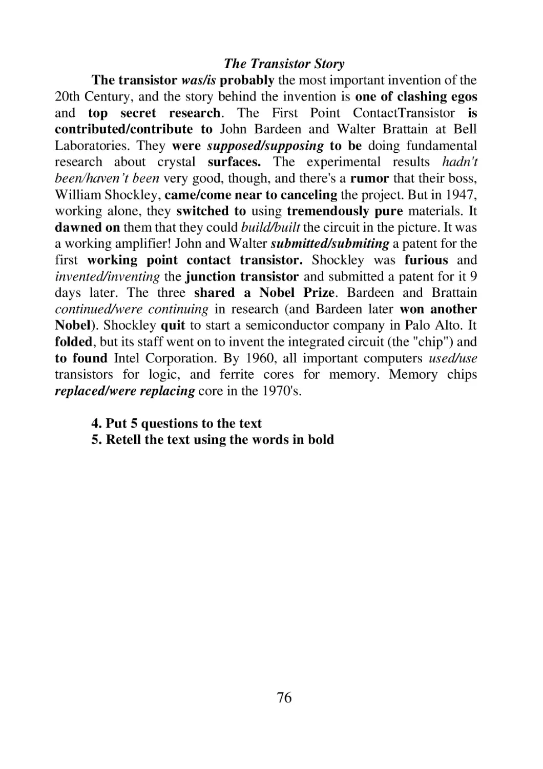
ELECTRONICS
Chernivtsi
2017
1
ББК 81.432.1–944: 22.3
УДК 811.111 (076.6)
A 647
Баланюк С.С. Електротехніка і електроніка / Навчальний
посібник з англійської мови для студентів фізико-технічних
спеціальностей / Баланюк С.С. – Чернівці: Книги – XXI, 2017. – 128 с.
Запропонований посібник містить навчальний матеріал,
необхідний для засвоєння термінології з таких фізико-технічних
спеціальностей, як фізика елементарних частинок, мікро- і
наноелектроніка, електротехніка та електротехнології, електронні
пристрої та системи.
Книга скомпонована за тематичними розділами з базовими і
додатковими автентичними текстами, де висвітлено сучасні напрямки
дослідження та розвитку цих галузей науки. Розроблені завдання і
вправи допоможуть студентам збагатити свій лексичний запас,
розвинути навики науково-технічного перекладу літератури за фахом,
а також практикуватись у висловлюванні за прочитаним матеріалом.
Рекомендується як для аудиторних занять, так і для самостійної
роботи студентів вищих навчальних закладів.
© Баланюк С. С.
CONTENTS
2
Why
Choose
Engineering?...............................................................4
Physical
Quantities
and
Units
of
Measurements…………………..5
Particle
Physics
Research…………………………………………..9
The
Large
Hadrons
Collider
(LHC)………………………………15
Solid
State
Physics……………………………………//…………16
Physics
Definition
of
Energy……………………………………..20
Mass-Energy Equivalence ……………………………………….
24
Shell
Places
Its
Faith
in
Solar
Energy…………………………….27
Photoelectric
Effect………………………………………..……..29
Energy
Efficiency………………………………………………...30
Electricity…………………………………………………………
32
Basics
of
Electricity........................................................................35
Definitions
of
Common
Electrical
Units…………………………39
Electromagnetism
………………………………………………...45
Electrical
Engineering
……………………………………………52
Fuse……………………………………………………………….
54
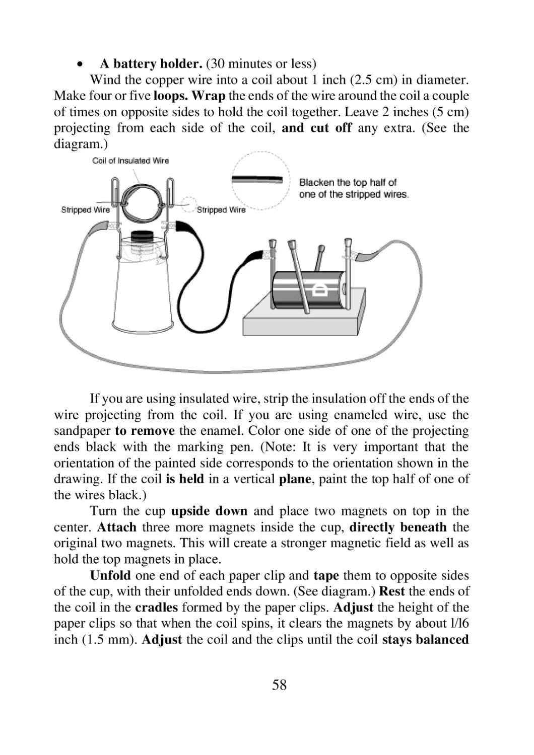
Stripped
Down
Motor…………………………………………….57
3
Electronics………………………………………………………...
65
Basic
Electronics
Components……………………………………68
Inductors,
Capacitors,
and
Transistors…………………………....71
Transistor
Standards
Identification
……………………………...74
Microelectronics
and
MEMS
Technology………………………..77
Electronic
Circuits
………………………………………………..80
Printed Circuit Board (PCB)…………………………………….
.82
Nanophysics………………………………………………………
87
COMPREHENSION READING
ACTIVITY................................96
SUPPLEMENT………………………………………………….1
09
UNIT I
Text 1
Why Choose Engineering?
1. Read and translate
Engineering is an exciting career. Engineers achieve great things.
In the history, people working in engineering have contributed to their
communities, countries, colleagues and civilisations by making tools,
machines and countless other things to help people improve their lives.
4
Studying engineering at the university will enhance your
understanding of the world, and contribute to your intellectual and
personal development. To ‘engineer’ literally means to “make things
happen”. Engineering is about the design and production of useful products
and services. Engineering know-how converts scientific knowledge into
technology and then technology into successful innovation. Many
seemingly simple aspects of our daily lives have been conceptualised,
designed and developed by an engineer.
Engineering affects almost every part of our lives, and a qualification
in this field can be your passport to a huge variety of rewarding careers.
Qualified engineers are in great demand all over the world, and are among
the best-paid professionals. You’ll need to be imaginative and to enjoy
solving problems, but as a graduate engineer your broad-ranging skills and
knowledge will be highly valued.
You can get a head start to your engineering career by studying
computing and information technologies, design, environment, materials
and structures.
Advances in technology mean there are always opportunities in
areas as diverse as cosmetics, communications, energy, health care,
manufacturing, music and transport. Or you may choose to work in a
particular engineering discipline such as aerospace, chemical, civil or
mechanical engineering. From information technology to medical science
and mining, from building roads to space travel, engineers are working to
make things happen. The diversity of engineering means that whatever
your interest, there is probably a place for you working in engineering.
Engineers are in demand. There is growing shortage of trained
engineering workers across all engineering sectors. We need more
engineering personnel to build roads and support hospitals.
Engineers get to do cool stuff. Being an engineer means you get to
be the first to develop or try out new technologies like artificial hearts,
developing and delivering better constructed environmentally
sustainable buildings like the first undersea house! Engineers design and
build virtual reality worlds, soccer fields or new planets. Engineers
discover and patent new materials that can cure cancer or cure the
common cold. Engineers are involved in making the future a reality.
Engineers work everywhere: in cities, regional and rural
communities, even remote wilderness areas. Some engineers work in
5
business offices, classrooms, others in factories or research labs; some
work outdoors or even in outer space.
2. Translate into English using the text
Зробити внесок, перетворити, нововведення, досягти, чудесна
професія, колеги, покращити, розвиток технологій, хороші
можливості, частково, космічна галузь, щоб все відбувалося, є попит
на інженерів, нестача, підтримувати, зробити важливий старт, велика
різноманітність, люблять вирішувати проблеми, найкраще
оплачувані, персонал, розробляти чи випробовувати, виліковувати,
відкривати, сільські общини, віддалені необжиті землі, бути
залученим.
3. Render the information of the text in 10-14 sentences
Text 2
Physical Quantities and Units of Measurements
1. Translate the text into Ukrainian and learn the words and
phrases written in bold
Physics is a science based upon exact measurement, so one must be
familiar with commonly used measuring devices and the units of
measurements. There are three basic concepts: length, mass and time. The
units used to measure them are called fundamental units. All other units are
called derived units because they can be written as some combination of
the three fundamental units.
The modernized metric system is known as the Systeme
International d'Unites (International System of Units), with the
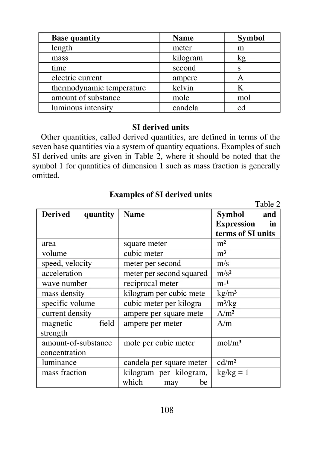
international abbreviation SI. It is founded on seven base units, listed
as length, mass, time, electric current, thermodynamic temperature,
amount of substance (based on number of atoms rather than mass), and
luminous intensity, that are regarded as dimensionally independent.
There are two widely used sets of fundamental units: a) the Metric
System and b) the English System. The Metric System or the International
decimal system of weights and measures is based on the metre and
kilogramme. Using metric units distance (length) is usually measured in
millimetres, centimetres, metres or kilometres; time is measured in
6
seconds, minutes, or hours; and mass is measured in grammes or
kilogrammes.
The English System uses the foot, yard and mile as units of length;
the ounce, pound and ton as units of mass and the second as the unit of
time.
The chief advantage of the Metric system over the English units is
that all metric units are divided into 10 or 100 parts. This enables
fractional distances and masses to be expressed as decimals. Decimals, it
is well known, are easier to manipulate in the addition, subtraction,
multiplication, and division of two or more quantities.
The Foot-Pound-Second (F.P.S.) System is used in Great Britain and
the United States of America. The Metric System (metre-kilogrammesecond) is invented in France and accepted universally in science but not
in engineering or commerce. Engineers and scientists have produced a
code of standard symbols for convenient representation of physical
quantities.This is a list of standard symbols (pay attention to the use of
capital or small letters).
length — l
work — w
mass — m
power — P
time — t
stress — σ
area — A
electric potential - V
volume − V
electric current — I
velocity — v
electric resistance – R
acceleration — a
temperature — t
density — ρ
heat — Q
force – f
specific heat — c
moment — m
latent heat — l
pressure — p
To simplify the representation of units a standard list of
abbreviations has been adopted. Here is a list of common abbreviations.
Learn them by heart.
foot— ft
litre — l
pound — lb
newton — n
second — s
kilogramme force — kgf
square foot — ft2
revolution — rev
cubic foot — ft³
watt — w
gallon — gal
volt — v
pound force — lbf kilogramme calorie — kcal
radian — rad
Fahrenheit temperature — °F [`færenhait]
7
horsepower — hp Temperature rise (Fahrenheit) — deg F
ampere — A
ohm —Ω (omega)
metre — m
Celsius temperature — °C (Centigrade)
gramme — g
Temperature rise (Celsius) — deg C
kilogramme — kg
British thermal unit — Btu
minute — min
Coulomb — C
square metre — m2 Celsius heat unit — Chu
cubic metre — m³ Metric horse power — Ps ("Ps" is the
abbreviation for "Pferde Starke" which is the German for horsepower).
In practice units of one system may be converted into units of the
other system.
(За матер. кн. Парахина А.В. Пособие по переводу
технических текстов, 1982. – 191 с. і журналу Physics Today, August 2003)
2. Answer the questions
1. What basic units are used to measure length, mass and time? 2.
What is the advantage of the Metric System over the English System? 3.
When was the Metric System invented? 4. Are decimals easy or difficult to
manipulate in the addition, subtraction, multiplication, and division? 5.
What kind of universal list has been adopted to simplify the representation
of units?
3. Translate into English
A. Фізика – природнича наука, що вивчає найбільш загальні і
фундаментальні закономірності. Вони визначають структуру й
еволюцію матеріального світу. Науковці вважають фізику
фундаментальною наукою, адже всі інші природничі науки (хімія,
геологія, біологія тощо) мають справу з певними різновидами
матеріальних систем, які підкоряються законам фізики. Наприклад,
властивості хімічних речовин визначаються властивостями молекул
та атомів, які їх складають, а ці властивості вивчають в таких галузях
фізики, як квантова механіка, термодинаміка і/або електрика
(електромагнетизм). Учення про будову матерії – одне з центральних
у фізиці, воно охоплює дві відомі категорії – речовину і поле.
Фізика тісно пов'язана з математикою, адже математика надає
апарат, за допомогою якого фізичні закони можуть бути точно
представлені. Фізичні теорії майже завжди формулюються у вигляді
математичних виразів, причому використовуються складніші розділи
математики, ніж звичайно в інших науках. І навпаки, розвиток
багатьох областей математики стимулювався потребами фізичних
8
теорій. Термін «фізика» з грецької φυσικός (physikos) - природний,
φύσις (physis) - природа перекладається як природнича отже, це наука,
котра досліджує загальні властивості матерії та явищ у ній, а також
виявляє загальні закони, які керують цими явищами; це наука про
закономірності природи. Фізики-науковці вивчають поведінку та
властивості матерії в широких межах її проявів, від
субмікроскопічних елементарних частинок, з яких побудоване все
матеріальне (фізика елементарних частинок), до поведінки всього
Всесвіту як єдиної системи (космологія).
B. Фізика в Україні
Фізика почала розвиватися в Україні з виникненням перших
університетів. У середині 19-го століття почали засновуватися
університетські фізичні факультети, а на початку 20 століття почали
розвиватися численні науково-дослідні інститути. В Україні
працювали такі визначні фізики, як Микола Миколайович Боголюбов,
Олександр Сергійович Давидов та багато інших.
Сучасні фізичні дослідження розподіляють на окремі галузі, які
вивчають різні аспекти матеріального світу. Фізика конденсованих
середовищ є однією з найбільших окремих галузей досліджень. Вона
сконцентрована на вивченні властивостей звичних проявів матерії,
таких, як тверді тіла та рідини. Атомна, молекулярна фізика та оптика
мають справу саме з індивідуальними атомами та молекулами. Галузь
фізики
елементарних
частинок
досліджує
властивості
субмікроскопічних, набагато менших, ніж атоми частинок, із яких
побудована вся матерія. Нарешті, астрофізика прикладає фізичні
закони до пояснення астрономічних феноменів, починаючи від Сонця
та інших об'єктів сонячної системи і закінчуючи Всесвітом як таким.
UNIT II
PARTICLE PHYSICS
1. Read and translate text 1
Particle Physics Research
Particle physics is a branch of physics that studies the elementary
constituents of matter and radiation, and the interactions between them. It
is also called "high energy physics", because many elementary particles do
not occur under normal circumstances in nature, but can be created and
9
detected during energetic collisions of other particles, as is done in
particle accelerators.
Modern particle physics research is focused on subatomic particles,
which have less structure than atoms. They may be elementary or
composite. These include atomic constituents such as electrons, protons,
and neutrons (protons and neutrons are actually composite particles, made
up of quarks), particles produced by radiative and scattering processes,
such as photons, neutrinos, and muons, as well as a wide range of exotic
particles.
All the particles and their interactions observed to date can be
described by a quantum field theory called the Standard Model. The
Standard Model has 40 species of elementary particles (24 fermions, 12
vector bosons, and 4 scalars), which can combine to form composite
particles, accounting for the hundreds of other species of particles
discovered since the 1960s.
The Electron is one of a class of subatomic particles called leptons,
which are believed to be fundamental particles (that is, they cannot be
broken down into smaller constituent parts). It carries an electric charge.
It is a lepton that participates in electromagnetic interactions, and its mass
is less than one thousandth of that of the smallest atom. Its electric charge
is defined by convention to be negative, with a value of -1 in atomic units.
Together with atomic nuclei, electrons make up atoms; their interaction
with adjacent nuclei is the main cause of chemical bonding.
The proton is a subatomic particle with an electric charge of one
positive fundamental unit and a mass of 938.3 MeV/c2, or about 1836 times
the mass of an electron. The proton is observed to be stable, with a lower
limit on its half-life of about 1035 years, although some theories predict
that the proton may decay.
Along with protons, neutrons make up the nucleus, held together
by the strong force. The neutron is a baryon and is considered to be
composed of two down quarks and one up quark. A free neutron will decay
with a half-life of about 10.3 minutes but it is stable if combined into a
nucleus. The neutron is about 0.2% more massive than a proton, which
translates to an energy difference of 1.29 MeV.
Isotopes are forms of an element whose nuclei have the same atomic
number – the number of protons in the nucleus – but different mass
numbers because they contain different numbers of neutrons. Carbon-14,
14C, or radiocarbon, is a radioactive isotope of carbon discovered on
10
February 27, 1940, by Martin Kamen and Sam Ruben. Its nucleus contains
6 protons and 8 neutrons. Its presence in organic materials is used
extensively as basis of the radiocarbon dating method to date
archaeological, geological, and hydrogeological samples.
http://hyperphysics.phy-astr.gsu.edu
http://physics.about.com
2. Match the equivalents to the meanings of the words and word
combinations
1.
2.
3.
4.
5.
6.
7.
8.
9.
10.
11.
12.
13.
14.
15.
16.
17.
18.
constituents
circumstances
occur
create
detect
collisions
research
include
scattering process
wave-particle duality
decay
samples
chemical bonding
conventional concepts
extensively
exhibit
established
inadequacy
19.
to carry an electric charge
20. species
a)
b)
c)
d)
e)
f)
g)
h)
i)
j)
k)
l)
m)
n)
o)
p)
q)
r)
s)
t)
Обставини
Траплятися
Складники
Включати
Дослідження
Зіткнення
Визначати
Проявляти
Процес розсіювання
Створювати
Розпад
Зразки
Звичні поняття
Дуалізм частинка-хвиля
Хімічне з’єднання
Установлений
Вид
Невідповідність
Надмірно
Володіти електричним зарядом
3. Find synonyms to the words and word combinations
Branches, studies, occur, create, detect, include, scattering processes,
propose, established, detectable, species, combine, participate, massive,
contain, to date.
4. Answer the questions
1. What does particle physics study?
11
2. Do elementary particles occur under normal circumstances in
nature?
3. What is modern particle physics research focused on?
4. What famous scientists contributed to the particle physics?
5. What kinds of particles are subatomic ones?
6. What do you know about the electron?
7. What kinds of particles make up the nucleus?
8. How many protons and neutrons does the nucleus of Carbon-14
isotop contain?
5. Name elementary particles
6. Retell the text Particle Physics Research
Text 2
1. Read and translate the text
Particle Physics Concepts
Atomic orbitals are the quantum states of the individual electrons in
the electron cloud around a single atom. Classically, the electrons were
thought to orbit the atomic nucleus, much like the planets around the Sun
(or more accurately, a moth orbiting very quickly around a lamp).
However electrons cannot be described as solid particles (as a planet or a
moth), so a more accurate comparison would be that of a (huge)
atmosphere (the spatially distributed electron) around a (tiny) planet (the
nucleus).
Electron configuration. In atomic physics and quantum chemistry,
the electron configuration is the arrangement of electrons in an atom,
molecule, or other physical structure (e.g., a crystal). Like other elementary
particles, the electron is subjected to the laws of quantum mechanics, and
exhibits both particle-like and wave-like nature.
Formally, the quantum state of a particular electron is defined by
its wavefunction, a complex-valued function of space and time.
Electrons are able to move from one energy level to another by
emission or absorption of a quantum of energy in the form of a photon.
Because of the Pauli Exclusion Principle, no more than two
electrons may exist in a given atomic orbital; therefore an electron may
only leap to another orbital if there is a vacancy there. Knowledge of the
electron configuration of different atoms is useful in understanding the
structure of the periodic table of elements.
12
Nuclear reaction is a process in which two nuclei or nuclear
particles collide, to produce different products than the initial particles. In
principle a reaction can involve more than two particles colliding, but such
an event is exceptionally rare. If the particles collide and separate without
changing, the process is called an elastic collision rather than a reaction.
A nuclear reaction can be represented by an equation similar to a
chemical equation, and balanced in an analogous manner. Nuclear decays
can be represented in the same way.
Radioactive decay is the set of various processes by which unstable
atomic nuclei (nuclides) emit subatomic particles (radiation). Decay is said
to occur in the parent nucleus and produces a daughter nucleus. This is a
random process, i.e. it is impossible to predict the decay of individual
atoms.
Nuclear fission is a nuclear reaction in which a heavy nucleus (such
as uranium) splits into two lighter nuclei (and possible some other
radioactive particles as well). In such radioactive heavy nuclei, the balance
between the strong nuclear force, attractive force and the electrostatic
repulsive force can be knocked out of equilibrium, by the introduction
of energy in the form of an absorbed neutron or photon, the nucleus
oscillates in an attempt to regain equilibrium until the electrostatic force
gains more power than the shorter-distanced nuclear force, at which point
the nucleus splits apart, releasing energy as it does so.
Nuclear fusion is a nuclear reaction in which two light nuclei (such
as hydrogen) combine to form heavier nuclei (such as helium). The
process releases excess binding energy from the reaction, based upon the
binding energies of the atoms involved in the process.
http://physics.about.com
2. Write down English equivalents from the text denoting:
поєднувати, ядерний синтез, поглинений нейтрон, відхилення,
рівновага, заново набути, винятково рідкісний, сила відштовхування,
сила притягання, може бути вибитим, розщеплення, розпад, створити
важчі ядра, залучений, принцип виключення, поглинання, з’єднуюча
сила, точне порівняння, розповсюджений у просторі, корисний,
перескочити до іншої орбіти, вільне місце, організувати
(облаштувати), функція з обчислення комплексу даних, зазнавати дії
закону, величезний, дрібний, виробляти енергію (звільняти енергію
внаслідок реакції).
3. Match the definitions with appropriate explanations
13
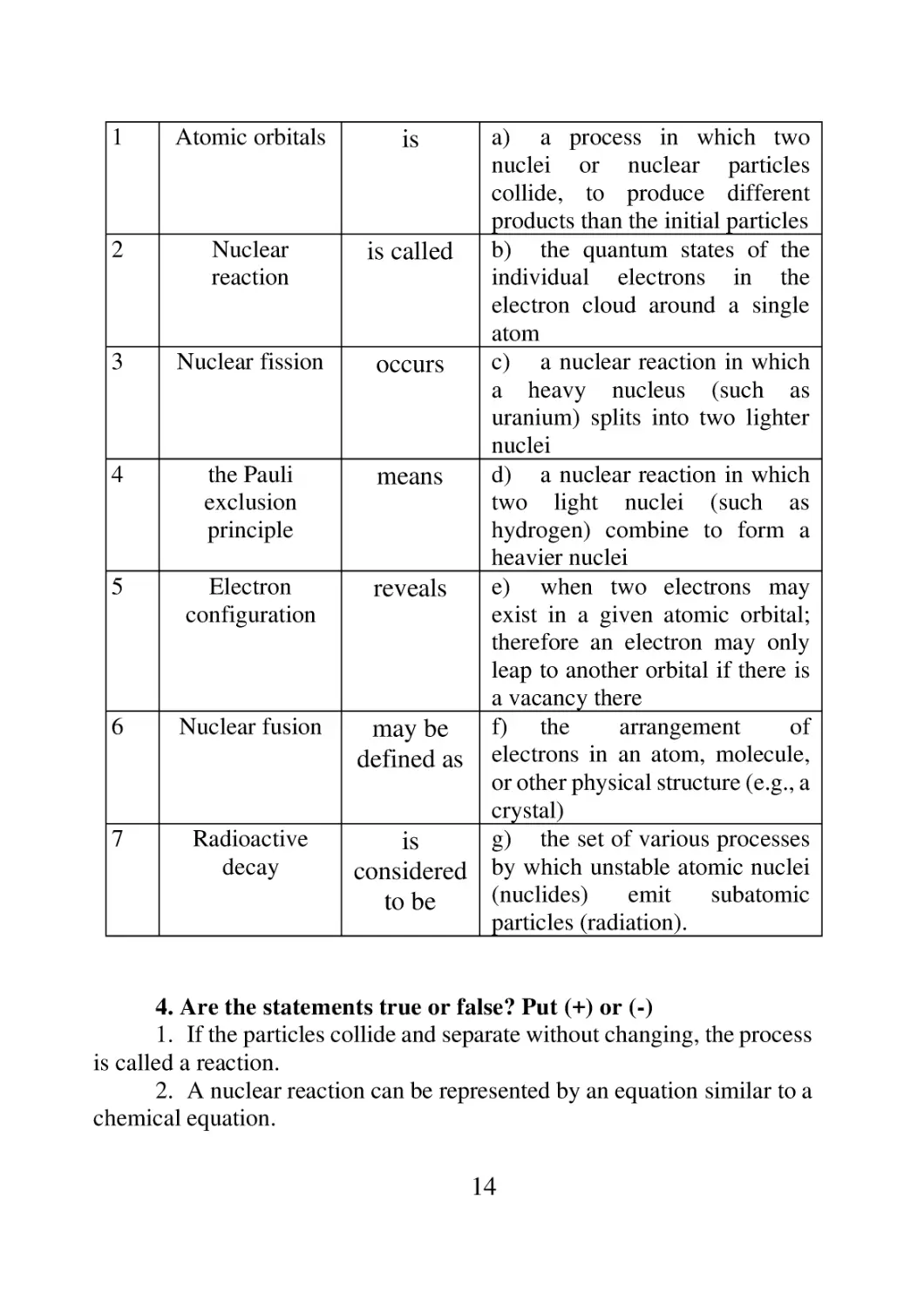
1
Atomic orbitals
is
2
Nuclear
reaction
is called
3
Nuclear fission
occurs
4
the Pauli
exclusion
principle
means
5
Electron
configuration
reveals
6
Nuclear fusion
may be
defined as
7
Radioactive
decay
is
considered
to be
a) a process in which two
nuclei or nuclear particles
collide, to produce different
products than the initial particles
b) the quantum states of the
individual electrons in the
electron cloud around a single
atom
c) a nuclear reaction in which
a heavy nucleus (such as
uranium) splits into two lighter
nuclei
d) a nuclear reaction in which
two light nuclei (such as
hydrogen) combine to form a
heavier nuclei
e) when two electrons may
exist in a given atomic orbital;
therefore an electron may only
leap to another orbital if there is
a vacancy there
f) the
arrangement
of
electrons in an atom, molecule,
or other physical structure (e.g., a
crystal)
g) the set of various processes
by which unstable atomic nuclei
(nuclides)
emit
subatomic
particles (radiation).
4. Are the statements true or false? Put (+) or (-)
1. If the particles collide and separate without changing, the process
is called a reaction.
2. A nuclear reaction can be represented by an equation similar to a
chemical equation.
14
3. The process releases little binding energy from the reaction,
based upon the binding energies of the atoms involved in the process.
4. Radioactive decay is the set of various processes by which ustable
atomic nuclei (nuclides) emit subatomic particles (radiation).
5. Like other elementary particles, the electron is subjected to the
laws of quantum mechanics, and exhibits only particle-like nature.
6. An electron may only leap to another orbital if there is a vacancy
there.
7. Knowledge of the electron configuration of different atoms is
useful in understanding the structure of the periodic table of elements.
5. Choose appropriate words from the databank to fill the gaps
in the text. Pay proper attention to the words in bold
a) The neutrino is an … particle. It has half-integer spin and is
therefore a fermion. All neutrinos observed to date have left-handed
chirality. Although they had been considered … for many years, recent
experiments have shown their mass to be non-zero. Because it is an
electrically neutral lepton, the … interacts neither by way of the strong nor
the electromagnetic force, but only through the weak force and gravity.
Because the cross section in weak nuclear interactions is very small,
neutrinos can pass through matter almost … . For typical neutrinos
produced in the sun (with energies of a few MeV), it would take
approximately one light year of lead to block half of them. … of neutrinos
is therefore challenging, … large detection volumes or high … artificial
neutrino beams.
There are three known types (flavors) of neutrinos: electron neutrino,
muon neutrino and … neutrino, named after their partner leptons in the
Standard Model.
Databank: massless, elementary, tau, requiring, intensity,
Detection, unhindered, neutrino.
b) Quarks are one of the two basic … of matter in the Standard
Model of particle physics. (The others are leptons.) … of quarks are called
antiquarks. Quarks and antiquarks are the only fundamental particles that
interact through all … of the fundamental forces.
An important property of quarks is called confinement, which states
that individual quarks are not seen because they are always confined inside
subatomic particles called hadrons (e.g., … and …; an exception is the top
quark, which decays so … that it does not hadronize, and can therefore be
15
observed more directly via its decay products. Confinement began as an
experimental observation, and is expected to follow from the … theory of
strong interactions, called quantum chromodynamics.
Databank: Antiparticles, constituents, four, protons and neutrons,
quickly, modern.
c) A hadron is a composite particle made of quarks in a bound state.
Hadrons come in two …: Baryons and Mesons. Baryons are fermions while
mesons are bosons. Baryons are further divided into … and hyperons. The
most well … hadrons are the proton and the neutron, which are both types
of nucleons.
Databank: classes, nucleons, known.
6. Retell the text Particle Physics Concepts
7. a). Read and translate the following text
The Large Hadron Collider (LHC)
LHC is a particle accelerator built near Geneva, Switzerland. Buried
approximately 50 to 175 meters underground, the Large Hadron Collider
resides inside a circular tunnel roughly 27 kilometers in circumference,
running along the border between Switzerland and France.
The LHC circulates a beam of charged particles (specifically
hadrons, probably either protons or lead ions) inside a tube which
maintains a continuous vacuum. The particles are guided in the
continuous vacuum within the circular tube using a series of magnetic
superconductors which accelerate and guide the charged particles. In order
to maintain the superconducting properties of the magnets, they remain
supercooled near absolute zero by a massive cryogenic system.
Once the beam reaches its highest energy levels, obtained by
steadily increasing the energy as the beam circles repeatedly through the
magnets, it will be maintained in a storage ring. This is a loop of tunnel
where the magnets will keep circulating the beam so that it retains its
kinetic energy.
The beams are expected to obtain energy levels up to 7 TeV (7 x
1012 electronvolts). Since two beams will collide with each other, the
energy of the collisions are therefore anticipated to reach 14 TeV from
protons. In addition, by accelerating heavier lead ions, they anticipate
collisions with energies in the range of 1,250 TeV energy levels on the
order of those obtained only moments after the Big Bang.
16
What Is the Large Hadron Collider Looking For?
Since the Large Hadron Collider will be having collisions of such
high energy, the hope is that it will release exotic particles which are
normally not observed. Any results from the Large Hadron Collider
collisions should have a major impact on our understanding of physics,
either confirming or refuting the projections from the Standard Model of
particle physics.
One major product which is being looked for is the Higgs boson, the
last particle from the Standard Model of particle physics that hasn't been
observed. It's also possible that the LHC will create some indicators of the
exotic dark matter, which makes up nearly 95% of the universe but cannot
be directly observed!
http://physics.about.com
7. b). Put 10 questions to the text
8. What do you know about the latest achievements of the LHC?
Text 3
1. Read and translate paying attention to the words given in bold
Solid-State Physics
Solid-state physics is the study of rigid matter, or solids, when
applying methods such as quantum mechanics, crystallography,
electromagnetism, and metallurgy. It is the largest branch of condensed
matter physics. Solid-state physics studies how the large-scale properties
of solid materials result from their atomic-scale properties. Thus, solidstate physics forms the theoretical basis of materials science. It also has
direct applications, for example in the technology of transistors and
semiconductors.
Background. Solid materials are formed from densely packed
atoms, which interact intensely. These interactions produce the
mechanical (e.g. hardness and elasticity), thermal, electrical, magnetic and
optical properties of solids. Depending on the material involved and the
conditions in which it was formed, the atoms may be arranged in a
regular, geometric pattern (crystalline solids, which include metals and
ordinary water ice) or irregularly (an amorphous solid such as common
window glass).
The bulk of solid-state physics, as a general theory and not really a
proven form of research, is focused on crystals. Primarily, this is because
the periodicity of atoms in a crystal — its defining characteristic —
facilitates mathematical modeling. Likewise, crystalline materials often
17
have electrical, magnetic, optical, or mechanical properties that can be
exploited for engineering purposes.
The forces between the atoms in a crystal can take a variety of forms.
For example, in a crystal of sodium chloride (common salt), the crystal is
made up of ionic sodium and chlorine, and held together with ionic bonds.
In others, the atoms share electrons and form covalent bonds. In metals,
electrons are shared amongst the whole crystal in metallic bonding.
Finally, the noble gases do not undergo any of these types of bonding. In
solid form, the noble gases are held together with van der Waals forces
resulting from the polarisation of the electronic charge cloud on each
atom. The differences between the types of solid result from the
differences between their bonding.
Crystal structure and properties. Many properties of materials are
affected by their crystal structure. This structure can be investigated using
a range of crystallographic techniques, including X-ray crystallography,
neutron diffraction and electron diffraction.
The sizes of the individual crystals in a crystalline solid material
vary depending on the material involved and the conditions when it was
formed. Most crystalline materials encountered in everyday life are
polycrystalline, with the individual crystals being microscopic in scale,
but macroscopic single crystals can be produced either naturally (e.g.
diamonds) or artificially.
Real crystals feature defects or irregularities in the ideal
arrangements, and it is these defects that critically determine many of the
electrical and mechanical properties of real materials.
The crystal lattice can vibrate. These vibrations are found to be
quantised, the quantised vibrational modes being known as phonons.
Phonons play a major role in many of the physical properties of solids, such
as the transmission of sound. In insulating solids, phonons are also the
primary mechanism by which heat conduction takes place. Phonons are
also necessary for understanding the lattice heat capacity of a solid, as in
the Einstein model.
Electronic properties. Properties of materials such as electrical
conduction and heat capacity are investigated by solid state physics. An
early model of electrical conduction was the Drude model, which applied
kinetic theory to the electrons in a solid. By assuming that the material
contains immobile positive ions and an "electron gas" of classical, noninteracting electrons, the Drude model was able to explain electrical and
18
thermal conductivity and the Hall Effect in metals, although it greatly
overestimated the electronic heat capacity.
Arnold Sommerfeld combined the classical Drude model with
quantum mechanics in the free electron model (or Drude-Sommerfeld
model).The nearly free electron model is a modification of the free electron
model meant to model the interaction between the conduction electrons and
the ions in a crystalline solid. By introducing the idea of electronic bands,
the theory explains the existence of conductors, semiconductors and
insulators.
http://en.wikipedia.org/wiki/Solid-state_physics
2.
Translate into English
Безперервні довільні рухи, щільно розміщені, періодичність,
таким чином, визначальні характеристики, зв’язки, призводити до…,
різнитися, залучати, велика частина твердотільної фізики, основи,
облаштування (організація), технічні цілі, застосовувати, залучати,
прямокутної форми, хмара електронних зарядів, благородний газ,
взаємодіяти, тверда матерія, штучно, який трапляється в щоденному
житті, під впливом, режим, кристалічна решітка, порушення,
полегшувати роботу з моделювання, методи, теплоємність,
переоцінювати, електронні смуги, властивості, передача звуку,
мікроскопічний за розміром, ізолятор.
a)
b)
c)
d)
e)
f)
g)
3. Compose sentences of your own using the structures:
By introducing the idea of…,
result from…,
resulting in…,
it has proven to be…,
it can be investigated using…,
it can be produced either… or…,
it is these properties that determine…
4. Read and translate the text into English
З історії фізики
З найдревніших часів люди намагалися зрозуміти властивості
матерії: чому різні речовини мають різні властивості, чому тіла
падають на землю, тощо; виникали питання про будову світу, про
природу Сонця і Місяця. Спочатку відповіді на ці запитання
намагалися шукати в філософії. Проте філософські теорії, котрі
давали відповіді на ці запитання не перевірялися на практиці. Однак,
19
ще в древні часи людство добилося значних успіхів в астрономії, а
грецький філософ Архімед навіть зміг дати точні кількісні
формулювання багатьох законів механіки й гідростатики. Деякі теорії
древніх мудреців, сформульовані у стародавніх Греції та Індії,
випереджали час. Одна з основних книг Аристотеля має назву
«Фізика», і фізика Аристотеля впродовж віків залишалася основою
знань про природу…
На поч. 20 ст. під тиском нових експериментальних даних
фізики почали переглядати старі теорії й замінювати їх новими,
заглядаючи дедалі глибше в будову матерії. Були відкриті нові явища:
рентгенівські промені та радіоактивність, з'явилися докази існування
електрона, експерименти з фотоефекту та вимірювання спектру
теплового випромінювання давали результати, які неможливо було
пояснити, виходячи із засад класичної фізики. В пресі цей період був
названий кризою фізики, проте в цей же час відбувся її тріумф. В 1905
році Альберт Ейнштейн побудував спеціальну теорію відносності, яка
продемонструвала, що поняття ефіру зайве при поясненні
електромагнітних явищ. При цьому довелося змінити класичну механіку
Ньютона, дати їй нове формулювання, справедливе при великих швидкостях.
Окрім того, вносились зміни і в уявлення про природу простору й часу.
Ейнштейн розвинув свою теорію у загальну теорію відносності,
опубліковану в 1916 році.
UNIT III
ENERGY
1. Read and translate text 1
Physics Definition of Energy
Energy and work occupy an important part of our ordinary life and
are among the most important topics in physics. In physics, work is done
only when an object is moved in the direction of the applied force. Energy
in physics is defined as the ability to do work. So, it is that work is the force
exerted multiplied by the distance, or W = FD. If you push a really heavy
object a certain distance, you do more work than if you push a lighter object
that same distance.
The energy stored in the various sources is derived from the
energy of the sun. For instance, when we burn wood, we are simply
converting the sun's power that was stored in the growing plant into
radiant (light) and thermal (heat) energy. Hydroelectric power is derived
from the running water that flows from higher elevations to lower
20
elevations. Again, it is the sun that provided the energy to evaporate water
from lower heights and transported it to the upper heights as rain. So all
the energy we deal with comes from the sun.
One of the most important and firmly established laws of physics is
that energy is conserved, that is, energy will always remain at the same
level in a closed system. The Earth can be considered as a closed system,
and many people argue that the Earth gains a useful net energy from the
sun. So, strictly speaking, even though the following terms are widely
used, we will never actually "run out" or "use up" energy.
The problem we actually have is related to the storage of energy. A
high level of energy is stored in the fuals: coal, natural gas, and oil, making
them the three most widely used and important energy sources in the world.
Unfortunately, when these fuels are burned in chemical or nuclear
reactions to release the energy, the original fuel mass is used up and
cannot be recreated without spending more energy than the amount that
could be obtained (defeating the purpose of an energy source altogether!).
It is for this reason that we must find infinite sources of energy before our
finite supplies run out.
Laws of physics dictate that energy can be changed from one form
to another (or into matter - the reason why there's energy in fossil fuels).
There are various forms of energy: kinetic energy (energy of motion),
potential energy, mechanical energy, nuclear energy, etc., but we cannot
directly use these forms of energy to turn on our TV or to cook food in the
microwave. That's where electricity comes in. Since electricity is the
primary form of energy consumed by the majority of the world's
population, power plants must exist to convert heat from burning biomass
or kinetic energy from falling water into the energy that flows through the
wire in our homes.
III. Learning about these two forms of energy (Kinetic and
Potential) is extremely important in understanding why man can obtain
the usable energy from things like waterfalls and spinning turbines.
Power plants serve to convert these physical forms of energy into energy
to run our TVs and cook food in the microwave – electricity.
Kinetic Energy (KE) is the name for energy associated with moving
objects. A good way to remember this is by the formula KE = (1/2) mv²,
where m is the mass of the object and v is the velocity of the object. So,
kinetic energy is dependent upon velocity and mass, and thus has to do
with moving objects.
21
Potential Energy (PE) is the name for energy stored in an object –
or, the "potential" of an object to do work. For instance, a rock at the top
of a cliff has more potential energy than one on the ground, because you
could drop the rock off of the cliff and hit something below (converting
the potential energy to kinetic).
Energy development is the ongoing effort to provide abundant and
accessible energy, due to knowledge, skills and constructions. When
harnessing energy from primary energy sources and converting them
into ever more convenient secondary energy forms, such as electrical
energy and cleaner fuels, both quantity (harnessing more primary energy)
and quality (more efficient conversion to secondary energy) are important.
http://library.thinkquest.org
2. Give English equivalents to the meanings of the words and
word combinations. Learn them by heart
Займати частину, звичне життя, напрямок, визначається,
штовхати, прикладена сила, відтворювати, легший предмет, певна
відстань, зберігати, перетворювати, випаровувати, підвищення,
висота, мати справу з, енергія променів, джерело, надходити з сонця,
ядерна реакція, вивільняти енергію, залишатися на тому ж рівні,
розглядати, вичерпати, невичерпні запаси, початкова форма, спожита
енергія, отримати, сперечатися, водопад, вмикати, якість, кількість,
помножити, турбіна, що обертається, залежний, швидкість, скеля,
камінь, зручний, видобувне паливо, приборкати (використовувати).
1.
2.
3.
4.
5.
6.
7.
8.
9.
10.
3. Complete the sentences (4-5 words more) using the text
Energy occupies an important part of our ordinary life and …
Work is done only when …
The energy stored in the various sources is derived from …
Kinetic energy is dependent upon …
One of the most important and firmly established laws of physics is...
The Earth can be considered …
We must find infinite sources of energy before …
Laws of physics dictate that energy can be change from…
Power plants serve …
Energy development is the ongoing effort to …
4. Find synonyms to the words and phrases
22
To occupy, ordinary life, to define, to store, to provide, to run out of
energy, to transport, is related to, to turn on, to convert, velocity, abundant,
harnessing.
5. Put 10 questions to the text Physics Definition of Energy
6. a) Translate the text paying attention to the words given in
bold.
Energy is the ability or capacity to do work or to produce change.
We often speak of needing energy to do work as human beings. There are
different forms of energy such as heat, light, sound, electricity, and
chemical energy.
There are two categories of energy. One is kinetic energy which is
the energy an object has while it is in motion. The other is potential energy
which is the energy a body has that is at rest but could exhibit due to its
place and condition. Even when an object is at rest the atoms and
molecules within the object move about so in a sense even objects at rest
have kinetic energy. The molecules within the object move faster as the
temperature increases.
An example of potential and kinetic energy could be an apple on a
table. It has the potential energy to fall by the force of gravity. If a sufficient
push occurs, the apple can tumble over the table to the ground. The work
that occurred to make this happen can be measured mathematically by
this formula:
Work = Force (the amount of energy needed or used) times the
distance to do the task.
It is common for energy to be converted from one form to another.
The law of conservation of energy states that although energy can be
changed in form it can be neither created nor destroyed. The theory of
relativity by Albert Einstein shows that mass and energy are equal and thus
that one can be converted into the other. Therefore the law of conservation
of energy includes both mass and energy.
b) Translate the words into English
Речовина, ізолятор, теорія відносності, існувати, рідина, суміш,
кількість, помножити, відстань, траплятися, перетворювати,
достатньо, закон, змінювати, створювати, таким чином, падати,
тверда речовина, завдяки, умова, зростання температури, вимірювати.
6. Energy Quiz. Mark in front of the correct answer to the
questions
23
1. This is the ability or capacity to do work or to produce change.
A mass b weight c energy
2. This is the energy an object has while it is in motion.
A potential b kinetic c mass
3. This is the energy a body has that is at rest but could exhibit due
to its place and condition.
A potential b kinetic c mass
4. This states that although energy and mass can be changed in form
it can be neither created nor destroyed.
A Law of Conservation of Energy b Law of Supply and Demand c
Law and Order of Energy Sources
5. This law of Albert Einstein states that mass and energy are equal
and thus that one can be converted into the other.
A conductivity b potentiality c relativity
8. Retell the text Physics Definition of Energy
Text 2
1. Read and translate paying attention to the meanings of the
words in bold. Insert the needed form of the verbs given in brackets
Mass-Energy Equivalence
1. In physics, mass-energy equivalence (to be) the concept that the
mass of a body (to be) a measure of its energy content. In this concept the
total internal energy E of a body at rest (to be) equal to the product of its
rest mass m and a suitable conversion factor to transform from units of
mass to units of energy. If the body (to be) not stationary relative to the
observer then account must (to make) for relativistic effects where m
(give) by the relativistic mass and E the relativistic energy of the body.
Albert Einstein (to propose) mass-energy equivalence in 1905 in one of his
Annus Mirabilis papers (to entitle) "Does the inertia of a body depend
upon its energy-content?" The equivalence (describe) by the famous
equation E = mc², where E (to be) energy, m (to be) mass, and c (to be) the
speed of light in a vacuum. The formula (to be) dimensionally consistent
and (not depend) on any specific system of measurement units. For
example, in many systems of natural units, the speed of light (to set) equal
to 1, and the formula (to become) the identity E = m; hence the term massenergy equivalence.
24
2. The equation E = mc² (to indicate) that energy always (to exhibit)
mass in whatever form the energy (to take). It (not to imply) that mass may
be “converted” to energy, for modern theory (to hold) that neither mass nor
energy may be destroyed, but only moved from one location to another. In
physics, mass must be (to differentiate) from matter. In cases where matter
particles (to create) or (to destroy), the precursors and products (to retain)
both the original mass and energy, which (to be) unchanged. Mass-energy
equivalence also (to mean) that mass conservation (to become) a
restatement of the law of energy conservation, which (to be) the first law
of thermodynamics.
E = mc² has sometimes (be used) as an explanation for the origin of
energy in nuclear processes, but mass-energy equivalence (not to explain)
the origin of such energies. Instead, this relationship merely (to indicate)
that the large amounts of energy released in such reactions may (to have)
a large enough mass, that the mass-loss may (to be measured) when the
released energy (and its mass) has (to be removed) from the system.
3. In inertial reference frames other than the rest frame or center of
mass frame, the equation E = mc² (to remain) true if the energy (to be) the
relativistic energy and the mass the relativistic mass. It (to be) also correct
if the energy (to be) the rest or invariant energy (also the minimum energy),
and the mass (to be) the rest or invariant mass. However, connection of the
total or relativistic energy with the rest or invariant mass (to require)
consideration of the system total momentum also, in systems and
reference frames where this (to have) a non-zero value. The formula then
required (to be) the extended version of Einstein's equation, called the
relativistic energy-momentum relationship:
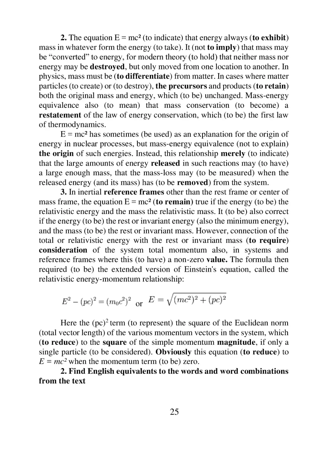
or
Here the (pc)2 term (to represent) the square of the Euclidean norm
(total vector length) of the various momentum vectors in the system, which
(to reduce) to the square of the simple momentum magnitude, if only a
single particle (to be considered). Obviously this equation (to reduce) to
E = mc² when the momentum term (to be) zero.
2. Find English equivalents to the words and word combinations
from the text
25
1.
2.
3.
4.
5.
6.
7.
8.
9.
10.
11.
12.
13.
14.
15.
16.
17.
18.
Величина
розглядати
очевидно
представляти
вимагати
система відліку
квадрат
рівняння
походження
звільняти
зберігати
послідовний
скорочувати
мати на увазі
спостерігач
одиниці вимірювання
розрізняти
виражати, демонструвати
3. Explain the concept of Mass-Energy Equivalence
4. Read and translate in writing, paying proper attention to the
use of passive constructions. Render the information of the text
Radiant Energy
Radiant energy is the energy of electromagnetic waves. The term is
most commonly used in the fields of radiometry, solar energy, heating and
lighting, but is also used less frequently in other fields (such as
telecommunications).
The quantity of radiant energy may be calculated by integrating
radiant flux (or power) with respect to time and, like all forms of energy,
its SI unit is the joule.
In applications involving transmission of power from one location
to another, "radiant energy" is sometimes used to refer to the
electromagnetic waves themselves, rather than their energy (a property of
the waves). Because electromagnetic (EM) radiation can be considered to
26
be a stream of photons, radiant energy can be viewed as the energy carried
by these photons.
Alternatively, EM radiation can be viewed as an electromagnetic
wave, which carries energy in its oscillating electric and magnetic fields.
These two views are completely equivalent, and are reconciled to one
another in quantum field theory.
5. Translate into English
1. Якщо всього 1 кілограм будь-якого речовини повністю
перетворити в енергію, то енергії, яка вивільняється буде досить, щоб
виробити 25 мільярдів кіловат-годин електроенергії; автомобіль 400
000 разів об'їхав навколо Землі; найбільший танкер 900 разів здійснив
кругосвітню подорож; два дні постачати електроенергію у таку
країну, як Сполучені Штати. 2. Вірно і зворотне: щоб
«матеріалізувати» всього один атом, необхідна гігантська енергія. 3.
Енергія сонця дає можливість жити всій планеті – людям і всьому
живому навколо нас. 4. Сонячна радіація – енергія випромінювання
Сонця – є основним джерелом енергії атмосферних процесів; вона
вимірюється кількістю тепла і виражається в мегаджоулях на 1 кв.м.
5. Променева енергія Сонця досягає земної поверхні, проникаючи
через шари атмосфери, що частково поглинає, відбиває і розсіює
сонячну радіацію. 6. Пряма радіація - сонячна радіація, яка доходить
до земної поверхні у вигляді пучка паралельних променів, що
виходять безпосередньо від сонячного диска. 7. Розсіяна радіація –
сонячна радіація, яка зазнала розсіювання в атмосфері і надходить на
земну поверхню з усього небесного зводу. 8. Сумарна сонячна
радіація – це сукупність прямої і розсіяної сонячної радіації, що
надходить у природних умовах на земну поверхню. 9. Сонячна
радіація залежить від географічної широти, висоти над рівнем моря,
прозорості атмосфери і хмарності.
Text 3
1. Read, translate, and define the main idea
Shell Places Its Faith in Solar Energy
Solar cells have long been touted as a major source of clean energy,
but until now have been too expensive for all but the most specialized
applications. Several times more costly than fossil fuels, solar power
accounts for just a fraction of 1 % of the world’s energy production. But
27
this situation is set to change, with governments taking global warming
more seriously and industry investing in new materials and processes with
which to manufacture solar cells, otherwise known as photovoltaics.
As a sign of industry’s increasing interest in harnessing the Sun’s
rays, energy giant Shell is buying out a joint venture that it holds with
Siemens and EON Energy. The new company, Shell Solar, will be the
fourth largest manufacturer of photovoltaics in the world. “For an
international energy company it makes perfect sense to be involved in renewable energy;” says Andre Romeyn, corporate communications
manager at Shell Solar. “It is estimated that between 30-40% of the
world’s energy will come from renewable energy sources by 2050-2060.
Photovoltaic technology is currently one of the best options in that
renewable-energy area.”
Photovoltaics are made from a semiconducting material sandwiched
between two electrodes, an arrangement that produces a current when
electrons in the semiconductor are liberated by incoming photons. Most
of today’s cells are built around crystalline silicon and convert a higher
proportion of incident energy into electricity than cells made from rival
materials. The disadvantage of cells made from crystalline silicon is that
they are expensive, as they need to be quite thick - with an active layer
about 0.2-0.3 mm deep - to soak up enough solar energy.
Shell Solar will make photovoltaics using both mono- and polycrystalline silicon. The former is made by growing a rod from a small
crystal and the latter by pouring liquid silicon into a mould and allowing
it to cool. One of the challenges for Shell’s researchers will be to improve
the efficiency of both types of crystal structure - currently 15 % and 13.5%
for cells made from mono- and poly-crystalline silicon, respectively. The
company will also investigate how to make the mono-crystalline silicon
thinner and how to scale up production of the poly-crystalline version.
In addition, Shell is carrying out R&D on the semiconductor
copper indium gallium diselenide. Although cells made from this material
currently have an efficiency of only 10-12%, the material absorbs solar
energy much better than crystalline silicon - which means that it can be
used in cells with an active layer just a few micrometres thick. Although
this technology is only just emerging on the market it has proved to be
promising. Shell is also investing in academic research. For example, it
supports work on thin ceramic elements carried out at the Technical
University of Delft.
28
Currently, solar cells are used to power private houses, as well as
industrial installations in remote regions.
(from Physics World)
Notes to the text
Account for – нараховувати, визначати, займати,
photovoltaic – фотогальванічний,
with governments taking global warming more seriously – при більш
серйозному розумінні урядами проблеми глобального потепління,
harnessing – використання, приборкання,
joint venture – сумісне підприємство,
sandwiched between two electrodes – розміщений між двома
електродами,
rival – конкуруючий,
to build up experience – накопичувати досвід,
pilot production line – виробництво експериментальної продукції,
to carry out – виконувати,
R&D – (research (дослідження) and development (розробка)) науково-дослідна та випробувально-конструкторська робота.
2. Learn by heart the words given in bold in the text. Find
sentences containing information on the following points:
1) the cost of solar energy;
2) the challenges for Shell’s researchers;
3) advantages and disadvantages of solar cells;
4) promising opportunities for technologies on harnessing the
sunrays’ energy.
3. Retell the text Shell Places its Faith in Solar Energy
4. Choose the appropriate form of the verbs in the text
Photoelectric effect
The photoelectric effect is the emission of electrons from matter
upon the absorption of electromagnetic radiation, such as ultraviolet
radiation or x-rays.
Upon exposing/exposed a metallic surface to electromagnetic
radiation that is above the threshold frequency or threshold wavelength
(which is specific to the type of surface and material), the photons are
absorbed/absorb and current is produced/producing.
29
No electrons are emitted/emitting for radiation with a frequency
below that of the threshold, as the electrons are unable to gain/to have
gained sufficient energy to overcome the electrostatic barrier
presented/presenting by the termination of the crystalline surface.
By conservation of energy, the energy of the photon is
absorbed/absorbing by the electron and, if sufficient, the electron can
escape/escaped from the material with a finite kinetic energy.
A single photon can provide only a single electron ejecting, as the
energy of one photon may only be absorbed/absorbing by one electron.
The electrons that are emitted/emitting are often termed/terming
photoelectrons.
5. Choose the words from the text to fill in the chart
Past
Pariciple I
Infinitive
Gerund Participle
Simple
II
6. Read and translate. Choose the correct form of the
words italicized
Energy Efficiency
Every year, much of the energy the country consumes/consume is
wasted because of transmission, heat loss and inefficient/unefficient
technology - costing families and businesses money, and leading to
increased carbon pollution.
Energy efficiency is one of the easiest/most easy and most cost
effective ways to combat/combuting climate change, clean the air we
breathe/breathes, improve the competitiveness of our businesses and
reduce energy costs for consumers. The Department of Energy is
working/work with universities, businesses and the National Labs to
develop/developed
new,
energy-efficient
technologies
while
boosting/boost the efficiency of current technologies on the market.
Reducing/reduce energy use in your home saves you money,
increases our energy security, and reduces the pollution that is emitted /
emitting from non-renewable/inrenewable sources of energy. If you are
planning to install a small renewable energy system to make/made your
30
own electricity, such as a solar electric system or small wind turbine,
reducing your electricity loads is the first step to saving you money by
allowing/allow you to purchase/purchased a smaller system.
9. Translate into English
Радіація на службі людини
Ядерна фізика – порівняно молода наука, але темпи її розвитку
настільки високі, що вже сьогодні досягнення фізиків-ядерників
вражають своєю масштабністю. Завдяки ядерній фізиці
промисловість озброїлася атомними електростанціями і реакторами
для опріснення води й отримання трансуранових елементів. Крім
того, були винайдені джерела γ- випромінювання для дефектоскопії,
активаційний аналіз для експрес-визначення домішок у сплавах,
вугіллі тощо. Величезне значення мають ізотопні джерела струму і
тепла. Їх застосовують для енергопостачання важкодоступних
районів і автоматичних станцій (наприклад, метеорологічних) або
супутників Землі.
Джерела γ-випромінювання застосовуються для автоматизації
різних операцій (наприклад, вимірювання щільності середовища,
товщини вугільного шару і т. ін.). Завдяки випромінюванню наука
отримала надійний інструмент практичного підтвердження багатьох
теорій, які потребували якісного та кількісного аналізу.
У сільському господарстві знайшли застосування установки для
опромінення овочів і фруктів з метою вберегти їх від гниття й цвілі.
Крім того, розроблені способи виведення нових сортів рослин шляхом
генетичних трансмутацій. Неоціненною є допомога ядерної фізики в
геології, біології і багатьох інших областях знань завдяки тому, що за
її допомогою можна одержувати неймовірно точні й швидкі
результати. Особливого поширення для людей її використання
знайшло в області медицини, де жодне серйозне лікування не
обходиться сьогодні без рентгена.
Однак чорнобильська катастрофа поставила під сумнів ідею
використання ядерної енергії як оптимальної альтернативи
природним джерелам енергії. На жаль, використання радіоактивності
пов’язане зі шкідливістю дії радіоактивного опромінення на людину,
що стає джерелом підвищеної небезпеки для неї та впливає на
подальше його розповсюдження. Крім того, з кожним роком чимраз
31
гострішою стає проблема поховання ядерних відходів, а ядерна зброя
дотепер залишається одним із найнебезпечніших видів озброєння.
Техногенні катастрофи, які останнім часом почастішали,
висунули перед ученими нове завдання – навчитися використовувати
ядерну фізику, максимально убезпечивши навколишнє середовище й
людину від можливих негативних наслідків.
http://linksdir.biz/linkinfo.php
UNIT IV
ELECTRICITY AND ELECTROMAGNETISM
1. Read and transate text 1
Electricity
Electricity is the flow of electrical power or charge. It is both a basic
part of nature and one of our most widely used forms of energy. Electricity
is actually a secondary energy source, also referred to as an energy
carrier. That means that we get electricity from the conversion of other
sources of energy, such as coal, nuclear, or solar energy. These are called
primary sources. The energy sources we use to make electricity can be
renewable or nonrenewable, but electricity itself is neither renewable nor
nonrenewable.
Electricity is a type of activity arising from the existence of
charge. The basic unit of charge is that on the proton or electron. The
proton’s charge is called positive while the electron's is negative.
Any object or particle is or can become electrically charged. The
smallest known charge of electricity is the charge associated with an
electron. This charge has been called a "negative" charge. An atom’s
nucleus has a positive charge. These two un-like charges attract one
another. The negatively charged electrons in an atom are kept near the
32
nucleus because of their attraction for the positively charged protons in
the nucleus. Like charges oppose and repel one another.
Around every charge there is an electric field. With every electric
field there is a magnetic field. While we can't see these fields, or yet know
exactly what they consist of, we can measure them with instruments and
control their behavior. We can then use this knowledge to our benefit.
The design and construction of electric motors, computers, radios,
televisions, stereos, and many other electrical and electronic devices
depend upon the knowledge of these basic principles of electricity.
Before electricity became available over 100 years ago, houses were
lit with kerosene lamps, food was cooled in iceboxes, and rooms were
warmed by wood-burning or coal-burning stoves.
Many scientists and inventors have worked to decipher the
principles of electricity since the 1600s. Some notable accomplishments
were made by Benjamin Franklin, Thomas Edison, and Nikola Tesla.
Benjamin Franklin demonstrated that lightning is electricity. Thomas
Edison invented the first long-lasting incandescent light bulb.
Prior to 1879, direct current (DC) electricity had been used in arc
lights for outdoor lighting. In the late 1800s, Nikola Tesla pioneered the
generation, transmission, and use of alternating current (AC) electricity,
which reduced the cost of transmitting electricity over long distances.
Tesla's inventions used electricity to bring indoor lighting to our homes
and to power industrial machines.
Despite its great importance in our daily lives, few of us probably
stop to think what life would be like without electricity. Like air and water,
we tend to take electricity for granted. But we use electricity to do many
jobs for us every day - from lighting, heating, and cooling our homes to
powering our televisions and computers.
2. Give Ukrainian equivalents to the meanings of the following
words and word combinations
Сила притягання, відштовхуватися, на користь, вимірювати,
поновлюваний, носій енергії, перетворення, заряджений, поведінка,
ядро, пов'язаний (асоціюється), стосується (відноситься), первинне
джерело, поведінка, пристрій, залежати, подібний, потік, означати,
атомний, спалювати, розшифровувати, сприймти як належне,
освітлення, змінний струм.
33
3. Answer the questions
1. What is electricity?
2. What do we get electricity from?
3. What kinds of energy sources are called primary ones?
4. Can any object or particle become electrically charged?
5. Why do un-like charges attract one another?
6. Why are negatively charged electrons in an atom kept near the
nucleus?
7. Is it possible to measure the magnetic field with instruments?
8. Does the design and construction of electrical and electronic devices
depend upon the knowledge of basic principles of electricity?
9. What is electricity mostly used for?
4. Make up plural forms to the nouns if possible
Charge, atom, nucleus, design, existence, radio, knowledge,
electron, flow, body, source, activity, electricity, magnetic field.
5. Fill in the the table with the words from the text Electricity in
the form of:
Infinitive
Past Simple
Gerund
Participle
II
Pariciple
I
6. Transform the sentences from Active into the Passive Voice
constructions
1. We call electric power as the amount of work done by an electric current
in a unit time. - Electric power…
2. You have used 200 watthours, or 0.2 kilowatthours, of electrical energy.
- 200 watthours, or 0.2 kilowatthours, of electrical energy…
3. When a current flows in a circuit with resistance, it does work. - Work…
4. Devices are converting this work into heat. - Heat… due to specific
devices.
5. We measured electricity in watts and kilowatts. – Electricity…
34
6. One watt is a very small amount of power. - One watt (consider) …
7. It would require nearly 750 watts to equal one horsepower. - To equal
one horsepower, nearly 750 watts…
8. We determine kilowatthours by multiplying the number of kilowatts
required by the number of hours of use. - Kilowatthours …
9. You had used a 40-watt light bulb to provide the lighting in this
room before they came. - A 40-watt light bulb…
7. Test yourself. a) Read and translate the text in writing
Materials differ in their ability to allow electricity to flow through
them. Conductors allow electricity to flow easily. Copper wire is a good
example and makes up our housing and appliance wiring.
Insulators are materials that don't allow electricity to pass through
them easily. Materials such as rubber are good insulators and are used
around appliance and house wires to keep the electricity from creating a
short circuit.
There are specific materials able to generate an electrical potential
when they are heated or cooled – it is a phenomenon of pyroelectricity.
As a result of this change in temperature, positive and negative charges
move to opposite ends due to migration (i.e. the material becomes
polarised) and hence, an electrical potential is established.
Pyroelectricity can be visualized as one side of a triangle, where
each corner represents energy states in the crystal: kinetic, electrical and
thermal energy. The side between electrical and thermal corners
represents the pyroelectric effect and produces no kinetic energy. The side
between kinetic and electrical corners represents the piezoelectric effect
and produces no heat.
Although artificial pyroelectric materials have been engineered, the
effect was first discovered in minerals such as quartz and tourmaline
and other ionic crystals.
b) Fill in the the table with the words from the text denoting:
Phenomena Materials
Devices
and
objects
35
Actions (in
any
wordform)
Energy
states
Text 2
1. Read and translate
Basics of Electricity
1). Static electricity - When electrical charges are at rest, meaning
they are not moving, we call that static electricity. If charges are in motion
we then have a flow of charge called electrical current.
Electrostatics is the study of charges, or charged objects that do not
involve moving charges or current. When positive or negative charge
builds up on objects, static electricity occurs. The friction between the
objects causes electrons to be transferred from one object to another. The
object that has lost the electrons has a positive charge and the object that
has gained them has an equal negative charge. An electrically neutral
object can be charged by bringing it in contact with a charged object: if
the charged object is positive, the neutral object gains a positive charge
when some of its electrons are attracted onto the positive object. If the
charged object is negative, the neutral object gains a negative charge when
some electrons are attracted onto it from the negative object.
2). Moving electric charges are the heart of basic electronics.
Knowing what moving charges are and how various electronic
components affect the moving charges is the foundation of basic
electronics. The study of charges in motion is called Electrodynamics. A
flow of electric charge makes up an electrical current.
3). An electric circuit is a path for an electric current to flow. This
is a complete path along which electrons can transmit their charges. An
electric circuit includes a battery, generator, or magnetic means for
producing current flow.
36
There are several things needed to complete an electrical circuit.
There must be an electromotive force from batteries or generators,
conductors such as copper wire and an appliance such as a bulb to be lit.
A device called a switch can be used to stop or open the circuit or close or
create the circuit. When a circuit is not completed because the electricity
is diverted to a path of least resistance it is a short circuit.
In a simple circuit there are two types of wiring. One is a parallel
circuit. This is when all the batteries and appliances such as bulbs are
wired with the positive terminals of the batteries wired together and the
negative terminals so there are parallel pathways for the electricity to
travel. In a parallel circuit, if one appliance such as a bulb goes out, the
rest of the circuit remains on. The force from the batteries does not
increase, however, if more batteries are added.
In a series circuit, the positive terminal or end of a battery is wired
to the negative terminal of the other battery and the positive end of one
appliance to the negative or terminal of the other appliance such as a bulb.
Thus, if one bulb or appliance goes out, the whole flow of electricity is
interrupted and the circuit goes out. However, if more batteries are added
to the circuit, the bulb will get brighter as more force will go to that bulb.
http://www.mcwdn.org/Physics/Electricity.html
2. Match the units to measure electricity
Ampere
Coulomb
Volt
Ohm
measures electrical current.
measures resistance to the
electricity.
measures electromotive force.
measures amount of charge.
flow
of
3. Translate in writing, pay attention to the meaning of the word
have
1. The object that has lost the electrons has a positive charge and the
object act that has gained them has an equal negative charge. 2. A device
called a switch has been used to create the circuit. 3. One appliance has
gone out but the rest of the circuit remains on. 4. We have more batteries
to be added to the circuit. 5. We want to have our household appliances
constantly charged. 6. An engineer will have to be very careful when
37
dealing with any form of electricity. 7. Having understood the main laws
of Electrodynamics, one can create a battery or an electric appliance.
4. Translate into English
Однаковий, сила тертя, траплятися (відбуватися), скорочення,
потік, означати, впливати, змінний струм, передавати, включати, рух,
клеми (перемикачі), коло (схема), проводка, електропристрій,
залишатися, додавати, збільшуватися, лампа згасає, послідовна схема,
завершити (закрити), провідник, коротке замкнення, опір, набувати
(отримувати), включати.
5. Complete the sentences
1. If charges are in motion we then have a...
2. Electrodynamics is the study of...
3. When positive or negative charge builds up on objects,...
4. Knowing how various electronic components affect the moving
charges is...
5. A device called a switch can be used to...
6. Electricity Quiz. Mark in front of the correct answers
1. Two particles with the same charge will repel or drive away from
each other.
А True В False
2. Two particles with opposite charges will be attracted to each other.
A True b False
3. Materials that allow electricity to flow in them easily such as
copper are called
а insulators b semiconductors c conductors.
4. Materials that don't allow electricity to flow in them easily are
called
а insulators b conductors c semiconductors
5. These materials conduct electricity under certain circumstances a insulators b conductors c semiconductors
6.This is the study of charges, or charged objects that do not involve
moving charges or current.
electrostatics b electrodynamics c gravity
7. This the study of charges in motion.
38
A electrostatics b electrodynamics c gravity
8. When one has connected a conductor, a source of electricity such
as a battery and an appliance such as a bulb, one has created an electric
а insulator b circuit c switch.
9. The positive terminals or ends of the batteries and appliances are
wired together and the negative ends of batteries and appliances are wired
together in this kind of circuit.
A short b series c parallel
10. In this kind of circuit the positive terminals and the negative
terminals of betteries and appliances are wired together.
A short b series c parallel
11. This is the measure of electric current.
A ohm b ampere c volt d coulomb
12. This measures electromotive force.
A ohm b ampere c volt d coulomb
13. This measures resistance to the flow of electricity.
A ohm b ampere c volt d coulomb
14. This is a measure of charge.
A ohm b ampere c volt d coulomb
15. This device is used to open and close a circuit.
A battery b bulb c switch
16. An electrical current which flows in the same direction via a
conductor or a current that does not change its polarity is called
A a direct current (D.C.) or a continuous current
B an alternating current (A.C.).
Text 3
1. Read and translate
Definitions of Common Electrical Units
Ampere – A: The ampere is that constant current which, if
maintained in two straight parallel conductors of infinite length, of
negligible circular cross section, and placed 1 meter apart in vacuum,
would produce between these conductors a force equal to 2 x 10⁻⁷ Newton
per meter of length.
Electric current is the same as electric quantity in movement, or
quantity per unit time, expressed like I = dq / dt, where I = electric current
(ampere, A), dq = electric quantity (coulomb, C), dt = time (s), Coulomb – C.
39
The standard unit of quantity in electrical measurements is the
quantity of electricity conveyed in one second by the current produced by
an electro-motive force of one volt acting in a circuit having a resistance
of one ohm, or the quantity transferred by one ampere in one second.
The flow of electric charge Q is referred to as an electric current I.
The amount of charge per unit time is the change in electric current. A
current flows at a constant value I during the time t, it transports the charge
Q = I × t. For a temporally constant power, the relationship between the
charge and current is I = Q / t or Q = I × t. Due to this relationship, the basic
units of amps and second the Coulomb in International System of Units is
set. The Coulomb unit can be represented as 1 C = 1 A × s. Charge Q, (unit
in ampere-hours Ah), discharge current I, (unit in amperes A), time t, (unit
in hours h).
Farad – F: The farad is the standard unit of capacitance. Reduced
to base SI units one farad is the equivalent of one second to the fourth power
ampere squared per kilogram per meter squared (s4 A2/kg m2).
When the voltage across a 1 F capacitor changes at a rate of one volt
per second (1 V/s) a current flow of 1 A results. A capacitance of 1 F
produces 1 V of potential difference for an electric charge of one coulomb
(1 C).
In common electrical and electronic circuits units of microfarads μF
(1 μF = 10-6 F) and picofarads pF (1 pF = 10-12 F) are used.
Ohm – Ω: The derived SI unit of electrical resistance - the
resistance between two points on a conductor when a constant potential
difference of 1 volt between them produces a current of 1 ampere. R = V /
I (1), where R = resistance (ohm, Ω), V = electrical potential (volt), I =
current flow (ampere)
Siemens – S: The unit of electrical conductance S = A / V. The
reciprocal of electrical Resistance is called conductance. Electrical
conduction is the movement of electrically charged particles through a
transmission medium. The movement can form an electric current in
response to an electric field. The underlying mechanism for this movement
depends on the material.
Conduction in metals and resistors is well described by Ohm's Law,
which states that the current is proportional to the applied electric field. G
= 1 / R (2), where G = conductance (siemens, S). Example: Conductance
of a conductor with resistance 10 Ω can be calculated as
G = 1 / (10 Ω) = 0.1 siemens, S.
40
Metals are good conductors because they have unfilled space in the
valence energy band.
Another medium, a "perfect vacuum," contains no charged particles;
vacuums normally behave as very good insulators. However, metal
electrode surfaces can cause a region of the vacuum to become conductive
by injecting free electrons or ions into either field emission or thermionic
emission.
Henry – H: The Henry is the unit of inductance. Reduced to base
SI units one henry is the equivalent of one kilogram meter squared per
second squared per ampere squared (kg m2 s-2 A-2).
An inductor is a passive electronic component that stores energy in
the form of a magnetic field. The standard unit of inductance is the henry
abbreviated H. This is a large unit and more commonly used units are the
microhenry abbreviated μH (1 μH =10-6H) and the millihenry abbreviated
mH (1mH =10-3 H). Occasionally, the nanohenry abbreviated nH (1 nH =
10-9 H) is used.
Joule – J: The unit of energy work or quantity of heat done when a
force of one Newton is applied over a displacement of one meter. One
joule is the equivalent of one watt of power radiated or dissipated for one
second.
In imperial units the British Thermal Unit (Btu) is used to express
energy. One Btu is equivalent to approximately 1,055 joules.
Watt: The watt is used to specify the rate at which electrical energy
is dissipated, or the rate at which electromagnetic energy is radiated,
absorbed, or dissipated.
The unit of power W or Joule/second. A watt is the International
System unit of power equal to one joule per second. A joule is a unit of
electrical energy equal to the work done when a current of one ampere
passes through a resistance of one ohm for one second. The symbol used
for a watt is "P" for power. Power in watts is found by multiplying a
circuits current (I) times its voltage (V). P = I*V
Weber – Wb: The unit of magnetic flux. The flux that when linking
a circuit of one turn, produces an Electro Motive Force - EMF - of 1 volt
as it is reduced to zero at a uniform rate in one second. 1 Weber is
equivalent to 108 Maxwells
Tesla – T: The unit of magnetic flux density the Tesla is equal to 1
Weber per square meter of circuit area.
41
Volt: The Volt - V - is the Standard International (SI) unit of electric
potential or electromotive force. A potential of one volt appears across a
resistance of one ohm when a current of one ampere flows through that
resistance. Reduced to SI base units, 1 (V) = 1 (kg m2 / s3 A)
http://www.engineeringtoolbox.com/electrical-units-d_454.html
http://www.sengpielaudio.com
2. Translate into English
Електропровідність, щільність потоку, напруга, англійська
система мір, енергія розсіюється, поверхня, спричиняти, частота,
потужність, електрорушійна сила, ємність, ємнісний опір, поперечний
розріз, незначний, зменшуватися, незаповнений простір, вказувати
(уточнити), зміщення, зворотний, множення, скорочення, ізолятор,
розряд, дорівнює, механізм, який лежить в основі, тимчасовий,
величина, ідеальний вакуум, безкінечний, переносити енергію.
3. Read, translate, and learn the terms and units
Electrical Measurement Definitions
Quantity
frequency f
force F
pressure p
energy E
Name
hertz (Hz)
newton (N)
pascal (Pa) = N/m²
work joule (J) = N·m
Definition
1/s
kg·m/s²
kg/m·s²
kg·m²/s²
power P
electric charge Q
voltage V
watt (W) = J/s
coulomb (C) = A·s
volt (V) = W/A
kg·m²/s³
A·s
kg·m²/A·s
current I
ampere (A) = Q/s
³
capacitance C
inductance
A
farad (F) = C/V = A·s/V = A²·s4/kg·
s/Ω
m²
L
henry (H) = Wb/A = V·s/A kg·m²/A²·
s²
42
resistance R
ohm (Ω) = V/A
conductance
siemens (S) = A/V
kg·m²A²·s
³
magnetic
flux
density
flux
B
A²·s³/kg·
m²
weber (Wb) = V·s
kg·m²/A·s
²
tesla (T) = Wb/m² = V·s/m² kg/A· s²
4. Read and translate the formulas:
DC power formulas
Voltage V in (V) calculation from current I in (A) and resistance R
in (Ω): V(V) = I(A) × R(Ω)
The power P in (W) calculation from voltage V in (V) and current I
in (A): P(W) = V(V) × I(A) = V2(V) / R(Ω) = I2(A) × R(Ω)
AC power formulas
The voltage V in volts (V) is equal to the current I in amps (A) times
the impedance Z in ohms (Ω): V(V) = I(A) × Z((Ω) = (| I | × | Z |) and (θI
+ θZ)
The apparent power S in volt-amps (VA) is equal to the voltage V
in volts (V) times the current I in amps (A): S(VA) = V(V) × I(A) = (| V |
× | I |) and (θV − θI)
The real power P in watts (W) is equal to the voltage V in volts (V)
times current I in amps (A) times the power factor (cos φ): P(W) = V(V)
× I(A) × cos φ
The reactive power Q in volt-amps reactive (VAR) is equal to the
voltage V in volts (V) times the current I in amps (A) time the sine of the
complex power phase angle (φ):
Q(VAR) = V(V) × I(A) × sin φ
The power factor (FP) is equal to the absolute value of the cosine of
the complex power phase angle (φ): PF = | cos φ |
5. Fill in the first column with the appropriate symbols
Symbol
What is it?
In equations they
commonly say
43
Adding
Sign.
Often ..is added to…/ plus
referred to as the 'plus' sign
Subtracting Sign. Often Minus/
…is
referred to as the 'minus' subtracted from…
sign
Multiplication Sign. Often …is multiplied by…
referred to as the 'times'
sign
Division Sign
...is divided into...
Equality Sign
...is equal to.../
equals
Absolute Value
Absolute Value
Not Equal to
…isn’t equal to...
Parenthesis
…in brackets…
Square Brackets
…
in
square
brackets…
Percent Sign - Out of 100
Per cent
Big
Sum
Sign
- Summation sign
Summation
Square Root Sign
Square Root out of
Inequality sign. Less Than …is less than…
Inequality sign. Greater …is greater than…
Than
Factorial
Factorial
Theta
[i: ta]
Pi
[pi:]
Approximately
Approximately.
Perpendicular
Perpendicular sign
Angle Sign
Angle Sign
Factorial Sign
Factorial Sign.
Therefore
Therefore
Infinity
Infinity sign
6. Read and translate. Fill in the gaps using the databank
44
Databank: to fuel, ways, private, environmental, generate, scale,
delivery.
Electricity generation is the first process in the … of electricity to
consumers. The other three processes are electric power transmission,
electricity distribution and electricity retailing.
The demand for electricity can be met in two different … The
primary method thus far has been for public or … utilities to construct large
scale centralized projects to generate and transmit the electricity required
… economies.
Many of these projects have caused unpleasant … effects such as air
or radiation pollution and the flooding of large areas of land. Distributed
generation creates power on a smaller … at locations of the electricity
network. Often, these sites … electricity as a byproduct of other industrial
processes such as using gas from landfills to drive turbines.
7. Choose the correct form of the words italicized
Electrical current, represented/represents by the letter "I" in
formulas, is the flow or rate of electric charge. This flowing/flown electric
charge is typically/typical carried/carrying by moving/moved electrons in
a metallic conductor or electronic components such as resistors or
transistors as an example. The unit of electrical current is the ampere,
named/naming after a french mathematician, Andre Marie Ampere. What
is electrical voltage? Electrical voltage is represented/representing by the
letter "V" in formulas and it is the electrical pressure of a moving/moved
charge. In the case of a static/statical charge, one that is not moving/move,
then voltage is the potential difference or pressure of the charge. The
relationship between current (I), resistance (R), and voltage (V) is
represented/representing by the formulas developed/developing in Ohm's
law.
Text 4
1. Read and translate the text
Electromagnetism
Electromagnetism is the physics of the electromagnetic field: a field,
encompassing all of space, which exerts a force on those particles that
possess the property of electric charge, and is in turn affected by the
presence and motion of such particles. Electrical phenomena are a
somewhat arbitrary division of electromagnetic phenomena. The concept
of electricity is closely connected with conduction that is the transfer of
45
some sort of energy by the movement of particles that are in contact with
each other, usually in a solid or liquid. The conduction of electrical
current occurs via the wires in your house. A material which provides
good conduction is called a conductor, while materials that provide poor
conduction are called insulators.
In other words electrical conduction is the movement of electrically
charged particles in a transmission medium. The movement can form an
electric current in response to an electric field. The underlying
mechanism for this movement depends on the material. Conduction in
metals and resistors is well described by Ohm's Law, which states that the
current is proportional to the applied electric field. Metals are good
conductors because they have unfilled space in the valence energy band.
Another medium, a "perfect vacuum," contains no charged particles;
vacuums normally behave as very good insulators. However, metal
electrode surfaces can cause a region of the vacuum to become conductive
by injecting free electrons or ions through either field emission or
thermionic emission.
A semiconductor is a material with an electrical conductivity that is
intermediate between that of an insulator and a conductor. A
semiconductor behaves as an insulator at very low temperature, and has an
appreciable electrical conductivity at room temperature although much
lower conductivity than a conductor.
A superconductor is an element or metallic alloy which, when
cooled to near absolute zero, dramatically lose all electrical resistance. In
principle, superconductors can allow electric current to flow without any
energy loss (although, in practice, an ideal superconductor is very hard to
produce). This type of current is called a supercurrent.
In addition, superconductors exhibit the Meissner effect in which
they cancel all magnetic flux inside, becoming perfectly diamagnetic
(discovered in 1933). In this case, the magnetic field lines actually travel
around the cooled superconductor. It is this property of superconductors
which is frequently used in magnetic levitation experiments.
Superconductivity was first discovered in 1911, when mercury was
cooled to 4 degrees Kelvin by Dutch physicist Heike Kamerlingh Onnes,
which earned him the 1913 Nobel Prize in physics.
(from Science Daily)
2. Give English equivalents to the meanings of the words and
word combinations
46
Поняття, поведінка, подібний, індукція, охолоджений, відкрито,
теорія, спричиняти, електричний струм, попередній, левітація, втрати
енергії, примінити, середовище, заряджені частинки, рух, передавати,
рідина, тверда речовина, траплятися, провід, забезпечувати, середній,
ізоляційний матеріал, поширити, потік, поверхня, електропровідний,
дозволяти, залежати, знаходитися в основі, голландський,
завдячувати.
3. Put 10 questions to the text Electricity and Electromagnetism
4. Read and translate. Make the experiment offered text and
describe the measurements
Ohm's Law is extremely important in learning basic electricity and
electronics. What is Ohm's Law? Ohm's Law is a formula that describes the
relationship between resistance, current and voltage in an electrical circuit.
The formula is R (resistance in ohms) = (equals) V (voltage in volts)
divided by I (current in amperes).
That is: R = V ÷ I ...and algebraic rules tells us that I = V ÷ R and
V = I*R.
I = V ÷ R, V = I*R, R = V ÷ I, and P (power in watts) = I*V are
the fundamental formulas of Ohm's law. (The mark * means to multiply the
two quantities together). Where V is the circuit voltage in volts, I is the
circuits amperage in amps, and R is the resistance in ohms.
Almost every electrical and electronic circuit involves resistance,
current, and voltage. This is why it is vital to understand the relationships
between them.
As an experiment you can set up a circuit by connecting resistors in
series with a battery, measure the voltage across the resistors with a
voltmeter, measure the current in the circuit by placing an ammeter in series
with the resistors and the battery. If you know the voltages and current in
the circuit, you can use Ohm’s law to calculate the resistance. With the
resistor out of the circuit you can measure it's resistance directly with an
ohm meter.
Below is a graphic chart showing the various relationships between
resistance, current, voltage, and power and shows how one unknown can
be calculated if you know the other two.
47
5. Read and translate. Complete the sentences using Participle I
or Participle II for the words in brackets. Pay attention to the
meanings of all the words given in bold
Thermodynamics is a branch of physics that studies the effects of
changes in temperature, pressure, and volume on physical systems at the
macroscopic scale by (analyze) the collective motion of their particles
(use) statistics.
Temperature is the physical property of a system (underlie) the
common notions of "hot" and "cold"; the material with the higher
temperature is said to be hotter. Physically, temperature is a measure of the
random agitation of matter and ambient photons, under the effect of
thermal fluctuations.
Entropy is an extensive state function (account) for the effects of
irreversibility (незворотність) in thermodynamic systems, particularly
in heat engines during an engine cycle.
While the concept of energy is central to the first law of
thermodynamics, (deal) with the conservation of energy, the concept of
entropy is central to the second law of thermodynamics, which deals with
physical processes and whether they occur spontaneously.
Spontaneous changes occur with an increase in entropy. Entropy
change has often been (define) as a change to a more (disorder) state at a
microscopic level. In recent years, entropy has been (interpret) in terms of
the "dispersal" of energy.
A cathode ray is a beam of electrons (travel) from the negatively
charged to positively charged end of a vacuum tube, across a voltage
48
difference between the electrodes (place) at each end. The electrode at the
negative end is (call) a cathode; the electrode at the positive end is (call)
an anode. Since electrons are (repel) by the negative charge, the cathode is
(see) as the "source" of the cathode ray in the vacuum chamber.
6. Read and translate the text below. Pay attention to the
constructions used in the Passive Voice. Retell the text
Magnetism is the force where objects are attracted or repelled to
one another. Usually these objects are metals such as iron.
Every magnet has two poles. This is where most of its magnetic
strength is most powerful. These poles are called north and south or northseeking and south seeking poles. The poles are called this as when a
magnet is hung or suspended the magnet lines up in a north - south
direction. When the north pole of one magnet is placed near the north pole
of another magnet, the poles are repelled. When the south poles of two
magnets are placed near one another, they also are repelled from one
another. When the north and south poles of two magnets are placed near
one another, they are attracted to one another.
When a magnet is broken into little pieces, regardless of how big or
small, each one has its own north and south poles. The areа around a
magnet can also behave like a magnet. This is called a magnetic field. The
larger the magnet and the closer the object to the magnet - the greater is the
force of the magnetic field.
The term magnetism is derived from Magnesia, the name of a region
in Asia Minor where lodestone, a naturally magnetic iron ore, was found
in ancient times. Iron is not the only material that is easily magnetized
when placed in a magnetic field; others include nickel and cobalt.
Magnets can also be formed that are called electromagnets. A
simple electromagnet is formed with a battery and copper wire coiled
around a metal rod such as a nail. There is evidence that there is an
electrical basis for magnetism.
7. Magnetism Quiz. Mark in front of the correct answer to the
questions.
1. This is a force where objects are attracted or repelled to one another
A light b sound c magnetism
2. Magnets have a north seeking pole and a south seeking pole.
A True b False
49
3. Two of the same kinds of poles repel each other.
A True b False
4. Two opposite poles attract each other.
A True b False
5. The area around a magnet that behaves like a magnet is a magnetic
a color b field c sound.
6. The further apart two magnets are from one another the stronger the
forces that attract or repel the magnets.
A True b False
7. When magnets are broken into small bits, the bits themselves can become
small magnets.
A True b False
8. Naturally occurring magnets in nature are called
a plastics b stones c lodestones.
9. Which of these is not used to create a simple electromagnet?
A battery b bulb c copper wire.
10. A simple electromagnet is formed with …
a a battery b a copper wire c a metal rod.
http://www.mcwdn.org/Physics/MagnetQuiz.html
8. Translate into English
A. Істотне значення для розвитку науково-технічного прогресу
має енергетична база техніки. Основним видом енергії нашого часу є
електрична. Легкість одержання, передавання й використання — все
це зробило електричну енергію найбільш універсальним видом
енергії. Лише електрична енергія дає можливість реально перейти до
загальної автоматизації виробництва.
Науково-технічний прогрес привів до широкого застосування в
технологічних процесах різних властивостей електрики (термічних,
світлових, електромагнітних тощо), а також до всебічного
застосування електричної енергії для управління, для потреб
транспорту, зв'язку і в усіх сферах побуту. Цей ріст споживання
електроенергії спостерігається нині у всьому світі. Кожні 8-9 років
виробництво електроенергії на Землі подвоюється.
Основними напрямами розвитку електроенергетики є
теплоенергетика й атомна енергетика. Це означає, що для переважної
більшості електростанцій, які будуватимуться, джерелами енергії
будуть відповідно хімічна енергія палива і ядерна енергія. У наш час
понад 80 % електроенергії виробляється на теплових електростанціях.
50
Їх значення в енергетиці ще тривалий час залишатиметься
визначальним.
Важливими тенденціями розвитку теплоенергетики є:
використання водяної пари високого тиску й температури, подальше
підвищення потужності енергетичних блоків, розвиток автоматизації
процесів на теплових електростанціях. Одним з найбільш ефективних
напрямів розвитку теплоенергетики є теплофікація, тобто
комбіноване вироблення електроенергії і одержання великих
кількостей теплоти, що дає можливість значно економніше
використовувати паливо.
B. Атомні електростанції. З часу введення в дію першої
атомної електростанції (АЕС) минуло близько 50 років. За цей час в
техніці АЕС сталися великі зміни: різко зросли потужності ядерних
реакторів, підвищилися техніко-економічні показники АЕС. Для
районів, віддалених від ресурсів хімічного палива, собівартість
кіловат-години для АЕС менша, ніж для теплових електростанцій.
Тому, незважаючи на дещо вищу вартість обладнання для АЕС, їх
загальні економічні показники в цих умовах кращі, ніж для теплових
електростанцій. Майже для всіх країн світу, особливо для тих, які не
мають достатніх ресурсів хімічного палива, програма створення АЕС
стала нині однією з найбільш важливих у розвитку енергетики й
економіки в цілому.
Розвиток атомної енергетики відбувається на основі створення
ядерних реакторів на теплових нейтронах. До важливих завдань
удосконалення цих реакторів і розвитку АЕС належать подальше
збільшення потужностей реакторів (до 1,5 - 2 млн. кВт і, можливо,
більше) і турбогенераторів для них, створення високотемпературного
реактора (800 - 1000 °С і вище), які мають велике значення для
поліпшення використання ядерного палива і застосування ядерної
енергії у високотемпературних технологічних процесах тощо.
http://shkola.ua/ (С.У. Гончаренко. “Фізика”. С. 290-294 )
51
UNIT V
APPLYING ELECTRICITY
1. Read and translate text 1
Electrical Engineering
Electrical engineering (sometimes referred to as electrical and
electronic engineering) is a professional engineering discipline that deals
with the study and application of electricity, electronics,
electromagnetism, and the electrical and electronic engineering (EEE).
The field first became an identifiable occupation in the late
nineteenth century with the commercialization of the electric telegraph and
electrical power supply. The field now covers a range of sub-disciplines
including those that deal with power, optoelectronics, digital electronics,
analog electronics, artificial intelligence, control systems, electronics,
signal processing and telecommunications.
Electrical engineering has now subdivided into a wide range of
subfields including electronics, digital computers, power engineering,
telecommunications, control systems, RF (Radio Frequency) engineering,
signal processing, instrumentation, and microelectronics. The subject of
electronic engineering is often treated as its own subfield but it intersects
with all the other subfields, including the power electronics of power
engineering.
From the Global Positioning System to electric power generation,
electrical engineers have contributed to the development of a wide range
of technologies. They design, develop, test and supervise the deployment
of electrical systems and electronic devices. For example, they may work
on the design of telecommunication systems, the operation of electric
power stations, the lighting and wiring of buildings, the design of
52
household appliances or the electrical control of industrial machinery.
Satellite communications is typical of what electrical engineers work on.
Fundamental to the discipline are the sciences of physics and
mathematics as these help to obtain both a qualitative and quantitative
description of how such systems will work. Today most engineering work
involves the use of computers and it is commonplace to use computeraided design programs when designing electrical systems. Nevertheless,
the ability to sketch ideas is still invaluable for quickly communicating
with others.
A wide range of instrumentation is used by electrical engineers. For
simple control circuits and alarms, a basic multimeter measuring voltage,
current and resistance may suffice. Where time-varying signals need to be
studied, the oscilloscope is also a ubiquitous instrument. In RF
engineering and high frequency telecommunications spectrum analyzers
and network analyzers are used. In some disciplines safety can be a
particular concern with instrumentation. For instance medical electronics
designers must take into account that much lower voltages than normal
can be dangerous when electrodes are directly in contact with internal
body fluids. Power transmission engineering also has great safety
concerns due to the high voltages used.
Electrical engineers are often required on major science projects.
For instance, large particle accelerators such as CERN need electrical
engineers to deal with many aspects of the project: from the power
distribution, to the instrumentation, to the manufacture and installation of
the superconducting electromagnets.
From Wikipedia, the free encyclopedia
2. Translate into English
Небезпечний,
високочастотний,
питання
безпеки,
встановлення, повсюдний, мати справу з, стосуватися,. вистачить,
інженери потрібні, комп’ютеризовані (створені на комп’ютері)
програми, супутник, часто сприймається як, брати до уваги,
безцінний,
прискорювач,
розробка,
нагляд,
експлуатація,
застосування, постачання, заняття, охоплювати, діапазон, штучний
розум, перетинатися, якісний і кількісний опис, підгалузь, розподіл
енергії, прискорювач елементарних частинок.
3. Make up sentences of yor own using the structures:
53
1.
2.
3.
4.
5.
6.
7.
8.
9.
10.
… is/are referred to…
... deal/deals with
... can/should be a particular concern with
... is/are often treated as
... have/has contributed to
…is/are commonplace to use
…is/can be used by
…are/is often required
…take/must be taken into account
…help/helps to obtain
4. Learn to read the most important formulas of Electrical
Engineering for electric voltage V, current I, resistance R, power P:
Voltage V = I × R = P / I = √(P × R) in volts V
Current I = V / R = P / V = √(P / R) in amperes A
Resistance R = V / I = P / I2 = V2 / P in ohms Ω
Power P = V × I = R × I2 = V2 / R in watts W
5. Read, translate, and fill in the gaps using the words from the
databank. Check up your proper knowledge of the words given in bold
Databank: motors, electric, properties, possible, tend to, constant,
field, to exhibit.
Three-phase is a common method of … power transmission. It is a
type of polyphase system used to power … and many other devices. Threephase has … that make it very desirable in electric power systems. Firstly
the phase currents … cancel one another (summing to zero in the case of
a linear balanced load). This makes it … to eliminate the neutral conductor
on some lines. Secondly power transfer into a linear balanced load is …,
which helps to reduce generator and motor vibrations. Finally, three-phase
systems can produce a magnetic … that rotates in a specified direction,
which simplifies the design of electric motors. Three is the lowest phase
order … all of these properties.
Text 2
1. Read and translate the text. Pay proper attention to the words
given in bold
Fuse
54
A miniature time-delay fuse used to protect electronic equipment. In
electronics and electrical engineering, a fuse (from the French fuser, Italian
fuso, "spindle") is a type of low resistance resistor that acts as a sacrificial
device to provide overcurrent protection, of either the load or source
circuit. Its essential component is a metal wire or strip that melts when too
much current flows in it, interrupting the circuit that it connects. Short
circuits, overloading, mismatched loads, or device failure are the prime
reasons for excessive current. Fuses are an alternative to circuit breakers.
A fuse interrupts excessive current (blows) so that further damage
by overheating or fire is prevented. Self-resetting fuses automatically
restore the circuit after the overload has cleared, and are useful in
environments where a human replacing a blown fuse (перегорілий
запобіжник) would be difficult or impossible, for example in aerospace or
nuclear applications.
A fuse consists of a metal strip or wire fuse element, of small crosssection compared to the circuit conductors, mounted between a pair of
electrical terminals (електричні клеми), and (usually) enclosed by a noncombustible housing (поміщений у незгораючу капсулу). The fuse is
arranged in series to carry all the current passing through the protected
circuit. The resistance of the element generates heat due to the current flow.
The size and construction of the element is (empirically) determined so
that the heat produced for a normal current does not cause the element to
attain a high temperature. If too high a current flows, the element rises to
a higher temperature and either directly melts, or else melts a soldered
joint within the fuse, opening the circuit.
The fuse element is made of zinc, copper, silver, aluminum, or alloys
to provide stable and predictable characteristics. The fuse ideally would
carry its rated current (номінальний струм) indefinitely, and melt
quickly on a small excess. The element must not be damaged by minor
harmless surges (перепади) of current, and must not oxidize or change its
behavior after possibly years of service.
The fuse elements may be shaped to increase heating effect. In large
fuses, current may be divided between multiple strips of metal. A dualelement fuse may contain a metal strip that melts instantly on a shortcircuit, and also contain a low-melting solder joint that responds to longterm overload of low values compared to a short-circuit. Fuse elements
may be supported by steel or nichrome wires, so that no strain is placed
55
on the element, but a spring may be included to increase the speed of
parting of the element fragments.
The fuse element may be surrounded by air, or by materials
intended to speed the quenching of the arc. Silica sand or non-conducting
liquids may be used.
From Wikipedia, the free encyclopedia
2. Translate into English
Створений за спеціальною формою, у незначній мірі,
двоелементний запобіжник, кварцовий пісок, одразу, перепади
струму, спаяне з’єднання, визначати, зростати, набути високої
температури, спричиняти, застосування в атомній енергетиці,
складати в ряд (ланцюг), попередньовизначені (також
передбачувані) характеристики, мідь, швидкість поділу (розпаду),
гартування електричної дуги, численні смужки, заміна, запобігання,
оточувати, напруга (деформація), пружина, величина, порівняти,
коротке замкнення, номінальний струм, завдяки, перегорілий
запобіжник, перегружена система, незгораючий, електроклеми,
пристрій-жертва, переривач електричного кола, неспрацювання
пристрою.
3. Read and translate in writing. Choose the appropriate form of
the verbs
In 1847, Breguet recommended/recommends use of reduced-section
conductors to protect telegraph stations from lightning strikes. Due to
melting/melted, the smaller wires would protect apparatus and wiring
inside the building. A variety of wire or foil fusible (плавкі) elements
were/wiil be in use to protect telegraph cables and lighting installations as
early as 1864. A fuse was patented/patenting by Thomas Edison in 1890 as
part of his electric distribution system.
Wiring regulations often define/defines a maximum fuse current
rating for particular circuits. Overcurrent protection devices are/were
essential in electrical systems to limit threats to human life and property
damage. The time and current operating characteristics of fuses are
chosen/chosed to provide adequate protection without needless
interruption. Slow blow fuses are designed to allow/allows harmless short
term over rating currents while still interrupting a sustained overload.
Fuses are manufactured/manufacture in a wide range of current and
voltage ratings to protect wiring systems and electrical equipment.
56
4. Find English synonyms to the words:
Струм, величина, визначати, пошкодження, встановлювати,
відповідати (стосуватися), призначати, надмірна напруга, здатність,
легкоплавкий, складник, контакти, захищати, характеристики,
забезпечувати, поміщати.
5. Put 10 questions to the text
Text 3
1. Read and translate the beginner's guide to construct an
electric motor
Strip Down the Motor
As motors go, this is about as simple as it gets.
A coil of wire becomes an electromagnet when current passes
through it. The electromagnet interacts with a permanent magnet,
causing the coil to spin. Voila! You have created an electric motor.
• 5 small disk or rectangular ceramic magnets (available at a Radio
Shop).
• 2 large paper clips.
• A plastic, paper, or Styrofoam cup.
• A solid (not stranded) enameled or insulated copper wire, about
2 feet (60 cm) long.
• Masking tape.
• A battery or power supply. We have successfully run motors on
one 1.5 volt D battery; additional batteries seem to make it easier to get the
motor to run. You may want to try 6 volt lantern batteries. We have also
had excellent results using a power supply (battery eliminator) set to
about 4 volts. The advantage of the power supply is that it will supply a
substantial current over a period of time. Unlike batteries, it doesn't have
to be replaced. Experiment with what you have, and use whatever works!
• 2 electrical lead wires with alligator clips at both ends (available at
Radio Shack).
• Wire strippers (if you are using insulated wire).
• Sandpaper (if you are using enameled wire).
• A black, waterproof marking pen.
57
•
A battery holder. (30 minutes or less)
Wind the copper wire into a coil about 1 inch (2.5 cm) in diameter.
Make four or five loops. Wrap the ends of the wire around the coil a couple
of times on opposite sides to hold the coil together. Leave 2 inches (5 cm)
projecting from each side of the coil, and cut off any extra. (See the
diagram.)
If you are using insulated wire, strip the insulation off the ends of the
wire projecting from the coil. If you are using enameled wire, use the
sandpaper to remove the enamel. Color one side of one of the projecting
ends black with the marking pen. (Note: It is very important that the
orientation of the painted side corresponds to the orientation shown in the
drawing. If the coil is held in a vertical plane, paint the top half of one of
the wires black.)
Turn the cup upside down and place two magnets on top in the
center. Attach three more magnets inside the cup, directly beneath the
original two magnets. This will create a stronger magnetic field as well as
hold the top magnets in place.
Unfold one end of each paper clip and tape them to opposite sides
of the cup, with their unfolded ends down. (See diagram.) Rest the ends of
the coil in the cradles formed by the paper clips. Adjust the height of the
paper clips so that when the coil spins, it clears the magnets by about l/l6
inch (1.5 mm). Adjust the coil and the clips until the coil stays balanced
58
and centered while spinning freely on the clips. Good balance is important
in getting the motor to operate well.
Once you have determined how long the projecting ends of the coil
must be to rest in the paper-clip cradles, you may trim off any excess wire.
(The length of the projecting ends depends on the separation of the paperclip cradles, which in turn depends on the width of the base of the cup you
are using. See diagram.)
If you are using a battery, place it in a battery holder. You can make
your own from a block of wood and four nails, as shown in the diagram.
Use the clip leads to connect the battery or power supply to the paper clips,
connecting one terminal of the battery to one paper clip and the other
terminal to the other paper clip.
Give the coil a spin to start it turning. If it doesn't keep spinning on
its own, check to make sure that the coil assembly is well balanced when
spinning, that the enamel has been thoroughly scraped off if enameled
wire has been used, that the projecting end has been painted with black pen
as noted, and that the coil and the magnet are close to each other but do not
hit each other. You might also try adjusting the distance separating the
cradles: This may affect the quality of the contact between the coil and the
cradles.
Keep making adjustments until the motor works. Have patience!
The success rate with this design has been quite good.
Current flows through the wire coil, and creates an electromagnet.
One face of the coil becomes a north pole, the other a south pole. The
permanent magnet attracts its opposite pole on the coil and repels its like
pole, causing the coil to spin.
Another way to describe the operation of the motor is to say that the
permanent magnets exert forces on the electrical currents flowing through
the loop of wire. When the loop of wire is in a vertical plane, the forces on
the top and bottom wires of the loop will be in opposite directions. These
oppositely directed forces produce a twisting force, or torque, on the loop
of wire that will make it turn.
Why is it so important to paint half of one projecting wire black?
Suppose that the permanent magnets are mounted with their north poles
facing upward. The north pole of the permanent magnet will repel the
north pole of the loop electromagnet and attract the south pole. But once
the south pole of the loop electromagnet was next to the north pole of the
59
permanent magnet, it would stay there. Any push on the loop would
merely set it rocking about this equilibrium position.
By painting half of one end black, you prevent current from flowing
for half of each spin. The magnetic field of the loop electromagnet is turned
off for that half-spin. As the south pole of the loop electromagnet comes
closest to the permanent magnet, the paint turns off the electric current. The
inertia of the rotating coil carries it through half of a turn, past the
insulating paint. When the electric current starts to flow again, the twisting
force is in the same direction as it was before. The coil continues to rotate
in the same direction.
In this motor, the sliding electrical contact between the ends of the
coil of wire and the paper clips turns off the current for half of each cycle.
Such sliding contacts are known as commutators. Most direct current
electric motors use more complicated commutators that reverse the
direction of current flow through the loop every half cycle. The more
complicated motors are twice as powerful as the motor described here.
This motor can also be used to demonstrate how a generator works.
Try hooking up the ends of the paper clips to a sensitive galvanometer
instead of the battery. Spin the coil and see if any current registers on the
meter.
http://www.exploratorium.edu/snacks/stripped_down_motor/index.html
2. Translate the words into English and learn them
Запобігти, вдвічі потужніший, штовхати, електродвигун на
основі прямого струму, вимикати струм, закрутити, котушка
(індуктор), рівновага, виток дроту, півоберта, скрепки для паперів,
деревяний брусок, гвіздки, відрізати (підрівняти) лишній дріт,
притягувати, відштовхувати, проявляти силу, зворотній напрямок,
ізоляційна фарба, крутитися, емаль, зіскребти, сила скручування,
момент обертання, звільніть краї котушки, люлька, розпрямити,
прилаштувати, зібрана система з котушкою (або система приводу
електромагнітного блоку), залежати, відокремлення, ширина,
джерело енергії, утримується у площині, наждачний папір, утримувач
батареї, клейка
стрічка, вільні (незакріплені)
контакти,
пінополістироловий (з пінопласту), пристрої для зачистки проводів.
3. Answer the questions
1. What kinds of components are needed to construct a motor?
60
2. How long does it take to construct a motor?
3. What kind of wire is usually used?
4. What are commutators for?
5. Why is it essential to adjust the height of the paper clips?
6. What may affect the quality of the contact between the coil and the
cradles?
7. What can create a stronger magnetic field as well as hold the top
magnets in place?
8. Do you know main important factors in getting the motor to operate
well? What are they?
9. What is the function of sliding electrical contact between the ends of
the coil of wire and the paper clips?
10. Which components of the construction can be replaced?
4. Explain the steps of the electrical motor construction
5. Describe the operation of the motor briefly (in 7-9 sentences)
6. Construct the similar motor on your own
7. Dwell on the problem of energy-efficiency adding your own
suggestions to the ideas given below
A. There are many ways you can reduce electricity use in your home:
• Appliances and electronics - Purchase energy-efficient products
and operate them efficiently.
• Lighting - Purchase energy-efficient products, operate them
efficiently, and incorporate more daylighting into your home using energyefficient windows and skylights.
• Electric space heating and cooling - Purchase energy-efficient
electric systems and operate them efficiently. Incorporate passive solar
design concepts into your home, which include using energy-efficient
windows. Properly insulate and airseal your home. Select an energyefficient heating system that doesn't use electricity.
• Electric water heating - Purchase an energy-efficient electric water
heater and operate it efficiently. Or select an energy-efficient water heater
that doesn't use electricity.
B. A "normal light bulb" is also known as an incandescent light bulb.
These bulbs have a very thin tungsten filament that is housed inside a glass
sphere. They typically come in sizes like "60 watt," "75 watt," "100 watt"
and so on.
61
The basic idea behind these bulbs is simple. Electricity runs in the
filament. Because the filament is so thin, it offers a good bit of resistance
to the electricity, and this resistance turns electrical energy into heat. The
filament glows because of the heat - it incandesces.
The problem with incandescent light bulbs is that the heat wastes a
lot of electricity. Heat is not light, and the purpose of the light bulb is light,
so all of the energy spent creating heat is a waste. Incandescent bulbs are
therefore very inefficient. They produce perhaps 15 lumens per watt of
input power.
A fluorescent bulb uses a completely different method to produce
light. There are electrodes at both ends of a fluorescent tube, and a gas
containing argon and mercury vapor is inside the tube. A stream of
electrons flows in the tube filled with gas from one electrode to the other
(in a manner similar to the stream of electrons in a cathode ray tube). These
electrons bump into the mercury atoms and excite them. As the mercury
atoms move from the excited state back to the unexcited state, they give off
ultraviolet photons. These photons hit the phosphor coating the inside of
the fluorescent tube, and this phosphor creates visible light.
A fluorescent bulb produces less heat, so it is much more efficient.
A fluorescent bulb can produce between 50 and 100 lumens per watt. This
makes fluorescent bulbs four to six times more efficient than incandescent
bulbs. That's why you can buy a 15-watt fluorescent bulb that produces the
same amount of light as a 60-watt incandescent bulb.
http://home.howstuffworks.com/question236.htm
C. If you wonder when you should turn off your personal computer
for energy savings, consider some general guidelines helping you make that
decision.
• Turn off the monitor if you aren't going to use your PC for more
than 20 minutes.
• Turn off both the CPU and monitor if you're not going to use your
computer for more than 2 hours.
Make sure your monitors, printers, and other accessories are on a
power strip/surge protector (стабілізатор напруги). When this equipment
is not in use for extended periods, turn off the switch on the power strip to
prevent them from drawing power even when shut off. If you don't use a
power strip, unplug extra equipment when it's not in use.
Most computers reach the end of their "useful" life due to advances
in technology long before the effects of being switched on and off multiple
62
times have a negative impact on their service life. The less time a PC is on,
the longer it will "last."
Many computers available today come with a sleep mode or power
management feature (система керування енергопостачанням). It was
estimated that using these features would save you up to $30 each year on
your electricity bills. Make sure you have the power-down feature set up
on your PC via your operating system software.
Some monitors consume 2 watts or less in sleep mode. Follow the
instructions for your particular model to ensure your monitor will
automatically go into sleep mode after a period of inactivity due to power
management features enabled. You can save even more by manually
turning off your monitor when you're not using it.
http://energy.gov/energysaver/articles/energy-efficient-computer-use
8.Read and translate the text using the terms from the previous
texts. Check up your proper knowledge of the words given in bold
Запобіжники в розподільному щиті
Запобі́жник або пла́вкий запобі́жник (рос. предохранитель,
англ. fuse, нім. Schmelzsicherung f) — комутаційний апарат
(switching device), призначений для вимикання кола, яке він
захищає, шляхом руйнування спеціально передбачених для цього
струмоведучих частин (current carrying parts) під дією струму, що
перевищує певне значення протягом визначеного часу.
Таким чином, запобіжник здійснює захист електричних мереж
та обладнання від перевантажень й коротких замикань,
забезпечуючи, за певних умов, ефект обмеження струму.
Конструкція плавкого запобіжника типу «Neozed»: основа
(fuse-base) з контактами (terminals) для підключення; ізоляційна
кришка (insulating cap); вставка (fuse-link), до складу якої входить
плавкий елемент (fuse-element); тримач вставки (fuse-carrier)
Запобіжник не слід ототожнювати лише з частиною, що
розплавляється при надструмах або тією частиною, яку належить
замінити після спрацьовування. Запобіжник містить складові
частини, що утворюють єдиний пристрій (апарат).
Основним робочим елементом запобіжника є плавкий елемент,
виготовлений із сплавів легкоплавких (fusible, low-melting) металів і
розташований у вставці та встановлений в тримачі запобіжника
(fuse-holder), що є поєднанням основи та тримача вставки.
63
Основними кількісними характеристиками запобіжника є
номінальна напруга, номінальний струм, а також номінальна
здатність до відмикання. Номінальна напруга (rate current) плавкого
запобіжника — найменша з номінальних напруг усіх його складових
частин (тримача, плавкої вставки). Стандартні значення номінальної
змінної напруги для плавких вставок:
Ряд І: 230, 400, 500 та 690 В;
Ряд ІІ: 120, 208, 240, 277, 415, 480 та 600В.
Переважними значеннями номінальної постійної напруги є
величини: 110; 125; 220; 250; 440; 460; 500; 600; 750 В.
Номінальний струм (rated current) запобіжника — найбільший
допустимий за умовами нагрівання частин запобіжника. Він
визначається як найменший із струмів, на який розраховані його
струмопровідні частини (тримач вставки fuse-link holder, контактні
стійки тощо). Цей струм відповідає найбільшому із струмів плавких
вставок, що призначені до встановлення на даному запобіжнику.
Номінальний струм плавкої вставки (rated current of a fuselink) — значення струму, який плавка вставка може тривалий час
проводити у встановлених умовах без пошкоджень. Ця величина
характеризує допустимий щодо умов нагрівання тривалий струм у
разі її встановлення в контактах чи в призначеному для неї патроні.
Здатність до вимикання (breaking capacity of a fuse) —
значення очікуваного струму, який вставка запобіжника спроможна
вимкнути при заданій напрузі та деяких інших приписаних умовах.
Для вставок дуже важливим є такий показник, як діапазон вимикання
(breaking range) тобто діапазон очікуваних струмів, у межах якого
забезпечується здатність до вимкнення вставки.
Матеріал з Вікіпедії
64
UNIT VI
ELECTRONICS
1. Read and translate Text 1
To study electronics it is very essential to understand electricity,
magnetism, electromagnetic field theory, including Ohm's law and other
basic principles of electricity explained in previous chapters. Electronics
is the branch of physics, engineering and technology dealing with
electrical circuits that involve active electrical components such as
vacuum tubes, transistors, diodes and integrated circuits, and associated
passive interconnection technologies. Electronics converts the knowledge
of electricity into useful work, i.e. electronics applies electrical current
flow of electrical charges to circuits to accomplish specific tasks. The
nonlinear behaviour of active components and their ability to control
electron flows makes amplification of weak signals possible and is usually
applied to information and signal processing. Similarly, the ability of
electronic devices to act as switches makes digital information processing
possible. Interconnection technologies such as circuit boards, electronics
packaging technology, and other varied forms of communication
infrastructure complete circuit functionality and transform the mixed
components into a working system.
Today, most electronic devices use semiconductor components to
perform electron control. The study of semiconductor devices and related
technology is considered a branch of solid state physics, whereas the
design and construction of electronic circuits to solve practical problems
come under electronics engineering.
Electronics is distinct from electrical and electro-mechanical
science and technology, which deals with the generation, distribution,
switching, storage and conversion of electrical energy to and from other
energy forms using wires, motors, generators, batteries, switches, relays,
transformers, resistors and other passive components. This distinction
started around 1906 with the invention by Lee De Forest of the triode,
which made electrical amplification of weak radio signals and audio
signals possible with a non-mechanical device. Until 1950 this field was
65
called "radio technology" because its principal application was the design
and theory of radio transmitters, receivers and vacuum tubes.
Mathematical methods are integral to the study of electronics. To
become proficient in electronics it is also necessary to become proficient
in the mathematics of circuit analysis. Circuit analysis is the study of
methods of solving generally linear systems for unknown variables such
as the voltage at a certain node or the current in a certain branch of a
network. A common analytical tool for this is the circuit simulator.
2. Translate into English
Змінні, застосування, лінійна система, певна галузь, інструмент,
електронна лампа, підключення, розподілення, виконувати,
конкретне завдання, інтегральна схема, вузол, впроваджувати, щоб
стати кваліфікованим, вирішення, відрізняється, вважається,
твердотільна фізика, поведінка, підсилення, мати справу, обробка
даних, інтегральна плата, доповнювати, приймач, з’єднувач
(перемикач), суттєвий, розробка, залучати (включати), звичайний
(також спільний).
3. Transform the sentences from Active into the Passive Voice
constructions
1. The study includes Ohm's law and other basic principles of electricity.
2. Electronics involves active electrical components such as vacuum
tubes, transistors, diodes and integrated circuits.
3. The ability of electronic devices to act as switches has made digital
information processing possible.
4. To.perform electron control most electronic devices are using
semiconductor components now.
5. Scientists have designed new radio transmitters,
6. The study of electronics includes mathematical methods.
7. These days, the design and construction of electronic circuits are
solving practical problems coming under electronics engineering.
4. Translate into Ukrainian in writing
1. Basic electronics is all about electrical components and the
circuits consisting of those components. 2. Common components are
resistors, capacitors, inductors, transistors, and integrated circuits. 3.
The components are interconnected with conductors, either physical wires
66
or printed circuits. 4. The components make up linear analog amplifiers,
oscillators, and filters as examples. 5. They also can be configured to create
digital logic circuits such as memories, gates, arithmetic units, and central
processing units. 6. You will find basic electronics in every computer, mp3
player, radio, TV and many other appliances in your home, car, or on your
body. 7. Each circuit has a specific task and components which are
interconnected to perform it.
5. Read, translate, and fill in the gaps using the words from the
databank. Check up your knowledge of the words in bold
Electron Configuration
Databank: laws, arrangement, electron, to move, defined, absolute,
properties, exist, periodic table.
In atomic physics and quantum chemistry, the electron
configuration is the … of electrons in an atom, molecule, or other physical
structure (e.g., a crystal).
Like other elementary particles, the electron is subject to the … of
quantum mechanics, and exhibits both particle-like and wave-like nature.
Formally, the quantum state of a particular electron is … by its
wavefunction, a complex-valued function of space and time. According
to the Copenhagen interpretation of quantum mechanics, the position of a
particular … is not well defined until an act of measurement causes it to
be detected. The probability that the act of measurement will detect the
electron at a particular point in space is proportional to the square of the …
value of the wavefunction at that point.
Electrons are able … from one energy level to another by emission
or absorption of a quantum of energy, in the form of a photon. Because of
the Pauli Exclusion Principle, no more than two electrons may … in a
given atomic orbital; therefore an electron may only leap to another orbital
if there is a vacancy there.
Knowledge of the electron configuration of different atoms is useful
in understanding the structure of the … of elements. The concept is also
useful for describing the chemical bonds that hold atoms together. In bulk
materials this same idea helps explain the peculiar … of lasers and
semiconductors.
6. Translate into English
67
Електроніка – галузь науки і техніки, у якій досліджуються
електронні явища y речовині і за результатами цих досліджень
розробляються
методи
створення
електронних
приладів,
електронних схем і систем.
Електроніку також визначають як науку про взаємодію
електронів з електромагнітними полями і про методи створення
електронних матеріалів, приладів та пристроїв, відповідно до яких
цю взаємодію використовують для перетворення електромагнітної
енергії здебільшого для передавання, опрацювання і зберігання
інформації.
Теоретичні завдання електроніки – це дослідження взаємодії
електронів як з макроскопічними полями в робочому просторі
електронного приладу, так і з мікроскопічними полями всередині
атома, молекули або кристалічних ґраток. Практичні завдання
електроніки зводяться до розроблення електронних приладів і
пристроїв, що виконують різні функції в системах перетворення і
передавання інформації, у системах керування, в обчислювальній
техніці, а також в енергетичних пристроях.
Електроніка натепер – одна з основних галузей світової
економіки. Більше того, рівень розвитку електроніки визначає і
вигляд сучасної цивілзації. Річ у тім, що електроніка є підґрунтям
інформаційних технологій, а також автоматики, телемеханіки,
обчислювальної техніки і т.ін.
Охоплюючи широке коло науково-технічних і виробничих
проблем, електроніка спирається на досягнення в різних галузях
знань. При цьому, з одного боку, електроніка ставить завдання перед
іншими науками і виробництвом, стимулюючи їх подальший
розвиток, і, з другого боку, озброює їх якісно новими технічними
засобами та методами дослідження.
Text 2
Basic Electronic Components
1. Read and translate
An electronic component is any physical entity in an electronic
system used to affect the electrons or their associated fields in a desired
manner consistent with the intended function of the electronic system.
Components are generally intended to be connected together, usually by
being soldered to a printed circuit board (PCB), to create an electronic
68
circuit with a particular function (for example an amplifier, radio
receiver, or oscillator). Components may be packaged singly or in more
complex groups as integrated circuits. Some common electronic
components are capacitors, inductors, resistors, diodes, transistors, etc.
Components are often categorized as active (e.g. transistors and thyristors)
or passive (e.g. resistors and capacitors).
Vacuum tubes were one of the earliest electronic components. They
dominated electronics until the 1950s. Since that time, solid state devices
have all but completely taken over. Vacuum tubes are still used in some
specialist applications such as high power RF (radio frequency)
amplifiers, cathode ray tubes, and some microwave devices.
Amplifiers can be constructed from glass "tubes" containing metal
elements, or more commonly today with solid state diodes, transistors, or
integrated circuits. An amplifier is simply a device or circuit that takes a
small signal input and controls a larger current as it output. The input
signal voltage is small and the output voltage is larger - amplified. A circuit
containing wire conductors, resistors, capacitors, inductors and amplifiers
can be configured in many ways to build various electronic circuits like
oscillators, digital logic circuits, computer circuits, television and video
circuits and much more. An oscillator by the way is just an amplifier with
some of the output fed back into the input. Sounds like a perpetual
motion machine but it isn't as the amplifiers power supply is providing
the additional energy that is lost in the circuit and keeps the circulation,
i.e. oscillations going.
Resistance is the opposition to current flow in various degrees. The
practical unit of resistance is called the ohm. A resistor on one ohm is
physically very large but provides only a small resistance to current flow.
A resistor of one million ohm's is physically small but presents a high
resistance to current flow. A resistance that develops 0.24 calorie of heat
when one ampere of current flows through it for one second has one ohm
of resistance. The unit of resistance is often represented by the Greek letter
omega. Resistors are often made of thin layers of carbon or lengths of
small copper wire. They can also be thin deposited layers of metallic
material.
Resistors can be connected in series (end to end), or in parallel
(across one another), or in a combination of series and parallel. If you
connect two, 1/4 watt, 100 ohm resistors across one another (i.e. in
parallel) then the total resistance in ohms is one half of one of the resistors.
69
In this example the resistance would be 50 ohms. The wattage doubles as
the current is now split between the two resistors. The combination can
now handle up to one half a watt safely. If the two resistors were connected
end-to-end (i.e. in series) the resistances add and in this case would be 200
ohms. The wattage in this series case stays the same, 1/4 watt. This
information is handy to know as it is easy to calculate in your head and
will allow you to devise additional resister values from a limited resistor
bench stock.
Connecting resistors in a string one pigtail to another is called
connecting them in series. When connected this way the resistance of one
resistor adds to the next in line. For example a 100 ohm resistor in series
with a 500 ohm resistor is the same as having a 600 ohm resistor. The
wattage capability stays the same, in other words if the resistors are all 1/4
watt the string is 1/4 watt.
Resistance in series resistance simply adds: R = R1 + R2. This can be
extended for more resistors: R = R1 + R2 + R3 + R4 + ...
When resistors are connected in parallel (parallel; meaning they are
tied across one another) their combined resistance is less than any of the
individual resistances. There is a special equation for the combined
resistance of two resistors R1 and R2:
Combined resistance of two resistors in parallel: R = R1 × R2
R1 + R2
Resistor values are measured in ohms, so a thousand ohms is written
as 1k to eliminate all the zeros. The k represents three zeros. A million
ohms is represented by 1M. Therefore; 1000 ohms = 1k ohm and 1000k
ohms = 1M ohm. Since resistors are so small their value is marked by a
color code.
Resistors use color coded stripes to indicate their value in ohms:
0=Black, 1=Brown, 2=Red, 3=Orange, 4=Yellow, 5=Green, 6=Blue,
7=Purple, 8=Gray, 9=White.
2. Translate into English
Тиристори, конденсатори, поєднаний опір, узгоджуючись з…,
вказувати величину, майже повністю замінили їх, електронні лампи,
електронно-променеві лампи, потужна радіо частота, окремо, в ряд,
спаяний, видалити, закодовані в колір смужки, позначається, ряд
(смуга), додаткові величини, безпечно (також безпроблемно), вічний
двигун, потужність, друкована плата, інтегральна схема, пристрої на
70
твердотільних технологіях, вимірюється, розробляти (придумувати),
сутність, впливати, передбачена функція, оскільки, підтримувати
циркуляцію, коливання, зв’язаний між собою, запас.
3. Are the statements true or false?
1. Components are generally intended to be connected together,
usually by being soldered to a printed circuit board (PCB).
2. An electronic component is any chemical entity in an electronic
system used to affect the electrons or their associated fields.
3. An electronic component is in a desired manner consistent with
the intended function of the electronic system.
4. Components may be packaged only singly.
5. Vacuum tubes are the latest electronic components.
6. An amplifier is simply a device or circuit that takes a small signal
input and controls a larger current as it output.
7. The amplifiers power supply is providing the additional energy
that is kept in the circuit and keeps the circulation, i.e. oscillations going.
8. Resistors are rarely made of thin layers of carbon or lengths of
small copper wire.
9. Resistor values are measured in watts.
10. Resistors use color coded stripes to indicate their value.
Text 3
1. Read and translate
Inductors, Capacitors, and Transistors
Inductors are usually made with coils of wire. The wire coils are
wound around iron cores, ferrite cores, or other materials except in the
case of an air core inductor where there is no core other than air. The
inductor stores electrical charge in magnetic fields. When the magnetic
field collapses it induces an electrical charge back into the wire. Inductors
are associated with circuit capacitance and can form a tuned circuit and
resonate at a particular frequency. Two coils close to one another, as they
are in a transformer, literally transfer charge from one coil to the other. This
is called mutual inductance. The cores are made from different materials
including powdered iron material. Ferrite core toroid is a special type of
inductor. Today, powdered iron cores and ferrite materials are used for
winding more efficient toroidal coils.
Ferrites are roughly divided into two groups.Those with
permeabilities up to 850 are usually made from nickel-zinc material and
71
have high volume resistivity ranging from 1x10⁵ to 1x10⁸. Higher
permeability ferrites are usually made from manganese-zinc material and
have volume resistivity ranging from 0.1x10² to 1x10². Iron powder
cores are usually color coded and have very high volume resistivity.
A capacitor is a device that stores an electrical charge when a
potential difference (voltage) exists between two conductors which are
usually two plates separated by a dielectric material (an insulating material
like air, paper, or special chemicals between two sheets of aluminum foil).
Capacitors block DC voltages and pass AC voltages. They are used as
filters, AC coupling capacitors and as by-pass capacitors. They are also
used in conjunction with resistors and inductors to form tuned circuits
and timing circuits. A capacitors value C (in Farads) is dependent upon
the ratio of the charge Q (in Coulombs) divided by the V (in volts).
Common capacitors come in values of microfarads or Pico farads. Often
you will have to convert between Pico farads and micro farads.
Some capacitors may be marked in micro farads and others of the
same capacitance value marked in Pico farads. One Pico farad equals one
micro-micro farad.
A transistor is a small electronic device that can cause changes in a
large electrical output signal by small changes in a small input signal. That
is, a weak input signal can be amplified (made stronger) by a transistor.
For example, very weak radio signals in the air can be picked up by a wire
antenna and processed by transistor amplifiers until they are strong enough
to be heard by the human ear.
The transistor is a three terminal, solid state electronic device. In a
three terminal device we can control electric current or voltage between
two of the terminals by applying an electric current or voltage to the third
terminal. This three terminal character of the transistor is what allows us to
make an amplifier for electrical signals, like the one in our radio. With the
three-terminal transistor we can also make an electric switch, which can be
controlled by another electrical switch. By cascading these switches
(switches that control switches that control switches, etc.) we can build up
very complicated logic circuits.
These logic circuits can be built very compact on a silicon chip with
1,000,000 transistors per square centimetre. We can turn them on and off
very rapidly by switching every 0.000000001 seconds. Such logic chips
are at the heart of your personal computer and many other gadgets you use
today.
72
2. Translate into English
Проникність, як посередник,
обхідний конденсатор,
триклемний, коливальний контур, перемикач (з’єднання), спеціально
(ретельно) спроектований, ємнісний опір, залежний від відношення,
феритова серцевина, резонансні схеми, низькі показники, грубо
поділений, складний, магнітне поле зникає, порівняти, котушка,
каскадне з’єднання, обопільна (взаємна) індукція, хімічна речовина,
алюмінієва фольга, спричиняти, прошарки, стосується основи,
спричиняти, вимагається, бувають (існують), порошок, змусити
працювати, випромінювач, домішки, підхопити, обробляти, ділити.
3. Translate into Ukrainian
1. A capacitor is an electrical device that can store energy in the
electric field between a pair of closely spaced conductors (called 'plates').
2. When voltage is applied to the capacitor, electric charges of equal
magnitude, but opposite polarity, build up on each plate. 3. Capacitors are
used in electrical circuits as energy-storage devices. 4. They can also be
used to differentiate between high-frequency and low-frequency signals
and this makes them useful in electronic filters. 5. With the 1650 invention
of the vacuum pump, scientists were able to study the effects of different
material in vacuums, and a more complete study of electricity soon
followed. 6. It was recorded as early as 1705 that in vacuums electrical
discharges could travel a larger distance. 7. Such phenomena and the
effects of them became popular as novelties, and were studied even by
reputable physicists such as Michael Faraday. 8. In the late 1800s,
physicist Phillip von Lenard studied the cathode rays intently and the 1905
Nobel Prize in Physics was earned by him for his work. 9. The most
popular commercial application of cathode ray technology is in the form
of traditional television sets.
Text 4
1. Read and translate paying attention to the meaning of the
words in bold. Learn the new words
Transistor Standards Identification
A transistor consists of three layers of silicon or germanium
semiconductor material. Impurities are added to each layer to create a
specific electrical positive or negative charged behavior. "P" is for a
73
positive charged layer and "N" is for a negative charged layer. Transistors
are either NPN or PNP in the configuration of the layers. There is no
particular difference here except the polarity of voltages that need to be
applied to make the transistor operate. The weak input signal is applied to
the center layer called the base and usually referenced to ground
(співвідноситься з основою) which is also connected to the bottom layer
called the emitter. The larger output signal is taken from the collector also
referenced to ground and the emitter. Additional resistors and capacitors
are required along with at least one DC power source to complete the
transistor amplifier.
To identify transistor from the numbers printed on them we need to
determine their electrical characteristics and for replacement to effect
repairs to equipment. The information below will help in understanding
what the numbers and letters printed on transistors mean. Joint Electron
Device Engineering Council (JEDEC, JIS, and Pro-Electron are standards
committees that try to establish standards for transistor production.
Transistor manufactures sometimes use their own numbering systems for
transistors they develop on their own. The links at the bottom of the page
will help in determining the transistor pin-out connections (схема
контактів) and electrical parameters and specifications.
TRANSISTOR STANDARDS: Digit - Letter - Serial number [suffix].
The transistors first digit is one less than the number of connections
the device has, except for 4N and 5N which are reserved for optocouplers
(оптрони). The number 2 is most common. The letter is always N. The
serial number runs from 100 to 9999 indicating its development date.
The (optional) suffix indicates the gain (hfe-high frequency
emmiters) group of the device. (The common-emitter current gain is
represented by βF or hFE; it is approximately the ratio of the DC collector
current to the DC base current in forward-active region. It is typically
greater than 100 for small-signal transistors but can be smaller in transistors
designed for high-power applications. Another important parameter is the
common-base current gain, αF. The common-base current gain is
approximately the gain of current from emitter to collector in the forwardactive region. This ratio usually has a value close to unity between 0.98 and
0.998. It is less than unity due to recombination of charge carriers as they
cross the base region.
A = low gain
74
B = medium gain
C = high gain
No suffix = ungrouped (any gain).
The digit is one less than the number of connections, i.e. 2 for most.
The first letter indicate the device application area according to the code.
Examples- 2N4401, 2N2222A, 2N104.
2SAXXXX PNP type high frequency
2SBXXXX PNP type low frequency
2SCXXXX NPN type high frequency
2SDXXXX NPN type low frequency.
2. Match the definitions with the name of electronic and electrical
components
1. Resistors
2. Capacitors
3. Inductors
4. А
transistor
5. An
amplifier
6. An
oscillator
7. А ferrite
material
a. are devices that store an electrical charge when a
potential difference (voltage) exists between two
conductors which are usually two plates separated by a
dielectric material.
b. are often made of thin layers of carbon or lengths of
small copper wire. They can also be thin deposited layers
of metallic material.
c. store electrical charge in magnetic fields.
d. is simply a device or circuit that takes a small signal input
and controls a larger current as it output.
e. is a small electronic device that can cause changes in a
large electrical output signal by small changes in a small
input signal. That is, a weak input signal can be amplified
(made stronger) by a transistor.
f. is just an amplifier with some of the output fed back into
the input.
g. a ceramic compound consisting of a mixed oxide of iron
and one or more other metals. Ferrite has ferrimagnetic
properties and is used in high-frequency electrical
components such as antennas.
3. Read and translate paying attention to the words in bold.
Choose the correct verb form in the sentences
75
The Transistor Story
The transistor was/is probably the most important invention of the
20th Century, and the story behind the invention is one of clashing egos
and top secret research. The First Point ContactTransistor is
contributed/contribute to John Bardeen and Walter Brattain at Bell
Laboratories. They were supposed/supposing to be doing fundamental
research about crystal surfaces. The experimental results hadn't
been/haven’t been very good, though, and there's a rumor that their boss,
William Shockley, came/come near to canceling the project. But in 1947,
working alone, they switched to using tremendously pure materials. It
dawned on them that they could build/built the circuit in the picture. It was
a working amplifier! John and Walter submitted/submiting a patent for the
first working point contact transistor. Shockley was furious and
invented/inventing the junction transistor and submitted a patent for it 9
days later. The three shared a Nobel Prize. Bardeen and Brattain
continued/were continuing in research (and Bardeen later won another
Nobel). Shockley quit to start a semiconductor company in Palo Alto. It
folded, but its staff went on to invent the integrated circuit (the "chip") and
to found Intel Corporation. By 1960, all important computers used/use
transistors for logic, and ferrite cores for memory. Memory chips
replaced/were replacing core in the 1970's.
4. Put 5 questions to the text
5. Retell the text using the words in bold
76
UNIT VII
ELECTRONIC CIRCUITS AND BOARDS
1. Read and translate Text 1 paying attention to the meaning of
the words in bold. Learn the new words
Electronic Circuits
Circuits and components can be divided into two groups: analog and
digital. A particular device may consist of circuitry that has one or the
other or a mix of the two types.
Most analog electronic appliances, such as radio receivers, are
constructed from combinations of a few types of basic circuits. Analog
circuits use a continuous range of voltage as opposed to discrete
(переривчасті, роздільні) levels as in digital circuits. The number of
different analog circuits so far devised is huge, especially because a
'circuit' can be defined as anything from a single component, to systems
containing thousands of components.
Analog circuits are sometimes called linear circuits although many
non-linear effects are used in analog circuits such as mixers
(перетворювач частот), modulators, etc. Good examples of analog
circuits include vacuum tube and transistor amplifiers, operational
amplifiers and oscillators.
One rarely finds modern circuits that are entirely analog. These days
analog circuitry may use digital or even microprocessor techniques to
improve performance. This type of circuit is usually called "mixed signal"
rather than analog or digital.
Sometimes it may be difficult to differentiate between analog and
digital circuits as they have elements of both linear and non-linear
operation. An example is the comparator (блок порівняння) which takes
in a continuous range of voltage but only outputs one of two levels as in a
digital circuit. Similarly, an overdriven (перезагружений,
перезапущений) transistor amplifier can take on (набувати
властивостей) the characteristics of a controlled switch having
essentially two levels of output.
Digital circuits are electric circuits based on a number of discrete
voltage levels. Digital circuits are the most common physical
representation of Boolean algebra and are the basis of all digital computers.
To most engineers, the terms "digital circuit", "digital system" and "logic"
(знак, символ) are interchangeable in the context of digital circuits. Most
digital circuits use a binary system with two voltage levels labeled "0" and
77
"1". Often logic "0" will be a lower voltage and referred to as "Low" while
logic "1" is referred to as "High". However, some systems use the reverse
definition ("0" is "High") or are current (струм) based. Ternary
(трійковий) (with three states) logic has been studied, and some prototype
computers made. Computers, electronic clocks, and programmable logic
controllers (програмовані регулятори символів) (used to control
industrial processes) are constructed of digital circuits. Digital signal
processors are another example.
Electronic circuitry often generates heat that must be dissipated
(розсіяний) to prevent immediate failure and improve long term
reliability. Techniques for heat dissipation (теплопередача) can include
heat sinks (радіатори) and fans (вентилятори) for air cooling, and other
forms of computer cooling such as water cooling. These techniques use
convection, conduction, & radiation (розсіювання, передача) of heat
energy.
Another problem associated with all electronic circuits is noise
(завади). Noise is defined as unwanted disturbances (втручання)
superposed (накладений, привнесений) on a useful signal that tend to
obscure (заважати, загрожувати) its information content. Noise is not
the same as signal distortion (спотворення) caused by a circuit. Noise
may be electromagnetically or thermally generated, which can be
decreased by lowering the operating temperature of the circuit. Other types
of noise, such as shot noise (ударний шум) cannot be removed
(видалений, знятий) as they are due to limitations in physical properties.
2. Read, translate, and fill in the gaps using the words from the
databank. Check up your knowledge of the words given in bold
Databank: is, equal, combination, values, associated, electronic,
circuit, oscillators.
Typical transistor circuit is a silicon transistor circuit showing
typical voltage ... When the forward base/emitter voltage is 0.6 to 0.7 V,
the transistor ... silicon. Germanium transistors will have a forward
base/emitter bias voltage of 0.2 to 0.3 V. This is a silicon transistor because
2.6 base volts minus 1.9 emitter volts ... a forward bias of 0.7 volts
indicating a silicon transistor. Resonant circuits are a ... of inductance,
capacitance and resistance. Tuned circuits are found within ... circuits
where, for example, only one certain frequency is of interest. The filtering
action of a tuned circuit is often ... with amplifiers as is found in a radios
78
intermediate frequency stage. Only one frequency is amplified due to the
filtering action of the tuned ... . Tuned circuits may be designed for a
very a narrow band of frequencies or with a wide bandwidth. Tuned
circuits are also found in ... . Here the tuned circuit allows oscillations only
at the tuned circuit’s resonant frequency in a properly designed circuit.
3. Put 5 questions to the text
4. Speak about Electronic circuits
5. Give explanations to the scheme of the transistor circuit:
6. Read and translate text 2 paying attention to the meanings of
the words given in bold. Learn the new words
Printed Circuit Board (PCB)
A Printed Circuit Board looks like a part of a 1983 Sinclair ZX
Spectrum computer board; it is now a populated (доповнена, збагачена)
PCB, showing the conductive traces (домішки; сліди провідникових
з’єднань), vias (наскрізні) and some mounted (нашаровані) electrical
components.
A printed circuit board is used to mechanically support and
electrically connect electronic components using conductive pathways,
tracks (шляхи, відбитки) or signal traces etched (травлений,
гравірований) from copper sheets (мідні листи) laminated (вкритий
тонким шаром) onto a non-conductive substrate (основа). It is also
referred to as printed wiring board (PWB) (монтажна плата) or
etched wiring board. A PCB populated with electronic components is a
printed circuit assembly (скомпонована плата, збірка) (PCA), also
79
known as a printed circuit board assembly. Printed circuit boards are used
in virtually all but (у всіх крім) the simplest commercially produced (які
серійно випускаються) electronic devices.
Alternatives to PCBs include wire wrap (суцільну обмотку) and
point-to-point (поточкову) construction. Printed Circuit Boards are often
less expensive and more reliable than these alternatives, though they
require more layout effort (серйозніших зусиль для монтування) and
higher initial cost. Printed Circuit Boards are much cheaper and faster for
high-volume production since production and soldering (спаювання,
нютування) of them can be done by automated equipment meeting the
quality control needs (вимоги) set by standards of the IPC organization.
Components and Soldering. Conducting layers of a PCB are
typically made of thin copper foil (мідна фольга). Insulating layers
dielectrics are typically laminated together with epoxy resin (смола)
prepreg (пріпрег з епоксидної смоли – це композитне волокно,
просочене синтетичною смолою для підвищення міцності
матеріалу). The board is typically coated with a solder mask (покрив)
that is green in color. Other colors that are normally available are blue,
black, white and red. There are quite a few different dielectrics that can be
chosen to provide different insulating values depending on the
requirements of the circuit. Some of these dielectrics are
polytetrafluoroethylene (Teflon), FR-4 (fluoroethylene), FR-1, CEM-1 or
CEM-3. Well known prepreg materials used in the PCB industry are FR2 (Phenolic cotton paper), FR-3 (Cotton paper and epoxy), FR-4 (Woven
glass (скловолокно) and epoxy) and others. Thermal expansion is an
important consideration especially with ball grid array (антена у вигляді
округлої решітки) (BGA) and naked die (непокритий фарбою)
technologies, and glass fiber (скловолокно) offers the best dimensional
stability.
FR-4 is by far the most common material used today. The board with
copper on it is called "copper-clad laminate". Copper foil thickness can
be specified in ounces per square foot or micrometres. One ounce per
square foot is 1.344 mils (millimeters) or 34 micros (micrometres).
Patterning (Etching). The vast majority of printed circuit boards
are made by bonding (склеювання, поєднання) a layer of copper over the
entire substrate, sometimes on both sides, (creating a "blank PCB"
(заготовка)) then removing unwanted copper after applying a
temporary mask (e.g., by etching), leaving only the desired (спеціальні,
80
необхідні) copper traces (домішки; з’єднання). A few PCBs are made by
adding traces to the bare substrate (or a substrate with a very thin layer
of copper) usually by a complex process of multiple electroplating
(гальванопокриття) steps. The PCB manufacturing method primarily
depends on whether it is for production volume or sample/prototype
quantities. Double-sided boards or multi-layer boards use vias (наскрізні
плати) to connect traces on either side of the substrate.
7. Read, translate, and fill in the gaps using the words from the
databank. Check up your proper knowledge of the words given in bold
Databank: circuit, used, easily, contrast, strips, blocks, cover.
A breadboard (макетна плата) is a reusable solderless device ...
to build a (generally temporary) prototype of an electronic ... and for
experimenting with circuit designs. This is in ... to stripboard (veroboard)
and similar prototyping PCBs which are used to build more permanent
prototypes or one offs (одноразові) and cannot ... be reused.
Usually breadboards have strips (known as bus ...) down one or both
sides either as part of the main unit or as separate ... clipped on to carry the
power rails. Sometimes there is a sticky foam backing and this will often
... the back of the entire assembly as sold even though the breadboard itself
is in several parts.
http://www.sciencedaily.com/articles/b/breadboard.htm
8. Read and translate the text
Microelectronics and MEMS Technology
Microelectronic Engineering is the area of technology associated
with the design and fabrication of electronic devices/systems or subsystems
using extremely small components - integrated circuits (IC's). These are
extremely small electronic circuits performing intended functions built on
semiconducting substrate. Advances in integrated circuits have allowed the
development of the technology we are all now familiar with, such as the
desktop PC and the iphone. Microelectromechanical Systems - MEMS which are fabricated using integrated circuit technology, allow for the
automatic screen rotation of these devices.
Micro-Electro-Mechanical Systems, or MEMS, is a technology that
in its most general form can be defined as miniaturized mechanical and
electro-mechanical elements (i.e., devices and structures) that are made
using the techniques of microfabrication. The critical physical dimensions
81
of MEMS devices can vary from well below one micron on the lower end
of the dimensional spectrum, all the way to several millimeters. Likewise,
the types of MEMS devices can vary from relatively simple structures
having no moving elements, to extremely complex electromechanical
systems with multiple moving elements under the control of integrated
microelectronics. The one main criterion of MEMS is that there are at least
some elements having some sort of mechanical functionality whether or
not these elements can move. The term used to define MEMS varies in
different parts of the world. In the United States they are predominantly
called MEMS, while in some other parts of the world they are called
“Microsystems Technology” or “micromachined devices”.
Over the past several decades MEMS researchers and developers
have demonstrated an extremely large number of microsensors for almost
every possible sensing modality including temperature, pressure, inertial
forces, chemical species, magnetic fields, radiation, etc. Remarkably, many
of these micromachined sensors have demonstrated performances
exceeding those of their macroscale counterparts. That is, the
micromachined version of, for example, a pressure transducer, usually
outperforms a pressure sensor made using the most precise macroscale
level machining techniques. Not only is the performance of MEMS devices
exceptional, but their method of production leverages the same batch
fabrication techniques used in the integrated circuit industry – which can
translate into low per-device production costs, as well as many other
benefits. Consequently, it is possible to not only achieve stellar device
performance, but to do so at a relatively low cost level. Not surprisingly,
silicon based discrete microsensors were quickly commercially exploited
and the markets for these devices continue to grow at a rapid rate.
While the functional elements of MEMS are miniaturized
structures, sensors, actuators, and microelectronics, the most notable (and
perhaps most interesting) elements are the microsensors and
microactuators. Microsensors and microactuators are appropriately
categorized as “transducers”, which are defined as devices that convert
energy from one form to another. In the case of microsensors, the device
typically converts a measured mechanical signal into an electrical signal.
More recently, the MEMS research and development community has
demonstrated a number of microactuators including: microvalves for
control of gas and liquid flows; optical switches and mirrors to redirect or
modulate light beams; independently controlled micromirror arrays for
82
displays, microresonators for a number of different applications,
micropumps to develop positive fluid pressures, microflaps to modulate
airstreams on airfoils, as well as many others. Surprisingly, even though
these microactuators are extremely small, they frequently can cause effects
at the macroscale level; that is, these tiny actuators can perform mechanical
feats far larger than their size would imply. For example, researchers have
placed small microactuators on the leading edge of airfoils of an aircraft
and have been able to steer the aircraft using only these microminiaturized
devices.
While more complex levels of integration are the future trend of
MEMS technology, the present state-of-the-art is more modest and usually
involves a single discrete microsensor, a single discrete microactuator, a
single microsensor integrated with electronics, a multiplicity of essentially
identical microsensors integrated with electronics.
It is even more interesting if MEMS can be merged not only with
microelectronics, but with other technologies such as photonics,
nanotechnology, etc. This is sometimes called “heterogeneous integration.”
Clearly, these technologies are filled with numerous commercial market
opportunities.
http://www.rit.edu/kgcoe/
9. Compose a plan and render the information of the text
Microelectronics and MEMS Technology in 10-15 sentences
10 a. Translate into English
Електроніка і мікроелектроніка
Важко точно визначити дату появи електроніки, оскільки багато
вчених та інженери були причетні до винаходу пристроїв, принцип
дії яких ґрунтувався на керуванні потоком електронів. Безумовно,
одне з найважливіших відкриттів у цій галузі належить Томсону
(лорду Кельвіну), який для вивчення катодних променів застосував
вакуумну трубку і показав, що ці промені насправді складаються з
негативно заряджених частинок – електронів. Близько ста років тому,
у 1906 р., за відкриття електронів Дж. Томсон одержав Нобелівську
премію з фізики.
Цьому визначному результату передували й інші винаходи,
що сприяли появі електроніки. У 1878 р. Крукс винайшов ранній
прототип трубки з «катодними променями». У 1895 р. Рентген
створив «рентгенівську трубку», призначену для одержання
83
жорсткого електромагнітного випромінювання. Але на практиці
застосовувати рентгенівські трубки почали лише після 1913 р.
завдяки удосконаленням, зробленим Куліджем.
З багатьох напрямів, за якими розвивалася електроніка, слід
виокремити три:
– вакуумні та напівпровідникові діоди;
– тріоди і транзистори;
– інтегральні схеми.
Принцип дії вакуумного діода вперше запатентував Едісон, але
придатність для практичних застосувань вакуумного діода
реалізував Флемінг у 1904 р. Сучасна назва діод з’явилася тільки в
1919 р. (грец. di – два, ode – шлях). Найважливішим для
започаткування електроніки як науково-технічного напряму можна
вважати винахід підсилювального електронного приладу –
вакуумного тріода (Де Форест, 1906 р.). Саме цей винахід можна
ставити в основу «столітнього ювілею» електроніки.
В основу першого покоління електроніки покладено ефект
емісії електронів з нагрітого катода і керування потоком цих
електронів у вакуумі за допомогою електричного поля.
Термоелектронну емісію відкрив американський винахідник Едісон
(1889) і дослідив англійський фізик Річардсон (Нобелівська премія з
фізики, 1928 р.). На підставі описаного ефекту був створений
активний схемний елемент – радіолампа, що дозволяє випрямляти
і підсилювати електричний сигнал, а також генерувати
електромагнітні коливання. Радіолампа – це вакуумна колба
(лампа) із двома (катод, анод) або великою кількістю електродів.
Катод під час нагрівання створює поблизу своєї поверхні необхідну
концентрацію електронів, а поле позитивно зарядженого анода
формує з цих електронів анодний струм. Якщо на анод подати
негативний потенціал, то анодний струм буде дорівнювати нулю.
Таким чином, діод може служити випрямлювачем змінного струму.
У тріоді додається ще один електрод – сітка. За допомогою
електричного потенціалу, поданого на сітку, можна керувати анодним
струмом,
наприклад,
підсилювати
його.
Це
дозволяє
використовувати тріод в електронних схемах як підсилювач або
генератор сигналів. Тому діод і тріод називають активними
схемними елементами. Резистор (електричний опір), конденсатор
84
(електроємність), котушка індуктивності належать до пасивних
елементів …
У своєму розвитку електроніка пройшла три етапи:
– лампова електроніка;
– напівпровідникова електроніка;
– мікроелектроніка – інтегральна електроніка.
Наноелектроніка – це сучасний, четвертий етап розвитку
електроніки.
Кожний з видів електроніки зароджувався в надрах фізики і
хімії, а для наноелектроніки виявилися значущими також і
досягнення біології.
Загалом, мікроелектроніку можна повноцінно вивчати лише
на засадах якісних знань з фізики, математики, інформатики й інших
дисциплін. Ці знання систематизуються і поглиблюються.
Вступ до спеціальності/Навч. посіб. /
Ю. М. Поплавко, О. В. Борисов, В. І. Ільченко та ін.
– К.: НТУУ «КПІ», 2010. – 160 с. ст.6-11
10 b. Give English definitions of the words given in bold
UNIT VIII
NANOTECHNOLOGY
1. Read and translate text 1
Promising Nanotechnology
On December 29, 1959, the influential American physicist Richard
P. Feynman presented a talk to the American Physical Society entitled
"There's Plenty of Room at the Bottom: An Invitation to Enter a New Field
of Physics" and introduced the concept of nanotechnology. Though
85
Feynman's speech inspired many researchers, it wasn't until the mid-1980s
that nanotechnology began to seep into the cultural mainstream
conversation. In 1986, the MIT researcher K. Eric Drexler wrote Engines
of Creation which laid out extensive prospects of emerging
nanotechnology research.
Nanotechnology is the understanding and control of matter at the
realm of 1 to 100 nanometers. (For reference, a piece of paper is about
100,000 nanometers thick). At the nanoscale, matter functions differently
from both the individual atomic and macroscopic scales, so some unique
properties are available for use in the field.
Nanotechnology is a natural end-result of scientific development
and our ability to understand and manipulate matter at smaller and smaller
levels. Just as computers have gone from bulky, room-filling monstrosities
to handheld computers, such reductions in size will continue until we
reach fundamental physical limits.
Nanotechnology works at tiny levels of matter, so knowledge of
atomic, molecular, chemical and quantum physics is essential to this field
of study. Working knowledge of biochemistry, chemistry, and biophysics,
as well as a proficiency with complex mathematics, would also help
qualify for this field.
One major application of nanotechnology is in the field of
medicine, and in fact the knowledge gained from research of natural
nanomachines, such as bacteria, has proven essential to the field. In this
respect, it has developed some close connections with biophysics. It is
theorized that man-made nanomachines could repair damage to the
human body that is currently untreatable.
http://physics.about.com/.htm
2. Give English equivalents to the meanings of the words and
word combinations. Learn them by heart
У цьому зв’язку, унікальні властивості, перспективна
нанотехнологія, для довідки, впливовий, просочуватися в ключові
теми культури спілкування, у наявності, зменшення, суттєвий,
штучно створений, набуті знання, сприяти отриманню кваліфікації,
оперувати матерією, надихати, доводити важливість, двигун,
мізерний, обізнаність, лікувати людське тіло, основні напрямки
застосування, громіздкий, невиліковний, кінцевий результат,
закласти перспективу, доповідь, здатність зрозуміти.
86
3. Give synonyms to the words and phrases
Knowledge gained, to repair damage to the human body, influential,
to seep into the conversation, to manipulate matter, are available, talk,
proficiency, essential, realm.
4. Put 8 questions to the text
5. Speak about Nanotechnology
Text 2
Nanotechnology Materials and Devices
1. Read and translate
One material which is frequently discussed in nanotechnological
research is graphene, an atom-thick form of graphite which was discovered
by a University of Manchester team in 2004. It is a sheet of carbon atoms
bound together with double electron bonds (called a sp² bond) in a thin
film only one atom thick.
Graphene is extracted from graphite, which is how it gets its name.
In fact, graphene provides the structural basis of all other graphitic
materials, from graphite itself to fullerenes (carbon nanotubes,
buckeyballs (фулерени), etc.). Atoms in graphene are arranged in a
honeycomb-style lattice pattern. Perfect graphene is in hexagonal form,
although imperfections can cause heptagonal or pentagonal structures.
Obtaining pure graphene in planar form is difficult and, until 2004,
it was assumed by many to be impossible. According to a March 2008
Scientific American, a sample smaller than the width of a human hair would
be approximately $1,000, making it currently one of the most expensive
materials on the face of the planet.
Since its discovery, graphene has grown central to much of the
research into nanotechnology, due to the unusual electrical, magnetic, and
other properties that it possesses. It remains to be seen what ultimate use
will be obtained from graphene, but research in this area is in extreme
demand.
A nanowire is a wire of dimensions of the order of a nanometer
(10−9 meters).
Alternatively, nanowires can be defined as structures that have a
lateral size constrained to tens of nanometers or less and an unconstrained
longitudinal size.
87
At these scales, quantum mechanical effects are important – hence
such wires are also known as "quantum wires".
Many different types of nanowires exist, including metallic (e.g., Ni,
Pt, Au), semiconducting (e.g., InP, Si, GaN, etc.), and insulating (e.g.,
SiO2, TiO2).
Molecular nanowires are composed of repeating molecular units
either organic or inorganic.
A nanolaser is a tiny laser which emits a coherent beam of light
through the vibration of a single electron, rather than the traditional (and
space-consuming) optical pumping process of a traditional laser. The
concept for a nanolaser was developed in 2003 by Mark Stockman at
Georgia State University.
Stockman's theory was that an electron that vibrated in a regular
pattern would emit light that was in phase (or coherent), just as the excited
electrons in a traditional laser emit coherent light. A laser can now fit on a
computer chip, but these nanolasers could be 1,000 times smaller than that.
When Stockman developed his idea in 2003, these vibrating
electrons (called nanopendulums or plasmons) had not actually been built
yet, so Stockman issued a challenge to the experimentalists to get on it.
In 2009, three different research teams have announced success. It
remains to be seen which, if any, of these processes will prove the most
effective, but the feat itself is certainly impressive and will promote further
research in this area.
http://www.sciencedaily.com/
2. Give English equivalents to the meanings of the words and
word combinations. Learn them by heart
Повздовжній (вертикальний), поперечний (також бічний),
взятися за справу, підійти за розміром (поміститися), заохочувати,
добувати, простір-поглинаючий, процес оптичного накачування,
дрібний (мізерний), повторюваний (з одних і тих самих)
молекулярних блоків, провід, величина, оголошувати, розробляти,
масштаб, фулерени, плоска форма, шаблон решітки, у стільниковому
стилі, необмежений, бути розташованим, чистий, можна визначити
як.., сьогодні, електронні зв’язки, поєднати, тонка плівка.
1.
3. Complete the sentences (with 4-5 words) using the text
Graphene is a material discovered by…
88
2.
3.
4.
5.
6.
7.
8.
9.
10.
11.
12.
Вouble electron bonds (called a sp² bond) in…
Graphene is extracted from …
Atoms in graphene are arranged in …
Graphene has grown central to …
Research in this area is in extreme …
A nanowire is a wire of …
Molecular nanowires are composed of …
A nanolaser is a tiny laser which …
The concept for a nanolaser was developed in …
A laser can now fit on …
Stockman issued a challenge to …
4. Read and translate the article Graphene: from Physics to
Applications. Find English equivalents for the words given in the table
1. решітка
2. облаштувати
3. покращувати
4. своєрідний
5. багатообіцяючі властивості
6. забезпечувати
7. легований графен
8. зразки
9. отримати вигоду
10. громіздкий
11. застосування
12. спокусливий
13. клейка стрічка
14. покриття
15. спостереження
16. вищезазначений
17. величезний
18. зв’язки
Graphene: from Physics to Applications
Graphene – one layer of carbon atoms arranged in a hexagonal
lattice – is the newest member in the family of carbon allotropes. Although
89
isolated graphene was reported for the first time only in 2004, the progress
it made over these years is enormous, and it rightly has been dubbed "the
wonder material".
There are three major areas of excitement about graphene. Firstly, it
is the first example of two-dimensional atomic crystal, which very
existence improves our understanding about thermodynamic stability of
low-dimensional systems. Secondly, the electronic properties of graphene
are very peculiar: electrons in graphene obey linear dispersion relation
(just like photons), thus mimicking massless relativistic particles. And the
last but not least, many properties of graphene are superior to those in all
other materials, so it is very tempting to use it in a variety of applications,
ranging from electronics to composite materials.
Historically, it is the electronic properties which attracted most of
attention. Electrons in graphene behave like massless relativistic particles,
which governs most of its electronic properties. Probably one of the most
spectacular consequences of such unusual dispersion relation is the
observation of half-integer Quantum Hall Effect and the absence of
localisation. The later might be very important for graphene-based field
effect transistors.
Generally crystals of graphene could be prepared with very few
defects (consequence of ultra strong carbon-carbon bonds), which, in
conjunction with the absence of localisation and high Fermi velocity
ensures very high mobility of the charge carriers and short time of flight
in ballistic regime. First prototypes of high-frequency transistors have been
recently developed and demonstrated very encouraging characteristics.
Also peculiar are graphene's optical properties. It has been measured
that graphene absorbs 2.3% of light – quite a sizable fraction for an
ultimately thin material. What is even more exciting is the fact that this
number is given solely by the combination of fundamental constants: πα
(π=e²/hc≈1/137 is the fine structure constant). Do it at home, multiply
3.14… by 1/137 and you will get something close to 0.023.
Such combination of high conductivity (resistance of doped
graphene can be as low as 10 Ohm) and low light adsorption makes this
material an ideal candidate for transparent conductive coating. Graphene
utilisation for this type of applications has been recently demonstrated by
constructing graphene-based liquid crystal and solar cells.
Furthermore, the general issue of graphene mass-production (until
recently only research-size graphene samples have been available) has
90
been resolved for these sort of applications with the introduction of a
novel technique: large area thin films of micrometer-size graphene flakes
can be produced by chemical exfoliation of graphite.
It is very tempting to use the unique properties of graphene for
applications. The already mentioned examples do not even nearly exhaust
the list of technologies which would benefit from using graphene.
Composite materials and photodetectors support for bio-objects in TEM
and mode-lockers for ultrafast lasers – all those and many more areas
would gain strongly from using graphene.
The issue, however, was always the mass-production of this
material. Since the very first experiments, the technique of choice for
graphene production for many researchers was the very naïve "Scotch-tape
method" – simple peeling of graphene monolayers from bulk graphite with
an adhesive tape. However, recent months seen a dramatic progress in
development of truly mass-production techniques for graphene synthesis.
Ranging from aforementioned chemical exfoliation to epitaxial growth,
these techniques give us a realistic hope that soon we will see products
based on this exciting two-dimensional material.
http://www.azonano.com/
6. Compose an annotation for the article Graphene: from Physics
to Applications
7. Translate the text into English
Нано-майбутнє
У зв’язку з потребами техніки нині великий прогрес досягнуто
в галузі нанофізики – нового наукового напряму фізичного
матеріалознавства, пов’язаного зі створенням і вивченням структури
та властивостей матеріалів, що сконденсовані з дуже малих
кристалів, кластерів, фрагментів (усього 103 – 106 атомів).
У науковій термінології «нано» означає 10–9: один нанометр
(нм) і дорівнює одній тисячній частці мікрометра («мікрона»), або
одній мільйонній частці міліметра, або одній мільярдній частці метра.
Надтонка мікроструктура, що має середній розмір фаз або гранул
(кластерів), шарів або ниток 100 нм (чи менше) вважається
наноструктурованою. Саме завдяки малим розмірам блоків
(частинок, гранул, фаз), з яких вони побудовані, наноматеріали
демонструють унікальні механічні, оптичні електричні й магнітні
властивості.
91
Полікристалічні дрібнозернисті матеріали із середнім
розміром зерна від 40 до 150 нм іноді називають мікрокристалічними;
а якщо середній розмір зерна менший за 40 нм, – нанокристалічними.
Відомо, що й у полікристалічній речовині зменшення розмірів
«зерен»-кристалітів може суттєво змінювати його властивості. Такі
зміни стають особливо помітними, коли середній розмір
кристалічних зерен знижується до 100 нм, але властивості дуже
змінюються, якщо розмір зерен стає меншим за 10 нм.
Нанотехнології були відомі в Україні ще до того, як їх почали
так називати у світі. Наночастки полімерів золота (розміром у кілька
мільйонних міліметра кожна) збираються у сферичну структуру. Те,
що сенсаційні повідомлення з переднього краю науки все частіше
стосуються розробок саме у царині наночасток, уже давно нікого не дивує.
Нанонаука з’явилася на межі фізики, хімії, матеріалознавства,
біології, електронної та комп’ютерної техніки й особливо інтенсивно
розвивалася в останні 15-20 років. Початком нанонауки можна
вважати грудень 1959-го р., коли Нобелівського лауреата з фізики
Ричарда Фейнмана запросили зробити доповідь на Різдвяному обіді
Американського
фізичного
товариства
Каліфорнійського
технологічного інституту. Свою лекцію пан Фейнман з притаманною
фізикам-теоретикам дотепністю назвав «There’s plenty room at the
bottom» («Знизу – повно-повнісенько місця»). Йшлося про грандіозні
перспективи, що обіцяє виготовлення матеріалів на атомномолекулярному рівні.
Лише у 80-х роках минулого сторіччя в дослідників з’явилася
апаратура, про яку мріяв Фейнман: сканувальні атомно-силові й
тунельні електронні мікроскопи. Паралельно високого прогресу
досягла обчислювальна техніка – це дозволило моделювати у
наномасштабі.
http://www.ut.net.ua
8. Read, translate, and render the information in English.
Compose an annotation of the article
Вчені розробили лазер, який зробить революцію в
нанотехнологіях
Вчені зуміли створити нанорозмірне джерело лазерного
випромінювання на поверхні кремнію, що дозволить впровадити
оптичні нанопристрої в мікрочіпи, підвищивши швидкість роботи
процесорів і передачі інформації між комп'ютерами, повідомляється
в статті дослідників, опублікованій в журналі Nature Photonics.
92
Вперше продемонстровано метод отримання нанорозмірних
структур на основі арсеніду галію на поверхні кремнію. Для цього
вчені вдосконалили методику хімічного осадження (chemical vapour
deposition technique; printing) напівпровідникових компонентів на
кремнієву поверхню при низьких температурах.
Робота зроблена на стику безлічі наукових дисциплін –
матеріалознавства, напівпровідникової та лазерної технологій,
оптоелектроніки і оптичної фізики. Запропонована методика
вирощування нанолазера може призвести до розвитку нових підходів
до отримання нанофотонних пристроїв, лазерів, фотодетекторів,
сонячних батарей.
У своїй роботі вчені показали, що вирощені ними нанолазери
можуть розташовуватися на поверхні кремнію з високою щільністю,
що дозволить створювати на їх основі високоефективні оптикоелектронні пристрої.
Нанолазер представляє собою шестигранну трапецію в 1-2
мікрона заввишки, має площу основи (bedding) всього 0.34
квадратних мікрона. Трапеція складається з арсеніду індію-галію
(InGaAs) – напівпровідникового матеріалу, що володіє високою
здатністю до генерації лазерного випромінювання.
Сам кремній, будучи основним матеріалом сучасної
мікроелектроніки, малопридатний для генерації лазерного
випромінювання і не може бути використаний для створення
подібних гібридних оптико-елекронних мікросхем. З цієї причини
вчені вже давно шукають способи створення подібних пристроїв з
використанням додаткових матеріалів, наприклад, напівпровідників з
так званої групи A3B5. Ці напівпровідники, що складаються з
елементів 3 та 5 груп таблиці Менделєєва, мають електрофізичні
параметри, які чудово підходять для створення на їх основі лазерів.
Подібні матеріали на нано-розмірному рівні вкрай складно
інтегрувати у кремнієві мікрочіпи – вони дуже сильно відрізняються
від кремнію за умовами отримання та обробки, а також своєю
кристалічною будовою. Опромінення таких нанорозмірних структур,
вирощених
на
поверхні
кремнію
зеленим
лазерним
випромінюванням, призводить до випускання ними лазерного пучка
в ІЧ-діапазоні. При цьому світло, поглинене структурами на основі
арсеніду галію, "замикається" всередині трапецій, циркулюючи в них
по гвинтовій траєкторії від основи трапеції до її вершини і назад.
93
Саме ця незвичайна властивість наноструктур на основі
арсеніду галію і дозволяє їм ставати джерелом лазерного
випромінювання. Це дозволяє вченим сподіватися на створення
незабаром гібридних нано-електронних оптичних пристроїв, які
будуть на порядки перевершувати за швидкодією сучасні електронні
мікрочіпи.
Eugen Borisov http://www.newsmarket.com.ua/
UNIT IX
COMPREHENSION READING ACTIVITY
Text 1
Read, translate, and correct the Ukrainian sentences of the text
if necessary
Ambient Energy Harnessed for Small Electronic Devices
1. Researchers have discovered a
way to capture and harness energy
transmitted by such sources as radio
and television transmitters, cell phone
Дослідники винайшли спосіб
добувати
і
використовувати
енергію, яка передається через такі
джерела як радіо- і телетрансляційні
94
networks
and
satellite
communications
systems.
By
scavenging this ambient energy from
the air around us, the technique could
provide a new way to power networks
of wireless sensors, microprocessors
and communications chips.
2. “There is a large amount of
electromagnetic energy all around us,
but nobody has been able to tap into
it,” said Manos Tentzeris, a professor
leading the research in the Georgia
Tech School of Electrical and
Computer Engineering. “We are
using an ultra-wideband antenna that
lets us exploit a variety of signals in
different frequency ranges, giving us
greatly increased power-gathering
capability.”
3. Tentzeris and his team are using
inkjet printers to combine sensors,
antennas and energy scavenging
capabilities on paper or flexible
polymers. The resulting self powered
wireless sensors could be used for
chemical, biological, heat and stress
sensing for defense and industry;
radio-frequency
identification
(RFID) tagging for manufacturing
and shipping, and monitoring tasks in
many
fields
including
communications and power usage.
системи,
мережі
стільникових
телефонів і системи наземного
зв’язку. Використовуючи енергію
оточуючого середовища, з повітря
навколо нас, така технологія могла б
забезпечити
новий
спосіб
зарядження мережі безпровідних
сенсорів, мікропроцесоів і телекомунікаційних
чіпів.
Керуючий дослідженням Манос
Тенцеріс, професор Вищої технічної
школи електричної і комп’ютерної
техніки у Джорджії, сказав: «Існує
величезна
кількість
електромагнітної енергії навколо
нас, але ніхто ще не зумів
перехопити
цей
потік,
щоб
використати. Ми застосовуємо
надпотужну широкосмугову антену,
яка дозволяє нам використати
різноманітні сигнали у різних
частотних діапазонах, даючи нам
значно
меншу
можливість
отримання енергії».
Тенцеріс
і
його
команда
застосовують струменеві принтери,
щоб
поєднати
властитвості
сенсорів, антен та здатність
отримання використаної енергії,
друкуючи ці присторї на папері чи
жорстких полімерах. Таким чином,
створені
самозабезпечуючі
безпровідні сеснори могли б бути
застосовані для виявлення хімічної,
біологічної, теплота напругочутливості для пристроїв оборони та
промисловості;
радіочастотна
ідентифікація призначається для
виробництва і постачання, а також
для моніторингу у багатьох галузях,
95
4. Communications
devices
transmit energy in many different
frequency ranges, or bands. The
team’s scavenging devices can
capture this energy, convert it from
AC to DC, and then store it in
capacitors and batteries. The
scavenging technology can take
advantage presently of frequencies
from FM radio to radar, a range
spanning 100 megahertz (MHz) to 15
gigahertz (GHz) or higher.
5. Scavenging
experiments
utilizing TV bands have already
yielded power amounting to hundreds
of microwatts, and multi-band
systems are expected to generate one
milliwatt or more. That amount of
power is enough to operate many
small electronic devices, including a
variety
of
sensors
and
microprocessors.
6. And by combining energy
scavenging
technology
with
supercapacitors and cycled operation,
the Georgia Tech team expects to
power devices requiring above 50
milliwatts. In this approach, energy
builds up in a battery-like
supercapacitor and is utilized when
the required power level is reached.
включаючи системи зв’язку та
енерговикористання.
Пристрої
зв'язку
передають
енергію по багатьом різним
діапазонам частот чи по смугам.
Пристрої отримання енергії цієї
групи вчених можуть розсіювати цю
енергію, перетворювати її зі
змінного струму на постійний
струм, а потім накопичувати її в
конденсаторах і батареях. Така
технологія
сьогодні
може
скористатися частотами радіо FM та
радарів, діапазон яких знаходиться в
межах від 100МГц до 15 ГГц і
більше.
Експерименти з отримання енергії
з оточуючого електромагнітного
поля, використовуючи телевізійні
лінії
передач,
уже
досягли
збільшення потужності до 100
мікроват, також передбачається, що
односмугові
системи
вироблятимуть 1 міліват і більше
енергії. Така кількість енергії
достатня для роботи багатьох
невеликих електронних пристроїв,
включаючи різноманітні сенсори та
мікропроцесори.
Також, поєднуючи технологію
отримання використаної енергії з
надпотужними конденсаторами і
цикловою дією системи, група
вчених з технічної школи Джорджії
очікує
отримати
можливість
забезпечувати енергією пристрої,
яким не потрібно більше 50 міліват.
За
цим
підходом
енергія
накопичується у батареї, схожій на
надпотужний
конденсатор
і
застосовується, коли досягається
необхідний рівень потужності.
96
7. The researchers have already
successfully operated a temperature
sensor using electromagnetic energy
captured from a television station that
was half a kilometer distant. They are
preparing another demonstration in
which
a
microprocessor-based
microcontroller would be activated
simply by holding it in the air.
8. Utilizing
ambient
electromagnetic energy could also
provide a form of system backup. If a
battery or a solar-collector/battery
package failed completely, scavenged
energy could allow the system to
transmit a wireless distress signal
while also potentially maintaining
critical functionalities.
9. The researchers are utilizing
inkjet technology to print these
energy scavenging devices on paper
or flexible paper-like polymers – a
technique they already are using to
produce sensors and antennas. This
approach enables the team to print not
only RF components and circuits, but
also novel sensing devices based on
such nanomaterials as carbon
nanotubes.
by Rick Robinson
Released: 7/7/2011
Source: Georgia Institute of Technology,
Research Communications
http://www.newswise.com/articles
Дослідники вже успішно ввели в
дію
температурний
сенсор,
використовуючи електромагнітну
енергію, отриману з телестанції, яка
знаходилася
на
відстані
2,5
кілометра. Вони готують ще одну
демонстрацію, в якій мікродетектор,
що базується на мікропроцесорі, має
бути активований просто під час
утримання його в повітрі.
Застосування енергії з оточуючого
електромагнітного
середовища
могло
б
також
забезпечити
резервний режим роботи пристрою.
Якщо батарея чи група сонячних
батарей повністю вийшла з ладу, то
застосування
енергії
електромагнітного поля могло б
дозволити системі отримувати
сигнал SOS, а також потенційно
забезпечувати підтримку основних
її функцій.
Дослідники
використовують
технологію струменевого принтера,
щоб друкувати на папері чи на
гнучких полімерах, схожих на папір,
пристрої на живленні з енергії
оточуючого
електромагнітного
середовища. Така технологія вже
застосовується
для
утилізації
сенсорів і антен. Такий винахід дає
можливість дослідницькій команді
друкувати не тільки компоненти RF
і електронні схеми, але також і
новітні сенсорні пристрої, які
базуються на таких наноматеріалах,
як вуглецеві нанотрубки.
Read and translate the following texts on your own. Consult the
dictionary if necessary
Text 2
Cost-effective, solvothermal synthesis of heteroatom
97
(S or N)-doped graphene developed
Date: July 24, 2014
A research team led by group leader Y.E. Sung, a professor at the
Seoul National University, has announced that they have developed costeffective technology to synthesize sulfur-doped and nitrogen-doped
graphenes which can be applied as high performance electrodes for
secondary batteries and fuel cells.
This achievement has great significance with regards to the
development of relative simplicity, scalablity, and cost effectiveness
processes that can produce heteroatom (S or N)-doped graphenes.
Moreover, these materials enhance the performance of secondary batteries
and drive down the cost of producing fuel cells. This process was due to
using common laboratory reagent, sodium hydroxide (NaOH) and
heteroatom-containing organic solvents as precursors. The research team
was able to synthesize sulfur-doped and nitrogen-doped graphenes by using
a simple, single-step solvothermal method.
These heteroatom-doped graphene exhibited high surface areas and
high contents of heteroatoms.In addition, the lithium-ion batteries that had
modified graphenes applied to it, exhibited a higher capacity than the
theoretical capacity of graphite which was previously used in lithium-ion
batteries. It presented high chemical stability which resulted in no capacity
degradation in charge and discharge experiments.
The heteroatom-doped graphenes suggest the potential to be
employed as an effective, alternative chemical material by demonstrating
performance comparable to that of the expensive platinum catalyst used for
the cathode of fuel cell batteries. Platinum has a high profile because of its
high chemical reactivity and electrocatalytic activity. However, limited
resources and high expense have been stumbling blocks in its effective
commercialization.
The professor says, "We expect that our synthetic approach will be
developed to produce doped carbon materials based on other elements (e.g.,
florine, boron, phosphorus) which can then increase the method's potential
applications in fuel cells, lithium secondary batteries, sensors, and semiconductors."
www.sciencedaily.com/releases/2014/07/140724104224.htm.
Text 3
New material allows for ultra-thin solar cells
Date: August 4, 2014
98
Extremely thin, semi-transparent, flexible solar cells could soon
become reality. At the Vienna University of Technology, a research team
has managed to create a semiconductor structure consisting of two ultrathin layers, which appears to be excellently suited for photovoltaic energy
conversion.
Several months ago, the team had already produced an ultra-thin
layer of the photoactive crystal tungsten diselenide. Now, this
semiconductor has successfully been combined with another layer made of
molybdenum disulphide, creating a designer-material that may be used in
future low-cost solar cells. With this advance, the researchers hope to
establish a new kind of solar cell technology.
Ultra-thin materials, which consist only of one or a few atomic layers
are currently a hot topic in materials science today. Research on twodimensional materials started with graphene, a material made of a single
layer of carbon atoms. Like other research groups all over the world,
Thomas Mueller and his team acquired the necessary know-how to handle,
analyse and improve ultra-thin layers by working with graphene. This
know-how has now been applied to other ultra-thin materials.
"Quite often, two-dimensional crystals have electronic properties
that are completely different from those of thicker layers of the same
material," says Thomas Mueller. His team was the first to combine two
different ultra-thin semiconductor layers and study their optoelectronic
properties.
Tungsten diselenide is a semiconductor which consists of three
atomic layers. One layer of tungsten is sandwiched between two layers of
selenium atoms. If the material is combined with molybdenium disulphide,
which also consists of three atomic layers, this problem is elegantly
circumvented. The heterostructure can now be used to build large-area
solar cells.
When light shines on a photoactive material single electrons are
removed from their original position. A positively charged hole remains,
where the electron used to be. Both the electron and the hole can move
freely in the material, but they only contribute to the electrical current when
they are kept apart so that they cannot recombine.
To prevent recombination of electrons and holes, metallic electrodes
can be used, through which the charge is sucked away - or a second material
is added.
99
This is only possible if the energies of the electrons in both layers
are tuned exactly the right way. In the experiment, this can be done using
electrostatic fields.
"One of the greatest challenges was to stack the two materials,
creating an atomically flat structure," says Thomas Mueller. "If there are
any molecules between the two layers, so that there is no direct contact, the
solar cell will not work." Eventually, this feat was accomplished by heating
both layers in vacuum and stacking it in ambient atmosphere. Water
between the two layers was removed by heating the layer structure once
again.
The material could be used for glass fronts, letting most of the light
in, but still creating electricity. As it only consists of a few atomic layers,
it is extremely light weight (300 square meters weigh only one gram), and
very flexible. Now the team is working on stacking more than two layers this will reduce transparency, but increase the electrical power.
Source:Vienna University of Technology, TU Vienna
www.sciencedaily.com/releases/2014/08/140804065952.htm.
Text 4
LEDs made from 'wonder material' perovskite
Date: August 5, 2014
Summary: Colourful LEDs made from a material known as
perovskite could lead to LED displays which are both cheaper and easier
to manufacture in future. A hybrid form of perovskite - the same type of
material which has recently been found to make highly efficient solar cells
that could one day replace silicon - has been used to make low-cost, easily
manufactured LEDs, potentially opening up a wide range of commercial
applications in future, such as flexible color displays.
A hybrid form of perovskite -- the same type of material which has
recently been found to make highly efficient solar cells that could one day
replace silicon - has been used to make low-cost, easily manufactured
LEDs, potentially opening up a wide range of commercial applications in
future, such as flexible colour displays.
This particular class of semiconducting perovskites have generated
excitement in the solar cell field over the past several years, after Professor
Henry Snaith's group at Oxford University found them to be remarkably
efficient at converting light to electricity. In just two short years,
100
perovskite-based solar cells have reached efficiencies of nearly 20%, a level
which took conventional silicon-based solar cells 20 years to reach.
Perovskite is a general term used to describe a group of materials
that have a distinctive crystal structure of cuboid and diamond shapes. They
have long been of interest for their superconducting and ferroelectric
properties. But in the past several years, their efficiency at converting light
into electrical energy has opened up a wide range of potential applications.
The perovskites that were used to make the LEDs are known as
organometal halide perovskites, and contain a mixture of lead, carbonbased ions and halogen ions known as halides. These materials dissolve
well in common solvents, and assemble to form perovskite crystals when
dried, making them cheap and simple to make.
The perovskite LEDs are made using a simple and scalable process
in which a perovskite solution is prepared and spin-coated onto the
substrate. This process does not require high temperature heating steps or
a high vacuum, and is therefore cheap to manufacture in a large scale. In
contrast, conventional methods for manufacturing LEDs make the cost
prohibitive for many large-area display applications.
"The big surprise to the semiconductor community is to find that
such simple process methods still produce very clean semiconductor
properties, without the need for the complex purification procedures
required for traditional semiconductors such as silicon," said Professor Sir
Richard Friend of the Cavendish Laboratory, who has led this programme
in Cambridge.
The team is now looking to increase the efficiency of the LEDs and
to use them for diode lasers, which are used in a range of scientific, medical
and industrial applications, such as materials processing and medical
equipment. The first commercially-available LED based on perovskite
could be available within five years.
University of Cambridge
www.sciencedaily.com/releases/2014/08/140805132140.htm
Text 5
Nanotube electronics and optoelectronics
In the last few decades, we have witnessed exponential advances in
Si microelectronics. These advances in computing, communications, and
automation are affecting just about every aspect of our lives and are
responsible for bringing in the ‘information age’. To a large extent, these
advances have been the result of the continuous scaling, i.e.
101
miniaturization, of electronic devices, particularly of the metal-oxidesemiconductor field-effect transistor (MOSFET), that has led to denser
circuitry and faster switching1 and 2. For example, since 1970 the physical
length of the gate and thickness of the gate insulator of MOSFETs have
been scaled by factors of about 500 and 120, respectively. However, the
scaling cannot continue forever; a number of fundamental scientific as well
as technological limitations place lower limits to the size of Si devices.
These involve, among others, electron tunneling through short channels
and thin insulator films and the associated leakage currents and passive
power dissipation, short channel effects, variations in device structure and
doping, etc.
The realization of the approaching limits of scaling has inspired a
worldwide effort to develop alternative device technologies. Some involve
radical departures from the existing technology and are considered for the
long term. A shorter term approach discussed here maintains the fieldeffect transistor (FET) principle, as well as the general current circuit
architecture, but replaces the Si channel of the FET by a one-dimensional
nanostructure with superior electrical transport properties. In addition to
the efforts to develop new electronic devices, direct bandgap onedimensional nanostructures are attracting attention because of the desire to
base both electronic and optoelectronic technologies on the same material.
Among the different one-dimensional materials, single-walled CNTs3 and
4 have many highly desirable and distinctive device properties.
Materialstoday Journal, Volume 9, Issue 10, October 2006, Pages 46–54
Phaedon Avouris, Jia Chen
Text 6
Introduction to Resonant Tunnelling Diode OptoElectronic
Integrated Circuits OEIC
OptoElectronic Integrated Circuits (OEIC) is a general term for a
technology that targets integrating optical devices and electronic devices
on the same semiconductor chip; for example, an optical detector on the
same chip as a transistor amplifier or a semiconductor laser on the same
chip as transistor. The objective is to emulate the success that silicon
technology has demonstrated with integration and to produce chips with
increased functionality, speed and reliability and reduced cost and size.
Most work so far has been carried out on receiver chips for optical
communication systems but there has been some work on transmitters and
on this web site we concentrate on a particular type of OEIC technology
102
that uses resonant tunnelling diodes (RTDs) with electroabsorption
modulators and laser diodes.
RTD OEIC technology is a monolithic technology that uses a
vertical stacking of epitaxial layers of semiconductor alloys - each section
of the stack has a different function - the RTD section of the stack is
particularly simple consiting of three epitaxial layers, in total, about 10nm
thick. The effect of the RTD layers is to give the device a highly nonlinear
current voltage characteristic that can be configured to give the device
electrical gain through negative differental resistance (NDR) - this leads
to large reductions in the energy required to switch the device on and off
as is required for digitally encoding optical signals in an optical
communications system. Furthermore, appropriately configured the RTD
OEIC devices can behave as optoelectronic voltage controlled oscillators
(OVCOs) which opens out the possibility of a whole new range of
applications. Because RTD have very broad bandwidth gain RTD based
oscillators have reached the highest frequency of any electronic oscillator
at 831 GHz (Suzuki, S. et al.).
RTDs have been integrated with electroabsoprtion modulators to
form a RTD-EAM and with laser diodes to form a RTD-LD. Integration of
RTD in both these devices has been shown to reduce significantly the
energy required to switch the device.
A recent spin off from the work on the RTD-LD has been a hybrid
integrated device that behaves as OVCO and displays classic nonlinear
systems behaviour such as self sustained oscillation, synchronisation and
chaos. The operation of RTD-LD oscillator can be accurately described
using classic nonlinear systems theory.
Applications of RTD OEICs - The wireless/optical interface
RTD-OEIC technology has recently been applied to a
wireless/optical interface technology - potentially providing a single chip
solution for converting digital information from the wireless domain to the
optical domain and back again. Wireless signals are phase shift keyed
(PSK) and the RTD-LD acts like an injection locked oscillator (ILO) that
can have its phase controlled by a weak wireless signal thus transferring
phase encoded digital signals from the wireless to the optical domain. It
works the other way round, optical to wireless, by using a resonant
tunnelling diode photodiode (RTD-PD) configured as a oscillator - then an
optical signal - the optical sub-carrier - controlls the phase of wireless
signal.
103
http://userweb.eng.gla.ac.uk/charles.ironside/RTD/RTDOpto.html
Text 7
Spin-based electronics: New material successfully tested
Date: July 30, 2014
Spintronics is an emerging field of electronics, where devices work
by manipulating the spin of electrons rather than the current generated by
their motion. This field can offer significant advantages to computer
technology. Controlling electron spin can be achieved with materials called
'topological insulators', which conduct electrons only across their surface.
One such material, samarium hexaboride (SmB6), has long been theorized
to be an ideal and robust topological insulator, but this has never been
shown practically.
Publishing in Nature Communications, scientists from the Paul
Scherrer Institute, the IOP (Chinese Academy of Science) and Hugo Dil's
team at EPFL, have demonstrated experimentally, for the first time, that
SmB6 is indeed a topological insulator.
Electronic technologies in the future could utilize an intrinsic
property of electrons called spin, which is what gives them their magnetic
properties. Spin can take either of two possible states: "up" or "down,"
which can be pictured respectively as clockwise or counter-clockwise
rotation of the electron around its axis.
Spin control can be achieved with materials called topological
insulators, which can conduct spin-polarized electrons across their surface
with 100% efficiency while the interior acts as an insulator.
However, topological insulators are still in the experimental phase.
One particular insulator, samarium hexaboride (SmB6), has been of great
interest. Unlike other topological insulators, SmB6's insulating properties
are based on a special phenomenon called the 'Kondo effect'. The Kondo
effect prevents the flow of electrons from being destroyed by irregularities
in the material's structure, making SmB6 a very robust and efficient
topological 'Kondo' insulator.
However, topological insulators are still in the experimental phase.
One particular insulator, samarium hexaboride (SmB6), has been of great
interest. Unlike other topological insulators, SmB6's insulating properties
are based on a special phenomenon called the 'Kondo effect'. The Kondo
effect prevents the flow of electrons from being destroyed by irregularities
104
in the material's structure, making SmB6 a very robust and efficient
topological 'Kondo' insulator.
The properties of ejected electrons (including spin) were measured
with a detector, which gave clues about how the electrons behaved while
they were still on the surface of SmB6. The data showed consistent
agreement with the predictions for a topological insulator.
"The only real verification that SmB6 is a topological Kondo
insulator comes from directly measuring the electron spin and how it's
affected in a Kondo insulator," says Hugo Dil. Although SmB6 shows
insulating behavior only at very low temperatures the experiments provide
a proof of principle, and more importantly, that Kondo topological
insulators actually exist, offering an exciting stepping-stone into a new era
of technology.
www.sciencedaily.com/releases/2014/07/140730094041.htm
Text 8
Nanotechnology: Paving the way for electronic applications
Date: July 8, 2014
The formation of electrically conducting 'nanoroads' on atomically
thin semiconductor nanomaterial enables the integration of electronic
components.
Two-dimensional sheets of electronic materials, such as graphene,
show promise for practical nanoelectronics applications, including
transparent electronic circuits used in electronic displays. Molybdenum
disulfide (MoS2) is of particular interest because, unlike metallic graphene,
it is semiconducting, like silicon -- the semiconductor that underpins
today's computer technology.
Now, a research team from the A*STAR Institute of High
Performance Computing in Singapore, with colleagues from China and the
United States, has calculated that, by adding hydrogen to a MoS2 surface,
regions of the surface can be converted into metallic 'roads'. These roads
can transport electrical charges between different areas of a MoS2
nanosheet, enabling the fabrication of integrated electronic circuits.
Computer chips require both semiconductors and metals.
Semiconductors (typically silicon) are the basis for electronic components
such as transistors, whereas metals (generally copper or gold) are used for
wires that transport electrical charges around a chip. One advantage of
using two-dimensional sheets such as MoS2 is that semiconductors and
105
metals can be integrated on the same sheet, facilitating the development of
nanoscale computer chips.
For this to become a reality, the semiconducting properties of a MoS2
need to be modified to enable some areas to become metallic and hence
electrically conducting. The scientists dub these regions 'nanoroads'. "The
design of conductive nanoroads on two-dimensional nanosheets - in a way
that doesn't compromise their structural integrity - is critical for
transporting electrical charges and to create reliable, highly conducting
channels for nanoelectronics applications," explains one of the authors.
MoS2 has to be modified before it can conduct electricity, since it
requires additional atoms to be able to transport electrical charges. The
researchers simulated the effects of adding hydrogen atoms to the surface
of a MoS2 and found that MoS2 will become metallic in areas where
hydrogen atoms bond to its surface. They showed that adding lines or
chains of hydrogen atoms to the surface created metallic strips. The
researchers' calculations reveal that these strips, or nanoroads, are reliable
electrical conductors, and, importantly, - they do not damage the structure
of the underlying sheets.
In terms of practical implementation, the technology already exists
for depositing hydrogen on semiconductor nanomaterials: hydrogen has
been deposited on other two-dimensional sheets, including graphene.
Before MoS2 can be used to produce components such as transistors, a
method for producing electron-deficient regions needs to be developed.
Once this practical challenge has been addressed, the way will be open to
successfully using MoS2 in integrated electronic applications.
www.sciencedaily.com/releases/2014/07/140708111019.htm
Text 9
Transformative Battery Technology at the National Labs
Date: January 17, 2012
Vince Battaglia leads a behind-the-scenes tour of Berkeley Lab's
Batteries for Advanced Transportation Technologies Program where
researchers aim to improve batteries upon which the range, efficiency, and
power of tomorrow's electric cars will depend.
At the Batteries for Advanced Transportation Technologies Program
at Berkeley National Lab, researchers are working to develop better
lithium-ion batteries that could run a vehicle for up to 300 miles.
Researchers like Vince Battaglia have been charged with building a better
106
battery for future generations of electric cars -- a mission to improve energy
security, reduce petroleum dependence and lower emissions.
Today, the top-performing electric and hybrid vehicles run on
lithium-ion batteries. It’s the same type of battery as is found in laptops and
mobile devices. It’s also the technology that could help meet the President’s
goal of 1 million electric cars on the road by 2015. What’s the breakthrough
that will put 10 million on the road?
That’s the question Battaglia and several other Energy Department
research teams are attempting to answer. Battery science can be tricky. At
the core of the battery puzzle is finding a material that stores enough energy
to run a vehicle for long distances, but is also lightweight, abundant and
safe to use. It must also be cost effective to produce on a mass scale, and
environmentally safe to dispose of after a minimum 15-year lifespan.
He said during the lecture that the size of a battery directly correlates
with the amount of energy it can store. In other words, with current
technology, for the Chevy Volt to travel 70 miles per charge rather than the
current 35 miles per charge, its battery would need to be twice as large.
That is, of course, unless we elevate batteries beyond the limitations of
current technology.
Among the technologies mentioned there are lithium-sulfur and
lithium-air, which could produce batteries with very high energy densities.
Though, these technologies will take a while to come to market. These are
what scientists call “known unknowns” because we know the technology
can be developed; we’re just uncertain how to do it -- for now.
In the meantime, the team at Berkeley’s Battery Lab along with
researchers at Argonne, Oak Ridge and Pacific Northwest are attempting
to improve lithium-ion batteries and determine what will power the next
generation of extended range electric vehicles
http://energy.gov/articles/transformative-battery-technology-national-labs
SUPPLEMENT
Part I
International System of Units (SI)
The SI is founded on seven SI base units for seven base quantities assumed to be mutually
independent, as given in Table 1
SI base units
107
Table 1
Base quantity
length
mass
time
electric current
thermodynamic temperature
amount of substance
luminous intensity
Name
meter
kilogram
second
ampere
kelvin
mole
candela
Symbol
m
kg
s
A
K
mol
cd
SI derived units
Other quantities, called derived quantities, are defined in terms of the
seven base quantities via a system of quantity equations. Examples of such
SI derived units are given in Table 2, where it should be noted that the
symbol 1 for quantities of dimension 1 such as mass fraction is generally
omitted.
Examples of SI derived units
Derived
quantity
area
volume
speed, velocity
acceleration
wave number
mass density
specific volume
current density
magnetic
field
strength
amount-of-substance
concentration
luminance
mass fraction
Table 2
Symbol
and
Expression
in
terms of SI units
square meter
m²
cubic meter
m³
meter per second
m/s
meter per second squared m/s²
reciprocal meter
m-¹
kilogram per cubic mete kg/m³
cubic meter per kilogra
m³/kg
ampere per square mete
A/m²
ampere per meter
A/m
Name
mole per cubic meter
mol/m³
candela per square meter
kilogram per kilogram,
which
may
be
cd/m²
kg/kg = 1
108
force
pressure
energy, work
electric potential
represented
by
number 1
netwon (N)
pascal
joule (J) N-m
volt (V)
the
m·kg·s-2
m-1·kg·s-2
m2·kg·s-2
m2·kg·s-3·A-1
The 20 SI prefixes used to form decimal multiples and
submultiples of SI units
Table 3
Factor
Name
Symbol
1024
yotta
Y
21
10
zetta
Z
1018
exa
E
1015
peta
P
12
10
tera
T
109
giga
G
106
mega
M
10³
kilo
k
10²
hecto
h
10¹
deka
da
Factor
Name
Symbol
-1
10
deci
d
10-2
centi
c
10-3
milli
m
-6
10
micro
µ
10-9
nano
n
10-12
pico
p
10-15
femto
f
18
10atto
a
10-21
zepto
z
10-24
yocto
y
http://physics.nist.gov/cuu/Units/prefixes.html
PART II
GREEK ALPHABET
109
1. Learn the letters by heart paying proper attention to the
pronunciation
Upper
case
Α
Β
Γ
Δ
Ε
Ζ
Η
Θ
Ι
Κ
Λ
Μ
Ν
Ξ
Ο
Π
Ρ
Σ
Τ
Υ
Φ
Χ
Ψ
Ω
Lower
case
α
β
γ
δ
ε
ζ
η
θ
ι
κ
λ
μ
ν
ξ
ο
π
ρ
σ
τ
υ
φ
χ
ψ
ω
Name
Pronunciation
alpha
beta
gamma
delta
epsilon
zeta
eta
theta
iota
kappa
lambda
mu
nu
xi
omicron
pi
rho
sigma
tau
upsilon
phi
chi
psi
omega
[`ælfə] ]
[`bi:tə]
[`gæmə]
[`deltə]
[`epsilən]
[`zi:tə]
[`i:tə]
[`i:tə]
[ai`outə]
[`kæpə]
[`læmdə]
[`mju:]
[`nju:]
[`ksi:[
[`omikrən]
[`pai]
[`rou]
[`sigmə]
[`tau]
[`jupsilən]
[`fai], [fi:]
[`kai], [ki:]
[`psai], [psi:]
[`oumigə]
2. Translate into English
Грецька абетка
Великі грецькі літери, які у написанні схожі на латинські літери
(Α,Β,Ε,Ζ,Η,Ι,Κ,Μ,Ν,Ο,Ρ,Τ,Υ,Χ), дуже рідко вживаються.
Сим
Значення
110
вол
α
β
Γ
γ
Δ
δ
E
ζ
η
Θ
θ
κ
Λ
λ
μ
коефіцієнт теплового розширення, альфа-частинки, кут, стала
тонкої структури, кутове прискорення, матриці Дірака, коефіцієнт
розширення, стехіометричний коефіцієнт, поляризованість,
коефіцієнт
тепловіддачі,
коефіцієнт
дисоціації,
питома
термоелектрорушійна сила, кут Маха, коефіцієнт поглинання,
натуральний показник поглинання світла, ступінь чорноти тіла,
стала затухання
кут, бета-частинки, швидкість частинки поділена на швидкість
світла, коефіцієнт квазіпружної сили, матриці Дірака, ізотермічна
стисливість, адіабатична стисливість, коефіцієнт затухання, кутова
ширина смуг інтерференції, кутове прискорення
гамма-функція, символи Крістофеля, фазовий простір, величина
адсорбції, циркуляція швидкості, ширина енергетичного рівня
кут, фактор Лоренца, фотон, гамма-промені, питома вага, матриці
Паулі, гіромагнітне співвідношення, термодинамічний коефіцієнт
тиску, коефіцієнт поверхневої іонізації, матриці Дірака
зміна величини (напр. Δx), оператор Лапласа, дисперсія,
флуктуація, ступінь лінійної поляризації, квантовий дефект
невелике переміщення, дельта-функція Дірака, дельта Кронекера
електрична константа, кутове
прискорення, одиничний
антисиметричний тензор, енергія
Дзета-функція Рімана
коефіцієнт корисної дії, динамічний коефіцієнт в’язкості,
метричний тензор Мінковського, коефіцієнт внутрішнього тертя,
в'язкість, фаза розсіяння, ета-нуль мезон
статистична
температура, точка
Кюрі, термодинамічна
температура, момент інерції, функція Хевісайда
кут до осі X в площині XY в сферичній та циліндричній системах
координат, потенційна температура, температура Дебая, кут
нутації, нормальна координата, міра змочування, кут Каббібо, кут
Вайнберга
коефіцієнт
екстинкції,
показник
адіабати,
магнітна
сприйнятливість середовища, парамагнітна сприйнятливість
космологічна стала, баріон, оператор Лежандра, лямбда-гіперон,
лямбда-плюс-гіперон
довжина хвилі, питома теплота плавлення, лінійна густина,
середня довжина вільного пробігу, комптонівська довжина хвилі,
власне значення оператора, матриці Гелл-Мана
коефіцієнт тертя, в'язкість відносна, магнітна проникність,
магнітна константа, хімічний потенціал, магнетон Бора, мюон,
111
ν
Ξ
ξ
Π
π
ρ
Σ
σ
τ
Υ
Φ
φ
Χ
χ
Ψ
ψ
Ω
ω
зведена маса, молярна маса, коефіцієнт Пуассона, ядерний
магнетон
частота,
нейтрино,
кінематичний
коефіцієнт
в’язкості,
стехиометричний коефіцієнт, число молів, ларморова частота,
коливальне квантове число
великий канонічний ансамбль, ксі-нуль-гіперон, ксі-мінус-гіперон
довжина когерентності
добуток, коефіцієнт Пельтьє, вектор Пойнтінга
3.14159..., пі-зв'язок, пі-плюс мезон, пі-нуль мезон
питомий опір, густина, густина заряду, радіус в полярній системі
координат, сферичній та циліндричній системах координат,
матриця густини, густина ймовірності
оператор сумування, сігма-плюс-гіперон, сігма-нуль-гіперон,
сігма-мінус-гіперон
електропровідність, напруження, стала Стефана-Больцмана,
поверхнева густина, поперечний переріз реакції, сигма-зв'язок,
секторна швидкість, поверхневий натяг, питома фотопровідність,
диференційний переріз розсіяння, стала екранування, товщина
час життя, тау-лептон, інтервал часу, час життя, період, лінійна
густина зарядів, коефіцієнт Томсона, час когерентності, матриця
Паулі, тангенційний вектор
Y-бозон
магнітний потік, потік електричного зміщення, робота виходу,
в'язь, дисипативна функція Релея, вільна енергія Гіббса, потік
енергії хвилі, оптична сила лінзи, світловий потік, квант магнітного
потоку
кут, електростатичний потенціал, фаза, хвильова функція, кут,
потенціал гравітаційного поля, функція, потенціал поля масових
сил
X-бозон
частота
Рабі,
температуропровідність,
діелектрична
сприйнятливість, спінова хвильова функція
хвильова функція, апертура інтерференції
хвильова функція, функція, функція струму
ом, тілесний кут, кількість можливих станів статистичної системи,
омега-мінус-гіперон, кутова швидкість прецесії, молекулярна
рефракція, циклічна частота
кутова частота, мезон, ймовірність стану, ларморова частота
прецесії, борівська частота, тілесний кут, швидкість течії
112
http://uk.wikipedia.org
PART III
Test Yourself
Multiple Choice Questions
on Alternating Current vs Direct Current
1. The distance that a signal’s energy can travel in the time it takes for one cycle
to occur is called the signal’s:
1. frequency
3. wavelength
2. amplitude
4. period
2. What is the average value of a 12 V peak wave?
1. 9.42 V
3. 7.64 V
2. 3.82 V
3. A test equipment item that has the ability to produce either square, triangular,
or sawtooth waveforms is called:
1. a radio frequency generator
3. a frequency meter or counter
2. an audio frequency generator
4. a function generator
4. Power companies supply ac, not dc, because:
1. dc is more dangerous
2. there are not enough batteries
3. it is easier to transmit ac
4. there is no longer a need for dc
5. What are the two main applications for ac?
1. direct, pulsating
3. power, information
2. electric, magnetic
4. static, dynamic
6. One oscilloscope selector knob that allows the major and minor divisions of
the graticule to be used to determine a signal amplitude value is called the:
1. position control
3. time/cm control
2. volts/cm control
4. intensity control
7. What does the CRT oscilloscope display?
1. current and frequency
3. frequency and voltage
2. voltage and period
4. rms voltage and current
8. Which percentages of full-amplitude rise time are used for a pulse wave?
1. 0 to 50 percent
3. 10 to 90 percent
2. 0 to 100 percent
4. 5 to 95 percent
113
9. The phase difference between sine waves of different frequencies is:
1. equal to their frequency differences
2. the difference in their fixed time displacement
3. constantly changing
4. the same all the time
10. What voltage will an ac voltmeter display?
1. rms
3. peak-to-peak
2. peak
4. average
11. If current varies periodically from zero to a maximum, back to zero, and
then repeats, the signal is:
1. direct
3. repetitive
2. alternating
4. pulsating
12. If a waveform period is determined to be 10 microseconds in duration, what
is the frequency of the signal?
1. 100 Hz
3. 100 kHz
2. 1000 Hz
4. 10 kHz
13. If a waveform period is determined to be 10 microseconds in duration, what
is the frequency of the signal?
1. 100 Hz
3. 100 kHz
2. 1000 Hz
4. 10 kHz
14. What is the peak value of a household appliance that uses a 230 V ac
source?
1. 230 V
3. 325 V
2. 163 V
4. 480 V
15. What term expresses the frequency of a rectangular wave?
1. period
3. PRT
2. Hz
4. PRF
16. AC effective voltage is named:
1. average
3. peak-to-peak
2. peak
4. root mean square
17. Test equipment selection enables the technician to both generate signals
and:
1. change signal frequencies
3. change circuit conditions
2. inject signals
4. sense circuit conditions
18. What is the waveform period difference between the 60 Hz electricity used
in this country and the 50 Hz used in Europe?
1. 4 ms
3. 3 ms
2. 16 ms
4. 20 ms
19. Why is ac current transfer more effective than dc current transfer over long
distances?
1. due to the height of power lines
2. due to the use of ac generators
114
3. due to very high voltages
4. due to step-up and step-down transformers reducing I-R losses
20. A sine wave reaches maximum positive voltage at:
1. 90°
3. 360°
2. 0°
4. –90°
http://examtimequiz.com/multiple-choice-questions
II Multiple Choice Questions
on Electronic Devices and circuits
1. A vacuum tube has electrodes confined inside an evacuated
(a) glass envelope only
(b) metal envelope only
(c) either of (a) and (b) above
(d) none of the above
2. In which of the following application vacuum tubes are still being used?
(a) public address system
(b) radio receivers
(c) radio transmitters
(d) electroplating plants
3. Vacuum tubes in a radio transmitter are used to
(a) provide dc supply
(b) generate high power radio waves
(c) record programs
(d) provide lighting inside the studio
4. Transistors have not replaced vacuum tubes because
(a) transistors are non-linear
(b) transistors do not have grid
(c) high power transistors are not available
(d) heat dissipation from transistors is difficult
5. Vacuum tubes are still used in some electronic device due to
(a) their long life
(b) their trouble free life
(c) their capacity to handle high power
(d) their better reliability
6. The emission of electrons in a vacuum diode is achieved by
(a) electrostatic field
(b) magnetic field
(c) heating
(d) electron bombardment
7. At ordinary temperatures, energy of free electrons in metals as compared
with work function is
(a) more
(b) less
(c) equal
(d) none of the above
8. The energy can be provided to electrons to cross the surface barrier by
(a) heating
(b) electric field
(c) light
(d) any of the above
9. The principle of emission of electrons from a metal surface, under the
influence of light is known as
(a) photo electric emission
(b) seebeck effect
115
(c) secondary emission
(d) none of the above
10. With an indirectly heated cathode, the heater voltage
(a) must be a steady dc voltage
(b) is applied to the cathode
(c) is separate from the cathode circuit
(d) none of the above
11. Secondary emission of electrons occurs when the metal surface is
(a) cooled to very low temperatures
(b) heated
(c) subjected to electric as well as magnetic field
(d) bombardment with high energy electrons
12. The filament of a vacuum tube can be heated by
(a) dc voltage only
(b) low frequency ac voltage
(c) rectified dc voltage
(d) any of the above
13. The work function for the oxide coated emitter material is
(a) 1.0 eV
(b) 2.63 eV
(c) 3.98 eV
(d) 4.52 eV
14. The work function of pure tungsten (вольфрам) is
(a) 1.5 eV
(b) 2.5 eV
(c) 8.5 eV
(d) 4.5 eV
15. Oxide coated cathodes are used for the tubes
(a) designed to handle small power
(b) designed to handle large power
(c) used in radio transmitters
(d) none of the above
16. The emission efficiency of a cathode is
(a) emission current/volt
(b) emission current/0C
(c) emission current/W
(d) emission current/electron density
17. A directly heated cathode may be made of
(a) tungsten
(b) thoriated (торійований) tungsten
(c) tungsten coated with strontium oxide
(d) any of the above
18. In case of indirectly heated tubes the heater filament (нитка
розжарювання) is usually made of
(a) manganin
(b) tungsten
(c) invar
(d) any of the above
19. The anode material is usually
(a) nickel
(b) carbon
(c) copper
(d) aluminium
20. Fins are often provided on
(a) heater filament
(b) cathode
116
(c) anode
(d) all of the above
21. In triodes, the grid is made in the form of
(a) single filament wire
(b) metal strip
(c) mesh (петля, сітка)
(d) metallic cylinder
22. In a troide, the third electrode is kept
(a) near the cathode
(b) near the anode
(c) exactly in between cathode and anode
(d) anywhere between cathode and anode
23. Which of the following vacuum tube cannot be used as an amplifier?
(a) Diode
(b) Triode
(c) Tetrode
(d) Pentode
24. The process by which impurities are added to a pure semi-conductor is
(a) Diffusing
(b) Drift (дрейфування)
(c) Doping (легування)
(d) Mixing
25. Which of the following is a passive component?
(a) Semi-conductor device
(b) Vacuum tube device
(c) Capacitors
(d) All of the above
26. A Germanium atom contains
(a) Two electron orbits
(b) Three valence electrons
(c) Four protons
(d) Four valance electron
27. The type of atomic bonding most common in semi-conductor is
(a) Metallic
(b) Ionic
(c) Covalent
(d) Chemical
28. When at atom either gains or loses an electron it is said to be
(a) Ionized
(b) Bonded
(c) Excited
(d) Stablised
(e) An acceptor
29. The diameter of an atom is
(a) 10-6 metre
(b) 10-10 metre
-15
(c) 10 metre
(d) 10-21 metre
30. The atomic weight of an atom is determined by
(a) The number of protons
(b) The number of neutrons
(c) The number of protons and neutrons
(d) The number of electrons and protons
31. The constituents of an atoms are
I. Protons
II. Neutrons
III. Electrons
IV. Positron
The mass of which two constituents is nearly the same?
(a) I and II only
(b) II and III only
(c) I and III only
(d) II and IV only
32. The number of protons in an atom is called its
(a) isotope number
(b) atomic number
117
(c) atomic weight
(d) none of the above
33. The maximum number of electrons in third orbit can be
(a) 3
(b) 6
(c) 12
(d) 18
34. Valence electrons are the
(a) loosely packed electrons
(b) mobile electrons
(c) electrons present in the outermost orbit
(d) electrons that of not carry any charge
35. Which of the following element has lowest atomic number?
(a) B
(b) Al
(c) Ga
(d) In
36. Which of the following element has four valence electrons?
(a) Silicon
(b) Germanium
(c) Both (a) and (b) above
(d) None of the above
37. Which of the following element has four valance electrons?
(a) Silicon
(b) Antimony (сурма)
(c) Phosphorous
(d) Boron
38. The forbidden energy gap (заборонена зона) for germanium is
(a) 0.12 eV
(b) 0.32 eV
(c) 0.72 eV
(d) 0.92 eV
39. Free electrons exist in
(a) First band
(b) Second band
(c) Third band
(d) Conduction band
40. The advantage of transistor over vacuum tube is
(a) no heat is required
(b) small size and light in weight
(c) very low power consumption
(d) all of the above
41. A collector collects
(a) electrons from the base in case of PNP transistor
(b) electrons from the emitter in case PNP transistor
(c) holes from the base in case of NPN transistor
(d) holes from the base in case of PNP transistor
42. A PNP transistor is made of
(a) Silicon
(b) Germanium
(c) Either silicon or germanium
(d) None of the above
43. A transistor which of the following region is very lightly doped and is
very thin?
(a) Emitter
(b) Base
(c) Collector
(d) None of the above
44. In a PNP transistor, with normal bias, the emitter junction
(a) is always reverse biased
(b) offers very high resistance
118
(c) offers a low resistance
(d) remains open
45. In a NPN transistor, when emitter junction is forward biased and collector
junction is reverse biased, the transistor will operate in
(a) active region
(b) saturation region
(c) cut off region
(d) inverted (інвертований, перевернутий,
зворотній) region
46. In a PNP transistor, electrons flow
(a) into the transistor at the collector only
(b) into the transistor at the base and the collector leads
(c) out of the transistor at base, and collector leads
(d) out of the transistor at base collector as well as emitter leads
47. A transistor may fail due to
(a) open weld (прошивка) at the wire leads (дротові виводи) to the
semiconductor
(b) short circuit caused by momentary overloads
(c) overheating due to circuit failures
(d) any of the above
48. Arrow head on a transistor symbol indicates
(a) Direction of electron current in emitter
(b) direction of hole current in emitter
(c) different current in emitter
(d) drift current in emitter
49. The heat sink (радіатор) disposes off (звільняється від) heat mainly
by
(a) radiation
(b) natural convection
(c) forced convection
(d) conduction
50. A transistor has
(а) Collector
(с) Base
(в) Emitter
In a PNP transistor the electron flow into the transistor at
(a) I only
(b) II only
(c) II and III only
(d) I and III only
51. A diac is a semi-conductor device which acts as a
(a) 2 terminal (полюс; клема) unidirectional switch
(b) 2 terminal bidirectional switch
(c) 3 terminal bidirectional switch
(d) 4 terminal multi-directional switch
52. A triac is a semi-conductor device which acts as a
(a) 2 terminal unidirectional switch
(b) 2 terminal bidirectional switch
(c) 3 terminal bidirectional switch
(d) 4 terminal multi-directional switch
119
53. The input and output signals for CE amplifier are always
(a) equal
(b) inphase
(c) out of phase
(d) complementary to each other
54. Common emitter transistor has
(a) high current and high voltage gain
(b) low current gain and low voltage gain
(c) high current gain and low voltage gain
(d) low current and voltage gain
55. Which of the following is not provided in a PNP transistor?
(a) Base
(b) Collector
(c) Emitter
(d) Heater
56. A dc amplifiers
(a) dc only
(b) ac only
(c) both ac and dc
(d) neither of the above
57. Which of the following device acts as an NPN and a PNP transistor
connected base to base and emitter to collector?
(a) UJT
(b) SCR
(c) Diac
(d) Triac
58. Which of the following is the fastest switching device?
(a) JFET
(b) BJT
(c) MOSFET
(d) Triode
59. An amplifier should have
(a) high fidelity (точність) (b) low noise
(c) stable operation
(d) all of the above
60. FET has
a) high input impedance
b ) low input impedance
c) high output impedance
d) both a and c
61. The biasing of JFET/MOSFET can be done by using
a) self-bias b) forward bias c) either a or b d) none.
62. The value for lattice constant for silicon equals to:
a)5.43*10+11 b)5.43*10-9 c)5.43*10-10 d)5.43*10-15
63. Common mode rejection ratio (коефіцієнт режиму відхилення) equals
a) adm/acm b)acm/adm c)adm/ac d)none.
64.An ideal diode conducts abruptly for
a) Vd>0 b)Vd<0 c)Vd=0 d)none
65.The area depleted (виснаження) of charge carrier and having only ions is
called
a) space charge region b) transistion region c) both a&b d)none
66. A clamping circuit (фіксуюча схема)is also called as
a) DC adder b) DC subtractor c) both a&c d)dc restorer
67. The peak inverse voltage of full wave rectifier is
a) Vmax b) 2Vmax c) Vmax/2 d) 2Vmin
120
68. A rectifier can be called as
a) amplitude detector b)signal detector c)neither a nor b d)either a or b.
69. A BJT is a:
a) current controlled current device b)voltage controlled current device c)
voltage controlled voltage device d)either a or b
70. MOSFET input resistance is typically of the order
a)1010-1015Ω b) 1010-1012Ω c) 1010-1021Ω d)none
71. JFET is a
a) voltage controlled voltage device b)voltage controlled current device c)
current controlled voltage device d)either a or b
72. What is ripple factor?
a) ripple (пульсація, вібрація) voltage/dc voltage b) Vrms/Vdc c)Irms/Idc d)any
of the above
73. the depletion region is an open circuited PN junction contain
a) electrons b) holes c) uncovered immobile impurity ions d) none.
74. the dynamic response R of a diode varies as
a)1/I b)1/I2 c)I d)I2.
75. Cut in voltage of silicon is approximately
a) 0.2 b) 0.6 c) 1.1 d) any other value
76. The reverse saturation current Io for a silicon diode varies
a) T3 b) T1.5 c) T2 d) 2T, where T is temp.
77. The product of diffusion capacitance CD and dynamic resistance of a diode
is equal to
a) τ2 b)τ c) 1/τ d)any other quantity, where τ is the lifetime of minority
carriers.
78. Fermi level represents the energy level with probability of it’s operation
a) 0 b) 50% c) 100% d) 25%
79. At 0 k all the quantum states with energy less than Fermi level ef are
occupied
a) true b) false
80. Intrinsic (внутрішня) concentration of charge carriers in a semi conductor
varies as
a) T b) T2 c) T3 d)t-3
81. The diffusion current is directly proportional to
a) applied electric field b)concentration radiant of charge carrier c)square of
applied electric field d)square root of applied eleсtric field.
82. The ratio of diffusion for holes to mobility for holes is proportional to
a) T b)T² c)1/T d)independent of T , where T is temperature
83. Light falls on one end of the long open circuited n-type semiconductor from
far low level injection the hole ct is due predominantly to
a) drift b) diffusion c) either a or b d) length of the bar
84. Forward transconductance Gfs=
121
a) ΔVds/ΔId b) ΔVgs/ΔVds c) ΔId/ΔVgs d) ΔVgs/ΔId.
85. MOSFET is said to be operate in depletion mode when
a) ΔVgs>0 b) ΔVgs<=0 c) ΔVgs=0 d) none.
86. When does the electric field become strong enough to pull free electrons to
the layer under the insulator?
a) ΔVgs<= ΔVt b) ΔVgs>= ΔVt c) ΔVgs>ΔVt d)none.
87. Which one of the following is a compound semiconductor?
a) GaAs b) GaSi c) Nacl d) none.
88. In pnp transistor, on reaching the collector junction potential behavior falls
down a) true b) false
89. Transistor α approaches unity when
a) σb/ σe>1 b) σb/ σe<1 c) σb/ σe=1 d)none
90. As the magnitude of reverse detector junction voltage increase the effective
bias width (ширина зміщення)
a) increases b)decreases c) remains unaffected d) none
91. Lateral pnp integrated transistor has current gain
a) lower than
b) higher than
c) of the same order as the conventional pnp transistor
d) of the same order as the conventional npn
92. Epitaxial growth involves chemical reaction - a) yes b) no
93. FET has offset voltage of about
a) 0.2v b) 0.6v c) 1.1v d) 0v
94. The concentration of minority carriers at JC in the base region of pnp
transistor operating in the active region
a) 0 b) thermal equilibrium value p c) same as the value of Je d) none
95. As the semiconductor photodiode has
a) photoconductive effect b) photo emissive effect c) photovoltaic effect d)
none
96. In a tunnel diode, width of depletion region is of the order of
a)100 amstrong units b)0.1 microns c)1 microns d)12.3 microns
97. Transferred electron bulk effect takes place in
a) ge-arsenide b) silicon c) ge d) none
98. In tunnel diode impurity concentration of the order of
a) 1 in 10^8 b) 1 in 10^5
c) 1 in 10^3 d) 1 in 10
99. The other name for the MOSFET is
a) IGFET b) IGMOSFET c) IGJFET d)NONE
100. FET has higher input impedance than BJT’s
a) true b) false
101. In an FET transconductance gm is proportional to
a) IDS b) IDS^2 c) sq. root of IDS d) 1/IDS
102. In a JFET, dynamic drain resistance rd is of the order of
122
a)1k b)10k c)100k d)10mΩ
103. Input resistance of FET common source amp in its low frequency small
signal operation is
a) very small b) medium c) high d) almost infinite
104. The current gain of the transistor amplifier is lowest in
a) CB configuration b) CE c) CC d) none
105. Input resistances of ideal voltage amplifier & ideal current amplifier are
a)∞,0 b)0, ∞ c) ∞,∞ d)0,0
106. Stability factor in fixed bias CE amplifier is given by
a) β b) β+1 c)1/ β+1 d)1/ β
107. In half wave rectifier,the lowest ripple (пульсація) frequency is
a) f/2 b)f c)2f d)3f
108. In a full wave rectifier the lowest ripple frequency is
a) f/2 b) f c) 2f d) 3f
mcet.in/.../OBJECTIVES_QUESTIONS(ELECTRONIC_DEVICES__ CIRCUITS.doc
123
ЛІТЕРАТУРА ТА ДЖЕРЕЛА,
корисні для подальшого ознайомлення з новими
досягненнями у фізико-технічній галузі
1. http://physics.about.com/.htm
2. http://hyperphysics.phy-astr.gsu.edu
3. http://www.sciencedaily.com/
4. http://posibnyky.vntu.edu.ua/fizika/2110.htm
5. http://library.thinkquest.org
6. http://www.sciencedictionary.org/physics/
7. http://linksdir.biz/linkinfo.php
8. http://www.openprojects.org.htm
9. http://spie.org/Documents/Publications.pdf
10. http://uk.wikipedia.org/wiki/Волоконна_оптика
11. http://inventors.about.com/od/lstartinventions/a/laser.htm
12. http://www.azonano.com
13. http://www.newswise.com/articles/ htm
14. http://www.ut.net.ua
15. http://shkola.ua
16. http://physics.nist.gov/.html
17. http://www.docbrown.info/page07/ptdata.htm
18. Гончаренко С.У. Фізика. Київ «Освіта», 2002. – 319 с.
19. Періодичні видання сучасної науково-технічної інформації:
Physics World, Physics Today, Science News, Journal of Renewable and
Sustainable Energy та ін.
124
Навчальне видання
Баланюк Світлана Сергіївна
ELECTRICAL ENGINEERING
and
ELECTRONICS
Навчальний посібник з англійської мови для студентів
спеціальностей «Електрика» і «Електроніка»
Підписано до друку15.08.2015 р. Формат 60х84 1/16.
125
Умов. друк. арк. 34, 25. Обл. вид. арк. 30, 87.
Видавничий дім «РОДОВІД».
Замовлення 15_121. Наклад 100 прим.
Україна, 58000, м. Чернівці, вул.. Заводська, 26 а.
Свідоцтво про державну реєстрацію
серія ДК № 3784 від 14.05.2010 р.
Друк ПП Валь І. Д.
Друкується за ухвалою Вченої ради факультету
іноземних мов Чернівецького національного університету
імені Юрія Федьковича
126