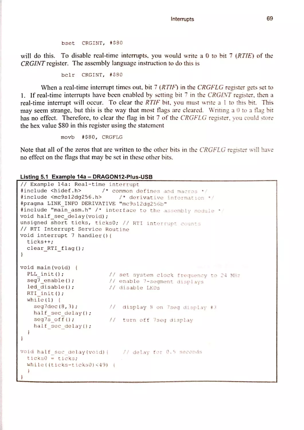
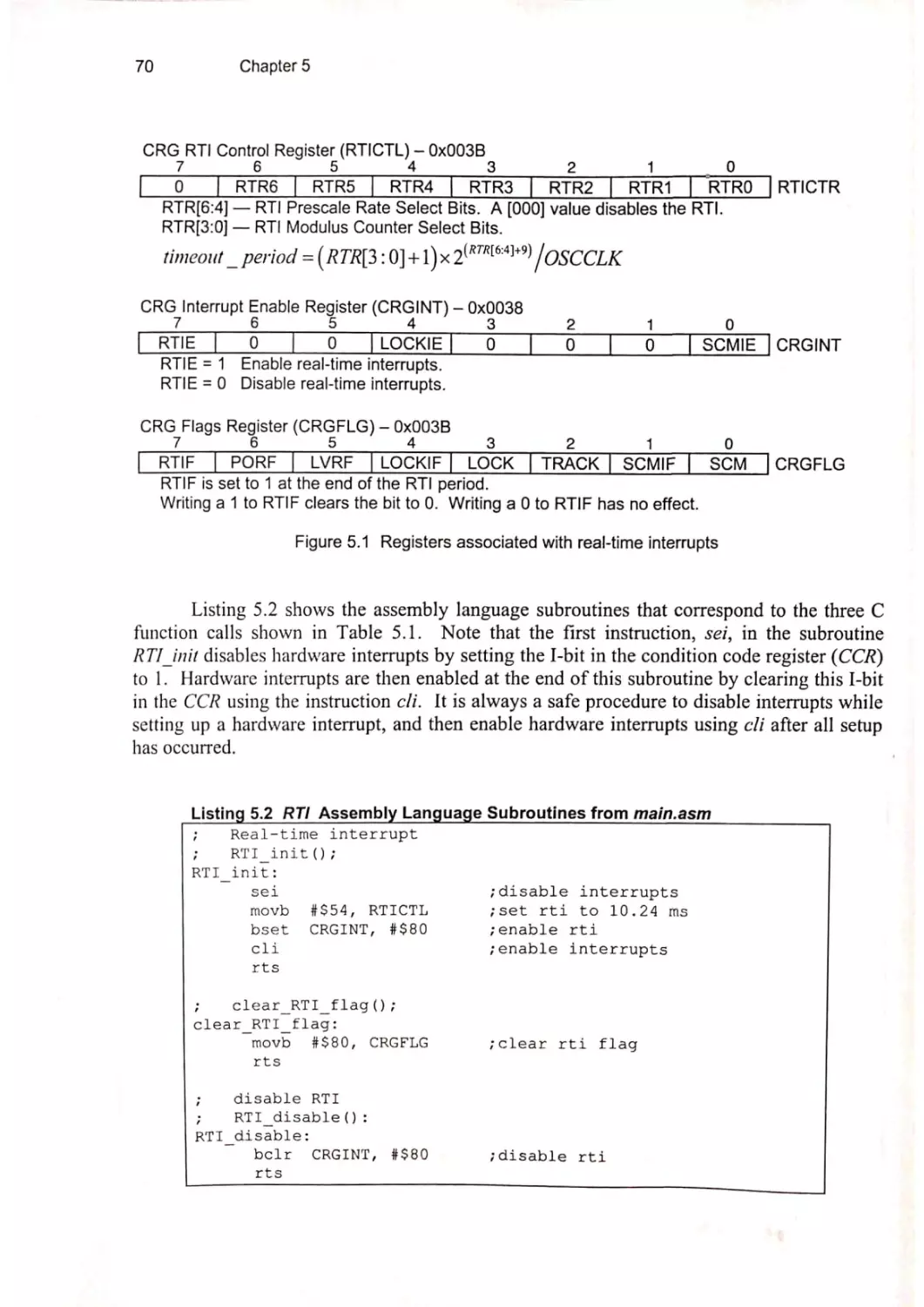
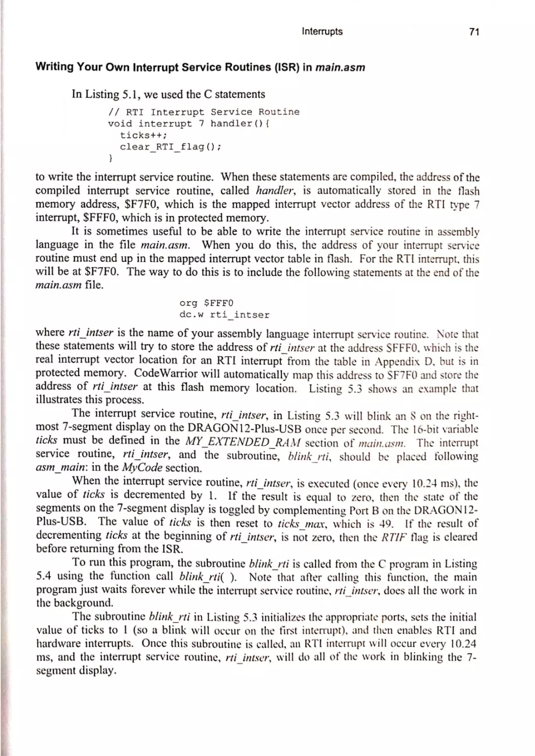
/


Author: Richard E. Haskell Darrin M. H.
Tags: programming languages programming computer science microprocessors reverse engineering
ISBN: 978-0-9824970-2-9
Year: 2011
Similar


Text
Programming the
DRAGON‘12-Plus-USB™
in C and Assembly Language
Using CodeWarrior™
Richard E. Haskell
Darrin M. Hanna
Oakland University, Rochester, Michigan
LBE Books
Rochester Hills, MI
Copyright 2011, 2018 by LBE Books. All rights reserved.
ISBN 978-0-9824970-2-9
Second Printing
Published by LBE Books, LLC
3201 University Drive
Suite 250
Auburn Hills, MI 48326
www.lbebooks.com
Preface
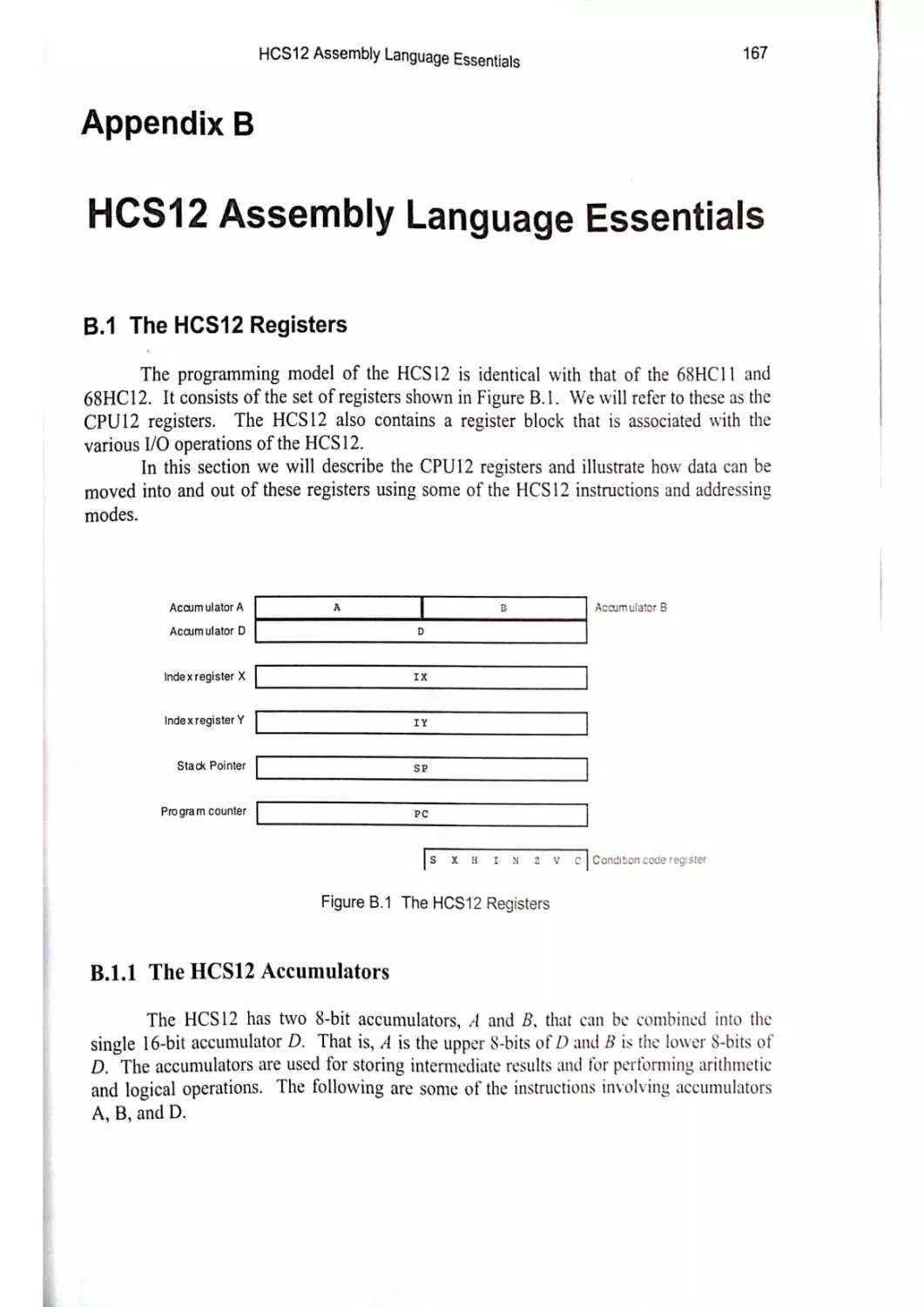
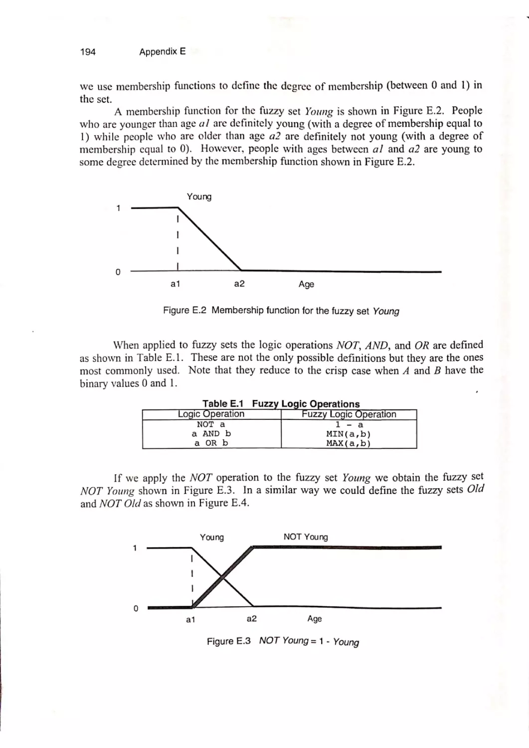
Microcontrollers such as the Freescale MC9SDG256 are remarkable devices. They contain
not only a sophisticated microprocessor with a rich set of instructions and addressing modes, but also
contain built-in RAM, EEPROM, and flash memoryas well as numerous useful I/O ports, including
parallel 1/O, several different types of serial I/O, timers, and A/D converters.
Wewill use a particular microcontroller, the Freescale MC9S 12DG256,thatit is one of the
more powerful in the popular HCS12 family of microcontrollers from Freescale with lots of /O
capabilities. This microcontroller is available on the DRAGON12-Plus-USB™development board
from Wytec, Inc. The DRAGON12-Plus-USB™has many built-in I/O devices including LEDs,
switches, four 7-segment displays, a hex keypad, an LCD display, a D/A converter chip, an on-board
speaker, a built-in H-bridge for driving motors, convenient headers for connecting servos and an
accelcrometer board available from Wytec, and female headers for connecting to your circuits on the
built-in protoboard.
A previous book from LBE Books, Learning By Example Using C — Programming the
DRAGON12-Plus™Using CodeWarrior showed howto write programs in C with a minimum of
effort for this development board. We did this by providing you with a CodeWamiorstationery
project that contained an assembly language file to do all the low-level interaction with the /O
registers. These assembly language routines becomefunction calls for your C program. Thus, in this
previous book you didn't have to learn any assembly language to get sophisticated programs to work
on this development board.
This current book provides these same CodeWamniorStationeryprojects so that you can wnite
C programs easily for the DRAGON 12-Plus-USB™development board. However, in this book we
look under the hood to see howall of the assembly language routines that are included in the
stationery project work. This way you will learn how to program the HCS12 microcontroller in
assembly language and howto call these assembly language routines from your top-level C program.
You will therefore be able to write your own assembly language subroutines that you can call from
your C program, and in this way get the maximum performance from the MC9SDG256
microcontroller.
In Chapter | we introduce the DRAGON 12-Plus-USB™development board. Chapter 2 will
include examples of using the parallel ports for outputs and Chapter 3 will include examples of using
the parallel ports for inputs. Liquid crystal displays are described in Chapter 4. The important topic
of intermupts are introduced in Chapter 5. Examples using the two 8-channel A/D converters that are
built into the MC9S12DG256 microcontroller are given in Chapter 6. Examples that show how to
use pulse-width modulation (PWM) to control the speed of a DC motoror the position of a servo are
presented in Chapter 7. Chapter 8 includes examples of using the serial communication interface
(SCI) and Chapter 9 shows howto use the serial peripheral interface (SPI). Examples using the
built-in timer module are given in Chapter 10 and an example of using the MC9S12DG256
microcontroller for fuzzy control is included in Chapter 11.
Manycolleagues, students and reviewers have influenced the development of this book.
Their stimulating discussions, probing questions, and critical comments are greatly appreciated.
Special thanks go to Michael Latcha and Osamah Rawashdeh with whom we have had many useful
discussionsrelated to the contents of this book.
Richard E. Haskell
Darrin M. Hanna
iil
Programming the DRAGON‘12-Plus-USB
in C and Assembly Language
Using CodeWarrior™
Table of Contents
1. Introduction
l
1.1 From Microprocessors to Microcontrollers
1.2 DRAGON12-Plus-USB™ Board
1.3 The CodeWarrior Development Tools
2. Parallel Ports — Outputs
|
4
5
6
2.1 MC9S12DG256Parallel I/O Ports
2.2 LEDs and 7-Segment Displays
Example | — Writing to Ports
Example 2 — C Function Calls
Example 3 — Delay Loops in C
Example 4 — Delay Loops in Assembly: ms_defay(int m)
Example 5 — Turning Single Bits On and OfT
Example 6 — Hex Counter
Example 7 — Multiplexing the 7-Segment Displays
Problems
6
7
9
10
16
18
20
24
28
29
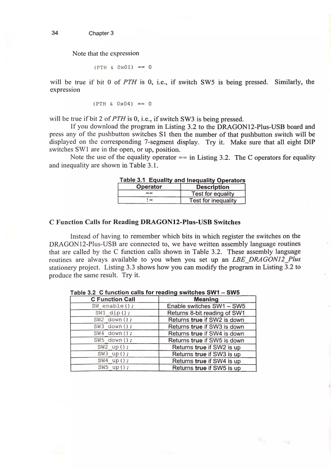
3. Parallel Ports — Inputs
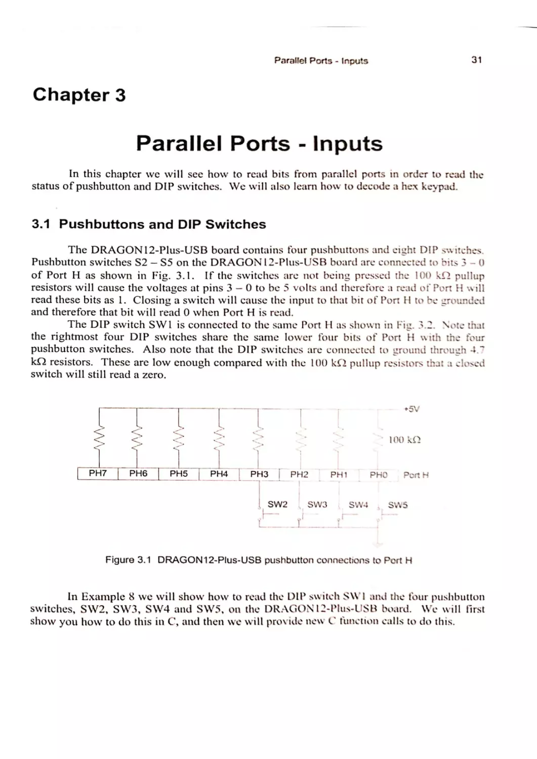
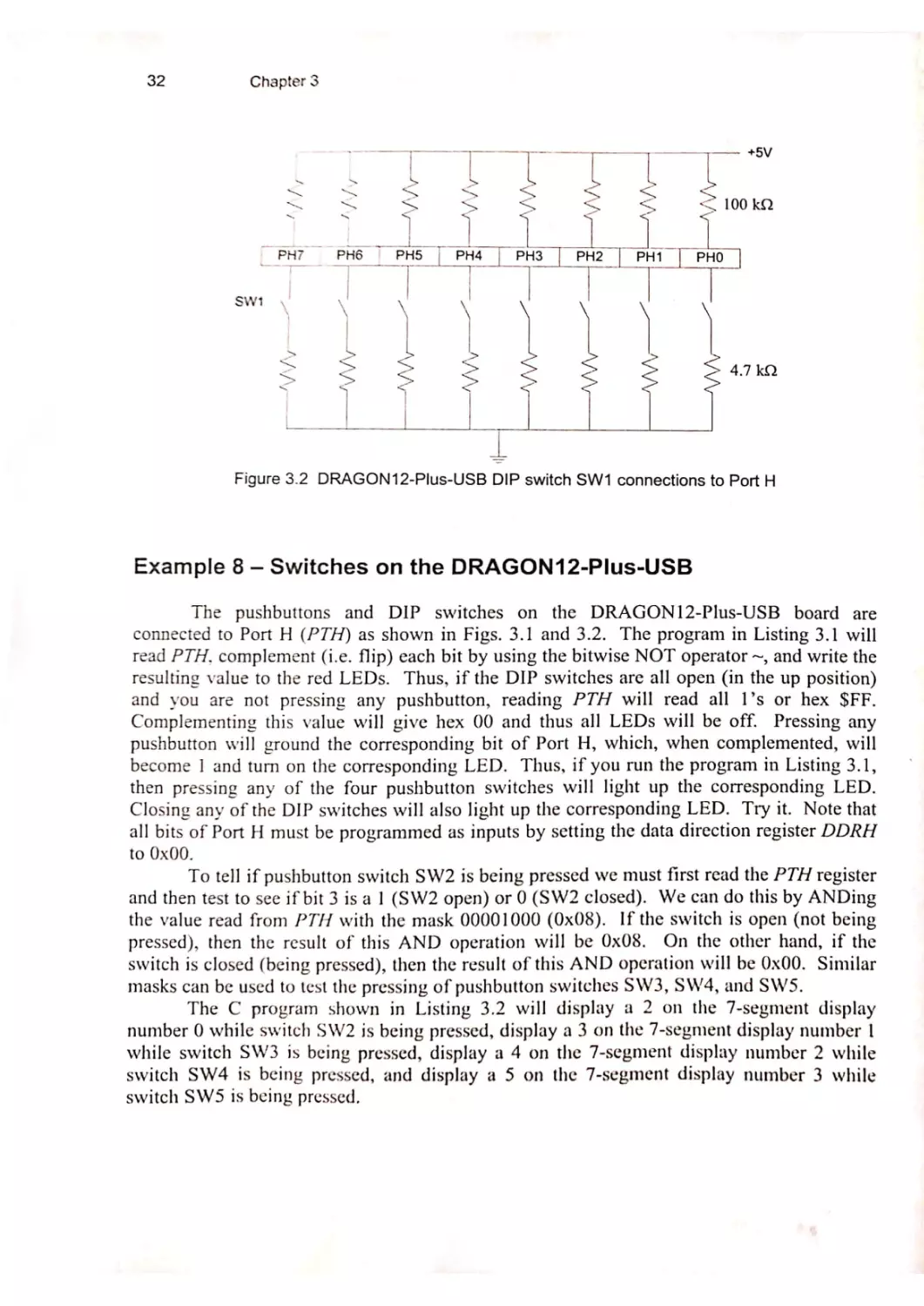
3.1 Pushbuttons and DIP Switches
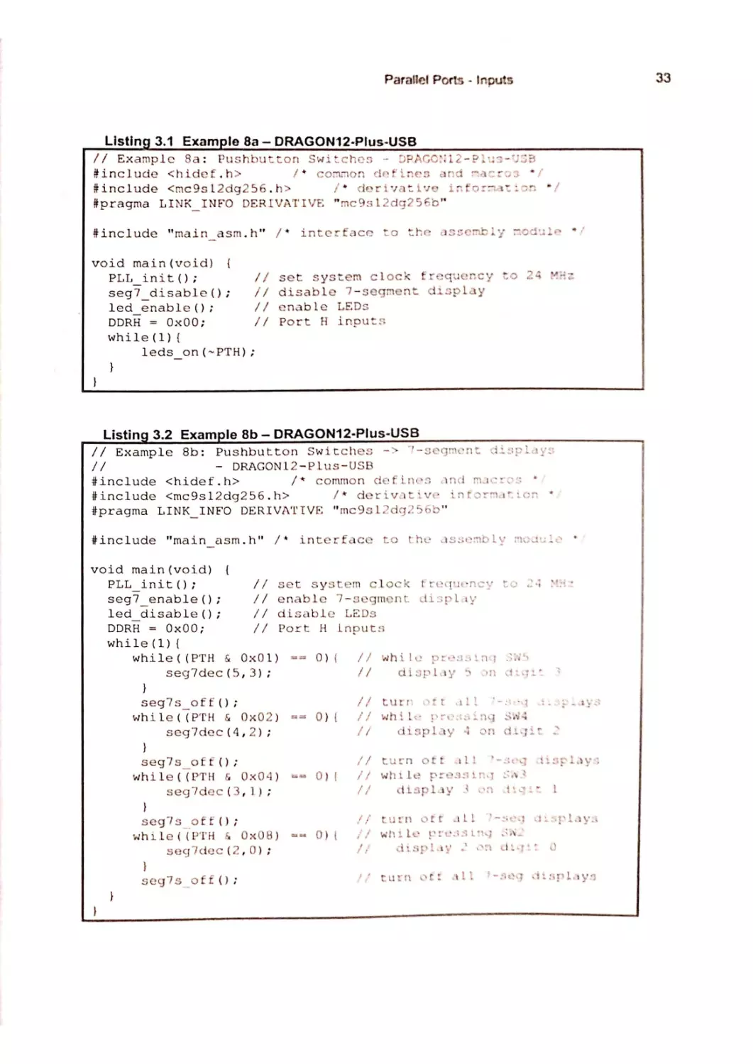
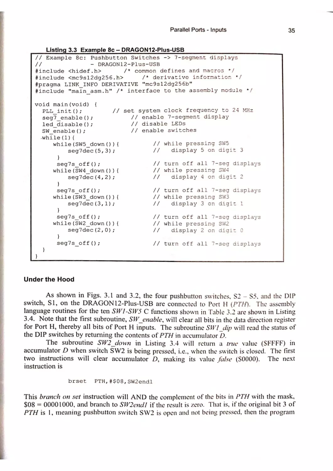
Example 8 — Switches on the DRAGON12-Plus-USB
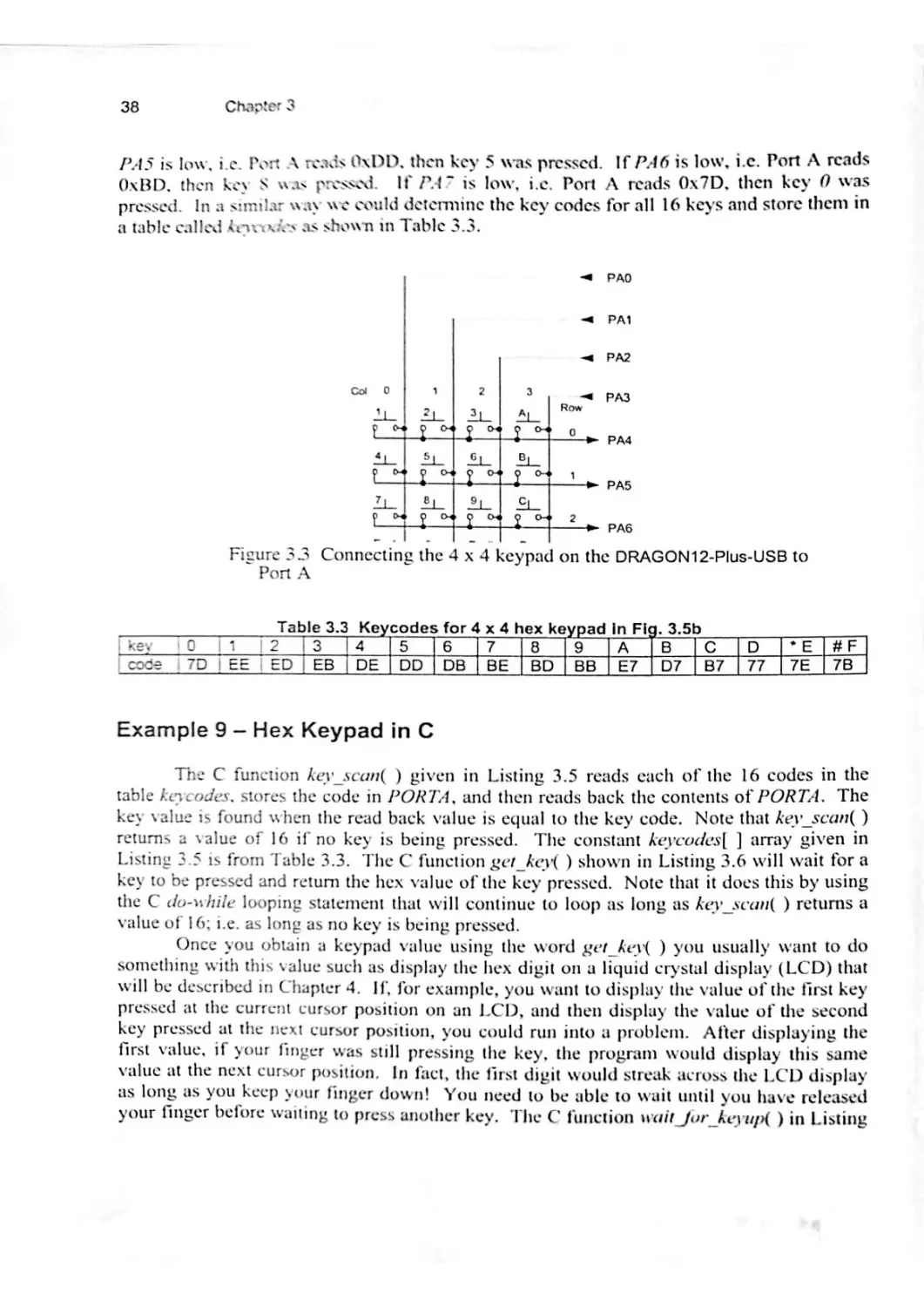
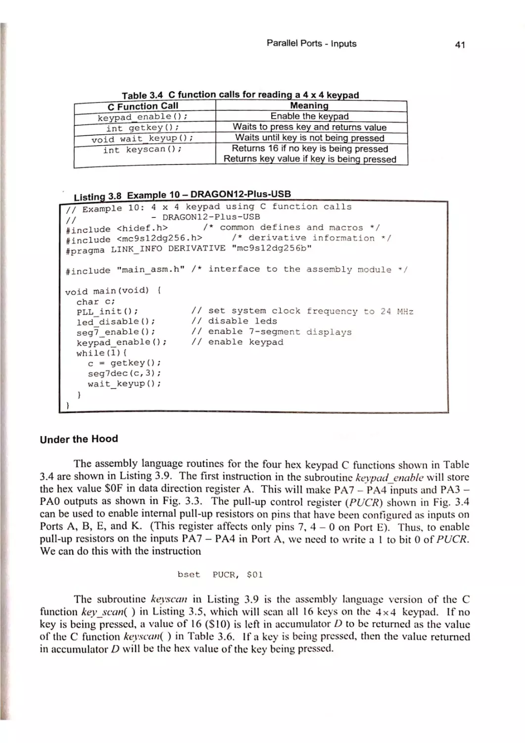
3.2 Hex Keypad
Example 9 — Hex Keypad in C
Example 10 — Keypad C Function Calls Problems
Problems
31
3]
32
37
38
40
44
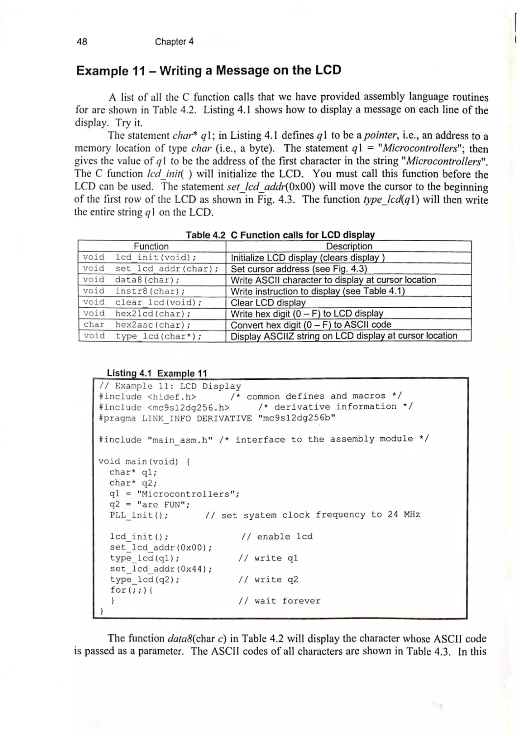
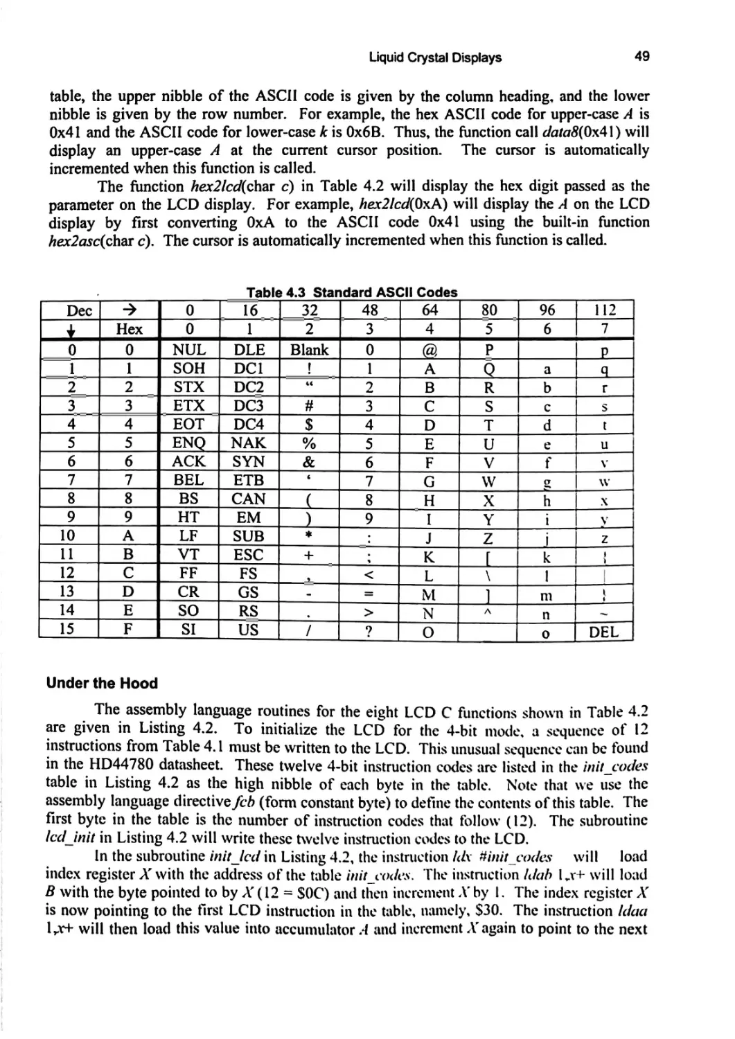
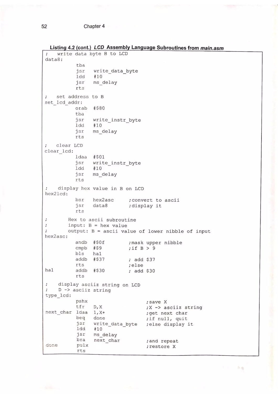
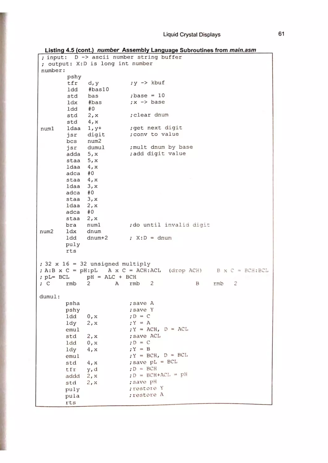
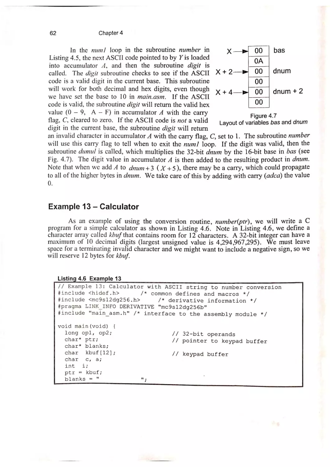
4. Liquid Crystal Displays
4.1 Liquid Crystal Displays
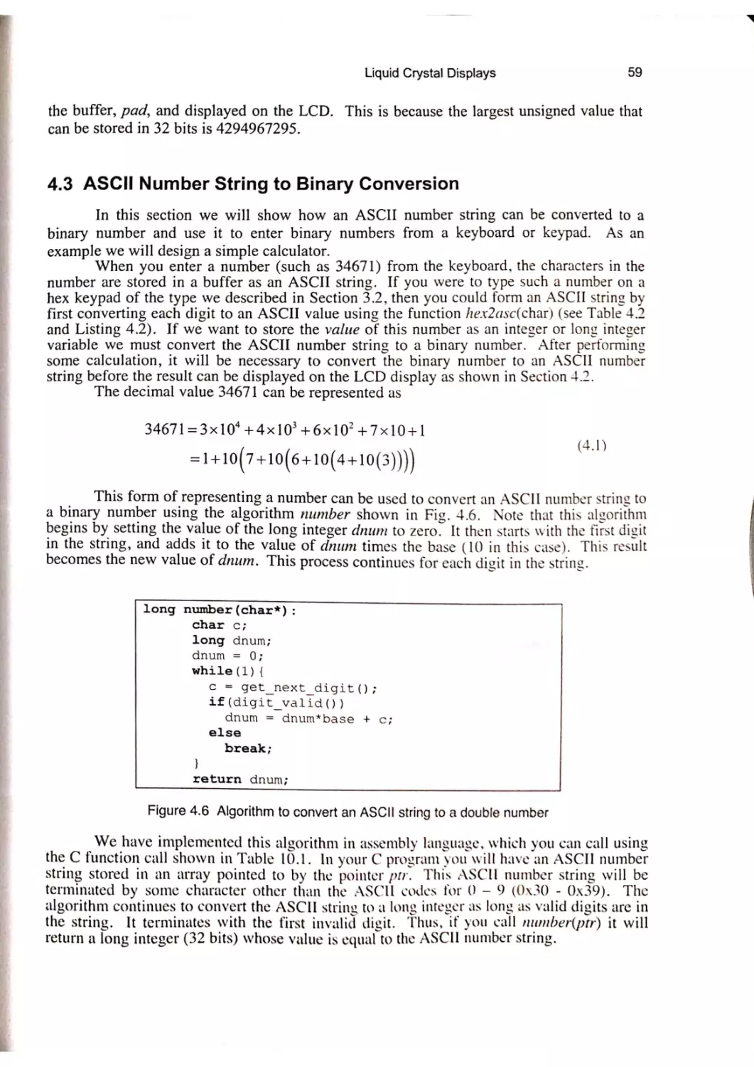
Example |1 — Writing a Message on the LCD
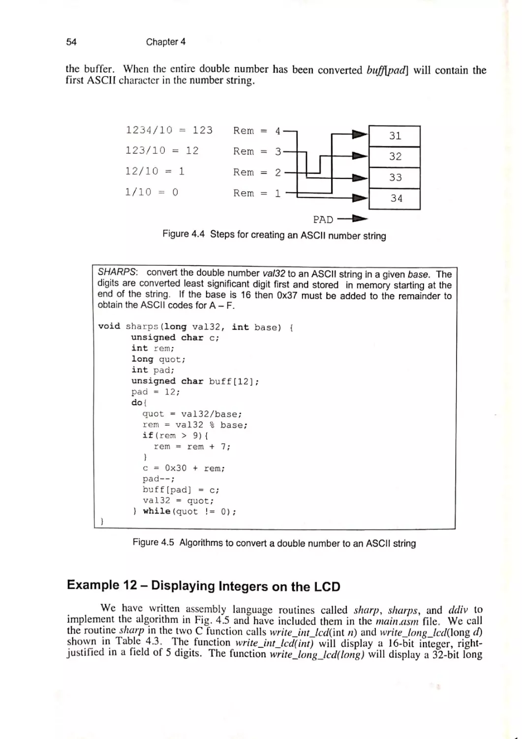
4.2 Binary Numberto ASCII String Conversion
Example 12 — Displaying Integers on the LCD
4.3, ASCII Number String to Binary Conversion
Example 13 — Calculator
Problems
45
45
48
53
54
59
62
65
y
5. Interrupts
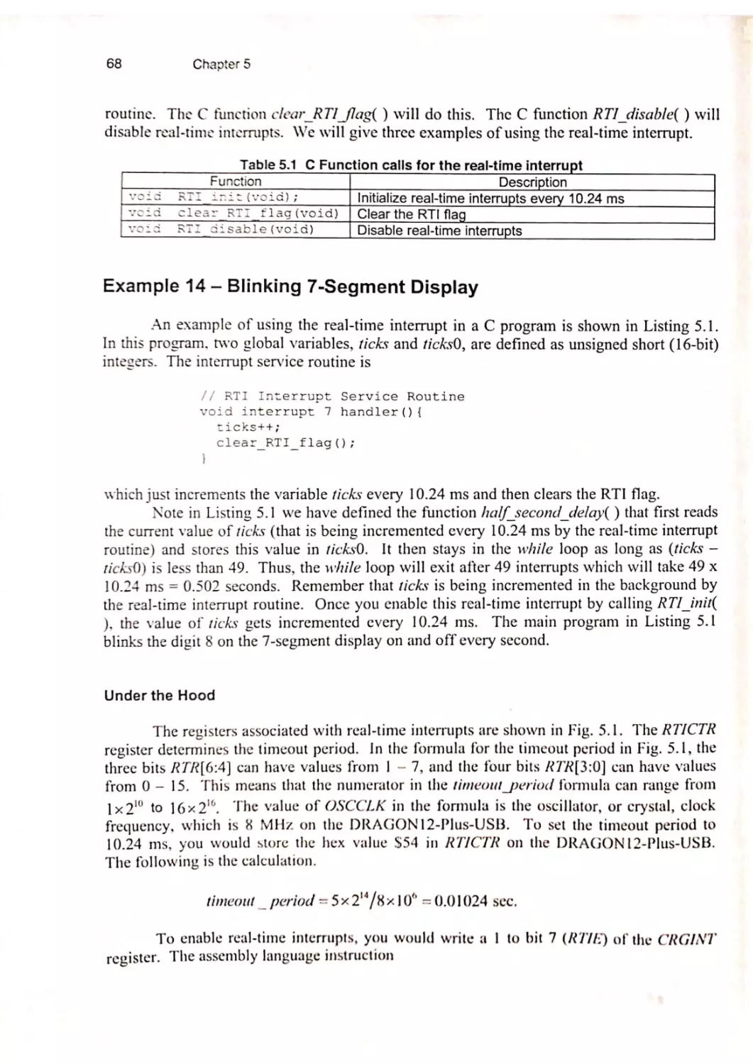
5.1 Hardware Interrupts
5.2 Real-Time Interrupts
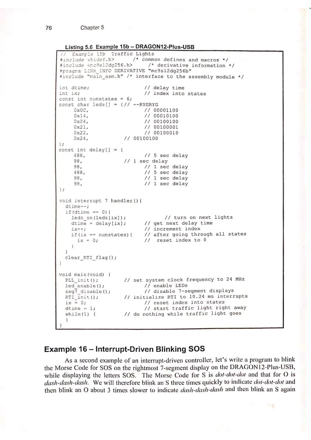
Example 14 — Blinking 7-Segment Display
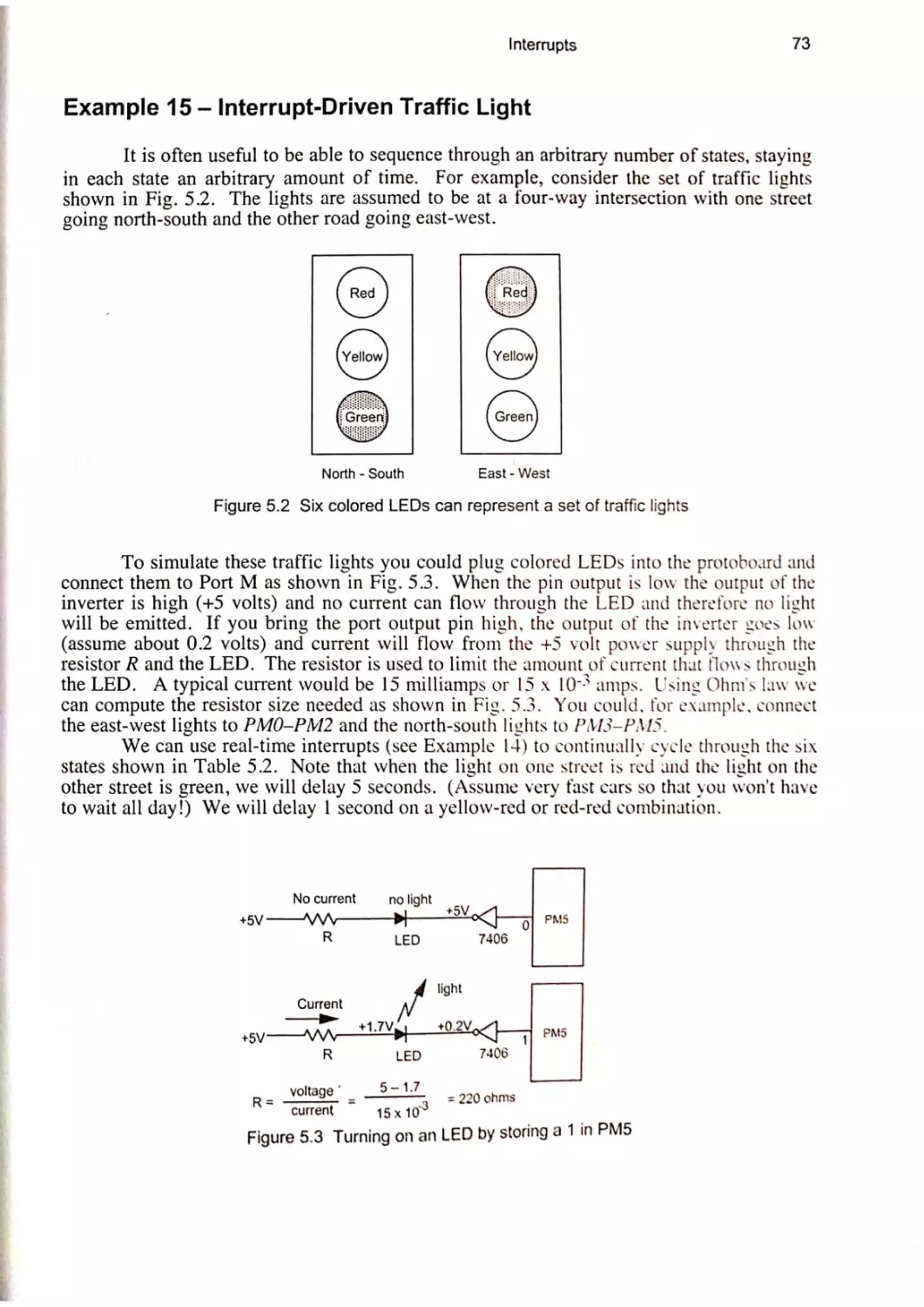
Example 15 — Interrupt-Driven Traffic Light
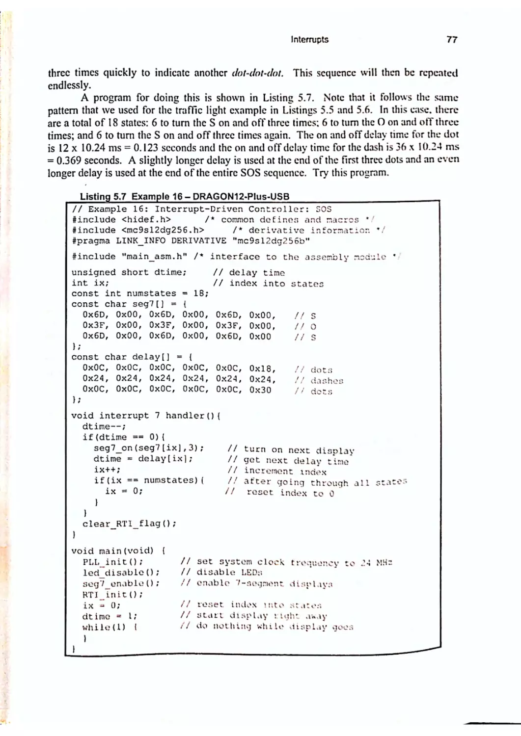
Example 16 — Interrupt-Driven Blinking SOS
6. Analog-to-Digital Converter
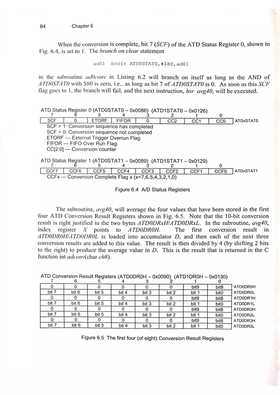
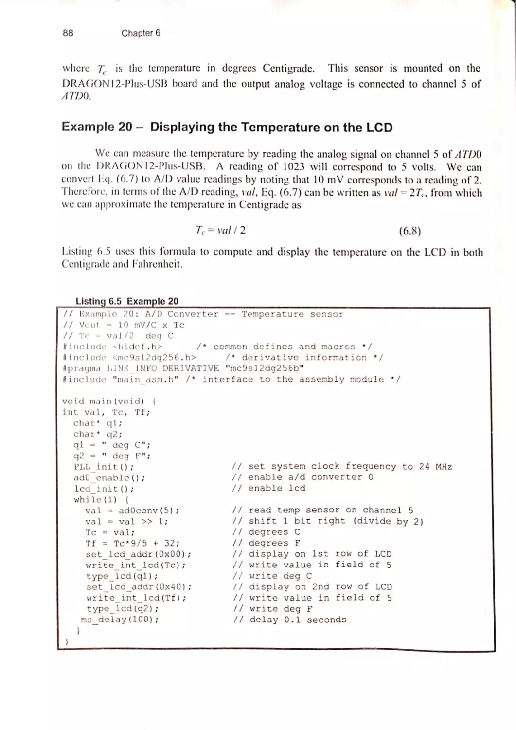
6.1 Analog-to-Digital Conversion
6.2 Using the MC9S12DG256 A/D Converters
Example 17 — Reading the Potentiometer Valuc
6.3. Measuring Acceleration
Example 18 — Measuring the x-)-z Components of Acceleration
Example 19 — Measuring the Coefficient of Static Friction
6.4 Measuring Temperature
Example 20 — Displaying the Temperature on the LCD
66
66
67
68
73
76
78
78
80
81
85
85
86
87
88
89
89
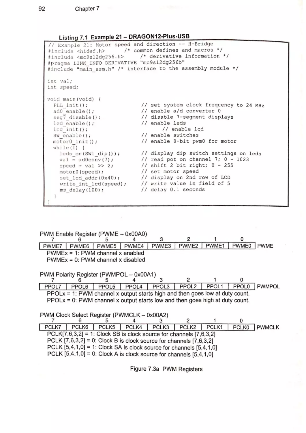
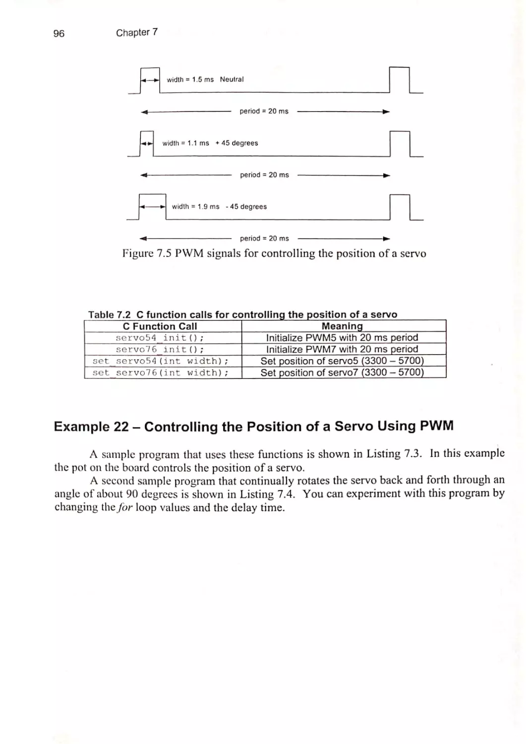
Example 21 — Controlling the Speed of a DC Motor Using PWM 90
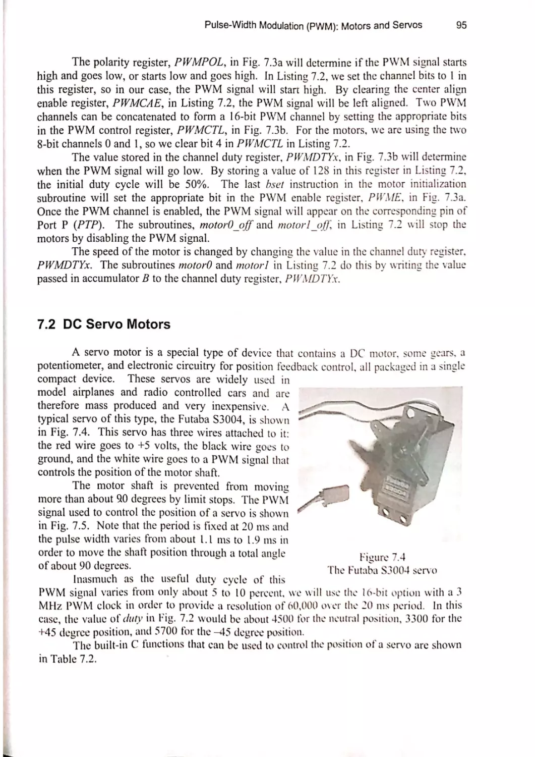
7.2 DC Servo Motors
95
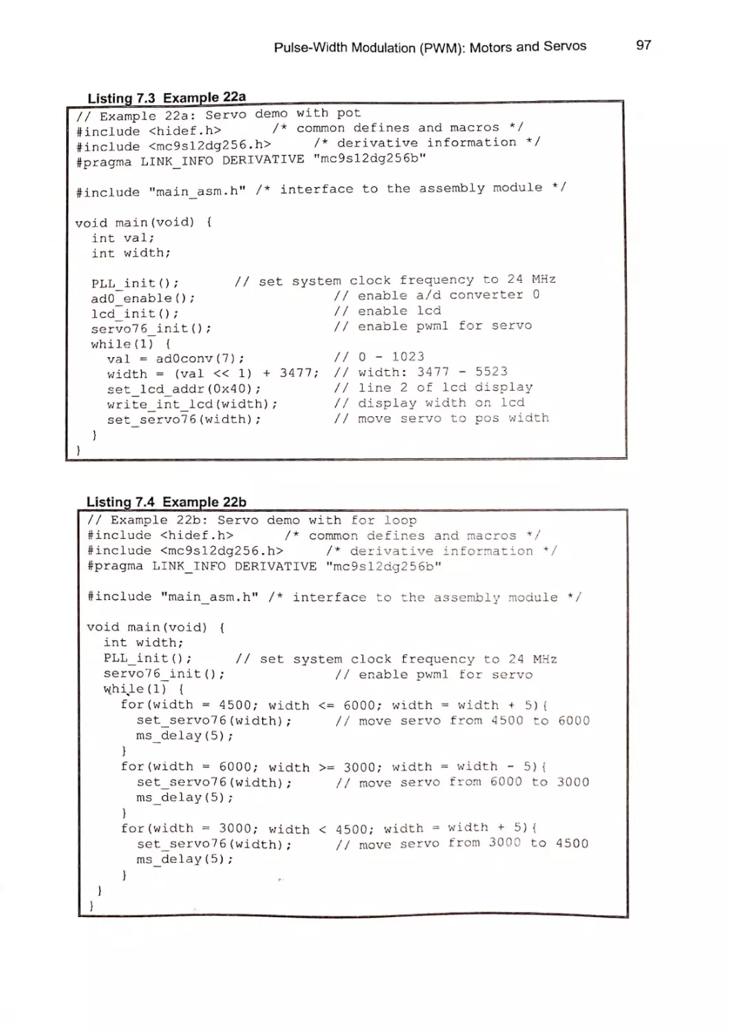
Example 22 — Controlling the Position of a Servo Using PWM
96
7. Pulse-Width Modulation (PWM) — Motors and Servos
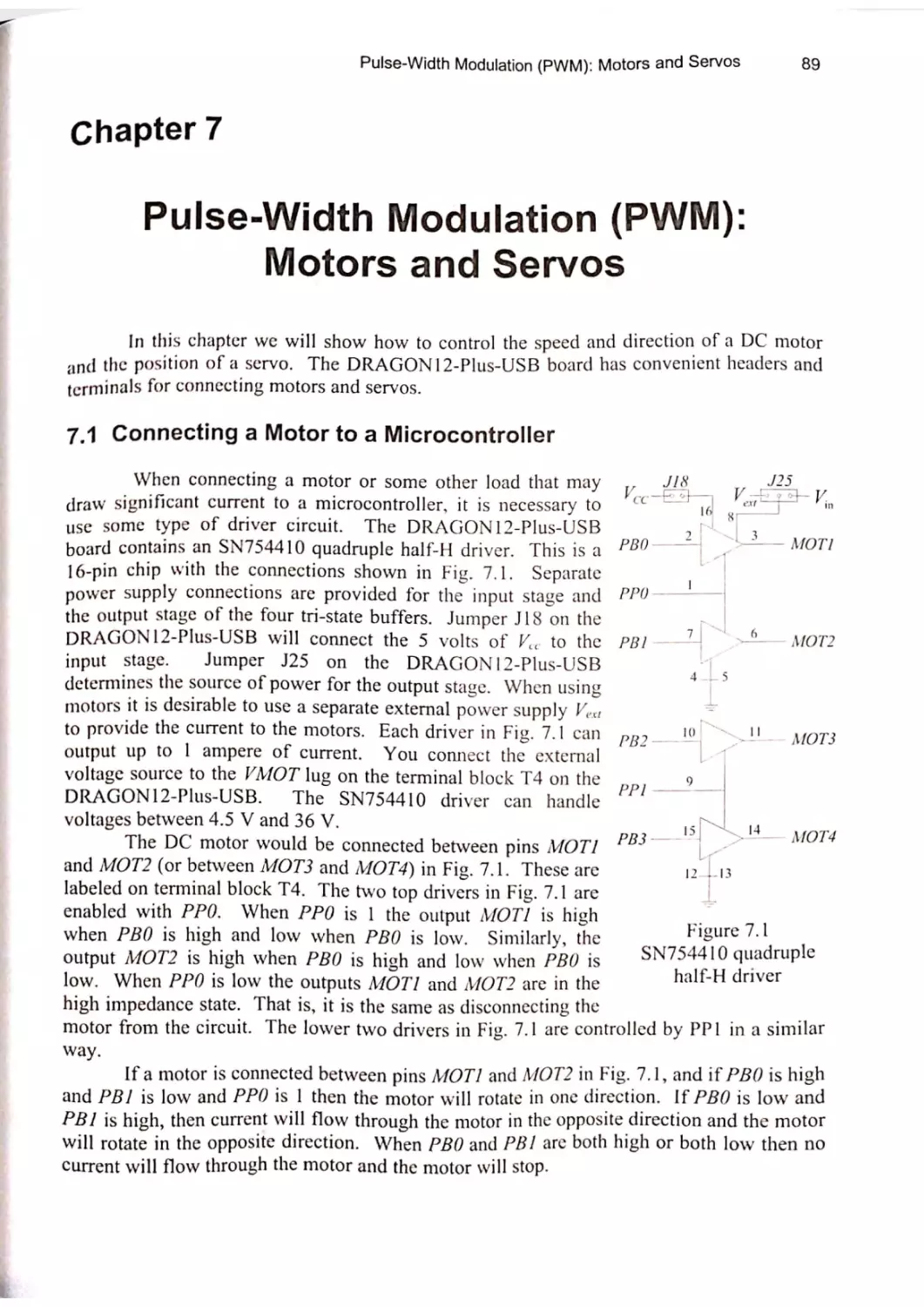
7.1. Connecting a Motor to a Microcontroller
8. Serial Communication Interface (SCI)
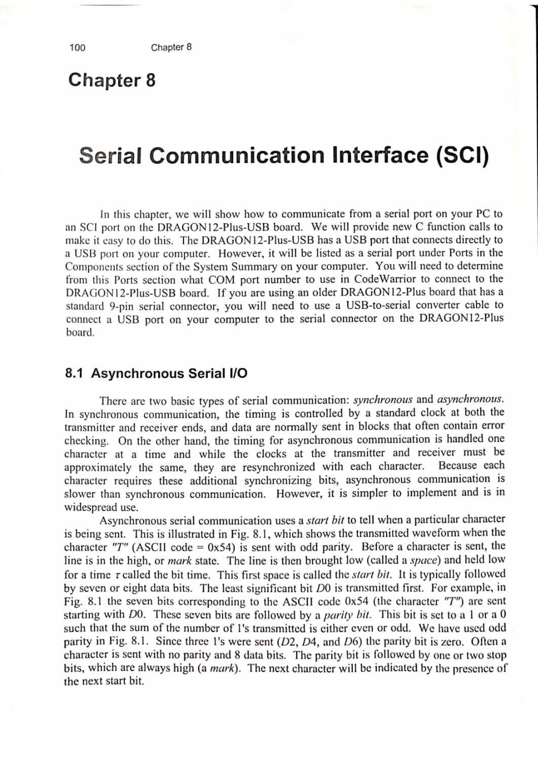
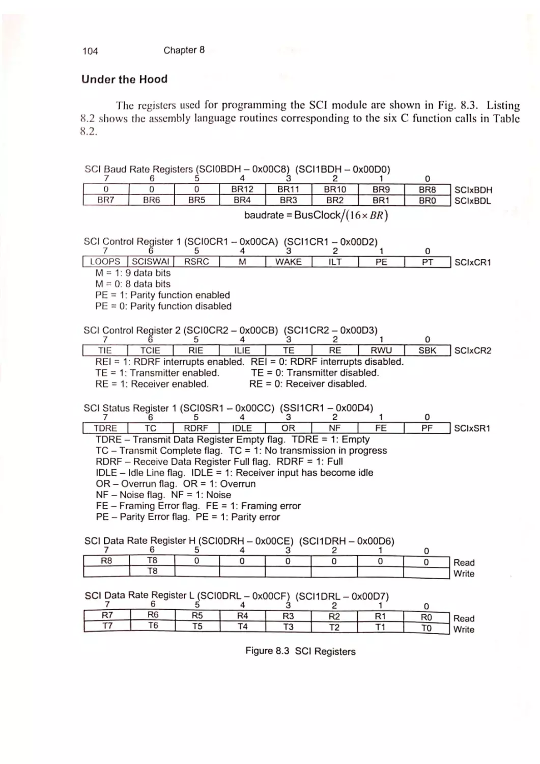
8.1 Asyncronous Scrial I/O
8.2 The 68HCS12 SCI Interface
Example 23 — SCI Echo with LCD Display
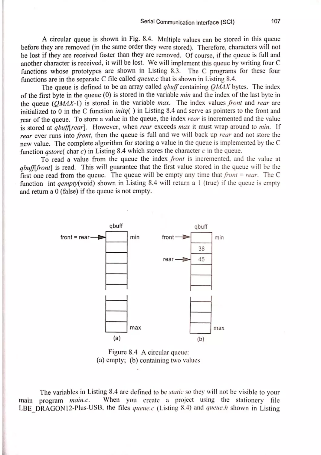
8.3 A Circular Queue Data Structure
Example 24 — Keypad Input to LCD Using a Queuc
100
100
101
103
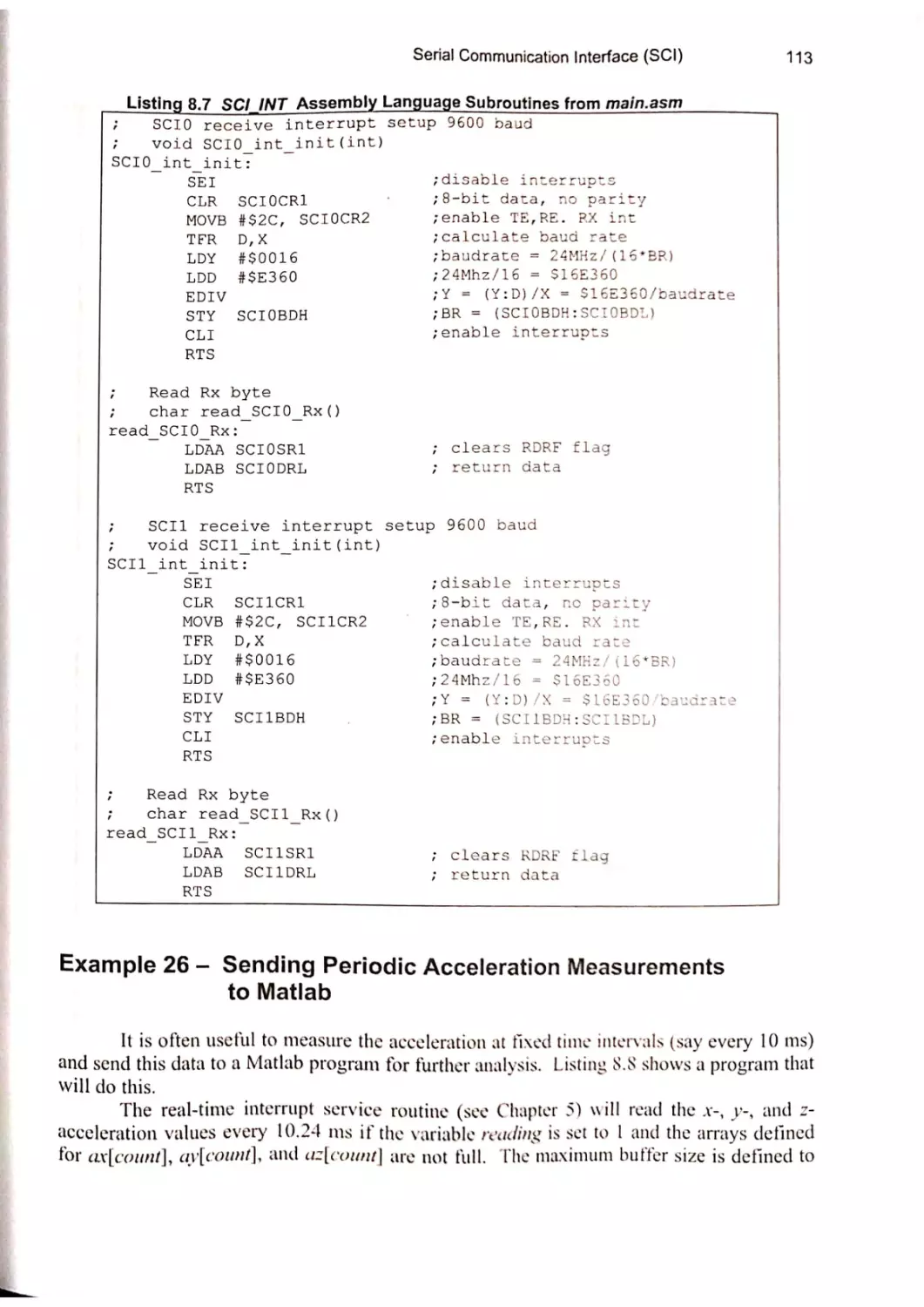
106
109
110
8.4 SCI Interface Using Interrupts
Example 25 — Display SCI Input on LCD Using Reccive Interrupts 111
Example 26 — Sending Periodic Acceleration Mcasurements
to Matlab
113
Problems
117
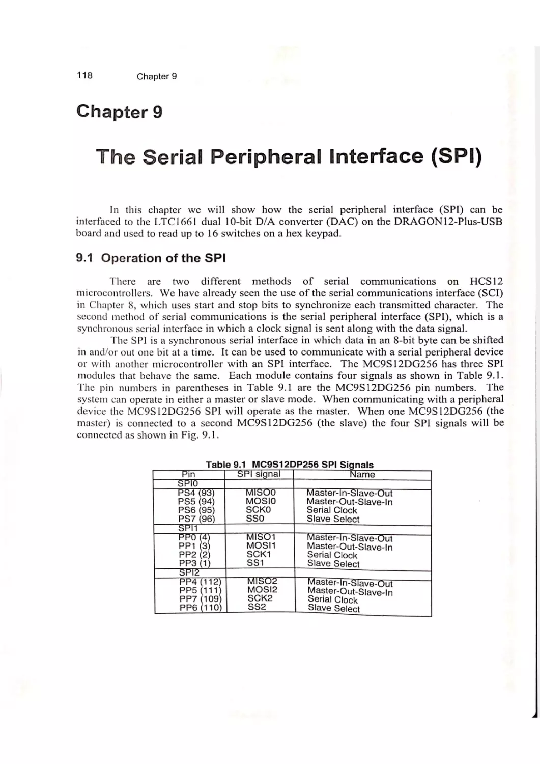
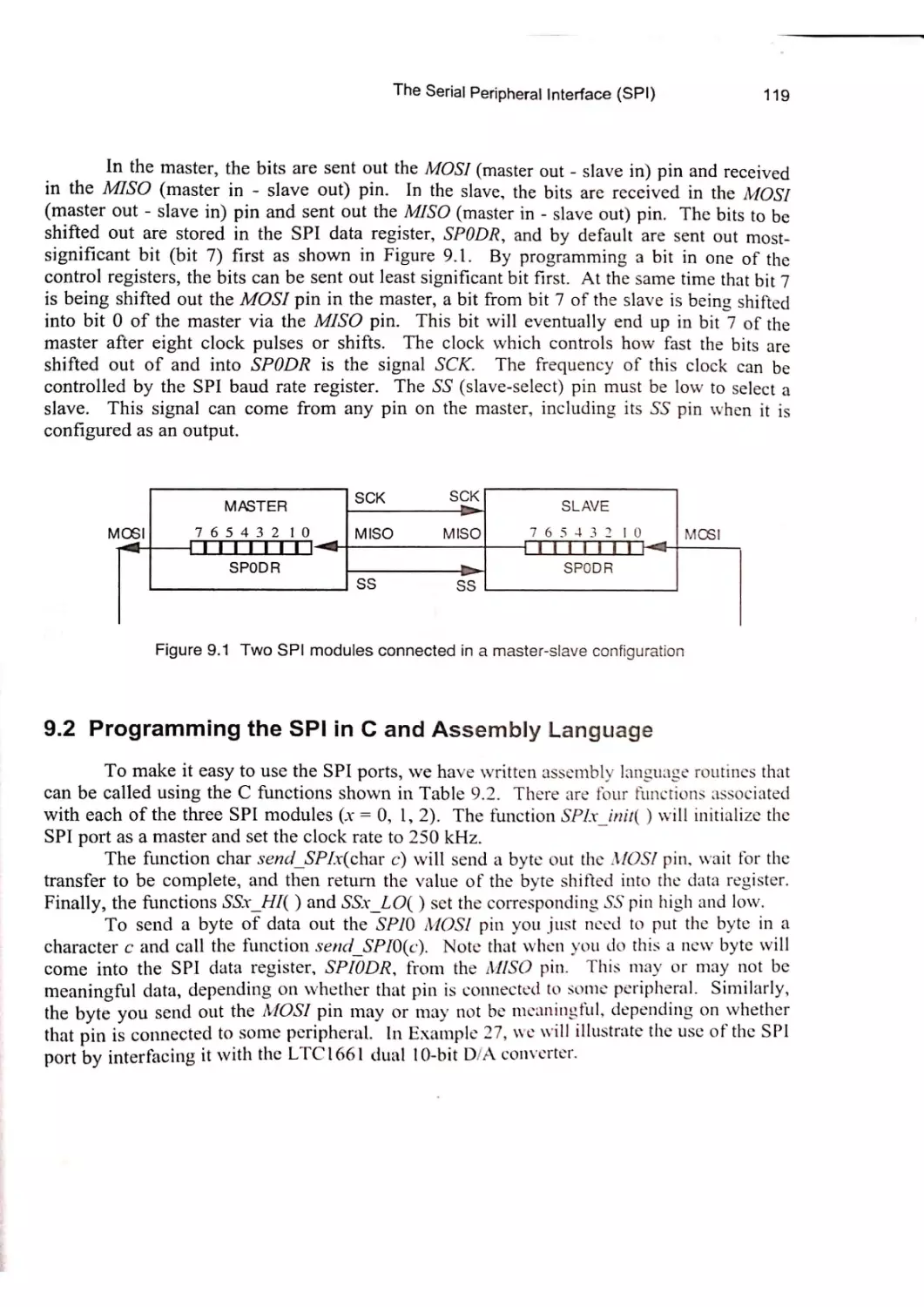
9. The Serial Peripheral Interface (SPI)
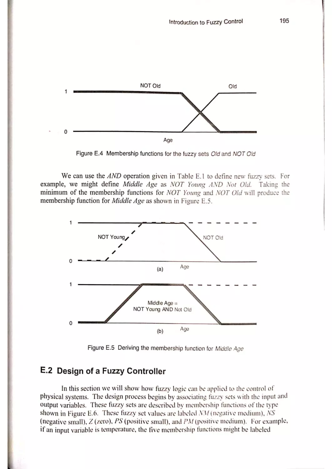
9.1 Operation of the SPI
9.2 Programming the SPI in C and Assembly Language
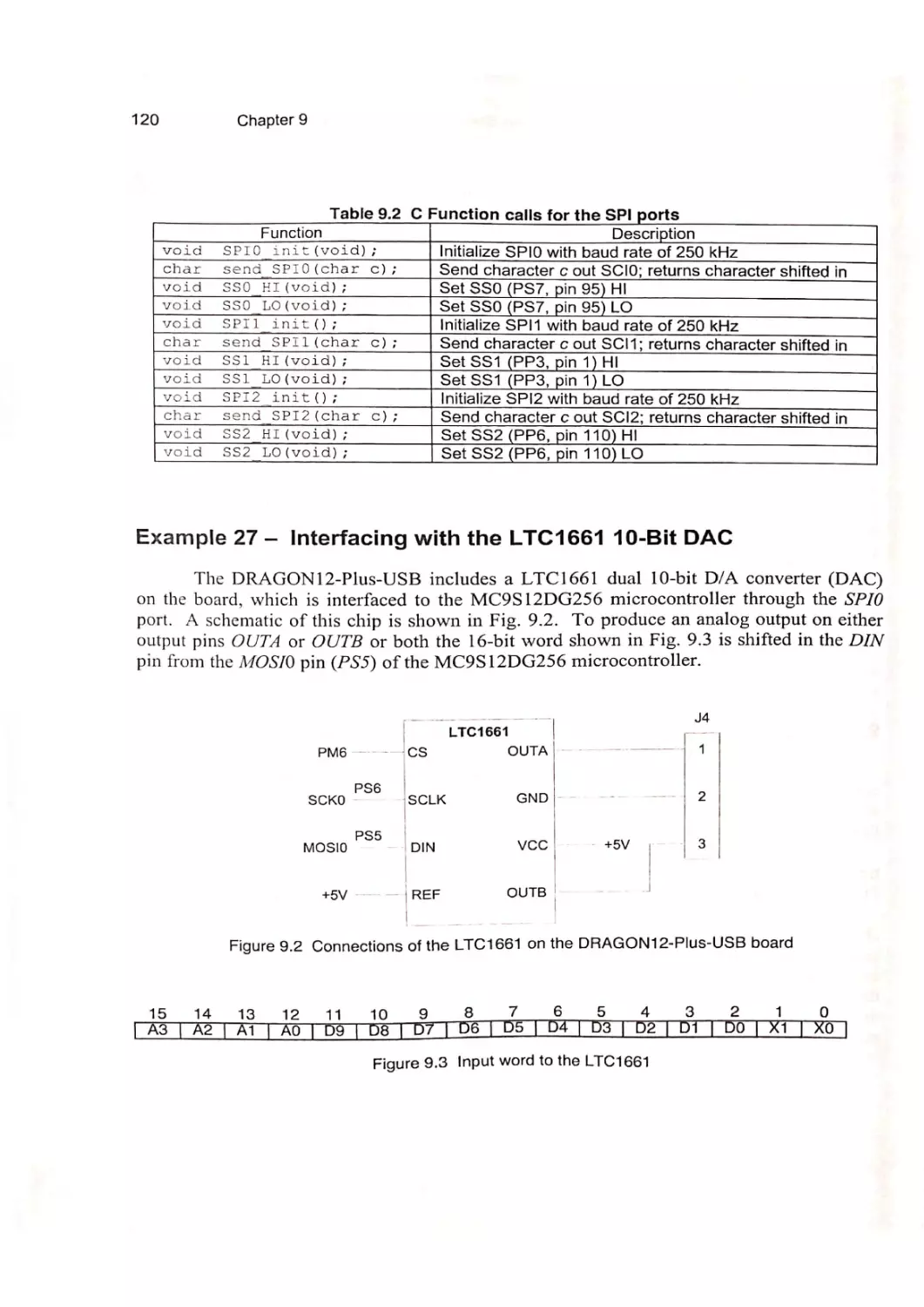
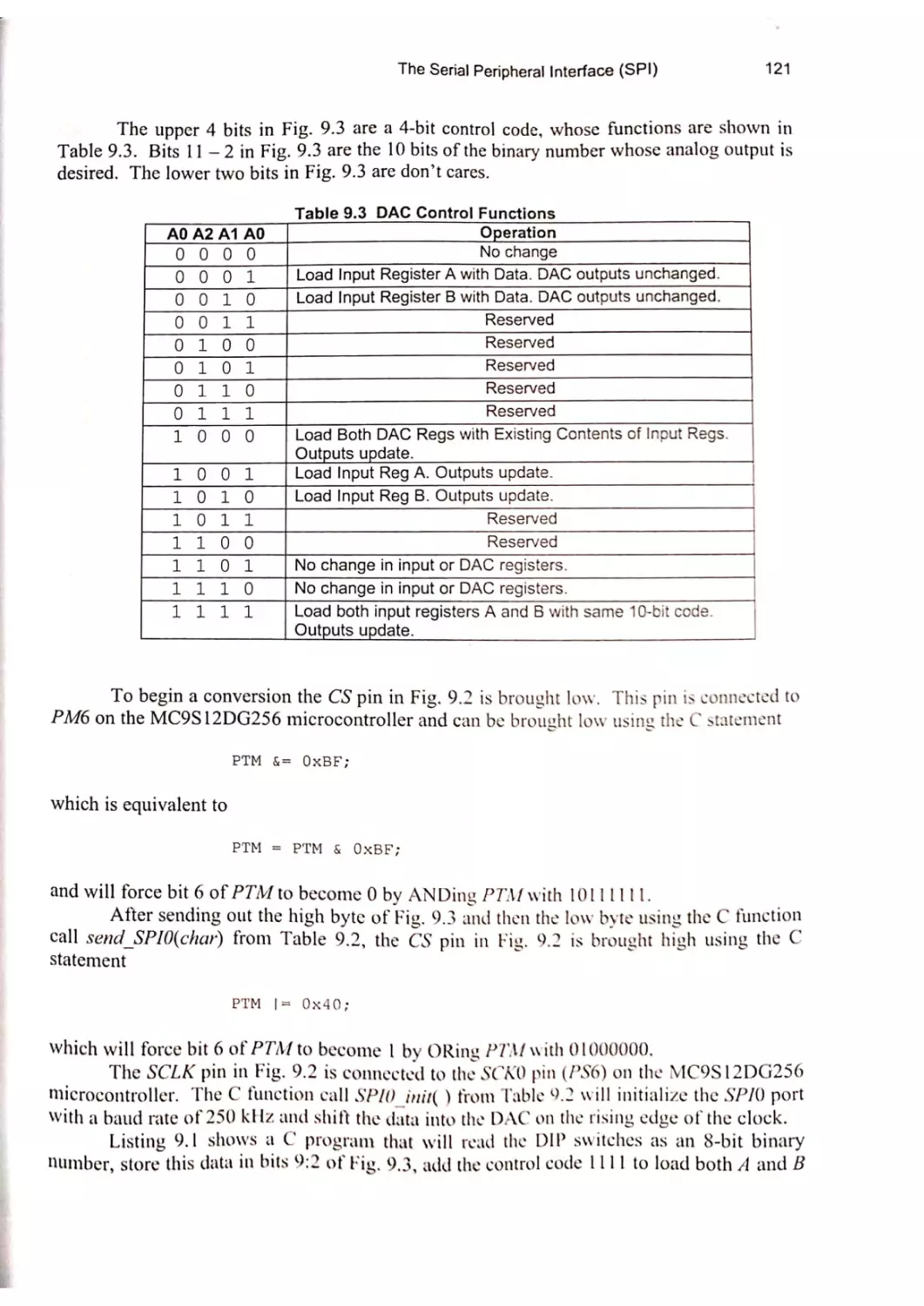
Example 27 — Interfacing with the LTC1661 10-Bit DAC
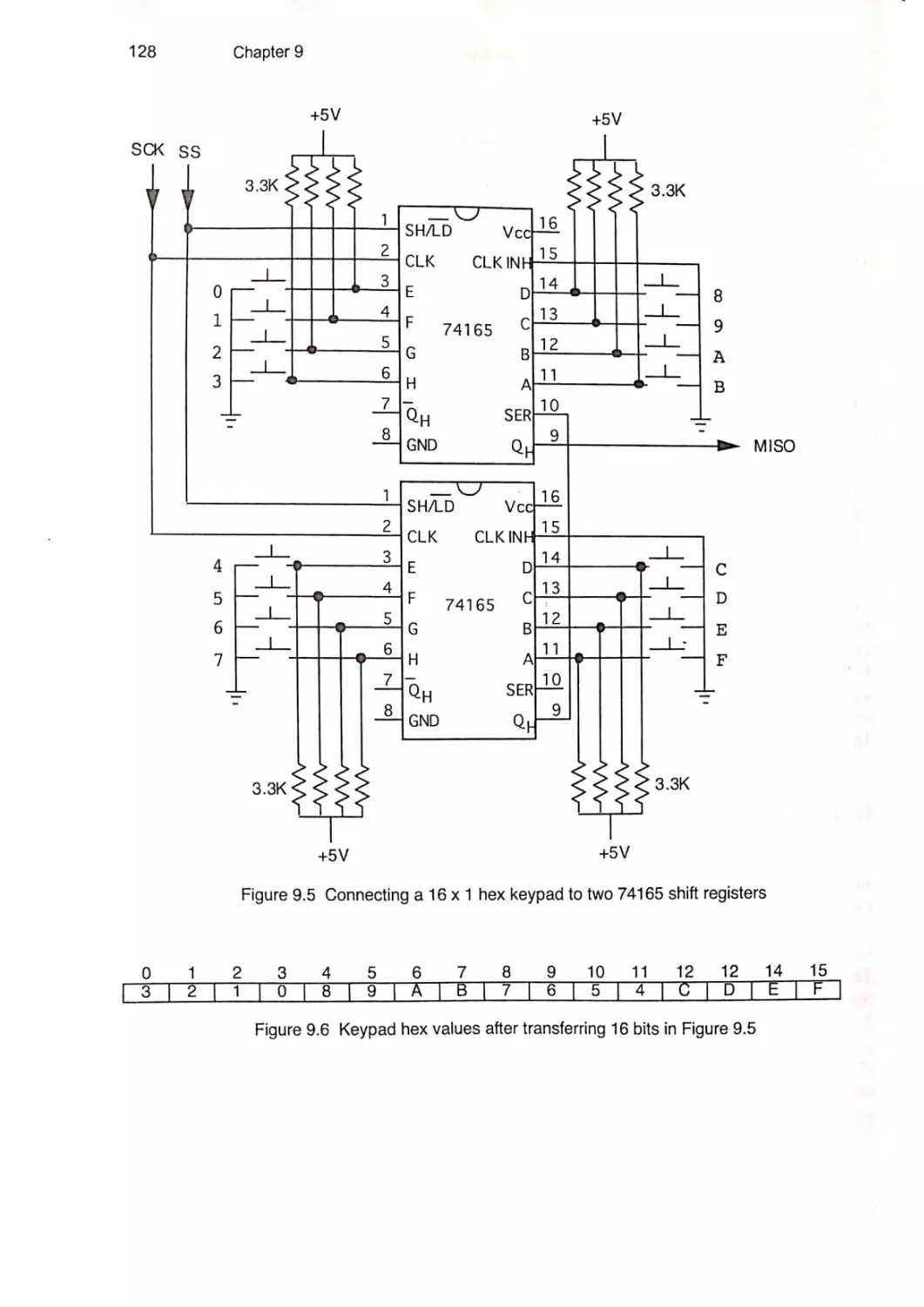
9.3 Keypad Interfacing with 74165 Shift Registers
Example 28 — Reading Data from Shift Registers Using SPI
Problems
vi
118
118
119
120
126
127
131
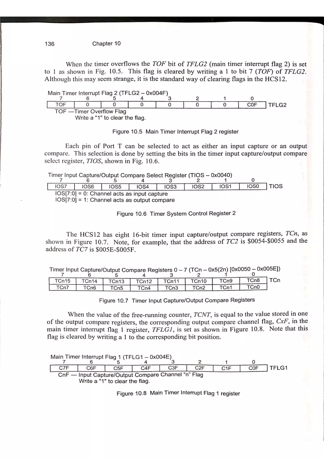
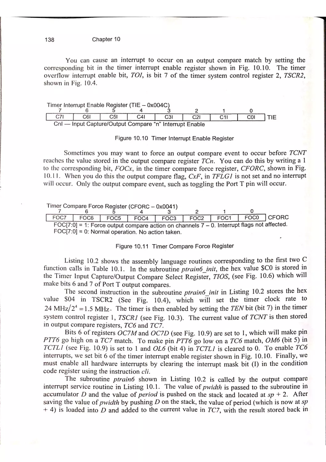
10. Timer
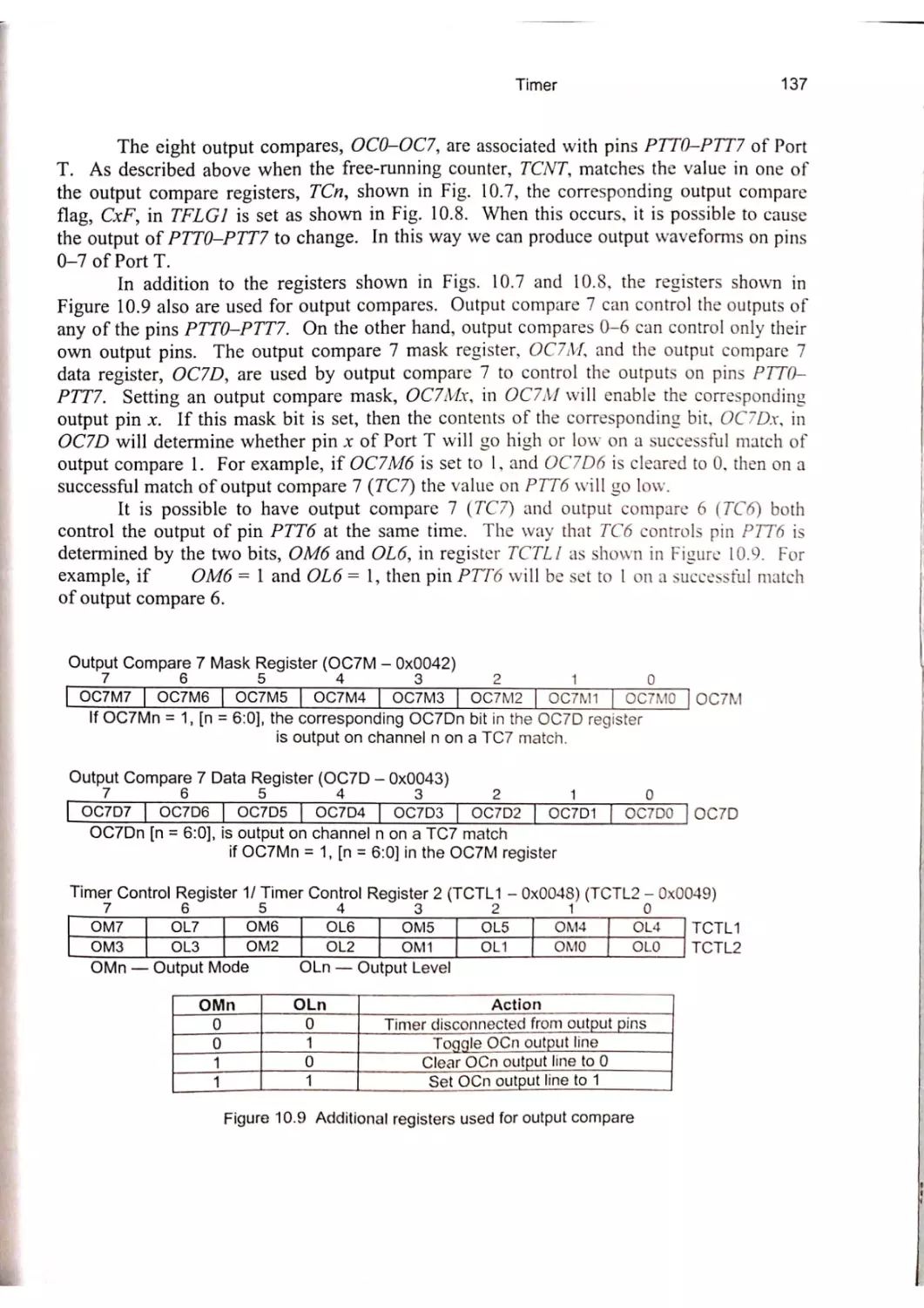
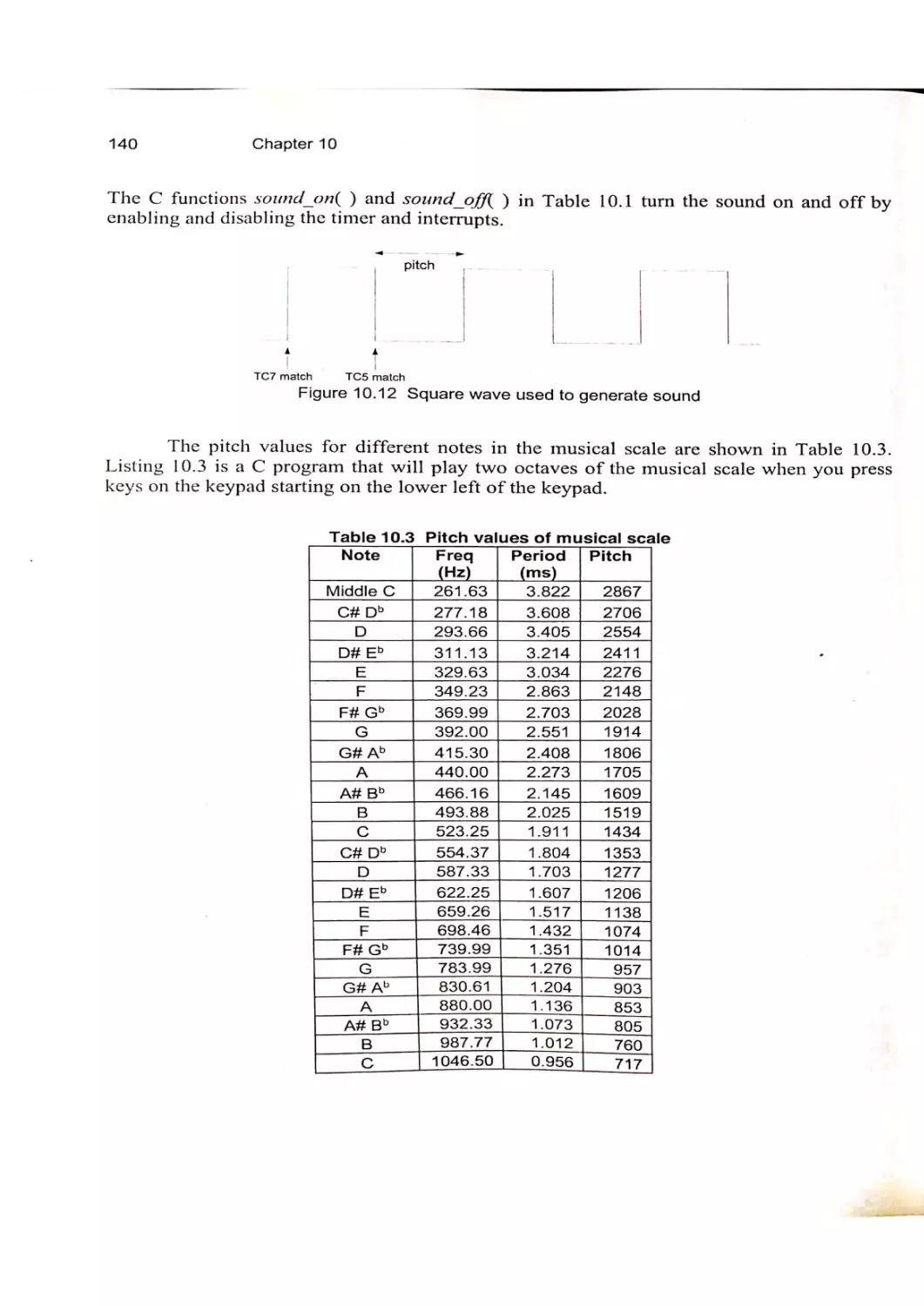
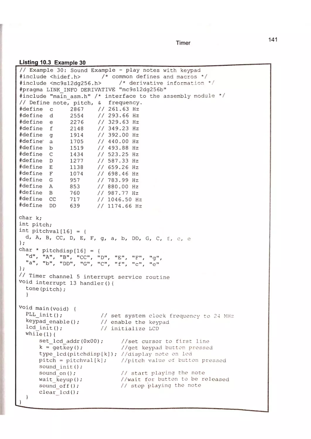
10.1 Output Compare
Example 29 — Interrupt-Driven Pulse Train
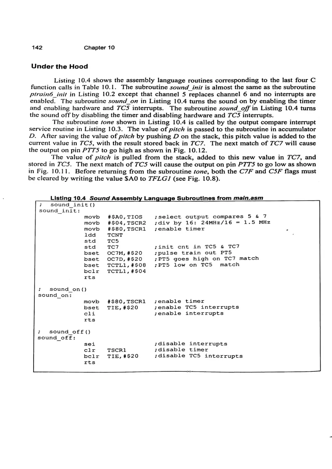
Example 30 — Playing Musical Notes with the Keypad
10.3. Input Capture
Example 31 — Measuring Input Pulse Widths
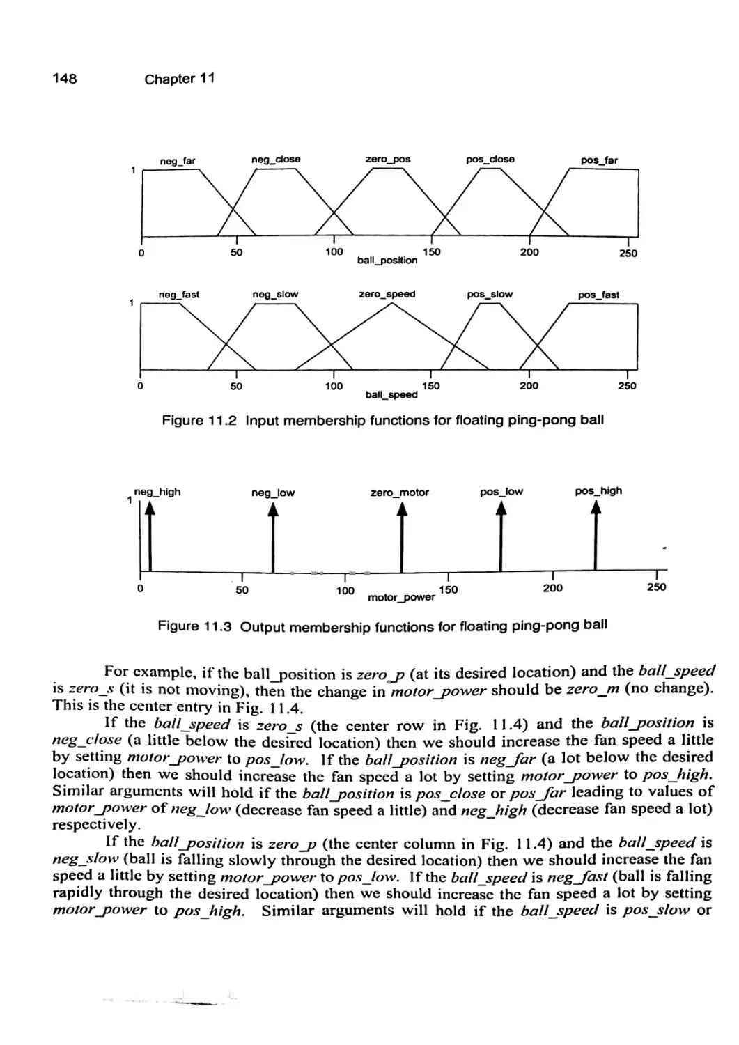
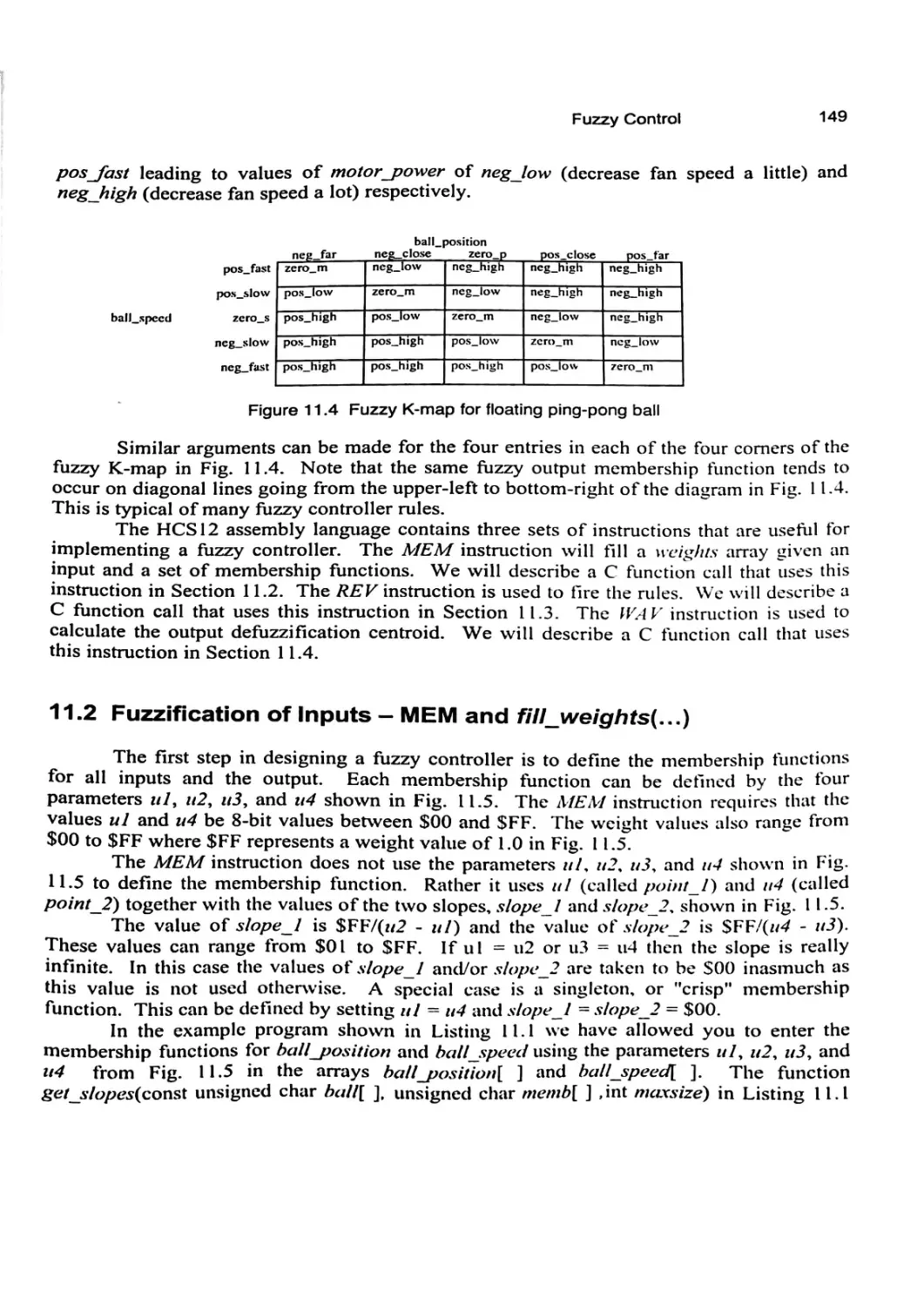
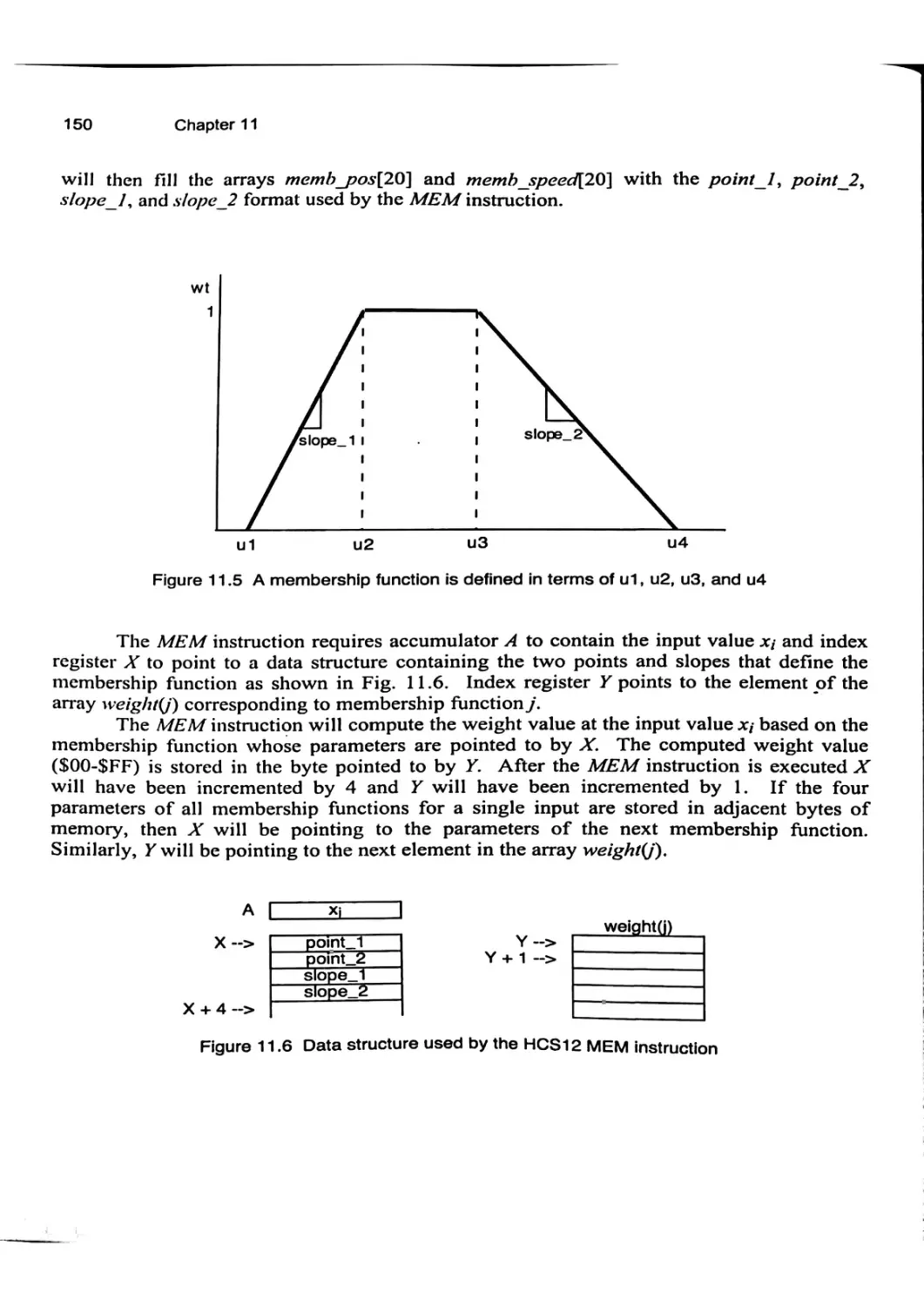
11. Fuzzy Control
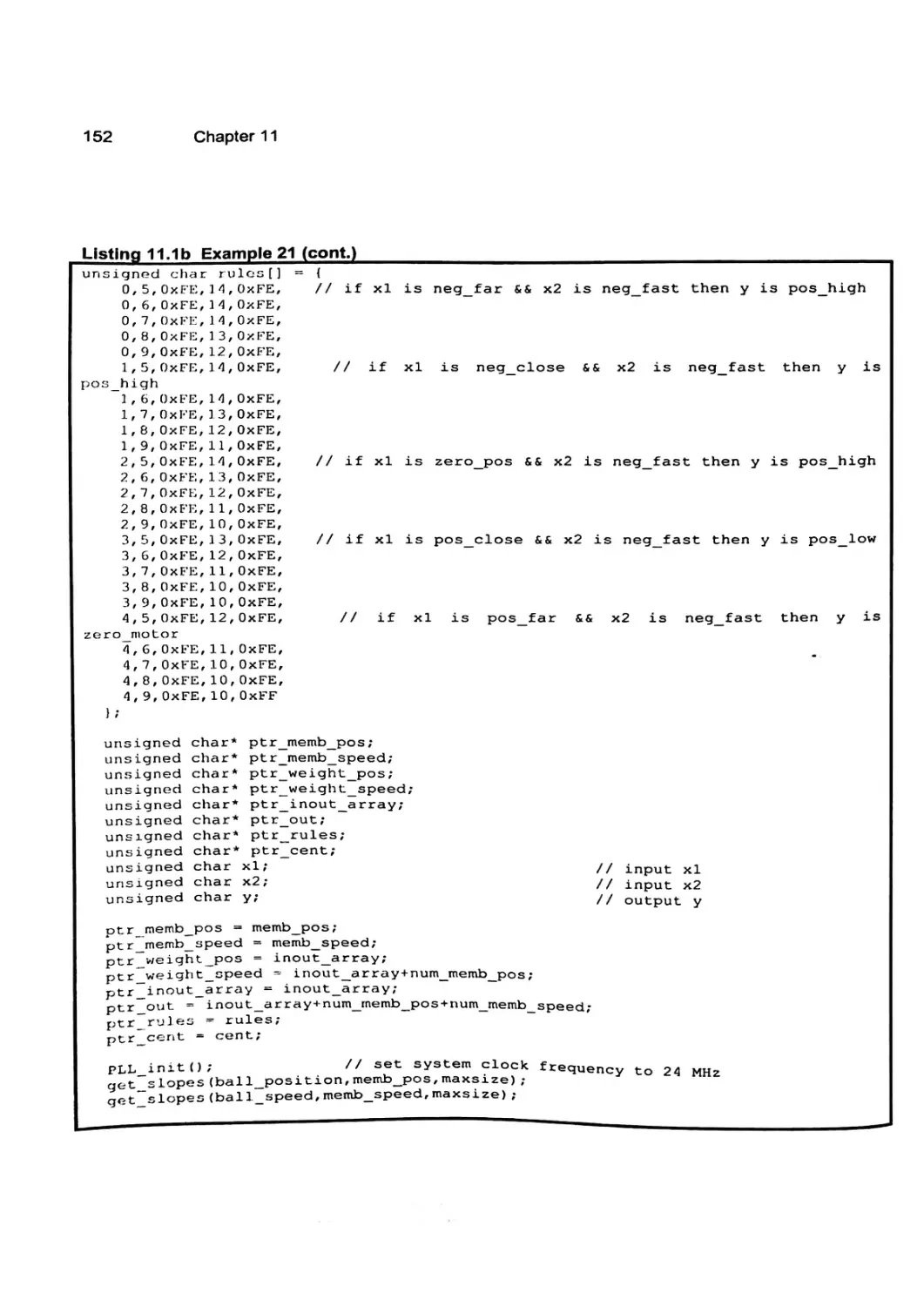
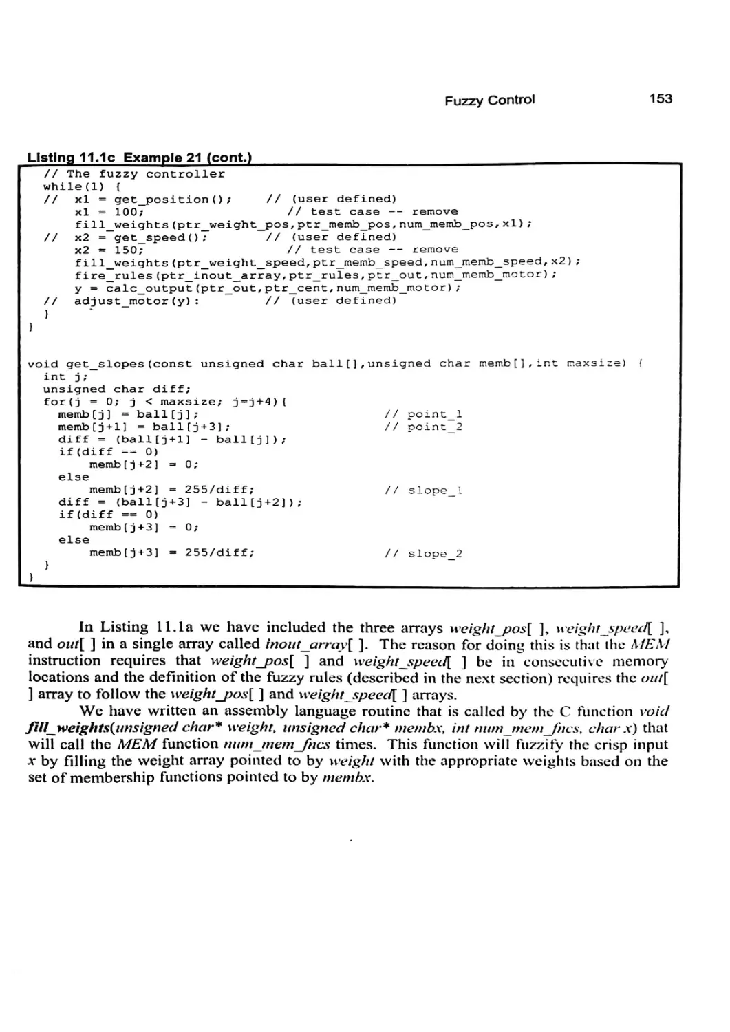
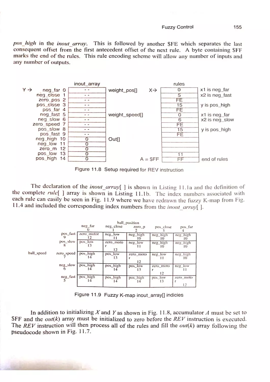
11.1
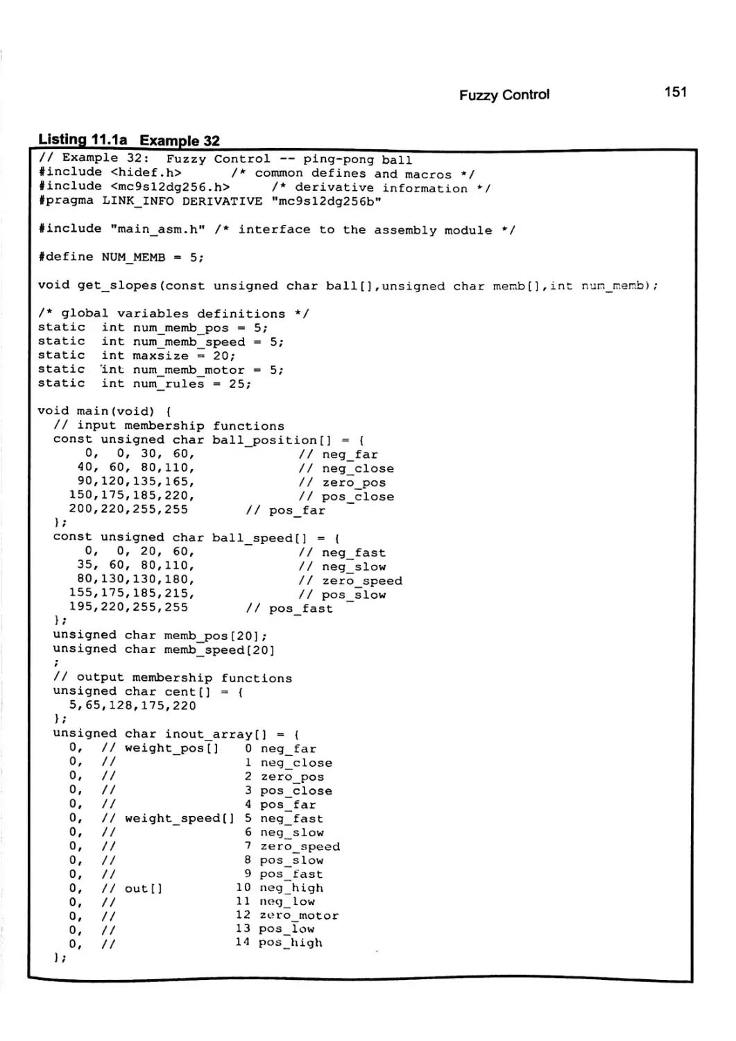
11.2
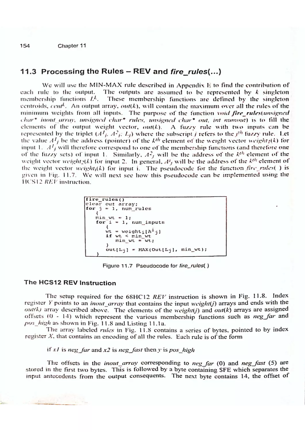
11.3
11.4
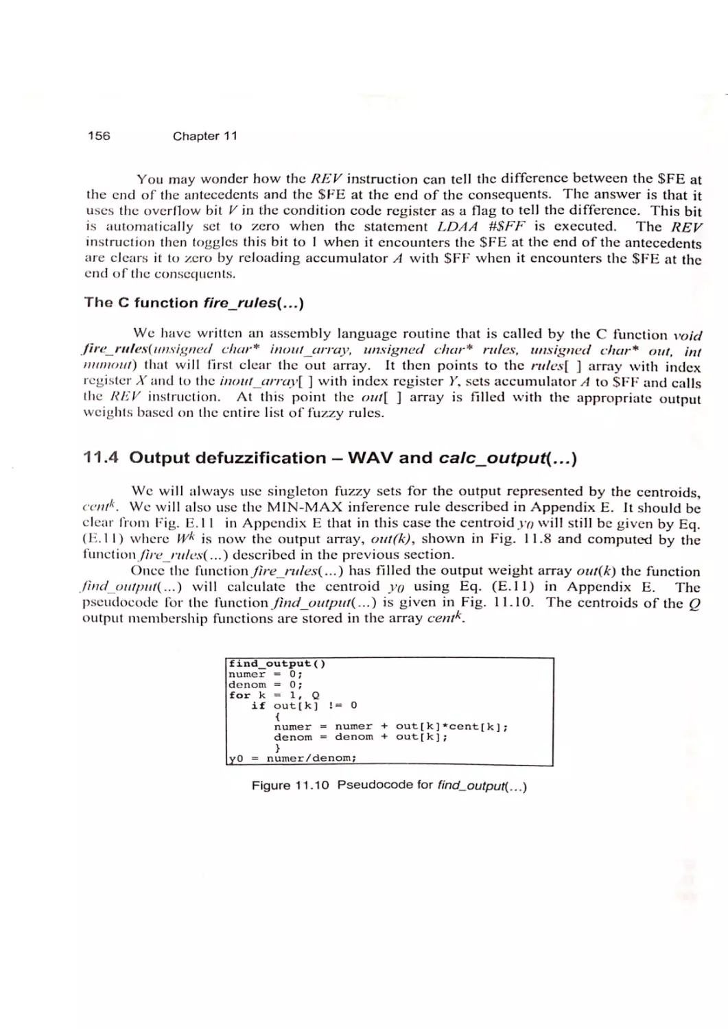
11.5
Design of a Fuzzy Controller
Fuzzification of Inputs — MEM andfill_weights(...)
Processing the Rules — REV andfire_riles(...)
Output Defuzzification-— WAV and calc_output(...)
Under the Hood — Fuzzy Control Assembly Routines
Problems
132
132
133
139
143
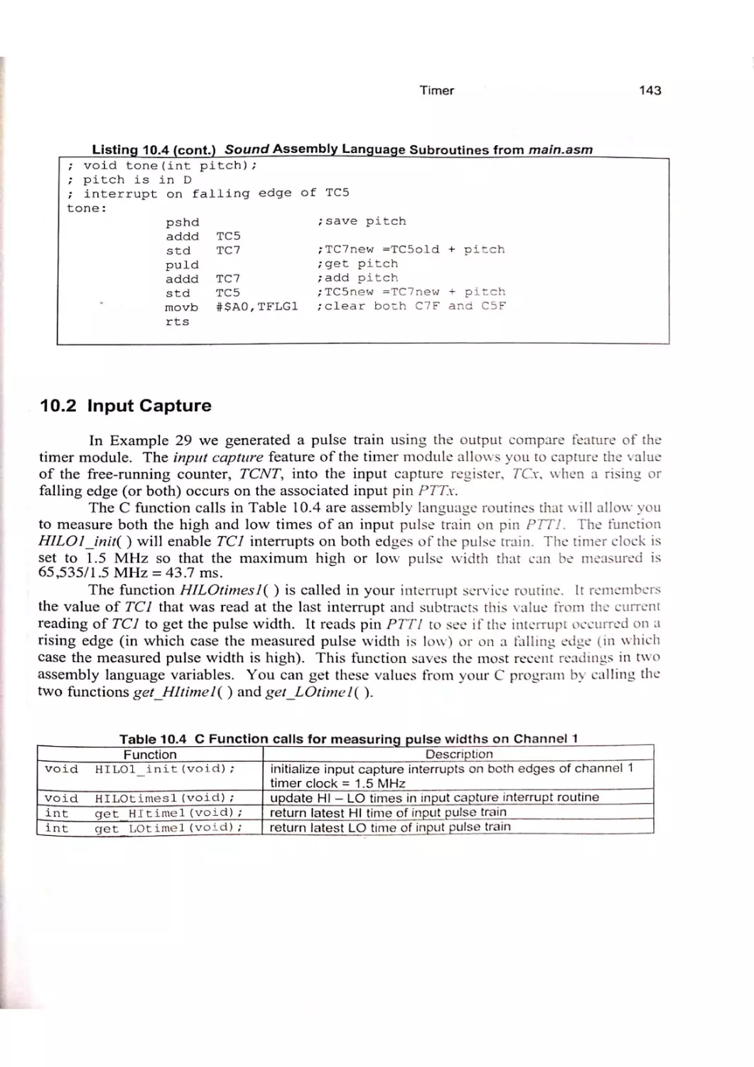
144
147
147
149
154
156
157
159
Appendix A — CodeWarrior Tutorial - DRAGON 12-Plus-USB
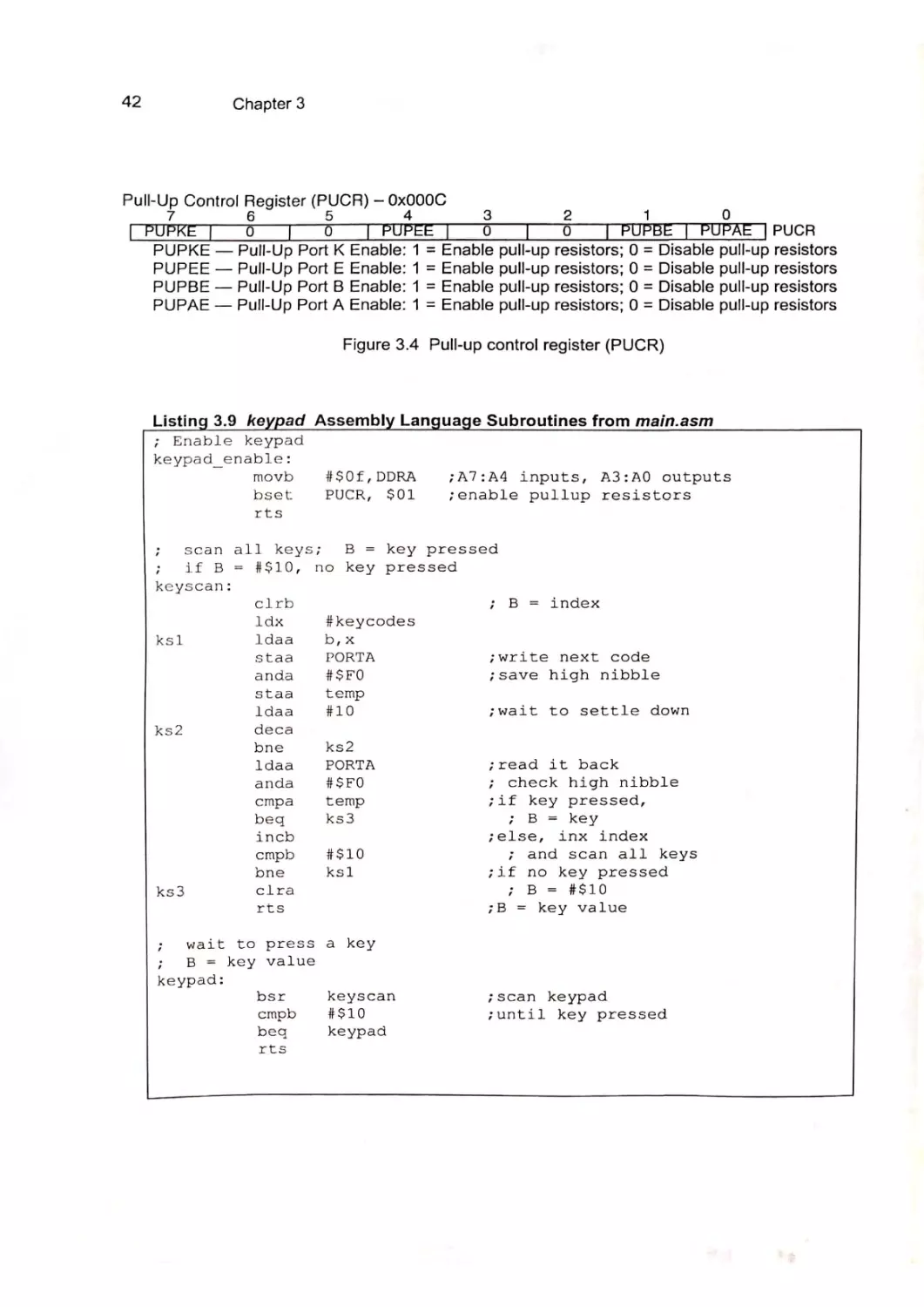
Appendix B —- HCS12 Assembly LanguageEssentials
Appendix C — Summary of C Function Calls to main.asm
Appendix D —- MC9S12DG256B Interrupt Vectors
Appendix E — Introduction to Fuzzy Control
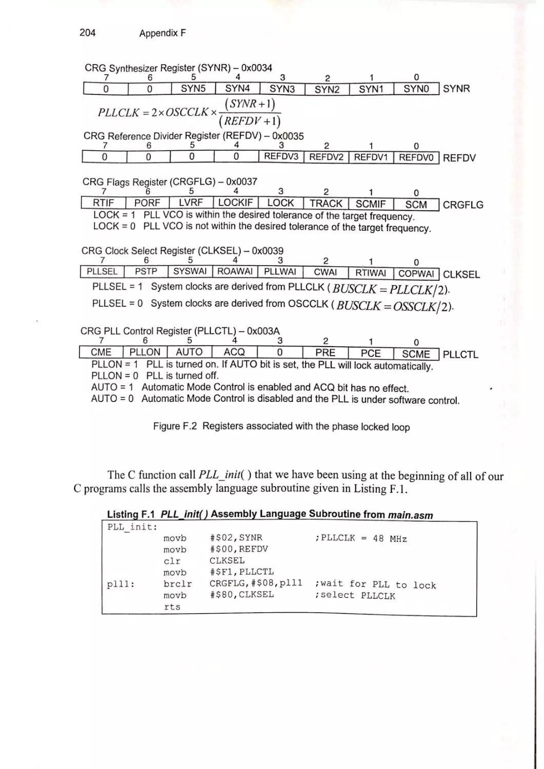
Appendix F — Phase Locked Loop
Appendix G — C Quick Reference Guide
161
167
187
191
193
203
206
Index
209
Vii
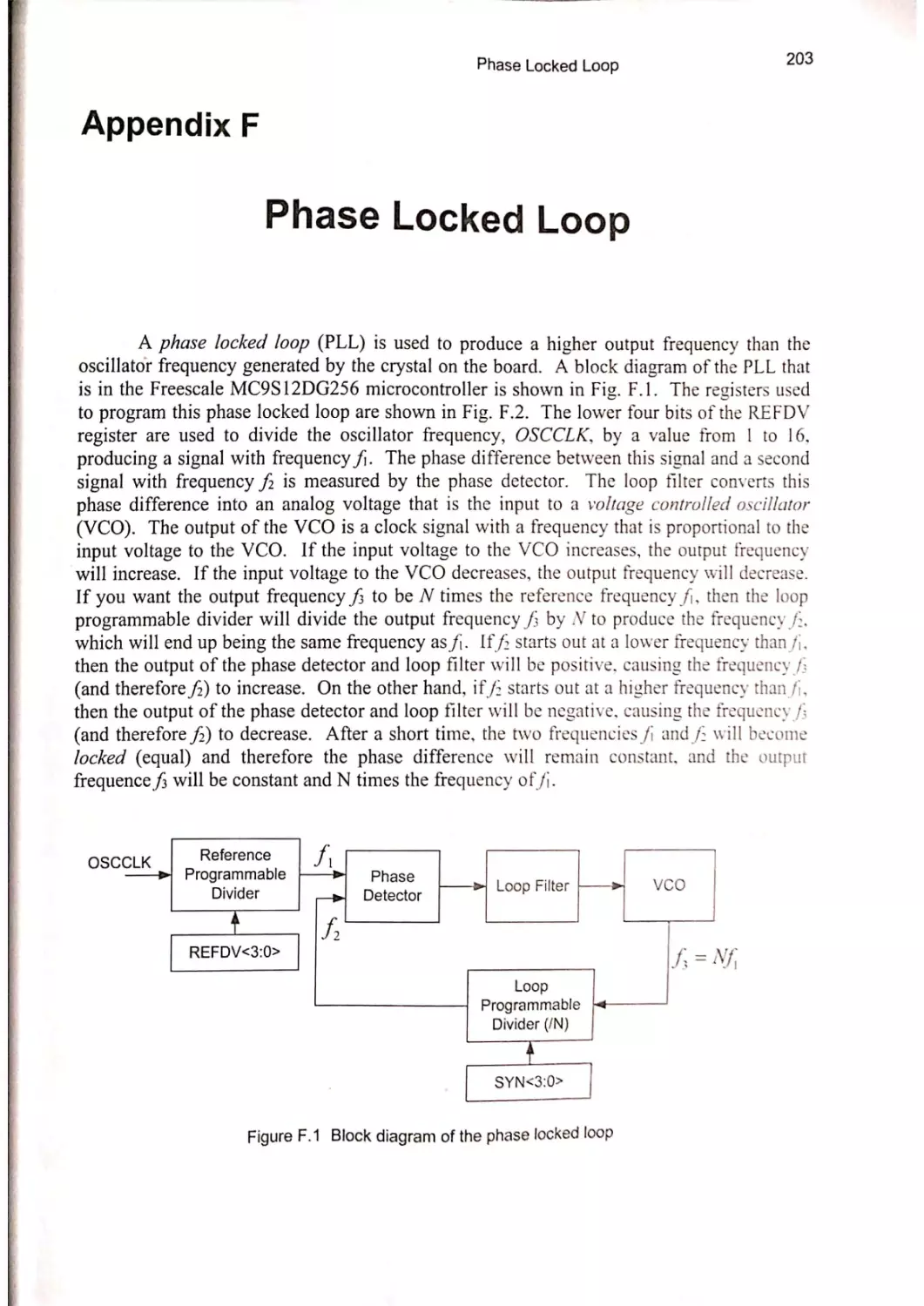
Introduction
1
Chapter1
Introduction
The HC$12 is a family of Freescale microcontrollers and is a direct descendentofthe
original Motorola 68HC11 and the more recent 68HC12. In this book you will Icarn howto
program the MC9S12DG256 microcontroller that ts on the Wytec DRAGON 12-Plus-USB™
board. You will Icarn to program this microcontroller in both assembly language and C
using the industry-standard CodeWarrior development system. To make it as casy as
possible we have provided a stationery project that you can build upon that includes a large
collection of built-in assembly language routines to access all of the various I/O functions of
the MC9S12DG256. You will access these routines through C functioncalls.
1.1 From Microprocessors to Microcontrollers
A major revolution in the computer industry has taken place in the past 25 years. The
making of the first microprocessor was madc possible by the remarkable development of
integrated circuits during the 1960s. This technology allowed hundreds and then thousands
of transistors to be etched onto a single picce ofsilicon. This Iced to the design of integrated
circuits in which more and more logic clements were incorporated into a single chip. In
1969 Intel undertook a contract to develop a sct ofintegrated circuits that could be used to
make a programmable clectronic calculator. Instead of developing yet another special
purpose integrated circuit with only a limited function, Intel chose to produce a more general
purpose device, the 4004 microprocessor, which could be programmed to perform many
different functions. This first microprocessor had only four data lines over which both
address information and data had to be sent to memory devices. Intel put this chip on the
market in 1971 as part of a four chip sct that formed a micro-programmable computer. The
4004 had many limitations and the following year Intel introduced the 8008 and two years
later the 8080 which became widely used in a host of different applications.
In 1975
Motorola producedits first microprocessor — the 6800.
bus).
The 6800 had § data lines (called a data bus) and 16 address lines (called an address
This means that it could address 2! = 65,536 different memory addresses, cach
containing 8 bits, or one byte of data. The heart of the 6800 was its CPU, or central
processing unit, sometimes referred to as an MPU, or microprocessor unit. The CPU
contained the registers and logic to execute the instruction set of the 6800. The 6800
registers included two 8-bit accumulators (4 and 8), a 16-bit index register (X), a 16-bit stack
pointer (SP), a 16-bit program counter (PC), and an 8-bit condition-code register (CCR).
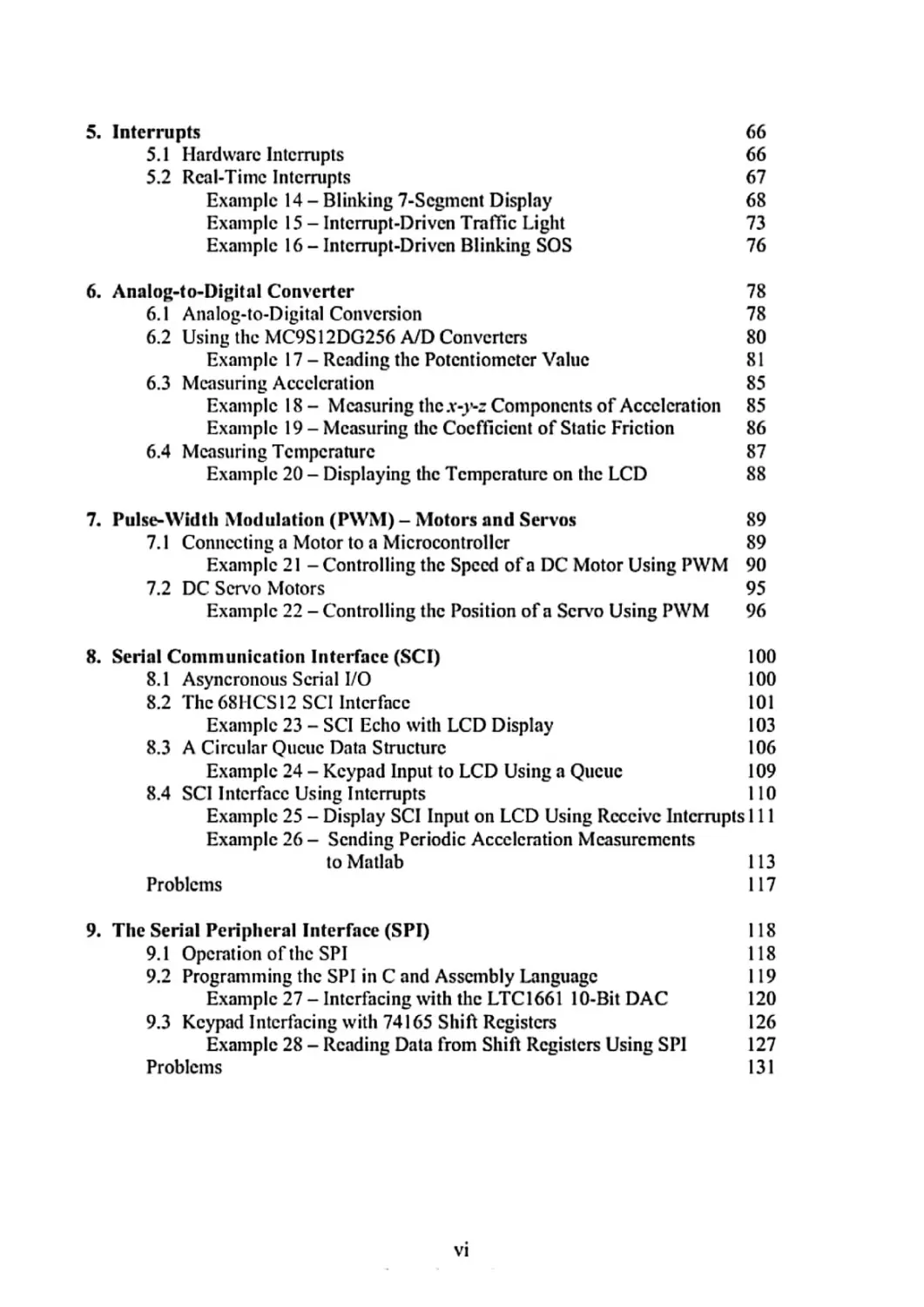
2
Chapter 1
Thus, the first microprocessors consisted only of a CPU that could address external memory
as shown in Fig. 1.1.
Data
Bus
RAM
CPU
ROM
(registers)
vo
Address
Bus
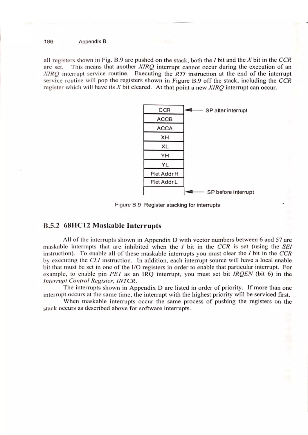
Figure 1.1 A microprocessor (CPU) connected to external memory
The external memory shown in Fig. 1.1 consists of read-write memory (RAM), readonly memory (ROM), and input/output memory (I/O). Typically the I/O memory consists of
dedicated special-purpose devices for performing such operations asparallel 1/O, serial I/O,
timer functions, and analog-to-digital (A/D) conversion. These I/O devices contain registers
that look like memory locations to the CPU. The RAM in Fig. 1.1 could be cither static
RAM (SRAM) or dynamic RAM (DRAM). Dynamic RAM can contain more bytes of
memory than static RAM for the samesize chip, but requires additional circuitry to refresh
the data pcriodically to keep it from being lost. Other types of memory devices that might be
connected to the address and data busses in Fig. 1.1 include erasable programmable readonly memory (EPROM),electrically-crasable programmable read-only memory (EEPROM),
and flash EEPROM. Both flash EEPROM and EEPROMarc non-volatile memory that will
maintain their data when poweris removed. Individual bytes can be crased and programmed
in EEPROM while flash EEPROMsnormally require crasing the entire memory array at one
time.
As integrated circuit technology developed over the years one of the trends has been
the development of faster and more complex microprocessors such as the Intcl 80x86 and
Pentium and the Motorola 680x0 and PowerPC. These microprocessors are in many of the
popular desktop computers used in offices all over the world. Another trend has been to
package more and morcfunctionality onto a single chip. The Motorola 6801 was introduced
in 1978 and included a small amount of RAM and ROMas well as parallel and scrial I/O on
a single chip. The following year Motorola introduced an EPROMversion ofthe 6801, the
68701, as well as the first of the low-cost 6805 family of microcontrollers.
The first 68HC11 was introduced by Motorola in 1985. This 8-bit microcontroller
(the A8 part) contained on a single chip the CPUI1 microprocessor, 8 Kbytes of ROM, 256
bytes of RAM, 512 bytes of EEPROM,up to 38 parallel I/O lines, a 16-bit timer that
included 3 input captures and 5 output compares, a synchronous scrial peripheral interface
(SPI), an asynchronous scrial communications interface (SCI), and an 8-channel, 8-bit A/D
converter. Since 1985 over five dozen different 68HC11 parts have been introduced by
Motorola. These parts differ in the types and amounts of on-board resources that are
includedin the chip.
Introduction
3
In 1997 Motorola introduced the 68HC12 as an enhanced 68HCI1. It is upward
compatible with the 68HC11 (but not at the object code level). It has a greatly enhanced
central processing unit (CPU12) that has several newinstructions and addressing modes
designed to make it casier to support higher-level languages.
Programs run significantly
faster on a 68HC12 for several reasons. The typical clock speed was increased from 2 MHz
on a 68HC11 to 8 MHz ona 68HC12. The numberof clock cycles required to execute many
of the instructions was reduced on the 68HC12. In addition, the new instructions and
addressing modes require fewerinstructions to perform the same task. This means that not
only do programs run faster, but they also take up less memoryspace.
In 2002 Motorola introduced the HCS12 family of microcontrollers, which are a
direct upgrade of the 68HC12 family. The Motorola Semiconductor Division was spun off
as Freescale Semiconductor in 2004. The MC9S12DG256 microcontroller that is on the
DRAGON 12-Plus-USB board has 256K bytes of flash EEPROM, 12K bytes of RAM, 4K
bytes of EEPROM, two 8-channel, 10-bit analog-to-digital (A/D) converters, two
asynchronous serial communication interfaces (SCI), three serial peripheral interfaces (SPI),
an 8-channel timer module that supports output compare and input capture, an 8-channel
pulse-width modulator (PWM), 29 discrete digital I/O channels, and comprchensive interrupt
functions. We will cover all of these I/O functions in this book. The MC9S12DG256
microcontroller has additional functions not covered in this book including two CAN 2.0
modules, an Inter-IC bus, and a digital Byte Data Link Controller (BDLC). The part can
operate up to 25 MHz and wewill runall of our programs at a clock speed of 24 MHz.
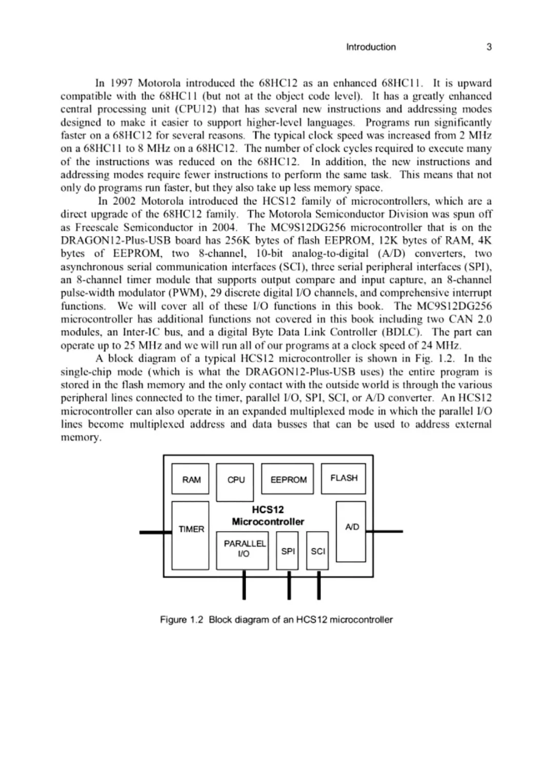
A block diagram of a typical HCS12 microcontroller is shown in Fig. 1.2. In the
single-chip mode (which is what the DRAGON1I2-Plus-USB uses) the entire program ts
stored in the flash memory and the only contact with the outside world is through the various
peripheral lines connected to the timer, parallel I/O, SPI, SCI, or A/D converter. An HCS12
microcontroller can also operate in an expanded multiplexed mode in which the parallel 1/O
lines become multiplexed address and data busses that can be used to address external
memory.
RAM
CPU
EEPROM
FLASH
HCS12
Microcontroller
ND
PARALLEL
vO
SPI}
SCI
Figure 1.2 Block diagram of an HCS12 microcontroller
4
Chapter 1
1.2 DRAGON12-Pius-USB™ Board
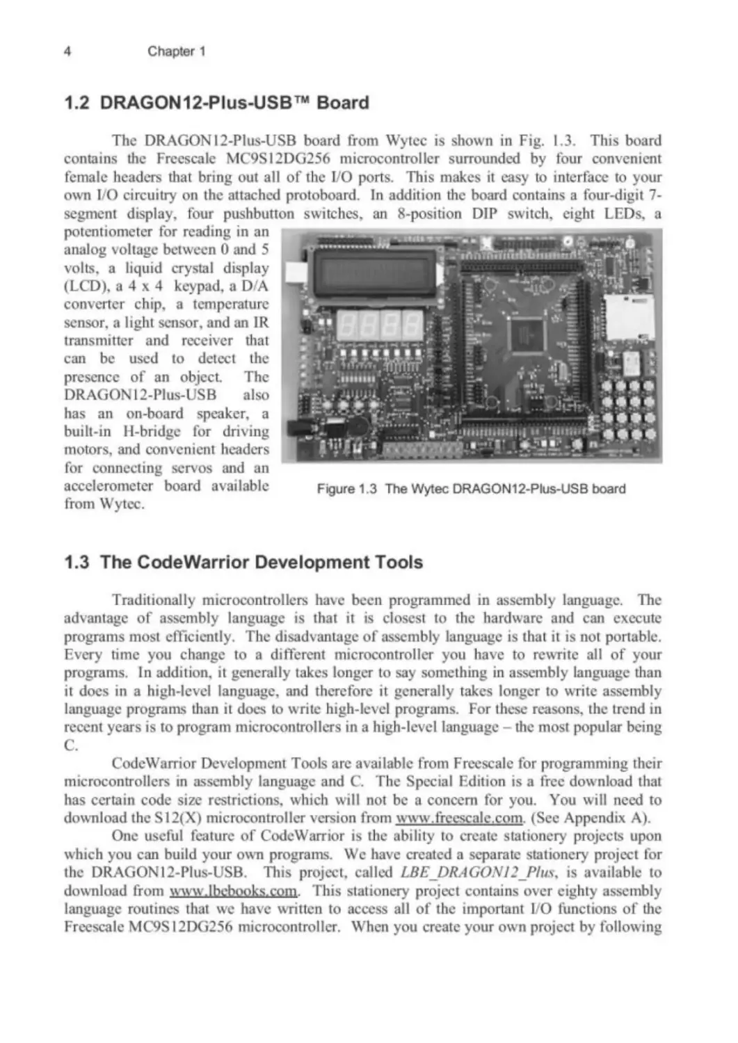
The DRAGON 12-Plus-USB board from Wytec is shown in Fig. 1.3. This board
contains the Freescale MC9SI2DG256 microcontroller surrounded by four convenient
female headers that bring out all of the I/O ports. This makesit easy to interface to your
own I/Ocircuitry on the attached protoboard. In addition the board contains a four-digit 7segment display, four pushbutton switches, an 8-position DIP switch, eight LEDs, a
potentiometer for reading in an
analog voltage between 0 and 5
volts, a liquid crystal display
(LCD),a4x4 keypad, a D/A
converter chip, a temperature
sensor, a light sensor, and an IR
transmitter and receiver that
can be
used to detect the
presence of an object.
The
DRAGON 12-Plus-USB
also
has an on-board speaker, a
built-in H-bridge for driving
motors, and convenient headers
for connecting servos and an
accelerometer board available
:
eee BSS.
ee LLL
=~ es
Figure 1.3 The Wytec DRAGON12-Plus-USB board
from Wytec.
1.3 The CodeWarrior Development Tools
Traditionally microcontrollers have been programmed in assembly language. The
advantage of assembly language is that it is closest to the hardware and can execute
programs most efficiently. The disadvantage of assembly languageis that it is not portable.
Every time you change to a different microcontroller you have to rewrite all of your
programs. In addition, it generally takes longer to say something in assembly language than
it does in a high-level language, and therefore it generally takes longer to write assembly
language programs than it does to write high-level programs. For these reasons, the trend in
recent years is to program microcontrollers in a high-level language — the most popular being
C,
CodeWarrior Development Tools are available from Freescale for programming their
microcontrollers in assembly language and C. The Special Edition is a free download that
has certain code size restrictions, which will not be a concern for you. You will need to
download the $12(X) microcontroller version from www.freescale.com. (See Appendix A).
One useful feature of CodeWarrior is the ability to create stationery projects upon
which you can build your own programs. Wehavecreated a separate stationery project for
the DRAGON12-Plus-USB. This project, called LBEDRAGONI2Plus, is available to
download from www.lbebooks.com. This stationery project contains over eighty assembly
language routines that we have written to access all of the important I/O functions ofthe
Freescale MC9S12DG256 microcontroller. When you create your own project by following
Introduction
5
the tutorial in Appendix A, these assembly language routines will automatically be included
in the file main.asm that will be part of your project. The top-level design in your project
will be a C program that is stored in the file main.c. In this book, we will show you how to
write your own assembly language routines that are stored in main.asm and howto call these
routines as C function calls from your top-level C program stored in main.c.
To use CodeWarrior with the DRAGON12-Plus-USB, the MC9S12DG256
microcontroller on these boards must contain the Serial Monitor. This Serial Monitor is 2
kbytes of code stored at addresses $F800 — SFFFF in the flash memory. This code is
executed when you press the reset button on the board and allows CodeWarrior to
communicate with your board through the serial port.
When you order one of the
development boards from Wytec, make sure to specify that you want the Serial Monitor
installed; otherwise, it will come with the Dbug monitor that is not compatible with
CodeWarrior.
Getting the DRAGON 12-Plus-USB board to do whatever you wantis challenging
and lots of fun. Therefore, let’s get started!
Chapter2
6
Chapter 2
Parallel Ports - Outputs
In this chapter you will learn how parallel ports are used to turn on LEDsand the
segments of a 7-segment display. Asin all of our examples wewill first show you how to do
it entirely in C, and then we will show howto doit using C calls to our built-in assembly
language routines. You will also learn how these assembly language routines work. Using
these built-in assembly language routines will make your C programs much shorter and
easier to write.
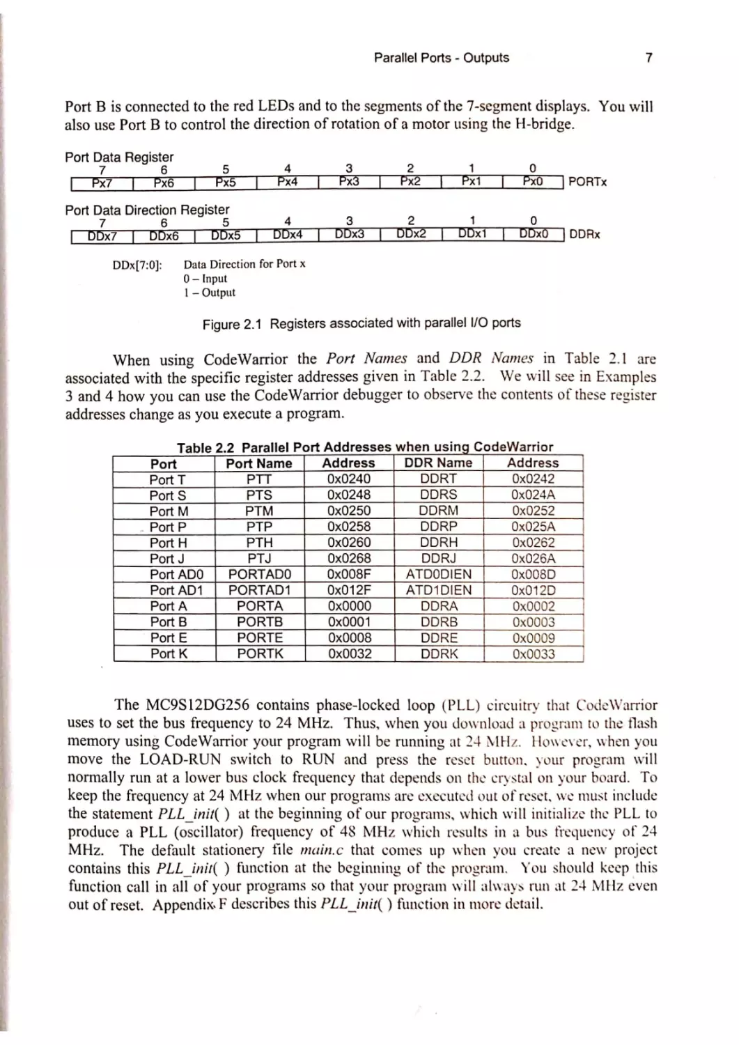
2.1 MC9S12DG256 Parallel I/O Ports
The MC9S12DG256registers associated with parallel I/O are listed in Table 2.1.
Each of these ports (except PORTADO and PORTADI) has a data register and a data
direction register of the type shown in Fig. 2.1. Each pin of an I/O port can beeither an
input or an output depending on thebits in the corresponding data direction register as shown
in Fig. 2.1.
Table 2.1 Parallel Ports in the MC9SDG256
PortName
DDRName
DRAGON12-Plus-USB use
Port T
PTT
DDRT
Speaker
Port S
Port M
PTS
PTM
DDRS
DDRM
SCI, SPI
Port P
PTP
DDRP
7-Seg enable, Servo
Port H
PTH
DDRH
Switches
Port J
PTJ
DDRJ
LED enable
Port ADO
PORTADO
Input only
pot
Port AD1
PORTAD1
Input only
Port A
PORTA
DDRA
Port B
Port E
Port K
PORTB
PORTE
PORTK
Port
DDRB
DDRE
DDRK
7
I
Keypad
LEDs, 7-Seg, H-bridge
Mode, XIRQ
LCD
Mostofthe I/O ports listed in Table 2.1 have alternate or special optional functions
many of which we will consider in later examples. Whenthe pins of an I/O port are not
being used for oneofthese alternate functions they can beused as general purpose I/O pins.
There are several different operating modes for the MC9S12DG256 including a
single-chip mode and expanded external memory modes. In the expanded external memory
modes, ports A and B are used for multiplexed address and data busses. The DRAGON 12Plus-USB board operates in the single-chip mode, so that ports A and B are available for
parallel I/O. Port A is connected to the 4 x 4 keypad. On the DRAGONI12-Plus-USB board
Parallel Ports - Outputs
7
Port B is connected to the red LEDsandto the segments of the 7-segment displays. You will
also use Port B to control the direction of rotation of a motor using the H-bridge.
Port Data Register
PxS |
|
[__Px7_|Pxe
Port Data Direction Register
5
6
7
[—DDx7_
|
DDx6
DDxS5
|
Px4
4
[|
[7
DDx4 [
Px3
3
DDx3
|
Px2
|
2
DDx2
0
1
2
3
4
5
6
7
[|
Pxi
|
1
DDxi
| PORTx
|.
Px0
|
0
DDx0 | DDRx
Data Direction for Port x
0 — Input
DDx[7:0]:
| — Output
Figure 2.1 Registers associated with parallel I/O ports
When using CodeWarrior the Port Names and DDR Names in Table 2.1 are
associated with the specific register addresses given in Table 2.2. Wewill see in Examples
3 and 4 how you can use the CodeWarrior debugger to observe the contents ofthese register
addresses change as you execute a program.
Table 2.2 Parallel Port Addresses when using CodeWarrior
Port
Port Name
Address
DDR Name
Port T
Port S
Port M
Port P
Port H
Port J
Port ADO
PortAD1
Port A
Port B
Port E
Port K
PTT
PTS
PTM
PTP
PTH
PTJ
PORTADO
PORTAD1
PORTA
PORTB
PORTE
PORTK
0x0240
0x0248
0x0250
0x0258
0x0260
0x0268
Ox008F
0x012F
0x0000
0x0001
0x0008
0x0032
DDRT
DDRS
DDRM
DDRP
DDRH
DDRJ
ATDODIEN
ATD1DIEN
DDRA
DDRB
DDRE
DDRK
Address
0x0242
Ox024A
0x0252
0x025A
0x0262
0x026A
0x008D
0x012D
0x0002.—sid|
Ox0003—si|
0x0009
|
0x0033.
|
The MC9S12DG256 contains phase-locked loop (PLL) circuitry that CodeWarrior
uses to set the bus frequency to 24 MHz. Thus, when you download a programtothe flash
memory using CodeWarrior your program will be running at 24+ MHz. However, when you
move the LOAD-RUN switch to RUN and press the reset button, your program will
normally run at a lower bus clock frequency that depends onthe crystal on your board. To
keep the frequency at 24 MHz whenourprogramsare executedout ofreset, we must include
the statement PLLinit( ) at the beginning ofour programs, which will initialize the PLL to
produce a PLL (oscillator) frequency of 48 MHz whichresults in a bus frequency of 24
MHz. The default stationery file main.c that comes up when youcreate a newproject
contains this PLLinit( ) function at the beginning of the program. You should keep this
function call in all of your programs so that your program will always run at 24+ MHz even
out of reset. Appendix. F describes this PLL_init( ) function in more detail.
8
Chapter 2
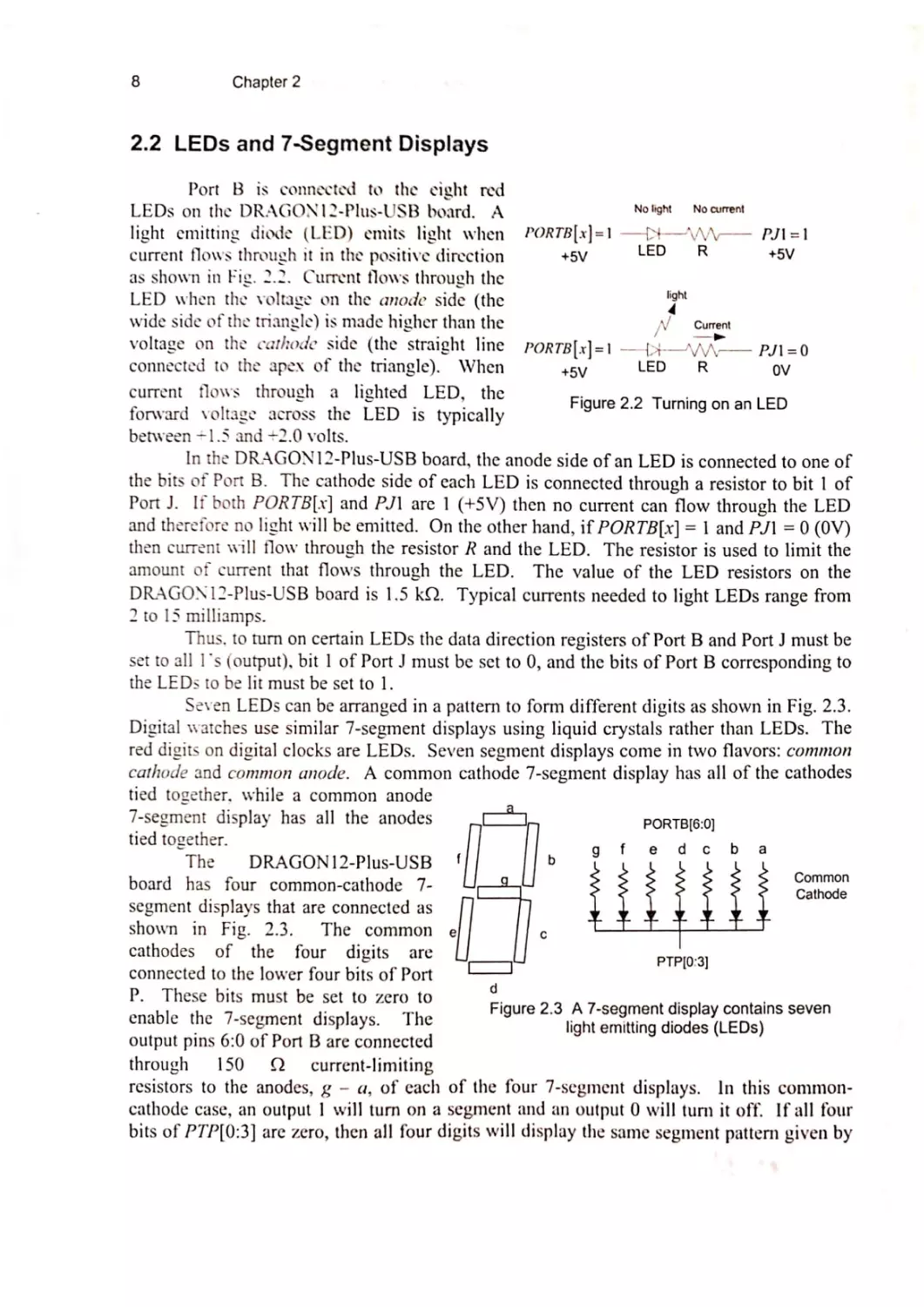
2.2 LEDs and 7-SegmentDisplays
Port B is connected to the eight red
LEDs on theDRAGON 12-Plus-USB board. A
Nome
light emitting diode (LED) emits light when
Mp oNere
PORTB[x}=1 —>4—\\\——.__ PJ1=1
current flows through it in the positive direction
+5V
LED
OR
+5V
as shown in Fig. 2.2. Current flows through the
LED whenthe voltage on the anode side (the
a"
wide side of the tnangle) 1s made higherthan the
voltage on the cathode side (the straight line
connected to the apex of the tnangle).
N
Current
PORTB[x]=1 — bt-—AA\A
When
+5V
current flows through a lighted LED, the
forward voltage across the LED is typically
LED
PJ1=-0
R
OV
Figure 2.2 Turning on an LED
between +1.5 and +2.0 volts.
In the DRAGON12-Plus-USB board, the anodeside of an LEDis connected to one of
the bits of Port B. The cathode side of each LED is connected through resistor to bit 1 of
Port J. It both PORTB[x] and PJ1 are 1 (+5V) then no current can flow through the LED
and therefore no light will be emitted. On the other hand, if PORTB[x] = 1 and P/1 = 0 (OV)
then current will flow through the resistor R and the LED. Theresistor is used to limit the
amount of current that flows through the LED. The value of the LED resistors on the
DRAGON 12-Plus-USB board is 1.5 kQ. Typical currents needed to light LEDs range from
2 to 15 milliamps.
Thus, to turn on certain LEDsthe data direction registers of Port B and Port J must be
set to all 1°s (output), bit 1 of Port J must be set to 0, and the bits of Port B corresponding to
the LEDs to be lit mustbeset to 1.
Seven LEDs can be arrangedin a pattern to form different digits as shownin Fig. 2.3.
Digital watches use similar 7-segment displays using liquid crystals rather than LEDs. The
red digits on digital clocks are LEDs. Seven segment displays comein two flavors: common
cathode and common anode. A common cathode 7-segment display has all of the cathodes
tied together, while a common anode
7-segment display has all the anodes
crc
PORTB[6:0]
tied together.
The
|©DRAGONI2-Plus-USB
board has four common-cathode 7-
g
!
b
: a mis —_data, ae
>
hgaa
a 6:0
ia
output pins
of Port B mya
are connected
through
=6150) =©Q current-limiting
e
dcba
C
chy
segment displays that are connected as
shown in Fig. 2.3.
The common e
cathodes of the four digits are
. of Port
connected to the lower four bits
f
—
i
cates
PTP[0:3]
Figure 2.3 A 7-segmentdisplay contains seven
light emitting diodes (LEDs)
resistors to the anodes, g — a, of each of the four 7-segment displays.
In this common-
cathode case, an output | will turn on a segment and an output 0 will turnit off. Ifall four
bits of PTP[0:3] are zero, thenall four digits will display the same segmentpattern given by
Paratio! Ports - Outputs
9
the output of Port B. To display different digits on the four 7-segment displays, the displays
must be multiplexed in time as will be shown in Example 6.
Example 1 — Writing to Ports
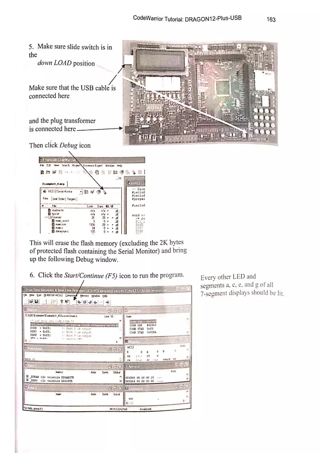
In this example, we will show how writing to ports can tum on the LEDs and 7segmentdisplays on the DRAGON| 2-Plus-USB.
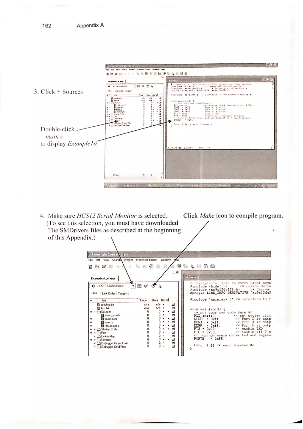
Followthe steps in the tutorial in Appendix A to set up CodeWamor andcreate a
newproject called Example! where you select the stationery file LBE_ DRAGONI2-Plus-
USB. When youopenthefile main.cin the Sourcefolder you shouldsee the program shown
in Listing 2.1. All text following a double slash // will be a commenttothe end¢of the line
The seven statements following the comment /* put your own code bere *
will do the following:
1. The statement PLL_init( ) will set the system clock frequency to 24 MHz as
described above. This should be thefirst statement in all of your programs.
2. The statement DDRB = OxFF will set all bits in data direction register B to | and
thereforeto all outputs. The notation 0.x means that FFts a hexadecimal number
equal to the binary number ILITTIIIT.
3. The statement DDRJ = OxFF will set all bits in data direction register J to | and
therefore to all outputs.
4. The statement DDRP = OxFF will set all bits in data direction register P to IT and
therefore to all outputs.
5. The statement P7/ = 0x00 will set all bits of port J to zero andtherefore will end!
the LEDs.
6. The statement PTP = 0x00 will set all bits of port P to zero and therefore will enadle
the 7-segmentdisplays.
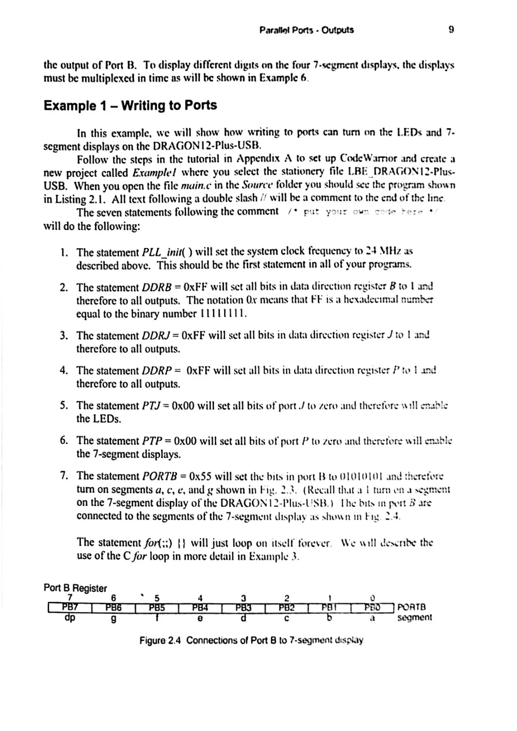
7. The statement PORTB = 0x55 will set the bits in port B to OLOLOLOL and therefore
turn on segmentsa, c, ¢, and g shown in Fig. 2.3. (Recall thata [turn on a segment
on the 7-segmentdisplay of the DRAGON 1 2-Plus-USB.) [he bits in pert 3 are
connected to the segments ofthe 7-segment display as shown in big. 24.
The statement for(;;) {} will just loop on itself forever. We wall descmbe the
use of the C for loop in more detail in Example 3
Port B Register
7
dp
6
g
“Pas
l
ren
Pag
ra
za
|
Figure 2.4 Connections of Port B to 7-segment disoiny
PEO) PORTA
a
segment
10
Chapter2
Listing 2.1 Example 1: DRAGON12-Plus-USB
Sola
// Example 1: Turn on every other segment on /~seg a) 5
/* common defines and macros
#include <hidef.h>
/* derivative information */
#include <mc9s12dg256.h>
#pragma LINK INFO DERIVATIVE "mc9s12dg256b'
#include "main _asm.h" /* interface to the assembly module */
void main(void)
{
/* put your own code here */
// set system clock frequency to 24 MHz
PLLinit();
DDRB
DDRJ
DDRP
// Port B is output
// Port J is output
// Port P is output
= Oxff;
= Oxff;
= Oxff;
// enable LED
// enable all 7-segment displays
PTJ = 0x00;
PTP = 0x00;
// turn on every other led and segment on 7-seg displays
PORTB
=
for(;;)
{} /* wait forever */
0x55;
Run the program shownin Listing 2.1. Then re-run the program with the value of
PTJ changed to 0x02. This should disable the LEDs. Next change P7J back to 0x00 and
change the value of P7P to Ox0A. This should disable digits 1 and 3 where digits are
labeled 0 — 3 from left to right.
Example 2 — C Function Calls
In this example, we will show how to write assembly language subroutines that are
called as C functions. The main C program is located in the file main.c and the assembly
language subroutines are located in the file main.asm.
Instead of having to remember that the LEDs and 7-segment displays on the
DRAGON 12-Plus-USB are connected to Port B and controlled by bits in Port J and Port P,
we have written six assembly language routines that are called by the six C function calls
shown in Table 2.3. These assembly language routines are always available to you when you
set up an LBE_DRAGON12-Plus-USB stationery project.
Table 2.3 C function calls for turning on the 7-segmentdisplay
C Function Call
ledenable();
leds on(int);
led disable();
leds off();
seg7 enable();
seg? disable();
seg7 on(int s,
int b);
seg7s off ();
Meaning
Sets DDRB and DDRJto outputs, clears DJ1 to 0,
and turns off all LEDs byclearing all bits of PORTB
Stores the lower8 bits of the integer int in Port B
Sets DDRJ to outputs and sedts DJ1 to 1
Turn off all LEDs by clearing Port B
Sets DDRB and DDRPtooutputs, clears the lower4
bits of Port P, and clearsall bits of PORTB
sets the lower 4 bits of Port P to 1
Display the segments s on the 7-segment digit no. b
Turn off all 7-segment displays by clearing Port B
Parallel Ports - Outputs
11
LEDs
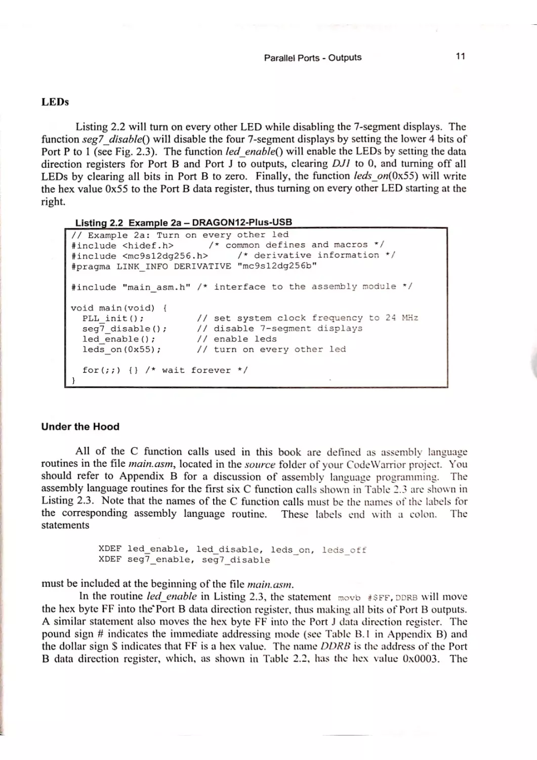
Listing 2.2 will turn on every other LED while disabling the 7-segment displays. The
function seg7_disable() will disable the four 7-segmentdisplays by setting the lower4 bits of
Port P to 1 (see Fig. 2.3). The function /ed_enable() will enable the LEDsbysetting the data
direction registers for Port B and Port J to outputs, clearing DJ// to 0, and turning offall
LEDsbyclearing all bits in Port B to zero. Finally, the function /eds_on(0x55) will write
the hex value 0x55 to the Port B data register, thus turning on every other LED starting at the
right.
Listing 2.2, Example 2a - DRAGON12-Plus-USB
// Example 2a: Turn on every other led
#include <hidef.h>
/* common defines and macros */
/* derivative information */
#include <mc9s12dg256.h>
#pragma LINKINFO DERIVATIVE "mc9s12dg256b"
#include "main_asm.h"
void main(void)
/*
interface to the assembly module */
{
PLLinit ();
// set system clock frequency to 24 MHz
seg/7_disable();
// disable 7-segment displays
led_enable();
// enable leds
leds_on(0x55);
// turn on every other led
for(;;)
{}
/* walt forever */
Under the Hood
All of the C function calls used in this book are defined as assembly language
routines in the file main.asm, located in the source folder of your CodeWarrior project. You
should refer to Appendix B for a discussion of assembly language programming.
The
assembly languageroutines for the first six C function calls shown in Table 2.3 are shownin
Listing 2.3. Note that the namesof the C function calls must be the names ofthe labels for
the corresponding assembly language routine.
These labels end with a colon.
The
statements
XDEF led_enable,
XDEF seg7_ enable,
led_disable,
leds_on,
leds off
seg? disable
mustbe included at the beginningof the file main.asm.
In the routine /ed_enable in Listing 2.3, the statement movb #$FF,DDRB will move
the hex byte FFinto the’Port B data direction register, thus making all bits of Port B outputs.
A similar statement also moves the hex byte FF into the Port J data direction register. The
pound sign # indicates the immediate addressing mode (see Table B.| in Appendix B) and
the dollar sign $ indicates that FF is a hex value. The name DDRBis the address ofthe Port
B data direction register, which, as shownin Table 2.2, has the hex value 0x0003. The
12
Chapter2
addressesofall of these register names are defined using equate statements (equ) in the file
mc9s12dg256.inc, which is located in the /ibraries folder in your CodeWarrior project.
Examples of this equate statement are shownin Listing 2.4.
In the subroutine /ed_enable in Listing 2.3, the statement bclr pPTJ,$02 will clear
bit 1 of the Port J data register. This bit clear statement will AND the complementof the
mask $02 with PTJ. Since the complement of $02 = 00000010 is 11111101, this mask will
clear bit | of PTJ, which enables all LEDs(see Fig. 2.2).
The next statement in the subroutine /ed_enable in Listing 2.8 is clr PORTB, which
clears all bits of Port B to zero, and thus turns off all LEDs.
Listing 2.3 led and seg7 Assembly Language Routines from main.asm
:
LEDS
led_enable:
movbd
movb
#SFF,DDRB
#SFF,DDRJ
;
;
DataDirB -->all outputs
DataDirJd -->all outputs
belr
PpTJ, $02
;
enable leds PJ1 = 0
elr
PORTB
;
Turn-off
PORTB
;
turn
;
turn off all
all
LEDS
rts
leds_on:
stab
on
selected led
rts
leds off:
clr
PORTB
leds
rcs
led_disable:
movb
#SFF,DDRJ
;
DataDirJ -->all outputs
bset
rts
PTJ,$02
>;
enable leds PJl1 = 0
;
7-Segment Displays
seg7 enable:
movb
#SFF,DDRB
;
DataDirB -->all outputs
movb
#SFF,DDRP
;
DataDirP -->all outputs
belr
PTP,SOF
;
enable 7-seg digits PTP[0:3]
elr
PORTB
;
Turn-off all 7-seg digits
;
;
DataDirP -->all outputs
disable 7-seg digits PTP[0:3]
= 0000
rts
seg/7 disable:
movb
#SFF,DDRP
bset
PTP,SOF
rts
= 1111
The C function call /ed_enable( ) in Listing 2.2 gets compiled as a jump to subroutine
(JSR) assembly language instruction that jumps to the subroutine ledenable: in Listing
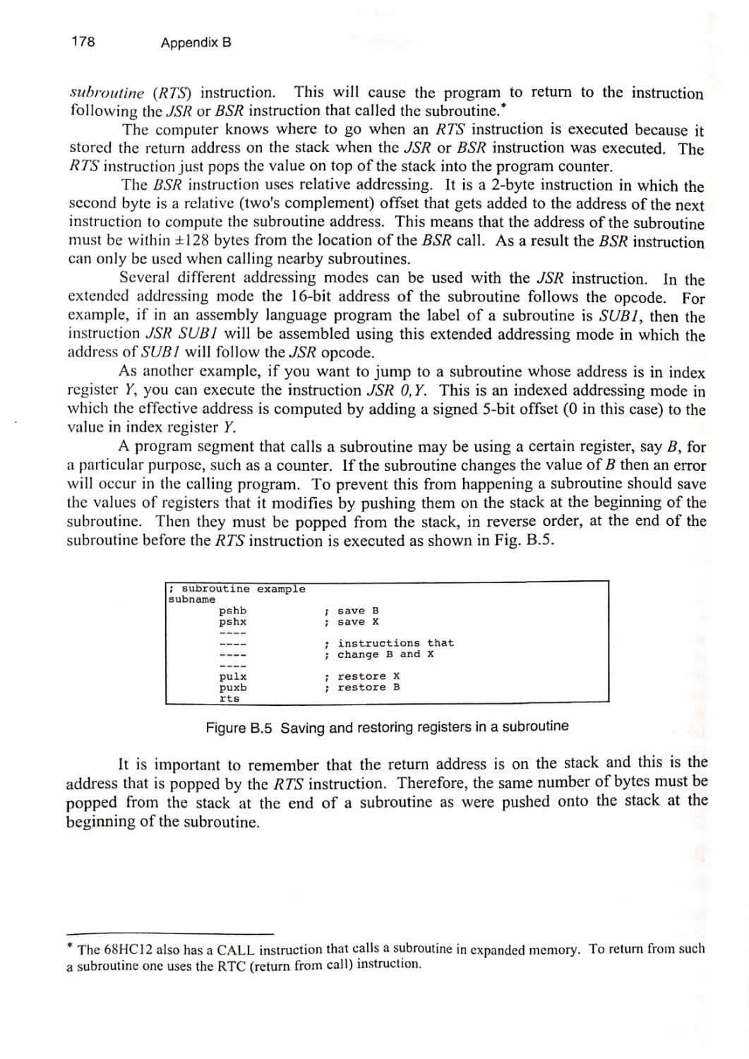
2.8. The last statement in this subroutine is a return from subroutine (RTS) instruction,
which will return to the statement following the JSR /ed_enable statement. This will be the
C function call /eds_on(0x55) in Listing 2.2, which will compile to a JSR to the subroutine
Parallel Ports - Outputs
13
leds_on in Listing 2.2. Thefirst instruction in this subroutine is stab PORTB. The reason
for this instruction is because the C function call /eds_on(int) in Table 2.3 passes a 16-bit
integer to the assembly language subroutine. If there is only one 16-bit integer passed to the
subroutine, it is passed in accumulator D, the concatenation of accumulators A and B. Thus,
the 8-bit byte 0x55, which is passed to the subroutine /eds_on in Listing 2.2, will be in
accumulator B. This value then gets stored in the Port B data register, PORTB, whichwill
turn on every other LED starting at the right. The RTSinstruction will return to the for loop
in Listing 2.2, which gets compiled to an assembly language statement that branches on
itself.
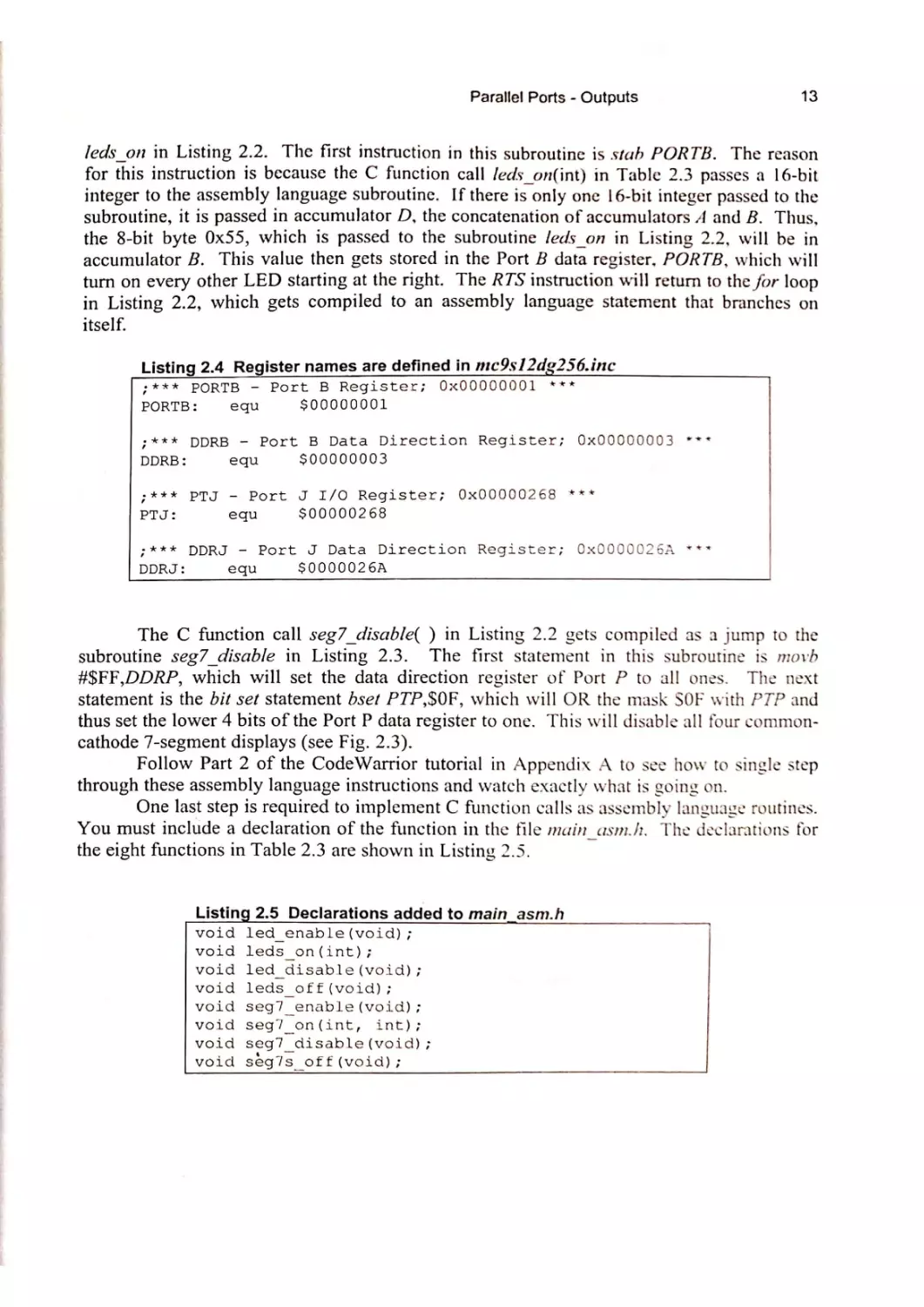
Listing 2.4 Register namesare defined in mc9s12dg256.inc
0x00000001
:*** PORTB - Port B Register;
PORTB:
equ
***
$00000001
;*** DDRB - Port B Data Direction Register;
DDRB:
equ
equ
0x00000268
equ
***
$00000268
3*** DDRJ - Port J Data Direction Register;
DDRJ:
***
$00000003
3*** PTJ - Port J I/O Register;
Prd?
0x00000003
AAR
O0x0000026A ***
$0000026A
The C function call seg7_disable( ) in Listing 2.2 gets compiled as a jump to the
subroutine seg7disable in Listing 2.3.
The first statement in this subroutine is movh
#$FF,DDRP, which will set the data direction register of Port P to all ones. The next
statement is the bit set statement bset PTP,SOF, which will OR the mask SOF with P7P and
thus set the lower 4 bits of the Port P data register to one. This will disable all four commoncathode 7-segmentdisplays (see Fig. 2.3).
Follow Part 2 of the CodeWarrior tutorial in Appendix A to see howto single step
through these assembly languageinstructions and watch exactly what is going on.
Onelast step is required to implement C functioncalls as assembly language routines.
You must include a declaration of the function in the file mainasm, The declarations for
the eight functions in Table 2.3 are showninListing 2.5.
Listing 2.5 Declarations added to main asm.h
void ledenable(void) ;
void
void
void
void
void
void
void
leds _on(int);
leddisable (void);
ledsoff (void);
seg? enable(void);
seg? _on(int, int);
seg? disable (void);
seg7s_ off (void);
14
Chapter 2
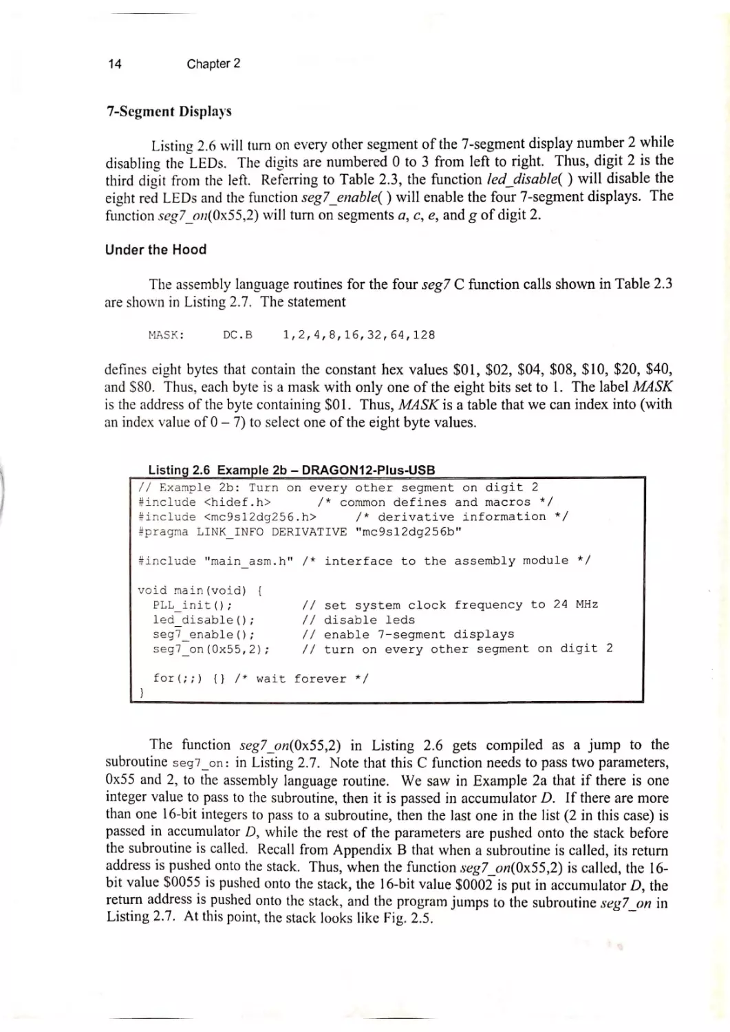
7-Segment Displays
Listing 2.6 will turn on every other segmentof the 7-segment display number 2 while
disabling the LEDs. The digits are numbered to 3 from left to right. Thus, digit 2 is the
third digit fromthe left. Referring to Table 2.3, the function /ed_disable( ) will disable the
eight red LEDs and the function seg7_enable( ) will enable the four 7-segmentdisplays. The
function seg7_on(0x55,2) will turn on segments a,c, e, and g ofdigit 2.
Under the Hood
The assembly language routines for the four seg7 C function calls shown in Table 2.3
are shownin Listing 2.7. The statement
MASK:
DC.B
1,2,4,8,16, 32, 64,128
defines eight bytes that contain the constant hex values $01, $02, $04, $08, $10, $20, $40,
and $80. Thus, each byte is a mask with only one ofthe eight bits set to 1. The label MASK
is the address of the byte containing $01. Thus, MASKis a table that we can index into (with
an index value of 0 — 7) to select one of the eight byte values.
Listing 2.6 Example 2b - DRAGON12-Plus-USB
// Example 2b: Turn on every other segment on digit 2
#include <hidef.h>
/* common defines and macros */
#include <mc9s12dg256.h>
/* derivative information */
#pragma LINKINFO DERIVATIVE "mc9sl2dg256b"
#include "main_asm.h" /* interface to the assembly module */
void main(void)
{
PLLanit();
// set system clock frequency to 24 MHz
leddisable();
// disable leds
seg7 enable();
// enable 7-segment displays
seg7_on(0x55,2);
// turn on every other segment on digit 2
for(;;)
{}
/* wait forever */
The function seg7on(0x55,2) in Listing 2.6 gets compiled as a jump to the
subroutine seg7_on: in Listing 2.7. Note that this C function needs to pass two parameters,
Ox55 and 2, to the assembly language routine. We saw in Example 2a that if there is one
integer value to pass to the subroutine, then it is passed in accumulator D. If there are more
than one 16-bit integers to pass to a subroutine, then the last one in the list (2 in this case) is
passed in accumulator D, while the rest of the parameters are pushed onto the stack before
the subroutineis called. Recall from Appendix B that when a subroutine is called, its return
address is pushed ontothe stack. Thus, when the function seg7_on(0x55,2) is called, the 16bit value $0055 is pushed onto the stack, the 16-bit value $0002 is put in accumulator D, the
return address is pushed onto the stack, and the program jumpsto the subroutine seg7_on in
Listing 2.7. At this point, the stack looks like Fig. 2.5.
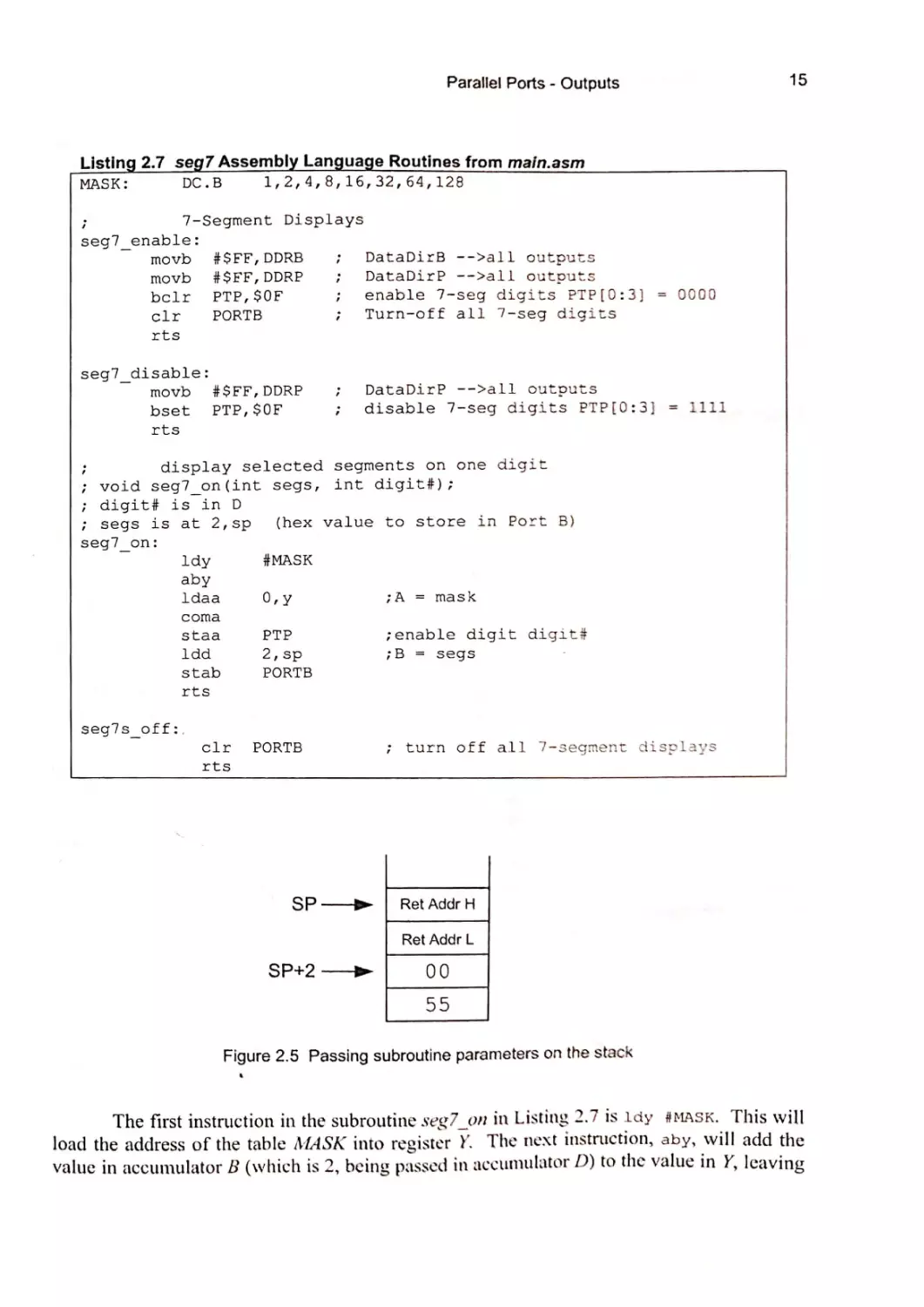
15
Parallel Ports - Outputs
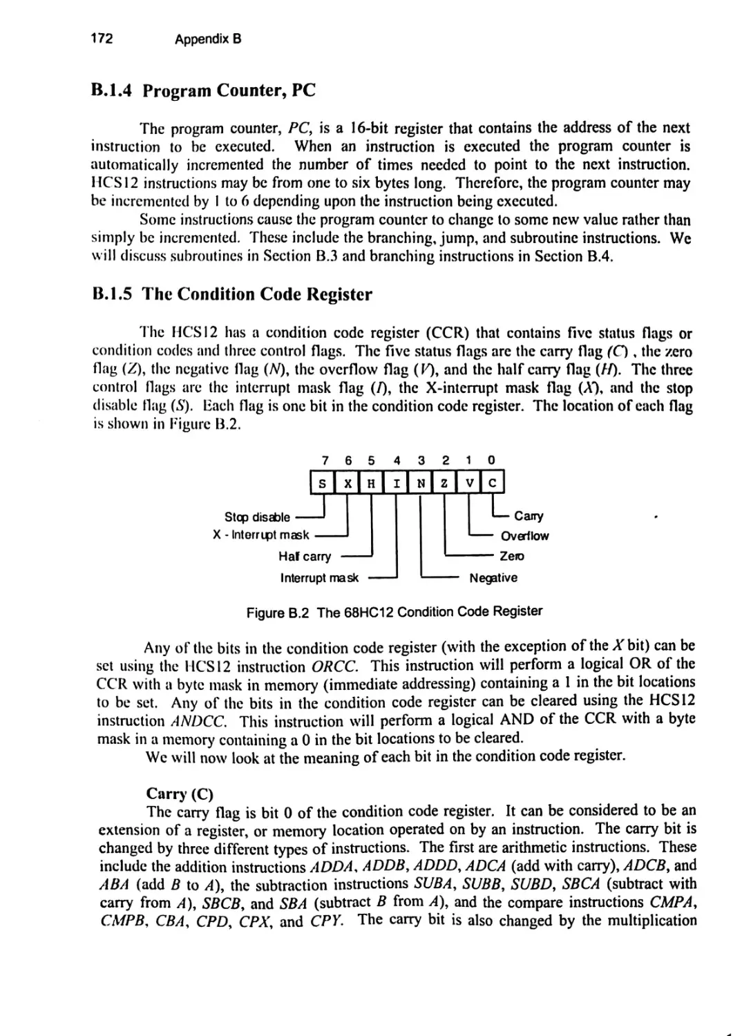
Listing 2.7 seg7 Assembly Language Routines from main.asm
MASK:
1,2,4,8,16,32,64,128
DC.B
7-Segment Displays
.
4
seg7 enable:
movb
#SFF,DDRB
;
DataDirB -->all outputs
movb
#SFF,DDRP
;
DataDirP -->all outputs
bclr
clr
PTP,S$OF
PORTB
;
;
enable 7-seg digits PTP[0:3}
Turn-off all 7-seg digits
:
DataDirP -->all outputs
;
disable 7-seg digits PTP[0:3]
= 0000
rts
seg7 disable:
movb #SFF,DDRP
PTP,SOF
bset
= illil
rts
display selected segments on one digit
; void seg7 on(int segs, int digit#);
; digit# is in D
(hex value to store in Port B)
; segs is at 2,sp
.
,
seg7on:
#MASK
ldy
aby
ldaa
coma
O,y
;A = mask
staa
PTP
2,sp
PORTB
;enable digit digit#
7B = segs
ldd
stab
rts
seg7soff:.
clr
PORTB
;
turn off all 7-segment displays
rts
SP —t
Ret AddrH
Ret Addr L
SP+2 ——>
00
55
Figure 2.5 Passing subroutine parameters on the stack
The first instruction in the subroutine seg7_on in Listing 2.7 is ldy #MASK. This will
load the address of the table MASK into register Y. The next instruction, aby, will add the
value in accumulator B (whichis 2, being passed in accumulator D) to the value in Y, leaving
16
Chapter 2
the sum in Y. Thus, Y nowpoints to the third byte in the MASK table, which contains the
constant $04. The next instruction, ldaa 0,y, will load this value $04 into accumulatorA,
and the nextinstruction, coma, will complementall bits of A, leaving the eight bits 11111011
in accumulator A. This value is then stored in the Port P data register, PTP, which will
enable only digit 2 of the four 7-segment displays. To light the segments of this digit, we
just need to store the hex value $55 from Fig. 2.5 in PORTB. The statement 1dd 2,sp will
load accumulator D with the 16-bit value located at SP +2 as shownin Fig. 2.5. The byte
$55 will be in accumulator B, so nowthe instruction stab PORTB will store this value in the
fort B data register, which will turn on segmentsa, c, e, and g of the 7-segment display on
igit 2.
Example 3 — Delay Loopsin C
Wewill generate a delay by making a simple software delay loop. A more accurate
way of producing a delay1s to use the timer module in the MC9S12DG256. Wewill look at
how to do this in Chapters 4 and 9. Listing 2.8 shows how to makea software delay using
two nested for loops in the function delay( ). The program in Listing 2.8 will blink on and
off the seven right-most red LEDsplusall segments of the right-most 7-segmentdisplay.
The C forloop has the following general form
for(initial index;
terminal_index;
increment)
{
statements;
}
In the inner for loop in the delay( ) function in Listing 2.8 the initial_index is defined by the
Statement j =0, where/ is a 16-bit integer declared along with in the statementinti, /;.
The terminal_index in the innerfor loop is defined by the statement j < 5999;and the
incrementis defined by the statement 7 ++. The statement j++ is equivalentto
j= /j+1
which just increments j by 1. Thus, in this for loop the index / starts at 0, the statements
between the braces {...} are executed (there are no statements in the innerfor loop in Listing
2.8), the index / is incremented by 1, and the statements between the braces are executed
again. This process continues until the terminal_index is reached,or in this case when the
statement j < 5999; is false, i.e. when j gets incremented to 5999. Thus, this for loop will
execute 5999 times. We chose this number becauseit is the same as the numberof times we
go through the inner loop of the assembly language delay routine (described in Example 4)
to produce a | millisecond delay. The delay in the C for loop will be somewhat longer
because the for loop gets compiled to assembly languageinstructions that take a few more
clock cycles than in the assembly language delay loop.
The inner for loop in the delay( ) function in Listing 2.8 will execute 500 times and,
each time through this outer for loop, the inner for loop will execute 5999 times. Thus, the
total numberof times through the inner loop before the de/ay(_ ) function exits will be 500 x
5999 = 2,999,500. The bus clock frequency of the microcontroller is 24 MHzso,if the inner
for loop took 4 clock cycles, then the total delay time will be
4x 2,999, 500/24, 000,000 =0.5 seconds.
Parallel Ports - Outputs
17
Before the main program in Listing 2.8 we have included the delay( ) function
prototype declaration
void delay (void);
The first void in this statement indicates that this function does not return any value to the
calling program. The second void in the parentheses indicates that there are no parameters to
be passed from the calling program to the function. All functions that you use in your C
programs must havea prototype declaration. These are often grouped together in a separate
A file, but you can also include them at the beginning of the program as we have donehere.
Listing2.8 Example 3 — DRAGON12-Plus-USB
// Example 3: Blinking 7-Segment Display
/* common defines and macros */
#include <hidef.h>
/* derivative information */
#include <mc9s12dg256.h>
#pragma LINKINFO DERIVATIVE "mc9sl12dg256b"
#include "main_asm.h"
/* interface to the assembly module */
void delay (void) ;
void main(void)
PLLinit ();
seg7 enable();
{
// set system clock frequency to 24 MHz
// enable 7-segment display
while (1) {
seg7_on(0x7F, 3);
// switch on all segments of digit 3
delay();
seg7s_off();
// switch off all segments
delay();
}
void delay()
{
ant 4,1
for(i = 0; i < 500; itt) {
for(j = 0; j < 5999; j++)
{
}
The main programin Listing 2.8 first enables the 7-segment displays and then enters
a while loop. The C while loop has the following general form
while(expression)
{
statements;
}
Whenthe while loop is executed the expression in the parentheses is evaluated, and if it is
true, the statements between the braces {...} are executed, and then the expression in the
parentheses is evaluated again.
As long as the expression is true, the statements will be
18
Chapter2
executed again.
When the expression becomes false, the while loop is exited without
executing the statements again. A value of zero for the expressionis taken to be false, and a
non-zero value is taken to be true. Therefore, in the statement whi/e(1) in Listing 2.8 the
expression is always true, so the while loop is never exited.
continually execute the statements within the while loop forever.
We use this statement to
Within the while loop, wefirst turn on all segments of the 7-segment display on the
right-most 7-segment display on the DRAGON12-Plus-USB, delay approximately half a
second, turn off all segments of the 7-segment display, and then delay approximately half a
second again. This process repeats endlessly, causing the display to blink on andoff about
every second. Try it.
Example 4 — Delay Loops in Assembly: ms_delay(int n)
Instead of having to write your own delay loop in C we have written an
assembly language routine that is called by the C function call shown in Table 2.4.
This assembly language routine is always available to you when you set up an
LBE_ DRAGON12-Plus-USB stationery project. Listing 2.9 shows how you can
modify the program in Listing 2.8 to produce the same result. Try it. Count the
number of blinks in 10, 20, or 30 seconds, and verify that each blink takes exactly 1
second.
Table 2.4 C function call delaying n milliseconds
C Function Call
Meaning
ms delay(int n);
Delay n milliseconds
Listing 2.9 Example 4—- DRAGON12-Plus-USB
// Example 4:
Blinking 7-Segment Display using msdelay()
f#finclude <hidef.h>
/* common defines and macros */
#include <mc9s12dg256.h>
/* derivative information */
#pragma LINKINFO DERIVATIVE “"mc9sl12dg256b"
#finclude "main_asm.h"
void main(void)
/*
interface to the assembly module */
{
PLLinit();
//
seg7_enable();
set system clock
frequency to 24 MHz
// enable 7-segment display
while (1) {
seg7_on(0x7F, 3);
// switch on all segments of digit 3
msdelay (500);
// delay
seg7s off ();
// switch off all segments
ms delay(500);
// delay
OS eee eee, eee ——_—_ —_—e ee eee ee
ee ee ee eereee eee
Parallel Ports - Outputs
19
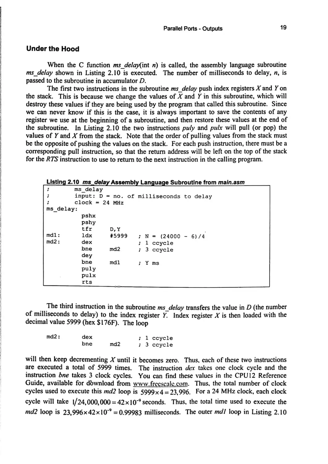
Underthe Hood
When the C function ms_delay(int n) is called, the assembly language subroutine
ms_delay shown in Listing 2.10 is executed.
The numberof milliseconds to delay, 7, is
passed to the subroutine in accumulator D.
The first two instructions in the subroutine ms_delay push indexregisters X and Y on
the stack. This is because we changethe values of X and in this subroutine, which will
destroy these values if they are being used by the program thatcalled this subroutine. Since
we can never know if this is the case, it is always important to save the contents of any
register we use at the beginning of a subroutine, and then restore these values at the end of
the subroutine. In Listing 2.10 the two instructions puly and pulx will pull (or pop) the
values of Y and_.X from the stack. Note that the order of pulling values from the stack must
be the opposite of pushing the values on the stack. For each push instruction, there must be a
corresponding pull instruction, so that the return addresswill be left on the top of the stack
for the RTS instruction to use to return to the nextinstruction in the calling program.
Listing 2.10 ms_delay Assembly Language Subroutine from main.asm
;
;
;
ms delay
input: D = no. of milliseconds to delay
Clock = 24 MHz
ms_delay:
pshx
pshy
md1:
md2 :
tfr
ldx
dex
bne
dey
bne
D,Y
#5999
md2
* N = (24000 - 6)/4
; 1 ccycle
; 3 ccycle
md1
,; Y ms
puly
pulx
rts
The third instruction in the subroutine ms_delay transfers the value in D (the number
of milliseconds to delay) to the index register Y. Index register X is then loaded with the
decimal value 5999 (hex $176F). The loop
md2:
dex
bne
md2
;
;
1 ccycle
3 ccycle
will then keep decrementing X until it becomes zero. Thus, each of these two instructions
are executed a total of 5999 times.
The instruction dex takes one clock cycle and the
instruction bne takes 3 clock cycles. You can find these values in the CPUI2 Reference
Guide, available for download from www.freescale.com. Thus, the total number of clock
cycles used to execute this md2 loop is 5999x 4 = 23,996. For a 24 MHz clock, each clock
cycle will take 1/24,000,000=42x10~° seconds. Thus, the total time used to execute the
md2 loop is 23,996x42x10~’ = 0.99983 milliseconds. The outer md/ loop in Listing 2.10
20
Chapter 2
loads index register X with 5999 (2 clock cycles), executes the md2 loop (0.99983 ms),
decrements Y(1 clock cycle), and, if Y is not equal to zero, branches back to md/ (3 clock
cycles).
These extra six clock cycles take 6/24,000 = 0.00025 milliseconds to execute,
Thus, each time through the md/ loop takes a total of 0.99983 + 0.00025 = 1.00008
milliseconds. Therefore, to delay 1 milliseconds, we just need to execute this loop 7 times,
but this is just the value that is in register Y,
Example 5 — Turning Single Bits On and Off
In this example we will show how to turn on and off individual LEDs on the
DRAGON I12-Plus-USBboard. Wewill first show you how to dothis entirely in C, and then
we will provide newCfunctioncalls to dothis.
Recall from Fig. 2.2 that setting a bit high in Port B will turn on the corresponding
LED on the DRAGON1I2-Plus-USB. Thus,it will be important to be able to set a particular
bit in a register to | or clear a particularbit to 0.
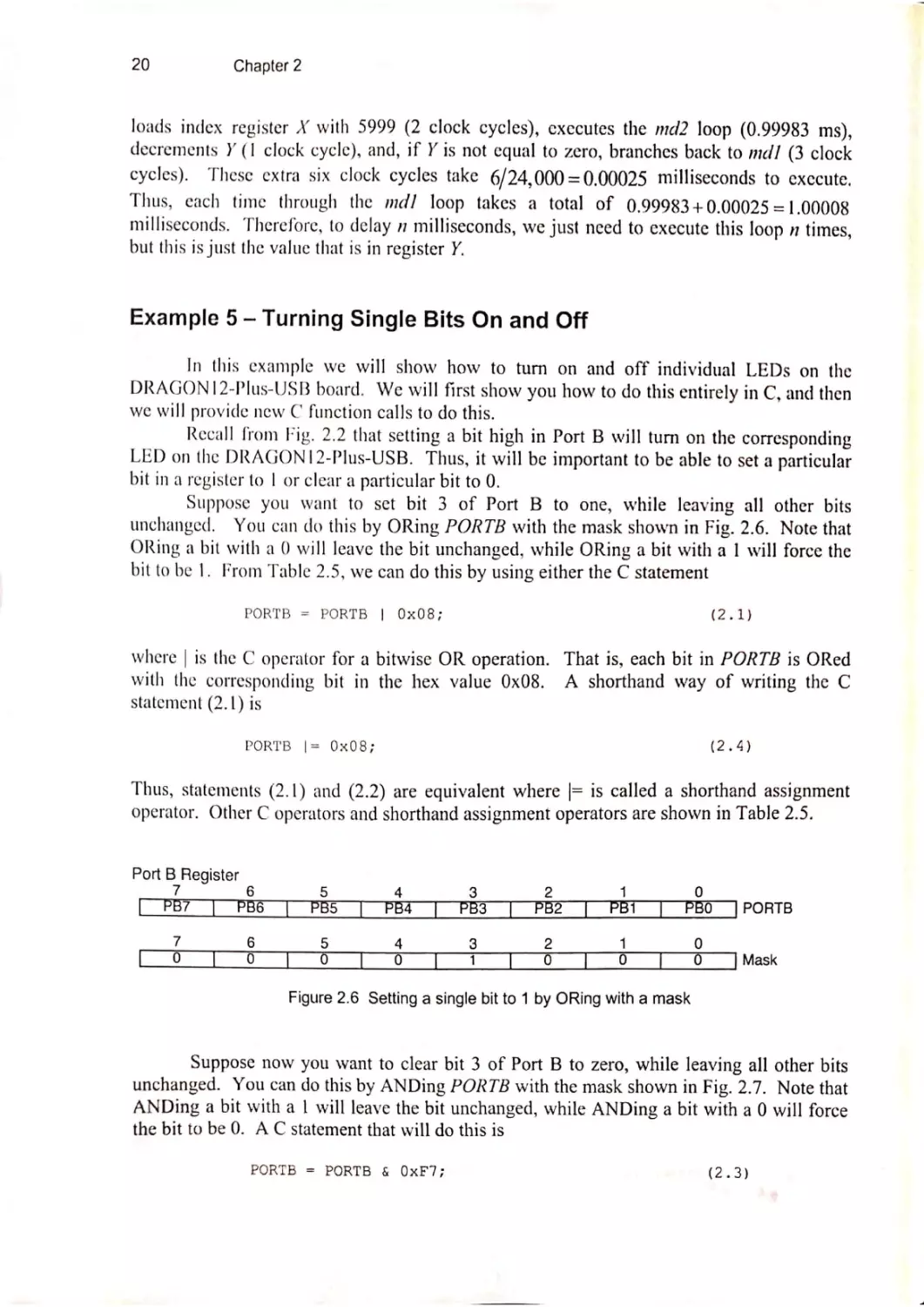
Suppose you want to set bit 3 of Port B to one, while leaving all other bits
unchanged. You can do this by ORing PORTB with the mask shown in Fig. 2.6. Notethat
ORing a bit with a 0 will leave the bit unchanged, while ORing a bit with a 1 will force the
bit to be 1. From Table 2.5, we can do this by using either the C statement
PORTB = PORTB
|
0x08;
(2.1)
where is the C operator for a bitwise OR operation. That is, each bit in PORTB is ORed
with the corresponding bit in the hex value 0x08.
A shorthand way of writing the C
statement (2.1) is
PORTB |= 0x08;
(2.4)
Thus, statements (2.1) and (2.2) are equivalent where |= is called a shorthand assignment
operator. Other C operators and shorthand assignmentoperators are shownin Table 2.5.
Port B Register
[|
7
PB7
|
7
L
oO
6
PB6
|
6
[|
oO
5
PBS
|
5
Jy
0
4
PB4
|
4
YT
0
3
PBS
3
7,
T
|
2
PB2
2
[...0
|
.
1
PBI
1
0
|
0
PBO
0
[0
|PORTB
|Mask
Figure 2.6 Setting a single bit to 1 by ORing with a mask
Suppose now you wantto clear bit 3 of Port B to zero, while leaving all otherbits
unchanged. Youcan do this by ANDing PORTB with the mask shownin Fig. 2.7. Note that
ANDinga bit with a | will leave the bit unchanged, while ANDinga bit with a 0 will force
the bit to be 0. A C statementthat will do this is
PORTB = PORTB & OXF7;
(2.3)
Parallel Ports - Outputs
21
or, using the shorthand assignmentoperator, we could use the equivalent statement
PORTB &= OXF7;
(2.4)
Port B Register
Zc
[_PB7
z
|
PBo
|
5
PBS
1
|
1
4
|
Pe4
|
1
|
|
1
3
PB3
|,
|
0
2
PB2
|
|
1
1
PBi
0
[|
|
1
PBO
|PORTB
0
1
2
3
4
5
6
7
|
6
|
1
| Mask
Figure 2.7 Clearing a single bit to 0 by ANDing with a mask
Table 2.5 Operators and Assignment Operators
Operator
Description
Assignment Operator
&
Bitwise AND
=
|
Bitwise OR
=
a“
Bitwise XOR
A=
+
Addition
+=
Subtraction
-=
Z
Multiplication
*=
/
Division
=
%
Modulus
%o=
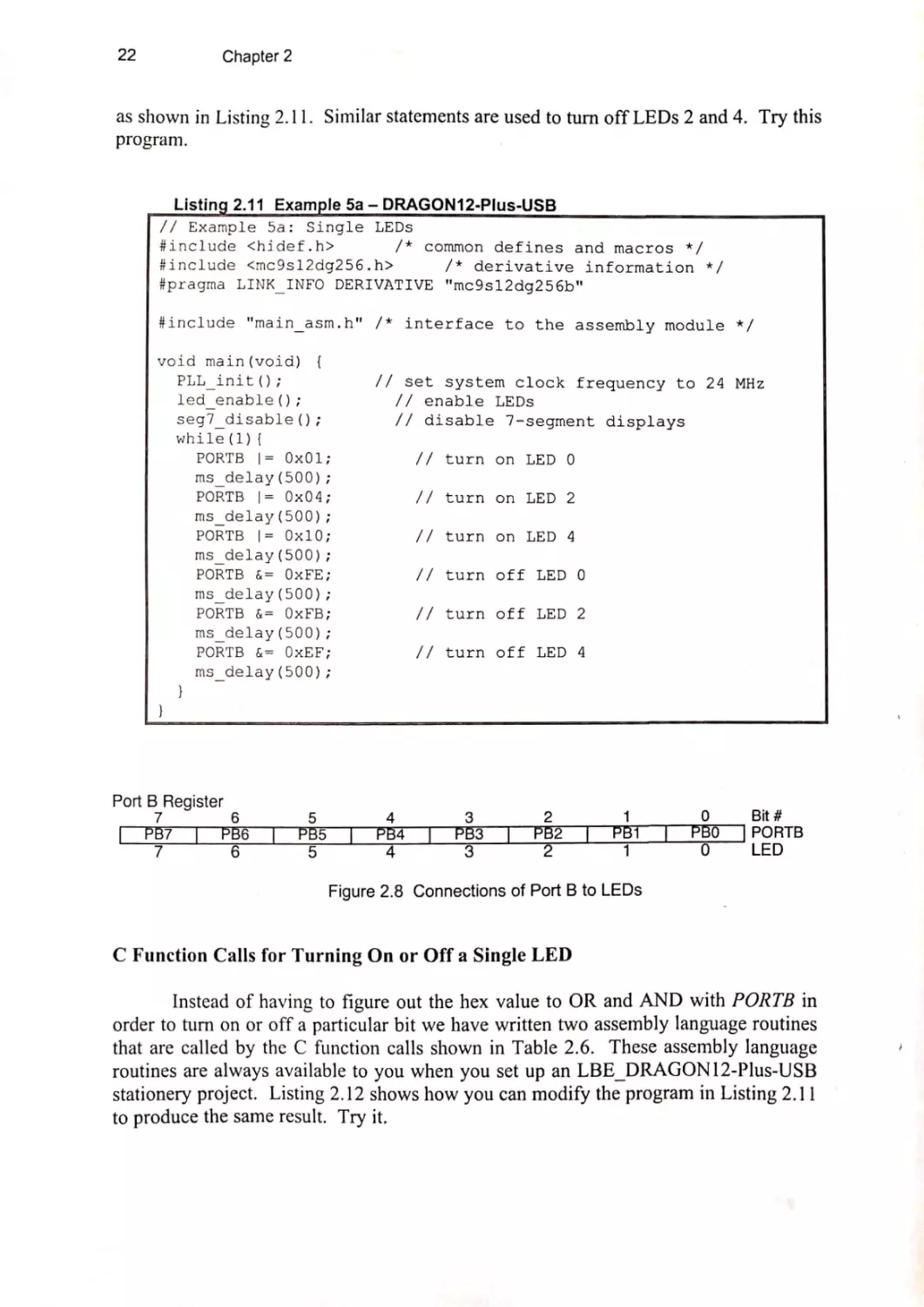
Consider the C program shownin Listing 2.11 which first turns on LEDs 0, 2, and 4
in turn, and then turns them off in turn.
We knowthat writing a | to the bit position in
PORTB corresponding to a particular LED (see Fig. 2.9) will turn on that LED.
For
example, writing a 1 to PBO in Fig. 2.9 will turn on LED 0 and writing a 0 to PBO will turn
off LED 0. As we have seen the way to turn on LED 0 while leaving all other LEDs
unchangedisto first read PORTB, then OR it with the mask 00000001 (or 0x01), and finally
write the resulting value back in PORTB. The statement that will do this is
PORTB = PORTB
|
0x01;
or, using the shorthand assignment operator from Table 2.5, we could use the equivalent
statement
PORTB
|=
Ox01;
as shownin Listing 2.11. Similar statements are used to turn on LEDs 2 and4.
To turn off LED 0, we would need to AND PORTB with 11111110 (or OxFE). We
can do this by using either the C statement
PORTB‘= PORTB & OXFE;
or, using the shorthand assignment operator, we could use the equivalent statement
PORTB &= OXFE;
22
Chapter2
as shownin Listing 2.11. Similar statements are used to turn off LEDs 2 and 4. Try this
program.
Listing 2.11 Example 5a - DRAGON12-Plus-USB
// Example 5a: Single LEDs
#include <hidef.h>
/* common defines and macros */
#include <mc9s12dg256.h>
/* derivative information */
#pragma LINKINFO DERIVATIVE "mc9s12dg256b"
#include "“main_asm.h" /* interface to the assembly module */
void main(void)
{
PLLinit ();
// set system clock frequency to 24 MHz
led_enable();
// enable LEDs
seg7disable();
// disable 7-segment displays
while (1) {
PORTB |= 0x01;
// turn on LED 0
ms delay(500);
PORTB |= 0x04;
// turn on LED 2
ms delay (500);
PORTB |= 0x10;
// turn on LED 4
ms delay (500);
PORTB &= OxFE;
// turn off LED 0
msdelay(500);
PORTB &= OxFB;
// turn off LED 2
ms delay(500);
PORTB &= OxEF;
ms_delay (500);
Port B Register
[_
€
PB7
7
|
6
Peo
6
|
5
PBS
5
// turn off LED 4
|
4
PB4
=
|
3
PBs
3
|
2
PB2
20
|
1
Pei
1
0
[ PBO
0)
Bit #
|PORTB
LED
Figure 2.8 Connections of Port B to LEDs
C Function Calls for Turning On or Off a Single LED
Instead of having to figure out the hex value to OR and AND with PORTB in
order to turn on oroff a particular bit we have written two assembly language routines
that are called by the C function calls shown in Table 2.6. These assembly language
routines are always available to you when you set up an LBE_DRAGON12-Plus-USB
stationery project. Listing 2.12 shows how you can modify the program in Listing 2.11
to produce the sameresult. Try it.
Parallel Ports - Outputs
23
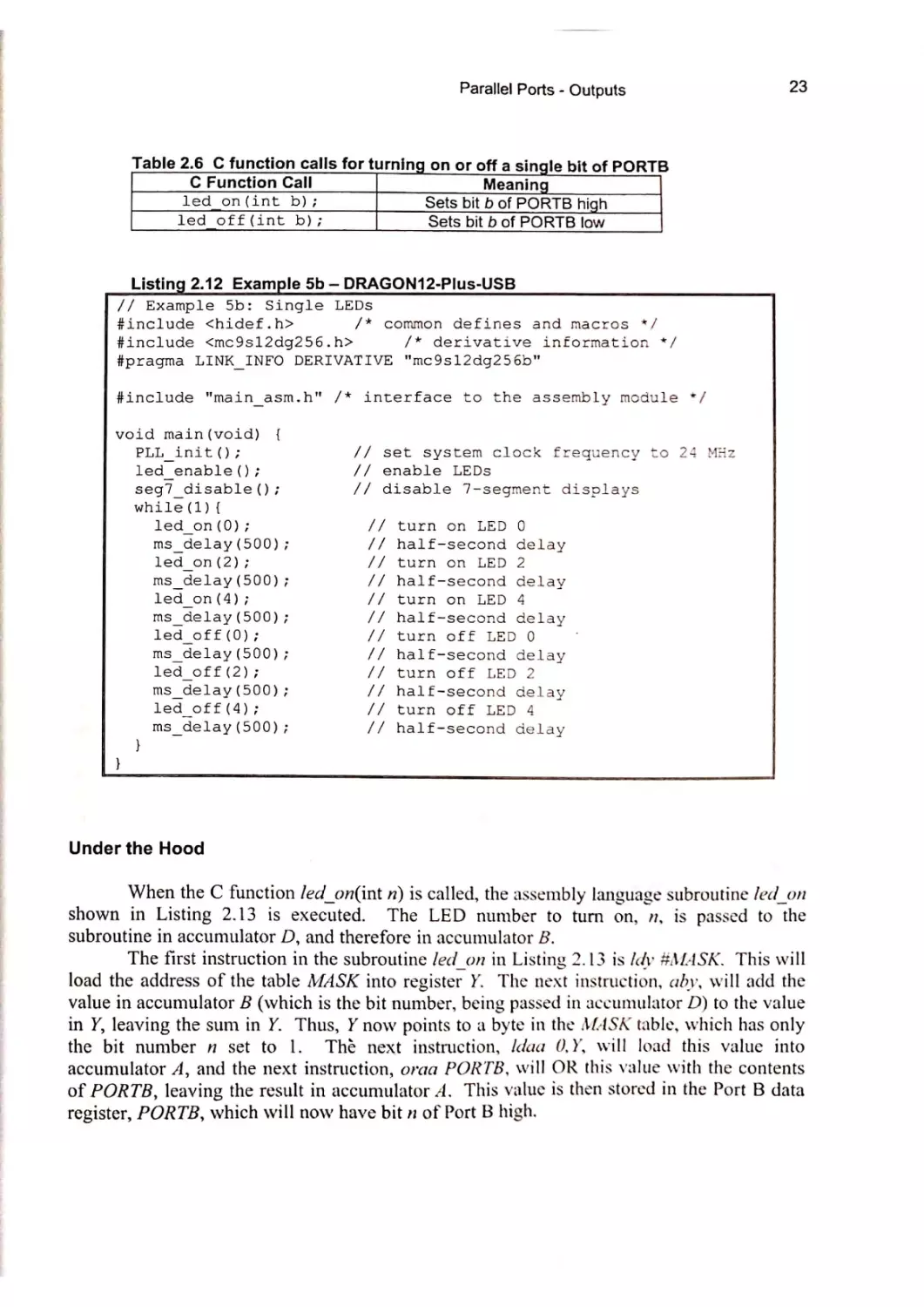
Table 2.6 C function calls for turning on or off a single bit of PORTB
C Function Call
led on(int b);
led off(int b);
Meaning
Sets bit b of PORTB high
Sets bit b of PORTB low
Listing 2.12 Example 5b - DRAGON12-Plus-USB
// Example 5b: Single LEDs
#include <hidef.h>
/* common defines and macros */
#include <mc9s12dg256.h>
/* derivative information */
#pragma LINK_INFO DERIVATIVE "mc9sl12dg256b"
#include "main_asm.h" /* interface to the assembly module */
void main(void)
{
PLLinit);
// set system clock frequency to 24 MHz
led_enable();
seg7disable();
// enable LEDs
// disable 7-segment displays
while (1) {
led_on(0);
// turn on LED 0
ms delay(500);
// half-second delay
led_on(2)j;
// turn on LED 2
ms_delay (500);
// half-second delay
led_on (4);
ms_delay (500);
led_off(0);
// turn on LED 4
// half-second delay
// turn off LED 0
"
msdelay (500);
// half-second delay
led_off(2);
ms_delay (500);
ledoff (4);
msdelay (500) ;
//
//
//
//
turn off LED 2
half-second delay
turn off LED 4
half-second delay
}
}
Under the Hood
Whenthe C function /ed_on(int n) is called, the assembly language subroutine /ed_on
shown in Listing 2.13 is executed. The LED numberto turn on, », is passed to the
subroutine in accumulator D, and therefore in accumulator B.
Thefirst instruction in the subroutine /ed_onin Listing 2.13 is /dvy #4MJ4SK. This will
load the address of the table MASK into register Y. The next instruction, aby, will add the
value in accumulator B (whichis the bit number, being passed in accumulator D) to the value
in Y, leaving the sum in Y. Thus, Y nowpoints to a byte in the A/4SKtable, which has only
the bit number n set to 1. The next instruction, /daa 0,Y, will load this value into
accumulator A, and the next instruction, oraa PORTB, will OR this value with the contents
of PORTB,leaving the result in accumulator A. This value is then stored in the Port B data
register, PORTB, which will nowhavebit » of Port B high.
24
Chapter 2
Listing 2.13 led Assembly Language Subroutines from main.asm
MASK:
DC.B
1,2,4,8,16,32,64,128
;
led_on( b# )
:
set bit number b# of PORTB to 1
led.on:
pshy
ldy
# MASK
aby
ldaa
oraa
staa
0,Y
PORTB
PORTB
7;OR mask with PORTB
;Sstore back in PORTB
puly
rts
;
led_off( b# )
;
clear bit number b# of PORTB to 0
led_off:
pshy
ldy
aby
ldaa
#MASK
0,
;complement mask
coma
anda
staa
PORTB
PORTB
;AND mask with PORTB
;store back in PORTB
puly
rts
When the C function /edoff{int n) is called, the assembly language subroutine
led_off shown in Listing 2.13 is executed. The bit numberto set low, n, is passed to the
subroutine in accumulator D, and therefore in accumulator B.
The first three instructions in the subroutine /ed_off in Listing 2.13 are the same as
the first three instructions in the subroutine /ed_on. Thus, at this point, the value in
accumulator A will contain a MASK value with a single bit set to 1. The next statement,
coma, will complementall bits, so that all bits in accumulator A will be 1 except bit number
n, which will be 0. This value in accumulator A is then ANDed with the contents of PORTB,
leaving the result in accumulator A. All bits in PORTB that are ANDed with | will remain
unchanged. However, the bit value that is ANDed with 0 will be forced to be 0. This
resulting value in accumulator A is then stored back in PORTB, which will cause bit n in
PORTBto golow.
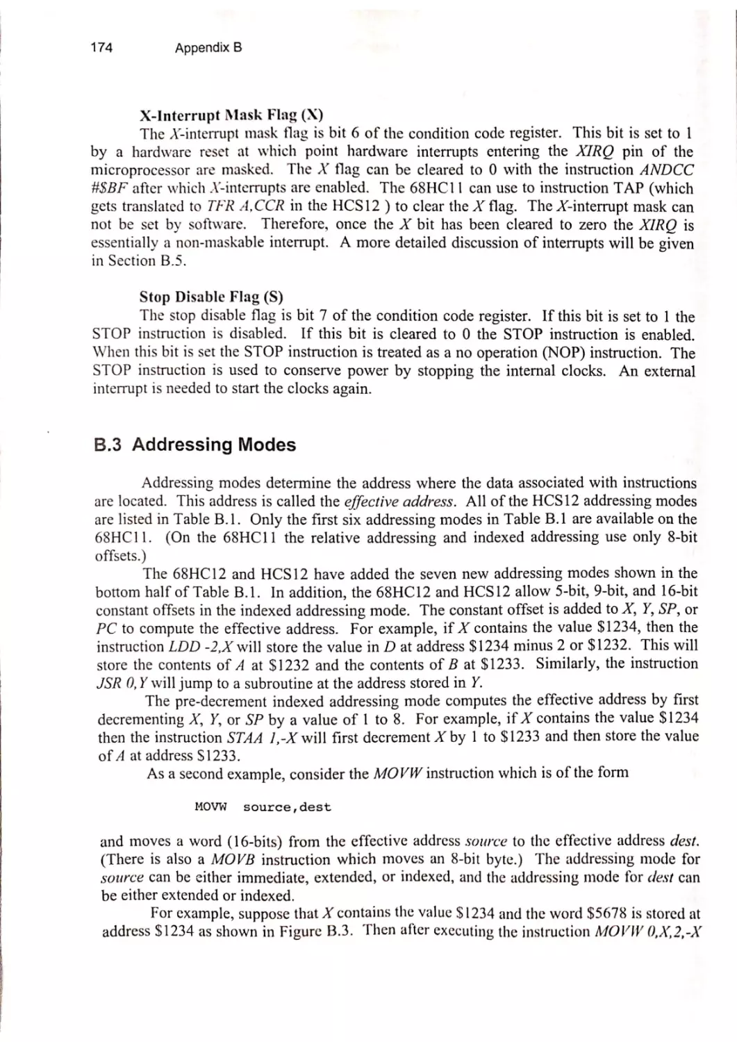
Example 6 — Hex Counter
In this example we will show how to have the each of the 7-segment displays on the
DRAGON 12-Plus-USB board count in hex from 0 to F continually. We will first show you
how to do this entirely in C, and then we will provide a new C function to display any hex
digit.
25
Wehave seen in Fig. 2.3 that the DRAGON12-Plus-USB board has a common-
cathode 7-segment display connected to Port B.
This means that on the DRAGON 12-Plus-
USBa turns a segment on and a 0 turns a segmentoff.
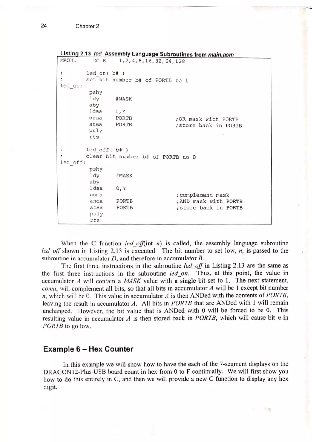
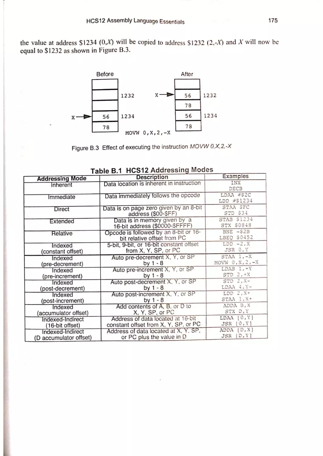
The table shown in Fig. 2.9 showsthe output values for each segmenta — g needed to
PrRrOrRPORPRFPRPRFPFPFOFRF OF ]p
DORPCOORPRPRPRFPOORP RH FP BID
OOrFRFORP RP RFP RP rRPrRPrRPrRrF OF FIN
OrPrPrPrFOrFPRPORF OFF OFFI
PRrRrRrPrPrPOrFOrROOOFOFR!0
g
0
0
1
1
1
1
1
0
1
1
1
1
0
1
1
1
FPrOrPrFPRrPRrFPRrRPOrRPFFOOOFIm
ZAAQRATP WO DIDUBWNHeE Ol”
display all hex digits, D, from 0 — F, for the DRAGON 12-Plus-USBboard.
code
3F
06
5B
4F
66
6D
a
Ce)
g
7D
07
TE
6F
77
7C
39
SE
79
7]
—
|
Cc
Co)
d
Figure 2 9 Segmentvalues required to display hex digits 0 — F
@
eeeS Le oS ~~ tes <=: \
OY
OPeeeeeeee eee POL
Seeeeee 8 OS eee eeee ee
Parallel Ports - Outputs
Listing 2.14 shows how wecancreate a table of the hex codesin Fig. 2.9 byusing a
constant character array called seg7tbi[]. The type declaration char defines each element of
the array seg7tbi[] to be an 8-bit byte. The type qualifier const defines each of these array
elements to be a constant that can’t be changed in the program. Note howthe braces {..} are
used in the array definition to define the 16 constant hex codes given in Fig. 2.9. Also note
that the type declarations for seg7tb/[] and the integer i used in the for loop must precede the
function call PLL_init( ).
In the while loop in Listing 2.13 there is afor loop with an index / that goes from0 to
15. Each time through this for loop the output of Port B is set to seg7th/[i], which will
output the proper hex code correspondingto the hex digit i. Note that the square brackets [ ]
are used to indicate array elements in C. The secondstatement in the for loop is a halfsecond delay before the next digit is displayed. Once all 16 digits have been displayed the
while(1) loop will just keep counting again. Try it. Note that all four 7-segment displays
count from 0 — F in unison. Wewill next see howto display a hex values on a single 7segmentdisplay and then, in Example 7, show howto display different values on each of the
7-segmentdisplays.
A C function call to display hex digits
Instead of having to make your own 7-segment decoder table, we have written
an assembly language routine that is called by the C function call seg7dec(int i, int 5)
shown in Table 2.7. This assembly language routine is always available to you when
you set up an LBE_DRAGON12-Plus-USBstationery project. Note that this function
26
Chapter 2
will display the hex value j on the 7-segment display number }, where b = 0 is theleftmost 7-segment display and 5 = 3 is the right-most 7-segment display. Listing 2.15
showsa programthat hasthe right-most 7-segment display count from 0 to F. Try it.
7-Segment Decoder - C version
idef.h>
/* common defines and macros */
<mce9s12dg256.h>
seg7tbl[]
/* derivative information */
=
{
Ox3F,0x06, Ox5B, 0x4f,
t $j
©
mw
FO
MO
8)
-
;
|}:
(D
Ql
@M
—_
ro
4
nH
Oo
=m
tk
-~O..Q
1|
Fl
rth
+
t-
'
=
yr oo
w ry
0x66, 0Ox6D, 0x7D, 0x07,
Ox7F,Ox6F,0x77,0x7C,
0x39, 0x5E,0x79, 0x71
)F
// set system clock frequency to 24 MHz
le();
le();
// enable 7-segment display
// disable LEDs
7 i < 16; Dee) {
B = seg7tbl [i];
Table 2.7 C function call for 7-segment displays
Meaning
C Function Call
Enables the 7-segmentdisplays
eg7 enable();
seg? disable();
Disables the 7-segmentdisplays
s,
seg7dec(int i,
(ant
int b);
int b);
Display the segments s on the 7-segmentdigit no. b
Display the hex value / on the 7-segmentdigit no. b
Paratiel Ports - Outputs
27
Listing 2.15 Example 6b — DRAGON12-Pius-US8
// Example 6b: Single Digit 7-Segment Decoder
#include <hidef.h>
/* common defines and macros ‘*/
/* derivative information °:
#include <mc9sl2dg256.h>
#pragma
‘
"mc9sl2dg256b”
LINK_INFO DERIVATIVE
#include "main_asm.h" /* interface to the assembly module °/
void main(void)
{
int i;
PLL init();
seg7_enable();
led_disable();
while (1) {
// set system clock frequency to 24 Mxz
// enable ?-segment display
// disable LEDs
for(i = O; i < 16; itt)
{
seg7dec (i, 3);
ms_delay (500);
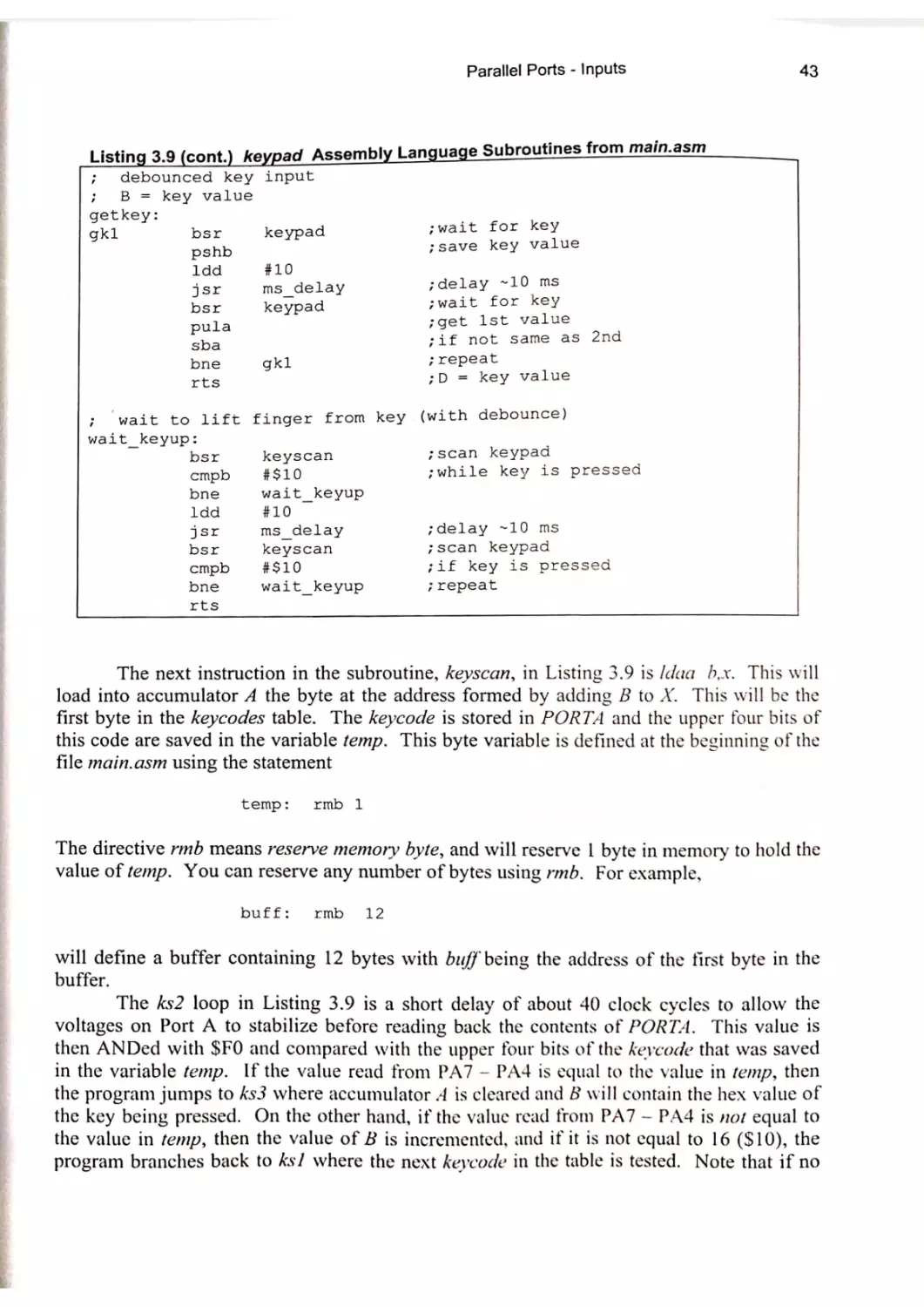
Under the Hood
Whenthe C function seg7dec(int i, int 5) is called, the assembly language subroutine
seg7dec shownin Listing 2.16 is executed. Recall from Example 2b that if there are more
than one 16-bit integer to pass to a subroutine, then the last one in the list (the digit number 4
in this case) is passed in accumulator D, and therefore in accumulator B, while the rest ofthe
parameters are pushed onto the stack before the subroutine ts called. The hex digit. /, 1s
therefore passed to the subroutine on the stack, above the return address, at SP2.
The first three instructions in the subroutine seg7decin Listing 2.16 are the same as
the first three instructions in the subroutine /ed_on in Listing 2.13. Thus, at this point, the
value in accumulator 4 will contain a MASK value with a single bit set to 1. The nent
statement, coma, will complementall bits, so that all bits in accumulator 4 will be | except
bit number 5, which will be 0. This value in accumulator +4 is then stored in PTP, which will
enable the 7-segmentdisplay, digit b.
The next instruction, /dd 2,sp, will load the load the value of the hex digit, é, into
accumulator D, and therefore into accumulator B. The next three instructions in the
subroutine seg7decin Listing 2.16 will use this hex digit value (between 0 and F) as an index
into the table SEG7TBL, and load the corresponding 7-segment code into accumulator <4.
This value is then stored in PORTB, which will nowdisplay the hex digit 7 on digit b ofthe
7-segment displays.
28
Chapter 2
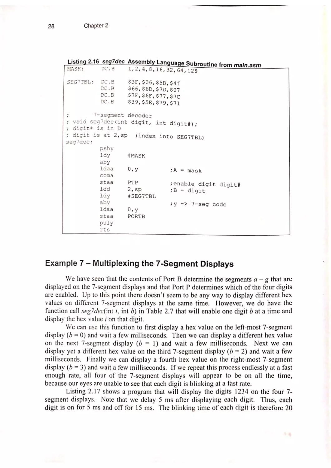
Listing2.16 seg7dec Assembly Language Subroutine
from main.asm
MASK:
OC <5
SEG7TBL:
DC.B
1,2,4,8,16,32, 64,128
S3F,$06,$5B, $4£
DC .B
$66,$6D,$7D, $07
DC .B
S7F,S6F,$77,$7C
Dc.B
$39,$5E,$79,$71
7-segment decoder
a seg/dec(int digit,
1t#
1s in D
is at 2,sp
int digit#);
(index into SEG7TBL)
~.
pshy
ldy
#MASK
aby
ldaa
O,y
coma
staa
ldd
ldy
7A = mask
PTP
2,.8p
#SEG7TBL
renable digit digit#
7B = digit
aby
ldaa
staa
7yY -> 7-seg code
0,y
PORTB
puly
rts
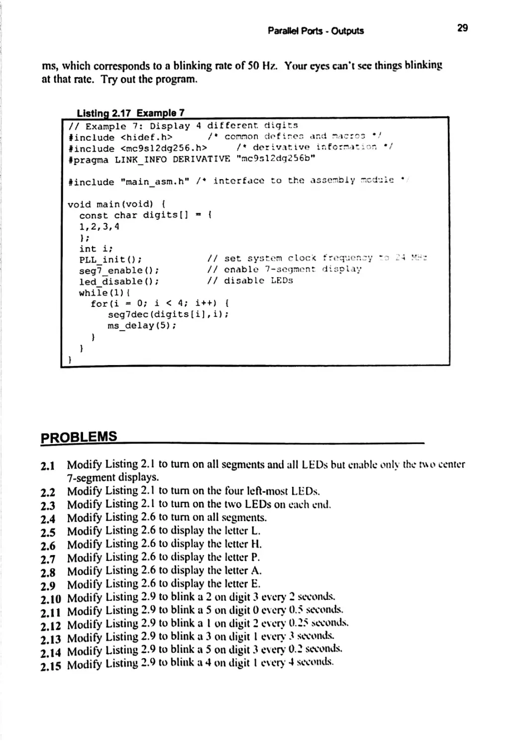
Example 7 — Multiplexing the 7-Segment Displays
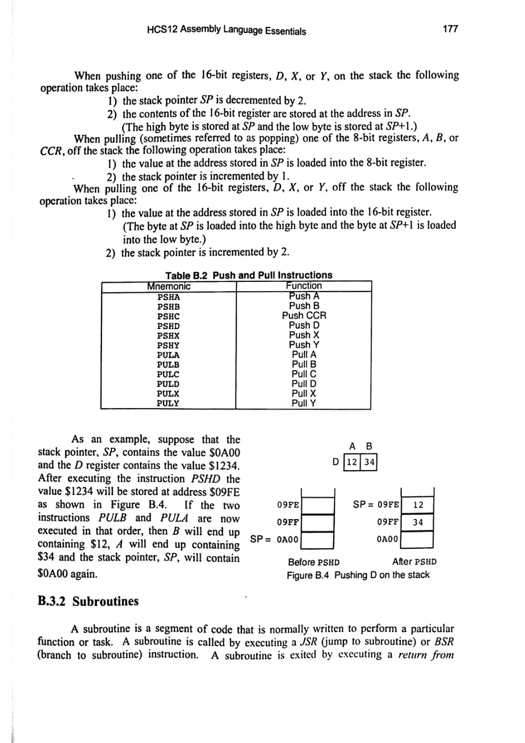
We have seen that the contents of Port B determine the segments a — g that are
displayed on the 7-segment displays and that Port P determines whichof the four digits
are enabled. Up to this point there doesn’t seem to be any wayto display different hex
values on different 7-segment displays at the same time. However, we do have the
function call seg7dec(inti, int b) in Table 2.7 that will enable one digit b at a time and
display the hex value / on that digit.
Wecan use this function to first display a hex value on the left-most 7-segment
display (b = 0) and wait a few milliseconds. Then wecan display a different hex value
on the next 7-segment display (6 = 1) and wait a few milliseconds. Next we can
display yet a different hex value on the third 7-segment display (6 = 2) and wait a few
milliseconds. Finally we can display a fourth hex value on the right-most 7-segment
display (b = 3) and wait a few milliseconds. If we repeat this process endlessly at afast
enough rate, all four of the 7-segment displays will appear to be onall the time,
because our eyesare unable to see that each digit is blinking at afastrate.
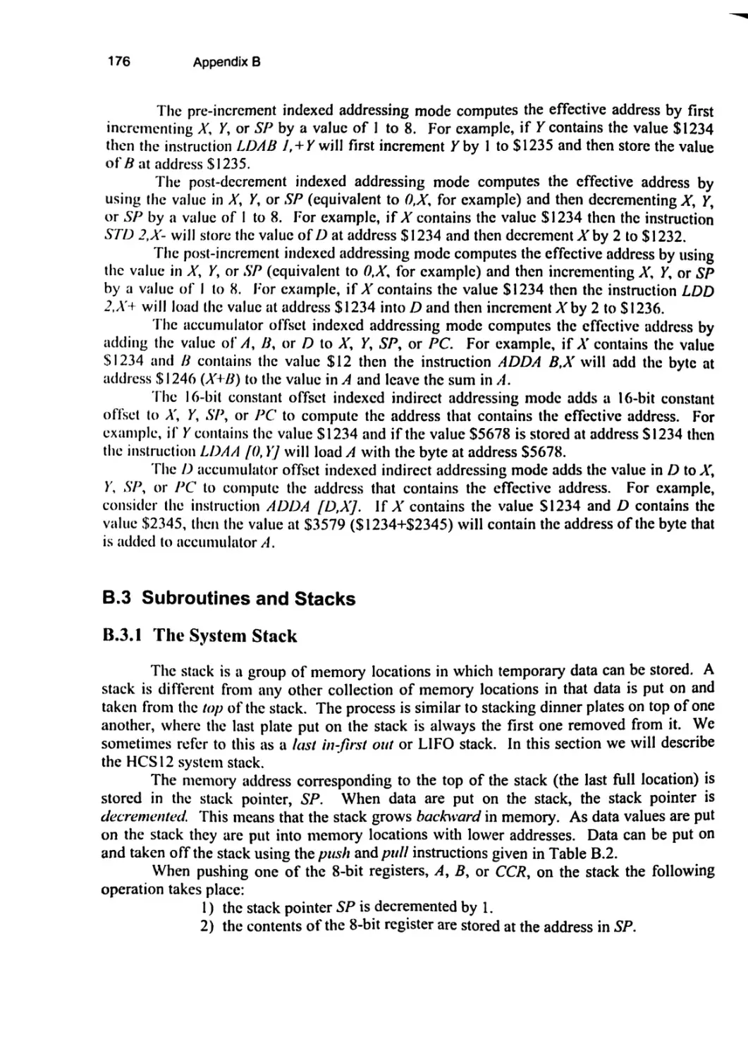
Listing 2.17 shows a program that will display the digits 1234 on the four 7segment displays.
Note that we delay 5 ms after displaying each digit. Thus, each
digit is on for 5 ms and off for 15 ms. The blinking time of each digit is therefore 20
Parallel Ports - Outputs
29
ms, which correspondsto a blinking rate of 50 Hz. Your cyes can’t see things blinking
at that rate. Try out the program.
Listing 2.17 Example 7
// Example 7: Display 4 different digits
/* common defines and macros
#include <hidef.h>
/* derivative information ¢%/
#include <mc9sl2dg256.h>
#pragma LINK_INFO DERIVATIVE "mc9sl2dq256b”
#include "main_asm.h" /* interface to the assembly mcduie *
void main(void)
{
const char digits[] = {
1,2,3,4
};
int i;
PLL_init();
// set system clock frequency To 24 MS
// enable 7-segment display
seg7_enable();
// disable LEDs
led_disable ();
while (1) {
for(i = 0; i < 4; i++)
{
seg7dec(digits[i],1i);
msdelay(5);
PROBLEMS
2.1
Modify Listing 2.1 to turn on all segments andall LEDs but enable onlythe twocenter
2.2
7-segment displays.
Modify Listing 2.1 to turn on the four left-most LEDs.
2.5
2.6
2.7.
2.8
2.9
Modify
Modify
Modify
Modify
Modify
2.3. Modify Listing 2.1 to turn on the two LEDsoneachend.
2.4 Modify Listing 2.6 to tum onall segments.
Listing 2.6
Listing 2.6
Listing 2.6
Listing 2.6
Listing 2.6
to display
to display
to display
to display
to display
the letter L.
the letter H.
theletter P.
the letter A.
the letter E.
2.10 Modify Listing 2.9 to blink a 2 ondigit 3 every 2 seconds.
9.11 Modify Listing 2.9 to blink a 5 on digit 0 every 0.5 seconds.
4.12 Modify Listing 2.9 to blink a | on digit 2 every 0.25 seconds.
9.13 Modify Listing 2.9 to blink a 3 on digit | every 3 seconds.
seconds.
9.14 Modify Listing 2.9 to blink a 5 ondigit 3 every 0.2
seconds.
9.15 Modify Listing 2.9 to blink a 4 ondigit | every4
30
Chapter 2
2.16 Modify Listing 2.12 to tum on LEDs1, 3, 5 in sequence and thenturn themoff in the
Same sequence.
ModifyListing 2.12 to tum on LEDs7, 6, 5 in sequence and then turn themoff in the
Same sequence.
NNN NNN NN NN
Nm Nh th ~ Ww ty te lp bo me
COomn~an Ss tide i Nm OO
2.18 ModifyListing 2.12 to turn on LEDs0,3, 4, 7 in sequence and then turn them off in
the same sequence.
=~
Modify Listing 2.12
Modity Listing 2.12
Modity Listing 2.15
ModifyListing 2.15
to
to
to
to
turn on and off each LED in sequence from rightto left.
turn on and off each LED in sequencefrom left to right.
count only the even hexdigits.
count only the odd hex digits.
ModifyListing 2.15 to count downfromF to 0.
ModifyListing 2.15 to count down only the even hex digits.
ModifyListing 2.15 to count down onlythe odd hexdigits.
ModifyListing 2.15 to count only hex digits that are divisible by 3.
ModifyListing 2.17 to display the hex number 93AF onthe 7-segmentdisplays.
ModifyListing 2.17 to display the word HELP onthe 7-segmentdisplays.
Write a program that will have the LEDs on the DRAGON 12-Plus-USB board countin
rm
Uo
—
)
to
S
binaryin steps of 1 every 0.5 seconds.
Write a program that will have the LEDs
binary in steps of 5 every 1.0 second.
Write a programthat will have the LEDs
binaryin steps of 10 every 0.5 seconds.
Wnite a programthat will have the LEDs
binaryin steps of 2 every 0.25 seconds.
Write a program that will have the LEDs
binaryin steps of 4 every 0.5 seconds.
Write a program that will have the LEDs
on the DRAGON12-Plus-USB board countin
on the DRAGON 12-Plus-USB board countin
on the DRAGON 12-Plus-USB board countin
on the DRAGON 12-Plus-USBboard countin
on the DRAGON12-Plus-USB boardcountin
binaryin steps of 1 every 0.2 seconds.
Write a program that will have the LEDs on the DRAGON 12-Plus-USB board countin
binaryin steps of 8 every 0.4 seconds.
Parallel Ports - inputs
31
Chapter 3
Parallel Ports - Inputs
In this chapter we will see howto read bits from parallel ports in order to read the
status of pushbutton and DIP switches. We will also learn howto decode a hex keypad.
3.1 Pushbuttons and DIP Switches
The DRAGON 12-Plus-USB board contains four pushbuttons and eight DIP switches.
Pushbutton switches S2 — S5 on the DRAGON |2-Plus-USB board are connected to bits 3 — 0
of Port H as shown in Fig. 3.1. If the switches are not being pressed the 100 k© pullup
resistors will cause the voltages at pins 3 — 0 to be 5 volts andtherefore a read of Port H will
read these bits as 1. Closing a switch will cause the input to that bit of Port H to be grounded
and therefore that bit will read 0 when Port H is read.
The DIP switch SW1 is connectedto the same Port H as shownin Fig. 3.2. Note that
the rightmost four DIP switches share the same lower four bits of Port H with the four
pushbutton switches. Also note that the DIP switches are connected to ground through 4.7
kQ resistors. These are low enough compared with the 100 kQpullup resistors that a closed
switch will still read a zero.
Clot
Lt
Ly}
4
pt ||
=
=
PH7
PH6
<s
Ss
<
PHS | PH4 | PH3 | PH2
|
| sw2
100 kKQ
.
. sw3
PH!
PHO
SW4
Pork
SW5
Figure 3.1 DRAGON12-Plus-USB pushbutton connections to Port H
In Example 8 we will showhowto read the DIP switch SWI and the four pushbutton
switches, SW2, SW3, SW4 and SW5, on the DRAGON 12-Plus-USB board. We will first
show youhowto dothis in C, and then we will provide new C function calls to dothis.
32
Chapter 3
re ne
=
.
~
S
—VW
<=
S
<<
Ss
of
H
:
2_|PHI
100 kQ
0
'
we
ye
“sS
PH6 - “PHS”[PH4 LFPH3
Swi
MIN
a
Ppp
PHT
Say,
os
—A\\\y
“Say
<
+5V
Li bia
Figure 3.2 DRAGON12-Plus-USB DIP switch SW1 connections to Port H
Example 8 — Switches on the DRAGON12-Plus-USB
The pushbuttons and DIP switches on the DRAGON12-Plus-USB board are
connected to Port H (PTH) as shownin Figs. 3.1 and 3.2. The programin Listing 3.1 will
read PTH, complement(i.e. flip) each bit by using the bitwise NOT operator ~, and write the
resulting value to the red LEDs. Thus, if the DIP switches are all open (in the up position)
and you are not pressing any pushbutton, reading PTH will read all 1’s or hex $FF.
Complementing this value will give hex 00 and thus all LEDs will be off. Pressing any
pushbutton will ground the corresponding bit of Port H, which, when complemented, will
become | and turn on the corresponding LED. Thus, if you run the program in Listing 3.1,
then pressing any of the four pushbutton switches will light up the corresponding LED.
Closing any of the DIP switches will also light up the corresponding LED. Try it. Note that
all bits of Port H must be programmedasinputs bysetting the data direction register DDRH
to 0x00.
To tell if pushbutton switch SW2 is being pressed we mustfirst read the P7H register
and then test to see if bit 3 is a | (SW2 open) or 0 (SW2 closed). We can do this by ANDing
the value read from PTH with the mask 00001000 (0x08). If the switch is open (not being
pressed), then the result of this AND operation will be 0x08. On the other hand, if the
switch is closed (being pressed), then the result of this AND operation will be 0x00. Similar
maskscan be usedto test the pressing of pushbutton switches SW3, SW4, and SWS.
The C program shownin Listing 3.2 will display a 2 on the 7-segment display
number 0 while switch SW2is being pressed, display a 3 on the 7-segment display number |
while switch SW3 is being pressed, display a 4 on the 7-segment display number 2 while
switch SW4 is being pressed, and display a 5 on the 7-segment display number 3 while
switch SWS1s being pressed,
33
Parallel Ports - inputs
Listing 3.1 Example 8a — DRAGON12-Plus-USB
// Example 8a: Pushbutton Switches - DRAGON1I2-Plus-USB
#include <hidef.h>
/* common defines and macros °*/
/* derivative information
#finclude <mc9sl2dg256.h>
#pragma LINK_INFO DERIVATIVE "mc9sl2dg256b5"
issembly module
y modu
#include “main_asm.h" /* interface to the ass¢
void main(void)
{
// set system clock frequency to 2
PLL_init();
seg7 disable();
// disable 7-segment display
led_enable();
// enable LEDs
DDRH = 0x00;
// Port H inputs
while (1) {
leds_on(~PTH)-;
}
Listing 3.2 Example 8b — DRAGON12-Plus-USB
// Example 8b:
EF
#include
Pushbutton Switches
—- DRAGONL2-Plus-USB
/*
<hidef.h>
common
-> /-segment
displ
and macros
defines
#include <mc9sl2dg256.h>
/* derivative
#pragma LINK_INFO DERIVATIVE
"“mc9sl2dg25ob"
*
information
#include “main_asm.h" /* interface to the assembly
void main(void)
{
PLLinit ()7
// set system clock frequency to
seg7_ enable();
// enable 7-segment display
leddisable ();
DDRH = 0x00;
// disable LEDs
// Port H inputs
while (1) {
while((PTH
&
Ox01)
==
0) {
seg7dec (5, 3);
//
}
seg/s off ();
while( (PTH
&
Ox02)
==
QO) {
}
seg7s off ();
&
Ox04)
== Q) |
display
turn
f/f
while
while( (PTH & Ox08)
seq/dec (2,0)?
//
//
}
}
seg7s off ();
pressing
off
f/
fy
on
|
dig
seq
all
SW4
display 4 on digit
all
?-seq
while pressing
3
display
f/f turn off
== QO) {
5
pressing
/f turn off
seg7dec (3,1);
seg/s_ off ();
while
f/f
//
seg7dec (4,2);
while( (PTH
//
all
while pressing
r
display -
turn off
al
Sw
iq
?-seq
SW.
chi
}
displ iys
34
Chapter 3
Note that the expression
(PTH & 0x01)
== 0
will be true if bit 0 of PTH is 0, 1.e., if switch SWS5 is being pressed.
Similarly, the
expression
(PTH & 0x04)
== 0
will be true if bit 2 of PTHis 0,i.e., if switch SW3is being pressed.
If you download the program in Listing 3.2 to the DRAGON12-Plus-USB board and
press any of the pushbutton switches S1 then the numberof that pushbutton switch will be
displayed on the corresponding 7-segment display.
Try it. Make sure that all eight DIP
switches SW1 are in the open, or up, position.
Note the use of the equality operator == in Listing 3.2. The C operators for equality
and inequality are shown in Table 3.1.
Table 3.1 Equality and Inequality Operators
Operator
Description
==
{=
Test for equality
Test for inequality
C Function Calls for Reading DRAGON12-Plus-USB Switches
Instead of having to remember whichbits in which register the switches on the
DRAGON 12-Plus-USB are connected to, we have written assembly language routines
that are called by the C function calls shown in Table 3.2. These assembly language
routines are always available to you when you set up an LBE_DRAGONI2_Plus
stationery project. Listing 3.3 shows how you can modify the program in Listing 3.2 to
produce the sameresult. Try it.
Table 3.2 C function calls for reading switches SW1 — SW5
C Function Call
Meaning
SW enable();
Enable switches SW1 — SW5
SW1 dip();
Returns 8-bit reading of SW1
SW2 down();
Returns true if SW2 is down
SW3 down();
Returns true if SW3 is down
SW4 down();
Returns true if SW4 is down
SW5 down();
Returns true if SW5 is down
SW2 up();
Returns true if SW2 is up
SW3 up();
Returns true if SW3 is up
SW4 up();
SW5_up();
Returnstrue if SW4 is up
Returnstrue if SW5 is up
s
Swe
=
~~
eeae ey
Parallel Ports - Inputs
35
Listing 3.3 Example 8c - DRAGON12-Plus-USB
// Example 8c:
Pushbutton Switches -> 7-segment displays
ii
- DRAGON12-Plus-USB
/* common defines and macros */
#include <hidef.h>
#include <mc9s12dg256.h>
/* derivative information */
#pragma LINK_INFO DERIVATIVE "mc9sl2dg256b"
#include "main_asm.h" /* interface to the assembly module */
void main(void)
{
PLL:init () ;
// set system clock frequency to 24 MHz
// enable 7-segment display
seg7 enable();
// disable LEDs
// enable switches
led_disable();
SW_enable();
While (1) {
while (SW5_down()) {
seg7dec (5,3);
// while pressing SW5
//
display 5 on digit 3
}
seg7soff ();
while (SW4 down ()) {
seg7dec (4,2);
}
seg7s_ off ();
while (SW3_down()) {
seg7dec (3,1);
}
seg/7s_off ();
while (SW2_ down ()) {
seg7dec (2,0);
// turn off all 7-seg displays
// while pressing SW4
//
display 4 on digit 2
//
turn off all
7-seg displays
// while pressing SW3
tt
display 3 on digit 1
// turn off all 7-seg displays
// while pressing SW2
Lf
display 2 on digit 0
}
seg/s_off ();
// turn off all ?-seg displays
}
}
Under the Hood
As shownin Figs. 3.1 and 3.2, the four pushbutton switches, S2 — $5, and the DIP
switch, Sl, on the DRAGON12-Plus-USB are connected to Port H (PTH).
The assembly
language routines for the ten SW/-SW5 C functions shownin Table 3.2 are shownin Listing
3.4. Note that the first subroutine, SWenable, will clear all bits in the data direction register
for Port H, thereby all bits of Port H inputs. The subroutine SW/_dipwill read the status of
the DIP switches by returning the contents of PTH in accumulator D.
The subroutine SW2_down in Listing 3.4 will return a we value (SFFFF) in
accumulator D when switch SW2is being pressed, i.e., when the switch is closed. The first
two instructions will clear accumulator D, making its value fa/se ($0000).
instruction is
brset
The next
PTH, #$08,SW2endl
This branch onset instruction will AND the complementofthe bits in P7H with the mask,
$08 = 00001000, and branch to SW2end/ ifthe result is zero. That is, if the original bit 3 of
PTHis |, meaning pushbutton switch SW2 is open andnot being pressed, then the program
36
Chapter 3
branches to SW2end/, which is an rts instruction that returns the value $0000 (false) in
accumulator D. On the other hand, if SW2 is being pressed, then bit 3 of PTH will be 0, and
the ANDing of the complement of the bits in PTH with the mask, $08 = 00001000 will not
be zero, so the branch will not be taken and the next instruction, /dd #$FFFF, will be
executed.
This instruction will load the value $FFFF (true) into accumulator D before
returning to the calling program.
The subroutine SW2_up in Listing 3.4 will return a srue value (S$FFFF) in
accumulator D when pushbutton switch SW2is not being pressed, i.e., when the switch is
open. This subroutine 1s very similar to the SW2_down subroutine except that the brset
instruction is replaced by the branch onclearinstruction
brclr
PTH, #$08,SW2end1
As you might expect, this instruction will AND the bits in PTH with the mask, $08 =
00001000, and branch to SW2end]/if the result is zero. Thatis, if bit 3 of PTH is 0, meaning
pushbutton switch SW2is closed and being pressed, then the program branches to SW2end1/,
which is an rts instruction that returns the value $0000 (fa/se) in accumulator D. On the
other hand, if SW2 is being pressed, then the instructions following the brc/r instruction will
be executed, returning a value of $FFFF (trve) in accumulator D to the calling program.
The remaining subroutines in Listing 3.4 work exactly the same ways as the
subroutines SW2_down and SW2_up except that the masks used in the brset and brcir
instructions are different, correspondingto bits 2, 1, and 0 of PTH.
Listing 3.4 SW1-5 Assembly Language Subroutines from main.asm
; Pushbutton end DIP switches
SW enable:
clr
DDRH
7;Port H inputs
rts
SW1 dip:
clra
ldab
rts
SW2_down:
ldd
PTH,
is
H
SW2
is down
#$08,SW2end1
RFSFREFF
rts
SW2_up:
SW2end2:
;Read Port
jreturn true
clra
cilrb
brset
SW2end1L:
PTH
;return true is SW2 is up
clra
elrbd
brcelr
ldd
rts
PTH, #$08,SW2end2
#SFFFF
Parallel Ports - Inputs
37
Listing 3.4(cont.) SW1-5 Assembly Language Subroutines from main.asm
SW3_down:
sreturn true is SW3 is down
clra
clrb
brset
SW3end1:
ldd
rts
PTH,
#$04,SW2end1
#SFFFF
;return true is SW3 is up
SW3_up:
clra
clrb
SW3end2:
brcelr
PTH, #$04,SW2end2
ldd
#SFFFF
rts
7return true is SW4 is down
SW4_down:
clra
clrb
brset
ldd
SW4end1:
PTH,
#$02,SW4end1
#SFFFF
rts
SW4_up:
sreturn true is SW4 is up
clra
clrb
brelr
PTH, #$02,SW4end2
ldd
#SFFrF
SW4end2:
rts
SW5_down:
#xreturn true is SWS is down
clra
clrb
brset
ldd
SWS5end1:
#$01,SWS5endl
rts
SW5_up:
sreturn true is SWS
clra
clrb
brclr
ldd
SWSend2:
PTH,
#SFFFF
PTH,
is up
#$01,SWS5end2
#SPFFF
rts
3.2 Hex Keypad
The DRAGON 12-Plus-USBhasa built-in 4x4 hex keypad that is connected to Port
A of the microcontroller as shown in Fig. 3.3. Note that pins PAO-PA3 are configured as
outputs and pins PA4—PA7 are configured as inputs. These four inputs are pulled up to 5
volts with four internal pull-up resistors. The C statement PUCR = 0x01 will enable these
pull-up resistors. Thus, if all the key switches are open, the four bits PA4—PA7 will all be
read as |'s. Ifa zero is written to only one of the inputs PAO—PA3 (one columnin Fig. 3.3),
then a key in that columnthat is pressed will cause the input connectedto its row to go low.
This can be read by the MCU to determine which key has beenpressed.
For example, in Fig. 3.3, suppose that PA/ is brought low while PAO, PA2, and PA3
are high. That is, a 1101, or OxD, is written to the low nibble (lower 4 bits) of Port A. If
Port A is then read and the high nibble, PA4—PA7,is not OxF, then either key 2, 5, 8, or 0,
must have been pressed. If PA4 is low,i.e. Port A reads OxED, then key 2 was pressed. If
38
Chapter 3
PASis low, i.e. Port A reads OxDD, then key 5 was pressed. If PAG is low, i.e. Port A reads
If PA? is low, i.e. Port A reads 0x7D, then key 0 was
OxBD, then key S was pressed.
pressed. In a similar way we could determine the key codes for all 16 keys and store them tn
a table called devooges as shown 1n Table 3.3.
~< PAO
Cot
O
1
t
4
oe
$}
t
Figure
6)
oe
tit
8}
o~<
3
PAI
~«
PA2
—<
PA’
2}
3
A
OR
oe
oe
t
Sa 8“ wana
5}
oe
1
t
2
“<«
fey
8;
oe
9}
oe
f
o-~m
me PAS
cy
oe
3
Oo
OP
2
pas
3.3 Connecting the 4 x 4 keypad on the DRAGON12-Plus-USBto
Port A
| key
code
Table 3.3 Keycodes for 4 x 4 hex keypadin Fig. 3.5b
{0
{1
|2
3
4
5
6
7
8
9
A
B
C
7D | EE | ED EB DE DD DB BE BD BB E7
D7
B7
D
77
*E
7E
#F
7B
Example 9 — Hex Keypad in C
The C function kev_scan( ) given in Listing 3.5 reads each of the 16 codes in the
table keycodes, stores the code in PORTA, andthen reads back the contents of PORTA. The
key value is found when the read back value is equal to the key code. Note that key_scan()
returns a value of 16 if no key is being pressed. The constant keycodes[ ] array given in
Listing 3.5 1s from Table 3.3. The C function ger_kev( ) shownin Listing 3.6 will wait for a
Key to be pressed and return the hex value of the key pressed. Note that it does this by using
the C do-while looping statement that will continue to loop as long as key_scan( ) returns a
value of 16; 1.¢. as long as no keyis being pressed.
Once you obtain a keypad value using the word gerkev( ) you usually want to do
something with this value such as display the hex digit on a liquid crystal display (LCD) that
will be described in Chapter 4. If, for example, you want to display the value ofthe first key
pressed at the current cursor position on an LCD, and then display the value of the second
key pressed at the next cursor position, you could run into a problem. After displaying the
first value, if your finger was still pressing the key, the program would display this same
value at the next cursor position, In fact, the first digit would streak across the LCD display
as long as you keep your finger down! Youneed to be able to wait until you have released
your finger before waiting to press another key. The C function waitJor_keyup( ) in Listing
39
Paralio’ Ports - treats
3.6 will do this. The C program mrain( ) shown m Listing 3.7 will display any key you press
on the right-most 7-segmentdisplay of the DRAGON 12-Pius-USB
Listing 3.5 C function keyscan{ )
int keyscan(votd) {
const
}e
int
char keyccdes[] ~ {
Ox7D, OxXEB, OxXED, OxEB,
OxDE, OxDD, OxOB, OxXBE,
OxBD, OxBB, OXE?,0OxD?,
OxB7,0x77, 0x78, 0x7B
i,j,
key-
char readback;
int found;
i= Q;
key = 16;
ff
found = Q;
while((i < 16) && (found #
PORTA = keycodes[i];
J<102
J++) {
}
readback =
=
a
bie
ff
wait
//
read back
PORTA;
if (readback == keycodes[i])(
key
¢
keycore
write
ff
i;
and exit
Sf
found = 1;
key num
get
an
fort} = Of
0)) {
f/
rceturn
1
}
fé
Let?
}
ff
return key;
else
check
next
«x
vt
Listing 3.6 C functions get key() and waitforkeyup{ )
{nt get _key(vold) |
int key;
do {|
key = key scan();
)
while(key ==
return
16):
key;
}
void wait for keyup(vold) {
while(key scan() !t# lodt
i
betesot eee
else
40
Chapter 3
Listing3.7_ Example 9 ~- DRAGON12-Plus-USB
// Example 9: 4 x 4 keypad in C - DRAGON12-Plus-USB
#include <hidef.h>
/* common defines and macros */
#include <mc9s12dg256.h>
/* derivative information */
#pragma LINKINFO DERIVATIVE "mc9s12dg256b"
#include "main_asm.h" /* interface to the assembly module */
int key scan (void) ;
int get_key(void);
void wait for keyup(void);
void main(void)
{
int c;
PLLinit ();
seg7 enable();
leddisable();
DDRA = OxOF;
PUCR = 0x01;
// set system clock frequency to 24 MHz
// enable 7-segment display
// disable LEDs
// Port A: A7:A4 inputs, A3:A0 outputs
// enable pullup resistors
while (1) {
c = get_key();
seg/dec (c, 3);
wait for keyup();
Example 10 — Keypad C Function Calls
Sometimes the switches making up a keypad will have a tendency to bounce when
they are pressed. That is, when contact is first made, it may open momentarily before
closing for good. This could lead to thinking that the key was up (and therefore continuing
the program) whenit really wasn't. In such a situation a digit might inadvertently get
displayed twice. To solve this problem, key switches are debounced, either in hardware or
software. The software solution is to delay for about 10 msafter a key pressing is sensed. If
the key is read again, and it is the same value as before, then you can conclude that the key
has stopped bouncing and the correct value has been read.
We have written assembly language routines for reading the 4x4 keypad, which
include the debounce delays. (The assembly language routines to read pushbutton switches
SW2 to SW5 described in Example 8 also include debounce delays.) The C function calls to
access these routines are shown in Table 3.4. The keypad_enable( ) routine will proper
ly set
the data direction register and enable the pull-up resistors of Port A. An
example of using
these routines to display the key value pressed on the right-most 7-segm
ent display of the
DRAGON 12-Plus-USB is givenin Listing 3.8.
Parallel Ports - Inputs
41
Table 3.4 C function calls for reading a 4 x 4 keypad
C Function Call
Meaning
keypad enable();
Enable the keypad
int getkey();
void wait keyup();
int keyscan();
Waits to press key and returns value
Waits until key is not being pressed
Returns 16 if no key is being pressed
Returns key value if key is being pressed
Listing 3.8 Example 10 - DRAGON12-Plus-USB
// Example 10: 4 x 4 keypad using C function calls
- DRAGON12-Plus-USB
//
/* common defines and macros
#include <hidef.h>
*/
/* derivative information */
#include <mc9sl2dg256.h>
#pragma LINK_INFO DERIVATIVE "mc9sl2dg256b"
4include "main_asm.h"
void main(void)
char C;
/*
interface to the assembly module */
{
PLL init();
// set system clock frequency to 24 MHz
seg7 enable();
keypadenable();
while(1) {
// enable 7-segment displays
// enable keypad
leddisable();
// disable leds
c = getkey();
seg7dec(c, 3);
wait_keyup();
}
Under the Hood
The assembly language routines for the four hex keypad C functions shown in Table
3.4 are shownin Listing 3.9. Thefirst instruction in the subroutine keypad enable will store
the hex value $OF in data direction register A. This will make PA7 — PA4 inputs and PA3 —
PAO outputs as shown in Fig. 3.3. The pull-up control register (PUCR) shown in Fig. 3.4
can be used to enable internalpull-up resistors on pins that have been configured as inputs on
Ports A, B, E, and K. (This register affects only pins 7, 4-0 on Port E). Thus, to enable
pull-up resistors on the inputs PA7 — PA4in Port A, we need to write a 1 to bit 0 of PUCR.
We can dothis with the instruction
bset
PUCR,
$0Ol
The subroutine keyscan in Listing 3.9 is the assembly language version of the C
function key_scan( ) in Listing 3.5, which will scan all 16 keys on the 4x4 keypad. If no
key is being pressed, a value of 16 ($10) is left in accumulator D to be returnedas the value
of the C function keyscan( ) in Table 3.6. Ifa key is being pressed, then the value returned
in accumulator D will be the hex value of the key being pressed.
42
Chapter3
Pull-Up Control Register (PUCR) — 0x000C
rd
6
5
[_PUPKE [0
PUPKE
PUPEE
PUPBE
PUPAE
—
—
—
—
4
]..0.
Pull-Up
Pull-Up
Pull-Up
Pull-Up
Port
Port
Port
Port
3
| PUPEE [0
K
E
B
A
Enable:
Enable:
Enable:
Enable:
1
1
1
1
=
=
=
=
Enable
Enable
Enable
Enable
|
pull-up
pull-up
pull-up
pull-up
2
0
1
0
| PUPBE | PUPAE ]PUCR
resistors;
resistors;
resistors;
resistors;
0
0
0
0
=
=
=
=
Disable
Disable
Disable
Disable
pull-up
pull-up
pull-up
pull-up
Figure 3.4 Pull-up control register (PUCR)
Listing 3.9 keypad Assembly Language Subroutines from main.asm
; Enable keypad
keypadenable:
movb
bset
#SO0f,DDRA
7;A7:A4
PUCR,
;enable pullup resistors
$01
inputs,
A3:A0 outputs
rts
;
scan all keys;
B= key pressed
;
if B = #$10, no key pressed
keyscan:
clLrb
; B = index
ksl
ks2
ldx
#keycodes
ldaa
Dy x
staa
PORTA
;write next code
anda
#SFO
jsave high nibble
staa
temp
ldaa
deca
bne
ldaa
#10
;wait to settle down
ks2
PORTA
s;read it back
anda
# SEO
;
cmpa
beg
inch
temp
ks3
;if key pressed,
; B = key
7else, inx index
cmpb
#$10
pne
ksl
rts
;
wait
to press
;
B= key value
7;
and scan all keys
;if no key pressed
;
clra
ks3
check high nibble
B = #$10
7B = key value
a
key
keypad:
bsr
keyscan
cmpb
#$10
beq
keypad
rts
7;scan keypad
;until key pressed
resistors
resistors
resistors
resistors
Parallel Ports - Inputs
43
Listing 3.9 (cont.) keypad Assembly Language Subroutines from main.asm
;
debounced key input
B= key value
;
getkey:
gkl
|
bsr
keypad
pshb
ldd
#10
jsxr
ms_delay
bsr
pula
sba
bne
keypad
swait for key
:save key value
;delay ~10 ms
swait for key
;get 1st value
:if not same as 2nd
;repeat
gkl
3D = key value
rts
)
; wait to lift finger from key (with debounce
wait_keyup:
;scan keypad
;while key is pressed
bsr
cmpb
keyscan
#$10
bne
wait_keyup
ldd
#10
jJsr
bsr
msdelay
keyscan
;delay ~10 ms
;scan keypad
cmpb
#$10
;if key is pressed
bne
rts
wait_keyup
; repeat
The next instruction in the subroutine, keyscan, in Listing 3.9 1s /daa b,x. This will
load into accumulator A the byte at the address formed by adding B to X. This will be the
first byte in the keycodes table. The keycode is stored in PORTAand the upperfour bits of
this code are saved in the variable temp. This byte variable is defined at the beginning ofthe
file main.asm using the statement
temp:
xrmb 1
The directive rmb meansreserve memory byte, and will reserve | byte in memory to hold the
value of temp. You can reserve any numberofbytes using rmb. For example,
buff:
rmb
12
will define a buffer containing 12 bytes with buffbeing the address of the first byte in the
buffer.
The ks2 loop in Listing 3.9 is a short delay of about 40 clock cycles to allow the
voltages on Port A to stabilize before reading back the contents of PORTA. This value is
then ANDed with $FO and compared with the upper four bits of the keycode that was saved
in the variable temp. If the value read from PA7 — PA4is equal to the value in temp, then
the program jumps to As3 where accumulator 4 is cleared and 8 will contain the hex value of
the key being pressed. On the other hand, if the value read from PA7 — PA4is not equal to
the value in femp, then the value of B is incremented, andifit is not equal to 16 ($10), the
program branches back to ks/ where the next keycodein the table is tested. Note that if no
44
Chapter 3
key is being pressed. all Aevcodes will be tested before the subroutine exits with a value in B
equal to 16 (S10).
The subroutine Aevpad in Listing 3.9 continually calls the subroutine keyscan until
the value in B ts something other than 16 ($10), i.e., until a key has been pressed. The
subroutine gevker in Listing 3.9 is the assembly language version of the C function get_key( )
in Listing 3.6, except that we have debounced the keys by adding a 10 ms delay. Wefirst
wait unt] a key has been pressed bycalling keypad, and then we save the key value by
pushing 8 onto the stack. After delaying 10 ms, we call keypad again. If the key has
stopped bouncing, the value in B should be the sameas the first value we pushed on the
stack. We can compare these two values bypulling this first value into A, and subtracting B
from 4. Ifthe result is zero, we have our debounced key valuestill in B and weexit the
subroutine. If the values are not equal, we go back and repeat the process until they are
equal.
Finally, the subroutine wait_keyup in Listing 3.9 is a debounced assembly language
version of the C function wait_for_keyup( ) in Listing 3.6. This subroutine continually calls
the subroutine Aeyscan until the value in B is 16 ($10), i.e., until a key has been released.
After delaying 10 ms, the subroutine then checks to makesure that the keyisstill up.
PROBLEMS
3.1
Modify Listing 3.1 to have the DIP switches on the DRAGON12-Plus-USB turn on the
corresponding segments of the 7-segment displays. Hint: Enable the 7-segment
displays and disable the LEDsin Listing 3.1.
3.2
Write a program that will toggle a 5 on and off on digit 3 of the 7-segment displays
when pushbutton SWS is pressed on the DRAGON 12-Plus-USB. Thatis, the first time
the button is pressed a 5 is displayed on the 7-segmentdisplay and stays displayed
whenthe button is released. The second time the button is pressed, the display goes
off. The third time the button is pressed the 5 is displayed again.
Liquid Crystal Displays
45
Chapter 4
Liquid Crystal Displays
In this chapter we will show how to write characters to the liquid crystal display
(LCD) on the DRAGON 12-Plus-USB board. We will provide newC function calls to make
it easy to dothis.
4.1 Liquid Crystal Displays
A liquid crystal display (LCD) is a commontype ofdisplay used tn a vanety of
applications such as watches, calculators, and laptop computers. Its big advantage ts that ut
uses much less power than an LED and therefore can be used in bater-powered
applications.
An LCD consists of a liquid crystal material sandwiched between two
conducting plates.
An AC voltage applied between the two conductors will cause the
reflectance (or transmittance) of the liquid crystal to change, making a character visible.
LCD displays comein a variety of configurations.
For example, the Sanyo DM1623 displays 2 lines of 16 characters. This display and
many other common ones use a built-in Hitachi HD44780 LCD Controller Driver that
performsall of the functions needed to drive the LCD andprovides an easy interface to a
microcontroller using an 8-bit data bus, DB0-DB7, andthree control signals, RS, & Wy and &.
It is also possible to communicate with the Hitachi HD44780 LCD Controller Driver over a
4-bit data bus. This is what the DRAGON 12-Plus-USB does. The relationships between &S,
R/W,and E are shownin Fig.4.1.
0
R/W
SBI
RS
0
Operation
Write instruction code
+
Read busy flag and address counter
—g
White data
Read data
Figure 4.1 Relationships between RS, RW, and E
46
Chapter 4
The signal, RS, can be thoughtofas a register select signal that selects either the LCD
control register (RS = 0) or the LCD data register (RS = 1). The read/write signal R/W is |
for a read operation and 0 for a write operation. Data or instruction codes are written on the
falling edge of E, and £ must be high for a read operation.
The HD44780 hasits own instruction set shown in Table 4.1. (For a complete data
sheet go to Attp:/Avww.hitachi.com/.) Thefirst eight are instruction codes that are written to
the LCD control register with RS = 0 and R/W = 0 as shownin Fig. 4.1. The last entry in
Table 4.1 shows the format of the busyflag and address counter when reading from the LCD
control register with RS = 0 and R/W = 1 as shown in Fig.4.1.
Instruction
Clear display
Table 4.1 HD44780 Instruction Set
DB7| DB DBS] DB4] DBF DB2] DB1| DBO
O;
OJ
OJ
Of
Of
Of
Of
T
Return home
0
0
0
0
0
0
1
x
Entry mode set
0
0
0
0
0
1
VD]
S
Display ON/OFF
control
0
0
0
0
1
D|
CY]
B
Cursor or display]
0
0
0
1
S/C]
R/L]
x
x
Function set
0
0
shift
Set the CG RAM]
address
Set the DD RAM
address
Read busy flag &
Description
{Clears display & returns cursor to home.
Sets I/D=1 in Entry Mode.
Returns cursor to home position (Address
Set DD RAM addressto zero.
I/D=1: increment cursor; S=0: normal;
I/D=0: decrement cursor; S=1 shift display.
Sets ON/OFFallaisplay (D), cursor (C),
andblink of cursor (B).
S/C=1: display shift; S/C=0: cursor move;
R/L=1: shift right; R/L=0: shift left.
0
1
1
DL|
CG
N
RAM
Fl]
x
address
17
DD RAM address
BF
Adaress counter
address
x
DL=1: 8 bits;
DL=0: 4 bits; N=1: 2 line;
N=0: 1 line; F=1: 5x10 dots; F=0; 5x7 dots.
Sets the CG RAM address,after which
CG RAMdata is sent and received.
Sets the DD RAM address,after which
DD RAM datais sent and received.
Read busyflag (BF) and address counter
contents.
The HD44780 contains a 128-byte data display memory (DD RAM)that contains the
ASCII codes of the characters being displayed on the LCD display. This DD RAM address
is set (address 0 is the display homeposition) using the Set the DD RAM addressinstruction.
After this is done, subsequent data writes will write the ASCII code of the character to be
displayed to the DD RAM address (and display the character) and then increment the DD
RAM addressso that the next character will be displayed in the next location.
The HD44780 also contains a 64-byte character-generator memory (CG RAM)that
can be used to change the font of up to 16 different characters. If you are interested in doing
this you can consult an HD44780 data sheet.
The data bus DB0O-DB7 on the HD44780 can be connected directly to a
microcontroller's data bus and the controller can be wired up to respond to reads and writes
to a particular series of addresses. The HD44780 can also be connected to the parallel I/O
ports on a microcontroller and then software can be written to produce the control signals
shown in Fig. 4.1. This is the approach taken on the DRAGON 12-Plus-USB board.
The diagram in Fig. 4.2 shows how the LCD connector on the DRAGON12-PlusUSB board is connected to Port K of the MC68HCS912DG256. Notethat only the upper 4
bits of the LCD controller data bus are connected to PTK[5:2] while the enable signal E is
connected to PK/ and theregister select signal RS is connected to PKO. The read/write line
is connected to PK7 through the header J5 on the DRAGON12-Plus-USB board. This
J5
header can also connect the read/write line directly to groundto provide write-only
operation
_ —F
Liquid Crystal Displays
47
of the LCD display. In this case, you will not be able to read the busy flag. This is not a
disadvantage because reading this flag is often problematic and an alternative is to simply
delay after writing to the LCD. This is what wewill do.
(DBO)
(DB1)
(DB2)
(DB3)
PK2 (DB4)
PK3 (DB5)
PK4 (DB6)
PK5 (DB7)
PK1 (E) _
PK7 (RW) ——
PKO(RS) —
Vec —__,
aa
Figure 4.2 Interfacing to a Liquid Crystal Display on the DRAGON12-Plus-USB board
Before you can write to the LCD you mustinitialize it. We have provided the C
function call LCD_init( ) to do this. This function initializes it for 4-bit, 2 line, 5 x 7 dot
Operation, display on, cursor off, no blinking, then clears the display and sets the cursor to
the homeposition.
You canset the cursor to any position on the display by calling the built-in C function
call set_lcd_addr(char ad) where adis an 8-bit hex address whose display position is shown
in Fig. 4.3. Note that there is a gap betweenthe endof the first line and the beginning ofthe
secondline.
00
40
Ol
41
02
42
03
43
04
44
05
45
06
46
07
47
os
48
[09
49
0A
[4a
0B
[4B
OC
[4c
Figure 4.3 Hex addressesof 16 x 2 LCD display
OD
4D
OF
4E
OF
4E
48
Chapter4
Example 11 — Writing a Message on the LCD
A list of all the C function calls that we have provided assembly language routines
for are shownin Table 4.2. Listing 4.1 shows how to display a message on eachline of the
display. Try it.
The statement char* q1; in Listing 4.1 defines g1 to be a pointer, i.e., an address to a
memory location of type char(i.e., a byte). The statement gl = "Microcontrollers"; then
gives the value of g! to be the address of the first character in the string "Microcontrollers".
The C function /ed_init( ) will initialize the LCD. You must call this function before the
LCD canbe used. The statement set_/cd_addr(0x00) will movethe cursor to the beginning
of the first row of the LCD as shownin Fig. 4.3. The function type_/cd(q1) will then write
the entire string g] on the LCD.
Table 4.2 C Function calls for LCD display
Function
Description
void
void
lcd init(void);
set lcd addr(char);
Initialize LCD display (clears display)
Set cursor address (see Fig. 4.3)
void
void
void
void
data8(char);
instr8(char);
clear lcd(void);
hex2lcd(char) ;
Write ASCII character to display at cursor location
Write instruction to display (see Table 4.1)
Clear LCD display
Write hex digit (0 — F) to LCD display
char
hex2asc(char) ;
Convert hex digit (0 — F) to ASCII code
void
type lcd(char*);
Display ASCIIZ string on LCD display at cursor location
Listing 4.1 Example 11
// Example 11: LCD Display
#include <hidef.h>
/* common defines and macros */
#include <mc9s12dg256.h>
/* derivative information */
#pragma LINKINFO DERIVATIVE “mc9s12dg256b"
#include "main_asm.h" /* interface to the assembly module */
void main(void)
{
char* gl;
char* a2;
ql = "Microcontrollers";
q2 = "are FUN";
PLL_init();
// set system clock frequency to 24 MHz
led_init();
set_lcd_addr(0x00) ;
typelcd(ql);
set_lcd_addr (0x44);
// enable lcd
// write ql
type_lcd(q2);
for(;;) {
// write q2
}
// wait forever
The function data&(char c) in Table 4.2 will display the character whose ASCII code
is passed as a parameter. The ASCII codesofall characters are shownin Table 4.3. In this
Liquid Crystal Displays
49
table, the upper nibble of the ASCII code is given by the column heading, and the lower
nibble is given by the row number. For example, the hex ASCII code for upper-case A 1s
0x41 and the ASCII code for lower-case k is 0x6B. Thus, the function call data8(0x41) will
display an upper-case A at the current cursor position.
incremented whenthis functionis called.
The cursor is automatically
The function hex2/cd(char c) in Table 4.2 will display the hex digit passed as the
parameter on the LCDdisplay. For example, hex2/cd(OxA) will display the A on the LCD
display by first converting OxA to the ASCII code 0x41 using the built-in function
hex2asc(char c). The cursor is automatically incremented whenthis function is called.
Table 4.3 Standard ASCII Codes
>
[ie [32
1
CT
2
48
64
380
0
@
A
P
Q
2
B
R
T
|3
4
#
3
C
D
E
F
G
EOT
ENQ
ACK
BEL
DC4
NAK
SYN
ETB
$
%
&
‘
4
5
6
7
9
HT
EM
)
9
FT
]
K
L
Z
[
\
]
BS
CAN
(
8
H
10
ll
12
A
B
E
LF
vT_|
FF
SUB
ESC
FS
*
+
Y
5
>
<
13
D
CR
GS
-
=
M
15
F
SI
US
/
9
O
E
SO.
RS
>
N
112
0
DEL
6
S
4
5
6
7
8
14
5
%
U
V
W
X
Y
x
Under the Hood
The assembly language routines for the eight LCD C functions shown in Table 4.2
are given in Listing 4.2. To initialize the LCD for the 4-bit mode, a sequence of 12
instructions from Table 4.1 must be written to the LCD. This unusual sequence can be found
in the HD44780 datasheet. These twelve 4-bit instruction codes are listed in the init_codes
table in Listing 4.2 as the high nibble of each byte in the table. Note that we use the
assembly language directivecb (form constantbyte) to define the contents of this table. The
first byte in the table is the numberofinstruction codes that follow (12). The subroutine
Icd_init in Listing 4.2 will write these twelve instruction codes to the LCD.
In the subroutine init_/cdin Listing 4.2, the instruction /dv #init_codes will load
index register XY with the address ofthe table init_codes. The instruction ddab 1x+ will load
B with the byte pointed to by V (12 = SOC) andthen increment V by |. The index register
is nowpointing to the first LCD instruction in the table, namely, $30. The instruction /daa
1,x+ will then load this value into accumulator 4 and increment ¥again to point to the next
50
Chapter 4
byte in the table.
The instruction jsr
write_instr_nibble jumps to the subroutine
write_instr_nibble, which will shift the 4-bit nibble 2 bits to the right so that it will end up in
PKS — PK2 as required in Fig. 4.2. The write_instr_nibble subroutine then brings EF (PK1)
high and then low(after a short delay) with RS (PKO) equal to zero. This satisfies the
Instruction write condition in Fig. 4.1.
The rest of the subroutine init_/cd in Listing 4.2 loops through the entire init_codes
table, writing each instruction to the LCD with a 5 ms delay between writes. While this
delay is longer than required for some of the instructions, it will satisfy the worst case
condition, and makes the programming easier by using a simple loop.
Listing 4.2 LCD Assembly Language Subroutines from main.asm
;
Initialize LCD
ledinit:
ldaa
#S$ff
Staa
DDRK
ldx
, port K = output
#init_codes
; point to init. codes.
pshb
ledils
; output instruction command.
idab
ldaa
1,x+
1,x+t
; no. of codes
; get next code
jsr
writeinstrnibble
; initiate write pulse.
pshd
ldd
#5
jsr
ms_delay
;delay 5 ms
puld
;
in reset sequence
decb
bne
;
to simplify coding
ledil
pulb
rts
; Initialization codes for 4-bit mode
; uses only data in high nibble
init_codes:
fcb
12
; number of high nibbles
fcb
$30
;
lst reset code,
fcb
$30
; 2nd
;
following 10 nibbles
fcb
$30
; 3rd
fcb
$20
; 4th
must delay 4.1ms
reste code, must delay 100us
must delay 40us each after sending
reset code,
reste code,
fcb
$20
;
4 bit mode,
2 line,
fcb
£cb
£Ccb
TED
$80
$00
$60
$00
; 4 bit mode, 2 line, 5X7 dot
; cursor incr, disable display shift
; cursor incr, disable display shift
; Gisplay on, cursor off, no blinking
fcb
Sco
; display on, cursor off, no blinking
fcb
900
; clear display,
set cursor to home pos
fcb
$10
;
set cursor to home pos
clear display,
5X7 dot
; write instruction upper nibble
write instrnibble:
anda
#5SF0
lsra
lsra
Oraa
#$02
; nibble in PK2-PK5
; E = 1 in PKl; RS = O in PKO
Liquid Crystal Displays
Listing 4.2 (cont.) LCD Assembly Language Subroutines from main.asm
win
staa
PORTK
ldy
#10
dey
bne
win
anda
#SFC
staa
rts
PORTK
E = 0 in PKl; RS = O in PXO
; write data upper nibble
writedata_nibble:
anda
#S$FO
wdn
™e
lsra
lsra
oraa
#$03
Staa
PORTK
ldy
#10
nibble in PK2-PK5
E = 1 in PKl; RS =
1
in PXKO
BE = 0 in PKl;
1
in PKO
dey
bne
wdn
anda
#SFD
staa
rts
PORTK
; write instruction byte
write instrbyte:
psha
jsr
write_instr_nibble
pula
asla
asla
asla
asla
jsr
write_instr_nibble
rts
;write data byte
write data byte:
psha
jsr
write_data_nibble
pula
asla
asla
asla
asla
jsr
writedata_nibble
rts
;
write instruction byte B to LCD
instr8;
tbha
jsr
ldd
jsr
rts
write_instr_byte
#10
ms_delay
RS =
51
52
Chapter4
Listing 4.2 (cont.) LCD Assembly Language Subroutines from main.asm
;
write data byte B to LCD
datas’:
tha
jsr
ldd
jsr
writedata_byte
#10
ms delay
a
;
set address to B
set_lcd_addr:
orab
#580
tba
jsr
writeinstrbyte
ldd
Jsr
#10
ms delay
rts
;
clear LCD
clearled:
ldaa
#$01
jsr
writeinstrbyte
ldd
#10
jsr
ms delay
rts
;
display hex value in B on LCD
hex21lcd:
bsr
jsr
rts
;
;
hex2asc
data8
;convert to ascii
;display it
Hex to ascii subroutine
input: B = hex value
;
output:
hex2asc:
B = ascii value of lower nibble of input
andb
#S0f
;mask upper nibble
cmpb
#$9
cif BS Gg
bls
hal
addb
#$37
rts
hal
addb
;
add $37
;else
#$30
; add $30
rts
:
display asciiz string on LCD
:
D -> asciiz string
type lcd:
pshx
next char
done
;save X
tfr
D, x
sX => asciiz string
ldaa
1,X+
;get next char
beq
done
,1£ null,
jsxr
writedata byte
;else display it
ldd
#10
jsr
msdelay
bra
pulx
next char
rcs
quit
zand repeat
s;restore X
Liquid Crystal Displays
53
The subroutine write_data_nibble in Listing 4.2 is similar to the subroutine
write_instr_nibble except that the value of RS (PKO) is set equal to 1. This satisfies the data
write condition in Fig. 4.1. The subroutines write_instr_byte and write_data_byte will write
an instruction byte and a data byte to the LCD bycalling the subroutines write_instr_nibble
and write_data_nibble twice, first by writing the upper nibble, and then shifting the lower
nibble to the upper nibble position.
Whenthe C function instr8(char b) in Table 4.2 is called, the subroutine instr8 in
Listing 4.2 is executed. The LCD instruction byte 5 is passed in accumulator B. Thefirst
instruction in the subroutine instr8 transfers this value to accumulator A, and then the
subroutine write_instr_byte is called followed by a 10 ms delay. This delay is necessary to
allow the LCD to complete its operation. The C function data8(char b) in Table 4.2 behaves
in a similar way bycalling the subroutine write_data_byte in the subroutine data8.
Whenthe C function set/cd|addr(char ad) in Table 4.2 is called, the subroutine
set_Ilcd_addr in Listing 4.2 is executed. The display address ad 1s passed in accumulator B.
Thefirst instruction in the subroutine set_/cd_addr ORsthis value with $80, whichsets bit
DB7 in Table 4.1, thus executing the LCD instruction Set the DD RAMaddress. Similarly,
the C function clear_Icd( ) in Table 4.2 executes the subroutine clear/cdin Listing 4.2.
This subroutine writes the instruction byte $01 to the LCD, which is the Clear display
instruction in Table 4.1.
The function hex2/cd(char c) in Table 4.2 will display the hex digit passed in
accumulator B on the LCD display. The subroutine hex2/cd in Listing 4.2 does this by
executing the subroutine hex2asc followed by data8. Note that the algorithm for converting
a hex digit (0 — F) to the corresponding ASCII code ($30 — $39, $41 — $46)is: if hex digit is
greater than 9, then add $37, else, add $30.
Finally, when the C function type_/cd(char* q) in Table 4.2 is called, the subroutine
type_Icd in Listing 4.2 is executed. The address ofthefirst byte in the stringto display on
the LCD is passed in accumulator D to the subroutine type_lcd. After transferring this
address to the index register X, each character in thestring is written to the LCD bycalling
the subroutine write_data_byte. This string is an ASCIIZ string, which meansthat the last
byte in the string contains a 0. This is used to tell whento stop displaying characters onthe
LCD. Note the use of the instruction /daa_1,X+ to incrementthroughthe characters in the
string using the post-increment, indexed addressing mode.
4.2 Binary Numberto ASCII String Conversion
In this section we will show howa binary number can be converted to an ASCII
string that can be displayed on an LCD display. To display the value of a 16-bit integer(in?)
or a 32-bit long integer (/ong) on a computer screen or LCD displayit is first necessary to
convert this integer to a string of ASCII characters. The steps used to create this string of
ASCII characters are illustrated in Fig. 4.4, Note that the algorithm consists of dividing the
numberby the base, and converting the remainder to an ASCII character.
Figure 4.5 showsthe algorithmfor a routine called sharps which will convert a 32-bit
double numberto an ASCII string according to the steps in Fig 4.4. Note that the index pad
starts at the end of the buffer, buff, and gets decremented before storing each ASCII code in
54
Chapter 4
the buffer. When the entire double number has been converted buff[pad] will contain the
first ASCII character in the numberstring.
1234/10 = 123
Rem =
4—
|
31
123/10
Rem
3
—
32
12/10 = 1
Rem = 2
—
33
1/10 = 0
Rem = 1
>
34
=
12
=
PAD —>>
Figure 4.4 Steps for creating an ASCII number string
SHARPS: convert the double number va/32 to an ASCII string in a given base. The
digits are converted leastsignificant digit first and stored in memory starting at the
end of the string. If the base is 16 then 0x37 must be added to the remainder to
obtain the ASCII codes for A — F.
void sharps(long val32,
unsigned char c;
int rem;
long quot;
int pad;
int base)
{
unsigned char buff[12];
pad = 12;
do {
quot = val32/base;
rem = val32 % base;
1f(rem > 9) {
rem = rem + 7;
}
c = 0x30 + rem;
pad==;
buff[pad]
= c;
val32 = quot;
} while(quot != 0);
Figure 4.5 Algorithms to convert a double numberto an ASCII string
Example 12 — Displaying Integers on the LCD
We have written assembly language routines called sharp, sharps, and ddiv to
implement the algorithm in Fig. 4.5 and have included them in the main.asmfile. Wecall
the routine sharp in the two C function calls write_int_Icd(int n) and write_long_Icd(long d)
shown in Table 4.3. The function write_int_lcd(int) will display a 16-bit integer, right-
justified in a field of 5 digits. The function write_long_Icd(long) will display a 32-bit long
Liquid Crystal Displays
55
integer, right-justified in a field of 10 digits. Listing 4.3 shows an example of using these
functions. Try it.
Listing 4.3 Example 12
// Example 12: Writing INTs and LONGs to LCD
#include <hidef.h>
/* common defines and macros */
#include <mc9s12dg256.h>
/* derivative information */
#pragma LINKINFO DERIVATIVE
"mc9s12dg256b"
#include "main_asm.h" /* interface to the assembly module */
int vall6;
long val32;
void main(void)
PLLinit ();
led_inait ();3
{
// set system clock frequency to 24 MHz
// enable lcd
vall6 = 54321;
set_lcd_addr (0x00);
writeint_lcd(vall16);
val32 = 2345678123;
set_lcd_addr (0x40) ;
writelonglcd(val32);
while(1) {
}
// display S-digit int
// display 10-digit long
Table 4.3 C function calls for writing integers to the LCD
C Function Call
Meaning
void writeintlcd (int);
Display a 16-bit integer right-justified in a field of 5 digits
void writelonglcd(long);
Display a 32-bit integer right-justified in a field of 10 digits
Under the Hood
The assembly language routines for the two integer display C functions shown in
Table 4.3 are given in Listing 4.4. The constant bas10 is equal to the base 10. Four bytes
are reserved for the 32-bit variable dnum, and 12 bytes are reservedfor the buffer buff. The
address padis thefirst address after the end ofthe buffer buff.
When the C function writeintIcd(int ”) in Table 4.3 is called, the subroutine
write_int_Icd in Listing 4.4 is executed. The integer 7 to display on the LCDis passed to the
subroutine in accumulator D. After filling the buffer (called pad) with blanks (ASCII $20),
the integer in D is stored in the lower two bytes of dauwm, with the upper two bytes filled
with zeros. Then the binary number to ASCII string conversion is performed bypointing to
the address pad with index register X, and calling the subroutine s/arps.
Chapter4
56
Subroutines from main.asm
Listing 4.4 Write Integer Assembly Language
basl10:
equ
10
dnum:
rmb
«64
buff:
rmb
12
pad:
rmb
1
write an integer to the LCD display
;
writeint_lcd(int);
'
writeint_lcd:
pshd
bsr
blankpad
;fill pad with blanks
;get D
puld
std
ely
cir
dnum+2
dnum
anum+1
ldx
#pad
1sr
sharps
ldx
#pad-5S
ldab
1,x+
jSr
cpx
data8
#pad
blo
wll
wll
;save D
;display the ascii string
rts
write an integer to the LCD display
;
writelong1lcd(long);
;
writelonglcd:
;save D
;save X
pshd
pshx
bsr
wlll
blank pad
;fi11 pad with blanks
rget X
,get D
pulx
puld
std
stx
ldx
ex
dnum+2
dnum
#pad
sharps
idx
#pad-10
ldab
1,x+
jsr
cpx
blo
data’
#pad
willl
;display the ascii string
rts
;
blank pad
blankpad:
bpl:
ldx
ldab
ldaa
#buff
#13
#520
staa
decb
bne
1,x+
rts
bpl
;ascii blank
o7
Liquid Crystal Displays
Listing 4.4 (cont.) Write Integer Assembly Language Subroutines from main.asm
; double division 32 / 16 = 32 16 rem
; numH:numL / denom = quotH:qoutL
;Y¥:D / X= Y:D
rem X
remL
use EDIV twice
Y:D/ X= Y
rem D
ddiv:
pshd
tir
ldy
ediv
bec
puld
ldd
;save numL
y,d
#0
ddl
;d = numH
;O0:numH / denom
7y = quotH, d = remH
;if div by 0
#SFFFF
squot = SFFFFFFFF
crr
d,y
tir
d,x
;rem = SFFFF
sty
tir
2,—-Sp
d,y
;save quotH on stack
7;y = remH
ldd
2, 8p
7d = numb
rts
ddl
ediv
zremH:numL/denom
t£yr
a,x
7x = remL
tir
puly
leas
y,a
;ad = quotL
7;yY = quotH
;f£ix stack
2,sp
Y = quotL
D = remL
rts
;
Binary number to ASCII string conversion
sharp:
pshd
;Save regs
pshy
pshx
shpl
;save ptr
ldy
ldd
ldx
isz
sty
std
dnum
dnum+2
#bas10
ddiv
dnum
dnum+2
tfr
sd
;b = rem
cmpb_
bls
#9
shpl
;if rem > 9
addb
#7
; add 7
addb
#$30
conv to ascii
1,-x
;restore ptr
‘store digit
pulx
stab
puly
;dnum/base rem in X
; => dnum
;restore regs
puld
rts
; input: x -> pad (ascii buffer)
; Output: x -> first char in ascii string
sharps:
bsr
sharp
sdo next digit
ldd
bne
dnum
sharps
;repeat until
; quot = 0
ldd
bne
rts
dnumt+2
sharps
x -> ascii buffer
58
Chapter4
The subroutine sharpsin Listing 4.4 implements the algorithm shownin Fig. 4.5. It
doesthis by repeatedly calling the subroutine sharp until the quotientleft in dnum is equal to
zero. The subroutine sharp converts the next digit in the conversion by dividing dnumby the
base, converting the remainder to ASCII, and storing this ASCII code in the nextlocation in
the buffer, which is being pointed to by X(see Fig. 4.4). The division is carried out using
the subroutine divin Listing 4.4. This division divides a 32-bit double integer (long) by a
16-bit integer, leaving a 32-bit quotient and a 16-bit remainder. Recall from Appendix C
that the unsigned division instruction ediv will divide the unsigned 32-bit number (Y:D) by
the unsigned 16-bit number X, and store the unsigned 16-bit quotient in Y and the unsigned
remainder in D. The problem is, that if the divisor in X is too small then the quotient won't
fit in Y, but could be as large as 32 bits. We solve this problem by using ddiv, whichcalls
ediv twice,first by dividing
(0: numH )/denom=quotH remH
and then dividing
(remH > numL )/denom = quotL remL
Note in the subroutine ddiv the value of quotH, which is in Y after the first ediv
instruction, is saved on the stack using the instruction sty 2,-sp.
This pre-decrement,
indexed addressing will first decrementthe stack pointer, sp, by 2 and then store the value of
Y in memory at the address pointed to by sp. At the beginning of the subroutine we pushed
D on the stack so that we could access mumL later. When weneedit later, the value of Y is
on the top of the stack, so we use the instruction /dd 2,sp to get the value of D from the
stack. At the end of the subroutine, we pull the value of Y from the top of the stack (which
contains the value of quotH), but the original value of D is still on the stack. We can't just
remove this value from the stack by pulling it into D, because D now contains the correct
value of quotL.
We need to add 2 to the stack pointer so that it will be pointing to the
subroutine return address. We can do this using the /oad effective address instruction leas
2,sp, Which loads into the stack pointer, sp, the effective address of the addressing mode
used. In this case, 2,sp adds 2 to sp, so the effective address is sp+2. Thus, the instruction
leas 2,sp is equivalent to sp = sp +2.
.
After calling the subroutine sharps in the subroutine write_int_/lcd in Listing 4.4,
there will be a maximumof five ASCII codes stored at the end of the buffer, buff. This 1s
becausethe largest 16-bit unsigned number is 65535. Thus, the first character in the number
string will be located at pad —5. Weloadthis address into X and then load each ASCII code
in turn into B using the instruction /dab 1,x+, and then display it on the LCD using the
subroutine data8. Note that X gets incremented by 1 each time we load B with the next
ASCII code. We stop the loop when X is no longer Jess than pad. Note that we use the
branching instruction d/o rather than bne, because we want to compare unsigned addresses
and bne would treat the addresses as signed numbers and could therefore not exit the loop
properly.
Whenthe C function write_long_Icd(long d) in Table 4.3 is called, the subroutine
write_long_Icd in Listing 4.4 is executed. The 32-bit long integer d to display on the LCD is
passed to the subroutine in X:D. Thatis, the high 16-bits of d are passed in index register A,
and the low 16-bits of d are passed in accumulator D, The operation of this subroutine is
very similar to the subroutine write_int_Icd, except that a maximum of10 digits are stored in
Liquid Crystal Displays
59
the buffer, pad, and displayed on the LCD. This is because the largest unsigned value that
can bestored in 32 bits is 4294967295.
;
;
=T:)DhCtC~<S;S SESE
|
4.3 ASCII NumberString to Binary Conversion
In this section we will show how an ASCII numberstring can be converted to a
binary number and use it to enter binary numbers from a keyboard or keypad. As an
example wewill design a simple calculator.
When you enter a number (such as 34671) from the keyboard, the characters in the
numberare stored in a buffer as an ASCII string. If you were to type such a number on a
hex keypad of the type we described in Section 3.2, then you could form an ASCII string by
first converting each digit to an ASCII value using the function hex2asc(char) (see Table 4.2
and Listing 4.2). If we want to store the va/ue of this numberas an integer or long integer
variable we must convert the ASCII numberstring to a binary number. After performing
some calculation, it will be necessary to convert the binary number to an ASCII number
string before the result can be displayed on the LCD display as shownin Section 4.2.
The decimal value 34671 can be represented as
34671 =3x10* +4x10° +6x10⁷ +7x10+1
=1+10(7+10(6+10(4+10(3))))
_
This form of representing a numbercan be used to convert an ASCII number string to
a binary number using the algorithm number shown in Fig. 4.6. Note that this algorithm
begins by setting the value of the long integer dnumto zero. It then starts with thefirst digit
in the string, and addsit to the value of dnumtimes the base (10 in this case). This result
becomesthe new value of dnum. This process continues for each digit in the string.
long number (char*) :
char c;
long dnum;
dnum = 0;
while (1) {
c = get_next digit();
if (digit valid())
dnum = dnum*base + c;
else
break;
}
return dnum;
Figure 4.6 Algorithm to convert an ASCII string to a double number
Wehave implemented this algorithm in assembly language, which you can call using
the C function call shown in Table 10.1. In your C programyouwill have an ASCII number
string stored in an array pointed to by the pointer prr. This ASCU numberstring will be
terminated by some character other than the ASCII codes for 0 — 9 (Ox30 - 0x39). The
algorithm continues to convert the ASCII string to a long integer as long as valid digits are in
the string. It terminates with the first invalid digit. Thus, if you call nuwmber(prr) it will
return a long integer (32 bits) whose value is equal to the ASCII numberstring.
60
Chapter 4
Table 4.4 C Function call for converting ASCII numberstring to binary
long
Function
number(char* ptr);
Description
Return 32-bit binary number equal to ASCII numberstring
Under the Hood
Whenthe C function number(char* ptr) shown in Table 4.4 is called, the subroutine
number shown in Listing 4.5 is executed. When this subroutine is called, accumulator D
contains the value of the pointer prr, i.e., it contains the address of the first ASCII character
in the ASCII numberstring. This value is transferred to index register Y. The value of the
base, 10, is then stored in the 16-bit word, bas, whichis located just before the 32-bit double
word, dnum, in memory.
Index register X points to bas, and the contents of dnum is
initialized to zero as shownin Fig.4.7.
Listing 4.5 number Assembly Language Subroutines from main.asm
bas:
dnum:
rmb
rmb
2
4
; input: A = ascii code of char
; Output: if carry=0 A=valid hex value of char
;
if carry=1 A=invalid char in current base
digit:
pshb
psha
dgtl
dgt2
Suba
blo
cmpa
bls
cmpa
#$30
dgt2
#9
dgt1l
#17
;ascii codes < 30
; are invalid
;char between
; 9 andA
; are invalid
blo
dgt2
;fill gap
Ssuba
cmpa
bhs
andcc
pulb
pulb
rts
pula
#7
bas+1l
dgt2
#SFE
; between 9&A
;digit must be
; < base
;clear carry (valid)
;pop old A
;restore B
;restore A
pulb
orcce
rts
;restore B
#$01
;set carry (invalid)
Liquid Crystal Displays
Listing 4.5 (cont.) number Assembly Language Subroutines from main.asm
; input:
D -> ascii number string buffer
; output: X:D is long int number
number:
pshy
numl
num2
Er
ldd
d,y
#bas10
zy -> kbuf
std
ldx
ldd
std
std
bas
#bas
#0
2%
4,xX
jbase = 10
7x -> base
ldaa
sr
1,yt
digit
bcs
num2
jsr
adda
dumul
5,x
staa
ldaa
5,x
4,x
adca_
#0
staa
ldaa
4,x
3,x
adca
#0
staa
ldaa
3,x
2,x
adca
#0
staa
2,x
bra
numl
;do until invalid digit
ldx
ldd
dnum
dnum+2
;
;clear dnum
sget next digit
;conv to value
smult dnum by base
;add digit value
X:D = dnum
puly
rts
; 32 x 16 = 32 unsigned multiply
7; A:B x C = pH:pL
; pL= BCL
; Cc
rmb
A x C = ACH:ACL
PH = ALC + BCH
z
A
rmb
(drop ACH)
2
B
dumul:
psha
;save A
pshy
ldd
ldy
;save Y
7;D=C
sY = A
0, x
2;x
;Y = ACH,
emul
std
“a; X
z;save ACL
ldd
0,x
2D =C
ldy
4,x
;Y =B
emul
D = ACL
7Y = BCH, D = BCL
std
tts
4,xX
y,a
;save pL = BCL
7D = BCH
addd
2,x
;D = BCHtACL = pH
stad
2,;%
puly
pula
rts
;save pH
;restore Y
srestore A
B x C = BCH:
rmb
2
62
Chapter 4
In the mum/ loop in the subroutine number in
X—r!
Listing 4.5, the next ASCII code pointed to by Y is loaded
00
bas
0A
into accumulator A, and then the subroutine digit 1s
called. The digit subroutine checks to see if the ASCII X + 2—>
00
code is a valid digit in the current base. This subroutine
00
dnum
will work for both decimal and hex digits, even though
we have set the base to 10 in main.asm. If the ASCII
codeis valid, the subroutine digit will return the valid hex
value (0 — 9, A — F) in accumulator 4 with the carry
flag, C, cleared to zero. If the ASCII code is not a valid
a
00
Figure 4.7
Layoutof variables bas and dnum
digit in the current base, the subroutine digit will return
an invalid character in accumulator A with the carry flag, C, set to 1. The subroutine number
will use this carry flag to tell when to exit the num/ loop. If the digit was valid, then the
subroutine dumu/ is called, which multiplies the 32-bit dnum by the 16-bit base in bas (see
Fig. 4.7). The digit value in accumulator A is then added to the resulting product in dnum.
Note that when we add A to dnum+3 (X +5), there may be a carry, which could propagate
to all of the higher bytes in dnum. Wetake care of this by adding with carry (adca) the value
0.
Example 13 — Calculator
As an example of using the conversion routine, number(ptr), we will write a C
program for a simple calculator as shown in Listing 4.6. Note in Listing 4.6, we define a
character array called kbuf that contains room for 12 characters. A 32-bit integer can have a
maximumof 10 decimal digits (largest unsigned value is 4,294,967,295). We must leave
space for a terminating invalid character and we might wantto include a negative sign, so we
will reserve 12 bytes for kbuf.
Listing 4.6 Example 13
// Example 13: Calculator with ASCII string to number conversion
#include <hidef.h>
/* common defines and macros */
#include <mc9sl12dg256.h>
/* derivative information */
#pragma LINKINFO DERIVATIVE "mc9sl2dg256b"
#include "main_asm.h" /* interface to the assembly module */
void main(void)
{
long opl, op2;
char* ptr;
// 32-bit operands
// pointer to keypad buffer
char* blanks;
char
kbuf[(12];
char
¢,
int
// keypad buffer
a;
Ww
ptr = kbuf;
blanks = "
ws
Liquid Crystal Displays
Listing 4.6 (cont.) Example 13
PLLinit ();
//
set system clock frequency to 24 MHz
enable lcd
led_init();
keypad enable ();
set lcd addr (0x00);
//
// enable keypad
// display on lst line
i=0;
while(1) {
c = getkey();
// read keypad
a = hex2asc(c);
kbuf[i] = a;
‘if(c < 10) {
data8 (a);
wait_keyup();
i++;
// kbuf index = 0
// convert to ascii
//
//
//
//
and store in kbuf
if 0 - 9
display on LCD
wait to release key
// inc index
} else {
switch (c) {
case OxE:
opl = number (ptr);
set_lcd_addr (0x40);
write long_lcd(opl);
set_lcd_addr (0x00);
type _lcd(blanks) ;
wait_keyup();
i= 0;
set_lcd_addr (0x00);
break;
case OxA:
op2 = number (ptr);
opl = opl + op2;
set_lced_addr (0x40);
// if enter (*) key
// convert to binary
// display on 2nd line
// clear 1st line
// wait to release key
// reset kbuf index
// display on lst line
// if key A
// convert to binary
// compute sum
// display on 2nd line
writelong_lcd(opl);
set_lcd_addr (0x00);
// clear lst line
typelced(blanks) ;
wait_keyup();
i = 0;
set_lcd_addr (0x00);
// wait to release key
// reset kbuf index
// display on lst line
break;
case OxF:
clear_lcd();
wait_keyup();
i = 0;
break;
default:
break;
//
//
//
//
if clear (#) key
clear led display
wait to release key
reset kbuf index
Wedefine a pointer called ptr to this keypad buffer using the statement
char* ptr;
andthenset this pointer to the address ofthe first character in kouf‘using the statement
ptr = kbuf;
64
Chapter 4
After initializing the LCD and enabling the keypad weenter an infinite while loop.
Wefirst wait for a key on the keypad to be pressed (using getkey( ))and then return the value
inc. This hex value is converted to ASCII using hex2asc( ) and the result (in a) is stored at
the next location in kbuf. If the hex value c read from the keypad wasless than 10 (i.e. 0 —
9), then it is displayed on the LCD using data8(a) and the program waits for you to lift your
finger from the keypad. The kbuf index i is then incremented and you can continueto type
in additional digits that will be displayed on the LCD and the ASCII values stored in kbuf.
If you type a key other than 0 — 9 (i.e. A — F) then the e/se part of the if statement
will be executed. This contains the C switch statement, which behaves like a case statement
that executes one of several possible cases depending on the value of the switch expression,
in this case the value of the hex value c. Note that the last statement in each of the casesis a
break statement that terminates the switch statement.
If c is equal to OXE (1.e. you pressed the E or * key) then the first case is executed.
The first statement in this case 1s
opl = number (ptr);
which will convert the ASCII string that you typed from the keypad to the long integer op1.
Note that the ASCII value for E (0x45) was stored in kbuf when you pressed E and became
the invalid digit that wasn’t between 0 and 9. The next two statements will write this long
integer, right-justified in a field of 10, on the second line. The following two statementswill
clear the first line. After waiting for you to lift your finger, the program thenresets the kbuf
index i to zero, sets the LCD address to the beginning ofthe first line, and then executes a
break statement that will break out of the switch statement.
After typing in one number and entering it by pressing £, you can type in another
number, but instead of pressing E you should press A this time, which will add the two
numbers together and display the sum.
The second case in the switch statement will execute if you press the A key. It begins
by displaying op1 again on line two. Thefirst statement will convert the second number you
typed to binary and store the result in op2. Then the sum of op! and op2is stored back in
op| and displayed on the second line. Thefirst line is erased by overwriting it with blanks
and then the program waits for youto lift your finger.
The LCD address is reset to the beginning of the first line and you can now enter
another number. If you press A again, the old sum will be added to your third number, and
the new sum will be displayed on the second line. You can continue to add numbersin this
fashion. Pressing the F (or #) key will clear the display. Try it.
Note that when youcall /cd_init( ), the cursor is not displayed. This was useful when
we just want to display text or numbers as in Examples 11 and 12. However, in the case of
the calculator, it would be useful to display a cursor. You can do this by adding the C
statement instr8(OxOF), which will display a blinking cursor, or instr8(Ox0E), which will
display a non-blinking cursor (see Table 4.1). Try it.
—-
-
yas=.
Liquid Crystal Displays
65
PROBLEMS
4.1
Modify Listing 4.1 to display your namecentered onthefirst two rows.
4.2
Modify Listing 4.1 to display the digits 0 — 9 in a row using for loop.
4.3
Modify Listing 4.1 to display the following figure made of $ signs centered on the
display.
SSSSS$
$
4.4
$
Modify Listing 4.3 to display the 16-bit integer 123 in the center of the second rowof
the LCD display. Rememberthat write_int_Icd(int) will display leading blanksin a
field of 5.
4.5
Modify Listing 4.3 to display the 32-bit long integer 1234567 in the centerof the first
row of the LCD display. Rememberthat writelong_Icd(long) will display leading
blanks in a field of 10.
4.6
The algorithm shownin Fig. 4.5 will work for any base. If you want to display hex
values on the LCD youcan openthefile main.asm and change the statement
bas10:
equ
10
basl10:
equ
16
to
Then, if you re-compile and re-run the program showninListing 4.3 the value 54321
will be displayed as its hex equivalent D431 and the value 2345678123 will be
displayedas its hex equivalent 8BD0352B. Tryit. Don’t forget to change the value of
bas10 back to 10.
4.7
Modify Listing 4.6 to
a) display the result of subtracting the second numberfromthefirst number when you
press the B key.
b) display the result of multiplying two numbers whenyoupressthe C key.
c) display the result of dividing the second numberinto the first number when you
press the D key.
66
Chapter 5
Chapter 5
Interrupts
In this chapter we will introduce the idea of interrupts and show howto usetherealtime interrupt to create a count variable that increments every 10 milliseconds. Wewill use
this count variable to blink a 7-segment display, implementa traffic light controller, and
blink the Morse code SOS.
5.1 HardwareInterrupts
Hardware interrupts allow external events to interrupt the normal execution of a
programand instead execute an interrupt service routine, after which the execution of the
original program picks up whereit left off. The addresses of the interrupt service routines
are called interrupt vectors. These interrupt vectors are stored in a special table in memory.
Whenaparticular interrupt occurs, the address of the interrupt service routine is looked up in
the interrupt vector table and control is transferred to that address.
There are over 50 different sources of interrupts on a MC9S12DG256 andtheir
interrupt vectors are stored in memory between the hex addresses SFF80 and $FFFF. The
most important interrupt vector is the reset vector that is located at addresses $FFFE and
When the RESET pin on an HCS12 microcontroller goes low, normal
$FFFF.
microprocessor functions are suspended. Whenthis pin returns high the microprocessor will
disable hardware interrupts and start executing instructions starting at the address stored at
$FFFE-SFFFF. HCS12 microcontrollers have a power-on reset (POR) circuit that causes the
reset signal to be asserted internally after power (5 volts) has been applied to the processor.
It is necessary for addresses $FFFE-$FFFF to be in some type of non-volatile
memory (ROM, EPROM, or Flash memory) so that a valid reset vector will be at that
address. Of course, the memory it points to must also be in non-volatile memory so that
some meaningful code will be executed when you turn on the processor.
In the
DRAGONI12-Plus-USB, the memory between $F800 and $FFFF is in protected flash
memory and contains the Serial Monitor in addition to the table of interrupt vectors.! The
reset vector at SFFFE - SFFFF contains the address $F800 which is the beginning of the
Serial Monitor. If the left slide switch SW7 on the DRAGONI12-Plus-USB is set to LOAD,
then when youpress the reset button, the Serial Monitor at $F800 will be executed. When
you download your program to the flash memory using CodeWarrior the Serial Monitor
maps the interrupt vector table between $FF80 - $FFFF to unprotected flash memory
between SF780 - SF7FF andstores the starting address of your program at $F7FE - $F7FF.
If the left slide switch SW7 is set to RUN, then when you press the reset button your
program whoseaddressis at $F7FE - $F7FF will be executed.
1 You mustorder the DRAGONI12-Plus-USB with the Serial Monitor included; otherwise, by default,it
comes with a Debug12 monitorinstalled.
ESaS oe aee ee
Interrupts
67
A hardware interrupt is an unexpected event that can occur at any time during the
execution of a program. It might result from pressing a key, having a byte received in the
SCI port, or when sometimer has timed out. When a hardware interrupt occurs, a series of
events takes place. The current instruction is completed, and then the programmingregisters
(see Fig. B.1 in Appendix B) are pushed on the stack. The return address will be the valuein
the program counter; i.e., the address of the instruction following the one being executed
when the interrupt occurs. This will be the address returned to after the interrupt service
routine is executed. After all registers in Fig. B.1 are pushed on the stack, both the / bit and
the X bit in the condition code register CCR are set This meansthat anotherinterrupt cannot
get serviced during the execution of the interrupt service routine. The address of the
interrupt service routine is loaded from the interrupt vector table into the programcounter so
that the first instruction in the interrupt service routine will be executed. The last instruction
of an interrupt service routine is the R7/ instruction, which will pop the registers shown in
Fig. B.1 off the stack, including the CCR register which will have its / bit cleared. At that
point a new interrupt can occurincluding one that might have occurred during the processing
of the previousinterrupt.
A list of all interrupt sources available on the MC9S12DG256 is given in Table D.1
in Appendix D. Note that each interrupt source has a vector number (between 0 and 57)
associated with it. The address of the interrupt vector for each interrupt source is also shown
in Table D.1.
5.2 Real-Time Interrupts
A real-time interrupt producesan interruptat periodicintervals. To use aninterrupt,
it is first necessary to write an interrupt service routine that will be executed when the
interrupt occurs. To write a real-time interrupt routine in C andtell it where the interrupt
vector is stored you would use the following form
void interrupt 7 handler () {
<< your C code goes here >>
}
The word interrupt tells the C compiler that this is an interrupt service routine and the
number 7 is the interrupt vector number from Table D.1. In this case the 7 is the vector
numberfor a real-time interrupt with the interrupt vector stored in addresses SFFFO - SFFF1.
The name ofthe interrupt service routine is handler( ), The compiler will automatically
assign the address of this interrupt routine to the proper interrupt vector address. When
using the Serial Monitor and CodeWarrior, these interrupt vector addresses have been
mapped to $F780 - $F7FF. Thus, you will find the address ofthe real-time interrupt service
routine handler( ) at addresses $F7FO - SF7F1.
We havewritten three assembly language routines for real-time interrupts that can be
called using the C functions shownin Table 5.1. The routine R7/ init() enables a real-time
interrupt that produces an interrupt every 10.24 milliseconds. Whenaninterrupt occurs, it
sets a flag in one of the RTI registers. You must clear this flag in the interrupt service
routine so as not to cause another interrupt immediately upon leaving the interrupt service
68
Chapter 5
routine. The C function clear_RTI_flag( ) will do this. The C function R7/_disable( ) will
disable real-time interrupts. We will give three examples of using the real-time interrupt.
Table 5.1 C Function calls for the real-time interrupt
Function
RTI init(void);
Description
Initialize real-time interrupts every 10.24 ms
roid
clear RTI _flag(void)
Clear the RTI flag
roid
RTI disable (void)
Disable real-time interrupts
oid
Example 14 — Blinking 7-SegmentDisplay
An example of using the real-time interrupt in a C program is shownin Listing 5.1.
In this program, two global variables, ticks and ticks0, are defined as unsigned short (16-bit)
integers. The interrupt service routineis
// RTI
Interrupt Service Routine
void interrupt 7 handler () {
tickst+;
clearRTI_flag();
}
which just increments the variable ticks every 10.24 ms and then clears the RTI flag.
Note in Listing 5.1 we have defined the function half_second_delay( ) thatfirst reads
the current value ofticks (that is being incremented every 10.24 msby thereal-time interrupt
routine) and stores this value in ficksO. It then stays in the while loop as long as (ticks —
ticksO) is less than 49. Thus, the w/i/e loop will exit after 49 interrupts which will take 49 x
10.24 ms = 0.502 seconds. Rememberthat ticks is being incremented in the background by
the real-time interrupt routine. Once you enable this real-time interrupt by calling RT/_init(
), the value of ticks gets incremented every 10.24 ms. The main programin Listing 5.1
blinks the digit 8 on the 7-segment display on and off every second.
Under the Hood
The registers associated with real-time interrupts are shown in Fig. 5.1. The R7/CTR
register determines the timeout period. In the formula for the timeout period in Fig. 5.1, the
three bits RTR[6:4] can have values from | — 7, and the four bits R7R[3:0] can have values
from 0 — 15. This means that the numerator in the fimeout_period formula can range from
1x2!° to 16x2'®.
The value of OSCCLK in the formula is the oscillator, or crystal, clock
frequency, which is 8 MHz on the DRAGON12-Plus-USB. To set the timeout period to
10.24 ms, you would store the hex value $54 in R77CTR on the DRAGON 12-Plus-USB.
The following is the calculation.
timeout _ period = 5x2'*/8x10° =0.01024 sec.
To enable real-time interrupts, you would write a 1 to bit 7 (R77E) of the CRGINT
register. The assembly language instruction
Interrupts
bset
CRGINT,
69
#$80
will do this. To disable real-time interrupts, you would write a 0 to bit 7 (RT/E) of the
CRGINT register. The assembly language instruction to do thisis
bclr
CRGINT,
#580
When areal-time interrupt times out, bit 7 (RT/F) in the CRGFLGregister gets set to
1. If real-time interrupts have been enabled bysetting bit 7 in the CRGINTregister, then a
real-time interrupt will occur. To clear the R7/F bit, you must write a | to this bit. This
may seem strange, but this is the way that most flags are cleared. Writing a 0 to a flag bit
has no effect. Therefore, to clear the flag in bit 7 of the CRGFLGregister, you could store
the hex value $80 in this register using the statement
movb
#$80,
CRGFLG
Note that all of the zeros that are written to the other bits in the CRGFLGregister will have
no effect on the flags that may beset in these otherbits.
Listing 5.1 Example 14a - DRAGON12-Plus-USB
// Example 14a: Real-time interrupt
#include <hidef.h>
/* common defines and macros *
#include <mc9s12dg256.h>
/* derivative information
#pragma LINK_ INFO DERIVATIVE
#include "main_asm.h" /*
*
"mc9sl2dq256b"
interface to the assembly
module °
void halfsec_delay (void) ;
unsigned short ticks,
ticks0O;
// RTI
interructr
// RTI Interrupt Service Routine
void interrupt 7 handler () {
ticks++;
clear_RTI_flag();
}
void main(void)
PLLinit ();
{
f/ set system clock frequency to 24 M
seg? enable();
// enable
leddisable();
//
disable
?-segment displays
LEDs
RTI init();
while(l)
{
seg/dec (8, 3);
‘f
display 8 on
f/f
turn off
half sec delay();
seg’s of f();
7seg display #4
7seg display
half sec delay();
}
}
VOold half sec delay (void) |
ticksO » ticks;
while ((ticks-ticks0)<49}
}
f/
{|
delay
for
0.5
coord
70
Chapter 5
CRG RTI Control Register ie 0x003B
Z
6
5
3
2
1
0
0
RTR6
RTR5
RTR4
RTR3
RTR2
RTR1
RTRO
RTR[6:4] — RTI Prescale Rate Select Bits. A [000] value disables the RTI.
RTR[3:0] — RTI Modulus CounterSelectBits.
RTICTR
timeout _ period =(RTR[3:0]+ 1) xAY) /OSCCLK
CRG Interrupt Enable Register (CRGINT) — 0x0038
7
6
3
4
RTIE
0
0
LOCKIE
RTIE = 1 Enable real-time interrupts.
RTIE =0 Disable real-time interrupts.
3
2
1
0
0
0
0
SCMIE
3
2
1
0
CRGINT
CRG Flags Register (CRGFLG) — 0x003B
7
6
5
4
RTIF
PORF
LVRF
LOCKIF
LOCK
TRACK SCMIF
SCM
RTIF is set to 1 at the end of the RTI period.
Writing a 1 to RTIF clears the bit to 0. Writing a 0 to RTIF has noeffect.
CRGFLG
Figure 5.1 Registers associated with real-time interrupts
Listing 5.2 shows the assembly language subroutines that correspond to the three C
function calls shown in Table 5.1.
Note that the first instruction, se/, in the subroutine
RTI_init disables hardware interrupts by setting the I-bit in the condition code register (CCR)
to 1. Hardware interrupts are then enabled at the end of this subroutine by clearing this I-bit
in the CCR using the instruction c/i. It is always a safe procedure to disable interrupts while
setting up a hardware interrupt, and then enable hardwareinterrupts using c/i after all setup
has occurred.
Listing 5.2 RTI Assembly Language Subroutines from main.asm
.
‘
Real-time interrupt
.
,
RTI_init();
RTIinit:
sei
movb
bset
Gli
rts
#$54, RTICTL
CRGINT,
#980
;disable interrupts
;set rti to 10.24 ms
;enable rti
;enable interrupts
clearRTI flag();
clear RTI_ flag:
.
,
movb
rts
#$80,
CRGFLG
;clear rti flag
disable RTI
RTI disable():
RTI_ disable:
bclr
CRGINT,
rts
#$80
idisable rti
Tr")
Interrupts
71
Writing Your OwnInterrupt Service Routines (ISR) in main.asm
In Listing 5.1, we used the C statements
// RTI Interrupt Service Routine
void interrupt 7 handler () {
tickst+;
ClearRTIflag();
}
to write the interrupt service routine. When these statements are compiled, the address of the
compiled interrupt service routine, called handler, is automatically stored in the flash
memory address, $F7F0, which is the mapped interrupt vector address of the RTI type 7
interrupt, $FFFO, whichis in protected memory.
It is sometimes useful to be able to write the interrupt service routine in assembly
language in the file main.asm. When you do this, the address of your interrupt service
routine must end up in the mappedinterrupt vectortable in flash. For the RTI interrupt, this
will be at $F7FO. The wayto dothis is to include the following statements at the end ofthe
main.asmfile.
org SFFFO
dc.w rti_intser
where rti_intser is the name of your assembly language interruptservice routine. Note that
these statements will try to store the address of rti_intser at the address SFFFO, whichis the
real interrupt vector location for an RTI interrupt from the table in Appendix D, but is in
protected memory. CodeWarrior will automatically map this address to SF7FO and store the
address of rti_intser at this flash memory location.
Listing 5.3 shows an example that
illustrates this process.
The interrupt service routine, rti_intser, in Listing 5.3 will blink an § onthe rightmost 7-segmentdisplay on the DRAGON 12-Plus-USB once per second. The 16-bit variable
ticks must be defined in the MY_EXTENDED_RAM section of main.asm. The interrupt
service routine, rti_intser, and the subroutine, blink_rti, should be placed following
asm_main: in the MyCodesection.
Whenthe interrupt service routine, rti_intser, is executed (once every 10.24 ms), the
value of ticks is decremented by 1. If the result is equal to zero, then the state of the
segments on the 7-segmentdisplay is toggled by complementing Port B on the DRAGON 12Plus-USB. The value of ticks is then reset to ticksmax, which is 49. If the result of
decrementing ticks at the beginning ofrti_intser, is not zero, then the R7IF flag is cleared
before returning from the ISR.
To run this program, the subroutine d/ink_rti is called from the C programin Listing
5.4 using the function call blink_rti( ). Note that after calling this function, the main
program just waits forever while the interrupt service routine, rti_intser, does all the work in
the background.
The subroutine dlink_rti in Listing 5.3 initializes the appropriate ports, sets the initial
value ofticks to | (so a blink will occur on the first interrupt), and then enables RTI and
hardware interrupts. Once this subroutine is called, an RTL interrupt will occur every 10.24
ms, and the interrupt service routine, rti_intser, will do all of the work in blinking the 7-
segment display.
72
Chapter 5
Listing 5.3 DRAGON12-Plus-USB ISR in main.asm
MYEXTENDEDRAM: SECTION
ticks max:
equ 49
ticks:
rmb 2
MyCode:
SECTION
asm_main:
rti_intser:
rti:
ldd
ticks
subd
#1
std
bne
ticks
CEL
com
PORTB
movw
movb
rts
#ticks max,ticks
#$80,CRGFLG
;decrement ticks
;if ticks = 0
;
toggle display
;
reset ticks to 49
;clear rtif
blinkrti:
;disable interrupts
sei
movb
movb
#SFF,DDRB
#SFF,DDRP
;port B outputs
;port P outputs
movb
#SFF,DDRJ
;port J outputs
movw
#1,ticks
bset
PTJ,$02
movb
#$07,PTP
elr
PORTB
movb
bset
eke
#$54,RTICTL
CRGINT, #$80
jticks = 1
;disable leds
;enable digit 3
;turn 7seg off
set rti to 10.24 ms
;enable rti
;enable interrupts
rts
;at the end of main.asm add
org SFFFO
dc.w rti_intser
end
Listing 5.4 Example 14b — Calling blink_rti()
// Example 14b: Turn on every other segment on 7-seg display
/* common defines and macros */
#include <hidef.h>
/* derivative information */
#include <mc9s12dg256.h>
#pragma LINKINFO DERIVATIVE "mc9s1l2dg256b"
#include "main_asm.h" /* interface to the assembly module */
void main(void)
PLLinit();
blink_rti ()?
while(1)
{}
{
// set system clock frequency to 24 MHz
// blink 7seg display using rti
/* wait forever */
Interrupts
73
Example 15 — Interrupt-Driven Traffic Light
It is often useful to be able to sequence through an arbitrary numberofstates, staying
in each state an arbitrary amount of time.
For example, consider the set of traffic lights
shown in Fig. 5.2. The lights are assumed to be at a four-way intersection with onestreet
going north-south and the other road going east-west.
North - South
East - West
Figure 5.2 Six colored LEDs can representa setoftraffic lights
To simulate these traffic lights you could plug colored LEDsinto the protoboard and
connect them to Port M as shownin Fig. 5.3. Whenthe pin output is lowthe output of the
inverter is high (+5 volts) and no current can flow through the LED andtheretore nolight
will be emitted. If you bring the port output pin high, the output of the inverter goes low
(assume about 0.2 volts) and current will flow from the +5 volt power supply through the
resistor R and the LED. Theresistoris used to limit the amount of current that flows through
the LED. A typical current would be 15 milliamps or 15 x 10-5 amps. Using Ohm's law we
can compute theresistor size needed as shown in Fig. 5.3. You could, for example, connect
the east-west lights to PMO-PM2and the north-southlights to PM3-—PM5.
Wecan usereal-time interrupts (see Example I4) to continually cycle through the six
states shown in Table 5.2. Note that whenthe light on onestreet is red and the light on the
other street is green, we will delay 5 seconds. (Assume veryfast cars so that you won't have
to wait all day!) We will delay | second on a yellow-red or red-red combination.
No current
+5V
WV
R
no light
>
ey
+
o<]
5] PMS
7406
LED
light
Current
——_
R
_
LED
— 1.7
voltage ‘ _ aw
a
current
15x 10°
7406
= 220 ohms
g a 1 in PM5
Figure 5.3 Turning on an LED by storin
74
Chapter 5
State
Table 5.2 Traffic Light States
Delay(sec.)
East West
North - South
0
Green
Red
5
1
2
Yellow
Red
Red
Red
1
1
3
4
Red
Red
Green
Yellow
5
1
5
Red
Red
1
The idea is to use interrupts so that the entire operation will be carried out in the
background with no need for the CPU to intervene to keep thetraffic lights going. The same
idea can be used to cycle through any set of states, which you can change by writing to an
output port.
Webegin by defining two arrays that represent the six states shown in Table 5.2.
These arrays are called /ights[ ] and delay[ ] in the program shownin Listing 5.5. The first
byte in the array /ights[ ] is the hex value 0x0C. This is the binary value 00001100 which
will be written out to Port M. The bits in Port M will be assigned to the “colored” LEDs
according to the bit positions --RYGRYG. Thus the hex value 0x0C will turn on the green
north-south light and the red east-westlight.
Thefirst entry in the array delay[ ] is the delay time measuredin ticks. A tick will be
the time between interrupts, which is 10.24 ms. Therefore, a delay of1 second will be 488
ticks and a delay of 5 seconds will be 98 ticks. The rest of the entries in the /ights[ ] array
store the values to be written to Port M for each state, and the corresponding entries in the
delay[ ] array contain the delay timeforthat state.
The variable dtime defined at the beginning of the program in Listing 5.5 1s used to
hold the numberofticks before a timeout that will moveto the next state. This value will be
initialized to 1 so that a state change will occur on thefirst interrupt. The variable ix will be
the index into the states.
The interrupt service routine, handler(), shown in Listing 5.5 starts by decrementing
the value of dtime. If the decremented value is not zero then the /F statementis skipped and
the RTIF flag is cleared. If the decremented value of dtime is equal to zero in the interrupt
service routine, then the /F statement is executed. Thefirst statement turns on the nextset of
lights by writing the value of /ights[ix] to Port M.
The next statement stores the
corresponding delay time for that state in dtime. The state index ix is then incremented and
whenit equals the numberofstates (6)it 1s reset to zero.
In the main program, Port M is set as output, the real-time interrupts are enabled,ix is
set to 0, and dtime is set to 1. The main program then just enters an infinite while loop. The
interrupt routine takes care of changing the traffic lights on schedule. The main program
could go on and do useful things while the traffic light is changing all on its own!
Listing 5.6 is a version ofthis traffic lights program that will run directly on the
DRAGON 12-Plus-USB using its red LEDsasthe traffic lights. You will have to pretend
that some of them are yellow and green!
Interrupts
Listing 5.5 Example 15a
#pragma LINK INFO DERIVATIVE "mc9sl2dg
to tthe a ssemblyy module */
#in
i clude "main asm.h" /* interface
// delay time
int dtime;
//
int ix;
const int numstates = 6;
const char lights[] = {
0x0C,
;
// --RYGRYG
// 00001100
// 00100100
Ox24,
const int delay[]
= {
488,
// 5 sec delay
// 1 sec delay
98,
//
//
//
//
98,
488,
98,
98,
be
into states
// 00100100
// 00100001
// 00100010
0x24,
0x21,
0x22,
};
index
// 00010100
0x14,
Vaee
——— . ee
a,
|
Traffic Lights
Example 15a
/* common defines and macros */
finclude <hidef.h>
/* =e. ee /
#include <mc9s12dg256.h>
//
—
ee
eer. ~~ eo
75
1
5
1
1
sec
sec
sec
sec
delay
delay
delay
delay
void interrupt 7 handler () {
dtime--;
if(dtime == 0) {
PTM = lights[ix];
dtime = delay[ix];
ixt+;
if(ix == numstates) {
ix = 0;
}
}
// turn on next lights
// get next delay time
// increment index
// after going through
//
reset index to 0
all
states
clearRTI_flag();
}
void main(void)
{
PLL_init();
// set system clock frequency to 24 MHz
DDRM = OxFF;
RTI_init();
ix = 07
dtime = 1;
while(1l) {
// all bits of Port M are output
// initialize RTI to 10.24 ms interrupts
// reset index into states
// start traffic light right away
// do nothing while traffic light goes
}
76
Chapter 5
<mc9sl2d0256.h>
/* derivative information */
INFO DERIVATIVE "mc9sl2dg256b"
-s
“
tt
taf,
“Qe
:
a
¢
$2 Ww 62, fp
i
r
it
wo
ww
S
nclude
QO
hs
p+
$e
we
PR:
Example i5b
raffic Lights
include <hidef. h>
/* common defines and macros */
"tj
tte
atistiig 5.6 ST 15b —- DRAGON12-Plus-USB
e “nr
_asm.h" /* interface to the assembly module */
// delay time
// index into states
int dtime;
int ix;
const
int numstates = 6;
const char leds[]
Ox0C,
0x14,
0x24,
=
{// --RYGRYG
// 00001100
// 00010100
// 00100100
Ox21,
Ox22,
Ox24,
//
// 00100001
// 00100010
00100100
be
const
int delay[])
=
{
//
// 1 sec
//
//
//
486,
98,
98,
488,
98,
5 sec
delay
1 sec
5 sec
1 sec
delay
delay
delay
delay
// 1 sec delay
98,
}
Ie
void interrupt 7 handler () {
dtime--;
if(dtime == 0) {
leds on(leds[ix]);
dtime = delay[ix];
// turn on next lights
// get next delay time
ixt++;
//
if(ix == numstates) {
ix = 0;
// after going through all states
//
reset index to 0
increment
index
}
}
clear RTI_flag();
}
void main(void)
{
PLL_init();
led enable();
// set system clock frequency to 24 MHz
// enable LEDs
seg? disable();
RTI_init();
ix = 0;
// disable 7-segment displays
// initialize RTI to 10.24 ms interrupts
// reset index into states
while(1)
// do nothing while traffic light goes
dtime = 1;
{
// start traffic light right away
}
Example 16 — Interrupt-Driven Blinking SOS
As a second example ofan interrupt-driven controller, let’s write a program to blink
the Morse Code for SOS onthe rightmost 7-segment display on the DRAGON12-Plus-USB,
while displaying the letters SOS. The Morse Code for S is dot-dot-dot and that for O is
dash-dash-dash. We will therefore blink an S three times quickly to indicate dot-dot-dot and
then blink an O about 3 times slower to indicate dash-dash-dash and then blink an S again
Interrupts
77
three times quickly to indicate another dot-dot-dot. This sequence will then be repeated
endlessly.
A program for doing this is shown in Listing 5.7. Note that it follows the same
pattern that we used for the traffic light example in Listings 5.5 and 5.6. In this case, there
are a total of 18 states: 6 to turn the S on andoffthree times; 6 to turn the O on and off three
times; and 6 to turn the S on andoff three times again. The on and off delay time for the dot
is 12 x 10.24 ms = 0.123 seconds andthe on and offdelaytime for the dash is 36 x 10.24 ms
= 0.369 seconds. A slightly longer delay is usedat the end of thefirst three dots and an even
longer delay is used at the end of the entire SOS sequence. Try this program.
Listing 5.7 Example 16 - DRAGON12-Plus-USB
// Example 16:
Interrupt-Driven Controller: SOS
#include <hidef.h>
/* common defines and macres */
#include <mc9s12dg256.h>
/* derivative information */
#pragma LINK_INFO DERIVATIVE "mc9sl2dg256b"
#include “main_asm.h" /* interface to the assembly module ‘
unsigned short dtime;
// delay time
int ix;
// index into states
const int numstates = 18;
const char seg7[] = {
Ox6D, 0x00, Ox6D,
0x00,
Ox6D,
0x00,
f7? s
Ox3F,
0x00,
Ox3F,
0x00,
Ox3F,
Ox00,
Ps "OO
Ox6D,
Ox00, Ox6D,
0x00,
Ox6D,
0x00
// Ss
Ox0C,
0x18,
// dots
0x24, 0x24, 0x24,
Ox0C, OxO0C, Ox0C,
0x24,
0x30
// dashes
// dots
};
const char delay[] = {
Ox0C,
Ox0C,
0x24, 0x24,
Ox0C, Ox0C,
Ox0C,
Ox0C,
}e
void interrupt 7 handler () {
dtime--;
if(dtime == 0) {
seg7_on(seg?[ix],3);
dtime = delay[ix];
// turn on next display
// get next delay time
ixt+;
// inerement index
if(ix == numstates) [
ix = 0;
// after going through all state
//
reset index to o>
}
}
clear_RT1_flag();
)
void main(void)
{
PLLinit();
// set system clock trequency to 24 MHz
leddisable ();
// disable LEDs
seg? enable ()?
RTI init();
ix = 0;
dtime = 1;
/f
// reset index inte states
// start display right away
while (l)
{/ do nothing while display goes
{
enable 7J-segment displays
}
I
—
78
Chapter 6
Chapter 6
Analog-to-Digital Converter
In this chapter we will show howto use the two 8-channel analog-to-digital (A/D)
converters that are part of the MC9S12DG256 microcontroller.
We will use the A/D
converter to read the potentiometer value, read the values of an x-y-z accelerometer, and
measure the temperature in Fahrenheit and Centigrade.
6.1 Analog-to-Digital Conversion
A/D converters transform an analog voltage within a given voltage range into a
corresponding digital number. For example, you might convert a voltage between 0 and 5
volts to an 8-bit binary number between 00000000 and 11111111. This represents a decimal
number between 0 and 255. In this case, a change in the least-significant bit (LSB) of 1
corresponds to a change in voltage of 5V/256 = 19.5 mV. This quantization error, or step
size, is inherent in any type of A/D conversion. We can minimize this error by using more
bits.
For example, a 10-bit A/D converter will have a step size between 0 and 5 volts of
5V/210 = 5V/1024 = 4.9 mV. The MC9S12DG256 A/D converters can be programmed to
do either 8-bit or 10-bit conversions. We will provide C functions to do 10-bit A/D
conversions.
There are several different methods used for performing A/D conversions. One of
the most popular, and the one used in the HCS12 microcontrollers, is the method of
successive approximation. We will illustrate this method by using a 4-bit conversion in
which the step size between 0 and 5 volts will be 5V/24 = 5V/16 = 0.3125 V. For x bits the
method of successive approximation requires n steps. The methodis essentially a binary
search as shownin Fig. 6.1 for fourbits.
Suppose that the input analog voltage to convert is Vj, = 3.5V. The first step 1s to
guess the mid-range voltage of 2.5V corresponding to the binary number 1000. That is, we
just set the most-significant bit. If this voltage (2.5V) is less than the voltage Vj, then we
want to keep this bit, because we know the input voltage is greater than 2.5V. We then add
the next most-significant bit and try 1100, or 3.75V, in step 2. This voltage is greater than
3.5V, so we have overshot the mark and mustdiscard this bit. Setting the next bit meansthat
we will try the value 1010, or 3.125V is step 3. This value is less than 3.5V so we will keep
this bit. Finally, we will set the last (least-significant) bit and try 1011, or 3.4375V in step 4.
This is still less than 3.5V so we keep this bit. We are now done and ourconverted value is
1011, which really represents 3.4375V, but is within our error margin of 0.3125V.
Analog-to-Digital Converter
79
voltage
SV
11
1110
1101
1100
3.75V
1011
3 4375V
Vin = 3.5V
3.125V
2.5V
OV
0101
0100
0011
0010
0007 |
0000
|
|
|
step 1
step 2
step 3
step 4
Figure 6.1 Illustrating the method of successive approximation
The successive approximation method illustrated in Fig. 6.1 can be implemented
using a comparator and D/A converter as shown in Figure 6.2. Assuming a 4-bit A/D
converter as shownin Figure 6.1, the control circuit will first put out the binary value 1000.
The D/A converter will convert this value to Vpa4 = 2.5V. Becausethis value is less than Vj)
=3.5V, the output, C, of the comparator will be 1. This tells the control circuit to keep this
bit and output the value 1100 in the second step, as shownin Fig. 6.1. This time the value of
Vp4 = 3.75V is greater than Vin = 3.5V, and therefore the output, C, of the comparator will
be 0. This tells the control circuit to throw away this bit and to output the value 1010 in step
3. This bit is kept as is the last bit as shown in Figure 6.1.
Vin
C
Binary Output
Camtrol
p~
DA
D/A Converter
Figure 6.2 Implementing the method of successive approximation
80
Chapter 6
6.2 Using the MC9S12DG256 A/D Converters
The MC9S12DG256 microcontroller has two 8-channel A/D converters, called A 7D0
and 47D1, which can produce either 8-bit or 10-bit conversions. These A/D converters
share the same input pins as PORTADO and PORTADI1, whichcan be usedfor digital inputs
When the AD converter is not being used. Pin 7 of PORTADOis connected to the center tap
of the potentiometer on the DRAGON 12-Plus-USB board. This input will vary between 0
and 5 volts as the white cap of the potentiometer (pot) is turned with a small screw driver.
We will use this input to illustrate the use of ATDO.
There are lots of registers associated with the use of the A/D converters. We will
look at these in the Under the Hood section below. To makeit easy, we have written several
assemblylanguage routines that are called by the C functions shown in Table 6.1.
The pinouts of the two A/D converters are shown in Table 6.2. On the DRAGON 12Plus-USB,. channel 7 of 47D0 is connected to the potentiometer, channel 5 of ATDO is
connected to a temperature sensor, and channel 4 of A7D0 is connected to the output of a
phototransistor. The DRAGON12-Plus-USB has a 10-pin header that is connected to
Channels 0-2 ofATD1. This header is convenient for connecting an x-y-z accelerometeror
the GP2D12 distance sensor to A/D channels of the MC9S12DG256 microcontroller.
cid
ad
Table 6.1 C Function calls for the A/D converters
Function
Description
nable (void
Enable ATDOfor 10 bits
ir
0id
adQconvy
(char ch®&) ;
adi
enable (void);
Return the average of 4 successive readings of channel ch#
Enable ATD1 for 10 bits
in:
adlconv(char ch®);
Return the average of 4 successive readings of channel ch#
Table 6.2 Pinouts for A/D Converter
| Channel
ATDO
Pin
|
No.
Name
|
Oo
PADDO
1
2
3
4
5
6
7
PADD1
PADD2
PADD3
PADD4
PADD5
PADD6
PADD7
Channel
ATD1
Pin
No.
Name
67
0
PADO8
68
69
71
73
75
77
79
81
1
2
3
4
5
6
7
PADO9
PAD10
PAD11
PAD12
PAD13
PAD14
PAD15
70
72
74
76
78
80
82
Pin No.
Pin No.
Analog-to-Digital Converter
81
Example 17 — Reading the Potentiometer Value
Listing 6.1 shows a program that reads channel 7 of ATDO, divides the value by 2 (to
reduce noise in the least-significant bit), and displays the result on the LCD display. The
values should vary from 0 to 511 as you turn the pot with a small screwdriver. Try it.
On the DRAGON 12-Plus-USB, tf you change the channel number from 7 to 4 in
Listing 6.1, the program will read the output of the on-board phototransistor. The resulting
display on the LCD will increase as you shine more light on the phototransistor.
Listing 6.1 Example 17
// Example 17: A/D Converter -- Pot
#finclude <hidef.h>
/* common defines and macros *
#include <mc9sl2dg256.h>
/* derivative informat
.
#pragma LINKINFO DERIVATIVE “mc9sl2dg256b"
#include "main_asm.h" /*
interface to the
assembly module
°
int val;
void main(void)
{
PLL:init () 7
// set system
ad0_enable();
// enable
ledinit ();
while(1) {
val = adOconv(7);
// enable led
a/d
// read pot
on
clock freque
rere
channe
val = val >> 1;
// shift
set_lcd_addr (0x40) ;
writeint lcd(val);
msdelay(100);
// display
on
2nd row
// write value
// delay 0.1!
1
bit
right:
}
)
Under the Hood
The subroutines in main.asm corresponding to the C functions shown in Table 6.1 are
given in Listing 6.2. The first three subroutines apply to A7DP, and the last three
subroutines apply to ATD/.
The subroutine adO enable will enadle APD tor 10-bit
resolution. The frequency of the A/D clock can be between S00 KHe and 2 MHz. It is set
ning the bits PRS[4:0] in the ATD Control Register 4 shown in Fig. 6.3 according to the
ormula
ATDelock =
|
[BusClock|
2( PRS+1)
tO.1)
In the subroutine aenable in Listing 6.2, we have stored the value SOB in the control
register ATDOCTL4. This wall select 10-bit resolution and use a value of PRS
TL in Eq.
(6.1), which wall divide the bus clock trequenes of 24 Mie by 24) giving an A/D clock
frequency of | MHz. Storing a value of SCO in the control register f7D0C7L2 will tum on
the A/D module and select the fast Hag clear mode, This convenient feature will clear the
A/D conversion complete tag when data are read trom the corresponding result register,
—=
;
82
Chapter 6
Listing 6.2 A/D Assembly Language Subroutines from main.asm
+
A/D converter PADDO-PADD7
;
add enable();
ad0O enable:
movb
movb
#S0B, ATDOCTL4
#$C0, ATDOCTL2
:10-bit resolution
;set ADPU & AFFC
/24 clock
rs
:
int adconv(char ch#)
adOconv:
ad01l
andb
#$07
ech.
O -— 7
orab
#$80
;right just
stab
ATDOCTLS
brclr ATDOSTATO, #$80,ad01
bsr
SCAN=0
MULT=0
;wait for conv
avg40
tts
ava40:
pshx
;Save reg
ldx
#ATDODROH
ldd
2,X%+
;adar0d
addd
addd
addd
lsrd
2,x+
2,x+
2,x+
j;tadrl
;+adr2
;t+adr3
1lsrd
;divide by 4
pulx
;restore reg
rts
; A/D converter PAD8-PAD15
:
adl_ enable ();
adl_enable:
;
movb
#S$0B, ATDICTL4
:10-bit resolution
movb
rts
#S$C0O, ATDICTL2
7set ADPU & AFFC
/24 clock
int adconv(char ch#)
adlconv:
andb
#S$07
ich. 0 - 7
orab
#$80
j t
iright
ane jus
stab ATDICTLS
adll
brclr ATDISTATO, #$80, ad11
bsr
avg4l
;wait for conv
res
avg4 is
pshx
ldx
ldd
2,%+
addd
2,x+
addd
addd
lsrd
lsrd
ie
#ATD1DROH
.
ene! Seg
—
2,x+
- r0
2,x+
pmade2
SEAN =0 MULT=0
ome
‘tadr3
pulx
divide by 4
rts
‘Yestore reg
Analog-to-Digital Converter
ATD Control Register 2 (ATDOCTL2 — 0x0082) (ATD1CTL2 — 0x0122)
7
ADPU
6
AFFC
5
AWAI
ETRIGLE|
3
ETRIGP
2
ETRIGE
1
ASCIE
83
0
ASCIF
ATDxCTL2
ADPU = 1: Normal ATD functionality; ADPU = 0: Power down ATD.
.
AFFC = 1: ATD Fast Flag Clear enabled; AFFC = 0: ATD FastFlag Cleardisabled.
ASCIE = 1: ATD Sequence Complete Interrupts enabled
ASCIE = 0: ATD Sequence Complete Interrupts disabled
ASCIF — ATD Sequence Complete Interrupt Flag
ATD Control Register 3 (ATDOCTL3 — 0x0083) (ATD1CTL3 — 0x0123)
7
6
5
4
3
2
1
0
0
S8C
S4C
S2C
S1C
FIFO
FR2Z1
FRZO
ATDxCTL3
PRSO
ATDxCTL4¢
S8C, S4C, S2C, S1C — Conversion Sequence Length
FIFO — Result Register FIFO Mode
FRZ1, FRZO — Background Debug Freeze Enable
ATD Control Register 4 VOSS aaa” (ATD1 oi — 0x01 oa
7
6
5
SRES8
SMP'1
SMPO
PRS4
PRS3
PRS2
PRS1
SRES8 1: 8-bit resolution; SRES8 = 0: 10-bit resolution.
SMP1, SMPO — Sample Time Select
PRS[4:0] — ATD Clock Prescaler
ATD Control Register 5 (ATDOCTLS5 — 0x0085) (ATD1CTLS5 — 0x0125)
7
6
5
4
3
2
1
0
DJM
DSGN
SCAN
MULT
0
CH2
CH1
CHO
ATDxCTL5
DJM = 1: Right justified data in result registers
DJM = 0: Left justified data in result registers
DSGN = 1: Signed data in result registers
DSGN = 0: Unsigned data in result registers
SCAN = 1: Continuous conversion sequences (scan mode)
SCAN = 0: Single conversion sequence
MULT = 1: Sample across several channels
MULT = 0: Sample only one channel
CH[2:0] — Analog input channel number select
Figure 6.3 A/D Control Registers
Once the A/D converter module has been enabled, a conversion is started by writing to
control register ATDOCTLS. Setting bit 7 (DJM) to 1 will right justify the data in the result
registers. Storing a 0 in bit 5 (SCAN) and bit 4 (MULT) will cause a single conversion
sequence ofonly one channel. The channel numberis stored in bits 2— 0. In the subroutine
ad0convinListing 6.2, the channel numberis passedas a parameter in accumulator B. After
masking this numberto the lower three bits, bit 7 is set to 1 to right justify the data in the
result registers, and the resulting value is written to ATDOCTLS. At this point, the
conversion begins. The numberof conversions that take place is determined bythe value of
the conversion sequence length in ATD Control Register 3 shownin Fig. 6.3. On reset, the
default value of this conversion sequence length is 4, which means, in our case, that four
separate conversions of the analog signal on the selected channel are performed, and the
results are stored in the first four words of the ATD Conversion Result Registers
(ATDDRHx/ATDDRLYX).
84
Chapter 6
Whenthe conversion is complete, bit 7 (SCF) of the ATD Status Register 0, shown in
Fig. 6.4, is set to 1. The branch onclear statement
ad 0 ]
brclr ATDOSTATO, #$80,ad0l
in the subroutine ad0conv in Listing 6.2 will branch on itself as long as the AND of
ATDOSTATO with $80is zero, 1.e., as long as bit 7 of ATDOSTATOis 0. As soon as this SCF
flag goes to 1, the branch will fail, and the next instruction, bsr avg40, will be executed.
ATD Status ney eter 0 apestane — 0x0086) (ATD1STATO — 0x0126)
7
SCF
0
4
FIFOR
ETORF
3
0
2
CC2
1
CC1
0
CCO
ATOxSTATO
0
CCFO
ATDxSTAT1
SCF = 1: Conversion sequence has completed
SCF = 0: Conversion sequence not completed
ETORF — External Trigger Overrun Flag
FIFOR — FIFO Over Run Flag.
CC[2:0] — Conversion counter
ATD Status Register 1 (ATDOSTAT1 — 0x0089) (ATD1STAT1 — 0x0129)
7
CCF7
6
CCF6
°
CCF5
4
CCF4
3
CCF3
2
CCF2
1
CCF 1
CCFx — Conversion Complete Flag x (x=7,6,5,4,3,2,1,0)
Figure 6.4 A/D Status Registers
The subroutine, avg40, will average the four values that have been storedin the first
four ATD Conversion Result Registers shown in Fig. 6.5. Note that the 10-bit conversion
result is right justified in the two bytes ATDODRxH/ATDODRxL. In the subroutine, avg40,
index register X points to ATDODROH.
The first conversion result in
ATDODROH/ATDODROL is loaded into accumulator D, and then each of the next three
conversion results are added to this value. The result is then divided by 4 (by shifting 2 bits
to the right) to produce the average value in D. This is the result that is returned in the C
function int adconv(char ch#).
ATD Conversion Result Registers (ATDODROH — 0x0090)
7
0
bit 7
0
bit 7
0
bit 7
0
bit 7
6
0
bit 6
0
bit 6
0
bit 6
0
bit 6
5
0
bit 5
0
bit 5
0
bit 5
0
bit 5
4
0
bit 4
0
bit 4
0
bit 4
0
bit 4
3
0
bit 3
0
bit 3
0
bit 3
0
bit 3
(ATD1DROH — 0x0130)
2
0
bit 2
0
bit 2
0
bit 2
0
bit 2
1
bit9
bit 1
bit9
bit 1
bit9
bit 1
bit9
bit 1
0
bit8
bitO
bit8
bitO
bit8
bitO
bit8
bitO
Figure 6.5 Thefirst four (of eight) Conversion Result Registers
ATDODROH
ATDODROL
ATDODR1H
ATDODR1L
ATDODR2H
ATDODR2L
ATDODR3H
ATDODR3L
—————————
i
Analog-to-Digital Converter
85
6.3 Measuring Acceleration
It is easy to measure all three components of acceleration using low-cost x-y-z
acceleration modules based on MEMS technology.
Wytec provides a tiny board that
contains the Kionix KXPS5-3157 x-y-z accelerometer. The board comes with a 6 foot ribbon
cable that plugs into header J36 on the DRAGON12-Plus-USB board. This connectsthe x-,
y-, and z-components from the accelerometer module to channels 0 — 2 of ATD1 respectively.
Example 18 — Measuring the x-y-z Components of Acceleration
Listing 6.3 shows a program that will allow youto test the accelerometer module by
continuously displaying the x-, y-, and z-components of acceleration on thefirst rowof the
LCD. As you tilt the accelerometer module these values will change because you are
measuring the acceleration of gravity. When the module is horizontal the z-value will be
maximum (corresponding to 1 g) and will become minimum if you turn the module over
(corresponding to -1 g). When the moduleis horizontal the x- and y-values are reading an
acceleration value corresponding to 0 g. These values will increase or decrease as youtilt
the module in one direction or another.
You should run this program andtilt the accelerometer until you understand whatIt is
measuring. Try shaking the module to see what maximum (and minimum) accelerations you
can detect.
Listing 6.3 Example 18
// Example 18: Using accelerometer module: A/D Converter
#include <hidef.h>
/* common defines and macros */
#include <mc9sl12dg256.h>
/* derivative information */
#pragma LINKINFO DERIVATIVE
"mc9sl2dg256b"
#include "main_asm.h" /* interface to the assembly module */
int ax;
int ay;
int
az;
void main(void)
{
PLL init ();
adl enable();
// set system clock frequency to 24 MHz
// enable a/d converter 1
ledinit();
while(l)
{
set lcd addr(0x00);
ax = adlconv(0);
write int lcd(ax);
ay = adlconv (1);
write int lcd(ay);
az = adlconv (2);
write int lcd(az);
ms delay(100);
// enable lcd
// display on lst row of LCD
// read ax on channel 0
// write value in field of 5
// read ax on channel 1
// write value in field of 5
;
// read ax on channel 2
// write value in field of 5
// delay 0.1 seconds
86
Chapter 6
Example 19 — Measuring the Coefficient of Static Friction
The accelerometer module can be used to
measure the coefficient of static friction using the
setup shown in lig. 6.6. A small block is placed
on a piece of poster board that is taped at one end
to the table. The other end of the poster board is
lifted up until the block just starts to slide down
*
Poster
board
the inclined plane. If this occurs at an angleg
then the coefficient of static friction 4, is given by
Tape
Figure 6.6 Measuring the coefficient
(6.2)
i. =tand
of static friction
This result 1s easily derived by drawing a free-body diagram of the block.
The accelerometer is mounted onthe poster board as shownin Fig. 6.6 where a, and
a: Measure the components of the acceleration of gravity, g. Thus,
a, = gsin@
(6.3)
a. = gcos0
(6.4)
and
rom Eqs. (6.2) — (6.4) wesee that
ua =tand=—
(6.5)
a_
To calculate the values of a, and a- to use in Eq. (6.5) we must subtract the value
corresponding to zero gravity from the measured accelerometer values. Let ao be the
measured accelerometer reading corresponding to zero gravity. We will assume that this
value is the same value for both a, and a-:. Thatis, it is the a, value when @ =0, andis the a:
value when @=90°. We will measure ao by measuring a, when @=0. In orderto deal only
with integer values we multiply Eq. (6.5) by 1000 before doing the calculation. Thus, the
integer that we compute will be calculated from
ut, = 1000
a. 7 ay
a, =,
(6.6)
Listing 6.4 will performthis calculation. To make the measurement you would make
sure that the poster board was horizontal and then press the reset button. This will start the
program and calculate a0 by averaging eight readings of ax. Then lift the poster board
slowly. The value of tang times 1000 will continuously be displayed on the LCD. This
displayed value whenthe block just starts to slide down the poster board will be 1000 times
the coefficient of static friction.
87
Analog-to-Digital Converter
Listing 6.4 Example 19
// Example 19.
include chides pe eating coefficient of static aa
c
:
‘
includ
common defines and macros
/* derivative information */
pragma Line 21209256 -h>
—TNF
DE
O
RIVATIVE "mc9sl12dg256b"
f#include "main_as
m.h"
/* interface to the assembly module */
int ax;
int az;
int a0;
int 4;
long ax0;
long az0;
long tan_theta;
void main (void)
PLLinit();
{
// set system clock frequency to 24 MHz
adl_enable();
Ledinks ()3
// enable a/d converter 1
// enable lcd
a0 = QO;
—
of ax to get a
for(i = 0; 4 < 4; fond)
// average 8 xvalues
} ae He adiconw (ig
// add 8 values of ax
a0 >>= 3;
while(1)
ax
=
_—
// divide by 8
{
Q;
az = Q;
ye
forli = OF 2 < By aaayy
ax +=
adlconv (0) ;
az += adlconv (2) ;
set_lcd_addr (0x00) ;
ax >>= 3;
az
>>=
// add 8 values of ax
// add 8 values of az
// display on lst row of LCD
// divide by 8
3;
write_int_lcd(a0);
write int_lcd(ax) ;
write _int_lcd(az);
// average 8 values of ax and az
// divide by 8
// write a0 in field of 5
// write ax in field of 5
// write az in field of 5
// calculate coeff of static
friction
ax0 = ax - a0;
azO = az - a0;
tan_theta = 1000*ax0/azo;
set_lcd_addr (0x40) ;
writelong_lcd(tan_theta);
msdelay(100);
// display on 2nd row of LCD
// write value in field of 10
// delay 0.1 seconds
6.4 Measuring Temperature
The Texas Instruments LM45 Precision Centigrade Temperature Sensor is a sensor
that converts temperature to an analog voltage. The output voltage is given by
Vou = AOmV/C)T-
(6.7)
88
Chapter 6
Where 7). is the temperature in degrees Centigrade.
This sensor is mounted on the
DRAGON 12-Plus-USB board and the output analog voltage is connected to channel 5 of
ATDO.
Example 20 — Displaying the Temperature on the LCD
We can measure the temperature by reading the analog signal on channel 5 of ATDO
on the DRAGONI2-Plus-USB. A reading of 1023 will correspond to 5 volts. We can
convert I:q. (6.7) to A/D value readings by noting that 10 mV correspondsto areading of2.
Therefore, in terms of the A/D reading, val, Eq. (6.7) can be written as val = 27., from which
we can approximate the temperature in Centigrade as
T.= val /2
(6.8)
Listing 6.5 uses this formula to compute and display the temperature on the LCDin both
Centigrade and Fahrenheit.
Listing 6.5 Example 20
// Kxample 20: A/D Converter -- Temperature sensor
// Vout
=
10 mV/C x Tec
// Tc = val/2 deg C
finclude <hidef.h>
finclude <me9sl2dg256.h>
/* common defines and macr n°
Wwe
*/
/* derivative informa - ton
=
*/
#pragma LINK INFO DERIVATIVE "mc9s12dg256b"
finclude "main asm.h" /*
void main(void)
int: val,
Te,
interface to the assembly module */
{
‘TL:
char* ql;
char* q2;
ql = " deg C";
q2 = " deg F";
PLL init ();
// set system clock frequency to 24 MHz
ad0 enable ();
led_init();
// enable a/d converter 0
// enable lcd
while(l)
{
val = adOconv (5);
// read temp sensor on channel 5
val = val >> 1;
// shift 1 bit right
Tc = val;
T£ = Tco*9/5 + 32;
set_lcd_addr (0x00);
// degrees C
// degrees F
// display on lst row of LCD
writeint_lced(Tc);
// write value in field of 5
type lcd(ql);
set_lced_addr (0x40);
// write deg C
// display on 2nd row of LCD
write int lcd(Tf£);
type lcd(q2);
// write value in field of 5
// write deg F
ms delay(100);
}
// delay 0.1 seconds
(divide by 2)
Pulse-Width Modulation (PWM): Motors and Servos
89
Chapter 7
Pulse-Width Modulation (PWM):
Motors and Servos
In this chapter we will show howto control the speed anddirection of a DC motor
andthe position of a servo. The DRAGON12-Plus-USB board has convenient headers and
terminals for connecting motors and servos.
7.1 Connecting a Motor to a Microcontroller
When connecting a motor or some other load that may
drawsignificant current to a microcontroller, it is necessary to
use some type of driver circuit. The DRAGON12-Plus-USB
board contains an SN754410 quadruple half-H driver. This is a
16-pin chip with the connections shown in Fig. 7.1.
Separate
power supply connections are provided for the input stage and
the output stage of the four tri-state buffers. Jumper J18 on the
DRAGON 12-Plus-USB will connect the 5 volts of V.. to the
input stage.
Jumper J25 on the DRAGON|!2-Plus-USB
determines the source of power for the output stage. When using
motorsit is desirable to use a separate external power supply Vex
to provide the current to the motors. Each driver in Fig. 7.1 can
output up to | ampere of current.
You connect the external
voltage source to the VMOT lug onthe terminal block T4 on the
DRAGON 12-Plus-USB.
The SN754410 driver can handle
voltages between 4.5 V and 36 V.
The DC motor would be connected between pins MOT!
and MOT2(or between MOT3 and MOT4)in Fig. 7.1. These are
labeled on terminal block T4. The twotop drivers in Fig. 7.1 are
enabled with PPO. When PPO is 1 the output MOT! is high
when PBO is high and low when PBOis low. Similarly, the
output MOT2 is high when PBO is high and low when PBOis
low. When PPO is low the outputs MOT] and MOT2are in the
r
J18
,
Vece-E ——
16
ppo—
: S25,
Vb
Fh,
Q
+3 mor!
Ppp ——
PBI——|__>>-*—-
MOT2
415
pp2—|
~>+—
Mors
pp3-—-| ~~."4
ora
PP]
.
9
.
me
Figure 7.1
SN754410 quadruple
half-H driver
high impedancestate. Thatis, it is the same as disconnecting the
motor from the circuit. The lower two drivers in Fig. 7.1 are controlled by PPI in a similar
Way.
If a motor is connected between pins MOT/ and MO72 inFig. 7.1, and if PBOis high
and PB/ is low and PPOis | then the motor will rotate in one direction. If PBO is low and
PB1 is high, then current will flow through the motor in the opposite direction and the motor
will rotate in the opposite direction. When P80 and PB/ are both high or both low then no
Current will flow through the motor and the motorwill stop.
90
Chapter 7
The spend of a DC motor depends on the voltage applied to the motor — the higher
the voltage the faster the motor will turn. If you just want to turn on a motorat a constant
speed, you can connect one side of the motor to AZOT/ in Fig. 7.1 and connect the other side
of the motor to ground. In this way you could connect up to four motors to the SN754410 in
Fig. 7.1. The polamty of the voltage connected to the motor will determine which waythe
motor tums. [fits tuming the wrong way, just exchange the two connectionsto the motor.
Example 21 — Controlling the Speed of a DC Motor Using PWM
To control the speed of a DC motor using a microcontroller, one normally uses a
pulse-width modulated signal of the type shown in Fig. 7.2. If this signal is connected to
PPO tn Fig. 7.1, then when the signal is high, current will flow through the motor assuming
that PAU and PB/ have different values.
When the PWMsignal (PPO) is low, then the
motor ts disconnected from the circuit, and no current flows through the motor.
The period ofthis pulse train remains constant and the width of the high time, called
duty in Fig. 7.2, 1s varied. The duty cycle of a PWM signal is defined as the percent time
vat the signal 1s high. Thatis,
duty
duty cycle = ———x100%
period
pwm
<@ duty —>
<——__—__—__—_———_ pe riod
>
Figure 7.2 A pulse-width modulated signal
e average DC value ofthe pwsignal in Fig. 7.2 will be proportional to the duty
cycle. A duty cycle of 100%will have a DC value equal to the maximum value of the pwm
signal. A duty cycle of 50%will have a DC value equal to half of the maximumvalue ofthe
pwmsignal, and so forth. If the voltage across the motor is proportional to this pwm signal,
then simply changing the pulse width dury andtherefore the duty cycle changes the speed of
the motor.
Port P of the MC9S12DG256can be usedto generate upto eight 8-bit PWMsignals
or four 16-bit PWMsignals. An 8-bit PWM signal will have a resolution of 256 different
values of the pulse width duty. A 16-bit PWMsignal will have a resolution of 65,536
different values of the pulse width duty. For speed control of a DC motor an 8-bit PWM
signal is usually more than adequate. We provide assembly language routines for generating
up to eight different 8-bit PWMsignals. For controlling a servo, a 16-bit PWM signal ts
sometimes needed, and we will provide two such routines in the neat section,
The $N754410 quadruple half-H driver shown in Fig. 7.1 has intemal diodes from
the output to .,, and to ground that will eliminate possible voltage spikes that would tend to
showup whenthe current through the motor changes quickly.
The built-in C functions that can be used to control the speed of a DC motor are
shownin Table 7.1.
Pulse-Width Modulation (P/M): Motors and Servos
ot
f a OC motor
Table 7.1 C function calls for controlling the speedo
C Function Call
motord init ()3
Meaning
Initialize PWMO with TO'msperod
motor?
motors
init ()?
Lait t??
Imtiahze PWM2 with 10 mrs perod | ___]
Initiahze PWM3with 1Omspencd
motord
init():
Initahze PWM4 with TO ms penod
motors init?
Initialize PWM5 with 10 ms pened
motorl init)?
motoré init);
moter? inttQ>
motorO(int speed);
motori (int speed) s
Initialize PWM with $0 ms panos
Initiahze PWM6 with 10 ms period
~
ie
eR
sr
if
Set speed of motor |
IRS
£2)
_
—__Set speedof motor! (0(0 255)
255)
in
Set speed of motore
Set speed of motors (0
235)
motord(int speed);
motordS(int speed);
Set speed of motors (0
__ Set speedof motors (0
235)
255)
motoro(int speed);
_Set speed of motor (0
255)
motor? (int speed);
_Set speed of motor’ (0
255)
motorO off ();
motorl oft (3
Disable PWMO0
7
Disable PWM
motor2 off();
_ Disable PWM2
motor2 (int speed);
motor3(int speed);
motor3
motor4
motors
motor6é
off
ott
off
otf
();
();
();
();
motor? off ();
3
Initialize PWM7 wath 10 ms penod
—_ Disable
___ Disable
Disable
Disable
__
PWM3
PWM4
PMS
PWM6
Disable PWM?
A sample program for the DRAGON 12-Plus-USB is shown in Listtag 7!
example the pot on the board controls the speed of a DC motor.
switches S1 control the direction of motor rotation
fs thes
Phe muhtmos: feo side
Under the Hood
The registers used for programming the PWM module are stiown tp bigs. 7 Ja and
7.3b. Each ofthe eight outputs of Port P (PTP) can be cnabled as a PWM output using the
PWMEregister in Fig. 7.3a. The me at which the output goes Hash and low is controlled by
the 8-bit counter, PHMCNTx, shownin Fig, 7.3b, The clock source for this counter can be
clock A, B, SA, or SB, depending on the settings in register PWMICLA bor channels 0 and
L, which are used in the motor driver in Piz. 7.1, we have sleeted clock San the
subroutines motorO_ init and motor! init in Listing 72 The clock trequenes is determined
by clock scaling and prescaling registers, PH MSCLA, PU MSCES, aod PH MERCER aw | To
7.3b. In Listing 7.2, we have set the prescalar clock, PIEMPRCLA, te hex 822, which means
~~.
that the clock rate ts the bus clock (24 MHz) divided by 4, oro Mts
The seale of register
Is set to hex $75 = 117, which means that the Sa clock nate is @ MELe (28117) = 25.64 kHz.
If we set the period register, PIPER, in Big 7 ib tw 283, the period will be
255/25.04 kHz = 9.95 ts.
92
Chapter 7
Listing 7.1 Example 21 — DRAGON12-Plus-USB
// Example 21: Motor speed and direction -- H-Bridge
#finclude <hidef.h>
/* common defines and macros */
/* derivative information */
finclude <mc9s12dg256.h>
fpragma
LINK
INFO DERIVATIVE
"mc9sl2dg256b"
tinclude "main_asm.h" /* interface to the assembly module */
int val;
int speed;
void main(void)
{
PLL init();
// set system clock frequency to 24 MHz
ad0Q_enable();
// enable a/d converter 0
seg7_ disable();
// disable 7-segment displays
led_enable();
// enable leds
led init();
// enable lcd
SW_enable();
// enable switches
motor0O init();
// enable 8-bit pwm0 for motor
while(1)
{
leds _on(SW1_dip());
// display dip switch settings on leds
val = adOconv(7);
speed = val >> 2;
// read pot on channel 7; 0 - 1023
// shift 2 bit rights 0 = 255
motor0 (speed) ;
// set motor speed
set_lcd_addr (0x40);
writeint_lcd(speed) ;
// display on 2nd row of LCD
// write value in field of 5
// delay 0.1 seconds
ms delay(100);
PWM Enable Register (PWME — 0x00A0)
7
PWME7
6
PWME6
5
PWME5
4
PWME4
3
PWME3
2
PWME2
1
PWME1
0
PWMEO
PWME
2
PPOL2
1
PPOL1
0
PPOLO
PWMPOL
PWMEx = 1: PWM channel x enabled
PWMEx = 0: PWM channelx disabled
PWMPolarity Register (PWMPOL — 0x00A1)
7
PPOL7
6
PPOL6
5
PPOL5
4
PPOL4
3
PPOL3
PPOLx = 1: PWM channelx output starts high and then goeslow at duty count.
PPOLx = 0: PWM channelx output starts low and then goeshigh at duty count.
PWM Clock Select Register (PWMCLK — 0x00A2)
7
PCLK7
6
PCLK6
5
PCLK5
4
PCLK4
3
PCLK3
2
PCLK2
1
PCLK1
PCLK[7,6,3,2] = 1: Clock SB is clock source for channels [7,6,3,2]
PCLK [7,6,3,2] = 0: Clock B is clock source for channels [7,6,3,2]
PCLK [5,4,1,0] = 1: Clock SA is clock source for channels [5,4,1,0]
PCLK[5,4,1,0] = 0: Clock A is clock source for channels [5,4,1,0]
Figure 7.3a PWM Registers
0
PCLKO
PWMCLK
Pulse-Width Modulation (PWM): Motors and Servos
PWMPrescale Clock Select Register (PWWMPRCLK — 0x00A3)
7
6
:
PCKB2
5
PCKB1
4
3
0
PCKBO
2
PCKA2
1
PCKA1
0
PCKAO_] PWMPRCLK
PCKB[2:0] — Prescalarselect for clock B. Clock Brate = BusClock/2°°°?
PCKA|2:0] — Prescalarselect for clock A. Clock A rate = BusClock/2°“**
PWMCenterAlign Enable Register (PWMCAE — 0x00A4)
r
CAE7
6
CAE6
5
CAE5
4
CAE4
3
CAE3
|
2
CAE2
1
CAE1
0
CAEO
PWMCAE
CAEx = 1: PWM channel x operates in Center Aligned Output Mode.
CAEx = 0: PWM channel x operatesin Left Aligned Output Mode.
PWM Control Register (PWMCTL — 0x00A5)
7
6
5
4
3
2
1
0
CON67
CON45
CON23_
CONO1
PSWAI
PFRZ
0
0
PWMCTL
CONxy = 1: Channels x and y are concatenated to form a 16-bit PWM.
Channelx is the high order byte and channely is the low orderbyte.
Channely pin is the output pin of the 16-bit PWM.
Channel y PCLK bit, PPOL bit, PWME bit, and CAE bit apply.
CONxy = 0: Channels x and y are separate 8-bit PWMs.
PWM Scale A Register (PWMSCLA — 0x00A8)
7
6
5
4
3
2
1
0
bit7
bit 6
bit 5
bit 4
bit 3
bit 2
bit 1
bit 0
PWMSCLA
Clock SA = Clock A/(2x PWMSCLA)
A value of PWMSCLA = $00 corresponds to PWMSCLA = 256.
PWMScale B Register (PWMSCLB — 0x00A9)
7
6
5
+
3
2
1
bit7
0
bit 6
bit 5
bit 4
bit 3
bit 2
bit 1
bit 0
PWMSCLB
Clock SB = Clock B/(2x PWMSCLB)
A value of PWMSCLB = $00 corresponds to PWMSCLB = 256.
PWM Channel Counter Registers (PWMCNTx; x = 0-7:
7
bit7
6
bit 6
5
bit 5
4
bit 4
3
bit 3
OxOOAC — Ox00B3)
2
bit 2
1
bit 1
0
bit O
PWMCNTXx
0
bit 0
PWMPERx
0
bit 0
PWMDTYx
8-bit up/down counter for each of the eight PWM channels
PWM Channel Period Registers (PWMPERx; x = 0-7:
z
bit7
6
bit 6
2
bit 5
4
bit 4
3
bit 3
O0x00B4 — 0x008B)
2
bit 2
1
bit 1
Period register determines the period for each of the eight PWMchannels
PWM Channel Duty Registers (PWMDTYx; x = 0-7:
r
bit7
6
bit 6
5
bit 5
4
bit 4
3
bit 3
Ox00BC — 0x00C3)
2
bit 2
1
bit 1
Duty register determines the duty for each of the eight PWM channels
Figure 7.3b PWMRegisters (cont.)
93
94
Chapter 7
Listing 7.2 motor Assembly Language Subroutines from main.asm
;
PvIM -- motors
10 ms period
8-bit mode
;
inputs
;
motors input duty cycles between 0 - 100%
; motorOinit();
motor0O init:
bset
bset
movb
0 - 255
Initialize pwm 0 - pin PPO
PWMPOL,
PWMCLK,
#$22,
#$01
#$01
PWMPRCLK
;start high
;use clock SA
;/4
24/4 = 6 MHz
movb
#5$75,
PWMSCLA
;SA = 6MHZ/2*117 = 25.64KHz
clr
PWMCAE
bclr
PWMCTL,
#$10
78-bit channels O and 1
movb
#255,
PWMPERO
;period =~ 10ms
movb
bset
#128,
PWME,
PWMDTYO
#501
finitial duty cycle = 50%
;enable PWMO
;left align
rts
; motorl init();
Initialize pwm 1 - pin PPl
motorl init:
bset
bset
PWMPOL,
PWMCLK,
#$02
#$02
;start high
;use clock SA
movb
#5$22,
PWMPRCLK
;/4
movb
#$75,
PWMSCLA
7;SA =
Glz
PWMCAE
bclr
PWMCTL,
#$10
;8-bit channels 0 and 1
movb
#255,
PWMPER1
;period =~
movb
bset
#128,
PWME,
PWMDTY1
#502
yinitial duty cycle = 50%
;enable PWM1
24/4 = 6 MHz
6MHZ/2*117 = 25.64KHz
;left align
10ms
rts
; MOTORS -- Input: duty cycle between 0 and 100%
; motorO(int duty);
motor0:
stab
PWMDTYO
;set new pulse width
rts
$$ motorl (int duty);
motorl1:
stab
PWMDTY1
;set new pulse width
rts
;
MOTORS -- turn motors off
; motor0 off ();
Turn motor 0 off
motor0 off:
belr
PWME,
#501
;disable PWMO
rts
; motorl off();
motorl off:
bclr
TES
Turn motor 1 off
PWME,
#502
;disable PWM1
Pulse-Width Modulation (PWM): Motors and Servos
95
The polarity register, PWMPOL,in Fig. 7.3a will determine if the PWMsignalstarts
high and goeslow,or starts low and goes high. In Listing 7.2, we set the channelbits to | in
this register, so in our case, the PWM signal will start high. By clearing the center align
enable register, PWMCAE,in Listing 7.2, the PWMsignal will be left aligned. Two PWM
channels can be concatenated to form a 16-bit PWMchannelbysetting the appropriate bits
in the PWM control register, PWMCTL,in Fig. 7.3b. For the motors, we are using the two
8-bit channels 0 and 1, so we clear bit 4 in PWMCTLin Listing 7.2.
The value stored in the channel duty register, PVMDTYx, in Fig. 7.3b will determine
when the PWMsignal will go low. By storing a value of 128 in this register in Listing 7.2,
the initial duty cycle will be 50%.
The last bsef instruction in the motor initialization
subroutine will set the appropriate bit in the PWMenable register, PWA/E, in Fig. 7.3a.
Once the PWM channelis enabled, the PWMsignal will appear on the corresponding pin of
Port P (PTP). The subroutines, motor0_off and motor!_off, in Listing 7.2 will stop the
motors by disabling the PWMsignal.
The speed of the motor is changed by changingthe value in the channel dutyregister,
PWMDTYx. The subroutines motor0 and motor! in Listing 7.2 do this by writing the value
passed in accumulator B to the channel duty register, PIVMDTYx.
7.2 DC Servo Motors
A servo motoris a special type of device that contains a DC motor, some gears, a
potentiometer, and electroniccircuitry for position feedback control, all packaged in a single
compact device.
These servos are widely used in
model airplanes and radio controlled cars and are
therefore mass produced and very inexpensive. A
typical servo ofthis type, the Futaba $3004, is shown
in Fig. 7.4. This servo has three wires attachedtoit:
the red wire goes to +5 volts, the black wire goes to
ground, and the white wire goes to a PWM signalthat
controls the position of the motorshaft.
The motor shaft is prevented from moving
more than about 0 degrees by limit stops. The PWM
signal used to control the position of a servo is shown |
in Fig. 7.5. Note that the period is fixed at 20 ms and
the pulse width varies from about L.1 ms to L.9 ms in
order to movethe shaft position throughatotal angle
of about 90 degrees.
Inasmuch as the useful duty cycle of this
Kieure 7.4
The Futaba $3004 servo
PWM signal varies from only about 5 to 10 percent, we will use the 16-bit option with a 3
MHz PWMclock in order to provide a resolution of 60,000 over the 20 ms period. In this
case, the value of duty in Fig. 7.2 would be about 4500for the neutral position, 3300 for the
+45 degree position, and 5700for the -45 degree position.
The built-in C functions that can be used to control the position of a servo are shown
in Table 7.2.
96
Chapter 7
e—e|
width=1.5ms
Neutral
{—
+}
period = 20 ms
width=1.1ms
+45 degrees
~¢
period = 20 ms
~
—P
width=1.9ms
>
-45 degrees
<q
period = 20 ms
oe
Figure 7.5 PWM signals for controlling the position of a servo
Table 7.2 C function calls for controlling the position of a servo
C Function Call
Meaning
servo54 init();
Initialize PWM5 with 20 ms period
servo76 init ();
Initialize PWM7 with 20 ms period
set_servo54 (int width);
Set position of servo5 (3300 — 5700)
set servo76(int width);
Set position of servo7 (3300 — 5700)
Example 22 — Controlling the Position of a Servo Using PWM
A sample programthat uses these functions is shownin Listing 7.3. In this example
the pot on the board controls the position of a servo.
A second sample program that continually rotates the servo back and forth through an
angle of about 90 degrees is shown in Listing 7.4. You can experiment with this program by
changing the for loop values and the delay time.
Pulse-Width Modulation (PWM): Motors and Servos
Listing 7.3 Example 22a
// Example 22a: Servo demo with pot
/* common defines and macros */
#include <hidef.h>
/* derivative information */
#include <mc9s12dg256.h>
#pragma LINK_INFO DERIVATIVE "mce9sl2dg256b"
#include "main _asm.h" /* interface to the assembly module sat f
void main(void)
int val;
int width;
{
// set system clock frequency to 24 MHz
// enable a/d converter 0
PLL init () ;
adO enable();
// enable lcd
ledinit();
// enable pwml for servo
servo76_init();
while(1)
{
// 0 - 1023
val = adOconv(7);
width =
(val <<
1)
+
3477;
//
width:
3477
-
5523
// line 2 of led display
set_lcd_addr (0x40);
writeint_lcd(width) ;
set_servo76 (width) ;
// display width on lcd
// move servo to pos width
Listing 7.4 Example 22b
// Example 22b: Servo demo with for loop
#include <hidef.h>
/* common defines and macros */
#include <mc9s12dg256.h>
/* derivative information */
#pragma LINK_ INFO DERIVATIVE
"mc9s12dg256b"
#include "main_asm.h" /* interface to the assembly module */
void main(void)
{
int width;
PLLinit ();
// set system clock frequency to 24 MHz
servo76init();
while(1l)
// enable pwml for servo
{
for(width = 4500; width <= 6000; width = width + 5) {
set_servo76 (width) ;
// move servo from 4500
to
6000
ms delay(5);
}
for(width = 6000;
width >= 3000;
set_servo76 (width) ;
width = width - 5) {
// move servo from 6000 to 3000
ms_delay(5);
}
for(width = 3000; width < 4500; width = width + 5) {
set_servo/76 (width);
ms delay(5);
}
// move servo from 3000 to 4500
97
98
Chapter 7
Under the Hood
Listing 7.5 shows the assembly language routines corresponding to the four C
function calls in Table 7.2. In the subroutine, servo54_init, we concatenate channels 4 and 5
by writing a | to bit 6 in the PWM control register, PWWMCTL, in Fig. 7.3b. Note that the
channel 5 pin will be used for the output, and the channel 5 bits are used in the PWMPOL,
PWMCLK, PWMCAE, and PWMEregisters. We select clock A by clearing bit 5 in
PWMCLK. By storing a hex $33 in PWMPRCLK, weset the clock frequency to 3 MHz by
dividing the 24 MHz bus clock by 8. To make the period exactly 20 ms, we store a value of
60000 in PWMPER4 (which is the concatenation of channels 4 and 5), which will give a
period of 60000/3 MHz = 20.0 ms.
width of 1.5 ms.
Storing 4500 in PWMDTY4will give aninitial pulse
The subroutine set_servo54 will store the value passed in accumulator D in register
PWMDTY4, which will
be the concatenation of PWMDTY4 and PWMDTYS5, with
PWMDTY4 being the high byte.
To move the servo over its complete range, this value
stored in PIVWMDTY4 should range from about 3000 to 6000.
The subroutines servo76_init and set_servo76 in Listing 7.5 behave in a similar
manner to servos4init and set_servo54 except in this case channels 6 and 7 are being
concatenated. The channel 7 pin is used for the output, and the channel7 bits are used in the
PWMPOL, PWMCLK, PWMCAE, and PWMEregisters. The 16-bit period and duty values
are stored in PIVMPER6 and PWMDTY6,respectively.
Pulse-Width Modulation (PWM): Motors and Servos
Listing 7.5 servo Assembly Language Subroutines from main.asm
; PWM -- servos 20 ms period
16-bit mode
;
pulse width 1.1 ms - 1.5 ms ~- 1.9 ms
+5700
4500
-3300
for duty inputs
;
; servo54 init();
Initialize pwm 5 - pin PP5
servo54 init:
bset
PWMPOL, #520
;start high
bclr
PWMCLK, #$20
zuse clock A
movb
#$33,PWMPRCLK
;/8
ele
PWMCAE
z;left align
bset
movw
PWMCTL, #$40
;concatenate 4 and 5
#60000,PWMPER4 ;period = 20ms
movw
bset
#4500,PWMDTY4
PWME, #$20
24/8 =
3 MHz
;initial pulse width = 1.5ms
;enable PWM5
rts
;
set duty cycle
,;
set_servos4(int width);
set_servo54:
std
PWMDTY4
,set new pulse width
rts
; servo76init();
servo76init:
bset
bclr
;
Initialize pwm 7 - pin PP?7
PWMPOL, #$80
PWMCLK, #$80
;start high
suse clock B
movb
clr
bset
#$33,PWMPRCLK
PWMCAE
PWMCTL, #$80
movw
;/8
24/8 = 3 MHz
sleft align
;concatenate 6 and 7
#60000, PWMPER6 ;period = 20ms
movw
#4500,PWMDTY6
;initial pulse width = 1.5ms
bset
rts
PWME, #$80
;enable PWM7
set duty cycle
* set_servo76(int width) ;
set_servo76é:
sta
ECS
PWMDTY 6
;set new vulse width
99
100
Chapter 8
Chapter 8
Serial Communication Interface (SCI)
In this chapter, we will show how to communicate from a serial port on your PC to
an SCI port on the DRAGON12-Plus-USB board. We will provide new C function calls to
make it easy to do this. The DRAGON 12-Plus-USB has a USB portthat connects directly to
a USB port on your computer. However, it will be listed as a serial port under Ports in the
Components section of the System Summary on your computer. Youwill need to determine
from this Ports section what COM port number to use in CodeWarrior to connect to the
DRAGON12-Plus-USB board. If you are using an older DRAGON 12-Plus board that has a
standard 9-pin serial connector, you will need to use a USB-to-serial converter cable to
connect a USB port on your computer to the serial connector on the DRAGON12-Plus
board.
8.1 AsynchronousSerial I/O
There are two basic types of serial communication: synchronous and asynchronous.
In synchronous communication, the timing is controlled by a standard clock at both the
transmitter and receiver ends, and data are normally sent in blocks that often contain error
checking. On the other hand, the timing for asynchronous communication is handled one
character at a time and while the clocks at the transmitter and receiver must be
approximately the same, they are resynchronized with each character. Because each
character requires these additional synchronizing bits, asynchronous communication is
slower than synchronous communication.
However, it is simpler to implement andis in
widespreaduse.
Asynchronousserial communication uses a start bit to tell when a particular character
is being sent. This is illustrated in Fig. 8.1, which showsthe transmitted waveform whenthe
character "7" (ASCII code = 0x54) is sent with odd parity. Before a character is sent, the
line is in the high, or mark state. The line is then brought low (called a space) and held low
for a time r called the bit time. This first space is called the start bit. It is typically followed
by seven or eight data bits. The least significant bit DO is transmitted first. For example, in
Fig. 8.1 the seven bits corresponding to the ASCII code 0x54 (the character "7") are sent
starting with DO. These seven bits are followed by a parity bit. This bit is set to a 1 or a0
such that the sum of the numberof 1's transmitted is cither even or odd. We have used odd
parity in Fig. 8.1. Since three 1's were sent (D2, D4, and D6)the parity bit is zero, Often a
character is sent with no parity and 8 data bits. The parity bit is followed by one or two stop
bits, which are always high (a mark). The next character will be indicated by the presence of
the nextstart bit.
Serial Communication Interface (SCI)
101
The reciprocal of the bit time is called the baud rate. Some common baudrates used
in serial communication are given in Table 8.1. We will provide you with a C functioncall
that allows you to set any baud rate when youinitialize the SCI port.
DO
MARK
SPACE
D1
D2
D3
D4
D5
D6
D7
STOP
————-
|__|
START
Figure 8.1
PARITY
ASCII code 54H = 1010100 ("T") sent with odd parity
Table 8.1 Common Asynchronous Serial Baud Rates
Baud rate Bittime
(msec)
110°
300
600
1200
2400
4800
9600
14400
19200
28800
38400
57600
No. ot
Char.
STOP
time
bits
(msec.)
Char./sec.
9.09
3.33
1.67
2
1
1
100.00
33.3 3
16.67
10
30
60
0.833
1
8.33
120
0.417
0.208
0.104
0.069
1
1
1
1
4.17
2.08
1.04
0.69
0.052
240
480
960
1440
1
0.52
1920
0.035
0.026
1
1
0.017
0.35
0.26
2880
3840
1
0.17
5760
8.2 The 68HCS12 SCI Interface
The MC9S12DG256 has two separate SCI modules, SCIO and SCII.
On the
DRAGON 12-Plus-USB board, jumper J42 is used to select whether SCIO or SCII ts
connected to the USB connector that you use to connect to a USB port of your PC. SCIO is
normally selected. Both SC1O and SCII have TTL header connectors on the DRAGON12Plus-USB board.
A functional block diagram of the serial communication interface is shownin Fig.
8.2. The main function of the SCL is to transform parallel data from the HCS12 intoserial
data and send it out through the transmit data pin 7xD, andto receive serial data through the
receive data pin RxDandtransform it to parallel data that can be read by the HCS 12.
The signals 7xD (pins PSI or PS3) and RxD (pins PSO or PS2) are generally
connected to a 9-pin
driver/receiver chip.
"D"
connector through an ELA-232-D (formally
RS-232C)
This driver/receiver transforms the logic 0 (0 volts) and logic | (5
Volts) signals to +12 volts and —12 volts respectively. (Sometimes +3 volts and —5S volts are
used.) This allows for more noise immunity when sending the signals over a long distance.
Pin 2 on the "D" connector ts normally the "transmit" pin 7D on the microcontroller board
and pin 3 is the "receive" pin RxD,
But if a straight-through cable is connected from the
Serial port on a PCto yourtarget HCS 12 board, then the PC's "transmit" pin must be pin 3 so
102
Chapter &
that it is connected to the RxD pin on the HCS12 board. Similarly, pin 2 on the PC will be
the “receive” pin sothat it is connected to the 7xD pin on the HCS12 board.
If you want to communicate between two DRAGONI2-Plus-USB boards using the
SCI port, it is necessary to interchange the wires in the cable so that the transmit pin at one
end is connected to the receive pin at the other end, and vice versa. We call this a null
modem,
SCI Control Register 1 (SCxCR1)
SC) Data Register H (SCxDRH)
SCI Control Register 2 (SCxCR2)
SCl Status Register 1 (SCxSR1)
SC Status Register 2 (SCxSR2)
SCI Baud Rate Control H (SCxBDH)| SCl Baud Rate Control L (SCxBDL)
r
Transmit Shift Register
D8! D7 D6 D5 D4 D3 D2 Dil DO
ERR RRRRE
T ransmitit DataRegst
DR
DataRegster (TDR)
TxD
Oo
PS1 (PS3)
—
SCxDRL
Receive Data Regster (RDR)
D8! D7 D6 DS D4 D3 D2 D1 DO
Receive Shift Register
.
Serial Data In
=
RxD
Pso (PS2)
Figure 8.2 Functional diagram of the Serial Communications Interface (SC!)
To use the SCI ports on the HCS12 it is necessary to program a numberofdifferent
registers, some of which are shown in Fig. 8.2. We have donethis for you by providing the
C function calls shown in Table 8.2. Additional SCI C function calls that are provided are
described in Section 8.4
Serial Communication Interface (SCl)
103
Table 8.2 C Function calls for the SCI port
Function
Description
vold
char
SCIO init (int b);
inchar0O (void);
Initialize SCIO with baud rate b
Wait for character in SCIO and return char
void
outchar0(char c);
Output character c out SCIO TxD pin
void
SCI1 init(int b);
Initialize SCI1_ with baud rate b
char
incharl(void);
Wait for character in SCI1 and return char
void
outcharl(char c);
Output character c out SCl1 TxD pin
Example 23 — SCI Echo with LCD Display
Listing 8.1 is a program that initializes the SCIO port to 9600 baud, waits for a
character to come in RxD, and then sends the same character back out 7xD. Totest this
program download it to the DRAGON12-Plus-USB board in the usual way, execute the
program, and then makesure that you close the Real-Time Debugger window. Then run any
convenient terminal program, such as HyperTerminal, running at 9600 baud. You can find
HyperTerminal on your PC by going to Start -> Programs -> Accessories ->
Communications -> HyperTerminal. Make sure you set up HyperTerminal with no hardware
handshaking. Pressing any key on the PC keyboardwill send the ASCII code ofthe key out
the serial port to the DRAGON 12-Plus-USB, which will display the character on the LCD
and then echo it back to the PC, where it will be displayed. Note that the terminal program
does not display a character on the screen until it has made a roundtrip to the DRAGON 12-
Plus-USB board and back. Try it. Note that when youget to the end of thefirst line ofthe
LCD display you must type 48 more characters before a character gets displayed on the
second line. (Recall the LCD memory addressesin Fig. 4.3.)
Listing8.1 Example 23
// Example 23: SCI Echo with LCD display
finclude <hidef.h>
/* common defines and macros */
#include <mc9s12dg256.h>
/* derivative information */
fpragma LINKINFO DERIVATIVE "mc9sl2dg256b"
#include "main_asm.h" /* interface to the assembly module */
void main(void)
{
char c;
PLLinit ()2
// set system clock frequency to 24 MHz
Ledinit () 7
// enable lcd
SCIO_ init (9600);
// initialize SCIO at 9600 baud
while(l) {
c = inchar0();
=// wait for character
data8(c);
// write it to the LCD
outchar0 (c);
// echo it back
104
Chapter 8
Under the Hood
The registers used for programming the SCI module are shownin Fig. 8.3. Listing
&.2 shows the assembly language routines corresponding to the six C function calls in Table
8.2.
SCI Baud Rate Registers (SCIOBDH — 0x00C8) (SCI1BDH — 0x00D0)
7
0
BR7
6
0
BR6
5
0
BR5
4
BR12
BR4
3
BR11
BR3
2
BR10
BR2
1
BRS
BR1
0
BR8
BRO
SCIxBDH
SCIxBDL
0
PT
SCIxCR1
0
SBK
SCIxCR2
0
Pr
SCIxSR1
baudrate = BusClock/(16x BR)
SCI Control Register 1 (SCIOCR1 — Ox00CA) (SCI1CR1 — 0x00D2)
,
LOOPS
6
SCISWAI
5
RSRC
4
M
3
WAKE
2
ILT
1
PE
M = 1: 9 data bits
M = 0: 8 data bits
PE = 1: Parity function enabled
PE = 0: Parity function disabled
SCI Control Register 2 (SCIOCR2 — OxOO0CB) (SCI1CR2 — 0x00D3)
,
TIE
6
TCIE
5
RIE
4
ILIE
3
Te
2
RE
1
RWU
REI = 1: RDRF interrupts enabled. REI = 0: RDRFinterrupts disabled.
TE = 1: Transmitter enabled.
TE = 0: Transmitter disabled.
RE = 1: Receiver enabled.
RE = 0: Receiver disabled.
SCI Status Register 1 (SCIOSR1 —O0x00CC) (SSI1CR1 — 0x00D4)
7
TDRE
6
TC
5
RDRF
4
IDLE
3
OR
2
NF
1
FE
TDRE — Transmit Data Register Empty flag. TDRE = 1: Empty
TC — Transmit Complete flag. TC = 1: No transmission in progress
RDRF — Receive Data Register Full flag. RDORF = 1: Full
IDLE — Idle Line flag. IDLE = 1: Receiver input has becomeidle
OR — Overrun flag. OR = 1: Overrun
NF — Noise flag. NF = 1: Noise
FE — Framing Errorflag. FE = 1: Framing error
PE — Parity Error flag. PE = 1: Parity error
SCI Data Rate Register H (SCIODRH — OxO0CE) (SCI1DRH — 0x00D6)
7
6
5
4
3
2
1
0
R8
T8
0
0
0
0
0
0
18
Read
Write
SCI Data Rate Register L (SCIODRL — OxOOCF) (SCI1DRL — 0x00D7)
7
6
5
4
3
R7
2
1
R6
0
R5
R4
R3
R2
R1
RO
T7
T6
T5
T4
T3
T2
Figure 8.3 SCI Registers
T1
TO
Read
Write
Serial Communication Interface (SCI)
105
In the subroutine SC/0_init, all of the bits in control register, SC/OCR/, are cleared to
zero. This will select 8 data bits and no parity as shownin Fig. 8.3. You canrefer to thefile
S12SCIV2.pdf, available from Freescale, for a description of the other bits in this control
register. We will always clear them to zero. The hex value $0C is stored in control register,
SCIOCR2. This will enable the SCI transmitter and receiver, while disabling all interrupts.
Finally, the subroutine SC/O_init, sets the baud rate. The baudrate is passed to the
subroutine in accumulator D. The 13-bit value, BR, to store in the baud rate registers,
SCIOBDH:SCIOBDL,is found using the formula
BR= BusClock/(1 6 x baudrate )
In our case, the BusClock is 24 MHz, and 24000000/ 16 = 1500000 = $16E360. Therefore,
we need to calculate BR=$16E360/D. The ediv instruction will divide (Y:D) by Xand
leave the quotient in Y. We must therefore first transfer D to X and then store $0016 in Y
and $E360 in D. After calling ediv, the quotient, Y, will be the value of BR to be stored in
SCIOBDH.
Whenreceiving a character, you mustfirst wait for the RDRF flag in status register 1 to go
high. In the subroutine inchar0 in Listing 8.2, the statement
inchar0:
brclr
SCIOSR1, #$20,inchar0
will do this. Recall that this statement will branch on itself as long as the AND of SC/OSR1
and $20 is zero, 1.e. as long as bit 5 of SCJOSR/ is zero. As soon as the RDRFflag goesto 1,
a character has been received in SCJODRL, and this value is loaded into accumulator B,
which returnsthis value to the calling function in the C program.
Whensending a character, you mustfirst wait for the 7DREflagin status register |
to go high, meaning that the transmit data register is empty. In the subroutine oufchar0in
Listing 8.2, the statement
outchar0:
brclr SCIOSRI1, #$80, outchar0
will do this by waiting for bit 7 of SC/OSR1 to go to |. As soon as the TDREflag goesto 1,
the transmit data register is empty, and the value in accumulator &, passed fromthe calling
function in the C program,is stored in SCIODRL.
The three SCI1 subroutines in Listing 8.2 are the same as the SCIO subroutines,
except that they use the SCI1 registers.
106
Chapter8
Listing 8.2 SCI Assembly Language Subroutines from main.asm
; SCIO - Serial Communications Interface
; Initialize SCIO,
SCIO init:
input:
~ CLR SCIOCR1
MOVB #$0C,
TFR D,X
D = baudrate
78-bit data, no parity
SCIOCR2 ;enable TE,RE. no interrupts
;calculate baud rate
LDY #$0016
LDD #$E360
;baudrate = 24MHz/ (16*BR)
;24Mhz/16 = $16E360
EDIV
7Y = (Y¥:D)/X = $16E360/baudrate
STY SCIOBDH
RTS
7;BR =
(SCIOBDH: SCIOBDL)
inchar0:
brclr SCIOSR1, #$20,inchar0
LDAB
SCIODRL
;wait for RDRF
;get char
RTS
outchar0:
brclr SCIOSR1, #$80, outchar0
;wait for TDRE
STAB
;write char
SCIODRL
RTS
;
SCI1 - Serial Communications Interface
;
Initialize SCI1,
input: D = baudrate
SCI1 init:
CLR SCI1CR1
;8-bit data, no parity
MOVB #S0C, SCI1CR2 ;enable TE,RE. no interrupts
TFR D,X
;Ccalculate baud rate
LDY #$0016
LDD #SE360
EDIV
;baudrate = 24MHz/ (16*BR)
724Mhz/16 = $16E360
;Y = (Y¥:D)/X = $16E360/baudrate
STY SCI1BDH
RTS
;BR =
(SCIOBDH:SCIOBDL)
incharl:
brcelr SCI1SR1, #$20,incharl
LDAB
RTS
SCI1DRL
outcharl:
brcelr SCI1SR1, #$80, outcharl
STAB
SCI1DRL
;wait for RDRF
;get char
;wait for TDRE
;write char
RTS
8.3 A Circular Queue Data Structure
A circular queue is a useful data structure to use when you needto store characters
read in an interrupt service routine. The queue can then be read as necessary without
missing any of the received characters. In Example 24, wewill illustrate using a queue by
storing values read from a keypad in a queue and then displaying them all on an LCD. In
Example 25 wewill use a queue to store characters received in the SCI port using interrupts.
Serial Communication Interface (SCI)
107
A circular queue is shown in Fig. 8.4. Multiple values can be stored in this queue
before they are removed (in the same order they were stored). Therefore, characters will not
be lost if they are received faster than they are removed. Ofcourse, if the queueis full and
another characteris received,it will be lost. We will implement this queue by writing four C
functions whose prototypes are shown in Listing 8.3.
The C programs for these four
functions are in the separate C file called queue.c that is shownin Listing 8.4.
The queueis defined to be an array called ghuff containing QMAXbytes. The index
of the first byte in the queue (0) is stored in the variable min and the index of the last byte in
the queue (OMAX-1) is stored in the variable max. The index values front and rearare
initialized to 0 in the C function initg( ) in Listing 8.4 and serve as pointers to the front and
rear of the queue. Tostore a value in the queue, the index rear is incremented andthe value
is stored at gbuff[rear]. However, when rear exceeds max it must wrap around to min. If
rear ever runsinto front, then the queue is full and we will back up rear and not store the
new value. The complete algorithm for storing a value in the queue is implemented bythe C
function gstore( char c) in Listing 8.4 whichstores the character c in the queue.
To read a value from the queue the index front is incremented, and the value at
gbuff[front] is read. This will guarantee that the first value stored in the queue will be the
first one read from the queue. The queue will be empty any time that front = rear. The C
function int gempty(void) shownin Listing 8.4 will return a | (true) if the queue is empty
and return a 0 (false) if the queue is not empty.
qbuff
front = rear >
qbuff
min
front >
min
38
rear —B>
45
max
(a)
max
(b)
Figure 8.4 A circular queue:
(a) empty; (b) containing two values
Thevariables in Listing 8.4 are definedto be static so they will not be visible to your
main program main.c.
When you create a project using the stationery file
LBE_DRAGON12-Plus-USB, the files queue.c (Listing 8.4) and gueve.h shown
in Listing
108
Chapter 8
8.3, will be in the source folder of your CodeWarrior project. These will be available for
you to use by including the statement #include "gueue.h" in your main program as shown in
Examples 24 and 25 below.
Note that the default value of QMAX(the size of the queue) is 16. This is too small
for manyreal applications, so you may wantto increase it for your particular application.
Listing 8.3 Function prototypes (queue.h)
// queue.h A character queue
void initq(void) ;
// initialize the queue
void qstore(char) ;
// store character in queue
int
qempty(void);
// return 0 if queve is not empty
char getq(void) ;
// read character from queue
Listing 8.4 A character queue (queue.c)
// queue.c A character queue
#include "queue.h"
// prototype definitions
#define
QMAX 16
Static char qbuff[QMAX];
// size of queue
// the queue
Static int
front;
static int
static int
rear;
min = 0;
Static int
max = QMAX-1; // end of queue
// queue pointers
// start of queue
void initq(void) {
min = 0;
front = 0;
rear = 0;
max = QMAX-1;
}
void
qstore(char c) {
reartt;
// inc rear
if (rear > max)
rear = min;
if (rear == front) {
rear--;
// queve is full
if (rear < min)
//
rewind rear
rear = max;
}else
qbuff[rear] = c;
// store c at rear
Serial Communication Interface (SCI)
109
Listing 8.4 (cont.) A character queue (queue.c)
int qempty (void) {
int. £lag;
if (front == rear)
flag = 1;
else
flag = 0;
return (flag);
}
char
getq(void) {
// ine front
front++;
if (front > max)
front = 0;
//
return qbuff[front];
return value at
front
}
Example 24 — Keypad Input to LCD Using a Queue
As an example of using the queue described in Listing 8.4, the program shown in
Listing 8.5 will display the characters (0 — 9) that you type on the keypad on thefirst line of
the LCD and store each character in the queue. When you press the the * key ("E"), the
program will read (and remove) each character stored in the queue, in turn, and displaythe
result on the second line of the LCD. Thefirst line will be cleared, waiting to enter more
characters into the queue. Pressing the # key ("F") will clear the display.
Listing 8.5 Example 24
jv
©
nt
()
a
/* common defines and m
/* derivative informatio
a
#include <hidef.h>
#include <mc9s12dg256.h>
J)
Example of using a queue
Oo
// Example 24:
#pragma LINKINFO DERIVATIVE "mc9sl2dg256b"
#include "queue.h"
#include "main_asm.h" /* interface to the assembly module */
void main(void)
{
Char* blanks;
char
Cc,
a;
blanks = "
PLLinit ();
ledinit () 3
initg ()+
keypad_enable();
set_lcd_addr (0x00);
Wis
// set system clock frequency to 24 MHz
// enable l1cd
// initialize the queue
// enable keypad
// display on lst line
110
Chapter 8
Listing 8.5 (cont.) Example 24
while(l)
{
c = getkey();
// read keypad
a = hex2asc(c);
qstore(a);
data8 (a);
wait keyup();
// convert to ascii
7
and store in queue
//
display on LCD
Tf
wait to release key
switch (c) {
case OxE:
// if enter
(*)
key
set_lcd_addr(0x40); // display on 2nd line
while (qempty() != 1) {
data8 (getq());
//
// empty the queue
and display on led
}
set_lcd_addr(0x00); // clear 1st line
typelcd(blanks) ;
wait_keyup();
// wait to release key
set_lcd_addr(0x00); // display on lst line
break;
case OxF:
clearlcd();
wait keyup();
// if clear (#) key
// clear lcd display
// wait to release key
break;
default:
break;
8.4 SCI Interface Using Interrupts
In Example 23 we used the SCI port to receive characters typed on the PC keyboard
and displayed the characters on the LCD. The problem with that example is that it takes
some time to display a character on the LCD. If many characters are coming in the SCI port
one after the other, then some of the characters may belost. This will happen if, during the
time it takes to write to the LCD and echo back the character, one or more characters have
overrun each other before they can be read using inchar0( ). The solution to this problem is
to enable receiver interrupts so that an SCI interrupt is generated each time a character 1s
received. The interrupt service routine can then read the received byte and store the value in
a queue using the function gstore(char c) as described in Section 8.3.
The built-in assembly language routines that can be used for SCI receive interrupts
can be called using the C functions shown in Table 8.3. The functions for using the queue
described in Section 8.3 are shownin Table 8.4.
Serial Communication Interface (SCI)
111
Table 8.3_C Function calls for the SCI port with interrupts
||
|
|
Function
Description
void
SCIO int _init(int b);
Initialize SCIO with interrupts and baud rate b
char
void
void
char
void
read SCIO Rx(void);
outchar0O(char c);
SCI1l_ int _init(int b);
read SCI1 Rx(void);
outcharl (char c);
Read character received in SCIO Rx port
Output character c out SCIO TxD pin
Initialize SCI1 with interrupts and baud rate b
Read character received in SCI1 Rx port
Output character c out SCl1 TxD pin
Table 8.4 C Function calls for using the character queue in queue.c
Function
Description
void
initq(void) ;
initialize the queue
void
gqstore(char) ;
store character in queue
int
char
qempty (void);
getq(void);
return 0 if queue is not empty
read character from queue
Example 25 — Display SCI Input on LCD Using Receive Interrupts
An example of using an SCI interrupt with a queueis given in Listing 8.6. Interrupt
number 20 is the SCIO interrupts and the function SC/0_int_init(9600) will enable receive
interrupts and initialize the SCIO port to 9600 baud. Everytime a character is received, the
interrupt service routine handler( ) shown in Listing 8.6 will execute. This routine simply
reads the received character using read_SCIO_Rx( ) and stores this value in the queue.
The main program continually monitors the queue, andif there is a character in the
queue,it will read it (which removesit from the queue), write it to the LCD, and echoit back
to the PC. Note that as long as the queue does not become full you will not miss any
characters.
Test this program by downloading it to the DRAGON12-Plus-USB board and
executing the program. Then close the download windowsoas to disconnect fromtheserial
port. Run the program host.exe and download sometext file that contains between 16 and 32
characters by pressing function key F6 and typing in the filename. Experiment by changing
the size of the queue in queue.c so that you can display all 32 characters on the LCD.
142
Chapter 8
Listing 8.6 Example 25
// Example 25: SCI using receive interrupts
#include <hidef.h>
/* common defines and macros */
#include <mc9sl2dp256.h>
/* derivative information */
#include "queue.h"
#include "main_asm.h" /* interface to the assembly module */
#pragma LINK_INFO DERIVATIVE "mc9s12dp256b"
// SCIO receive Interrupt Service Routine
void interrupt 20 handler() {
qstore (readSCIO Rx());
}
void main(void)
char c;
{
PLLinit();
// set system clock frequency to 24 MHz
led.init ();
// enable lcd
initg();
// initialize the queue
SCIO_int_init(9600);
// initialize SCIO at with interrupts
while (1) {
while(qempty()
c = getq();
data8(c);
outchar0 (c) ;
!= 1) {
// empty the queue
//
and display on lcd
// write it to the LCD
// echo it back
Under the Hood
Listing 8.7 gives the assembly language subroutines associated with the new C
function calls shown in Table 8.3. The only differences between the subroutines SCI0_init
in Listing 8.2 and SC/0_int_init in Listing 8.7 is that in the latter case we store the hex value
$2C in SCIOCR2, which will enable receive interrupts by writing a 1 to bit 5 (REJ) in control
register 2 in Fig. 8.3. We also need to enable hardware interrupts by including the
instruction CL/ at the end of the SC/0_int_init subroutine.
The subroutine readSCIORx in Listing 8.7 will just read the byte that has been
shifted in Rx and loaded into SC/JODRL. A dummy read of SC/OSR/ is required, because the
RDRFflag is cleared by a read of SC/OSR/ followed by a read of SCJODRL. Note how C
function read_SCIO_Rx( ) is used in the interrupt service routine in Listing 8.6 to read the
value received in the SCI port and storing it in the queue.
|
Serial Communication Interface (SCI)
113
Listing 8.7 SCIi_INT Assembly Language Subroutines from main.asm
;
SCI1O receive interrupt setup 9600 baud
;
void SCIO int_init (int)
SCIO_intinit:
SEI
CLR
;disable interrupts
SCIOCR1
MOVB #$2C,
TFR
D,X
LDY
LDD
SCIOCR2
#$0016
#$E360
;8-bit data, no parity
;enable TE,RE. RX int
;calculate baud rate
sbaudrate = 24MHz/ (15*BR)
724Mhz/16 = $16E360
7Y = (Y¥:D)/X = $166360/baudrate
EDIV
STY
CLI
:
SCIOBDH
;BR = (SCIOBDH:SCIOBDL)
;enable interrupts
RTS
;
Read Rx byte
;
char read_SCIO_ Rx()
readSCIO Rx:
clears RDRF flag
LDAA SCIOSR1
;
LDAB SCIODRL
; return data
RTS
;
SCI1 receive interrupt setup 9600 baud
;
void SCI1_ int_init (int)
SCI1_ int_init:
SEI
CLR
SCIICRI1
MOVB #$2C, SCI1CR2
;disable interrupts
;8-bit data, no parity
;enable TE,RE. RX int
TFR
OD,X
s;calculate baud rate
LDY
#$0016
;baudrate = 24MHKz/(16*BR
LDD
#SE360
7;24Mhz/16 = $16E3560
EDIV
STY
CLI
7Y =
SCI1BDH
(Y¥:D)/X = $16E360/baudrate
7;BR = (SCI1BDH:SCI1BDL)
senable interrupts
RTS
;
Read Rx byte
;
char readSCI1 Rx()
read_SCI1_ Rx:
LDAA
SCI1SR1
; clears RDRF flag
LDAB
SCI1DRL
>;
return data
RTS
Example 26 — Sending Periodic Acceleration Measurements
to Matlab
It is often useful to measure the acceleration at fixed time intervals (say every 10 ms)
and send this data to a Matlab programfor further analysis. Listing 8.8 shows a programthat
Will do this.
The real-time interrupt service routine (see Chapter 5) will read the x-, y-, and z-
acceleration values every 10.24 ms if the variable reading is set to | andthe arrays defined
for ax[count], ay[count], and az[count] are not full. The maximumbuffersize is defined to
114
Chapter 8
be 1024 (about 10 seconds of data) at the beginning of the program. Note that the main
program will collect acceleration data as long as you are holding down switch SWS on the
DRAGON 12-Plus-USB board.
Listing 8.8 Example 26 - DRAGON12-Plus-USB
// Example 26: Read all three acceleration channels every 10 ms
// and send the data to MATLAB
#include <hidef.h>
/* common defines and macros */
#include <mc9s12dg256.h>
/*
derivative
information */
#pragma LINKINFO DERIVATIVE "mc9s12dg256b"
#include "main_asm.h" /* interface to the assembly module */
#define BufMax 1024
int
// size of buffer arrays
(~10s/10.24ms)
ax[BufMax];
int ay[BufMax];
int az[BufMax];
int count;
int reading;
void interrupt 7 handler(){
if
(count<BufMax &&
// RTI service routine
reading==1)
{
ax[count]=adlconv(0);
// ax: channel 0
ay[count]=adlconv(1);
az[count]=adlconv(2);
// ay: channel 1
// az: channel 2
COUNnT++;
}
clearRTI_flag();
}
void main(void)
{
int i;
char* message;
int lsb,msb,al, ah;
PLLinit();
// set system clock frequency to 24 MHz
adl_enable();
ledinit ();
SCIO_init (9600) ;
// enable a/d converter 1
// enable lcd
// initialize SCIO at 9600 baud
SW_enable();
// enable switches
RTI init();
// enable RTI
count=0;
reading=0;
// initialize count
// read flag: false
message="SW5:
get data";
set_lcd_addr (0x00) ;
type_lcd(message) ;
message="SW2:
send data";
set_lcd_addr (0x40);
typelcd(message) ;
Serial Communication Interface (SCI)
Listing 8.8 (cont.) Example 26 - DRAGON12-Pius-USB
while(l)
{
if (SWS _down()) {
//
collecting the acceleration data
message = " Collecting data";
set_lcd_addr (0x00);
type_lcd(message) ;
reading=1;
// set read flag true
while(SWS5down ()) {
// wait to release SW5
}
reading=0;
// stop reading data
set_lcd_addr (0x00);
writeint_lcd(count);
message=" values
"9
type_lcd(message) ;
}
if (SW2_down()) {
// sending the acceleration data to MATLAB
if
(count>0) {
message=" Sending data...";
set_lcd_addr (0x40);
type_lcd(message) ;
count--;
// make sure buffer has data
lsb = count & Ox0OOFF;
msb = count >>8;
outchar0O(lsb);
// send LSB of count
outchar0 (msb) ;
// send MSB of count
for (1=0;i<count;i+tt) {
al = ax[{i]
ah = ax[i]
& Ox0OOFF;
>> 8;
outchar0 (al);
// send ax lo
outchar0 (ah) ;
// send ax hi
al = ay[i]
& Ox0OOFF;
ah = ay[i]
>>
8;
outchar0 (al);
// send ay lo
outchar0 (ah) ;
al = az[{i] & OxOOFF;
// send ay hi
ah = az[i] >> 8;
outchar0O (al);
//
outchar0 (ah);
// send az hi
}
message="
send az
lo
as
set_lcd_addr (0x40);
type_lcd(message) ;
while (SW2_down() {
}
// wait to release SW2
}
else {
message="No data to send";
set_lcd_addr (0x40) ;
type_lcd(message) ;
while (SW2_down() ) {
// wait to release SW2
}
message="
set _led_addr (0x40) ;
type_lcd(message) ;
a
115
116
Chapter 8
Once you have collected the acceleration data, you must make sure that the
CodeWarrior Debug windowIs closed, and then run the Matlab function dragon2matlab( )
shownin Listing 8.9. Press switch SW2to send the data out the serial port to Matlab. This
Matlab function will collect the acceleration data and plot it on a graph. An example in
which the accelerometer was bouncedthree times is shownin Fig.8.5.
Listing 8.9 Matlab program to collect acceleration data
function dragon2matlab()
che
ina flash the prog ram in Example 26
ogram and close the CodeWarrior Debug window
s
)
Sl to collect acceleration data
MATLAB function d ragon2matlab ()
n
shbutton S2 to send
collected data
s = serial ('COM1', 'BaudRate', 9600, 'DataBits',8) ;
fopen(s);
ovens
the
serial
port
count = fread(s,1,'int16')
for i = l:count
eget 16-bit integer
eget acceleration data
ax (1)=—fread(s,1, "inti6é*);
ay (i)=fread(s,1,'intl16');
az (i)=fread(s,1, 'inti6") ;
ena
fclose(s);
dt=0.01024;
for i=l:count
t(1)=(i-1) *dt;
end
tdata
plot(t,ax,'-r', t, ay,
T
'-g', t, az,
T
T
T
'-b')
T
T
T
T
1.2
1A
16
accelerometer output
700
collected every 10.24 ms
0
0
02
04
O06
06
1
18
Figure 8.5 Matlab plot resulting from three bounces of the accelerometer
Serial Communication Interface (SCI)
117
PROBLEMS
8.1
Modify Listing 8.1 to type your name on the PC keyboard and display it on the second
row of the LCD display as you typeit.
8.2
Write a program that uses the hex keypad described in Section 3.2. As you type
characters on the keyboard, convert the hex value to ASCII and send the character out
the SCIO port. Test the program by running a terminal program on the PC that should
display the characters that you type on the keypad.
8.3.
Write a program that will collect light data from the light sensor on the DRAGON 12Plus-USB board every 100 ms for a period of 10 seconds when key | on the hex
keypad is pressed. When key on the hex keypadis pressed, the 100 samplesoflight
data will be sent out the serial port to a Matlab program that will plot the data as a
function of time.
118
Chapter9
Chapter 9
The Serial Peripheral Interface (SPI)
In this chapter we will show how the serial peripheral interface (SPI) can be
interfaced to the LTC1661 dual 10-bit D/A converter (DAC) on the DRAGON 12-Plus-USB
board and used to read up to 16 switches on a hex keypad.
9.1 Operation of the SPI
There are two different methods of serial communications on HCS12
microcontrollers. We have already seen the use of the serial communications interface (SCI)
in Chapter 8, which uses start and stop bits to synchronize each transmitted character. The
second method of serial communicationsis the serial peripheral interface (SPI), which is a
synchronous serial interface in which a clock signal is sent along withthe data signal.
The SPI is a synchronousserial interface in which data in an 8-bit byte can be shifted
in and/or out one bit at a time. It can be used to communicate with a serial peripheral device
or with another microcontroller with an SPI interface. The MC9S12DG256 has three SPI
modules that behave the same. Each module contains four signals as shown in Table 9.1.
The pin numbers in parentheses in Table 9.1 are the MC9S12DG256 pin numbers.
The
system can operate in either a master or slave mode. When communicating with a peripheral
device the MC9S12DG256 SPI will operate as the master. When one MC9S12DG256 (the
master) is connected to a second MC9S12DG256 (the slave) the four SPI signals will be
connected as showninFig. 9.1.
Table 9.1 MC9S12DP256 SPI Signals
Pin
SPI signal
Name
SPIO
PS4 (93)
PS5 (94)
PS6 (95)
MISOO
MOSIO
SCKO
Master-In-Slave-Out
Master-Out-Slave-In
Serial Clock
PPO tS
MISO1
Master-In-Slave-Out
PS7 (96)
SPI1
PP1 (3
PP2 (2)
SSO
MOSI1
SCK1
Slave Select
Master-Out-Slave-In
Serial Clock
PPS (1)
SS1
Slave Select
BEE
PP4 (112)
PP5 (111)
MISO2
MOSI2
Master-In-SlaveMasecOursioce
PP7 (109)
SCK2
Serial Clock
PP6 (110)
SS2
Slave Select
The Serial Peripheral Interface (SP!)
119
In the master, the bits are sent out the MOS/ (master out - slave in) pin and received
in the MZSO (master in - slave out) pin. In the slave, the bits are received in the MOSI
(master out - slave in) pin andsent out the M/SO (masterin - slave out) pin. Thebits to be
shifted out are stored in the SPI data register, SPODR, and by default are sent out most-
significant bit (bit 7) first as shown in Figure 9.1. By programming a bit in one of the
control registers, the bits can be sent out least significant bit first. At the same timethat bit 7
is being shifted out the MOSIpin in the master, a bit from bit 7 of the slave is being shifted
into bit O of the master via the M/SO pin. This bit will eventually end up in bit 7 of the
master after eight clock pulses or shifts. The clock which controls how fast the bits are
shifted out of and into SPODR is the signal SCK.
The frequency of this clock can be
controlled by the SPI baud rate register. The SS (slave-select) pin must be lowtoselect a
slave. This signal can come from any pin on the master, including its SS pin whenit is
configured as an output.
MASTER
MOSI
ee
Prt
Loo to 2
SPODR
lO
MISO
MISO
pe
SS
SS
SLAVE
tii}
76543210
MCSI
SPODR
Figure 9.1 Two SPI modules connected in a master-slave configuration
9.2 Programming the SPI in C and Assembly Language
To makeit easy to use the SPI ports, we have written assembly language routines that
can be called using the C functions shown in Table 9.2. There are four functions associated
with each of the three SPI modules (x = 0, 1, 2). The function SPlx_init( ) will initialize the
SPI port as a master andset the clock rate to 250 kHz.
The function char send_SPJx(char c) will send a byte out the WOS/ pin, wait for the
transfer to be complete, and then return the value of the byte shifted into the data register.
Finally, the functions SSx_H/( ) and SSx_LO() set the corresponding SS pin high and low.
To send a byte of data out the SP/0 MOSI pin youjust need to put the byte in a
character c and call the function send_SPJ0(c). Note that when you dothis a newbyte will
come into the SPI data register, SPJODR, from the M/SO pin. This may or may not be
meaningful data, depending on whetherthat pin is connected to some peripheral. Similarly,
the byte you send out the MOS/ pin may or maynot be meaningful, depending on whether
that pin is connected to some peripheral. In Example 27, we will illustrate the use of the SPI
port by interfacing it with the LTC1661 dual 10-bit D/A converter.
120
Chapter 9
Table 9.2 C Function calls for the SPI ports
void
char
void
void
void
char
void
void
Function
SPIO init(void);
send SPIO(char c);
SSO HI (void);
SSO LO(void);
SPI1 init();
send SPIl(char c);
SS1l HI (void);
SS1l LO(void);
Description
Initialize SPIO with baud rate of 250 kHz
Send character c out SCIO; returns character shifted in
Set SSO (PS7, pin 95) HI
Set SSO (PS7, pin 95) LO
Initialize SPI1 with baud rate of 250 kHz
Send character c out SCl1; returns character shifted in
Set SS1 (PP3, pin 1) HI
Set SS1 (PP3, pin 1) LO
void
SPI2 init();
Initialize SPI2 with baud rate of 250 kHz
char
void
void
send SPIiz(char c):;
SS2 HI (void);
SS2 LO(void);
Send character c out SCI2; returns character shifted in
Set SS2 (PP6, pin 110) HI
Set SS2 (PP6, pin 110) LO
Example 27 — Interfacing with the LTC1661 10-Bit DAC
The DRAGON12-Plus-USB includes a LTC1661 dual 10-bit D/A converter (DAC)
on the board, whichis interfaced to the MC9S12DG256 microcontroller through the SPIO
port. A schematic of this chip is shown in Fig. 9.2. To produce an analog output on either
output pins OUTA or OUTB or both the 16-bit word shownin Fig. 9.3 is shifted in the DIN
pin from the MOS/O pin (PS5) of the MC9S12DG256 microcontroller.
Se
LTC1661
|
sooo!
OUTA|
pmMée ———CS
ale
4
|
2
GND|
‘SCLK
SCKO
J4
|
|
Mosio
PSS
+5V
DIN
vcc |
| REF
OUTB |
|
|
3
+5V
Figure 9.2 Connections of the LTC1661 on the DRAGON12-Plus-USB board
15
14
#13
#12
#141
«10
#9
#8
7
#6
%5
4
#.}3
2
#1
0
[A3 [ A2 7 Ait | AO | bo | ba | D7 | D6 [ DS [| D4 | D3 [ D2] Di [ DOT] Xi [ XO |
Figure 9.3 Input word to the LTC1661
The Serial Peripheral Interface (SP!)
121
The upper 4 bits in Fig. 9.3 are a 4-bit control code, whose functions are shownin
Table 9.3. Bits 11 —2 in Fig. 9.3 are the 10 bits of the binary number whose analog output is
desired. The lower two bits in Fig. 9.3 are don’t cares.
Table 9.3 DAC Control Functions
AO A2 A1 AO
Operation
00 0 0
No change
00 0 i
0010
Load Input Register A with Data. DAC outputs unchanged.
Load Input Register B with Data. DAC outputs unchanged.
GOL
0100
0101
O110
Reserved
Reserved
Reserved
Reserved
i
Reserved
100 0
Load Both DAC Regswith Existing Contents of Input Regs.
1
Outputs update.
Load Input Reg A. Outputs update.
1010
Load Input Reg B. Outputs update.
10d1z1
Reserved
iL
00
1100
11041
Reserved
No changein input or DAC registers.
1a 4 Q
No changein input or DAC registers.
L a & ob
Load both input registers A and B with same 10-bit code.
|
|
Outputs update.
To begin a conversion the CS pin in Fig. 9.2 is brought low. This pin is connectedto
PM6 on the MC9S12DG256 microcontroller and can be brought lowusing the Cstatement
PTM &= OxBF;
which is equivalent to
PTM = PTM & OXBF;
and will force bit 6 of PTMto become 0 by ANDing PTM with LOLLLLLL.
After sending out the high byte of Fig. 9.3 andthen the lowbyte using the C function
call send_SPI0(char) from Table 9.2, the CS pin in Fig. 9.2 is brought high using the C
statement
PTM
|= 0x40;
Which will force bit 6 of PTMto become | by ORing P7'M with OL000000.
The SCLK pin in Fig. 9.2 is connected to the SCKOpin (PS6) on the MC9S12DG256
microcontroller. The C function call SP/0_init( ) from Table 9.2 will initialize the SP/0port
With a baud rate of 250 KHz andshift the data into the DAConthe rising edge ofthe clock.
Listing 9.1 shows a C programthat will read the DIP switches as an 8-bit binary
number, store this data in bits 9:2 of Fig. 9.3, add the control code 1111 to load both A and B
122
Chapter 9
DAC registers, send this 16-bit word to the LTC1661 DAC, read channel 1 of the ADC1
A/D converter, and display this value on the LCD. Totest this program you must connect a
wire between OUTA from the DAC (pin | of header /4) and channel 1 of ADCI (pin PADO9
of header H6).
Listing 9.1 Example 27
//
Example 27:
SPI-Driven DAC
#include <hidef.h>
/* common defines and macros */
#include <mc9s12dgq256.h>
/* derivative information */
#pragma LINK_INFO DERIVATIVE “mc9s12dg256b"
#include "“main_asm.h" /* interface to the assembly module */
int
val;
char oc:
void main(void)
{f{
PLL, init);
2dl enable();
// set system clock frequency to 24 MHz
// enable a/d converter 1
led _init();
SPIO init();
SW_enable();
// enable lcd
// enable SPIO mode 0
// enable DIP switch
DDRM = OxFF;
// port M outputs
while(1l)
val =
{
SW1l_ dip();
// read dip switch
val = val << 2;
// shift 2 bits left
val = val
val = val
// 8-bit input data
// add control code;
&
|
Ox03FF;
OxFOOO;
wO = val >> 8;
PTM &= OxBF;
// get high byte
// bring PM6 low
c = sendSPIO(w0);
// send high byte
c = sendSPIO (val);
//
PIM
// bring PM6 high
|= 0x40;
load DACs A&B
send low byte
val = adlconv(l1);
//
read channel
1
of ADCl
set_lcd_addr(0x40);
write int_lcd(val);
// display on 2nd row of LCD
// write value in field of 5
ms delay(100);
// delay 0.1 seconds
Note that the statement
val
= val
<<
23
will shift the 8-bit DIP switch reading that has been stored in the 16-bit variable va/ two bits
to the left. When doing this, it performs a sign-extend operation. This means that a DIP
switch reading of 10000000, when shifted 2 bits to the left, will be stored in val as
1111111000000000. Thus, bits D9 and D8 in Fig. 9.3 become | when they should be 0.
Wetherefore use the instruction
val
=
val
&
Ox03FF;
to force the upper six bits in Fig. 9.3 to be zero before adding the
control code with the
instructio
n
val
=
yal
|
OxFOOO;
The Serial Peripheral Interface (SPI)
123
Under the Hood
The SPI registers are shownin Fig. 9.4. There are two control registers, a baudrate
register, a status register, and a data register.
)
SPI Control eegene 1 Rear - ee) eer — Ox00F0) (SPIZCR1 0~ OxO0F8
1
2
7
MSTR
SPTIE
Sple_| SPE
SPIE = 1: SPI interrupts enabled.
CPOL [| CPHA |] SSOE [| LSBFE | SPixCR1
SPIE = 0: SPI interrupts disabled.
SPE = 0: SPI disabled
SPE= 1: SPI enabled.
SPTIE = 1: SPTEF interrupts enabled.
MSTR = 1: SPI in Master mode.
SPTEF = 0: SPI interrupts disabled
MSTR = 0: SPI in Slave mode.
SSOE = 1: If MODFEN = 1, SS pin is slave select output, else SS not used by master
SSOE = 0: If MODFEN = 1, SS input with MODF feature. else SS not used by master
_SBFE = 1: Data is transferred least significant bit first.
v0 “OD
CPHA = 1: Sampling of data occurs at even edges (2.4,6,...,16) of the SCK clock
CPHA= 0: Sampling of data occurs at odd edges (1,3,5,....15) of the SCK clock
MN
CPOL = 1: Active-low clocks selected. In idle state SCK is high.
CPOL = 0: Active-high clocks selected. In idle state SCK is low.
LSBFE = 0: Datais transferred mostsignificant bit first.
SPI Control Register 2 SER - a) resins — Ox00F1) (SPI2ZCR2 3} Ox00F9)
1
2
fs
Vw
[—
0
0
0
MODFEN
BIDIROE
0
SPISWAI |
——"*
SPCO
SPixCR2
MODFEN = 1: SS port pin with MODF feature
MODFEN = 0: SS port pin not used by the SPI.
BIDIROE — Output enable in the Bidirectional mode of operation
SPISWAI — SPI Stop in Wait ModeBit
SPCO — Serial Pin Control Bit 0
SPI oe pale Regal erUSR ~ enor) (SPI1BR — Ox00F2) (SPI2ZBR -— Ox00FA)
SPPR2_|
SPPR1_|
SPPRO
0
2
SPR2_ | SPR1_
ny
U
[ SPRO_
Y
SPix8
72
0
3
BaudRateDivisor = (SPPR[2:0]+1)x 20°"
BaudRate = BusClock/ BaudRateDivisor
~ Ox00F) 8)
~ 0x00F3) (SPIZSR
Sih Staite Register (SPIOSR — 0x00DB) (SPI1SR
1
2
3
OT] sexs
0
0
SPTEF MODF
0
SPIF
SPIF — SPIF Interrupt flag. SPIF = 1: New data copied to SPIDR
SPTEF — SPI Transmit Empty Interrupt flag. SPTEF = 1: SPI Data Register empty
MODF — Modefault flag. MODF = 1: Modefault has occurred
SPI Ea Regaer nee ~ ext) (SPI1TDR — OxO0F5) (SPI2Z0R — OxOOFD)
3
2
1
0
f bitd
mitt
bit2
bit3
bits
bitS
bit6
bit7
~
Figure 9.4 SPI Registers
SPIxDR
124
Chapter 9
The masterinitiates a transfer by storing a byte in the SPI data register. By default,
the bits are shifted out of SP/xDR most-significant bit (bit 7) first and received in the leastsignificant bit (bit 0) as shown in Figure 9.1. If the LSBFE bit in the SPI control register 1,
SPIxCR1, is set to 1, then data is transferred least-significant bit first rather than the more
normal most-significant bit first.
The clock which controls how fast the bits are shifted out of and into SP/xDR is the
serial clock SCK. The frequency of this clock can be controlled by the SPI baud rate
register, SP/xBR, shown in Figure 9.4. The SPI baud rate is determined by dividing the bus
clock (24 MHz) by the baudrate divisor given by
BaudRateDivisor = (SPPR{2:0}+1)x gl sraizcne)
The SPI control register 1, SP/xCR/, is shown in Figure 9.4. The two bits CPOL and
CPHAcontrol the polarity and phase of the clock. If CPOL = 0, the clock idles low and data
are shifted in and out onthe rising edge of the clock if CPHA = 0, and onthe falling edge of
the clock if CPHA = 1. If CPOL = 1, the clock idles high and data are shifted in and out on
the falling edge of the clock 1f CPHA = 0, and onthe rising edge of the clock if CPHA = 1.
If CPHA = 1, the SS slave select line can remain low during successive transfers. On the
other hand, if CPHA = 0, the SS line must be deasserted and reasserted between each
successive byte of data transferred.
To use the SPI, the SPE bit in the control register SP/xCR/ must be set to 1, and to
use the SPI as the master the MS7R bit must be set to 1. Setting the SPIE bit will enable
interrupts which will cause a hardware interrupt to occur when a byte data transfer has been
completed.
Whenthe eight bits have been completely shifted out of (and/or into) the SP/xDR the
SPIFflag (bit 7) in the SPI status register, SP/xSR, shown in Figure 9.4 is set to 1. This bit
is cleared by reading the status register, SP/xSR, followed by accessing the data register,
SPIXDR,
The SSOEbit in SP/xCR/ can enable an SS output modein a master (if MODIFENin
SPIxCR2 is set to 1) in which the SS output automatically goes low during each SPI
transmission and then goes high during each idling state so that external devices are
deselected.
In the bidirectional mode, a single pin (OSI for a master and M/SOfor a slave) can
be used for both input and output. The bidirectional modeis enabled by setting bit SPCO in
the SPI control register 2, SP/xCR2, shown in Figure 9.4. When in the bidirectional mode,
bit BIDIROE in SPIxCR2 is the output enable bit. When B/D/JROE = |, the output drives the
MOST pin.
When BIDIROE =(), the output buffer is in the high-impedance state, and an
input from the MOSIpin can be read.
. Listing 9.2 shows the assembly language routines corresponding to the twelve C
function calls in Table 9.2. In the subroutine SP/0_init, the hex value $53 is stored in
SPIOBR, whichsets the BaudRateDivisor to
BaudRateDivisor = (S + 1) x 2°") = 6x1l6= 96
The SPI baud rate is then 24 MHz/96 = 250 kHz. The next statement moves the hex value
$50 into SPIOCR/. This enables the SPI as a master by setting the SPE and MSTRbits, and
clears both CPOL and CPHA bits to zero. This meansthat the clock idles low and data are
shifted in and outon the rising edge of the clock. Clearing all bits in SPJOCR2 disables the
MODFfeature. Finally, the SSO pin is configured as an output by setting bit 7 of the data
The Serial Peripheral Interface (SP!)
direction register, DDRS. The output of this SSO pin is then cleared to zero.
subroutines are used to initialize SPI1 and SPI2.
Listing 9.2 SPI Assembly Language Subroutines from main.asm
;
;
SPI ports
Initialize SPI with baud rate of 250 KHz
; void SPIO init();
SPIOinit:
movb
movb
#$53,
#$50,
SPIOBR
SPIOCR1
elr
SPIOCR2
bset
bclr
DDRS,
PTS,
#$80
#$80
;divide 24 MHz clock by 96
;master,
CPHA=0,
CPOL=0
;disable MODF
;SSO an output port
;SSO = 0
rcs
¢ void SPI1_init();
SPI1_ init:
SPI1BR
SPI1CR1
;divide 24 MHz clock by
movb
movb
#$53,
#$50,
clr
bset
SPI1CR2
DDRP, #$08
;disable MODF
bclr
PTP,
#$08
7SS1 = 0
SPI2BR
;master,
CPHA=0,
CPOL=0
7SS1 an output port
rts
; void SPI2_ init();
SPI2_init:
movb
#$53,
movb
clr
#$50, SPI2CR1
SPI2CR2
;divide 24 MHz clock by 96
;master, CPHA=0, CPOL=0
;disable MODF
bset
DDRP,
#$40
;SS2 an output port
bclr
PTP,
#$40
;SS2
=
0
rts
;
send byte out SPI port and receive byte in
char send_SPI0O(char) ;
send_SPI0:
snd0
snd0ol
brclr SPIOSR, #$20,snd0
swait for SPTEF=1
stab
;Sstart sending byte
wait until sent
get received byte
SPIODR
brclr SPIOSR, #$80,snd0l
ldab
SPIODR
rts
char send_SPI1 (char) ;
send_SPI1:
sndl
brclr SPI1SR, #$20,sndl
brclr SPI1SR, #$80,sndll
s;wait for SPTEF=1
;start sending byte
j;wait until sent
ldab
;get received byte
stab
sndall
SPII1DR
SPII1DR
rts
char send_SPI2 (char) ;
send SPI2:
snd2
snd2l
brelr SPI2SR, #$20, snd2
stab
SPI2DR
brelr SPI2SR, #$80, snd21
SPI2DR
ldab
rts
swait
s;start
for
SPTEF=1
sending byte
s;wait until sent
;get received byte
125
Similar
Chapter 9
126
Listing 9.2 (cont.) SP/ Assembly Language Subroutines from main.asm
>
set SS high
; SSO_HI();
SSO HI:
7
bset
PTS, #$80
;set bit 7 of port S
PTP,
#$08
;set bit 3 of port P
PTP,
#$40
;set bit 6 of port P
PTS,
#$80
;clear bit 7 of port S
PTP,
#$08
:clear bit 3 of port P
PTP,
#$40
;clear bit
rts
*
SS1_HI();
SS1 HI:
bset
rts
»
SS2 HI();
SS2 HI:
bset
rts
;
set SS low
; SSO_LO();
SSO_ LO:
bclr
rts
; SS1_LO();
SS1_LO:
bclr
rts
; SS2_LO();
SS2_LO:
bclr
6 of port P
rts
The subroutine sendSPIO mustfirst wait for the SPTEF bit in the status register,
SPIOSR, to go to 1, indicating that the SPI data register is empty. The character passedto the
subroutine in accumulator B from the C program is then stored in the SPI data register,
SPIODR. The subroutine then waits for the SP7EFbit in the status register, SP/OSR, to go to
1, indicating that the character has been sent. Finally, the byte received in the data registeris
loaded into accumulator B, which is returned to the C program. Similar subroutines are used
to send andreceive data in SPI] and SPI2.
The subroutine SSO H/ will set pin SSO (bit 7 of port S) to | and the subroutine
SSO_LO will clear SSO to 0. The subroutine SS/_H/ will set pin SS/ (bit 3 of port P) to 1
and the subroutine SS/_LO will clear SS/ to 0. Finally, the SS2_H/will set pin SS2 (bit 6 of
port P) to | and the subroutine SS2_LO will clear SS2 to 0.
9.3 KeypadInterfacing with 74165 Shift Registers
Keypad interfacing was described in Section 3.2 of Chapter 3. In that section the
keypad wasin the form of a 4 x 4 matrix. Some keypads have an alternate form in which
The Serial Peripheral Interface (SPI)
127
one side of each key is connected to a commonground. In this section, we will show how
the SPI port can be used to read this type of 16x1 hex keypad by using 74165 shift registers.
A 16x1 hex keypad (or any collection of 16 switches) can be connected to two
74165 shift registers as shown in Fig. 9.5. In this case, one side of each switch is connected
to ground. The 74165 is an 8-bit parallel in/serial out shift register. The other side of each
switch is connected to one of the parallel inputs (4-H) of the shift register. If pin |
(SH/~LD) of the 74165 is brought low, the values on the eight parallel inputs are latched into
the shift register. When the SH/~LDpin is high and the CLK INH pin ts low, then on the
rising edge of the CLK input the eightbits in the shift register are shifted onebit to the right.
Bit A is shifted to B, B to C, etc. Bit G 1s shifted to H which shows up ontheserial output
pin, Oy. In Fig. 9.5 the output Oy of the lower 74165 is connected to the serial inputpin,
SER, of the upper 74165. The output Oy of the upper 74165 is connected to the ‘SO pin
of one of the SPI ports in the MC9S12DG256.
In Fig. 9.5, the SPI signal SCK is connected to each CLK pin ofthe two 74165 chips
and the SPI signal SS is connected to each SH/~LDpin ofthe two 74165 chips. Note that the
MOSpin of the SPI port is not connected to anything. We are only interested in receiving
bytes in the MISO pin. Todo this, of course, we must write a dummy value (say zero) to the
cadineneeateeiee
a
SPI data register, SPJODR, (by calling our C function sendSPI0(0)) andit will be shifted
out the unconnected MOSI pin at the sametime thatthe desired byte is being shifted in the
MISOpin.
Notice in Fig. 9.5 that pin H of the upper 74165 (key 3) will be the first bit shifted
out. This will end up in the most-significant bit of the first byte transferred. After
transferring one byte, the register contents of the lower 74165 will have beenshiftedinto the
upper 74165 shift register. The value associated with key 7 will nowbe at the output Oyof
the upper 74165. After a second byte is transferred, this key 7 value will be at the mostsignificant bit location of this second byte. If the first byte transferred becomes the mostsignificant byte of a 16-bit word then thebits of this 16-bit integerwill be associated with the
16 hex key values as indicated in Fig. 9.6.
Example 28 — Reading Data from Shift Registers Using SPI
The C function read_/6shift( ) shown in Listing 9.3 will return the 16-bit value
shownin Fig. 9.6. It does this by shifting in two8-bit bytes through the SPI port. Note that
the high byte is read first, shifted 8 bits to the left, and then ORed with the lowbyte.
Note from Fig. 9.5 that if no key is being pressed, thenall ofthe parallel inputs to the
shift registers are pulled high. This means that all of the bits in Fig. 9.6 will be set to I.
Thus,the value ofthis 16-bit value will be OxFFFE. If any key was being pressed when the
function read_l6shifi( ) is executedthen the bit associated with that key will be zero. The
function ger_key( ) shown in Listing 9.4 will search forthe bit in Fig, 9.6 thatis clearedto
Zero. It does this by ANDing data with a mask with onlyasingle bit set and checking to see
If that bit was zero. The mask starts with the most-significant bit set (Ox8000) which
Corresponds to bit number 0 in Fig. 9.6 and then shifts the bit right each time through the
SE
While loop by using the statement
128
Chapter9
+5V
+5V
SCK SS
V
3.3K
:
$
1
acc Nal
1
SH/_LD
p—
Veco
Scuk
0
—1_
:
scion
2
3 [-
cLkint3
Ste
©
2
zaigs
g
CC
G
B
e—__4
+
i
pH4
OTF
3.3K
9
2 —tt“sa
jt_¢—| 3
an,
sero
2 Gnp
Qh 2
1
—= MISO
eae, Net
LISHLD
VetLB
S4eLK CLK INH
——
3
4;>-&—— TE
D
6
G
B
H
A
7
tL
—t
——
4
5
6
tL
14
—.
e°®
—-C
13
12
W
a,
SERLE
1 eno
Qt
—l
—L
—L
E
F
L
5a 333
3.3K
+5V
+5V
Figure 9.5 Connecting a 16 x 1 hex keypad to two 74165 shift registers
oO
1
2
3
4
5
6
7
8
9
10
11
#12
#+(12
+#+14
15
3
2
1
0
8
9
A
B
£
6
3
4
C
D
E
r
Figure 9.6 Keypad hex valuesafter transferring 16 bits in Figure 9.5
The Serial Peripheral Interface (SPI)
129
Listing 9.3 read_16shift() function
int read16shift (void) {
data;
int
char
CC;
SSO_LO();
// latch data
SSOHI();
c = send_SPI0(0);
Gata = Cc;
data = data << 8;
c = send_SPI0(0);
data = data |
return data;
mask >>=
// get 1st byte by sending dummy data
// get 2nd byte by sending dummy data
c;
1;
which is equivalent to
mask = mask >>
1;
Welabel the most-significantbit in Fig. 9.6 as 0 rather than 15 so that this bit number
will correspond to the index value in the table keytb/[ ] shown in Listing 9.4. When a zero
bit value is found, the value of keytb/[i] will be the hex value of the key being pressed and
this value is returned as the value of the function gerkey( ). Note that if no keyis being
pressed the value of get_key( ) is 16.
Listing 9.5 shows a main program that will use the two functions given in Listings
9.3 and 9.4. This programwill wait for you to press a key and thendisplay the key value on
the LCD.
Chapter 9
130
Listing 9.4 get key() function
char get_key(){
const char keytbl[]
= {
Ox3,
Ox2,
Oxl,
Ox0,
0x8,
Ox7,
OxC,
0x9,
Ox6,
OxD,
OxA,
Ox5,
OxE,
OxB,
0x4,
OxF
}3
data;
mask,
int i,
char found;
char key;
data = readl6éshift();
mask = 0x8000;
found = 0;
i = 0;
key = 16;
// not found if key = 16
while((i < 16) && (found == 0)) {
if((data & mask) == 0) {
found = 1;
key = keytbl[iJ;
}
else {
mask >>= 1;
itt?
}
}
return key;
Listing 9.5 Example 28
// Example 28:
SPI Keypad Interfacing with 74165 Shift Registers
#include <hidef.h>
/* common defines and macros */
#include <mc9s12dp256.h>
/* derivative information */
#include "main_asm.h" /* interface to the assembly module */
#pragma LINKINFO DERIVATIVE "mc9s12dp256b"
int read16shift (void) ;
char get_key(void);
void main(void)
char key;
{
PLLinit();
led_init();
SPIO init();
// set system clock frequency to 24 MHz
// enable led
// enable SPIO
set_lcd_addr (0x40);
while(1)
{
key = get_key();
if (key < 16) {
key = hex2asc(key); // convert to ascii
// display on led
data8 (key) ;
}
The Serial Peripheral Interface (SPI)
131
PROBLEMS
9.1
The Analog Devices AD7376 is a+15 V Operation Digital Potentiometer. A
simplified block diagram is shown below.
SD0 —
AD7376
SDI — Digtal
CLK —4
p— A
|
Potntioreter
i
B
CS —
You can go to http://www.analog.com/en/prod/0..761 797 AD7376°o2C00_him! to
download the full data sheet. The fixed resistance between 4 and B. R4R, can be 10
kO, 50 kO, 100 kO, or 1 MO. The output JWis the "wiper" that causes the resistance
between W andB to be given by the equation
Ryp(D) =(D/128)x Ryg + Ry
where D is 7-bit data that has been shifted into SD/ and Rw is the wiper contact
resistance equal to 120 U.
You can interface the AD7376 to an SPI port by connecting the SPI SSsignal to the
CS pin, the SCK signal to the CLK pin, the MOS/signal to the SD/ pin, and the \/SO
signal to the SDO pin. When CSis low 8-bit data is shifted into SD/, MSBfirst. Each
bit is latched on the rising edge of the clock that idles low. The SDO pin can be
connected to the SD/ pin of a second AD7376to daisy-chain multiple variable resistors.
Write a C function called R(int n) that will cause the resistance between I and B
to be n ohms. Assumethat Rag = 10 kQ, so that
should be between 0 and (0,000.
132
Chapter 10
Chapter 10
Timer
Timers are an important part of microcontroller interfacing. They can be used to
produce delays, measure time intervals such as pulse widths, create various output
wavelorms such as pulse-width modulated signals, count the number ofevents, and other
similar activities.
We have already used the pulse-width modulation (PWM) module in
Chapter 7 and the real-time interrupt in Section 5.2. The HCS12 family of microcontrollers
has a fairly sophisticated enhanced timer capture module associated with port T that can
perform all of the above functions.
All timer functions are based around single, free-
running 16-bit up counter called TCNT.
The two most basic functions that the timer can perform are output compares and
input captures. In Section 10.1 we will use the output compare function to generate a pulse
train using interrupts. We include an example that will play musical notes on the speaker
that is built into the DRAGON12-Plus-USB board. In Section 10.2 we will use the input
capture function to measure pulse widths and periods of input signals.
Accumulator feature of the timer module will be discussed in Section 10.3.
The Pulse
10.1 Output Compare
Each of the eight pins of port T can be programmedto output pulsetrains using the
output compare function.
The way it works is that each pin has a 16-bit output compare
register associated with it, into which you can write a 16-bit value. When the free-running
up counter, TCNT, reaches the value in the output compare register, you can make any
number of things happen.
For example, you could have the pin go high, or go low, or
toggle. You could cause an interrupt to occur on an output compare match at which time
you could update the output compareregister for the next event you want to happen.
[t turns out that pin 7 of port T (P7T7) is special because it can be used in
conjunction with any other pin to produce some useful effects. For example, suppose we
want to produce the pulse train shown in Fig. 10.1. We can set it up such that on a TC7
match (i.e. when the value of the free-running counter, TCNT, is equal to the contents of the
output compare register, 7C7) the signal on pin PT7T6 will go high. We canalso set it up
such that on a TC6 match(i.e. when the value of the free-running counter, TCNT, is equalto
the contents of the output compare register, 7C6) the signal on pin PTT6 will go low. If the
value in 7C6 is pwidth greater than the value in 7C7 then the first pulse in Fig. 10.1 will
occur when TCNTpasses these two values. But howdo we getit to produce the second
pulse one period later? The answeris that we cause an interrupt to occur on the falling edge
of the pulse train (i.e. on a TC6 match), and in this interrupt service routine we will update
the values of 7C6 and TC7 based on the values of pwidth and period. The newvalue of TC7
will be the old 7C7 plus period and the new value of TC6 will be the new value of TC7 plus
Timer
pwidth.
133
Note that it doesn’t matter if these sums exceed OxFFFF because the sum will
simply wrap around as will the counter TCNT.
TC6 match
ef
period
———_———_
pwidth
~<a
TC7 match
Figure 10.1 Pulse train
To makeit easy, we have written assembly languageroutines that can be called from
the C functions shown in Table 10.1. The first two functions in Table 10.1 can be used to
producethe pulsetrain in Fig. 10.1. These functions will be used in Example 29. Thelast
four functions in Table 10.1 will be used in Example 30 to play musical notes on the built-in
speaker when keyson the keypad are pressed.
Le
Table 10.1 C Function calls for generating a pulsetrain
Function
Description
void ptrain6init (void);
void ptrain6é(int period,
initialize pulse train interrupts on PT6
timer clock = 1.5 MHz
int pwidth);
update TC6 and TC7 in timer 6 interrupt routine
void soundinit (void) ;
initialize pulse train interrupts on PT5 (speaker)
void sound on(void) ;
void sound off (void);
timer clock = 1.5 MHz
Turn sound on by enabling timer and interrupts
Turn soundoff by disabling timer and interrupts
void tone(int pitch);
Set pitch value of sound by updating TCS and
ba
TC7in timer 5 interrupt routine
Example 29 — Interrupt-Driven Pulse Train
The C programin Listing 10.1 uses the first two function calls in Table 10.1 to
generate the pulse train shown in Fig. 10.1 on P76. Note that the timer clock is set to 1.5
MHzso that the largest possible period is 65,535/1.5 MHz = 43.7 ms. To change this
limitation, you will need to write your own assembly language subroutines using the
information in the following Under the Hoodsection.
134
Chapter 10
Listing 10.1 Example 29
Interrupt-Driven Pulse Train
// Example 29:
44+ nclude <hidef.h>
/* common defines and macros */
#include <mc9sl2dg256.h>
/* derivative information */
#pragma LINK_INFO DERIVATIVE "mc9s12dg256b"
#include "main_asm.h" /* interface to the assembly module */
int period;
// period of pulse train
int pwidth;
// high pulse width of pulse train
//
Timer channel 6 interrupt service routine
void interrupt 14 handler () {
ptrain6é(period, pwidth);
}
void main(void)
{
PLL. init ();
ptrain6 init();
// set system clock frequency to 24 MHz
period = 5734;
pwidth = 2867;
while(1)
{
// do nothing while generating pulse train
}
Under the Hood
:
The registers associated with the timer are shown in Table 10.2. All timer functions
are based arounda single, free-running 16-bit up counter, TCN7, shownin Fig. 10.2. The
address of TCNT ($0044) is the address of the high byte of TCNT. The contents of TCNT
should be accessed as a word so asto read the real 16-bit value stored in TCNT.
Table 10.2 Timer Registers in the HCS12
Name
Register Addr
TIOS
0040
Timer Input Capture/Output Compare Select
CFORC
OC7M
OC7D
0041
0042
0043
Timer Compare Force Register
Output Compare 7 Mask Register
Output Compare 7 Data Register
TCNT
TSCR1
TTOV
TCTL1
0044
0046
0047
0048
Timer Count Register
Timer System Control Register 1
Timer Toggle Overflow Register
Timer Control Register 1
TCTL2
TOT1,3
TCTL4
0049
004A
004B
Timer Control Register 2
Timer Control Register 3
Timer Control Register 4
TIE
004C
Timer Interrupt Enable Register
TSCR2
004D
TFLG1
TFLG2
004E
004F
Timer System Control Register 2
TCn(0-7)
0050-005F
Description
Main TimerInterrupt Flag 1
Main TimerInterrupt Flag 2
Timer Input Capture /Output Compare Register n
——_ ee ee
eeee errrerr r,rhlerrt
—_—
Timer
Timer Count Register (TCNT — 0x0044 — 0x0045)
135
7
6
5
4
3
2
1
0
tent15
tcnt7
tent14
tent6
tent13
tent5
tent12
tent4
tent11
tent3
tcnt10
tcnt2
tent9
tent
tent8
tentO
TCNTHi
TCNTLo
Free-running 16-bit up counter
Figure 10.2 Timer Counter
You mustfirst enable the timer bysetting bit 7 of the timer system controlregister1,
TSCR1, shown in Fig. 10.3. Thus, the assembly languageinstruction
movb
#$80,TSCR1
will enable the timer, and any time you access TCNT you will obtain a newcounter value.
7
TEN
6
TSWAI
5
TSFRZ
4
TFFCA
TEN = 1: Timer enabled.
3
0
2
0
1
0
oO
Timer System Control Register 1 (TSCR1 — 0x0046)
0
TSCR1
TEN = 0: Timer disabled.
TSWAI — Timer Module Stops While in Wait
TSFRZ — Timer and Modulus Counter Stop While in Freeze Mode
TFFCA — Timer Fast Flag ClearAll
Figure 10.3 Timer System Control Register 1
The value of TCNTis incremented at a rate that dependsonthe three bits, PR2: PRO,
in the timer system control register 2, TSCR2, shownin Fig. 10.4 according to the formula
Timerclock rate = BusClock/2°*°"
The default values of PR[2:0] are 000, so if the bus clock rate is 24 MHz, then the timer
clock rate will be 24 MHz and TCNTwill increment once about every 41.6 ns. This means
that the counter will overflow (go from $FFFF to $0000) about every 2.73 ms. Bychanging
these three bits in TSCR2 youcan divide the clock rate by 2, 4, 8, 16, 32, 64, or 128. These
bits may be changedat any time; however, the change will not take effect until the next time
that all prescaled counter stages are zero. For a 24 MHz busclock, the slowest timer clock
rate would be 24 MHz/ 2’ =187.5 kHz, at which rate the timer would overflow about every
350 ms.
Timer System Control Pays 2 (TSCR1 — 0x004D)
7
6
4
3
TOI
TOI = 1:
TOI = 0:
TCRE =
TCRE =
0
0
0
TCRE
2
1
0
PR2
PR1
PRO
Timer overflow interrupt enabled.
Timer overflow interrupt disabled.
1; Counter reset by a successful output compare 7.
0: Counter reset inhibited and counterfree runs.
PR[2:0] — Timer Prescaler Select
Timer clock rate = BusClock/2 PRY2 0]
Figure 10.4 Timer System Control Register 2
TSCR2
Ee
136
Chapter 10
Whenthe timer overflows the TOF bit of TFLG2 (main timer interrupt flag 2) is set
to 1 as shown in Fig. 10.5. This flag is cleared by writing a 1 to bit 7 (TOF) of TFLG2.
Althoughthis may seem strange,it is the standard wayof clearing flags in the HCS12.
Main Timer Interrupt Flag 2 (TFLG2 — 0x004F)
7
6
5
4
3
2
1
0
TOF
0
0
0
0
0
0
COF
TFLG2
TOF —Timer Overflow Flag
Write a "1" to clear the flag.
Figure 10.5 Main Timer Interrupt Flag 2 register
Each pin of Port T can be selected to act as either an input capture or an output
compare. This selection is done by setting the bits in the timer input capture/output compare
select register, 7/OS, shownin Fig. 10.6.
Timer Input Capture/Output Compare Select Register eo — Oe
7
6
5
4
3
lOS7
lOS6
1O0S5
1lOS4
1OS3
lOS2
1OS1
0
lOSO
TIOS
lOS[7:0] = 0: Channel acts as input capture
l[OS[7:0] = 1: Channel acts as output compare
Figure 10.6 Timer System Control Register 2
The HCS12 has eight 16-bit timer input capture/output compare registers, T7Cn, as
shownin Figure 10.7. Note, for example, that the address of TC2 1s $0054-$0055 and the
address of TC7 is $005E-SOOSF.
Timer Input Capture/Output Compare Registers 0 — 7 oo - uxot2n) [Ox0050 7 0x005E])
_
TCn15
6
TCn14
5
4
3
TCn13
TCn12
TCn11
TCn10
TCng
TCn8s
TGnz7
TCn6
TCn5
TCn4
rCns
TEn2
TCn1
TCnO
TCn
Figure 10.7 Timer Input Capture/Output Compare Registers
Whenthe value of the free-running counter, TCNT,is equal to the value stored in one
of the output compareregisters, the corresponding output compare channel flag, Cx’, in the
main timer interrupt flag 1 register, TFLG/, is set as shownin Figure 10.8. Note that this
flag is cleared by writing a 1 to the correspondingbit position.
Main Timer Interrupt Fla g 1 (TFLG1 — 0x004E)
7
C7F
6
C6F
5
CSF
4
C4F
|
3
C3F
2
1
C2F
CiF
CnF — Input Capture/Output Compare Channel “n” Flag
Write a "1" to clear the flag.
Figure 10.8 Main TimerInterrupt Flag 1 register
COF
TFLG1
|
Timer
137
The eight output compares, OCO—OC7,are associated with pins PTT0-PTT7of Port
T. As described above when the free-running counter, 7CNT7, matches the value in one of
the output compare registers, 7Cn, shown in Fig. 10.7, the corresponding output compare
flag, CxF, in TFLG/ is set as shown in Fig. 10.8. When this occurs, it is possible to cause
the output of PTT0-PT77to change. In this way we can produce output waveformsonpins
0-7 of Port T.
In addition to the registers shown in Figs. 10.7 and 10.8, the registers shown in
Figure 10.9 also are used for output compares. Output compare 7 can control the outputs of
any of the pins PTT0—PTT7. On the other hand, output compares 0-6 can control only their
own output pins. The output compare 7 mask register, OC7M, and the output compare 7
data register, OC7D, are used by output compare 7 to control the outputs on pins P7TT0-
OC7D will determine whether pin x of Port T will go high or lowon a successful match of
output compare 1. For example, if OC7M6is set to 1, and OC7D61s cleared to 0, then ona
successful match of output compare 7 (TC7) the value on PTT76 will go low.
It is possible to have output compare 7 (7C7) and output compare 6 (7C6) both
control the output of pin P7T6 at the same time. The waythat 7C6 controls pin PTT6 is
determined by the two bits, OM6 and OL6, in register TCTL/ as shownin Figure 10.9. For
example, if
OM6 = | and OL6 = 1, then pin PT76 will be set to | on a successful match
of output compare 6.
Output Compare 7 Mask Register (OC7M — 0x0042)
rc
6
>
4
3
2
1
0
OC7M7
OC7M6
OC7M5
OC7M4
OC7M3
OC7M2
OC7M1
OC7MO
OC7M
If OC7Mn = 1, [n = 6:0], the corresponding OC7Dn bit in the OC7D register
is output on channel n on a TC7 match.
Output Compare 7 Data Register (OC7D — 0x0043)
7
6
5
4q
3
2
1
0
OC7D7
OC7D6
OC7D5
OC7D4
OC7D3
OC7D2
OC7D1
OCc7D0
OC7D
OC7Dn [n = 6:0], is output on channel n on a TC7 match
if OC7Mn = 1, [n = 6:0] in the OC7Mregister
Timer Control Register 1/ Timer Control Register 2 (TCTL1 — 0x0048) (TCTL2 = 0x0049)
¢
6
OM7
OM3
OL7
OL3
5
OM6
OM2
OMn — Output Mode
4
OL6
OL2
3
2
1
OM5
OM1
OL5
OL1
OM4
OMO
OL4
OLO
OLn — Output Level
OMn
OLn
Action
0
0
0
1
Timer disconnected from output pins
Toggle OCn output line
1
1
0
1
Clear OCn outputline to 0
Set OCnoutput line to 1
Figure 10.9 Additional registers used for output compare
TCTL4
TCTL2
ne
PTT7. Setting an output compare mask, OC7Mx, in OC7Mwill enable the corresponding
output pin x. If this mask bit is set, then the contents of the corresponding bit, OC7Dx,in
138
Chapter 10
You can cause an interrupt to occur on an output compare match by setting the
corresponding bit in the timer interrupt enable register shown in Fig. 10.10. The timer
overflow interrupt enable bit, TO/, is bit 7 of the timer system control register 2, TSCR2,
shown inFig. 10.4.
Timer Interrupt Enable Register (TIE — 0x004C)
i
C7
6
Cél
5
Cdl
4
C4l
3
C3!
2
C2]
1
C1
0
Col
TIE
Cn! — Input Capture/Output Compare “n” Interrupt Enable
Figure 10.10 Timer Interrupt Enable Register
Sometimes you may want to force an output compare event to occur before TCNT
reaches the value stored in the output compare register TCn. You can dothis by writing a 1
to the corresponding bit, FOCx, in the timer compare force register, CFORC, shownin Fig.
10.11. When you do this the output compare flag, CxF, in TFLG/ is not set and no interrupt
will occur. Only the output compare event, such as toggling the Port T pin will occur.
Timer Compare Force Register (CFORC — 0x0041)
7
6
5
4
3
2
1
0
FOC7
FOC6
FOCS5
FOC4
FOC3
FOC2
FOC1
FOCO
CFORC
FOC[7:0] = 1: Force output compare action on channels 7 — 0. Interrupt flags not affected.
FOC[7:0] = 0: Normal operation. No action taken.
Figure 10.11 Timer Compare Force Register
Listing 10.2 shows the assembly language routines corresponding to the first two C
function calls in Table 10.1. In the subroutine ptrain6_init, the hex value $CO is stored in
the Timer Input Capture/Output Compare Select Register, 7/OS, (see Fig. 10.6) which will
makebits 6 and 7 of Port T output compares.
The secondinstruction in the subroutine ptrain6_init in Listing 10.2 stores the hex
value
$04
in TSCR2
(See Fig.
10.4),
which will
set the timer clock rate to
24 MHz/2* =1.5 MHz. Thetimer is then enabled bysetting the TEN bit (bit 7) in the timer
system control register 1, TSCR/ (see Fig. 10.3). The current value of TCNTis then stored
In Output compare registers, TC6 and TC7.
Bits 6 of registers OC7M and OC7D(see Fig. 10.9) are set to 1, which will make pin
PTT6 go high on a TC7 match. To make pin PTT6 go low on a TC6 match, OM6(bit 5) in
TCTLI (see Fig. 10.9) is set to 1 and OL6 (bit 4) in TCTL/ is cleared to 0. To enable TC6
interrupts, weset bit 6 of the timer interrupt enable register shown in Fig. 10.10. Finally, we
must enable all hardware interrupts by clearing the interrupt mask bit (I) in the condition
code register using the instruction cli.
The subroutine ptrain6 shown in Listing 10.2 is called by the output compare
interrupt service routine in Listing 10.1. The value of pwidth is passed to the subroutine in
accumulator D and the value of period is pushed on the stack and located at sp + 2. After
saving the value of pwidth by pushing D onthestack, the value of period (which is now at sp
+ 4) is loaded into D and added to the current value in TC7, with the result stored back in
Timer
139
TC7. The next match of TC7 will cause the output on pin P7T76 to go high as shownin Fig.
10.1. The value of pwidth, now on the top ofthe stack, is added to this new value in TC7
and stored in 7C6. The next match of TC6 will cause the output on pin PTT6 to go low as
shown in Fig. 10.1. The value of pwidth, whichisstill on top of the stack, must be pulled
from the stack so that the return address will be back on top of the stack. Before returning
from the subroutine ptrain6, both the C7F and C6F flags must be cleared by writing the
value $CO to TFLG/(see Fig. 10.8).
Listing 10.2 Pulse Train Assembly Language Subroutines from main.asm
;
ptrain6éinit ()
ptrain6init:
movb
movb
movb
#$C0,TIOS
#$04,TSCR2
#$80,TSCR1l
ldd
std
std
TCNT
TC6
TC?
bset
bset
bset
OC7M, #$40
OC7D, #$40
TCTL1,#$20
belr
TCTL1,#$10
bset
TIE, #$40
;select output compares 6 & 7
;div by 16: 24MHz/16 = 1.5 MHz
;enable timer
sinit ent
in TC6
;pulse train out PT6
;PT6 goes high on TC7 match
;PT6 low on TC6 match
;enable TC6 interrupts
eli
rts
;enable interrupts
; void ptrain(int period,
; pwidth is in D
; period is at 2,sp
int pwidth);
; return address is at 0,sp
ptrain6é:
pshd
;Ssave pwidth
ldd
addd
4,sp
TC7
7D = period
std
TC7
*TC7new =TC7old + period
addd
0,sp
;add pwidth
std
TC6
*TC6new =TC7new + pwidth
puld
movb
& TC7
#$C0,TFLG1
;restore D
j;clear both C7F and C6F
rts
Example 30 — Playing Musical Notes with the Keypad
The DRAGON 12-Plus-USB speaker is connected to P775. We can produce sound
by generating a square wave on P7TS as shownin Fig. 10.12. We'll use the same interrupt
scheme described above for producing the pulse train on PT76 shownin Fig. 10.1. The C
function sound_init( ) given in Table 10.1 will initialize pulse train interrupts on PTTS using
a timer clock of 1.5 MHz.
The C function tone(pitch) in Table 10.1 performs the same
function as ptrain(period, width) by updating TCS and TC7in a timer 5 interrupt routine.
140
Chapter 10
The C functions sound_on( ) and sound_off{( ) in Table 10.1 turn the sound on and off by
enabling and disabling the timer andinterrupts.
=
|
-
pitch
|
|
(
4
'
|
|
__|
|
‘a
A
|
|
TC7 match
TC5 match
Figure 10.12 Square wave used to generate sound
The pitch values for different notes in the musical scale are shown in Table 10.3.
Listing 10.3 is a C program that will play two octaves of the musical scale when you press
keys on the keypadstarting on the lower left of the keypad.
Table 10.3 Pitch values of musical scale
Note
Freq
Period
(Hz)
(ms)
Pitch
Middle C
261.63
3.822
2867
C# D>
D
D# EP
E
F
FH G>
G
G# A°
A
A# BP
B
C
C# D®
D
D# E>
E
F
FH G°
G
G# A»
A
A# BP
B
ee
277.18
293.66
311.43
329.63
349.23
369.99
392.00
415.30
440.00
466.16
493.88
523.25
554.37
587.33
622.25
659.26
698.46
739.99
783.99
830.61
880.00
932.33
987.77
1046.50
3.608
3.405
3.214
3.034
2.863
2.703
2,551
2.408
2.213
2.145
2.025
1.911
1.804
1.703
1.607
1.517
1.432
1.351
1.276
1.204
1.136
1.073
1.012
0.956
2706
2554
2411
2276
2148
2028
1914
1806
1705
1609
1519
1434
1353
1277
1206
1138
1074
1014
957
903
853
805
760
717
-
141
Timer
Listing10.3 Example 30
// Example 30: Sound Example - play notes with keypad
#include <hidef.h>
/* common defines and macros */
#include <mc9s12dg256.h>
/* derivative information *
/
#pragma LINKINFO DERIVATIVE "mc9s12dg256b"
#include "main_asm.h" /* interface to the assembly module */
// Define note, pitch,
&
frequency.
#define
c
2867
// 261.63 Hz
#define
d
2554
// 293.66 Hz
#define
e
2276
//
#define
f
2148
// 349.23 Hz
#define
g
1914
// 392.00 Hz
#define’
a
1705
// 440.00 Hz
#define
b
1519
//
493.88 Hz
#define
#define
#define
#define
C
D
E
F
1434
1277
1138
1074
f/
//
//
//
523.25,
587.33
659.26
698.46
#define
G
957
// 783.99 Hz
#define
#define
A
B
853
760
// 880.00 Hz
// 987.77 Hz
#define
CC
Tit
#define
// 1046.50 Hz
DD
639
// 1174.66 Hz
329.63 Hz
Hz
Hz
Hz
Hz
Char k;
int pitch;
int pitchval[16]
= {
d, A, B, CC, D, E, F, g, a, b,
DD, G, C,
f, c, e
Char * pitchdisp[16] = {
;
a,
A
"Ep.
"a",
Mp5".
"DD",
“eC,
=p".
ors
me.
oo",
"G",
Tor.
me.
mee,
We
// Timer Channel 5 interrupt service routine
void interrupt 13 handler() {
tone (pitch) ;
}
Void main(void)
{
PLLinit();
keypad_enable();
led_init();
// set system clock frequency to 24 MHz
// enable the keypad
// initialize LCD
While (1) {
set_lcd_addr (0x00);
//set cursor to first line
k = getkey();
//get keypad button pressed
Pitch = pitchval[k];
//pitch value of button pressed
type lcd(pitchdisp[k]); //display note on led
Sound init();
soundon();
// start playing the note
wait
//wait
keyup ();
sound_off();
Clearlcd();
for button
to be
// stop playing the note
released
142
Chapter 10
Under the Hood
Listing 10.4 shows the assembly language routines corresponding to the last four C
function calls in Table 10.1. The subroutine sound_init is almost the same as the subroutine
ptrain6_init in Listing 10.2 except that channel 5 replaces channel 6 and no interrupts are
enabled. The subroutine sound_on in Listing 10.4 turns the sound on by enabling the timer
and enabling hardware and 7C5 interrupts. The subroutine sound_off in Listing 10.4 turns
the sound off by disabling the timer and disabling hardware and 7C5 interrupts.
The subroutine fone shown in Listing 10.4 is called by the output compare interrupt
service routine in Listing 10.3. The value of pitch is passed to the subroutine in accumulator
D. After saving the value of pitch by pushing D onthestack, this pitch value is added to the
current value in 7C5, with the result stored back in 7C7. The next match of TC7 will cause
the output on pin P7T5 to go high as shownin Fig. 10.12.
The value of pitch is pulled from the stack, added to this new value in 7C7, and
stored in 7C5. The next match of TC5 will cause the output on pin P7T5 to go low as shown
in Fig. 10.11. Before returning from the subroutine tone, both the C7F and C5F flags must
be cleared by writing the value $AO to 7FLG/(see Fig. 10.8).
Listing 10.4 Sound Assembly Language Subroutines from main.asm
Z
sound_init()
soundinit:
movb
movb
#$SA0,TIOS
#$04,TSCR2
;select output compares 5 & 7
;div by 16: 24MHzZ/16 = 1.5 MHz
movb
#$80,TSCR1
7;enable
ldd
TCNT
std
std
TC5
TC7
ginit
bset
bset
bset
OC7M, #$20
OC7D, #$20
TCTL1, #$08
;pulse train out PT5
;PTS goes high on TC7 match
7PT5 low on TC5
match
belr
TCTL1, #$04
timer
.
'
cnt
in
TC5
&
TC7
rts
;
sound_on()
soundon:
movb
#$80,TSCR1
7;enable timer
bset
TIE, #$20
;enable
TCS
7;enable
interrupts
cli
interrupts
rts
;
soundoff ()
soundoff:
sei
;Gisable
interrupts
clr
TSCR1
;disable timer
belr
TIE, #$20
;disable TC5
rts
interrupts
Timer
;
Listing 10.4 (cont.) Sound Assembly Language Subroutines from main.asm
void tone(int pitch);
;
piteh
;
interrupt on falling edge of TCS
is
in
143
D
tone:
pshd
addd
std
puld
addd
std
movb
rts
save pitch
TC5
Lor
TC7
TCS
-TC/new =TC5old + pitch
sget pitch
zadd pitch
7;TCSnew =TC7new + pitch
#SA0O,TFLG1l
;clear both
C7F and CSF
10.2 Input Capture
In Example 29 we generated a pulse train using the output compare feature ofthe
timer module. The input capture feature of the timer module allows youto capture the value
of the free-running counter, TCNT, into the input capture register, 7Cxy, when a rising or
falling edge (or both) occurs on the associated input pin P77x.
The C function calls in Table 10.4 are assembly language routines that will allow you
to measure both the high and low times of an input pulse train on pin P77/. The function
HILO1_init( ) will enable TC/ interrupts on both edges ofthe pulse train. The timer clock is
set to 1.5 MHz so that the maximum high or lowpulse width that can be measured Is
65 ,535/1.5 MHz = 43.7 ms.
The function H/LOtimes/( ) is called in yourinterrupt service routine. It remembers
the value of TC/ that wasread at the last interrupt and subtracts this value from the current
reading of TC/ to get the pulse width. It reads pin P77/tosee if the interrupt occurred on a
rising edge (in which case the measured pulse width is low) or on a falling edge (in which
case the measured pulse width is high). This function saves the most recent readings in two
assembly language variables. You canget these values from your C programbycalling the
two functions getH/timel() and get_LOtimel().
Table 10.4 C Function calls for measuring pulse widths on Channel 1
=
Function
Description
HILO1 init (void);
initialize input capture interrupts on both edges of channel 1
|}Void
HILOtimes] (void);
timer clock = 1.5 MHz
update HI — LO timesin input capture interrupt routine
pint
get HItimel (void);
pint
get LOtimel (void);
void
return latest HI time of input pulse train
return latest LO time of input pulse train
144
Chapter 10
Example 31 — Measuring Input Pulse Widths
In this example we will show how to measure the high time and low time (and
therefore the period) of an input pulse train using an input capture interrupt on timer channel
1. Listing 10.5 shows an example of reading the high and low pulse widths of an input pulse
train, and displaying these values together with the period on the LCD display. Note that the
values displayed will be multiples of 1/1.5 MHz = 0.667 usec.
//
Listing 10.5 Example 31
Example 31: Measuring
Input Pulse Widths on Channel
1
#include <hidef.h>
/* common defines and macros */
#include <mc9s12dg256.h>
/* derivative information */
#pragma LINK_INFO DERIVATIVE "mc9s12dg256b"
#include "main_asm.h" /* interface to the assembly module
//
Timer channel 1 interrupt
void interrupt 9 handlerl1() {
HILOtimes1 () ;
service
*/
routine
// update HI-LO times on Ch 1
)
void main(void)
{
int periodl;
// period of input pulse train on Ch 1
int HI_timel;
int LOtimel;
// measured HI time of pulse train on Ch 1
// measured LO time of pulse train on Ch 1
PLL_init();
// set system clock frequency to 24 MHz
ledinit();
HILO1 init();
while(l) {
HI_timel = get_HI_timel();
LO_timel
get_LOtimel();
// read new HItimel
// read new LOtimel
set lcd addr(0x00) ;
write
int
lcd(HI
timel);
writeintlcd(LOtimel);
periodl
=
HI_timel
+
// write HiItime on row 1
of lcd
// write LOtime on row 1 of lcd
LOtimel;
set_lcd_addr (0x40);
writeint_lcd(periodl) ;
// write period on row 2 of lcd
ms_delay(100);
Under the Hood
The eight pins of Port T can be selected as input capture lines by clearing the
appropriate bits in the 7/OS register as shown in Figure 10.6. When configured for an input
capture the corresponding input capture/output compare register, 7Cx, shownin Figure 10.7
are used to capture the current counter value, TCNT, when a rising or falling edge (or both)
occurs on the associated pin P77x.
When this occurs, the corresponding input capture
channel flag, CxF, in the main timer flag 1 register, TFLG/, is set as shown in Figure 10.8.
Note that this flag is cleared by writing a | to the corresponding bit position. The two bits
EDGxB and EDG«xA in timer contro] registers, TC7L3 and TC7L4, are used to select the
capture edge as shownin Figure 10.13.
145
Timer
Timer Control Register 3/ Timer contro! megister 4 (TCTL3 — 0x004A) (TCTL4 — 0x004B)
7
EDG7B
EDG3B
5
EDG6B
EDG2B
6
EDG7A
EDG3A
EDG6A
EDG2A
EDG5B
EDG1B
2
EDG5A
EDG1A
1
EDG4B
EDGOB
O
EDG4A
EDGOA
TCTL3
TCTL4
EDGnB, EDGnA — Input Capture Edge Control
EDGnB
O
0
1
EDGnA
O
1
O
Configuration
Capture disabled
Capture on rising edges only
Capture on falling edges only
1
1
Capture on both rising and falling edges
Figure 10.13 Timer control registers 3 and 4
Listing 10.6 shows the assembly language routines corresponding to the last four C
function calls in Table 10.1.
The subroutine H/LO/ init in Listing 10.6 first configures
channel 1 to be an input capture port by clearing bit | of 7/OS.
It then sets the tmer rate to
1.5 MHz by writing $04 to TSCR2 (see Fig. 10.4) and enables the timer bysetting bit 7 of
TSCRI (see Fig. 10.3). After loading the current value of TCNTinto 7C/, it configures
TCTL4 (see Fig. 10.13) to capture (and interrupt) on both rising andfalling edges ofthe
input signal. Writing a 1 to bit 1 in TFLG/ (see Fig. 10.8) will clear any old flag. Finally,
TCI interrupts are enabled bysetting bit | of 7/E (see Fig. 10.10), and hardware interrupts
are enabled with the c/i instruction.
The subroutine H/LOtimes!] shown in Listing 10.6 is called by the input capture
interrupt service routine in Listing 10.5.
The first instruction loads D with the contents of
TC1, which will be the value to TCNT captured whenthe interrupt occurred. This value is
saved by pushing it on the stack. The value capturedat the last interrupt, stored in 7C/o/d,
is then subtracted from the current value in D. Bit | of P7T is then tested to see if the
interrupt occurred because of a rising or falling edge of the input signal. If theinterrupt
occurred because of a rising edge ofthe input signal, the branch will not occur andthe value
of D (the time since the last interrupt) is stored in the vanable LOftime?. Otherwise, the
branch will occur and the value of D is stored in the variable A/_time/. In either case, the
instruction pu/d will get the saved value of TC/, which was captured by the interrupt, and
store this value in 7Clo/d — ready for the next interrupt.
Before returning from the
subroutine, the C/F flag is cleared by writing a | to bit | of TALG/ (see Fig. 10.8).
The subroutine getH/_time/ in Listing 10.6 simply load D with the value in
HI_timel (which is continually being updated in the interrupt service routine) and returns
this value to the C function int get_H/_time/(). Similarly, the subroutine ver LO time! in
Listing 10.6 will load D with the value in LO_time/ andreturn this value to the C function
int get_LO_timel().
146
Chapter 10
I
Re
Me
Ne
Listing 10.6 Sound Assembly Language Subroutines from main.asm _
calc HI-LO times of pulse
train
on
Ch
1
and store results in HI_timel and LOtimel
void HILO1_ init (void);
ILO1 init:
belr
TIOS, #$02
;select input capture 1
movb
movb
ldd
std
bset
#$04,TSCR2
#$80,TSCR1l
TCNT
TCl
TCTL4,#S$0OC
;div by 16: 24MHzZ/16 = 1.5 MHz
;enable timer
movb
#$02,TFLG1
;clear
bset
TIE, #$02
;enable TCl
cli
sinit cnt in TCl
;interrupt on both edges of Ch 1
any old flag on
7;enable
Ch
1
interrupts
interrupts
rts
Ve
calc HI-LO times of pulse train on Ch 1
=e
and store results in HI_timel and LOtimel
“—
void getHILOtimesl1 (void) ;
ILOtimesl1:
ldd
TCl
pshd
;save TCl
subd
TClold
;LO_time’
brcelr
PTT,$02,HL1
;if
std
LOtimel;
;store LOtimel
bra
HL2
HL1:
std
HI_timel;
HL2:
puld
std
bset
TClold;
TFLG1, #$02
ze
get_HI_timel:
HI_timel
int get_LOtimel (void)
get_LOtimel:
ldd
rts
LO_timel
se
;
hi,
;get TCl
int get_HI_timel (void)
ldd
rts
is
;save HI_timel
rts
;
PTT1
;TClold = TCl
;clear int flag
rising edge
Fuzzy Control
147
Chapter11
Fuzzy Control
In this example we will show howto use the DRAGON 12-Plus-USB board as a fuzzy
controller. Before reading this example you should read Appendix E.
11.1 Design of a Fuzzy Controller
In Appendix E we show that the design of a fuzzy controller consists of the three
parts shown in Fig. 11.1. The crisp inputs are first mapped to fuzzy sets using geft_inputs( ):
the fuzzy rules are then applied to the input fuzzy sets using fire_ru/es( ); and then a
defuzzification operation is performed on the output fuzzy sets to produce a crisp output
usingfind_output( ).
In this example we will design a fuzzy controller
that will keep a ping-pong ball floating at the center ofa
INPUTS
vertical, Plexiglas cylinder. The position of the ball could
be measured using an ultrasonic transducerat the bottom of
the cylinder. Two consecutive position readings can be
used to determine the instantaneous velocity of the ball.
The output of the fuzzy controller will be a signal that will
control the speed of a muffin fan at the bottom ofthe
cylinder that blows air up the cylinder to keep the pingpong ball at the desired height.
A second ultrasonic
transducer outside the cylinder could measure the height of
your hand above the floor, and the fuzzy controller could
|
|
Y
Y
Mapto Fuzzy Sets
FUZZY RULES
The two inputs to
the controller will be the ball_position and ball_speed and
fire mules.
If AAND B then L
iff
ton
Detueziica
!
makethe ping-pong ball follow your hand!
The first step in the design is to define the
membership functions for the inputs.
get_inputso:
ourputd):
1
utp
find_o
Figure 11.1 A fuzzy controller
we will use the two sets of membership functions shown
in Fig. 11.2. To use the built-in HCS12 fuzzy control assembly language instructions the
values of ball_position and ball_speed must be an 8-bit number between O and 255.
The second step is to define the output motor power.
The output membership
functions are defined as singletons and are shown in Fig. 11.3.
motor_power must be between0 and 255.
Again the value of
The third step is to determine the fuzzy rules. These will be commonsense rules
based on the two inputs, ba/l_position and ballspeed, and the output, motor_power. It Is
convenient to represent these rules in the form of a 5 x 5 fuzzy K-map of the form shownin
Fig. 11.4. The entries in this fuzzy K-map are the membership functions of the output,
motor_power.
148
Chapter 11
l
100
|
50
0
|
100
|
50
0
ball_speed
T
250
1
200
{
150
pos_fast
pos_slow
zero_speed
neg_slow
neg_fast
_
ball_position
pos_far
pos_close
zero_pos
neg_close
neg_far
t
250
I
200
|
150
Figure 11.2 Input membership functions for floating ping-pong ball
50
0
100
motor_power
pos_high
pos_low
zero_motor
neg_low
neg_high
|
|
]
150
200
250
Figure 11.3 Output membership functions for floating ping-pong ball
For example,if the ball_position is zero_p (at its desired location) and the ball_speed
is zero_s (it is not moving), then the change inmotor_power should be zero_m (no change).
This is the center entry in Fig. 11.4.
If the ball_speed is zero_s (the center row in Fig. 11.4) and the ball_position is
neg_close (a little below the desired location) then we should increase the fan speed little
by setting mofor_powerto pos_low. lf the ball_position is neg_far (a lot below the desired
location) then we should increase the fan speed a lot by setting motor_powerto pos_high.
Similar arguments will hold if the ballposition is pos_close or pos_far\eading to values of
motor_power of neg_low(decrease fan speeda little) and neg_high (decrease fan specd lot)
respectively.
If the ball_position is zero_p (the center columnin Fig. 11.4) and the ball_speedis
neg_slow(ball is falling slowly through the desired location) then we should increase the fan
speed a little by setting motor_powerto pos_low. lf the ball_speed is neg_fast (ball is falling
rapidly through the desired location) then we should increase the fan speed lot bysetting
motor_power to pos_high. Similar arguments will hold if the ba//_speed is pos_slow or
ee
Fuzzy Control
149
pos_fast leading to values of motor_power of neglow (decrease fan speed a little) and
neg_high (decrease fan speed a lot) respectively.
ball_position
pos_fast
ball_specd
oO=
aeelow
neg_hiar
dghigh=
neehigh
pos_slow
pos_low
zero_m
neg_low
neg_high
neg_high
zero_s
pos_high
pos_low
zero_m
neg_low
neg_high
neg_slow
pos_high
pos_high
pos_low
zero_m
neg_low
neg_fast
pos_high
pos_high
pos_high
pos_low
zero_m
Figure 11.4 Fuzzy K-mapforfloating ping-pong ball
Similar arguments can be madefor the four entries in each of the four corners of the
fuzzy K-map in Fig. 11.4. Note that the same fuzzy output membership function tends to
occur on diagonal lines going from the upper-left to bottom-right of the diagram in Fig. | 1.4.
This is typical of many fuzzy controller rules.
The HCS12 assembly language containsthree sets of instructions that are useful for
implementing a fuzzy controller. The MEM instruction will fill a weights array given an
input and a set of membership functions. We will describe a C function call that uses this
instruction in Section 11.2. The REV instruction is used to fire the rules. We will describe a
C function call that uses this instruction in Section 11.3. The WAVinstruction is used to
calculate the output defuzzification centroid. We will describe a C function call that uses
this instruction in Section 11.4.
11.2 Fuzzification of Inputs — MEM and fill_weights(...)
The first step in designing a fuzzy controller is to define the membership functions
for all inputs and the output. Each membership function can be defined by the four
parameters wl, u2, u3, and uw4 shown in Fig. 11.5.
The AEMinstruction requires that the
values uJ and w4 be 8-bit values between $00 and $FF. The weight values also range from
$00 to $FF where $FFrepresents a weightvalue of1.0 in Fig. 11.5.
The MEMinstruction does not use the parameters u/, u2, v3, and u4 shown in Fig.
11.5 to define the membership function. Rather it uses w/ (called point_1) and u4 (called
point_2) together with the values of the two slopes, s/ope_1 and s/ope_2, shownin Fig. 11.5.
The value of s/ope_/ is $FF/(u2 - w/) and the value of s/ope_2 is SFF/(u4 - 3).
These values can range from $01 to S$FF.
If ul = u2 or u3 = v4 then the slope is really
infinite. In this case the values of s/ope_/ and/or slope_? are taken to be SOO inasmuch as
this value is not used otherwise. A special case is a singleton, or "crisp" membership
function. This can be definedbysetting w/ = u4 and s/ope_/ = slope_2 = $00.
In the example program shownin Listing 11.1 we have allowed you to enter the
membership functions for ball_position and ball_speedusing the parameters w/, u2, u3, and
The function
from Fig. 11.5 in the arrays ball_position[ ] and ball_speeadl ].
u4
get_slopes(const unsigned char dall[ }, unsigned char memb[ ] ,int maxsize) in Listing 11.1
150
Chapter 11
will then fill the arrays memb_pos[20] and memb_speea[20] with the point_1, point_2,
slope_1, and slope_2 format used by the MEM instruction.
wt
u4
c
OO
Cc
N
ul
Figure 11.5 A membership function is defined in terms of u1, u2, u3, and u4
The MEMinstruction requires accumulator A to contain the input value x; and index
register X to point to a data structure containing the two points and slopes that define the
membership function as shown in Fig. 11.6. Index register Y points to the element of the
array weigh/(j) corresponding to membership function /.
The MEMinstruction will compute the weight value at the input value x; based on the
membership function whose parameters are pointed to by X. The computed weight value
($00-$FF) is stored in the byte pointed to by Y. After the MEM instruction is executed XY
will have been incremented by 4 and Y will have been incremented by 1.
If the four
parameters of all membership functions for a single input are stored in adjacent bytes of
memory, then X will be pointing to the parameters of the next membership function.
Similarly, Y will be pointing to the next element in the array weight(j).
A |
X -->
Xj
_|
point_1
Y -->
point_2
Y+1-->
slope_1
slope_2
X+4-->
Figure 11.6 Data structure used by the HCS12 MEMinstruction
Fuzzy Control
Listing11.1a Example 32
// Example 32:
Fuzzy Control -- ping-pong ball
#include <hidef.h>
/* common defines and macros */
#include <mc9s12dg256.h>
/* derivative information */
#pragma LINK_INFO DERIVATIVE "mc9s12dg256b"
#include "main_asm.h" /* interface to the assembly module */
#define NUM_MEMB = 5;
void get_slopes(const unsigned char ball[],unsigned char memb[],int num_memb);
/* global variables definitions */
Static
static
static
static
Static
int
int
int
‘int
int
num_membpos = 5;
num_memb_speed = 5;
maxsize = 20;
num_membmotor = 5;
num_rules = 25;
void main(void)
{
// input membership functions
const unsigned char ball position[] = {
0,
O, 30, 60,
// neg_far
40,
60,
80,110,
// neg_close
90,120,135,165,
//
150,175,185,220,
// pos_close
200,220,255,255
// pos_far
};
const unsigned char ballspeed[]
0,
O,
20,
zero_pos
60,
= {
// negfast
35, 60, 80,110,
// neg_slow
80,130,130,180,
155,175,185,215,
195,220,255,255
// zero_speed
// pos_slow
// pos_fast
}?
unsigned char memb_pos[20];
unsigned char memb_speed(20]
// output membership functions
unsigned char cent[]
5,65,128,175,220
=
{
};
unsigned char inout_array[]
{
// weight_pos[]
J//
S//
0 negfar
1 neg_close
2 zero_pos
0,
J//
3 pos_close
0,
J//
4 pos far
0,
0,
0,
0,
// weight_speed[] 5
JSs/
6
J//
7
J//
8
0,
//
0,
// out)
10 neg_high
0,
0,
//
JS/
11 neg_low
12 zero_motor
0,
0,
he
=
0,
0,
0,
//
S/
neg_fast
neg_ slow
zero_speed
pos_slow
9 posfast
13 pos_low
14 pos_high
151
152
Chapter 11
Listing 11.1b Example 21 (cont.)
unsigned char rules[]
0,5,0xFE,14, OxFE,
0,6,OxFE,14,0xFE,
=
{
//
if xl
is
neg_far
&&
x2
is neg_fast
then y
is pos_high
0,7,0xFE,14,O0xFE,
0,8, O0xFE,13,02FE,
0,9,0xFE,12,O0xFE,
1,5,0OxFE,14,0xFE,
//
if
xl
is
neg_close
&&
x2
is
neg_fast
then
y
is
pos_high
1,6,0OxFE, 14, OxFE,
1,7,0xFE,13,O0xFE,
1,8, OxFE,12,O0xFE,
1,9,OxFE,11,0xFE,
2,5,0xFE,14, OxFE,
// if x1
is zero_pos && x2
is negfast then y is pos_high
2,6,O0xFE,13,0xFE,
2,7,0xFE,12,O0xFE,
2,8,0xFE,11,O0xFE,
2,9, OxFE, 10, OxFE,
3,5,O0xFE,13,0xFE,
// if x1 is pos_close && x2 is negfast then y is pos_low
3,6,0xFE,12,O0xFE,
3,7,O0xFE,11,0xFE,
3,8, OxFE,10, O0xFE,
3,9, OxFE,10,O0xFE,
4,5,O0xFE,12,0xFE,
//
if
x1
is
pos_far
&&
x2
is
negfast
zero_motor
4,6,OxFE,11, OxFE,
4,7,O0xFE,10,OxFE,
4,8,OxFE,10,O0xFE,
4,9, OxFE,10, OxFF
Mi
unsigned char*
ptr_memb_pos;
unsigned char* ptr_memb_speed;
unsigned char*
unsigned char*
ptr_weight_pos;
ptr_weight_ speed;
unsigned char* ptr_inout_array;
unsigned char*
ptr_out;
unsigned char* ptr_rules;
unsigned char* ptr_cent;
unsigned char xl;
//
input x1
unsigned char x2;
// input x2
unsigned char y;
// output y
ptr _memb_pos = memb_pos;
ptr_memb_speed = memb_speed;
ptr_weight_pos
=
inout_array;
ptr_weight_speed = inout_array+num_memb_pos;
ptr_inout_array = inout_array;
ptr_out = inout_array+num_memb_pos+num_memb_ speed;
ptr_rules = rules;
ptr_cent
=
cent;
e) ;
//emset
s,maxsizclock
b_posystem
,m
on
ti
si
po
l_
al
(b
es
op
sl
get_
d,memb_speed,maxsize) ;
PLL_init();
get slopes (ball_spee
frequency
to
24
MHz
then
y
is
153
Fuzzy Control
Listing 11.1c Example 21 (cont.)
// The fuzzy controller
while(1) {
//
x1 = get_position();
//
x1 = 100;
//
(user defined)
// test case -- remove
fill weights (ptr_weight_pos,ptr_memb_pos,num_memb_pos, x1);
// (user defined)
x2 = get_speed();
// test case -- remove
x2 = 150;
fill weights (ptr_weight_speed,ptr_memb_speed,num_memb_speed, x2);
fire rules(ptr_inout_array,ptr_rules,ptr_out,num_memb_motor);
y = calc_output(ptr_out,ptr_cent,num_memb_motor);
//
adjust_motor(y):
//
(user defined)
void get _slopes(const unsigned char ball[],unsigned
char memb[],int
maxsize)
{
int Jj;
unsigned char diff;
for(j = O; j < maxsize;
memb(j]
j3=j3+4) {
= ball[j];
memb[(j+1J] = ball[j+3];
diff = (ball[j+1) - ball[j]);
if (diff == 0)
memb[j+2] = 0O;
else
memb[j+2]) = 255/diff;
diff = (ball[j+3] - ball[j+2));
if(diff == 0)
memb[j+3] = O;
else
memb[j+3] = 255/diff;
// point _1l
// point 2
//
slope 1
//
slope _2
In Listing 11.la we have included the three arrays weight_pos[ ], weight_speed{ J,
and out[ ] in a single array called inout_array[ ]. The reason for doing this is that theJEM
instruction requires that weight_pos[ ] and weight_speed[ ] be in consecutive memory
locations andthe definition of the fuzzy rules (described in the next section) requires the ou[
] array to follow the weight_pos[ ] and weight_speed{ ] arrays.
Wehave written an assembly languageroutine that is called by the C function void
Sill_weights(unsigned char* weight, unsigned char* membx, int num_mem_fncs, char x) that
will call the MEM function rw1_mem_fncs times. This function will fuzzify the crisp input
x by filling the weight array pointed to by weight with the appropriate weights based on the
set of membership functions pointed to by membx.
154
Chapter 11
11.3 Processing the Rules — REV and fire_rules(...)
We will use the MIN-MAX rule described in Appendix I to find the contribution of
each rule to the output.
The outputs are assumed to be represented by 4 singleton
membership functions 44.9
These membership functions are defined by the singleton
centroids, cen. An output array, out(k), Will contain the maximum over all the rules of the
minimum weights from all inputs. The purpose of the function vad fire_rulestunsisned
char® inout array, unsigned char® rules, unsigned char*® out, int numout) is to fill the
elements of the output weight vector, ow).
A fuzzy rule with two inputs can be
represented by the triplet (4/;, 4°); £,) where the subscript f refers to the 7? fuszy rule, Let
the value A4; be the address (pointer) of the Afclement of the weight vector weight (4) for
input lL. 1/4; will therefore correspondto one of the membership functtrons (and therefore one
of the fuzzy sets) of input tl. Similarly. 4?) wall be the address of the 44% clement of the
weight vector weiedtA) tor input 2. In general, 44, will be the address of the 44% clement of
the weight vector wemelr(A) for input i.
given in Big. 21.7.
The pseudocode for the function firertulest ) ts
We will next see how this pseudocode can be implemented using the
HOCSt2 RAV instruction.
fire_rules()
Clear
out
for j
=
1,
array;
num_rules
{
min_owt = 1;
for i=
1,
{
num_inputs
;
wt = weight; [A*5]
if wt < min_wt
minwt = wt;
}
out([L5]
= MAX(Out[Lj],
min_wt);
Figure 11.7 Pseudocodefor fire_rules{ )
The HCS12 REV Instruction
The setup required for the 68HC12 REV instruction is shown in Fig. 11.8. Index
register Y points to an inout_array that contains the input weight(/) arrays and ends with the
guttky array described above. The elements of the weig/tj) and out(k) arrays are assigned
offsets (0 - 14) which represent the various membership functions such as neg_far and
pos_high as shownin Fig. 11.8 and Listing 11.1a.
The array Jabeled ru/es in Fig. 11.8 contains a series of bytes, pointed to by index
register X, that contains an encoding of all the rules. Each rule is of the form
if x/J is neyfar and x2 is neg_fast then y is pos_high
The offsets in the inout_array corresponding to neg far (0) and neg_fast (5) are
stored in the first two bytes. This is followed bya byte containing SFE which separates the
inful aritccedents from the output consequents. The next byte contains 14, the offset of
nt ce
Fuzzy Control
pos_high in the inoutarray.
155
This is followed by another $FE which separates the last
consequent offset from the first antecedent offset of the next rule. A byte containing $FF
marks the end of the rules. This rule encoding scheme will allow any numberofinputs and
any number of outputs.
inout_array
Yo
rules
neg_far O
weight_pos[]
x>
x1 is neg_far
neq close 1
x2 is neg_fast
zero_pos 2
pos_ciose 3
y is pos_high
pos_far 4
neg_fast 5
weight_speed[]
x1 is neg_far
neg slow 6
x2 is neg_slow
zero_speed 7
pos_siow 8
y is pos_high
pos_fast 9
neg _high 10 |
Out[]
neg_low 11
zero_m 12
pos_low 13
pos_high 14
A = SFF
end of rules
Figure 11.8 Setup required for REV instruction
The declaration of the inout_array[ ] is showninListing I1.la and the definition of
the complete ru/e[ ] array is shownin Listing 11.1b. The index numbers associated with
each rule can easily be seen in Fig. 11.9 where we have redrawn the fuzzy K-map from Fig.
11.4 and included the corresponding index numbers fromthe inoutarray{ |.
pos_fast
9
negz_close
0
I
zero_motor
pos_low
13
zero_p
pos_close
2
Tneg_low
12
pos_slow
ball_speed
ball_position
neg_far
neg_high
11
zero_moto
neg_high
I
neg_low
r
os_far
g
4
neg_high
10
neg_high
11]
10
neg_high
10
10
12
zero_speed
7
pos_high
14
neg_slow
pos_high
14
6
neg_fast
pos_high
14
pos_low
13
pos_high
14
pos_high
14
zero_moto
neg_low
r
neg high
1]
12
pos_low
13
pos_high
14
zero_moto
10
neg_low
r
11
12
pos_low
13
7ero_moto
r
12
Figure 11.9 Fuzzy K-map inout_array[] indicies
In addition to initializing XY and Y as shownin Fig. 11.8, accumulator A mustbeset to
SFF and the owt(k) array must be initialized to zero before the REVinstruction is executed.
The REV instruction will then process all of the rules and fill the owr(k) array following the
Pseudocode shownin Fig. 11.7.
156
Chapter 11
You may wonder how the REV instruction can tell the difference between the $FE at
the end of the antecedents and the $FE at the end of the consequents. The answeris thatit
uses the overflow bit V in the condition code register as a flag to tel] the difference. This bit
is automatically set to zero when the statement LDAA #3$FF is executed.
The REV
instruction then toggles this bit to 1 when it encounters the SFE at the end of the antecedents
are Clears it to zero by reloading accumulator A with $FF when it encounters the $FE at the
end of the consequents.
The C function fire_rules(...)
We have written an assembly language routine that is called by the C function void
SJire_rules(unsigned char*® inout_array, unsigned char* rules, unsigned char* out, int
numout) that will first clear the out array. It then points to the ru/es[ ] array with index
register Y and to the inout_array[ ] with index register Y, sets accumulator A to SFF and calls
the REVinstruction.
At this point the owf[ ] array is filled with the appropriate output
weights based on the entire list of fuzzy rules.
11.4 Output defuzzification — WAV and calc_output(...)
We will always use singleton fuzzy sets for the output represented by the centroids,
cent*, We will also use the MIN-MAX inference rule described in Appendix E. It should be
clear from Fig. E.11 in Appendix Ethat in this case the centroid jy will still be given by Eq.
(E.11) where WA is nowthe output array, out(k), shown in Fig. 11.8 and computed by the
function fire_rules(...) described in the previous section.
Once the function fire_riu/es(...) has filled the output weight array out(k) the function
Jindoutput(...) will calculate the centroid yg using Eq. (E.11) in Appendix E.
The
pseudocode for the function find_output(...) is given in Fig. 11.10. The centroids of the O
output membership functions are stored in the array cent.
find_output()
numer
=
0;
denom =
0;
for k = 1, Q
if out[k]
!=
0
{
numer =
denom =
numer +
denom +
out[k]*cent[k];
out[k];
yO = numer/denom;
Figure 11.10 Pseudocode for find_output(...)
157
Fuzzy Control
The HCS12 WAVInstruction
The values of numer and denom in Fig. 11.10 can easily be calculated using the
HCS12 WAV instruction.
If index register X points to cent[k], index register Y points to
out{k], and accumulator B contains the number of output membership functions, Q, then the
HCS12 WAV instruction will compute a 24-bit value for numer and store the result in Y-D
and compute a 16-bit value for denom and store this result in X. Therefore, if the WAV
instruction is followed by the instruction ED/V (see Appendix C) then the centroid value vg
will be left in Y.
We have written an assembly languageroutine that is called by the Cfunction
unsigned char calc_output(unsigned char* out, unsigned char* cent, int numout) that will
return the crisp output by using the WAV instruction as described above.
The complete while loop for the fuzzy controller is shown in Listing Il.lc. The
functions get_position( ) and get_speed( ) are user-defined functions for reading the position
The position can be measured using an ultrasonic
and speed of the ping-pong ball.
transducer.
The
speed
can be
computed
by
subtracting
two successive position
measurements.
After calling fi//_weights(...) for both inputs, fire_ri/es(...), and calc_output(...), the
word adjust_motor(y) is a user-defined word that will set the speed of the fan according the
value of the output centroid y.
11.5 Under the Hood — Fuzzy Control Assembly Routines
In the previous sections of this chapter we have used the following three C function
calls to design a fuzzy controller.
void fill_weights(unsigned char* weight, unsigned char* membx,int num_mem_fnes, char x)
void fire_rules(unsigned char* inout_array, unsigned char* rules, unsigned char* out, int numout)
unsigned char calc_output(unsigned char* out, unsigned char* cent, int numout)
The three assembly language subroutines that are executed by these three C functions
are given in Listing 11.2. The subroutine /i//weights receives pointers to the weight and
membership arrays and the number of membership functions (5) on the stack and gets the
Input value x in accumulator B. After setting up these values as shownin Fig. 11.6, the
instruction MEMis called five times. Note that when MEMis called, the number of
membership functions is stored in 8 and the instruction dbne B.fiv/ will decrement B and
branch not equalto fw/, i.e., to the MEMinstruction.
The subroutine fire_ru/es shown in Listing 11.2 receives pointers to the inout, rules,
and out arrays on the stack and gets the number of outputs in accumulator D (B).
The
Subroutine first clears the owt array and thensets up the registers for the REV instruction as
Shownin Fig. 11.8.
|
The subroutine calc_oufput shown in Listing 11.2 receives pointers to the out and
cent arrays on the stack and gets the number of outputs in accumulator D (8). The
subroutine first sets up the registers for the JVAVinstruction, which expects index register X
to point to cent[k], index register Y to point to out[k], and accumulator B to contain the
158
Chapter11
number of output membership functions. Then the WAV instruction will compute a 24-bit
Value for numer (shown in Fig. 11.10) and store the result in Y:D and compute a 16-bit value
for denomand store this result in X. The WAV instruction is followed by the instruction
EDIV, whichwill leave the quotient (centroid value yg) in Y. This valueis transferred to D,
Which will return the 8-bit output in B to the C program.
Listing 11.2 Fuzzy Control Assembly LanguageSubroutines from main.asm
; Fuzzy Control routines
* void fill weights(unsigned char* weight, unsigned char* membx,
int
num_memfnes, char x)
fill weights:
pshb
ldd
ldx
ldy
pula
fwl:
7; Save x
3,8)
5,Sp
; B = num_mem_funcs
7,Sp
; Y -> weight
mem
dbne
;
X -> membx
;
A= xX
;
fuzzy membership grade
B, fwl
rts
; void firerules(unsigned char* inout_array,
unsigned char* out, int numout)
unsigned char* rules,
Fire rules:
fr0
ldy
ele
2,30
1, X¥+
;Y -> out array
dbne
ldx
B, £x0
7B = numout
4,sp
ldy
ldaa
rev
6,sSp
7X -> rules
7;Y -> inout array
tSFF
;must set A = SFF
;Clear out array
;rule evaluation
rts
;
unsigned char calcoutput (unsigned char* out,
unsigned char* cent,
numout)
calc output:
ldx
ldy
7B = numout
7X -> cent array
i -—* QUE array
wav
ediv
LEY
;Y = quotient
;D = quot A = OQ,
rts
B = output
int
159
Fuzzy Control
PROBLEMS
11.1 Run the program in Listing Id using the simulator mode. Set a breakpoint atthefirst
get_slopes(...) function andsingle-step through the instructions of each function call.
Observethe contents of the inout_array[ ] and note howthe output centroid valueis
11.2
a. Implement the floating ping-pong ball fuzzy control problem described in this
chapter. Use an ultrasonic transducer to measure the distanceto the ping-pongball.
The difference between two consecutive distance measurements can be used to
represent the ball speed. A muffin fan at the bottom of the Plexiglas cylinder is
used to maintain the ping-pong ball at a fixed height within the cylinder.
b. Add a dial that you canuseto set the height of the ping-pong ball.
c. Adda modethat has the ping-pong ball move between two different heights every
10 seconds.
d. Use a second ultrasonic transducer to measure the distance from the floor to your
hand. Usethe serial port to send this distance to your ping-pongball setup. Have
the ping-pongball float at the height of your hand abovethe floor. As you move
your hand up and down,the ping-pong ball should follow!
11.3 A fuzzy controller is used to maintain the idle speed of an automobile engine. Theidle
speed can be controlled by varying both the throttle position and the spark advance. In
this problem wewill consider only the throttle position. The two inputs will be
x1: the RPM error (current RPM - desired RPM)
x2: the change in RPM error from one measurementto the next
The output, y, will be a signal to a stepper motorthat changesthe throttle position. All
input and outputvalues are scaled from 0 - 255. The membership functions for the two
inputs are given in the following tables.
Input x1
NM_1
NS_1
a
PS_1
PM_1
ul
0
0
100
136
156
u2
)
100
128
156
235
u3
20
100
128
156
255
ud
100
120
156
255
255
Input x2
ul
u2
u3
ud
NS_2
L.6
PS_2
0
64
128
0
128
192
64
128
205
128
192
55
|
The output, y, will have the five centroid values, 10, 80, 128, 176, and 245,
corresponding toNM_y, NS_y, Z_y, PS_y, and PM_y.
a. Make plots of the membership functions for the two inputs, x/ and x2, and the
output, y.
|
b. Makeup list of rules that seem sensible to you. For example, one rule might be
IF x/ is NS_J and x2 is Z_2 THEN yts PS_y
Make a fuzzy K-mapofyourrule set similarto the one shownin Fig. 11.9.
a
calculated.
160
Chapter 11
c. Write a fuzzy control program for this problem by following the format in Listing
LL.1.
11.4 Suggest how you might design a fuzzy control system for each of the following
applications:
a. An auto-focusing camera.
b. The braking system ofa truck.
c. A washing machine
d. A rain-dependent variable-speed windshield wiper.
ge
e.
f.
An electric oven.
Acceleration and deceleration control ofa train.
A robot manipulator.
CodeWarrior Tutorial: DRAGON12-Plus-USB
161
Appendix A
CodeWarrior Tutorial
DRAGON(12-Plus-USB
Thelatest free version of CodeWarrior — Special Edition: CodeWarriorfor HCS12(X)
Microcontrollers (Classic) V5.2 is available from www.freescale.com.
To use CodeWarrior with the Dragon12 board, you will need to download the following two
zip files from http://www.|lbebooks.com/downloads.htm#LBECDragon 12.
LBE_CodeWarrior_SMDrivers.zip and LBE_DRAGONI2_Plus.zip.
When you unzip LBE_CodeWarrior_SMDrivers.zip there will be three folders.
Put all three of these folders in the folder Program Files\Freescale\CWS12v5.2\.
When you unzip LBE_DRAGONI2_Plus.zip there will be a single folder. Put this folder in
the folder Program Files\Freescale\CWS12v5.2\(CodeWarrior_Examples)\HCS12X
In this tutorial you will execute the program in Example la.
1. Start the program by double-clicking the CodeWarrior IDE icon on the desktop.
2. When you run CodeWarrior V5.2 (IDE.exe) youget this startup dialog.
Startup
¢
,
ee Ay eee See er eerae ee Sor
piciaiailag. —m™
Create New Project
Click Load Example Project
|
ee
Load Example Project
.
|
Click + and select LBE_DRAGON1I2_Plus
Load Previous Project
Projectname
nin
Sted Using CodeWamor
Exampies!_4mcp
Location
D\LBE\Exemples!_4
et fet=h1ent}
bes2
eet
ee
—
_
iv Display on Startup
=
oreit
GlobalAddressing
HCS12X_LED
HCS12X_XGATE_cre
HCS12X_XGATE_SéitwareReuuest
LEE_ORAGONIY
PagedCopydown
$12X_Automotye Custer Cel
t
StringTatie
.
1
=i);
> name and
XQaTeteks} Click Sev... to fill in file _—
* MC9S12 -
location
where you want the project saved.
a
Click Create Project
aP Cancel |
Appendix A
162
fie
tH
fon
Got
hort
Bogen.’
Pxeme ice
era
ep
XAeghguertwsnr.89 3B
a
Exampiert sme|
;
3.
Click + Sources
"RY a >
mower
@ +4
=
at
0
o
9
Co
Os
Co
ce
a
om
(2
Occ ss
DTG
+ Ont
O@eocg
teen
of “(Date
Os
6
+g
a
O32 + Ours
OTP - Geta
4 Cj ehe Me
5
6
-
a
9
‘
> Eidumane Cxtttes”
0
7
Oc
3
‘
0
°
o-emq diepiey
2842"
tee
(ent)
3
omer t
on
aos . oak tone Mi tote heve ©
Pil neat)
ort eysies ci ak (c3oqguersy to id Mita
t1wh - Owtt
Peeve Gg coctt peat
3
9
red
esti
Double-click
a
OL eee
eee
°
peer
tae
pegeen!
Sineiucie ‘eetn_omn Bo oe jclertsce 42 the ereemhifp eatule ©
ee
Soares:
Bow wh
oat. oe
°
‘
we
eoery other
Poseses LIM IEPD LERTIA
Fame | eh Ont | Sager
oc. Pe
Tern of
$e
C:actedea «dian? b>
© cream Getines eet secrar ©
s.nciade metal erres . rive . esi bhp Dh inferazticn ©
entire
tte CeeBOA
-
.
fween'e
==
SSS
‘6 ha rm Seeson
fae J 4@ evstpat
Port
ta Hh ere >
om
MeeTD
fere
a
-* Opty
}
F
38 oreesat
ensbio Let
erah o al! F-eeyeen:
Ofte”
“© west
()
let en! segeent ca
terecmr
do enlsos
* eg dlep are
©
main.
‘
+
a
to display Examplela
0 ies
4. Make sure HCS/2 Serial Monitoris selected.
Click Make icon to compile program.
(To see this selection, you must have downloaded
The SMDriversfiles as described at the beginning
of this Appendix.)
Ri,tieeet au ay aye
Fle
Ed®
View
Sead
Bioee eae
Examples1_4 mcp
aaenieemeneom eneraenren
| @ HCS 12 Senal Morutor
// Exasple la Turn cn every other sega
ve comaeia defan
¢idclude t«hidef h>
| my Fy
/
Files | Link Order | Targets|
¢
Fie
Code
B readme tt
BD tos txt
Data He
ra
wa
% ~(aSources
*
Q mon_asmh
& man asm
<
Q manc
¥
B®) datapage c
@ + (Startup Code
* +COPim
0
oO
0
0
0
0
0
+ (3 Linker Map
0
y + QLitvanes
++ ©)
C) Debugges
Debugger Project
Fie
Crd Fies
r/a
ne
O-
Sinclude <«mc9sl2dg256 hos
/@ derivot
fprogxe LINK_INFO DERIVATIVE *ec9sl2dg2
Ak
#include "main_asm h” ’@ interfece tot
a:
a
void main(void) {
ea
“¢ put your own code here #/
O°
a
|
PLL_anit().
DDRB = Oxff:
// set eysten cloc
// Port Bais cutp
|
Qr- edd
2
Q-
DDRP = Oxff.
PTJ = 0x00.
PTP = 0x00.
// Port P is outp
7/ enable LED
// enable all 7-s
O-
// turn on every other led ond segren
DDRJ
O*--s
zi
0
O°
+z
0
0
Q0 >
a
a
= Oxff:
// Port J is outp
= OxSS:
} for(:.) {} “* wait forever #*/
AACA
CodeWarrior Tutorial: DRAGON12-Plus-USB
5. Makesureslide switch isin
the
163
are
j
|
down LOAD position
, j ,
Sk
iat
p
Gi
i aem
o
: ays
:
Makesure that the USB cableis
connected here
ke en ae
BSR
and the plug transformer
is connected here —___—>
FR
L
as spay cteon. ie
d ee
Then click Debug icon
ALed abhiK
BoesGuv«:
Examplet1_4 mcp |
———————
#includ
Flee | Lek Cron | Targets |
Spragaa
[@ WCSi2Seduoee
«
// Exom
ol BY BHR
Fle
Sinclud
Ce
BD tcatrate
B tom
va
we
43 Scaces
D mensmh
D rman om
ax
0
nae
var
#includ
a:
os
Baees
Oe
a
1S
Be
es
24
Oe
© sf
Dom:
BD dvxemes
Os&S
15
void 9
7* pu
FLI_1
CDRS
DUR
Oe eg
OLRE
This will erase the flash memory (excluding the 2K bytes
of protected flash containing the Serial Monitor) and bring
up the following Debug window.
Every other LED and
6. Click the Start/Continue (F5) icon to run the program.
segments a, c, e, and g ofall
7-segmentdisplays should belit.
eeePh weiie
se wae
“CALUE\Examien\Evamoles! _4s\Souces\manc
/© Bat your oan code hece #/
An
TRETIIITE,
Use RORoe
DORE» Oxtt;
DDRI » Oxtt;
DORP = Oxtt;
fs Poxt Bis outpuc
7¢ Pore J as output
4’ Pare Pia output
OTT = Avan.
1+ amente TED
re
@ _DDRAD <2 volatile DDRABSTR
® _DDRI <1> volatile DDRISTR
85
Line10
“
CO4S LDD
CO4B STAB
CO4D STAB
a
#22015
0x03
Ox026A
TNS Gees »
¥
a
baits eri...
c te ?
Iv
erat
pron
Q
rl in} rth
164
Appendix A
een,
—*
.
>
f
CL aS TS
em
= Uzeaaaetadiass eee ” Giisictemaaae U-eeeees
Sa 7 Meeritaeespane
Smee
94
Se a ed
Mreliseske
7. Press the reset button
(the LEDs and
7-segment displays
should go out)
arin
:
ota pceSofa
eT é peat
aT)tii
ope ae e
te
} feat pig eet
8. Now movetheslide.
switch up to the
RUN mode
9. Press the reset button again. Your program
10. Nowmovetheslide switch
is running in flash memory on the board
right back to the LOAD mode
and press the reset button. The
Serial Monitoris running on
the board (the 7-segment
display
will go out) and you
are ready to download a new
and the LEDs and 7-segmentdisplays
should come back on.
11. Close the Debug window
File “on en
MONITOR-HCS12
scott ‘aenary "Wdow ‘ae
im) ie) ee) _lelzisielj oI
: ;
;
anemic
re es 4\Souces\manc
|
pur yeur uum
;
Line 10
“ft
ZS
Caneel
DDRB
+ Oxtt;
‘/ Fort Bo is outpuc
DDRIDDRP
= Oxf;
© Uxff;
7 Port J is cutput
#/ Fort. Po ia output
OTT = Anne
46
5 ay
wernt
ries
ene nti oS
tag yl
Qian
'
043 LDD
:
4
£22015
C043 STAB
0x03
CO4D STAB
Ox0Z6éA
as
J
ton
>
ome
HM:‘eaGE.CSue
Aiea
Fa
F man
code here */
eles
}
} a ce CRA
a
OD
ra
sed
Bee
Pe
ae
i HOI2
i (ste
Auto
0
A
0
B
0
A
PV EL BIBSATES
ae‘fe
mone
| Auto
.
Symb
Geb
~ @ _PPPAB <2 volatile DDRABSTR
W _DDRI
<l> volatale DDRISTR
'
® o000e0 oo 00 00 20...
8
goooca 05 00 00 OV
¥
BLY Sores ‘SaaS E TREESee
t
oa
eee ate
=
ee
ae
actekide
nite
aekhaes
erp
....
eRoo SORER
mie
.
Pe ae SS
man
”
im
2
?
For Helo, press Fl
99C9S120G256B
Ereskpoirt
CodeWarrior Tutorial: DRAGON12-Plus-USB
165
Example 1b — Read Example 1
At this point you could create a completely new project by following steps 2 and 3 above and
edit main.c to be some new program. Instead wewill keep the same project and just keep
changing main.c to be Example] b — Example4b.
12. Select File > Open... Locate and openthe file Copy ofExample 1b main.c.
Ae
I Project
Nene Vert Fie
Werke et
22278 GM's a Bb
Prd wd Corn Fle
Corie
Cm
Crew
|
So
ry
‘
Com Noeet
0
rs
mu
so wateone
)
9
eto
cue
8
°
ot
itae
= Owft
i
Q-
a
/
_
#
3
for(.
a
here ©
* eat etek CioR (naeaaiat VA 20.
Output
it
‘ Fort
(furs J 9 curbat
output
+ Oxtt
/
+ Oxtt
+ x00.
© 0000
{
'
rv
re |
ae |
g
o-
a |
DO
.
include ‘anin_aae h° *@ interface to the ceomanly wviuls 07
Ores
ae
on cesastasiay
o sane atsses and »poceae «
Pauclude <actsiidg?54 by
soo intcreation
Spreres LINK_INTO DERIVATIVE “ses134978 6b°
a
a:
a |
dnqrst Promet..
Taso ca ocex? ciher tepeest
ple be
Sieciede ¢chidel bd»
(
void nsve(woid)
wour own ordis
Men,
.
%
"
0
fave Worteowe Ae
ap
|
-onAS
ve
we
4.
ine
ort
FR nak OE a elesNe |
Sh)
Bos
’
se
ere:
c
cle
re
y
——
Processus Lpert
Colo
4
1%
aan o LD.
orab'e all %-coyaent diepisys
turn oe every Other Jed and wevaeu't om 7-ced Gisp.evs
OxSS
2 Q
, “© wast laree
ox
Open Peat
uw
ee
14. Select all of main.c and paste
13. Selectall of Copy ofExample 1b
Copy of Example 1b main.cin its place
main.c and copyit to the clipboard.
15. Save the file main.c
a fee et0
rh Ce few ern
ace
neers Ce
"ecesmr ir.
Window Mp
xRoOQ
$a >350Bb
rs
e f
CRISS
8 TIE
aoe ee eee
Tara on over %
Lae
Exampiett_(mcp |
Donal
“ere12
1@ WCiliedikeee
Fees
'
eta“bidet =
Vi DY SY
Ub Onier | Norte
toatl
Cs ouces
moras h
ban one
Bem
B desxcox<
CG dane Cote
Pom
UO Lek boo
Ulhwan
> (2 Detnagze Proms! Faw
(2) Detaspye Cad Fes
v4
ve
*
0
Wa
wae
=
sa
ne |
4
a
8
ae |
1
Qo
0
1
0
0
ae per
i
ae es ce
°
2 tes
x
the fous
rh
~
n
9
|
a)
{i
‘ }
}
: |
hun ©
| :
t!
4}
Oven
o-
gs
; {
Oo.
a
Reeds
4
oO 3
o-
ey
i
Oe eed
¢
le
Siociude *marn_asm b* /@ aotertoce to
@ Nekateans
a
Bees
O-
a) omyere
sed aeaiewe 6
dude <wc9si2
ac dalsdaased"
iene Lik rico iepraarnve - ss
he tee de OS
oe ie
come
Ry
x
>
166
Appendix A
Repeat steps 4— 11 for Example 1b.
Repeat steps 4 — 11 for Example Ic.
Read Example 2:
Repeat steps 12 — 13 for Copy ofExample 2a main.c.
Repeat steps 12 — 13 for Copy ofExample 2b main.c.
Read Example 3:
Repeat steps 12 — 13 for Copy ofExample 3a main.c.
Repeat steps 12 — 13 for Copy ofExample 3b main.c.
Read Example 4:
Repeat steps 12 — 13 for Copy ofExample 4a main.c.
Repeat steps 12 — 13 for Copy ofExample 4b main.c.
167
HCS12 Assembly Language Essentials
Appendix B
HCS12 Assembly Language Essentials
B.1 The HCS12 Registers
The programming model of the HCS12 is identical with that of the 68HC11 and
68HC12. It consists of the set of registers shown in Figure B.1. Wewill refer to these as the
CPU12 registers. The HCS12 also contains a register block that is associated with the
variousI/O operations of the HCS12.
In this section we will describe the CPU12 registers and illustrate howdata can be
moved into and out of these registers using some of the HCS12 instructions and addressing
modes.
Accumulator A
Accumulator 6
Accumulator D
Inde x register X
IX
Inde x register Y
IY
Stack Pointer
SP
Program counter
PC
js
x
HIN
rhhan
cacar
~cfor
Condition
code
regists
Figure B.1 The HCS12 Registers
B.1.1 The HCS12 Accumulators
The HCS12 has two 8-bit accumulators, A and B, that can be combined into the
single 16-bit accumulator D. That is, A is the upper 8-bits of D andB is the lower8-bits of
D. The accumulators are used for storing intermediate results and for performing arithmetic
and logical operations. The following are some ofthe instructions involving accumulators
A, B, and D.
eS eee
ls
EAE neRSPO ilt
168
Appendix B
Load and Store Instructions:
LDAA
LDAB
LDD
STAA
STAB
sip
Load A from memory
Load B from memory
Load D from memory
Store A to memory
Store B to memory
Store D to memory
Transfer and Exchange Instructions:
Transfer A to B
TAB
Transfer B to A
TBA
EXG A,B
Exchange A and B
Addition and Subtraction Instructions:
ABA
ADDA
ADDB
ADCA
ADCB
ADDD
SBA
SUBA
SUBB
SBCA
SBCB
SUBD
Add B to A
Add memoryto A
Add memory to B
Add memory with carry to A
Add memorywith carry to B
Add memoryto D
Subtract B from A
Subtract memory from A
Subtract
Subtract
Subtract
Subtract
memoryfrom B
memory with borrowfrom A
memory with borrowfrom B
memory from D
Decrement and Increment Instructions:
Decrement A
DECA
Decrement B
DECB
Increment A
INCA
INCB
Increment B
Compare and Test Instructions:
Compare A to B
CBA
Compare A to memory
CMPA
Compare B to memory
CMPB
Compare D to memory
CPD
Test A for zero or minus
TSTA
Test B for zero or minus
TSTB
Boolean Logic Instructions:
AND A with memory
ANDA
AND B with memory
ANDB
EORA
Exclusive OR A with memory
EORB
Exclusive OR B with memory
OR A with memory
ORAA
OR B with memory
ORAB
HCS12 Assembly Language Essentials
169
Clear, Complement, and NegateInstructions:
Clear A
CLRA
CLRB
COMA
COMB
NEGA
NEGB
Clear B
One's complement A
One's complement B
Two's complement A
Two's complement B
Shift and Rotate Instructions:
Logic shift left A
LSLA
Logic shift left B
LSLB
Logic shift left D
LSLD
Logic shift right A
LSRA
Logic shift right B
LSRB
LSRD
ASLA
ASLB
ASLD
ASRA
ASRB
ROLA
ROLB
RORA
RORB
Logic shift right D
Arithmetic shift left A
Arithmetic shift left B
Arithmetic shift left D
Arithmetic shift right A
Arithmetic shift right B
Rotate left A through carry
Rotate left B through carry
Rotate right A through carry
Rotate right B through carry
Stacking Instructions:
PSHA
Push A
PSHB
Push B
PSHD
Push D
PULA
PULB
PULD
Pull A
Pull B
Pull D
Someofthe instructions in the abovelist describe an operation involving a memory
location. Where in memory the data resides is determined by the addressing mode. In
general, several different addressing modes can be used with each memory access
instruction. We will discuss addressing modesin more detail in Section B.2.
170
Appendix B
B.1.2 Index Registers, X and Y
The index registers X and Y are 16-bit registers that are used for several different
purposes, They can be used in a mannersimilar to the accumulators for temporary storage
When moving 16-bit data to and from memory. The following are some ofthe instructions
involving index registers X and Y.
Load and Store Instructions:
LDX
LDY
STX
STY
LEAX
LEAY
Load X from memory
Load Y from memory
Store X to memory
Store Y to memory
Load effective address into X
Load effective address into Y
Transfer and Exchange Instructions:
EXG X,Y
XGDX
XGDY
Exchange X and Y
Exchange D and X
Exchange D and Y
Addition and Subtraction Instructions:
ABX
Add B to X
ABY
Add B to Y
Decrement and Increment Instructions:
DEX
Decrement X
DEY
Decrement Y
INX
Increment X
INY
Increment Y
Compareand Test Instructions:
CPX
Compare X to memory
CPY
Compare Y to memory
Stacking Instructions:
PSHX
PSHY
PULX
PULY
Push X
Push Y
Pull X
Pull Y
The main use of the index registers X and Y is in conjunction with various modes of
addressing. An addressing mode is what specifies where a particular data item is to be
found. For example, the instruction LDAA #$10 is an example of the immediate addressing
mode. This meansthat the data $10 immediately follows the opcode in memory. The$ sign
means that 10 is a hexadecimal value. The # sign meansthat it is immediate addressing.
One of the most important addressing modes associated with the index registers XY and is
indexed addressing. For example, the instruction
HCS12 Assembly Language Essentials
171
LDAA 0,X
meansload into accumulator A the byte in memory at the address that is in index register YX.
Wesay that X is pointing to a byte in memory. The zero in the above instruction is a
displacement that gets added to the value of X. For example, the instruction LDD 4,X will
load two bytes of memory into accumulator D (A:B). The byte at address X+4will be loaded
into accumulator A and the byte at address X+5 will be loaded into accumulator B.
B.1.3 Stack Pointer, SP
The stack is a region of memory that is set aside for storing temporary data. The
stack pointer, SP, is a 16-bit register that contains the address of the top of the stack. The
stack is used by the HCS12 to save the return address when a subroutine is called. It is also
used to save register values whenaninterrupt occurs.
The stack can be used to save the contents of registers A, B, X, and Yusing the
instructions PSHA, PSHB, PSHX, and PSHY.
These values are removed from the stack
using the instructions PULA, PULB, PULX, and PULY.
The following are someof the instructions involving the stack pointer, SP.
Load and Store Instructions:
LDS
STS
Load SP from memory
Store SP to memory
LEAS
Load effective address into SP
TSX
Transfer SP to X
TSyY
TXS
TYS
Transfer SP to Y
Transfer X to SP
Transfer Y to SP
EXG X,SP__
Exchange X and SP
Decrement and Increment Instructions:
DES
Decrement SP
INS
Increment SP
CompareandTest Instructions:
CPS
CPY
Compare SP to memory
Compare Y to memory
SS
=?
‘
Transfer and Exchange Instructions:
172
Appendix B
B.1.4 Program Counter, PC
The program counter, PC, is a 16-bit register that contains the address of the next
instruction to be executed.
When an instruction is executed the program counter is
automatically incremented the number of times needed to point to the next instruction.
HCS12 instructions may be from one to six bytes long. Therefore, the program counter may
be incrementedby | to 6 depending upontheinstruction being executed.
Someinstructions cause the program counter to change to some new valuerather than
simply be incremented. These include the branching, jump, and subroutine instructions. We
will discuss subroutines in Section B.3 and branching instructions in Section B.4.
B.1.5 The Condition Code Register
The HCS12 has a condition code register (CCR) that contains five status flags or
condition codes andthree control flags. The five status flags are the carry flag (C) , the zero
flag (Z), the negative flag (N), the overflow flag (V), and the half carry flag (H). The three
control flags are the interrupt mask flag (/), the X-interrupt mask flag (A), and the stop
disable flag (S). Each flag is one bit in the condition code register. The location of eachflag
is shownin Figure B.2.
765 4 3 2 1 0
s[xfu[z[x[z]v[c
Stop disable ——
X - Interrupt mask
Haf carry ——
Interrupt mask
—— Cary
—— Overflow
Zen
——— Negative
Figure B.2 The 68HC12 Condition Code Register
Anyof the bits in the condition code register (with the exception of the X bit) can be
set using the HCS12 instruction ORCC. This instruction will perform a logical OR ofthe
CCR with a byte mask in memory (immediate addressing) containing a 1 in the bit locations
to be set. Any of the bits in the condition code register can be cleared using the HCS12
instruction ANDCC. This instruction will perform a logical AND of the CCR with a byte
mask in a memory containing a 0 in the bit locations to becleared.
Wewill nowlook at the meaning of each bit in the condition coderegister.
Carry(C)
The carry flag is bit 0 of the condition code register. It can be considered to be an
extension of a register, or memory location operated on by an instruction. Thecarry bit 1s
changedby three different types of instructions. Thefirst are arithmetic instructions. These
include the addition instructions ADDA, ADDB, ADDD, ADCA (addwith carry), ADCB,and
ABA (add B to A), the subtraction instructions SUBA, SUBB, SUBD, SBCA (subtract with
carry from A), SBCB, and SBA (subtract B from A), and the compare instructions CMPA,
CMPB, CBA, CPD, CPX, and CPY. Thecarry bit is also changed by the multiplication
HCS12 Assembly Language Essentials
173
instructions, MUL, EMUL, and EMULS,thefive division instructions, JD/V, JDIVS, EDIV,
EDIVS, and FDIV, the negate instructions, NEG, NEGA, and NEGB,and the decimal adjust
instruction, DAA.
The second group of instructions that can change the carry bit are the shifting and
rotating instructions such as ASL, ASLA, ASLB, ASR, ASRA ASRB, LSL, LSLA, LSLB, LSR,
LSRA, LSRB, LSRD, ROL, ROLA, ROLB, ROR, RORA, and RORB.
Finally, the carry bit can be set to 1 with the instruction SEC(set carry), and cleared
to zero with the instruction CLC (clear carry). These instructions which are valid for the
68HC11 get translated to the HCS12 instructions ORCC #$01 and ANDCC #8FE
respectively.
Zero Flag (Z)
The zero flag is bit 2 of the condition code register. This flag is set to 1 when the
result of an instruction is zero. If the result of an instruction 1s not zero, the Z flag is cleared
to zcro. This Z flag is tested by the branching instruction BEQ (branch if equalto zero, Z =
1) and BNE (branchif not equal to zero, Z = 0). These branchinginstructions are described
in Section B.4.
Negative Flag (N)
The negative flag is bit 3 of the condition code register. Negative numbersare stored
in HCS12 computers using the two's complement representation. In this representation a
negative numberis indicated when bit 7 (the left-most bit) of a byte is set to 1. When the
result of an instruction leaves the sign bit set (bit 7 of a byte or bit 15 of a word), the N flag
is set to 1. If the result of an instruction is positive, (the sign bit is 0), the N flag is cleared to
0. The N flag is tested by the branching instruction BM/ (branch if minus, V = 1) and BPL
(branch if plus,V = 0). These branchinginstructions are described in Section B.4.
Overflow Flag (V)
The overflow flag is bit 1 of the condition code register. It is set any time the result
of a signed (two's complement) operation is out of range. The V flag is tested by the
branching instructions BVS (branch if overflow set, V = 1) and BVC(branchif overflow
clear, V= 0).
Half Carry (H)
The half carry flag is bit 5 of the condition code register. It contains the carry from
bit 3 to bit 4 resulting from an 8-bit addition or subtraction operation. Thehalf carry flag is
used by the microprocessor when performing binary-coded decimal (BCD) addition. As a
programmeryou normally don't need to worry aboutthe half-carry flag.
Interrupt Mask Flag(I)
The interrupt mask flag is bit 4 of the condition code register. Whenit is set to I,
hardwareinterrupts are masked and the HCS12 will not respondto aninterrupt. Whenthe /
flag is clearedto 0, interrupts are enabled and the HCS12 will service hardwareinterrupts.
The / flag is set to | with the instruction SE/ (set interrupt mask) and is cleared to
zero with the instruction CL/ (clear interrupt mask). The 68HC1I2 translates these two
instructions to ORCC #$/0 and ANDCC #SEFrespectively. A more detailed discussion of
interrupts will be given in Section B.5.
I< - ——
oO
174
Appendix B
X-Interrupt Mask Flag (NX)
The X-interrupt mask flag is bit 6 of the condition code register. This bit is set to 1
by a hardware reset at which point hardware interrupts entering the X7RQ pin of the
microprocessor are masked. The Xflag can be cleared to 0 with the instruction ANDCC
#$BF after which \-interrupts are enabled. The 68HC11 canuse to instruction TAP (which
gets translated to 7FR A,CCR in the HCS12 ) to clear the X flag. The X-interrupt mask can
not be set by software. Therefore, once the X bit has been cleared to zero the X/ROQ is
essentially a non-maskable interrupt. A more detailed discussion ofinterrupts will be given
in Section B.5.
Stop Disable Flag (S)
The stop disable flag is bit 7 of the condition code register. If this bit is set to 1 the
STOP instruction is disabled. If this bit is cleared to 0 the STOP instruction is enabled.
Whenthis bit is set the STOP instruction is treated as a no operation (NOP)instruction. The
STOP instruction is used to conserve power by stopping the internal clocks. An external
interrupt 1s needed to start the clocks again.
B.3 Addressing Modes
Addressing modes determine the address where the data associated with instructions
are located. This addressis called the effective address. All of the HCS12 addressing modes
are listed in Table B.1. Only thefirst six addressing modes in Table B.1 are available on the
68HCI1. (On the 68HC11 the relative addressing and indexed addressing use only 8-bit
offsets.)
The 68HC12 and HCS12 have added the seven new addressing modes shown in the
bottom half of Table B.1. In addition, the 68HC12 and HCS12 allow 5-bit, 9-bit, and 16-bit
constant offsets in the indexed addressing mode. The constant offset is added to xX, Y, SP, or
PC to compute the effective address. For example, if X contains the value $1234, then the
instruction LDD -2,X will store the value in D at address $1234 minus 2 or $1232. This will
store the contents of A at $1232 and the contents of B at $1233. Similarly, the instruction
JSR 0,¥ will jumpto a subroutine at the address stored in Y.
The pre-decrement indexed addressing mode computes the effective address byfirst
decrementing X, Y, or SP by a value of 1 to 8. For example, if X contains the value $1234
then the instruction STAA /,-X will first decrement X by 1 to $1233 and then store the value
of A at address $1233.
As a second example, consider the MOVWinstruction whichis of the form
MOVW
source,dest
and moves a word (16-bits) from the effective address source to the effective address dest.
(There is also a MOVBinstruction which movesan 8-bit byte.) The addressing mode for
source can be either immediate, extended, or indexed, and the addressing mode for dest can
be either extended or indexed.
For example, suppose that X contains the value $1234 and the word $5678 is stored at
address $1234 as shownin Figure B.3. Then after executing the instruction MOVW0,X,2,-X
175
HCS12 Assembly Language Essentials
the value at address $1234 (0,X) will be copied to address $1232 (2.-X) and X will nowbe
equal to $1232 as shown in Figure B.3.
After
Before
X—P|
1232
SSG
1232
78
Xx—P
56
56
1234
1234
78
78
MOVW
0,X%,2 eh
Figure B.3 Effect of executing theinstruction MOVW 0,X,2,-X
Table B.1 HCS12 Addressing Modes
Addressing Mode
Description
|
Data Is on page zero given by an 8-bit
INX
DECS
LDAA #$2C
LDD #$1234
STAA SFC
Data is in memory given by a
16-bit address ($0000-SFFFF)
STAB $1234
STX $0848
|
|
bit relative offset from PC
LBEQ $0452
from X, Y, SP, or PC
JSR 0,¥
Inherent
Data locationIs inherent in instruction
Immediate
Data immediately follows the opcode
Direct
Extended
address ($00-SFF)
Relative
Opcodeis followed by an 8-bit or 16-
Indexed
5-bit, 9-bit, or 16-bit constant offset
(constantoffset)
Indexed
Auto pre-decrement x, Y, or SP
Indexed
(pre-increment)
Indexed
(post-decrement)
Indexed
(post-increment)
Auto pre-increment X, Y, or SP
by 1-8
Auto post-decrement X, Y, or SP
by 1-8
Auto post-incrementX, Y, or SP
by 1-8
(pre-decrement)
Indexed
(accumulator offset)
Indexed-Indirect
by 1-8
Add contents of A, B, or D to
STD $34
|
LD -2,x
|
STAA 1,-%
MOVW 0,X,2,-X_
LDAB
STD
STD
LDAA
LDD
STAA
1,+
2,+X
2,X4,Y2,X+
1,X+
ADDA 8,X
STX D,%
LDAA [0,¥]
Address of data located at X, Y, SP,
ADDA [D,X]
constantoffset from X, Y, SP, or PC
(D accumulator offset)
or PC plus the value in D
|
BNE -$25
X, Y, SP,.or PC
Addressof data located at 16-bit
(16-bit offset)
Indexed-Indirect
Examples
JSR [0,Y]
JSR [D,Y¥]
|
176
Appendix B
The pre-increment indexed addressing mode computes the effective address byfirst
incrementing X, Y, or SP by a value of 1 to 8. For example, if Y contains the value $1234
then the instruction LDAB /,+Y will first increment Y by 1 to $1235 and thenstore the value
of B at address $1235.
The post-decrement indexed addressing mode computes the effective address by
using the value in X, Y, or SP (equivalent to 0,X, for example) and then decrementing_X,Y,
or SP by a value of | to 8. For example, if X contains the value $1234 then the instruction
STD 2,X- will store the value of D at address $1234 and then decrement.X by 2 to $1232.
The post-increment indexed addressing mode computesthe effective address by using
the value in X, Y, or SP (equivalent to 0,X, for example) and then incrementing X, Y, or SP
by a value of | to 8. For example, if X contains the value $1234 then the instruction LDD
2,\'+ will load the value at address $1234 into D and then increment_Xby 2 to $1236.
The accumulator offset indexed addressing mode computesthe effective address by
adding the value of A, B, or D to X, Y, SP, or PC. For example, if X contains the value
$1234 and B contains the value $12 then the instruction ADDA B,Xwill add the byte at
address $1246 (X+B)to the value in 4 and leave the sum in A.
The 16-bit constant offset indexed indirect addressing mode adds a 16-bit constant
offset to X, Y, SP, or PC to compute the address that contains the effective address. For
example, if Y contains the value $1234 and if the value $5678is stored at address $1234 then
the instruction LDAA [0,¥] will load A with the byte at address $5678.
The D accumulator offset indexed indirect addressing mode addsthe value in D to_.X,
Y, SP, or PC to compute the address that contains the effective address. For example,
consider the instruction ADDA [D,X]. If X contains the value $1234 and D contains the
value $2345, then the value at $3579 ($1234+$2345) will contain the address of the byte that
is added to accumulator A.
B.3 Subroutines and Stacks
B.3.1 The System Stack
The stack is a group of memory locations in which temporary data can be stored. A
stack is different from any other collection of memory locations in that data is put on and
taken fromthe sop ofthe stack. The processis similar to stacking dinner plates on topof one
another, where the last plate put on the stack is always the first one removed from it. We
sometimes refer to this as a /ast in-first out or LIFO stack. In this section we will describe
the HCS12 systemstack.
The memory address corresponding to the top of the stack (the last full location) is
stored in the stack pointer, SP. When data are put on the stack, the stack pointer 1s
decremented. This meansthat the stack grows backward in memory. Asdata values are put
on the stack they are put into memory locations with lower addresses. Data can be put on
and taken off the stack using the push and pull instructions given in Table B.2.
When pushing oneof the 8-bit registers, 4, B, or CCR, on the stack the following
operation takes place:
1) the stack pointer SP is decremented by 1.
2) the contents ofthe 8-bit register are stored at the address in SP.
177
HCS12 Assembly LanguageEssentials
Whenpushing one of the 16-bit registers, D, X, or Y, on the stack the following
operation takes place:
1) the stack pointer SP is decremented by2.
2) the contents of the 16-bit register are stored at the addressin SP.
(The high byte is stored at SP and the low byte is stored at SP+1.)
Whenpulling (sometimes referred to as popping) one of the 8-bit registers, A, B, or
CCR, off the stack the following operation takes place:
1) the value at the addressstored in SPis loadedinto the 8-bitregister.
2) the stack pointeris incremented by1.
Whenpulling one of the 16-bit registers, D, X, or Y, off the stack the following
operation takes place:
1) the value at the address stored in SP is loaded into the 16-bit register.
(The byte at SP is loaded into the high byte and the byte at SP+1 1s loaded
into the low byte.)
2) the stack pointer is incremented by 2.
Table B.2 Push and Pull Instructions
Mnemonic
Function
PSHA
Push A
PSHB
PSHC
PSHD
PSHX
PSHY
PULA
PULB
PULC
Push B
Push CCR
Push D
Push X
Push Y
Pull A
Pull B
Pull C
PULD
Pull D
PULX
PULY
Pull X
Pull Y
As an example, suppose that the
stack pointer, SP, contains the value $0A00
and the D register contains the value $1234.
After executing the instruction PSHD the
value $1234 will be stored at address $O9FE
as shown in Figure B.4.
If the two
‘AS
D 12) 34
O9FE
instructions PULB and PULA are now
09FF
executed in that order, then B will end up
containing $12, A will end up containing ors ane0
$34 and the stack pointer, SP, will contain
$0A00 again.
SP= 09FE}
12
O9FF|
34
pane
Before PSHD
After PSHD
Figure B.4 Pushing D on the stack
B.3.2 Subroutines
A subroutine is a segment of code that is normally written to perform a particular
function or task. A subroutine is called by executing a JSR (jump to subroutine) or BSR
(branch to subroutine) instruction.
A subroutine is exited by executing a return from
178
Appendix B
subroutine (RTS) instruction. This will cause the program to return to the instruction
following the JSR or BSR instruction that called the subroutine.”
The computer knows where to go when an R7S instruction is executed becauseit
stored the return address on the stack when the JSR or BSR instruction was executed. The
RTSinstruction just pops the value ontop of the stack into the program counter.
The BSR instruction uses relative addressing. It is a 2-byte instruction in which the
second byte is a relative (two's complement) offset that gets added to the address of the next
instruction to compute the subroutine address. This means that the address of the subroutine
must be within +128 bytes from the location of the BSR call. As a result the BSR instruction
can only be used whencalling nearby subroutines.
Several different addressing modes can be used with the JSR instruction.
In the
extended addressing mode the 16-bit address of the subroutine follows the opcode.
For
example, if in an assembly language program the label of a subroutine is SUBJ, then the
instruction JSR SUB/ will be assembled using this extended addressing mode in which the
address of SUB/ will follow the JSR opcode.
As another example, if you want to jump to a subroutine whose addressis in index
register Y, you can execute the instruction JSR 0,Y. This is an indexed addressing mode in
whichthe effective address is computed by adding a signed 5-bit offset (0 in this case) to the
value in indexregister Y.
A program segment that calls a subroutine may be using a certain register, say B, for
a particular purpose, such as a counter. If the subroutine changes the value of B then an error
will occur in the calling program. To prevent this from happening a subroutine should save
the values of registers that it modifies by pushing them onthe stack at the beginning ofthe
subroutine. Then they must be popped from the stack, in reverse order, at the end of the
subroutine before the RTS instruction is executed as shownin Fig. B.5.
; subroutine example
subname
pshb
pshx
;
;
save B
save X
;
change B and X
instructions that
pulx
puxb
; restore X
+ restore B
rts
Figure B.5 Saving andrestoring registers in a subroutine
It is important to remember that the return address is on the stack and this is the
address that is popped by the RTS instruction. Therefore, the same number of bytes must be
popped from the stack at the end of a subroutine as were pushed onto the stack at the
beginning of the subroutine.
* The 68HC12 also has a CALLinstruction that calls a subroutine in expanded memory. To return from such
a subroutine one uses the RTC (return fromcall) instruction.
HCS12 Assembly Language Essentials
179
B.4 Branching Instructions
The HCS12 has a large number of branch instructions. There are two major
categories, short branch and long branch instructions. When writing assembly language
programs you would normally use the short branch instructions. We will first look at short
conditional branch instructions that test only a single bit in the condition code register. We
will then explore the difference between unsigned and signed branch instructions.
B.4.1 Short Conditional Branch Instructions
The instructions shown in Table B.3 test the state of one of the flags in the condition
code register. Other branchinginstructions, that will be describedin later sections, test some
combination ofthe status flags.
A branching instruction will cause a branch to occur if the branch test is trve. For
example, the branching instruction BEQ (branch if equal zero) will cause a branch in the
program if the Z flag in the condition code register is 1. This will be the case if the result of
the previousinstruction produced a result of zero.
Table B.3. Simple Short Conditional Branch Instructions
Operation
Branchif
Branch if
Branchif
Branch if
Branchif
Branchif
Branchif
Branch if
equal zero
not equal zero
plus
minus
carry clear
carry set
overflow set
overflow clear
Mnemonic
BEQ
BNE
BPL
BMI
BCC
BCS
BVS
BVC
Branch lest
Z=1
Z=0
N=0
N=1
C=0
C=1
V=1
V=0
The conditional branch instructions shownin Table B.3 are all two bytes long. The
first byte is the opcode and the second byte is the relative displacement of the branch
destination. This is the two's complement number that must be added to the value ofthe
program counter + 2 (the address of the next instruction) to obtain the address of the
instruction to be executed if the branch test is true.
If the branch test is fa/se, then the
instruction following the branchinstruction is executed. This ts illustrated in Fig. B.6. Note
that if Z = 1 when the BEO instruction is executed, the program will branch to the address
formed by adding the displacement (06) to the address of the next instruction (5014); that is,
to address 501A = 5014 + 06.
180
Appendix B
PC=
27 06
BEQ DONE
5016
5017
-= == =
—
sacri
SO1A
-—- --
5012
PC+2= 5014
2-0 2-1
__. q—
-- --
DONE: —--
Ly = 5014 + 06 = 501A
Figure B.6 The displacement (06) in a branchinstruction is added to the program counter + 2
to obtain the destination address of the branch.
If a branching instruction branches backward in memory, the displacement must be
negative. It is just the two's complement of the number of bytes between the address of the
next instruction (PC + 2) and the branch destination address. These displacements are
automatically calculated by the assembler.
As an example of calculating a branch displacement, suppose a branchinstruction is
to branch backward —8 bytes from the address of the next instruction.
Since —8 is
represented as a two's complement hexadecimal number by $F8, the branch displacement
will be F8 as shownin Fig. B.7. Note that this subtraction is done by subtracting the address
of the next instruction (PC + 2) from the destination address. The result, $FFF8, is the 16-
bit hexadecimal representation of —8)}9.
When a two's complement, 8-bit hexadecimal
number such as $F8 is stored as a 16-bit number, the sign bit (1 in this case) is extended to
the left through the high order byte. Thus, $F8 and $FFF8 both represent the negative
number —819. When using a short branchinstruction, the displacement $F8 is used; when
using a long branchinstruction, the displacement $FFF8 is used.
PC=
PC+2=
500c
500D
500F
5012
5014
5016
—-—-26
---
LOOP1:
--- -F8
--- --
---—---BNE LOOP1
---
500C
-5014
FFF 8
LOOP1
IP +2
Figure B.7 Negative branches can be found by subtracting the addressof the
next instruction from the destination address
Note that since the branch displacement for the short branch instructions given in
Table B.3 is a single 8-bit byte, a short branch instruction can only branch forward a
maximumof 127 bytes ($7F) and backward a maximum of -128 bytes ($80). The counting
of these bytes always begins at the address of the instruction fo//owing the branchinstruction.
Atfirst this may seem like a serious limitation. Actually it is not.
In fact, the 68HCI1 has
only short branch instructions. Well written assembly language programs should not need to
branch conditionally more than +127 bytes. Branches should take place within small
program segments or subroutines. If you need to perform lots of instructions within a loop,
for example, you should use subroutine calls to make the program more modular. This will
make the program mucheasier to debug and maintain.
In the unlikely event that you do need to branch conditionally more than +127 bytes
you can use the HCS12 long branchinstructions. Each of the instructions in Table B.3 has a
long branch equivalent. For example, the instruction LBEQ (long branchif equal to zero)
uses the test Z = 1 just as the instruction BEQ does. However, this instruction uses a 16-bit
signed displacement rather than an 8-bit displacement. This means that the branching
displacement can range from -32,769 ($8000) to +32,767 (S7FFF). The opcodes for the long
branch instructions are two bytes long so that these long branch instructions use a total of
four bytes and execute slower than the short branchinstructions.
B.4.2 Unconditional Branch and Jump Instructions
Theinstructions in Table B.3 are conditional jumpinstructions that mayor maynot
cause a branch to occur depending upon the value of one ofthe bits in the condition code
register. Sometimes you may want to jump no matter what. This is called an unconditional
branch or jump. Three different versions of unconditional branch and jump instructions are
shownin Table B.4.
The short BRA (branch always) instruction has an 8-bit displacement as an operand.
This is the same two's complement displacement described above for conditional branch
instructions. It will allow an unconditional jump a maximumof [27 bytes forwardor -128
bytes backward.
If you need to jumpa farther distance you canuse the long branch always instruction,
LBRA.
This requires a two-byte operand which represents a 16-bit two's complement
number that must be added to the address of the next instruction to obtain the destination
address.
Table B.4 Unconditional Branch and Jump Instructions
Operation
Mnemonic
Operand
Short Branch Always
BRA
8-bit displacement
Jump
JMP
<effective address>
Long Branch Always
LBRA
16-bit displacement
Both the short and long branch afvays instructions in Table B.4 use a relative
displacementin the instruction. Since this is the numberthat is added to the address ofthe
following instruction, it is independent ofthe destination offset address. This means that if
the entire program is moved within the memory, this relative displacement does not change.
The use of relative displacements for determining a destination address will allow you to
Write position-independent code. This meansthat a program can be moved to anylocation in
memory andstill run.
The JMP instruction shown in Table B.2 will jump uncondionally to the effective
address determined by the particular addressing mode usedin the operand. This could be an
absolute address (extended addressing) or some formof indexed addressing,
182
Appendix B
B.4.4 Unsigned and Signed Branch Instructions
The conditional branch instructions given in Table B.3 are the ones most commonly
used,
In fact, you can write any program using only these.
However, sometimes it is
convenient to use the additional conditional branch instructions given in Tables B.5 and B.6.
You must, however, be careful.
It 1s very easy to make a mistake when using these
conditional branch instructions. The instructions in Table B.S must only be used when you
are thinking about wasigned numbers; that is, 8-bit numbers with decimal values between 0
and 255 ($00-$FF), or 16-bit numbers with decimal values between 0 and 65,535 ($0000SFFFF).
The branching instructions in Table B.6 must only be used when youare thinking
about signed numbers; that is, 8-bit signed numbers with decimal values between —128 (S80)
and +127, ($7F), or 16-bit signed numbers with decimal values between —32,768 ($8000)
and +32,767 ($7FFF).
Table B.5 Conditional Jump Instructions to Use Following
a Comparison of UNSIGNED Numbers
Operation
Mnemonic
[Branch Test
Branch if Higher
BHI
BLS
BHS
Corz=0
CorZ=1
CeO
Branch if Lower
BLO
C=1
Branch if Lower or Same
Branch if Higher or Same
Table B.6 Conditional Jump Instructions to Use Following
a Comparison of SIGNED Numbers
Operation
Branch
Branch
Branch
Branch
tf
if
if
if
Mnemonic
Greater Than or equal
Less Than
Greater Than
Less than or Equal
BGE
BLT
BGT
BLE
Branch Test
N
N
Z
Z
xorV=0
xor V=1
or (N xor V) =O
or (N xor V) = 1
It is very easy to confuse the instructions in Tables B.S and B.6. This can lead to
execution errors that are sometimes hard to find. For example, suppose accumulator B is
used as a counter and you want to go through a loop 20019 ($C8) times. You might think
that the loop shownin Fig. B.8 will work.
CLRB
LOOP
INCB
CMPB
BLT
7;set
#SC8
LOOP
B
=
0
;increment B
;compare B to C8H
sloop if B < 200
Figure B.8 How manytimesis the instruction INCB exectued?
HCS12 Assembly Language Essentials
183
It won't! The branching instruction BLT LOOP will fail the first time. This is
because the value of B is 1 and the value of $C8 is not 20019 but is —5610._ Rememberthat
the BLT instruction (and all the instructions in Table B.6) consider all numbers to be two's
complement signed numbers. Inasmuch as | (the value of B) is greater than —56)9 the
instruction BLT will not branch.
Theinstruction you really want to use is BLO (branch if lower). This instruction, and
all instructions in Table B.5 treat all numbers as unsigned numbers, so that $C8 is considered
to be 200)9 and not —56)0.
In Table B.5 note that the instructions BHS and BLO test only the carry flag and are
the same as BCC and BCSrespectively. All other instructions in Tables B.5 and B.6 use
branchtests that involve more than one flag in the condition coderegister.
B.4.5 Bit-Condition Branch Instructions
The HCS12 has two bit-condition branch instructions that are given in Table B.7.
The BRCLRinstruction will branch if selected bits in a particular memory location are zero.
The bits are selected by setting correspondingbits in a mask to |. The BRCLR instruction
will then branch if the logical AND of the memory location with the mask is zero. The
general form ofthe instruction is
BRCLR
opr,msk,rel
Where opr is the addressing mode for the memory location to be tested, msk is the mask
value, and re/ is the label of the branch destination address.
Table B.7 Bit-Condition Branch Instructions
Operation
Mnemonic
Branch if Selected Bits Clear
Branchif Selected Bits Set
BRCLR
BRSET
Branch Test
(M) & (mask) = 0
!(M) & (mask) = 0
The BRSET instruction shown in Table B.7 will branch if selected bits in a particular
memory location are 1. In this case the BRSETinstruction will branch if the logical AND of
the one's complement of the memory location with the maskis zero.
B.4.6 Decrement and Branch Instructions
The HCS12 has two decrement and branchinstructions that are given in Table B.8.
The DBEQinstruction will decrement a counter (A, B, D, X, Y, or SP) and branchif the
Counter is equal to zero. The DBNEinstruction will decrement a counter (A, B, D, X, Y, or
SP) andbranchif the counteris not equal to zero. As an example the instructions
fwl:
mem
dbne
; fuzzy membership grade
B,fwl
are used in the fuzzy control function fillweights(...) in main.asm to execute the MEM
struction B times.
184
Appendix B
Table B.8 Decrement and Branch Instructions
Mnemonic
Operation
Operation
Decrement counter and branch if = 0
DBEQ
centr -l -> cntr
Decrement counter and branchif not = 0
DBNE
cntr -1 -> ecntr
(cntr = A, B, D, X, Y, or SP)
(cntr = A, B, D, X, Y, or SP)
branch if cntr = 0
branch if cntr not = 0
B.5 HCS12 Interrupts
There are over fifty sources of interrupts on the MC9S12DP256B as shown in
Appendix D. These interrupts are divided into two categories: non-maskable and maskable.
The maskable interrupts can be masked by setting the I-bit in the condition code register.
Non-maskable interrupts cannot be masked.
We will discuss non-maskable interrupts in
B.5.1 HCS12 Non-Maskable Interrupts
There are six HCS12 non-maskable interrupts shown in Table B.9. Eachinterrupt
source has a 16-bit vector address that holds the address (interrupt vector) of the code to be
executed when the interrupt occurs.
Table B.9
Vector Address
HCS12 Non-Maskable Interrupts
InterruptSource
SFFFE-SFFFF
Reset
SFFFC-SFFFD
COP Clock Monitor Fail Reset
SFFFA-SFFFB
COP Failure Reset
SFFF8-SFFF9
UnimplementedInstruction Trap
SFFF6-SFFF7
SFFF4-SFFF5
SWI
XIRQ
The non-maskable interrupts shown in Table B.9 are listed in order of priority. If
more than one interrupt occurs at the same time, the interrupt with the highest priority will
be servicedfirst. We will briefly describe each of these non-maskable interrupts in turn.
Reset
When the RESET pin on a HCS12 goes low, normal microprocessor functions are
suspended.
When this pin returns high the microprocessor will set bits X and / in the
condition code register and start executing instructions starting at the address stored at
SFFFE-SFFFF. The HCS12 has a power-on reset (POR) circuit that causes the reset signal to
be asserted internally after power has been applied to the processor.
It is necessary for addresses $FFFE-SFFFF to be in some type of non-volatile
memory (ROM, EPROM, or Flash memory) so that a valid reset vector will be at that
address. Of course, the memory it points to must also be in non-volatile memory so that
some meaningful code will be executed when youturn on the processor.
HCS12 Assembly Language Essentials
185
COP (Computer Operating Properly)
The two COP (computeroperating properly) interrupt sources shown in Table B.9 are
used to help detect both hardware and software errors. When the clock monitor is enabled
(by setting the CME bit in the CRG PLL Control Register, PLLCTL) special circuitry will
producea resetif the clock stops or its frequency falls below about 500 KHz.
The COP Failure Reset is a watchdog timer that will produce a reset if a special
sequence ($55 followed by $AA) isn't written to the CRG COP TimerArm/Reset Register
(ARMCOP)within a specified time. You would include this operation as part of your
software when you know that certain portions of code must be executed within acertain
time. A-COP failure would bean indication that your software wasnot operating properly.
Unimplemented Instruction Trap
All 1-byte opcodes in the HCS12 are valid except $18 which requires a secondbyte
to form the complete opcode. Only 54 of the 256 possible second bytes are valid. If your
program tries to execute one of these invalid 2-byte opcodes, the program will trap to the
address stored in $FFF8-SFFF9.
Software Interrupts (SWI)
A software interrupt occurs when you execute the SW/ instruction. This will cause
the instructions at the address stored in $FFF6-SFFF7 to be executed. Before this happens
the return address (the address following the SW/ instruction) is pushed on the stack together
with registers Y, X, A, B, and CCR as shownin Fig. B.9. After pushing these values on the
stack the interrupt mask, /, in the condition code register, CCR, is set to |. This will prevent
any maskable interrupts from being processed while in the software interrupt routine. The /
bit can be cleared to zero by either executing the CL/ (clear interrupt mask) instruction or by
executing the R7/ (return from interrupt) instruction. The R7/ instruction is executed at the
end of all interrupt service routines. It will pop from the stack all of the values shown in
Figure B.9. This will include the CCR register which may have hadthe bit cleared to zero
if interrupts had been enabled before the SWI instruction was executed. A similar sequence
Whenthe R7/ instruction is executed the return address on the stack is popped into
the program counter. The programwill therefore continueat the pointin the program where
the interrupt occurred.
For a software interrupt this would be the statement following the
SWI instruction.
Non-maskable Interrupt Request (XIRQ)
The X/RQ is pin PEO on the HCS12. The X/7ROinterrupt is a pseudo-non-maskable
interrupt that is associated with the Xbit in the CCR. After reset this bit is set which inhibits
interrupts when the X/RQ pin goes low. However, software can clear the Xbit in the CCR
by using the instruction, AVDCC #8BF. Oncethis bit has beencleared it cannot be set to |
again by software. Thus, at this point the interrupt becomes non-maskable.
When an AZRQ interrupt occurs by a high to low signal on pin PEO the current
instruction is completed and then the registers shown in Figure B.9 are pushed onthe stack.
The return address will be the value in the program counter; i.e., the address of the
instruction following the one being executed whenthe interrupt occurs.
address returned to after the interrupt service routine is executed.
This will be the
The X/RQ interrupt
Service routine address is stored in the vector address $FFF4-SFFFS (see Table B.9). After
186
Appendix B
all registers shownin Fig. B.9 are pushedonthe stack, both the / bit and the Xbit in the CCR
are set.
This means that another X/RQ interrupt cannot occur during the execution of an
A7RQinterrupt service routine. Executing the R77 instruction at the end of the interrupt
service routine will pop the registers shown in Figure B.9 off the stack, including the CCR
register which will have its X bit cleared. At that point a new X/RQ interrupt can occur.
CCR
<i——- SP after interrupt
ACCB
ACCA
XH
XL
YH
Yt.
Ret AddrH
Ret AddrL
—~<at——- SP before interrupt
Figure B.9 Register stacking for interrupts
B.5.2 68HC12 Maskable Interrupts
All of the interrupts shown in Appendix D with vector numbers between 6 and 57 are
maskable interrupts that are inhibited when the / bit in the CCR is set (using the SE/
instruction).
To enable all of these maskable interrupts you must clear the / bit in the CCR
by executing the CZ/ instruction. In addition, each interrupt source will have a local enable
bit that must be set in one of the I/O registers in order to enable that particular interrupt. For
example, to enable pin PE/ as an IRQ interrupt, you must set bit JROEN (bit 6) in the
Interrupt Control Register, INTCR.
The interrupts shown in Appendix arelisted in order of priority. If more than one
interrupt occurs at the same time, the interrupt with the highest priority will be servicedfirst.
When maskable interrupts occur the same process of pushing the registers on the
stack occurs as described above for software interrupts.
187
Seee eee
Sr
Summary of C Function Calls to main.asm
Appendix C
Summary of C Function Calls
to Main.asm
Chapter 2: C function calls for turning on the 7-segment display
Meaning
C Function Call
_
led_enable ();
Sets DDRB and DDR4Jto outputs, clears DJ1 to 0,
and turns off all LEDs by clearing all bits of PORTB
ledson(int);
leddisable ();
ledsoff();
seg7_enable();
Stores the lower 8 bits of the integer intinPortB
Sets DDRJ to outputs and sedts DJ1 to 1
Turn off all LEDs by clearing Port B
Sets DDRB and DDRP to outputs, clears the lower 4
seg7disable();
bits of Port P, and clearsall bits of PORTB
sets the lower 4 bits of Port P to 1
seg7on(int s,
seg7soff();
int b);
__
__|
Display the segments s on the 7-segmentdigit no. 0_|
Turnoff all 7-segment displays by clearing PorttB
Chapter 2: C function call delaying n milliseconds
Meaning
C Function Call
msdelay(int n);
Chapter 2:
—
Delay n milliseconds
C function calls for turning on or off a single bit of PORTB
Meaning
C Function Call
ledon(int b);
ledoff(int b);
Sets bit b of PORTB high
Sets bit b of PORTB low
Chapter 2: C function call for 7-segment displays
C Function Call
Meaning
seg7enable();
Enables the 7-segment displays
seg7disable();
seg7on(int s, int b);
seg7dec(int i, int b);
Disables the 7-segment displays
Display the segments s on the 7-segmentdigit no. b
Display the hex value / on the 7-segment digit no. b
Chapter 3: C function calls for reading switches SW1 — SW5
_-
C Function Call
SWenable () ;
Meaning
Enable switches SW1 — SW5
SW1_dip();
Returns 8-bit reading of SW1
ments
SW2_down () ;
SW3_down () ;
Returns true if SW2 is down
Returns true if SW3 is down
——
aaa
SW4_down ();
SW5_down () ;
SW2_up();
Returns true if SW4 is down
Returns true if SW5 is down
Returnstrue if SW2 is up
—
ss
al
SW3_up() ;
Returns true if SW3 is up
SW4 up();
Returnstrue if SW4 is up
SW5_up();
Returns true if SW5 is up
——
_
_
Appendix C
188
Chapter 3: C function calls for reading a 4 x 4 keypad
Meaning
C Function Call
keypadenable ();
Enable the keypad
Waits to press key and returns value
Waits until key is not being pressed
Returns 16 if no key is being pressed
Returns key value if key is beingpressed
int getkey ();
| void wait_keyup();
int keyscan();
Chapter 4: C Function calls for LCD display
C Function Call
void
led_init (void) ;
void
set_led_addr (char) ;
void
P void
~dataB (char);
_instxr8 (char ):
void
clearled(void);
void
hex2led(char);
char
hex2asc (char);
void
typelced(char*);
Meaning
Initialize LCD display (clears display )
Set cursor address(see Fig. 6.3)
Write ASCII character to display at cursor location
Write instruction to display (see Table 6.1)
Clear LCD display
Write hex digit (O — F) to LCD display
Convert hex digit (0 — F) to ASCII code
Display ASCIIZ string on LCD display at cursor location
Chapter 4: C function calls for writing integers to the LCD
Meaning
C Function Call
void write intled(int);
Display a 16-bit integer right-justified in a field of 5 digits
Display a 32-bit integer right-justified in a field of 10 digits
void writelongled(long) ;
Chapter 4: C Function call for converting ASCII numberstring to binary
long
C Function Call
number (char* ptr);
Meaning
7
Return 32-bit binary number equal to ASCII numberstring
Chapter 5: C Function calls for the real-time interrupt
C Function Call
void
RTIinit (void);
void
clearRTI flag(void)
void
RTIdisable (void)
Meaning
Initialize real-time interrupts every 10.24 ms
Clear the RTI flag
Disable real-time interrupts
Chapter 6: C Function calls for the A/D converters
Meaning
C Function Call
void
ad0Oenable(void);
Enable ATDOfor 10 bits
int
void
adOconv (char ch#);
adl_enable(void);
Return the average of 4 successive readings of channel ch#
Enable ATD1 for 10 bits
ine
EEL
adlconv (char
Return the average of 4 successive readings of channel ch#
ch#);
Summary of C Function Calls to main.asm
Chapter 7: C function calls for controlling the speed of a DC motor
C Function Call
void motor0init (void);
void motorlinit (void);
_
;
Meaning
Initialize PWMOwith 10 ms period
Initialize PWM1 with 10 ms period
Initialize PWM2 with 10 ms period
void motor2init (void);
void motor3init (void);
Initialize PWM3 with 10 ms period
void motor4init(void); _
Initialize PWM4 with 10 ms period
void motor6init(void);
void motor7init(void);
Initialize PWM6 with 10 ms period
Initialize PWM7 with 10 ms period
void motor5init(void); _
void
void
void
void
void
void
void
void
motor0O (int
motorl(int
motor2(int
motor3 (int
motor4(int
motor5(int
motor6(int
motor7 (int
Initialize PWM5 with 10 ms period
Set
Set
Set
Set
Set
Set
Set
Set
speed);
speed);
speed);
speed);
speed);
speed);
speed) ;
speed);
speed
speed
speed
speed
speed
speed
speed
speed
of motorO
of motor’
of motor2
of motor3
of motor4
of motor5
of motor6
of motor7
(0 — 255)
(0 — 255)
(0 — 255)
(0 — 255)
(0 — 255)
(0 — 255)
(0 — 255)
(0 — 255)
Chapter 7: C function calls for controlling the position of a servo
Meaning
_
C Function Call
void servo54init();
_
Initialize PWM5 with 20 ms period
void servo76init();
Initialize PWM7 with 20 ms period
void setservo54(int width);
void setservo76(int width);
Set position of servo5 (3300 — 5700)
Set position of servo7 (3300 — 5700)
Chapter 8: C Function calls for the SCI port
_
C Function Call
_
Meaning
void
SCIOinit(int b);
Initialize SCIO with baud rate b
char
void
inchar0 (void);
outcharO(char c);
void
SCI1init(int b);
Wait for character in SCIO and return char
Output character c out SCIO TxD pin
Char
void
incharl (void) ;
outcharl(char c);
Initialize SCl1 with baud rate b
Wait for character in SCI1 and return char
Output character c out SCl1 TxD pin
Chapter 8: C Functioncalls for the SCIport with interrupts
void
C Function Call
SCIOintinit(int b);
|Char
readSCIORx(void);
|VOid
outcharO(char c);
[void
SCI1lintinit(int b);_
|Char
[Void
readSCI1_Rx(void);
outcharl (char c);
;
Void qstore(char);
Char
Initialize SCIO with interrupts and baud rate b
Read character received in SCIO Rx port
Output character c out SCIO TxD pin
Initialize SCl1 with interrupts and baud rate b
Read character received in SCI1 Rx port
Output character c out SCI1 TxD pin
Chapter 8: C Function calls for using the character queue in queue.c
Meaning
;
C Function Call
Void initq(void);
int
Meaning
_qempty (void);
getq(void);_
initialize the queue
store character in queue
return O if queue is not empty
read character from queue
189
Appendix C
190
Chapter 9: C Function calls for the SPI ports
Meaning
C Function Call
void
SPIO init(void);
eaize SPIO with baudrate of 250 KHz
cterpin
return S Character shifted in
c out
chara
end SSO
Set
(PS7.
95)SCIO;:
Hi
(char Cc)?
SP10e:
sendak
char S
e
void
void
SPI1init();
char
void
send SPI1(char Cc)?
SS1_HI (void);
void
S81LO(void);
Set SS1 (PP3, pin 1) LO
void
SPI2_init();
char
void
send SPI2(char c);
SS2_HI(void);
pulatze SPI2 with baud rate of 250 KHz
void
a
ean
=o!
<=
Set SSO (PS7, pin 95) LO
SSOLO(void);
_
piatze SPI1 with baud rate of 250 KHz
end character c out SCI1: retur ns charactershifted in
Set SS1 (PP3, pin 1) HI
a
a
7
TT
end character c out SCI2: returns
charactershifted in
Set SS2 (PP6, pin 110) HI
SS2_LO(void);
Set SS2 (PP6, pin 110) LO
Chapter 10: C Function calls for generating a pulsetrain
C Function Call
void ptrain6_init(void);
void ptrain6é(int period,
Meaning
initialize pulse train interrupts on PT6
timer clock = 1.5 MHz
int pwidth);
void sound_init(void);
update TC6 and TC7in timer 6 interrupt routine
initialize pulse train interrupts on PT5 (speaker)
timer clock = 1.5 MHz
Turn sound on by enabling timer and interrupts
void soundon(void);
void soundoff (void);
void tone(int pitch);
Turn sound off by disabling timer and interrupts
Set pitch value of sound by updating TC5 and TC7in
timer 5 interrupt routine
Chapter 10: C Function calls for measuringpulse widths on Channel 1
void
|
Meaning
initialize input capture interrupts on both edges of channel 1
C Function Call
HILO1init(void);
timer clock = 1.5 MHz
void
HILOtimes1 (void);
update HI — LO timesin input capture interrupt routine
int
getHItimel (void);
return latest HI time of input pulse train
int
getLOtimel (void) ;
return latest LO time of input pulsetrain
Chapter 11: C function calls for a fuzzy controller
C Function Call
void £fill_weights (unsigned char*
unsigned char*
membx,
int
nummem_fncs,
char x);
void fire_rules(unsigned char* inout_array,
unsigned char*
int
rules,
————"}
Meaning
weight,
unsigned char* out,
_s
———"}
Given a crisp input x and membership
functions, membx,fill the corresponding weight
array.
el
Given inout_array containing weight arrays and
a set of rules,fire all rules andfill the out array.
numout) >;
et
unsigned char calc output(unsigned char*
Calculate crisp output given the out array and
out,
the output membership singletons, cent.
unsigned char*
cent,
int numout) ;
gee
MC9S12DP256BInterrupt Vectors
Appendix D
MC9S12DP256B Interrupt Vectors
Interrupt Source
po Po] RO Ee] ee] ee] Re] eel]
vo} Go| Ga] Co] Go] po} po] po] pO] py] po] po]
| C3] ro] | S| | co] a] oA] Gr] ss] C2] 0] ] Of KO] co] GJ a] EH] | Co] Dy] HB] Oo] SO] O] SPAY YAN] yO
Vector
Number
35
36
nay
Vector Address
Unimplemented Instruction Trap
SFFFE-SFFFF
SFFFC-SFFFD
SFFFA-SFFFB
SFFF8-SFFF9
SWI
XIRQ
IRQ
SFFF6-SFFF/7
SFFF4A-SFFFS5S
SFFF2-SFFF3
Reset
Clock Monitor Fail Reset
COP Failure Reset
Real-Time Interrupt
SFFFO-SFFF1
Timer Channel 0
SFFEE-SFFEF
Timer Channel 1
SFFEC-SFFED
Timer Channel 2
SFFEA-SFFEB
TimerChannel 3
SFFES-SFFE9
Timer Channel 4
SFFE6-SFFE7
Timer Channel 5
SFFE4-SFFE5
Timer Channel 6
Timer Channel 7
Timer Overflow
Pulse Accumulator A Overflow
SFFE2-SFFE3
SFFEO-SFFE1
Pulse Accumulator Input Edge
SPIO
SFFDE-SFFDF
SFFDC-SFFDD
SFFDA-SFFDB
SFFD8-SFFD9
SCI 0
SCI 1
SFFD6-SFFD?
SFFD4-SFFD5
ATDO
SFFD2-SFFD3
Port J
SFFCE-SFFCF
ATD1
SFFDO-SFFD1
Port H
SFFCC-SFFCD
Modulus Down Counter Underflow
Pulse Accumulator B Overllow
SFFCA-SFFCB
SFFCS-SFFC9
CRG PLL lock
CRG Self Clock Mode
SFFCO-SFFC?
SFFC4I-SFFCS5S
BDLC
IC Bus
SFFC2-SFFC3
SFFCO-SFFC1
SPT1
SEFBE-SFFBF
SPl2
EEPROM
FLASH
SFFBC-SFFBD
SFFBA-S$FFBB
SFFBS-SFFB9
CANO wake-up
CANOerrors
CANO receive
SFFB6-SFFB7
SFFB4-SFFBS
SFFB2-$FFB3
191
192
Appendix D
39
CANO transmit
SFFBO-SFFB1
40
CAN1 wake-up
SFFAE-SFFAF
41
CANT errors
“SFFAC-SFFAD
42
CAN1 receive
SFFAA-SFFAB
43
CANT1transmit
SFFA8-SFFA9
44
CAN2wake-up
SFFA6-SFFA7
45
CAN2 errors
SFFA4-—SFFA5
46
CAN2 receive
SFFA2-SFFA3
47
48
CANZ2transmit
CANS wake-up—
SFFAO-SFFA1
SFF9E-SFF9OF
49
CANS errors
51
CANS transmit
52
CAN4 wake-up
53
CAN4 errors
54
55
56
57
CAN4receive
CAN4 transmit
Port P Interrupt
PWM Emergency Shutdown
50
CANSreceive
Reserved
_—
Zz
SFF9C-SFF9D
_
SFF9A-SFF9B
ZZ
SFF98-SFF99
SFF96-SFF97
oe
7
7
SFFA4-SFF95
SFF92-SFF93
SFF90-SFF91
_ S$FF8E-SFF8F
_ $FF8C-SFF8D
~ SFF80—-SFF8B
Introduction to Fuzzy Control
193
Appendix E
Introduction to Fuzzy Control
Fuzzy logic has been applied successfully to a wide variety ofdifficult control
problems. The input and output control variables are members of fuzzy sets that admit
varying degrees of membership. In this appendix we will introduce the basic ideas of
fuzzy sets. We will then describe how a fuzzy controller works and present an overall
approach to implementing a fuzzy controller on a microcontroller. The HCS12 has some
special instructions which simplify the implementation of a fuzzy controller. We define
some C functions in Example 20 that use these HCS12 instructions to implement a fuzzy
controller.
E.1 Fuzzy Sets
Lotfi Zadeh introduced the term fuzzy sets in 1965." In normal "crisp" logic the
basic assumption is that assertions, or statements, are either true or false. But this
assumption leads to paradoxes. For example, is the sentence in Figure E.| true or false?
If the sentence is true, then it must be false; but if it is false, then it must be true. There
are many such paradoxes in whichit appears that true must be equal to false.
The sentence on the other side
of the line is false
The sentence on the other side
of the line is false
Figure E.1
Is this sentencetrue of false?
Fuzzy logic does not require that everything beeither true or false. In normal
"crisp" set theory an element either belongs to the set, or it doesn't. However, a little
reflection should convince youthat most things in the world aren't that black and white.
For example, is a given person young’? We can consider young to be a fuzzy set in which
* L. Zadeh, "Fuzzy Sets," Inform. and Contr., Vol. 8, pp. 338-353, 1965.
194
Appendix E
we use membership functions to define the degree of membership (between 0 and 1) in
the set.
A membership function for the fuzzy set Young is shownin Figure E.2. People
who are youngerthan age a/ are definitely young (with a degree of membership equal to
1) while people who are older than age a2 are definitely not young (with a degree of
membership equal to 0). However, people with ages between a/ and a2 are young to
some degree determined by the membership function shownin Figure E.2.
Young
at
a2
Age
Figure E.2 Membership function for the fuzzy set Young
When applied to fuzzy sets the logic operations NOT, AND, and OR are defined
as shown in Table E.1. These are not the only possible definitions but they are the ones
most commonly used. Note that they reduce to the crisp case when A and B havethe
binary values 0 and 1.
Table E.1 Fuzzy Logic Operations
Logic Operation
Fuzzy Logic Operation
NOT a
l-a
a AND b
MIN(a,b)
a OR b
MAX (a,b)
If we apply the NOT operation to the fuzzy set Young we obtain the fuzzy set
NOT Young shownin Figure E.3. In a similar way we could define the fuzzy sets Old
and NOT Old as shownin Figure E.4.
Young
al
NOT Young
a2
Age
Figure E.3 NOT Young 1 - Young
Introduction to Fuzzy Control
NOT Old
195
Old
Age
Figure E.4 Membershipfunctions for the fuzzy sets Old and NOT Old
Wecan use the AND operation given in Table E.1 to define newfuzzysets. For
example, we might define Middle Age as NOT Young AND Not Old. Taking the
minimum of the membership functions for VOT Young and NOT Oldwill produce the
membership function for Middle Age as showninFigure E.5.
NOT Young,
7
NOT Old
4
4
(a)
Age
NOT Young AND Not Old
(o)
Age
Figure E.5 Deriving the membershipfunction for Middle Age
E.2 Design of a Fuzzy Controller
In this section we will showhowfuzzylogic can be applied to the control of
physical systems. The design process begins by associating fuzzy sets with the input and
Output variables. These fuzzy sets are described by membership functions ofthe type
Shownin Figure E.6. These fuzzy set values are labeled VV/ (negative medium), VS
(negative small), Z (zero), PS (positive small), and ?.\/ (posite medium). For example,
if an input variable is temperature, the five membership functions might be labeled
196
Appendix E
COLD, COOL,MEDIUM, WARM, and HOT. The shape of the membership functions
are, in general, trapezoids that may have notop (triangles) or may havevertical sides as
shownin Figure E.6.
NM
ol
0
NS
Z
PS
PM
1
l
|
|
36
82
128
174
220 255
Universe of discourse
Figure E.6 Example of fuzzy membership functions
A functional diagram of a fuzzy controller is shown in Figure E.7. The inputs to
a fuzzy controller are assigned to the fuzzy variables with a degree of membership given
by the membership functions. For example, in Figure E.6 an input value of 140 would
have a degree of membership of 0.25 in Z and a degree of membership of 0.5 in PS. On
the other hand, an input value of 85 would belong to NS with a degree of membership of
1.0. In general, an input value will belong to all fuzzy sets with different degrees of
membership (including zero).
INPUTS
--_—_—_- —————— rrSSS st—CS
14
Map to Fuzzy Sets
get_inputs();
FUZZY RULES
fire_rules();
lf AAND B then L
°
Defuzzification
find_output();
ee eens
OUTPUT
Figure E.7 Functional diagram of a fuzzy controller
The fuzzy controller itself consists of a set of fuzzy rules of the form ifx; is PM
ANDx2 is Z, then y is NM, where x; and x2 are inputs, yis the output, and PM, Z and NM
eeeeserey
wet
are fuzzy sets of the type shown in Figure E.6. For example, a fuzzy rule for an air
conditioner might be if temperature is WARM ANDchangein temperature is ZERO, then
Introduction to Fuzzy Control
197
motor speed is FAST. Note that WARM,ZERO, and FASTare fuzzy sets. After applying
all of the fuzzy rules to a givenset of input variables, the output (motor speed in this
case) will, in general, belong to more than one fuzzy set with different weights. The
weighted output fuzzy sets are combined in a mannerto be described below and then a
centroid defuzzification process is used to obtain a single crisp output value.
The fuzzy controller shown in Figure E.7 consists of three parts: the fuzzification
of inputs, the processing of rules, and the defuzzification of the output. The overall
algorithm of a fuzzy controller is shown in Figure E.8 where each function represents the
three parts of the controller shown in Figure E.7. Wewill consider each of these parts
separately.
doforever
{
getinputs();
firerules();
find_output()
s
}
Figure E.8 Overall algorithm of a fuzzy controller
E.3 Fuzzification of Inputs
For each crisp input x; a set of weights w;! are computed for each membership
function such as those shown in Figure E.6. In general, each input will have a different
set and number of membership functions.
For input number j the weight 1’ can be
stored in a vector weight;{j], j = 1, M; where ©; is the number of membership functions
for input i. Each value in the weight vector is a weight value between 0 and | given by
the shape of a particular membership function. Typically for a given input the weight
vector will contain up to two non-zero entries in adjacent cells.
The purposeof the function get_inputs() is to read each input value x; and fill the
weight vector weight/M;/ with the degree of membership of x; in each input fuzzyset.
The pseudo-code for get_inputs() is shown in Figure E.9. In this figure 4; is the number
of membership functions for input/.
get_inputs()
for i = 1, num_inputs
{
get_x(1);
fill_weight(xj;, Mj);
}
Figure E.9 Pseudocodefor get_inputs()
The function get_x(i) is problem dependent andwill consist of reading the input
values xj, i= 1, num_inputs. The function fill_weight(x;, Mj) will fill the weight vector
weight[Mj] with the degree of membership ofx; in each ofthe 4/4; membership functions
for input /.
198
Appendix E
E.4 Fuzzy Inference
The heart of a fuzzy controller is the list of fuzzy rules. Fuzzy logic inferenceis
used to find a fuzzy output, given a fuzzy input and a list of fuzzy rules. In a fuzzy
controller the inputs are normally crisp, non-fuzzy values that must first be fuzzified in
the first step of Figure E.7 as described in Section E.3. The output also needs to be a
crisp value used to contro] some device. Therefore, the fuzzy output resulting from
processing the fuzzy rules must be defuzzified as describedin the next section. The way
fuzzy rules are processedts illustrated in Figure E.10 where fuzzy sets are representedby
their membership functions m.
Fuzzy inference involves aset of fuzzy rules of the form
if xy is Ay and x2 1s B; then y is Ly
rule |
if.x7 is Ap and x2 1s Bp then y is Lo
rule 2
Given the fact that
x7 is A'and x1s B'
fact
the problem1s to find the conclusion
yis L'
conclusion
In this representation of the problem, 4), 42, B;, B2, A’, and B' are input fuzzy
sets and L;, £2, and L' are output fuzzy sets. Fuzzy reasoning would form the union of
the intersection of 4’ and A). This is interpreted as being the maximum(union) ofthe
minimum (intersection) of the membership functions A‘ and Aj. In Figure E.10 A’ ts
taken to be the singleton fuzzy set.x; = a. In rule 1, the maximumof the intersection
(minimum) ofthis singleton with 4] 1s the value wy shown in Figure E.10. Similarly, the
maximumofthe intersection (minimum) ofthe singleton x2 = 4 with By is the value w2
shown in Figure E.10. The fact xy = @ and x> = b applied to the antecedent x; is Ay and
x? iy By; is interpreted as the intersection (minimum) ofwy and w, ie. 2 for rule 1 in
Figure E.10. The conclusion of rule 1, y is Ly, is found by taking the intersection (Tnorm) of w2 with L). This is normally the minimumoperation which would truncate £7
to the height w2. However, for fuzzy control it is sometimes advantageous to use a
product T-normfor this intersection which would havethe effect of multiplying L; by w2
as shownin rule | in Figure E.10. Thus, rule | in Figure E.10 will contribute the fuzzy
set w2*L, to the conclusion fuzzy set L'. Similarly, rule 2 in Figure E.10 will contribute
the fuzzy set w/*ZL> to the conclusion fuzzy set L’ because wy is the minimum of wy and
w2 for rule 2. Note that if ZL) and L> are singletons (as is normally the case) then there
will be no difference in using the minimumT-normorthe product T-norm.
The conclusion fuzzy set L' is found by forming the T-conorm of w2*Z; and
wy*L>. This is normally the maximumoperation. However, sometimesbetter results are
obtained bytaking the sum of w2*Z; and w/*Z2 as shownin Figure E.10. The difference
between these two approachesis shown in Figure E.11.
Introduction to Fuzzy Control
m
199
L1
tule 4
—>-
yO -
w2*L1
y
ut
A2
B2 tule2
L2
—>>
oa ae
--
wi*l2
y
y sum
m
{?
yO
y
m
m
2 see a ELS
Figure E.10 Fuzzy inference
m
”
|?
bA
yO
y
Maximum
yO
Sum
y
yO
y
Singletons
Figure E.11 Comparing the MAX rule and the SUM rule
If L; and L2 are singletons (the normal case) then taking the maximum or sum of
the two rules shownin Figure E.10 will be the same as shown in Figure E.11. [In general,
they won't be the same if more than one rule contribute to the same output fuzzy set Lj.
In this case the maximum rule will keep only the maximum value while the sumrule will
add the contributions of each.
The conclusion output L’ is a fuzzy set shown by the bold line membership
function in Figures E.10 and E.11. To obtain a crisp output sometype ofdefuzzification
process is required. The most common methodis to compute the centroid ofthe area of
L'. We will see that using the sum rule will be helpful in analyzing centroid
defuzzification in Section E.5.
200
Appendix E
E.5 Centroid Defuzzification
The last step in the fuzzy controller shown in Figure E.7 is defuzzification. This
involves finding the centroid of the net output fuzzy set L‘ shown in Figures E.10 and
E.11. Although we have used the MIN-MAXrule in the previous section wewill begin
by deriving the centroid equation for the sum rule shown in Figure E.11. This will
illuminate the assumptions made in deriving the defuzzification equation that we will
actually use in the fuzzy controller.
Let L(y) be the original output membership function associated with rule i where
y is the output universe of discourse (see Figure E.10.).
membership function will be reduced to the value
After applying rule i this
mi(y) = wiLi(y)
(E.3)
where wj is the minimum weight found by applying rule i. The sum of these reduced
output membership functions overall rules is then given by
N
Mi) = Ymi(y)
(E.2)
i=]
where N is the number ofrules.
The crisp output value yg is then given by the centroid of \/(y) from the equation
fvM(ydy
yo =
fM(v)dy
(E.3)
Note that the centroid of membership function L;(y) is given by
fvLi(vidy
Cj
(E.4)
- fLiddy
But
l= {Liddy
(E.5)
is just the area of membership function L;(). Substituting (E.5) into (E.4) we can write
SyLiQdy = eli
Using Eqs. (E.1) and (E.2) we can write the numeratorof (E.3) as
(E.6)
201
Introduction to Fuzzy Control
fyMO)ady
N
= |y UwiLi(y) dy
i=/
N
= vsywjLj(y) dy
i=]
N
= > wicjl;
(E.7)
i=]
where (E.6) wasusedin the last step.
Similarly, using (E.1) and (E.2) the denominatorof (E.3) can be written as
N
JMiy)dy = |LwyLi(y) dy
i=]
N
= >JSwiLj(y) dy
i=]
N
= > wil;
(E.8)
i=]
where (E.5) was used in the last step.
Substituting (E.7) and (E.8) into (E.3) we can
write the crisp output of the fuzzy controller as
N
» wicilj
i=/
yo="N
-
7]
wylj
j=]
Eq. (E.9) says that we can compute the output centroid from the centroids, cj, ofthe
individual output membership functions.
Note in Eq. (E.9) the summation is over all NV rules. But the number ofoutput
membership functions, Q, will, in general, be less than the number ofrules, V.
This
meansthat in the sums in Eq. (E.9) there will be many terms that will have the same
values of c; and J;. For example, suppose that rules 2, 3, and 4 in the sumall have the
output membership function L‘as the consequent. This meansthat in the sum
w2c2/2 + w3c313 + wacgly
the values c; and /; are the same values ck and /‘ because they are just the centroid and
area of the k/” output membership function. These three terms would then contribute the
value
(wz + w3 + wa)ckTk = kekjk
202
Appendix E
to the sum, where
Wk = (w2 + w3 + w4)
is the sum ofall weights from rules whose consequent is output membership function ZL‘.
This meansthat the equation for the output value, yg, given by (E.9) can be rewritten as
Q
> Wickjk
k=]
>, Wik
k=]
If the area ofall output membership functions, /‘ are equal, then Eq. (E.10) reduces to
Q
» Wkek
V0
_A=l
Q
2,
(E.11)
k=]
Eqs. (E.10) and (E.11) show that the output crisp value of a fuzzy controller can be
computed by summing over only the number of output membership functions rather than
overall fuzzy rules. Also, if we use Eq. (E.11) to compute the output crisp value, then
we need to specify only the centroids, ck, of the output fuzzy membership functions.
This is equivalent to assuming singleton fuzzy sets for the output.
For more information on fuzzy control you can consult the many booksonthis
topic including
Fuzzy Logic and Control: Software and Hardware Applications, Vol. 2, by M.
Jamshidi, N. Vadiee, and T. Ross, Prentice-Hall, Upper Saddle River, NJ, 1993.
Applications of Fuzzy Logic: Towards High Machine Intelligence Quotient Systems,
by M. Jamshidi, A. Titli, L. Zadeh, and S. Boverie, Prentice-Hall, Upper Saddle
River, NJ, 1997.
203
Phase Locked Loop
Appendix F
Phase Locked Loop
A phase locked loop (PLL) is used to produce a higher output frequency than the
oscillator frequency generated by the crystal on the board. A block diagram of the PLL that
is in the Freescale MC9S12DG256 microcontroller is shown in Fig. F.1. The registers used
to program this phase locked loop are shown in Fig. F.2. The lower four bits of the REFDV
register are used to divide the oscillator frequency, OSCCLK, by a value from | to 16,
producing a signal with frequency /|. The phase difference betweenthis signal and a second
signal with frequency f2 is measured by the phase detector. The loop filter converts this
phase difference into an analog voltage that is the input to a voltage controlled oscillator
(VCO). The output of the VCO is a clock signal with a frequencythat is proportional to the
input voltage to the VCO. If the input voltage to the VCO increases, the output frequency
will increase. If the input voltage to the VCO decreases, the output frequencywill decrease.
If you want the output frequency f, to be N times the reference frequency/|, then the loop
programmable divider will divide the output frequency /; by NVto produce the frequency/),
which will end up being the same frequency as fi. [ff starts out at a lower frequencythan/\,
then the output of the phase detector and loop filter will be positive, causing the frequency/:
(and therefore /2) to increase. Onthe other hand,if/: starts out at a higher frequencythan/),
then the output of the phase detector and loopfilter will be negative, causing the frequency/:
(and therefore f2) to decrease. After a short time, the two frequencies /| and /: will become
locked (equal) and therefore the phase difference will remain constant, and the output
frequence/; will be constant and N times the frequencyof/\.
OSCCLK
Reference
t1
—— Programmable -——|
Divider
Af
REFDV<3:0>
Phase
Detector
>| Loop Filter +»
P
f
VCO
|
=
f, = =Nf,
a |
eS
Loop
Programmable
Divider (/N)
SYN<3:0>
Figure F.1 Block diagram of the phaselocked loop
204
Appendix F
CRG Synthesizer RegrsieF (SYNR) 7 0x0034
7
6
0
0
SYN5
SYN4
3
2
1
0
SYN3
SYN2
SYN1
SYNO
SYNR
(S YNR + 1)
——————~
x
PLLCLK =2xOSCCLK
( REFDV+ 1)
CRG Reference Divider Register (REFDV) — 0x0035
7
6
5
4
3
2
1
0
0
0
0
0
REFDV3
REFDV2
REFDV1
REFDVO
3
2
1
0
REFDV
CRGFlags Register (CRGFLG) — 0x0037
at
6
5
4
RTIF
PORF
LVRF
LOCKIF
LOCK
TRACK SCMIF
SCM
LOCK =1 PLL VCOis within the desired tolerance of the target frequency.
LOCK =0 PLL VCOis not within the desired tolerance of the target frequency.
CRG Clock Select Registe r (CLKSEL) — 0x0039
5
7
6
4
3
PSTP SYSWAI ROAWAI PLLWAI
PLLSEL
2
CWAI
1
RTIWAI
0
COPWAI
CRGFLG
CLKSEL
PLLSEL=1 System clocks are derived from PLLCLK (BUSCLK = PLLCLK/2)-
PLLSEL =0 System clocks are derived from OSCCLK ( BUSCLK = OSSCLK/2).
CRG PLL Control Register (PLLCTL) — 0x003A
7
6
5
4
3
2
1
0
CME
PLLON
AUTO
ACQ
0
PRE
PCE
SCME
PLLON = 1 PLLis turned on. If AUTObit is set, the PLL will lock automatically.
PLLON =0 PLLis turnedoff.
AUTO =1
PLLCTL
Automatic Mode Control is enabled and ACQbit has noeffect.
AUTO =0 Automatic Mode Control is disabled and the PLL is under software control.
Figure F.2 Registers associated with the phase locked loop
The C function call PLL_init( ) that we have been using at the beginning ofall of our
C programscalls the assembly language subroutine givenin Listing F.1.
Listing F.1 PLL_init() Assembly Language Subroutine from main.asm
PLLinit:
movb
movb
clr
plii:
movb
brelr
movb
rts
#S02,SYNR
#$00,REFDV
CLKSEL
#SF1,PLLCTL
CRGFLG, #$08,p111
#$80,CLKSEL
;PLLCLK = 48 MHz
;wait for PLL to lock
select PLLCLK
Phase Locked Loop
205
PlusUSB is 8 MHz.
PLLCLK frequency of
Using the equation for PLLCLK in Fig. F.2, this will produce a
PLLCLK =2x8x10° x (2+1) = 48 MHz
(0+1)
a art ris it mt aed
ar
TT
Thefirst two instructions in Listing F.1 store a value of 2 in register SYNR and a 0 in
register REFDV. The value of the oscillator frequency, OSCCLK, on the DRAGON ]12-
The nextinstruction in Listing F.1 will clear the register CLKSEL, which, from Fig.
F.2, will clear bit PLLSEL. This meansthat the bus frequency, BUSCLK,will be
BUSCLK = OSSCLK/2 =8x10°/2 = 4 MHz
It is necessary to use this bus frequency because, at this point, the PLL is not locked. The
one-instruction loop, p//J:, in Listing F.1 will wait for the PLL to lock bypolling the LOCK
bit in the CRGFLG register in Fig. F.2.
er ee
Thelast instruction in Listing F.1 will set the PLLSEL bit in the CLKSELregisterin
Fig. 5.2. This meansthat the bus frequency, BUSCLK, will now be
BUSCLK = PLLCLK/2 = 48x10°/2 = 24 MHz
Thus, after calling the C function call PLZZinit( ), the bus frequency will be 24 MHz.
Appendix G
206
Appendix G
Quick Reference Guide
Category
L
7
q3
SCIO init
val 32
char c
| ldentifer Names
|
|
Integer Numbers
Can contain any letter, digit, or underscore _
Can not begin with a digit or be a keyword
Case sensilive
-128 to + 127
siyned char (8 bit)
|
|
unsigned char (8 bit)
short (16 bit)
0 to 255
-32.768 to +32,767
unsigned char x3
short Jay
unsigned short (16 bit)
0 to 65,535
unsigned short
~32,768 to +32,767
int (16 bit)
0 to 65,535
unsigned int (16 bit)
ne (32 bit) -2,147,483,648 to
|
|
2,147,483,647
re ono long (32 bit)
i LS A CS
\
_ Constants
=a
ticks
int 3
unsigned int Green
long var32
unsigned
long Black
0 to 4,294,967,295
float (32 bits) 6 significant digits
double (64 bits) 10 significant digits
long double (64 bits) 10 significant digits
"Real Numbers
_ (floating point)
a
Example
Definition
float radiu:
double rese
|
|
]
“Decimal
1234
;
a
Hexadecimal (Hex)
|
OxF
OxASCY
char
~ Characters
|
cha:
{
_ Constant character
Usedto build a table of constant values
Ox GF, OxOE, Ox5B, Ox4f,
| arrays
|
=
| Characterstrings
Ox 7D, 0x07,
x66,
Ox6D,
Ox7F,
Ox6F,0x77,0xIC,
|
|
0x39, OxSE, 0x79, 0x71
;
a
|
seg?tbi{} = {
const char
|
}
i>
“This is a string”
char’ qi;
char* a2;
ql = “Programming”;
a
q2 = “Microcontrollers”;
Arrays
|
A named collection of values of a particular
type.
unsigned char memb_speed[20]
unsigned ones cent| * = {
, 65, 128,178,220
be
membspeed[j+2}
x = cent([2];
|
| Pointers
|
An address that points to some memory
location,
= 0;
ee
char* ptr;
char* plus;
char kbuf[12];
ptr = kbuf;
plus
| Arithmetic operators
:
|
t
+ (addition)
- (subtraction)
* (multiplication)
/ (division)
%> (mod)
=
Ny}
Me
Sal
count = count + 1;
count++
a
207
C Quick Reference Guide
C Quick Reference Guide (cont.)
Relational operators
: I=, o, <, =, =, ===, i=
while(a <= b);
if(clr == 1)
(Logical negation)
Logic operators
&&
(Logical AND)
I
(Logical OR)
&
|
(Bitwise AND)
(Bitwise OR)
.
(Bitwise Exclusive OR)
while((i < 16)
0)){
(found ==
&&
if((data & mask) == 0) {
|
found = 1;
key = keytbl [i];
alee {
mask >>= 1;
Lt 3
}
Shift operators
Shorthand operators
speed = val >> 2;
<< (shift left)
>> (shift right)
data = data << 8;
++ (increment)
-- (decrement)
tickst+;
+=a+=bsameasa=at+tb
a t= 5;
-=, *=,/=%=
data |= ¢c;
PTH &= OXFE;
i--;
<<=, >>=, A= &=, |=
mask >>= 1;
Functions
return_type function_name(paraml, ...parmN){
void qstore(char c) {
local_declarations;
reart+;
statements;
if(rear > max)
}
rear = min;
if(rear == front) {
rear=-;
1f(rear < min)
rear = max;
}else
qouff[rear]
= c;
}
char getq(void) {
Lront++;
if(front > max)
Front = 0;
return gbuff[front];
Main program
preprocessor statements
}
void main(void)
{
PLLinit();
void main(void) {
declarations;
DDRH = Oxff;
PTH = 0x55;
=
statements;
while(1l)
j
if statement
{
}
if(expression){
}
if (readback == keycodes[i]) {
statement;
key = 1;
found = 1;
else
statement;
\
}
else
i++;
for loop
for(initial_index; terminal_index; increment)
for(i = 07 1 < 16; i++) {
statement;
PORTB = seg7tbl [i];
delay ();
}
while loop
while(expression)
statement;
while (SW1_ down()) {
seg/dec (1) ;}
208
Appendix G
C Quick Reference Guide(cont.)
switch statement
switch(expression) {
case alternative:
switch (c) {
case OxE:
statements;
set_lcd_addr (0x40);
break;
while (gempty()
!= 0) {
data8 (getq());
case alternative2:
}
statements;
set_lcd_addr (0x00) ;
type_lcd(blanks) ;
break;
default:
wait _keyup () ;
set_lced_addr (0x00);
statements;
break;
break;
case OxF:
clear lcd();
wait keyup() ;
break;
default:
break;
}
static storage class
Interrupts
A static local variable will retain its value from
call to call.
A static global variable is not visible to other
programfiles.
void interrupt <vector_number> int_name() {
statements;
j
static char gqbuff[QMAX];
static int front;
static int rear;
void interrupt 7 handler() {
ticks++;
clearRTI flag();
eeEEEEOEeeeEeEeEeEeEeEeE eee
SS
Index
209
Index
7-Segmentdisplay, 7-15, 34-29
multiplexing, 28-29
A/D converter, (see Analog-to-digital
converter)
Accelerometer, 85-87
Addressbus, 1
Analog-to-digital converter, 78-88
measuring acceleration, 85,
Counter
hex, 24-26
D/A converter, (see Digital-to-analog
converter)
Data bus, |
Data direction register, 6-7, 9-10
Delay loop, 16-20
Digital-to-analog converter (DAC),
113-16
measuring temperature, 87-88
on the MC9S12DG256, 80
120-122
LTC1661, 120-22
DRAGON 12-Plus-USB, 4-5
reading potentiometer, 81
EEPROM,2-3
registers, 83-84
successive approximation
method, 78-79
ASCII codes, 49
Assembly language, 11-16, 167-86
addressing modes, 174-76
branchinginstructions, 179-84
HCS12 registers, 167-74
passing subroutine parameters,
14-15
subroutines, 12, 15, 177-78
stacks, 176-77
C programming language
assignmentoperators, 21
equate statement, 12
for loop, 9, 16-17
operators, 21
quick reference guide, 206-8
while loop, 17-18
Calculator, 62-64
CodeWarrior, 4-5, 7
tutorial, 161-66
Coefficient of friction, 86-87
Conversion
ASCII string to binary number,
59-62
binary number to ASCII string,
53-59
Freescale
MC9S12DG256, 3-4
Function calls
7-segmentdisplays, 10, 26, 187
A/D converter, 80, 188
converting ASCII numberstring
to binary, 60, 188
converting binary numberto
ASCII string, 55, 188
delay, 18, 187
fuzzy controller, 157, 190
generating a pulse train, 133, 190
LCD display, 48, 55, 188
LEDs, 23, 187
measuring pulse widths, 143, 190
motor speed, 91, 189
queue, 189
reading keypad, 41, 188
reading switches, 34, 187
real-time interrupt, 68, 188
SCI port, 103, 111, 189
servo, controlling, 96, 189
sounds, 133, 190
SPI ports, 120, 190
Fuzzy control, 147-160, 193-202
fuzzitication of inputs, 149-53,
197
fuzzy inference, 198-99
fuzzy K-map, 149
210
Index
MEMinstruction, 150, 157
membership functions, 147-51
output defuzzification, 156-58,
200-2
processing rules, 154-56
REV instruction, 154, 157
HCS12, 3
Microprocessor
4004,1
6800, |
8008, |
8080, |
WAV instruction, 156-57
Fuzzy sets, 193-95
Motor, 89-95
H-bridge (see SN754410 quadruple
Musical notes, 140
half-H driver)
controlling speed using PWM,
89-95
playing with keypad, 139-41
HCS12, 1, 3
Output compare, (see Timer)
Input capture, (see Timer)
Interrupt vectors, 191-92
Interrupts, 67-77, 184-86
HCS12, 184-86
interrupt-driven blinking SOS,
76-77
interrupt-driventraffic light,
73-76
measuring pulse widths, 144-46
pulse train, 133-34
real-time, 67-72
SCI, 110-16
Keypad
hex, 37-44, 109-10
interfacing with 74165 shift
register, 126-30
LCD,(see Liquid crystal display)
LED,(see Light emitting diode)
Light emitting diode (LED), 8-14, 2024, 29-30, 73
Liquid crystal display, 45-65
HD44780 LCD Controller, 45
HD44780 instruction set, 46
Matlab, 113-116
function to receive serial data,
116
sending acceleration data to
Matlab, 113-16
Microcontroller
68HC11, 1-3
68HC12, 1, 3
Parrallel ports
addresses, 7
inputs, 31-44
MC9S812DG256, 6-7
outputs, 6-30
Phase locked loop (PLL), 203-5
PLLregisters, 204
PLL_init(), 7-8, 204
PLL, (see Phase locked loop)
Potentiometer
SPI digital, 131
Pulse-width modulation (PWM),
89-99
Pushbuttons, (see Switch)
PWM (see Pulse-width modulation)
Queue, 106-10
RAM, 2-3
ROM, 2-3
SCI (see Serial communication
interface)
Serial communication interface (SCI),
100-17
baudrate, 101, 104-5
functional diagram, 102
HCS12 interface, 101-3
SCI registers, 104
using interrupts, 110-16
Serial monitor, 5
Serial peripheral interface (SPI), 118-
3]
Index
MC9S12DG256 operation,
118-19
programming in C, 119-20
SPI registers, 123
Servo, 89, 95-98
Controlling position using PWM,
96-98
Seven-segment display (see 7-Segment
display)
SN754410 quadruple half-H driver,
89-90
Speaker, 139-40
Subroutine, (see Assembly language)
Switch
DIP, 31-36
hex keypad, 37-44, 109-10
Pushbutton, 31, 34-37
Timer, 132-46
generating pulse train, 132-34
input capture, 143-46
measuring pulse width, 144-46
output compare, 132-43
registers, 134-38
Wytec
DRAGON 12-Plus-USB, 4
r
Zadeh, Lotfi, 193
211