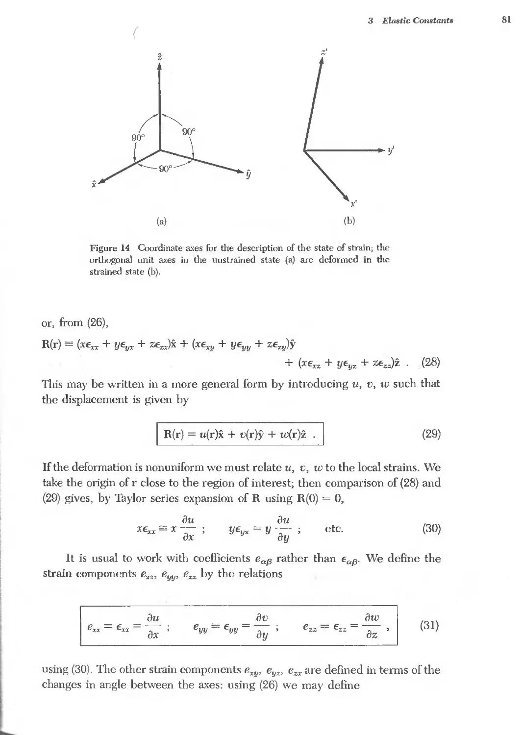
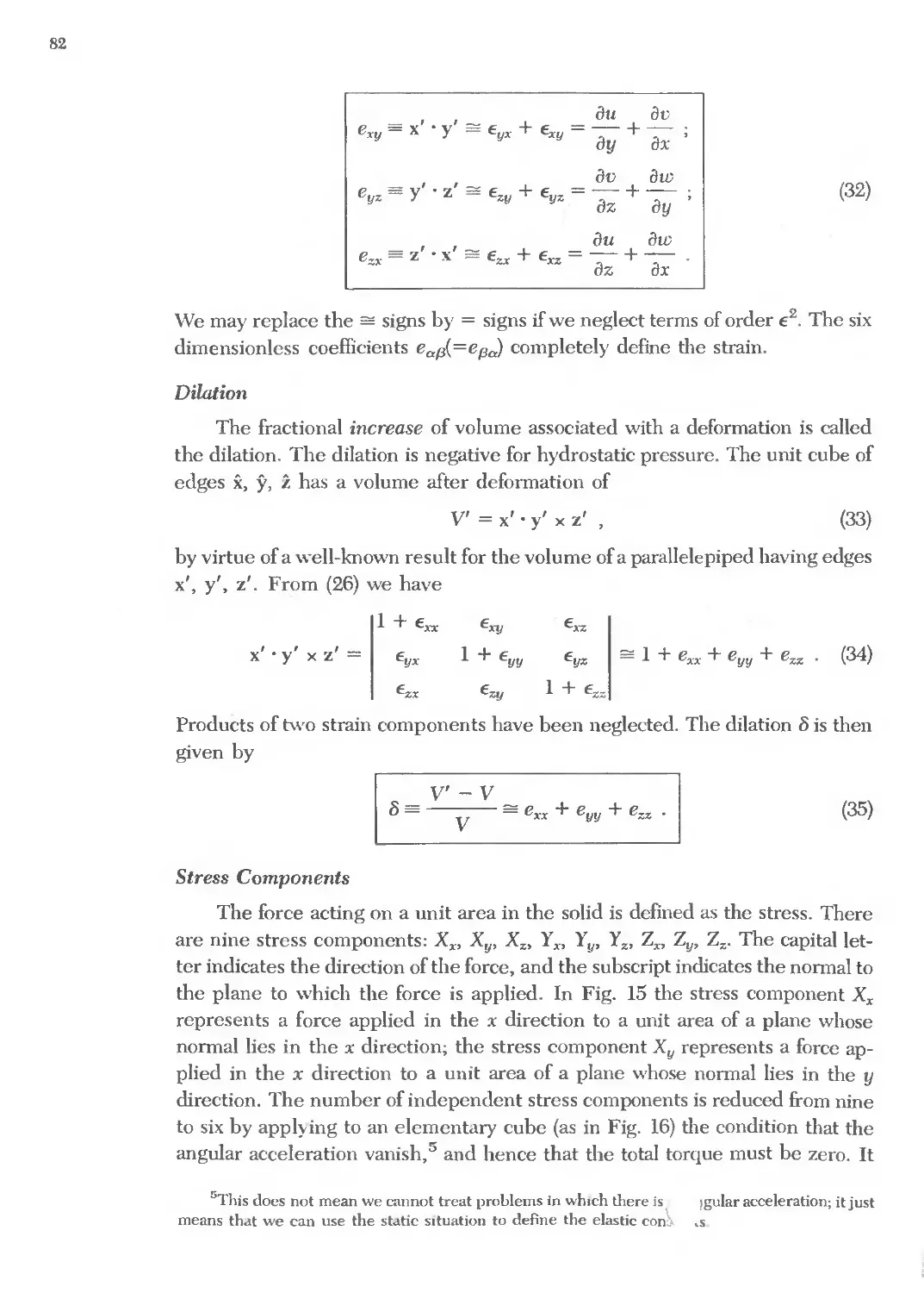
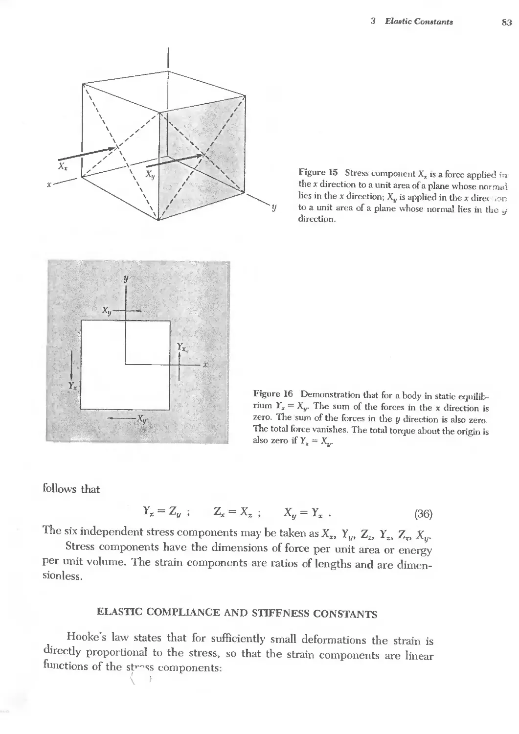
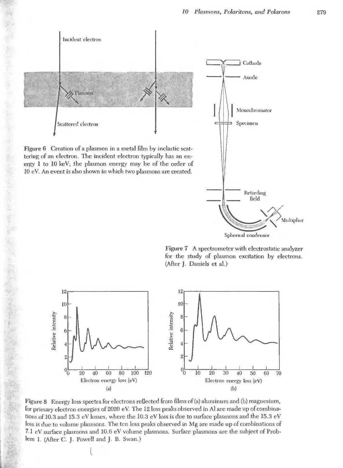
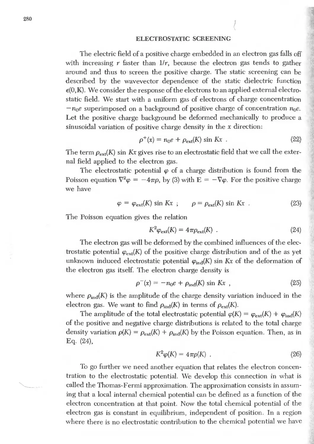
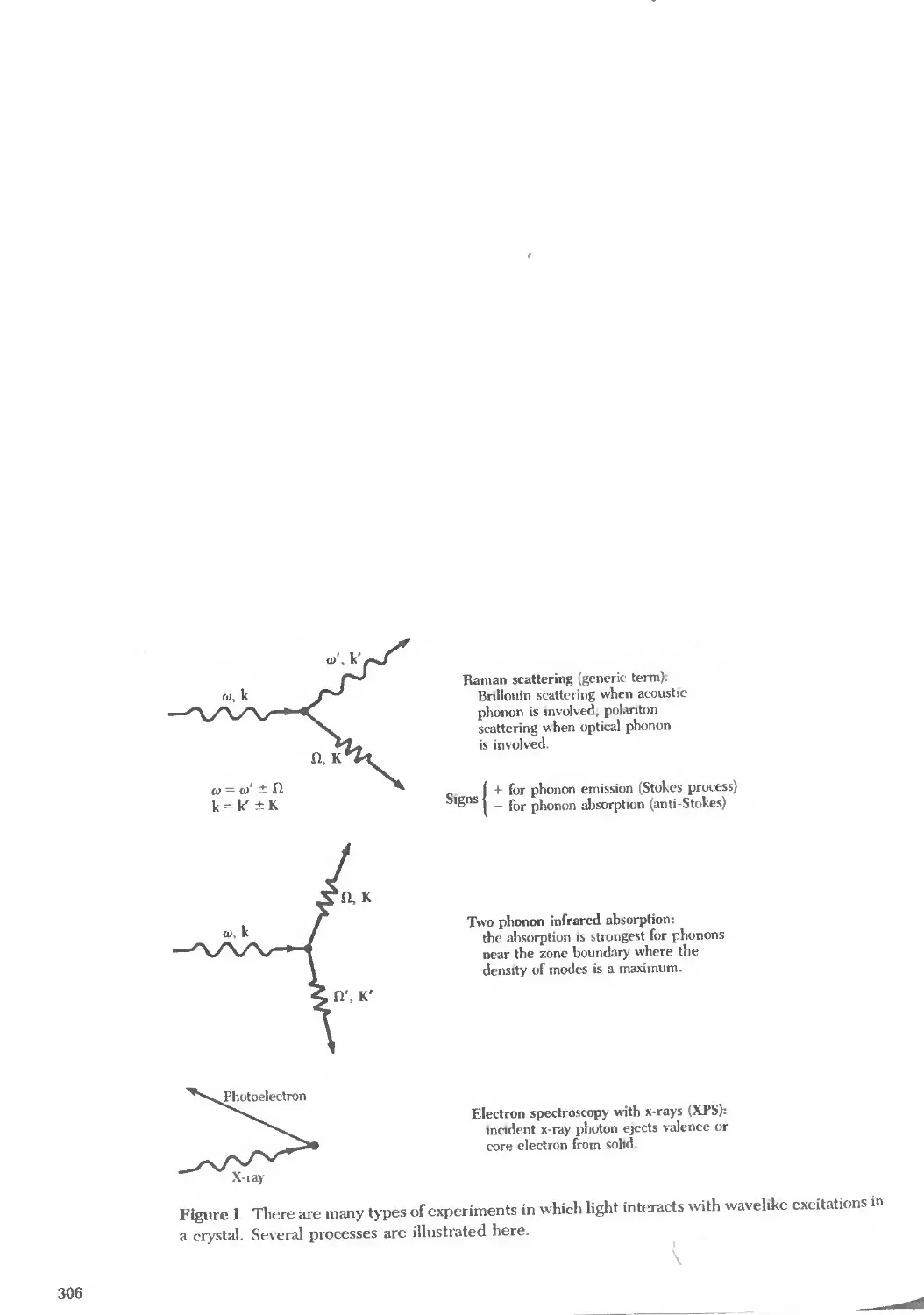
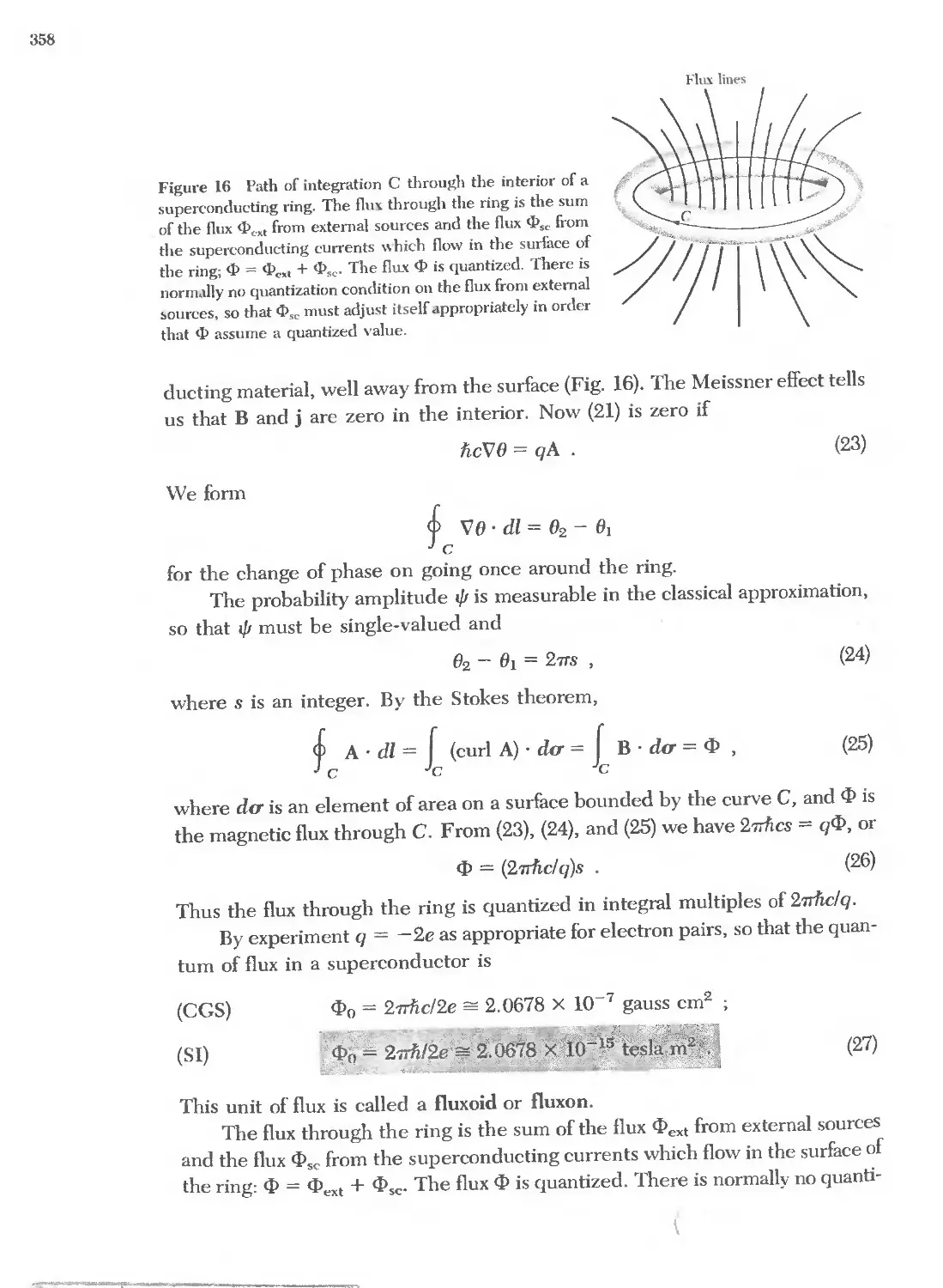
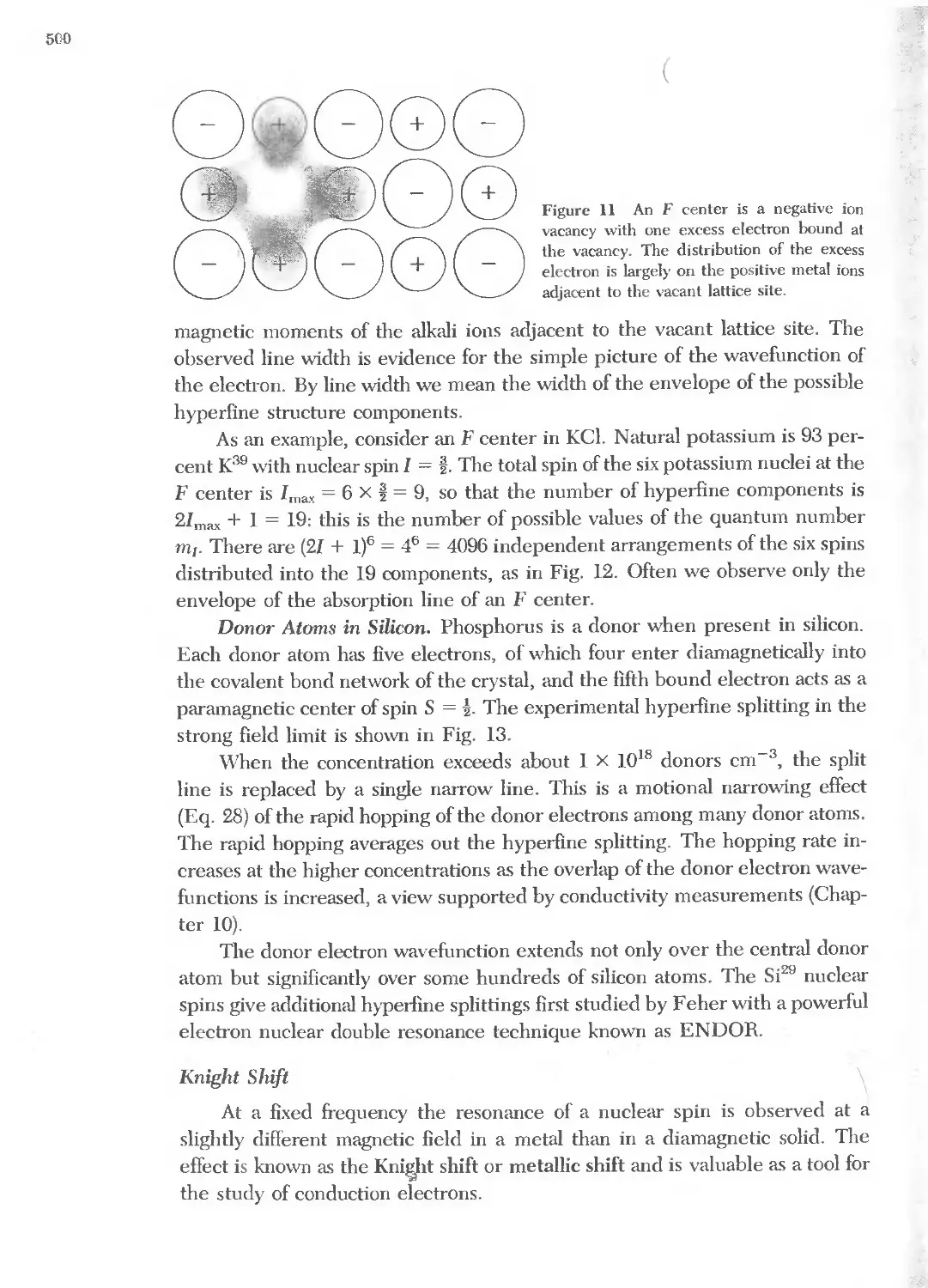
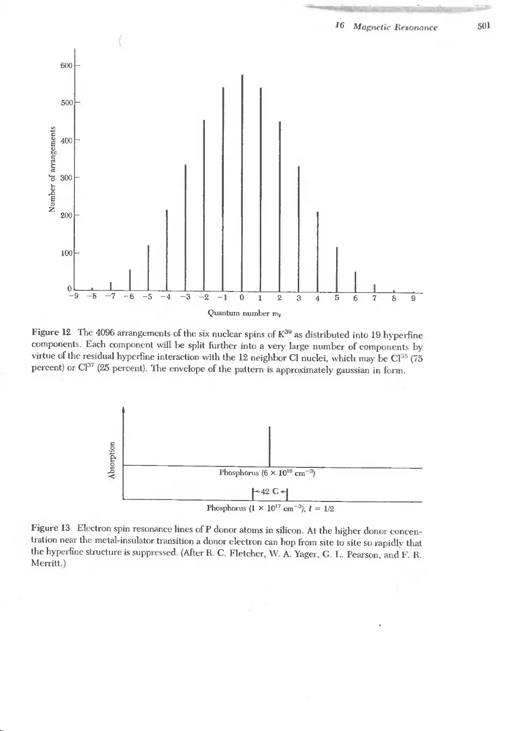
/
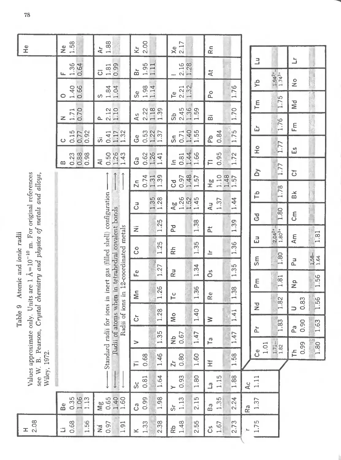

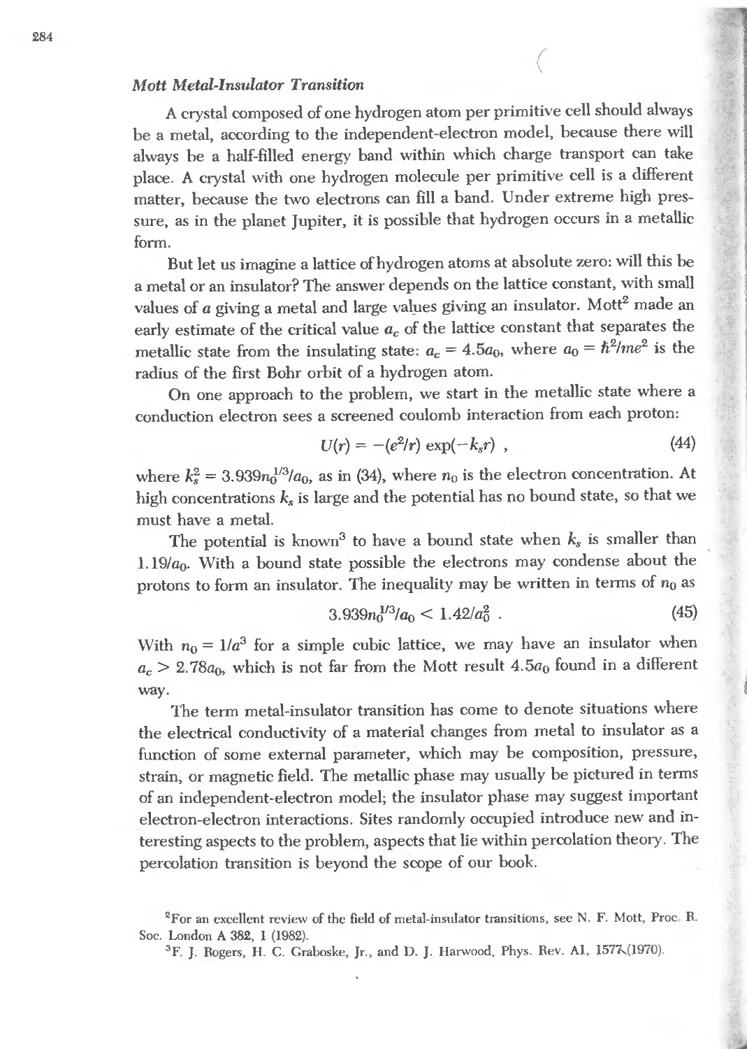
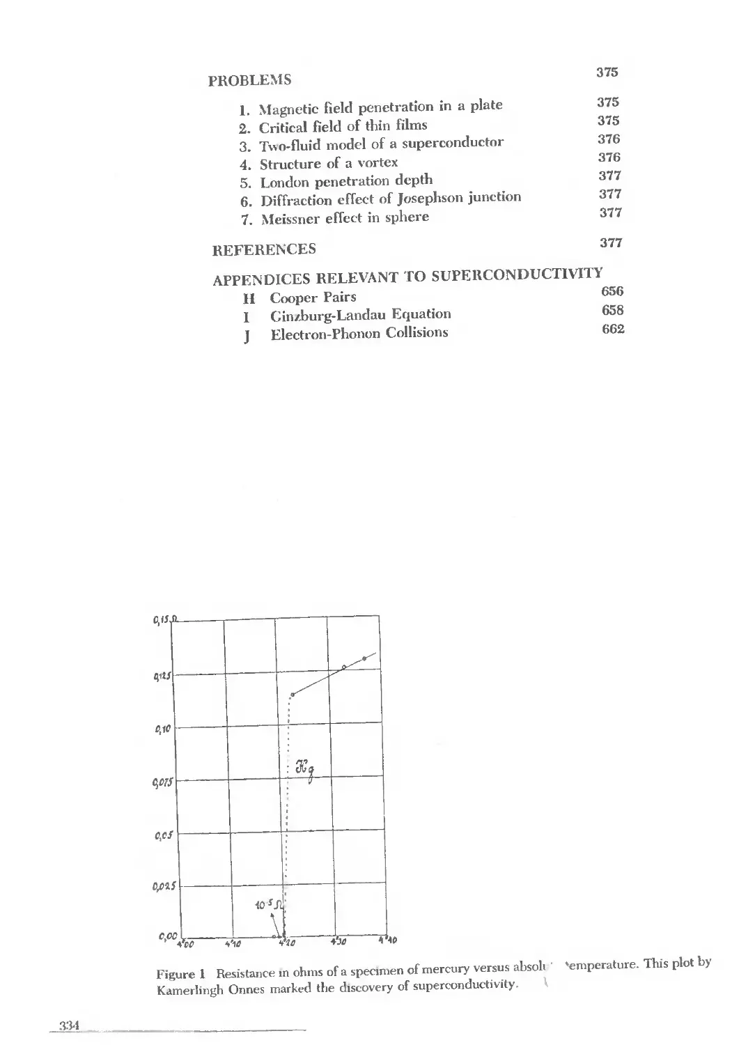
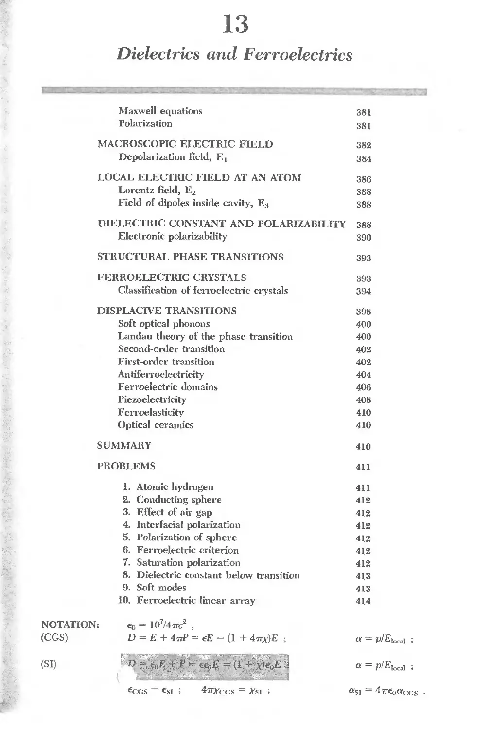
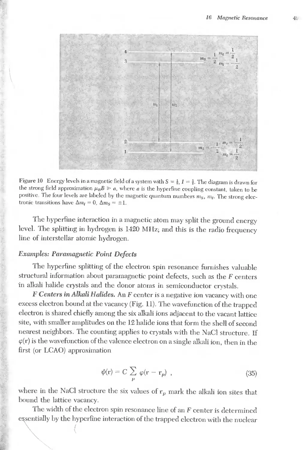
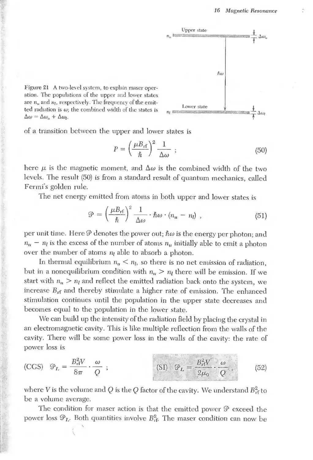

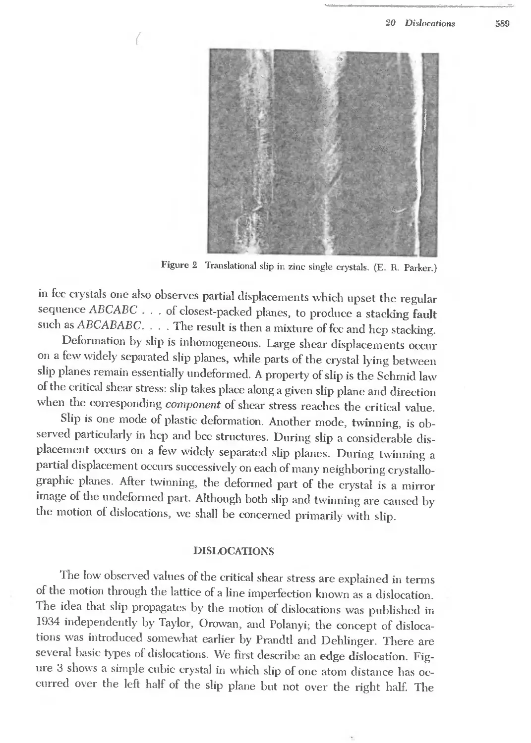


Text
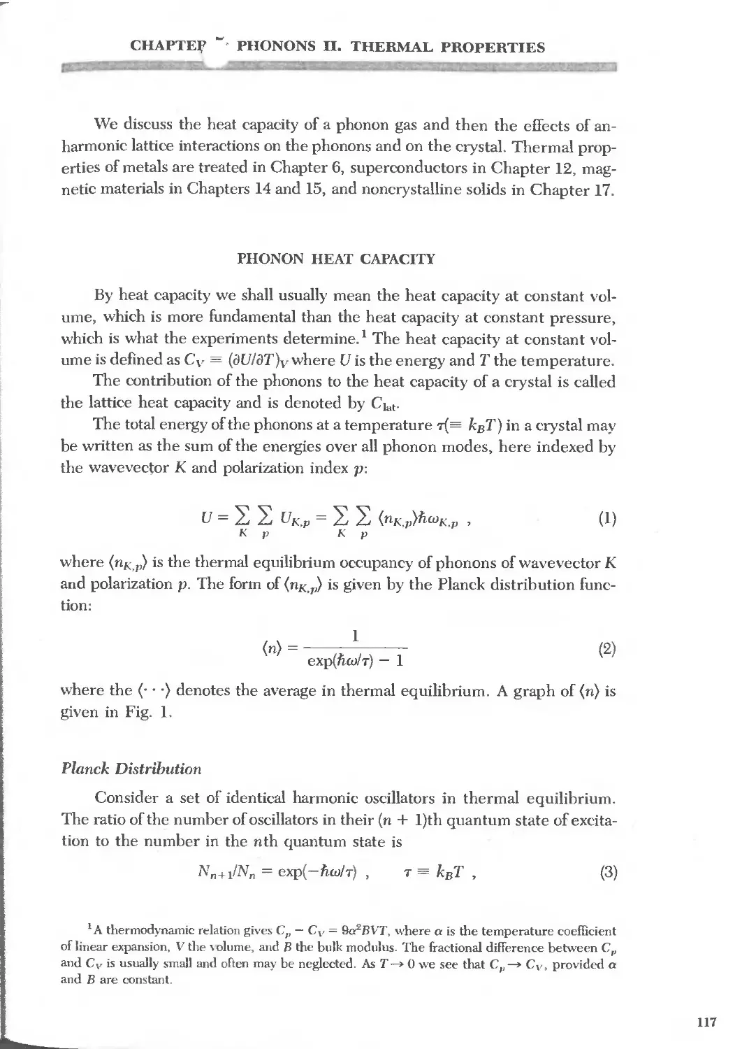
j
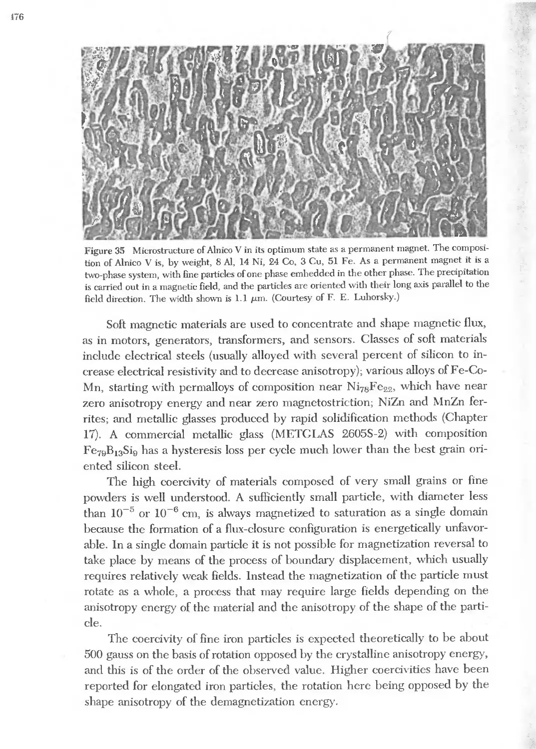
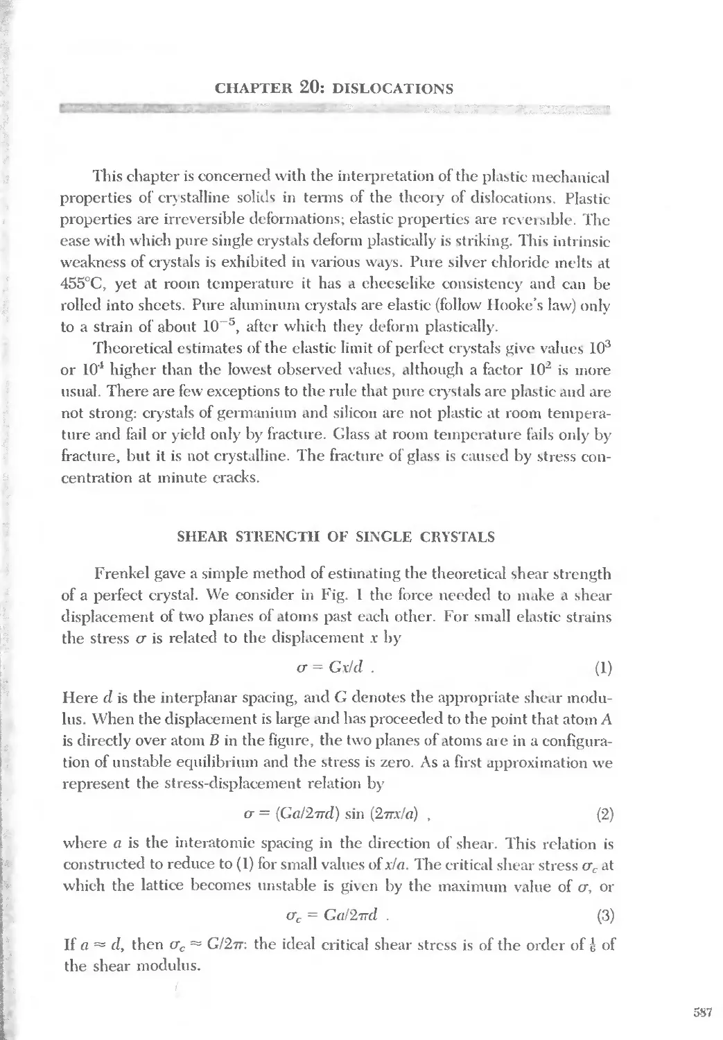
J2JN _)
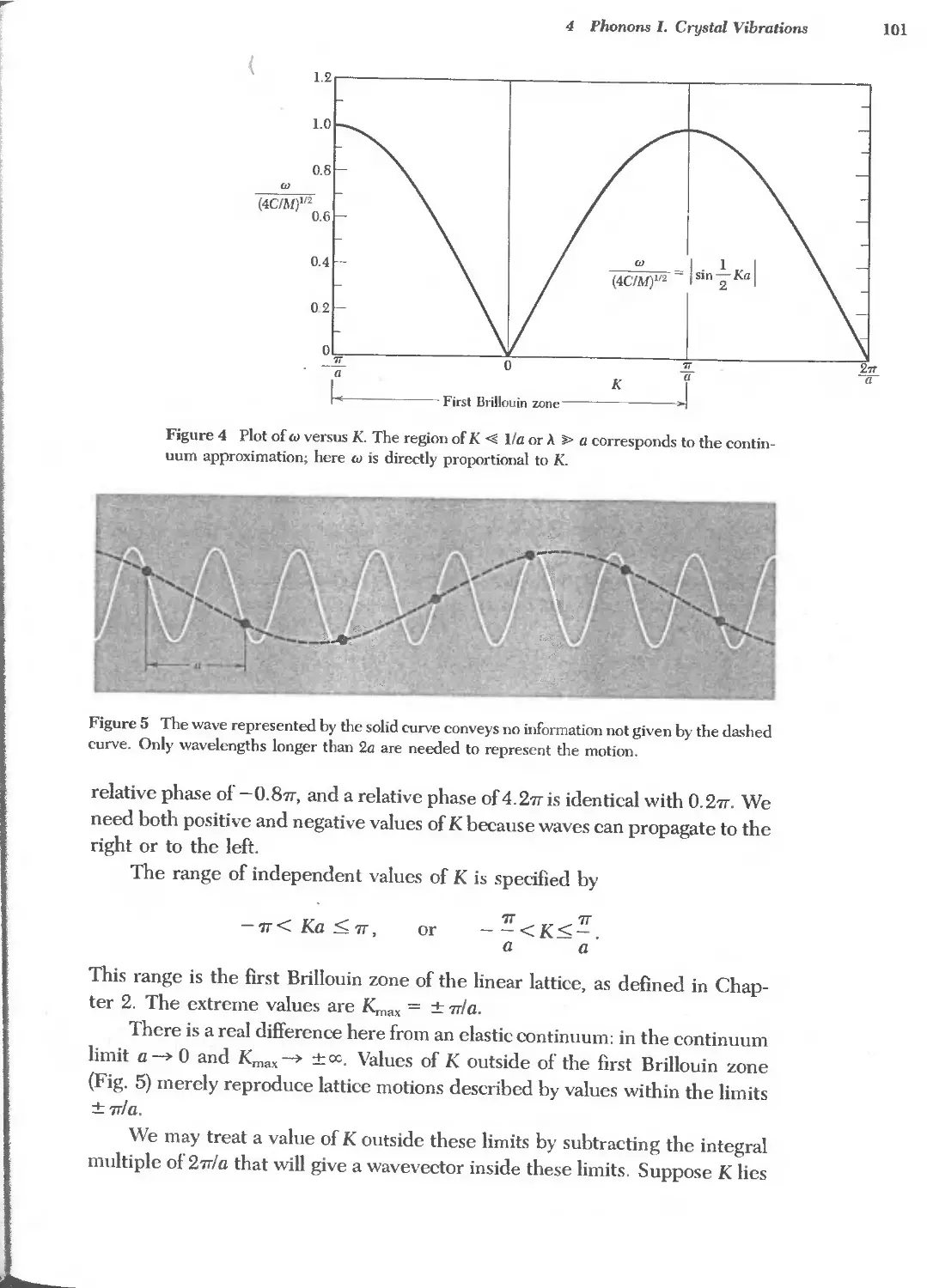
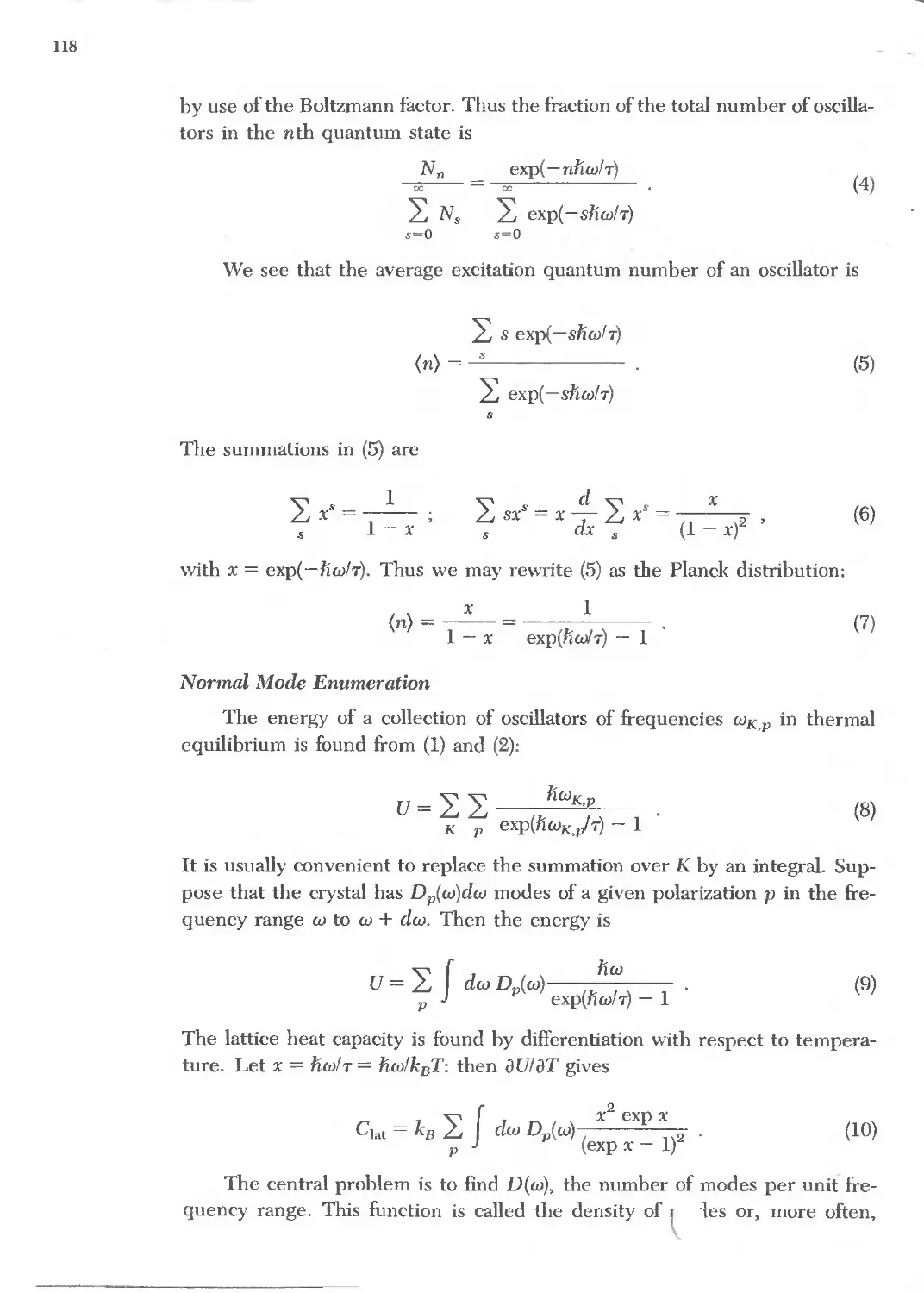
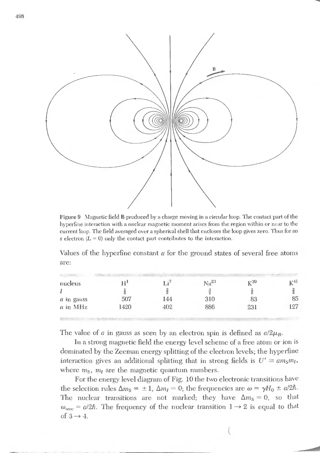
i')07Ji1) O'i" r.Jl1lJ'OiJ'l1n
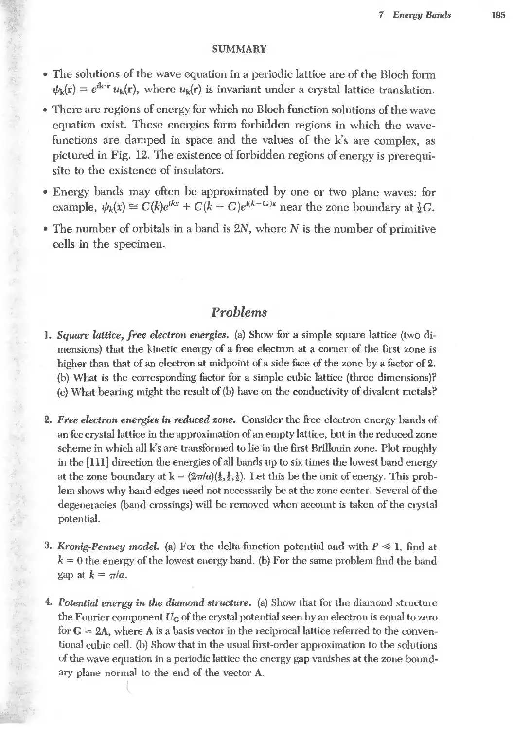
O''v7b; i')'1!J'"
i7
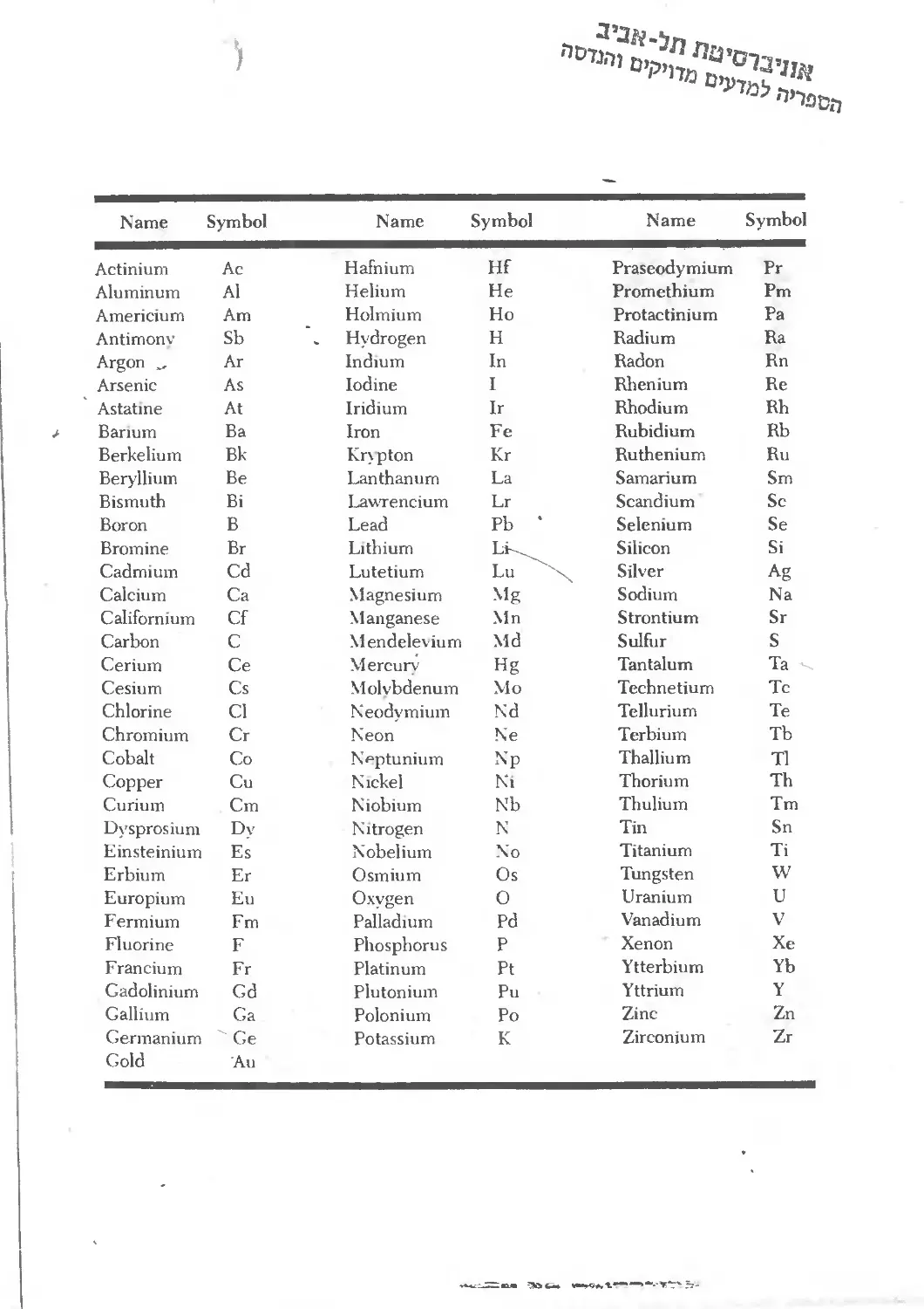
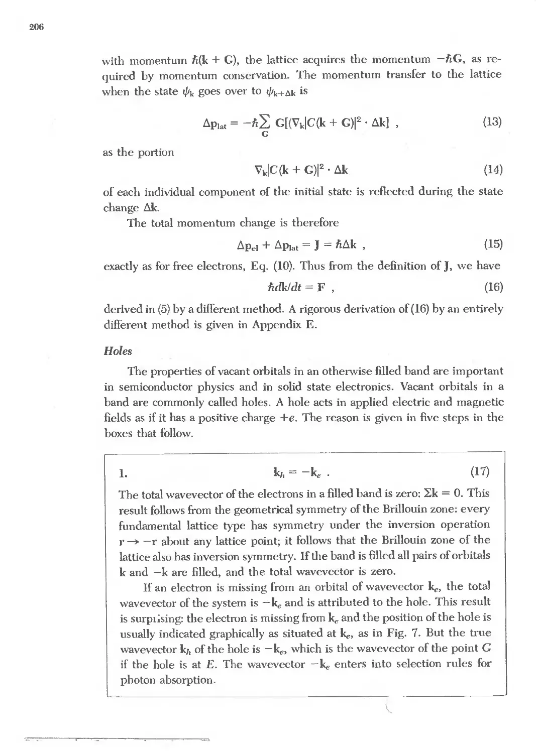
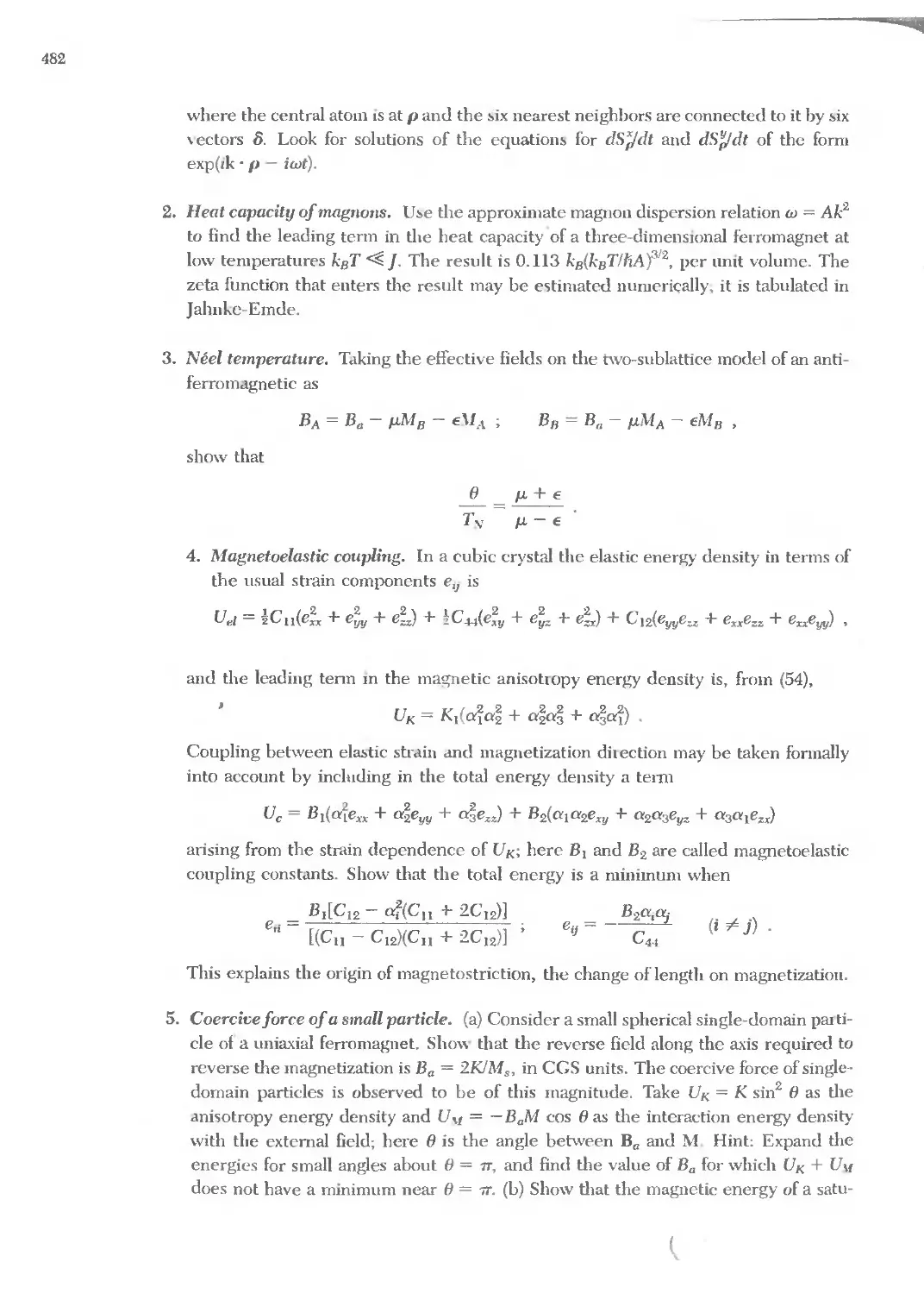
Name Symbol Name Symbol Name Symbol
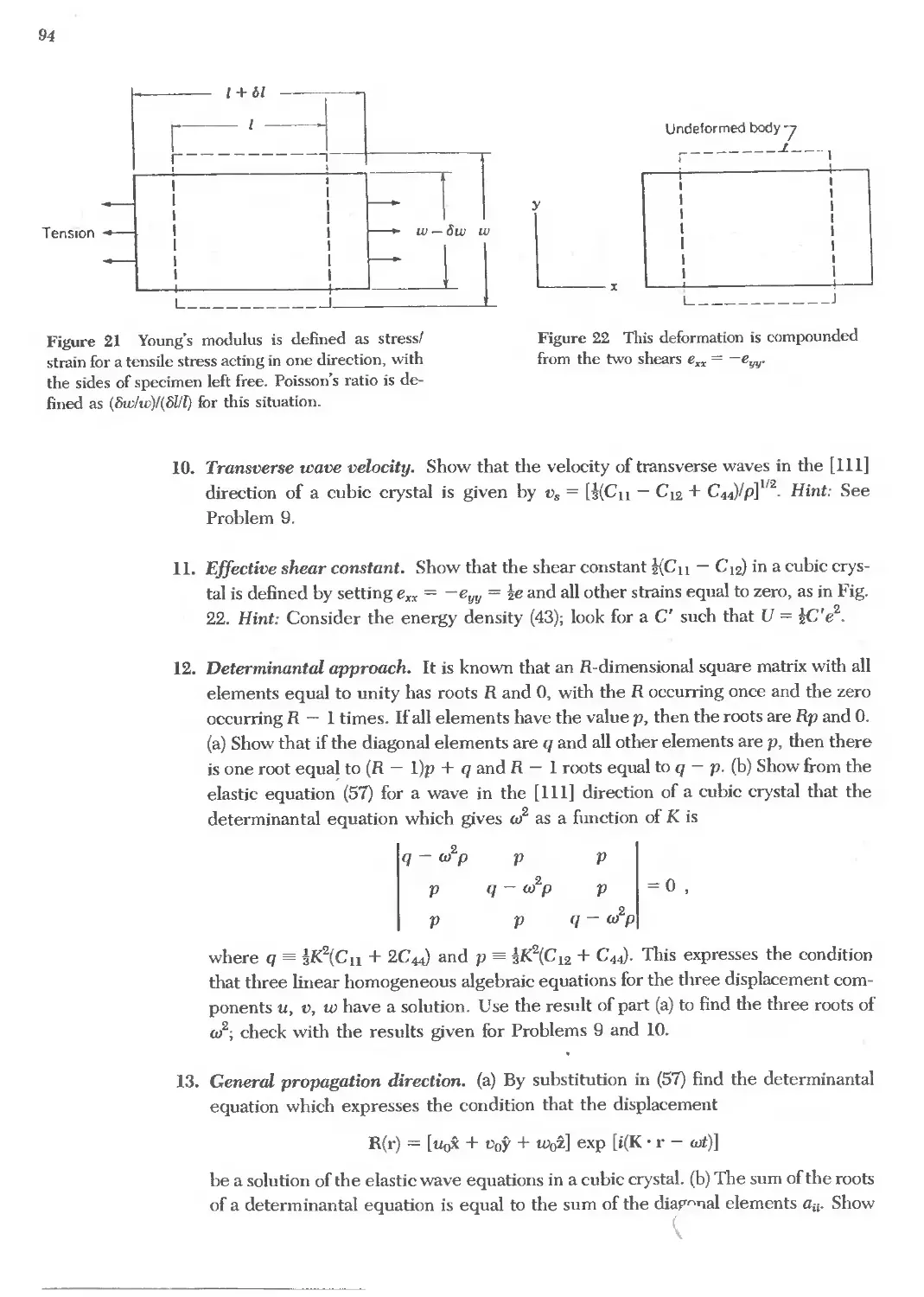
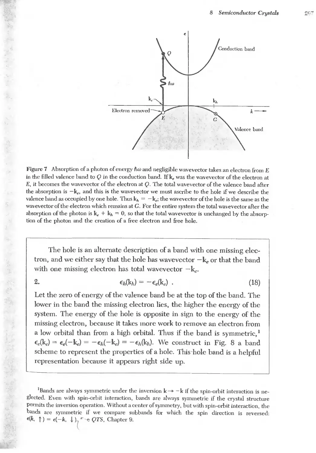
Actinium Ac Hafnium Hf Praseodymium Pr
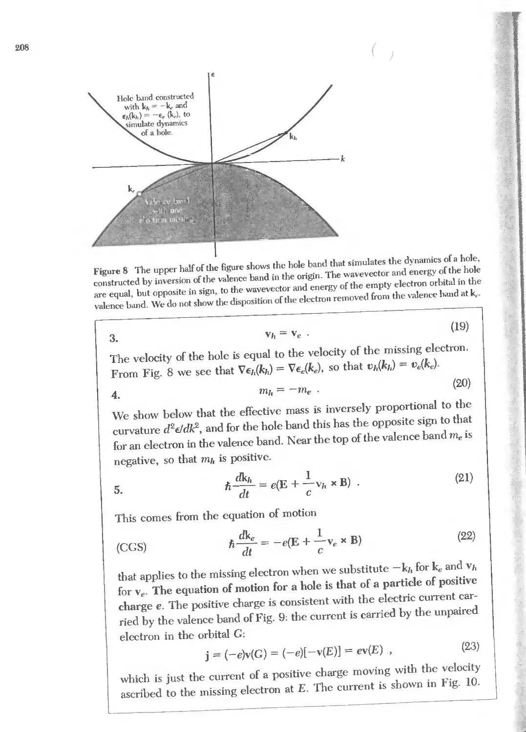
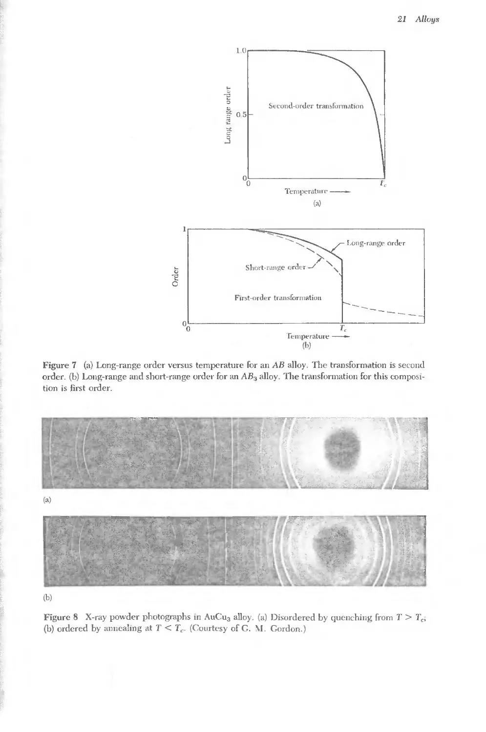
Aluminum Al Helium He Promethium Pm
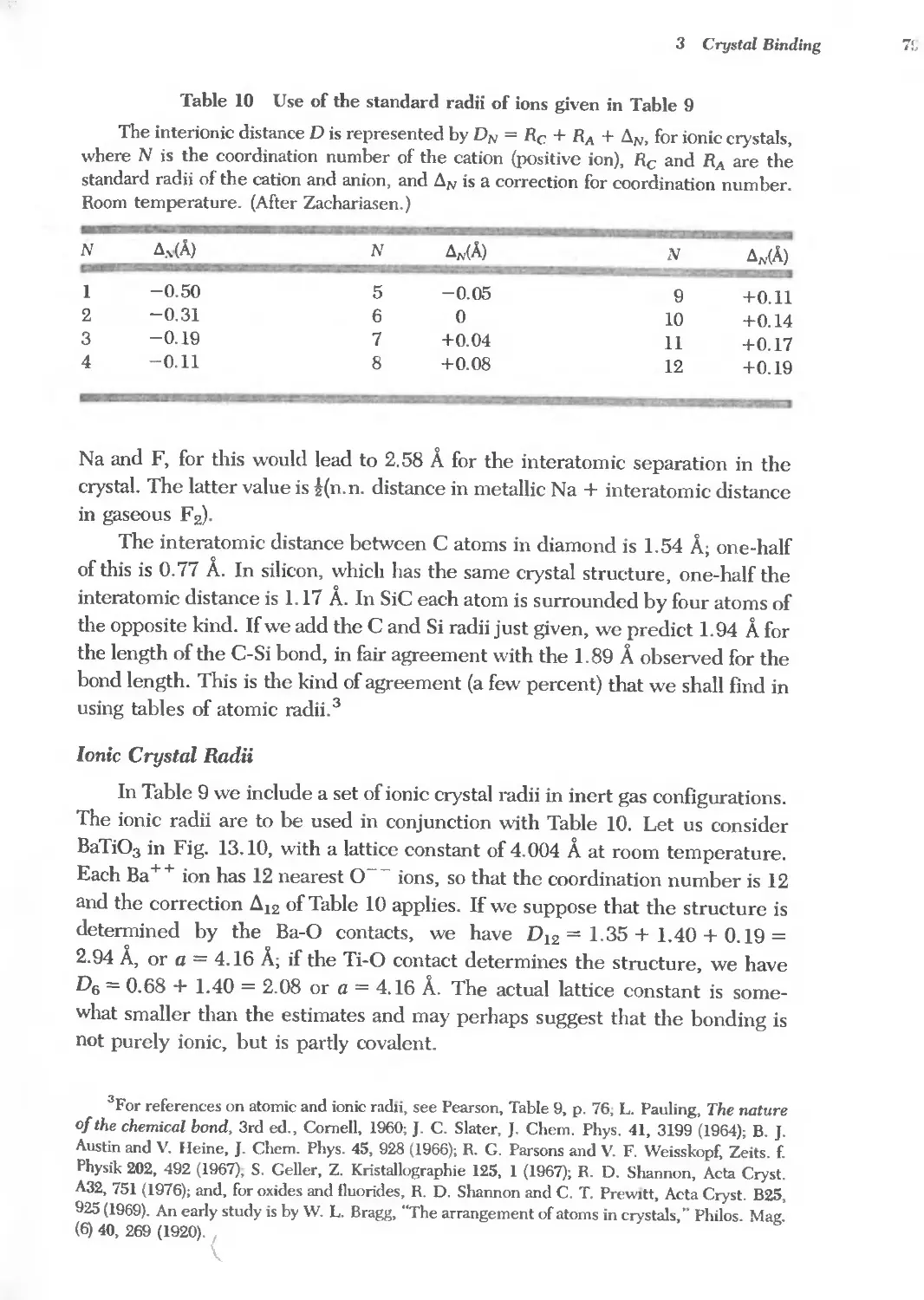
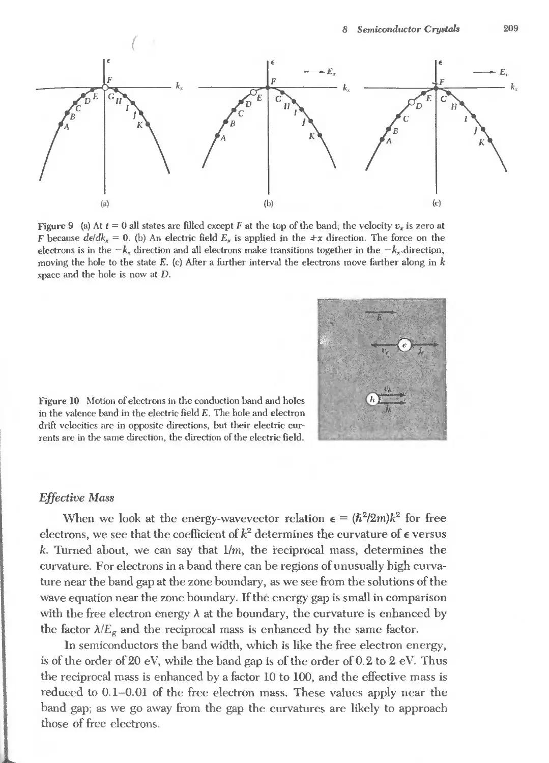
Americium Am Holmium Ho Protactinium Pa
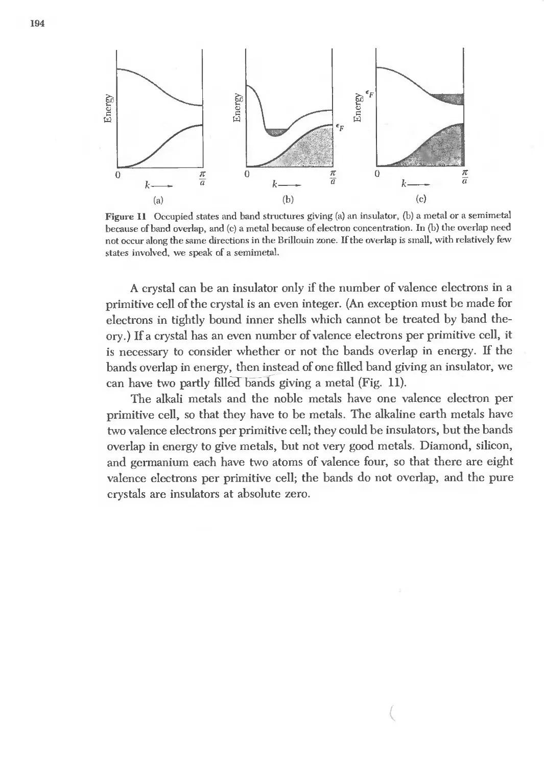
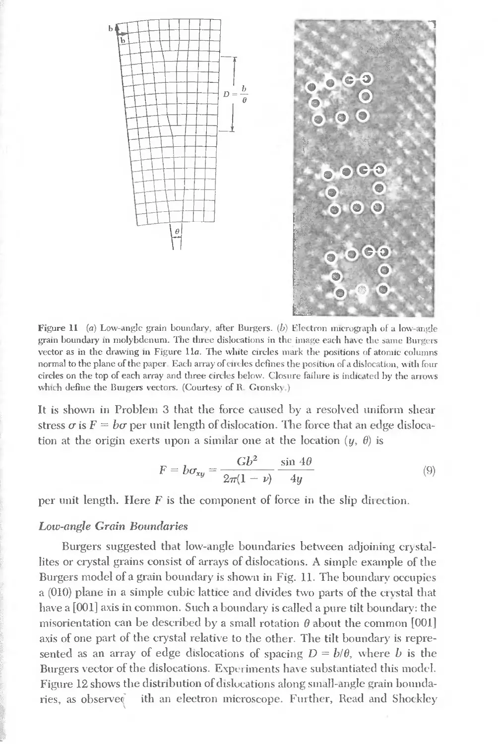
Antimonv Sb Hydrogen H Radium Ra
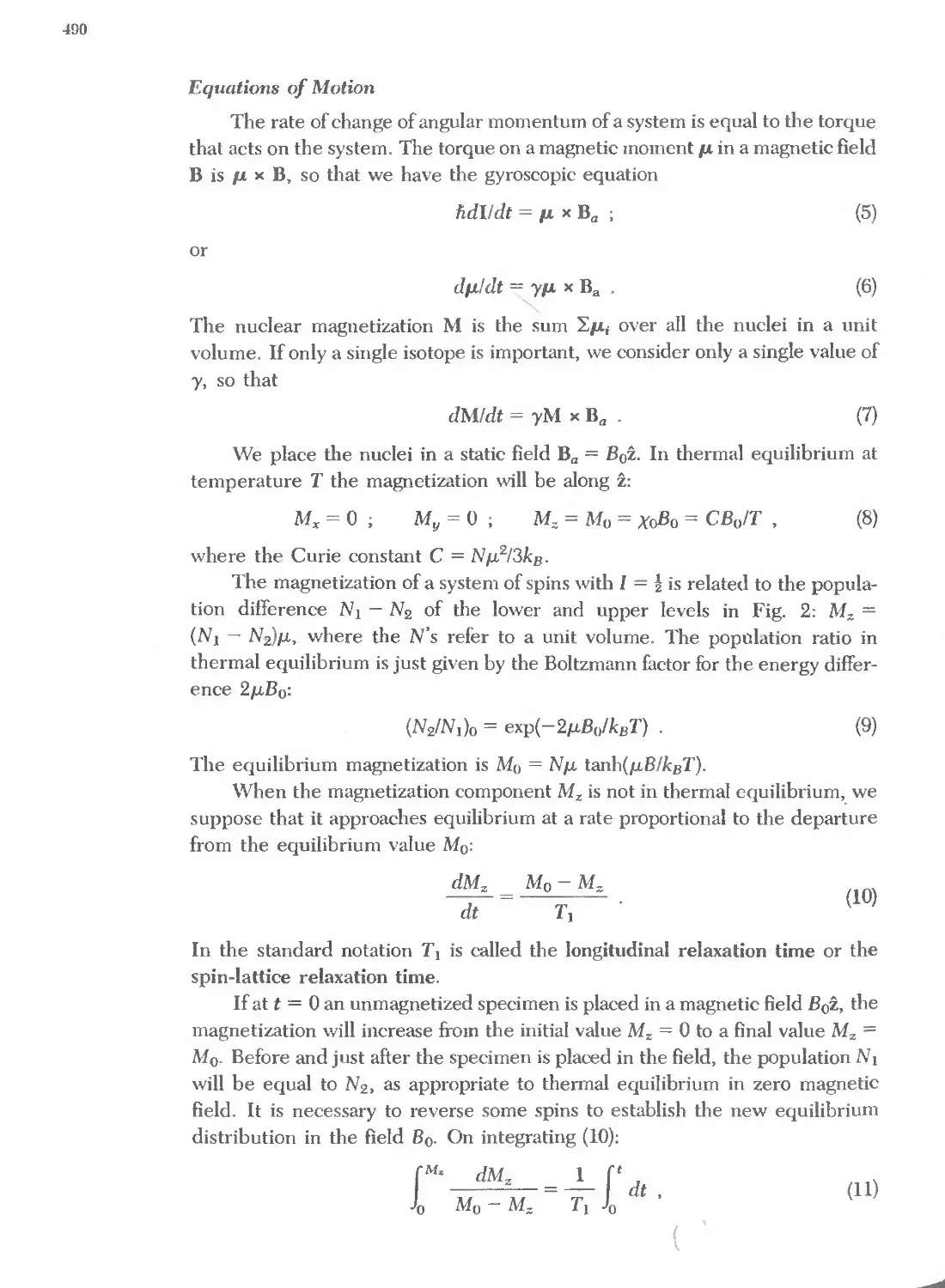
Argon Ar IndIUm In Radon Rn
Arsenic As Iodine I Rhenium Re
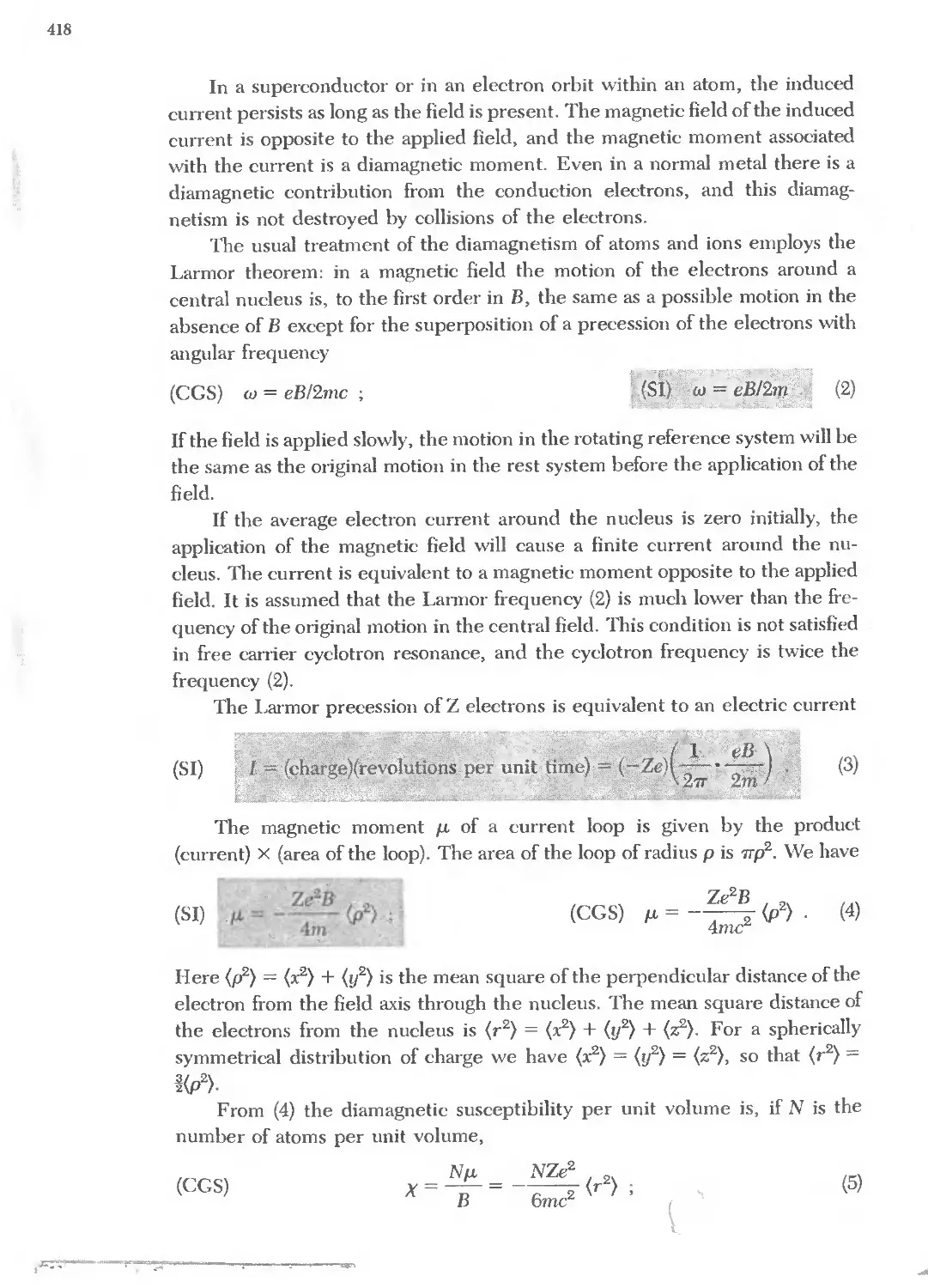
Astatme At Iridium Ir Rhodium Rh
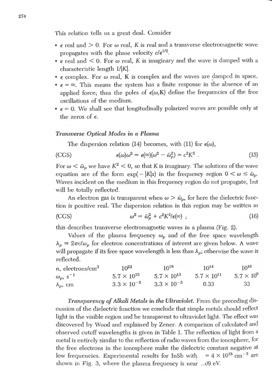
.; Banum Ba Iron Fe Rubidium Rb
Berkelium Bk Kr pton Kr Ruthenium Ru
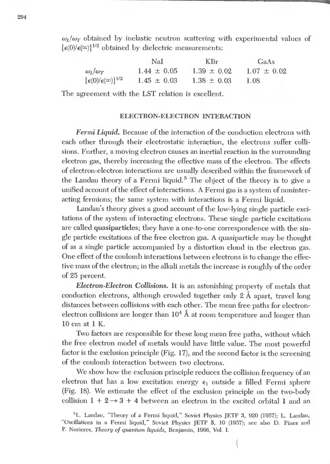
Beryllium Be Lanthanum La Samarium Sm
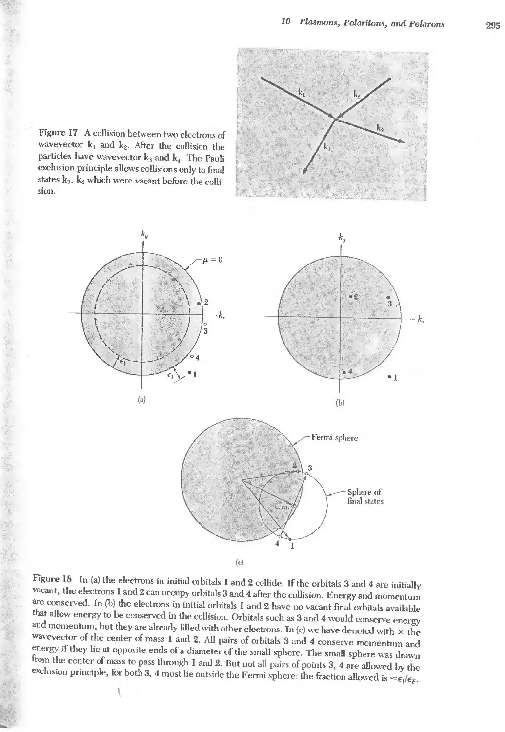
Bismuth Bi Lawrencium Lr Scandium Sc
Boron B Lead Pb Selenium Se
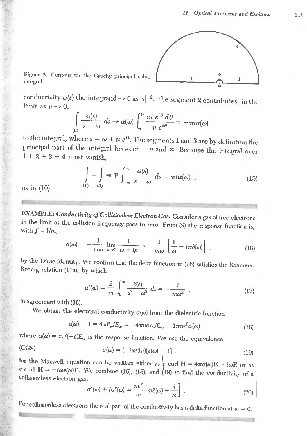
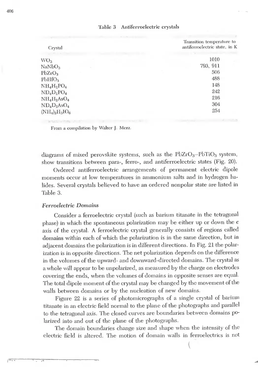
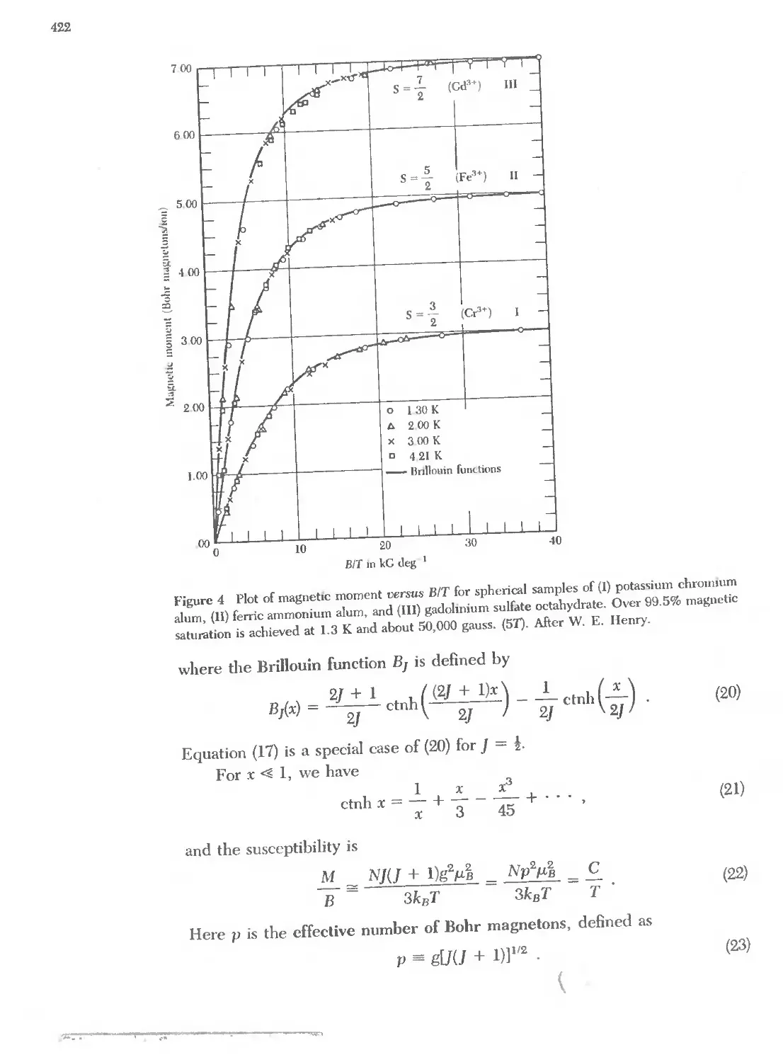
Bromine Br LIthium L" Silicon Si
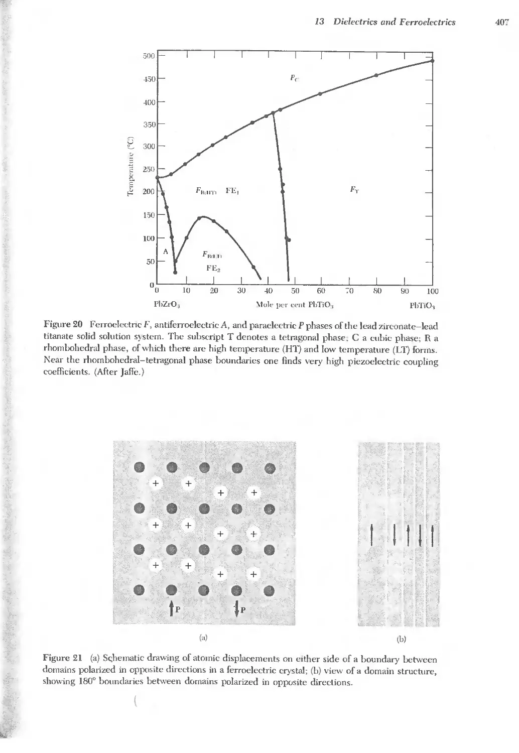
Cadmium Cd Lutetium L Silver Ag
Calcium Ca lagnesium lg Sodium Na
Californium Cf langanese ln Strontium Sr
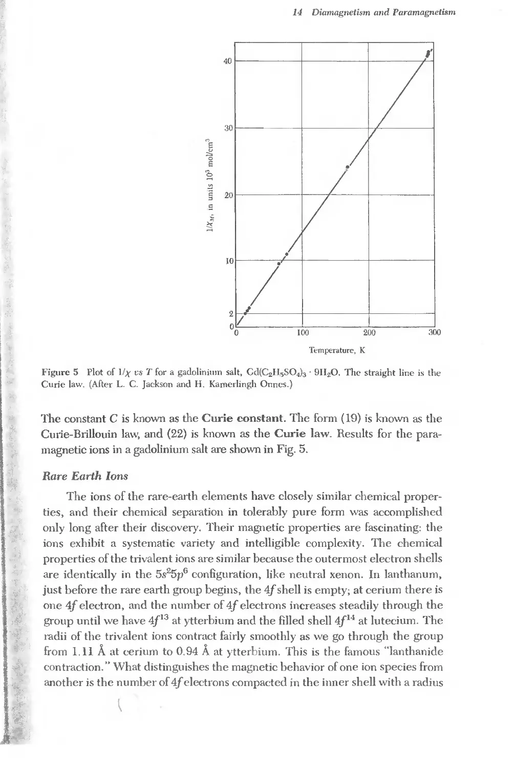
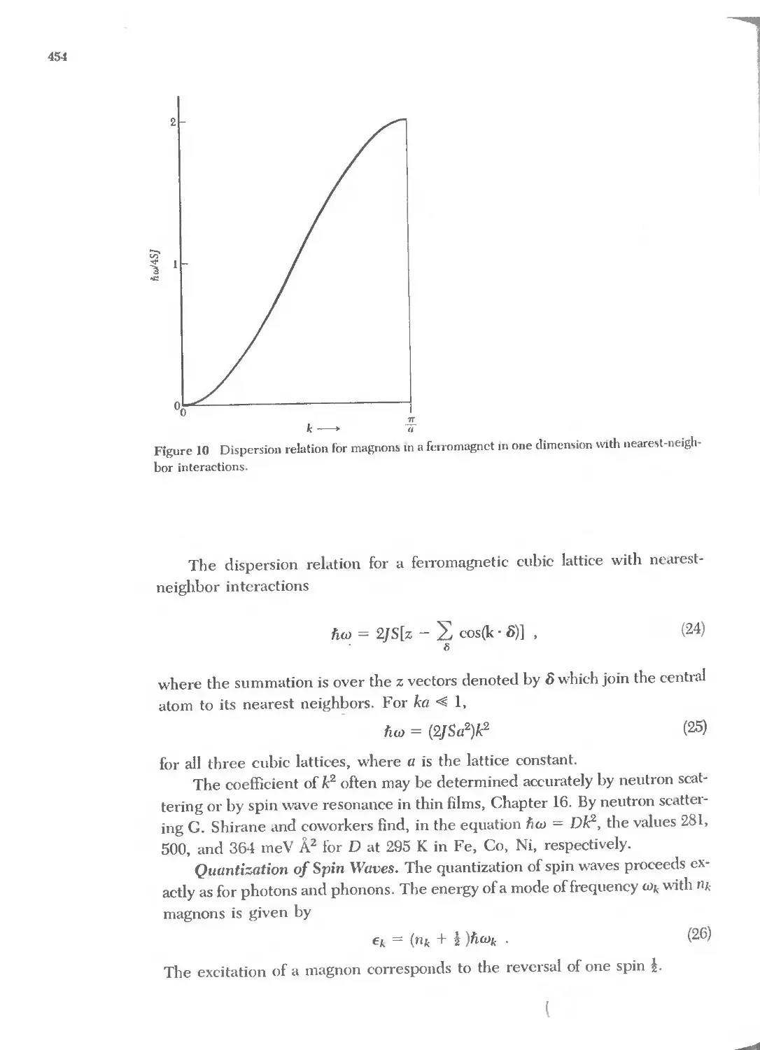
Carbon C lendele"ium ld Sulfur S
Cerium Ce Iercur Hg Tantalum Ta "-
Cesium Cs \lolvbdenum \10 Technetium Tc
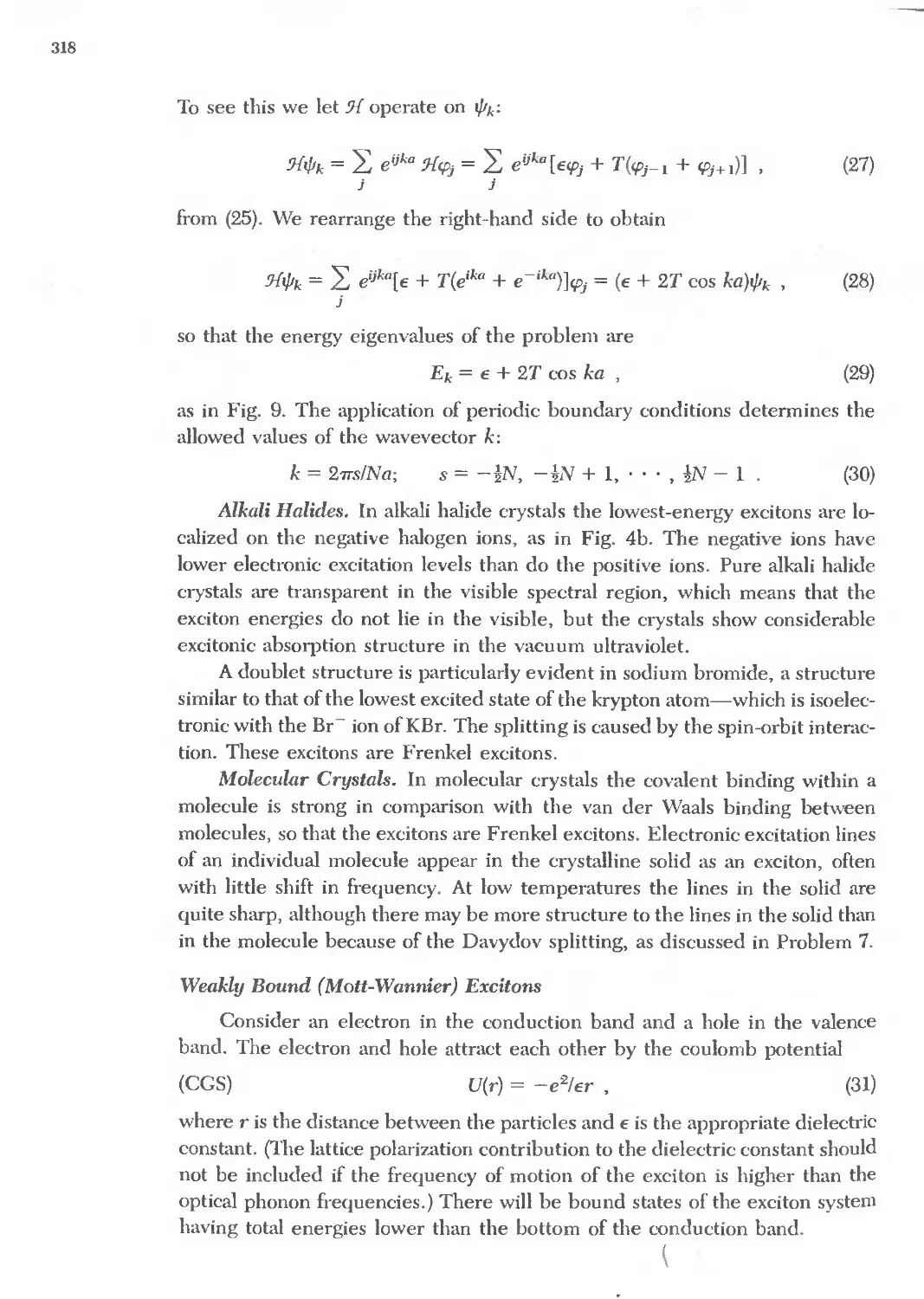
Chlorine Cl !'\eodymium !'\d Tellurium Te
Chromium Cr !'\eon !\e Terbium Tb
Cobalt Co !,\pptunium :\p Thallium Tl
Copper Cu 1'\lckel !'\I Thorium Th
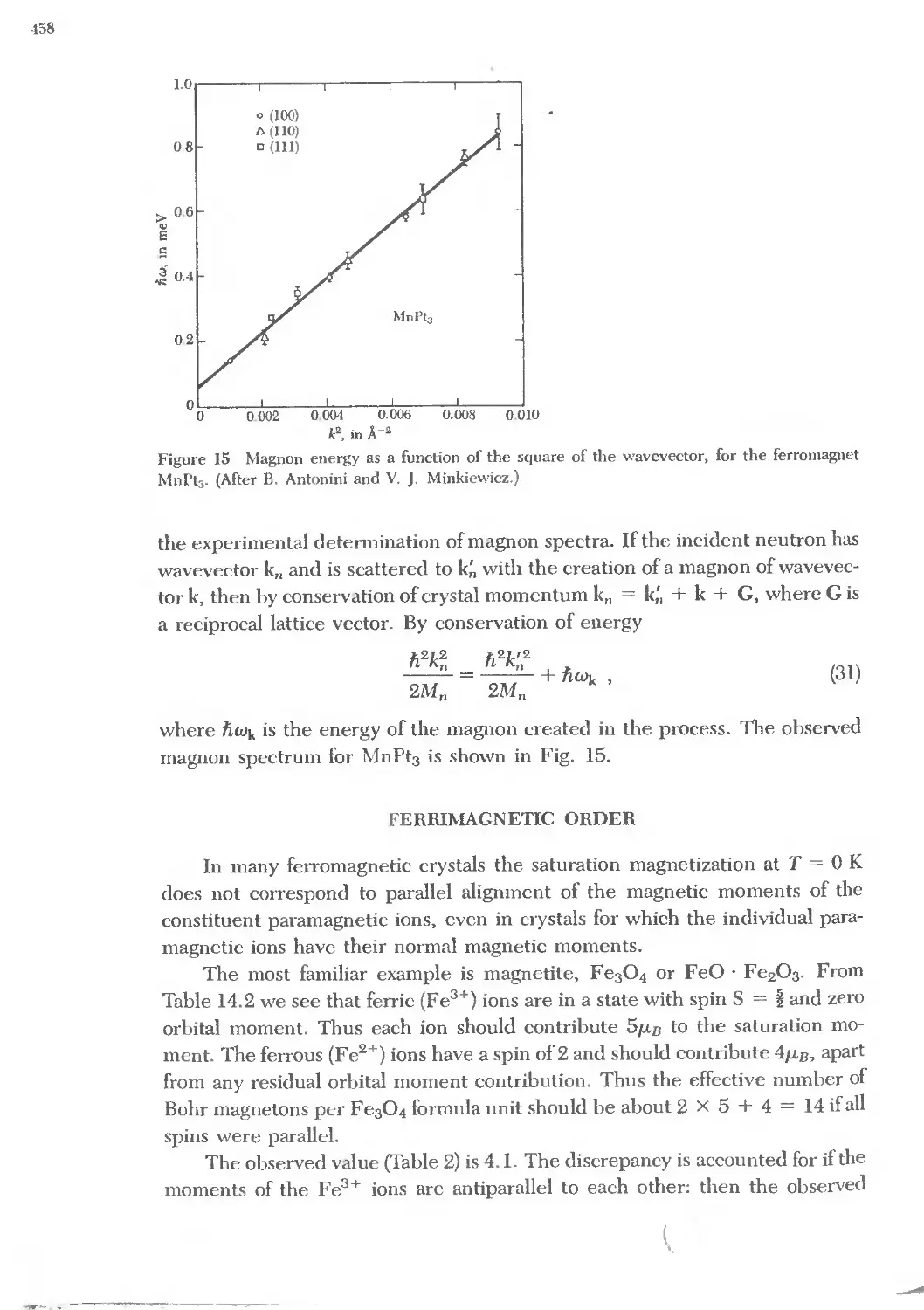
Curium Cm !\iobium !\'b Thulium Tm
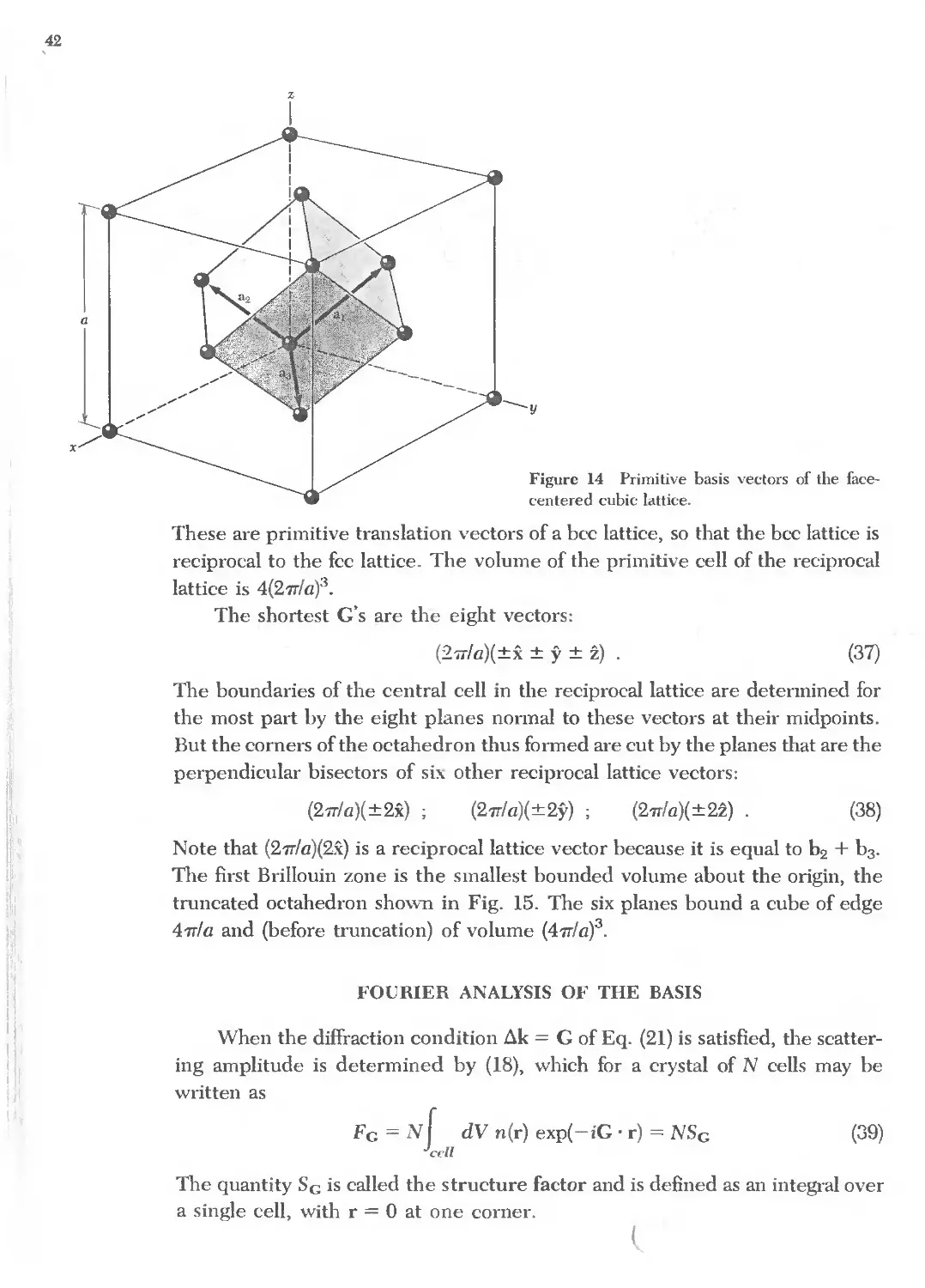
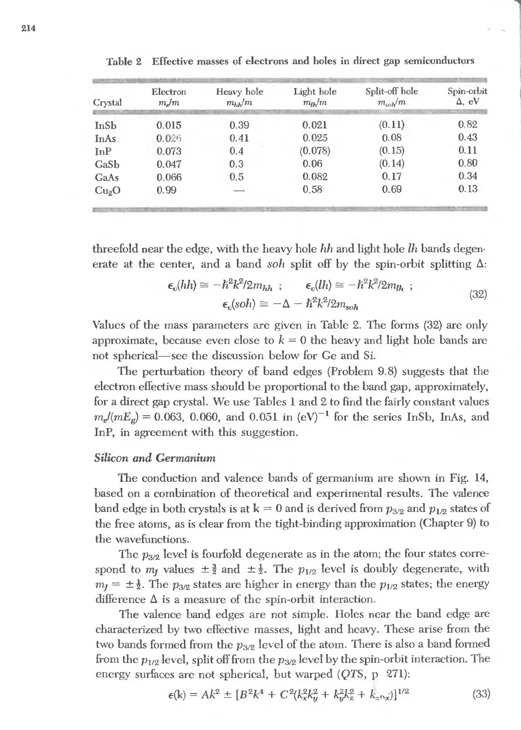
Dysprosium Dy !'\Itrogen 1'\ Tin Sn
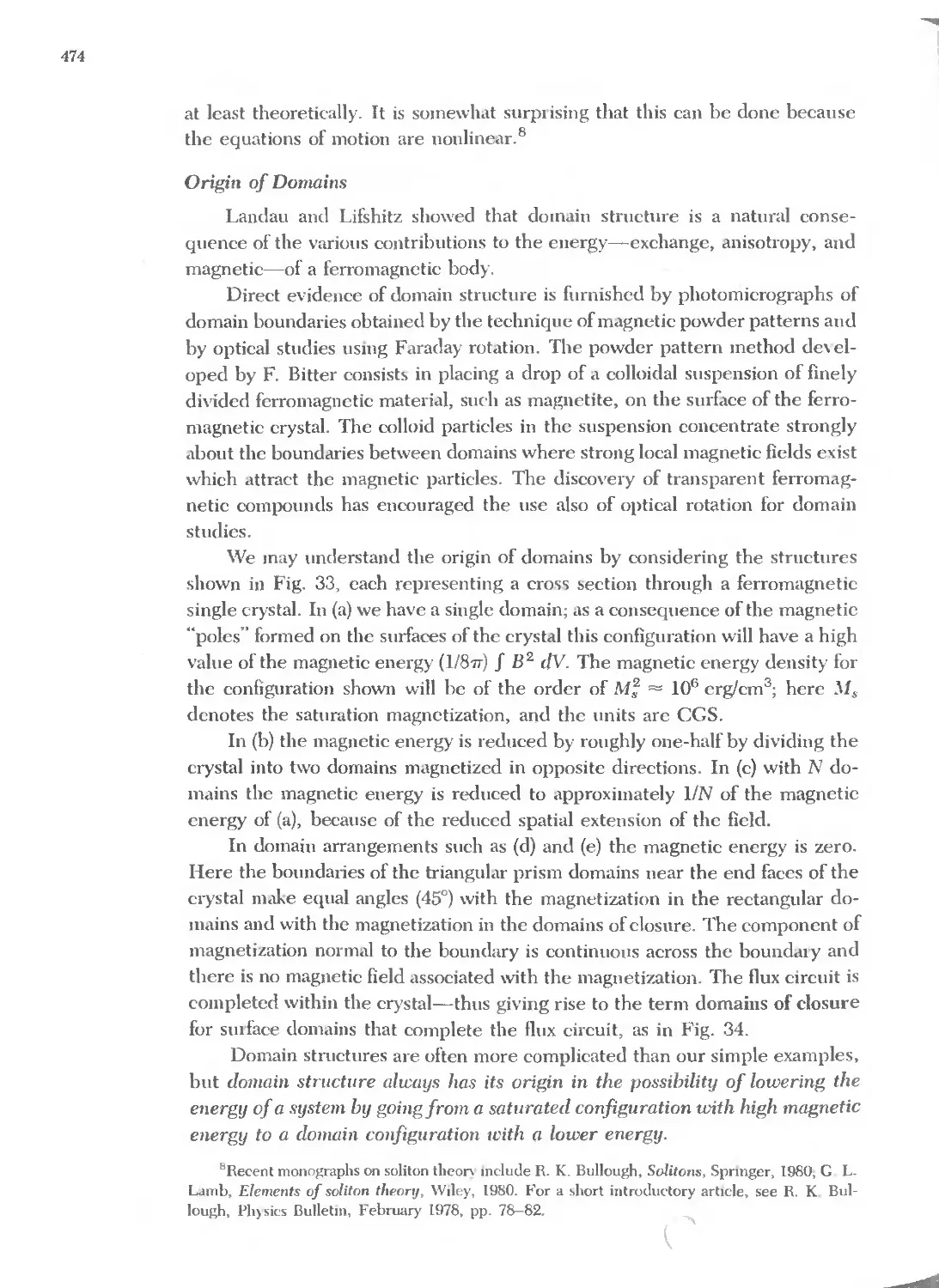
Einsteinium Es Xobelium \:0 Titanium Ti
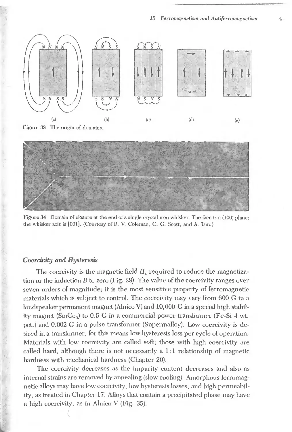
Erbium Er Osmium Os Tungsten W
Europium Eu Oxygen 0 Uranium U
Fermium Fm PalladIUm pd Vanadium V
Fluorine F Phosphorus P Xenon Xe
Francium Fr Platinum Pt Ytterbium Yb
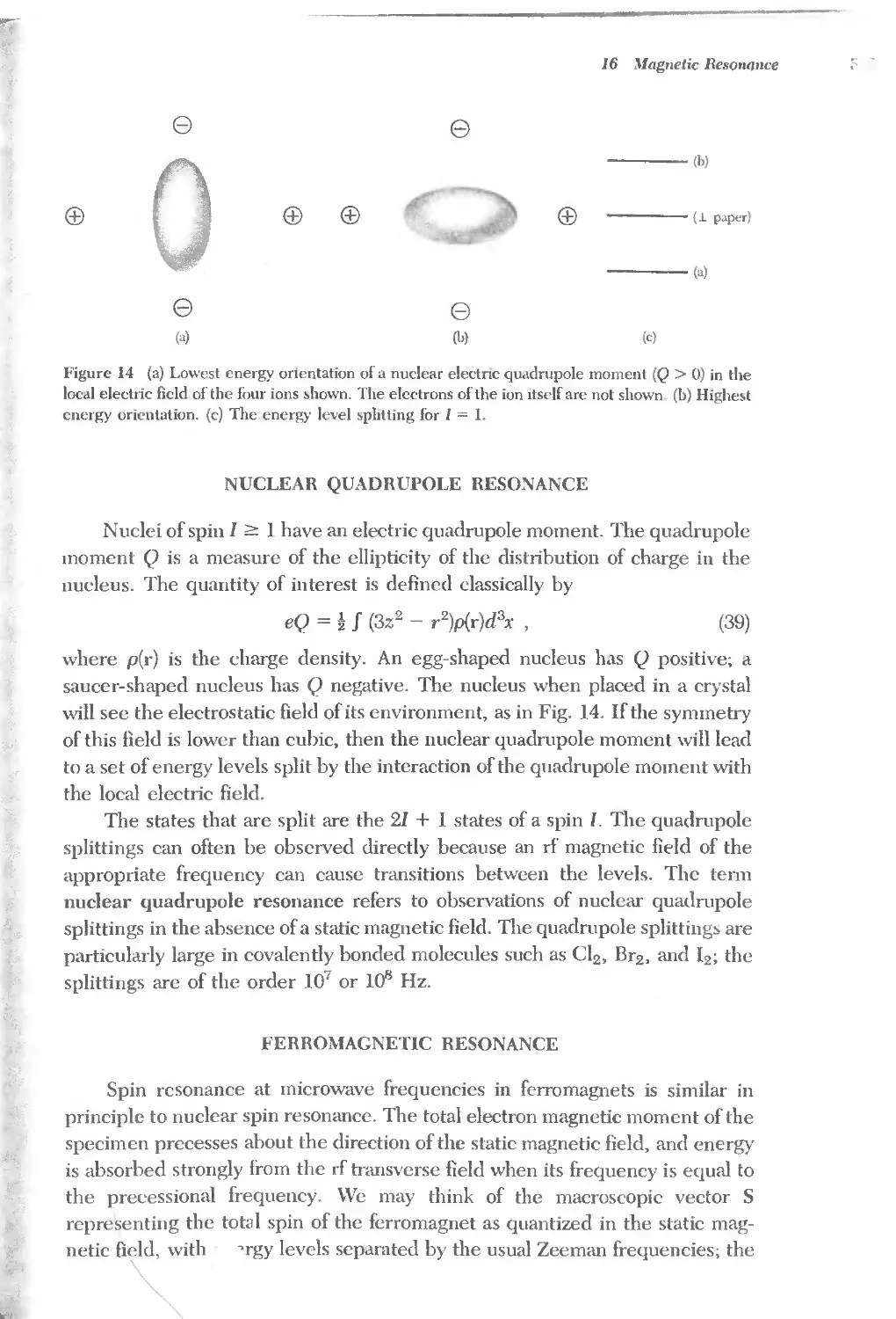
Gadolinium Gd Plutonium Pu Yttrium Y
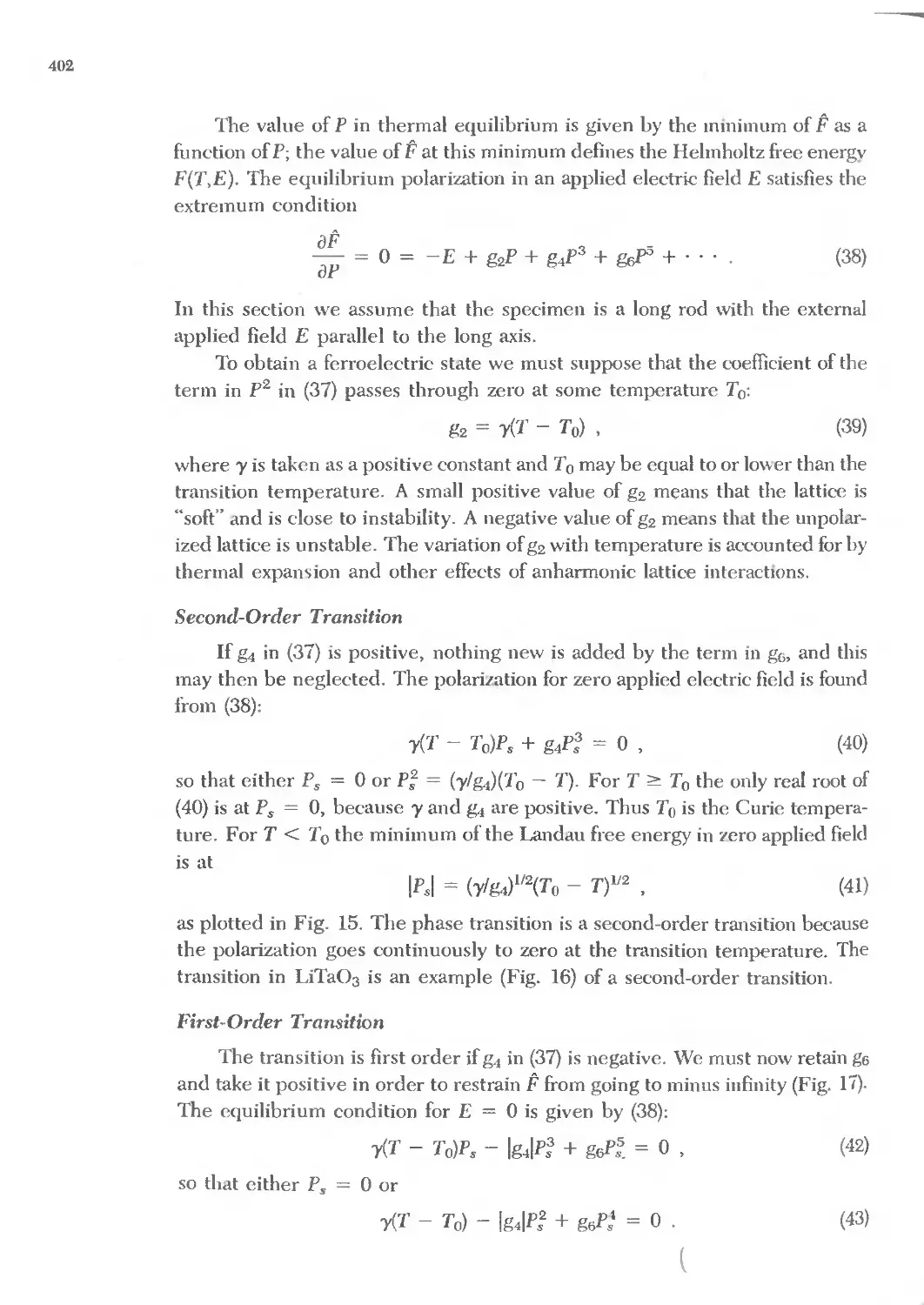
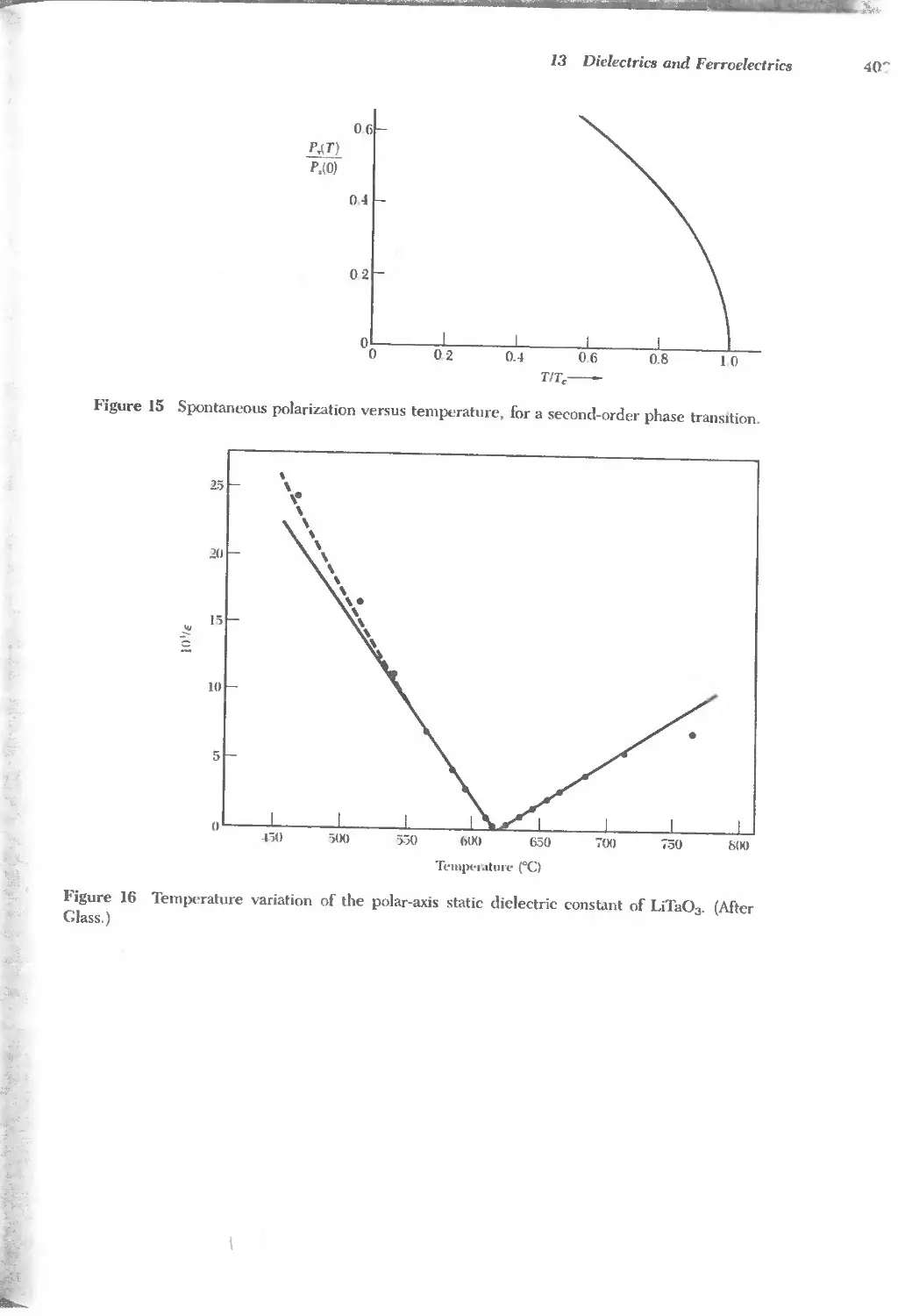
Gallium Ga Polonium Po Zinc Zn
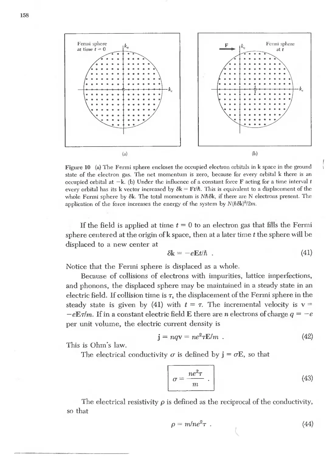
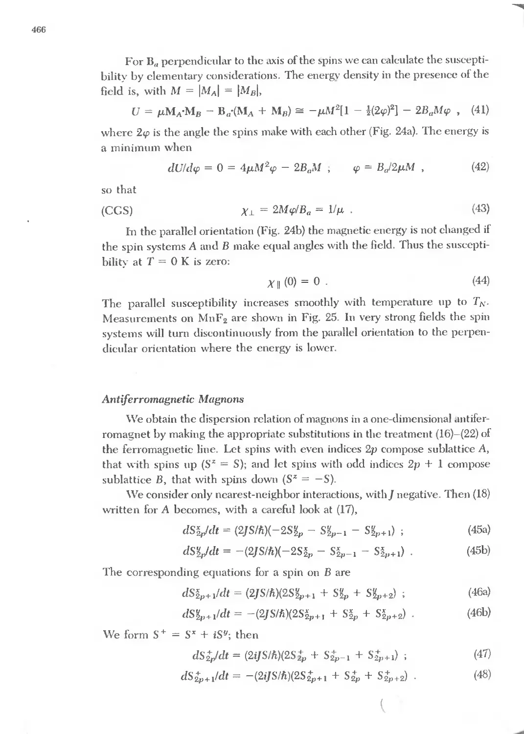
Germanium Ge Potassium K Zirconium Zr
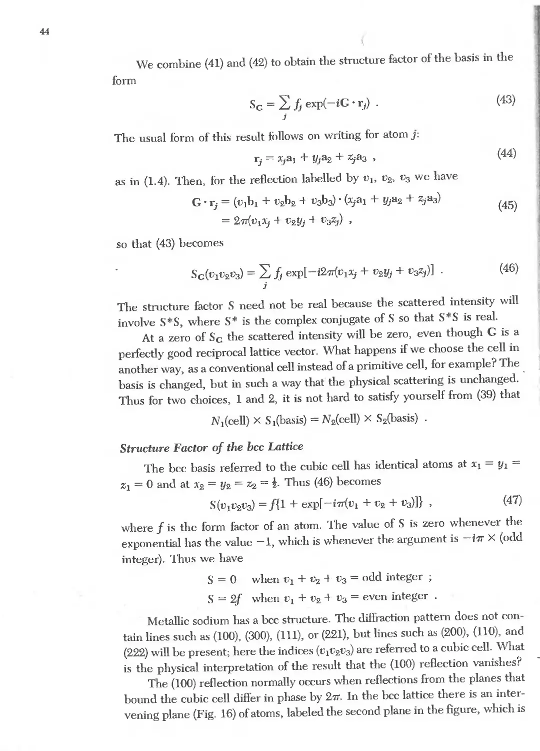
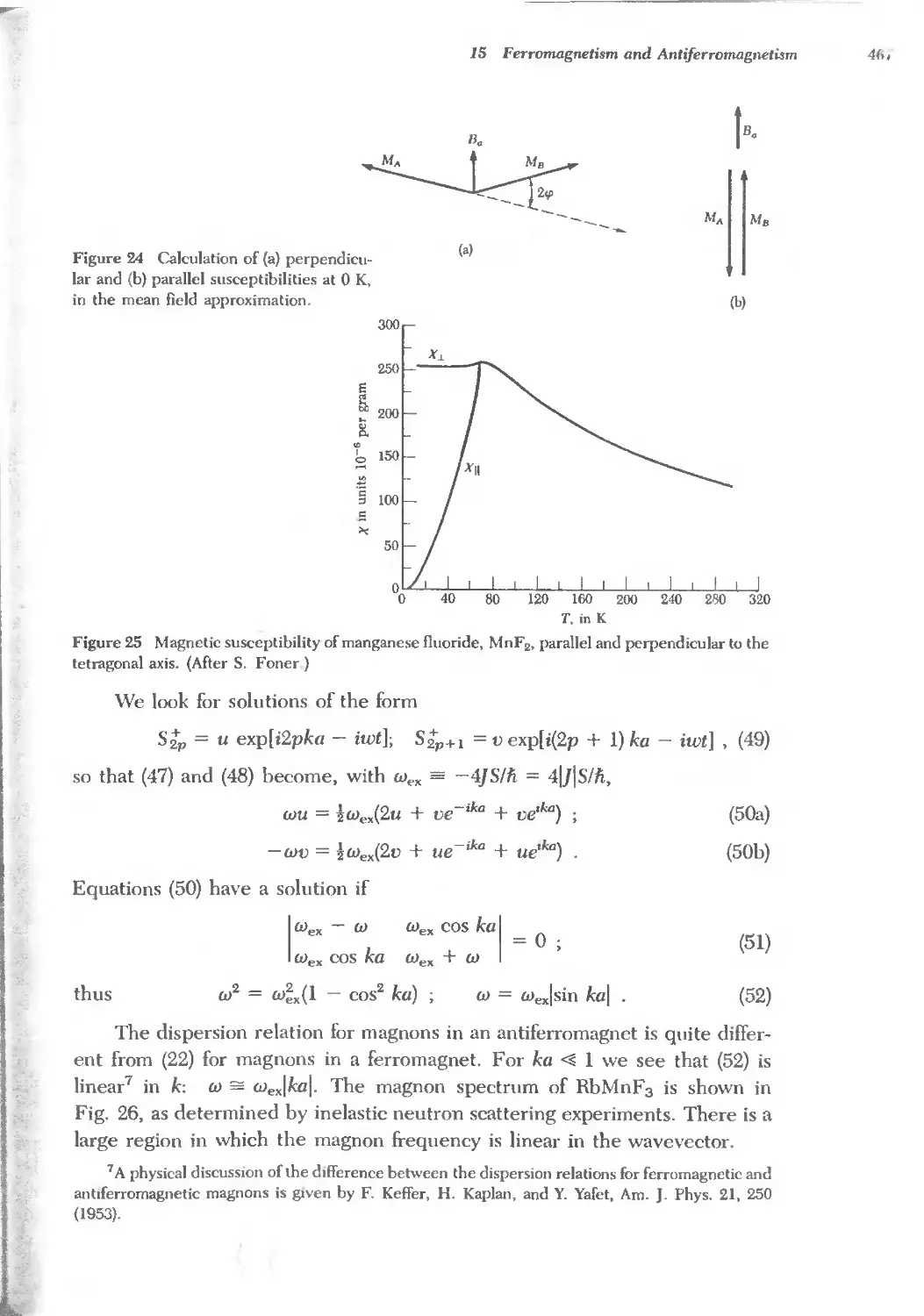
Gold "Au
-=_ ............,.,,1.---.."F. !"l-
J
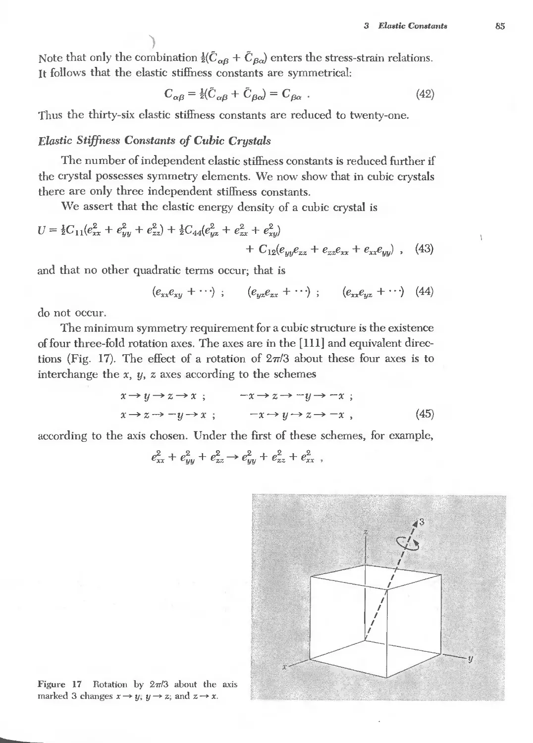
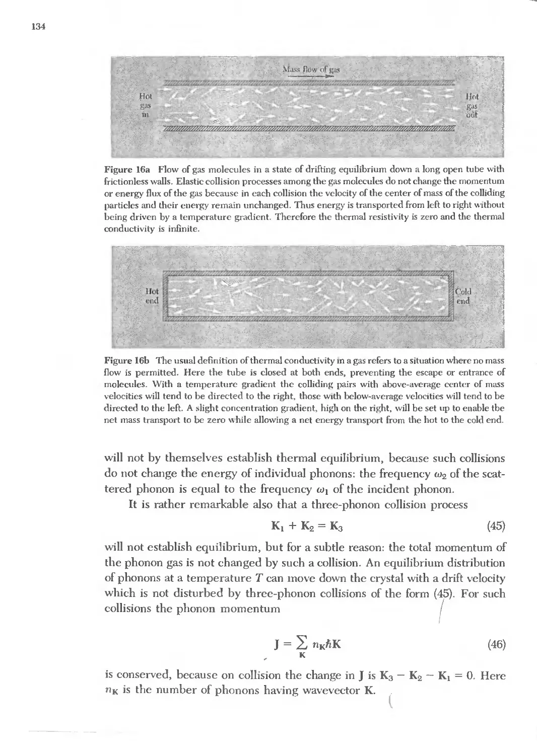
"' '" ..
:: :::..
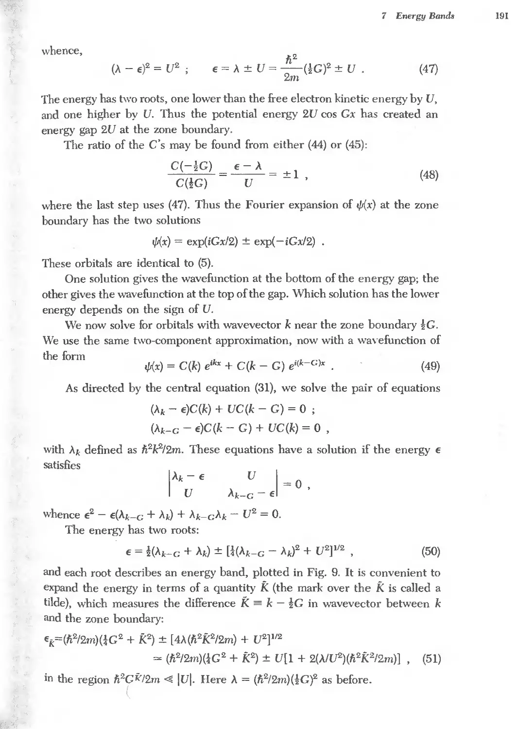
" ;:' M ':! 41
41 .. ell I::
'" o.. oo o.. oo '" oo
J: - Z < M '<!' >< at:) a: (,0 .. ::
.. o..
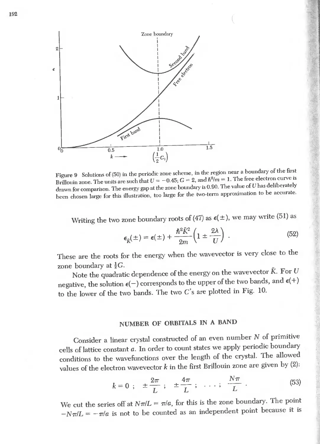
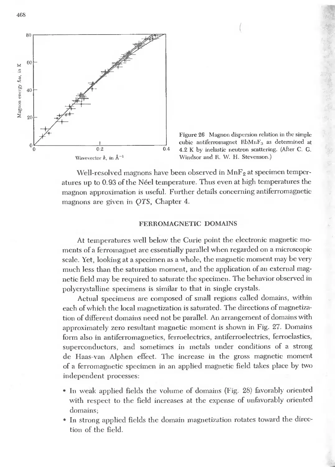
., 'b,. oo
.b,. ...I (,0 ...I
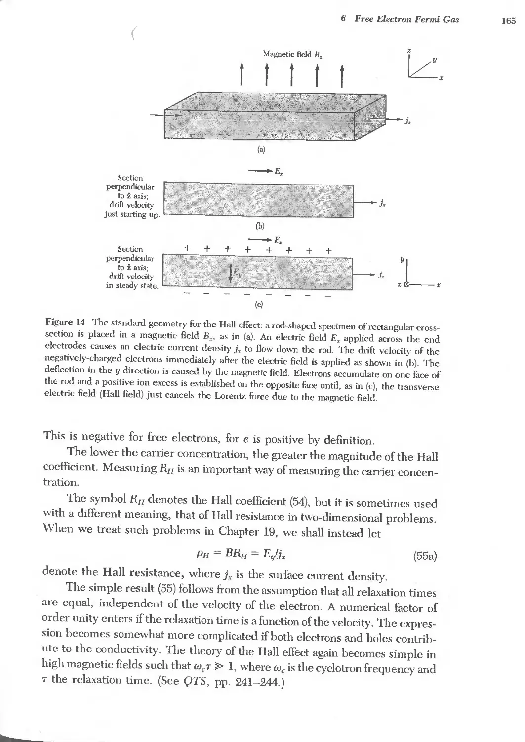
il ;:' ., ':!
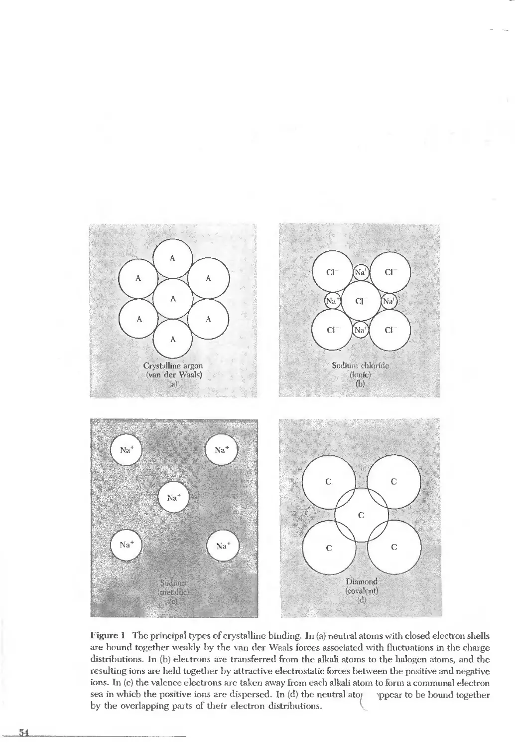
'"
u. c1 u oo o.. oo - oo ..
M CD ..,. at:) < (,0 " '"
.. 0
oo
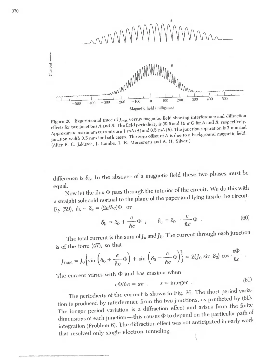
il :::.. > (,0 z
;' "ell ? .. '0
0 oo oo '" eII oo oo '"
en M en '<!' I- at:) c.. (,0 E M ::
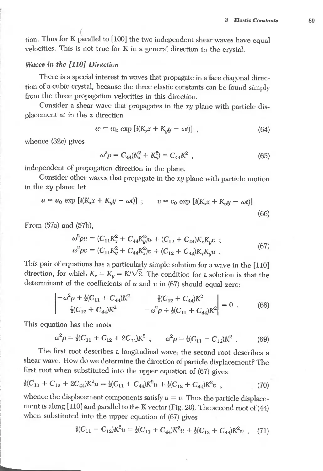
'" .. 'C
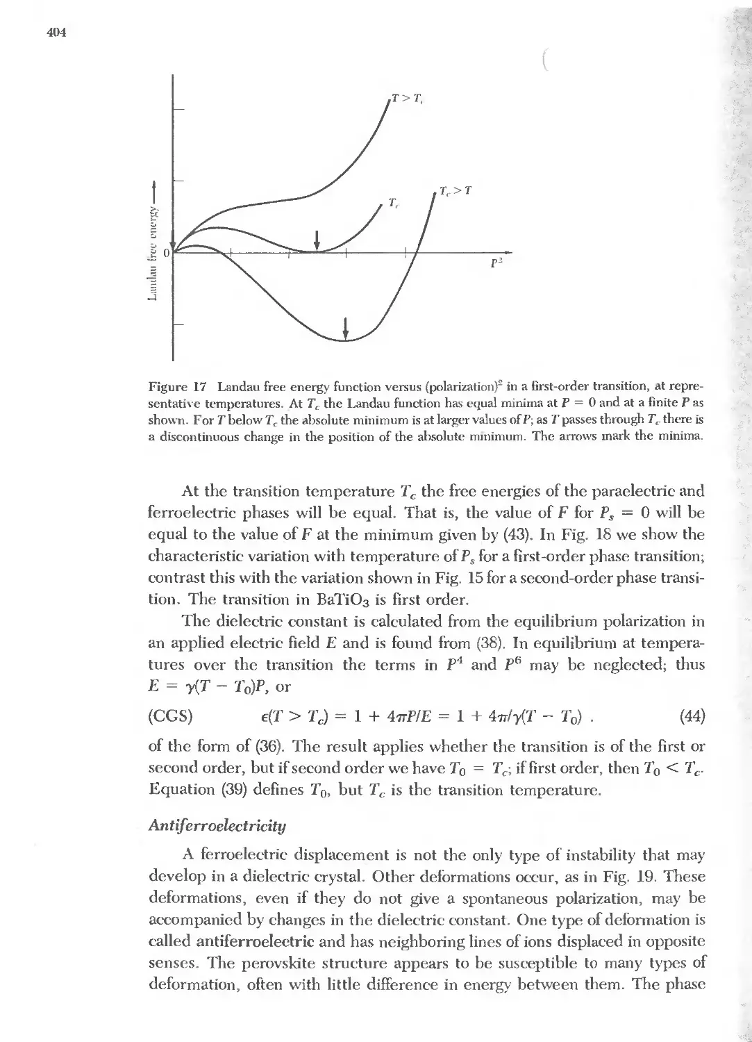
:::.. :::.. oo
:::.. I- (,0
;:' 'u, ':! :c M
"
oo < oo en oo m oo
Z c.. M ..,. at:) (,0 " ..
" .. E
.. .. "h. "h. ... '"
.. " .. w (,0 Il..
;:' 41 ;1 I:: :Q
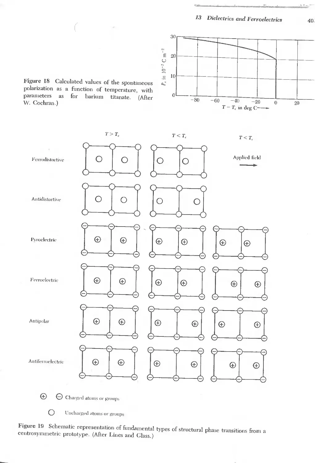
U c1 (ij oo oo oo oo
M CJ ..,. en at:) c.. (,0 '"
'0 .. '"
oo I/)
:::.. :::.. ::J: (,0 W .
;:' 'ia ;1 '" (,0
., i: " '1"
CD < oo CJ '" oo
M ..,. - at:) (,0 "
.. "
'"
oo U
'iij , i- ... :JJ ::.> - l' " :: '" " (,0
'" :c CI
o.. ;; - C .. .. ..
".-.;, ::J -" -.: '" '" '"
- N M ..,. U ..,. at:) ::J: at:)
> b.()- C
ell ...c":::: c 1:1 " .. :¥
; ::.> at:) oo
Z r-. ':'d ...... '" '" I- (,0 CD
- - =: :: =:
:JJ - :,
'0 S ;; "3 ... CI "1::
oo oo oo
E :JJ -.: U M ..,. < ..,. at:) < at:) (,0 i
I/) E i
c 0 -.: -5 ::: , "0 .. ..
oo (
0 ... 0 :JJ C " " :: .., (,0 U at:) (,0
:;: ;:J .8 '" :c " '"
;.., .':: .. .. ,.
III (3 oo c:: oo
o.. ... ;.) Z M ..,. c.. ..,. I at:) (,0
I/) ... ::.> '" '"
CI ell (3 t> ;> ::.> -0 "'"ij :, .. E ..
iii ;; ;:J '" w oo < '"
'E ... '- (,0 I-
-0 ,J:; :JJ '0 :c '" '"
C;; . 0 ;:J .. '" -
0 , ... oo .J:5
... ::: U M '<!' a: '<!' at:) o.. I ..
u E ::.> .. i
'C E '"
c <:: c :JJ ;:J E ..
c ... oo ;'r-,
0 t> '- ... c " '" en (,0 c.. I-
o.. 0 ::.> 0 ;; 41 '" .. :, I/) ..
- ::.> E "1:: ..
o.. J; C oo oo oo
(J CJ ::.> ..>0: ::.> .;:: ;:J Il.. M ..,. a: ..,. at:) 0 at:) (,0 '"
ell 0 <:.J E Q.
jjj o.. :JJ >-.1:. .. ..
1 ... '" z "
"iii ... ; ., c.. (,0 1-1
o.. .c X c :; ;:J .r 1: .0 U '41 ..
ell I- O"'B "1:: "!.o oo oo f
'S B M ..,. I- '<!' at:) a: at:) (,0 '"
";:; 0; -; 0 'C -.., I->
0 C .. ..
;; .- oo S
CI> -; 0.. .. Z (,0 lr.)
ell I/) -0
E :JJ ..J .. "0 .. .. ,
.c -0 o.. oo oo oo
- 0 U M ..,. '<!' at:) at:) (,0
=: - E -0 . . ... '" "'III
< ::.>"1:: . c....: .0 .. I
o.. oo
"j -0 ' ::.> c.. (,0 c.. at:) (,0 I-
:JJ , ::.> '" :c ;'11I '" ..
0) , ;:J -- 5- or. oo oo i
;; - M ..,. Z ..,. at:) I- at:) (,0 '"
:c " oo 0 , E 41 i .. .
c .. .. .c "1:: "to!
III -0 '"
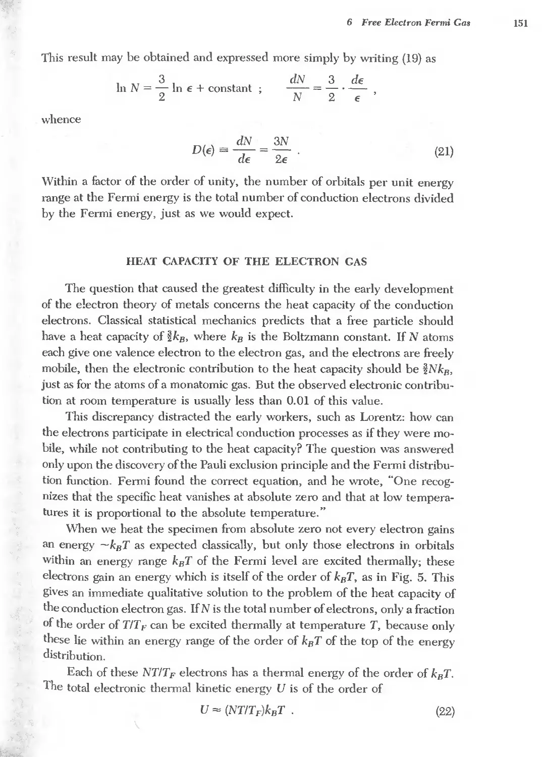
.r. P... u (,0 l- I (,0 i
I- , ... .. .. :> .. ..
.- B .. .. .. ..
(J , 'C i= oo o.. oo :I: '"
C M ..,. N ..,. at:) (,0 1I I
'6 ::.> -0 ;;
(3 J;
0 ::.> ... ...
"C .; -0 9:! E '"
ell U .. 0- .. III U
:.; E= ;:J "1:: "1:: .. ..
c.. t- S ...3: '" oo oo oo
, en M ..,. > ..,. at:) ...J at:) (,0 < (,0 r-
'" li " '"
41 CI .. Ia .. o.. .. Ia .. 10 ..
CD '" u '" en '" CD '" a: oo
M ..,. at:) (,0 I-
=
- III '" oo .Q '" U, '"
or. '" '" '" o.. oo
::J: ::i Z M ..,. a: at:) u (,0 Il.. r-
)
)
.:r
,)t>-r.. 'Ii -:;'h
01,"1'0 -I /J.
"1"'J:J 'l.1'Cl"1,J,
b ..,i.J.; 'll/i
')''1!J
(),)
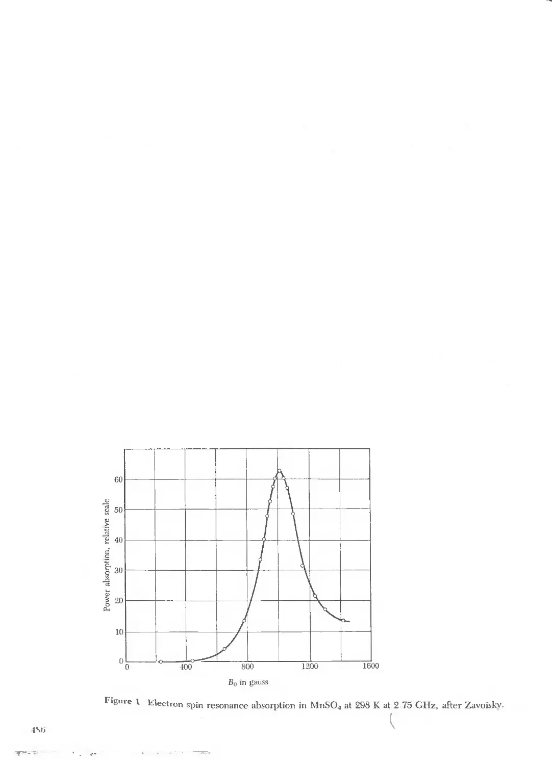
CHARLES KITTEL
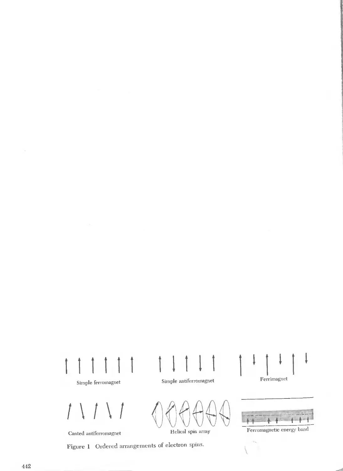
Introduction
to
Solid State
Physics
SEVENTH EDITION
@)
John Wiley & Sons, Inc., New York, Chichester,
Brisbane, Toronto, Singapore
L6 J\
j j.:J.1}
- ¥- \'\
t ,f (0 D
c(j
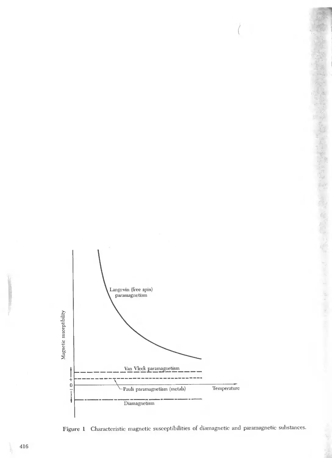
About the Author
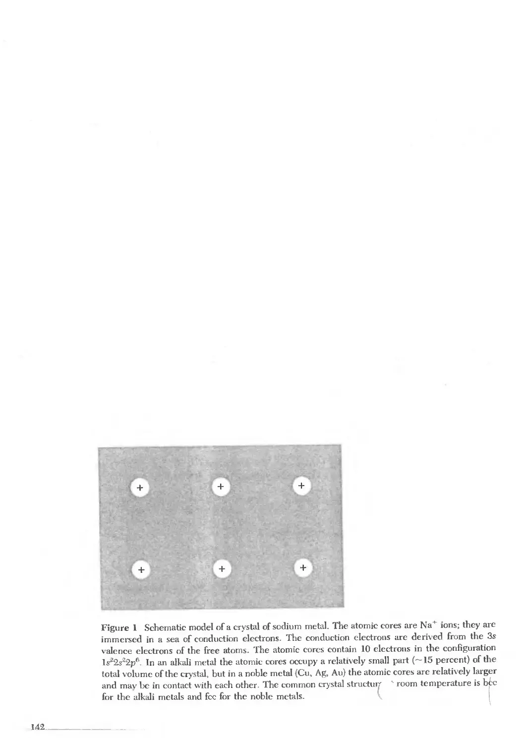
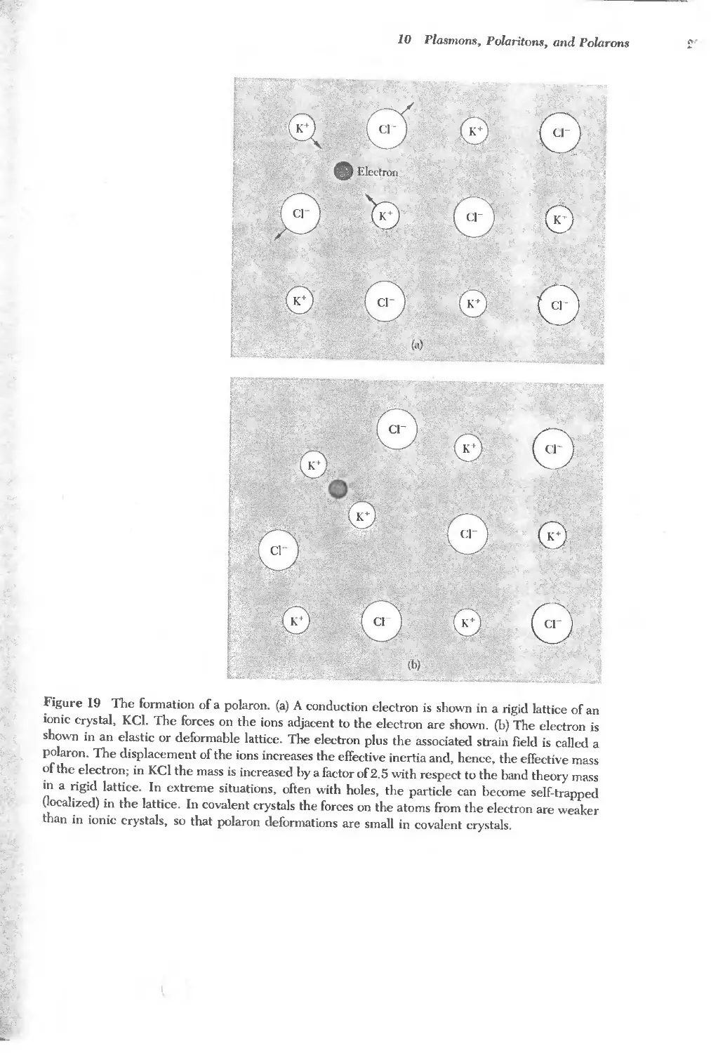
Charles Kittel taught solid state physics at Berkeley from 1951 to 1978;
earlier he was a member of the solid state group at the Bell Laboratories. His
undergraduate work was at M.L T. and at Cambridge University, followed by
graduate work at the University of Wisconsin. He is a member of the National
Academy of Science and of the American Academy of Arts and Sciences.
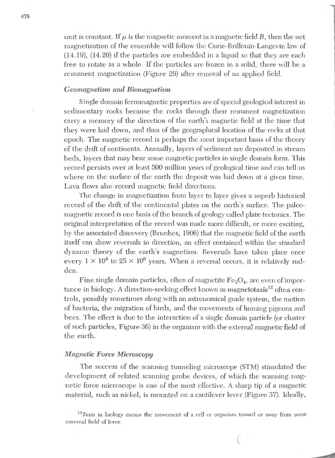
His research in solids began with studies of ferromagnetic, antuerromag-
netic, and paramagnetic resonance, along with work on magnetic domains, spin
waves, and domain boundaries in ferromagnets and ferroelectrics. His work on
the single domain structure of fine particles has had broad application in mag-
netic recording, geomagnetism, and biomagnetism. Along with collaborators at
Berkeley he did the first work on cyclotron resonance in semiconductors, which
led to the understanding of the band structure of silicon, germanium, and in-
dium antimonide, together with the theory of their impurity states. He also
worked on the interpretation of magnetoplasma resonance in semiconductors
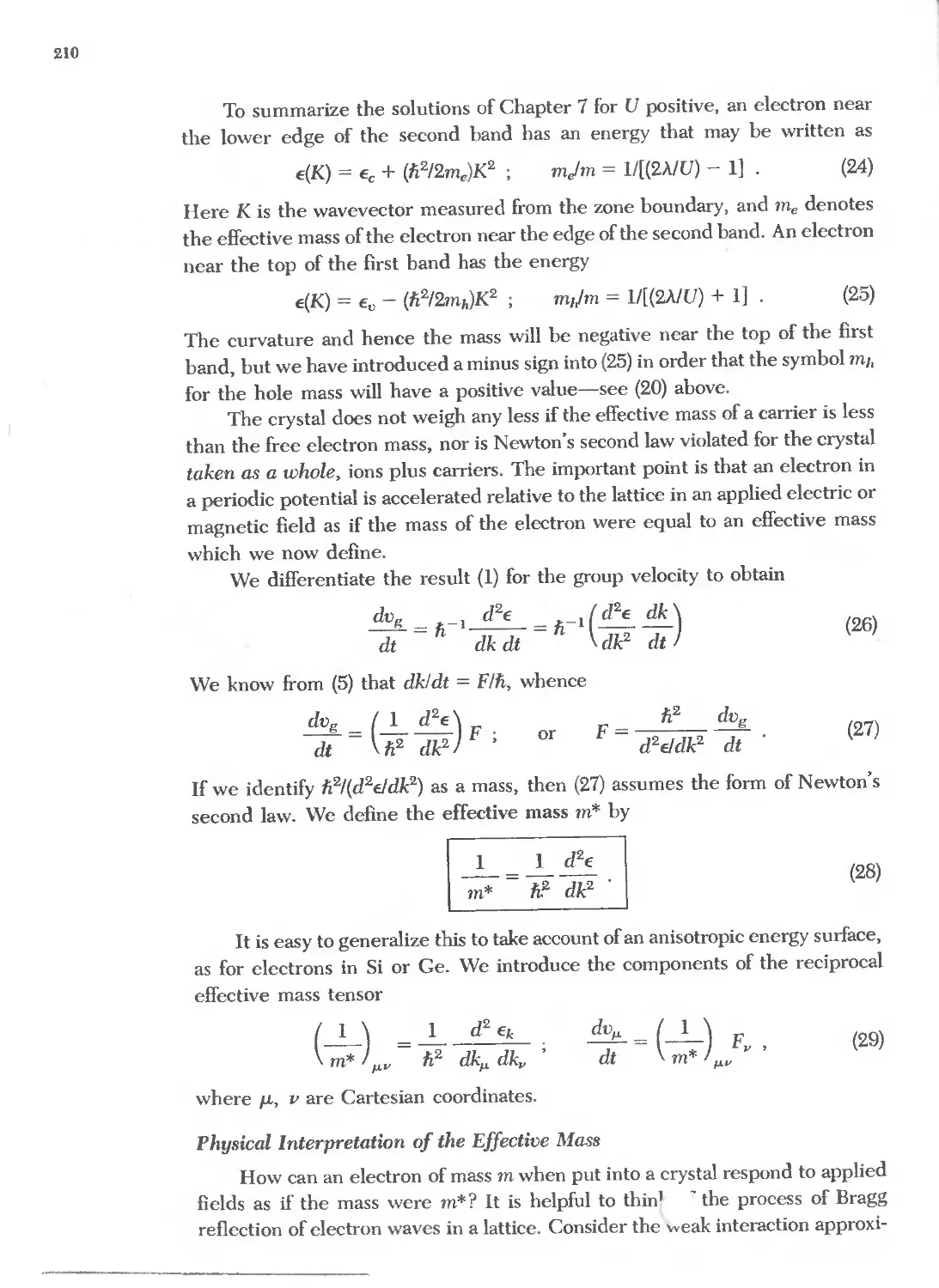
and of Alfven resonance in electron-hole drops in germanium.
The first edition of ISSP integrated the elementary aspects of solid state
physics for study by seniors and beginning graduate students. Now in its sev-
enth edition, ISSP plays the same part for the current generation of students.
Copyright @ 1953, 1956, 1966, 1971, 1976, 1986, 1996 by John WIley & Sons, Inc.
All rights reserved. Published simultaneously in Canada.
Reproduction or translation of any part of this work beyond that permitted by Section 107 or 108
of the 1976 United States Copyright Act without the permission of the copyright owner is
unlawful. Requests for permission or further information should be addressed to the Permissions
Department, John Wiley & Sons, Inc.
Library of Congress Cataloging in Publication Data:
Charles Kittel.
Introduction to solid state physics I Charles Kittel. - 7th ed.
p. em.
Includes index.
ISBN 0-471-11181-3 (cloth : alk. paper)
) Solid state physics. 1. Title.
QC176.K5 1996
530.4'I-dc20 95-18445
CIP
f\, ,,\V
/"
rN"
Printed in the United States of America
15 14 13 12 11
\ )
Preface
This book is the seventh edition of an elementary text on solid state physics
for senior and beginning graduate students of physical science and engineering.
The book is an update of the sixth edition of 1986 and includes additions,
improvements, and corrections made in that edition in 13 successive printings-
which it was time to pull together-and a number of new topics besides. Signif-
icant advances in the field have been added or discussed more fully: thus high
temperature superconductors are treated, and results of scanning tunneling
microscopy are displayed; the treatment of fiber optics is expanded. There are
discussions, among other topics, of nanostructures, superlattices, Bloch!
Wannier levels, Zener tunneling, light-emitting diodes, and new magnetic
materials. The additions have been made within a boundary condition intended
to keep the text within one volume and at a reasonable price.
The theoretical level of the text itself has not been changed. There is more
discussion of useful materials. The treatment of elastic constants and elastic
waves which was dropped after the fourth edition has now been returned be-
cause, as many have pointed out, the matter is useful and not easily accessible
elsewhere. The treatment of superconductors is much more extensive than is
usual in a text at this level: either you do it or you don't.
Solid state physics is concerned with the properties, often astonishing and
often of great utility, that result from the distribution of electrons in metals,
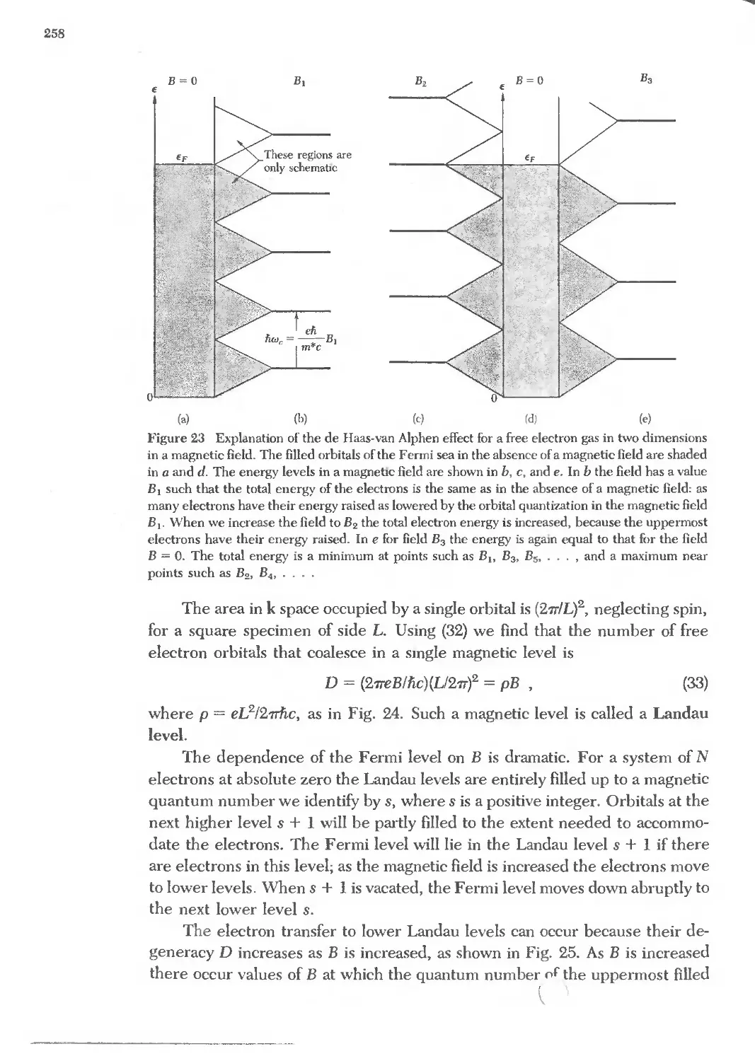
semiconductors, and insulators. The book also tells how the excitations and
impenections of real solids can be understood with simple models whose power
and scope are now firmly established. The subject matter supports a profitable
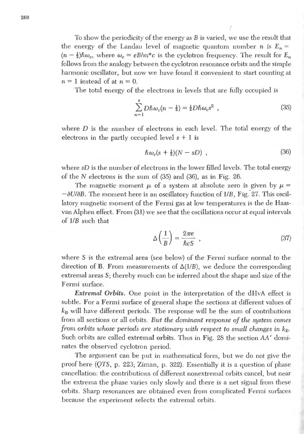
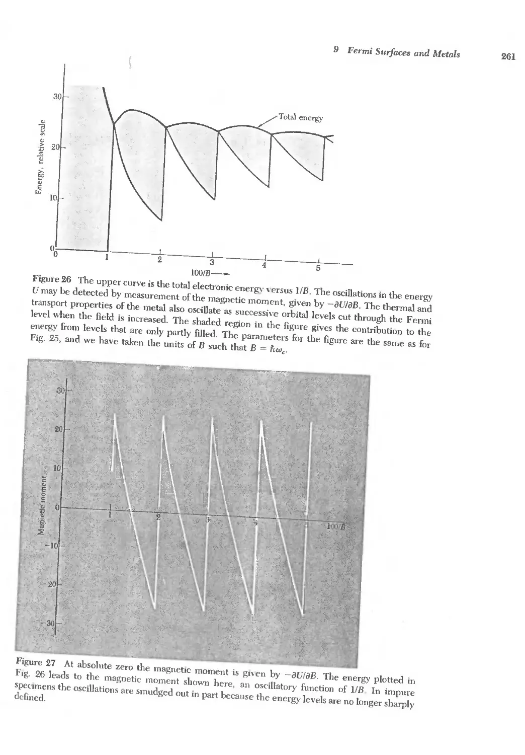
interplay of experiment, application, and theory. The book, in English and in
many translations, has helped give several generations of students a picture of
the process. Students also find the field attractive because of the frequent possi-
bility of working in small groups.
Instructors will use the book as the foundation of a course in their own
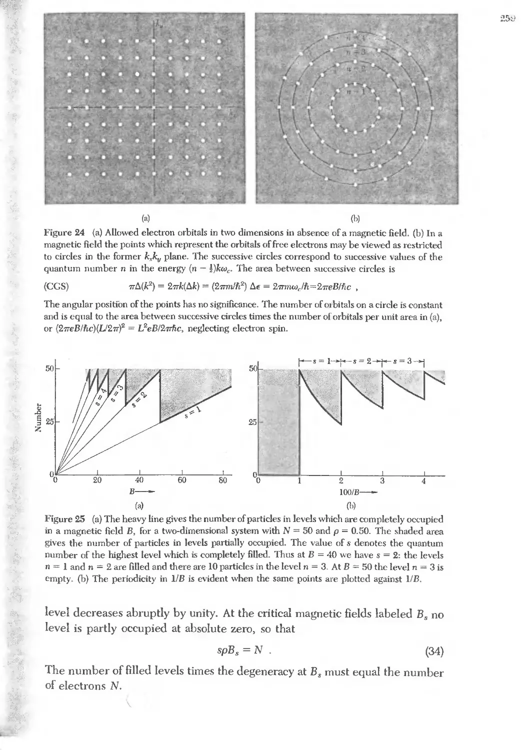
way, yet there are two general patterns to the introduction, selection and order
of the basic material. If students have a significant preparation in elementary
quantum mech:.. 1, they will like to begin with the quantum theory of elec-
ii;
iv
)
trons in one-dimensional solids, starting with the free electron gas in Chapter 6
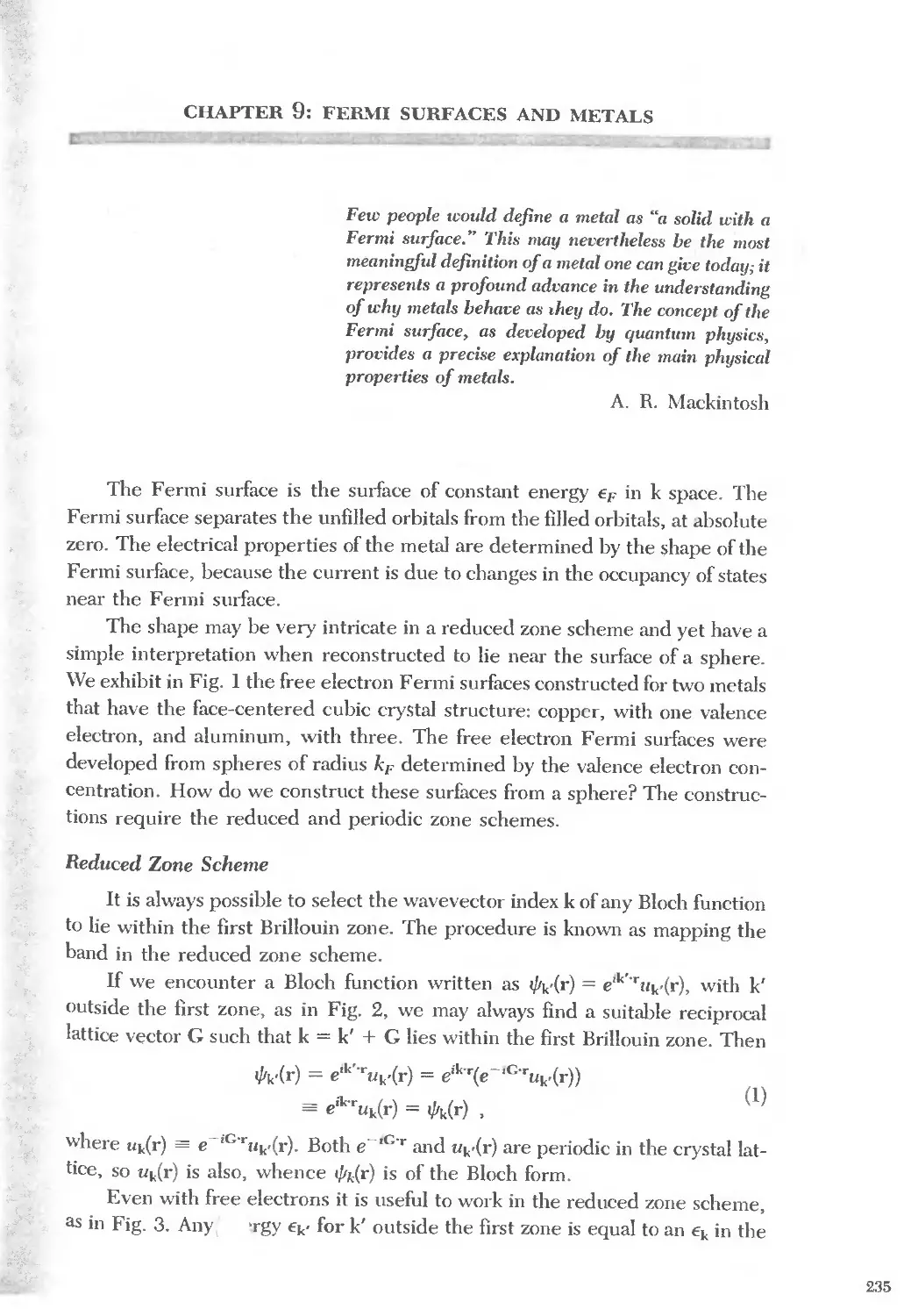
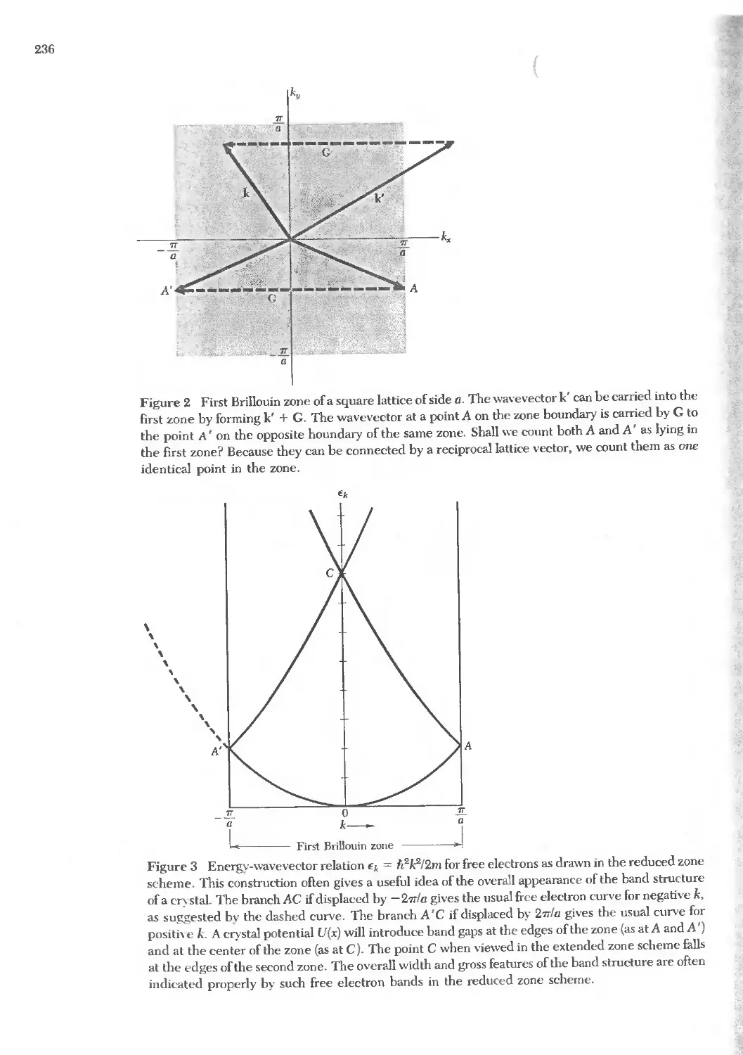
and energy bands in Chapter 7. One will need to treat the reciprocal lattice in
three dimensions (Chapter 2) before plunging into semiconductors (Chapter 8)
and Fermi sunaces (Chapter 9). Crystal structures, crystal binding, and pho-
nons could be considered as recreational reading. In a more gradual approach,
the first eight chapters through the physics of semiconductors are read consecu-
tively as a one-semester introduction to the field.
What about the necessary statistical mechanics? A vague discomfort at the
thought of the chemical potential is still characteristic of a physics education.
This intellectual gap is due to the obscurity of the writings of J. Willard Gibbs,
who discovered and understood the matter 100 years ago. Herbert Kroemer
and I have clarified the physics of the chemical potential in the early chapters of
our book on thermal physics.
Review series give excellent extended treatments of all the subjects
treated in this book and many more besides; thus with good conscience I give
few references to original papers. In these omissions no lack of honor is in-
tended to those who first set sail On these seas.
The crystallographic notation conforms with current usage in physics.
Important equations are repeated in SI and CGS-Gaussian units, where these
differ. Exceptions are figure captions, chapter summaries, some problems, and
any long section of text where a single indicated substitution will translate from
CGS to SI. Chapter Contents pages discuss conventions adopted to make paral-
lel usage simple. The dual usage in this book has been found useful and accept-
able.
Tables are in conventional units. The symbol e denotes the charge on the
proton and is positive. The notation (18) refers to Equation (18) of the current
chapter, but (3.18) refers to Equation 18 of Chapter 3. A caret A over a vector
refers to a unit vector. Few of the problems are exactly easy; most were devised
to carry forward the subject of the chapter. With a few exceptions, the prob-
lems are those of the original sixth edition.
This edition owes much to the advice of Professor Steven G. Louie. For
collected corrections, data, and illustrations I am grateful to P. Allen, M. Beas-
ley, D. Chemla, T.-C. Chiang, M. L. Cohen, M. G. Craford, A. E. Curzon,
D. Eigler, L. M. Falicov, R. B. Frankel, J. Friedel, T. H. Geballe, D. M.
Ginsberg, C. Herring, H. F. Hess, N. Holonyak, Jr., M. Jacob, J. Mamin,
P. McEuen, J. G. Mullen, J. C. Phillips, D. E. Prober, Marta Puebla, D. S.
Rokhsar, L. Takacs, Tingye Li, M. A. Van Hove, E. R. Weber, R. M. White,
J. P. Wolfe, and A. Zettl. Of the Wiley staff I have particularly great debts to
Clifford Mills for publication supervision, to Cathy Donovan for her ingenuity
in processing the additions between the thirteen successive printings, and to
Suzanne Ingrao of Ingrao Associates for her skill and understanding during the
editorial process.
Preface v
)
Corrections a'nd suggestions will be gratefully received and may be ad-
dressed to the author at the Department of Physics, University of California,
Berkeley, CA 94720-7300; by email to kittel@uclink4.Berkeley.edu; and by fax
to (510) 643-9473.
C. Kittel
An Instructor's Manual is available for this revision; several problems have
been added (to Chapter 3 and Chapter 6); one dropped (from Chapter 4), and
several corrections made. Instructors who have adopted the text for classroom
use should direct a request on departmental letterhead to John Wiley & Sons,
Inc., 605 Third Avenue, New York, NY 10158-0012. Limited requests for per-
mission to copy figures or other material should be addressed to the Permis-
sions Editor at this address.
Contents
Guide to Tables ix
General References xi
1 CRYSTAL STRUCTURE 1
2 RECIPROCAL LATTICE 21
3 CRYSTAL BINDING AND ELASTIC CONSTANTS 53
4 PHONONS I. CRYSTAL VIBRATIONS 91
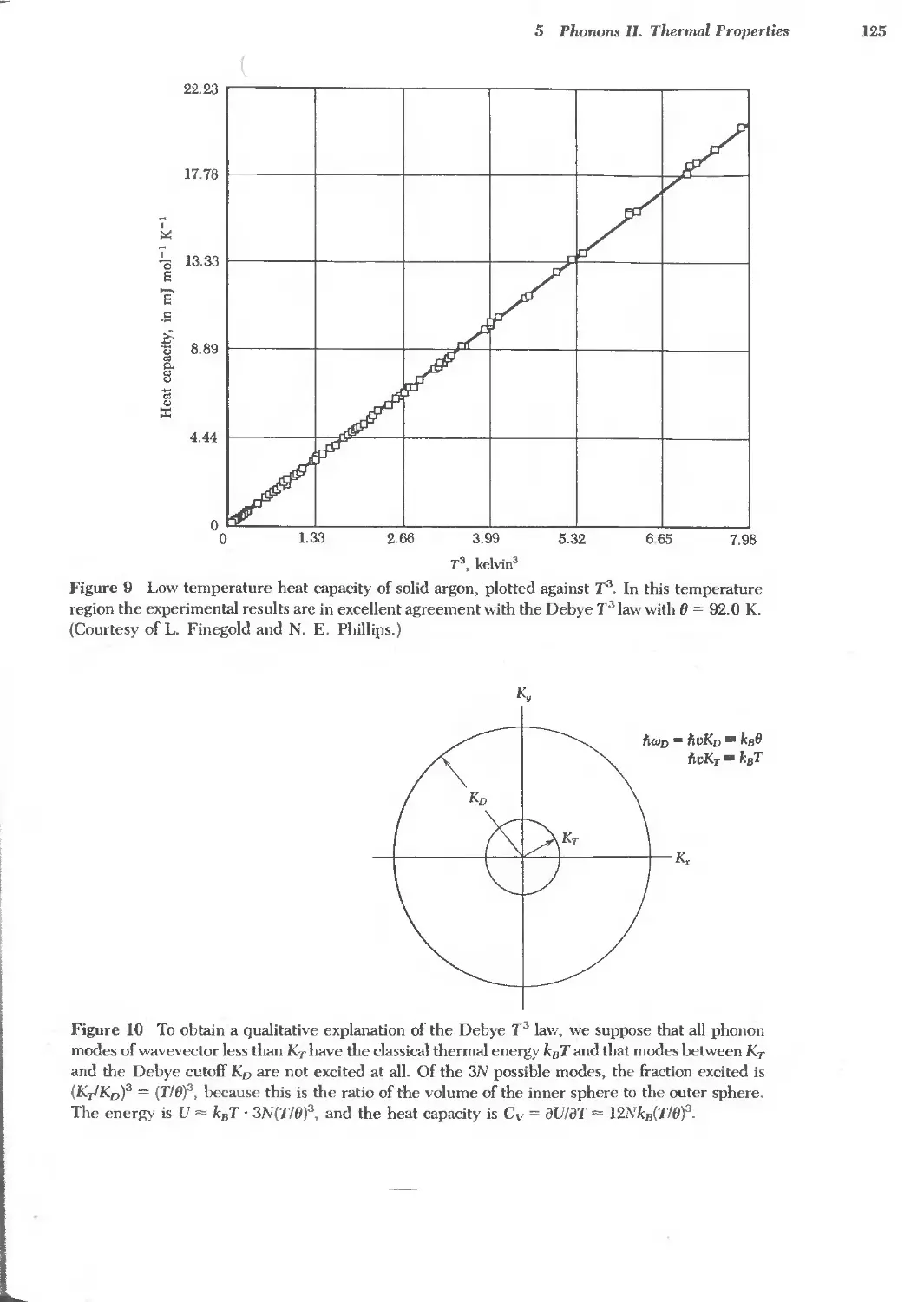
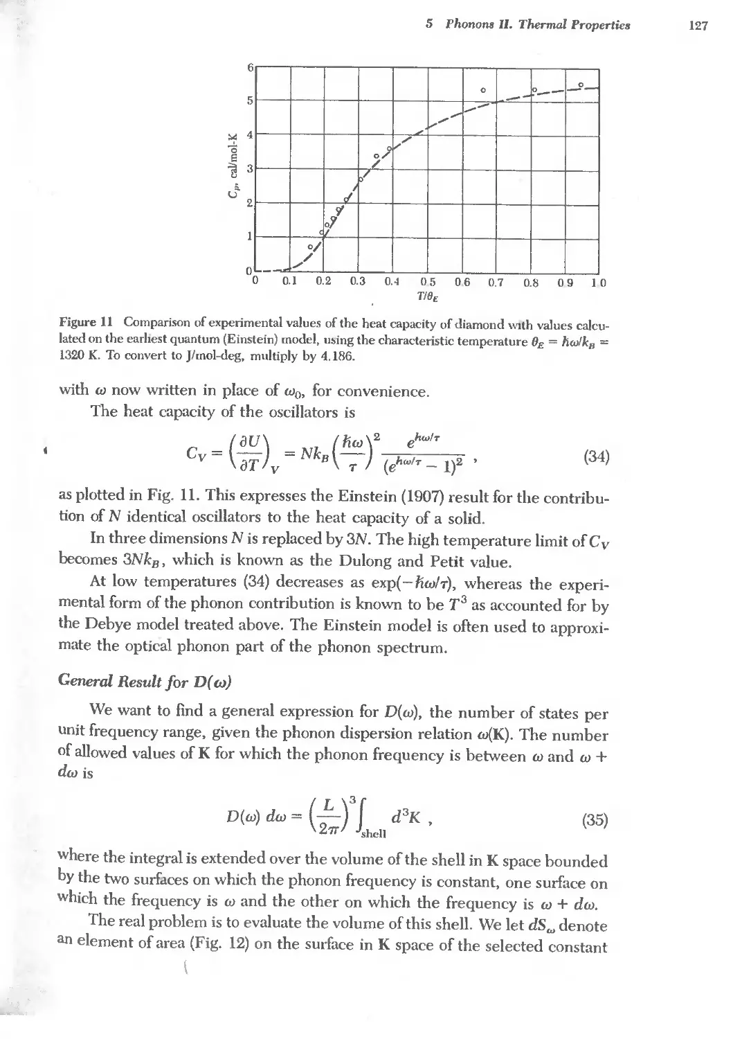
5 PHONONS II. THERMAL PROPERTIES 115
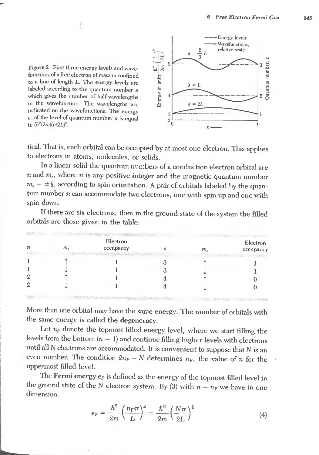
6 FREE ELECTRON FERMI GAS 141 '-,
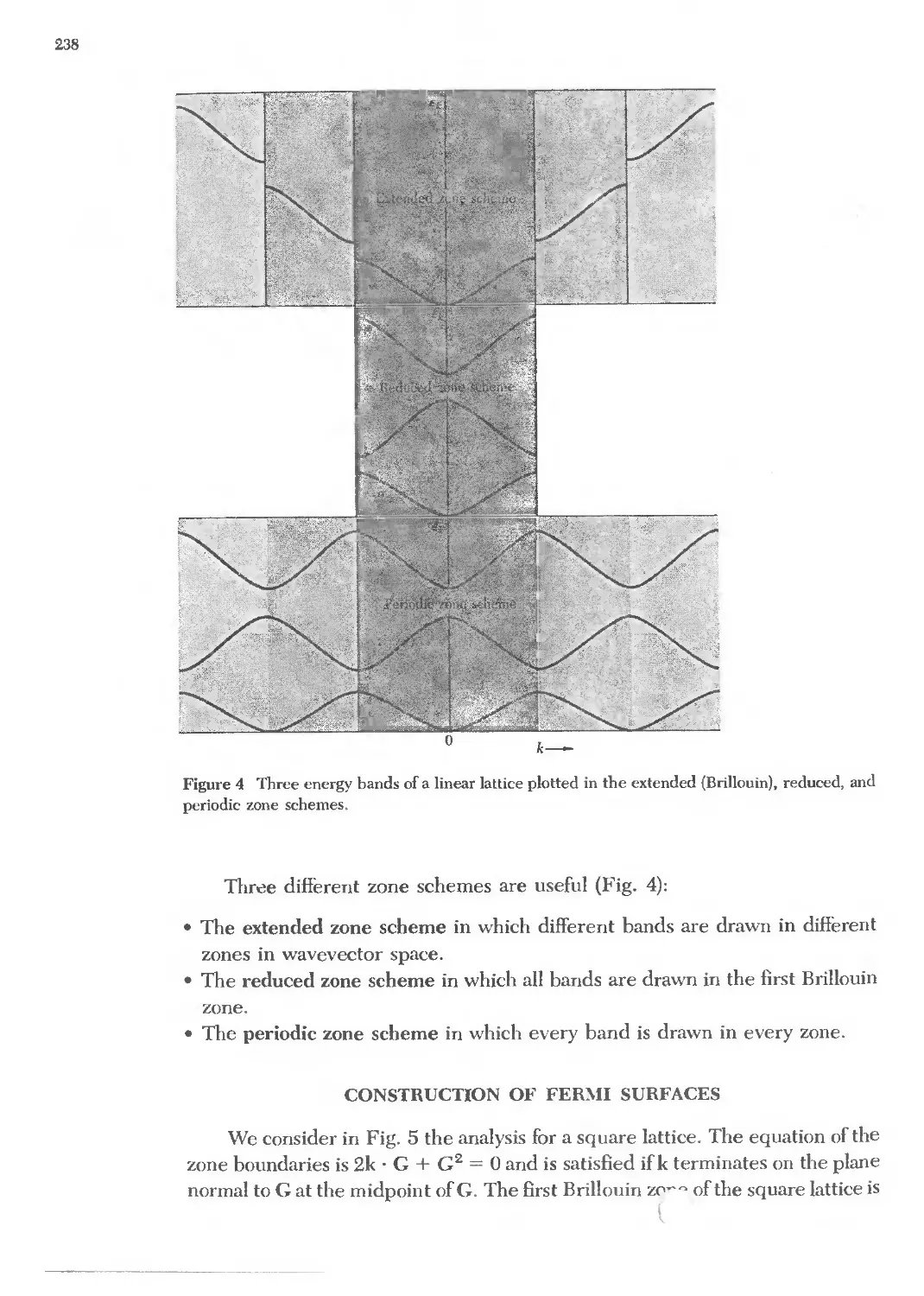
7 ENERGY BANDS 173
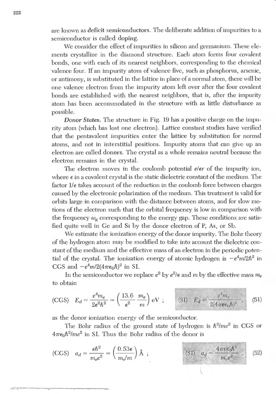
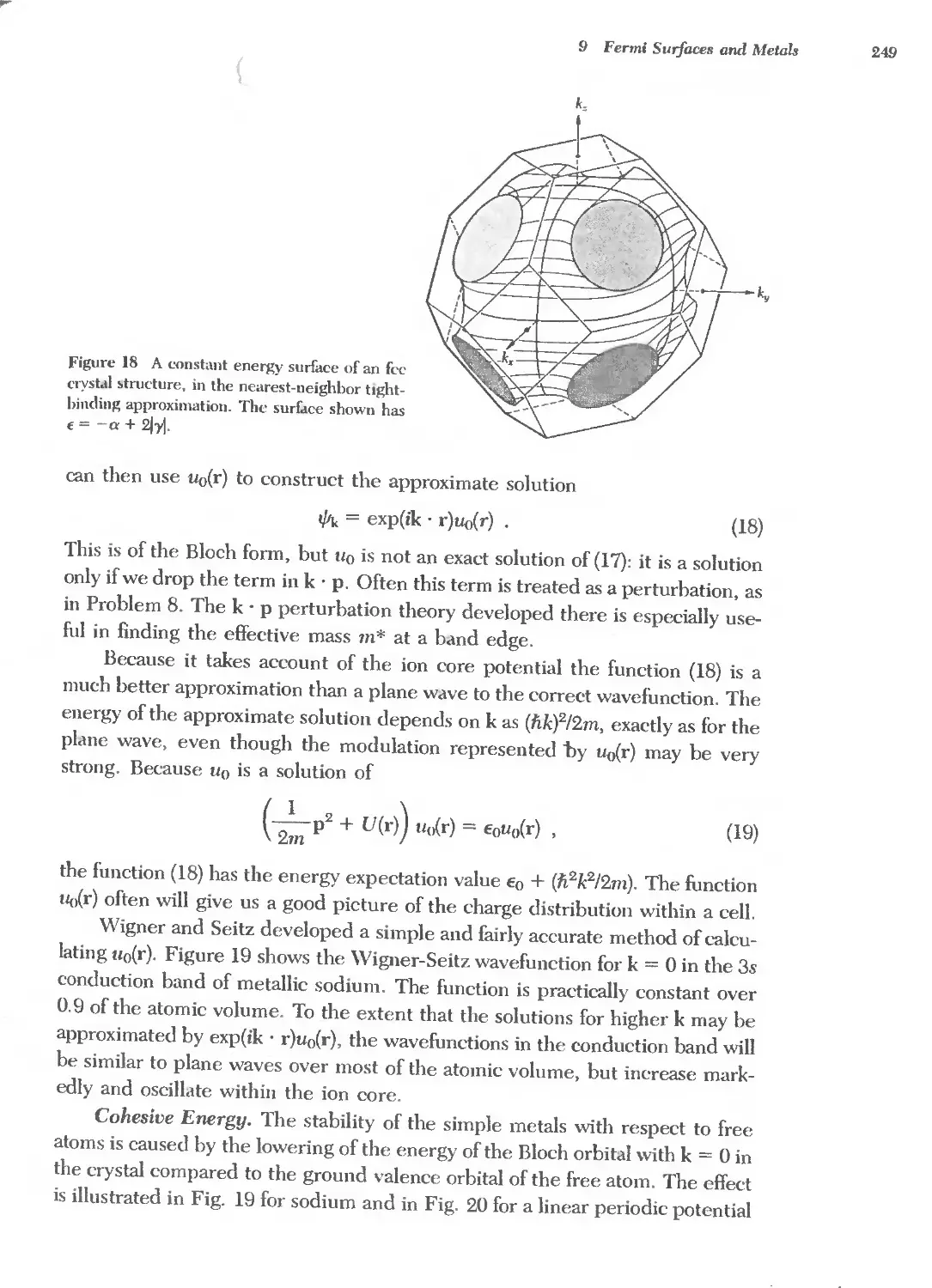
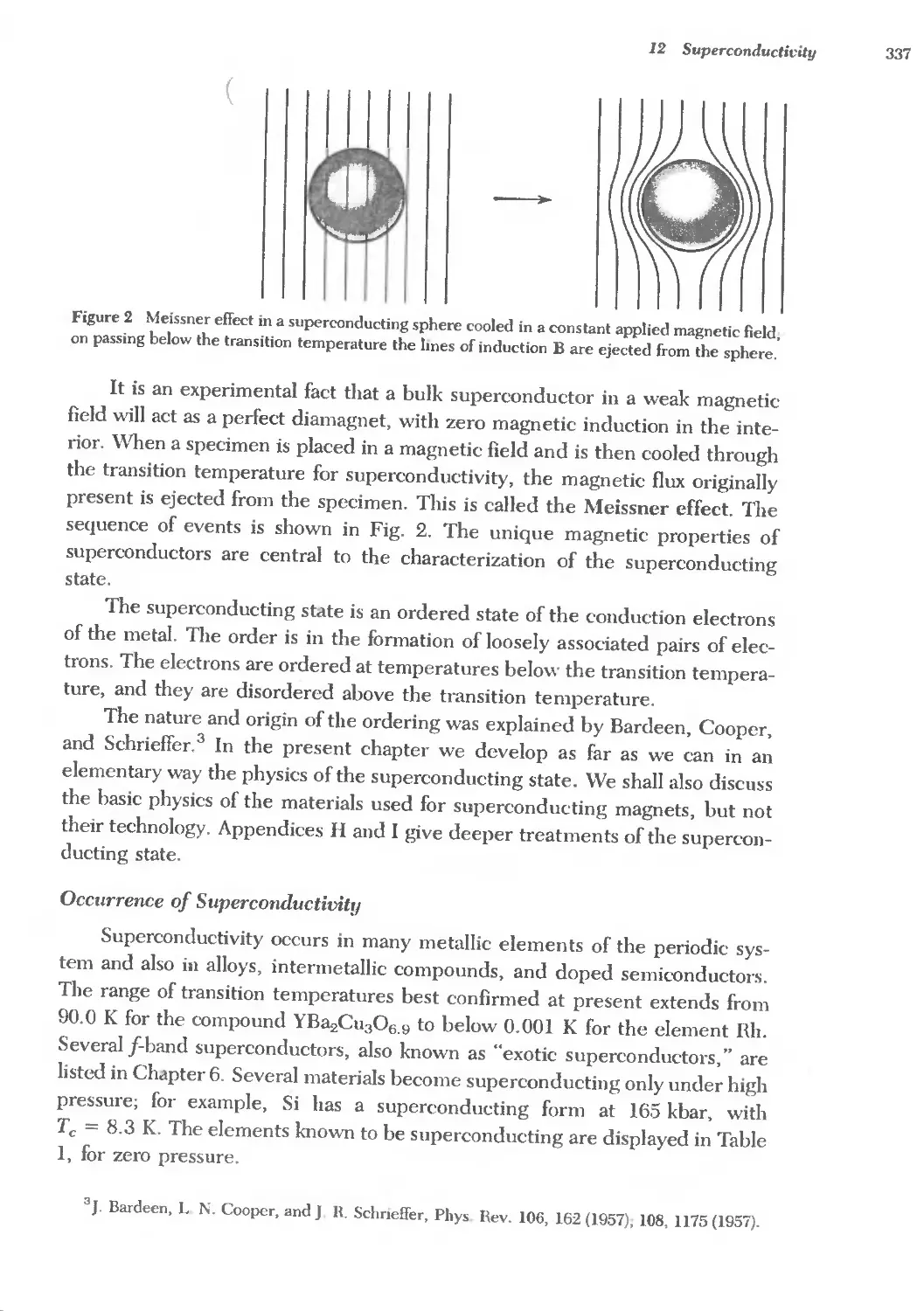
8 SEMICONDUCTOR CRYSTALS 191
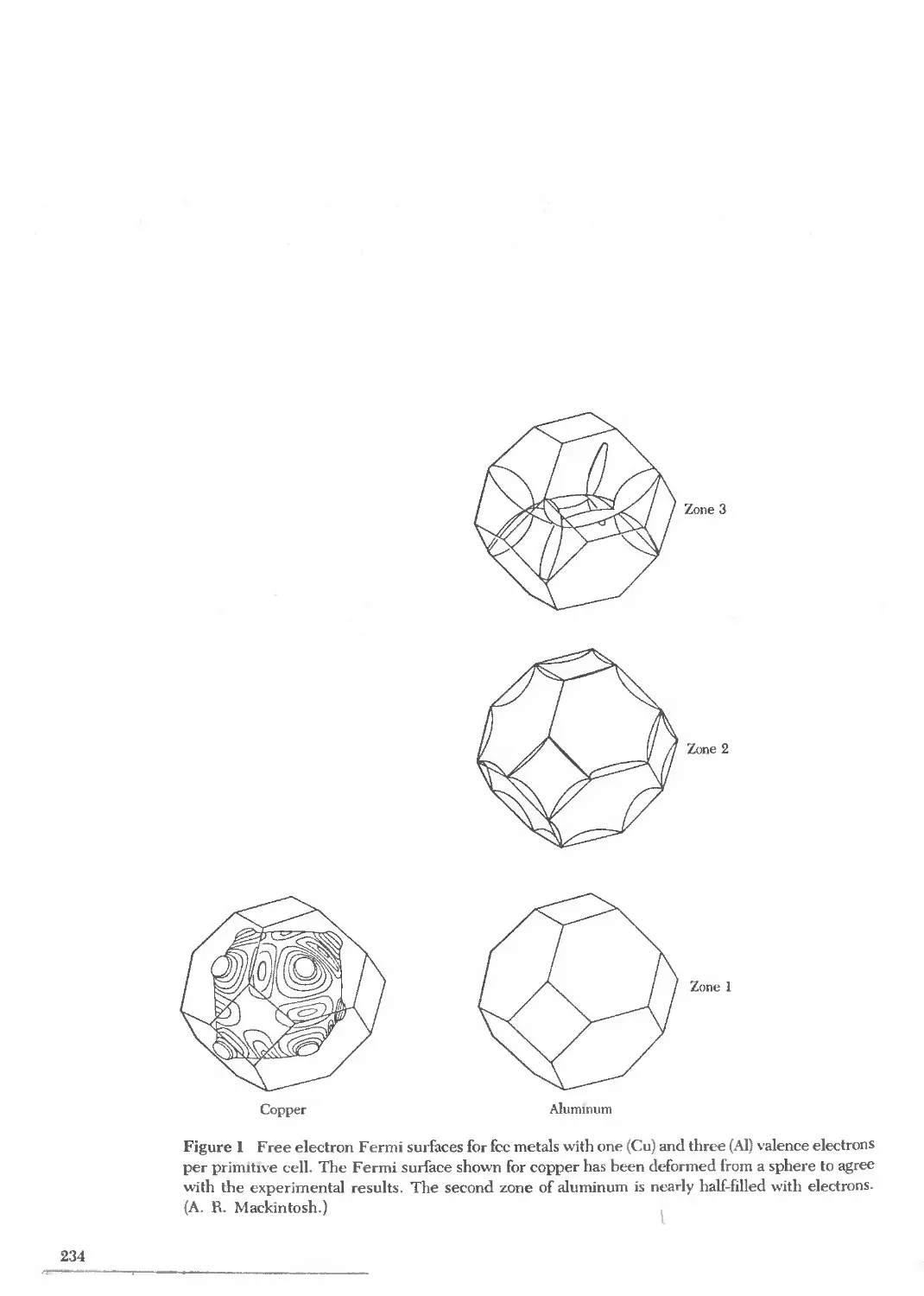
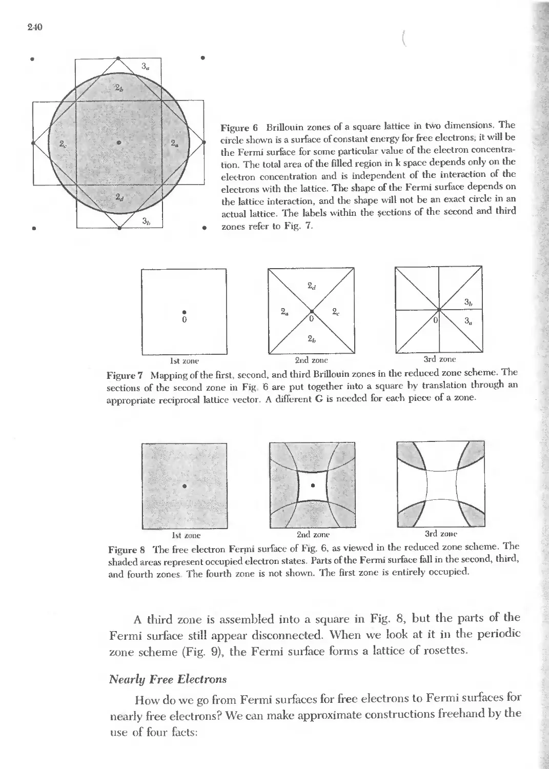
9 FERMI SURF ACES AND METALS 233
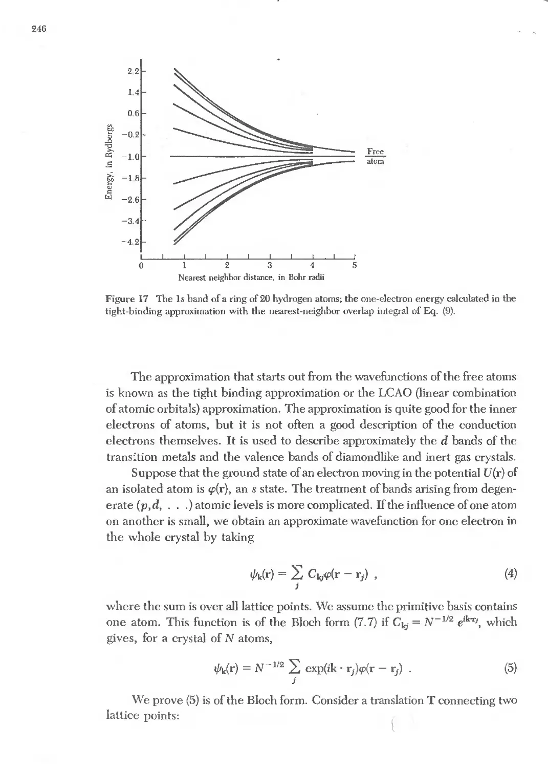
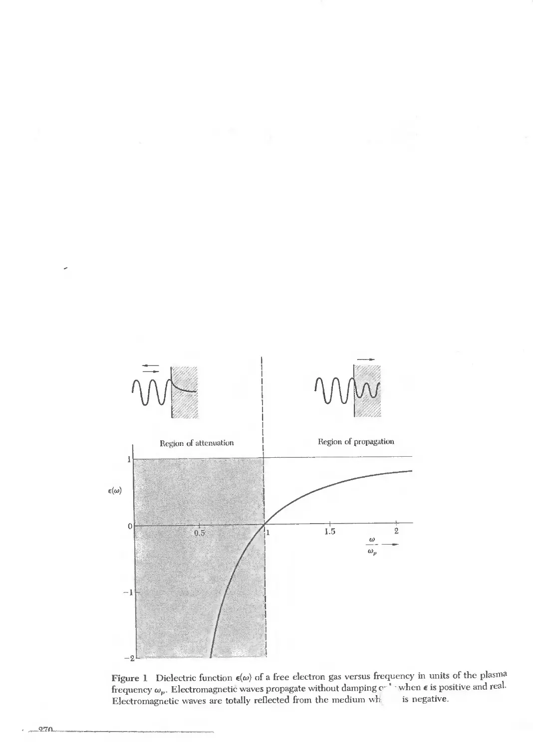
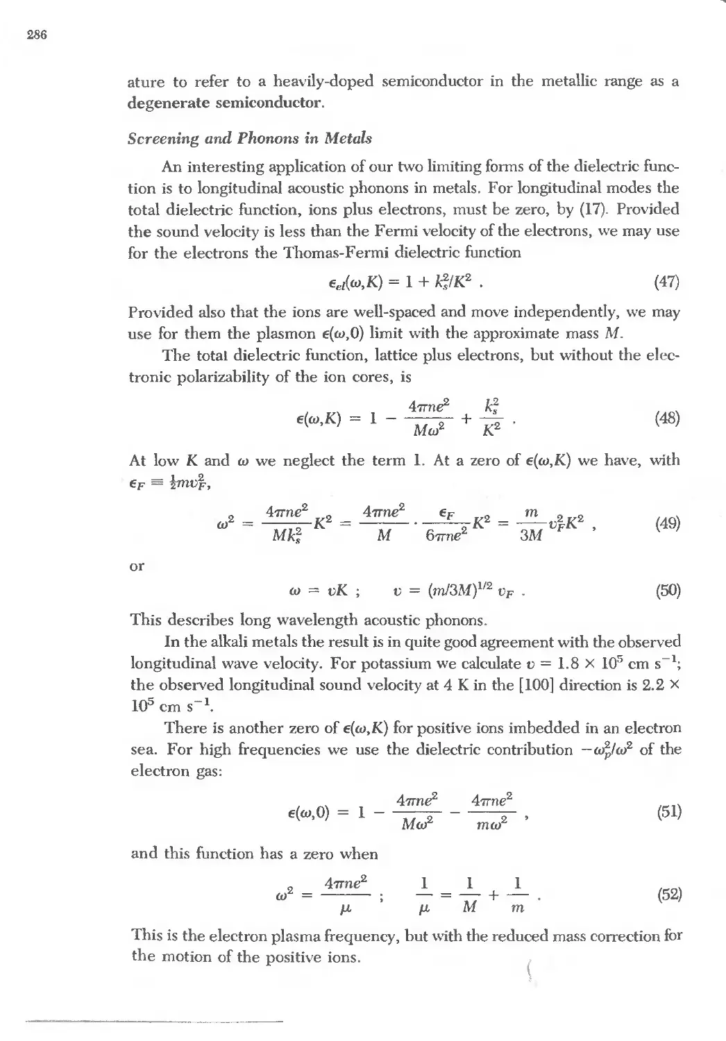
10 PLASMONS, POLARITONS, AND POLARONS 269
11 OPTICAL PROCESSES AND EXOTONS 305
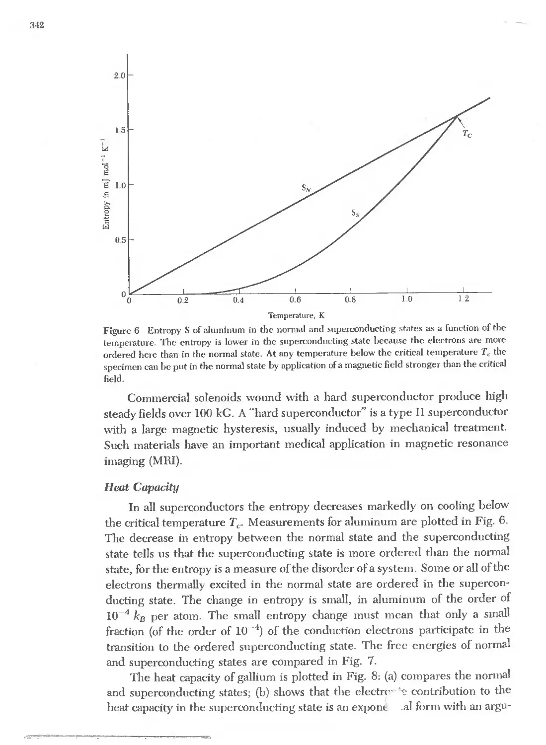
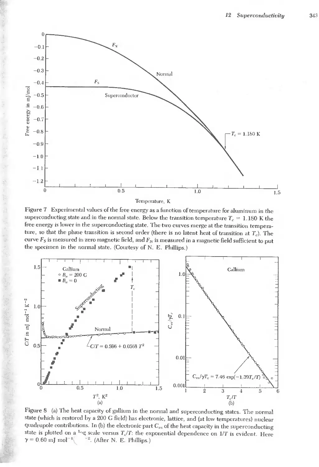
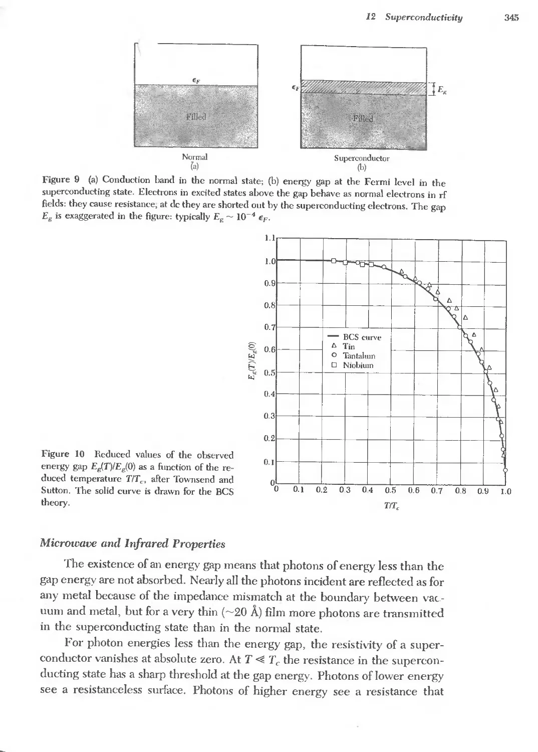
12 SUPERCONDUCTIVITY 333
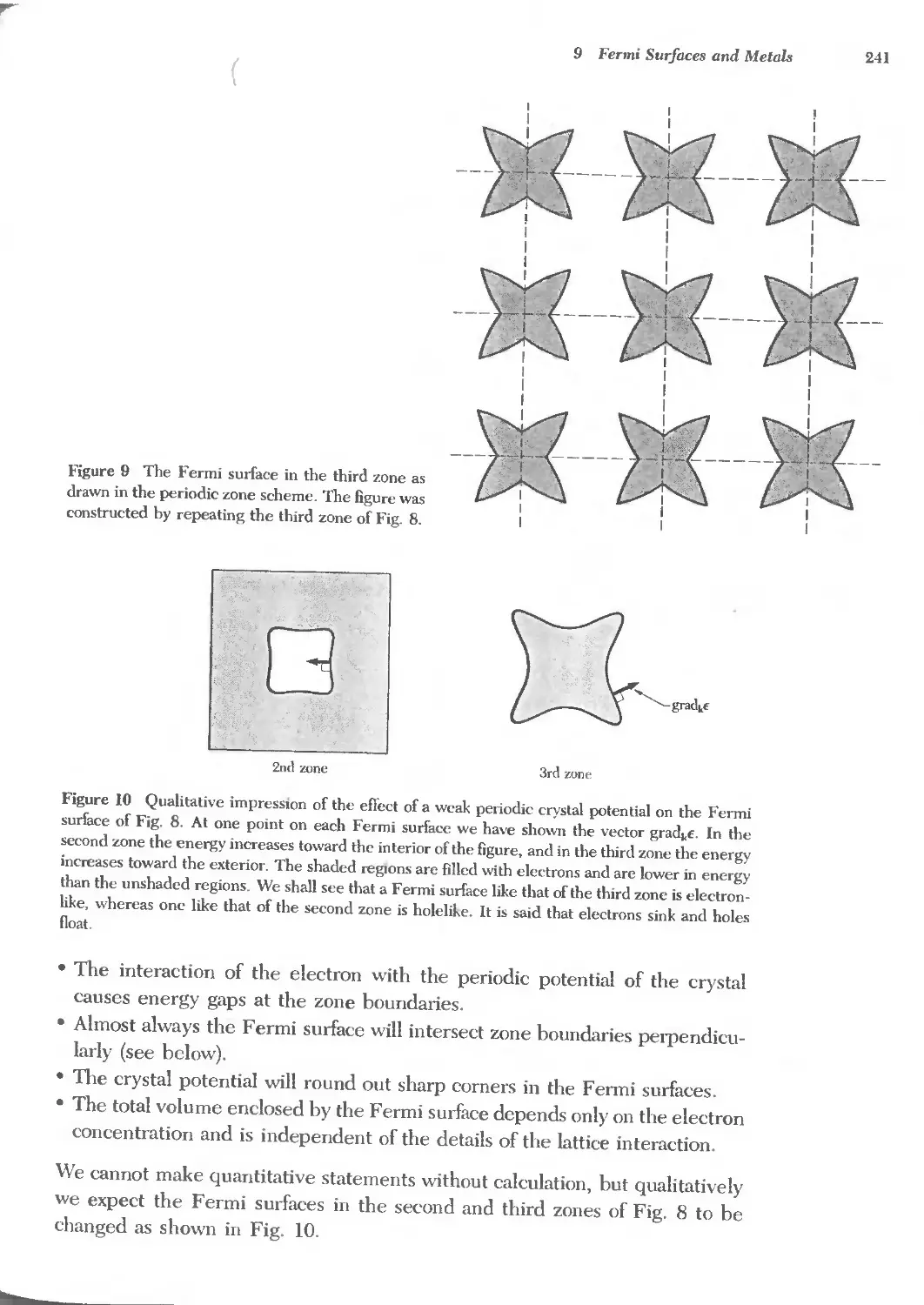
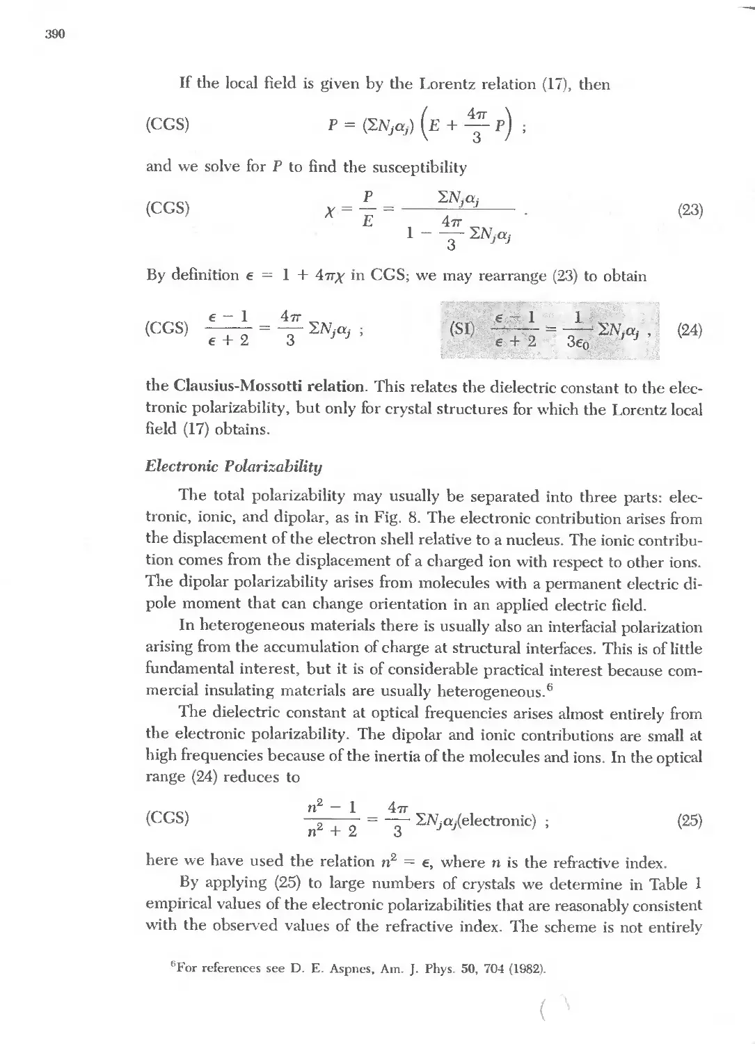
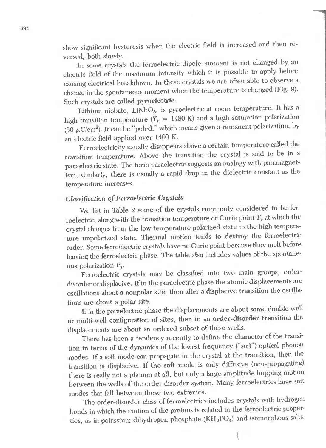
13 DIELECTRICS AND FERROELECTRICS 379
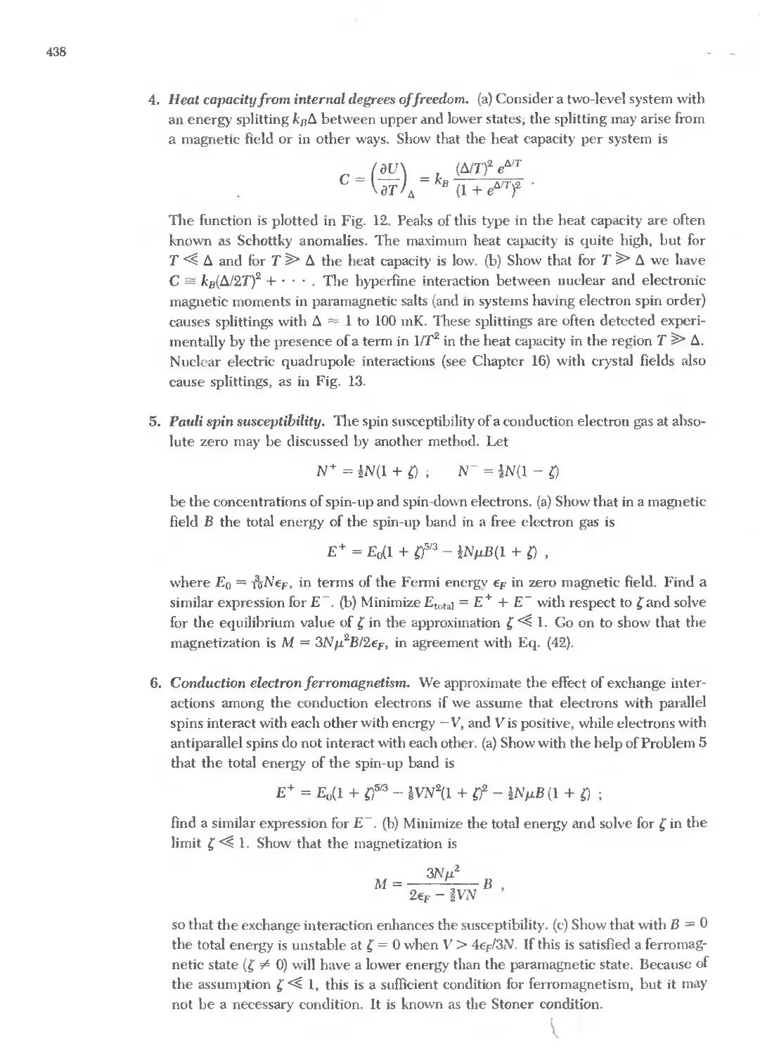
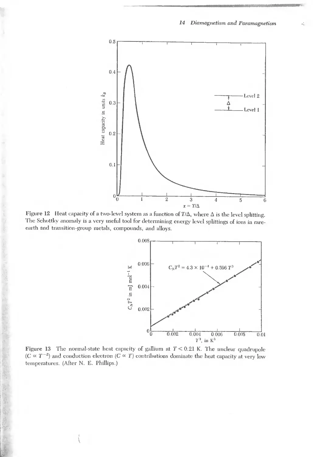
14 DIAMAGNETISM AND PARAMAGNETISM 415
15 FERROMAGNETISM AND ANTIFERROMAGNETISM 441
16 MAGNETIC RESONANCE 485 ; ,
17 NONCRYSTALLINE SOliDS 519
G
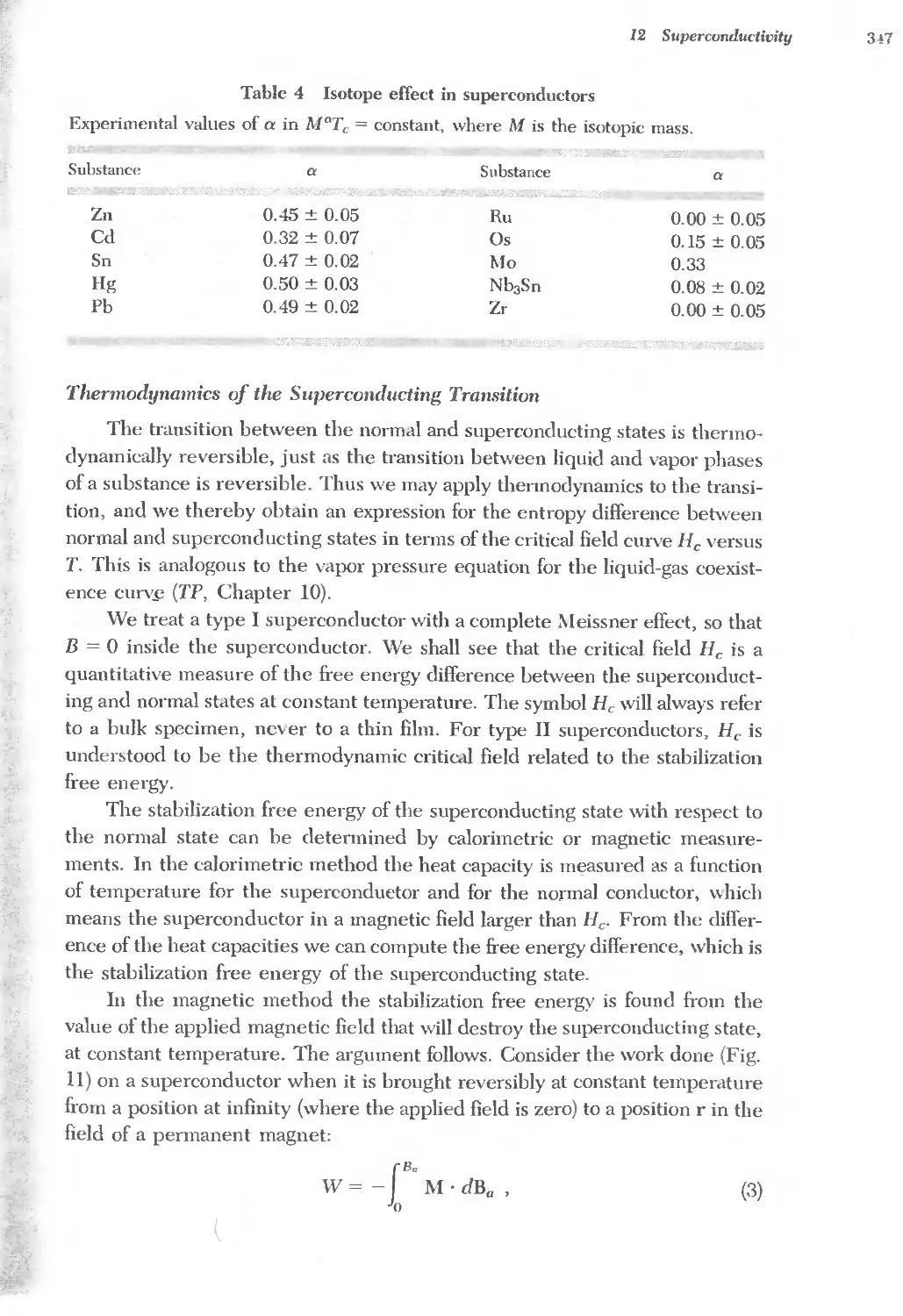
18 POINT DEFFf'TS 539
vii
r--
viii
t
./"
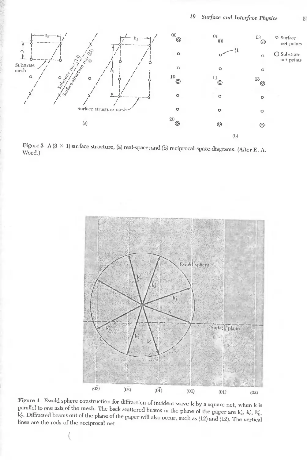
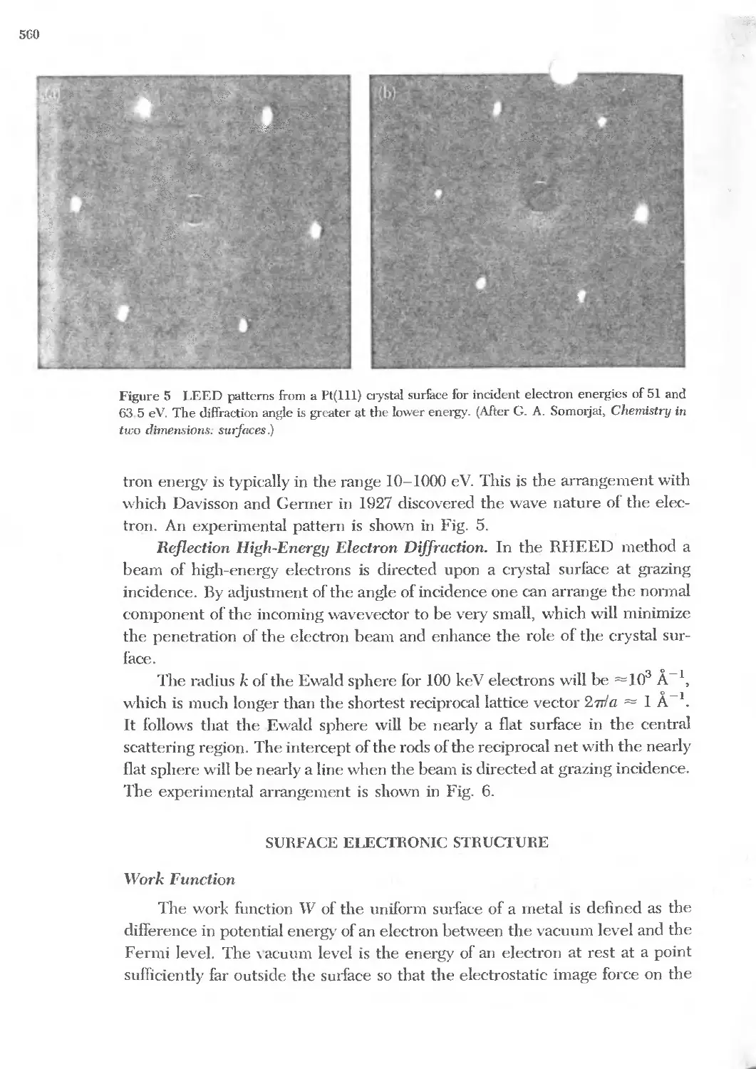
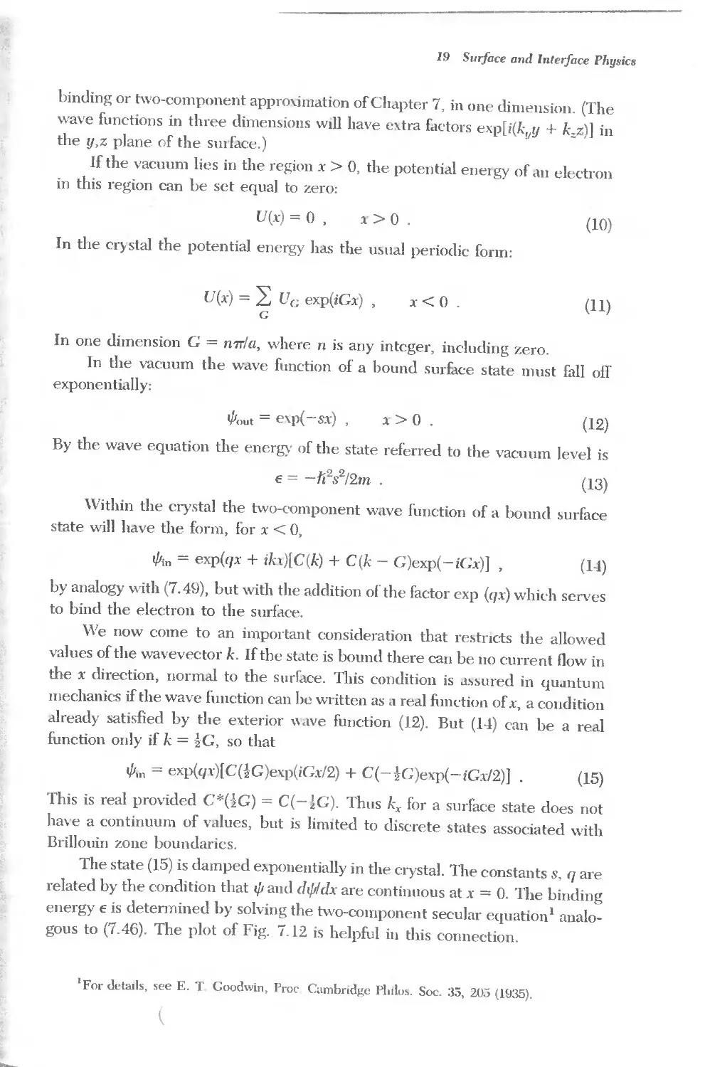
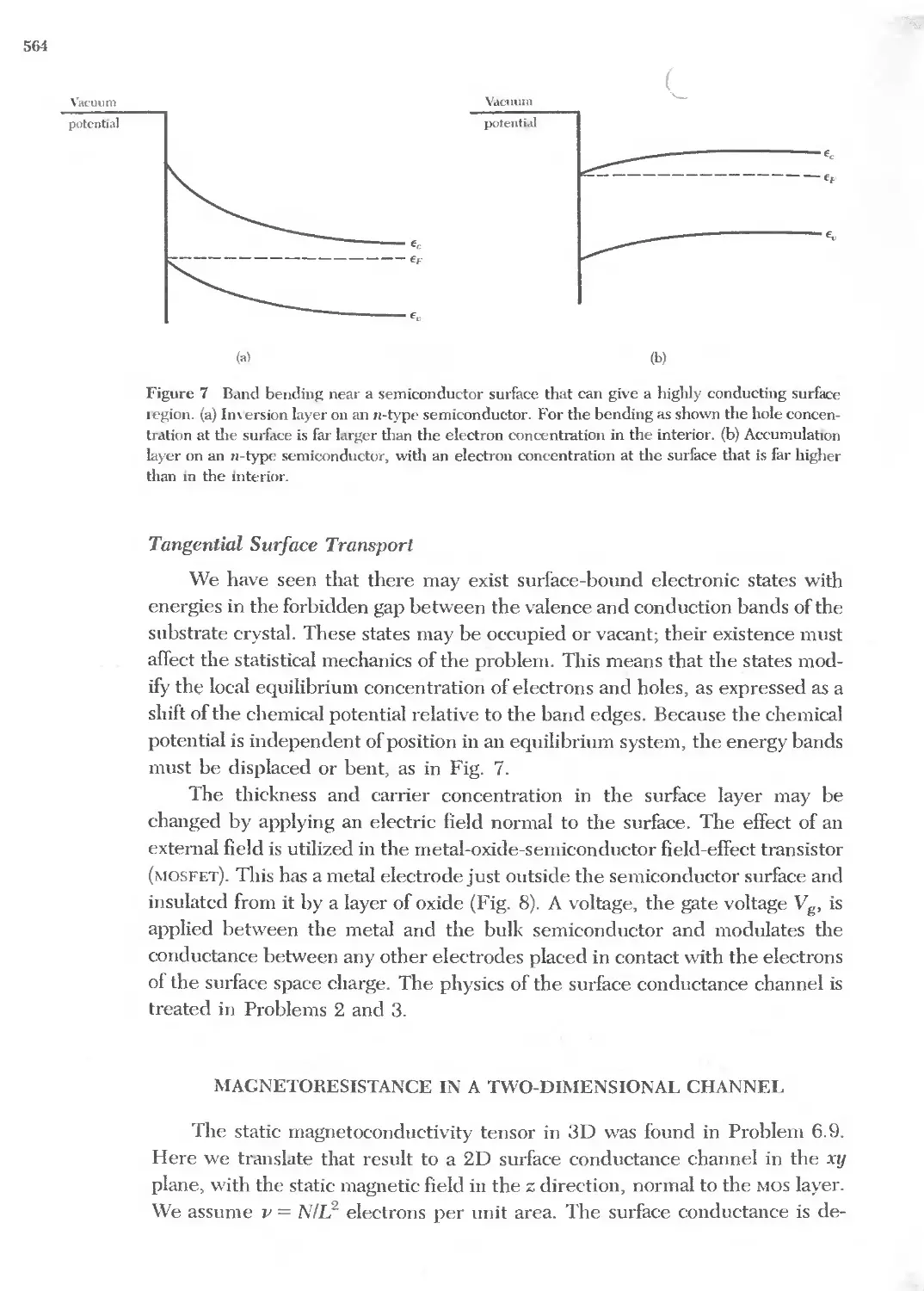
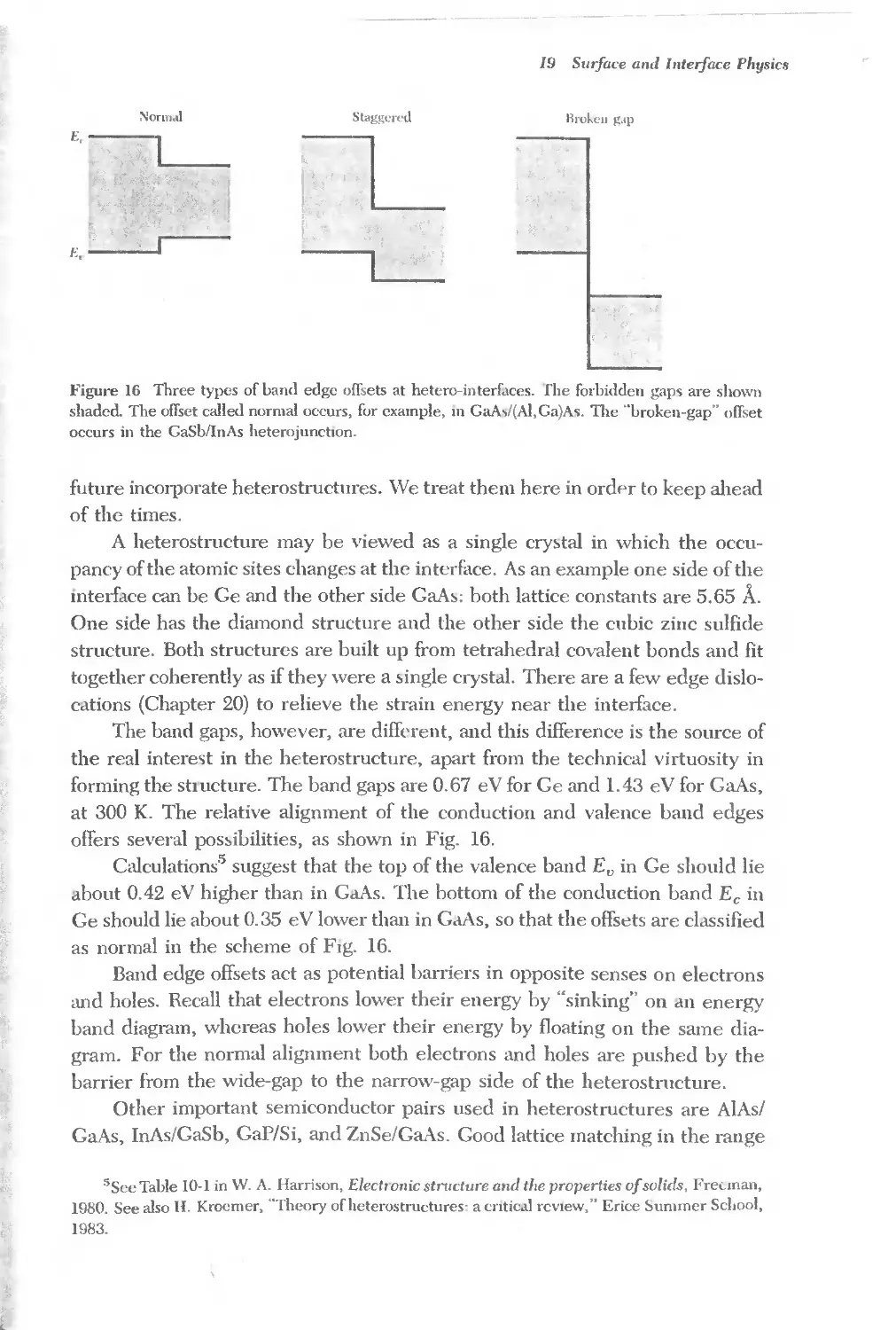
19 SURFACE AND INTERFACE PHYSICS
20 DISLOCATIONS
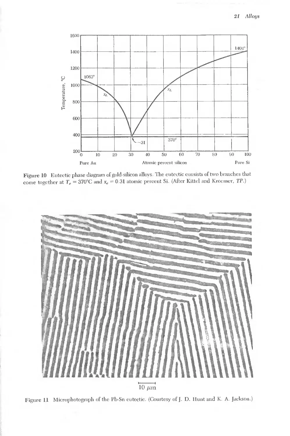
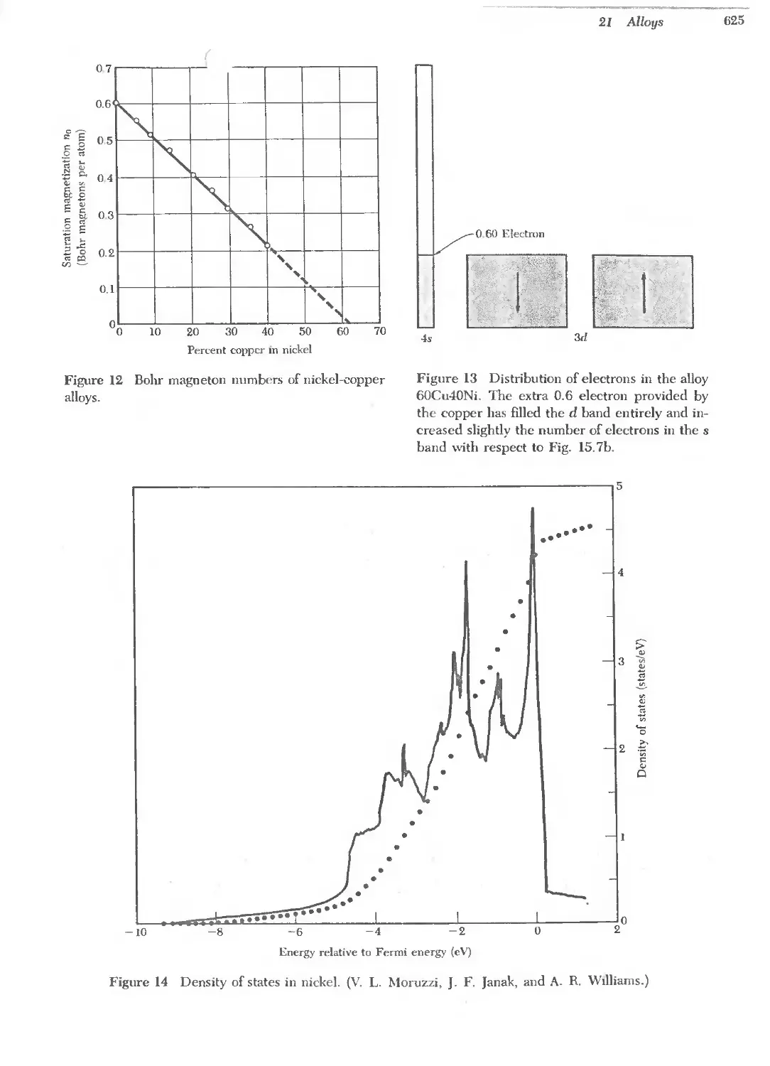
21 ALLOYS
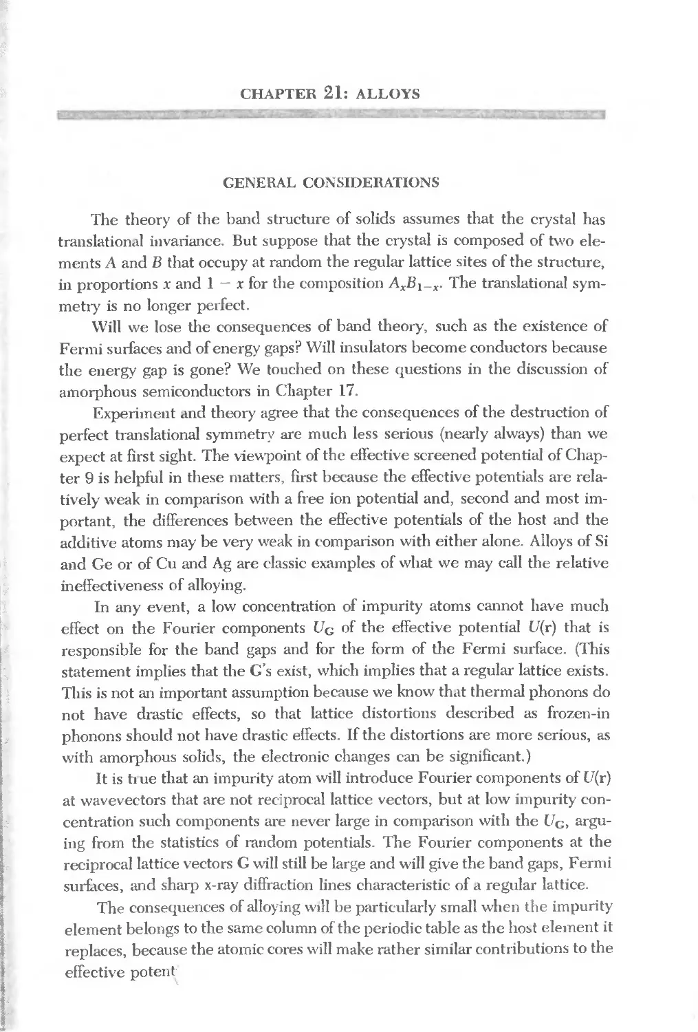
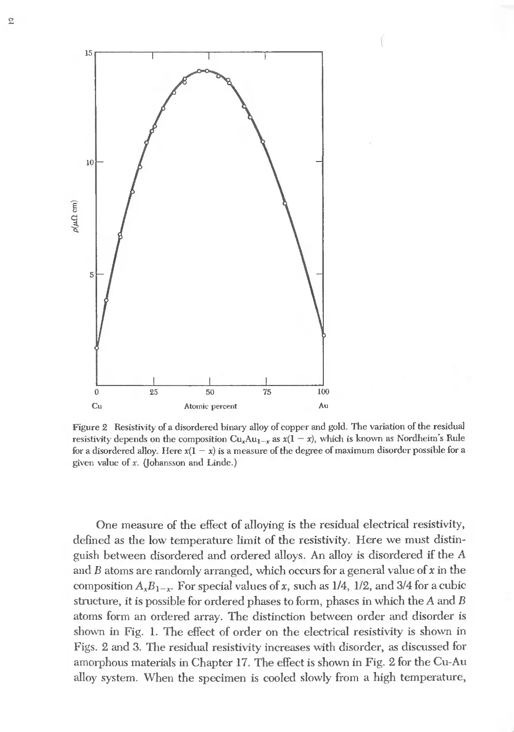
553
585
609
Appendix
A TEMPERATURE DEPENDENCE OF THE REFLECTION LINES 631
B EWALD CALCULATION OF LATTICE SUMS 634
C QUANTIZATION OF ELASTIC WAVES: PHONONS 638
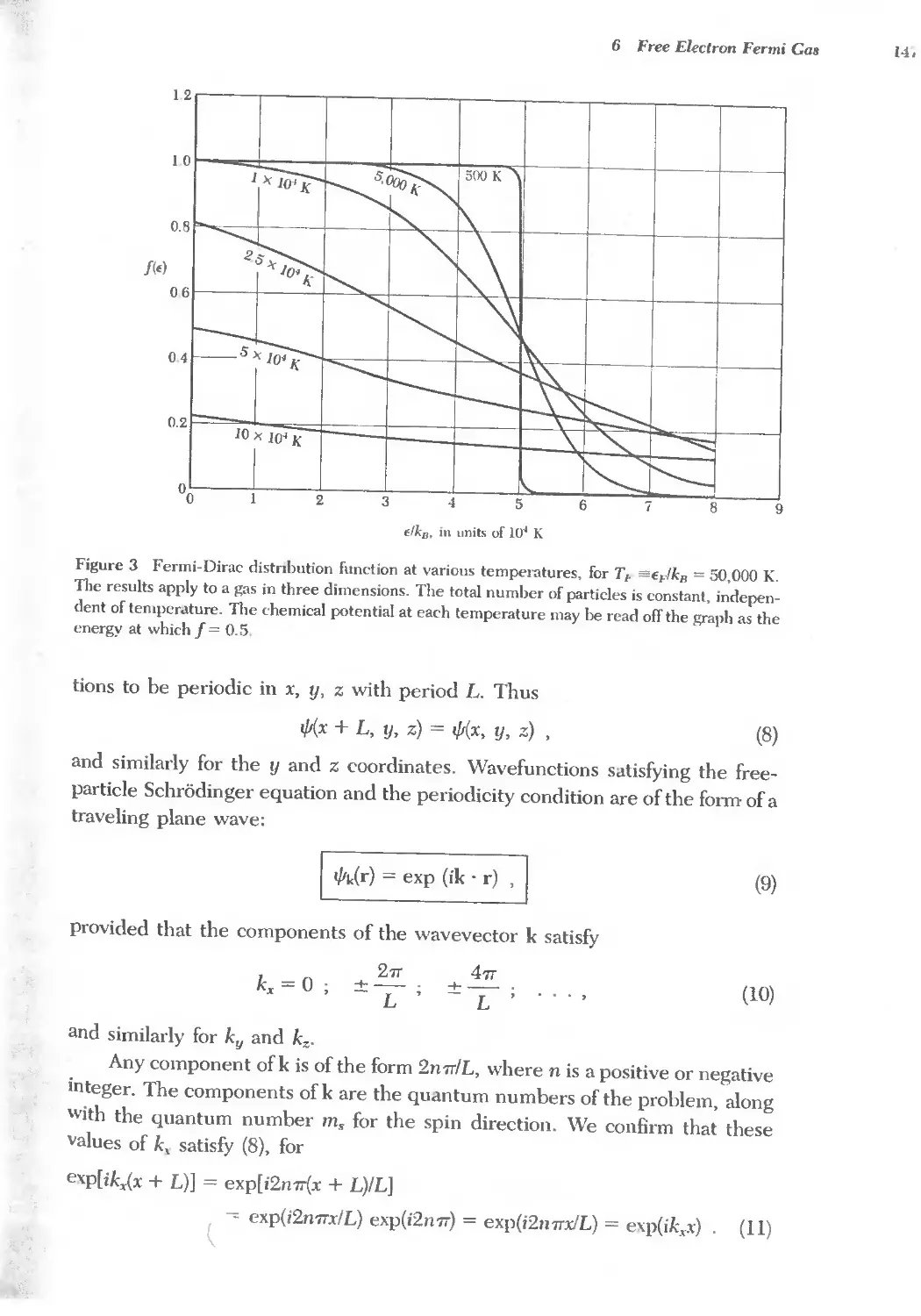
D FERMI-DIRAC DISTRIBUTION FUNCTION 643
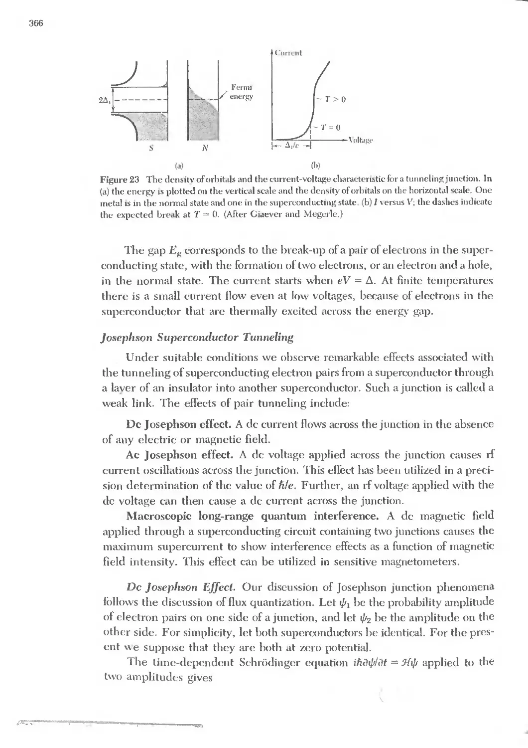
E DERIVATION OF dkJdt EQUATION 646
F BOLTZMANN TRANSPORT EQUATION 641
"- G VECTOR POTENTIAL, FIELD MOMENTUM, AND GAUGE
TRANSFORMATIONS 651
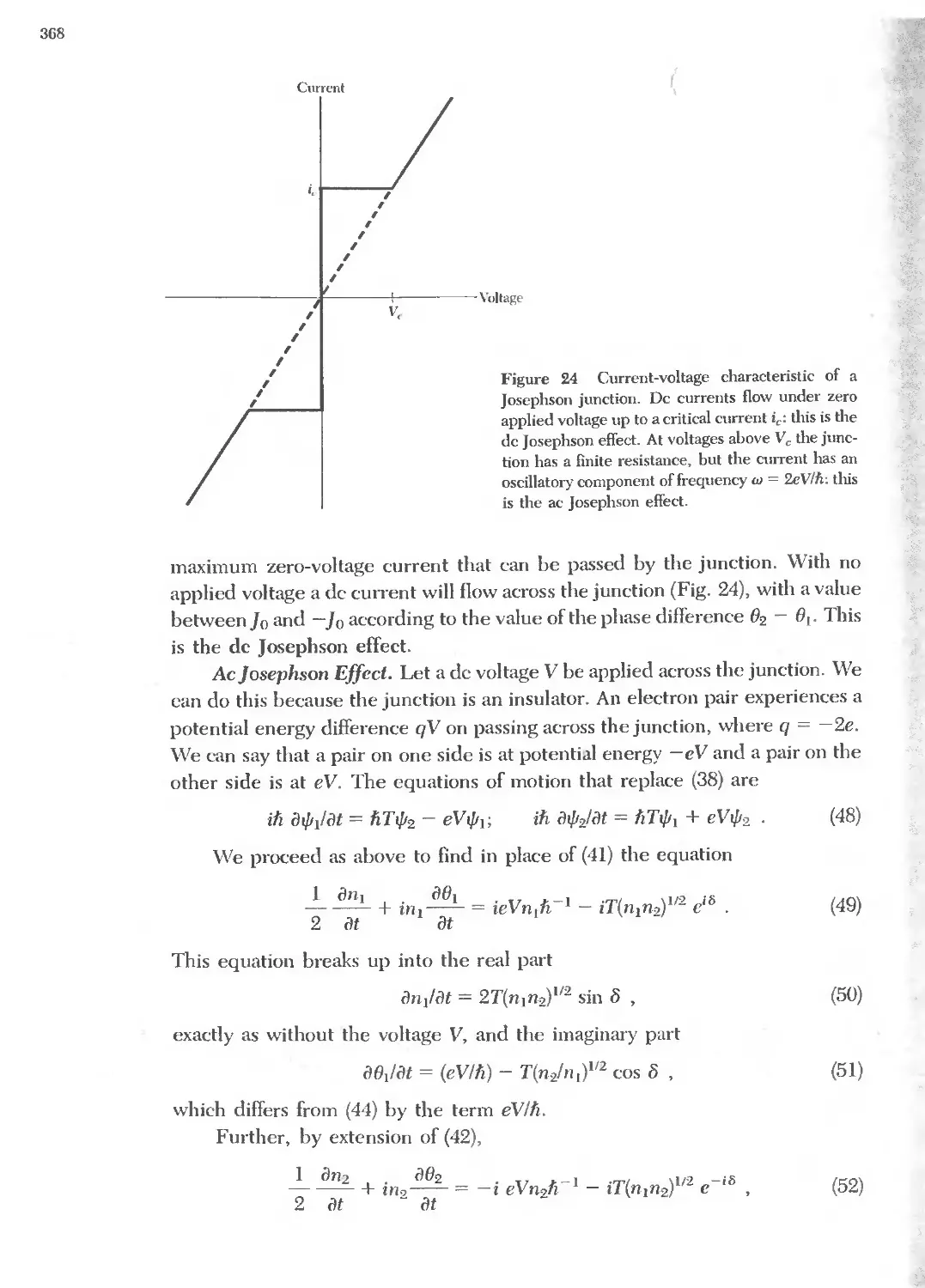
H COOPER PAIRS 656
I GINSBURG-LANDAU EQUATION 658
J ELECTRON-PHONON COLLISIONS 662
Subject Index 667
Table of SI Prefixes 613
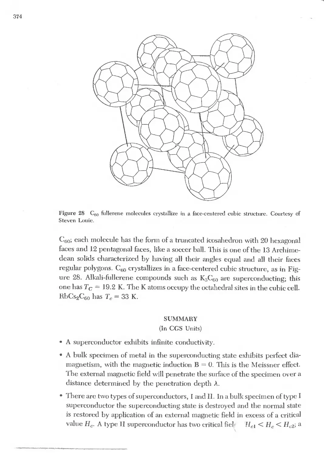
(
Guide to Tables
1.1 Fourteen lattice types in three dimensions 10
1.2 Characteristics of cubic lattices 12
1.3 Crystal structures of the elements 23
1.4 Density and atomic concentration of the elements 24
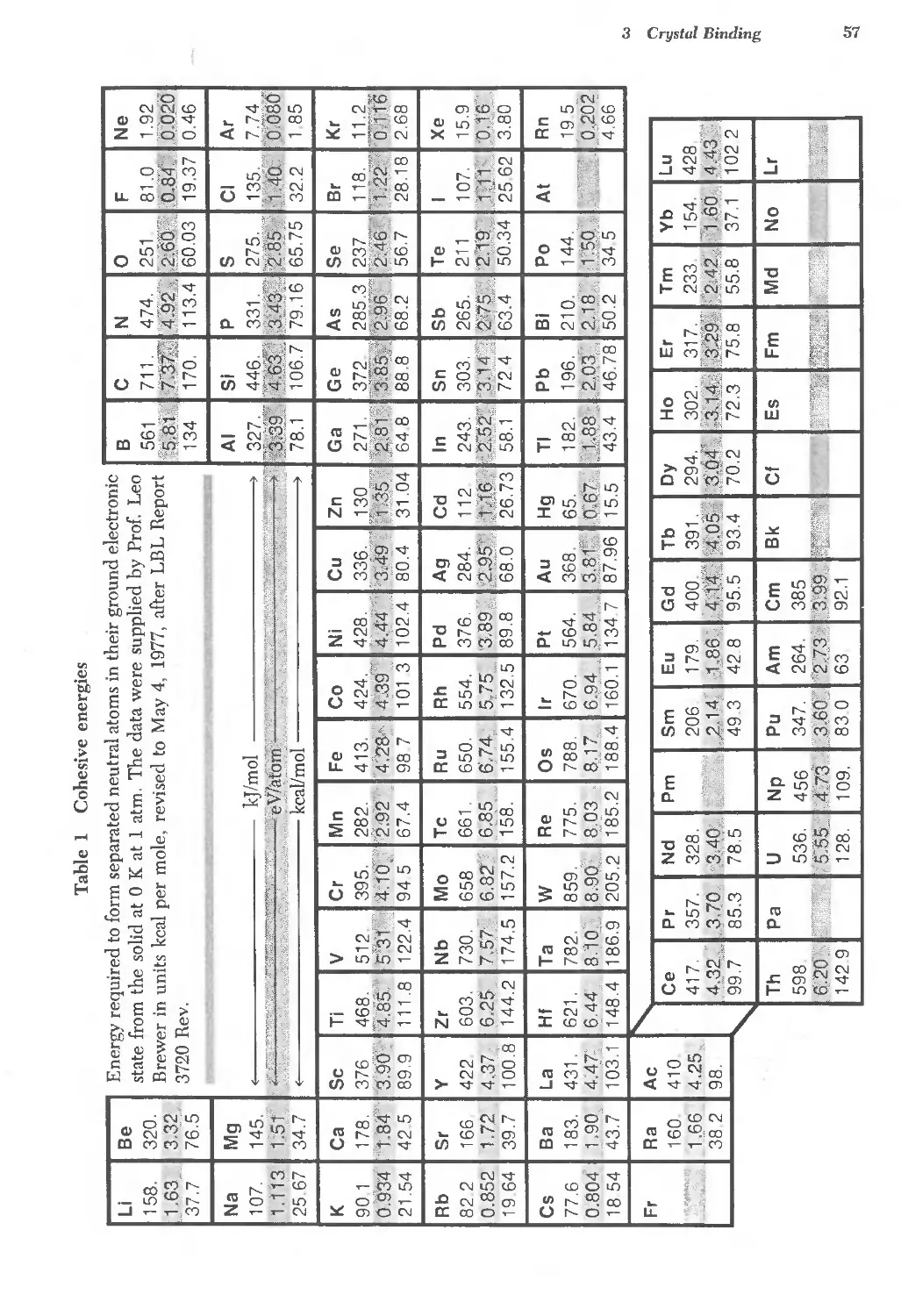
3.1 Cohesive energies of the elements 57
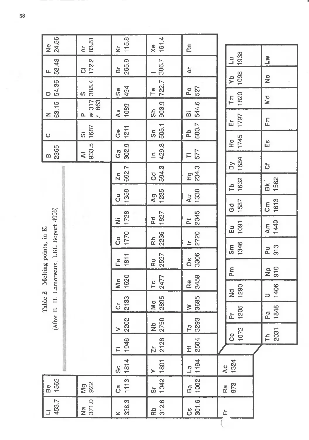
3.2 Melting temperatures of the elements 58
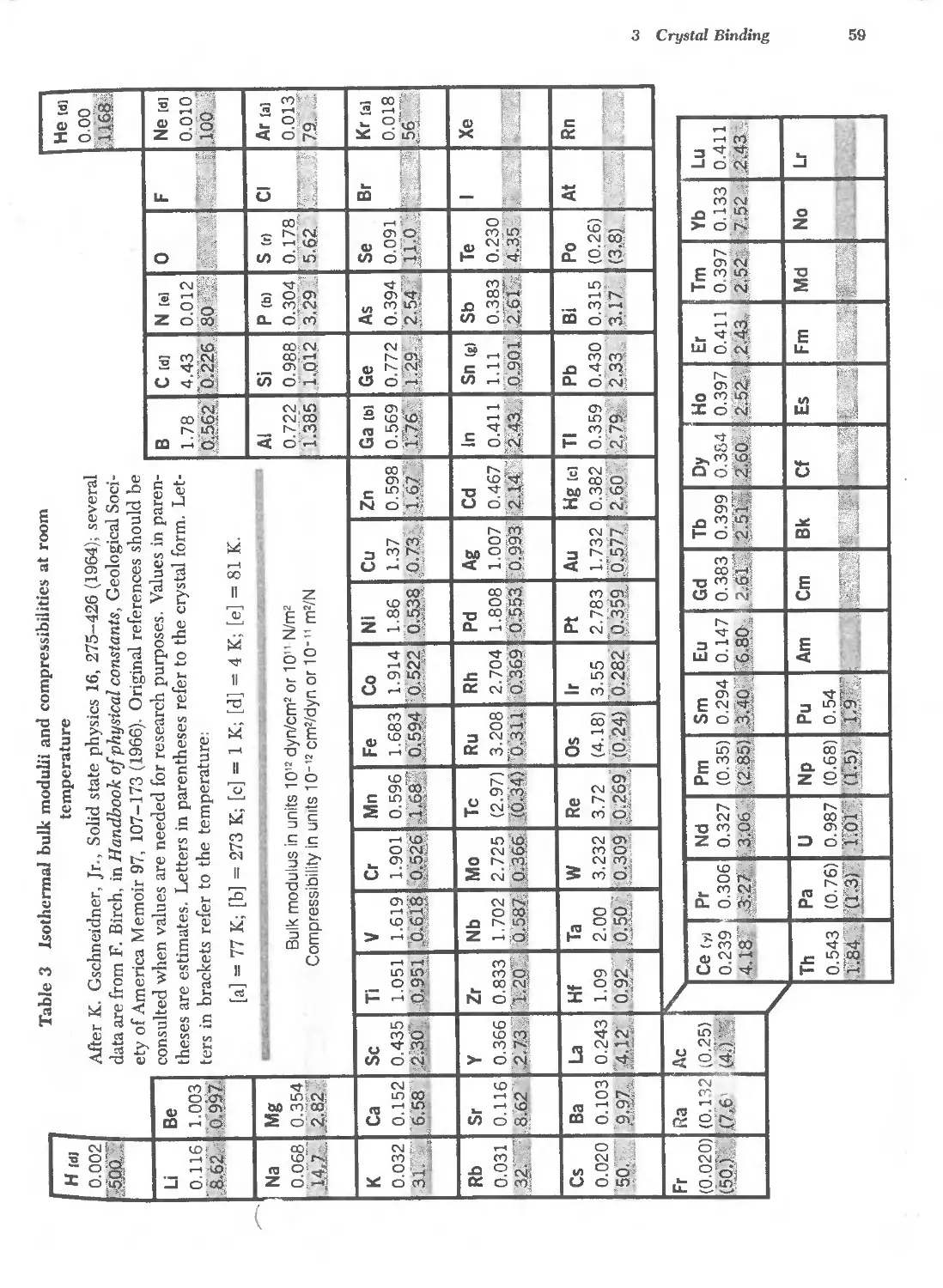
3.3 Bulk modulii and compressibilities of the elements 59
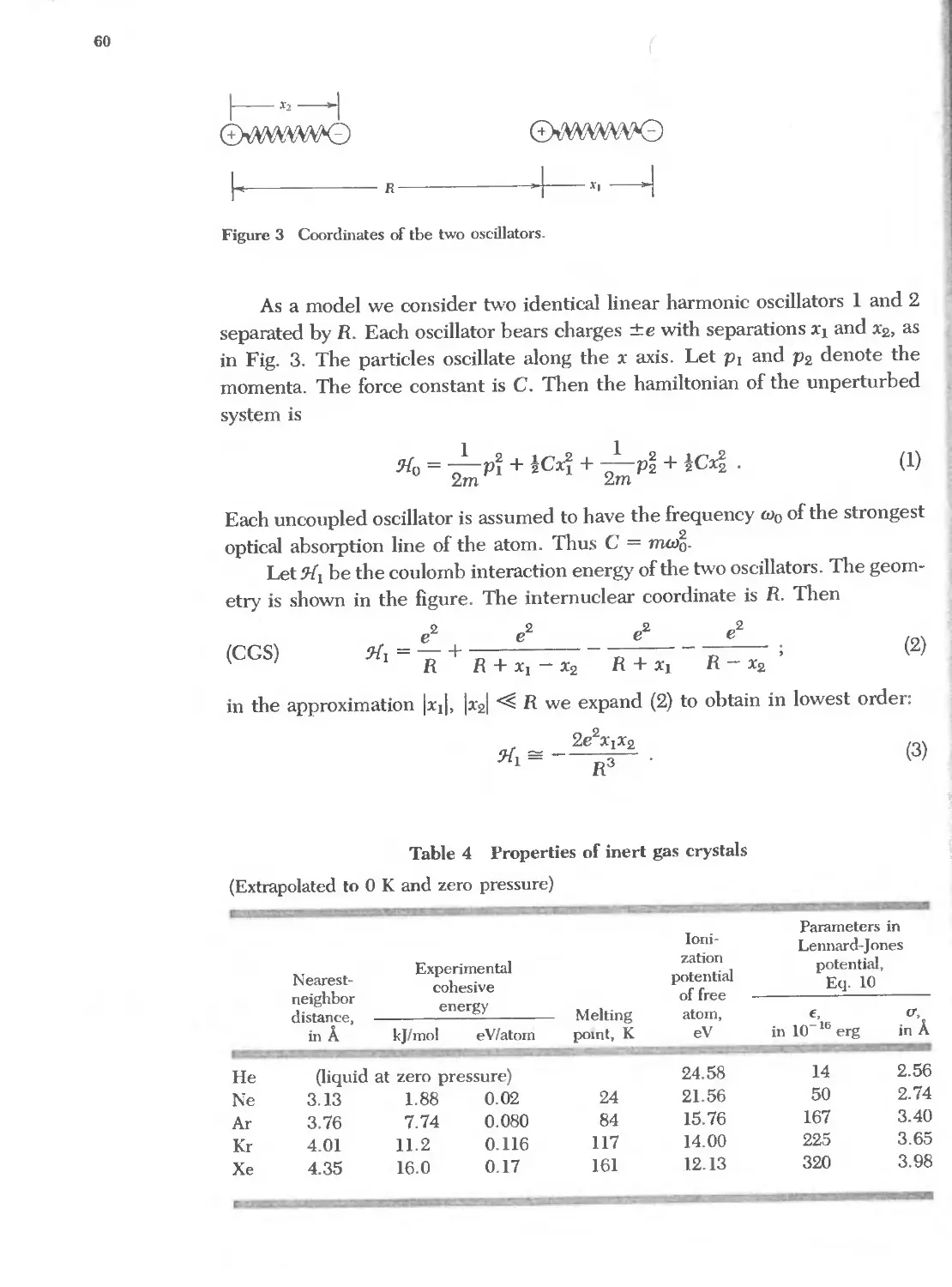
3.4 Properties of inert gas crystals 60
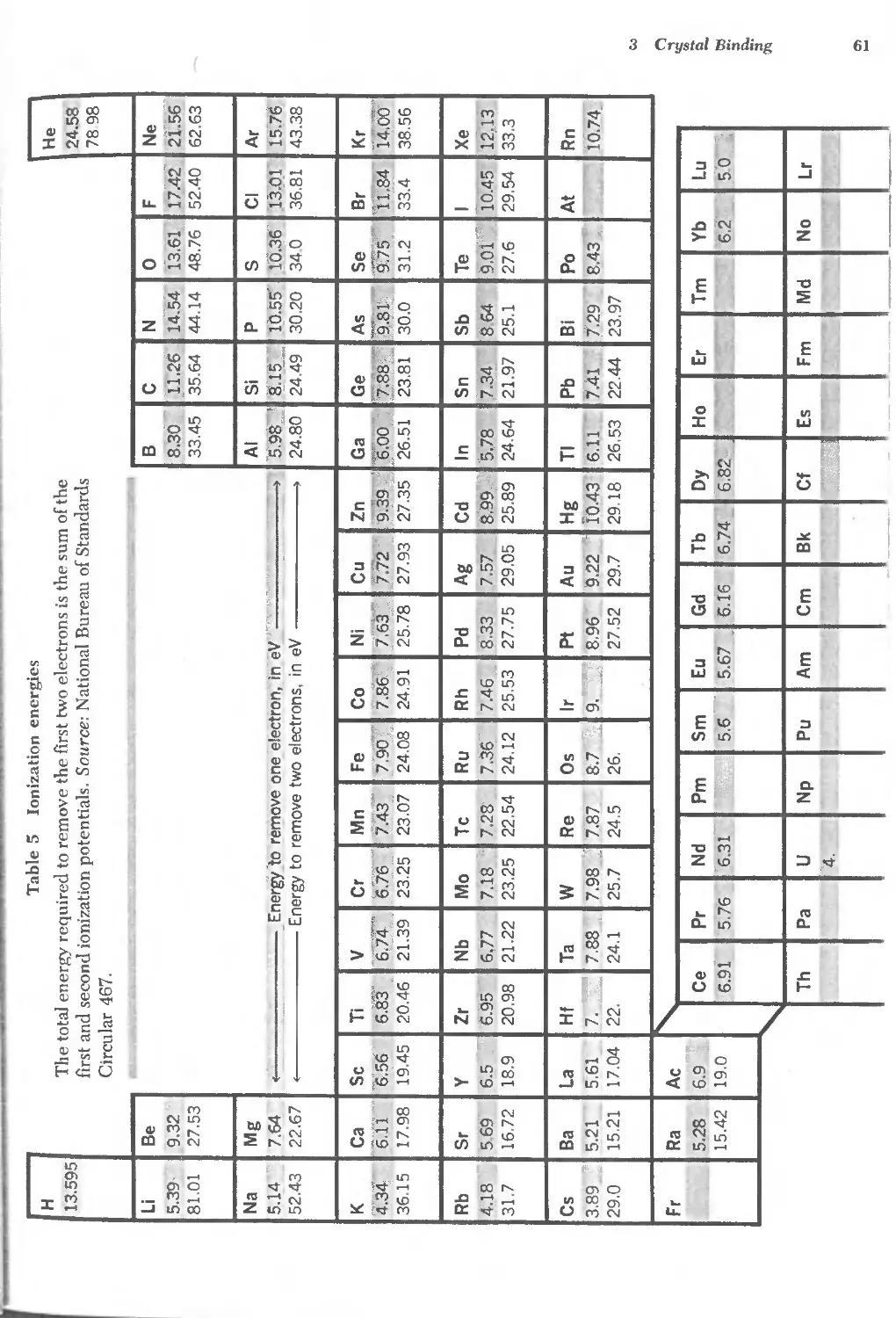
3.5 Ionization energies 61
3.6 Electron affinities of negative ions 68
3.7 Properties of alkali halide crystals 73
3.8 Fractional ionic character of bonds 76
3.9 Atomic and ionic radii 78
3.10 Standard radii of ions 79
3.11 Elastic stiffness constants of cubic crystals at 0 K and 300 K 91
3.12 Elastic stiffness constants of cubic crystals at 300 K 92
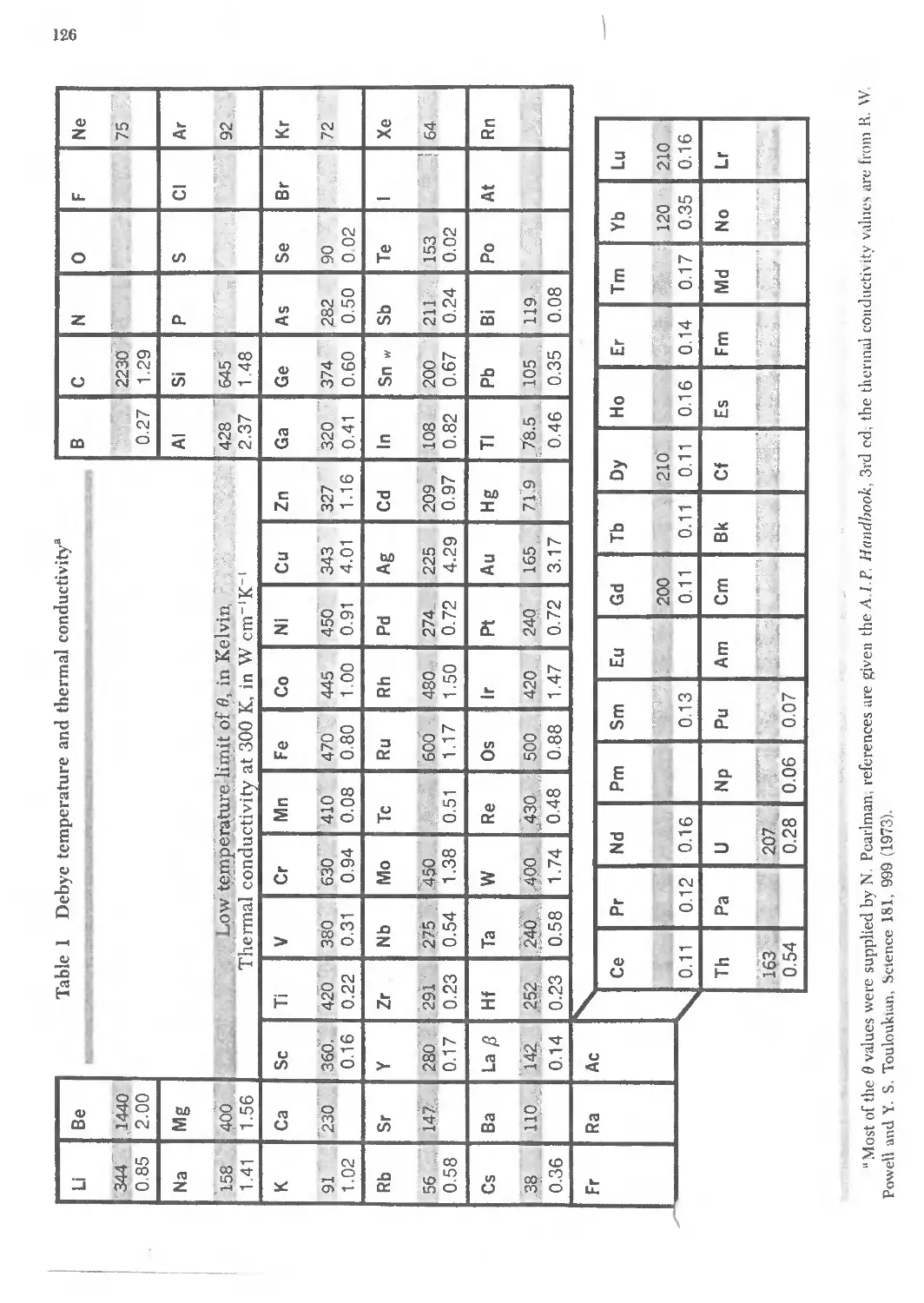
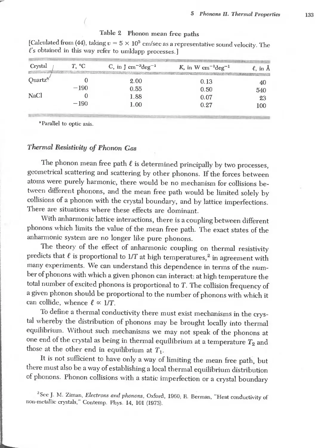
5.1 Debye temperature and thermal conductivity 126
5.2 Phonon mean free paths 133
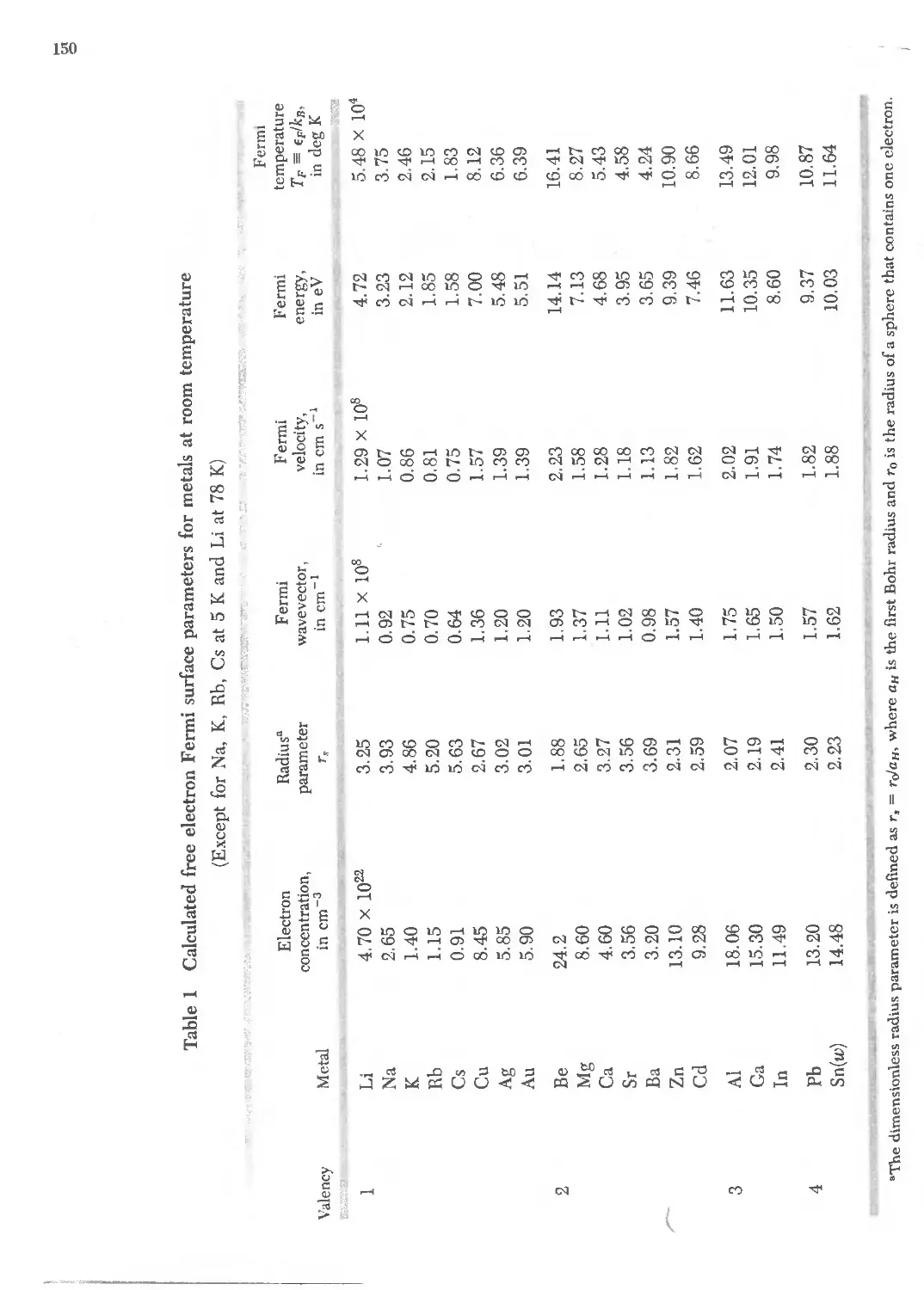
6.1 Free electron Fermi surface parameters for metals 150
6.2 Electron heat capacity of metals 157
6.3 Electrical conductivity and resistivity of metals 160
6.4 Hall coefficients 167
6.5 Lorenz numbers 168
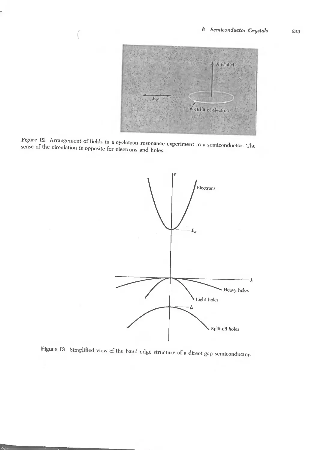
8.1 Energy gaps in semiconductors 201
8.2 Effective masses of holes and electrons 214
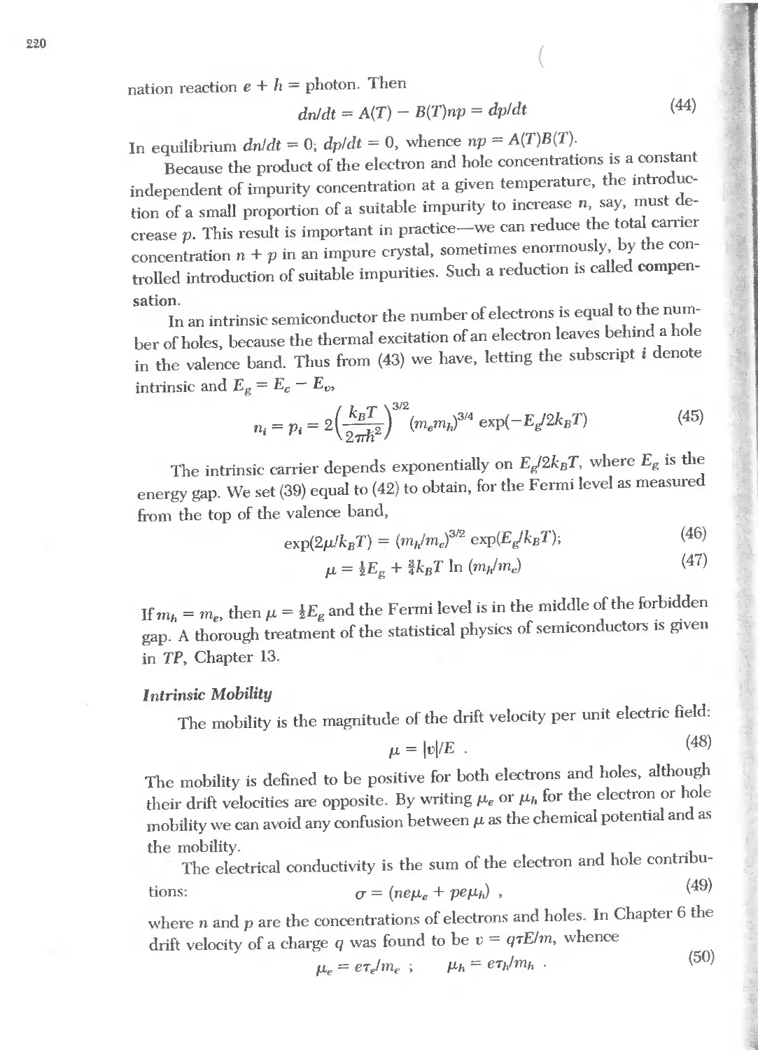
8.3 Carrier mobilities at room temperature 221
8.4 Static dielectric constants of semiconductors 223
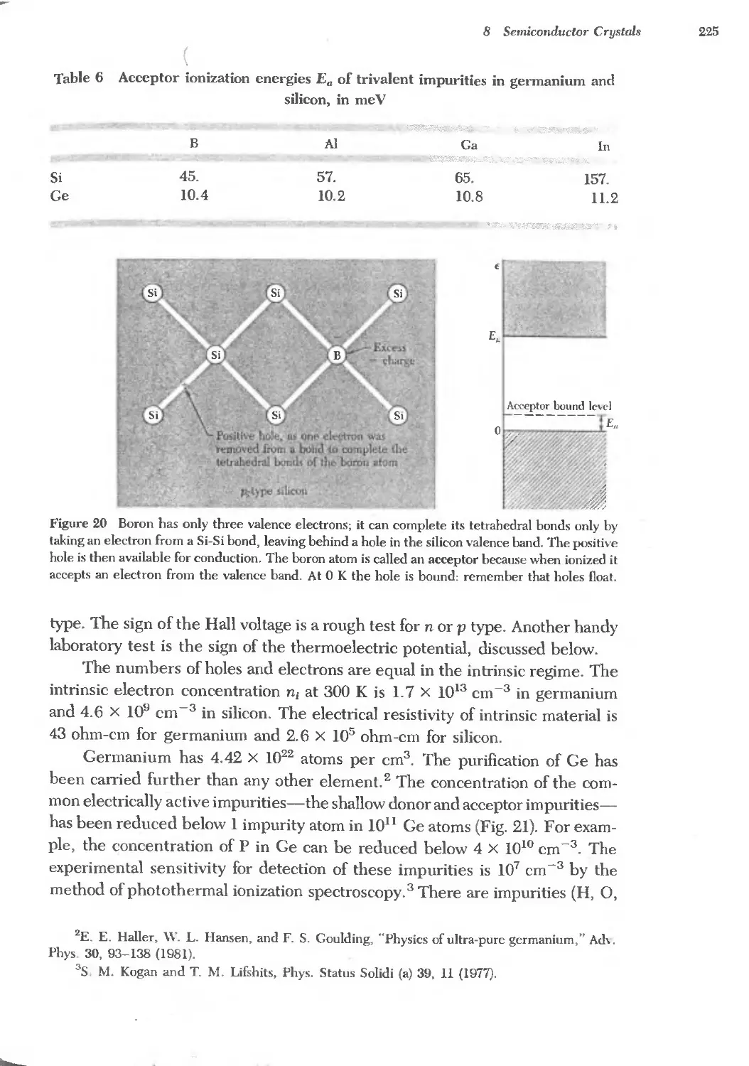
8.5 Donor ionization energies 224
8.6 Acceptor ionization energies 225
8.7 Electron and hole concentrations in semimefals 229
ix
x
10.1 Ultraviolet transmission limits of alkali metals 275
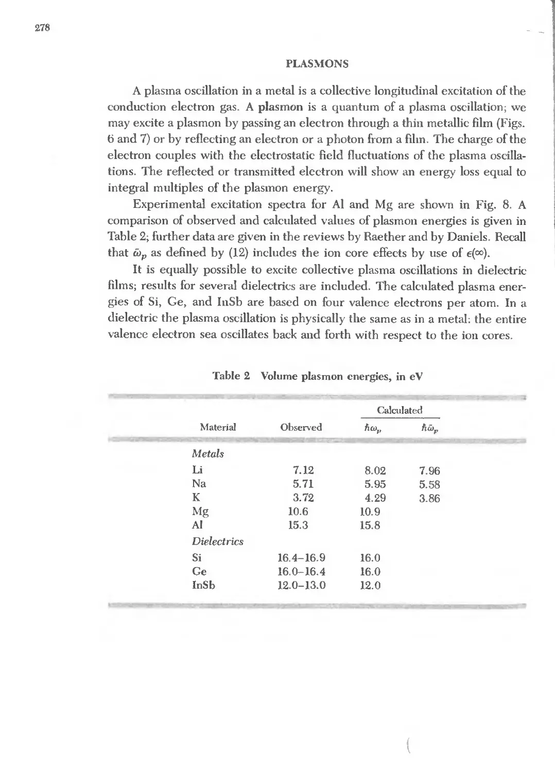
10.2 Volume plasmon energies 278
10.3 Lattice frequencies 292
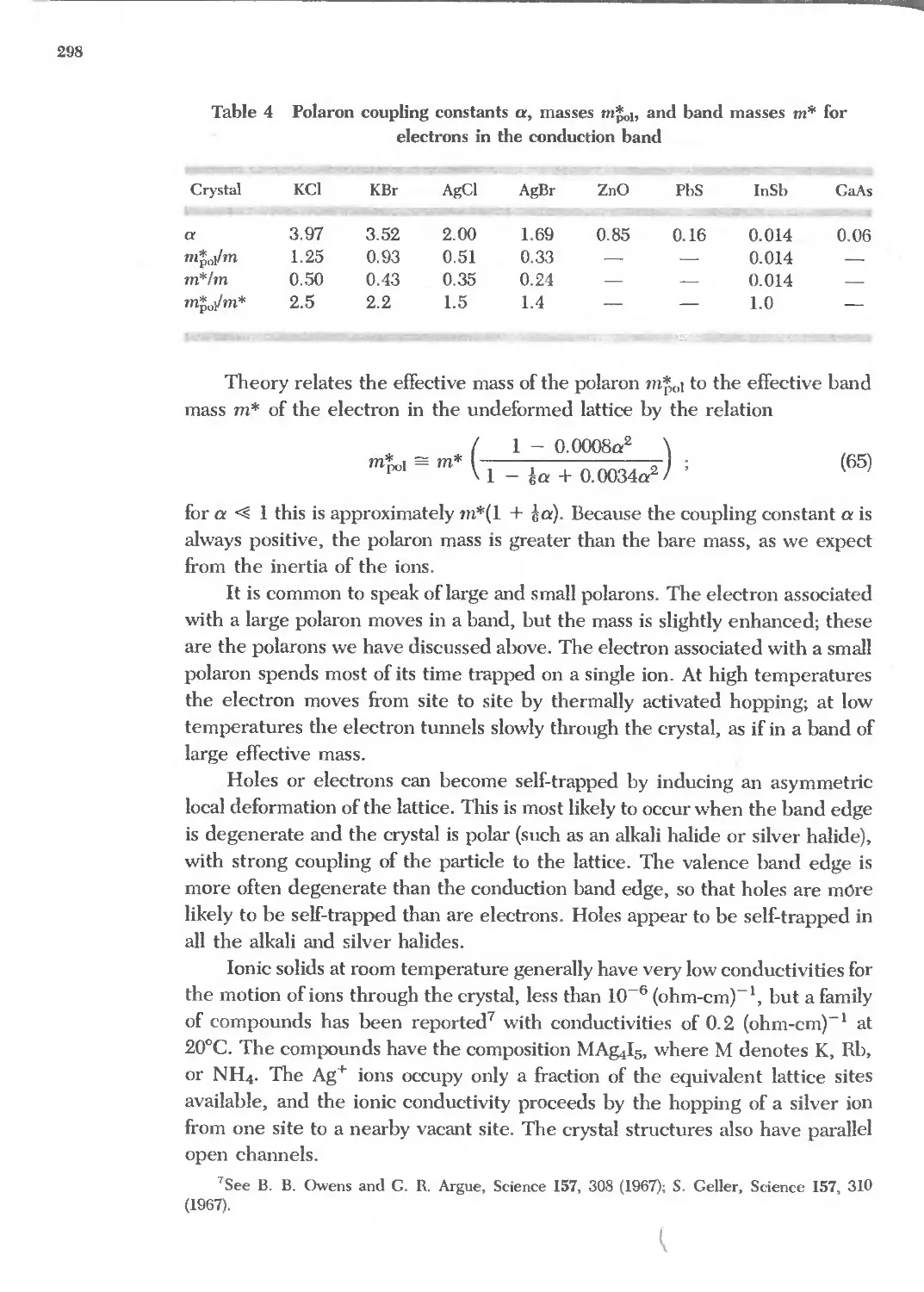
lOA Polaron masses and coupling constants 298
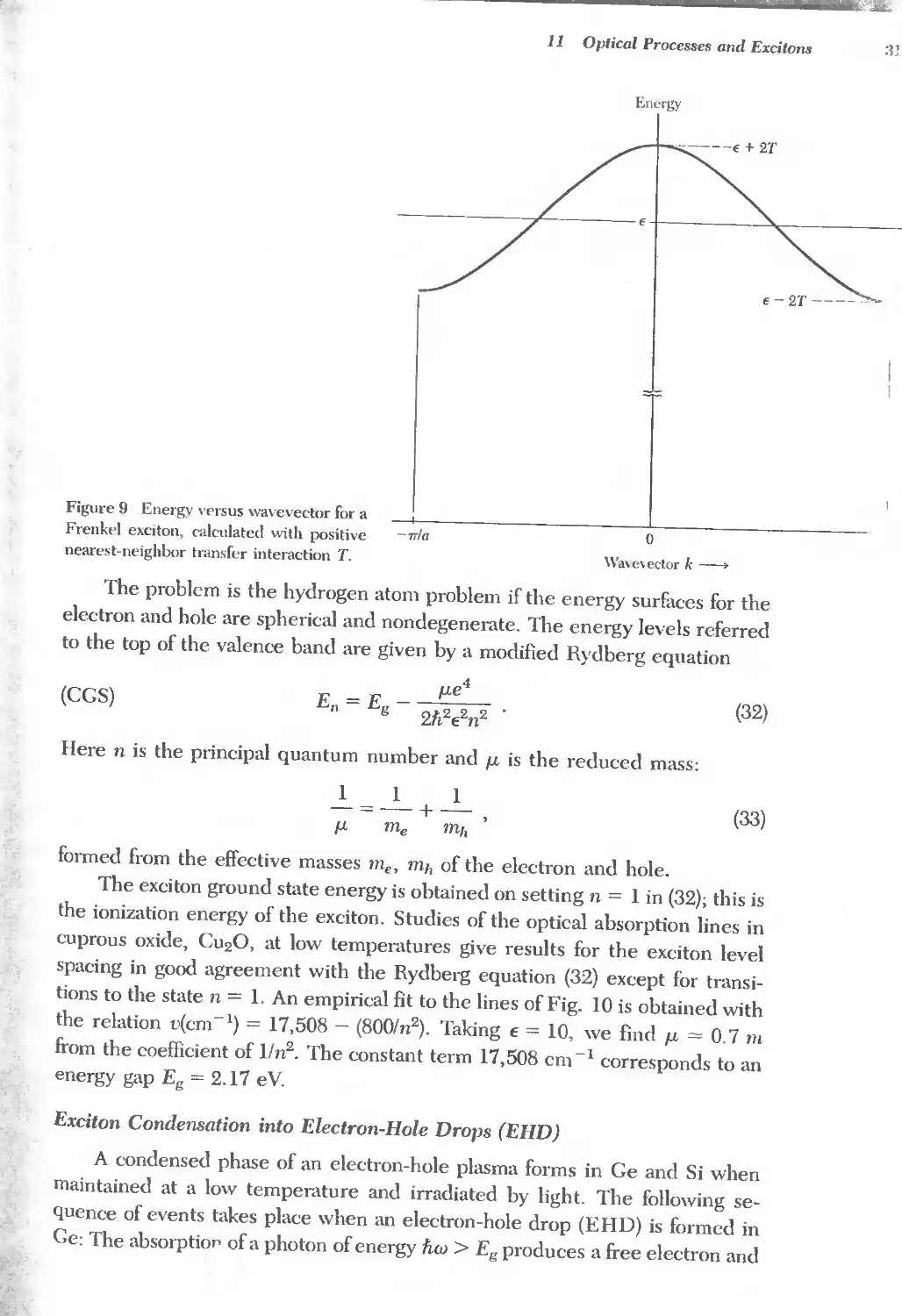
11.1 Exciton binding energies 314
11.2 Electron-hole liquid parameters 322
11.3 Acronyms of current experimental methods for band structure studies 328
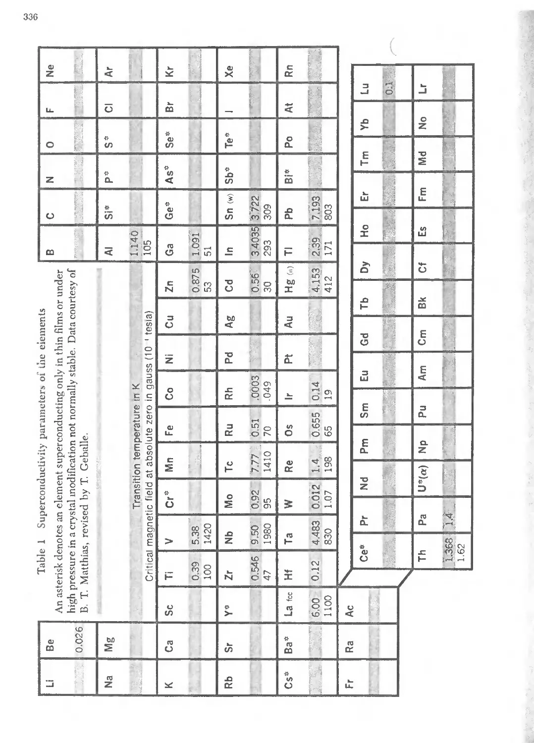
12.1 Superconductivity parameters of the elements 336
12.2 Superconductivity of selected compounds 338
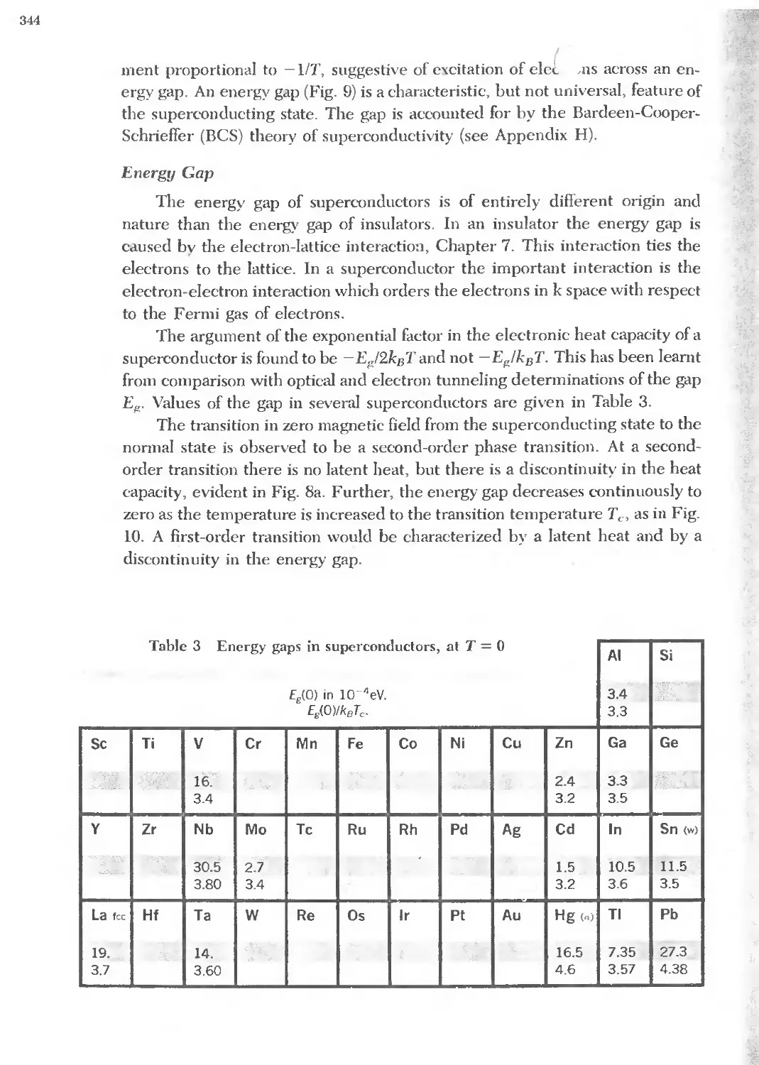
12.3 Energy gaps in superconductors 344
1204 Isotope effect in superconductors 347
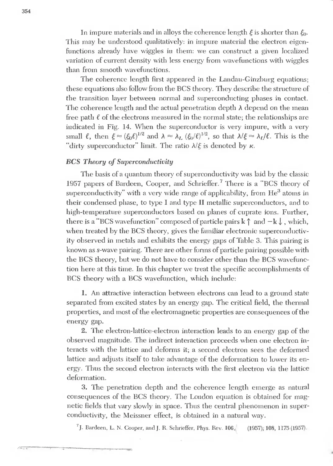
12.5 Coherence length and penetration depth 353
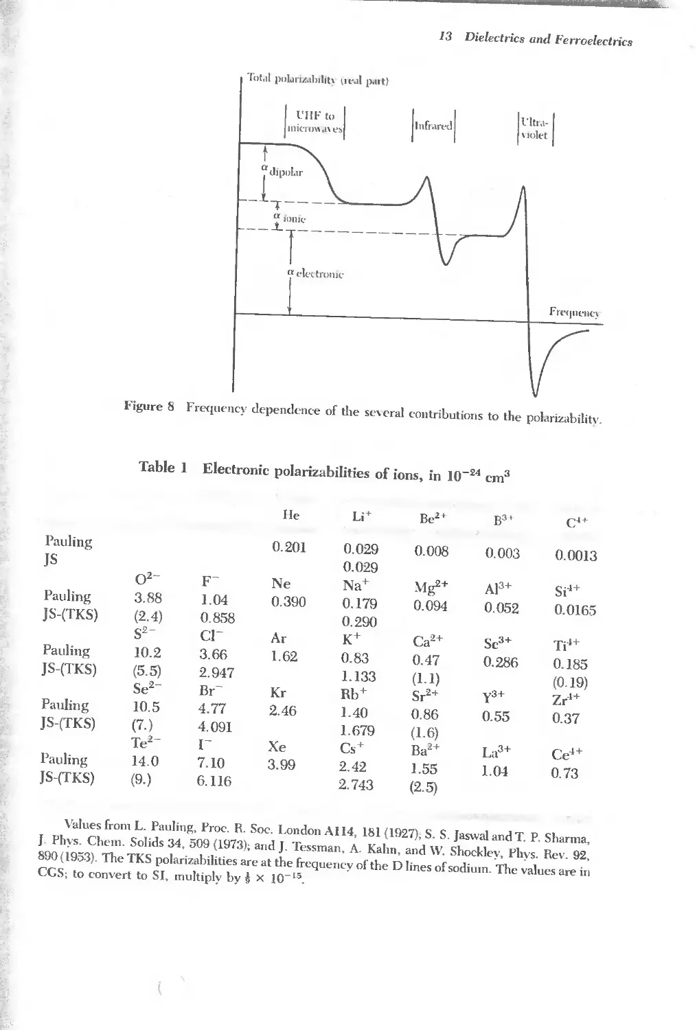
13.1 Electronic polarizabilities of ions 391
13.2 Ferroelectric crystals 396
..... 13.3 Antiferroelectric crystals 406
14.1 Magneton numbers of lanthanide group ions 425
14.2 Magneton numbers of iron group ions 426
15.1 Critical point exponents of ferromagnets 445
15.2 Ferromagnetic crystals 449
15.3 Antiferromagnetic crystals 465
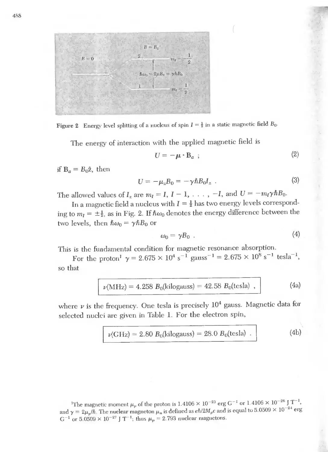
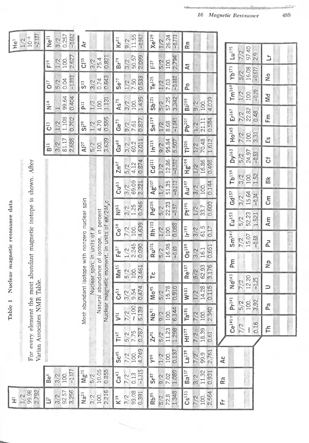
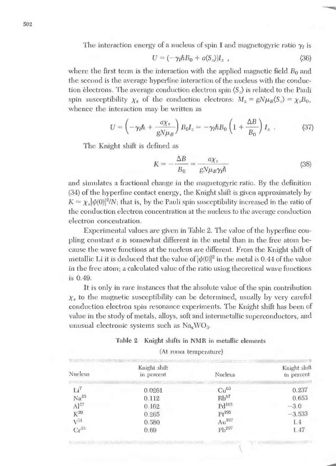
16.1 Nuclear magnetic resonance data 489
16.2 Knight shifts in NMR 502
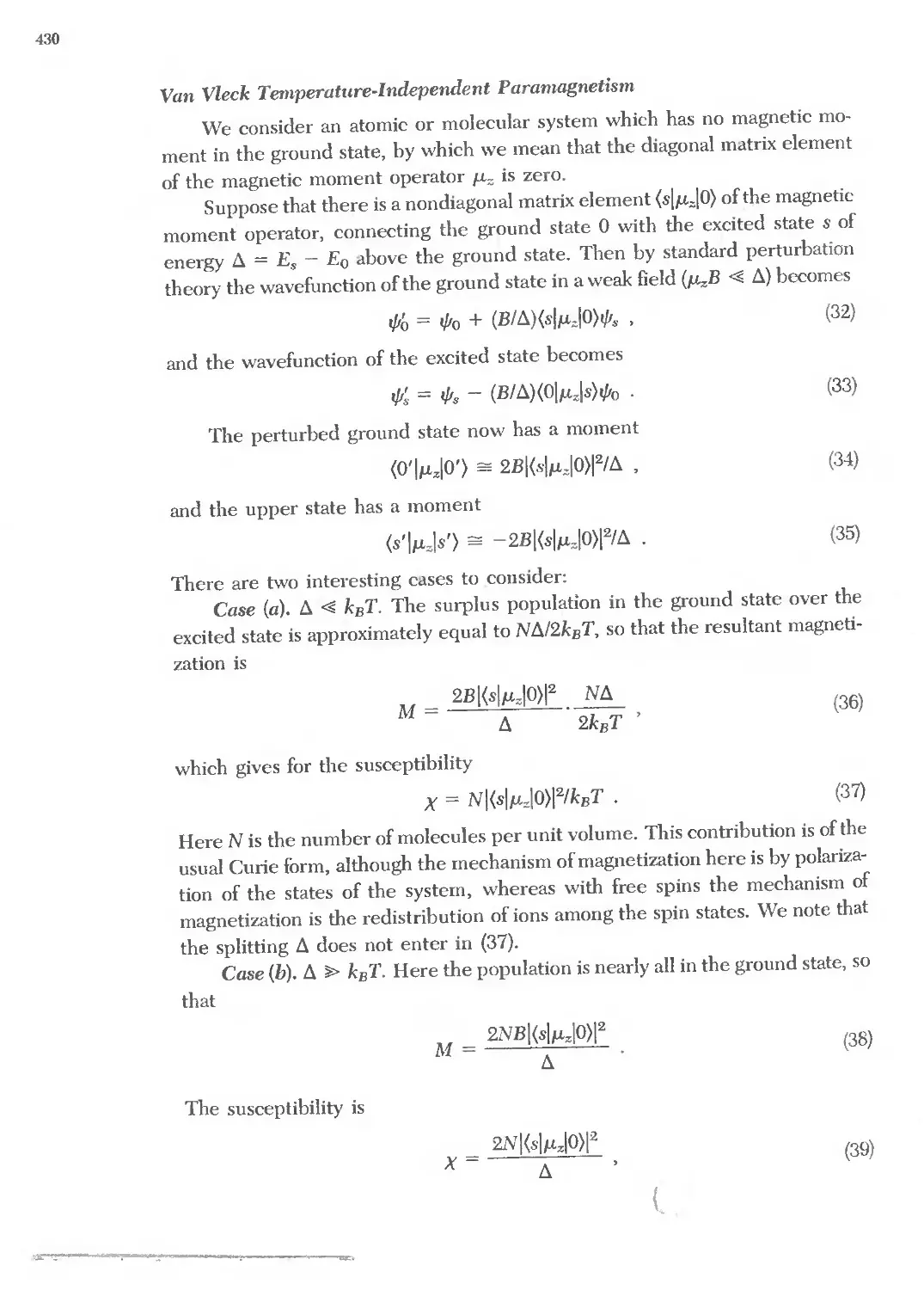
18.1 Diffusion constants and activation energies 545
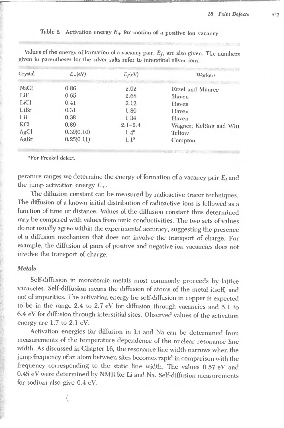
18.2 Activation energy for a positive ion vacancy 547
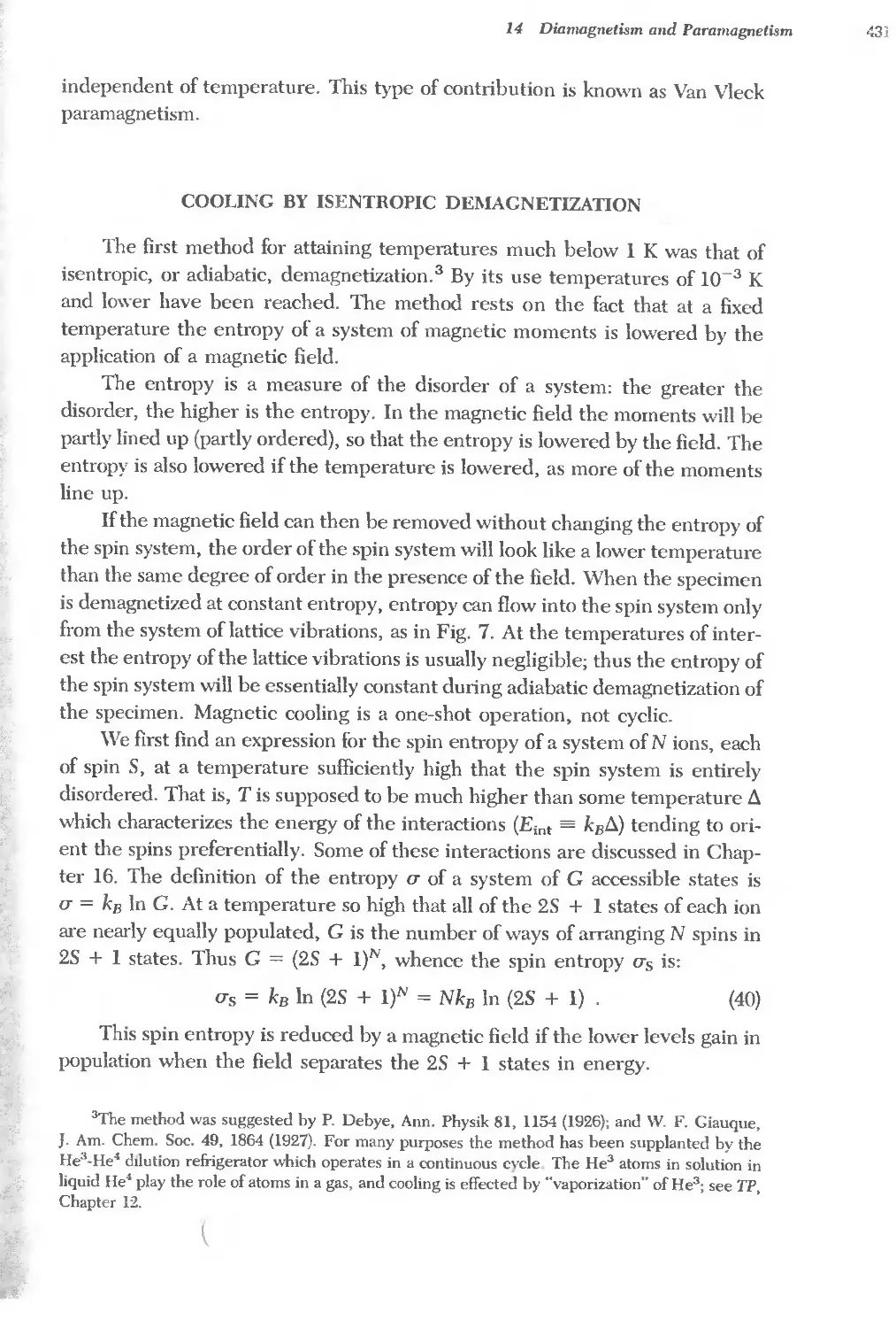
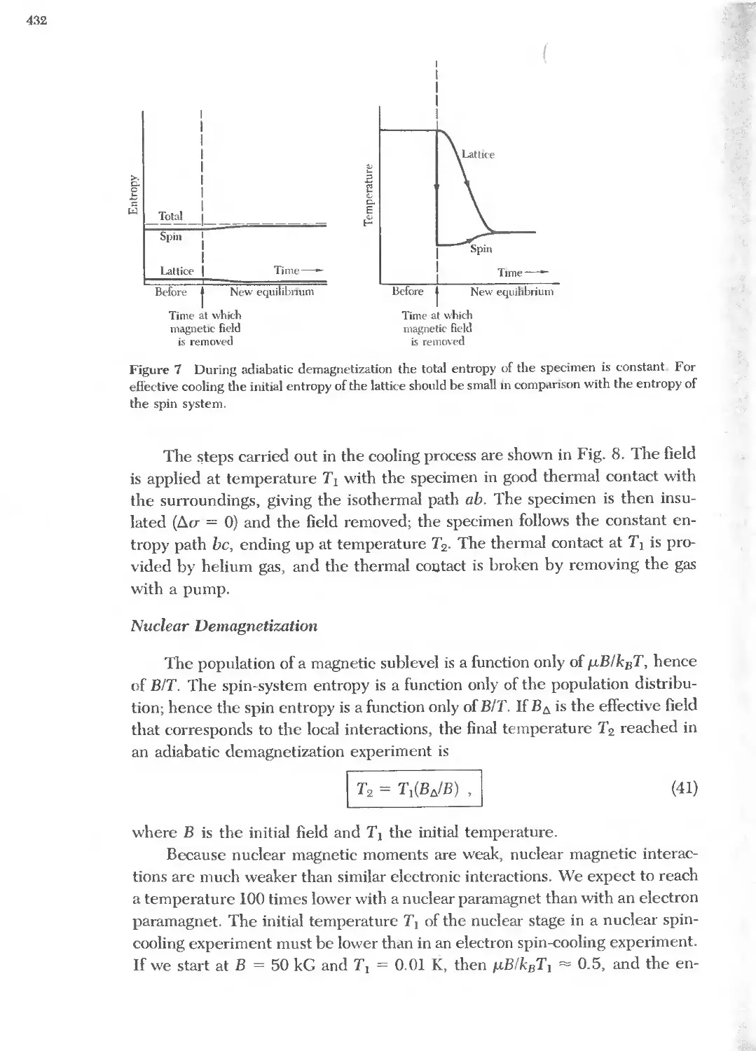
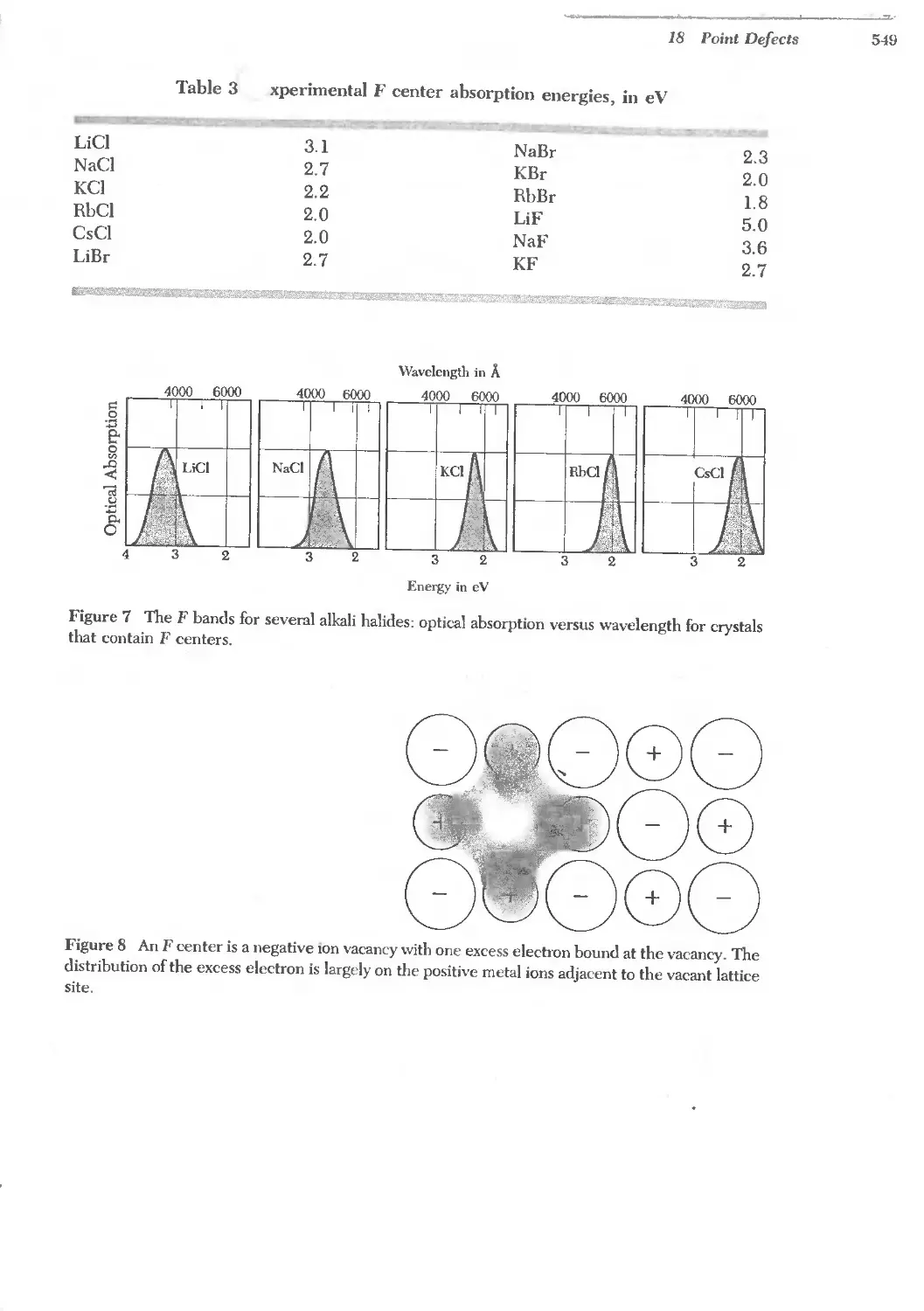
18.3 Experimental F center absorption energies 549
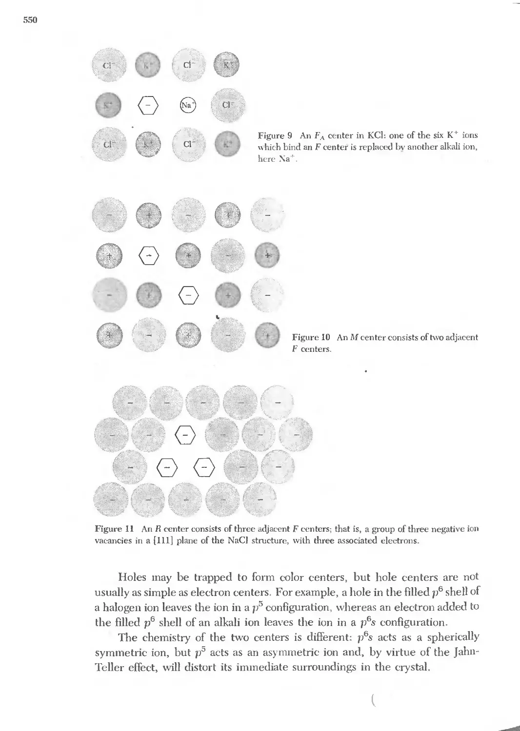
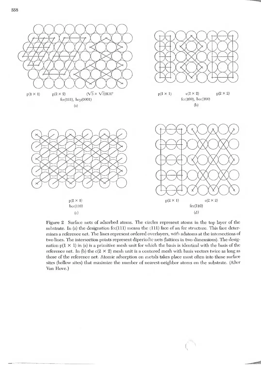
19.1 Top layer atomic relaxation 556
19.2 Electron work functions 562
20.1 Elastic limit and shear modulus 588
20.2 Dislocation densities 598
21.1 Electron/atom ratios of electron compounds 616
(
Selected General References
Statistical physics background
C. Kittel and H. Kroemer, Thel7nal physics, 2nd ed., Freeman, 1980. Has a full,
dear discussion of the chemical potential and of semiconductor statistics; cited as
TP.
Intermediate text
J. M. Ziman, Principles of the theory of solick, Cambridge, 1972.
Advanced texts
C. Kittel, Quantum theory of solick, 2nd re\ised printing, Wiley, 1987, with solu-
tions appendix by C. Y. Fong; cited as QTS.
J. Callaway, Quantum theory of the solid state, 2nd ed., Academic, 1991.
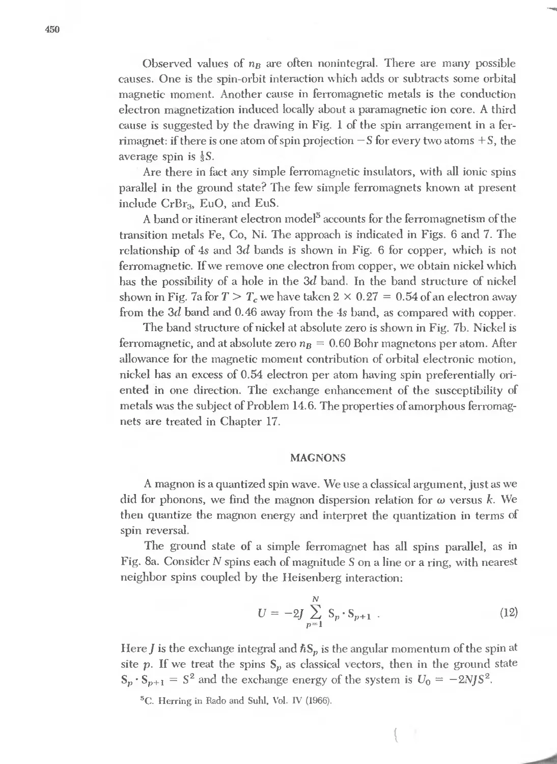
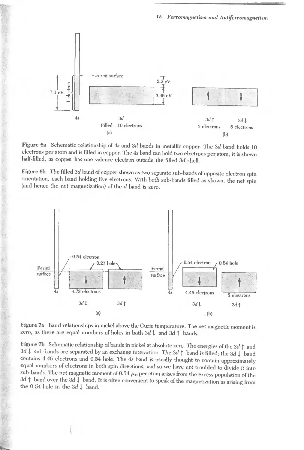
Applied solid state
R. Dalven, Introduction to applied solid state physics, 2nd ed., Plenum, 1990. A
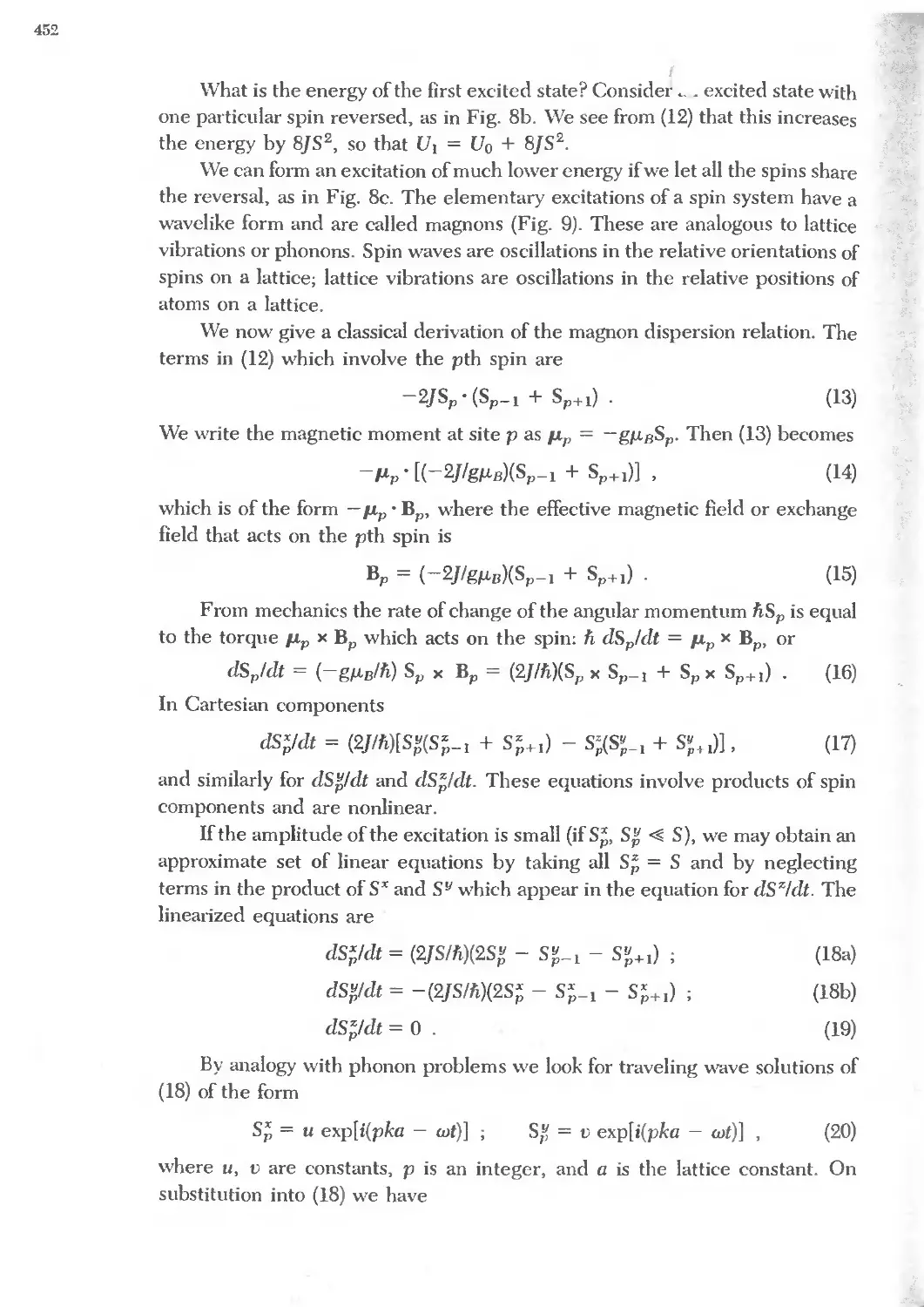
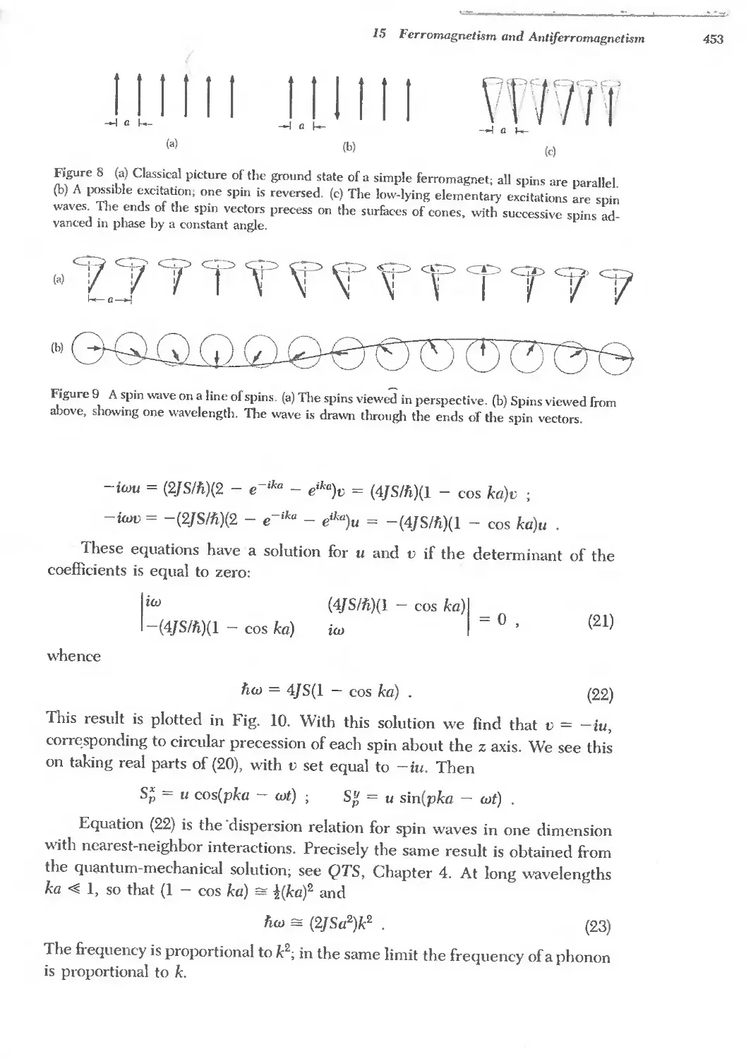
readable introduction to representative areas in a vast field.
Review series
F. Seitz and others, Solid state physics, admnces in research and applications,
Vols. 1-(48}, plus supplements. This valuable continuing series is often cataloged as
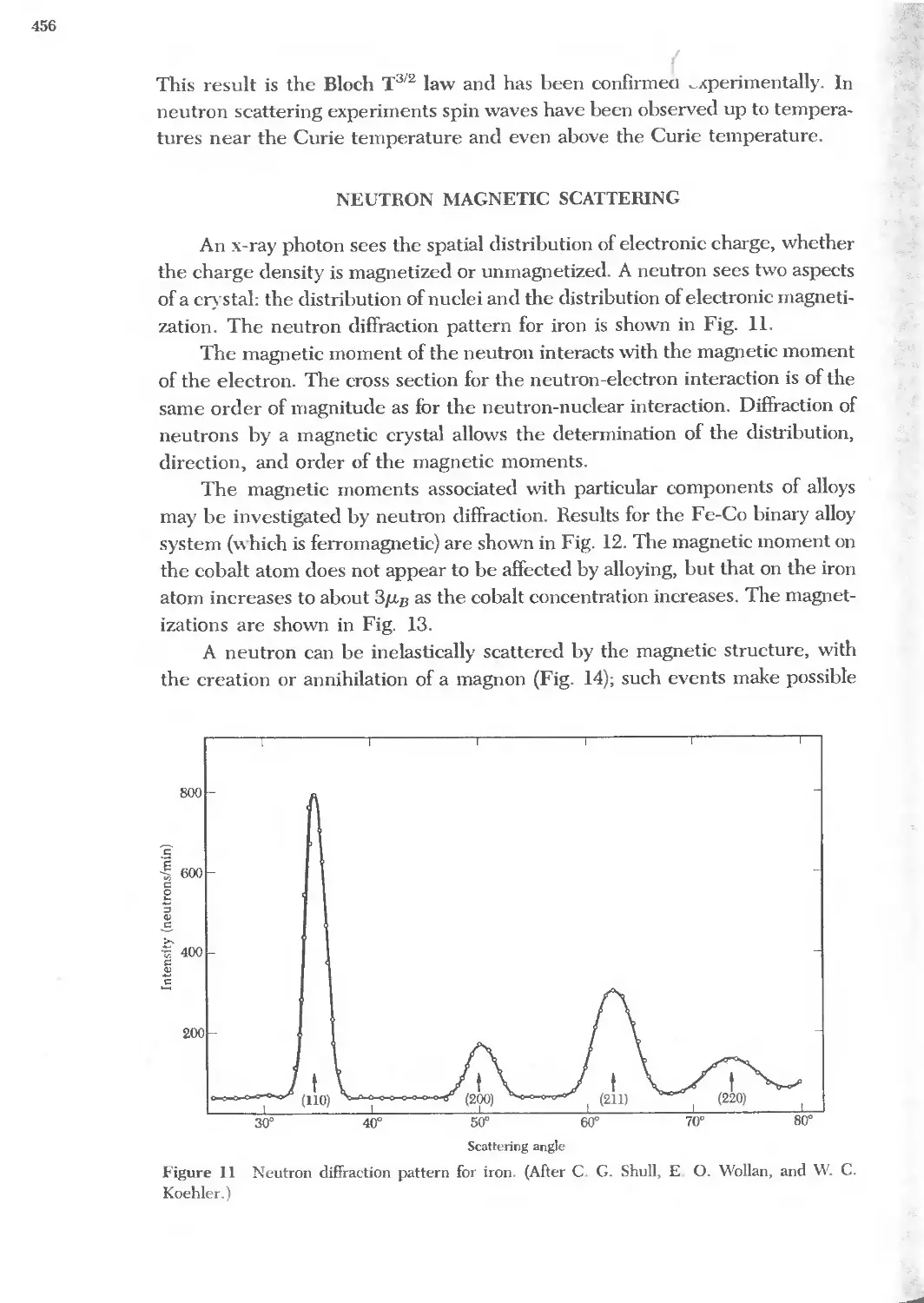
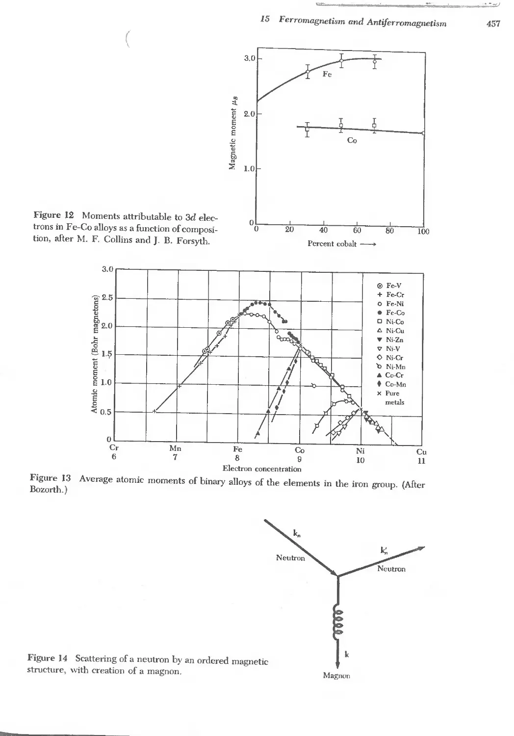
a serial, as if it were a journal, and is cited here as Solid state physics.
Literature guides
There are many good databases, library and organizational; this is the way to go for
monograph and journal searches.
(
>.;
{
.....
1
Crystal Structure
PERIODIC ARRAYS OF ATOMS 3
Lattice translation vectors 4
Basis and the crystal structure 5
Primitive lattice cell 6
FUNDAMENTAL TYPES OF LATIICES 8
Two-dimensional lattice types 8
Three-dimensional lattice types 10
INDEX SYSTEM FOR CRYSTAL PLANES IZ
SIMPLE CRYSTAL STRUCTURES 15
Sodium chloride structure 15
Cesium chloride structure 17
Hexagonal close-packed structure 17
Diamond structure 19
Cubic zinc sulfide structure 20
DIRECT IMAGING OF ATOMIC STRUCTURE 20
NONIDEAL CRYSTAL STRUCTURES
Random stacking and polytypism
1. Tetrahedral angles
2. Indices of planes
3. Hcp structure
21
22
22
25
25
25
25
25
25
CRYSTAL STRUCTURE DATA
SUMMARY
PROBLEMS
REFERENCES
UNITS: I A = 1 angstrom = 10- 8 cm = 0.1 nm = 10- 10 m.
01
III
!
., !
I,
i
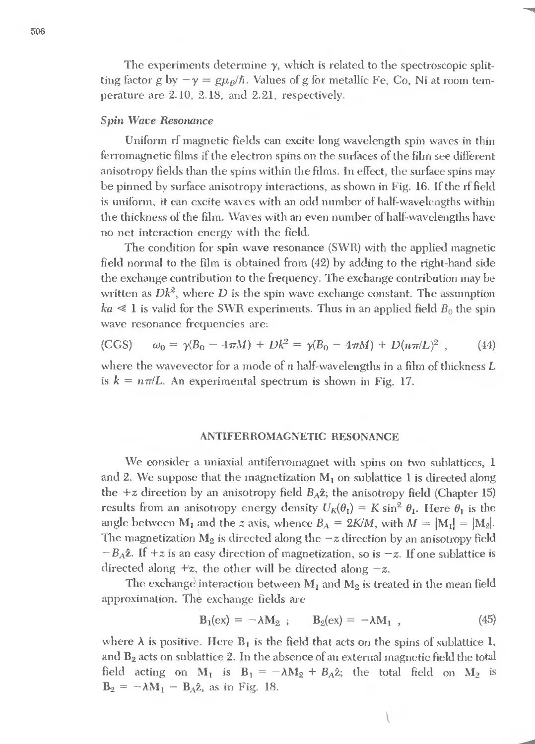
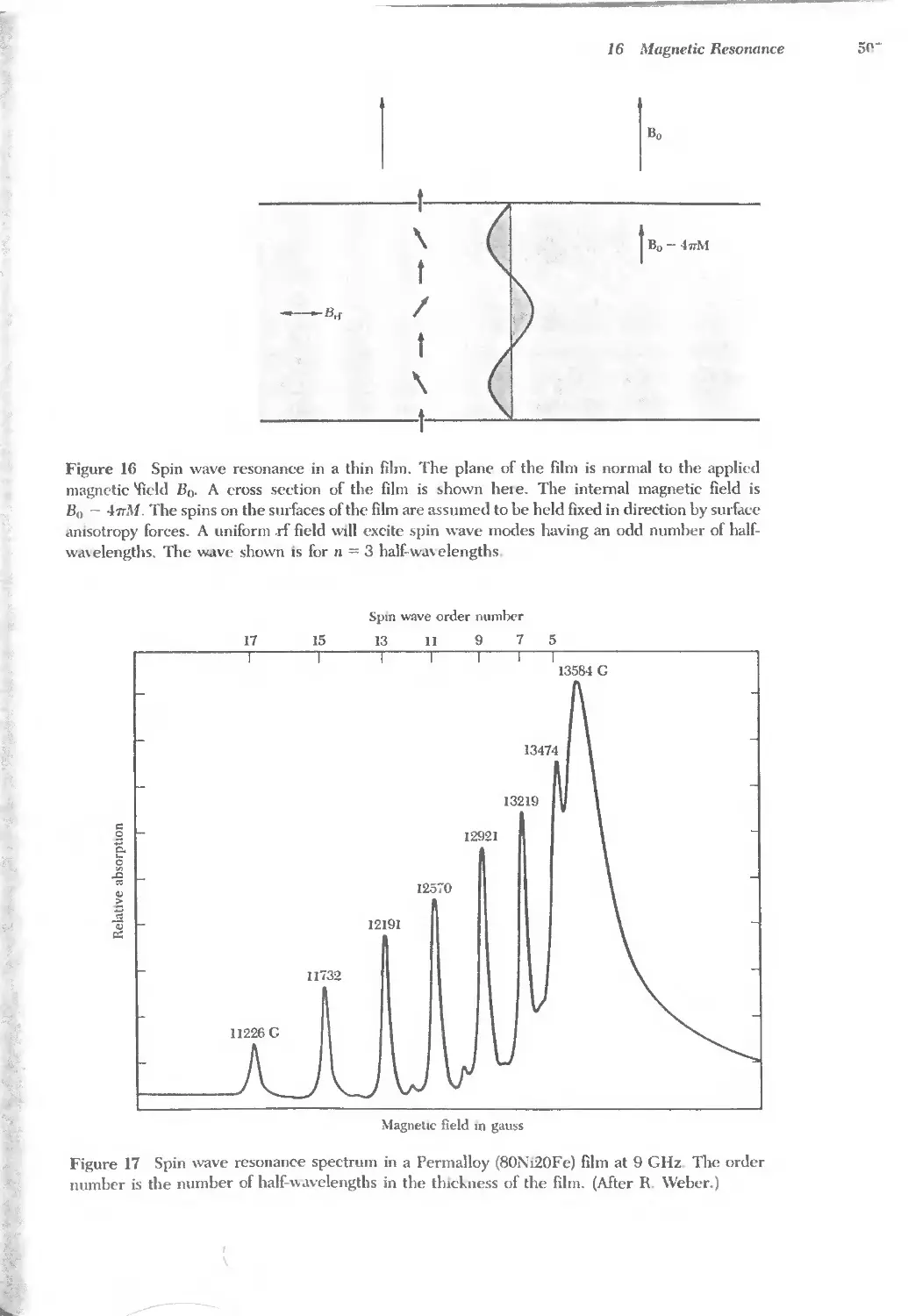
I
II
(a)
(b)
oV'
,'-'" \
(c)
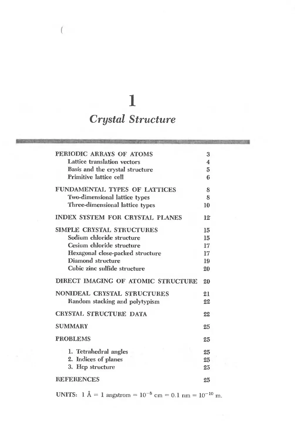
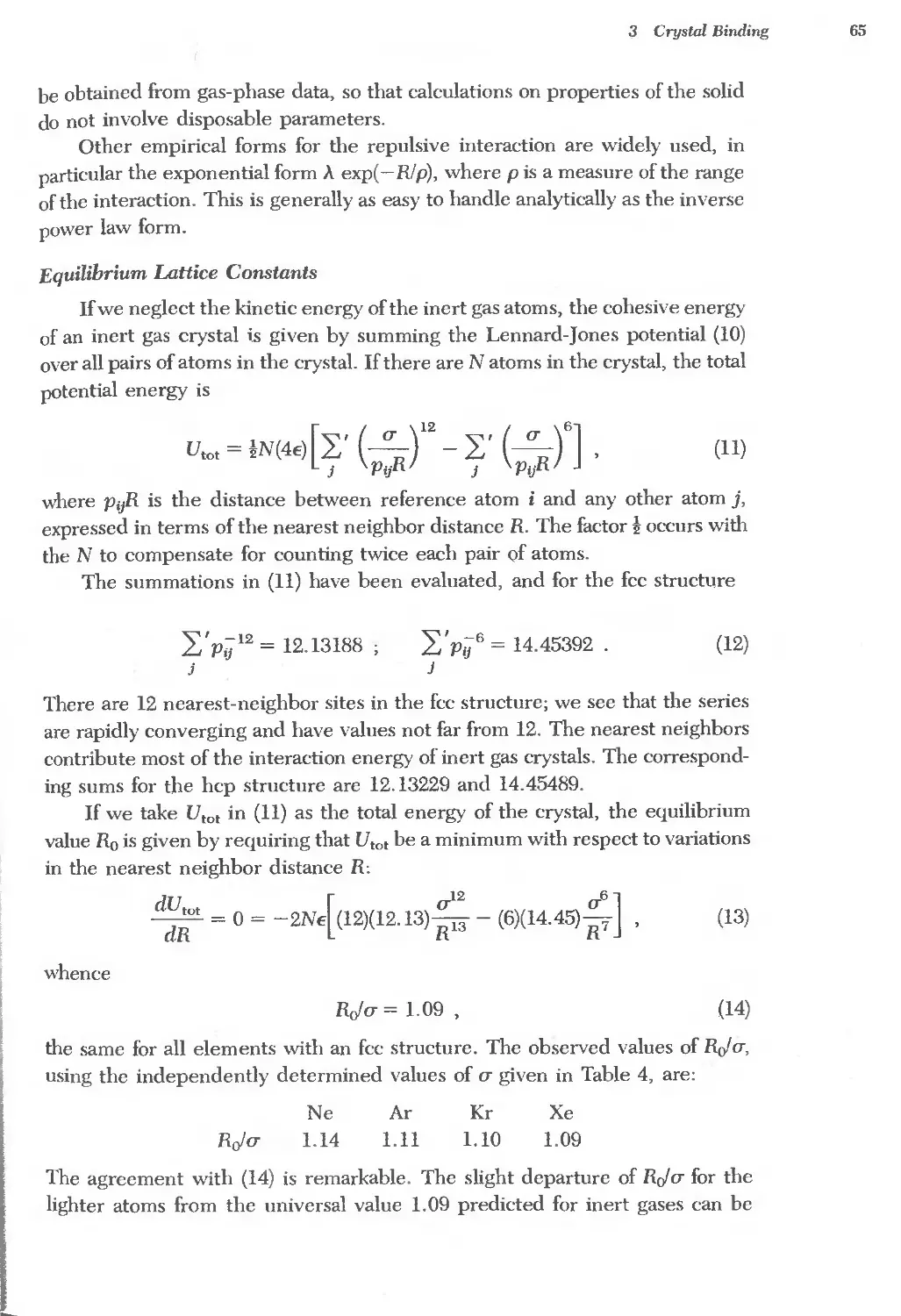
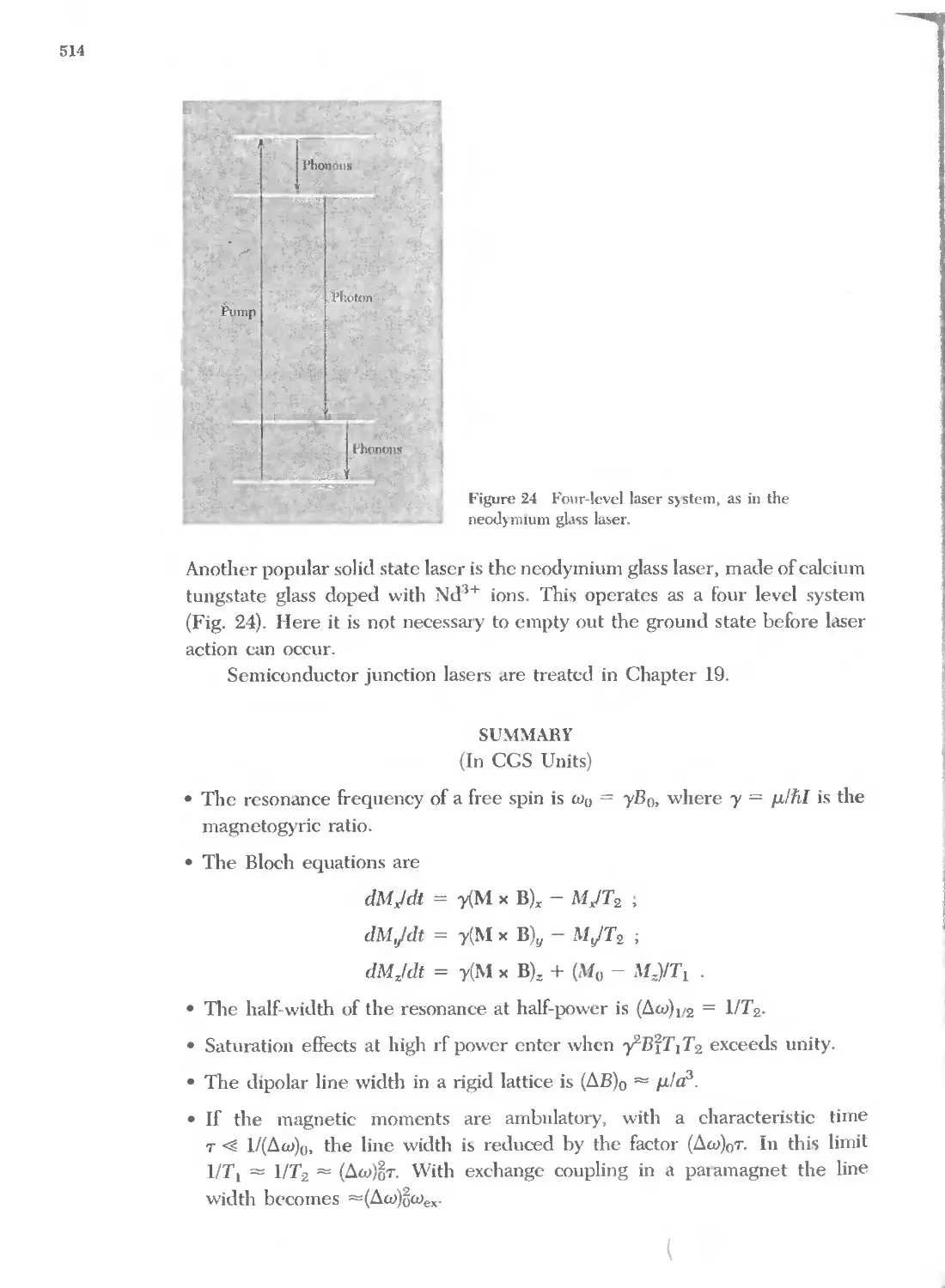
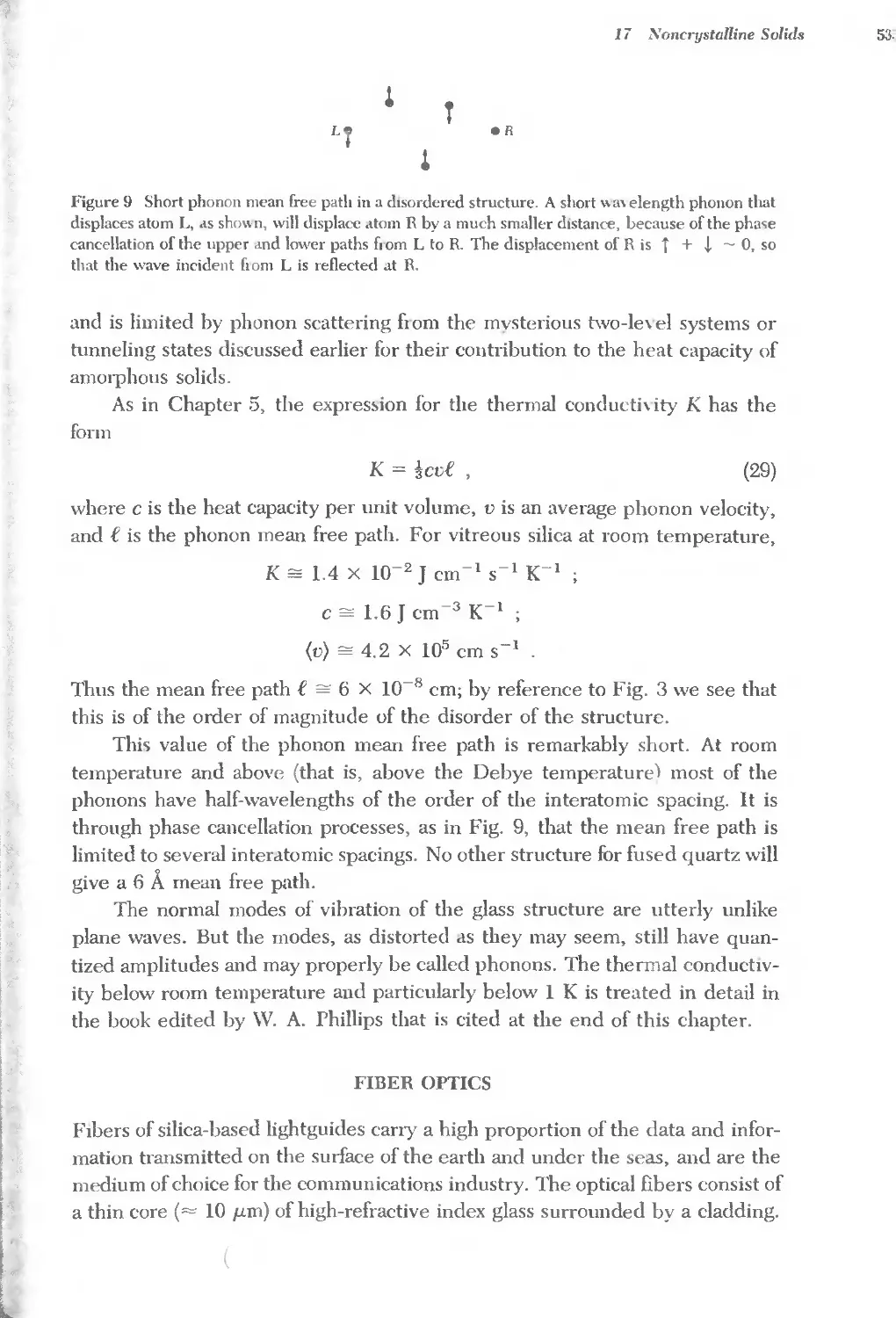
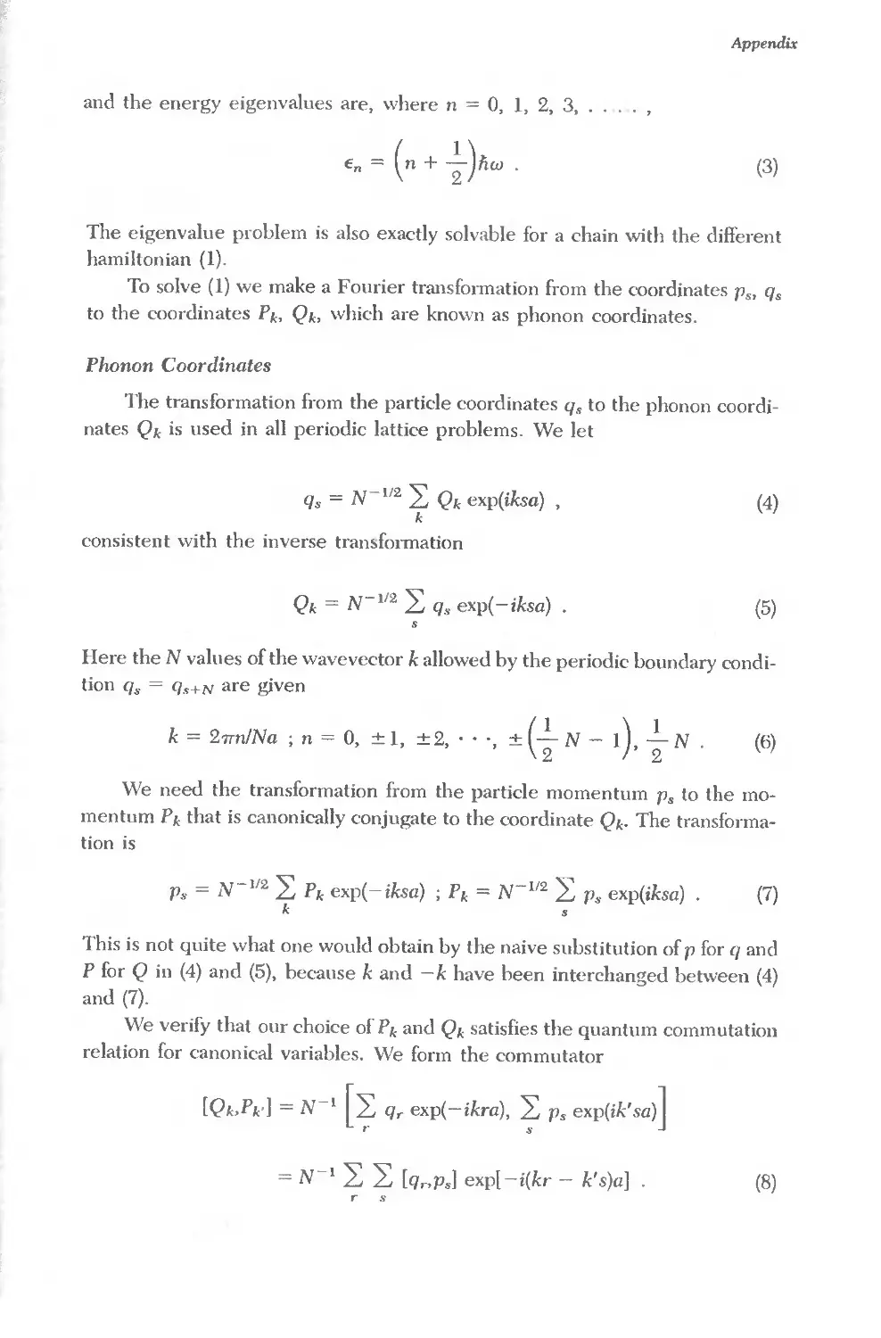
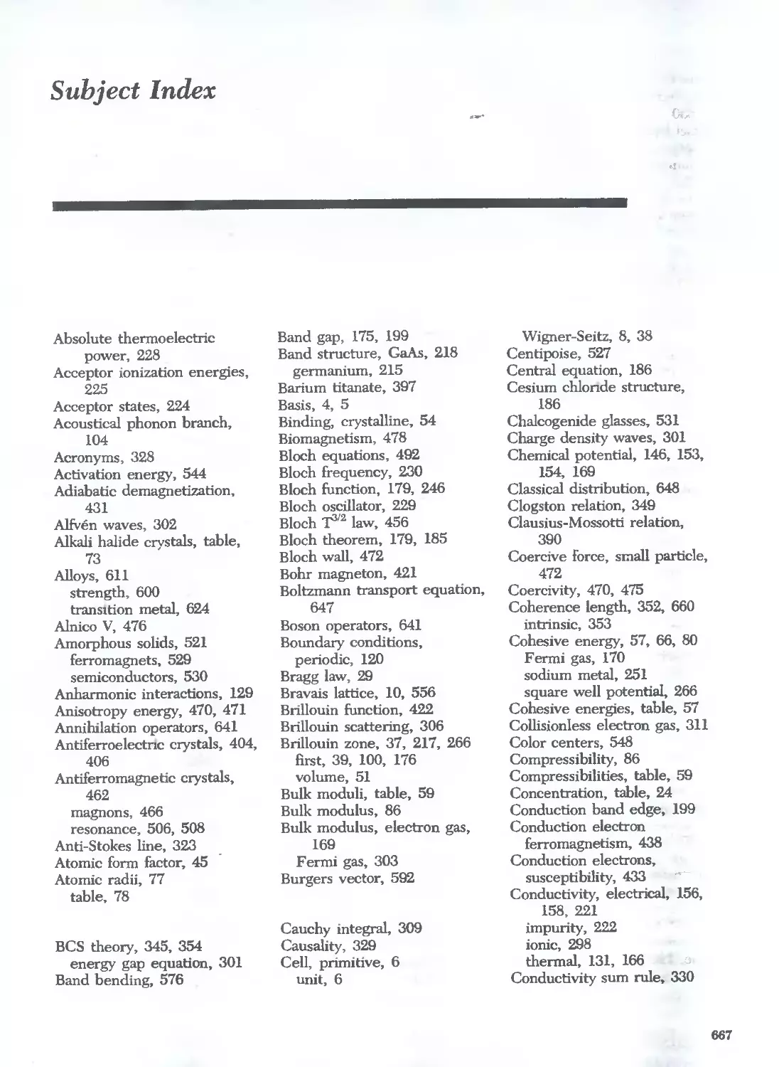
Figure I Relation of the external form of crystals to the form of the elementary building blocks"
The building blocks are identical in (a) and (h), but different cry<>o' faces are developed. (c) Cleav-
ing a crystal of rod.salt. "
2
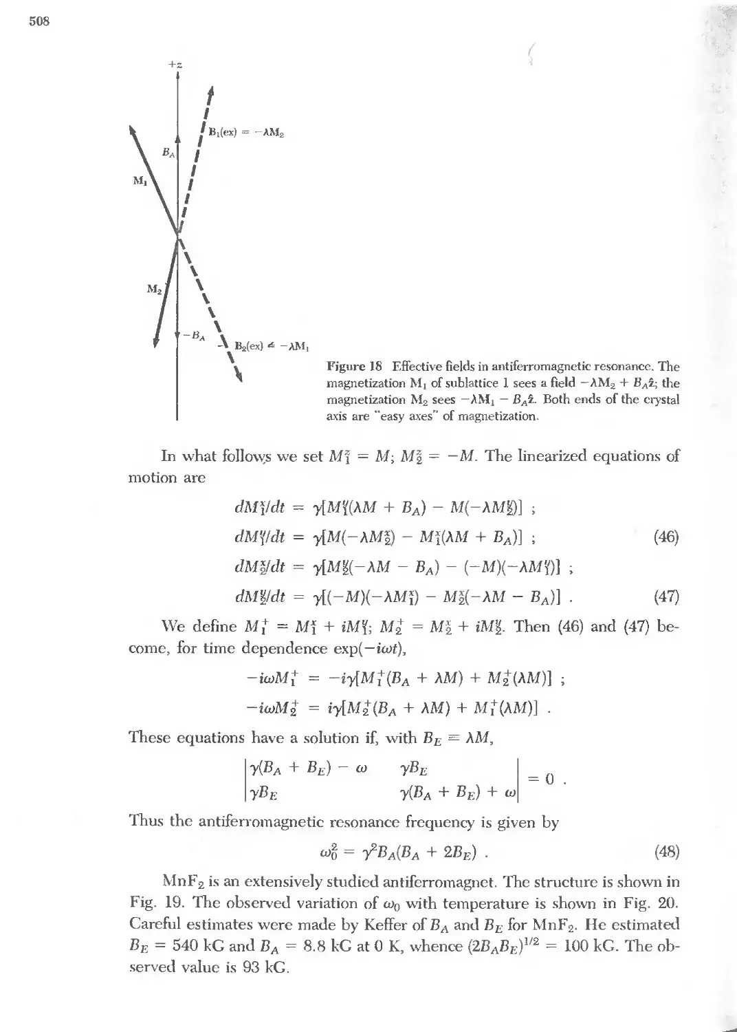
"
CHAPTER 1: CRYSTAL STRUCTURE
Solid state physics is largely concerned with crystals and electrons in crys-
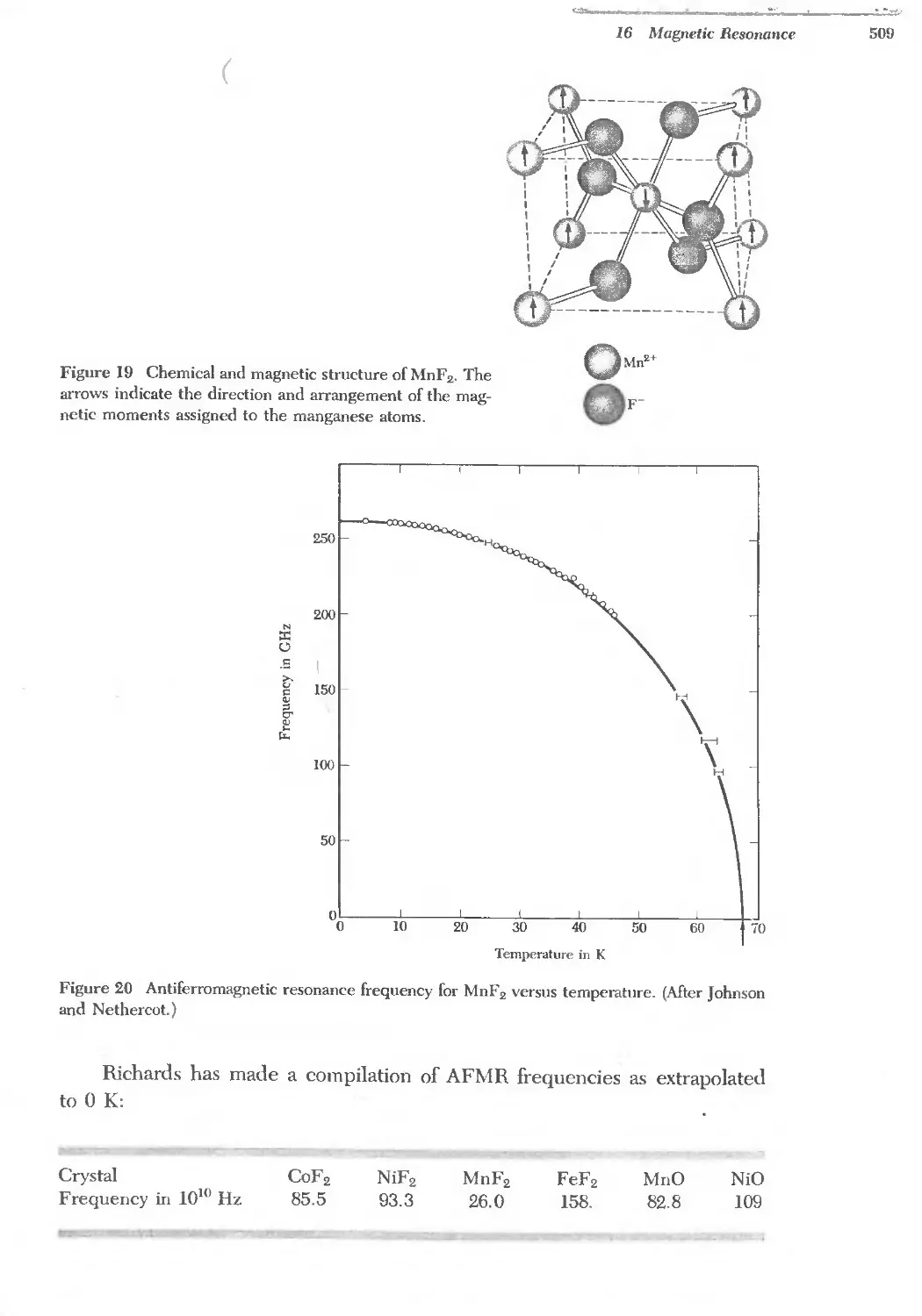
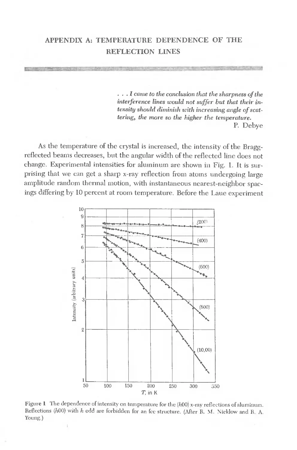
tals. The study of solid state physics began in the early years of this century
following the discovery of x-ray diffraction by crystals and the publication of a
series of simple calculations ana successful predictions of the properties of
crystals.
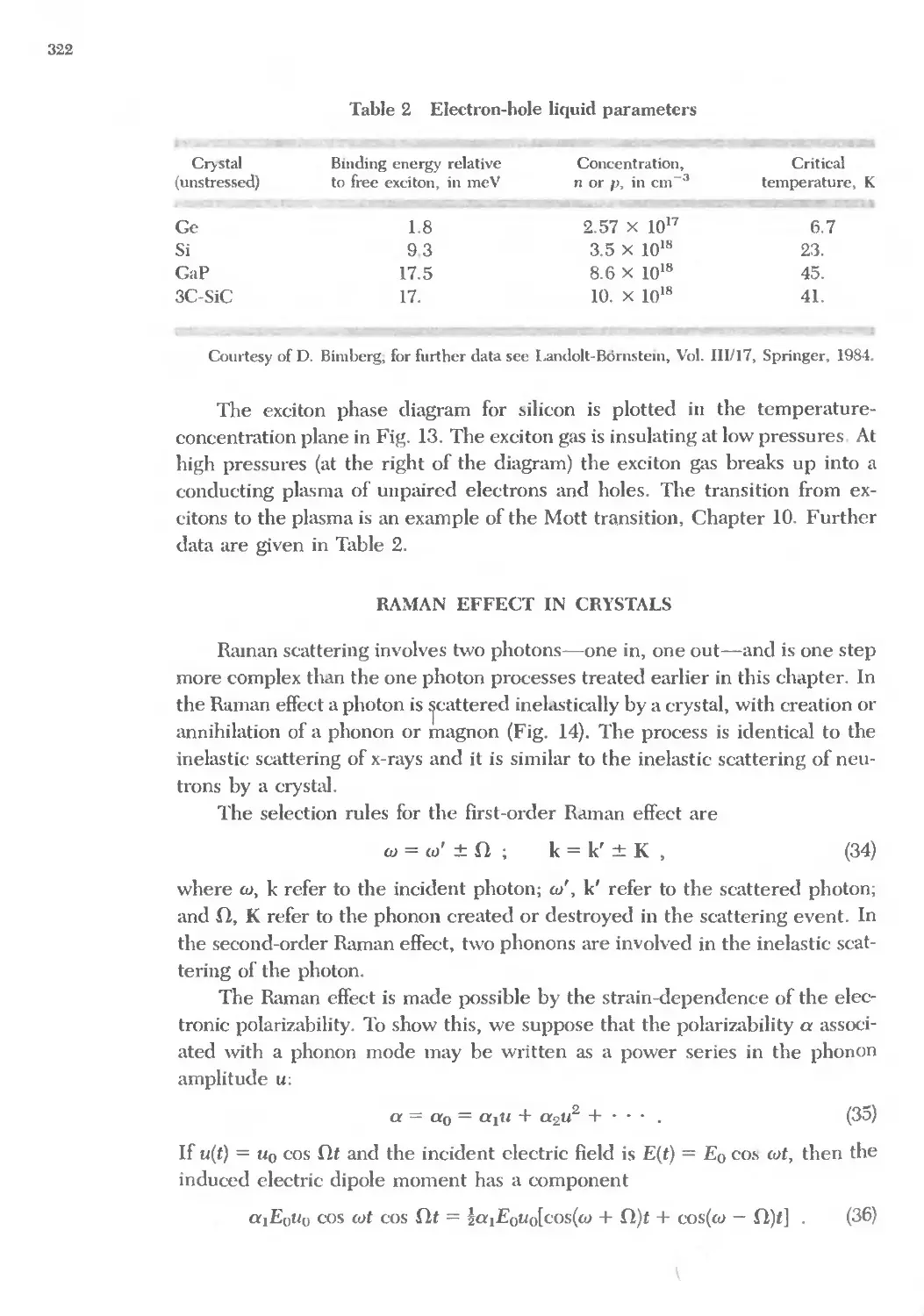
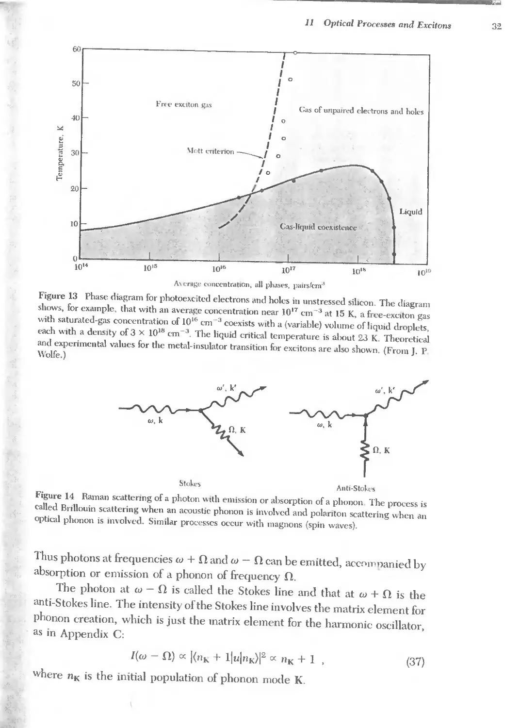
When a crystal grows in a constant environment, the fonn develops as if
identical building blocks were added continuously (-Fig. 1). The building blocks
are atoms or groups of atoms, so that a crystal is a three-dimensional periodic
array of atoms.
This was known in the 18th century when mineralogists discovered that
the index numbers of the directions of all faces of a crystal are exact integers.
Only the arrangement of identical particles in a periodic array can account for
the law of integral indices, 1 as discussed below.
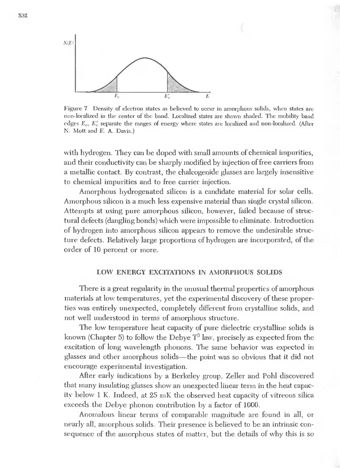
In 1912 a paper entitled «Interference effects with Rontgen rays" was pre-
sented to the Bavarian Academy of Sciences in Munich. In the first part of the
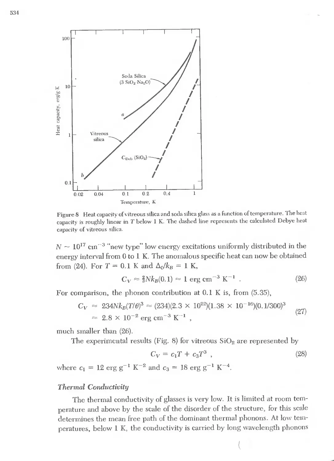
paper, Laue developed an elementary theory of the diffraction of x-rays by a
periodic array. In the second part, Friedrich and Knipping reported the first
experimental observations of x-ray diffraction by crystals. 2
The work proved decisively that crystals are composed of a periodic array
of atoms. With an established atomic model of a cry<;tal, physicists now could
think much further. The studies have been extended to include amorphous or
noncrystalline solids, glasses, and liquids. The wider field is known as con-
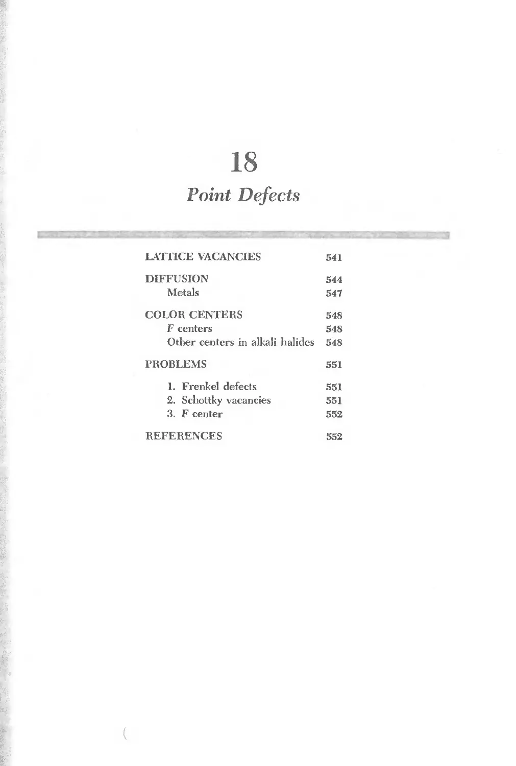
densed matter physics, and it is now the largest and probably the most vigorous
area of physics.
PERIODIC ARRAYS OF ATOMS
An ideal crystal is constructed by the infinite repetition of identical struc-
tural units in space. In the simplest crystals the structural unit is a single atom,
as in copper, silver, gold, iron, aluminum, and the alkali metals. But the small-
est structural unit may comprise many atoms or molecules.
The structure of all crystals can be described in terms of a lattice, with a
group of atoms attached to every lattice point. The group of atoms is called the
basis; when repeated in space it fOTITIS the crystal structure.
'i'
t
1 R. J. Haiiy, Essai d' une t1Ieorie sur /a stmcture efts cristaux, Paris, 1784; Traite de crista/-
/ographie, Paris, 180l.
'For personal accoun t < of the early years of x-ray diffraction studies of crystals, see P. P. Ewald,
ed., Fifty years of x-ra fraction, A. Oosthoek's Uitgeversmij., Utrecht, 1962.
,
t
3
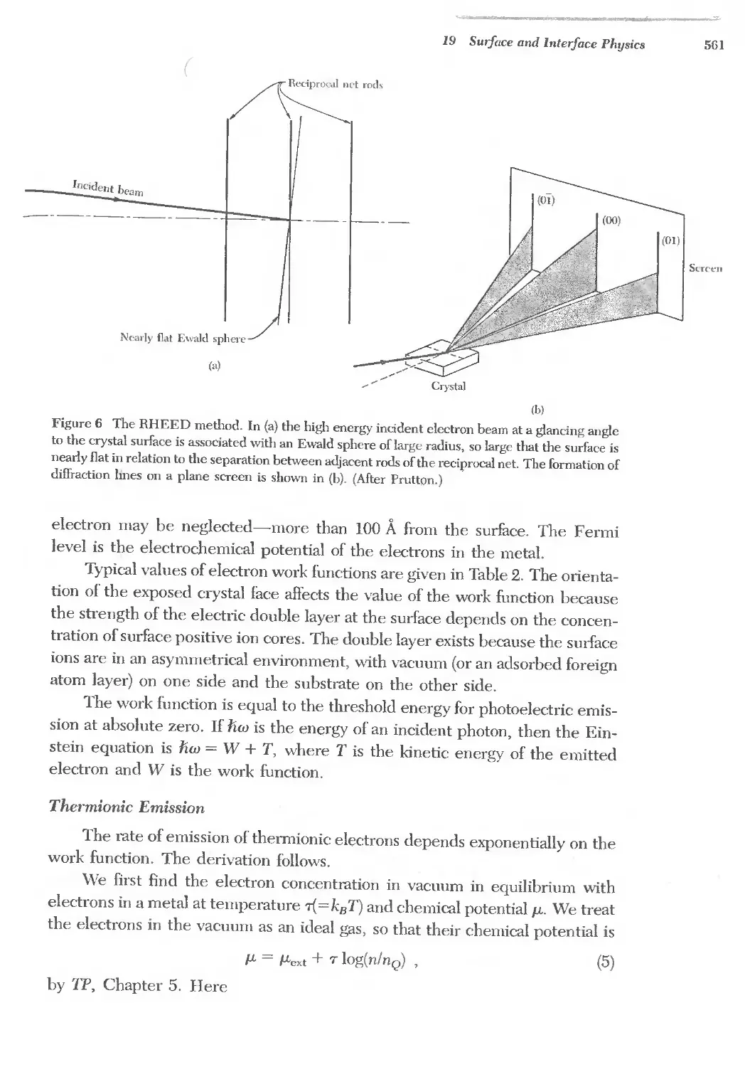
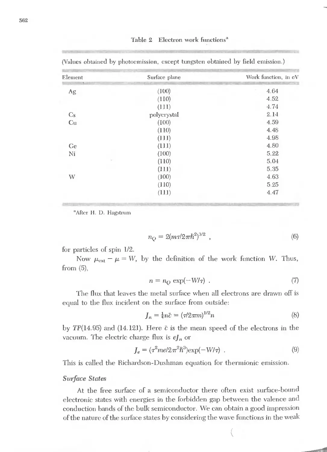
4
Lattice Translation Vectors
The lattice is defined by three fundamental translation vectors al> a2, a3
such that the atomic arrangement looks the same in every respect when viewed
from the point r as when viewed from the point
(
r' = r + ulal + U2a2 + U3a3 ,
(1)
where UI> U2, U3 are arbitrary integers. The set of points r' defined by (1) for all
Ub U2, U3 defines a lattice.
A lattice is a regular periodic array of points in space. (The analog in two
dimensions is called a net, as in Chapter 18.) A lattice is a mathematical abstrac-
tion; the crystal structure is formed when a basis of atoms is attached identically
to every lattice point. The logical relation is
lattice'+ basis = crystal structure . (2)
The lattice and the translation vectors al> a2, a3 are said to be primitive if
any two points r, r' from which the atomic arrangement looks the same always
satisfy (1) with a suitable choice of the integers ul> U2, U3' With this definition of
the primitive translation vectors, there is no cell of smaller volume that can
serve as a building block for the crystal structure.
We often use primitive translation vectors to define the crystal axes. How-
ever, nonprimitive crystal axes are often used when they have a simpler rela-
tion to the symmetry of the structure. .The crystal axes al> a2, a3 form three
adjacent edges of a parallelepiped. If there are lattice points only at the corners,
then it is a primitive parallelepiped.
A lattice translation operation is defined as the displacement of a crystal by
a crystal translation vector
T = ulal + U2 + U3a3
(3)
Any two lattice points are connected by a vector of this form.
To describe a crystal structure, there are three important questions to
answer: What is the lattice? What choice of al> a2, a3 do we wish to make? What
is the basis?
More than one lattice is always possible for a given structure, and more
than one set of axes is always possible for a given lattice. The basis is identified
once these choices have been made. Everything (including the x-ray diffraction
pattern) works out correctly in the end provided that (3) has been satisfied.
The symmetry operations of a crystal carry the crystal structure into itself.
These include the lattice translation operations. Further, there are rotation and
reflection operations, called point operations. About lattice points or certain
special points within an elementary parallel piped it may be possible to apply
rotations aI'<l reflections that carry the crystal into itself.
Finally, there may exist compound operations made up of combined trans-
lation and point operations. Textbooks on crystallography are largely devoted to
1 Crystal Structure
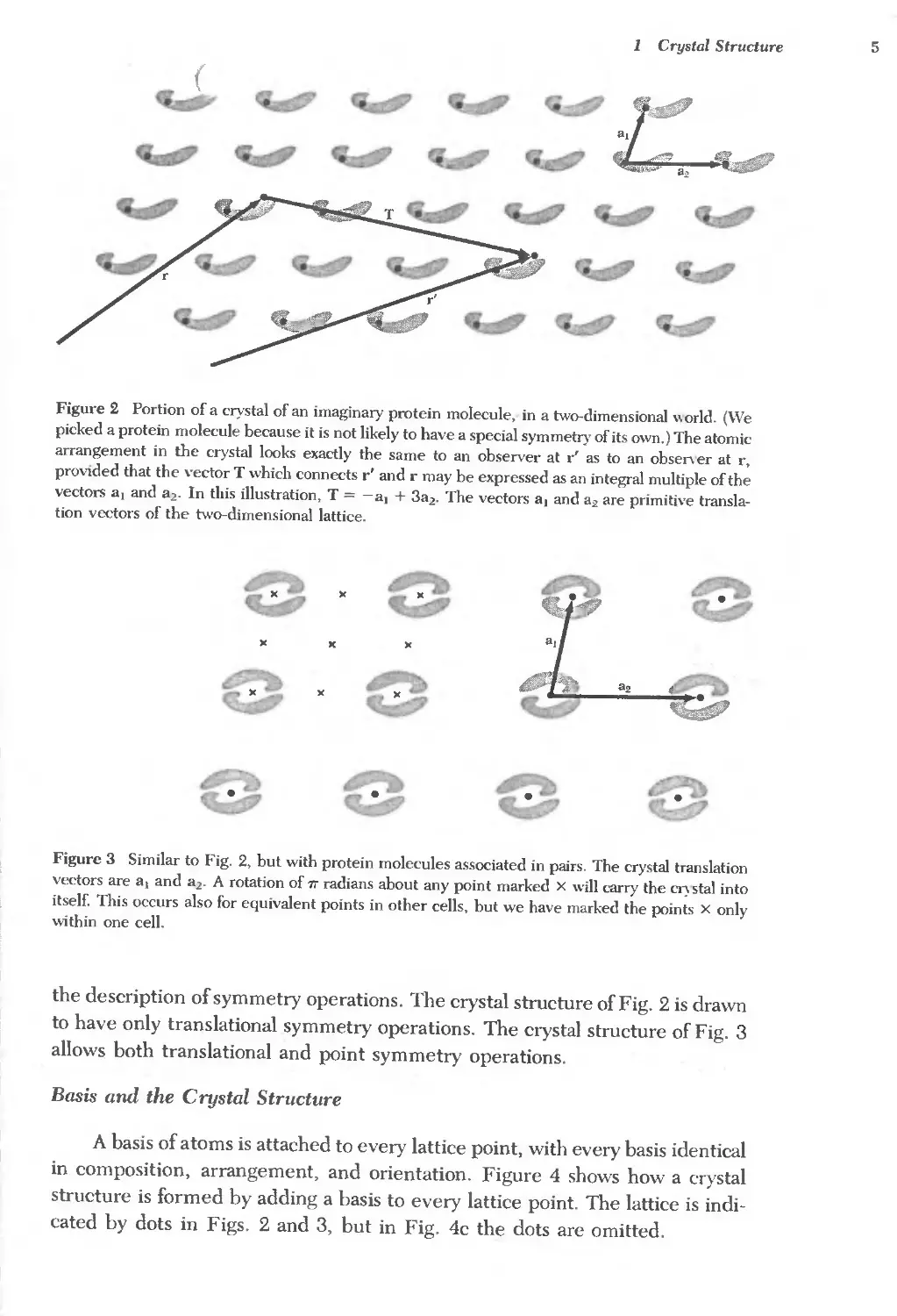
5
(
l:
. 3,2
.
T
Figure 2 Portion of a crystal of an imaginary protein molecule, in a two-dimensional "orld. (We
picked a protein molecule because it is not likely to have a special symmetry of its own.) The atomic
arrangement in tbe crystal looks exactly the same to an observer at r' as to an obsen er at r,
provIded that the ,'ector T which connects r' and r may be expressed as an integral multiple of the
vectors 3, and 32' In this illustration, T = -3, + 332' The vectors 31 and a2 are primitive transla-
tion vectors of the two-dimensional lattice.
" "
"
"
"
"
"
"
.
.
.
.
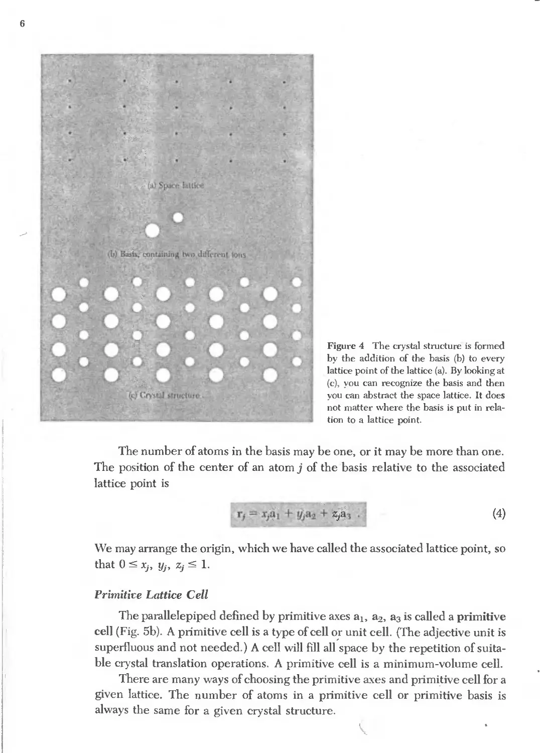
Figure 3 Similar to Fig. 2, but with protein molecules associated in pairs. The crystal translation
vectors are 3, and 32' A rotation of 7r radians about any point marked x will carry the Cf} stal into
itself. This occurs also for equivalent points in other cells, but we have marked the points X only
within one cell.
the description of symmetry operations. The crystal structure of Fig. 2 is drawn
to have only translational symmetry operations. The crystal structure of Fig. 3
allows both translational and point symmetry operations.
Basis and the Crystal Structure
A basis of atoms is attached to every lattice point, with every basis identical
in composition, arrangement, and orientation. Figure 4 shows how a crystal
structure is formed by adding a basis to every lattice point. The lattice is indi-
cated by dots in Figs. 2 and 3, but in Fig. 4c the dots are omitted.
6
"y
JII!I
.-'
..
.
Figure 4 The crystal structure is formed
by the addition of the basis (b) to every
lattice point of the lattice (a). By looking at
(c), you can recognize the basis and then
you can abstract the space lattice. It does
not matter where the basis is put in rela-
tion to a lattice point.
The number of atoms in the basis may be one, or it may be more than one.
The position of the center of an atom j of the basis relative to the associated
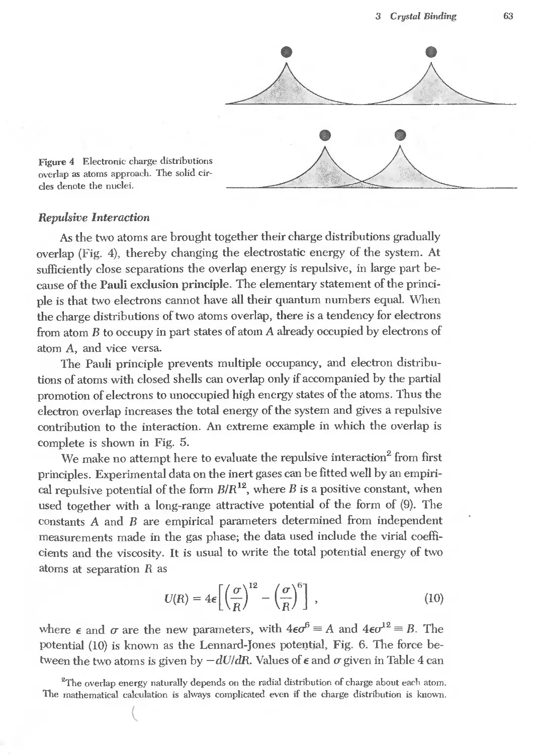
lattice point is
(4)
We may arrange the origin, which we have called the associated lattice point, so
that 0 Xj, Yj, Zj 1.
Primitire Lattice Cell
The parallelepiped defined by primitive axes al> a2, 23 is called a primitive
cell (Fig. 5b). A primitive cell is a type of cell or unit cell. (The adjective unit is
superfluous and not needed.) A cell will fill all space by the repetition of suita-
ble crystal translation operations. A primitive cell is a minimum-volume cell.
There are many ways of choosing the primitive a.xes and primitive cell for a
given lattice. The number of atoms in a primitive cell or primitive basis is
always the same for a given crystal structure.
'-
1 Crystal Structure
7
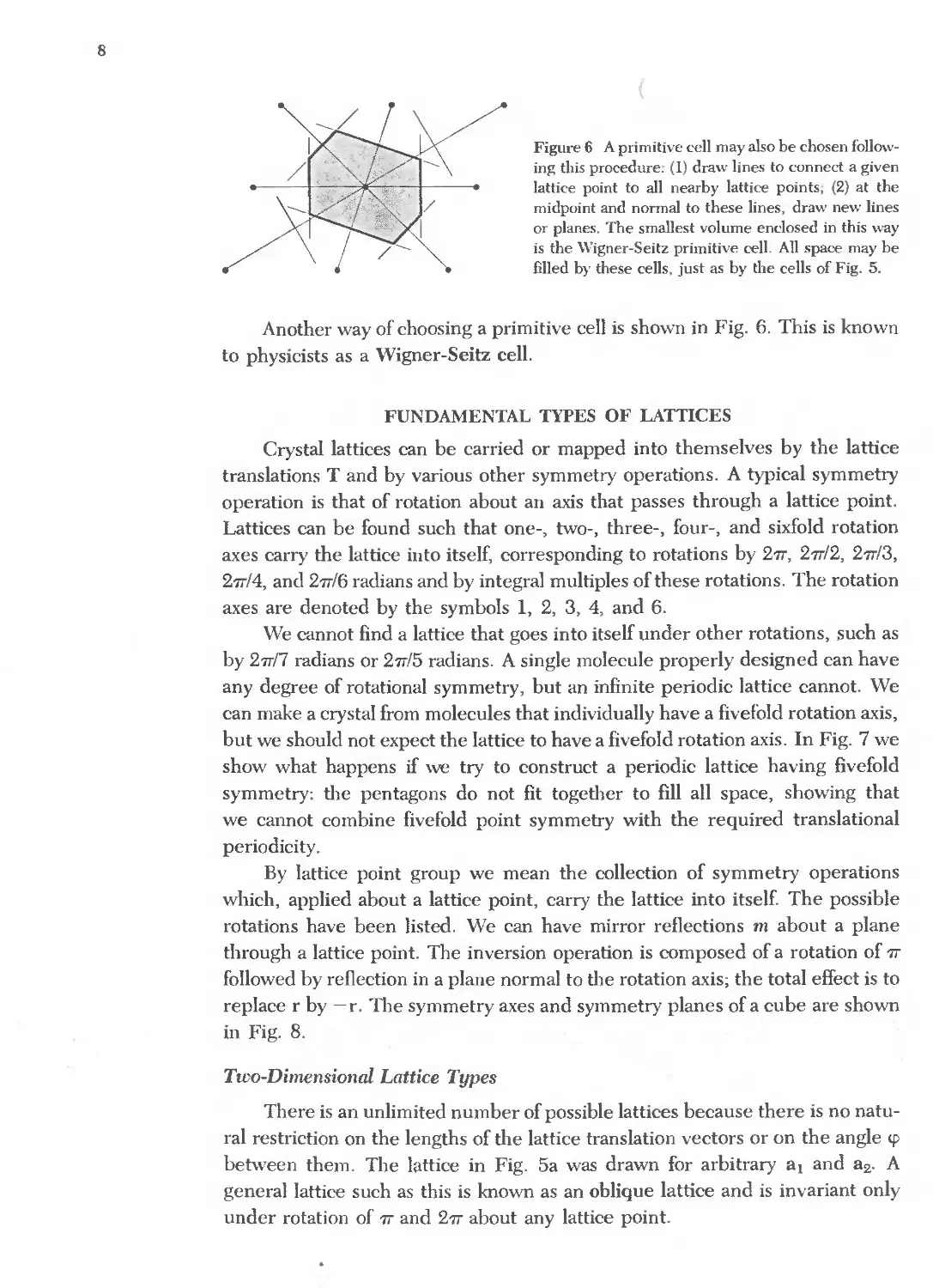
. . . . . .
.
o.
.
0,
. . . . .
(0)
.
.
.
.
. .
o!!' '
(b)
(e)
Figure Sa Lattice points of a space lattice in two dimensions. All pairs of vectors a h a2 are
translation vectors of the lattice. But a/", a2'" are not primitive translation vectors because we
cannot form the lattice translation T from integral combinations of al'" and a2"" All other pairs
shown of a, and a2 may be taken as the primitive translation vectors of the lattice. The parallelo-
grams I, 2, 3 are equal in area and any of them could be taken as the primitive cell. The parallelo-
gram 4 has twice the area of a primitive cell.
Figure sb Primitive cell of a space lattice in three dimensions.
Figure 5c Suppose these points are identical atoms: sketch in on the figure a set oflattice points, a
choice of primitive a.xes, a primitive cell, and the basis of atoms associated with a lattice point.
There is always one lattice point per primitive cell. If the primitive cell is
a parallelepiped with lattice points at each of the eight corners, each lattice
point is shared among eight cells, so that the total number of lattice points in
the cell is one: 8 X ! = 1.
The volume of a parallelepiped with axes 21. 22, 23 is
V c = 121 . 22 X 231 ' (5)
by elementary vector analysis. The basis associated with a primitive cell is
called a primitive basis. No basis contains fewer atoms than a primitive basis
contains.
I
\
8
(
Figure 6 A primitive cell may also be chosen follow-
ing this procedure. (1) draw lines to connect a given
lattice point to all nearby lattice points, (2) at the
midpoint and normal to these lines, draw new lines
or planes. The smallest volume enclosed in this way
is the Wigner-Seitz primitive cell. An space may be
filled by these cells. just as by the cells of Fig. 5.
Another way of choosing a primitive cell is shown in Fig. 6. This is known
to physicists as a Wigner-Seitz cell.
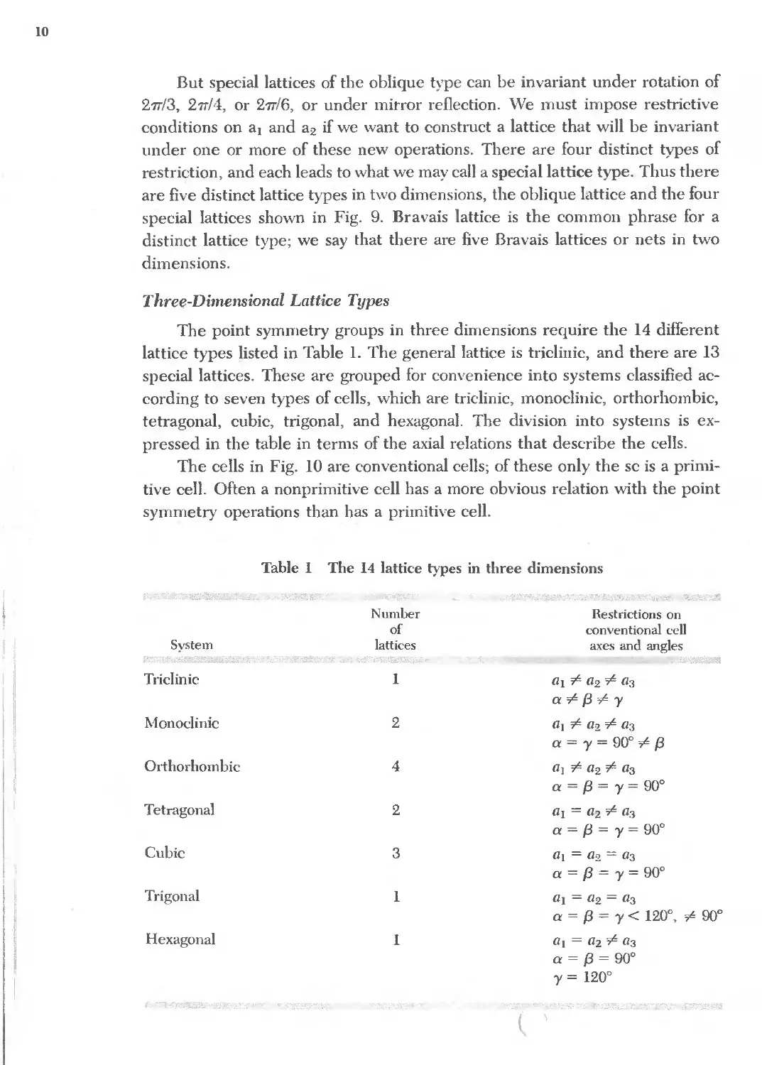
FUNDAMENTAL TYPES OF LATTICES
Crystal lattices can be carried or mapped into themselves by the lattice
translations T and by various other symmetry operations. A typical symmetry
operation is that of rotation about an axis that passes through a lattice point.
Lattices can be found such that one-, two-, three-, four-, and sixfold rotation
axes carry the lattice into itself, corresponding to rotations by 2'1T, 2'1T/2, 2'1T/3,
2'1T/4, and 2'1T/6 radians and by integral multiples of these rotations. The rotation
axes are denoted by the symbols 1, 2, 3, 4, and 6.
We cannot find a lattice that goes into itself under other rotations, such as
by 2'1T/7 radians or 2'1T/5 radians. A single molecule properly designed can have
any degree of rotational symmetry, but an infinite periodic lattice cannot. We
can make a crystal from molecules that individually have a fivefold rotation axis,
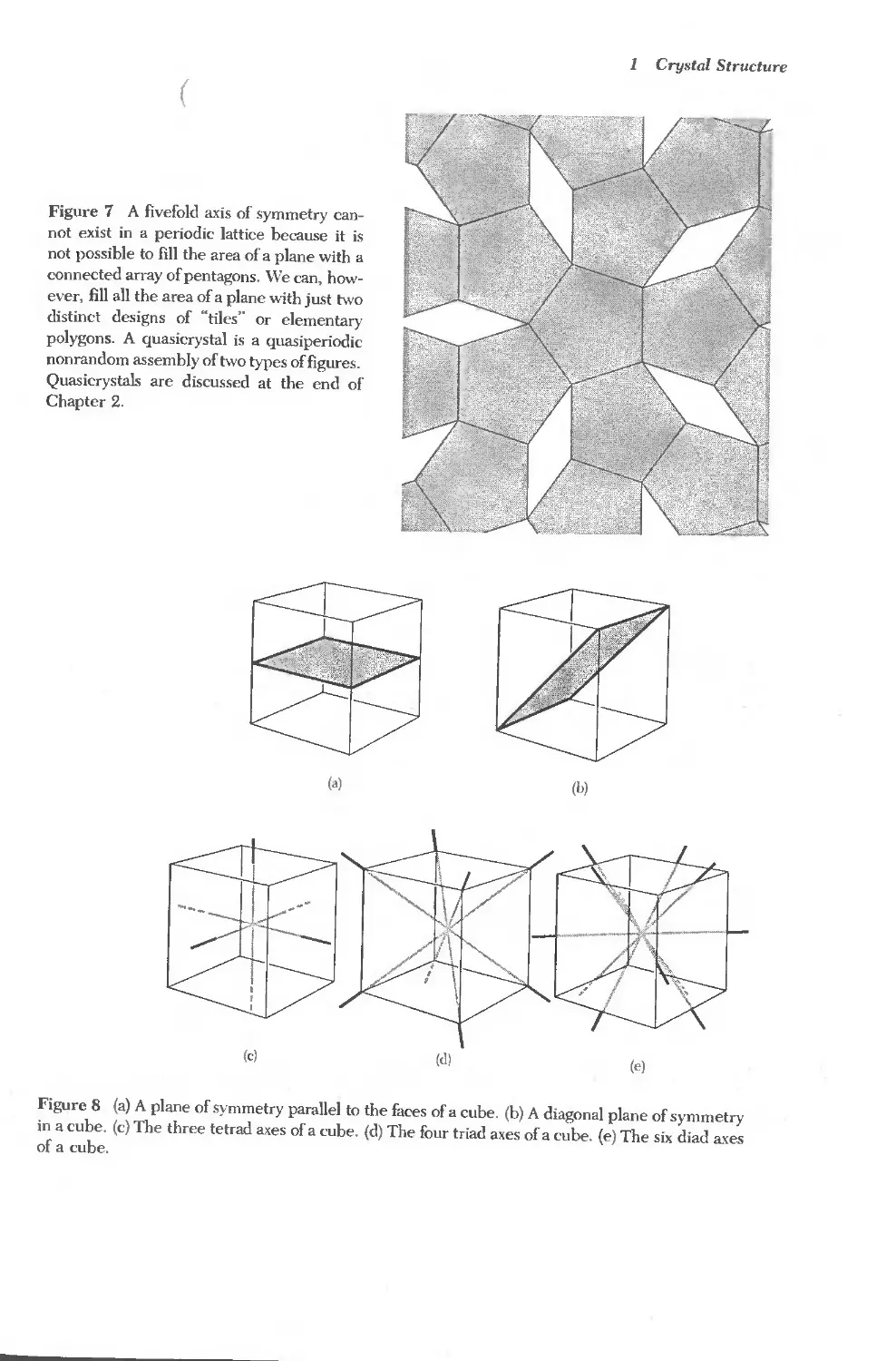
but we should not expect the lattice to have a fivefold rotation axis. In Fig. 7 we
show what happens if we try to construct a periodic lattice having fivefold
symmetry: the pentagons do not fit together to fill all space, showing that
we cannot combine fivefold point symmetry with the required translational
periodicity.
By lattice point group we mean the collection of symmetry operations
which, applied about a lattice point, carry the lattice into itself. The possible
rotations have been listed. We can have mirror reflections m about a plane
through a lattice point. The inversion operation is composed of a rotation of'1T
followed by reflection in a plane normal to the rotation axis; the total effect is to
replace r by -r. The symmetry axes and symmetry planes of a cube are shown
in Fig. 8.
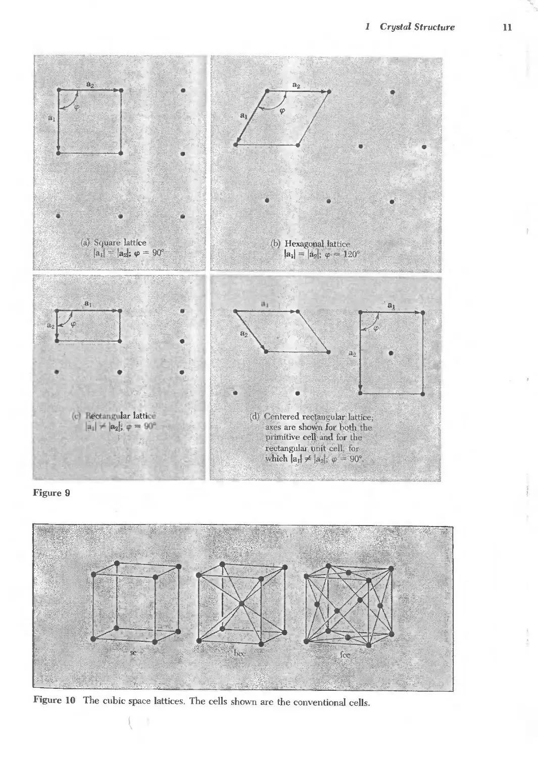
Two-Dimensional Lattice Types
There is an unlimited number of possible lattices because there is no natu-
ral restriction on the lengths of the lattice translation vectors or on the angle <p
between them. The lattice in Fig. 5a was drawn for arbitrary at and a2' A
general lattice such as this is known as an oblique lattice and is invariant only
under rotation of '1T and 2'1T about any lattice point.
(
Figure 7 A fivefold a.xis of symmetry can-
not exist in a periodic lattice because it is
not possible to fill the area of a plane with a
connected array of pentagons. \Ve can, how-
ever, fill all the area of a plane with just two
distinct designs of "tiles" Or elementary
polygons. A quasicrystal is a quasiperiodic
nonrandom assembly of two types of figures.
Quasicrystals are discussed at the end of
Chapter 2.
(d)
1 Crystal Structure
(h)
(e)
(<1)
(e)
Figure 8 (a) A plane of symmetry parallel to the faces of a cube. (b) A diagonal plane of symmetry
in a cube. (c) The three tetrad a.xes of a cube. (d) The four triad axes of a cube. (e) The six diad a.xes
of a cube.
10
But special lattices of the oblique type can be invariant under rotation of
2n-/3, 2n/4, or 2n-/6, or under mirror reflection. We must impose restrictive
conditions on aJ and a2 if we want to construct a lattice that will be invariant
under one or more of these new operations. There are four distinct types of
restriction, and each leads to what we may call a special lattice type. Thus there
are five distinct lattice types in two dimensions, the oblique lattice and the four
special lattices shown in Fig. 9. Bravais lattice is the common phrase for a
distinct lattice type; we say that there are five Bravais lattices or nets in two
dimensions.
Three-Dimensional Lattice Types
The point symmetry groups in three dimensions require the 14 different
lattice types listed in Table 1. The general lattice is triclillic, and there are 13
special lattices. These are grouped for convenience into systems classified ac-
cording to seven types of cells, which are triclinic, monoclinic, orthorhombic,
tetragonal, cubic, trigonal, and hexagonal. The division into systems is ex-
pressed in the table in terms of the axial relations that describe the cells.
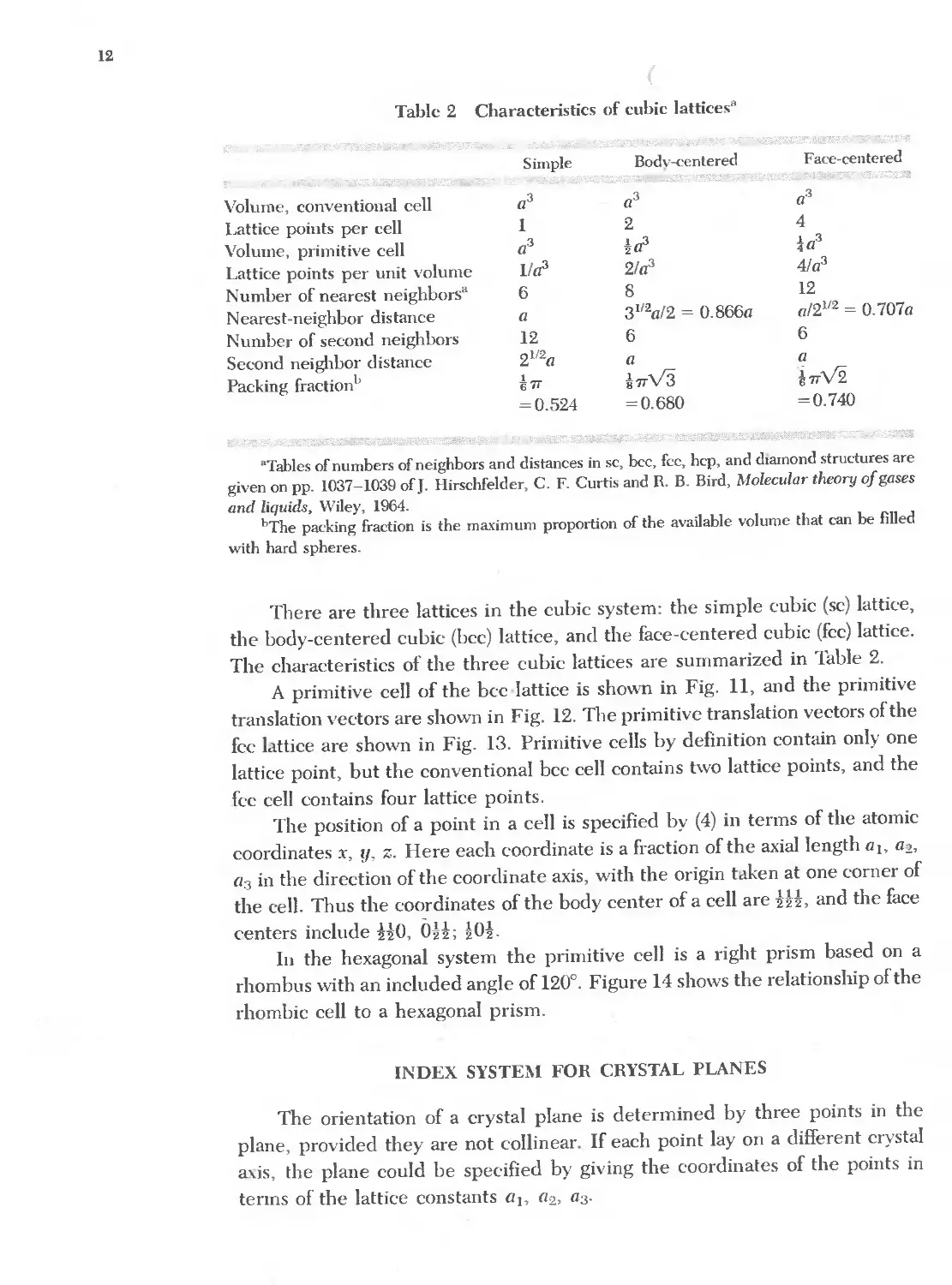
The cells in Fig. 10 are conventional cells; of these only the sc is a primi-
tive cell. Often a nonprimitive cell has a more obvious relation with the point
symmetry operations than has a primitive cell.
Table 1 The 14 lattice types in three dimensions
! j
, !
I
I
Ii
I,
i J
111
Number
of
lattices
-.
1
2
4
2
3
1
1
System
Triclinic
Monoclinic
Orthorhombic
Tetragonal
Cubic
I
I
Trigonal
Hexagonal
Restrictions on
conventional cell
a.xes and angles
OJ ¥' 02 ¥' 03
a¥'{3¥'y
OJ ¥' 02 ¥' 03
a=y=90o¥'{3
OJ ¥' 02 ¥' 03
a={3=y=90°
OJ = 02 ¥' 03
a={3=y=90°
OJ = 02 = 03
a={3=y=90°
OJ = 02 = 03
a = {3 = y < 120°, ¥' 90°
OJ = 02 ¥' 03
a={3=90°
y = 120°
1 Crystal Structure
11
.
(:c lar latH
82J:
iF
Figure 9
Figure 10 The cubic space lattices. The cells shown are the conventional cells.
I
\
12
(
Tablc 2 Characteristics of cubic lattices.
Simple Bodv-centered Face-centered
-
Volume, conventional cell 0 3 0 3 0 3
Lattice points per cell 1 2 4
Volume, primitive cell 0 3 it? !03
Lattice points per unit volume 110 3 2/0 3 410 3
Number of nearest neighbors. 6 8 12
Nearest-neighbor distance 0 3 1/2 0/2 = 0.8660 0/2 112 = 0.7070
Number of second neighbors 12 6 6
Second neighbor distance 2 1/2 0 0 0
Packing fraction b !7T bV3 7TV2
= 0.524 =0.680 =0.740
"Tables of numbers of neighbors and distances in sc, bcc, fcc, hcp, and dIamond structures are
given on pp. 1037-1039 of}. Hirschfelder, C. F. Curtis and R. B. Bird, Molecular theory of gases
and liquids, Wiley, 1964.
bThe packing fraction is the ma.ximum proportion of the available volume that can be filled
with hard spheres.
There are three lattices in the cubic system: the simple cubic (sc) lattice,
the body-centered cubic (bcc) lattice, and the face-centered cubic (fcc) lattice.
The characteristics of the three cubic lattices are summarized in Table 2.
A primitive cell of the bcc lattice is shown in Fig. 11, and the primitive
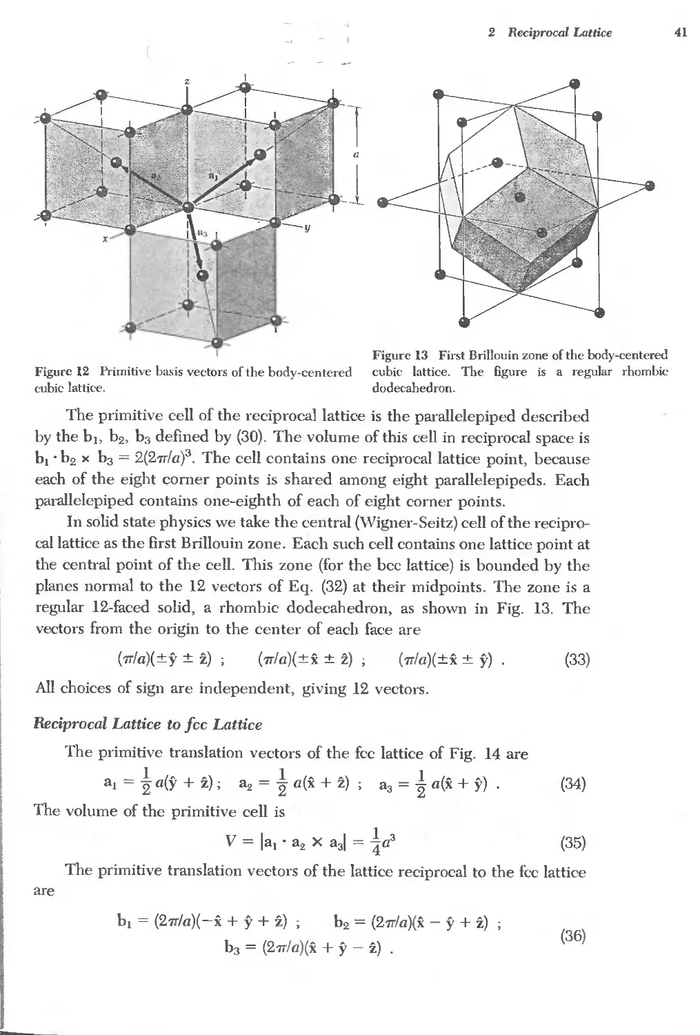
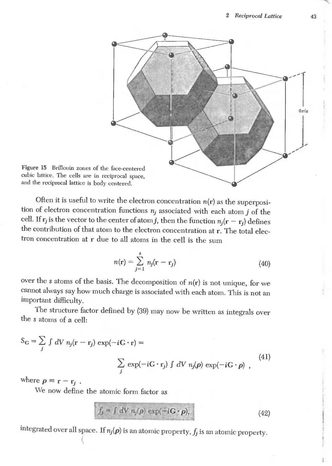
translation vectors are shown in Fig. 12. The primitive translation vectors of the
fcc lattice are shown in Fig. 13. Primitive cells by definition contain only one
lattice point, but the conventional bcc cell contains two lattice points, and the
fcc cell contains four lattice points.
The position of a point in a cell is specified by (4) in terms of the atomic
coordinates x, y, z. Here each coordinate is a fraction of the axial length OJ, 02,
a3 in the direction of the coordinate axis, with the origin taken at one corner of
the cell. Thus the coordinates of the body center of a cell are Ht, and the face
centers include HO, OH; tot.
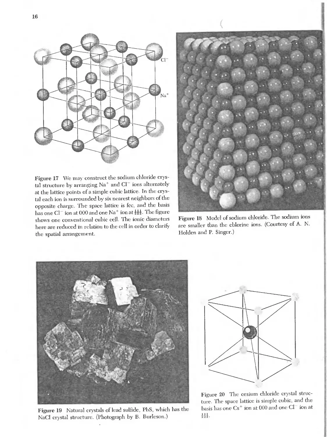
In the hexagonal system the primitive cell is a right prism based on a
rhombus with an included angle of 120°. Figure 14 shows the relationship of the
rhombic cell to a hexagonal prism.
INDEX SYSTEM FOR CRYSTAL PLANES
The orientation of a crystal plane is determined by three points in the
plane, provided they are not collinear. If each point lay on a different crystal
a'l.is, the plane could be specified by giving the coordinates of the points in
terms of the lattice constants aJ, a2, 03'
(
T
..
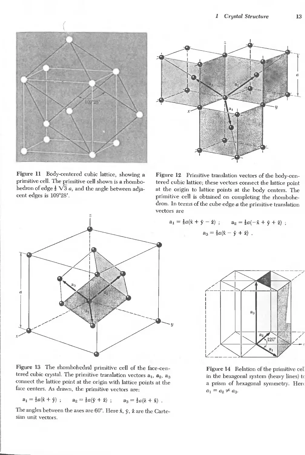
Figure 11 Body-centered cubic lattice, showing a
primitive cell. The primitive cell shown is a rhombo-
hedron of edge 1 V3 a, and the angle between adja-
cent edges is 109°28'.
z
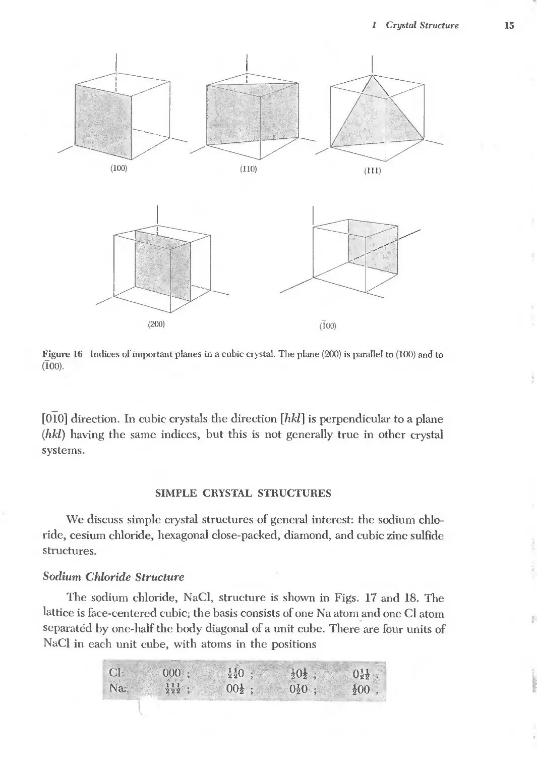
Figure 13 The rhombohedral primitIve cell of the face-cen-
tered cubic crystal. The primitive translation vectors a" , a3
connect the lattice point at the origin with lattice points at the
face centers. As drawn, the primitive vectors are:
al = la(x + y) ;
a2 = la(y + z) ;
a3 = la(z + x) .
The angles between the axes are 60°. Here x, y, z are the Carte-
sian unit vectors.
1 Crystal Structure
13
1
a
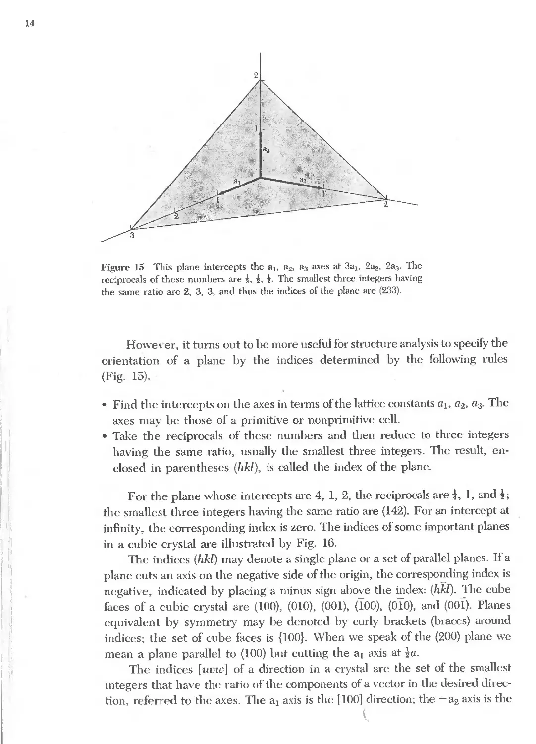
l
Figure 12 Primitive translation vectors of the body-cen-
tered cubic lattice; these vectors connect the lattice point
at the origin to lattice points at the body centers. The
primitive cell is obtained on completing the rhombohe-
dron. In terms of the cube edge a the primitive translation
vectors are
a, = la(x + y - z) ; a2 = la(-x + y + z)
a3 = la(x - y + z) .
-y
/
/
,L"
Figure 14 Relation of the primitive cel
in the bexagonal system (heavy lines) t<
a prism of hexagonal symmetry. Hen
al = a2 "" a3'
14
2
Figure 15 This plane intercepts the a" a2, a3 axes at 3a" 2a2' 2a3' The
rec:procals of these numbers are 1, t 1. The smallest three mtegers having
the same ratio are 2, 3, 3, and thus the indices of the plane are (233).
! I
III
I II
,j
!: I!
1; II
n
I II
J I.
1 1'1
. '1
I : II
i'
'I
11
I ;
d1
I 1
I j!
Howe\ er, it turns out to be more useful for structure analysis to specify the
orientation of a plane by the indices determined by the following rules
(Fig. 15).
. Find the intercepts on the axes in terms of the lattice constants aj, a2, a3' The
axes may be those of a primitive or nonprimitive cell.
. Take the reciprocals of these numbers and then reduce to three integers
having the same ratio, usually the smallest three integers. The result, en-
closed in parentheses (hkl), is called the index of the plane.
For the plane whose intercepts are 4, 1, 2, the reciprocals are t, 1, and l;
the smallest three integers having the same ratio are (142). For an intercept at
infinity, the corresponding index is zero. The indices of some important planes
in a cubic crystal are illustrated by Fig. 16.
The indices (hkl) may denote a single plane or a set of parallel planes. If a
plane cuts an axis on the negative side of the origin, the corresponding index is
negative, indicated by placing a minus sign above the index: (hId). The cube
faces of a cubic crystal are (100), (010), (001), (100), (010), and (001). Planes
equivalent by symmetry may be denoted by curly brackets (braces) around
indices; the set of cube faces is {100}. When we speak of the (200) plane we
mean a plane parallel to (100) but cutting the al axis at la.
The indices [uvw] of a direction in a crystal are the set of the smallest
integers that have the ratio of the components of a vector in the desired direc-
tion, referred to the axes. The al axis is the [100] direction; the -a2 axis is the
"
1 Crystal Structure 15
(loo)
(110)
(Ill)
-----
(ZOO)
(roo)
Figure 16 Indices of Important planes in a cubic crystal. The plane (200) is parallel to (100) and to
(100).
[010] direction. In cubic crystals the direction [hkl] is perpendicular to a plane
(hkl) having the same indices, but this is not generally true in other crystal
systems.
SIMPLE CRYSTAL STRUCTURES
We discuss simple crystal structures of general interest: the sodium chlo-
ride, cesium chloride, hexagonal close-packed, diamond, and cubic zinc sulfide
structures.
Sodium Chloride Structure
The sodium chloride, NaCl, structure is shown in Figs. 17 and 18. The
lattice is face-centered cubic; the basis consists of one Na atom and one CI atom
separated by one-half the body diagonal of a unit cube. There are four units of
NaCI in each unit cube, with atoms in the positions
i
16
Figure 17 "Ve ma construct the sodium chloride crys-
tal structure by arranging Na+ and CI- ions alternately
at the lattice points of a simple cubic lattice. In the crys-
tal each ion is surrounded by six nearest neighbors of the
opposite charge. The space lattice is fcc, and the basIs
has one CI- ion at 000 and one Na+ ion ad!!. The figure
shows one conventional cubic cell. The ionic diameters
here are reduced m relation to the cell in 01 der to clarifY
the spatial arrangement.
,.!
A;-
".
A
Figure 19 Natural crvstals oflead sulfide, PbS, which has the
NaCI crystal structure. (Photograph by B. Burleson.)
:'{
(
." .'
, . .
..'
, .
,.
" .
"
..
. .
...
. .
:.
. .
.1 .
,.
Figure 18 Model of sodium chloride. The sodIUm ions
arc smaller tban the cblorine ions. (Courtesy of A. N.
Holden and P. Singer.)
-------'!!":----
7
Figure 20 The cesium chloride crystal struc-
ture. The space lattice is simple cubic, and the
basis has one Cs+ Ion at 000 and one Cl- ion at
lB.
1 Crystal Structure 17
I
"-
Each atom has as nearest neighbors six atoms of the opposite kind. Representa-
tive crystals having the NaCI arrangement include those in the following table.
The cube edge a is given in angstroms; 1 A == 1O- B cm == 10- 10 m == Jll nm.
- --I
r
Figure 19 is a photograph of crystals of lead sulfide (PbS) from Joplin,
Missouri. The Joplin specimens form in beautiful cubes.
Cesium Chwride Structure
The cesium chloride structure is shown in Fig. 20. There is one molecule
per primitive cell, with atoms at the corners 000 and body-centered positions
Hi of the simple cubic space lattice. Each atom may be viewed as at the center
of a cube of atoms of the opposite kind, so that the number of nearest neighbors
or coordination number is eight.
]
a
-bl."
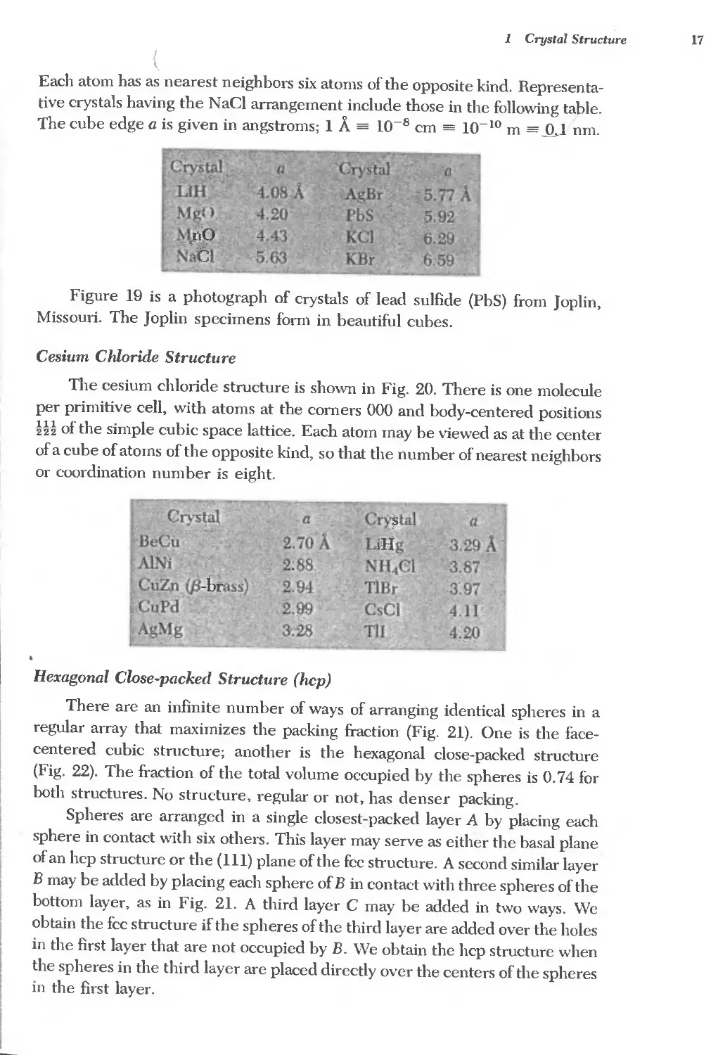
Hexagonal Cwse-packed Structure (hcp)
There are an infinite number of ways of arranging identical spheres in a
regular array that maximizes the packing &action (Fig. 21). One is the face-
centered cubic structure; another is the hexagonal close-packed structure
(Fig. 22). The fraction of the total volume occupied by the spheres is 0.74 for
both structures. No structure, regular or not, has denser packing.
Spheres are arranged in a single closest-packed layer A by placing each
sphere in contact with six others. This layer may serve as either the basal plane
of an hcp structure or the (Ill) plane of the fcc structure. A second similar layer
B may be added by placing each sphere of B in contact with three spheres of the
bottom layer, as in Fig. 21. A third layer C may be added in two ways. We
obtain the fcc structure if the spheres of the third layer are added over the holes
in the first layer that are not occupied by B. We obtain the hcp structure when
the spheres in the third layer are placed directly over the centers of the spheres
in the first layer.
18
,
+
+
+
+ "
+
+
+ '
+
+
Figure 21 A close-packed layer of spheres is shown, with centers at points marked A. A second and
identical layer of spheres can be placed on top of this, above and parallel to the plane of the
drawing, with centers over the points marked B. There are two choices for a third layer. It can go
in over A or over C. If it goes in over A the sequence is ABABAB. . . and the structure is hexagonal
close-packed. If the third layer goes in over C the sequence is ABCABCABC. . . and the structure
is face-centered cubic.
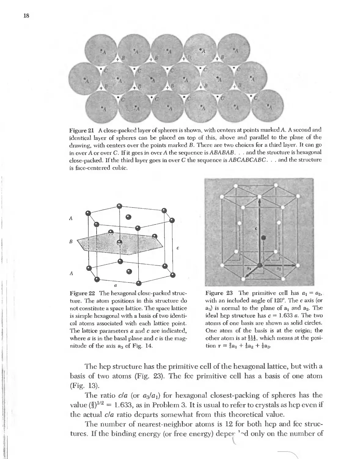
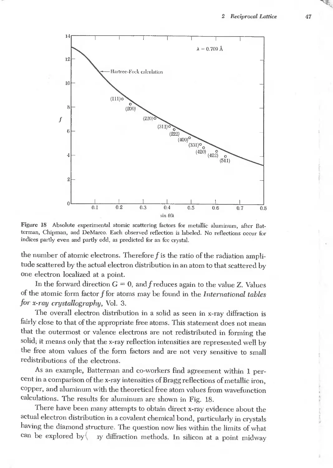
A
B
A
, I
! I
I
I.
I
I
I
Figure 22 The hexagonal close-packed struc-
ture. The atom positions in this structure do
not constitute a space lattice. The space lattice
is simple hexagonal with a basis of two identi-
cal atoms associated with each lattice point.
The lattice parameters a and c are indicated,
where a is in the basal plane and c is the mag-
nitude of the axis a3 of Fig. 14.
-';'e
Figure 23 The primitive cell has at = a2,
with an included angle of 120°. The c axis (or
a,) is normal to the plane of at and a2. The
ideal hcp structure has c = 1.633 a. The two
atoms of one basis are shown as solid circles.
One atom of the basis is at the origin; the
other atom is at Hi. which means at the posi-
tion r = fa} + !a2 + !a3-
The hcp structure has the primitive cell of the hexagonal lattice, but with a
basis of two atoms (Fig. 23). The fcc primitive cell has a basis of one atom
(Fig. 13).
The ratio cia (or a:Jal) for hexagonal closest-packing of spheres has the
value (i)1/2 = 1.633, as in Problem 3. It is usual to refer to crystals as hcp even if
the actual cia ratio departs somewhat from this theoretical value.
The number of nearest-neighbor atoms is 12 for both hcp and fcc struc-
tures. If the binding energy (or free energy) deper 1 d only on the number of
\.
rI
II
, i
II
<
I
0 2
;5;;,,-
:1 ..!...
4 4
I 0
2
I "1
-
4 4
A
0 I
2
o
1
2
o
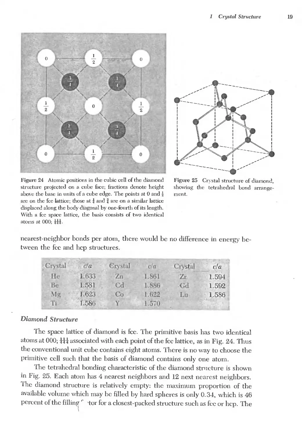
Figure 24 Atomic posItions in the cubic cell of the diamond
structure projected on a cube face; fractions denote height
abo\ e the base in units of a cube edge. The points at 0 and!
are on the fcc lattice; those at ! and are on a similar lattice
displaced along the body dIagonal by one-wurth of its length.
With a fcc space lattice, the basis consists of two identical
atoms at 000; !H.
1 Crystal Structure
19
-------- --
-----r
...--,......
Figure 25 Crystal structure of diamond,
showing the tetrahedral bond arrange-
ment.
nearest-neighbor bonds per atom, there would be no difference in energy be-
tween the fcc and hcp structures.
,'"'
">¥
'sf
CIa
.,,:<:,
1.594
1. 592
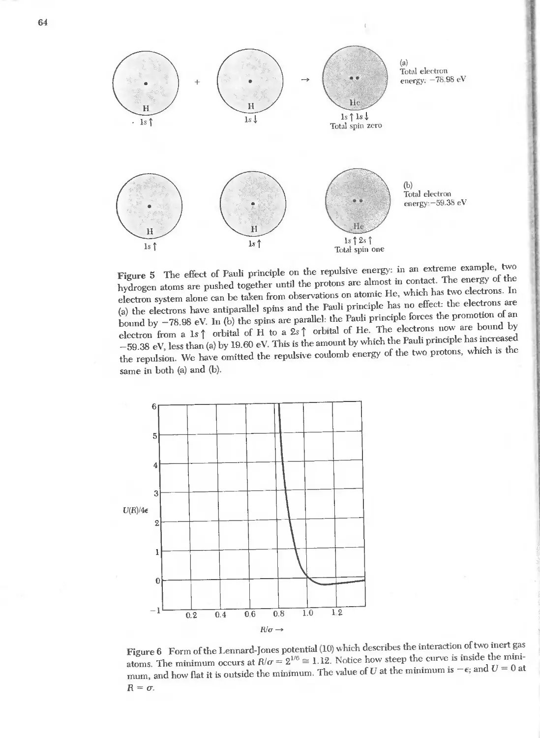
Diamond Structure
The space lattice of diamond is fcc. The primitive basis has two identical
atoms at 000; tH associated with each point of the fcc lattice, as in Fig. 24. Thus
the conventional unit cube contains eight atoms. There is no way to choose the
primitive cell such that the basis of diamond contains only one atom.
The tetrahedral bonding characteristic of the diamond structure is shown
in Fig. 25. Each atom has 4 nearest neighbors and 12 next nearest neighbors.
The diamond structure is relatively empty: the maximum proportion of the
available volume which may be filIed by hard spheres is only 0.34, which is 46
percent of the filIing r 'tor for a closest-packed structure such as fee or hcp. The
I
20
(
diamond structure is an example of the directional covalent bonding found in
column IV of the periodic table of elements.
Carbon, silicon, germanium, and tin can crystallize in the diamond struc-
ture, with lattice constants a = 3.56,5.43,5.65, and 6.46 A, respectively. Here
a is the edge of the conventional cubic cell.
Cubic Zinc Sulfide Structure
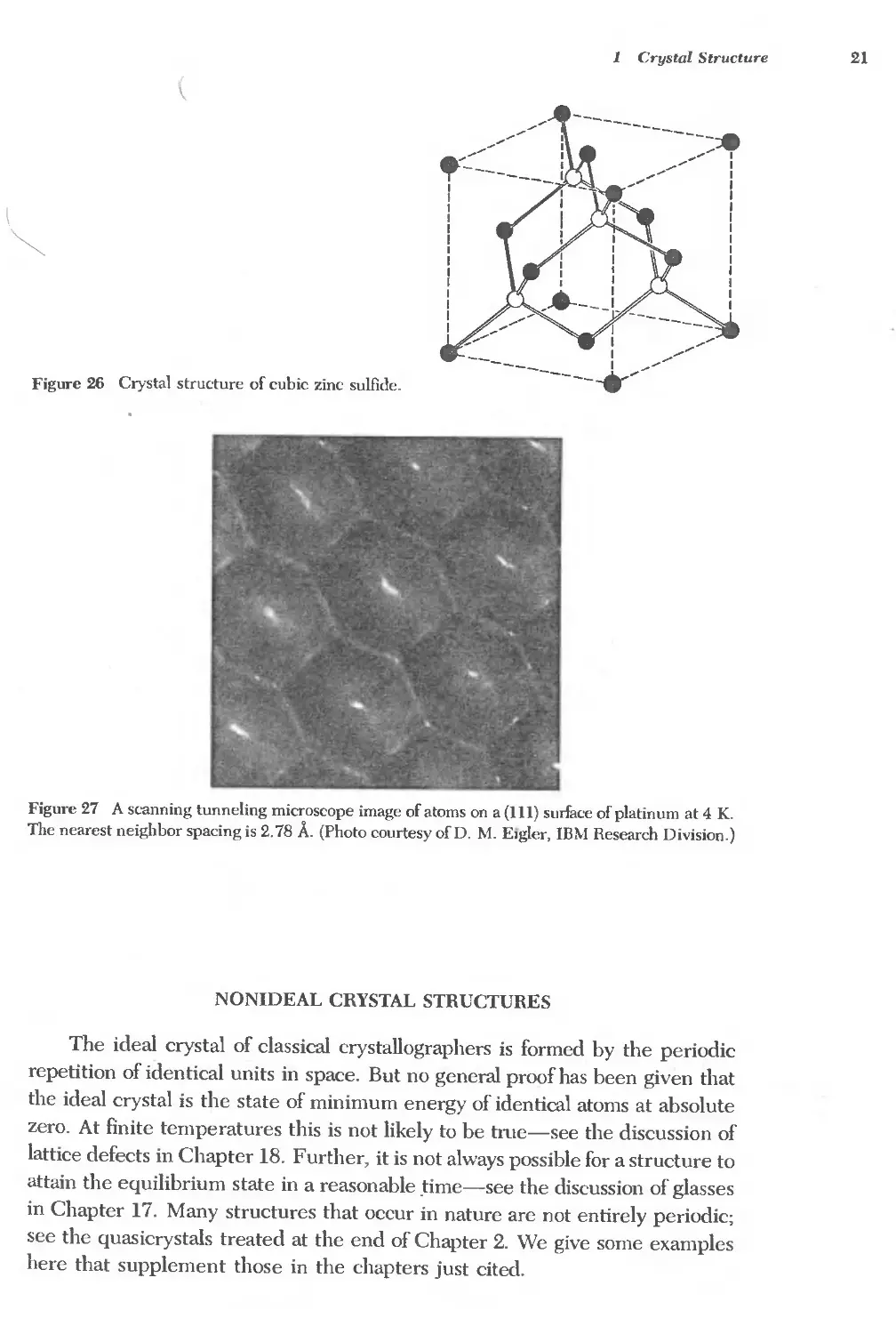
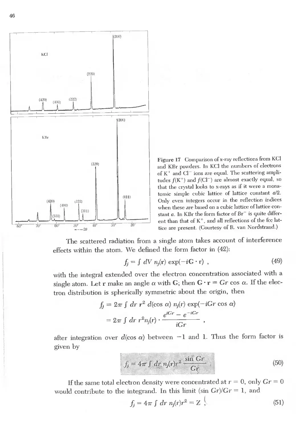
The diamond structure may be viewed as two fcc structures displaced from
each other by one-quarter of a body diagonal. The cubic zinc sulfide (zinc
blende) structure results when Zn atoms are placed on one fee lattice and S
atoms on the other fcc lattice, as in Fig. 26. The conventional cell is a cube. The
coordinates of the Zn atoms are 000; OH; 101; HO; the coordinates of the S
atoms are !H; Hi; Hi; iU. The lattice is fcc. There are four molecules of ZnS
per conventional cell. About each atom there are four equally distant atoms of
the opposite kind arranged at the comers of a regular tetral1edron.
The diamond structure allows a center-of-inversion symmetry operation at
the midpoint of every line between nearest-neighbor atoms. The inversion
operation carries an atom at r into an atom at -r. The cubic ZnS structure does
not have inversion 5ymmetry. Examples of the cubic zinc sulfide structure are
The close equality of several pairs, notably (AI, Ga)P and (AI, Ga)As, makes pos-
sible the construction of semiconductor heterojunctions (Chapter 19).
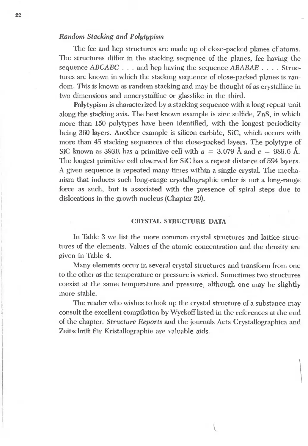
DIRECT IMAGING OF ATOMIC STRUCTURE
Direct images of crystal structure have been produced by transmission
electron microscopy. Perhaps the most beautiful images are produced by scan-
ning tunneling microscopy; in STM (Chapter 19) one exploits the large varia-
tions in quantum tunneling as a function of the height of a fine metal tip above
the surface of a crystal. The image of Figure 27 was produced in this way; see
also Figures 12.19 and 19.21. An STM method has been developed that will
assemble single atoms into an organized layer nanometer structure on a crystal
substrate: see the electron corral in Figure 19.21.
1 Crystal Structure 21
(
\
..-: //
I ----
I
I
I
I
I
I
I
I
I
I
I
I
I
--------------;4t
--
--
-
Figure 26 Crystal structure of cubic zinc sulfide.
I
I _
I --
-- 1-
------- -------
---.
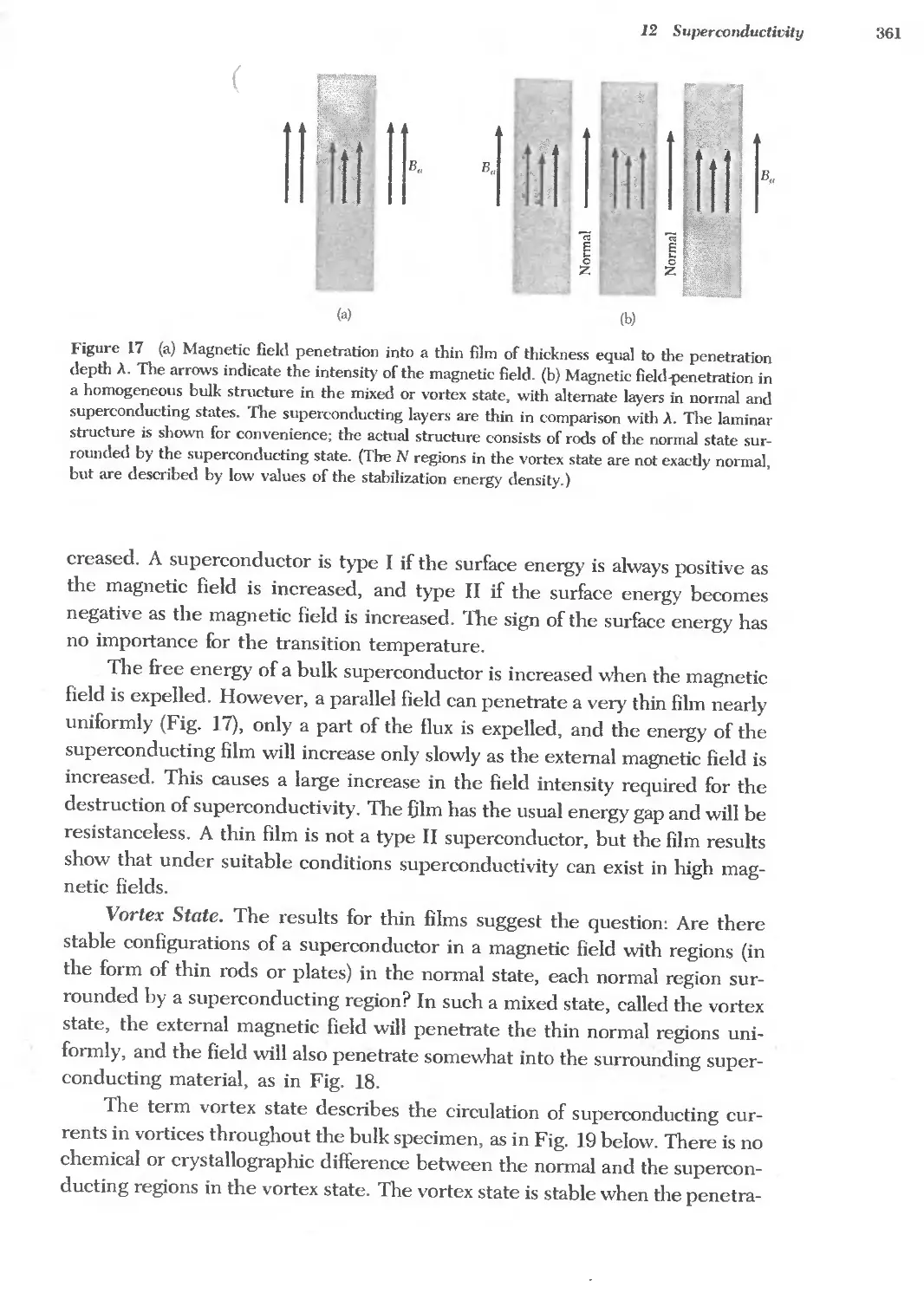
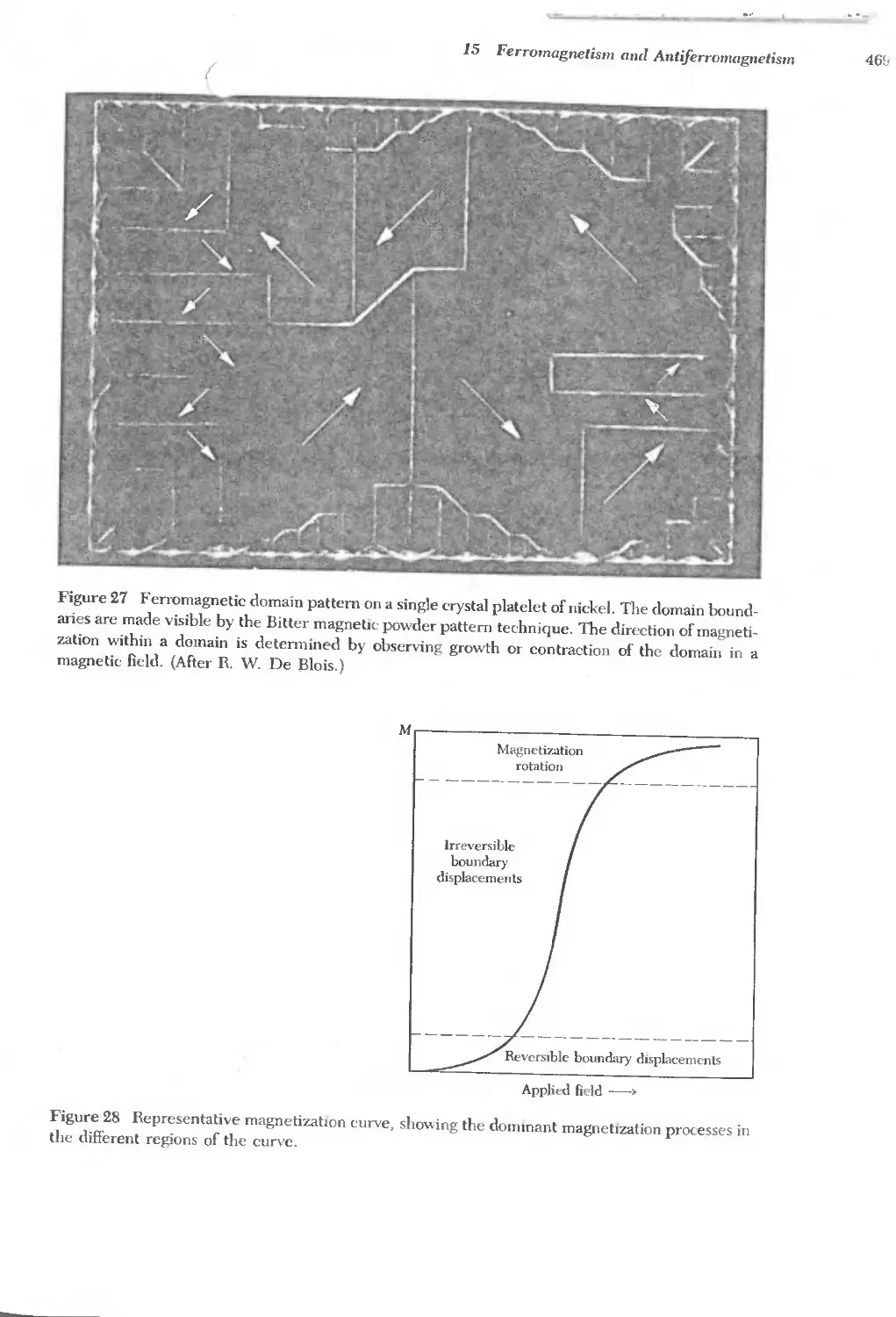
Figure 27 A scanning tunneling microscope image of atoms on a (111) surface of platinum at 4 K.
The nearest neighbor spacing is 2.78 A. (Photo courtesy of D. M. E,gler, IBM Research Division.)
NONIDEAL CRYSTAL STRUCTURES
The ideal crystal of classical crystallographers is formed by the periodic
repetition of identical units in space. But no general proof has been given that
the ideal crystal is the state of minimum energy of identical atoms at absolute
zero. At finite temperatures this is not likely to be tme-see the discussion of
lattice defects in Chapter 18. Further, it is not always possible for a structure to
attain the equilibrium state in a reasonable .time-see the discussion of glasses
in Chapter 17. Many structures that occur in nature are not entirely periodic;
see the quasicrystals treated at the end of Chapter 2. We give some examples
here that supplement those in the chapters just cited.
22
Random Stacking and Polytypism
The fcc and hcp structures are made up of close-packed planes of atoms.
The structures differ in the stacking sequence of the planes, fee having the
sequence ABCABC . . . and hcp having the sequence ABABAB . . . . Struc-
tures are known in which the stacking sequence of close-packed planes is ran-
dom. This is known as random stacking and may be thought of as crystalline in
two dimensions and noncrystalline or glasslike in the third.
Polytypism is characterized by a stacking sequence with a long repeat unit
along the stacking axis. The best known example is zinc sulfide, ZnS, in which
more than 150 polytypes have been identified, with the longest periodicity
being 360 layers. Another example is silicon carbide, SiC, which occurs with
more than 45 stacking sequences of the close-packed layers. The polytype of
SiC known as 393R has a primitive cell with a = 3.079 A and c = 989.6 A.
The longest primitive cell observed for SiC has a repeat distance of 594 layers.
A given sequence is repeated many times within a single crystal. The mecha-
nism that induces such long-range crystaUographic order is not a long-range
force as such, but is associated with the presence of spiral steps due to
dislocations in the growth nucleus (Chapter 20).
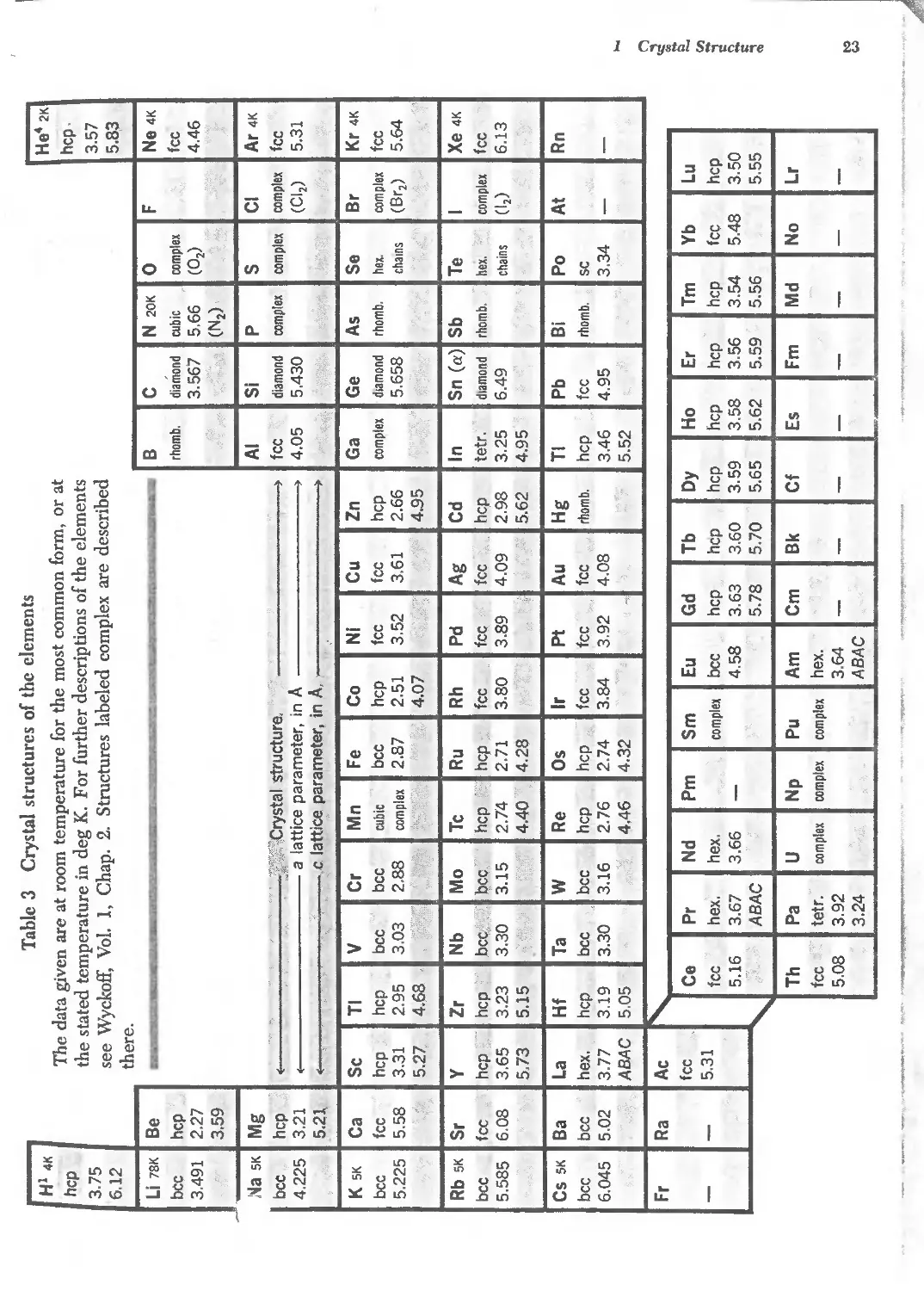
CRYSTAL STRUCTURE DATA
In Table 3 we list the more common crystal structures and lattice struc-
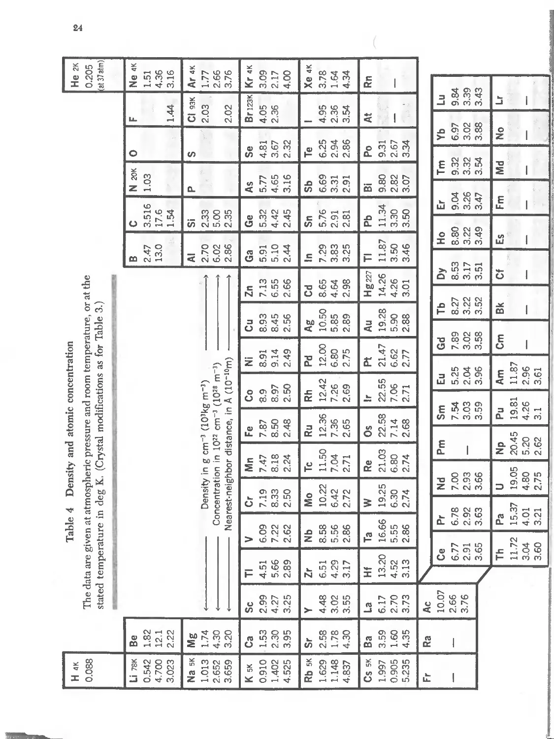
tures of the elements. Values of the atomic concentration and the density are
given in Table 4.
Many elements occur in several crystal structures and transform from one
to the other as the temperature or pressure is varied. Sometimes two structures
coexist at the same temperature and pressure, although one may be slightly
more stable.
The reader who wishes to look up the crystal structure of a substance may
consult the excellent compilation by Wyckoff listed in the references at the end
of the chapter. Structure Reports and the journals Acta CrystaUographica and
Zeitschrift fur Kristallographie are valuable aids.
\
\
Crystal Structure 23 "
1
i
i
J
'" I
'" i
N . ..... ("r) ...
4'Gj 0.1t)CX) Gj r
u . . Z
::J: .e M It) 8"
o..
...I .eMit) ...I
i
..... u
.c 0
> o . Z
_It)
0
'"
0
N
Z 8" I
o.. E t
w .eMit) .....
(J 8" ,
0 III !
::J: .eMit) W
m 8"
>. -
C .eMit) (J
...1':..0 C f
o Q) . N
. S t 0.00
S Q) '" .c u'-'?I':
'-- Q1 I- .eMit) I
J3 Q)
I':...c::: Q) (J
0'::':: a
'" S 0 ><
i:: S '" Q)
Q) 01':"0. I
S °:8s z
Q) . 8
S°"O W
Q)
.;3 '" Q) 0
g"Q)-
... ...c:::"O Q) (J ., .,
.........0 E -a.
0 ....Q)..:g E
'" J3.;3", V) a c.. a
Q)
... cE <II
.a
::I ... i! ..... .,
u E Q.
::I .... 0 0
l: 2 c.. z a
'" g" ....
1:1. 'en
S S . ..
.,
'" Q) t>.O c<I -a.
.... Q) E
s"O ci. a
C) o I': <II
o . ..d
M "'Q)C)
.... ...
Q) <II ::I .
... .....
:c <II
... .
Q)-
o.
€i S
'Q .s "E
.;g"i-zi
3 .
'" Q) .
Q) Q) Q) i
t:...c:::Q)...c::: !
.... '" ....
Y'T:':!i'
8" II/) c:: r-4 r
<II u C\! C\!
m .eN(\') :!!: .eMit)
'" '" ..... '"
... a.It)N co 0"1 '"
.....
x 0.......... f1I
-CM\6 ::i ::;00:
24
(
'" LO '" '" '" '"
N o .. .....<D<D .. I'-.<D<D .. 8 .. ;:2;
QI C\j QI tOM..... ... I'-. <D I'-. ... QI s:: I
::J: . <'> Z ocicY) NcY) "";N..t cY).....;
0 -;;; <C >< 0:
'" . '" " .:i I
'" '" ...I m....;....;
'" M C\j I/)<D ;1)
C3 0 0 ... OM ::c "'y I
..... ..... N N m ..tN - ..tN"";
, .c B; 0 .'
, >- ....;....; z I
..... I'-. C\j I/)q-<D r;)rD
QI OO<DM t!!! C\j0'l00 0
0 VI VI ..t...-)N NN c.. mN"";
E ;1) '"C I
'" I- m....;...-) :E
M I'-.I/)<D 0'1.......... 0C\jl'-.
q , '" I'-. <D ..... .c <DMO'I ai 00000
z ..... c.. <C .o..t....; VI "";N mN""; ¥
S<DI'-. E
, ... C\jq- I
<D OO LoJ m....;...-) .....
;;:; ;1) 8 C\j C\j I/) <D..........
QI Mq-q- s:: 1'-.0'100 .c oM to
U . I'-. . en NoON " .o..tN VI .oNN c.. ..... 0 .
M.......... .....MM
0C\j0'l ,
0 00C\jq- '" I
I'-. ::J: 05...-)""; LoJ ,
1'-.0 0C\j<D O'IMtO OOO<D
q- . 1'-.000 III C\j 00 C\j r-4
.M <C N N " .o.oN .= "....;....; t=
m C\j ..... .....MM
MI'-......
.... >r,1.f)r-ttl') - I
v N <D COO""; M (,)
-:S ,. MI/)<D ti3;:2; N C\j <D .....
s:: .....to<D '"C 'C\j0
..... N ro.:""N (,) OO..tN ::J: q- . .
c: .....q-M I'-. C\j C\j
... .c C\j C\j to ""' I
OM 0 00 I- 05"";""; m
as v MI/)<D I/) to 0'1 C\j000
0'Iq-1/) '0000 o 0'1 00
...- <C 0 . 0 C\ . 0
;::I'::> (,) OOOON ..... to C\j <C .....I/)C\j >
e 0'IC\j00
c '"C 00010 E I
v ... 801/) I'-. " "....;....; (,)
0 P-.,£ .....q-O'I q-C\jl'-.
"J: e E z 0'I.....q- '"C . 00 I'-. it . <D I'-.
c: '" oomN c.. C\j . . ..... . .
... .8 c: .....<DN C\j<DC\j I'-.
.... I 0 S E OO<D.....
C e '" Eb o:
Q,) c C\j It) LoJ .oN""; <C .....C\jM
" 0 :8 I e. 1'-.0 q-<DO'I to<D.....
C 0 0 0'10'110 .c . C\j <D . 0 I'-.
0 ... c: ES< (,) Q:iOON 0: C\j . . C\j . . ..... >
" "OJj .....I'-.C\j C\jl'-.C\j
bD E ;1)MO'I OO<D
" a.:a .JI::..., . 01/) o C\j.....
"s 0 I <D 00 VI "....;....; c.. C\ . .
Q,) 0 E oj !X> M<DI/) I/)q-OO .....q-M
.s ... e ..... <> <> QI . M <D '" . ..... <D
;::I C\j . . C\j . .
c: c: ..... "OON 0: .....I'-.C\j 0 C\jl'-.C\j I/)
Ci! m N ro
"0 10...... E q-0C\j
Q,) ..... E...... .!!? I 0. . C\j <D
C ... '" 0 M c.. Z 0 . 0
c: P-.c . I'-.00q- I1"!Sr:: 00q- C\jl/)C\j
E o s:: q-.....C\j QI o 00 I'-.
c: c: .8 :E ..... . . ..... . .
"OON ..... I'-. C\j 0: C\j<DC\j to
'" V .- O..c 8 M <D OOto
C .co . '"C 0'1 <D . 00 I'-.
Q,) P-. C\j to z "N""; ::J 0'1 . .
'" bO "iI) Q) O'IMO C\jC\jC\j C\j0q- .....q-C\j
0 cZ 0
e ... .....M I/) o q- I'-. . M I'-.
"OON :E o 0 . ;: 0'1 . .
D fJ :!J (,) .....<DC\j .....<DC\j I'-.
..,. .5 c: .... OOC\jM M..........
I'-.O'I<D III '0C\j
V ..... 0 ro ... I/) . .
::c <:: v U OJ <D c.. N""; c.. .....q-M
Z 0'IC\jC\j OO<D<D <DI/)<D
C ... 0C\j<D .c 101/)00 . I/) 00
v ;::I I > "N z OO.oN <D . .
> ..... I/) C\j C\j
'61:; I'-. ..... I/) ::;
& QI I'-.O'I<D .c
Q,) 0 (,) N""; I- .....MM
a e ......00'1 .....0'11'-. C\jC\jM
to<DOO ... I/)C\j..... - . 1/)..... II
<:: Q,) t= .,f.oN ..t....; ::J: M . . /
; N .....q-M
"0 Q,) I'-.
Q,) ..... 0'11'-. I/) C\jl/) I'-. OM O<D<D
..c: .s u 0'IC\jC\j Oto ..... I'-. I'-. U . <D I'-.
E-< III o . .
'" VI N..t....; >- ..t....;....; ...I N""; <C .....C\jM
C\j.....C\j bDq-oo MOtO 00000 0'101/)
QI 00 . C\j I'-.MC\j III I/)MO'I ... I/)I'-.M III I/)<DM III I
o C\j .
m .......... C\j :E ...; -i ...-) (,) r-4NM VI N oci m rr:;......oci 0:
'" fg '" 8 '" MC\jO'l 0C\j1/) '" ro !;) '" I'-. I/) to
'" '" '" '" '"
.. .... ..... I/) to '" .....0C\j 0'1 OM
0 1/)1'-.0 III O<D<D O'Iq-tO .c <D.....OO '" 0'I0'IC\j ... I
::J: 0 :.::i o-i....; z r-4NcY) o......oci 0: .....; oci (,) ""';c:5lli .....
1 Crystal Structure 25
SUMMARY
. A lattice is an array of points related by the lattice translation operator T =
uial + U2 a 2 + U3 a 3, where u.. U2, U3 are integers and a.. a2, a3 are the crystal
axes.
- To form a crystal we attach to every lattice point an identical basis composed
of s atoms at the positions rj = xjal + Yja2 + Zja3, withj = 1, 2, . . . , s. Here
x, y, Z may be selected to have values between 0 and 1.
- The axes a.. a2, a3 are primitive for the minimum cell volume lal . a2 x a31 for
which the crystal can be constructed from a lattice translation operator T and
a basis at every lattice point.
Problems
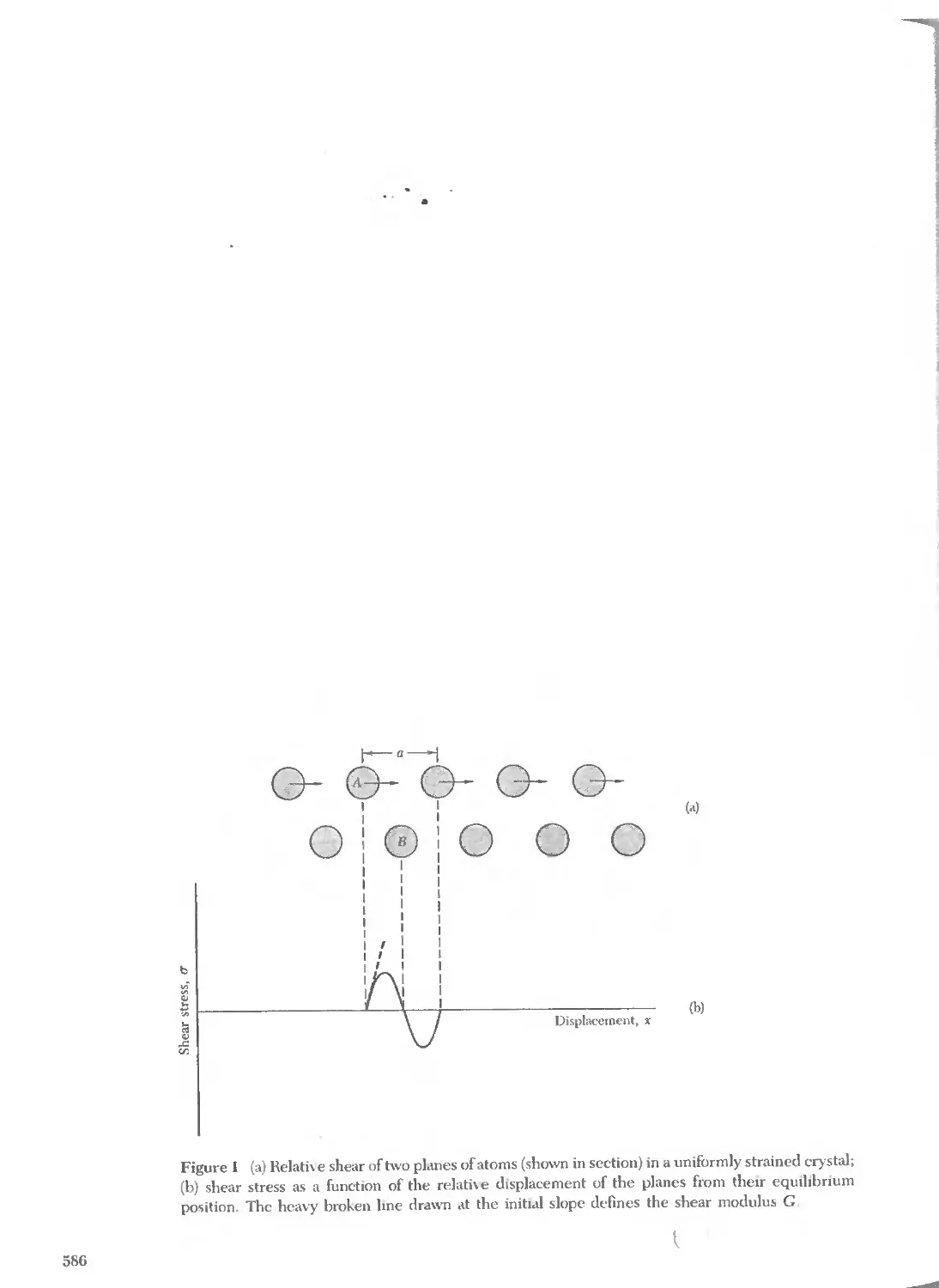
1. Tetrahedral angles. The angles between the tetrahedral bonds of diamond are the
same as the angles between the body diagonals of a cube, as in Fig. 12. Use elemen-
tary vector analysis to finrl the value of the angle.
2. Indices of planes. Consider the planes with indices (100) and (001); the lattice is fcc,
and the indices refer to the conventional cubic cell. What are the indices of these
planes when referred to the primitive axes of Fig. 13?
3. Hcp structure. Show that the cia ratio for an ideal hexagonal close-packed structure
is (!)1/2 = 1.633. If cia is significantly larger than this value, the crystal structure may
be thought of as composed of planes of closely packed atoms, the planes being loosely
stacked.
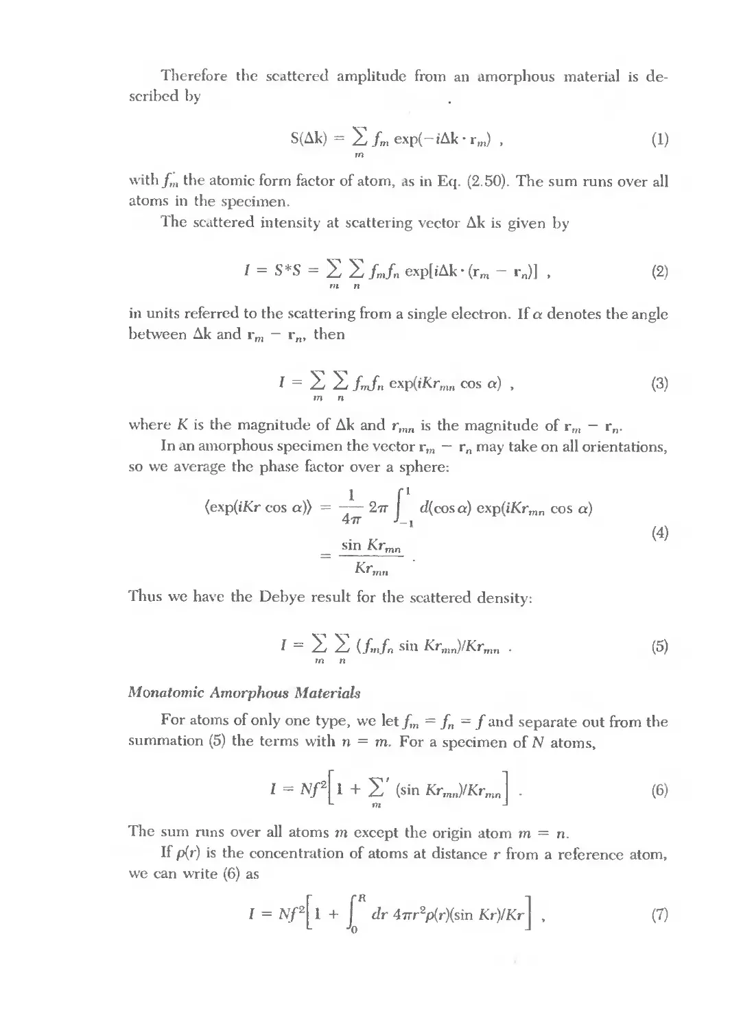
References
ELEMENTARY
W. B. Pearson, Crystal chemistry and physics of metals and alloys, Wiley, 1972.
H. D. Megaw, Crystal structures: a working approach, Saunders, 1973.
CRYSTALLOGRAPHY
M. J. Buerger, Introduction to crystal geometry, McGraw-Hill, 1971.
G Bums and A. M. Glaser, Space groups for solid state physictsts, Academic, 1978.
F. C. Phillips, An introduction to crystallography, 4th ed., Wiley, 1971. A good place to begin.
H. J Juretscke, Crystal pllYsics: macroscopic physics of anisotropic solids, Benjamin, 1974
B K. Vainshtein, Modern crystallography, Springer, 1981.
J. F. Nye, Physical properties of crystals, Oxford, 1985.
CRYSTAL GROWTH
W. G. Pfann, Zone 1Mlting, Kneger, 1978, 196&.
A. W. Vere, Crystal grouth. principles and progress, Plenum, 1987.
J. C. Brice, Crystal grou;th processes, Halsted, 1986.
S. H Liu, "Fractals and their applica.hon in condensed matter physics," Sohd state physics 39, 207
(1986).
26
Series: Journal of Crystal Growth, includes proceedings of the International Conferences on Crystal
Growth.
Springer Series: Crystals-Growth, Properties, and Applications.
CLASSICAL TABLES AND HANDBOOKS
International tables for x-ray crystallography, Kynoch Press, 4 volumes, Birmingham, 1952-1974.
J. F. Nye; Physical properties of crystals: their representation by tensors and mattices, Oxford,
1984.
P. Villars and L. D. Calvert, Pearson's handbook of crystal/ographic data forintemwtal/ic phases,
Amer. Soc. Metals, 3 vols., 1985.
A. F. Wells, Structural inorganic chemistry, 5th ed., Oxford University Press, 1990, 1984c.
W. G. Wyckoff, Crystal structures, 2nd ed., Krieger, 1981.
,I
'II
I
I I I
!i
(
2
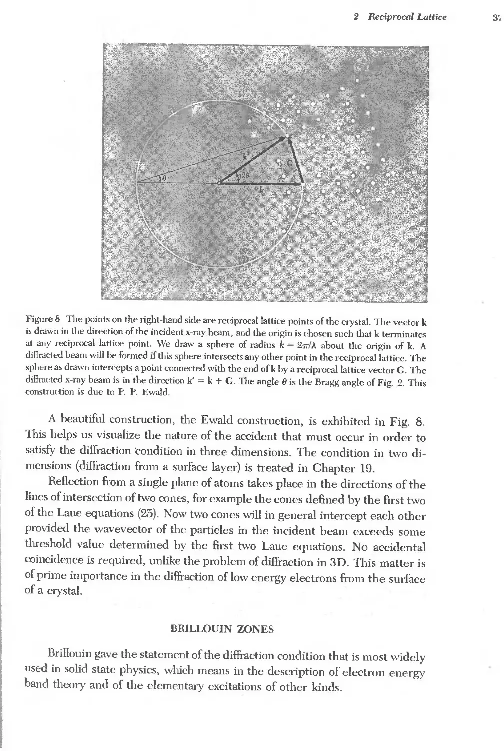
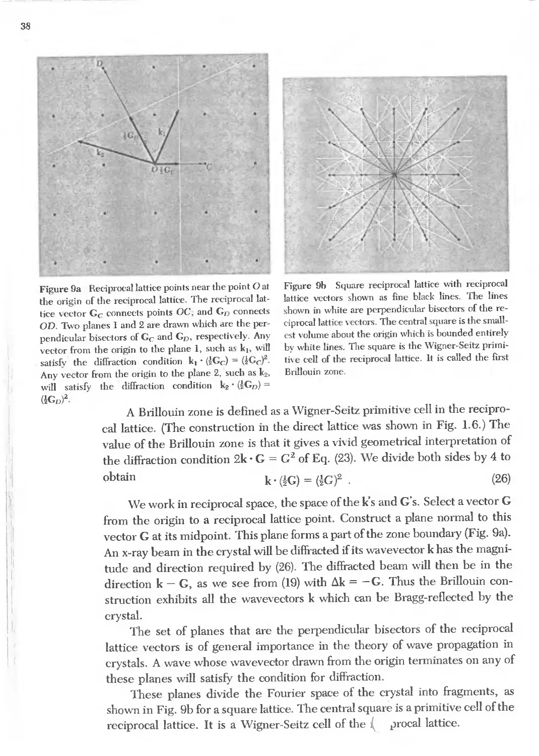
Rec;iprocal Lattice
DIFFRACTION OF WAVES BY CRYSTALS 29
Bragg law 29
SCATIERED WAVE AMPLITUDE 30
Fourier analysis 30
Reciprocal lattice vectors 33
Diffraction conditions 34
Laue equations 36
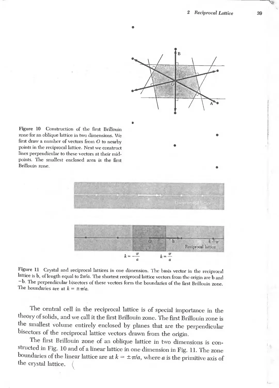
BRILLOUIN ZONES 37
Reciproeallattice to se lattice 40
Reciprocal lattice to bce lattice 40
Reciprocal lattice to fcc lattice 41
FOURIER ANALYSIS OF THE BASIS 42
Structure factor of the bec lattice 44
Structure factor of the fce lattice 45
Atomic form factor 45
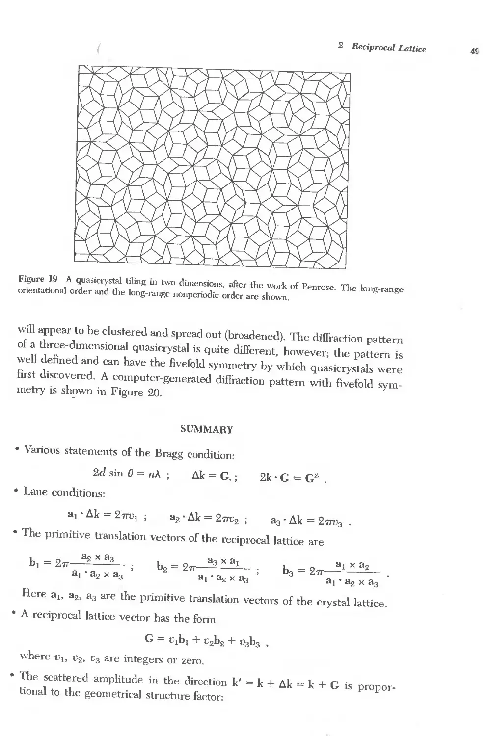
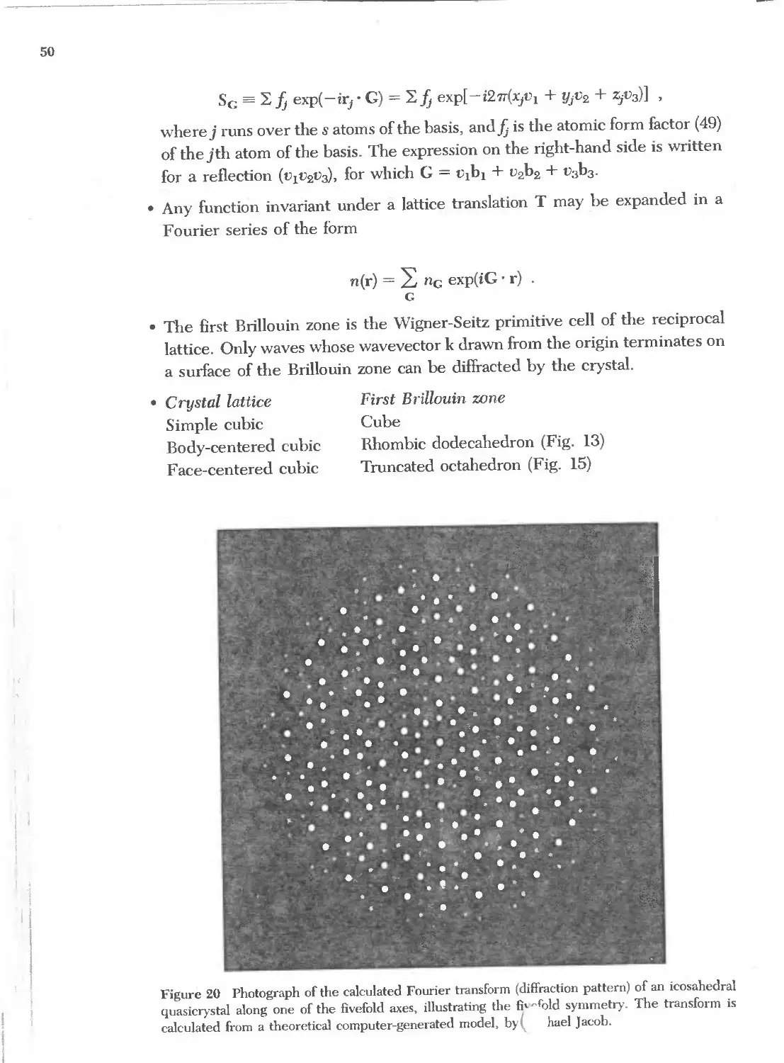
QUASICRYSTALS 48
SUMMARY 49
PROBLEMS 51
1. Interplanar separation 51
2. Hexagonal space lattice 51
3. Volume of Brillouin zone 51
4. Width of diffraction maximum 51
5. Structure factor of diamond 51
6. Form factor of atomic hydrogen 52
7. Diatomic line 52
REFERENCES 52
\
28
(
\
\
10
"-
"- X-ray photon
"-
............ I'\r-..
J".... .......
........ i--.i-- "-
.....
Neutrons
"- ......
Electrons............. '\.
....... .......... "-
.............
5
0<
£
1.0
Q)
...
;;::
0.5
0.1 1
100
50
10
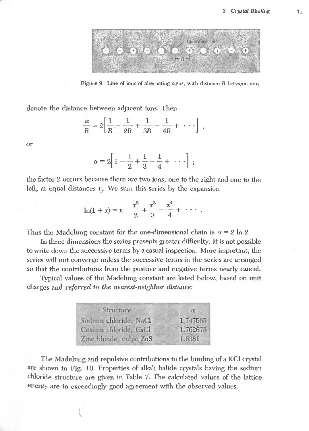
5
Figure I \Vavelength versus parti-
cle energy, for photons, neutrons,
and electrons.
Photon energy, keV
Neutron energy, 0.01 eV
Electron energy, 100 eV
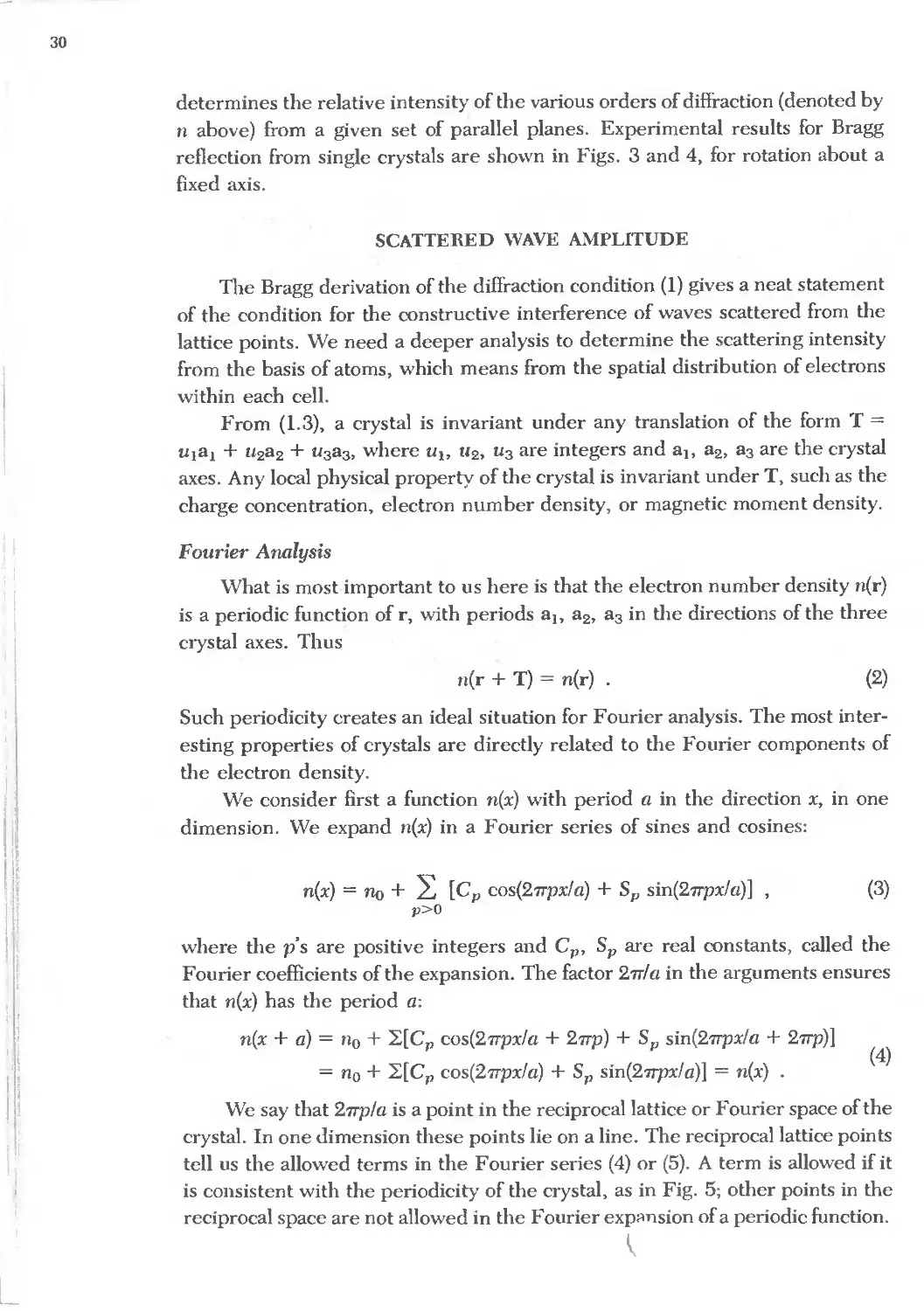
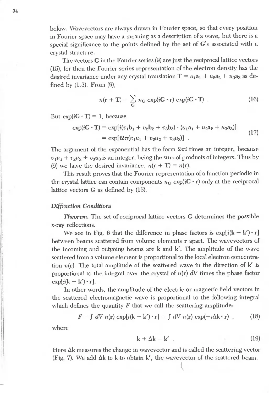
Figure 2 Derivation of the Bragg equation 2d sm 8 = nA, here d is the spacing of parallcl atomic
planes and 2'/Tn is the difference in phase between reflections from snccessive planes. The refleetmg
planes have nothing to do with the surface planes bounding the partienlar specimen.
- TER 2: RECIPROCAL LATTICE
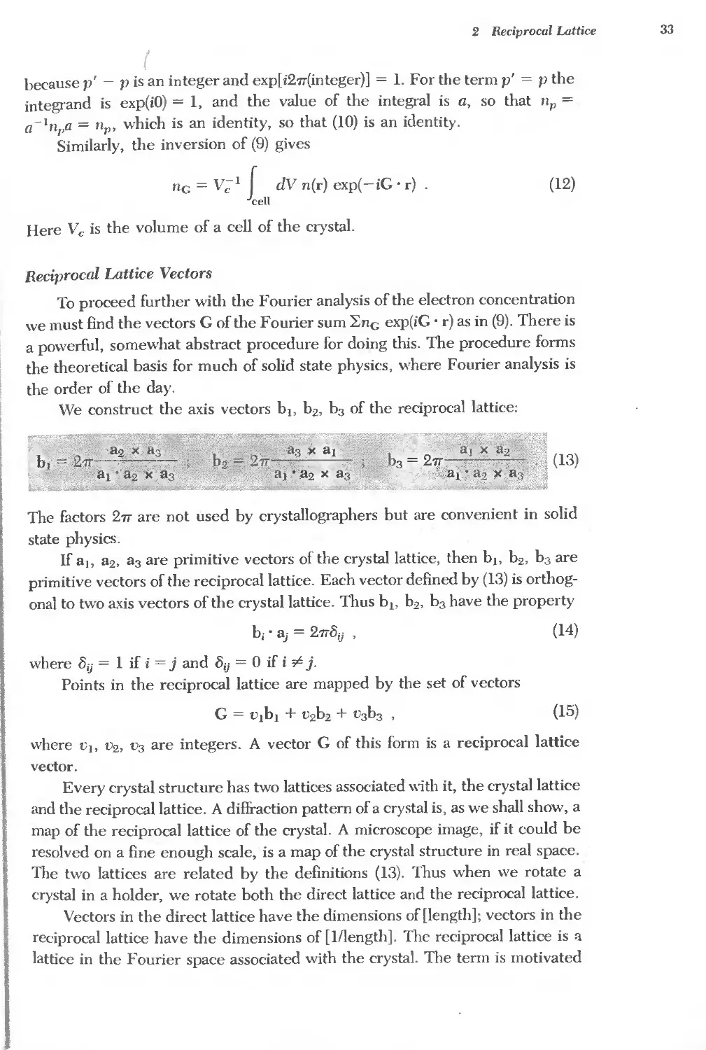
DIFFRACTION OF WAVES BY CRYSTALS
Bragg Law
We study crystal structure through the diffraction of photons, neutrons,
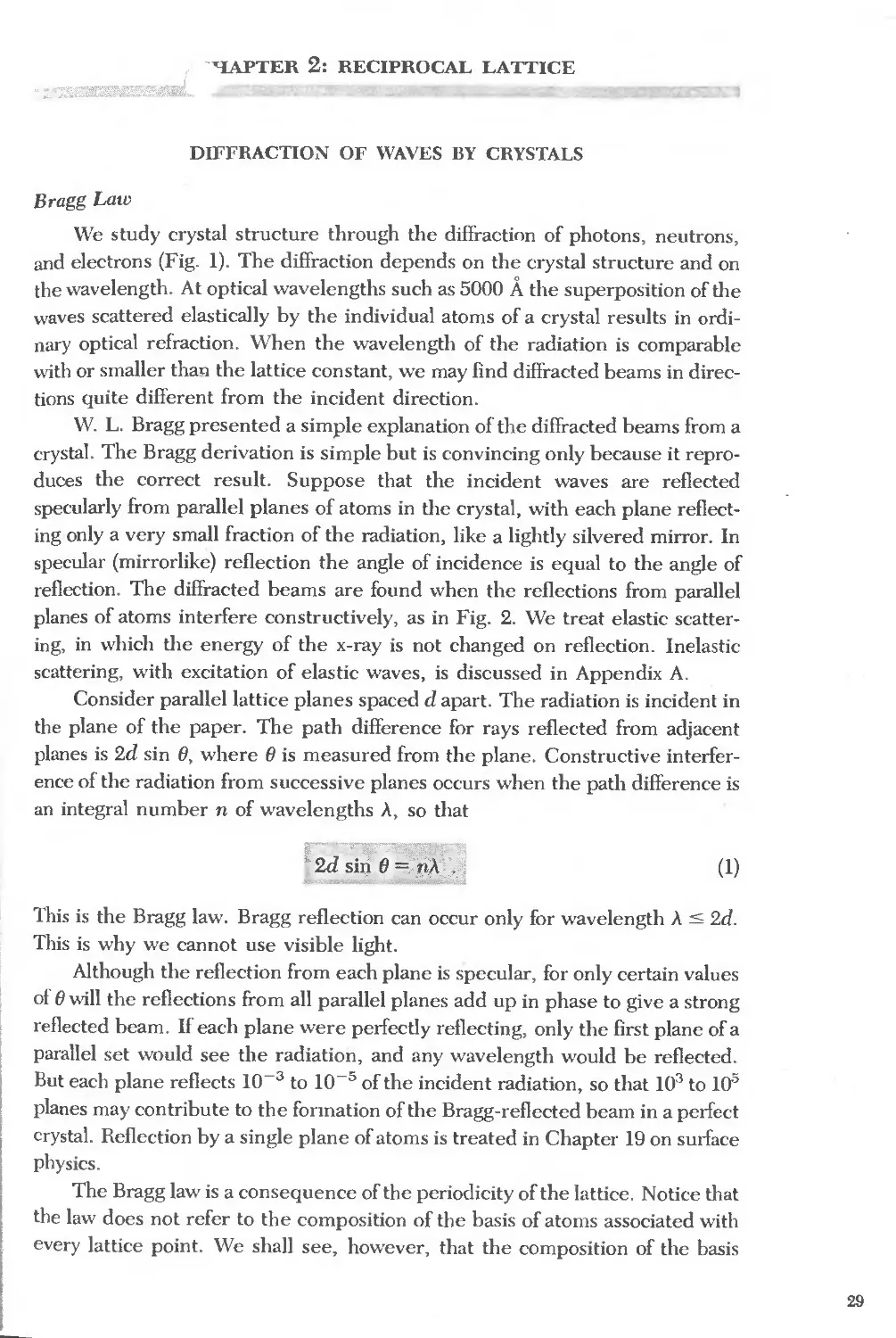
and electrons (Fig. 1). The diffraction depends on the crystal structure and on
the wavelength. At optical wavelengths such as 5000 A the superposition of the
waves scattered elastically by the individual atoms of a crystal results in ordi-
nary optical refraction. When the wavelength of the radiation is comparable
with or smaller that:! the lattice constant, we may find diffracted beams in direc-
tions quite different from the incident direction.
W. L. Bragg presented a simple explanation of the diffracted beams from a
crystal. The Bragg derivation is simple but is convincing only because it repro-
duces the correct result. Suppose that the incident waves are reflected
specularly from parallel planes of atoms in the crystal, with each plane reflect-
ing only a very small fraction of the radiation, like a lightly silvered mirror. In
specular (mirrorlike) reflection the angle of incidence is equal to the angle of
reflection. The diffracted beams are found when the reflections from parallel
planes of atoms interfere constructively, as in Fig. 2. We treat elastic scatter-
ing, in which the energy of the x-ray is not changed on reflection. Inelastic
scattering, with excitation of elastic waves, is discussed in Appendix A.
Consider parallel lattice planes spaced d apart. The radiation is incident in
the plane of the paper. The path difference for rays reflected from adjacent
planes is 2d sin e, where e is measured from the plane. Constructive interfer-
ence of the radiation from successive planes occurs when the path difference is
an integral number n of wavelengths A, so that
(1)
This is the Bragg law. Bragg reflection can occur only for wavelength A 2d.
This is why we cannot use visible light.
Although the reflection from each plane is specular, for only certain values
of e will the reflections from all parallel planes add up in phase to give a strong
reflected beam. If each plane were perfectly reflecting, only the first plane of a
parallel set would see the radiation, and any wavelength would be reflected.
But each plane reflects 10- 3 to 10- 5 of the incident radiation, so that 10 3 to 10 5
planes may contribute to the formation of the Bragg-reflected beam in a perfect
crystal. Reflection by a single plane of atoms is treated in Chapter 19 on surface
physics.
The Bragg law is a consequence of the periodicity of the lattice. Notice that
the law does not refer to the composition of the basis of atoms associated with
every lattice point. We shall see, however, that the composition of the basis
29
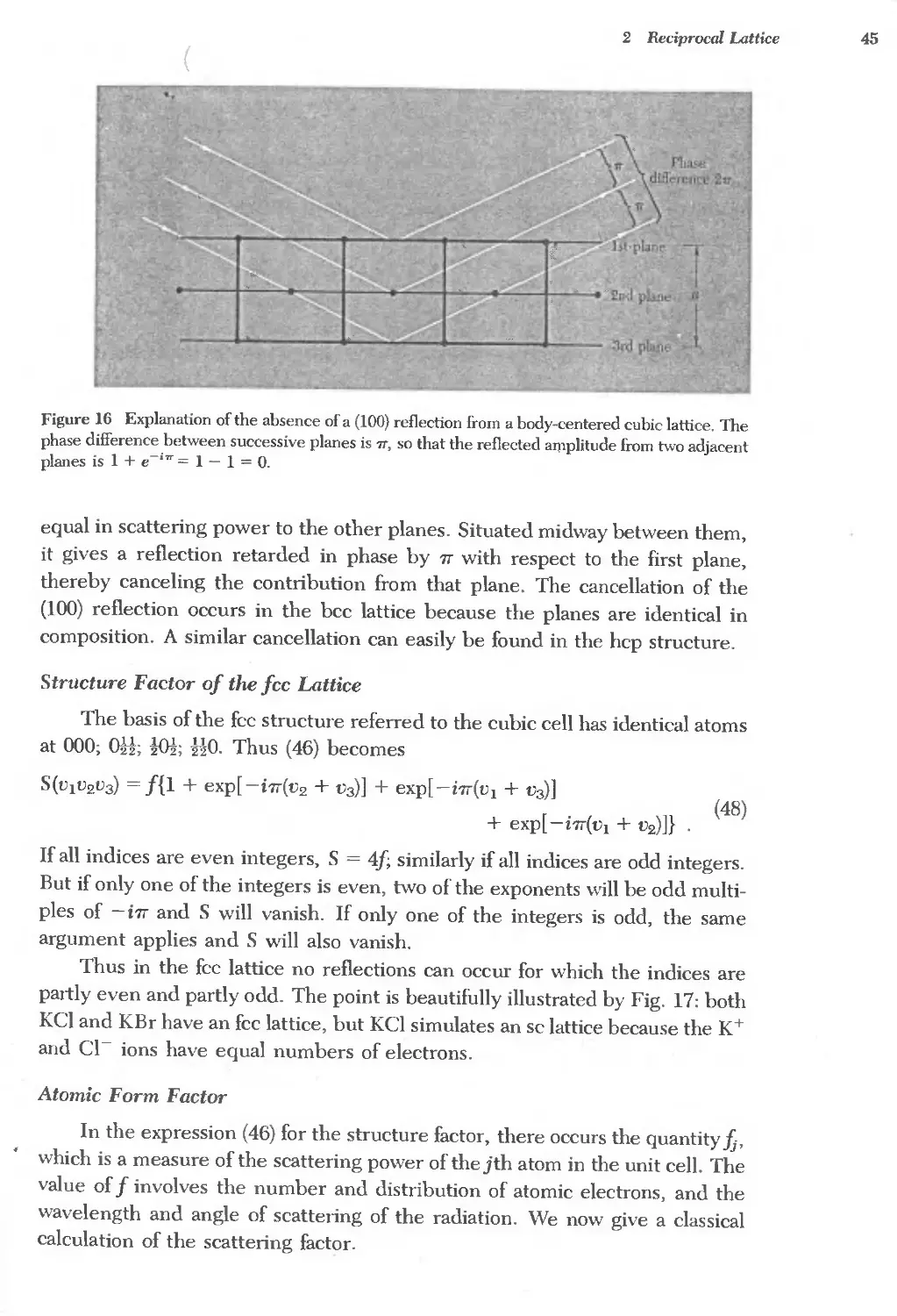
30
determines the relative intensity of the various orders of diffraction (denoted by
n above) from a given set of parallel planes. Experimental results for Bragg
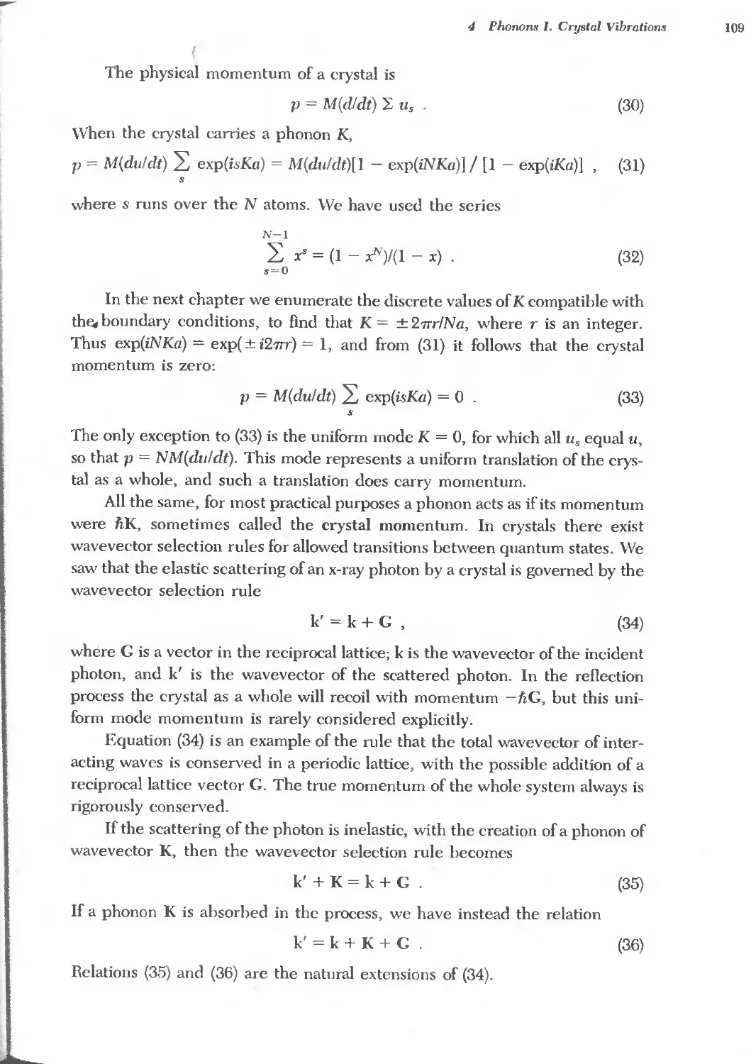
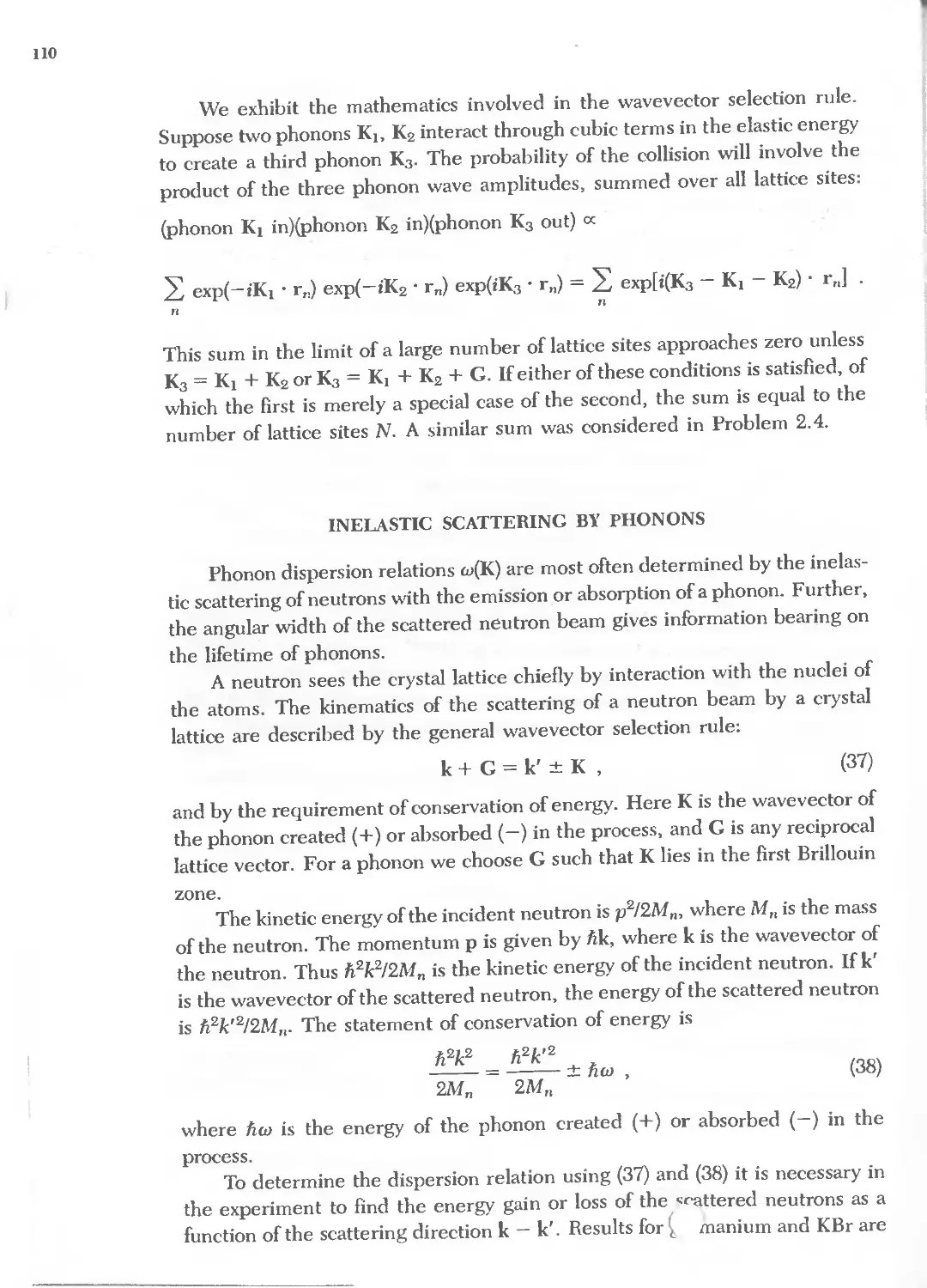
reflection from single crystals are shown in Figs. 3 and 4, for rotation about a
fixed axis.
SCATTERED WAVE AMPLITUDE
The Bragg derivation of the diffraction condition (1) gives a neat statement
of the condition for the constructive interference of waves scattered from the
lattice points. We need a deeper analysis to determine the scattering intensity
from the basis of atoms, which means from the spatial distribution of electrons
within each cell.
From (1.3), a crystal is invariant under any translation of the form T =
ulal + U2a2 + U3a3, where U1> U2, U3 are integers and a1> a2, a3 are the crystal
axes. Any local physical property of the crystal is invariant under T, such as the
charge concentration, electron number density, or magnetic moment density.
j I
{ I
.f I
j!
i
11
i
Fourier Analysis
What is most important to us here is that the electron number density n(r)
is a periodic function of r, with periods a1> a2, a3 in the directions of the three
crystal axes. Thus
n(r + T) = n(r) .
(2)
1
! '
III
!' I
,
\ "
J!
Ii
i
1
Such periodicity creates an ideal situation for Fourier analysis. The most inter-
esting properties of crystals are directly related to the Fourier components of
the electron density.
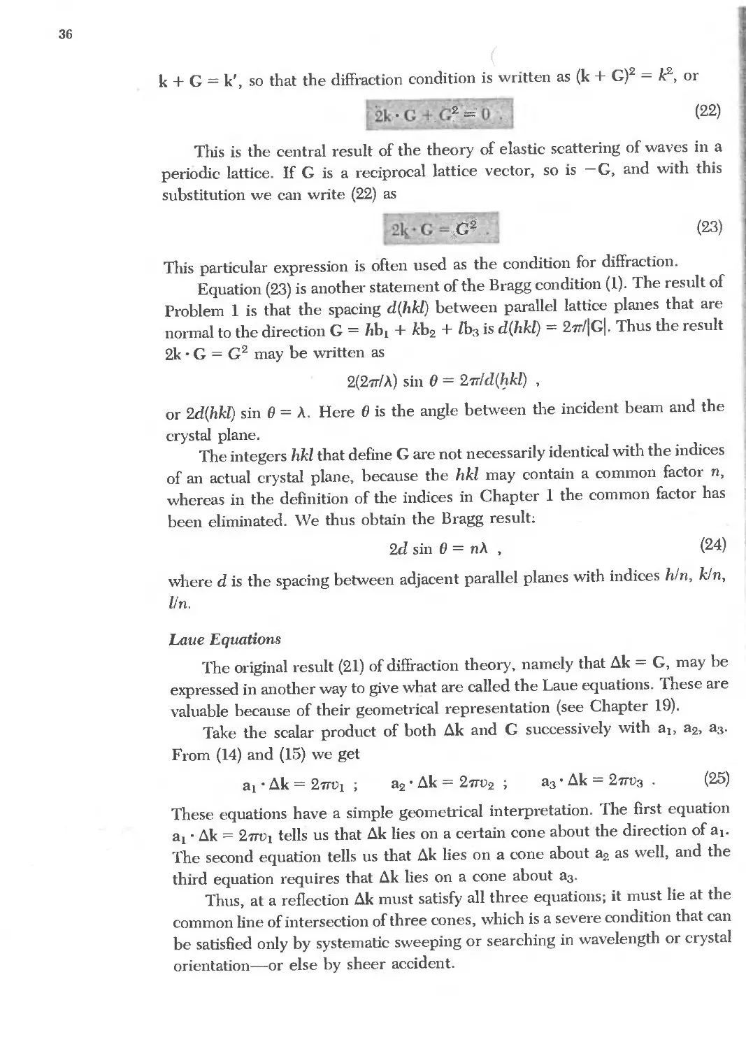
We consider first a function n(x) with period a in the direction x, in one
dimension. We expand n(x) in a Fourier series of sines and cosines:
n(x) = no + L [C p cos(27rpx/a) + Sp sin(27rpx/a)] ,
p>o
(3)
II
,
"
I ' i'
I,
i
I
where the p's are positive integers and C p , Sp are real constants, called the
Fourier coefficients of the expansion. The factor 27T/a in the arguments ensures
that n(x) has the period a:
n(x + a) = no + L[C p cos(27rpx/a + 27rp) + Sp sin(27rpx/a + 27rp)]
= no + L[C p cos(27rpx/a) + Sp sin(27rpx/a)] = n(x) .
(4)
r J
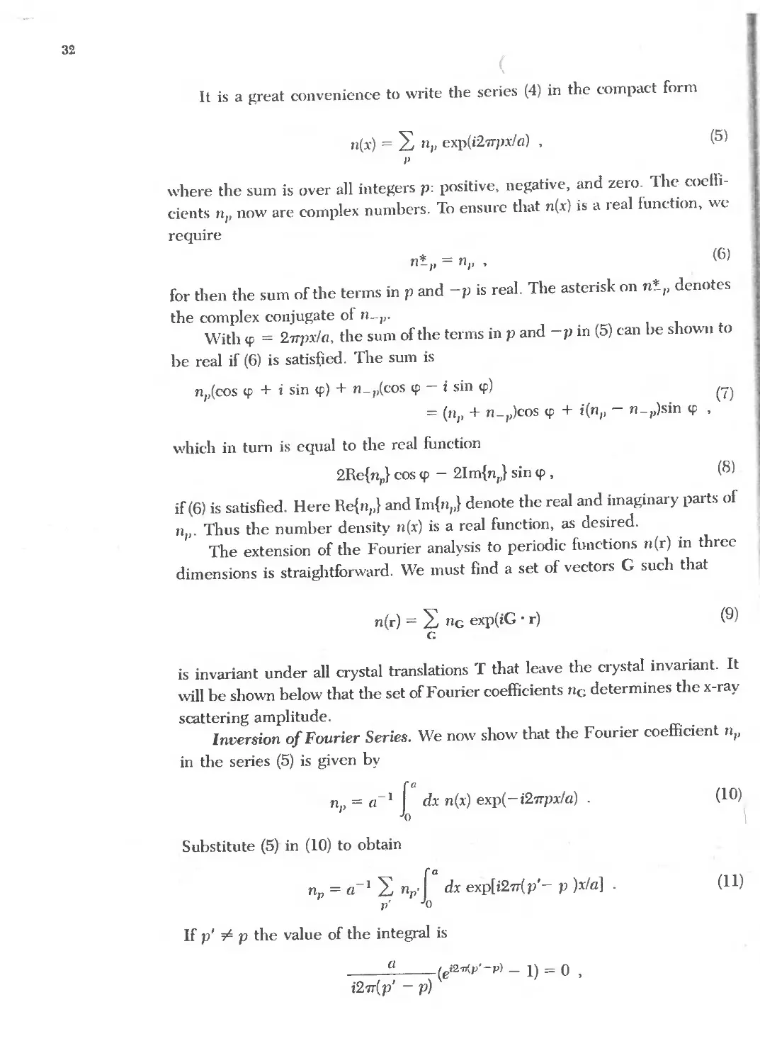
We say that 27rp/a is a point in the reciprocal lattice or Fourier space of the
crystal. In one dimension these points lie on a line. The reciprocal lattice points
tell us the allowed terms in the Fourier series (4) or (5). A term is allowed if it
is consistent with the periodicity of the crystal, as in Fig. 5; other points in the
reciprocal space are not allowed in the Fourier exp;:msion of a periodic function.
\
I
l_
2 Reciprocal Lattice
31
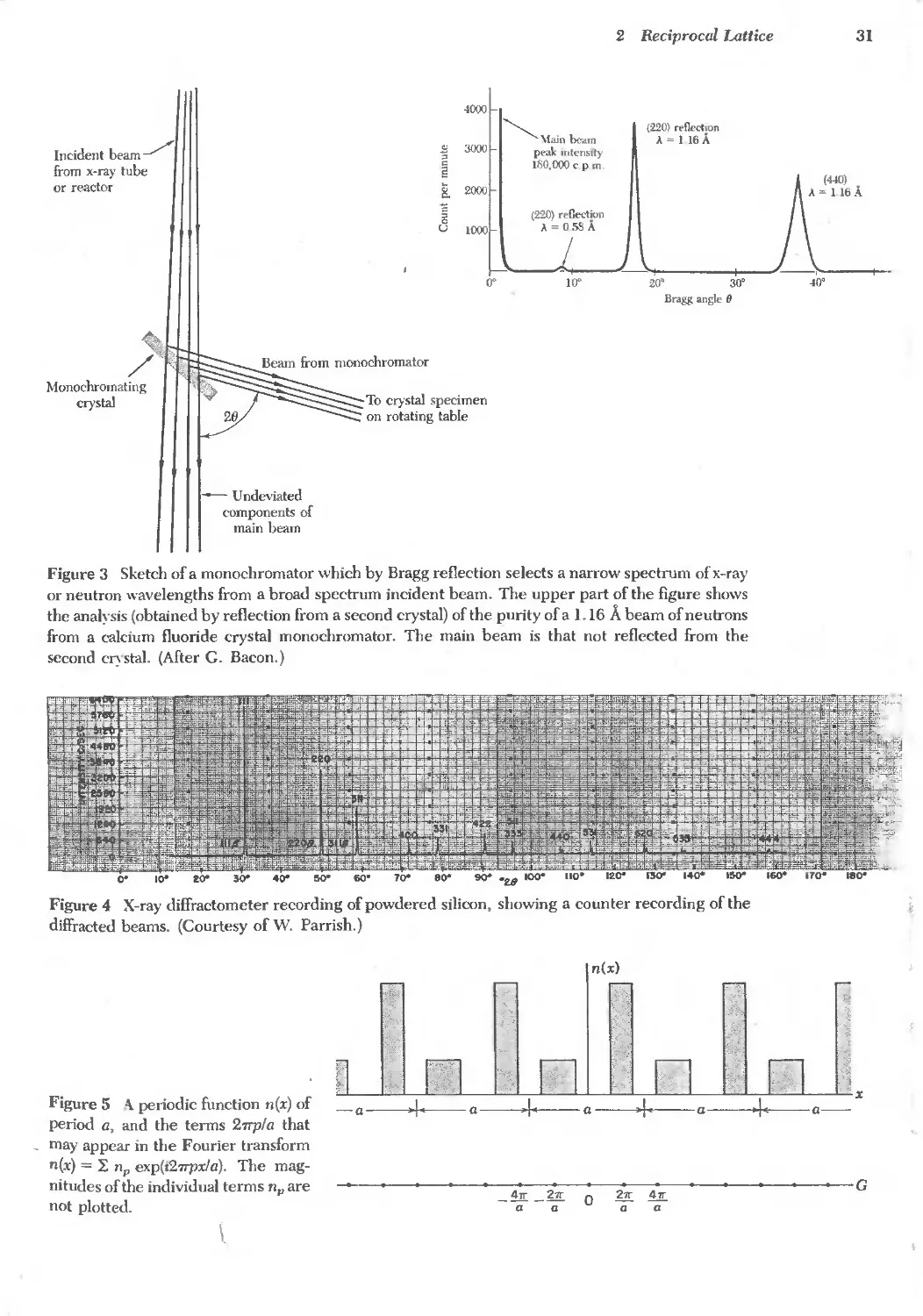
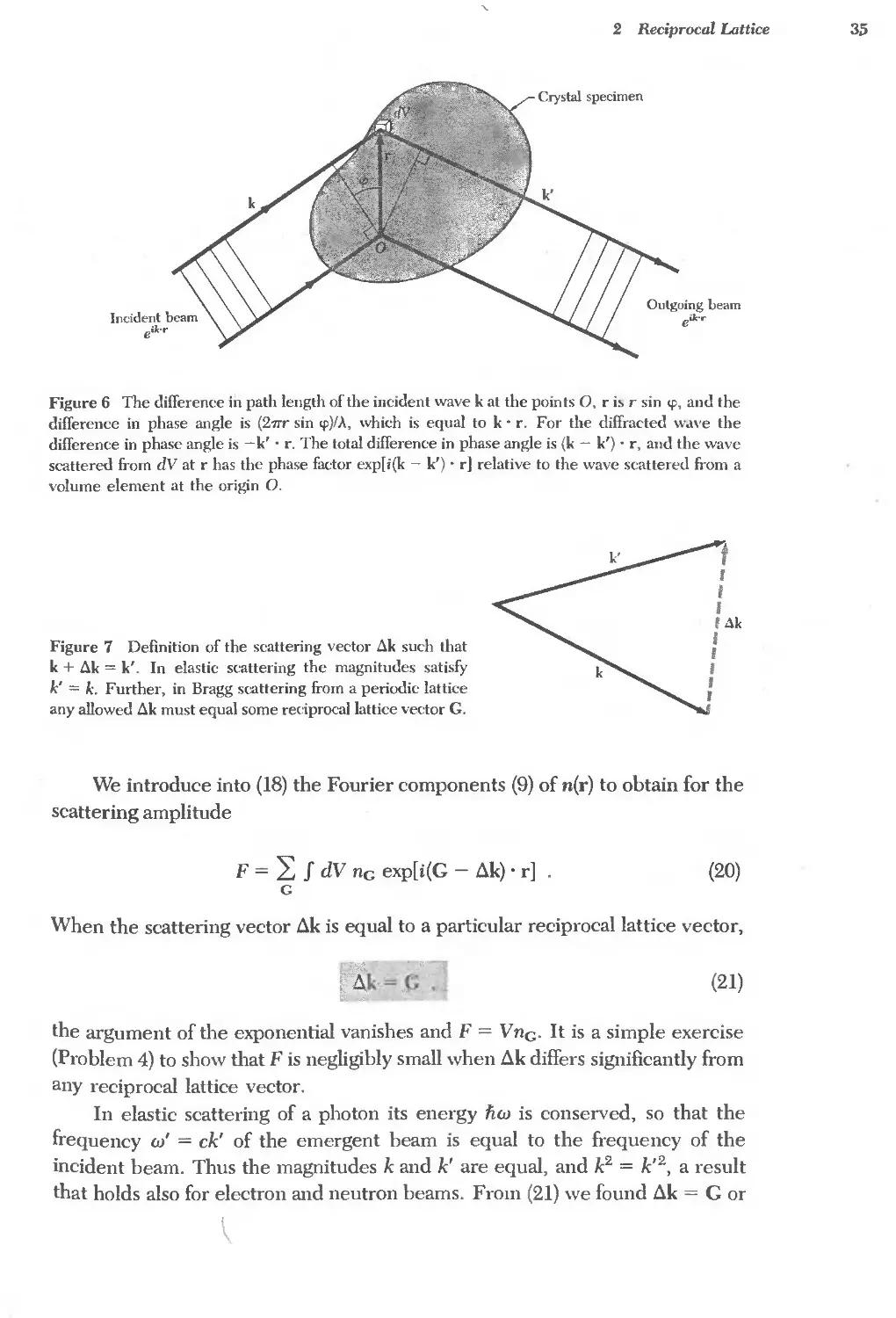
4000
Incident beam--./ 3000 \fain beam
, pea" mtensIty
from x-ray tube c 180,000 c p m
c
or reactor 8- 2000
0 (220) reflection
U 1000 A 058A
/
0" 10"
(220) reflection
A 116A
20" 30'
Brdgg angle (J
)
Monochrornating
crystal
To crystal specimen
on rotaling table
- Undeviated
components of
main beam
Figure 3 Sketch of a monochromator which by Bragg reflection selects a narrow spectrum of x-ray
or neutron wavelengths from a broad spectrum incident beam. The upper part of the figure shows
the analysis (obtained by reflection from a second crystal) of the purity of a 1.16 A beam of neutrons
from a calcium fluoride crystal monochromator. The main beam is that not reflected from the
second c stal. (After G. Bacon.)
Figure 4 X-ray diffractometer recording of powdered silicon, showing a counter recording of the
diffracted beams. (Courtesy of W. Parrish.)
,.
"
n(>:)
78-
f1
Figure 5 -\ periodic function n(x) of
period a, and the terms 271pla that
_ may appear in the Fourier transform
n(x) = L np exp(.271pxla). The mag-
nitudes of the individual terms lip are
not plotted.
,:f>
-
>{;<
-a
/
'j
"'.x
a-
_ 4; _ 211" 0
211'" 4Jr
a a
G
32
(
It is a great convenience to write the series (4) in the compact form
n(x) = L np exp(i21TpX!a) ,
I'
(5)
where the sum is over all integers p: positive, negative, and zero. The coefH-
dents n" now are complex numbers. To ensure that n(x) is a real function, we
require
n!. IJ = 11" ,
(6)
for then the sum of the terms in p and -p is real. The asterisk on n!p denotes
the complex conjugate of n_I"
\Nith <p = 27Tpx!a, the sum ofthe terms in p and -,) in (5) can be shown to
he real if (6) is satisf.led. The sum is
np(cos <p + i sin <p) + n_,,(cos II' - i sin <p)
= (n p + n_,,)cos <p + i(n" - n_,,)sin <p
which in turn is equal to the real function
(7)
2Re{n p } cos <p - 2Im{n p } sin <p , (8)
if(6) is satisfied. Here Re{n,,} and Im{n,,} denote the real and imaginary parts of
np' Thus the number density n(x) is a real function, as desired.
The extension of the Fourier analysis to periodic functions n(r) in three
dimensions is straightforward. We must find a set of vectors G such that
n(r) = L ne exp(iG . r)
e
(9)
is invariant under all crystal translations T that leave the crystal invariant. It
will be shown below that the set of Fourier coefficients ne determines the x-ray
scattering amplitude.
Inversion of Fourier Series. We now show that the Fourier coefficient n"
in the series (5) is given by
np = a-I r dx n(x) exp(-i21Tpxla)
o
Substitute (5) in (10) to obtain
(10)
\
np = a-I L np, i a dx exp[i21T(p'- p )x!a]
p' 0
(II)
If p' # P the value of the integral is
a (ei2-n(P'-P) - I) = 0
i21T(p' - p) ,
2 Reciprocal Lattice 33
(
because p' - P is an integer and exp[i2'7T(integer)] = 1. For the term p' = p the
integrand is exp(iO) = 1, and the value of the integral is a, so that np =
a-1nl'a = np, which is an identity, so that (10) is an identity.
Similarly, the inversion of (9) gives
nc = V;l i dv n(r) exp(-iG' r)
cell
(12)
Here V c is the volume of a cell of the crystal.
Reciprocal Lattice Vectors
To proceed further with the Fourier analysis of the electron concentration
we must find the vectors G of the Fourier sum Lnc exp(iG. r) as in (9). There is
a powerful, somewhat abstract procedure for doing this. The procedure forms
the theoretical basis for much of solid state physics, where Fourier analysis is
the order of the day.
We construct the axis vectors bi> b z , b 3 of the reciprocal lattice:
(13)
The factors 2'7T are not used by crystallographers but are convenient in solid
state physics.
If ai> az. a3 are primitive vectors of the crystal lattice, then bi> b z , b 3 are
primitive vectors of the reciprocal lattice. Each vector defined by (13) is orthog-
onal to two axis vectors of the crystal lattice. Thus bI> b 2 , b 3 have the property
b i . aj = 2'7TBij ,
where Bij = 1 if i = j and Bij = 0 if i op j.
Points in the reciprocal lattice are mapped by the set of vectors
G = v1b l + V2b2 + V3b3 ,
(14)
(15)
where Vi> V2, V3 are integers. A vector G of this form is a reciprocal lattice
vector.
Every crystal structure has two lattices associated with it, the crystal lattice
and the reciprocal lattice. A diffi-action pattern of a crystal is, as we shall show, a
map of the reciprocal lattice of the crystal. A microscope image, if it could be
resolved on a fine enough scale, is a map of the crystal structure in real space.
The two lattices are related by the definitions (13). Thus when we rotate a
crystal in a holder, we rotate both the direct lattice and the reciprocal lattice.
Vectors in the direct lattice have the dimensions of [length]; vectors in the
reciprocal lattice have the dimensions of [l/length]. The reciprocal lattice is '1
lattice in the Fourier space associated with the crystal. The term is motivated
34
below. \Vavevectors are always drawn in Fourier space, so that every position
in Fourier space may have a meaning as a description of a wave, but there is a
special significance to the points defined by the set of G's associated with a
crystal structure.
The vectors G in the Fourier series (9) are just the reciprocal lattice vectors
(15), for then the Fourier series representation of the electron density has the
desired invariance under any crystal translation T = ulal + U2a2 + U3a3 as de-
fined by (1.3). From (9),
n(r + T) = L nc exp(iG . r) exp(iG . T)
c
(16)
,
I
I
I
\ 1
t
I
1t
Iii
!
1
1
But exp(iG . T) = 1, because
exp(iG'T) = exp[i(vlb l + V2b2 + v 3 b 3 ) . (ulal + U2a2 + U3a3)]
= exp[i27T(VlUl + V2U2 + V3U3)] .
The argument of the exponential has the form 2m times an integer, because
VlUl + V2U2 + V3U3 is an integer, being the sum of products of integers. Thus by
(9) we have the desired invariance, n(r + T) = n(r).
This result proves that the Fourier representation of a function periodic in
the crystal lattice can contain components nc exp(iG . r) only at the reciprocal
lattice vectors G as defined by (15).
(17)
Diffraction Conditions
Theorem. The set of reciprocal lattice vectors G determines the possible
x-ray reflections.
We see in Fig. 6 that the difference in phase factors is exp[i(k - k'), r]
between beams scattered from volume elements r apart. The wavevectors of
the incoming and outgoing beams are k and k'. The amplitude of the wave
scattered from a volume element is proportional to the local electron concentra-
tion n(r). The total amplitude of the scattered wave in the direction of k' is
proportional to the integral over the crystal of n(r) dV times the phase factor
exp[i(k - k'), r].
In other words, the amplitude of the electric or magnetic field vectors in
the scattered electromagnetic wave is proportional to the following integral
which defines the quantity F that we call the scattering amplitude:
F = f dV n(r) exp[i(k - k'). r] = f dV n(r) exp(-i£lk' r) , (18)
I
L
II
,:1
where
k+£lk=k' .
(19)
Here £lk measures the change in wavevector and is called the scattering vector
(Fig. 7). We add £lk to k to obtain k', the wavevector of the scattered beam.
2 Reciprocal Lattice
35
Figure 6 The difference in path length of the incident wave k at the points 0, r b r sin cp, and the
difference in phase angle is (27fT sin cp)IA, which is equal to k. r. For the diffracted wave the
difference in phase angle is -k' . r. The total difference in phase angle is (k - k') . r, and the wave
scattered from dV at r has the phase factor exp(i(k - k') . r] relative to the wave scattered from a
volume element at the origin O.
Figure 7 Definition of the scattering vector Ll.k such that
k + Ll.k = k'. In elastic scattering the magnitudes satisfy
k' = k. Further, in Bragg scattering from a periodic lattice
any allowed Ll.k must equal some reciprocal lattice vector G.
We introduce into (18) the Fourier components (9) of n(r) to obtain for the
scattering amplitude
F = 2: f dV nc exp[i(G - £lk) . r]
c
(20)
When the scattering vector £lk is equal to a particular reciprocal lattice vector,
(21)
the argument of the exponential vanishes and F = Vnc. It is a simple exercise
(Problem 4) to show that F is negligibly small when £lk differs significantly from
any reciprocal lattice vector.
In elastic scattering of a photon its energy fiw is conserved, so that the
frequency w' = ck' of the emergent beam is equal to the frequency of the
incident beam. Thus the magnitudes k and k' are equal, and k 2 = k'2, a result
that holds also for electron and neutron beams. From (21) we found £lk = G or
\,
36
(
k + G = k', so that the diffraction condition is written as (k + G)2 = k?', or
z'b::"
(22)
This is the central result of the theory of elastic scattering of waves in a
periodic lattice. If G is a reciprocal lattice vector, so is -G, and with this
substitution we can write (22) as
d'4
(23)
This particular expression is often used as the condition for diffraction.
Equation (23) is another statement of the Bragg condition (1). The result of
Problem 1 is that the spacing d(hkl) between parallel lattice planes that are
normal to the direction G = hb 1 + kb 2 + lb 3 is d(hkl) = 21T/IGI. Thus the result
2k. G = G 2 may be written as
2(21TIA) sin fJ = 21Tld(lykl) ,
or 2d(hkl) sin fJ = A. Here fJ is the angle between the incident beam and the
crystal plane.
The integers hkl that define G are not necessarily identical with the indices
of an actual crystal plane, because the hkl may contain a common factor n,
whereas in the definition of the indices in Chapter 1 the common factor has
been eliminated. \Ve thus obtain the Bragg result:
2d sin fJ = nA ,
(24)
where d is the spacing between adjacent parallel planes with indices hln, kin,
lIn.
Laue Equations
The original result (21) of diffraction theory, namely that £lk = G, may be
expressed in another way to give what are called the Laue equations. These are
valuable because of their geometrical representation (see Chapter 19).
Take the scalar product of both £lk and G successively with at> a2, a3'
From (14) and (15) we get
al . £lk = 21TVI ;
a2 . £lk = 21TV2 ;
a3 . £lk = 21T V 3 .
(25)
These equations have a simple geometrical interpretation. The first equation
al . £lk = 21TVI tells us that £lk lies on a certain cone about the direction of aI'
The second equation tells us that £lk lies on a cone about a2 as well, and the
third equation requires that £lk lies on a cone about a3'
Thus, at a reflection £lk must satisfy all three equations; it must lie at the
common line of intersection of three cones, which is a severe condition that can
be satisfied only by systematic sweeping or searching in wavelength or crystal
orientation-or else by sheer accident.
2 Reciprocal Lattice 3.
Figure 8 The points on the right-hand side are reciprocal lattice points of the crystal. The vector k
is dra\vl1 in the direction of the incident x-ray hearn, and the origin is chosen such that k terminates
at any reciprocal lattice point. We draw a sphere of radius k = 27ft A about the origin of k. A
diffracted beam will be formed if this sphere intersects any other point in the reciprocal lattice. The
sphere as drawn intercepts a point connected with the end ofk by a reciprocal lattice vector G. The
diffracted x-ray beam is in the direction k' = k + G. The angle () is the Bragg angle of Fig. 2. This
construction is due to P. P. Ewald.
A beautiful construction, the Ewald construction, is exhibited in Fig. 8.
This helps us visualize the nature of the accident that must occur in order to
satisfy the diffraction condition in three dimensions. The condition in two di-
mensions (diffraction from a surface layer) is treated in Chapter 19.
Reflection from a single plane of atoms takes place in the directions of the
lines of intersection of two cones, for example the cones defined by the first two
of the Laue equations (25). Now two cones will in general intercept each other
provided the wavevector of the particles in the incident beam exceeds some
threshold value determined by the first two Laue equations. No accidental
coincidence is required, unlike the problem of diffraction in 3D. This matter is
of prime importance in the diffraction of low energy electrons from the surface
of a crystal.
BRILLOUIN ZONES
Brillouin gave the statement of the diffraction condition that is most widely
used in solid state physics, which means in the description of electron energy
band theory and of the elementary excitations of other kinds.
38
-'<"..
- x,
Figure 9a Reciprocal lattice points near the point a at
the origin of the reciprocal lattice. The rcciprocallat-
tice vector C e connects points ac, and CD connects
aD. Two planes 1 and 2 are drawn which are the per-
pendicular bisectors of C e and CD, respecth-ely. Any
vector from the origin to the plane 1, such as k" will
satisfy the diffraction condition k l ' (lCd = (lC e )".
Any vector from the origin to the plane 2, such as k 2 ,
will satisfy the diffraction condition k 2 ' (lC D ) =
(lcd.
Figure 9b Square reciprocal lattice with reciprocal
lattice vectors shown as fine black lines. The lines
shown in white are perpendicular bisectors of the re-
ciprocallattice vectors. The central square is the small-
est volume about the origin which is bounded entirely
by white lines. The square is the Wigner-Seitz primi-
Ii\ e cell of the reciprocallathce. It is called the first
Bnllouin zone.
j,
I:
11
l'
" 1
:11
"
II:i
1":'
l i: , .
I,
Ir
i:
'I
II
I.
I!.
i;
A Brillouin zone is defined as a Wigner-Seitz primitive cell in the recipro-
callattice. (The construction in the direct lattice was shown in Fig. 1.6.) The
value of the Brillouin zone is that it gives a vh id geometrical interpretation of
the diffraction condition 2k. G = G 2 of Eq. (23). We divide both sides by 4 to
obtain k. (<<;) = (!G)2 . (26)
\Ve work in reciprocal space, the space of the k's and G's. Select a vector G
from the origin to a reciprocal lattice point. Construct a plane norma] to this
vector G at its midpoint. This p]ane forms a part of the zone boundary (Fig. 9a).
An x-ray beam in the crystal will be diffracted if its wavevector k has the magni-
tude and direction required by (26). The diffracted beam will then be in the
direction k - G, as we see from (19) with Llk = -G. Thus the Brillouin con-
struction exhibits all the wavevectors k which can be Bragg-reflected by the
crystaL
The set of planes that are the perpendicular bisectors of the reciprocal
lattice vectors is of general importance in the theory of wave propagation in
crystals. A wave whose wavevector drawn from the origin terminates on any of
these planes will satisfy the condition for diffraction.
These planes divide the Fourier space of the crystal into fragments, as
shown in Fig. 9b for a square lattice. The central square is a primitive cell of the
reciproca] lattice. It is a 'Vigner-Seitz cell of the \. procal ]attice.
.
2 Reciprocal Lattice
39
.
.
Figure 10 Construction of the first Brillouin
zone for an oblique lattice in two dimensions. We
first draw a numher of vectors from 0 to nearby
points in the reciprocal lattice. Next we construct
lines perpendicular to these vectors at their mid-
points. The smallest enclosed area is the first
Brillouin zone.
.
.
.
toea
k=-!!...
a
k=!!...
a
Figure 11 Crystal and reciprocal lattices in one dimension. The basis vector in the reciprocal
lattice is b, oflength equal to 2-rrfa. The shortest reciprocal lattice vectors from the origin are band
- b. The perpendicular bisectors of these vectors form the boundaries of the first Brillouin zone.
The houndaries are at k = :!::.-rrfa.
The central cell in the reciprocal lattice is of special importance in the
theory of solids, and we call it the first Brillouin zone. The first Brillouin zone is
the smallest volume entirely enclosed by planes that are the perpendicular
bisectors of the reciprocal lattice vectors drawn from the origin.
The first Brillouin zone of an oblique lattice in two dimensions is con-
structed in Fig. 10 and of a linear lattice in one dimension in Fig. n. The zone
boundaries of the linear lattice are at k = :!:.TT/a, where a is the primitive axis of
the crystal lattice. (
!t
1-",--
40
Historically, Brillouin zones are not part of the language of x-ray diffraction
analysis of crystal structures, but the zones are an essential part of the analysis
of the electronic energy-band structure of crystals. The special utility ofthe first
Brillouin zone is developed in Chapter 9.
Reciprocal Lattice to Be Lattice
The primitive translation vectors of a simple cubic lattice may be taken as
the set
al = ax ; a2 = ay ; a3 = az . (27a)
Here x, y, z are orthogonal vectors of unit length. The volume of the cell is
a I . a2 x a3 = a 3 . The primitive translation vectors of the reciprocal lattice are
found from the standard prescription (13):
b i = (27rla)x ;
b 2 = (27rl a )y ;
b 3 = (27rla)z .
(27b)
Here the reciprocal lattice is itself a simple cubic lattice, now oflattice constant
27rla.
The boundaries of the first Brillouin zones are the planes normal to the six
reciprocal lattice vectors :!::bb :!::b 2 , :!::b 3 at their midpoints:
:!::!b I = :!::(7rla)x ; :!::!b 2 = :!::(7rla)y ; :!::!b 3 = :!::(7rla)z .
The six planes bound a cube of edge 27rla and of volume (27rl a )3; this cube is the
first Brillouin zone of the sc crystal lattice.
Reciprocal Lattice to bcc Lattice
The primitive translation vectors of the bcc lattice (Fig. 12) are
al = !a(-x + y + z) ;
a2 = ia(x - y + z) ;
a3 = !a(x + y - z), (28)
where a is the side of the conventional cube and x, y, z are orthogonal unit
vectors parallel to the cube edges. The volume of the primitive cell is
v = lal . a2 x a31 = it? .
(29)
The primitive translations of the reciprocal lattice are defined by (13). We
have, using (28),
b i = (27rla)(y + z); b 2 = (27rla)(x + z); b 3 = (27rl a )(x + y) . (30)
Note by comparison with Fig. 14 (p. 42) that these are just the primitive vectors
of an fcc lattice, so that an fec lattice is the reciprocal lattice of the bee lattice.
The general reciprocal lattice vector is, for integral Vb , V3,
G = vib i + V2 b 2 + V3b3 = (27r/a)[(V2 + V3)X + (VI + V3)y + (VI + v z]. (31)
The shortest G's are the following 12 vectors, where all choices of sign are
independent:
(27rla)(:!::y:!:: z) ;
(27rla)(:!::x:!:: z) ;
(27rla)(:!::x :!:: y) .
(32)
x
, .
Figure 12 Primitive basis vectors of the body-centered
cubic lattice.
2 Reciprocal Lattice 41
1
a
1
Figure 13 First Brillouin zone of the body-centered
cubic lattice. The figure is a regular rhombic
dodecahedron.
The primitive cell of the reciproca1lattice is the parallelepiped described
by the bl> b 2 , b 3 defined by (30). The volume of this cell in reciprocal space is
b i . b 2 )( b 3 = 2(27rla)3. The cell contains one reciprocal lattice point, because
each of the eight comer points is shared among eight parallelepipeds. Each
parallelepiped contains one-eighth of each of eight comer points.
In solid state physics we take the central (Wigner-Seitz) cell of the recipro-
callattice as the first Brillouin zone. Each such cell contains one lattice point at
the central point of the cell. This zone (for the bcc lattice) is bounded by the
planes normal to the 12 vectors of Eq. (32) at their midpoints. The zone is a
regular 12-faced solid, a rhombic dodecahedron, as shown in Fig. 13. The
vectors from the origin to the center of each face are
(7rla)C:!:y :t z) ;
(7rla)(:tx:t z) ;
All choices of sign are independent, giving 12 vectors.
(7rla)(:tx:t y)
(33)
Reciprocal Lattice to fcc Lattice
The primitive translation vectors of the fcc lattice of Fig. 14 are
a l = -! a(y + z) ; a 2 = -! a(x + z) a3 = -! a(x + y) (34)
The volume of the primitive cell is
V = lal . a 2 X a 3 1 = ia3 (35)
The primitive translation vectors of the lattice reciprocal to the fcc lattice
are
b i = (27rla)( -x + y + z) ; b 2 = (27rla)(x - y + z)
b 3 = (27rla)(x + y - z) .
(36)
42
z
r
a
1
Figure 14 Primitive basis vectors of the face-
centered cubic lduice.
j ..
;1
Ii
I;'
:j
j
1
!
These are primitive translation vectors of a bcc lattice, so that the bee lattice is
reciprocal to the fcc lattice. The volume of the primitive cell of the reciprocal
lattice is 4(2TTla)3.
The shortest G's are the eight vectors:
(27Tla)(:!:x :!: Y :!: z)
(37)
, \
I
11
.]!
' I II .
I'
It
1 1 1i :'
1',.
i!i
]
i!1
I ' h
.,
'I
.,
i!
Ii'
i!1
il!
! I
II)
The boundaries of the central cell in the reciprocal lattice are determined for
the most part by the eight planes normal to these vectors at their midpoints.
But the corners of the octahedron thus formed are cut by the planes that are the
perpendicular bisectors of si:l. other reciprocal lattice vectors:
(2TTla)( :!:2x) ;
(2TTla)(:!:2y) ;
(2TTla)( :!:2z) .
(38)
Note that (2TTla)(2x) is a reciprocal lattice vector because it is equal to b 2 + b 3 .
The first Brillouin zone is the smallest bounded volume about the origin, the
truncated octahedron shown in Fig. 15. The six planes bound a cube of edge
4TTIa and (before truncation) of volume (4TTlaf
FOURIER ANALYSIS OF THE BASIS
When the diffraction condition £lk = G of Eq. (21) is satisfied, the scatter-
ing amplitude is determined by (18), which for a crystal of N cells may be
written as
Fe = N f dV n(r) exp(-iG. r) = NS e
cell
(39)
The quantity Se is called the structure factor and is defined as an integral over
a single cell, with r = 0 at one corner.
l
-oJE'i..-
2 Reciprocal Lattice 43
Figure 15 Brillouin zones of the face-centered
cubic lattice. The cells are in reciprocal space,
and the reciprocal lattice is body centered.
Often it is useful to write the electron concentration n(r) as the superposi-
tion of electron concentration functions nj associated with each atom j of the
cell. If rj is the vector to the center of atomj, then the function nj(r - rj) defines
the contribution of that atom to the electron concentration at r. The total elec-
tron concentration at r due to all atoms in the cell is the sum
.
n(r) = 2: nir - rj)
j=l
(40)
over the s atoms of the basis. The decomposition of n(r) is not unique, for we
cannot always say how much charge is associated with each atom. This is not an
important difficulty.
The structure factor defined by (39) may now be written as integrals over
the s atoms of a cell:
Sc = 2: f dV nj(r - rj) exp(-iG' r) =
j
L exp(-iG' rj) f dV nip) exp(-iG' p) ,
j
(41)
where p == r - rj .
\Ve now define the atomic form factor as
;
,
f
r:'
, !!fic ;f:
B.
(42)
integrated over all space. If nip) is an atomic property, jj is an atomic property.
(
44
We combine (41) and (42) to obtain the structure factor of the basis in the
form
Sc = 2: jj exp( -iG . rj) .
j
(43)
The usual form of this result follows on writing for atom j:
rj = Xjal + Yja2 + Zj a 3 ,
as in (1.4). Then, for the reflection labelled by VI> V2, V3 we have
G. rj = (vlb l + V2b2 + V3b3). (Xjal + Yj a 2 + Zj a 3)
= 27T(VIXj + V2Yj + V3 Z j) ,
so that (43) becomes
(44)
(45)
SdVIV2V3) = 2: jj exp[ -i27T( V IXj + V2Yj + V3 Z j)]
j
(46)
The structure factor S need not be real because the scattered intensity will
involve S*S, where S* is the complex conjugate of S so that S*S is real.
At a zero of Sc the scattered intensity will be zero, even though G is a
perfectly good reciprocal lattice vector. What happens if we choose the cell in
another way, as a conventional cell instead of a primitive cell, for example? The
basis is changed, but in such a way that the physical scattering is unchanged.
Thus for two choices, 1 and 2, it is not hard to satisfy yourself from (39) that
NI(cell) X Sl(basis) = N 2 (cell) X S2(basis)
Structure Factor of the bcc Lattice
The bcc basis referred to the cubic cell has identical atoms at Xl = YI =
Zl = 0 and at X2 = Y2 = Z2 = !. Thus (46) becomes
S (VIV2V3) = f{1 + exp[ -i7T(Vl + V2 + V3)]} ,
(47)
where f is the form factor of an atom. The value of S is zero whenever the
exponential has the value -1, which is whenever the argument is -i7T X (odd
integer). Thus we have
S = 0 when VI + V2 + V3 = odd integer ;
S = 2f when VI + V2 + V3 = even integer .
Metallic sodium has a bcc structure. The diffraction pattern does not con-
tain lines such as (100), (300), (111), or (221), but lines such as (200), (110), and
(222) will be present; here the indices (VIV2V3) are referred to a cubic cell. What
is the physical interpretation of the result that the (100) reflection vanishes?
The (100) reflection normally occurs when reflections from the planes that
bound the cubic cell differ in phase by 27T. In the bcc lattice there is an inter-
vening plane (Fig. 16) of atoms, labeled the second plane in the figure, which is
(
2 Reciprocal Lattice 45
Figure 16 Explanation of the absence of a (100) reflection from a body-centered cubic lattice. The
phase difference between successive planes is 7T. so that the reflected amplitude from two adjacent
planes is 1 + e-i = 1- 1 = O.
equal in scattering power to the other planes. Situated midway between them,
it gives a reflection retarded in phase by 7r with respect to the first plane,
thereby canceling the contribution from that plane. The cancellation of the
(100) reflection occurs in the bcc lattice because the planes are identical in
composition. A similar cancellation can easily be found in the hcp structure.
Structure Factor of the fcc Lattice
The basis of the fcc structure referred to the cubic cell has identical atoms
at 000; OM; !ot Mo. Thus (46) becomes
S(VIV2 V 3) = I{1 + exp[ -i7r(V2 + V3)] + exp[ -i7r(VI + V3)]
+ exp[ -i7r(VI + V2)]}
(48)
If all indices are even integers, S = 4J; similarly if all indices are odd integers.
But if only one of the integers is even, two of the exponents will be odd multi-
ples of -i7r and S will vanish. If only one of the integers is odd, the same
argument applies and S will also vanish.
Thus in the fcc lattice no reflections can occur for which the indices are
paltly even and partly odd. The point is beautifully illustrated by Fig. 17: both
KCI and KBr have an fcc lattice, but KCI simulates an sc lattice because the K+
and CI- ions have equal numbers of electrons.
Atomic Form Factor
In the expression (46) for the structure factor, there occurs the quantity jj.
. which is a measure of the scattering power of the jth atom in the unit cell. The
value of I involves the number and distribution of atomic electrons, and the
wavelength and angle of scattering of the radiation. We now give a classical
calculation of the scattering factor.
46
(200)
HJ
(2201
e2l)
(200)
kH,
(Ill)
Figure 17 Comparison of x-ray reflections from KCI
and KBr powders. In KCI the numbers of electrons
of K+ and CI- ions are eqnal. The scattering ampli-
tudes f(K+) and f(CI-) are almost exactly equal, so
that the cry. tal looks to x-rays as if it were a mona-
tomic simple cubic lattice of lattice constant a/2.
Only even integers occur in the reflection indices
when these are based on a cubic lattice oflattice con-
stant a. In KBr the form factor of Br- is quite differ-
ent than that of K+, and all reflections of the fee lat-
tice are present. (Courtesy of R. van /liordstrand.)
(210)
bO°
,,0" -10°
-26
3(t 20°
bO'
70°
The scattered radiation from a single atom takes account of interference
effects within the atom. We defined the form factor in (42):
jj = f dV n)r) exp( -iG . r) ,
(49)
with the integral extended over the electron concentration associated with a
single atom. Let r make an angle a with G; then G . r = Gr cos a. If the elec-
tron distribution is spherically symmetric about the origin, then
jj == 27T f dr r 2 d(cos a) nir) exp(-iGr cos a)
eiGr _ e- iGr
= 27T f dr r2nk) . .
lGr
after integration over d(cos a) between -1 and 1. Thus the fonn factor is
given by
(50)
If the same total electron density were concentrated at r = 0, only Gr = 0
would contribute to the integrand. In this limit (sin Gr)/Gr = 1, and
jj = 47T f dr nk)r 2 = Z (51)
2 Reciprocal Lattice 47
14
10
8
f (220)0
6 (311)0 0
(222)
(400)0
(331)0 0
4 (420) (422) 0
(511)
2
0
0.8
sin 6/A
A = 0.709 A
-lIarlree-Fock calculation
Figure 18 Absolute experimental atomic scattering fuctors for metallic aluminum, after Bat.
terman, Chipman, and DeMarco. Each observed reflection is labeled. No reflections occur for
indices partly even and partly odd, as predicted fur an fcc crystal.
the number of atomic electrons. Therefore f is the ratio of the radiation ampli-
tude scattered by the actual electron distribution in an atom to that scattered by
one electron localized at a point.
In the forward direction G = 0, and f reduces again to the value Z. Values
of the atomic form factor f for atoms may be found in the International tables
for x-ray crystallography, Vol. 3.
The overall electron distribution in a solid as seen in x-ray diffraction is
fairly close to that of the appropriate free atoms. This statement does not mean
that the outermost or valence electrons are not redistributed in forming the
solid; it means only that the x-ray reflection intensities are represented well by
the free atom values of the fonn factors and are not very sensitive to small
redistributions of the electrons.
As an example, Batterman and co-workers find agreement within 1 per-
cent in a comparison of the x-ray intensities of Bragg reflections of metallic iron,
COpper, and aluminum with the theoretical free atom values from wavefunction
calculations. The results for aluminum are shown in Fig. 18.
There have been many attempts to obtain direct x-ray evidence about the
actual electron distribution in a covalent chemical bond, particularly in crystals
having the diamond structure. The question now lies within the limits of what
can be explored by \ lY diffraction methods. In silicon at a point midway
48
(
between two nearest-neighbor atoms, there is an appreciable increase in elec-
tron concentration over what is expected from the overlap of the electron densi-
ties calculated for two free atoms.
Scattering from crystal surfaces is treated in Chapter 19. It is shown in
Appendix A that thermal motion does not broaden a diffraction line, but only
reduces the intensity. The lost intensity reappears as long, low wings about the
position of the diffraction line.
QUASICRYSTALS
In 1984 quasicrystals were first observed/ these are structures which can-
not be indexed to any Bravais lattice and "which have symmetries intermediate
between a crystal and a liquid." They were first observed in grains of size 2 J..Lm
in an alloy of Al with 14 at pct Mn. The smaller Mn atoms are each surrounded
by 12 Al atoms arranged at the comers of an icosahedron. The structure is made
up of parallel icosahedra attached at their edges. Crystals cannot exhibit the
fivefold symmetry of an icosahedron, but a crystal can be constructed by nucle-
ation at a center cell, followed by outward growth from there. All of the space of
a nodule cannot be filled by repeating the basic unit (see Figures 19 and 1. 7 for
the picture in two dimensions), although the "parallel" part of the specification
does give a long-range orientational order to the structure. It is perhaps sur-
prising that the x-ray diffraction pattern of such a structure can have fivefold
symmetry; that is how they were first observed.
The known quasicrystals are intermetallic alloys and are very poor electri-
cal conductors; they are nearly insulators with a somewhat well-defined band
gap (Chapter 7) at the Fermi level. They are of great interest intellectually in
expanding the definition of crystal lattice.
A distinctly different crystal diffraction pattern results from an almost peri-
odic structure, one that is neither rigorously periodic nor simply amorphous (as
for a glass, Chapter 17). An almost periodic structure can be expressed in one
dimension if we are given the electron charge density wave:
p(X) = L[C" cos[27/"n(1 + 7")xla] ,
(52)
where 7" is an irrational fraction. The terms in 27/"nla by themselves give the
usual lattice with translational periodicity a. When the terms in 7" are added,
the charge density is almost periodic; that is, the period (1 + 7")a is not an
integral multiple of the period a, because 7 is irrational. The period gives a
long-range nonrandom order to the structure, and the long-range order gives a
diffraction pattern, which appears split off from the pattern defined by the
short-range order. This is dominated by the reciprocal lattice points in nb but
ID. Levine and P J. Steinhardt, Phys. Re.. Lett 53,2477 (1984), Phys Rev. 834,596 (1986),
D. S. Schechtman and other>, Phys. Rev. Lett. 53, 1951 (1984).
(
2 Reciprocal Lattice
4{
Figure 19 A quasicrystal tiling in two dimensions, after the work of Penrose. The long-range
onentational order and the long-range nonperiodic order are shown.
will appear to be clustered and spread out (broadened). The diffraction pattern
of a three-dimensional quasicrystal is quite different, however; the pattern is
well defined and can have the fivefold symmetry by which quasicrystals were
first discovered. A computer-generated diffTaction pattern with fivefold sym-
metry is sh9wn in Figure 20.
SUMMARY
· Various statements of the Bragg condition:
2d sin () = nA
t.k = G. ;
2k . G = G 2 .
· Laue conditions:
al . t.k = 27TVI
a2 . t.k = 27TV2 ;
a3' Llk = 27TV3
. The primitive translation vectors of the reciprocal lattice are
a2 xa 3
b l = 27T
al . a2 x a 3
b a3 x a l
2 = 27T
a l . a2 x a3
al x a 2
b 3 = 27T
al . a2 x a 3
Here ai> a2, a3 are the primitive translation vectors of the crystal lattice.
· A reciprocal lattice vector has the fonn
G = v1b l + v2b2 + V3 b 3 ,
where Vi> V2, ti3 are integers or zero.
· The scattered amplitude in the direction k' = k + t.k = k + G is propor-
tional to the geometrical structure factor:
50
Sc == L jj exp( -ir j . G) = L jj exp[ -i27T(x j V l + Yj V 2 + Zj V 3)] ,
where j runs over the s atoms of the basis, and jj is the atomic form factor (49)
of the jth atom of the basis. The expression on the right-hand side is written
for a reflection (VIV2V3), for which G = v1b 1 + V2 b 2 + V3 b 3'
. Any function invariant under a lattice translation T may be expanded in a
Fourier series of the form
n(r) = 2: nc exp(iG' r) .
c
. The first Brillouin zone is the Wigner-Seitz primitive cell of the reciprocal
lattice. Only waves whose wavevector k drawn from the origin terminates on
a surface of the Brillouin zone can be diffracted by the crystal.
. Crystal lattice First Brillouin zone
Simple cubic Cube
Body-centered cubic Rhombic dodecahedron (Fig. 13)
Face-centered cubic Truncated octahedron (Fig. 15)
c.'"
.
.
.
. .
. .'
.
:>
.
, .
.
. . .
.
Ij'
.
.,.
.. .. .
. .
.
.
. .
., .
-. .
.
.
. .
.
. .
.
.
.
.
. .
.
. .
.It' . .
. .
. . .
... . .
. . . .
. .---..-
.
.
.
.
.
.
.
. .
. .' . .
. if. !,. · .
· 1. , . ..
. ..... .
?/ .. . .
'.. " .
. ..,
.
.
.
:
" .
. .
. .
. .
. . .
.
.
. .
.
. .
.
. .
.
.
. .
.....
.. .-J ..""
-- t,.... > . . . · . It. .
. .. . .
.
'1'
.
1:
1
!
I j
J
';f,
.
.,.:'
't<
.
. , .
.
.
.
.
.
. '" .
.
.h
Figure 20 Photograph of the calculated Fourier transform (diffraction pattern) of an icosahedral
quasicrystal along one of the fivefold axes, illustrating the fi< fold symmetry. The transform is
calculated from a theoretical computer-generated model, by( hael Jacob.
2 Reciprocal Lattice 51
Problems
1. lnterplanar separation. Consider a plane hkl in a crystal lattice. (a) Prove that the
reciprocal lattice vector G = hb 1 + kb z + lb 3 is perpendicular to this plane. (b) Prove
that the distance between two adjacent parallel planes of the lattice is d(hkl) =
21Tf1Gl . (c) Show for a simple cubic lattice that d Z = aZf(h z + k 2 + lZ) .
2. Hexagonal space lattice. The primitive translation vectors of the hexagonal space
lattice may be taken as
al = (3 I1z af2)X + (af2)Y ;
aZ = -(3 112 af2)x + (af2)y ;
a3=ci .
(a) Show that the volume of the primitive cell is (3 I1z f2)a z c.
(b) Show that the primitive translations of the reciprocal lattice are
b l = (21Tf3 1 / 2 a)X + (21Tfa)y ;
b z = -(21Tf3 112 a)x + (21Tfa)y ;
b 3 = (21Tfc)z ,
so that the lattice is its own reciprocal, but with a rotation of axes.
(c) Describe and sketch the first Brillouin zone of the hexagonal space lattice.
3. Volume of Brillouin zone. Show that the volume of the first Brillouin zone is
(21T)3fV c , where V c is the volume of a crystal primitive cell. Hint: The volume of a
Brillouin zone is equal to the volume of the primitive parallelepiped in Fourier
space. Recall the vector identity (c x a) x (a x b) = (c. a x b)a .
4. Width of diffraction maximum. We suppose that in a linear crystal there are identical
point scattering centers at every lattice point Pm = ma, where m is an integer. By
analogy with (20) the total scattered radiation amplitude will be proportional to F =
L exp[ -ima . llk]. The sum over M lattice points is
F = 1 - exp[ -iM(a . llk)]
1 - exp[ -i(a .llk)] ,
by the use of the series
M-l M
2: xm= .
m O 1 - x
(a) The scattered intensity is proportional to IFl z . Show that
I I z sinz1M(a . llk)
F == F*F =
sinz1(a . Ak)
(b) We know that a diffraction maximum appears when a . Ak = 21Th, where h is an
integer. We change llk slightly and define f: in a 'llk = 21Th + f: such that f: gives the
position of the first zero in sin 1M (a 'llk). Show that f: = 21TfM, so that the width of
the diffraction maximum is proportional to 11M and can be extremely narrow for
macroscopic values of M. The same result holds true for a three-dimensional crystal.
5. Structure factor of diamond. The crystal structure of diamond is described in Chap-
ter 1. The basis( .sists of eight atoms if the cell is taken as the conventional cube.
52
(
"
:;
"
'Ei 800
k
"
p.
;g600
8
400
"
"
s
(Ill)
(220)
0.45°
0.65°
600
75°
e 200
:;
"
Z 0
20°
30"
45°
Counter position 26
Figure 21 Neutron diffraction pattern for powdered diamond. (After G. Bacon.)
(a) Find the structure factor S of this basis. (b) Find the zeros of S and show that the
allowed reflections of the diamond structure satisfy VI + V2 + Va = 4n, where all in-
dices are even and n is any integer, or else all indices are odd (Fig. 21). (Notice that
h, k, 1 may be written for Vb V2, Va and this is often done.)
6. Form factor of atomic hydrogen. For the hydrogen atom in its ground state, the
number density is n(r) = (7Ta )-I exp(-2r1ao), where ao is the Bohr radius. Show that
the form factor is fe = 16/(4 + G2a t
7. Diatomic line. Consider a line of atoms ABAB . . . AB, with an A-B bond length of
la. The form factors are fA, fB for atoms A, B, respectively. The incident beam of
x-rays is perpendicular to the line of atoms. (a) Show that the interference condition is
nA = a cos e, where e is the angle between the diffracted beam and the line of
atoms. (b) Show that the intensity of the diffracted beam is proportional to If A - fBI 2
for n odd, and to If A + fBI 2 for n even. (c) Explain what happens if fA = fB'
References
X-RAY DIFFRACTiON
C. S. Barrett and T. B. Massalski, Structure of metals: crystallographic methods, principles, data.
3rd. ed. rev., Oxford 1980. Excellent guide to the practical solution of relatively simple struc-
tures.
M. J. Buerger, Contemporary crystallography, McGraw-Hili, 1970. A fine introduction.
B. E. Warren, X-ray diffraction, Addison-Wesley, 1969.
C. Janot, QUlLSicrystals: a primer, Oxford, 1993.
D. P. DiVincenzo and P. J. Steinhardt, eds., Quasicrystals, World Scientific, 1991.
R. Currat and T. Jansen, "Excitations in incommensurate crystal phases:' Sohd state physics 41,
201 (1988).
NEUTRON DIFFRACTiON
G. E. Bacon, Neutron diffraction, 3rd ed., Oxford, 1975.
S. W. Lovesey, Theory of neutron scattering from condensed matter, 2 vols., Oxford, 1985.
W. Marshall and S. W. Lovesey, Theory of thermal neutron scattering, Oxford, 1971.
(
3
Crystal Binding and Elastic Constants
CRYSTALS OF INERT GASES
IONIC CRYSTALS
COVALENT CRYSTALS
METALS
HYDROGEN BONDS
ATOMIC RADII
ANALYSIS OF ELASTIC STRAINS
ELASTIC COMPLIANCE AND STIFFNESS CONSTANTS
ELASTIC WAVES IN CUBIC CRYSTALS
SUMMARY
PROBLEMS
1. Quantum solid
2. Cohesive energy of bcc and fcc neon
3. Solid molecular hydrogen
4. Possibility of ionic crystals R+R
5. Linear ionic crystal '"
6. Cubic ZnS structure
7. Divalent ionic crystals
8. Young's modulus and Poisson's ratio
9. Longitudinal wave velocity
10. Transverse wave velocity
n. Effective shear constant
12. Determinantal approach
13. General propagation direction
14. Stability criteria
REFERENCES
55
66
72
75
76
77
80
83
87
90
92
92
92
92
93
93
93
93
93
93
94
94
94
94
95
95
Figure 1 The principal types of crystalline binding. In (a) neutral atoms with closed electron shells
are bound together weakly by the \an der Waals forces associated with fluLtuations in the charge
distributions. In (b) electrons are transferred from the alkali atoms to the halogen atoms, and the
resulting ions are held together by attractive electrostatic forces between the positive and negative
ions. In (c) the valence electrons are taken away from each alkali atom to form a communal electron
sea in whicb the posItive ions are dispersed. In (d) the neutral atol 'ppear to be bound together
by the overlapping parts of their electron distnbutions. \..
54
CHAPTER 3: CRYSTAL BINDING
In this chapter we are concerned with the jIuestion: What holds a crystal
together? The attractive electrostatic interactiph between the negative charges
of the electrons and the positive charges of the nuclei is entirely responsible for
the cohesion of solids. Magnetic forces have only a weak effect on cohesion, and
gravitational forces are negligible. Specialized terms categorize distinctive situ-
ations: exchange energy, van der Waals forces, and covalent bonds. The ob-
served differences between the forms of condensed matter are caused in the
final analysis by differences in the distribution of the outermost electrons and
the ion cores (Fig. 1).
The cohesive energy of a crystal is defined as the energy that must be
added to the crystal to separate its components into neutral free atoms at rest,
at infinite separation, with the same electronic configuration. The term lattice
energy is used in the discussion of ionic crystals and is defined as the energy
that must be added to the crystal to separate its component ions into free ions at
rest at infinite separation.
Values of the cohesive energy of the crystalline elements are given in
Table 1. Notice the wide variation in cohesive energy between different col-
umns of the periodic table. The inert gas crystals are weakly bound, with cohe-
sive energies less than a few percent of the cohesive energies of the elements in
the C, Si, Ge. . . column. The alkali metal crystals have intermediate values of
the cohesive energy. The transition element metals (in the middle columns) are
quite strongly bound. The melting temperatures (Table 2) and bulk modulii
(Table 3) vary roughly as the cohesive energies.
CRYSTALS OF INERT GASES
The inert gases form the simplest crystals. The electron distribution is very
close to that of the free atoms. Their properties at absolute zero are summa-
rized in Table 4. The crystals are transparent insulators, weakly bound, with
low melting temperatures. The atoms have very high ionization energies (see
Table 5). The outermost electron shells of the atoms are completely filled, and
the distribution of electron charge in the free atom is spherically symmetric. In
the crystal the inert gas atoms pack together as closely as possible l : the crystal
structures (Fig. 2) are all cubic close-packed (fcc), except He 3 and He 4 .
IZero-point motion of the atoms (kinetic energy at absolute zero) is a quantum effect that plays
a dominant role in He 3 and He". They do not solidifY at zero pressure even at absolute zero. The
average fluctuation at 0 K of a He atom from its eqllllibrium positIon is of the order of 30 to 40
percent of the nearest-neighbor distance. The heavier the atom, the less important are the zero-
point effects. If we omit zero-point motion, we calculate a molar volume of9 cm 3 mol- I for solid
helium, as compared with the observed values of27.5 and 36.8 cm 3 mol- I for liquid He" and liquid
He 3 , respeLtively. In the round state of helium we must take account of the zero-point motion of
the atoms. \
55
56
(
,
Figure 2 Cubic close-packed (fcc) crystal structure of the inert gases Ne, Ar, Kr, and Xe. The
lattice parameters of the cubic cells are 4.46, 5.31, 5.64, and 6.13 A, respectively, at 4 K.
What holds an inert gas crystal together? The electron distribution in the
crystal cannot be significantly distorted from the electron distribution around
the free atoms, because the cohesive energy of an atom in the crystal is only 1
percent or less of the ionization energy of an atomic electron. Thus not much
energy is available to distort the free atom charge distributions. Part of this
distortion gives the van der Waals interaction.
Van der Waals-London Interaction
Consider two identical inert gas atoms at a separation R large in compari-
son with the radii of the atoms. What interactions exist between the two neutral
atoms? If the charge distributions on the atoms were rigid, the interaction
between atoms would be zero, because the electrostatic potential of a spherical
distribution of electronic charge is canceled outside a neutral atom by the elec-
trostatic potential of the charge on the nucleus. Then the inert gas atoms could
show no cohesion and could not condense. But the atoms induce dipole mo-
ments in each other, and the induced moments cause an attractive interaction
between the atoms.
'0
C\J'CIJ<D
ell CDol v
z r-= O 0
o!QM
"'::<X;?cri
LL CO :9; or-
T""" :q
o :N,g
;
Z v ii'fi
:1
U i
CD $
. 2 t
8 8..
Q.J ....
QJA-.
"'g£
g'"2
6!J.:=
.... 0..
'03 go
-:5 0')
s:: 2::-4
.- Q.) "'
. '" ""
Q.J E <II
s:: E ::;;
: ':::-0
. Q.) .8
........c:
19E-<
o C E .;;
u -0 Q)
2 I-<
-4 Q)"'
<II -
Q.J 0.. <II 0
:C E
E 0
... 0..
-
o:E 8
-...I<
15
'3 '2
0'''' ;I
g .5 ;>
?o @
2
. (\Ul)
ell '<6
CD C'? C'? r--
ffi
T"""T"""{C"')
v:@ I[)
o.. r-- ro
<I: r-- :;0"
U
i7;ff;:-i l1)
en ;
o
r--
c.. !
(ij ; g
< j
,
.P4-7
CI I[) I[) , .
:!: ':;..:'
C'? r--
r---: -:..- . <D
C'CO'T"""LO
Z T"""T"""N
P$
} {
;:i'p'N
00
ai::
lg
rn ! t
<I: C\J;CIJ (D
';
f:
; !i
:I ; :6
U C') J??' ro
z ;!,;
'" 'C')
8 ,
f!1
" ':',
. 'to r--
m ,(0! ro
Il.. v ,v CD
,
C ; ;:
:!: C\J iC\J (D
.lb'l[)
.... - 'f: v
U C'? C't CD
%i:i}V
-
>I[)J.[)
.' ro
g i}f) ;=
i= vi
J&. -
(D (b CD
to) r-- ,0: m
en C') ,f') ro
oot l1)
ro r-- "<x:! C\J
U 0+- v
v
or- M 11)
o 'PI .-:
CDO C\J
(j) io a
(l) u-) :T;1
x PjC')
-
"Ai C\J
r--: j<D
O.R-)(ilil..{)
T"""; 'iN
u v
C1>'iC')
!g
,
i ;,
ccj! iv
c55 g i
ccj
c v
- C\J
'C C\J
()
.t8;o
CI 9"ai 00
<I: C\J '1)11 <D
'C
n. C') ro
11[)
. I[) ,
.c -;J, t-;,
c: I[) I[)
'.TIV
6 v'
:I 1'-,1[)
I[) ",' I[)
c: (D (D'
ill I[)!OO
to) !X:1,1[)
I- <D <D,T"""
J'''", C\J
ro N'
0 00 r--
I[) I[)
:!: (D <6
. ll?
s:J ot[)" v
C') ., r--
Z r-- ......
'C\J
ccj t[) -i
N 0 "!v
(D <D,,
" ,ro
C\J r--' .
C')o
C\J .0
> v v
(DClJr--
in <DI'--:cri
C')
C\Jv
C\J I[) <D
s:J C\J<X:!CD
c: roo
iN'
I[) 0 (D
c CD ,,!, (D
c: ,o.v
<
;. -,
j
CD ; jg
.
s:J :go,;<6
c.. ,t:\j, V
i
i
:
,
oo,v
_ I- ro ,' ccj
,- v
''i'
,NI[)
CI LCi' LCi
J: <D q
:lg
<I: C') 'C'?\ ro
1r--
j, ;
a: l1) t.r) or-
6"";;;
r--CY)'(D
.= ill <D ,-
>1V
001'-'00
UJ co OJ
o r-- oo'
C\J
LCiC'?LCi
m r-- 0.; ro
c: r-- 00'
"biC\J
o:
3: ro ro C\J
4 '7;1 (j)
O'<6
ra CO ':ro:' CO
I- r-- ro
, ',V
- N J
::J: (D <D'
3 Crystal Binding
00 rt5
.3 !
s:J , ;::
> r;;;:'C')
;
..
wc.:J
. g'<f' C\J
v'Q' .
>- CD ' .:0
C C\J r'i r--
. :g
. .
- {d' ro
:I R <x:!, C\J
w or- T: ( V
E (D v'C')
oT"""-;;O)
(/) C\J "':: v
E
Co
'C oo : I[)
z ci:g:
. <:> C'?
.. :?; 1'--:' LCi
Co C') C');' ro
, ,
m ;ci
() v v; CD
/
, _..,T- "
ro ;ccj to) o .
C'), .0 . ro
...I v..q <I: v v CD
. o"r-- o<DC\J
ro C') CD . ro <D 'ro
ro . C')
CD 'v c: C')
'..q v lil
(DOl[)
rn r--:!X:1ro .t
U r--o
57
o
Z
'C
:!:
ro
E
Il..
-
t-:
rn
W
o
CD
E
UC')
C\J
CD
,,
r--: o
.r
<D'.M m
Co I[) J:::-:, 0
z v'
"
(D ro
C') C\J
=> I[)
ro
c..
I
CD
ro C\J
.c CD v
I- I[)
58
<0
l!)
CII-i
ZN
OJ
""
M
Il..l!)
<0
M
-i
Ol!)
l!)
,....
Z
U
l!)
<0
CD
m
CJ>
CJ>
""
.5 go
t:c:
,..J
,..J
,;;
c
'0
Po
b{)
=
'J:
Q)
:::g
,;
;:J
OJ
Q.J
...
o
E
OJ
e-:I ,..J
:I:
N
CII$
CD,....
ן-
M
0;
"'M
<I: OJ
N
N
- r-.
U,....
""
cri
en
I-M
,....<0
MOJ
Q. 3: ...
I-
OJ
(ij
l!)
M
<i:g
...
Q.J
Cl N
:.=E
q
rot::
ZM
OJ
tD
;:
CJ>
tD
"'<0
CD N
CII""
CIJ*
0>
(/) OJ
<I:
,....
(g
0>
ro N
CJg
I':
eN
Ng
OJ
l!)
U
OJ
N
z
o
o I-
U
,....
ClIO;
Il..,....
o
eN
:.=E
M
... M
UN
N
o
>gj
<0
""
i=
""
,....
M
III ;:
U,....
C'?
<0
M
M
'<2:
CII"'"
x
r-.
<0
OJ
- M
l-
N
CllC\I
1-1-
0>
s:JM
eng
,....
etD
eng
OJ
ci
eN
-""
M
'C-i
Um
l!)
Cl M
<I:
I-
'C N
Q.
<0
.eM
c:gj
I-
N
c:
l-
I-
tJ""
I-N
l!)
00>
:.=Ere
o
s:Jl!)
Z
OJ
N
NN
o
>
N
""
rn
<0
s:JN
C:M
e
c:
<
01-
Q.
<0
-i
CD
I-
s:JO
Q.g
I-
i=rt;
M
CI-i
::J:
OJ
M
<I:
l!)
""
C::
o
N
=
<0
(/)0
O
0>
CIIl!)
a:
l!)
0>
3:
M
0>
roN
I-M
""
o
:I:
""
0>
ro,....
...I ,....
N
(/)0
UM
OJ
M
...I
OJ
s:J0>
>
o
E N
I-
I-
0>
w
l!)
0""
::J:
""
»OJ
c
N
s:JM
I-
I-
'C OJ
CJ
c;;
<0
E ""
en
E
Q.
o
'CO>
Z
l!)
o
a:
N
CIII-
U
/
""
UN
<I:
ro
C:O>
U::
(
J:
...I
o
Z
'C
:.=E
E
Il..
(/)
w
(3
N
<O
CD
M
E ,....
U
0>
E ""
<I:
M
0..0;
0. 0
zC;;
<0
o
;:)
OJ
ro
Q.,....
,....
M
.e 0
I-C\I
/
I
1'1
0'\Qi ... .
0'"",,,
o,
0 ;@1
(1) oed;
z Oi
u.
o I
; r
.\0)
''''*>,1\
o;t ,(\11
u ..i;dj
:
m ......:CJJ
e
8
...
"t;
'"
:S
.b15
c55::g
ca ;:J 0.. S .
o 0 s:: J-4
--. .6b .
..s"' _
"'oQ);:JCC
c,Q.)gcat;
coc..?Q»C
C\I c.; . 0
Q.)
.b6 -5
gE<.8
.. c..... ::s J-4
.
:30-tJ2::
"C;; . ...-:... a
;:>.. ::hc.o Q.)
.g:& g; 2 jj 2::
Q),& ""c
.J(C")JaQ)
8 -oag,
"1:\...1:) I Q) 0.. S
_ t'--Ot::Q)
o i: a Q.) .- .....
cn I"""! Q.)
.::t: Q)2::-B
.5 ;Q)o
..c.o as :: ;e:
s::ge..Er.n
"1:\'-Q)ccQ)Q)
::.> :::E :> ....
.E os .5
(,) e. ":::
oo@ Q)?4
J::S-oQ)...
Q)<2::
a .::
Q.)
d:: .c8
<"1j CJ...
.-
..c
'"
..,
c.
e
o
"
-g f
os :I
:.sf
:I Q)
"C C.
..:.c'"
:i
..c
<i
E
'0
C')
Q)
:c
C\lF1
:2 O d
C!'gj
:z: 0 f i
8;
I\) am;
m rl:
r
......,4Dj
:::i 0'00:
i ,: ,
fa :J
o! ,
<o
,i.,
,;
U "
iN!
- ...... \O
.r- "'
(I) 0'10
'<tf;,1
B
a.. O;c,.t
COiN,
00;.--'..
- q
en 0'....,
C\I,IO
C\I.CO
:::;: I"- ;('1)
...... o
......
00
II
EE
z
0°
0
o C
N >-
E-o
u<;;-
cE
>-u
-ON
N
- I
00
""
II
::0
......
C'J
t'-
II
en en
. ......
C C
:J :J
. -
en>-
::J ;
o en
E
."'-
_Cl.
:J E
roo
()
l-
I-
II
o;t P;f
Ln;,Nj
1).0 '" , «!J
::E 0'''''1
<OJ 1
z o;
(
00
.. ......
ED
...... ,..-"-
l l
.q ,it;>
0'> '<i!
II) <,:, !
< O,N,
N JJ
I\) r:::; !
CJ 0 i
B 0'1 _ A;
<OJ
CJ 0 ;H
00 : I
c: !
N o
8 5i
row
CO C'q'
CX1 1
Z ......;01
'<tN'
...... N
o 0'1 ln
U l?
'" "<t';
ff5. '
,....;'d
1
t
..: 0 J
r-4 7\011
o IN!
0'> IOj
U ,....;'d .
t;'/
:d
> r
(ri't
O
i= ""';0
;CX)
to ....... J.C')'
u 0:.0
8 !;1
o
CII
><
g;
C\I;\1
.- O;
!
l
:ti9 f
- .......,a
c .-;:S4j
(I) ......te;!!
.=i
B i
I"-
o
1).00
<......
na
5
o;t
o
.el"-
O::C\I
CO
o
"!,
0:: '" g,.
I'-
" ;
- NiO;
I- ,
10
C\I
01"-
::EC\I
C\I
o
.QI"-
Z""';
'"
'"
00
NO
CO
CO
'"
>-0
CO.
......N
....... '-Q
ci)o
c
0::
f
1
<
_ i
to ,,-,J
C\I
s'!i
rJ
('1")"......
m O'M,;
0'>
'" ""
.Q '<t,cY").!
0.. 0 'N,
M
'" of',
i= o'
:!i ;;:
1).0 "':\01
::J: O!N
:J:::'l
I"- rn<
4 .....4to ;
m:t
I"- :('I)!
c:: N toJ
l!) ' :
10 N'
....;;oi
CO i
VI r; S'!
o '$J
C\I }Si
I\)I"-
0:: ....; 91
C\lO>'
'" 0',1
t
';' #
Ole}
0\0;1
N ,oj
0'> iN'
...... 0 C\;1
:c ...-4 .c::):
N'
C\J
.,j 0 ,"'I;
('t') :{:
8
o,mj
ot . " . JJI , '
C\I \.;:;1
VI C? 8:1
U O}!"l'
3 Crystal Binding
,
"':'
...IO"
'" ,?
;
:;:;i
E <':,!!"!I
I- 0'<"1;
.
w
'<t
c:J
>,(Y)
Co
J
'C ""
CJ 0 r\t
I"-
:::;
.....0
'<t
0'>
EC\I
(1)0
LO
E<':
0..8
I"-
C\I
'C'"
Zo
CO
o
...":
0..0
->.
cu
UO"f
I
<0;_
N 8
:i. S$
N
(Y'
'-;,"'1;
8't:',)
6rf'f!:
Nf,
C?'01
It e<
59
.::i
o
Z
-
'C
::E
E
u.
II)
.....
-
u
m
I
E
U
E
<
oor
Q. ;!ill
Z 8 J
I"-
CO
0'>
:;:)0
o:c
I"-
S
(Y')tR.,,:i
'<t\f'
.e l
I- o'
I
60
(
I
r- X 2 -j
I.
R
.f- X' -1
Figure 3 Coordinates of tbe two oscillators.
As a model we consider two identical linear harmonic oscillators 1 and 2
separated by R. Each oscillator bears charges :te with separations Xl and X2, as
in Fig. 3. The particles oscillate along the X axis. Let PI and P2 denote the
momenta. The force constant is C. Then the hamiltonian of the unperturbed
system is
I 2 2 1 2 2
%0 = -PI + lCxi + -P2 + lCxz .
2m 2m
Each uncoupled oscillator is assumed to have the frequency Wo of the strongest
optical absorption line of the atom. Thus C = mw .
Let %1 be the coulomb interaction energy of the two oscillators. The geom-
etry is shown in the figure. The internuclear coordinate is R. Then
(1)
e 2 e 2 e 2 e 2
(CGS) %1 =-+ ----. (2)
R R + XI - X2 R + Xl R - X2 '
in the approximation lXII, IX21 R we expand (2) to obtain in lowest order:
% = _ 2e 2 xI x 2 (3)
1- R3
Table 4 Properties of inert gas crystals
(Extrapolated to 0 K and zero pressure)
Ioni- Parameters in
Lennard-Jones
Experimental zation potential,
Nearest- potential
neighbor cohesive of free Eq.1O
distance, energy Melting atom, E, U,
in A kJ/mol eVlatom pomt, K eV in 10- 16 erg in A
He (liquid at zero pressure) 24.58 14 2.56
Ne 3.13 1.88 0.02 24 21.56 50 2.74
Ar 3.76 7.74 0.080 84 15.76 167 3.40
Kr 4.01 11.2 0.II6 II7 14.00 225 3.65
Xe 4.35 16.0 0.17 161 12.13 320 3.98
3 Crystal Binding
61
r fg 00 [ cry 'R 00 1° (Y") '
(J) cry OL{) cry
/I> 1'" . N '..0 M ...._..t ctS Q) ! M e -0 ,-'"
/I> 00 i.....- <{
:x: N I' Z N ...... '<t ,......cry X ...... (Y) a: ....
IN lO ..::i
a .......... i !'<t. L{) '<t -oJ '1.0
.'<1: '<t q:CX) '<t L{)
,.... N (3 .("1') .... :H>M 0 oi < I
L&. ...... L{) --1,("1') CC i""" (Y) - ,...... N
.Q tN 0 I
Y""'f'""'" '<0 . . Iii. , I < > ..0 Z
"'I' ,",,'0 'LO N ..... cry
/r; 00 !I' . q " 0 '<t I
10 '<t \O\M {E.
0 .... '<t C/) -.......,M .0"> N 0.. 0:5
E -c
,'<t ::=; It> a Lp1 I' I- :i:
,1.0 ,It} N ,;O ...... m m
rw:; OJO III eo .Q ..0 N . I
z ...... 0.. .... cry <I: ",::cry C/) 00 N i:i5 ."',
E ,
'<0 I'I(J) .: .1' L&. I
1J")''<t cO OO '<t'm ...... I
.... ..0 g,;;t Q) I!,X) . c (Y)' . .D '<t. N I
iii .' (Y) . ....
0 .'...... M !'-jN C/) ,r--N 0.. .,.... N
'"".0 0 III I
L{) ;U) '<t (Y) ::J: w !
'0 '<t -CIO 00 ra q,..o 00 .... L{)
(Y") M < (J) <:i ,.... <:i .... ..0 , I u_
m 0:5 cry N !iN .: ,..0 N i= ..0 N N I
>. 00
'" ' L{) .: . m M co 0 ,..0
II>
-:5 '" 0"> cry 0'100 '<I: ....
... c j<'? " -c 0'1' 1).0 oi
OJ J -.. lC) :0 I I
'- -0 N p-..: N 0 00 N :J: ..... N
0
E c .D .00:
OJ "'cry ... I- ..0 aI
;;; en L{) !
, N(J) ,.... 0 N I'
'- :J . 1).0 L{) oi N oi I
II> '. I'
0 0, ,N <I: " N <I: ci N
-:5
-c .... E
. II> ::, ;";jg: L{) N ..0 0
'" ... (Y") I' '" L{)
c ;:J I . -c cry " 0'1 " ,
z '" _ lC) a:
0 > f"""fN 0.. 0:5 N 0:5 N
l:; > r--
() c; (!) (!) <0 E
II> c .!: . " .... M f W ..0 <I:
'bb Q3 .S (J) L{) "1
0 C <Ii 0 ;;t .e '<t ..0 i
.. c 0 '" " -= oi
II> l z 0 a: N
c t; 2 E <0
II> <.; r 1 r. '1 C/) ..0 0..
'" (!) N
C ... a; a; '\0 ....
.sa £::: CII .(Y") <:i III ,.... ..0 I
II> C (!) a: " 0 0:5
-;;j c 0 L&. f',N N N
-:5 VJ
.. 0 E Q.
'2 II> '" II> (!) I II' '<t 0.. Z
0 > ] i) > , 00 L{) " L{)
.... 0 C E 0 e u N N CII 00 <:i
E E :i: I,....'N I- " N a: " N I ....
or.> II> II>
... -0 -c (Y)
II> 0 .8 , JlC) ;:3: -j Z ,..0 ::;) ,<:i
.8 0.. ,- L{)
:c ....i i_ 00 00 "
-0 C ' 0 .... cry 0'1 u) I
::.> .sa OJ.!) N :i: " N " N
.: (!)
:: N c C ... " ra
C' .- W .w I ;gj N 0.. ..0 0..
Q) C ,.... N ......
... 0 If.:: , ....; .D r-- .... <:i
tc;; > .<0 N Z ..0 N ,...: N .......
... c 1;'1 Q) 0'1 .e
II> 0 00 0 ..0 I-
c () gs
II> II> CD '<t L{) (J)
'" "" 0 N (j) 0 :I: N ) /
"@ -0 ... j:: ..0 N ..0 N ,...: N
:8 c OJ
OJ "3 1I'(j) I::r:a
... tJ L{) '<t
2: '" ... '\0 '<t ...... :0 I' a
... u u ,"1'oi L{) 0:5 ra <0 " u (J) oi
£::: C/) i-\!) .....-4 > ..0 ...... -oJ u) .... <I: ..0 ....
(Y) " 00 N ...... N
N L{) I>D $ f'""'t (J) (j) " .... N 00 '<t
/I> (Y") " N ra "'r"'"t " en <0 ..0 ra N u) ra N L{)
m oi N ,...: N 0 j..o .... ll) .... aI ..0 ...... a: u) ....
It} - ft"",,,
0> tiJ q cry L{)
It} '<t '<t -'-'...... 00 (j) 0
M .... ra .... N (Y) ..0 .D ...... .... III 00 oi
:x: .... ::J ..0 00 z ..0 L{) 1"; cry a: <:i cry 0 M N
62
The total hamiltonian with the approximate form (3) for :J-{I can be diagonal-
ized by the normal mode transformation
I
Xs == v'2 (XI + X2)
1
Xa == v'2 (xI - X2)
(4)
or, on solving for Xl and X2,
1
Xl = v'2 (x s + xa)
1
X2 = v'2 (x s - xa) .
(5)
The subscripts s and a denote symmetric and antisymmetric modes of motion.
Further, we have the momenta Ps, Pa associated with the two modes:
I
PI == v'2 (Ps + Pa) ;
1
P2 == v'2 (Ps - Pa) .
(6)
The total hamiltonian :J-{o + :J-{I after the transformations (5) and (6) is
[ 1 2 1 ( 2e2 ) 2 ] [ I 2 I ( 2e2 ) .2 ]
:J-{ = 2m Ps +"2 C - R3 Xs + 2m Pa +"2 C + R3 Xa .
(7)
The two frequencies of the coupled oscillators are found by inspection of (7) to
be
w = [( C :t :) / m r 2 == w o [ 1 :t ( 3) - i ( ;23 r + . . . ] , (8)
with Wo given by (C/m)1I2. In (8) we have expanded the square root.
The zero point energy of the system is ili(w s + w a ); because of the interac-
tion the sum is lowered from the uncoupled value 2 . iliwo by
1 ( 2e2 ) 2 A
tJ.U = !1i ( tJ.w + tJ.w ) = -liw . - - = -- .
" s a 0 8 CR 3 R6
(9)
This attractive interaction varies as the minus sixth power of the separation of
the two oscillators.
This is called the van der Waals interaction, known also as the London
interaction or the induced dipole-dipole interaction. It is the principal attrac-
tive interaction in crystals of inert gases and also in crystals of many organic
molecules. The interaction is a quantum effect, in the sense fhat tJ.U --+ 0 as
Ii --+ O. Thus the zero point energy of the system is lowered' by the dipole-
dipole coupling of Eq. (3). The van der Waals interaction does not depend for
its existence on any overlap of the change densities of the two atoms.
An approximate value of A for identical atoms is given by liwocf, where
liwo is the energy of the strongest optical absorption line and Ci is the electronic
polarizability, Chapter 13.
(
3 Crystal Binding 63
.
.
.
.
Figure 4 Electronic charge distributions
overlap as atoms approach. The solid cir-
cles denote the nuclei.
Repulsive Interaction
As the two atoms are brought together their charge distributions gradually
overlap (Fig. 4), thereby changing the electrostatic energy of the system. At
sufficiently close separations the overlap energy is repulsive, in large part be-
cause of the Pauli exclusion principle. The elementary statement of the princi-
ple is that two electrons cannot have all their quantum numbers equal. When
the charge distributions of two atoms overlap, there is a tendency for electrons
from atom B to occupy in part states of atom A already occupied by electrons of
atom A, and vice versa.
The Pauli principle prevents multiple occupancy, and electron distribu-
tions of atoms with closed shells can overlap only if accompanied by the partial
promotion of electrons to unoccupied high energy states of the atoms. Thus the
electron overlap increases the total energy of the system and gives a repulsive
contribution to the interaction. An extreme example in which the overlap is
complete is shown in Fig. 5.
We make no attempt here to evaluate the repulsive interaction 2 from first
principles. Experimental data on the inert gases can be fitted well by an empiri-
cal repulsive potential of the form B/R 12 , where B is a positive constant, when
used together with a long-range attractive potential of the form of (9). The
constants A and B are empirical parameters determined from independent
measurements made in the gas phase; the data used include the virial coeffi-
cients and the viscosity. It is usual to write the total potential energy of two
atoms at separation R as
U(R) = 4e[ (; Y2 - (;f J '
(10)
where e and a are the new parameters, with 4ed' == A and 4eif 2 == B. The
potential (10) is known as the Lennard-Jones poteQtial, Fig. 6. The force be-
tween the two atoms is given by -dU/dR. Values of e and a given in Table 4 can
2The overlap energy naturally depends on the radial distribution of charge about each atom.
The mathematical calculation is always complicated even if the charge distribution is known.
(
64
@@
-1 , (
_ t.. _ + ,,'.' ,
7' \::0 "" , ,
H H .
. 1st 1d
1st
(a)
Total electron
energy. -7898 eV
1spd
Total spin zero
(b)
Total electron
energy'-59.38 eV
Is t 2s t
Totdl spin one
Figure 5 The effect of Pauli principle on the repulsive energy: in an extreme example, two
hydrogen atoms are pushed together until the protons are almost in contact. The energy of the
electron system alone can be taken from observations on atomic He, which has two electrons. In
(a) the electrons have antiparallel spins and the Pauli principle has no effect: the electrons are
bound by -78.98 eV. In (b) the spins are parallel: the Pauli principle forces the promotion of an
electron from a Is t orbital of H to a 28 t orbItal of He. The electrons noW are bound by
-59.38 eV, less than (a) by 19.60 eV. This is the amount by which the Pauli principle has increased
the repulsion. We have omitted the repulsive coulomb energy of the two protons, which is the
same in both (a) and (b).
6
5
4
3
V(R)/4E
2
\
\
0
-1 0.2 0.4 06
0,8 1.0 12
Rlu --+
Figure 6 Form of the Lennard-Jones potential (10) "hich describes the interaction of two inert gas
atoms. The minimum occurs at RIa = 2 116 == 1.12. Notice how steep the curve is inside the mini-
mum, and how flat it is outside the mimmum. The value of U at the minimum is -f'; and U = 0 at
R=a.
3 Crystal Binding 65
be obtained from gas-phase data, so that calculations on properties of the solid
do not involve disposable parameters.
Other empirical forms for the repulsive interaction are widely used, in
particular the exponential form A exp( - Rip), where p is a measure of the range
of the interaction. This is generally as easy to handle analytically as the inverse
power law form.
Equilibrium Lattice Constants
If we neglect the kinetic energy of the inert gas atoms, the cohesive energy
of an inert gas crystal i.s given by summing the Lennard-Jones potential (10)
over all pairs of atoms in the crystal. If there are N atoms in the crystal, the total
potential energy is
U tot = IN(4E) [ L' ( ) 12 _ L' ( ) 6 ] , (ll)
j pijR j pijR
where pijR is the distance between reference atom i and any other atom j,
expressed in terms of the nearest neighbor distance R. The factor I occurs with
the N to compensate for counting twice each pair of atoms.
The summations in (ll) have been evaluated, and for the fcc structure
"'" - 12
Pij = 12.13188 ;
j
"", -6
Pij = 14.45392 .
j
(12)
There are 12 nearest-neighbor sites in the fcc structure; we see that the series
are rapidly converging and have values not far from 12. The nearest neighbors
contribute most of the interaction energy of inert gas crystals. The correspond-
ing sums for the hcp structure are 12.13229 and 14.45489.
If we take U tot in (ll) as the total energy of the crystal, the equilibrium
value Ro is given by requiring that U tot be a minimum with respect to variations
in the nearest neighbor distance R:
dU tot [ if2 u 6 ]
dE{ = 0 = -2NE (12)(12.13) R13 - (6)(14.45) R7 '
(13)
whence
RJu = 1.09 ,
(14)
the same for all elements with an fcc structure. The observed values of RJu,
using the independently determined values of u given in Table 4, are:
RJu
Ne
1.14
Ar
1.ll
Kr
1.10
Xe
1.09
The agreement with (14) is remarkable. The slight departure of RJu for the
lighter atoms from the universal value 1.09 predicted for inert gases can be
66
explained by zero-point quantum effects. From measurements on the gas phase
we have predicted the lattice constant of the crystal.
Cohesive Energy
The cohesive energy of inert gas crystals at absolute zero and at zero pres-
sure is obtained by substituting (12) and (14) in (ll):
Utot(R) = 2NE[(12.13)( ; f 2 - (14.45)( ;r J ' (15)
and, at R = Ro,
Utot(R o ) = -(2. 15)(4N E) ,
(16)
the same for all inert gases. This is the calculated cohesive energy when the
atoms are at rest. Quantum-mechanical corrections act to reduce the binding
by 28, 10, 6, and 4 percent of Eq. (16) for Ne, Ar, Kr, and Xe, respectively.
The heavier the atom, the smaller the quantum correction. We can under-
stand the origin of the quantum correction by consideration of a simple model
in which an atom is confined by fixed boundaries. If the particle has the quan-
tum wavelength A, where A is determined by the boundaries, then the particle
has kinetic energy p2/2M = (h/A)2/2M with the de Broglie relation p = hi A for
the connection between the momentum and the wavelength of a particle. On
this model the quantum zero-point correction to the energy is inversely propor-
tional to the mass. The final calculated cohesive energies agree with the experi-
mental values of Table 4 within 7 to I percent.
One consequence of the quantum kinetic energy is that a crystal of the
isotope Ne 20 is observed to have a larger lattice constant than a crystal of Ne 22 .
The higher quantum kinetic energy of the lighter isotope expands the lattice,
because the kinetic energy is reduced by expansion. The observed lattice con-
stants (extrapolated to absolute zero from 2.5 K) are Ne 20 , 4.4644 A; Ne 22 ,
4.4559 A.
IONIC CRYSTALS
Ionic crystals are made up of positive and negative ions. The ionic bond
results from the electrostatic interaction of oppositely charged ions. Two com-
mon crystal structures found for ionic crystals, the sodium chloride and the
cesium chloride structures, were shown in Chapter 1.
The electronic configurations of all ions of a simple ionic crystal correspond
to closed electronic shells, as in the inert gas atoms. In lithium fluoride the
configuration of the neutral atoms are, according to the periodic table in the
front endpapers of this book, Li: Is 2 2s, F: Is 2 2s 2 2 p 5. The singly charged ions
have the configurations Li+: Is 2 , F-: Is 2 2s 2 2 p 6, as for helium and neon, respec-
tively. Inert gas atoms have closed shells, and the charge distributions are
spherically symmetric. We expect that the charge dh utions on each ion in
\.
3 Crystal Binding 67
Figure 7 Electron density distribution in the base
plane of NaCl, after x-ray studies by G. Schoknecht.
The numbers on the contours give the relative elec- +,
tron concentration.
+ 5.14 eV - +
Ionization
Gas energy Gas
GJ + C - + 3.61 eV
Electron
Figure 8 The energy per molecule unit of a crystal Gas Gas affinity
of sodium chloride is (7.9 - 5.1 + 3.6) = 6.4 eV
lower than the energy of separated neutral atoms.
The lattice energy with respect to separated ions is
7.9 eV per molecule unit. All values on the figure are + - N C + 7ge\
experimental. Values of the ionization energy are
given in Table 5, and values of the electron affinity Coh"",'
are given in Table 6. Gas Gas Crystal cnt'rg:
an ionic crystal will have approximately spherical symmetry, with some distor-
tion near the region of contact with neighboring atoms. This picture is con-
fInned by x-ray studies of electron distributions (Fig. 7).
A quick estimate suggests that we are not misguided in looking to electro-
static interactions for a large part of the binding energy of an ionic crystal. The
distance between a positive ion and the nearest negative ion in crystalline
sodium chloride is 2.81 X 10- 8 cm, and the attractive coulomb part of the po-
tential energy of the two ions by themselves is 5.1 eV. This value may be
compared (Fig. 8) with the experimental value of7.9 eV per molecular unit for
the lattice energy of crystalline NaCI with respect to separated Na+ and CI-
ions. We now ca' 1ate the energy more closely.
\.
68
(
Table 6 Electron affinities of negative ions
The electron affinity is positive for a stable negative ion. Source: R. Rotop and W. C.
Lineberger, J. Phys. Chem. Ref. Data 4, 539 (1975).
Electron affinity energy
Atom
Electron affinity energy
Atom
H
Li
C
o
F
Na
Al
0.7542 eV
0.62
1.27
1.46
3.40
0.55
0.46
Si
P
S
CI
Br
I
K
1.39 eV
0.74
2.08
3.61
3.36
3.06
0.50
i
Electrostatic or Madelung Energy
The long-range interaction between ions with charge :kq is the electro-
static interaction :kq2jr, attractive between ions of opposite charge and repul-
sive between ions of the same charge. The ions arrange themselves in whatever
crystal structure gives the strongest attractive interaction compatible with the
repulsive interaction at short distances between ion cores. The repulsive inter-
actions between ions with inert gas configurations are similar to those between
inert gas atoms. The van der Waals part of the attractive interaction in ionic
crystals makes a relatively small contribution to the cohesive energy in ionic
crystals, of the order of 1 or 2 percent. The main contribution to the binding
energy of ionic crystals is electrostatic and is called the Madelung energy.
If Vij is the interaction energy between ions i and j, we define a sum Vi
which includes all interactions involving the ion i:
V. = ",,'V..
, L-i &J'
j
(17)
where the summation includes all ions exceptj = i. \\'e suppose that Vij may be j
w,iUm " the ,urn of acentnd field <cpuhive potential of the 10= A exp( -,; p). i
where A and p are empirical parameters, and a coulomb potential :kq2jr. Thus '
(CGS)
Vij = A exp(-rJp) :k q2jrij ,
(18)
where the + sign is taken for the like charges and the - sign for unlike charges.
In SI units the coulomb interaction is :kq2j47TEor; ""e write this section in CGS
units in which the coulomb interaction is :kq2jr.
3 Crystal Binding 69
The repulsive term describes the fact that each ion resists overlap with the
electron distributions of neighboring ions. We treat the strength A and range p
as constants to be determined from observed values of the lattice constant and
compressibility; we have used the exponential form of the empirical repulsive
potential rather than the R -12 form used for the inert gases. The change is
made because it may give a better representation of the repulsive interaction.
For the ions, we do not have gas-phase data available to permit the indepen-
dent determination of A and p. We note that p is a measure of the range of the
repulsive interaction: when r = p, the repulsive interaction is reduced to e -1 of
the value at r = O.
In the NaCI structure the value of U j does not depend on whether the
reference ion i is a positive or a negative ion. The sum in (17) can be arranged to
converge rapidly, so that its value will not depend on the site of the reference
ion in the crystal, as long as it is not near the surface. We neglect surface effects
and write the total lattice energy U tot of a crystal composed of N molecules or
2N ions as U tot = NU j . Here N, rather than 2N, occurs because we must count
each pair of interactions only once or each bond only once. The total lattice
energy is defined as the energy required to separate the crystal into individual
ions at an infinite distance apart.
It is convenient again to introduce quantities Pij such that rij == pijR, where
R is the nearest-neighbor separation in the crystal. If we include the repulsive
interaction only among nearest neighbors, we have
(CGS)
q2
A exp(-R/p) --
R
(nearest neighbors)
(19)
Uij=
1 q2
+--
-P!i R
(otherwise).
Thus
(CGS)
( 2 )
-RIp aq
U tot = NU j = N zAe - R '
(20)
where z is the number of nearest neighbors of any ion and
",,' (:!:)
a == L.i - == Madelung constant
j Pij
(21)
The sum should include the nearest-neighbor contribution, which is just z. The
(:!:) sign is discussed just before (25). The value of the Madelung constant is of
central importance in the theory of an ionic crystal. Methods for its calculation
are discussed below.
70
At the equilibrium separation dUto/dR = 0, so that
dU i NzA Nexq2
(CGS) N dR = -pexp(-Rlp) + = 0
(22)
or
(CGS)
R5 exp( - Rd p) = paq21zA .
(23)
This determines the equilibrium separation Ro if the parameters p, A of the
repulsive interaction are known. For SI, replace q2 by lI47TEo.
The total lattice energy of the crystal of 2N ions at their equilibrium sepa-
ration Ro may be written, using (20) and (23), as
(CGS)
U = _ N exq2 ( 1 _ L )
tot 110 Ro
(24)
The term - Nexq2/Ro is the Madelung energy. We shall find that p is of the order
of O.IR o , so that the repulsive interaction has a very short range.
Evaluation of the Madelung Constant
The first calculation of the coulomb energy constant ex was made by
Madelung. A powerful general method for lattice sum calculations was devel-
oped by Ewald and is developed in Appendix B. Computers are now used for
the calculations.
The definition of the Madelung constant ex is, by (21),
ex=L' (:!:) .
j PiJ
For (20) to give a stable crystal it is necessary that ex be positive. If we take the
reference ion as a negative charge the plus sign will apply to positive ions and
the minus sign to negative ions.
An equivalent definition is
= L' (:!:) ,
R j rj
where rj is the distance of the jth ion from the reference ion and R is the
nearest-neighbor distance. It must be emphasized that the value given for ex
will depend on whether it is defined in terms of the nearest-neighbor distance
R or in terms of the lattice parameter a or in terms of some other relevant
length.
As an example, we compute the Madelung constant for the infinite line of
ions of alternating sign in Fig. 9. Pick a negative ion as reference ion, and let R
(
(25)
3 Crystal Binding ..
Figure 9 Line of ions of alternating signs, with distance R between ions.
denote the distance between adjacent ions. Then
; = 2[ - 2 + 3 - 4 + . . 0 J '
or
a = 2 [ 1 - + - + .. O J .
234 '
the factor 2 occurs because there are two ions, one to the right and one to the
left, at equal distances rj. We sum this series by the expansion
x 2 x 3 x 4
In(1 + x) = x - - + - - - + 0 . 0 .
234
Thus the Madelung constant for the one-dimensional chain is a = 2 In 2.
In three dimensions the series presents greater difficulty. It is not possible
to write down the successive terms by a casual inspection. More important, the
series will not converge unless the successive terms in the series are arranged
so that the contributions from the positive and negative terms nearly canceL
Typical values of the Madelung constant are listed below, based on unit
charges and referred to the nearest-neighbor distance:
OI!I!U!"?b,
I
's i
nS
1" ,I?
1;1626
+' """'l
e
-
The Madelung and repulsive contributions to the binding of a KCl crystal
are shown in Fig. 10. Properties of alkali halide crystals having the sodium
chloride structure are given in Table 7. The calculated values of the lattice
energy are in exceedingly good agreement with the observed values.
(
72
14
12
10
8
6
4
;>
'" 2
=
0
'"
c
-2
-4
-6
-8
-10
-12
-14
Figure 10
Repulsive energy
(24 x WI) exp(-RlO.30) eV
2
3
4
5
6 R in 10- 8 em
Total , Equilibrium
energy '\ L Position
, Coulomb energy
.. (25 21R) eV
COVALENT CRYSTALS
I
t
.
1
Ener per molecule of KCI crystal, showing Madelung and repulsive contributions.
The covalent bond is the classical electron pair or homopolar bond of
chemistry, particularly of organic chemistry. It is a strong bond: the bond be-
tween two carbon atoms in diamond with respect to separated neutral atoms is
comparable ,-,ith the bond strength in ionic crystals.
The covalent bond has strong directional properties (Fig. ll). Thus car-
bon, silicon, and germanium have the diamond structure, with atoms joined to
four nearest neighbors at tetrahedral angles, even though this arrangement
gives a low filling of space, 0.34 of the available space, compared with 0.74 for a
close-packed structure. The tetrahedral bond allows only four nearest neigh-
bors, whereas a close-packed structure has 12. We should not overemphasize
the similarity of the bonding of carbon and silicon. Carbon gives biology, but
silicon gives geology and semiconductor technology.
The covalent bond is usually formed from two electrons, one from each
atom participating in the bond. The electrons forming the bond tend to be
partly localized in the region between the two atoms joined by the bond. The
spins of the hvo electrons in the bond are antiparallel.
E
o
tl::
-0
fij
r2
.5
...
gf.j
'" >.
ii..o
.E5
:t:
g
.
E
8 g
o CJ
c: Q)
.....
'"
;>
'1::
p..
f!" E
=" 0
tl::
f: .
p..f:
CJ ="
'1::
Q) Q)
..s::: ...
p..p..
0
E
"'-0
-0 fij
fij Q)
Q) ...
B
'" ...
... Q)
Q) p..
S'
... Q).....
Q) ... 0
p.. E ...
o 0 Q)
... 0 N
... Q)
1-
o
Q) "'..
:a ]
1;J
...
..o
c Q)
._
Q) '"
.. ...
0..0
: .5
p....
Q} 0
=" ...
'"@ Q)
;> N
Q)
:;:::1
"0
..
..c
'"
Q)
E
CJ
E
..
U .s
Z "[;
Q.)
..s:::
.....
..s
"[;
..
]
t
CJ
Q.)
:E
cu
..s:::
cu
..>0:
cu
'-
o
--
"'"0
Q)
:;
o CJ
E
Po;:::' U
E !:J
8'"
@'
... '"
5
Q) .-
Q) Q)
() Q)
:c
jB
Q) ...
OJ o<
E.5
ci
IJ:< Po
t.'1
Q) ... Q)
_ . 6t1 'f
=,i;E
p.. c:: E c::
g..-..
-<:
..
E
..e
:; Z
"'"0"'"00
o _
E= 0
0......
............
""5 c 0
I'Q .-
B . o<
f::2 -;s .5
.=.tJ; ..
Z g &"
"'o
c;qc;q.....c.c5
0:> co <D
C'1 ""'""' ......t ,.......j
-:s
c:
Q)
E
.\:
Q)
Ei"
t.:I
0000
c.O.-4
o
C'l
MO;'COI-
c;qcOo;
0:> co I-
C'1 ....-4 ""'""' ,.,...-4
..... 0 0 <D
O:>M <D
M MM
0000
(,00......0:>
0:> 0:> 0:> m
It) It)
0000
<D <D
gj
C'1 ,.,...-4 ,.,...-4 ........-4
o>'M'MM
tt5...rc;q
""'""'oct-tO
C'1 ,.,...-4 ,.,...-4 ........-4
<D<D
;t&j
C'1-t....-4,"",,",
O.....COlt)
O:> 'o:!'
MMM
0000
:g
0...............
I""""4COoo;::::j lCO(1).....-I
I- 0:> 1'-: <D 'o:!' m It)
to C'i C'I C'i .-4
O.-4 0
-1-lt)0
0lt)1-0
c;qc;qc;q('j
...
u::c
;.::j;.::j;.::j;.::j
1-00:>1-
.-4C'1COM
MCOO:>
c;qc;qc;q('j
- ...
U
CI:S CI:S CI:S (Ij
ZZZZ
<Dlt)lt)
g<D
.-4 .-4 ""'""' .-4
'If;''iCc;;''::4
...ro;o;.....<
O:><Dlt)lt)
.-4 .-4 .-4 .-4
0000 'iO 0;'
g
.-4 .-4 ""'""' .-4
CO<D(,OCO
g;
0000
..... It) 0 It)
OMCO
.....c;qc;qc;q
at:) 'o:!'CO I-
I- "'"
"".-4.-4.-4
'o:!'I-C0 2
I- 'o:!' 0:>
<D.....
c;q('j('j('j
...
u ......
::<:::<:::<:::<:
3 Crystal Binding
'o:!' 'o:!' M <D
olr.icOo;
COlt) M
.-4 .-4 .-4 .-4
'o:!' M c.o 0:>
ooffi
.-4 .-4 .-4 .-4
..... M CO CO
O M
MMMM
0000
COO:>MO:>
1-.....00:>
.....<('j('j('j
c.oO(,O
c.o It) M 0
C'1.-4.-4.-4
lC.-4m.-4
oogj t;;
c;q('j('j('j
- ...
u ......
..0 ..0 ..0 ..0
p::p::p::p::
73
i
'"
.
>.
..<:
Po
Q)
:g
"0
VJ
::E
>.
.0
'"
Q)
:;:;
'"
"
o
.
>
E
o
..!:
'"
£:)
74
Figure 11 Calculated valence electron concentration in germanium. The numbers on the contours
give the electron concentration per primitive cell, with four valence electrons per atom (eight
electrons per primitive cell). Note the high concentration midway along the Ge-Ge bond, as we
expect for covalent bonding. (After J. R. Chehkowsky and M. L. Cohen.)
The binding of molecular hydrogen is a simple example of a covalent bond.
The strongest binding (Fig. 12) occurs when the spins of the two electrons are
anti parallel. The binding depends on the relative spin orientation not because
there are strong magnetic dipole forces between the spins, but because the
Pauli principle modifies the distribution of charge according to the spin orienta-
tion. This spin-dependent coulomb energy is called the exchange interaction.
The Pauli principle gives a strong repulsive interaction between atoms
with filled shells. If the shells are not filled, electron overlap can be accommo-
dated without excitation of electrons to high energy states and the bond will be
shorter. Compare the bond length (2 A) of Cl z with the interatomic distance
(3.76 A) of Ar in solid Ar; also compare the cohesive energies given in Table 1.
The difference between Cl z and Arz is that the CI atom has five electrons in the
3p shell and the Ar atom has six, filling the shell, so that the repulsive interac-
tion is stronger in Ar than in Cl.
The elements C, Si, and Ge lack four electrons with respect to filled shells,
and thus these elements (for example) can have an attractive interaction associ-
ated with charge overlap. The electron configuration of carbon is Is z 2s z 2 p z. To
form a tetrahedral system of covalent bonds the carbon atom must first be
promoted to the electronic configuration Is z 2s2 p 3. This promotion from the
ground state requires 4 eV, an amount more than regained when the bonds are
formed.
There is a continuous range of crystals between the ionic and the covalent
limits. It is often important to estimate the extent a given bond is ionic or
covalent. A semiempirical theory of the fractional ionic or covalent character of
"
0.6
0.4
02
<.0
g
""
X
'5
C
;;;
-0.2
-0.4
-06
o
3 Crystal Binding 75
o
6
Intennolecutlr separation, in units au = 0.53 A
Figure 12 Energy of molecular hydrogen (H,,) referred to separated neutral atoms. A negative
energy corresponds to binding. The curve N refers to a classical calculation with free atom charge
densities; A is the result for parallel electron spins, taking the Pauli exclusion principle into ac-
count, and S (the stable state) for antiparallel spins. The density of charge is represented by contour
lines for the states A and S.
a bond in a dielectric crystal has been developed with considerable success by
J. C. Phillips, Table 8, p. 76.
METALS
Metals are characterized by high electrical conductivity, and a large num-
ber of electrons in a metal are free to move about, usually one or two per atom.
The electrons available to move about are called conduction electrons. The
valence electrons of the atom become the conduction electrons of the metal.
In some metals the interaction of the ion cores with the conduction elec-
trons always makes a large contribution to the binding energy, but the charac-
teristic feature of metallic binding is the lowering of the energy of the valence
electrons in the metal as compared with the free atom. This lowering is exhib-
ited by several simDle models treated in Chapters 7 and 9.
I
\
76
(
Table 8 Fractional ionic character of bonds in binary crystals
Fractional Fractional
Crystal ionic character Crystal ionic character
1 :f
Si 0.00
.j ;,
SiC 0.18 GaAs 0.31 -
Ge 0.00 GaSb 0.26
AgCI 0.86 1 -
ZnO 0.62 '
ZnS 0.62 AgBr 0.85
ZnSe 0.63 AgI 0.77
ZnTe 0.61
MgO 0.84
CdO 0.79 MgS 0.79
CdS 0.69 MgSe 0.79
CdSe 0.70
CdTe 0.67 LiF 0.92
NaCI 0.94
InP 0.42 RbF 0.96
InAs 0.36
InSb 0.32
Mter J. C. Phillips, Bonds and bands in semiconductors, Academic Press, 1973, Chap. 2.
The binding energy of an alkali metal crystal is considerably less than that
of an alkali halide crystal: the bond formed by a conduction electron is not very
strong. The interatomic distances are relatively large in the alkali metals be-
cause the kinetic energy of the conduction electrons is lower at large inter-
atomic distances. This leads to weak binding. Metals tend to crystallize in rela-
tively close packed structures: hcp, fcc, bcc, and some other closely related
structures, and not in loosely-packed structures such as diamond.
In the transition metals there is additional binding from inner electron
shells. Transition metals and the metals immediately following them in the
periodic table have large d-electron shells and are characterized by high bind-
ing energy.
HYDROGEN BONDS
Because neutral hydrogen has only one electron, it should form a covalent
bond with only one other atom. It is known, however, that under certain condi-
tions an atom of hydrogen is attracted by rather strong forces to two atoms, thus
forming a hydrogen bond between them, with a bond energy of the order of
0.1 eV. It is believed that the hydrogen bond is largely ionic in character, being
formed only between the most electronegative atoms, particularly F, 0, and N.
'\
3 Crystal Binding 77
Figure 13 The hydrogen difluoride ion HF;
is stabilized by a hydrogen bond. The sketch
is of an extreme model of the bond, extreme
in the sense that the proton is shown bare of
electrons.
.
H+
<a)
In the extreme ionic form of the hydrogen bond, the hydrogen atom loses its
electron to another atom in the molecule; the bare proton forms the hydrogen
bond. The atoms adjacent to the proton are so close that more than two of them
would get in each other's way; thus the hydrogen bond connects only two atoms
(Fig. 13).
The hydrogen bond is an important part of the interaction between H 2 0
molecules and is responsible together with the electrostatic attraction of the
electric dipole moments for the striking physical properties of water and ice. It
is important in certain ferroelectric crystals (Chapter 13).
ATO HC RADII
Distances between atoms in crystals can be measured very accurately by
x-ray diffraction, often to I part in let. Can we say that the observed distance
between atoms may be assigned partly to atom A and partly to atom B? Can a
definite meaning be assigned to the radius of an atom or an ion, irrespective of
the nature and composition of the crystal?
Strictly, the answer is no. The charge distribution around an atom is not
limited by a rigid spherical boundary. Nonetheless, the concept of an atomic
radius is fruitful in predicting interatomic spacing. The existence and probable
lattice constants of phases that have not yet been synthesized can be predicted
from the additive properties of the atomic radii. Further, the electronic config-
uration of the constituent atoms often can be inferred by comparison of mea-
sured and predicted values of the lattice constants.
To make predictions of lattice constants it is convenient to assign (Table 9)
sets of self-consistent radii to various types of bonds: one set for ionic crystals
with the constituent ions 6-coordinated in inert gas closed-shell configurations,
another set for the ions in tetrahedrally-coordinated structures, and another set
for 12-coordinated metals (close-packed).
The predicted self-consistent radii of the cation Na + and the anion F- as
given in Table 9 would lead to 0.97 A + 1.36 A = 2.33 A for the interatomic
separation in the crystal NaF, as compared with the observed 2.32 A. This
agreement is much better than if we assume atomic (neutral) configurations for
---
78
co 0 .....
IV IV u: IV .....' c:
:J: Z N >< N' a::
hi " .:i
<D '<1"' .....0"\ 1..0 f'"""f: <D o;j' ..J
C') <D' <X1 0"\, ... ..... ..... "r
I.i.. .....40 u ..... 0 CO ..... ..... N ..... :t
0\0 '<I" '<1"' co '<1"' ..... I '*<D
"t <D <X1 IV --: N "1 0 .....
0 ..... 0 (/') (/') ..... ..... N ..... D- '} .-;
.....0 N 0 N co 0"\ II) <D 0"\ 0
..... ..... ..... ..... '" N ..... C') .c "t "1 II) ":
z ..... 0 D- N ,..; <t N ..... ..... (/') N ..... ..... CO
II) ..... N ..... ,.....,I N C')N ..... ..... 0 II) '<I"
..........0"\ '<I" IV II)N C') c: ..... "tu: .c co
U 00,0 en 0 ..... ..... C) 0"'; ..... (/') 0 ..... ..... D- o
C') coco 0 <D C') N <D ..... ..... .,f <D II)
N co 0"\ II) N '<I" <II <DN'<I" co "t"? 0"\
CO 0 do ;;: 0 < ..... C) o....:.- c: 0 1I"""'1;:t""""t i= 0
'" 0; I i .....IX>.....
IV '<I" ..... 0"\ 0 co .....
<.) "" ..... "1"1 0"\ u: D.O ..... "t II)
c: .s c: "C
<; N 0 ..... ..... u 0 .-1;.-1 :J: ..... ..... ..... i: M
c: .c .x
(l) .S ..... ,:a: I- CO
... t;
" " "1'
C; '" ... '" U <t '..... I 0
c: <; ;:J",
'6iJ "t) ,gpc: "C ;<X1 E
.;:: c:,.8 C) ,!r-I U
I 0"\
0 8 +-I "1
... 'C' z it
0 ::=;- S .a
.:a . --(l) "
<II 5:Hi "'<D UJ
.... E oo ""Vi oJ
<.) "" <.)-0 0 "1
'2 s ..<:: --g " :f .8 u
.S I :::::: ;:" '" E
0 c '" .S
'" ..... (l).,,,, I 'II) (/')
c: II t; .-a" 5 IV '" "1
<II 0-0:: i:' blJ ... 0 I.i.. 0 '-"..-I
<.) t 21 E
"s ...
(l) . .6...... D-
o ...
< <II .- c: c:
2 ..<:: .S Sr: :2:
<.>
"" '2 S i31'.
IV .9 V}
:c Eif 0 ...
... u
"2 u t9 .8';g
0
Ii .- -
(l) '0' c::
0
E '" ...
.... .:a
.;:< <II -0
(l) ... oj
0 p.. c-i "'
... I- ""E;, ;
0.
o.ca C]) a
<II ..... V;
'" >.
(l) 1 1;11
::I
(l)
(l) <II ,..; U ,..;
'"
I ..J <I:
II) <DC') II) 0 0 :1 ,; '<I" .....
IV C')O ..... tID<D'<I"<D 'tf "1
O..-C Or-1.....4 ,..; N <II <II
co ..... :2: co N a::
co co .!) ..... ..... C')v,' co co l!) C') II)
a <D L!) "" 0"\ C');," C') .c "t l!) '" ": ":
:J: N :.::i 0 z 0 ::.:: ...... M L( N a:: N U ,N
i
3 Crystal Binding
-,
'"
Table 10 Use of the standard radii of ions given in Table 9
The interionic distance D is represented by DN = Re + R A + AN, for ionic crystals,
where N is the coordination number of the cation (positive ion), Re and R A are the
standard radii of the cation and anion, and AN is a correction for coordination number.
Room temperature. (After Zachariasen.)
N .,(A) N .,(A) N .,(A)
1 -0.50 5 -0.05 9 +0.11
2 -0.31 6 0 10 +0.14
3 -0.19 7 +0.04 11 +0.17
4 -0.11 8 +0.08 12 +0.19
Na and F, for this would lead to 2.58 A for the interatomic separation in the
crystal. The latter value is Hn.n. distance in metallic Na + interatomic distance
in gaseous F 2)'
The interatomic distance between C atoms in diamond is 1.54 A; one-half
of this is 0.77 A. In silicon, which has the same crystal structure, one-half the
interatomic distance is 1.17 A. In SiC each atom is surrounded by four atoms of
the opposite kind. If we add the C and Si radii just given, we predict 1. 94 A for
the length of the C-Si bond, in fair agreement with the 1.89 A observed for the
bond length. This is the kind of agreement (a few percent) that we shall find in
using tables of atomic radii. 3
Ionic Crystal Radii
In Table 9 we include a set of ionic crystal radii in inert gas configurations.
The ionic radii are to be used in conjunction with Table 10. Let us consider
BaTi0 3 in Fig. 13.10, with a lattice constant of 4.004 A at room temperature.
Each Ba++ ion has 12 nearest 0-- ions, so that the coordination number is 12
and the correction Ll l2 of Table 10 applies. If we suppose that the structure is
determined by the Ba-O contacts, we have D l2 = 1.35 + 1.40 + 0.19 =
2.94 A, or a = 4.16 A; if the Ti-O contact determines the structure, we have
D6 = 0.68 + 1.40 = 2.08 or a = 4.16 A. The actual lattice constant is some-
what smaller than the estimates and may perhaps suggest that the bonding is
not purely ionic, but is partly covalent.
3For references on atomic and ionic radIi, see Pearson, Table 9, p. 76, L. Pauling, The nature
o/the chemical bond, 3rd ed., Cornell, 1960; J. C. Slater, J. Chern. Phys. 41, 3199 (1964); B. J.
Austin and V. Heine, J. Chern. Phys. 45, 928 (1966); R. G. Parsons and V. F. Weisskopf, Zeits. £
Physik 202, 492 (1967), S. Geller, Z. Kristallographie 125, I (1967); R. D. Shannon, Acta Cryst.
A32, 751 (1976); and, for oxides and fluorides, R. D. Shannon and C. T. PrewItt, Acta Cryst. B25,
925 (1969). An early study is by W. L. Bragg, "The arrangement of atoms in crystals," Philos. Mag.
(6) 40, 269 (1920). <-
80
(
ANALYSIS OF ELASTIC STRAINS
We consider the elastic properties of a crystal viewed as a homogeneous
continuous medium rather than as a periodic array of atoms. The continuum
approximation is usually valid for elastic waves of wavelengths A longer than
10- 6 cm, which means for frequencies below 1011 or 10 12 Hz. Some of the
material below looks complicated because of the unavoidable multiplicity of
subscripts on the symbols. The basic physical ideas are simple: we use Hooke's
law and Newton's second law. Hooke's law states that in an elastic solid the
strain is directly proportional to the stress. The law applies to small strains only.
We say that we are in the nonlinear region when the strains are so large that
Hooke's law is no longer satisfied.
We specifY the strain in terms of the components ex:", e yy , e zz , e xy , e yz , e zx
which are defined below. We treat infinitesimal strains only. We shall not dis-
tinguish in our notation between isothermal (constant temperature) and adia-
batic (constant entropy) deformations. The small differences between the iso-
thermal and adiabatic elastic constants are not often of importance at room
temperature and below.
We imagine that three orthogonal vectors x, y, Z of unit length are embed-
ded securely in the unstrained solid, as shown in Fig. 14. After a small uniform
deformation of the solid has taken place the axes are distorted in orientation and
in length. In a uniform deformation each primitive cell of the crystal is de-
formed in the same way. The new axes x', y', z' may be written in terms of the
old axes:
x' = (1 + Exx)X + ExyY + ExzZ ;
y' = EyxX + (1 + Eyy)Y + EyzZ ;
z' = EzxX + EzyY + (1 + Ezz)Z .
The coefficients EaJ3 define the deformation; they are dimensionless and have
values 1 if the strain is small. The original axes were of unit length, but the
new axes will not necessarily be of unit length. For example,
(26)
x' . x' = 1 + 2Exx + x + y + z ,
whence x' == 1 + Exx + .... The fractional changes of length of the x, Y, and Z
axes are Exx, Eyy, Ezz, respectively, to the first order.
What is the effect of the deformation (26) on an atom originally at r = xX +
yy + zz? The origin is taken at some other atom. If the deformation is uniform,
then after deformation the point will be at the position 4 r' = xx' + yy' + zz'.
The displacement R of the deformation is defined by
R = r ' - r = x(x' - x) + y(y' - y) + z(z' - z) ,
(27)
4This is obviously correct if we choose the x axis such that r = :d, then r' = xx' by definition
of x'.
3 Elastic Constanh
81
(
;::'
!)
y'
x
x'
(a)
(b)
Figure 14 Coordinate axes for the description of the state of strain; the
orthogonal unit axes in the unstrained state (a) are deformed in the
strained state (b).
or, from (26),
R(r) = (XExx + YEyx + ZEzx)X + (XE xy + YEyy + ZEzy)Y
+ (XE xz + YEyz + ZEzz)Z. (28)
This may be written in a more general form by introducing u, v, w such that
the displacement is given by
I R(r) = u(r)x + v(r)y + w(r)z . I
(29)
lEthe deformation is nonuniform we must relate u, v, w to the local strains. We
take the origin of r close to the region of interest; then comparison of (28) and
(29) gives, by Taylor series expansion of R using R(O) = 0,
au
XE xx == x - ;
ax
au
YEyx = Yay;
etc.
(30)
It is usual to work with coefficients e a J3 rather than EaJ3' We define the
strain components en, e yy , e zz by the relations
au
e xx == Exx = -
ax
av
e =15 =-
yy yy ay
aw
e zz == Ezz = -
az
(31)
using (30). The other strain components e xy , e yz , e= are defined in terms of the
changes in angle between the axes: using (26) we may define
82
_, , _ _ au au
e xy = x 0 y = Eyx + Exy - - + -
ay ax
_, , _ _ av aw
e yz = y 0 z = Ezy + Eyz - - + -
az ay
au aw
e"x == z' 0 x' 2: Ezx + Ex" = a;; + -a;;-
(32)
We may replace the 2: signs by = signs if we neglect terms of order E 2 . The six
dimensionless coefficients ea:{3( =e{3a:) completely define the strain.
Dilation
The fractional increase of volume associated with a deformation is calIed
the dilation. The dilation is negative for hydrostatic pressure. The unit cube of
edges x, y, L has a volume after deformation of
V' = x' . y' x z' ,
(33)
by virtue of a well-known result for the volume of a parallelepiped having edges
x', y', z'. From (26) we have
1 + En: Exy E=
x' °Y , x z' = Eyx I+Eyy Ey" 2: 1 + e xx + e yy + e z " . (34)
E"x E zy 1 + E""
products of two strain components have been neglected. The dilation l) is then
given by
V'-V I
l) == V 2: e xx + e yy + e"" .
(35)
Stress Components
The force acting on a unit area in the solid is defined as the stress. There
are nine stress components: Xx, Xv' X z , Yx, Yy, Y", Zx, Zy, Zz. The capital let-
ter indicates the direction of the force, and the subscript indicates the normal to
the plane to which the force is applied. In Fig. 15 the stress component Xx
represents a force applied in the x direction to a unit area of a plane whose
normal lies in the x direction; the stress component Xy represents a force ap-
plied in the x direction to a unit area of a plane whose normal lies in the y
direction. The number of independent stress components is reduced from nine
to six by applying to an elementary cube (as in Fig. 16) the condition that the
angular acceleration vanish, 5 and hence that the total torque must be zero. It
5This docs not mean we cmmot treat problems in which there is
means that we can use the static situation to define the elastic con
!gular acceleration; it just
.s
3 EIa.tic Con.tanh
83
x--
Figure 15 Stress component X. IS a force applied i..
the x direction to a unit area of a plane whose norm,,1
lies in the x direction; Xy is apphed in the x dire( , n
to a unit area of a plane whose normal lies in the "
direction.
Figure 16 Demonstration that for a body in static equilib-
rium Y. = Xy. The sum of the forces 111 the x direction is
zero. The sum of the forces in the y direction is also zero.
The total force vanishes. The total torque about the origin is
also zero if Y. = Xy.
follows that
Yz = Zy ; Zx = Xz ; Xy = Y x . (36)
The six independent stress components may be taken as Xx, Y y, Zz, Y z, Z., Xy.
Stress components have the dimensions of force per unit area or energy
per unit volume. The strain components are ratios of lengths and are dimen-
sionless.
ELASTIC COMPLIANCE AND STIFFNESS CONSTANTS
Hooke's law states that for sufficiently small deformations the strain is
directly proportional to the stress, so that the strain components are linear
functions of the str s components:
\. )
84
)
en = SuXx + S12Yy + Sl z + S14Y" + SlSZx + SlfjX y
e yy = S21 X x + S22 Y y + S23 Z Z + S24 Y " + S2S Z x + S20y
e z " = S31 X x + S32Y y + S33 Z " + S34 Y " + S3:;Zx + S30y ;
e yz = S41 X x + S42Yy + S43Z" + S44 Y " + S4S Z x + S40y ;
e"x = SSlX x + SS2Yy + SS z + SS4 Y " + SssZx + SS0y
e xy = S61 X x + S62Yy + S63Z" + S64 Y " + S x + S60y .
(37)
Xx = Cuen + C 12 e yy + C 13 e zz + C 14 e yz + C1Se= + C 16 e xy ;
Y y = C 21 e xx + C 22 e yy + C 23 e z " + C 24 eyz + C 25 e= + C 26 e xy ;
Z" = C 31 e xx + C 32 e yy + C 33 e= + C 34 eyz + C 3S e= + C 36 e xy
Y" = C 41 e xx + C 42 e yy + C 43 e zz + C 44 eyz + C 4S e= + C 46 e xy ;
Zx = CSle xx + C S2 e yy + C S3 e z " + C 54 e yz + C 5S e= + C S6 e xy
Xy = C 61 e xx + C 62 e yy + C 63 e zz + C 64 e y " + C 6S e= + C 66 exy
The quantities Su, S12 . . . are called elastic compliance constants or elas-
tic constants; the quantities Cu, C 12 , . . . are called the elastic stiffness con-
stants or moduli of elasticity. The S's have the dimensions of [area]![force] or
[volume]![energy]. The C's have the dimensions of [force]![area] or [energy]!
[volume].
(38)
Elastic Energy Density
The 36 constants in (37) or in (38) may be reduced in number by several
considerations. The elastic energy density U is a quadratic function of the
strains, in the approximation of Hooke's law (recall the expression for the en-
ergy of a stretched spring). Thus we may write
1 6 6 _
U = - 2: 2: CAp.eAep. ,
2 A=l 1'=1
(39)
where the indices 1 through 6 are defined as:
1 = xx ; 2 = yy ; 3 = zz; 4 = yz ; 5 = zx; 6 = xy. (40)
The C's are related to the C's of (38), as we see in (42) below.
The stress components are found from the derivative of U with respect to
the associated strain component. This result follows from the definition of po-
tential energy. Consider the stress Xx applied to one face of a unit cube, the
opposite face being held at rest:
au au _ 1 6 _ _
Xx = - = - = CUel + - 2: (C l /3 + C/31)e/3
ae n ael 2 /3=2
(41)
3 EIa.tic Cornotanta
85
)
Note that only the combination I(C a {3 + C{3J enters the stress-strain relations.
It follows that the elastic stiffness constants are symmetrical:
C a {3 = I(C a {3 + C{3J = C{3a . (42)
Thus the thirty-six elastic stiffness constants are reduced to twenty-one.
Elastic Stiffness Constants of Cubic Crystals
The number of independent elastic stiffness constants is reduced further if
the crystal possesses symmetry elements. We now show that in cubic crystals
there are only three independent stiffness constants.
\Ve assert that the elastic energy density of a cubic crystal is
U = ICl1(e x + e y + e z) + IC4ie + e + e y)
+ Cdeyyezz + ezze xx + exxe yy ), (43)
and that no other quadratic terms occur; that is
(exxe xy + . ..) ;
(eyze zx + ...)
(exxeyz + ...) (44)
do not occur.
The minimum symmetry requirement for a cubic structure is the existence
of four three-fold rotation axes. The axes are in the [Ill] and equivalent direc-
tions (Fig. 17). The effect of a rotation of 27r/3 about these four axes is to
interchange the x, y, z axes according to the schemes
x-+y-+z-+x;
-x-+ z-+ -y-+-x
x-+z-+ -y-+x
-x-+ y-+ z-+-x
(45)
according to the axis chosen. Under the first of these schemes, for example,
x + e y + e z -+ e y + e z + e x ,
Figure 17 Rotation by 2'11-13 about the axis
marked 3 changes x -+ y, y -+ z; and z -+ x.
-
86
and similarly for the other terms in parentheses in (43). Thus (43) is invariant
under the operations considered. But each of the terms exhibited in (44) is odd
in one or more indices. A rotation in the set (45) can be found which will change
the sign of the term, because e xy = -ex(_y)' for example. Thus the terms (44)
are not invariant under the required operations.
It remains to verify that the numerical factors in (43) are correct. By (41)
iJU/iJe xx = Xx = Cne xx + C 12 (e yy + e zz ) . (46)
The appearance of C n e xx agrees with (38). On further comparison, we see that
C 12 = C 13
C 14 = C 15 = C 16 = 0 .
(47)
Further, from (43),
iJUliJe xy = Xy = C 44 e xy ;
On comparison with (38) we have
C 61 = C 62 = C 63 = C 64 = C 65 = 0
(48)
C 66 = C-H .
(49)
Thus from (43) we find that the array of values of the elastic stiffness con-
stants is reduced for a cubic crystal to the matrix
e xx e yy e zz e yz e zx e xy
Xx C n C 12 C 12 0 0 0
Y y C 12 C n C 12 0 0 0
Zz C 12 C 12 C n 0 0 0
Yz 0 0 0 C 44 0 0
Zx 0 0 0 0 C 44 0
Xy 0 0 0 0 0 C 44
(50)
For cubic crystals the stiffness and compliance constants are related by
C M = 1/5 44 ; C n - C 12 = (Sn - 5 12 )-1 ;
C n + 2C 12 = (Sn + 2Sd- 1 (51)
These relations follow on evaluating the inverse matrix to (50).
Bulk Modulus and Compressibility
Consider the uniform dilation exx = e yy = e zz = lB. For this deformation
the energy density (43) of a cubic crystal is
U = i(C n + 2C 1 z)B 2 . (52)
We may define the bulk modulus B by the relation
U = lBB2 ,
\
)
(53)
3 Elastic Constan" 87
Figure 18 Cube of volume t:.x t:.y t:.z acted
on by a stress - X.(x) on the face at x, and
ax.
x.(x + t:.x) == x.(x) + - !lx on the parallel
ax
face at x + t:.x. 111e net force is
( ax. )
a;:- t:.x t:.y t:.z. Other forces in the x direc-
tion arise from the vanation across the cube of
the stresses X. and X" which are not shown.
The net x component of the force on the
cube is
( ax. ax" ax, )
Fz= -+ +- t:.xt:.yt:.z.
ax ay az
The force equals the mass of the cube time<
the component of the acceleration in the x di-
rection. The mass is p t:.x t:.y t:.z and the accel-
eration is a 2 ufat 2 .
which is equivalent to the definition -V dpldV. For a cubic crystal
B = !(C n + 2C l 0 .
(54)
The compressibility K is defined as K == lIB. Values of Band K are given in
Table 3.
ELASTIC WAVES IN CUBIC CRYSTALS
By considering as in Figs. 18 and 19 the forces acting on an element of
volume in the crystal we obtain the equation of motion in the x direction
a 2 u ax x ax y ax z
p-=-+-+- (55)
at 2 ax ay az
here p is the density and u is the displacement in the x direction. There are
similar equations for the y and z directions. From (38) and (50) it follows that for
a cubic crystal
a 2 u ae xx ( ae yy a ezz ) C ( aeXY a ezx )
P----"2= C II -+ C l2 -+- + 44 -+- ;
at ax a). ax ay az
here the x, y, z directions are parallel to the cube edges. Using the definitions
(31) and (32) of the strain components we have
a 2 u a 2 u ( a2u a 2 u ) ( a2v a 2 w )
p ----"2 = CII + C 44 + ----"2 + (C 12 + C 44 ) - + -
at ax ay az ax ay ax az
(57a)
(56)
where u, v, w are J components of the displacement R as defined by (29).
88
(
x
Figure 19 If springs A and B are stretched equally, the block between them experi-
ences no net force. This illustrates the fact that a uniform stress X. in a solid does not
give a net force on a volume element. If the spring at B is stretched more than the
spring at A, the block between them will be accelerated by the force X.(B) - X.(A).
The corresponding equations of motion for a 2 v/af and a 2 w/af are found
directly from (57a) by symmetry:
a 2 v a 2 v ( a 2 v a 2v ) ( a2u a 2 w )
P--:2 = C n --:-:2 + C 44 + + (C 12 + C 44 ) - + - ;
a.. ay ax az ax ay ay az
(5Th)
a 2 w a 2 w ( a2w a 2 w ) ( a2u a 2 v )
P --:2 = C n ---y + C 44 ---y + + (C 12 + C 44 ) - + - .
a.. az ax ay ax az ay az
(57c)
We now look for simple special solutions of these equations.
Waves in the [1001 Direction
One solution of (57a) is given by a longitudinal wave
u = Uo exp [i(Kx - c.ut)] ,
(58)
where u is the x component of the particle displacement. Both the wavevector
and the particle motion are along the x cube edge. Here K = 27T/ A is the
wavevector and (J) = 27TV is the angular frequency. If we substitute (58) into
(57a) we find
(J)2p = C n K2 ; (59)
thus the velocity (J)/K of a longitudinal wave in the [100] direction is
V s = vA = cnlK = (C n /p)1I2 . (60)
Consider a transverse or shear wave with the wavevector along the x cube
edge and with the particle displacement v in the y direction:
v = Vo exp [i(Kx - (J)t)] . (61)
On substitution in (5Th) this gives the dispersion relation
(J)2p = C 44 K 2 ; (62)
thus the velocity cnlK of a transverse wave in the [100] direction is
V s = (C 4 ip)1I2 . (63)
The identical velocity is obtained if the particle displacement is in the z direc-
3 Elastic Constants
89
(
tion. Thus for K parallel to [100] the two independent shear waves have equal
velocities. This is not true for K in a general direction in the crystal.
Waves in the [110j Direction
There is a special interest in waves that propagate in a face diagonal direc-
tion of a cubic crystal, because the three elastic constants can be found simply
from the three propagation velocities in this direction.
Consider a shear wave that propagates in the xy plane with particle dis-
placement w in the z direction
w = Wo exp [i(K....x + Kyy - wt)] ,
(64)
whence (32c) gives
= + = ,
independent of propagation direction in the plane.
Consider other waves that propagate in the xy plane with particle motion
in the xy plane: let
u = Uo exp [i(K....x + Kyy - wt)] ;
v = Vo exp [i(K....x + Kyy - wt)]
(66)
From (57 a) and (57b),
w 2 pu = (Cll + C44 )U + (C 12 + C 44 )K"Kyv
w 2 pv = (CllK + C44 )V + (C 12 + C 44 )K"KyU
This pair of equations has a particularly simple solution for a wave in the [110]
direction, for which Kx = Ky = Krv'2. The condition for a solution is that the
determinant of the coefficients of u and v in (67) should equal zero:
(67)
l -w 2p + t(C ll + C 44 )K 2
t(C 12 + C 44 )K 2
t(C 12 + C 4 JK 2 I
2 1 2=0.
-w p + 2(C ll + C 44 )K
(68)
This equation has the roots
w 2 p = t(C ll + C 12 + 2C 44 )K 2
w 2 p = I(C ll - C 12 )K 2 .
(69)
The first root describes a longitudinal wave; the second root describes a
shear wave. How do we determine the direction of particle displacement? The
first root when substituted into the upper equation of (67) gives
t(C ll + C 12 + 2C44) U = I(C ll + C44) U + t(C 12 + C44) V , (70)
whence the displacement components satisfy u = v. Thus the particle displace-
ment is along [110] and parallel to the K vector (Fig. 20). The second root of (44)
when substituted into the upper equation of (67) gives
t(C ll - C 12 )K 2 u = t(C ll + C 44 )K 2 u + t(C 12 + C4J V, (71)
Iro....-
90
I
Jr--
/L
/K
Wave in [100] direction
L:Cu
T:C44
I
X _I
T2
L
\K
W.l,e in [llO] direction
L: (Cu + CJ2 + 2C44)
TJ' C44
T 2 : (Cu-Cd
K
I
L
T
T
Wave in [Ill] direction
L: A (Cu + 2CJ2 + 4C4.j)
f. (Cu- CJ2 + C 44 )
Figure 20 Effective elastic constants for the three modes of elastic waves in the principal
propagation directions in cubic crystals. The two transverse modes are degenerate for prop-
agation in the [100] and [Ill] directions.
whence u = -v. The particle displacement is along [110] and perpendicular to
the K vector.
Selected values of the adiabatic elastic stiffness constants of cubic crystals
at low temperatures and at room temperature are given in Table II. Notice the
general tendency for the elastic constants to decrease as the temperature is
increased. Further values at room temperature alone are given in Table 12.
There are three nonnal modes of wave motion in a crystal for a given
magnitude and direction of the wavevector K. In general, the polarizations
(directions of particle displacement) of these modes are not exactly parallel or
perpendicular to K. In the special propagation directions [100], [Ill], and [lID]
of a cubic crystal two of the three modes for a given K are such that the particle
motion is exactly transverse to K and in the third mode the motion is exactly
longitudinal (parallel to K). The analysis is much simpler in these special direc-
tions than in general directions.
SUMMARY
· Crystals of inert gas atoms are bound by the van der Waals interaction (in-
duced dipole-dipole interaction), and this varies with distance as I/R 6 .
· The repulsive interaction between atoms arises generally from the electro-
static repulsion of overlapping charge distributions and the Pauli principle,
which compels overlapping electrons of parallel spin to enter orbitals of
higher energy.
· Ionic crystals are bound by the electrostatic attrac' of charged ions of
\.
"
3 ElaBtic CorrBtarrtB 91
Table 11 Adiabatic elastic stiffness constants of cubic crystals
at low temperature and at room temperature
The values given at 0 K were obtained by extrapolation of measurements carried
out down to 4 K. The table was compiled with the assistance of Professor Charles S.
Smith.
Stiffness constants,
in 10 12 d} ne/cm 2 (lOll N/m 2 )
Crystal Cll C I2 C 44 Temperature, K Density, gjcm 3
W 5.326 2.049 1.631 0 19.317
5.233 2.045 1. 607 300
Ta 2.663 1.582 0.874 0 16.696
2.609 1.574 0.818 300
Cu 1. 762 1.249 0.818 0 9.018
1. 684 1.214 0.754 300
Ag 1.315 0.973 0.511 0 10.635
1. 240 0.937 0.461 300
Au 2.016 1. 697 0.454 0 19.488
1. 923 1.631 0.420 300
A1 1.143 0.619 0.316 0 2.733
1. 068 0.607 0.282 300
K 0.0416 0.0341 0.0286 4
0.0370 0.0314 0.0188 295
Pb 0.555 0.454 0.194 0 11.599
0.495 0.423 0.149 300
Ni 2.612 1. 508 1.317 0 8.968
2.508 1.500 1. 235 300
Pd 2.341 1. 761 0.712 0 12.132
2.271 1. 761 0.717 300
opposite sign. The electrostatic energy of a structure of 2N ions of charge
-J:q is
q2 (-J:)q2
U= -Nex-= -N2:-,
R rij
where ex is the Madelung constant and R is the distance between nearest
neighbors.
· Metals are bound by the reduction in the kinetic energy of the valence elec-
trons in the metal as compared with the free atom.
;
\
(CGS)
92
(
Table 12 Adiabatic elastic stiffness constants
of several cubic crystals at room temperature
or 300 K.
Stiffness constants,
in 101 2 dynefcm 2 or 1011 N/m 2
Cll C I2 C 44
Diamond
Na
Li
Ge
Si
GaSb
InSb
MgO
NaCI
10.76
0.073
0.135
1.285
1.66
0.885
0.672
2.86
0.487
1.25
0.062
0.114
0.483
0.639
0.404
0.367
0.87
0.124
5.76
0.042
0.088
0.680
0.796
0.433
0.302
1.48
0.126
. A covalent bond is characterized by the overlap of charge distributions of
antiparallel electron spin. The Pauli contribution to the repulsion is reduced
for antiparallel spins, and this makes possible a greater degree of overlap. The
overlapping electrons bind their associated ion cores by electrostatic attrac-
tion.
Problems
1. Quantum solid. In a quantum solid the dominant repulsive energy is the zero-point
energy of the atoms. Consider a crude one-dimensional model of crystalline He 4
with each He atom confined to a line segment of length L. In the ground state the
wave function within each segment is taken as a half wavelength of a free particle.
Find the zero-point kinetic energy per particle.
2. Cohesive energy ofbcc andfcc neon. Using the Lennard-Jones potential, calculate
the ratio of the cohesive energies of neon in the bcc and fcc structures (Ans. 0.958).
The lattice sums for the bcc structures are:
"",,' -12
.LJ Pi} = 9.11418 ;
j
2:' pij6 = 12.2533
j
3. Solid molecular hydrogen. For H 2 one finds from measurements on the gas that the
Lennard-Jones parameters are E = 50 X 10- 16 erg and a = 2.96 A. Find the cohe-
sive energy in kJ per mole of H 2 ; do the calculation for an fcc structure. Treat each
H 2 molecule as a sphere. The observed value of the cohesive energy is 0.751 kJI
mol, much less than we calculated, so that quantum corrections must be very im-
portant.
3 Elastic Constant.
93
(
4. Possibility of ionic crystals R +R -. Imagine a crystal that exploits for binding the
coulomb attraction of the positive and negative ions of the same atom or molecule R.
This is believed to occur with certain organic molecules, but it is not found when R
is a single atom. Use the data in Tables 5 and 6 to evaluate the stability of such a
form of Na in the NaCI structure relative to normal metallic sodium. Evaluate the
energy at the observed interatomic distance in metallic sodium, and use 0.78 eVas
the electron affinity of Na.
5. Linear ionic crystal. Consider a line of 2N ions of altemating charge c:!:q with a
repulsive potential energy A/R n between nearest neighbors. (a) Show that at the
equilibrium separation
V(R o ) = 2Nq n 2 (1 _ ) .
(b) Let the crystal be compressed so that Ro Ro(I - fJ). Show that the work done
in compressing a unit length of the crystal has the leading term ICfJ 2 , where
(CGS)
(CGS)
(n - l)lln 2
C= .
Ro
To obtain the results in SI, replace q2 by q2/4'TTEo, Note; We should not expect to
obtain this result from the expression for V(Ro), but we must use the complete
expression for VCR).
6. Cubic ZnS structure. Using 11 and p from Table 7 and the Madelung constants given
in the text, calculate the cohesive energy of KCI in the cubic ZnS structure de-
scribed in Chapter 1. Compare with the value calculated for KCl in the NaCI struc-
ture.
7. Divalent ionic crystals. Barium oxide has the NaCI structure. Estimate the cohe-
sive energies per molecule of the hypothetical crystals Ba +0- and Ba++O-- re-
ferred to separated neutral atoms. The observed nearest-neighbor internuclear dis-
tance is Ro = 2.76 A; the first and second ionization potentials of Ba are 5.19 and
9.96 eV; and the electron affinities of the first and second electrons added to the
neutral oxygen atom are 1.5 and -9.0 eV. The first electron affinity of the neutral
oxygen atom is the energy released in the reaction 0 + e 0 -. The second elec-
tron affinity is the energy released in the reaction 0- + e 0--. Which valence
state do you predict will occur? Assume Ro is the same for both forms, and neglect
the repulsive energy.
8. Young's modulus and Poisson's ratio. A cubic crystal is subject to tension in the
[100] direction. Find expressions in terms of the elastic stiffnesses for Young's mod-
ulus and Poisson's ratio as defined in Fig. 21.
9. Longitudinal wave velocity. Show that the velocity of a longitudinal wave in the
[Ill] direction of a cubic crystal is given by V s = [!(C ll + 2C 12 + 4C 44 )/P]1I2. Hint:
For such a wave u = v = w. Let u = uoeiK(x+Y+ZVV3e-iwt, and use Eq. (57a).
94
'+61
r-'-1
r----------i-
Undeformed body 7
,-------1.---- 1
L__________--.J
=i y
=-=r 1 L,
TensIon
L__________J
Figure 21 Young's modulus is defined as stress/
strain for a tensile stress acting in one direction, with
the sides of specimen left free. Poisson's ratio is de-
fined as (&v/w)/( WI) for this situation.
Figure 22 This deformation is compounded
from the two shears en = -e yy .
10. Transverse wave velocity. Show that the velocity of transverse waves in the [Ill]
direction of a cubic crystal is given by VB = [l(C ll - C 12 + C 44 )/P]1I2. Hint: See
Problem 9.
II. Effective shear constant. Show that the shear constant HC II - Cd in a cubic crys-
tal is defined by setting exx = -e yy = !e and all other strains equal to zero, as in Fig.
22. Hint: Consider the energy density (43); look for a C' such that U = !C'e 2 .
12. Determinantal approach. It is known that an R-dimensional square matrix with all
elements equal to unity has roots Rand 0, with the R occurring once and the zero
occurring R - I times. If all elements have the value p, then the roots are Rp and O.
(a) Show that if the diagonal elements are q and all other elements are p, then there
is one root equa! to (R - I)p + q and R - I roots equal to q - p. (b) Show from the
elastic equation (57) for a wave in the [Ill] direction of a cubic crystal that the
determinantal equation which gives w 2 as a function of K is
q - w 2 p P P
2 =0,
P q-wp P
P P q - w 2 p
where q == lK 2 (C ll + 2C 44 ) and p == lK 2 (C 12 + C 4 ,v. This expresses the condition
that three linear homogeneous algebraic equations for the three displacement com-
ponents u, v, w have a solution. Use the result of part (a) to find the three roots of
w 2 ; check with the results given for Problems 9 and 10.
13. General propagation direction. (a) By substitution in (57) find the determinantal
equation which expresses the condition that the displacement
R(r) = [Uoi + vor + Woz] exp [i(K' r - wt)]
be a solution of the elastic wave equations in a cubic crystal. (b) The sum of the roots
of a determinantal equation is equal to the sum of the dim: 7r 'Tlal elements ai;' Show
\.
3 Elastic Constant.
95
from part (a) that the sum of the squares of the three elastic wave velocities in any
direction in a cubic crystal is equal to (C ll + 2C 44 )/P. Recall that v; = w 2 /K2.
14. Stability criteria. The criterion that a cubic crystal with one atom in the primitive
cell be stable against small homogeneous deformations is that the energy density
(43) be positive for all combinations of strain components. What restrictions are
thereby imposed on the elastic stiffness constants? (In mathematical language the
problem is to find the conditions that a real symmetric quadratic form should be
positive definite. The solution is given in books on algebra; see also Korn and Korn,
Mathe11Wtical Handbook, McGraw-Hili, 1961, Sec. 13.5-6.) Ans. C 44 > 0, Cll > 0,
C 1 - C 2 > 0, and C II + 2C 12 > O. For an example of the instability which results
when C II "" C 12 see L. R. Testardi et aI., Phys. Rev. Letters 15, 250 (1965).
References
M. Born and K. Huang, Dynamical theory of crystal lattices, Oxford, 1954. The classic work on
ionic crystals.
G. Leibfried, in Encyclo. of physics 7/1, 1955. Superb review of lattice properties.
M. P. Tosi, "Cohesion of ionic solids in the Born model," Solid state physics 16, 1 (1964).
L. Pauling, Nature of the chemical bond, 3rd ed., Cornell, 1960.
J. Hirschfelder, C. F. Curtis, and R. B. Bird, Molecular theory of gases and liquids, Wiley, 1964.
G. K. Horton, "Ideal rare gas crystals," Amer. J. Phy. 36, 93 (1968). A good review of the lattice
properties of crystals of the inert gases.
T. K. Gaylord, "Tensor description of physical properties of crystals," Amer. J. Phys. 43, 861
(1975).
M. D. Joesten and L. Schaad, Hydrogen bonding, Dekker, 1974.
W. B. Pearson, Crystal chemistry and physics of nwtals and alloys, Wiley-Interscience, 1972.
F. A. Cotton and G. Wilkinson, Advanced inorganic chemistry, 4th ed., Wiley, 1980.
G. Maitland et a!., lntenrwlecular forces: their origin and determination, Oxford, 1981.
H. J. Juretschke, Crystal physics: macroscopic physics of anisotropic solids, Benjamin, 1974.
R. A. Guyer, "Physics of quantum crystals," Solid state physics 23, 413, (1969).
J. F. Nye, Physical properties of crystals: their representation by tensors and matrices, Oxford,
1957.
H. B. Huntington, "Elastic constants of crystals," Solid state physics 7, 213 (1958).
A. E. H. Love, A treatise on the mathematical theory of elasticity, Dover paperback, 1944.
W. P. Mason, Physical acoustics and the properties of solids, Van Nostrand, 1958.
W. P. Mason, ed., Physical acoustics, in several volumes, Academic Press, VoL I, 1964.
C. Zener, Elasticity and anelasticity of nwtals, University of Chicago Press, 1948.
T. A. Bak, ed., Phonons and phonon interactions, Benjamin, 1964.
I
\
(
"
.'1j
t
'I
.
'1
.
j
I
!
i
i
1
i
I
j
(
4
Phonons I. Crystal Vibrations
VIBRATIONS OF CRYSTALS WITH MONATOMIC BASIS 99
First Brillouin zone 100
Group velocity 102
Long wavelength limit 103
Derivation of force constants from experiment 103
TWO ATOMS PER PRIMITIVE BASIS 104
QUANTIZATION OF ELASTIC WAVES 107
PHONON MOMENTUM 108
INELASTIC SCATTERING BY PHONONS 110
SUMMARY 112
PROBLEMS 112
1. Monatomic linear lattice 112
2. Continuum wave equation 112
3. Basis of two unlike atoms 112
4. Kohn anomaly 113
5. Diatomic chain 113
6. Atomic vibrations in a metal 113
7. Soft phonon modes 113
REFERENCES 114
Chapter 5 treats the thermal properties of phonons. Chapter 10 treats the interaction of
phonons and photons, and the interaction of phonons and electrons.
I
I
(I;
i
I
I
I
I
,
o
I
11I _1
I
I
,J)
I
I
I
I
I
.1.
'(
I
I
8-1
Name Field
. Electron -
Photon E]ectromagnetlc wave
-.J\/V"- Phonon Elasbc \\ a, e
"'----.
--III-- Plasmon Collective electron wave
---illt...r- Magnon \Iagnetization wave
-
- Polaron Electron + el hc deformation
- EXCiton PolJ.rization wave
Figure 1 Important elementary excitations in solids. The origins of the
concepts and the names of the excitations are discussed by C. T. Walker
and G. A. Sl.lck. Am. J. Phys. 38, 1380 (1970).
I I I I
I I I I
I . : I I
-j' :-,
I I 1
I I I I
I I I I
I I I I
I I I I
), . , I ,!,
':i
" y I i
I I I I
1/. Us+1 1I.&+2 U...+3 U s + 4
I I I
I I I I
}. I I .!
.' . ,-,
y 'f 'j 'I'
I I I I (Dashed lines) Planes of atoms
I I I I Figure 2
I I I I
I I I I when in equilibrium. (Solid lines) Planes
.l }, I ,!,
,- of atoms when displaced as for a longitudi-
'r' 'i I i
II --t I I nal wave. The coordinate II measures the
I I I I
8 + 1 8+2 8+3 8+4 displacement of the planes.
lu.-2 t US-l tu. .: t Us+1 ' .u +2
..
--
K
98
,)
"
Figure 3 Planes of atoms as displaced during
passage of a transv," ,vave.
CHAPTER 4: PHONONS I. CRYSTAL VIBRATIONS
VIBRATIONS OF CRYSTALS WITH MONATOMIC BASIS
Consider the elastic vibrations of a crystal with one atom in the primitive
cell. \Ve want to find the frequency of an elastic wave in terms of the wavevec-
tor that describes the wave and in terms of the elastic constants.
The mathematical solution is simplest in the [100], [llO], and [Ill] propa-
gation directions in cubic crystals. These are the directions of the cube edge,
face diagonal, and body diagonal. When a wave propagates along one of these
directions, entire planes of atoms move in phase with displacements either
parallel or perpendicular to the direction of the wavevector. We can describe
with a single coordinate Us the displacement of the plane s from its equilibrium
position. The problem is then one dimensional. For each wavevector there are
three modes, one of longitudinal polarization (Fig. 2) and two of transverse
polarization (Fig. 3).
We assume that the elastic response of the crystal is a linear function of the
forces. That is equivalent to the assumption that the elastic energy is a quad-
ratic function of the relative displacement of any two points in the crystal.
Terms in the energy that are linear will vanish in equilibrium-see the mini-
mum in Fig. 3.6. Cubic and higher order terms may be neglected for suffi-
ciently small elastic deformations, but play some role at high temperatures, as
we see in Chapter 5.
We assume accordingly that the force on the plane s caused by the dis-
placement of the plane s + p is proportional to the difference u s +" - Us of their
displacements. For brevity we consider only nearest-neighbor interactions, so
that p = :!: 1. The total force on s comes from planes s :!: 1:
Fs = C(u s +! - us) + C(Us-I - us) . (1)
This expression is linear in the displacements and is of the form of Hooke's law.
The constant C is the force constant between nearest-neighbor planes and
will differ for longitudinal and transverse waves. It is convenient hereafter to
regard C as defined for one atom of the plane, so that Fs is the force on one atom
in the plane s.
The equation of motion of the plane s is
d 2 u
M dr' = C(US+I + Us-I - 2u s ) , (2)
where M is the m, of an atom. We look for solutions with all displacements
\
99
100
(
having the time dependence exp(-iwt). Then d 2 uJdf = -w 2 u s , and (2) be-
comes
-McJ2u s = C(us+I + U s -l - 2u s ) .
(3)
This is a difference equation in the displacements u and has traveling wave
solutions of the form:
Us:!:: 1 = u exp(isKa) exp(:!: iKa) ,
(4)
where a is the spacing between planes and K is the wavevector. The value to
use for a will depend on the direction of K.
With (4), we have from (3):
-w 2 Mu exp(isKa) = Cu{exp[i(s+ I)Ka]+exp[i(s-I)Ka]-2 exp(isKa)}. (5)
We cancel u exp(isKa) from both sides, to leave
w 2 M = -C[exp(iKa) + exp(-iKa) - 2]
(6)
With the identity 2 cos Ka = exp(iKa) + exp(-iKa), we have the dispersion
relation connecting wand K:
cJ2 = (2CIM)(1 - cos Ka) .
(1)
The boundary of the first Brillouin zone lies at K = :!: 1Tla. We show from
(7) that the slope of w versus K is zero at the zone boundary:
cJw2ldK = (2Ca/M) sin Ka = 0
(8)
at K = :!: 1Tla, for here sin Ka = sin (:!: 1T) = O. The special significance of
phonon wavevectors that lie on the zone boundary is developed in (12) below.
By a trigonometric identity (1) may be written as
w 2 = (4CIM) sin 2 IKa ;
w = (4CIM)1I2Isin IKal
(9)
A plot of w versus K is given in Fig. 4.
First BriUouin Zone
What range of K is physically significant for elastic waves? Only those in
the first Brillouin zone. From (4) the ratio of the displacements of two succes-
sive planes is given by
Us+I U exp[i(s+ I)Ka] ( .
- = = exptKa)
Us u exp(isKa)
The range -1T to +1T for the phase Ka covers all independent values of the
exponential.
There is absolutely no point in saying that two adjacent atoms are out of
phase by more than 1T: a relative phase of 1.21T is physically identical with a
(10)
.....
4 Phonons ,. Crystal Vibrations
101
(
1.2
1.0
(4C 112 = I sin + Ka I
O.B
co
(4CIM)112
0.6
0.4
02
o
-
,:
K
7T
J
First Brillouin zone
Figure 4 Plot of w versus K. The region of K <i( Ita or A a corresponds to the contin-
uum approximation; here w is directly proportional to K.
,
,
?;;"-
!...
Figure 5 The wave represented by the solid curve conveys no information not given by the dashed
curve. Only wavelengths longer than 2a are needed to represent the motion.
relative phase of -O.87T, and a relative phase of 4.27T is identical with O.27T. We
need both positive and negative values of K because waves can propagate to the
right or to the left.
The range of independent values of K is specified by
1T 7T
- -<K:<:;-.
a a
This range is the first Brillouin zone of the linear lattice, as defined in Chap-
ter 2. The extreme values are Kmax = :!:: 7Tla.
There is a real difference here from an elastic continuum: in the continuum
limit a 0 and Kmax :!::oo. Values of K outside of the first Brillouin zone
(Fig. 5) merely reproduce lattice motions described by values within the limits
:!:: 7Tla.
We may treat a value of K outside these limits by subtracting the integral
multiple of27Tla that will give a wavevector inside these limits. Suppose K lies
-1T< Ka :<:;7T,
or
102
outside the first zone, but a related wavevector K' defined by K' "" K - 2'ITnla
lies within the first zone, where n is an integer. Then the displacement ratio
(10) becomes
us+llu s = exp(iKa) "" exp(i2'ITn) exp[i(Ka - 21m)] "" exp(iK' a), (ll)
because exp(i2'ITn) = 1. Thus the displacement can always be described by a
wavevector within the first zone. We note that 2'ITnla is a reciprocal lattice
vector because 2'ITla is a reciprocal lattice vector. Thus by subtraction of an
appropriate reciprocal lattice vector from K, we always obtain an equivalent
wavevector in the first zone.
At the boundaries Kmax = :!: 'lTla of the Brillouin zone the solution Us =
u exp(isKa) does not represent a traveling wave, but a standing wave. At the
zone boundaries sKmaxa = :!: S'IT, whence
Us = u exp(:!: is'IT) = u (- l)S .
(12)
This is a standing wave: alternate atoms oscillate in opposite phases, because
Us = :!: 1 according to whether s is an even or an odd integer. The wave moves
neither to tye right nor to the left.
This situation is equivalent to Bragg reflection of x-rays: when the Bragg
condition is satisfied a traveling wave cannot propagate in a lattice, but through
successive reflections back and forth, a standing wave is set up.
The critical value Kmax = :!: 'lTla found here satisfies the Bragg condition
2d sin (J = nA: we have (J = !'IT, d = a, K = 2'ITIA, n = 1, so that A = 2a. With
x-rays it is possible to have n equal to other integers besides unity because the
amplitude of the electromagnetic wave has a meaning in the space between
atoms, but the displacement amplitude of an elastic wave usually has a meaning
only at the atoms themselves.
Group Velocity
The transmission velocity of a wave packet is the group velocity, given as
V g = dw/dK ,
or
V g = grad K w(K) ,
(13)
the gradient of the frequency with respect to K. This is the velocity of energy
propagation in the medium.
With the particular dispersion relation (9), the group velocity (Fig. 6) is
vI' = (Ca 2 /M)1I2 cos !Ka . (14)
This is zero at the edge of the zone where K = 'lTla. Here the wave is a standing
wave, as in (12), and we expect zero net transmission velocity for a standing
wave. (
"-' --
4 Phonons ,. Crystal Vibrations 103
1.0
,
>i
7r
v.
(Ca 2 /M)'!2
05
Figure 6 Group velocity v" versus K, for model of
Fig. 4. At the zone boundary the group velocity is
zero.
00
2a
K
Long Wavelength Limit
When Ka <i.; 1 we expand cos Kn == 1 - HKa)2, so that the dispersion rela-
tion (7) becomes
w 2 = (CIM)K 2 a 2 .
(15)
The result that the frequency is directly proportional to the wavevector in the
long wavelength limit is equivalent to the statement that the velocity of sound
is independent offi-equency in this limit. Thus v = wlK, exactly as in the contin-
uum theory of elastic waves-in the continuum limit a = 0 and thus Ka = O.
Derivation of Force Constants from Experiment
In metals the effective forces may be of quite long range, carried from ion
to ion through the conduction electron sea (Chapter 10). Interactions have been
found between planes of atoms separated by as many as 20 planes. We can
make a statement about the range of the forces from the observed dispersion
relation for w. The generalization of the dispersion relation (7) to p nearest
planes is easily found to be
w 2 = (21M) L Cp(I - cos pKa) . (I6a)
1'>0
We solve for the interplanar force constants C p by multiplying both sides
by cos rKn, where r is an integer, and integrating over the range of indepen-
dent values of K:
1'.1 f Tria dK wR cos rKa = 2 L C p f Tria dK (1 - cos pKa) cos rKa
-7Tla p>O -7Tla
= -27TC r la . (I6b)
The integral vanishes except for p = r. Thus
Ma f Tria
C p = -- dK w cos pKa
27T -Tria
(17)
gives the force co nt at range pa, for a structure with a monatomic basis.
t
104
(
TWO ATOMS PER PRIMITIVE BASIS
The phonon dispersion relation shows new features in crystals with two or
more atoms per primitive basis. Consider, for example, the NaCI or diamond
structures, with two atoms in the primitive cell. For each polarization mode in
a given propagation direction the dispersion relation C1J versus K develops two
branches, known as the acoustical and optical branches. We have longitudinal
LA and transverse acoustical TA modes, and longitudinal LO and transverse
optical TO modes, as in Fig. 7.
If there are p atoms in the primitive cell, there are 3p branches to the
dispersion relation: 3 acoustical branches and 3p - 3 optical branches. Thus
germanium (Fig. 8a) and KBr (Fig. 8b), each with two atoms in a primitive cell,
have six branches: one LA, one LO, two TA, and two TO.
The numerology of the branches follows from the number of degrees of
freedom of the atoms. With p atoms in the primitive cell and N primitive cells,
there are pN atoms. Each atom has three degrees of freedom, one for each of
the x, y, z directions, making a total of3pN degrees offreedom for the crystal.
The number of allowed K values in a single branch is just N for one Brillouin
zone. 1 Thus the LA and the two TA branches have a total of3N modes, thereby
accounting for 3N of the total degrees of freedom. The remaining (3p - 3)N
degrees of freedom are accommodated by the optical branches.
We consider a cubic crystal where atoms of mass M 1 lie on one set of planes
and atoms of mass M 2 lie on planes interleaved between those of the first set
(Fig. 9). It is not essential that the masses be different, but either the force
constants or the masses will be different if the two atoms of the basis are in
nonequivalent sites. Let a denote the repeat distance of the lattice in the direc-
tion normal to the lattice planes considered. \Ve treat waves that propagate in a
symmetry direction for which a single plane contains only a single type of ion;
such directions are [111] in the NaCI structure and [100] in the CsCI structure.
We write the equations of motion under the assumption that each plane
interacts only with its nearest-neighbor planes and that the force constants are
identical between all pairs of nearest-neighbor planes. We refer to Fig. 9 to
obtain
-
f
"
!
,
f
r-
.
j
j
>
I
,
,<
d 2 u s ;
M 1 dt?- = C(v s + Vs-J - 2u s )
d 2 v
M 2 d/ = C(Us+l + Us - 2v s )
(18)
I We show in Chapter 5 by application of periodic boundary condlhons to the modes of the
crystal of \ olume V that there is one K value in the volume (27T)3/V In Fourier space. The volume of
a Brillouin zone is (27T)3/V" where V c is the volume of a crystal primitive cell. Thus the number of
allowed K values in a Brillouin zone is VlV c , which IS just N, the number of prim.hve cells in the
crystal.
(
[ ( 1 1 )J "2
2C -+-
M, M.
Figure 7 Optical and acoustical branches of the
dispersion relalton for a diatomic linear lattice,
showmg the hmiting frequencies at K = 0 and
K = Kma., = wla. The lattice constant is a.
10
4 Phonons I. Crystal Vibrations 105
Ophca1 phonon branch
hi, > .\1,
I
I (2CIM.)"2
I
I
,(2C1M,)'12
I
I
I
I
,
I
I
I
I
K
1T
a
5 0 0 LO
0 0
N 0
:r:
.. 4
'8 N
:r:
.E .. TO
C '8 .
.
" == 3 1
"
:I C
c:r
'" "
.J:: !': 0
" c;-
o " LA
" .J:: 2
0
..r:: " 0
0.- 0 .
"
0 0 . D\
..r::
0.-
.
o 2 0.4 0 6 0.8
K1K,aan in [Ill] dlrcction
Figure 8a Phonon dispcrsion relations in the [Ill] direc-
tion III germ,nllum at 80 K The two TA phonon branches
are horizontal at the zone boundary position, K",ax =
(2wlll)(!H) The LO and TO branches coincide at K = 0,
this also IS a consequence of the crystal symmetry of Ce.
The results \\cre obtamed with neutron inelastic scatter-
ing by C. J'l;ihson and C. Nelin.
1.0
00
K/K"",,, in [HI] dlrcction
Figure 8b DIspersion curves in the [Ill]
direction in KBr at 90 K, after A. D. B.
Woods, B :'>\ Brockhouse, R A. Cowley,
and \v. Cochran. The extrapolation to
K = 0 of the TO, LO branches are mlled
W'£, WL, these are discussed III Chapter 10.
We look for a solution in the form of a traveling wa\'e, now with different
amplitudes II, v on alternate planes:
Us = u exp(isKa) exp( -iwt) ;
V s = v exp(isKa) e:\p(-iwt) .
(19)
Recall the definition of a in Fig. 9 as the distance between nearest identical
planes, not nearest-neighbor planes.
-
106
U.-l
u.
VjJ-l
--
--
.
.
I,
v.
Us+l Vs+l
--
-
K
M I M 2
.
a ,I
Figure 9 A diatomic crystal structure with ma"es M I> M 2 connected by fOR'e constant C between
adjacent planes. The displacements of atoms M I are denoted by U s - I> u." u.,+ I> . . . ,and of atoms
M 2 by Vs-I> v" Vs+I' The repeat distan<-'e is a in the direction of the wavevector K. The atoms are
shown in their undisplaced positions.
.
On substitution of (19) in (18) we have
-wZM1u = Cv[1 + exp(-iKa)] - 2Cu
-wzMzv = Cu[exp(iKa) + 1] - 2Cv .
The homogeneous linear equations have a solution only if the determinant of
the coefficients of the unknowns u, v vanishes:
2C - M1w Z
-C[1 + exp(iKa)]
or
(20)
-C[1 + exp(-iKa)]
=0
2C - Mzw z '
(21)
M 1 M z w 4 - 2C(M 1 + Mz)w Z + 2C z (l - cos Ka) = 0 . (22)
\Ve can solve this equation exactly for w Z , but it is simpler to examine the
limiting cases Ka 1 and Ka = :t 7T at the zone boundary. For small Ka we
have cos Ka == 1 - !KZa Z + . . . , and the two roots are
wZ==2C ( + )
M 1 M z
Z !C Z Z
w == K a
M 1 + M z
The extent of the first Brillouin zone is -7T/a ::5 K ::5 7T/a, where a is the repeat
distance of the lattice. At K illax = :t 7T/a the roots are
W Z = 2C/M 1 ;
(optical branch)
(23)
(acoustical branch) .
(24)
w Z = 2C/M z .
(25)
The dependence of won K is shown in Fig. 7 for M 1 > M z .
The particle displacements in the transverse acoustical (TA) and transverse
optical (TO) branches are shown in Fig. 10. For the optical branch at K = 0 we
find, on substitution of (23) in (20),
u
M z
M 1
(
(26)
v
4 Phonons I. Crystal Vibrations !C'7
Optical mode
Figure 10 Transverse optical and trans-
verse acoustical waves in a diatomic linear
lattice, illmtrated by the particle displace-
ments for the two modes at the same
wavelength.
Acoustical mode
The atoms vibrate against each other, but their center of mass is fixed. If the
two atoms carry opposite charges, as in Fig. 10, we may excite a motion of this
type with the electric field of a light wave, so that the branch is called the
optical branch. At a general K the ratio u/v will be complex, as follows from
either of the equations (20). Another solution for the amplitude ratio at smaH K
is u = v, obtained as the K = 0 limit of (24). The atoms (and their center of
mass) move together, as in long wavelength acoustical vibrations, whence the
term acoustical branch.
Wavelike solutions do not exist for certain frequencies, here between
(2C/M 1)1/2 and (2C/M 2)112. This is a characteristic feature of elastic w"!ves in poly-
atomic lattices. There is a frequency gap at the boundary Kmax = :t 7T/a of the
first Brillouin zone. If we look for solutions in the gap with w real, then the
wavevector K will be complex, so that the wave is damped in space.
QUANTIZATION OF ELASTIC WAVES
The energy of a lattice vibration is quantized. The quantum of energy is
called a phonon in analogy with the photon of the electromagnetic wave. Elastic
waves in crystals are made up of phonons. Thermal vibrations in crystals are
thermally excited phonons, like the thermally e'(cited photons of black-body
electromagnetic radiation in a cavity.
The energy of an elastic mode of angular frequency w is
E = (n + ! )hw
(27)
when the mode is excited to quantum number n; that is, when the mode is
OCcupied by n phonons. The term !hw is the zero point energy of the mode.
It OCcurs for both phonons and photons as a consequence of their equivalence
to a quantum harmonic osciHator of frequency w, for which the energy eigen-
values are also (n + !)hw. The quantum theory of phonons is developed in
Appendix C. l
108 ' ')
.
.
( 1:4 I
]
\Ve can easily quantize the mean square phonon amplitude. Consider the
standing wave mode of amplitude
U = Uo cos Kx cos wt
Here u is the displacement of a volume element from its equilibrium position at
x in the crystal.
The energy in the mode, as in any harmonic oscillator, is half kinetic en-
ergy and half potential energy, when averaged over time. The kinetic energy
density is !p(aulat)Z, where p is the mass density. In a crystal of volume V, the
volume integral of the kinetic energy is pVW2U sin 2 wt. The time average
kinetic energy is
(29)
!pVWZu = Hn + !)liw ,
and the square of the amplitude is
u = 4(n + !)lilpVw .
(28)
This relates the displacement in a given mode to the phonon occupancy n of the
mode.
\Vhat is the sign of w? The equations of motion such as (2) are equations for
w Z , and if this is positive then w can have either sign, + or -. But the energy of
a phonon must be positive, so it is conventional and suitable to view w as
positive. (For circularly polarized waves both signs are often used, to distin-
guish one sense of rotation from the other.) If the crystal structure is unstable,
or becomes unstable through an unusual temperature dependence of the force
constants (Chapter 13), then W Z will be negative and w will be imaginary.
A mode with w imaginary will be unstable, at least if the real part of w is
negative. The crystal will transform spontaneously to a more stable structure.
An optical mode with w close to zero is called a soft mode, and these are often
involved in phase transitions, as in ferroelectric crystals.
PHONON MOMENTUM
A phonon of wavevector K will interact with particles such as photons,
neutrons, and electrons as if it had a momentum liK. However, a phonon does
not carry physical momentum.
The reason that phonons on a lattice do not carry momentum is that a
phonon coordinate (except for K = 0) involves relative coordinates of the atoms.
Thus in an Hz molecule the internuclear vibrational coordinate rl - rz is a
relative coordinate and does not carry linear momentum; the center of mass
coordinate ! (rl + rz) corresponds to the uniform mode K = 0 and can carry
linear momentum.
]
i
--
r
4 Phonons I. Crystal Vibrations
109
I
I
The physical momentum of a crystal is
p = M(d/dt) Us (30)
When the crystal carries a phonon K,
p = M(du/dt) 2: exp(isKa) = M(du/dt)[l - exp(iNKa)] / [1 - exp(iKa)], (31)
s
where s runs over the N atoms. We have used the series
N-l
2: X s = (1 - x"I)/(1 - x) .
s=o
(32)
In the next chapter we enumerate the discrete values of K compatible with
tht'4 boundary conditions, to find that K = :t 27TrINa, where r is an integer.
Thus exp(iNKa) = exp(:t i27Tr) = 1, and from (31) it follows that the crystal
momentum is zero:
p = M(du/dt) 2: exp(isKa) = 0 .
s
(33)
The only exception to (33) is the uniform mode K = 0, for which aU Us equal u,
so that p = NM(du/dt). This mode represents a uniform translation of the crys-
tal as a whole, and such a translation does carry momentum.
All the same, for most practical purposes a phonon acts as if its momentum
were fiK, sometimes called the crystal momentum. In crystals there exist
wavevector selection rules for aUowed transitions between quantum states. We
saw that the elastic scattering of an x-ray photon by a crystal is governed by the
wavevector selection rule
k' = k + G ,
(34)
where G is a vector in the reciprocal lattice; k is the wavevector of the incident
photon, and k' is the wavevector of the scattered photon. In the reflection
process the crystal as a whole will recoil with momentum -liG, but this uni-
form mode momentum is rarely considered explicitly.
Equation (34) is an example of the rule that the total wavevector of inter-
acting waves is conserved in a periodic lattice, with the possible addition of a
reciprocal lattice vector G. The true momentum of the whole system always is
rigorously conserved.
If the scattering of the photon is inelastic, with the creation of a phonon of
wavevector K, then the wavevector selection rule becomes
k' + K = k + G .
(35)
If a phonon K is absorbed in the process, we have instead the relation
k' = k + K + G .
Relations (35) and (36) are the natural extensions of (34).
(36)
no
We exhibit the mathematics involved in the wavevector selection rule.
Suppose two phonons Ki> Kz interact through cubic terms in the elastic energy
to create a third phonon Ka. The probability of the collision will involve the
product of the three phonon wave amplitudes, summed over all lattice sites:
(phonon KI in)(phonon Kz in)(phonon Ka out) oc
2: exp(-iK I . r n ) exp(-iKz. rn) exp(iK a . rn) = 2: exp[i(K a - KI - Kz). rn] .
n
n
This sum in the limit of a large number of lattice sites approaches zero unless
Ka = KI + Kz or Ka = KI + Kz + G. If either of these conditions is satisfied, of
which the first is merely a special case of the second, the sum is equal to the
number of lattice sites N. A similar sum was considered in Problem 2.4.
INELASTIC SCATTERING BY PHONONS
Phonon dispersion relations w(K) are most often determined by the inelas-
tic scattering of neutrons with the emission or absorption of a phonon. Further,
the angular width of the scattered neutron beam gives infOrmation bearing on
the lifetime of phonons.
A neutron sees the crysta11attice chiefly by interaction with the nuclei of
the atoms. The kinematics of the scattering of a neutron beam by a crystal
lattice are described by the general wave vector selection rule:
k + G = k' :t K ,
(37)
and by the requirement of conservation of energy. Here K is the wave vector of
the phonon created (+) or absorbed (-) in the process, and G is any reciprocal
lattice vector. For a phonon we choose G such that K lies in the first Brillouin
zone.
The kinetic energy of the incident neutron is pZ/2M n, where M n is the mass
of the neutron. The momentum p is given by lik, where k is the wave vector of
the neutron. Thus li z k z /2M n is the kinetic energy of the incident neutron. Ifk'
is the wavevector of the scattered neutron, the energy of the scattered neutron
is li z k,z/2M,.. The statement of conservation of energy is
lizkz lizk'z
-=-:tliw (38)
2M n 2M n
where liw is the energy of the phonon created (+) or absorbed (-) in the
process.
To determine the dispersion relation using (37) and (38) it is necessary in
the experiment to find the energy gain or loss of the C'attered neutrons as a
function of the scattering direction k - k'. Results for manium and KBr are
4 Phonons I. Crystal Vibrations HI
4 '.
8 08 . [110]
" [Joo] .
.e. .
.
00
- o . 0
- 2 - 0
.0 0
>. 0
0
.0 . 0
0 - 0
. Longitudinal 0 0
o Transverse 0 0
0
0 loo 0 liO 0
\Vavevector in units 2'1T'/a
[1111
. . .
.
.
o
o
.
o
Hi
Figure II The dispersion curves of sodium for phonons propagating in the [Dol], [HO], and [HI]
directions at 90 K, as determined by inelastic scattering of neutrons, by \Voods, Brockhouse,
March and Bo\\ ers.
.""".
..
-
i:.... ......
.
,
411
,
-, t .
...-"".:::::::!- - -- - =-
--..;r..-..s. . ---:.J"""'-" ...
.
<' :1:;
-
..
,.t,. c.
!!] "
"
!
-or
J.
\
{:>-- (
.....-
':, )
'J.:
f '_!
.....
-- " 'I
.,
'Ii
'*
.......
"
J.
.
-
"
i
.J
"
:
-.. -
... 0
Figure 12 A triple axis neutron spectrometer at Brookhaven. (Courtesy of B. H. Grier.)
given in Fig. 8; results for sodium are given in Fig. n. A spectrometer used for
phonon studies is shown in Fig. 12.
Recently the concept of "mirror symmetry" has been introduced into the
study of alkali-halide ion dynamics. 2 The idea is to consider the crystal that
would be formed if the signs of the ions in A +B- were reversed. Now A -B+
does not exist, but a nearest mass pair that does exist will have, it turns out
experimentally, a phonon dispersion relation remarkably similar to that of
A +B-. Thus KF is the approximate mirror image of NaCI, for K+ is isoelec-
tronic with CI- and F- is isoelectronic with Na +.
2L. L. Foldvand P "egan, Phys. Rev. B25, 1260 (1982); L. L. Foldy and T. A. Witten, Solid
State Commun. '37, 7( }81).
L.
(
1
I
i
1 1
:!
.
112
SUMMARY
. The quantum unit of a crystal vibration is a phonon. If the angular frequency
is w, the energy of the phonon is nw.
. When a phonon of wavevector K is created by the inelastic scattering of a
photon or neutron from wavevector k to k', the wavevector selection rule that
governs the process is
k = k' + K + G ,
where G is a reciprocal lattice vector.
. All elastic waves can be described by wavevectors that lie within the first
Brillouin zone in reciprocal space.
. If there are p atoms in the primitive cell, the phonon dispersion relation will
have 3 acoustical phonon branches and 3p - 3 optical phonon branches.
Problems
1. Monatomic linear lattice. Consider a longitudinal wave
Us = u cos(wt - sKa)
which propagates in a monatomic linear lattice of atoms of mass M, spacing a, and
nearest-neighbor interaction C.
(a) Show that the total energy of the wave is
E = !M L (dujdt)2 + !C L (us - U s +1)2 ,
where s runs over all atoms.
(b) By substitution of Us in this expression, show that the time-average total energy
per atom is
MW2U2 + !C(1 - cos Ka)u 2 = lMw 2 U 2 ,
where in the last step we have used the dispersion relation (9) for this problem.
2. Continuum wave equation. Show that for long wavelengths the equation of motion
(2) reduces to the continuum elastic wave equation
iJ 2 u 2 iJ 2 u
-=v-
iJt 2 iJx 2 '
where v is the velocity of sound.
3. Basis of two unlike atoms. For the problem treated by (18) to (26), find the amplitude
ratios u/v for the two branches at Kmax = 7T/a. Show that at this value of K the two
lattices act as if decoupled: one lattice remains at rest while the other lattice moves.
4 Phonons I. Crystal Vibrations 113
(
,
4. Kohn ano11Ully. We suppose that the interplanar force constant C p between planes s
and s + p is of the form
C sin pkoa
=A
p pa
where A and ko are constants and p runs over all integers. Such a form is expected in
metals. Use this and Eq. (16a) to find an expression for w 2 and also for aw 2 /aK. Prove
that aw 2 /aK is infinite when K = ko. Thus a plot of w 2 versus K or of w versus K has a
vertical tangent at ko: there is a kink at ko in the phonon dispersion relation w(K).
5. Diatomic chain. Consider the normal modes of a linear chain in which the force
constants between nearest-neighbor atoms are alternately C and lOCo Let the masses
be equal, and let the nearest-neighbor separation be a/2. Find w{K) at K = 0 and
K = 7T/a. Sketch in the dispersion relation by eye. This problem simulates a crystal of.
diatomic molecules such as H 2 .
6. Atomic vibrations in a metal. Consider point ions of mass M and charge e immersed
in a uniform sea of conduction electrons. The ions are imagined to be in stable
equilibrium when at regular lattice points. If one ion is displaced a small distance r
from its equilibrium position, the restoring force is largely due to the electric charge
within the sphere of radius r centered at the equilibrium position. Take the number
density of ions (or of conduction electrons) as 3/47TR 3 , which defines R. (a) Show that
the frequency of a single ion set into oscillation is w = (e 2 /MR3)lI2. (b) Estimate the
value of this frequency for sodium, roughly. (c) From (a), (b), and some common
sense, estimate the order of magnitude of the velocity of sound in the metal.
*7. Soft phonon modes. Consider a line of ions of equal mass but alternating in charge,
with e p = e( - 1)p as the charge on the pth ion. The interatomic potential is the sum of
two contributions: (1) a short-range interaction of force constant C lR = y that acts
between nearest neighbors only, and (2) a coulomb interaction between all ions.
(a) Show that the contribution of the coulomb interaction to the atomic force con-
stants is C pc = 2( -l)P e 2 / p 3 r?, where a is the equilibrium nearest-neighbor distance.
(b) From (100) show that the dispersion relation may be written as
W2/W = sin 2 lKa + a L (-l)P (1 - cos pKa)p-3 ,
p l
where w "'" 4y1M and a = e 2 /ya 3 . (c) Show that w 2 is negative (unstable mode) at the
zone boundary Ka = 7T if a > 0.475 or 4/7 (3), where is a Riemann zeta function.
Show further that the speed of sound at small Ka is imaginary if a> (2 In 2)-1 =
0.721. Thus w 2 goes to zero and the lattice is unstable for some value of Ka in the
interval (0,7T) if 0.475 < a < 0.721. Notice that the phonon spectrum is not that of a
diatomic lattice because the interaction of any ion with its neighbors is the same as
that of any other ion.
*This problem is rather difficult.
114
References
H. Bilz and W. Kress, PhOflOn dispersion relations in insulators, Springer, 1979. An atlas.
G. A. Horton and A. A. Maradudin, eds., Dynamical pmperties of solid , North-Holland. A contin-
uing series 1974-(1990).
W. P. Mason, ed., Physical acoustics, Academic Press. A continuing series, vols. 1-(20).
W. Cochran, Dynamics of atoms in crystals, Crane, Russak, N.)'., 1973. A good text.
J. A. Reissland, Physics of phorlons, Wiley, 1973.
H. Bottger, Principles of the theory of lattice dYflUmics, Weinheim: Physik Verlag, 1983.
P. Bruesch, Plwnons, theory and experirnerlts, Springer, 1987
.
5
Phonons II. Thermal Properties
PHONON HEAT CAPACITY 117
Planck distribution 117
Normal mode enumeration 118
Density of states in one dimension 119
Density of states in three dimensions 120
Debye model for density of states 122
Debye T 3 law 124
Einstein model of the density of states 124
General result for D(w) 127
ANHARMONIC CRYSTAL INTERACTIONS 129
Thermal expansion 130
THERMAL CONDUCTIVITY 131
Thermal resistivity of phonon gas 133
Umklapp processes 135
Imperfections 137
PROBLEMS 139
1. Singularity in density of states 139
2. Rms thermal dilation of crystal cell 139
3. Zero point lattice displacement and strain 139
4. Heat capacity of layer lattice 139
5. Griineisen constant 139
REFERENCES 140
t
(
2
2
x = kaT'''",
3
4
4
<n>
3
Figure 1 Plot of Planck distribution function. At high temperatures the occupancy of a state is
approximately linear in the temperature. The function (,.) + !, which is not plotted, approaches the
dashed line as asymptote at high temperatures. The dashed line is the dassicallimit.
116
CHAPTEJ;1 -. PHONONS II. THERMAL PROPERTIES
We discuss the heat capacity of a phonon gas and then the effects of an-
harmonic lattice interactions on the phonons and on the crystal. Thermal prop-
erties of metals are treated in Chapter 6, superconductors in Chapter 12, mag-
netic materials in Chapters 14 and 15, and noncrystalline solids in Chapter 17.
PHONON HEAT CAPACITY
By heat capacity we shall usually mean the heat capacity at constant vol-
ume, which is more fundamental than the heat capacity at constant pressure,
which is what the experiments determine. 1 The heat capacity at constant vol-
ume is defined as C" = (aU/aT)" where U is the energy and T the temperature.
The contribution of the phonons to the heat capacity of a crystal is called
the lattice heat capacity and is denoted by C lat .
The total energy ofthe phonons at a temperature 7(= kBT) in a crystal may
be written as the sum of the energies over all phonon modes, here indexed by
the wavevector K and polarization index p:
U = L L UK,p = L L (nK,p)nWK.p ,
K p K p
(1)
where (nK.p) is the thermal equilibrium occupancy of phonons of wavevector K
and polarization p. The form of (nK,p) is given by the Planck distribution func-
tion:
1
(n) =
exp(nwIT) - 1
where the (. . .) denotes the average in thermal equilibrium. A graph of (n) is
given in Fig. 1.
(2)
Planck Distribution
Consider a set of identical harmonic oscillators in thermal equilibrium.
The ratio of the number of oscillators in their (n + l)th quantum state of excita-
tion to the number in the nth quantum state is
Nn+1/N n = exp(-nwlT) ,
T = kBT ,
(3)
I A thermodynamic relation gives C p - C" = 9a 2 BVT, where a is the temperature coefficient
of linear expansion, V the \ olume, and B the bulk modulus. The fractional difference between C.'
and C" is usually small and often may be neglected. As T-> 0 we see that C p -> C", provided a
and B are constant.
117
118
by use of the Boltzmann factor. Thus the fraction of the total number of oscilla-
tors in the nth quantum state is
----00---
exp( - n/!wf T)
(4)
N n
L N s L exp(-s/!wfT)
s=O 8=0
We see that the average excitation quantum number of an oscillator is
L s exp(-s/!WfT)
(n) = s
L exp( - s/!wfT)
(5)
The summations in (5) are
1
Lx s =-;
s 1 - x
'V d'Vs x
LJsxs=x-LJX = 2
s dx s (1 - x)
(6)
with x = exp( -/!wfT). Thus we may rewrite (5) as the Planck distribution:
x 1
(n) = - =
1 - x exp(/!wfT) - 1
(7)
Normal Mode Enumeration
The energy of a collection of oscillators of frequencies wK,p in thermal
equilibrium is found from (1) and (2):
U = L L /!wK,p
K p exp(/!wK,pfT) - 1
(8)
It is usually convenient to replace the summation over K by an integral. Sup-
pose that the crystal has Dp(w)dw modes of a given polarization p in the fre-
quency range w to w + dw. Then the energy is
U = L J dw D (w) /!w
p p exp(/!wfT) - 1
The lattice heat capacity is found by differentiation with respect to tempera-
ture. Let x = /!WfT = /!wfkBT: then auraT gives
(9)
J x2expx
C lal = k B LJ dw Dp(w) ( 2
P exp x-I)
The central problem is to find D(w), the number of modes per unit fre-
quency range. This function is called the density of ies or, more often,
(10)
5 Phonons II. Thermal Properties I iJ
Fixed_ I' . . . :l . r1 . 'I _Fixed
s=O I 2 s=1O
Figure 2 Elastic line of N + I atoms, "ith N = 10, for boundary condItions that the end atoms
s = 0 and s = 10 are fixed. The particle displacements in the normal modes for either longitudinal
or transverse displacements are of the form, Us oc sin sKa. This form is automatically zero at the
atom at the end s = 0, and we choose K to make the displacemen.t zero at the end s = 10.
o
.
w 2w
lOa lOa
lOw
lOa
K-
Figure 3 The boundary condition sin sKa = 0 for s = 10 can be satisfied by choosing K =
1TllOa, 21TllOa, . . . , 91TllOa, where lOa is the length L of the line. The present figure is in K
space. The dots are not atoms but are the allowed values of K. Of the N + I particles on the line,
only N - I are allowed to move, and their most general motion can be expressed in terms of the
N - I allowed values of K. This quantization of K has nothing to do "ith quantum mechanics but
follows classically from the boundary conditions that the end atoms be fixed.
density of states. The best practical way to obtain the density of states is to
measure the dispersion relation w versus K in selected crystal directions by
inelastic neutron scattering and then to make a theoretical analytic fit to give
the dispersion relation in a general direction, from which D(w) may be calcu-
lated.
Density of States in One Dimension
Consider the boundary value problem for vibrations of a one-dimensional
line (Fig. 2) of length L carrying N + 1 particles at separation a. We suppose
that the particles s = 0 and s = N at the ends of the line are held fixed. Each
normal vibrational mode of polarization p has the form of a standing wave,
where Us is the displacement of the particle s:
Us = u(O) exp( -iWK,pt) sin sKa ,
(11)
where WK,p is related to K by the appropriate dispersion relation.
As in Fig. 3, the wavevector K is restricted by the fixed-end boundary
conditions to the values
7T 27T
K=r;, L
37T
L
(N - 1)7T
L
(12)
The solution for K = 7TIL has
Us ex sin (s7TaIL)
(13)
and vanishes for s = 0 and s = N as required.
The solution for K = N7TIL = 7Tla = Kmax has Us ex sin S7T; this permits no
motion of any atom, because sin S7T vanishes at each atom. Thus there arc
N - 1 allowed in0 p 1)endent values of K in (12). This number is equal to the
{.
1 .
120
(
number of particles allowed to move. Each allowed value of K is associated with
a standing wave. For the one-dimensional line there is one mode for each
interval 6.K = 7T/L, so that the number of modes per unit range of K is Ll7T for
K :S 7Tla, and 0 for K > 7Tla.
There are three polarizations p for each value of K: in one dimension two of
these are transverse and one longitudinal. In three dimensions the polariza-
tions are this simple only for wavevectors in certain special crystal directions.
Another device for enumerating modes is often used that is equally valid.
We consider the medium as unbounded, but require that the solutions be
periodic over a large distance L, so that u(sa) = u(sa + L). The method of peri-
odic boundary conditions (Figs. 4 and 5) does not change the physics of the
problem in any essential respect for a large system. In the running wave solu-
tion Us = u(O) exp[i(sKa - wKt)] the allowed values of K are
27T 47T 67T
K = 0, +- +- +-
-L -L -L
n
-
N7T
L
(14)
This method of enumeration gives the same number of modes (one per
mobile atom) as given by (12), but we have now both plus and minus values of
K, with the interval 6.K = 27T/L between successive values of K. For periodic
boundary conditions the number of modes per unit range of K is Ll27T for
-7Tla :S K:S 7Tla, and 0 otherwise. The situation in a two-dimensional lattice is
portrayed in Fig. 6.
We need to know D(w), the number of modes per unit frequency range.
The number of modes D(w) dw in dw at w is given in one dimension by
LdK L dw
D(w) dw=--dw=-.-.
7T dw 7T dw/dK
(15)
We can obtain the group velocity dw/dK from the dispersion relation w versus
K. There is a singularity in D(w) whenever the dispersion relation w(K) is
horizontal; that is, whenever the group velocity is zero.
Density of States in Three Dimensions
We apply periodic boundary conditions over N 3 primitive cells within a
cube of side L, so that K is determined by the condition
exp[i(Kxx + KyY + K;"z)] = exp{i[KAx + L) + Ky(y + L) + K".(z + L)]} (16)
K., Ky, K;:; = 0 ;
27T
+-
- L
47T
+-
- L
N7T
L
' i
whence
Therefore there is one allowed value of K per volume (27T/L)3 in K space, or
(17)
( L ) 3 V
27T = 87?
(18)
J
1
I
5 Phonons II. Thermal Properties
Figure 4 Consider N particles constraine9 to slide on a circular ring. The
particles can oscillate if connected by elastic springs. In a normal mode the
displacement u. of atom s will be of the form sin sKa or cos sKa: these are
independent modes. By the geometrical periodicity of the ring the bound-
ary condition is that UN+. = Us for all s, so that NKa must be an integral
multiple of 21T. For N = 8 the allowed independent values of K are 0,
21T/8a, 41Tf8a, 61T/8a, and 81T/8a. The value K = 0 is meaningless for the
sine furm, because sin sOa = O. The value 81T/8a has a meaning only for
the cosine form, because sin (s81Ta/8a) = sin S1T = O. The three other val-
ues of K are allowed fur both the sine and cosine modes, giving a total of
eight allowed modes for the eight particles. Thus the periodic boundary
condition leads to one allowed mode per particle, exactly as for the fixed-
end boundary condition of Fig. 3. If we had taken the modes in the com-
plex form exp(isKa), the periodic boundary condition would lead to the
eight modes with K = 0, ::!:.21T/Na, ::!:.41T/Na, ::!:.61T/Na, and 81T/Na, as in
Eq. (14).
. . . . . . . .
N1T 61T 41T 21T 0 21T 41T 61T N1T
L L L L L L L L
K-
Figure 5 Allowed values of wavevector K for periodic boundary conditions applied to a linear
lattice of periodicity N = 8 atoms on a line of length L. The K = 0 solution is the uniform mode.
The special points ::!:.N1TfL represent only a single solution because exp(i1Ts) is identical to
exp(-i1TS); thus there are eight allowed modes, with dIsplacements of the sth atom proportional to
I, exp(::!:.i1Tsf4), exp(::!:.i1Tsf2), exp(::!:.i31Tsf4), exp(i1Ts).
1T
{l
'I
Figure 6 Allowed values in Fourier space of the phonon wavevector K for a square lattice of lattice
constant a, with periodic boundary conditions applied over a square of side L = lOa. The uniform
mode is marked with a cross. There is one allowed value of K per area (21TflOa)" = (21TfL)2, so that
within the circle of area 1TK 2 the smoothed number of allowed points is 1TK 2 (U21T)2.
121
8=1
Q
122
allowed values of K per unit volume of K space, for each polarization and for
each branch. The volume of the specimen is V = L 3 .
The total number of modes with wavevector less than K is found from (18)
to be (L/27T)3 times the volume of a sphere of radius K. Thus
N = (L/27T)3(47TK 3 /3)
(19)
for each polarization type. The density of states for each polarization is
D(w) = dNldw = (VK 2 /21T2)(dKldw)
(20)
Debye Model for Density of States
In the Debye approximation the velocity of sound is taken as constant for
each polarization type, as it would be for a classical elastic continuum. The
dispersion relation is written as
w=vK,
with v the constant velocity of sound.
The density of states (20) becomes
D(w) = Vw 2 /21T2v 3
(21)
(22)
If there are N primitive cells in the specimen, the total number of acoustic
phonon modes is N. A cutoff frequency Wv is determined by (19) as
wb = 61T2v 3 NIV .
(23)
To this frequency there corresponds a cutoff wavevector in K space:
Kv = wrJv = (61T2NIV)1/3 .
(24)
On the Debye model we do not allow modes of wavevector larger than Kv. The
number of modes with K :::; Kv exhausts the number of degrees of freedom of a
monatomic lattice.
The thermal energy (9) is given by
f { WD ( Vw2 ) ( liw )
U = dw D(w)(n(w»liw = dw r,w/T '
o 27T v e - 1
\(25)
for each polarization type. For brevity we assume that the phonon velocity is
independent of the polarization, so that we multiply by the factor 3 to obtain
3Vli { "'" w3 3Vk T4 L X D X3
u=- dw = dx- ( 26 )
21T2v 3 0 e""JIT - 1 21T2v 3 li 3 0 . eX - 1 '
where x == liwIT == liwlkBT and
Xv == liwv1kBT == 81T . (27)
This defines the Debye temperature 8 in terms of Wv defined by (23). We
may express e as
e = . ( 61T2N ) 1/3
k B V '
(
(28)
<'"',
5 Phonons II. Thermal Properties
123
25
Figure 7 Heat capacity C v of a solid. according to
the Debye approximation. The vertical scale is in J
mol-I K- I . The horizontal scale is the temperature
normalized to the Debye temperature O. The re-
gion of the T 3 law is below 0.10. The asymptotic
value at high values ofTIO is 24.943 J mol-I deg- I ,
i 20
>.:
I
5
£.
-5
..
Co
"
"
..
'"
:I:
0.2
04
0.8 1.0
T16-
1.2
1.4 16
6
5
4
-0
E
'" 3
"
"
.5
U- 2
Germanium
Figure 8 Heat capacity of silicon and genna-
nium. Note the decrease at low temperatures.
To convert a value in callmol-K to J/mol-K, mul.
tiply by 4.186.
100
200
300
Temperature, K
so that the total phonon energy is
U = 9Nk T ( I.. ) 3 L Xv dx
BOO eX - 1 '
where N is the number of atoms in the specimen and Xv = OfT.
The heat capacity is found most easily by differentiating the middle expres-
sion of (26) with respect to temperature. Then
3V!i 2 L "'D w 4 e""'/T ( T ) 3 L Xv X4 eX
C v = 7? 3k 2 dw ( '- wiT _ )2 = 9Nk B - dx 2
2 v BT 0 e" 1 0 0 (eX - 1)
(29)
(30)
The Debye heat capacity is plotted in Fig. 7. At T 0 the heat capacity ap-
proaches the classical value of 3Nk B . Measured values for silicon and germa-
nium are plotted i ig. 8.
124
(
I "" 3 1 "" 00 00 1 II
dx -!-- = dx X 3 L exp(-sx) = 6 L 4 = 7r 5 '
o e - 1 0 s=1 1 S 1
where the sum over S-4 is found in standard tables. Thus U == 37r 4 Nk B T 4 /5£P for
T 0, and
(31)
Debye T 3 Law
At very low temperatures we may approximate (29) by letting the upper
limit go to infinity. We have
127r4 ( T ) 3 ( T ) 3
C v == -----s- Nk B 8 == 234 Nk B 8 '
(32)
which is the Debye T 3 approximation. Experimental results for argon are plot-
ted in Fig. 9.
At sufficiently low temperatures the T 3 approximation is quite good; that
is, when only long wavelength acoustic modes are thermally excited. These are
just the modes that may be treated as an elastic continuum with macroscopic
elastic constants. The energy of the short wavelength modes (for which this
approximation fails) is too high for them to be populated significantly at low
temperatures.
We understand the T 3 result by a simple argument (Fig. 10). Only those
lattice modes having fiw < kBT will be excited to any appreciable extent at a
low temperature T. The excitation of these modes will be approximately classi-
cal, each with an energy close to kBT, according to Fig. 1.
Of the allowed volume in K space, the fraction occupied by the excited
modes is ofthe order of (WT/WV? or (KT/K v ?, where K T is a "thermal" wavevec-
tor defined such that fivK T = kBT and Kv is the Debye cutoff wavevector. Thus
the fraction occupied is (T/8)3 of the total volume in K space. There are of the
order of 3N(T/8)3 excited modes, each having energy kBT. The energy is
-3Nk B T(T/8)3, and the heat capacity is -12Nk B (T/8)3.
For actual crystals the temperatures at which the T 3 approximation holds
are quite low. It may be necessary to be below T = 8/50 to get reasonably pure
T 3 behavior.
Selected values of 8 are given in Table 1. Note, for example, in the alkali
metals that the heavier atoms have the lowest 8' s, because the velocity of sound
decreases as the density increases.
0'
11
-
Einstein Model of the Density of States
Consider N oscillators of the same frequency Wo and in one dimension. The
Einstein density of states is D(w) = NB(w - wo), where the delta function is
centered at woo The thermal energy of the system is
Nfiw
U = N(n)fiw = ft IT 1 ,
e W -
(33)
5 Phonons II. Thermal Properties
125
(
22.23
17.78
.,
:.0:
., 13.33
"0
E
E
.5
8.89
.
'"
1;;
.,
4.44
5.32
665
7.98
T 3 , kelvin 3
Figure 9 Low temperature heat capacity of solid argon, plotted against T 3 . In this temperature
region the experimental results are in excellent agreement with the Debye T31aw with 0 = 92.0 K.
(Courtesy of L. Finegold and N. E. Phillips.)
K"
""'D = "VKD - k B 6
"VKr - kBT
K,
Figure 10 To obtain a qualitative explanation of the Debye T 3 law, we suppose that all phonon
modes of wavevector less than K T have the classical thermal energy kBT and that modes between K T
and the Debye cutoff K D are not excited at all. Of the 3N possible modes, the fraction excited is
(Ky/K D )3 = (TIO)3, because this is the ratio of the volume of the inner sphere to the outer sphere.
The energy is U = kBT . 3N(TIO)3, and the heat capacity is C v = aU/aT = 121'>:k B (TIO)3.
126
'"
:::J
'"0
C
o
'"
<ii
S
..
'"
-:S
'"0
C
<11
'"
..
.2
<11
..
'"
S
E
'"
....
..c
'"
Q
....
'"
:c
CI>
Z
....
o
z
u
m
CI>
m
:::i
rl-J
'If)
,I'-
;g
N
C\I
t. I I'-
F.
";
......C\J
k ll)
'd
.'
..
<[
N
0'\
u
:
;
(/)
0..
III
It.
, -
in
co
IO
$,....:
it;-
<
<X) I'-
N ra
;VC\l CI
0
:;
b! 8
.S '
B Z
:s:
.5 c 0
u
<C".
.....
,00
.....0
.S;:
.- CI:\
]i:f'
.8.,
'i ,t)
, . ::3
; At-o
8.' c ...
2.:8 u
Ci1
O'E
...
'"
::t:
1>.0
:!:
-,
to'::g ra
.""': u
f
m v
..... :.::
ra
Z
".
..
:.::
..
m
t
CI>
(/)
In
<[
CI>
CI
r::
N
CI>
....
r::
:!:
>
i=
f.)
(/)
N
'"
,,,; C\I
00
0'\0
o
N ll)
<X) .
NO
I" 0
V<D
O
i'
;
.(>')0
I
to
"'
N .
(>')
I
(>')0
;;!i><i
o 0;
10.
vO
If) 0
J _ -0 a
00::>
'" .
vO
10 :g
.... .
v O
! v
.0 (1)
'f') .
\Do
,
g
(>')0
, C\I
; C\I
;v o
;ci
\D .
(>')0
'.0
.(>')
,N
f C\I
.....C?
O'\
i"
CI>
><
..a
(/)
r::
(/)
.:
"t:J
U
I .....
0'\(1)
o.
NO
1>.0
<[
"t:J
0..
.e
c::
c::
'I
o
:!:
.
0::>
0(")
If), .
- ..-
..a
Z
...
N
(")
T C\!
,NO
.
tlo'''''''
co'r:
NO
>-
...
(/)
..a
c::
,v
. <.0
C\I
"'0
If) .
....0
:0.',;-V
....C\J
NO
.....
01.0
o .
NO
C\J
8
....0
(1)
1f)C\I
N .
N-V
; C\J
v.....
'" .
NO
t10
Oll)
,....:
." .....
\;0..-
o
\D
"
; ;
v.
.....
0::>
lOll?
If) 0
r::
c::
.....
<[
f
m
';c 0::>
0'\0
::;0
..a
0..
I ., ll)
If)(")
o .
.....0
i=
,
If) 1.0
.v
R, o
1>.0
:I:
0'\
'r:: 1
<[
I .....
If)
'c<5
it
. ,C\I
:: t-:
NO
=
-1
......
0-v
N .
v
In
o
10::>
00::>
o .
1l)0
CI>
c::
.' 0::>
g,
,v'j0
3:
-v
0.....
0,. .
) -_i"""
;
-
:I:
;N'1
If), ." , . I ,J
C'J: 0 I"
<:Q,iN :::
: -o
ra
..J
ra
m
<-.1
;'J
0,
.....
.....
In
U
1.0
oo:
P>.O
f.)
<[
ra
c::
...
....
..J
..a
>-
. .....
t3. \i ;;
o
:I:
>.
o
..a
I-
"t:J
CI
LrJ
E
(/)
E
0..
"t:J
Z
...
0..
CI>
U
" 1.0
O
.... .
C\l0
" ll)
0(")
o
1.0
o
bT-
.... .
C\l0
o
8
NO
(")
o
1.0
c:i
C\J
o
c:i
/
f:
J, ;
f- ,
f
o
Z
"t:J
:!:
1.5t
t,.>
!.j
t'i
u ti 1
t
3 i;'.
F
"1
In
LrJ
E
<[
0..
a.
Z
"- , '<D
';1. C?
; 0
::J
10::>
-I' (\J
'0 .
.C\I 0
ra
0..
..c
I-
I",.
f >c:i
:::
:i
-
r
;>
f"
c
"
-5
-d'
c;
?
c:;
""
c
c
.;::
....
".;;
...;
'-<:
-5
.....
o
o
Q)
>
.51
'"
0;
(J
c
0;
...
1::
"
os
cf)
""i: [-
'"
"'.....
C1J
zgJ
>.
..c-
""
0;
OJ
o.
g.
'" "
o;JJ
Q) ,...
1
c; "
" 0
"""3:;
;> 0
..,f'o
cn
;
;::."
'" :::
o '"
::;;-
OJ
o
Po
5 Phonon/J II. Thermal Properties 127
6
0 10_- J-
-
".... 1--
0..) v.....
/
/
,/
'I
0'/
0/
/
- .....
5
:.:: 4
"0
e
3
u"
2
o
o 0.1 0.2 0.3 0.4 05 06 0.7 0.8 09 10
T/(h
Figure 11 Comparison of experimental values of the heat capacity of diamond wIth values calcu-
lated on the earlIest quantum (Einstein) model, u ing the characteristic temperature 8 E = hwlk B =
1320 K. To convert to J/mol-deg, multiply by 4.186.
with w now written in place of wo, for convenience.
The heat capacity of the oscillators is
( au ) ( liw ) 2 ehwfT
C y = aT y = Nk B ----:; (e hwfT _ 1)2 ' (34)
as plotted in Fig. 11. This expresses the Einstein (1907) result for the contribu-
tion of N identical oscillators to the heat capacity of a solid.
In three dimensions N is replaced by 3N. The high temperature limit of C y
becomes 3Nk B , which is known as the Dulong and Petit value.
At low temperatures (34) decreases as exp( -liwlT), whereas the experi-
mental form of the phonon contribution is known to be T 3 as accounted for by
the Debye model treated above. The Einstein model is often used to approxi-
mate the optical phonon part of the phonon spectrum.
General Result for D( w)
We want to find a general expression for D(w), the number of states per
unit frequency range, given the phonon dispersion relation w(K). The number
of allowed values of K for which the phonon frequency is between wand w +
dw is
D(w) dw = ( rf d 3 K,
27T shell
where the integral is extended over the volume of the shell in K space bounded
by the two surfaces on which the phonon frequency is constant, one surface on
which the frequency is wand the other on which the frequency is w + dw.
The real problem is to evaluate the volume of this shell. We let dS w denote
an element of area (Fig. 12) on the surface in K space of the selected constant
l
(35)
128
(
K.
Ky
frequency w. The element of volume between the constant frequency surfaces
w and w + dw is a right cylinder of base dS w and altitude dK.L' so that
1 d 3 K = I dS",dK.L .
shell
(36)
Figure 12 Element of area dS w on a constant
frequency surface in K space. The volume be-
tween two surfaces of constant &equency at w
and w + dw is equal to f dS w dw/IVKwl.
Here dK.L is the perpendicular distance (Fig. 13) between the surface w con-
stant and the surface w + dw constant. The value of dK.L will vary from one
point to another on the surface.
The gradient of w, which is VKw, is also normal to the surface w constant,
and the quantity
IVKwl dK.L = dw ,
is the difference in frequency between the two surfaces connected by dK.L.
Thus the element of the volume is
t
.
.
dw dw
dS w dK.L = dS", _ I '" ! = dS", - ,
"KW v g
where v g = IVKw! is the magnitude of the group velocity of a phonon. For (35)
we have
( L ) 3 I dS
D(w) dw= - dw .
211" v g
We divide both sides by dw and write V = L 3 for the volume of the crystal: the
result for the density of states is
V I dSw
D(w)=- -.
(211")3 v g
(37)
5 phonons II. Thermal Properties 129
I
f
I
Figure 13 The quantity dK l is the perpendicular distance be-
tween two constant frequency surfaces in K space, one at fre-
quency wand the other at frequency w + dw.
D(w) D(w)
w w
(a) (b)
Figure 14 Density of states as a function of frequency for (a) the Debye solid and (b) an actual
crystal structure. The spectrum for the crystal starts as w. for small w, but discontinuities develop at
singular points.
The integral is taken over the area of the surface w constant, in K space. The
result refers to a single branch of the dispersion relation. We can use this result
also in electron band theory.
There is a special interest in the contribution to D(w) from points at which
the group velocity is zero. Such critical points produce singularities (known as
Van Hove singularities) in the distribution function (Fig. 14).
\
ANHARMONIC CRYSTAL INTERACTIONS
The theory of lattice vibrations discussed thus far has been limited in the
potential energy to terms quadratic in the interatomic displacements. This is
the harmonic theory; among its consequences are:
· Two lattice waves do not interact; a single wave does not decay or change
form with time.
· There is no thermal expansion.
· Adiabatic and isothermal elastic constants are equal.
· The elastic constants are independent of pressure and temperature.
· The heat capacity becomes constant at high temperatures T > 8.
130
In real crystals none of these consequences is satisfied accurately. The devia-
tions may be attributed to the neglect of anharmonic (higher than quadratic)
terms in the interatomic displacements. We discuss some of the simpler aspects
of anharmonic effects.
Beautiful demonstrations of anharmonic effects are the experiments on the
interaction of two phonons to produce a third phonon at a frequency W3 =
WI + W2. Shiren described an experiment in which a beam of longitudinal
phonons of frequency 9.20 GHz interacts in an MgO crystal with a parallel
beam of longitudinal phonons at 9.18 GHz. The interaction of the two beams
produced a third beam of longitudinal phonons at 9.20 + 9.18 = 18.38 GHz.
Three-phonon processes are caused by third-order terms in the lattice
pot ntial energy. A typical term might be U 3 = Aexxeyyezz, where the e's are
strain components and A is a constant. The A's have the same dimensions as
elastic stiffness constants but may have values perhaps an order of magnitude
larger. The physics of the phonon interaction can be stated simply: the pres-
ence of one phonon causes a periodic elastic strain which (through the an-
harmonic interaction) modulates in space and time the elastic constant of the
crystal. A second phonon perceives the modulation of the elastic constant and
thereupon is scattered to produce a third phonon, just as from a moving three-
dimensional grating.
Thermal Expansion
We may understand thermal expansion by considering for a classical oscil-
lator the effect of anharmonic terms in the potential energy on the mean separa-
tion of a pair of atoms at a temperature T. We take the potential energy of the
atoms at a displacement x from their equilibrium separation at absolute zero as
U(x) = cx 2 - gx 3 - fx 4 ,
(38)
with c, g, and f all positive. The term in x 3 represents the asymmetry of the
mutual repulsion of the atoms and the term in x 4 represents the softening of the
vibration at large amplitudes. The minimum at x = 0 is not an absolute mini-
mum, but for small oscillations the form is an adequate representation of an
interatomic potential.
We calculate the average displacement by using the Boltzmann distribu-
tion function, which weights the possible values of x according to their thermo-
dynamic probability:
{'" dx x exp[ -,BU(x)]
(x) = -:
L", dx exp[ -,BU(x)]
(
I
l
5 phonons II. Thermal Properties 131
Triple pomt 1
?
/
.1
./
/
/'
",'
..
0'
..
1.62
546
0": 5.42
1.66
"
"
8 538
'"
'"
-'
'"
,
"
"
t<
1.70
'"
a
5.34
174
Figure 15 Lattice constant of solid argon as a func-
tion of temperature.
5.30
o
1.78
20
40
60
80
Temperature. K
with {3 == 1/k B T. For displacements such that the anharmonic terms in the en-
ergy are small in comparison with kBT, we may expand the integrands as
f dx x exp( - {3U) = f dx [exp( - {3cx 2 )](x + {3gx 4 + {3fx 5 ) = (3-r?-/2/4)(g/C 5l2 ){3-3/2 ;
f dx exp( - {3U) = f dx exp( - {3cx 2 ) = (1T1 {3c)112 , (39)
whence the thermal expansion is
3g
(x) = kBT
4c
in the classical region. Note that in (39) we have left cx 2 in the exponential, but
we have expanded exp({3gx 3 + {3fx 4 ) = 1 + {3gx 3 + {3fx 4 + ....
Measurements of the lattice constant of solid argon are shown in Fig. 15.
The slope of the curve is proportional to the thermal expansion coefficient. The
expansion coefficient vanishes as T --+ 0, as we expect from Problem 5. In low-
est order the thermal expansion does not involve the symmetric term fx 4 in
U(x), but only the antisymmetric term gx 3 .
(40)
THERMAL CONDUCTIVITY
The thermal conductivity coefficient K of a solid is defined with respect to
the steady-state flow of heat down a long rod with a temperature gradient
dT/dx:
dT
ju = -K-;z; ,
(41)
where ju is the flux of thermal energy, or the energy transmitted across unit
area per unit time.
l
132
(
This form implies that the process of thermal energy transfer is a random
process. The energy does not simply enter one end of the specimen and pro-
ceed directly in a straight path to the other end, but diffuses through the speci-
men, suffering frequent collisions. If the energy were propagated directly
through the specimen without deflection, then the expression for the thermal
flux would not depend on the temperature gradient, but only on the difference
in temperature I1T between the ends of the specimen, regardless of the length
of the specimen. The random nature df the conductivity process brings the
temperature gradient and, as we shall see,Al mean free path into the expression
for the thermal flux.
From the kinetic theory of gases we find below in a certain approximation
the following expression for the thermal conductivity:
K = lCvf ,
(42)
where C is the heat capacity per unit volume, v is the average particle velocity,
and f is the mean free path of a particle between collisions. This result was
applied first by Debye to describe thermal conductivity in dielectric solids,
with C as the heat capacity of the phonons, v the phonon velocity, and f the
phonon mean free path. Several representative values of the mean free path are
given in Table 2.
We give the elementary kinetic theory which leads to (42). The flux of
particles in the x direction is tn(lvxl), where n is the concentration of molecules;
in equilibrium there is a flux of equal magnitude in the opposite direction. The
(. . .) denote average value.
If c is the heat capacity of a particle, then in moving from a region at lo-
cal temperature T + I1T to a region at local temperature T a particle will
give up energy c I1T. Now I1T between the ends of a free path of the particle is
given by
dT dT
I1T = --;j;fx = --;j;VxT ,
where T is the average time between collisions.
The net flux of energy (from both senses of the particle flux) is therefore
dT dT
ju = -n(v;)cT --;j; = -In(v 2 ) CT --;j; .
(43)
If, as for phonons, v is constant, we may write (43) as
dT
ju = -lCvf --;j; ,
with f == VT and C == nc. Thus K = lCvf.
(44)
(
5 phonons II. Thermal Properties 133
Table 2 Phonon mean free paths
[Calculated from (44), taking v = 5 X 10 5 cm/sec as a representative sound velocity. The
C's obtained in this way refer to umklapp processes.]
Crystal I T,oC C, in J cm- 3 deg- 1
=)
Quartz" 0 2.00
-190 0.55
NaCI 0 1.88
-190 1.00
K, in W cm-Ideg- 1
€, in A
0.13
0.50
0.07
0.27
40
540
23
100
. Parallel to optic axis.
Thermal Resistivity of Phonon Gas
The phonon mean free path f is determined principally by two processes,
geometrical scattering and scattering by other phonons. If the forces between
atoms were purely harmonic, there would be no mechanism for collisions be-
tween different phonons, and the mean free path would be limited solely by
collisions of a phonon with the crystal boundary, and by lattice imperfections.
There are situations where these effects are dominant.
\Vith anharmonic lattice interactions, there is a coupling between different
phonons which limits the value of the mean free path. The exact states of the
anharmonic system are no longer like pure phonons.
The theory of the effect of anharmonic coupling on thermal resistivity
predicts that f is proportional to liT at high temperatures,2 in agreement with
many experiments. We can understand this dependence in terms of the num-
ber of phonons with which a given phonon can interact: at high temperature the
total number of excited phonons is proportional to T. The collision frequency of
a given phonon should be proportional to the number of phonons with which it
can collide, whence f ex liT.
To define a thermal conductivity there must exist mechanisms in the crys-
tal whereby the distribution of phonons may be brought locally into thermal
equilibrium. Without such mechanisms we may not speak of the phonons at
one end of the crystal as being in thermal equilibrium at a temperature T 2 and
those at the other end in equilibrium at Ti'
lt is not sufficient to have only a way of limiting the mean free path, but
there must also be a way of establishing a local thermal equilibrium distribution
of phonons. Phonon collisions with a static imperfection or a crystal boundary
2S ee J. M. Ziman, Electrons and phonons, Oxford, 1960, R. Berman, "Heat conductivity of
non-metallic crystals," Contemp. Phys 14, 101 (1973).
134
Figure 16a Flow of gas molecules in a state of drifting eqUIlibrium down a long open tube with
frictionless walls. Elastic collision processes among the gas molecules do not change the momentum
or energy flux of the gas because in each collision the velocity of the center of mass of the colliding
particles and their energy remain unchanged. l11Us energy is transported from left to right wIthout
being driven by a temperature gradient. 111erefore the thermal resistivity is zero and the thermal
conductivity is infinite.
Figure 16b The usnal definition of thermal conductivity III a gas refers to a situation where no mass
flow is permitted. Here the tube is closed at both ends, preventing the escape or entrance of
molecules. With a temperature gradient the colliding pairs with above-average center of mass
velocities will tend to be directed to the right, those wIth below-average velocIties will tend to be
directed to the left. A .light concentration gradient, high on the right, will be set up to enable tbe
net mass transport to be zero \\ hile allowing a net energy transport from the hot to the cold end.
will not by themselves establish thermal equilibrium, because such collisions
do not change the energy of individual phonons: the frequency W2 of the scat-
tered phonon is equal to the frequency WI of the incident phonon.
It is rather remarkable also that a three-phonon collision process
KI + K 2 = K3
(45)
will not establish equilibrium, but for a subtle reason: the total momentum of
the phonon gas is not changed by such a collision. An equilibrium distribution
of phonons at a temperature T can move down the crystal with a drift velocity
which is not disturbed by three-phonon collisions of the form (45). For such
collisions the phonon momentum I
,
J = L nKIiK
K
(46)
is conserved, because on collision the change in J is K3 - K 2 - KI = O. Here
IlK is the number of phonons having wavevector K.
(
5 Phonons II. Thermal Properties IJ:
Figure 16c In a crystal we may arrange to create phonons chiefly at one end, as by illuminating the
left end with a lamp. From that end there \\ III be a net flux of phonons toward the right end of the
crystal. If only N processes (K I + K 2 = 1<;,) occur, the phonon flux is unchangcd in momentum On
collision and some phonon flux wIll persIst down the length of the crystal. On arrival of phonons at
the right end we can arrange in principle to com ert most of their energy to radiation, thereby
creating a sink for the phonons. Just as in (a) the thermal resistivity is zero.
Figure 16d In U processes there is a large net change in phonon momentnm in each collision
event. An initial net phonon flux wIll rapidly decay as we move to the right. The ends may act as
sources and sinks. Net energy transport under a temperature gradient occurs as in (b).
For a distribution with J =;6 0, collisions such as (45) are incapable of estab-
lishing complete thermal equilibrium because they leave J unchanged. If we
start a distribution of hot phonons down a rod with J =;6 0, the distribution will
propagate down the rod with J unchanged. Therefore there is no thermal resis-
tance. The problem as illustrated in Fig. 16 is like that of the collisions between
molecules of a gas in a straight tube with frictionless walls.
Umklapp Processes
The important three-phonon processes that cause thermal resistivity are
not of the form Kl + K 2 = K3 in which K is conserved, but are of the form
Kl + K 2 = K3 + G ,
(47)
where G is a reciprocal lattice vector (Fig. 17). These processes, discovered by
Peierls, are called umklapp processes. \Ve recall that G may occur in all mo-
mentum conservation laws in crystals. In all allowed processes of the form of
(46) and (47), energy is conserved.
We have seen examples of wave interaction processes in crystals for which
the total wavevect(W change need not be zero, but may be a reciprocal lattice
l
136
(
Ky
".
K.
(a)
(b)
Figure 17 (a) Normal K, + K 2 = K3 and (b) umklapp KI + K 2 = K3 + G phonon collision pro-
cesses in a two-dimensional square lattice. The square in each figure represents the first Brillouin
zone in the phonon K space; this zone contains all the possible independent vdlues of the phonon
wavevector. Vectors K with arrowheads at the center of the zone represent phonons absorbed in
the collision process, those with arrowheads away from the center of the zone represent phonons
emitted in the collision. We see in (b) that in the umklapp process the direction of the x-component
of the phonon flux has been reversed. The reciprocal lattice vector G as shown is oflength 27Tla,
where a is the lattice constant of the crystal lattice, and is parallel to the K. axis. For all processes, N
or U, energy must be conserved, so that WI + W2 = W3
vector. Such processes are always possible in periodic lattices. The argument is
particularly strong for phonons: the only meaningful phonon K's lie in the first
Brillouin zone, so that any longer K produced in a collision must be brought
back into the first zone by addition of a G. A collision of two phonons both with
a negative value of Kx can by an umklapp process (G ,= 0) create a phonon with
positive K,. Umklapp processes are also called U processes.
Collisions in which G = 0 are called normal processes or N processes. At
high temperatures T > 0 all phonon modes are excited because kBT> /iw max .
A substantial proportion of all phonon collisions will then be U processes, with
the attendant high momentum change in the collision. In this regime we can
estimate the thermal resistivity without particular distinction between Nand U
processes; by the earlier argument about nonlinear effects we expect to find a
lattice thermal resistivity ex T at high temperatures.
The energy of phonons K I, K 2 suitable for umklapp to occur is of the order
of !kBO, because each of the phonons 1 and 2 must have wavevectors of the
order of !G in order for the collision (47) to be possible. If both phonons have
low K, and therefore low energy, there is no way to get from their collision a
phonon of wavevector outside the first zone. The umklapp process must con-
serve energy, just as for the normal process. At low temperatures the number
of suitable phonons of the high energy !kBe required may be expected to vary
roughly as exp(-O/2T), according to the Boltzmann factor. The exponential
form is in good agreement with experiment. In summary, the phonon mean
t
i
I
JI!
K
i
h
S\
,
i
f
{co.
i;
,
I
t;
i,.,
"-
....-
I
:.::
I
5
:::
5
1£.
.
t>
"
""
t::
8
-;;;
t::
;:
Figure 18 Themlal conductivity of a highly
purified crystal of sodium fluoride, after
H. E. Jackson, C. T. Walker, and T. F.
McNelly.
5 Phonon. II. Thermal Properties 137
200
100
50
20
10
5
2
1
1 2
5 10 20
Temperature, K
rree path which enters (42) is the mean free path for umklapp collisions between
phonons and not for all collisions between phonons.
Imperfections
Geometrical effects may also be important in limiting the mean free path.
We must consider scattering by crystal boundaries, the distribution of isotopic
masses in natural chemical elements, chemical impurities, lattice imperfec-
tions, and amorphous structures.
When at low temperatures the mean free path € becomes comparable with
the width of the test specimen, the value of € is limited by the width, and the
thermal conductivity becomes a function of the dimensions of the specimen.
This effect was discovered by de Haas and Biermasz. The abrupt decrease in
thermal conductivity of pure crystals at low temperatures is caused by the size
effect.
At low temperatures the umklapp process becomes ineffective in limiting
the thermal conductivity, and the size effect becomes dominant, as shown in
Fig. 18. One would expect then that the phonon mean free path would be
constant and of the order of the diameter D of the specimen, so that
K = CvD .
(48)
The only temperature-dependent term on the right is C, the heat capacity,
which varies as 1'3 at low temperatures. \Ve expect the thermal conductivity to
vary as 1'3 at low temperatures. The size effect enters whenever the phonon
mean free path becomes comparable with the diameter of the specimen.
--
138
100
50
20
-;" 10
U
:.-
... 5
.-
'<:
i.
2
"
."
::
"
-;;
E 0.5
'"'
-"
E-
02
0.1
1 2
5102050
Temperature. K
100 200 500
Figure 19 Isotope effect on thermal conduction in germanium, amounting to a factor of three at
the conductivity maximum. The enriched specimen is 96 percent Ge 74 ; natural germanium is 20
percent Ge 70 , 27 percent Ge 72 , 8 percent Ge 73 , 37 percent Ge 74 , and 8 percent Ge 76 . Below 5 K
the enriched specimen has K = 0.060 T 3 , which agrees well with Casimir's theory for thermal
resistance caused by boundary scattering. (After T. H. Ceballe and G. W. Hull.)
Dielectric crystals may have thermal conductivities as high as metals. Syn-
thetic sapphire (Al z 0 3 ) has one of the highest values of the conductivity: nearly
200 \V cm- 1 K- 1 at 30 K. The maximum of the thermal conductivity in sap-
phire is greater than the maximum of 100 \V cm- 1 K- 1 in copper. Metallic
gallium, however, has a conductivity of 845 W cm- 1 K- 1 at 1.8 K. The elec-
tronic contribution to the thermal conductivity of metals is treated in
Chapter 6.
In an otherwise perfect crystal, the distribution of isotopes of the chemical
elements often provides an important mechanism for phonon scattering. The
random distribution of isotopic mass disturbs the periodicity of the density as
seen by an elastic wave. In some substances scattering of phonons by isotopes is
comparable in importance to scattering by other phonons. Results for germa-
nium are shown in Fig. 19. Enhanced thermal conductivity has been observed
also in isotopically pure silicon and diamond; the latter has device importance
as a heat sink for laser sources.
\.
(
5 Phonons II. Thermal Properties 139
Problems
1. Singularity in density of states. (a) From the dispersion relation derived in Chapter
4 for a monatomic linear lattice of N atoms with nearest neighbor interactions, show
that the density of modes is
2N
D(w) =-.
7T (w n - W 2 )112 '
1
where W m is the maximum frequency. (b) Suppose that an optical phonon branch has
the form w{K) = Wo - AK 2 , near K = 0 in three dimensions. Show that D(w) =
(L!27T)3(27TIA 3 / 2 )(WO - wil2 for w < Wo and D(w) = 0 for w> Wo. Here the density of
modes is discontinuous.
2. Rms thermal dilation of crystal ceU. (a) Estimate for 300 K the root mean square
thermal dilation flV/V'for a primitive cell of sodium. Take the bulk modulus as 7 X
lO lD erg cm -3. Note that the Debye temperature 158 K is less than 300 K, so that the
thermal energy is of the order of kBT. (b) Use this result to estimate the root mean
square thermal fluctuation llala of the lattice parameter.
3. Zero point lattice displacement and strain. (a) In the Debye approximation, show
that the mean square displacement of an atom at absolute zero is (R 2 ) =
3Iiwbt871-pv 3 , where v is the velocity of sound. Start from the result (4.29) summed
over the independent lattice modes: (R 2 ) = (1i12pV)"Lw -I. We have included a factor
of! to go from mean square amplitude to mean square displacement. (b) Show that
"Lw -I and (R 2 ) diverge for a one-dimensional lattice, but that the mean square strain
is finite. Consider «(iJRliJX)2) = !"LK 2 u;i as the mean square strain, and show that it is
equal to IiWbL!4MNv 3 for a line of N atoms each of mass M, counting longitudinal
modes only. The divergence of R 2 is not significant for any physical measurement.
4, Heat capacity of layer lattice. (a) Consider a dielectric crystal made up ofIayers of
atoms, with rigid coupling between layers so that the motion of the atoms is re-
stricted to the plane of the layer. Show that the phonon heat capacity in the Debye
approximation in the low temperature limit is proportional to T 2 . (b) Suppose in-
stead, as in many layer structures, that adjacent layers are very weakly bound to each
other. What form would you expect the phonon heat capacity to approach at ex-
tremely low temperatures?
.5. Gruneisen constant. (a) Show that the free energy of a phonon mode of frequency w
is kBT In [2 sinh (liw/2k B T)]. It is necessary to retain the zero-point energy !liw to
obtain this result. (b) If II is the fractional volume change, then the free energy of the
crystal may be written as
F(ll, T) = tBll 2 + kBT L In [2 sinh (licq/2k B T)] ,
* This problem is sorr \at difficult.
\.
140
(
where B is the bulk modulus. Assume that the volume dependence of Wx is w!w =
-'Yll, where 'Y is knowTI as the Gruneisen constant. If'Y is taken as independent of the
mode K, show that F is a minimum with respect to II when Bll =
'Y};!liw coth (liw!2k B T), and show that this may be written in terms of the thermal
energy density as II = 'YU(T)!B. (c) Show that on the Debye model 'Y =
-iJ In O!iJ In V. Note: Many approximations are involved in this theory: the result (a)
is valid only if w is independent of temperature; 'Y may be quite different for different
modes.
References
R. A. Cowley, "Anharmonic crystals," Repts. Prog. Phys. 31, pt. 1, 123-166 (1968).
G. Leibfried and W. Ludwig, ''Theory of anharmonic effects in crystals," Solid state physics 12,
276-444 (1961).
T. Riste, ed., Anharmonic lattices, structural transitions and melting, Noordhoff, 1964.
R. S. Krishnan, Thermal expansion of crystals, Plenum, 1980.
A. D. Bruce and R. A. Cowley, Structural phase transitions, Taylor and Francis, 1981.
M. Toda, Theory of nonlinear lattices, Springer, 1981.
THERMAL CONDUCTIVITY
J. E. Parrott and A. D. Stuckes, Thermal conductivity of solids, Academic Press, 1975.
P. G. Klemens, "Thermal conductivity and lattice vibration modes," Solid state physics 7, 1-98
(1958); see also Encyclo. of physics 14, 198 (1956).
C. y. Ho, R. W. Powell and P. E. Liley, Thermal conductivity of the elements: A comprehensive
review, J. of Phys. and Chern. Ref. Data, Vol. 3, Supplement 1.
R. P. Tye, ed., Thermal conductivity, Academic Press, 1969.
J. M. Ziman, Electrons and phonons, Oxford, 1960, Chapter 8.
R. Berman, Thermal conduction in solids, Oxford, 1976.
C. M. Bhandari and D. M. Rowe, Thermal conduction in semiconductors, Wiley, 1988.
\
i
(
6
Free Electron Fermi Gas
ENERGY LEVELS IN ONE DIMENSION 144
EFFECT OF TEMPERATURE ON THE FERMI-DIRAC
DISTRIBUTION 146
FREE ELECTRON GAS IN THREE DIMENSIONS 146
HEAT CAPACITY OF THE ELECTRON GAS 151
Experimental heat capacity of metals 155
Heavy fermions 156
ELECTRICAL CONDUCTIVITY AND OHM'S LAW 156
Experimental electrical resistivity of metals 159
Umklapp scattering 162
MOTION IN MAGNETIC FIELDS 163
Hall effect 164
THERMAL CONDUCTIVITY OF METALS 166
Ratio of thermal to electrical conductivity 166
NANOSTRUCTURES 1G8
PROBLEMS 169
1. Kinetic energy of electron gas 169
2. Pressure and bulk modulus of an electron gas 169
3. Chemical potential in two dimensions 169
4. Fermi gases in astrophysics 169
5. Liquid He 3 170
6. Frequency dependence of the electrical conductivity 170
7. Dynamic magnetoconductivity tensor for free electrons 170
8. Cohesive energy of free electron Fermi gas 170
9. Static magnetoconductivity tensor 171
10. Maximum surface resistance 171
II. Small metal spheres 171
12. Density of states-nanometric wire 172
13. Quantization of conductance 172
REFERENCES 172
+
+
+
+
+
+
Figure 1 Schematic model of a crystal of sodium metal. The atomic cores are Na+ ions; they are
immersed in a sea of conduction electrons. The conduction electrons are derived from the 3s
valence electrons of the free atoms. The atomic cores contain 10 electrons in the configuration
Is22s 2 2p". In an alkali metal the atomic cores occupy a relatIvely small part (-15 percent) of the
total volume of the crystal, but in a noble metal (Cu, Ag, Au) the atomic cores are relatively larger
and mav be in contact with each other. The common crystal structur{ 'room temperature is btc
for the alkali metals and fcc for the noble metals. \ I
i
142
CHAPTER 6: FREE ELECTRON FERMI GAS
In a theory which has given results like these, there
must cerlainly be a great deal of truth.
H. A. Lorentz
We can understand many physical properties of metals, and not only of the
simple metals, in terms of the free electron model. According to this model, the
valence electrons of the constituent atoms become conduction electrons and
move about freely through the volume of the metal.
Even in metals for which the free electron model works best, the charge
distribution of the conduction electrons reflects the strong electrostatic poten-
tial of the ion cores. The utility of the free electron model is greatest for proper-
ties that depend essentially on the kinetic properties of the conduction elec-
trons. The interaction of the conduction electrons with the ions of the lattice is
treated in Chapter 7.
The simplest metals are the alkali metals-lithium, sodium, pot ssium,
cesium, and rubidium. In a free atom of sodium the valence electron is in a 3s
state; in the metal this electron becomes a conduction electron. \Ve speak of the
3s conduction band.
A monovalent crystal which contains N atoms will have N conduction elec-
trons and N positive ion cores. The Na+ ion core contains 10 electrons that
occupy the Is, 28, and 2p shells of the free ion, with a spatial distribution that is
essentially the same when in the metal as in the free ion.
The ion cores fill only about 15 percent of the volume of a sodium crystal,
as in Fig. 1. The radius of the free Na + ion is 0.98 A, whereas one-half of the
nearest-neighbor distance of the metal is 1.83 A.
The interpretation of metallic properties in terms of the motion of free
electrons was developed long before the invention of quantum mechanics. The
classical theory had several conspicuous successes, notably the derivation of the
form of Ohm's law and the relation between the electrical and thermal conduc-
tivity. The classical theory fails to explain the heat capacity and the magnetic
susceptibility of the conduction electrons. (These are not failures of the free
electron model, but failures of the Maxwell distribution function.)
There is a further difficulty. From many types of experiments it is clear
that a conduction electron in a metal can move freely in a straight path over
many atomic distances, undeflected by collisions with other conduction elec-
trons or by collisions with the atom cores. In a very pure specimen at low
temperatures the mean free path may be as long as 10 8 interatomic spacings
(more than 1 cm).
\Vhy is condensed matter so transparent to conduction electrons? TIle
answer to the q, ion contains two parts: (a) A conduction electron is not
113
144
(
n 2 d 2 1/1
J{l/1n = -- 2 - d ;' = Enl/1n ,
m x
(1)
deflected by ion cores arranged on a periodic lattice because matter waves
propagate freely in a periodic structure. (b) A conduction electron is scattered
only infrequently by other conduction electrons. This property is a conse-
quence of the Pauli exclusion principle. Bya free electron Fermi gas, we mean
a gas of free electrons subject to the Pauli principle.
ENERGY LEVELS IN ONE DIMENSION
Consider a free electron gas in one dimension, taking account of quantum
theory and of the Pauli principle. An electron of mass Tn is confined to a length
L by infinite barriers (Fig. 2). The wavefunction I/1n(x) of the electron is a solu-
tion of the Schrodinger equation J{1/1 = EI/1; with the neglect of potential energy
we have J{ = p2/2m, where p is the momentum. In quantum theory p may be
represented by -in dId x, so that
where En is the energy of the electron in the orbital.
We use the term orbital to denote a solution of the wave equation for a
system of only one electron. The term allows us to distinguish between an exact
quantum state of the wave equation of a system of N electrons and an approxi-
mate quantum state which we construct by assigning the N electrons to N
different orbitals, where each orbital is a solution of a wave equation for one
electron. The orbital model is exact only if there are no interactions between
electrons.
The boundary conditions are I/1n(O) = 0; I/1n(L) = 0, as imposed by the infi-
nite potential energy barriers. They are satisfied if the wavefunction is sinelike
with an integral number n of half-wavelengths between 0 and L:
( 27T )
I/1n = A sin -x ;
An
!nAn = L ,
(2)
where A is a constant. We see that (2) is a solution of (1), because
dl/1n _ A ( n7T ) ( n7T )
- - - cos -x .
dx L L'
d 2 1/1n ( n7T ) 2 . ( n7T )
-=-A - sin -x
dx 2 L L'
whence the energy En is given by
h 2 ( n7T ) 2
E" = 2m L
(3)
We want to accommodate N electrons on the line. According to the Pauli
exclusion principle no two electrons can have all their quantum numbers iden-
......
6 Free Ekctron Fermi Cas 145
(
Figure 2 First three energy levels and wave-
functions of a free electron of mass m confined
to a line of length L. The energy levels are
labeled according to the quantum number n
which gives the number of half-wavelengths
in the wavefunction. The wavelengths are
indicated on the wavefunctions. The energy
E" of the level of quantum number n is equal
to (h 2 /2m)(n/2L)2.
:---- 1 E 9
...:'"
---Energy levels
- Wavefullchons.
relative scale
'"
"
5
x_
L
tical. That is, each orbital can be occupied by at most one electron. This applies
to electrons in atoms, molecules, or solids.
In a linear solid the quantum numbers of a conduction electron orbital are
nand ms, where n is any positive integer and the magnetic quantum number
ms = ::t!, according to spin orientation. A pair of orbitals labeled by the quan-
tum number n can accommodate two electrons, one with spin up and one with
spin down.
If there are six electrons, then in the ground state of the system the filled
orbitals are those given in the table:
Electron Electron
n m, occupancy n m, occupancy
I r 1 3 r 1
I ! 1 3 ! I
2 r 1 4 r 0
2 ! I 4 ! 0
More than one orbital may have the same energy. The number of orbitals with
the same energy is called the degeneracy.
Let nF denote the topmost filled energy level, where we start filling the
levels from the bottom (n = 1) and continue filling higher levels with electrons
until all N electrons are accommodated. It is convenient to sl.lppose that N is an
even number. The condition 2nF = N determines nF, the value of n for the
uppermost filled level.
The Fermi energy EF is defined as the energy of the topmost filled level in
the ground state of the N electron system. By (3) with n = nF we have in one
dimension:
EF= ( nF7T ) 2 = ( N7T ) 2
2m L 2m 2L
(4)
146
EFFECT OF TEMPERATURE ON THE FERMI-DIRAC DISTRIBUTION
The ground state is the state of the N electron system at <.bsolute zero.
What happens as the temperature is increased? This is a standard problem in
elementary statistical mechanics, and the solution is given by the Fermi-Dirac
distribution function (Appendix D and TP, Chapter 7).
The kinetic energy of the electron gas increases as the temperature is
increased: some energy levels are occupied which were vacant at absolute zero,
and some levels are vacant which were occupied at absolute zero (Fig. 3). The
Fermi-DiI'ac distribution gives the probability that an orbital at energy E will
be occupied in an ideal electron gas in thermal equilibrium:
1
f(E)=
exp[(E - J-t)lkIJT] + 1
(5)
The quantity J-t is a function of the temperature; J-t is to be chosen for the
particular problem in such a way that the total number of particles in the
system comes out correctly-that is, equal to N. At absolute zero J-t = El', be-
cause in the limit T 0 the function f(E) changes discontinuously from the
value 1 (filled) to the value 0 (empty) at E = EF = J-t. At all temperatures f(E) is
equal to when E = J-t, for then the denominator of (5) has the value 2.
The quantity J-t is the chemical potential (TP, Chapter 5), and we see that
at ab olute zero the chemical potential is equal to the Fermi energy, defined as
the energy of the topmo t filled orbital at absolute zero.
The high energy tail of the distribution is that part for which E - J-t kBT;
here the exponential term is dominantin the denominator of (5), so thatf(E) ==
exp[(J-t - E)lkBT]. This limit is called the Boltzmann or Maxwell distribution.
FREE ELECTRON GAS IN THREE DIMENSIONS
The free-particle Schrodinger equation in three dimensions is
h 2 ( ;P a 2 a 2 )
- - - + - + - l/ik(r) = Ek l/ik(r) .
2m ax 2 ay2 az 2
If the electrons are confined to a cube of edge L, the wavefunction is the
standing wave
(6)
I/i,,(r) = A sin (nn,xIL) sin (nll y yIL) sin (nll"zIL) ,
(7)
where n" ny, n= are positive integers. The origin is at one corner of the cube.
It is convenient to introduce wavefunctions that satisfy periodic boundary
conditions, as we did for phonons in Chapter 5. We n( require the wavefunc-
6 Free Eke/ron Fermi Gas 14.
12
10
10 X 10' /(
0.8
f(E)
06
04
0.2
00
2
3
4
5
9
Elk B , in units of 10' K
Figure 3 Fermi-Dirac distnbution function at various temperatures, for T, =EF1k8 = 50,000 K.
The results apply to a gas in three dimensions. The total number of particles is constant, indepen-
dent of temperature. The chemical potential at each temperature may be read off the graph as the
energy at which f = 0.5
tions to be periodic in x, y, z with period L. Thus
«/J(x + L, y, z) = I/J(x, y, z) ,
(8)
and similarly for the y and z coordinates. Wavefunctions satisfying the free-
particle Schr6dinger equation and the periodicity condition are of the form of a
traveling plane wave:
/I/Jk(r) = exp Uk . r) , I
(9)
provided that the components of the wavevector k satisfy
k", = 0 ;
21T
+-
- L
41T
+-
- L
. . . ,
(10)
and similarly for ky and k z .
Any component ofk is of the form 2n1T/L, where n is a positive or negative
integer. The components ofk are the quantum numbers of the problem, along
with the quantum number ms for the spin direction. We confirm that these
values of k, satisfy (8), for
exp[ik;o:(x + L)] = exp[i2n1T(x + L)/L]
( --= exp(i2n1Tx/L) exp(i2n1T) = exp(i2n1TxlL) = expUk",x) (11)
Pl/Jk(r) = -iliVI/Jk(r) = liklfJk(r) ,
(13)
148
(
On substituting (9) in (6) we have the energy €k of the orbital with wave-
vector k:
li 2 li 2
€k = -k 2 = -(k; + k 2 + k;) .
2m 2m y
The magnitude of the wavevector is related to the wavelength A by k = 27TtA.
The linear momentum p may be represented in quantum mechanics by
the operator p = -iliV, whence for the orbital (9)
(12)
so that the plane wave t/Jk is an eigenfunction of the linear momentum with the
eigenvalue lik. The particle velocity in the orbital k is given by v = liklm.
In the ground state of a system of N free electrons the occupied orbitals
may be represented as points inside a sphere in k space. The energy at the
surface of the sphere is the Fermi energy; the wavevectors at the Fermi surface
have a magnitude k F such that (Fig. 4):
li 2
€F = -k . (14)
2m
From (10) we see that there is one allowed wavevector-that is, one dis-
tinct triplet of quantum numbers k n ky, kz-for the volume element (27TtL)3 of
k space. Thus in the sphere of volume 47Tk /3 the total number of orbitals is
2' 47Tk1J3 = p = N
(27TtL)3 37f2 F ,
(15)
where the factor 2 on the left comes from the two allowed values of ms, the spin
quantum number, for each allowed value of k. Then
_ ( 37f2N ) 1/3
k F - -
V '
(16)
VF = (li1 ) = ( ) ( 3 N r 3 .
(18)
which depends only on the particle concentration.
Using (14),
€F = ( 37f2N ) 213 .
2m V
(17)
This relates the Fermi energy to the electron concentration NtV. The electron
velocity VF at the Fermi surface is
Calculated values of k F , VF, and €F are given in Table 1 for selected metals; also
given are values of the quantity T F which is defined as €Flk B . (The quantity T F
has nothing to do with the temperature of the electron gas!)
6 Free Ekctron Fermi Gas 149
(
k.
k F
Fermi surface,
at energy
eF
k.
Figure 4 In the ground state of a system of N free elec-
trons the occupied orbitals of the system fill a sphere of
radius k F , where EF = h2k 12m is the energy of an electron
having a wave vector k F . k,
D(e)
"
"
"
Figure 5 Density of single-particle states as a function
of energy, for a free electron gas in three dimensions.
The dashed curve represents the density j(E,T)D(E) of
filled orbitals at a finite temperature, but such that k"T
is small in comparison with EF' The shaded area repre-
sents the filled orbitals at absolute zero. The average
energy is increased when the temperature is increased
from 0 to T, for electrons are thermally excited from
region 1 to region 2.
..'i
.5
.:e
o
o
.
"
"
Q
Energy, €-
We now find an expression for the number of orbitals per unit energy
range, D(e), called the density of states. l We use (17) for the total number of
orbitals of energy e:
= ( 2me ) 3/2
N 3 h2 '
(19)
so that the density of states (Fig. 5) is
dN V ( 2m ) 3/2
D(e) == de = 2 . . e 1l2
(20)
IStrictly, D(E) is the density of one-particle states, Or density of orbitals. Often one sets the
volume V = 1 in expressions for D(E).
I
---
150
Q)
....
;:j
....
Q)
t:l.
e
e
c
c
....
b
r
"5 Q'
Q) 00
JZ :.:3 h
'"
.... -0
C
Q)
[
i
u i
3 .D '"
'" \.
's ;,l '"
....
Q) d
Z
c::: ...
e JZ
...
C,I ...
IV
Q)
Q) ><
Q)
..J::
...
...,
Q)
'"3
C,I
-;
u
....
Q)
:!5
",. 10
c:: I ........
E t.J) x
\II Q)
'" III """ 00 If) <D If) C') c.:J <D 0>
C ""::!'It-"o::tI1""""4COI""""!C"')C"')
.- >r5 c-; ci ci .... cO to to
.
.- 6'iJ>
E ... '"
'" '" <:
.-
.
.
i
t,1
!",
._ .;.7
S. '"
g E
Qj t,)
> .5
.;
0-
""..... I
E g E
'" ;> C.i
<:
'"' .-
..
2
::J '"
.:as':
0.
I
,
.
i
Ii'
k
d"
c .s!')
Ie
g"Ec.;
- '" <:
.-
8
....1-C')OO O('O
c.:J at:)c.:J0><D
tOcO>r5 ocO
.... ....
c.:JC')c.:Jlf)00000.... C')00lf)at:)0><D
1-c.:J....00lf)0 lf) ........(,OO><DC')
c-; ci .... .... r-: >r5 >r5 r-: c-; c-; oi r-:
....
'"
o
....
0> .... 00
OO>
c-;cioi
.... ....
C') at:) 0
<D C') <D
.....ocO
.... ....
X
0>1-<D....lf)1-0>0> C')000000C')c.:Jc.:J c.:J....
c.:J000001-lf)C')C') c.:Jlf)c.:J........00<D 00>1-
......-!.....4000........ .....; 0.1.............4,....4................1""""4 0.11"'"'"4........
'"
o
....
x
;::::gH g$
........oodo........................
If)C')<D0C')1-c.:J....
c.:J0>00c.:J<D<D00
c-;c-; >r5>r5cic-;c-;
gj
o
....
X
o If)0 If)....at:)lf)0
I-<D ....O>"<!'OOO>
ci ........dcolf'5lf'5
'"
1)
C')1-....c.:J001-0
O>C')....OO)lf)'o:!'
........ .....4......id.....41"'"'"4
00lf)1-<D0>....0>
00<Dc.:Jlf)<DC')lf)
....cic-;c-;c-;cici
00(,00000
c.:J<D<Dlf)c.:J....c.:J
cO c-;c-;c-;oi
c.:J ....
If) If) 0
I- <D If)
........1""""4......i
1-0>....
o...."<!'
cicici
(,0 0 0>
o C') "<!'
ct5lf'5""';
.... ........
._C'3 ..cVJ::3t.O;:3 Q)t.OC'3 C'3c.-c_C'3
....4Z uu« :;;U NU <o,.s
>.
C.i
<:
'"
'"
>-
....
c.:J
C')
l
$
0....
.... ....
c:
e
<:i
'"
"
'"
c
o
'"
c
.;;
C
o
C.i
'"
-5
'"
..
'"
.<:
'"'
.....
o
'"
::J
.:a
"
..
'"
-5
I- C')
C') 0
oio
....
c.:J 00
00 00
.........
{:
"""
c
'"'
;g
.:a
"
..
1:
o
...
'"
...
c::
'"
.g
I- c.:J
If) <D
,....4.....4
g
cici
"
"
'"
...
'"
.<:
:t
"
II
....
...,
'"
"
<:::
'"
...,
000
c.:J"<!'
c-;
.... ....
...
;J
'"
"
Po
"
'"
.:a
e
"
"
'"
-a
.::2
'"
E
.:a
'"
r
3
..cc
JJ-.CJ)
"<!'
6 Free Eke/ron Fermi Gas 151
This result may be obtained and expressed more simply by writing (19) as
3
In N = - In € + constant
2
dN 3d€
-=---
N 2 €
whence
dN 3N
D(€) == - = - .
d€ 2€
(21)
Within a factor of the order of unity, the number of orbitals per unit energy
range at the Fermi energy is the total number of conduction electrons divided
by the Fermi energy, just as we would expect.
HEAT CAPACITY OF THE ELECTRON GAS
The question that caused the greatest difficulty in the early development
of the e!ectron theory of metals concerns the heat capacity of the conduction
electrons. Classical statistical mechanics predicts that a free particle should
have a heat capacity of kB' where k B is the Boltzmann constant. If N atoms
each give one valence electron to the electron gas, and the electrons are freely
mobile, then the electronic contribution to the heat capacity should be !Nk B ,
just as for the atoms of a monatomic gas. But the observed electronic contribu-
tion at room temperature is usually less than 0.01 of this value.
This discrepancy distracted the early workers, such as Lorentz: how can
the electrons participate in electrical conduction processes as if they were mo-
bile, while not contributing to the heat capacity? The question was answered
only upon the discovery of the Pauli exclusion principle and the Fermi distribu-
tion function. Fermi found the correct equation, and he wrote, "One recog-
nizes that the specific heat vanishes at absolute zero and that at low tempera-
tures it is proportional to the absolute temperature."
en we heat the specimen from absolute zero not every electron gains
an energy -kBT as expected classically, but only those electrons in orbitals
within an energy range kBT of the Fermi level are excited thermally; these
electrons gain an energy which is itself of the order of kBT, as in Fig. 5. This
gives an immediate qualitative solution to the problem of the heat capacity of
, the conduction electron gas. If N is the total number of electrons, only a fraction
of the order of TIT F can be excited thermally at temperature T, because only
these lie within an energy range of the order of kBT of the top of the energy
distribution.
Each of these NTIT F electrons has a thermal energy of the order of kBT.
The total electronic thermal kinetic energy U is of the order of
U = (NTIT F)kBT .
(22)
\
152
(
The electronic heat capacity is given by
Gel = aU/aT = NkB(TIT F )
(23)
and is directly proportional to T, in agreement with the experimental results
discussed in the following section. At room temperature Gel is smaller than the
classical value !Nk B by a factor ofthe order of 0.01 or less, for T F - 5 X 10 4 K.
We now derive a quantitative expression for the electronic heat capacity
valid at low temperatures kBT eF' The increase flU == U(T) - U(O) in the
total energy (Fig. 5) of a system of N electrons when heated from 0 to T is
flU = f' de eD(e) fee) - fF de eD(e) . (24)
o 0
Here fee) is the Fermi-Dirac function and D(e) is the number of orbitals per
unit energy range. We multiply the identity I
N = f' de D(e) fee) = fF de D(e)
o 0
(25)
by eF to obtain
(fF + {') de eFf(e)D(e) = fF dE eFD(e)
o E F 0
We use (26) to rewrite (24) as
flU = {' de(e - eF)f(e)D(e) + fF de(eF - e)[l - f(e)]D(e) (27)
E F 0
The first integral on the right-hand side of (27) gives the energy needed to take
electrons from eF to the orbitals of energy e > EF, and the second integral gives
the energy needed to bring the electrons to eF from orbitals below eF' Both
contributions to the energy are positive.
The product f(e)D(E)de in the first integral is the number of electrons
elevated to orbitals in the energy range de at an energy e. The factor [1 - fee)]
in the second integral is the probability that an electron has been removed from
an orbital e. The function flU is plotted in Fig. 6. In Fig. 3 we plotted the
Fermi-Dirac distribution function versus E for six values of the temperature.
The electron concentration of the Fermi gas was taken such that eFlk B =
50,000 K, characteristic of the conduction electrons in a metal.
The heat capacity of the electron gas is found on differentiating flU with
respect to T. The only temperature-dependent term in (27) is fee), whence we
can group terms to obtain
(26)
dU 1 00 df
Gel = dT = 0 dE(E - eF) dT D(e) .
(28)
At the temperatures of interest in metals TfeF < 0.01, and we see from
Fig. 3 that (e - eF) dfl dT has large positive peaks at energies near eF' It is a good
(
\
05
<]
Figure 6 Temperature dependence of the
energy of a noninteracting fermion gas in
three dimensions. The energy is plotted in
normalized form as !!.UINEF, where N is the
number of electrons. The temperature is
plotted as kBT1Er.
6 Free Ekctron Fermi Gas 153
1.0
1.0
00
0.4 0.6
0.8
+2
Region of degenerate quantum gas
kBTIE,.-
0
-2
J1.
-4
-6
0 2 3
k"T-
Figure 7 Plot of the chemical potential JL ,ersus temperature k"T for a gas of noninteracting
fermiuns in three dimensions. For convenience in plotting, the units of JL and kBT are 0.76313,-.
approximation to evaluate the density of states D(E) at EF and take it outside of
the integral:
L x df
Gel == D(EF) 0 dE(E - EF) dT .
Examination of the graphs in Figs. 7 and 8 of the variation of J1.. with T
suggests that when kBT <0; EF we ignore the temperature dependence of the
chemical potential J1.. in the Fermi-Dirac distribution function and replace J1.. by
;
i
I
........
(29)
154
105
1.00
..!!:...
EF
Three dimensions
0.95
o
0.1
T
--
00
EF
Figure 8 Variation with temperature of the chemical potential J-L, for free electron Fermi gases in
one and three dimensions. In common metals 'rft'F = 0.01 at room temperature, so that J-L is closely
equal to t'F' These curves were calculated from series expansions of the integral for the number of
particles in the system.
the constant €F' We have then, with T == kBT,
df = € - €F .
dT r
exp[(€ - €F)IT]
{exp[(€ - €F)IT] + 1}2
(30)
We set
x == (€ - €F)IT ,
and it follows from (29) and (30) that
(31)
J x eX
Gel = k T D(€F) dx x 2 ( X )2
-E IT e + 1
We may safely replace the lower limit by -00 because the factor eX in the
integrand is already negligible at x = -€FIT if we are concerned with low tem-
peratures such that €FIT 100 or more. The integral 2 becomes
(32)
J ro IT Tf2
-ro dx X2 (eX + 1)2 = 3 '
(33)
2The integral is not elementary, but may be evaluated from the more familiar result
L dx -
o e"x+1-12a 2 '
on dIfferentiation of both sides with respect to the parameter a
\.
6 Free Electron Fenni Gas 155
3.0
0
..e
e 2.5
.5
!-:'
U
efT = 2.08 + 2.57 7"'........ __.-.
.-.
Potassium .............
----.-
"""'#1-
.........
.....,.,.<
..e;;....
0.1
0.2
0.3
7"', in K 2
Figure 9 Experimental heat capacity values for potassium, plotted as efT versus T 2 . (After W. H.
Lien and N. E. Phillips.)
whence the heat capacity of an electron gas is
Cel = !-n2D(EF)k¥JT
(34)
From (21) we have
D(EF) = 3Nf2EF = 3Nf2k B T F
for a free electron gas with kBT F == EF' Thus (34) becomes
Cel = !-n2Nk B TfT F .
(35)
(36)
Recall that although T F is called the Fermi temperature, it is not an actual
temperature, but only a convenient reference notation.
Experimental Heat Capacity of Metals
At temperatures much below both the Debye temperature and the Fermi
temperature, the heat capacity of metals may be written as the sum of electron
and phonon contributions: C = yT + AT 3 , where y and A are constants charac-
teristic of the material. The electronic term is linear in T and is dominant at
sufficiently low temperatures. It is convenient to exhibit the experimental val-
ues of C as a plot of CfT versus T2;
CfT = y + AT 2 ,
(37)
for then the points should lie on a straight line with slope A and intercept y.
Such a plot for potassium is shown in Fig. 9. Observed values of y, called the
Sommerfeld parameter, are given in Table 2.
The observed values of the coefficient yare of the expected magnitude,
but often do not agree very closely with the value calculated for free electrons
of mass m by use of (34). It is common practice to express the ratio of the
observed to the free electron values of the electronic heat capacity as a ratio of
;
'-
mth
m
y(observed)
y(free)
(38)
156
(
a thermal effective mass mth to the electron mass m, where mth is defined by
the relation
This form arises in a natural way because EF is inversely proportional to the
mass of the electron, whence y DC. m. Values of the ratio are given in Table 2.
The departure from unity involves three separate effects: \
. The interaction of the conduction electrons with the periodic potential of the
rigid crystal lattice. The effective mass of an electron in this potential is called
the band effective mass and is treated later.
. The interaction of the conduction electrons with phonons. An electron tends
to polarize or distort the lattice in its neighborhood, so that the moving elec-
tron tries to drag nearby ions along, thereby increasing the effective mass of
the electron.
. The interaction of the conduction electrons with themselves. A moving elec-
tron causes an inertial reaction in the surrounding electron gas, thereby in-
creasing the effective mass of the electron.
Heavy Fermions. Several metallic compounds have been discovered that
have enormous values, two or three orders of magnitude higher than usual, of
the electronic heat capacity. The heavy fermion compounds include UBeI3,
CeA , and CeCu2Si2' It has been suggested that f electrons in these com-
pounds may have inertial masses as high as 1000 m, because of the weak over-
lap of wavefunctions off electrons on neighboring ions (see Chapter 9, "tight
binding"). References are given by Z. Fisk, J. L. Smith, and H. R. Ott, Physics
Today, 38, S-20 Ganuary, 1985). The heavy fermion compounds form a class of
superconductors known as "exotic superconductors."
ELECTRICAL CONDUCTIVITY AND OHM'S LAW
The momentum of a free electron is related to the wavevector by mv = lik.
In an electric field E and magnetic field B the force F on an electron of charge
-e is -e[E + (1/c)v x B], so that Newton's second law of motion becomes
(CGS)
I F=my,=<-;\;-=-'(E++vxB) .1
(39)
In the absence of collisions the Fermi sphere (Fig. 10) in k space is displaced at
a uniform rate by a constant applied electric field. We integrate with B = 0 to
obtain
k(l) - k(O) = -eEIIIi .
(40)
j
6 Free Electron Fermi Gas
157
(
0'\
'" .....
z c:t a
,....
G> C 0:
u C) II)
\DeLe, M"
(j) N 00 0'\ ; "'"
'" d!S ""! c .....
DJ C) 0 ..... ..... .....
,("I) 00 00' g(\f
","(.n <!) 00 !R 15
c \D'I' 00 "'C \D
N c5fp a u a 'd c5 ::c
Q>
..c: If);m" 1!)' ;w,,<:'
<> \D 0'\ !(N'
0'\;0'00 "'" ",",0 ;
°2 :J '-Dj;t.n,M \D "!q :J . x _ .
0 u °i f""; c:t a O .-4 c:t O ,.-i
....
..,
<>
Q>
Z <X?
'- "g -
0 0.. \D
'" '" '"
Q> ]
::
"; Q> M
.. S
s:: '- 'is: &)
0 0
l:: .... z
<>
Q> i: .
Q> oS -0 >.
Q> '" 1
s::
.:: 0 -0 "
<>
'"0 .G- Q)
s:: c: C:
'C ..:: c; Q)
2;, -0 U) "0
co .D II
i: Po " 0 31>
' E
Q> <> '"
S J2 '" :0
'" E
0;: " E
Q>
Po C;
>< :f
co
-== ;:;
Po'"
IN 1"<:::
<5 C;
Q> ()
;C '"
I" I"
<5 I:
f- OJ
-£ '" 0
-I .....
0 #Kf
,.... 0 "'" ; }
G> ..... 1!) M '" 0: ... '"
DJ a 0 a u (I) DJ
C> ''<t '(0 .... ;-ro
M "'" 00 00 (0\ \D 00'.0 <!) ..... .... \D O.M M
\D I' ..... '" 'q N q '- N .c '<!: 0: N '" N i .'<!:
:::i ..... a N z ..... ..... :.c: N .... ....; c:: N .... ..... u M jN .....
158
Fermi sphere
.at time t=O
k"
...!.... k.
Fermi sphere
.1 t
k,.
k,.
(.)
(b)
Figure 10 (a) The Fermi sphere encloses the occupied electron orbitals in k space in the ground
state of the electron gas. The net momentum is zero, because for every orbital k there is an
occupied orbital at -I<. (b) Under the influence of a constant force F acting for a time interval t
every orbital has its k vector increased by 5k = Ftfli. This is equivalent to a dbplacement of the
whole Fermi sphere by 51<. The total momentum is N1i5k, if there are N electrons present. The
application of the force increases the energy of the system by N(fj5k)lf2m.
If the field is applied at time t = 0 to an electron gas that fills the Fermi
sphere centered at the origin ofk space, then at a later time t the sphere will be
displaced to a new center at
Bk = -eEt/1i .
(41)
Notice that the Fermi sphere is displaced as a whole.
Because of collisions of electrons with impurities, lattice imperfections,
and phonons, the displaced sphere may be maintained in a steady state in an
electric field. If collision time is T, the displacement of the Fermi sphere in the
steady state is given by (41) with t = T. The incremental velocity is v =
-eEr/m. If in a constant electric field E there are n electrons of charge q = -e
per unit volume, the electric current density is
j = nqv = ne 2 TE/m .
(42)
This is Ohm's law.
The electrical conductivity u is defined by j = uE, so that
(43)
The electrical resistivity p is defined as the reciprocal of the conductivity,
so that
p = mlne 2 r .
J
'-
(44)
6 Free Electron Fermi Gas 159
Values of the electrical conductivity and resistivity of the elements are given in
Table 3. It is useful to remember that a in Gaussian units has the dimensions of
frequency.
It is easy to understand the result (43) for the conductivity. We expect the
charge transported to be proportional to the charge density ne; the factor elm
enters because the acceleration in a given electric field is proportional to e and
inversely proportional to the mass m. The time T describes the free time during
which the field acts on the carrier. Closely the same result for the electrical
conductivity is obtained for a classical (Maxwellian) gas of electrons, as realized
at low carrier concentration in many semiconductor problems. The mathemat-
ics of this similarity is developed in the section on transport theory in TP,
Chapter 14.
It is possible to obtain crystals of copper so pure that their conductivity at
liquid helium temperatures (4 K) is nearly 10 5 times that at room temperature;
for these conditions T = 2 X 10- 9 s at 4 K. The mean free path e of a conduc-
tion electron is defined as
£ = VFT ,
(4.5)
where VF is the velocity at the Fermi surface, because all collisions involve only
electrons near the Fermi surface. From Table 1 we have VF = 1..57 X
10 8 cm s -1 for Cu; thus the mean free path is
£(4 K) = 0.3 cm ;
£(300 K) = 3 X 10- 6 cm .
Mean free paths as long as 10 cm have been observed in very pure metals in the
liquid helium temperature range. For electron-electron collisions, see Eq.
(10.63).
Experimental Electrical Resistivity of Metals
The electrical resistivity of most metals is dominated at room temperature
(300 K) by collisions of the conduction electrons with lattice phonons and at
liquid helium temperature (4 K) by collisions with impurity atoms and mechan-
ical imperfections in the lattice (Fig. U). The rates of these collisions are often
independent to a good approximation, so that if the electric field were switched
off the momentum distribution would relax back to its ground state with the net
relaxation time
\
,
1 1 1
-=-+- ,
T TL Ti
where TL and Ti are the collision times for scat.tering by phonons and by imper-
fections, respectively.
The net resistivity is given by
(46)
P=PL+Pi'
(47)
160
Q)
z
11
....
o
t.i
.
z
u
co
I
::'='Q-
'"
0> '"
1>1 g--d
c= .E
'" .::< CIS
Q) - :;:!
S <:! '"
'0 . c
"t
.c ",..c
.;: i;:J
'-S . CIS
V) ..c
f "'g.
"'C Q)-
a ::E
..c E-< .
.g ..c.g
c c'-
8
CIS '61 Ii:)
<> '"
E \oJ.}
<> "'.....
Q)Q).
..a E
g
M >.Q)
Q.) E:
:E +:
. <:!
£
Q)
co
:::i
roLD
.0 N
Me»
," N
OM III
-40) Z
:t
i
j
. J
f
u
II)
Q..
in
<t
t>D
::i:
''"
;
I
' ir!
e»c\i
8'
...
E
ul y
EiE
..c:'J:::
&;>
,
0,0
..... .....
...
0, 0
2_2
->c,oc
:> ::J
c:1 c:
-<,
.
i
g-;.!:2
'''Oi
g1Ct:
(j
(Y)O
"(iM III
N' "'" U
.....'1..{)
..... r-.
c\j <i
...
co
Q)
II)
'"
c:t
Q)
C)
III
C)
C
N
:J
U
z
o
U
, !
(\j
"ro
-' m
Q)
....
c
::i:
...
U
>
i=
u
II)
;<
!<'
!i.
;c:
. LO
10 1 IX?
<,. "'"
0.....
,
'0) N
'" 0'1
..-t Lri
roo
cor-.
(().....
(Y)
o
r..:
'N
'0 ro
...10)
(\j
'" .
.om
.M
0.....
'rom
":N
..0......
'oim
LD .
.0'1
0.....
(Y).....
'N .
.M
0"'"
.....ro
N .
'"
0"'"
00'
,....;' \D
c\j'e»
0'\0'1
M...... .J:J
.....; r..: 0:;
Q)
X
.c
II)
E
c
II)
.=
"C
U
t>D
c:t
"C
Q..
J::.
c::
:J
c::
u
I-
o
::i:
.c
z
...
N
>-
Vi
I <
t'C:t'O' ("I")
iN .
0:;;
5
1'0.......
"'=t LD
-Ht--.
M c:6
«« <
r--.
. .......
,C'!
\.O .......
i"fh LO
0:0
.0.....
[;,
'00
oro
N","
;
'LD
!'1
"'r-( r--.
1'-- .
.","
0.....
"I I
<0)
'mLO
,\0 <i
fa.....
"'""'"
,C\!c\i
<0","
....... LD
; c:O
OLO
,
.,...... Lf)
N
OLD
;CON VI
0..... U
c
c::
-
<
o
Q..
co
.c
Q..
i=
g
t>D
:I:
:J
c:t
it
'"
o
Q)
c::
(2.
-
:I:
III
...J
III
co
-
';--
N'
N .
. <.D
0"'"
\j)'
co .
0<.D
. .....
0.....
coo
"'" .
to"N
--'-j
<6
,0
<
om
I-! a.ri
;0 Q)
:\O 0
'LDN
,. .
''''" N
.
,<.D "'"
,01 0
<0
'<.D
0'1
""';u)
b
.....
}-...... rn
';j1; <.D
.00
o
'0'\
OOM
i""" ..r)
\D).....
r-. .
, M
0.....
M<.D
'ci g j
(Y)
.......0-) c.J
or-. c:t
'"
C'!m III
OM c::
00
jt.()o ...
>0 N LL
:J
...J
.c
>-
E
I-
o
:I:
»
C
.c
I-
"C
C)
:J
"'-I
E
II)
E
Q..
t';1
"C
Z
Q:
Q)
U
0'\
cv)
OLO
<<.D
ON
'"
...... .
.N
O<.D
'
..... .
oro
(')r-.
..... .
. r-.
or-.
.....0
..... .
.0
om
o
::
0.....
0<
'" .
0"'"
.M
0.....
.....
,,-' C;
:0, co
10
'....... .
- . Q)
to Q)
i
,"
""""!m
;OLO
( . .
. r-.
;.0 <.D
,
'N
6 0;
I
[ "
... \ 1.'
...I <,
H
VJ
; ;
o
Z
"C
::i:
E
....
'"
"'-I
f:.
J",if
r 1 '
-
U
-'"
CO
1 " 1
.<
,
r
E
U
E
<
t, I
:J
Q..
0'
r-. .
OM
."'"
0.....
c.
Z
LD
00.
q
0.....
::J
'0) r-.
m
ON
III
Q..
i J
i
J::.
I-
' \C'!
. LO
0.....
!
t
...-
(
(a)
6 Free Electron Fermi Cas 161
Figure II Electrical resistivity in most meta]s arises from collisions of electrons with irregularities
in the lattice, as in (a) by phonons and in (h) by impurities and vacant lattice sites.
(b)
5.0
oc
S 40
Figure 12 Resistance of potassium below
20 K, as measured on two specimens by
D. MacDonald and K. Mendelssohn Thc dif-
ferent intercepts at 0 K are attributed to dif-
ferent concentrdtions of impurities and static
impen..'Ctions in the two specimens.
oJ
"
c
30
'"
0:;
0:; 2.0
1.0 0
6.0
5 10 15
20
Tempt.....u:ure. K
where PL is the resistivity caused by the thermal phonons, and P, is the resistiv-
ity caused by scattering of the electron waves by static defects that disturb the
periodicity of the lattice. Often PL is independent of the number of defects
when their concentration is small, and often P, is independent of temperature.
This empirical observation expresses Matthiessen's rule, which is convenient
in analyzing experimental data (Fig. 12).
The residual resistivity, p,(O), is the extrapolated resistivity at 0 K because
PI, vanishes as T -7 O. The lattice resistivity, PL(T) = P - P,(O), is the same for
different specimens of a metal, even though p,(O) may itself vary widely. The
162
resistivity ratio of a specimen is usually defined as the ratio of its resistivity at
room temperature to its residual resistivity. It is a convenient approximate
indicator of sample purity: for many materials an impurity in solid solution
creates a residual resistivity of about 1 JLohm-cm (1 x 10- 6 ohm-cm) per
atomic percent of impurity. A copper specimen with a resistivity ratio of 1000
will have a residual resistivity of 1. 7 x 10- 3 JLohm-cm, corresponding to an
impurity concentration of about 20 ppm. In exceptionally pure specimens the
resistivity ratio may be as high as 10 6 , whereas in some alloys (e.g., manganin) it
is as low as 1.1.
The temperature-dependent part of the electrical resistivity is propor-
tional to the rate at which an electron collides with thermal phonons and ther-
mal electrons (Chapter 10). The collision rate with phonons is proportional to
the concentration of thermal phonons. One simple limit is at temperatures over
the Debye temperature e: here the phonon concentration is proportional to the
temperature T, so that p DC. T for T > e. A sketch of the theory is given in
Appendix J.
Umklapp Scattering
Umklapp scattering of electrons by phonons (Chapter 5) accounts for most
of the electrical resistivity of metals at low temperatures. These are electron-
phonon scattering processes in which a reciprocal lattice vector G is involved,
so that electron momentum change in the process may be much larger than in
a normal electron-phonon scattering process at low temperatures. (In an
umklapp process the wavevector of one particle may be "flipped over.")
Consider a section perpendicular to [100] through two adjacent Brillouin
zones in bcc potassium, with the equivalent Fermi spheres inscribed within
each (Fig. 13). The lower half of the figure shows the normal electron-phonon
collision k' = k + q, while the upper half shows a possible scattering process
k' = k + q + G involving the same phonon and terminating outside the first
Brillouin zone, at the point A. This point is exactly equivalent to the point A'
inside the original zone, where AA' is a reciprocal lattice vector G.
This scattering is an umklapp process, in analogy to phonons. Such colli-
sions are strong scatterers because the scattering angle can be close to 7f, and a
single collision can practically restore the electron to its ground orbital.
When the Fermi surface does not intersect the zone boundary, there is
some minimum phonon wavevector qo for umklapp scattering. At low enough
temperatures the number of phonons available for umklapp scattering falls as
exp( - euIT), where e u is a characteristic temperature calculable from the geom-
etry of the Fermi surface inside the Brillouin zone. For a spherical Fermi
surface with one electron orbital per atom inside the bcc Brillouin zone, one
can show "by geometry that qo = 0.267 k F .
\
6 Free Electron Fermi Gas 163
G
Figure 13 Two Fermi spheres in adjacent zones: a
construction to show the role of phonon umklapp
processes in electrical resbtivity.
The experimental data for potassium have the expected exponential form
with (}u = 23 K compared with the Debye (} = 91 K. At the very lowest tem-
peratures (below about 2 K in potassium) the number of umklapp processes is
negligible and the lattice resistivity is then caused only by small angle scatter-
ing, which is the normal scattering.
Bloch obtained an analytic result for the normal scattering, ,,,ith PL DC. T5f(f3
at very low temperatures. This is a classic limiting result. These normal pro-
cesses contribute to the resistivity in all metals, but they have not yet been
clearly isolated for any metal because of the large competing effects of imper-
fection scattering, electron-electron scattering, and umklapp scattering.
MOTION IN MAGNETIC FIELDS
By the argument of (39) and (41) we are led to the equation of motion for
the displacement Bk of a Fermi sphere of particles acted on by a force F and by
friction as represented by collisions:
Ii ( + ) Bk = F .
dt T
The free particle acceleration term is (lidJdt) Bk and the 'effect of collisions (the
friction) is represented by fj.BkiT, where T is the collision time.
Consider now the motion of the system in a uniform magnetic field B. The
Lorentz force on an electron is
(48)
(CGS)
F=-e(E+ VXB);
(49)
(SI)
\
If mv I = IiBk, then the equation of motion is
(CGS) m( 1t + ) v = -e(E + v x B)
"
(50)
164
(
An important situation is the follm,..ing: let a static magnetic field B lie
along the z axis. Then the equations of motion are
(CGS)
eBT
Ey = -WeTEx = --Ex
me
(53)
(CGS)
m ( +-.!:.. ) v = -e ( E + V )
dt T x x e y
m ( +-.!:.. ) v = -e ( E - V )
dt T Y Y e x
m (:t + :) V z = -eEz .
The results in SI are obtained by replacing e by l.
In the steady state in a static electric field the time derivatives are zero, so
that the drift velocity is
(51)
eT
V x = --Ex - WeTV y ;
m
eT
V y = --Ey + WeTV x
m
eT
V z = --E z
m
(52)
where We == eBlme is the cyclotron frequency, as discussed in Chapter 8 for
cyclotron resonance in semiconductors.
Hall Effect
The Hall field is the electric field developed across two faces of a conduc-
tor, in the direction j )( B, when a current j flows across a magnetic field B.
Consider a rod-shaped specimen in a longitudinal electric field Ex and a trans-
verse magnetic field, as in Fig. 14. If current cannot flow out of the rod in the y
direction we must have 8v y = O. From (52) this is possible only if there is a
transverse electric field
(SI)
The quantity deiiiied by
I R H E I (54)
l,
is called the Hall coefficient. To evaluate it on our simple model we use
jx = ne 2 TEjm and obtain
(CGS)
R H =
eBTEjme
ne2TExBlm
1
(55)
nee
(SI)
6 Free Electron Fermi Gas 165
(
Magnetic field Bx
ILx
r r r r r
j,
(a)
-E,
Section
perpendicular
to z axis;
drift velocity
just starting up.
(b)
-E,
Section + + + + + + + +
perpendicular
to z axis;
drift velocity
in steady state.
(c)
j,
j, L
: x
Figure 14 The standard geometry for the Hall effect: a rod-shaped specimen of rectangular cross-
section is placed in a magnetic field Bz, as in (a). An electric field Ex applied across the end
electrodes causes an electric current density iT to flow down the rod. The drift velocity of the
negatively-charged electrons immediately after the electric field is applied as shown in (b). The
deflection in the y direction is caused by the magnetic field. Electrons accumulate on one face of
the rod and a positive ion excess is established on the opposite face until, as in (c), the transverse
electric field (Hall field) just cancels the Lorentz force due to the magnetic field.
This is negative for free electrons, for e is positive by definition.
The lower the carrier concentration, the greater the magnitude of the Hall
coefficient. Measuring R H is an important way of measuring the carrier concen-
tration.
The symbol R H denotes the Hall coefficient (54), but it is sometimes used
with a different meaning, that of Hall resistance in two-dimensional problems.
When we treat such problems in Chapter 19, we shall instead let
PH = ER H = Eyljx
(55a)
denote the Hall resistance, where jT is the surface current density.
The simple result (55) follows from the assumption that all relaxation times
are equal, independent of the velocity of the electron. A numerical factor of
order unity enters if the relaxation time is a function of the velocity. The expres-
sion becomes somewhat more complicated if both electrons and holes contrib-
ute to the conductivity. The theory of the Hall effect again becomes simple in
high magnetic fields such that WeT 1, where We is the cyclotron frequency and
T the relaxation time. (See QTS, pp. 241-244.)
--
166
In Table 4 observed values of the Hall coefficient are compared with values
calculated from the carrier concentration. The most accurate measurements are
made by the method of helicon resonance which is treated as a problem in
Chapter 10. In the table "conv." stands for "conventional."
The accurate values for sodium and potassium are in excellent agreement
with values calculated for one conduction electron per atom, using (55). Notice,
however, the experimental values for the trivalent elements aluminum and
indium: these agree "..ith values calculated for one positive charge carrier per
atom and thus disagree in magnitude and sign with values calculated for the
expected three negative charge carriers.
The problem of an apparent positive sign for the charge carriers arises also
for Be and As, as seen in the table. The anomaly of the sign was explained by
Peierls (1928). The motion of carriers of apparent positive sign, which Heisen-
berg later called "holes," cannot be explained by a free electron gas, hut finds a
IMtural explanation ill terms of the energy b,llld theory developed in Chapters
7-9. Band theory also accounts for the occurrence of very large values of the
Hall coefficient, as for As, Sb. and Bi.
THERMAL CONDUCTMTY OF METALS
In Chapter 5 we found an expression K = !CtJt for the thermal conductiv-
ity of particles of velocity v, heat capacity C per unit volume, and mean free
path .e. The thermal conductivity of a Fermi gas follows from (36) for the heat
capacity, and "..ith €F = lmv :
Tf nk T Tfnk TT
Kel = _ 3 . ----"2 . VF . .e =
mVF 3m
(56)
Here .e = VFT; the electron concentration is n, and T is the collision time.
Do the electrons or the phonons carry the greater part of the heat current
in a metal? In pure metals the electronic contribution is dominant at all temper-
atures. In impure metals or in disordered alloys, the electron mean free path is
reduced by collision "..ith impurities, and the phonon contribution may be
comparable with the electronic contribution.
Ratio of Thermal to Electrical Conductivity
The Wiedemann-Franz law states that for metals at not too low tempera-
tures the ratio of the thermal conductivity to the electrical conductivity is di-
rectly proportional to the temperature, with the value of the constant of propor-
tionality independent of the particular metal. This result was important in the
(
6 Free Electron Fermi Gas 16
Table 4 Comparison of observed Hall coefficients with free electron theory
[The experimental values of R H as obtained by conventional methods are summarized
&om data at room temperature presented in the Landolt-Bornstein tables. The values
obtained by the helicon wave method at 4 K are by J. M. Goodman. The values of the
carrier concentration n are from Table 1.4 except for Na, K, AI, In, where Goodman's
values are used. To convert the value of R H in CGS units to the value in volt-cm/amp-
gauss, multiply by 9 X 10¹¹; to convert R H in CGS to m 3 /cou:omb, multiply by 9 X
IQl3.] (
-. ........... -
Experimental
RIl.
Metal Method in 10- 24 CGS units
Li conv. -1.89
Na helicon -2.619
conv. -2.3
K helicon -4.946
cony. -4.7
Rb cony. -5.6
Cu cony. -0.6
Ag conY. -1.0
Au conv. -0.8
Be cony. +2.7
Mg conY. -0.92
Al helicon + 1.136
In helicon + 1. 774
As cony. +50.
Sb cony. -22.
Bi conv. -6000.
t :{.
"
As,umed Calculated
carriers - IInec,
per atom in 10- 24 CGS units
1 electron -1.48
1 electron -2.603
1 electron -4.944
1 electron -6.04
1 electron -0.82
1 electron -l.l9
I electron - l.l8
I hole
1 hole
+ l.l35
+ 1. 780
168
(
Table 5 Experimental Lorenz numbers
L X 10" watt-ohm/deg" L X 10" watt-ohmldeg"
Metal O°C 100°C Metal O°C l000e
Ag 2.31 2.37 pb 2.47 2.56
Au 2.35 2.40 Pt 2.51 2.60
Cd 2.42 2.43 Sn 2.52 2.49
Cu 2.23 2.33 W 3.04 3.20
Mo 2.61 2.79 Zn 2.31 2.33
history of the theory of metals, for it supported the picture of an electron gas.. It
can be explained by using (43) for u and (56) for K:
K = Tlk TnT/3m = Tl ( kB ) 2T (51)
u ne 2 Tlm 3 e
The Lorenz number L is defined as
L == K/uT
(58)
and according to (51) should have the value
1T 2 ( k ) 2
L =:3 : = 2.72 X 10- 13 (erg/esu - deg)2
=2.45 X 10- 8 watt-ohm/delf (59)
i
This remarkable result involves neither n nor m. It does not involve T if the
relaxation times are identical for electrical and thermal processes. Experimen-
tal values of L at O°C and at 100°C as given in Table 5 are in good agreement
with (59). At low temperatures (T e) the Lorenz number tends to decrease;
see the book by Ziman.
NANOSTRUCTURES
The term nanostructure denotes a condensed matter structure having a mini-
mum dimension approximately between 1 nm (10 A) and 10 nm (100 A). These
structures may be fine particles, fine wires, or thin films. Fine particles typi- . c ' : ' : , .
cally contain between 10 and 1,000 atoms. Semiconductor technology (see sec-
tion "superlattices" in Chapter 8) has made it possible to fabricate small pools of
electrons called in various ways: single-electron transistors, quantum dots, arti-
ficial atoms, Coulomb islands, or quantum corrals (Chapter 19). The unusual
physical properties of nanostructures compared with bulk solids are attributed
to several factors involving properties treated above and in later chapters:
J
.
-I
6 Free Electron Fenni Gas 169
(
· The ratio of the number of atoms on the surface to the number of atoms in the
interior may be of the order of unity.
· The ratio of surface energy to total energy may be of the order of unity.
· The conduction or valence electrons are confined to a small length or volume,
so that the quantum wavelength of the lowest electronic state is constricted
and consequently the minimum wavelength is shorter than in the bulk solid.
. A wavelength or boundary condition shift will change the optical absorption
spectrum (Chapter ll).
· Assemblies of nanoclusters of metals may have great hardness and yield
strength, because it is difficult to create and to move dislocations (Chapter 20)
in spatially confined regions.
· Magnetic monolayers, as of alternating films of ferromagnetic iron and of
paramagnetic chromium, may have the magnetization (Chapter 15) of the
iron films coupled by tunneling of the magnetization through the chromium
barriers.
Problems
1. Kinetic energy of electron gas. Show that the kinetic energy of a three-dimensional
gas of N free electrons at 0 K is
U o = !NEF .
(60)
2. Pressure and bulk modulus of an electron gas. (a) Derive a relation connecting the
pressure and volume of an electron gas at 0 K. Hint: Use the result of Problem 1 and
the relation between EF and electron concentration. The result may be written as
p = i(UdV). (b) Show that the bulk modulus B = - V(iJp/iJV) of an electron gas at
o K is B = 5p/3 = IOU o /9V. (c) Estimate for potassium, using Table 1, the value of
the electron gas contribution to B.
3. Chemical potential in two dimensions. Show that the chemical potential of a Fermi
gas in two dimensions is given by:
p..(T) = kBT In [exp(7TTIh 2 /mk B T) - I] ,
(61)
for n electrons per unit area. Note: The density of orbitals of a free electron gas in
two dimensions is independent of energy: D(E) = ml7rh 2 , per unit area of specimen.
4. Fermi gases in astrophysics. (a) Given M0 = 2 X 10 33 g for the mass of the Sun,
estimate the number of electrons in the Sun. In a white dwarf star this number of
electrons may be ionized and contained in a sphere of radius 2 X 10 9 cm; find the
Fenni energy of the electrons in electron volts. (b) The energy of an electron in the
relativistic limit E me 2 is related to the wavevector as E "" pe = hke. Show that
the Fermi energy in this limit is EF = he(N/V)1I3 , roughly. (c) If the above number
of electrons were contained within a pulsar of radius 10 km, show that the Fermi
energy would be =1(1' eV. This value explains why pulsars are believed to be com-
170
posed largely of neutrons rather than of protons and electrons, for the energy re-
lease in the reaction n -+ p + e - is only. 0.8 x l(f eV, which is not large enough to
enable many electrons to furm a Fermi sea. The neutron decay proceeds only until
the electron concentration builds up enough to create a Fermi level of 0.8 X l(f eV,
at which point the neutron, proton, and electron concentrations are in equilibrium.
5. Liquid He 3 . The atom He 3 has spin 1 and is a fermion. The density of liquid He 3 is
0.081 g cm -3 near absolute zero. Calculate the Fermi energy EF and the Fermi
temperature T F .
6. Frequency dependence of the electrical conductivity. Use the equation m(dvldt +
VIT) = -eE for the electron drift velocity v to show that the conductivity at fre-
quency W is
( l+iWT )
a(w) = a(0) 1 + (WT)2 '
(62)
where a(0) = ne 2 Tlm.
*7. Dynamic magnetoconductivity tensor for free electrons. A metal with a concentra-
tion n of free electrons of charge -e is in a static magnetic field Bz. The electric
current density in the xy plane is related to the electric field by
jx = uxxEx + uxyEy ;
jy = uyxEx + uyyEy .
Assume that the frequency w We and w lIT, where We == eBlmc and T is the
collision time. (a) Solve the drift velocity equation (51) to find the components of the
magnetoconcluctivity tensor:
Uxx = U yy = iw /47Tw ;
U xy = -u yx = wew /47TW2 ,
where w == 47TT1e 2 1m. (b) Note from a Maxwell equation that the dielectric function
tensor of the medium is related to the conductivity tensor as E = 1 + i(47Tlw)u.
Consider an electromagnetic wave with wavevector k = kZ. Show that the disper-
sion relation for this wave in the medium is
c 2 k 2 = w 2 - w :!: wew;,tw .
(63)
At a given frequency there are two modes of propagation with different wavevectors
and different velocities. The two modes ,correspond to circularly polarized waves.
Because a linearly polarized wave can be decomposed into two circularly polarized
waves, it follows that the plane of polarization of a linearly polarized wave will be
rotated by the magnetic field.
*8. Cohesive energy of free electron Fermi gas. We defme the dimensionless length r.
as rrfaH' where ro is the radius of a sphere that contains one electron, and aH is the
Bohr radius rhe 2 m. (a) Show that the average kinetic energy per electron in a free
electron Fermi gas at 0 K is 2.2I/r , where the energy is expressed in rydbergs,
*This problem is somewhat difficult.
(
6 Free Electron Fermi Gas I7l
with I Ry = me 4 /21i 2 . (b) Show that the coulomb energy of a point positive charge e
interacting with the uniform electron distribution of one electron in the volume of
radius ro is -3e2/2ro, or -3Ir. in rydbergs. (c) Show that the coulomb self-energy of
the electron distribution in the sphere is 3e2/5ro, or 6/5r. in rydbergs. (d) The sum
of (b) and (c) gives -1.80Ir. for the total coulomb energy per electron. Show that the
equilibrium value of r. is 2.45. Will such a metal be stable with respect to separated
H atoms?
9. Static magnetoconductivity tensor. For the drift velocity theory of (51), show that
the static current density can be written in matrix form as
'x ) ( I-WeT
jy = 7 0 )2 WeT I
. I + WeT 0 0
x
1+L4)(;:)
(64)
In the high magnetic field limit of WeT 1, show that
U yx = neclB = -U xy .
(65)
In this limit Uxx = 0, to order llw e T. The quantity u yx is called the Hall conductivity.
10. Maximum surface resistance. Consider a square sheet of side L, thickness d, and
electrical resistivity p. The resistance measured between opposite edges of the
sheet is called the surface resistance: Rsq = pULd = pld, which is independent of
the area L 2 of the sheet. (Rsq is called the resistance per square and is expressed in
ohms per square, because pld has the dimensions of ohms.) If we express p by (44),
then Rsq = mlnde 2 T. Suppose now that the minimum value of the collision time is
determined by scattering from the surfaces of the sheet, so that T = dlVF, where VF
is the Fenni velocity. Thus the maximum surface resistivity is Rsq = mVFlnd 2 e 2 .
Show for a monatomic metal sheet one atom in thickness that Rsq = Iile 2 = 4. I kn,
where 1 kn is 10 3 ohms.
"'11. Small metal spheres. Consider free electrons in a spherical square well potential of
radius a, with an infinitely high boundary. (a) Show that the wave function of an
orbital of angular momentum e and projection m has the form
r/J = R k €(r)Y€m(8,cp) ,
(66)
where the radial wave function has the form
Rkf(r) = (7T/2kr)1I2Jf+1I2(kr) ,
'J
and Y is a spherical harmonic. Here J is a Bessel function of half-integral order and
",--satisfies the boundary condition h+ll2(ka) = O. The roots give the energy eigenval-
Ues E of the levels above the bottom of the well, where E = 1i 2 k 2 /2m . (b) Show that
the order of the levels above the ground orbital is
\
\ Is, Ip, Id, 2s, If, 2p, Ig, 2d, Ih, 3s, 2f, . .
where s, p, d, f g, h denote e = 0, 1, 2, 3, 4, 5.
(
"
172
12. Density of states-nanometric wire. (a) Consider a nanometric wire in the form of
a rectangular parallelepiped, with two sides LeI: = Ly = I nm and the long axis L" =
1 cm. The single particle eigenstates of the system may be written as
r/J = sin (nx7TX1Lx) sin (ny7T1//Ly) exp[i27TNz]
The energy of the eigenstate is, with n = n x , fly:
E(n, N) - E(n) = (2nfiN)2/2m = AN 2 = V2mv 2 ,
w here v is t he electron velocity along the z-axis. Here A = (2nliil2m and N =
\I [(E - ElA]. Then fiE = 2ANflN, show that the density of states Dn at fixed n, with
account of the two spin orientations and the two :!: values of N, is
Dn(E) = 4flNlflE = 2/AN = 2/ \I [(E - E,JIA] = 2/7rhv
(b) Sum over the values of n for \ffiich E 2: En to show that
D(E) = LDn(E) = L(2/7rh)[lIv(E)]8(E - En) ,
where 8(x) is the Heaviside unit function, zero for x < 0 and unity for x > O.
13. Quantization of conductance. The current in the nanometric wire of Problem 12 is
1= (N+ - N-)evF, where N+ - N_ = D(EF)eV, where V is the bias voltage. Show
that the current may be written as
1= D(EF)eVevF = (2fh7rh 2 )n occ V
where nocc is the number of occupied states n" ny, hence the quantized conduc-
tance is (2e2/7rh2)nocc.
References
D. N. Langenberg, "Resource letter OEPM-l on the ordinary electronic properties of metals,"
Amer. J. Phys. 36, 777 (1968). An excellent early bibliography on transport effects, anomalous
skin effect, Azbel-Kaner cyclotron resonance, magnetoplasma waves, size effects, conduction
electron spin resonance, optical spectra and photoemission, quantum oscillations, magnetic
breakdown, ultrasonic effects, and the Kohn effect.
G. T. Meaden, Electrical resistance of metals, Plenum, New York, 1965.
C. M. Hurd, The Hall effect in metals and alloys, Plenum, 1972.
C. L. Chien and C. R. Westgate, eds., Hall effect and its applications, Plenum, 1980.
C. M. Hurd, Electrons in metals, Wiley, 1975.
S. Kagoshima, et al., One-dimensional conductors, Springer, 1988.
J. Ziman, Electrons and phonons, Oxford, 1960.
',j
)
.
...
1.7
i
(
7
Energy Bands
NEARLY FREE ELECTRON MODEL 176
Origin of the energy gap 177
Magnitude of the energy gap 179
BLOCH FUNCTIONS 179
KRONIG-PENNEY MODEL 180
WAVE EQUATION OF ELECTRON IN A PERIODIC POTENTIAL 183
Restatement of the Bloch theorem 185
Crystal momentum of an electron 186
Solution of the central equation 186
Kronig-Penney model in reciprocal space 187
Empty lattice approximation 188
Approximate solution near a zone boundary 189
NUMBER OF ORBITALS IN A BAND 192
Metals and insulators 193
SUMMARY 195
PROBLEMS 195
1. Square lattice, free electron energies 195
2. Free electron energies in reduced zone 195
3. Kronig-Penney model 195
4. Potential energy in the diamond structure 195
5. Complex wavevectors in the energy gap 196
6. Square lattice 196
REFERENCES 196
D
D
Encrgy
Insulator
"Ictal
Scmimctal
D
D
Semiconductor
D
Semiconductor
Figure I Schematic electron occupancy of allowed energy bands for an insulator, metal, semi-
metal. and semiconductor. The vertical extent of the boxes mdicates the allowed energy regions;
the shaded areas indicate the regions filled with electrons. In a semimetal (such as bismuth) one
band is almost filled and another band is nearly empty at absolute zero, but a pure semiconductor
(such as silicon) becomes an insulator at absolute zero. The left of the two semiconductors shown is
at a finite temperature, with carriers excited thermallv. The other Sf"- 'conductor is electron-defi-
cient hecause of impurities. . (
174
CHAPTER 7: ENERGY BANDS
When I started to think about it, I felt that the main
problem was to explain how the electrons could sneak
by all the ions in a metal. . . . By straight Fourier
analysis I found to my delight that the wave differed
from the plane wave of free electrom only by a peri-
odic modulation.
F. Bloch
The free electron model of metals gives us good insight into the heat
capacity, thermal conductivity, electrical conductivity, magnetic susceptibility,
and electrodynamics of metals. But the model fails to help us with other large
questions: the distinction between metals, semimetals, semiconductors, and
insulators; the occurrence of positive values of the Hall coefficient; the relation
of conduction electrons in the metal to the valence electrons of free atoms; and
many transport properties, particularly magnetotransport. We need a less naIve
theory, and fortunately it turns out that almost any simple attempt to improve
upon the free electron model is enormously profitable.
The difference between a good conductor and a good insulator is striking.
The electrical resistivity of a pure metal may be as low as 10- 10 ohm-cm at a
temperature of 1 K, apart from the possibility of superconductivity. The resis-
tivity of a good insulator may be as high as 10 22 ohm-cm. This range of 10 32 may
be the widest of any common physical property of solids.
Every solid contains electrons. The important question for electrical con-
ductivity is how the electrons respond to an applied electric field. We shall see
that electrons in crystals are arranged in energy bands (Fig. 1) separated by
regions in energy for which no wavelike electron orbitals exist. Such forbidden
regions are called energy gaps or band gaps, and result from the interaction of
the conduction electron waves with the ion cores of the crystal.
The crystal behaves as an insulator if the allowed energy bands are either
filled or empty, for then no electrons can move in an electric field. The crystal
behaves as a metal if one or more bands are partly filled, say between 10 and 90
percent filled. The crystal is a semiconductor or a semimetal if one or two bands
are slightly filled or slightly empty.
To understand the difference between insulators and conductors, we must
extend the free electron model to take account of the periodic lattice of the
solid. The possibility of a band gap is the most important new property that
emerges.
We shall encounter other quite remarkable properties of electrons in crys-
tals. For example, they respond to applied electric or magnetic fields as if the
electrons were endowed with an effective mass m*, which may be larger or
smaller than thp free electron mass, or may even be negative. Electrons in
crystals respon J applied fields as if endowed with negative or positive
176
(
charges, -e or +e, and herein lies the explanation of the negative and positive
values of the Hall coefficient.
NEARLY FREE ELECTRON MODEL
On the free electron model the allowed energy values are distributed es-
sentially continuously &om zero to infinity. We saw in Chapter 6 that
h 2 (k 2 k 2 k 2 )
Ek=-X+Y+z,
2m
(1)
where, for periodic boundary conditions over a cube of side L,
k x , ky, k z = 0 ;
27T
+-.
- L '
47T
+-
- L
(2)
The free electron wavefunctions are of the form
I/Ik(r) = exp(ik . r) ;
(3)
they represent running waves and carry momentum p = hk.
The band structure of a crystal can often be explained by the nearly &ee
electron model for which the band electrons are treated as perturbed only
weakly by the periodic potential of the ion cores. This model answers almost all
the qualitative questions about the behavior of electrons in metals.
We know that Bragg reflection is a characteristic feature of wave propaga-
tion in crystals. Bragg reflection of electron waves in crystals is the cause of
energy gaps. (At Bragg reflection wavelike solutions of the Schr6dinger equa-
tion do not exist, as in Fig. 2.) These energy gaps are of decisive significance in
determining whether a solid is an insulator or a conductor.
We explain physically the origin of energy gaps in the simple problem of a
linear solid of lattice constant a. The low energy portions of the band structure
are shown qualitatively in Fig. 2, in (a) for entirely free electrons and in (b) for
electrons that are nearly &ee, but with an energy gap at k = :!: 7T/a. The Bragg
condition (k + G)2 = k 2 for diffraction of a wave of wave vector k becomes in one
dimension
i
,
>
k = :!:!G = :!: tl7Tla ,
(4)
where G = 27Tn/a is a reciprocal lattice vector and tl is an integer. The first
reflections and the first energy gap occur at k = :!: 7T/a. The region in k space
between -7T/a and 7T/a is the first Brillouin ZOne of this lattice. Other energy
gaps occur for other values of the integer n.
The wavefunctions at k = :!: 7T/a are not the traveling waves exp(i7Txla) or
exp( -hrx/a) of free electrons. At these special values of k the wavefunctions are
(
7 Energy Bands 177
(a)
IE.
k
k
(b)
Figure 2 (a) Plot of energy E versus wavevector k for a free electron. (b) Plot of energy versus
wavevector for an electron in a monatomic linear lattice oflattice constant a. The energy gap Eg
shown is associated with the first Bragg reflection at k = :!: TrIa; other gaps are found at :!: nTrla, for
integral values of n.
made up of equal parts of waves traveling to the right and to the left. When the
Bragg reflection condition k = :!: 7Tla is satisfied by the wavevector, a wave
traveling to the right is Bragg-reflected to travel to the left, and vice versa.
Each subsequent Bragg reflection will reverse the direction of travel of the
wave. A wave that travels neither to the right nor to the left is a standing wave:
it doesn't go anywhere.
The time-independent state is represented by standing waves. We can
form two different standing waves from the two traveling waves exp(:!: i7Txla),
namely
«J;(+) = exp(i7Txla) + exp(-i7Tx/a) = 2 cos (7Txla) ;
«J;(-) = exp(i7TXla) - exp(-i7Tx/a) = 2i sin (7Txla) .
The standing waves are labeled (+) or (-) according to whether or not they
change sign when -x is substituted for x. Both standing waves are composed of
equal parts of right- and left-directed traveling waves.
(5)
Origin of the Energy Gap
The two standing waves «J;( +) and «J;( -) pile up electrons at different re-
gions, and therefore the two waves have different values of the potential
energy. This is the origin of the energy gap. The probability density p of a
particle is «J;*«J; = 1«J;1 2 . For a pure traveling wave exp(ikx), we have p =
exp( -ikx) exp(ikx) = 1, so that the charge density is constant. The charge den-
sity is not constant for linear combinations of plane waves. Consider the stand-
ing wave «J;( +) in (5); for this we have
p( +) = I«J;( + )1 2 C( cos 2 7TX/a .
This function piles up electrons (negative charge) on the positive ions centered
at x = 0, a, 2a, . . . in Fig. 3, where the potential energy is lowest.
178
Figure 3a pictures the variation of the electrostatic potential energy of a
conduction electron in the field of the positive ion cores. The ion cores bear a
net positive charge because the atoms are ionized in the metal, with the va-
lence electrons taken off to form the conduction band. The potential energy of
an electron in the field of a positive ion is negative, so that the force between
them is attractive.
For the other standing wave «J;( -) the probability density is
p( -) = I«J;( - )1 2 ex sin 2 7Txla ,
which concentrates electrons away from the ion cores. In Fig. 3b we show the
electron concentration for the standing waves «J;( +), «J;( -), and for a traveling
wave.
When we calculate the average or expectation values of the potential en-
ergy over these three charge distributions, we find that the potential energy of
t, potenti.ll C'lwrgv
x
(a)
x
(b)
Figure 3 (a) Variation of potential energy of a conduction electron in the field of the ion cores of
a linear lattice. (b) Distribution of probability density p in the lattice for 11/1(- W <X sin 2 m:la;
11/1(+ W <X cas 2 1Tx/a, and for a traveling wave. The wavcfunction 1/1(+) piles up electronic charge on
the cores of the positive ions, thereby lowering the potential energy in comparison with the average
potential energy seen by a tra\eling wave. The wa efunction 1/1(-) pIles up charge In the region
between the ions, thereby raising the potential energy in comparison with that seen by a traveling
wave. This figure IS the key to understanding the ongin of the en t gap.
7 Energy Bands I7!
p( +) is lower than that of the traveling wave, whereas the potential energy of
p( -) is higher than the traveling wave. We have an energy gap of width Eg if he
energies of p( - ) and p( +) differ by Ego Just below the energy gap at points A in
Fig. 2 the wavefunction is «/I( +), and just above the gap at points B the wave-
function is «/1(-).
Magnitude of the Energy Gap
The wavefunctions at the Brillouin zone boundary k = 7Tla are
v'2 cos 7Txla and v'2 sin 7TXla, normalized over unit length of line. We write
the potential energy of an electron in the crystal at point x as
Vex) = V cos 27TXla .
The first-order energy difference between the two standing wave states is
Eg = f dx Vex) [1«/1(+)1 2 - 1«/1(-)1 2 ]
o
= 2 J dx V Cos(27TXla) (cos 2 7TXla - sin 2 7TXla) = V
We see that the gap is equal to the Fourier component of the crystal potential.
"
BLOCH FUNCTIONS
F. Bloch proved the important theorem that the solutions of the Schro-
dinger equation for a periodic potential must be of a special form:
I «/Ik(r) = lIk(r) exp(ik . r) , I
(7)
where uk(r) has the period of the crystal lattice with uk(r) = lIker + T). The
result (7) expresses the Bloch theorem:
The eigenfunctions of the wave equation for a periodic potential are
the product of a plane wave exp(ik . r) times a function uk(r) with the
periodicity of the crystal lattice.
A one-electron wavefunction of the form (7) is called a Bloch function and
can be decomposed into a sum of traveling waves, as we see later. Bloch func-
tions can be assembled into localized wave packets to represent electrons that
propagate freely through the potential field of the ion cores.
We give now a restricted proof of the Bloch theorem, valid when «/Ik is
nondegenerate. That is, when there is no other wavefunction with the same
energy and way ctor as «/Ik' The general case will be treated later. \\le con-
\
180
sider N identical lattice points on a ring of length Na. The potential energy is
periodic in a, with U(x) = U(x + sa), where s is an integer.
We are guided by the symmetry ofthe ring to look for solutions ofthe wave
equation such that
«J;(x + a) = C«J;(x) ,
(8)
where C is a constant. Then, on going once around the ring,
«J;(x + Na) = «J;(x) = C N «J;(x) ,
because «J;(x) must be single-valued. It follows that C is one of the N roots of
unity, or
C = exp(i27TSIN) ;
s = 0, 1, 2, . . . , N - 1 .
(9)
We see that
«J;(x) = Uk(X) exp(i27TsxINa) (10)
satisfies (8), provided that Uk(X) has the periodicity a, so that Uk(X) = Uk(X + a).
With k = 27TsINa, we have the Bloch result (7). For another derivation, see
(29).
KRONIG-PENNEY MODEL
A periodic potential for which the wave equation can be solved in terms of
elementary functions is the square-well array of Fig. 4. The wave equation is
fi2 d 2 «J;
- 2m dx2 + U(x)«J; = E«J; ,
(11)
where U(x) is the potential energy and E is the energy eigenvalue.
In the region 0 < x < a in which U = 0, the eigenfunction is a linear
combination,
«J; = Ae iKx + Be- iKx , (12)
of prane waves traveling to the right and to the left, with energy
E = fi2K2/2m . (13)
In the region - b < x < 0 within the barrier the solution is of the form
«J; = Ce Qx + De- Qx ,
(14)
with
U o - E = fi2Q2/2m .
(15)
--..... 7 Energy Bands 181
r X ) U.
Figure 4 Square-well periodic potential as in-
troduced by Kronig and Penney.
-(a + b) -b 0
a a + b
X-
We want the complete solution to have the Bloch form (7). Thus the solu-
tion in the region a < x < a + b must be related to the solution (14) in the
region -b < x < 0 by the Bloch theorem:
I/J(a < x < a + b) = I/J(-b < x < 0) eik(a+b) , (16)
which serves to define the wavevector k used as an index to label the solution.
The constants A, B, C, D are chosen so that I/J and dI/Jldx are continuous at
x = 0 and x = a. These are the usual quantum mechanical boundary conditions
in problems that involve square potential wells. At x = 0,
A+B=C+D;
iK(A-B) = Q(C-D) .
(17)
(18)
At x = a, with the use of (16) for I/J(a) under the barrier in terms of I/J(-b),
Ae iKa + Be- iKa = (Ce- Qb + De Qb ) eik(a+b) ; (19)
iK(Ae iKn - Be- iKa ) = Q(Ce- Qb - De Qb ) eik(a+b) (20)
The four equations (17) to (20) have a solution only if the determinant of
the coefficients of A, B, C, D vanishes, or if
[(Q2 - K 2 )/2QK] sinh Qb sin Ka + cosh Qb cos Ka = cos k(a + b) . (21a)
It is rather tedious to obtain this equation.
The result is simplified if we represent the potential by the periodic delta
function obtained when we pass to the limit b = 0 and U o = 00 in such a way
that Q 2 bal2 = P, a finite quantity. In this limit Q K and Qb <!!: 1. Then (21a)
reduces to I
(PIKa)sin Ka + coo Ka = cos ka .
(21b)
The ranges of K for which this equation has solutions are plotted in Fig. 5,
for the case P = 37T/2. The corresponding values of the energy are plotted in
Fig. 6. Note the energy gaps at the zone boundaries. The wavevector k of the
Bloch function is the important index, not the K in (12), which is related to the
energy by (13). A treatment of this problem in wavevector space is given later
in this chapter.
-
182
Ka
Figure 5 Plot of the function (PIKa) sin Ka + cas Ka, for P = 3r.12. The allowed values of the
energy E are given by those ranges of Ka = (2mElln ll2 a for which the function lies between :!: 1.
For other values of the energy there are no traveling wave or Bloch-like solutions to the wave
equation, so that forbidden gaps in the energy spectrum are formed.
20
15 I
) ./
/
C"; /
) /
/
.., 10 I
/
a I
" /'
.:;
..;
5 ,
,
,,'" ".
" 2" 3" 411
ka
Figure 6 Plot of energy vs. wavenumber for the Kronig-Penney potential, with P = 3r.12. Notice
the energy gaps at ka = r., 27T. 37T. . . .
/
(
7 Energy Banda 183
WAVE EQUATION OF ELECTRON IN A PERIODIC POTENTIAL
We considered in Fig. 3 the approximate form we expect for the solution of
the Schr6dinger equation if the wavevector is at a zone boundary, as at k = 71"1 a.
We treat in detail the wave equation for a general potential, at general values of
k. Let U(x) denote the potential energy of an electron in a linear lattice oflattice
constant a. We know that the potential energy is invariant under a crystal
lattice translation: U(x) = U(x + a). A function invariant under a crystal lattice
translation may be expanded as a Fourier series in the reciprocal lattice vectors
G. We write the Fourier series for the potential energy as
U(x) = L U G e iGr .
G
(22)
The values of the coefficients U G for actual crystal potentials tend to decrease
rapidly with increasing magnitude of G. For a bare coulomb potential U G de-
creases as lIG 2 .
We want the potential energy U(x) to be a real function:
U(x) = L Ude iGr + e-iG = 2 L U G cos Gx .
G>O G>O
(23)
For convenience we have assumed that the crystal is symmetric about x = 0
and that U o = o.
The wave equation of an electron in the crystal is!l-l1J1 = EIJ1, where!l-l is the
hamiltonian and E is the energy eigenvalue. The solutions IJ1 are called eigen-
functions or orbitals or Bloch functions. Explicitly, the wave equation is
\
l '
... '. ...
..
( p2 + U(x) ) lJ1(x) = ( p2 + L U G e iGr ) lJ1(x) = EIJ1(X) . (24)
2m 2m G
Equation (24) is written in the one-electron approximation in which the orbital
IJ1(x) describes the motion of one electron in the potential of the ion cores and in
the average potential of the other conduction electrons.
The wavefunction lJ1(x) may be expressed as a Fourier series summed over
all values of the wavevector permitted by the boundary conditions, so that
' ,
IJ1 = L C(k) e ikr ,
k
where k is real. (We could equally well write the index k as a subscript 011 C, as
in C k .)
The set of values of k has the form 2mdL, because these values satisfy
periodic boundary conditions over length L. Here n is any integer, positive or
negative. We do ,.. -. assume, nor is it generally true, that lJ1(x) itself is periodic
\
(25)
Ak = fj, 2 k 2 /2m .
(28)
184
in the fundamental lattice translation a. The translational properties of t/J(x) are
determined by the Bloch theorem (7).
Not all wavevectors of the set 27Tn/L enter the Fourier expansion of any
one Bloch function. If one particular wavevector k is contained in a 1/1, then all
other wavevectors in the Fourier expansion of this 1/1 will have the form k + G,
where G is any reciprocal lattice vector. We prove this result in (29) below.
We can label a wavefunction 1/1 that contains a component k as I/1k or,
equally well, as I/1k+G, because if k enters the Fourier expansion then k + G
may enter. The wavevectors k + G running over G are a restricted subset of
the set 27Tn/L, as shown in Fig. 7.
We shall usually choose as a label for the Bloch function that k which lies
within the fir!>t Brillouin zone. \Vhen other conventions are used, we shall say
so. This situation differs from the phonon problem, where there are no compo-
nents of the ion motion outside the first zone. The electron problem is like the
x-ray diffraction problem because the electromagnetic field exists everywhere
within the crystal and not only at the ions.
To solve the wave equation, substitute (25) in (24) to obtain a set of linear
algebraic equations for the Fourier coefficients. The kinetic energy term is
1 1 ( d ) 2 fj,2 d 2 1/1 fj,2 .
_p2t/J(X) = - -ifj,- t/J(x) = --- = -L PC(k) e'kx
2m 2m dx 2m dX2 2m k
and the potential energy term is
(L U G e lGx ) t/J(x) = L L U G eIGxC(k) e lh
G G k
The wave equation is obtained as the sum:
fj,2
L -f<2C(k) e lh + L L UGC(k) el(HG)x = EL C(k) e lkx . (26)
k 2m G k k
Each Fourier component must have the same coefficient on both sides of the
equation. Thus
(Ak - E)C(k) + L U(;C(k - G) = 0
G
(27)
with the notation
Equation (27) is a useful form of the wave equation in a periodic lattice,
although unfamiliar because a set of algebraic equations has taken the place of
7 Energy Bands 185
ek n _ 271"
a
-ko
........ -k'J + 21T
a
-k" + 471"
a
· t... ...... t...... .+..-...... t.. · ...... t.........t..... ....t...
-30 -2 7 -10 0 10 20 30
I k, in units 2... L
Figure 7 The lower points represent values of the" ave' ector k = 27/"n1L allowed by the periodic
boundary condition on the wavefunction over a ring of circumference L composed of 20 primitive
eells. The allowed values continue to :too. The upper points represent the first few wavevectors
which may enter into the Fourier expansion of a wa,-efunction I/J(x), starting from a particular
wavevector k = ko = -8(27/"IL). The shortest reciproeallattice vector is 27/"la = 20(27/"IL).
the usual differential equation. The set appears unpleasant and formidable be-
cause there are, in principle, an infinite number of C(k - G) to be determined.
In practice a small number will often suffice, perhaps two or four. It takes some
experience to appreciate the practical advantages of the algebraic approach.
Restatement of the Bloch Theorem
Once we determine the C's from (27), the wavefunction (25) is given as
I/1k(X) = l: C(k - G) ei(k-G)x ,
G
(29)
which may be rearranged as
I/1k(X) = (l: C(k - G) e- iG .,) e ikx = eikxuk(X) ,
G
with the definition
Uk(X) = l: C(k - G) e- iGx .
G
Because Uk(X) is a Fourier series over the reciprocal lattice vectors, it is
invariant under a crystal lattice translati n_ so that Uk(X) = Uk(X + T). We
verify this directly by evaluating Uk(X + T):
Uk(X + T) = L C(k - G) e-iG(x+T) = e-iGT[L C(k - G) e- iGx ] = e- iGT Uk(X) .
Because exp(-iGT) = 1 by (2.17), it follows that uT<f.x + T) = Uk(X), therebyes-
tablishing the periodicity of Uk. This is an alternate and exact proof of the Bloch
theorem and is valid even when the I/1k are degenerate.
186
Crystal Momentum of an Electron
What is the significance of the wavevector k used to label the Bloch fimc-
tion? It has several properties:
· Under a crystal lattice translation which carries r to r + T we have
%(r + T) = e ik ' T e 1k ' r uk(r + T) = e1k-T %(r) , (30)
because uJJr + T) = uk(r). Thus exp(ik. T) is the phase factor l by which a
Bloch function is multiplied when we make a crystal lattice translation T.
· If the lattice potential vanishes, the central equation (27) reduces to
(A k - E)C(k) = 0, so that all C(k - G) are zero except C(k), and thus uk(r)
is constant. We have %(r) = e 1k . r , just as for a free electron. (This assumes
we have had the foresight to pick the "right" k as the label. For many
purposes other choices of k, differing by a reciprocal lattice vector, will be
more convenient.)
· The quantity k enters in the conservation laws that govern collision processes
in crystals. (The conservation laws are really selection rules for transitions.)
Thus lik is called the crystal momentum of an electron. If an electron k
absorbs in a collision a phonon of wavevector g, the selection rule is k + g =
k' + G. In this process the electron is scattered from a state k to a state k',
with G a reciprocal lattice vector. Any arbitrariness in labeling the Bloch
functions can be absorbed in the G without changing the physics of the
process.
Solution of the Central Equation
Equation (27) may be called the central equation:
(Ak - E)C(k) + 2: UcC(k - G) = 0
(;;
(31)
represents a set of simultaneous linear equations that connect the coefficients
C(k - G) for all reciprocal lattice vectors G. It is a set because there are as
many equations as there are coefficients C. These equations are consistent if
the determinant of the coefficients vanishes.
Let us write out the equations for an explicit problem. We let g denote the
shortest G. We suppose that the potential energy U(x) contains only a single
IWe may also say that exp(ik' T) is the eigenvalue of the crystal translation operation T, and f/lk
is the eigenvector. That is, Trh,(x) = rh,(x + T) = exp(ik' T)rh,(x), so that k is a suitable label for the
eigenvalue. Here we have used the Bloch theorem.
(
7 Energy Bands 11>.
Fourier component V g = V_ g , denoted by V. Then a block of the determinant
of the coefficients is given by:
Ak-#2g - E V 0 0 0
V Ak-g - E V 0 0
0 V Ak - E V 0 (32)
0 0 V Ak+g - E V
0 0 0 V Ak+2g - E
To see this, write out five successive equations of the set (31). The determinant
in principle is infinite in extent, but it will often be sufficient to set equal to zero
the portion we have shown.
At a given k, each root E or Ek lies on a different energy band, except in case
of coincidence. The solution of the determinant (32) gives a set of energy eigen-
values Enk> where n is an index for ordering the energies and k is the wavevector
that labels Ck.
Most often k will be taken in the first zone, to reduce possible confusion in
the labeling. If we chose a k different from the original by some reciprocal
lattice vector, we would have obtained the same set of equations in a different
order-but having the same energy spectrum.
Kronig-Penney Model in Reciprocal Space 2
As an example of the use of the central equation (31) for a problem that is
exactly solvable, we use the Kronig-Penney model of a periodic delta-function
potential:
V(x) = 2 L V c cos Gx = AaL S(x - sa) ,
c>o s
(33)
where A is a constant and a the lattice spacing. The sum is over all integers s
between 0 and Va. The boundary conditions are periodic over a ring of unit
length, which means over Va atoms. Thus the Fourier coefficients of the poten-
tial are
V c = r dx V(x) cos Gx = AaL r dx S(x - sa) cos Gx
o s 0
(34)
= AaL cos Gsa = A
s
2This treatment was suggested by Surjit Singh, Am. J. Phys. 51, 179 (1983).
]
188
(
We write the central equation with k as the Bloch index. Thus (31)
becomes
(42)
(Ak - e)C(k) + AL C(k - 27m/a) = 0 ,
(35)
n
where Ak == 1i 2 k 2 /2m and the sum is over all integers n. We want to solve (35)
for e(k).
We define
f(k) = L C(k - 27m/a) ,
(36)
n
so that (35) becomes
C(k) = _ (2mA/1i 2 )f(k)
f<2 - (2mE/1i 2 )
(37)
Because the sum (36) is over all coefficients C, we have, for any n,
f(k) = f(k - 27m/a)
(38)
This relation lets us write
C(k - 27m/a) = - (2mA/1i 2 )f(k)[(k - 27Tn/a)2 - (2mEf1i 2 W 1 (39)
We sum both sides over all n to obtain, using (36) and cancellingf(k) from both
sides,
(1i 2 /2mA) = - L [(k - 27m/a)2 - (2mEf1i 2 W 1 .
(40)
n
The sum can be carried out with the help of the standard relation
1
ctn x = L .
n n7T + x
(41)
After trigonometric manipulations in which we use relations for the difference
of two cotangents and the product of two sines, the sum in (40) becomes
a 2 sin Ka
4Ka(cos ka - cos Ka) ,
where we write K 2 = 2me/1i 2 as in (13).
The final result for (40) is
(mAa 2 /21i 2 )(Ka)-1 sin Ka + cos Ka = cos ka , (43)
which agrees with the Kronig-Penney result (21b) with P written for mAa 2 /21i 2 .
Empty Lattice Approximation
Actual band structures are usually exhibited as plots of energy versus
wavevector in the first Brillouin zone. When wavevectors happen to be given
outside the first zone, they are carried back into the first zone by subtracting a
7 Energy Bands 189
(
suitable reciprocal lattice vector. SJIch a translation can always be found. The
operation is helpful in visualization and economical of graph paper.
When band energies are approximated fairly well by free electron energies
Ek = 1i 2 k 2 /2m, it is advisable to start a calculation by carrying the free electron
energies back into the first zone. The procedure is simple enough once you get
the hang of it. \"e look for a G such that a k' in the first zone satisfies
k' + G = k ,
where k is unrestricted and is the true free electron wavevector in the empty
lattice. (Once the plane wave is modulated by the lattice, there is no single
"true" wavevector for the state 1/1.)
If we drop the prime on k' as unnecessary baggage, the free electron
energy can always be written as
E(k..,ky,k,J = (1i 2 /2m)(k + G)2
= (1i 2 /2m) [(k x + G x )2 + (k y + G y )2 + (k" + G z )2] ,
with k in the first zone and G allowed to run over the appropriate reciprocal
lattice points.
We consider as an example the low-lying free electron bands of a simple
cubic lattice. Suppose we want to exhibit the energy as a function of k in the
[100] direction. For convenience, choose units such that 1i 2 /2m = 1. We show
several low-lying bands in this empty lattice approximation with their energies
E(OOO) at k = 0 and E(kxOO) along the kx axis in the first zone:
Band Ga127T .WOO) E(kxOO)
1 000 ° p
x
2,3 100,100 (27Tla)2 (k x :t 27Tla)2
- - (27Tla)2 k; + (27Tla)2
4,5,6,7 01O,0l0,OQ1,00!
8,9,10,11 !1O, !Ol, 110 ,!0! 2(27Tlaj2 (k x + 27Tla)2 + (27Tla)2
12,13,14,15 110, 1Q1, 11Q, 101 2(27Tla)2 (k x - 27Tla)2 + (27Tla)2
16,17,18,19 011,011,011,011 2(27Tla)2 k; + 2(27Tla)2
These free electron bands are plotted in Fig. 8. It is a good exercise to plot the
same bands for k parallel to the [111] direction of wavevector space. /'
./'
Approximate Solution Near a Zone Boundary
We suppose that the Fourier components U c of the potential energy are
smaIl in comparison with the kinetic energy of a free electron at the zone
boundary. We first consider a wavevector exactly at the zone boundary at !G,
that is, at TrIa. Here -
------
F = (!G)2 ;
(k - G)2 = (!G - G)2 = (!G)2 ,
190
Figure 8 Low-lying free electron energy bands of
the empty sc lattice, as transformed to the first Bril-
louin zone and plotted vs. (kiXJ). The free electron
energy is ft2(k + G)2/2m, where the C's are given in
the second column of the table. The bold curves are
in the first Brillouin zone, with -Trla:S kx:S TrIa.
Energy bands drawn in this way are said to be in the
reduced zone scheme.
so that at the zone boundary the kinetic energy of the two component waves
k = ::t!G are equal.
If C(!G) is an important coefficient in the orbital (29) at the zone bound-
ary, then C(-!G) is also an important coefficient. This result also follows from
the discussion of (5). We retain only those equations in the central equation that
contain both coefficients C(!G) and C(-!G), and neglect all other coefficients.
One equation of (31) becomes, with k = !G and A := 1i 2 (!G)2/2m,
(44)
(A - E)C(!G) + UC(-!G) = 0
Another equation of (31) becomes
(A - E)C( -!G) + UC(!G) = 0
(45)
These two equations have nontrivial solutions for the two coefficients if the
energy E satisfies
IA E
U 1 =0
A - E '
(46)
(
7 Energy Bands 191
whence,
fi2
E = A ::t U = -(iG)2 ::t U .
2m
The energy has two roots, one lower than the free electron kinetic energy by U,
and one higher by U. Thus the potential energy 2U cos Gx has created an
energy gap 2U at the zone boundary.
The ratio of the C's may be found from either (44) or (45):
(A - E)2 = U 2 ;
(47)
C(-iG) E - A
=-= +1
C(!G) U -,
(48)
where the last step uses (47). Thus the Fourier expansion of t/J(x) at the zone
boundary has the two solutions
t/J(x) = exp(iGx/2) ::t exp( -iGx/2) .
These orbitals are identical to (5).
One solution gives the wavefunction at the bottom of the energy gap; the
other gives the wavefunction at the top of the gap. Which solution has the lower
energy depends on the sign of U.
We now solve for orbitals with wavevector k near the zone boundary iG.
We use the same two-component approximation, now with a wa\"efunction of
the form
t/J(x) = C(k) e 1kx + C(k - G) ei(k-G)x .
(49)
As directed by the central equation (31), we solve the pair of equations
(A k - E)C(k) + UC(k - G) = 0 ;
(Ak-G - E)C(k - G) + UC(k) = 0 ,
with Ak defined as fi 2 k 2 /2m. These equations have a solution if the energy E
satisfies
U I
=0
A k - G - E '
whence - E(Ak-G + Ak) + Ak-GAk - U 2 = o.
The energy has two roots:
IAk E
E = !(A k - G + Ak) ::t [!(Ak-G - Ak)2 + U 2 p'2 ,
(50)
and each root describes an energy band, plotted in Fig. 9. It is convenient to
expand the energy in terms of a quantity f< (the mark over the f< is called a
tilde), which measures the difference f< == k - !G in wavevector between k
and the zone boundary:
Eii:=(fi2/2m)(!G 2 + f(2) ::t [4A(fi2f<2/2m) + U 2 p'2
= (fi 2 /2m)(!G 2 + f(2) ::t U[1 + 2(A/U 2 )(fi2f< 2 /2m)], (51)
in the region fi 2 Ck'/2m Iul. Here A = (fi 2 /2m)(iG)2 as before.
(
t
192
(
IN(2 ( 2>' )
ER(:t);: E(:t) + - 1:t - .
2m U
(52)
2
Zone boundary
i
I
I
I
I
I
I
I
€
00
<:
!
I
0.5
k-
1.0
(iCt)
1.5
Figure 9 Solutions of (50) in the periodIc zone scheme, in the region near a boundary of the first
Brillouin zone. The units are such that U = -0.45; G = 2, and ,,21m = 1. The free electron curve is
drawn for comparison. The energy gap at the zone boundary is 0.90. The value of U has deliberately
been chosen large for this illustration, too large for the two-term approximation to be accurate.
Writing the two zone boundary roots of (47) as E(:t), we may write (51) as
These are the roots for the energy when the wavevector is very close to the
zone boundary at iG.
Note the quadratic dependence of the energy on the wave vector K. For U
negative, the solution E( -) corresponds to the upper of the two bands, and E( +)
to the lower of the two bands. The two C's are plotted in Fig. 10.
NUMBER OF ORBITALS IN A BAND
Consider a linear crystal constructed of an even number N of primitive
cells oflattice constant a. In order to count states we apply periodic boundary
conditions to the wavefunctions over the length of the crystal. The allowed
values of the electron wavevector k in the first Brillouin zone are given by (2):
k=O;
27T
+-.
- L '
47T
+-.
- L '
N7T
L
(53)
We cut the series off at N7T/L ;: 7T/a, for this is the zone boundary. The point
-N7T/L;: -7T/a is not to be counted as an independent point because it is
7 Energy Bands 193
(
o
C(k - G)
C(k)
o
0.5
1.0
1.5
k- !G
Figure 10 Ratio of the coefficients in .p(x) = C(k) exp(ikx) + C(k - G) exp[i(k - G}.rl as calculated
near the boundary of the first Brillouin zone. One component dominates as we move away from the
boundary. .---------
connected by a reciprocal lattice vector with 'TrIa. The total number of points is
exactly N, the number of primitive cens.
Each primitive cell contributes exactly one independent value of k to each
energy band. This result carries over into three dimensions. With account
taken of the two independent orientations of the electron spin, there are 2N
independent orbitals in each energy band. If there is a single atom of valence
one in each primitive cen, the band can be half fined with electrons. If each
atom contributes two valence electrons to the band, the band can be exactly
fined. If there are two atoms of valence one in each primitive cen, the I)and can
also be exactly filled.
Metals and Insulators
If the valence electrons exactly fin one or more bands, leaving others
empty, the crystal will be an insulator. An external electric field win not cause
current flow in an insulator. (We suppose that the electric field is not strong
enough to disrupt the electronic structure.) Provided that a filled band is sepa-
rated by an energy gap from the next higher band, there is no continuous way
to change the total momentum of the electrons if every accessible state is fined.
Nothing changes when the field is applied. This is quite unlike the situation for
free electrons for which k increases uniformly in a field (Chapter 6).
194
"
'"
w
@'F
...
"
'"
W
k-
(c)
1C
a
k-
(b)
1C
If
o
k-
(a)
1C
If
o
o
Figure II Occupied states and band structures giving (a) an insulator, (b) a metal or a semimetal
because of band overlap, and (c) a metal because of electron concentration. In (b) the overlap need
not occur along the same directions in the Brillouin zone. If the overlap is small, with relatively few
states involved, we speak of a semimetal.
A crystal can be an insulator only if the number of valence electrons in a
primitive cell of the crystal is an even integer. (An exception must be made for
electrons in tightly bound inner shells which cannot be treated by band the-
ory.) If a crystal has an even number of valence electrons per primitive cell, it
is necessary to consider whether or not the bands overlap in energy. If the
bands overlap in energy, then instead of one filled band giving an insulator, we
can have two partly flileabancfs giving a metal (Fig. 11).
The alkali metals and the noble metals have one valence electron per
primitive cell, so that they have to be metals. The alkaline earth metals have
two valence electrons per primitive cell; they could be insulators, but the bands
overlap in energy to give metals, but not very good metals. Diamond, silicon,
and germanium each have two atoms of valence four, so that there are eight
valence electrons per primitive cell; the bands do not overlap, and the pure
crystals are insulators at absolute zero.
(
7 Energy Bands 195
SUMMARY
· The solutions of the wave equation in a periodic lattice are of the Bloch form
IJIk(r) = e ih uk(r), where uk(r) is invariant under a crystal lattice translation.
· There are regions of energy for which no Bloch function solutions of the wave
equation exist. These energies form forbidden regions in which the wave-
functions are damped in space and the values of the k's are complex, as
pictured in Fig. 12. The existence of forbidden regions of energy is prerequi-
site to the existence of insulators.
· Energy bands may often be approximated by one or two plane waves: for
example, IfJk(X) == C(k)e ikx + C(k - C)ei(k-C)x near the zone boundary at IC.
· The number of orbitals in a band is 2N, where N is the number of primitive
cells in the specimen.
Problems
1. Square lattice, free electron energies. (a) Show for a simple square lattice (two di-
mensions) that the kinetic energy of a free electron at a corner of the first zone is
higher than that of an electron at midpoint of a side face of the zone by a factor of 2.
(b) What is the corresponding factor for a simple cubic lattice (three dimensions)?
(c) What bearing might the result of (b) have on the conductivity of divalent metals?
2. Free electron energies in reduced zone. Consider the free electron energy bands of
an fcc crystal lattice in the approximation of an empty lattice, but in the reduced zone
scheme in which all k's are transformed to lie in the first Brillouin zone. Plot roughly
in the [Ill] direction the energies of all bands up to six times the lowest band energy
at the zone boundary at k = (21Tla)(1, 1, 1). Let this be the unit of energy. This prob-
lem shows why band edges need not necessarily be at the zone center. Several of the
degeneracies (band crossings) will be removed when account is taken of the crystal
potential.
3. Kronig-Penney model. (a) For the delta-function potential and with P 1. find at
k = 0 the energy of the lowest energy band. (b) For the same problem find the band
gap at k = 1Tla.
4. Potential energy in the diamond structure. (a) Show that for the diamond structure
the Fourier component Dc ofthe crystal potential seen by an electron is equal to zero
for G = 2A, where A is a basis vector in the reciprocal lattice referred to the conven-
tional cubic cell. (b) show that in the usual first-order approximation to the solutions
of the wave equation in a periodic lattice the energy gap vanishes at the zone bound-
ary plane normal to the end of the vector A.
(
(
.;
196
.'
;"{
::
" -'k
0.2i
E
Q:!
0.26 T ------......
'"
0 ... '....
'S "\
" 025 Energy gap I
I
.5 1 ,
.- .,-
;;"
024
0 0.005 0.01
Imaginary part of kfG
0.23
0.48 0.50 0.51
Real pari of kfG
052
Figure 12 In the energy gap there exist solutions of the wave equation for complex values of the
wavevector. At the boundary of the first zone the real part of the wavevector is ie. The imaginary
part of k in the gap is plotted in the approximation of two plane waves, for U = 0.01 h 2 e 2 /2m. In
an infinite unbounded crystal the wavevector must be real, or else the amplitude will increase
without limit. But on a surface or at a junction there can exist solutions with complex wavevector.
"'S. Complex wavevectors in the energy gap. Find an expression for the imaginary part of
the wavevector in the energy gap at the boundary of the first Brillouin zone, in the
approximation that led to Eq. (46). Give the result for the Im(k) at the center of the
energy gap. The result for small Im(k) is
(ft2/2m)[lm(k)]2 = 2mV 2 /ft 2 C 2
The form as plotted in Fig. 12 is of importance in the theory of Zener tunneling from
one band to another in the presence of a strong electric field.
6. Square lattice. Consider a square lattice in two dimensions with the crystal potential
V(x,y) = -4V Cos(27TXla) cos(2'1T!Jla) .
Apply the central equation to find approximately the energy gap at the corner point
(TrIa, TrIa) of the Brillouin zone. It will suffice to solve a 2 x 2 determinantal equation.
References
J. M. Ziman, Principles of the theory of solids, Cambndge, 2nd ed., 1972.
N. F. Mott and H. Jones, Theory of the properlies of metals and alloys, Oxford, 1936. (Dover
paperback reprint)
(Further references on band theory are given at the end of Chapter 9.)
*This problem is somewhat difficult.
,
ill
;.
Ii""'"
8
Semiconductor Crystals
BAND GAP 199
EQUATIONS OF MOTION 203
Physical derivation of iiI{ = F 205
Holes 206
Effective mass 209
Physical interpretation of the effective mass 210
Effective masses in semiconductors 212
Silicon and germanium 214
INTRINSIC CARRIER CONCENTRATION 216
Intrinsic mobility 220
IMPURITY CONDUCTIVITY 221
Donor states 222
Acceptor states 224
Thermal ionization of donors and acceptors 226
THERMOELECTRIC EFFECTS 227
SEMIMETALS 228
SUPERLATTICES 228
SUMMARY 231
PROBLEMS 231
1. Impurity orbits 231
2. Ionization of donors 231
3. Hall effect with two carrier types 231
4. Cyclotron resonance 232
5. Magnetoresistance with two carrier types 232
REFERENCES 232
NOTE: The discussion of carrier orbits in applied fields is continued in Chapter 9.
Amorphous semiconductors are treated in Chapter 17. Junctions and barriers are
treated in Chapter 19.
-
"
I
"
:;
"
.9
<;
u
"
"
u
.9
u
"
%
<5
U
Figure I Carrier concentrations for metals, semimetals, and semiconductors. The semiconductor
range may be extended upward by increasing the impurity concen > ..,n, and the range can be
extended downward to merge eventually with the insulator range. "
IO!<
CHAPTER 8: SEMICONDUCTOR CRYSTALS
Carrier concentrations representative of metals, semimetals, and semicon-
ductors are shown in Fig. 1. Semiconductors are generally classified by their
electrical resistivity at room temperature, with values in the range of 10- 2 to
10 9 ohm-cm, and strongly dependent on temperature. At absolute zero a pure,
perfect crystal of most semiconductors will be an insulator, if we arbitrarily
define an insulator as having a resistivity above 10 14 ohm-cm.
Devices based on semiconductors include transistors, switches, diodes,
photovoltaic cells, detectors, and thermistors. These may be used as single
circuit elements or as components of integrated circuits. \Ve discuss in this
chapter the central physical features of the classical semiconductor crystals,
particularly silicon, germanium, and gallium arsenide.
Some useful nomenclature: the semiconductor compounds of chemical for-
mula AB, where A is a trivalent element and B is a pentavalent element, are
called III-V (tllree-five) compounds. Examples are indium antimonide and gal-
lium arsenide. Where A is divalent and B is hexavalent, the compound is called
a II-VI compound; examples are zinc sulfide and cadmium sulfide. Silicon and
germanium are sometimes called diamond-type semiconductors, because they
have the crystal structure of diamond. Diamond itself is more an insulator
rather than a semiconductor. Silicon carbide SiC is a IV-IV compound.
A highly purified semiconductor exhibits intrinsic conductivity, as distin-
guished from the impurity conductivity ofless pure specimens. In the intrinsic
temperature range the electrical properties of a semiconductor are not essen-
tially modified by impurities in the crystal. An electronic band scheme leading
to intrinsic conductivity is indicated in Fig. 2. The conduction band is vacant at
absolute zero and is separated by an energy gap Eg from the filled valence band.
The band gap is the difference in energy between the lowest point of the
conduction band and the highest point of the valence band. The lowest point in
the conduction band is called the conduction band edge; the highest point in
the valence band is called the valence band edge.
As the temperature is increased, electrons are thermally excited from the
valence band to the conduction band (Fig. 3). Both the electrons in the conduc-
tion band and the vacant orbitals or holes left behind in the valence band
contribute to the electrical conductivity.
BAND GAP
The intrinsic conductivity and intrinsic carrier concentrations are largely
controlled by EgjkBT, the ratio of the band gap to the temperature. When this
ratio is large, the concentration of intrinsic carriers will be low and the conduc-
tivity will be low. Band gaps of representative semiconductors are given in
Table 1. The be" alues of the band gap are obtained by optical absorption.
19;;
200
Hi
(
Figure 2 Band scheme for intrinsic conductivity in a semiconductor. At 0 K the conductI\'ity is
zero because all states in the valence band are filled and all states in the conduction band are
vacant. As the temperature is increased, electrons are thermally excited from the valence band to
the conduction band, where they become mobile.
IOU
" 10 13 ..,
E
" "
" '"
E 10. 2 '1:
" 5
"
- .5
" "
" .£
10" "
"
8 8
"
EO
u
'" '"
10'"
101)
200 215 230 245 260 275 290 305
Temperature. K
10"
275 300 325 350 375 400 42.5 450
Temperature, K
(a)
(h)
Figure 3 Intrinsic electron concentration as a function of temperdture for (a) germanium and
(b) silicon. Under intrinsic conditions the hole concentration is equal to the electron concentration.
The intrinsic concentratIon at a given temperature is higher in Ce than in 5i because the energy gap
is narrower in Ce (0.66 eV) than in 5i (l.ll eV). (After W. C Dunlap.)
,....
8 Semiconductor Crystal, 201
(
Table 1 Energy gap between the valence and conduction bands
(i = indirect gap; d = direct gap)
I ) --.a . .l 1H1' ._
Eg. eV Eg, eV
Crystal Gap OK 300 K Crystal Gap OK 300 K
- , wu
Diamond 5.4 HgTe" d -0.30
Si 1.17 1.11 PbS d 0.286 0.34-0.37
Ge i 0.744 0.66 PbSe 0.165 0.27
uSn d 0.00 0.00 PbTe 0.190 0.29
InSb d 0.23 0.17 CdS d 2.582 2.42
InAs d 0.43 0.36 CdSe d 1. 840 1.74
InP d 1.42 1.27 CdTe d 1. 607 1.44
GaP 2.32 2.25 ZnO 3.436 3.2
GaAs d 1.52 1.43 ZnS 3.91 3.6
GaSb d 0.81 0.68 SnTe d 0.3 0.18
AlSb 1.65 1.6 AgCI 3.2
SiC(hex) 3.0 AgI 2.8
Te d 0.33 CU20 d 2.172
ZnSb 0.56 0.56 Ti0 2 3.03
"'-',.,.,,..
"HgTe is a semimetal; the bands overlap.
The threshold of continuous optical absorption at frequency w dctermines
the band gap E = fiw -in Figs. 4a and 5a. In the direct absorption process a
photon is absorbed by the crystal with the creation of an electron and a hole.
In the indirect absorption process in Figs. 4b and 5b the minimum energy
gap of the band structure involves electrons and holes separated by a substan-
tial wavevector kc. Here a direct photon transition at the energy of the mini-
mum gap cannot satisfy the requirement of conservation of wavevector, be-
cause photon wavevectors are negligible at the energy range of interest. But if
a phonon of wavevector K and frequency f! is created in the process, then we
can have
k(photon) = kc + K == 0 ;
fiw = E + fif! .
as required by the conservation laws. The phonon energy fif! will generally be
much less than Eg: a phonon even of high wavevector is an easily accessible
SOurce of crystal momentum because the phonon energies are characteristically
small (-0.01 to 0.03 eV) in comparison with the energy gap. If the temperature
is high enough that the necessary phonon is already thermally excited in the
crystal, it is possible also to have a photon absorption process in which the
phonon is absorbed.
202
CH\!>TAL WITH DIHECT GAP
Absorption
Tran parcnt
regIOn
Onset of d,rect
photon
tran ltioll
"'...
hw#!,
Photon Cilel gv 1iw---»
(a)
CHYSTAL WITH INDIHECT GAP
Ahsorption
E" + hO Evcrl
Photon energy liw -+
(b)
Figure 4 Optical absorption in pure insulators at absolute zero. In (a) the threshold determines the
energy gap as E" = liw", In (b) the optical absorption is wedker near the threshold: at
liw = E" + 1i0 a photon is absorbed with the creation of three.vartides: a free electron, a free
hole, and a phonon of energy "0. In (b) the energy Evert marks the threshold for the creation of a
free electron and a free hole, with no phonon involved. Such a transition is called vertical; it is
similar to the direct transition in (a). These plots do not show absorption lines that sometimes are
seen lying just to the low energy side of the threshold. Such lines are due to the creation of a bound
electron-hole pair, called an exciton.
k
(a)
E
(b)
Figure 5 In (a) the lowest point of the conduction band occurs at the same value ofk as the highest
point of the valence band. A direct optical transition is drawn vertically with no significant change of
k, because the absorbed photon has a very small wavevector. The threshold frequency W g for
absorption by the direct transition determines the energy gap Eg = liw g . The indirect transiti n in
(b) involves both a photon and a phonon because the band edges of the conduction and valence
bands are widely separated in k space. The threshold energy for the indirect process in (b) is greater
than the true band gap. The absorption threshold for the indirect transition between the band
edges is at "w = Eg + 1i0, where 0 is the frequency of an emitted phonon of wavevector
K == - kc. At higher temperatures phonons are already present; if a phonon is absorbed along with a
photon, the threshold energy is liw = Eg - 1i0. Note: The figure shows only the threshold transi-
tions. Transitions occur generally between almost all points of the two bands for which the
'wavevectors and energy can be conserved.
(
8 Semiconductor Crystals 203
10"
:'i
10 4
I
"
u 10"
.5
0;
'u
IE
8
"
.9
E-
o
JJ
-<
.'
1
0.1
hw in e V ----..
Figure 6 Optical absorption in pure indium antimonide, InSb. The transition is direct because
both conduction and valence band edges are at the center of the Brillouin zone, k = O. Notice the
sharp threshold. (After G. W. Gobeli and H. Y. Fan.)
The band gap may also be deduced from the temperature dependence of
the conductivity or of the carrier concentration in the intrinsic range. The
carrier concentration is obtained from measurements of the Hall voltage (Chap-
ter 6), sometimes supplemented by conductivity measurements. Optical meas-
urements determine whether the gap is direct or indirect. The band edges in
Ge and in Si are connected by indirect transitions; the band edges in InSb are
connected by a direct transition (Fig. 6). The gap in uSn is direct and is exactly
zero; HgTe and HgSe are semimetals and have negative gaps-the bands
overlap.
EQUATIONS OF MOTION
"Ve derive the equation of motion of an electron in an energy band. We
look at the motion of a wave packet in an applied electric field. Suppose that the
wave packet is mw' up of wavefunctions near a particular wavevector k. The
,-.
(CGS)
dk e
h-=--vxB
dt c
(6)
204
(
group velocity is v g = dwldk. The frequency associated witH a wave function of
energy E is w = E/h, and so
V g = h- l dEldk
or
v = h-- l VleE(k) .
(1)
The effects of the crystal on the electron motion are contained in the dispersion
relation E(k).
The work fiE done on the electron by the electric field E in the interval
fit is
fIE = -eEv g fit .
(2)
We observe that
fiE = (dEldk)flk = hVg flk ,
using (1). On comparing (2) with (3) we have
flk = -(eElh)flt ,
(3)
(4)
whence hdkldt = -eE, the same relation as for free electrons.
We may write (4) in terms of the external force F as
I h F I
(5)
This is an important relation: in a crystal hdJddt is equal to the external force on
the electron. In free space d(mv)ldt is equal to the force. We have not over-
thrown Newton's second law of motion: the electron in the crystal is subject to
forces from the crystal lattice as well as from external sources.
The force term in (5) also includes the Lorentz force on an electron in a
magnetic field, under ordinary conditions where the magnetic field is not so
strong that it breaks down the band structure. Thus the equation of motion of
an electron of group velocity v in a constant magnetic field B is
where the right-hand side is the Lorentz force on the electron. With the group
velocity hv = gradleE, the rate of change of the wavevector is
(CGS)
dk e
-=--VExB
dt h 2 c Ie
(7)
where now both sides of the equation refer to the coordinates in k space.
We see from the vector cross-product in (7) that in a magnetic field an
electron moves in k space in a direction normal to the direction of the gradient
of the energy E, so that the electron moves on a surface of constant energy.
J
.,
8 Semiconductor Crystals 205
The value of the 1 Jection k B of k on B is constant during the motion. The
motion in k space is on a plane normal to the direction of B, and the orbit is
defined by the intersection of this plane with a smface of constant energy.
Physical Derivation of lik = F
We consider the Bloch eigenfunction !f;k belonging to the energy eigen-
value Ek and wavevector k:
!f;k = L C(k + G) exp[i(k + G) . r]
G
The expectation value of the momentum of an electron in the state k is
(8)
Pel = (kl-iIiVlk) = L Ii(k + G)lc(k + G)12 = Ii(k + L GIC(k + G)12) ,
G G
(9)
using Llc(k + G)12 = 1.
We examine the transfer of momentum between the electron and the lat-
tice when the state k of the electron is changed to k + b.k by the application of
an external force. We imagine an insulating crystal electrostatically neutral
except for a single electron in the state k of an otherwise empty band.
\Ve suppose that a weak external force is applied for a time interval such
that the total impulse given to the entire crystal system is J = IF dt. If the
conduction electron were free (m* = m), the total momentum imparted to the
crystal system by the impulse would appear in the change of momentum of the
conduction electron:
J = b.Ptot = b.PeI = lib.k .
(10)
The neutral crystal suffers no net interaction with the electric field, either
directly or indirectly through the free electron.
If the conduction electron interacts with the periodic potential of the crys-
tal lattice, we must have
J = b.Ptot = b.Plat + b.pel
From the result (9) for Pel we have
(ll)
b.Pel = lib.k + L IiG[(VklC(k + G)12) . b.k]
G
(12)
The change b.Plat in the lattice momentum resulting from the change of
state of the electron may be derived by an elementary physical consideration.
An electron .reflected by the lattice transfers momentum to the lattice. If an
incident electron with plane wave component of momentum lik is reflected
206
with momentum Ii(k + G), the lattice acquires the momentum -IiG, as re-
quired by momentum conservation. The momentum transfer to the lattice
when the state tJlk goes over to tJlHAk is
Plat = -IiL G[(VkIC(k + G)1 2 . k] ,
G
(13)
as the portion
VklC(k + G)1 2 . k
(14)
of each individual component of the initial state is reflected during the state
change .
The total momentum change is therefore
Pd + P]at = J = Ii k ,
(15)
exactly as for free electrons, Eq. (10). Thus from the definition of J, we have
IidkJdt = F ,
(16)
derived in (5) by a different method. A rigorous derivation of (16) by an entirely
different method is given in Appendix E.
Holes
The properties of vacant orbitals in an otherwise filled band are important
in semiconductor physics and in solid state electronics. Vacant orbitals in a
band are commonly called holes. A hole acts in applied electric and magnetic
fields as if it has a positive charge +e. The reason is given in five steps in the
boxes that follow.
1.
k h = -ke .
(17)
The total wavevector of the electrons in a filled band is zero: Lk = O. This
result follows from the geometrical symmetry of the Brillouin zone: every
fundamental lattice type has symmetry under the inversion operation
r -r about any lattice point; it follows that the Brillouin zone of the
lattice also has inversion symmetry. If the band is filled all pairs of orbitals
k and -k are filled, and the total wavevector is zero.
If an electron is missing from an orbital of wavevector ke, the total
wavevector of the system is - ke and is attributed to the hole. This result
is surpl;sing: the electron is missing from ke and the position of the hole is
usually indicated graphically as situated at ke, as in Fig. 7. But the true
wavevector kIt of the hole is -ke, which is the wavevector of the point G
if the hole is at E. The wavevector -k" enters into selection rules for
photon absorption.
8 Semiconductor Crystals 2t:
k-
Figure 7 Absorption of a photon of energy "61 and negligible wavevector takes an electron from E
in the filled valence band to Q in the conduction band. If ke was the wavevector of the electron at
E, it becomes the wavevector of the electron at Q. The total wavevector of the valence band after
the absorption is -k., and this is the wavevector we must ascribe to the hole if we describe the
valence band as occupied by one hole. Thus k h = - ke; the wavevector of the hole is the same as the
wavevector of the electron which remains at G. For the entire system the total wavevector after the
absorption of the photon is ke + k h = 0, so that the total wavevector is unchanged by the absorp-
tion of the photon and the creation of a free electron and &ee hole.
The hole is an alternate description of a band with one missing elec-
tron, and we either say that the hole has wavevector -ke or that the band
with one missing electron has total wavevector - ke.
2.
E/,(k h ) = - Ee(ke) .
(18)
Let the zero of energy of the valence band be at the top ofthe band. The
lower in the band the missing electron lies, the higher the energy of the
system. The energy of the hole is opposite in sign to the energy of the
missing electron, because it takes more work to remove an electron from
a low orbital than from a high orbital. Thus if the band is symmetric, 1
Ee(ke) = Ee<-k,,) = -Eh(-k e ) = -Eh(kh). We construct in Fig. 8 a band
scheme to represent the properties of a hole. This 'hole band is a helpful
representation because it appears right side up.
IBands are always symmetric under the inversion k -k if the spin-orbit interaction is ne-
glected. Even with spin-orbit interaction, bands are always symmetric if the crystal structure
pennits the inversion operation. \Vithout a center of symmetry, but with spin-orbit interaction, the
bands are symmetric if we compare sub bands for which the spin direction is reversed:
E(k, t) = E(-k, !)1. e QTS, Chapter 9.
This comes from the equation of motion
dk e 1
h- = -e ( E + -v x B )
dt c e
(CGS)
(22)
208
(
)
Hole band constructed
with k. = -k,. and
0/,(\<.) = -0. (k.). to
imulate dynamics
of a "ole
k
k,.
Figure 8 The upper half of the figure shows the hole band that simulates the dynamics of a hole,
constructed by inversion of the valence band in the origin. The wave vector and energy of the hole
are equal. but opposite in sign, to the wavevector and energy of the empty electron orbital in the
valence b.md. \Vc do not show the disposition of the electron removed from the valence h,md at k, .
3.
Vh = V e .
(19)
The velocity of the hole is equal to the velocity of the missing electron.
From Fig. 8 we see that Veh(kh) = Vee(k e ), so that vh(k h ) = ve(k e ).
4.
m,. = -me .
(20)
We show below that the effective mass is inversely proportional to the
curvature d 2 e/dk 2 , and for the hole band this has the opposite sign to that
for an electron in the valence band. Near the top of the valence band me is
negative, so that m,. is positive.
dk , . 1
h- d = e(E + -VI. x B)
t c
(21)
5.
that applies to the missing electron when we substitute - k" for ke and v"
for v e . The equation of motion for a hole is that of a particle of positive
charge e. The positive charge is consistent with the electric current car-
ried by the valence band of Fig. 9: the current is carried by the unpaired
electron in the orbital G:
j = (-e)v(G) = (-e)[ -v(E)] = ev(E)
(23)
it
which is just the current of a positive charge moving with the velocity
ascribed to the missing electron at E. The current is shown in Fig. 10.
8 Semiconductor Crystals 209
(
-E,
-E,
F
k,
k..
k,
(a)
(b)
(e)
Figure 9 (a) At t = 0 all states are filled except F at the top of the band, the velocity v. is zero at
F because dEfdk. = O. (b) An electric field E, is applied in the x direction. The force on the
electrons is in the - k. direction and all electrons make transitions together in the - k..directipn,
moving the hole to the state E. (c) After a further interval the electrons move farther along in k
space and the hole is now at D.
Figure 10 Motion of electrons in the conduction band and holes
in the valence band in the electric field E. The hole and electron
drift velocities are in opposite directions, but their electric cur-
rents arc in the same directIon, the directIon of the electric field.
Effective Mass
When we look at the energy-wavevector relation E = {1i 2 /2m)k 2 for free
electrons, we see that the coefficient of P determines the curvature of E versus
k. Turned about, we can say that 11m, the reciprocal mass, determines the
curvature. For electrons in a band there can be regions of unusually high curva-
ture near the band gap at the zone boundary, as we see from the solutions of the
wave equation near the zone boundary. If the energy gap is small in comparison
with the free electron energy A at the boundary, the curvature is enhanced by
the factor AlEg and the reciprocal mass is enhanced by the same factor.
In semiconductors the band width, which is like the free electron energy,
is of the order of 20 eV, while the band gap is of the order of 0.2 to 2 eV. Thus
the reciprocal mass is enhanced by a factor 10 to 100, and the effective mass is
reduced to 0.1-0.01 of the free electron mass. These values apply near the
band gap; as we go away from the gap the curvatures are likely to approach
those of free electrons.
210
To summarize the solutions of Chapter 7 for U positive, an electron near
the lower edge of the second band has an energy that may be written as
E(K) = Ec + (fi?/2m e )K 2 ;
m,/m = 1I[(2A1U) - 1] .
(24)
Here K is the wavevector measured from the zone boundary, and me denotes
the effective mass of the electron near the edge of the second band. An electron
near the top of the first band has the energy
E(K) = Eo - (fi2/2mh)K2; mllm = 1I[(2A1U) + 1] . (25)
The curvature and hence the mass will be negative near the top of the first
band, but we have introduced a minus sign into (25) in order that the symbol mh
for the hole mass will have a positive value-see (20) above.
The crystal does not weigh any less if the effective mass of a carrier is less
than the free electron mass, nor is Newton's second law violated for the crystal
taken as a whole, ions plus carriers. The important point is that an electron in
a periodic potential is accelerated relative to the lattice in an applied electric or
magnetic field as if the mass of the electron were equal to an effective mass
which we now define.
We differentiate the result (1) for the group velocity to obtain
dV g = fi-l = fi_l ( d 2 E )
dt dk dt dP dt
(26)
We know from (5) that dkldt = Flfi, whence
dV g ( 1 d 2 E ) _ fi2 dV g
dt= f1 dP F; or F- d 2 E!dP dt
If we identify fi2/(d 2 E/dP) as a mass, then (27) assumes the form of Newton's
second law. We define the effective mass m* by
(27)
1 1 d 2 E
m* = Ii? dP
(28)
It is easy to generalize this to take account of an anisotropic energy smface,
as for electrons in Si or Ge. We introduce the components of the reciprocal
effective mass tensor
( 1 ) 1 d 2 Ek
m* IL" - fi2 dk lL dk"
where J.L, v are Cartesian coordinates.
dV IL ( 1 )
- dt = ----;- F",
m IL"
(29)
Physical Interpretation of the Effective Mass
How can an electron of mass m when put into a crystal respond to applied
fields as if the mass were m*? It is helpful to thin' . the process of Bragg
reflection of electron waves in a lattice. Consider the weak interaction approxi-
CrystaJ "\
(a)
8 Semiconductor Crystals 21'
(b)
Figure 11 Explanation of negative effective masses which occur near a Brillouin zone boundary. In
(a) the energy of the electron beam incident on a thin crystal is slightly too low to satisfy the
condition for Bragg reflection and the beam is transmitted through the crystal. The application of a
small voltage across the grid may, as in (b), cause the Bragg condition to be satisfied, and the
electron beam will then be reflected from the appropriate set of crystal planes.
mation treated in Chapter 7. Near the bottom of the lower band the orbital is
represented quite adequately by a plane wave exp(ikx) with momentum lik; the
wave component exp[i(k - G)x] with momentum Ii(k - G) is small and in-
creases only slowly as k is increased, and in this region m* = m. An increase in
the reflected component exp[i(k - G)x] as k is increased represents momentum
transfer to the electron from the lattice.
Near the boundary the reflected component is quite large; at the boundary
it becomes equal in amplitude to the forward component, at which point the
eigenfunctions are standing waves, rather than running waves. Here the mo-
mentum component 1i(-tG) cancels the momentum component li(tG).
It is not surprising to find negative values for m* just below a zone bound-
ary. A single electron in an energy band may have positive or negative effective
mass: the states of positive effective mass occur near the bottom of a band
because positive effective mass means that the band has upward curvature
(d 2 E!dP is positive). States of'negative effective mass occur near the top of the
band. A negative effective mass means that on going from state k to state
k + !lk, the momentum transfer to the lattice from the electron is larger than
the momentum transfer from the applied force to the electron. Although k is
increased by !lk by the applied electric field, the approach to Bragg reflection
can give an overall decrease in the fOrward momentum of the electron; when
this happens the effective mass is negative (Fig. 11).
As we proceed in the second band away from the boundary, the amplitude
of exp[i(k - G)x] decreases rapidly and m* assumes a small positive value.
Here the increase in electron velocity resulting from a given external impulse is
larger than that which a free electron would experience. The lattice makes up
the difference t' .ugh the reduced recoil it experiences when the amplitude of
exp[i(k - G)x] '. liminished.
212
''!
(
If the energy in a band depends only slightly on k, then the effective mass
will be very large. That is, m*/m 1 when d 2 E!dk 2 is very small. The tight-
binding approximation discussed in Chapter 9 gives quick insight into the for-
mation of narrow bands. If the wavefunctions centered on neighboring atoms
overlap very little, then the overlap integral will be small; the width of the band
narrow; and the effective mass large.
The overlap of wavefunctions centered on neighboring atoms is small for
the inner or core electrons. The 4f electrons of the rare earth metals, for exam-
ple, overlap very little. The overlap integral determines the rate of quantum
tunneling of an electron from one ion to another. \Vhen the effective mass is
large, the electron tunnels slowly from one ion to an adjacent ion in the lattice.
Effective Masses in Semiconductors
In many semiconductors it has been possible to .determine by cyclotron
resonance the form of the energy surfaces of the conduction and valence bands
near the band edges. The determination of the energy surface is equivalent to a
determination of the effective mass tensor (29). Cyclotron resonance in a semi-
conductor is carried out with centimeter wave or millimeter wave radiation at
low carrier concentration.
The current carriers are accelerated in helical orbits about the axis of a
static magnetic field. The angular rotation frequency We is
.i1i
<;1
.
(CGS)
eB
W c =-,
m*c
(30)
where m* is the appropriate cyclotron effective mass. Resonant absorption of
energy from an rf electric field perpendicular to the static magnetic field
(Fig. 12) occurs when the rf frequency is equal to the cyclotron frequency.
Holes and electrons rotate in opposite senses in a magnetic field.
We consider the experiment for m*/m = 0.1. At fe = 24 GHz, or We =
1.5 X lOll S-I, we have B = 860 G at resonance. The line width is determined
by the collision relaxation time T, and to obtain a distinctive resonance it is
necessary that WeT 1. The mean free path must be long enough to permit the
average carrier to get one radian around a circle between collisions. The re-
quirements are met with the use of higher frequency radiation and higher
magnetic fields, with high purity crystals in liquid helium.
In direct-gap semiconductors with band edges at the center of the Bril-
louin zone, the bands have the structure shown in Fig. 13. The conduction
band edge is spherical with the effective mass me:
Ee = Eg + fi 2 k 2 /2m e , (31)
referred to the valence band edge. The valence bands are characteristically
,
(
8 Semiconductor Crystals 213
Figure 12 Arrangement of fields in a cyclotron resonance experiment in a semiconductor. The
sense of the circulation is opposite for electrons and holes.
k
He,IVY holes
Split-ofT holes
Figure 13 Simplified view of thc band edge structure of a direct gap semiconductor.
-
214
Table 2 Effective masses of electrons and holes in direct gap semiconductors
Electron Heavy hole Light hole Split-off hole Spin-orbit
Crystal m)m mhh 1m mlh 1m m$oh 1m r:., eV
InSb 0.015 0.39 0.021 (0.11) 0.82
InAs 0.02f:j 0.41 0.025 0.08 0.43
InP 0.073 0.4 (0.078) (0.15) 0.11
GaSb 0.047 0.3 0.06 (0.14) 0.80
GaAs 0.066 0.5 0.082 0.17 0.34
CU20 0.99 0.58 0.69 0.13
1
I
I
threefold near the edge, with the heavy hole 1111 and light hole 111 bands degen.
erate at the center, and a band so11 split off by the spin-orbit splitting 1::.:
E,,(1111) == -1i2k2/2mhh; E.,(l11) == -1i2k2/2mllJ
E,,(8011) == -I::. - 1i 2 k 2 /2m so h
(32)
Values of the mass parameters are given in Table 2. The forms (32) are only
approximate, because even close to k = 0 the heavy and light hole bands are
not spherical-see the discussion below for Ge and Si.
The perturbation theory of band edges (Problem 9.8) suggests that the
electron effective mass should be proportional to the band gap, approximately,
for a direct gap crystal. We use Tables 1 and 2 to find the fairly constant values
m.f(mEg) = 0.063, 0.060, and 0.051 in (eV)-1 for the series InSb, InAs, and
InP, in agreement with this suggestion.
Silicon and Germanium
The conduction and valence bands of germanium are shown in Fig. 14,
based on a combination of theoretical and experimental results. The valence
band edge in both crystals is at k = 0 and is derived from P312 and P1I2 states of
the free atoms, as is clear from the tight-binding approximation (Chapter 9) to
the wavefunctions.
The P312 level is fourfold degenerate as in the atom; the four states corre-
spond to mJ values ::!:! and ::!: t. The P1I2 level is doubly degenerate, with
mJ = ::!: t. The P312 states are higher in energy than the PlI2 states; the energy
difference I::. is a measure of the spin-orbit interaction.
The valence band edges are not simple. Holes near the band edge are
characterized by two effective masses, light and heavy. These arise from the
two bands formed from the P312 level of the atom. There is also a band formed
from the P1I2 level, split off from the P312 level by the spin-orbit interaction. The
energy surfaces are not spherical, but warped (QTS, p '271):
E(k) = Ak 2 ::!: [B 2 k t + C2(k; + k + k z n.x)]112 (33)
8 Semiconductor Crystals 215
6
5 Ce
4
3
5.4 eV
2
>-
"
.5
>-
"
"
t.:i
-11
-12
-13
I< = 21T ( )
a 2 2 2
[llll
1<=0
I
I< = 21T (1 0 0)
a
[IOO]
Figure 14 Calculated band structure of germanium, after C. ¥. Fong. The general features are in
good agreement with experiment. The four valence bands are shown in gray. The fine structure of
the valence band edge is caused by spin-orbit splitting. The energy gap is indirect; the conduction
band edge is at the pomt (21Tla)(HI). The constant energy surfaces around this point are ellipsoidal.
I
\.
Si: A = -4.29 ;
Ge: A = -13.38 ;
IBI = 0.68 ;
IBI = 8.48 ;
ICI = 4.87 ;
ICI = 13.15 ;
I::. = 0.044 eV
I::. = 0.29 eV
216
(
The choice of sign distinguishes the two masses. The split-off band has E(k) =
-I::. + Ak 2 . The experiments give, in units h 2 /2m,
Roughly, the light and heavy holes in germanium have masses 0.043 m and
0.34 m; in silicon 0.16 m and 0.52 m; in diamond 0.7 m and 2.12 m.
The conduction band edges in Ge are at the equivalent points L f the
Brillouin zone, Fig. 15a. Each band edge has a spheroidal energy surface ori-
ented along a (Ill) crystal axis, with a longitudinal mass ml = 1.59 m and a
transverse mass mt = 0.082 m. For a static magnetic field at an angle e with the
longitudinal axis of a spheroid, the effective cyclotron mass me is
1 cos 2 e sin 2 e
= +--
me m:;: mtml
Results for Ge are shown in Fig. 16.
In silicon the conduction band edges are spheroids oriented along the
equivalent (100) directions in the Brillouin zone, with mass parameters ml =
0.92 m and mt = 0.19 m, as in Fig. 17a. The band edges lie along the lines
labeled I::. in the zone of Fig. 15a, a little way in from the boundary points X.
In GaAs we have A = -6.98, B = -4.5, ICI = 6.2, I::. = 0.341 eV. The
band structure is shown in Fig. 17b.
INTRINSIC CARRIER CONCENTRATION
We want the concentration of intrinsic carriers in terms of the band gap.
We do the calculation for simple parabolic band edges. We first calculate in
terms of the chemical potential I-'- the number of electrons excited to the con-
duction band at temperature T. In semiconductor physics I-'- is called the Fermi
level. At the temperatures of interest we may suppose for the conduction band
of a semiconductor that E - I-'- p kBT, and the Fermi-Dirac distribution func-
tion reduces to
Ie = exp[(1-'- - E)lkBT] . (35)
This is the probability that a conduction electron orbital is occupied, in an
approximation valid when Ie <!;; l.
The energy of an electron in the conduction band is
Ek = Ee + h2k2/2me , (36)
where Ee is the energy at the conduction band edge, as in Fig. 18. Here me is
the effective mass of an electron. Thus from (6.20) the density of states at E is
1 ( 2me ) 3/2 1/2
De(E) = 21f (E - Ee) .
(37)
(
fee
k
.
(a)
8 Semiconductor Crystals 217
k
k.
(b)
Figure 15 Standard labels of the symmetry points and axes of the Brillouin zones of the fee and bee
lattices. The zone centers are r. In (a) the boundary point at (27TIa)(IOO) is X; the boundary point at
(27TIa)(!H) is L; the line t:. runs between rand X. In (b) the corresponding symbols are H, P and t:..
0.40
Figure 16 Effective cyclotron mass of electrons in germa-
nium at 4 K for magnetic field direcbons in a 110 plane.
There are four independent mass spheroids in Ce, one along
each III axis, but viewed in the 110 plane two spheroids
aJways appear equivalent. (After Dresselhaus, Kip, and
Kittel.)
r!i. T
f 1\ 1
Ii J
J
I I 0\
I
.o-
-,
tt>..- l..cr
8 I:: '0
'
"I - "I
0.36
0.32
028
" 0.24
E 0.20
'"
;>
016
0.12
0.08
004
o
-10 0 10 20 30 40 50 60 70 80 90 100
Angle in degrees m 110 plane from [0011 aXIS
218
>-
"
.5
k z
Ie"
(a)
r
(b)
},.
Figure 17a Constant energy ellipsOIds for elec-
trons in silicon, drawn for 111,1111, = 5.
Figure 17b Band structure of GaAs, after S. G. Louie.
The concentration of electrons in the conduction band is
I x 1 ( 2m ) 3/2
n = De(E)fe(E)dE = ----:::2 -+ exp(Il Jk B T) X
2w h
IX (E - Ec)1I2 exp( -ElkBT)dE ,
Ec
(38)
which integrates to give
( m k T ) 3/2
n = 2 2 2 exp[(fL - Ec)lkBT]
(39)
The problem is solved for n when fL is known. It is useful to calculate the
equilibrium concentration of holes p. The distribution function fh for holes is
related to the electron distribution function fe by ii. = 1 - fe, because a hole is
the absence of an electron. We have
1
fh=l-
exp[(E - fL)lkBT] + 1
= exp[(E - fL)lkBT] ,
provided (fL - E) P kBT.
If the holes near the top of the valence band behave as particles with
effective mass mh, the density of hole states is given by
1
exp[(fL - E)lkBT] + 1
(40)
1 ( 2m ) 3/2
Dh(E) = 2-rr h2h (Ev - E)1I2 ,
\.
(41)
8 Semiconductor CnJstals
219
Conduction
b.md
t'
I
Ee
EJ.: = Ec - E.-
F 'nm level
I
'"
-----------
E.
f(')
Figure 18 Energy scale for statistical calcula-
tions. The Fermi distribution function is shown
on the same scale, for a temperature knT "" Eg.
The Fermi level fL is taken to lie well within the
band gap, as for an intrimic semiconductor. If
E = fL, thenf= t.
V.dcnce
band
A
\ where Ev is the energy at the valence band edge. Proceeding as in (38) we
obtain
I Ee ( m k T ) 312
P = _= D,,('=)ji,(E)dE = 2 ;:;'2 exp[(E v - fL)/kBT]
(42)
for the concentration p of holes in the valence band.
We multiply together the expressions for nand p to obtain the equilibrium
relation, with the energy gap Eg = Ec - Ev,
( k T ) 3
np = 4 2::n2 (me m ,,)312 exp(-EikBT)
(43)
This useful result does not involve the Fermi level fL. It is an expression of the
law of mass action.
We have nowhere assumed in the derivation that the material is intrinsic:
the result holds in the presence of impurities as well. The only assumption
made is that the distance of the Fermi level from the edge of both bands is large
in comparison with kBT. At 300 K the value of np is 2.10 X 10 19 cm -6, 2.89 X
10 26 cm -6, and 6.55 X 10 12 cm -6, for the actual band structures of Si, Ce, and
GaAs, respectively.
A simple kinetic argument shows why the product np is constant at a given
temperature. Suppose that the equilibrium population of electrons and holes is
maintained by black-body photon radiation at temperature T. The photons gen-
erate electron-hol<> oairs at a rate A(T), while B(T)np is the rate of the recombi-
\
exp(2pJk B T) = (m,/m e )3/2 exp(EjkBT);
fL = lEg + !kBT In (m,/me)
(46)
(47)
220
(
nation reaction e + h = photon. Then
dn/dt = A(T) - B(T)np = dpldt
(44)
In equilibrium dn/dt = 0; dpldt = 0, whence np = A(T)B(T).
Because the product of the electron and hole concentrations is a constant
independent of impurity concentration at a given temperature, the introduc-
tion of a small proportion of a suitable impurity to increase n, say, must de-
crease p. This result is important in practice-we can reduce the total carrier
concentration n + p in an impure crystal, sometimes enormously, by the con-
trolled introduction of suitable impurities. Such a reduction is called compen-
sation.
In an intrinsic semiconductor the number of electrons is equal to the num-
ber of holes, because the thermal excitation of an electron leaves behind a hole
in the valence band. Thus from (43) we have, letting the subscript i denote
intrinsic and Eg = Ec - Ev,
( kT ) 3/2
ni = Pi = 2 2 2 (m e mh)3/4 exp( - Ej2kBT)
The intrinsic carrier depends exponentially on Ej2kBT, where Eg is the
energy gap. We set (39) equal to (42) to obtain, for the Fermi level as measured
from the top of the valence band,
(45)
Ifmh = me' then fL = lEg and the Fermi level is in the middle of the forbidden
gap. A thorough treatment of the statistical physics of semiconductors is given
in TP, Chapter 13.
Intrinsic Mobility
The mobility is the magnitude of the drift velocity per unit electric field:
fL=Mili.
The mobility is defined to be positive for both electrons and holes, although
their drift velocities are opposite. By writing fLe or fLl. for the electron or hole
mobility we can avoid any confusion between fL as the chemical potential and as
the mobility.
The electrical conductivity is the sum of the electron and hole contribu-
tions: u = (nefLe + pefLh) , (49)
where nand p are the concentrations of electrons and holes. In Chapter 6 the
drift velocity of a charge q was found to be v = q-rElm, whence
fLe = e-r)m e ; fLh = e7.,/mh . (50)
B Semiconductor Cnptals 221
(
Table 3 Carrier mobilities at room temperature, in cm 2 N-s
Crystal Electrons Holes Crystal Electrons Holes
Diamond 1800 1200 GaAs 8000 300
Si 1350 480 GaSb 5000 1000
Ge 3600 1800 PbS 550 600
InSb 800 450 PbSe 1020 930
InAs 30000 450 PbTe 2500 1000
InP 4500 100 AgCI 50
AlAs 280 KBr (100 K) 100
AISb 900 400 SiC 100 10-20
The mobilities depend on temperature as a modest power law. The tempera-
ture dependence of the conductivity in the intrinsic region will be dominated
by the exponential dependence exp( - Ei2kB T) of the carrier concentration,
Eq. (45).
Table 3 gives experimental values of the mobility at room temperature.
The mobility in 51 units is expressed in m 2 N -s and is 10- 4 of the mobility in
practical units. For most substances the values quoted are limited by the scat-
tering of carriers by thermal phonons. The hole mobilities typically are smaller
than the electron mobilities because of the occurrence of band degeneracy at
the valence band edge at the zone center, thereby making possible interband
scattering processes that reduce the mobility considerably.
In some crystals, particularly in ionic crystals, the holes are essentially
immobile and get about only by thermally-activated hopping from ion to ion.
111e principal cause of this "self-trapping" is the lattice distortion associated
with the Jahn-Teller effect of degenerate states (Chapter 14). The necessary
orbital degeneracy is much more frequent for holes than for electrons.
There is a tendency for crystals with small energy gaps at direct band
edges to have high values of the electron mobility. By (9.41) small gaps lead to
light effective masses, which by (50) favor high mobilities. The highest mobility
observed in a semiconductor is 5 X 10 6 cm 2 N-s in PbTe at 4 K, where the gap
is 0.19 eV.
IMPURITY CONDUCTIVITY
Certain impurities and imperfections drastically affect the electrical prop-
erties of a semiconductor. The addition of boron to silicon in the proportion of
I boron atom to 10 5 silicon atoms increases the conductivity of pure silicon by a
factor of 10. 3 at room temperature. In a compound semiconductor a stoichiomet-
ric deficiency of one constituent will act as an impurity; such semiconductors
222
are known as deficit semiconductors. The deliberate addition of impurities to a
semiconductor is called doping.
We consider the effect of impurities in silicon and germanium. These ele-
ments crystallize in the diamond structure. Each atom forms four covalent
bonds, one with each of its nearest neighbors, corresponding to the chemical
valence four. If an impurity atom of valence five, such as phosphorus, arsenic,
or antimony, is substituted in the lattice in place of a normal atom, there will be
one valence electron from the impurity atom left over after the four covalent
bonds are established with the nearest neighbors, that is, after the impurity
atom has been accommodated in the structure with as little disturbance as
possible.
Donor States. The structure in Fig. 19 has a positive charge on the impu-
rity atom (which has lost one electron). Lattice constant studies have verified
that the pentavalent impurities enter the lattice by substitution for normal
atoms, and not in interstitial positions. Impurity atoms that can give up an
electron are called donors. The crystal as a whole remains neutral because the
electron remains in the crystal.
The electron moves in the coulomb potential elEr of the impurity ion,
where E in a covalent crystal is the static dielectric constant of the medium. The
factor liE takes account of the reduction in the coulomb force between charges
caused by the electronic polarization of the medium. This treatment is valid for
orbits large in comparison with the distance between atoms, and for slow mo-
tions of the electron such that the orbital frequency is low in comparison with
the frequency w g corresponding to the energy gap. These conditions are satis-
fied quite well in Ge and Si by the donor electron of P, As, or Sb.
We estimate the ionization energy of the donor impurity. The Bohr theory
of the hydrogen atom may be modified to take into account the dielectric con-
stant of the medium and the effective mass of an electron in the periodic poten-
tial of the crystal. The ionization energy of atomic hydrogen is -e 4 m12fi2 in
CGS and -e 4 m/2(41TE o !i)2 in SI.
In the semiconductor we replace e 2 by e 2 /E and m by the effective mass me
to obtain
e 4 m e ( 13.6 me )
(CGS) Ed=-= -- eV
2e-fi 2 e- m
4#
(51)
as the donor ionization energy of the semiconductor.
The Bohr radius of the ground state of hydrogen is fi2/me 2 in CGS or
41TE o !i 2 Irne 2 in SI. Thus the Bohr radius of the donor is
(CGS) ad = ffi2 = ( O.53E ) A
m e e 2 m./m
(52)
I
"
8 Semiconductor CnJstals 223
Si S. Si
E.
Si As
>..
Si Si Si 0
'ill"
Figure 19 Charges associated with an arsenic impurity atom in silicon. Arsenic has five valence
electrons, but silicon has only four valence electrons. Thus four electrons on the arsenic form
tetrahedral covalent bonds similar to silicon, and the fifth electron is available for conduction. The
arsenic atom is called a donor because when ionized it donates an electron to the conduction band.
The application to germanium and silicon is complicated by the anisotropic
effective mass of the conduction electrons. But the dielectric constant has the
more important effect qn the donor energy because it enters as the square,
whereas the effective mass enters only as the first power.
To obtain a general impression of the impurity levels we use me = 0.1 m
for electrons in germanium and me = 0.2 m in silicon. The static dielectric
constant is given in Table 4. The ionization energy of the free hydrogen atom is
13.6 eV. For germanium the donor ionization energy Ed on our model is
5 meV, reduced with respect to hydrogen by the factor m.Jme- = 4 X 10- 4 .
The corresponding result for silicon is 20 me V. Calculations using the correct
anisotropic mass tensor predict 9.05 meV for gem1anium and 29.8 meV for
silicon. Observed values of donor ionization energies in Si and Ge are given in
Table 5. Recall that 1 meV == 10- 3 eV. In GaAs donors have Ed = 6 meV.
The radius of the first Bohr orbit is increased by Em/me over the value
Table 4 Static relative dielectric constant of semiconductors
Crystal E Crystal E
Diamond 5.5 GaSb 15.69
Si 11.7 GaAs 13.13
Ge 15.8 AlAs 10.1
InSb 17.88 AISb 10.3
lnAs 14.55 SiC 10.2
InP 12.37 CU20 7.1
p
As
Sb
224
(
Table 5 Donor ionization energies Ed of pentavalent impurities in germanium and
silicon, in meV
Si
Ge
45.
12.0
49.
12.7
39.
9.6
0.53'A for the free hydrogen atom. The corresponding radius is
(160)(0.53) = 80 'A in germanium and (60)(0.53) = 30 'A in silicon. These are
large radii, so that donor orbits overlap at relatively low donor concentrations,
compared to the number of host atoms. With appreciable overlap, an "impurity
band" is formed from the donor states: see the discussion of the metal-insulator
transition in Chapter 10.
The semiconductor can conduct in the impurity band by electrons hopping
from donor to donor. The process of impurity band conduction sets in at lower
donor concentration levels if there are also some acceptor atoms present, so
that some of the donors are always ionized. It is easier for a donor electron to
hop to an ionized (unoccupied) donor than to an occupied donor atom, so that
two electrons will not have to occupy the same site during charge transport.
Acceptor States. A hole may be bound to a trivalent impurity in germa-
nium or silicon (Fig. 20), just as an electron is bound to a pentavalent impurity.
Trivalent impurities such as B, AI, Ga, and In are called acceptors because they
accept electrons from the valence band in order to complete the covalent bonds
with neighbor atoms, leaving holes in the band.
When an acceptor is ionized a hole is freed, which requires an input of
energy. On the usual energy band diagram, an electron rises when it gains
energy, whereas a hole sinks in gaining energy.
Experimental ionization energies of acceptors in germanium and silicon
are given in Table 6. The Bohr model applies qualitatively for holes jU6t as for
electrons, but the degeneracy at the top of the valence band complicates the
effective mass problem.
The tables show that donor and acceptor ionization energies in Si are com-
parable with kBT at room temperature (26 meV), so that the thermal ionization
of donors and acceptors is important in the electrical conductivity of silicon at
room temperature. If donor atoms are present in considerably greater numbers
than acceptors, the thermal ionization of donors will release electrons into the
conduction band. The conductivity of the specimen then will be controlled by
electrons (negative charges), and the material is said to be n type.
If acceptors are dominant, holes will be released into the valence band and
the conductivity will be controlled by holes (positive charges): the material is p
8 Semiconductor Crystals 225
(
Table 6 Acceptor ionization energies Ea of trivalent impurities in germanium and
silicon, in me V
B Al Ga In
Si 45. 57. 65. 157.
Ge lOA 10.2 10.8 11.2
$'fI
Si
Si
Si
E"
Si
B
o , .
;/
Acceptor bound le\eI
--------
En
Si
Si
S.
Figure 20 Boron has only three valence electrons; it can complete its tetrahedral bonds only by
taking an electron from a Si-Si bond, leaving behind a hole in the silicon valence band. The positive
hole is then available for conduction. The boron atom is called an acceptor because when ionized it
accepts an electron from the valence band. At 0 K the hole is bound: remember that holes float.
type. The sign of the Hall voltage is a rough test for n or p type. Another handy
laboratory test is the sign of the thermoelectric potential, discussed below.
The numbers of holes and electrons are equal in the intrinsic regime. The
intrinsic electron concentration nj at 300 K is 1. 7 X 10 13 cm -3 in germanium
and 4.6 X 10 9 cm -3 in silicon. The electrical resistivity of intrinsic material is
43 ohm-cm for germanium and 2.6 X 10 5 ohm-cm for silicon.
Germanium has 4.42 X 10 22 atoms per cm 3 . The purification of Ge has
been carried further than any other element. 2 The concentration of the com-
mon electrically active impurities-the shallow donor and acceptor impurities-
has been reduced below 1 impurity atom in lOll Ge atoms (Fig. 21). For exam-
ple, the concentration of Pin Ge can be reduced below 4 X 1010 cm- 3 . The
experimental sensitivity for detection of these impurities is 10 7 cm- 3 by the
method of photothermal ionization spectroscopy. 3 There are impurities (H, 0,
2E. E. Haller, W. L. Hansen, and F. S. Goulding, "Physics of ultra-pure germanium," Ad,.
Phys 30, 93-138 (1981).
3S M. Kogan and T. M. Lifshits, Phys. Status Solidi (a) 39, II (1977).
---
226
I
10 12
-
M
I
E
(J
"
.2
i!
g 10"
"
"
o
"
"E
'"
u
N-type annealed
-
n
u
1010
o
I
10
20
30
I
40
50
lO00rr
Figure 21 Temperature dependence of the free carrier concentration in ultrapure Ge, after R. N.
Hall. The net concentration of electrically active impurities IS 2 X 10 10 cm -3, as determined by
Hall coefficient measurements. The rapid onset ofintrinsic excitation is evident at low values of liT.
The carrier concentration is closely constant between 20 K and 200 K.
Si, C) whose concentrations in Ge cannot usually be reduced below 10 12 _
10 14 cm -3, but these do not affect electrical measurements and therefore may
be hard to detect.
Thermal Ionization of Donors and Acceptors
The calculation of the equilibrium concentration of conduction electrons
from ionized donors is identical with the standard calculation in statistical me-
chanics of the thermal ionization of hydrogen atoms (TP, p. 369). If there are no
acceptors present, the result in the low temperature limit kBT Ed is
I n == (n O N d )I12 exp(-Ei2k B T) , I
with no == 2(m e k B T/27T1i 2 )3/2; here Nd is the concentration of donors. To obtain
(53) we apply the laws of chemical equilibria to the concentration ratio [e][N;!]/
[NdJ. and then set [N;t] = [e] = n. Identical results hold for acceptors, under
the assumption of no donor atoms.
If the donor and acceptor concentrations are comparable, affairs are com-
plicated and the equations are solved by numerical methods. However, the law
of mass action (43) requires the np product to be constant at a given tempera-
ture. An excess of donors will increase the electron concentration and decrease
the hole concentration; the sum n + p will increase. The conductivity will in-
crease as n + p if the mobilities are equal, as in Fig "2.
\
(53)
8 Semiconductor Crystals 227
10 13
,
,
"
,
,
,
,
,
,
" L
" (lO
, c«:.
'''.It':
' O
,"
"
,
"
; 10 12
-
3
£.
.E
"
"
u 10"
,
,
,
,
,
,
,
,
,
,
,
,
,
,
,
,
,
"
,
,
,
,
,
,
"
8
"
o
'"
"
10"""5
:r:
1010
10 10
10"
10 12
10 7
10 13
Electron cont'entration. ('m- 3
Figure 22 Electrical conductivity and hole concentration p calculated as a function of electron
concentration n for a semiconductor at a temperature such that np = ufo cm -6. The conductivity
is symmetrical about n = 10 10 cm -3. For n > 10 10 the specimen is n type; for n < 10 10 , it is p type.
We have taken P-e = P-h. for the mobilities.
,,'f
THERMOELECTRIC EFFECfS
Consider a semiconductor maintained at a constant temperature while an
electric field drives through it an electric current density jq. If the current is
carried only by electrons, the charge flux is
jq = n(-e)(-J-te)E = neJ-teE ,
(54)
where J-te is the electron mobility. The average energy transported by an elec-
tron is, referred to the Fermi level J-t,
(Ec - J-t) + !kBT ,
where Ec is the energy at the conduction band edge. We refer the energy to the
Fermi level because different conductors in contact have the same Fermi level.
The energy flux that accompanies the charge flux is
ju = n(Ec - J-t + !kBT)(-J-te)E
(55)
The Peltier coefficient II is defined by the relation ju = lljq; it is the
energy carried per unit charge. For electrons,
lle = -(Ec - J-t + !kBT)/e
(56)
\.
TI=QT.
(60)
228
(
,
and is negative because the energy flux is opposite to the charge flux. For holes
jq = pep,hE; ju = p(p, - Ev + !kBT)p,h E
where Ev is the energy at the valence band edge. Thus
TIh = (p, - Ev + !kBT)/e (58)
and is positive. Equations (56) and (58) are the result of our simple drift velocity
theory; a treatment by the Boltzmann transport equation gives minor numeri-
cal differences. 4
The absolute thermoelectric power Q is defined from the open circuit
. electric field created by a temperature gradient:
(57)
E=QgradT.
The Peltier coefficient TI is related to the thermoelectric power Q by
(59)
This is the famous Kelvin relation of irreversible thermodynamics. 5 A measure-
ment of the sign of the voltage across a semiconductor specimen, one end of
which is heated, is a rough and ready way to tell if the specimen is n type or p
type (Fig. 23).
SEMIMETALS
In semimetals the conduction band edge is very slightly lower in energy
than the valence band edge. A small overlap in energy of the conduction and
valence bands leads to small concentration of holes in the valence band and of
electrons in the conduction band (Table 7). Three of the semimetals, arsenic,
antimony, and bismuth, are in group V of the periodic table.
Their atoms associate in pairs in the crystal lattice, with two ions and ten
valence electrons per primitive cell. The even number of valence electrons
would allow these elements to be insulators. Like semiconductors, the semi-
metals may be doped with suitable impurities to vary the relative numbers of
holes and electrons. Their concentrations may also be varied with pressure, for
the band edge overlap varies with pressure.
SUPERLATTICES
Consider a multilayer crystal of alternating thin layers of different compo-
sitions. Coherent layers on a nanometer thickness scale may be deposited by
4R. A. Smith, Semiconductors, 2nd ed.; Cambridge, 1978; H. Fritzsche, Solid State Commun.
9, 1813 (1971). A simple discussion of Boltzmann transport theory is given in Appendix F.
5H. B. Callen, Thennodynamics, 2nd ed.; Wiley, 1985.
8 Semiconductor Crystals 229
(
o
I
p-type
06
0.4
02
"0
>
£
E-;" -0.2
0-
n-type
I
...
-0.4
-0.6
...
-08
200 300 400 500 600 700 800 900
Temperature. in K
Figure 23 Peltier coefficient of n and p silicon as a function of temperature. Above 600 K the
specimens act as intrinsic semiconductors. The curves are calculated and the points are experimen-
tal. (Mter T. H. Geballe and G. W. Hull.)
Table 7 Electron and hole concentrations in semimetals
Semimetal
n e ) in em- 3
-
(2.12 :!: 0.01) x 10 20
(5.54 :!: 0.05) X 10 19
2.88 X 10 17
2.72 X 10 18
. -3
nh, In em
Arsenic
Antimony
Bismuth
Graphite
(2.12 :!: 0.01) X 10 20
(5A9 :!: 0.03) X 10 19
3.00 X 10 17
2.04 X 10 18
molecular-beam epitaxy or metal-organic vapor deposition, thus building up a
superperiodic structure on a large scale. Systems of alternate layers of GaAs
and GaAIAs have been studied to 50 periods or more, with lattice spacing A of
perhaps 5 nm (50 .A). A superperiodic crystal potential arises from the super-
periodic structure and acts on the conduction electrons and holes to create new
(small) Brillouin zones and mini energy bands superposed on the band struc-
tures of the constituent layers. Here we treat the motion of an electron in a
superlattice in an applied electric field; magnetic fields are treated in
Chapter 19.
Bloch Oscillator
Consider a collision less electron in a periodic lattice in one dimension,
with motion normal to the planes of the superlattice. The equation of motion in
230
a constant electric field parallel to k is hdkJdt = -eE or, for motion across a
Brillouin zone with reciprocal lattice vector G = 2TrIA, we have hG = h2TrIA =
eET. The Bloch frequency of the motion is wB = 2TrIT = eEAlh. The electron
accelerates from k = 0 toward the zone boundary; when it reaches k = TriA it
reappears (as by an Umklapp process) at the zone boundary at the identical
point -TriA, using the argument of Chapter 2.
We consider the motion in a model system in real space. We suppose that
the electron lies in a simple energy band of width eo:
€ = €o(1 - cos kA)
The velocity in k-space (momentum space) is
v = h- 1 d€ldk = (A€Jfl) sin kA ,
(61)
(62)
and the position of the electron in real space, ,,,;th the initial condition z = 0 at
t = 0, is given by
z = f v dt = f dk v(k)(dtldk) = (AeJh) f dk (-MeE) sin kA
= (-€JeE)(cos kA - 1) = (-€JeE)(cos(-eE.-\t/h) - 1) .
(63)
This confirms that the oscillation frequency in real space is WB = eEAlh. The
motion in the periodic lattice is quite different from the motion in free space,
for which the acceleration is constant.
Wannier Ladder
The electrostatic energy of the system is increased by eEA if the initial
position of the electron is displaced by one lattice constant from z = 0 to z = A.
For a displacement of the initial position by n lattice constants, the energy
eigenvalues are
€n = neEA + €o(1 - cos kA) .
(64)
This set of solutions defines the Wannier Ladder of energy levels, with adja-
cent level separation tJ.€ = eEA = hWB. The exact solution of the wave equation
gives a continuum of states, with density peaked sharply at the eigenvalues
(64). The ladders are observed in optical experiments. The Bloch frequency has
not been observed directly (as of mid-1993).
Estimates. Let E = 3 X 10 4 V cm-I, €o = 0.1 eV, and A = 10- 6 cm; then
WB = 4.6 X 10 13 S-l and the localization length is €JeE = 3 nm. For narrow
bands in strong fields it may be possible to localize the electron wavefunction
dominantly on a single atom; changing the index n in €n will change the localiza-
tion site of the electron.
Zener Tunneling
Thus far we have considered the effect of the electrostatic potential - eEz
(or - eEnA) on one energy band; the potential tilts f' whole band. Higher
I
8 Semiconductor Crystals 2'>1
bands will also be tilted similarly, creatin& the possibility of crossing between
ladder levels of different bands. The interaction between different band levels
at the same energy opens the possibility for an electron in one band at n to cross
to another band at n'. This field-induced interband tunneling is an example of
Zener breakdown, met most often at a single Junction as in the Zener diode.
SUMMARY
· The motion of a wave packet centered at wavevector k is described by F =
hdkJdt, where F is the applied force. The motion in real space is obtained
from the group velocity v g = h-1Vk€(k).
· The smaller the energy gap, the smaller is Im*1 near the gap.
· A crystal with one hole has one empty electron state in an otherwise fHIed
band. The properties of the hole are those of the N - 1 electrons:
(a) If the electron is missing from the state of wavevector ke, then the
wavevector of the hole is k h = - k" .
(b) The rate of change of k h in an applied field requires the assignment of a
positive charge to the hole: eh = e = -ee'
(c) If Y e is the velocity an electron would have in the state k", then the veloc-
ity to be ascribed to the hole of wavevector k h = -k" is Vh = Y e .
(d) The energy of the hole referred to zero for a filled band is positive and is
€h(k h ) = - €(ke) .
(e) The effective mass of a hole is opposite to the effective mass of an electron
at the same point on the energy band: mh = -me
Problems
1. Impurity orbits. Indium antimonide has Eg = 0.23 eV; dielectric constant E = 18;
electron effective mass me = 0.015 m. Calculate (a) the donor ionization energy;
(b) the radius of the ground state orbit. (c) At what minimum donor concentration will
appreciable overlap effects between the orbits of adjacent impurity atoms occur? This
overlap tends to produce an impurity band-a band of energy levels which permit
conductivity presumably by a hopping mechanism in which electrons move from one
impurity site to a neighboring ionized impurity site.
2. Ionization of donors. In a particular semiconductor there are 10 13 donors/cm 3 with
an ionization energy Ed of I meV and an effective mass 0.01 m. (a) Estim.lte the
concentration of conduction electrons at 4 K. (b) What is the value of the Hall coeffi-
cient? Assume no acceptor atoms are present and that Eg kBT.
3. HaU effect with two carrier types. Assuming concentrations n,p; elaxation times Te,
Th; and masses me, mh, show that the Hall coefficient in the drift velocity approxima-
tion is
E(k) = h2 ( + + k; ) ,
2m. 2ml
where m, is the transverse mass parameter and ml is the longitudinal mass parameter.
A surface on which E(k) is constant will be a spheroid. Use the equation of motion (6),
with v = h-1VkE, to show that We = eB/(m[1n,)1I2 c when the static magnetic field B lies
in the x,y plane. This result agrees with (34) when e = n/2. The result is in CGS; to
obtain SI, omit the c.
5. Magnetoresistance with two carrier types. Problem 6.9 shows that in the drift veloc-
ity approximation the motion of charge carriers in electric and magnetic fields does
not lead to transverse magnetoresistance. The result is different with two carrier
types. Consider a conductor with a concentration n of electrons of effective mass me
and relaxation time Te; and a concentration p of holes of effective mass mh and relaxa-
tion time Th. Treat the limit of very strong magnetic fields, WeT 1. (a) Show in this
limit that u yx = (n - p)eclB. (b) Show that the Hall field is given by, with Q == WeT,
Ey=-(n-p) (;e + ;J -1Ex>
232
I p - nb 2
(CGS) R H = -;;;. (p + nb? '
where b = JL.tJLh is the mobility ratio. In the derivation neglect terms of order B 2 . In
SI we drop the c. Hint: In the presence of a longitudinal electric field, find the
transverse electric field such that the transverse current vanishes. The algebra may
seem tedious, but the result is worth the trouble. Use (6.64), but for two carrier
types; neglect (WeT? in comparison with WeT.
4. Cyclotron resonance for a spheroidal energy surface. Consider the energy surface
which vanishes if n = p. (c) Show that the effective conductivity in the x direction is
ec [( n p ) 2 ( n p ) -1 ]
Ueff=- -+- +(n-p) -+- .
B Qe Qh Qe Qh
If n = p, U 0: B- 2 . If n # p, U saturates in strong fields; that is, it approaches a limit
independent of B as B --+ 00.
References
K. Seeger, Semiconductor physics: an introduction, 4th ed., Springer, 1989.
R. Dalven, Introduction to applied solid state physics, 2nd ed., Plenum, 1990.
R. A. Smith, Semiconductors, 2nd ed., Cambridge, 1978.
S. M. Sze, Semiconductor devices, physics, and technology, Wiley, 1985.
M. L. Cohen and J. R. Chelikowsky, Electronic structure and optical properties of semiconduc-
tors, 2nd ed., Springer, 1989.
C. W. Beenakker and H. van Houten, "Quantum transport in semiconductor nanostructures,"
SolId state physics 44, 1 (1991).
G. Bastard et al., "Electronic states in semiconductor heterostructures," Solid state physics 44,230
(1991).
9
Fermi Surfaces and Metals
Reduced zone scheme 235
Periodic zone scheme 237
CONSTRUCTION OF FERMI SURFACES 238
Nearly free electrons 240
ELECTRON ORBITS, HOLE ORBITS, AND OPEN ORBITS 242
CALCULATION OF ENERGY BANDS 244
Tight binding method for energy bands 245
Wigner-Seitz method 248
Cohesive energy 249
Pseudopotential methods 252
EXPERIMENTAL METHODS IN FERMI SURFACE STUDIES 255
Quantization of orbits in a magnetic field 255
De Haas-van Alphen effect 257
Extremal orbits 260
Fermi surface of copper 262
Example: Fermi surface of gold 262
Magnetic breakdown 264
SUMMARY 265
PROBLEMS 266
1. Brillouin zones of rectangular lattice
2. Brillouin zone, rectangular lattice
3. Hexagonal close-packed struchlre
4. Brillouin zones of two-dimensional divalent metal
5. Open orbits
6. Cohesive energy for a square well potential
7. De Haas-van Alphen period of potassium
8. Band edge structure on k . p perturbation theory
9. Wannier functions
10. Open orbits and magnetoresistance
II. Landau levels
REFERENCES
--
266
266
266
266
266
266
266
267
267
267
268
268
Copper
Alummum
Zone 3
Zooe2
Zone I
Figure I Free electron Fermi surfaces for fcc metals with one (Cu) and three (AI) valence electrons
per primItive cell. The Fermi surface shown for copper has been deformed from a sphere to agree
with the experimental results. The second zone of aluminum is nearly half-filled with electrons.
(A. R. Mackintosh.)
234
CHAPTER 9: FER.c\1I SURFACES AND METALS
Few people would define a metal as "a solid with a
Fermi surface." This may nevertheless be the most
meaningful definition of a metal one can give today; it
represents a profound advance in the understanding
of why metals behave as they do. The concept of the
Fermi surface, as developed by quantulIl physics,
provides a precise explanation of the main physical
properties of metals.
A. R. Mackintosh
The Fermi surface is the sUlface of constant energy €F in k space. The
Fermi surface separates the unfilled orbitals from the filled orbitals, at absolute
zero. The electrical properties of the metal are determined by the shape of the
Fermi sUlface, because the current is due to changes in the occupancy of states
near the Fermi sUlface.
The shape may be very intricate in a reduced zone scheme and yet have a
simple interpretation when reconstructed to lie near the sUlface of a sphere.
We exhibit in Fig. 1 the free electron Fermi surfaces constructed for two metals
that have the face-centered cubic crystal structure: coppcr, with one valence
electron, and aluminum, with three. The free electron Fermi surfaces were
developed from spheres of radius k F determined by the valence electron con-
centration. How do we constnlct these surfaces from a sphere? The construc-
tions require the reduced and periodic zone schemes.
Reduced Zone Schel1U!
It is always possible to select the wavevector index k of any Bloch function
to lie within the first Brillouin zone. The procedure is known as mapping the
band in the reduced zone scheme.
If we encounter a Bloch function written as IjJdr) = e,k"rUk,(r), with k'
outside the first zone, as in Fig. 2, we may always find a suitable reciprocal
lattice vector G such that k = k' + G lies within the first Brillouin zone. Then
IjJdr) = e.k"ruk'(r) = eik-r(e-,G'rUk.(r»
== e ik ' r uk(r) = IjJk(r) ,
(1)
where uk(r) == e-iG'ruk.(r). Both e-. G ' r and uk.(r) are periodic in the crystallat-
tice, so uk(r) is also, whence IjJk(r) is of the Bloch form.
Even with free electrons it is useful to work in the reduced zone scheme,
as in Fig. 3. Any, 'rgy €k' for k' outside the first zone is equal to an €k in the
235
236
(
k
.
A'
Figure 2 First Brillouin zone of a square lattice of side a. The wavevector k' can be carried into the
first zone by forming k' + G. The wavevector at a point A on the zone boundary is carried by G to
the point A' on the opposite houndary of the same zone. Shall we count both A and A' as lying in
the first zone? Because they can be connected by a reciprocal lattice vector, we count them as one
identical point in the zone.
ek
\
,
,
,
,
,
,
,
,
,
,
,
,
,
A'
_.!T-
o
1<
First Brillouin zone
.!T-
o
.1
Figure 3 Energv-wavevector relation £k = h 2 /!-/2m for free electrons as drawn in the reduced zone
scheme. This construction often gives a useful idea of the overall appearance of the band structure
of a cl!stal. The branch AC if displaced by -27Tla gives the usual free electron curve for negative k,
as suggested bv the dashed curve. The branch A'C if displaced by 27Tla gives the usual curve for
positi\ e l.. A crystal potential U(x) will introduce band gaps at the edges ofthe zone (as at A and A')
and at the center of the zone (as at C). The point C when viewed in the extended zone scheme falls
at the edges of the second zone. The overall width and gross features of the band structure are often
indicated properly by such free electron bands in the reduced zone scheme.
9 Fermi Surfaces and Metals 237
(
,
first zone, where k = k' + G. Thus we need solve for the energy only in the
first Brillouin zone, for each band. An energy band is a single branch of the Ek
versus k smface.
In the reduced zone scheme we should not be surprised to find different
energies at the same value of the wavevector. Each different energy character-
izes a different band.
Two wavefunctions at the same k but of different energies will be indepen-
dent of each other: the wavefunctions will be made up of different combinations
of the plane wave components exp[i(k + G)' r] in the expansion of (7.29). Be-
cause the values of the coefficients C(k + G) will differ for the different bands
we should add a symbol, say n, to the C's to serve as a band index: C,,(k + G).
Thus the Bloch function for a state of wave vector k in the band n can be written
as
t/!",k = exp(ik . r)u",k(r) = 2: C,,(k + G) exp[i(k + G) . r]
C
Periodic Zone Scheme
\Ve can repeat a given Brillouin zone periodically through all of wavevec-
tor space. To repeat a zone, we translate the zone by a reciprocal lattice vector.
If we can translate a band from other zones into the first zone, we can translate
a band in the first Zone into every other zone. In this scheme the energy Ek of
a band is a periodic function in the reciprocal lattice:
Ek = Ek+C '
(2)
Here Ek+C is understood to refer to the same energy band as Ek'
The result of this construction is known as the periodic zone scheme. The
periodic property of the energy also can be seen easily from the central equa-
tion (7.27).
Consider for example an energy band of a simple cubic lattice as calculated
in the tight-binding approximation in (13) below:
Ek = -a - 2')' (cos kxa + cos kya + .cos kzu) , (3)
where a and ')' are constants. A reciprocal lattice vector of the sc lattice is
G = (27Tla)x; if we add this vector to k the only change in (3) is
cos kxa cos (k x + 27Tla)a = cos (kxa + 27T) ,
but this is identically equal to cos kxa. The energy is unchanged when the
wavevector is increased by a reciprocal lattice vector, so th&t the energy is a
periodic function of the wavevector.
238
o
k-
Figure 4 Three energy bands of a linear lattice plotted in the extended (Brillouin), reduced, and
periodic zone schemes.
Three different zone schemes are useful (Fig. 4):
. The extended zone scheme in which different bands are drawn in different
zones in wavevector space.
· The reduced zone scheme in which all bands are drawn in the first Brillouin
zone.
. The periodic zone scheme in which every band is drawn in every zone.
CONSTRUCTION OF FER II SURFACES
We consider in Fig. 5 the analysis for a square lattice. The equation of the
zone boundaries is 2k . G + G 2 = 0 and is satisfied ifk terminates on the plane
normal to G at the midpoint ofG. The first Brillouin z(' of the square lattice is
l
9 Fermi Surfaces and Metals 239
Figure 5 (a) Construction in k space of the first three BrIllouin zones of a square lattice. The three
shortest forms of the reciprocal lattice vectors are indicated as G), G 2 , and G 3 . The lines drn\\ n are
the perpendicular bisectors of these G's. (b) On constructing all lines equi\alent by symmetry to
the three lines in (a) we obtain the regions in k space which form the first three Brillouin zones. 111e
numbers denote the zone to which the regions belong; the numbers here are ordered according to
the length of the vector G involved in the construction of the outer boundary of the region.
the area enclosed by the perpendicular bisectors of G 1 and of the three recipro-
callattice vectors equivalent by symmetry to G 1 in Fig. Sa. These four recipro-
callattice vectors are:!: (27Tla)k and :!: (27Tla)ky-
The second zone is constructed from G 2 and the three vectors equivalent
to it by symmetry, and similarly for the third zone. The pieces of the second
and third zones are drawn in Fig. Sb.
To determine the boundaries of some zones we have to consider sets of
several nonequivalent reciprocal lattice vectors. Thus the boundaries of sec-
tion 3a of the third zone are formed from the perpendicular bisectors of three
G's, namely (27Tla)kx; (47Tla)k y ; and (27Tla)(kx + ky).
The free electron Fermi sUlface for an arbitrary electron concentration is
shown in Fig. 6. It is inconvenient to have sections of the Fermi sUlface that
belong to the same zone appear detached from one another. The detachment
can be repaired by a transformation to the reduced zone scheme.
We take the triangle labeled 2a and move it by a reciprocal lattice vector
G == -(27Tla)k x such that the triangle reappears in the area of the first Brillouin
zone (Fig. 7). Other reciprocal lattice vectors will shift the triangles 2 b , 2c, 2d to
other parts of the first zone, completing the mapping of the second zone into
the reduced zone scheme. The parts of the Fermi smface falling in the second
ZOne are now corH}ected, as shown in Fig. 8.
. ,,e)
240
(
Figure 6 Brillouin zones of a square lattice in two dimensions. The
cIrcle shown is a surface of constant energy for free electrons, it will be
the Fermi surfuce for some particular value of the electron concentra-
tIon. The total area of the filled region In k space depends only on the
ele{.tron concentration and is independent of the interaction of the
electrons with the lattice. The shape of the Fermi surface depends on
the lattice interaction, and the shape will not be an exact circle in an
actual lattice. The labels within the ections of the second and third
zones refer to Fig. 7.
.
o
c
hi ZOJ1t' 3rd zone
Figure 7 Mapping of the first, sccond, and third Brillouin zones in the reduced ZOlle scheme. The
sectiolls of the seeond zone in Fig 6 are put together into a square hv translation through an
appropriate reciprocal lattice vector. A different G is ncedcd for eaeh piece of a zone.
ht Lone 3rd ZOIU>
Figure 8 The free electron Feqni surface of FIg. 6, as viewcd in the reduced zone scheme. The
shaded areas represent occupied electron states. Parts of the Fermi surface fall in the second, third,
and fourth zones The fourth zone is not shown. The first zone is entirely oceupied.
A third zone is assembled into a square in Fig. 8, but the parts of the
Fermi surface still appear disconnected. When we look at it in the periodic
zone scheme (Fig. 9), the Fermi smface forms a lattice of rosettes.
Nearly Free Electrons
How do we go from Fermi smfaces for free electrons to Fermi smfaces for
nearly free electrons? We can make approximate constructions freehand by the
use of four facts:
(
I
9 Fermi Surfaces and Metals 241
I I
:' m : m i
",'1.' . .,; I".:";" I',:"
--- . " ..:c- . t . . ----- - - . . ----- ' 1-- ' , _ . __
t ,'<, \ , .- /: _ \:, I' ;
, I. '. I ',., I "
, I' I
I I I
I I I
i, i, I"
';::i l ".. "';",::';;:;' ' ;I... "
----; - ----- . -, ----- ' f''': ---
. <!'; ., .... , ;'7t; ",. .' I;;};'; ;
I I I
I I I
.: : ..,I:/
'; t ''f ",.,.
--- ".", ----- ----- -",,' ---
:.,' , ..., I
I . i '
I I
I I
Figure 9 The Fermi surface in the third zone as
drawn in the periodic zone scheme. The figure was
constructed by repeating the third ZOne of Fig. 8.
ffi .;,,,.
.- {,- -:€
.., \'
''" ;; "---- gradkE
2nd zone
3rd zone
Figure 10 Qualitative impressIOn of the effect of a weak periodic crystal potential on the Fermi
surface of Fig. 8. At one point on each Fermi surfaee we have shown the vector gradkE. In the
second zone the energy inereases toward the interior of the figure, and in the third zone the energy
increases toward the exterior. The shaded regIOns arc fillcd with electrons and are lower in energy
than the unshaded regions. We shall see that a Fermi surfaee like that of the third zone is electron-
like, whereas One like that of the second zone is holeliJ..e. It is said that electrons sink and holes
float.
· The interaction of the electron with the periodic potential of the crystal
causes energy gaps at the zone boundaries.
· Almost always the Fermi surface will intersect zone boundaries perpendicu-
larly (see below).
· The crystal potential will round out sharp corners in the Fermi surfaces.
· The total volume enclosed by the Fermi sUlface depends only on the electron
concentration and is independent of the details of the lattice interaction.
We cannot make quantitative statements without calculation, but qualitatively
we expect the Fermi sUlfaces in the second and third zones of Fig. 8 to be
changed as shown in Fig. 10.
-
242
Freehand impressions of the Fermi surfaces derived from free electron
sUlfaces are useful. Fermi surfaces for free electrons are constructed by a pro-
cedure credited to Harrison, Fig. 11. Tl1e reciprocal lattice points are deter-
mined, and a free-electron sphere of radius appropriate to the electron concen-
tration is drawn around each point. Any point in k space that lies within at least
one sphere corresponds to an occupied state in the first zone. Points within at
least two spheres correspond to occupied states in the second zone, and simi-
larly for points in three or more spheres.
We said earlier that the alkali metals are the simplest metals, with weak
interactions between the conduction electrons and the lattice. Because the
alkalis have only one valence electron per atom, the first Brillouin zone bound-
aries are distant from the approximately spherical Fermi surface that fills one-
half of the volume of the zone. It is known by calculation and experiment that
the Fermi surface ofNa is closely spherical, and that for Cs the Fermi surface is
deformed by perhaps 10 percent from a sphere.
The divalent metals Be and Mg also have weak lattice interactions and
nearly spherical Fermi surfaces. But because they have two valence electrons
each, the Fermi sUIface encloses twice the volume in k space as for the alkalis.
That is, the volume enclosed by the Fermi sUlface is exactly equal to that of a
zone, but because the sUIface is spherical it extends out of the first zone and
into the second zone.
ELECTRON ORBITS, HOLE ORBITS, AND OPEN ORBITS
We saw in Eq. (B.7) that electrons in a static magnetic field move on a
curve of constant energy on a plane nonnal to B. An electron on the Fermi
sUlface will move in a curve on the Fermi sUIface, because this is a surface of
constant energy. Three types of orbits in a magnetic field are shown in Fig. 12.
The closed orbits of (a) and (b) are traversed in opposite senses. Because
particles of opposite charge circulate in a magnetic field in opposite senses, we
say that one orbit is electronlike and the other orbit is holelike. Electrons in
holelike orbits move in a magnetic field as if endowed with a positive charge.
This is consistent with the treatment of holes in Chapter B.
In (c) the orbit is not closed: the particle on reaching the zone boundary at
A is instantly umklapped back to B, where B is equivalent to B' because they
are connected by a reciprocal lattice vector. Such an orbit is called an open
orbit. Open orbits have an important effect on the magnetoresistance.
Vacant orbitals near the top of an otherwise filled band give rise to holelike
orbits, as in Figs. 13 and 14. A view of a possible energy sUIface in three
dimensions is given in Fig. 15.
Orbits that enclose filled states are electron orbits. Orbits that enclose
empty states are hole orbits. Orbits that move from zor to zone without clos-
ing are open orbits. \
Figure II Harrison construction of free
electron Fermi surfaces on the second,
third, and fourth zones for a square lattice.
The Fenni surface encloses the entire first
zone, which therefore is filled with elec-
trons.
Hole orbit
o
BOllt
of paper
(a)
9 Fermi Surfaces and Metals 213
Electron orbit
(b)
Open orbits
(c)
Figure 12 Motion in a magnetic field of the wavevector of an electron on the Fermi surface, in (a)
and (b) for Fermi surfaces topologically equivalent to those of Fig. 10. In (a) the wavevector moves
around the orbit in a clockwise direction; in (b) the wavevector moves around the orbit in a counter-
clockwise direction. The direction in (b) is what we expect for a free electron of charge -eo the
smaller k values have the lower energy, so that the filled electron states lie inside the Fermi
surface. \Ve call the orbit in (b) electronlike. The sense of the motion in a magnetic field is opposite
in (a) to that in (b), so that we refer to the orbit in (a) as holelike. A hole moves as a particle of
positive charge e. In (c) for a rectangular zone we show the motion on an open orbit in the periodic
zone scheme. This is topologically intermediate between a hole orbIt and an electron orbit.
Figure 13 (a) Vacant states at the corners of an
almost-filled band, drawn in the reduced zone
scheme. (b) In the periodic zone scheme the
Various parts of the Fermi surface are con-
nected. Each circle forms a holelike orbit. The
different circles are entirely equivalent to each
other, and the densIty of states is that of a single
circle. (The orbits need not be true circles: for
the lattice shown It is only required that the
orbits have fourfold symmetry.)
(a) ,
(b)
244
E
,. ,
ky
Figure 14 Vacant states near the top of an almost filled band in a two-
dimensional crystal. This figure is equivalent to Fig. 12a.
(a)
kx
(b)
Figure 15 Constant energy surface in the Brillouin zone of a simple cubic lattice, for the assumed
energv band "k = -C/ - 2y(cos k,a + cos kya + cos kza). (a) Constant energy surface" = -C/. The
filled volume contains one electron per primitive cell. (b) The same surface exhibited in the peri-
odic zone scheme. The connectivity of the orbits is clearly shown. Can you find electron, hole, and
open orbits for motion in a magnetic field Bz? (A. Sommerfeld and H. A. Bethe.)
CALCULATION OF ENERGY BANDS
Few masters of energy band calculation learned their methods entirely
from books. Band calculation is a craft learned by experience, often developed
in groups, and needing access to computers. Wigner and Seitz, who performed
the first serious band calculations in 1933, refer to afternoons spent on the
manual desk calculators of those days, using one afternoon for a trial wavefunc-
tion. Modern computers have eased the pain. However, the formulation of the
problem requires great care, and the computer programs are not trivial.
Here we limit ourselves to three methods useful to beginners: the tight-
binding method, useful for interpolation; the Wigner-Seitz method, useful for
the visualization and understanding of the alkali metals; and the pseudopoten-
tial method, utilizing the general theory of Chapter 7, which shows the simplic-
ity of many problems. Reviews of these and other methods are cited at the end
of this chapter.
j
(
9 Fermi Surfaces and Metals 245
(a)
(b)
(c)
Figure 16 (a) Schematic drawing of wavefunctions of electrons on two hydrogen atoms at large
separation. (h) Ground state wavefunction at closer separation. (c) Excited state wavefunction.
Tight Binding Method for Energy Bands
Let us start with neutral separated atoms and watch the changes in the
atomic energy levels as the charge distributions of adjacent atoms overlap when
the atoms are brought together to form a crystal. Consider two hydrogen
atoms, each with an electron in the Is ground state. The wavefunctions I/JA, I/JB
on the separated atoms are shown in Fig. 16a.
As the atoms are brought together, their wavefunctions overlap. We con-
sider the two combinations I/JA :t I/JB' Each combination shares an electron with
the two protons, but an electron in the state I/JA + I/JB will have a somewhat
lower energy than in the state I/JA - I/JB.
In I/JA + I/JB the electron spends part of the time in the region midway
between the two protons, and in this region it is in the attractive potential of
both protons at once, thereby increasing the binding energy. In I/JA - I/JB the
probability density vanishes midway between the nuclei; an extra binding does
not appear.
As two atoms are brought together, two separated energy levels are
formed for each level of the isolated atom. For N atoms, N orbitals are formed
for each orbital of the isolated atom (Fig. 17).
As free atoms are brought together, the coulomb interaction between the
atom cores and the electron splits the energy levels, spreading them into
bands. Each state of given quantum number of the free atom is spread in the
crystal into a band of energies. The width of the band is proportional to the
strength of the overlap interaction between neighboring atoms.
There will be bands formed from p, d, . . . states (I = 1,2, . . .) of the free
atoms. States degenerate in the free atom will form different bands. Each will
not have the same energy as any other band over any substantial range of the
wavevector. Bands may coincide in energy at certain values ofk in the Brillouin
zone.
--
246
22
1.4
0.6
"" -0.2
'"
..0
-c
»
c:; -1.0
.::
-18
'"
"
t>I -2.6
-3.4
-4.2
I
0
Free
I t I I t
I 234 5
Nearest neighbor distance, in Bohr radii
Figure 17 The Is band of a ring of 20 hydrogen atoms; the one-electron energy calculated in the
tight-binding approximation with the nearest-neighbor overlap integral of Eq. (9).
The approximation that starts out from the wavefunctions of the free atoms
is known as the tight binding approximation or the LCAO (linear combination
of atomic orbitals) approximation. The approximation is quite good for the inner
electrons of atoms, but it is not often a good description of the conduction
electrons themselves. It is used to describe approximately the d bands of the
trans:tion metals and the valence bands of diamondlike and inert gas crystals.
Suppose that the ground state of an electron moving in the potential VCr) of
an isolated atom is cp(r), an s state. The treatment of bands arising from degen-
erate (p,d, . . .) atomic levels is more complicated. If the influence of one atom
on another is small, we obtain an approximate wavefunction for one electron in
the whole crystal by taking
ifJk(r) = 2: Ckjcp(r - rj) ,
j
(4)
where the sum is over all lattice points. We assume the primitive basis contains
one atom. This function is of the Bloch form (7.7) if C kj = N- 1I2 e ik ' rJ , which
gives, for a crystal of N atoms,
ifJk(r) = N- 1/2 2: exp(ik. rj)cp(r - rj)
j
(5)
We prove (5) is of the Bloch form. Consider a translation T connecting two
lattice points:
9 Fermi Surfaces and Metals 2.17
lfik(r + T) = N- 1/2 2: exp(ik' r)rp(r + T - rj)
j
= exp(ik . T) N- 1I2 2: exp[ik . (rj - T)]rp[r - (rj - T)] (6)
j
= exp(ik . T)lfik(r) ,
exactly the Bloch condition.
We find the first-order energy by calculating the diagonal matrix elements
of the hamiltonian of the crystal:
(kIHlk) = N- I 2: 2: exp[ik. (rj - r m )] (rpmIHlrp) ,
j m
(7)
where rpm == rp(r - r m ). Writing Pm = r m - r j ,
(kIHlk) = 2: exp(-ik' p,,J f dV rp*(r - Pm)Hrp(r)
m
(8)
We now neglect all integrals in (8) except those on the same atom and
those between nearest neighbors connected by p. We write
f dV rp*(r)Hrp(r) = -a ;
f dV rp*(r - p)Hrp(r) = -y ;
(9)
and we have the first-order energy, provided (klk) = 1:
(kIHlk) = -a - y 2: exp( -ik . PnJ = Ek .
(10)
m
The dependence of the overlap energy y on the interatomic separation p
can be evaluated explicitly for two hydrogen atoms in Is states. In rydberg
energy units, Ry = me 4 /2h 2 , we have
y(Ry) = 2(1 + P/ao) exp( -plao) ,
(ll)
where llo = h 2 /7M 2 . The overlap energy decreases exponentially with the sepa-
ration.
For a simple cubic structure the nearest-neighbor atoms are at
Pm=(:!:a,O,O); (O,:!:a,O); (O,O,:!:a),
(12)
so that (10) becomes
Ek = -a - 2y(cos kxa + cos kya + cos kza) (13)
Thus the energies are confined to a band of width I2y. The weaker the overlap,
the narrower is the energy band. A constant energy surface is shown in Fig. 15.
For ka 1, Ek =.. -a - 6y + yf<2a 2 . The effective mass is m* = h 2 /2ya 2 . When
248
the overlap integral y is small, the band is narrow and the effective mass is
high.
We considered one orbital of each free atom and obtained one band E". The
number of orbitals in the band that corresponds to a nondegenerate atomic
level is 2N, for N atoms. We see this directly: values of k within the first
Brillouin zone define independent wavefunctions. The simple cubic zone has
-'TrIa < k., < 'TrIa, etc. The zone volume is 87i3la 3 . The number of orbitals
(counting both spin orientations) per unit volume ofk space is VI47i3, so that the
number of orbitals is 2V/a 3 . Here V is the volume of the crystal, and lIa 3 is the
number of atoms per unit volume. Thus there are 2N orbitals.
For the bcc structure with eight nearest neighbors,
E" = -a - 8y cos tkxa cos lkya cos tk"a (14)
A constant energy surface is shown in Fig. 18.
For the fcc structure with 12 nearest neighbors,
E" = -a - 4y(cos lkya cos lk"a + cos tk"a cos lkxa +
cos lkxa cos lkya) (15)
Wigner-Seitz Method
Wigner and Seitz showed that at least for the alkali metals there is no
inconsistency between the electron wavefunctions of free atoms and the nearly
free electron model of the band structure of a crystal. Over most of a band the
energy may depend on the wavevector nearly as for a free electron. However,
the Bloch wavefunction, unlike a plane wave, will pile up charge on the positive
ion cores as in the atomic wavefunction.
A Bloch function satisfies the wave equation
( 2 p2 + U(r)) eilc-ru,,(r) = E" eilc-ru,,(r)
(16)
With p == -ili grad, we have
p eilc-ru,,(r) = lik eihu,,(r) + eilc-rpu,,(r)
p2 eilc-rtt,,(r) = (lik)2 e,lc-ru,,(r) + ei"'r (21ik . p)u,,(r) + e,lc-r p 2 u ,,(r)
thus (16) may be written as an equation for u,,:
( 2 (p + likf + U(r)) u,,(r) = E"u,,(r)
(17)
At k = 0 we have 1/10 = uo(r), where uo(r) has the periodicity of the lattice, sees
the ion cores, and near them will look like the wavefunction of the free atom.
It is much easier to find a solution at k = 0 than for a general k, because at
k = 0 a nondegenerate solution will have the full symmetry of the crystal. We
,...
{
9 Fermi Surfaces and MetaU 249
Figure 18 A constant energy surface of an fee
crystdl _tructure, in the nearest-neighbor hght-
binding approximation. The surfdce shown has
E = -a + 21Y1.
can then use uo(r) to construct the approximate solution
I/1k = exp(ik . r)Uo(r) .
(18)
This is of the Bloch form, but tlo is not an exact solution of (17): it is a solution
only if we drop the term in k . p. Often this term is treated as a perturbation, as
in Problem 8. The k . p perturbation theory developed there is especially use-
ful in finding the effective mass m* at a band edge.
Because it takes account of the ion core potential the function (18) is a
much better approximation than a plane wave to the correct wavefimction. The
energy of the approximate solution depends on k as (lik)2/2m, exactly as for the
plane wave, even though the modulation represented by tlo(r) may be very
strong. Because tlo is a solution of
( p2 + VCr) ) tlo(r) = Eotlo(r) ,
2m
(19)
the function (18) has the energy expectation value Eo + (1i 2 k 2 /2m). The function
tlo(r) often will give us a good picture of the charge distribution within a cell.
Wigner and Seitz developed a simple and fairly accurate method of calcu-
lating tlo(r). Figure 19 shows the Wigner-Seitz wavefunction for k = 0 in the 3s
conduction band of metallic sodium. The function is practically constant over
0.9 of the atomic volume. To the extent that the solutions for higher k may be
approximated by exp(ik . r)tlo(r), the wavefunctions in the conduction band will
be similar to plane waves over most of the atomic volume, but increase mark-
edly and oscillate within the ion core.
Cohesive Energy. The stability of the simple metals with respect to free
atoms is caused by the lowering of the energy of the Bloch orbital with k = 0 in
the crystal compared to the ground valence orbital of the free atom. The effect
is illustrated in Fig. 19 for sodium and in Fig. 20 for a linear periodic potential
250
1/1
o
-
Metal, k = 0
- -..
....
.......
-'-.
Fl"ee atom
....
....
....
l\1etal, k at Brillouin
zone boundary
o
2
3
4
r(Bohr units)
Figure 19 Radial wavefunctions fur the 3s orbital of free sodium atom and for 3s conduction band
in sodium metal. The wavefunctions, which are not normalized here, are found by integrating the
Schrodinger equation for an electron in the potential well of an Na + ion core. For the free atom the
wavefunction is integrated subject to the usual Schrodinger boundary condition .p(r) 0 as r 00;
the energy eigenvalue is -5.15 eV. The wavefunction forwavevector k = 0 in the metal is subject
to the Wigner-Seitz boundary condition that d.pldr = 0 when r is midway between neighboring
atoms; the energy of this orbital is -8.2 eV, considerably lower than for the free atom. The orbitals
at the zone boundary are not filled in sodium; their energy is +2.7 eV. (After E. Wigner and
F. Seitz.)
""
"
.5
;;g
-0.45
-.;
'-
o
2
3
]
'"
"
""
bla--
Figure 20 Ground orbital (k = 0) energy for an electron in a periodic square well potential of
depth IUol = 2f12/ma 2 . The energy is lowered as the wells come closer together. Here a is held
constant and b is varied. Large bla corresponds to separated atoms. (Courtesy ofC. Y. Fong.)
9 Fermi Surfaces and Metals ,'1
-5 15 eV
Cround state
"-tom
k = 0 state
Cohesive energy
-----1--------6.3 eV
Figure 21 Cohesive energy of sodium metal is the
difference between the average energy of an elec-
tron in the metal (-6.3 eV) and the ground state
energy (-5.15 eV) of the valence 3s electron in the
n-ee atom, referred to an Na + ion plus n-ee electron
at infinite separation.
-B.2e
of attractive square wells. The ground orbital energy is much lower at the actual
spacing in the metal than for isolated atoms.
A decrease in ground orbital energy will increase the binding. The de-
crease in ground orbital energy is a consequence of the change in the boundary
condition on the wavefunction: The Schrodinger boundary condition for the
free atom is I/J(r) --'> 0 as r --'> 00. In the crystal the k = 0 wavefunction llo(r) has
the symmetry of the lattice and is symmetric about r = O. To have this, the
normal derivative of.p must vanish across every plane midway between adja-
cent atoms.
III a spherical approximation to the shape of the smallest Wigner-Seitz cell
we use the Wigner-Seitz boundary condition
(d.p/dr)r o = 0 ,
(20)
where ro is the radius of a sphere equal in volume to a primitive cell of the
lattice. In sodium, ro = 3.95 Bohr units, or 2.08 A.; the half-distance to a near-
est neighbor is 1.86 A. The spherical approximation is not bad for fcc and bcc
structures. The boundary condition allows the ground orbital wavefunction to
have much less curvature than the free atom boundary condition. Much less
curvature means much less kinetic energy.
In sodium the other filled orbitals in the conduction band can be repre-
sented in a rough approximation by wavefunctions of the form (18), with
h 2 f<2
10,,= 10 0+- .
2m
.p" = eik-rllo(r) ;
The Fermi energy is 3.1 eV, from Table 6.1. The average kinetic energy per
electron is 0.6 of the Fermi energy, or 1.9 eV. Because Eo = -8.2 eV at k = 0,
the average electron energy is (EJ = -8.2 + 1.9 = -6.3 eV, compared with
-5.15 eV for the valence electron of the free atom, Fig. 21.
We therefore estimate that sodium metal is stable by about 1.1 eV with
respect to the fre r 'Itom. This result agrees well with the experimental value
252
1.13 eV. We have neglected several corrections whose overall effect in sodium
is small.
pseudopotential Methods
Conduction electron wavefunctions are usually smoothly varying in the
region between the ion cores, but have a complicated nodal structure in the
region of the cores. This behavior is illustrated by the ground orbital of sodium,
Fig. 19. It is helpful to view the nodes in the conduction electron wavefunction
in the core region as created by the requirement that the function be orthogo-
nal to the wavefunctions of the core electrons. This all comes out of the Schro-
dinger equation, but we can see that we need the flexibility of two nodes in the
3s conduction orbital ofNa in order to be orthogonal both to the Is core orbital
with no nodes and the 2s core orbital with one node.
Outside the core the potential energy that acts on the conduction electron
is relatively weak: the potential energy is only the coulomb potential of the
singly-charged positive ion cores and is reduced markedly by the electrostatic
screening of the other conduction electrons, Chapter 10. In this outer region
the conduction electron wavefunctions are as smoothly varying as plane waves.
If the conduction orbitals in this outer region are approximately plane
waves, the energy must depend on the wavevector approximately as Ek =
1i, 2 k 2 /2m as for free electrons. But how do we treat the conduction orbitals in the
core region where the orbitals are not at all like plane waves?
What goes on in the core is largely irrelevant to the dependence of E on k.
Recall that we can calculate the energy by applying the hamiltonian operator to
an orbital at any point in space. Applied in the outer region, this operation will
give an energy nearly equal to the free electron energy.
This argument leads naturally to the idea that we might replace the actual
potential energy (and filled shells) in the core region by an effective potential
energl that gives the same wavefunctions outside the core as are given by the
actual ion cores. It is startling to find that the effective potential or pseudopo-
tential that satisfies this requirement is nearly zero. This conclusion about
pseudopotenbals is supported by a large amount of empirical experience as well
as by theoretical arguments. The result is referred to as the cancellation theo-
rem.
i
,
-«9;
IJ. C. Phillips and L Kleinman, Phys. Rev. 116, 287 (1959); E. Antoncik, J. Phys. Chern.
Sohds 10, 314 (1959). The general theory of pseudo potentials is discussed by B. J. Austm, V. Heine,
and L. J. Sham, Phys. Rev. 127,276 (1962), see also Vol. 24 of Solid state physics. The utility of the
empty core model has been known for many years. it goes back to E. Fermi, Nuovo Cimento 2, 157
(1934), H. Hellmann, Acta Physioclumica URSS 1, 913 (1935), and H. Hellmann and W. Kas-
satotschkin, J. Chern. Phys. 4, 324 (1936), who wrote "Since the field of the ion determined in this
way runs a rather flat course, it is sufficient in the first approximation to set the valence electron in
the lattice equal to a plane wave."
9 Fermi Surfaces and Metals 253
(
The pseudopotential for a problem is not unique nor exact, but it may be
very good. On the Empty Core Model (ECM) we can even take the unscreened
pseudopotential to be zero inside some radius Re:
{ o , for r < He
VCr) =
-e 2 /r , for r> Re
This potential should now be screened as described in Chapter 10. Each com-
ponent V(K) of VCr) is to be divided by the dielectric constant E(K) of the
electron gas. If, just as an example, we use the Thomas-Fermi dielectric func-
tion (10.33), we obtain the screened pseudopotential plotted in Fig. 22a.
The pseudopotential as drawn is much weaker than the true potential, but
the pseudopotential was adjusted so that the wavefunction in the outer region is
nearly identical to that for the true potential. In the language of scattering
theory, we adjust the phase shifts of the pseudopotential to match those of the
true potential.
Calculation of the band structure depends only on the Fourier components
of the pseudopotential at the reciprocal lattice vectors. Usually only a few val-
ues of the coefficients V(C) are needed to get a good band structure: see the
V(q in Fig. 22b. These coefficients are sometimes calculated from model po-
tentials, and sometimes they are obtained from fits of tentative band structures
to the results of optical measurements. Good values of V(O) can be estimated
from first principles; it is shown in (10.43) that for a screened Coulomb poten-
tial V(O) = -iEF'
In the remarkably successful Empirical Pseudopotential Method (EPM)
the band structure is calculated using a few coefficients V(G) deduced from
theoretical fits to measurements of the optical reflectance and absorption of
crystals, as discussed in Chapter 11. Tables of values of V(C) are given in the
review by M. L. Cohen and V. Heine.
Charge density maps can be plotted from the wavefunctions generated by
the EPM-see Fig. 3.11. The results are in excellent agreement with x-ray
diffraction determinations; such maps give an understanding of the bonding
and have great predictive value for proposed new structures and compounds.
The EPM values of the coefficients V(C) often are additive in the contribu-
tions of the several types of ions that are present. Thus it may be possible to
construct the V(C) for entirely new structures, starting from results on known
structures. Further, the pressure dependence of a band structure may be de-
termined when it is possible to estimate from the form of the VCr) curve the
dependence of V(C) on small variations of C.
It is often possible to calculate band structures, cohesive energy, lattice
constants, and bulk moduli from first principles. In such ab initio pseudopoten-
tial calculations the basic inputs are the crystal structure type and the atomic
number, along with well-tested theoretical approximations to exchange energy
(21)
254
0.6 0
0
"
"C
-I
"g
.5
.:
5"
-2
-,
R.
r. in units of Bohr radii----
2
3
4
o ____ : t: a ____ _J
I
: olet\lia\ ......
..,c"o.o\' 0. \,otC1\tia\ _----
I et\co. \?S;? ......-"'-
: 1\sc _...-;,,""
....-:...
...
........
.
.
.
.
.
.
.
.
.
.
i Ionic poten tia1
.
.
.
.
.
.
.
.
.
.
.
.
.
.
.
.
Figure 22a Pseudopotential for metallic sodium, based on the empty core model and screened by
the Thomas-Fermi dielectric function. The calculations were made for an empty core radius Re =
1. 66ao, where ao is the Bohr radius, and for a screening parameter ksao = 0.79. The dashed curve
shows the a sumed unscreened potential, as from (21). The dotted curve is the actual potential of
the ion core, other values of U(r) are -50.4, -11.6, and -4.6, for r = 0.15, 0.4, and 0.7, respec-
tively. Thus the actual potential ofthe ion (chosen to fit the energy levels of the free atom) is very
much larger than the pseudopotential, over 200 times larger at r = 0.15.
G a
g
:;:,
3
C
"
"
'"
Figure 22b A typical reciprocal space
pseudopotential. Values of U(k) fur
wavevectors equal to the reciprocal
lattice vectors, G, are indicated by the
dots. For very small k the potential
approaches (-213) times the Fermi
energy, which is the screened-ion limit
for metals. This limit is derived in
Chapter 1(\ (After M. L. Cohen.)
(
9 Fermi Surfaces and Metals 2 5
terms. This is not the same as calculating from atomic number alone, but it is
the most reasonable basis for a first-principles calculation. The results of M. T.
Yin and M. L. Cohen, Phys. Rev. B 26, 5668 (1982), are compared with experi-
ment in the table that follows.
Lattice Cohesive Bulk
constant energy modulus
(A.) (eV) (Mbar)
Silicon
Calculated 5.45 4.84 0.98
Experimental 5.43 4.63 0.99
Germanium
Calculated 5.66 4.26 0.73
Experimental 5.65 3.85 0.77
Diamond
Calculated 3.60 8.10 4.33
Experimental 3.57 7.35 4.43
EXPERIMENTAL METHODS IN FERMI SURFACE STUDIES
Powerful experimental methods have been developed for the determina-
tion of Fermi surfaces. The methods include magnetoresistallce, anomalous
skin effect, cyclotron resonance, magneto-acoustic geometric effects, the Shub-
nikow-de Haas effect, and the de Haas-van Alphen effect. Further information
on the momentum distribution is given by positron annihilation, Compton scat-
tering, and the Kohn effect.
We propose to study one method rather thoroughly. All the methods are
useful, but all need detailed theoretical analysis and are not for beginners. We
select the de Haas-van Alphen effect because it exhibits very well the charac-
teristic periodicity in 1/B of the properties of a metal in a uniform magnetic
field.
Quantization of Orbits in a Magnetic Field
The momentum P of a particle in a magnetic field is the sum (Appendix G)
of two parts, the kinetic momentum Pkin = mv = hk and the potential momen-
tum or field momentum P6eld = qA/c, where q is the charge. The vector poten-
tial is related to the magnetic field by B = curl A. The total momentum is
(CGS) P = Pkin + P6eld = hk + qA/c
In SI the factor r- 1 is omitted.
(22)
f p . dr = f hk . dr + fA' dr .
(24)
256
Following the semiclassical approach of On sager an" .fshitz, we assume
that the orbits in a magnetic field are quantized by the Bohr-Sommerfeld
relation
f p . dr = (n + ")')27rli , (23)
when n is an integer and")' is a phase correction that for free electrons has the
value i. Then
The equation of motion of a particle of charge q in a magnetic field is
dk q dr
h-=-- xB
dt cdt
(25a)
We integrate with respect to time to give
hk = .!L r x B ,
c
apart from an additive constant which does not contribute to the final result.
Thus one of the path integrals in (24) is
,( q,( q,( 2q
j hk . dr = --;;- j r x B . dr = - --;;- B . j r x dr = - -;;- <1> ,
(25b)
where <1> is the magnetic flux contained within the orbit in real space. We have
used the geometrical result that
f r x dr = 2 X (area enclosed by the orbit) .
The other path integral in (24) is
q f q f q f q
_ A.dr=- curIA.du=- B.du=-<1> ,
c c c c
(25c)
by the Stokes theorem; here du is the area element in real space. The momen-
tum path integral is the sum of (25b) and (25c):
f p . dr = - <1> = (n + ")')27rli . (26)
It follows that the orbit of an electron is quantized in such a way that the
flux through it is
<1>n = (n + ")')(27rlicle) .
(27)
The flux unit 27T'hcle = 4.14 X 10- 7 gauss cm 2 or T m 2 .
In the de Haas-van Alphen effect discussed below we need the area of the
orbit in wavevector space. We obtained in (27) the flux through the orbit in real
space. By (25a) we know that a line element 6.r in the plane normal to B is
9 Fermi Surfaces and Metals 257
related to 6.k by 6. (hcleB) 6.k, so that the area SrI in k space is related to the
area A" of the orbit in r space by
A" = (hcleB)2S" .
(28)
It follows that
( hc ) 2 1 2mc
<1>" = - -SrI = (n + ')')- ,
e B e
from (27), whence the area of an orbit in k space will satisfy
21Te
SrI = (n + ')')- B .
hc
(29)
(30)
In Fermi surface experiments we may be interested in the increment 6.B
for which two successive orbits, n and n + 1, have the same area in k space on
the Fem1i surface. T e areas are equal when
s( - ) = 21Te ,
B"+1 B" hc
(31)
from (30). We have the important result that equal increments of liB reproduce
similar orbits-this periodicity in liB is a striking feature of the magneto-
oscillatory effects in metals at low temp ratures: resistivity, susceptibility,
heat capacity.
The population of orbits on or near the Fermi surface oscillates as B is
varied, causing a wide variety of effects. From the period of the oscillation we
reconstruct the Fermi surface. The result (30) is indeP<indent of the gauge of
the vector potential used in the expression (22) for momentum; that is, p is not
gauge invariant, but SrI is. Gauge invariance is discussed further in Chapter 12
and in Appendix G.
De Haas-van Alphen Effect
The de Haas-van Alphen effect is the oscillation of the magnetic moment of
a metal as a function of the static magnetic field intensity. The effect can be
observed in pure specimens at low temperatures in strong magnetic fields: we
do not want the quantization of the electron orbits to be blurred by collisions,
and we do not want the population oscillations to be averaged out by them1al
population of adjacent orbits.
The analysis of the dHvA effect is given for absolute zero in Fig. 23. The
electron spin is neglected. The treatment is given for a two-dimensional (20)
system; in 3D we need only multiply the 2D wavefunction by plane wave fac-
tors exp(ik",z), where the magnetic field is parallel to the z axis. The area of an
orbit in k x , ky space is quantized as in (30). The area between successive or-
bits is
6.S = SrI - S"-1 = 21TeB/hc .
(32)
258
B =0
B.
B.
. B = 0
Ba
.
(a) (h) (0) (d) (e)
Figure 23 Explanation of the de Haas-van Alphen effect for a free electron gas in two dimensions
in a magnetic field. The filled orbitals of the Fermi sea in the absence of a magnetic field are shaded
in a and d. The energy levels in a magnetIc field are shown in b, c, and e. In b the field has a value
BI such that the total energy of the electrons is the same as in the absence of a magnetic field: as
many electrons have their energy raised as lowered by the orbital quantization in the magnetic field
B.. When we increase the field to B 2 the total electron energy is increased, because the uppermost
electrons have their energy raised. In e for field Ba the energy is agam equal to that fur the field
B = O. The total energy is a minimum at points such as Bh Ba, Bs, . . . , and a maximum near
points such as Bo, B., . . . .
The area in k space occupied by a single orbital is (2'11"/L)2, neglecting spin,
for a square specimen of side L. Using (32) we find that the number of free
electron orbitals that coalesce in a smgle magnetic level is
D = (2'11"eB/hc}(L/2'11")2 = pB ,
(33)
where p = eL 2 /27rlic, as in Fig. 24. Such a magnetic level is called a Landau
level.
The dependence of the Fermi level on B is dramatic. For a system of N
electrons at absolute zero the Landau levels are entirely filled up to a magnetic
quantum number we identify by s, where s is a positive integer. Orbitals at the
next higher level s + 1 will be partly filled to the extent needed to accommo-
date the electrons. The Fermi level will lie in the Landau level s + 1 if there
are electrons in this level; as the magnetic field is increased the electrons move
to lower levels. "Vhen s + 1 is vacated, the Fermi level moves down abruptly to
the next lower level s.
The electron transfer to lower Landau levels can occur because their de-
generacy D increases as B is increased, as shown in Fig. 25. As B is increased
there occur values of B at which the quantum number ()f the uppermost filled
\ \
25
.
00
Figure 24 (a) Allowed electron orbitals in two dimensions in absence of a magnetic field. (b) In a
magnetic field the points which represent the orbitals of free electrons may be viewed as restricted
to circles in the former k,ky plane. The successive circles correspond to successive \ alues of the
quantum number n in the energy (n - !)kw c . The area between successive circles is
(CGS)
7Tt::.(P) = 27Tk(t::.k) = (2mn!h 2 ) t::.E = 27Tr11W c lh=27TeBlhc ,
The angular position of the points has no significance. The number of Olbitals on a circle is constant
and is equal to the area between successive circles times the number of orbitals per unit area in (a),
or (27TeBlhc)(U27T)2 = L 2 eB/2'1rlic, neglecting electron spin.
40 60 80 00
B- lOO/B-
00
Figure 25 (a) The heavy line gives the number of particles in levels which are completely occupied
in a magnetic field B, for a two-dimensional system with N = 50 and p = 0.50. The shaded area
gives the number of particles in levels partially occupied. The value of s denotes the quantum
number of the highest level which is completely filled. Thus at B = 40 we have s = 2: the levels
n = 1 and n = 2 are filled and there are 10 particles in the level n = 3. At B = 50 the level n = 3 is
empty. (b) The periodicity in liB is evident when the same points are plotted against liB.
20
I
4
level decreases abruptly by unity. At the critical magnetic fields labeled B. no
level is partly occupied at absolute zero, so that
spB. = N .
(34)
The number of filled levels times the degeneracy at B. must equal the number
of electrons N.
\
260
(
To show the periodicity of the energy as B is varied, we use the result that
the energy of the Landau level of magnetic quantum number n is E" =
(n - l)hw e , where We = eBlm*c is the cyclotron frequency. The result for E"
follows from the analogy between the cyclotron resonance orbits and the simple
harmonic oscillator, but now we have found it convenient to start counting at
n = 1 instead of at n = O.
The total energy of the electrons in levels that are fully occupied is
.
L Dhwe(n - 1) = 1Dh w cS 2 ,
,,=1
(35)
where D is the number of electrons in each level. The tofal energy of the
electrons in the partly occupied level s + 1 is
hwe(s + l)(N - sD) ,
(36)
where sD is the number of electrons in the lower filled levels. The total energy
of the N electrons is the sum of (35) and (36), as in Fig. 26.
The magnetic moment J.L of a system at absolute zero is given by J.L =
-aU/aB. The moment here is an oscillatory function of liB, Fig.- 27. This oscil-
latory magnetic moment of the Fermi gas at low temperatures is the de Haas-
van Alphen effect. From (31) we see that the oscillations occur at equal intervals
of 1/B such that
6. ( ) = 21Te
B hcS'
(37)
where S is the extremal area (see below) of the Fermi smface normal to the
direction of B. From measurements of 6.(1/B), we deduce the corresponding
extremal areas S; thereby much can be inferred about the shape and size of the
Fermi surface.
Extremal Orbits. One point in the interpretation of the dHvA effect is
subtle. For a Fermi surface of general shape the sections at different values of
k B will have different periods. The response will be the sum of contributions
from all sections or all orbits. But the dominant response of the system comes
from orbits whose periods are stationary with respect to small changes in k B .
Such orbits are called extremal orbits. Thus in Fig. 28 the section AA' domi-
nates the observed cyclotron period.
The argument can be put in mathematical form, but we do not give the
proof here (QTS, p. 223; Ziman, p. 322). Essentially it is a question of phase
cancellation: the contributions of different nonextremal orbits cancel, but near
the extrema the phase varies only slowly and there is a net signal from these
orbits. Sharp resonances are obtained even from complicated Fermi surfaces
because the experiment selects the extremal orbits.
9 Fermi Surfaces and Metals
261
]
"
I
2
I
4
I
5
30
"
c
W
00
I
3
1001B_
Figure 26 The upper curve is the total electronic energy \ ersus liB. The oscillations in the energy
U may be detected by measurement of the magnetic moment, given by -aU/aB. The thermal and
transport properties of the metal also oscillate as successive orbitalleveIs cut through the Fermi
level when the field is increased. The shaded region in the figure gives the contribution to the
enl'rgy ITom levels that are only partly filled. The parameters for the figure are the same as for
Fig. 25, and we have taken the units of B such that B = "wc'
I
Figure 27 At absolute zero the magnetic moment is gl\en by -aUlaB. The energy plotted in
Fig. 26 leads to the magnetic moment shown here, an oscillatory function of lIB In impure
Spellrnens the oscillations are smudged out in part because the energy levels are no longer sharply
defined.
262
A'
:\fagnetic
-
field
Figure 28 The orbits in the section AA' are extremal
orbits: the cyclotron period is roughly constant over a
reasonable section of the Fermi surface. Other sections
such as BB' have orbits that vary in period along the
section.
A
Fermi Surface of Copper. The Fermi surface of copper is distinctly non-
spherical: eight necks make contact with the hexagonal faces of the first Bril-
louin zone of the fcc lattice. The electron concentration in a monovalent metal
with an fec structure is n = 4/ a 3 : there are four electrons in a cube of volume a 3 .
The radius of a free electron Fermi sphere is
k F = (31fn)1I3 = (121f/a 3 )113 = (4.90/a) ,
(38)
and the diameter is 9.80/a.
The shortest distance across the Brillouin zone (the distance between hex-
agonal faces) is (21T/a)(3)112 = 10.88/a, somewhat larger than the dian1eter of the
free electron sphere. The sphere does not touch the zone boundary, but we
know that the presence of a zone boundary tends to lower the band energy near
the boundary. Thus it is plausible that the Fermi surface should neck out to
meet the closest (hexagonal) faces of the zone (Figs. 18 and 29).
The square faces of the zone are more distant, with separation 12.57/a, and
the Fermi surface does not neck out to meet these faces.
EXAMPLE: Fermi Surface of Gold. In gold for quite a wide range of field directions
Shoenberg finds the magnetic moment has a period of 2 x 10- 9 gauss-I. This period
corresponds to an extremal orbit of area
S = 27Tetflc = 9.55 x 10 7 =48 xl 16 -2
l:.(l/B) 2 x 10⁻⁹ . 0 cm .
From Table 6.1, we have k F = 1.2 X 10 8 cm- I for a free electron Fermi sphere for gold,
or an extremal area of 4.5 x 10 16 cm- 2 , in general agreement with the experimental
value. The actual periods reported by Shoenberg are 2.05 x 10- 9 gauss- I for the orbit
Bill of Fig. 28 and 1.95 x 10- 9 gauss- I for BlOo, In the [111] direction in Au a large
period of 6 x 10- 8 gauss- I is also found; the corresponding orbital area is 1.6 X
10 15 cm- 2 . This is the "neck" orbit N. Another extremal orbit, the "dog's bone," is
shown in Fig. 30; its area in Au is about 0.4 of the belly area. Experimental results are
shown in Fig. 31. To do the example in SI, drop c from the relation for S and use as the
period 2 X 10- 5 tesla- l .
\
--..
Figure 29 Fermi surface of copper, after Pippard. The
Brillouin zone of the fcc structure is the truncated octa.
hedron derived in Chapter 2. The Fermi surface makes
contact with the boundary at the center of the hexagonal
faces of the zone, in the [Ill] directions in k space. Two
"belly" extremal orbits are shown, denoted by B; the
extremal "neck" orbit is denoted by N.
_ 'i
45.0 kG
I
45.5 kG
9 Fermi Surfaces and Metals
2bJ
Figure 30 Dog's bone orbit of an electron on the
Fermi surface of copper or gold in a magnetic
field. This orbit is classified as holelike because
the energy increases toward the interior of the
orbit.
I
46.0 kG
Figure 31 De Haas.van Alphen effect in gold with B II [110]. The oscillation is from the dog's
bone orbit of Fig. 30. The signal is related to the second derivative of the magnetic moment with
respect to field. The results were obtained by a field modulation technique in a high-homogeneity
superconducting solenoid at about 1.2 K. (Courtesy of I. M. Templeton.)
\
\ J
264
Figure 32 Multiply-connected hole surface of
magnesium in bands 1 and 2, according to
L. 1. FaJicov. (Drawing by Marta Puebla.)
High magnetic field
Weak magnetic field
(a) (b)
Figure 33 Breakdown of band structure by a strong magnetic field. Brillouin zone boundaries are
the light lines. The free electron orbits (a) in a strong field change connectivity in a weak field (b) to
become open orbits in the first band and electron orbits in the second band. Both bands are
mapped together.
The free electron Fermi sphere of aluminum fills the first zone entirely
and has a large overlap into the second and third zones, Fig. 1. The third zone
Fenni smface is quite complicated, even though it is just made up of certain
pieces of the surface of the free electron sphere. The free electron model also
gives small pockets of holes in the fourth zone, but when the lattice potential is
taken into account these empty out, the electrons being added to the third
zone. The general features of the predicted Fermi surface of aluminum are
quite well verified by experiment. Figure 32 shows part of the free electron
Fermi surface of magnesium.
Magnetic Breakdown. Electrons in sufficiently high magnetic fields will
move in free particle orbits, the circular cyclotron orbits of Fig. 33a. Here the
magnetic forces are dominant, and the lattice potential is a slight perturbation.
In this limit the classification of the orbitals into bands may have little impor-
tance. However, we know that at low magnetic fields the motion is described
' i
5
9 Fermi Surfaces and Metals 265
(
by (8.7) with the band structure €k that obtains in the absence of a magnetic
field.
The eventual breakdown of this description as the magnetic field is in-
creased is called magnetic breakdown. 2 The passage to strong magnetic fields
may drastically change the connectivity of the orbits, as in the figure. The onset
of magnetic breakdown will be revealed by physical properties such as mag-
netoresistance that depend sensitively on the connectivity.
The condition for magnetic breakdown is that hWe€F > Ei, approximately.
Here €F is the free electron Fermi energy and Eg is the energy gap. This
condition is much milder, especially in metals with small gaps, than the naive
condition that the magnetic splitting hW e exceed the gap.
Small gaps may be found in hcp metals where the gap across the hexagonal
face of the zone would be zero except for a small splitting introduced by the
spin-orbit interaction. In Mg the splitting is of the order of 10- 3 eV; for this gap
and €F - 10 eV the breakdown condition is hW e > 10- 5 eV, or B > 1000 G.
SUMMARY
· A Fermi surface is the surface in k space of constant energy equal to €F' The
Fermi surface separates filled states from empty states at absolute zero. The
form of the Fermi surface is usually exhibited best in the reduced zone
scheme, but the connectivity of the surfaces is clearest in the periodic zone
scheme.
· An energy band is a single branch of the €k versus k surface.
· The cohesion of simple metals is accounted for by the lowering of energy of
the k = 0 conduction band orbital when the boundary conditions on the
wavefunction are changed from Schrodinger to Wigner-Seitz.
· The periodicity in the de Haas-van Alphen effect measures the extremal
cross-section area S in k space of the Fermi surface, the cross section being
taken perpendicular to B:
6. ( ) = 27Te .
B hcS
2R. \V. Stark and L. M. Falicov, "Magnetic Breakdown in Metals," in Low temperature phys-
ics, Vol. V, North Holland, 1967, pp. 235-286.
266
Problems
1. Brillouin zones of rectangular lattice. Make a plot of the first two Brillouin zones of
a primitive rectangular two-dimensional lattice with axes a, b = 3a.
2. Brillouin zone, rectangular lattice. A two-dimensional metal has one atom of va-
lency one in a simple rectangular primitive cell a = 2 A; b = 4 'A. (a) Draw the first
Brillouin zone. Give its dimensions, in cm- I . (b) Calculate the radius of the free
electron Fermi sphere, in cm- I . (c) Draw this sphere to scale on a drawing of the
first Brillouin zone. Make another sketch to show the first few periods of the free
electron band in the periodic zone scheme, for both the first and second energy
bands. Assume there is a small energy gap at the zone boundary.
3. Hexagonal close-packed structure. Consider the first Brillouin zone of a crystal with
a simple hexagonal lattice in three dimensions with lattice constants a and c. Let G c
denote the shortest reciprocal lattice vector parallel to the c axis of the crystal
lattice. (a) Show that for a hexagonal close-packed crystal structure the Fourier
component V(G c ) of the crystal potential V(r) is zero. (b) Is V(2G c ) also zero? (c)Why
is it possible in principle to obtain an insulator made up of divalent atoms at the
lattice points of a simple hexagonal lattice? (d) Why is it not possible to obtain an
insulator made up of monovalent atoms in a hexagonal-close-packed structure?
4. Brillouin zones of two-dimensional divalent metal. A two-dimensional metal in the
form of a square lattice has two conduction electrons per atom. In the almost free
electron approximation, sketch carefully the electron and hole energy surfaces. For
the electrons choose a zone scheme such that the Fermi surface is shown as closed.
5. Open orbits. An open orbit in a monovalent tetragon.J metal connects opposite
faces of the boundary of a Brillouin zone. The faces are separated by G = 2 X
10 8 cm -1. A magnetic field B = 103 gauss = 10- 1 tesla is normal to the plane of the
open orbit. (a) What is the order of magnitude of the period of the motion in k
space? Take v = 10 8 cm/sec. (b) Describe in real space the motion of an electron on
this orbit in the presence of the magnetic field.
6. Cohesi""e energy for a square well potential. (a) Find an expression for the binding
energy of an electron in one dimension in a single square well of depth V o and width
a. (This is the standard first problem in elementary quantum mechanics.) Assume
that the solution is symmetric about the midpoint of the well. (b) Find a numerical
result for the binding energy in terms of V o for the special case Ivol = 2f 2/ma2 and
compare with the appropriate limit of Fig. 20. In this limit of widely separated wells
the band width goes to zero, so the energy for k = 0 is the same as the energy for
any other k in the lowest energy band. Other bands are formed from the excited
states of the well, in this limit.
7. De Haas-van Alphen period of potassium. (a) Calculate the period A.(I/B) expected
for potassium on the free electron model. (b) \Vhat is the area in real space of the
extremal orbit, for B = 10 kG = 1 T? The same period applies to oscillations in the
electrical resistivity, known as the Shubnikow-de Haas en- d.
(
9 Fermi Surfaces and Metals 267
*8. Band edge structure on k. p perturbation theory. Consider a nondegenerate or-
bital .pnk at k = 0 ip the band n of a cubic crystal. Use second-order perturbation
theory to find the result
En(k) = En(O) + f 2p +!!.- ' l(nOlk' pljO)1 2
2m m 2 j En(O) - EiO)
(39)
"'f
where the sum is over all other orbitals .pjk at k = O. The effective mass at this
poin t is
= 1 + ' l(nOlpljO)1 2 .
m* m j En(O) - EiO)
(40)
The mass at the conduction band edge in a narrow gap semiconductor is often
dominated by the effect of the valence band edge, whence
m 2
- = - l(clplv)1 2 ,
m* mEg v
(41)
where the sum is over the valence bands; Eg is the energy gap. For given matrix
elements, small gaps lead to small masses.
9. Wannier functiom. The \Vannier functions of a band are defined in terms of the
Bloch functions of the same band by
w(r - r n ) = N- 1/2 exp(-ik . r n ) .pk(r)
k
(42)
where r n is a lattice point. (a) Prove that Wannier functions about different lattice
points n,m are orthogonal:
f dV w*(r - rn)w(r - r m ) = 0 ,
n m.
(43)
This orthogonality property makes the functions often of greater use than atomic
orbitals centered on different lattice sites, because the latter are not generally or-
thogonal. (b) The Wannier functions are peaked around the lattice sites. Show that
for .pk = N- 1I2 e ikx uo(x) the \Vannier function is
;( ) _ () sin 7T(X - xn)/a
Ie X - X n - Uo X 7T(X _ xn)/a
for N atoms on a line of lattice constant a.
10. Open orbits and magnetoresistance. \Ve considered the transverse magnetoresis-
tance offree electrons in Problem 6.9 and of electrons and holes in Problem 8.5. In
some crystals the magnetoresistance saturates except in special crystal orientations.
An open orbit carries current only in a single direction in the plane normal to the
magnetic field; such carriers are not deflected by the field. In the arrangement of
Fig. 6.13, let the open orbits be parallel to k x ; in real space these orbits carry
*This problem is s(' ewhat difficult.
\
(
current parallel to the y axis. Let a yy = sao be the conductIvity of the open orbits;
this defines the constant s. The magnetoconductivity tensor in the high field limit
WeT 1 is
( Q-2
Q -I
ao
o
_Q-I
S
o
D.
268
with Q == WeT. (a) Show that the Hall field is Ey = -Ex/sQ. (b) Show that the effec-
tive resistivity in the x direction is p = (Q2/ ao )(S/s + 1), so that the resistivity does
not saturate, but increases as B 2 .
*11. Landau levels. The vector potential of a uniform magnetic field Bi is A = -ByX in
the Landau gauge. The hamiltonian of a free electron without spin is
H = -(li 2 /2m)(iP/a!f + a 2 /az?) + (1/2m)[ -ilia/ax - eyB/c]2 .
We will look for an eigenfunction of the wave equation H.p = E.p in the form
.p = x(y) exp[i(k.x + k"z)]
(a) Show that x(y) satisfies the equation
(li2/2m)d2x/d!f + [E - (li2k /2m) -lmw (y - Yo)2]X = 0 ,
where We = eB/mc and Yo = cliVeB. (b) Show that this is the wave equation of a
harmonic oscillator with frequency We, where
En = (n + l)liw e + li 2 J;./2m
References
T. E. Faber, Introduction to the theory of liquid TMtals, Academic Press, 1974.
W. A. Harrison, Electronic structure and the properties of solids, Freeman, 1980.
J. M. Ziman, Principles of the theory of solids, 2nd ed., Cambridge, 1972.
V. L. Moruzzi, J. F. Janak, and A. R. Williams, Calculated electronic properties of TMtals, Per-
gamon, 1978. Compilation.
A. B. Pippard, Magnetoresistance in metals, Cambridge, 1989.
W. A. de Heer, W. D. Knight, M. Y. Chou, and M. L. Cohen, "Electronic shell structure and
metal clusters," Solid state physics, 40, 93 (1987).
FERMI SURFACES
A. P. Cracknell and K. C. Wong, Fenni surface, Oxford, 1973.
L. M. Falicov, "Fenni surface studies," Electrons in crystalline solids, IAEA. Vienna, 1973.
I. M. Lifshitz, M. Ya. Azbel, and M. I. Kaganov, Electronic theory of metals, Consultants Bureau,
1973.
A. B. Pippard, Dynamics of conduction electrons, Gordon and Breach, 1965.
P. B. Visscher and L. M. Falicov, "Fermi surface properties of metals," Pbys. Status Solidi B 54, 9
(1972). Index to Fermi surfaces and band structures.
M. Springford, ed., Electrons at the Fenni surface, Cambridge, 1980.
D. Shoenberg, Magnetic oscillations in metals, Cambridge, 1984.
C. R. Stewart, "Heavy fermion systems," Revs. Mod. Phys. 56, 755 (1984).
A C. Hewson, Kondo problem to heavy fennions, Cambridge, 1993.
PSEUDOPOTENTIALS
Solid state physics 24 (1970) contains three articles on pseudopotentials by V. Heine, M. L. Cohen,
and D. Weaire.
10
Plasmons, Polaritons, and Polarons
DIELECTRIC FUNCTION OF THE ELECTRON GAS 271
Plasma optics 272
Dispersion relation for electromagnetic waves 273
Transverse optical modes in a plasma 274
Transparency of alkali metals in the ultraviolet 274
Longitudinal plasma oscillations 276
PLASMONS 278
ELECTROSTATIC SCREENING 280
Screened mulomb potential 282
Pseudopotential component U(o) 283
Mott metal-insulator transition 284
Screening and phonons in metals 286
POLARITONS 287
LST relation 291
ELECTRON-ELECTRON INTERACTION 294
Fermi liquid 294
ELECTRON-PHONON INTERACTION: POLARONS 297
PEIERLS INSTABILITY OF LINEAR METALS 300
SUMMARY 301
PROBLEMS 302
1. Surface plasmons 302
2. Interfaee plasmons 302
3. Alfven waves 302
4. Helicon waves 303
5. Plasmon mode of a sphere 303
6. Magnetoplasma frequency 303
7. Photon branch at low Wavevector 303
8. Plasma frequency and electrical conductivity 303
9. Bulk modulus of the Fermi gas 303
10. Response of eleetron gas 304
11. Gap plasmons and the van der Waals interaction 304
REFERENCES
304
NOTE: The text and problems of this chapter assume facility in the use of electromag-
netic theory at the level of a good senior course.
Region ({ attenuation
Region of propagation
o
1.5
2
E(W)
W
W"
-}
Figure 1 Dielectric function E(W) of a free electron gas versus frequency in units of the plasma
frequency w p ' Electromagnetic waves propagate without damping 0'-' . when E is positive and real.
Electromagnetic waves are totally reflected from the medium wh is negative.
. _9. 71\
CHAPTER 10: PLASMONS, POLARITONS, AND POLARONS
DIELECTRIC FUNCTION OF THE ELECTRON GAS
The dielectric function E(w,K) of the electron gas, with its strong depend-
ence on frequency and wavevector, has significant consequences for the physi-
cal properties of solids. In one limit, E(W,O) describes the collective excitations
of the Fermi sea-the volume and surface plasmons. In another limit, E(O,K)
describes the electrostatic screening of the electron-electron, electron-lattice,
and electron-impurity interactions in crystals.
We use the dielectric function of an ionic crystal to derive the polariton
spectrum. Later we discuss the properties of polarons. But first we are con-
cerned with the electron gas in metals.
Definitions of the Dielectric Function. The dielectric constant E of electro-
statics is defined in terms of the electric field E and the polarization P, the
dipole moment density:
(CGS) D = E + 47TP = EE
(1)
Thus defined, E is also known as the relative permittivity.
The introduction of the displacement D is motivated by the usefulness of
this vector related to the external applied charge density Pext in the same way as
E is related to the total charge density P = Pext + Pind, where Pind is the charge
density induced in the system by Pext.
Thus the divergence relation of the electric field is
(CGS)
(2)
(3)
div D = div EE = 47TPext
div E = 47Tp = 47T(Pext + Pind)
Parts of this chapter will be written in CGS; to obtain results in SI, write 1/ EO for
47T.
)
2 1
CPext(K) = Pext(K) = e(K)
cp(K) p(K) ,
(3e)
272
(
We shall need relations between the Fourier components of D, E, p, and the
electrostatic potential cpo For brevity we do not exhibit here the frequency dependence.
Define e(K) such that
D(K) = e(K)E(K) ;
(3a)
then (3) becomes
div E = div E(K) e iK ' r = 47T P(K) e iKr ,
(3b)
and (2) becomes
div D = div e(K)E(K) e'K'r = 47T Pext(K) ej}(,r .
(3c)
Each ofthe equations must be satisfied term by term; we divide one by the other to
obtain
e(K) = Pext(K) = 1 _ Pind(K) .
p(K) p(K)
(3d)
The electrostatic potential CPext defined by -Vcpext = D satisfies the Poisson equa-
tion V 2 CPext = -47TPext; and the electrostatic potential cP defined by - V cP = E satisfies
V2cp = -47Tp. The Fourier components of the potentials must therefore satisfy
by (3d). We use this relation in the treatment of the screened coulomb potential.
plasma Optics
The long wavelength dielectric response E(W,O) or e(w) of an electron gas is
obtained from the equation of motion of a free electron in an electric field:
d 2 x
m df- = -eE . (4)
If x and E have the time dependence e- iwt , then
-w 2 mx = -eE ;
x = eElmw 2 .
(5)
<it1
'.
The dipole moment of one electron is -ex = -e 2 Elmw 2 , and the polarization,
defined as the dipole moment per unit volume, is
ne 2
p= -nex= --E,
mw 2
<
-
(6)
where n is the electron concentration.
II"'""
(
10 Plasmons, Polaritons, and Polarons
273
The dielectric function at frequency w is
(CGS)
P(w)
47T E(w) ;
I !
The dielectric function of the free electron gas follows from (6) and (7):
D(w)
E(W) "'" - "'" 1 +
E(w)
(7)
(SI)
47Tnc?
(CGS) E(W) = 1 - -----0 ;
mw-
"81
--,j
c?
w =;.
'
(8)
The plasma frequency w p is defined by the relation
(CGS) w "'" 47Tnc?/m ;
p
{1)
(9)
A plasma is a medium with equal concentration of positive and negative
charges, of which at least one charge type is mobile. In a solid the negative
charges of the conduction electrons are balanced by an equal concentration of
positive charge of the ion cores. We write the dielectric function (8) as
E(W) = 1
o
w-
_ --E..
o ,
w-
(10)
plotted in Fig. 1.
If the positive ion COre background has a dielectric constant labeled 1"(00)
essentially constant up to frequencies well above w p , then (8) becomes
E(W) = 1"(00) - 47Tne 2 /mw 2 = 1"(00)[1 - wVW2] , (11)
where w p is defined as
W = 47Tne 2 /E(00)m
(12)
Notice that I" = 0 at w = w p '
Dispersion Relation for Electromagnetic Waves
In a nonmagnetic isotropic medium the electromagnetic wave equation is
(CGS) iPDliJt 2 = C 2 V 2 E ;
(13)
We look for a solution with E ex: exp(-iwt) exp(iK. r) and D = E(w,K)E; then
we have the dispersion relation for electromagnetic waves:
(CGS) E(w,K)w 2 = c 2 K 2 ;
(14)
274
This relation tells us a great deal. Consider
. IE real and> O. For w real, K is real and a transverse electromagnetic wave
propagates with the phase velocity cllE l / 2 .
. IE real and < O. For w real, K is imaginary and the wave is damped with a
characteristic length 1I1KI.
. IE complex. For w real, K is complex and the waves are ?ampcd in space.
. IE = 00. This means the system has a finite response in the absence of an
applied force; thus the poles of E(w,K) define the frequencies of the free
oscillations of the medium.
. IE = O. \Ve shall see that longitudinally polarized wa\'es are possible only at
the zeros of IE.
Transverse Optical Modes in a Pwsma
The dispersion relation (14) becomes, with (11) for lE(w).
(CGS) E(w)w 2 = E(00)(w2 - w ) = c 2 K 2 .
(15)
For w < w p we have K 2 < 0, so that K is imaginary. The solutions of the wave
equation are of the form exp( - IKlx) in the frequency region 0 < w :5 w p '
Waves incident on the medium in this frequency region do not propagate, but
will be totally reflected.
An electron gas is transparent when w > w p , for here the dielectric func-
tion is positive real. The dispersion relation in this region may be written as
(CGS) w 2 = w + c 2 K 2 /1E(00) ; (16)
this describes transverse electromagnetic waves in a plasma (Fig. 2).
Values of the plasma frequency w p and of the free space wavelength
Ap == 2'Tfclw p for electron concentrations of interest are given below. A wave
will propagate if its free space wavelength is less than A p ; otherwise the wave is
reflected.
n, electrons/cm 3
-I
w p , s
Ap, cm
102 2
5.7 X 10 15
3.3 X 10- 5
10 18
5.7 X 10 13
3.3 X 10- 3
10 14
5.7 X lOll
0.33
10 10
5.7 X 10 9
33
Transparency of Alkali Metals in the Ultraviowt. From the preceding dis-
cussion of the dielectric function we conclude that simple metals should reflect
light in the visible region and be transparent to ultraviolet light. The effect was
discovered by Wood and explained by Zener. A comparison of calculated and
observed cutoff wavelengths is given in Table 1. The reflection of light from a
metal is entirely similar to the reflection of radio waves from the ionosphere, for
the free electrons in the ionosphere make the dielectric constant negative at
low frequencies. Experimental results for InSb wit} = 4 X 10 18 em -3 are
shown in Fig. 3, where the plasma frequency is near ..09 eV.
10 Plasmons, Polan/ons, and Polarons 2,5
2
W
W"
cK
W"
Figure 2 Dispersion relation for transvcrse electromagnetic wavcs in a plasma. The group velocity
v. = dwldK is the slope of the dispersion curve. Although the dielcctric function is between zero
and one, the group velocity is less than the velocIty of light in vacuum.
1.00
o
<II
.e 0.50
<II
<:::
<II
:>::
Figure 3 Rcflectance of indium antimonide with
n = 4 X 10 18 cm- 3 . (After J. N. Hodgson.)
o
0.05
0.10 015
Photon energy, eV
0.20
Table 1 Ultraviolet transmission limits of alkali metals, in A
Li Na K Rb Cs
!!III>:
Ap, calculated, mass m 1550 2090 2870 3220 3620
Ap, observed 1550 2100 3150 3400
I
.t ;:q,,-'C t___ t ".h,...... -
276
(
\
E(WL) == 0
(17)
Longitudinal Plasma Oscillations
The zeros of the dielectric function determine the frequencies of the longi-
tudinal modes of oscillation. That is, the condition
determines the longitudinal frequency WL near K == O.
By the geometry of a longitudinal polarization wave there is a depolariza-
tion field E == -47TP, discussed below. Thus D == E + 47TP == 0 for a longitudi-
nal wave in a plasma or more generally in a crystal. In SI units, D == EoE +
P== O.
For an el tron gas, at the zero of the dielectric function
E(WJ == 1 - wVw't == 0 ,
(18)
whence WL == WI" Thus there is a free longitudinal oscillation mode (Fig. 4) of an
electron gas at the plasma frequency described by (15) as the low-frequency
cutoff of transverse electromagnetic waves.
A longitudinal plasma oscillation with K == 0 is shown in Fig. 5 as a uniform
displacement of an electron gas in a thin metallic slab. The electron gas is
moved as a whole with respect to the positive ion background. The displace-
ment u of the electron gas creates an electric field E == 47Tneu that acts as a
restoring force on the gas.
The equation of motion of a unit volume of the electron gas of concentra-
tion n is
(CGS)
d 2 u
nm- == -neE
dt'2
- 47Tn 2 e 2 u ,
(19)
or
(CGS)
d 2 u
dt'2 + w u == 0 ;
WI' == ( 47T;e 2 ) 112 .
(20)
!
-!if
"
This is the equation of motion of a simple harmonic oscillator of frequency wI"
the plasma frequency. The expression for wI' is identical with (9), which arose in
a different connection. In SI, the displacement u creates the electric field E ==
neu/Eo, whence wI' == (ne 2 /Eom)1I2.
A plasma oscillation of small wavevectochas approxiglately the frequency
wI" The wavevector dependence of the dispersion relation for longitudinal
oscillations in a Fermi gas is given by
W == WI' (1 + 3k2v 110w + . . .) ,
(21)
where VF is the electron velocity at the Fermi energy.
,
i
I
(,
10 Plasmons, Polaritons, and Polarons
277
Figure 4 A plasma oscillation. The arrows indicate the direction of displacement of the electrons.
(h)
(c)
Surface charge density
u = -ncu
(d)
Figure 5 In (a) is shown a thin slab or film of a metal. A cross section is shown in (b), with the
positive ion cores indicated by + signs and the electron sea indicated by the gray background. The
slab is electrically neutral. In (c) the negative charge has been displa<.'Cd upward unifonnly by a
small distance u, shown exaggerated in the figure. As in (d), this displacement establishes a surface
charge density -neu on the upper surface of the slab and +neu on the lower surface, where n is
the electron concentration. An electric field E = 41Tneu is produced inside the slab This field tends
to restore the electron sea to its equilibrium position (b). In SI units, E = neU/Eo.
........
278
PLAS IONS
A plasma oscillation in a metal is a collective longitudinal excitation of the
conduction electron gas. A plasmon is a quantum of a plasma oscillation; we
may excite a plasmon by passing an electron through a thin metallic film (Figs.
6 and 7) or by reflecting an electron or a photon from a film. The charge of the
electron couples with the electrostatic field fluctuations of the plasma oscilla-
tions. The reflected or transmitted electron will show an energy loss equal to
integral multiples of the plasmon energy.
Experimental excitation spectra for Al and Mg are shown in Fig. 8. A
comparison of observed and calculated values of plasmon energies is given in
Table 2; further data are given in the reviews by Raether and by Daniels. Recall
that w p as defined by (12) includes the ion core effects by use of E(OO).
It is equally possible to excite collective plasma oscillations in dielectric
films; results for several dielectrics are included. The calculated plasma ener-
gies of Si, Ge, and InSb are based on four valence electrons per atom. In a
dielectric the plasma oscillation is physically the same as in a metal: the entire
valence electron sea oscillates back and forth with respect to the ion cores.
Table 2 Volume plasmon energies, in eV
Calculated
Material Observed flw p flw p
Metals
Li 7.12 8.02 7.96
Na 5.71 5.95 5.58
K 3.72 4.29 3.86
Mg 10.6 10.9
AI 15.3 15.8
Dielectrics
Si 16.4-16.9 16.0
Ge 16.0-16.4 16.0
InSb 12.0-13.0 12.0
{
10 Plnsmons, Polaritons, and Polnrons
279
Inducllt electron
L- ----' Cathode
- Anode
Monochromator
Spccllnen
Figure 6 Creation of a plasmon in a metal film by inelastic scat-
tering of an electron. The incident electron typically has an en-
ergy 1 to 10 keY, the plasmon energy may be of the order of
10 eV. An event is aho shown in which two plasmons are created.
Retarding
field
"'""-
SphenLall'Ondensor
Figure 7 A spectrometer with electrostatic analyzer
for the study of plasmon excItation by electrons.
(After J. Daniels et al.)
12 12
10 10
8
c c
" "
.5 6 .5
" "
.<: <:
4 4
0; 0;
'" '"
2
00 20 40 60 80 100 120 00
Electron energy loss (eV)
(a)
50 60 iO
Electron energy loss (eV)
(h)
Figure 8 Energy loss spectra for electrons reflected from films of (a) aluminum and (b) magnesium,
fOr pnmary electron energies of2020 eV. The 12 loss peaks observed in Al are made up of combina-
tions of 10.3 and 15.3 eV losses, where the 10.3 eV loss is due to surface plasmons and the 15.3 eV
loss is due to volume plasmons. The ten loss peaks observed in Mg are made up of combinations of
7.1 eV surface plasmons and 10.6 eV volume plasmons. Surface plasmons are the subject ofProb-
lem 1. (After C. J. Powell and J. B. Swan.)
l
280
(
ELECTROSTATIC SCREENING
The electric field of a positive charge embedded in an electron gas falls off
with increasing r faster than lIr, because the electron gas tends to gather
around and thus to screen the positive charge. The static screening can be
described by the wavevector dependence of the static dielectric function
E(O,K). We consider the response of the electrons to an applied external electro-
static field. We start with a uniform gas of electrons of charge concentration
-noe superimposed on a background of positive charge of concentration nae.
Let the positive charge background be deformed mechanically to produce a
sinusoidal variation of positive charge density in the x direction:
p+(x) = noe + Pext(K) sin Kx .
(22)
The term Pext(K) sin Kx gives rise to an electrostatic field that we call the exter-
nal field applied to the electron gas.
The electrostatic potential cP of a charge distribution is found from the
Poisson equation V2cp = -41T'p, by (3) with E = -Vcp. For the positive charge
we have
cp = CPext(K) sin Kx ;
P = Pext(K) sin Kx .
(23)
.'J,
The Poisson equation gives the relation
K 2 cpext(K) = 41T'Pext(K) (24)
The electron gas will be deformed by the combined influences of the elec-
trostatic potential CPext(K) of the positive charge distribution and of the as yet
unknown induced electrostatic potential CPmd(K) sin Kx of the deformation of
the electron gas itself. The electron charge density is
p-(x) = -nae + Pmd(K) sin Kx ,
(25)
where Pind(K) is the amplitude of the charge density variation induced in the
electron gas. We want to find Pmd(K) in terms of Pext(K).
The amplitude of the total electrostatic potential cp(K) = CPext(K) + CPmd(K)
of the positive and negative charge distributions is related to the total charge
density variation p(K) = Pext(K) + Pmd(K) by the Poisson equation. Then, as in
Eq. (24),
K 2 cp(K) = 41T'p(K) .
(26)
......
To go further we need another equation that relates the electron concen-
tration to the electrostatic potential. \Ve develop this connection in what is
called the Thomas-Fermi approximation. The approximation consists in assum-
ing that a local internal chemical potential can be defined as a function of the
electron concentration at that point. Now the total chemical potential of the
electron gas is constant in equilibrium, independent of position. In a region
where there is no electrostatic contribution to the chemical potential we have
,...
"
\
/ ChemIcal potential
10 Plasmons, Polaritons, and Polarons 281
p.
o I
Region of normal
ele<.'tron concentration
/'e<,O(r)
r
Figure 9 In thermal and diffusive equilibrium the chemical potential is constant, to maintain it
constant we increase the electron concentration in regions of space where the potential energy is
low, and we decrease the concentration where the potential is high.
Region of enhanced
electron concentration
o Ji2 _2213
J.L = EF = -(317110)
2m
at absolute zero, according to (6.17). In a region where the electrostatic poten-
tial is (f'(x), the total chemical potential (Fig. 9) is constant and equal to
(27)
h 2 h 2
J.L = EF(X) - e(f'(x) == -[3'lfn(x)]213 - ecp(x) == -[3'lfno]213 , (28)
2m 2m
where EF(X) is the local value of the Fermi energy.
The expression (28) is valid for static electrostatic potentials that vary
slowly compared with the wavelength of an electron at the Fermi level; specifi-
cally, the approximation is q k F . By a Taylor series expansion of EF' Eq. (28)
may be written as
dE F
_ 1 [n(x) - no] == ecp(x)
eno
(29)
From (27) we have dEF/dnO = 2EF/ 3T1 0, whence
3 e(f'(x)
n(x) - no == -110-
2 EF
The left-hand side is the induced part of the electron concentration; thus
the Fourier components of this equation are
(30)
Pind(K) = -(3nofh2EF)(f'(K) .
(31)
By (26) this becomes
Pind(K) = -(671710e%FK2)p(K) ,
(32)
By (3d) we have
( 0 K ) = 1 - Pmd(K) = 1 + k 2 /K 2
E , P(K) S
(33)
here, after some rearrangement,
k == 61Tnoe2/EF = 4(3/17)113 n /3/ao = 417e 2 D(E F ) ,
(34)
282
.,
where ao is the Bohr radius and D(eF) is the density of states for a free electron
gas. The approximation (33) for e(O,K) is called the Thomas-Fermi dielectric
function, and 1/k s is the Thomas-Fermi screening length, as in (40) below. For
copper with no = 8.5 x 10 22 cm- 3 , the screening length is 0.55 'A.
We have derived two limiting expressions for the dielectric function of an
electron gas:
k;
E ( OK ) =l+-'
, K 2 '
W 2
_ ----E...
w 2
E(W,O) = 1
(35)
We notice that e(O,K) as K - 0 does not approach the same limit as E(W,O) as
W _ O. This means that great care must be taken with the dielectric function
near the origin of the w-K plane. The full theory for the general function E(W,K)
is due to Lindhard. I
Screened Coulomb Potential. We consider a point charge q placed in a sea
of conduction electrons. The Poisson equation for the unscreened coulomb
potential is
V 2 f,Oo = -41TqS(r) ,
and we know that f,Oo = qlr. Let us write
f,Oo(r) = (21T)-3 f dK f,Oo(K) exp(iK. r)
We use in (36) the Fourier representation of the delta function:
S(r) = (21T)-3 f dK exp(iK. r) ,
whence K 2 f,Oo(K) = 41Tq.
By (3e),
f,Oo(K)/f,O(K) = E(K) ,
(36)
(37)
(38)
where f,O(K) is the total or screened potential. We use E(K) in the Thomas-Fermi
form (33) to find
41Tq
f,O(K) = K2 + k
The screened coulomb potential is the transform of f,O(K):
41Tq L '" 21TK2 f 1
f,O(r) = - ( ) 3 dK 2 k 2 d(cos 8) exp(iKr cos 8)
21T 0 K + s -1
- _ L "" dK K sin Kr q
= - exp( - ksr)
1TT 0 K2+k; r
(39)
(40)
I A good discussion of the Lindhard dielectric function is given by J. Ziman, Principles of the
theory of solids, 2nd cd., Cambridge, 1972, Chapter 5. The algebraic steps in the evaluation of
Ziman's equation (5.16) are given in detail by C. Kittel, Solid state phv.'ns 22, 1 (1968), Section 6.
I
(
10 Plasmons, Polan/ons, and Polarons 283
T-
-01
!'J
;;
5
0:;
Figure lOa Comparison of screened and unscreened coulomb potentials of a static unit positive
charge. The screening length lIk. is set equal to unity. The static screened interaction is taken in
the Thomas-Fermi approximation, which holds for low wavevectors q k F ; more complete calcu-
lations with all wavevectors included exhibit spatial oscillations, called Friedel oscillations, in 2k F r
and are plotted in QTS, p. 114.
as in Fig. lOa. The screening parameter ks is defined by (34). The exponential
factor reduces the range of the coulomb potential. The bare potential q/r is
obtained on letting the charge concentration no - 0, for then ks - O. In the
vacuum limit q;(K) = 41Tq/K 2 .
One application of the screened interaction is to the resistivity of certain
alloys. The atoms of the series Cu, Zn, Ca, Ce, As have valences 1, 2, 3, 4, 5.
An atom of Zn, Ca, Ce, or As added substitutionally to metallic Cu has an
excess charge, referred to Cu, of 1, 2, 3, or 4 if all the valence electrons join the
conduction band of the host metal. The foreign atom scatters the conduction
electrons, with an interaction given by the screened coulomb potential. This
scattering contributes to the residual electrical resistivity, and calculations by
Mott of the resistivity increase are in fair agreement with experiment.
Pseudopotential Component U(O). In the legend to Fig. 9.22b we stated a
result that is important in pseudopotential theory: "For very small k the poten-
tial approaches -i times the Fermi energy." The result, which is known as the
screened ion limit for metals, can be derived from Eq. (39). When converted to
the potential energy of an electron of charge e in a metal of valency z with no
ions per unit volume, the potential energy component at k = 0 becomes
U(O) = -eznoep(O) = -41TZnoe2/k
The result (34) for k in this situation reads
k = 61Tznoe2/EF ,
(41)
(42)
whence
U(O) = -iEF .
(43)
l
3.939nJI3/Clo < l.42/aB .
(45)
284
(
Mott Metal-Insulator Transition
A crystal composed of one hydrogen atom per primitive cell should always
be a metal, according to the independent-electron model, because there will
always be a half-filled energy band within which charge transport can take
place. A crystal with one hydrogen molecule per primitive cell is a different
matter, because the two electrons can fill a band. Under extreme high pres-
sure, as in the planet Jupiter, it is possible that hydrogen occurs in a metallic
form.
But let us imagine a lattice of hydrogen atoms at absolute zero: will this be
a metal or an insulator? The answer depends on the lattice constant, with small
values of a giving a metal and large val}les giving an insulator. Mote made an
early estimate of the critical value a c of the lattice constant that separates the
metallic state from the insulating state: a c = 4.5ao, where ao = 1i.2/ is the
radius of the first Bohr orbit of a hydrogen atom.
On one approach to the problem, we start in the metallic state where a
conduction electron sees a screened coulomb interaction from each proton:
U(r) = -(e 2 /r) exp(-ksr) ,
(44)
where k; = 3.939nJI3/ao, as in (34), where no is the electron concentration. At
high concentrations ks is large and the potential has no bound state, so that we
must have a metal.
The potential is known 3 to have a bound state when ks is smaller than
l.19/ao. With a bound state possible the electrons may condense about the
protons to form an insulator. The inequality may be written in terms of no as
With no = 1/a 3 for a simple cubic lattice, we may have an insulator when
a c > 2.78ao, which is not far n-Qm the Mott result 4.5ao found in a different
way.
The term metal-insulator transition has come to denote situations where
the electrical conductivity of a material changes from metal to insulator as a
function of some external parameter, which may be composition, pressure,
strain, or magnetic field. The metallic phase may usually be pictured in terms
of an independent-electron model; the insulator phase may suggest important
electron-electron interactions. Sites randomly occupied introduce new and in-
teresting aspects to the problem, aspects that lie within percolation theory. The
percolation transition is beyond the scope of our book.
2For an excellent review of the field of metal-insulator transitions, see N. F. Mott, Proc R.
Soc. London A 382, 1 (1982).
3F. J. Rogers, H. C. Graboske, Jr., and D. J. Harwood, Phys. Rev. AI, 1577..(1970).
10 Plasmons, Polaritons, and Polarons 285
Hi'
10 2
I 10
5
"
9-
==
0-
b
Insulator
Metal
10- 1
10- 2
o
8
n. in 10 1B em- 3
Figure lob Semilog plot of observed "zero temperature'" conductivity a(O) versus donor concen-
tration n for phosphorous donors in silicon. (After T. F. Rosenbaum, et al.)
When a semiconductor is doped with increasing concentrations of donor
(or acceptor) atoms, a transition will occur to a conducting metallic phase. Ex-
perimental results for P atoms in silicon are shown in Figure lOb. Here the
insulator-metal transition takes place when the concentration is so high that the
ground state wavefunctions of electrons on neighboring impurity atoms overlap
significantly.
The observed value of the critical concentration in the Si: P alloy system is
nc = 3.74 X 10 18 cm -3, as in the figure. If we take 32 X 10- 8 cm as the radius
of the ground state of a donor in Si in the spherical approximation, then by the
Mott criterion a c = 1.44 X 10- 6 cm. The P atoms are believed to occupy lattice
sites at random, but if instead their lattice were simple cubic, the critical Mott
concentration would be
nc = 1Ia = 0.33 X 10 18 cm- 3 ,
(46)
appreciably less than the observed value. It is usual in the semiconductor liter-
""--
286
ature to refer to a heavily-doped semiconductor in the metallic range as a
degenerate semiconductor.
Screening and Phonons in Metals
An interesting application of our two limiting fonns of the dielectric func-
tion is to longitudinal acoustic phonons in metals. For longitudinal modes the
total dielectric function, ions plus electrons, must be zero, by (17). Provided
the sound velocity is less than the Fermi velocity of the electrons, we may use
for the electrons the Thomas-Fermi dielectric function
Eel(W,K) = 1 + k;/K 2 .
(47)
Provided also that the ions are well-spaced and move independently, we may
use for them the plasmon E(W,O) limit with the approximate mass M.
The total dielectric function, lattice plus electrons, but without the elec-
tronic polarizability of the ion cores, is
47TneZ k';
E(w,K) = 1 - Mw 2 + K 2 (48)
At low K and W we neglect the term 1. At a zero of E(w,K) we have, with
EF == !mv ,
2 47Tne 2 2 47Tne 2 EF 2 m 2 2 (49)
W = -K = -.-K = -vFK
Mk; M 67Tne 2 3M '
or
W = vK ;
v = (m13M)l/2 VF .
(SO)
This describes long wavelength acoustic phonons.
In the alkali metals the result is in quite good agreement with the observed
longitudinal wave velocity. For potassium we calculate v = 1.8 X 10 5 cm s-\
the observed longitudinal sound velocity at 4 K in the [100] direction is 2.2 X
UP cm S-1.
There is another zero of E(w,K) for positive ions imbedded in an electron
sea. For high frequencies we use the dielectric contribution -uJ,)w 2 of the
electron gas:
E(W,O) = 1
47Tne 2 47Tne 2
----
M w 2 m w 2
(51)
and this function has a zero when
2 47Tne 2
W=-;
JL
1 1 1
-=-+-
JL M m
(52)
This is the electron plasma frequency, but with the reduced mass correction fur
the motion of the positive ions.
10 Pwsmons, Powritons, and Polarons 287
0.052
TO
0.050
LO
0.0-18
fiWLO I
,
,
,
,
,
_____l______! oE _________
liC1J-ro : ra
,
,
,
1
,<'
"I
""
=,
£,
=,
iE,
J
J
J
J
,
00-16
;>
.; 0.044
a
.., 0.042
0.0-10
0.038
0.036
0.3 0.4
cK, 111 eV
Figure 11 A plot of the observed energies and wave vectors of the polaritons and of the LO
phonons in GaP. The theoretical dispersion curves are shown by the solid lines. The dbpersion
curves for the uncoupled phonons and photons are shown by the short, dashed lines. (After C. H.
Henry and J. J. Hopfield.)
o
01
0.2
05
0.6
0.7
0.8
POLARITONS
Longitudinal optical phonons and transverse optical phonons were dis-
cussed in Chapter 4, but we deferred treatment of the interaction of transverse
optical phonons with transverse electromagnetic waves. At resonance the
phonon-photon coupling entirely changes the character of the propagation, and
a forbidden band is established for reasons that have nothing to do with the
periodicity of the lattice.
By resonance we mean a condition in which the frequencies and wavevec-
tors of both waves are approximately equal. The region of the crossover of the
two dashed curves in Fig. 11 is the resonance region; the two dashed curves are
the dispersion relations for photons and transverse optical phonons in the ab-
sence of any coupling between them. In reality, however, there always is cou-
pling implicit in Maxwell's equations and expressed by the dielectric function.
The quantum of the coupled phonon-photon transverse wave field is called a
polariton.
In this section we see how the coupling is responsible for the dispersion
relations shown as solid curves in the figure. All takes place at very low values
of the wavevector in comparison with a zone boundary, because at crossover
<u(photon) = ck(photon) = <u(phonon) = 10 13 S-l; thus k = 300 cm- l .
An early warning: although the symbol <UL will necessarily arise in the
theory, the effects do not concern longitudinal optical phonons. Longitudinal
pho nons do not cou nl e to transverse photons in the bulk of a crystal.
-. (
288
(
\
The coupling of the electric field E of the photon with the dielectric polar-
ization P of the TO phonon is described by the electromagnetic wave equation:
c 2 K 2 E = w 2 (E + 47TP)
(CGS)
(53)
At low wavevectors the TO phonon frequency WT is independent of K. The
polarization is proportional to the displacement of the positive ions relative to
the negative ions, so that the equation of motion of the polarization is like that
of an oscillator and may be written as, with P = Nqu,
47TNq2/M
e(w) = e(oo) +
w}-w 2
(58)
-w 2 p + w}p = (Nq2/M)E ,
(54)
where there are N ion pairs of effective charge q and reduced mass M, per unit
volume. For simplicity we neglect the electronic contribution to the polariza-
tion.
The equations (53) and (54) have a solution when
\ w 2 - c 2 K 2
Nq2/M
47TW 2 \ _
2 2 - 0 .
w - WT
(55)
This gives the polariton dispersion relation, similar to that plotted in Figs. II
and 12. At K = 0 there are two roots, W = 0 for the photon and
w 2 = w} + 47TNq2/M (56)
for the polariton. Here WT is the TO phonon frequency in the absence of cou-
pling with photons.
The dielectric function obtained from (54) is:
47TNq2/M
e(w) = 1 + 47TPIE = 1 +
w}-w 2
(57)
If there is tm optical electronic contribution to the polarization from the ion
cores, this should be included. In the frequency range from zero up through
the infrared, we write
in accord with the definition of e(oo) as the optical dielectric constant, obtained
as the square of the optical refractive index.
We set w = 0 to obtain the static dielectric function:
e(O) = e(oo) + 47TNq2/Mw} ,
(59)
which is combined with (58) to obtain e(w) in terms of accessible parameters:
10 Plasmons, Polaritons, and Polarons 289
(
3
- Real K
---- Magnitude of K
when K is pure
imaginary
wT = 1 X 10'4 rad S-1
t»'1 = 1 X 10 1 .,1 rad 5- 1
2
i' WL
.5
i
WT 1
Phononlike
0.5
1.0
1.5
K, in W' cm-'
Figure 12 Coupled modes of photons and transverse optical phonons in an ionic crystal. The fine
horizontal line represents oscillators of rrequency WT in the absence of coupling to the electromag-
netic field, and the fine line labeled W = cKJViA corresponds to electromagnetic waves in the
crystal, but uncoupled to the lattice oscillators WT' The heavy lines are the dispession relations in
the presence of coupling between the lattice oscillators and the electromagnetic wave. One effect of
the coupling is to create the frequency gap between WL and WJ-: within this gap the wavevector is
pure imaginary of magnitude given by the broken line in the figure. In the gap the wave attenuates
as exp(-IKlx), and we see from the plot that the attenuation is much stronger near wTthan nearwL'
The character of the branches varies with K; there is a region of mixed electric-mechanical aspects
near the nominal crossover. Note, finally, it is intuitively obvious that the group velocity oflight in
the medium is always <c, because the slope 3wlaK for the actual dispersion relations (heavy lines) is
everywhere less than the slope c for the uncoupled photon in free space.
W
e(w) = e(oo) + [e(O) - e(oo)]
w -w 2
( w t - W 2 )
e(oo) 2 2
WT - W
or
_ w e(O) - w 2 e(00) _ 00 ( wt - w 2 )
e(w) - 2 2 - e() 2 2 '
WT-w WT-w
(60)
The zero of e(w) defines the frequency WL, as the pole of e(w) defines WT' The
zero gives
e(oo)wt = e(O)w .
(61)
Waves do not propagate in the frequency region for which e(w) is negative,
between its pole at w = WT and its zero at w = WL, as in Fig. 13. For negative e,
waves do not propagate because then K is imaginary for real w, and
-...
290
5
4
3
2
"
.;:
<II
"
a
-1 "'T
1
-2
-3
(a)
Figure 13a Plot of ",(w) fTom (60) fOT ",(00) = 2 and ",(0) = 3. The dielectric constant is negative
between W = WT and WL = (3/2)1/2 wT , that is, between the pole (infinity) of ",(w) and the zero of ",(w).
Incident electromagnetic waves of fTequencies WT < W < WL will not propagate in the medium, but
will be Teflected at the boundary.
28
24
20
16
" 12
.2
"
;:: 8
t;
<II 4
"
-5 r
0
<:>
-. -4
""
-:;! -8
"
:x:
- 12
- 16
- 20
10' 10' 10' w' 10' 10" 10' w' 10" 1010 10" 10. 2 10" 10'. 10'5 10'"
Frequency in Hz
(b)
Figure 13b Dielectric function (real part) of STF 2 measured oveT a wide fTequency range, exhibit-
ing the decrease of the ionic polarizability at high frequencies. (A. von Hippel.)
(
10 Plas11U)ns, Polaritons, and Polarons 2') 1
jl\
jK
< Lx
Lx
[0 phonon LO phonon
Figure 14 Relative displacements of the positive and negative ions at one instant of tIme for a wave
in an optical mode traveling along the z axis. The planes of nodes (zero displacement) are shown, for
long wavelength phonons the nodal planes are separated by many planes of atoms. In the tranwerse
optical phonon mode the particle displacement is perpendicular to the wavevector K, the macro-
scopic electric field in an infinite medium will lie only in the::!:: X direction for the mode shown, and
by the symmetry of the problem aEjax = O. It follows that div E = 0 for a TO phonon. In the
longitudmal optical phonon mode the particle displacemen ts and hence the dielectric polarization P
are parallel to the wavevector. The macroscopic electrIc field E satisfies D = E + 41TP = 0 in CGS
or ,E + P = 0 in SI; by symmetry E and P are parallel to the z axis, and aE/az"" O. Thus
div E "" 0 for an LO phonon, and ",(w) div E is zero only if ",(w) = O.
exp(iKx) exp( -IKlx), damped in space. The zero of E(W), by our earlier argu-
ment, is the LO frequency at low K, Fig. 14. Just as with the plasma frequency
wp, the frequency WL has two meanings, one as the LO frequency at low K and
the other as the upper cutoff frequency of the forbidden band for propagation of
an electromagnetic wave. The value of WL is identical at both frequencies.
LST Relation
We write (61) as
WI
wf
E(O)
E(oo) ,
(62)
where E(O) is the static dielectric constant and E(:>O) is the high-frequency limit of
the dielectric function, defined to include the core electron contribution. This
result is the Lyddane-Sachs-Teller relation. The derivation assumed a cubic
crystal with two atoms per primitive cell. 4 For soft modes with WT 0 we see
that E(O) 00, a characteristic of ferroelectricity.
Undamped electromagnetic waves with frequencies within the gap cannot
propagate in a thick crystal. The reflectivity of a crystal surface is expected to be
high in this frequency region, as in Fig. 15.
'For the extensIOn to complex structures, see A. S. Barker, Jr., "'Infrared dielectric behavior of
ferroelectric crystals,"' in Ferroelectricity, E. F. Weller, ed., Elsevier, 1967. Barker gives an inter-
esting derivation of the LST relation by a causality argument.
\
Table 3 Lattice frequencies, chiefly at 300 K
Static Optical
dielectric dielectric
constant constan t WT. in 10 13 S-I WL. in 10 13 S-I
Crystal «(0) «(x) experimental LST relation
LiH 12.9 3.6 11. 21.
LiF 8.9 1.9 5.8 12.
LiCI 12.0 2.7 3.6 7.5
LiBr 13.2 3.2 3.0 6.1
NaF 5.1 1.7 4.5 7.8
NaCI 5.9 2.25 3.1 5.0
NaBr 6.4 2.6 2.5 3.9
KF 5.5 1.5 3.6 6.1
KCl 4.85 2.1 2.7 4.0
KI 5.1 2.7 1.9 2.6
RbF 6.5 1.9 2.9 5.4
RbI 5.5 2.6 1.4 1.9
CsCI 7.2 2.6 1.9 3.1
CsI 5.65 3.0 1.2 1.6
TlCI 31.9 5.1 1.2 3.0
TlBr 29.8 5.4 0.81 1.9
AgCI 12.3 4.0 1.9 3.4
AgBr 13.1 4.6 1.5 2.5
MgO 9.8 2.95 7.5 14.
CaP 10.7 8.5 6.9 7.6
CaAs 12.9 10.9 5.1 5.5
CaSb 16.1 14.4 4.3 4.6
InP 12.4 9.6 5.7 6.5
InAs 14.9 12.3 4.1 4.5
InSb 17.7 15.6 3.5 3.7
SiC 9.6 6.7 14.9 17.9
C 5.5 5.5 25.1 25.1
Si 11.7 11.7 9.9 9.9
Ce 15.8 15.8 5.7 5.7
Data largely due to E. Burstein.
292
(
For films of thickness less than a wavelength the situation is changed.
Because for frequencies in the gap the wave attenuates as exp(-IKlx), it is
possible for the radiation to be transmitted through a film for the small values of
IKI near WL, but for the large values oflKI near WT the wave will be reflected. By
reflection at nonnormal incidence the frequency WL of longitudinal optical
phonons can be observed, as in Fig. 16.
Experimental values of E(O), E(oo), and WT are given in Table 3, with val-
ues of WL calculated using the LST relation, Eq. (62). We compare values of
10 Plasmons, Po/aritons, and Polarons 293
(
100
100
80 --lOOK
------ 200 K
-300 K
"E
"
i::
" 60
""
.:
c
2
'-'
" 40
c
"
to::
20
Photon wavelength in 10- 4 cm
Figure 15 Reflectance of a crystal of NaCI at several temperatures, versus wavelength. The nomi-
nal values of WL and WT at room temperature correspond to wavelengths of 38 and 61 X 10- 4 cm,
respectively. (After A. Mitsuishi et aI.)
\\llve number in em-I
1000 400 307 2.50 200
1.0
0.8
I
o p polarization
. s polarization
0.6
c
"
" I
"
"" I
f::
" I
0.4 I
Qj I
to:: I Trans\erse
j-- optIcal
I phonon
0.2
Longitudinal
V optical
0 phonon
10 12.5 148 20 25 32.6 40 50
Wavelength in 10- 4 cm
Figure 16 Reflectance versus wavelength of a LiF film backed by silver, for radiation incident near
30°. The longitudinal optical phonon absorbs strongly the radiation polarized (p) in the plane
normal to the film, but absorbs hardly at all the radiation polarized (8) parallel to the film. (After
D. W. Berreman.)
-
294
wdwr obtained by inelastic neutron scattering with experimental values of
[e(O)/e(oo)] 1/2 obtained by dielectric measurements:
wdwr
[e(0)/e(oo}F/2
NaI
1.44 :!: 0.05
1.45 :!: 0.03
KBr
1.39 :!: 0.02
1.38 :!: 0.03
GaAs
1.07 :!: 0.02
1.08
The agreement with the LST relation is excellent.
ELECTRON-ELECTRON INTERACTION
Fermi Liquid. Because of the interaction of the conduction electrons with
each other through their electrostatic interaction, the electrons suffer colli-
sions. Further, a moving electron causes an inertial reaction in the surrounding
electron gas, thereby increasing the effective mass of the electron. The effects
of electron-electron interactions are usually described within the framework of
the Landau theory of a Fermi liquid. 5 The object of the theory is to give a
unified account of the effect of interactions. A Fermi gas is a system of noninter-
acting fermions; the same system with interactions is a Fermi liquid.
Landau's theory gives a good account of the low-lying single particle exci-
tations of the system of interacting electrons. These single particle excitations
are called quasiparticles; they have a one-to-one correspondence with the sin-
gle particle excitations of the free electron gas. A quasiparticle may be thought
of as a single particle accompanied by a distortion cloud in the electron gas.
One effect of the coulomb interactions between electrons is to change the effec-
tive mass of the electron; in the alkali metals the increase is roughly of the order
of 25 percent.
Electron-Electron CoUisions. It is an astonishing property of metals that
conduction electrons, although crowded together only 2 A apart, travel long
distances between collisions with each other. The mean free paths for electron-
electron collisions are longer than 10 4 A at room temperature and longer than
10 cm at 1 K.
Two factors are responsible for these long mean n-ee paths, without which
the free electron model of metals would have little value. The most powerlul
factor is the exclusion principle (Fig. 17), and the second factor is the screening
of the coulomb interaction between two electrons.
We show how the exclusion principle reduces the collision frequency of an
electron that has a low excitation energy el outside a filled Fermi sphere
(Fig. 18). We estimate the effect of the exclusion principle on the two-body
collision 1 + 2 3 + 4 between an electron in the excited orbital I and an
5L. Landau, "Theory of a Fermi liquid:' Soviet Physics JETP 3, 920 (1957); L. Landau,
"Oscillations in a Fermi liquid:' Soviet Physics JETP 5, 10 (1957); see also D. Pines and
P. Nozieres, Theory of quantum liquids, Benjamin, 1966, Vol. 1.
Figure I7 A collision between two electrons of
wavevector k l and k 2 . After the collision the
particles have wavevector k3 and 1<.,. The Pauli
exclusion principle allows collisions only to final
states ka, I<., which were vacant before the colli-
y' sion.
{,
ky
(a)
,;,:: ;-
.'i
10 Plasmons, Polaritons, and Polarons
295
ky
k,
k,
(b)
Sphere of
final st,lfes
(c)
Figure 18 In (a) the electrons in initial orbitals I and 2 collide. If the orbitals 3 and 4 are initIally
vacant, the electrons I and 2 can occupy orbitals 3 and 4 after the collision. Encrgyand momentum
are conserved. In (b) the electrons in initial orbitals I and 2 have no vacant final orbitals available
that aIlow energy to be conserved in the coIlision. Orbitals such as 3 and 4 would conserve energy
and momentum, but they are already fiIled with other electrons. In (c) we have denoted with x the
wavevector of the center of mass I and 2. All pairs of orbitals 3 and 4 conserve momentum and
energy if they lie at opposite ends of a diameter of the small sphere. The small sphere was drawn
from the center of mass to pass through I and 2. But not all pairs of points 3, 4 are allowed by the
exclusion principle, for both 3, 4 must lie outside the Fermi sphere. the rraction allowed is =E,/EF.
,;01'
296
(
electron in the filled orbital 2 in the Fermi sea. It is convenient to refer all
energies to the Fermi level p, taken as the zero of energy; thus El will be
positive and E2 will be negative. Because of the exclusion principle the orbitals
3 and 4 of the electrons after collision must lie outside the Fermi sphere, all
orbitals within the sphere being already occupied; thus ,both energies E3, E4
must be positive referred to zero on the Fermi sphere.
The conservation of energy requires that I E 21 < Eh for otherwise
E3 + E4 = El + E2 could not be positive. This means that collisions are possible
only if the orbital 2 lies within a shell of thickness El within the Fermi sun ace,
as in Fig. 18a. Thus the fraction =EI/EF of the electrons in filled orbitals pro-
vides a suitable target for electron 1. But even if the target electron 2 is in the
suitable energy shell, only a small fraction of the final orbitals compatible with
conservation of energy and momentum are allowed by the exclusion principle.
This gives a second factor of EI /E F'
In Fig. 18c we show a small sphere on which all pairs of orbitals 3, 4 at
opposite ends of a diameter satisfy the conservation laws, but collisions can
occur only ifboth orbitals 3, 4 lie outside the Fermi sea. The product of the two
fractions is (EI /E F)2. If El corresponds to 1 K and EF to 5 X 10 4 K, we have
(EI /E F)2 = 4 X 10- 10 , the factor by which the exclusion principle reduces the
collision rate.
The argument is not changed for a thermal distribution of electrons at a
low temperature such that kBT EF' We replace El by the thermal energy
=kBT, and now the rate at which electron-electron collisions take place is re-
duced below the classical value by (k n T/EF)2, so that the effective collision cross
section a is
. ¥,
a = (k B TIEF)2 ao ,
(63)
where ao is the cross section for the electron-electron interaction.
The interaction of one electron with another has a range of the order of the
screening length lIks as in (34). Numerical calculations give the effective cross
section with screening for collisions between electrons as of the order of
10- 15 cm2 or 10 'A 2 in typical metals. The effect of the electron gas background
in electron-electron collisions is to reduce ao below the value expected from the
Ruthenord scattering equation for the unscreened coulomb potential. How-
ever, much the greatest reduction in the crosS section is caused by the Pauli
factor (k B T/EF)2.
At room temperature in a typical metal kBT/EF is _10- 2 , so that
a _ 1O- 4a o - 10- 19 cm 2 . The mean free path for electron-electron collisions
is f = lIna _ 10- 4 cm at room temperature. This is longer than the mean free
path due to electron-phonon collisions by at least a factor of 10,. so that at room
temperature collisions with phonons are likely to be dominant. At liquid he-
lium temperatures a contribution proportional to T 2 has been found in the
10 Plasmons, Pola,-itons, and Polarons 297
(
\
resistivity of a number of metals, consistent with the form of the electron-elec-
tron scattering cross section (63). The mean free path of electrons in indium at
2 K is of the order of 30 cm, as expected from (63). Thus the Pauli principle
explains one of the central questions of the theory of metals: how do the elec-
trons travel long distances without colliding with each other?
ELECTRON-PHONON INTERACTION: POLARONS
The most common effect of the electron-phonon interaction is seen in the
temperature dependence of the electrical resistivity, which for pure copper is
1.55 microhm-cm at O°C and 2.28 microhm-cm at 100°C. The electrons are
scattered by the phonons, and the higher the temperature, the more phonons
there are and hence more scattering. Above the Debye temperature the num-
ber of thermal phonons is roughly proportional to the absolute temperature,
and we find that the resistivity increases approximately as the absolute temper-
ature in any reasonably pure metal in this temperature region.
A more subtle effect of the electron-phonon interaction is the apparent
increase in electron mass that occurs because the electron drags the heavy ion
cores along with it. In an insulator the combination of the electron and its strain
field is known as a polaron, 6 Fig. 19. The effect is large in ionic crystals because
of the strong coulomb interaction between ions and electrons. In covalent crys-
tals the effect is weak because neutral atoms have only a weak interaction with
electrons.
The strength of the electron-lattice interaction is measured by the dimen-
sionless coupling constant a given by
1
-a=
2
deformation energy
IiWL
(64)
where WL is the longitudinal optical phonon frequency near zero wave vector.
We view !a as "the number of phonons which surround a slowmoving electron
in a crystal."
Values of a deduced from diverse experiments and theory are given in
Table 4, after F. C. Brown. The values of a are high in ionic crystals and low
in covalent crystals. The values of the effective mass mj,ol of the polaron
are from cyclotron resonance experiments. The values given for the band
effective mass m* were calculated from mj,ol' The last row in the table gives
the factor mtol Im* by which the band mass is increased by the deformation of
the lattice.
6S ee QTS. Chapter 7.
-
298
Table 4 Polaron coupling constants a, masses m&1> and band masses m* for
electrons in the conduction band
Crystal KCl KBr AgCI AgBr ZnO PbS InSb CaAs
a 3.97 3.52 2.00 1.69 0.85 0.16 0.014 0.06
lll ol/m 1.25 0.93 0.51 0.33 0.014
m*/m 0.50 0.43 0.35 0.24 0.014
m o]/m* 2.5 2.2 1.5 1.4 1.0
Theory relates the effective mass of the polaron m ol to the effective band
mass m* of the electron in the undeformed lattice by the relation
( 1 - 0.OOO8a 2 )
m* I = m*
po - 1 - !a + 0.0034a 2
for a «i 1 this is approximately m*(1 + !a). Because the coupling constant a is
always positive, the polaron mass is greater than the bare mass, as we expect
from the inertia of the ions.
It is common to speak of large and small polarons. The electron associated
with a large polaron moves in a band, but the mass is slightly enhanced; these
are the polarons we have discussed above. The electron associated with a small
polaron spends most of its time trapped on a single ion. At high temperatures
the electron moves from site to site by thermally activated hopping; at low
temperatures the electron tunnels slowly through the crystal, as if in a band of
large effective mass.
Holes or electrons can become self-trapped by inducing an asymmetric
local deformation of the lattice. This is most likely to occur when the band edge
is degenerate and the crystal is polar (such as an alkali halide or silver halide),
with strong coupling of the particle to the lattice. The valence band edge is
more often degenerate than the conduction band edge, so that holes are mOre
likely to be self-trapped than are electrons. Holes appear to be self-trapped in
all the alkali and silver halides.
Ionic solids at room temperature generally have very low conductivities for
the motion of ions through the crystal, less than 10- 6 (ohm-cm)-l, but a family
of compounds has been reported 7 with conductivities of 0.2 (ohm-cm)-l at
20°C. The compounds have the composition MA&Is, where M denotes K, Rb,
or NH4' The Ag+ ions occupy only a fraction of the equivalent lattice sites
available, and the ionic conductivity proceeds by the hopping of a silver ion
from one site to a nearby vacant site. The crystal structures also have parallel
open channels.
7S ee B. B. Owens and C. R. Argue, Science 157, 308 (1967); S. Geller, Science 157, 310
(1967).
(65)
\
10 Plasmons, Powritons, and Powrons
t
Figure 19 The fonnation of a polaron. (a) A conduction electron is shown in a rigid lattice of an
ionic crystal, KCI. The forces on the ions adjacent to the electron are shown. (b) The electron is
shown in an elastic or deformable lattice. The electron plus the associated strain field is caIled a
polaron. The displacement of the ions increases the effective inertia and, hence, the effective mass
of the electron; in KCl the mass is increased by a factor of2.5 with respect to the band theory mass
in a rigid lattice. In extreme situations, often with holes, the particle can become self-trapped
(localized) in the lattice. In covalent crystals the forces on the atoms from the electron are weaker
than in ionic crystals, so that polaron deformations are smaIl in covalent crystals.
300
t
PEIERLS INSTABILITY OF LINEAR METALS
Consider a one-dimensional metal with an electron gas filling all conduc-
tion band orbitals out to the wavevector k F , at absolute zero of temperature.
Peierls suggested that such a linear metal is unstable with respect to a static
lattice deformation of wavevector G = 2k F . Such a deformation creates an en-
ergy gap at the Fermi surface, thereby lowering the energy of electrons below
the energy gap, Fig. 20. The deformation proceeds until limited by the in-
crease of elastic energy: the equilibrium deformation tJ. is given by the root of
d
dtJ. (EelectTOnic + Eelastic) = 0 .
(66)
Consider the elastic strain tJ. cos 2k F x. The spatial-average elastic energy
per unit length is Eelastic = !CtJ. 2 (cos 2 2kFx) = !CtJ. 2 , where C is the force con-
stant of the linear metal. We next calculate Eelectronic- Suppose that the ion
contribution to the lattice potential seen by a conduction electron is propor-
tional to the deformation: U(x) = 2AtJ. cos 2k F x. From (7.51) we have
EK = (1i2/2m)(k + K2) :t: [4(1i2k /2m)(1i2K2/2m) + A 2tJ.2]l/2 (67)
It is convenient to define
XK == 1i 2 K 2 /m ;
XF == 1i 2 k'f,lm ;
x == 1i 2 Kk F /m .
We retain the - sign in (67) and form
dEK _A2tJ.
dtJ. (XFXK + A2tJ.2)1/2 '
whence, with dK/7T' as the number of orbitals per unit length,
dEelect.-onic = i kF dK dEK = - (2A2tJ.17T' ) i kF dK
dtJ. 7T' 0 dtJ. 0 (XFXK + A2tJ.2)1/2
_ ( 2 k i XF dx _ 2 . -1
- - 2A tJ./7T')( F/XF) ( 2 2 2 1/2 - -(2A tJ./7T')(k F lxF) smh (xFIAtJ.)
o x+AtJ.)
We put it all together. The equilibrium deformation is the root of
!CtJ. - (2A 2 m tJ.l7rli 2 k F ) sinh -1(1i2k /mAtJ.) = 0 .
The root tJ. that corresponds to the minimum energy is given by
1i2k /mAtJ. = sinh(-1i 2 k F 'ITC/4mA 2 ) ,
(68)
whence
IAJtJ. = (2h2k /m) exp(-1i 2 k F 'ITC/4mA 2 ) ,
if the argument of the sinh in (68) is P 1. We assume k F t k max'
(69)
(
10 Plasmons, Polaritons, and Polarons 301
Energy gap infroduced
by Peierls inSfabiht)
.;';'
>.
r
t2
Free electron energy
Figure 20 Peierls instability. Electrons with wavevec-
tors near the Fermi surface have their energy lowered
by a lattice deformation.
o
k..
\Vavevector
The result is of the form of the energy gap equation in the BCS theory
of superconductivity, Chapter 12. The deformation l1 is a collective effect
of all the electrons. If we set W = 1i2k /2m = conduction band width;
N(O) = 2mhTfj, 2 k F = density of orbitals at Fermi level; V = 2A 2 /C = effective
electron-electron interaction energy, then we can write (69) as
IAIl1 = 4W exp[ -l/N(O)V] ,
(70)
which is analogous to the BCS energy gap equation. 8 An example of a Peierls
insulator is TaS3'
SUMMARY
· The dielectric function may be defined as
Pext( w, K)
e(w,K) =
Pexf(w,K) + Pind(W,K) ,
in terms of the applied and induced charge density components at w,K.
· The plasma frequency w p = [41Tne 2 /e«X)m]l/2 is the frequency of the uniform
collective longitudinal oscillation of the electron gas against a background of
fixed positive ions. It is also the low cutoff for propagation of transverse elec-
tromagnetic waves in the plasma.
· The poles of the dielectric function define WT and the zeroes define WL.
8 A review of charge density waves and superlattices in metallic layered structures is given by
J. A. Wilson, F. J. Di Salvo and S. Mahajan, Advances in Physics 24, 117 (1975); this article contains
some of the most beautiful diffraction photographs in solid state physics. P. B. Littlewood and
V. Heine, J. Phys C. 14,2493 (1981) have shown how the Peierls effect is modified by the electron-
electron interaction; see also J. E. Hirsch, Phys. Rev. Lett. 51, 296 (1983).
--
---
302
. In a plasma the coulomh interaction is screened; it becomes (qlr) exp(-ksr),
where the screening length lIks = (E F /67rnr) 112.
. A metal-insulator transition may occur when the nearest-neighbor separation
a becomes of the order of 4ao, where ao is the radius of the first Bohr orbit in
the insulator. The metallic phase exists at smaller values of a.
. A polariton is a quantum of the coupled TO phonon-photon fields. The cou-
pling is assured by the Maxwell equations. The spectral region WT < W < wI.
is forbidden to electromagnetic wave propagation.
. The Lyddane-Sachs-Teller relation is w'i/w = E(O)Ie(OO).
Problems
1. Surface plasmons. Consider a semi-infinite plasma on the positive side of the
plane z = O. A solution of Laplace's equation V2'P = 0 in the plasma is
'Pi(X,Z) = A cos kx e- h , whence E zi = kA cos kx e- kz ; Exl = kA sin kx e- kz .
(a) Show that in the vacuum 'Po(x,z) = A cos kx e kz for z < 0 satisfies the boundary
condition that the tangential component of E be continuous at the boundary, that is,
find Exo. (b) Note that Dt = E(w)E i ; Do = E(). Show that the boundary condition that
the normal component ofD be continuous at the boundary requires that E(w) = -1,
whence from (10) we have the Stern-Ferrell result:
w; = !w
(71)
for the frequency W s of a surface plasma oscillation.
2. Interface plasmons. We consider the plane interface z = 0 between metal 1 at
z > 0 and metal 2 at z < O. Metal 1 has bulk plasmon frequency Wpl; mctal 2 has
w p 2' The dielectric constants in both metals are those of &ee electron gases. Show
that surface plasmons associated with the interface have the frequency
W = U<W 1 + W 2W12 .
3. Alfven waves. Consider a solid with an equal conccntration n of electrons of mass
me and holes of mass m". TIlis sItuation may arise in a semimetal or in a compensated
semiconductor. Place the solid in a uniform magnetic field B = Bz. Introduce the
coordinate = x + iy appropriate lor circularly polarized motion, with having
time dependence e- iw ,. Let We == eBlmec and Wh == eBlmhc. (a) In CGS units, show
that e = eE+lmew{w + we}; h = -eE+1m/w{w - Wh) are the displacements of the
electrons and holes in the electric field E+ e- twt = (Ex + iEy) e- twt . (b) Show that
the dielectric polarization p+ = ne(g, - e) in the regime W «!; We, WI. may be writ-
ten as p+ = nc 2 (m,. + m e )E+IB 2 , and the dielectric function E(W) ""
EI + .!1rP+/E+ = E, + 41TC 2 p1B 2 , where E, is the dielectric constant of the host lat-
tice and p == n(m e + mh) is the mass density of the carriers. If El may be neglected,
\
'(
10 Plasmons, Polaritons, and Polarons
303
the dispersion relation w 2 t:(w) = c-K 2 becomes, for electromagnetic waves propa-
gating in the z direction, w 2 = (B 2 /41Tp)K 2 . Such wa\ es are known as Alfven wm ,'
they propagate with the constant ve:ocity B/(41Tp)1I2. If B = 10 kG, n = IO IB cm -3,
m = 10- 27 g, the velocity is -10'1 cm S-I. Alfven waves have been observed in
semi metals and in electron-hole drops in germanium (Chapter ll).
4. llelicon waves. (a) Employ the method of Problem 3 to treat a specimen with only
one carrier type, say holes in concentration p, and in the limit w WI, = eB/ml.c,
Show that t:(w) =: 41Tpe 2 /ml.wWl" where D+(w) = t:(w)E+(w). The term t:/ in t: has
been neglected. (b) Show further that the dispersion relation becomes
w = (Bcl41Tpe)K 2 , the helicon disper ion relation, in CGS. For K = 1 cm- I and
B = 1000 G, estimate the helicon frequency in sodium metal. (The frequency is
negative; with circular-polarized modes the sign of the &equency refers to the sense
of the rot,ltion.)
5. Pla.smon mode of a sphere. The frequency of the uniform plasmon mode of a sphere
is determined by the depolarization field E = -41TP/3 of a sphere, where the polar-
ization P = - ner, with r as the average displacement of the electrons of concentra-
tion n. Show from F = ma that the resonance frequency of the electron gas is
w5 = 41T11e 2 /3m. Because all electrons participate in the oscillation, such an excita-
tion is called a collective excitation or collective mode of the electron gas.
6. Magnetopla.smafrequency. Use the method of Problem 5 to find the frequency of
the uniform plasmon mode of a sphere placed in a constant uniform magnetic field
B. Let B- be along the z axis. The solution should go to the cyclotron frequency
-We = -eB/me in one limit and to Wo = (41Tne 2 /3m)I/2 in another limit. Take the
motion in the x - y plane.
7. Photon branch at low wavevector. (a) Find what (56) becomes when t:(oo) is taken
into account. (b) Show that there is a solution of (55) which at low wavevector is
w = cK/VE(O), which is what you expect for a photon in a crystal of refractive index
n 2 = t:.
8. Pla.sma frequency and electrical conductivity. An I)rganic conductor has recently
been found by optical studies to have w p =' 1.80 X 10 15 s-I for the plasma fre-
quency, and T = 2.83 X 10- 15 s for the electron relaxation time at room tempera-
ture. (a) Calculate the electrical conductivity from these data. The carrier mass is
not known and is not needed here. Take t:(oo) = 1. Convert the result to units
(0 cm)-l. (b) From the crystal and chemical structure, the conduction electron
concentration is 4.7 X 10² 1 cm- 3 . Calculate the electron effective mass m*.
9. Bulk modulus of the Fermi gas. Show that the contribution of the kinetic energy to
the bulk modulus of the electron gas at absolute zero is B = !nmv1', It is convenient
to use (6.60). We can use our result for B to find the velocity of sound, whIch in a
compressible fluid IS v = (B/p)1/2, whence v = (m13M)II2 VF , in agreement with (46).
These estimates neglect attractive interactions.
References
304
\
10. Response of electron gas. It is sometimes stated erroneously in books on electro-
magnetism that the static conductivity a, which in gaussian units has the dimensions
of a frequency, measures the response frequency of a metal to an electric field
suddenly applied. Criticize this statement as it might apply to copper at room
temperature. The resistivity is -lp,ohm-cm; the electron concentration is
8 x Hf 2 cm- 3 , the mean free path is -400 A; the Fermi velocity is
1.6 x 10 8 cm S-l. You will not necessarily need all these data. Give the order of
magnitude of the three frequencies a, w p , and lIT that might be relevant in the
problem. Set up and solve the problem of the response x(t) of the system to an
electric field E(t < 0) = 0; E(t > 0) = 1. The system is a sheet of copper; the field
is applied normal to the sheet. Include the damping. Solve the differential equation
by elementary methods.
*11. Gap plasmons and the van der Waals interaction. Consider two semi-infinite media
with plane surfaces z = O,d. The dielectric function of the identical media is e(w).
Show that for surface plasmons symmetrical with respect to the gap the frequency
n:ust satisfy e(w) = -tanh (KdJ2), where K 2 = k; + . The electric potential will
have the form
cp = f(z) exp(ik,x + ikyY - iwt) .
Look for nonretarded solutions-that is, solutions of the Laplace equation rather
than of the wave equation. The sum of the zero-point energy of all gap modes is the
nometarded part of the van der Waals attraction between the two specimens-see
N. G. van Kampen, B. R. A. Nijboer, and K. Schram, Physics Letters 26A, 307
(1968).
J. N. Hodgson, Optical absorption and dispersion in solids, Chapman and Hall, 1970. Good intro-
ductory survey.
F. Stem, '"Elementary theory ofthe optical propelties of metals," Solid state physics 15, 300 (1963).
H. G. Schuster, ed., One-dimensional conductors, Springer, 1975.
N. F. Mott, Metal-insulator transitions, Taylor & Francis, 1990.
L. V. Keldysh, D. A. Kirzhnitz, and A. A. Maradudin, Dielectric function of condensed systems,
Elsevier, 1989.
SOLID STATE PLASMAS
A. C. Baynham and A. D. Boardman, Plasma effects in semiconductors: helicon and Alfven waves,
Taylor & Francis, 1971.
J. Daniels, C. v. Festenberg, H. Raether, and K. Zeppenfeld, "Optical constants of solids by
electron spectroscopy," Springer tracts in modem physics 54, 78 (1970).
E. N. Economou and K. L. Ngai, "Surface plasma oscillations and related surface effects in solids,"
Advances in chemical physics 27, 265 (1974).
P. M. Platzman and P. A. Wolff, Waves and interactions in solid state plasmas, Academic Press,
1973. Good general reference; also contains account of Fermi liquid theory and experiments.
H. Raether, Excitation of plasrnons, Springer, 1980; Surface plas11Wns, Springer, 1988.
"
,.
POLARONS
J. J. Devreese, ed., Polarons and excitons, Plenum, 1984.
J. Appel, '"Polarons," SolId state physics 21, 193 (1968).
J. Singh, "Dynamics of excitons," Solid state physics 38, 295 (1984).
*This problem is somewhat difficult.
(
11
Optical Processes and Excitons
OPTICAL REFLECTANCE 307
Kramers-Kronig relations 308
Example: conductivity of col\isionless electron gas 311
Electronic interband transitions 312
EXCITONS 312
Frenkel excitons 316
Alkali halides 318
Molecular crystals 318
'Wealdy bound (Mott-Wannier) excitons 318
Exciton condensation into electron-hole drops (EHD) 319
RAMAN EFFECT IN CRYSTALS 322
Electron spectroscopy with x-rays 324
ENERGY LOSS OF FAST PARTICLES IN A SOLID 326
SUM,\IARY 329
PROBLEMS 329
1. Causality and the response function 329
2. Dissipation sum rule 329
3. Reflection at normal incidence 330
4. Conductivity sum rule and superconductivity 330
5. Dielectric constant and the semiconductor energy gap 330
6. Hagen-Rubens relation for infrared reflectivity of metals 331
7. Davydov splitting of exciton lines 331
REFERENCES 332
CtJ=CtJ' n
k k' :tK
Raman scattering (generic term).
Bnllouin scattering when acoustic
phonon is Involved. polanton
scattering ",ben optkal pbonon
is in\'olved.
S { + for pbonon emission (Sto!.es process)
Igns _ for pbonon absorptIon (anti-Stokes)
Two pbonon infrared absorption:
tbe absorption IS strongest for pbonons
near tbe zone boundary wbere tbe
density of modes is a maximum.
Electron spectroscopy "ilb x-rays (XPS):
mCldent x-ray photon ejects \'alence or
core electron from sohd
Figure 1 There are many types of experiments in which light interacts with wavehke excitations in
a crystal. Se\ era! processes are illustrated here.
306
\.
---------
CHAPTER 11: OPTICAL PROCESSES AND EXCITONS
1.»
The dielectric function €(w,K) was introduced in the preceding chapter to
describe the response of a crystal to an electromagnetic field. The dielectric
function depends sensitively on the electronic band structure of a crystal, and
studies of the dielectric function by optical spectroscopy are very useful in the
determination of the overall band structure of a crystal. Indeed, in the last
decade optical spectroscopy developed into the single most important experi-
mental tool for band structure determination.
In the infrared, visible, and ultraviolet spectral regions the wavevector of
the radiation is very small compared with the shortest reciprocal lattice vector,
and therefore it may usually be taken as zero. We are concerned then with the
real €' and imaginary E' parts of the dielectric function €(w) = €'(w) + iE'(W),
also written as €J(w) + i€2(W).
However, the dielectric function is not directly accessible experimentally
from optical measurements: the directly accessible functions are the reflectance
R(w), the refractive index new), and the extinction coefficient K(w). Our first
objective is to relate the experimentally observable quantities to the real and
imaginary parts of the dielectric function.
OPTICAL REFLECTANCE
The optical measurements that give the fullest information on the elec-
tronic system are measurements of the reflectivity of light at normal incidence
on single crystals. The reflectivity coefficient r(w) is a complex function defined
at the crystal surface as the ratio of the reflected electric field E(reH) to the
incident electric field E(inc):
E(reH)/E(inc) == r(w) == p(w) exp[iO(w)] ,
(1)
where we have separated the amplitude pew) and phase e(w) components of the
reflectivity coefficient.
The refractive index new) and the extinction coefficient K(w) in the crystal
are related to the reHectivity at normal incidence by
n+iK-l
r(w) = n + iK + 1 '
(2)
as derived in Problem 3 by elementary consideration of the continuitv of the
components of E and B parallel to the crystal surface. By definition n(w) and
K(w) are related to the dielectric function €(w) by
Ve(w) == new) + iK(w) == N(w) , (3)
307
308
(
where N(w) is the complex refractive index. Do not confuse K(w) as used here
with a wavevector.
If the incident traveling wave has the wavevector k, then the y component
of a wave traveling in the x direction is
Ey(inc) = EyO exp[i(kx - wt)] . (4)
The transmitted wave in the medium is attenuated because, by the dispersion
relation for electromagnetic waves, the wavevector in the medium is related to
the incident k in vacuum by (n + iK)k:
Ey(trans) ex exp{i[(n + iK)kx - wt]} = exp( - Kkx) exp[i(nkx - wt)], (5)
One quantity measured in experiments is the reflectance R, defined as the
ratio of the reflected intensity to the incident intensity:
R = E*(refl)E(refl)/E*(inc)E(inc) = r*r = p2 . (6)
It is difficult to measure the phase O(w) of the reflected wave, but we show
below that it can be calculated from the measured reflectance R(w) if this is
known at all frequencies.
Once we know both R(w) and O(w), we can proceed by (2) to obtain n(w) and
K(w). We use these in (3) to obtain E(W) = E'(W) + iE"(w), where E'(W) and E"(w)
are the real and imaginary parts of the dielectric function. The inversion of (3)
gives
E'(W) = n 2 - K 2 ;
E"(w) = 2nK .
(7)
We now show how to find the phase O(w) as an integral over the reflectance
R(w); by a similar method we relate the real and imaginary parts of the dielec-
tric function. In this way we can find everything from the experimental R(w).
Kramers-Kronig Relations
The Kramers- Kronig relations enable us to find the real part of the re-
sponse of a linear passive system if we know the imaginary part of the response
at all frequencies, and vice versa. They are central to the analysis of optical
experiments on solids,
The response of any linear passive system can be represented as the super-
position of the responses of a collection of damped harmonic oscillators. Let the
response function a(w) = a'(w) + id'(w) of the collection of oscillators be
defined by
x", = a(w) F", , (8)
where the applied force field is the real part ofF", exp(-iwt) and the total displace-
ment x = L x is the real part of x", exp(-iwt). From the equation of motion,
j j
M . ( d 2 /dt 2 + P .didt + w ) x. = F
J J J J '
,...
(
we have the complex response function of the oscillator system:
11 Optical Processes and Excitons 309
r 2 2 + "
a(w) = L J j = L/; Wj - W lWPj (9)
j w'j- w 2 - iWPJ J (wJ- ( 2 )2 + w2pJ '
where the constants jj = IIM j and relaxation frequencies Pj are all positive for a
passive system. The masses are MJ'
If a(w) is the dielectric polarizability of atoms in concentration n, then f
has the form of an oscillator strength times ne 2 /m; such a dielectric response
function is said to be of the Kramers-Heisenberg form. The relations we dev-
elop also apply to the electrical conductivity a(w) in Ohm's law, jw = a(w)Ew.
We need not assume the specific form (9), but we make use of three prop-
erties of the response function viewed as a function of the complex variable w.
Any function with the following properties will satisfY the Kramers-Kronig rela-
tions (1I):
(a) The poles of a(w) are all below the real axis.
(b) The integral of a(w)lw vanishes when taken around an infinite semicir-
cle in the upper half of the complex w-plane. It suffices that a(w) -70 uniformly
as Iwl-7 00.
(c) The function a'(w) is even and a"(w) is odd with respect to real w.
Consider the Cauchy integral in the form
1 J '" a(s)
a(w)= p -d.s
7T1 _'" s - w
(10)
where P denotes the plincipal part of the integral, as discussed in the mathe-
matical note that follows. The right-hand side is to be completed by an integral
over the semicircle at infinity in the upper half-plane, but we have seen in (b)
that this integral vanishes.
We equate the real parts of (10) to obtain
1 J '" d'(s) 1 [L '" d'(s) J o d'(p) ]
a'(w)=-}) -d.s=-p -ds+ -dp
7T -00 s - W 7T 0 S - W -00 P - w
In the last integral we substitute s for -p and use property (c) that a"( -s) =
-a"(s); this integral then becomes
L '" a"(s) d.s
o s + w
and we have, with
1 1 2s
-+-=
s - w s + W S2 - w2 '
310
the result
2 L x 8a"(8)
a'(w) = - P Z 2 d.s .
7T 08-W
(lIa)
This is one of the Kramers-Kronig relations. The other relation follows on
equating the imaginary parts of Eq. (10);
1 f "" a'(8) 1 [I X
a"(w)=--P -d.s=--p
7T _"" 8 - W 7T 0
a'(8) d8 _ L "" a'(8) d8 ] ,
8-W 0 8+W
whence
" 2w L x a'(8)
a(w)=--P Z 2 d.s.
7T 0 s-w
(lIb)
These relations are applied below to the analysis of optical reflectance data; this
is their most important application.
Let us apply the Kramers-Kronig relations to r(w) viewed as a response
function between the incident and reflected waves in (1) and (6). We apply
(11) to
In r(w) = In RlIZ(w) + iO(w)
to obtain the phase in terms of the reflectance:
(12)
w L "" In R(8)
O(w) = -- P 2 9 d.s
7T 0 8 -w-
(13)
We integrate by parts to obtain a form that gives insight into the contribu-
tions to the phase angle:
) 1 L "" I 8 + w i d InR(8) d
O(w = -- In - .s .
27T 0 8 - W d8
Spectral regions in which the reflectance is constant do not contribute to the
integral; further, spectral regions 8 P wand 8 <1S w do not contribute much
because the function In 1(8 + W)/(8 - w)1 is small in these regions.
MathematicalNote. To obtain the Cauchy integral (10) we take the integral
f a(8)(8 - W)-l d.s over the contour l in Fig. 2. The function a(8) is analytic in the
upper half-plane, so that the value of the integral is zero. The contribution of
segment 4 to the integral vanishes if the integrand a(8)/8 -40 faster than 181- 1 as
181-400. For the response function (9) the integrand -40 as 181- 3 ; and for the
(14)
'See E. T. \Vhittaker and G. N. Walson, Modern analysis, 'ridge, 1935, p. 117.
\
II Optical Processes and Excitons 311
Figure 2 Contour for the Cauchy principal value
integral.
conductivity a(s) the integrand 0 as 181- 2 . The segment 2 contributes, in the
limit as u 0,
f a(8) L o iu e ie de
- d.s a(co) 'e = -7Tia(co)
8 - co '1r u e'
(2)
to the integral, where 8 = co + u e ie . The segments 1 and 3 are by definition the
principal part of the integral between -(X) and 00. Because the integral Over
1 + 2 + 3 + 4 must vanish,
as in (10).
f f f oo a(8)
+ == P ---=-- cIs = 7Tia(co) ,
-00 8 co
(I) (3)
(15)
' )}
EXAMPLE: Conductivity ofCoUisionless Electron Gas. Consider a gas of free electrons
in the limit as the collision frequency goes to zero. From (9) the response function is,
with f = 11m,
1 1 1 [ 1 ]
a(w) = --lim ----:--- = -- - - hro(w) ,
mw p->o w + Ip mw w
(16)
by the Dirac identity. We confirm that the delta function in (16) satisfies the Kramers-
Kronig relation (lla), by which
a'(w) = f oo ds=-
m 0 S2_eJ- mui'
(17)
in agreement with (16).
We obtain the electrical conductivity a(w) from the dielectric function
e(w) - 1 = 47rP,jE., = -47r11ex./E., = 47r71e 2 a(w) ,
where a(w) = x.,/(-e)E., is the response function. We use the equivalence
(18)
(CGS) a(w) = (-iwI47r)[e(w) - 1] , (19)
for the Maxwell equation can be written either as h curl H = 47ra(w)E - iwE or as
c curl H = -iwe(w)E. We combine (16), (18), and [19) to find the conductivity of a
collisionless electron gas: I
a'(w) + id'(w) = n;2 [ 7ro(w) + ] . (20)
For collisionless electrons the real part of the conductivity has a delta function at w = o.
V,,[Ec(k) - Ee(k)] = 0
(22)
312
(
Electronic lnterband Transitions
It carne as a surprise that optical spectroscopy developed as an important
experimental tool for the determination of band structure. First, the absorption
and reflection bands of crystals are broad and apparently featureless functions
of the photon energy when this is greater than the band gap. Second, direct
interband absorption of a photon hw will occur at all points in the Brillouin zone
for which energy is conserved:
hw = Ec(k) - Ec(k) ,
(21)
where c is an empty band and v is a filled band. The total absorption at given w
is an integral over all transitions in the zone that satisfy (21).
Three factors unraveled the spectra:
. The broad bands are not like a spectral line greatly broadened by damping,
but the bands convey much intelligence which emerges when derivatives are
taken of the reflectance (Fig. 3); derivatives with respect to wavelength, elec-
tric field, temperature, pressure, or uniaxial stress, for example. The spec-
troscopy of derivatives is called modulation spectroscopy.
. The relation (21) does not exclude spectral structure in a crystal, because
transitions accumulate at frequencies for which the bands c, v are parallel-
that is, at frequencies where
At these critical points in k space the joint density of states Dc(EL + hw)D.-(Ec)
is singular, according to the same argument we used in (5.37) to show that the
density of phonon modes D(w) is singular when V"w is zero.
. The pseudopotential method for calculating energy bands helps identify the
positions in the Brillouin zone of the critical points found in modulation spec-
tra. Band-band energy differences can be calculated with an accuracy as good
as 0.1 eV. The experimental results can then be fed back to give improve-
ments in the pseudopotential calculations.
EXCITONS
Reflectance and absorption spectra often show structure for photon ener-
gies just below the energy gap, where we might expect the crystal to be trans-
parent. This structure is caused by the absorption of a photon with the creation
of a bound electron-hole pair. An electron and a hole may be bound together by
their attractive coulomb interaction, just as an electron is bound to a proton to
form a neutral hydrogen atom.
The bound electron-hole pair is called an exciton, Fig. 4. An exciton can
move through the crystal and transport energy; it does not transport charge
II Optical Processes and Exciton. 313
(
o
(a)
o
(c)
Figure 3 Comparison of (a) reflectance, (b) wavelength derivative reflectance (first derivative). and
(c) electroreflectance (third denvative), of the spectral region in germanium between 3.0 and
3.6 eV. (After data by D. D. Sell, E. O. Kane, and D. E. Aspnes.)
because it is electrically neutral. It is similar to positronium, which is formed
from an electron and a positron.
Excitons can be formed in every insulating crystal. \Vhen the band gap is
indirect, excitons near the direct gap may be unstable with respect to decay
into a free electron and free hole. All excitons are unstable with respect to the
ultimate recombination process in which the electron drops into the hole. Ex-
citons can also form complexes, such as a biexciton from two excitons.
\Ve have seen that a free electron and free hole are created whenever a
photon of energy greater than the energy gap is absorbed in a crystal. The
threshold for this process is hw > Eg in a direct process. In the indirect
phonon-assisted process of Chapter 8 the threshold is lower by the phonon
energy hf!. But in the fom1ation of excitons the energy is lowered with respect
to these thresholds by the binding energy of the exciton, which may be in the
range I meV to I eV, as in Table 1.
Excitons can be formed by photon absorption at any critical point (22), for
ifV"E L = V"Ec the group velocities of electron and hole are equal and the parti-
cles may be bound by their coulomb attraction. Transitions leading to the for-
mation of excitons below the energy gap are indicated in Figs. 5 and 6.
314
.
.
.
.
. .
. . . .
............
.
. .
.
.
.
.
.
.
Figure 4a An exciton is a bound electron-hole pair, usually free to
move together through the crystal In some respects it is similar to
an atom of positronium, formed from a positron and an electron.
The excIton shown is a Mott-Wannier exciton: it is weakly bound,
with an average electron-hole di.tance large in companson wIth a
lattice constant.
,,- I_w. ,,,,"
I j , ·
+
+
+
+
!,. ;;t"
+
+,,,',r, l .p .....
+ :
/<
1 I
,'.
+
+ '"
Figure 4b A tightly bound or Frenkel exciton shown localIzed 011
one atom in an alkali halide crystal. An ideal Frenkel exciton wIll
travel as a Wa\ e throughout the crystal, but the e1cctron IS always
close to the hole.
Table 1 Binding energy of excitons, in me V
Si 14.7 BaO 56. RbCl 440.
Ge 4.15 InP 4.0 LiF (1000)
GaAs 4.2 InSb (0.4) AgBr 20.
GaP 3.5 KI 480. AgCI 30.
CdS 29. KCI 400. TICI 11.
CdSe 15. KBr 400. TlBr 6.
Data assembled by Frederick C. Brown and Arnold SchmIdt.
-
II Optical Processes and Excitons 3).,
Valence band
(e(Jcctive ma,s mh)
Conduction hand ../
(effective mass me)
k-
Figure 5 Exciton levels in relation to the conduction band edge, for a sImple band structure wIth
both mnduction and valence band edges at k = O. An exciton can ha\ e translational kinetic energy.
Excitons arc unstable with respect to radi,ltive recombination in which the electron drops mto the
hole in the valence band, accompanied by the emission of a photon or phonons.
,$
ConduFtion band,cqntmuuIn;,,:'
, '''I
,; ". 1
} E t I I l } Exciton binding
XCl on. eve S
____________ ___ energy
Energy g.lp
.'
;"'-17
Val llce hand coutinuuW fJ;
;. " ["
",.fl
Figure 6 Energy levels of an exciton created in a direct process. Optical transitions from the top of
;1' the valence band arc shown by the arrows; the longest arrow corresponds to the energy gap. The
binding energy of the exciton is Ee.. referred to a free electron and free hole. The lowest frequency
absorption line of the crystal at absolute zero is not Em but is E - Eer
The binding energy of the exciton can be measured in three ways:
· In optical transitions from the ",lienee band, by the difference between the
energy required to create an exciton and the energy to create a free electron
and free hole, Fig. 7.
· In recombination luminescence, by comparison of the energy of the free
electron-hole recombination line with the energy of the exciton recombina-
tion line.
· By photo-ionization of excitons, to form free carriers. This experiment re-
quires a high concentration of excitons.
316
12
I I
..
5 10
"b
-
" 0.9
0;
:;
!5 Ob
g
9
t o.
:;;:
06 ,
I
I
I
0 1 I
ISO
(
EXcit()11 ah"lrptool1
.. I
,.,.,....
.
\ ....,.
. ...
.,., ""'\
Al)Mlrptml1 v.ith fOTl11.\.hon
of free dt. dron-h(Jlt.' p,.UfS
.
.
.
If'.
1
I
I
I
I
I
II
ISl
I
153
I
15-1
I
155
I
I
I
I
I
156
I
151
Photon el1el P;} III t> \
Figure i Effect of an exciton level on thc optical absorptron of a semiconductor for photons of
energ\ near the band gap E. in galhum arsemde at 21 K The \ertIcal scale b the mten\itv absorp-
tIon coefficIent, as in I(x) = 10 exp(-ax). The energy gap and excIton binding elwrgy are deduced
from the shape of the ahsorption curve. the gap E. is I 521 1"" and the exciton binding energy is
0003-11"\-. (After M D. Sturge)
"Ve discuss excitons in two different limiting approximations, one by
Frenkel in which the exciton is small and tightly bound, and the other by Mott
and \\'annier in which the exciton is weakly bound, with an electron-hole
separation large in comparison with a lattice constant. Intermediate examples
are known.
Frenkel Excitons
In a tightly bound exciton (Fig. 4b) the excitation is localized on or near a
single atom: the hole is usually on the same atom as the electron although the
pair may be anywhere in the crystal. A Frenkel exciton is essentially an excited
state of a single atom, but the excitation can hop from one atom to another by
virtue of the coupling between neighbors. The excitation wave travels through
the crystal much as the reversed spin of a magnon travels through the crystrtl.
The crystalline inert gases have excitons which in their ground states
correspond somewhat to the Frenkel model. Atomic krypton has its lowest
strong atomic transitio.n at 9.99 eY. The corresponding transition in the crystal
is closely equal and is at 10.17 eV, Fig. 8. The energy gap in the crystal is 11. 7
eV, so the exciton ground state energy is 11.7 - 10.17 = 1.5 eV, referred to a
free electron and free hole separated and at rest in the crystal.
The translational states of Frenkel excitons have the form of propagating
waves, like all other excitations in a periodic structure. Consider a crystal of N
1J Optical Processes and Excitons 317
(
15
10
-
"">.
..::;
'6L
..£
()
13.0
120
11.0
100
liw, eV
Figure 8 Absorption spectrum of sohd krypton at 20 K. (After G. BaldinL)
atoms on a line or ring. If U J is the ground state of atom j, the ground state of
the crystal is
rJlg = IlJU2 . . . UN- JIlN ,
(23)
if interactions between the atoms are neglected. If a single atom j is in an
excited state v J ' the system is described by
'P J = III U 2 . . . Ilj-1 V jllj+1 . . . UN .
(24)
This function has the same energy as the function 'PI with any other atom I
excited. However, the functions 'P that describe a single excited atom and
N - 1 atoms in their ground state are not the stationary quantum states of the
problem. If there is any interaction between an excited atom and a nearby atom
in its ground state, the excitation energy will be passed from atom to atom. The
eigenstates will have a wavelike form, as we now how.
When the hamiltonian of the system operates on the function 'Pj with the
jth atom excited, we obtain
J{'P J = E'Pj + T('Pj-1 + 'PJ+I) ,
(25)
where E is the free atom excitation energy; the interaction T measures the rate
of transfer ofthe excitation fromj to its nearest neighbors, j - 1 andj + 1. TIle
solutions of (25) are waves of the Bloch form:
rJlk = L e}"p(ijka) 'P J
J
(26)
318
To see this we let J{ operate on Ih:
J{f/lk = 2: eijka J{CPj = 2: eijka[€cpj + T(CPj-l + CPj+l)] , (27)
j j
from (25). We rearrange the right-hand side to obtain
J{f/lk = 2: eijka[€ + T(e ika + e-ika)]cpj = (€ + 2T cos ka)f/lk , (28)
j
so that the energy eigenvalues of the problem are
Ek = € + 2T cos ka ,
(29)
as in Fig. 9. The application of periodic boundary conditions determines the
allowed values of the wavevector k:
k = 27Ts/Na;
s = -iN, -iN + 1, . . . , !N - 1 .
(30)
Alkali Halides. In alkali halide crystals the lowest-energy excitons are lo-
calized on the negative halogen ions, as in Fig. 4b. The negative ions have
lower electronic excitation levels than do the positive ions. Pure alkali halide
crystals are transparent in the visible spectral region, which means that the
exciton energies do not lie in the visible, but the crystals show considerable
excitonic absorption structure in the vacuum ultraviolet.
A doublet structure is particularly evident in sodium bromide, a structure
similar to that of the lowest excited state of the krypton atom-which is isoelec-
tronic with the Br- ion ofKBr. The splitting is caused by the spin-orbit interac-
tion. These excitons are Frenkel excitons.
Molecular Crystals. In molecular crystals the covalent binding within a
molecule is strong in comparison with the van der Waals binding between
molecules, so that the excitons are Frenkel excitons. Electronic excitation lines
of an individual molecule appear in the crystalline solid as an exciton, often
with little shift in frequency. At low temperatures the lines in the solid are
quite sharp, although there may be more structure to the lines in the solid than
in the molecule because of the Davydov splitting, as discussed in Problem 7.
Weakly Bound (Mott-Wannier) Excitons
Consider an electron in the conduction band and a hole in the valence
band. The electron and hole attract each other by the coulomb potential
(CGS) U(r) = -e 2 /€r , (31)
where r is the distance between the particles and € is the appropriate dielectric
constant. (The lattice polarization contribution to the dielectric constant should
not be included if the frequency of motion of the exciton is higher than the
optical phonon frequencies.) There will be bound states of the exciton system
having total energies lower than the bottom of the conduction band.
""1Br
II Optical Processes and Exciton. :H
Energy
-----E + 2T
E
t x ,-.:
.
Figure 9 Energv "ersus wavevector for a
Frenh'l eAclton, calculated with positive -rrla
nearest-neighbor transfer interaction T.
o
\\'a,e,eetor k -->
The problem is the hydrogen atom problem if the energy Surhlces for the
electron and hole are spherical and non degenerate. The energy levels referred
to the top of the valence band are given by a modified Rydberg equation
lLe 4
E =E -
n g 2h 2 f: 2 n 2
(CGS)
(32)
Here n is the principal quantum number and IL is the reduced mass:
1 1 1
-=-+-
IL 1ne In,,'
(33)
formed from the effective masses me, mh of the electron and hole.
The exciton ground state energy is obtained on setting n = 1 in (32); this is
the ionization energy of the exciton. Studies of the optical absorption lines in
cuprous oxide, CU20, at low temperatures give results for the exciton level
spacing in good agreement with the Rydberg equation (32) except for transi-
tions to the state n = 1. An empirical fit to the lines of Fig. 10 is obtained with
the relation v(cm- 1 ) = 17,508 - (800/n 2 ). Taking f: = 10, we find IL = 0.7 m
from the coefficient of l/n 2 . The constant term 17,508 cm -1 corresponds to an
energy gap Eg = 2.17 e V.
Exciton Condensation into Electron-Hole Drops (EHD)
A condensed phase of an electron-hole plasma forms in Ge and Si when
maintained at a low temperature and irradiated by light. The following se-
quence of events takes place when an electron-hole drop (EHD) is formed in
Ge: The absorptiop of a photon of energy hw > Eg produces a free electron and
(
320
Photon energy in eV
212
213
2.14
2.15
2.16
1
-1
-3
?
o
:2 -2
.E
o
17,100
17,200
17,300
17,400
Photon energy in em-I
Figure 10 Logarithm of the optical transmission versUS photon energy in cuprous oxide at 77 K,
showmg a series of exciton lines. Note that on the vertical axis the 10gaI ithm is plotted decreasing
upward, thus a peak corresponds to absorption The band gap Eg is 2.17 eV. (After P. W.
Baumeister.)
free hole, with high efficiency. These combine rapidly, perhaps in 1 ns, to form
an exciton. The exciton may decay with annihilation of the e-h pair with a
lifetime of 8 ILS.
But if the exciton concentration is sufficiently high-over 10 13 cm -3 at
2 K-most of the excitons will condense into a drop. The drop lifetime is 40 ILS,
but in strained Ge may be as long as 600 ILS' Within the drop the excitons
dissolve into a degenerate Fermi gas of electrons and holes, with metallic prop-
erties: this state was predicted by L. V. Keldysh. The binding energy in Ge is
1.8 meV with respect to free excitons, and the concentration 11 = P = 2.57 X
10 17 cm- 3 .
Experimental studies of the condensed EHD phase have utilized the
methods of recombination (luminescence) radiation, light scattering, plasma
resonance, A1fven wave resonance, and p - 11 junction noise.
Figure 11 shows the recombination radiation in Ge from free excitons
(714 meV) and from the EHD phase (709 meV). The width of the 714 meV line
is accounted for by Doppler broadening, and the width of the 709 me V line is
compatible with the kinetic energy distribution of electrons and holes in a
Fermi gas of concentration 2 X 10 17 cm- 3 . Figure 12 is a photograph of a large
EHD.
II Optical Processes and Excitons
321
(
FE
'
"
'"
.5
'F
I,
704
7]6
li.w, in meV
Figure 11 Recombination radiation of free electrons and of electron-hole drops in Ge at 3.04 K.
The Fenni energy in the drop is EF and the cohesive energy of the drop with respect to a free
exdton is <1>8' (After T. K. Lo.)
'<I.
I -.'P
-,:t:'
Figure 12 Photograph of an electron-hole drop in a 4 mm (hsk of pure germanium. The drop is the
intense spot adjacent to the set screw on the left of the disk. The photograph is the image of the
drop obtained by focusing its electron-hole recombination luminescence onto the surface of an
infrared-sensItive videcon image tube. (After J. P. Wolfe et aJ.)
322
Table 2 Electron-hole liquid parameters
CIJstal Bmding energy relative Concentration, Critical
(unstressed) to free exciton, in mcV n or p in crn- 3 temperature, K
Ge 1.8 2.57 X 10 17 6.7
Si 93 3.5 X 10 1B 23.
GaP 17.5 8.6 X 10 1B 45.
3C-SiC 17. 10. X 10lB 41.
Courtesy of D. Bimberg, for further data see Landolt-B6rnstem, Vol. HUl7, Springer, 1984.
The exciton phase diagram for ilicon is plotted in the temperature-
concentration plane in Fig. 13. The exciton gas is insulating at low pressures At
high pressures (at the right of the diagram) the exciton gas breaks up into a
conducting plasma of unpaired electrons and holes. The transition from ex-
citons to the plasma is an example of the Mott transition, Chapter 10. Further
data are given in Table 2.
RAMAN EFFECT IN CRYSTALS
Raman scattering involves two photons-one in, one out-and is one step
more complex than the one photon processes treated earlier in this ch,lPter. In
the Raman effect a photon is cattered inelastically by a crystal, with creation or
annihilation of a phonon or magnon (Fig. 14). The process is identical to the
inelastic scattering of x-rays and it is similar to the inelastic scattering of neu-
trons by a crystal.
The selection rules for the first-order Raman effect are
w=w':tD;
k = k' :t K ,
(34)
where w, k refer to the incident photon; w', k' refer to the scattered photon;
and D, K refer to the phonon created or destroyed in the scattering event. In
the second-order Raman effect, two phonons are involved in the inelastic scat-
tering of the photon.
The Raman effect is made possible by the strain-dependence of the elc(.
tronic polarizability. To show this, we suppose that the polari7.ability a associ-
ated with a phonon mode may be written as a power series in the phonon
amplitude U:
a = ao = alu + a2u2 + . . . .
(35)
If u(t) = Uo cos Ot and the incident electric field is E(t) = Eo co wt, then the
induced electric dipole moment has a component
alEouo cos wt cos Dt = !aIEouo[cos(w + O)t + cos(w - D)t] (36)
60
50
40
i
"
30
"
c,
"
20
10
0
10 14
I
I
I 0
I
I
I
I 0
I
I 0
I
\lott cntenoo __I 0
I
/0
/
Fn e exuton gas
10'5
10'6
A, cnge ("i)OL'CutrdtIOn. all pJld.!l( S. palrs/enr]
""'
11 O"tical Processes and Excitons 32
Gas of uopatred eledrons aod holes
1017
10"
10 m
Figure 13 Phase diagram for photoeAcited electrons and holcs in unstressed silIcon. The diagram
shows, for example. that with au average concentration near 10 17 cm -3 at 15 K, a free-excIton gas
with saturated-gas concentration of 10'6 cm- 3 coexists w,th a (variable) volume ofliquid droplets,
each w,th a dcnslty of 3 x 10 18 cm- 3 . The liquid en tical temperature is about 23 K. Theoretical
and experimental values for the metal-insulator transition for excitons are ,1150 sho\\ n. (From J. P
Wolfe.)
!o es
Antl-Stcks
< ,..
Figure 14 Raman scattermg of a photon "tth emission or absorption of a phonon The process is
called Bnllouin scattering whcn an acoustic phonon is involved and polanton scattering "hen an
optical phonon is 111\ olvcd. Similar processes Occur with magnons (spin waves).
Thus photons at frequencies w + nand w - n can be emitted, accfllT\nanied by
absorption or emission of a phonon of frequency n.
The photon at w - n is called the Stokes line and that at w + n is the
anti-Stokes line. The intensity of the Stokes line involves the matrix element for
phonon creation, which is jmt the matrix element for the harmonic oscillator,
- as in Appendix C:
I(w - n) oc 1(1IJ.. + llulrlK}1 2 oc 1IK + 1
where nK is the initial population of phonon mode K.
(37)
J(w + 0) ex: l(l1K - llull1K)12 ex: l1K .
(38)
324
(
The anti-Stokes line involves phonon annihilation, WIllI a photon intensity
proportional to
If the phonon population is initially in thermal equilibrium at temperature
T, the intensity ratio of the two lines is
J(w + 0)
J(w - 0)
(l1K)
(> - exp(-Ii.o/kBT) ,
l1K + 1
(39)
with (nK> given by the Planck distribution function l/[exp(Ii.fl/kBT) - 1]. We
see that the relative intensity of the anti-Stokes lines vanishes as T --'» 0, be-
cause here there are no thermal phonons available to be annihilated.
Observations on the K = 0 optical phonon in silicon are shown in Figs. 15
and 16. Silicon has two identical atoms in the primitive cell, and there is no
electric dipole moment associated with the primitive cell in the absence of
deformation by phonons. But lXIU does not vanish for silicon at K = 0, so that
we can observe the mode by fi.rst-order Raman scattering of light.
The second-order Raman effect arises from the term lX2U2 in the polariza-
bility. Inelastic scattering oflight in this order is accompanied by the creation of
two phonons, or the absorption of two phonons, or the creation of one and the
absorption of another phonon. The phol1ons may have different frequencies.
The intensity distribution in the scattered photon spectrum may be quite com-
plicated if there are several atoms in the primitive cell because of the corre-
sponding number of optical phonon modes.
Second-order Raman spectra have been observed and analyzed in numer-
ous crystals. Measurements on gallium phosphide (GaP) are shown in Fig. 17.
Electron Spectroscopy with X-Rays
The next degree of complexity in optical processes involves a photon in
and an electron out of the solid, as in Fig. 1. The important techniques of x-ray
photoemission from solids (XPS) and ultraviolet photoemission (UPS) have re-
cently been developed. In solid state physics they are used in band structure
studies and surface physics, including catalysis and adsorption.
XPS and UPS spectra can be compared directly with valence band densi-
ties of states D(E). The specimen is irradiated with highly monochromatized
x-rays or ultraviolet photons. The photon is absorbed, with the emission of a
photoelectron whose kinetic energy is equal to the energy of the incident pho-
ton minus the binding energy of the electron in the solid. The electrons come
from a thin layer near the surface, typically 50 A in depth.
The resolution of ESCA spectrometer systems is of the order of 0.6 eV,
which permits refined studies of band structure, particularly of core electrons.
ESCA stands for electron spectroscopy for chemical analysis.
(
4
20 K
Stokes
s.hcon (II I)
samp ""
3
.
"
"
] 2
Raman sh.ft, cm- I
Figure 15 First-order Raman spectra of the K = 0 opti-
cal mode of a silicon crystal observed at three tempera-
tures. The incident photon has a wavelength of5145 A.
The optical phonon frequency is equal to the frequency
shift, it depends slightly on the temperature. (After T. R.
Hart, R L. Aggarwal, and B. Lax.)
.
;;;
"
"
]
-800 -700
1l Optical Processes and Excitons
325
""
.
"
0-
.s
0-
1;
0:;
0::
10- 3
Temperature. III K
Figure 16 Intensity ratio anti-Stokes to Stokes
lines as a function of temperature, for the obser-
vations of Fig. 15 on the optkal mode of silicon.
The observed temperature dependence is in
good agreement wIth the predktion of Eq. (39):
the solid curve is a plot of the function
exp(-MlIk B 1').
ft n
II II
II ..
" II
II II
II ..
-300 -200 -100
o
Rdmdll shift. em- I
Figure 17 Raman spectrum of CaP at 20 K The two highest peaks are the first-order Raman lilies
associated with the excitation of an LO phonon at 404 em -I and a TO phonon at 366 em -I. All the
other peaks involve two phono ns (After M. V. Hobden and J P. Russell)
326
The valence band structure of silver is shown by Fig. 18, with the zero of
energy set at the Fermi level. Electrons in the first 3 eV below the Fermi level
come from the 58 conduction band. The strong peak with structure below 3 eV
is from the 4d valence electrons.
Excitations are also seen from deeper levels, often accompanied by excita-
tion of plasmons. For example, in silicon the 2p electron with a binding energy
close to 99.2 eV is observed in replica at 117 eV with single plasmon excitation
and at 134.7 eV with two plasmon excitation. The plasmon energy is 18 eV.
ENERGY LOSS OF FAST PARTICLES IN A SOLID
So far we have used photons as probes of the electronic structure of solids.
\Ve can also use electron beams for the same purpose. The results also involve
the dielectric function, now through the imaginary part of lI€(w). The dielectric
function enters as Im{€(w)} into the energy loss by an electromagnetic wave in a
solid, but as - Im{lI€(w)} into the energy loss by a charged particle that pene-
trates a solid.
Consider this difference. The general result from electromagnetic theory
for the power dissipation density by dielectric losses is
(CGS)
1
!J' = - E . (aD/at) ,
417
(40)
per unit volume. With a transverse electromagnetic wave Ee- iwt in the crystal,
we have dD/dt = -iw €(w)Ee- iwt , whence the time-average power is
1. .
!J' = _(Re{Ee-.wt}Re{-iw€(w)Ee-. wt })
417
= wE 2 «€' cos wt - €' sin wt)cos wt) = w€'(w)E 2 ,
417 817
(41)
proportional to €'(w). The tangential component of E is continuous across the
boundary of the solid.
If a particle of charge e and velocity venters a crystal, the dielectric dis-
placement is
(CGS)
e
D(r,t) = -grad I I '
r - vt
because by the Poisson equation it is D, and not E, that is related to the free
charge. In an isotropic medium the Fourier component E(w,k) is related to the
Fourier component D(w,k) of D(r,t) by E(w,k) = D(w,k)/€(w,k}.
\
(42)
11 Optical Processes and Excitons
3 "
-
50
""
c
40
.£
11 30
u
20
;:
"
(5 10
o 9
5
Bmding energy, eV
Figure 18 Valence band electron emission from silver, after Siegbahn and co-workers.
The time-average power dissipation associated with this Fourier compo-
nent is
qp(w.k) = (Re{€-I(w,k)D(w.k)e-iwt}Re{-iw D(w,k)e-iwt})
417
= 4 w D 2 (W.k)([ ( )' cos wt + ( r sin wt][-sin wtJ) .
whence
1 ( 1 ) " 1 €"(U},k) '>
qp(w.k) = - 817 W -; D2(W.k) = 817 w D-(w,k) .
(43)
The result is the motivation for the introduction of the energy loss function
- Im{I/€(w,k)} and it is also a motivation for experimeljts on energy losses by
fast electrons in thin films.
If the dielectric function is independent of k, the power loss is
2 e 2
qp(w) = -- Im{I/€(w)}ln(k o v/w) ,
17 nv
(44)
where hko is the maximum possible momentum transfer from the primary parti-
cle to an electron of the crystal. Figure 19 shows the excellent experimental
, agreement between values of €'(w) deduced from optical reflectivity measure-
ments with values deduced from electron energy loss measurements.
Table 3 lists the acronyms for some of the principal experimental methods
used in studies of energy band structure. particularly of the gross aspects of the
structure. These methods differ from those used in J?ermi surface studies,
Chapter 9.
328
-;- 7
6
Cu 5
4
.' E"
3
2 2
00
10
20
e\
30
00
10
20
30
eV
Figure 19 E"(w) for Cu and Au; the bold lines are from energy loss measurements by J. Daniels,
and the other lines were calculated from optical measurements by D. Beaglehole, and L. R. Can-
field et at
Table 3 Acronyms of current experimental methods for band structure studies
AES
ELS
ER t
ESCA
EXAFS
FD IS
FI 1
lAP
INS
lR t
ISS
lTD
LEED
RHEED
SAM
SE 1
SES
SI IS
SLEED
TDMS
TEM
THEED
UPS
XPS
Auger electron spectroscopy
Electron (energy) loss spectroscopy
Evaporation rate monitoring
Electron spectroscopy for r>hewi2al allalysis
Extended x-ray absorption fine structure
Flash desorption mass spectrometry
Field ionization microscopy
Imaging atom probe
Inel;;-stic neutron scattering
Ion rate monitoring
Ion scattering spectrometry
Isothermal desorption spectrometry
Low energy electron diffraction
Reflection high energy electron diffraction
Scanning Auger microscopy
Scanning electron microscopy
Secondary electron spectroscopy
Secondary ion mass spectrometry
Spin-polarized low energy electron diffraction
Therma1 desorption mass spectrometry
Transmission electron microscopy
Transmission high energy electron diffraction
Ultraviolet photoelectron spectroscopy
X-ray photoelectron spectroscopy
11 Optical Processes and Excitons 329
(
SUMMARY
· The Kramers-Kronig relations connect the real and imaginary parts of a re-
sponse function:
a'(w) = p 1 '" :a"(s) 2 d.s ;
11 0 s-w
2w 1 '" ' ( )
a"(w) = --p a s ds.
11 0 S2-w 2
· The complex refractive index N(w) = n(w) + iK(w), where n is the refractive
index and K is the extinction coefficient; further, €(w) = N 2 (w), whence
€'(w) = n 2 - K2 and €'(w) = 2nK.
· The reflectance at normal incidence is
(n - 1)2 + [(2-
R=
(n + 1)2 + [(2-
· The energy loss function - Im{lI€(w)} gives the energy loss by a charged
particle moving in a solid.
Problems
l. Causality and the response function. The Kramers-Kronig relations are consistent
with the principle that an effect not precede its cause. Consider a delta-function force
applied at time t = 0:
1 L oo .
F(t) = S(t) = - e-' w ' dw ,
27T -00
whence Fw = 1/27T. (a) Show by direct integration or by use of the KK relations that
the oscillator response function
a(w) = (w6 - w 2 - iwp)-l
gives zero displacement, x(t) = 0, for t < 0 under the above force. For t < 0 the
contour integral may be completed by a semicircle in the upper half-plane.
(b) Evaluate x(t) for t > O. Note that a(w) has poles at :!:(w6 - tp2)1/2 - tip, both in
the lower half-plane.
2. Dissipation sum rule. By comparison of a'(w) from (9) and from (lla) in the limit
w 00, show that the following sum rule for the oscillator strengths must hold:
2 L '"
Lh = - sa"(s) ds
7T 0
330
3. Reflection at normal incidence. Comider.\n c\cctrom.ignetic wave in vacuum, with
field component of the form
E!iinc) = B=(inc) = Ae,(kx-w,j
Let the wave be incident upon a medium of dielectric constant e and permeability
p- = 1 that fills the half-sp.\ce x > O. Show that the reflectivity coeffIcient r(w) as
defined by E(rell) = ,.(w)E(inc) is given by
() lI+iK-I
rw =
n + iK + 1 '
where n + iK == e 1 / 2 , with nand K real. Show further that the rellectance is
( ) (II - 1)2 + J.(2
Rw =
(n + 1)2 + J.(2
*4. Conductir;ity sum rule anci superconductivity. \Ve write the electriml conductivity
.is a{w) = u'(w) + ia"(w), where 0-', 0" are real. (a) Show by.\ KJamers-Kronig rela-
tion tlut
2 1 00
lim w a"(w) = - o-'(s) ds .
w....:;JC 7T' 0
This result is used in the theory of superconductivity. If at very high frcquencies
(such as x-ray frequencies) a"(w) is identical for the superconducting and normal
states, then we must have
r U;(w) dw = r u:,(w) dw
o 0
But at frcquencies 0 < w < w g within the supcrconducting energy gap the real part
of the conductivity of a superconductor ,.anishes, so that in this region the integral on
the left-hand side is lower by = U Wg' There must be an additioual contribution to u;
to balance this deficiency. (b) Show that if u;(w < w g ) < u (w < w g ), as is observe<l
experimentally, then u;(w) can have a delta function contribution at w = 0, and from
the delta function there is a contribution a';(w) = u w/w. The delta function corre-
sponds to infinite conductivity at zero frequcncy. (c) By elementary consideration of
the cla sical motion of conduction electrons at very high frequencies, show that
(CGS)
LX> u'(w) dw = 7n1(?/2m
o
a result found by Ferrell and Glover.
5. Dielectric constant and the semiconductor energy gap. The effect on e"(w) of an
energy g.\p w g in a semiconductor may be approximated very roughly by sub tituting
Hi(w - w g ) for S(w) in the response function (16); that is, we take '(w) =
(27r71e 2 /mw)7rS(w - w g ). This is crude because it puts all the absorption at the gap
*Th" problem is somewhat difficult.
\
11 Optical Processes and ExcitorlS 3'< .
frequency. The factor 1/2 enters as soon as we move the delta function away from the
origin, because the integral in the sum rule of Problem 2 starts at the origin. Show
that the real p.\rt of the dielectric constant on this model is
e'(w) = 1 + wiJ(w - w ,
w == 47Tne 2 /m
It follows that the static dielectric constant is e'(O) = 1 + w /w:, widely used as a rule
of thnmb.
6. lIagen-Rubens relation for infrared reflectjr:ity of metak The complex refractive
index n + iK of .\ metal for WT 1 is given by
(CGS)
e(w) == (n + iK)2 = 1 + 47Tiu o lw
where Uo is the conductivity for static fields. We assume here that intraband currents
are dominant; interband transitions are neglected. Using the result of Problem 3 for
the reflection coefficient at normal incidence, show that
(CGS)
R = 1 - (2wl7TUo)112 ,
provided that Uo j? w. Thb i the Hagen-Rubens rel.ltion. For sodium at room tem-
perature, Uo = 2.1 X 10 17 s -I in CGS and T = 3.1 X 10- 14 s, as deduced from T =
uom/ne 2 . Radiation of 10 J.tm has w = 1.88 X 10 1 - 1 s-I, so that the Hagen-Rubens
result hould apply: R = 0.976. The result calculated from experimental values of n
and K is 0.987. Hint: If Uo j? w, then n 2 = K 2 . This implifies the algebra.
*7. Davydov splitting of exciton lines. The Frenkel exciton band of Fig. 9 is doubled
when there are two atoms A, B in a primitive cell. Extend the theory of Eqs. (25) to
(29) to a linear crystal AB.AB.AB.AB. with transfer integrals TI behveen AB .\nd T 2
between B. A. Find an equation for the two bands as functions of the wavevector. The
splitting between the bands at k = 0 is called the Davydov splitting.
*11l1s problem is somewhat difficult.
References
\.
332
M. Balkanski, ed., Optical properties of semiconductors, North-Holland, 1980.
N. Bloembergen, Nonlinear optics, Benjamin, 1965.
D. A. Shirley, ed., Electron spectroscopy, North-Holland, 1972.
M. Cardona, Modulation spectroscopy, Academic, 1969.
C. D. Jeffries and L. V. Keldysh, eds., Electron-hole droplets in semiconductors, North-Holland,
1983.
J. C. Phillips, "Fundamental optical spectra of solids,"' Sohd state physics 18, 56 (1966).
R. Loudon, Quantum theory of light, 2nd ed., Oxford, 1983.
E. I. Rashba and M. D. Sturge, eds., Excitons, North-Holland, 1982.
D. C. Reynolds and T. C. Collins, Excitons, their properties and uses, Academic, 1981.
K. Cho, Excitons, Springer, 1979.
W. M. Yen and P. M. Selzer, eds., Laser spectroscopy of solids, Springer, 1986; vo\. II, 1989.
Y. R. Shen, Principles of nonlinear optics, Wiley, 1984.
F. C. Brown, "Ultraviolet spectroscopy of solids with use of synchrotron radiation," Solid state
physics 29, 1 (1974).
P. O. Nilsson, "Optical properties of metals and aHoys," Solid state physics 29, 139 (1974).
T. M. Rice, "Electron-hole liquid in semiconductors: theoretical aspects," Sohd state physics, 32, 1
(1977).
M. Cardona, ed., Light scattering in solids, 3 vols., Springer, 1982-83.
(
12
Superconductivity
EXPERIMENTAL SURVEY 335
Occurrence of superconductivity 337
Destruction of superconductivity by magnetic fields 338
Meissner effect 338
Heat capacity 342
Energy gap 344
Microwave and infrared properties 345
Isotope effect 346
THEORETICAL SURVEY 346
Thermodynamics of the superconducting transition 347
London equation 349
Coherence length 352
BCS theory of superconductivity 354
BCS ground state 355
Flux quantization in a superconducting ring 356
Duration of persistent currents 359
Type n superconductors 360
Vortex state 361
Estimation of Hel and H c2 362
Single particle tunneling 364
Josephson superconductor tunneling 366
Dc Josephson effect 366
Ac Josephson effect 368
Macroscopic quantum interference 369
HIGH-TEMPERATURE SUPERCONDUCTORS 371
Critical fields and critical currents 372
Hall number 373
Fullerenes 373
SUMMARY 374
NOTATION: In this chapter Ba denotes the applied magnetic field. In the CGS system
the critical value Bae of the applied field will be denoted by the symbol He in accordance
WIth the custom of workers in superconductivity. Values of Bae are given in gauss in CGS
units and in teslas in SI units, with 1 T = 10 4 G. In SI we have Bae = JLoHe'
PROBLHtS
375
1. tagnetic field penetration in a plate
2. Critical field of thin films
3. T\\o-fluid model of a superconductor
4. Structure of a vortex
5. London penetration depth
6. Diffraction effect of Josephson junction
7. Meissner effect in sphere
375
375
376
376
377
377
377
REFEREl'CES
377
APPENDICES RELEVANT TO SUPEUCONDUCTIVITY
11 Cooper Pairs 656
I GinLburg-Landau Equation 656
J Electron-Phonon Collisions 662
./
,
:
: X
v
:
iOrj
D,15
41!S
o,fC
QC15
C,c!
D,025
C,OD HO
.,0
.to
+JO
4 40
Figure 1 Resistance m ohms of a speCImen of mercury versus absoh' 'emperature. This plot by
Kamerlingh Onnes marked the dIscovery of superconductivity. \
CHAPTER 12: SUPERCONDUCTIVITY
The electrical resistivity of many metals and alloys drops suddenly to zero
when the specimen is cooled to a sufficiently low temperature, often a tempera-
ture in the liquid helium range. This phenomenon, called superconducth,ity,
was observed first by Kamerlingh Onnes l in Leiden in 1911, three years after
he first liquified helium. At a critical temperature Tc the specimen undergoes a
phase transition from a state of normal electriml resistivity to a superconduct-
ing state, Fig. 1.
Superconductivity is now very well understood. It is a field with many
practical and theoretical aspects. The length of this chapter and the relevant
appendices reflect the richness and subtleties of the field.
EXPERIMENTAL SURVEY
In the sllperconducting state the de electrical resistivity is zero, or so close
to zero that persistent electrical currents have been observed to flow without
attenuation in superconducting rings for more than a year, until at last the
experimentalist wearied of the experiment.
The decay of supercurrents in a solenoid was studied by File and Mills 2
using precision nuclear magnetic resonance methods to measure the magnetic
field associated with the supercurrent. They concluded that the decay time of
the supercurrent is not less than 100,000 years. We estimate the decay time
below.
In some superconducting materials, particularly those used for supercon-
ducting magnets, finite decay times are observed because of an irreversible
redistribution of magnetic flux in the material.
The magnetic properties exhibited by superconductors are as dramatic as
their electrical properties. The magnetic properties cannot be accounted for by
the assumption that a superconductor is a normal conductor with zero electrical
resistivity.
1
1 H. Kamerlingh Gnnes, Akad. van Wetenschappen (Amsterdam) 14, 113, 818 (1911). 'The
value of the mercury resistance used was 172.7 ohms in the liquid condItion at O°C; extrapolation
from the melting point to O°C by means of the temperature coefficient of solid mercury gl\ es a
resistance corresponding to this of 39.7 ohms in the solid state. At 4.3 K thIs had sunk to 0 084
ohms, that is. to 0 0021 times the resistance which the sohd mercury would have at O°C. At 3 K the
resIstance was found to have fallen below 3 X 10 6 ohms, that is to one tcn-millionth of the value
which It would have at O°C. As the temperature sank further to 1.5 K this value remained the upper
limit of the resistance." Historical references are givcn by C. J. Gorter. Rev. Mod Phys. J6, 1
(1964).
2J. File and R. ,hils, Phys. Rev. Lett. 10. 93 (1963).
335
336
<II
Z
o
z
u
I:C
1
...'-
Q) 0
"0;>.
C '"
... ...
o
'" '" 0
::: c.::
.: c Q
CJ Q)
. 1:::3
- .- CiS
<- 0 t:;
C >-.
" 0-
bIJ c:a
Q) I::
g
c
] (5
0. Q)
Q)O ..
.- P.
:5 =' il
1 j1 I
t 2""O
a .
U') o>
c:
2.5 ",..
3 2:1
.
.;
1'r;Q
.....
<II
I:C
:J
I
I
k
t:
t:!
f
;
;
J:J
I. <_'
"'""I
<D
0J
o
c3
1
1
:t
f1
u
"
en
..
0..
..
ii5
i ,t
t 1
...
I:C
j; 1
..
I/)
<
..
<II
C)
ct
! Ie:
" . (1J "Q...-4
'-";i- <.!:J .....jL,()
m
(J)
o
;
(J)
(J)
::>
m
:>Co>
S c
Q) 0
... ...
::> Q)
co N
... Q)
:;
Eo
JIl.2
c m
.gco
"en TI
. *
u
Q;
C
0>
m
E
ro
B t=
:!:
f1 : :;i
It)
.....
c IX!CY)
N 0Lf)
u
z
o
U
<II
c
:!:
>
<J
en
m
U
,
I,tl
I
00 0
!T)0J
."<1"
It).....
8
0.....
<II
><
"
..
.c
en
E
c
en
N
g
p)CY)
r
(\") '"
!:
og
u
oct
og
c..
f;:
..c:
c::
c::
<J
I-
o
:!:
.c
Z
N
..
>-
in
.c
c::
f
"
f1
"
t<
.
'.
'"
"'!o
OCY)
M
'001
,0"<1"
....
"'!o
0.....
.i"
'" 0
":;;
" ...-4
N
0)Lf)
,001
0 0
1.{)00
. 01
en.....
<D
.....
0"<1"
c
c::
f':
o
0..
"
I:C
.'
';,
.c
0..
--
(\")
,en CY)
,...-Ii 0
." 00
i=
'01
i;
N.....
J:
.(\"),
Il")"
....'"
t..f. ;;
oct
:
,
a:
.=
"<t
-w; C\
0.....
en
o
LO
LO
It)
o <D
QJ
c::
';:
:
.... .....
3:
'N
.......
'00
ci
m
I-
:;30
CY)
"<too
-
J:
N
.....
o
"
"
0 0
0 0
. .....
l\D ...-4
m
.....
k
f
..
m
I:C
.....
.c
>- "
I
I
l; I
.c
I-
og
C)
I.>J
,.
J3 :1
E
0..
/
1
/
<J
oct
(I .. "
M
m
c::
(
-
: :1
o
Z
og
:!:
E
. !
h ·
(,
;
:..J'
!. ,:;,
i
en
I.>J
-
u
.or::
I:C
E
u
; J
, ,
/£
b,
E
oct
0..
{
Jt
;
"B'
;-
::J
m
0..
..c:
I-
$1",
.{Y), <D
I : .-4
,
12 Superconductivity 337
(
11111
, ;
---
Figure 2 Meissner effect in a superconducting sphere cooled in a constant applied magnetic field,
on passing below the transition temperature the lInes of induction B are ejected from the sphere.
It is an experimental fact that a bulk superconductor in a weak magnetic
field will act as a perfect diamagnet, with zero magnetic induction in the inte-
rior. \\'hen a specimen is placed in a magnetic field and is then cooled through
the transition temperature for superconductivity, the magnetic flux originally
present is ejected from the specimen. This is called the Meissner effect. The
sequence of events is shown in Fig. 2. The unique magnetic propelties of
superconductors are central to the characterization of the superconducting
state.
The superconducting state is an ordered state of the conduction electmns
of the metal. The order is in the formation of loosely associated pairs of elec-
trons. The electrons are ordered at temperatures below the transition tempera-
ture, and they are disordered above the transition temperature.
The natm'e and origin of the ordering was explained by Bardeen, Cooper,
and Schrieffer. 3 In the present chapter we develop as far as we can in an
elementary way the physics of the superconducting state. \Ve shall also discuss
the basic physics of the materials used for superconducting magnets, but not
their technology. Appendices II and I give deeper treatments of the supercon-
ducting state.
Occurrence of Superconductivity
Superconductivity occurs in many metallic elements of the periodic sys-
tem and also in alloys, intemlCtallic compounds, and doped semiconductOl's.
The range of transition temperatures best confirmed at present extends from
90.0 K for the compound YBa.ZCU306.9 to below 0.001 K for the clement Rh.
Several f-band superconductOl's, also known as "exotic superconductors," are
listed in Chaptel' 6. Several materials become superconducting only under high
pressure; fOl' example, Si has a superconducting form at 165 kbar, with
Tc = 8.3 K. The elements known to be superconducting are displayed in Table
I, fOl' zero pressure.
3J. Bardeen, L N. Cooper, and J It Schneffer, Phys Hev. 106, 162 (1957),108, 1175 (1957).
338
Will every nonmagnetic metallic element become a superconductor at suf-
ficiently low temperatm'es? We do not know. In experimental searches for
superconductOl's with ultralow transition temperatures it is important to elimi-
nate from the specimen even trace quantities of foreign paramagnetic ele-
ments, because they can lower the transition temperature severely. One part of
Fe in 10 4 will de troy the superconductivity of Mo, which when pure has Te =
0.92 K; and 1 at. pen:ent of gadolinium lowers the transition temperature of
lanthanum from 5.6 K to 0.6 K. Nonmagnetic impurities have no very marked
effect on the transition temperatm'e. The transition temperatures of a numbel'
of interesting superconducting compounds are listed in Table 2. Several organic
compounds show superconductivity at fairly low temperatures.
Destruction of Superconductivity by Magnetic Fields
A sufficiently strong magnetic field will destroy superconductivity. The
threshold or critical value of the applied magnetic field for the destruction of
superconductivity is denoted by He(T) and is a function of the temperature. At
the cl"itical temperature the critical field is zero: Hc(Te) = O. The variation of
the critical field with temperature for several superconducting elements is
shown in Fig. 3.
The threshold curves separate the superconducting state in the lower left
of the figure from the normal state in the upper right. Note: We hould denote
the critical value of the applied magnetic field as Bae, but this is not common
practice among workers in superconductivity. In the CGS system we shall
always understand that He == Bae, and in the SI we have He == BacIJLo. The
symbol Ba denotes the applied magnetic field.
Meissner Effect
Meissner and Ochsenfeld (1933) found that if a superconductor is cooled in
a magnetic field to below the transition temperature, then at the transition the
lines of induction B are pushed out (Fig. 2). The Meissner effect shows that a
bulk superconductor behaves as if inside the specimen B = O.
Table 2 Superconductivity of selected compounds
Nb 3 Sn
Nb 3 Ge
Nb;>Al
NbN
K 3 C 6 0
Te, Te.
in K Compound in K
18.05 V 3 Ga 16.5
23.2 V 3 Si 17.1
17.5 YBa2Cu306 9 900
16.0 Rb 2 CsC 60 31.3
19.2 La3In lOA
-
Compound
600
"
E
....... -.
12 Superconductivity .139
900
300
B
o
o
Temperature. in K
Figure 3 Experimental threshold cunes of the crltic.1I field He(T) versus temperature for >everal
superconductors. A speeimen is superconductmg below the curve and normal ..bO\e the cuneo
We obtain a particularly useful form of this result if we limit ourselves to
long thin specimens with long axis parallel to B,,; now the demagnetizing field
contribution (see Chapter 13) to B will be negligible, whence;4
(CGS) M 1 (1)
B = B" + 47TM = 0 ; or
B" 47T
(SI) B = B" + J.toM = 0 ; or M I 2
-= --= -EoC
B" ILo
The result B = 0 cannot be derived from the characterization of a uper-
conductor as a medium of zero resistivity. From Ohm's law, E = pj, we see
that if the resistivity p goes to zero while j is held finite, then E must be zero.
Bya Maxwell equation dB/dt is proportional to curl E, so that zero resistivity
implies dB/dt = O. This argument is not entirely transparent, but the result
predicts that the flux through the metal cannot change on cooling through the
transition. The Meissner effect contradicts this result and suggests that perfect
diamagnetism is an essential property of the superconducting tate.
We expect another difference between a superconductor and a perfect
conductor, defined as a conductor in which the electmns have an infinite mean
free path. When the problem is solved in detail, it turns out that a perfect
conductor when placed in a magnetic field cannot produce a permanent eddy
Current screen: the field wiII penetrate about I cm in an hour.5
< '
,"'.,
.
· Diamagnetism, the magnetization M, and the m..gnetic susceptIbility are defined in Chapter
14. The magnitude of the apparent diamagnetic susceptIbility of bulk superconductors is very much
larger than in typIcal diamagnetic substances. In (I), M is the magnetization equi"alent to the
superconducting currents in the specimen.
5 A. B. Pippard, r ...amics of conduction electrons, Gordon and Breach, 1965.
\
(
340
II,.
<
"
..,.
I
I
II" II,
Applied nl.lgneltc field B,,-
(b)
Nnnn.ll-
statt"
Type I
T)pe II
-;;
..,.
I
II,
Applied magneltc field B,,-
(a)
Figure 4 (a) Magnetization versus applied magnetic field for a bulk superconductor exhibiting a
complete Meissner effect (perfcct diamagnetism). A superconductor with this behavior is called a
type I superconductor. Above the critical field H, the specimen is a normal conductor and the
magnetization is too small to be seen on this scale. Note that minus 411"M is plotted on the vertical
scale. the negative value of 1\1 corresponds to dIamagnetism. (b) Superconducting magnctization
curve of a type II superconductor. The flux starts to penetrate the specimen at a field H'I lower
than the thermodvnamic critical field He- The specimen is in a vortex state between Hcl and He2'
and it has superconducting e1<,ctrical propertIes up to H e2 . Abov<, H e2 the sp<,cimen is a normal
conductor in ev<,ry resp<'ct, except for possibl<, surface effects. For given He the area under the
magnetization curve is the same for a type II superconductor as fur a type I. (CeS units in all parts
of this figure.)
,,{
The magnetization curve expected for a supel'conductor under the condi-
tions of the Meissner-Ochsenfeld experiment is sketched in Fig. 4a. This ap-
plies quantitatively to a specimen in the form of a long solid cylinder placed in
a longitudinal magnetic field. Pure specimens of many materials exhibit this
behaviOl'; they al'e called type I superconductors or, formerly, soft supercon-
ductors. The values of [-[< are always too low for type I superconductors to have
any useful tcchnical application in coils for superconducting magnets.
Other materials eJ\hihit a magnetization curve of the fonn of Fig. 4b and
al'e known as type II superconductors. They tend to be alloys (as in Fig. Sa) or
transition metals with high values of the electl"ical resistivity in the normal
state: that is, the electronic mean fl'ee path in the nonnal state is short. We shall
see later why the mean free path is involved in the "magnetization" of super-
conductors.
Type II superconductors have !>uperconducting electrical pi"Operties up to
a field denoted by Hc2' Between the lower critical field He! and the upper
critical field 11 c2 the flux density B ¥' 0 and the Meissner effect is said to be
incomplete. The value of H c2 may be 100 times or more higher (Fig. 5b) than
the value of the critical field He calculated from the thermodynamics of the
transition. In the region between He! and H c2 the superconductor is threaded
by flux lines and is said to be in the "ortex state. A field H c2 of 410 kG (41 teslas)
has been attained in an alloy of Nb, AI, and Ge at the boiling point of helium,
and 540 kG (54 teslas) has been reported fOl' PhM0 6 S S '
'4
.A
/
j\]
I ' .
. .. I'
-.,'. . -'-
D .-.:;.__ . .
...1...-L .'-- .-;-- l---""'"'-' e!5'. L
400 800 r 1200 1600 2000 2,jOO I
Applied 1l1o\gnctu." field B" in gauss
Figure 5a Supcrconducting magnetization curves of annealed polycryst.\lline lead and lead-
indium aUoys at 42 K. (A) lead. (B) lead-2.08 wt. percent indium; (C) lead-8.23 wt. percent
indium; (D) lead-20.4 wt. percent indium. (After Livingston.)
50
600
" 400
;;t
=
..
"
.... 200
I
.!:
= 30
,;;
:.;
"'0
"ii
c:::
Qi
"
be
"
E 20
"
1:
u
12 Superconductivity
341
2800
I .-.I.... _
3200 36001
40
"
"
"
,
"
" PbMo 51 S.
,
... \
....., \
" \
, \
,
\"
......, \ "-
, \ "-
'\ , Nb 1 (AIo 7 Ce O 3)
''\.. ,
\' ,
\" ,
\ ' ,
\ ,-,
\ ,,
\ "
.........
............
o
4
8
10
12
24
14
16
Temperature, K
Figure 5b Stronger magnetic fields than any now contemplated m practical superconducting
de' ices are "ithin the capability of certain Type 11 matelials. These material> cannot be explOIted.
however, until their critical current density can be raIsed and until they can be fabricated as finely
divided conductors. (MagnetIc fields of more than about 20 tesla. can be generated only in pul.es,
and so portions of the curves shown as broken line. were mea.ured in that way.)
342
20
15
02
0.4
0.6
0.8
10
12
I
-0
E
E 10
.5
>,
""
05
Temperature, K
Figure 6 Entropy S of aluminum in the norn1.\1 and superconducting states as a function of the
temperature. The entropy is lower in the superconducting state bec.\lIse the electrons are more
ordered here than in the normal state. At any temperature below the critical temperature Tc the
specimen can be put in the normal state by application of a magnetic field stronger than the critical
field.
Commercial solenoids wound with a hard supen;onductor produce high
steady fields over 100 kG. A "hard superconductor" is a type II superconductor
with a large magnetic hysteresis, usually induced by mechanical treatment.
Such materials have an important medical application in magnetic resonance
imaging (MRI).
Heat Capacity
In all superconductors the entropy decreases markedly on cooling below
the critical temperature Tc. Measurements for aluminum are plotted in Fig. 6.
The decrease in entropy between the normal state and the superconducting
state tells us that the superconducting state is more ordered than the normal
state, for the entropy is a measure of the disOl.der of a system. Some or all of the
electrons thermally excited in the normal state are ordered in the supercon-
ducting state. The change in entropy is small, in aluminum of the order of
10- 4 k B per atom. The small entropy change must mean that only a small
fraction (of the order of 10- 4 ) of the conduction electrons participate in the
transition to the ordered superconducting state. The free energies of normal
and superconducting states are compared in Fig. 7.
The heat capacity of gallium is plotted in Fig. 8: (a) compares the normal
and superconducting states; (b) shows that the electr£'- . contribution to the
heat capacity in the superconducting state is an expon .al form with an arg u -
-=--
-01
-02
-03
-0.4
-0
f -0.5
E
E -0.6
to
-0.7
"
"
-0.8
-09
-10
-II
-12
o
12 Superconductivity 34:;
o
05
1.0
1.5
Temperature, K
Figure 7 Experimental values of the free energy as a function of temperature for aluminum in the
supercondueting state dnd in the normal state. Below the tunsition temperature Tc = 1.180 K the
free energy is lower in the superconducting state. The two curves merge at the transition tempera-
ture, so that the ph.\se transition is >eeond order (there is no latent heat of transition at Tc). The
curve Fs is measured in zero magnetic field, and FN is me.\sured in a magnetic field sufficient to put
the specimen in the normal state. (Courtesy of N. E. Phillips.)
0.001
1 2 3
T 2 , K 2 Tc lT
W
Figure 8 (a) The heat capacIty of gallium in the normal and superconducting states. The normal
state (which is restored by a 200 G field) has electronic, lattice, and (at low temperatures) nuclear
quadrupole contributions. In (b) the electronic part G es of the heat capacity III the superconductmg
state is plotted on a 1"g scale versus T .!T: the exponential dependence on liT is eHdent. Here
")' = 0 60 mJ mol-\ -2. (After N. E. Phillips.)
1.5
..
I
1.0
i
-0
E
E
"
....
u
%
GallIUm
Gallium
o B" = 200 G
. B,,=O
.1
rI' I
I I
Tc
I
I
I
I
I
I
:f
u
Q.
"If
& .
",<; .
'::Iv .
.
.
.
J
.
.
.
1.5
4
34.1
ment pmporlional to -liT, suggestive of c'\citation of elc[ ,ns acmss an en-
ergy gap. An energy gap (Fig. 9) is a characteristic, but not universal, feature of
the supel'conducting state. The gap is accounted fm' by the Bardeen-Coopel'-
Schl"ieffel' (BCS) theory of superconductivity (see Appendix H).
Energy Gap
The energy gap of superconductors is of entil'ely different ongm and
nature than the energy gap of insulators. In an insulatm' the energy gap is
caused bv the electmn-Iattice interactioa, Chap tel' 7. This intemction ties the
electrons to the lattice. In a superconductm' the important intemction is the
electmn-electron interaction which orders the electmns in k space with respect
to the Fenl1i gas of electrons.
The argument of the exponential factor in the electronic heat capacity of a
supen;onductor is found to be - E/!./2k n T and not - E/!.lknT. This has been learnt
from comparison with optical and electron tunneling determinations of the gap
E{.(' Values of the gap in several superconductm's arc given in Table 3.
The h'ansition in zcm magnetic field from the superconducting state to the
normal state is observed to be a second-m'der phase transition. At a second-
order transition there is no latent heat, but thel'e is a discontinuity in the heat
capacity, evident in Fig. 8a. Furthel', the energy gap decreases continuously to
zero as the temperatUl'e is increased to the transition tempemtUl'e Tn as in Fig.
10. A fh'st-order transition would be characterized by a latent heat and by a
discontinuity in the enel'gy gap.
Table 3 Energy gaps in superconductors, at T = 0 AI Si
1
[.(O) In 1O-4 e V. 3.4
[.(O)/kaTe. 3.3
Sc Ti V Cr Mn Fe Co Ni Cu Zn Ga
16:" 2.4 3.3
3.4 3.2 3.5
Nb Mo Tc Cd In Sn (w)
30.5 2:f' 1.5 10.5 11.5
3.80 3.4 3.2 3.6 3.5
Ta W Re Hg(..) TI Pb
14. 16.5 7.35 27.3
3.60 4.6 3.57 4.38
12 Superconductivity 345
OF
Normal Superconductor
Figure 9 (a) Conduction band in the normal state; (b) energy gap at the Fermi level in the
superconducting state. Electrons in excited states above the gap behave as normal electrons in rf
fields: they cause resistance. at dc they are shorted out by the superconducting electrons. The gap
Eg is exaggerated in the figure: typically Eg - 10- 4 EF.
1.1
"U' :J...o.. Cr.
'<zc "
\"
- BCS curve \
A Tin
o Tantalum '\
o NIObium f.f>
1\
,
QI Q2 03 04 Q5 Q6 Q7 08 Q9 1.0
1.0
0.9
0.8
0.7
8 0.6
for
E
"' 0.5
0.4
0.3
0.2
Figure 10 Rcduced values of the observed
energy gap Eg(T)/Eg(O) as a function of the re-
duced temperature TITc. after Townsend and
Sutton. The solid curve is drawn for the BCS
theory .
0.1
00
TITc
Microwave and Infrared Properties
The existence of an energy gap means that photons of energy less than the
gap energy are not absorbed. Nearly all the photons incident are reflected as for
any metal because of the impedance mismatch at the boundary between vac-
uum and metal, but for a very thin (-20 A) film mOl'e photons are tmnsmitted
in the superconducting state than in the normal state.
FOI' photon energies less than the enel'gy gap, the I'esistivity of a super-
conductor vanishes at absolute zero. At T Tc the I'esistance in the supercon-
ducting state has a sharp threshold at the gap energy. Photons of lower enel'gy
see a resistanceless smface. Photons of highel' energy see a I'esistance that
346
approaches that of the nonnal state because such photons cause transitions to
unoccupied normal energy levels above the gap.
As the temperature is increased not only does the gap decrease in energy,
but the resistivity for photons with energy below the gap energy no longer
vanishes, except at zero frequency. At zero &equency the superconducting
electrons short-circuit any normal electrons that have been thermally excited
above the gap. At finite frequencies the inertia of the superconducting elec-
trons prevents them from completely screening the electric field, so that ther-
mally excited normal electrons now can absorb energy (Problem 3).
Isotope Effect
It has been observed that the critical temperature of superconductors
varies with isotopic mass. In mercury Te varies from 4.185 K to 4.146 K as the
average atomic mass M varies from 199.5 to 203.4 atomic mass units. The
transition temperature changes smoothly when we mix different isotopes of the
same element. The experimental results within each series of isotopes may be
fitted by a relation of the form
MaTe = constant
(2)
Observed values of a are given in Table 4.
From the dependence of Te on the isotopic mass we learn that lattice
vibrations and hence electron-lattice interactions are deeply involved in super-
conductivity. This was a fundamental discovery: there is no other reason for the
superconducting transition temperature to depend on the number of neutrons
in the nucleus.
The original BCS model gave the result Te ex 8Debye ex M- 1I2 , so that a = i
in (2), but the inclusion of coulomb interactions between the electrons changes
the relation. Nothing is sacred about a = i. The absence of an isotope effect in
Ru and Zr has been accounted for in terms of the electron band structure of
these metals.
THEORETICAL SURVEY
A theoretical understanding of the phenomena associated with supercon-
ductivity has been reached in several ways. Certain results follow directly from
thermodynamics. Many important results can be described by phenomenologi-
cal equations: the London equations and the Landau-Ginzburg equations (Ap-
pendix 1). A successful quantum theory of superconductivity was given by Bar-
deen, Cooper, and Schrieffer, and has provided the basis for subsequent work.
Josephson and Anderson discovered the importance of the phase of the super-
conducting wavefunction.
12 Superconductivity 3H
Table 4 Isotope effect in superconductors
Experimental values of a in rTe = constant, where M is the isotopic mass.
'-
Substance a S II bstance a
Zn 0.45 :!: 0.05 Ru 0.00 :!: 0.05
Cd 0.32 :!: 0.07 Os 0.15 :!: 0.05
Sn 0.47:!: 0.02 fo 0.33
Hg 0.50 :!: 0.03 Nb 3 Sn 0.08 :!: 0.02
Pb 0.49 :!: 0.02 Zr O.OO:!: 0.05
Thermodynamics of the Superconducting Transition
The transition between the normal and superconducting states is thermo-
dynamically reversible, just as the transition between liquid and vapor phases
of a substance is reversible. Thus we may apply thermodynamics to the transi-
tion, and we thereby obtain an expression for the entropy difference between
normal and superconducting states in terms of the critical field curve He versus
T. This is analogous to the vapor pressure equation for the liquid-gas coexist-
ence curv.!: (TP, Chapter 10).
\Ve treat a type I superconductor with a complete ;\Ieissner effect, so that
B = 0 inside the superconductor. We shall see that the critical field He is a
quantitative measure of the free energy difference between the superconduct-
ing and normal states at constant temperature. The symbol He will always refer
to a bulk specimen, nC'ver to a thin film. For type II superconductors, He is
undentood to be the thermodynamic critical field related to the stabilization
free energy.
The stabilization free energy of the superconducting state with respect to
the normal state can be determined by calorimetric or magnetic measure-
ments. In the calorimetric method the heat capacity is measured as a function
of temperature for the superconduetor and for the normal conductor, \-\-hich
means the superconductor in a magnetic field larger than He. From the differ-
ence of the heat capacities we can compute the rree energy difference, which is
the stabilization free energy of the superconducting state.
In the magnetic method the stabilization free energy is found from the
value of the applied magnetic field that will destroy the superconducting state,
at constant temperature. The argument follows. Consider the work done (Fig.
11) on a superconductor when it is brought reversibly at constant temperature
from a position at infinity (where the applied field is zero) to a position r in the
field of a permanent magnet:
L Ba
W = - M . dBa ,
o
(3)
(
348
"'M g et
-
.2!-
) Superconductor
(
Hc
_______ Superconductor phase
)
-----Normal phase
(coexisting in
equilibrium)
(b)
Figure II (a) A superconductor in which the Meissner effect is complete has B = 0, as if the
magnetization were M = -BaI47T, in CGS units. (b) When the applied field reaches the value Ban
the normal state can coexist in equilibrium with the superconductmg state. In coexistence the free
energy densities are equal: FN(T, Bac) = Fs(T, Bac).
per unit volume of specimen. This work appears in the energy of the magnetic
field. The thermodynamic identity for the process is
dF = - 1\1 . dB a ,
as in TP, Chapter 8.
For a superconductor with M related to Ba by (1) we have
(CGS)
1
dFs=-BadBa
41T
(SI)
The increase in the free energy density of the superconductor is
(CGS)
F s(Ba) - F s(O) = B /81T
Z0' +'!;
(SI)
(4)
(5)
(6)
on being brought from a position where the applied field is zero to a position
where the applied field is Ba-
12 Superconducticity 34!
Now consi a normal nonmagnetic metal. If we neglect the small suscep-
tibilit y 6 of a metal in the normal state, then M = 0 and the energy of the normal
metal is independent of field. At the critical field we have
FN(Bae) = FN(O) .
(7)
The results (6) and (7) are all we need to determine the stabilization energy
of the superconducting state at absolute zero. At the critical value Bae of the
applied magnetic field the energies are equal in the normal and superconduct-
ing states:
(CGS)
FN(Bae) = Fs(Bae) = Fs(O) + B c!87r ,
(8)
(SI)
In SI units He == Bae/lLo, whereas in CGS units He == Bae.
The specimen is stable in either state when the applied field is equal to the
critical field. Now by (7) it follows that
(CGS) !1F == F N(O) - F s(O) = B c!87r , (9)
where !1F is the stabilization free energy density of the superconducting state.
For aluminum, Bae at absolute zero is 105 gauss, so that at absolute zero !1F =
(105)2/87r = 439 erg cm- 3 , in excellent agreement with the result of thermal
measurements, 430 erg cm- 3 .
At a finite temperature the normal and superconducting phases are in
equilibrium when the magnetic field is such that their free energies F = U _
TS are equal. The free energies of the two phases are sketched in Fig. 12 as a
function of the magnetic field. Experimental curves of the free energies of the
two phases for aluminum are shown in Fig. 7. Because the slopes dFIdT are
equal at the transition temperature, there is no latent heat at Te.
London Equation
We saw that the Meissner effect implies a magnetic susceptibility X =
-1/47r in CGS in the superconducting state or, in SI, X = -1. This sweeping
assumption tends to cut off further discussion, and it does not account for the
flux penetration observed in thin films. Can we modifY a constitutive equation
of electrodynamics (such as Ohm's law) in some way to obtain the Meissner
6This is an adequate assumption for type I superconductors. In type II superconductors in
high fields the change in spin paramagnetism of the conduction electrons lowers the energy of the
normal phase significantly. In some, but not all, type II superconductors the upper critical field is
limited by this effect. Clogston has suggested that H c2 (max) = 18,400 Te, where H e2 is in gauss and
Te in K. See A. M. Clogston, PhIs. Rev. LeU. 9, 266 (1962); B. Chandrasekhar, AppL Phys Lett.
I, 7 (1962).
350
f\
.!
"
&
'"
.,,
&'
,,'
S
.
;:;
-;:J
[i
'"
;:;
"-
Applied 1I1.I nehc field B,,-
Figure 12 The flce energy demity F" of J'nonmagnetic normal met..1 is approximately indepen-
dent of the intel1\lty of the applied magnetIc field B". At .\ temperature T < Tc the met.\lls a
superconductor in Locrn magnetic field, so that Fs(T, 0) is lowcr than FN(T, 0) An ..pplicd magnetic
field incrc.\ses F.. by B /81T, in CGS units, so that Fs(T, Bn) = F,(T, 0) + B /81T. IfB" IS larger than
thc cntIcal field B"c the free enel gy density IS lower in the normal tatc than in thc supercondudmg
state, and now the normal st..te is the stable ,t.\te. The origin of the vertical scale III the drawing is
at F,(T, 0). The figore equally applies to Us and UN at T = O.
effect? \Ve do not want to modifY the 1axwell equations themselves. Electrical
conduction in the normal state of a metal is described by Ohm's law j = CTE. We
need to modify this drastically to describe conduetion and the Meissner effect
in the superconducting state. Let us make a postulate and see what happens.
\Ve postulate that in the superconducting state the current density is di-
reetly proportional to the vector potential A of the local magnetic field, where
B = curl A. The gauge of A will be specified. In CGS units we write the con-
stant of proportionality as -cl417Ar.. for reasons that \\ill become clear. Here c
is the speed of light and A L is a constant with the dimensions of length. In SI
units we write -l/lLoAr... Thus
. c
( CGS ) ) = --A.
417A1. '
n: , ' J
A:,
.....
(10)
This is the London equation. \Ve express it another way by taking the curl of
both ides to obtain
(CGS)
. c
curl) = --B
417Ar..
"
(SI)
(11)
The London equation (10) is understood to be written with the vector
potential in the London gauge in which div A = 0, and An = 0 on any external
(
-."
'.1
12 Superconductivity 351
'. r 1111 ·
Figure 13 Penetration or an applied magnetic field into a semi-infinite superconductor. The pene-
tration depth A IS defined as the dbtance in which the field decreases by the fi1ctor e- I . Typically,
A = 500 A In a pure superconductor.
surface through which no external current is fed. The subscript n denotes the
component normal to the surface. Thus div j = 0 andj" = 0, the actual physical
boundary conditions. TIle form (10) applies to a simply connected superconduc-
tor; additional terms may be present in .t ring or cylinder, but (ll) holds true
independent of geometry.
First we show that the London equation leads to the Meissner effect. Bya
M.\\:well equation wc know that
(CGS)
411"
curl B = - j
c
- ----"
(SI) curl B ";'; j ;
- .A
(12)
under static conditions. We take the curl of both sides to obtain
411"
(CGS) curl curl B = - V' 2 B = - curl j
c
[ - - r
(SI) c rl,; rl B ::.v2B = I-tocurl j.:;,
which may be combined with the London equation (11) to give for a super-
conductor
iA-
V' 2 B = B/A}: .
(13)
This equation is seen to account for the Meissner effect because it does not
allow a solution uniform in space, so that a uniform magnetic field cannot exist
in a superconductor. That is, B(r) = Bo = constant is not a solution of (13) un-
less the constant field Bo is identicaHy zero. The result follows because V' 2B O is
always zero, but Bo/AI is not zero unless Bo is zero. Note further that (12)
enSures that j = 0 in a region where B = O.
In the pure superconducting state the only field allowed is exponentially
damped as we go in from an external surface. Let a semi-infinite superconduc-
tor occupy the space on the positive side of the x axis, as in Fig. 13. If B(O) is
the field at the plane boundary, then the field inside is
B(x) = B(O) exp( -xl Ad ,
(14)
l
(CGS) A L = (mc 2 /4'1mq2)112 ;
(14a)
352
for this is a solution of (13). In this example the magnetic fi is assumed to be
parallel to the boundary. Thus we see AI" measures the depth of penetration of
the magnetic field; it is known as the London penetration depth. Actual pene-
tration depths are not described precisely by AI_ alone, for the London equation
is now known to be somewhat oversimplified. It is shown by comparison of (22)
with (11) that
for particles of charge q and mass m in concentration n. Values are given in
Table 5.
An applied magnetic field Ba will penetrate a thin film fairly uniformly if
the thickness is much less than A L ; thus in a thin film the Meissner effect is not
complete. In a thin film the induced field is much less than Bm and there is
little effect of Ba on the energy density of the superconducting state, so that (6)
does not apply. It follows that the critical field He of thin films in parallel
magnetic fields will be very high.
Coherence Length
The London penetration depth AI" is a fundamental length that eharacter-
izes a superconductor. An independent length is the coherence length f The
coherence length is a measure of the distance within which the superconduct-
ing electron concentration cannot change drastically in a spatially-varying mag-
netic field.
The London equation is a local equation: it relates the current density at a
point r to the vector potential at the same point. So long as j(r) is given as a
constant times A(r), the current is required to follow exactly any variation in the
vector potential. But the coherence length g is a measure of the range over
which we should average A to obtain j. It is also a measure of the minimum
spatial extent of a transition layer between normal and superconductor. The
coherence length is best introduced into the theory through the Landau-
Ginzburg equations, Appendix I. Now we give a plausibility argument for the
energy required to modulate the superconducting electron concentration.
Any spatial variation in the state of an electronic system requires extra
kinetic energy. A modulation of an eigenfunction increases the kinetic energy
because the modulation will increase the integral of d 2 cpldx 2 . It is reasonable to
restrict the spatial variation of j(r) in such a way that the extra energy is less than
the stabilization energy of the superconducting state.
\Ve compare the plane wave I/J(x) = e ikx with the strongly modulated wave-
function:
cp(x) = 2- 112 (e,(k+q)x + e ih ) .
(15a)
12 S"l'ercoud"cticity 353
Tar ") Calculated intrinsic coherence length and
London penetration depth, at absolute zero
Sn
Al
Pb
Cd
Nb
Intrinsic Pippard London
coherence penetration
length {o, -depth AL'
in 10- 6 cm in 10- 6 cm Ad{o
23. 3.4 0.16
160. 1.6 0.010
8.3 3.7 0.45
76. 11.0 0.14
3.8 3.9 1.02
Metal
Mter R. Meservey and B. B. Schwartz.
The probability density associated with the plane wave is uniform in space:
if;*if; = e- ih eik.< = 1, whereas q;*q; is modulated with the wavevector q:
q;*q; = !(e-i(k+q)x + e-ikx)(ei(k+q)x + e 'kx )
= !(2 + e iqx + e- iq ,) = 1 + cos qx .
(15b)
The kinetic energy of the wave if;(x) is E = fi 2 k 2 /2m; the kinetic energy of
the modulated density distribution is higher, for
f ( fi2 d 2 ) 1 ( fi2 ) fi2 fi2
dxq;* --- q;=- - [(k+q)2+k2]=-k2+_kq,
2m dx 2 2 2m 2m 2m
where we neglect q2 for q k.
The increase of energy required to modulate is fi 2 kq/2m. If this increase
exceeds the energy gap EI(' superconductivity will be destroyed. 111e critieal
value qo of the modulation waveveetor is given by
fi2
-k1.qo= E
2m I(
(16a)
"Ve define an intrinsie coherence length go related to the critical modula-
tion by go = 1/qo. We have
go = fi 2 k r /2mEI( = fiv 1 .l2EI( ,
(16b)
where Vp is the electron velocity at the Fermi surfaee. On the BCS theory a
similar result is found (QTS, p. 173):
I go = 2fiv f -l7rE g . I
(17)
Calculated values of go from (17) are given in Table 5. The intrinsic coherence
length go is characteristic of a pure superconductor.
--
354
In impure materials and in alloys the coherence length g is horter than go.
This may be understood qualitatively: in impure material the electron eigen-
functions already ha"e wiggles in them: we can construct a given localized
variation of current density with less ener!,'Y from wavefunctions with wiggles
than from smooth wavefunctions.
The coherence length first appeared in the Landau-Ginzburg equations;
these equations also follow from the BCS theory. TIley describe the structure of
the transition layer between normal and superconducting phases in contact.
The coherence length and the actual penetration depth A depend on the mean
free path f of the electrons measured in the normal tate; the relation hips are
indicated in Fig. 14. When the superconductor is very impure, with a very
small f, then g = (gof)1I2 and A = A,. (gO/f)I/2, so that Alg = A,jf. This is the
"dirty superconductor" limit. The ratio Alg is denoted by K.
Res Theory of Superconductivity
The basis of a quantum theory of superconductivity was laid by the classic
1957 papers of Bardeen, Cooper, and Schrieffer. 7 There is a "BCS theory of
superconductivity" with a very wide range of applicability, from He 3 atoms in
their condensed phase, to type I and type II metallic superconductors, and to
high-temperature superconductors based on planes of cuprate ions. Further,
there is a "BCS wavefunction" composed of particle pairs k i and - k t , which,
when treated by the BCS theory, gives the familiar electronic superconductiv-
ity observed in metals and exhibits the energy gaps of Table 3. This pairing is
known as s-wave pairing. There are other forms of particle pairing possible with
the BCS theory, but we do not have to consider other than the BCS wavefunc-
tion here at this time. In this chapter we treat the specific accomplishments of
BCS theory with a BCS wavefunction, \\hich include:
1. An attractive interaction between electrons can lead to a ground state
separated from excited states by an energy gap. The critical field, the thermal
properties, and most of the electromagnetic properties are consequences of the
energy gap.
2. The electron-lattice-electron interaction leads to an energy gap of the
observed magnitude. The indirect interaction proceeds when one electron in-
teracts with the lattice and deforms it; a second electron sees the deformed
lattice and adjusts itself to take advantage of the deformation to lower its en-
ergy. Thus the second electron interacts with the first electron via the lattice
deformation.
3. The penetration depth and the coherence length emerge as natural
consequences of the BCS theory. The London equation is obtained for mag-
netic fields that vary slowly in space. Thus the central phenomenon in super-
conductivIty, the Meissner effect, is obtained in a natural way.
7}. Bardeen, L. N. Cooper, and}. R SchneITer, Phys. Rev. 106,\
(1957), 108, 1175 (1957)
('JJ;._...
Figure 14 Penctration depth A
,md the coherence length {; ,\5
functIons of the mean free path t
of the conductIon electrons in the
normal stdte. All lengths are III
units of {;o, the intrinsic coher-
ence length. The curves are
sketched for (;o = IOA L For shOl t
mean free paths the coherence
length becomes shorter and the
penetration depth becomes
longer. The increase in the ratio
KAI{; favors type II superconduc-
tivity.
12 Superconductivity 3;',
0.1
o
o
1
e
-
2
4. The criterion for the transition temperature of an element or alloy in-
volves the electron density of orbitals D(Ep) of one spin at the Fermi level and
the electron-lattice interaction U, which can be estimated from the electrical
resistivity because the resistivity at room temperature is a measure of the elec-
tron-phonon interaction. For UD(EF) 1 the BCS theory predicts
Tc = 1.148 exp[ -IIUD(E F )] ,
(18)
where 8 is the Debye temperature and U is an attractive interaction. The result
for Tc is satisfied at least qualitatively by the experimental data. There is an
interesting apparent par.\dox: the higher the resistivity at room temperature
the higher is U, and thus the more likely it is that a metal will be a supercon-
ductor when cooled.
5. Magnetic flux through a superconducting ring is quantized and the ef-
fective unit of charge is 2e rather than e. The BCS ground state involves pairs of
electrons; thus flux quantization in terms of the pair charge 2e is a consequence
of the theory.
Res Ground State
The filled Fermi sea is the ground state of a Fermi gas of non interacting
electrons. This state allows arbitrarily small excitations-we can form an ex-
cited state by taking an electron from the Fermi surface and raising it ju t above
the Fermi surface. The BCS theory shows that with an appropriate attractive
interaction between electrons the new ground state is supereonducting and is
separated by a finite energy Eg from its lowest exeited state.
The formation of the BCS ground state is suggested. by Fig. 15. The BCS
state in (b) contains admixtures of one-electron orbitals from above the Fermi
energy EF' At first sight the BCS state appears to have a higher energy than the
Fermi state: the comparison of (b) with (a) shows that the kinetic energy of the
BCS state is hig L -,. than that of the Fermi state. But the attractive potential
\.
356
energy of the BCS state, although not represented in tl gure, acts to lower
the total energy of the BCS state with respect to the Fermi state.
When the BCS ground state of a many-electron system is described in
terms of the occupancy of one-particle orbitals, those near EF are filled some-
what like a Fermi-Dir_ac distribution for some finite temperature.
The central feature of the BCS state is that the one-particle orbitals are
occupied in pairs: if an orbital with wavevector k and spin up is occupied, then
the orbital with wavevector - k and spin downjs also occupied. Ifk l t -is vacant,
then -kl is also vacant. The pairs are called Cooper pairs, treated in Appen-
dix H. They have spin zero and have many attributes of posons.
The boson condensation temperature (TP, Chapter 1) calculated for metal-
lic concentrations is of the ordecof the Fermi temperature (10 4 - uP K). The
superconducting transition temperature is much lower and takes place when
the electron pairs break up into two fermions. The model of a superconductor
as composed of noninteracting bosons cannot be taken absolutely literally, for
there are about 10 6 electrons in the volume occupied by a single Cooper pair.
Flux Quantization in a Superconducting Ring
We prove that the total magnetic flux that passes through a superconduct-
ing ring may assume only quantized values, integral multiples of the flU:\. quan-
tum 27rliclq, where by experiment q = 2e, the charge of an electron pair. Flux
quantization is a beautiful example of a long-range quantum effect in which the
coherence of the superconducting state extends over a ring or solenoid.
Let us first consider the electromagnetic field as an example of a similar
boson field. The electric field intensity E(r) acts qualitatively as a probability
field amplitude. When the total number of photons is large, the energy density
may be written as
E*(r)E(r)/47T == n(r)liw ,
where n(r) is the number density of photons of frequency w. Then we may write
the electric field in a semiclassical approximation as
E(r) == (47rliw)l/2 n (r)1/2 e i 8;r)
E*(r) == (47rliw)1/2 n (r)I/2 e- i 8;.-) ,
where O(r) is the phase of the field. A similar probability amplitude describes
Cooper pairs.
The arguments that follow apply to a boson gas with a large number of
bosons in the same orbital. \Ve then can treat the boson probability amplitude
as a classical quantity, just as the electromagnetic field is used for photons. Both
amplitude and phase are then meaningful and observable. The arguments do
not apply to a metal in the normal state because an electron in the normal state
acts as a single unpaired fermion that cannot be treated classically.
We first show that a charged boson gas obeys the London equation. Let
12 Superconductil.ity .!
(
E_
EF
E-
(a)
(b)
Figure 15 (a) Probability P that an orbital of kinetic energy E is occupied in the ground state of the
non interacting Fermi gas; (b) the BCS ground state differs from the Fermi state in a region of width
of the order of the energy gap Eg. Both curves are for absolute zero.
tJ;(r) be the particle probability amplitude. We Suppose that the pair concentra-
tion n = ifi*ifi = constant. At absolute zero n is one-half of the concentration of
electrons in the conduction band, for n refers to pairs. Then we may write
ifi = n l / 2 e i6 (r) ;
ifi* = n l /2 e- i6 (r) ,
(19)
The phase O(r) is important for what follows. In SI units, set e = 1 in the
equations that follow.
The velocity of a particle is, from the Hamilton equations of mechanics,
(CGS)
l ( q ) 1 ( . q )
v=- p--A =- -tf/.V--A
m e m c
The particle flux is given by
ifi*vifi = : (h V 0 - A) ,
(20)
so that the electric current density is
n q ( q )
j = qifi*vifi = - hVO - -A
m c
(21)
We may take the curl of both sides to obtain the London equation:
nq2
(CGS) curl j = --B ,
me
(22)
with use of the fact that the curl of the gradient of a scalar is identicaHy zero.
The constant that multiplies B agrees with (14a). We recall that the Meissner
effect is a consequence of the London equation, which we have here derived.
Quantization of the magnetic flux through a ring is a dramatic consequence
of Eq. (21). Let.us take a closed path C through the interior of the supercon-
358
Flux lines
Figure 16 Path of integration C through the interior of a
superconducting ring. The flux through the ring is the sum
of the flux <1>ex. from external sources and the flux <1>,e from
the superconducting currents "hich flow in the surface of J "-- --- "\..
the ring; <1> = <1>ex. + <1>,e' The fllLx <1> is quantized. There is / I 1 """." " / """- \ ' " \"
norm,lIly no quantization condition on the flux from external \ "'"
sources, so that <1>,e must adjust itself appropriately in order
that <1> assume a quantized value.
ducting material, well away from the surface (Fig. 16). The Meissner effect tells
us that Band j are zero in the interior. Now (21) is zero if
neV(} = qA .
(23)
We form
f V () . dl = (}2 - (}l
c
for the change of phase on going once around the ring.
The probability amplitude I/J is measurable in the classical approximation,
so that I/J must be single-valued and
(}2 - (}l = 27TS ,
(24)
where S is an integer. By the Stokes theorem,
fA' dl = i (curl A) . du = i B. du = II> ,
C C C
(25)
where du is an element of area on a surface bounded by the curve C, and II> is
the magnetic flux through C. From (23), (24), and (25) we have 2r.hcs = qll>, or
II> = (2r.hclq)s .
(26)
Thus the flux through the ring is quantized in integral multiples of 2r.hclq.
By experiment q = -2e as appropriate for electron pairs, so that the quan-
tum of flux in a superconductor is
(CGS)
(SI)
11>0 = 27rlicl2e == 2.0678 X 10- 7 gauss cm 2
(27)
This unit of flux is called a fluxoid or fluxon.
The flux through the ring is the sum of the flux lI>ext from external sources
and the flux II>sc from the superconducting currents which flow in the surface of
the ring: II> = lI>ext + II>sc. The flux II> is quantized. There is normally no quanti-
12 Superconductidty
359
zation condition on the flux from external sources, so that <1>sc must adjust itself
appropriately in order that <1> assume a quantized value.
Suppose a magnetic monopole of strength g is situated just below the
center of a superconducting ring. The magnetic flux through the ring is
(g/,2)(21Tr2) = 21Tg, and by (27) this must equal an integral multiple of 1The/e.
Thus the minimum permissible value of g in CGS is hcl2e, the famous Dirac
result.
Duration of Persistent Currents
Consider a persistent current that flows in a ring of a type I superconduc-
tor of wire of length L and cross-sectional area A. The persistent current main-
tains a flux through the ring of some integral number of fluxoids (27). A fluxoid
cannot leak out of the ring and thereby reduce the persistent current unless by
a thermal fluctuation a minimum volume of the superconducting ring is mo-
mentarily in the normal state.
TIle probability per unit time that a fluxoid will leak out is the product
P = (attempt frequency)(activation barrier factor) .
(28)
The activation barrier factor is exp( - :1F/k B T), where the free energy of the
barrier is
AF = (minimum volume)(excess free energy density of normal state) .
The minimum volume of the ring that must turn normal to allow a fluxoid to
escape is of the order of R{?, where f is the coherence length of the super-
conductor and R the wire thickness. The excess free energy density of the
normal state is H /81T, whence the barrier free energy is
AF = Rg 2 H /81T .
(29)
Let the wire thickness be 10- 4 em, the coherence length = 10- 4 em, and
He = 10 3 G; then AF = 10- 7 erg. As we approach the transition temperature
from below, AF will decrease toward zero, but the value given is a fair estimate
between absolute zero and 0.8 Te. Thus the activation barrier factor is
exp(-AF/kBT) = exp(-IOB) = 1O-(434XI0 7 ) .
TIle characteristic frequency with which the minimum volume can attempt
to change its state must be of order of E,jh. If Eg = 10- 15 erg, the attempt
frequency is = 10- 15 /10- 27 = 10 12 S-I. The leakage probability (28) becomes
P = 101210-4.34XI07 S-1 = 10- 4 34XlO 7 S-1 .
The reciprocal of this is a measure of the time required for a fluxoid to leak
out, T = liP = 10 4 34X 10 7 s.
The age of the universe is only 10 18 s, so that a fluxoid will never leah. out
-f ..."
Type II Superconductors
TIlere is no difference in the mechanism of superconductivity in type I and
type II superconductors. Both types have similar thermal properties at the
superconductor-nonnal transition in zero magnetic field. But the Meissner
effect is entirely different (Fig. 5).
A good type I superconductor excludes a magnetic field until superconduc-
tivity is destroyed suddenly, and then the field penetrates completely. A good
type II superconductor excludes the field completely up to a field Hcl' Above
Hel the field is partially excluded, but the specimen remains electrically super-
conducting. At a much higher field, H e2 , the flux penetrates completely and
superconductivity vanishes. (An outer surface layer of the specimen may re-
main superconducting up to a still higher field He3')
An important difference in a type I and a type II superconductor is in the
mean free path of the conduction electrons in the normal state. If the coherence
length g is longer than the penetration depth A, the superconductor will be
type I. Most pure metals are type I, with K < 1 (see Table 5 on p. 353).
But, when the mean free path is short, the coherence length is short and
the penetration depth is great (Fig. 14). This is the situation when K = Alg> 1,
and the superconductor will be type II.
We can change some metals from type I to type II by a modest addition of
an alloying element. In Figure 5 the addition of 2 wt. pereent of indium
changes lead from type I to type II, although the transition temperature is
scarcely changed at all. Nothing fundamental has been done to the electronic
structure of lead by this amount of alloying, but the magnetic behavior as a
superconductor has changed drastically.
The theory of type II superconductors was developed by Ginzburg,
Landau, Abrikosov, and Gorkov. Later Kunzler and co-workers observed that
Nb 3 Sn wires can carry large supercurrents in fields approaching 100 kG; this
led to the commercial development of strong field superconducting magnets.
Consider the interface between a region in the superconducting state and
a region in the normal state. The interface has a surface energy that may be
positive or negative and that decreases as the applied magnetic field is in-
360
in the age of the universe, under our assumed conditioni ccordingly, the
current is maintained.
There are two circumstances in which the activation energy is much lower
and a fluxoid can be observed to leak out of a ring-either very close to the
critical temperature, where He is very small, or when the material of the ring is
a type II superconductor and already has fluxoids embedded in it. These special
situations are discussed in the literature under the subject of fluctuations in
superconductors.
12 Superconductivity 361
(
"
E
o
z
'"
E
o
z
(a)
(b)
Figure 17 (a) Magnetic field penetmtion into a thin film of thickness equal to the penetration
depth A. The arrows indicate the intensity of the magnetic field. (b) Magnetic fieId-penetration in
a homogeneous bulk structure in the mixed or vortex state, with alternate layers in normal and
superconducting states. The superconducting layers are thin in comparison with A. The laminar
structure is shown for convenience; the actual structure consists of rods of the normal state sur-
rounded by the superconducting state. (The N regions in the vortex state are not exactly normal,
but are described by low values of the stabilization energy density.)
creased. A superconductor is type I if the surface energy is always positive as
the magnetic field is increased, and type II if the surface energy becomes
negative as the magnetic field is increased. TIle sign of the surface energy has
no importance for the transition temperature.
TIle free energy of a bulk superconductor is increased when the magnetic
field is expelled. However, a parallel field can penetrate a very thin film nearly
uniformly (Fig. 17), only a part of the flux is expelled, and the energy of the
superconducting film will increase only slowly as the external magnetic field is
increased. This causes a large increase in the field intensity required for the
destruction of superconductivity. TIle £Hm has the usual energy gap and will be
resistanceless. A thin film is not a type II superconductor, but the film results
show that under suitable conditions superconductivity can exist in high mag-
netic fields.
Vortex State. The results for thin films suggest the question: Are there
stable configurations of a superconductor in a magnetic field with regions (in
the form of thin rods or plates) in the normal state, each normal region sur-
rounded by a superconducting region? In such a mixed state, called the vortex
state, the external magnetic field will penetrate the thin normal regions uni-
formly, and the field will also penetrate somewhat into the surrounding super-
conducting material, as in Fig. 18.
The term vortex state describes the circulation of superconducting cur-
rents in vortices throughout the bulk specimen, as in Fig. 19 below. There is no
chemical or crystallographic difference between the normal and the supercon-
ducting regions in the vortex state. The vortex state is stable when the penetra-
:362
T\ pc I supereonductor
E A
o
Type II supt'f{ ouductor
E<iiA
t.(x)
o
Figure 18 Variation of the magnetic field and energy
gap parameter ll(x) at the interface of superconduct-
ing and normal regions, for type 1 and type 11 super-
conductors. The energy gap parameter is a measure
of the stabilization energy density of the supercon-
ducting state.
tion of the applied field into the superconducting material causes the surface
energy to become negative. A type II superconductor is characterized by a
vortex state stable over a certain range of magnetic field strength; namely,
between Hel and H e2 .
Estimation olHeI and Hez. What is the condition for the onset of the vortex
state as the applied magnetic field is increased? We estimate Hel from the
penetration depth A. The field in the normal core of the fluxoid will be Hc1
when the applied field is Rei'
The field will extend out from the normal core a distance A into the super-
conducting environment. The flux thus associated with a single core is 7TA 2 He!>
and this must be equal to the flux quantum <1>0 defined by (21). Thus
Hc1 = <1>d7TA2 . (30)
This is the field for nucleation of a single fluxoid.
"
12 Superconductivity .3b.J
iI
';?"'-
I!f" .
1,.)0-
"
1i
\,
l
ooo'&'
Figure 19 Flux lattice in NbSe2 at 1,000 gauss at 0.2K, as viewed with a scanning tunneling
microscope. The photo shows the density of states at the Fermi level, as in Figure 23. The vortex
cores have a high density of states and are shaded white; the superconducting regions are dark, wIth
no statcs at the Fermi level. The amplitude and spatial extent of these states is determined by a
potential well formed by fl(x) as in Figure 18 for a Type II superconductor. The potential wcll
confines the core state wavefunctions in the image here. The star shape is a finer fe.lture, a result
special to NbSe2 of the sixfold distUl bance of the charge density at the Fermi surface. Photo
courtesy of H. F. Hess, AT&T Bell Laboratones.
At H e2 the fluxoids are packed together as tightly as possible, consistent
with the preservation of the superconducting state. This me,lllS as densely as
the coherence length g will allow. The extemal field penetrates the specimen
almost uniformly, with small ripples on the scale of the fluxoid lattice. Each
core is responsible for carrying a flux of the order of 7Te H e2 , which also is
quantized to «1>0' TIlliS
H e2 = «I>d7Tg 2
(31)
gives the upper critical field. The larger the ratio Mg, the larger is the ratio of
H e2 to Hcl'
It remains to find a relation between these critical fields and the thermody-
namic critical field He that measures the stabilization energy density of the
Superconducting state, which is known by (9) to be H /87T. In a type II super-
conductor we can determine He only indirectly by calorimetric measurement of
\.
(CGS)
_ 1 2 2
fmal', - --B" x 7TA .
87T
(33)
364
the stabilization energy. To estimate Hel in terms of He. ( onsider the stabil-
ity of the vortex state at absolute zero in the impure limit g < A; here K > 1 and
the coherence length is short in comparison with the penetration depth.
We estimate in the vortex state the stabilization energy of a fluxoid core
viewed as a normal metal cylinder which carries an average magnetic field B".
The radius is of the order of the coherence length, the thickness of the bound-
ary between Nand S phases. The energy of the normal core referred to the
energy of a pure superconductor is given by the product of the stabilization
energy times the area of the core:
(CGS)
1 2 2
feore = -He X 7Tg ,
87T
(32)
per unit length. But there is also a decrease in magnetic energy because of the
penetration of the applied field B" into the superconducting material around
the core:
f.
For a single fluxoid we add these two contributions to obtain
(CGS) f = !c--ore + fnM!', = i(H g2 - B A 2) . (34)
The core is stable iff < O. The threshold field for a stable fluxoid is atf = 0, or,
with Hel written for Bm
HelIHe = g/A .
(35)
{
TIle threshold field divides the region of positive surface energy from the
region of negative surface energy.
We can combine (30) and (35) to obtain a relation for He:
7TgAH e = «1>0 .
We can combine (30), (31), and (35) to obtain
(HelHez)l/2 = He ,
(36)
(37a)
and
H e2 = (Alg)H e = KHe
(37b)
Single Particle Tunneling
Consider two metals separated by an insulator, as in Fig. 20. The insulator
normally acts as a barrier to the flow of conduction electrons from one metal to
the other. If the barrier is sufficiently thin (less than 10 or 20 A) there is a
significant probability that an electron which impinges on the barrier will pass
from one metal to the other: this is called tunneling. In many experiments the
(
12 Superconductivity
Figure 20 Two metals, A and B, separated by a thin layer of an insulator C.
(a)
(b)
(c)
(d)
Figure 21 Preparation of an AJ/Al.Oa/Sn sandwich. (a) Glass slide with indium contacts. (b) An
aluminum strip 1 mm wide and 1000 to 3000 A thick has been deposited across the contacts. (c) The
aluminum strip has been oxidized to form an AI.O a layer 10 to 20 A in th,ckness. (d) A tin film has
been deposited across the aluminum film, forming an AI/AI.OafSn sandwich. The external leads are
connected to the indium contacts; two contacts are used for the current measurement and two for
the voltage measurement. (After Giaever and Megerle.)
u
'-.:
v
Volt:ige
(h)
Figure 22 (a) Linear current-voltage relation fOJ junction of normal metals separated b} oxide
layer; (b) current-voltage relation with one metal normal and the other mctal superconducting.
Voltage
(,t)
insulating layer is simply a thin oxide layer formed on one of two evaporated
metal films, as in Fig. 2l.
\Vhen both metals are normal conductors, the current-voltage relation of
the sandwich or tunneling junction is ohmic at low voltages, with the current
directly proportional to the applied voltage. Giaever (1960) discovered that if
one of the metals becomes superconducting the current-voltage characteristic
changes from the straight line of Fig. 22a to the curve shown in Fig. 22b.
Figure 23a contrasts the electron density of orbitals in the superconductor
with that in the normal metal. In the superconductor there is an energy gap
centered at the Fermi level. At absolute zero no current can flow until the
applied voltage is V = E,j2e = A/e.
366
('lInuIt
N
\oltctg(.
(.1) n,)
Figure 23 The dcn.ilv of orhit,lls and the current-voltage chamcl('mtic for a tllnnelingjllnction. In
(,1) the energy IS plotted on the vertical.cale and the dcmity of orhitals on Ihe horizont"l ,calc. One
ll1etalls 111 Ihe normal st,\le and one in the Hlpercondllclll1g state (h) I \ erslls \'; the da.hcs indicate
the expccted break al T = O. (After Ciaever and Megerle.)
The gap Eg corresponds to the brcak-up of a pair of electrons in the super-
conducting state, with the formation of two electrons, or an electron and a hole,
in the normal state. The current starts when eV = 1::1. At finite temperatures
there is a small current flow even at low voltages, because of electrons in the
superconductor that are thermally excited .\cross the energy gap.
Josephson Superconcluctor Tunneling
Under suitable conditions we observe remarkable effects associated with
the tunneling of superconducting electron pairs from a superconductor through
a laver of an insulator into another superconductor. Such a junction is called a
weak link. The effects of pair tunneling include:
Dc Josephson effect. A dc current flows across the junction in the absence
of any electric or magnetic field.
Ac Josephson effect. A dc voltage applied across the junction causes rf
current oscillations across the junction. This effect has been utilized in a preci-
sion determination of the value of file. Further, an rf voltage applied with the
de voltage can then caus.e a dc current across the junction.
Macroscopic long-range quantum interfel'ence. A dc magnetic field
applied through a superconducting circuit containing two junctions causes the
maximum supercurrent to show interference effects as a function of magnetic
field intensity. This effect can be utilized in sensitive magnetometers.
Dc Josephson Effect. Our disemsion of Josephson junction phenomena
follows the discussion of flux quantization. Let 1/11 be the probability amplitude
of electron pairs on one side of a junction, and let 1/12 be the amplitude on the
other side. For simplicity, let both superconductors be identical. For the pres-
ent \\e suppose that they are both .\t zero potential.
The time-dependent Schrodinger equation ilial/1lat = J{1/1 applied to the
two amplitudes gives
\
t-];...
- -- '
.t'
"
,
12 Superconductivity
.-" aI/;, -" 1 ' 1/;
,f/.- = 1/ ,.
at - ,
al/;2
ili- = 1i1'1/;, .
at
(38)
Here h1' represents the effect of the electron-pair coupling or transfer interac-
tion across the insul.\tor; 1'11.\s the dimensions of a ,ate or frequency. It is a
measure of the leakage of 1/;, into the, egion 2, .1I1d of 1/;2 into the region 1. If the
insulator is very thick, l' is .lero and there is no IJ.1ir tuuneling.
Let 1/;, = IIJ/2 e 'o , and 1/;2 = lIA / 2 e iO >. Then
a. l , all ao
'I'} - 1 -'/2 IOI +'1/; } - TIjI
-at- 211 , e at "ill--' 2
(39)
al/;2 _ I -1/2 iO> all 2 . a0 2 _ .
- - 2 11 2 e - + '1/;2- - -,rl/;,
at at cJt
We multiply (39) by 111 /2 e-'lh to obtdin. with B == O 2 - 0 10
1 all, ao,
- - + ill - = -i1'(" 11.,)112 e,l; .
2 cJt ' at ' -
We multiply (40) by IIA/2 e- iO > to obtain
1 an, a0 2 I;
- ---"- + i1l 2 - = -i1'(I1}/12)'/2 e-' . (42)
2 at at
(40)
(41)
.
,
.
Now equate the real and imaginary parts of (41) and simil.u'ly of (42):
an, } /'
- = 21'(n,1I2) - sin B
at
dll2 ' I'
- = -21' ( 11 n ) - sin B
at ' 2
(.13)
ao, ( /12 ) 112
- = -1' - cos B ;
at II}
ao<) ( n} ) 112
---"- = -1' - co B .
at 112
(,1.1)
If II, == 112 as for identical superconductors 1 and 2, we ha"e from (c14) that
ao, = a0 2
at at
a
-(0 2 - oJ) = 0
at
(45)
From (43) we see that
a/12 an,
at at
(46)
The current now from (1) to (2) is proportional to all 2 /at or, the S.}me thing,
-an/at. We therefore conclude from (43) that the current J of superconductor
pairs aclOSS the junction depend on the phase diffelCnce B .\S
I J = In in B = In in (0 2 - 0,) . I
(47)
where Jo is proportional to the transfer interaction 1'. The current Jo is the
Current
I
,
368
i,
,
,
,
,
,
,
,
,
,
,
,
,
,
I
,
,
,
,
v,
Voltage
Figure 24 Current-voltage characteristic of a
Josephson junction. Dc currents flow under zero
applied voltage up to a critical current ie: this is the
dc Josephson effect. At voltages above V e the junc-
tion has a finite resistance, but the current has an
oscillatory component of frequency w = 2eVIIi: tins
is the ac Josephson effect.
maximum zero-voltage current that can be passed by the junction. 'With no
applied voltage a dc current will flow across the junction (Fig. 24), with a value
between] 0 and -]0 according to the value of the phase difference O 2 - 0,. This
is the de Josephson effect.
AcJosephson Effect. Let a de voltage V be applied across the junction. We
can do this because the junction is an insulator. An electron pair experiences a
potential energy difference qV on passing across the junction, where q = -2e.
We can say that a pair on one side is at potential energy -eV and a pair on the
other side is at eV. The equations of motion that replace (38) are
ih al/1/at = fiTI/12 - eVI/1I;
ifi al/12/at = hTI/11 + eVI/12
(48)
We proceed as above to find in place of (41) the equation
1 anI ao, I I/-} ./;
-- + in - = ieVn fi- - iT(n n ) - e l
2at lat ' 1_
This equation breaks up into the real part
an/at = 2T(nln2)'/2 sin B ,
exactly as without the voltage V, and the imaginary part
aol/at = (eV/h) - T(n2/n ,)'12 cos B , (51)
which differs from (44) by the term eV/h.
Further, by extension of (42),
(49)
(50)
1 an2 a02 2 ./;
- - + in.,- = -i eVn h-1 - iT(n n.)'I' e- I (52)
2 at - at - I 2 ,
12 Superconducticity 369
(
Figure 25 The arrangement for experiment on mac-
roscopic quantum interference. A magnetic flux <I>
passes through the interior of the loop.
'--lnsuJator b
whence
an2/at = -2T(n}n2)1/2 sin B ;
a0 2 /at = -(eV/h) - T(n}/n2)1/2 cos B
From (51) and (54) with n} == n2, we have
a(02 - o})/at = aB/at = -2eV/h
(53)
(54)
(55)
We see by integration of (55) that with a dc voltage across the junction the
relative phase of the probability amplitudes vary as
B(t) = B(D) - (2eVt/h) .
(56)
The superconducting c urrent is given by (47) with (56 ) for the phase:
I 1 = 10 sin [B(D) - (2cVt/h)] .1
(57)
The current oscillates with frequency
w = 2eV/h
(58)
This is the ac Josephson effect. A de voltage of 1 /LV produces a frequency of
483.6 MHz. The relation (58) says that a photon of energy /ZW = 2eV is emitted
or absorbed when an electron pair crosses the barrier. By measuring the volt-
age and the frequency it is possible to obtain a very precise values of e//z.
Macroscopic Quantum Interference. We saw in (24) and (26) that the phase
difference O 2 - 0 1 around a closed circuit which encompasses a total magnetic
flux <l> is given by
O 2 - 0 1 = (2e/hc)<l> .
(59)
The flux is the sum of that due to external fields and that due to currents in the
circui t itself.
We consider two Josephson junctions in parallel, as in Fig. 25. No voltage
is applied. Let the phase difference between points 1 and 2 taken on a path
through junction a be Ba. When taken on a path through junction b, the phase
BW. H. ParJ..er, B N. Taylor, and D. N. Langenberg, Phys. Re\. LeU. 18, 287 (1967).
370
,
-300 -ZOO -100 0 lOO 100 30{)
\IJ lIl"I'l fiell! (1I1I1I1 ,IUS;)
...;
I
-500
I
- ilK)
\
40(}
I
500
1
I'igure 26 Experimental trace of in,,' vers'" magnetic field showing interference and lhffraction
effects for t\\O junctIOns A and B. The field periodicity IS 39.5 and 16 mC for A and B, re,pectively.
Approximate maximum currcnb are 1 mA (A) and 0.5 iliA (B). The junction separation is 3 mm ami
junction width 0.5 nun for both case'. The cro offset of A is due to a h"ckground magnetie field.
(Arter R. C. Jakle,ie, J. Lambe, J. E Mercereau and A II Siher.)
diflerence is {it,. In the absence of a magnetic field these two phases must be
equal.
Now let the flux <1> pass through the interior of the circuit. \Ve do this with
a traight solenoid normal to the plane of the paper and lying inside the circuit.
By (59), {it, - B" = (2e/f!e)<1>, or
e
B IJ = Bo + -<1>
he
e
B" = Bo - -<1> .
lie
(60)
The total current is the sum ofJ" andJIJ. The current through each junction
is of the form (47), so that
hotal = Jo {sin (B o + :e <1» + sin (Bo - :e <1»} = 2(Jo sin Bo) cos
The current varies with <1> ,md has maxima when
e<1>/lie = S1T ,
s = integer
(61)
The periodicity of the current is hown in Fig. 26. The hort period varia-
tion is produced by interference from the two junctions, as predicted by (61),
The longer period variation is a diffraction effect and arises from the finite
dimensions of each junction-this causes <1> to depend on the particuI.u path of
integration (Problem 6). The diffraction effect W,\S not anticipated in early work
tlMt resoh ed only single electron tunneling. I
(
\
12 Superconductivity
HIGH-TEMPERATURE SUPERCONDUCTORS
High Tc or HTS, denotes superconductivity in materials, chiefly oxides,
with high transition temperatures, accompanied by high critical currents and
magnetic fields. By 1988 the long-standing 23 K ceiling of Tc in intermetallic
compounds had been elevated to 125 K in bulk superconductmg oxides; these
passed the standard tests for supcrconducti\ ity-the Meissner effect, ac Jo-
sephson effect, persistent currents of long duration, and substantially zero de
resistivity. By 1994 HTS showed promise in pre-commercial applications, as in
thm film devices, and wires were being fabricated. Lcvitated vehicles and long
distance power transmission have not arrived.
Memorable steps in the ,Idvancc include:
BaPb o 75 Bi o.2.,>03
Lal 8513.10 15 CU0 4
YBa2Cu307
Tl2Ba2Ca2Cu30lo
Tc = 12 K
Tc = 36 K
Tc = 90 K
T c = 120 K
lBPBO]
[LBCO]
[YBCO]
[THCO ]
A relatcd mercury compound may have Tc = 140 K. The material with most
research behind it is YBCO.
The crystal structures of these materials, except for BPBO, are Qxygen-
defect modifications of the perovskite structure of Figure 13.10, with about
one-third of the oxygen positions vacant. The primitive cell is developed from
that of a tetragonal perovskitc tripled along the C <This. Per formula unit of
YBa2Cu307, the positive ion valencies based on y+3, Ba+ 2 , Cu+ 2 are 3 X 1 +
2 X 2 + 2 X 3 = 13 and the ncgative (oxygen) valency is -2 X 7 = -14. The
quasitetragonal or orthorhombic cell dimensions of YBCO are, in nm, a =
0.388, b = 0.384, C = 1.163, with cell volume 0.173 nm 3 ; if there is one excess
charge carrier in this volume the carrier concentration in no = 5.77 X 10 21
cm -3. The excess carriers typically arc holes embedded in doped antiferromag-
netic insulators.
Parallel sheets of CU02 are a structural feature of all HTS with T c > 40 K;
these are known as the cuprate HTS. In YBCO shown in Figure 27 the CU02
planes are parallel to the plane of the ab a.xes in the orthorhombic primitive
cell. Two of these planes, those through the interior of the cell, are the domi-
nant conducting pathways. The oxygen content per cell can be changed revers-
ibly from 7.0 to 6.0 atoms, simply by pumping oxygen in and out of the parallel
chains of CuO that run along the b axis of the figure. At the composition
YBa2Cu306 the crystal is an insulator, with antiferromagnetic order of the
Cu spins. An increase in oxygen above 0 6 '> makes the crystal metallic .md non-
magnetic; the crystal is superconducting abo\e ° 664 , A c11.\rge-neutral formula
for YBa2Cu307 can be written as YBa2(Cu2+hCCu3+) (02-h or as
YBa2(Cu2+h(02-)6(0-).
(
372
Cu2
03
02
}Oi J : , -,
r", r 7 01
,-,
05
b/
I'igure 27 TIle crystal structure of YBa2CUa07, showing a primitive cell. The planes containing
sites marked Cu2, 02, and 03 form the conducting pathways.
In the TlBaCaCu compounds, Te increases with the number of sheets of
CuOz stacked continuously in a crystal cell: thus for the series
(CuOz)BaOzTIOz, (CuOz)zCaBaOzTIOz, (CuOzhCazBazOzTlzOz the Te's are
82, 109, 122 K. Isostructural compounds where Bi replaces TI and Sr replaces
Ba have Te = 10, 90, 110 K for the one, two, and three layer compounds.
All these layer compounds are strongly anisotropic in electrical properties
measured parallel or perpendicular to the layers. It is unrealistic in any approx-
imation to neglect the anistropy of the normal or superconducting properties.
Critical Fields ancl Critical Currents
Critical field and current values in HTS may be quite uncertain, because
in anisotropic media the measurements are difficult and perhaps subject to
large reevaluation for giant flux creep time effects. \Ve give reasonably ac-
cepted values of the critical parameters for comparison with conventional mate-
rials.
High Te suggests a high stabilization energy and high energy gap for the
superconducting state, from which follow high He (from Eq. (9)) and short
coherence lengths go (from Eq. (17)). Taken in combination with a normal pene-
tration depth from Eq. (14a), these results lead to extreme type II behavior;
high K in Eq. (37b) and very high Hez in Eqs. (31) and (1.25). At the high
temperatures accessible with HTS materials, thermally activated creep of
12 Superconductivity 373
fluxons may limit L .ible current values; thus the achievement of high Tc does
not assure that a given material will have usefi.ll high current applications.
In the low temperature limit the London penetration depths are Aab = 140
nm and Ac = 700 nm, from magnetization measurements; the coherence length
t"ab = 1.5 nm from critical field measurements. The Ginzburg-Landau parame-
ter Kab = Aab1t"ab = 100, which amply satisfies the criterion K> I for a type II
superconductor. The coherence length normal to the CU02 planes is t"c = 0.2 -
0.6 mn, of the order of the interplanar spacing itself. In thin films the critical
current density at 4 K is jab = 1.2 X 10 7 Alcm 2 in the ab plane, andjc = 4.2 X
10 5 Alcm 2 in the c direction, suggestive of a quasi-2D superconductor with
planes connected by Josephson tunneling. Critical currents in ceramic powders
are much smaller, typically 10 4 Alcm 2 . From jab we may infer HC2(ab) 2': 10 7
G = 1000 T; values up to 100 T have been measured in YECO.
In narrow bridges (50 nm) much higher critical current densities have
been observed, being limited by the depairing of Cooper pairs. A bridge is
narrow if no fluxons form within the volume of the bridge, and the GL parame-
ter 1/1 may be taken as constant within the bridge. Then (1.10) becomes
-a + {3I/J + !mv 2 = 0, (62)
where the last term is the kinetic energy of the Cooper pairs, each of mass m.
The current density is
j = 2el1/Jl 2 v = (2eI1/Jl 2 / m I/ 2 )(2a - 21311/11 2 )1/2, (63)
which is a maximum with respect tof= 11/1]2/11/101 2 whenfc = V(2/3) . Here 1/10 is
the GL parameter at zero current. Thus the maximum (depairing) current den-
sity is
jc = (4/3V3)(eKlmg,J11/101 2 ;
(64)
the critical depairing velocity V c = Klmf For A = 100 nm and t" = 1 nm, we
have jc = 1.3 X 10 9 Alcm 2 in good agreement with experiment.
Hall Number
The Hall number is defined as the inverse Hall constant I1Rue normalized
to the formula volume. If only holes or electrons conduct, as in simple metals,
the Hall number gives the carrier concentration per formula volume. In YBCO
the Hall number is p-type and proportional to temperature for HUe, for T some-
what above Tc, and is of the order of unity at 300 K, giving a carrier concentra-
tion = 7 X 10 21 cm -3.
Fullerenes
These are stable, cage like molecules that constitute the third form of pure
carbon; the other two arc diamond and graphite. The archetype fullerene is
374
l'igure 28 Coo fullerene molecules crystallize in a face-centered cubic stmcture. Courtesy of
Steven Louie.
C 60 ; each molecule has the form of a truncated icosahedron with 20 hexagonal
faces and 12 pentagonal faces, like a soccer ball. 111is is one of the 13 Archime-
dean solids characterized by having all their angles equal and all their faces
regular polygons. C GO crystallizes in a face-centered cubic structure, as in Fig-
ure 28. Alkali-fullerene compounds such as K 3 C 60 are snperconducting; this
one has T c = 19.2 K. The K atoms occupy the octahedral sites in the cubic cell.
RbCs 2 C 60 has Te = 33 K.
SUMMARY
(In CGS Units)
. A superconductor exhibits infinite conductivity.
· A bulk specimen of metal in the superconducting state exhibits perfect dia-
magnetism, with the magnetic induction B = O. 111is is the Meissner effect.
The external magnetic field will penetrate the surface of the specimen over a
distance determined by the penetration depth A.
. There are two types of superconductors, I and II. In a bulk specimen of type I
superconductor the superconducting state is destroyed and the normal state
is restored by application of an external magnetic field in excess of a critical
value He. A type II superconductor has two critical fie! Hc1 < He < H c2 ; a
,
t:
f
12 Superconductivity
175
vortex state exists in the range between Hcl and H e2 . The stabilization energy
density of the pure supermnducting state is HV87T in both type I and II
supen..'Onductors.
· In the superconducting state an energy gap, Eg = 4kBTe separates supercon-
ducting electrons below from normal electrons above the gap. The gap is
detected in experiments on heat capacity, infrared absorptiQn, and tunneling.
. The London equation
c
j = - A
47TA L
or
c
curlj = --B
47TA 2
1_
leads to the Meissner effect through the penetration equation V 2 B = BlAt
where A L = (mc 2 /47Tne 2 )l/2 is the London penetration depth.
· Three important lengths enter the theory of superconductivity: the London
penetration depth A L ; the intrinsic coherence length go; and the normal elec-
tron mean free path f.
· In the London equation A or B should be a weighted average over the mher-
ence length f the intrinsic mherence length go = 2/iv F I7TE g .
· The BCS theory accounts for a superconducting state formed from pairs of
electrons k i and -k t . 111ese pairs act as bosons.
· Type II superconductOl-s have g < A. The critical fields are related by Hel =
WA)H e and H e2 = (AlfJHe. 111e Ginzburg-Landau parameter K is defined as
AI f Values of H e2 are as high as 500 kG = 50 T.
Problems
1. Magnetic field penetration in a plate. The penetration equation may be written as
A 2 V 2 B = B, where A is the penetration depth. (a) Show that B(x) inside a supercon-
ducting plate perpendicular to the x axis and of thickness 8 is given by
cosh (xl A)
B ( x ) = B
a cosh (8/2A) ,
where Ba is the field outside the plate and parallel to it; here x = 0 is at the center of
the plate. (b) The effective magnetization M(x) in the plate is defined by B( 1:) - Ba =
47TM(x). Show that, in CGS, 47TM(x) = -B a (1/8A 2 )(l'P - 4x 2 ), for 8 A. In SI we
replace the 47T by JLo.
2. Critical field of thin films. (a) Using the result of Problem lb, show that the free
energy density at T=;:O K within a superconducting film of thickness 8 in an external
magnetic field Ba is given by, for 8 A,
(CGS)
(
Fs(x, Ba) = Us(O) + (8 2 - 4X2)B /647TA2 .
(
In SI the factor 7T is replaced by t JLo. We neglect a kinetic energy contribution to the
problem. (b) Show that the magnetic contribution to Fs when averaged over the
thickness of the film is B (lJl).lI967T. (c) Show that the critical field of the thin film is
proportional to (A!lJ)H e , where He is the bulk critical field, if we consider only the
magnetic contribution to Us.
376
3. Two-fluid model of a supercondudor. On the two-fluid model of a superconductor
we assume that at temperatures 0 < T < Te the current density may be written as the
sum of the contributions of normal and superconducting electrons: j = jN + js, where
jN = aoE and js is given by the London equation. Here ao is an ordinary nonnaI
conductivity, decreased by the reduction in the number of normal electrons at tem-
perature T as compared to the normal state. Neglect inertial effects on bothjN andjs.
(a) Show from the Maxwell equations that the dispersion relation connecting
wavevector k and frequency w for electromagnetic waves in the superconductor is
(CGS)
k 2 c 2 = 47TaoM - c 2 AZ2 + w 2
or
(SI)
(r
where A is given by (14a) with n replaced by ns. Recall that curl curl B = -V 2 B.
(b) If T is the relaxation time of the normal electrons and nN is their concentration,
show by use of the expression ao = n;..,e2Tlm that at frequencies w liT the disper-
sion relation does not involve the normal electrons in an important way, so that the
motion of the electrons is desc.ribed by the London equation alone. The supercurrent
short-circuits the normal electrons. The London equation itself only holds true if hw
is smaIl in comparison with the energy gap. Note: The frequencies of interest are
such that w w p , where w p is the plasma frequency.
*4. Structure of a vortex. (a) Find a solution to the London equation that has cylindrical
symmetry and applies outside a line core. In cylindrical polar coordinates, we want a
solution of
B - A 2 V 2 B = 0
that is singular at the origin and for which the total flux is the flux quantum:
2...1 00 dp pB(p) = o .
o
The equation is in fact valid only outside the norma] core of radius f (b) Show that
the solution has the limits
B(p) = ( o/27TA2)ln(A!p) ,
B(p) = ( o/27TA2)(..A!2p)1/2 exp(-pIA)
(g p A)
(p A)
*This problem is somewhat difficult.
ill
12 Superconductivity 377
5. London penetratio:. depth. (a) Take the time derivative of the London equation (10)
to show that iJj/iJt = (c 2 /4'17'AVE. (b) If mdvldt = qE, as for free carriers of charge q
and mass m, show that At = mc 2 /4'17'nl.
*6. Diffraction effect of Josephson junction. Consider a junction of rectangular cross
section with a magnetic field B applied in the plane of the junction, normal to an edge
of width w. Let the thickness of the junction be T. Assume for convenience that the
phase difference of the two superconductors is '17'/2 when B = O. Show that the dc
current in the presence of the magnetic field is
sin(wTBellJc)
J =Jo
(wTBellJc)
7. Meissner effect in sphere. Consider a sphere of a type I superconductor with critica1
field He. (a) Show that in the Meissner regime the effective magnetization M within
the sphere is given by -8'17'M/3 = Ba, the uniform applied magnetic field. (b) Show
that the magnetic field at the surface of the sphere in the equatorial plane is 3Bal2. (It
follows that the applied field at which the r..leissner effect starts to break down is
2Hj3.) Reminder: The demagnetization field of a uniformly magnetized sphere is
-4'17'M/3.
References
R. D. Parks, ed., Superconductivity, Dekker, 1969. Good collection of review articles.
J. R. Schrieffer, Theory of superconductivity, revised ed., Benjamin/Cummings, 1983.
C. fuckayzen, Theory of superconductivity, Interscience, 1965.
M. Tmkham, Introduction to superconductivity, Krieger, 1980.
M. Cnsan, Theory of superconductivity, World Scientific, 1989.
TYPE II SUPERCONDUCTIVITY
P. G. de Gennes, Superconductivity of metaL and alloys, Addison-Wesley, 1989.
T. Luhman and D. Dew-Hughes, eds., Metallurgy of super conducting materiaL , Academic, 1979.
M. N. Wilson, Superconducting magnets, Oxford, 1983.
D. Saint-James, E. D. Thomas, and G Sarma, Type II superconductivity, Pergamon, 1969.
R. P. Heubener, Magnetic flux structures in superconductors, Springer, 1979.
HIGH TEMPERATURE SUPERCONDUCTORS
G. Bums, High-temperature superconductivity, Academic, 1991.
M. Tinkham and C. J. Lobb, "Physical properties of the new superconductors," Solid state physics
42, 90 (1989).
R. F. Curl and R. E. Smalley, "Fullerenes," Sci. Am. No.4, p. 54 (1991).
D. R. Huffman, "Solid C 60 ," Physics Today, No. 11,22 (1991). Summary of physical properties of
the buckminsterfullerenes.
JOSEPHSON EFFECTS
A Barone and G. Paterno, Physics and applications of the Josephson effect, Wiley, 1982.
E. L. Wolf, Principles of electron tunneling spectroscopy, Oxford, 1985.
J. C. GaJlop, SQUIDS, the Josephson effects, and superconducting electronics, Hilger, 1991.
J Clarke and R. H. Koch, "Impact of high-temperature superconductIvity on SQUID magnetome-
ters," Science 242, 217 (1988).
(
fr.: .
T
13
Dielectrics and F erroelectrics
Maxwell equations 381
Polarization 381
MACROSCOPIC ELECTRIC FIELD 382
Depolarization field, EI 384
LOCAL ELECTRIC FIELD AT AN ATOM 386
Lorentz field, E 2 388
Field of dipoles inside cavity, E3 388
DIELECTRIC CONSTANT AND POLARIZABILITY 388
Electronic polarizability 390
STRUCTURAL PHASE TRANSITIONS 393
FERROELECTRIC CRYSTALS 393
Classification of ferroelectric crystals 394
DISPLACIVE TRANSITIONS 398
Soft optical phonons 400
Landau theory of the phase transition 400
Second-order transition 402
First-order transition 402
Antiferroelectricity 404
Ferroelectric domains 406
Piezoelectricity 408
Ferroelasticity 410
Optical ceramics 410
SUMMARY 410
PROBLEMS 411
1. Atomic hydrogen
2. Conducting sphere
3. Effect of air gap
4. Interfacial polarization
5. Polarization of sphere
6. Ferroelectric criterion
7. Saturation polarization
8. Dielectric constant below transition
9. Soft modes
10. Ferroelectric linear array
NOTATION:
(CGS)
EO = 107/41Tc 2 ;
D = E + 47TP = EE = (1 + 41TX)E
(SI)
ECGS = ESI
41TXCGS = XSI
411
412
412
412
412
412
412
413
413
414
a = p/E 1ocaJ ;
a = p/E locaJ ;
aSI = 41TEOaCGS
(
o
"A...
p = 19 X 10- 18 esu-cm
Figure 1 The permanent dipole moment of a molecule of
water has the magnitude 1.9 X 10- 18 esu-cm and is di-
rected from 0-- ion toward the midpoint of the line con-
necting the H+ ions. (To convert to SI units, multiply by
! X lOll.)
Ho"
Figure 2 Electrostatic potential and field components in CGS at position r, () for a dipole p
directed along the z axis. For () = 0, we have Ex = Ey = 0 and Ex = 2plr 3 ; for () = 7T12 we have
Ex = Ey = 0 and E. = -plr 3 . To convert to SI, replace p by pI47TED' (After E M. Purcell.)
380
f
I
CHAPTER 13: DIELECTRICS AND FERROELECTRICS
"" Y%::::""'!:; T :,;:':::,1
First we relate the applied electric field to the internal electric field in a
dielectric crystal. The study of the electric field within dielectric matter arises
when we ask:
· What is the relation in the material between the dielectric polarization P and
the macroscopic electric field E in the Maxwell equations?
· What is the relation between the dielectric polarization and the local electric
field which acts at the site of an atom in the lattice? The local field determines
the dipole moment of the atom.
MaxweU Equations
(CGS)
47T 1 a
curl H = -j + - -(E + 47TP)
c c at
1 aB
curl E = - - - .
c at '
div E = 47Tp
div B = 0 ;
Polarization
The polarization P is defined as the dipole moment per unit volume,
averaged over the volume of a cell. The total dipole moment is defined as
p = "Lqnrn ,
(1)
where r n is the position vector of the charge qR" The value of the sum will be
independent of the origin chosen for the position vectors, provided that the
system is neutral. The dipole moment of a water molecule is shown in Fig. l.
The electric field at a point r from a dipole moment p is given by a standard
result of elementary electrostatics:
(CGS)
3(p' r)r - rp
E(r) = rs ;
(2)
The lines of force of a dipole pointing along the z axis are shown in Fig. 2.
381
382
MACROSCOPIC ELECTRIC FIELD
One contribution to the electric field inside a body is that of the applied
electric field, defined as
Eo == field produced by fixed charges extemal to the body (3)
The other contribution to the electric field is the sum of the fields of all charges
that constitute the body. If the body is neutral, the contribution to the average
field may be expressed in terms of the sum of the fields of atomic dipoles.
We define the average electric field E(ro) as the average field over the
volume of the crystal cell that contains the lattice point ro:
E(ro) = I dV e(r) ,
V c
(4)
where e(r) is the microscopic electric field at the point r. The field E is a much
smoother quantity than the microscopic field e. We could well have written the
dipole field (2) as e(r) because it is a microscopic unsmoothed field.
We call E the macroscopic electric field. It is adequate for all problems in
the electrodynamics of crystals provided that we know the connection between
E, the polarization P, and the current density j, and provided that the wave-
lengths of interest are long in comparison with the lattice spacing. I
To find the contribution of the polarization to the macroscopic field, we can
simplify the sum over all the dipoles in the specimen. By a famous theorem of
electrostatics 2 the macroscopic electric field caused by a uniform polarization is
equal to the electric field in vacuum of a fictitious surface charge density
I A detailed derivation of the Maxwell equations for the macroscopic fields E and B, starting
from the }'1axwell equations in terms of the microscopic fields e and h, is given by E. M. Purcell,
Electricity and magnetism, 2nd ed., McGraw-Bdl, 1985.
2The electrostatic potential in CGS units of a dipole p is rp(r) = P' grad(lIr). For a volume
distrIbution of polarization P we have
rp(r) = I dV (P. grad+)
which by a vector identity becomes
rp(r) = I dV (- div P + diV :)
If P is constant, then div P = 0 and by the Gauss theorem we have
rp(r) = I dS n = I dS : '
where dS is an element of area on the surface of the body. This completes the proof.
( \
13 Dielectrics and Ferroelectrics 383
d.
E,(r)
u= -p
E,(r)
(.1)
(bJ
Figure 3 (a) A uniformly polarized dielectric slab, with the polarization vector P normal to the
plane of the slab. (b) A pair of uniformly charged parallel plates which give rise to the identical
electric field E, as in (a). The upper plate has the surface charge dens.tv (]" = +P, and the lower
plate has (]" = - P.
u = n' P on the surface of the body. Here n is the unit normal to the surface,
drawn outward from the polarized matter.
We apply the result to a thin dielectric slab (Fig. 3a) with a unifonn volume
poiarizatioll P. The electric field EI(r) produced by the polarization is equal to
the field pi oduced by the fictitious surface charge density u = n' P on the
surface of the slab. On the upper boundary the unit vector n is directed upward
and on the lower boundary n is directed downward. The upper boundary bears
the fictitious charge u = n' P = P per unit area, and the lower boundary bears
- P per unit area.
The electric field EI due to these charges has a simple form at any point
between the plates, but comfortably removed from their edges. By Gauss's law
(CGS) EI = -47T1 ul
-47TP
(4a)
We add EI to the applied field Eo to obtain the total macroscopic field
inside the slab, with z the unit vector normal to the plane of the slab:
(CGS)
E = Eo + EI = Eo - 47TPZ ;
(5)
(SI)
We define
EI == field of the surface charge density n . P on the boundary (6)
This field is smoothly varying in space inside and outside the body and satisfies
the Maxwell equations as written for the macroscopic field E. The reason EI is
a smooth function when viewed on an atomic scale is that we have replaced the
discrete lattice of dipoles Pj with the smoothed polarization P.
\
I E = Eo + El . I
(7)
384
Depolarization Field, El
The geometry in many of our problems is such that the polarization is
uniform within the body, and then the only contributions to the macroscopic
Geld are from Eo and E 1 :
(
Here Eo is the applied field and El is the Geld due to the uniform polarization.
The field El is called the depolarization field, for within the body it tends
to oppose the applied Geld Eo as in Fig. 4. Specimens in the shape of ellipsoids,
a class that includes spheres, cylinders, and discs as limiting forms, have an
advantageous property: a uniform polarization produces a uniform depolariza-
tion field inside the body. This is a famous nathematical result demonstrated in
classic texts on electricity and magnetism. 3
If P.., P.y, P.::, are the components of the polarization P referred to the
principal axes of an ellipsoid, then the components of the depolarization field
are written
(CGS) Eh -N,P.t E1!l -N!lP.y E 1 ::, -N::,P.::,
(SI) x
(8)
Here N x , Ny, N::, are the depolarization factors; their values depend on the
ratios of the principal axes of the ellipsoid. The N's are positive and satisfy the
sum rule Nt + Ny + N::, = 477 in CGS, and Nt + N!I + N::, = 1 in SI.
Values of N parallel to the figure axis of ellipsoids of revolution are plotted
in Fig. 5; additional cases have been calculated by Osborn 4 and by Stoner. In
limiting cases N has the values:
N N
Shape Axis (CGS) (SI)
Sphere any 47T/3 1/3
ThiI! slab normal 47T 1
Thin slab in plane 0 0
Long circular cylinder longitudinal 0 0
Long circular cylinder transverse 2'17' 1/2
We can reduce the depolarization field to zero in two ways, either by working
with a long fine specimen or by making an electrical connection between elec-
trodes deposited on the opposite surfaces of a thin slab.
3R. Becker. Electromagnetic fields and interactions, Blaisdell, 1964, pp. 102-107.
4J. A. Osborn, Phys. Rev. 67, 351 (1945), E. C. Stoner, Philosophical Magazine 36, 803 (1945)
13 Dielectrics and FerroelectriCJf :3
1(
+ + +
..
Eo
..
1(
1(
+ + - -
Figure 4 The depolarization field E, is opposite to P. The fictitious surface charges are indicated:
the field of these charges is EI within the ellipsoid.
CGS Sl
10 10
08 08
0.6 0.6
"
.z ;;,:
'"
O O
02 0.2
0 0
0 6
dCI
Figure 5 Depolarization factor N parallel to the figure axis of ellipsoids of revolutIon, as a function
of the axial ratio cia.
A uniform applied field Eo will induce uniform polarization in an ellipsoid.
We introduce the dielectric susceptibility X such that the relations
(CGS) P = XE ;
(9)
connect the macroscopic field E inside the ellipsoid with the polarization P.
Here XSI = 47TXCGS'
If Eo is uniform and parallel to a principal axis of the ellipsoid, then
(CGS) E = Eo + El = Eo - NP
)
1jP
(10)
by (8), whence
(CGS)
P = X(E o - SP) ;
P= X Eo
1 + NX
(ll)
(SI)
The value of the polarization depends on the depolarization factor N.
386
LOCAL ELECTRIC FIELD AT AN ATOM
The value of the local electric field that acts at the site of an atom is
significantly different from the value of the macroscopic electric field. We can
convince ourselves of this by consideration of the local field at a site with a cubic
arrangement of neighbors 5 in a crystal of spherical shape. The macroscopic
electric field in a sphere is
(CGS)
47T
E = Eo + EI = Eo - - P
3
(12)
(SI)
by (10).
But consider the field that acts on the atom at the center of the sphere (this
atom is not unrepresentative). If all dipoles are parallel to the z axis and have
magnitude p, the z component of the field at the center due to all other dipoles
is, from (2),
(CGS)
'" 3zf - rf '" 2zf - xr - y
Edipole = P L.. 5 = P L.. 5 .
i rj i ri
(13)
In SI we replace p by p/47TEo. The x, y, z directions are equivalent because of
the symmetry of the lattice and of the sphere; thus
222
L z = L x = L y '
i rj i ri i ri
whence Edipole = O.
The correct local field is just equal to the applied field, E10cal = Eo, for an
atom site with a cubic environment in a spherical specimen. Thus the local field
is not the same as the macroscopic average field E.
We now develop an expression for the local field at a general lattice site,
not necessarily of cubic symmetry. The local field at an atom is the sum of the
electric field Eo from external sources and of the field from the dipoles within
the specimen. It is convenient to decompose the dipole field so that part of the
summation over dipoles may be replaced by integration.
We write
E10cal = Eo + EI + E 2 + E3 .
(14)
5 Atom sites in a cubic crystal do not necessarily have cubic symmetry: thus the 0 2 - sites in the
barium titanate structure of Fig. 10 do not have a cubic environment. However, the Na+ and cr
sites in the NaCI structure and the Cs+ and Cl- sites in the CsCI structure have cubic symmetry.
(
-
-
-
-
13 Dielectrics and Ferroelectrics 31,.
lE,lmm lhpnlt.\
lIl'Hle 'phl'n'
Figure 6 The internal electric field on an atom in a crystal is the sum of the external applied field
Eo and of the field due to the other atoms in the crystal. The standard method of summing the
dipole fields of the other atoms is first to sum individually over a moderate number of neighboring
atoms inside an imaginary sphere concentric with the reference atom: this defines the field E 3 .
which vanishes at a reference site with cubic symmetry. The atoms outside the sphere can be
treated as a uniformly polarized dielectric. Their contribution to the field at the reference point is
E, + E2' where EI is the depolarization field associated with the outer boundary and E 2 is the field
associated with the surface of the spherical cavity.
Here
Eo = field produced by fixed charges external to the body;
El = depolarization field, from a surface charge density fi . P on the outer
surface of the specimen;
E 2 = Lorentz cavity field: field from polarization charges on inside of a
spherical cavity cut (as a mathematical fiction) out of the specimen with the
reference atom as center, as in Fig. 6; El + E 2 is the field due to uniform
polarization of the body in which a hole has been created;
E3 = field of atoms inside cavity.
The contribution El + E 2 + E3 to the local field is the total field at one
atom caused by the dipole moments of all the other atoms in the specimen:
(CGS)
'V 3(Pi' ri)ri - I7Pi
El + E 2 + E3 = L..
rf
(15)
and in SI we replace Pi by p/47TEO'
Dipoles at distances greater than perhaps ten lattice constants from the
reference site make a smoothly varying contribution to this sum, a contribution
which may be replaced by two surface integrals. One surface integral is taken
over the outer surface of the ellipsoidal specimen and defines E}, as in Eq. (6).
The second surface integral defines E 2 and may be taken over any interior
surface that is a suitable distance (say 50 A) from the reference site. 'We count in
E3 any dipoles not included in the volume bounded by the inner and outer
surfaces. It is convenient to let the interior surface be spherical.
I
\
(CG5)
L w 4w
E 2 = (a- 2 )(2wa sin e)(a de)(p cos e)(cos e) = - P ;
o 3
(16)
388
Lorentz Field, E 2
The field E 2 due to the polarization charges on the surface of the fictitious
cavity was calculated by Lorentz. If e is the polar angle (Fig. 7) referred to the
polarization direction, the surface charge density on the surface of the cavity is
- P cas e. The electric field at the center of the spherical cavity of radius a is
(
(51)
This is the negative of the depolarization field EI in a polarized sphere, so that
EI + E 2 = 0 for a sphere.
Field of Dipoles Inside Cavity, E3
The field E3 due to the dipoles within the spherical cavity is the only term
that depends on the crystal structure. 'We showed for a reference site with cubic
surroundings in a sphere that E3 = 0 if all the atoms may be replaced by point
dipoles parallel to each other.
The total local field at a cubic site is, from (14) and (16),
4w 4w
Elocal = Eo + EI + - P = E + - P
3 3
(CGS)
(17)
(51)
This is the Lorentz relation: the field acting at an atom in a cubic site is the
macroscopic field E of Eq. (7) plus 4wP/3 or P/3Eo from the polarization of the
other atoms in the specimen. Experimental data for cubic ionic crystals support
the Lorentz relation.
DIELECTRIC CO;\1STANT AND POLARIZABILITY
The dielectric constant E of an isotropic or cubic medium relative to vac-
uum is defined in terms of the macroscopic field E:
(CGS)
E + 4wP
E == = 1 + 4wX ;
E
(18)
(51)
Remember that XSI = 4wXcGs, by definition, but ESI == ECGS'
31'
N
13 Dielectrics and Ferroelectrics 38!
tl'
Figure 7 Calculation of the field in a spherical cavity in a uni-
formly polarized medium.
Ch.u t. cm lin =
2:1111 ,ill () "il de. p coo, ()
The susceptibility (9) is related to the dielectric constant by
P E - 1
(CGS) X = - = -
E 47T
(19)
In a noncubic crystal the dielectric respOl1se is described by the components of
the susceptibility tensor or of the dielectric constant tensor:
(CGS)
P!'- = X!'-vEv ;
E!'-v = 8!'-v + 47TX!'-v
(20)
(SI)
The polarizability a of an atom is defined in terms of the local electric field
at the atom:
p = aElocal ,
(21)
where p is the dipole moment. This definition applies in CGS and in SI, but
as! = 47TEoUCGS' The polarizability is an atomic property, but the dielectric
constant will depend on the manner in which the atoms are assembled to form a
crystal. For a non-spherical atom a will be a tensor.
The polarization of a crystal may be expressed approximately as the prod-
uct of the polarizabilities of the atoms times the local electric field:
P = 2: Njpj = 2: NpJEloc(j) ,
j J
(22)
where N j is the concentration and a J the polarizability of atoms j, and EJ()c(j) is
the local field at atom sites j.
'We want to relate the dielectric constant to the polarizabilities; the result
will depend on the relation that holds between the macroscopic electric field
and the local electric field. We give the derivation in CGS units and state the
result in both systems of units.
390
(CGS)
If the local field is given by the Lorentz relation (17), then
P = ('LNp;) (E + 4; p)
(CGS)
and we solve for P to find the susceptibility
P 'LNJuj
X = Ii = 41T
1- -'LNu.
3 J J
(23)
By definition E
1 + 47TX in CGS; we may rearrange (23) to obtain
E - 1 41T
(CGS) - = - 'LN.u.
E+2 3 J J
(24)
the Clausius-Mossotti relation. This relates the dielectric constant to the elec-
tronic polarizability, but only for crystal structures for which the Lorentz local
field (17) obtains.
Electronic Polarizability
The total polarizability may usually be separated into three parts: elec-
tronic, ionic, and dipolar, as in Fig. 8. The electronic contribution arises from
the displacement of the electron shell relative to a nucleus. The ionic contribu-
tion comes from the displacement of a charged ion with respect to other ions.
The dipolar polarizability arises from molecules with a permanent electric di-
pole moment that can change orientation in an applied electric field.
In heterogeneous materials there is usually also an interfacial polarization
arising from the accumulation of charge at structural interfaces. This is of little
fundamental interest, but it is of considerable practical interest because com-
mercial insulating materials are usually heterogeneous. 6
The dielectric constant at optical frequencies arises almost entirely from
the electronic polarizability. The dipolar and ionic contributions are small at
high frequencies because of the inertia of the molecules and ions. In the optical
range (24) reduces to
n 2 - 1 47T
(CGS) 2 = - 'LNp)electronic) ; (25)
n + 2 3
here we have used the relation n 2 = E, where n is the refractive index.
By applying (25) to large numbers of crystals we determine in Table 1
empirical values of the electronic polarizabilities that are reasonably consistent
with the observed values of the refractive index. The scheme is not entirely
6For references see D. E. Aspnes, Am. J. Phys. 50, 704 (1982).
( \
13 Dielectrics and Ferroelectrics
Toldl pnldrI/...tlnhh II t'oll p.1I t)
/ l'BF to /
Inicl()\\.l\t:'
/lnr..,red/
/ l"ltr.,- /
\lOlt't
i
cr(hpol.II'
_1.---
__llt' __-------
a l"let trol1ll"
FnO(IIIt'nq
Figure 8 Frequency dependence of the se cral contributions to the polarizabilitv.
Table 1 Electronic polarizabilities of ions, in 10- 24 cm3
He Lj+ Be2+ B3+ C H
Pauling 0.201 0.029 0.008 0.003 0.0013
JS 0.029
0 2 - F- Ne Na+ M 2+ AP+ Si H
. g
Pauling 3.88 1.04 0.390 0.179 0.094 0.052 0.0165
JS-(TKS) (2.4) 0.858 0.290
S2- CI- Ar K+ Ca 2 + Sc 3 + Ti H
Pauling 10.2 3.66 1.62 0.83 0.47 0.286 0.185
JS-(TKS) (5.5) 2.947 1.133 (1.1) (0.19)
Se 2 - Br- Kr Rb+ Sr 2 + y3+ Zr H
Pauling 10.5 4.77 2.46 1.40 0.86 0.55 0.37
JS-(TKS) (7.) 4.091 1.679 (1.6)
7_ r Xe Cs+ Ba2+ La 3 + Ce H
e-
Pauling 14.0 7.10 3.99 2.42 1.55 1.04 0.73
JS-(TKS) (9.) 6.Il6 2.743 (2.5)
Values from L Pauling, Proc. R. Soc. London A1l4, 181 (1927), S. S. Jaswal and T. P. Sharma,
J Phys. Chem. Solids 34, 509 (1973); and J. Tessman, A. Kahn, and W. Shockley, Phys. Rev. 92,
890 (l953). The TKS polarizabilities are at the frequency of the D lines of sodium. The values are in
CGS; to convert to SI. multiply by X 10-1-'.
-eEloc = f3x = mW5x ,
so that the static electronic polarizability is
a(electronic) = p/E 1oc = -ex/E 1oc = e 2 /mw6
(26)
392
(
self-consistent, because the electronic polarizability of an J\". depends some-
what on the environment in which it is placed. The negative ions are highly
polarizable because they are large.
Classical Theory of Electronic Polarizability. An electron bound harmoni-
cally to an atom will show resonance absorption at a frequency Wo = (f3/m) 112,
where f3 is the force constant. The displacement x of the electron occasioned by
the application of a field E 10c is given by
(27)
The electronic polarizability will depend on frequency, and it is shown in
the following example that for frequency w
(CGS)
e 2 /m
a(electronic) =
w6-w 2
(28)
but in the visible region the frequency dependence (dispersion) is not usually
very important in most transparent materials.
;- .
EXAMPLE: Frequency dependence. Find the frequency dependence of the electronic
polarizability of an electron having the resonance frequency woo treating the system as a
simple harmonic oscillator.
The equation of motion in the local electric field E 10c sin wt is
(Fx
m dr + mw5x = -eEloc sin wt ,
so that, for x = Xo sin wt,
m(-w 2 + wij)xo = -eEloc
The dipole moment has the amplitude
e2Eloc
Po = -exo =
m(wij - w 2 )
from which (28) follows.
In quantum theory the expression corresponding to (28) is
(CGS)
a(electronic) = 2: frj
mjw -w2'
(29)
where fy is called the oscillator strength of the electric dipole transition be-
tween the atomic states i and j.
- ,'
13 Dielectrics and F erroelectrics 393
(
- ....RUCTURAL PHASE TRANSITIONS
It is not uncommon for crystals to transform from one crystal structure to
another as the temperature or pressure is varied. The stable structure A at
absolute zero generally has the lowest accessible internal energy of all the
possible structures. Even this selection of a structure A can be varied with
application of pressure, because a low atomic volume will favor closest-packed
or even metallic structures. Hydrogen and xenon, for example, become metal-
lic under extreme pressure.
Some other structure B may have a softer or lower frequency phonon
spectrum than A. As the temperature is increased the phonons in B will be
more highly excited (higher thermal average occupancies) than the phonons in
A. Because the entropy increases with the occupancy, the entropy of B will
become higher than the entropy of A as the temperature is increased.
It is thereby possible for the stable structure to transform from A to B as
the temperature is increased. The stable structure at a temperature T is deter-
mined by the minimum of the free energy F = U - TS. There will be a transi-
tion from A to B if a temperature Tc exists (below the melting point) such that
FA(T c ) = FB(T c )'
Often several structures have nearly the same internal energy at absolute
zero. The phonon dispersion relations for the structures may, however, be
rather different. The phonon energies are sensitive to the number and arrange-
ment of nearby atoms; these are the quantities that change as the structure is
changed.
Some structural phase transitions have only small effects on the macro-
scopic physical properties of the material. However, if the transition is influ-
enced by an applied stress, the crystal may yield mechanically quite easily near
the transition temperature because the relative proportions in the two phases
will change under stress. Some other structural phase transitions may have
spectacular effects on the macroscopic electrical properties.
Ferroelectric transitions are a subgroup of structural phase transitions, a
subgroup marked by the appearance of a spontaneous diElectric polarization in
the crystal. Ferroelectrics are of theoretical and technical interest because they
often have unusually high and unusually temperature-dependent values of the
dielectric constant, the piezoelectric effect, the pyroelectric effect, and electro-
optical effects, including optical frequency doubling.
FERROELECTRIC CRYSTALS
A ferroelectric crystal exhibits an electric dipole moment even in the ab-
sence of an external electric field. In the ferroelectric state the center of posi-
tive charge of the crystal does not coincide with the center of negative charge.
The plot of polarizations versus electric field for the ferroelectric state
shows a hysteresis loop. A crystal in a normal dielectric state usually does not
394
show significant hysteresis whcn the elcctric field is incrcascd and then re-
versed, both slowly.
In some crystab the ferroelectric dipole moment is not changcd by an
electric field of the maximum intensity which it is possible to apply before
causing electrical breakdown. In these crystals we are often able to observe a
change in the spontaneous moment when the temper.lture is changed (Fig. 9).
Such crystals are called pyroelectric.
Lithium niobate, LiNb0 3 , is pyroelcctric at room temperature. It has a
high transition tempcrature (Tc = 1480 K) and a high saturation polarization
(50 p.C/cm 2 ). It can be "poled," which means given a remanent polarization, by
an electric field applied over 1400 K.
Ferroelectricity usually disappears above a certain tempcrature called the
transition temperature. Above the transition the cr stal is said to be in a
paraelectric state. The term paraelectric suggests an analogy with paramagnet-
ism; similarly, there is mually a rapid drop in the dielectric constant as the
tempelature increases.
Classification of Ferroelectric Crystals
We lbt in Table 2 ome of the crystals commonly considercd to be fer-
roelectric, along with the transition temperature or Curie point Tc at which the
crystal changes from the low temperature polarized state to the high tempera-
ture unpolarized state. Thermal motion tends to destroy the ferroelectric
order. Some ferroelectric crystals have no Curie point because they melt hefore
leaving the ferroelectric phase. The tahle also includes values of the spontane-
ous polarization Ps.
Ferroelectric crystals may be classified into l'."o main groups, order-
disorder or displacive. If in the paraelectric phase the atomic displacements are
oscillations about a nonpolar sitc, then after a displacive transition the oscilla-
tions are about a polar site.
If in the paraelcctric phase the displacements are about some double-well
or multi-well configuration of sites, then in an order-disorder transition the
displacements are about an ordered subset of these ""ells.
There has been a tendency recently to define the character of the transi-
tion in terms of the dynamics of the lowest frequency ('\oft") optical phonon
modes. If a soft mode can propagate in the crystal at the transition, then the
transition is displacive. If the soft mode is only diffusive (non-propagating)
there is really not a phonon at all, but only a large amplitude hopping motion
between the wells of the order-disorder system. Many ferroelectrics have soft
modes that fall between these two extremes.
The order-disorder class of ferroelcctrics includes crystals with hydrogen
Londs in which the motion of the protons is related to the ferroelectric proper-
ties, as in potassium dihydrogen phosphate (KH 2 PO.J and isomorphous salts.
10000
3
8000
;:; l
C
.. x
a 6000 j
3 ...
....
iJ 0
-;:;
0 4000 400
T(oq
To = 449°C
Tc = 492°C
2000
04
I
I 03
E
"
u
..:!.
!;; 02
%
01
0.0
50
5
E 40
.£
,,
30
0
,}.i"
!
!
-
13 Dielectrics and Ferroelectrics
( )
(b)
dl'
dT
(e)
100
200
300
100
500
600
Temperature (oq
Figure 9 The temperature variation of (a) the dielectric constant E, (b) the p)roelectrie coefficient
dPIdT, and (c) the specific heat c p ' of PbTi0 3 . (After Remeika and Glass.)
(
Table 2 Ferroelectric crystals 8
(
396
To obtain Ps in the CGS unit of esu cm -2, multiply the value given in ILC cm -2 by
3 X 10 3 .
Tc. in K P., in p..C cm- 2 , at T K
KDP type KH 2 P0 4 123 4.75 [96]
KD 2 P0 4 213 4.83 [180]
RbH 2 P0 4 147 5.6 [90]
KH 2 As0 4 97 5.0 [78]
GeTe 670
TGS type Tri-glycine
sulfate 322 2.8 [29]
Tri-glycine
selenate 295 3.2 [283]
Perovskites BaTi0 3 408 26.0 [296]
KNb0 3 708 30.0 [523]
PbTi0 3 765 >50 [296]
LiTa03 938 50
LiNb0 3 1480 71 [296]
a A compilation of data on ferroelectric and antiferroelectric materials is given by E. C. Sub-
arao. Ferroelectrics 5, 267 (1973).
The behavior of crystals in which the hydrogen has been replaced by deuterium
is interesting:
Curie temperature
KHzP04
123 K
KDzP04
213 K
KHzAs04
96 K
KDzAs04
162 K
The substitution of deuterons for protons nearly doubles Tn although the frac-
tional change in the molecular weight of the compound is less than 2 percent.
This extraordinarily large isotope shift is believed to be a quantum effect involv-
ing the mass-dependence of the de Broglie wavelength. Neutron diffraction
data show that above the Curie temperature the proton distribution along the
hydrogen bond is symmetrically elongated. Below the Curie temperature the
distribution is more concentrated and asymmetric with respect to neighboring
ions, so that one end of the hydrogen bond is preferred by the proton over the
other end.
The displacive class of ferroelectrics includes ionic crystal structures
closely related to the perovskite and ilmenite structures. The simplest fer-
roelectdc crystal is GeTe with the sodium chloride structure. \Ve shall devote
ourselves primarily to crystals with the perovskite structure, Fig. 10.
13 Dielectrics and Ferroelectrics 397
O1'i"
o
o 11 . 1"" 0 r
" O I
OB,I!+
OO!-
(.1) (b)
Figure 10 (a) The crystal structure of barium titanate. The prototype crystal is calcium titanate
(perovskite). The structure is cubic, with Ba 2 + ions at the cube corners, 0 2 - ions at the face
centers, and a Ti H ion at the body center. (b) Below the Curie temperature the structure is slightly
deformed, with Ba + + and Ti H ions displaced relative to the 0 2 - ions, thereby developing a dipole
moment. The upper and lower oxygen ions may move downward slightly.
20 X 1O-!
16
eo
"
;:;:
I2
Hhombohedr,d
\lollodilHC
Tctr l.t!;on.ll
o
-200
4
o
40
80
]20
Tempelatllre("C)
Figure 11 Spontaneous polarization projected on cube edge of barium titanate, as a function of
temperature. (After W. J. Ierz.)
Consider the order of magnitude of the ferroelectric effects in barium
titanate: the observed saturation polarization Ps at room temperature (Fig. 11)
is 8 X 10 4 esu cm -2. The volume of a cell is (4 X 1O- 8 ? = 64 X 10- 24 cm 3 , so
that the dipole moment of a cell is
(CG5) P == (8 X 10 4 esu cm- 2 )(64 X 10- 24 cm 3 ) == 5 X 10- 18 esu cm
(51)
398
If the positive iom Ba 2 + and Tll+ were moved by S = 0.1 A with respect
to the negative 0 2 - ions, the dipole moment of a cell would be
6eS == 3 X 10- 18 esu cm. In LiNb0 3 the displacements are considerably
larger, being 0.9 A and 0.5 A for the lithium and lliobum ions respectively.
DISPLACIVE TRAl'iSITIONS
Two viewpoints contribute to an understanding of a ferroelectric displ,lcive
transition and by extension to displacive transitions in general. We may speak
of a polarization catastrophe in which for some critical condition the polariza-
tion or some Fourier component of the polarization becomes very large.
Equally, we may speak of the condensation of a transverse optical phonon.
Here the word condensation is to be understood in the Bose-Eimtein sense
(TP, p. 199) of a time-independent displacement of finite amplitude. This can
occur when the corresponding TO phonon frequency vanishes at some point in
the Brillouin zone. LO phonons always have higher frequencies than the TO
phonons of the same wavevector, so we are not concerned with LO phonon
condensation.
In a polarization catastrophe the local electric field caused by the ionic
displacement is larger than the ela tic restoring force, thereby giving an ,lsym-
metrical shift in the positions of the ions. Higher order restoring forces will
limit the shift to a finite displacement.
The occurrence of ferroell!ctricity (and antiferroelectricity) in many
permskite-structure crystals suggests that this structure is favorably disposed
to a displacive transition. Local field calculations make clear the reason for the
favored position of this structure: the 0 2 - ions do not have cubic surroundings,
and the local field factors turn out to be unusually large.
We give first the simple form of the catastrophe theory, supposing that the
local field at all atoms is equal to E + 41TP/3 in CGS or E + P/3Eo in SI. The
theory given now leads to a second-order transition; the physical ideas can be
carried over to a first-order transition. In a second-order transition there is no
latent heat; the order parameter (in this instance, the polarization) is not dis-
continuous at the transition temperature. In a first-order transition there is
a latent heat; the order parameter changes discontinuously at the transition
temperature.
We rewrite (24) for the dielectric constant in the form
81T
1 + -LNja,
3
41T
1- -LN,a,
3
(30)
(CGS)
E=
l
13 Dielectrics and Ferroelectrics
;
fJ()()
-B.I.,:) ')Sru ,\TIO)
-C.", 2 rU ,TIO)
8 5()()
"
5
o
o .5 6 7 I!
U)()() ,, ) I
T- T, III (
Figure 12 Dielectnc constant versus 1/(T - Tc) in the paraelectnc state (T > Tc) of perovskltes,
alter G. Rupprecht .\IId R. O. Bell.
where at is the electronic plus ionic polarizability of an ion of type i and Nt is
the number of ions i per unit volume. The dielectric constant becomes infimte
and permits a finite polarization in zero applied field when
(CGS)
L N,aj = 3/47T .
(31)
This is the condition for a polarization catastrophe.
The value of E in (30) is sensitive to small departures of L N,at from the
critical value 3/47T. If we write
(CGS)
(47T/3) L N,at = 1 - 38 ,
(32)
where 8 1, the dielectric constant in (30) becomes
E = 1/8 .
Suppose near the critical temperature 8 varies linearly with temperature:
(33)
8 = (T - Tc)/g ,
(34)
where g is a constant. Such a variation of 8 or L N,aj might come from normal
thermal expansion of the lattic.-'. The dielectric Constant has the form
E=
T - Tc '
close to the observed temperature variation in the paraelectric state, Fig. 12.
g
(35)
Soft Optical Phonons
The Lyddane-Sachs-Teller relation (Chapter 10) is
w}/w't = e(co)/e(O) .
400
(36)
The static dielectric constant increases when the transverse optical phonon
frequency decreases. When the static dielectric constant e(O) has a high value,
such as 100 to 10,000, we find that WT has a low value.
When WT = 0 the crystal is unstable because there is no effective restor-
ing force. The ferroelectric BaTi0 3 at 24°C has a TO mode at 12 cm-I, a low
frequency for an optical mode.
If the transition to a ferroelectric state is first order, we do not find WT = 0
or e(O) = co at the transition. The LST relation suggests only that e(O) extrapo-
lates to a singularity at a temperature To below Tc. In disordered ("dirty")
ferroelectrics the static dielectric constant can be larger than suggested by the
LST relations. 7
The association of a high static dielectric constant with a low frequency
optical mode is supported by experiments on strontium titanate, SrTi0 3 . Ac-
cording to the LST relation, if the reciprocal of the static dielectric constant has
a temperature dependence 1/e(O) C( (T - To), then the square of the optical
mode frequency will have a similar temperature dependence: w} C( (T - To), if
WL is independent of temperature. The result for w} is very well confirmed by
Fig. 13. Measurements of CUr versus T for another ferroelectric crystal, SbSI,
are shown in Fig. 14.
Landau Theory of the Phase Transition
A ferroelectric with a first-order phase transition between the ferroelectric
and the paraelectric state is distinguished by a discontinuous change of the
saturation polarization at the transition temperature. The transition between
the normal and superconducting states is a second-order transition, as is the
transition between the ferromagnetic and paramagnetic states. In these transi-
tions the degree of order goes to zero without a discontinuous change as the
temperature is increased.
We can obtain a consistent formal thermodynamic theory of the behavior
of a ferroelectric crystal by considering the form of the expansion of the energy
as a function of the polarization P. We assume that the Landau 8 free energy
density F in one dimension may be expanded formally as
F(P;T,E) = -EP + go + !g2P2 + !g4P4 + g6P6 + (37)
where the coefficients gn depend on the temperature.
7e Burns and E. Burstein, Ferroelectrics 7, 297 (1974).
BIn TP, see pp. 69 and 298 for a discussion of the Landau function.
0003
13 Dielectrics and Ferroelectrics 40
,
""
6 -
-
:>.
"
4 [
""-
2
()
100 200 300 -100 500
{
\
..,
"
"
"
"
0:;
'5
'-
I
/
/
/
0002
. 0001
'"
0:;
00
12
10
Tempt'r.lture. "-
Figure 13 Plot of the square of the frequency of the zero wavevector transverse optic mode against
temperature. for SrTiO a . as observed in neutron dIffraction experiments by Cowley. The broken
Ime is the reciprocal of the dielectric constant from the measurements of Mitsui and Westphal.
50
40
,.
E 30
"
.S
>-
"
" 20
'"
"
0'
'"
.::
10
o
00 00 ro 0
IT - Tel. in K
Figure 14 Decrease of a transverse phonon frequency as the Curie temperature is approached
from below. in the ferroelectric crystal antimony sulphoiodide. SbSI. (After Raman scattermg ex-
periments by C. H Perry and D. K. Agrawal.)
The series does not contain terms in odd powers of P if the unpolarized
crystal has a center of inversion symmetry, but crystals are known in which odd
powers are important. Power series expansions of the free energy do not always
exist, for nonanalytic terms are known to occur, especially when very near a
transition. For example, the transition in KH 2 P0 4 appears to have a logarith-
mic singularity in the heat capacity at the transition, which is not classifiable as
either first or second order.
402
The value of P in thermal equilibrium is given by the mmimum of F as a
function of P; the value of F at this minimum defines the Helmholtz free energv
F(T,E). The equilibrium polarization in an applied electric field E satisfies the
extremum condition
iJF
iJP
o = - E + g2P + g4P3 + gr,P'5 + . . . .
(38)
In this section we assume that the specimen is a long rod with the external
applied field E parallel to the long axis.
To obtain a ferroelectric state we must suppose that the coefficient of the
term in p2 in (37) passes through zero at some temperature To:
g2 = y(T - To) ,
(39)
where yis taken as a positive constant and To may be equal to or 100 er than the
transition temperature. A small positive value of g2 means that the lattice is
"soft" and is close to instability. A negative value of g2 means that the un polar-
ized lattice is unstable. The variation of g2 with temperature is accounted for by
thermal expamion and other effects of anharmonic lattice interactions.
Second-Order Transition
If g4 in (37) is positive, nothing new is added by the term in g6, and this
may then be neglected. The polari.lation for zero applied electric field is found
from (38):
y(T - To)Ps + g4P; = 0 , (40)
so that either Ps = 0 or P; = (ylg.j)(To - T). For T To the only real root of
(40) is at Ps = 0, because l' and &j are positive. Thus To is the Curie tempera-
ture. For T < To the minimum of the Landau free energy in 7ero applied field
is at
Ipsi = (y l &t)1/2(To - T)1I2 ,
(41)
as plotted in Fig. 15. The phase transition is a second-order transition because
the polarization goes continuously to zero at the transition temperature. The
transition in LiTa03 is an example (Fig. 16) of a second-order transition.
First-Order Transition
The transition is first order if g.j in (37) is negative. \Ve must now retain g6
and take it positive in order to restrain F from going to minus infinity (Fig. 17).
The equilibrium condition for E = 0 is given by (38):
y(T - To)Ps - Ig4lp; + g = 0 ,
so that either Ps 0 or
(42)
y(T - To) - Ig4!P; + g6 P s j
o
(43)
l
...........
;''i...
13 Dielectrics and Ferroelectrics
40-
06
P,(T)
P,(O)
04
02
0
0
TlTc-
Figure 15 Spontaneous polarization versus temperature, for a second-order phase transItion.
.
25 \.
\
\
\
\
20 \
\
\
\
\.
\
l \
\
\
JO
5
(I
(I
')(X,
550
hlX,
650
,(X,
,50
hex,
Figure 16 Temperature variation of the polar-axis static dielectric constant of LiTaO a . (After
Glass.)
Telllpl'I..ture eC)
,j1.l
.......
(
404
T,.>T
>.
"
r"
,;j
Figure 17 Landau free energy function versus (polarization). in a first-order transition, at repre-
sentative temperatures. At Tc the Landau function has equal minima at P = 0 and at a finite Pas
shown. For TbelowTc the absolute minimum is at larger values ofP; as Tpasses through Tc there is
a discontinuous change in the position of the absolute mmimum. The arrows mark the minima.
At the transition temperature Tc the free energies of the paraelectric and
ferroelectric phases will be equal. That is, the value of F for Ps = 0 will be
equal to the value of F at the minimum given by (43). In Fig. 18 we show the
characteristic variation with temperature of Ps for a first-order phase transition;
contrast this with the variation shown in Fig. 15 for a second-order phase transi-
tion. The transition in BaTi0 3 is first order.
The dielectric constant is calculated from the equilibrium polarization in
an applied electric field E and is found from (38). In equilibrium at tempera-
tures over the transition the terms in p4 and p6 may be neglected; thus
E = -y(T - To)P, or
(CGS) E(T > Tc) = 1 + 47TP/E = 1 + 47T/y(T - To)
.'
,,->,
(44)
of the form of (36). The result applies whether the transition is of the first or
second order, but if second order we have To = T6 if first order, then To < Tc.
Equation (39) defines To, but Tc is the transition temperature.
Antiferroelectricity
A ferroelectric displacement is not the only type of instability that may
develop in a dielectric crystal. Other deformations occur, as in Fig. 19. These
deformations, even if they do not give a spontaneous polarization, may be
accompanied by changes in the dielectric constant. One type of deformation is
called antiferroelectric and has neighboring lines of ions displaced in opposite
senses. The perovskite structure appears to be susceptible to many types of
deformation, often with little difference in energy between them. The phase
'0;< --
13 Dielectrics and Ferroelectrics
40.
r
(
30
- 20
U
,
8
10
Figure 18 Calculated values of the spontaneous
polarization as a function of temperature, with
parameters as for barium titanate. (After
W. Cochran.)
Fel rodhtm tn.e
Antidistortivt:'
Pvroeleclric
FerroeJt' tric
Anhpol.tr
Antiferro('It:'( trit.
0.:
o
-80
-60 -40 -20 0
T-T,lI1degC-
20
T>T,
T<T,
T<T,
EBEEJ
EBm
I @ I @ 11@ 1@ ! 1@ 1@ I
r @ r @ I 1@ 1@ I I @1 @1
I @ I @ I 1@ r @1 1@ r @1
I @ I @ ! 1@ ! @! I @! @1
Al'phed field
-
@ e Ch.\rged .1tom.. or grollp
o l'm:hJ.lgeo dtom or group...
Figure 19 Schematic representation of fundamental types of structural phase transitions from a
centrosymmetric prototype. (After Lines and Glass.)
406
Table 3 Antiferroelectric crystals
Crystal
TransitIon temperature to
antiferroeleetrie state, in K
W0 3
NaNb0 3
PbZr03
pbHf0 3
NH 4 H 2 P0 4
ND 4 D 2 P0 4
NH 4 H 2 As0 4
ND 4 D 2 As0 4
(NH 4 hH 3 I0 6
1010
793, 911
506
488
148
242
216
304
254
From a compilation by Walter J. Merz.
diagrams of mixed perovskite systems, such as the PbZr03-PbTi03 system,
show transitions between para-, ferro-, and antiferroelectric states (Fig. 20).
Ordered antiferroelectric arrangements of permanent electric dipole
moments occur at low temperatures in ammonium salts and in hydrogen ha-
lides. Several crystals believed to have an ordered nonpolar state are listed in
Table 3.
Ferroelectric Domains
Consider a ferroelectric crystal (such as barium titanate in the tetragonal
phase) in which the spontaneous polarization may be either up or down the c
axis of the crystal. A ferroelectric crystal generally consists of regions called
domains within each of which the polarization is in the same direction, but in
adjacent domains the polarization is in different directions. In Fig. 21 the polar-
ization is in opposite directions. The net polarization depends on the difference
in the volumes of the upward- and downward-directed domains. The crystal as
a whole will appear to be unpolarized, as measured by the charge on electrodes
covering the ends, when the volumes of domains in opposite senses are equal.
The total dipole moment of the crystal may be changed by the movement of the
walls between domains or by the nucleation of new domains.
Figure 22 is a series of photomicrographs of a single crystal of barium
titanate in an electric field normal to the plane of the photographs and parallel
to the tetragonal axis. The closed curves are boundaries between domains po-
larized into and out of the plane of the photographs.
The domain boundaries change size and shape when the intensity of the
electric field is altered. The motion of domain walls in ferroelectrics is not
l
I -'
...
f f.
13 Dielectrics and Ferroelectrics
407
:-
PhZ,Oj
\1ole per ('{"Ilt PhTiO")
PhT,O,
Figure 20 Ferroelectnc F, antiferroelectric A, and paraelectric P phases of the lead zirconate-lead
titanate solid solution s}stem. The subscript T denotes a tctragonal phase. C a cubic phase; R a
rhombohedral phase, of which there are high temperature (HT) and low temperature (LT) forms.
!':ear the rhombohedral-tetragonal phase boundaries one finds very high piezoelectric coupling
coefficients. (After Jaffe.)
(a)
(b)
Figure 21 (a) Sc:hematic drawing of atomic displacements on eIther side of a boundary between
domains polarized in opposite directions in a ferroelectric crystal; (b) view of a domain structure,
showing 180 0 boundaries between domains polarized in opposite directions.
I
Figure 22 Ferroelectric domains on the face of a single crystal of barium titanate. The face is
normal to the tetragonal or c axis. TIle net polarization of the crystal as judged by domain volumes is
increased markedly as the electric field intensity parallel to the axis is increased from 550 volts/cm
to 980 V/cm. The domain boundaries are made vIsible by etching the crystal in a weak acid solu-
tion (R. C. Miller.)
408
,. --.'
OJ;
o
, G .
. ,.
550 'A-m
705 '"/em
o 011111
-,
!J&O '/lIl1
simple: it is known 9 that in an electric field a 180 0 wall in BaTi0 3 appears to
move by the repeated nucleation of steps by thermal fluctuations along the
parent wall. A "180 0 wall" is the boundary between regions having opposite
polarization directions.
Piezoelectricity
All crystals in a ferroelectric state are also piezoelectric: a stress Z applied
to the crystal will change the electric polarization (Fig. 23). Similarly, an elec-
tric field E applied to the crystal will cause the crystal to become strained. In
schematic one-dimensional notation, the piezoelectric equations are
(CGS)
P = Zd + EX ;
e = Zs + Ed ,
(45)
where P is the polarization, Z the stress, d the piezoelectric strain constant, E
the electric field, X the dielectric susceptibility, e the elastic strain, and s the
elastic compliance constant. To obtain (45) in SI, replace X by EoX. These rela-
tions exhibit the development of polarization by an applied stress and the
development of elastic strain by an applied electric field.
A crystal may be piezoelectric without being ferroelectric: a schematic
example of such a structure is given in Fig. 24. Quartz is piezoelectric, but not
ferroelectric; barium titanate is both. For order of magnitude, in quartz
9w. J. Merz, Phys. Rev. 95, 690 (1954); R. Landauer, J. Appl Phys. 28, 227 (1957); R C.
Miller and A. Savage, Phys. Rev. 115, 1176 (1959). For the theory of the thickness of domain walls
in ferroelectrics, see C. Kittel, Solid State Comm. 10, 119 (1972) and references cited there.
(
13 Dielectrics and Ferroclectrics 40!.
StR.....
w
Figure 23 (a) Unstressed ferroelectric crvstal and (b) stressed ferroelectric crystal. The stress
changes the polarization by lI.P, the induced piewelectnc polarization.
tn' \
,
"\
),
>'ii
'1
;
I
j Str ",
w
Figure 24 (a) The unstressed crystal has a threefold symmetry axis. The arrows represent dipole
moments, each set of three arrows represents a planar group of ions denoted by A;B 3 -, with a B3-
ion at each vertex. The sum of the three dipole moments at each vertex is zero. (b) The crystal when
stressed develops a polarizatIon 10 the direction indicated. The sum of the dipole moments about
each vertex is no longer zero.
d = 10- 7 cm/statvolt and in barium titanate d = 10- 5 cm/statvolt. The general
definition lO of the piezoelectric strain constants is
d;k = (aeklaE;h ,
(46)
where i == x, y, z and k == xx, yy, zz, yz, zx, xy. To convert to em/stat V from
values of d;k given in mIY, multiply by 3 X 10 4 .
The lead zirconate-Iead titanate system (called the PZT system), Fig. 20,
is widely used in polycrystalline (ceramic) form with compositions of very high
piezoelectric coupling. The synthetic polymer polyvinylidenfluoride (PVF 2) is
five times more strongly piezoelectric than crystalline quartz. Thin stretched
films of PVF 2 are flexible and are easy to handle as ultrasonic transducers.
Being flexible, the films are easy to handle in medical applications to monitor
blood pressure and respiration.
IOThe piezoelectric strain constants fonn a third-rank tensor. A concise treatment of the effect
of symmetries on the tensor properties of cl"}stals is given in the A.1.P. Handbook, 3rd ed., pp.
9-10 to 9-15, see also H. J. Juretscke, Crystal physics-macroscopic phystcS of anisotropic solids,
Benjamin, 1974
410
The response of piezoelectric crystals in transducer applications is charac-
terized by the electromechanical coupling factor k, whose square is defined by
k Z = mechanical energy stored .
electric energy stored
(47)
The result can be expressed in terms of the material constants used in (45). The
relation is given in works on the applications of piezoelectric crystals.
F erroel<lsticity
A crystal is ferroelastic if it has two or more stable orientation states in
the absence of mechanical stress and if it can be reproducibly transformed from
one to another of these states by application of mechanical stress. RealiLations
are few: gadolinium molybdate Gd z (Mo0 4 h has a combined ferroelectric-
ferroelastic transition; lead phosphate Pb 3 (P0 4 )z has a pure ferroelastic transi-
tion; several crystals have combined ferroelectric-ferroelastic transitions.
Optical Ceramics
The addition oflanthanum to the PZT system gives a reasonably transpar-
ent product with useful electro-optical properties. The PLZT system has been
used as the basis of optical memories.
SUMMARY
(In CGS Units)
· The electric field averaged over the volume of the specimen defines the
macroscopic electric field E of the Maxwell equations.
· The electric field that acts at the site rj of an atom j is the local electric
field, Eloc. It is a sum over all charges, grouped in terms as
Eloc(rj) = Eo + El + Ez + E 3 (rj), where only E3 varies rapidly within a cell.
Here:
Eo = external electric field;
El = depolarization field associated with the boundary of the specimen;
Ez = field from polarization outside a sphere centered about rj;
E3(rJ) = field at rj due to all atoms inside the sphere.
· The macroscopic field E of the Maxwell equations is equal to Eo + E..
which, in general, is not equal to Eloc(rj).
· The depolarization field in an ellipsoid is El,... = -N,..."P", where N,..." is the
depolarization tensor; the polarization P is the dipole moment per unit vol-
ume. In a sphere N = 411"/3.
(
i -...
I
IJ Dielectrics and Ferroelectrics 4'
· The Lorentz field is Ez = 41TP/3.
· The polarizability a of an atom is defined in terms of the local electric field as
p = aE Joc '
· The dielectric susceptibility X and dielectric constant E are defined in terms of
the macroscopic electric field E as D = E + 47TP = EE = (1 + 41TX)E, or
X = PIE. In SI, we have X = PIEoF-.
· At atom at a site with cubic symmetry has E 10c
the Clausius-Mossotti relation (24).
E + (47T/3)P and satisfies
Problems
1. Polarizability of atomic hydrogen. Consider a semiclassical model of the ground
state of the hydrogen atom in an electric field normal to the plane of the orbit
(Fig. 25), and show that for this model a = atb where all is the radius of the unper-
turbed orbit. Note: If the applied field is in the x direction, then the x component of
the field of the nucleus at the displaced position of the electron orbit must be equal
to the applied field. The correct quantum-mechanical result is larger than this by
the factor . (\Ve are speaking of ao in the expansion a = ao + alE + . . . .) 'We
assume x all. One can also calculate al on this model.
Figure 25 An electron in a circular orbit of ra-
dius all is displaced a distance x on application
of an electric field E in the -x directIon. The
force on the electron due to the nucleus is e2/a 1
in CGS or e2/47Teoa 1 in SI The problem as-
sumes x <t au.
(CGS)
E(1 + q)
Eeff = ( . /4 ) '
1 - fEWq 7/"U
412
(
2. Polarizability of conducting sphere. Show that the polarizal y of a conducting
metallic sphere of radius a is a = a 3 . This result is most easily obtained by noting
that E = 0 inside the sphere and then using the depolarization factor 47/"/3 for a
sphere (Fig. 26). The result gives values of a of the order of magnitude of the
observed polarizabilities of atoms. A lattice ofN conducting spheres per unit volume
has dielectric constant E = 1 + 47/"Na 3 , for Na 3 «; 1. The suggested proportionality
of a to the cube of the ionic radius is satisfied quite well for alkali and halogen ions.
To do the problem in SI, use! as the depolarization factor.
3. Effect of air gap. Discuss the effect of an air gap (Fig. 27) between condenser plates
and dielectric on the measurement of high dielectric constants. What is the highest
apparent dielectric constant possible if the air gap thickness is 10- 3 of the total
thickness? The presence of air gaps can seriously distort the measurement of high
dielectric constants.
4. Interfacial polarization. Show that a parallel-plate capacitor made up of two paral-
lei layers of material-one layer with dielectric constant E, zero conductivity, and
thickness d, and the other layer with E = 0 for convenience, finite conductivity u,
and thickness qd-behaves as if the space between the condenser plates were filled
with a homogeneous dielectric with dielectric constant
where w is the angular frequency. Values of Eeff as high as 10 4 or 10 5 caused largely
by this Maxwell-\Vagner mechanism are sometimes found, but the high values are
always accompanied by large ac losses.
5. Polarization of sphere. A sphere of dielectric constant E is placed in a uniform
external electric field Eo. (a) What is the volume average electric field E in the
sphere? (b) Show that the polarization in the sphere is P = xEoI[1 + (47/"X/3)],
where X = (E - 1)/47/". Hint: You do not need to calculate E 10c in this problem; in
fact it is confusing to do so, because E and X are defined so that P = xE. We require
Eo to be unchanged by insertion of the sphere. 'We can produce a fixed Eo by placing
positive charges on one thin plate of an insulator and negative charges on an oppo-
site plate. If the plates are always far from the sphere, the field of the plates will
remain unchanged when the sphere is inserted between them. The results above
are in CGS.
,
1.
6. Ferroelectric criterion for atoms. Consider a system of two neutral atoms separated
by a fixed distance a, each atom having a polarizability a. Find the relation between
a and a for such a system to be ferroelectric. Hint: The dipolar field is strongest
along the axis of the dipole.
7. Saturation polarization at Curie point. In a first-order transition the equilibrium
condition (43) with T set equal Tc gives one equation for the polarization Ps(Tc). A
_.
13 Dielectri<:s and Ferroelectrics 413
(
Figure 26 The total field inside a conducting sphere is zero. If a field Eo is applied externally, then
tbe field EI due to surface charges on the sphere must just cancel Eo, so that Eo + EI = 0 within
the sphere. But E. can be simulated by the depolarization field -47TP/3 of a uniformly polariLed
sphere of polarization P. Relate P to Eo and calculate the dipole moment p of the sphere. In 51 the
depolarization field is - P/3Eo.
r / -' \'
,
d
'1 d t /
... ,,'"
E=l ir
0
Figure 27 An air gap of thickness qd is in series in a capacitor with a dielectric slab of thickness d.
further condition_ at the Curie point is that F(P., Tc) = F(O, TJ. (a) Combining
these two conditions, show that P;(Tc) = 3Ig4/14g6' (b) Using this result, show that
Tc = To + 3g !16yg6'
8. Dielectric constant below transition temperature. In terms of the parameters in the
Landau free energy expansion, show that for a second-order phase transition the
dielectric constant below the transition temperature is
€ = 1 + 47r6.PIE = 1 + 27rly(Tc - T)
This result may be compared with (44) above the transition.
9. Soft mod€s and lattice transformations. Sketch a monatomic linear lattice ofJattice
constant a. (a) Add to each of six atoms a vector to indicate the direction of the
displacement at a given time caused by a longi}udinal phonon with wavevector at
the zone boundary. (b) Sketch the crystal structure that results if this zone boundary
414
phonon becomes unstable (W-7 0) as the crystal is cooled through Tc. (c) Sketch on
one graph the essential aspects of the longitudinal phonon dispersion relation for the
monatomic lattice at T well above Tc and at T = Tc. Add to the graph the same
information for phonons in the new structure at T well below Tc.
10. Ferroelectric linear array. Consider a line of atoms of polarizability ex and separa-
tion a. Show that the array can polarize spontaneously if ex 2: a 3 /4"Ln- 3 , where the
sum is over all positive integers and is given in tables as 1.202. . . .
References
A. D. Bruce and R. A. Cowley, Structural phase transitions, Taylor & Francis, 1981.
H. Frohlich, Theory of dielectrics, Oxford, 1958c, 1986.
E. Fatuzzo and W. J. Merz, Ferroelectricity, North-Holland, 1967.
K. A. MftIler and H. Thomas, eds., Structural phase transitIOns, Springer, 1981.
M. E. Lines and A. M. Glass, Ferroelectrics and related 7Iwterials, Oxford, 1977.
B. Jaffe, W. R. Cook, Jr., and H. Jaffe, Piezoelectric ceramics, Ac-ademic, 1971.
Ferroelectrics. A Journal.
G. A. Samura and P. S. Peercy, "Study of soft-mode transitions at high pressure," Solid state physics
36,1(1981).
J .-C. Toledano and P. Toledano, Landau theory of phase transitions: application to structural, incom-
mensurate, magnetic, and liquid crystal systems, World Scientific, 1987.
(
'. ....
14
Diamagnetism and Paramagnetism
LANGEVIN DIAMAGNETISM EQUATION 417
QUANTUM THEORY OF DIAMAGNETISM OF
MONONUCLEAR SYSTEMS 419
PARAMAGNETISM 420
QUANTUM THEORY OF PARAMAGNETISM 420
Rare earth ions 423
Hund rules 424
Iron group ions 425
Crystal field splitting 426
Quenching of the orbital angular momentum 426
Spectroscopic splitting factor 429
Van Vleck temperature-independent paramagnetism 4JO
COOLING BY ISENTROPIC DEMAGNETIZATION 431
Nuclear demagnetization 432
PARAMAGNETIC SUSCEPTIBILITY OF
CONDUCTION ELECTRONS 433
SUMMARY 436
PROBLEMS 436
1. Diamagnetic susceptibility of atomic hydrogen 436
2. Hund rules 437
3. Triplet excited states 437
4. Heat capacity from internal degrees of freedom 438
5. Pauli spin susceptibility 438
6. Conduction electron ferromagnetism 438
7. Two-level system 440
8. Paramagnetism of S :::: 1 system 440
REFERENCES 440
NOTATION: In the problems treated in this chapter the magnetic field B is always
closely equal to the applied field Ba. so that we write B for Ba in most instances.
(
)
416
c.
.s.!
o:i
"
'"'
'"
::E
I ______3 ___
+ -------------------------------
o
Paub paramagnetism (met..!s)
DIamagnetism
(
Temperature
Figure 1 Characteristic magnetic susceptibilities of diamagnetic and paramagnetic substances.
. "
(
CHAPTEt. 4; DIAMAGNETISM AND PARAMAGNETISM
Magnetism is inseparable from quantum mechanics, for a strictly classic..1
system in thermal equilibrium can display no magnetic moment, e..en in a
lnagnetic field. The magnetic moment of a free atom has three principal
sources: the spin with which electrons are endowed; their orbital angular mo-
mentum about the nucleus, and the change in the orbital moment induced by
an applied magnetic field.
The first two effects give paramagnetic contributions to the magnetization,
and the third gives a diamagnetic contribution. In the ground Is state of the
hydrogen atpm the orbital moment is zero, and the magnetic moment is that of
the electron spin along with a small induced diamagnetic moment. In the Is2
tate of helium the spin and orbital moments are both zero, and there is only an
induced moment. Atoms with filled electron shells have zero spin and zero
orbital moment: these moments are associated with unfilled shells.
The m..gnetization M is defined as the magnetic moment per unit volume.
The magnetic susceptibility per unit volume is defined as
M
(CGS) X = 13 ;
T'
(SI):;"'X ' p:oM , (1)
't' '"' B ";
where B is the macroscopic magnetic field intensity. In both systems of units X
is dimensionless. \Ve shall sometimes for convenience refer to M/B as the sus-
ceptibility without specifying the system of units.
Quite frequently a susceptibility is defined referred to unit mass or to a
mole of the substance. The molar susceptibility is written as XM; the magnetic
moment per gram is sometimes written as u. Substances with a negative mag-
netic susceptibility are called diamagnetic. Substances with a positive suscepti-
bility are called paramagnetic, as in Fig. 1.
Ordered arrays of magnetic moments are discussed in Chapter 15, the
arrays may be ferromagnetic, ferrimagnetic, antiferromagnetic, helical, or
more complex in form. Nuclear magnetic moments give rise to nuclear
paramagnetism. Magnetic moments of nuclei are of the order of 10- 3 times
smaller than the magnetic moment of the electron.
LANGEVIN DIAMAGNETISM EQUATION
Diamagnetism is associated with the tendency of electrical charges par-
tially to shield the interior of a body from an applied magnetic field. In electro-
magnetism we are familiar with Lenz's law: when the flux through an elechical
circuit is changed, an mduced current is set up in such a direction as to oppose
the flux change.
417
418
In a superconductor or in an electron orbit within an atom, the induced
cunent persists as long as the field is present. The magnetic field of the induced
current is opposite to the applied field, and the magnetic moment associated
with the current is a diamagnetic moment. Even in a normal metal there is a
diamagnetic contribution from the conduction electrons, and this diamag-
netism is not destroyed by collisions of the electrons.
The usual treatment of the diamagnetism of atoms and ions employs the
Larmor theorem: in a magnetic field the motion of the electrons around a
central nucleus is, to the first order in B, the same as a possible motion in the
absence of B except for the superposition of a precession of the electrons with
angular frequency
(CG5) w = eB/2mc
(2)
If the field is applied slowly, the motion in the rotating reference system will be
the same as the original motion in the rest system before the application of the
field.
If the average electron current around the nucleus is zero initially, the
application of the magnetic field will cause a finite current around the nu-
cleus. The current is equivalent to a magnetic moment opposite to the applied
field. It is assumed that the Larmor frequency (2) is much lower than the fi'e-
quency of the original motion in the central field. This condition is not satisfied
in free carrier cyclotron resonance, and the cyclotron frequency is twice the
frequency (2).
The Larmor precession of Z electrons is equivalent to an electric current
(51)
(3)
The magnetic moment I-t of a current loop is given by the product
(current) X (area of the loop). The area of the loop of radius p is 7Tp2. We have
(51)
Ze 2 B
(CG5) I-t = - (p2) .
4mc
(4)
Here ([l-) = ( ) + (y2) is the mean square of the perpendicular distance of the
electron from the field axis through the nucleus. The mean square distance of
the electrons from the nucleus is (r 2 ) = ( ) + (y2) + (Z2). For a spherically
symmetrical distribution of charge we have (r) = (y2) = (Z2), so that (r 2 ) =
( ).
From (4) the diamagnetic susceptibility per unit volume is, if N is the
number of atoms per unit volume,
(CG5)
x = NI-t = _ NZe 2 (r 2 )
B 6mc 2
'\
(5)
\
t
...
14 Diamagnetism and Paramagnetism 41S
(51)
This is the classical Langevin result.
The problem of calculating the diamagnetic susceptibility of an isolated
atom is reduced to the calculation of(r 2 } for the electron distribution within the
atom. The distribution can be calculated by quantum mechanics.
Experimental values for neutral atoms are most easily obtained for the
inert gases. Typical experimental values of the molar susceptibilities are the
following:
.
He Ne Ar Kr Xe
-1.9 -7.2 - 19.4 -28.0 -43.0
!<
Xu ill CGS in 10- 6 crn 3 /rnole:
In dielectric solids the diamagnetic contribution of the ion cores is de-
scribed roughly by the Langevin result. The contribution of conduction elec-
trons is more complicated, as is evident from the de Haas-van Alphen effect
discussed in Chapter 9.
QUANTUM THEORY OF DIAMAGNETISM OF MONONUCLEAR SYSTEMS
From (G. 18) the effect of a magnetic field is to add to the hamiltonian the
terms
ieh e 2 .
J{' =-(V'A+A'V)+-A 2 ;
2mc 2mc 2
for an atomic electron these terms may usually be treated as a small perturba-
tion. If the magnetic field is uniform and in the z direction, we may write
(6)
Ax = -!yB ,
Ay = hB ,
Az = 0
(7)
and (6) becomes
iehB ( a a ) e2B2
J{' = - x- - y- + -(r + y2)
2mc ay ax 8me?
The first term on the right is proportional to the orbital angular mumen-
tum component Lz if r is measured from the nucleus. In mononuclear systems
this term gives rise only to paramagnetism. The second term gives for a spheri-
cally symmetric system a contribution
(8)
(
\
2B 2
E' = (r2)
12me? '
(9)
PARAMAGNETISM
420
by first-order perturbation theory. The associated magneti( Jment is diamag-
netic:
aE' e 2 (r 2 )
f-L = -;;B = - 6mc2 B , (10)
in agreement with the classical result.
Electronic paramagnetism (positive contribution to X) is found in:
1. Atoms, molecules, and lattice defects possessing an odd number of
electrons, as here the total spin of the system cannot be zero. Examples: free
sodium atoms; gaseous nitric oxide (NO); organic free radicals such as
triphenylmethyl, C(C6HSh; F centers in alkali halides.
2. Free atoms and ions with a partly fillcd inner shell: transition elements;
ions isoelectronic with transition elements; rare earth and actinide elements.
Examples: Mn 2 +, Gd 3 +, U4+. Paramagnetism is exhibited by many of these
ions even when incorporated into solids, but not invariably.
3. A few compounds with an even numbcr of electrons, including molecu-
lar oxygen and organic biradicals.
4. Metals.
QUANTUM THEORY OF PARAMAGNETISM
The magnetic moment of an atQm or ion in free space is given by
I p = yhJ = -gJ.LBJ , I
(11)
where the total angular momentum IiJ is the sum of the orbitalliL and spin liS if
angular momenta.
The constant 'Y is the ratio of the magnetic moment to the angular momen-
tum; 'Y is called the gyromagnetic ratio or magnetogyric ratio. For electronic
systems a quantity g called the g filCtor or the spectroscopic splitting factor is
defined by
gf-LB == -yh .
(12)
For an electron spin g = 2.0023, usually taken as 2.00. For a free atom the g
factor is given by the Lande equation
J(J + 1) + S(S + 1) - L(L + 1)
g=l+
2J(J + 1) /
(13)
14 Diamagnetism and Paramagnetism 421
(
100
05
1.5
20
Ins J.L%
( // I IJ.B 1--J.L
"
" 1
. -2" J.L
.s
0.75
E-
"'050
9
C
1; 0.25
00
Figure 2 Energy level splitting for one electron
in a magnetic field B directed along the positive z
axis. For an electron the magnetic moment J.I. is
opposite III sign to the spin S, so that J.I. =
-gJ.l.BS. In the low energy state the magnetic
moment is paralIel to the magnetic field.
Figure 3 Fractional populations of a two-level
s}stem in thermal equilibrium at temperature T
in a magnetIc field B. The magnetic moment is
proportional to the difference between the two
curves.
The Bohr magneton f-LB is defined as efiJ2mc in CGS and eh/2m in SI. It is
closely equal to the spin magnetic moment of a free electron.
The energy levels of the system in a magnetic field are
U = -p..' B = 1njgf-LBB , (14)
where mj is the azimuthal quantum number and has the values J, J - 1, .
-]. For a single spin with no orbital moment we have mj = :!:: and g = 2,
whence U = :!::f-LBB. This splitting is shO\\n in Fig. 2.
If a system has only two levels the equilibrium populations are, with
T == kBT,
N 1 exp(f-LBIT) (15)
N exp(f-LBh) + exp( - f-LBIT)
N 2 exp( - f-LBI T) (16)
N exp(j.LBh) + exp( - f-LBh)
here N}, N 2 are the populations of the lower and upper levels, and
N = N 1 + N 2 is the total number of atoms. The fractional populations are plot-
ted in Fig. 3.
The projection of the magnetic moment of the upper state along the field
direction is -f-L and of the lower state is f-L. The resultant magnetization for N
atoms per unit volume is, with x == f-LBlkBT,
e'" - e- X
M = (N 1 - N 2 )f-L = Nf-L' _ = Nf-L tanh x .
eX+e x
(17)
For x 1, tanh x == x, and we have
M == Nf-L(f-LBlkBT)
(18)
In a magnetic field an atom with angular momentum quantum number J
has 2J + 1 equally spaced energy levels. The magnetization (Fig. 4) is given by
M = NgJf-LBBj(x) ,
(x == gJ f-LBBlkBT) ,
(19)
-
422
1.00
\II
700
600
s = (Fe'+) II
2
500
1
'"
a
E 400
300
s = (Cr+)
2
J
'"
;;:200
o 130K
A 200K
)( 300 K
D 421 K
BrIllouin funllions
00
o
10
20
BIT 10 kG <leg 1
30
-10
Figure 4 Plot of magnetIc moment versus BIT for spherical samples of (1) potas.ium chrOlnIUm
alum, (11) ferric ammonium alum, and (III) gadohnium sulfate octahydrate. Over 99.5% magnetic
saturation is achieved at 1.3 K and about 50,000 gauss. (51'). After W. E. Henry.
where the Brillouin function BJ is defined by
Bi x ) = 2J + 1 ctnh ( 2J + l)X ) - ctnh ( )
2J 2J 2J 2J
Equation (17) is a special case of (20) for J = !.
For x 1, we have
1 x x 3
ctnhx=-+---+
x 3 45
(20)
(21)
and the susceptibility is
M
B
NJ(J + I)g21L
3k B T
Np21L
3k B T
C
T
(22)
Here p is the effective number of Bohr magnetons, defined as
p == gU(J + 1)]1I2 .
(23)
<..
_.
I
i
14 Diamagnetism and Paramagnetism
30
40
"
E
'"
o
E
g 20
::
JO
/
2/
o
o
100
200
300
Temperature, K
Figure 5 Plot of lIx vs T for a gadolinium salt, Cd(C 2 H,SO.h . 911 2 0. The straight line is the
Curie law. (After L. C. Jackson and H. Kamerlingh Onnes.)
The constant C is known as the Curie constant. The form (19) is known as the
Cmie-Brillouin law, and (22) is known as the Curie law. Results for the para-
magnetic ions in a gadolinium salt are shown in Fig. 5.
Rare Earth Ions
The ions of the rare-earth elements have closely similar chemical proper-
ties, and their chemical separation in tolerably pure form was accomplished
only long after their discovery. Their magnetic properties are fascinating: the
ions exhibit a systematic variety and intelligible complexity. The chemical
properties of the trivalent ions are similar because the outermost electron shells
are identically in the 5s 2 5 p 6 configuration, like neutral xenon. In lanthanum,
just before the rare earth group begins, the 4f shell is empty; at cerium there is
one 4f electron, and the number of 4f electrons increases steadily through the
group until we have 4P3 at ytterbium and the filled shell4p4 at lutecium. The
radii of the trivalent ions contract fairly smoothly as we go through the group
from 1. 11 A at cerium to 0.94 A at ytterbium. This is the famous ulanthanide
contraction." What distinguishes the magnetic behavior of one ion species from
another is the number of 4f electrons compacted in the inner shell with a radius
\
(
of perhaps 0.3 A. Even in the metals the 4f core re', s its integrity and
its atomic properties: no other group of elements in the periodic table is as
interesting.
The preceding discussion of paramagnetism applies to atoms that have a
(2J + I)-fold degenerate ground state, the degeneracy being lifted by a mag-
netic field. The influence of all higher energy states of the system is negleCted.
These assumptions appear to be satisfied by a number of rare-earth ions,
Table 1. The calculated magneton numbers are obtained with g values from the
Lande result (13) and the ground-state level assignment predicted by the Hund
theory of spectral terms. The discrepancy between the experimental magneton
numbers and those calculated on these assumptions is quite marked for Eu 3 +
and Sm 3 + ions. For these ions it is necessary to consider the influence of the
high states of the L-S multiplet, as the intelvals between successive states of
the multiplet are not large compared to kBT at room temperature. A multiplet
is the set oflevels of differentJ values arising out of a given Land S. The levels
of a multiplet are split by the spin-orbit interaction.
424
H und Rules
The Hund rules as applied to electrons in a given shell oHm atom affirm
that electrons will occupy orbitals in such a way that the ground state is charac-
terized by the following:
1. The maximum value of the total spin S allowed by the exclusion
principle;
2. The maximum value of the orbital angular momentum L consistent with
this value of S;
3. The value of the total angular momentum J is equal to IL - sl when the
shell is less than half full and to L + S when the shell is more than half full.
When the shell is just half full, the application of the first rule gives L = 0, so
that J = s.
.
The first Hund rule has its origin in the exclusion principle and the cou-
10mL repulsion between electrons. The exclusion principle prevents two elec-
trons of the same spin from being at the same place at the same time. Thus
electrons of the same spin are kept apart, further apart than electrons of oppo-
site spin. Because of the coulomo interaction the energy of electrons of the
same spin is lower-the average potential energy is less positive for parallel
spin than for antiparallel spin. A good example is the ion Mn 2 +. This ion has
five electrons in the 3d shell, which is theref re half-filled. The spins can all be
parallel if each electron enters a different orbital, and there are exactly five
different orbitals available, characterized by the orbital quantum numbers
1nL = 2, 1,0, -1, -2. These wiII be occupied by one electron each. \Ve expect
S = i, and because 2.1nL = 0 the only possible value of L is 0, as observed.
.-".
14 Diamagnetism and Paramagnetism 4'"
,
(
Table 1 EfTl e magneton numbers p for trivalent lanthanide group ions
:;!!c/;OD
l
-
i'
..
(Near room temperature)
.. ,,- g]" -' ".
p(calc) =
Ion Configuration Basic level gUU + 1)]"2
-'!!t , """lil: L..... - 'im..... -
Ce 3 + 4PSS2pB 2PS/2 2.S4
Pr 3 + 4pSS2pB 3H 4 3.S8
Nd 3 + 4f3Ss2 p B 41 9 / 2 3.62
Pm 3 + 4j4Ss2pB s1 4 2.68
Sm 3 + 4j5Ss2pB BH s / 2 0.84
Eu 3 + 4j6SsV 7po 0
Gd 3 + 4J'SS2pB 85 7 / 2 7.94
Tb 3 + 4fdsS2 p B 7P B 9.72
Dy+ 4{"5s 2 pB BH 1S / 2 10.63
Ho3+ 4pOSS2pB s1 8 10.60
Er 3 + 4f l1 S s 2 p B 41 1S / 2 9.S9
Tm 3 + 4P 2 58 2 pB 3H B 7.S7
Yb 3 + 4P 3 SS2pB 2P 7 / 2 4.54
p(exp),
approximate
..
2.4
3.S
3.S
I.S
3.4
8.0
9.S
10.6
10.4
9.S
7.3
4.S
The second Hund rule is best approached by model calculations. Pauling
and \\Tilson, 1 for example, give a calculation of the spectral terms that arise from
thc configuration r i . The third Hund rule is a consequence of the sign of the
spin-orbit interaction: For a single electron the energy is lowest when the spin
is antiparallel to the orbital angular momentum. But the low energy pairs mL,
nls are progrcssively uscd up as we add electrons to the shell; by the exclusion
principle whcn the shell is more than half full the state of lowest energy neces-
sarily has the spin parallel to the orbit.
Consider two exml1ples of the Hund rules: The ion Ce 3 + has a single f
electron; an f elcctron has I = 3 and s = 1. Because the f shell is less than half
full, the] value by the preceding rule is IL - 51 = L - 1 = i. The ion Pr 3 + has
twof electrons: one of the rules tells us that the spins add to give 5 = 1. Bothf
electrons cannot have ml = 3 without violating the Pauli exclusion principle, so
that the maximum L consistent with the Pauli principle is not 6, but 5. The]
value is IL - 51 = 5 - 1 = 4.
Iron Group Ions
Table 2 shows that the experimental magneton numbers for salts of the iron
transition group of the peliodic table are in poor agreement with (18). The
values often agree quite well with magneton numbers p = 2[5(5 + 1)]1/2 calcu-
IL Pauling and E. B. Wilson, Introduction to quantum mechanics, McCraw-Hili, 1935,
pp 239-246.
426
Table 2 Effective magneton numbers for iron group ions
Config- Basic p(calc) = p(calc) =
Ion uration level gU(J + 1)]"2 2[ S(S + 1)]112 p(exp)"
"" "
Ti 3 +, V H 3d l 2 D 3I2 1.55 1.73 1.8
V 3 + 3d 2 3F 2 1.63 2.83 2.8
Cr 3 +, V 2 + 3d 3 4F 3I2 0.77 3.87 3.8
ln3+, C + 3d 4 5DO 0 4.90 4.9
Fe 3 +, Mn 2 + 3d 5 6S 5 / 2 5.92 5.92 5.9
Fe 2 + 3d 6 5D 4 6.70 4.90 5.4
Co H 3d 7 4F9/2 6.63 3.87 4.8
Ni H 3d 8 3F 4 5.59 2.83 3.2
Cu 2 + 3d 9 2D 5 / 2 3.55 1.73 1.9
a Representative values.
lated as if the orbital moment were not there at all. We say that the orbital
moments are quenched.
Crystal Field Splitting
The difference in behavior of the rare earth and the iron group salts is that
the 4f shell responsible for paramagnetism in the rare earth ions lies deep
inside the ions, within the 5s and 5p shells, whereas in the iron group ions the
3d shell responsible for paramagnetism is the outermost shell. The 3d shell
experiences the intense inhomogeneous electric field produced by neighboring
ions. This inhomogeneous electric field is called the crystal field. The interac-
tion of the paramagnetic ions with the crystal field has two major effects: the
coupling ofL and S vectors is largely broken up, so that the stateS are no longer
specified by their J values; further, the 2L + 1 sublevels belonging to a given L
which are degenerate in the free ion may nOw be split by the crystal field, as in
Fig. 6. This splitting diminishes the contribution of the orbital motion to the
magnetic moment.
Quenching of the Orbital Angular Momentum
In an electric field directed toward a fixed nucleus, the plane of a classical
orbit is fixed in space, so that all the orbital angular momentum components Lx,
Ly, Lz are constant. In quantum theory one angular momentum component,
usually taken as Lz, and the square of the total orbital angular momentum L 2 are
constant in a central field. In a noncentral field the plane of the orbit will move
about; the angular momentum components are no longer constant and may
average to zero. In a crystal Lz will no longer be a constant of the motion,
although to a good approximation L 2 may continue to be constant. When Lz
averages to zero, the orbital angular momentum i{ d to be quenched. The
il;-. .
14 Diamagnetism and Paramagnetism
>t'
@
@
@
z
z
z
x
P"Py
y
y
P=
@
@
@
(a) (b) (c) (d)
Figure 6 Consider an atom with orbital angular momentum L = 1 placed in the uniaxial crystalline
electric field of the two positive ions along the z axis. In the /Tee atom the states mL = :!: I, 0 have
identical energies-they are degenerate. In the crystal the atom has a lower energy when the
electron cloud is close to positive ions as in (a) than when it is oriented midway between them, as
in (b) and (c). The wavefunctions that give rise to these charge densities are of the form zf(r), xf(r)
and yf(r) and are called the p=, pro py orbitals, respectively. In an axially symmetric field, as shown,
the Px and py orbitals are degenerate. The energy levels referred to the /Tee atom (dotted line) are
shown In (d). If the electric field does not have axial symmetry, all three states will have dIfferent
energies.
magnetic moment of a state is given by the average value of the magnetic
moment operator J.tB(L + 28). In a magnetic field along the z direction the
orbital contribution to the magnetic moment is proportional to the quantum
expectation value of Lz; the orbital magnetic moment is quenched if the me-
chanical moment Lz is quenched.
When the spin-orbit interaction energy is introduced, the spin may drag
some orbital moment along with it. If the sign of the interaction favors parallel
orientation of the spin and orbital magnetic moments, the total magnetic mo-
ment will be larger than for the spin alone, and the g value will be larger than 2.
The experimental results are in agreement with the known variation of sign of
the spin-orbit interaction: g > 2 when the 3d shell is more than half full, g = 2
when the shell is half full, and g < 2 when the shell is less than half full.
We consider a single electron with orbital quantum number L = 1 moving
about a nucleus, the whole being placed in an inhomogeneous crystalline elec-
tric field. We omit electron spin.
In a crystal of orthorhombic symmetry the charges on neighboring ions
will produce an electrostatic potential cp about the nucleus of the form
ecp = Ar + B y 2 - (A + B)Z2 ,
(24)
where A and B are constants. This expression is the lowest degree polynomial
in x, y, z which is a solution of the Laplace equation 'ij2cp = 0 and compatible
with the syml '1' of the crystal.
\
428
I
In free space the ground state is three-fold del', crate, with magnetic
quantum numbers 1nL = 1, 0, -1. In a magnetic field these levels are split by
energies proportional to the field B, and it is this field-proportional splitting
which is responsible for the normal paramagnetic susceptibility of the ion. In
the crystal the picture may be different. We take as the three wavefunctions
associated with the unperturbed ground state of the ion
U x = xf(r) ;
U y = yf(r) ;
U z = zf(r) .
(25)
These wavefunctions are orthogonal, and we assume that they are normalized.
Each of the U's can be shown to have the property
\
2Ui = L(L + I)U; = 2U i , (26)
where 2 is the operator for the square of the orbital angular momentum, in
units of Ii. The result (26) confirms that the selected wavefunctions are in fact p
functions, having L = 1.
We observe now that the U's are diagonal with respect to the perturbation,
as by symmetry the nondiagonal elements vanish:
(UxleqJjuy) = (Uxleq:>IU z ) = (Uyleq:>IU z ) = 0 .
Consider for example
(Uxleq:>IU y ) = J xylf(r)12{Ax 2 + BI/ - (A + B)Z2} dx dy dz (28)
(27)
the integrand is an odd function of x (and also of y) and therefore the integral
must be zero. The energy levels are then given by the diagonal matrix
elements:
(Uxleq:>\u x )
J If(r)1 2 {Ax 4 + By 2 x 2 - (A + B)Z2 } dx dy dz
A(1 1 - 1 2 ) ,
(29)
where
11 = J If(r)1 2 x 4 dx dy dz
In addition,
1 2 = J If(r)1 2 x 2 y2 dx dy dz .
(Uyleq:>IU y ) = B(1 1 - 1 2 )
(Uzleq:>IU z ) = -(A + B)(1 1 - 1 2 ) .
The three eigenstates in the crystal field are p functions with their angular lobes
directed along each of the x, y, z axes, respectively.
The orbital moment of each of the levels is zero, because
(UxILzlux) = <UyILzIU y ) = (UzILzIU z ) = 0 .
This effect is known as quenching. The level still has a definite total angular
momentum, since 2 is diagonal and gives L = 1, but the spatial components
of the angular momentum are not constants of the motion and their time aver-
age is zero in the first approximation. Therefore the components of the orbital
magnetic moment also vanish in the same approximation. The role of the crystal
14 Diamagnetism and Paramagnetism 4
(
field in the qu _-:hing process is to split the originally degenerate levels into
nonmagnetic levels separated by energies J.LH, so that the magnetic field is a
small perturbation in comparison with the crystal field.
At a lattice site of cubic symmetry there is no term in the potential of the
form (24), that is, quadratic in the electron coordinates. Now the ground state
of an ion with one p electron (or with one hole in a p shell) will be triply
degenerate. However, the energy of the ion will be lowered if the ion displaces
itself with respect to the surroundings, thereby creating a noncubic potential
such as (24). Such a spontaneous displacement is known as a Jahn- Teller effect
and is often large and important, particularly with the Mn 3 + and Cu 2 + ions 2
and with holes in alkali and silver halides.
Spectroscopic Splitting Factor
We suppose for convenience that the crystal field constants, A, B are such
that U", = xf(r) is the orbital wave function of the ground state of the atom in
the crystal. For a spin S = ! there are two possible spin states Sz = :t! repre-
sented by the spin functions a, (3, which in the absence of a magnetic field are
degenerate in the zeroth approximation. The problem is to take into account
the spin-orbit interaction energy AL. S.
If the ground state function is 1/10 = U",a = xf(r)a in the zeroth approxima-
tion, then in the first approximation, considering the AL. S interaction by
standard perturbation theory, we have
1/1 = [U", - i(Al2A I )Uy]a - i(Al2A Uz{3 ,
(30)
where Al is the energy difference between the U'" and U y states, and A 2 is the
difference between the U'" and U z states. The term in U z {3 actually has only a
second order effect on the result and may be discarded. The expectation value
of the orbital angular momentum to the first order is given directly by
(I/1!L z ll/1) = -AlAI,
and the magnetic moment of the state as measured in the z direction is
J.LB(I/1!L z + 25",11/1) = [-(AlAI) + 1]J.LB .
As the separation between the levels Sz = :t! in a field H is
AE = gJ.LBH = 2[1 - (AlAI)]J.LBH ,
the g value or spectroscopic splitting factor (12) in the z direction is
g = 2[1 - (AlAI)] .
(31)
2S ee L. Orgel, Introduction to transition metal chemistry, 2nd ed., Wiley, 1966; extensive
references are given by M. D. Sturge, Phys. Rev. 140, A880 (1965).
430
Van Vleck Temperature-Independent Paramagnetism
We consider an atomic or molecular system which has no magnetic mo-
ment in the ground state, by which we mean that the diagonal matrix element
of the magnetic moment operator f-L" is zero.
Suppose that there is a nondiagonal matrix element (slf-Lzl0) of the magnetic
moment operator, connecting the ground state ° with the excited state s of
energy t:. = Es - Eo above the ground state. Then by standard perturbation
theory the wavefunction of the ground state in a weak field (f-LzB t:.) becomes
1/10 = 1/10 + (BI t:.)(sl f-L"IO) I/1s ,
(32)
and the wavefunction of the excited state becomes
1/1 = I/1s - (BI t:.)(OIf-Lzl s )1/10 .
(33)
The perturbed ground state now has a moment
(o'lf-LzIO') == 2BI(slf-L"lo)lZ/t:. ,
(34)
and the upper state has a moment
(s'If-L"ls') == -2BI(slf-L"lo)1 2 /t:.
(35)
There are two interesting cases to consider:
Case (a). t:. kBT. The surplus population in the ground state over the
excited state is approximately equal to N!1I2k B T, so that the resultant magneti-
zation is
M = 2BI(slf-L"IO)12 Nt:.
t:. 2k B T '
(36)
which gives for the susceptibility
x = NI(slf-L"IO)1 2 Ik B T .
(37)
Here N is the number of molecules per unit volume. This contribution is of the
usual Curie form, although the mechanism of magnetization here is by polariza-
tion of the states of the system, whereas with free spins the mechanism of
magnetization is the redistribution of ions among the spin states. We note that
the splitting t:. does not enter in (37).
Case (b). t:. kBT. Here the population is nearly all in the ground state, so
that
M = 2NBI(slf-Lzlo)1 2
t:.
(38)
The susceptibility is
2N1(slf-Lzlo)j2
X = t:.
(39)
l
S&. "_
14 Diamagnetism and Paramagnetism 431
independent of temperature. This type of contribution is known as Van Vleck
paramagnetism.
COOLING BY IS:ENTROPIC DEMAGNETIZATION
The first method for attaining temperatures much below 1 K was that of
isentropic, or adiabatic, demagnetization. 3 By its use temperatures of 10- 3 K
and lower have been reached. The method rests on the fact that at a fixed
temperature the entropy of a system of magnetic moments is lowered by the
application of a magnetic field.
The entropy is a measure of the disorder of a system: the greater the
disorder, the higher is the entropy. In the magnetic field the moments will be
partly lined up (partly ordered), so that the entropy is lowered by the field. The
entropy is also lowered if the temperature is lowered, as more of the moments
line up.
If the magnetic field can then be removed without changing the entropy of
the spin system, the order of the spin system will look like a lower temperature
than the same degree of order in the presence of the field. When the specimen
is demagnetized at constant entropy, entropy can flow into the spin system only
from the system oflattice vibrations, as in Fig. 7. At the temperatures ofinter-
est the entropy of the lattice vibrations is usually negligible; thus the entropy of
the spin system will be essentially constant during adiabatic demagnetization of
the specimen. Magnetic cooling is a one-shot operation, not cyclic.
We first find an expression for the spin entropy of a system of N ions, each
of spin 5, at a temperature sufficiently high that the spin system is entirely
disordered. That is, T is supposed to be much higher than some temperature A
which characterizes the energy of the interactions (E int == kBA) tending to ori-
ent the spins preferentially. Some of these interactions are discussed in Chap-
ter 16. The definition of the entropy U of a system of G accessible states is
u = k B In G. At a temperature so high that all of the 25 + 1 states of each ion
are nearly equally populated, G is the number of ways of arranging N spins in
25 + 1 states. Thus G = (25 + I)N, whence the spin entropy Us is:
Us = k B In (25 + I)N = Nk B In (25 + 1) .
(40)
This spin entropy is reduced by a magnetic field if the lower levels gain in
population when the field separates the 25 + 1 states in energy.
3The method was suggested by P. Debye, Ann. Physik 81, 1154 (1926); and W. F. Giauque,
J. Am. Chern. Soc. 49, 1864 (1927). For many purposes the method has been supplanted by the
He 3 -He' dIlution refi-igerator which operates in a continuous cvcle The He 3 atoms in solution in
liquid He' play the role of atoms in a gas, and cooling is effected by "vaporization" of He 3 ; see TP,
Chapter 12.
(
Total
'"
0.
E
432
>.
0.
W
Spin I
I
Lattice I
Time---
Time-
Before New equihbrium
Time at which
magnetic field
is removed
Before t New equilibnum
Time at which
magnetIc field
is removed
Figure 7 During adiabatic demagnetization the total entropy of the specimen is constant For
effective cooling the initial entropy of the lattice should be smallm compaTlson with the entropy of
the spin system.
The !iteps carried out in the cooling process are shown in Fig. 8. The field
is applied at temperature TI with the specimen in good thermal contact with
the surroundings, giving the isothermal path ab. The specimen is then insu-
lated (!1u = 0) and the field removed; the specimen follows the constant en-
tropy path be, ending up at temperature T 2 . The thermal contact at TI is pro-
vided by helium gas, and the thermal COIl tact is broken by removing the gas
with a pump.
Nuclear Demagnetization
The population of a magnetic sublevel is a function only of p..BlkBT, hence
of BIT. The spin-system entropy is a function only of the population distribu-
tion; hence the spin entropy is a function only of BIT. If Bll is the effective field
that corresponds to the local interactions, the final temperature T 2 reached in
an adiabatic demagnetization experiment is
I T 2 = T1(BllIB) , I
(41)
where B is the initial field and TI the initial temperature.
Because nuclear magnetic moments are weak, nuclear magnetic interac-
tions are much weaker than similar electronic interactions. We expect to reach
a temperature 100 times lower with a nuclear paramagnet than with an electron
paramagnet. The initial temperature TI of the nuclear stage in a nuclear spin-
cooling experiment must be lower than in an electron spin-cooling experiment.
If we start at B = 50 kG and TI = 0.01 K, then J.LBlkBTI = 0.5, and the en-
.......
"' - ,
14 lJiamagnetism and PararrnIgnetism
433
(
0.7
,
0.6 "
'"
"'"
:<:
0.5
:;
.;: 0.4
>.
0.
0.3
;:;
t: 0.2
C.
'"
01
00
5
10
15
20
25
30
T, mK
Figure 8 Entropy for a spin I system as a functIon of temperature, assuming an internal random
magnetic field Bd of 100 gauss. The specimen is magnetized isothermally along ab, and is then
insulated thermally. The external magnetic field is turned off along be. In order to keep the figure
on a reasonable scale the initial temperature TJ is lower than would be used in practice, and so is
the external magnetIc field
tropy decrease on magnetization is over 10 percent of the maximum spin en-
tropy. This is sufilcient to overwhelm the lattice and from (41) we estimate a
final temperature T 2 = 10- 7 K. The first 4 nuclear cooling experiment was car-
ried out on Cu nuclei in the metal, starting from a first stage at about 0.02 K
as attained by electronic cooling. The lowest temperature reached was
1.2 X 10- 6 K.
The results in Fig. 9 fit a line of the form of (41): T 2 = T 1 (3.1/B) with B in
gauss, so that Bll = 3.1 gauss. This is the effective interaction field of the mag-
netic moments of the Cu nuclei. TIle motivation for using nuclei in a metal is
that conduction electrons help ensure rapid thermal contact of lattice and nu-
clei at the temperature of the first stage. The present record 5 for a spin temper-
ature is 280 pK, in rhodium.
PARAMAGN:ETIC SUSCEPTIBILITY OF CONDUCTION ELECTRONS
\Ve are going to try to show how on the basis of these statistics the fact that many
metals are diamagnetic, or only weakly paramagnetic, can be brought into agree-
ment with the existence of a magnetic moment of the electrons.
W. Pauli, 1927
Classical free electron theory gives an unsatisfactory account of the para-
magnetic susceptibility of the conduction electrons. An electron has associated
with it a magnetic moment of one Bohr magneton, /-LB. One might expect that
<N. KurU, F. N. H. Robinson, F. E. Simon, and D. A Spohr, Nature 178, 450 (1956); for
reviews see N. Kurti, Cryogenics 1, 2 (1960), Adv. in Cryogenic Engmeering 8, 1(1963).
5p. J. Hakonen et a\., Phys. Rev. Left 70,2818 (1993).
434
...
::I.
5
Q,
1 4
E
:; .1
'"
:;
-:i
2
G:
Imhal II-,.'gnellc field III kC
5 W ro
1
03 06 I 2 3
hullal BIT in 10" C/K
Figure 9 Nuclear demagnetiutions of copper nuclei in the metal, starting from 0.012 K and
VaflOUS fields (After \1. V Hobden and N. Kurti.)
thc conduction electrons would make a Curie-type paramagnetic contribution
(22) to the magnetization of the metal: M = Np, BlkBT. Instead it is observed
that the magnetization of most normal nonferromagnetic metals is independent
of temperature.
Pauli showed that the application of the Fermi-Dirac distribution (Chap-
ter 6) would correct the theory as required. We first give a qualitative explana-
tion of the situation. The result (18) tells us that the probability an atom will be
lined up parallel to the field B exceeds the probability of the antiparallel orien-
tation by roughly p,BlkBT. For N atoms per unit volume, this gives a net mag-
netization =Np, 2 Blk B T, the standard result.
Most conduction electrons in a metal, however, have no possibility of
turning over when a field is applied, because most orbitals in the Fermi sea
with parallel spin are already occupied. Only the electrons within a range kilT
of the top of the Fermi distribution have a chance to turn over in the field; thus
only the fraction TIT F of the total number of electrons contribute to the suscep-
tibility. Hence
Np,2B T Np,2
M=-'-=-B
kBT T F kBT F
which is independent of temperature and of the observed order of magnitude.
We now calculate the expression for the paramagnetic smceptibility of a
free electron gas at T T F. We follow the method of calculation sugge ted by
Fig. 10. An .lltcmate derivation is the subject of Problem 5.
{ I
,:.:......
...
14 Diamagnetism and Paramagnetism ... ,
Tote\1 energy. J...mebt' +
m.lgnchc, of electrons
Densltv of
orbll s
Dcn"tv of
orhlt I
I
W
Figurc 10 Pauli paramagnetism at absolute zero; the orbitals in the shaded region. in (a) are
occupied. The numbers of electrons m the "up" and "down" band will adjust to make the encrgies
equal at the Fermi level. The chemIcal potential (Fermi level) of the moment up electrons is equal
to that of the moment down electrons. In (b) we show the excess of moment up electrons m the
magnetic field.
The concentration of electrons with magnetic moments parallel to the
magnetic field is
1 f EF 1 I EF 1
N+ = - dE D(E + J.LB) == - dE D(E) + - J.LB D(EF) ,
2 -,,8 2 0 2
written for absolute zero. Here iD(E + J.LB) is the density of orbitals of one
spin orientation, with allowance for the downward shift of energy bv - J.LB.
The approximation is written for kBT E F .
The concentration of electrons with magnetic moments antiparallel to the
magnetic field is
1 J EF 1 I EF 1
N_ = - dE D(E - J.LB) == - dE D(E) - - J.LB D(E[<')
2 1'8 2 0 2
The magnetization is given by M = J.L(N + - N _), so that
3NJ.L2
M = J.L2 D(EF)B = - B , (-12)
2k B T F
with D(EF) = 3N/2EF = 3N12k B T F from Chapter 6. The result (42) gives the
Pauli spin magnetization of the conduction electrons, for kBT E F .
In deriving the paramagnetic susceptibility, we have supposed that the
spatial motion of the electrons is not affected by the magnetic field. But the
wavefunctions are modified by the magnetic field; Landau has shown that for
{
I
free electrons this causes a diamagnetic moment equall" -! of the paramag-
netic moment. Thus the total magnetization of a free electron gas is
Np,
M=-B
kBT F
436
(43)
Before comparing (43) with the experiment we must take account of the
diamagnetism of the ionic cores, of band effects, and of electron-electron inter-
actions. In sodium the interaction effects increase the spin susceptibility by
perhaps 75 percent.
The magnetic susceptibility is considerably higher for most transition met-
als (with unfmed inner electron shells) than for the alkali metals (Fig. II). The
high values suggest that the density of orbitals is unusually high for transition
metals, in agreement with measurements of the electronic heat capacity. We
saw in Chapter 9 how this arises from band theory.
SUMMARY
(In CGS Units)
. The diamagnetic susceptibility of N atoms of atomic number Z is X =
-Ze 2 N(r 2 )/6mc 2 , where (r 2 ) is the mean square atomic radius. (Langevin)
. Atoms with a permanent magnetic moment p, have a paramagnetic suscepti-
bility X = Np,2/3k B T, for p,B 4 kBT. (Curie-Langevin)
. For a system of spins S =1, the exact magnetization is M =
Np, tanh(p,B/kBT), where p, = !gP,B' (Brillouin)
. The ground state of electrons in the same shell have the maximum value of S
allowed by the Pauli principle and the maximum L consistent with this S. The
] value is L + S if the shell is more than half full and IL - S I if the shell is less
than half full.
. A cooling process operates by demagnetization of a par.unagnetic salt at con-
stant entropy. The Hnal temperature reached is of the order of (B,)B)Tinihah
where Bt. is the effective local Held and B is the initial applied magnetic Held.
The paramagnetic susceptibility of a Fermi gas of conduction electrons is
X = 3N p,2/2£F, independent of temperature for kBT 4 £F' (Pauli)
Problems
1. Diamagnetic susceptibility of atomic hydrogen. The wave function of the hydrogen
atom in its ground state (Is) is t/J = (7Ta )-1/2 exp(-rlao), \\here ao = fi2/me 2 =
0529 X 10- 8 cm. The charge density is p(x, y, z) = -elt/J1 2 , according to the statisti-
cal interpretation of the wave function. Show that for this state (r 2 ) = 3a5,
and calculate the molar diamagnetic susceptibility of atomic hydrogen
(-2.36 x 10- 6 cm 3 /mole).
......... .. -
14 Diamagnetism and Paramagnetism 437
(
u
1.0
.
\:
\
\ T
\ /
V V
\ /' .......Cr
.-"
\ ./ =-
- :J( ./ -- W
- ---
.I"
\
- "
V- ",b
- ..!;-
PI . - Rh
-- - \10
'-=-- -
l-- -Td
1\.- 1If
-
Rb -
70
60
5.0
""
1;
'-'
w
I
.: 40
.
c.
"
VJ
3.0
20
00 200 400 600 800 1000 1200 1400 l6(X) 1800 2000 2200
T. in K
Figure 11 Temperature dependence of the magnetic susceptibility of metals. (Courtesy of C. J.
Kriessmall.)
2. Hund rules. Apply the Hund rules to find the ground state (the basic level ill the
notation of Table 1) of (a) Eu H , in the c:onfiguration 4[' 5S 2 p 6; (b) Yh 3 +; (c) Tb 3 +. The
results for (b) and (c) arc in Table 1, but you should give the separate steps in applying
the rules.
3. Triplet excited states. Some organic molecules have a triplet (5 = 1) excited state at
an encrgy kBI::.. above a singlet (5 = 0) ground state. (a) Find an expression for the
magnetic moment (11-) in a field B. (b) Show that the susceptibility for T I::.. is
approximately independent of 1::... (c) With the help of a diagram of energy Icvels
versus field and a rough ketch of entropy versus field, explain how this system might
be cooled by adiabatic magnetization (not demagneti.tation).
438
4. Heat capacity from internal degrees of freeclorn. (a) Consider a two-level system with
an energy splitting knl::.. between upper and lower states, the splitting may arise from
a magnetic field or in other ways. Show that the heat capacity per system is
C = ( iJU ) = k (I::../T)2 e l11T
iJT 11 n (1 + e 111T )2
The function is plotted in Fig. 12. Peaks of this type in the heat capacity are often
t.nown as Schottky anomalies. The m:L'Cimum heat capacity is quite high, but for
T I::.. and for T I::.. the heat capacity is low. (b) Show that for T I::.. we have
C"", k n (I::../2T)2 + . . . . The hyperfine interaction between nuclear and electronic
magnetic moments in paramagnetic salts (and m systems havmg electron spin order)
causes splittings with I::.. = 1 to 100 mK. These splittings are often detected experi-
mentally by the presence of a term in lIT 2 in the heat capacity in the region T 1::...
Nuclear electric quadrupole interactions (see Chapter 16) with crystal field also
cause splittings, as in Fig. 13.
5. Pauli spin susceptibility. The spin su ceptibility of a conduction electron gas at ahso-
lute zero may be discussed by another method. Let
N+ = !N(1 + (J ,
N- = N(1 - (J
be the concentrations of spin-up and spin-do\\ n electrons. (a) Show that in a magnetic
field B the total energy of the spin-up band in a free electron gas is
E+ = E o (1 + (J513 - !NILB(1 + (J ,
where Eo = rt;NEF, in terms of the Fermi encrgv EF in zero magnetic field. Find a
similar expression for E-. (b) Minimize E,ata} = E+ + E- with respect to (and solve
for the equilibrium value of ( in the approximation ( 1. Go on to show that the
magnetization is M = 3NIL 2 B/2EF' in agreement with Eq. (42).
6. Conduction electron ferromagnetism. We approximate the effect of exchange inter-
actions among the conduction electrons if we assume that electrons with parallel
spins interact with each other with energy - V, and V is positive, while electrons with
antiparallel spins do not interact with each other. (a) Show with the help of Problem 5
that the total energy of the spin-up band is
E+ = Eo(1 + (J513 - AVN 2 (1 + (J2 - !NILB(1 + (J ;
find a similar expressIOn for E-. (b) Minimize the total energy and solve for (in the
limit ( 1. Show that the magnetization is
3N ILl
M= B
2EF - iVN
so that the exchange interaction enhances the susceptibility. (c) Show that with B = 0
the total energy is unstable at ( = 0 when V> 4EF/3N. If this is satisfied a ferromag-
netic state «( ¥' 0) will have a lower energy than the paramagnetic state. Because of
the assumption ( 1, this is a sufficient condition for ferromagnetism, but it may
not be a necessary condition. It is known as the Stoner condition.
\
05
14 Diamagnetism and Paramagnetism
.:.
04
'" Le\el 2
-'< ,
C 03 13.
::I t Le\ell
5
g
'"
g 0.2
'"
::c
0.1
\
00
0008
0006
,.
"0
E
E 0004
5
-<
U 0.002 -
0 0
2
4
5
6
3
x= TIA
Figure 12 lIeat cap,icity of a two-level system as a function ofTICJ., where CJ. is the level sphtting.
The Schottkv anonMly is a very useful tool for determining energy level splittings of ions in rare-
e.uth and tr,msition-group metals, compounds, .md alloys.
o 004 0 006
1'3 in K 3
Figure 13 The normal-state heat capatity of gallium at T < 0.21 K. The nucledr quadrupole
(C ex 1'-2) and couduLtion electron (C ex f) contributions domuMte the hedt capacity at very low
temperatures. (After N. E. Phillips.)
",,"
C"T 2 = 4 3 X 10- 4 + 0 596 T 3 /"
"".
y"
",.
./e
..'
.'"
....t1
.'"
0002
OOOS
001
u = -I:::. tanh(l:::./kBT) ;
C = k B (I:::./k B T)2 sech 2 (I:::./k B T) .
4.10
(
7. Two-level system. The result of Problem 4 is often seen in anotllf;r form. (a) If the two
energy levels are at I:::. and -I:::., show that the energy and heat capacity are
(b) If the system has a random composition such that all values of I:::. are equally likely
up to some limit 1:::. 0 , show that the heat capacity is linearly proportional to the tem-
perature, provided kBT 1:::.0' This result was applied to the heat capacity of dilute
magnetic alloys by W. Marshall, Phys. Rev. 118, 1519 (1960). It is also used in the
theory of glasses, Chapter 17.
8. Paramagnetism of S = 1 system. (a) Find the magnetization as a function of magnetic
field and temperature for a system of spins with S = 1, moment M, and concentration
n. (b) Show that in the limit MB kT the result is M (2nM 2 /3kT)B.
References
A. Abragam and B. Bleaney, Electron paramagnetic resonance of transition ions, Dover, 1986.
H. B. G. Casimir, Magnetism and very low temperatures, Dover, 1961. A classic.
M. 1. Darby and K. N. R. Taylor, Physics of rare earth solids, Halsted, 1972.
A. J. Freeman, The actinides. electronic structure and related properties, Academic, 1974.
R. D. Hudson, Principles and applications of magnetic cooling, Elsevier, 1972.
H. Knoepfel, Pulsed high magnetic fields, North-Holland, 1970.
O. V. Lounasmaa, Experimental principles and methods below 1 K, Academic Press, 1974.
L. Orgel, Introduction to transition metal chemistry, 2nd ed., WIley, 1966.
}. H. Van V1eck, The theory of electric and magnetic susceptibilities, Oxford, 1932. Superb deriva-
tions of basic theorems.
G. K. White, Experimental techniques in low temperature physics, 3rd ed., Oxford, 1987.
R. M. White, Quantum theory of magnetism, Springer, 1982.
A. J. Freeman and G. H. Lander, Handbook on the physics and chemistry of the actinides. North-
Holland, 1984-1993.
M. D. Sturge, "'Jahn-Teller effect in solids," Solid state physics 20, 91 (1967).
M.C. M. O'Brien and C. C. Chancey, "'The Jahn-Teller effect: An introduction and current re-
view," Amer. J Physics 61, 688 (1993).
- ""' "
( 15
Ferromagnetism and Antiferromagnetism
FERROMAGNETIC ORDER 443
Curie point and the exchange integral 443
Temperature dependence of the saturation magnetization 446
Saturation magnetization at absolute zero 448
MAGNONS 450
Quantization of spin waves 454
Thermal excitation of magnons 455
NEUTRON MAGNETIC SCATTERIXG 456
FERRIMAGNETIC ORDER 458
Curie temperature and susceptibility of ferrimagnets 460
Iron garnets 461
ANTIFERROMAGNETIC ORDER 462
Susceptibility below the Neel temperature 465
Antiferromagnetic magnons 466
FERROMAGNETIC DOMAINS 468
Anisotropy energy 470
Transition region between domains 472
Solitons 473
Origin of domains 474
Coercivity and hysteresis 475
SINGLE DOMAIN PARTICLES 477
Geomagnetism and biomagnetism 478
Magnetic force microscopy 478
MAGNETIC BUBBLE DOMAINS 480
SUMMARY 481
PROBLEMS 481
1. Magnon dispersion relation 481
2. Heat capacity of magnons 482
3. Neel temperature 482
4. Magnetoelastic coupling 492
5. Coercive force of a small particle 482
6. Saturation magnetization near Tc 483
7. Neel wall 483
REFERENCES 483
NOTATION: (CGS) B = H + 47TM; (SI) B = J-Lo(H + M). We call Ba the applied mag-
netic field in both systems of units: in CGS we have Ba = Ha and in SI we have Ba =
J.LoHa' The susceptibility is X = MIBa in CGS and X = MlHa = J-LoMIBa in SI. One
tesla = 10 4 gauss.
---
t t t t t t
Simple ferromagnet
I \ I \ I
Canted anti ferromagnet
t 1 t 1 t
Simple anhferromagnet
D B
Figure 1 Ordered arrangements of electron spms.
HelIcal spm array
442
1
l
1
l
l
Ferri magnet
- :S" -f";;;:::"i -M 1
FerromagnetIc energy band
\
-
CHAPTER 15: FERROMAGNETISM AND ANTIFERROMAGNETISM
FERROMAGNETIC ORDER
A ferromagnet has a spontaneous magnetic moment-a magnetic moment
even in zero applied magnetic field. The existence of a spontaneous moment
suggests that electron spins and magnetic moments are arranged in a regular
manner. The order need not be simple: all of the spin arrangements sketched in
Fig. I except the simple antiferromagnet have a spontaneous magnetic mo-
ment, called the saturation moment.
Curie Point and the Exchange Integral
Comider a paramagnet with a concentration of N ions of spin S. Given an
internal interaction tending to line up the magnetic moments parallel to each
other, we shall have a ferromagnet. Let us postulate such an interaction and call
it the exchange field. 1 The orienting effect of the exchange field is opposed by
thermal agitation, and at elevated temperatures the spin order is destroyed.
We treat the exchange field as equivalent to a magnetic field B F . The
m.tgnitude of the exchange field may be as high as 10 7 gauss (10 3 tesla). We
assume that BE is proportional to the magnetization 1\1.
The magnetization is defined as the magnetic moment per unit volume;
unless otherwise specified it is understood to be the value in thermal equilib-
rium at the temperature T. If domains (regions magnetized in different direc-
tions) are present, the magnetization refers to the value within a domain.
In the mean field approximation we assume each magnetic atom experi-
ences a field proportional to the magnetization:
BE = AM ,
(I)
where A is a comtant, independent of temper.tture. According to (1), each spin
sees the average magnetization of all the other spins. In truth, it may see only
near neighbors, but our simplification is good for a first look at the problem.
111e Curie temperature Te is the temperature above which the spontane-
ous magnetization vanishes; it separate the disordered paramagnetic phase at
T> Te from the ordered ferromagnetic phase at T < Te. \Ve can find Te in
terms of A.
I Also called the molecular field or the \Veiss field. after Pierre \Veiss "ho was the first to
imagine such a field. The exchange field B F simulates a real magnetic field in the expressIons for the
energy -p. . BE and the torque p. )( BE on a magnetic moment J.L. But B, IS not really a magne!lc
field and therefore does not cnter into the \Iaxwell equatIOns. for example. there is no current
density j related to BE by curl H = 411j1c. The magnitude of BE IS typIcally 10 4 larger than the
average magnetic field of the magne!lc dipoles of the ferromagnet.
4,'
M C
X=-=
Ba (1' - CA)
The susceptibility (3) has a singularity at l' = CA. At this temperature (and
below) there exists a spontaneous magnetization, because if X is infinite we can
have a finite M for zero Ba. From (3) we have the Curie-Weiss law
(3)
444
(
Consider the paramagnetic phase: an applied field. Va will cause a finite
magnetization and this in turn will cause a finite exchange fIeld BE' If XI' is the
paramagnetic susceptibility,
(CCS) M = XI'(B a + BE) ;
(2)
The magnetization is equal to a constant susceptibility times a field only if the
fractional alignment is small: this is where the assumption enters that the speci-
men is in the paramagnetic phase.
The paramagnetic susceptibility is given by the Curie law XI' = CfT,
where C is the Curie constant. Substitute (I) in (2); we find MT = C(Ba + AM)
and
(CCS)
(CCS)
C
X=
l' - Tc
This expression describes fairly well the observed susceptibility variation in the
paramagnetic region above the Curie point.
Detailed calculations 2 predict
Tc = CA .
(4)
I
X ex: (1' _ Tc)1.33
at temperatures very close to 1',;, in general agreement with the experimental
data summarized in Table 1. The reciprocal susceptibility of nickel is plotted in
Fig. 2.
From (4) and the definition (14.22) of the Curie constant C we may deter-
mine the value of the mean field constant A in (I):
1'c 3k n 1',;
A=-=
C Ng 2 S(S + I)J.Ln
(CCS)
(5)
For iron Tc = 1000 K, g = 2, and S = I; from (5) we have A = 5000. With
M8 = 1700 we have BE = AM = (5000)(1700) = 10 7 C = 10 3 T. The exchange
field in iron is very much stronger than the real magnetic field due to the other
magnetic ions in the crystal: a magnetic ion produces a field = J.Lnfa3 or about
10 3 C = 0.1 T at a neighboring lattice point.
2Experimentally the susceptibility for r ;$> re is given quite accurately by c/(r - 0), where 0
is appreciably greater than the actual transition temperature re. St.'C the review by C. Domb in
Magnetism, Vol. 2A, G. T. Rado and H. Suhl, eds., Academic Press, 1965
1
.-
15 Ferromagnetism and Antiferromagnetism 445
Ta ." 1 Critical point exponents for ferromagnets
As T --+ Tc from above, the susceptibility X becomes proportional to (T - T c )-"; as
T--+ Tc from below, the magnetization Ms becomes proportional to (T c - T)(3. In the
mean field approximation, 'Y = 1 and f3 = !.
'Y f3 Tc, in K
Fe 1.33 ::!: 0.015 0.34 ::!: 0.04 1043
Co 1.21 ::!: 0.04 1388
Ni 1.35 ::!: 0.02 0.42 ::!: 0.07 627.2
Gd 1.3 ::!: 0.1 292.5
Cr02 1.63 ::!: 0.02 386.5
CrBr3 1.215 ::!: 0.02 0.368 ::!: 0.005 32.56
EuS 0.33 ::!: 0.015 16.50
Experimental data colkcted by H. E. Stanley.
3
2
I
;:;
x
?
-'"
350
Temperature in °c
Figure 2 Reciprocal of the susceptibility per gram of nickel in the neighborhood of the Curie
temperature (358°C). The density is p. The dashed line is a linear extrapolation from high tempera-
tures. (After P. Weiss and R. ForreL)
446
The exch,mge field gives an approximate representation of the quantum-
mechanical exchange interaction. On certain assumptions it can be shown 3 that
the energy of interaction of atoms i, j bearing electron spins S" SJ contains a
term
u = - 2JS; . Sj ,
(6)
where J is the exchange integral and is related to the overlap of the charge
distributions of the atoms i, j. Equation (6) is called the Heisenberg model.
The charge distribution of a ystem of two spins depends on whether the
spins are parallel or antiparallel, 4 for the Pauli principle excludes two electrons
of the same pin from being at the same place at the same time. It does not
exclude two electrons of opposite spin. Thus the electrostatic energy of a sys-
tem will dcpcnd on the relative orientation of the spins: the difference in en-
ergy defines the exchange energy.
The exchange energy of two electrons may be written in the form -2Jst . S2
as in (6), just as if there were a direct coupling bctween the directions of the two
spins. For many purposes in ferromagnetism it is a good approximation to treat
the spins as classical angular momentum vectors.
\Ve can establish an approximate connection between the exchange inte-
gral J and the Curie temperature Tc. Suppose that the atom under considera-
tion has z nearest neighbors, each connected with the central atom by the
interaction J. For more distant neighbors we take J as zero. The mean field
theory result is
3kB T c
J = 2zS(S + 1)
(7)
Bettcr statistical approximations give somewhat differcnt results. For
the sc, bcc, and fcc structures with S = t Rushbrooke and Wood give
kBTchJ = 0.28; 0.325; and 0.346, respectively, as compared with 0.500 from (7)
for all three structures. If iron is represented by the Heisenberg model with
S = 1, then the observed Curie temperature corresponds to J = 11.9 meV.
Temperature Dependence of the Saturation Magnetization
We Cdn also use the mean field approximation below the Curie tempera-
ture to find the magnetization as a function of temperature. We proceed as
3S ee most texts on quantum theory; also J. H. Van Vleck. Rev. Mod. Phys. 17,27 (1945). The
origin of exchange in insulators is reviewed by P W. Anderson III Rado and Suhl, Vol. 1, 25 (1963),
m metals by C. Herring in Vol. IV (1966).
4If two spins are antiparallel, the wavefunctions of the two electrons must be symmetric, as in
the combination u(rl)v(r2) + u(r2)v(r\). If the two spins are parallel, the Pauli principle reqUIres
that the orbital part of the wavefunction be antIsymmetric, as in u(rl)v(r2) - u(r2)v(rl), for here If
we interchange the coordinates r.. r2 the wavefunction changes sign. If we set the posItIons equal
so that rl = r2, then the antisymmetric functIon vanishes: for parallel spins there is zero probabIlity
of finding the two electrons at the same position.
(
---011IIII
15 FeTTomagnetisrn and Antifer"TOmagnetisrn 1..7
08
tanh(,n1t)
for/=05
for t = I
for t = 2
02
0.4
06
08
10
1.2
m
Figure 3 Graphical solution of Eq. (9) for the reduced magnehzation m as a function of tempera-
ture. 111e reduced magnetization is defined as rn = MINp.. 111e left-hand sIde ofEq. (9) is plotted as
a >traight line III with unit slope 111e right-hand side is tanh(mlt) and is plotted vs. III for three
different values of the reduced temperature t = k n TINp.2>.. = T1Tc. 111e three curves correspond to
the temperatures 2Tn Tc. and O.5T c ' 111e curve for t = 2 inter>ects the straIght line m only at
III = O. as appropri.\te for the param.\gnetic region (there is no external apphed magnetic field). 111e
curve for t = 1 (or T = Tc) IS tangent to the >traight line III at the origin; this temperature marks the
onset of ferromagnetism. 111e curve for t = 0 5 IS in the ferromagnetic region and intersel'ts the
straight line III at about m = O.94Np.. As t-+ 0 the interl"Cpt moves up to m = 1. so that .ul
magnetic moments are lined up ..t absolute zero.
before, but instead of the Curie law we use the complete Brillouin expression
for the magnetization. For spin t this is M = NJ..t tanh(J..tBlkBT).
If we omit the applied magnetic field and replace B by the molecular field
BE = AM, then
M = NJ..t tanh(J..tAMlkBT) .
(8)
We shaH see that solutions of this equation with nonzero M exist in the temper-
ature range between 0 and Tc.
To solve (8) we write it in terms of the reduced magnetization m == MIN J..t
and the reduced temperature t == kBTINJ..t2A, whence
m = tanh(mlt)
(9)
We then plot the right and left sides of this equation separately as functions of
m, as in Fig. 3. The intercept of the two curves gives the value of m at the
temperature of interest. The critical temperature is t = 1, or Tc = NJ..t2A1kB'
The curves of M versus T obtained in this way reproduce roughly the
features of the experimental results, as shown in Fig. 4 for nickel. As T in-
creases the magnetization decreases smoothly to zero at T = Tc. This behavior
classifies the usual ferromagnetic/paramagnetic transition as a second order
transition.
448
(
10 o 0
0.8
8 0 . 6
i
!::::.
i 0.4
0.2
0 0.6 1.0
0 02 0.4 08
TITc
Figure 4 Saturation magnetization of nickel as a function of temperature, together with the theo-
retical Curve for S = i on the mean field theory. Experimental values by P. Weiss and R. Forrer.
The mean field theory does not give a good description of the variation of
M at low temperatures. For T Tc the argument of tanh in (9) is large, and
tanh = 1 - 2e- 2t . . . .
To lowest order the magnetization deviation !:lM = M(O) - M(T) is
!:lM = 2Np., exp(-2ANp.,2/k B T) .
(10)
The argument of the exponential is equal to -2T c /T. For T = 0.1T c we have
!:lM/Np., = 4 x 10- 9 .
The experimental results show a much more rapid dependence of !:lM on
temperature at low temperatures. At T = 0.1T c we have !:lM/M = 2 x 10- 3
from the data of Fig. 5. The leading term in!:lM is observed from experiment to
have the form
!:lM/M(O) = AT 3/2 ,
(11)
where the constant A has the experimental value (7.5 :!:: 0.2) x 10- 6 deg- 3/2
for Ni and (3.4 :!:: 0.2) x 10- 6 deg- 3/2 for Fe. The result (11) finds a natural
explanation in terms of spin wave theory, as discussed below.
Saturation Magnetization at Absolute Zero
Table 2 gives representative values of the saturation magnetization Ms, the
ferromagnetic Curie temperature, and the effective magneton I)umber defined
by Ms(O) = nBN p.,B, where N is the number of formula units per unit volume.
Do not confuse nB with the paramagnetic effective magneton number p defined
by (14.23).
--7
15 Ferromagnetism and Antiferromagnetism 449
(
o
m,
.E
<I
10
T(K) eUIVe
Upper
Middle
Lower
,.
!
.,
. .
.
field :.
12 kG J'
6kG .
..
1 kG . ..
..
...
40 60
T. in K
o
20
Figure 5 Decrease in magnetization of nickel with temperature, after Argyle, Champ, and Pugh.
In the plot tJ.M == 0 at 4.2 K.
Table 2 Ferromagnetic crystals
Magnetization M" in gauss Curie
IIB(O K), temperature,
Substance Room temperaturp OK per formula unit in K
Fe 1707 1740 2.22 1043
Co 1400 1446 1.72 1388
Ni 48.5 510 0.606 627
Cd 2060 7.63 292
Dy 2920 10.2 88
MnAs 670 870 3.4 318
MnBi 620 680 3.52 630
MnSb 710 3.5 587
Cr02 51.5 2.03 386
MnOFe203 410 5.0 573
FeOFe203 480 4.1 858
NiOFe203 270 2.4 858
CuOFe203 13.5 1.3 728
Mg OFe 2 0 3 110 1.1 713
EuO 1920 6.8 69
Y3 Fe 5 0 12 130 200 5.0 560
450
Observed values of nB are often nonintegraI. There are many possible
causes. One is the spin-orbit interaction \\ hich adds or subtracts some orbital
magnetic moment. Another cause in ferromagnetic metals is the conduction
electron magnetization induced 10cally about a paramagnetic ion core. A third
cause is suggested by the drawing in Fig. 1 of the spin arrangement in a fer-
rimagnet: if there is one atom of spin projection - S for every two atoms + S, the
average spin is IS.
Are there in fact any simple ferromagnetic insulators, with all ionic spins
parallel in the ground state? The few simple ferromagnets known at present
include CrBr3, EuO, and EuS.
A band or itinerant electron model 5 accounts for the ferromagnetism ofthe
transition metals Fe, Co, Ni. The approach is indicated in Figs. 6 and 7. The
relationship of 4s and 3d bands is shown in Fig. 6 for copper, which is not
ferromagnetic. If we remove one electron from copper, we obtain nickel which
has the possibility of a hole in the 3d band. In the band structure of nickel
shown in Fig. 7a for T > Tc we have taken 2 x 0.27 = 0.54 of an electron away
from the 3d band and 0.46 away from the 4s band, as compared with copper.
The band structure of nickel at absolute zero is shown in Fig. 7b. Nickel is
ferromagnetic, and at ab olute zero nB = 0.60 Bohr magnetons per atom. After
allowance for the magnetic moment contribution of orbital electronic motion,
nickel has an excess of 0.54 electron per atom having spin preferentially Oli-
ented in one direction. The exchange enhancement of the susceptibility of
metals was the subject of Problem 14.6. The properties of amorphous ferromag-
nets are treated in Chapter 17.
MAGNONS
A magnon is a quantized spin wave. We use a classical argument, just as we
did for phonons, we find the magnon dispersion relation for w versus k. We
then quantize the magnon energy and interpret the quantization in terms of
spin reversal.
The ground state of a simple ferromagnet has all spins parallel, as in
Fig. 8a. Consider N spins each of magnitude S on a line or a ring, with nearest
neighbor spins coupled by the Heisenberg interaction:
N
U = -2J 2: Sp' Sp+l .
p=l
(12)
Here J is the exchange integral and hS p is the angular momentum of the spin at
site p. If we treat the spins Sp as classical \ectors, then in the ground state
Sp'Sp+l = S2 and the exchange energy of the system is U o = -2NJS2.
5c. Herring in Rado and Suhl, Vol. IV (1966).
t
15 Ferromagnetism and Antiferromagnetism
r E { - Fenm surface
I! I, .".
eV
/ 3 ev
j . t ';1:
.
4.
3d
F,lled-IO electrons
(a)
3dt
5 electrons
3d
5 electrons
(b)
Figure 6a Schematic relationship of 4s and 3d bands in metallic copper. The 3d band holds 10
electrons per atom and IS filled in copper. TI1e 4s band can hold two electrons per atom; it is shown
half-filled, as copper has one valence electron outside the filled 3d shell.
Figure 6b The filled 3d band of copper shown as two separ.lte sub-bands of upposite electron spin
orientation, each band holding fi\e electrons. W,th both sub-bands filled as ,hown, the net spin
(and hence the net m.lgnetization) of the d band IS zero.
0.54 electron
Fermi
surface
O'27h le
- T/ _-?"_ ;>" - ,
. ..-'-' '.
. ....:. I . . ,i . .,..,.. .' t i . ::"i:" '.
v 'i5 "-"i5y '. ,:-' , _ * : ff /
4.73 electrons
Fermi
surface
1::':= ... 1 . O' . l:u .. :e . ".' . . . . . ' .. ... . .
.';:K.' J ".; E I'" t <::.,!
...... '." V . ... -'.._.".... .
-\ ?i'" t-- _,' .": y. ':".
4 46 electrons 5 elcctr ns
4.
4.
3c1!
3dt
3d
3dt
f.
(a)
(h)
Figure 7a B.md relationships in nickel above the Curie temperature. The net magnetic moment is
zero, as there are equal numbers of holes in both 3d! and 3d t bands.
Figure 7b Schematic rebtionship ofb.mds in nickel at absolute zero. The energies of the 3d t and
3d! sub-bands are separated by an exchange mteraction. The 3d t band is filled; the 3d! band
contains 4.46 electrons and 0.54 hole. The 4s band IS usually thought to contain approxunately
equal numbers of electrons in both spin directions, and so we have not troubled to divide It into
sub-bands. The net magnetic moment of 0.54 P-n per atom arises from the excess populatIOn of the
3d t band 0\ er the 3d! band. It IS often convenient to speak of the magnetization as arIsing from
the 0.54 hole in the 3d! hand.
(
.........
I
What is the energy of the first excited state? Consider <, . excited state with
one particular spin reversed, as in Fig. 8b. \Ve see from (12) that this increases
the energy by 8JS2, so that VI = V o + 8JS2.
\Ve can form an excitation of much lower energy if we let all the spins share
the reversal, as in Fig. 8c. The elementary excitations of a spin system have a
wavelike form and are called magnons (Fig. 9). These are analogous to lattice
vibrations or phonons. Spin waves are oscillations in the relative orientations of
spins on a lattice; lattice vibrations are oscillations in the relative positions of
atoms on a lattice.
We now give a classical derivation of the magnon dispersion relation. The
terms in (12) which involve the pth spin are
452
-2JSp' (Sp-l + Sp+l) .
(13)
We write the magnetic moment at site pas Pp = -gI-LBSp' Then (13) becomes
-Pp' [(-2j!gI-LB)(Sp-1 + Sp+l)] ,
(14)
which is of the form - Pp . Bp, where the effective magnetic field or exchange
field that acts on the pth spin is
Bp = (-2j!gI-LB)(Sp-1 + Sp+l) .
(15)
From mechanics the rate of change of the angular momentum hS p is equal
to the torque Pp x Bp which acts on the spin: h dSp/dt = Pp x Bp, or
dSp/dt = (-gI-LB/h) Sp x Bp = (2j!h)(Sp X Sp_1 + Sp x Sp+l)' (16)
In Cartesian components
dS;/dt = (2j!h)[Sg(S _1 + S +1) - S;(S _I + S +l)]' (17)
and similarly for dSg/dt and dS /dt. These equations involve products of spin
components and are nonlinear.
If the amplitude of the excitation is small (ifS;, sg S), we may obtain an
approximate set of linear equations by taking all S = S and by neglecting
terms in the product of SX and SY which appear in the equation for dsx/dt. The
linemized equations are
dS /dt = (2JS/h)(2Sg - S -l - S +1) ;
dSWdt = -(2JS/h)(2S; - S -l - S +I)
dS /dt = 0 .
(18a)
(18b)
(19)
By analogy with phonon problems we look for traveling wave solutions of
(18) of the form
S; = u exp[i(pka - wt)] ; S = v exp[i(pka - wt)] , (20)
where u, v are constants, p is an integer, and a is the lattice constant. On
substitution into (18) we have
"'-,- -.
15 Ferromagnetism and Antlferromagnetisrn 453
I
IIIIfI
--I a I--
I I 1 I I I
--I a I-
\1\\7 \77'r;r
a I----
(a)
(b)
(c)
Figure 8 (a) Classical picture of the ground state of a simple ferromagnet; all spins are parallel.
(b) A possible excitation, one spin is reversed. (c) The low-lying elementary excitations are spin
waves. TI1e ends of the spin vectors precess on the surfaces of cones. with successive spins ad-
vanced in phase by a constant angle.
(a)77Vl \f T
I-----a--i
CD
I
G.t:> <:72> v 7
!/ I I
, I I
(h)
Figure 9 A spin wave on a line of spins. (a) TI1e spins viewed in perspective. (b) Spins viewed from
above. showing one wavelength. The wave is drawn through the ends of the spin vectors.
-iwu = (2JS/h)(2 - e- ika - eika)v = (4JS/h)(1 - cos ka)v ;
-iwv = -(2JS/h)(2 - e- ika - eika)u = -(4JS/h)(1 - cos ka)u
These equations have a solution for u and v if the determinant of the
coefficients is equa1 to zero:
l iW
-(4JS/h)(1 - cos ka)
4JS/h)(1 - cos ka) 1 = 0 ,
lW
(21)
whence
hw = 4JS(1 - cos ka) .
(22)
This result is plotted in Fig. 10. With this solution we find that v = -iu,
corr<::sponding to circular precession of each spin about the z axis. We see this
on taking real parts of (20), with v set equa1 to -iu. Then
S; = u cos(pka - wt) ; sg = u sin(pka - wt)
Equation (22) is the "dispersion relation for spin waves in one dimension
with nearest-neighbor interactions. Precisely the same result is obtained from
the quantum-mechanical solution; see QTS, Chapter 4. At long wavelengths
ka 1, so that (1 - cos ka) == t(ka)2 and
hw == (2JSa 2 )k 2 . (23)
The frequency is proportional to k 2 ; in the same limit the frequency of a phonon
is proportiona1 to k.
454
2
;;;-
....
..,
00
7r
k ---+ a
Figure 10 Dispersion relation for magnon In a fe. romagnct In one dimemion wIth neare,t-neigh-
bor interactions.
The dispersion relation for a feITomagnetic cubic lattice with nearest-
neighbor interactions
hw = 2JS[z - L cos(k. 8)] ,
. /)
(24)
where the summation is over the z vectors denoted by 8 which join the central
atom to its nearest neighbors. For ka 1,
flw = (2JSa 2 )k 2
(25)
for all three cubic lattices, where a is the lattice constant.
The coefficient of k 2 often may be determined accurately by neutron scat-
tering or by spin wave resonance in thin films, Chapter 16. By neutron scatter-
ing G. Shirane and coworkers find, in the equation I1w = Dfc2, the values 281,
500, and 364 meV 'A. 2 for D at 295 K in Fe, Co, Ni, respectively.
Quantization of Spin Waves. The quantization of spin waves proceeds eX-
actly as for photons and phonons. The energy of a mode of frequency Wk with nk
magnons is given by
tEl. = (nk + 1 )hWk .
(26)
The excitation of a magnon corresponds to the reversal of one spin 1.
--
15 Fermmagnetism (md Antiferromagnetism
Thermal Excitation of Magnons
In thermal equilibrium the average value of the number of magnons ex-
cited in the mode k is given by the Planck distribution: 6
1
(nk) =
exp(liWJ,./kBT) - 1
(27)
The total number of magnons excited at a temperature Tis
-t nk = I dw D(w)(n(w) ,
(28)
where D(w) is the number of magnon modes per unit frequency range. The
integral is taken over the allowed range ofk, which is the first Brillouin zone. At
sumciently low temperatures we may carry the integral between 0 and :xJ be-
cause (n(w) 0 exponentially as w 00.
Magnons have a single polarization for each value ofk. In three dimensions
the number of modes of wavevector less than k is (l/21T)3(41TP/3) per unit vol-
ume, whence the number of magnons D(w)dw 'With frequency in dw at w is
(l/21T)3(41Tk 2 )(dk/dw) dw. In the approximation (25),
dw = 4JSa 2 k = 2 ( 2JSa2 ) 112 w 1l2
dk Ii Ii
Thus the density of modes for magnons is
1 ( Ii ) 3/2
D(w) = - - w 1l2
41? 2JSa 2 '
(29)
so that the total number of magnons is, from (28),
1 ( Ii ) 3/2 1 00 w1l2 1 ( kBT ) 3/2 1 00 Xll2
n -- - dw -- - dx
-t k - 41? 2JSa 2 0 e{:'ltw - 1 - 41? 2JSa 2 0 ff - 1
The definite integral is found in tables and has the value (0.0587)(41?).
The number N of atoms per unit volume is Q/a 3 , where Q = 1, 2, 4 for sc,
bee, fee lattices, respectively. Now (Lnk)/NS is equal to the fractional change of
magnetization t:,.M/M(O), whence
MIl = 0.0587 . ( kBT ) 3/2
M(O) SQ 2JS
(30)
6111e argument is exactly as for phonons or photons. The Planck distnbution follows for any
problem where the energy le\ els are Identical with those of a harmonic oscIllator or collection of
harmonic oscillators.
NEUTRON MAGNETIC SCATTERING
456
I
This result is the Bloch T 3 / 2 law and has been confirmea Aperimentally. In
neutron scattering experiments spin waves have been observed up to tempera-
tures near the Curie temperature and even above the Curie temperature.
An x-ray photon sees the spatial distribution of electronic charge, whether
the charge density is magnetized or unmagnetized. A neutron sees two aspects
of a crystal: the distribution of nuclei and the distribution of electronic magneti-
zation. The neutron diffraction pattern for iron is shown in Fig. II.
The magnetic moment of the neutron interacts with the magnetic moment
of the electron. The cross section for the neutron-electron interaction is of the
same order of magnitude as for the neutron-nuclear interaction. Diffraction of
neutrons by a magnetic crystal allows the determination of the disbibution,
direction, and order of the magnetic moments.
The magnetic moments associated with particular components of alloys
may be investigated by neutron diffraction. Results for the Fe-Co binary alloy
system (" hich is ferromagnetic) are shown in Fig. 12. The magnetic moment on
the cobalt atom does not appear to be affected by alloying, but that on the iron
atom increases to about 3p'B as the cobalt concentration increases. The magnet-
izations are shown in Fig. 13.
A neutron can be ineiastically scattered by the magnetic structure, with
the creation or annihilation of a magnon (Fig. 14); such events make possible
800
"
600
c
E
"
'"
.s
'"'
.r;; 400
c
'"
li
t
(no)
40°
7ri'
8ri'
200
30°
Scattering angle
Figure 11 Neutron diffraction pattern for iron. (After C G. Shull, E o. Wollan, and W. C.
Koehler. )
15 Ferromagnetism and Antiferromagnetism
457
(
'.
..
:\.
" 2.0
'"
E
0
E
.8
"
fo
1.0
Figure 12 Moments attributable to 3d elec-
trons in Fe-Co alloys as a function of composi-
tion, after M. F. Collins and J. B. Forsyth.
-;;;-2.5
c
.s
a
E 2.0
..c
o
q;
C
'"
E
1.0
"
's
.s
-< 0.5
o
o
20
40 60
80
100
Percent cobaIt ---+
3.0
@ Fe-V
+ Fe-Cr
o Fe-Ni
. Fe-Co
aNi-Co
Ni-Cu
.. Ni-Zn
V NI-V
<> Ni-Cr
'b Ni-Mn
£ Co-Cr
. Co- Mn
)( Pure
metals
o
Cr
6
Mn
7
Fe
8
Co
9
Ni
10
Cu
11
Figure 13 Average atomic moments of binary alloys of the elements in the iron group. (After
Bozorth. )
Electron concentration
k
Figure 14 Scattering of a neutron by an ordered magnetic
structure, with creation of a magnon.
-
Magnon
458
1.0
o (100)
A (110)
08 c (Ill)
MnP!3
;> 06
"
E
5
j 0.4
02
o
o 0002 0004 0.006 0.008 0 OlD
k 2 ,inA-2
Figure 15 Magnon energy as a function of the sqnare of the wavcvector, for the ferromagnet
MnPI.3. (After B. Antonini and V. J. Minkiewicz.)
the experimental determination of magnon spectra. If the incident neutron has
wavevector k n and is scattered to k with the creation of a magnon of wavevec-
tor k, then by conservation of crystal momentum k n = k:, + k + G, where G is
a reciprocal lattice vector. By conservation of energy
h2k h2k 2
-=-+hWj.
2M n 2M n
(31)
where hWk is the energy of the magnon created in the process. The observed
magnon spectrum for MnPt3 is shown in Fig. 15.
FERRIMAGNETIC ORDER
In many ferromagnetic crystals the saturation magnetization at T = 0 K
does not correspond to parallel alignment of the magnetic moments of the
constituent paramagnetic ions, even in crystals for which the individual para-
magnetic ions have their normal magnetic moments.
The most familiar example is magnetite, Fe304 or FeO . Fe203' From
Table 14.2 we see that ferric (Fe 3 +) ions are in a state with spin S = i and zero
orbital moment. Thus each ion should contribute 511-B to the saturation mo-
ment. The ferrous (Fe 2 +) ions have a spin of2 and should contribute 411-B, apart
from any residual orbital moment contribution. Thus the effective number of
Bohr magnetons per Fe304 formula unit should be about 2 x 5 + 4 = 14 if all
spins were parallel.
The observed value (Table 2) is 4.1. The discrepancy is accounted for if the
moments of the Fe 3 + ions are anti parallel to each other: then the observed
--
15 Ferromagnetism and Antiferromagnetism 4
8Fe 3 +
.
Tetrahedral !
sites A
111111 "f
(4)
::: I I I I I I I 1 1 1 lJ. 1 I 1'-",
BFe 3 +
Figure 16 Spin arrangements in magnetite, FeO . Fe203, showing how the moments of the Fe 3 +
ions cancel out, leaving only the moments of the Fe 2 + ions.
moment arises only from the Fe 2 + ion, as in Fig. 16. Neutron diffraction results
agree with this model.
A systematic discussion of the consequences of this type of spin order was
given by L. Neel with reference to an important class of magnetic oxides known
as ferrites. The usual chemical formula of a ferrite is MO . Fe203, where M is
a divalent cation, often Zn, Cd, Fe, Ni, Cu, Co, or Mg. The term ferrimagnetic
was coined originally to describe the ferrite-type ferromagnetic spin order such
as Fig. 16, and by extension the term covers almost any compound in which
some ions have a moment antiparallel to other ions. Many ferrimagnets are
poor conductors of electricity, a quality exploited in applications such as rf
transformer cores.
The cubic ferrites have the spinel crystal structure shown in Fig. 17. There
are eight occupied tetrahedral (or A) sites and 16 occupied octahedral (or B)
sites in a unit cube. The lattice constant is about 8 A. A remarkable feature of
the spinels is that all exchange integrals lAA, lAB, and IBB are negative and
favor antipamllel alignment of the spins connected by the interaction.
But the AB interaction is the strongest, so that the A spins are parallel to each
other and the B spins are parallel to each other, just in order that the A spins
may be antiparallel to the B spins. If 1 in U = -21S;' Sj is positive, we say
that the exchange integral is ferromagnetic; if 1 is negative, the exchange inte-
gral is antiferromagnetic.
We now prove that three antiferromagnetic interactions can result in fer-
rimagnetism. The mean exchange fields acting on the A and B spin lattices may
be written
B A = -'\M A - JLMB ;
BB = -JLM A - JlM B ;
(32)
taking all mean field constants '\, JL, JI to be positive. The minus sign then
corresponds to an anti parallel interaction. The interaction energy density is
U = -!(B.-\'M A + BB'M B ) = l,\MX + JLMA'M B + !JlMfi (33)
460
(
0 2 -
Mg2+
. A13+
Figure 17 Crystal structure of the mineral spinel MgAI 2 0 4 : the Mg"+ ions occupy tetrahedral
sites, each surrounded by four oxygen ions; the AI"+ occupy octahedral sites, each surrounded by
six oxygen ions. This is a normal spinel arrangement: the divalent metal ions occupy the tetrahedral
sites. In the inverse spinel arrangement the tetrahedral sites are occupied by trivalent metal ions,
while the octahedral sites are occupied half b} divalent and half by trivalent metal ions.
this is lower when M A is anti parallel to M B than when M A is parallel to M B . The
energy when antiparallel should be compared with zero, because a possible
solution is M A = M B = O. Thus when
fJ-MAM B > H,\MX + vMfi) ,
(34)
the ground state will have M A directed oppositely to M B . (Under certain condi-
tions there may be noncollinear spin arrays of still lower energy.)
Curie Temperature and Susceptibility of Ferrimagnets
We define separate Curie constants C A and C B for the ions on the A and B
sites. For simplicity, let all interactions be zero except for an antiparallel inter-
action between the A and B sites: B A = - fJ-M B ; BB = - fJ-MA, where fJ- is
positive. The same constant fJ- is involved in both expressions because of the
form of (33).
We have in the mean field approximation
(CGS)
MAT = CA(B a - fJ-M B ) ;
MBT = CB(B a - fJ-M A ) ,
(35)
where Ba is the applied field. These equations have a nonzero solution for M A
and M B in zero applied field if
l:c B
fJ-CA I = 0
T '
(36)
so that the ferrimagnetic Curie temperature is given by Tc = fJ-(C A C B )1I2.
I
15
I""
15 Ferromagnetism and Antiferromagnetism 461
3.0
25
20
10
0.5
Tc
o
550 650 700 750 800
Temperature (0e)
Figure 18 Reciprocal susceptibility of magnetite, FeO . Fe2 0 a.
(CGS)
We solve (35) for M A and M B to obtain the susceptibility at T> Tc:
x=
M A + M B
Ba
(C A + CB)T - 2p,C A C B
T 2 -T;
(37)
a result more complicated than (4). Experimental values for F 04 are plotted
in Fig. 18. The curvature of the plot of lIX versus T is a characteristic feature of
a ferrimagnet. We consider below the antiferromagnetic limit C A = C B .
Iron Garnets. The iron garnets are cubic ferrimagnetic insulators with the
general fonnula M 3 Fe s OI2, where M is a trivalent metal ion and the Fe is the
trivalent ferric ion (S = i, L = 0). An example is yttrium iron garnet Y 3 Fe s Ol2,
known as YlG. Here y3+ is diamagnetic.
The net magnetization of YIG is due to the resultant of two oppositely
magnetized lattices of Fe 3 + ions. At absolute zero each ferric ion contributes
:!:: 5p,B to the magnetization, but in each formula unit the three Fe 3 + ions on
sites denoted as d sites are magnetized in one sense and the two Fe 3 + ions on a
sites are magnetized in the opposite sense, giving a resultant of5P,B per formula
unit in good agreement with the measurements of Geller et al.
The mean field at an a site due to the ions on the d sites is Ba =
-(1.5 X 10⁴)M a . The observed Curie temperature 559 K of YIG is due to
the a-d interaction. The only magnetic ions in YlG are the ferric ions. Because
these are in an L = 0 state with a spherical charge distribution their interaction
with lattice deformations and phonons is weak. As a result YIG is characterized
by very narrow linewidths in ferromagnetic resonance experiments.
In the rare-earth iron garnets the ions M 3 + are paramagnetic trivalent
rare-earth ions. Magnetization curves are given in Fig. 19. The rare-earth ions
occupy sites labeled c; the magnetization Me of the ions on the c lattice is
opposite to the net magnetization of the ferric ions on the a + d sites. At low
temperatures the combined moments of the three rare-earth ions in a formula
462
15
a
"
"
:; (a)
E
.E 10
<II (d) (c)
c.
"
:l-
S
"
<II
E
0
E
. Y
1i>
lib
"
::E
300
400
500
600
700
T, in K
Figure 19 Experimental values of the saturation magnetization versus temperature of various iron
garnets, after R. Pauthenet. The formula unit is M 3 Fe,OI2' where M is a trivalent metal ion. The
temperature at which the magnetization crosses zero is called the compensation temperature; here
the magnetization of the M sublattice is equal and opposite to the net magnetization of the ferric ion
subl"ttices. Per formula unit there are 3 Fe 3 + ions On tetrahedral sides d; 2 Fe 3 + ions on octahedral
sites a; and 3 M 3 + ions on sites denoted by c. The ferric ions contribute (3 - 2)51lB = 51lB per
furmula unit. The ferric ion coupling is strong and determines the Curie temperature. If the M 3 +
ions are rare-earth ions they are magnetized opposite to the resultant of the Fe 3 + ions. The M 3 +
contribution drops rapidly with increasing temperature because the M-Fe coupling is weak. Meas-
urements On single crystal specimens are reported by Geller et aI., Phys. Rev. 137, 1034 (1965).
unit may dominate the net moment of the Fe 3 + ions, but because of the weak
c-a and c-d coupling the rare-earth lattice loses its magnetization rapidly with
increasing temperature. The total moment can pass through zero and then
increase again as the Fe 3 + moment starts to be dominant.
ANTWERROMAGNETICORDER
A classical example of magnetic structure determination by neutrons is
shown in Fig. 20 for MnO, which has the NaCI structure. At 80 K there are
extra neutron reflections not present at 293 K. The reflections at 80 K may be
classified in terms of a cubic unit cell of lattice constant 8.85 A. At 293 K the
reflections correspond to an fcc unit cell of lattice constant 4.43 A.
"
$; . '
--
100
80
60
40
C
-S 20
"
c
Ji
" 0
"
S
G
100
"
]
80
60
40
20
0
1i!RfU¥ .
15 Ferromagnetism and Antiferromagnetism 463
I(lll)
(311)
I
(331)
I
(511)
I
a,,=885A
(200)
I
(311)
I
ao = 4.43 A
MnO
293K
10"
20'
30'
40"
Scattering angle
Figure 20 Neutron diffraction patterns for lnO below and above the spin-ordering temperature
of 120 K, after C. G. Shull, W. A. Strauser, and E. O. Wollan. The reflection indices are based On
an 8.85 A ccll at 80 K and on a 4.43 A cell at 293 K. At the higher temperature the I\In 2 + ions are
still magnetic, but they are no longer ordered.
But the lattice constant determined by x-ray reflection is 4.43 A at both
temperatures, 80 K and 293 K. We conclude that the chemical unit cell has the
4.43 A lattice parameter, but that at 80 K the electronic magnetic moments of
the Mn 2 + ions are ordered in some nonferromagnetic arrangement. If the or-
dering were ferromagnetic, the chemical and magnetic cells would give the
same reflections.
The spin arrangement sho'wn in Fig. 21 is consistent with the neutron
diffraction results and with magnetic measurements. The spins in a single [111]
plane are parallel, but adjacent [111] planes are antiparalIeI. Thus .MnG is an
antiferromagnet, as in Fig. 22.
In an antiferromagnet the spins are ordered in an antiparallel arrange-
ment with zero net moment at temperatures below the ordering or Neel tem-
perature (Tahle 3). The susceptibility of an antiferromagnet is not infinite at
T = TN, but has a weak cusp, as in Fig. 23.
An antiferromagnet is a special case of a ferrimagnet for which both sublat-
tices A and B have equal saturation magnetizations. Thus C A = C B in (37), and
464
(
Figure 21 Ordered arrangements of spins of the Mn 2 + ions in manganese oxide, MnO, as deter-
mined by neutron diffraction. The 0 2 - ions are not shown.
.a
Figure 22 Spin orderIng in ferromagnets U > 0) and antiferromagnets U < 0)
Paramagnetism
Susceptibility X
o
c
x=-
T
Curie law
Fenomagnetism
AntiferromagnetIsm
T
x
\
\
\
o Tc
-6
o T
C
x= T+ 6
(T>T",)
T
c
X = T - T,
Cune-\Veiss law
(T> TcJ
Figure 23 Temperature dependence of the magnetic susceptibility in paramagnets, ferromagnets,
and antiferromagnets. Below the Neel temperature of an antiferromagnet the spms have antiparal-
leI orientations, the susceptibility attains its maximum value at TN where there is a well-defined
kink in the curve of X versus T The transition is also marked bv peaks in the heat capacity and the
thermal expansion coefficient.
15 Ferromagnet m and Antiferromagnetism
( Table 3
Antiferromagnetic crystals
Transition
Paramagnetic temperature, Curie-Weiss 0 X(O)
Substance ion lattice TN, in K 0, in K T" x(T N )
MnO fcc 116 610 5.3 !
MnS fcc 160 528 3.3 0.82
MnTe hex. layer 307 690 2.25
MnF2 bc tetr 67 82 1.24 0.76
FeF 2 bc tetr 79 117 1.48 0.72
FeCh hex. layer 24 48 2.0 <0.2
FeO fcc 198 570 2.9 0.8
CoCh hex. layer 25 38.1 1.53
CoO fcc 291 330 1.14
NiCI 2 hex. layer 50 68.2 1.37
NiO fcc 525 -2000 -4
Cr bcc 308
the Neel temperature in the mean field approximation is given by
TN = p,C ,
(38)
where C refers to a single sublattice. The susceptibility in the paramagnetic
region T > TN is obtained from (37):
2CT - 2p,C 2 2C
X = T 2 - (p,Cf = T + p,C
2C
T + TN
(39)
The experimental results at T > TN are of the form
(CGS)
2C
X= T+O '
(40)
Experimental values of OfT N listed in Table 3 often differ substantially from the
value unity expected from (39). Values of OfT N of the observed magnitude may
be obtained when next-nearest-neighbor interactions are provided for, and
when possible sublattice arrangements are considered. If a mean field con-
stant -E is introduced to describe interactions within a sublattice, then
OfT N = (p., + E)f(p, - E).
Susceptibility Below the Neel Temperature
There are two situations: with the applied magnetic field perpendicular to
the axis of the spins; and with the field parallel to the axis of the spins. At and
above the Neel temperature the susceptibility is nearly independent of the
direction of the field relative to the spin axis.
- ..." ,
465
.......
466
For B" perpendicul.u to the <\Xis of the pins we can calculate the suscepti-
bility by elementary comiderations. The energv density in the presence of the
field is, with M = IMAI = IMBI,
U = p.MA"M B - B,,"(M A + M n ) == -p.M 2 [1 - !(2<p)2] - 2B"M<p, (41)
where 2<p is the angle the spins nMke with each other (Fig. 24a). The energy is
a minimum when
dU/d<p = 0 = 4p.M 2 <p - 2B,,M ,
<p = B./2p.M ,
(42)
so that
(CGS)
Xl- = 2Mq;/B a = IIp. .
(43)
111 the parallel orientation (Fig. 24b) the magnetic energy is not changed if
the spin systems A and B make equal angles with the field. Thus the suscepti-
bility at T = 0 K is zero:
X II (0) = 0 .
(44)
The parallel susceptibility increases smoothly with temper<\ture up to TN'
Measurements on MnF 2 are shown in Fig. 25. In very strong fields the pin
systems will turn discontinuously from the parallel orientation to the perpen-
dicular orientation where the energy is lower.
Antiferromagnetic Magnons
\Ve obtain the dispersion relation of magnons in a one-dimensional <lIltifer-
romagnet by making the appropriate substitutions in the treatment (16)-(22) of
the ferromagnetic line. Let spins with even indices 2p compose sublattice A,
that with spins up (SZ = S); and let spins with odd indices 2p + 1 compose
sublattice B, that with spins down (SZ = -S).
\Ve consider only nearest-neighbor interactions, with] negative. Then (18)
written for A becomes, with a careful look at (17),
dS "Idt = (2]Slh)(-2S p - S ,)-l - S p+l) ;
dS "Idt = -(2]SIM(-2S p - S ,)-l - S ,'+l)
The corresponding equations for a spin on Bare
(45a)
(45b)
dS p+lldt = (2]Slh)(2S +1 + S p + S p+2)
dS p+lldt = -(2]Slh)(2S ')+1 + S p + S ,'+2)
We form S+ = SX + iS Y ; then
dSt"ldt = (2i]Slh)(25;:p + Stp-l + St,,+l)
dStP+lldt = -(2i]Slh)(2St p +l + st p + St P +2)
( 46a)
(46b)
(47)
(48)
\
15 Ferromagnetism and Antiferromagnetism 4("
Figure 24 Calculation of (a) perpendicu-
lar and (b) parallel susceptibilities at 0 K,
in the mean field approximation.
(a)
t B .
..1\..
B.
t5--
----<=1 2 \0
--
-----
(b)
300
x
250
e
!j, 200
R
'"
I 150
'c 100
"
5
><
160 200
T, in K
Figure 25 Magnetic susceptibility of manganese fluoride, MnF., parallel and perpendicular to the
tetragonal axis. (After S. Foner)
We look for solutions of the form
Sit p = u exp[i2pka - iwt]; Sitp+1 = v exp[i(2p + 1) ka - iwt] , (49)
so that (47) and (48) become, with W ex == -4JS/h = 4IJls/h,
WU = !w e .(2u + ve- ika + ve,ka)
-wv = !w ex (2v + ue- ika + ue,ka)
(50a)
(SOb)
Equations (50) have a solution if
I Wex - W
W ex cos ka
W ex cos ka l = 0 ;
W ex + W
(51)
thus
W 2 = w x(l - cos 2 ka) ;
W = wexlsin kal
(52)
The dispersion relation for magnons in an antiferromagnet is quite differ-
ent from (22) for mag nons in a ferromagnet. For ka 1 we see that (52) is
Iinear 7 in k: W == wexlkal. The magnon spectrum of RbMnF 3 is shown in
Fig. 26, as determined by inelastic neutron scattering experiments. There is a
large region in which the magnon frequency is linear in the wave vector.
7 A physical discussIOn oflhe dIfference between the dispersion relations for ferromagnetic and
anhferromagnetic magnons is gIVen by F. Keffer, H. Kaplan, and Y. Yafet, Am. J. Phys. 21, 250
(l953).
80
468
5
i
"'"
>.
;:;
c
"
c
S
""
"
\Va\-e'\ectoT k. In A-I
Figure 26 Magnon dispersion relation in the simple
cubic antiferromagnet RbMnF 3 as determined at
4.2 K by inelastic neutron scattering. (After C. G.
Windsor and R. W. H. Stevenson.)
\Vell-resolved magnons have been observed in MnF 2 at specimen temper-
atures up to 0.93 of the Neel temperature. Thus even at high temperatures the
magnon apprm..imation is useful. Further details concerning antiferromagnetic
magnons are given in QTS, Chapter 4.
FERROMAGNETIC DOMAINS
At temperatures well below the Curie point the electronic magnetic mo-
ments of a ferromagnet are essentially parallel when regarded on a microscopic
scale. Yet, looking at a specimen as a whole, the magnetic moment may be very
much less than the saturation moment, and the application of an external mag-
netic field may be required to saturate the specimen. The behavior observed in
polycrystalline specimens is similar to that in single crystals.
Actual specimens are composed of small regions called domains, within
each of which the local magnetization is saturated. The directions of magnetiza-
tion of different domains need not be parallel. An arrangement of domains with
approximately zero resultant magnetic moment is shown in Fig. 27. Domains
form also in antiferromagnetics, ferroelectrics, antiferroelectrics, ferroelastics,
superconductors, and sometimes in metals under conditions of a strong
de Haas-van Alphen effect. The increase in the gross magnetic moment
of a ferromagnetic specimen in an applied magnetic field takes place by two
independent processes:
· In weak applied fields the volume of domains (Fig. 28) favorably oriented
with respect to the field increases at the expense of unfavorably oriented
domains;
· In strong applied fields the domain magnetization rotates toward the direc-
tion of the field.
(
15 Ferromagnetism and Antiferromagnetism
46&
EJ.,";
<')'
,
/
..
-- ;:i"
,
..
...
"
Figure 27 Ferromagnetic domain pattern on a singJe crystaJ platelet of nickel. The domain bound-
aries are made visible by the Bitter magnetIc powder pattern technique. The direction of magneti-
zation within a domain is determined by observing growth or contraction of thc domain in a
magnetic field. (After R. W. De Blois.)
M
Irreversible
boundary
displacements
Magnetization
rotation
Applied field --->
Figure 28 Representative magnetizatIOn curve, sho"'ing the dommant magnetIzation proLesses in
the different regions of the curve.
470
MagnetIc mductIon (CCS)
B = 11 + 4".\1
B, + II
\lagnetlc field /I
Figure 29 The tcdmical n1.lgndization curve. The cocrcivity He is the rcverse field that reduces B
to zero, a related coerci\ Ity H ci reduces 111 or B - H to zelO. The rcmanence Be is the value of B
at H = 0 11le saturation induction B. IS the hnHt of B - 11 at large H, and the saturation magnehza-
tion 111. = B.l47r. In SI the vcrtical axi. is B = JLof.H + 111).
Technical terms defined by the h)steresis loop are shown in Fig. 29. The
eoereivity is usually defined as the reverse field He that reduces the induction B
to zero, starting from saturation. In high coercivity materials the cocrcivity lICI
is defined as the revcrse field that reduces the magnetization M to zero.
The domain structure of ferromagnetic materials enters their applications.
In a transformer core we want low losses in taking the core around a cycle: this
means that we want low coercivity, \\hich goes with a high perme<\bility. By
making pure, homogeneous, and well-oriented material we facilitate domain
boundary displacement and thereby attain high permeability. Relative permea-
bility values as high as 4 X 10 6 have been reported.
In a permanent magnet we want a high coercivity, which we may achieve
by suppressing boundary displacement, which is best done by eliminating
domain boundaries. This is accomplbhed in very fine particles or crystallites
that consist of a single domain, without boundaries. By controlled precipitation
of a second metallurgical phase the specimen may be heterogeneous on a very
fine seale. Characteristically there is a critical radius below which single domain
attributes are found.
Anisotropy Energy
There is an cnergy in a ferromagnetic crystal which directs the magnetiza-
tion along certain crystallographic a.xes called directions of '\:>y magnetizatIOn.
\
15 Ferromagnetism ancl AntiferrollUlgnetism
:.; 800
200
400 100
Fe N.
°0 200 400 600 00 100 200 300
B. (gauss)
Figure 30 Magnetlz,ltion cllnc for single cT)stals of Iron. IlIckel, and cobalt. From the olTves for
iron \\e see that the [100] directions me ca,y directions of m,'gnetization and the [1111 directions
are hard directions rhe applied field 15 Bw (After Hond., and Kaya.)
(a)
(t(t
(b)
Figure 31 Asymmetl y of the overlap of electron distnbutions on neighboring ions pro\ides one
mechanism of magnetocrystalJine anisotropy. Bccause of spin-orbit interaction the ch.\rge di,tribll-
tion IS sphcroidal .md not spherical. The asymmetry IS tied to the direction of the spin, so that .,
rotation of the spin directIons relative to the cry,tal axes changes the e},change energy and also
changes the electro\tatie interaction energv of the charge distribntions on pairs of atoms. Both
effects give nse to an anisotropy energy. The energy of (a) is not the same as the energy of (b).
This energy is called the magnetocrystalline or anisotropy energy. It does not
come about from the pure isotropic exchange interaction considered thus far.
Cobalt is a hexagonal crystal. The hexagonal axis is the direction of easy
magneti.lation at room temperature, as shown in Fig. 30. One origin of the
anisotropy energy is illustrated by Fig. 31. The magnetization of the crystal
sees the crystal lattice through orbital overlap of the electrons: the spin inter-
acts with the orbital motion by means of the spin-orbit coupling.
In cobalt the anisotropy energy density is given by
UK = K; sin 2 () + K 2 sin-l () ,
(53)
where () is the angle the magnetization makes with the hexagonal axis. At room
temperature Kl = 4.1 X 10 6 erglcm 3 ; K 2 = l.0 X 10" erglcm 3 .
Iron is a cubic crystal, and the cube edges are the directions of easy mag-
netization. To represent the anisotropy energy of iron magneti.led in an arbi-
trary direction wit' -lirection cosines ab a2, a3 l.eferred.to the cube edges, we
,
(
are guided by cubic symmetry. The expression for the anisotropy energy must
be an even power of each ai, provided opposite ends of a crystal axis are equiva-
lent magnetically, and it must be invariant under interchanges of the a, among
themselves. The lowest order combination satisfying the symmetry require-
ments is aT + a + , but this is identically equal to unity and does not de-
scribe anisotropy effects. The next combination is of the fourth degree:
ata + aIa + a a , and then of the sixth degree: aIa . Thus
UK = Kl(aIa + a a + a aD + K2aI a . (54)
At room temperature Kl = 4.2 X 10 5 erglcm 3 and K 2 = 1.5 X 10 5 erglcm 3 .
472
Transition Region Between Domains
A Bloch wall in a crystal is the transition layer that separates adjacent
regions (domains) magnetized in different directions. The entire change in spin
direction between domains does not occur in one discontinuous jump across a
single atomic plane, but takes place in a gradual way over many atomic planes
(Fig. 32). The exchange energy is lower when the change is distributed over
many spins.
This behavior may be understood by interpreting the Heisenberg equation
(6) classically. We replace cos cp by 1 - fcp2; then W ex = JS2cp2 is the exchange
energy between two spins making a small angle cp with each other. Here J is the
exchange integral and S is the spin quantum number; W ex is referred to the
energy for parallel spins.
If a total change of 7f occurs in N equal steps, the angle between neighbor-
ing spins is 7fIN, and the exchange energy per pair of neighboring atoms is
w ex = JS 2 (7fIN)2. The total exchange energy of a line of N + 1 atoms is
Nw ex = JS27f2IN .
(55)
The wall would thicken without limit were it not for the anisotropy energy,
which acts to limit the width of the transition layer. The spins contained within
the wall are largely directed away from the axes of easy magnetization, so there
is an anisotropy energy associated with the wall, roughly proportional to the
wall thickness.
Consider a wall parallel to the cube face of a simple cubic lattice and
separating domains magnetized in opposite directions. We wish to determine
the number N of atomic planes contained withm the wall. The energy per unit
area of wall is the sum of contributions from exchange and anisotropy energies:
U w = U ex + {Tanis'
The exchange energy is given approximately by (55) for each line of atoms
normal to the plane of the wall. There are lIa 2 such lines per unit area, where a
is the lattice constant. Thus U ex = 7f2JS2INa 2 .
. "'"
15 Fcrromagnetism alld AntifcTromagllctism 473
(
N
-------- ------
N N
N
Figure 32 The structure of the Bloch wall separating domains In iron the thickness of the transi-
tion region is about 300 lattice constants.
The anisotropy energy is of the order of the anisotropy constant times the
thickness Na, or Uanis = KNa; therefore
U w = (7T 2 ]S2/Na 2 ) + KNa
This is a minimum with respect to N when
iJuwfiJN = 0 = -(7T 2 ]S2/N 2 a 2 ) + Kn
(56)
(57)
or
N = (7T 2 ]S2/Ka 3 )1/2
For order of magnitude, N = 300 in iron.
The total wall energy per unit area on our model is
U w = 27T(K]S2/ a )1/2 ;
(58)
(59)
in iron U w = 1 erglcm 2 . Accurate calculation for a 180 0 wall in a (100) plane
gives U w = 2(2KdS 2 /a)l/2.
Solitons
Bloch waIls are an example of a fascinating class of physical and mathemati-
cal problems known as solitons. A rough desCliption of a classical soliton is a
solitary wave that shows great stability in collision \vith other solitary waves.
Bloch walls in the absence of applied magnetic fields are static solitary waves,
but they move uniformly in an applied field and their collisions can be studied,
474
-
I
I
at least theoretically. It is somewh,\t surpi ising that this can be done because
the equations of motion are nonlinear. 8
Origin of Domains
Landau and Lifshitz showed that domain structure is a natural conse-
quence of the various contributions to the energy-exchange, anisotropy, and
magnetic-of a ferromagnetic body.
Direct evidence of domain structure is furnished by photomicrographs of
domain boundaries obtained by the technique of magnetic powder patterns and
by optical studies usmg Faraday rotation. The powder pattern method de\ el-
oped by F. Bitter consist in placing a drop of a colloidal suspension of finely
divided ferromagnetic material, such as magnetite, on the sUl'face of the ferro-
magnetic crystal. The colloid particles in the suspension concentrate strongly
about the boundaries between domains where strong local magnetic fields exist
which attract the magnetic particles. The discovery of transparent ferromag-
netic compounds has encouraged the use also of optical rotation for domain
studies.
\Ve may understand the origin of domains by considering the structures
shown in Fig. 33, each representing a cro ection through a ferromagnetic
single crystal. In (a) we have a single domain; ,\S a consequence of the magnetic
"poles" formed on the surfaces of the crystal this configuration will have a high
value of the magnetic energy (l/87T) f B 2 dV. The magnetic energy density for
the configuration shown will be of the order of M.; = 10 6 erglcm 3 ; here Jl s
dcnotes the saturation magnetization, and the units are CGS.
In (b) the magnetic energy is reduced by roughly one-half by dividing the
crystal into two domains magnetized in opposite directions. In (c) with N do-
mains the magnetic energy is reduced to approximately l/N of the magnetic
energy of (a), because of the reduced spatial extension of the field.
In domain arrangements such as (d) and (e) the magnetic energy is zero.
Here the boundaries of the triangular prism domains near the end faces of the
cI'ystal make equal angles (45°) with the magnetization in the rectangular do-
mains and with the magnetization in the domains of closure. The component of
magneti..mtion normal to the boundary is continuous across the boundalY and
there is no magnetic field associated with the magnetization. The flux circuit is
completed within the crystal-thus giving rise to the term domains of closure
for SUI face domains that complete the flux circuit, as in Fig. 34.
Domain structures are often more complicated than our simple examples,
but domain stmcture always has its origin in the possibility of lowering the
energy of a system by going from a saturated configuration with high magnetic
energy to a domain configuration with a lower energy.
BRecent monographs on soliton theo[\ mclude R. K. BulJough, Solitons, SprInger, 1980, G L.
Ldmb, Elements of soliton theory, W.Iey, 1980. For a short introductory article, see R. K Bul-
lough, Ph) sics Bulletm, February 1978, pp. 78-82.
\
'"
(a)
(b)
Figure 33 The origm of domains.
15 Ferromagnetism ancl AntiferTOmagnetism 4,
(e)
(d)
(e)
Figure 34 Domain of closure at the end of a smgle crystal iron whIsker. The face is a (100) plane;
the whisker axis is [0011. (Courtesy of R. V. Coleman, C. G. Scott, and A. Isin.)
,
Coercivity and llysteresis
The coercivity is the magnetic field He required to reduce the magnetiza-
tion or the induction B to zero (Fig. 29). The value of the coercivity ranges over
seven orders of magnitude; it is the most sensitive property of ferromagnetic
materials which is subject to control. The coercivity may vary from 600 G in a
loudspeaker permanent magnet (Alnico V) and 10,000 G in a pecial high stabil-
ity magnet (SmCo 5 ) to 0.5 G in a commel"Cial power transformer (Fe-Si 4 wt.
pet.) and 0.002 G in a pulse transformer (Supermalloy). Low coercivity is de-
sired in a transformer, for this means low hysteresis loss per cycle of operation.
Materials with low coercivity are called soft; those with high coen:ivity are
called hard, although there is not necessarily a 1: 1 relationship of magnetic
hardness with mechanical hardness (Chapter 20).
The coercivity decrea es as the impurity content decreases and also as
internal strains are removed by annealing (slow cooling). Amorphous ferromag-
netic alloys may have low coelcivity, low hysteresis losses, and high permeabil-
ity, as treated in Chapter 17. Alloys that contain a precipitated phase may have
a high coercivity, as 111 Alnico V (Fig. 35).
{
\
t/6
r
IfJtJ}:." , ., . "
. .\ . ' ' r
_. . .
,. 0 Ii, o-,1i"
- . ' . .
I " , }<
., i1 I'
t. i t
, .,
,
t' (,
", \ r.- , 1
.
6, . . " . i; 'I
, t . . ."
.
.' \ "It " J
It !
f'!' I, tI ... (
.....
.I ..
./
'I'
1 ,
;;/
.
,
f . ;
\ '
. f \ ",
'\ \I ..
)
.
"
:
Figure 35 Microstructure of Alnico V in its optimum state as a permanent magnet. The composi-
tion of Alnico V is, by weight, 8 AI, 14 Ni, 24 Co, 3 Cu, 51 Fe. As a permanent magnet it is a
two-phase system, with fine particles of one phase emhedded in the other phase. The precipitation
is carried out in a magnetic field, and the particles are oriented with their long axis parallel to the
field direction. The width shown is 1.1 /-Lm. (Courtesy of F. E. Luhorsky)
Soft magnetic materials are used to concentrate and shape magnetic flux,
as in motors, generators, transformers, and sensors. Classes of soft materials
include electrical steels (usually alloyed with several percent of silicon to in-
crease electrical resistivity and to decrease anisotropy); various alloys of Fe- Co-
Mn, starting with permalloys of composition near Ni78Fe22, which have near
zero anisotropy energy and near zero magnetostriction; NiZn and MnZn fer-
rites; and metallic glasses produced by rapid solidification methods (Chapter
17). A commercial metallic glass (METGLAS 2605S-2) with composition
Fe79B13Sig has a hysteresis loss per cycle much lower than the best grain ori-
ented silicon steel.
The high coercivity of materials composed of very small grains or fine
powders is well understood. A sufficiently small particle, with diameter less
than 10- 5 or 10- 6 cm, is always magnetized to saturation as a single domain
because the formation of a flux-closure configuration is energetically unfavor-
able. In a single domain particle it is not possible for magnetization reversal to
take place by means of the process of boundary displacement, which usually
requires relatively weak fields. Instead the magnetization of the particle must
rotate as a whole, a process that may require large fields depending on the
anisotropy energy of the material and the anisotropy of the shape of the parti-
cle.
The coercivity of fine iron particles is expected theoretically to be about
500 gauss on the basis of rotation opposed by the crystalline anisotropy energy,
and this is of the order of the observed value. Higher coercivities have been
reported for elongated iron particles, the rotation here being opposed by the
shape anisotropy of the demagnetization energy.
15 Ferromagnetism and Antiferromagnetism 477
Rare earth me( in alloys with Mn, Fe, Co, and Ni have very large crystal
anisotropies and correspondingly large coercivities, of the order of 2KJM. These
alloys are exceptionally good permanent magnets. For example, the hexagonal
compound SmC0 5 has an anisotropy energy 1.1 X 10 8 erg cm- 3 , equivalent to
acoercivity 2KJM of290 kG (29 T). Magnets ofNd2Fe14B have energy products
as high as 50 MGOe, exceeding all other commercially available magnets.
Friedberg and Paul 9 developed a theory of the pinning of domain walls in
single phase polycrystalline materials that gives a good account of experimental
results over a wide range of materials. In particular their theory gives a good
account of the high coercivity ofSmC0 5 , predicting He = 9 kG where 10 kG is
observed.
SINGLE DOMAIN PARTICLES
The dominant industrial and commercial applications of ferromagnetism
are in magnetic recording devices, where the magnetic material is in the form
of single domain particles or regions. The total value of the production of mag-
netic devices for recording may be comparable with the total value of semicon-
ductor device production and greatly exceeds the value of superconducting
device production, the latter being held back by low critical temperatures, as
compared with magnetic Curie temperatures. The magnetic recording devices
or memories typically are in the form of hard disks in computers and tape
cassettes in video and audio recorders.
An ideal single domain particle is a fine particle, usually elongated, that
has its magnetic moment directed toward one end or the other of the particle.
The alternative orientations may be labeled as N or S; + or -; in digital record-
ing, as 0 or 1. To have digital properties a ferromagnetic particle should be fine
enough, typically 10-100 nm, so that only one domain is within the particle. 10
If the fine particle is elongated (acicular) or has uniaxial crystal symmetry, only
two values of the magnetic moment of the single domain are permitted, which
is what one wants for digital properties. The first successful recording material
was acicular 7-Fe203 with length-to-width ratio of about 5: 1, coercivity near
200 Oe and a length <1/Lm; chromium dioxide Cr02 is the basis of a better
material, 11 in a form highly acicular (20: 1) with coercivity near 500 Oe.
Effective elongation can be attained with spheres by making a chain, like a
string of beads. An ensemble of such chains or of elongated single domain
particles is said to exhibit superparamagnetism if the magnetic moment of a
9R. Friedherg and D 1 Paul, Phys. Rev. Lett. 34, 1234 (1975).
we. Kittel, "Theory of the structure of ferromagnetic domains in films and small particles,"
Ph,s Rev. 70, 965 (1946), "PhysIcal theory of ferromagnetic domams," Revs. Mod. Phys. 21,
541-583 (1949).
lIR M. White, "'laterials aspect of magnetic recordmg," J. Mag. and Magnetic Mat. 88,
165-176 (1990).
--
478
unit is constant. If IL is the magnetic moment in a magnetic field n, then the net
magnetization of the ensemble will f()llow the Curie-Brillouin-Langevin law of
(1-1.19), (14.20) if the particles are embedded in a liquid so that they are each
free to rotate as a whole. If the particles are frozen in a solid, there will be a
remanent magnetization (Figure 29) after removal of an applied field.
Geomagnetism and Biomagnetism
Single domain ferromagnetic properties are of special geological intere:"t in
sedimentary rocks because the rocks through their remanent magnetization
carry a memory of the direction of the earth's magnetic field at the time that
they were laid down, and thus of the geographical location of the rocks at that
epoch. The magnetic record is perhaps the mo:"t important basis of the theory
of the drift of continents. Annually, layers of sediment are deposited in stream
beds, layers that may bear some magnetic particles in ingle domain form. This
record persists over at least 500 million years of geological time and can tell us
where on the surface of the earth the deposit was laid down at a given time.
Lava flows also record magnetic field directions.
The change in magnetizatioll from layer to layer gives a snperb historical
record of the drift of the continental plates on the earth's surface. The paleo-
magnetic record is one basis of the branch of geology called plate tectonics. The
original interpretation of the record was made more difficult, or more exciting,
by the associated discovery (Brunhes, 1906) that the magnetic field of the earth
itself can show reversals in direction, an effect contained within the standard
dynamo theory of the earth's magnetism. Reversals have taken place once
e\ ery 1 X 10 4 to 25 X 10 6 years. When a reversal occurs, it is relatively sud-
den.
Fine single domain particles, often of magnetite Fe304, are even of impor-
tance in biology. A direction-seeking effect known as magnetotaxis l2 often con-
trols, possibly sometimes along with an astJollomical guide system, the motion
of bacteria, the migration of birds, and the movements of homing pigeons and
bees. The effect is due to the interaction of a single domain particle (or cluster
of such particles, Figure 36) in the organism with the external magnetic field of
the earth.
'Magnetic Force Microscopy
The suc'Cess of the scanning tunneling microscope (STM) stimulated the
development of related scanning probe devices, of which the scanning mag-
netic force microscope is one of the most eflective. A sharp tip of a magnetic
material, such as nickel, is mounted on a cantilever lever (Figure 37). Ideally,
12Taxis in Liology meanS the movement of a cell or organism toward or away from some
e"(temal field of force.
( ,
15 Ferromagnctism and Antiferromagnctism
( " '
...::. -.
r
. , )
, ,'t
'fJl. r ,....t.
I'
I,: ."'"
Ji ,- )
.,' ..,
f ..
\ ':'\ n
I ..>
'?i ,>
\. :<-,
\, --.: '\--:-.
\ ' - . . "\''\
.". "'"
'<" ') -,
; ' , ',. \,.
.. 'Hi '; . ' -')1
, . h\
"\ n \
'"'\!-
Figure 36 Thin section of a cell of a magnetotactic bacterium .howing a cham of 50 nm p,lftides of
Fe30.. Drawing by Marta Puebla from a photograph by R. 13. Frankel and others
Magnetic
field
"'----, ----, ----, ----, -
( ," ¥ .... " ....,
sample -f- I -I-I-
FlexIble
cantJJ.'ver
sen or
Figure 37 Basic concept of magnetic force microscopy. A magnetic tip attached to a flexible
cantuever i. used to detect the magnetic field produced hy the regions of altematmg magnetization
in the plane of the sample. (After GlUetter, Mamin, and Rugar, 1992.)
but not yet, the tip is a single domain particle. Forces from the magnetic
sample act on the tip and cause a change, such as a deflection, in the cantilever
status, and an image is formed by scanning the sample relative to the tip. The
magnetic force microscope (MFM) is the only magnetic imaging technique that
can provide high resolution (10-100 urn) with little surface preparation. One
can, for example, observe and image the magnetic flux that exits from the
surface at the intersection of a Bloch wall with the surface (Figure 32). An
important application is to the study of magnetic recording media- Figure 38
shows the magnetic signal from a test pattern of 2 /Lm bits magnetized in the
plane of a Co-alloy dbk; the parallel component of the field sensed by the
sensor tip is what the photo shows.
\..
l'
,0
I lO m I
Figure 38 Test strip magnetization in the plane of a Co-alloy disk in 2 /-LID bits, as detected hy
MFM close abme the plane of the disk. (After Rugar et al.)
MAGNETIC BUBBLE DOMAINS
Magnetic recording discs and tapes offer the lowest cost form of mass data
storage or memory. Their drawback is that in order to write or read data they
require mechanical motion of the head with respect to the magnetic material.
The mechanical motion involves an electrical power drive, slow access times,
and periodic maintenance.
Electrical methods of entry and read-out using semiconductor memories
can avoid these difficulties. However, semiconductor memories are not truly
permanent-they lose their data if all power is removed.
Magnetic bubble domains in a ferrite or garnet film can be used to record
data, and a sequence of bubbles can be shifted by electromagnetic signals.
Bubble memories are nonvolatile, which means that they retain data without
need for electrical po" er.
Small cylindrical magnetic domains (bubble domains) can be stabilized in a
uniaxial magnetic material by a bias magnetic field normal to the plane of the
specimen and parallel to the easy axis of magnetization. The formation of bub-
bles is illustrated in Fig. 39. Magnetic bubbles are used for high density mem-
ory storage, for example in portable personal computers.
Below a critical value of the bias field a circular domain as in (b) is unstable
with respect to a serpentine domain pattern, as in (a). At still higher fields the
bubble is unstable with respect to a saturated configuration. The energetics are
treated by Bobeck. 13
13A H. Boheck, Bell S}st. Tech. J. 46, 1901 (1967)
15 Ferromagnelis,n and Antiferromagnetism 481
(
\ b - -
n
-
-
;
'-
.......
. ,
. .
Figure 39 Formation of bubble domains in a garnet
film 6/-Lm thick: (a) unmagnetized, (b) 110 G. (After
A. H. Bobeck and E. Dell" Torre.)
.........
Ih\
SUMMARY
(In CGS Units)
· The susceptibility of a ferromagnet above the Curie temperature has the form
X = C/(T - Tc) in the mean field approximation.
· In the mean field approximation the effective magnetic field seen by a mag-
netic moment in a ferromagnet is Ba + AM, when A = TJC and Ba is the
applied magnetic field.
· The elementary excitations in a ferromagnet are magnons. Their dispersion
relation for ka 1 has the form /iw = J/(2a 2 in zero external magnetic field.
The thermal excitation of magnons leads at low temperatures to a heat capac-
ity and to a fractional magnetization change both proportional to T 3 / 2 ,
. In an antiferromagnet two spin lattices are equal, but antiparallel. In a ferri-
magnet two lattices are antiparallel, but the magnetic moment of one is larger
than the magnetic moment of the other.
. In an antiferromagnet the susceptibility above the Neel temperature has the
form X = 2C/(T + 6).
. The magnon dispersion relation in an antiferromagnet has the form /iw = Jka.
The thermal excitation of magnons leads at low temperatures to a term in T 3
in the heat capacity, in addition to the phonon term in T 3 .
. A Bloch wall separates domains magnetized in different directions. The thick-
ness of a wall is = (J/Ka 3 )1I2 lattice constants, and the energy per unit area
is = (KJla)1I2, where K is the anisotropy energy density.
Problems
1. Magnon dispersion relation. Derive the magnon dispersion relation (24) for a spin S
on a simple cubic lattice, Z = 6. Hint: Show first that (18a) is replaced by
dS;Jdt = (2]SIli)(6St - L S +8) ,
{;
-
---41
482
where the central atom IS at I) and the ix nearest neighbors are connected to it by ix
ectors O. Look for solutions of the equation for dS;Jdt and dS'/Jdt of the fonn
exp(lk . I) - iwt).
2. Heat capacity of mag nons. U e the approximate magnon dispersion relation w = Ak 2
to find the leading term in the heat capacity of a three-dimensIOnal ferromagnet at
low temperatures kBT J. The result is 0.113 k B (k B TIliA)3/2. per UnIt volume. The
zeta function that enters the result may be e timated numeri<;ally, it is tabulated in
Jahn\..c-Emde.
3. Neel temperature. Taking the effective fields on the two-sublattice model of an anti-
ferromagnetic as
B A = Bo - p..M B - e\1,\
BB = Ba - p..M A - eM B ,
show that
= p..+e
Tv p.. - e
4. Magnetoelastic coupling. In a cubic crystal the elastic energy density in terms of
the usual strain components e,) is
Vel = !Cll(e;x + e y + e z) + iC4-j(e;y + e z + e;,) + Cdeyyezz + exxe zz + exxe yy )
and the leading term m the ma netic anisotlOpy energy density is, from (54),
V K = Kl( a + a a + a5 ) .
Coupling between ela tic strain and magnetization diICction may be taken formally
into account by including in the total energy density a term
V c = Bl(afe xx + a eyy + a5e zz ) + B2(ala2exy + a2a3eyz + a3aleZX)
arising from the strain dependence of VK; here BI and B 2 are called magnetoelastic
coupling constants. Show that the total energy is a minimum when
B I [C 12 - af(C n + 2CdJ
e.= .
.. [(Cll - C 12 )(C ll + 2Cd] ,
B 2 a,aj
eij= -
C 44
(i j)
This explains the origin of magnetostriction, the change of length on magnetization.
5. Coercive force of a small particle. (a) Consider a small spherical single-domain pm ti-
cle of a uniaxial ferromagnet. Sho" that the reverse field along the axis required to
reverse the magnetization is Ba = 2K/M s , in CGS units. The coercive force of single-
domain particles is observed to be of this magnitude. Take V K = K sin 2 e as the
ani otropy energy density and V \1 = - BaM cos e as the interaction energy density
with the external field; here e is the angle between Ba and M Hint: Expand the
energies for small angles about e = 7T, and find the value of Ba for which V K + V"
does not have a minimum near e = 7T. (b) Show that the magnetic energy of a satu-
\.
15 Ferronaagnetism and Antiferromagnetisni. 4'
I /8) 1= 0 I /8) - 0
Bloch w.,11
'e-ci \,\.all
Fi:;ure 40 A Bloch wall and a Nee! wall in a tlun film The magnetization m the Bloch \\allis
normal to the plane of the film and add, to the wall energ\ a demagnetizatIon energy -1II;8d per
umt length of wdll, __ here 8 is the wall tluekness and d the film thickness. In the :-led \\.111 the
nldgnetIzatIon is pat'alld to the slllface. the addition to the \\all enelgy is neghgtble \\hen d 8.
The addItIon to the Nee! wall energy __hen d 8 IS the subject of Problem 7. (Afier S 11d-
delhoek )
rated sphere of diameter d is =M;d 3 . An arrangement with appreciahly le s magnetic
energy has a single wall in an equatorial plane. The domain wall energy \\ilI be
7Tu u d 2 /4. where U w is the wall energy per unit area. Estimate for cobalt the critical
radius helow which the particles are stable as single domains. taking the v.tlue of
JSZta as for iron.
6. Saturation magnetizrltion near Tc. Show that in the mean field apprm.imation the
saturation magnetization just below the Curie temperature has the dominant tem-
perature dependence (Tv - T)I/2. Assume the spin is!. The result is the sanle as that
for a second-order transition in a ferroelectric Cl"\ stal, as discussed in Chapter 13. TIle
experimental data for ferromagnets (Table 1) suggest that the exponent is closer to
0.33.
7. Neel wall. The direction of magnetization change in a domain wall goes from th.lt of
the Bloch wall to that of a Neel wall (Fig. 40) in thin films of mateJial of BC"gligihle
crystalline anisotropy energy, such as Permalloy. The intercept of the Bloch wall with
the surface of the film creates a surface rpglon of high demagnetization energy. The
Neel wall avoids this intercept contribution, but at the expense of a demagneti7A'1hon
.::ontribution throughout the volume of the wall. The Neel wall becomes cnerget!cally
favorable when the film becomes sufficiently thin. Consider, however, the energetics
of the Neel wall in bulk material of negligible c stalline anisotropy energy. There is
now a demagnetization contribution to the wall energy density. By a qu.llitative
argument similar to (56), show that U w = (-;r'lJSz!Sa 2 ) + (27TM;Na). Find.\ for \\hich
Uu is a minimum. Estimate the order of magnitude of u," for typical \ahles of J. M."
and a.
References
E. Della Torre and A H. Bobeck, Magnetic bulJbles, North-Holland, 1974
A II Eschenfelder. Magnetic bubble technology. Springer, 198!.
A Herpm. Theorie (lu maglletisme. Presses universihures, 1968.
F Keffer, "Spin waves," Encyc1o. of physics 18/2 (1966).
484
C. Kittel and J K Galt, "FerromagnetIc domains," Sohd state physJ 437 (1956).
G. T. Rado and H. Suhl, eds , MagnetIsm, AcademIc Press. B.1S1C encyclopedIc work
K. J. Standley, OAille magnetic materials, 2nd cd., Oxr,ml, 1972.
S. V. Vonsovskii, Magnetism, Halsted, 1975, 2 vol
R M. \Vhlte, Quantum theory of magnetIsm, 2nd ed, Sprmger, 1983.
R. M WhIte and T. II. Geballe, Long range or-der in solilL , Academic, 1979.
K. P. Sinha and N. Kumar, InteractIOns m magnetically orllered solids, Oxford, 1980.
D C Mattis, TheolY of magnetism, Springer, 1985.
P. G Drazin, Solitons, Cambridge, 1983
E. P. Wohlfarth, ed., IIandbook all magnetic materials, North-Holland, se\eral volumes.
Journal of Magnetism and Magnetic Materials
Y Ishikawa and N MIUra, eds., Physics and engineerillg al'l'lications of magnetism, Springer,
1991.
J. Jensen and A. R. M,f(.kmtosh, Rare earth magnetism, Oxford, 1991.
J. Crangle, Solid state magnetism, Arnold, 1991.
C. D. Mee and E. D. Daniel, Magnetrc recorlling handbook, McGraw-Hili, 1990.
R S. Wadas, Biomagnetism, Ellis Ho)"\\ood, 1991 Good general re\iew of the magnetic aspects of
organisms.
H. N. Bertram and Jian-Gang Zhu, "Fundament,ll magnetlLation processes in tlun-film recording
media," Sohd state physics 46, 271 (1992)
P. Gruetter, H. J Man}in, and D. Rugar, "Magnetic force microscopy (MF\I)," m Scanning tun-
neling mic.-oscoP!I II, Springer (1992)
.......
. -" r
(
16
Magnetic Resonance
NUCLEAR MAGNETIC RESONANCE 487
Equations of motion 490
LINE WIDTH 494
Motional narrowing 494
HYPERFINE SPLITTING 497
Examples: paramagnetic point defects 499
Knight shift 500
NUCLEAR QUADRUPOLE RESONANCE 503
FERROMAGNETIC RESONANCE 503
Shape effects in FMR 504
Spin wave resonance 506
ANTIFERROMAGNETIC RESONANCE 506
ELECTRON PARAMAGNETIC RESONANCE 510
Exchange narrowing 510
Zero-field splitting 510
PRINCIPLE OF MASER ACfION 510
Three-level maser 512
Ruby laser 512
SUMMARY 514
PROBLEMS 515
1. Equivalent elcctrical circuit 515
2. Rotating coordinate system 515
3. Hyperfinc effects on ESR in metals 515
4. FMR in the anisotropy field 515
5. Exchange frequency resonance 516
6. Rf saturation 516
REFERENCES 516
NOTATION: In this chapter the symbols Ba and Bo refer to the applied field, and B j is
the applied field plus the demagnetizing field In particular we write Ba = Bo'i. For CGS
readers it may be simpler to read H for B whenever it occurs in this chapter
"
] 50
"
40
C
9
f 30
,.
"
20
""
Figure 1
1\6
-r-- .
60
1600
10
o
o
400
Bo In gauss
Electron spin resonance absorption in MnS04 at 298 K at 2 75 GHz, after Zavoiskv.
CHAPTER 16: l\fAGNETIC RESONANCE
In this chapter we discuss dynamical magnetic effects associated with the
spin angular momentum of nuclei and of electrons. The principal phenomena
are often identified in the literature by their initial letters, such as
NMR: nuclear magnetic resonance
NQR: nuclear quadrupole resonance
EPR or ESR: electron paramagnetic resonance (Fig. 1)
FMR: ferromagnetic resonance
S\VR: spin wave resonance (ferromagnetic films)
AFMR: antiferromagnetic resonance
CESR: conduction electron spin resonance
The information that can be obtained about solids by resonance studies
may be categorized:
· Electronic structure of single defects, as revealed by the fine structure of the
absorption.
· Motion of the spin or of the surroundings, as revealed by changes in the line
width.
· Internal magnetic fields sampled by the spin, as revealed by the position of
the resonance line (chemical shift; Knight shift).
· Collective spin excitations.
It is best to discuss NMR as a basis for a brief account of the other reso-
nance experiments. A great impact ofNMR has been in organic chemistry and
biochemistry, where NMR provides a powerful tool for the identification and
the structure determination of complex molecules. This Sllccess is due to the
extremely high resolution attainable in diamagnetic liquids. A major medical
application of NMR is magnetic resonance imaging (MRI), which allows the
resolution in 3D of abnormal growths, configurations, and reactions in the
whole body.
NUCLEAR MAGNETIC RESONANCE
\Ve consider a nucleus that possesses a magnetic moment p, and an angular
momentum hi. The two quantities are parallel, and we may write
p, = yhl ;
(1)
the magnetogyric ratio y is constant. By convention I denotes the nuclear angu-
lar momentum mpasured in units of h.
\
187
488
Figure 2 Energv le\el sphtting of a nucleus of spin I = I in a static magnetic field Bo.
The energy of interaction with the applied magnetic field is
U = - J.t . Ba ;
(2)
if Ba = Boz, then
U = -JLzBo = -yfiBolz .
(3)
The allowed values ofI z are fill = 1, 1 - 1, . . . , -1, and U = -fIlaftBo.
In a magnetic field a nucleus with 1 = ! has two energy levels correspond-
ing to 1n[ = ::t!, as in Fig. 2. If fiwo denotes the energy difference between the
two levels, then fiwo = yfiBo or
Wo = yBo .
(4)
This is the fundamental condition for magnetic resonance absorption.
For the proton' y = 2.675 X 10 4 S-1 gauss- l = 2.675 X 10 8 S-l tesla-"
so that
v(MHz) = 4.258 Bo(kilogauss) = 42.58 Bo(tesla) ,
(4a)
where v is the frequency. One tesla is precisely 10 4 gauss. Magnetic data for
selected nuclei are given in Table 1. For the electron spin,
\
v(GHz) = 2.80 Bo(kilogauss) = 28.0 Bo(tesla)
(4b)
IThe magnetIc moment 1-'" of the proton is 1.4106 X 10- 23 erg C- I or 1 4106 X 10- 26 J T- 1 ,
and l' ;:; 21-',/h The nuclear magneton 1-'.. is defined as efd2M p c and is equal to 5.0509 X 10- 24 erg
C- I or 5.0509 X 10- 27 J T- 1 ; thus I-'p = 2 79.'3 nuclear maguetons.
.....
(1) ' 'b
:I: .............-1 .
'"
-;;;
'"0
C)
"
!:
'"
C
o
'"
C)
...
.!:
c;
c
bII
'"
E
(!)
Po.
.8
.
-
(!)
fJJ
<II
E
...
'"
C)
<:i
:J
Z
C)
:E
c
(!) '"
E
. (!).!S
, Q) C)
ill 0
£:.
(!)<:
1;;
] '1
OJN
RN O!
X N
--
.-<I -f'.,.
N NI..{)(.O
(1) '''!o
z (Y) 0,1
I .....
' g
-....-!C\I
.,...,
<:> Ll)O 'I
Z ....0'>0
OJN
M '
U .....f_ 0,
. .1" '00
.-<I ) :: 'r6
c:I '(r) ro N
...
(!)
c:I::
<:
o
..c:
'"
t:
I
I
C
<II
'"0
C
;:J
..c:
<II
... <IS
0:0
E
(!)p:;
-:S
z
.....
- g::
m r"\_ I
"'"
:::i (r) 0'> (Y)
...
oct
-
N ""'" C\I
U
(Y)
M N '<t $
U,_ dci
. ....
gq
o..r-Ir-1r-1
, Ll)
tq
ii5-'<to
I .m
N gm
ct:tn.-!(Y)
\
:T
I, '
?:'
!:: ..,
;:' I " -<>
, z
.., .,/ CI)
:J __
ffi 0 -
2
g . .!:
..c:: c
."!::' -- _ c
.i::- E
a. a.. 0 0
.8 E
. m
'O::s <1>
-g
< E
f l' ! j
'" :J
o Z
:::!: . ."
II
;' II
t,:
'.,
;'"
Ll) Ll)
'"'
:ELl)_0
,
M '"
Nra g
Z (Y) - N
j
Ll) .....
('\J
............-Ie
m-,
" 0'>'
0-... d
c:I (Y) Ll) N
I '(Y)
O'(r)
.....(1) u: lt1
en r-1 f'.,. 0
&l1 i.-- . LO
......" :£.':8
oct: (Y) r-1 r-1
"
.....(1)
C) 01"0
-'
ra q
C) (r)\ON
'<t
I:
N Ll)'<to
M 10'\.....t
:, :
U (Y)\ON
I.D
NLl)'<t
,,,!I':
(r)....0
0- 01
o 8
t) ..... .... '<t
",Ll) 0
........NO
c (\.IO\D
:E ;:0-8
M N q
.......Lf'?"":
U (Y) 0'>.0
;. 001
N8 M
, ....
> ". I Iri
"
"
i= Ll),,0
01
1, g
en f'.,. r-1 .q-
.,.,
5
U"OI
, OJ ....
0-
MO'>O
'-----
""'"
.-<I
-NI
IlL ''<t
N g ,
SO....N
....
N '(\J cY)
,qo
r--;tr--....I
I..{) N
N N"d"
'1:t rq
CJ')p:1Ll)(Y)
; -
CJ')>-<ro,1
'<t "-
I:: t?
0'>0ILl)
t \O"C"oJ
- ,
tJ '"'""' r-1 I..
0: LO'('T)
bn i
oct_Ll),
L1'I ; '-(Y)
,
0.. <!) N I
co
.s:: g
a::: .......--4,0
o N $
-::J ..........\0 0
a::: .-if
..,
I-
ro 0
0- 0 61
:E iO....O
;;:: \' .
.c' 8
Z 0'> - '"
MOJ
0-1.. t:
N LOr-1r-1
. "
0- g-q
>- '"""' r-1 0
· .m
CO L -
en Ca r--.. -...-4
-N 00
.c "- N <'?
0: .in "....
.
16 Magnetic Resonance
I::
0:
J
:t fZ.-'
o
0..
0- . g;
& ;:8q
c:I p>::.... '<t
o if .... O!;
1:t '"'"'!LO
0.. N 0
ro N
:<,.,f v r-1
'R
:" !
'KI.D'<I;'
:L 'j,-.t.-! a
0- k"" .
::J R8
oct p) ....,0
a
0- ".." r--..o
+. cYi\q
O"....MO
,
}, MI.DO
0- ....
-
Of'"l....O
'M\O
O:)!)I.D(Y)
M
m
3:
roll)
N -
. .....
'<t.
....0
o
.
'iO'>
... - I
::J: ,,,.... 0
?(j) \0
Co"a;t'-: c.J
..J " 01 N oct
N-
0:s :3
m rn r-1 0
'(\J 0 .;1;
....CJ) 0......... 0 U1
t) " .... C\J
lCiJ
rN
r
r;;i
M co',....,
nR
> U') jl
i
E (\I dl
.........00
t- ........ r-1 J
'"
-: ,
""N 0
i
-0 g
:I:,,- (Y)
N fri
- ........"'=t d
Q tn NI
0-
g
t-(Y).-!1"'""4
U'I ,,-, \b;
-:0" .
C)' 'T
M....
\/):J
LLJ LOL!1........
" " co
E :;; :;;
en ,....., r-1 I
E i: i '
0.. 1. I,
N
"'0 ......... N
Z....._I
v ;i. N
n: ' "8
Ii;
" .\0
-(1) N ;.....-\
t)! I 0
!<
1\1
0:
"
,
,
/
r-':
i'l
i
r
fe
''' - .,'
489
...
...I
'J
'{j
t;:
o
Z
.j
t :1
i"
"tJ
:E
t ,'11!
I
'.I
k
f:J
fi
E
i'-
'"
LIJ
-
U
"'"
c:I
E
t)
E
oct
::J
0..
I
c.
Z
::I
1\1
0..
.s::
I-
I:
,
490
Equations of Motion
The rate of change of angular momentum of a system is equal to the torque
that acts on the system. The torque on a magnetic moment p. in a magnetic field
B is p. )( B, so that we have the gyroscopic equation
fidIldt = P. )( Ba ;
(5)
or
dp.ldt = "Ip. )( Ba . (6)
"'-
The nuclear magnetization M is the sum "ip.j over all the nuclei in a unit
volume. If only a single isotope is important, we consider only a single value of
"I, so that
dMldt = "1M )( Ba .
(7)
We place the nuclei in a static field Ba = Boz. In thermal equilibrium at
temperature l' the magnetization will be along 70:
Mx = 0; My = 0 ; M z = Mo = XoBo = CBolT , (8)
where thE' Curie constant C = NJL2/3kB'
The magnetization of a system of spins with I = l is related to the popula-
tion difference N 1 - N 2 of the lower and upper levels in Fig. 2: M z =
(N 1 - N 2 )JL, where the N's refer to a unit volume. The popnlation ratio in
thermal equilibrium is just given by the Boltzmann factor for the energy differ-
ence 2JLBo:
(N 2 IN 1 )0 = exp(-2JLB o lk B T) .
(9)
The equilibrium magnetization is Mo = NJL tanh(JLBlkBT).
\Vhen the magnetization component Mx is not in thermal equilibrium,. we
suppose that it approaches equilibrium at a rate proportional to the departure
from the equilibrium value Mo:
dM z
dt
Mo - M z
T}
(10)
In the standard notation 1'1 is called the longitudinal relaxation time or the
spin-lattice relaxation time.
If at t = 0 an unmagnetized specimen is placed in a magnetic field Boz, the
magnetization will increase from the initial value M z = 0 to a final value M z =
Mo. Before and just after the specimen is placed in the field, the population N I
will be equal to N 2 , as appropriate to thermal equilibrium in zero magnetic
field. It is necessary to reverse some spins to establish the new equilibrium
distribution in the field Bo. On integrating (10):
1 M . dM 1 I t
- dt
o Mo - M z = -r; 0 '
(ll)
(
\
--
'II..
,< '>.".-"
16 Magnetic Resonance 49,
1 ------------------
Mo
"
2
tIT,-
Figure 3 At time t = 0 an un magnetized specimcn M =(0) = 0 is placed m a static magnetIc field Bo.
The magnetization increases with time and approaches the new equilibrnnTI value /11 0 = XoBo. This
experiment defines the longitudmal relaxation time 1',. The magnetic energy density -M' B
decreases as pa, t of the spin populatIon moves into the lower level. The asymptotIc value at t 1',
is - MoBo. The energy flows from the spm system to the system oflattice vibrations; thus 1'1 is also
called the spin-lattice relaxation time.
or
Mo
log
Mo - M z
t
1'1
Mz(t) = M o [l - exp( -tIT 1 )] ,
(12)
as in Fig. 3. The magnetic energy - M . Ba decreases as M z approaches its new
equilibrium value.
Typical processes whercby the magnetization approaches equilibrium are
indicated in Fig. 4. The dominant spin-lattice interaction of paramagnetic ions
in crystals is by the phonon modulation of the crystalline electric field. Relaxa-
tion proceeds by three principal processes (Fig. 4b): direct (emission or absorp-
tion of a phonon); Raman (scattering of a phonon); and Orbach (intervention of
a third state). A thorough experimental analysis of spin-lattice relaxation in
several rare-earth salts at helium temperatures has been given by Scott and
Jeffries;2 they discuss the evidence for the three processes.
Taking account of (10), the z componcnt of the equation of motion (7)
becomes
dM z Mo - M z
- d = y(M x Ba ) z + ,
t 1'1
(13a)
where (Mo - Mz)/TI is an extra term in the equation of motion, arising from the
spin-lattice interactions not included in the magnetic field Ba. Th'lt is, besides
precessing about the magnetic Geld, M will relax to the equilibro'.m value Mo.
If in a static field Boz the transverse magnetization compOlldlt Mx is not
zero, then Mx will decay to zero, and similarly for My. The decay occurs be-
2p. L. Scott and C. D. JeffrIes, Phys. Rev. 127, 32 (1962).
,
\
J -;;;:r-
_ t..::::..i-
;1\
""i
-
:
492
(
Insulator Metal
Figure 4a Some important processes that contribute to longitudinal magnetization relaxation in an
insulator and in a metal. For the insulator we show a phonon scattered inelastically by the spin
system. The spin system moves to a lower energy state, and the emitted phonon has higher energy
by hwo than the absorbed phonon. For the metal we show a similar inelastic scattering process in
which a conduction electron is scattered.
W+Wu/
Direct Raman Orbach
llT. C< T llT. C< T 7 or T 9 JlT, c< exp(-6/k B T)
Figure 4b Spin relaxation from 2-+ 1 by phonon emission, phonon scattering, and a two-stage
phonon process. The temperature dependence of the longitudinal relaxation tune 1'. is shown for
the several processes.
cause in thermal equilibrium the transverse components are zero. \Ve can'pro-
vide for transverse relaxation: \
dMjdt = y(M x Bo)x - Mxl1'2
dM/dt = y(M x Bo)y - M/12 ,
(13b)
I
( 13c)
/
where 1'2 is called the transverse relaxation time.
The magnetic energy - M . Bo does Dot change as Mx or My changes, pro-
vided that Bo is along z. No energy need flow out of the spin system during
relaxation of Mx or My, so that the conditions that determine 1'2 may be less
strict than for 1'1' Sometimes the two times are nearly equal, and sometimes
1'1 ;? 1'2, depending on local conditions.
The time 1'2 is a measure of the time during which the individual moments
that contribute to Mx> My remain in phase with each other. Different local
magnetic fields at the different spins will cause them to precess at different
frequencies. If initially the spins have a common phase, the phases will become
random in the course of time and the values of Mx> My will become zero. We
can think of 1'2 as a dephasing time.
The set of equations (13) are called the Bloch equations. They are not
symmetrical in x, y, and z because we have biased the system with a static
magnetic field along Z. In experiments an rf magnetic field is usually applied
16 Magnetic Resonance 493
(
To rf supply and circuit
for measuring inductance
and losses_
m en
B. - ; f Bo (stalic)
rfmil
r . ,
Figure 5 Schematic arrangement for magnetic resonance experiments.
along the x or y axes. Our main interest is in the behavior of the magnetization
in the combined If and static fields, as in Fig. 5. The Bloch equations are
plausible, but not exact; they do not describe all spin phenomena, particularly
not those in solids.
We determine the frequency of free precession of the spin system in a
static field BlI = Boz and with M z = Mo. The Bloch equations reduce to
elM x
-;It = rBoMy
Mx
l '
2
elMy _ My
- elt = -rBo M ,
T 2
elM.
---.::.. = 0
elt
(14)
We look for damped oscillatory solutions of the form
Mx = m exp(-tIT') cas wt ; My = -m exp(-tIT') sin wt (15)
On substitution in (14) we have for the left-hand equation
1 1
-w sin wt - - cas wt = -'\IB o sin wt - - cos wt , ( 16 )
T' I Tz
so that the free precession is characterized by
Wo = rBo ;
T' = Tz
(17)
The motion (15) is similar to that of a damped hm-monic oscillator in two
dimensions. The analogy suggests correctly that the spin system will show reso-
nance absorption of energy from a driving field near the frequency Wo = rBo,
and the frequency width of the response of the system to the driving field will
be /1w = lITz. Figure 6 shows the resonance of protons in water.
The Bloch equations may be soh.ed to give the power absorption from a
rotating magnetic field of amplitude B 1 :
Bx = B 1 cos wt ; By = -B, sin wt (18)
After a routine calculation one finds that the power absorption is
f!P(w) = wr M ]2 B 2
1 + (wo - w)Z11 I
The haIf-width of the resonance at half-maximum power is
(CGS)
(19)
(/1w)1f2 = lITz .
(20)
-
.J9.J
Figure 6 Proton I csonancc ab,orp-
hon in water. (E L Hahn.)
LINE WIDTH
The magnetic dipolar interaction is mually the mmt important C,ll1 e of
line broadening in a rigid lattice of magnetic dipole . The nhlgnetic field toB
seen by a m,lgnetic dipole p-, due to a magnetic dipole P-2 at a point r'2 from the
fir,t dipole is
(CGS)
toB = 3(P-2. rdrl2 - P-2 r iz
5 '
rl2
(21)
by a fimdament,ll result of n1.lgneto tatics.
The order of m,lgnitude of the interaction is, ....ith B, wIitten for t:.B,
(CGS)
B;=l-'-lr 1 .
(22)
The strong dependence on r uggests that close neighbor interactions will be
dominant, so that
(CGS)
B; = J.Lla 3 ,
(23)
where a is the separation of nearest neighbors. This result gives us a mea Ul e of
the width of the spin resonance line, assuming random orientation of the neigh-
bors. For protons ,It 2'\ separation,
1.4 X 10- 23 G cm 3
B; = -21 1 = 2 gau s = 2 X 10- 4 tesla (24)
8 X 10 cm
To express (21), (22), and (23) in SI, multiply the right-hand sides by f.Ld41T.
Motional Narrowing
The line width decre,l es for nuclei in rapid relative motion. The effect m
solids is I1lmtrated hy Fig. 7. d,ffmion resemble a randt w,llk as atoms jump
16 :lfagnctic Resonance 4'
60
50
"
;;\, 40
..c
'" 3.0
i
J
"
.J 20
10-
0
150 200 350
Temperature K
Figure 7 EfTect of dIffusIOn of nuclei on the LIT N\IH line width in metallic litlllum. At low
temperatures the width dgrees "ith the theoretIcal value for a rigid 1,lttIce. A, tile tempt'rature
mcreases the dllJi"lon rate mcrea,es and the hne width dccH'dSes. 11le abrupt decrease m line
width above T = 230 K occurs when the dllJiJslOn hopping tnne T becomes shorter than 1/yB; lllu,
the experiment gives a direct measure of the hopping time for an atom to chdnge latlIte slte\. (After
H S. Gutow>ky and B. II McGarvey.)
from one crystal site to another. An .Itom remains in one site for an average
time T that decreases markedly as the temperature increases.
The motional effects on the line width are even more spectacular in normal
liquids, because the molecules are highly mobile. The width of the proton
reson.mce line in water is only 10- 5 of the width expectC'd for water molecules
frozen in position.
The effect of nuclear motion on 1'z and on the line width is subtle, but can
be understood by an elementary argument. \Ve know from the Bloch equations
that 1'2 is a measure of the time in which an individual spin becomes dephased
by one radian because of a local pertUlbation in the m.lgnetic field intensity.
Let (t.w)o = yB i denote the local frequency de\ iation due to a perturbation B,.
The local field may be caused by dipolar interactions with other spins.
If the atoms are in rapid relative motion, the local field B i scen by a given
spin will fluctuate rapidly in time. We suppose that the local field has a v.llue
+Bj for an average time T and then change to -B" as in Fig. 8a. Such a
random change could be caused by a change of the angle between p. and r in
(21). In the time T the spin will precess by an extra phase angle l>cp = :!:yB,T
relative to the phase angle of the teadv prece sion in the applied field Bo.
The motional narrowing effect arises for short T such that l>cp «i L After n
intervals of duration T the mean square de phasing angle in the field Bo ....ill be
(cpZ) = n(l>cp)2 = n"IB TZ ,
(25)
by analogy with a random walk pi ocess: the me.m squ.lre displacement from the
initIal position afte.r teps of length e in random dilCctions is (r 2 ) = ne z .
\ I
B;
+1
(
496
o
r- -
1-
- '--- '- '-- '- - '- '-
-}
-+1Tf..-
Phase 10(1) " Phase In constant
" local field B; = +}
,
,
,
,
,
,
,
"
,
,
,
,
1-
Figure 8 Phase of a spin in a constant local field, as compared with dephasing of a spin which after
fixed time inteT"als T hops at random among sites having local fields:!: 1. The dephilsing is measured
relative to the phase of a spin in the applied field Bo.
The average number af steps necessary to' dephase a spin by ane radian is
n = 1/yB'fT2. (Spins dephased by much more than ane radian dO' nat contrib-
ute to' the absarptian signal.) This number af steps takes place in a time
T 2 = nT = 1/yBfT , (26)
quite different fram the rigid lattice result T 2 == 1/'}'B,. From (26) we abtain as
the line width far rapid matian with a characteristic time T:
I1w = 1/T 2 = ('}'B,)2T ,
(27)
ar
I1w = 1/T 2 = (l1w)5T ,
(28)
'where (l1w)o is the line width in the rigid lattice.
The argument assumes that (I1W)OT 1, as atherwise l>cp will nat be l.
Thus I1w (l1w)o. The sharter is T, the narrower is the resanance line! This
remarkable effect is known as mational narrawing. 3 The ratatianal relaxatian
"The physical ideas are due to N. Bloembergen, E 1. PurcelJ, and R. V. Pound, Phys. Rev.
73, 679 (1948) The result differs from the theory of optical line width caused bv strong colJisions
betwecn atoms (as in a gas discharge), where a short T gives a brood line. In the nuclear spin
problem the collisions are weak. In most optical problems the colhsions of atoms are strong enough
to interrupt the phase of the oscillation. In nuclear resonance the phase may vary smoothly in a
collision, although the frequency may vary suddenly from one value to another nearby value.
--;1
(
time of water mOlecules at room temperature is known from dielectric constant
measurements to be of the order of 10- 10 s; if ( w)o = 10 5 s-\ then ( W)OT =
10- 5 and W = ( W)6T = 1 S-1. Thus the motion narrows the proton resonance
line to about 10- 5 of the static width.
16 Magnetic Resonance 49
HYPERFINE SPLITTING
The hyperfine interaction is the magnetic interaction between the mag-
netic moment of a nucleus and the magnetic moment of an electron. To an
observer stationed on the nucleus, the interaction is caused by the magnetic
field produced by the magnetic moment of the electron and by the motion of
the electron about the nucleus. There is an electron current about the nucleus
if the electron is in a state with orbital angular momentum about the nucleus.
But even if the electron is in a state of zero orbital angular momentum, there is
an electron spin current about the nucleus, and this current gives rise to the
contact hyperfine interaction, of particular importance in solids. We can un-
derstand the origin of the contact interaction by a qualitative physical argu-
ment, given in CGS.
The results of the Dirac theory of the electron suggest that the magnetic
moment of J-tB = elil2mc of the electron arises from the circulation of an elec-
tron with velocity c in a current loop of radius approximately the electron
Compton wavelength, Kc = lilmc - 10- 11 cm. The electric current associated
with the circulation is
I - e X (turns per unit time) - eclKc ,
and the magnetic field (Fig. 9) produced by the current is
(CGS) B - I/Kcc - elK; .
The observer on the nucleus has the probability
(29)
(30)
p = 11/1(0)12K .
(31)
of finding himself inside the electron, that is, within a sphere of volume K
about the electron. Here 1/1(0) is the value of the electron wavefunction at the
nucleus. Thus the average value of the magnetic field seen by the nucleus is
B = ell/1(0)1 2 K c = J-tBII/1(0)1 2 ,
(32)
where J-tB = efi/2mc = !eKc is the Bohr magneton.
The contact part of the hyperfine interaction energy is
U = -PI' B = -PI' PBII/1(0)1 2 = yhJ-tBII/1(0)1 2 I. S ,
(33)
where I is the nuclear spin in units of h.
The contact interaction in an atom has the form
U = aI . S .
(34)
---
498
Figure 9 \lagnetic field B produced by a charge moving in a drcul"r loop. The contact part of the
hypen.ne interaction "ith a nuclear magnetic moment arises from the region within or nc.!r to the
current loop. The field averaged over a spherical shell that encloses the loop ghes zero. Thus for an
s electron (L = 0) only the contact part contributes to the interaction.
Values of the hyperfine constant a for the ground states of several free atoms
are:
".- ..'.-- r",f "1'
nucleus HI Li 7 Na 23 K 39 K 41
I 1- ;! ;! i i
2 2 2
a in gauss 507 144 310 83 85
a in MHz 1420 402 886 231 127
- '\.B?'* , ""h iii!
The value of a in gauss as seen by an electron spin is defined as a/2ILR'
In a strong magnetic field the energy level scheme of a fi.ee atom or ion is
dominated by the Zeeman energy splitting of the electron levels; the hyperfine
interaction gives an additional splitting that in strong fields is V' == amSm[,
where ms, m[ are the magnetic quantum numbers.
For the energy level diagram of Fig. 10 the two electronic transitions have
the selection rules Llms = :!:: 1, LlmI = 0; the frequencies are w = l'Ho :!:: a/2ft.
The nuclear transitions are not marked; they ha\ e Llms = 0, so that
W nuc = a/2ft. The frequency of the nuclear transition 1 2 is equal to tlMt
of 3 4.
(
--
16 Magnetic Resonance 4
\
\
Figure 10 Energy levels in a magnetic field of a system wIth S = !, 1 = !. The diagram is drawn for
the strong field approximation JiBB P a, where a is the hyperfine coupling constant, taken to be
poslthe The four levels are labeled by the magnetic quantum numbers fIls, "'I' The strong elec-
tronic transitions have IYllJlI = 0, t:m1s = :t L
The hyperfine interaction in a magnetic atom may split the ground energy
level. The splitting in hydrogen is 1420 MHz; and this is the radio frequency
line of interstellar atomic hydrogen.
Examples: Par'amagnetic Point Defects
The hyperfine splitting of the electron spin resonance furnishes valuable
structural information about paramagnetic point defects, such as the F centers
in alkali halide crystals and the donor atoms in semiconductor crystals.
F Cente,'s in Alkali Halides. An F center is a negative ion vacancy with one
excess electron bound at the vacancy (Fig. ll). The wavefunction of the trapped
electron is shared chiefly among the six alkali ions adjacent to the vacant lattice
site, with smaller amplitudes on the 12 halide ions that form the shell of second
nearest neighbors. The counting applies to crystals with the NaCI structure. If
q:>(r) is the wavefunction ofthe valence electron on a single alkali ion, then in the
first (or LCAO) approximation
IfJ(r) = C L q:>(r - r,,) ,
I'
(35)
where in the NaCI structure the six values of r p mark the alkali ion sites that
bound the lattice vacancy.
The width of the electron spin resonance line of an F center is determined
iallY by the I('"crfine internetion ofthe 'mpped deetron with ,he nncleM
'",,-
500
T
(
o 080
i. 08
080
Figure 11 An F center is a negative ion
vacancy with one excess electron bound at
the vacancy. The distribution of the excess
electron is largely on the positive metal ions
adjacent to the vacant lattice site.
magnetic moments of the alkali ions adjacent to the vacant lattice site. The
observed line width is evidence for the simple picture of the wavefunction of
the electron. By line width we mean the width of the envelope of the possible
hyperfine structure components.
As an example, consider an F center in KCI. Natural potassium is 93 per-
cent K 39 with nuclear spin I = i. The total spin of the six potassium nuclei at the
F center is Imax = 6 X i = 9, so that the number of hyperfine components is
2Imax + 1 = 19: this is the number of possible values of the quantum number
mI' There are (21 + 1)6 = 4 6 = 4096 independent arrangements of the six spins
distributed into the 19 components, as in Fig. 12. Often we observe only the
envelope of the absorption line of an F center.
Donor' Atoms in Silicon. Phosphorus is a donor when present in silicon.
Each donor atom has five electrons, of which four enter diamagnetically into
the covalent bond network of the crystal, and the fifth bound electron acts as a
paramagnetic center of spin S = !. The experimental hyperfine splitting in the
strong field limit is shown in Fig. 13.
When the concentration exceeds about 1 X 10 18 donors cm- 3 , the split
line is replaced by a single narrow line. This is a motional narrowing effect
(Eq. 28) of the rapid hopping of the donor electrons among many donor atoms.
The rapid hopping averages out the hyperfine splitting. The hopping rate in-
creases at the higher concentrations as the overlap of the donor electron wave-
functions is increased, a view supported by conductivity measurements (Chap-
ter 10).
The donor electron wavefunction extends not only over the central donor
atom but significantly over some hundreds of silicon atoms. The Si 29 nuclear
spins give additional hyperflne splittings first studied by Feher with a powerful
electron nuclear double resonance technique known as ENDOR.
Knight Shift
\
\
At a fixed frequency the resonance of a nuclear spin is observed at a
slightly different magnetic field in a metal than in a diamagnetic solid. The
effect is known as the Knil!Jlt shift or metallic shift and is valuable as a tool for
the study of conduction electrons.
16 MU1: nd ic R...onance 501
600
500
"
" 400
e
"
b()
c
t
"
300
0
"
,.c
e
"
z
200
100
0 I I
-9 -8 -7 -6 -5 -4 -3 -2 -1 0
2
3 4
I
5 6
I
7
8
9
Quantum number m,
Figure 12 The 4096 arrangements of the six nuclear spins of K 39 as distributed into 19 hypemne
components. Each component wiII be split further into a very large number of components by
virtue of the residual hypemne interaction with the 12 neighbor Cl nuclei, which may be CI'" (75
percent) or Cp7 (25 percent). The envelope of the pattern is approximately gaussian in form.
"
.2
e-
o
-<
Phosphorus (6 x 10 18 em 3)
Phosphorus (1 x 10" em -3); I = 1/2
Figure 13 Electron spin resonance hnes of P donor atoms in silicon. At the higher donor concen-
tration near the metal-insulator transitIon a donor electron can hop from site to site so rapidly that
the hyperfine structure is suppressed. (After R. C. Fletcher, W. A. Yager, G. L. Pearson, and F. R.
Merritt. )
---
502
The interaction energy of a nucleus of spin I and magnetogyric ratio 1'1 is
u = (-I'r/iBo + a(Sz))Iz ,
(36)
where the first term is the interaction with the applied magnetic field Bo and
the second is the average hyperfine interaction of the nucleus with the conduc-
tion electrons. The average conduction electron spin (Sz) is related to the Pauli
spin susceptibility XS of the conductiou electrons; M z = gN/LB(Sz) = XsBo,
whence the intel action may be written as
u = ( -I' l t + a;, ) Bolz = -l'l tB o ( 1 + LlB ) lz
gilo/Ln Bo
The Knight shift is defined as
K = _ LlB = axs
Bo gN /LBI'IIi
(37)
(38)
and simulates a fractional change in the magnetogyric ratio. By the definition
(34) of the hyperfine contact energy, the Knight shift is ghen approximately by
K = x-II/1(0)1 2 /N; that is, by the Pauli spin mceptibllity incre ed in the ratio of
the conduction elcctron concentration at the nucleus to the average conduction
electron concentration.
Experimental values are given in Table 2. The value of the hyperfine cou-
pling constant a is somewhat different in the metal than in the free atom be-
cause the wave hmctions at the nucleus are different. From the Knight shift of
metallic Li it is deduced that the value ofll/1(0)1 2 in the metal is 0.44 of the value
in the free atom; a calcul,lted value of the ratio using theoretical wave functions
is 0.49.
It i only in rare imtances that the absolute value of the spin contrihution
XS' to the magnetic usceptibility can be determined, usually by very careful
conduction electron spin resonance experiments. The Knight shift has been of
value in the study of met,lls, alloys, soft and intermetallic superconductor , and
unusual electronic systems such as Na,. \VO J .
Table 2 Knight shifts in NMR in metallic elements
(At room temperature)
. { _x7j£L__
-" ;J,,,, ;7.;;.;'t:!.{£,;' ,, .£':3£;;':;:;..- $;;:'£ ,; J:
]I
Knight sluft
In percent
Nucleus
Knight shift
in percent Nucleus
f'I'JI! ;t'1t'
Li 7
Na 13
AF7
K 39
V 51
Cr.';.3
0.0261
0.112
0162
0265
0580
0.69
Cu 63
Rb 87
Pd L05
pt l95
AU l97
Pb 207
0.237
0.653
-30
-3.533
1.4
1.47
\..
--
......-
-1
(a)
16 :\lagnetic ResQfI"flce .'
e
(b)
EB EB EB (.l paper)
(a)
e
(b) (e)
t
e
EB
e
Figure 14 (a) Lowest energy onentation of a nuclear electnc qu.!drupole moment (Q > 0) in the
loc.!1 electric field of the four ions ,hown. The electrons of the ion Itself are not shown (b) Highe,t
cnergy orientation. (c) The energy level ,phtting for I = l.
NUCLEAR QUADRUPOLE RESO:'JANCE
Nuclei of spin I?: I have an electric quadrupole moment. The quadrupole
moment Q is a measure of the ellipticity of the distribution of charge in the
nucleus. The quantity of interest is defined classically by
eQ = l f (3z 2 - ,.2)p(r)d 3 x ,
(39)
where p(r) is the charge density. An egg-shaped nucleus Ius Q positive; a
saucer-shaped nucleus has Q negative. The nucleus when placed in a crystal
will see the electrostatic field of its environment, as in Fig. 14. If the symmetry
of this field is lower than cubic, then the nuclear quadrupole moment will lead
to a set of energy levels split by the interaction of the quadrupole moment with
the local electric field.
The states that are split are the 21 + I states of a spin 1. The quadrupole
spliUings can often be observed directly because an rf magnetic field of the
appropriate frequency can cause transitions between the levels. The term
nuclear lluadrupole resonance refers to observations of nuclear quallrupole
spliUings in the absence of a static magnetic field. The quadrupole spliUing are
particularly large in covalently bonded molecules such as C1 2 , Br2, and 1 2 ; the
splittings are of the order 10 7 or loB Hz.
FERROMAGNETIC RESONANCE
Spin resonance at microwave frequencies in ferromagnets is similar in
principle to nuclear spin resonance. The total electron magnetic moment of the
specimen precesses about the direction of the static magnetic field, and energy
is absorbed strongly from the rf transverse fIeld when its frequency is equal to
the precessional frequency. \Ve may think of the macroscopic vector S
representing the total spin of the ferromagnet as quantized in the static mag-
netic field, with 'rgy levels separated by the usual Zeeman frequencies; the
\
'"
""
i.,/'i
(
magnetic selection rule I1ms = :t 1 allows transitions OnlY between adjacent
levels.
The unusual features of ferromagnetic resonance include:
· The transverse susceptibility components X' and X' are very large because
the magnetization of a ferromagnet in a given static field is very much larger
than the magnetization of electronic or nuclear paramagnets in the same
field.
· The shape of the specimen plays an important role. Because the magnetiza-
tion is large, the demagnetization field is large.
· The strong exchange coupling between the ferromagnetic electrons tends to
suppress the dipolar contribution to the line width, so that the ferromagnetic
resonance lines can be quite sharp «1 G) under favorable conditions.
· Saturation effects occur at low rf power levels. It is not possible, as it is with
nuclear spin systems, to drive a ferromagnetic spin system so hard that the
magnetization M z is reduced to zero or reversed. The ferromagnetic reso-
nance excitation breaks down into spin wave modes before the magnetization
vector can be rotated appreciably from its initial direction.
501
Shape Effects in FMR
\\le treat the effects of specimen shape on the resonance frequency. Con-
sider a specimen of a cubic ferromagnetic insulator in the form of an ellipsoid
with principal axes parallel to x, y, z axes of a cartesian coordinate system. The
demagnetization factors N x , Ny, N z are identical with the depolarization factors
defined in Chapter 13. The components of the internal magnetic field B; in the
ellipsoid are related to the applied field by
B = B - NxM x ; B = B - NyMy ; B = B - N}.I z .
The Lorentz field (47T/3)M and the exchange field AM do not contribute to the
torque because their vector product with M vanishes identically. In SI we
replace the components of M by J.LoM, with the appropriate redefinition of
the N's.
The components of the spin equation of motion 1\1 = '}'(M X Bi) become,
for an applied static field Boz,
dM x
--;It = '}'(MyB - MzB ) = '}'[Bo + (Ny - Nz)M]M y (40)
dMy
--;It = '}'[M(-NxM x ) - MABo - NzM)) = -'}'[Bo + (N x - Nz)JI]..\I x
To first order we may set dMzldt = 0 and M z = M. Solutions of (40) with
time dependence exp( - iwt) exist if
l iw
-'}'[B o + (N x - Nz)M]
:[B o + (Ny - Nz)M] I = 0 ,
lW
( 10
9
8
7
6
-
,
- 5
-
4
3
2
Figure 15 FMR in a polished sphere of
yttrium iron garnet at 3.33 GHz and 300 K
for Bo II [Ul]. The total line width at half-power
is only 0.2 G. (After R. C. LeCraw and
E. Spencer.)
"P -'
16 Magnetic Resonance 505
o
Applied magnetic field (in gauss)
(CGS)
so that the ferromagnetic resonance frequency in the applied He]d Bo is
(41)
CUB = '1[Bo + (Ny - N;:)..\I][B o + (N x - Nz)M]
(SI)
The frequency Wo is called the frequency of the uniform mode, in distinction to
the frequencies of magnon and other nonuniform modes. In the uniform mode
aI] the moments precess together in phase with the same amplitude.
For a sphere N x = Ny = N z , so that CUo = I'Bo. A very sharp resonance-
line in this geometry is shown in Fig. 15. For a flat plate with Bo perpendicular
to the plate N x = Ny = 0; N z = 47T, whence the ferromagnetic resonance fre-
quency is
(CGS) CUo = I'(Bo - 47Tl\{)
(42)
If Bo is paral]e] to- the plane of the _ plate, the xz plane, then N x = N z = 0;
Ny = 47T, and
C! _--<:,
(43)
(CGS) Wo = I'[Bo(Bo + 47TM)]112
""""""
506
The e'\pel iments determine y, which i related to the spectroscopic split-
ting factor g bv -y == gJLBlfz. V,llues of g for metallic Fe, Co, Ni at room tem-
perature are 2.10, 2.18, and 2.21, respedh,ely.
Spin 'Vare Resonance
Uniform rf magnetic fields can excite long wavelength spin wa\ es in thin
ferromagnetic films if the electron spins on the surf..lces of the film see different
anisotropy fields than the pins within the films. In effect, the surface spins may
be pinned by urface anisotropy interactions, as shown in Fig. 16. If the rffield
is uniform, it ('an excite wa\ e with an odd number of half-wavelengths within
the thickness of the film. \Va\es with an even number of half-wavelengths have
no net interaction energy \\ i th the field.
The condition for spin wave resonance (S\VR) with the applied magnetic
field normal to the film is obtained from (42) by adding to the right-hand side
the exchange contribution to the frequency. The exchange contribution may be
written as Dk 2 , where D is the spin wave exchange constant. The assumption
ka 1 is valid for the SWR experiments. Thus in an applied field Bo the pin
wave re onance frequencies are:
(CGS)
WI) = y{Bo - -.l1dl) + DP = y{B() - 47TM) + D(n7TIL)2 ,
(14)
where the wavevector for a mode of 11 half-wavelengths in a film of thickness L
is k = n7TlL. An e'Xperimental spectrum is shown in Fig. 17.
ANTIFERRO IAGNETIC RESONANCE
\Ve consider a uniaxial antiferromagnet with spins on two sublattices, 1
and 2. \Ve suppose that the magneti.lation M 1 on sublattice 1 is directed along
the +z direction by an anisotropy field BAZ; the anisotropy field (Chapter 15)
results from an anisotropy energy density UK(OI) = K sin 2 0 1 , Here 0 1 is the
angle between M 1 and the z axis, whence B.... = 2K/M, with M = 1M II = JMd.
The magnetization M 2 is directed along the -z direction by an anisotropy field
- BAz. If +z b an easy direction of magnetization, so is -z. If one sublattice is
directed along +z, the other will be directed along -z.
The exchange\interaction between M 1 and M 2 is treated in the mean field
approximation. The exchange fields are
BI(ex) = -AM 2 ;
B 2 (ex) = -AMI ,
(45)
where A is positive. Here H) is the field that acts on the spins of sublattice 1,
and Bz acts on ublattice 2. In the absence of an external magnetic field the total
field acting on :\1) is B) = -AM 2 + BAZ; the total field on 12 is
B 2 = -AMI - BAz, as in Fi . 18.
\
-001III
_B"
16 Magnetic Resonance
5(\-
1
t
\
t
I
t
\
t
t Bo - 4".1>1
Figure 16 Spin wave resonance in a thin film. The plane of the film is normal to the applied
magnetic IIkld Bo. A cross section of the film is shown hele. The internal magnetic field is
Bo - 411".\1. The spins on the surfaces of the film are assumed to be held fixed in direction by surface
,mlsotropy forces. A uniform .n field will excite spin wave modes having an odd numher of half-
wa\ elengths. The w.lve shown IS for n = 3 half-w.J\ elengths
17
15
Spm wave order numher
9
7 5
c
g
e.
S;
{;
"
::
OJ
0:
12191
11732
1I226 G
t::
13584 G
13474
13219
12921
12570
Magnetic field 10 gauss
Figure 17 Spin wave resonance spectrum in a Permalloy (80N120Fe) film at 9 GHz The order
number is the number of half-".Jvelengths in the thIckness of the film. (After R Weber.)
.....
-----------
508
+z
(
{
f
I
I B,(ex) = -.1.1.1 2
I
I
I
I
I
\
\
\
\
\
-8 \
A ..\ J!,,(ex) '" -AM,
\
\
Figure 18 Effective fields in antiferromagnetic resonance. The
magnetization M I of sublattice 1 sees a field - AM 2 + B AZ; the
magnetization M 2 sees -AMI - BAz. Both ends of the crystal
axis are "easy axes" of magnetization.
In what follo s we set Ml = M; M = -M. The linearized equations of
motion are
dMI/dt = y[Mr(AM + B A ) - M(-AM )]
dMr/dt = y[M(-AM ) - MI(AM + B A )]
dM¥dt = y[M (-AM - B A ) - (-M)(-AMm
dM /dt = y[(-M)(-AMi) - M (-AM - B A )]
(46)
(47)
We define Mi = MI + iMt Mi = M 2 + iM . Then (46) and (47) be-
come, for time dependence exp( -iwt),
-iwMi = -iy[Mi(B A + AM) + Mt(AM)]
-iwMt = iy[Mi(B A + AM) + Mi(AM)]
These equations have a solution if, with BE == AM,
I Y(B A + BE) - w
yB E
yBE I
-0
y(B A + BE) + w
Thus the antiferromagnetic resonance frequency is given by
w6 = yBA(B A + 2B E ) .
(48)
MnF2 is an extensively studied antiferromagnet. The structure is shown in
Fig. 19. The observed variation of Wo with temperature is shown in Fig. 20.
Careful estimates were made by Keffer of B A and BE for MnF 2 . He estimated
BE = 540 kG and B A = 8.8 kG at 0 K, whence (2B A B E )1I2 = 100 kG. The ob-
served value is 93 kG.
-
. -ff '
16 Magnetic Resanance
509
(
Figure 19 Chemical and magnetic structure of MnF 2. The
arrows indicate the direction and arrangement of the mag-
netic moments assigned to the manganese atoms.
o Mn 2 +
.. F-
250 -
200
=
U
.5 I
'"
" 150
" \
(I)
"
""
(I)
'\
100 H
50
0 40 50 60 70
0 10 20 30
Temperature in K
. .......
... .
..
..
Figure 20 Antiferromagnetic resonance frequency for MnF2 versus temperature. (After Johnson
and Nethercot.)
Richards has made a compilation of AFMR frequencies as extrapolated
to 0 K:
Crystal
Frequency in 10 10 Hz
CoF 2
85.5
NiF 2
93.3
MnF2
26.0
FeF 2
158.
MnO
82.8
NiO
109
510
ELECTRON PARAMAGNETIC RESONANCE
Electron spin resonance is a vast area of research. \Ve mention two topics
of interest.
Exchange Narrowing
\Ve comider a paramagnet with an exchange interaction] among nearest-
neighbor electron spins. The temperature is assumed to be well above any
spin-ordering temperature Te. Under these conditions the width of the spin
resonance line is usually much narrower than expected for the dipole-dipole
interaction. The effect is called exchange narrowing; there is a close analogy
with motional narrowing. \Ve interpret the exchange frequency We = Jlh as a
hopping frequency lIT. Then by generalization of the motional-narrowing re-
sult (28) we have for the width of the exchange-narrowed line:
!1w = (!1w)'ij/w ex , (49)
where (!1w)i'j = y(Br) is the square of the static dipolar width in the absence of
exchange.
A useful and striking example of eXlhange narrowing is the paramagnetic
organic crystal known as the g marker or DPPH, diphenyl picryl hydrazyl,
often used for magnetic field calibration. This free radical has a 1.35 G half-
width of the resonance line at half-power, only a few percent of the pure dipole
width.
Zero-Field Splitting
A number of paramagnetic ions have crystal field splittings of their mag-
netic ground state energy levels in the range of 10 10 - lOll Hz, conveniently
accessible by microwave techniques. Much of the pioneer work is due to
B. Bleaney and co-workers at Oxford. The Mn 2 + ion is popular and has been
studied in many crystals as an additive impurity. A ground state splitting in the
range 10 7 - 10 9 Hz is observed, according to the environment.
PRINCIPLE OF MASER ACfION
Crystals can be used as microwave and light amplifiers and as sources of
coherent radiation. A maser amplifies microwaves by the stimulated emission
of radiation; a laser amplifies light by the same method. The principle, due to
Townes, may be understood from the two-level magnetic system of Fig. 21.
There are nil atoms in the upper state &nd 111 atoms in the lower state. We
immerse the system in radiation at frequency W; the amplitude of the magnetic
component of the radiation field is Btf. The probability per atom per unit time
(
. .t=...-...
16 Magnelk Resanance
Upper state
-L
T wu
nO.
hw
Figure 21 A two-le\e1 s stem, to explain maser oper-
ation. The populations of the upper and lower states
are n.. and n[, respecti\el}. The frequenc) of the emit-
ted radIation is w; the combined WIdth of the states is
t:..w = t.w" + t.w/.
n,
Lower state
--L
T.l w1
of a transition between the upper and lower states is
p = ('h:rfr tL '
(50)
p
here fL is the magnetic moment, and D.w is the combined width of the two
levels. The re ult (50) is from a standard result of quantum mechanics, called
Fermi's golden rule.
The net energy emitted from atoms in both upper and lower states is
( fLBrf ) 2 1
W' = T D.w ' nw . (n" - n,) ,
(51)
per unit time. Here W' denotes the power out; nw is the energy per photon; and
nIl - n, is the excess of the number of atoms n" initially able to emit a photon
over the number of atoms n, able to absorb a photon.
In thermal equilibrium n" < n" so there is no net emission of radiation,
but in a non equilibrium condition with n" > nl there will be emission. If we
start with nIl > n, and reflect the emitted radiation back onto the system, we
increa e Brf and thereby stimulate a higher rate of emission. The enhanced
stimulation continues until the population in the upper state decreases and
becomes equal to the population in the lower state.
We can build up the intensity of the radiation field by placing the crystal in
an electromagnetic cavity. This is like multiple reflection from the walls of the
cavity. There will be some po" er loss in the walls of the cavity: the rate of
power loss is
(CGS)
W' - B rV .
[, - 81T Q
(52)
where V is the volume and Q is the Q factor of the cavity. We understand B to
be a volume average.
The condition for maser action is that the emitted power W' exceed the
power loss W'v Both quantities involve B f' The maser condition can now be
I
\
512
I
expressed in terms of the population excess in the uppel date:
(CGS)
VD.B
11 -11 1 >-
u 87Tl.LQ ,
r-
(SI)
L
V D.B I
lIu - 111 > 21.LoJ-LQ ,
(53)
where J-L is the magnetic moment. The line width D.B is defined in terms of the
combined line width D.w of the upper and lower states as J-LD.B = nD.w. The
central problem of the maser or laser is to obtain a suitable excess population in
the upper state. This is accomplished in various ways in various devices.
Three-Level Afaser
The three-level maser system (Fig. 22) is a clever solution to the excess
population problem. Such a system may derive its energy levels from magnetic
ions in a crystal, as Bloembergen showed. Rf power is applied at the pump
frequency nw p = E3 - EI in sufficient intensity to maintain the population of
level 3 substantially equal to the population oflevel1. Now consider the rate of
change of the population 11-2 of level 2 owing to normal thermal relaxation pro-
cesses. In terms of the indicated transition rates P,
d1l2/dt = -1I2P(2 ->- 1) - 1I2P(2 ->- 3) + 1I3P(3 ->- 2) + 1I 1 P(1 ->- 2). (54)
In the steady state d1lo2./dt = 0, and by virtue of the saturation rf power we have
113 = lIb whence
112
111
P(3 ->- 2) + P(l ->- 2)
P(2 ->- 1) + P(2 ->- 3)
(55)
The transition rates are affected by many details of the paramagnetic ion
and its environment, but one can hardly fail with this system, for either 112 > 111
and we get maser action between levels 2 and 1, or 112 < 111 = 113 and we get
maser action between levels 3 and 2. The energy levels of the Er 3 + ion are used
in communication fiber optics amplifiers, as treated at the end of Chapter 17.
The ion is optically pumped from level 1 to level 3; there is fast nonradiative
decay from level 3 to level 2. The signal at a wavelength of 1.55 J-Lm is amplified
by stimulated emission from level 2 to level 1. The wavelength is favorable for
long-distance propagation in the optical fiber. The bandwidth is of the order of
4 x 10 12 Hz.
Ruby Laser
The same crystal, ruby, used in the microwave maser was also the first
crystal to exhibit optical maser action, but a different set of energy levels of
Cr 3 + are involved (Fig. 23). About 15,000 cm -I above the ground state there
lie a pair of states labeled 2E, spaced 29 cm- I apart. Above 2E lie two broad
bands of states, labeled 4F 1 and 4F 2. Because the bands are broad they can be
16 Magnetic Resona 513
J'
" ...
Figure 22 Three-level maser system Two possible modes of operation are shown, starting from rf
saturation of the states 3 and 1 to obtain n3 = nl'
30
Broad bands
Intermediate levels
., 'F,
e
15
'E
'"
"
w 10
5
o 4A.
Cround
Figure 23 Energy level diagram of Cr H in ruhy, as used in laser operation. The initial excitation
takes place to the broad bands; the} decay to the intermediate levels by the emission of phonons,
and the intermediate levels radiate photons as the ion makes the transition to the ground level.
populated efficiently by optical absorption from broadband light sources such as
xenon flash lamps.
In operation of a ruby laser both of the broad 4F bands are populated by
broadband light. Atoms thus excited wi1\ decay in 10- 7 sec by radiation less
processes with the emission of phonons to the states 2E. Photon emission from
the lower of the states 2E to the ground state occurs slowly, in about
5 x 10- 3 sec, so that a large excited population can pile up in 2E. For laser
action this population must exceed that in the ground state.
The stored energy in ruby is 10 8 erg cm -3 if 10 20 ci3+ ions cm -3 are in an
excited state. The ruby laser can emit at a very high power level if all this stored
energy comes out in a short burst. The overall efficiency of.conversion of a ruby
laser from input electrical energy to output laser light is about one percent.
514
Figure 24 Four-level laser s}stem, as in the
neod} nUUlll gl<l s la>er.
Another popular solid state laser is the neodymium glass laser, made of calcium
tungstate glass doped with NcP+ ions. Thi operates as a four level system
(Fig. 24). Here it is not necessalY to empty out the ground state before laser
action ean occur.
Semiconductor junction lasers are treated in Chapter 19.
SU\C\IARY
(In CGS Units)
· The resonance frequency of a free spin is Wo = yBa, where y = p,lhI is the
magnetogyric ratio.
· The Bloch equations are
dM)dt = ,.{M x B)x - M)T 2
dM,jdt = y(M x B)y - M,jT2 ;
dlilidt = y(M x B)z + (Mo - Mz)ITI
· The half-width of the resonance at half-power is (llwh/2 = lIT 2 .
· Saturation effects at high rf power enter when yBrTIT2 exceeds unity.
· The chpolar line width in a rigid lattice is (llB)o = p,la 3 .
. If the magnetic moments are ambulatory, with a characteristic time
T lI(llw)o, the line width b reduced by the factor (llW)OT. Iu thi limit
I1T 1 = lIT 2 = (llw)5T. With exchange coupling in a palamagnet the line
width becomes =(llw)5wex-
16 IIlagnetic Resanance 5'
· The ferromagnctic rcsonance frequency in an ellipsoid of demagnetization
factors N x , Ny, N z is w5 = ylBo + (Ny - N z )lI1]lBo + (N x - Nz)M].
· The antiferromagnetic resonance frequency is WB = yBA(B A + 2B E ), in a
spherical specimen with zero applied field. Here B A is the anisotropy field
and BE is the exchange field.
· The condition for maser action is that nil - n, > V b.B/87TJLQ
Problems
1. Equivalent electrical circuit. Consicler an empty eoil of induetance Lo in a serie VI ith
a resistance Ro; show if the coil is completely filled with a spin systcm charactcrized
by the susceptibility components x'(w) and X'(w) that the mductance at frequency w
becomes L = [1 + 41TX'(w)]Lo, in series with .m effective resistance R =
41TwX'(w)I-{) + Ro. In this problem X = X' + iX' is defined for a linearly polarized rf
field. Hint: Consider the impedance of the cireuit. (CGS unit .)
2. Rotating coordinate system. We define the vcctor F(t) = Fx(t)x + Fy(t)y + F,(t)z.
Let the coordmate system of the unit veetors X, y, z rotate with an instantaneous
angular velocity n, so that dX/dt = nyZ - n:y, etc. (a) Show that
dF/dt = (dFldt)R + n)( F, where (dFldt)R is the time derivative of F as viewed in
the rotating frame R. (b) Show that (7) may be wntten (d f!dt)R = '}'M )( (Ba + !11'}').
This is the equation of motion of M in a rotating coordinate sy tem. The tramforma-
tion to a rotating system is extraordinarily useful; it is exploited wIdely in the litera-
ture. (c) Let n = -'}'Boz; thus in the rotating frame there is no static magnetic field.
StIli in the rotating frame, we now apply a dc pulse B IX for a time t. If the magnetiza-
tion is initially along Z, find an expression for the pulse length t such that the magneti-
zation VI ill be directed along -z at the end of the pul e. (Neglect relaxation eiTccts.)
(d) Decribe this pulse as viewed from the laboratory frame of leference.
3. Ilyperfine effects on ESR in metaL . We suppose that the electnm spin of a conduc-
tion eleetron in a metal sees an eiTective magnetic field from the hyperfine interaction
of the electron spin with the nuclear spin. Let the;:; component of the field ccn by
the conduction electron be written
B j = ( .!!.- ) f IJ,
N )=1
where IJ is equally likely to be ::t 1. (a) Show that (Br) = (al2N)2N. (b) Show that
(Bt> = 3(a/2N)4N 2 , for N 1.
4. FMR in the anisotropy field. Consider a spherical specimen of a uniaxial ferromag-
netic crystal with an anisotropy energy density of the form UK = K sin 2 8, wherc 8 is
the angle between the magnetization and the z aXIS. \Ve assume that K is positive.
Show that the ferromagnetic resonance frequency in an external magnetic fielcl Boz is
Wo = -y(Bo + B.4.), where B.4. == 2KIM..
516
W6 = A 2 (YA.lM n l - YnlMAD2
5. Exchange frequency resonance. Consider a ferrimagnet with J sublattices A and B
of magnetizations M A and M n , where M n is opposite to M.... when the spin system is
at rest. The gyromagnetic ratios are Y...., Yn and the molecular fields are B.... = -AM n ;
Bn = -AM..... Show that there is a resonance at
This is called the exch,mge frequency resonance.
6. Rf saturation. Given, at equilibrium for temperature T, a two-level spin system in a
magnetic field Hoz, with population NJ, N 2 and transition rates \V 12 , W 21 . We apply
an rf signal that gives a transition rate Wrf. (a) Derive the equation for dM/dt and
show that in the steady state
M z = MoI(I + 2WrfT l ) ,
where IIT l = W l2 + W 21 . It ""ill be helpful to write N = N l + N 2 , n = N l - N 2 ; and
no = N(W 2l - Wd/(W 2l + \Vd. We see that as long as 2W rfT l I the ab orption
of energy from the rf field does not substantially alter the population dishibutiol1
from its thermal equilibrium value. (b) Using the expression for n, write down the
rate at which energy is absorbed from the rf field. What happens as W rf approaches
I/2T I ? This effect is called saturation, and its onset may be used to measure Tl'
References
INTRODUCTION
C P. Slichter, Principles of magnetic resonance, 3rd ed., Springer, 1990. An cxcellent introduc-
tion.
NUCLEAR MAGNETIC RESONANCE
D. Wolf, Spin temperature and nuclear spin relaxation, Oxford, 1979.
A. Abragam, Nuclear magnetISm, Oxford, 1961. Definitive and comprehensive
A Abraham and M. Goldman, Nuclear magnetism: order and disorder, Oxford, 1982.
T. P. Das and E. L. Hahn, "Nuclear quadlUpole resonance spectroscopy:' Solid state physics,
Supplement I, 1958.
D. G. Gadian, Nuclear magnetic resonance and its application to living systems, Oxford, 1982.
V. Jaccarino, "Nuclear resonance in antiferromagnets:" Magnetism* IIA.
A. 1. Portis and H. H. Lindqnist, "Nuclear resonance in ferromagnetic materials," Maglletism IIA,
357.
Progress in nuclear magnetic resonance spectroscopy, Pergamon. A series.
G A. Webb, ed, Annual reports on NMR spectroscopy, Academic Press, 1980.
A. L. Horowitz, MRI physics for the physician, Springer, 1989.
ELECTRON SPIN RESONANCE
A. Abragam and B. Bleaney, Electron paramagnetic resonance of transitron ions, Oxford, 1970.
W. Low, "ParamagnetIc resonance in solids," Solid state physics, Supplement 2, 1960.
K. J. Standley and H. A Vaughan, Electron spm relaxation in solids, HIlger, London, 1969
J. E. Wertz and J. H. Bolton, Electron spin resonance, Chapman and Hall, 1986.
*Edlted by G. T. Hado and II Suhl, Academic Press.
.- ....;0
16 Magnetic Resonance
51
FERRO- AND . TIFERROMAGNETIC RESONANCE
M Sparks, Ferromagnetic relaxatIOn theory, McGra\\-l-hll, 1964.
S Foner, '"AntIferromagnetic and ferrimagnetIc resonance," Magnetism I, 384.
C W. Haas and II. B. Callen, '"FerromagnetIc relaxation and resonance line WIdths," Magnetrsm I,
450.
H. W. Darnon, "FerromagnetIc resonance at high power," Mag,wtism I, 552.
QUANTUM ELECTRONICS
G. J. F. Troup, Masers and lmiers, 2nd ed , Halsted, 1973.
A Yariv, Quantum electroflics. Wiley, 3rt! ed , 1989.
J W. Orton, D. H Paxman, and J. C. Wallmg, Solid state maser, Pergamon, 1970.
II. M. Nussellzveig, Introduction to quafltunl optics, Gordon and Breach, 1973.
-
--
..........
17
Noncrystalline Solids
DIFFRACTION PATTERN 521
Monatomic amorphous materials 522
Radial distribution function 523
Structure of vitreous silica, Si0 2 524
GLASSES 527
Viscosity and the hopping rate 528
<li/ AMORPHOUSFERROMAGNETS 529
AMORPHOUS SEMICONDUCTORS 530
LOW ENERGY EXCITATIONS IN AMORPHOUS SOLIDS 532
Heat capacity calculation 533
Thermal conductivity 534
"'!;./ FIBER OPTICS 535
i Rayleigh attenuation 536
"
r
; REFERENCES 537
ii
:
(
---
; .
CHAPTER 17: NONCRYSTALLINE SOLIDS
It is generally agreed that the terms amorphous solid, noncrystalline solid,
disordered solid, glass, or liquid have no precise structural meaning beyond the
description that the structure is "not crystalline on any significant scale." The
principal structural order present is imposed by the approximately constant
separation of nearest-neighbor atoms or molecules. '''e exclude from the pres-
ent discussion disordered crystalline alloys (Chapter 21) where different atoms
randomly occupy the sites of a regular crystal lattice.
DIFFRACTION PATTERN
The x-ray or neutron diffraction pattern of an amorphous material such as
a liquid or a glass consists of one or more broad diffuse rings, when viewed on
the plane normal to the incident x-ray beam. The pattern is different from
the diffraction pattern of powdered crystalline material which shows a large
number of fairly sharp rings. The result tells us that a liquid does not have a
unit of structure that repeats itself identically at periodic intervals in three
dimensions.
In a simple monatomic liquid the positions of the atoms show only a short
range structure referred to an origin on anyone atom. '''e never find the center
of another atom closer than a distance equal to the atomic diameter, but at
roughly this distance we expect to find about the number of nearest-neighbor
atoms that we find in a crystalline form of the material.
Although the x-ray pattern of a typical amorphous material is distinctly
different from that of a typical crystalline material, there is no sharp division
between them. For crystalline powder samples of smaller and smaller particle
size, the powder pattern lines broaden continuously, and for small enough
crystalline particles the pattern becomes similar to the amorphous pattern of a
liquid or a glass.
From a typical liquid or glass diffraction pattern, containing three or four
diffuse rings, the only quantity which can be determined directly is the radial
distribution function. This is obtained from a Fourier analysis of the experimen-
tal x-ray scattering curve, and gives directly the average number of atoms to be
found at any distance from a given atom. The method of Fourier analysis is
equally applicable to a liquid, a glass, or a powdered crystalline material.
It is convenient to begin the analysis of the diffraction pattern with
Eq. (2.43). Instead of writing it for the structure factor ofthe basis, we ,-,:rite the
sum for all the atoms in the specimen. Further, instead of specializing the
scattering to the reciprocal lattice vectors G characteristic of a crystal, we con-
sider arbitrary scattering vectors L\k = k' - k, as in Fig. 2.6. We do this be-
cause scattering from amorphous materials is not limited to the reciprocallat-
tice vectors, which in any event cannot here be defined.
I
j
521
Therefore the scattered amplitude from an amorphous material is de-
scribcd by
S(L\k) = L 1m exp(-iL\k. r m ) ,
(1)
m
withf,;. the atomic form factor of atom, as in Eq. (2.50). The sum runs over all
atoms in the specimen.
The sCdttered intensity at scattering vector L\k is given by
I = S * S = L L f,,,I,, exp[ iL\k . (r m - r If)] ,
(2)
,, n
in units referred to the scattering from a single electron. If a denotes the angle
between L\k and r m - r If' then
I = L L I,J" exp(iKr m " cos a) ,
m "
(3)
where K is the magnitude of L\k and r m " is the magnitude of r m - r no
In an amorphous specimen the vector r m - r" may take on all orientations,
so we average the phase factor over a sphere:
1 J l
(exp(iKr cos a)} = - 27T d(cosa) exp(iKr mn cos a)
47T -I
sin Kr m"
Kr mll
(4)
Thus we have the Oebye result for the scattered density:
I = L L (f,,,I,, sin Kr"I11)/Kr mn
m n
(5)
Monatomic Amorphous Materials
For atoms of only one type, we let f,,, = In = I and separate out from the
summation (5) the terms with n = m. For a specimen of N atoms,
I = NP[ 1 + L' (sin Krm,,)/Kr m ,,] .
m
(6)
The sum runs over all atoms m except the origin atom m = n.
If p(r) is the concentration of atoms at distance r from a reference atom,
we can write (6) as
I = NP[ 1 + L R dr 47Tr 2 p(r)(sin Kr)/Kr] ,
(7)
fJ
where R is the (very large) radius of the specllm::l1. ...,,,. t'\J _____
concentration; then (7) may be written as
I = NJ2{ 1 + i R dr 47Tr 2 [p(r) - po](sin Kr)IKr + (PolK) f! dr 47Tr sin Kr}
(8)
The second integral in (8) gh.es the scattering from a uniform concentration and
may be neglected except in the forward region of very small angles; it reduces
to a delta function at the origin as R 00.
Radial Distribution Function
It is convenient to introduce the liquid structure factor defined by
S(K) = I1Nj2 .
(9)
Note that this is not at all the same as S(L\k) in (1). From (8) we have, after
dropping the delta function contribution,
S(K) = 1 + f' d,' 47Tr 2 [p(r) - poJ(sin Kr)IKr .
o
(10)
We define the radial distribution function g(r) such that
p(r) = g(r)po .
(11)
Then (10) becomes
S(K) = 1 + 47TPo f' dr[g(r) - 1]r 2 (sin Kr)IKr
o
= 1 + Po J dr [g(r) - 1] exp(iK. r) ,
(12)
because (sin Kr)IKr is the spherically symmetric or s term in the expansion of
exp(iK . r).
By the Fourier integral theorem in three dimensions,
:
t
Iz:
: ,-
"
j
.
,:
i
g(r) - 1 = + J elK [S(K) - 1] exp(-iK. r)
871PO
= ; J dK [S(K) - 1] K sin Kr .
27T por
This result allows us to calculate the radial distribution function g(r) (also called
the two-atom correlation function) from the measured structure factor S(K).
One of the simplest liquids well suited to x-ray diffraction study is liquid
sodium. The plot of the radial distribution 47Tr 2 p(r) vs. r is given in Fig. 1,
together with the distribution of neighbors in crystalline sodium.
(13)
524
5
(
25
20
15
-;::-
L
24
""
10
o
o
4
10
rin A
Figure 1 (a) Radial distribution curve 41rrp(r) for liquid sodium. (b) Average density curve
41rr2po. (c) Distribution of neighbors in crystalline sodIUm. (After Tarasov and Warren.)
Structure of Vitreous Silica, Si0 2
Vitreous silica (fused quartz) is a simple glass. The x-ray scattering curve is
given in Fig. 2. The radial distribution curve 471-r 2 P(r) vs. r is given in Fig. 3.
Because there are two kinds of atoms, p(r) is actually the superposition of two
electron concentration curves, one about a silicon atom as origin and one about
an oxygen atom as origin.
The first peak is at 1.62 A, elose to the average Si-O distance found in
crystalline silicates. The x-ray workers conclude from the intensity of the first
peak that each silicon atom is tetrahedrally surrounded by four oxygen atoms.
The relative proportions ofSi and 0 tell us that each 0 atom is bonded to two Si
atoms. From the geometry of a tetrahedron, the 0-0 distance should be
2.65 A, compatible with the distance suggested by the shoulder in Fig. 3.
The x-ray results are consistent with the standard model of an oxide glass,
due to Zachariasen. Figure 4 illustrates in two dimensions the irregular struc-
ture of a glass and the regularly repeating structure of a crystal of identical
chemical composition. The x-ray results are completely explained by picturing
glassy silica as a random network in which each silicon is tetrahedrally sur-
rounded by four oxygens, each oxygen bonded to two silicons, the two bonds to
an oxygen being roughly diametrically opposite. The orientation of one tetrahe-
dral group with respect to a neighboring group about the connecting Si-O-Si
- ..."
525
500
(
100
\
I- I
'- -
--
-
02
04
06
08
10
400
300
l;-
;;;
"
"
.5
200
o
00
sin 8
--x-
Figure 2 Scattered x-ra intensity vs scattering angle e, for vitreous Si0 2 (After B. E. Warren.)
bond can be practicallv random. There is a definite structural scheme involved:
each atom has a definite number of nearest neighbors at a definite distance, but
no unit of structure repeats itselfidentically at regular intervals in three dimen-
sions, and hence the material is not crystalline.
It is not possible to explain the x-ray results by assuming that vitreous silica
consists of very small crystals of some crystalline form of quartz, such as cris-
toballite. Small angle x-ray scattering is not observed, but would be expected
from discrete particles with breaks and voids between them. The scheme of
bonding in glass must be essentially continuous, at least for the major part of
the material, although the scheme of coordination about each atom is the same
in vitreous silica and in crystalline cristoballite.
The low thermal conductivity of glasses at room temperature, as discussed
presently, also is consistent with the continuous random network mo el.
A comparison of experimental and calculated results for amorphous germa-
nium is shown in Fig. 5. The calculations are for a random network model and
for a microcrystallite model. The latter model gives a very poor agreement. The
random network model is supported for amorphous silicon by studies of the
band gap and spectroscopic work on the 2p shell.
526
0:;'
<s:
1:
.".
I
I_J
I
5i-0
0-0
5.-5.
5.-0 0.0
o
10
20
30
4.0
50
60
70
Tm A
Figure 3 Radial distribution curve for vitreous Si0 2 . as the Fourier transform of Fig. 2. The
pO'ltions of the peaks give the distances of atoms from a sIlicon or an oxygen. From the areas under
the peaks it is possIble to calculate the number of neighbors at that distance. The vertical lines
indicate the first few average interatomic distances; the heights of the lines are proportional to the
peak areas. (After B. E. Warren.)
<a)
(b)
Figure 4 Schematic two-dimensional analogs Illustrating the differences between: (a) the regularly
repeating structure of a crystal and (b) continuous random netv.ork of a glass. (After Zachariasen )
\
---""""11II
!
,-
..1
2
17 Noncrystalline Solids
{>
c
.9
<::
c
.E
£
;r!
.., 40
5
""
1j
::J
"" II
..,
a: 2.0
0.0
-2.0
0
4.0
(b)
Scattering vector 47T sin8/A in A-I
Figure 5 Comparison of experimental (dashed curve) and calculated (solid curve) reduced inten-
sity function for amorphous germanium. (a) Amorphous germanium compared with microcrystallite
model. (b) Amorphous germanium compared wIth random network model. (Results by J. Gracz}k
and P. Chaudhan.)
CLASSES
A glass has the random structure of the liquid from which it is derived by
cooling below the freezing point, without crystallization. Also, a glass has the
elastic properties of an isotropic solid.
By general agreement, we say that a liquid on being cooled becomes a
glass when the viscosity equals 10 13 poise, where a poise is the CGS unit of
viscosity. 1 This defines the glass transition temperature Tg. At temperatures
above Tg we have a liquid; below Tg we have a glass. The transiti0n is not a
thermodynamic phase transition, only a transition for "practical purposes."
Relatively few liquids can be cooled fast enough in the bulk to form a glass
before crystallization intervenes. Molecules of most substance,> have high
IThe SI unit of viscosity is I Nsm- 2 , so that I poise = 0.1 Nsm- 2 . It is quite common to find
viscosities gIven in cp or centipoise, beIng 10- 2 poise.
528
(
enough mobility in the liquid so that on cooling a liquid-solio melting transition
occurs a long time before the viscosity increases to 10 13 poise or 10 15 cpo
By contrast, liquid water has a viscosity l.8 cp at the freezing point; the
viscosity increases enormously on freezing. We can often make a glass by de-
positing a jet of atoms of a substrate cooled to a low temperature, a process
which will sometimes produce an amorphous layer with glasslike properties.
Amorphous ribbons of some metal alloys may be produced in this way in indus-
trial quantities.
The value 10 13 poise used to define Tg is arbitrary, but not unreasonable.
If we bond a slab of glass 1 cm thick to two plane parallel vertical surfaces, the
glass will flow perceptibly in one year under its own weight when the viscosity
drops below 10 13 poise. (For comparison, the viscosity of the mantle of the
earth is of the order of 10 22 poise.)
Viscosity and the Hopping Rate
The viscosity of a liquid is related to the rate at which molecules undergo
thermal rearrangement on a local scale, as by hopping into a vacant neighbor
site or by interchange of two neighbor molecules. The physics of the transport
process is somewhat different from that of viscosity in the gas phase, but the gas
phase result gives a qualitative lower limit to the viscosity of the liquid phase, a
limit that applies to nearest-neighbor hopping of atoms.
The gas result (TP 14.34) is
7J = !pcf ,
(14)
where 7J is the viscosity, p the density, (; the mean thermal velocity, and f the
mean free path. In the liquid 1 is the order of magnitude of the intermolecular
separation a. With "typical" values p = 2 g cm- 3 ; C = 10 5 cm s-\ a =
5 X 10- 8 cm, we have
7](min) = 0.3 X 10- 2 poise = 0.3 cp
(15)
as an estimate of the lower limit of the viscosity of a liquid. (Tables in chemical
handbooks only rarely list values below this.)
We give now a very simple model of the viscosity of a liquid. In order to
hop successfully, a molecule must surmount the potential energy barrier pre-
sented by its neighbors in the liquid. The preceding estimate of the minimum
viscosity applies when this barrier may be neglected. If the barrier is of height
E, the molecule will have sufficient thermal energy to pass over the barrier only
a fraction
f = exp( - E/kBT)
(16)
of the time. Here E is an appropriate free energy and is called the activation
"- - ,
(
energy for the process that determines the rate of hopping. It is related to the
activation energy for self-diffi1sion treated in Chapter 18.
The viscosity will be increased as the probability of successful hopping is
decreased. Thus
17 Noncrystalline Solids 529
7J = 7J(min)/f = 7J(min) exp(E/kBT) .
(17)
If 7J = 10 13 poise at the glass transition, the order of magnitude off must be
f = 0.3 X 10- 15 (18)
at the transition, using (15). The corresponding activation energy is
E/kBT g = -In f = In(3 X 10¹⁵) = 35.6 . (19)
If Tg = 2000 K, then kBTg = 2.7 X 10- 13 erg and E = 9.6 X 10- 12 erg =
6 eV. This is a high potential energy barrier.
Glasses with lower values of T g will have correspondingly lower values of
E. (Activation energies obtained in this way are often labeled as EvisC") Materials
that are glass-formers are characterized by activation energies of the order of
1 eV or more; non-glass-formers may have activation energies of the order of
0.01 eV.
When being pressed into molds or drawn into tubes, glass is used in a
range of temperatures at which its viscosity is 10 3 to 10 6 poises. The working
range for vitreous silica begins over 2000°C, so high that the practical useful-
ness of the material is severely limited. In common glass about 25 percent of
Na20 is added as a network modifier to Si0 2 in order to reduce below 1000°C
the temperature needed to make the glass fluid enough for the forming opera-
tions needed to make electric lamp bulbs, window glass, and bottles.
AMORPHOUSFERROMAGNETS
Amorphous metallic alloys are formed by very rapid quenching (cooling) of
a liquid alloy, commonly by directing a molten stream of the alloy onto the
surface of a rapidly rotating drum. This process produces a continuous "melt-
spun" ribbon of amorphous alloy in industrial quantities.
Ferromagnetic amorphous alloys were developed because amorphous
materials have nearly isotropic properties, and isotropic materials should have
essentially zero magnetocrystalline anisotropy energy. As discussed in Chap-
ter 15, the absence of directions ofhanl and easy magnetization should result in
low coercivities, low hysteresis losses, and high permeabilities. Because amor-
phous alloys are also random alloys, their electrical resistivity is high. All these
properties have technological value for application as soft magnetic materials.
The trade name Metglas is attached to several of these.
The transition metal-metalloid (TM-M) alloys are an important class of
530
magnetic amorphous alloys. The transition metal component is usually about 80
percent of Fe, Co, or Ni, with the mctalloid component B, C, Si, P, or AI. The
prcsence of the metalloids lo\\ers the melting point, making it possible to
quench the alloy through the glass transition temperature rapidly enough to
stabilize the amoqJhous phasc. For example, the composition FesoBzo (known
as Metglas 2605) has Tg = 441°C, as compared with the melting temperature
1538°C of pure iron.
The Curie temperature of this composition in the amorphous phase is
647 K, and the value of the magnetization Ms at 300 K is 1257, compared with
Tc = 1043 K and JI s = 1707 for pure iron (Table 15.2). The coercivity is
0.04 G, and the maximum value of the permeability is 3 x 10 5 . Coercivities as
low as 0.006 G have been reported for another composition. 2
High coercivity materials can be produced by the same melt-spin proce s
if the spin rate or quench rate is decreased to produce a fine-grained cry talline
phase, which may be of metastable comp{) ition. If the grain size is arranged to
match the optimum size for single domains, the coerclvity can be quite high.
J. L. Croat has reported lI ci = 7.5 kG for the metastable alloy Nd o .jFeo.6 at the
optimum melt-spin velocity 5 Il1 S-I. This material may come to have practical
application. Figure 6 hows the peak in the coercivity of a Sm-Fe alloy as the
spin velocity is varied.
AMORPHOUS SEMICONDUCTORS
Amorphous semiconductors can be prepared as thin films by evaporation
or sputtering, or in some materials as bulk glasses by supercooling the melt.
What happens to the electron energy band model in a solid without regu-
lar crystalline order? The Bloch theorem is not applicable when the strncture is
not periodic, so that the electron states cannot be described by well-defined k
values. Thus, the momentum selection rule for optical transitions is relaxed;
hence all infrared and Raman modes contribute to the absorption spectra. The
optical absorption edge is rather featureless. Allowed bands and energy gaps
still occur because the form of the density of statcs vs. energy is determined
most strongly by local electron bonding configurations.
Both electrons and holes can carry current in an amorphous semiconduc-
tor. The carriers may be scattered strongly by the disordered structure, so that
the mean free path may sometimes be of the order of the scale of the disorder.
Anderson proposed that the states near band edges may be localized and do not
extend through the solid (Fig. 7). ConductiGn in :.hese states may take place by
a thermally-assisted hopping process, for which the Hall effect is anomalous
2The values are laken from Ihe excellent review by F. E. Luborsky, "Amorphous ferromag-
nels," in E. P. Wohlfarth, ed , Ferromagnetic matenals, v. 1, Norlh-Ho:land, 1980.
(
----
17 NoncnJstalline Solids
24
Smo _I Fe O.6
16
G"
Co
:!;
8
o
o
10
40
v. (m/s)
Figure 6 Coercivlty at room temperature vs. melt-spin velocity v. for SI110 .Feo 6, The ma>..imum
cocrcivity is 24 kG and occurs at 1.65 m S-I, which is believed to correspond to single domain
behavior in each cl"}stallite. At higher spm rates the cocrcivity decreases bemuse the deposited
matcnal becomes amorphous (morc Isotropic). At lower spin rates thc crystallites anneal to sizes
above the single domain regIme; domain boundaries give a lower coercivity. (After J. L Croat.)
and cannot be used to determine the carrier concentration. The quantum Hall
effect (Chapter 19) provides experimental evidence for localized states and
mobility edges.
Amorphous materials appear to behave almost like intrinsic semiconduc-
tors, with the Fermi level lying near to the center of the gap. However, the
pinning of the Fermi level is known to arise from the presence of defects, such
as dangling bonds and other misfits in the structure, which produce localized
stdtes in the gap. The presence of these states, along with the tendency in
covalent alloys for local valence requirements to be satisfied, necessitates the
use of special techniques for preparation of doped specimens.
Two distinct classes of amorphous semiconductors are widely studied:
tetrahedrally-bonded amorphous solids such as silicon and germanium, and
the chalcogenide glasses. The latter are multicomponent solids of which one
major constituent is a "chalcogen" clement-sulfur, selenium, or tellurium.
The tetrahedrally-bonded materials have properties similar to those of
their crystalline forms, provided the dangling-bond defects are compensated
[
I
(
532
("
.\lEi
E
Figure 7 Density of electron states as believed to occur in amorphous solids, when states are
110n-locali.led in the center of the band. Localized states are shown shaded. The mobility band
edges En E; separate the ranges of energy where states are locahzed and non-localized. (After
K Mott and E. A. Davis.)
with hydrogen. They can be doped with small amounts of chemical impurities,
and their conductivity can be sharply modified by injection of free carriers from
a metallic contact. By contrast, the chalcogenide glasses are largely insensitive
to chemical impurities and to free carrier injection.
Amorphous hydrogenated silicon is a candidate material for solar cells.
Amorphous silicon is a much less expensive material than single crystal silicon.
Attempts at using pure amorphous silicon, however, failed because of struc-
tural defects (dangling bonds) which were impossible to eliminate. Introduction
of hydrogen into amorphous silicon appears to remove the undesirable struc-
ture defects. Relatively large proportions of hydrogen are incorporated, of the
order of 10 percent or more.
LOW ENERGY EXCITATIONS IN A lORPHOUS SOLIDS
There is a great regularity in the unusual thermal propertks of amorphous
materials at low temperatures, yet the experimental discovery of these proper-
ties was entirely unexpected, completely different from crystalline solids, and
not well understood in terms of amorphous structure.
The low temperature heat capacity of pure dielectric crystalline solids is
known (Chapter 5) to follow the Debye T 3 law, precisely as expected from the
excitation of long wavelength phonons. The same behavior was eApected in
glasses and other amorphous solids-the point was so obvious that it did not
encourage experimental investigation.
After early indications by a Berkeley group, Zeller and Pohl discovered
that many insulating glasses show an uneA-pected linear term in the heat capac-
ity below 1 K. Indeed, at 25 mK the obsen'ed heat capacity of vitreous silica
exceeds the Debye phonon contribution by a factor of 1000.
Anomalous linear terms of comparable magnitude are found in all, or
nearly all, amorphous solids. Their presence is believed to be an intrinsic con-
sequence of the amorphous states of matter, but the details of why this is so
=--:4..'
17 Noncrystalline Solids 5
remain unclear. \Vork by Hunklinger and associates gives strong evidence that
the anomalous properties arise from two-level systems and not from multi-level
oscillator systems; in brief, the evidence is that the systems can be saturated by
intense phonon fields, just as a two-level spin system can be saturated by an
intense rf magnetic field (Problem 16.6).
Heat Capacity Calculation
Consider an amorphous solid with a concentration N of two-level systems
at low energies; that is, with a level splitting I::. much less than the phonon
Debye cutoff kBO. The partition function of one system is, with 7 = kBT,
Z = exp(I::./27) + exp( -/1/27) = 2 cosh(/1/27)
(20)
The thermal average energy is
U = -M tanh(I::./27) ,
and the heat capacity of the single system is
C v = k B (aU/a7) = k B (/1/27)2 sech 2 (/1/27)
(21)
(22)
These results are given in detail in TP, pp. 62-63.
Now suppose that I::. is distributed with uniform probability in the range
I::. = 0 to I::. = 1::.0. The average value of C v is
C v = (k B /47 2 ) fllO dl::. (1::.2/l::.o)sechV:J./27)
o
( 2kB7 ) f llol2T dx x 2 sech 2 x .
I::.() 0
(23)
The integral cannot be carried out in closed form.
Two limits are of special interest. For 7 1::. 0 , the sech 2 x term is roughly 1
from x = 0 to x = 1, and roughly zero for x > 1. The value of the integral is
roughly U3, whence
C v = 2k T/3I::.o ,
(24)
for T < l::.ofk B .
For 7 1::. 0 , the value of the integral is roughly !(l::.of2k B T?, so that in this
limit
C v = I::.fJ12k B T 2 ,
(25)
which approaches zero as T increases.
Thus the interesting region is at low temperatures, for here the two-level
system contributes to the heat capacity a term linear in the temperature. This
term, originally introduced by W. Marshall for dilute magnetic impurities in
metals, has no connection with the usual conduction electron h at capacity
which is also proportional to T.
The empirical result appears to be that all disordered solids have
534
100
I
I
/
/
/
/
I
I
I
/
COoL (Si02) 1
/
/
:.: 10
""
"
i-
<J
"
0.
8
01
002 004
Temperature. K
Figure 8 Heat capacity of, Itreous 'Ilica and soda sihca gl.\Ss as a funchon of temperature. The heat
capacit) is roughly linear In T below 1 K. The dashed line represents the calculated Debye heat
c.'pacitv of vitreous sIlica.
N - 10 17 cm- 3 "new type" low energy excitations uniformly distributed in the
energy interval from 0 to 1 K. The anomalous specific heat can now be obtained
from (24). For T = 0.1 K and /:1ofk B = 1 K,
C v = NkB(O.l) = 1 erg cm- 3 K- I . (26)
For comparison, the phonon contribution at 0.1 K is, from (5.35),
C v = 234Nk B (T/O)3 = (234)(2.3 X 10 22 )(1.38 X 10- 16 )(0.11300)3
2.8 X 10- 2 erg cm- 3 K-I (27)
much smaller than (26).
The experimental results (Fig. 8) for vitreous Si0 2 are represented by
C v = clT + C3T3 , (28)
where CI = 12 erg g-I K- 2 and C3 = 18 erg g-I K- 4 .
Thermal Conductivity
The thermal conductivity of glasses is very low. It is limited at room tem-
perature and above by the scale of the disorder of the structure, for this scale
determines the mean free path of the dominant thermal phonons. At low tem-
perature!>, below 1 K, the conductivity is carried by long wavelength phonons
(
17 Noncrystalline Solids 53.
1
T
LT
eR
1
Figure 9 Short phonon mean free path in a dISordered structure. A short \\a\elength phonon that
displaces atom L, .\s sho\\n, will displace .\t0111 R by a much smaller dIstance, because of the pha.e
cancellation of the upper and lower paths f.ol11 L to R. The displacement of R is i + t - 0, so
that the wave incident flOm L is reflected .\t R.
and is limited by phonon scattering flOm the mvsterious two-Ie\ el systems or
tunneling states discussed earlier for their contribution to the heat capacity of
amorphous solids.
As in Chapter 5, the expres ion for the thermal conducth ity K has the
form
K=kvf,
(29)
where c is the heat capacity per unit volume, v is an average phonon velocity,
and f is the phonon mean free path. For vitreous silica at room temperature,
K == 1.4 X 10- 2 J cm- I S-I K- I
c== 1.6Jcm- 3 K- I ;
(v) == 4.2 X 10 5 cm S-I
Thus the mean free path f == 6 X 10- 8 cm; by reference to Fig. 3 we see that
this is of the order of magnitude of the disorder of the structure.
This value of the phonon mean free path is remarkably short. At room
temperature and above (that is, above the Debye temperature) most of the
phollons have half-wavelengths of the order of the interatomic spacing. It is
through phase cancellation processes, as in Fig. 9, that the mean free path is
limited to several interatomic spacings. No other structure fur fused quartz will
give a 6 A mean free path.
The normal modes of vibration of the glass structure are utterly unlike
plane waves. But the modes, as distorted as they may seem, still have quan-
tized amplitudes and may properly be called phonons. The thermal conductIv-
ity below room temperature and particularly below 1 K is treated in detail in
the book edited by W. A. Phillips that is cited at the end of this chapter.
FIBER OPTICS
FIbers of silica-based lightguides carry a high proportion of the data and infor-
mation transmitted on the surface of the earth and undcr the seas, and are the
medium of choice for the communications industry. The optical fibers consist of
a thin core (= 10 p..m) of high-refractive index glass surrounded by a cladding.
I
l
536
..,
(
0.2
1.2
1.4 1.5
Wavelength (pm)
1
0.8
E
0.4
0.1
Figure 10 The transmission characteristic of communication-quality optical fibers, showing the
attenuation in units of decibels per km as a function of the wavelength oflight, in JLm. The Rayleigh
scattering regime is dominant on the left of the curve, except for a strong impurity absorption line
associated with OH ions that accompany Si0 2 ; the line is the second harmonic of a line at 2.7 JLm
known as the "water line." The wavelength marked at 1.31 JLm is used in 1994 transmission lines; it
will be replaced by the wavelength 1.55 JLm available from Eu 3 + ion laser amplifiers, which are
used every 100 km in typical long distance undersea applications. The power needed to pump the
amplifiers is supplied by copper wires. (Courtesy of Tingye Li, AT&T Bell Laboratories.)
The digital data are carried by light, with a minimum attenuation near 0.20 db
km- 1 at wavelengths near 1.55 /Lm, which is in the infrared (Figure 10). A
range of 100 km corresponds to a loss of 20 db, which is readily supplied by an
Eu 3 + laser amplifier.
The optic window of high-purity glasses near this wavelength is limited on
the low frequency side by phonon absorption bands and on the high frequency
side by Rayleigh scattering and, ultimately, by electronic absorption. In the
optic window the losses are determined by the Rayleigh scattering intrinsic to
static fluctuations in the local dielectric constant of an inhomogeneous medium,
and the attenuation varies as the fourth power of the frequency.
It is fortunate that an excellent source is available for radiation at 1.55 /Lm.
As shown in Figure 16.24, excited (pumped) erbium Er 3 + ions can amplify in
an erbium-doped section of fiber.
Rayleigh attenuation
The attenuation oflight waves in glass is dominated at short wavelengths in the
infrared by the same scattering process, called Rayleigh scattering, that is re-
sponsible for the blue light of the sky. The extinction coefficient, or attenuation
coefficient, h has the dimension of reciprocal length and for light scattered in a
17 Noncrystalline Solids 537
(
gas is given after hdyleigh by
h = (2w 4 /37Tc 4 N)«n - 1)2),
(30)
where n is the local refractive index and N is the number of scattering centers
per unit volume. The energy flux as a function of distance has the form
exp(-hx).
Derivations of (30) are found in good texts on electrodynamics; the struc-
ture of the result may be understood by a general argument: The radiant en-
ergy scattered from a dipole element p is proportional to (dp2/dt 2 )2, and this
accounts for the factor w 4 . The local polarizability a enters as a 2 ; if there are N
random scattering centers per unit volume, the scattered energy averaged over
these random sources will go as N«t!.a)2), or «t!.n)2)/N. Thus we have the essen-
tial factors that appear in (30). As applied to a glass, t!.n should refer to the
variations in polarization around each group of Si-O bonds, and satisfactory
numerical estimates of the attenuation may be made in this way.
Problem
1. MetaUic Optic Fibres? In Nature 379, 124 (1996) it is speculated that metallic wires
can act as optic fibres, transmitting light with a long delay appropriate to the high
refractive index characteristic of metals. Unfortunately the refractive index of a typi-
cal metal is dominated by a free-electron term in i ll2 , so that the propagation of a light
wave is in fact highly damped in a metal. Show that in sodium (p. 331) at room
temperature a wave of vacuum wavelength 10 JLm will have a damping length of
0.1 JLm. This may be contrasted with the 100 km damping length found for light in
high quality glass fibres.
References
S. R. Elliott, Physics of amorphous mate'ials, 2nd ed., Wiley 1990.
G. Keiser, Optical fiber communications, 2nd ed., McGraw-Hill, 1991.
H.-J. Giintherodt and H. Beck, eds., Metallic glasses, 2 vols., Springer, 1980, 1983.
N. M. March, Liquid metals: concepts and theory, Cambridge, 1990.
W. A. Phillips, ed., Amorphous solid. . low temperature properties, Springer, 1981.
N. F. Mott and E. A. Davis, Electronic processes in noncrystalline materials, Oxford, 2nd ed.,
1979
J. Ziman, Models of disorder, Cambridge, 1979.
G. O. Jones, Glass, 2nd ed., Chapman and Hall, 1971.
R. Zallen, Physics of amorphous solids, Wiley, 1983.
F. Wooten and D Weaire, "Modeling tetrahedrally bonded random networks by computer," Solid
state physics 40, 1 (1987).
Journal of Non-Crystalline Solids.
G. Venkatar, D. Sahoo, and V. Balakrishnan, Beyond the cry talline state, Springer, 1989.
G. S. Cargill, Structure of metallic alloy glasses, Solid state physics 30, 227 (1975).
Fumlko Yonezawa, "Glass transition and relaxation of disordered structures," Solid state physics
45, 179 (1991).
H. Murata, Handbook of optical fibers and cables, Dekker, 1988.
--
t
;
,t:';.,
;!5
"-.,,,
'>::
18
Point Defects
LATTICE VACANCIES 541
DIFFUSION 544
Metals 547
COLOR CENTERS 548
F centers 548
Other centers in alkali halides 548
PROBLEMS 551
1. Frenkel defects 551
2. Schottky vacancies 551
3. F center 552
REFERENCES 552
,l!J:
:j
t D
4 0-"
"
'"
,c
"." ,
.......
D
+
..
.. ....i'
--
"c-'"
CJ
,,' -..
-'
.....
" .
..
I
,
"'fl
"",-' !
,
T:"
t-
+
... J:;,J1r
(
\R
t
--..
'$';
;' 4
" .....
"
Figure 1 A plane of a pure alkali halide crystal, showing a vacant positive ion site, a vacant
negative ion site, and a coupled pair of vacant sItes of opposite sign.
540
-----""""'I
I T -:f .
CHAPTER 18: POINT DEFECTS
The common point imperfections in crystals are chemical impurities,
vacant lattice sites, and extra atoms not in regular lattice positions. Linear
imperfections are treated under dislocations, Chapter 20. The crystal surface
is a pl.tnar imperfection, with surface electron, phonon, and magnon states,
Chapter 19.
Some important properties of crystals are controlled as much by imperfec-
tions as by the nature of the host crystal, which may act only as a solvent or
matrix or vehicle for the imperfections. The conductivity of some semiconduc-
tors is due entirely to trace amounts of chemical impurities. The color and
luminescence of many crystals arise !Tom impurities or imperfections. Atomic
diffusion may be accelerated enormously by impurities or imperfections.
Mechanical and plastic properties are usually controlled by imperfections.
LATTICE VACANCIES
The simplest imperfection is a lattice vacancy, which is a mlssmg
atom or ion, also known as a Schottky defect. A lattice vacancy is often indicated
in illustrations and in chemical equations by a square (Fig. 1). We create a
Schottky defect in a perfect crystal by transferring an atom from a lattice site in
the interior to a lattice site on the surface of the crystal. In thermal equilibrium
a certain number oflattice vacancies are always present in an otherwise perfect
crystal, because the entropy is increased by the presence of disorder in the
structure.
In metals with close-packed structures the proportion oflattice sitc vacant
at temperatures just below the melting point is of the order of 10- 3 to 10- 4 . But
in some alloys, in particular the very hard transition metal carbides such as TiC,
the proportion of vacant sites of one component can be as high as 50 percent.
The probability that a given site is vacant is proportional to the Boltzmann
factor for thermal equilibrium: P = exp(-EvlkBT), where Ev is the energy
required to take an atom from a lattice site inside the crystal to a lattice site on
the surface. If there are N atoms, the equilibrium number n of vacancies is
given by the Boltzmann factor
= exp( - Ev1kBT) .
N-n
n
(1)
If n N, then
nlN == exp(-EvlkBT) .
If Ev = 1 eV and T = 1000 K, then nlN = e- 12 = 10- 5 .
(2)
54!
-411
542
The equilibrium concentration of vacancies decreases as the temperature
decreases. The actual concen ration of vacancies will be higher than the equi-
librium value if the crystal is grown at an elevated temperature and then cooled
suddenly, thereby freezing in the vacancies (see the discussion of diffusion
below).
In ionic crystals it is usually favorable energetically to form roughly equal
numbers of positive and negative ion vacancies. The formation of pairs of vacan-
cies keeps the crystal electrostatic.llly neutral on a local scale. From a statistical
calcuLltion we obtain
n = N exp(-E,J2k B T)
(3)
for the number of pairs, where Ep is the energy of formation of a pair.
Another vacancy defect is the Frenkel defect (Fig. 2) in which an atom is
transferred from a lattice site to an interstitial position, a position not normally
occupied by an atom. The calculation of the equilibrium number of Frenkel
defects proceeds along the lines of Problem 1. If the number n of Frenkel
defects is much smaller than the number of lattice sites N and the number of
interstitial sites N', the result is
n = (NN')112 exp(-E,/2k B T) ,
(4)
where E, is the energy necessary to remove an atom from a lattice site to an
interstitial position.
In pure alkali halides the most common lattice vacancies are Schottky
defects; in pure silver halides the most common vacancies are Frenkel defects.
Lattice vacancies are present in alkali halides when these contain additions
of divalent elements. If a crystal of KCI is grown wIth controlled amounts of
CaCI 2 , the density varies as if a K+ lattice vacancy were formed fur each Ca 2 +
ion in the crystal. The Ca 2 + enters the lattice in a normal K+ site and the two
CI- ions enter two Cl- sites in the KCI crystal (Fig. 3). Demands of charge
neutrality result in a vacant metal on site.
The experimental results show that the addition of CaClz to KCllowers the
density of the crystal. The density would increase if no vacancies were pro-
duced, because Ca 2 + is a heavier and smaller ion than K+.
The mechanism of electrical conductivity in alkali and silver halide crystals
is usually the motion of ions and not the motion of electrons. Thb has been
established by comparing the transport of charge with the transport of mass as
measured by the material plated out on electrodes in contact with the crystal.
The study of ionic conductivity is an important tool in the investigation of
lattice defects. Work on alkali and silver halides containing known additions of
divalent metal ions shows that at not too high temperatures the ionic conductiv-
Ity is directly proportional to the amount of divalent addition. This is not be-
cause the divalent ions are intrinsically highly mobile, for it is predominantly
the monovalent metal ion which deposits at the cathode. The lattice vacancies
introduced with the divalent ions are responsible for tn p enhanced diffusion
t
-------
..,:\
f
-I-
,Ir.
I
18 Point Defects .,.
,..,'
'<0 :o..
'"
£' I
'>
.
iJ.:f
J\ t ',
· JJJ \..:""
I!#
.
, t:Ji" ,
";v,_
Figure 2 Schottky and Frenkel defects in an ionic crystal. The arrows il1!hc"te the displacement of
the ions. In a Schottky defect the ion end, up on the ,"naee of the crystal, in a Frenkel defect It
IS removed to an interstitial position.
'iI'
T'-
,,+
D
""':"e
w
-
6r
f{'" 0
, J
t'
....
' il' . " . "" , ' . ' . '
.,.,
Figure 3 Production of a lattice vacancy by the solution of CaCI. in KCl: to ensure electrical
neutrality a positive lOll vacancy is introduced into the bttice wIth each divalent cation Ca++. The
two Cl- ions of CaCI. enter normal negative ion sites.
0000000
OO()OOOO
O 1!'9i!. . ' , ' . illr\ . ' . 0 fIR\ 0 10. . '
\f$.J V
OO uOOO
o 00000
O O.OOO
0000000
OOOOOG3)O
0000000
88sgg88
0000000
0000000
0000000
0000000
0000000
OOeOGOO
000 -000
0000000
0000000
0000000
(a) (b) (c)
Figure 4 Three basic mechanisms of diffusion: (a) Interchange by rotation about a midpoint. More
than two atoms may rotate together. (b) Migration through interstitial sites. (c) Atoms exchange
position with vacant lattice sites. (After Seitz.)
(Fig. 4c). The diffusion of a vacancy in one direction is equivalent to the diffu-
sion of an atom in the opposite direction. When lattice defects are generated
thermally, their energy of formation gives an extra contribution to the heat
capacity of the cry tal, as shown in Fig. 5.
An associated pair of vacancies of opposite sign exhibits an electric dipole
moment, with contributions to the dielectric constant and dielectric loss due to
the motion of pa;'.< of vacancies. The dielectric relaxation time is a measure of
(
f
'f
544
40
35
30
:.:
I
"
-0 25
e
;;;
"
20
15
10
300
(
'-
C p
I
I
I
I
I
I
I
I
I
_____-1
12 + O.OO5T I
I
Temperature. K
Figurc 5 Heat capacity of silver bromide exhibiting the excess heat capacity from the formation of
lattice defects. (After R. W. Christy and A. W. Lawson.)
the time required for one of the vacant sites to jump by one atomic position
with respect to the other. The dipole moment can change at low frequencies,
but not at high. In sodium chloride the relaxation frequency is 1000 S-1 at
85°C.
DIFFUSION
\Vhen there is a concentration gradient of impurity atoms or vacancies in a
solid, there will be a flux of these through the solid. In equilibrium the impuri-
ties or vacancies will be distributed uniformly. The net flux J N of atoms of one
species in a solid is related to the gradient of the concentration N of this species
by a phenomenological relation called Fick's law:
IN = -DgradN.
(5)
Here J N is the number of atoms crossing unit area in unit time; the constant D
is the diffusion constant or diffusivity and has the units cm 2 /s or m 2 /s. The
minus sign means that diffusion occurs away from regions of high concentra-
tion. The form (5) of the law of diffusion is often adequate, but rigorously the
gradient of the chemical potential is the driving force for diffusion and not the
concentration gradient alone (TP, p. 406).
The diffusion constant is often found to vary with temperature as
D = Do exp(- ElkBT) ;
(6)
here E is the activation energy for the process. Experimental results on the
diffusion of carbon in alpha iron are shown in Fig. 6. The data are represented
by E = 0.87 eV, Do = 0.020 cm 2 /s. Representative values of Do and E are
given in Table 1.
18 Point Defects 545
(
Temperature ('e)
o
..,.
I
s:
I
<-
Co>
"'E
"
.S
Q
10- 6
10- 2
lO- ro
10- 14
10- 18
2 a8 a4 &0 6 22 L8 14 10 Q6 0
10 3 /T(K)
Figure 6 Diffusion coefficient of carbon in iron, after Wert. The logarithm of D is directly propor-
tional to liT.
Table I Diffusion constants and activation energies
Host Do E Host Do E
crystal Atom cm 2 s- 1 eV crystal Atom cm 2 s- 1 eV
""""1J;: ::t,
Cu Cu 0.20 2.04 Si Al 8.0 3.47
Cu Zn 0.34 1.98 Si Ga 3.6 3.51
Ag Ag 0.40 1.91 Si In 16.0 3.90
Ag Cu 1.2 2.00 Si As 0.32 3.56
Ag Au 0.26 1.98 Si Sb 5.6 3.94
Ag Pb 0.22 1.65 Si Li 2 X 10- 3 0.66
Na Na 0.24 0.45 Si Au 1 X 10- 3 1.13
U U 2 X 10- 3 1.20 Ge Ge 10.0 3.1
To diffuse, an atom must overcome the potential energy barrier presented
by its nearest neighbors. We treat the diffusion of impurity atoms between
interstitial sites. The same argument will apply to the diffusion of vacant lattice
sites.
If the barrier is of height E, the atom will have sufficient thermal ene'rgy to
pass over the barrier a fraction exp( - Elk B T) of the time. Quantum tunneling
through the barrier is another possible process, but is usually important only
for the lightest nuclei, particularly hydrogen.
....
546
If v is a characteristic atomic vibrational frequency, then the probability p
that sometime dming unit time the atom will have enough thermal energy to
pass over the barrier is
p = vexp(-E/knT) .
(7)
In unjt time the atom makes v passes at the barrier, with a probability
e\p(-E/knT) ofsunnounting the banier on each try. The quantity 17 is called
the jump frequency.
We consider two parallel planes of impmity atoms in interstitial sites. The
planes are separated by lattice constant a. There are S impmity atoms on one
plane and (S + a dSldx) on the other. The net number of atoms crossing be-
tween the planes in unit time is = -pa dSldx. If N is the total concentration of
impmity atoms, then S = aN per unit area of a plane.
The diffusion flux may now be written as
IN = -pa 2 (dNId1:)
On comparison with (5) we have the result
(8)
I D = va 2 exp(-E/knT) , I
of the fOI"m (6) with Do = va 2 .
If the impmities are charged, we may find the ionic mobility p, and the
conductivity u from the diffusivity by using the Einstein relation knTP, = qD
from TP, p. 406:
(9)
p, = (qva 2 /k n T) exp(-E/knT) ;
u = Nqp, = (Nq 2 va 2 /k n T) exp(-E/knT) ,
(10)
(ll)
where N is the concentration of impmity ions of charge q.
The proportion of vacancies is independent of temperature in the range in
which the number of vacancies is determined by the number of divalent metal
ions. Then the slope of a plot of In u versus l/knT gives E+, the barrier activa-
tion energy fO!" the jumping of positive ion vacancies (Table 2). Diffusion is very
slow at low temperatures. At room temperature the jump frequency is of the
order of 1 S-I, and at 100 K it is of the order of 10- 25 S-I.
The proportion of vacancies in the temperature range in which the concen-
tration of defects is determined by thermal generation is given by
f exp(-Etl 2k n T ) ,
(12)
\,here Efis the energy off ormation of a vacancy pair, according to the them"}' of
Schottky or Frenkel defects. Here the slope of a plot of In u versus l/knT will
be E+ + lEf, according to (10) and (12). From measurements in different tem-
f
i
r
t
f
f
18 Poi,1t Defects
517
Table 2 Activation energy E+ for motion of a posith-e ion "acancy
Values of the energy of formation of a vacancy pair, Ef. are also given The numbers
given in parentheses for the silver salts I efer to inter titial silver ions.
-- ,",,11'
Crystal EAeV) E.r<eV) \Vorkers
-- f'1:'
NaCI 0.86 2.02 Etzel and :-'laurer
LiF 0.65 2.68 Haven
LiCI 0.41 2.12 Haven
LiBr 0.31 1.80 Haven
Lil 0.38 1".34 Haven
KCI 0.89 2.1-2.4 Wagner; Kelting and Witt
AgCI 0.39(0.10) 1.4 2 Teltow
AgBr 0.25(0.11) 1.1 2 Compton
"For Frenkel defect.
perature ranges we determine the energy of formation of a vacancy pair Ef and
the jump activation cnergy E+.
, The diffusion constant can be measmed by radioactive tracer techniques.
f The diffusion of a known initial distribution of radioactive ions is followed as a
function of time or distance. Values of the diffusion constant thus determined
may be compared with values from ionic conductivities. The two sets of values
do not usually agree within the experimental accuracy, suggesting the presence
of a diffusion mechanism that does not involve the transpO!"t of charge. For
example, tlIC diffusion of pairs of positive and negative ion vacancies does not
involve the transport of charge.
Metals
Self-diffusion in monatomic metals most commonly pl"Oceeds by lattice
vacancies. Self-diff\1sion means the diffusion of atoms of the metal itself, and
not of impmities. The activation energy fO!" self-diffusion in copper is expected
to be in the range 2.4 to 2.7 eY fO!" diffusion through vacancies and 5.1 to
6.4 eY for diffusion through interstitial sites. Observed values of the activation
energy are 1. 7 to 2.1 e Y.
Activation energies for diffusion in Li and Na can be determined fwm
measmements of the temperature dependence of the nuclear resonance line
width. As discussed in Chapter 16, the resonance line width narrows when the
jump frequency of an atom between sites becomes rapid in comparison with the
frequency corresponding to the static line width. The values 0.57 eY and
0.45 eY were determined by NMR for Li and Na. Self-diffusion measmements
for sodium also give 0.4 eY.
(
548
COLOR CENTERS
/
,
\
Pme alkali halide crystals are transparent thmughout the visible region of
the spectrum. The crystals may be colored in a number of ways:
· by the introduction of chemical impurities;
· by the intmduction of an excess of the metal ion (we may heat the crystal in
the vapor of the alkali metal and then cool it quickly-an NaCI crystal heated
in the presence of sodium vapOI" becomes yellow; a KCI crystal heated in
potassium vapor becomes magenta);
· by x-ray, ')I-ray, neutron, and electron bombardment; and
· by electmlysis. A color center is a lattice defect that absorbs visible light. An
OI"dinary lattice vacancy does not colOI" alkali halide crystals, although it af-
fects the absorption in the ultraviolet.
F Centers
The name F center comes from the German word for color, Farbe. We
usually produce F centers by heating the crystal in excess alkali vapor or by
x-irradiation. The central absorption band (F band) associated with F centers in
several alkali halides are shown in Fig. 7, and the quantum energies are listed
in Table 3. Experimental properties of F centers have been investigated in
detail, originally by Poh!.
The F center has been identified by electron spin resonance as an electmn
bound at a negative ion vacancy (Fig. 8), in agreement with a model suggested
by de Boer. When excess alkali atoms are added to an alkali halide crystal, a
corresponding number of negative ion vacancies are created. The valence elec-
tmn of the alkali atom is not bound to the atom; the electmn migrates in the
crystal and becomes bound to a vacant negative ion site. A negative ion vacancy
in a perfect periodic lattice has the effect of an isolated positive charge: it
attracts and binds an electron. We can simulate the electrostatic effect of a
negative ion vacancy by adding a positive charge q to the normal charge -q of
an occupied negative ion site.
The F center is the simplest trapped-electmn center in alkali halide crys-
tals. The optical absorption of an F center alises fmm an electric dipole transi-
tion to a bound excited state of the center.
Other Centers in Alkali Halides
In the FA center one of the six nearest neighbors of an F center has been
replaced by a different alkali ion, Fig. 9. MOI"e complex trapped-electron cen-
ters are formed by groups of F centers, Fig. 10 and ll. Thus two adjacent F
centers fOI"m an M center. Three adjacent F centers form an R center. Different
centers are distinguished by their optical absorption frequencies.
18 Point Defects 549
Table 3
xperimental F center absorption energies, in eV
LiCI
NaCI
KCI
RbCI
CsCI
LiBr
3.1
2.7
2.2
2.0
2.0
2.7
NaBr
KBr
RbBr
LiF
NaF
KF
2.3
2.0
1.8
5.0
3.6
2.7
Wavelength in A
4000 6000
J::
.52
e-
O
<a
.
15.
o
RbCl
4000 6000
3
Energy in eV
Figure 7 The F bands for several alkali halides: optical absorption versus wavelength for crystals
that contain F centers.
Figure 8 An F center is a negative Ion vacancy with one excess electron bound at the vacancy. The
distribution of the excess electron is largely on the positive metal ions adjacent to the vacant lattice
site.
550
o E)
Figure 9 An FA center in KCl: one of the six K+ ions
\\ hich bind an F center is replaced bv another alkali ion,
here :\a+
o
o
Figure 10 An M center consists of two adjacent
F centers.
Figure II An R center consists of three adjacent F centers; that is, a group of three negative ion
vacancies in a [Ill] plane of the NaCI structure, with three associated electrons.
Holes may be trapped to fOI"m colOI" centers, but hole centers are not
usually as simple as electmn centers. FOI" example, a hole in the filled p6 shell of
a halogen ion leaves the ion in a p5 configuration, whereas an electron added to
the filled p6 shell of an alkali ion leaves the ion in a p6 8 configmation.
The chemistry of the two centers is different: p6 8 acts as a spherically
symmetric ion, but p5 acts as an asymmetric ion and, by virtue of the Jalm-
Tcller effect, will distort its immediate smroundings in the crystal.
--
18 Point Defects 5:.-
J
t.
1
.
CI->
I-
i'
CI-
(9-
V K center
Figure 12 A V K center formed when a hole is trapped by a pair of negatIve ions resembles a
negative halogen molecule-ion, which is Cl" in KCI. No lattice vacancies or e,tra atoms are in-
volved in a V K center. The center at the left of the figure probably is not stable: the hexagon
represents a hole trapped near a positIve ion vacancy, such a center would be the antimorph to an
F center. Holes have a lower energy trapped in a V K center than in an anti-F centlr.
The antimorph to the F center is a hole trapped at a positive ion vacancy,
but no such center has been identified experimentally in alkali halides; in
insulating oxides the 0- (called V-) defect is known. The best-known trapped-
hole center is the V K center, Fig. 12. The VKcenter is formed when a hole is
trapped by a halogen ion in an alkali halide crystal. Electron spin reSonance
shows that the center is like a negative halogen molecular ion, such as CI2" in
KCI. The Jahn-Teller trapping of free holes is the most effective form of self-
trapping of charge caniers in perfect crystals.
Problems
1. Frenkel defects. Show that the number n of interstitial atoms in equilibrium with n
lattice vacancies in a crystal ha\ing N lattice points and N' possible intelstitial posi-
tions is given by the equation
E[ = kBT In [(N - n)(N' - n)/n 2 ] ,
whence, for n N, N', we have n "" (NN')112 ehp(-E[/2k B T). Here E[ is the energy
necessary to remove an atom from a lattice site to an interstitial position.
2. Schottky vacancies. Suppose that the energy required to remove a sodium atom
from the inside of a sodium crystal to the boundm y is 1 eV. Calculate the concentra-
tion of Schottky vacancies at 300 K.
-,
, -
3. F center. (a) Treat an F center as a free electron of mass 111 mm '" in the field of a
point charge e in a medium of dielectric constant E = n 2 ; what is the ls-2p energy
difference of F centers in NaCI? (b) Compare from Table 3 the F center excitation
energy in NaCI with the 3s-3p energy difference of the free sodium atom.
References
c. P. Flynn, Point defects and diffusion, OAford, 1972.
W. B. Fowler, ed., Physics of colo," centers, Academic Press, 1968.
N. B. Hannay, Solid state chemistnj, Plenum, 1973-1976.
F. A. Huntley, ed., Lnttice defects in semiconductors, Institute of Physics, London, 1975.
J. J. Markham, F cente,'s in alkali halides, Academic Press, 1966.
A. S. Nowick and J. J. Burton, eds., 'Diffusion in solids-recent developments, Academic Press,
1975.
K K. Rebane, Impurity spectm of solids, Plenum, 1970.
J H. Schulman and W. D. Compton, Color cente,'s in solids, Pergamon, 1962.
A. M Stoneham, Theory of defects in solids, Oxford, 1975.
W. Hayes and A. M. Stoneham, Defects and defect processes in nonmetallic solids, Wiley, 1985.
R Balian, M. Kleman, and J.-P. Poirier, eds., Physics of defects, North-Holland, 198!.
t-l. Lannoo and J. Bourgoin, Point defects ill semiconductors, 2 \ols., Springer, 1981-83.
Y. Farge and M. Fontana, Electronic and vibrational properties of point defects in ionic crystals,
North-Holland, 1979.
Defects in solids, I'<orth-Holland. A series.
Crystalldttice defects. A journal.
(
19
Surface and Interface Physics
Reconstruction and relaxation 555
SURFACE CRYSTALLOGRAPHY 556
Reflection high-energy electron diffraction 560
SURFACE ELECTRONIC STRUCTURE 560
Work function 560
Thermionic emission 561
Surface states 562
Tangential surface transport 564
MAGNETORESISTANCE IN A TWO-DIMENSIONAL CHANNEL 564
Integral Quantized Hall effect (IQHE) 566
IQHE in real systems 568
Fractional quantized Hall effect (FQHE) 570
p-n JUNCTIONS 570
Rectification 572
Solar cells and photovoltaic detectors 573
Schottky barrier 573
HETEROSTRUCTURES 574
n-N heterojunction 576
SEMICONDUCTOR LASERS 577
LIGHT-EMITTING DIODES 579
SCANNING TUNNELING MICROSCOPY 580
PROBLEMS 581
I. Diffraction from a linear array and square array 581
2. Surface subbands in electric quantum limit 583
3. Shubnikov-de Haas effect in a surface channel 583
REFERENCES 584
-
D.mglmg bonds
Figure 1 Dangling bonds from the (Ill) surface of a covalently bonded dIamond cubIc structure.
(After "I Prutton, Surface physics, Clarendon, 1975.)
(
554
--
CHAPTER 19: SUHFACE AND INTEHFACE PIUSICS
,,:
Reconstruction and Relaxation
The smface of a crystalline solid in vacuum is generally defined as the few,
approximately three, outermost atomic layers of the solid that differ signifi-
cantly from the bulk. The surface may be entirely clean or it may have fOl"eign
atoms deposited on it Ol" incorporated in it. The bulk of the crystal IS called the
substrate.
If the surface is clean the top layer may be either reconstructed or, ome-
times, unreconstructed. In unreconstructed surfaces the atomic arrangement is
in registry with that of the bulk except fOl" an interlayer spacing change (called
multilayer relaxation) at the top surface.
The shrinking of the interlayer distance between the first and second layer
of atoms with respect to subsequent layers in the bulk is a rather dominant
phenomenon. The surfuce may be thought of as an intermediate between the
diatomic molecule and the bulk sh ucture. Because the interatondc distances in
diatomic molecules are much lIlaller than in the bulk, there is ,I rationale for
the surface relaxation. This may be contrasted with reconstruction where the
relaxation of atoms yields new smface primitive cells. In relaxation the atoms
maintain their structure in the surface plane as it was accOl"ding to the projec-
tion of the bulk cell on the smface; only their distance from the bulk ch.mges.
Experimental values of the top-layer relaxation fOl" metals are given in
Table 1. Note the frequency of occurrence of contractions in the interlayer
spacing at the surface.
Sometimes in metals, but most often in nonmetals, the atoms in the sur-
face layer fOl"m superstructures in which the atoms in the layer arc not in
registry with the atoms in corresponding layers in the substrate. SUiface recon-
struction can be a consequence of a rearrangement of broken covalent or ionic
bonds at the surface. Under such conditions the atoms at the surface hunch into
rows with alternately larger and smaller spacings than in the bulk. That is, for
some crystab held together by valence bonds, creation of .1 smface ollld leave
unsaturated bonds dangling into space (Fig. 1). The energy may then be low-
ered if neighboring atoms approach each other and form bonds with their
othelwise unused valence electrons. Atomic displacements can be as large as
0.5 A.
Reconstruction does not necessarily require formation of a superstructure.
For example, on GaAs (IlO) surfaces a Ga-As bond rotation occurs that leaves
the point group intact. The driving fOl"ce is electron tramfer from Ga to As,
which fills the dangling bonds on As and depletes them on Ga.
Surfaces of planes nominally of high indices may be built up of low index
l<c
(
U'
556
I
Table 1 Rela:\.ation of topmost interlayer spacing at unreconsh uded clean metal
surfaces
Each entry consists of:
Chemica! s}mbol (interlayer spacing change from bulk value).
[After F. Jona and P. M. Marcus, in "The Structure of SUlfaces II," eds. J. F. van der
Veen and M. _\. Van Hove, Springer-Verlag (Heidelberg, 1988), p. 90]
hcp(lO-lO)
bcc(211)
fcc(311)
bcc(310)
fcc(331)
fcc(210)
bcc(I11)
bcc(21O)
Re (-5%), Sc (-2%), Ti (-2%), Zr (-1%)
Al (+1%), Ag (0%), Cu (-0.7%), Pt (+1%), Rh (0%)
Fe (+0.5%), Na (0%), V (-0.3%), W (0'«)
Al (0%), Cu (-1%), Rh (0%)
Fe (-5%), Mo (-9.5%), Ta (-ll%), V (-7%), W (-8%)
Al (-8.5%), Ag (-8%), Cu (-8.5%), Ni (-8.5%), Pb (-16%),
Rh (-3%)
Re (-17%)
Fe (-10%), W (-12%)
Al (-13%), Ni (-16%), Cu (-5%)
Fe (-16%)
Al (-12%)
Al (-15.5%)
Fe (-17%)
Fe (-22%)
hcp(OOOI)
fcc(lll)
bcc(llO)
fcc(100)
bcc(lOO)
fcc(llO)
planes separated by steps one (or two) atoms in height. Such terrace-step ar-
rangements are important in evaporation and desOl})tion because the attach-
ment energ;. of atoms is often low at the steps and at kinks in the steps. The
chemical acth-ity of such sites may be high. The presence of periodic arrays of
steps may be detected by douLle and triple beams of diffraction in LEED (see
below) experiments.
SURFACE CRYSTALLOGRAPHY
The smface structure is in general diperiodic. This does not necessarily
mean that all its atoms lie in a plane, but rather that the structure is peIiodic
only in two dimensions. The surface structure can be the structure of foreign
material deposited on the substrate or it can be the selvage of the pure sub-
strate.
In Chapter 1 we used the term Bravais lattice for the array of equivalent
points in two or in three dimensions, that is, for dipeIiodic or triperiodic struc-
tures. In the physics of smfaces it is common to speak of a two-dimensional
lattice. Further, the area unit may be called a mesh.
\Ve showed in Fig. 1. 9 four of the five nets possible for a diperiodic struc-
19 Surface and Interface Physics 557
ture; the fIfth net i _ .e general oblique net, with no special symmetry relation
between the mesh basis vectors al> a2' Thus the fIve distinct nets are the
oblique, square, hexagonal, rectangular, and centered rectangular.
The substrate net parallel to the surface is used as the reference net for the
description of the surface. For example, if the surface of a cubic substrate
crystal is the (llI) surface, the substrate net is hexagonal (Fig. 1.9b), and the
surface net is referred to these axes.
The vectors Cl> C2 that defIne the mesh of the surface stmcture may be
expressed in ten11S of the reference net al> a2 by a matrix operation P:
(Cl) = P ( a1) = (PH
C2 a2 P 21
P 12 ) ( a I) .
P 22 a2
(1)
Provided that the included angles of the two meshes are equal, the short-
hand notation due to E. A. \Vood may be used. In this notation, which is widely
used, the relation of the mesh Cl> C2 to the reference mesh al> a2 is expressed as
( Cl C2 )
- X - Ra ,
al a2
(2)
in terms of the lengths of the mesh basis vectors and the angle a of relative
rotation R of the two meshes. If a = 0, the angle is omitted. Examples of the
Wood notation are given in Fig. 2.
The reciprocal net vectors of the surface mesh may be written as ci, c ,
deHned by
C 1 . ci = C2 . cf = 0 ;
CI . ci = C2 . c = 27T (or 1) .
(3)
Here the 27T (or 1) indicates that two conventions are in use. The defInitions (3)
used in Fig. 3 may be compared with the defInitions (2.10) and (2.11) for the
reciprocal lattice vectors of a triperiodic lattice.
The reciprocal net points of a diperiodic net may be thought of-when we
are in three dimensions-as rods. The rods are infInite in extent and normal to
the surface plane, where they pass through the reciprocal net points. It may be
helpful to think of the rods as generated by a triperiodic lattice which is ex-
panded without limit along one of its axes. Then the reciprocal lattice points
along this axis are moved closer together and in the limit form a rod.
The usefulness of the rod concept comes out with the Ewald sphere con-
stmction explained in Fig. 2.8. Diffraction occurs everywhere the Ewald
sphere intercepts a reciprocal net rod. Each diffracted beam is labelled with the
indices hk of the reciprocal net vector
g = hci + kci
(4)
forming the beam.
Low energy electron diffraction (LEE D) is illustrated by Fig. 4. The elec-
558
1'(1 Xl)
1'(2 X 2) (V3 X V3)LnO"
fcc(Ill), hep(OOOI)
(a)
1'(2 X L)
bee(llO)
(e)
-
1'(1 Xl)
c(2 X 2) 1'(2 X 2)
fee(100), bce(100)
(b)
1'(2 X I)
c(2 X 2)
fec(lIO)
(eI)
Figure 2 Surface nets of adsorbed atoms. The circles represent atoms in the top layer of the
substrate. In (a) the designation fcc(lll) means the till) face of an fee structure. This face deter-
mines a reference net. The lines represent ordered o\"erlayers, wit l , adatoms at the intersections of
two lines. The intersection points represent diperiodic nets (lattice' in two dimensIOns). The desig-
nation p(1 X I) in (a) is a primitive mesh unit for" hich the basis is identical with the basis of the
reference net. In (b) the c(2 x 2) mesh unit is a centered mesh with basis vectors twice as long as
those of the reference net. Atomic adsorption on metals takes place most often into those surface
sites (hollow sites) that maximize the number of nearest-neighbor atoms on the substrate. (After
Van Hove.)
(
----e!II!II
r-- a ,,/
rf------,f
at: /:
LO----/_-6
Substrate /1
mesh /1
o /
/
/
I
X
/
/
/
/
X
/y
r;:y./ ;.,\.::::
-\:it .So
/ '
/ $
...$-/ C;-
O i:-::/ .::;r
/ "':!
/
/
xq
I
/
19 SlIIface and Interface Physics "
00 01 03 o Surf..!(,l-'
@ @ @ net pomts
0 .....--U 0 o Substr.\te
0
net poiuts
0 0 0
10 11 13
@ @ @
0 0 0
0 0 0
20
@ @ @
(h)
tf- b 2 i/
f f----- 1
/ I I I
/ b / b
/ : / :
0/ V/ i
// /1.:--- 7 --*
Surface structure mesh./
(a)
Figure 3 A (3 x 1) surface stmcture, (a) real-space, and (b) reciprocal-space diagrams. (Mter E. A.
Wood.)
(03)
(0-2)
(Ol)
(00)
(01)
(02)
Figure 4 Ewald sphere construction for diffraction of incident wave k by a square net, when k is
parallel to one axis of the mesh. The back sC<lttered beams in the plane of the paper are k;, k , 1<;"
k DIffracted beams out of the plane of the paper wIll <llso occur, such as (12) and (12). The verhc<ll
lines are the rods of the reciprocal net.
(
560
fi
'"t.i :
"I'::"
;;it_,,_ %;- J
12
'"
."
?i
Figure 5 LEED patterns from a Pt(IU) crystal surface for incident electron energies of 51 and
63 5 eV. The diffraction angle is greater at the lower energy. (Mter G. A. Sommjai, Chemistry in
two dimensions. swfuces.)
tron energy is typically in the range 10-1000 eY. This is the arrangement with
which Davisson and Germer in 1927 discovered the wave nature of the elec-
tron. An experimental pattern is shown in Fig. 5.
Re.J"kction High-Energy Electron Diffraction. In the RIIEED method a
beam of high-energy electrons is directed upon a crystal surface at grazing
incidence. By adjustment of the angle of incidence one can arrange the normal
component of the incoming wavevector to be very small, which will minimize
the penetration of the electron beam and enhance the role of the crystal sur-
face.
The radius k of the Ewald sphere for 100 ke V electrons will be = 10 3 A-I,
which is much longer than the shortest reciprocal lattice vector 2ma = 1 A -I.
It follows that the Ewald sphere will be nearly a flat surface in the central
scattering region. The intercept of the rods of the reciprocal net with the nearly
flat sphere will be nearly a line when the beam is directed at grazing incidence.
The experimental arrangement is shown in Fig. 6.
SURFACE ELECTRONIC STRUCTURE
Work Function
The work function \\' of the uniform smface of a metal is defined as the
difference in potential energy of an electron between the vacuum level and the
Fermi level. The \ acuum level is the energy of an electron at rest at a point
sufficiently far outside the sUlface so that the electrostatic image force on the
19 Surface and Interface Physics 561
(
n;:ctmds
(a)
(01)
Incident beam
Sc.rct.'n
Nearly f1 lt Ewald sphel-e
Crystal
(b)
Figure 6 The RHEED method. In (a) the high energy incident electron beam at a glancing angle
to the crystal surface is associated with an Ewald sphere ofIarge radius, so large that the surface is
nearly flat in relation to the separation between adjacent rods of the reciprocal net. The formation of
diffraction hnes on a plane screen is shown in (b). (Mter Prutton.)
electron may be neglected-more than 100 A from the surface. The Fermi
level is the electrochemical potential of the electrons in the metal.
Typical values of electron work functions are given in Table 2. The orienta-
tion of the exposed crystal face affects the value of the work function because
the strength of the electric double layer at the sUlface depends on the concen-
tration of surface positive ion cores. The double layer exists bec-ause the sUlface
ions are in an asymmetrical environment, with vacuum (or an adsorbed foreign
atom layer) on one side and the substrate on the other side.
The work function is equal to the threshold energy for photoelectric emis-
sion at absolute zero. If /iw is the energy of an incident photon, then the Ein-
stein equation is /iw = W + T, where T is the kinetic energy of the emitted
electron and W is the work function.
Thermionic Emission
The rate of emission of thermionic electrons depends exponentially on the
work function. The derivation follows.
\Ve first find the electron concentration in vacuum in equilibrium with
electrons in a metal at temperature 7(=k B T) and chemical potential J-L. We treat
the electrons in the vacuum as an ideal gas, so that their chemical potential is
J-L = J-Lext + T 10g(n/nQ) ,
(5)
by TP, Chapter 5. Here
562
Table 2 Electron wOl'k functions a
(Values ohtained hy photoemission, except tungsten ohtained by field emis ioll.)
Element Surface plane
Ag (100)
(1I0)
(III)
Cs polycrystal
Cu (100)
(110)
(Ill)
Ge (Ill)
Ni (100)
(110)
(Ill)
W (100)
(IlO)
(Ill)
Work function, in eV
4.64
452
4.74
2.14
4.59
4.48
4.98
4.80
5.22
5.04
5.35
4.63
525
4.47
aAftcr H. D. Hag,trum
nQ = 2(mTI27rli 2 )3/2 ,
(6)
for particles of spin 112.
Now J.L,'xt - J.L = "V, by the definition of the work function "V. Thus,
from (5),
n = nQ exp( - WIT) .
(7)
The flux that leaves the metal surface when all electrons are drawn off is
equal to the flux incident on the surface from outside:
In = !nc = (7f2mn)1I2 n (8)
by TP(14.95) and (14.121). Here c is the mean speed of the electrons in the
vacuum. The electric charge flux is eI n or
Ie = (T 2 meI27T 2 fi3)exp(-Wh) .
(9)
This is called the Richa.dson-Dushman equation for thermionic emission.
Surface States
At the free surface of a semiconductor there often exist surface-bound
electronic states with energies in the forbidden gap between the valence and
conduction bands of the bulk semiconductor. We can obtain a good impression
of the nature of the sur/ace states by considering the wave functions in the we_.k
(
\
....
19 Surface and Interface Physics
binding or two-component apprm-imation of Chapter 7, in one dimension. (The
wave functions in three dimemiolls wIll have e'\tra factors exp[i(kyY + k"z)] in
the y,z plane of the smface.)
If the vacuum lies in the region x > 0, the potential enelgy of an electron
in this region can be set equal to zero:
U(x) = 0 ,
:1.>0.
(10)
In the cr)-stal the potential energy has the mual periodic form:
U(x) = L U c exp(iGx) ,
G
x<O.
(11)
In one dimension G = n7T/a, where n is any intcger, including zero.
In the vacuum the wave function of a bound surface state must fall ofT
exponentially:
«/1out = e'\p( - sx) ,
:1.>0.
(12)
By the wave equation the energy of the state referred to the vacuum level is
E = -1i?S2/ 2m . (13)
\Vithin the crystal the two-component wave function of a bound urface
state will have the form, for x < 0,
IPin = exp(qx + ih)[C(k) + C(k - G)exp(-iGx)] ,
(14)
by analogy with (7.49), but with the addition of the factor exp (qx) which serves
to bind the electron to the surf.lce.
\Ve now come to an important consideration that re tncts the allowed
values of the wavevector k. If the state is bound there can be no current now in
the x direction, normal to the sur/ace. This condition is a ured in qU.llltum
mechanics if the wave function can be written as .1 real function of x, a condition
already satisfied by the exterior "ave function (12). But (14) can be a real
function only if k = !G, so that
«/1111 = exp(qY)[C(!G)exp(iGx/2) + C(-!G)exp(-iGx/2)] (15)
This is real provided C*OG) = C(-1G). Thus kx for a surface state does not
have a continuum of vdlues, but is limited to discrete tates associated with
Brillouin zone boundarics.
The state (15) is damped e:\ponentially in the crystal. The constants s, q are
related by the condition that «/1 and dl/JIdx are continuous at x = O. The binding
energy E is determined by solving the two-component secular equation l analo-
gous to (7.46). The plot of Fig. 7.12 is helpful in this connection.
'For detaIls, see E. T Goodwin, Proc Cambndge PI"I",. Soc. 33, 203 (1935).
(,
564
\TaCUlIrn
potential
Vacuum
(
'-
potentiJ.1
'c
'c
'c
'"
(al
(b)
Figure 7 B,md bending near a semiconductor surface that can give a highly conducting surface
legion. (a) Imersion layer 011 an ,,-type semiconductor. For the bending as shown the hole concen-
tration at the smface is far l.lrger than the electron concentration in the interior. (b) Accumulahon
layer on an "-type semiconductor, with an electron concentration at the surface that is far higher
than III the mkrior.
Tangential Surface Transport
We have seen that there may exist smface-bound electronic states with
energies in the forbidden gap between the valence and conduction bands of the
substrate crystal. Thcse states may be occupied or vacant; their existence must
affect the statistical mechanics of the problem. This means that the states mod-
ify the local equilibrium concentration of electrons and holes, as expressed as a
shift of the chemical potential relative to the band edges. Because the chemical
potential is independent of position in an equilibrium system, the energy bands
must be displaced or bent, as in Fig. 7.
The thickness and carrier concentration in the surface layer may be
changed by applying an electric field normal to the surface. The effect of an
external field is utilized in the metal-oxide-semiconductor field-effect transistor
( IOSFET). This has a metal electrode just outside the semiconductor surface and
insulatcd from it by a layer of oxide (Fig. 8). A voltage, the gate voltage V g , is
applied between the metal and the bulk semiconductor and modulates the
conductance between any other electrodes placed in contact with the electrons
of the surface space charge. The physics of the sudace conductance channel is
treated in Problems 2 and 3.
MAGNETO RESISTANCE IN A TWO-DIMENSIONAL CHANNEL
The static magnetoconductivity tensor in 3D was found in Problem 6.9.
Here we tr,mslate that result to a 2D surface conductance channel in the xy
plane, with the static magnetic field in the z direction, normal to the MOS layer.
\Ve assume v = NIL 2 electrons per unit area. The surface conductance is de-
19 Surface and Interface Physics 565
(
\'"
Figure 8 A metal-oxide-semiconductor traJlSlstor. The gate voltage V g is applied between the
metal and the semiconduLtor, causing an accumulation of charge carricrs at the oxide interface.
This establishes a two-dimensional conductivity channel in the plane of the interface, which is the
xy plane.
fined as the volume conductivity times the layer thickness. The surface current
density is defined as the current crossing a line of unit length in the surface.
Thus, with (6.43) and (6.65), the surface tensor conductance components
become
U xx =
Uo
1 + (w e 7l
U xy =
UOWeT
1 + (W e T)2 '
(16)
where Uo = ve 2 Tlm and We = eBlme in CGS and eBlm in SI. The following
discussion is written in CGS only, except where ohms are used.
These results apply specifically in the relaxation time approximation used
in Chapter 6. When WeT 1, as for strong magnetic field and low tempera-
hIres, the surface conductivity components approach the limits
U xx = 0 ;
U xy = veelB .
(17)
The limit for u xy is a general property of free electrons in crossed electric
Ey and magnetic fields Bzo We establish the result that such electrons drift in
the x direction with velocity VD = eEylBz. Consider the electrons from a
Lorentz frame that moves in the x direction with this velocity. By electromag-
netic theory there is in this frame an electric field E = -vDBje that will cancel
the applied field Ey for the above choice of VD' Viewed in the laboratory frame,
all electrons drift in the x direction with velocity VD in addition to any velocity
components they had before Ey was applied.
Thus jx = uxyEy = vevD = (veelB)Ey, so that
u xy = veelB (18)
as in (17). The experiments measure the voltage V in the y direction and the
current I in the x direction (Fig. 9). Here Ix = jxLy = (veelB)(EyLy) =
(veelB)V y ' The Hall resistance is
PH = VylIx = B/vee (18a)
566
\Ve see thatjx can flow with zero En so that the effective conductance can
be infinite. Paradoxically, this limit occurs only when U xx and U yy are zero.
Consider the tensor relations
jx = uHE x + uxyEy ;
jy = uyxEx + uyyEy .
(19)
In the' Hall effect geometry jy = 0, so that Ey = (u,Juyy)Ex, with u xy = -uYX'
Thus
jx = (u xx + c?;,juyy)E x = a{eff)Ex ,
and in the limit u xx = u yy = 0 the effective conductance is infinite.
(20)
Integral Quantized Hall Effect (IQHE)
The results of the original measurements 2 under quantum conditions of
temperature and magnetic field are shown in Fig. 10. The results are remark-
able: at certain values of the gate voltage the voltage drop in the direction of
current flow goes essentially to zero, as if the effective conductance were infi-
nite. Further, there are plateaus of the Hall voltage near these same values of
gate voltage, and the values of the Hall resistivity VlIli x at these plateaus are
accurately equal to (25,813/integer) ohms, where 25,813 is the value of hie
expressed in ohms.
The IQHE voltage minima V pp may be explained on a model that is, how-
ever, oversimplified. Later we give a general theory. Apply a strong magnetic
field such that the separation nw c kBT. It is meaningful to speak of Landau
levels that are completely filled or completely empty. Let the electron surface
concentration (proportional to the gate voltage) be adjusted to any of the set of
values that cause the Fermi level to fall at a Landau level: from (9.33) and
(9.34),
seBJhc = v ,
(21)
where s is any integer and v is the electron surface concentration.
When the above conditions are satisfied, the electron collision time is
greatly enhanced. No elastic collisions are possible from one state to another
state in the same Landau level because all possible final states of equal energy
are occupied. The Pauli principle prohibits an elastic collision. Inelastic colli-
sions to a vacant Landau level are possible with the absorption of the necessary
energy from a phonon, but there are very few thermal phonons of energy
greater than the interlevel spacing by virtue of the assumption nw c kBT.
The quantization of the Hall resistance follows on combining (18a) and (21):
PH = hlse 2 = 27TIsca , (22)
where ex is the fine structure constant e 2 1nc == 1/137, and s is an integer.
2K. \Qn Khtzing, G. Dorda, and M. Pepper, Phys Rev. LeU. 45, 494 (1980).
"
19 Surface and 1nteiface Physics
1" 1
Ix I"y
J
I, I"x .1
Figure 9 Applied field Eo and drift current Ix in a quantum Hall effect (IQHE) experimcnt.
35
30
25
1 20
> :e
E
- E
;;- 15 ;;."
10
5
o
(b)
"'c. III \ults -
Figure 10 In the origmallQHE measurements a magnetic field of 180 kG (18 1') pomts out of the
paper. The temperature is 15 K. A constant current of IjLA IS forced to flow beh\een the source
and the drain Voltages V pp and V H are plotted versus the gate \Ultage V g , whIch is proportIonal to
the Fermi level. (After K \on Khtzing, G Dorda, and M. Pepper)
\
oW'!
568
(
IQHE in Real Systems
The measurements (Fig. 10) suggest that the above theory of the IQHE is
too good. The Hall resistivity is accurately quantized at 25,813/s ohms,
whether or not the semiconductor is of very high purity and perfection. The
sharp Landau levels (Fig. lla) are broadened in the real crystal (Fig. llb), but
this does not affect the Hall resistivity. The occurrence of plateaus in the Hall
resistance, evident in the U H curve of Fig. 10, is not expected in ideal systems
because partially filled Landau levels will exist for all gate voltages except those
for which the Fermi level exactly coincides with a Landau level. Yet the experi-
ments show that a range of V g values gives the exact Hall resistance.
Laughlin 3 interpreted the results for real systems as the expression of the
general principle of gauge invariance. The argument is subtle and somewhat
reminiscent of the flux quantization in a superconductor in Chapter 12.
In Laughlin's thought-experiment the 2D electron system is bent to form a
cylinder (Fig. 12) whose smface is pierced everywhere by a strong magnetic
field B normal to the surface. The current I (former Ix) circles the loop. The
magnetic field B acts on the charge carriers to produce a Hall voltage V H (for-
mer V y ) perpendicular to the current and to B-that is, V H is developed be-
tween one edge of the cylinder and the other.
The circulating current I is accompanied by a small magnetic flux cp that
threads the current loop. The aim of the thought-experiment is to find the
relation between I and V H' We start with the electromagnetic relation that
relates I to the total energy U of a resistanceless system:
au I acp
-=-VI=--'
at x x c at '
.sU
I=c- .
.scp
(23)
The value of I can now be found from the variation .sU of the electronic energy
that accompanies a small variation .scp of the flux.
The carrier states divide into two classes:
· Localized states, which are not continuous around the loop.
· Extended states, continuous around the loop.
Localized and extended states cannot coexist at the same energy, according to
our present understanding of localization.
The tvw classes of states respond differently to the application of the flux cpo
The localized states are unaffected to first order because they do not enclose
any significant part of cpo To a localized state a change in cp looks like a gauge
transformation, which cannot affect the energy of the state.
3R B. Laughlin, Phys Rev. B 23, 5632 (1981), see also hIs article in the McGraw-Hill year-
book of scrence and technology, 1984, pp. 209-214. A review is given by H. L. Stormer and D. C.
Tsui, Science 220, 1241 (1983).
19 Suiface and Inteiface Physics 569
(
\-Ioh.lit)
.
8
o
.
;;
Q
Mw,.
"w,.
Mw,
i/1w(.
(.1)
,hI
Figure II Density of states in a 2D electron gas in a strong magnetic field. (a) Ideal 2D clysta1.
(b) Real 2D clystal, with impurities and imperfections.
a 'P
Figure 12 GeometIy for Laughlin's thought-experiment. The 2D electron system is wrapped
around to furm a cylinder. A strong magnetic field B pierces the cylinder everywhere nomal to its
surface. A current 1 circles the loop, giving rise to the Hall voltage V ll and a small magnetIc flux '"
through the loop
The extended states enclose cp, and their energy may be changed. How-
ever, if the magnetic flux is varied by a flux quantum, bcp = he/e, all extended
orbits are identical to those before the flux quantum was added. The argument
here is identical to that for the flux quantization in the superconducting ring
treated in Chapter 12, but with the 2e of the Cooper pair replaced bye.
If the Fermi level falls within the localized states of Fig. lIb, all extended
states (Landau levels) below the Fermi level will be filled with electrons both
before and after the flux change bcp. However, during the change an integral
number of states, generally one per Landau level, enter the cylinder at one
edge and leave it at the opposite edge.
The number must be integral because the system is physically i.dentical
before and after the flux change. If the transferred state is transferred while
occupied by one electron, it contributes an energy change eV H; if N occupied
states are transferred, the energy change is NeV H .
This electron transfer is the only way the degenerate 2D electron system
-
570
can change its energy. We can understand the effect by looking at a model
system without disorder in the Landau gauge for the vector potential:
A = -Byx .
(24)
An increase cSA that corresponds to the flux increase cScp is equivalent to a
displac ment of an extended state by cSAIB in the y direction. By the Stokes
theorem and the definition of the vector potential we have cScp = L"cSA. Thus cScp
causes a motion of the entire electron gas in the y direction.
By CSU = NeVIl and cScp = hcle, we have
1= c(/1ut/1cp) = cNe 2 V Il lhc = (Ne 2 /h)VIl , (25)
so that the Hall resistance is
PIl = VIlli = hlN e 2 ,
(26)
as in (22).
Fractional Quantized HaU Effect (FQHE). A quantized Hall effect has
been reported for similar systems at fractional values of the index s, by working
at lower temperatures and higher magnetic fields. In the extreme quantum
limit the lowe t Landau level is only partially occupied, and the integral QHE
treated above should not occur. It has been observed,4 however, that the Hall
resistance Pll is quantized in units of 3h!e 2 when the occupation of the lowest
Landau level is 1/3 and 2/3, and Pxx vanishes for these occupations. Similar
breaks have been reported for occupations of 2/5, 3/5, 4/5, and 2/7.
p-n JUNCTIONS
A p-n junction is made from a single crystal modified in two separate
regions. Acceptor impurity atoms are incorporated into one part to produce the
p region in which the majority carriers are holes. Donor impurity atoms in the
other part produce the n region in which the majority carriers are electrons.
The interface region may be less than 10- 4 cm thick. Away from the junction
region on the p side there are (-) ionized acceptor impurity atoms and an equal
concentration of free holes. On the n side there are (+) ionized donor atoms
and an equal concentration of free electrons. Thus the majority carriers are
holes on the p side and electrons on the n side, Fig. 13.
Holes concentrated on the p side would like to diffuse to fill the crystal
uniformly. Electrons would like to diffuse from the n side. But diffusion will
upset the local electrical neutrality of the system.
4D. C. Twi, H. L. Stormer, and A. C. Gossard, Ph}s. Rev. Let!. 48,1562 (l982), A. M. Chang
et a1., Phys. Rev. Let!. 53, 997 (1984). For a discussion of the theory see R Laughlin m G. Bauer et
aI., cds., Two-d,mensional system.s, heterostructures, and superlattices, Spnnger, 1984.
\.
----
I;t
19 Surface and Interface PI.ysics 5,
Cuncentratlun
of holes
Concentr.\tiun
of electrons
(a)
Figure 13 (a) Variation of the hole and electron concentrations ;:.
across an unl"ased (zero applied voltage) junction. TI,e carriers are
in thermal eqUIlibrium with the acceptor and donor impurity
atoms, so th,1I the product p" of the hole and electron concentra- 0.
hons is constant throughout the crystal in conformIty with the law ..J
of mass action. (h) Electrostatic potential from acceptor (-) and E.
donor (+) ions near the Junction. The potential gradient inhIbIts OJ
dll1l1sion of holes from the p sIde to the n side, and It inhibits :;;
,hl1usion of electron. from the n side to the p side. The electric field
in the Junction region is called the built-in e1ectnc field.
(b)
i
A small charge transfer by diffusion leaves behind on the p side an excess
of (-) IOnized acceptors and on the n side an eXCess of (+) ionized donors. This
charge double layer creates an electric field directed from n to p that inhibits
diffusion and thereby maintains the separation of the two carrier types. Became
of this double layer the electrostatic potential in the crystal takes a jump ill
passing through the region of the junction.
In thermal equilibrium the chemical potential of each carrier type is every-
where constant in the crystal, even across the junction. For holes
knT In p(r) + eq:>(r) = constant ,
(27£1)
where p is the hole concentration and cp the electrostatic potential. Thus p is
low where cp is high. For electrons
kBT In n(r) - ecp(r) = constant ,
(27b)
and n will be low where cp is low.
The total chemical potential is constant across the crystal. The effect of the
concentration gradient exactly cancels the electrostatic potential, and the net
particle I10w of each carrier type is zero. However, even in thermal equilibrium
there is a small flow of electrons from n to p where the electrons end their lives
by recombination with holes. The recombination current Jnr is balanced by a
current J"g of electrons which are generated thermally in the p region and
which are pushed by the built-in field to the n region. Thus in zero external
applied electric field
J....(O) + ]"g(0) = 0 ,
(28)
"
fi;'
I
572
''''''III!
for othelWise electrons would accumulate indefinitely on ont.. Jlde of the bar-
rier.
Rectification
A p-n junction can act as a rectifier. A large current will flow if we apply a
voltage across the junction in one direction, but if the voltage is in the opposite
direction only a very small current will flow. If an alternating voltage is applied
across the junction the current will flow chiefly in one direction-the junction
has rectified the current (Fig. 14).
For back voltage bias a negative voltage is applied to the p region and a
positive voltage to the n region, thereby increasing the potential difference
between the two regions. Now practically no electrons can climb the potential
energy hill from the low side of the barrier to the high side. The recombination
current is reduced by the Boltzmann factor:
J",.{V back) = J",,{O) exp (-elvjlkBT) .
(29)
The Boltzmann factor controls the number of electrons with enough energy to
get over the barrier.
The thermal generation current of electrons is not particularly affected by
the back voltage because the generation electrons flow downhill (from p to n)
anyway:
J"g(V back) = J"g(O) .
(30)
We saw in (28) that J"r(O) = - J"g(O); thus the generation current dominates the
recombination current for a back bias.
\Vhen a fOlWard voltage is applied, the recombination current increases
because the potential energy barrier is lowered, thereby enabling more elec-
trons to flow from the n side to the p side:
J"r(V fOlWard) = J"r(O) exp (elvjlkBT)
(31)
Again the generation current is unchanged:
J"g(V fOlWard) = J"g(O)
(32)
The hole current flowing across the junction behaves similarly to the elec-
tron current. The applied voltage which lowers the height of the barrier for
electrons also lowers it for holes, so that large numbers of electrons flow from
the n region under the same voltage conditions that produce large hole currents
in the opposite direction.
The electric currents of holes and electrons are additive, so that the total
fOlWard electric current is
I = I.[exp(eV/kBT) - 1] ,
(33)
where Is is the sum of the two generation currents. This equation is well satis-
19 Surface and Interface Physics 573
(
100
o
o Experimental
- Theory
10
I
o
"0
..
=
0.1
0.01
Figure 14 Rectification characteristic of a p-n junction
in germanium, after Shockley. The voltage is plotted
verticalIy and the current horiwntalIy.
0.001
0.01
0.1 1.0
10
100
Current in mllliamps/cm 2
fied for p-n junctions in germanium (Fig. 14), but not quite as well in other
semicond uctors.
Solar Cells and Photovoltaic Detectors
Let us shine light on a p-n junction, one without an external bias voltage.
Each absorbed photon creates an electron and a hole. When these carriers
diffuse to the junction, the built-in electric field of the junction separates them
at the energy barrier. The separation of the carriers produces a forward voltage
across the barrier: forward, bec.'ause the electric field of the photo excited
carriers is opposite to the built-in field of the junction.
The appearance of a forward voltage across an illuminated junction is
called the photovoltaic effect. An illuminated junction can deliver power to an
external circuit. Large area p-n junctions of silicon are used to convert solar
photons to electrical energy.
Schottky Barrier
When a semiconductor is brought into contact with a metal, there is
formed in the semiconductor a barrier layer from which charge carriers are
severely depleted. The barrier layer is also called a depletion layer or xhaus-
tion layer.
In Fig. 15 an n-type semiconductor is brought into contact with a metal.
The Fermi levels are coincident after the transfer of electrons to the conduction
band of the metal. Positively charged donor ions are left behind in this region
-
574
Vacuum
Ic\el
Metal Semiconductor
(a) Before contact (b) Just after
con tact
(c) EqUIlibrium
estabhshed
Figure 15 Rectifying harrier between a metal and a »-type semiconduclOl. The Fermi level is
shown as a broken line.
that is practically stripped of electrons. Here the Poisson equation is
(CGS) div D = 47Tne
(gI)%iC'rlh :D ; 'heh:d'71 (34)
where n is the donor concentration. The electrostatic potential is determined
by
(CGS) d 2 cp/dx 2 = -47Tne/E
,; ""'""_.- tJ 'r ',., '_;,;__ :<.-fi
(SlY, d2iplrl); :;g;::'w.J iJ, . o. (35)
which has a solution of the form
(CGS) cp = -(27mele)x 2
r(slf;:7 ' {ne i )i. " .; (36)
The origin of x has been taken for convenience at the right-hand edge of
the barrier. The contact is at -Xb, and here the potential energy relative to the
right-hand side is -ecpo, whence the thickness of the barrier is
(CGS) Xb = (elcpoIl27TTJe)1I2
U ' II ..
(S J; &h,, ,(2 {)lcp'
..,= 4i. -. ,:.. ."'_.. ,,<
(37)
With e = 16; ecpo = 0.5 eV; n = 10 16 cm- 3 , we find Xb = 0.3 p.m. This is a
somewhat simplified view of the metal-semiconductor contact.
HETEROSTRUCTURES
Semiconductor heterostructures are layers of two or more different semi-
conductors grown coherently with one common crystal structure. Heterostruc-
tures offer extra degrees of freedom in the design of semiconductor junction
devices, because both the impurity doping and the conduction and valence
band offsets at the junction can be controlled. This freedom is the basis of the
prediction that most devices that utilize compound semiconductors will in the
\.
------
II
19 Smface and Interface Physics
;\1uTll1.l1
E. ;l";(::l d ,
'" ".
'7/";
. . ;"t'"
Staggered
Brul..cn .Ip
h"il
I "" .
f' .
". ;"',p: -,., }
E.
,l
Figure 16 Three types ofbam1 edge ol1sets at hetem-interfaces. [he forbidden gap are shown
shaded. The offset called normal occurs, for example, In GaA,/(AI,Ga)A . TIle "broken-gap" offset
occurs in the GaSb/lnAs heterojunchon.
"
future incorporate heterostructures. 'We treat them here in ordf'r to keep ahead
of the times.
A heterostructure may be viewed as a single cry tal in which the occu-
pancy of the atomic sites changes at the interface. As an example one side of the
mterface can be Ge and the other side GaA ; both lattice constants are 5.65 A-
One side has the diamond structure and the other side the cubic zinc sulfide
structure. Both structurcs are built up from tetrahedral covalent bonds and fit
together coherently as if they were a ingle crystal. There are a few edge dislo-
cations (Chapter 20) to relieve the strain energy near the interface.
The band gaps, however, are different, and this difference is the source of
the real intere t in the heterostructure, apart from the technical virtuosity in
forming the shucture. The band gaps are 0.67 eV for Ge and 1.43 eV for GaAs,
at 300 K. The relative alignment of the conduction and valence band edges
offers several pos ibilities, as shown in Fig. 16.
Calculations. 5 suggest that the top of the valence band Ev in Ge should lie
about 0.42 eV higher than in GaAs. The bottom of the conduction band Ec in
Ge should lie about 0.35 eV lower than in GaAs, so that the offsets are classified
as normal in the scheme of FIg. 16.
Band edge offsets act as potential barriers in opposite senses on electrons
and holes. Recall that electrons lower their energy by "sinking" on an energy
band diagram, whcreas holes lower their energy by floating on the same dia-
gram. For the normal alignment both electrons and holes are pushed by the
barrier from the wide-gap to the narrow-gap side of the heterostructure.
Other important semiconductor pairs used in heterostructures are AIAs/
GaAs, InAs/GaSb, GaP/Si, and ZnSe/GaAs. Good lattice matching in the range
f
>
Iij
SSee Table 10-1 in W. A. Harrison, Elecfr ollic stn/clum alld the properties of solids, Freunan,
1980. See also H. Kraemer, ''Theory ofheterostruc!llres' a cntical revIew," Erice llmmer SelJool,
1983.
"
,76
Fe
(
',--
F.L.
Ec
E,
<a)
(b)
Figure 17 (a) Two semiconductors not in contact; the absolute band edge energies are labeled Eo
for the conduction band edge and Ev for the valence band edge. An «absolute energy" means
referred to infinite distance. The Fermi levels in the two materials are determined by the donor
concentrations, as well as by the band structure. (b) The same semiconductors as a heterojunction,
so that the two parts are in diffusive equilibrium. This requires that the Fermi level (F.L.) be
independent of position, which is accomplished by transfer of electrons from the N-side to the
n-side of the interface. A depletion layer of positively ionized donors is left behind on the N-side.
0.1-1.0 percent is often accomplished by use of alloys of different elements,
which may also adjust energy gaps to meet specific device needs.
n-N Heterojunction
As a practical example, consider two n-type semiconductors with a large
offset of the two conduction bands, as sketched in Fig. 17a for a semiconductor
pair with a normal band line-up. The n-type material with the higher conduc-
tion band edge is labeled with a capital letter as N -type, and the junction shown
is called an n-N junction. The electron transport properties across the junction
are similar to those across a Schottky barrier. Far from the interface the two
semiconductors must be electrically neutral in composition. However, the two
Fermi levels, each determined by the doping, must coincide if there is to be
zero net electron transport in the absence of an external bias voltage.
These two considerations fix the "far-off" conduction band edge energies
relative to the Fermi level, as in Fig. 17b. The combination of a specified band
offset (determined by the host material composition) at the interface and the
distant band energies (determined by the Fermi level) can be reconciled only if
the bands bend near the interface, as in the figure. The necessary band bending
is created by space charges consequent to the transfer of electrons from the
N-side to the lower n-side. This transfer leaves behind on the N-side a positive
donor space charge layer, which through the Poisson equation of electrostatics
is the source of the positive second derivative (upward curvature) in the con-
duction band edge energy on that side.
On the n-side there is now a negative space charge because of the excess of
electrons on that side. The layer of negative space charge gives a negative
19 Surface and Interface Physics 577
second derivative (c.._ .-nward curvature) in the conduction band edge energy.
On the n-side the band as a whole bends down toward the junction. This differs
from the usual p-n junction. The downward bending and the potential step
form a potential well for electrons. The well is the basis for the new physical
phenomena characteristic of heterostructure physics.
If the doping on the n-side Qow EJ is reduced to a negligible value, there
will be very few ionized donors on that side in the electron-rich layer. The
mobility of these electrons is largely limited only by lattice scattering, which
falls off sharply as the temperature is lowered. Low temperature mobilities as
high as 2 X 10 6 cm 2 V- 1 s- 1 have been observed in GaAs/(AI,Ga)As.
If now the thickness of the N-side semiconductor is reduced below the
depletion layer thickness on that side, the N material will be entirely depleted
of its low mobility electrons. All of the electrical conduction parallel to the
interface will be carried by the high-mobility electrons on the n-side, equal in
number to the number of ionized N-side donors, but spatially separated from
them by the potential step. Such high mobility structures playa large role in
solid state studies of 2D electron gases and also in new classes of high speed
field effect transistors for computer applications at low temperatures.
SEMICONDUCTOR LASERS
Stimulated emission of radiation can occur in direct-gap semiconductors
from the radiation emitted when electrons recombine with holes. The electron
and hole concentrations created by illumination are larger than their equilib-
rium concentrations. The recombination times for the excess carriers are much
longer than the times for the conduction electrons to reach thermal equilibrium
with each other in the conduction band, and for the holes to reach thermal
equilibrium with each other in the valence band. This steady state condition for
the electron and hole populations is described by separate Fermi levels J..tc and
!-tv for the two bands, called quasi-Fermi levels.
With !-tc and !-tv referred to their band edges, the condition for population
inversion is that
> + .
For laser action the quasi-Fermi levels must be separated by more than the
band gap.
Population inversion and laser action can be achieved by forward bias of an
ordinary GaAs or InP junction, but almost all practical injection lasers employ
the double heterostructure proposed by H. Kroemer (Fig. 18). Here the" lasing
semiconductor is embedded between two wider-gap semiconductor regions of
opposite doping. An example is GaAs embedded in (AI, Ga)As. In such a struc-
ture there is a potential barrier that prevents the outflow of electrons to the
-
578
.
- -r--
___1
Figure 18 Double heterostructure injection l..,er. Electrons flow from the right into the optically-
active la) er, where they form a degenerate electron gas. The potentIal ha....ier provided b} the wide
energy gap on the p side prevents the electrons from escaping to the left. Holes flow from the left
into the active layer, but cannot escape to the right.
p-type region, and an opposite potential barrier that prevents the outflow of
holes to the n-type region.
The value of !-tc in the optically active layer lines up with !-t.. in the n
contact; similarly, !-tv lines up with !-t p in the p contact. Inversion can be
achieved if we apply a bias voltage larger than the voltage equivalent of the
active layer energy gap. The diode wafer proviues its own electromagnetic
cavity, for the reflectivity at the crystal-air intertace is high. Crystals are usually
polished to provide two flat parallel smfaces; the radiation is emitted in the
plane of the heterojunctions.
Crystals with direct band gaps are required normally for junction lasers.
Indirect gaps involve phonons as well as photons; carriers recombine less effi-
ciently because of competing processes, and no laser action has been observed
in indirect gap semiconductors.
Gdllium arsenide has been widely studied as the optically active layer. It
emits in the near infrared at 8383 A or 1.48 eV; the exact wavelength depends
on temperature. The gap is direct (Chapter 8). In a heterojunction the system is
very efficient: the ratio of light energy output to dc electrical energy input is
near 50 percent, and the differential efficiency for small changes is up to
90 percent.
The wavelength can be adjusted over a wide range in the alloy S) stem
(
--
19 Surfilce ancl1nterface Physics
Ir;::
v
+ II -
(a)
Ec
o
O 0 0 0
l Ee
fi(JJ--"""" T --------Il n
IlP------ ----- v Eg
o 0 0 O [ EV
...
:!'
[;
-0
I'-<
Ev
Di tance
(L)
Figure 19 Electron-hole recombindtion into photons, dCroSS d p-n Junction.
Caxlnl-xPyAsl-y, so that we can match the laser wavelength to the dbsorption
minimum of optical fibers used as a transmission medium. The combination of
double heterostructure lasers with glass fibers forms the basis of the new
lightwave communication technology that is gradually replacing transmission of
signals over copper lines.
LIGHT-El\UTTING DIODES
The efficiency of light-emitting diodes is now at the point of exceeding
incandescent lamps. Consider a p-n junction with a voltage source V splitting
the two chemical potentials J-t.. and J-t p by eV, as in Figure 19. Electrons from
the n side are injected into the p side, and holes from the p side are injected
into the n side. These injected carriers annihilate each other across the junc-
tion, thus generating photons if the quantum efficiency is unity.
The generdtion or recombination process will be much stronger in a direct-
gap semiconductor (Figure 8.5a) thdn in an indirect gap semicomluctor (Figure
I.
380
(
8.Sb). In a direct gap semiconductor such as GaAs, the ban Lo-band photons
are absorbed in a distance = 1 !.tm, which is strong absorption. The direct gap
ternary semiconductor GaAs 1 - x Px gives light tuned to shorter wavelengths as
the composition variable x is increased. This composition was made by
Holonyak into one of the first p-n diode lasers and into the first visible-spec-
trum (red) LED. Blue-emitting heterostructures have now been made, such as
InxGal-xN - AlyGal_yN.
The performance of LED's has increased markedly over the years, from
about 0.1 lumens/watt in 1962 to about 40 lumens/watt in 1994, compared with
15 lumens/watt for a standard white unfiltered incandescent lamp. To quote
Craford and Holonyak, "We are entering an entirely new era in lighting (illumi-
nation) with an ultimate form oflamp-a direct gap III-V alloy p-n heterostruc-
ture."
SCANl'iING TUNNELING MICROSCOPY
The original and still the central application of scanning tunneling micros-
copy is to the observation of the atomic structure of crystal surfaces. STr..I is a
dream method that sounds much too simple to permit observations on the
atomic scale for which it was developed by Binnig and Rohrer. The develop-
ment was an extraordinary accomplishment, for which they received the 1986
Nobel Prize for Physics. An account of the history is given in their Kobel
lecture for that year-accompanied by a quotation from the almost traditional
letter of rejection of major work from a scientific publication to which they
submitted an early paper.
One takes a sharp metal tip, preferably a tip that has one atom that pro-
trudes a bit more than all the other atoms of the tip, and brings it to within 4 A
to 8 A of a crystal surface. A voltage applied between the tip and the surface
causes a tunneling current of electrons to flow. By tunneling we mean the
standard quantum tunneling of a particle through a potential barrier. The trans-
mission of electrons through a barrier is exponentially sensitive to the width of
the barrier. The transmission flux in the experimental situation varies by a
factor of abou t 10 for a I-A change in the separation of the tip from the surface.
This fact is the key to how such a simple device can have a very fine spatial
resolution. The greatest part of the tunnel current flows from the surface into
the outermost atom of the tip, thus giving resolution on an atomic scale.
The most common way to operate an STM is to apply a voltage between
the tip and the surface, and to adjust the height of the tip continuously to keep
the tunnel current constant as the tip is scanned across the surface. The signal
actually recorded is proportional to the voltage applied to a piezo-ceramic crys-
tal whose displacement moves the tip perpendicular to the surface. The theory
shows that for small bias voltage the trajectory of the tip measured in this way
19 Surface and Interface Physics 581
Figure 20 A "quantum corral" of mean radius 71 A was formed by moving 48 Fe atoms On a Cu
(111) surface. The Fe atoms scatter surface state electrons, confining them to the interior of the
corral. The rings in the corral are the density distribution of the electrons in the three quantum
states of the corral that lie close to the Fermi energy. The atoms were imaged and moved into
position by a low temperature, ultra-high vacuum scanning tunneling microscope. Photo courtesy
of D. M. Eigler, IBM Research DIvision.
corresponds to it contour of constant local density of states in the surface, taken
at the Fermi level. What you are seeing is what the STM "feels"-a map of how
the conduction electrons in the surface extend out into the vacuum that sepa-
rates the surface from the tip.
With STM one can resolve single atoms, as in Figure 1.27, and surface
corrugations as small as one thousandth of an atomic diameter. The tip can be
used to move atoms around on the surface, strikingly shown here in Figure 20.
Problems
1. Diffraction from a linear array and a square array. The diffraction pattern of a
linear structure oflattice constant a is explained 6 in Fig. 21. Somewhat similar struc-
tures are important in molecular biology: DNA and many proteins are linear helices.
(a) A cylindrical film is e:l.1Josed to the diffraction pattern of Fig. 21b; the axis of the
cylinder is coincident \\ith the axis of the linear structure or fiber. Describe the
6 Another viewpoint is useful' for a hnear lattIce the diffraction pattern is described by the
single Laue equation a . llk = 2..q, where q is an integer. The lattice sums which led to the other
Laue equations do not occur for a lmear lattIce. Now a . llk = const. is the equation of a plane, thus
the reciprocal lattice becomes a set of parallel planes normal to the lme of atoms.
582
--
Incident heeun
'-'2q,"
__ Fiber specnnen
"
....
/
//- a cos 0 = palh
d.ffcrcnc'es = nA
1 mlerft'reuce
/1
0 1 "
:1
(a)
(h)
Figure 21 The diffraction pdttern from a slOgle line ofldttice constant a in a monochromatic x-ray
beam perpendiculdr to the line. (a) 111e condition for constructive interference is a cos (j = oA,
where n is an integer. (h) For given n the diffracted rays of constant A lie on the surf.lce of a cone.
(a)
!
!'
(b)
Figure 22 (a) Backward scattering pattern of 76 eV electrons incident normally on the (110) face of
a nickel crystal, a model of the surface is shown in (b). (Courtesy of A. U. MacRae)
(
------
19 SurftlCe (Jud Interfilce Physics
appearance of the diffraction IMttel n on thc film. (11) -\ H,lt photogl.,lphic pl<lte I
placed behind the fiher and nO! nMI to the ll1cidcnt be<lm. Sketch roughl} the .Ippe,ll-
ance of the dIffractIon pattern on the pl<lte. (c) A \mglc plane of <ltom forms <I \qu,lre
lattice of I<lttice con tant a. The plane is normal to the incident x-r<lY he.un. Sketch
roughly the appearance of the diffraetion pattelll on the pllOtogr.lpllle plate. l-hllt:
The diffraction from <I plane of atoms mn be inferred from the pattcm for h\o
perpendicular lines of atoms. (d) Figure 22 shows the electron dlllj.,letlOn p<lttem 111
the backward diJ ection from the nickel atoms on the (11 0) urfaee of <I nickel cn. tal
Explain the orientation of the dIllj.aetion p,lttern in rel<ltion to the ,Itonuc positIom of
the surface atoms shown in the model. As ume tlMt only the Ulface <lt01l1S .ue effec-
the in the ref]ection of low-energy electIons.
2. Surface subbands in electdc quantum limit, Comider the contdct plane heh\cen an
insulator and a semiconductor, as in a met.ll-oxll!e- emiconduetor tr,Ulshtor or
\1O FET. \Vith d trong cleetric field applied dCro the Si0 2 -Si intel face, the potential
energy of a conductIon electron may he approximated hv V(x) = eEx Ii)r x positi\ e
and by V(x) = ex) for"\: negative, where the ongin of x i at the intelface. The wa\e-
function is 0 for x neg.ltive ,md may be sep.lrated .\S I/J(x,y,z) = u(x) exp[i(kyY + k.z)],
"here u(x) sati fies the differential e(!uation
-(li 2 /271l)d 2 u/dx 2 + V(x)u = Ell
With the model potential for V(x) the exact eigcnfunctlOm ale Auy functiou , hnt
we can find a fairly good ground state energy from the \ ,11 iational tnal function
x exp(-ax). (a) Show that (E) = (li 2 /2m)a 2 + 3eE/2a. (b) Show that the cnergv is a
minimum when a = (3eEIII/2li 2 )1/3. (c) Show that (E)rnm = 1.b9(li 2 /2m)1/J (.3r'E/2)1J3. In
the exact solutIOn for the ground state energy the [Ictor 1.89 is rcpl<lccd hy 1. 78. As
E is II1creased the extent of the wavefunction in the"\: direction i decreased. The
function I/(-\:) defines a surface cOllduction channel ou the semiconductor side of the
inter['lce. The various eigenvalues of u(x) define what ale called electric uhbands.
Because the eigenfunction are real functions of x the \tdtes do not c,nlY eurrent in
the x direetion, but they do Cally a surf<lce c-h,mnel cunent in the !/,Z pl.me. The
dependence of the channel on the electric field E in the x direction makes the de\ Ice
a field effect transistor.
3. Shubnikov-de llaas effect in a surface channel. The effect descrihcs the periodic
variation with 1/B (or \\ith electron concentration) of the longitudinal electricdl resis-
tance of a specimen in a strong perpendicular magnetIc field at a low tempcl,\ture.
These are the conditions in which a de IIaas-\an Alphen effect is ohsened, .t di -
cussed in Chapter 9. The effect can he discu sed imply m 2D. (a\ Show that the
density of free elcctron 01 bitals in 2D is m/27Tli 2 , with omission of spiu ,md \ alley
degeneracy. The surface conceutration of electrons can now be "ritten as v =
mEF/27Tli 2 . (b) show that the S-dH oscillations have the pedod t!.(lIB) = eli/mCEF =
e/27Tlicv. In SI set c = 1. (c) According to the view of the im ersioll layt'r as a planar
capacitor the surface charge concentration v \aries directly as the gate \oltage V g
across the interface. Show that the resistance oscillations are periodic hmctlOns of the
gate \oltage, as in Fig. 23.
(
'\
584
(
"-
..2
u
10
v . In volts
Figure 23 Source-drain resistance of an n-channel MOSFET as a function of the gate voltage V"' at
transverse magnetic fields of 33.3 and 37.7 kG, at 4 K. (After G. Landwehr et aL)
References
R. Vanselow, ed., Chemistry and physics of solid surfaces, Springer, 1979-.
G. A. Somorjai and M. A. Van Hove, Arlsorbed monolayers Oil solid surfaces, Springer, 1979.
1'. N. Rodin and G. Ert!, eds., Nature of the surface chemical bond, North Holland, 1979.
M. A. Van Hove and S. Y. Tong, Surface crystallography by LEED, Springer, 1979.
A. A. Maradudin, R. F. Wallis, and L. Dobrzynski, eds., Halldbook of surfaces and interfaces,
Garland STM Press, 1980.
M. Prutton, Surface physics, 2nd ed., Oxford, 1983. Good introduction.
G. A. Somorjai, Chemistry in two dimensions. surfaces, Cornell, 1981. Fine experimental intro-
dnctIon, with emphasis On adsorption of molecnles On surfaces.
T. Ando, A. B. Fowler, and F. Stern, "Electronic propertIes of two-dimensional systems," Rev.
Mod. Phys. 5-1, 437-672 (1982).
H. C. Casey and M. B. Panish, lleterostmcture lasers, Academic, 1978.
H. K. Henisch, Semicollductor cOlltacts, Oxford, 1984.
Surface Science. A Journal.
A. Z.lIlgwill, Phy ics at surfaces, Cambridge, 1988.
J. 1. Blakely, ed, Surface physics of materials, 2 vols., Academic, 1975.
R E. Prange and S. M. Girvin, eds., Quantum Hall effect, 2nd ed., Sptinger 1990.
M. Lannoo and P. Friedel, Atomic and electrollic structure of s[lffaces, Springer, 1991.
S. G. DavIson and J. D. Levine, "Surface states." Solid state physics 25, 1 (1970).
1'. Chakraborty and P. Pietnen, Fractional qualltulI! Hall effect, Springer, 1988.
M. G. Claford and F. M. Steranka, "LIght-emitting diodes," EncyclopedIa of apphed physics 8,
485-514 (1994).
C Julian Chen, jlltroduction to scallnillg tunllelmg microscopy, Oxford, 1993.
(
20
Dislocations
SHEAR STRENGTH OF SINGLE CRYSTALS 587
Slip 588
DISLOCATIONS 589
Burgers vectors 592
Stress fields of dislocations 593
Low-angle grain boundaries 595
Dislocation densities 598
Dislocation multiplication and slip 600
STRENGTH OF ALLOYS 600
DISLOCATIONS AND CRYSTAL GROWTH 603
Whiskers 604
HARDNESS OF MATERIALS 606
PROBLEMS 606
I. Lines of closest packing 606
2. Dislocation pairs 606
3. Force on dislocation 606
REFERENCES 607
-
r- a ------J
G-&G-G-G-
I
o !O 0 0
I I
I I
I I
I I
I :
I I I
, I I
, I I
I I
I I
I
(a)
b
Displacement, x
(b)
'"
'"
.c:
en
Figure 1 (a) Relath e shear of two pl.mes of atoms (shown in section) in a uniformly strained crystal;
(b) shear stress as a funchon of the relative displacement of the planes from their eqUlhbnum
po ition. The heavy broken Ime drawn at the inihal slope defines the shear modulus G
586
--
.
- r
CHAPTER 20: DISLOCATIONS
This chapter is concerned with the interpretation of the pla tic mech.mical
properties of cr) stalline soliJ in terms of the theOi y of di locatiom. Plastic
properties arc irreversible defornMtions; elastic properties are revel Ible. The
ease with \...hieh pure single crystals deform plastically is triking. Thi intrinsic
weakness of crystals is exhibited in various w.IYS. PiliI' ilver chloride melts at
455°C, yet .\t room temperature it has a cheese like con istency and c.m be
rolled into sheets. Pure aluminum crystals are elastic (follow Hooke's law) only
to a strain of about 10- 5 , aftcr whieh they ddtJrJn plastic,\lIy.
Theoretical e timates of the elastic limit of perfect crystals givp value 10 3
or 10 4 higher than the lowe t observed values, ,\Ithough a factor 10 2 is more
usual. There are fe\'\! exceptions to the rule that pure cry\tals are pla tic and are
not strong: crystals of germanium and silicon are not plastic at room tempera-
ture and fail or yield only by fracture. Glass at room temperature f lils only by
fracture, but it is not cryst,liline. The fracture of gla is caused by tress con-
centration at minute cracks.
SHEAR STRENGTH OF SINGLE CRYSTALS
Frenkel gave a simple method of estimating the theoretical hear trength
of a perfect crystal. We consider in Fig. 1 the force needed to ma"e ,\ hear
displacement of two planes of atom past e,lch other. For sm.lll cla tic strains
the stress a is related to the displ,lCement x hy
a= GtM .
(1)
Here d is the interplanar spacing, and G denotes the appropriate she,lr modu-
lus. When the displacement is large ,md has proceeded to the point that atom A
is directly over atom B in the figure, the two planes of atoms 3.J c in a configura-
tion of unstable equilibrium and the tress is zero. As a first approximation we
represent the stress-displacement relation by
a = (Ga/27TCl) sin (27Tx/a)
(2)
where a is the interatomic spacing in the direction of shear. This relation is
constructed to reduce to (1) for small values of x/a. The critical shear stress a c at
which the lattice becomes unstable is gi\en by the maximum v,lIue of a, or
a c = Ga/27Td .
(3)
If a = d, then a c = G/27T: the ideal critical shear strc s is of the order of of
the shear modulus.
587
,58
(
The observations in Table I show the experimental values of the elastic
limit are much smaIler than (3) would suggest. The theoretical estimate may be
impro"ed by consideration of the actual form of the intermolecular forces and
by consideration of other configurations of mechanical stability available to the
lattice as it is sheared. Mackenzie has shown that these tV\lO effects may reduce
the theoretical ideal shear strength to about G/20, corresponding to a critical
shear strain angle of about 2 degrees. The observed low values of the shear
strength can be explained only by the presence of imperfections that can act as
sources of mechanical weakness in real crystals. The movement of crystal im-
perfections called dislocations is responsible for slip at very low applied
stresses.
Table I Comparison of shear modulus and elastic limit
Sn, single crystal
Ag, single crystal
AI, single crystal
AI, pure, polycrystal
AI, commercial drawn
Duralumin
Fe, soft, polycrystal
Heat-treated carbon steel
Nickel-chrome steel
Shear modulus G,
in dyn/cm 2
1.9 X IO ll
2.8 X IO ll
2.5 X IO ll
2.5 X IO lI
-2.5 X IOIl
-2.5 X IO ll
7.7 X IOIl
-8 X IOIl
-8 X IO ll
Elastic limit u c ,
in dyn/cm 2
1.3 X I0 7
6XI0 6
4XI0 6
2.6 X I0 8
9.9 X I0 8
3.6 X I0 9
1.5 X I0 9
6.5 X I0 9
1.2 X IOIO
After Molt.
Slip
Glu c
15,000
4.5,000
60,000
900
250
70
500
120
6.5
Plastic deformation in crystals occurs by slip, an example of which is shown
in Fig. 2. In slip one part of the crystal slides as a unit across an adjacent part.
The surface on which slip takes place is known as the slip plane. The direction
of motion is known as the slip direction. The great importance oflattice proper-
ties for plastic strain is indicated by the highly anisotropic nature of slip. Dis-
placement takes place along crystallographic planes with a set of small Miller
indices, such as the {Ill} planes in fcc metals and the {1l0}, {1l2}, and {123}
planes in bee metals.
The slip direction is in the line of closest atomic packing, (110) in fee
metals and (Ill) in bee metals. To maintain the crystal structure after slip, the
displacement or slip vector must equal a lattice translation vector. The shortest
lattice translation vector expressed in terms of the lattice constant a in a fee
structure is of the form (a/2)(x + y); in a bcc structure it is (a/2)(x + y + z). But
20 Dis/ocations 589
(
;".
\""'-
- j:t
,
Figure 2 Translational slip in zinc single crystals. (E. R. Parker.)
in fcc crystals one also observes partial displacements which upset the regular
sequence ABCABC . . . of closest-packed planes, to produce a stacking fault
such as ABCABABC. . . . The result is then a mixture of fcc and hcp stacking.
Deformation by slip is inhomogeneous. Large shear displacements occur
on a few widely separated slip planes, while parts of the crystal lying between
slip planes remain essentially undeformed. A property of slip is the Schmid law
of the critical shear stress: slip takes place along a given slip plane and direction
when the corresponding component of shear stress reaches the critical value.
Slip is one mode of plastic deformation. Another mode, twinning, is ob-
served particularly in hcp and bcc structures. During slip a considerable dis-
placement Occurs on a few widely separated slip planes. During twinning a
partial displacement occurs successively on each of many neighboring crystallo-
graphic planes. After twinning, the deformed part of the crystal is a mirror
image of the undefonned part. Although both slip and twinning are caused by
the motion of dislocations, we shall be concerned primarily with slip.
DISLOCATIONS
The 10\,\1 observed values of the critical shear stress are explained in terms
of the motion through the lattice of a line imperfection known as a dislocation.
The idea that slip propagates by the motion of dislocations was published in
1934 independently by Taylor, Orowan, and Polanyi; the concept of disloca-
tions was introduced somewhat earlier by Prandtl and Dehlinger. There are
several basic types of dislocations. We first describe an edge dislocation. Fig-
ure 3 shows a simple cubic crystal in which slip of one atom distance has oc-
curred over the left half of the slip plane but not over the right half. The
--
590
Slip
direction
Figure 3 An edge dislocation EF in the glide plane ABCD. The figure ,hows the slipped region
ABEF in which the atoms have bcen dbplaced by more than half a I.lt!lce constant and the un-
shpped rcgion "'ECD with dIsplacement less than half a lattice constant.
boundary between the lipped and un slipped regions h called the dislocation.
Its po ition is marked by the termination of an extra vertical half-plane of atoms
crowded into the upper half of the crystal as shown in Fig. 4. Near the disloca-
tion the cryst<ll is highly strained. The simple edge dislocation extends indefi-
nitely in the slip plane in a direction normal to the slip direction. In Fig. 5 we
sho\'\' a photograph of a dislocation in a two-dimensional soap bubble raft ob-
tained by the method of Bragg and Nye.
The mechanism responsible for the mobility of a dislocation is shown in
Fig. 6. The motion of an edge dislocation through a crystal is analogous to the
passage of a ruck or wrinkle across a mg: the mck moves more easily than the
\'\ hole mg. If atoms on one side of the slip plane are moved with respect to
those on the other side, atoms at the slip plane will experience repulsive forces
from some neighbors and attractive forces from others across the slip plane.
These fon es cancel to a first approximation. The external stress required to
move a dislocation has been calculated and is quite small, probably below
10 5 dyn/cm 2 , provided that the bonding forces in the crystal are not highly
directional. Thus dislocations may make a crystal very plastic. Passage of a
dislocation through a crystal is equivalent to a slip displacement of one palt of
the crystal.
The second simple type of dislocation is the screw dislocation, sketched in
Figs. 7 and 8. A screw dislocation marks the boundary between lipped and
unslipped parts of the crystal. The boundary parallels the slip direction, instead
of l}ing perpendicular to it as for the edge dislocation. The screw dislocation
may be thought of as produced by cutting the crystal partway through with a
20 Dislocations
(1)(j
C}. -'
C1 C) \!)(j
£' c£5 .-(')
°o(j e1 o £5£'8 ' .
C)1, . B .' e.
Q'1 o . o. ttI
. p. 0
o o9, o O o
.'. {!j .'
(j o
<j(5, ".
4\t . .
...
... ...
Figure 4 Structure of an edge ""loe.Hion.
The deformation may be thought of a caused
by inserting an extra plane of atoms on the
upper half of the !I axis. Atoms in the upper
half-crystal .\re compressed by the in ertion;
those in thc lowcr half are extended.
M
o
O 0..
flit.
......
6
O .
:
.
"
i
t!i
.
" I!j
. "
..",
d (; ..
tit .,...
.
.' . tj.
. <!5titti
Ij .., "-
Ij
tj.
tj
. . . fi
fltfj .
Figure 5 A dIslocation m a two-dimensional bubble raft. The dislocalton is l'IOSt e.\S1ly seen b,
turnmg the page by 30° m Its plane and sighting at a low angle. (W. 1. LOlller, after BI.lgg and
NYe.)
.
f( .
Figure 6 Mohon of a dIsloca-
tion under a shear tendmg to
move the upper sUlface of the
specImen to the nght
(D. Hull)
-y
i
92
c
E
B
Figure 7 A screw dislocation. A partABEF of the slip plane has slipped In the direction parallel to
the dislocation line EF. A screw dislocation may be visualized as a helical arrangement of lattice
planes, such that we change planes on going completely around the dIslocation line. (After Cot-
trell.)
Figure 8 Another view of a screw dislocation. The broken
crtical line that marks the dIslocation is surrounded by
strained material.
knife and shearing it parallel to the edge of the cut by one atom spacing. A
screw dislocation transforms successive atom planes into the surface of a helix;
this accounts for the name of the dislocation.
Burgers Vectors
Other dislocation forms may be constructed from segments of edge and
screw dislocations. Burgers has shown that the most general form of a linear
dislocation pattern in a crystal can be described as shown in Fig. 9. We consider
any closed curve not necessarily planar within a crystal, or an open curve termi-
nating on the surface at both ends: (a) Make a cut along any simple surface
bounded by the line. (b) Displace the material on one side of this surface by a
vector b relative to the other side; here b is ca11ed the Burgers vector. (c) In
regions where b is not parallel to the cut surface, this relative displacement will
either produce a gap or cause the h'V'o halves to overlap. In these cases we
imagine that we either add material to fill the gap or subtract material to pre-
vent overlap. (d) Rejoin the material on both sides. We leave the strain dis-
placement intact at the time of rewelding, but afterwards we allow the medium
20 Dislocations 593
(
Figure 9 General method of forming a dislocation ring in a medium. The medium IS represented
by the rectangular block. The ring is represented by the closed curve in the interior in the block. A
cut is made along the sUlface bounded by the curve and indicated by the contoured area. The
material on one side of the cut is displaced relative to that on the other by vector distance b, which
may be oriented arbitrarily relative to the sUlface. Forces will be required to effect the displace-
ment. The medium is filled in or cut awa) so as to be contmuous after the displacement. It is then
joined in the displaced state and the apphed forces are relaxed. Hele b is the Burgers vector of the
dislocation. (After Seitz.)
to come to internal equilibrium. The resulting strain pattern is that of the
dislocation characterized jointly by the boundary curve and the Burgers vector.
The Burgers vector must be equal to a lattice vector in order that the rewelding
process will maintain the crystallinity of the material. The Burgers vector of a
screw dislocation (Figs. 7 and 8) is parallel to the dislocation line; that of an
edge dislocation (Figs. 3 and 4) is perpendicular to the dislocation line and lies
in the slip plane.
Stress Fields of Dislocations
The stress field of a screw dislocation is particularly simple. Figure 10
shows a shell of material surrounding an axial screw dislocation. The shell of
circumference 27Tt- has been sheared by an amount b to give a shear strain
e = b/27Tr. The corresponding shear stress in an elastic continuum is
a = Ge = Gb/27Tr .
(4)
This expression cannot hold in the region immediately around the dislocation
line, as the strains here are too large for continuum or linear elasticity theory to
apply. The elastic energy of the shell is dEs = lGe 2 dV = (Gb 2 /47T) drJr per
unit length. The total elastic energy per unit length of a screw dislocation is
found on integration to be
Gb 2 R
Es=-In-
47T ro
(5)
594
Di location
I hne
I
Figure 10 Shell of elastically dIstorted crystal surrounding
screw dislocation wIth Burgers vector b; see also FIg. 16.
where Rand ro are appropriate upper and lower limits for the variable r. A
reasonable value of ro is comparable to the magnitude b of the Burgers vector or
to the lattice constant; the value of R cannot exceed the dimensions of the
ery tal. The value of the ratio Rlro is not very important because it enters in a
logarithm term.
\Ve now show the form of the energy of an edge dislocation. Let a rr and
aoo denote the tensile stresses in the radial and circumferential directions, and
let arlJ denote the shear stress. In an isotropic elastic continuum, a'r and aoo are
pi oportional to (sin 6)/r: we need a function that falls off as lIr and that changes
sign when y is replaced by -yo The shear stress a,f) is proportional to (cos 8)/r:
considering the plane y = 0 we see from Fig. 4 that the shear stress is an odd
function of x. The constants of proportionality in the stress are proportional to
the shear modulus C and to the Burgers vedor b of the displacement. The final
result, \,,'hich is derived in books cited in the references, is
Cb sin 6
a =a: =- -
,-r 00 27T(1 - v) r '
Cb cos 6
arlJ=
27T(1 - v) r
(6)
where the Pois on ratio v = 0 3 for most crystals. The strain energy of a unit
length of edge dislocation is
Cb l R
Ee = In - .
47T(1 - v) ro
(7)
We want an expression for the shear stress component a xy on planes paral-
lel to the slip plane in Fig. 4. From the stress components a rp aoo, and arlJ
evaluated on the plane a distance y above the slip plane, we find
cb x(:r - y2)
a yy = 27T(I - v) . (:r + Ij)2 .
(8)
b
I, I
t1 \ I
I
r-
,--
-
l-
I--
I
,
lb
D=-
J O
. .
.
.
c:J
o
. .
. .
\
. .
.
.
C3
.
. .
. . C :J
. .
. . ..
...
Figure 11 (a) Low-anglc grain boundary, after Burgers. (h) FlcLtrnn mlcroglaph of a low-angle
gram boundary 1Il1l10lybdenum. The three dislocations in the image each havc the »une Burgels
vector as in thc dr.\wmg III Figure lla. The wlute cIrcles mark the pOSItions of atomIc columns
normal to the plane of the paper Each array of cudes defines the posltIun of.\ dblocatlOn, \\1th four
circles on the top of each array and three Lirdes below. Closnre failure is indKated hy the '\1"IO\\S
whIch define the Bmgers vectors. (Courtesy of H GlOmkv)
It is shown in Problem 3 that the force caused by a resolved uniform shear
stress a is F = ba per unit length of dislocation. The force that an edge disloca-
tion at the origin exerts upon a similar one at the loc,ltion (y, e) is
Gb 2 sin 40
F=ba =
xy 217(1 - v) 4y
(9)
per unit length. Here F is the component of force in the slip dile<.tion.
Low-angle Grain Boundaries
Burgers suggested that low-,mgle boundaries between adjoining cr)stal-
lites or crystal grains consist of arrays of dislocations. A simple example of the
Burgers model of a grain boundary is shown in Fig. 11. The boundary occupies
a (010) plane in a simple cubic lathce and divides two parts of the Cl vstal that
have a [001] axis in common. Such a boundary is called a pure tilt boundary: the
misorientation can be described by a small rotation 0 about the common [001]
axis of one part of the crystal relative to the other. The tilt boundary is repre-
sented as an array of edge dislocations of spacing D = ble, "here b is the
Burgers vector of the dislocations. E-xpcl iments hav I' substantiated this model.
Figure 12 shows the distribution of dlslueations along small-angle grain hounda-
ries, as observe - ith an eleetran microscope. Fill ther, Read and Sho<.kley
\
i
596
(
..
iF
""I"'"
...'"
Figure 12 Electron micrograph of dislocation structures in low-angle grain boundaries in an Al-
7 percent Mg solid solution. Notice the lines of small dots on the right. Mag. x 17,000. (R. Good-
rich and G. Thomas.)
derived a theory of the interfacial energy as a function of the angle of tilt, with
re ults in excellent agreement with measurements.
Direct verification of the Burgers model is provided by the quantitative
x-ray and optical studies of low-angle boundaries in germanium crystals by
Vogel and co-workers. By counting etch pits along the intersection of a low-
angle grain boundary with an etched germanium surface (Fig. 13), they deter-
mined the dislocation spacing D. They assumed that each etch pit marked the
end of a dislocation. The angle of tilt calculated from the relation e = bID
agrees well with the angle measured directly by means of x-rays.
The interpretation of low-angle boundaries as arrays of dislocations is fur-
ther supported by the fact that pure tilt boundaries move normal to themselves
on application of a suitable stress. The motion has been demonstrated in a
beautiful experiment, Fig. 14. The specimen is a bicrystal of zinc containing a
2° tilt boundary with dislocations about 30 atomic planes apart. Que side of the
crystal was clamped, and a force was applied at a point on the opposite side of
the boundary. Motion of the boundary took place by cooperative motion of the
dislocations in the array, each dislocation moving an equal distance in its own
slip plane. The motion was produced by stresses of the order of magnitude of
the yield stress for zinc crystals, strong evidence that ordinary deformation
results from the motion of dislocations.
Grain boundaries and dislocations offer relatively little resistance to diffu-
sion of atoms in comparison with diffusion in perfect crystals. A dislocation is an
(
\
20 DisloClltions
59
Figure 13 DIslocation ctch pits in low-angle boundary on (100) face of germanium, the angle of the
boundary is 27.5". The boundary lies in a (all) plane; the lme of the dislocations is [100]. The
Burger vector is the shortest lattice translation \ ector, or Ibl = a/"'v'2 = 4.0 A. (F. L. Vogel, Jr.)
-- '"
Figure 14 Motion of a low-angle grain boundar\ under stress. The boundmy is the straight vertical
line, and it is photographed under vertical Illumination, thereby making evident the 2" angular
change in the cleavage surface of the zinc cr) stal at the boundary. The irregular horizontallme is
a smaJl step in the cleavage surface which sen es as a reference mark. The crvstalls clamped at the
left, at the right it is subject to a force normal to the plane of the page. Top, original position of
boundary, bottom, moved back 0.4 mm O. \\ashburn and E. R. Pd.rker.)
"--
598
-
open pass.\ge for diffmion. DifTu ion is greatcr in pla tica]]y dcfolmed material
than in annealcd crystals. DIfTmion alol.lg grain boundarics controls the rates of
some precipitation reactions in solids: the precipitation of tin from lead-tin
solutions at room temperature procecd about lOb times faster than expected
from diffusion in ,m ideal lattice.
Dislocation Densities
The density of dislocations is the numbcr of dislocation lines that intersect
a unit area in the crystal. The density range from well below 10 2 dislocations/
cm 2 in the best germanium and silicon crystals to 10 1I or 10 12 dislocations/cm 2
in heayily deformed metal crystals. Thc methods availablc for estimating dislo-
cation densities are compared in Table 2. The actudl dislocdtion configurations
in cast or annedled (slowly cooled) crystals correspond either to a group of
low-angle grain boundaries or to a three-dimensiOl1<l1 neh\ork of disloc.ltions
arranged in cells, as shown in Fig. 15.
Lattice vacancies that precipitate .\long an existing edge dislocation \\ ill eat
away a portion of the extra h.\lf-plane of atoms and cause the dislocation to
climb, \\ hich means to move at right angles to the slip direction. If no disloca-
tions are prcsent, the crystal will become snpersahll\lted with lattice vacancie ;
their precipitation in penny-shaped vacancy pldtes m.lY be followed by collapse
of the plates and formation of dislocation rings that grow with further vdcancy
precipitation, as in Fig. 16.
Table 2 Methods for estimating dislocation demities.
- ':'<;V"t.. ji;,';r --lli,} ;ij:f.;","'>t0"
Width
of
Techmque Specimen thIckness image
'0"''J' '':'',.t '-....,,._,,r'w; .Jm:i! .I L..'icb,:;'Tj
Electron microscopy
X-ray transmIssion
X-ray reflection
Decoration
Etch pits
> 1000 A
0.1-1.0 mm
<2JLm (min.) - 50JLm (ma.x.)
-lOJLm (depth of focus)
no limit
-100 A
5JLm
2JLm
0.5JLm
0.5JLm b
-
-
'W. G. Johnston.
bUmlt of resolution of etch pib.
_- -;-l
l\1a.ximum
practical
densIty, pcr cm 2
-- -
10 11 _10 12
IQ4-10 5
10 6 -10";
2 X 10 7
4xlO S
iii
11
(
r
20 Vi.,locatio,,"
",,',. ;1:"
-, , 't
. 1. .:;. ' ;l.. A\t
"' ¥ftt,yf.-( -T
. U'';£,.;r.."t-.
;-'1\-.. '....
:,:-: .!
_..kr
"
«i''i't'
'I'..r\"- .,
. '....-,..
,.... ,
,
..
J
-,.'
s,
'.
....
'.
"
\' "?
, ,
'!1r
J.,-
,
, I
't .
, :':"c.........
\
.'
"
t-
II-'
_1-
Figure 15 Cell structurc of thrcc-dllIlell'ional t.mgles of lhsloc.ltion, in deformed aluminnm.
(P. R. Swann.)
Figure 16 Electron nllcrograph of dlsloeahon loops formcd by aggregation ,\lid collapse of, .Ican-
cles III AI-5 percent \Ig qnenched from 550°C The helieal disloeation, .Ire fOlmul L} ',Ieaney
condensation on a screw disloeation \Iag x43.000. (A. Fikum and G Thon].]\)
18
i
.
!Z
I
tiOO
Dislocation Multiplication and Slip
Plastic deformation causes a very great increase in dislocation density,
typically from 10 8 to about lOll dislocations/cm 2 during deformation. If a dislo-
cation moves completely across its slip plane an offset of one atom spacing is
produced, but offsets up to 100 to 1000 atom spacings are observed. This means
that dislocations multiply during deformation.
Consider a closed circular dislocation loop of radius r surrounding a
slipped area having the radius of the loop. Such a loop will be partly edge,
partly screw, and mostly of intermediate character. The strain energy of the
loop increases as its circumference, so that the loop wiII tend to shrink in size.
However, the loop will tend to expand if a shear stress is acting that favors slip.
A commOl feature of all dislocation sources is the bowing of dislocations. A
dislocation segment pinned at each end is called a Frank-Read source, and it
can lead (Fig. 11) to the generation of a large number of concentric dislocations
on a single slip plane (Fig. 18). Related types of dislocation multiplication
mechanisms account for slip and for the increased density of dislocations during
plastic deformation. Double cross-slip is the most common source.
STRENGTH OF ALLOYS
Pure crystals are very plastic and yield at very low stresses. There appear
to be four important ways of increasing the yield strength of an alloy so that it
will withstand shear stresses as high as 10- 2 G. They are mechanical blocking of
dislocation motion, pinning of dislocations by solute atoms, impeding disloca-
tion motion by short-range order, and increasing the dislocation density so that
tangling of dislocations results. All four strengthening mechanisms depend for
their success upon impeding dislocation motion. A fifth mechanism, that of
removing all dislocations from the crystal, may operate for certain fine hairlike
crystals (whiskers) that are discussed in the section on crystal growth.
Mechanical blocking of dislocation motion can be produced most directly
by introducing tiny particles of a second phase into a crystal lattice. This pro-
cess is followed in the hardening of steel, where particles of iron carbide are
precipitated into iron, and in hardening aluminum, where particles of Al 2 Cu
are precipitated. The pinning of a dislocation by particles is shown in Fig. 19.
In strengthening by the addition of small particles there are two cases to be
considered: either the particle can be defonned with the matrix, which re-
quires that the particle can be traversed by the dislocation, or the particle
cannot be traversed by the dislocation. If the particle cannot be cut, the stress
necessary to force a dislocation between particles spaced L apart on a slip plane
should be approximately
utG = btL .
(10)
The smaller the spacing L, the higher is the yield stress u. Before particles
precipitate, L is large and the strength is low. Immediately after precipitation is
20 DisloCl/livns
601
(
Figure 17 Frank-Read mechanism for multiplication of dhlocations, showing successive stages in
the generation of a dislocation loop b\ the segment BC of a dislocation line. 1 he process can be
repeated indefiniteh
Figure 18 A Frank-Read dislocatIon source in sihcon, decorated with copper precipitates and
vie\\ed with infrarcd illummation T\\o complete dislocatIon loops are visihle, and the third, inner-
most loop is near wmpletlOn. (After \\' C Dash.)
-
602
Figure 19 Disloc,'tion pinned by pmtldes in magne\ium o\lde (Electron micrograph by
G Thomas and J. W.lShbum.)
complete and many small particles are present, L is a mmIlnum and the
strength is a maximum. If the alloy is then held at a high temperature, some
particles grow at the expense of others, so that L increase and the strength
drops. Hard intennetallic phases, such as refractory mides, cannot be cut by
dislocations.
The strength of dilute solid solutions is believed to result from the pinning
of dislocations by solute atoms. The solubility of a foreign atom will be greater
in the neighborhood of a dislocation than elsewhere in a crystal. An atom that
tends to expand the crystal will dissolve preferentially in the expanded region
near an edge dislocation. A small atom will tend to dissoh-e preferentially in the
contracted region near the dislocation-a dislocation offels both expanded and
contracted regions.
As a result of the affinity of solute atoms for dislocatIons, each dislocatIon
wlll collect a cloud of associated solute atoms during cooling, at a time when the
mobility of solute atoms is high. At still lower temperatures diffusion of solute
atoms effectively ceases, and the solute atom cloud becomes fixed in the crys-
tal. "'hen a dislocation moves, leaving its solute cloud behind, the energy of
the cr- stal mmt increase. The increase in energy can only be provided by an
increased stress acting on the dislocation as it pull .may flOm the solute atom
cloud, and so the pre cnce of the cloud trengthens the crystal.
{.
,
,
.,;
20 Dislocations
>
The passage of a dislocation across a slip plane in pure (:l"}..,tals does not
alter the binding energy across the plane after the di..,location is gone. The
internal enel6'Y of the crystal remains unaffected. The same is true for random
solid solutions, because the solution is equally landom across a shp planc after
slip. 'lost solid solutions, however, IM\ e short-range order. Atoms of diffcrent
species are not arranged at random on the lattice sites, but tend to ha\ e an
excess or a deficiency of pairs of unlike atoms. Thus in ordered allo}s di..,loca-
tions tend to move in pairs: the second dislocation reorders the loml disol der
left by the first dislocation.
The strength of a crystalline material increases with plastic deformation.
The phenomenon is called work-hardening or strain-hardening. TIle strength
is believed to increase because of the increased density of di..,locations and the
greater difficulty of mO\ing a given disloc,ltion across a slip plane that is
threaded by many dislocations. Strain-hardening frequently is employed in the
strengthening of materials, but its usefulness is limited to low enough tempera-
tures so that annealing does not occur.
An important factor in strain-hardening is the total density of dislocations.
In most metals dislocations tend to form cells (Fig. 15) of dislocation-free areas
of dimensions of the order of I ILm. But unless we can get a uniform lugh
density of dislocations we cannot strain-harden a metal to its theoretical
strength, because of slip in the dislocation-free areas. A high total density is
accomplished by explosive deformation or by special thermal-mechanical treat-
ments, as of martensite in steel.
Each of the mechanisms of strengthening crystals can laise the yield
strength to the range of 10- 3 G to 10- 2 G. All mechanisms begin to break
down at temperatures where diffusion can occur at an apprcciable rate. \Vhen
diffusion is rapid, precipitated particles dissolve; olute clouds dIift along with
dislocations as they glide; short-range order repairs itself behind slowly moving
dislocations; and dislocation climb and annealing tend to decrcase the disloca-
tion density. The resulting time-dependent deformation is called creep. This
irreversible motion precedes the elastic limit. The search for alloys for use at
very high temperatures is a search for reduced diffusion rates, so that the four
strengthening mechanisms will survive to high temperatures. But the central
problem of strong alloys is not strength, but ductility, for failure is often by
fracture.
DISLOCATIONS AND CRYSTAL CROWTH
In some cases the presence of dislocations may be the controlling factor in
crystal growth. \Vhen crystals are grown in conditions ofIow supersaturation, of
the order of 1 percent, it has been obsened that the growth rate is enormously
faster than that calculated for an ideal crystal. The actual growth ratc is ex-
plained in terms of the effect of dislocations on growth.
(
The theory of growth of ideal crystals predicts that in cryStln growth from
vapor a supersaturation (pressure/equilibrium vapor pressure) of the order of 10
is required to nucleate new crystals, of the order of 5 to form liquid drops, and
of 1.5 to form a two-dimensional monolayer of molecules on the face of a perfect
crystal. Volmer and Schultze observed growth of iodine crystals at vapor super-
saturations down to less than 1 percent, where the growth rate should have
been down by the factor exp( -3000) from the rate defined as the minimum
observable growth.
The large disagreement expresses the difficulty of nucleating a new mono-
layer on a completed surface 'of an ideal crystal. But if a screw dislocation is
present (Fig. 20), it is never necessary to nucleate a new layer; the crystal will
grow in spiral fashion at the edge of the discontinuity shown. An atom can be
bound to a step more strongly than to a plane. The calculated growth rates for
this mechanism are in good agreement with observation. \Ve expect that nearly
all crystals in nature grown at low supersaturation will contain dislocations, as
otherwise they could not have grown. Spiral growth patterns have been ob-
served on a large number of crystals. A beautiful example of the growth pattern
from a single screw dislocation is given in Fig. 21.
If the growth rate is independent of direction of the edge in the plane of
the surface, the growth pattern is an Archimedes spiral, r = aO, where a is a
constant. The limiting minimum radius of curvature near the dislocation is
determined by the supersaturation. If the radius of curvature is too small,
atoms on the curved edge evaporate until the equilibrium curvature is attained.
Away from the origin each part of the step acquires new atoms at a constant
rate, so that dr/dt = const.
Whiskers
Fine hairlike crystals or whiskers have been observed to grow under con-
ditions of high supersaturation without the necessity for more than perhaps one
dislocation. It may be that these crystals contain a single axial screw dislocation
that aids their essentially one-dimensional growth. From the absence of dislo-
cations we would expect these crystal whiskers to have high yield strengths, of
the order of the calculated value G/30 discussed earlier in this chapter. A single
axial screw dislocation, if present, could not cause yielding, because in bending
the crystal the dislocation is not subjected to a shear stress parallel to its Bur-
gers vector. That is, the stress is not in a direction that can cause slip. Herring
and Galt observed whiskers of tin of radius -10- 4 cm with elastic properties
near those expected from theoretically perfect crystals. They observed yield
strains of the order of 10- 2 , which correspond to shear stresses of order 10- 2 G,
about 1000 times greater than in bulk tin, confirming the early estimates of the
strength of perfect crystals. Theoretical or ideal elastic properties have been
observed for a number of materials. A single domain whisker of nickel is shown
in Fig. 22.
20 Dislocations 605
(
..,..,,-,.,.-':f!:-"- - a
l l l l
: )
\
" /
__ . " . . ... 1'
,,.>-
I j
Figure 20 De\ elopment of a spiral step produced by intersection of a screw dislocation \\ith the
surface of a crystal as in Fig. 8. Each cube represents a molecule. (F. C. Frank.)
Figure 21 Phase contrast micrograph of a hexagonal spiral growth pattern on a SiC crystal. The
step height is 165 A (A. R. Verma.)
Figure 22 A nickel whis\..er of dIameter 1000 A bent in a loop (R. W De Blois.)
606
HARDNESS OF IATERIALS
The hardness of materials is measured in several ways, the simplest test for
nonmetals being the scratch test. Substance A is harder than substance B if A
will scratch B but B will not scratch A. A standard scale is used for representa-
tive minerals, with diamond, the hardest, assigned the value 10 and talc, the
softest, assigned the value 1:
10 diamond C
9 corundum Al 2 0 3
8 topaz Al 2 Si0 4 F 2
7 quartz Si0 2
6 orthoclase KAISi 3 0 B
5 apatite Cas(P04hF
4 fluorite CaF 2
3 calcite CaC0 3
2 gypsum CaS04 . 2H 2 0
1 talc 3MgO . 4Si0 2 . H 2 0
There is great current interest in the development of materials of great
hardness, for example as films for use as scratch-resistant coatings on lenses. It
is widely felt that the scale between diamond and corundum is misleading,
because diamond is much, much harder than corundum. It has been suggested
that one might assign diamond the hardness 15, with the gap between 9 and 15
to be filled in eventually by synthetic materials, such as compounds ofC and B.
Modern scales of hardness, such as the VHN scale, are based on indenter
tests in which an indenter is pressed into the surface of the material and the size
of the impression is measured. The Vickers Hardness Numbers of selected
materials are tabulated below, after conversion by E. R. Weber to units of CPa
[CN/m 2 ]:
Diamond 45.3 BeO 7.01
SiC 20.0 Steel (quenched) 4.59
Si 3 N 4 18.5 Cu (annealed) 0.25
Al 2 0 3 14.0 Al (annealed) 0.12
B 13.5 Pb 0.032
WC 11.3
The data are from the text below by J. C. Anderson and others.
Problems
I. Lines of closest pacl.-ing. Show that the lines of closest atomic packing are (110) in fcc
structures and (Ill) in bcc structures.
2. Dislocation pairs. (a) Find a pair of dislocations equivalent to a row oflattice vacan-
cies; (b) find a pair of dislocations equivalent to a row of interstitial atoms.
3. Force on dislocation. Consider a crystal in the form of a cube of side L containing an
edge dislocation of Burgers vector b. If the crystal is subjected to a shear stress u on
the upper and lower faces in the direction of slip, show by considering energy bal-
ance that the force acting on the dislocation is F = bu per,' . length.
-
Ii
20 Dislocations
References
ELE fE;IITARY
D. Hull and D. J Bacon, Introduction to dislocations, 3rd ed., Pergamon, 1984.
C. R. Barrett, W. D. Nix, and A. S. Tete/man, Principles of engineering materials, Prentice Hall,
1973.
M. J. Whelan, Worked examples in dislocations, Institute of Metals, 1990.
S. Amelinda, Direct observation of dislocations, Supp!. 6 to Solid state physics, Academic, 1964.
J. C. Anderson and others, Materials science, 3rd edition, Van Nostrand Reinhold (UK), 1985.
ADVANCED
F. R. N. Nabarro, Theory of crystal dislocations, Dover, 1987.
J. P. HIrth and Jens Lathe, Theory of dislocations, 2nd ed., Wiley, 1982.
G. Thomas and 1. J. Goringe, Transmission electron microscopy of materialB, Wiley, 1979.
(
(
21
Alloys
GENERAL CONSIDERATIONS 611
SUBSTITUTIONAL SOLID SOLUTIONS-
HUME-ROTHERY RULES 614
ORDER-DISORDER TRANSFORMATION 617
Elementary theory of order 618
PHASE DIAGRAMS 622
Eutectics 622
TRANSITION METAL ALLOYS 624
Electrical Conductivity 624
KONDO EFFECT 628
PROBLEMS 630
1. Superlattice lines in CU3Au 630
2. Configurational heat capacity 630
REFERENCES 630
Ordered
(a)
Disordered
(b)
Figure 1 Ordered (a) and disordered (b) arrangements of AB ions in. . , alloy AB
'-
610
Jt
i
CHAPTER 21: ALLOYS
GENERAL CONSIDERATIONS
The theory of the band structure of solids assumes that the crystal has
translational invariance. But suppose that the crystal is composed of two ele-
ments A and B that occupy at random the regular lattice sites of the structure,
in proportions x and 1 - x for the composition AxBl-x. The translational sym-
metry is no longer perfect.
Will we lose the consequences of band theory, such as the existence of
Fermi surfaces and of energy gaps? Will insulators become conductors because
the energy gap is gone? We touched on these questions in the discussion of
amorphous semiconductors in Chapter 17.
Experiment and theory agree that the consequences of the destruction of
perfect translational symmetry are much less serious (nearly always) than we
expect at first sight. The vie\\'1)oint of the effective screened potential of Chap-
ter 9 is helpful in these matters, first because the effective potentials are rela-
tively weak in comparison with a free ion potential and, second and most im-
portant, the differences between the effective potentials of the host and the
additive atoms may be very weak in comparison with either alone. Ailoys of Si
and Ge or of Cu and Ag are classic examples of what we may call the relative
ineffectiveness of alloying.
In any event, a low concentration of impurity atoms cannot have much
effect on the Fourier components U c of the effective potential U(r) that is
responsible for the band gaps and for the form of the Fermi surface. (This
statement implies that the G's exist, which implies that a regular lattice exists.
This is not an important assumption because we know that thermal phonons do
not have drastic effects, so that lattice distortions described as frozen-in
phonons should not have drastic effects. If the distortions are more serious, as
with amorphous solids, the electronic changes can be significant.)
It is hue that an impurity atom will introduce Fourier components of U(r)
at wavevectors that are not reciprocal lattice vectors, but at low impurity con-
centration such components are never large in comparison with the U c , argu-
ing from the statistics of random potentials. The Fourier components at the
reciprocal lattice vectors G will still be large and will give the band gaps, Fermi
surfaces, and sharp x-ray diffraction lines characteristic of a regular lattice.
The consequences of alloying wIll be particularly small when the impurity
element belongs to the same column of the periodic table as the ho t element it
replaces, because the atomic cores will make rather similar contributions to the
effective potent
\
2
c
15
'i
cs:
E
"
o
25
50
75
100
Cu
Atomic percent
Au
Figure 2 Resistivity of a disordered binary aHoy of copper and gold. The variation of the residual
resistivity depends on the composition CUxAUI_x as x(l - x), which is known as Nordheim's Rule
for a disordered alloy. Here x(l - x) is a measure of the degree of maximum disorder possible for a
given value of x. Oohansson and Linde.)
One measure of the effect of alloying is the residual electrical resistivity,
defined as the low temperature limit of the resistivity. Here we must distin-
guish between disordered and ordered alloys. An alloy is disordered if the A
and B atoms are randomly arranged, which occurs for a general value of x in the
composition A.,Bl-x' For special values of x, such as 1/4, 1/2, and 3/4 for a cubic
structure, it is possible for ordered phases to form, phases in which the A and B
atoms form an ordered array. The distinction between order and disorder is
shown in Fig. 1. The effect of order on the electrical resistivity is shown in
Figs. 2 and 3. The residual resistivity increases with disorder, as discussed for
amorphous materials in Chapter 17. The effect is shown in Fig. 2 for the Cu-Au
alloy system. When the specimen is cooled slowly from a high temperature,
(
15
10
E
<.>
'i
<s:
o
Cu
21 Alloys 613
.
"
\o!
.'
100
25
50
Atomic percent
Au
Figure 3 Effect of ordered phases on the resistivity of a binary alloy CU,AUl-x' The allo s here
have becn annealed, whereas those in Fig 2 have been quenched (cooled rapidly). The composi-
tions ofJow residual resistivity correspond to the ordered compositions CU3Au and CuAu. U ohans-
son and Linde.)
ordered stmctures are formed at CU3Au and CuAu; these stmctures have a
lower residual resistivity by virtue of their order, as in Fig. 3.
Thus we can use the residual electrical resistivity to measure the effect of
alloying in a disordered stmcture. One atomic percent of copper dissolved in
silver (which lies in the same column of the periodic table) increases the resid-
ual resistivity by 0.077 p,ohm-cm. This corresponds to a geometrical scattering
cross section which is only 3 percent of the naive "projected area" of the. impu-
rity atom, so that the scattering effect is very small.
In insulators there is no experimental evidence for a significant reduction
of band gap caused by the random potential components. For example, silicon
and germanium form homogeneous solid solutions, known as substitutional
614
alloys, over the entire composition range, but the band edge energies valY
continuously with composition from the pure Si gap to the pure Ge gap.
It is widely believed, however, that the density of states near the band
edges in amorphous materials is smudged out by the gross ab ence of transla-
tional svmmetry. Some of the new states thus formed just inside the gap may
not necessarily be current-carrying states because they may not extend
throughout the crystal.
SUBSTITUTIONAL SOLID SOLUTIONS-HU fE-ROTHERY RULES
'Ve now discuss substitutional solid solutions of one metal A in another
metal B of different valence, where A and B occupy, at random, equivalent
sites in the structure. Hume-Rothery treated the empirical requirements for
the stability of a solid solution of A and B as a single phase system.
One requirement is that the atomic diameters be compatible, which
means that they should not differ by more than 15 percent. For example, the
diameters are favorable in the Cu (2.,55 A) - Zn (2.65 A) alloy system: zinc
dissolves in copper as an fcc solid solution up to 38 atomic percent zinc. The
diameters are less favorable in the Cu (2.55 A) - Cd (2.97 A) system, where
onlv 1. 7 atomic percent cadmium is soluble in copper. The atomic diameters
referred to copper are 1.04 for zinc and 1.16,5 for cadmium.
Although the atomic diameters may be favorable, solid solutions will not
form when there is a strong chemical tendency for A and B to form "intermetal-
lic compounds," which are compounds of definite chemical proportions. If A is
strongly electronegative and B strongly electropositive, compounds such as AB
and A 2 B may precipitate from the solid solution. (This is different from the
formation of an ordered alloy phase only by the greater chemical bonding
strength of the intermetallic compounds.) Although the atomic diameter ratio is
favorable for As in Cu (1.02), only 6 atomic percent As is soluble. The diameter
ratio is also favorable for Sb in Mg (1.06), yet the solubility of Sb in Mg is very
small.
The electronic structure of alloys can often be described by the average
number of conduction electrons (or valence electrons) per atom, denoted by n.
In the alloy CuZn the value of n is 1.50; in CuAI, n = 2.00. Changes in electron
concentration determine structural changes in many alloy systems.
The phase diagram of the copper-zinc system l is shown in Fig. 4. The fcc
structure of pure copper (n = 1) persists on the addition of zinc (n = 2) until the
electron concentration reaches 1.38. A bcc structure occurs at a minimum elec-
'The phases of interest are usually denoted by metallurgists b\ Creek characters: In the Cu-Zn
system "e have a (fee), {3 (bee), l' (complex cubic cell of 52 atoms), ,,(hcp) and 1) (hcp), "and 1) differ
considerably In cia raho The meanIng of the characters depends on the alloy system.
21 -illoys
to
20
30
Atomic percent 7lnC
40 50 60
70
80
90
)(0')
E
700
llOO
1000
900
800
1:
"
"
600
500
400
300
200
o
10
,,+ {3' {3 {3' + Y
Y+E
E + 1)
30
40
50
60
70
80
90
100
\Velght percent ZinC
Figure 4 EqUlhbrium diagr,un of pha.es In the copper-zinc allov sy.tem. The a pha,c is fcc, {3 and
(3' me hcc, l' IS a complex structure, " and 1] arc both h p, but" has a cia ratio ne,1r I 56 and 1] for
pure Zn) has cia = 1.86 The {3' phase is ordered hcc, by \\ hieh we mean that rno,t of the ClI at"ms
occupy sites On one Sc sllblathce mId most of the Zn ,1torns occupy sites on a second sc sublattlce
that Interpcnetrates the first sublattke. The {3 phase IS dIsordered bcc: any site is C<lually hhel to
be occupied by a Cu or Zn atom, almost irrespecthe of " hat atoms are In the neighbonng sites.
tron concentration of about 1.48. The y phase exists for the approximate range
of n between 1.58 and 1.66, and the hcp phase EO occurs near 1.75.
The term electron compound denotes an intermediate pha e (sllch as the {3
phase of CuZn) who e crystal structUle is determined by a fairlv well defined
electron to atom ratio. For many alloys the ratio is close to the Hume-Rotherv
rules: 1.50 for the {3 phase, 1.62 for the y phase, and 1.75 for thc EO phase.
Representative experimental values are collected in Table 1, based on the usual
chemical valence of 1 for Cu dnd Ag; 2 for Zn and Cd; 3 for AI and Ga; 4 for Sl,
Ge, and Sn
The Hume-Rothery rule find a simple expression in terms of the band
theory of nearly free electrons. The observed limIt of the fcc phase occurs close
to the electron concentration of 1.36 at which an inscribed Fermi phere lI1a .es
contact with the Brillouin zone boundary for the fcc lattice. The observed elec-
tron concenh ation of the bcc phase is close to the concentration 1.48 at which
an inscribed Fermi sphere makes contact with the zone boundan' for the bcc
I
i
(
Table 1 Electron/atom ratios of electron eompound
';;::..?;'f-9'J. ,"
Minimum
fee phase bee phase
Alloy boundary boundary
Cu-Zn 1.38 1.48
Cu-Al 1.41 1.48
Cu-Ga 1.41
Cu-Si 1.42 1.49
Cu-Ge 1.36
Cu-Sn 1.27 1.49
Ag-Zn 1.38
Ag-Cd 1.42 1.50
Ag-Al 1.41
-y-phase
boundaries
hep phase
boundaries
1.58-1.66
1. 63-1. 77
1. 78-1. 87
1. 60-1. 63
1.58-1.63
1.59-1.63
1. 73-1. 75
1.67-1.90
1.65-1.82
1. 55-1. 80
lattice. Contact of the Fermi sphere with the zone boundary for the l' phase is
at the concentration 1.54. Contact for the hcp phase is at the concentration 1.69
for the ideal cia ratio.
\Vhy is there a connection between the electron concentrations at which a
new phase appears and at which the Fermi surface makes contact with the
boundary of the Brillouin zone? We recall that the energy bands split into two
at the region of contact on the zone boundary (Chapter 9). If we add more
electrons to the alloy at this stage, they will have to be accommodated in the
upper band or in states of high energy near the zone corners of the lower band.
Both options are possible, and both involve an increase of energy. Therefore it
may be energetically favorable for the crystal structure to change to one which
can contain a Fermi surface of larger volume (more electrons) before contact is
made with the wne boundary. In this way H. Jones made plausible the se-
quence of structures fcc, bcc, 1', hcp with increasing electron concentration.
Measurements of the lattice parameter of Li- Mg alloys are shown in Fig. 5.
In the range shown the structure is bcc. The lattice contracts during the initial
stages of the addition of Mg to Li. When the lithium content drops below 50
atomic percent, corresponding to an average electron concentration increasing
above 1.5 per atom, the lattice starts to expand. We have seen that for a spheri-
cal Fenni surface contact \\ith the zone boundary is established at n = 1.48
electrons per atom, in a bcc lattice. It appears that the expansion of the lattice
arises from the onset of overlap across the zone boundary.
The transformation from fcc to bcc is illustrated by Fig. 6; this shows the
number of orbitals per unit energy range as a function of energy, for the fcc and
bcc structures. As the number of electrons is increased, a point is reached
where it is easier to accommodate additional electrons in the Brillouin wne of
the bcc lattice rather than in the Brillouin wne of the fcc lattice. The figure is
drawn for copper.
35,
3520
.'"
"
E 3510
E
rb
"
.. 3.500
'"
0;
E
e
'"
c. 3490
'"
-:;
-1
3.480
3.470
20 30 40 50 60 70 100
21 Alloys 617
Atomic percent lithium
Figure 5 Lattice parameter of body-centered cubic magnesium-lithium alloys. (After
D. W. Levinson.)
040
>-
'"
0.30
.=
'"
:- 020
"
'"
1)
.,
CS"
Figure 6 Number of orbitals per unit energy range
for the first Brillouin zone of the fcc and bcc lattices,
as a function of energy.
00 I 2 3 4 7 8 9
Energy in cV
ORDER-DISORDER TRANSFORMATION
The dashed horizontal line in the beta-phase (bcc) region of the phase
diagram (Fig. 4) of the Cu-Zn system represents the transition temperature
between the ordered (low temperature) and disordered (high temperature)
states of the alloy. In the common ordered arrangement of an AB alloy ith a
bcc structure all the nearest-neighbor atoms of a B atom are A atoms, and vice
versa. This arrangement results when the dominant interaction among the
atoms is an attraction between A and B atoms. (If the AB interaction is weakly
attractive or repulsive, a two-phase system is formed in which some crystallites
are largely A and other crystallites are largely B.)
--
618
The allov is completely ordered at ab olute zero. It becomes less ordered
as the temperature is mcreased, until a transItion temperature is reached above
which the structure is disordered. The transition temperatUl e marks the disap-
pearance oflong-range order, which is order over many interatomic distances,
but some short-range order or correlation among near neighbors may persist
above' the transition. The long-range order in an AB alloy is shown in Fig. 7a.
Long- and short-range order for an alloy of composition AB3 is given in Fig. Th.
The degree of order is defined below.
If an alloy is cooled rapidly from high temperatures to a temperature below
the transition, a metastable condition may be plOduced ill which a nonequilib-
rium disorder is fro.len in the structure. The reverse effect occurs when an
ordered specimen is disordered at constant temperature by heavy irradiation
with nuclear particles. The degree of order may be investigated experimentally
by x-ray diffraction. The disordered structure in Fig. 8 has diffraction lines at
the same positions as if the lattice points were all occupied by only onc type of
atom, because the effective scattering power of each plane is equal to the aver-
age of the A and B scattering powers. The ordered structure has extra diffrac-
tion lines not possessed by the disordered structure. The extra lines are called
superstructure lines.
The use of the tenns order and disorder in this chapter always refers to
regular lattice sites; it is the occupancy that is randomly A or B. Do not confuse
this usage with that of Chapter 17 on nonclystalline solids where there are no
regular lattice sites and the structure itself is random. Both possibilities, how-
ever different, occur in nature.
The structure of the ordered CuZn alloy is the cesium chloride structure
(Fig. 1.20). The space lattice is simple cubic, and the basis has one Cu atom at
000 and one Zn atom at !H. The diffraction structure factor
S(hkl) = feu + fZn e-hr(h+k+l) .
(1)
This cannot vanish because feu =F fZn; therefore all reflections of the simple
cubic space lattice will occur. In the disordered structure the situation is differ-
ent: the basis is equally likely to have either Zn or Cu at 000 and either Zn or
Cu at Hi. Then t¥le average structure factor is
(S(hkl) = (f) + (f)e-r-rr(h+I..+l) ,
(2)
where (f) = !Ucu + fZn)' Equation (2) is eAactly the form of the result for the
bce lattice; the reflections vanish when h + k + I is odd. We see that the or-
dered lattice has reflections (the superstructure lines) not present in the disor-
dered lattice (Fig. 8).
Elementary Theory of Order
We give a simple statistical treatment of the dependence of order on tem-
perature for an AB alloy with a bec structure. The case A:yT' liffers from AB, the
\.
<5
00
21 Alloys
10
"
"
05
If
.::;
5l cond-order tran furnMhon
00
I,
Temper.\tllre -
(0)
-............... Long-nmgr order
"-
:>-,
Short-r.mge order J ,
First-order transformation
---
T,
Tempt'raturc -
(b)
Figure 7 (a) Long-range order versus temperature for an AB alloy. The transformdtion is second
order. (b) Long-range and short-range order for an AB, alloy. The trdnsformation for thi compOM-
tion is first order.
(a)
,
l
I
(b)
"
Figure 8 X-ray powder photographs m AUCU3 alloy. (a) Disordered by quenching from T> Tc>
(b) ordered by annealmg ,it T < Tc. (Courtesy of C. \1. Cordon.)
t<
,
it
020
(
former having a first-order transition marked by a latent he..,.. and the latter
having a second-order transition marked by a discontinuity in the heat capacity
(Fig. 9). We introduce a measure of the long-range order. We call one simple
cubic lattice a and the other b: the bcc structure is composed of the two inter-
penetrating sc lattices, and the nearest neighbors of an atom on one lattice lie
on the other lattice. If there are N atoms A and N atoms B in the alloy, the
long-range order parameter P is defined so that the number of A's on the
lattice a is equal to i(1 + P)N. The number of A's on lattice b is equal to
!(1 - P)N. When P = :!: 1, the order is perfect and each lattice contains only
one type of atom. When P = 0, each lattice contains equal numbers of A and B
atoms and there is no long-range order.
We consider that part of the internal energy associated with the bond
energies of AA, AB, and BB nearest-neighbor pairs. The total bond energy is
E = NAAU AA + NBBU BB + NABU AB ,
(3)
where Ny is the number of nearest-neighbor ij bonds, and UiJ is the energy of an
ij bond.
The probability that an atom A on lattice a will have an AA bond is equal to
the probability that an A occupies a particular nearest-neighbor site on b, times
the number of nearest-neighbor sites, which is 8 for the bcc structure. We
assume that the probabilities are independent. Thus, by the preceding expres-
sions for the number of A's on a and b,
N AA = 8[i{1 + P)N][i(1 - P)] = 2(1 - P2)N ;
N BB = 8[i{1 + P)N][i(1 - P)] = 2(1 - P2)N ;
NAB = 8N[!(1 + p)f + 8N[!(1 - p)]2 = 4(1 + P2)N
(4)
The energy (3) becomes
E = Eo + 2Np 2 U ,
(5)
where
Eo = 2N(U AA + U BB + 2U AB ) ;
U = 2U AB - U AA - U BB
(6)
We now calculate the entropy of this distribution of atoms. There are
i(1 + P)N atoms A and i(1 - P)N atoms B on lattice a; there are !(1 - P)N atoms
A and !(1 + P)N atoms B on lattice b. The number of arrangements G of these
atoms is
G = [ [i(1 + P)N (1 - P)N]! r .
From the definition of the entropy as S = k B In G, we have, using Stirling's
approximation,
(7)
S = 2Nk B In 2 - Nk B [(1 + P) In (1 + P) + (1 - P) In (1 - P)] . (8)
This defines the entropy of mixing. For P = :!:1, S = 0; for P = 0, S =
2Nk B In 2.
21 Alloys 621
(
8.32
768
E
o
t 6.40
""
.,
""'"
'0 5.76
'"
o
.E 5.12
'"
8. 448
5
'"
:I: 3.84
3 20
2.56
Figure 9 Heat capacity versus temperature of CuZn 0
alloy (j3-brass).
100 200 300 400 500 600 700
Temperature in °C
The equilibrium order is determined by the requirement that the free
energy F = E - TS be a minimum with respect to the order parameter P. On
differentiating F with respect to P, we have as the condition for the minimum
l+P
4NPU+ NkBTln-= 0
I-P
(9)
The transcendental equation for P may be solved graphically; we find the
smoothly decreasing curve shown in Fig. 7a. Near the transition we may ex-
pand (9), to find 4NPU + 2Nk B TP = O. At the transition temperature P = 0, so
that
Tc = -2u/k B .
(10)
For a transition to occur, the effective interaction U must be negative.
The short-range order parameter r is a measure of the fraction of the
average number q of nearest-neighbor bonds that are AB bonds. \\Then com-
pletely disordered, an AB alloy has an average of four AB bonds about each
atom A. The total possible is eight. We may define
,.. = !(q - 4) ,
(ll)
so that r = 1 in complete order and r = 0 in complete disorder. ObserVe that ,..
is a measure only of the local order about an atom, whereas the long-range
order parameter P refers to the purity of the entire population on a given
sublattice. Above the transition temperature Tc the long-range order is rigor-
ously zero, but the short-range order is not.
622
PHASE DIAGRAMS
There is a large amount of information in a phase diagram even for a binary
system, as in Fig. 4. The areas enclosed by cur. es relate to the equilibrium
state in that region of composition and temperature. The curves mark the
course of phase transitions as plotted in the T-x plane, where x is the composi-
tion parameter.
The equilibrium state is the state of minimum free energy of the binary
system at given T, x. Thus the analysis of a phase diagram is the subject of
thermodynamics. Several extraordinary results corne out of this analysis, in
particular the existence of low-melting-point eutectic compositions. Because
the analy is has been treatcd in Chapter 11 of TP, we only outline the principal
results here.
Two substances will dissolve in each other and form a homogeneous mix-
ture if that is the configuration of lowest free energy accessible to the compo-
nents. The substances will form a heterogeneous mixture if the combined free
energy of the two separate phases side by side is lower than the free energy of
the homogeneous mixture. Now we say that the mixture exhibits a solubility
gap. In Fig. 4 we see that compositions near CUo 6OZUO 40 are in a solubility gap
and are mixtures of fcc and bcc phases of different structures and compositions.
The phase diagram represents the temperature dependence of the solubility
gaps.
When a small fl action of a homogeneous liquid freezes, the composition of
the solid that forms is almost always different from that of the liquid. Consider a
horizontal section near the composition Cuo 80ZnO 20 in Fig. 4. Let x denote the
weight percent of zinc. At a given tempel ature, there are three regions:
x > XL, the equilibrium system is a homogeneous liquid.
Xs < X < XL, there is a solid phase of composition Xs and a liquid
phase of composition XL.
X < Xs, equilibrium sy tem is a homogeneous solid.
The point XL traces a curve called the liquidus cur.'e, and the point Xs traces the
solidus curve.
Eutectics. Mixtures with two liquidus branches in their phase diagram are
called eutectics, as in Fig. 10 for the Au-Si system. The minimum solidification
temperature is called the eutectic temperature; here the composition is the
eutectic composition. The solid at this composition consists of two separate
phases, as in the microphotograph of Fig. II.
There are many binary systems in which the liquid phase persists to tem-
peratures below the lower melting temperature of the constituents. Thus
AUo.69Sio 31 solidifies at 370°C as a two-phase heterogeneous mixture, although
Au and Si solidify at 1063°C and 1404°C, respectivelv. One phase of the eutec-
tic is nearly pure gold; the other nearly pure silicon.
---
21 A/loys
1600
i
"
e
1<
if
\.. -31 3iO"
200
o
10
20
30
40
5U
60
iO
80
90
IUU
Pure Au
Atomic perccnt silicon
Pure SI
Figure 10 EutectIc phase diagram of gold-sIlicon allovs The eutcctic cOlmst> of two branches that
come togcther at T. = 370°C and x. = 0 31 atomic percent Si. (After Kiltel .md Kroemer, TP.)
I ' £ '-=
-
t-----i
1OJ.l.1U
Figure 11 Microphotograph of the Pb-Sn eutecllc. (Courtesy ofJ. D. Hunt and K. A. Jackson)
I
624
(
The Au-Si eutectic is important in semiconductor techm,_ 6Y because the
eutectic permits low temperature welding of gold contact wires to silicon de-
vices. Lead-tin alloys have a similar eutectic of Pb o 26SnO.74 at 183°C. This or
nearby compositions are used in solder: nearby if a range of melting tempera-
tures is desired for ease in handling.
TRANSITION METAL ALLOYS
When we add copper to nickel the effective magneton number per atom
decreases linearly and goes through zero near CUo.6oNio.4o, as shown in Fig. 12.
At this composition the extra electron from the copper has filled the 3d band, Or
the spin-up and spin-down 3d sub-bands that were shown in Fig. 15.7b. The
situation is shown schematically in Fig. 13.
For simplicity the block drawings represent the density of states as uni-
form in energy. The actual density is known to be far from uniform; the result of
a modem calculation is shown in Fig. 14 for nickel. The width of the 3d band is
about 5 eY. At the top, where the magnetic effects are determined, the density
of states is particularly high. The average density of states is an order of magni-
tude higher in the 3d band than in the 4s band. This enhanced density of states
ratio gives a rough indication of the expected enhancement of the electronic
heat capacity and of the paramagnetic susceptibility in the nonferromagnetic
transition metals as compared with the simple monovalent metals.
Figure 15 shows the effect of the addition of small amounts of other ele-
ments to nickel. On the band model an alloying metal with z valence electrons
outside a filled d shell is expected to decrease the magnetization of nickel by
approximately z Bohr magnetons per solute atom. This simple relation holds
well for Sn, AI, Zn, and Cu, with z = 4, 3, 2, and 1, respectively. For Co, Fe,
and Mn the localized moment model of Friedel accounts for effective z values of
-1, -2, and -3, respectively. .
The average atomic magnetic moments of binary alloys of the elements in
the iron group are plotted in Fig. 16 as a function of the concentration of
electrons outside the 3p shell. This is called a Slater-Pauling plot. The main
sequence of alloys on the right-hand branch follows the rules discussed in con-
nection with Fig. 15. As the electron concentration is decreased a point is
reached at which neither of the 3d sub-bands is entirely filled, and the mag-
netic moment then decreases toward the left-hand side of the plot.
El.ectrical Conductivity. It might be thought that in the transition metals
the availability of the 3d band as a path for conduction in parallel with the 4s
band would increase the conductivity, but this is not the way it works out. The
resistivity of the s electron path is increased by collisions with the d electrons,
this is a powertul extra scattering mechanism not available when the d band is
filled.
(
07
s:!E
" 0
o ct
:;: 1-0
" "
p,
"
fc g
" -
E ;g
s::
B E
,,'"
VJ -
"
I"
"
,
,
,
,
"
0.6
05
04
03
o 60 Electron
0.2
0.1
00
70
30
40
50
60
10
20
4s
Percent copper In nickel
21 Alloys
625
3d
Figure 13 Distribution of electrons in the alloy
6OCu40Ni. The extra 0.6 electron provided by
the copper has filled the d band entirely and in-
creased slightly the number of electrons in the s
band with respect to Fig. 15.7b.
Figure 12 Bohr magneton numbers of nickel"",-"'Opper
alloys.
-10
-8
Energy relative to Fermi energy (eV)
5
...
....
4
>
3
"
0
2 '
is
"
Q
o
2
Figure 14 Density of states in nickel. (V. L. Moruzzi, J. F. Janak, and A. R. WIlliams.)
..
626
28
/
,
/
24
,
/
, ,,"'-...
,
/ Fe
,
&
60
80
100
5
"
c
"
<;
c
..
"
5
l:
"
e.
c
52
"
c
!:!'
S
c
..g
E
"
en
Added elements in atom percent
Figure 15 Saturation magnetization of nickel alloys in Bohr magnetons per atom as a function of
the atomIC percent of solute element.
(
30
25
c
0
OJ 20
c
..
"
E
..c
0
8 15
C
'"
E
0
E
10
E
0
:;:
05
0
Cr
6
Figure 16
21 Alloys
@ Fe-V
+ Fe-Cr
o Fe-N.
. Fe-Co
o N.-Co
l:J. N.Cu
... "1.-Zn
V 1'<.-V
o N.-Cr
'0 Ni-:>ln
'" Co-Cr
. Co-Mn
-I'
( .
h
X Pure
mct.als
Mn
7
Fe
8
Co
9
Ni
10
Electron concentratIOn
Average atomic moments ofbmary allo}s of the clements in the non group. (BozOIth.)
\Vc compare thc values of the electrical resi tivities of Ni, Pd, and Pt in
microhm-em at 18°C with that of the noble metals Cu, Ag, and Au immediately
following them in the periodic table:
,
,
t
NI
-
----"
Pd
'-IiI
Pt
'- --
105
7.4
10.8
f.
Au
Cu
Ag
,.r.'.i'_. '"£k-1ii
1.7 1.6
2.2
_ ".,- _ -.II!:
111e resistivities of the noble metals are lower than those of the transition met-
als by a factor of the ordcr of 1/5. This shows the effectiveness of the s-d scattcr-
ing mechanism.
II
(
>28
20
2.0
020
o
10
-10
-20 0
6
2k,r
Figure 17 Magnetization of a free electron Fermi gas at T = 0 in neighborhood of a poillt magnetic
moment at the origin r = 0, according to the HKKY theory. TIIC horizontal axis b 2k/.r, where k F is
the \\a\evector on the Fermi sphere. (de Genlles.)
3
9
12
KONDO EFFECT
In dilute solid solutions of a magnetic ion in a nonmagnetic metal crystal
(such as Mn in Cu) the exchange coupling between the ion and the conduction
electrons has important consequences. The conduction electron gas is magne-
tized in the vicinity of the magnetic ion, with the spatial dependence shown in
Fig. 17. This magnetization causes an indirect exchange interaction 2 between
two magnetic ions, because a second ion perceives the magnetization induced
by the first ion. The interaction, known as the Friedel or RKKY interaction,
also plays a role in the magnetic spin order of the rare-earth metals, where the
spins of the 4f ion cores are coupled togcther by the magnetization induced in
the conduction electron gas.
A consequence of the magnetic ion-conduction electron interaction is the
Kondo effect. A minimum in the electrical resistivity-temperature curve of
dilute magnetic alloys at low temperatures has been observed in alloys of Cu,
Ag, Au, Mg, Zn with Cr, Mn, and Fe as impuritie , among others.
2 A reviev. of indirect exchange interactions in metals is gIven by C Kittel, Sohd state physIcs
22, 1 (1968), a review of the Kondo effect is given by J Kondo, '"Theory of dilute magnetIc alloys,"
Sohd state physics 23, 184 (1969) and A J Heeger. "Locahzed moments and non moments III
metals the Kondo effect," Solid state physics 23, 248 (1969). The notatIon RKKY stands for Ruder-
man, Kittel, Kasuya, and Yosida.
21 Alloys 629
0090 0200
AuFe
0198
0196
0194
5 5
" "
'i 0192 'i
.= =
i- i.
o OSO 0.190
.;;;
'" 0188 '"
0:: 0::
0.078
00,6 0.186
0.074
........... 0
o 2 3 4
T, K
Figure 18 A comparison of experimental and theoretical results for thc incI ease of electrieal
rcslstivity at 10\\ temperatures m dilute alloys of iron III gold. The resistance minimum lies to the
nght of the figurc, for the reslstivitv IIlcreases at high temperatures becausc of scattering of elec-
trons by thermal phonons. The expenmcnts are due to D. K. C. MacDonald, W. B. Pearson, and
I. M. Templeton, the theory is by J. Kondo. An exact solution was given by K Wilson.
The occurrence of a resistance minimum is connected with the existence of
localized magnetic moments on the impurity atoms. 'Where a resistance mini-
mum is found, there is inevitably a local moment. Kondo showed that the
anomalously high scattering probability of magnetic ions at low temperatures is
a consequence of the dynamic nature of the scattering by the exchange coupling
and of the sharpness of the Fermi surface at low temperatures. The tempera-
ture region in which the Kondo effect is important is shown in Fig. 18.
The central result is that the spin-dependent contribution to the resistivity
is
[ 3z] ]
Pspm = cp,\t 1 + ----;; In T = Cpo - CPl In T ,
where ] is the exchange energy; z the number of nearest neighbors, c the
concentration; and PM is a measure of the strength of the exchange scattering.
(12)
630
'We see that the spin resistivity increases toward 10\" temperatures if] is nega-
tive. If the phonon contribution to the electrical resistivity goes as T' in the
region of interest and if the resistivities are additive, then the total resistivity
has the form
P = aT' + cpo - CPl In T ,
(13)
with a minimum at
dp/dT = 5aT 4 - cp/T = 0 ,
(14)
",hence
T rnin = (cPi/ 5a )1I5 .
(15)
111e temperature at which the resistivity is a minimum varies as the one-fifth
power of the concentration of the magnetic impurity, in agreement with experi-
ment at least for Fe in Cu.
Problems
1. Superlattice lines in Cu3f\u. CU3Au alloy (75% Cu, 2,'5% Au) has an ordered state
below 400°C, in which the gold atoms occupy the 000 positions and the copper atoms
the BO, lOl, and Oll positions m a face-centered cubIc lattice. Give the indices of
the new x-ray reflections that appear when the alloy goes from the disordered to the
ordered state. List all new reflections with indices 2.
2. Configurational heat capacity, Derive an expression in terms of P(T) for the heat
capacity associated with order/disorder effects in an AB aHoy. [The entropy (8) is
called the configurational entropy or entropy of mixing.]
References
H. EhrenreICh and L. M Schwartz, '"Electronic Structure of Allovs," Solid state physics 31, 150
(1976).
V. L Moruzzi, J. F. Janak, and A. R. Williams, Calculated electronic properties of 1n€tals, Per-
gamon, 1978.
F. Rosenberger, Funda1n€ntals of cnJstal growth 1. Springer, 1981. Discussion of phase diagrams.
D. de Fontaine, "Configurational thermodynamics of solid solutions," Sohd state physIcs 34, 73
(1979).
J. Kondo, ''Theory of dilute magnetic alloys," Solid state physics 23, 183 (1968).
C. Kittel, '"Indirect exchange mteraction in metals," Sohd state physics 22, 1 (1968).
(
APPENDIX A: TEMPERATURE DEPENDENCE OF THE
REFLECTION LINES
. . . I came to the conclusion that the sharpness of the
inteiference lines would not suffer but that their in-
tensity should diminish tcith increasing angle of scat-
tering, the more so the higher the temperature.
P. Debye
As the temperature of the crystal is increased, the intensity of the Bragg-
reflected beams decreases, but the angular width of the reflected line does not
change. Experimental intensities for aluminum are shown in Fig. 1. It is sur-
prising that we can get a sharp x-ray reflection from atoms undergoing large
amplitude random thermal motion, with instantaneous nearest-neighbor spac-
ings differing by 10 percent at room temperature. Before the Laue experiment
2
.. ....-.-. ....-.-.-. .-.- J200)
': .........-. -----a-a-
. .... -. .... ....-. rJ 4OO )
, " h....... .-.-.-.
'\. .... .. '.
,. '. ..........
'. ....
'. ... .............. t-.. 600)
'.
.'( ...., .....
\ .,
.\
.'. .,
.,
., .... ......(800)
.,
., .,
"' .,
r...
"\
,
\ (10,00)
'\
.,
.,
100
150 200
T,1n K
250
300
3.50
10
9
8
7
6
5
c
"
c
£
3
C
<>
oS
I
50
Figure 1 The dependence of mtensitv on temperature for the (hOO) x-ray reflections of aluminum.
Reflections (hOO) with h odd are forbidden for an fcc structure. (After R. f. "\;icklow and R A
Young)
.2
was done, but when the proposal was discussed I in a coffee h..n.se in Munich,
the objection was made that the instantaneous positions of the atoms in a crystal
at room tcmperature are far from a regular periodic array, because of the large
thermal fluctuation. Therefore, the argument went, one should not expect a
well-defined diffracted beam.
But such a beam is found. The reason was given by Debye. Consider the
radiation amplitude scattered by a crystal: let the position of the atom nomi-
nally at rj contain a term u(t) fluctuating in time: r(t) = rj + u(t). 'We suppose
each atom fluctuates independently about its own equilibrium position. 2 Then
the thermal average of the structure factor (2.43) contains terms
jj exp( - iG . rj)(exp( - iG . u)} ,
(1)
where ( . . . ) denotes thermal average. The series expansion of the exponential
is
(exp( -iG . u» = 1 - i(G' u} - l«G . u)2} + . . . .
(2)
But (G . u) = 0, because u is a random thermal displacement uncorrelated with
the direction of G. Further,
«G' u)2) = G 2 (u 2 }(cos 2 e} = !(1l2}G 2 .
The factor! arises as the geometrical average of cos 2 e over a sphere.
The function
exp( _t(u 2 }G 2 ) = 1 - t(1l2}G 2 + . . .
(3)
has the same series expansion as (2) for the first two terms shown here. For a
harmonic oscillator all terms in the series (2) and (3) can be shown to be identi-
cal. Then the scattered intensity, which is the square of the amplitude, is
I = 10 exp( _!(u 2 }G 2 ) ,
(4)
where 10 is the scattered intensity from the rigid lattice. The exponential factor
is the Debye-WaHer factor.
Here (1l2) is the mean square displacement of an atom. The thermal aver-
age potential energy (U) of a classical harmonic oscillator in three dimensions is
kBT, whence
(U) = lC(u 2 } = lMw 2 (1l2} = kBT ,
(5)
where C is the force constant, M is the mass of an atom, and w is the frequency
of the oscillator. \Ve have used the result w 2 = CIM. Thus the scattered inten-
sity is
I(hkl) = 10 exp(-k B TG 2 /Mw 2 ) ,
(6)
'P. P Ewald, pnvate l"Ommunicahon.
2This is the Einstein model of a solid, it b not a very good model at low temperatures, but it
works well at high temperatures. For a general treatment of scattering by thermal fluctuations, see
QTS, Chapter 20.
Appendix 633
where hkl are th<:! jices of the reciprocal lattice vector e. This classical result
is a good approximation at high temperatures.
For quantum oscillators (u 2 ) does not vanish even at T = 0; there is zero-
point motion. On the independent harmonic oscillator model the zero-point
energy is hw; this is the energy of a three-dimensional quantum harmonic
oscillator in its ground state referred to the classical energy of the same oscilla-
tor at rest. Half of the oscillator energy is potential energy, so that in the
ground state
(U) = lMw 2 (u 2 ) = hw
whence, by (4),
(1/2) = 3h12Mw ,
(7)
l(hkl) = 10 exp(-hG 2 /2Mw)
(8)
at absolute zero. HG = 10 9 cm- I , w = 10 14 S-I, and M = 10- 22 g, the argu-
ment of the exponential is approximately 0.1, so that II10 = 0.9. At absolute
zero 90 percent of the beam is elastically scattered and 10 percent is inelastic-
ally scattered.
We see from (6) and from Fig. 1 that the intensity of the diffracted line
decreases, but not catastrophically, as the temperature is increased. Reflections
of low G are affected less than reflections of high G. 111e intensity we have
calculated is that of the coherent diffraction or the elastic scattering in the
well-defined Bragg directions. The intensity lost from these directions is the
inelastic scattering and appears as a diffuse background. In inelastic scattering
the x-ray photon causes the excitation or de-excitation of a lattice vibration, and
the photon changes direction and energy.
At a given temperature the Debye-\Valler factor of a diffraction line de-
creases with an increase in the magnitude of the reciprocal lattice vector e
associated with the reflection. The larger lei is, the weaker the reflection at
high temperatures. The temperature dependence of the reflected intensity for
the (hOD) reflections of aluminum is shown in Fig. 1. The theory we have
worked out here for x-ray reflection applies equally well to neutron diffraction
and to the Mossbauer effect, the recoilless emission of gamma rays by nuclei
bound in crystals.
X-rays can be absorbed in a crystal also by the inelastic processes of photo-
ionization 9f electrons and Compton scattering. In the photoeffect the x-ray
photon is/absorbed and an electron is ejected from an atom. In the Compton
effect the photon is scattered inelastically by an electron: the photon loses
energy and the electron is ejected from an atom. The depth of penetration 3 of
the x-ray beam depends on the solid and On the photon energy, but 1 em is
typical. A diffracted beam in Bragg reflection may remove the energy in a much
shorter distance, perhaps 10- 3 cm in an ideal crystal.
3S ee W. Heitler, Quantum theory of radiation, 3rd ed., Oxford. 1954, p. 223.
-
APPENDIX B: EWALD CAI,CULATION OF LATTICE SUMS
The problem is to calculate the dectro tatic potential e\.perienced by one
ion in the presence of all the other ions in the crystal. VVe comider a lattice
made up of ions with positive or negative ch.lIges and sholl assume that the ions
are spherical.
We compute the total potential 'P = 'PI + 'P2 at ,11\ ion ,IS the sum of two
distinct but related potentials. The potential 'PI is th,lt of a structure \\lith a
Gaussian distrIbution of charge situated at each ion site, with signs the same as
those of the real ions. According to the definition of the Madelung constant, the
charge di tJibution on the reference point is not considered to contribute to the
potential 'PI or 'P2 (Fig. 1,1). We therefore calculate the potential 'PI as the
diflerence
'PI 'Pa -_'Pb
j\!
V -v=:\ V
(.II
fi
V \ --v-
(hI
Figure 1 (a) eh,u-ge dl,tnhutlon ",ed for computmg potential <Ph the potenl1.11 <Po IS eomputed (It
meludes the d.lShed curve .It the ref..., enee pomt). ,,1111... <PI, IS the potcnti.11 of the da,hed cun e
alone (h) eh,lrge dlStnbutlon fi,r potential If> The referen('e point IS denoted hy an \.
';34
Appendix
of two potentials, 'Pa being the potential of a continuous series of Gaussian
distributions ,md 'Pb being the potential of the single Gaussian dish ibution on
the reference point.
The potential 'P2 is that of a lattice of point charges with an additional
Gaussian distribution of opposite sign uperposed upon the point charges
(Fig. Ib).
The point of splitting the problem into the two parts 'PI and 'P2 is that by a
suitable choice of the parameter determining the width of each Gaussian peak
we ran get very good convergence of both parts at the same time. The Gaussian
distributions drop out completely on taking the sum of the separate ch.uge
distributions giving rise to 'PI and 'P2, so that the value of the total potential 'P
is independent of the width parameter, but the rapidity of convelgence de-
pends on the value chosen for the parameter.
\Ve calculate first the potential 'Pa of a continuous Ganssi.U1 distribution.
We expand 'Pa and the charge density p in Fourier series:
'Pa = 2: ccexp(iG . r)
c
(1)
p = 2: Pcexp(iG . r) ,
c
(2)
iii
where G is 27T times a vector in the reciprocal lattice. The Poisson equation is
'iJ2'Pa = -47Tp ,
or
L G 2 c c exp(iG. r) = 47T L Pcexp(iG. r) ,
so that
Cc = 47Tpc!G 2 .
(3)
We suppose in finding Pc that there is associated with each lattice point of
the Bravais lattice a basis containing ions of charge qt at positions rt relative to
the lattice point. Each ion point is therefore the center of a Gaussian charge
distribution of density
p(r) = qkrl/7T)3/2exp( -TJr 2 ) ,
where the factor in front of the exponential ensures that the total charge associ-
ated with the ion is qt; the range parameter TJ is to be chosen judiciously to
ensure rapid convergence of the final result (6), which is in value independent
of TJ.
We would normally evaluate Pc by multiplying both sides of (2) by
it exp( - iG . r) and in tegrating over the volume 6. of one cell, so that the charge
distribution to be considered is that originating on the ion points within the cell
.>6
(
and also that of the tails of the distributions originating in a.J. Jther cells. It is
easy to see, however, that the integral of the total charge density times
e_\.p[ -(iG . r)] over a single cell is equal to the integral of the charge density
originating in a single cell times exp[ -(iG . r)] over all space.
\Ve have therefore
Pc J exp(iG' r)exp(-iG' r) dr = Pc!:J.
one
<'ell
J qt(T}!7T)3/2 exp[ -T}(r - rt)2]exp( -iG . r) dr
II
space
This expression is readily evaluated:
Pc!:J. = qtexp(-iG' r t ) (T}17T)3I2 J exp[ -(iG . + T}e)] d
all
space
= (2: qtexp(-iG' r t )) exp(-C 2 /4T}) = S(G)exp(-C 2 /4T}) ,
t
where S(G) = 2: qtexp(-iG' rt) is just the structure factor (Chapter 2) in ap-
t
propriate units. Using (1) and (3),
47T "
CPa = - L.. S(G)C- 2 exp(iG . r - C 2 /4T})
!:J. c
(4)
At the origin r = 0 we have
47T "
CPa = - L.. S(G)C- 2 exp(-C 2 /4T})
!:J. c
The potential CPb at the reference ion point i due to the central Caussian
distribution is
CPb = L'" (47Tr 2 dr)(plr) = 2q;(T}17T)1/2 ,
o
and so
47T "\'
CPl(i) = t; S(G)C- 2 exp(-C 2 /4T}) - 2q,(T}I7T)1/2 .
The potential CF2 is to be evaluated at the reference point, and it differs
from zero because other ions have the tails of their Gaussian distributions. over-
Appendix 637
(
lapping the refert;h e point. The potential is due to three contrihutions from
each ion point:
[ 1 1 i r , f oo p(r) ]
q/ - - - p(r) dr - - dr ,
n r/ 0 .-, r
where the terms are from the point charge, from the part of the Gaussian
distribution lying inside a sphere of radius r/ about the Ith ion point, and from
that part lying outside the sphere, respectively. On substituting for p(r) and
carrying out elementary manipulations, we have
lp2 = L F(T}1/2 r /) ,
/ r/
(5)
where
F(x) = (2/7T 1 / 2 ) foo exp(-s2) ds
x
Finally,
q\i) = 47T L S(G)G- 2 exp(-G 2 /4T}) - 2q;(T}/7T)1/2 + L F(T}1/2 n ) (6)
Ll G / n
is the desired total potential of the reference ion i in the field of all the other
ions in the crystal. In the application of the Ewald method the trick is to choose
T} such that both sums in (6) converge rapidly.
Ewald-Kornfeld Method for Lattice Sums for Dipole Arrays
Kornfeld extended the Ewald method to dipolar and quadrupolar arrays.
\Ve discuss here the field of a dipole array at a point which is not a lattice point.
According to (4) and (5) the potential at a point r in a lattice of positive unit
point charges is
cp = (47T/Ll) L S(G)G- 2 exp[iG . r - G 2 /4T}] + L F(v;j r/)/n , (7)
G /
where r/ is the distance from r to the lattice point l.
The first term on the right gives the potential of the charge distribution
p = (T}/7T)3/2 exp(-T}r 2 ) about each lattice point. By a well-known relation in
electrostatics we obtain the potential of an array of unit dipoles pointing in the z
direction by taking -dldz of the above potential. The term under discussion
contributes
-(47Ti/Ll) L S(G)(G z /G 2 ) exp[iG . r - G 2 /4T}] ,
G
and the z component of the electric field from this term is Ez = ihplaz 2 , or
..
638
-(47T!!:J.) L S(G)(C;!C Z ) exp[iG' r - C Z !47J]
G
(8)
The second term on the right of (7) after one differentiation gives
- L zi[(F(v:;]ri)!rp) + (2!r?)(7J!7T)IIZ exp(-7JI/)]
i
dnd the;:; component of this IMrt of the field is
L {z?[(3F(v:;]ri)!rt) + (6!r/)(T}!7T)I/Z exp(-7Jrl)
+ (4/r i Z )(T}3!7T)JlZ exp(-7Jrl)] - [(F(v:;]ri)!rp)
+ (2!riz)(7J!7T)I/Z e\p(-T}r?m
The total Ez is given by the sum of (8) and (9). The effects of any number of
lattices may be added.
(9)
APPENDIX C: QUANTIZATION OF ELASTIC WAVES: PHONONS
Phonons were intmduced in Chapter 4 as quantized ela tic waves. How do
we quantize an elastic wave? As a simple model of phonons in a cry tal, con-
sider the \ ibrations of a linear lattice of particles connected by prings. \Ve can
quantize the particle motion exactly as for a harmonic o cillator or set of cou-
pled harmonic oscillators. To do this we make a transformation from particle
coordinates to phonon coordinates, also called wave coordinates because they
represent a traveling wave.
Let N particles of mass M be connected by springs of force constant C and
length a. To fix the boundary conditions, let the particles form a circul,lr ring.
\Ve consider the transverse displacements of the particles out of the plane of
the ring. The displacement of particle s is qs and its momentum is P.,. The
hamiltonian of the system is
_ { 1 Z 1 Z }
H - L.. - Ps + - C(qs+ I - qs)
s= I 2M 2
(1)
The hamiltonian of a harmonic oscillator is
1 1
H = - pZ + - Cx z
2M 2
(2)
f
Appendix
and the energy eigenvalues are, where n = 0, 1, 2, 3,
En = (n + )nw .
(3)
The eigenvalue problem is also exactly solvable for a chain with the different
hamiltonian (1).
To solve (1) we make a Fourier transformation from the coordinates P.. qs
to the coordinates P k , Qk, which are known as phonon coordinates.
Phonon Coordinates
The transformation from the particle coordinates qs to the phonon coordi-
nates Qk is used in all periodic lattice problems. We let
qs = N- 1I2 L Qk exp(iksa) ,
k
consistent with the inverse tran!>formation
(4)
Qk = N- 1/2 L qs exp(-iksa)
(5)
Here the N values of the wavevector k allowed by the periodic boundary condi-
tion qs = q.<+N are given
k = 27Tn/Na ; n = 0, :!:1, :!:2,"', :!: ( N - 1), N . (6)
"Ve need the transformation from the particle momentum Ps to the mo-
mentum P k that is canonically conjugate to the coordinate Qk. The transforma-
tion is
Ps = N- 1/2 L P k exp(-iksa) ; P k = N- 1/2 L Ps exp(iksa) . (7)
k s
This is not quite what one would obtain by the naive substitution of p for q and
P for Q in (4) and (5), because k and -k have been interchanged between (4)
and (7).
"Ve verify that our choice of P k and Qk satisfies the quantum commutation
relation for canonical variables. "Ve form the commutator
[Qk,P k '] = N- 1 [ qr exp(-ikra), ps eXP(ik'sa)]
= N- 1 L L [qnPs] exp[ -i(kr - k's)a]
r s
(8)
Because the operators q, p are conjugate, they satisfy the commutation relation
[qnPs] = iM(r,s) , (9)
where 15(r,s) is the Kronecker delta symbol.
Thus (8) becomes
[Qk,P k '] = N- 1 ih L exp[-i(k - k')ra] = iM(k,k') , (10)
so that Qk, P k also are conjugate variables. Here we have evaluated the summa-
tion as
L exp[ -i(k - k')ra] = L exp[ -i27T(n - n')rlN]
r
r
(11)
= N15(n,n') = N15(k,k') ,
where we have used (6) and a standard result for the finite series in (11).
We carry out the transformations (7) and (4) on the hamiltonian (1), and
make use of the summation (11):
L P; = N- 1 L L L PkP k , exp[ -i(k + k')sa]
s s k k'
= L L PkPk,'O(-k,k') = L PkP- k
k k' k
(12)
L (qS+l - qs)2 = N- 1 L L L QkQk' exp(iksa)[exp(ika) - 1]
s s k k'
x exp(ik' sa)[exp(ik' a) - 1] = 2 L QkQ-k(I - cos ka) (13)
k
Thus the hamiltonian (1) becomes, in phonon coordinates,
H = L { PkP -k + CQkQ-k(I - cos ka) }
k 2M
(14)
If we introduce the symbol Wk defined by
Wk == (2CIM)1I2 (1 - cos ka)1/2 ,
we have the phonon hamiltonian in the form
(15)
H = L { PkP -k + MWk2 QkQ-k }
k 2M 2
(16)
/\pl'endix 641
(
The equation 01 motion of the phonon coordinate operator Q i found b)
the standard prescription of quantum mechanic :
ihi,h = [Q ,H] = ihP -kIM,
with H given by (14). Further, using the commutator (17),
ihQ = [(h,H] = l\C'[P-k,H] = ihwk2Qk ,
(17)
(18)
so that
QJ.. + Wk 2 Qk = 0 .
(19)
This is the equation of motion of a harmonic oscillator with the frequency Wk.
The energy eigenvalues of a quantum harmonic oscillator are
€ = (nk + )hWk ,
(20)
where the quantum number Ilk = 0, 1, 2, . . . . The energy of the entire sys-
tem of all phonons is
U = f (Ilk + )hWk .
(21)
This result demonstr,\tes the quantization of the energy of elastic wa\ es on a
line.
Creation and Annihilation Operators
It is helpful in advanced work to transform the phonon hamiltonian (16)
into the form of a set of harmonic oscillators:
H = f hw ( at ak + )
(22)
Here at, a are harmonic oscillator operators, also called creation and destruc-
tion operators or boson operators. The transformation is derived below.
The boson creation operator a+ which "creates a phonon" is defined bv the
property
a+ln) = (11 + 1) 1I2 1n + 1) ,
(23)
when acting on a harmonic oscillator state of quantum number n, and the boson
annihilation operator a which "destroys a phonon" is defined by the pmperty
aln) = n 1/2 1n - 1) .
(24)
It f()lIow that
a+aln} = a+n/ 2 In - I} = 11111} ,
(25)
() tl1<lt III} is an eigenstate of the operator a+ a with the integral eigenvalue 11,
c,tlled t 1C quantum numbcr or occupancy of the o cilbtor. 'Vhen the phonon
mode k i in the eigemt,ltp bbeled by Ilk, we m,ly S,l)' that there arc nk phollon
m the mode. The eigenvalues of(22) Me {J = L (Ilk + !)liwk- in ,Igreemeut with
(21).
Because
aa+ln) = a(1I + 1)1/2111 + l} = (II + I)III) ,
(26)
the commutator of the boson wave oper,ltors at ,md ak atisfies the lelation
[a,ll+] == aa+ - a+a = 1 .
(27)
We ,till ha..e to prove that the h,uniltonian (16) C.HI be expres ed .IS (19) ill
term of the phonon opel ators at, ak. This can be done by the tr.U1sformation
at = (2h)-1I2[(Mwk)I/2Q_k - i(Mwd- I / 2 Pd
llk = (2h)-l/2[(Mwk)I/2Qk + i(Mwd- I / 2 p_d
(28)
(29)
The invel se rebtions are
Qk = (h/ 2Mw k)1I2(ak + a"!:.k)
P k = i(hMwkJ2)1/2(at - a-d.
Bv (.1), (5), and (29) the p,lrticle po ition oper,ltor become
(30)
(31)
q, = L (fz/2NMwk)/2[ak e\p(ik.5) + at exp(-iks)]
k
(32)
This equation rcl,lte the pal tide di'placement operator to the phonon creation
and .mmhil.ltion oper,ltors.
To obt,lin (29) from (28), we lIse the propertie
Q k = Qk ; pt = P- k (33)
\\hieh fellow from (5) and (7) by use of the quantum mechanicall equirement
tl1<lt q, and p, he helmitian oper,ltors:
q, = q:- ,
11. = p; .
(34)
Then (28) follo\\ from the tr.lmfonnatiom (4), (5), and (7). We ..enfv that the
commutation relation (33) is s.ltisfied by the operators defined by (28) and (29):
[ak,atJ = (2htl(Mwk[Qk,Q-k] - i[Qk,Pd + i[P -k,Q-d
+ [P -k-Pd/JlwkJ
(.35)
A1'1'endix
By use of [QbP ,] = ih8(k,k') from (10) we h,we
[abak'] = 8(k,k') .
(36)
It remains to show that the ver ion of (I 6) and (2.2) of the phonon hamilto-
ni,\l1 ,Ire identical. \Ve note tl1.lt WI.. = w_ from (15), and \\e form
1 1
hWk(atak + a:J..cI_ ) = - (P P-k + P-kP ) + - MWk2(Q Q_k + Q-kQ )
2M 2
This exhibits the equivalence of the two exprcs iom (14) ,uIlI (22) f()).l1. We
identify WI.. = (2CIM)Jl2(1 - cos ka)1/2 in (I5) with the cl,ls,ic,11 frequency of the
oscIllator mode of wavevector k.
APPENDIX D: FERl\U-DIRAC DISTRIBUTION FUNCTION
The Fenni-Dir,lc dbtribution function l may be derived in everal teps by
use of a modern approach to statistical mechanics. \Ve outline the argument
here. The notation is such that conventional entropy S is related to the limda-
mental entropy a by S = kBa, and the kelvin temperature T is related to the
fundamental temperature 7 by 7 = kBT, where k B is the Boltzmann comt,mt
with the value 1.3 066 X 10- 2 . 3 J K- l .
The leading quantities are the entropy, the temperature, the Boltzmann
factor, the chemical potenti,ll, the Gibbs lactor, and the distnbution functiom.
The enhopy measures the number of quantum st,lte acces ible to a ystem. A
closed system might be in any of the e qu,mtml1 tates and (we assume) with
equal probability. The fundamental a sumption is that qu,mtum tates are
either accessible or il\acces ible to the system, and the s\stem is equally likely
to be in anyone accessible state as in any other ,Iccessihlc state. Given {!,
accessible states, the enhopy is defined as a = log g. The entropy thus defined
will be a function of the energy U, the number of particles N, and the volume V
of the system.
'Vhen two svstem , e,lch of pecified energv, ale bruught into thermal
contact they may transfer energy; their tot,11 energy lemains constant, but the
constraints on their individu,11 energies are lIfted A tr,\l1 fer of energy in one
direction, or perhap in the other, may increa e the product gl{!,2 that measures
the number of ,Iccessible states of the combined s}stems. 'Vhat we call the
fundamental a sumption biases the outcome in favor of that alloc,ltion of the
total energy that m,lximi.lCs the number of accessihle tate : more IS better, ,md
more likely. This statement is the kernel of the l,\\v of inCiease of entropy,
ITllls .Ippen, 10110\\5 dosel} the IIltrodUllIC>Il to (' Klttel.md II klOenlt'r. fIlerl/l"l pI..",,,
2nd ed . Freeman. 191->0.
6.H
(
which is the general expression of the second law of thermol1ynamics.
\Ve have brought two systems into thermal contact so that they may trans-
fer energy. \Vhat is the most probable outcome of the encounter? One system
will gain energy at the expense of the other, and meanwhile the total entropy of
the two systems will increase. Eventually the entropy will reach a maximum for
the given total energy. It is not difficult to show that the maximum is attained
when the value of (iJaliJU)NY for one system is equal to the value of the same
quantity for the second system. This equality property for two systems in ther-
mal contact is the property we expect of the temperature. Accordingly, the
fundamental temperature 7 is defined by the relation
== (; ) NY .
The use of 117 assures that energy will flow from high 7 to low 7; no more
complicated relation is needed.
Now consider a very simple example of the Boltzmann factor. Let a small
system with only two states, one at energy 0 and one at energy E, be placed in
thermal contact with a large system that we call the reservoir. The total energy
of the combined systems is U o ; when the small system is in the state of energy
0, the reservoir has energy U o and will have g(U o ) states accessible to it. \Vhen
the small system is in the state of energy E, the reservoir will have energy
U o - E and will have g(U o - E) states accessible to it. By the fundamental
assumption, the ratio of the probability of finding the small system with energy
E to the probability of finding it with energy 0 is
(1)
P(E)
P(O)
g(U o - E)
g(U o )
exp[a(U o - E)]
exp[a(U o )]
(2)
The reservoir entropy a may be expanded in a Taylor series:
a(U o - E) = a(U o ) - E(iJaliJU o ) = a(U o ) - EfT ,
(3)
by the definition (1) of the temperature. Higher order terms in the expansion
may be dropped. Cancellation of the term exp[a(U o )], which occurs in the
numerator and denominator of (2) after the substitution of (3), leaves us with
P(E)/P(O) = exp(-EfT) .
(4)
This is Boltzmann's result. To show its use, we calculate the thermal aver-
age energy (E) of the two-state system in thermal contact with a reservoir at
temperature 7:
" E exp( - EfT)
(E) = 2.. E,P(Ei) = 0 . P(O) + EP(E) =
1 + exp(-d7)
(5)
Appendix 645
(
where we have imposed the normalization condition on the sum of the proba-
bilities:
P(O) +'P(E) = 1 .
(6)
The argument can be generalized immediately to find the average energy of a
harmonic oscillator at temperature 7, as in the Planck law.
The most important extension of the theory is to systems that can transfer
particles as well as energy with the reservoir. For two systems in diffusive and
thermal contact, the entropy will be a maximum with respect to the transfer of
particles as well as to the transfer of energy. Not only must (iJU/iJU)N. v be equal
for the two systems, but (iJu/iJl\')u.v must also be equal, where N refers to the
number of particles of a given species. The new equality condition is the occa-
sion for the introduction 2 of the chemical potential fJ-.
fJ- ( iJu )
- -; = iJN v v .
For two systems in thermal and diffusive contact, 7, = 72 and fJ-l = fJ-2' The
sign in (7) is chosen to ensure that the direction of particle flow is from high
chemical potential to low chemical potential as equilibrium is approached.
The Gibbs factor is an extension of the Boltzmann factor (4) and allows us
to treat systems that can transfer particles. The simplest example is a system
with two states, one with 0 particles and 0 energy, and one with 1 particle and
energy E. The system is in contact with a reservoir at temperature 7 and chemi-
cal potential fJ-. \Ve extend (3) for the reservoir entropy:
(7)
u(U o - E;N o - 1) = u(Uo;N o ) - E(iJU/iJU o ) - 1 . (iJu/iJN o )
= u(Uo;N o ) - E/7 + fJ-h .
By analogy with (4), we have the Gibbs factor
(8)
P(l,E)/P(O,O) = exp[(fJ- - E)h] ,
(9)
for the ratio of the probability that the system is occupied by 1 particle at
energy E to the probability that the system is unoccupied, with energy O. The
result (9) after normalization is readily expressed as
1
P(l,E) =
exp[(E - fJ-)h] + 1
This is the Fermi-Dirac distribution function.
(10)
>TP Chapter 5 has a careful treatment of the chemical potenhal
646
APPENDIX E: DERIVATION OF THE dkJdt EQUATION
The simple and rigorous derivation that follows is due to Kroemer. In
quantum mechanics, fur any operator A we have
d(A)/dt = (ilfi)([H,A]) , (1)
where H is the hamiltonian. See also C. L. Cook, American J. Phys. 55, 953
(1987).
We let A be the lattice translation operator T defined by
Tf(x) = f(x + a) ,
(2)
where a is a basis \ector, here in one dimension. For a Bloch function
Tih(x) = exp(ika)lfIk(x) .
(3)
This result is usually written for one band, but it holds even if t/Jk is a linear
combination of Bloch states from ,my number of bands, but having the identiAal
wavevector k in the reduced Lone scheme.
The crystal hamiltonian Ho commutes with the lattice translation operator
T, o that [Ho, T] = O. If we add a uniform external force F, then
H = Hu - Fx ,
(4)
and
[H,T] = FaT.
(5)
From (1) and (5),
d(T)/dt = (ilfi)(Fa)(T) .
(6)
From (6) we form
(T)*d(T)ldt = (iFa/fi)I(T)1 2 ;
(T)d(T*)/dt = -(iFalfi)I(T)1 2
On addition,
dl(T)1 2 /dt = 0 .
(7)
This is the equation of a circle in the complex plane. The coordinate axes in
the plane are the real and imaginary parts of the eigenvalue exp(ika). If (T) is
initially on the unit circle, it will rem<lin on the unit circle.
For t/J's tlMt satisfy periodic boundary conditions, (T) can lie on the unit
circle only if t/Jk is a single Bloch function or a sllperpo ition of Bloch functions
from different bands, but with the same reduced k.
As (T) moves around the unit circle, the wave vector k changes exactly at
the s,une r<lte for the components of t/Jk in alllMnds. \Vith (T) = exp(ika), we
Appendix
have from (6) that
ia dkldt = iFa/h ,
(8)
or
dk/dt = FH! ,
(9)
,\11 exact re!>ult.
This does not mean that interband mixing (such a Zener tunneling) does
not occur under the influence of applied electric fields. It just means th.\t k
evolves at a constant rate for every component of a wave packet. The result is
easily extended Lo three dimensions.
APPENDIX F: BOLTZMANN TRANSPORT EQUATION
The classical theory of transport processes is based on the Boltzmann
tramport equation. We work in the six-dimensional space of Cartesian coordi-
nates I' .md velocity v. The classical dbtribution functionf(r, v) is defined by the
rel,\tion
f(r,v)drdv = number of particles in drdv .
(1)
The Boltzmann equation is derived by the following argument. We con-
sider the effect of a time displacement dt on the distribution function. The
Liouville theorcm of classical mechanics tells us that if we follow a volume
element along a Bowline the distribution is conserved:
f(t + dt,r + dr, v + dv) = f(t,r,v) ,
(2)
in the absence of collisions. 'Vith collisions
f(t + dt,r + dr, v + dv) - f(t,r, v) = elt(af/at)mlh.iol1'
(3)
Thus
elt(af/at) + ell' . grad r f + dv . grad v f = dt(af/at)mll
Let ex denote the acceleration dvldt; then
(4)
I af/at + v . grad r f + ex . gl ad v f = (af/at)mll I
(5)
This is the Boltzmann transport equation.
In many problems the collision term (af/at)mll may be treated by the intro-
duction of a relaxation time T,(r, v), defined by the equation
(af/at)cnll = -(f - fo)/Tc .
(6)
Here fo is the distribution function in thermal equilibrium. D( t confuse Tc
for relaxation time with T for temperature. Suppose that a nonequilibrium dis-
tribution of velocities is set up by external forces which are suddenly removed.
The decay of the distribution towards equilibrium is then obt<lined from (6) as
a(f - fo)
at
_ f- fo
Tc
(7)
if we note that afr)at = 0 by definition of the equilIbrium distribution. This
equation has the solution
(f - fo)/ = (f - fo)/ o exp(-t/Tc)
(8)
It is not excluded th,lt Tc may be a function of rand v.
We combine (1), (5), and (6) to obtain the Boltzmann transport equation in
the relaxation time approximation:
af + ex . grad v f + v . gradrf = _ f - fo
at Tc
(9)
In the steady state af/at = 0 by definition.
Particle Diffusion
Consider an isothermal system with a gradient of the particle concentra-
tion. The steady-state Boltzmann transport equation in the relaxation time ap-
proximation becomes
vxdfldx = -(f - fo)/T c ,
(10)
where the nonequilibrium distribution function f varies along the x direction.
We may write (10) to first order as
II = fo - vxTcdfo/dx ,
(11)
where we have replaced aflax by dfo/dx. We can iterate to obtain higher order
solutions when desired. Thus the second order solution is
f2 = fo - vxTcd/JIdx = fo - v,Tcdfo/d-r + r;T d2fo/d;(2 . (12)
The iteration may be used in the treatment of nonlinear effects.
Classical Distribution
Let fo be the distribution function in the classical limit:
fo = exp[(fL - E)/T] .
(13)
We are at liberty to take whatever normalization for the distribution function is
AI,pendix 649
most convenient bl Ise the tr,msport equation is linear in f and fo. \Ve can
take the normaliz<ltion as in (13) rather than as in (I). Then
df</dx = (df<}ldp)(dpJdx) = (fo/T)(dp.ldx) , (14)
and the first order solution (ll) for the nonequilibrium distribution becomes
f = fo - (v,TJo/T)(dp.ldx) (15)
The particle flux density in the x direction is
In' = J vxfD(E)dE , (16)
where D(E) is the density of electron states per unit volume per unit energy
range: 1 . ( 2M ) 3/2
D(E) = - - EI/2 (17)
27T 2 h 2 '
as in (6.20). Thus
J n x = J vxfoD(E)dE - (dpJdx) J (V x 2 Tcfo/T)D(E)dE (18)
The first integral vanishes because v, is an odd function and f<) is an even
function of V,. This confirms that the net particle flux vanishes for the equilib-
rium distribution fo. The second integr<ll will not vanish.
Before evaluating the second integral, we have an opportunity to m<lke use
of what we may know about the velocity dependence of the relaxation time Tc'
Only for the sake of example we assume that Tc is constant, independent of
velocity; Tc may then be taken out of the integral:
J,,' = -(dpJdx)(Tc/T) J v/foD(E)dE . (19)
The integral may be written a
! J V%D(E)dE = J (!MV2)f<)D(E)dE = nT/M , (20)
3M
because the integral is just the kinetic energy density nT of the particles. Here
ffoD(E)dE = n is the concentration. The particle flux density is
In' = -(nTcIM)(dp.ldx) = -(TcT1M)(dn/dx) ,
(21)
because
JL = T log n + constant .
(22)
The result (21) is of the form of the diffusion equation with the diffusivity
Dn = TcT1M = !(V 2 )Tc .
(23)
Another possible assumption about the relaxation time is that it is in-
versely proportional to the velocity, as in Tc = l/v, where the mean free path 1
is constant. Instead of (19) we have
In' = -(dpJdx)(lIT) J (v,2Iv)f o D(E)dE , (24)
--
650
and now thc integr,ll mav be writtcn ,IS
! I vfoD(f:)df: = Ane
where e is the <lVCI,lge speed. Thus
JII" = -A(len/T)(dpJdx) = - le(dI1Ml:)
and the diffmivity is
(25)
(26)
DII = He.
(27)
Fermi-Dirac Distribution
The distribution funchon i\
1
fo = exp[(f: - fL)/T] + 1
To form dfo/dx as jn (14) we need the deriv,ltive dfo/dfL. We ,lrgue helow th,ll
dfo/dfL = o(f: - p.) , (29)
(28)
<It low temperatures T fL. Here 0 is the Dir,lC delta function, which h<ls the
property for a general function F(f:) that
{'" F(f:)o(f: - fL)df: = F(fL) .
-x
(30)
Now consider the integral fo l' (f:)(dfo/dfL)ck At low temperatures clfo/dfL is \cry
l,lrge for f: = fL and is sm<lll elsewhere. Unless the function F(f:) is VCl y r,lpidly
v,lrying near fL we may take F(f:) out ide the integral, wIth the value F(fL):
L'" F(f:)(dfoldfL)df: = F(fL) i'" (dfo/dp.)df: = -F(fL) r (dfr./df:)clf:
o 0 () (31)
= - F(fL) [fo(f:) ]0 = F(fL)fr.)(O) ,
where we have used clfo/clfL = -clfr./ck We have also u edfo = 0 for f: = x. At
low temperatures f(0) = 1; thus the right-hand side of (31) is just F(fL), consist-
ent with the delta function approximation. Thus
dfo/dx = o(f: - fL)dfL/dx .
The particle flux density is, from (16),
J,,x = -(clfLldx)Tc I V.,2 0 (f: - fL)D(f:)df:
(32)
(33)
where Tc is the relaxation time at the surface f: = fL of the Fellni sphere. The
integral has the v,llue
!vl(3n/2f:F) = nlm ,
(34)
.. -.
Appendix
by use of D(p.) = 3n/2E1' at absolute zero, ,,,here E1' == imv¥, defines the velocity
VI' on the Fermi !>urface. Thus
ln x = -(nTc1m)dp.ldx .
At absolute zero p.(0) = (h 2 /2m)(37T 2 n)2/3, whence
dp.ldx = a(h 2 /2m)(37T 2 )2/3/ n l/3}dnldx
= (EF/n)dn/dx ,
(35)
(36)
so that (33) becomes
ln x = -(2TJ3m)EF dnldx = -lvlTc dn/clx
The diffusivity is the coefficient of dnldx:
(37)
Dn = Iv,.-2Tc ,
(38)
closely similar in form to the result (23) for the classical distribution of veloci-
ties. In (38) the relaxation time is to be taken at the Fermi energy.
We see we can solve transport problems where the Fermi-Dirac dbtribu-
tion <Ipplies, as in metals, as easily as where the chu,sical applOximation applies.
Eltxtrical Conductivity
The isothermal electrical conductivity a follows from the result for the
particle diffusivity when we multiply the particle flux density by the particle
charge q and replace the gradient dp.ldx of the chemical potential by the gradi-
ent qd<p/dx = -qEx of the external potential, where Ex is the x component of
the electric field intensity. The electric current demity follows flOm (21):
}" = (1Jq2Tc/m)E; a = nq2T)m , (39)
for a classical gas with relaxation time Tc' For the Fermi-Dirac distribution,
from (35),
}q = (nq 2T c/ m )E ;
a = nq2Tc/m .
(40)
APPENDIX G: VECTOR POTENTIAL, FIELD MOMENTUM,
AND GAUGE TRANSFORMATIONS
This section is included because it is hard to find the magnetic vector
potential A discussed thoroughly in one place, and we need the vector potential
52
in superconducth-ity. It may seem mysterious that the hamiltonian of a particle
in a magnetic field has the form derived in (18) below:
1 ( Q ) 2
H = 2M P - A + Qcp ,
(1)
where Q is the charge; M is the mass; A is the vector potential, and cp is the
electrostatic potential. This expression is valid in classical mechanics and in
quantum mechanics. Because the kinetic energy of a particle is not changed by
a static magnetic field, it is perhaps unexpected that the \ ector potential of the
magnetic field enters the hamiltonian. As we shall see, the key is the observa-
tion that the momentum P is the sum of two parts, the kinetic momentum
Pkin = Mv
which is familiar to us, and the potential momentum or field momentum
(2)
- Q
Plield - - A
c
(3)
The total momentum is
P = Pkm + Plield = Mv + 5L A ,
c
(4)
and the kinetic energy is
Mv 2 = (Mv)2 = ( p _ 5L A ) 2
:2 2M 2M c
The vector potential l is related to the magnetic field by
B = curl A .
(5)
(6)
We assume that we work in nonmagnetic material so that Hand B are treated as
identical.
Lagrangian Equations of Motion
To find the hamiltonian, the prescription of classical mechanics is clear: we
must first find the Lagrangian. The Lagrangian in generalized coordinates is
L = Mil - Qcp(q) + SL q. A(q)
2 c
(7)
IFor an elemental"} treatment of the vector potential see E M. Purcell, Electncity and mag-
netVim, 2nd ed., McGraw-HIll, 1984
Appendix 653
This is correct beL. ..se it le.lds to the correct equation of motion of a charge in
combined electric and magnetic fields, as we now show.
In Cartesian coordinates the Lagrange equation of motion is
ef iJL iJL
----=0
eft iJx iJx '
(8)
and similarly for y and :;. From (7) we form
iJL Q iJcp Q ( . iJAx . iJA y . iJA z )
-=- -+- x-+y-+z-
iJx iJx c iJx iJx iJx
(9)
iJL Q
-=Mx+-A .
. . ,
ux C
(10)
iJ = Mf + J2.. cIA, = Mf + J2.. ( iJAx + i iJA x + y iJA x + z iJA x ) .
cIt iJx c eft c iJt iJx iJy iJz
(11)
Thus (8) becomes
M .. Q iJcp Q [ iJ.-\x . ( iJAx iJA y ) . ( iJAx iJA", )]
x+ -+- -+y--- +z--- =0,
iJx c iJt iJy iJx iJz iJx
(12)
or
ef 2 x Q
J I- l 2 =QEx+-[vxB]x,
(t c
(13)
with
iJcp 1 iJA x
E =-----
T iJx c iJt
(14)
B = curl A
(15)
Equation (13) is the Lorentz force equation. This confirms that (7) is correct.
We note in (14) that E has one contribution from the electrostatic potential cp
and another from the time derivative of the magnetic vector potential A.
Derivation of the Hamiltonian
The momentum p is defined in terms of the Lagrangian as
P ;= = M q ' + J2.. A
iJq c'
in agreement with (4). The hamiltonian H(p,q) is defined by
H(p,q);= poq - L ,
(16)
(17)
654
or
H = Mil + JL q . A - Mil + Qcp - JL q' A = ( p _ JL A ) 2 + Qcp ,
c 2 c 2M c
(18)
<lS in (1).
Field Momentum
The momentum in the electromagnetic field th<lt accomp<lnie a particle
moving in a magnetic field is given by the volume integral of the Poynting
vector, so that
Plleld = J dV E x B .
47TC
(19)
\Ve work in the nonrelativistic approximation with v c, where v is the veloc-
ity of the p<lrticle. At low valucs of vlc we consider B to arise from an external
source alone, but E arises from the charge on the particle. For a charge Q at r',
E = -Vcp ;
V 2 cp = -47TQ o(r - r')
(20)
Thus
PI = - J dv V cp X curl A
47TC
(21)
By <l standard vector relation we have
f dV Vcp X curl A = - f dv [A X curl (Vcp) - A div Vcp - (Vcp) div A] (22)
But curl (Vcp) = 0, and we can always choose the gauge such that div A = O.
This is the transverse gauge.
Thus, we have
'-....,
1 J 1 J Q
PI = - - dv A V 2 cp = - dV AQ o(r - r') = - A
4= c c
(23)
This is the interpretation of the field contribution to the total momentum
P = Mv + QA/c.
GAUGE TRANSFORMATION '.
Suppose Hifi = EIfr, where
H = ( p - JL A ) 2 (24)
2M c
Appendix
Let us m.\ke a gauge transformation to A', where
A' = A + Vx ,
(25)
\\here X is a scal.u-. Now B = curl A = curl A', bec,\U e curl (VX) == O. The
Schr6dinger equation becomes
1 ( Q Q ) 2
- P - -A' + -V X I/J = EI/J.
2M C C
(26)
What I/J' ,\tisfies
( p - JL A, ) 21/J' = EI/J' ,
2M C
(27)
with the s,\me E as for I/J? Equation (27) is equivalent to
( p - SL A - SL V X ) 21/J' = EI/J'
2M C C
(28)
We try
I/J' = exp(iQx/hc)1/J .
(29)
Now
pl/J' = exp(iQx/fic)pl/J + SL (Vx)e,.,p(iQx/hc)1/J ,
c
so that
(p - VX)I/J' = exp(iQx/fic)pl/J
and
1 ( Q Q ) 2, . 1 ( Q ) 2
- p--A--Vx I/J =exp(IQx/fIC)- p--A I/J
2M c c 2.'11 c
= exp(iQx/hckl/J .
Thus I/J' = exp(iQx1fic)1/J satisfies the Schr6dmger equation after the gauge
transformation (25). The energy E is mvariant under the transformation. The
gauge hansfonnation on A merely changes the loc,ll phase of-the wavefunction.
\Ne see t)ut
(30)
I/J'*I/J' = I/J*I/J ,
(31)
so that the charge density is inv,lriant under a gauge transformation.
Gauge in the London Equation
Becau e of the equation of continuity in the flow of electric charge we
require that in a superconductor
(
div j = 0 ,
so that the vector potential in the London equation j = -cA/47rA't must satisfy
div A = 0 .
(32)
Further, there is no current flow through a \ acuum/superconductor interface.
The normal component of the current across the interface must vanish: jn = 0,
so that the vector potential in the London equation must satisfy
An = 0 .
(33)
The gauge of the vector potential in the London equation of superconductivity
is to be chosen so that (32) and (33) are s<\tisfied.
APPENDIX H: COOPER PAIRS
For a complete set of states of a two-electron system that satisfy periodic
boundary conditions in a cube of unit volume, we take plane wave product
functions
cp(k).kz;rl.rz) = exp[i(k} . rl + k z ' rz)]
(1)
We assume that the electrons are of opposite spin.
We introduce center-of-mass and relative coordinates:
R = l(r, + rz)
K = k} + k z ;
r = rl - rz ;
(2)
(3)
k = l(k} - k z ) ,
so that
k 1 . rl + k z ' rz = K. R + k. r .
(4)
Thus (1) becomes
cp(K,k;R,r) = exp(iK' R) exp(ik . r) ,
and the kinetic energy of the two-electron system is
EK + Ek = (flhm)(lK Z + F) .
(5)
(6)
We give special attention to the product fimctions for which the center-of-
mass wavevector K = 0, so that k) = -k z . With an interaction H} between the
two electrons, we set up the eigenvalue problem in terms of the expansion
x(r) = gk exp(ik' r) .
(7)
A""endix 657
The Sehrcidingt'l eqnation i
(II o + III - £)x(r) = () = Lk [(E k - £)gk + 1l 1 gde,-p(ik'. r) , (H)
wllt're II I i the interadion energ of the two elcetron . J \ere E i, the eigen-
v,llnt'.
,'c t,lke the se,llar prodnct with c'\p(ik. r) to obtain
(E k - E)gk + Lk gk (kIIl,lk') = () ,
(9)
the secnl.u. eqlhltion of thc problem.
Now tran form the sum to an integr,ll:
(E - £)g(E) + IdE' g(E')Il I (E,E')N(E') = ()
(10)
where N(E') is the nnmber of two electron ,t,\tc \\ ith total momentnm K = ()
and with kinetic enelgy in dE' at E'.
Now eomidel the matrix dements II I(£,E ') = (kill Ilk'). Stndie of these
by Bardeen suggest tlJ.lt they are important \"hen the two electrom are con-
fined to a thin energy shell near the Fermi urfaee-within a shell of thickness
hw" above E.. wherc WI> is the Debye phonon cutoff frequenC\. 'e a sume
that
II,(E,E') = - V
(11)
for E,E' within the shell and zero otherwise. Here V is assumed to be positive.
Thus (10) becomes
1 2 <.,
(E - £)g(E) = V dE' g(E')N(E') = C .
2 ,.
(12)
with Em = £F + hWIJ. Here C is a constant, independent of r.
From (12) we have
geE) =
E - E
(13)
and
1 2 <.., N(E')
1 = V dE'"
2<, E - E
With N(E') approximately constant and equal to N/: over the small energ range
between 2£m and 2E/., we take it out of tll(' integral to obtain
(J4)
1 1 2Em - £
1 = NFV 2<,. dE' = "fI.',.V log
2<, E' - £ 2E/: - E
Let the eigenvalue £ of (15) be written as
£ = 2£f - 6. ,
(15)
(16)
which defines the binding energ\ 6. of the electIon IMir, rclati\t. to two free
658
electrons at the Fermi surface. Then (15) becomes
, 2£m - 2£F + 6. 2hwD + 6.
1 = NFv log 6. = NFV log 6.
(17)
or
lIN F V = log(1 + 2hwD/6.) .
(18)
This result for the binding energy of a Cooper pair may be written as
2hwD
6. = (19)
exp(lIN F V) - 1
For V positive (attractive interaction) the energy of the system is lowered by
excitation of a pair of electrons above the Fermi level. Therefore the Fermi sea
is unstable in an important way. The binding energy (19) is closely related to
the superconducting energy gap Eg. The BCS calculations show that a high
density of Cooper pairs may form in a metal.
APPENDIX I: GINZBURG-LANDAU EQUATION
VVe owe to Ginzburg and Landau an elegant theory of the phenomenology
of the superconducting state and of the spatial variation of the order parameter
in that state. An extension of the theory by Abrikosov describes the structure of
the vortex state which is exploited technologically in superconducting magnets.
The attractions of the GL theory are the natural introduction of the coherence
length and of the wavcfunction used in the theory of the Josephson effects in
Chapter 12.
We introduce the order parameter tfi(r) with the property that
tfi*(r)ljJ(r) = ns(r) ,
(1)
the local concentration of superconducting electrons. The mathematical formu-
lation of the definition of the function IjJ(r) will come out of the BCS theory. We
first set up a form for the free energy density Fs(r) in a superconductor as a
function of the order parameter. VVe assume that in the general vicinity of the
transition temperature
(BQ
Fs(r) = FN - (1M 2 + !/3ltfil 4 + (1I2m)I(-ihV - qA/c)tfi/ 2 -.t M. dBa,
(2)
with the phenomenological positive constants a, {3, and In, of which more will
be said. Here:
1. FN is the free energy density of the normal state.
c
J
Appenllix
2. -all.W + !1311/11 4 is a tvpical Landau form (as in Chapter 13) for the
e:>..pansion of the free energy in terms of an order parameter that vanishes at a
second-order phase transition. This term nMY be viewed as -al1s + !1311 and
by itself is a minimum with respect to liS when ns(T) = a!l3.
3. The term in Igr<,d I/f represents an increase in energy caused by a
spatial variation of the order parameter. It has the form of the kinetic energy in
quantum mechanics.' The kinetic 1l10mentum-ifiV is accompanied by the field
momentum -qAlc to ensure the gauge invariance of the free energy, as in
Appendix G. Here q = -2e for an electron pair.
4. The term - fM . dB,;, with the fictitious magnetizdtion
1\1 = (B - Ba)!47T, represents the increase in the superconducting free energy
caused by the expulsion of magnetic flux from the superconductor.
The separate terms in (2) will be illustrated by examples as we progress
further. First let us derive the GL equation (6). We minimize the total free
energy f dV F s(r) with respect to variations in the function If.r(r). We have
BF s(r) = [- al/l + 1311/11 2 1/1 + (l/2m)( -ifiV - qAlc)I/I' (ifiV - qAlc)]BI/I* + c.c.
(3)
We integrate by parts to obtain
f dV (V I/I)(V Bt/J*) = - f dV (V21/1)Bt/J* ,
(4)
if Bt/J* vanishes on the boundaries. It follows that
DfdV Fs = fdV BI/I*[-al/l + 1311/11 2 1/1 + (l/2m)(-ifiV - qAlC)21/1] + c.c. (5)
This integral is zero if the term in brackets is zero:
I [(l/2m)(-ifiV - qAlC)2 - a + 1311/11 2 ]1/1 = 0 . \
(6)
This is the Ginzburg-Landau equation; it resembles a Schrodinger equation
for 1/1.
By minimizing (2) with respect to BA we obtain a gauge-invariant exprps-
sion for the supercurrent flux:
js(r) = -(iqfi!2m)(t/J*VI/I - I/IVt/J*) - (q2!mc)t/J*I/IA .
(7)
At a free surface of the specimen we must choose the gauge to satisfy the
boundary condition that no current flows out of the superconductor into the
vacuum: n' is = 0, where n is the surface normal.
IA contribution of the form !VMI 2 , where M is the magnetization, was introduced by Lmdau
and Llfsllltz t'\ resent the exchange energy density in a ferromagnet, see QTS, p. 6.5.
o
(
Coherence Length. The intrinsic coherence length may be defined from
(6). Let A = 0 and suppose that {311/11 2 may be neglected in comparison with a.
In one dimension the GL equation (6) reduces to
fi2 d 2 1/1
- 2m dx 2 = al/1 .
(8)
This has a wavelike solution of the form exp(ixl(J, where is defined by
:; (fi2/2ma)1/2 .
(9)
A more interesting special solution is obtained if we retain the nonlinear
term {311/11 2 in (6). Let us look for a solution with 1/1 = 0 at x = 0 and with 1/1 --'; 1/10
as x --'; 00. This situation represents a boundary between normal and supercon-
ducting states. Such states can coexist if there is a magnetic field He in the
normal region. For the moment we neglect the penetration of the field into the
superconducting region: we take the field penetration depth A , which de-
fines an extreme type I superconductor.
The solution of
fi2 d,21f;
----
2m dx 2
al/1 + {311/1'21/1 = 0,
(10)
subject to our boundary conditions, is
IjJ(x) = (al{3)"2 tan h(x/V2(J
(ll)
This may be verified by direct substitution. Deep inside the superconductor
we have 1/10 = (al{3)1/2, as follows from the minimization of the terms
-all/11 2 + WII/1I-1 in the free energy. We see from (11) that marks the extent of
the coherence of the superconducting wavefunction into the normal region.
VVe have seen that deep inside the superconductor the free energy is a
minimum when '1/101 2 = al{3, so that
Fs = FN - a 2 /2{3 = FN - H;:187T ,
(12)
by definition of the thermodynamic critical field He as the stahilization free
energy density of the superconducting state. It follows that the critical field is
rel,\ted to a and {3 hy
He = (47Ta 2 /{3)"2 .
(13)
Consider the penetration depth of a weak magnetic field (B H,.) into a
superconductor. \Ve assume that '1/11 2 in the superconductor is equal to 11/101 2 , the
value in the absence of a field. Then the equation for the supercurrent flux
reduces to
Appendix 661
js(r) = -(q2/mc)ll/1oI2A ,
(14)
which is just the London equation js(r) = -(cl47TA 2 )A, with the penetration
depth
A = ( me?- ) 1/2 = ( mc2{3 ) 1/2
47Tq211/1012 47Tq 2 ex'
(15)
The dimensionless ratio K == AI of the two characteristic lengths is an
important parameter in the theory of superconductivity. From (9) and (15) we
find
/= ; ( r 2 . (16)
We now show that the value K = 1l\12 divides type I superconductors
(K < I/"V2) from type II superconductors (K > 1/V2).
Calculation of the Upper Critical Field. Supe.rcgnducting regions nucleate
spontaneously within a normal conductor when the applied magnetic field is
decreased below a value denoted by H c2 ' At the onset of superconductivity 11/11
is small and we linearize the GL equatioIT (6) to obtain
(-ifiV - qAlC)21/1 = ex .
2m
(17)
The magnetic field in a superconducting region at the onset of supercon-
ductivity is just the applied field, so that A = B(O,x,O) and (17) becomes
fi ( a2 a 2 ) 1 ( . a qB ) 2
-- - + - 1/1 + - tfi- + - x 1/1 = exl/1 .
2m ax.'l az 2 2m ay c
This is of the same form as the Schrodinger equation of a free particle in a
magnetic field.
We look for a solution in the form exp[i(kyY + kzz)]cp(x) and find
(1/2m)[ -fi 2 d 2 Idx.'l + fi2k + (fiky - qBxlc)2]cp = excp . (19)
(18)
this is the equation for an harmonic oscillator, if we set E = ex -
(fi2/2m)(k + k ) as the eigenvalue of
(1/2m)[ -fi 2 d 2 ldx 2 + (q2B2/c 2 )X 2 - (2fik y qBlc)x]cp = Ecp . (20)
The term linear in x can be transformed away by a shift of the origin from 0
to Xo = fik y qBl2mc, so that (20) becomes, with X = x - Xo,
[ fi2 d 2 ]
- 2m dX2 + hn(qBhnc)2X2 cp = (E + fi 2 kfj2m)cp .
(21)
662
The lal'ge t value of the magnetic field B for which solutions of (21) exist is
given by the lowest eigenvalue, which is
!hw = hqBmaxl2mc = a - fi.2k /2m , (22)
\\ here w is the oscillator frequency qB/me. With k" set cqu,,1 to zero,
Bunx "'" H e2 = 2amclqfi. .
(23)
This result may be expressed by (13) and (16) in terms of the thermody-
namic critical field He and the GL parameter K"'" Alf
_ 2w . nc . He = v'2 mc f13 H = V2KH (24)
H e2 - q1i (47ra2/{3) 1/2 - liq V2;; e e .
When AI > I/V2, a superconductor has H e2 > He and is s"id to bc of type II.
It is helpful to write H e2 in terms of the flux quantum CPo = 27rhclq and
e = h 2 /2ma:
2mca qCPo h 2
H2=-'-'
e qh 27rhc 2ma 2
CPo
21Te
(25)
This tells us that at the upper critical field the flux density H"2 in the material is
equal to one flux quantum per are" 27re, consistent wIth a fluxoid lattice spac-
ing of the order of f
APPENDIX J: ELECTRON-PHONON COLLISIONS
Phonons distOl.t the local crystal structure and hence distort the local b,md
structure. This distortion is sensed by the conduction electrons. The important
effects of the coupling of electrons with phonons are
· Electrons are scattered from one state k to another state k', leading to electri-
cal resistivity.
....
Appendix
· Phonons can be absorbed in the scattering event, leading to the attenuation
of ultrasonic waves.
· An electron will carry with it a crystal distortion, and the effective m,\ss of the
electron is thereby increased.
· A crystal distortion associated with one electron can be sensed by a second
electron, thereby causing the electron-electron interaction that enters the
theory of superconductivity.
The deformation potential approximation is that the electron energy £(k) is
coupled to the crystal dilation t.(r) or fractional volume change by
£(k,r) = Eo(k) + Ct.(r) ,
(1)
whe!e C is a constant. The approximation is useful for spherical band edges
Eo(k) at long phonon wavelengths and low electron concentrations. The dilation
may be expressed in terms of the phonon operators a q , a; of Appendix C by
t.(r) = i L (li/2M w q )I/2Iql[a q exp(iq . r) - a; exp( -iq . r)] , (2)
q
as in QTS, p. 23. Here M is the mass of the crystal. The result (2) also follows
from (C.32) on forming qs - qs-I in the limit k 1.
In the Born approximation for the scattering we are concerned with the
I1Mtrix elements of CLl(r) between the one-electron Bloch states Ik) and Ik'),
with Ik) = exp(ik. r)uI«r). In the wave field representation the matrix element
is
H' = I d 3 x 'V(r)CLl(r)l/J(r) = L ct-cI«k'ICLllk)
1<'1<
= iC L ct-CI< L (1i/2Mw q ) 1I2 Iql(a q I d 3 x uk,uI<e,(I<-I<'+q)' r (3)
1<'1< q
- a; I d 3 x uk,uI<ei(I<-I<'-q)' r) ,
where
t/1(r) = L CI<rpk(r) = L ckexp(ik. r)uk(r) ,
I< I<
(4)
where ct, CI< are the fermion creation and annihilation operators. The product
tlk,(r)UI«r) involves the periodic parts of the Bloch functions and is itself periodic
in the lattice; thus the integral in (3) vanishes unless
k - k' :!:: q = { o
vector in the reciprocal lattice.
In semiconductors at low temperatures only the possibility zero ( _ rocesses)
may be allowed energetically.
Let us limit ourselves to N processes, and for convenience we approximate
f d 3 x Uk'Uk by unity. Then the deformation potential perturbation is
H' = iC (1i/2Mw q )l!2Iql(a q ct+ q ck - a;;ct-qCk) .
kq
(5)
Relaxation Time. Ie the presence of the electron-phonon interaction the
wavevector k is not a constant of the motion for the electron alone, but the Sl1I11
of the wavevectors of the electron and virtual phonon is conserved. Suppose an
electron is initially in the state Ik); how long will it stay in the same state?
We calculate first the probability w per unit time that the electron in k will
emit a phonon q. If nq is the initial population of the phonon state,
w(k - q;n q + llk;n q } = (27T/Ii)I(k - q;n q + IIH'lk;n q )1 2 B(£k - liw q - £k-q) ,
(6)
by time-dependent perturbation theory. Here
I(k - q;n q + IIH'lk;n q )12 = (C 2 Iiq/2Mc s )(n q + 1)
(7)
The total collision rate W of an electron in the state Ik) with a phonon
system at absolute zero is, with nq = 0,
W = r d(cos Oq) lqm dq q 3 B(£k - Ek-q - liw q ) ,
47TpC s -1 0
where p is the mass density.
The argument of the delta function is
1i 2 1i 2
-(2k' q - q2) - licsq = -(2k . q - q2 - qqc) , (9)
2m* 2m*
(8)
where qc 5 21im" c s , with C s the velocity of sound. The minimum value of k for
which the argument can be zero is krnin = !(q + qc), which for q = 0 reduces
to krnin = lqc = m*cJIi. For this value of k the electron group velocity
v g = krnin/m* is equal to the velocity of sound. Thus the threshold for the
emission of phonons by electrons in a crystal is that the electron group velocity
should exceed the acoustic velocity. This requirement resembles the Cerenkov
threshold for the emission of photons in crystals by fast electrons. The electron
energy at the threshold is lm*c; 10- 27 . 1011 10- 16 erg 1 K. An elec-
tron of energy below this threshold will not be slowed down in a perfect crystal
at absolute zero, even by higher order electron-phonon interactions, at least in
the harmonic apprmdmation for the phonolls.
Appenllix 665
For k qc W, ,\y neglect the qq, term in (9). The integrals in (8) become
r dJ.L I dq q3(2m*lh2q)fj(2kJ.L - q) = (8m*lh 2 ) f dJ.L k 2 J.L2 = 8m*k 2 /3h 2 ,
-1 0
(10)
and the phonon emission r,\te is
2C 2 m*P
'V(emi sion) =
37TPC,h 2
directly proportion,\l to the electron energy 1"1(" The loss of the component of
wavevector parallel to the original direction of the electron when a phonon is
emitted at an angle e to k is given by q ("os e. The fractional rate of loss of k= b
given by the transition rate integral with the extra factor (qlk) cos e in the
integrand. Instead of (10), we have
(11)
(2m*lh 2 k) r dJ.L 8PJ.L4 = 16m*F/5h 2 ,
(I
(12)
so that the fractional rate of decrease of k= is
W(k=) = 4C 2 111*P/57TPC.,h 2
(13)
This quantity enters into the electrical resistivity.
The above results apply to absolute zero. At a temperature knT hC,k the
integrated phonon emission rate is
C 2 m*kk B T
\.V(emission) = , 3 .
7TC-;ph'
(14)
For electrons in thermal equilibrium at not too low temperatures the required
inequality is easily satisfied for the nns value of k. If we take C = 10- 12 erg;
m* = 10- 27 g; k = 10 7 cm- I ; c, = 3 X 10:> cm S-I; p = 5 g CI11-:\ then W =
10 12 S-I. At absolute zero (13) gives W = 5 X 10 10 S-I with these same
parameters.
(
Subject Index
()v
:1'>0
oJ:
Absolute thermoelectric
power, 228
Acceptor ionization energies,
225
Acceptor states, 224
Acoustical phonon branch,
104
Acronyms, 328
Activation energy, 544
Adiabatic demagnetization,
431
Alfven waves, 302
Alkali halide crystals, table,
73
Alloys, 611
strength, 600
transition metal, 624
Alnico V, 476
Amorphous solids, 521
ferromagnets, 529
semiconductors, 530
Anharmonic interactions, 129
Anisotropy energy, 470, 471
Annihilation operators, 641
Antiferroelectnc crystals, 404,
406
Antiferromagnetic crystals,
462
magnons, 466
resonance, 506, 508
Anti-Stokes line, 323
Atomic form factor, 45
Atomic radii, 77
table, 78
BCS theory, 345, 354
energy gap equation, 301
Band bending, 576
Band gap, 175, 199
Band structure, GaAs, 218
germanium, 215
Barium titanate, 397
Basis, 4, 5
Binding, crystalline, 54
Biomagnetism, 478
Bloch equations, 492
Bloch frequency, 230
Bloch function, 179, 246
Bloch oscillator, 229
Bloch 1'1'2 law, 456
Bloch theorem, 179, 185
Bloch wall, 472
Bohr magneton, 421
Boltzmann transport equation,
647
Boson operators, 641
Boundary conditions,
periodic, 120
Bragg law, 29
Bravais lattice, 10, 556
Brillouin function, 422
Brillouin scattering, 306
Brillouin zone, 37, 217, 266
first, 39, 100, 176
volume, 51
Bulk moduli, table, 59
Bulk modulus, 86
Bulk modulus, electron gas,
169
Fermi gas, 303
Burgers vector, 592
Cauchy integral, 309
Causality, 329
Cell, primitive, 6
unit, 6
Wigner-Seitz, 8, 38
Centipoise, 52:7
Central equation, 186
Cesium chlonde structure,
186
Chalcogenide glasses, 531
Charge density waves, 301
Chemical potential, 146, 153,
154, 169
Classical distribution, 648
Clogston relation, 349
Clausius-Mossotti relation,
390
Coercive force, small particle,
472
Coercivity, 470, 475
Coherence length, 352, 660
intrinsic, 353
Cohesive energy, 57, 66, 80
Fermi gas, 170
sodium metal, 251
square well potential, 266
Cohesive energies, table, 57
Co\lisionless electron gas, 311
Color centers, 548
Compressibility, 86
Compressibilities, table, 59
Concentration, table, 24
Conduction band edge, 199
Conduction electron
ferromagnetism, 438
Conduction electrons,
susceptibility, 433
Conductivity, electrical, 156,
158, 221
impurity, 222
ionic, 298
thermal, 131, 166 (I
Conductivity sum rule, 330
667
668 Index
Conductor, perfect, 339
Configurational heat capacity,
630
Contact hyperfine interaction,
497
Continuum wave equation,
112
Cooper pairs, 356, 656
Covalent bond, 72
Covalent crystals, 72
Creation operators, 641
Creep, 603
Critical currents, 372
Critical field, 339, 372
thin films, 375
Critical magnetic field, 372
Critical point exponents, 445
Critical points, 312
Critical shear stress, 588
Critical temperature, 399
Crystal field, 426
splitting, 426
Crystal growth, 25
Crystal momentum, 109, 186
Crystal structure, elements,
23
Crystalline binding, 54
Crystallography, surface, 556
Cubic lattices, 12
Cubic zinc sulfide structure,
20
Curie constant, 423
law, 423
temperature, 443
Curie-Weiss law, 444
Cyclotron frequency, 164
Cyclotron resonance, 213
spheroidal energy surface,
231
Dangling bonds, 554
Davydov splitting, 331
Deformation, 80
De Haas-van Alphen effect,
257
period, 266
Debye model, density of
states, 122
Debye scattering, 522
Debye 1'3 law, 124
Debye temperature, 122
table, 126
Debye-Waller factor, 632
Defects, paramagnetic, 499
Deficit semiconductors, 222
Degeneracy, 145
Degenerate semiconductor,
286
Demagnetization, isentropic,
431
Demagnetization factors, 504
Density, table, 24
Density of modes (see density
of states),
Density of states, 128, 149
Debye model, 120
Einstein model, 124
general result, 127
one dimension, 118
singularity, 139
three dimensions, 119
Depolarization factors, 384
Depolarization field, 384
Diamagnetism, 417
Diamond structure, 19, 51,
195
Dielectric constant, 388
semiconductors, 223, 330
Dielectric function, 307
electron gas, 271
Lindhard, 282
Thomas-Fermi, 282
Dielectrics, 381
Dielectric susceptibility, 385
Diffraction, Josephson
junction, 369
Diffraction conditions, wave,
34
Diffusion, 495, 544
particle, 648
Diffusivity, 544
Dilation, 82
Direct gap semiconductor,
213
Direct photon absorption,
201, 202
Dislocation densities, 598
Dislocation multiplication,
600
Dislocations, 589
Dispersion relation, phonons,
100, 104
electromagnetic waves, 273
Displacive transition, 394, 398
Dissipation sum rule, 329
Distribution, classical
Fermi-Dirac, 130
Planck, 101
Dog's bone orbit, 263
Domains, origin of, 474
closure, 474
ferroelectric, 406
magnetic bubble, 481
Donor ionization energies,
224
Donor states, 222
Doping, 222
Dulong and Petit value, 127
Edge dislocation, 589
Effective mass, 209, 210, 212
negative, 211
semiconductors, table, 212,
214
tensor, 210
thermal, 156
Einstein equation, 561
Einstein model, density of
states,
Elastic compliance, 83
Elastic limit,
Elastic stiffness, 83, 91
Elastic strain, 80
Elastic waves, 87
Elastic wave quantization,
Electric field, local, 386
macroscopic, 382
Electric quadruple moment,
503
Electrical conductivity, 156,
651
table, 160
Electrical resistivity, 159
table, 160
Electromechanical coupling
factor, 410
Electron affinities, 6B
Electron compound, 615, 616
Electron density distribution,
67
Electron heat capacity, table,
257
Electron orbits, 242
Electron spin resonance, 485
Electron work functions, 560
table, 562
Electron-electron collisions,
294
Electron-electron interaction,
294
I.,
t
Electron-hole drops, ,321
Electron-lattice interaction,
297
Electron-phonon collisions,
662
Electronic polarizabilities,
table, 391
Electronic structure, surface,
560
Electrostatic screening, 280
Elementary excitations, 98
Empirical pseudopotential
method, 253
Empty core model, 253
Empty lattice approximation,
188
ENDOR, 500
Energy band calculation, 244
Energy bands, 173, 175
Energy gap, 173, 175
superconductors, 344
table, semiconductors, 201
Energy levels, one
dimension, 144
Energy loss, fast particles,
326
Energy loss spectra,
electrons, 279
Entropy, superconductors,
342
Entropy of mixing, 620
Equation of motion, hole, 208
Equations of motion,
electron, 203
ESCA,324
Eutectics, 622
Ewald construction, 37
sphere, 559
sums, 634
Ewald-Kornfeld method, 637
Exchange energy, 446
field, 443
frequency resonance, 516
integral, 443
interaction, 74
narrowing, 510
Excitons, 312
Exclusion principle, Pauli, 64
Exotic superconductors, 156
Extended zone scheme, 238
Extinction coefficient, 307
Extremal orbits, 260
F centers, 499, 548, 552
Factor, atomic form, 43, 45
structure, 44
Fermi energy, 145
gas, 141, 146
level, 144
liquid, 294
surface, copper, 262
surface, gold, 262
surface parameters, table,
150
surfaces, 238
Fermi-Dirac distribution, 146,
643
Fermions, heavy, 156, 337
Ferroelasticity, 410
Ferroelectricity criterion, 412
crystals, 381, 393
domains, 388
linear array, 414
Ferromagnetism, crystals,
443, 449
amorphous, 529
conduction electron, 438
domains, 468
order, 458
resonance, 503
Fiber optics, 535
Fick's law, 544
Fine structure constant, 566
First Brillouin zone, 39, 100,
176
First-order transition, 402
Flux quantization, 356
Fluxoid, 358, 363
Fourier analvsis, 30, 42, 183
Fractional q antized Hall
effect (FQHE), 570
Frank-Read source, 600
Free-energy,
superconductors, 343
Frenkel defect, 542, 551
Frenkel exciton, 314, 316
Friedel oscillations, 283
Fullerenes, 373
Fused quartz, 524
Gap, direct, 202
Gap, indirect, 202
Gap plasmons, 304
Gauge transformation, 654
Geomagnetism, 478
Ginzburg-Landau equation, 658
Ginzburg-Landau parameter,
354, 661
Index 669
GLAG theory, 360
Glass, 527
chalcogenide, 531
transition temperature, 527
Grain boundary, small-angle,
595
Croup velocity, 102
Gruneisen constant, 129
Gyromagnetic ratio, 420
Gyroscopic equation, 490
Hagen-Rubens relation, 335
Hall coefficient, 164
table, 167
Hall effect, 164, 373
two carrier types, 231
Hall resistance, 165
Hall resistivitv, 564
Hardness, 606
He 3 , liquid, 170
Heat capacity, configurational,
630
electron gas, 151
glasses, 533
metals, 155
phonon, 117
superconductors, 342
Heavy fermions, 156, 337
Heisenberg model, 446
Helicon waves, 303
Heterojunction, 576
Heterostructures, 574
Hexagonal dose-packed
structure, 17, 25
Hexagonal lattice, 51
High temperature
superconductors, 371
Hole, equation of motion,
206, 208
Hole orbits, 242
Hole trapping, 298
Hooke's law, 83
HTS, 371
Hume-Rothery rules,
Hund rules, 424
Hydrogen bonds, 76
Hyperfine constant, 498
Hyperfine effects, ESR in
metals, 515
Hyperfine splitting, 497
Hysteresis, 475
Ilmenite, 396
670 Index
Impurity conductivity, 222
Impurity orbits, 230
Index system, 12
Indirect gap, 202
Indirect photon absorption,
201
Inelastic scattering, phqnons,
110
Inert gas crystals, table, 60
Injection laser, 577
Insulators, 193
Interband transitions, 312
Interface plasmons, 302
Interfacial polarization, 412
Intrinsic carrier
concentration, 200, 216
Intrinsic coherence length,
353
Intrinsic mobility, 220
Intrin ic semiconductors, 199
Inverse spinel, 460
Ionic bond, 66
Ionic character, table, 76
Ionic conductivity, 298, 542
Ionic crystals, 66
Ionic radii, 79
table, 78
Ionization, thermal, 226
Ionization energies, acceptor,
225
donor, 224
table, 61
Iron garnets, 461
Iron group, 425
Isentropic demagneti,lation,
431
Isotope effect,
superconductors, 346, 347
Isotope effect, thermal
conduction, 138
Jahn-Teller effect, 221, 429
trapping, 551
Josephson tunneling, 367,
369, 377
Jump frequency, 546
Junction, superconducting,
364
Junctions, p-n, 570
kp perturbation theory, 267
Kelvin relation, 228
Knight shift, 500, 502
Kohn anomaly, 113
Kondo effect, 628
Kramers- Heisf'nberg
dispersion, 309
Kramers- Kromg relations,
308, 310
Kronig-Penney model, 180,
195
reciprocal space, 187
LA modes, 104
Lagrangian equations, 652
Landau gauge, 570
Landau level, 268, 278, 566
Landau theory, Fermi liquid,
294
Landau theory, phase
transition, 400
Landau-Ginzburg equations,
354
Langevin diamagnetism, 417
Langevin result, 419
Lanthanide group, 425
Larmor frequency, 418
Larmor theorem, 418
Laser, 510, 577
injection, 578
ruby, 512
semiconductor, 577
Lattice, 4
Bravais, 10
Lattice constants,
equilibrium, 65
Lattice frequencies, table, 292
Lattice momentum, 205
Lattice sums, dipole arrays,
637
Lattice translation operator,
647
Lattice types, 8, 10
Lattice vacancies, 541
Lattices, cubic, 12
Laue equation, 36, 581, 631
Law of mass action, 219
LCAO approximation, 245
LEED, 557, 558
Lennard-Jones potential, 63,
64
Lenz's law, 417
Lindhard dielectric function,
282
Line width, 494
Liquid He 3 , 170
Liquidus, 622
LO modes, 104
Local electric field, 386
London equation, 349, 655
London gauge, 656
London penetration depth,
353, 373, 377
Longitudinal plasma
oscillations, 276
Longitudinal relaxatIon time,
490
Long-range order, 620
Lorentz field, 388
Lorenz number, 168
Low-angle grain boundary,
595
LST relation, 291, 294
Luminescence, 315
Lyddane-Sachs-Teller relation,
291
Madelung constant, 69
Madelung energy, 68
Magnetic breakdown, 268
Magnetic bubble domains,
480
Magnetic force microscopy,
478
Magnetic monopole, 358
Magnetic resonance, 487
Magnetic resonance
tomography, 487
Magnetic susceptibility, 417
Magnetite, 461
Magnetization, 417
saturation, 446
Magnetoconductivity, tensor,
170, 271
Magnetocrystalline energy,
471
Magnetoelastic coupling, 479
Magnetogyric ratio, 420
Magneton numbers, 425
Magnetoplasma frequency, 303
Magnetoresistance, 564
two carrier types, 231
Magnetotaxis, 478
Magnons, 450
antiferromagnetic, 466
dispersion relation, 481
Maser action, 510
Matthiessen's rule, 161
Maxwell equations, 382
Mean field approxImation,
443
Mean free paths, phonon, 233
Meissner effect, 337, 338
sphere, 377
Melting points, table, 58
Melt-spin velocity, 529
Mesh, 556
Metal-insulator transition, 284
Metals, 75, 141
Metal spheres, 171
Metglas, 530
Miller indices (see index
system), 12
Mobility, intrinsic, 220
Mobility edges, 569
Mobility gap, 569
Mobilities, table, 221
Molecular crystals, 318
Molecular field, 443
Molecular hydrogen, 73, 78
Momentum crystal, 109, 186
field, 652, 654
lattice, 205
phonon, 108
Monopole, magnetic, 358
MOSFET, 564, 583, 584
Motional narrowing, 494, 496
Mott exciton, 314
Mott transition, 284, 320
Mott-Wannier excitons, 318
np product, 219
Nanostructures, 168
Nearly free electron model,
276
Neel temperature, 463, 465,
482
Neel wall, 483
Negative effective mass, 211
Neutron diffraction, 50, 111,
456
scattering, 454, 456
spectrometer, 111
NMR tomography, 487
Noncrvstalline solid, 519
Nonid al structures, 21
Normal mode enumeration,
117
Normal processes, 136
Normal spinel, 460
Nuclear demagnetization, 432
Nuclear magnetic resonance,
487
table, 489
Nuclear magneton, 488
Nuclear paramagnetism, 417
Nuclear quadrupole
resonance, 503
Ohm's law, 156
Open orbits, 242, 266
magnetoresistance, 267
Optical absorption, 203
Optical ceramics, 410
Optical phonon branch, 104
Optical phonons, soft, 400
Orbit, dog's bone, 263
Orbits, electron, 242
extremal, 260
hole, 242
open, 266
Order, long-range, 620
short-range, 621
Order parameter, 658
Order-disorder
transformation, 617
transition, 394
Oscillations, Friedel, 283
Oscillator strength, 392
p-n junctions, 570
Paramagnetic defects, 499
Paramagnetism, 417, 420
conduction electrons, 433
nuclear, 417
Van Vleck, 430
Particle diffusion, 648
Pauli exclusion principle, 63
Pauli spin magnetization, 435,
438, 502
Peierls instability, 300
insulator, 301
Peltier coefficient, 228
Penetration depth, London,
353 _
Periodic boundary conditions,
120
Periodic zone scheme, 237
Perovskite, 396
Persistent currents, 359
phase diagrams, 615, 622
Phase transitions, structural,
393
Phonons, 107, 108, 117
coordinates, 639
dispersion relations, 127
gas, thermal resistivity, 133
heat capacity, 117 ,%"
lnde:r 67
inelastic scattering, 110
mean free path, 133..
metals, 286 ., <
modes, soft, 113
momentum, 108
Photovoltaic detectors, 573
Piezoelectricity, 408
Planck distribution, 116
Plasmon frequency, 98, 273,
278
interface, 302
mode, sphere, 303
optics, 272
oscillation, 277
surface, 279, 302
table, 278
Poise, 527
Poisson equation, 272
Poisson's ratio, 94
Polaritons, 2B7
Polarizability, 388, 389
conducting sphere, 412
electronic, 390
Polarization, 381
interfacial, 412
saturation, 412
Polaron, 297, 299
coupling constant, 298
Polytypism, 22
Power absorption, 493
Primitive cell, 6, 193
Pseudopotential, components,
283
metallic sodium, 254
method, 252, 312
Pyroelectric, 394
PZT system, 409
..j;f'
Quantization, elastic wave,
107, 638
Hall effect, 566
orbits in magnetic field,
255 "I';\J1
spin waves, 454 '}
Quantum corral, 581
Quantum interference, 366,
369
Quantum solid, 92
Quantum theory,
diamagnetism, 419 ,
paramagnetism, 420 ;
Quasicrystals, 48 ,
Quasi-Fermi levels, 577 ."
Quasiparticles, 294 ->{'
Ll
;;.......
lnaex
3nching, orbital angular
momentum, 426
E,564
ial di tribution function,
523
1an effect, 322
'att('nng, 306
dom network, 526
dom tacking, 22
(',1Iih ions, 423
'n; 'h ..ttenuation, 536
r .allattice points, 38
,proci\llattice vectors, 33
ombination radiation, 321
onst: uction, 554
tification, 570
tlccd zone scheme, 195,
235
ecLmce, 293, 307, 308
ecticJn, normal incidence,
33\)
ectivity coefficient, 307
-active index, 307
lXat lOn, 556
red, 492
rbach, 492
amau, 492
Lxation time,
ngitudinal, 490
)in-Iattice, 490
lanence, 470
"itance, surface, 171
:-:.tance per square, 171
"iti'.-ity, electIical, 158,
159
sth'ity ratio, 162
)onc,e, electron gas, 304
JOme function, 309
lturation, 516
ED, 560
.0n- Dushman
equation, 562
,Y theory, 628
ing coordinate system,
515
I laser, 512
mtion magnetization, 446
ration polarization, 412
ration, rf, 516
niug tunneling
microscopy, 20
Schottky barrier, 573
Schottky defect, 541
Schottky vacancies, 551
Screened Coulomb potential,
282
Screening, electrostatic, 280
Screw dislocation, 590
Second-order transition, 402
Self-diffusion, 547
Self-trapping, 221
Semiconductor, degenerate,
286
Semiconductor crystals, 174,
199
Semiconductor lasers, 577
Semiconductors, deficit, 222
Semimetals, 174, 203, 228
Shear constant, 94
Shear strength, single
crystals, 587
Shear stress, critical, 587
Short-range order, 621
Shubnikov-de Haas effect, 583
Single domain particles, 477
Singularities, Van Hove, 129
Singularity, density of states,
139
Slater-Pauling plot, 627
Slip, 588
Sodium chloride structure, 15
Sodium metal, 142
Soft modes, 400, 413
Solar cells, 573
Solidus, 622
Solitons, 473
Solubility gap, 622
Spectroscopic splitting factor,
429
Spheres, metal, 171
Spinel, 459
Spin-lattice interaction, 491
Spin-lattice relaxation time,
490
Spin wave (see also magnon),
450
quantization, 454
resonance, 506
Square lattice,
Stability criteria, 95
Stabilization free energy, 347
Stacking fault, 589
STM, 20
Stokes line, 323
Strain component, 81
Strength of alloys, 600
I
Stress component, L.
Structural phase transitions,
393
Structure factor, 42, 635
bcc lattice, 44
diamond, 51
fcc lattice, 45
Substrate, 555
Superconductivity, table, 336
exotic, 156, 337
type I, 340
type II, 340, 360
Superlattices, 618, 630
Superparamagnetism, 477
Surface crystallography, 556
electronic structure, 560
nets, 558
plasmons, 279, 302
resistance, 171
states, 562
subbands, 562
transport, 564
Susceptibility, dielectric, 385
magnetic, 417
Symmetry operation, 4
TA modes, 104
Taxis, 478
Temperature, Debye, 122
Temperature dependence,
reflection lines, 633
Tetrahedral angle, 25
Thermal conductivity, 131,
166
glasses, 534
isotope effect, 138
metals, 166
table, 126
Thermal dilation, 139
Thermal effective mass, 156
Thermal excitation of
magnons, 455
Thermal expansion, 130
Thermal ionization, 226
Thermal resistivity, phonon
gas, 133
Thermionic emission, 561
Thermodynamics,
superconducting transition, 347
Thermoelectric effects, 227
Thomas- Fermi approximation,
280
Thomas-Fermi dielectric
function, 282
Three-level maser, 51
Tight binding method, 245
TO modes, 104
Tomography, magnetic
resonance, 342, 487
Transistor, MOS, 564
Transition, displacive, 394
first-order, 402
metal-insulator, 284
order-disorder, 394
second-order, 402
Transition metal alloys, 624
Transition temperature, glass,
527
Transitions, displacive, 398
Translation operation, 4
Translation vector, 4
Transparency, alkali metals,
274
Transport, surface, 564
Transport equation,
Boltzmann,
Transverse optical modes,
plasma, 274
Transverse relaxation time,
492
Triplet excited states, 437
Tunneling, 364
Josephson, 366
Tunneling microscope, 580
Twinning, 589
Two-fluid model, 372, 376
Two-level system, 440
Type I superconductors, 340
Type II superconductors, 340,
360
Ultraviolet transmission
limits, 275
Umklapp processes, 135, 162
Unit cell, 6
UPS, 324
Upper critical field, 661
Valence band edge, 199
Van der Waals interaction, 54,
56, 304
Van Hove singularities, 129
Van Vleck paramagnetism,
430
Vector potential, 651
Vickers hardness number, 606
Viscosity, 527
Vitreous silica, 524
Vortex state, 340, 361, 376
\Vannier functions, 267
Wannier ladder, 230
\Vave equation, continuum,
112
Table of SI Prefixes
Fraction
Prefix
10- 15
10- 12
10- 9
10- 6
10- 3
10 3
10 6
10 9
10 12
femto
pico
nano
micro
milli
kilo
mega
giga
tera
--"( * p);:
Index 673
periodic lattice, 184
periodic potential, 183
\Vavevectors, energy gap, 196
Weiss field, 443
Whiskers, 604
Wiedemann-Franz law, 166
\Vigner-Seitz boundary
condition, 250, 251
Wigner-Seitz cell, 8, 38, 251
Wlgner-Seitz method, 244,
248
Work function, 560
Work-hardening, 603
XPS, 324
Young's modulus, 94
Yttrium iron garnet, 505
Zener breakdown, 231
Zener tunneling, 230
Zero-point lattice
displacement, 139
Zero-point motion, 55, 62
Zero-field splitting, 510
ZnS structure, 20
Symbol
f
p
n
IL
m
k
M
G
T
("i"
r
f7;}-
Table of Values "
Quantity Symbol" Value CCS 51
.
Velocity of light c 2.997925 10 10 cm S-I 10' m S-I
Proton charge e 1.60219 10-\9 C
4.80325 10- 10 esu
Planck's constant h 6.6262D 10- 27 erg s 10- 34 J s
11 = h/27r 1.05459 10- 27 erg s 10- 34 J s
Avogadro's numbe.r .v 6.02217 X 10 23 mol- I
Atomic mass unit amu 1.66053 10- 24 g 10- 27 kg
Electron re t mass m 9.10956 10- 28 g 10- 3 \ kg
Proton rest mass ,\t p 1.67261 10- 24 g 10- 27 kg
Proton mass/electron mass Up/m 1836.1
Reciprocal fine structure 1/a. 137.036 .
constant flc/e 2
Electron radius e 2 /mc 2 re 2.81794 10- 13 cm 10- 15 III
Electron Compton e 3.86159 10- 11 cm 10- 13 m
wavelength f"1/mc
Bohr radius h Z /me 2 ro 5.29177 10- 9 cm 10- 11 m
Bohr magneton efW2mc J.LB 9.27410 10- 21 erg C-I 1O- z4 J T.'
Rydberg constant me 4 /2h 2 R or Ry 2. 17991 10- 11 erg 10- 18 J
13.6058 eV
1 electron volt eV 1.60219 10- 12 erg 10-\9 J
eV/h 2.41797 x 10 14 Hz
eV/hc 8.06546 10 3 cm- I .. 10 5 m- I
eV/k B 1. 16048 x 10 4 K -
Boltzmann constant k B 1.38062 10- 16 erg K- I 10- 23 J K
Perrmttivity of &ee space Eo 1 10 7 /47rc 2
Permeability of &ee space 1J.<J 1 47T X 10-
Source. B 'IoJ Ta'\.lor. \V H Packer. dnd 0 \I Langenberg. Rev \1od Phys 41, 375 (1969) See aho E. R. Cohen and B N Taylor. jOUn:i I
of Phys,c:.ltand Chemacal Referem.e Oat.... 2(.n, 663 (l973)
/