/


Text
Ш el trend1
Weltrend Semiconductor, Inc.
WT751002
PC POWER SUPPLY SUPERVISOR
Data Sheet
REV. 1.00
August 20, 2002
The information in this document is subject to change without notice.
©Weltrend Semiconductor, Inc. All Rights Reserved.
2F, No. 24, Industry E. 9th RD., Science-Based Industrial Park, Hsin-Chu, Taiwan
TEL:886-3-5780241 FAX:886-3-5794278.5770419
Email:support@weltrend.com.tw
WT751002
Rev. 1.00
в
'fUeltrend
вввв
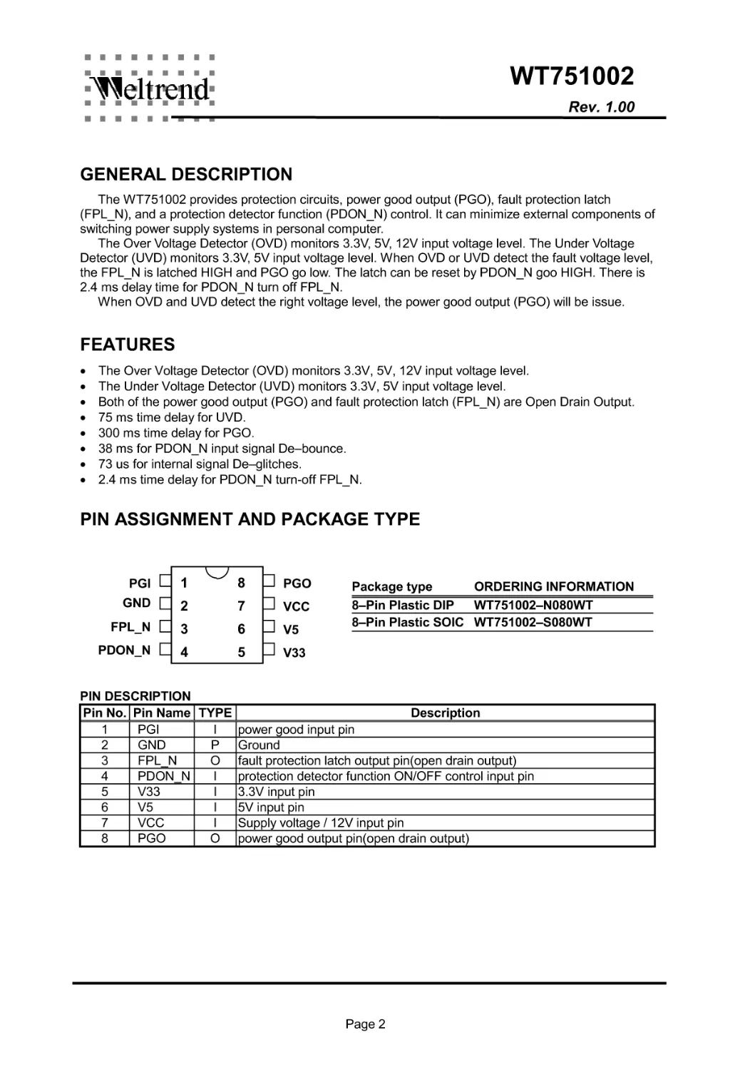
GENERAL DESCRIPTION
The WT751002 provides protection circuits, power good output (PGO), fault protection latch
(FPL_N), and a protection detector function (PDON_N) control. It can minimize external components of
switching power supply systems in personal computer.
The Over Voltage Detector (OVD) monitors 3.3V, 5V, 12V input voltage level. The Under Voltage
Detector (UVD) monitors 3.3V, 5V input voltage level. When OVD or UVD detect the fault voltage level,
the FPL_N is latched HIGH and PGO go low. The latch can be reset by PDON_N goo HIGH. There is
2.4 ms delay time for PDON_N turn off FPL_N.
When OVD and UVD detect the right voltage level, the power good output (PGO) will be issue.
FEATURES
• The Over Voltage Detector (OVD) monitors 3.3V, 5V, 12V input voltage level.
• The Under Voltage Detector (UVD) monitors 3.3V, 5V input voltage level.
• Both of the power good output (PGO) and fault protection latch (FPL_N) are Open Drain Output.
• 75 ms time delay for UVD.
• 300 ms time delay for PGO.
• 38 ms for PDON_N input signal De-bounce.
• 73 us for internal signal De-glitches.
• 2.4 ms time delay for PDON_N turn-off FPL_N.
PIN ASSIGNMENT AND PACKAGE TYPE
PGI □ 1 8 □ PGO
GND □ 2 7 □ VCC
FPL_N □ 3 6 □ V5
PDON_N □ 4 5 □ V33
Package type ORDERING INFORMATION
8-Pin Plastic DIP WT751002-N080WT
8-Pin Plastic SOIC WT751002-S080WT
PIN DESCRIPTION
Pin No. Pin Name TYPE Description
1 PGI I power good input pin
2 GND P Ground
3 FPL_N 0 fault protection latch output pin(open drain output)
4 PDON_N I protection detector function ON/OFF control input pin
5 V33 I 3.3V input pin
6 V5 I 5V input pin
7 VCC I Supply voltage / 12V input pin
8 PGO 0 power good output pin(open drain output)
Page 2
WT751002
Rev. 1.00
Hl eltrend-
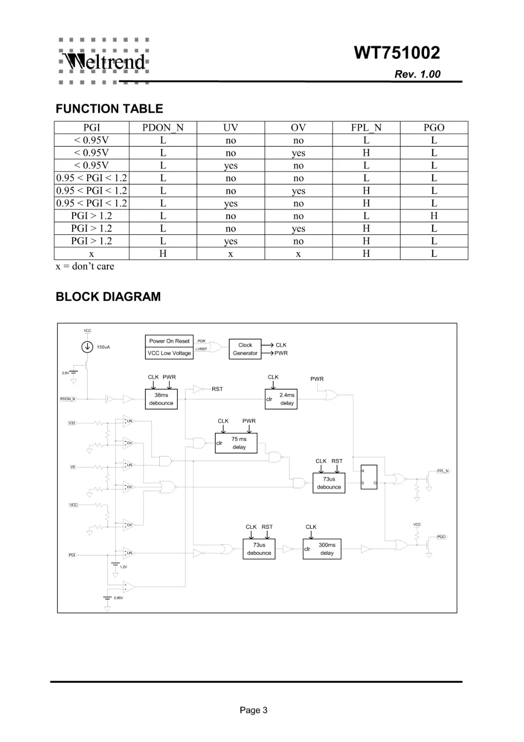
FUNCTION TABLE
PGI PDONN UV ov FPL_N PGO
< 0.95V L no no L L
< 0.95V L no yes H L
< 0.95V L yes no L L
0.95 < PGI < 1.2 L no no L L
0.95 < PGI < 1.2 L no yes H L
0.95 < PGI < 1.2 L yes no H L
PGI > 1.2 L no no L H
PGI > 1.2 L no yes H L
PGI > 1.2 L yes no H L
X H X X H L
x = don’t care
BLOCK DIAGRAM
Page 3
WT751002
Rev. 1.00
cl t rend-
В
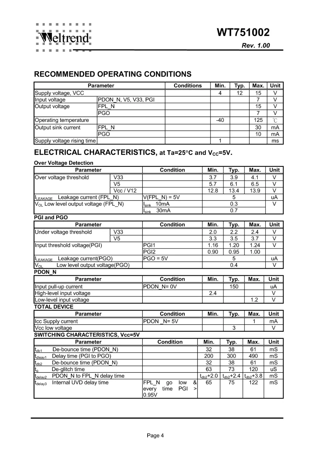
RECOMMENDED OPERATING CONDITIONS
Parameter Conditions Min. Typ. Max. Unit
Supply voltage, VCC 4 12 15 V
Input voltage PDON_N, V5, V33, PG I 7 V
Output voltage FPL_N 15 V
PGO 7 V
Operating temperature -40 125 °C
Output sink current FPL_N 30 mA
PGO 10 mA
Supply voltage rising time 1 ms
ELECTRICAL CHARACTERISTICS, at Ta=25°C and VCC=5V.
Over Voltage Detection
Parameter Condition Min. Typ- Max. Unit
Over voltage threshold V33 3.7 3.9 4.1 V
V5 5.7 6.1 6.5 V
Vcc/V12 12.8 13.4 13.9 V
Leakage Leakage current (FPL_N) V(FPL_N) = 5V 5 uA
Vol Low level output voltage (FPL_N) 'sink 10mA 0.3 V
'sink 30mA 0.7
PGI and PGO
Parameter Condition Min. Typ- Max. Unit
Under voltage threshold V33 2.0 2.2 2.4 V
V5 3.3 3.5 3.7 V
Input threshold voltage(PGI) PGI1 1.16 1.20 1.24 V
PGI2 0.90 0.95 1.00
Leakage Leakage current(PGO) PGO = 5V 5 uA
Vol Low level output voltage(PGO) 0.4 V
PDON_N
Parameter Condition Min. Typ. Max. Unit
Input pull-up current PDON_N=0V 150 uA
High-level input voltage 2.4 V
Low-level input voltage 1.2 V
TOTAL DEVICE
Parameter Condition Min. Typ. Max. Unit
Icc Supply current PDON _N= 5V 1 mA
Vcc low voltage 3 V
SWITCHING CHARACTERISTICS, Vcc=5V
Parameter Condition Min. Typ. Max. Unit
tdbi De-bounce time (PDON_N) 32 38 61 mS
tdieavi Delay time (PGI to PGO) 200 300 490 mS
tdb2 De-bounce time (PDON_N) 32 38 61 mS
tq De-glitch time 63 73 120 uS
tdeiav2 PDON_N to FPL_N delay time tdb2+2.0 tdb2+2.4 tdb2+3.8 mS
tdeiays Internal UVD delay time FPL_N go low & every time PGI > 0.95V 65 75 122 mS
Page 4
WT751002
Rev. 1.00
meltrend1
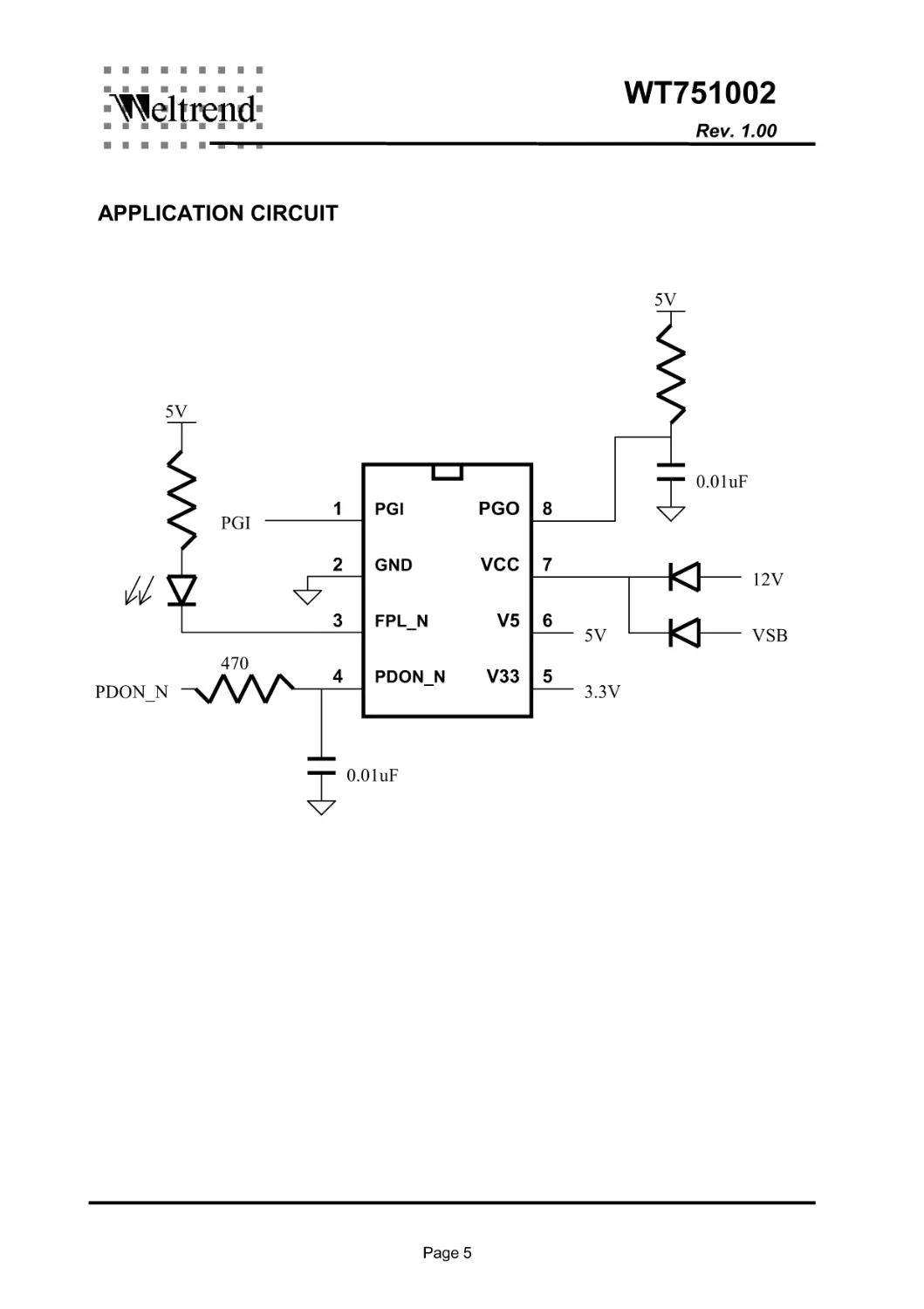
APPLICATION CIRCUIT
-p O.OluF
Page 5
meltrend1
APPLICATION TIMMING
1.) PGI (UNDER_VOLTAGE) :
WT751002
Rev. 1.00
Page 6
WT751002
Rev. 1.00
Hl eltrend-
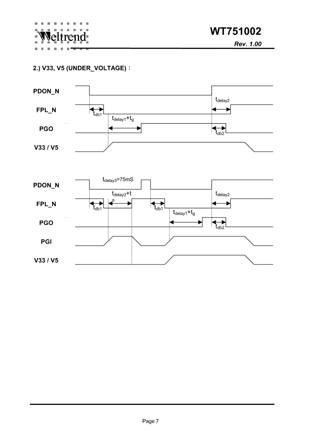
2.) V33, V5 (UNDER_VOLTAGE) :
PDON_N
FPL_N
PGO
V33 / V5
PDON_N
FPL_N
PGO
PGI
V33 / V5
tdelay2
tdelay! +tg
tdelay3_75mS
Page 7
WT751002
Rev. 1.00
meltrend1
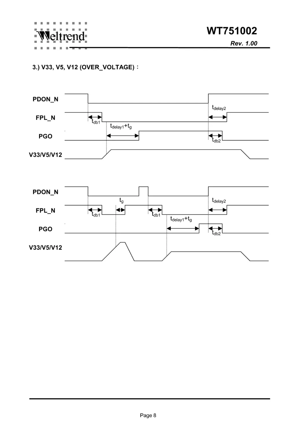
3.) V33, V5, V12 (OVER_VOLTAGE) :
Page 8