/


Text
DESIGN FOR MANUFACTURABILITY AND YIELD
FOR NANO-SCALE CMOS
Series on Integrated Circuits and Systems
Series Editor:
Anantha Chandrakasan
Massachusetts Institute of Technology
Cambridge, Massachusetts
Low Power Methodology Manual: For System-on-Chip Design
Michael Keating, David Flynn, Rob Aitken, Alan Gibbons, and Kaijian Shi
ISBN 978-0-387-71818-7
Modern Circuit Placement: Best Practices and Results
Gi-Joon Nam and Jason Cong
ISBN 978-0-387-36837-5
CMOS Biotechnology
Hakho Lee, Donhee Ham and Robert M. Westervelt
ISBN 978-0-387-36836-8
SAT-Based Scalable Formal Verification Solutions
Malay Ganai and Aarti Gupta
ISBN 978-0-387-69166-4, 2007
Ultra-Low Voltage Nano-Scale Memories
Kiyoo Itoh, Masashi Horiguchi and Hitoshi Tanaka
ISBN 978-0-387-33398-4, 2007
Routing Congestion in VLSI Circuits: Estimation and Optimization
Prashant Saxena, Rupesh S. Shelar, Sachin Sapatnekar
ISBN 978-0-387-30037-5, 2007
Ultra-Low Power Wireless Technologies for Sensor Networks
Brian Otis and Jan Rabaey
ISBN 978-0-387-30930-9, 2007
Sub-Threshold Design for Ultra Low-Power Systems
Alice Wang, Benton H. Calhoun and Anantha Chandrakasan
ISBN 978-0-387-33515-5, 2006
High Performance Energy Efficient Microprocessor Design
Vojin Oklibdzija and Ram Krishnamurthy (Eds.)
ISBN 978-0-387-28594-8, 2006
Abstraction Refinement for Large Scale Model Checking
Chao Wang, Gary D. Hachtel, and Fabio Somenzi
ISBN 978-0-387-28594-2, 2006
A Practical Introduction to PSL
Cindy Eisner and Dana Fisman
ISBN 978-0-387-35313-5, 2006
Thermal and Power Management of Integrated Systems
Arman Vassighi and Manoj Sachdev
ISBN 978-0-387-25762-4, 2006
Leakage in Nanometer CMOS Technologies
Siva G. Narendra and Anantha Chandrakasan
ISBN 978-0-387-25737-2, 2005
Statistical Analysis and Optimization for VLSI: Timing and Power
Ashish Srivastava, Dennis Sylvester, and David Blaauw
ISBN 978-0-387-26049-9, 2005
DESIGN FOR MANUFACTURABILITY
AND YIELD FOR NANO-SCALE CMOS
by
CHARLES C. CHIANG
Synopsys Inc.
Mountain View, CA, USA
and
JAMIL KAWA
Synopsys Inc.
Mountain View, CA, USA
A C.I.P. Catalogue record for this book is available from the Library of Congress.
ISBN 978-1-4020-5187-6 (HB)
ISBN 978-1-4020-5188-3 (e-book)
Published by Springer,
P.O. Box 17, 3300 AA Dordrecht, The Netherlands.
www.springer.com
Printed on acid-free paper
The contributing authors of this book have used figures and content published in IEEE conferences
c IEEE). Those figures and content from IEEE publications that are included
and journals (
in this book are printed with permission from the IEEE
All Rights Reserved
c 2007 Springer
No part of this work may be reproduced, stored in a retrieval system, or transmitted in any form
or by any means, electronic, mechanical, photocopying, microfilming, recording or otherwise,
without written permission from the Publisher, with the exception of any material supplied
specifically for the purpose of being entered and executed on a computer system, for exclusive
use by the purchaser of the work.
To my wife Susan
(Show-Hsing) and my
daughters Wei Diana and
Ann - Charles
To my wife Zeina and my
children Nura, Tamara,
and Rami - Jamil
Contents
List of Figures
List of Tables
Preface
Acknowledgments
xiii
xix
xxi
xxvii
1. INTRODUCTION
1
1.1
What is DFM/DFY
1.2
DFM/DFY Critical for IC Manufacturing
1.2.1 New Materials
1.2.2 Sub-wavelength Lithography
1.2.3 New Devices
1.2.4 Proliferation of Processes
1.2.5 Intra-die Variability
1.2.6 Error Free Masks Too Costly
1.2.7 Cost of a Silicon Spin
2
3
6
9
12
14
15
15
1.3
DFM Categories and Classifications
1.3.1 First Time Failures
1.3.2 Time Related Failures
16
16
17
1.4
How Do Various DFM Solutions Tie up with Specific
Design Flows
17
DFM and DFY: Fully Intertwined
19
1.5
1
2. RANDOM DEFECTS
21
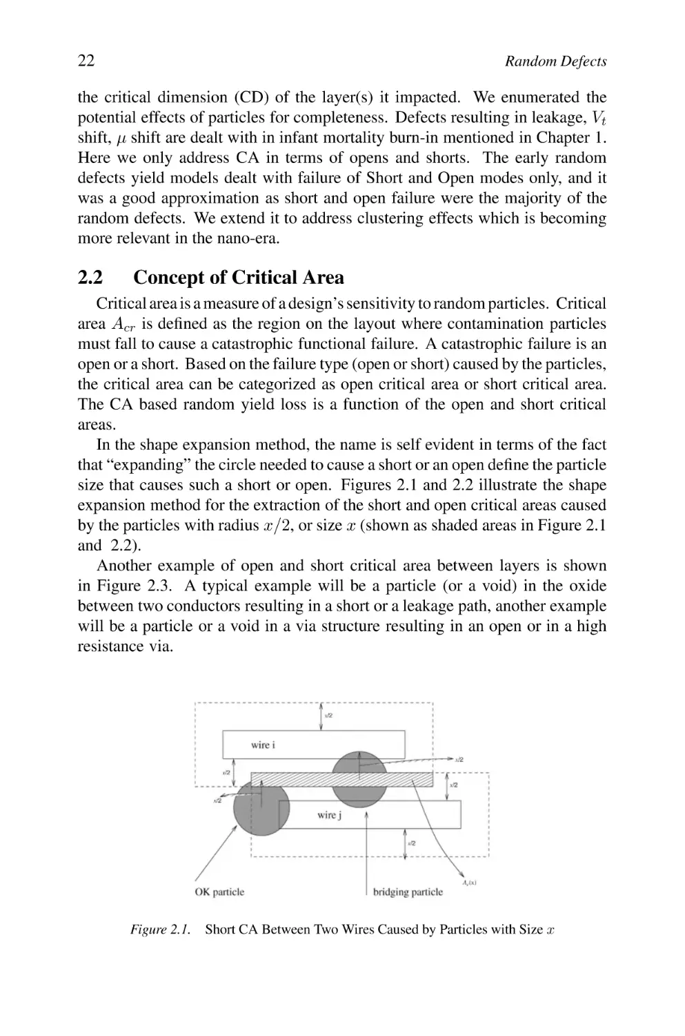
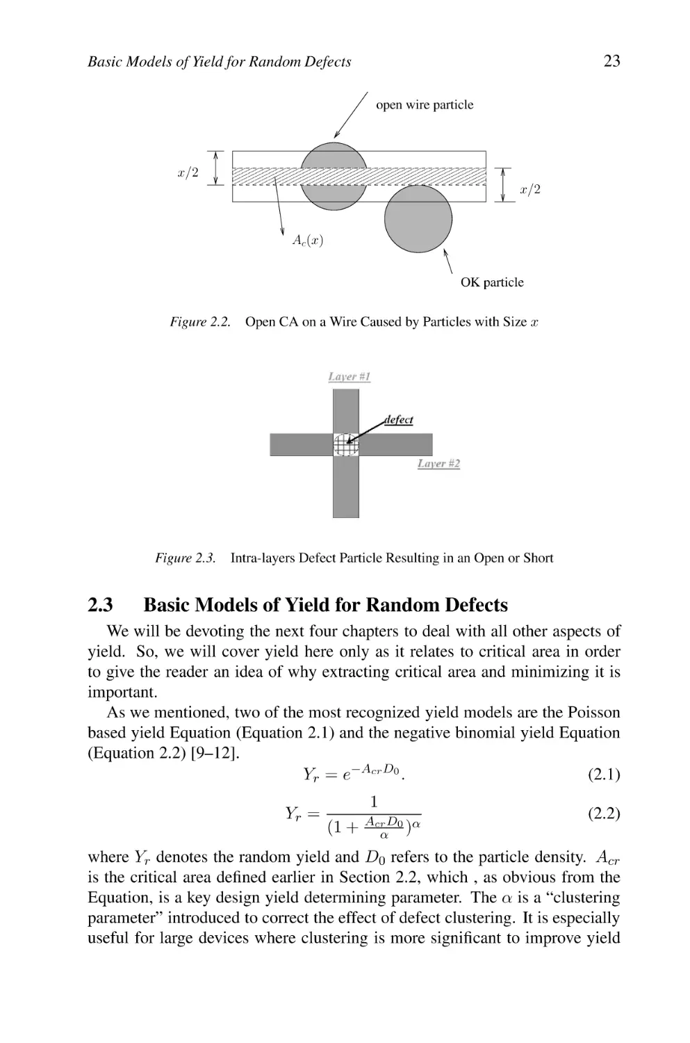
2.1
Types of Defects
21
2.2
Concept of Critical Area
22
vii
viii
Contents
2.3
Basic Models of Yield for Random Defects
23
2.4
Critical Area Analysis (CAA)
2.4.1 Classical Methods of CA Extraction
2.4.2 Approximations
2.4.3 Comparison of Approximate and Traditional CA
24
24
25
26
2.5
Mathematical Formulation of Approximation Method
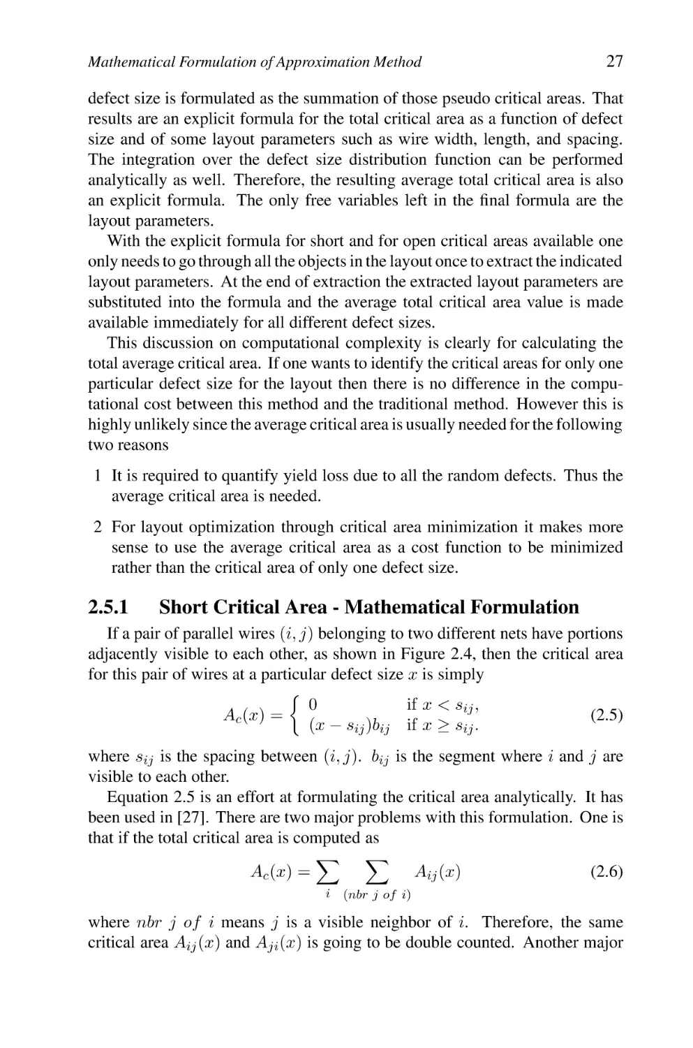
2.5.1 Short Critical Area - Mathematical Formulation
2.5.2 Open Critical Area - Mathematical Formulation
26
27
31
2.6
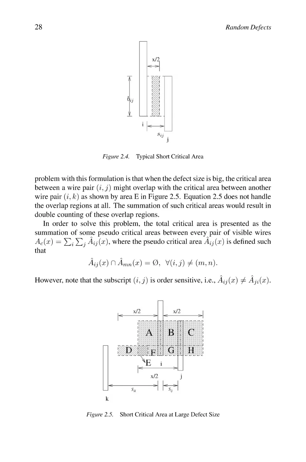
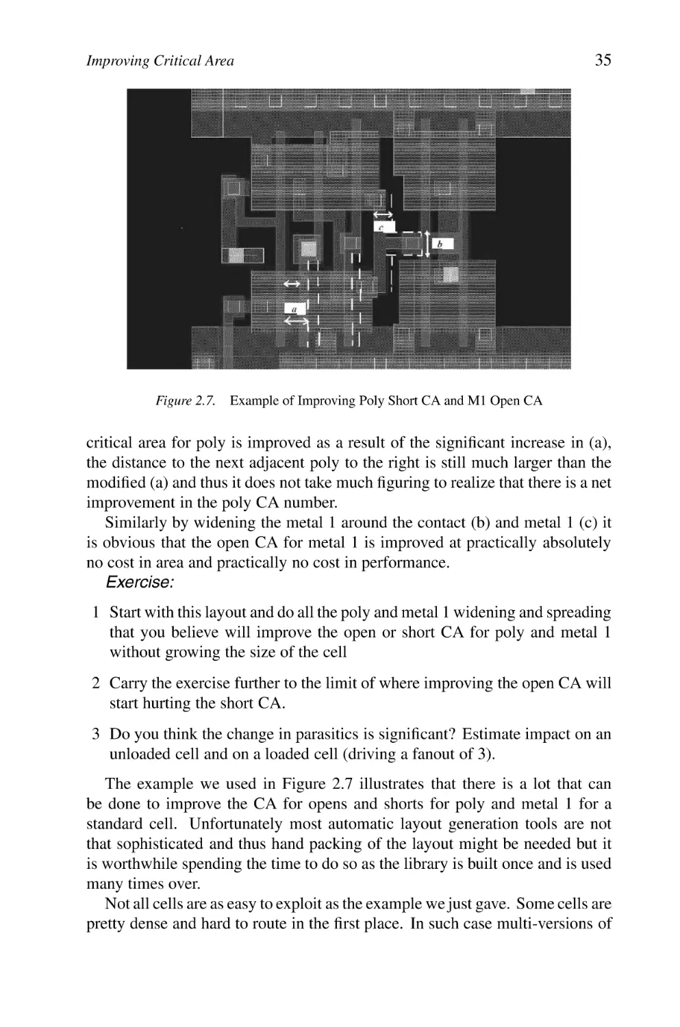
Improving Critical Area
2.6.1 Cell Library Yield Grading
2.6.2 Average CA Yield Improvement
2.6.3 Weighted Average CA Yield Improvement
2.6.4 Key Benefits of the Proposed Algorithm
34
34
36
41
47
2.7
Experimental Results
2.7.1 Validation of Fast Critical Area Analysis Evaluation
2.7.2 Comparison of Critical Area Reductions
2.7.3 Discussion
48
48
48
50
2.8
Conclusions
51
3. SYSTEMATIC YIELD - LITHOGRAPHY
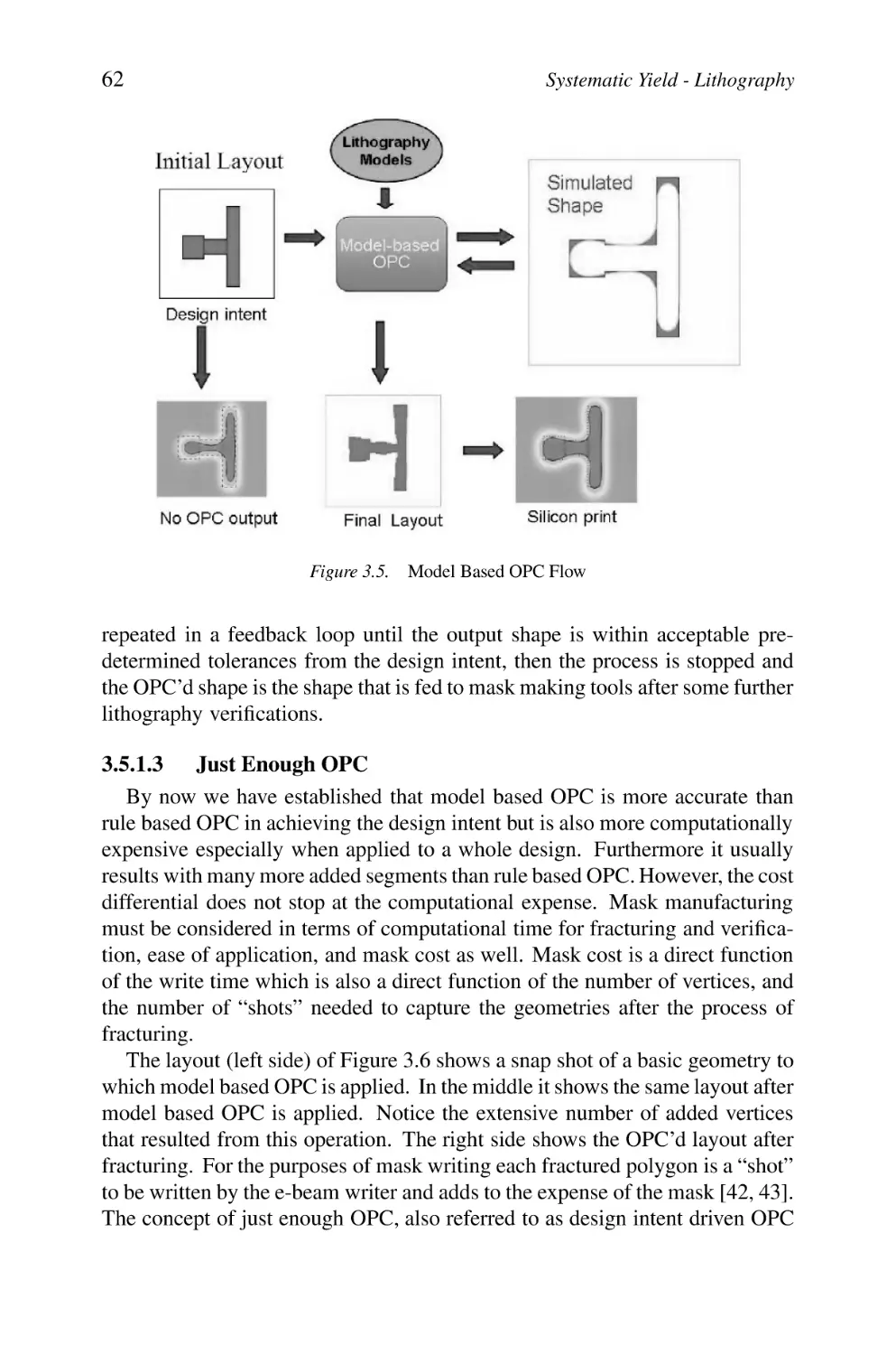
53
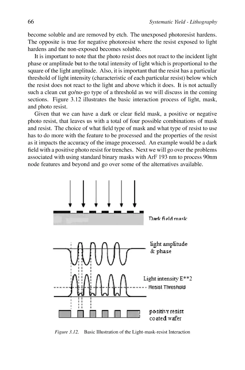
3.1
Introduction
53
3.2
Optics Fundamentals
53
3.3
Basic Design Flow
55
3.4
Lithography and Process Issues
3.4.1 Masks Writing
3.4.2 Optical System Interactions
3.4.3 Resist
3.4.4 Etch
57
57
57
57
58
3.5
Resolution Enhancement Technique (RET)
3.5.1 Optical Proximity Correction (OPC)
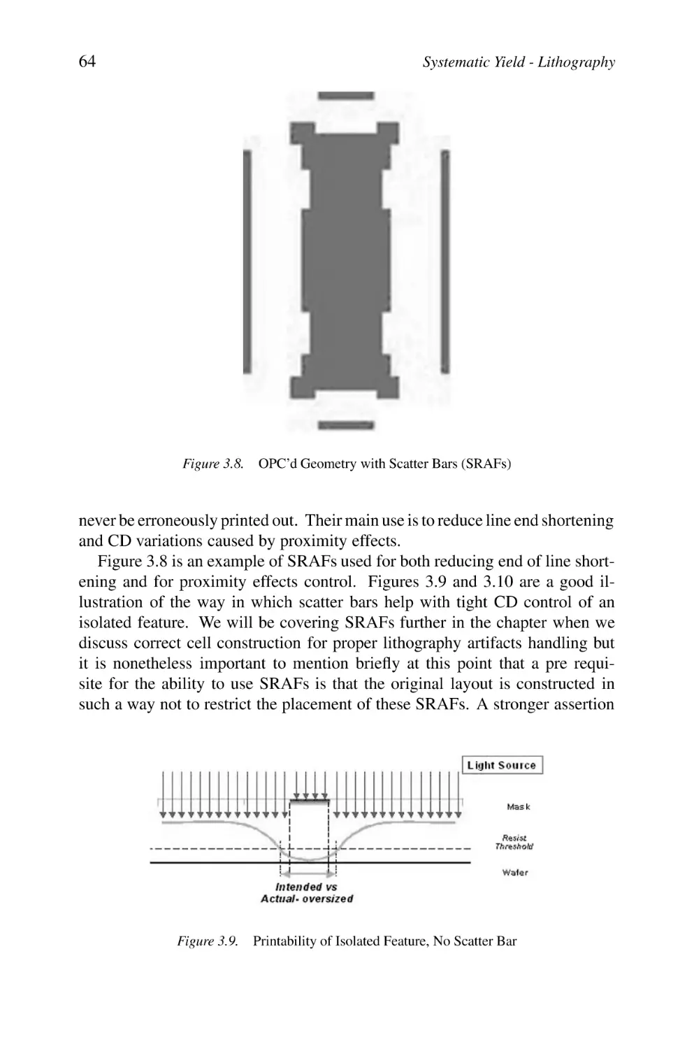
3.5.2 Sub Resolution Assist Feature (SRAF)
3.5.3 Phase Shift Masks (PSM)
3.5.4 Off Axis Illumination (OAI)
58
59
63
65
71
3.6
Other Optical Techniques
3.6.1 Immersion Technology
3.6.2 Double Dipole Lithography (DDL)
73
73
73
ix
Contents
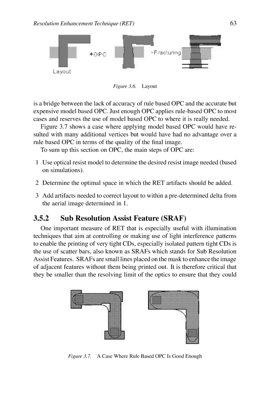
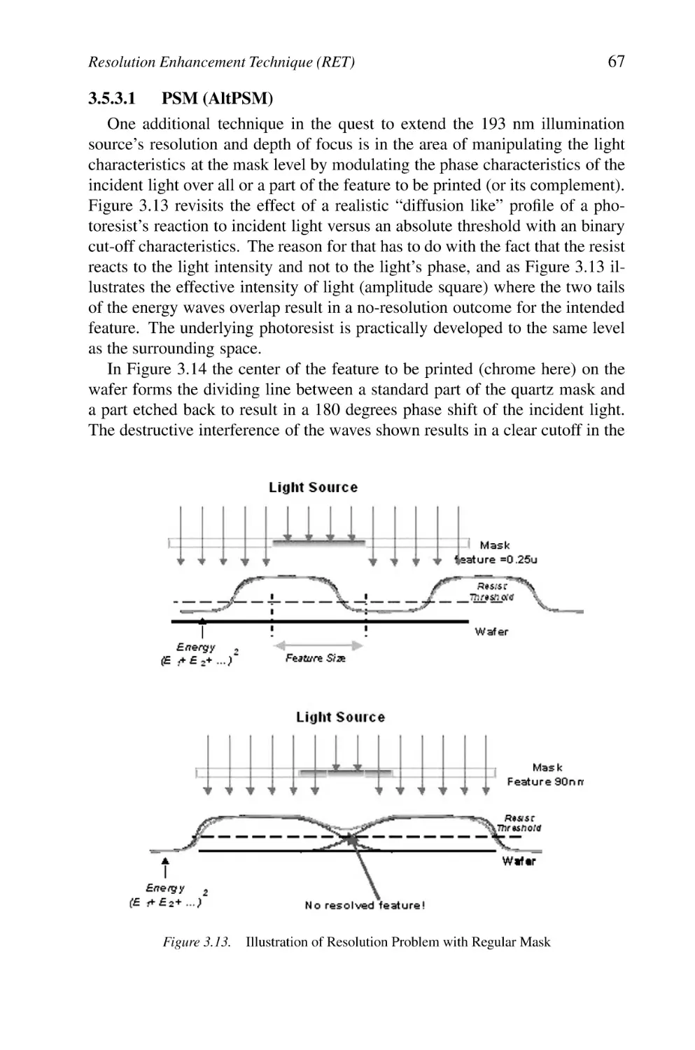
3.6.3
Chromeless Phase Lithography (CPL)
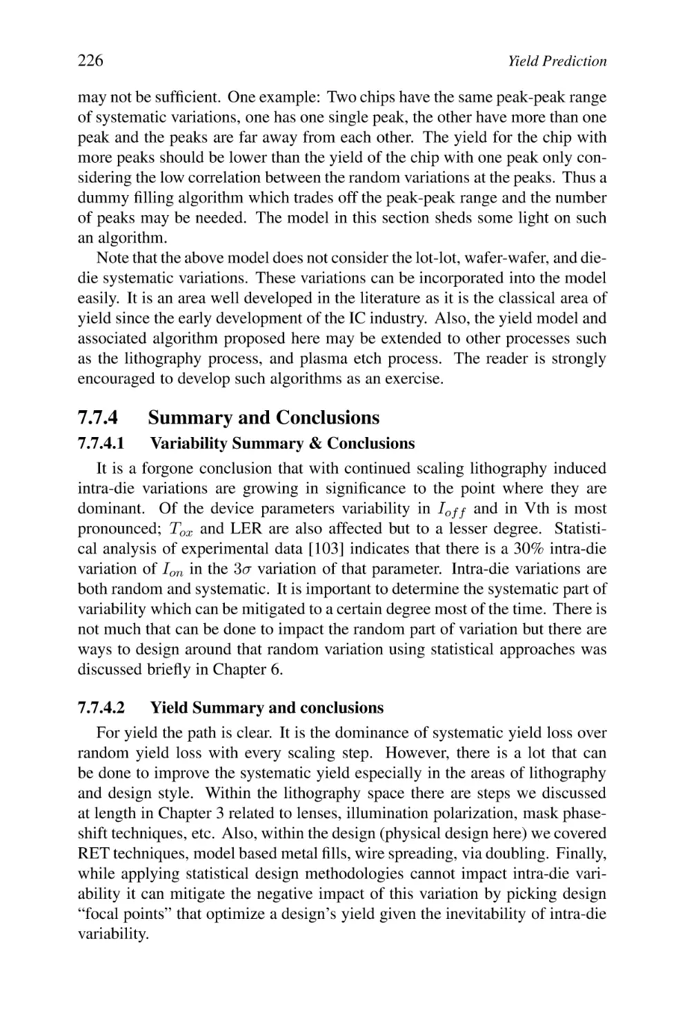
74
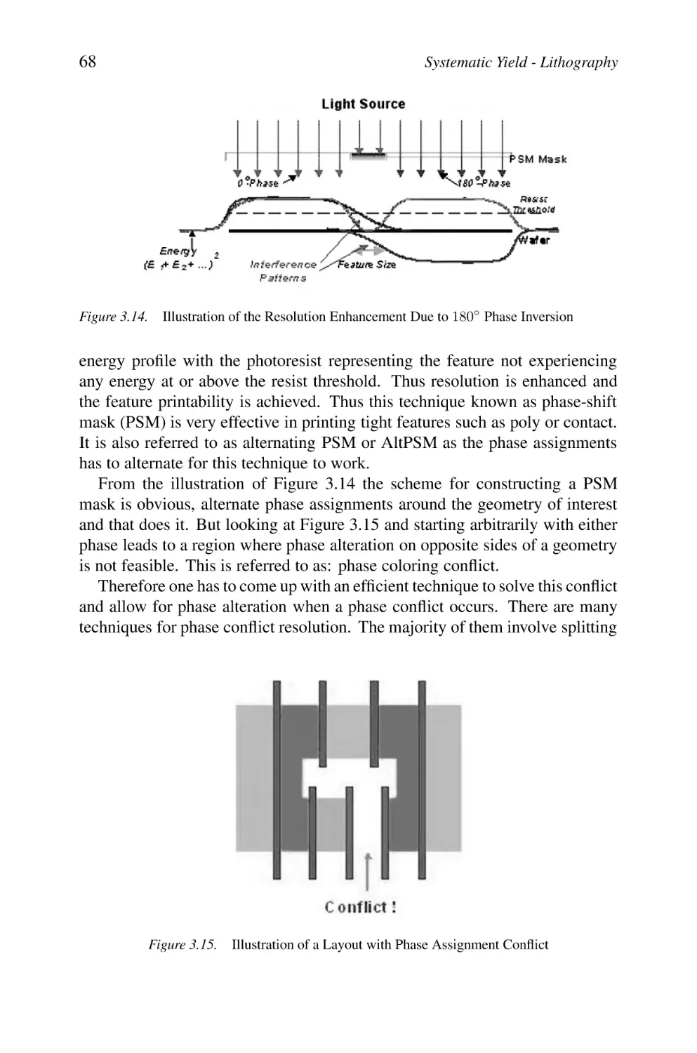
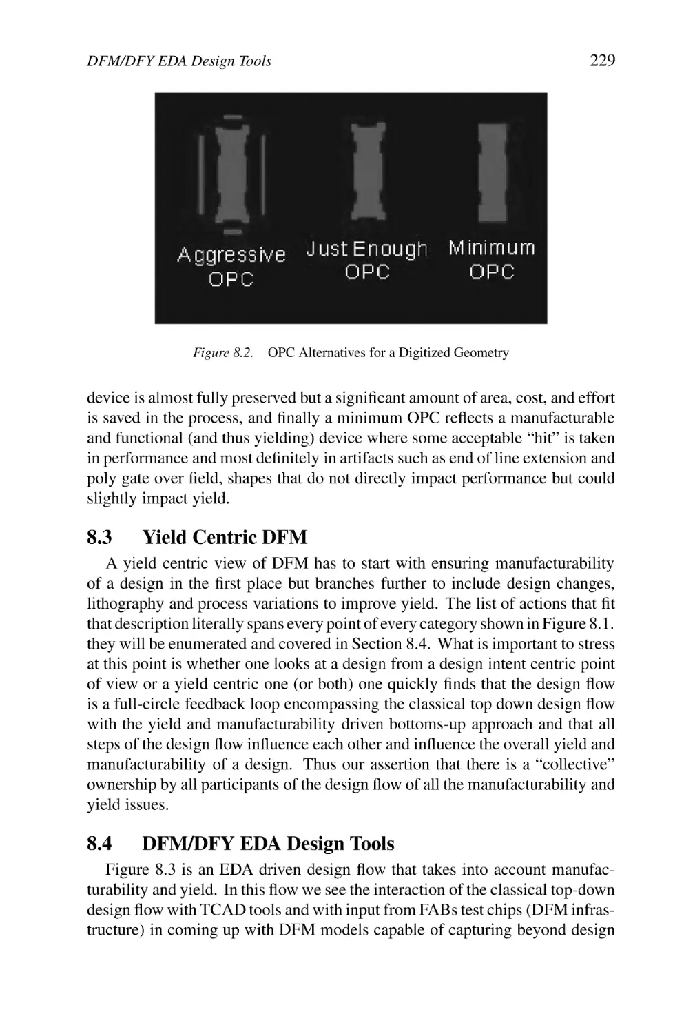
3.7
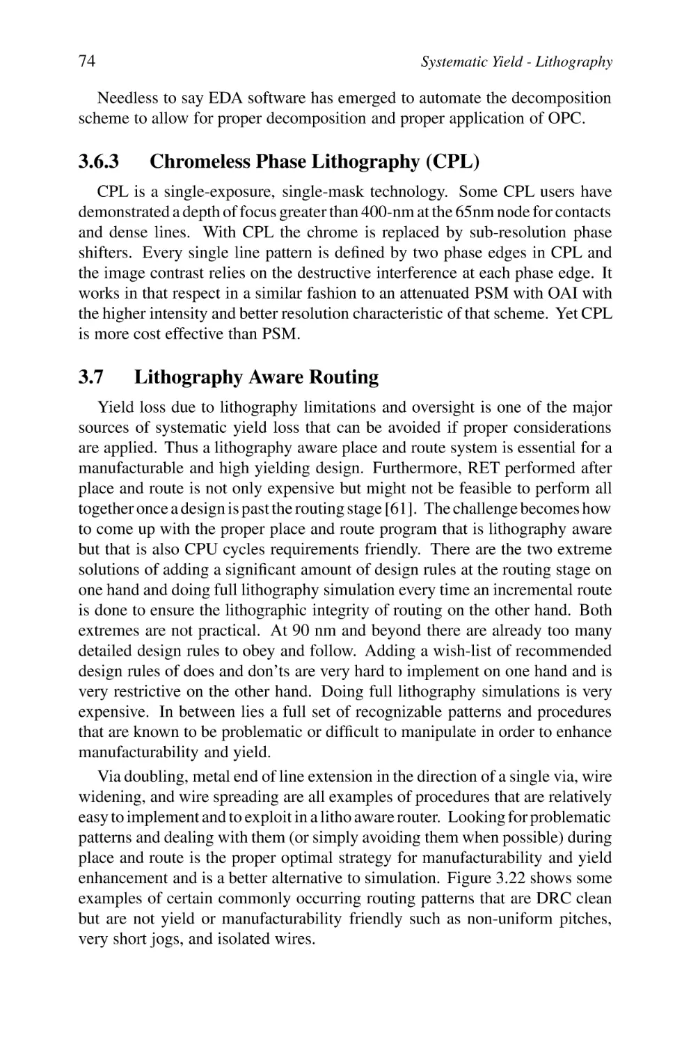
Lithography Aware Routing
74
3.8
RET and Lithography Verification
3.8.1 Lithography Rule Check (LRC)
3.8.2 Pattern Simulation
75
76
77
3.9
Integrated Flow
3.9.1 Mask Preparation and Repair
3.9.2 Design Intent
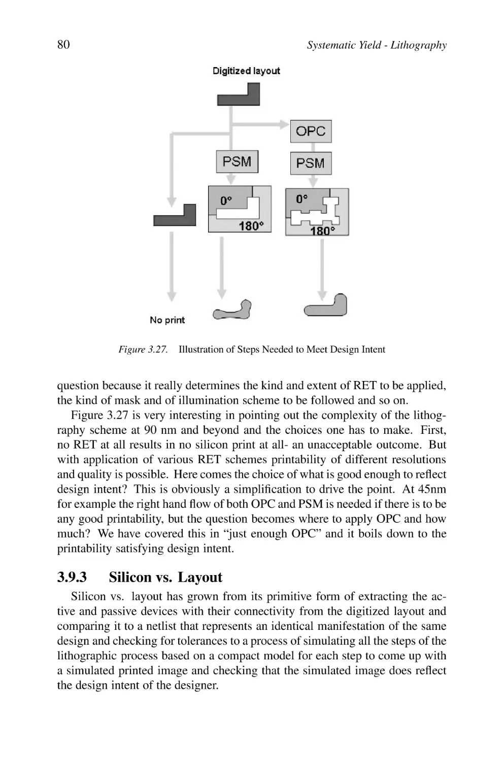
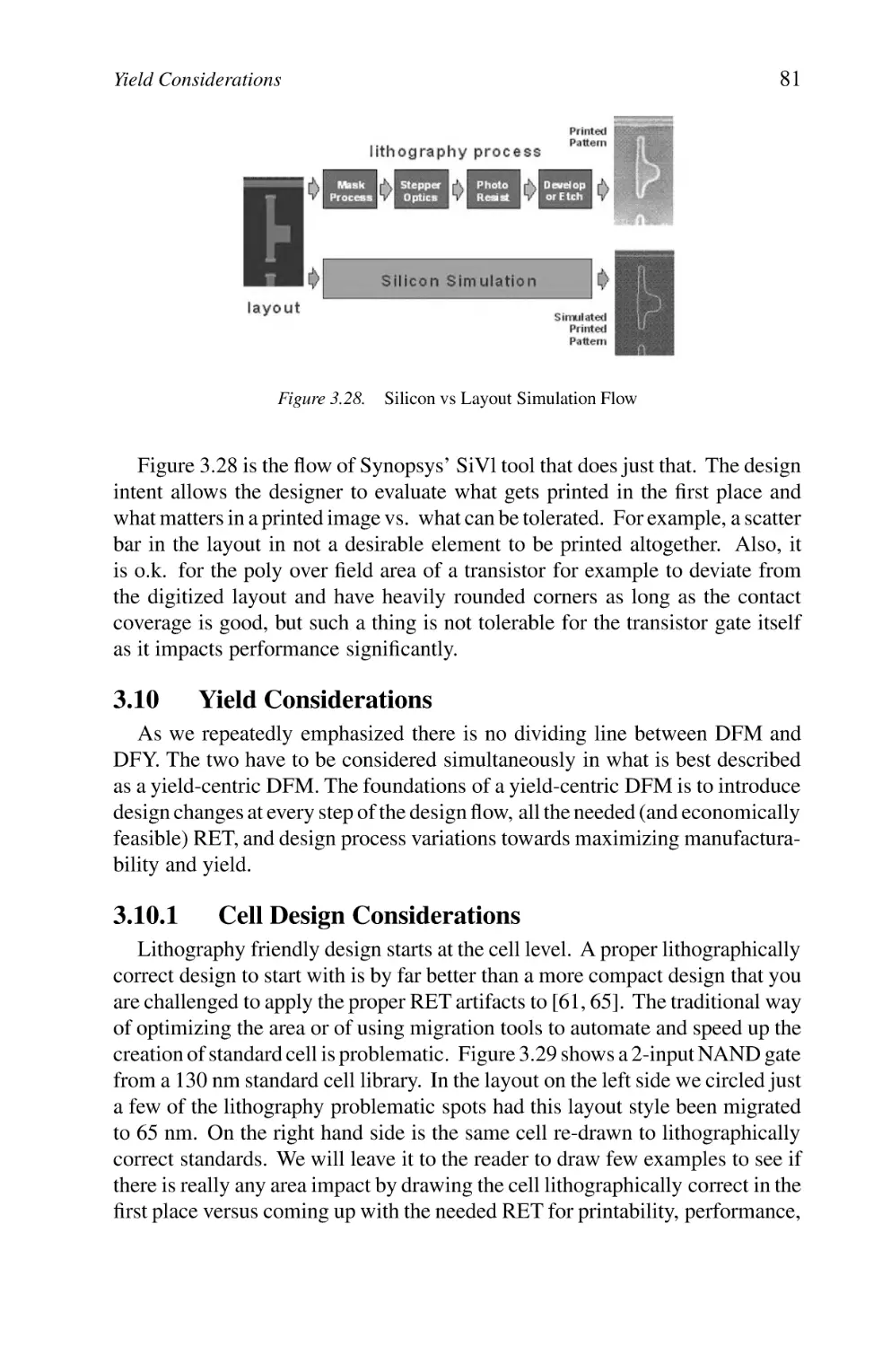
3.9.3 Silicon vs. Layout
77
77
79
80
3.10 Yield Considerations
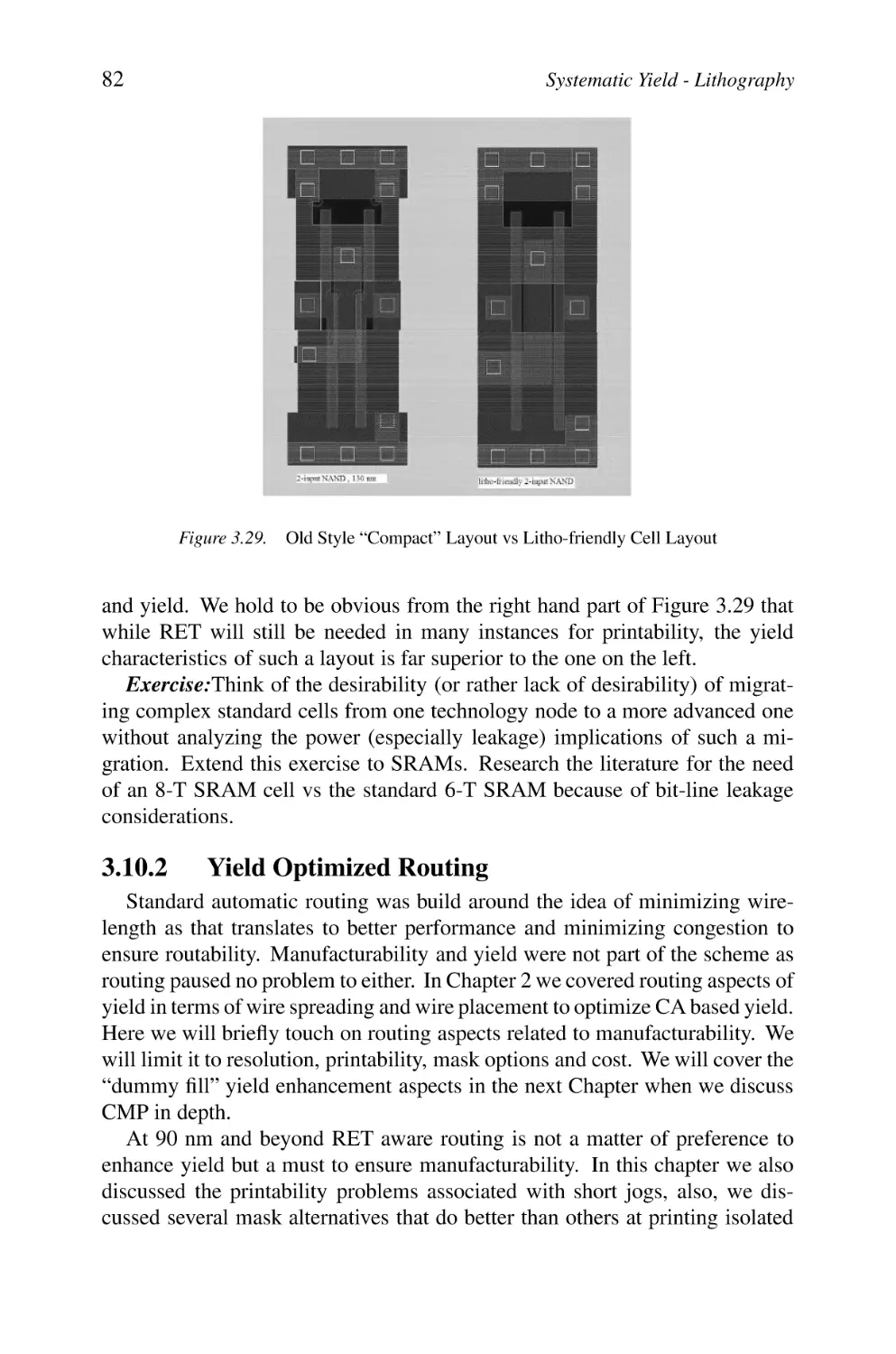
3.10.1 Cell Design Considerations
3.10.2 Yield Optimized Routing
81
81
82
3.11 Practical Application
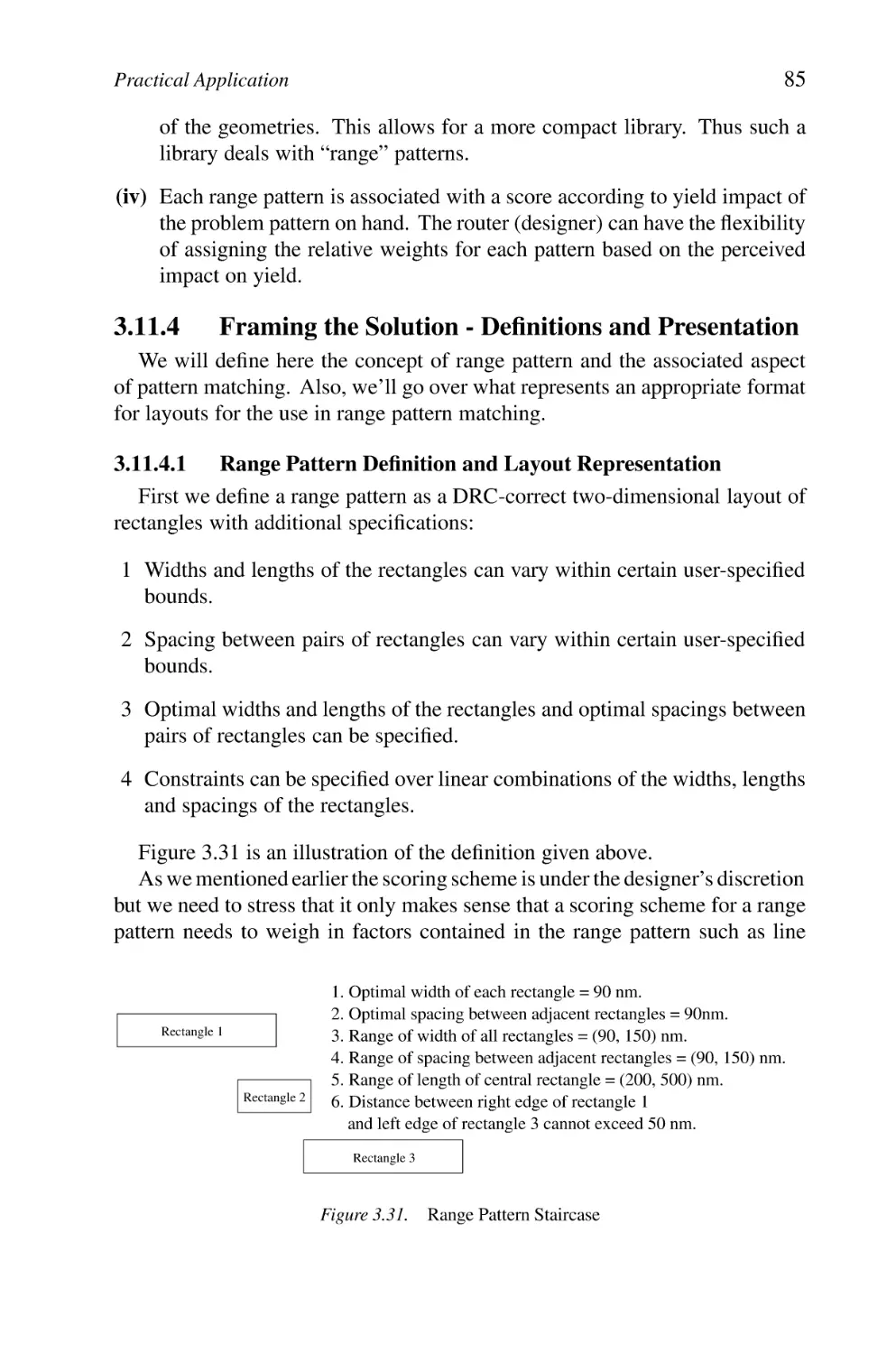
3.11.1 Framing the problem
3.11.2 Potential Solutions
3.11.3 Proposed Solution
3.11.4 Framing the Solution - Definitions and Presentation
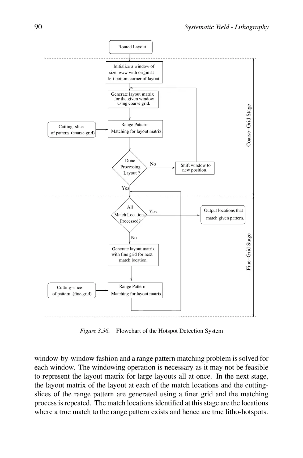
3.11.5 Litho-Hotspot Detection System
3.11.6 Summary & Results
83
83
84
84
85
88
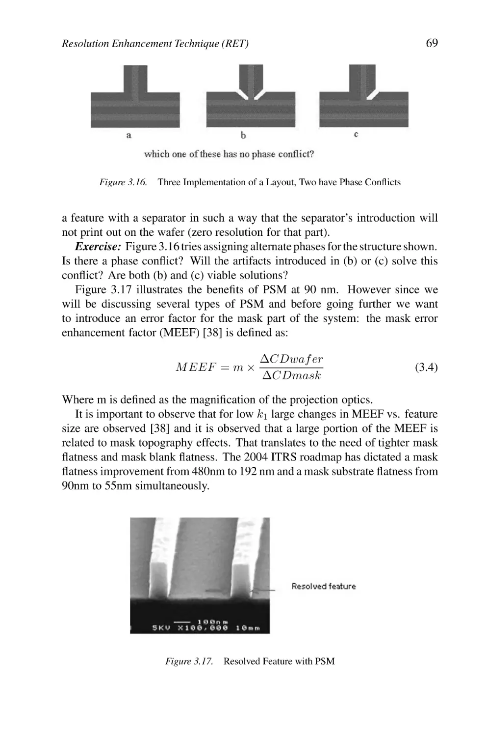
95
3.12 DFM & DFY Centric Summary
96
3.13 Lithography Specific Summary
97
4. SYSTEMATIC YIELD - CHEMICAL MECHANICAL POLISHING (CMP)
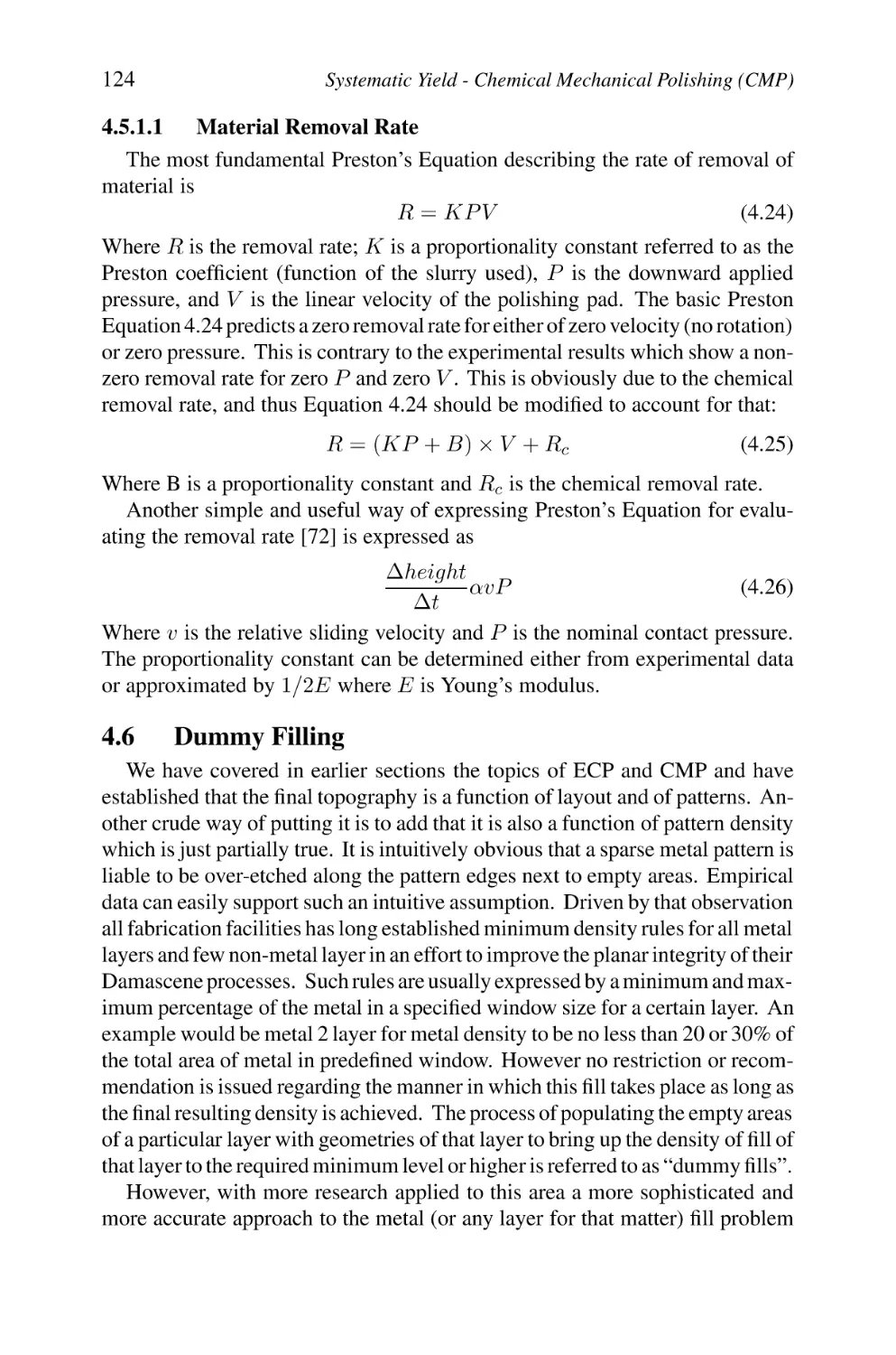
99
4.1
Introduction
99
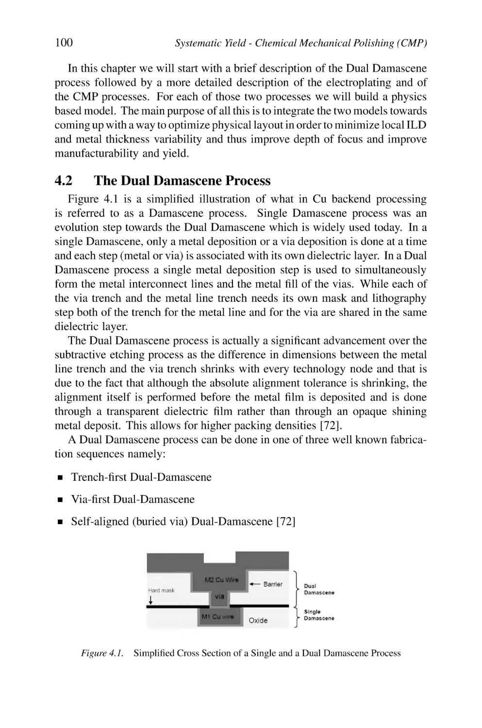
4.2
The Dual Damascene Process
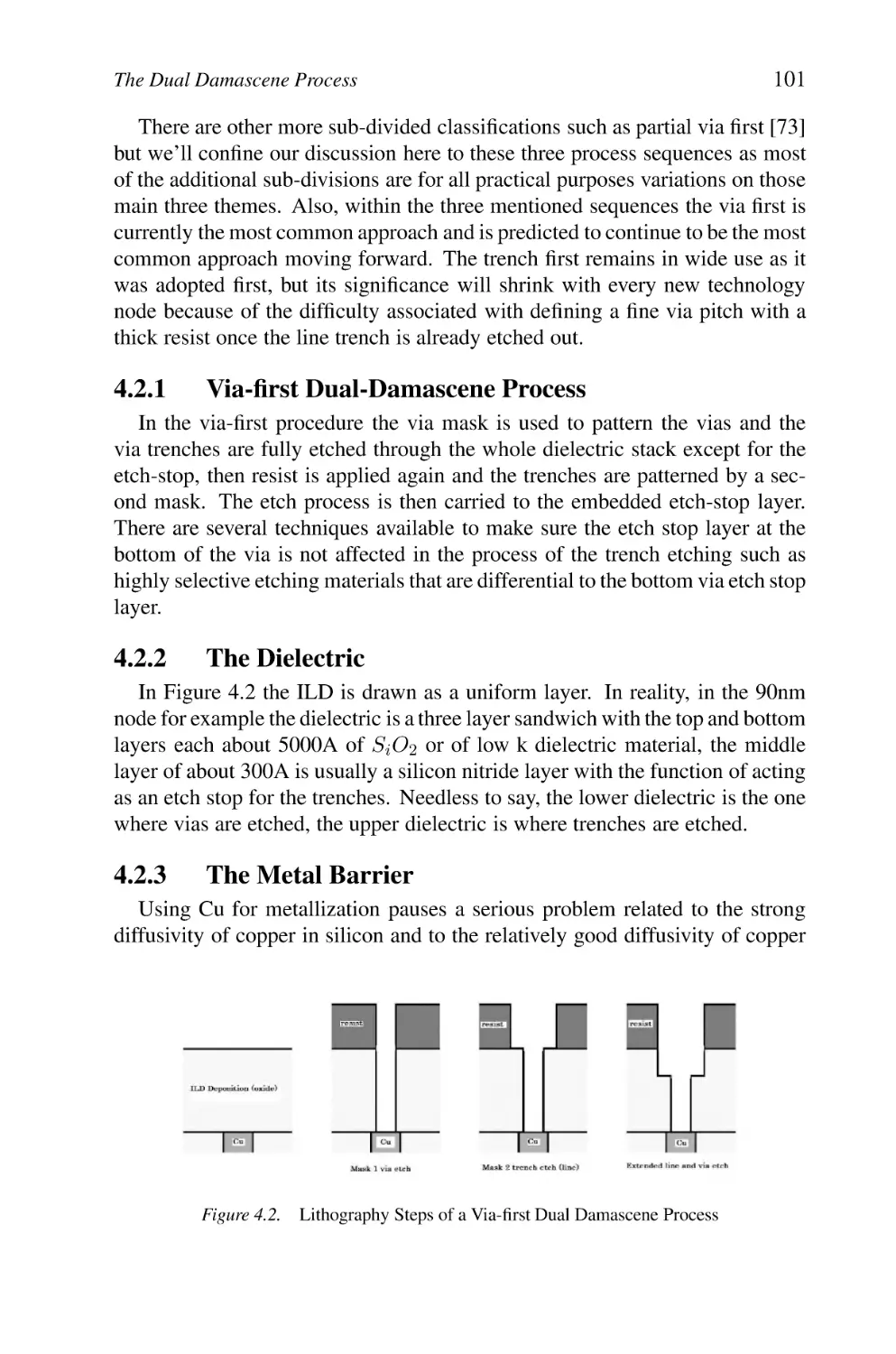
4.2.1 Via-first Dual-Damascene Process
4.2.2 The Dielectric
4.2.3 The Metal Barrier
100
101
101
101
4.3
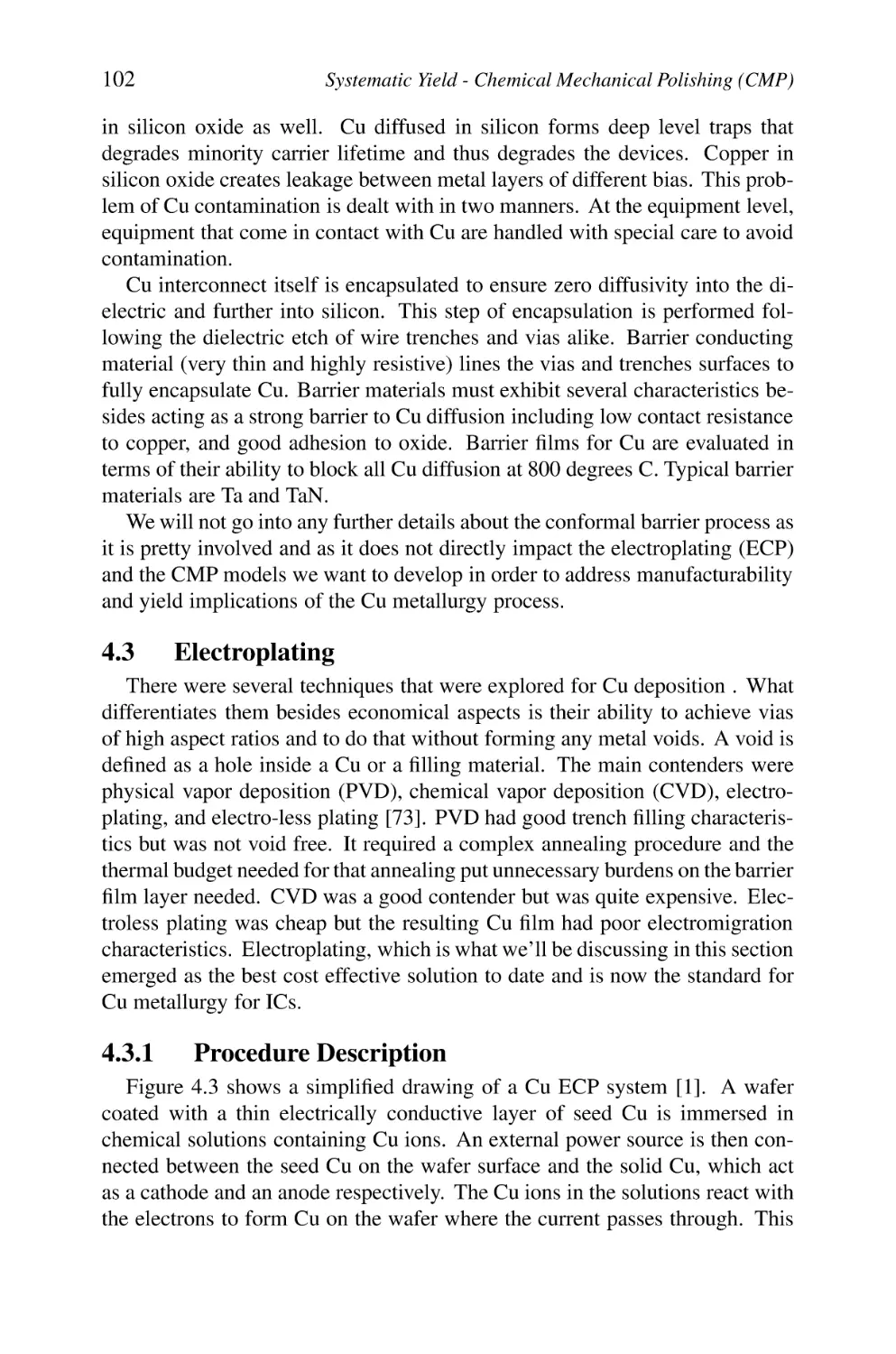
Electroplating
4.3.1 Procedure Description
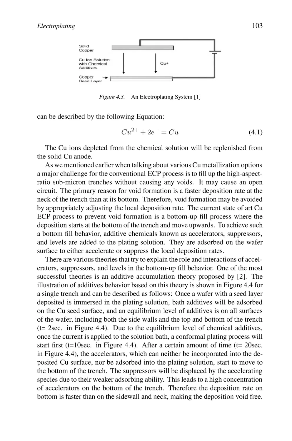
4.3.2 Electroplating Model
102
102
105
4.4
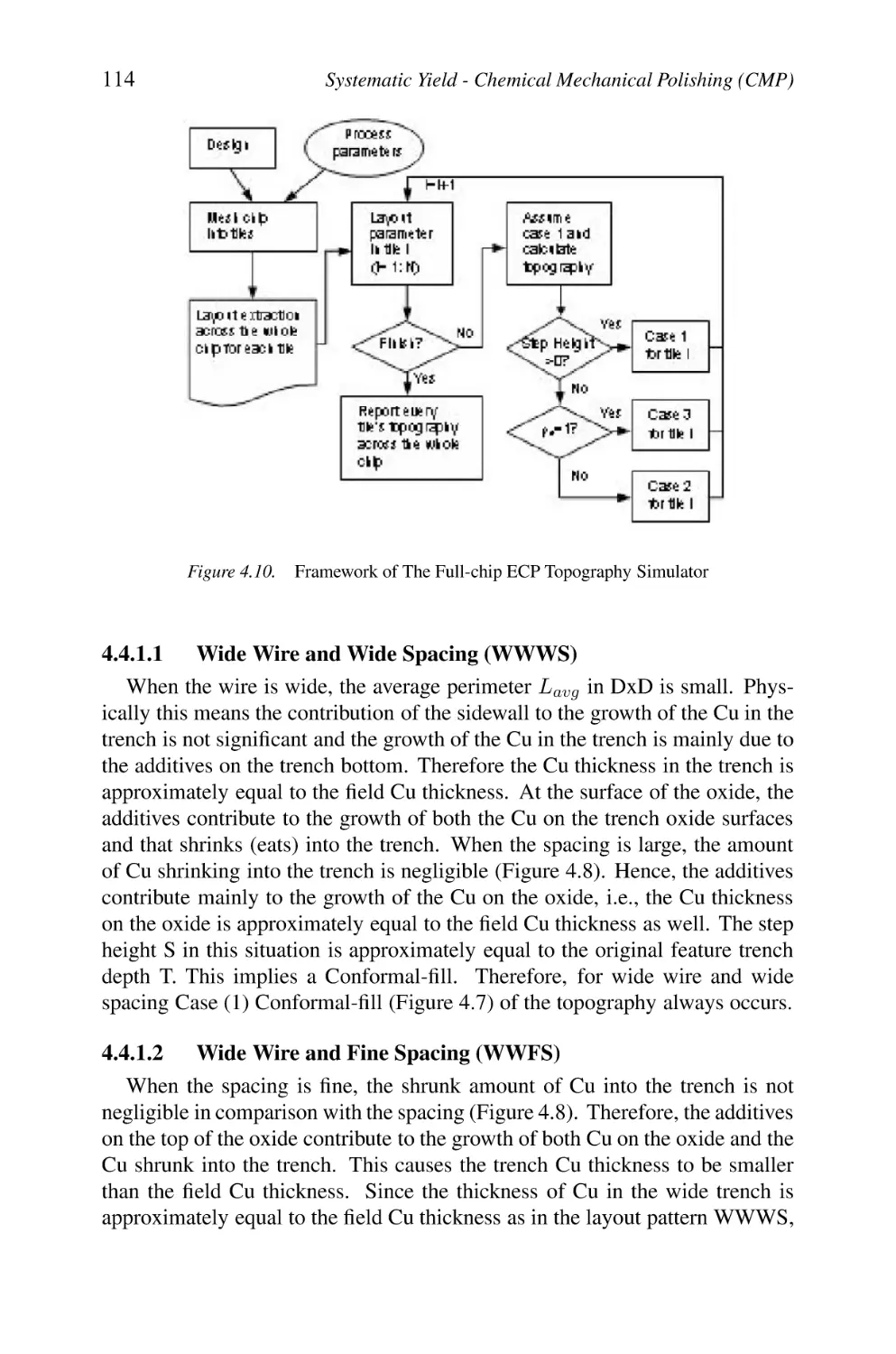
A Full Chip Simulation Algorithm
4.4.1 Case Selection
4.4.2 Tile Size and Interaction Length
4.4.3 Model Verification
112
113
115
116
x
Contents
4.4.4
4.5
CMP
4.5.1
Key Advantages of ECP Topography Model
121
CMP Process Description
121
122
4.6
Dummy Filling
4.6.1 Rule Based
4.6.2 Model Based
124
125
125
4.7
Application: ILD CMP Model Based Dummy Filling
4.7.1 Introduction
4.7.2 The 2-D Low-pass-filter CMP Model
4.7.3 The Dummy Filling Problem
4.7.4 The Linear Programming Method
4.7.5 The Min-variance Interactive Method
4.7.6 Improving the Detection Capability
4.7.7 Simulation Results
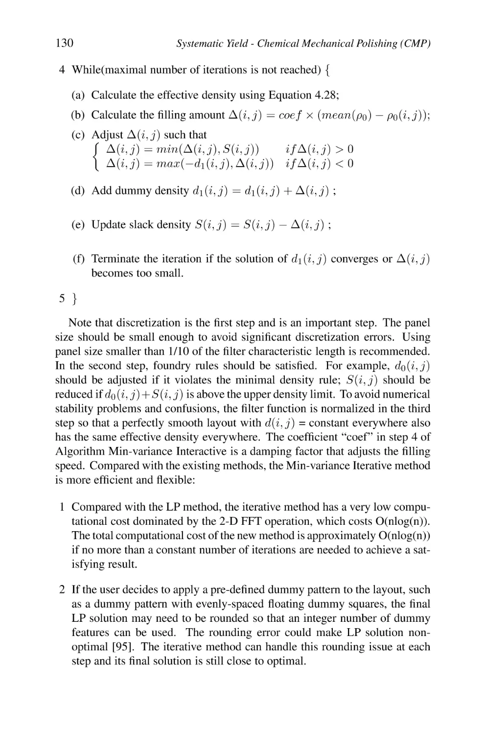
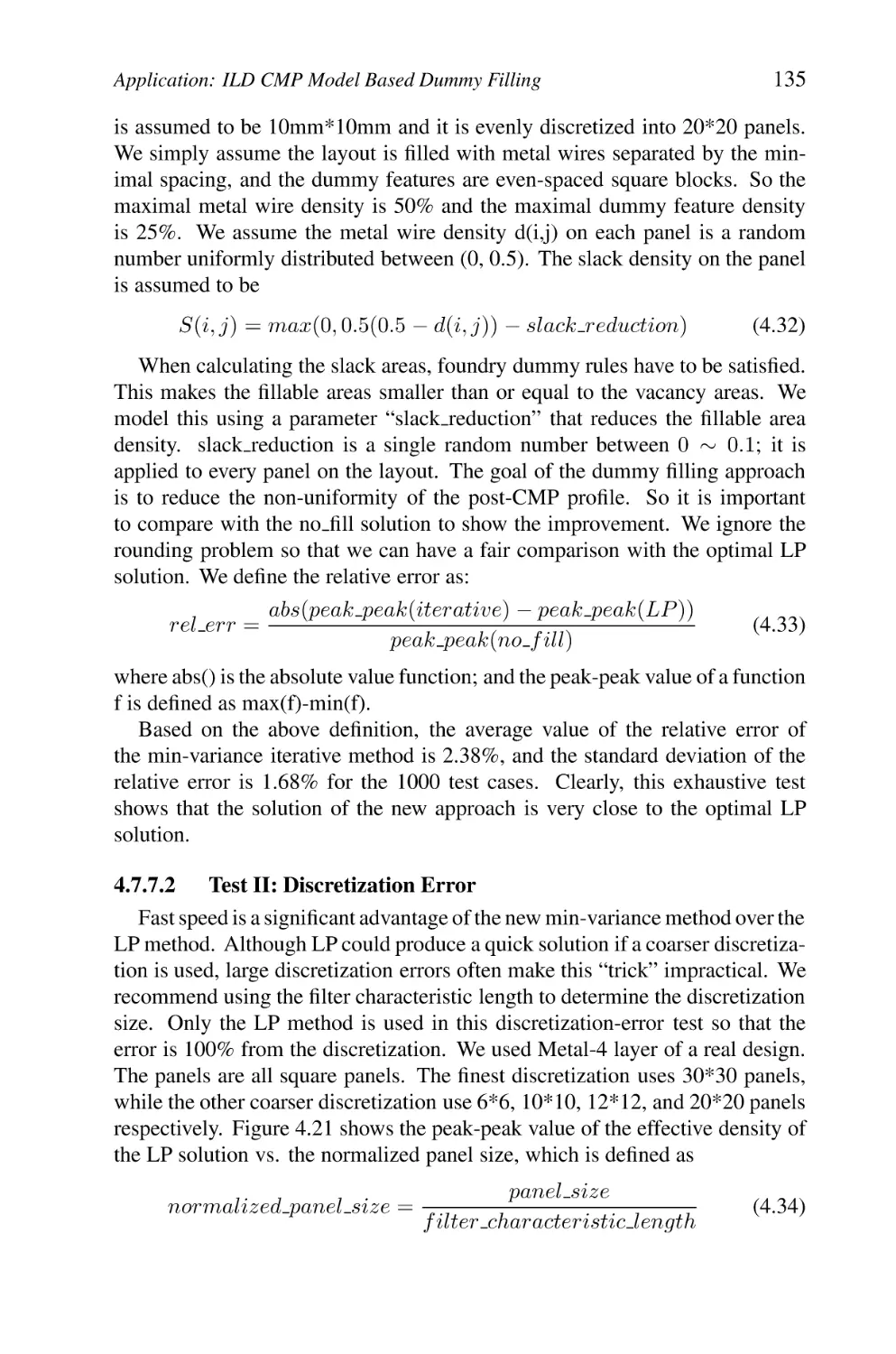
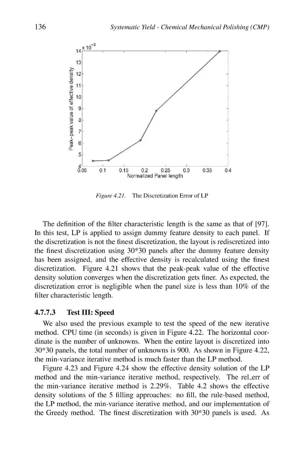
127
127
128
128
129
129
132
134
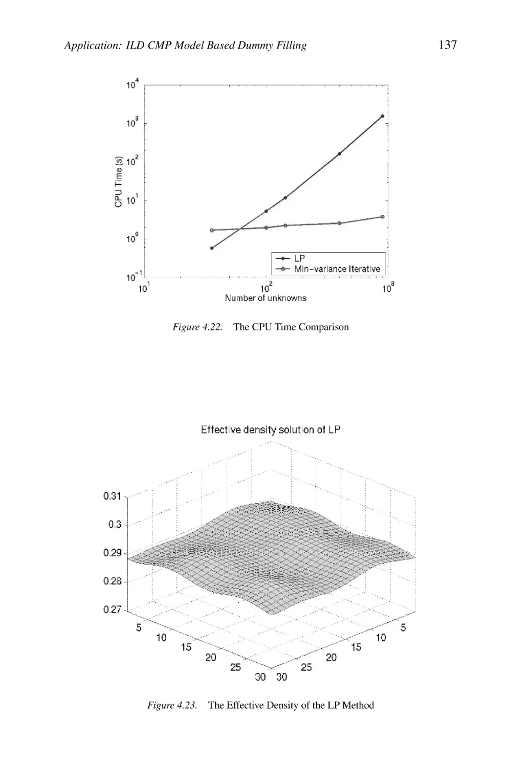
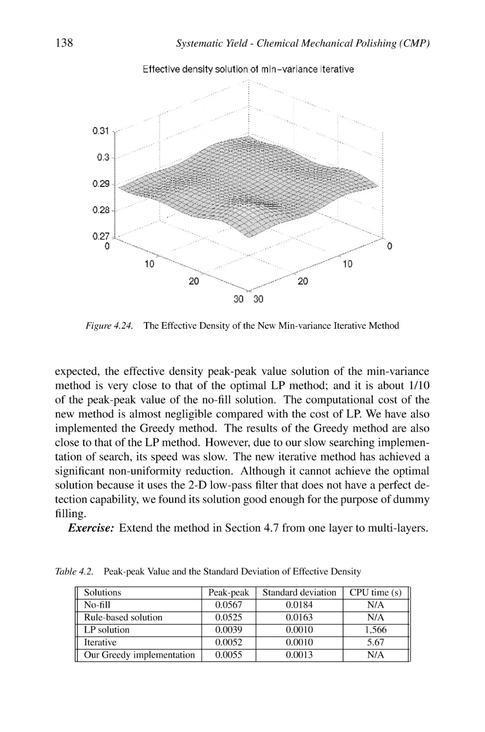
4.8
Application: Cu CMP Model Based Dummy Filling
4.8.1 Why Model Based Metal Filling?
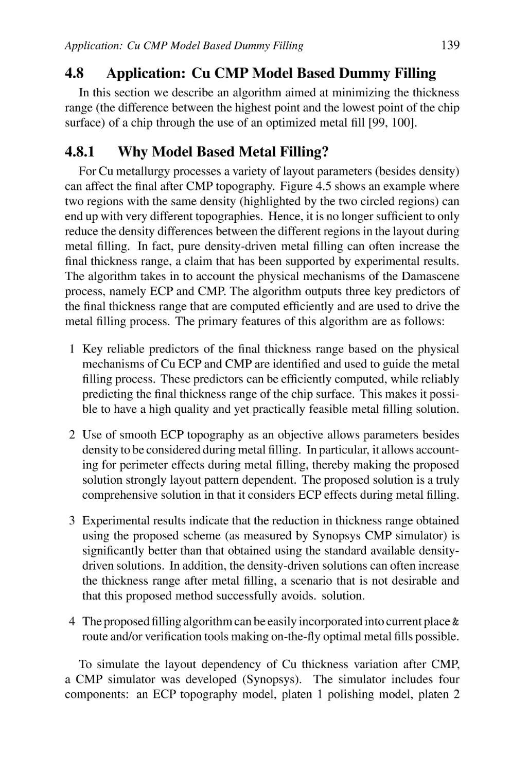
4.8.2 Predictors of the Final (Post-CMP) Thickness Range
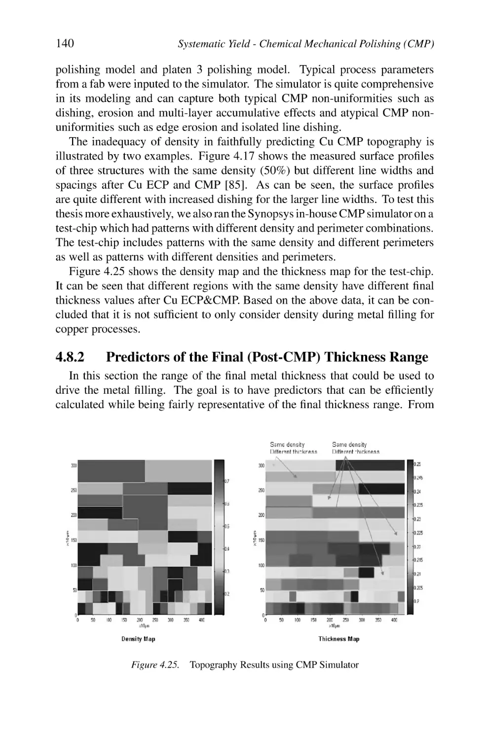
4.8.3 ECP Thickness Versus Final Thickness
4.8.4 Effective Density Versus Final Thickness
4.8.5 Details of the Proposed Metal Filling Algorithm
4.8.6 Experimental Results
4.8.7 Discussion of Results
139
139
140
141
141
142
148
148
5. VARIABILITY & PARAMETRIC YIELD
151
5.1
Introduction to Variability and Parametric Yield
151
5.2
Nature of Variability
151
5.3
Source of Variability
5.3.1 Wafer Level Variability
5.3.2 Materials Based Variability
5.3.3 Atomistic Variability
5.3.4 Lithography Based Variability
5.3.5 Local Variability
5.3.6 Environmental Variability & Aging
5.3.7 Device and Interconnect Parameters Variability
152
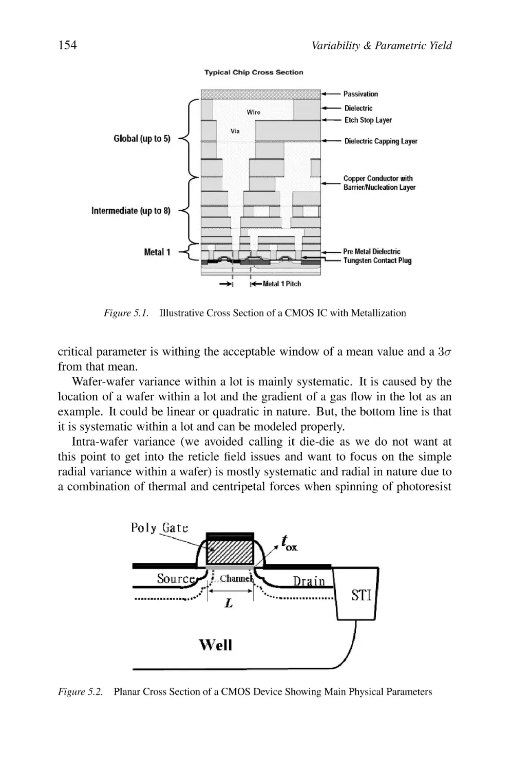
153
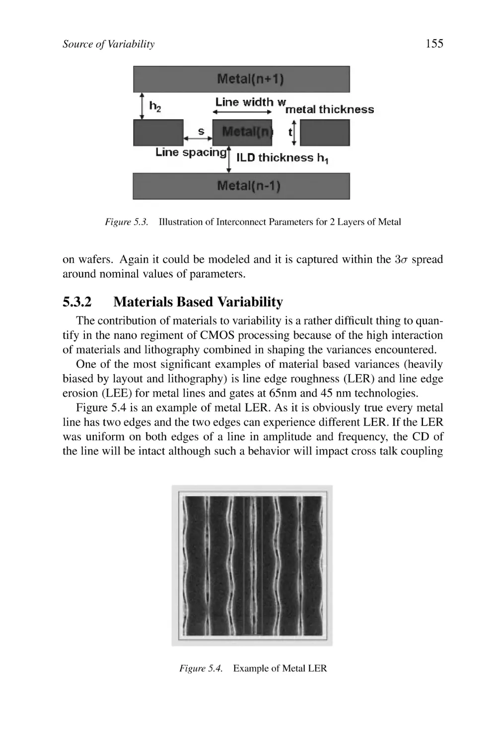
155
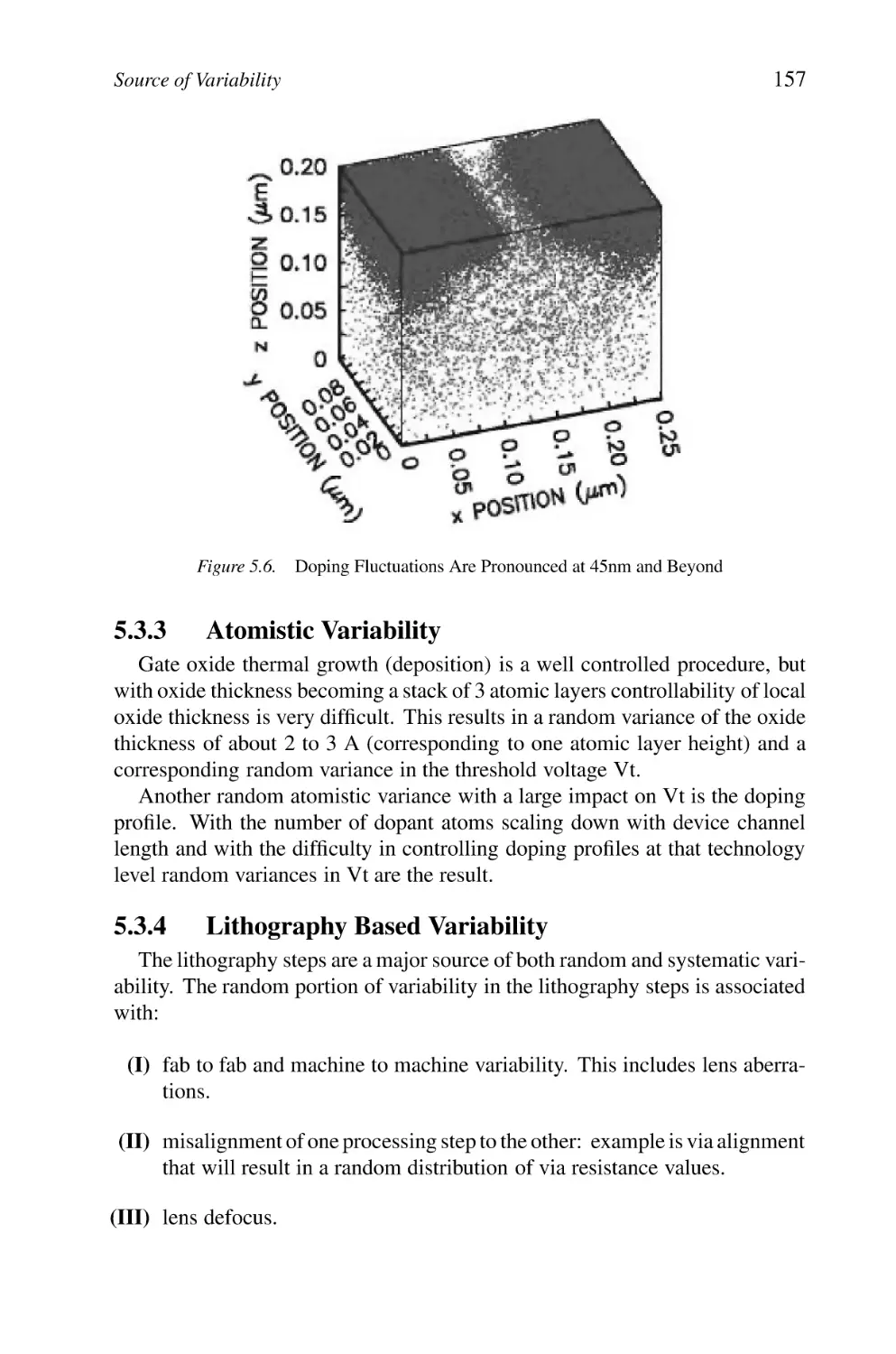
157
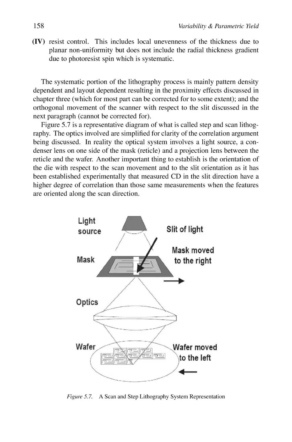
157
159
159
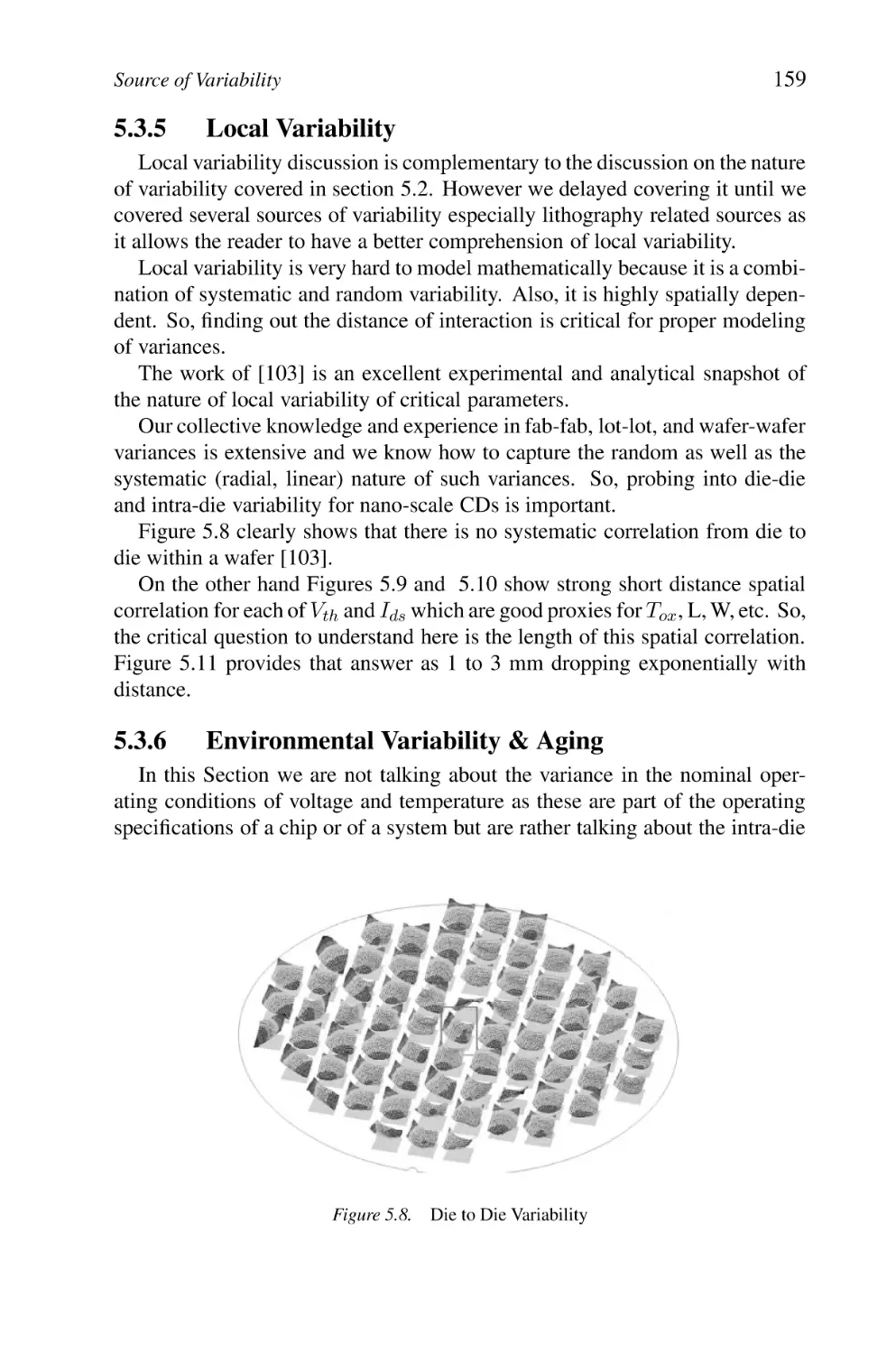
162
5.4
Yield Loss Sources & Mechanisms
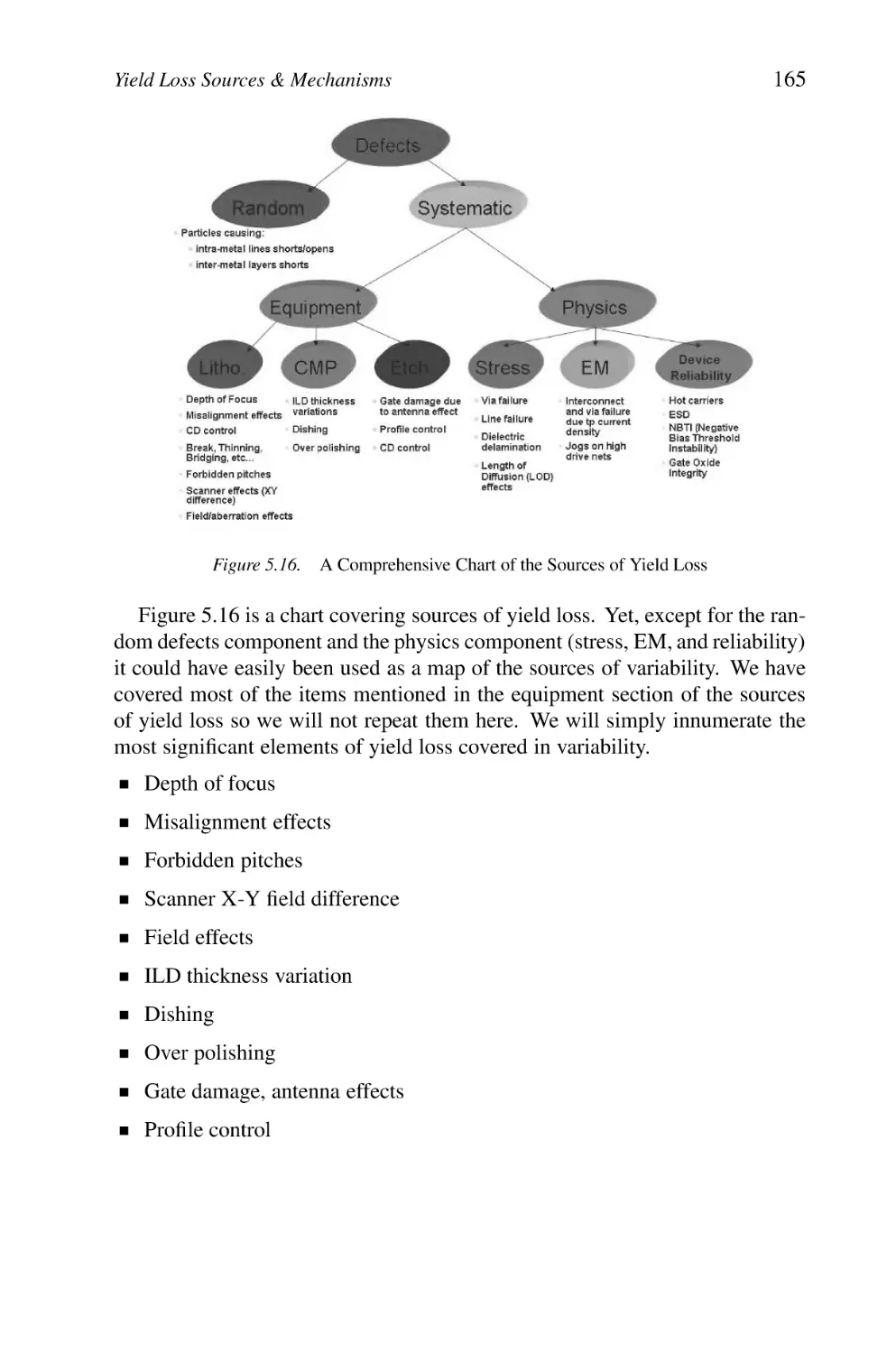
164
5.5
Parametric Yield
166
xi
Contents
5.6
Parametric Yield Test Structures
167
5.7
Variability & Parametric Yield Summary & Conclusions
168
6. DESIGN FOR YIELD
169
6.1
Introduction
169
6.2
Static Timing and Power Analysis
6.2.1 Overview
6.2.2 Critical Path Method (CPM)
170
170
171
6.3
Design in the Presence of Variability
172
6.4
Statistical Timing Analysis
6.4.1 Overview
6.4.2 SSTA: Issues, Concerns, and Approaches
6.4.3 Parametric and Delay Modeling PDFs
6.4.4 Correlation Issues
173
173
175
177
178
6.5
A Plurality of SSTA Methodologies
6.5.1 Early SSTA Approach: Using Continuous PDFs
6.5.2 Four Block-based Approaches
180
180
181
6.6
Bounding Approaches
185
6.7
Statistical Design Optimization
186
6.8
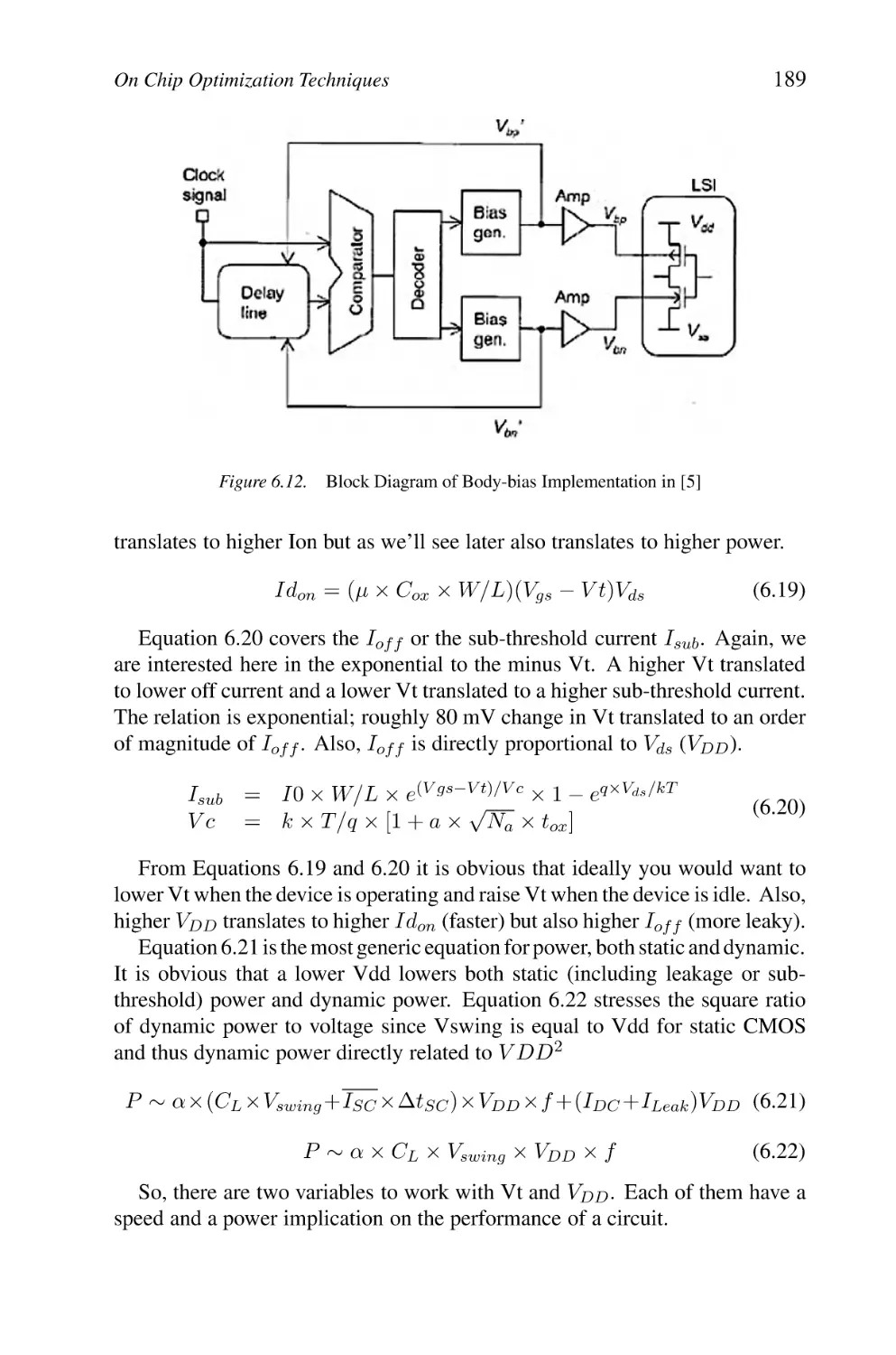
On Chip Optimization Techniques
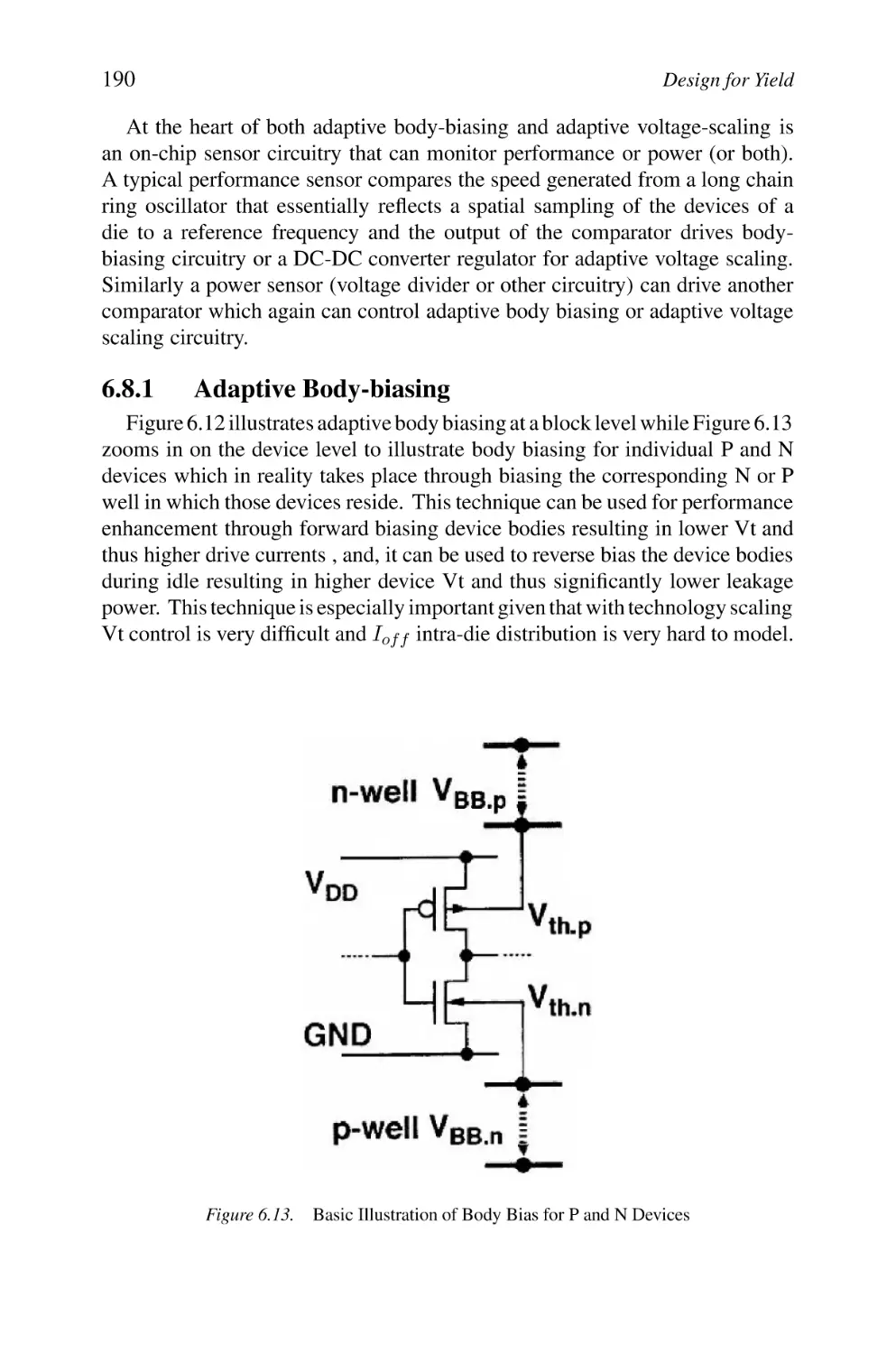
6.8.1 Adaptive Body-biasing
6.8.2 Adaptive Voltage Scaling
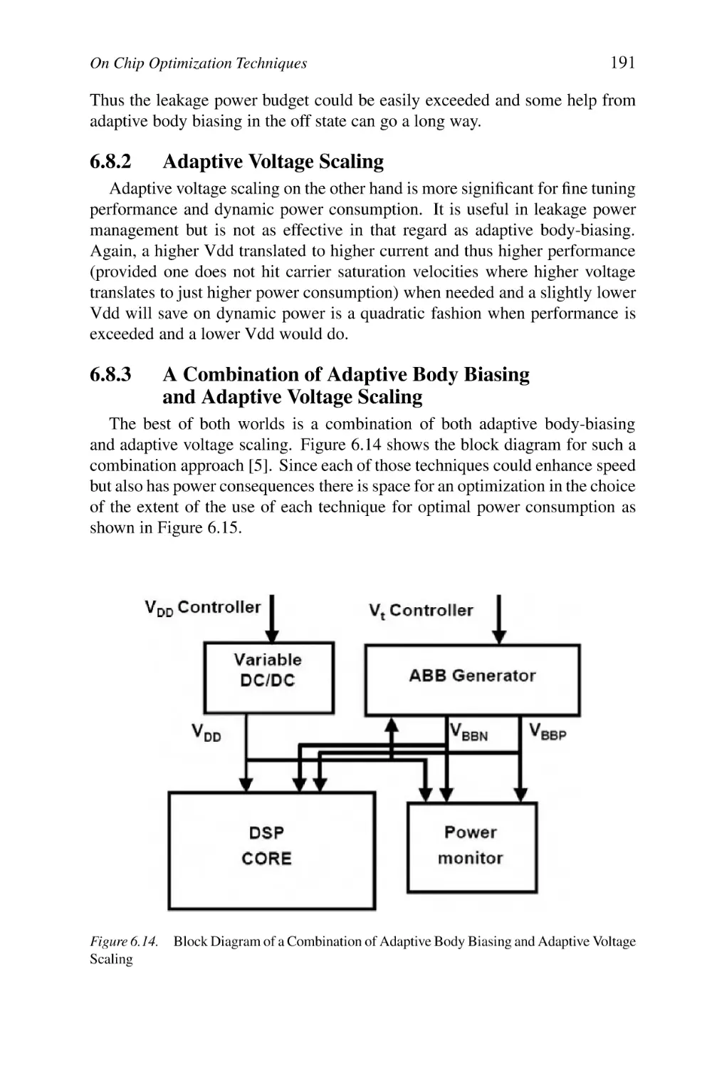
6.8.3 A Combination
188
190
191
191
6.9
Summary: Design for Yield
6.9.1 Summary for SSTA
6.9.2 Summary for Statistical Design Optimization
192
192
192
7. YIELD PREDICTION
195
7.1
Introduction
195
7.2
Yield Loss Sources & Mechanisms
196
7.3
Yield Modeling
7.3.1 Early Work in Yield Modeling
196
196
7.4
Yield Enhancement Mechanisms
7.4.1 IP Development
7.4.2 Synthesis
7.4.3 Placement and Routing
199
199
199
199
xii
Contents
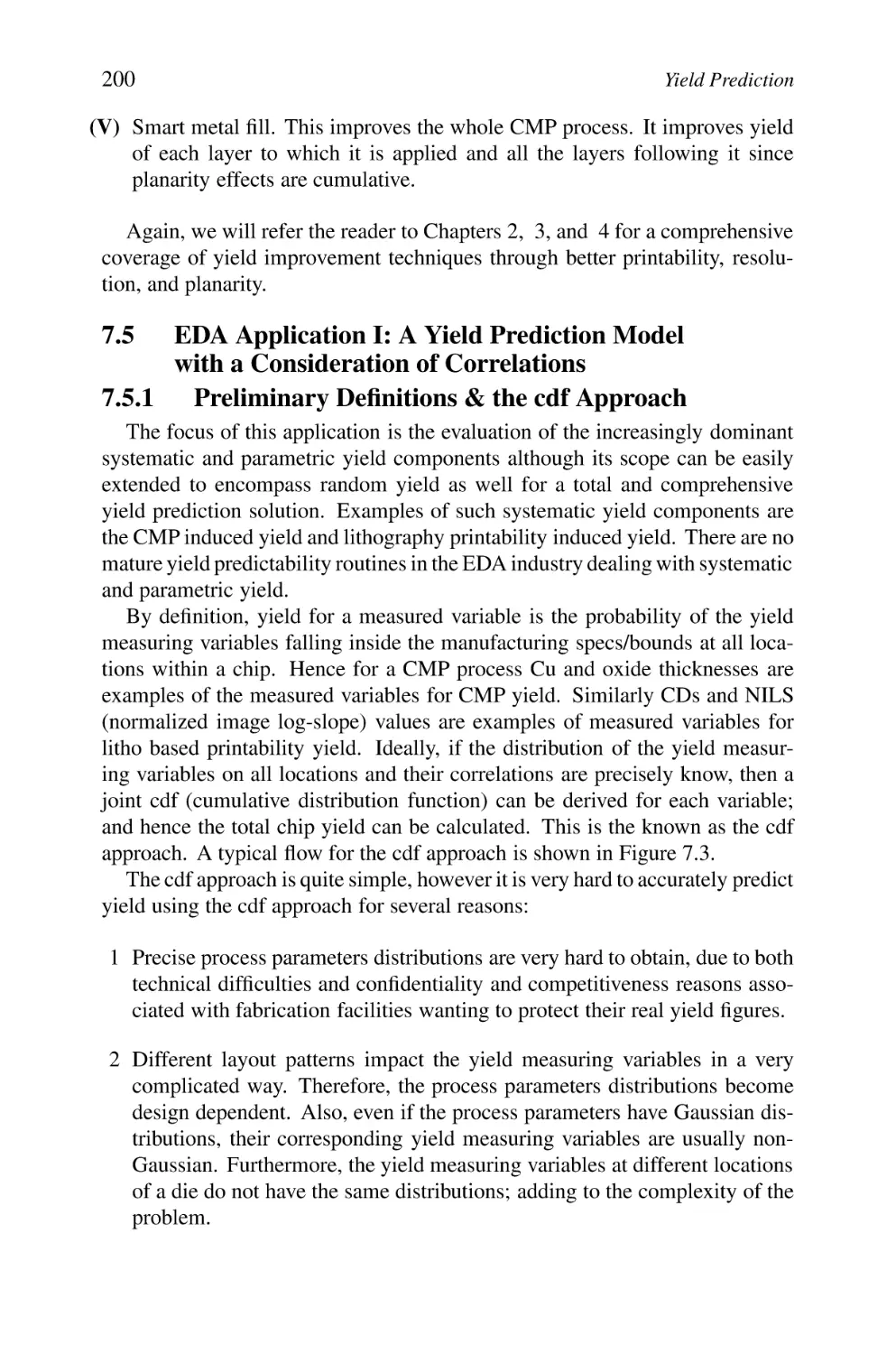
7.5
EDA Application I
7.5.1 Preliminary Definitions & the cdf Approach
7.5.2 Our Proposed Solution
7.5.3 A Brief Description of the Key Ideas
7.5.4 Example and Results
200
200
201
203
208
7.6
EDA Application II
7.6.1 Background
7.6.2 Variation Decomposition
7.6.3 Variations Handled by Hotspot Model
7.6.4 Application Example: CMP Yield
211
211
212
214
214
7.7
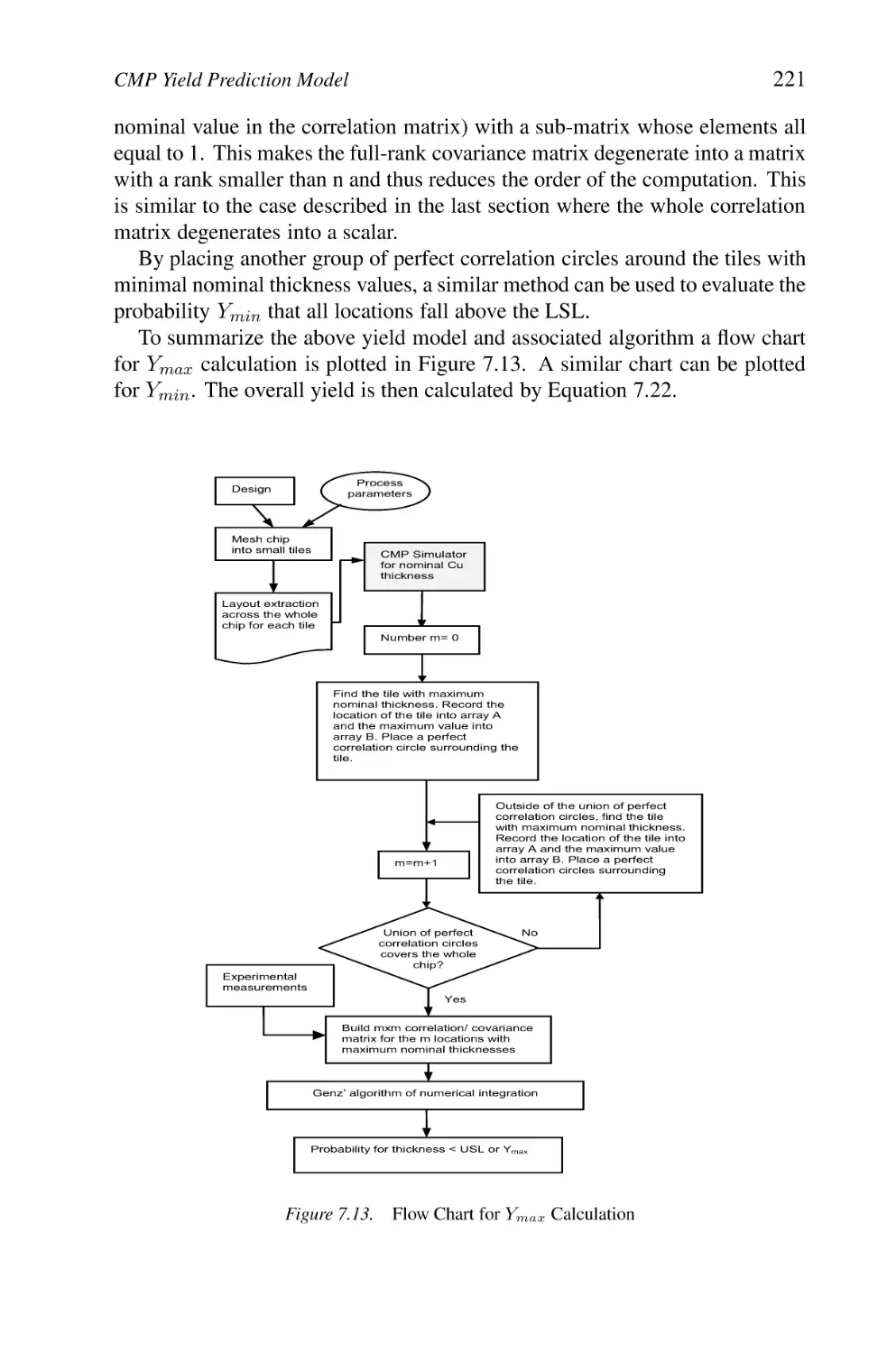
CMP Yield Prediction Model
7.7.1 Yield Prediction Algorithm
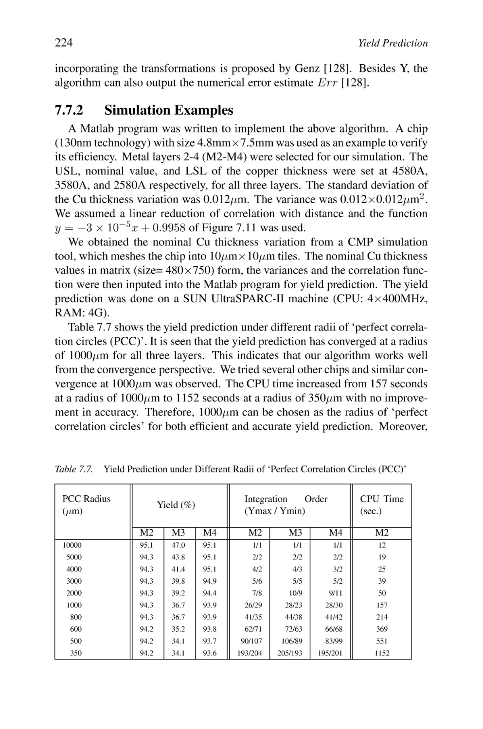
7.7.2 Simulation Examples
7.7.3 Recap and some conclusions
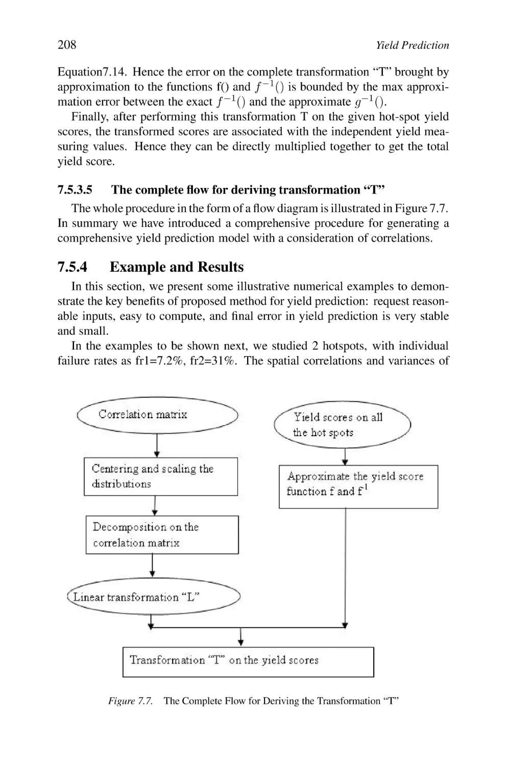
7.7.4 Summary and Conclusions
215
216
224
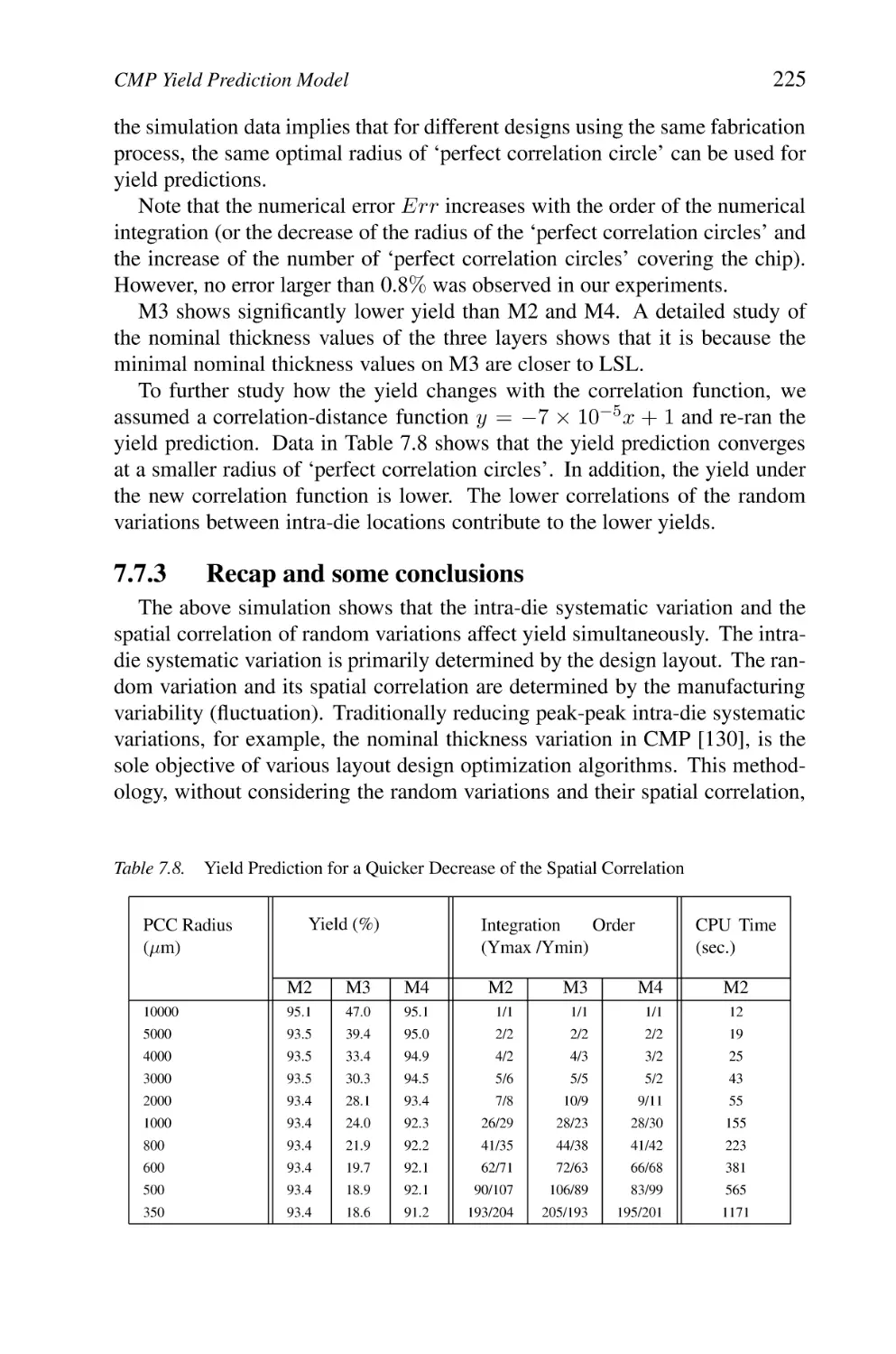
225
226
8. CONCLUSIONS
227
8.1
The Case for a DFM/DFY Driven Design
227
8.2
Design Intent Manufacturing (Lithography) Centric DFM
228
8.3
Yield Centric DFM
229
8.4
DFM/DFY EDA Design Tools
8.4.1 Implementation
8.4.2 Physical Verification
8.4.3 Mask Synthesis
8.4.4 Mask Inspection
8.4.5 TCAD
8.4.6 Process Modeling and Simulation
229
231
235
236
237
239
239
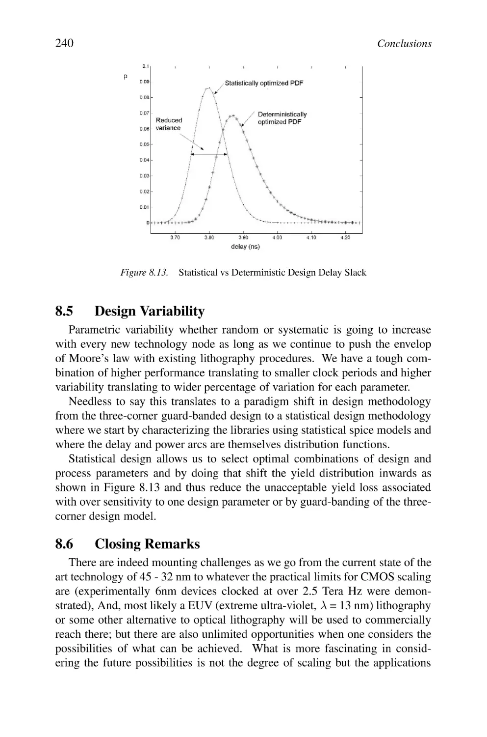
8.5
Design Variability
240
8.6
Closing Remarks
240
References
243
Index
253
List of Figures
1.1
1.2
1.3
1.4
1.5
1.6
1.7
1.8
1.9
1.10
1.11
2.1
2.2
2.3
2.4
2.5
2.6
2.7
2.8
2.9
2.10
2.11
3.1
3.2
Cu Cross Section Showing Potential Problems
Basic Gate Illustration
NA= I sin α
Basic Example of OPC at 180nm
Example of Strong (180) PSM
Double-gate FET
TCAD Simulated FinFET
Layout of Multi-segment FinFET
Simulated 5nm MOSFET with Silicon Crystal
Superimposed Next to A Bulk-CMOS Equivalent
Revenue as a Function of Design Cycle
Typical ASIC Design Flow
Short CA Between Two Wires Caused by Particles with Size x
Open CA on a Wire Caused by Particles with Size x
Intra-layers Defect Particle Resulting in an Open or Short
Typical Short Critical Area
Short Critical Area at Large Defect Size
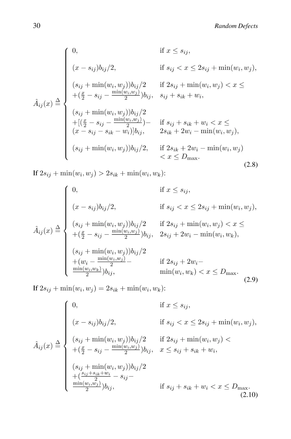
Open Critical Area on Wire i
Example of Improving Poly Short CA and M1 Open CA
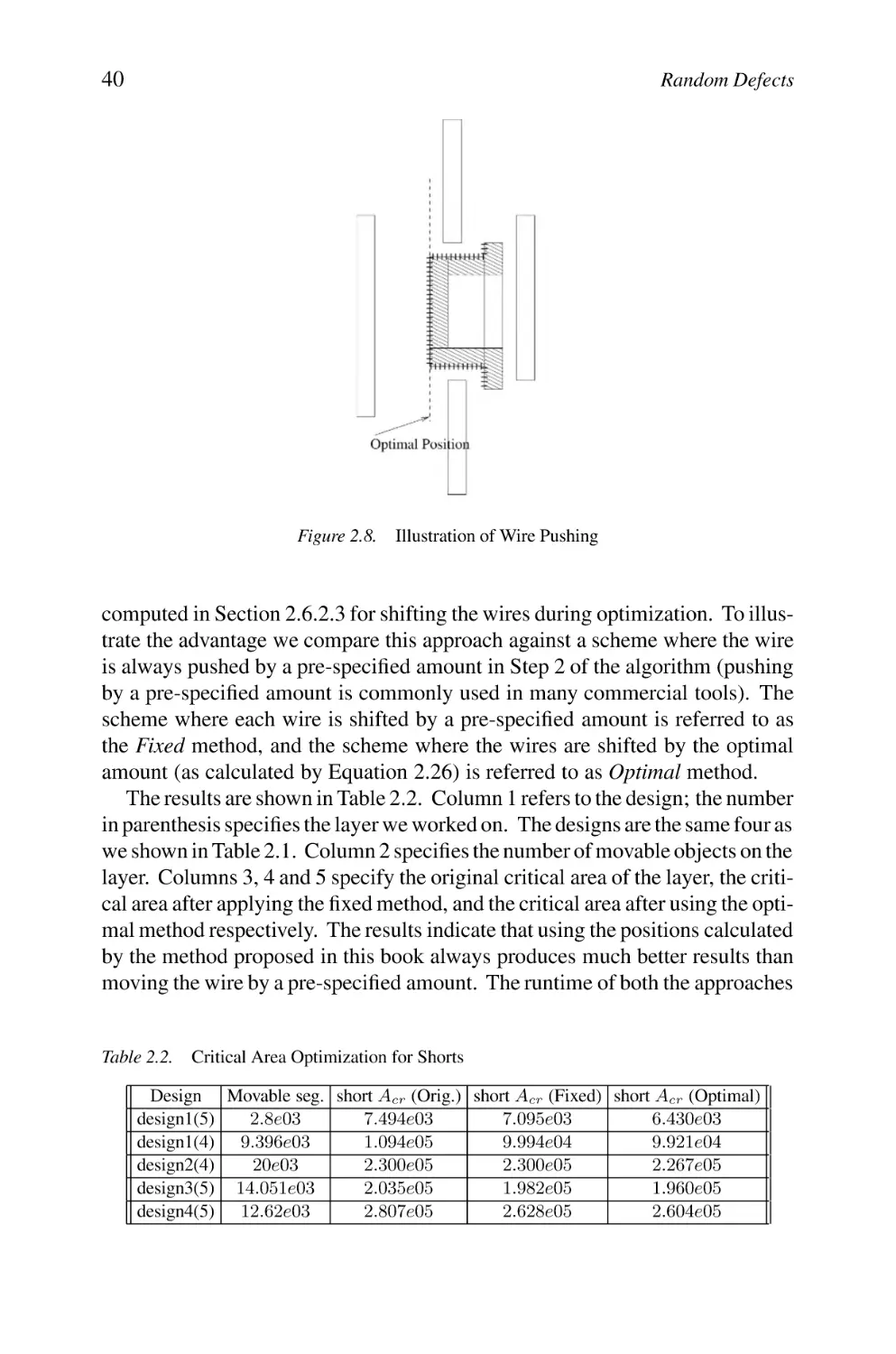
Illustration of Wire Pushing
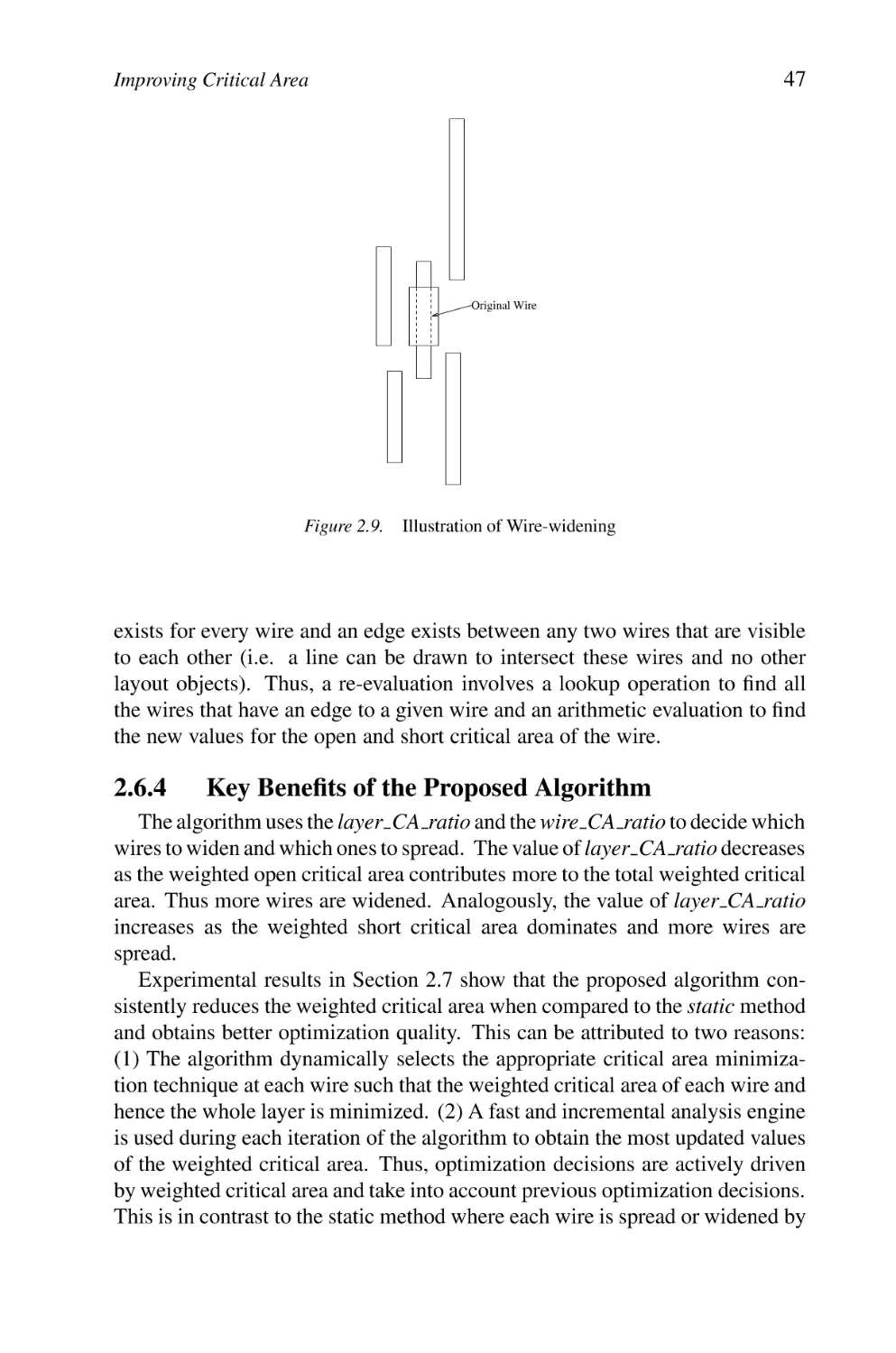
Illustration of Wire-widening
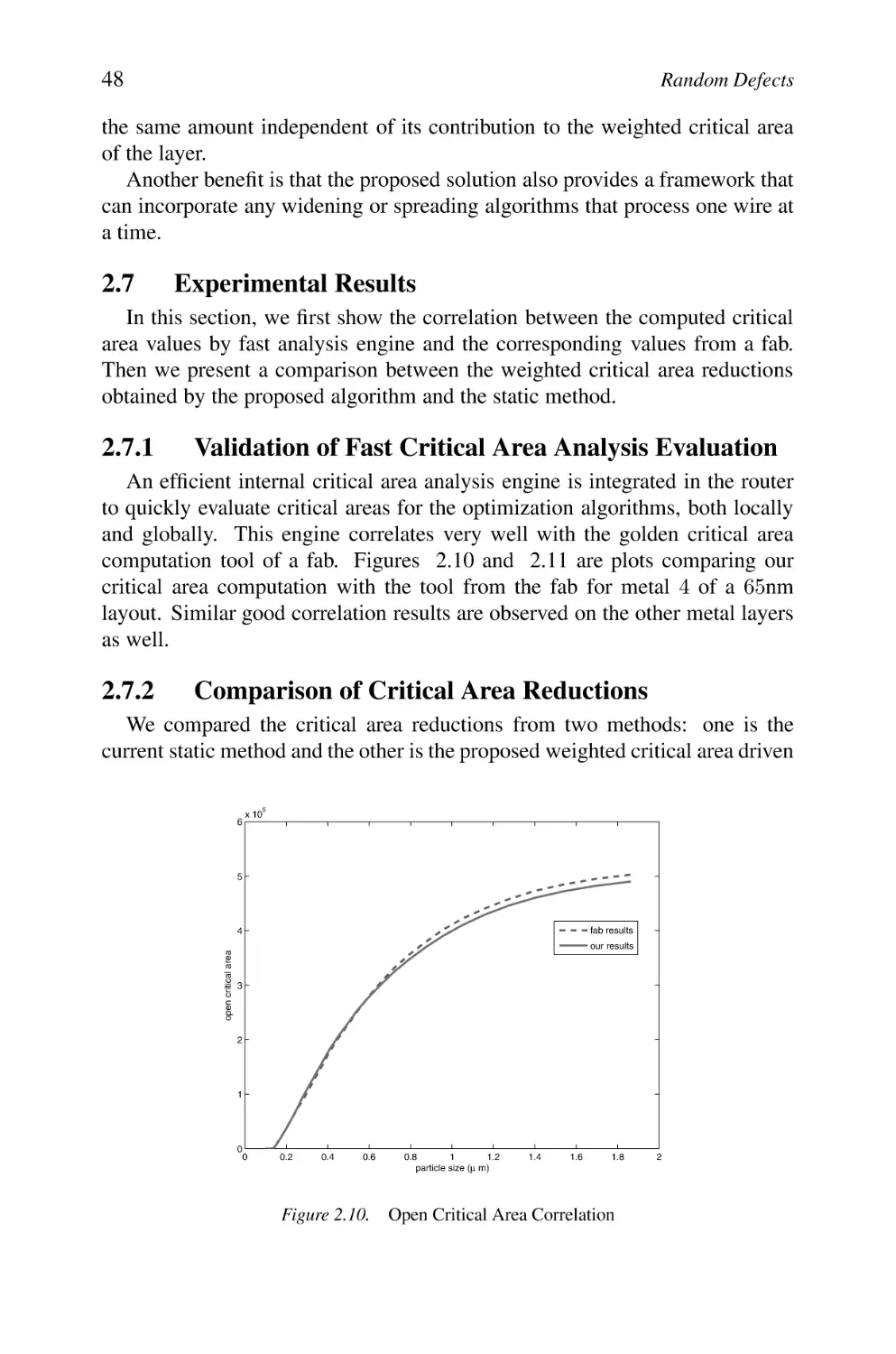
Open Critical Area Correlation
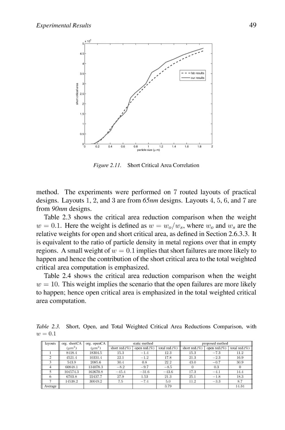
Short Critical Area Correlation
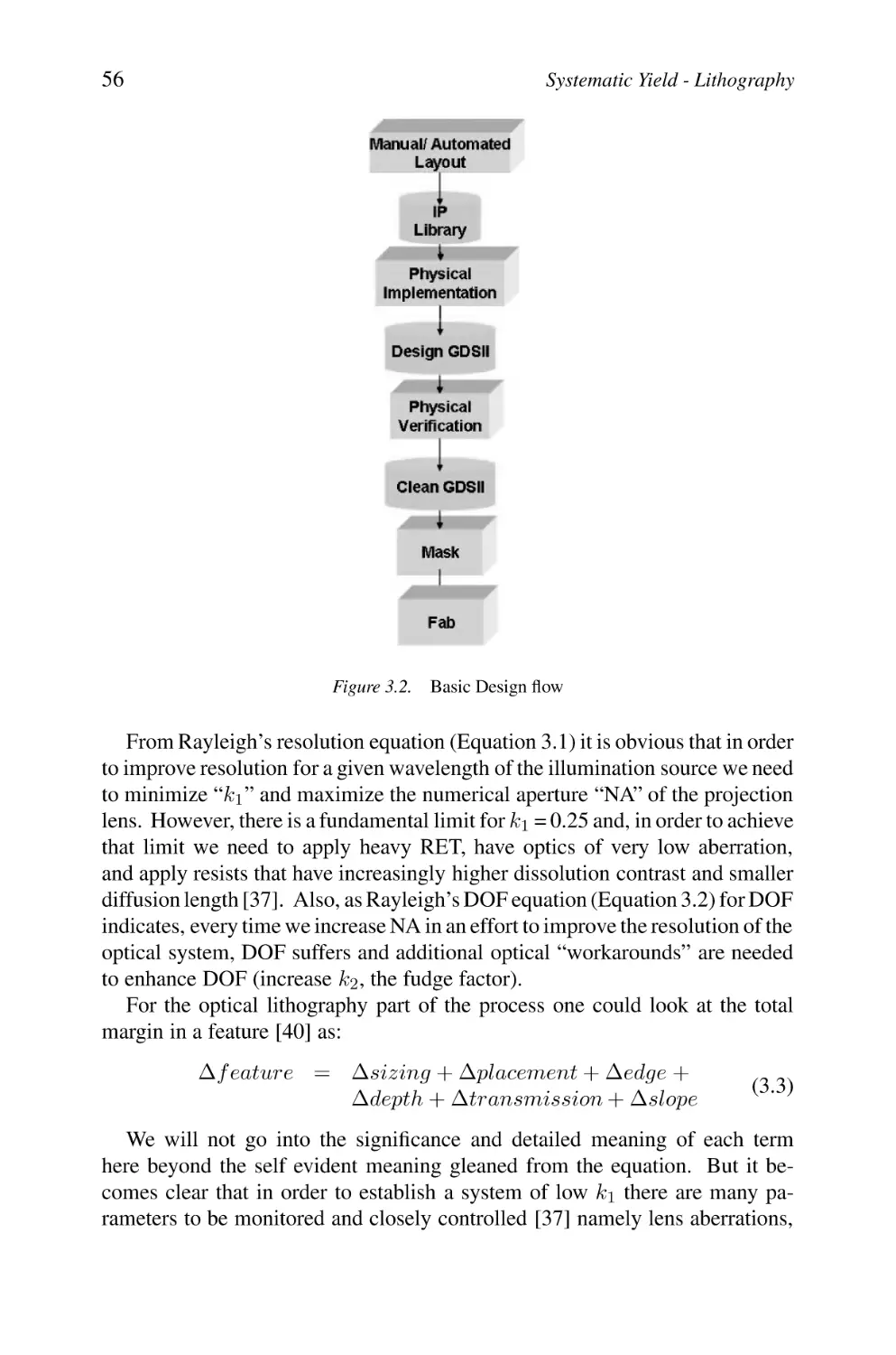
Basic Optical Lithography IC Manufacturing System
Basic Design flow
xiii
4
4
8
9
9
10
11
11
13
16
18
22
23
23
28
28
32
35
40
47
48
49
54
56
xiv
List of Figures
3.3
3.4
3.5
3.6
3.7
3.8
3.9
3.10
3.11
3.12
3.13
3.14
3.15
3.16
3.17
3.18
3.19
3.20
3.21
3.22
3.23
3.24
3.25
3.26
3.27
3.28
3.29
3.30
3.31
3.32
3.33
3.34
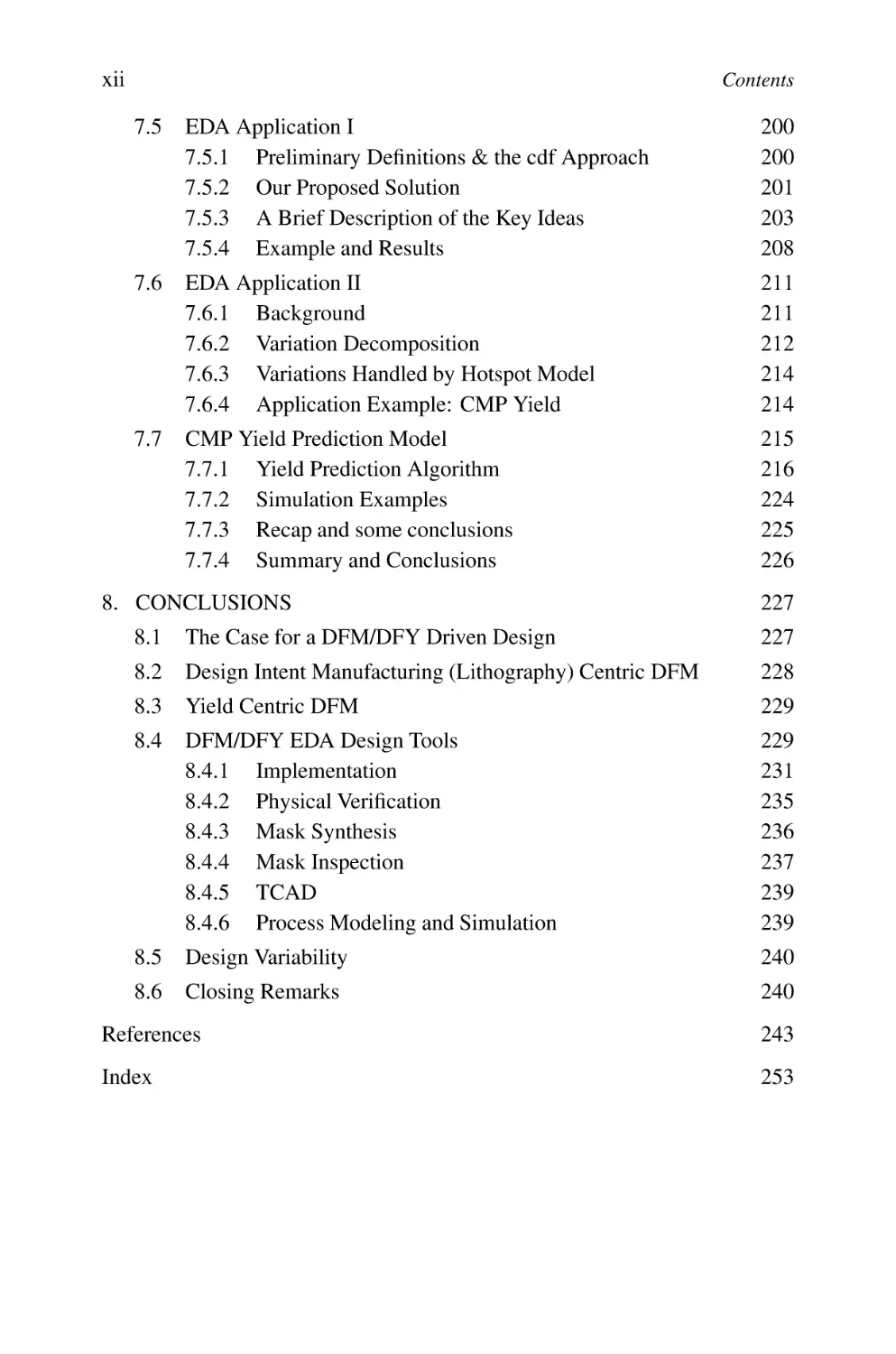
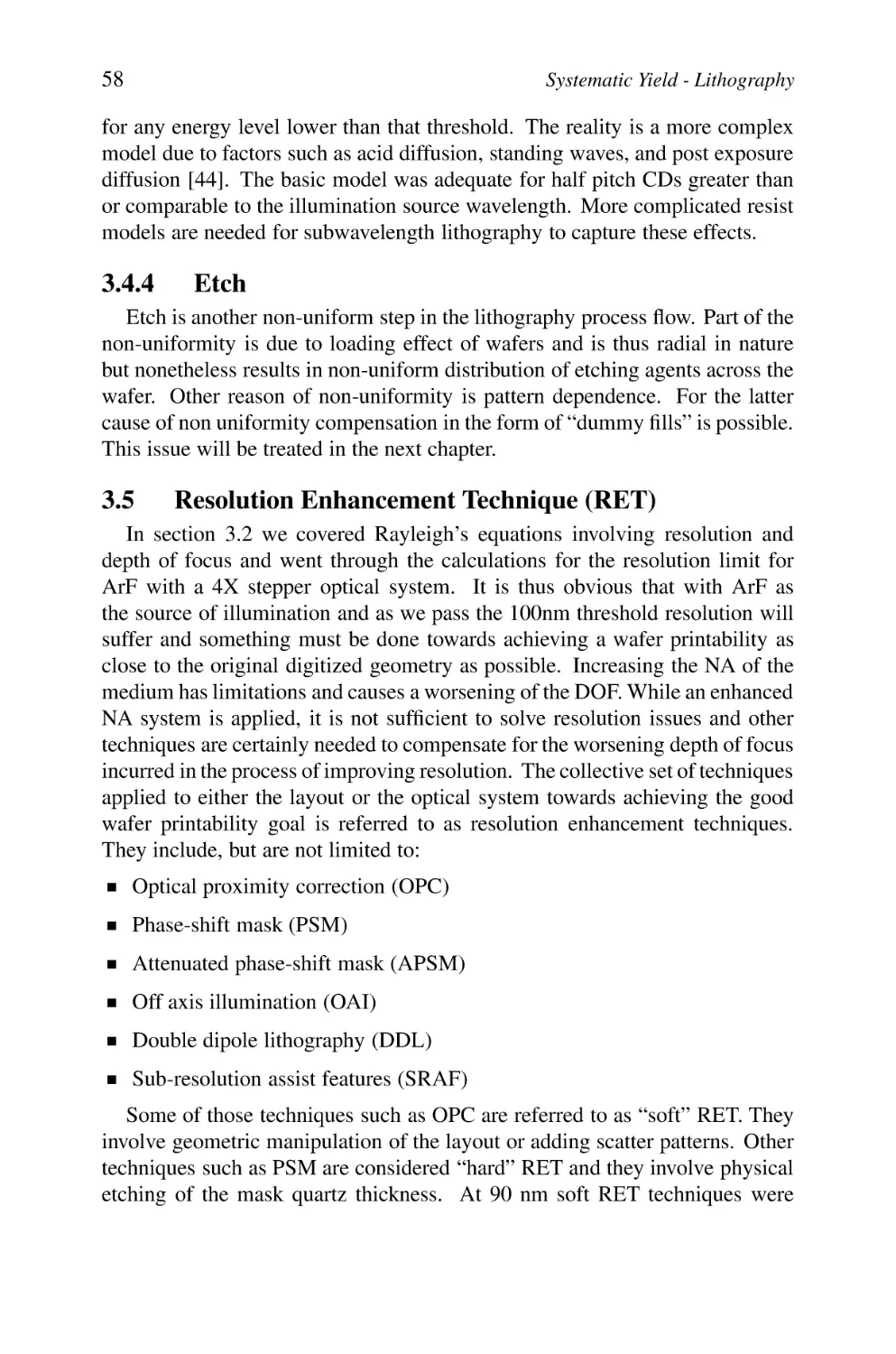
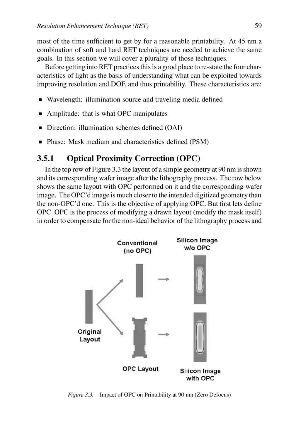
Impact of OPC on Printability at 90 nm (Zero Defocus)
Silicon Wafter Image with/without OPC
and with/without Defocus
Model Based OPC Flow
Layout
A Case Where Rule Based OPC Is Good Enough
OPC’d Geometry with Scatter Bars (SRAFs)
Printability of Isolated Feature, No Scatter Bar
Printability of Isolated Feature, with Scatter Bar
A Dark Field (Positive) Binary Mask
Basic Illustration of the Light-mask-resist Interaction
Illustration of Resolution Problem with Regular Mask
Illustration of the Resolution Enhancement Due to 180◦ Phase
Inversion
Illustration of a Layout with Phase Assignment Conflict
Three Implementation of a Layout, Two have Phase Conflicts
Resolved Feature with PSM
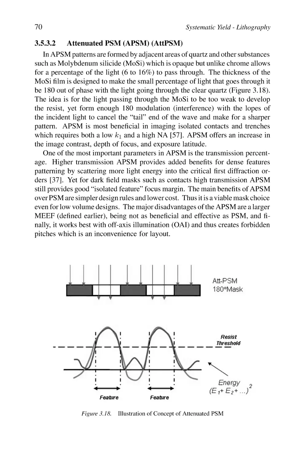
Illustration of Concept of Attenuated PSM
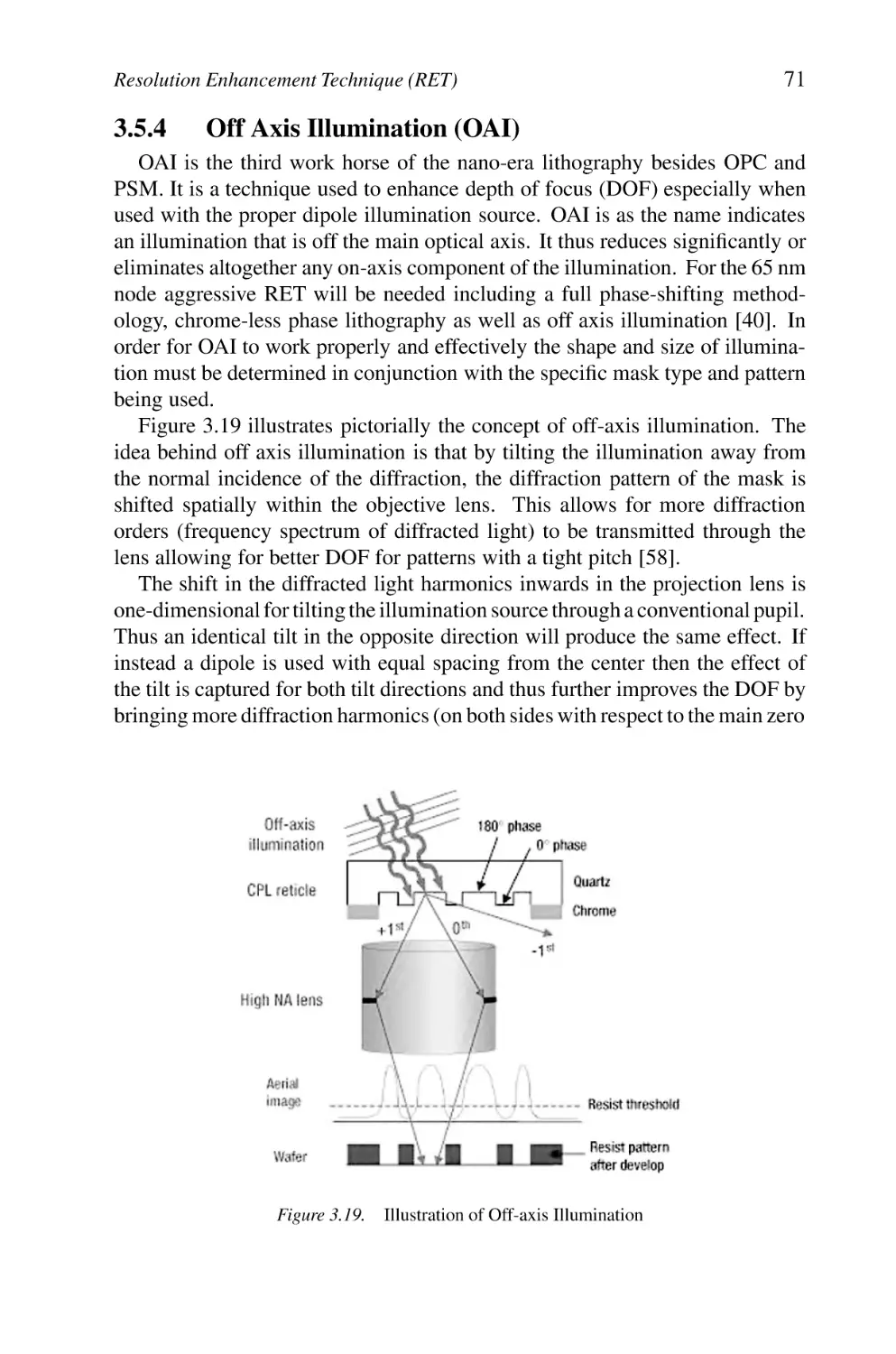
Illustration of Off-axis Illumination
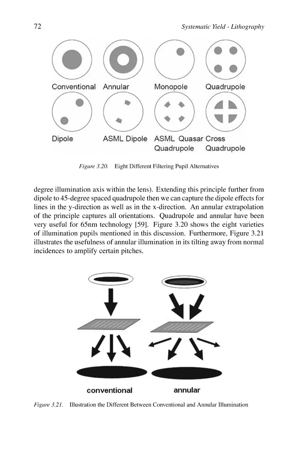
Eight Different Filtering Pupil Alternatives
Illustration the Different Between Conventional
and Annular Illumination
Problem Place and Route Patterns
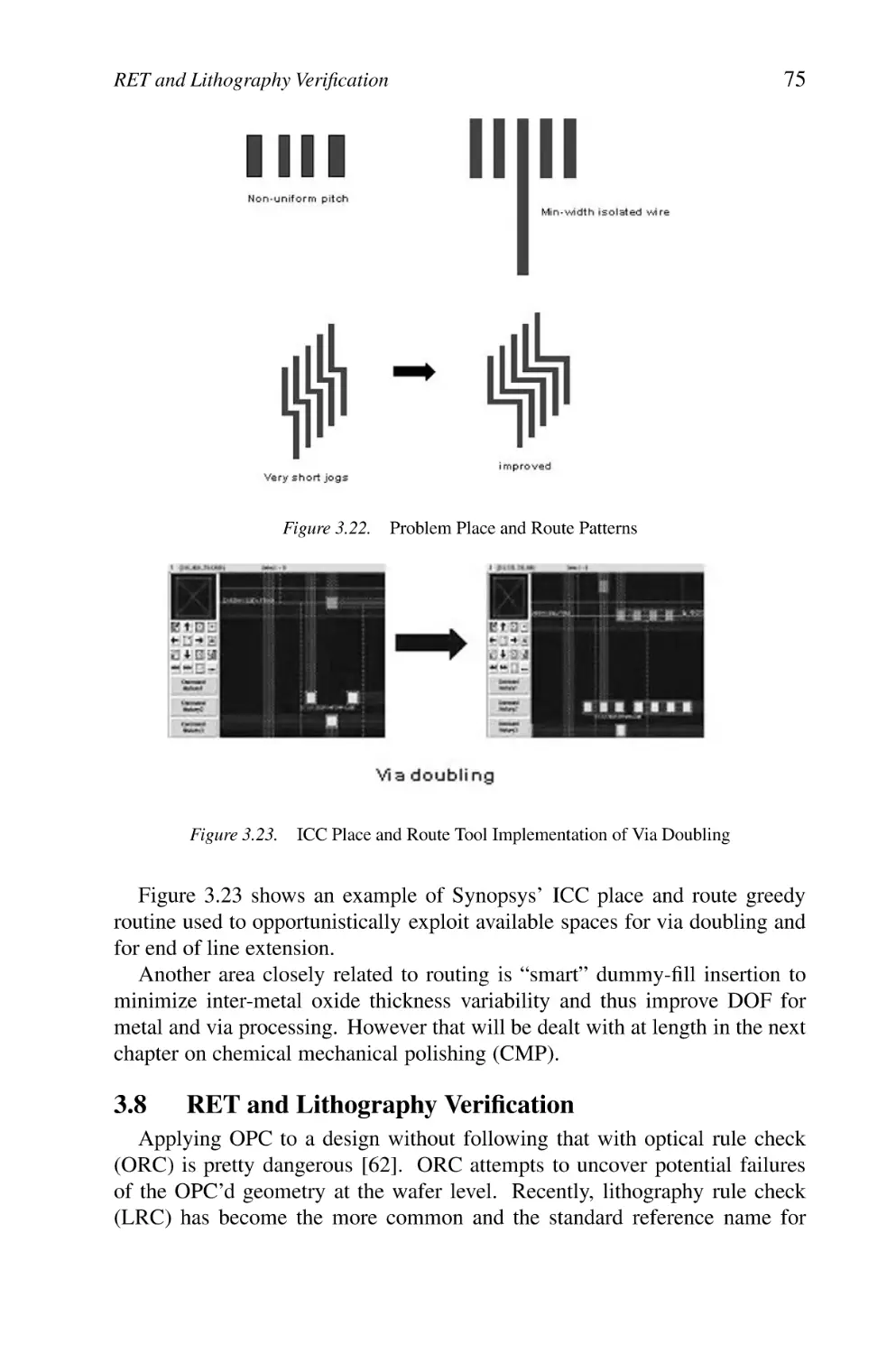
ICC Place and Route Tool Implementation of Via Doubling
Three Known Problem Patterns from a 65nm LRC Library
Design Flow Including OPC and LRC
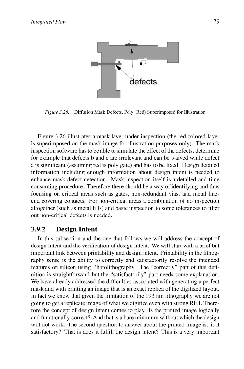
Diffusion Mask Defects, Poly (Red) Superimposed
for Illustration
Illustration of Steps Needed to Meet Design Intent
Silicon vs Layout Simulation Flow
Old Style “Compact” Layout vs Litho-friendly Cell Layout
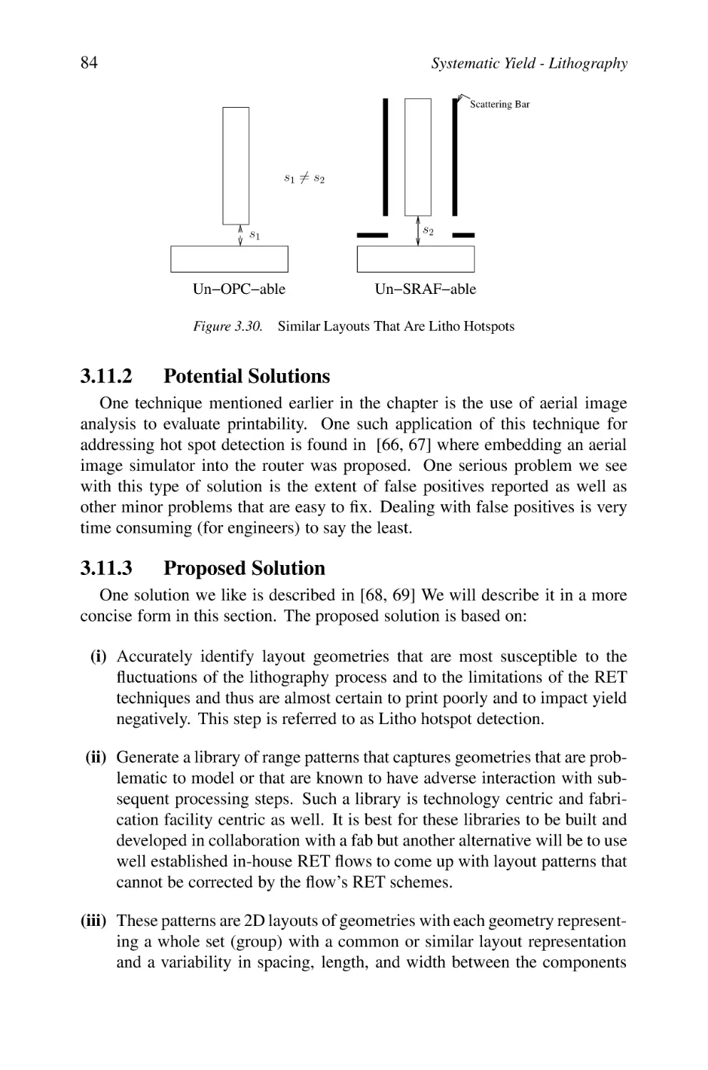
Similar Layouts That Are Litho Hotspots
Range Pattern Staircase
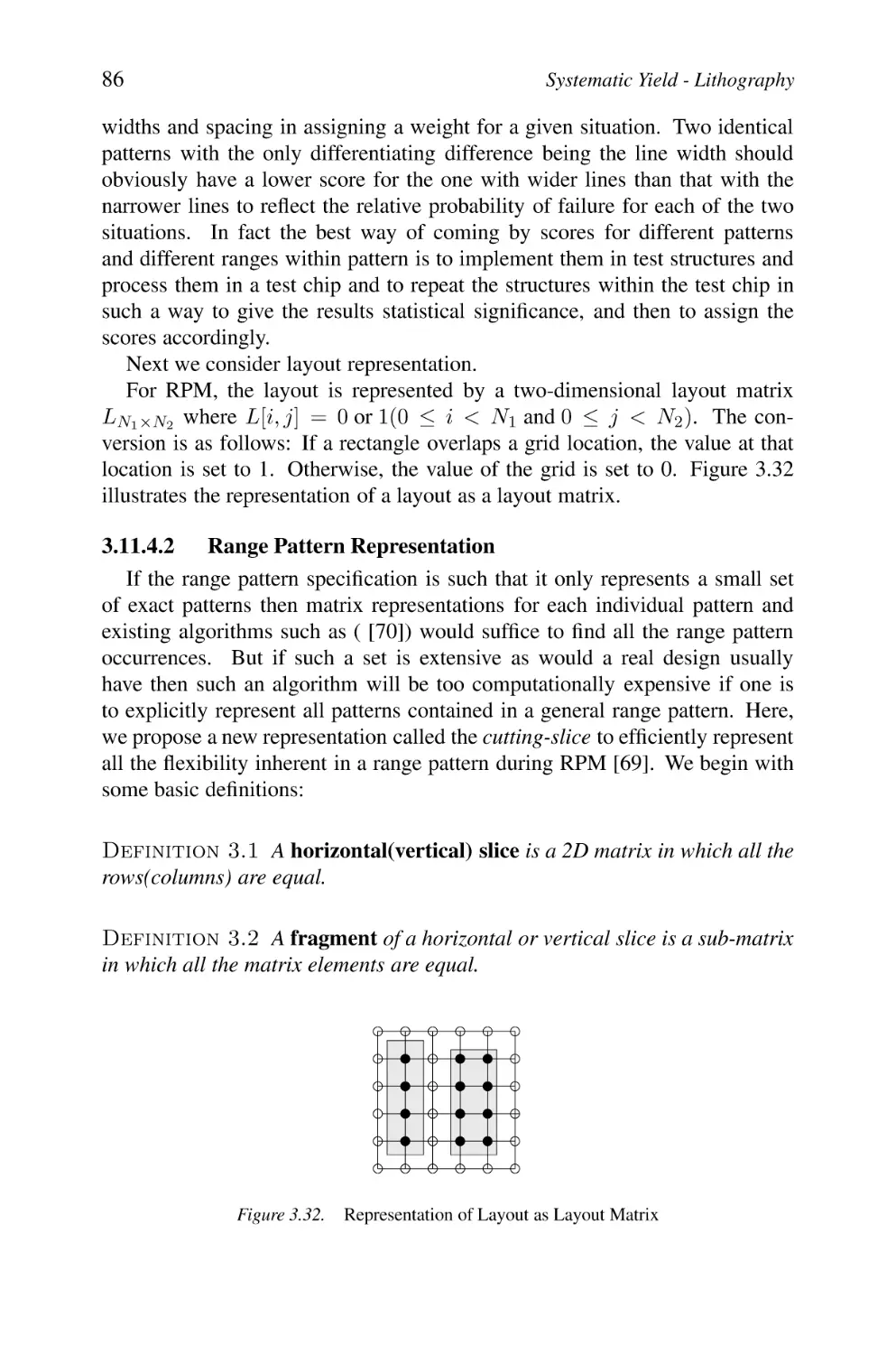
Representation of Layout as Layout Matrix
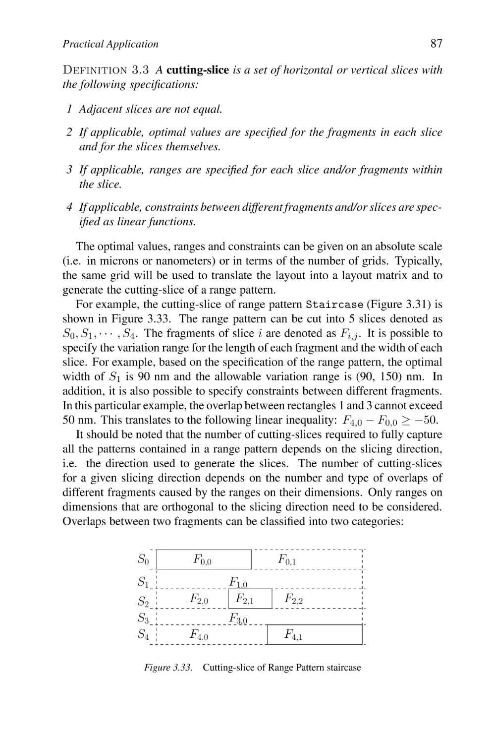
Cutting-slice of Range Pattern staircase
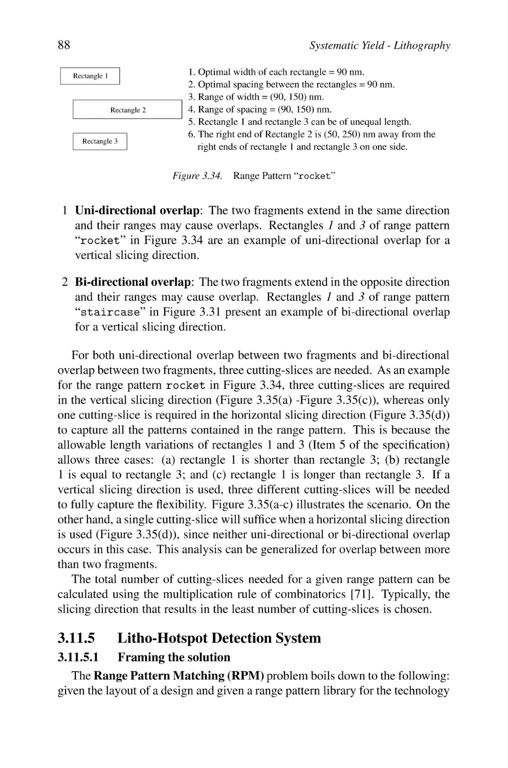
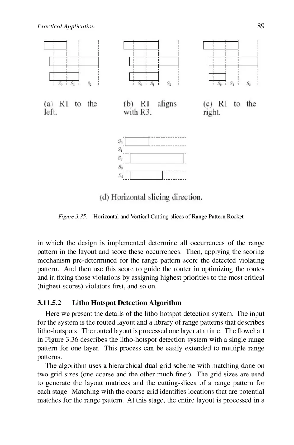
Range Pattern “rocket”
59
60
62
63
63
64
64
65
65
66
67
68
68
69
69
70
71
72
72
75
75
76
78
79
80
81
82
84
85
86
87
88
List of Figures
3.35
3.36
3.37
3.38
3.39
4.1
4.2
4.3
4.4
4.5
4.6
4.7
4.8
4.9
4.10
4.11
4.12
4.13
4.14
4.15
4.16
4.17
4.18
4.19
4.20
4.21
4.22
4.23
4.24
4.25
4.26
5.1
Horizontal and Vertical Cutting-slices of Range
Pattern Rocket
Flowchart of the Hotspot Detection System
Cutting-slice of Range Pattern Mountain
Layout Block Encoding
Drill and Fly
Simplified Cross Section of a Single and a Dual
Damascene Process
Lithography Steps of a Via-first Dual Damascene Process
An Electroplating System [1]
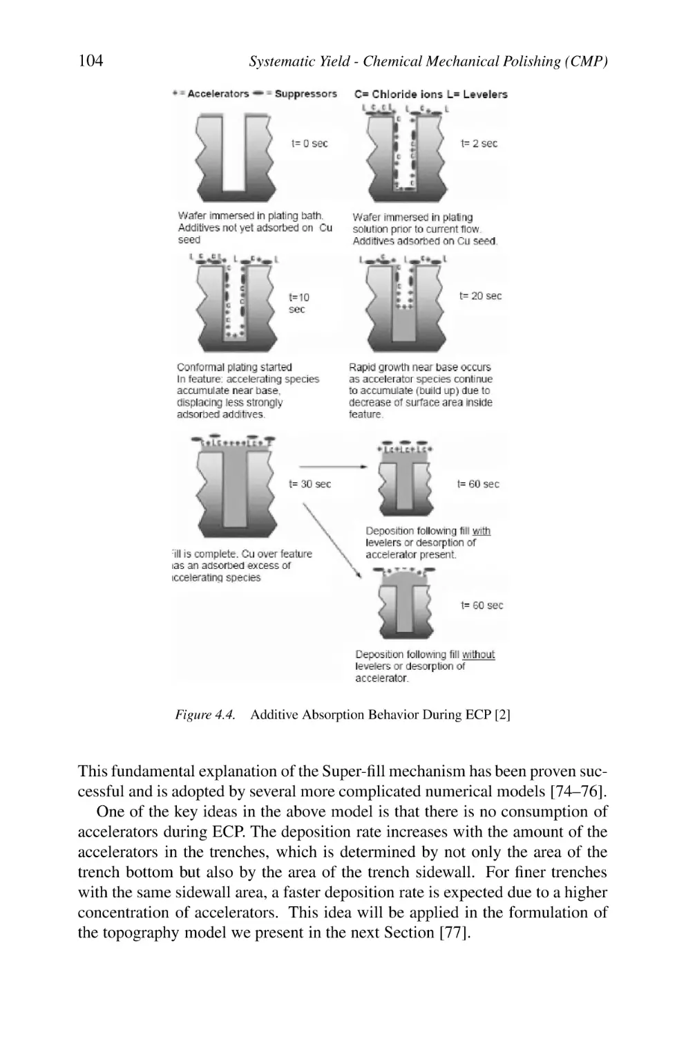
Additive Absorption Behavior During ECP [2]
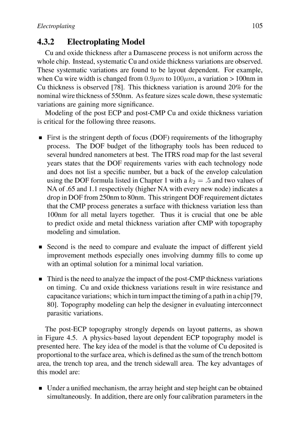
A Typical Topography After ECP Process
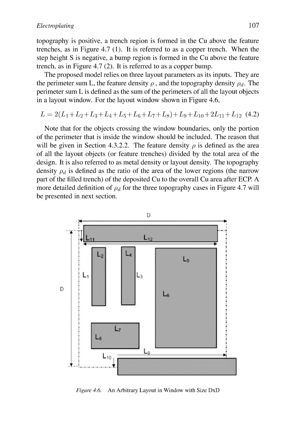
An Arbitrary Layout in Window with Size DxD
Three Kinds of Post-ECP Topographies of a Wire
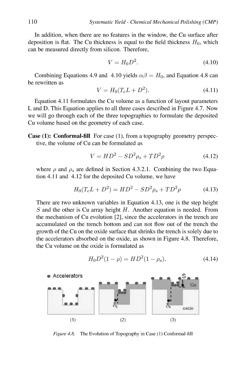
The Evolution of Topography in Case (1) Conformal-fill
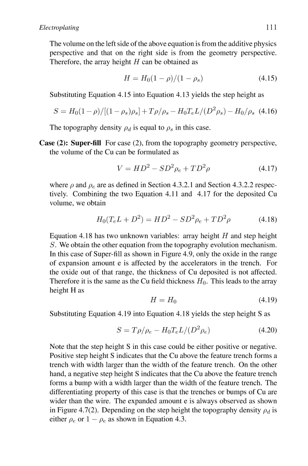
The Evolution of Topography in Case (2) Super-fill
Framework of The Full-chip ECP Topography Simulator
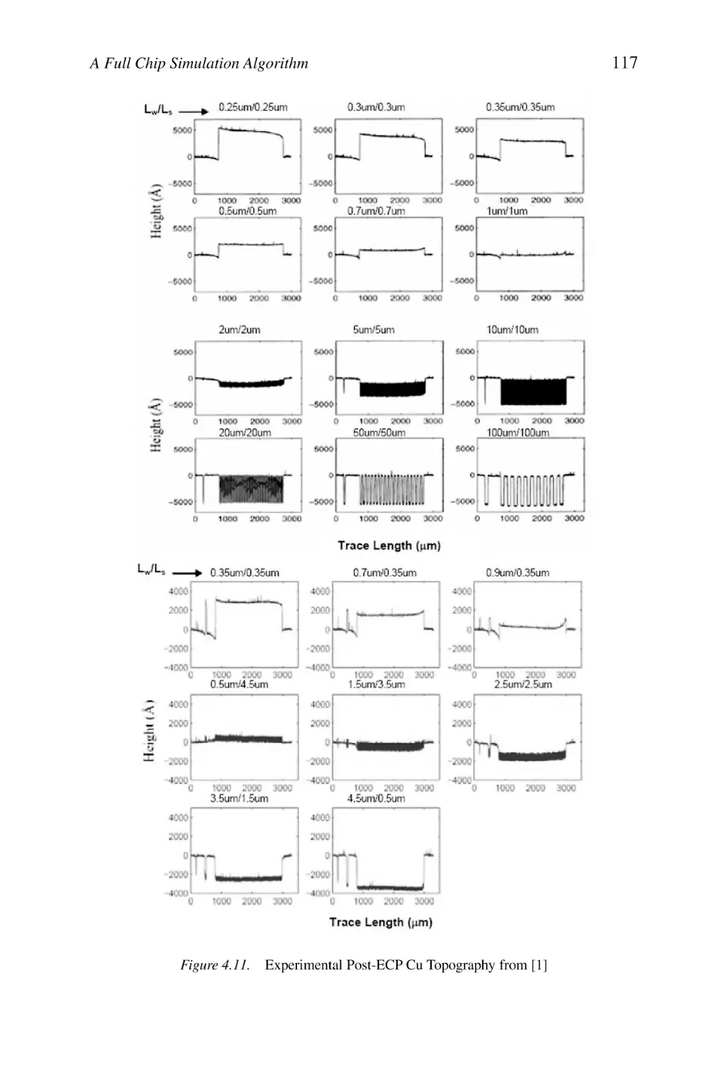
Experimental Post-ECP Cu Topography from [1]
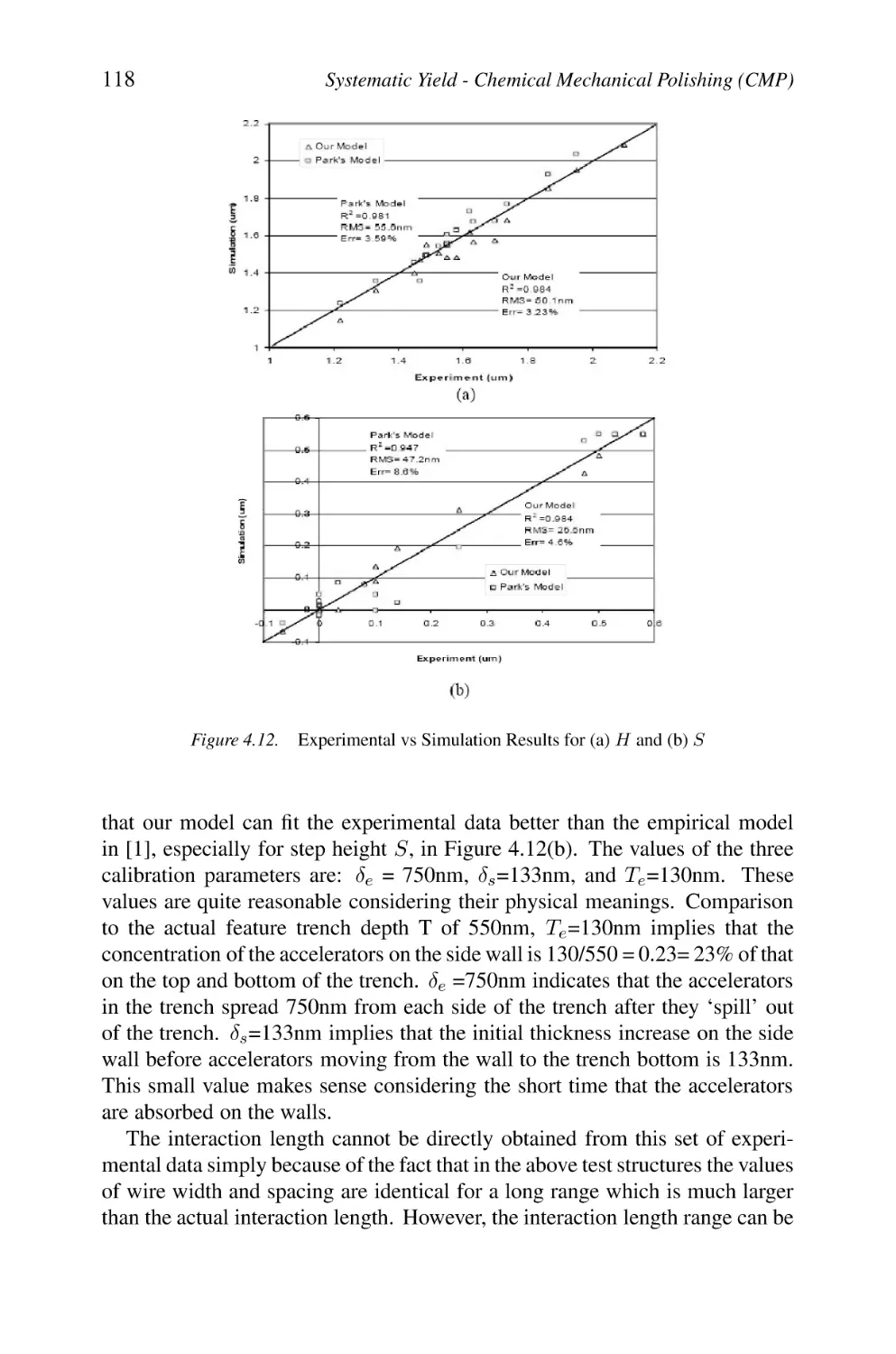
Experimental vs Simulation Results for (a) H and (b) S
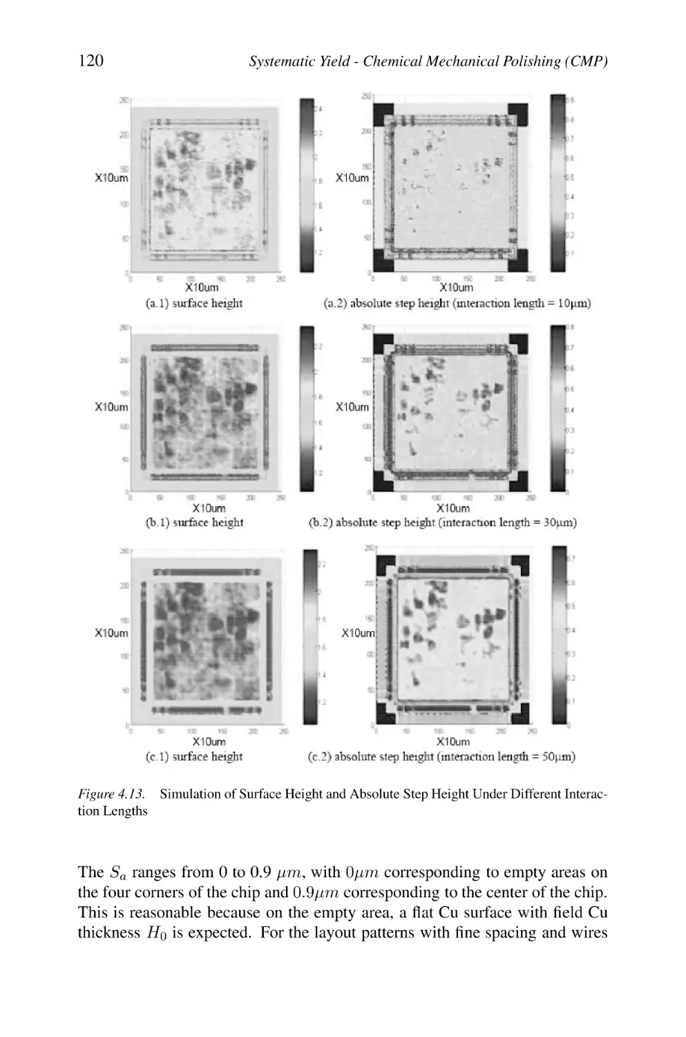
Simulation of Surface Height and Absolute Step Height Under Different Interaction Lengths
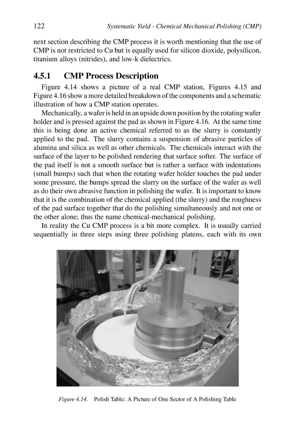
Polish Table: A Picture of One Sector of A Polishing Table
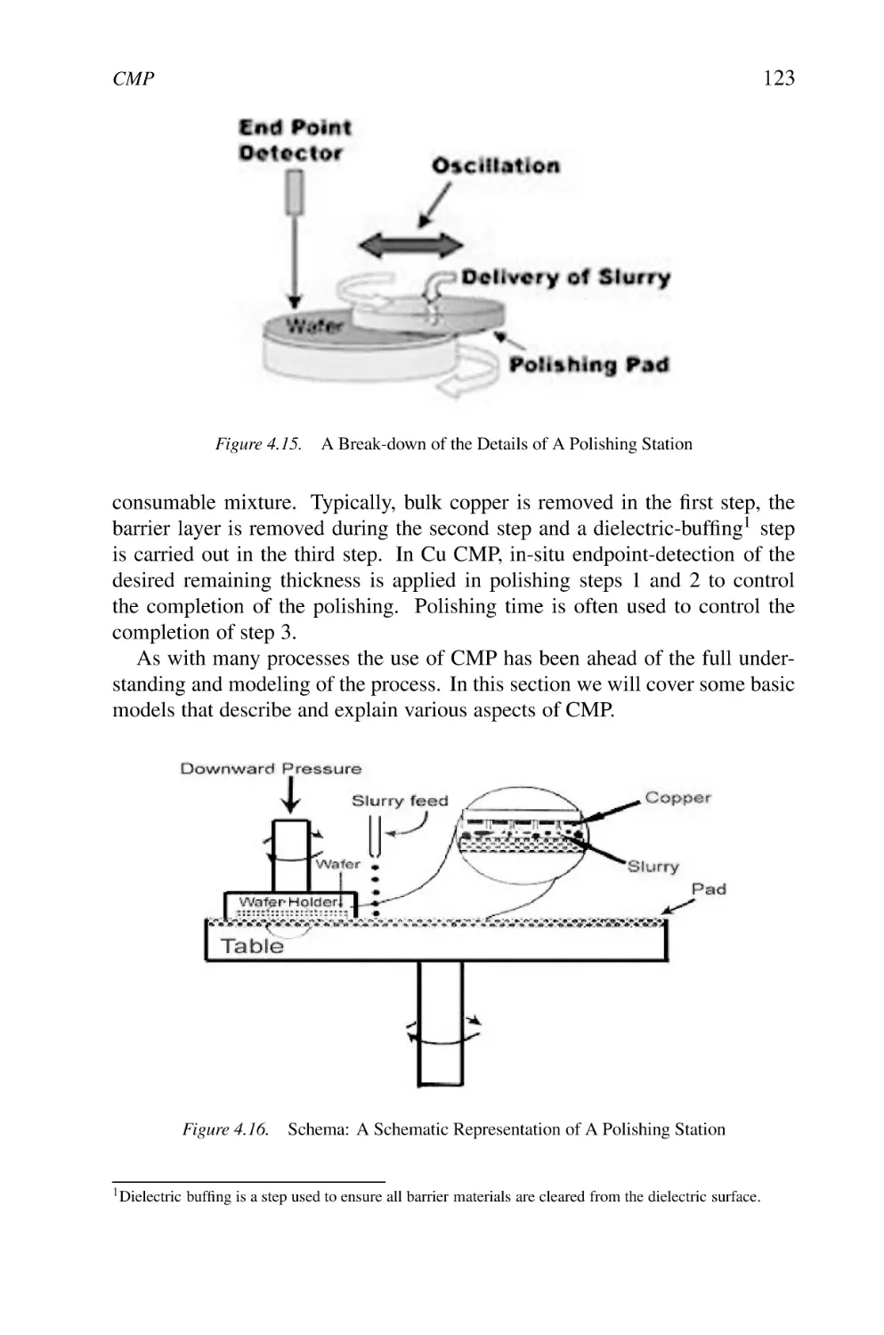
A Break-down of the Details of A Polishing Station
Schema: A Schematic Representation of A Polishing Station
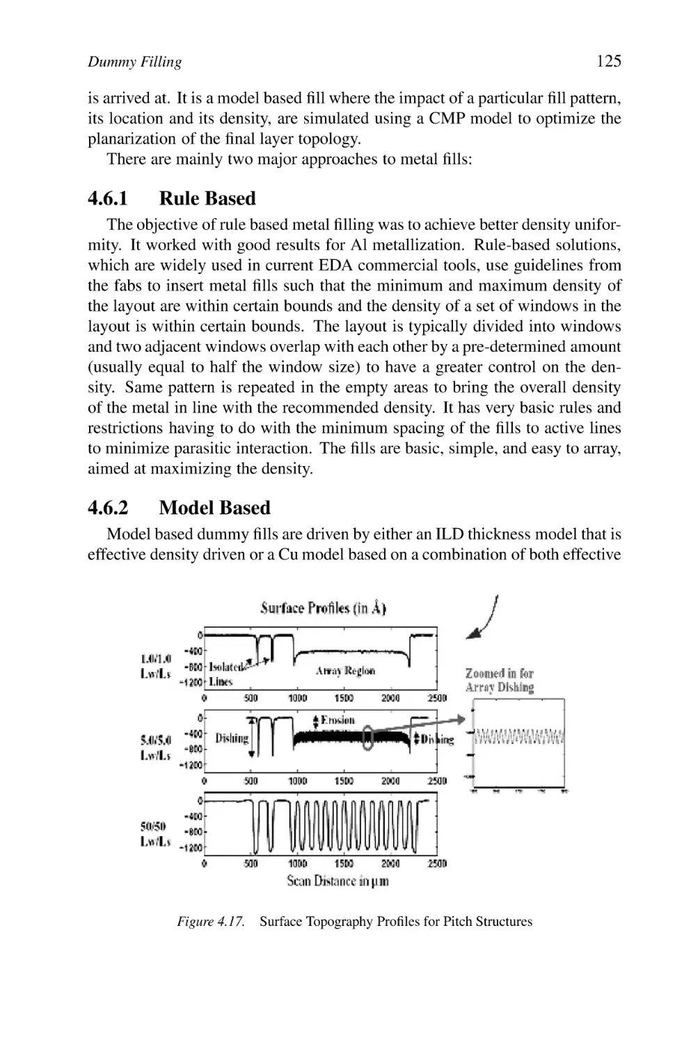
Surface Topography Profiles for Pitch Structures
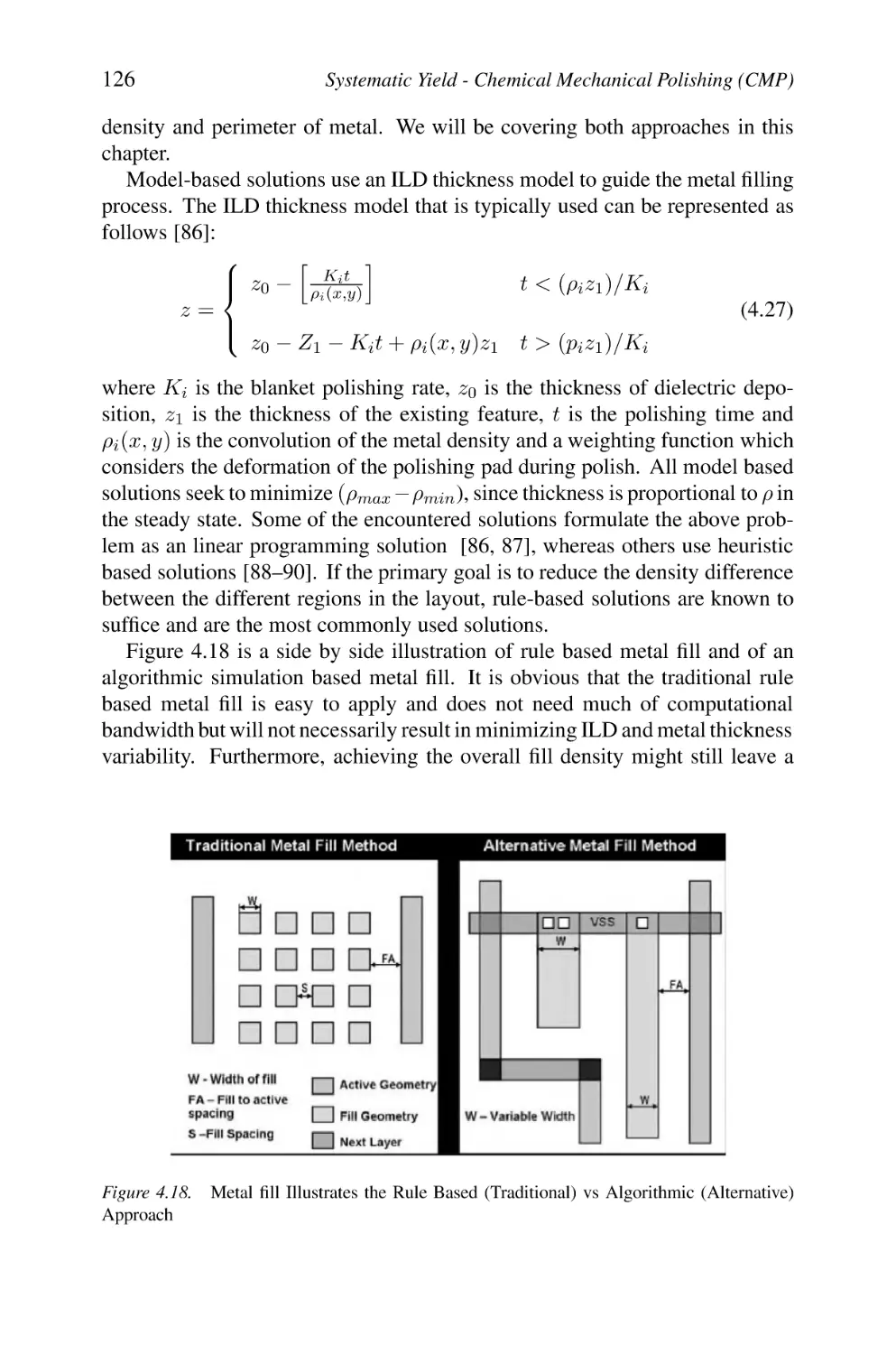
Metal fill Illustrates the Rule Based (Traditional)
vs Algorithmic (Alternative) Approach
Solutions of a Simple 1-D Problem
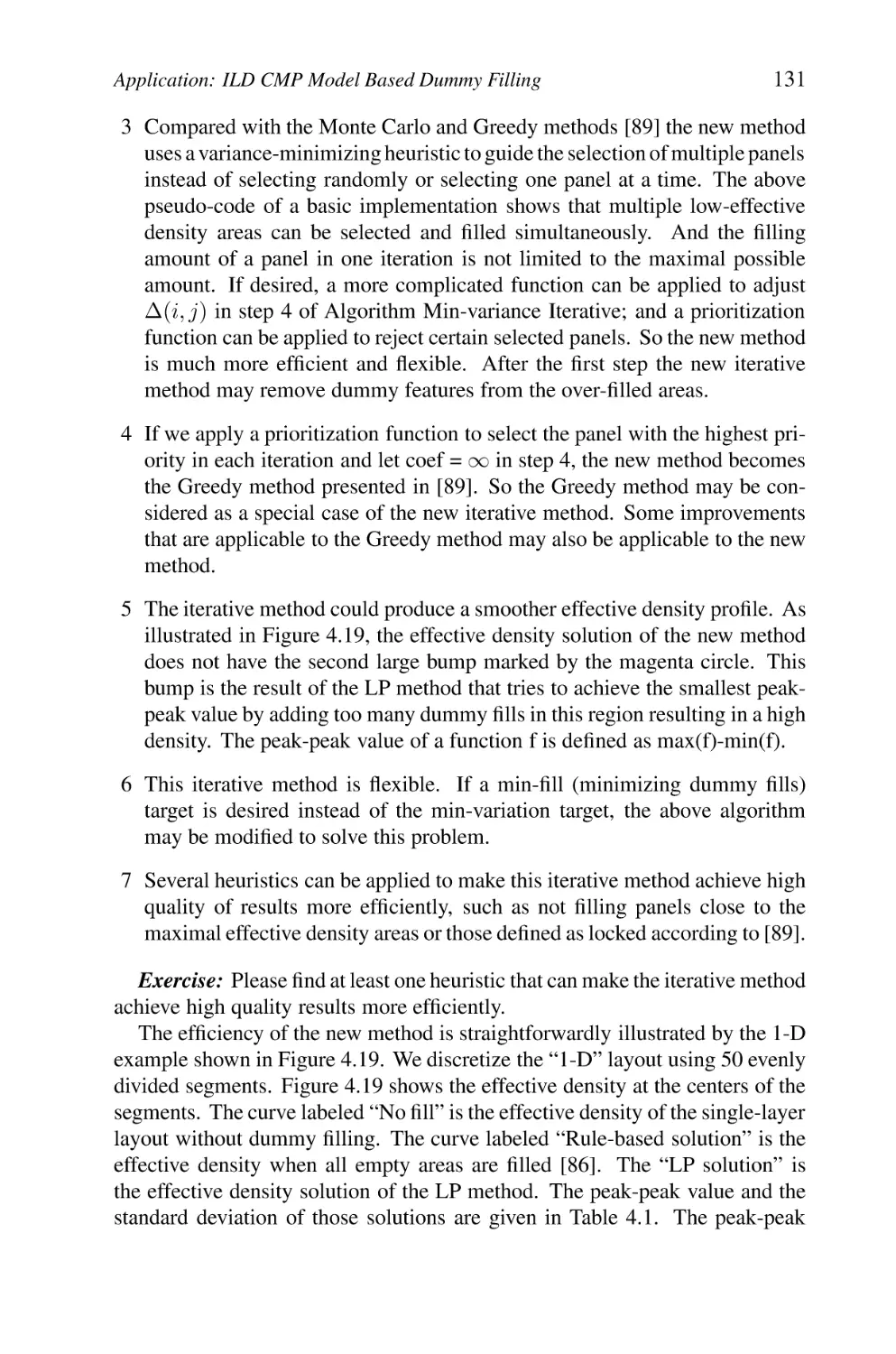
A Specific Case
The Discretization Error of LP
The CPU Time Comparison
The Effective Density of the LP Method
The Effective Density of the New Min-variance
Iterative Method
Topography Results using CMP Simulator
Impact of ECP Thickness Range on Final Thickness Range
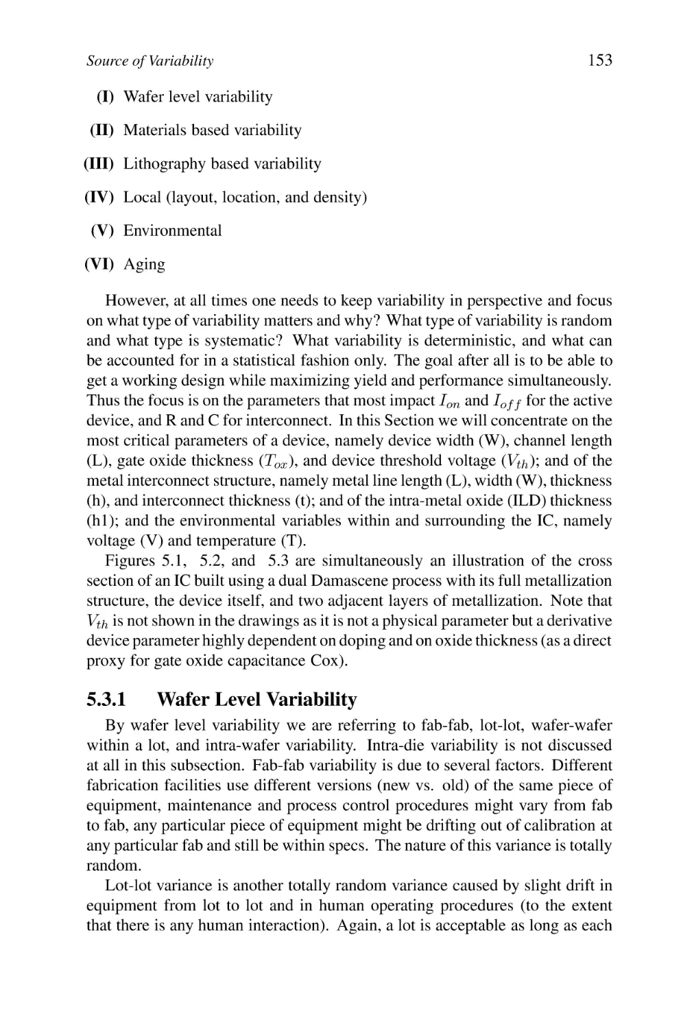
Illustrative Cross Section of a CMOS IC with Metallization
xv
89
90
93
93
95
100
101
103
104
106
107
108
110
112
114
117
118
120
122
123
123
125
126
132
133
136
137
137
138
140
142
154
xvi
List of Figures
5.2
5.3
5.4
5.5
5.6
5.7
5.8
5.9
5.10
5.11
5.12
5.13
5.14
5.15
5.16
5.17
6.1
6.2
6.3
6.4
6.5
6.6
6.7
6.8
6.9
6.10
6.11
6.12
6.13
Planar Cross Section of a CMOS Device Showing Main
Physical Parameters
Illustration of Interconnect Parameters for 2 Layers of Metal
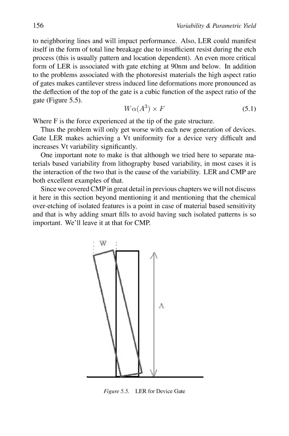
Example of Metal LER
LER for Device Gate
Doping Fluctuations Are Pronounced at 45nm and Beyond
A Scan and Step Lithography System Representation
Die to Die Variability
Ids within Die Variability
Vth within Die Variability
Correlation Length
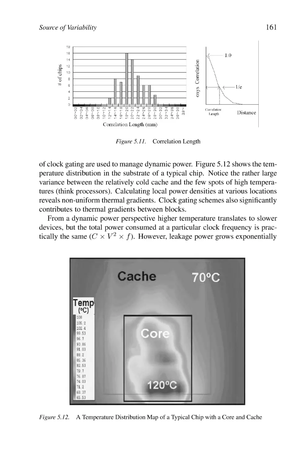
A Temperature Distribution Map of a Typical Chip
with a Core and Cache
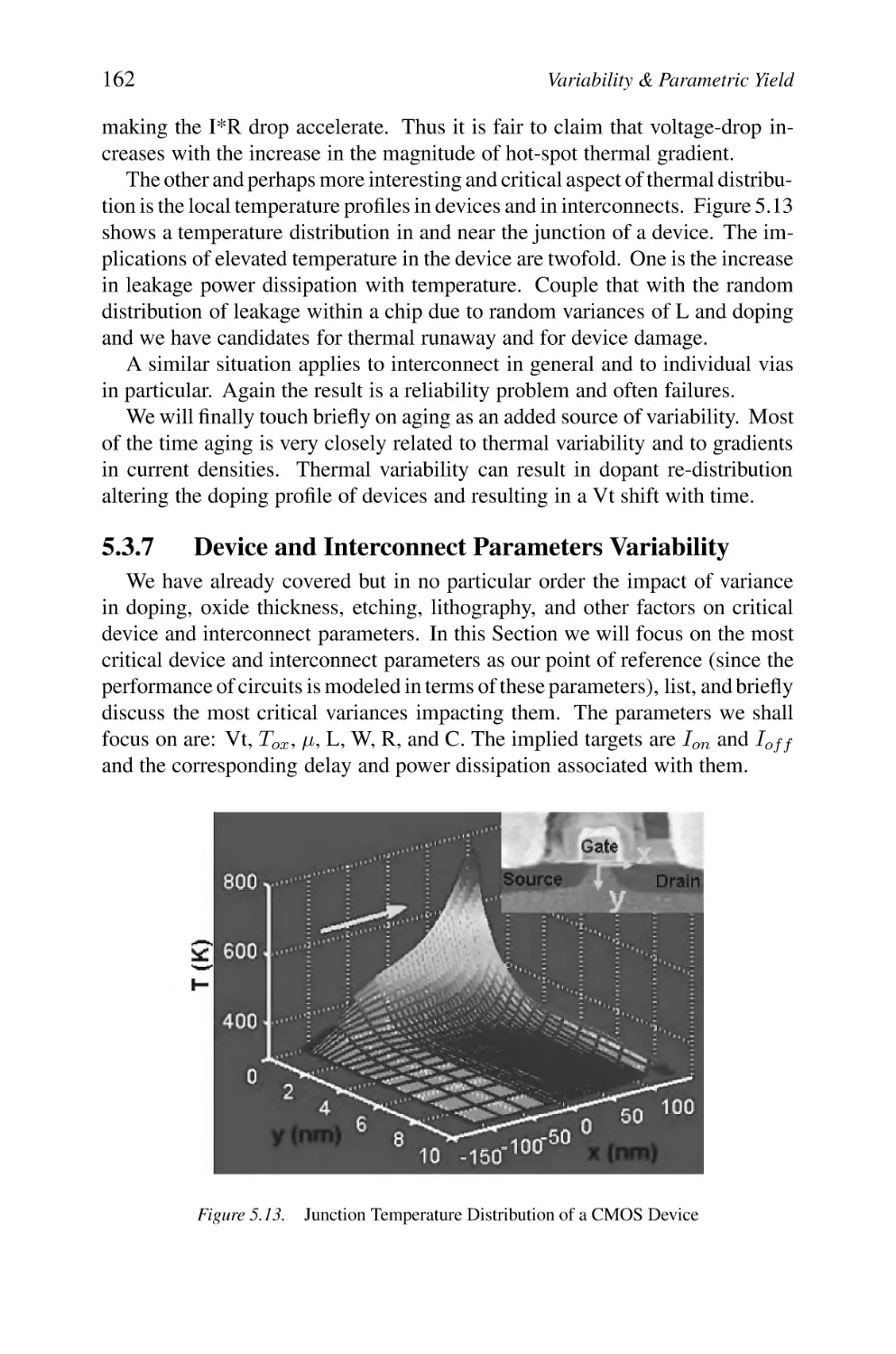
Junction Temperature Distribution of a CMOS Device
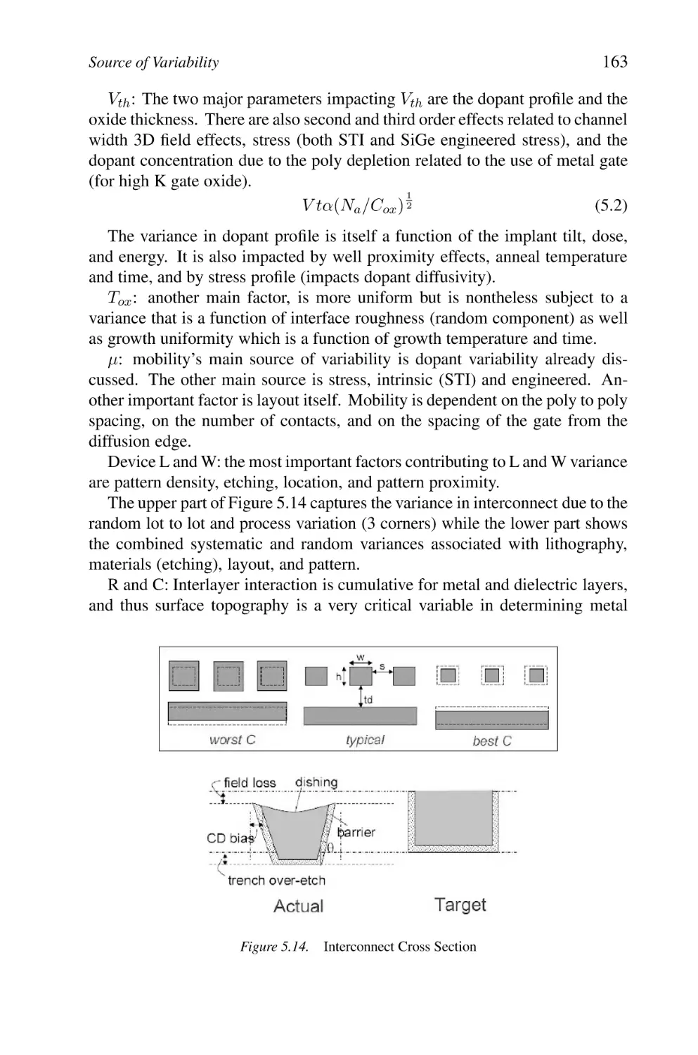
Interconnect Cross Section
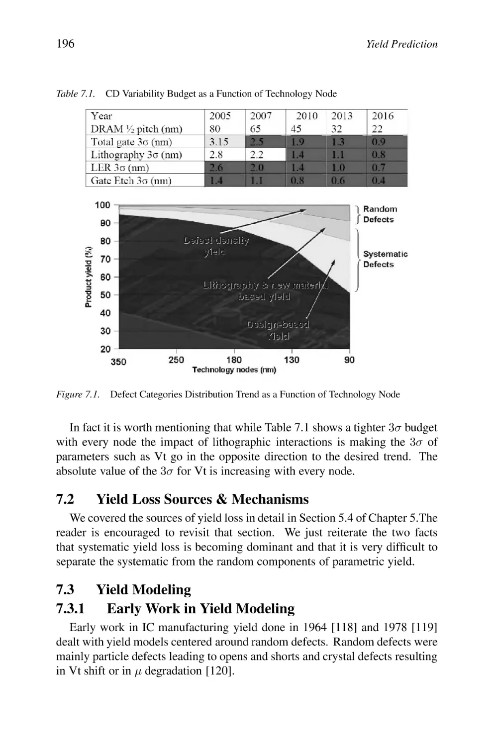
Defect Categories Distribution Trend as a Function
of Technology Node
A Comprehensive Chart of the Sources of Yield Loss
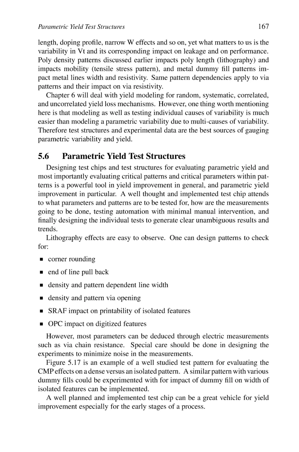
A Well Designed Pattern for CMP Evaluation
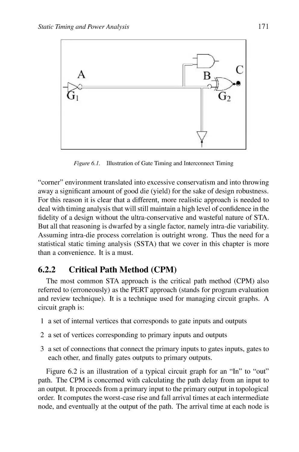
Illustration of Gate Timing and Interconnect Timing
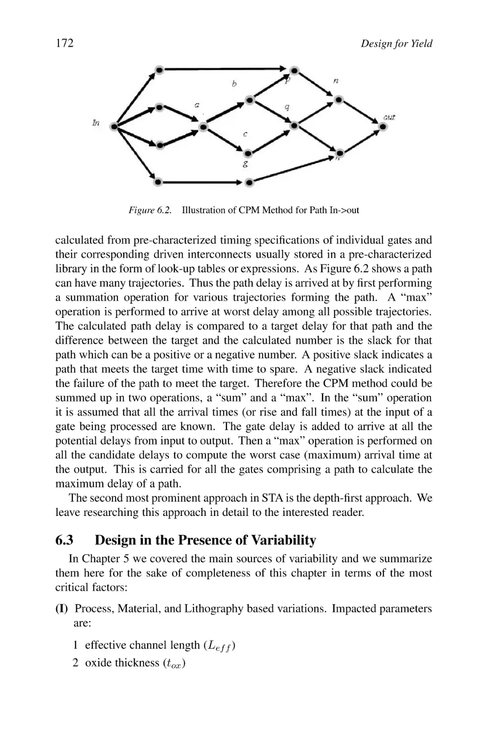
Illustration of CPM Method for Path In->out
Confidence Levels for 1σ, 2σ, and 3σ
for a Normal Distribution
Probability Density Function for a Normal
Distribution Function of a Variable x with μ = 0
for Various Values of σ
Gate and Interconnect Delays Are Represented
as PDFs in SSTA
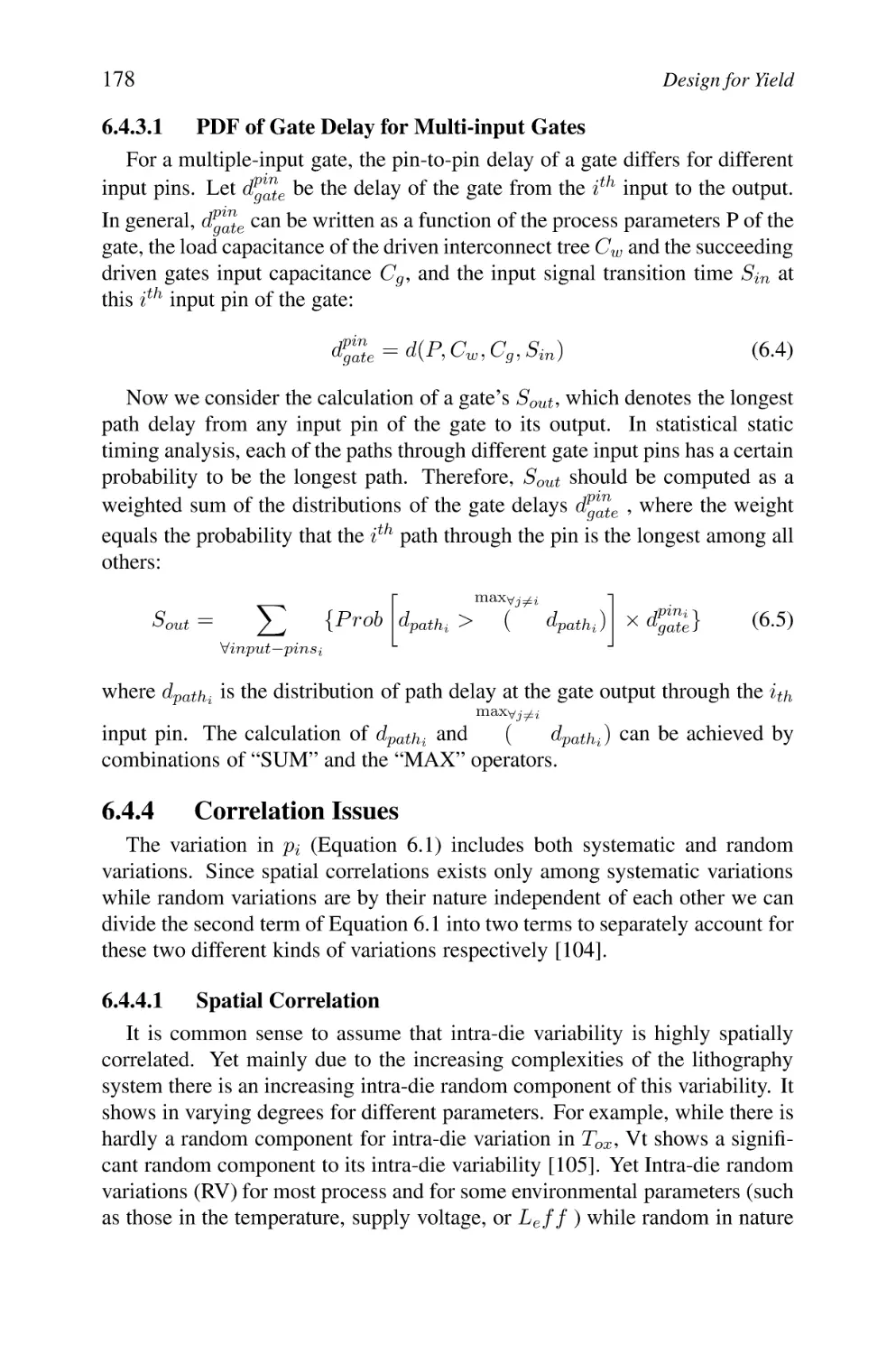
Grid Model of Spatial Correlation
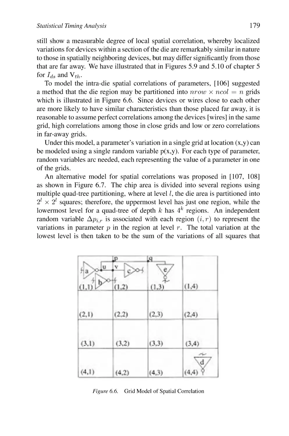
The Quad-tree Model for Spatially Correlated Variations
Illustration of the Computation of (a) Upper and (b) Lower
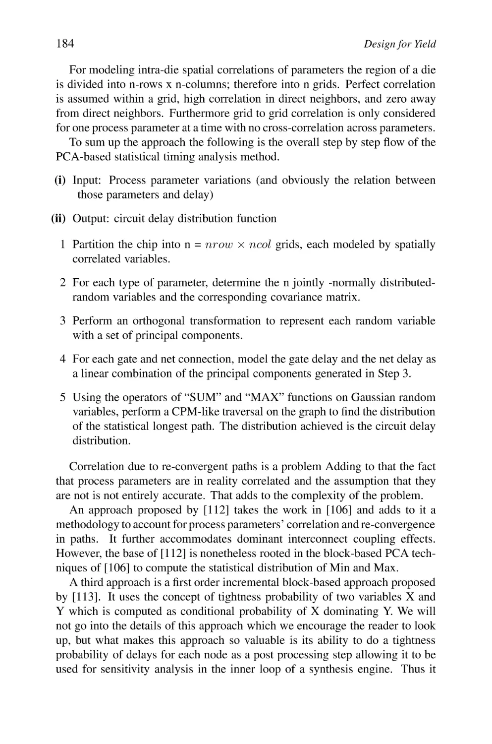
Bounds for the CDF X(t) for Paths a-b-d and a-c-e [3, 4]
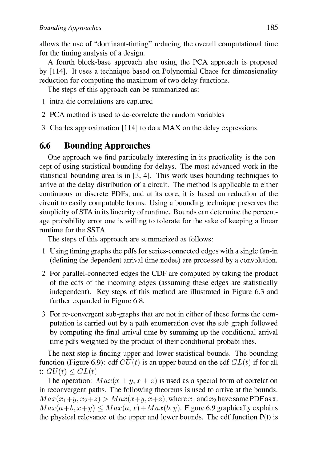
Illustration of Upper and Lower Bound Functions
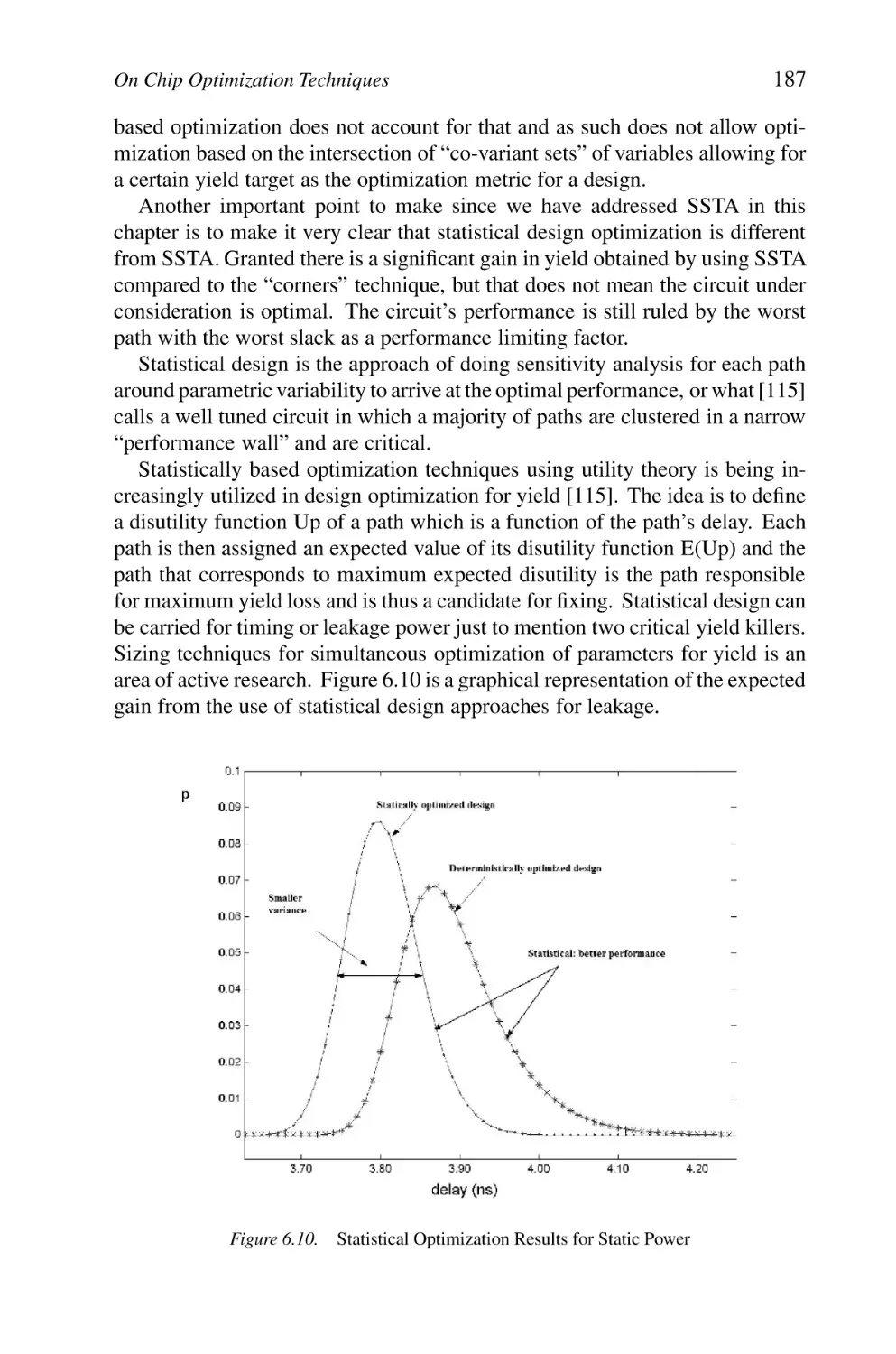
Statistical Optimization Results for Static Power
Statistical Design Optimization Always Superior
to Worst Case
Block Diagram of Body-bias Implementation in [5]
Basic Illustration of Body Bias for P and N Devices
154
155
155
156
157
158
159
160
160
161
161
162
163
164
165
168
171
172
174
174
177
179
180
186
186
187
188
189
190
List of Figures
6.14
6.15
7.1
7.2
7.3
7.4
7.5
7.6
7.7
7.8
7.9
7.10
7.11
7.12
7.13
8.1
8.2
8.3
8.4
8.5
8.6
8.7
8.8
8.9
8.10
8.11
8.12
Block Diagram of a Combination of Adaptive Body Biasing
and Adaptive Voltage Scaling
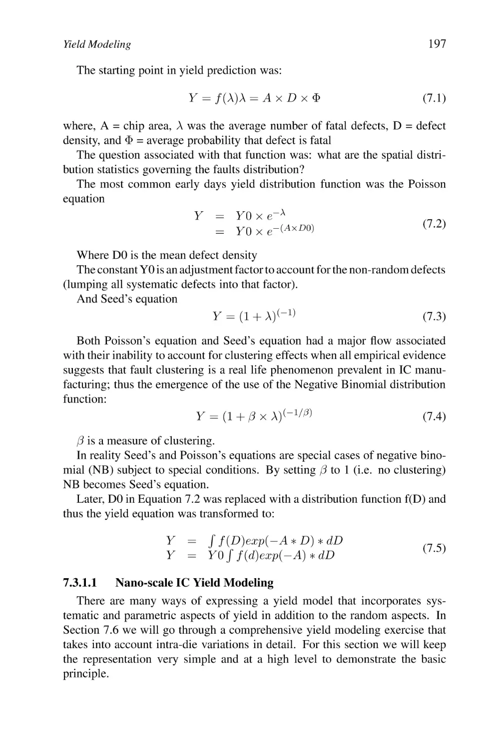
Optimization of Speed and Power Using Both Adaptive Voltage Scaling and Body Bias [5]
Defect Categories Distribution Trend as a Function
of Technology Node
A Simplified Design Flow for Illustration Purposes
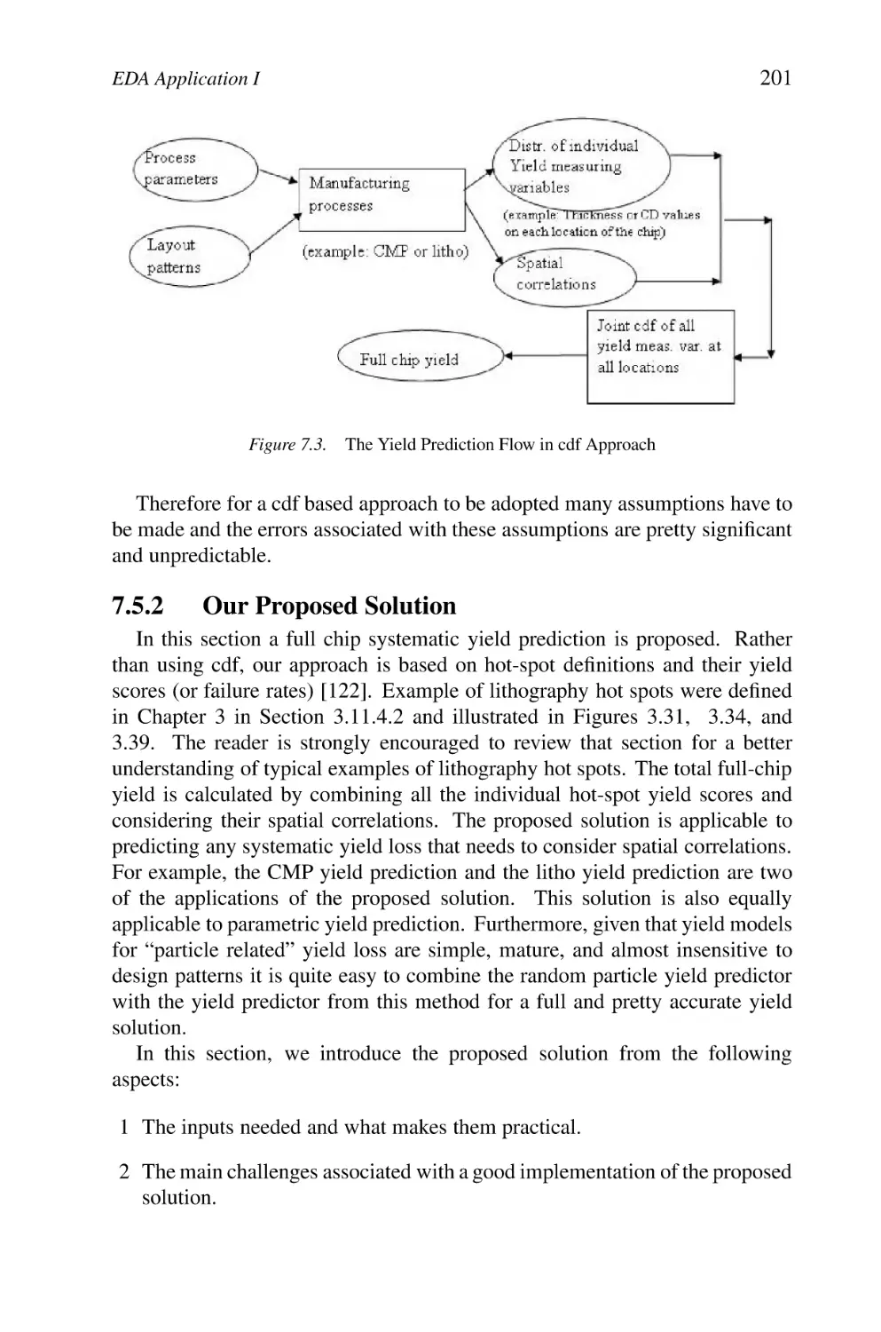
The Yield Prediction Flow in cdf Approach
Derivation of the Transformation “T” for Hot-spot
Yield Scores
Distribution of Yield Measuring Variable and Yield
Score Function
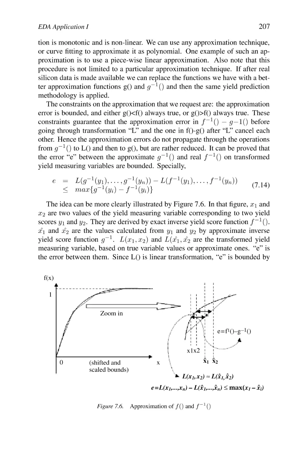
Approximation of f () and f −1 ()
The Complete Flow for Deriving the Transformation “T”
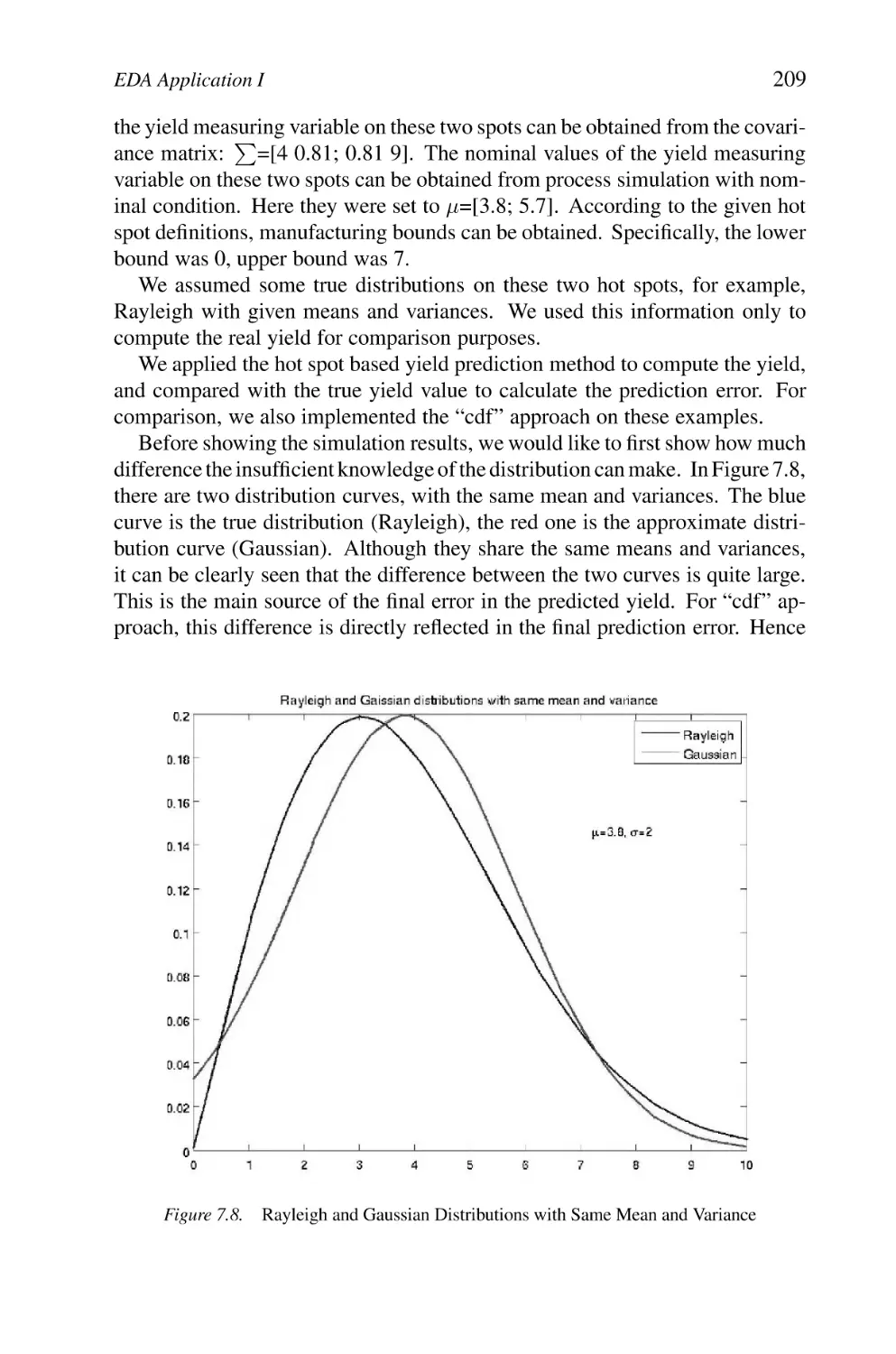
Rayleigh and Gaussian Distributions with Same Mean and
Variance
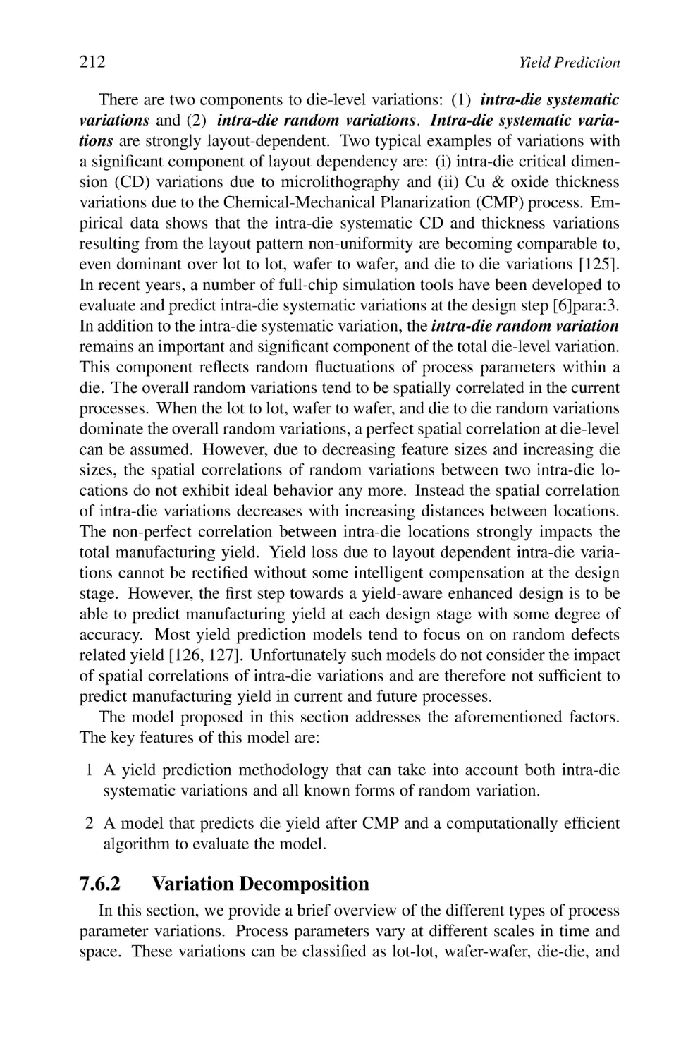
Typical Post-CMP Topography [6]
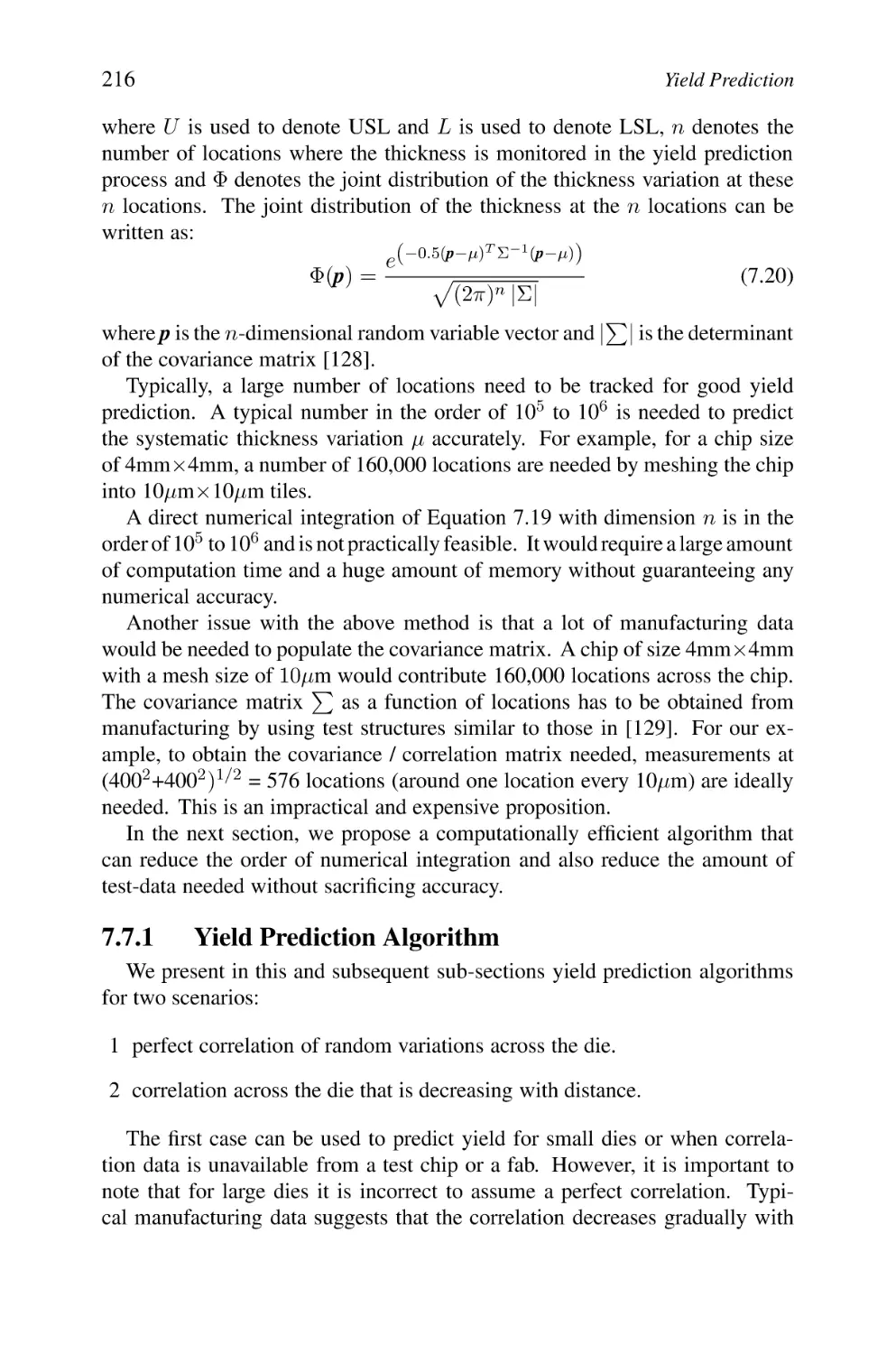
Yield Prediction for The Case of Perfect Across-chip Correlation
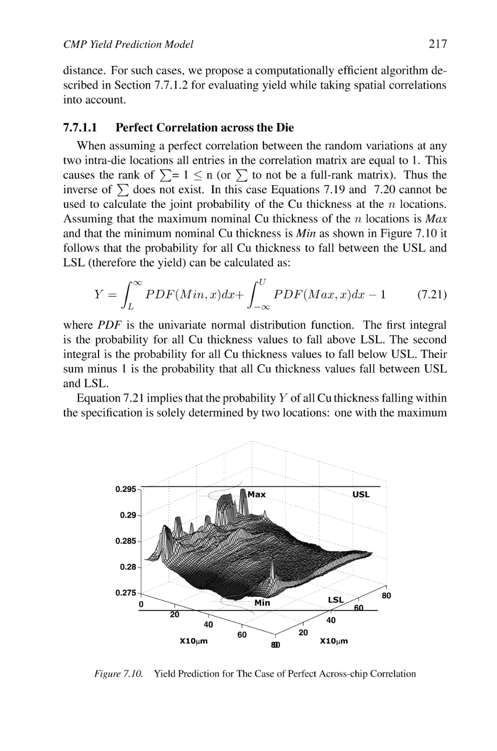
Spatial Correlations of Random Variation as Function of Distances
Perfect Correlation Circles Surrounding Maximum
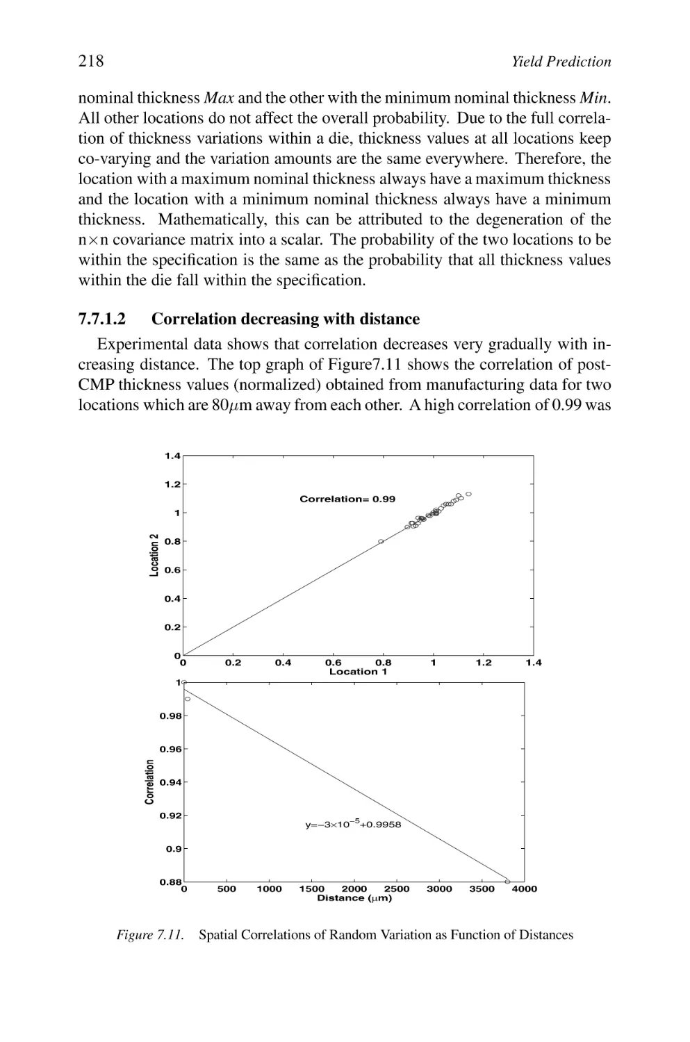
Thickness Values
Flow Chart for Ymax Calculation
A Top-down View of Manufacturability and Yield
Derailing Factors
OPC Alternatives for a Digitized Geometry
An EDA DFM/DFY Centric Design Flow
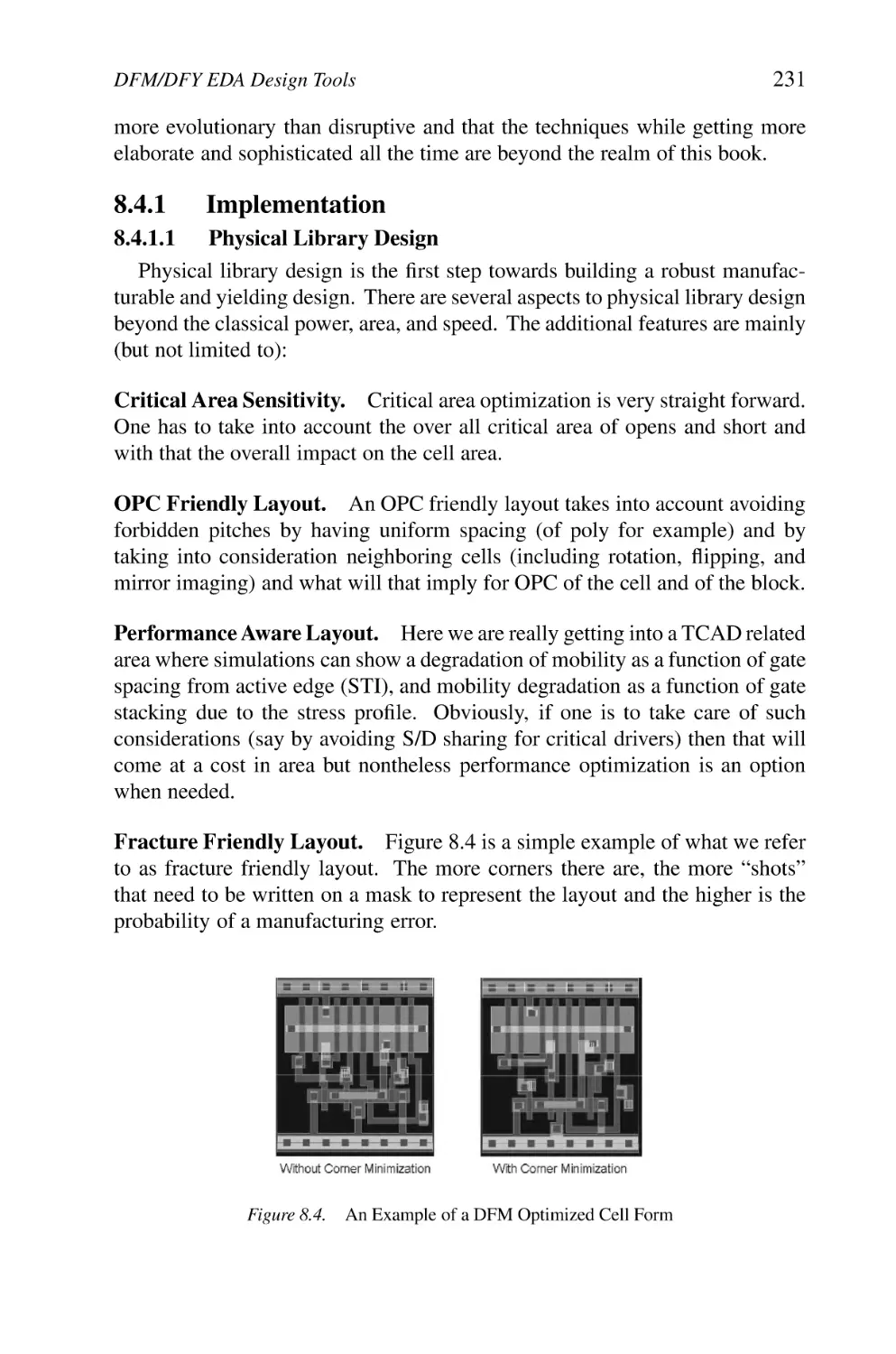
An Example of a DFM Optimized Cell Form
Table of Alternative Implementations of a Cell with Arcs
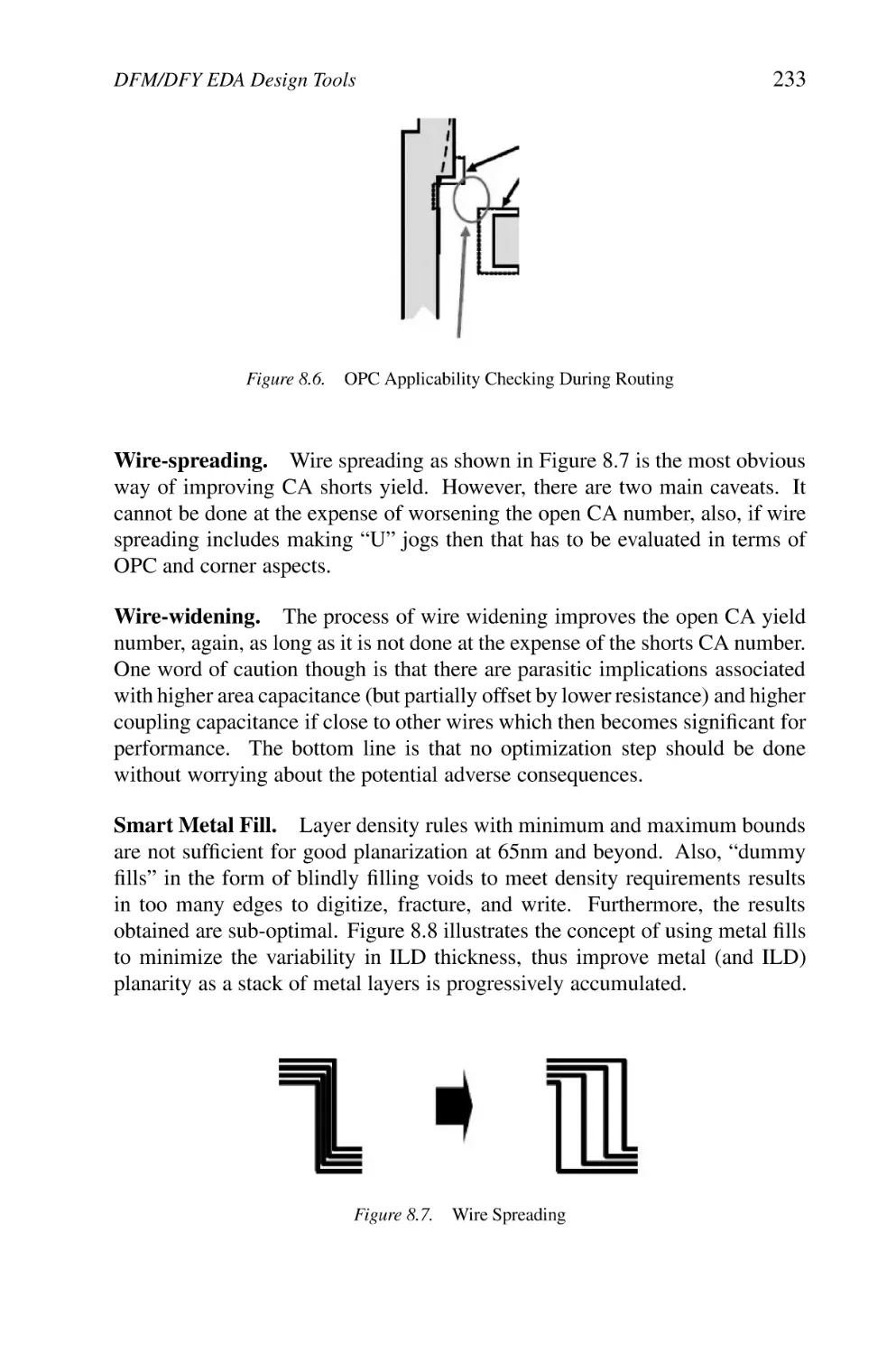
OPC Applicability Checking During Routing
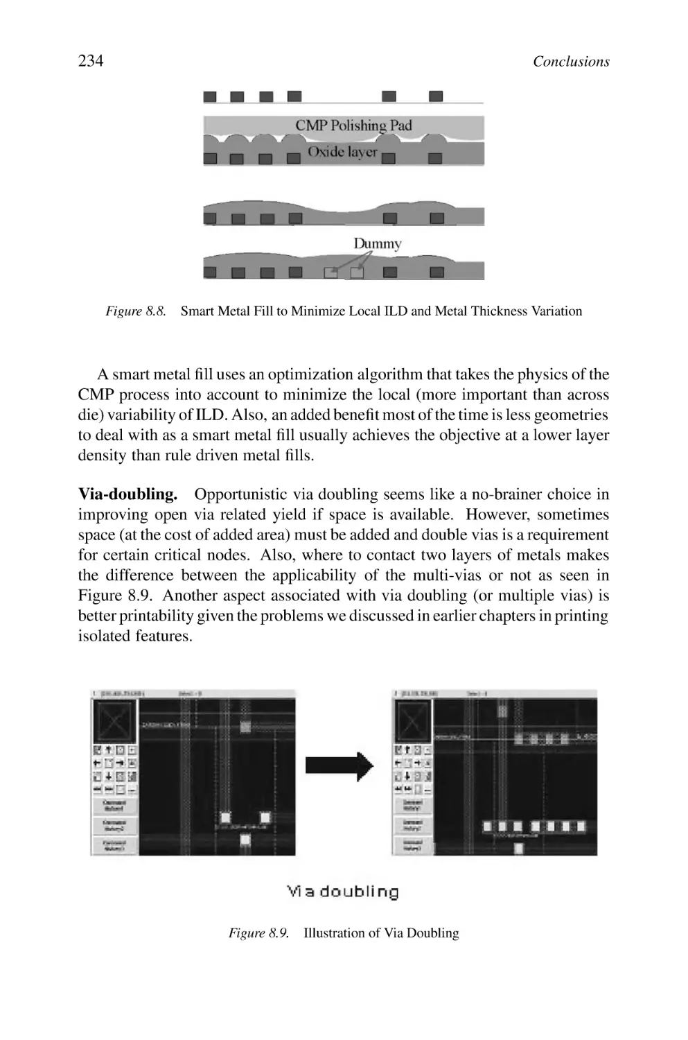
Wire Spreading
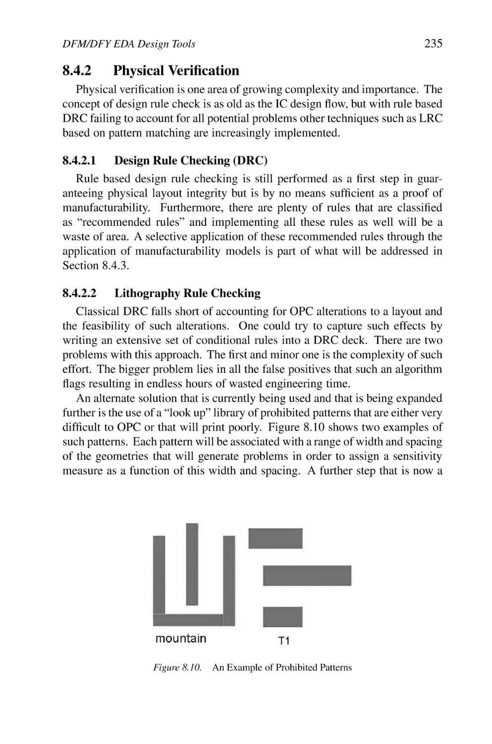
Smart Metal Fill to Minimize Local ILD and Metal Thickness
Variation
Illustration of Via Doubling
An Example of Prohibited Patterns
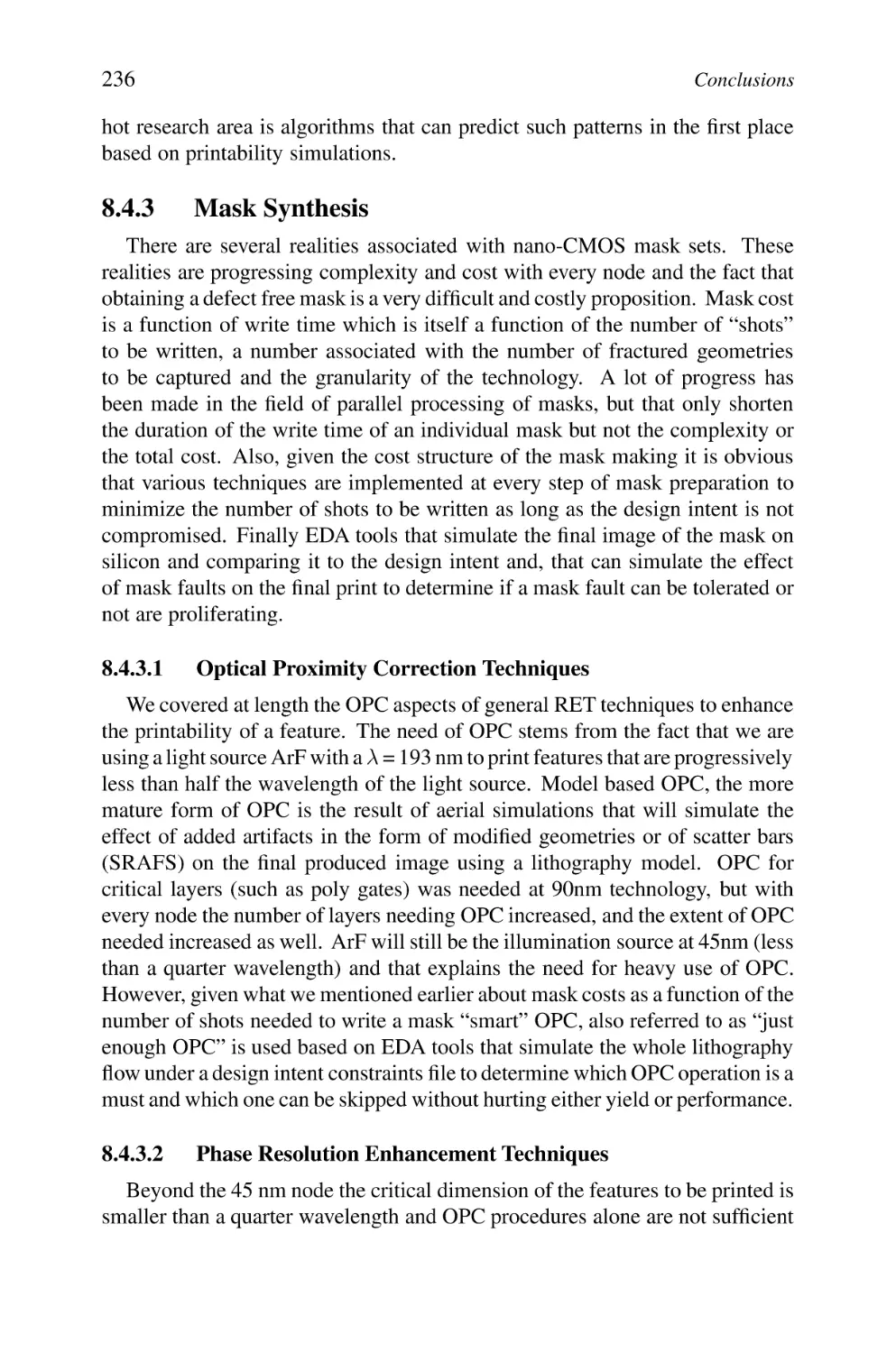
Data Fracturing
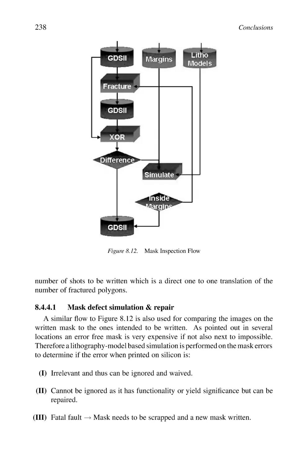
Mask Inspection Flow
xvii
191
192
196
198
201
203
206
207
208
209
215
217
218
220
221
228
229
230
231
232
233
233
234
234
235
237
238
xviii
8.13
8.14
8.15
8.16
List of Figures
Statistical vs Deterministic Design Delay Slack
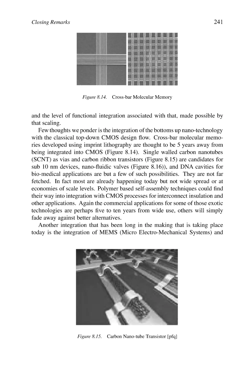
Cross-bar Molecular Memory
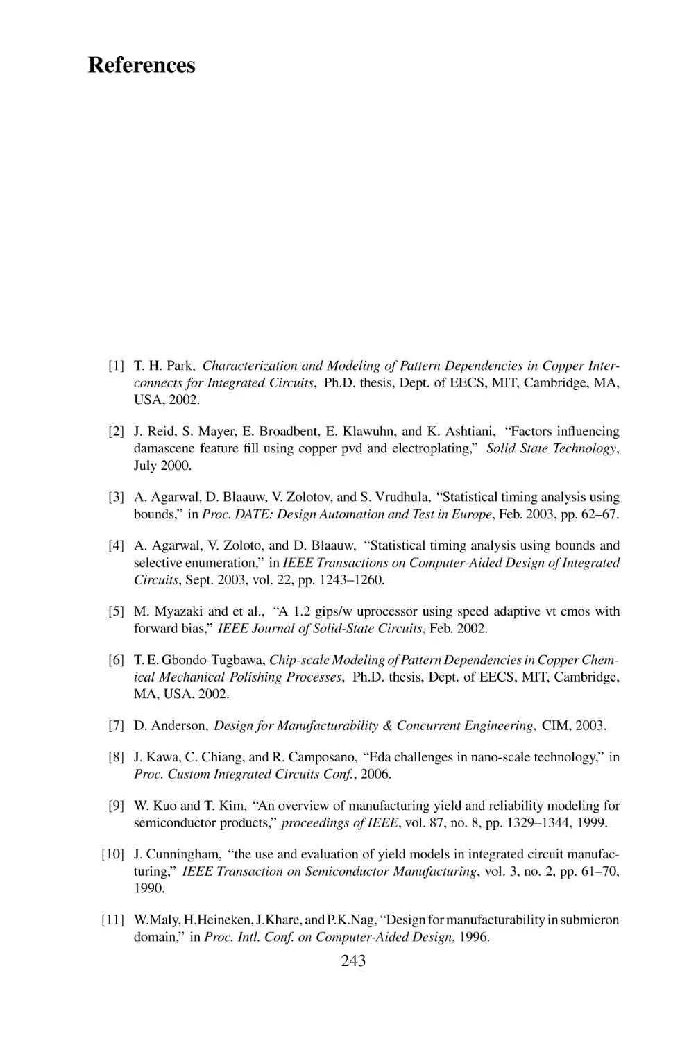
Carbon Nano-tube Transistor [pfq]
Nano-fluidic Valve [xyz]
240
241
241
242
List of Tables
1.1
1.2
1.3
1.4
1.5
1.6
2.1
2.2
2.3
2.4
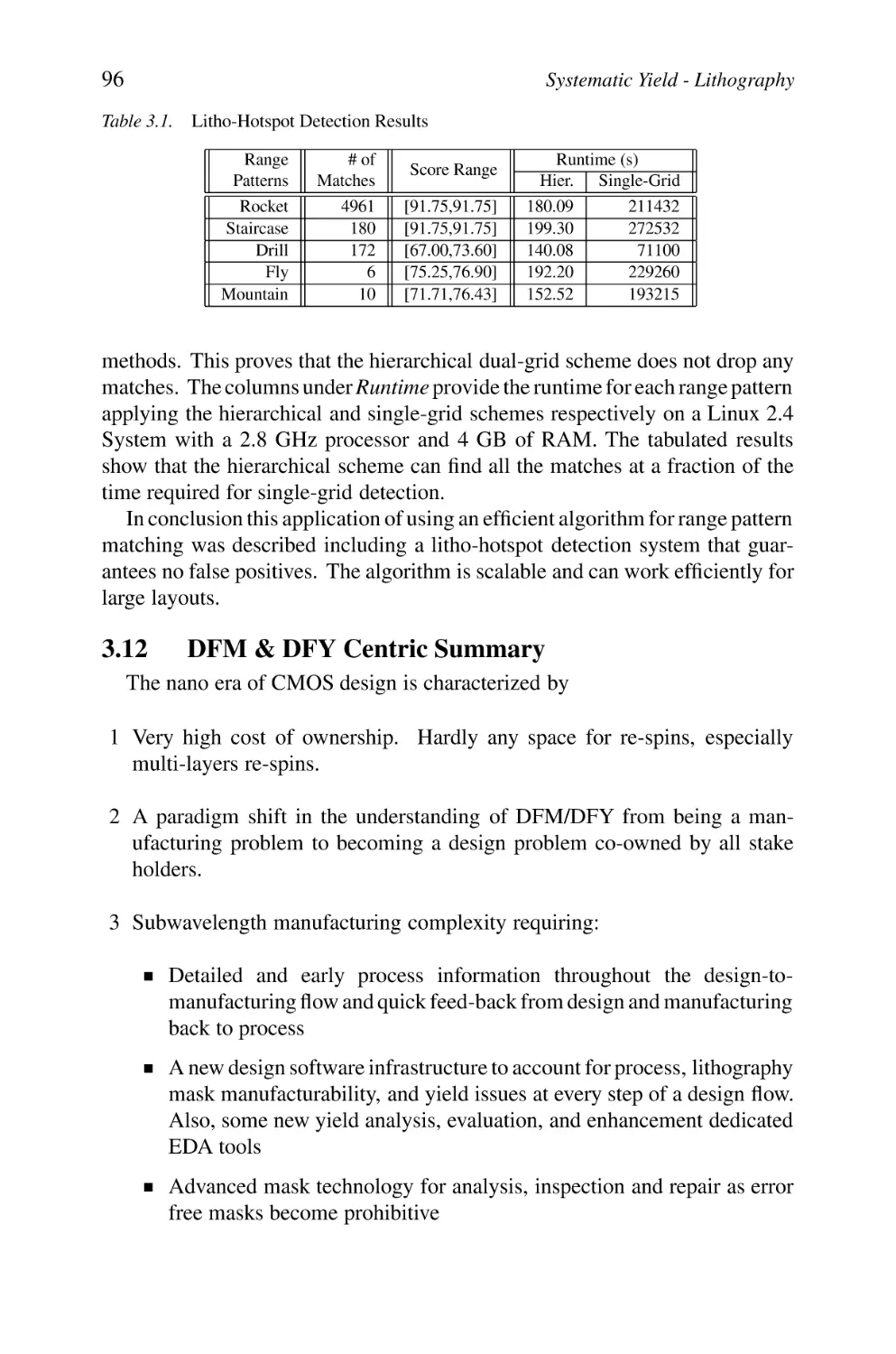
3.1
4.1
4.2
4.3
6.1
7.1
7.2
7.3
Cost of Defect Repair at Every Stage of Production
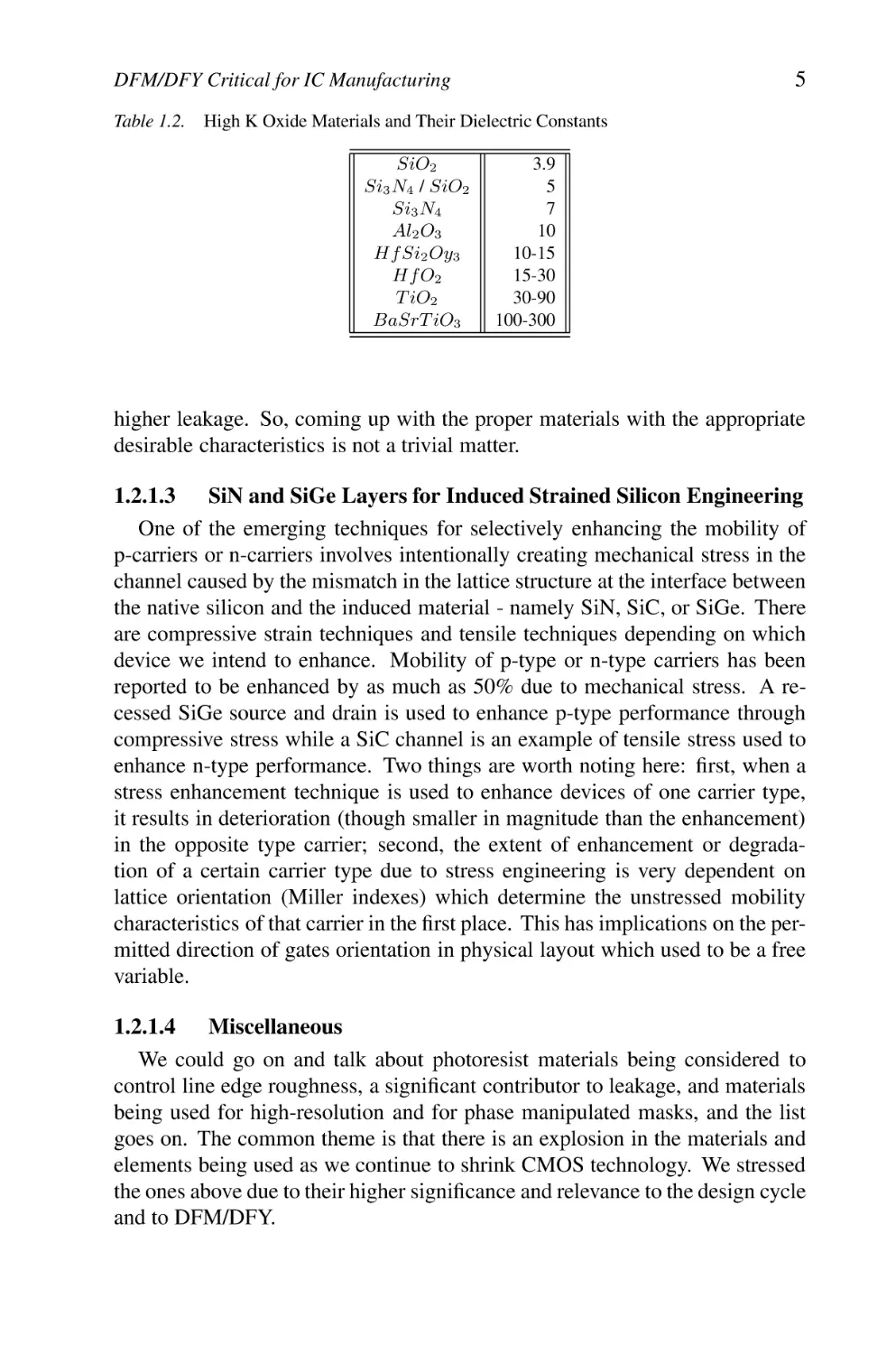
High K Oxide Materials and Their Dielectric Constants
Indicates the k1 , NA Combinations vs Resolution
Light Wavelength Versus the Technology Node
Intra-die Variability Increase with Technology Node
Mask Preparation File Data Size - ITRS 2004
CA Results and Run Time in Shape Expansion Method and
Our Method
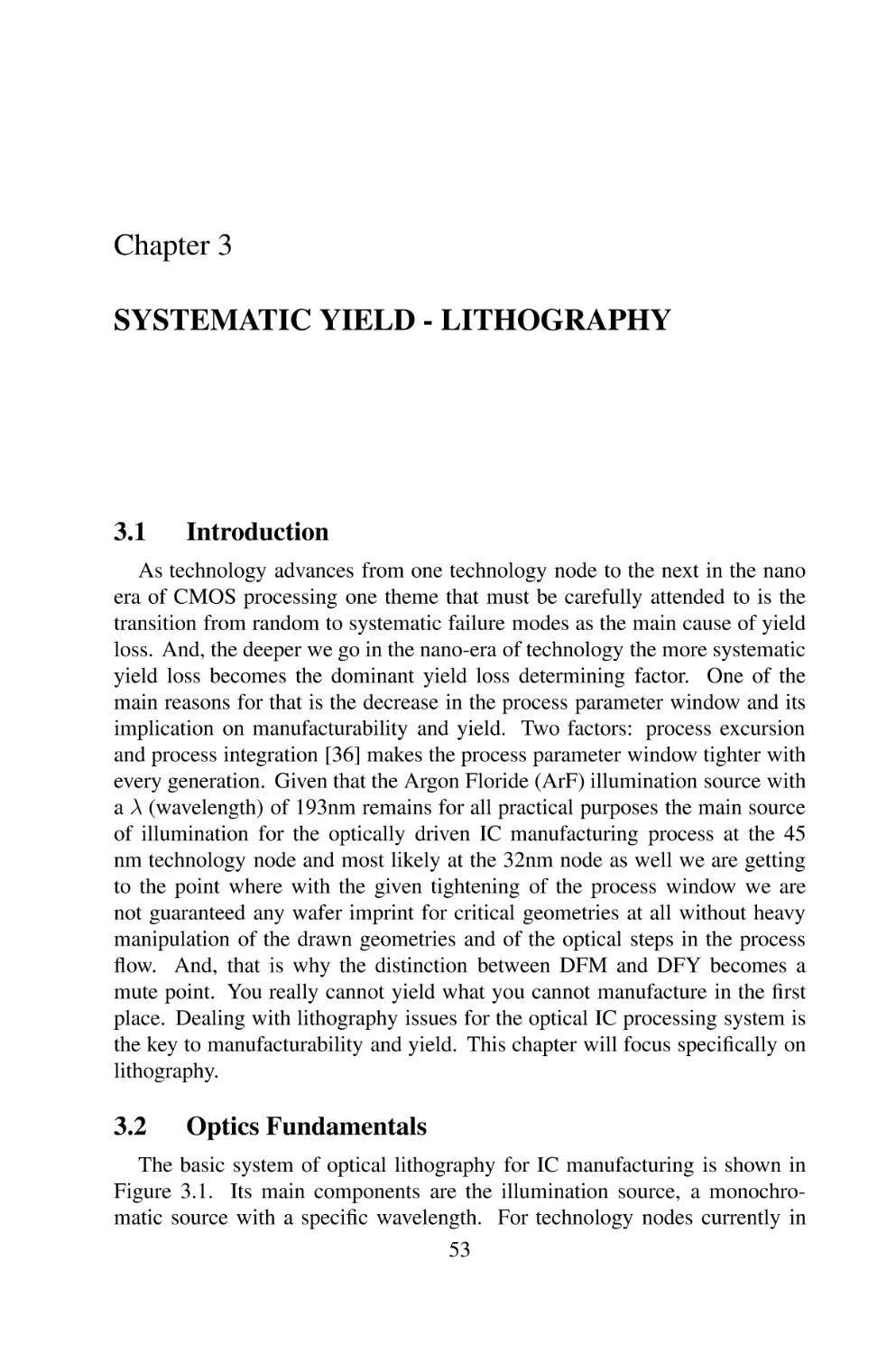
Critical Area Optimization for Shorts
Short, Open, and Total Weighted Critical Area
Reductions Comparison, with w = 0.1
Short, Open, and Total Weighted Critical Area
Reductions Comparison, with w = 10
Litho-Hotspot Detection Results
Peak-peak Value and the Standard Deviation of Effective
Density
Peak-peak Value and the Standard Deviation of Effective
Density
Comparison of Different Metal Filling Results
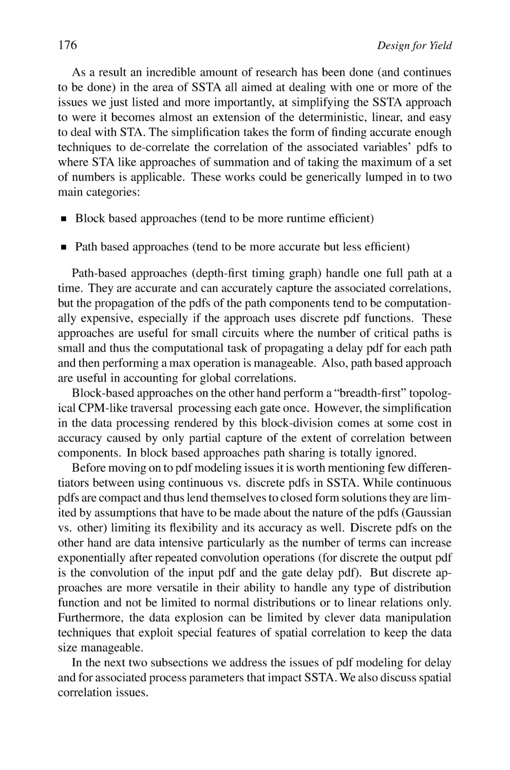
Absolute and Relative Variability of Vt for Successive Technology Nodes
CD Variability Budget as a Function of Technology Node
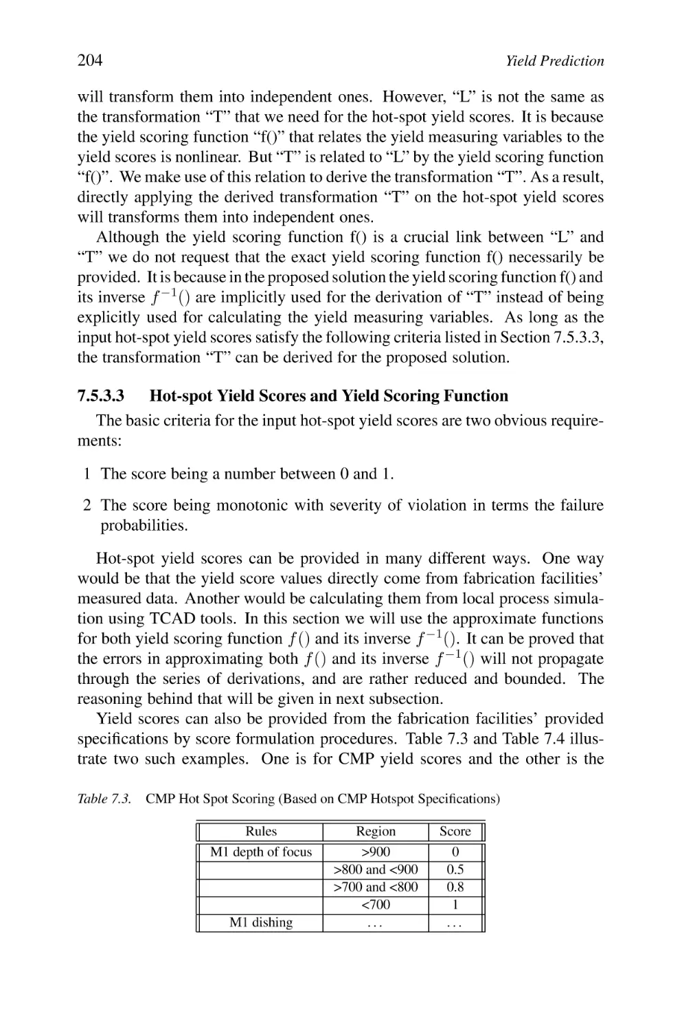
A Possible CMP Hot Spot Specifications for 65nm
CMP Hot Spot Scoring (Based on CMP
Hotspot Specifications)
xix
2
5
7
7
15
15
26
40
49
50
96
132
138
149
173
196
202
204
xx
List of Tables
7.4
7.5
7.6
7.7
7.8
Litho Hot Spot and Score Specifications (Derived from a
Foundry Specs)
Simulation Results for the Case When True Distribution is
Rayleigh (σ1 = 2, σ2 = 3)
Simulation Results for the Case When True Distribution is
Laplace (σ1 =2, σ2 =3; μ1 =3, μ2 =3.5)
Yield Prediction under Different Radii of ‘Perfect
Correlation Circles (PCC)’
Yield Prediction for a Quicker Decrease of the Spatial Correlation
205
210
210
224
225
Preface
For any given industry striving to improve product quality, reliability, and
yield on an ongoing basis is a fundamental task for the simple reason that higher
product quality and reliability translates to higher sales, and higher yield translates to higher profitability. The electronic industry is no exception to that rule.
In fact one of the driving considerations that transitioned the electronics industry from the era of discrete components to the era of the integrated circuit (IC)
was the goal of achieving higher quality and reliability through less components
to handle and assemble, and higher yields through smaller miniature devices.
In this book we will focus on the technical aspects of manufacutrability and
yield as the industry moves well into the nano-era of integrated circuits.
Since the inception of the integrated circuits (IC) industry the manufacturing
process has been based on optical lithography. The process of yield improvement focused on creating a cleaner processing environment (clean rooms) that
reduced the number of particles in the manufacturing area which resulted in a
lower number of random defects and thus higher yields, and on shrinking the
design features that resulted in smaller die areas and thus more dies per wafer.
Those two factors were on a collision course as smaller features meant that a
smaller random particle could cause circuit defects that it did not cause when
the geometries were more relaxed. Thus the requirement for cleaner fabrication facilities (clean rooms) and tighter process controls went hand in hand with
shrinking geometric features.
Needless to say, along the IC progress path following Moore’s law, solutions to challenges of high significance were required from all contributors to
the manufacturing steps - from more accurate steppers, to lenses with larger
numerical apertures, to illumination sources of light with shorter wavelengths,
to mask writers (E-Beams) capable of parallel processing with tighter spot size
and reasonable write time and throughput, to reticles with fewer defects, to
new metal compounds capable of higher current densities, to more advanced
etching materials and procedures, and to highly advanced metrology. And,
xxi
xxii
Preface
with every significant change there was a learning curve that resulted in a step
back in yield until the particularities of each new step were fully understood
and mastered, then yield was back on track and we moved forward. One such
significant change was the use of Copper (Cu) instead of Aluminum (Al) or Al
compounds; low K dielectrics was another such challenge, stacked vias with
high aspect ratios, and the need for super planarization was also another significant challenge. Those four examples were by no means exclusive but were
indeed major steps on the road to the nanometer era in IC manufacturing.
But, the IC optical manufacturing process found itself bumping its head
against limitations rooted in physics that altered the learning curve process
outlined in the last paragraph and called for a dramatically different approach
not just to ensure yield improvement as we continue to shrink features, but to
ensure that the manufacturability of smaller ICs is feasible in the first place.
The IC industry was hitting barriers that threatened an end to the journey of
optical lithography with an unpleasant outcome: zero yield; i.e. end of scalability. Moving from optical lithography to other means (atomic, molecular, self
assembling structures, etc) meant a major discontinuity and a major disruption
in the manufacturing and engineering techniques developed and mastered over
the last fifty years at a staggering investment cost. Needless to say it is worth
mentioning that re-training the design community in an alternative discipline
of design cannot happen overnight either and will be very disruptive in nature
should alternatives to the current manufacturing techniques emerge in short order. Simply put, the momentum of the optical lithography based IC industry is
too strong to alter in such short order.
Optically, light source with a wavelength of 193 nano-meters (nm) was the
end of the path in wavelength reduction with a big gap extending all the way to
the 13nm extreme ultra-violet (EUV) light source. Efforts to develop 157nm
and beyond came to a halt due to delays and to insurmountable technical challenges and we were faced with having to use 193nm light to print sub-90 nm
features- features that are smaller than a half wave-length of the light source
used. This called for a whole set of “engineering tricks” and techniques to
extend the life of the 193nm based lithography. Also, on the materials front,
“bulk” modeling of the behavior of dopant materials has quickly reached the
end of its validity and quantum mechanical behavior of material needed to be
taken into account. Unevenness in dopant distribution became very critical.
Deterministic behavior had to be abandoned and replaced with statistical behavior and bulk properties had to be dealt with quantum mechanically. Single
atomic layer gate oxides raised the need for high K gate dielectric with the challenge of making sure the electric field in the channel is not weakened. Fully
salicided poly and metal gate options are considered to deal with this problem
with a handful of new materials competing as candidates for the high k dielectric. The process of designing low K dielectric materials for intra-metal oxides
Preface
xxiii
to reduce capacitance (improve speed) encountered big challenges in how to
reduce K without increasing leakage. Not to be ignored is the complexity of the
metallurgy and of other aspects of the manufacturing process. Via stacking and
tighter metal pitches made planarization more critical than ever before; smart
dummy fills that improved planarization without hurting the timing of a circuit
became critical.
Thus designing for yield has changed to become designing for manufacturability and yield at the same time. The two go hand in hand - you cannot yield
what you cannot manufacture. Also, faults impacting yield, which were dominated by particles (random defects) are not anymore the major mode of yield loss
in ICs. Systematic variations impacting leakage, timing, and other manufacturing aspects in manufacturing are increasingly becoming the dominant factor;
more so with every new technology node. Furthermore, the random component
of variability which was strictly global in nature (die-die, wafer-wafer, lot-lot)
has a new intra-die component of considerable significance.
In this book we start with a detailed definition of design for yield (DFY) and
design for manufacturability (DFM) followed by a brief historical background
of DFM/DFY where random (particle) defects were dominant and quickly move
to the current challenges in manufacturability and yield and the solutions being
devised to deal with those challenges for every step of a typical design flow.
However, we do not present them in the order of steps in the typical design flow
but in terms of categories that have logical and relational links.
In Chapter 1, after defining DFM/DFY and covering a brief historical perspective we go over why DFM/DFY has become so critical,we go through the
classifications and categories of DFM and discuss what solutions are proposed
for each problem and at what stage of the design flow, and through what tool(s)
is such a problem addressed. We also start creating the logical link between
DFM and DFY. Chapter 1 is a generic overview.
In Chapter 2 we cover a major random component of yield: critical area
(CA), in depth. We discuss various algorithms used in critical area analysis
(CAA) for extracting critical area of a design and evaluate them in terms of
accuracy versus runtime. We cover techniques used in library design and in
place and route that will improve the CA component of yield.
In Chapter 3 we move to define and explain the main systematic components
of yield. We cover lithography in depth, explain the major problems associated
with optical lithography, their root causes, and what remedies can be applied to
solve them. We go over many examples of resolution enhancement techniques
(RET) as it applies to the characteristics of light that we can manipulate in an
effort to reduce the “k1 ” factor of the lithography system namely direction,
amplitude, and phase. We discuss and analyze lithography aspects such as forbidden pitches, non-manufacturable patterns, etc. We discuss at length mask
alternative styles, what problem is each alternative used to solve, their pros and
xxiv
Preface
cons both technical and economical. We discuss mask preparation, generation,
inspection, and repair. Lenses, filters, and illumination technologies are examined. Then we go over a practical design flow and examine what can be done
at the routing stage after the major RET techniques are applied to the layout at
the cell library design stage. We discuss lithography aware routing techniques.
We also address various aspects of lithography rules checking and how it forms
the link between classical design rule check (DRC) and manufacturability.
In Chapter 4 we cover the important planarization procedure of chemical
mechanical polishing (CMP). We describe the process, identify the critical
parameters that define it and the impact of each parameter on the overall planarization procedure. We cover Cu metallurgy, Cu deposition and etching and
the following CMP steps, and address problems such as dishing and how they
are related to the CMP parameters and to the neighboring metal patterns. We
address the effects of the CMP variables and of the metal patterns on thickness
variation in intra-metal insulating layers (ILD) and how that variation in turn
affects manufacturability and yield. We cover the effect of metal patterns and
local metal densities on ILD variation and get to the concept of metal “dummy
fills”. We discuss and analyze rule based versus model based “dummy fills”.
Finally, we address the ILD thickness variation on timing. Impacting parameters including resistance (R) and capacitance (C); and discuss how model based
“smart fills” minimizes R and C variability, simultaneously.
In Chapter 5 we include a comprehensive coverage of variability and of variability’s impact on parametric yield. We discuss the growing significance of
parametric yield in the overall yield picture. We discuss intra-die variability
vs. inter-die variability. We cover the critical process parameters that have the
most significant impact on parametric yield, discuss the sources of variability
for those parameters, and the impact of the variability in each parameter on
parametric yield. We touch on techniques for reducing parametric variability towards improving parametric yield. Coverage of parametric yield in this
chapter is restricted mainly to the variability components of major parameters.
Chapter 6 integrates the knowledge acquired in the previous chapters towards
the concept of design for yield. It stresses techniques to avoid manufacturability
bottlenecks and addresses analysis tools and methodologies for both manufacturability and yield optimization. It introduces and covers statistical timing
analysis and statistical design as more productive and mature alternatives to the
classical case-file design methodologies.
Chapter 7 sums up the contribution of the components of yield- random
and systematic, towards the goals of yield modeling and yield prediction. We
introduce several comprehensive yield models that a designer can use towards
evaluating the overall yield of a design as well as towards enabling the designer
to do a sensitivity analysis in order to evaluate the impact of key parameters
under certain design topologies on yield. Such sensitivity analysis can go a
Preface
xxv
long way towards enhancing yield by avoiding patterns and topologies that
have adverse impact on yield.
Finally, Chapter 8 is a review and summation of all the concepts of DFM &
DFY introduced in this book. It enables the DFM/DFY student or practicing
engineer to regroup in few pages the most important concepts one should keep
in mind when designing for manufacturability and yield.
Charles C. Chiang and Jamil Kawa
Acknowledgments
Dr. Qing Su, Dr. Subarna Sinha, Dr. Jianfeng Luo, and Dr. Xin Wang of
Synopsys, Inc., Mr. Yi Wang and Prof. Xuan Zeng from Fudan University,
Shanghai, for their contribution to the materials presented in this book and Dr.
Subarna Sinha, Dr. Qing Su, and Dr. Min-Chun Tsai of Synopsys, Inc, HuangYu Chen, Tai-Chen Chen, Szu-Jui Chou, Guang-Wan Liao, Chung-Wei Lin,
and Professor Yao-Wen Chang of Taiwan University, Taipei, for their careful
review of the manuscript and their valuable comments
xxvii
Chapter 1
INTRODUCTION
1.1
What is DFM/DFY? Historical Prospective
Design for manufacturability (DFM) in its broad definition stands for the
methodology of ensuring that a product can be manufactured repeatedly, consistently, reliably, and cost effectively by taking all the measures needed for that
goal starting at the concept stage of a design and implementing these measures
throughout the design, manufacturing, and assembly processes. It is a solid
awareness that a product’s quality and yield start at the design stage and are
not simply a manufacturing responsibility. There are two motivations behind
caring for DFM. Both motivations are rooted in maximizing the profit of any
given project; the first is minimizing the cost of the final product of the project,
and the second is minimizing the potential for loss associated with any defective
parts that need to be replaced. In fact a study [7] estimates the cost of fixing
a defective part at anywhere from 10 times to 10,000 times the initial cost of
the part depending on the stage of the product cycle where the part is recalled
(Table 1.1). Arguably, the numbers in Table 1.1 vary widely from product to
product, and from industry to industry, but the trend in the scale of replacement
cost is clear. You simply want to discover and eliminate any potential problem
as close to the beginning of the product cycle as possible, preferably right at
the design simulation and analysis stage.
The concept of DFM has been around for quite some time and has until
recently stood by itself separate from “yield models” which were dedicated
mainly to calculating yield as a function of defect densities. The concept of design for yield (DFY) is on the other hand a relatively new concept that stemmed
from the fact that in the nano era of CMOS it is not sufficient to obey design
rules, e.g., DFM rules, as the resulting yield could still be prohibitively low and
therefore a new set of design procedures (model based) need to be applied to a
design beyond manufacutrability rules to ensure decent yield [8].
1
2
Table 1.1.
Introduction
Cost of Defect Repair at Every Stage of Production
Level of Completion
Part itself
At sub-assembly
At final assembly
At the dealer/distributor
At the customer
Cost to find and repair defect
1X
10X
100X
1,000X
10,000X
Also, in this book we will focus on the DFM for the semiconductor IC industry but we would like to mention outright that all the historical classical concepts
of DFM such as component simplification, standardization, minimization of the
number of modules to be assembled, avoiding tight tolerances, and design robustness still apply in one form or another to the IC industry although DFM
(and DFY) in the IC industry has many particularities that are new and that are
unique to it.
Some early works in DFM and DFY for the IC industry tried to differentiate
between DFM & DFY along the lines that anything rule based is DFM and
anything model based is DFY. We believe the concepts of DFM and DFY have
converged and that it does not make any sense to try to draw any distinction.
Therefore we will use DFM to mean DFM/DFY.
As we mentioned earlier DFM and DFY have always been tied together, in
fact most of the time whenever DFM was discussed, both DFM and DFY were
implied. Yet we recently encounter a special stress in the IC industry on the
concept of DFY and that is really an effort to emphasize the added concept that
yield is no longer a manufacturing issue but a collectively shared issue between
all participants of a production process. It is a statement that the design and
implementation teams hold as much, if not more, responsibility for yield than
does the manufacturing team. In 2004 a study estimated the total financial loss
due to yield in the IC industry at $30 Billion dollars per year. That is why
DFM/DFY is currently the most active area of research in the EDA industry.
1.2
Why is DFM/DFY Becoming Ever so Critical
for IC Manufacturing?
Rarely have so many variables (factors) of a particular design and manufacturing process undergone significant fundamental changes simultaneously
such as what we are witnessing today in the nanometer era of the IC industry.
Further complicating matters in the emergence of structurally novel new devices
(double gate devices, triple gate devices, and FinFETs) and the proliferation of
dedicated sub-processes at every technology node directed toward meeting the
needs of specific applications. Needless to say, the increase in the number of
new variables introduced into the mix of any process renders the probability of
DFM/DFY Critical for IC Manufacturing
3
error due to a fault in any of those variables higher, and thus the need for a meticulous accountability of the impact of each variable on the overall process flow.
In this section we will give a brief introduction to a plurality of those variables.
A more detailed coverage of each variable is left for the body of the book.
1.2.1
New Materials
A quick count of the number of elements of the periodic table used in the IC
industry from its inception until the onset of the nano era of CMOS and that
used or being experimented with as a potential solution to one of the problems
the industry is facing is very revealing. It is not an increase of ten or fifteen
percent but rather a multiple of greater than four. In this section we will focus on
the materials being used for metallurgy, for low K dielectric, high K dielectric,
and engineered mechanical strain materials.
1.2.1.1 Copper
The switch from Aluminum (Al) and aluminum alloys to Copper (Cu) was a
major and fundamental change. Aluminum metallurgy involved the deposition
of aluminum (or aluminum alloy) all over the wafer and then the selective etch
of that aluminum except for the traces forming the metal routes as defined by
metal masks. The move to copper was needed as the wires were getting narrower
and aluminum alloys could no longer deliver the current carrying capabilities
needed by the circuitry. Copper had a higher current carrying capability, but,
it couldn’t be spun and etched the way aluminum could. Copper deposition
is an electroplating procedure that will be described at length when chemical
mechanical polishing (CMP) is discussed in Chapter 4. Metal migration (including open vias) was the main problem with Al but no other major problem
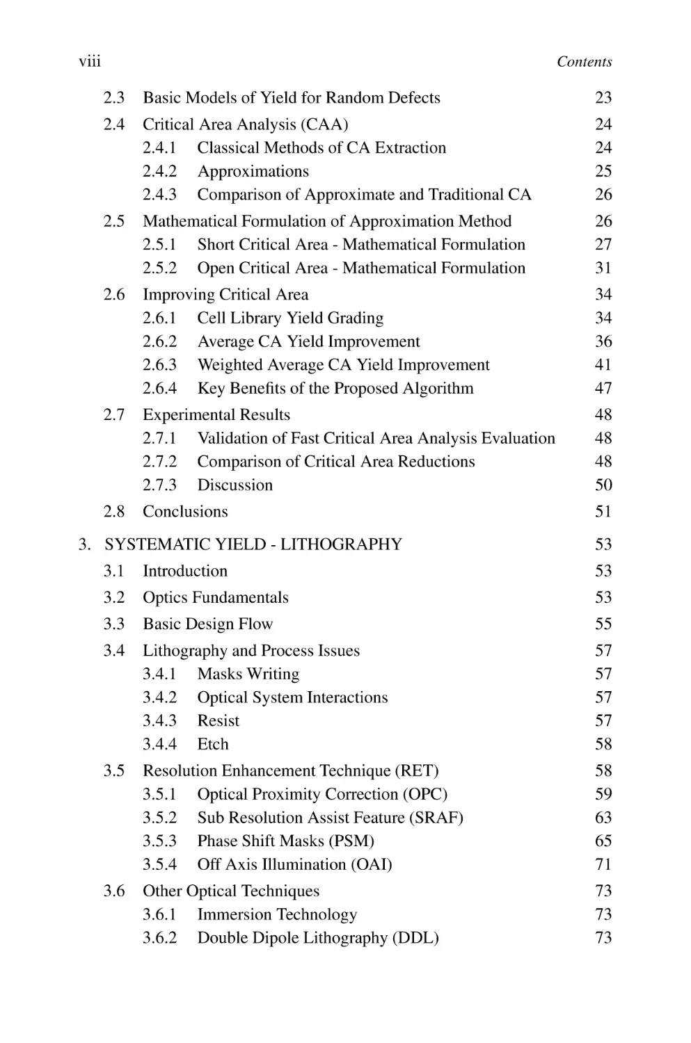
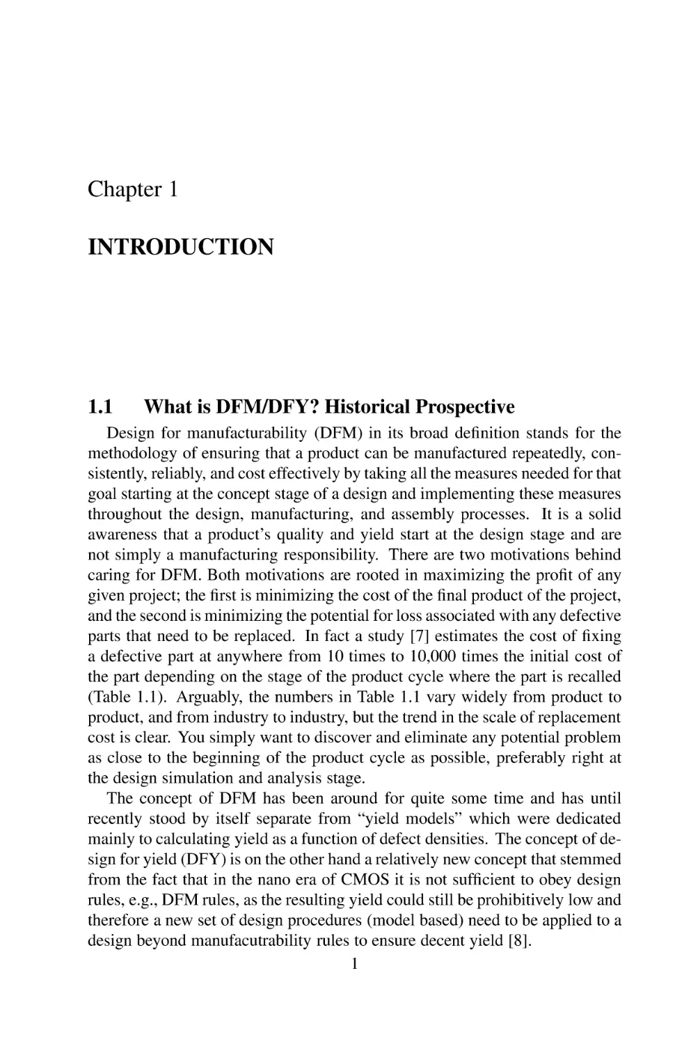
was there. Figure 1.1 shows a typical cross section of a copper metallurgy for
one layer and the slew of problems associated with it from dishing to field oxide
loss, to erosion. Also, given that a typical CMOS process of 90 nm or beyond
has no less than 8 metal layers, planarization of the layers becomes a must.
CMP is used for that, and CMP issues are not trivial. Again it will be discussed
at length in Chapter 4.
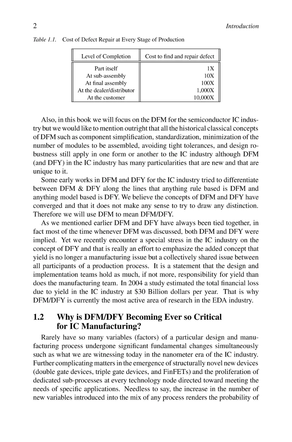
1.2.1.2 Low K and High K Dielectrics
Gate oxide scaling has resulted in gate oxide thickness reaching the limit of
a few mono-atomic layers that is very hard to control. The only way to use
thicker gate oxide and still maintain the proper gate coupling capacitance is to
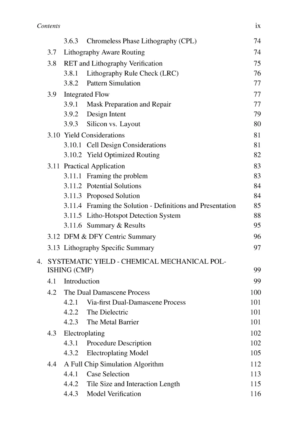
resort to higher dielectric (K) materials. Figure 1.2 shows a simple basic gate
structure.
Cox = K × A/d
(1.1)
4
Introduction
Figure 1.1.
Cu Cross Section Showing Potential Problems
where Cox is the gate capacitance, A is the cross sectional area and d is the
oxide thickness.
An increase in the value of K allows for an unchanged Cox with a larger
value of d. The issue is not as simple as that, as other aspects such as poly
field degradation, etc. calls for additional measures such as the use of metal
gates with their own set of work function matching between the metal gate
and polysilicon related problems. Nonetheless the dominant trend is for higher
K dielectrics for gate oxide. Use of plasma nitrided dielectrics and high K
dielectrics is growing. Table 1.2 lists few of the options being considered for
high K oxides to achieve a variety of dielectric characteristics.
The exact opposite trend applies to inter-metal oxide layers (ILD). There,
a lower K is desired to lower the capacitance of the underlying interconnect
since with the increasing gate count of a typical design and shrinking device
dimensions and supply voltages renders the interconnect delays as the dominant
component of delay in most given critical paths; thus a reduction of C through a
reduction of K is desirable. However, lower K means more porous material, and
Figure 1.2.
Basic Gate Illustration
5
DFM/DFY Critical for IC Manufacturing
Table 1.2.
High K Oxide Materials and Their Dielectric Constants
SiO2
Si3 N4 / SiO2
Si3 N4
Al2 O3
Hf Si2 Oy3
Hf O2
T iO2
BaSrT iO3
3.9
5
7
10
10-15
15-30
30-90
100-300
higher leakage. So, coming up with the proper materials with the appropriate
desirable characteristics is not a trivial matter.
1.2.1.3 SiN and SiGe Layers for Induced Strained Silicon Engineering
One of the emerging techniques for selectively enhancing the mobility of
p-carriers or n-carriers involves intentionally creating mechanical stress in the
channel caused by the mismatch in the lattice structure at the interface between
the native silicon and the induced material - namely SiN, SiC, or SiGe. There
are compressive strain techniques and tensile techniques depending on which
device we intend to enhance. Mobility of p-type or n-type carriers has been
reported to be enhanced by as much as 50% due to mechanical stress. A recessed SiGe source and drain is used to enhance p-type performance through
compressive stress while a SiC channel is an example of tensile stress used to
enhance n-type performance. Two things are worth noting here: first, when a
stress enhancement technique is used to enhance devices of one carrier type,
it results in deterioration (though smaller in magnitude than the enhancement)
in the opposite type carrier; second, the extent of enhancement or degradation of a certain carrier type due to stress engineering is very dependent on
lattice orientation (Miller indexes) which determine the unstressed mobility
characteristics of that carrier in the first place. This has implications on the permitted direction of gates orientation in physical layout which used to be a free
variable.
1.2.1.4 Miscellaneous
We could go on and talk about photoresist materials being considered to
control line edge roughness, a significant contributor to leakage, and materials
being used for high-resolution and for phase manipulated masks, and the list
goes on. The common theme is that there is an explosion in the materials and
elements being used as we continue to shrink CMOS technology. We stressed
the ones above due to their higher significance and relevance to the design cycle
and to DFM/DFY.
6
1.2.2
Introduction
Sub-wavelength Lithography
Sub-wavelength lithography will be covered in depth in Chapter 3, so our coverage of this issue here will be brief and will focus mainly on the chronological
turning points in lithography and their impact on yield and manufacturability.
1.2.2.1 Some Basic Equations
Let us start by citing four characteristics of light that will guide our work
in lithography related matters through the book. Light has wave properties
namely wavelength, direction, amplitude, and phase. All lithography manipulation schemes revolve around manipulating one of those four characteristics.
But, before addressing any issues impacting lithography it is useful to review
some basic optical fundamentals. One such basic fundamental is that photoresist reacts to a threshold of light intensity (energy) and not to the wave shape
nor its phase. We will need this fact later when we explain resolution enhancement through the use of phase-shift and others technologies. The other two
fundamentals we would like to address briefly here are the two equations that
describe the relation between resolution and depth of focus, the parameters of
light wavelength, and the lens numerical aperture.
First is Rayleigh’s equation for resolution
R = k1 × λ/N A
(1.2)
where R = resolution = minimum feature, k1 = resolution constant, λ = wavelength of the light source, NA = numerical aperture which is a function of the
lens and of the refraction index of the medium between the wafer and the lens
of the contact aligner.
Depth of Focus (DOF):
DOF = k2 × λ/N A2
(1.3)
where DOF is defined as the range of items in focus in an image and λ =
wavelength of the light source.
At this point we want to bring into attention few implications of the above
two equations. The necessity of using the 193nm light source for the 45nm
technology node implies an effort to increase NA and to reduce k1 . While resolution improves with higher NA, DOF suffers at a squared rate of the increase
in NA. The other point is that as k1 is reduced to very low values (0.25) to
meet the need of 45nm the proximity interaction effects of neighboring geometries increases complicating things further (we will not cover here the factors
impacting k1 ).
Table 1.3 before indicates the typical combination of NA and k1 needed to
meet technology requirements for 193 nm light source.
7
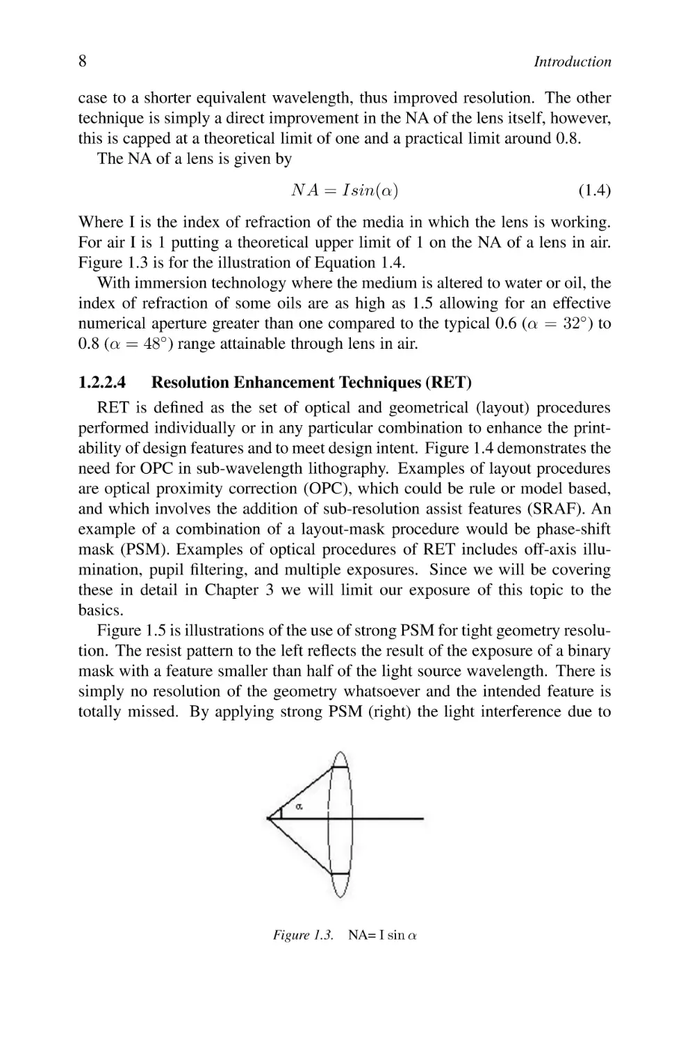
DFM/DFY Critical for IC Manufacturing
Table 1.3.
Indicates the k1 , NA Combinations vs Resolution
Light source λ
193nm
193nm
193nm
193nm
193nm
193nm
193nm
193nm
NA
0.6
.75
.85
1
1.1
1.1
1.2
1.3
k1
0.4
.35
.4
.34
.37
.25
.27
.3
Resolution
130nm
90nm
90nm
65nm
65nm
45nm
45nm
45nm
Again, this topic will be covered at length in Chapter 3, but it important
to note that as k1 values drop below .4 heavy use of resolution enhancement
techniques (RET) are needed to achieve any acceptable printability.
1.2.2.2 Light Sources
Table 1.4 shows the wavelength of the light source used versus the technology
node processed using that source light. We obviously skipped many technology
nodes but the point we wanted to stress here is that past the 130nm technology
node the critical dimension (CD) of the featured technology is significantly less
than half of the wavelength (λ) of the light source used in the lithography.
It is also significant to mention that efforts to develop a 157 nm illumination
source has been all but abandoned in 2005 due to vast technical difficulties
associated with the mask and photoresist technologies needed to go along with
that light source. There is practically no serious candidate for a lithography light
source beyond the ArF (Argon Floride) 193nm light source until the extreme
ultra violet (EUV) light source with a wavelength of 13 nm. A lot of progress
in the development of the EUV illumination source has been reported in the last
several years with two “alpha” EUV systems installed in the year 2006 but any
serious deployment of that source for full production is still many years away
at best estimate.
1.2.2.3 Lens Technology
As Rayleigh’s equation (Equation 1.2) indicates a higher NA leads to an
improved resolution limit. One of the techniques successfully used to improve
the NA of the lens projection medium has been immersion technology where a
drop of fluid is introduced between the lens and the exposed wafer. The change
in the index of refraction in which the light source travels translates in this
Table 1.4.
Light Wavelength Versus the Technology Node
Light source λ
Technology node
436nm
3,000nm
365nm
600nm
248nm
130nm
193nm
90nm
193nm
65nm
8
Introduction
case to a shorter equivalent wavelength, thus improved resolution. The other
technique is simply a direct improvement in the NA of the lens itself, however,
this is capped at a theoretical limit of one and a practical limit around 0.8.
The NA of a lens is given by
N A = Isin(α)
(1.4)
Where I is the index of refraction of the media in which the lens is working.
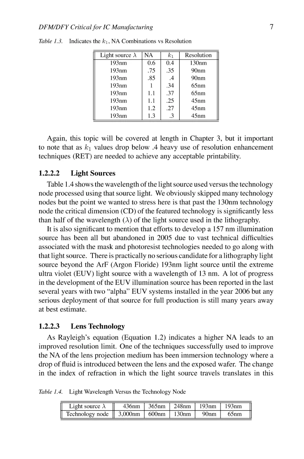
For air I is 1 putting a theoretical upper limit of 1 on the NA of a lens in air.
Figure 1.3 is for the illustration of Equation 1.4.
With immersion technology where the medium is altered to water or oil, the
index of refraction of some oils are as high as 1.5 allowing for an effective
numerical aperture greater than one compared to the typical 0.6 (α = 32◦ ) to
0.8 (α = 48◦ ) range attainable through lens in air.
1.2.2.4 Resolution Enhancement Techniques (RET)
RET is defined as the set of optical and geometrical (layout) procedures
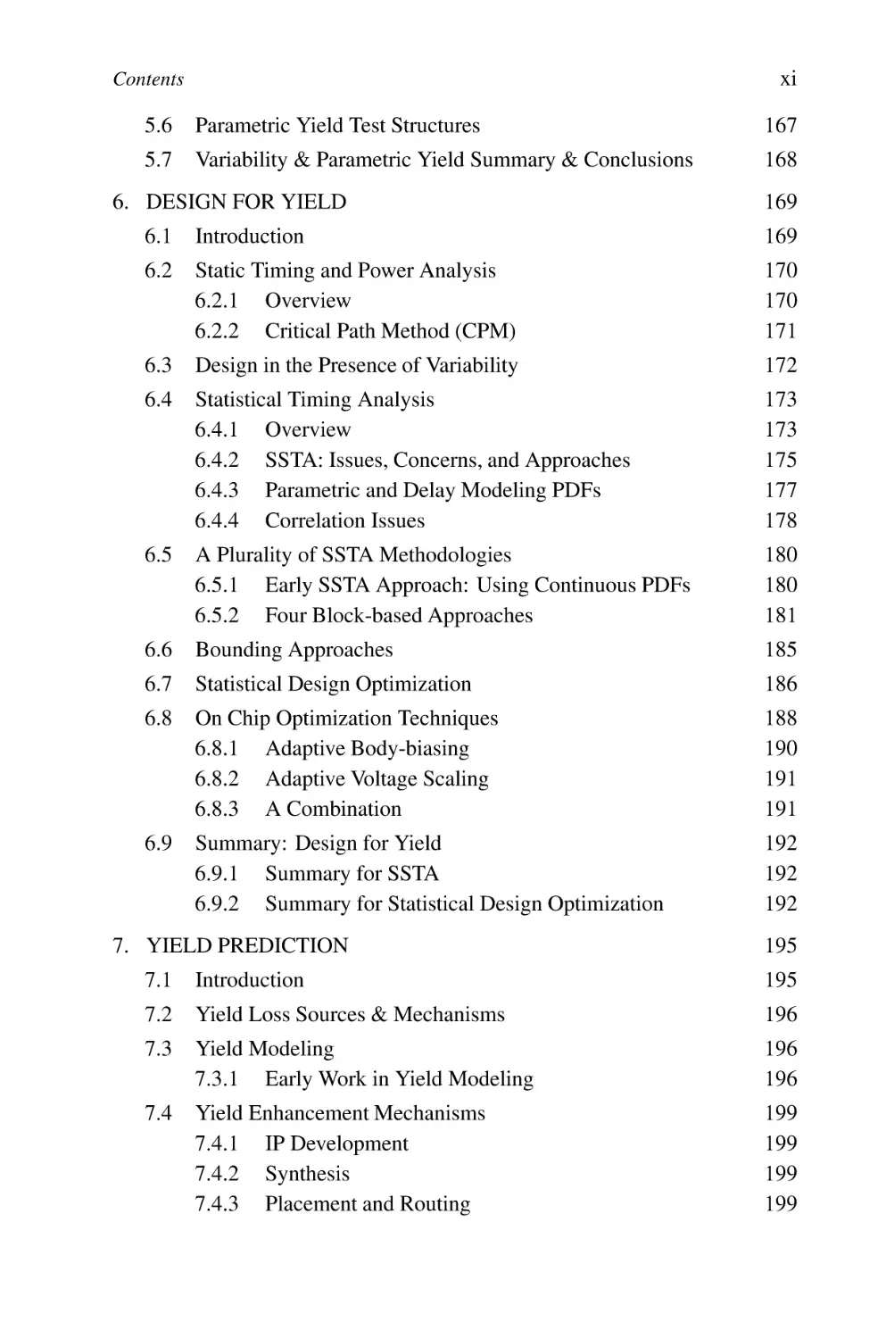
performed individually or in any particular combination to enhance the printability of design features and to meet design intent. Figure 1.4 demonstrates the
need for OPC in sub-wavelength lithography. Examples of layout procedures
are optical proximity correction (OPC), which could be rule or model based,
and which involves the addition of sub-resolution assist features (SRAF). An
example of a combination of a layout-mask procedure would be phase-shift
mask (PSM). Examples of optical procedures of RET includes off-axis illumination, pupil filtering, and multiple exposures. Since we will be covering
these in detail in Chapter 3 we will limit our exposure of this topic to the
basics.
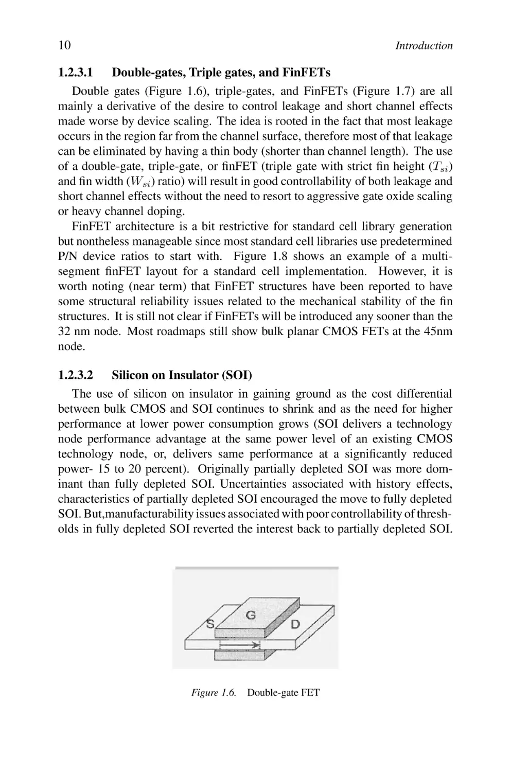
Figure 1.5 is illustrations of the use of strong PSM for tight geometry resolution. The resist pattern to the left reflects the result of the exposure of a binary
mask with a feature smaller than half of the light source wavelength. There is
simply no resolution of the geometry whatsoever and the intended feature is
totally missed. By applying strong PSM (right) the light interference due to
Figure 1.3. NA= I sin α
DFM/DFY Critical for IC Manufacturing
Figure 1.4.
9
Basic Example of OPC at 180nm
the phase altered light wave allows a good resolution of the intended geometry.
PSM is achieved by special processing of the mask based on a defined pattern
to create a 180 degrees phase shift for light waves passing through the treated
mask pattern.
1.2.3
New Devices
In this section we briefly touch on new devices in the context of the ever
growing complexity of correctly extracting devices and interconnect, and in the
context of growing complexity of process integration. The motivating factors
are again dominated by power (especially leakage control) and performance
considerations.
Figure 1.5.
Example of Strong (180) PSM
10
Introduction
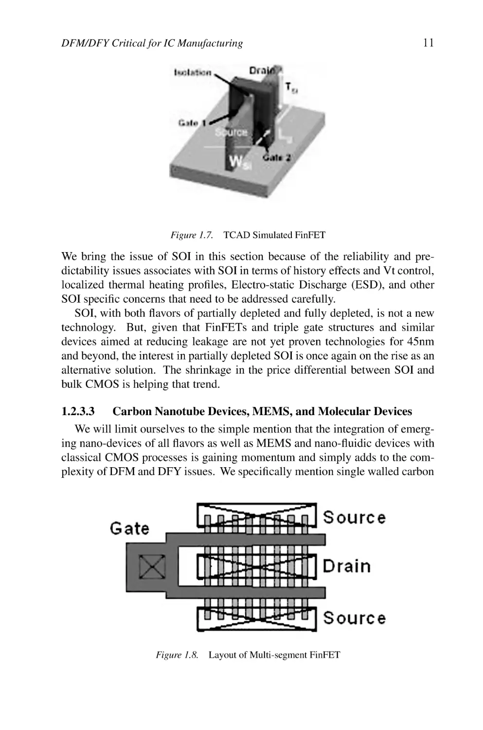
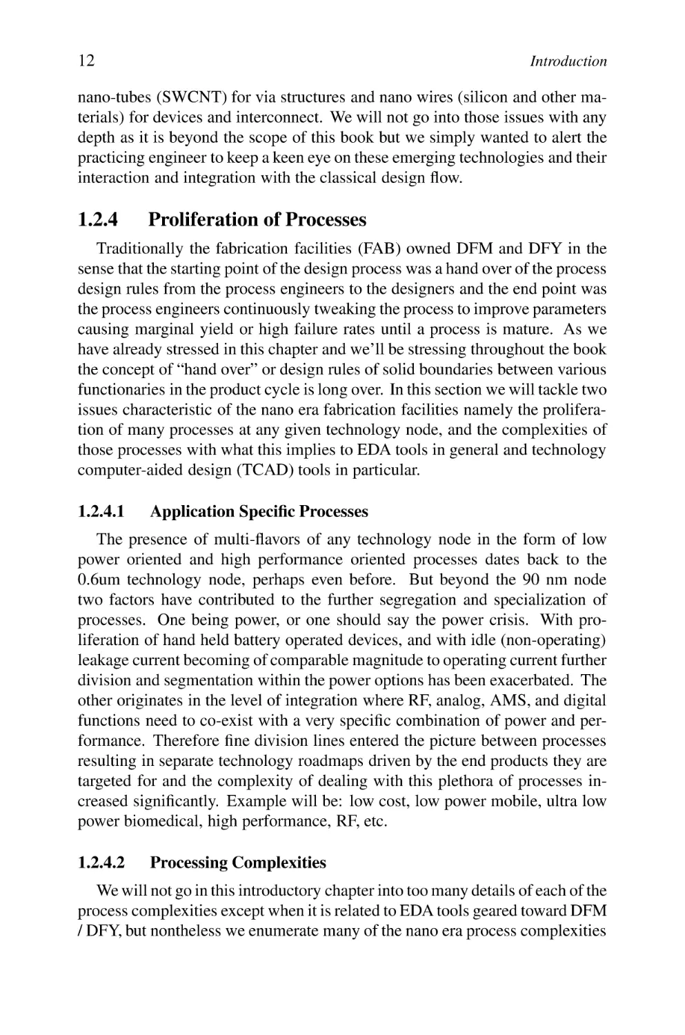
1.2.3.1 Double-gates, Triple gates, and FinFETs
Double gates (Figure 1.6), triple-gates, and FinFETs (Figure 1.7) are all
mainly a derivative of the desire to control leakage and short channel effects
made worse by device scaling. The idea is rooted in the fact that most leakage
occurs in the region far from the channel surface, therefore most of that leakage
can be eliminated by having a thin body (shorter than channel length). The use
of a double-gate, triple-gate, or finFET (triple gate with strict fin height (Tsi )
and fin width (Wsi ) ratio) will result in good controllability of both leakage and
short channel effects without the need to resort to aggressive gate oxide scaling
or heavy channel doping.
FinFET architecture is a bit restrictive for standard cell library generation
but nontheless manageable since most standard cell libraries use predetermined
P/N device ratios to start with. Figure 1.8 shows an example of a multisegment finFET layout for a standard cell implementation. However, it is
worth noting (near term) that FinFET structures have been reported to have
some structural reliability issues related to the mechanical stability of the fin
structures. It is still not clear if FinFETs will be introduced any sooner than the
32 nm node. Most roadmaps still show bulk planar CMOS FETs at the 45nm
node.
1.2.3.2 Silicon on Insulator (SOI)
The use of silicon on insulator in gaining ground as the cost differential
between bulk CMOS and SOI continues to shrink and as the need for higher
performance at lower power consumption grows (SOI delivers a technology
node performance advantage at the same power level of an existing CMOS
technology node, or, delivers same performance at a significantly reduced
power- 15 to 20 percent). Originally partially depleted SOI was more dominant than fully depleted SOI. Uncertainties associated with history effects,
characteristics of partially depleted SOI encouraged the move to fully depleted
SOI. But,manufacturability issues associated with poor controllability of thresholds in fully depleted SOI reverted the interest back to partially depleted SOI.
Figure 1.6.
Double-gate FET
DFM/DFY Critical for IC Manufacturing
Figure 1.7.
11
TCAD Simulated FinFET
We bring the issue of SOI in this section because of the reliability and predictability issues associates with SOI in terms of history effects and Vt control,
localized thermal heating profiles, Electro-static Discharge (ESD), and other
SOI specific concerns that need to be addressed carefully.
SOI, with both flavors of partially depleted and fully depleted, is not a new
technology. But, given that FinFETs and triple gate structures and similar
devices aimed at reducing leakage are not yet proven technologies for 45nm
and beyond, the interest in partially depleted SOI is once again on the rise as an
alternative solution. The shrinkage in the price differential between SOI and
bulk CMOS is helping that trend.
1.2.3.3 Carbon Nanotube Devices, MEMS, and Molecular Devices
We will limit ourselves to the simple mention that the integration of emerging nano-devices of all flavors as well as MEMS and nano-fluidic devices with
classical CMOS processes is gaining momentum and simply adds to the complexity of DFM and DFY issues. We specifically mention single walled carbon
Figure 1.8.
Layout of Multi-segment FinFET
12
Introduction
nano-tubes (SWCNT) for via structures and nano wires (silicon and other materials) for devices and interconnect. We will not go into those issues with any
depth as it is beyond the scope of this book but we simply wanted to alert the
practicing engineer to keep a keen eye on these emerging technologies and their
interaction and integration with the classical design flow.
1.2.4
Proliferation of Processes
Traditionally the fabrication facilities (FAB) owned DFM and DFY in the
sense that the starting point of the design process was a hand over of the process
design rules from the process engineers to the designers and the end point was
the process engineers continuously tweaking the process to improve parameters
causing marginal yield or high failure rates until a process is mature. As we
have already stressed in this chapter and we’ll be stressing throughout the book
the concept of “hand over” or design rules of solid boundaries between various
functionaries in the product cycle is long over. In this section we will tackle two
issues characteristic of the nano era fabrication facilities namely the proliferation of many processes at any given technology node, and the complexities of
those processes with what this implies to EDA tools in general and technology
computer-aided design (TCAD) tools in particular.
1.2.4.1
Application Specific Processes
The presence of multi-flavors of any technology node in the form of low
power oriented and high performance oriented processes dates back to the
0.6um technology node, perhaps even before. But beyond the 90 nm node
two factors have contributed to the further segregation and specialization of
processes. One being power, or one should say the power crisis. With proliferation of hand held battery operated devices, and with idle (non-operating)
leakage current becoming of comparable magnitude to operating current further
division and segmentation within the power options has been exacerbated. The
other originates in the level of integration where RF, analog, AMS, and digital
functions need to co-exist with a very specific combination of power and performance. Therefore fine division lines entered the picture between processes
resulting in separate technology roadmaps driven by the end products they are
targeted for and the complexity of dealing with this plethora of processes increased significantly. Example will be: low cost, low power mobile, ultra low
power biomedical, high performance, RF, etc.
1.2.4.2
Processing Complexities
We will not go in this introductory chapter into too many details of each of the
process complexities except when it is related to EDA tools geared toward DFM
/ DFY, but nontheless we enumerate many of the nano era process complexities
DFM/DFY Critical for IC Manufacturing
13
that impacts manufacturability and yield directly or indirectly. Most of those
complexities are driven by scaling requirements (thin body, ultra shallow junctions, high dopant concentrations, etc) and power (leakage) requirements. To
list but a few:
Co-implantation of species to suppress diffusion
Diffusion-less activation for ultra shallow junctions
Diffusion free annealing processes
Solid phase epitaxy (SPE)
Spike annealing, flash annealing, and sub-melt laser annealing
High-tilt high-current implantation (highly needed for double gates)
Lateral dopant activation
Through gate implants (TGI)
Elevated source drain
Dopant introduction via plasma immersion
1.2.4.3 DFM/DFY Applications for TCAD
One common derivative of the combination of the continuous scaling and the
complexities of processing needed to achieve this scaling within tight power and
performance constraints is added variability. One such example of variability
that TCAD tools has to deal with is atomistic doping profiles for carriers and
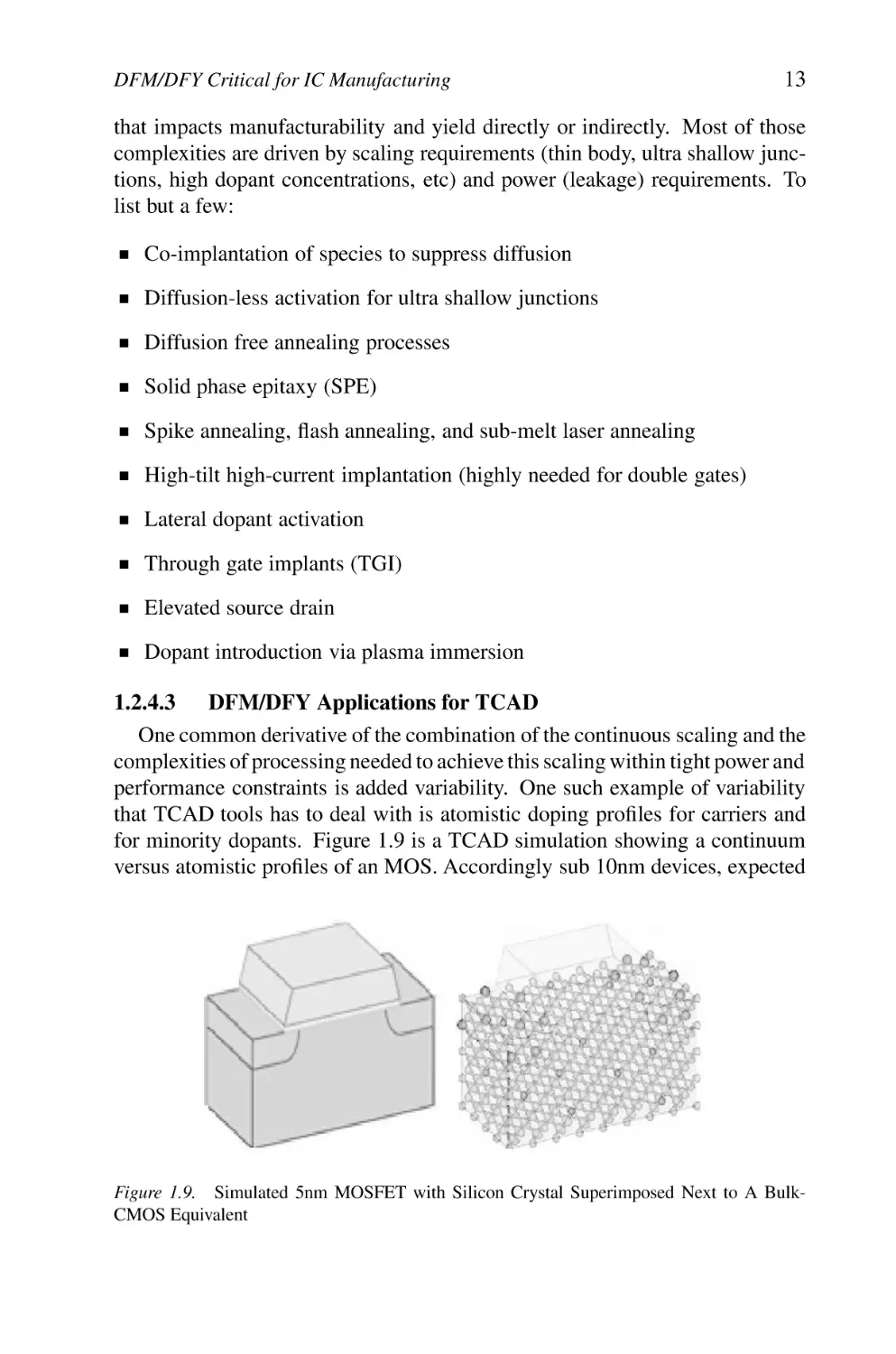
for minority dopants. Figure 1.9 is a TCAD simulation showing a continuum
versus atomistic profiles of an MOS. Accordingly sub 10nm devices, expected
Figure 1.9. Simulated 5nm MOSFET with Silicon Crystal Superimposed Next to A BulkCMOS Equivalent
14
Introduction
to be available around 2016 will have approximately 10 atoms along the effective channel length and the position of each silicon, dopant, or insulator atom
having a microscopic impact on device characteristics. Therefore continuous
doping profile models using Kinetic Monte-Carlo (KMC) simulators will not
hold any longer and an atomistic statistical 3-D (quantum mechanical considerations) model will need to be implemented in order to correctly capture atomic
interaction at that level.
Another DFM application is tied to layout dependency of the tensile stress
profile created by the gate liner on the device performance. Stress engineering
as pointed out earlier is widely used at 65 nm and beyond to enhance the
performance of devices but that performance enhancement is highly layout
dependent. Tools are currently developed that can analyze such dependency
and extract profiles of layout hot spots as well as performance degradation as a
function of position. We’ll be covering this in more depth in Chapter 6.
1.2.5
Intra-die Variability
Linear and radial variability from die to die and wafer to wafer were the
dominant sources of variability in the IC industry. The designer guard-banded
a design against such variability through simulating across what was referred to
as the process corners: slow, typical, and fast (these corners also covered environmental variability). The slow corner assumed variability in each parameter
to reflect the worse effect on performance simultaneously. In other words it was
worst case oxide thickness taking place at the same time as worst case threshold
voltage (Vt) and the worst case effective channel length (Lef f ). Add to that the
fact a designer accounted for “worst case” environmental variables along with
the slow process corner (high temperature and low supply voltage). Similarly
the “best case” simulation accounted for the fastest effect for each parameter
plus cold temperature and high supply voltage. Obviously that was an overkill
on the part of the designer, but, still the methodology worked sufficiently well.
Intra-die variability was insignificant.
The ITRS roadmap shows an annual growth in the die size of DRAM of
roughly 3% annually to accommodate roughly 60% more components in keeping up with Moore’s law (the 60% comes from technology sizing plus die size
growth). That means the lithography field size for a 4 X stepper has to grow by
12% annually reducing the controllability and increasing intra-die variability.
Now intra-die variability is very significant as Table 1.5 shows.
A significant portion of intra-die variability is systematic and is layout and
pattern dependent and thus could be corrected for to some degree as we’ll be
covering in more detail in Chapter 5 but the rest of the variability is random and
is best dealt with in a statistical approach.
One important point to make here regarding intra-die variability is that it is
not limited to parameters such as Vt and tox which now have a higher percent
15
DFM/DFY Critical for IC Manufacturing
Table 1.5.
Intra-die Variability Increase with Technology Node
L(nm)
Vt(mV)
σ-Vt(mV)
σ-vt/Vt
250
450
21
4.7%
180
400
23
5.8%
130
330
27
8.2%
90
300
28
9.3%
65
280
30
10.7%
45
200
32
16%
variation but geometries that were once treated as rectangular in cross section
such as wires or uniform such as intra-metal oxide thickness can no longer be
assumed as such and extraction tools need to take that into account.
1.2.6
Error Free Masks Too Costly
Mask writing equipment are expensive and their throughput is relatively low.
Various rasterization techniques and parallel processing has sped mask writing
some but the overall cost of a mask set is still a function of the mask write time
which is in turn a function of size of the data to be written. Table 1.6 shows the
explosion in data volume as we advance to the next technology note. What is
most interesting about Table 6 is that the data volume was revised downward
from the 2003 ITRS forecast. We’ll be commenting on that later in the context
for smart OPC but needless to say masks are becoming more expensive; and
with the explosion of data points to be written to a mask and the growing field
size, getting an error free mask is, in addition to being very expensive, quite
hard to come by. This has resulted in the implementation of mask inspection
EDA tools that can simulate the impact on a mask error on the overall print out
and determining if that error needs to be re-worked or is tolerable. This is an
increasingly growing (in size and importance) part of DFM/DFY tools.
1.2.7
Cost of a Silicon Spin
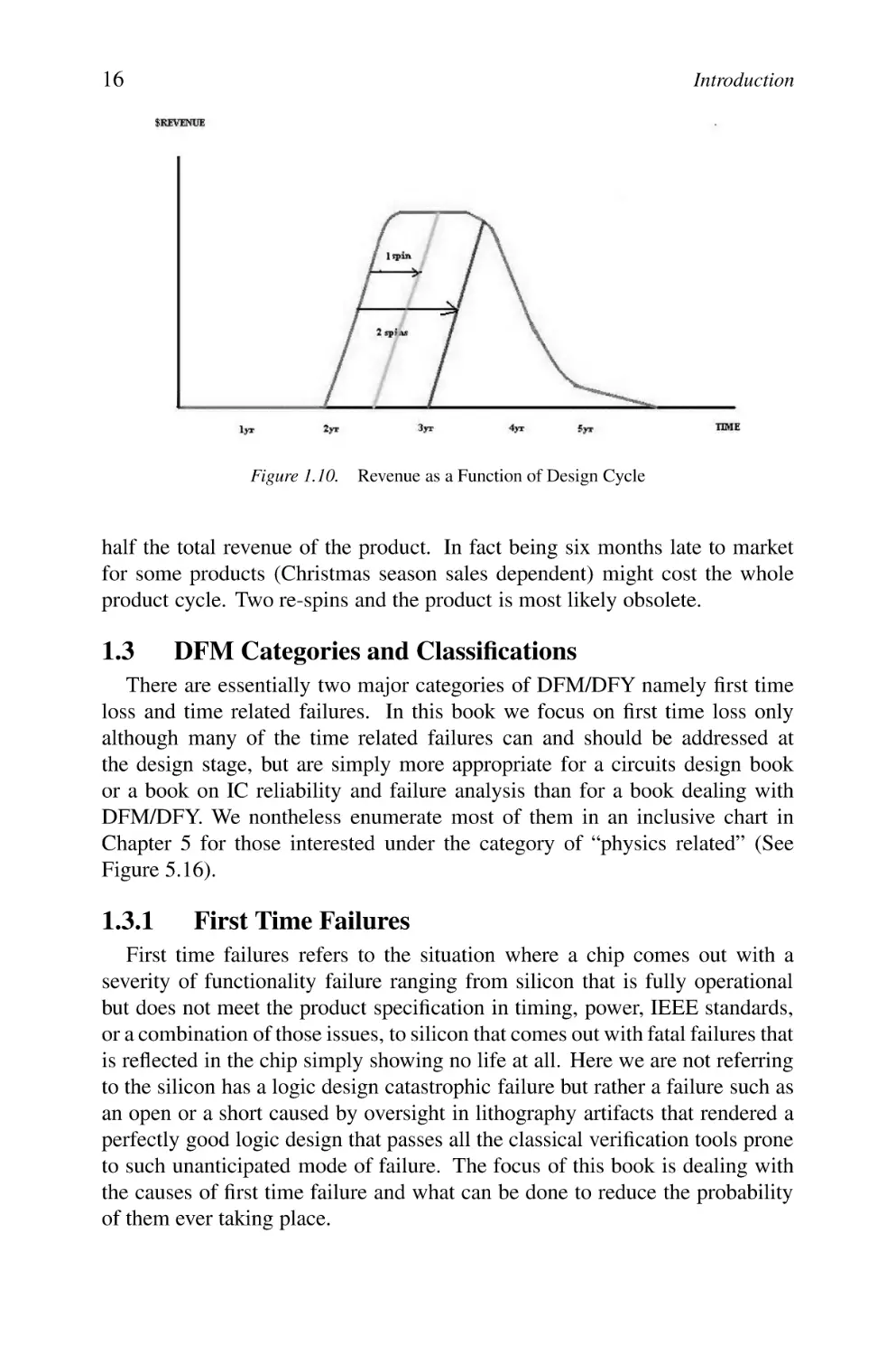
When we talk about the cost of a silicon spin we are talking about three
different factors, all tied together, and all very costly. Figure 1.10 shows the
typical life cycle of a new product. The typical time needed for a product from
concept to first silicon is product dependent but is estimated on an average to be
two years with a total cost anywhere from $25 Million to $40 Million. A typical
re-spin is 6 months.
Now, the cost of a re-spin is interesting to figure out. From a materials and
engineering time perspective it is no more than perhaps $2 millions. But, if we
look at the cost from a product life cycle point of view, it could be as high as
Table 1.6.
Mask Preparation File Data Size - ITRS 2004
Year
Node
Data
2004
90nm
144GB
2007
65nm
486GB
2009
45nm
1,094GB
16
Introduction
Figure 1.10.
Revenue as a Function of Design Cycle
half the total revenue of the product. In fact being six months late to market
for some products (Christmas season sales dependent) might cost the whole
product cycle. Two re-spins and the product is most likely obsolete.
1.3
DFM Categories and Classifications
There are essentially two major categories of DFM/DFY namely first time
loss and time related failures. In this book we focus on first time loss only
although many of the time related failures can and should be addressed at
the design stage, but are simply more appropriate for a circuits design book
or a book on IC reliability and failure analysis than for a book dealing with
DFM/DFY. We nontheless enumerate most of them in an inclusive chart in
Chapter 5 for those interested under the category of “physics related” (See
Figure 5.16).
1.3.1
First Time Failures
First time failures refers to the situation where a chip comes out with a
severity of functionality failure ranging from silicon that is fully operational
but does not meet the product specification in timing, power, IEEE standards,
or a combination of those issues, to silicon that comes out with fatal failures that
is reflected in the chip simply showing no life at all. Here we are not referring
to the silicon has a logic design catastrophic failure but rather a failure such as
an open or a short caused by oversight in lithography artifacts that rendered a
perfectly good logic design that passes all the classical verification tools prone
to such unanticipated mode of failure. The focus of this book is dealing with
the causes of first time failure and what can be done to reduce the probability
of them ever taking place.
Tie up of Various DFM Solutions
1.3.2
17
Time Related Failures
Time related failures are parts that exhibit failures in the field due to drift in
certain parameters with time or due to the marginality of an aspect of the design
that deteriorates with time until a failure occurs. Two examples of such a phenomena are metal migration and the drift in Vt of devices with time. A design
can have a marginality in the current carrying capability of some interconnect,
and the presence of a high current density in that interconnect weakens it over
time in the form of a drift in the interconnect particles leading to additional thinning in the interconnect that leads to failure. There are EDA tools that are capable of analyzing a design for such weaknesses and catching them before a design
is released. However, the same electro-migration phenomena could occur due
to a lithography or a CMP related issue and not due to a current density violation
reason. That aspect of failure is addressed in detail in this book. The other example of field failures we cited here is Vt shift with time. This is especially critical
given the shallow junctions and the high doping concentrations characteristic of
the nano-scale devices. This is the area of TCAD tools to make sure the design
of device and process modules do not result in high electric fields that cause a
severe enough drift in Vt with time such that it results in a device failure in the
field.
As we mentioned at the very beginning of this chapter field failures are the
most expensive type of failures and as such should be avoided at all costs. The
time honored procedure in the IC industry to eliminate time related failures
is to conduct static and dynamic burn-in tests where the parts (or a sample
of the parts) undergo biased burn in for 1000 or 10,000 hours under the extreme environmental conditions that are specified IEEE standards and specifications. This procedure should ferret out most if not all such weaknesses
in a design. Static burn-in eliminates weak links in what is known as infant
mortality. The dynamic burn-in ensures that the device junctions encounter the
same electric field profile they will undergo when the part is operating normally
in the field executing the functionality it was designed to perform. Therefore
it is of utmost importance that dynamic burn in vector sets be comprehensive
and exhaustive. That is the extent of our coverage of time related failures in
this book.
1.4
How Do Various DFM Solutions Tie up with Specific
Design Flows
Since we strongly believe that manufacturability and yield should be designed
in to a product from the very onset of the design process we strongly advocate a
design flow approach for DFM/DFY. Obviously there is no single design flow
followed across the industry, so the design flow we will use is one we believe
to be a good and comprehensive example for a system on a chip (SOC) design.
18
Introduction
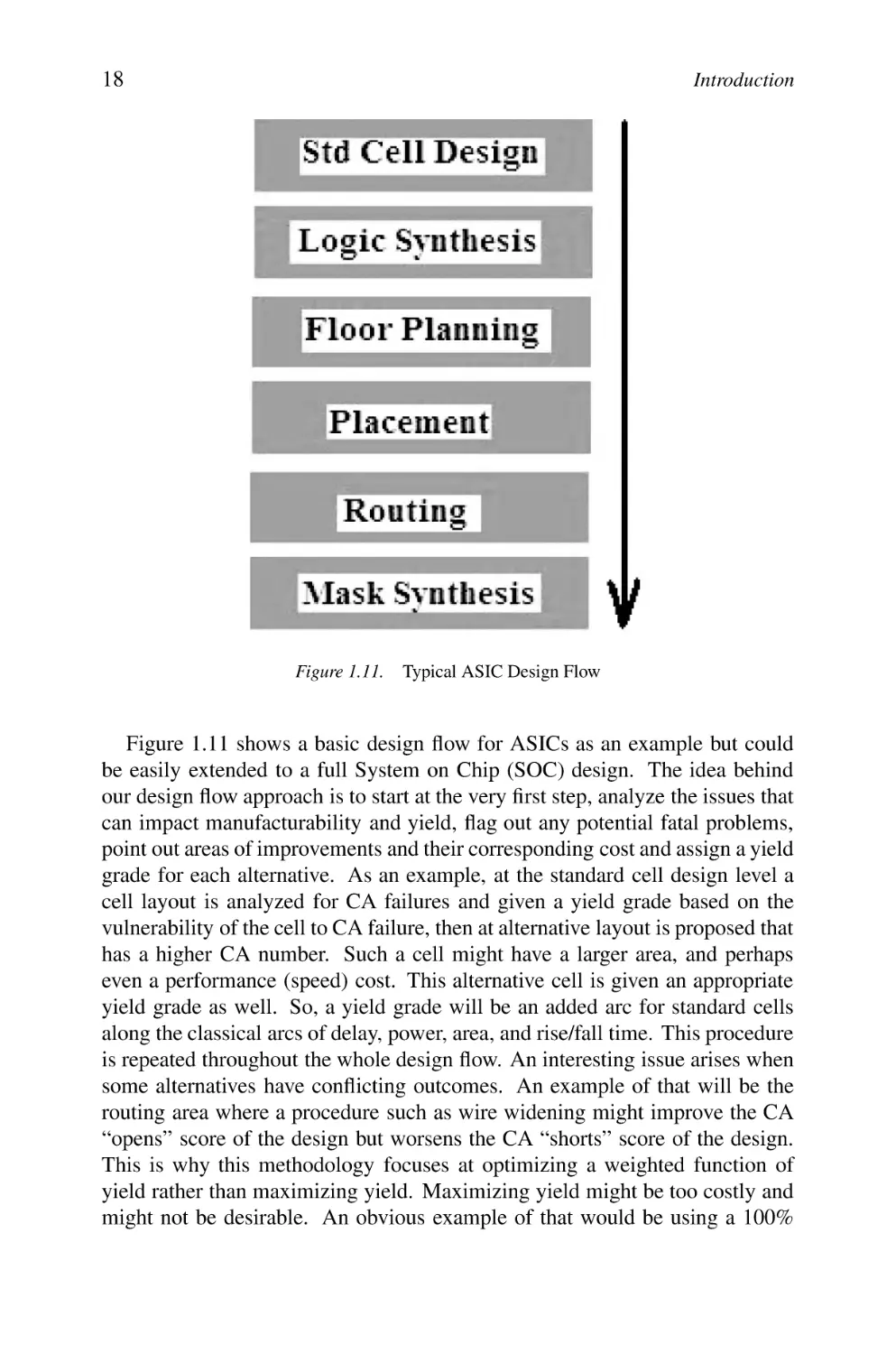
Figure 1.11.
Typical ASIC Design Flow
Figure 1.11 shows a basic design flow for ASICs as an example but could
be easily extended to a full System on Chip (SOC) design. The idea behind
our design flow approach is to start at the very first step, analyze the issues that
can impact manufacturability and yield, flag out any potential fatal problems,
point out areas of improvements and their corresponding cost and assign a yield
grade for each alternative. As an example, at the standard cell design level a
cell layout is analyzed for CA failures and given a yield grade based on the
vulnerability of the cell to CA failure, then at alternative layout is proposed that
has a higher CA number. Such a cell might have a larger area, and perhaps
even a performance (speed) cost. This alternative cell is given an appropriate
yield grade as well. So, a yield grade will be an added arc for standard cells
along the classical arcs of delay, power, area, and rise/fall time. This procedure
is repeated throughout the whole design flow. An interesting issue arises when
some alternatives have conflicting outcomes. An example of that will be the
routing area where a procedure such as wire widening might improve the CA
“opens” score of the design but worsens the CA “shorts” score of the design.
This is why this methodology focuses at optimizing a weighted function of
yield rather than maximizing yield. Maximizing yield might be too costly and
might not be desirable. An obvious example of that would be using a 100%
DFM and DFY: Fully Intertwined
19
defect free mask! A yield engine interacting with the various EDA design
tools controlling such a flow is highly desirable to close the loop of interaction
between the modules in the context of DFM/DFY.
1.5
DFM and DFY: Fully Intertwined
In summing up this chapter it is not hard for the reader to see the complexities associated with all aspects of the nano era IC manufacturing. Two major
conclusions are self-evident. First, no single group owns the DFM and DFY
responsibility, yet an oversight or the slightest error by one group or individual
in the whole product flow is sufficient to either kill the product or to impact the
product yield adversely and in a significant manner. It follows that close cooperation and open communications between the electronic design automation
(EDA), design (including verification), mask preparation, fabrication, assembly, and testing communities is needed. It also suggests that this communication
is a closed loop, two directional feed back. The second obvious conclusion is
that functionality and yield can and should be designed into the product. By
the time a design is committed to a mask it is too late and too expensive to try
to do anything significant to impact functionality, reliability, or yield.
Chapter 2
RANDOM DEFECTS
Dealing with random defects in IC manufacturing and coming up with yield
models that estimates yield as a function of die area and of the density of random
defects dates back to the early sixties. The three most used yield models are the
Poisson distribution model, the Seed’s model, and the negative-binomial model.
The Poisson and the negative-binomial models have emerged as dominant. We
will limit our discussion to them.
2.1
Types of Defects
When we talk about random defects we refer to all types of defects that cannot
be controlled or modeled in a predictable and systematic way. They include
random particles in the resist or in the materials to be added or removed, or
defects in the crystal structure itself that alters the intended behavior of the
material and results in excessive leakage or in a shift in the device threshold
(Vt) leading to the failure of the device. The failure modes resulting from these
defects are
1 Opens
2 Shorts
3 Leakage
4 Vt shift
5 Variability in Mobility (μ)
Random defects as described above did not have to result in a total failure of
the device but in a significant deterioration in its performance. A killer random
1
to 13 of
defect was recognized as a defect that amounted to anywhere from 10
21
22
Random Defects
the critical dimension (CD) of the layer(s) it impacted. We enumerated the
potential effects of particles for completeness. Defects resulting in leakage, Vt
shift, μ shift are dealt with in infant mortality burn-in mentioned in Chapter 1.
Here we only address CA in terms of opens and shorts. The early random
defects yield models dealt with failure of Short and Open modes only, and it
was a good approximation as short and open failure were the majority of the
random defects. We extend it to address clustering effects which is becoming
more relevant in the nano-era.
2.2
Concept of Critical Area
Critical area is a measure of a design’s sensitivity to random particles. Critical
area Acr is defined as the region on the layout where contamination particles
must fall to cause a catastrophic functional failure. A catastrophic failure is an
open or a short. Based on the failure type (open or short) caused by the particles,
the critical area can be categorized as open critical area or short critical area.
The CA based random yield loss is a function of the open and short critical
areas.
In the shape expansion method, the name is self evident in terms of the fact
that “expanding” the circle needed to cause a short or an open define the particle
size that causes such a short or open. Figures 2.1 and 2.2 illustrate the shape
expansion method for the extraction of the short and open critical areas caused
by the particles with radius x/2, or size x (shown as shaded areas in Figure 2.1
and 2.2).
Another example of open and short critical area between layers is shown
in Figure 2.3. A typical example will be a particle (or a void) in the oxide
between two conductors resulting in a short or a leakage path, another example
will be a particle or a void in a via structure resulting in an open or in a high
resistance via.
Figure 2.1.
Short CA Between Two Wires Caused by Particles with Size x
23
Basic Models of Yield for Random Defects
open wire particle
x/2
x/2
Ac (x)
OK particle
Figure 2.2.
Figure 2.3.
2.3
Open CA on a Wire Caused by Particles with Size x
Intra-layers Defect Particle Resulting in an Open or Short
Basic Models of Yield for Random Defects
We will be devoting the next four chapters to deal with all other aspects of
yield. So, we will cover yield here only as it relates to critical area in order
to give the reader an idea of why extracting critical area and minimizing it is
important.
As we mentioned, two of the most recognized yield models are the Poisson
based yield Equation (Equation 2.1) and the negative binomial yield Equation
(Equation 2.2) [9–12].
(2.1)
Yr = e−Acr D0 .
Yr =
1
(1 +
Acr D0 α
α )
(2.2)
where Yr denotes the random yield and D0 refers to the particle density. Acr
is the critical area defined earlier in Section 2.2, which , as obvious from the
Equation, is a key design yield determining parameter. The α is a “clustering
parameter” introduced to correct the effect of defect clustering. It is especially
useful for large devices where clustering is more significant to improve yield
24
Random Defects
prediction. It is also obvious that in order to maximize yield, that number needs
to be minimized. In more advanced yield models, D0 was replaced by D where
D, rather than being a constant number D0 is now a defect density distribution
function f(D). However, it is worth noting at this point that almost all yield models used by the IC industry for yield modeling fall into two categories: Poisson
distribution based model and negative binomial distribution based model. We
want to be clear at this point that we are not advocating one modeling method
over the others. Different applications and the need for different levels of confidence as well as the design size might dictate which modeling method is most
appropriate for that particular situation.
2.4
Critical Area Analysis (CAA)
In this section we will cover two standard methods of CA extraction namely
the shape expansion method and the Monte Carlo method as well as a newly
developed approximation method that exploits certain clustering phenomena
of particle defects to result in a relatively accurate but fast method of CA extraction. The main differences between the first two standard methods and the
approximate method are computation cost and accuracy. While the standard
methods, also known in the industry as “exact” methods are accurate, they
are computationally expensive. The approximate method on the other hand is
close enough in accuracy especially when the CA calculation is needed to be
performed in short order to make a decision in the routing stage for example
among alternative options for the purpose of improving CA associated yield,
yet it is computationally very efficient. Another benefit of the approximate
method is that it makes CAA driven layout optimization possible.
2.4.1
Classical Methods of CA Extraction
The shape expansion based method is designed to compute the critical area
for a particular given defect size. The critical area needs to be recomputed if
the defect size is changed. The average critical area is calculated by integrating
these critical areas at different defect sizes with defect size distribution function.
The Monte Carlo method does not limit itself to any specific defect size. The
generator simply generates random defects with their sizes following the given
defect size distribution function. Both these methods suffer from the problem
of huge run time for accurate estimation.
Once the critical areas for all the wires are computed, the geometric union of
these areas gives the total critical area Ac (x) at the defect size x. The average
value of total critical area for all different defect sizes is calculated as
Acr =
xmax
xmin
Ac (x)f (x)dx
(2.3)
25
Critical Area Analysis (CAA)
where xmin and xmax are the minimal and maximal defect sizes, f (x) is the
defect size distribution function.
For modern processes, it is widely accepted that the defect size distribution
function is similar to Equation 2.4 [13–15].
f (x) =
⎧
⎪
⎨
⎪
⎩
x
x20
if 0 < x ≤ x0 ,
x20
x3
if x0 ≤ x ≤ xmax ,
(2.4)
where x0 is the minimal spacing in the design rules.
At each particular defect size, the traditional shape expansion method computes the geometric union of the critical areas for all the wires to obtain the total
critical area. Due to the existence of the overlaps between the geometry shapes,
the total critical area is not a linear sum of each individual wire’s critical area.
Several algorithms (mostly based on scan-line or quad-tree data-structures) have
been used for efficiently computing the geometric union. However, none of
these methods can handle the geometric union analytically. Therefore there
is no way to predict the total critical area at a different defect size. The
whole extraction and computation procedure has to be repeated for different defect sizes. Thus we need approximation methods that can efficiently
do that.
2.4.2
Approximations
As we mentioned earlier in the chapter using a shape expansion method
for computing the CA of a particular design is an accurate but computation
runtime expensive method [16–24], and the same applies to the Monte Carlo
method [19, 20, 25]. It is not exactly practical for applications such as multilayer metal routing where alternative yield improvement scenarios need to be
evaluated by recomputing the CA of the design and the corresponding impact
on yield for each proposed alteration to come up with an optimal solution. Thus,
when the typical shape expanding technique is used, an approximation in the
form of using a limited number of defect sample-sizes is used to speed up the
calculation of CA. This introduces an inaccuracy in its own right reducing the
significance of the accuracy of the method. Ways to speed up the on-the-fly
calculation of CA within a particular step of the design flow has recently been
an area of active research. The approach we describe in this section is a very
efficient and promising approach that has been recently put into practice in the
Synopsys ICC place and route suite with good results [26]. The approximation
method is a shape expansion type of method, but it does not limit itself to any
particular defect size. Furthermore, this approximation technique exploits well
known and empirically proven defect clustering phenomena.
26
Random Defects
Table 2.1.
CA Results and Run Time in Shape Expansion Method and Our Method
designs
design 1
design 2
design 3
design 4
short Acr
open Acr
short Acr
open Acr
short Acr
open Acr
short Acr
open Acr
traditional method
results
run time
2.8949e5
42 min
5.8922e5
7 min
1.2450e6
3hr 14min
2.7109e6
24 min
2.8225e6
5hr 8min
3.5000e6
29 min
2.4867e6
5hr 51min
4.4026e6
23 min
new method
results
run time
2.9426e5
41 sec
6.0319e5
24 sec
1.3970e6
3 min
2.7556e6
2 min
2.8387e6
3.5 min
3.5979e6
2.3 min
2.9197e6
3 min
4.5653e6
2 min
Thus there has been many attempts at coming up with an explicit analytical formulation of critical area [27] but almost all of them have the limitation
of not properly dealing with the overlaps between critical areas of individual wires. Furthermore, some of them make the unrealistic assumption of a
fixed wire width and wire spacing for the whole design, again impacting their
accuracy.
In this method an explicit formula for the average critical area is generated. The layout-related parameters in the formula can be derived in one
sweep through the objects of a layout. Therefore, if the traditional shape
expansion-based method needs to compute the critical area m times for m different defect sizes, the proposed method can speed up the run time by at least a
factor of m.
2.4.3
Comparison of Approximate and Traditional CA
Extraction Techniques
In this section we present simulation results comparing the approximation
method of calculating the average critical area presented here with the traditional shape expansion based method. We will discuss the details of the approximation method in the next section. We ran the proposed method and the
traditional shape expansion method on 4 practical design layouts. The design
sizes varied from 0.6mm × 0.6mm to 1mm × 1mm. The data in Table 2.1
shows that both methods give very close results yet the proposed approximation method is dramatically faster than the traditional method (note that in
the traditional method, we use 20 defect sizes to compute the average critical
area).
2.5
Mathematical Formulation of Approximation Method
For this approach, an explicit formula for the total critical area is derived by
introducing the concept of pseudo critical areas for the individual wires. Those
areas are not overlapping with each other. The total critical area at any particular
Mathematical Formulation of Approximation Method
27
defect size is formulated as the summation of those pseudo critical areas. That
results are an explicit formula for the total critical area as a function of defect
size and of some layout parameters such as wire width, length, and spacing.
The integration over the defect size distribution function can be performed
analytically as well. Therefore, the resulting average total critical area is also
an explicit formula. The only free variables left in the final formula are the
layout parameters.
With the explicit formula for short and for open critical areas available one
only needs to go through all the objects in the layout once to extract the indicated
layout parameters. At the end of extraction the extracted layout parameters are
substituted into the formula and the average total critical area value is made
available immediately for all different defect sizes.
This discussion on computational complexity is clearly for calculating the
total average critical area. If one wants to identify the critical areas for only one
particular defect size for the layout then there is no difference in the computational cost between this method and the traditional method. However this is
highly unlikely since the average critical area is usually needed for the following
two reasons
1 It is required to quantify yield loss due to all the random defects. Thus the
average critical area is needed.
2 For layout optimization through critical area minimization it makes more
sense to use the average critical area as a cost function to be minimized
rather than the critical area of only one defect size.
2.5.1
Short Critical Area - Mathematical Formulation
If a pair of parallel wires (i, j) belonging to two different nets have portions
adjacently visible to each other, as shown in Figure 2.4, then the critical area
for this pair of wires at a particular defect size x is simply
0
if x < sij ,
(2.5)
Ac (x) =
(x − sij )bij if x ≥ sij .
where sij is the spacing between (i, j). bij is the segment where i and j are
visible to each other.
Equation 2.5 is an effort at formulating the critical area analytically. It has
been used in [27]. There are two major problems with this formulation. One is
that if the total critical area is computed as
Aij (x)
(2.6)
Ac (x) =
i
(nbr j of i)
where nbr j of i means j is a visible neighbor of i. Therefore, the same
critical area Aij (x) and Aji (x) is going to be double counted. Another major
28
Random Defects
bij
sij
Figure 2.4.
Typical Short Critical Area
problem with this formulation is that when the defect size is big, the critical area
between a wire pair (i, j) might overlap with the critical area between another
wire pair (i, k) as shown by area E in Figure 2.5. Equation 2.5 does not handle
the overlap regions at all. The summation of such critical areas would result in
double counting of these overlap regions.
In order to solve this problem, the total critical area is presented as the
summation of some pseudo critical areas between every pair of visible wires
Ac (x) = i j Âij (x), where the pseudo critical area Âij (x) is defined such
that
Âij (x) ∩ Âmn (x) = Ø, ∀(i, j) = (m, n).
However, note that the subscript (i, j) is order sensitive, i.e., Âij (x) = Âji (x).
Figure 2.5. Short Critical Area at Large Defect Size
Mathematical Formulation of Approximation Method
29
As shown in Figure 2.5, the wire i is split into two segments. One segment
has one visible neighbor j on one side and no visible neighbor on the other side.
The other segment has visible neighbors j and k on both sides.
For the segment of wire i that has a visible neighbor on only one side the
Δ
Δ
pseudo critical area is defined as Âij (x) = A + B/2, Âji (x) = B/2 + C.
Note that in this case the actual critical area between wires (i, j) is Aij (x) =
A + B + C. Thus Âij (x) + Âji (x) = Aij (x), Âij ∩ Âji = Ø. Each region
in the shaded area as shown in Figure 2.5 is included in only pseudo critical
area only. Equation 2.7 defines Âij (x) analytically for the segment of wire
i that has a visible neighbor on only one side (the visible neighbor in this
case is j).
⎧
0,
⎪
⎪
⎪
⎪
if x ≤ sij ,
⎪
⎪
⎪
⎪
⎪
⎪
⎨ (x − s )b /2,
ij ij
Δ
Âij (x) =
if sij < x ≤ 2sij + min(wi , wj ),
⎪
⎪
⎪
⎪
⎪
⎪
⎪
min(wi ,wj )
x
⎪
⎪
)bij ,
⎪ (sij + min(wi , wj ))bij /2 + ( 2 − sij −
2
⎩
if 2sij + min(wi , wj ) < x ≤ Dmax ,
(2.7)
where bij is the length of the overlap portion between i and j, sij is the spacing
between i and j, wi , wj are the wire-widths for the two wires, and Dmax is the
maximum random defect size.
For the segment of the wire i that has visible neighbors on both sides the
Δ
pseudo critical area is defined as Âij (x) = F + G/2, where the region F is
the region of the critical area Aij (x) that goes to the other side of wire i but
is not covered by the other side critical area Aik (x). The region E which is
the overlap region between the critical areas Aij (x) and Aik (x), is included as
Δ
part of the pseudo critical area Âik (x). Âik (x) = D/2 + E/2. Note that the
regions included by Âik (x) should not go to the other side of wire i because
that part has been covered by Âij (x). The region H is already totally included
as part of the pseudo critical area Âji (x). Following these steps every region in
the shaded area as shown in Figure 2.5 is included in only one pseudo critical
area.
Equations 2.8, 2.9, and 2.10 define Âij (x) analytically for a segment of
wire i with visible neighbors on both sides. If 2sij + min(wi , wj ) < 2sik +
min(wi , wk ):
30
Random Defects
Δ
Âij (x) =
⎧
⎪
⎪
⎪
⎪
⎪
⎪
⎪
⎪
⎪
⎪
⎪
⎪
⎪
⎪
⎪
⎪
⎪
⎪
⎪
⎪
⎨
⎪
⎪
⎪
⎪
⎪
⎪
⎪
⎪
⎪
⎪
⎪
⎪
⎪
⎪
⎪
⎪
⎪
⎪
⎪
⎪
⎩
0,
if x ≤ sij ,
(x − sij )bij /2,
if sij < x ≤ 2sij + min(wi , wj ),
if 2sij + min(wi , wj ) < x ≤
(sij + min(wi , wj ))bij /2
min(wi ,wj )
x
)bij , sij + sik + wi ,
+( 2 − sij −
2
(sij + min(wi , wj ))bij /2
min(wi ,wj )
)−
+[( x2 − sij −
2
(x − sij − sik − wi )]bij ,
(sij + min(wi , wj ))bij /2,
if sij + sik + wi < x ≤
2sik + 2wi − min(wi , wj ),
if 2sik + 2wi − min(wi , wj )
< x ≤ Dmax .
(2.8)
If 2sij + min(wi , wj ) > 2sik + min(wi , wk ):
⎧
0,
if x ≤ sij ,
⎪
⎪
⎪
⎪
⎪
⎪
⎪
⎪
if sij < x ≤ 2sij + min(wi , wj ),
(x − sij )bij /2,
⎪
⎪
⎪
⎪
⎪
⎪
⎪
⎨ (sij + min(wi , wj ))bij /2
if 2sij + min(wi , wj ) < x ≤
Δ
min(wi ,wj )
Âij (x) =
x
)bij , 2sij + 2wi − min(wi , wk ),
+( 2 − sij −
⎪
2
⎪
⎪
⎪
⎪
⎪
⎪
⎪
(sij + min(wi , wj ))bij /2
⎪
⎪
⎪
⎪ +(wi − min(wi ,wj ) −
⎪
if 2sij + 2wi −
⎪
2
⎪
⎩ min(wi ,wk )
)bij ,
min(wi , wk ) < x ≤ Dmax .
2
(2.9)
If 2sij + min(wi , wj ) = 2sik + min(wi , wk ):
⎧
0,
if x ≤ sij ,
⎪
⎪
⎪
⎪
⎪
⎪
⎪
⎪
if sij < x ≤ 2sij + min(wi , wj ),
(x − sij )bij /2,
⎪
⎪
⎪
⎪
⎪
⎪
⎪
⎨ (sij + min(wi , wj ))bij /2
if 2sij + min(wi , wj ) <
Δ
min(wi ,wj )
Âij (x) =
x
)bij , x ≤ sij + sik + wi ,
+( 2 − sij −
⎪
2
⎪
⎪
⎪
⎪
⎪
⎪
⎪
i , wj ))bij /2
⎪
⎪ (sijsij++smin(w
⎪
ik +wi
⎪
− sij −
+(
⎪
⎪
2
⎪
⎩ min(wi ,wj ) )b ,
if sij + sik + wi < x ≤ Dmax .
ij
2
(2.10)
31
Mathematical Formulation of Approximation Method
The total critical area at a particular defect size is the sum of all the pseudo critical areas shown in Equations 2.7, 2.8, 2.9,and 2.10. Ac (x) = i j Âij (x).
By integrating Ac (x) with the probability distribution function of the defect
sizes in Equation 2.4 we have the averaged total short critical area Acr as
follows: For the segments of the wires that have only one side visible neighbor
the average short critical area is:
1
sij
1
x20 bij [
+
−
].
(2.11)
AcrS−1side =
2
4sij
4Dmax 2Dmax
i
j
For the segments of the wires that have visible neighbors on both sides, the
average short critical area is as shown below:
If 2sij + min(wi , wj ) < 2sik + min(wi , wk ):
AcrS−2side1 =
i
x20 bij [
j
1
1
+
−
4sij
2(sij + sik + wi )
1
−
4(2sik + 2wi − min(wi , wj ))
sik + min(wi , wj )
].
2
4Dmax
(2.12)
If 2sij + min(wi , wj ) > 2sik + min(wi , wk ):
AcrS−2side2 =
i
x20 bij [
j
1
1
−
4sij
4(2sij + 2wi − min(wi , wj ))
sij + 2wi − min(wi , wj )
].
2
4Dmax
(2.13)
For 2sij + min(wi , wj ) = 2sik + min(wi , wk ):
AcrS−2side3 =
i
−
2.5.2
j
x20 bij [
1
4sij
sij + wi
1
−
].
2
4(sij + sik + wi )
4Dmax
(2.14)
Open Critical Area - Mathematical Formulation
Theoretically, the basic derivation fundamental ideas for the open critical area formula are a complement of the ideas used for the short critical
area.
The middle wire in Figure 2.6 is the object for which the pseudo open critical
area is formulated. It can be seen from this figure that for large defect sizes
32
Random Defects
li0
bijk
bij
sik
sij
Figure 2.6. Open Critical Area on Wire i
the actual open critical area on wire i begins to overlap with those on wires j
and k. In order to avoid counting the overlap regions more than once when
calculating the total open critical area, the concept of pseudo open critical areas
is introduced. For small defect sizes, when the actual open critical area on wire
i has no overlap with the ones on any other objects, the pseudo open critical
area is defined to be the same as the actual open critical area. As the defect size
increases the pseudo open critical area grows. It should stop growing on the
side when it begins to touch the open critical area of its visible neighbor on that
same side. For the example shown in Figure 2.6 the pseudo open critical area
for the mid wire i should be Âi (x) = A + B + C + D + E + F + G + H + I.
Regions E, F , and I are half of the overlapped shaded region in Figure 2.6 that
is close to wire i.
For the segment of wire i that has no visible neighbors on either side as
shown by the segment with length li0 in Figure 2.6 the pseudo critical area is
defined to be always the same as the actual open critical area because this part of
the critical area never overlaps with those of the other wires. Its mathematical
formulation is therefore:
0
if x ≤ wi
(2.15)
Âi (x) =
(x − wi )li0 if wi < x ≤ Dmax
Integrating Equation 2.15 with the defect size distribution function in Equation 2.4 results in the average pseudo critical area as:
Â0nbr = x20 li0 [
1
1
wi
−
+
].
2
2wi Dmax 2Dmax
(2.16)
Mathematical Formulation of Approximation Method
33
For the segment of the wire i that has visible neighbor on one side only as
shown by the segment of length bij in Figure 2.6 the pseudo critical area is
formulated as:
⎧
if x ≤ wi
⎪
⎪ 0
⎪
⎪
⎨
(x − wi )bij
if wi < x ≤ sij + wi + wj
Âij (x) =
⎪
⎪
⎪
⎪
⎩ x
s +w +w
( 2 − wi + ij 2i j )bij if sij + wi + wj < x ≤ Dmax
(2.17)
Integrating Equation 2.17 with the defect size distribution function in Equation 2.4 results in the average pseudo critical area as:
Â1nbr = x20 bij [
sij − wi + wj
1
1
1
−
−
−
]. (2.18)
2
2wi 4(sij + wi + wj ) 2Dmax
4Dmax
For the segment of the wire i that has visible neighbors on both sides as
shown by the segment with length bijk in Figure 2.6, the pseudo critical area is
formulated as follows: without loss of generality in this formulation we assume
the spacing between wire pair (i, j) is not larger than that between wire pair
(i, k), i.e., sij <= sik .
⎧
0
⎪
⎪
⎪
⎪
⎪
⎪
⎪
⎪
(x − wi )bijk
⎪
⎪
⎪
⎪
⎨
s +w +w
( x2 − wi + ij 2i j )bijk
Âijk (x) =
⎪
⎪
⎪
⎪
⎪
⎪
⎪
⎪
⎪
s +w +w
⎪
⎪
( ij 2i j + sik +w2i +wk
⎪
⎩
−wi )bijk
if x ≤ wi
if wi < x ≤ sij + wi + wj
if sij + wi + wj < x ≤
sik + wi + wk
if sik + wi + wk < x ≤ Dmax
(2.19)
Integrating Equation 2.19 with the defect size distribution function in Equation 2.4, we have average pseudo critical area:
1
1
1
−
−
2wi 4(sij + wi + wj ) 4(sik + wi + wk )
wj + wk + sij + sik
].
(2.20)
−
2
4Dmax
Â2nbr = x20 bijk [
Equations 2.16, 2.18 and 2.20 analytically describe the average pseudo open
critical area for each kind of segment in a wire i. The total average open critical
34
Random Defects
area is the sum of all the average pseudo critical areas shown in these Equations.
The explicit formula for the total average open critical area is:
Acr−open = x20
(
(−
i
−
nbr−j
bij
(sij + wj )bij
−
)
2
4(sij + wi + wj )
4Dmax
wi li1
li0
wi li0
li
li1
+
−
+
+
), (2.21)
2
2
2Dmax 4Dmax Dmax 2Dmax 2wi
where li is the total length of the wire i, li0 is the total length of the wire segments
that have visible neighbors on one side only , bij is the length of the segment of
wire i visible by neighbor j, sij is the spacing between wire i and its neighbor
j, and Dmax is the maximum defect size.
2.6
Improving Critical Area
In this section we will focus on the CA aspects of yield improvement. That
is, reducing the critical area of any particular layer of an individual standard
cell or of a whole routed design. In Chapter 6 we will present a comprehensive
design flow view of yield yet it is important to emphasize at this point that
yield optimization steps are all interlinked and must be dealt with collectively
through a weighted total yield model. An example of that would be poly to
poly spacing in a standard cell where the short CA for poly is improved but the
diffusion capacitance of the impacted node is higher and thus might impact the
performance of the cell, etc. This will be the only mention of that issue in this
section as our focus here is limited to CA optimization.
2.6.1
Cell Library Yield Grading
In Chapter 1 we mentioned that designing for yield starts at the very basic
steps of a design, and that yield could and should be designed in. In this section
we will be covering the concept of yield grading for standard cells from the
perspective of CA which is extensively covered in this chapter. Our choice
of standard cell is a matter of practicality since standard cells are the basic
building blocks of ASIC and SOC designs and since every standard cell is more
or less unique and should be optimized individually for optimal CA yield; unlike
structured arrays such as SRAFs where once the basic cell is optimized the task
is practically complete.
In Figure 2.7 two examples are given of improving the short and open CA for
poly and metal 1 respectively for a selected standard cell at no cost in area and
hardly any cost in performance (node capacitance). For the poly gate shown
the poly to poly spacing is labeled (a). We propose new positions for the poly
gates as indicated in the white dotted lines to the right of the original gates.
Obviously the contact to the power must be moved to the right as well. We
did not show that here to avoid cluttering the figure. By doing that the shorts
Improving Critical Area
Figure 2.7.
35
Example of Improving Poly Short CA and M1 Open CA
critical area for poly is improved as a result of the significant increase in (a),
the distance to the next adjacent poly to the right is still much larger than the
modified (a) and thus it does not take much figuring to realize that there is a net
improvement in the poly CA number.
Similarly by widening the metal 1 around the contact (b) and metal 1 (c) it
is obvious that the open CA for metal 1 is improved at practically absolutely
no cost in area and practically no cost in performance.
Exercise:
1 Start with this layout and do all the poly and metal 1 widening and spreading
that you believe will improve the open or short CA for poly and metal 1
without growing the size of the cell
2 Carry the exercise further to the limit of where improving the open CA will
start hurting the short CA.
3 Do you think the change in parasitics is significant? Estimate impact on an
unloaded cell and on a loaded cell (driving a fanout of 3).
The example we used in Figure 2.7 illustrates that there is a lot that can
be done to improve the CA for opens and shorts for poly and metal 1 for a
standard cell. Unfortunately most automatic layout generation tools are not
that sophisticated and thus hand packing of the layout might be needed but it
is worthwhile spending the time to do so as the library is built once and is used
many times over.
Not all cells are as easy to exploit as the example we just gave. Some cells are
pretty dense and hard to route in the first place. In such case multi-versions of
36
Random Defects
the cell are generated at the expense of area and performance (keeping things in
perspective the interconnect delay is the dominant source of delay for a critical
path in deep submicron). Another alternative would be weaker cells (less drive)
if area is of the most importance.
Anyhow, what we want to stress in this section is that the classical arcs of
delay, area, and power are not any more sufficient for choosing among alternatives in design synthesis. The added arc that is needed is the yield arc that is
based on CA extraction and grading for poly, metal, vias, etc.
Coming up with the proper value for a yield metric for different versions of
a cell is best done empirically through the use of test chips that have certain
alternative equivalent structures positioned and repeated in such a way that
the yield data gathered from them has statistical significance and merit. It is
a tedious process but it is done once for a library (if the test structures are
well thought through) and used repeatedly, also note that even a few percentage
points of yield is worth the effort (typical yield differentials between alternatives
are somewhere from zero to 7%).
Exercise: Although we will be covering lithography in the next chapter
we encourage the reader with basic lithography knowledge to look at the same
example of Figure 2.7 and add all the lithography artifacts that the reader believes will improve yield (such as contact enclosure, end of line extension etc.).
Again, ask yourself if these artifacts will impact CA yield or performance.
Always think of alternatives: what might a certain enhancement of a certain
parameter do to other parameters?
2.6.2
Routing and Post Routing CA Yield
Improvement - Average CA
Improving CA yield in the routing or post routing stage translates to one of
two main operations. One is wire repositioning to improve the Short CA (wire
spreading). The other is in the form of wire widening for Open CA. In this
section we will discuss Short CA optimization by various wire-spreading algorithm. First we briefly cover the traditional approach of wire spreading which
is a direct derivative of the traditional way of extracting CA. Then, we will go in
detail into the “one iteration” optimization algorithm exploiting in Section 2.5.1
which has a higher level of accuracy and a much shorter execution time.
2.6.2.1
Traditional Routing and Post Routing Short CA
Yield Improvement
Utilizing the available output of the traditional approaches for short CA
extraction there are two main methodologies for routing and post routing short
CA improvement [28–30]. One methodology starts with the extracted critical
area value for one particular defect size, re-positioning a wire, and evaluates
37
Improving Critical Area
the impact of the repositioning of the wire on the short CA to come up with the
optimal wire position. Another methodology which is not much different does
not restrict itself to optimizing wire positions for the short CA of one defect size
but starts by moving the wire under question by a small amount, compute the
change in the short CA, then repeat this process until no further improvement
is obtained.
The first methodology of positioning the wires for optimizing the short CA for
one defect size has a major flaw because a wire position that is optimal for short
CA for a particular defect size is by default not optimal for any other defect size.
The second methodology which optimizes for the average CA is accurate
but very time consuming as a re-calculation of the CA for all defect sizes has
to be done for every iteration of wire movements.
2.6.2.2 Exploiting the Approximate CA Extraction Approach
Since the approximation approach of Section 2.5.1 calculates the CA in one
iteration it is obvious that applying it to the second approach of the previous
Section 2.6.2.1 is the optimal choice for wire spreading CA optimization. In this
subsection we will go through a thorough formulation of using this approach
to optimize yield through maximizing the average CA of a design.
2.6.2.3 Optimal Position of a Wire
In this section, we discuss how the optimal final position of a wire is computed. This is later used in our “one iteration” optimization. A wire’s optimal
location depends on its position relative to all its visible neighbors and is calculated using the idea of the formulation based critical area evaluation. Since here
we only consider the critical area around one particular wire the formula discussed earlier for a wire’s critical area has a slight change from the ones shown
in Section 2.4.2. This is due to the fact that for the purpose of post layout
optimization we are moving one wire at a time, therefore only the evaluation of
critical area contributed by the wire pairs between the target wire and its visible
neighbors is needed. For the purpose of simplicity in the presentation of the
formulation we assume the maximum defect size Dmax = ∞, and consider
only short critical area. Therefore the critical area between wire i and j for the
segments of wire i that have one size only neighbor is
1
1
)bij .
−
(2.22)
Acr−short (i, j) = (
2sij
4(2sij + wj )
The critical area between wires i and j for the segments of wire i that have both
side neighbors is:
Acr−short(i, j) = ( 2s1ij −
1
4(2sij +wj )
−
1
4(sij +sik +wi ) )bijk
(2.23)
38
Random Defects
The critical areas of a wire i on its left and right sides are:
Acr (i)lef t
=
Acr (i)right =
bij
lef t−nbr−j 2sij
−
bij
4(2sij +wj ) −
bijk
2−side−nbr 4(sij +sik +wi ) ,
bik
bik
rght−nbr−k 2sik − 4(2sik +wk ) −
bijk
2−side−nbr 4(sij +sik +wi ) ,
(2.24)
Δ
If the wire width is kept unchanged, sij + sik = m is a constant for any left
neighbor wire j and right neighbor k. The final optimal spacing s∗ij is
s∗ij = min[Acr (i)lef t + Acr (i)right ].
sij
(2.25)
The change between the optimal spacing and original spacing is the movement
amount for this wire in order to minimize the critical area contributed by the
wire pairs between this wire and its visible neighbors.
If we further approximate Equation 2.24 by replacing the summation with
one neighbor only which contributes the most critical area on that side (or with
the nearest visible neighbor on that side) and, assume same wire width for all
the wires, we can calculate the optimal location for wire i explicitly:
s∗ij =
sij + sik )
1+
bik
bij
.
(2.26)
Here (sij + sik ) is the distance between the two side neighbors j and k. It is a
constant because at this step we only move wire i.
Again, these assumptions are not necessary. If the exact solution is preferred
it can be calculated without these assumptions. But the formula will be a little
more complicated.
2.6.2.4 Optimization Algorithm Details
Here we describe the basic flow of the optimization algorithm and a few
key implementation features. We focus on a single layer at one time and we
leave vias untouched. Hence the only movable objects on a layer are the wires.
Typically in routing each layer has a preferred direction of routing, either horizontal or vertical. Since the majority of the wires on a layer are in the preferred
direction for that layer, the direction of movement is chosen to be perpendicular to the preferred direction on the layer, i.e., the horizontal wires are moved
along the vertical axis and vice-versa. Furthermore, only the wires along the
preferred direction are candidates for moving. For ease of explanation, let us
Improving Critical Area
39
assume that we are optimizing a layer where the preferred direction is vertical.
The algorithm works as follows:
1 For each vertical wire in the layer compute the difference between the critical
areas on both sides. The difference between the critical areas on both sides
is called the optimization potential.
2 Pick the wire with the largest optimization potential and shift it to the optimal
location computed using Equation 2.26.
3 The optimization potentials of the visible neighbors of the shifted wire are
re-computed (as their visible neighbors have changed) and Step 2 is repeated
until all the movable objects have been processed once.
Note that once a wire is shifted to the optimal location it is locked and is not
re-visited for the remainder of the iteration. Since the optimal location of a wire
as computed in Equation 2.26 depends of the positions of the visible neighbors,
it may help to run several iterations of the optimization routine to take into
account these modifications.
In order to shift the wire to the final location (in Step 2 of the algorithm)
without violating any DRC rules the following two steps have to be done efficiently:
Spacing-visible neighbors : Find all the objects that are visible to the wire
being moved modulo the spacing rules. We call these the spacing-visible
neighbors to differentiate them from the visible neighbors used in the critical
area computation. The spacing-visible neighbors of all the movable wires
in the layout are computed in one sweep through the layout. An efficient
variant of the algorithm outlined in [31] is used for the purpose. We leave
the details of looking this up as an exercise to the reader.
Wire-pushing: Given the spacing-visible neighbors and the optimal position
of a wire push the wire to the specified optimal location. The basic idea of
wire pushing is illustrated in Figure 2.8. Thus, the original wire is replaced
by a set of horizontal and vertical wire segments such that most of the
original wire is now located at the calculated optimal position while obeying
the spacing rules of the given layer. The actual pushing algorithm is a
modification of the well-known skyline algorithm [32].
Exercise Describe and outline the algorithm in [31]. How it can be used in
the computing of spacing-visible neighbors?
2.6.2.5 Results
We also present some preliminary optimization results. The main objective
of these experiments is to demonstrate the benefits of using the optimal position
40
Random Defects
Figure 2.8.
Illustration of Wire Pushing
computed in Section 2.6.2.3 for shifting the wires during optimization. To illustrate the advantage we compare this approach against a scheme where the wire
is always pushed by a pre-specified amount in Step 2 of the algorithm (pushing
by a pre-specified amount is commonly used in many commercial tools). The
scheme where each wire is shifted by a pre-specified amount is referred to as
the Fixed method, and the scheme where the wires are shifted by the optimal
amount (as calculated by Equation 2.26) is referred to as Optimal method.
The results are shown in Table 2.2. Column 1 refers to the design; the number
in parenthesis specifies the layer we worked on. The designs are the same four as
we shown in Table 2.1. Column 2 specifies the number of movable objects on the
layer. Columns 3, 4 and 5 specify the original critical area of the layer, the critical area after applying the fixed method, and the critical area after using the optimal method respectively. The results indicate that using the positions calculated
by the method proposed in this book always produces much better results than
moving the wire by a pre-specified amount. The runtime of both the approaches
Table 2.2.
Critical Area Optimization for Shorts
Design Movable seg. short Acr (Orig.) short Acr (Fixed) short Acr (Optimal)
design1(5)
2.8e03
7.494e03
7.095e03
6.430e03
design1(4) 9.396e03
1.094e05
9.994e04
9.921e04
design2(4)
20e03
2.300e05
2.300e05
2.267e05
design3(5) 14.051e03
2.035e05
1.982e05
1.960e05
design4(5) 12.62e03
2.807e05
2.628e05
2.604e05
Improving Critical Area
41
are very comparable as computing the optimal position of a wire is very fast.
Thus, this approach gives superior results at a negligible computational cost.
Exercise: Formulate the wire spreading problem for one of the two methodologies outlined in Section 2.6.2.1
2.6.3
Routing and Post Routing CA Yield
Improvement - Weighted Average CA
In Section 2.6.2 we discussed three approaches for average short CA yield
optimization, using mainly wire spreading without considering open CA. Short
CA optimization was the focus in the past because in the processes at that time
short defect was the dominating problem. However, in current deep sub-micro
manufacturing process open defects are more of a problem. Hence both short
CA and open CA (or total CA) need to be optimized. Optimizing only one
of the two will not guarantee that total CA is improved. Furthermore, it is
preferable for the total CA optimization algorithm in order to have the ability to
address differing weights between short defects and open defects by adjusting
the optimization heuristics automatically. The total CA is needed because of the
defect clustering effect is an emerging fabric phenomena [33] where particles
tend to selectively cluster in metal regions or in empty regions. Thus while the
optimization algorithms are mathematically correct, they are unfortunately not
realistic and do not necessarily result in improving yield. In fact they may result
in worsening the yield. Since particles in the metal region can cause mainly
opens and those in the empty region can mainly cause shorts, the primary effect
of this variation is that the contribution of the short or open critical area to the
random yield calculation can vary. This variation must be considered by the
yield optimization solutions in order to ensure yield improvement at all times
[34, 35].
Let’s first revisit the rationale behind the typical short CA and open CA
techniques - wire spreading and wire widening. If a pair of wires (i, j) belonging
to different nets have segments visible to each other, as shown in Figure 2.1,
their short critical area at a particular particle size x is (as shown in Equation 2.5)
0
if x < sij ,
(2.27)
Ac (x) =
(x − sij )bij if x ≥ sij .
where sij is the spacing between the two wires and bij is the visible length.
The open critical area on a wire for particle size x, as shown in Figure 2.2,
is formulated as
0
if x ≤ wi ,
(2.28)
Ao (x) =
(x − wi )li if wi < x ≤ Dmax ,
where wi is the wire width and li is the wire length.
42
Random Defects
After integrating the above equations with the particle size distribution function in Equation 2.4, and assuming the maximum particle size is infinity
Dmax = ∞ we arrive at the following formula for average short and open
critical areas:
bij
As =
,
(2.29)
2sij
Ao =
li
.
2wi
(2.30)
Equation 2.29 shows that for same visible length bij an increase in spacing
sij makes the short critical area smaller. This is the rationale behind wirespreading techniques used to reduce the short critical area: move the wire or
a segment of a wire away from the wire with which it has small spacing and
large visible length. Similarly, Equation 2.30 clearly shows that wire-widening
technique can effectively reduce the open critical area.
However, only the use of wire-spreading or wire-widening can negatively
impact total critical area. For example wire-spreading typically introduces jogs
and hence increases the wire length. Thus the actual wire length of the wire i is
increased from li to li + 2x, where x is the move amount of the wire-spreading
(i.e., the jog length). From Equation 2.30, the increase of wire length results in
an increase of the open critical area. Therefore, after wire-spreading by amount
+2x
.
x, the open critical area becomes Âo = li2w
i
A similar effect is observed for wire-widening. Increase in the wire width
reduces the open critical area but increases the short critical area. Widening the
bij
+
wire by y causes the following change in short critical area: Âs = 2(sij −y/2)
bik
2(sik −y/2) .
Therefore it is not necessarily true that a random yield optimization algorithm
based on minimizing only the short or open critical areas can always minimize
the total critical area and thereby improve the total random yield.
2.6.3.1 Current Critical Area Minimization Methods
There has been a lot of work done to minimize critical area during routing or
post-routing [28, 29]. However most of the techniques aim to minimize only
the short or open critical area with the majority of emphasis on short critical
area minimization. More recently new techniques have targeted both short and
open critical area minimization simultaneously.
In this section, we discuss a commercially available prominent critical area
minimization solution. The algorithm first does wire-spreading followed by
wire-widening.
The wire-spreading step of the algorithm works as follows. The algorithm
divides the entire routing region into switch-boxes and processes them one
by one from sparse to dense. Within a switch-box wires longer than a pre-
Improving Critical Area
43
specified threshold are candidates for spreading. For each such wire the two
sides are analyzed and segments of the wire that only have a neighbor on one
side are moved to the adjacent track away from its neighbor. Typically jogs
are introduced to maintain connectivity between the displaced segment and
the remainder of the wire. However, vias can also be moved if space on the
upper and lower layers permits the lengthening of corresponding segments to
maintain connectivity. We refer to the wire-spreading step of this method as
the track-based wire-spreading.
As discussed before the introduced jogs increase the wire length and hence
increase the open critical area. To counter this during the wire widening step
of the algorithm the introduced jogs are widened as much as possible without
introducing DRC errors while still maintaining connectivity.
2.6.3.2 Limitations of Current Method
In spite of performing both wire-spreading and wire-widening, the current
method suffers from some key limitations. First, always performing wirespreading before wire-widening is wasteful if the short critical area is not a
dominant factor in the total yield loss of a given design. An example of such
a scenario is when the original open critical area is much larger than the short
critical area and hence contributes more to yield loss. Short critical area reduction in this case is undesirable and wasteful since it does not necessarily
minimize the total critical area (the open critical area might increase) and could
also introduce new problems like OPC issues due to the increased presence of
jogs (OPC will be addressed in the next chapter).
In addition, the current static solution does not take into account the possibility that the short and open critical areas might not necessarily be equally
weighted in the random yield calculation. This is a growing trend in current and
future processes. Recall that in the yield model in Section 2.3, the yield relies on
the product of Acr D0 , where Acr is critical area and D0 is the particle density.
With process advances, in many modern processes, it has been observed that the
particles tend to selectively cluster in the metal or in empty regions of the chip,
thus resulting in different densities in these regions [33]. For example, one fab
we collaborated with found that the particle density in metal regions was much
larger than the corresponding value in empty regions for one of their processes.
Under these circumstances, it is not sufficient to only consider the critical area in
the yield optimization algorithms. The different particle densities in the metal
and empty regions also should be considered.
In this section, we introduce a modified total critical area formulation that
takes clustering into account. Then we discuss a yield optimization solution
that uses the new critical area formulation to efficiently combine wire-widening
and wire-spreading to improve the total yield. This targeted approach ensures
that random yield is always improved.
44
Random Defects
2.6.3.3
A Proposed Alternate Solution - Weighted
Total Critical Area Formulation
The short critical areas are centered between the wires, and the open critical
areas are centered on the wires. Theoretically, total critical area should be
the union of short critical area and open critical area, because there might be
overlaps between short and open critical areas for large particle sizes. However,
in typical fabs, most particles are not too large resulting in a low probability of
occurrence for the large particle sizes. Therefore, it is fair to approximate the
total critical area as the sum of short critical area and open critical area.
As we discussed earlier in current processes starting at 90nm and moving
below it has been observed that the particles are no longer uniformly distributed.
Instead the particle distribution on metal regions and that on empty regions are
uniform respectively but with different densities.1
One way to handle this clustering effect in the current yield models is to use
different particle densities D0 for these two different regions. An equivalent
way to handle this effect is to introduce weighting factors ws and wo for short
and open critical areas while using the same average particle density D0 . This
is preferable as the routing tool can also use this weight information to guide the
optimization suitably. Hence the weighted total critical area is formulated as
Awtotal = ws ∗ Ashort + wo ∗ Aopen
(2.31)
It is clear that the weighted critical area is a proxy of the random yield and is
the value that needs to be minimized for improving random yield. Hence it is
used as the cost function to drive our algorithm for improving the total random
yield.
2.6.3.4 Yield Optimization Algorithm Details
The proposed yield optimization algorithm works layer-by-layer. Thus, vias
are not touched and the only movable objects on a layer are the wires2 . Typically,
in routing, each layer has a preferred direction of routing, either horizontal or
vertical. Since the majority of the wires on a layer are in the preferred direction,
the direction of movement is chosen to be orthogonal to the preferred direction
on the layer. Furthermore, only the wires along the preferred direction are
candidates for moving.
The algorithm computes the optimization potential of all the wires. The
optimization potential of a wire is a function of its weighted short and weighted
1 This clustering effect cannot be addressed by α in the Negative Binomial model (Y
r
=
1
(1+
Acr D0 α
)
α
) since
it does not distinguish between particles on the metal versus empty regions and also cannot accommodate
uniform particle densities in each individual region.
2 The proposed algorithm can be easily extended to the case where the vias can be moved as well.
Improving Critical Area
45
open critical area and is a measure of both the severity of the problem in the
local area and the flexibility available for improvement. The wire with the
largest optimization potential is processed first and locked. It is widened or
spread depending on the relationship between the ratio of the weighted open
and the weighted short critical area of the wire and the corresponding ratio for
the layer. This gives an indication as to which component of the critical area
of the wire contributes more to the weighted critical area of the layer. The
dominant component is then reduced using the appropriate technique, either
widening or spreading. This results in a reduction in the weighted critical area
of the wire. Subsequently, the optimization potentials of the remaining wires
are updated as needed. Then, the wire with the largest optimization potential
among the unlocked wires is picked and the process is repeated.
From the above description, we can see that the algorithm dynamically adjusts the number of wires that are widened and spread in accordance with the absolute values and the weighting factors of the open and short critical areas. The
amount by which a wire is spread or widened also varies depending on the configuration of its neighboring wires and is described later in the section. Since the
weighted critical area of the entire layer is simply the summation of the weighted
critical areas of the individual wires, reductions on the weighted critical area of
the wires ensures a reduction of the weighted critical area of the entire layer.
To summarize, the proposed algorithm takes the routed layer and the weighting factors of the open and short critical areas as input and works in the following
sequence.
1 Compute the layer CA ratio which is a function of the weighted open and
weighted short critical area of the layer.
2 For each preferred-direction wire in the layer, compute the optimization
potential.
3 Pick the wire i with the largest optimization potential.
(a) Compute the wire CA ratio = (weighted open critical area/weighted
short critical area) of i.
(b) If the wire CA ratio is greater than layer CA ratio, do wire-widening.
Else, do wire-spreading.
(c) Re-compute the optimization potentials of the visible neighbors of i (as
their visible neighbors have changed). Lock i.
4 Go to Step 3 if there is an unlocked preferred-direction wire.
In order to widen a wire or spread a wire without violating any DRC rules
(Step 3 of the algorithm),the following steps have to be done efficiently:
Spacing-visible neighbors: Find all the objects that are visible to the wire
being moved, modulo the spacing rules. We call these the spacing-visible
46
Random Defects
neighbors to differentiate them from the visible neighbors used in the critical
area computation. The spacing-visible neighbors of all the movable wires
in the layout are computed in one sweep through the layout. An efficient
variant of the algorithm outlined in [31] is used for the purpose. We skip the
details here for the sake of brevity. The reader is encouraged to list them as
an exercise.
Wire-spreading: The spreading of a specific wire works as follows. First,
the optimal position of the wire is computed. This is the position at which
the short critical area is balanced on both sides and is typically set to be a
multiple of the manufacturing grid. Given the spacing-visible neighbors and
the optimal position, the wire is pushed to the specified optimal location.
The basic idea of wire pushing is illustrated in Figure 2.8. The algorithm is a
modification of the well-known skyline algorithm [32]. DRC rules are used
to determine the desired distance from each spacing-visible neighbor and
the skyline created from these displacements gives the final profile. Thus,
the original wire is replaced by new wire segments such that most of the
original wire is at the optimal position. Jogs are introduced to maintain
connectivity. Suitable restrictions are imposed to ensure that the jog length
is not smaller than a certain pre-specified amount, as lithographic correction
methods like OPC tend to have problems with short jogs. We will refer to
this wire-spreading step in our proposed algorithm as the sensitivity-based
wire-spreading since it uses the critical area formulation to derive the movement amount of wire-spreading for each wire.
The track-based wire-spreading algorithm can also be used at this step
for spreading a particular wire, as used in the static method. In Section 2.7,
we show that both methods perform equally well for most cases, though the
sensitivity-based wire-spreading algorithm tends to be more consistent in
minimizing the short critical area.
Wire-widening: A similar skyline-based method is used to determine the
optimal widths of each segment of the wire. This time the spacing-visible
neighbors on both sides are used. A skyline is generated for each side such
that DRC rules are not violated. Then, a modified skyline that merges the
two skylines (one of the skylines is flipped to ensure both are in the same
direction) is computed and used to determine the optimal width of each wire
segment. Again, suitable restrictions are imposed to ensure that too many
short segments are not created. The basic idea is illustrated in Figure 2.9.
It should be noted that the algorithm has similar runtime complexity as the
currently available static methods. This is because the algorithm processes
each wire only once like the previous methods. The extra runtime overhead
due to repeated local re-evaluations of the critical area of the neighboring wires
is negligible as the neighbor relationship is maintained in a graph where a node
47
Improving Critical Area
Original Wire
Figure 2.9.
Illustration of Wire-widening
exists for every wire and an edge exists between any two wires that are visible
to each other (i.e. a line can be drawn to intersect these wires and no other
layout objects). Thus, a re-evaluation involves a lookup operation to find all
the wires that have an edge to a given wire and an arithmetic evaluation to find
the new values for the open and short critical area of the wire.
2.6.4
Key Benefits of the Proposed Algorithm
The algorithm uses the layer CA ratio and the wire CA ratio to decide which
wires to widen and which ones to spread. The value of layer CA ratio decreases
as the weighted open critical area contributes more to the total weighted critical
area. Thus more wires are widened. Analogously, the value of layer CA ratio
increases as the weighted short critical area dominates and more wires are
spread.
Experimental results in Section 2.7 show that the proposed algorithm consistently reduces the weighted critical area when compared to the static method
and obtains better optimization quality. This can be attributed to two reasons:
(1) The algorithm dynamically selects the appropriate critical area minimization technique at each wire such that the weighted critical area of each wire and
hence the whole layer is minimized. (2) A fast and incremental analysis engine
is used during each iteration of the algorithm to obtain the most updated values
of the weighted critical area. Thus, optimization decisions are actively driven
by weighted critical area and take into account previous optimization decisions.
This is in contrast to the static method where each wire is spread or widened by
48
Random Defects
the same amount independent of its contribution to the weighted critical area
of the layer.
Another benefit is that the proposed solution also provides a framework that
can incorporate any widening or spreading algorithms that process one wire at
a time.
2.7
Experimental Results
In this section, we first show the correlation between the computed critical
area values by fast analysis engine and the corresponding values from a fab.
Then we present a comparison between the weighted critical area reductions
obtained by the proposed algorithm and the static method.
2.7.1
Validation of Fast Critical Area Analysis Evaluation
An efficient internal critical area analysis engine is integrated in the router
to quickly evaluate critical areas for the optimization algorithms, both locally
and globally. This engine correlates very well with the golden critical area
computation tool of a fab. Figures 2.10 and 2.11 are plots comparing our
critical area computation with the tool from the fab for metal 4 of a 65nm
layout. Similar good correlation results are observed on the other metal layers
as well.
2.7.2
Comparison of Critical Area Reductions
We compared the critical area reductions from two methods: one is the
current static method and the other is the proposed weighted critical area driven
5
6
x 10
5
fab results
open critical area
4
our results
3
2
1
0
0
0.2
0.4
0.6
Figure 2.10.
0.8
1
1.2
particle size (µ m)
1.4
1.6
1.8
Open Critical Area Correlation
2
49
Experimental Results
5
5
x 10
4.5
4
fab results
3.5
short critical area
our results
3
2.5
2
1.5
1
0.5
0
0
0.2
0.4
0.6
Figure 2.11.
0.8
1
1.2
particle size (µ m)
1.4
1.6
1.8
2
Short Critical Area Correlation
method. The experiments were performed on 7 routed layouts of practical
designs. Layouts 1, 2, and 3 are from 65nm designs. Layouts 4, 5, 6, and 7 are
from 90nm designs.
Table 2.3 shows the critical area reduction comparison when the weight
w = 0.1. Here the weight is defined as w = wo /ws , where wo and ws are the
relative weights for open and short critical area, as defined in Section 2.6.3.3. It
is equivalent to the ratio of particle density in metal regions over that in empty
regions. A small weight of w = 0.1 implies that short failures are more likely to
happen and hence the contribution of the short critical area to the total weighted
critical area computation is emphasized.
Table 2.4 shows the critical area reduction comparison when the weight
w = 10. This weight implies the scenario that the open failures are more likely
to happen; hence open critical area is emphasized in the total weighted critical
area computation.
Table 2.3.
w = 0.1
layouts
1
2
3
4
5
6
7
Average
Short, Open, and Total Weighted Critical Area Reductions Comparison, with
org. shortCA
(μm2 )
8418.4
4521.4
543.9
60848.1
104574.3
6703.8
14538.2
org. openCA
(μm2 )
18304.5
10331.4
2085.6
134078.3
162670.8
22437.7
30049.2
short red.(%)
15.3
22.1
30.4
−8.2
−45.4
27.9
7.5
static method
open red.(%)
−1.4
−1.2
0.8
−9.7
−31.6
1.53
−7.4
total red.(%)
12.3
17.8
22.2
−8.5
−43.6
21.3
5.0
3.79
proposed method
short red.(%) open red.(%) total red.(%)
15.3
−7.3
11.2
21.3
−2.3
16.9
43.0
−0.7
30.9
0
0.3
0
17.3
−4.1
14.4
25.1
−1.8
18.3
11.2
−3.3
8.7
14.34
50
Random Defects
Table 2.4.
layouts
1
2
3
4
5
6
7
Average
Short, Open, and Total Weighted Critical Area Reductions Comparison, with w = 10
org. shortCA
(μm2 )
8418.4
4521.4
543.9
60848.1
104574.3
6703.8
14538.2
org. openCA
(μm2 )
18304.5
10331.4
2085.6
134078.3
162670.8
22437.7
30049.2
short red.(%)
15.3
22.1
30.4
−8.2
−45.4
27.9
7.5
static method
open red.(%)
−1.4
−1.2
0.8
−9.7
−31.6
1.53
−7.4
total red.(%)
−0.7
−0.2
1.6
−9.6
−32.5
2.3
−6.7
−6.54
proposed method
short red.(%) open red.(%) total red.(%)
−0.5
3.5
3.3
−2.2
10.0
9.5
−0.9
8.0
7.8
−0.01
0.14
0.14
−0.03
0.29
0.27
−48.3
34.0
31.6
−33.0
24.9
22.2
10.69
In both Table 2.3 and Table 2.4, the original short and open critical areas
of the 7 layouts are reported in the 2nd and 3rd column. The reductions in
short, open, and total weighted critical areas obtained by static method are
reported in columns 4–6. Columns 7–9 report the reductions in short, open,
and total weighted critical areas obtained by our proposed method. The average
improvement in the total weighted critical area reductions by the two methods
are reported in the last row. The comparison of the average improvements
clearly shows the advantage of our proposed method.
2.7.3
Discussion
It should be noted that for the static method, the open and short critical area
reductions are identical for both tables. This is due to the fact that a static
order of critical area reduction techniques is performed independent of the
relative magnitudes of the short and open critical area or their relative weights.
Hence, the weighted critical area of the whole layer is not always reduced. It
is especially problematic for the scenario when weighted open critical area is
more significant. Table 2.4 shows that for this case, the total weighted critical
areas are worse for 5 out of 7 designs. This happens because wire-spreading is
always performed first, which is wasteful when the weighted short critical area
is smaller than the weighted open critical area.
On the other hand, our proposed method takes the different contributions
of the weighted short and open critical areas into account. Therefore, the
total weighted critical area is consistently improved. When the short critical
area is emphasized (w = 0.1, as shown in Table 2.3), it is improved more.
The average improvement on total weighted critical area for the 7 designs is
14.34%. Similarly, when open critical area is emphasized, (w = 10, as shown
in Table 2.4), it is improved more. The average improvement on total weighted
critical area for the 7 designs is 10.69%.
Another benefit of the proposed solution is that the wire-spreading technique
in our algorithm is driven by critical area (we call it the sensitivity-based algorithm). The track-based algorithm can also used for the wire-spreading portion
of the proposed algorithm. However, as we can see from Table 2.3, even when
short critical area is emphasized, the track-based algorithm can not always
guarantee positive improvement in short critical area and total weighted critical
Conclusions
51
area. This happens because the short critical area is not directly used as a cost
function to drive the wire-spreading3 . In comparison, the sensitivity-based algorithm always guarantees positive improvement and hence consistently improves
the random yield. One advantage of the track-based wire-spreading is that it
makes the subsequent ECO steps easier. But the sensitivity-based method can
also incorporate ECO by restricting the wire movement to only routing tracks
or half tracks. While this might result in some reduction in optimization ability,
it will still consistently reduce the short critical area.
It should be noted that both wire-spreading and wire-widening can impact
timing. Wire-spreading increases the length of wires and can hence worsens timing. Wire-widening reduces wire resistance and increases capacitance
slightly and can consequently cause setup violations. One should incorporate a
simple timing model in our yield optimization algorithm to better control their
impact on timing.
2.8
Conclusions
In this chapter we covered the concept of critical area of a design with its
sub-categories of open and short critical areas and how CA is used in various
basic random yield models. We covered classical derivation techniques and
introduced a fast approximation technique that calculates the CA of a design
in one pass. Then we covered the area of improving CA and thus yield at the
basic cell level then at the routing and post routing level. The impact of defect
clustering and of weighted open and short CA was addressed next and a CA
optimization technique that deals with these aspects was covered in detail.
The concept of random yield optimization is perhaps the oldest and most
thoroughly studied in the IC industry, yet it is no less important today at 65 nm
and beyond than it was at 3nm and older technology nodes.
3 Of
course in practice, it is possible to make no change to the layout if a negative improvement in the short
critical area is obtained.
Chapter 3
SYSTEMATIC YIELD - LITHOGRAPHY
3.1
Introduction
As technology advances from one technology node to the next in the nano
era of CMOS processing one theme that must be carefully attended to is the
transition from random to systematic failure modes as the main cause of yield
loss. And, the deeper we go in the nano-era of technology the more systematic
yield loss becomes the dominant yield loss determining factor. One of the
main reasons for that is the decrease in the process parameter window and its
implication on manufacturability and yield. Two factors: process excursion
and process integration [36] makes the process parameter window tighter with
every generation. Given that the Argon Floride (ArF) illumination source with
a λ (wavelength) of 193nm remains for all practical purposes the main source
of illumination for the optically driven IC manufacturing process at the 45
nm technology node and most likely at the 32nm node as well we are getting
to the point where with the given tightening of the process window we are
not guaranteed any wafer imprint for critical geometries at all without heavy
manipulation of the drawn geometries and of the optical steps in the process
flow. And, that is why the distinction between DFM and DFY becomes a
mute point. You really cannot yield what you cannot manufacture in the first
place. Dealing with lithography issues for the optical IC processing system is
the key to manufacturability and yield. This chapter will focus specifically on
lithography.
3.2
Optics Fundamentals
The basic system of optical lithography for IC manufacturing is shown in
Figure 3.1. Its main components are the illumination source, a monochromatic source with a specific wavelength. For technology nodes currently in
53
54
Systematic Yield - Lithography
Figure 3.1.
Basic Optical Lithography IC Manufacturing System
production and development the main two sources are Krypton Floride (KrF)
with wavelength λ = 248 nm used in technology nodes 130 nm and higher,
and ArF with wavelength λ = 193 nm used in technology nodes 130 nm and
beyond. ArF is currently used in 90nm, 65nm, 45nm, and is the default expectation for the 32nm node given that efforts for developing the Fluorine
(F2) 157 nm illumination source has been all but abandoned due to significant
technical hurdles; and that EUV lithography is still years away from a full
production mode.
The condensation lens shown next to the illumination source is for focusing
the monochromatic light source on the 4x or 5x (4x most common) photo-mask.
The illumination pupil (not shown here goes between illumination source and
condenser lens) is optimized to maximize the process window and to simultaneously maintain the fidelity of the pattern [37]. The photo-mask (also known
as reticle) is made of fused quartz on which a light absorbing material (chrome)
is patterned reflecting the digitized geometry to be projected on the wafer. The
next component in the projection lens, with a numerical aperture NA where
NA = n * sin (α) and α is the angle shown in Figure 3.1. The n is a diffraction
index characteristic of the medium of projection. It is one for air, greater than
1 for water or oil. It is easy to see from the equation for NA that the maximum
theoretical value for NA is one. A more realistic range for NA is 0.65 to 0.85 for
air as the medium. but with some oils experimented with recently the overall
effective NA of greater than 1.25 can be achieved. The practice of applying
a medium other than air between the projection lens and the wafer is known
as immersion technology and has been used for the 90 nm node to improve
resolution. The projection lens reduces the light that passes through the mask
onto the wafer. Wafers are coated with a photoresist (positive or negative) and
the projected light develops the photoresist such that the projected pattern (or its
complement) is etched away with chemicals defining the pattern on the silicon
wafer.
55
Basic Design Flow
The optics of the system are covered by Rayleigh’s Equations governing
system resolution and depth of focus
Resolution(R) = k1 × λ/N A
(3.1)
Depth of F ocus(DOF ) = k2 × λ/N A2
(3.2)
Where λ = Exposure wavelength, NA = Numerical Aperture, k1 , k2 = unit-less
process “goodness” parameters or “scaling factors”, typical range for k1 0.25
- 0.7, and typical value of k2 0.5 Reducing k1 of a lithography system is an
ongoing challenge for lithography tools manufacturers.
Note that by increasing NA, R increases but DOF suffers (Equations 3.1
and 3.2). Resolution, or critical dimension (CD), is defined as the half-pitch
of dense lines and spaces pattern [38]. Maximum wafer CD = 0.25 ×λ / NA.
And, for a 4X projection max CD mask = λ / NA. Theoretical maximum NA
in air is 1, and with immersion technology lets assume that a NA of 1.25 is
achievable. That makes max CD mask is 0.8 ×λ. Therefore for ArF with λ of
193nm that number is 155 nm for a mask and 39 nm for a wafer. Depth of focus
is defined as the distance along the optical axis over which the image is in focus
(Figure 3.1) or put differently it is the distance which the wafer plane can be
moved (think flatness) while maintaining an acceptably sharp image of projection for that lens position. Another way of defining DOF is the distance between
the negative focal failure point and the positive focal failure point of a given
image [39].
3.3
Basic Design Flow
The flow chart of Figure 3.2 is typical of an ASIC or an SOC implementation.
It has been the classical way of doing designs since the early days of the IC
industry. Before the advent of 130nm a clean (verified) design GDSII was
processed by a mask preparation software in terms of fracturing and bias and
a mask was then produced (written). No further processing of the GDSII is
needed. And, the idea is that for all practical purposes what you see (digitize)
is what you get on the wafer.
That was the case when the half pitch of the feature produced was larger or
comparable to the wavelength of the light source used for illumination. Once
the half-pitch of the features became smaller than the incident light wavelength
printability became an issue. Resolution enhancement techniques (RET) as
well as lens manufacturing advances the optical medium manipulation, and
light source polarization techniques became required to push the limits of the
ArF light source capabilities.
Exercise: For ArF with λ =193nm, a NA of 0.65, and a k1 of 0.35 calculate the maximum possible resolution for the optical system (as was done in
Section 3.2)
56
Systematic Yield - Lithography
Figure 3.2. Basic Design flow
From Rayleigh’s resolution equation (Equation 3.1) it is obvious that in order
to improve resolution for a given wavelength of the illumination source we need
to minimize “k1 ” and maximize the numerical aperture “NA” of the projection
lens. However, there is a fundamental limit for k1 = 0.25 and, in order to achieve
that limit we need to apply heavy RET, have optics of very low aberration,
and apply resists that have increasingly higher dissolution contrast and smaller
diffusion length [37]. Also, as Rayleigh’s DOF equation (Equation 3.2) for DOF
indicates, every time we increase NA in an effort to improve the resolution of the
optical system, DOF suffers and additional optical “workarounds” are needed
to enhance DOF (increase k2 , the fudge factor).
For the optical lithography part of the process one could look at the total
margin in a feature [40] as:
Δf eature = Δsizing + Δplacement + Δedge +
Δdepth + Δtransmission + Δslope
(3.3)
We will not go into the significance and detailed meaning of each term
here beyond the self evident meaning gleaned from the equation. But it becomes clear that in order to establish a system of low k1 there are many parameters to be monitored and closely controlled [37] namely lens aberrations,
Lithography and Process Issues
57
pupil transmission, illumination profiles, illumination polarization, system vibrations, scattered light, exposure dose control, focus, and leveling control [41].
As we will see later in this chapter this basic flow did not survive for 90nm and
beyond. More steps were needed increasing the complexity and cost of the
flow.
3.4
Lithography and Process Issues
In this section we will touch briefly on the four main components that contribute to the overall integrity of the optical lithography design flow. We mention
them and describe them briefly as they are the reason behind our need for RET.
3.4.1
Masks Writing
We will be covering mask writing and data preparation in Section 3.9 of
this Chapter, but here we want to cover some basics associated with mask
writing [42, 43] as it pertains to errors introduced into the lithography process
and the consequences of these errors in terms of RET requirements.
Even without any RET mask making introduces errors associated with the
limited capabilities and tolerances of the mask writing equipment (e-beam or
laser) and the mask making starting material including absolute mask flatness.
An error free mask is an expensive proposition.
3.4.2
Optical System Interactions
The goal of lithography is to end up with images on the wafer that satisfy
certain tolerances, uniformities, and geometric integrity. Optical system limitations in terms of non-uniform exposure and defocus results in fluctuations
in uniformity and linearity and sometimes results in printed geometries outside of the tolerances window for the process altogether. Add to that well
know limitations and phenomena such as end of line shortening [44] and corner rounding which gets exacerbated in subwavelength lithography and one
gets another compelling reason for RET implementation in the subwavelength
lithography processing space. The issue of defocus deserves special attention
as it gets critical in the overall lithography “budget” at 90 nm and beyond. The
projected image from a mask on the wafer could result in a good CD under
perfect focus conditions. But photoresist is a three-dimensional body with a
particular topology and a finite thickness that experiences fluctuations due to
the manufacturing process. This results in a finite defocus that can result is a
poor projection of an image [44]. Such a defocus should be compensated for
and budgeted for in the lithography process.
3.4.3
Resist
The basic simplified resist model is a threshold based model where the resist
was fully developed for energy levels above the threshold and fully undeveloped
58
Systematic Yield - Lithography
for any energy level lower than that threshold. The reality is a more complex
model due to factors such as acid diffusion, standing waves, and post exposure
diffusion [44]. The basic model was adequate for half pitch CDs greater than
or comparable to the illumination source wavelength. More complicated resist
models are needed for subwavelength lithography to capture these effects.
3.4.4
Etch
Etch is another non-uniform step in the lithography process flow. Part of the
non-uniformity is due to loading effect of wafers and is thus radial in nature
but nonetheless results in non-uniform distribution of etching agents across the
wafer. Other reason of non-uniformity is pattern dependence. For the latter
cause of non uniformity compensation in the form of “dummy fills” is possible.
This issue will be treated in the next chapter.
3.5
Resolution Enhancement Technique (RET)
In section 3.2 we covered Rayleigh’s equations involving resolution and
depth of focus and went through the calculations for the resolution limit for
ArF with a 4X stepper optical system. It is thus obvious that with ArF as
the source of illumination and as we pass the 100nm threshold resolution will
suffer and something must be done towards achieving a wafer printability as
close to the original digitized geometry as possible. Increasing the NA of the
medium has limitations and causes a worsening of the DOF. While an enhanced
NA system is applied, it is not sufficient to solve resolution issues and other
techniques are certainly needed to compensate for the worsening depth of focus
incurred in the process of improving resolution. The collective set of techniques
applied to either the layout or the optical system towards achieving the good
wafer printability goal is referred to as resolution enhancement techniques.
They include, but are not limited to:
Optical proximity correction (OPC)
Phase-shift mask (PSM)
Attenuated phase-shift mask (APSM)
Off axis illumination (OAI)
Double dipole lithography (DDL)
Sub-resolution assist features (SRAF)
Some of those techniques such as OPC are referred to as “soft” RET. They
involve geometric manipulation of the layout or adding scatter patterns. Other
techniques such as PSM are considered “hard” RET and they involve physical
etching of the mask quartz thickness. At 90 nm soft RET techniques were
Resolution Enhancement Technique (RET)
59
most of the time sufficient to get by for a reasonable printability. At 45 nm a
combination of soft and hard RET techniques are needed to achieve the same
goals. In this section we will cover a plurality of those techniques.
Before getting into RET practices this is a good place to re-state the four characteristics of light as the basis of understanding what can be exploited towards
improving resolution and DOF, and thus printability. These characteristics are:
Wavelength: illumination source and traveling media defined
Amplitude: that is what OPC manipulates
Direction: illumination schemes defined (OAI)
Phase: Mask medium and characteristics defined (PSM)
3.5.1
Optical Proximity Correction (OPC)
In the top row of Figure 3.3 the layout of a simple geometry at 90 nm is shown
and its corresponding wafer image after the lithography process. The row below
shows the same layout with OPC performed on it and the corresponding wafer
image. The OPC’d image is much closer to the intended digitized geometry than
the non-OPC’d one. This is the objective of applying OPC. But first lets define
OPC. OPC is the process of modifying a drawn layout (modify the mask itself)
in order to compensate for the non-ideal behavior of the lithography process and
Figure 3.3.
Impact of OPC on Printability at 90 nm (Zero Defocus)
60
Systematic Yield - Lithography
in order to bring the final wafer printout as close to the original intended layout
as possible. The procedure involves dividing the initial polygon into smaller and
simpler segments and modifying the segments by adding or removing artifacts
to the layout. OPC could be rule based or model based. In rule based OPC
straightforward rules are applied to modify the underlying layout and simulating
their effects while in model based OPC a feedback simulation system is applied
back and forth on a geometry to end up with an optimal solution as close to
the design intent as possible. It is important to stress that an exact inverse
formulation mapping the desired wafer image back to layout does not exist and
will be extremely complicated and non-linear if it were to exist because we are
dealing with wave limit behavior of optics and three dimensional non-linear
behavior of resist add to that the errors generated by an imperfect mask[45].
Thus it is important to know that there is no single OPC solution and that it is
an interactive approximation based on simulation around a model in order to
bring the printed image to within a specified tolerance (error) from the ideal
desired image.
The main objectives of OPC are:
1 restore dimensional accuracy
2 increase overall process window
3 improve systematic and functional yield
4 improve chip performance
In the previous Figure 3.3 we showed the need for OPC at 90nm due to resolution effects only assuming zero defocus. Figure 3.4 simulates the OPC/nonOPC effects for resolution and defocus at 90nm and at 65 nm. It becomes
Figure 3.4.
Silicon Wafter Image with/without OPC and with/without Defocus
Resolution Enhancement Technique (RET)
61
clear that at 65nm and beyond OPC is not anymore a voluntary enhancement
to improve printability but a necessity if any image is to be printed altogether.
3.5.1.1 Rule Based OPC
The two main categories of OPC are rule based and model based. Rule
based is more simpler as it involves applying specific rules and recipes to specific geometries of various layers. Simulations are done first for a particular
lithography system to come up with the geometry correction rules needed and
to assess the effect of the performed OPC on the final image. Also, experimental data obtained from the lithography system in consideration is used to fine
tune the geometric procedures. This has the great advantage of a fast correction
time as no simulation is needed after the added OPC corrections [44]. Given
that OPC is usually applied to a whole design being processed it is clear that
applying rule based OPC is more manageable than the model based OPC which
involves interactive simulation with more variables and is thus computationally
expensive. However, rule based OPC might be inadequate in many cases and
that leaves no alternative to model based OPC.
3.5.1.2 Model Based OPC
Model-based OPC is more complex and involves simulation of various process effects, which may be accomplished by computing a weighted sum of
pre-simulated results for simple edges and corners that are stored in a library.
Again the role of experimental data in constructing a model for proximity effects is crucial [46–48]. Some early models set up two separate models, one for
the optics involved and another for the process parameters involved in an effort
to simplify the optimization process [49–51]. Managing the large geometry
database is CPU intensive, and the simulations involved in model-based OPC
are even more CPU intensive since there is no closed form solution for the optimal layout. Thus applying OPC to a whole design using model based OPC is
very time consuming. Model based OPC is needed to compensate for the higher
systematic patterning distortions due to the lower k1 lithography process [52].
One of the main drivers for model based OPC versus rule based OPC is dealing
with isolated feature DOF issues which rule based OPC does not deal (in general) properly with. Convolution is the basis of most OPC modeling methods.
The convolution process captures proximity effects at a specific point in the
pattern by combining the influences of nearby pattern elements. The convolution kernel usually places a higher weight on the ambit of the evaluation point
defined to include areas and patterns that are closest to it.
Figure 3.5 shows a simplified illustration of model based OPC. The initial
layout (design intent) is run against the OPC model and an initial set of OPC
modifications are applied followed by some quick simulations to determine the
closeness of the resulting output image to the design intent. The process is
62
Systematic Yield - Lithography
Figure 3.5.
Model Based OPC Flow
repeated in a feedback loop until the output shape is within acceptable predetermined tolerances from the design intent, then the process is stopped and
the OPC’d shape is the shape that is fed to mask making tools after some further
lithography verifications.
3.5.1.3 Just Enough OPC
By now we have established that model based OPC is more accurate than
rule based OPC in achieving the design intent but is also more computationally
expensive especially when applied to a whole design. Furthermore it usually
results with many more added segments than rule based OPC. However, the cost
differential does not stop at the computational expense. Mask manufacturing
must be considered in terms of computational time for fracturing and verification, ease of application, and mask cost as well. Mask cost is a direct function
of the write time which is also a direct function of the number of vertices, and
the number of “shots” needed to capture the geometries after the process of
fracturing.
The layout (left side) of Figure 3.6 shows a snap shot of a basic geometry to
which model based OPC is applied. In the middle it shows the same layout after
model based OPC is applied. Notice the extensive number of added vertices
that resulted from this operation. The right side shows the OPC’d layout after
fracturing. For the purposes of mask writing each fractured polygon is a “shot”
to be written by the e-beam writer and adds to the expense of the mask [42, 43].
The concept of just enough OPC, also referred to as design intent driven OPC
Resolution Enhancement Technique (RET)
63
Figure 3.6. Layout
is a bridge between the lack of accuracy of rule based OPC and the accurate but
expensive model based OPC. Just enough OPC applies rule-based OPC to most
cases and reserves the use of model based OPC to where it is really needed.
Figure 3.7 shows a case where applying model based OPC would have resulted with many additional vertices but would have had no advantage over a
rule based OPC in terms of the quality of the final image.
To sum up this section on OPC, the main steps of OPC are:
1 Use optical resist model to determine the desired resist image needed (based
on simulations).
2 Determine the optimal space in which the RET artifacts should be added.
3 Add artifacts needed to correct layout to within a pre-determined delta from
the aerial image determined in 1.
3.5.2
Sub Resolution Assist Feature (SRAF)
One important measure of RET that is especially useful with illumination
techniques that aim at controlling or making use of light interference patterns
to enable the printing of very tight CDs, especially isolated pattern tight CDs is
the use of scatter bars, also known as SRAFs which stands for Sub Resolution
Assist Features. SRAFs are small lines placed on the mask to enhance the image
of adjacent features without them being printed out. It is therefore critical that
they be smaller than the resolving limit of the optics to ensure that they could
Figure 3.7.
A Case Where Rule Based OPC Is Good Enough
64
Systematic Yield - Lithography
Figure 3.8.
OPC’d Geometry with Scatter Bars (SRAFs)
never be erroneously printed out. Their main use is to reduce line end shortening
and CD variations caused by proximity effects.
Figure 3.8 is an example of SRAFs used for both reducing end of line shortening and for proximity effects control. Figures 3.9 and 3.10 are a good illustration of the way in which scatter bars help with tight CD control of an
isolated feature. We will be covering SRAFs further in the chapter when we
discuss correct cell construction for proper lithography artifacts handling but
it is nonetheless important to mention briefly at this point that a pre requisite for the ability to use SRAFs is that the original layout is constructed in
such a way not to restrict the placement of these SRAFs. A stronger assertion
Figure 3.9.
Printability of Isolated Feature, No Scatter Bar
Resolution Enhancement Technique (RET)
Figure 3.10.
65
Printability of Isolated Feature, with Scatter Bar
would say not to obstruct the optimal placement of the SRAFs and not just their
placements [53].
3.5.3
Phase Shift Masks (PSM)
Before getting into phase shift masks (PSM), attenuated phase shift masks
(APSM), and other optical techniques for enhancing resolution and (or)
DOF [54–56]. We will briefly go over the vanilla version of masks namely
the binary mask. A binary mask is simply a flat surface made of clear quartz
which is totally transparent to light and coated with chrome . Chrome is etched
out for what represents the layout pattern to be printed. This is known as a dark
field (positive) mask. The complement of that would be a clear field (negative)
mask where the chrome represents the feature to be printed on the underlying
wafer. Chrome is opaque and thus block light. Figure 3.11 is an illustration of
a basic dark field binary mask.
Wafers are coated with photoresist, a polymer substance sensitive to light.
It could be positive or negative photoresist. Positive photoresist areas of the
wafers exposed to the light going through the quartz once developed by light
Figure 3.11.
A Dark Field (Positive) Binary Mask
66
Systematic Yield - Lithography
become soluble and are removed by etch. The unexposed photoresist hardens.
The opposite is true for negative photoresist where the resist exposed to light
hardens and the non-exposed becomes soluble.
It is important to note that the photo resist does not react to the incident light
phase or amplitude but to the total intensity of light which is proportional to the
square of the light amplitude. Also, it is important that the resist has a particular
threshold of light intensity (characteristic of each particular resist) below which
the resist does not react to the light and above which it does. It is not actually
such a clean cut go/no-go type of a threshold as we will discuss in the coming
sections. Figure 3.12 illustrates the basic interaction process of light, mask,
and photo resist.
Given that we can have a dark or clear field mask, a positive or negative
photo resist, that leaves us with a total of four possible combinations of mask
and resist. The choice of what field type of mask and what type of resist to use
has to do more with the feature to be processed and the properties of the resist
as it impacts the accuracy of the image processed. An example would be a dark
field with a positive photo resist for trenches. Next we will go over the problems
associated with using standard binary masks with ArF 193 nm to process 90nm
node features and beyond and go over some of the alternatives available.
Figure 3.12.
Basic Illustration of the Light-mask-resist Interaction
Resolution Enhancement Technique (RET)
67
3.5.3.1 PSM (AltPSM)
One additional technique in the quest to extend the 193 nm illumination
source’s resolution and depth of focus is in the area of manipulating the light
characteristics at the mask level by modulating the phase characteristics of the
incident light over all or a part of the feature to be printed (or its complement).
Figure 3.13 revisits the effect of a realistic “diffusion like” profile of a photoresist’s reaction to incident light versus an absolute threshold with an binary
cut-off characteristics. The reason for that has to do with the fact that the resist
reacts to the light intensity and not to the light’s phase, and as Figure 3.13 illustrates the effective intensity of light (amplitude square) where the two tails
of the energy waves overlap result in a no-resolution outcome for the intended
feature. The underlying photoresist is practically developed to the same level
as the surrounding space.
In Figure 3.14 the center of the feature to be printed (chrome here) on the
wafer forms the dividing line between a standard part of the quartz mask and
a part etched back to result in a 180 degrees phase shift of the incident light.
The destructive interference of the waves shown results in a clear cutoff in the
Figure 3.13.
Illustration of Resolution Problem with Regular Mask
68
Figure 3.14.
Systematic Yield - Lithography
Illustration of the Resolution Enhancement Due to 180◦ Phase Inversion
energy profile with the photoresist representing the feature not experiencing
any energy at or above the resist threshold. Thus resolution is enhanced and
the feature printability is achieved. Thus this technique known as phase-shift
mask (PSM) is very effective in printing tight features such as poly or contact.
It is also referred to as alternating PSM or AltPSM as the phase assignments
has to alternate for this technique to work.
From the illustration of Figure 3.14 the scheme for constructing a PSM
mask is obvious, alternate phase assignments around the geometry of interest
and that does it. But looking at Figure 3.15 and starting arbitrarily with either
phase leads to a region where phase alteration on opposite sides of a geometry
is not feasible. This is referred to as: phase coloring conflict.
Therefore one has to come up with an efficient technique to solve this conflict
and allow for phase alteration when a phase conflict occurs. There are many
techniques for phase conflict resolution. The majority of them involve splitting
Figure 3.15.
Illustration of a Layout with Phase Assignment Conflict
69
Resolution Enhancement Technique (RET)
Figure 3.16.
Three Implementation of a Layout, Two have Phase Conflicts
a feature with a separator in such a way that the separator’s introduction will
not print out on the wafer (zero resolution for that part).
Exercise: Figure 3.16 tries assigning alternate phases for the structure shown.
Is there a phase conflict? Will the artifacts introduced in (b) or (c) solve this
conflict? Are both (b) and (c) viable solutions?
Figure 3.17 illustrates the benefits of PSM at 90 nm. However since we
will be discussing several types of PSM and before going further we want
to introduce an error factor for the mask part of the system: the mask error
enhancement factor (MEEF) [38] is defined as:
M EEF = m ×
ΔCDwaf er
ΔCDmask
(3.4)
Where m is defined as the magnification of the projection optics.
It is important to observe that for low k1 large changes in MEEF vs. feature
size are observed [38] and it is observed that a large portion of the MEEF is
related to mask topography effects. That translates to the need of tighter mask
flatness and mask blank flatness. The 2004 ITRS roadmap has dictated a mask
flatness improvement from 480nm to 192 nm and a mask substrate flatness from
90nm to 55nm simultaneously.
Figure 3.17.
Resolved Feature with PSM
70
Systematic Yield - Lithography
3.5.3.2 Attenuated PSM (APSM) (AttPSM)
In APSM patterns are formed by adjacent areas of quartz and other substances
such as Molybdenum silicide (MoSi) which is opaque but unlike chrome allows
for a percentage of the light (6 to 16%) to pass through. The thickness of the
MoSi film is designed to make the small percentage of light that goes through it
be 180 out of phase with the light going through the clear quartz (Figure 3.18).
The idea is for the light passing through the MoSi to be too weak to develop
the resist, yet form enough 180 modulation (interference) with the lopes of
the incident light to cancel the “tail” end of the wave and make for a sharper
pattern. APSM is most beneficial in imaging isolated contacts and trenches
which requires both a low k1 and a high NA [57]. APSM offers an increase in
the image contrast, depth of focus, and exposure latitude.
One of the most important parameters in APSM is the transmission percentage. Higher transmission APSM provides added benefits for dense features
patterning by scattering more light energy into the critical first diffraction orders [37]. Yet for dark field masks such as contacts high transmission APSM
still provides good “isolated feature” focus margin. The main benefits of APSM
over PSM are simpler design rules and lower cost. Thus it is a viable mask choice
even for low volume designs. The major disadvantages of the APSM are a larger
MEEF (defined earlier), being not as beneficial and effective as PSM, and finally, it works best with off-axis illumination (OAI) and thus creates forbidden
pitches which is an inconvenience for layout.
Figure 3.18.
Illustration of Concept of Attenuated PSM
Resolution Enhancement Technique (RET)
3.5.4
71
Off Axis Illumination (OAI)
OAI is the third work horse of the nano-era lithography besides OPC and
PSM. It is a technique used to enhance depth of focus (DOF) especially when
used with the proper dipole illumination source. OAI is as the name indicates
an illumination that is off the main optical axis. It thus reduces significantly or
eliminates altogether any on-axis component of the illumination. For the 65 nm
node aggressive RET will be needed including a full phase-shifting methodology, chrome-less phase lithography as well as off axis illumination [40]. In
order for OAI to work properly and effectively the shape and size of illumination must be determined in conjunction with the specific mask type and pattern
being used.
Figure 3.19 illustrates pictorially the concept of off-axis illumination. The
idea behind off axis illumination is that by tilting the illumination away from
the normal incidence of the diffraction, the diffraction pattern of the mask is
shifted spatially within the objective lens. This allows for more diffraction
orders (frequency spectrum of diffracted light) to be transmitted through the
lens allowing for better DOF for patterns with a tight pitch [58].
The shift in the diffracted light harmonics inwards in the projection lens is
one-dimensional for tilting the illumination source through a conventional pupil.
Thus an identical tilt in the opposite direction will produce the same effect. If
instead a dipole is used with equal spacing from the center then the effect of
the tilt is captured for both tilt directions and thus further improves the DOF by
bringing more diffraction harmonics (on both sides with respect to the main zero
Figure 3.19.
Illustration of Off-axis Illumination
72
Systematic Yield - Lithography
Figure 3.20.
Eight Different Filtering Pupil Alternatives
degree illumination axis within the lens). Extending this principle further from
dipole to 45-degree spaced quadrupole then we can capture the dipole effects for
lines in the y-direction as well as in the x-direction. An annular extrapolation
of the principle captures all orientations. Quadrupole and annular have been
very useful for 65nm technology [59]. Figure 3.20 shows the eight varieties
of illumination pupils mentioned in this discussion. Furthermore, Figure 3.21
illustrates the usefulness of annular illumination in its tilting away from normal
incidences to amplify certain pitches.
Figure 3.21.
Illustration the Different Between Conventional and Annular Illumination
Other Optical Techniques
73
However, a particular angle for off-axis illumination optimizes DOF for a
particular pitch. It will not work for any other pitch. Moreover, it might print
nothing in another angle which happens to be the forbidden pitch. Thus the
angle of off-axis illumination has to be worked out properly depending on the
pitch of the pattern being processed.
3.6
Other Optical Techniques
3.6.1
Immersion Technology
We have already mentioned immersion lithography earlier. The principle is
so simple one would think it is barely worth mentioning, yet it was one of the
earliest techniques used to extend the capabilities of the 193 nm lithography.
The principle is that the viscosity of water (later on other fluids such as a variety
of oils) is higher than air and the change of speed of the light wave through such
a medium translated to a shorter effective wavelength. The early application
was in the form of a droplet of water, but now other oils have been experimented
with. The early application of the technology had some problems in the form
of bubbles manifesting between the lens and the translucent surface leading to
non-uniformity. But since then this technology has been enhanced. With some
oils an effective NA of as high as 1.3 is achievable.
3.6.2
Double Dipole Lithography (DDL)
Double dipole lithography (DDL) is an RET technique useful for ArF with
λ = 193nm using binary chrome masks with optical k1 < 0.35 without resorting
to hard RET techniques such as PSM, but it has its problems and limitations [60].
DDL uses extreme off-axis illumination. But, because DDL has a high contrast
only for structures perpendicular to the dipole orientation DDL needs a pattern decomposition scheme into vertical and horizontal geometries, and needs
double exposure, thus there is the added overlay issue from the separate image
composition. Also, DDL is hard to apply to layers such as poly that is implemented with a clear mask and positive photo resist. For DDL scattering bars
are needed as well as model based OPC to control background transmission
during exposure. The width and placement of each scattering bar is a function
of the vertical feature pitch and mask orientation [60]. DDL is one of the main
contenders for low k1 45 nm lithography. Because of the need for double exposure DDL’s throughput is sacrificed but, the simplicity of the mask makes up
for that. There are two types of shielding associated with DDL:
1 Main feature shielding (MFS) protects features that are oriented parallel to
the dipole’s long axis.
2 Background light shielding (BLS): that shielding minimizes background
flare in the clear field area.
74
Systematic Yield - Lithography
Needless to say EDA software has emerged to automate the decomposition
scheme to allow for proper decomposition and proper application of OPC.
3.6.3
Chromeless Phase Lithography (CPL)
CPL is a single-exposure, single-mask technology. Some CPL users have
demonstrated a depth of focus greater than 400-nm at the 65nm node for contacts
and dense lines. With CPL the chrome is replaced by sub-resolution phase
shifters. Every single line pattern is defined by two phase edges in CPL and
the image contrast relies on the destructive interference at each phase edge. It
works in that respect in a similar fashion to an attenuated PSM with OAI with
the higher intensity and better resolution characteristic of that scheme. Yet CPL
is more cost effective than PSM.
3.7
Lithography Aware Routing
Yield loss due to lithography limitations and oversight is one of the major
sources of systematic yield loss that can be avoided if proper considerations
are applied. Thus a lithography aware place and route system is essential for a
manufacturable and high yielding design. Furthermore, RET performed after
place and route is not only expensive but might not be feasible to perform all
together once a design is past the routing stage [61]. The challenge becomes how
to come up with the proper place and route program that is lithography aware
but that is also CPU cycles requirements friendly. There are the two extreme
solutions of adding a significant amount of design rules at the routing stage on
one hand and doing full lithography simulation every time an incremental route
is done to ensure the lithographic integrity of routing on the other hand. Both
extremes are not practical. At 90 nm and beyond there are already too many
detailed design rules to obey and follow. Adding a wish-list of recommended
design rules of does and don’ts are very hard to implement on one hand and is
very restrictive on the other hand. Doing full lithography simulations is very
expensive. In between lies a full set of recognizable patterns and procedures
that are known to be problematic or difficult to manipulate in order to enhance
manufacturability and yield.
Via doubling, metal end of line extension in the direction of a single via, wire
widening, and wire spreading are all examples of procedures that are relatively
easy to implement and to exploit in a litho aware router. Looking for problematic
patterns and dealing with them (or simply avoiding them when possible) during
place and route is the proper optimal strategy for manufacturability and yield
enhancement and is a better alternative to simulation. Figure 3.22 shows some
examples of certain commonly occurring routing patterns that are DRC clean
but are not yield or manufacturability friendly such as non-uniform pitches,
very short jogs, and isolated wires.
75
RET and Lithography Verification
Figure 3.22.
Figure 3.23.
Problem Place and Route Patterns
ICC Place and Route Tool Implementation of Via Doubling
Figure 3.23 shows an example of Synopsys’ ICC place and route greedy
routine used to opportunistically exploit available spaces for via doubling and
for end of line extension.
Another area closely related to routing is “smart” dummy-fill insertion to
minimize inter-metal oxide thickness variability and thus improve DOF for
metal and via processing. However that will be dealt with at length in the next
chapter on chemical mechanical polishing (CMP).
3.8
RET and Lithography Verification
Applying OPC to a design without following that with optical rule check
(ORC) is pretty dangerous [62]. ORC attempts to uncover potential failures
of the OPC’d geometry at the wafer level. Recently, lithography rule check
(LRC) has become the more common and the standard reference name for
76
Systematic Yield - Lithography
ORC and we will use it in this book as well. In this section we will cover
LRC, the procedure of using a library of recognized manufacturing problematic pattern and the research area of pattern simulation which attempts
to build a library of potential problematic patterns for a new technology before there is enough wealth of experience to generate such a library from user
data.
3.8.1
Lithography Rule Check (LRC)
As just mentioned in the first paragraph of this section the goal of LRC is to
discover potential printed image failures at the wafer level through the simulation of the optical system’s interaction with a given geometry influenced by its
surroundings. For LRC to be useful it requires a very reliable simulation of the
aerial and resist image at the wafer level, otherwise an overwhelming number
of false errors will be reported by the simulation which is a very undesirable
outcome [62]. Given that LRC applies an integrated optical system level aerial
simulation it is very good at capturing the interaction of many layers of the
process simultaneously. However, the main issue with that is that the simulation problem becomes unnecessarily intractable. Therefore the simulation is
just limited to anywhere from one layer to a very few number of layers at a
time [63, 64].
Figure 3.24 shows few examples of lithographically problematic patterns
from a 65 nm library reported by a major foundry. As with the case of detailed
routing covered earlier an LRC routine can attempt to catch problems by executing a set of detailed lithography rules on the whole design which has two
inherent challenges
1 Difficulty of implementation as the rules become very exhaustive if they
are to attempt to catch all lithography potential errors and we believe this
is the easier of the two challenges. Also, many litho effects are non-linear.
Furthermore, such rules can’t properly model some lithography effects.
Figure 3.24.
Three Known Problem Patterns from a 65nm LRC Library
Integrated Flow
77
2 A multitude of false positives (thousands) that such a routine generates which
the designer has to go through one at a time to decide validity or lack of it
and waive the false positive. A procedure that is time consuming and risky.
The other way of doing LRC is to frame the problem as follows:
1 Use silicon simulation to analyze layout printability for CDs, enclosures,
bridging, and assist feature printing for pattern elements of a library.
2 Given a library of patterns and its range specifications, find all locations that
match the pattern and score these matched locations.
For this procedure the designer can specify cost of each range specification
for scoring the pattern matches.
3.8.2
Pattern Simulation
As we mentioned earlier in this section this is a hot area of research, it tries
to use simulation based on a full optical and lithography flow to come up with
a library of potential problematic patterns and assign a score to the impact of
each pattern on manufacturability or yield.
3.9
Integrated Flow
Figure 3.25 shows a proposed design flow suitable for 90 nm and beyond. It
has all the elements of the “old” design flow presented at the beginning of the
chapter with some major differences that can be summed up as follows:
1 The new model is interactive with major feedback loops. It is not any longer
top down. It is as much bottoms up as it is top down.
2 Fab based lithography models are the major driver of the bottoms up part of
the flow. All the lithography centric blocks are built around the fab/process
based litho model.
3 Furthermore the physical implementation starting at the IP libraries is built
around OPC, PSM applicability, and printability models.
4 An added layer of physical verification in the form of design intent (silicon
vs layout) verification is added to address and verify design intent.
3.9.1
Mask Preparation and Repair
A photomask is the first physical manifestation of the design. With the proliferation of strong RET requirements to push the capabilities of the ArF 193
nm lithography further, mask write time, and thus cost has gone up considerably. Mask write time is driven mainly by shot count determined by fractured
78
Systematic Yield - Lithography
Figure 3.25.
Design Flow Including OPC and LRC
results after PSM and OPC. But, what is equally important is that with so many
geometries to write the probability of having an absolutely defect free mask is
low. Also, insisting on a perfect mask will not only result in very expensive
mask sets but will also make the turn around time (TAT) very long. Starting
with blank mask specifications and moving through the process of mask making
and inspection it is clear that a mask centric simulation is needed using experimentally anchored metrology operators as well as statistical analysis to study
the layout RET specific mask requirements [40]. Per the ITRS roadmap blank
flatness tolerances for both masks and wafers getting tighter. Mask flatness
for tolerance is to be tightened from 480nm in 2002 to 192 nm in 2006 with
a corresponding mask substrate flatness not to exceed 55nm. These are pretty
tight tolerances for a mask
Thus mask preparation, inspection, and repair tools such as CATS (Synopsys)
are very critical. These tools transcribe GDSII or OASIS polygon files into
rectangles and trapezoids suitable for mask writers and prepares direct-write
files. The next task these tools undertake is mask inspection which is a critical
step in deciding to waive an error, repair it, or scrap the whole mask.
79
Integrated Flow
Figure 3.26.
Diffusion Mask Defects, Poly (Red) Superimposed for Illustration
Figure 3.26 illustrates a mask layer under inspection (the red colored layer
is superimposed on the mask image for illustration purposes only). The mask
inspection software has to be able to simulate the effect of the defects, determine
for example that defects b and c are irrelevant and can be waived while defect
a is significant (assuming red is poly gate) and has to be fixed. Design detailed
information including enough information about design intent is needed to
enhance mask defect detection. Mask inspection itself is a detailed and time
consuming procedure. Therefore there should be a way of identifying and thus
focusing on critical areas such as gates, non-redundant vias, and metal lineend covering contacts. For non-critical areas a combination of no inspection
altogether (such as metal fills) and basic inspection to some tolerances to filter
out non-critical defects is needed.
3.9.2
Design Intent
In this subsection and the one that follows we will address the concept of
design intent and the verification of design intent. We will start with a brief but
important link between printability and design intent. Printability in the lithography sense is the ability to correctly and satisfactorily resolve the intended
features on silicon using Photolithography. The “correctly” part of this definition is straightforward but the “satisfactorily” part needs some explanation.
We have already addressed the difficulties associated with generating a perfect
mask and with printing an image that is an exact replica of the digitized layout.
In fact we know that given the limitation of the 193 nm lithography we are not
going to get a replicate image of what we digitize even with strong RET. Therefore the concept of design intent comes to play. Is the printed image logically
and functionally correct? And that is a bare minimum without which the design
will not work. The second question to answer about the printed image is: is it
satisfactory? That is does it fulfill the design intent? This is a very important
80
Systematic Yield - Lithography
Figure 3.27.
Illustration of Steps Needed to Meet Design Intent
question because it really determines the kind and extent of RET to be applied,
the kind of mask and of illumination scheme to be followed and so on.
Figure 3.27 is very interesting in pointing out the complexity of the lithography scheme at 90 nm and beyond and the choices one has to make. First,
no RET at all results in no silicon print at all- an unacceptable outcome. But
with application of various RET schemes printability of different resolutions
and quality is possible. Here comes the choice of what is good enough to reflect
design intent? This is obviously a simplification to drive the point. At 45nm
for example the right hand flow of both OPC and PSM is needed if there is to be
any good printability, but the question becomes where to apply OPC and how
much? We have covered this in “just enough OPC” and it boils down to the
printability satisfying design intent.
3.9.3
Silicon vs. Layout
Silicon vs. layout has grown from its primitive form of extracting the active and passive devices with their connectivity from the digitized layout and
comparing it to a netlist that represents an identical manifestation of the same
design and checking for tolerances to a process of simulating all the steps of the
lithographic process based on a compact model for each step to come up with
a simulated printed image and checking that the simulated image does reflect
the design intent of the designer.
81
Yield Considerations
Figure 3.28.
Silicon vs Layout Simulation Flow
Figure 3.28 is the flow of Synopsys’ SiVl tool that does just that. The design
intent allows the designer to evaluate what gets printed in the first place and
what matters in a printed image vs. what can be tolerated. For example, a scatter
bar in the layout in not a desirable element to be printed altogether. Also, it
is o.k. for the poly over field area of a transistor for example to deviate from
the digitized layout and have heavily rounded corners as long as the contact
coverage is good, but such a thing is not tolerable for the transistor gate itself
as it impacts performance significantly.
3.10
Yield Considerations
As we repeatedly emphasized there is no dividing line between DFM and
DFY. The two have to be considered simultaneously in what is best described
as a yield-centric DFM. The foundations of a yield-centric DFM is to introduce
design changes at every step of the design flow, all the needed (and economically
feasible) RET, and design process variations towards maximizing manufacturability and yield.
3.10.1
Cell Design Considerations
Lithography friendly design starts at the cell level. A proper lithographically
correct design to start with is by far better than a more compact design that you
are challenged to apply the proper RET artifacts to [61, 65]. The traditional way
of optimizing the area or of using migration tools to automate and speed up the
creation of standard cell is problematic. Figure 3.29 shows a 2-input NAND gate
from a 130 nm standard cell library. In the layout on the left side we circled just
a few of the lithography problematic spots had this layout style been migrated
to 65 nm. On the right hand side is the same cell re-drawn to lithographically
correct standards. We will leave it to the reader to draw few examples to see if
there is really any area impact by drawing the cell lithographically correct in the
first place versus coming up with the needed RET for printability, performance,
82
Systematic Yield - Lithography
Figure 3.29.
Old Style “Compact” Layout vs Litho-friendly Cell Layout
and yield. We hold to be obvious from the right hand part of Figure 3.29 that
while RET will still be needed in many instances for printability, the yield
characteristics of such a layout is far superior to the one on the left.
Exercise:Think of the desirability (or rather lack of desirability) of migrating complex standard cells from one technology node to a more advanced one
without analyzing the power (especially leakage) implications of such a migration. Extend this exercise to SRAMs. Research the literature for the need
of an 8-T SRAM cell vs the standard 6-T SRAM because of bit-line leakage
considerations.
3.10.2
Yield Optimized Routing
Standard automatic routing was build around the idea of minimizing wirelength as that translates to better performance and minimizing congestion to
ensure routability. Manufacturability and yield were not part of the scheme as
routing paused no problem to either. In Chapter 2 we covered routing aspects of
yield in terms of wire spreading and wire placement to optimize CA based yield.
Here we will briefly touch on routing aspects related to manufacturability. We
will limit it to resolution, printability, mask options and cost. We will cover the
“dummy fill” yield enhancement aspects in the next Chapter when we discuss
CMP in depth.
At 90 nm and beyond RET aware routing is not a matter of preference to
enhance yield but a must to ensure manufacturability. In this chapter we also
discussed the printability problems associated with short jogs, also, we discussed several mask alternatives that do better than others at printing isolated
Practical Application
83
artifacts such as isolated wires and contacts (PSM, APSM, OAI, etc). Those
mask alternatives and the corresponding cost of processing vary significantly
and must be taken into consideration (based on potential volume and part ASP)
before choosing any specific course of optimization. In section 3.7 we discussed lithography aware routing and covered the basic preferable alternatives
that should be followed for manufacturability. In summary, post routing yield
enhancement processing has to balance many alternatives beyond the yield
number to include the cost of the additional yield over the expected life of a
design.
3.11
Practical Application: Lithography Hot-spot
Detection Using Pattern Matching
3.11.1
Framing the problem
We have covered earlier in the chapter that with a low k1 and high NA lithography system needed to develop nano-scale CDs of 65 nm and below heavy
use of RET techniques are needed. Thus at the cell layout stage, and more
importantly at the routing stage proper spacing considerations and neighbor
interaction considerations are needed to be built in to allow for the application
of the required RET. Also, applying RET solutions blindly (purely rule based)
might be counter productive and might result with “hot-spots” such as poor
printability or worse (such as shorts and opens). Thus metal routes need to be
checked out against some rules to be supplied by fabs. Unfortunately fab supplied recommended rules fall short of what is needed for checking for potential
hot spots because:
(i) lithography interactions are non-local, they span a distance of over 1um
making local next neighbor rules inadequate.
(ii) the large number of recommended rules making implementation and tracking difficult.
(iii) no weight is given to each rule to reflect the yield impact of violating such
a rule in a marginal way due to RET application.
(iv) heavy RET could take the form of OPC only or scattering patterns, and a
geometry that is perfectly OPC-able might actually be a hot spot because
it is not scatter pattern SRAF-able Figure 3.30.
Figure 3.30 shows an example where two similar layouts could become lithohotspots due to different RET constraints (the one on the left is “un-OPC-able”
and the one on the right is “un-SRAF-able”).
84
Systematic Yield - Lithography
Scattering Bar
s1 = s2
s2
s1
Un−OPC−able
Figure 3.30.
3.11.2
Un−SRAF−able
Similar Layouts That Are Litho Hotspots
Potential Solutions
One technique mentioned earlier in the chapter is the use of aerial image
analysis to evaluate printability. One such application of this technique for
addressing hot spot detection is found in [66, 67] where embedding an aerial
image simulator into the router was proposed. One serious problem we see
with this type of solution is the extent of false positives reported as well as
other minor problems that are easy to fix. Dealing with false positives is very
time consuming (for engineers) to say the least.
3.11.3
Proposed Solution
One solution we like is described in [68, 69] We will describe it in a more
concise form in this section. The proposed solution is based on:
(i) Accurately identify layout geometries that are most susceptible to the
fluctuations of the lithography process and to the limitations of the RET
techniques and thus are almost certain to print poorly and to impact yield
negatively. This step is referred to as Litho hotspot detection.
(ii) Generate a library of range patterns that captures geometries that are problematic to model or that are known to have adverse interaction with subsequent processing steps. Such a library is technology centric and fabrication facility centric as well. It is best for these libraries to be built and
developed in collaboration with a fab but another alternative will be to use
well established in-house RET flows to come up with layout patterns that
cannot be corrected by the flow’s RET schemes.
(iii) These patterns are 2D layouts of geometries with each geometry representing a whole set (group) with a common or similar layout representation
and a variability in spacing, length, and width between the components
85
Practical Application
of the geometries. This allows for a more compact library. Thus such a
library deals with “range” patterns.
(iv) Each range pattern is associated with a score according to yield impact of
the problem pattern on hand. The router (designer) can have the flexibility
of assigning the relative weights for each pattern based on the perceived
impact on yield.
3.11.4
Framing the Solution - Definitions and Presentation
We will define here the concept of range pattern and the associated aspect
of pattern matching. Also, we’ll go over what represents an appropriate format
for layouts for the use in range pattern matching.
3.11.4.1 Range Pattern Definition and Layout Representation
First we define a range pattern as a DRC-correct two-dimensional layout of
rectangles with additional specifications:
1 Widths and lengths of the rectangles can vary within certain user-specified
bounds.
2 Spacing between pairs of rectangles can vary within certain user-specified
bounds.
3 Optimal widths and lengths of the rectangles and optimal spacings between
pairs of rectangles can be specified.
4 Constraints can be specified over linear combinations of the widths, lengths
and spacings of the rectangles.
Figure 3.31 is an illustration of the definition given above.
As we mentioned earlier the scoring scheme is under the designer’s discretion
but we need to stress that it only makes sense that a scoring scheme for a range
pattern needs to weigh in factors contained in the range pattern such as line
Rectangle 1
Rectangle 2
1. Optimal width of each rectangle = 90 nm.
2. Optimal spacing between adjacent rectangles = 90nm.
3. Range of width of all rectangles = (90, 150) nm.
4. Range of spacing between adjacent rectangles = (90, 150) nm.
5. Range of length of central rectangle = (200, 500) nm.
6. Distance between right edge of rectangle 1
and left edge of rectangle 3 cannot exceed 50 nm.
Rectangle 3
Figure 3.31.
Range Pattern Staircase
86
Systematic Yield - Lithography
widths and spacing in assigning a weight for a given situation. Two identical
patterns with the only differentiating difference being the line width should
obviously have a lower score for the one with wider lines than that with the
narrower lines to reflect the relative probability of failure for each of the two
situations. In fact the best way of coming by scores for different patterns
and different ranges within pattern is to implement them in test structures and
process them in a test chip and to repeat the structures within the test chip in
such a way to give the results statistical significance, and then to assign the
scores accordingly.
Next we consider layout representation.
For RPM, the layout is represented by a two-dimensional layout matrix
LN1 ×N2 where L[i, j] = 0 or 1(0 ≤ i < N1 and 0 ≤ j < N2 ). The conversion is as follows: If a rectangle overlaps a grid location, the value at that
location is set to 1. Otherwise, the value of the grid is set to 0. Figure 3.32
illustrates the representation of a layout as a layout matrix.
3.11.4.2 Range Pattern Representation
If the range pattern specification is such that it only represents a small set
of exact patterns then matrix representations for each individual pattern and
existing algorithms such as ( [70]) would suffice to find all the range pattern
occurrences. But if such a set is extensive as would a real design usually
have then such an algorithm will be too computationally expensive if one is
to explicitly represent all patterns contained in a general range pattern. Here,
we propose a new representation called the cutting-slice to efficiently represent
all the flexibility inherent in a range pattern during RPM [69]. We begin with
some basic definitions:
Definition 3.1 A horizontal(vertical) slice is a 2D matrix in which all the
rows(columns) are equal.
Definition 3.2 A fragment of a horizontal or vertical slice is a sub-matrix
in which all the matrix elements are equal.
Figure 3.32.
Representation of Layout as Layout Matrix
87
Practical Application
Definition 3.3 A cutting-slice is a set of horizontal or vertical slices with
the following specifications:
1 Adjacent slices are not equal.
2 If applicable, optimal values are specified for the fragments in each slice
and for the slices themselves.
3 If applicable, ranges are specified for each slice and/or fragments within
the slice.
4 If applicable, constraints between different fragments and/or slices are specified as linear functions.
The optimal values, ranges and constraints can be given on an absolute scale
(i.e. in microns or nanometers) or in terms of the number of grids. Typically,
the same grid will be used to translate the layout into a layout matrix and to
generate the cutting-slice of a range pattern.
For example, the cutting-slice of range pattern Staircase (Figure 3.31) is
shown in Figure 3.33. The range pattern can be cut into 5 slices denoted as
S0 , S1 , · · · , S4 . The fragments of slice i are denoted as Fi,j . It is possible to
specify the variation range for the length of each fragment and the width of each
slice. For example, based on the specification of the range pattern, the optimal
width of S1 is 90 nm and the allowable variation range is (90, 150) nm. In
addition, it is also possible to specify constraints between different fragments.
In this particular example, the overlap between rectangles 1 and 3 cannot exceed
50 nm. This translates to the following linear inequality: F4,0 − F0,0 ≥ −50.
It should be noted that the number of cutting-slices required to fully capture
all the patterns contained in a range pattern depends on the slicing direction,
i.e. the direction used to generate the slices. The number of cutting-slices
for a given slicing direction depends on the number and type of overlaps of
different fragments caused by the ranges on their dimensions. Only ranges on
dimensions that are orthogonal to the slicing direction need to be considered.
Overlaps between two fragments can be classified into two categories:
S0
S1
S2
S3
S4
F0,0
F2,0
F4,0
Figure 3.33.
F0,1
F1,0
F2,1
F3,0
F2,2
F4,1
Cutting-slice of Range Pattern staircase
88
Systematic Yield - Lithography
Rectangle 1
Rectangle 2
Rectangle 3
1. Optimal width of each rectangle = 90 nm.
2. Optimal spacing between the rectangles = 90 nm.
3. Range of width = (90, 150) nm.
4. Range of spacing = (90, 150) nm.
5. Rectangle 1 and rectangle 3 can be of unequal length.
6. The right end of Rectangle 2 is (50, 250) nm away from the
right ends of rectangle 1 and rectangle 3 on one side.
Figure 3.34.
Range Pattern “rocket”
1 Uni-directional overlap: The two fragments extend in the same direction
and their ranges may cause overlaps. Rectangles 1 and 3 of range pattern
“rocket” in Figure 3.34 are an example of uni-directional overlap for a
vertical slicing direction.
2 Bi-directional overlap: The two fragments extend in the opposite direction
and their ranges may cause overlap. Rectangles 1 and 3 of range pattern
“staircase” in Figure 3.31 present an example of bi-directional overlap
for a vertical slicing direction.
For both uni-directional overlap between two fragments and bi-directional
overlap between two fragments, three cutting-slices are needed. As an example
for the range pattern rocket in Figure 3.34, three cutting-slices are required
in the vertical slicing direction (Figure 3.35(a) -Figure 3.35(c)), whereas only
one cutting-slice is required in the horizontal slicing direction (Figure 3.35(d))
to capture all the patterns contained in the range pattern. This is because the
allowable length variations of rectangles 1 and 3 (Item 5 of the specification)
allows three cases: (a) rectangle 1 is shorter than rectangle 3; (b) rectangle
1 is equal to rectangle 3; and (c) rectangle 1 is longer than rectangle 3. If a
vertical slicing direction is used, three different cutting-slices will be needed
to fully capture the flexibility. Figure 3.35(a-c) illustrates the scenario. On the
other hand, a single cutting-slice will suffice when a horizontal slicing direction
is used (Figure 3.35(d)), since neither uni-directional or bi-directional overlap
occurs in this case. This analysis can be generalized for overlap between more
than two fragments.
The total number of cutting-slices needed for a given range pattern can be
calculated using the multiplication rule of combinatorics [71]. Typically, the
slicing direction that results in the least number of cutting-slices is chosen.
3.11.5
Litho-Hotspot Detection System
3.11.5.1 Framing the solution
The Range Pattern Matching (RPM) problem boils down to the following:
given the layout of a design and given a range pattern library for the technology
Practical Application
Figure 3.35.
89
Horizontal and Vertical Cutting-slices of Range Pattern Rocket
in which the design is implemented determine all occurrences of the range
pattern in the layout and score these occurrences. Then, applying the scoring
mechanism pre-determined for the range pattern score the detected violating
pattern. And then use this score to guide the router in optimizing the routes
and in fixing those violations by assigning highest priorities to the most critical
(highest scores) violators first, and so on.
3.11.5.2 Litho Hotspot Detection Algorithm
Here we present the details of the litho-hotspot detection system. The input
for the system is the routed layout and a library of range patterns that describes
litho-hotspots. The routed layout is processed one layer at a time. The flowchart
in Figure 3.36 describes the litho-hotspot detection system with a single range
pattern for one layer. This process can be easily extended to multiple range
patterns.
The algorithm uses a hierarchical dual-grid scheme with matching done on
two grid sizes (one coarse and the other much finer). The grid sizes are used
to generate the layout matrices and the cutting-slices of a range pattern for
each stage. Matching with the coarse grid identifies locations that are potential
matches for the range pattern. At this stage, the entire layout is processed in a
90
Systematic Yield - Lithography
Routed Layout
Initialize a window of
size wxw with origin at
left bottom corner of layout.
Cutting−slice
of pattern (coarse grid)
Coarse−Grid Stage
Generate layout matrix
for the given window
using coarse grid.
Range Pattern
Matching for layout matrix.
Done
Processing
Layout ?
No
Shift window to
new position.
Yes
Yes
Output locations that
match given pattern.
No
Generate layout matrix
with fine grid for next
match location.
Cutting−slice
of pattern (fine grid)
Figure 3.36.
Fine−Grid Stage
All
Match Locations
Processed?
Range Pattern
Matching for layout matrix.
Flowchart of the Hotspot Detection System
window-by-window fashion and a range pattern matching problem is solved for
each window. The windowing operation is necessary as it may not be feasible
to represent the layout matrix for large layouts all at once. In the next stage,
the layout matrix of the layout at each of the match locations and the cuttingslices of the range pattern are generated using a finer grid and the matching
process is repeated. The match locations identified at this stage are the locations
where a true match to the range pattern exists and hence are true litho-hotspots.
Practical Application
91
Typically, the fine grid size is equal to the manufacturing grid size. Thus, the
coarse-grid stage helps to quickly identify potential match locations, whereas
the fine-grid stage ensures that only true matches are returned. The algorithm
is executed on both the original and a 90◦ -rotated layout.
3.11.5.3 Range Pattern Matching Sub-Problem
In this section, we discuss the solution for the RPM problem for a given
range pattern and a given window of the layout, which is represented as a
layout matrix. The matching problem is invoked both for the original range
pattern and its 180◦ -rotated version. For ease of presentation, we discuss the
solution for the original range pattern and also assume that a single cutting-slice
in the vertical slicing direction can completely represent it.
The matching algorithm is performed block by block. Here a block refers
to a sub-matrix of the layout matrix. The number of columns in the block is
equal to the width of the layout matrix. The height of the block is equal to
h, where minR ≤ h ≤ maxR . Here, minR and maxR denote the minimum
and maximum possible number of rows of the range pattern, respectively (the
height of the range pattern is not unique as the widths, lengths and spacings
can vary). The first block starts from the left bottom corner of the layout
matrix.
A ad hoc approach would look for potential matches at each location of
a block. This would make the task computationally infeasible. Instead, a
fast filtering operation is first performed at each block to efficiently filter out
locations that can never be matched to the range pattern. The details of the
filtering algorithm are provided in the next section. It can be proved that this
operation never filters out locations that are true matches of the range pattern
and hence does not result in the loss of any true matches of the range pattern
in the window. All the locations that are not filtered out are examined more
closely to determines if there is a match. To achieve this, the layout matrix
near the match location is decomposed into slices and a thorough comparison
is done between the slices of the layout matrix and the slices in the cutting-slice
of the range pattern. This includes a check of the constraints on the fragments
of each slice or between slices as well as constraints on the slices themselves.
If the location passes the verification phase during the coarse-grid stage it is a
potential match and is re-examined during the more refined fine-grid stage. If
the location passes the verification during the fine-grid stage, a true match is
recorded. In addition, a matching score is computed based on the cost function
provided with the range pattern.
It is necessary to enumerate all the blocks whose heights are between minR
and maxR to find all the occurrences of the range pattern without loss of
matches. However, these blocks share a lot of common information. In order
to reuse work done in encoding the previous block, the blocks are processed
92
Systematic Yield - Lithography
in a worm-like fashion such that only a few rows are changed each time. This
enables incremental encoding of the block, thereby greatly improving runtime.
KMP-based Filter. The starting step of the filtering operation is to encode
both the block B and the cutting-slice C of the range pattern as 1-D strings. Let
the string representations of B and C be BE and CE , respectively. Given BE
and CE , a KMP matching is done to find all potential matches of CE in BE .
All locations that are not matches are filtered out. The locations that match
are mapped back to locations in the block and are examined more closely to
determine if they are true matches.
The block and cutting-slice encoding are done as follows:
Definition 3.4 The run-length compression of a column C[j][N ] is equal
to {b0 , b1 , · · · , bn−1 }, where
1 bi = bi+1 (0 ≤ i < n − 1);
2 C[j][N ] can be represented as a concatenation of n segments, i.e. b0 repeated σ0 times, b1 repeated σ1 times, and so on.
3
n−1
i=0 σi
= N.
For the range pattern, the run-length compression of each vertical slice (a
vertical slice is uniquely represented by a single column) is generated. This is a
string of alternating 0’s and 1’s. A “1” is appended at the top of each string generated after run-length compression to distinguish between strings “01” and “1”.
Each string is encoded into an integer value using binary encoding. Encoding
each slice converts the cutting-slice of the range pattern into a string of numbers,
where the length of the string is equal to the number of slices in the cutting-slice.
As an example, the slices in the cutting-slice of the range pattern Mountain
(Figure 3.37) are encoded as follows: S0: “11” = 3; S1: “101” = 5; S2:
“1101” = 13; S3: “101” = 5; S4: “11” = 3; The 1-D string representation of the
range pattern is {3, 5, 13, 5, 3}.
The block is encoded in a similar fashion. First, the slices in a block are
identified in one sweep starting from the left end of the block. The slices
are created such that no two adjacent ones are equal. Then, the run-length
compression of each slice is generated and each slice is encoded using the
same method used for the slices in the cutting-slice of the range pattern. Using
this method, the 1-D string representation of the layout in Figure 3.38 is the
string {2, 10, 10, 2, 3, 5, 13, 5, 3, 2, 10, 10, 2}. It is easy to see that there is an
exact match of the encoded range pattern {3, 5, 13, 5, 3} in the encoded block.
Hence, columns 5-14 of the block with the pattern in Figure 3.38 are examined
more closely to see if it is a true match. The remaining locations can never be
true matches and are therefore filtered out. This is reflected in the following
Theorem.
93
F4,0
F3,1
F1,0
F2,0 F2,1
F3,0
S2
S3
5. Spacing range between vertical rectangles = (90, 120) nm.
S4
F1,1
1. Width of each rectangle = 90 nm.
2. Spacing between middle vertical rectangle
and horizontal rectangle = 90 nm.
3. Range of width = (90, 150) nm.
4. Range of spacing between middle vertical
and horizontal rectangles = (90, 150) nm.
S1
S0
F0,0
F2,2
Practical Application
Figure 3.37.
Cutting-slice of Range Pattern Mountain
Theorem 3.5 The filtering algorithm satisfies the following conditions: Let
C denote the cutting-slice of a range pattern PR . For every occurrence of the
original range pattern PR in the original block B, there is an occurrence of the
encoded cutting-slice CE in the encoded block BE .
Proof Sketch: We will prove the theorem for the case when the range pattern
PR has a single cutting-slice C and for the case when the occurrences of PR in
B have the same orientation.
The block encoding has two steps: (1) block slicing, (2) run-length compression of each slice. The block slicing process moves horizontally from one
end to the other identifying vertical slices such that no two adjacent slices are
equal. By definition, a vertical slice is a 2D matrix where all the columns are
Figure 3.38.
Layout Block Encoding
94
Systematic Yield - Lithography
equal. Also by definition of a cutting-slice, the slices in C have the property
that no two adjacent slices are equal. Since the range pattern PR has a single
cutting-slice C, the block slicing ensures that all occurrences of PR in B will
be replaced by slices that are identical to the slices in the cutting-slice C. Furthermore, since the same run-length compression is used for each slice of the
block both occurrences of C in the sliced block will have the same encoding
and will be represented by the same string in BE . In addition, this string is equal
to CE since the same run-length compression is also used on the slices in C to
generate CE . The same can be shown to hold if a range pattern PR has multiple
cutting-slices. Thus, no true matches are lost during the filtering operation.
However, it is not necessarily true that each occurrence of the encoded range
pattern in the encoded block implies a true match.
3.11.5.4 Scalability and Runtime Optimization
In most practical cases a direct translation of the entire layout into a layout
matrix is impossible. Hence the hotspot detection system works on a windowby-window basis in an incremental fashion to cover the entire layout and an
RPM algorithm is executed for each window. It is necessary to ensure that
consecutive windows overlap to avoid loss of matches. The amount of overlap
between adjacent windows depends on the maximum possible size of the range
pattern. If the maximum possible numbers of rows and columns of the range
pattern are m1 and m2 , respectively, the amount of vertical overlap between
two consecutive windows should be (m1 + 1) and the amount of horizontal
overlap should be (m2 + 1), respectively.
The grid size used for generating the layout matrix and the cutting-slices of
a range pattern can greatly impact the runtime. One possible choice is to use
the manufacturing grid, which is typically 5 nm in current processes. We are
going to capture that choice in Theorem 3.6 stated here and then leave its proof
to the reader.
Theorem 3.6 Let single-grid hotspot detection consist of overlapping window generation to cover the entire layout along with range pattern matching
within each window for a given range pattern. If the layout matrix and the
cutting-slices of a range pattern are generated using the manufacturing grid,
then single-grid hotspot detection can determine all occurrences of the range
pattern in the layout.
Exercise: Prove Theorem 3.6.
The runtime for directly finding matches on the whole layout using a fine grid
size is very slow. Hence, a hierarchical matching strategy is adopted to speed up
the program. First matching is done on the coarse grid. During the translation
of the layout to the layout matrix and the generation of the cutting-slice(s) using
a coarse grid, it is not necessary that every rectangle in the layout aligns to the
95
Practical Application
coarse grid. This introduces the possibility of rounding errors. To counter this,
the constraints in the range pattern are typically relaxed (i.e. a wider range is
allowed) during this stage. Then, a second round of matching is carried out on
the match locations found in the coarse-grid stage. This check is typically done
using a much finer grid (usually equal to the manufacturing grid) to eliminate
errors due to rounding issues or over-relaxation of constraints. It should be
noted that the coarse grid size has to be less than the smaller of the two: the
minimum width or the minimum spacing of the layer. Otherwise, neighboring
features might merge resulting in an incorrect translation of the layout into a
layout matrix.
Range patterns “staircase”, “rocket” and “mountain” are shown in
Figure 3.31, Figure 3.34 and Figure 3.37, respectively. Range patterns Drill
and Fly are shown in Figure 3.39.
3.11.6
Summary & Results
The outlined litho-hotspot detection system was tested on the metal 2 layer
of a 65 nm design where the litho-hotspot library had 5 range patterns. The
design size was a 1.8 × 1.8mm2 and had 774K rectangles. For the hierarchical
matching strategy, the coarse grid size was set to be 50 nm and the fine grid size
was equal to the manufacturing grid, namely 5 nm.
The results for this library are shown in Table 3.1. Column Range Patterns
identifies the different range patterns in the library. The number of locations
in the layout that match each range pattern are shown in Column # of Matches.
Column Score Range shows the score range of the matches in the layout. These
results confirm the assumption that many similar patterns can exist for a given
layout.
To test if the hierarchical detection system is accounting for all the true
matches a single-grid detection system was implemented using a grid size of
5 nm. The match locations were identical for the hierarchical and single-grid
1. Optimal width of each line = 90 nm.
2. Optimal spacing between the lines = 90 nm.
3. Range of width = (90, 150) nm.
4. Range of spacing = (90, 150) nm.
(a) Drill
(b) Fly
Figure 3.39.
Drill and Fly
96
Systematic Yield - Lithography
Table 3.1.
Litho-Hotspot Detection Results
Range
Patterns
Rocket
Staircase
Drill
Fly
Mountain
# of
Matches
4961
180
172
6
10
Score Range
[91.75,91.75]
[91.75,91.75]
[67.00,73.60]
[75.25,76.90]
[71.71,76.43]
Runtime (s)
Hier. Single-Grid
180.09
211432
199.30
272532
140.08
71100
192.20
229260
152.52
193215
methods. This proves that the hierarchical dual-grid scheme does not drop any
matches. The columns under Runtime provide the runtime for each range pattern
applying the hierarchical and single-grid schemes respectively on a Linux 2.4
System with a 2.8 GHz processor and 4 GB of RAM. The tabulated results
show that the hierarchical scheme can find all the matches at a fraction of the
time required for single-grid detection.
In conclusion this application of using an efficient algorithm for range pattern
matching was described including a litho-hotspot detection system that guarantees no false positives. The algorithm is scalable and can work efficiently for
large layouts.
3.12
DFM & DFY Centric Summary
The nano era of CMOS design is characterized by
1 Very high cost of ownership. Hardly any space for re-spins, especially
multi-layers re-spins.
2 A paradigm shift in the understanding of DFM/DFY from being a manufacturing problem to becoming a design problem co-owned by all stake
holders.
3 Subwavelength manufacturing complexity requiring:
Detailed and early process information throughout the design-tomanufacturing flow and quick feed-back from design and manufacturing
back to process
A new design software infrastructure to account for process, lithography
mask manufacturability, and yield issues at every step of a design flow.
Also, some new yield analysis, evaluation, and enhancement dedicated
EDA tools
Advanced mask technology for analysis, inspection and repair as error
free masks become prohibitive
Lithography Specific Summary
3.13
97
Lithography Specific Summary
To sum up we will list the main challenges of lithography [11] as the ArF, λ =
193nm source of illumination remains the main viable alternative for the 45 nm
node and perhaps beyond with requirements of resolving critical dimensions
less than a quarter of the light source wavelength:
1 Lack of linearity of low k1 processes
Lenses with higher NA
Immersion technology
2 Low DOF due to the high NA needed
Significant difficulty of patterning small isolated features due to the high
NA loss of DOF
3 High complexity of RET and of scanner illumination schemes needed to
improve DOF
Model based OPC
Lithography rule checks
OPC aware routers
Complex illumination schemes that are highly technology specific (OAI
and mask flavors)
4 New resist materials needed for better line edge roughness (LER is a leakage
contributor)
5 Mask technologies
PSM varieties
Flatter masks
Mask preparation, inspection, and repair complexities
6 Huge database at all steps and the need for extensive computing power
7 Lithography friendly design (layout) methodologies
8 Enhanced metrology
9 Data-base size management
Smart selective OPC
Chapter 4
SYSTEMATIC YIELD - CHEMICAL
MECHANICAL POLISHING (CMP)
4.1
Introduction
The classical IC manufacturing process is divided into what is referred to as
“front end” processing and “backend” processing. The front end processing are
the steps associated with building the devices themselves (gates) while backend
processing refers to the interconnect steps that start at the level of contacting
the transistor terminals and then progressing through a vertical stack of metal
layers separated by layers of dielectric material. Wire segments in various metal
layers are connected vertically to one another through vias that are etched in
the dielectric layers for the purpose of such connectivity.
Aluminum interconnect was the standard metal used for IC manufacturing
for all technology nodes 130nm and above. Limitations associated with the
current carrying capability, high resistance, and metal migration of Aluminum
prompted the search for a replacement. Gold (Au), Silver (Ag), and Copper (Cu)
were the three contenders; and Cu emerged as the new standard on a combination
of high current carrying capability, low resistance, and cost. But, dealing with
Cu interconnect meant developing a totally different backend process namely
the Damascene and then the Dual Damascene processes. Since Cu cannot be
etched out using abrasive subtractive etching procedures as was used for Al,
metal sputtering was not an option. A patterned trench filled with Cu through
electroplating; and then etched in a columnar fashion are the basics of the
modern Dual Damascene processes (Dual Damascene processes with Al fills
were done first). Since this book is intended for the nano CMOS technology we
will completely skip the Aluminum alloy metallurgy used in 130nm and older
technology nodes and focus on Cu metallurgy currently used in all the nano
scale processes.
99
100
Systematic Yield - Chemical Mechanical Polishing (CMP)
In this chapter we will start with a brief description of the Dual Damascene
process followed by a more detailed description of the electroplating and of
the CMP processes. For each of those two processes we will build a physics
based model. The main purpose of all this is to integrate the two models towards
coming up with a way to optimize physical layout in order to minimize local ILD
and metal thickness variability and thus improve depth of focus and improve
manufacturability and yield.
4.2
The Dual Damascene Process
Figure 4.1 is a simplified illustration of what in Cu backend processing
is referred to as a Damascene process. Single Damascene process was an
evolution step towards the Dual Damascene which is widely used today. In a
single Damascene, only a metal deposition or a via deposition is done at a time
and each step (metal or via) is associated with its own dielectric layer. In a Dual
Damascene process a single metal deposition step is used to simultaneously
form the metal interconnect lines and the metal fill of the vias. While each of
the via trench and the metal line trench needs its own mask and lithography
step both of the trench for the metal line and for the via are shared in the same
dielectric layer.
The Dual Damascene process is actually a significant advancement over the
subtractive etching process as the difference in dimensions between the metal
line trench and the via trench shrinks with every technology node and that is
due to the fact that although the absolute alignment tolerance is shrinking, the
alignment itself is performed before the metal film is deposited and is done
through a transparent dielectric film rather than through an opaque shining
metal deposit. This allows for higher packing densities [72].
A Dual Damascene process can be done in one of three well known fabrication sequences namely:
Trench-first Dual-Damascene
Via-first Dual-Damascene
Self-aligned (buried via) Dual-Damascene [72]
Figure 4.1. Simplified Cross Section of a Single and a Dual Damascene Process
The Dual Damascene Process
101
There are other more sub-divided classifications such as partial via first [73]
but we’ll confine our discussion here to these three process sequences as most
of the additional sub-divisions are for all practical purposes variations on those
main three themes. Also, within the three mentioned sequences the via first is
currently the most common approach and is predicted to continue to be the most
common approach moving forward. The trench first remains in wide use as it
was adopted first, but its significance will shrink with every new technology
node because of the difficulty associated with defining a fine via pitch with a
thick resist once the line trench is already etched out.
4.2.1
Via-first Dual-Damascene Process
In the via-first procedure the via mask is used to pattern the vias and the
via trenches are fully etched through the whole dielectric stack except for the
etch-stop, then resist is applied again and the trenches are patterned by a second mask. The etch process is then carried to the embedded etch-stop layer.
There are several techniques available to make sure the etch stop layer at the
bottom of the via is not affected in the process of the trench etching such as
highly selective etching materials that are differential to the bottom via etch stop
layer.
4.2.2
The Dielectric
In Figure 4.2 the ILD is drawn as a uniform layer. In reality, in the 90nm
node for example the dielectric is a three layer sandwich with the top and bottom
layers each about 5000A of Si O2 or of low k dielectric material, the middle
layer of about 300A is usually a silicon nitride layer with the function of acting
as an etch stop for the trenches. Needless to say, the lower dielectric is the one
where vias are etched, the upper dielectric is where trenches are etched.
4.2.3
The Metal Barrier
Using Cu for metallization pauses a serious problem related to the strong
diffusivity of copper in silicon and to the relatively good diffusivity of copper
Figure 4.2. Lithography Steps of a Via-first Dual Damascene Process
102
Systematic Yield - Chemical Mechanical Polishing (CMP)
in silicon oxide as well. Cu diffused in silicon forms deep level traps that
degrades minority carrier lifetime and thus degrades the devices. Copper in
silicon oxide creates leakage between metal layers of different bias. This problem of Cu contamination is dealt with in two manners. At the equipment level,
equipment that come in contact with Cu are handled with special care to avoid
contamination.
Cu interconnect itself is encapsulated to ensure zero diffusivity into the dielectric and further into silicon. This step of encapsulation is performed following the dielectric etch of wire trenches and vias alike. Barrier conducting
material (very thin and highly resistive) lines the vias and trenches surfaces to
fully encapsulate Cu. Barrier materials must exhibit several characteristics besides acting as a strong barrier to Cu diffusion including low contact resistance
to copper, and good adhesion to oxide. Barrier films for Cu are evaluated in
terms of their ability to block all Cu diffusion at 800 degrees C. Typical barrier
materials are Ta and TaN.
We will not go into any further details about the conformal barrier process as
it is pretty involved and as it does not directly impact the electroplating (ECP)
and the CMP models we want to develop in order to address manufacturability
and yield implications of the Cu metallurgy process.
4.3
Electroplating
There were several techniques that were explored for Cu deposition . What
differentiates them besides economical aspects is their ability to achieve vias
of high aspect ratios and to do that without forming any metal voids. A void is
defined as a hole inside a Cu or a filling material. The main contenders were
physical vapor deposition (PVD), chemical vapor deposition (CVD), electroplating, and electro-less plating [73]. PVD had good trench filling characteristics but was not void free. It required a complex annealing procedure and the
thermal budget needed for that annealing put unnecessary burdens on the barrier
film layer needed. CVD was a good contender but was quite expensive. Electroless plating was cheap but the resulting Cu film had poor electromigration
characteristics. Electroplating, which is what we’ll be discussing in this section
emerged as the best cost effective solution to date and is now the standard for
Cu metallurgy for ICs.
4.3.1
Procedure Description
Figure 4.3 shows a simplified drawing of a Cu ECP system [1]. A wafer
coated with a thin electrically conductive layer of seed Cu is immersed in
chemical solutions containing Cu ions. An external power source is then connected between the seed Cu on the wafer surface and the solid Cu, which act
as a cathode and an anode respectively. The Cu ions in the solutions react with
the electrons to form Cu on the wafer where the current passes through. This
103
Electroplating
Figure 4.3.
An Electroplating System [1]
can be described by the following Equation:
Cu2+ + 2e− = Cu
(4.1)
The Cu ions depleted from the chemical solution will be replenished from
the solid Cu anode.
As we mentioned earlier when talking about various Cu metallization options
a major challenge for the conventional ECP process is to fill up the high-aspectratio sub-micron trenches without causing any voids. It may cause an open
circuit. The primary reason for void formation is a faster deposition rate at the
neck of the trench than at its bottom. Therefore, void formation may be avoided
by appropriately adjusting the local deposition rate. The current state of art Cu
ECP process to prevent void formation is a bottom-up fill process where the
deposition starts at the bottom of the trench and move upwards. To achieve such
a bottom fill behavior, additive chemicals known as accelerators, suppressors,
and levels are added to the plating solution. They are adsorbed on the wafer
surface to either accelerate or suppress the local deposition rates.
There are various theories that try to explain the role and interactions of accelerators, suppressors, and levels in the bottom-up fill behavior. One of the most
successful theories is an additive accumulation theory proposed by [2]. The
illustration of additives behavior based on this theory is shown in Figure 4.4 for
a single trench and can be described as follows: Once a wafer with a seed layer
deposited is immersed in the plating solution, bath additives will be adsorbed
on the Cu seed surface, and an equilibrium level of additives is on all surfaces
of the wafer, including both the side walls and the top and bottom of the trench
(t= 2sec. in Figure 4.4). Due to the equilibrium level of chemical additives,
once the current is applied to the solution bath, a conformal plating process will
start first (t=10sec. in Figure 4.4). After a certain amount of time (t= 20sec.
in Figure 4.4), the accelerators, which can neither be incorporated into the deposited Cu surface, nor be adsorbed into the plating solution, start to move to
the bottom of the trench. The suppressors will be displaced by the accelerating
species due to their weaker adsorbing ability. This leads to a high concentration
of accelerators on the bottom of the trench. Therefore the deposition rate on
bottom is faster than on the sidewall and neck, making the deposition void free.
104
Systematic Yield - Chemical Mechanical Polishing (CMP)
Figure 4.4.
Additive Absorption Behavior During ECP [2]
This fundamental explanation of the Super-fill mechanism has been proven successful and is adopted by several more complicated numerical models [74–76].
One of the key ideas in the above model is that there is no consumption of
accelerators during ECP. The deposition rate increases with the amount of the
accelerators in the trenches, which is determined by not only the area of the
trench bottom but also by the area of the trench sidewall. For finer trenches
with the same sidewall area, a faster deposition rate is expected due to a higher
concentration of accelerators. This idea will be applied in the formulation of
the topography model we present in the next Section [77].
Electroplating
4.3.2
105
Electroplating Model
Cu and oxide thickness after a Damascene process is not uniform across the
whole chip. Instead, systematic Cu and oxide thickness variations are observed.
These systematic variations are found to be layout dependent. For example,
when Cu wire width is changed from 0.9μm to 100μm, a variation > 100nm in
Cu thickness is observed [78]. This thickness variation is around 20% for the
nominal wire thickness of 550nm. As feature sizes scale down, these systematic
variations are gaining more significance.
Modeling of the post ECP and post-CMP Cu and oxide thickness variation
is critical for the following three reasons.
First is the stringent depth of focus (DOF) requirements of the lithography
process. The DOF budget of the lithography tools has been reduced to
several hundred nanometers at best. The ITRS road map for the last several
years states that the DOF requirements varies with each technology node
and does not list a specific number, but a back of the envelop calculation
using the DOF formula listed in Chapter 1 with a k2 = .5 and two values of
NA of .65 and 1.1 respectively (higher NA with every new node) indicates a
drop in DOF from 250nm to 80nm. This stringent DOF requirement dictates
that the CMP process generates a surface with thickness variation less than
100nm for all metal layers together. Thus it is crucial that one be able
to predict oxide and metal thickness variation after CMP with topography
modeling and simulation.
Second is the need to compare and evaluate the impact of different yield
improvement methods especially ones involving dummy fills to come up
with an optimal solution for a minimal local variation.
Third is the need to analyze the impact of the post-CMP thickness variations
on timing. Cu and oxide thickness variations result in wire resistance and
capacitance variations; which in turn impact the timing of a path in a chip [79,
80]. Topography modeling can help the designer in evaluating interconnect
parasitic variations.
The post-ECP topography strongly depends on layout patterns, as shown
in Figure 4.5. A physics-based layout dependent ECP topography model is
presented here. The key idea of the model is that the volume of Cu deposited is
proportional to the surface area, which is defined as the sum of the trench bottom
area, the trench top area, and the trench sidewall area. The key advantages of
this model are:
Under a unified mechanism, the array height and step height can be obtained
simultaneously. In addition, there are only four calibration parameters in the
106
Systematic Yield - Chemical Mechanical Polishing (CMP)
Figure 4.5.
A Typical Topography After ECP Process
model, much fewer than the ten calibration parameters required in the empirical model in [1]. The physical significance of the calibration parameters
in this model is clearer and therefore the risk of over-fitting is lower.
The layout attributes, layout density, and perimeter sum - instead of the
wire width and spacing - are used in the model to reflect the dependency of
the topography on the layout. These layout attributes are applicable to any
arbitrary layout pattern in a practical design.
The whole chip is meshed into a number of small tiles. The topography
model is directly built around the tile instead of around each small feature.
The interaction length can be incorporated into the model easily to consider
the long-range interactions in ECP processes.
4.3.2.1 Model Terminology
There are several terms that will be repeatedly used in presenting the ECP
model formulation. They essentially represent the inputs and outputs of the
model.
The two output variables that represent the final topography are the array
height H, and the step height S. As shown in Figure 4.5 and Figure 4.7, the
array height H is defined as the thickness of Cu above the oxide after deposition;
the step height S is defined as the difference of Cu height between the Cu above
the oxide and the Cu above the trench in the oxide. When the height of Cu
above the oxide is larger than the height of Cu above the trench, the step height
S is a positive value. Otherwise, it is a negative value.
Throughout this section “feature trenches” refers to trenches in the oxide.
They will eventually be the wires and vias after the CMP process is completed.
Therefore, their widths are the same as the wire widths. The depth of the
feature trench is denoted as T in Figure 4.7. When the step height S in the Cu
107
Electroplating
topography is positive, a trench region is formed in the Cu above the feature
trenches, as in Figure 4.7 (1). It is referred to as a copper trench. When the
step height S is negative, a bump region is formed in the Cu above the feature
trench, as in Figure 4.7 (2). It is referred to as a copper bump.
The proposed model relies on three layout parameters as its inputs. They are
the perimeter sum L, the feature density ρ , and the topography density ρd . The
perimeter sum L is defined as the sum of the perimeters of all the layout objects
in a layout window. For the layout window shown in Figure 4.6,
L = 2(L1 +L2 +L3 +L4 +L5 +L6 +L7 +L8 )+L9 +L10 +2L11 +L12 (4.2)
Note that for the objects crossing the window boundaries, only the portion
of the perimeter that is inside the window should be included. The reason that
will be given in Section 4.3.2.2. The feature density ρ is defined as the area
of all the layout objects (or feature trenches) divided by the total area of the
design. It is also referred to as metal density or layout density. The topography
density ρd is defined as the ratio of the area of the lower regions (the narrow
part of the filled trench) of the deposited Cu to the overall Cu area after ECP. A
more detailed definition of ρd for the three topography cases in Figure 4.7 will
be presented in next section.
Figure 4.6.
An Arbitrary Layout in Window with Size DxD
108
Systematic Yield - Chemical Mechanical Polishing (CMP)
Figure 4.7.
Three Kinds of Post-ECP Topographies of a Wire
Besides the above parameters, a process parameter: field copper thickness
H0 is introduced. It is referred to as the Cu thickness over a big empty area on
the chip where there are no Cu wires.
4.3.2.2 Three Cases of Deposition Topographies
There are primarily three different topographies that result after an ECP
process. For simplicity of the presentation, Figure 4.7(1)-(3) show the three
topographies for a single wire only. However, the following discussion is applicable to multi-wires as well.
In case (1), the Cu above the oxide is higher than that above the trench. There
is a positive step height S. In addition, the Cu trench width is smaller than the
feature trench width in the oxide by amount δs , as shown in Figure 4.7(1).
This case is called Conformal-fill. In case (2), the width of the Cu above the
feature trench is wider than the feature trench width by amount δe . This is the
differentiating property for case (2). The step height S can be either positive or
negative in this case, as to be discussed later. Figure 4.7(2) only illustrates the
case of a negative step height S for simplicity. This case is called Super-fill. In
case (3), the Cu surface is flat after deposition. S=0 in this case. This is case is
called Over-fill.
The evaluation of topography density ρd for these three cases can be derived
by definition as follows:
⎧
case(1)
ρd = ρs
⎪
⎪
⎨
ρd = 1 − ρe case(2), S < 0
(4.3)
case(2), S > 0
ρd = ρe
⎪
⎪
⎩
case(3), S = 0
ρd = 1
where ρs is referred to as the shrunk density for case (1), and can be calculated
as the feature density after shrinking all the layout features by an amount of δs ;
ρe is referred to as the expanded density for case (2), and can be calculated as
the feature density after expanding all the layout features by an amount of δe .
109
Electroplating
These density variables are needed when we formulate the deposited copper
volume in the next section.
4.3.2.3 Topography Modeling for the Three Cases
In this section, the topography as a function of layout variables is formulated.
This is done through evaluating the volume of Cu after deposition, which can
be evaluated from two different perspectives. One is from an additive physics
perspective, the other one is from a topography geometry perspective.
First the deposited Cu volume based on the additive physics is formulated.
One fundamental concept in the ECP topography model is that the volume of
Cu deposited is proportional to the amount of accelerators on the wafer surface.
Mathematically,
V = αC
(4.4)
where V is the volume of Cu, α is a proportionality coefficient, and C is the
amount of accelerators on the wafer surface. Based on the additive acceleration
model the amount of the accelerators C is proportional to the surface area SA,
which is defined as the sum of the oxide area, the trench bottom area, and the
trench sidewall area. Therefore,
C = βSA
(4.5)
where β is a proportionality coefficient. For an arbitrary layout in a window
with size DxD as shown in Figure 4.6, the surface area SA can be formulated as
SA = T L + D2
(4.6)
where T is the feature trench depth. Note that L is the perimeter sum including
only the portion of the feature perimeters that are inside the window, because
only this portion corresponds to the side walls falling in the window DxD
(Equation 4.2). Considering that the original concentration of the accelerators
absorbed on the sidewall may be smaller than that on the top and bottom of the
trenches, an effective surface area SAef f can be defined as
SAef f = Te L + D2 ,
(4.7)
where Te is the effective trench depth, and Te < T. From Equations 4.4 to 4.7,
an Equation for the deposited Cu volume V can be obtained as
V = αβSAef f = αβ(Te L + D2 ).
(4.8)
In order to evaluate the coefficients α and β , consider the case where there
is no feature in a given window. Since L=0,
V = αβD2 .
(4.9)
110
Systematic Yield - Chemical Mechanical Polishing (CMP)
In addition, when there are no features in the window, the Cu surface after
deposition is flat. The Cu thickness is equal to the field thickness H0 , which
can be measured directly from silicon. Therefore,
V = H0 D 2 .
(4.10)
Combining Equations 4.9 and 4.10 yields αβ = H0 , and Equation 4.8 can
be rewritten as
(4.11)
V = H0 (Te L + D2 ).
Equation 4.11 formulates the Cu volume as a function of layout parameters
L and D. This Equation applies to all three cases described in Figure 4.7. Now
we will go through each of the three topographies to formulate the deposited
Cu volume based on the geometry of each case.
Case (1): Conformal-fill For case (1), from a topography geometry perspective, the volume of Cu can be formulated as
V = HD 2 − SD 2 ρs + T D 2 ρ
(4.12)
where ρ and ρs are defined in Section 4.3.2.1. Combining the two Equation 4.11 and 4.12 for the deposited Cu volume, we have
H0 (Te L + D2 ) = HD 2 − SD 2 ρs + T D 2 ρ
(4.13)
There are two unknown variables in Equation 4.13, one is the step height
S and the other is Cu array height H. Another equation is needed. From
the mechanism of Cu evolution [2], since the accelerators in the trench are
accumulated on the trench bottom and can not flow out of the trench the
growth of the Cu on the oxide surface that shrinks the trench is solely due to
the accelerators absorbed on the oxide, as shown in Figure 4.8. Therefore,
the Cu volume on the oxide is formulated as
H0 D2 (1 − ρ) = HD 2 (1 − ρs ).
Figure 4.8.
The Evolution of Topography in Case (1) Conformal-fill
(4.14)
111
Electroplating
The volume on the left side of the above equation is from the additive physics
perspective and that on the right side is from the geometry perspective.
Therefore, the array height H can be obtained as
H = H0 (1 − ρ)/(1 − ρs )
(4.15)
Substituting Equation 4.15 into Equation 4.13 yields the step height as
S = H0 (1 − ρ)/[(1 − ρs )ρs ] + T ρ/ρs − H0 Te L/(D2 ρs ) − H0 /ρs (4.16)
The topography density ρd is equal to ρs in this case.
Case (2): Super-fill For case (2), from the topography geometry perspective,
the volume of the Cu can be formulated as
V = HD 2 − SD 2 ρe + T D 2 ρ
(4.17)
where ρ and ρe are as defined in Section 4.3.2.1 and Section 4.3.2.2 respectively. Combining the two Equation 4.11 and 4.17 for the deposited Cu
volume, we obtain
H0 (Te L + D2 ) = HD 2 − SD 2 ρe + T D 2 ρ
(4.18)
Equation 4.18 has two unknown variables: array height H and step height
S. We obtain the other equation from the topography evolution mechanism.
In this case of Super-fill as shown in Figure 4.9, only the oxide in the range
of expansion amount e is affected by the accelerators in the trench. For
the oxide out of that range, the thickness of Cu deposited is not affected.
Therefore it is the same as the Cu field thickness H0 . This leads to the array
height H as
(4.19)
H = H0
Substituting Equation 4.19 into Equation 4.18 yields the step height S as
S = T ρ/ρe − H0 Te L/(D2 ρe )
(4.20)
Note that the step height S in this case could be either positive or negative.
Positive step height S indicates that the Cu above the feature trench forms a
trench with width larger than the width of the feature trench. On the other
hand, a negative step height S indicates that the Cu above the feature trench
forms a bump with a width larger than the width of the feature trench. The
differentiating property of this case is that the trenches or bumps of Cu are
wider than the wire. The expanded amount e is always observed as shown
in Figure 4.7(2). Depending on the step height the topography density ρd is
either ρe or 1 − ρe as shown in Equation 4.3.
112
Systematic Yield - Chemical Mechanical Polishing (CMP)
Figure 4.9.
The Evolution of Topography in Case (2) Super-fill
When the step height S = 0, we have the special case of Super-fill as
will be described in case (3). Case (3) implies the whole window is in the
range of the expanded amount δe . Therefore the entire oxide surface is
affected by the accelerators in the trench and H is not equal to H0 any
more. This implication will be used for the case selection in the next
section.
Case (3): Over-fill For case (3), by definition, the step height
S=0
(4.21)
Since from a topography geometry perspective, the volume of deposited Cu
is formulated as
(4.22)
V = HD 2 + T D 2 ρ
Combining the two Equations 4.11 and 4.22 for the Cu volume, we therefore
have the formula for the array height obtained by
H = H0 + H0 (Te L/D2 ) − T ρ
(4.23)
Since the step height S=0, the topography density ρd = 1. Note that in the
above formulations the term L/D2 can be taken as the average perimeter of
window DxD. This term, similar to the layout density ρ, reflects the ‘density
of perimeter’ in the window. The advantage of using this term is that the
window size D does not explicitly show up in the formulation. We denote
it by Lavg and will use it in later sections for convenience.
4.4
A Full Chip Simulation Algorithm
To evaluate the topography across a whole chip, the chip is divided into
tiles. Each tile corresponds to a window of size DxD as shown in Figure 4.6.
Assuming that the shrinking and expanding amounts δs and δe are obtained
A Full Chip Simulation Algorithm
113
by experimental calibration, the layout density ρ, the shrunk density ρs , the
expanded density ρe , and the average feature perimeter Lavg in each tile can
be extracted from the layout. These parameters can be substituted into the
model formulations in Section 4.3’s last subsection to obtain the chip topography. There are two remaining issues that need to be addressed for full chip
simulation. One is the case selection algorithm based on layout patterns; the
other is the extension of tile-scale modeling to chip-scale modeling by taking
the interaction length into consideration.
4.4.1
Case Selection
Given the layout parameters of a design and the calibrated process parameters, an algorithm is needed to determine which of the three cases shown in
Figure 4.7 should be applied to a particular tile to compute array height H and
step height S.
Because of the evolution process of Cu topography, the accelerators in the
trench do not affect the Cu growth on the oxide surface in the early stages.
Therefore, case (1), the Conformal-fill case, should always occur first. The
step height S calculated thereafter should be larger than 0. However, if for the
given layout pattern the calculation of S from case (1) model turns out to be
smaller than 0, it indicates that there are too many accelerators for this particular
tile to stay in case (1). Therefore either case (2) or case (3) should occur. In
that situation, the expanded topography density ρe should be used to determine
whether case (2) or case (3) occurs. If ρe < 1, only part of the oxide in the tile
is affected by the accelerators in the trenches. Therefore, case (2) occurs. If
ρe = 1, the whole tile is affected by what we discussed earlier and then we have
to resort to value of the shrunk amount δs -derived from the three expansion
process parameter- to determine which case (case (2) or case (3)), a tile falls in.
These three parameters are the fitting parameters for the model and needed to
be calibrated from experimental data.
The framework of the case selection algorithm is shown in Figure 4.10.
Note that the implementation of the algorithm should take into consideration
the extreme cases as well. For example, when ρs = 0 or ρe = 0, it means that
the topography after deposition is flat. Therefore it should directly lead us to
case (3) in the case selection algorithm.
Before further discussion it is worthwhile to take a look at the dependency of
the case selection on the layout patterns. We discuss the following four layout
patterns: wide wire and wide spacing (WWWS), wide wire and fine spacing
(WWFS), fine wire and wide spacing (FWWS, or isolated fine wire), fine wire
and fine spacing (FWFS). Note that when fine or wide wire width and fine or
wide spacing are referred to, it means that the width and spacing are far smaller
or larger than the shrunk or expanded amounts in the topography.
114
Systematic Yield - Chemical Mechanical Polishing (CMP)
Figure 4.10.
Framework of The Full-chip ECP Topography Simulator
4.4.1.1 Wide Wire and Wide Spacing (WWWS)
When the wire is wide, the average perimeter Lavg in DxD is small. Physically this means the contribution of the sidewall to the growth of the Cu in the
trench is not significant and the growth of the Cu in the trench is mainly due to
the additives on the trench bottom. Therefore the Cu thickness in the trench is
approximately equal to the field Cu thickness. At the surface of the oxide, the
additives contribute to the growth of both the Cu on the trench oxide surfaces
and that shrinks (eats) into the trench. When the spacing is large, the amount
of Cu shrinking into the trench is negligible (Figure 4.8). Hence, the additives
contribute mainly to the growth of the Cu on the oxide, i.e., the Cu thickness
on the oxide is approximately equal to the field Cu thickness as well. The step
height S in this situation is approximately equal to the original feature trench
depth T. This implies a Conformal-fill. Therefore, for wide wire and wide
spacing Case (1) Conformal-fill (Figure 4.7) of the topography always occurs.
4.4.1.2 Wide Wire and Fine Spacing (WWFS)
When the spacing is fine, the shrunk amount of Cu into the trench is not
negligible in comparison with the spacing (Figure 4.8). Therefore, the additives
on the top of the oxide contribute to the growth of both Cu on the oxide and the
Cu shrunk into the trench. This causes the trench Cu thickness to be smaller
than the field Cu thickness. Since the thickness of Cu in the wide trench is
approximately equal to the field Cu thickness as in the layout pattern WWWS,
A Full Chip Simulation Algorithm
115
the step height S is smaller than the original trench depth. However, the Cu
in the trench will never grow higher than that on the top of the oxide. Once
the height of Cu in the trench is equal to that on the oxide the additives in the
trench will ‘spill’ over to the oxide and either case (2) Super-fill or (3) Over-fill
of Figure 4.7 will occur. Because the spacing is fine, the whole oxide surface
is covered by the additives from the trenches and therefore Over-fill occurs. In
an extreme case where the spacing is equal to zero, Over-fill occurs from the
beginning of deposition. Therefore, for a wide wire and fine spacing pattern,
two cases may occur. When the spacing is very fine, case (3) occurs. When the
fine spacing is relatively wider, Super-fill occurs.
4.4.1.3
Fine Wire and Wide Spacing (FWWS)
When the wire is fine, the average perimeter Lavg is large. The contribution
of the additives on the side wall to the growth of Cu in the trench is significant
compared to that on the trench bottom. Mathematically, the step height S
calculated using Equation 4.20 is smaller than zero. Therefore, the additives
will ‘spill’ out at some stage during the deposition. Since the spacing is large,
the additives ‘spilled’ out can not cover the whole oxide surface. Hence Supper
Fill in Figure 4.7(2) occurs for the isolated fine wire.
4.4.1.4
Fine Wire and Fine Spacing (FWFS)
When the wire is fine, similar to that in FWWS, the additives will ‘spill’
out of the trench at some stage during the deposition. However, since spacing is fine, the whole oxide surface is covered by the additives ‘spilled’ out.
Therefore Over-fill occurs, as shown in Figure 4.7(3). Figure 4.5 shows typical
topographies corresponding to the above four layout patterns.
From the above discussion of the three post-ECP topographies it is clear that
the final topography depends on layout patterns instead of simply on the layout
density. For example, a layout pattern with fine wires and fine spacing and a
layout pattern with wide wire and wide spacing can have the same layout density.
But the former pattern leads to a conformal topography as in Conformal-fill and
the latter one leads to a Super-fill or Over-fill. The perimeter plays an important
role in ECP topography. This indicates that the final topography after CMP is
not solely a function of the layout density. The density based dummy filling or
slotting is not sufficient for Cu CMP. A pattern-driven dummy filling or slotting
algorithm considering both the layout density and the layout feature perimeter
is needed.
4.4.2
Tile Size and Interaction Length
Another issue for chip-scale simulation is the selection of the tile size. The
size of the tile is primarily determined by the interaction length of the ECP
116
Systematic Yield - Chemical Mechanical Polishing (CMP)
process. A tile size that is smaller than the interaction length is preferred
for more accurate results. However, the whole chip simulation time is longer
when the tile size is smaller. Based on experimental data from [1, 81, 82], it
is estimated that the interaction length of the ECP process is in the range of
several micrometers to 50μm. For the examples in this chapter a tile size of
10μm is chosen. It is smaller than the tile size used in CMP simulation, which
is usually around 20 ∼ 40μm due to the relatively large interaction length of
CMP (100 ∼ 200μm for Cu CMP, 500μm ∼ 2mm for oxide CMP). The
convolution of the layout density and feature perimeter sum in each tile with a
pre-defined weight density function can be applied to incorporate the influences
of neighboring tiles in the range of the interaction length, as shown in the CMP
simulation of [83–85].
4.4.3
Model Verification
4.4.3.1 Experimental Verification from Test Structures
Experimental data from the test structures in [1] was used to verify the model
proposed here. The field Cu deposition thickness H0 is 1.55μm and the trench
depth T is 0.55μm. The Cu topographies over the structures with regular wire
widths and spacings spanning from 0.25μm to 100μm are measured using high
resolution profilers. Figure 4.11 shows the topographies measured with the field
Cu thickness as a reference.
The GDSII file for these test structures was not available to us. However,
once the line width LW and spacing LS are known, the layout parameters for
these test structures can be derived as:
ρ
= Lw /(Lw + Ls )
Lavg = 2/(Lw + Ls )
ρe
=
ρs
=
1
whenδe ≥ Ls /2
(Lw + 2δe )/Lw + Ls ) whenδs < Lw /2
0
when δs ≥ Lw /2
(Lw − 2δs )/(Lw + Ls ) when δe < Lw /w
Substituting these layout parameters into the model, we can simulate the
array height H and step height S. In Figure 4.12 the triangle points show the
correlation between experimental data and the simulation data from our model.
The correlation clearly shows that the simulation results fit the experimental
data well. The average error is 3.23% for the array height and 4.6% for the
step height. Simulation data obtained by implementing the model in [1] is also
plotted in Figure 4.12 for comparison. Its correlation with the experimental data
is illustrated by the square points. The two subplots in Figure 4.12 clearly show
A Full Chip Simulation Algorithm
Figure 4.11.
Experimental Post-ECP Cu Topography from [1]
117
118
Systematic Yield - Chemical Mechanical Polishing (CMP)
Figure 4.12.
Experimental vs Simulation Results for (a) H and (b) S
that our model can fit the experimental data better than the empirical model
in [1], especially for step height S, in Figure 4.12(b). The values of the three
calibration parameters are: δe = 750nm, δs =133nm, and Te =130nm. These
values are quite reasonable considering their physical meanings. Comparison
to the actual feature trench depth T of 550nm, Te =130nm implies that the
concentration of the accelerators on the side wall is 130/550 = 0.23= 23% of that
on the top and bottom of the trench. δe =750nm indicates that the accelerators
in the trench spread 750nm from each side of the trench after they ‘spill’ out
of the trench. δs =133nm implies that the initial thickness increase on the side
wall before accelerators moving from the wall to the trench bottom is 133nm.
This small value makes sense considering the short time that the accelerators
are absorbed on the walls.
The interaction length cannot be directly obtained from this set of experimental data simply because of the fact that in the above test structures the values
of wire width and spacing are identical for a long range which is much larger
than the actual interaction length. However, the interaction length range can be
A Full Chip Simulation Algorithm
119
estimated from the experimental results to be between 20μm and 50μm. The
reason is that if the interaction length is smaller than 20μm, a Cu thickness
equal to the field thickness should be observed at least on the center of the
oxide. It is observed that for the 20μm/20μm wire width/spacing structure the
Cu thickness on the oxide is smaller than the field Cu thickness (Figure 4.11).
Hence, the interaction length should be larger than 20μm. Similarly, the interaction length should be smaller than 50μm since the Cu thickness on the oxide
of the 50μm/50μm test structures is equal to the field Cu thickness already
(Figure 4.11). Therefore, for 50μm/50μm and 100μm/100μm structures, the
wire width and spacing should be considered to be independent of each other.
This indicates that in the simulation ρe = 1, ρs = 1, ρ = 1, Lavg = 0 should be
applied to the tiles that are totally covered by the wide wires, and ρe = 0, ρs =
0, ρ= 0, Lavg = 0 should be applied to the tiles that are totally covered by the
spacing. This yields a 1.55μm Cu thickness on the oxide spacing and a 1.55μm
Cu thickness in the trench. The step height is 0.55μm, which is the same as the
trench depth, implying a Conformal-fill.
4.4.3.2
Simulation Results for a Real Design
One of the main advantages of the ECP model presented here is that it is not
an empirical model built on regular test structures. Therefore, it can be applied
directly to real designs and is not limited by any specific layout pattern.
Simulations on a real chip (2.45mm×2.35mm) with six metal layers were
performed using calibration parameters obtained from the last section. The CPU
(Linux, Intel XEON 2.20GHz, 2.06G) time including both layout extraction and
topography simulation time is less than 2 minutes for each layer. We show the
simulation results for metal three as one representative example. To avoid any
confusion due to the negative step height in case (2) Super-fill (Figure 4.7), we
introduce the surface height Hs and absolute step height Sa in the simulation.
When the step height is positive, they are equal to the array height and step
height respectively. The only difference is in case (2) of Figure 4.7 where the
step height is negative. In this situation, the surface height Hs is equal to HS
and the absolute step height Sa is equal to −S. The Sa is always positive and
Hs is always the highest height in the tile.
There are two purposes for these simulations, one is to test the applicability
of the model to a real chip, the other is to test the sensitivity of the model to
the interaction length. Figure 4.13 shows the simulation results of the surface
heights Hs and absolute step heights Sa with three different interaction lengths
10μm, 30μm and 50μm. Figure 4.13 shows that reasonable simulation results
were obtained. The Hs ranges from 1.0 ∼ 2.4μm, with 1.0μm corresponding
to the skirt of the chip and 2.4μm corresponding to the center of the chip. This
makes sense because the skirt is patterned with fine spacing and wide wires,
whereas the center of the chip is patterned with fine spacing and fine wires.
120
Systematic Yield - Chemical Mechanical Polishing (CMP)
Figure 4.13. Simulation of Surface Height and Absolute Step Height Under Different Interaction Lengths
The Sa ranges from 0 to 0.9 μm, with 0μm corresponding to empty areas on
the four corners of the chip and 0.9μm corresponding to the center of the chip.
This is reasonable because on the empty area, a flat Cu surface with field Cu
thickness H0 is expected. For the layout patterns with fine spacing and wires
121
CMP
in the center of the chip, the absolute step height increases with array height,
hence a larger step height is obtained.
The simulation results in Figure 4.13 also show the sensitivities of the topography to the change of interaction length. When the interaction length
increases from 10μm to 50μm, the surface height variation decreases from
1.4μm to 1.2μm; the step height variation decreases from 0.9μm to 0.7μm.
Therefore, an accurate calibration of the interaction length is needed for accurate
simulations.
4.4.4
Key Advantages of ECP Topography Model
In Sections 4.3 and 4.4 a full-chip ECP topography model was developed
and tested. The key advantages of this ECP model over an empirical model are:
It is built based on additive physics in the ECP deposition process with much
fewer process parameters to calibrate.
It is a unified model for the evaluation of array height and step height. The
interaction between these two variables is preserved.
It can be applied to arbitrary layout patterns in practical designs. It is not
limited to just regular test structures.
The incorporation of the interaction length into the model is easy and enables
efficient full chip ECP simulation. This model can be used for full-chip ECP
and CMP topography simulation to help evaluate a layout for catastrophic
failure prevention, yield-aware design, and variation aware timing analysis.
It can also be applied for the pattern-driven model-based dummy fillings
and slotting
4.5
CMP
In Figure 4.5 of Section 4.3.2 we illustrated the topography of a silicon
wafer after an ECP process. Also, in the same section we mentioned three
main reasons why the surface of the wafer (post ECP) need to be planarized.
Topping that list of reasons is the depth of focus (DOF) budget issue that need
to be addressed in order for subsequent lithography steps to be carried successfully. Achieving planarity at the nano scale over a radial range of several
millimeters is a very difficult task. After considering several alternatives the
semiconductor industry has settled on chemical mechanical polishing for this
purpose. Chemical-mechanical polishing (CMP) is a process used to remove
surface irregularities and to obtain a uniform (planar) wafer surface. CMP is
not totally new. It has its roots in the glass polishing industry, but obviously, the
tolerances needed for the semiconductor application are more stringent causing
CMP to be a heavily studied and researched process. Before moving to the
122
Systematic Yield - Chemical Mechanical Polishing (CMP)
next section describing the CMP process it is worth mentioning that the use of
CMP is not restricted to Cu but is equally used for silicon dioxide, polysilicon,
titanium alloys (nitrides), and low-k dielectrics.
4.5.1
CMP Process Description
Figure 4.14 shows a picture of a real CMP station, Figures 4.15 and
Figure 4.16 show a more detailed breakdown of the components and a schematic
illustration of how a CMP station operates.
Mechanically, a wafer is held in an upside down position by the rotating wafer
holder and is pressed against the pad as shown in Figure 4.16. At the same time
this is being done an active chemical referred to as the slurry is constantly
applied to the pad. The slurry contains a suspension of abrasive particles of
alumina and silica as well as other chemicals. The chemicals interact with the
surface of the layer to be polished rendering that surface softer. The surface of
the pad itself is not a smooth surface but is rather a surface with indentations
(small bumps) such that when the rotating wafer holder touches the pad under
some pressure, the bumps spread the slurry on the surface of the wafer as well
as do their own abrasive function in polishing the wafer. It is important to know
that it is the combination of the chemical applied (the slurry) and the roughness
of the pad surface together that do the polishing simultaneously and not one or
the other alone; thus the name chemical-mechanical polishing.
In reality the Cu CMP process is a bit more complex. It is usually carried
sequentially in three steps using three polishing platens, each with its own
Figure 4.14.
Polish Table: A Picture of One Sector of A Polishing Table
123
CMP
Figure 4.15.
A Break-down of the Details of A Polishing Station
consumable mixture. Typically, bulk copper is removed in the first step, the
barrier layer is removed during the second step and a dielectric-buffing1 step
is carried out in the third step. In Cu CMP, in-situ endpoint-detection of the
desired remaining thickness is applied in polishing steps 1 and 2 to control
the completion of the polishing. Polishing time is often used to control the
completion of step 3.
As with many processes the use of CMP has been ahead of the full understanding and modeling of the process. In this section we will cover some basic
models that describe and explain various aspects of CMP.
Figure 4.16.
1 Dielectric
Schema: A Schematic Representation of A Polishing Station
buffing is a step used to ensure all barrier materials are cleared from the dielectric surface.
124
Systematic Yield - Chemical Mechanical Polishing (CMP)
4.5.1.1 Material Removal Rate
The most fundamental Preston’s Equation describing the rate of removal of
material is
R = KP V
(4.24)
Where R is the removal rate; K is a proportionality constant referred to as the
Preston coefficient (function of the slurry used), P is the downward applied
pressure, and V is the linear velocity of the polishing pad. The basic Preston
Equation 4.24 predicts a zero removal rate for either of zero velocity (no rotation)
or zero pressure. This is contrary to the experimental results which show a nonzero removal rate for zero P and zero V . This is obviously due to the chemical
removal rate, and thus Equation 4.24 should be modified to account for that:
R = (KP + B) × V + Rc
(4.25)
Where B is a proportionality constant and Rc is the chemical removal rate.
Another simple and useful way of expressing Preston’s Equation for evaluating the removal rate [72] is expressed as
Δheight
αvP
(4.26)
Δt
Where v is the relative sliding velocity and P is the nominal contact pressure.
The proportionality constant can be determined either from experimental data
or approximated by 1/2E where E is Young’s modulus.
4.6
Dummy Filling
We have covered in earlier sections the topics of ECP and CMP and have
established that the final topography is a function of layout and of patterns. Another crude way of putting it is to add that it is also a function of pattern density
which is just partially true. It is intuitively obvious that a sparse metal pattern is
liable to be over-etched along the pattern edges next to empty areas. Empirical
data can easily support such an intuitive assumption. Driven by that observation
all fabrication facilities has long established minimum density rules for all metal
layers and few non-metal layer in an effort to improve the planar integrity of their
Damascene processes. Such rules are usually expressed by a minimum and maximum percentage of the metal in a specified window size for a certain layer. An
example would be metal 2 layer for metal density to be no less than 20 or 30% of
the total area of metal in predefined window. However no restriction or recommendation is issued regarding the manner in which this fill takes place as long as
the final resulting density is achieved. The process of populating the empty areas
of a particular layer with geometries of that layer to bring up the density of fill of
that layer to the required minimum level or higher is referred to as “dummy fills”.
However, with more research applied to this area a more sophisticated and
more accurate approach to the metal (or any layer for that matter) fill problem
125
Dummy Filling
is arrived at. It is a model based fill where the impact of a particular fill pattern,
its location and its density, are simulated using a CMP model to optimize the
planarization of the final layer topology.
There are mainly two major approaches to metal fills:
4.6.1
Rule Based
The objective of rule based metal filling was to achieve better density uniformity. It worked with good results for Al metallization. Rule-based solutions,
which are widely used in current EDA commercial tools, use guidelines from
the fabs to insert metal fills such that the minimum and maximum density of
the layout are within certain bounds and the density of a set of windows in the
layout is within certain bounds. The layout is typically divided into windows
and two adjacent windows overlap with each other by a pre-determined amount
(usually equal to half the window size) to have a greater control on the density. Same pattern is repeated in the empty areas to bring the overall density
of the metal in line with the recommended density. It has very basic rules and
restrictions having to do with the minimum spacing of the fills to active lines
to minimize parasitic interaction. The fills are basic, simple, and easy to array,
aimed at maximizing the density.
4.6.2
Model Based
Model based dummy fills are driven by either an ILD thickness model that is
effective density driven or a Cu model based on a combination of both effective
Figure 4.17.
Surface Topography Profiles for Pitch Structures
126
Systematic Yield - Chemical Mechanical Polishing (CMP)
density and perimeter of metal. We will be covering both approaches in this
chapter.
Model-based solutions use an ILD thickness model to guide the metal filling
process. The ILD thickness model that is typically used can be represented as
follows [86]:
⎧
it
⎪
t < (ρi z1 )/Ki
⎨ z0 − ρiK
(x,y)
(4.27)
z=
⎪
⎩
z0 − Z1 − Ki t + ρi (x, y)z1 t > (pi z1 )/Ki
where Ki is the blanket polishing rate, z0 is the thickness of dielectric deposition, z1 is the thickness of the existing feature, t is the polishing time and
ρi (x, y) is the convolution of the metal density and a weighting function which
considers the deformation of the polishing pad during polish. All model based
solutions seek to minimize (ρmax −ρmin ), since thickness is proportional to ρ in
the steady state. Some of the encountered solutions formulate the above problem as an linear programming solution [86, 87], whereas others use heuristic
based solutions [88–90]. If the primary goal is to reduce the density difference
between the different regions in the layout, rule-based solutions are known to
suffice and are the most commonly used solutions.
Figure 4.18 is a side by side illustration of rule based metal fill and of an
algorithmic simulation based metal fill. It is obvious that the traditional rule
based metal fill is easy to apply and does not need much of computational
bandwidth but will not necessarily result in minimizing ILD and metal thickness
variability. Furthermore, achieving the overall fill density might still leave a
Figure 4.18.
Approach
Metal fill Illustrates the Rule Based (Traditional) vs Algorithmic (Alternative)
Application: ILD CMP Model Based Dummy Filling
127
small active region un-evenly protected and thus a yield hot spot candidate. On
the other hand a model based fill is computationally more expensive and slows
down the router, but the resulting metal fill is superior in every aspect.
4.7
Application: ILD CMP Model Based Dummy Filling
4.7.1
Introduction
In Nano-CMOS regimes post-CMP wafer topography variation is a major
cause of many yield and circuit performance variation rooted problems. Recent
studies show post-CMP topography strongly depends on the features density
in ILD CMP process [91]. Improving the density uniformity through dummy
feature filling often leads to a better CMP planarization quality [92, 86]. Both
oxide CMP [86] and copper CMP processes [93] have benefited from dummy
filling. Major foundries have also set foundry rules requiring filling dummy
features to improve the quality of CMP. However, the simple rule-based filling
are not efficient [86]; it is not even effective in some cases. Smart dummy
filling methods may significantly improve the filling quality by guiding the
filling using an accurate CMP process model [88, 89, 92, 94, 95]. Results show
that the smart dummy filling approaches can achieve much better post-CMP
topography uniformity than “no fill” or rule-based filling [86].
Smart dummy filling is a complicated process that usually includes CMP
process modeling, layout density acquisition, dummy feature density assignment, and dummy feature placement. Applying a fast dummy feature density
assignment algorithm in combination with the right CMP model is the key to
efficiently solving the smart dummy-filling problem. An accurate 2-D low-pass
filter CMP model has already been developed and tested [96–98]; it is computationally inexpensive and easy to calibrate. Various smart dummy density
assignment algorithms have been reported [88, 89, 92, 94, 95]. The linear
programming method produces an optimal solution but it is also the most computationally time-consuming method. The Greedy method and the random
Monte Carlo method [89] have been shown to be much faster. The Monte
Carlo method randomly selects a panel for the filling in each step; the Greedy
method searches for the panel with the highest priority in each step and fills it
with the maximum possible amount of dummy features [89]. In this section
we present a new iterative method that seamlessly couples with the 2-D CMP
filter model. Instead of randomly selecting (Monte Carlo), or searching and
filling one panel at a time (Greedy), this method guides the simultaneous filling of many panels using a variance minimizing heuristic. It iteratively fills
in the low-density areas and nearby areas (or removes dummy fills from the
overfilled areas) to achieve a result very close to the optimal solution. The new
method has a low computational cost of O(nlog(n)). ILD CMP dummy filling
is a linear problem that is perfect for illustrating the filling algorithms, so we
128
Systematic Yield - Chemical Mechanical Polishing (CMP)
discuss dummy filling methods for single-layer oxide CMP with a min-variation
[3] target in this section.
4.7.2
The 2-D Low-pass-filter CMP Model
A detailed CMP process model, which takes process parameters such as
slurry contents, down pressure, pad material, and pad speed into consideration,
is usually complicated. However, an abstract-level model may be simple since
the CMP process that is designed to polish uneven surfaces is analogous to a
low-pass “filter”. A 2-D low-pass-filter CMP model is found to be both efficient
and easy to calibrate [97, 98]. According to the 2-D low-pass-filter model, the
inter-level dielectric (ILD) thickness z [97] in the oxide CMP process is a
function of the effective pattern density in Equation 4.27. After the layout is
discretized using rectangle panels, the effective pattern density at the centroid
of panel (i, j) is a 2-D convolution of the pattern density with the filter function.
The effective pattern density can be calculated using [86]:
ρ0 (i, j) = IF F T [F T T [d(i, j)] × F F T [f (i, j)]]
(4.28)
where ρ0 (i, j) is the effective pattern density at the centroid of panel (i, j),
d(i, j) is the pattern density, and f (i, j) is the 2-D low pass filter function
extracted from experimental data. The authors of [97] suggested that an elliptic
filter function is a good approximation. In this section, we adopt the filter
function used in [86]:
f (x, y) = c0 exp c1 (x2 + y 2 )c2
4.7.3
(4.29)
The Dummy Filling Problem
Only the single-layer metal dummy-filling problem of oxide CMP is discussed in this section. Assuming the wafer surface is perfectly flat before the
metal layer is deposited, we minimize the effective density variation by adding
dummy metal density in empty areas and removing dummy density from overfilled areas. According to the second Equation in 4.27, minimizing the effective density variation is equivalent to minimizing the ILD thickness variation
z = z0 − z1 − Ki t + ρ0 (x, y)z1 . The min-variation problem for single-layer
dummy filling was presented in [86]. Here we modify the Equations slightly:
Minimize
(4.30)
ρH − ρL
Subject to
≤ ρ0 (i, j) ≤ ρH
0
≤ ρL
≤ S(i, j)
0
≤ dj (i, j)
d(i, j) = d0 (i, j) + d1 (i, j)
≤ 1
(4.31)
129
Application: ILD CMP Model Based Dummy Filling
where ρH and ρL are the maximal and minimal effective density of the layout,
d1 (i, j) is the filled dummy feature density on panel(i, j), and S(i, j) is the
slack density or the allowed maximal dummy feature density according to the
foundry rules.
4.7.4
The Linear Programming Method
The linear programming (LP) method was presented in [86, 92]. Although
this method produces the minimal, it suffers several drawbacks. The first drawback is its expensive computational cost, which is O(n3 ) [88]. When the discretization size is large and the problem has lots of unknowns and constraints,
LP is a time-consuming method. A second drawback is that the LP solution
may need to be rounded to an integer number of fill features. The rounding error
could make the LP solution not optimal. We implemented the LP method by
formulating the filling problem using the standard LP format [86], and solving
it using lp solve 4.0.
4.7.5
The Min-variance Interactive Method
To improve the computational efficiency and the dummy filling quality, we
developed the min-variance iterative method that integrates seamlessly with
the effective density model. This method guides the filling using a varianceminimizing heuristic.
Our goal is to reduce the effective density non-uniformity. The new iterative
method first calculates the effective density of the layout by applying the filter
model in Equation 4.28 at each step. It then calculates a target effective density as the mean of the effective density. Based on the difference between the
local effective density value and the target effective density value, panels are
prioritized and many panels are selected simultaneously for filling. The new
method then assigns dummy features in low-effective-density areas or removes
the already filled dummy features from high-effective-density areas. The above
process is repeated until the uniformity of the effective density cannot be further
improved, or until the maximum number of iterations is reached. Assuming
no prioritization process is applied and the target effective density value is the
mean value of the effective density of the entire layout, the basic min-variance
iterative algorithm may be described by the following pseudo code:
Algorithm Min-variance Iterative
1 Evenly discretize the layout into panels (tiles).
2 Calculate the existing feature density d0 (i, j) and the slack density S(i, j) .
3 Normalize the filter function, e.g., f (i, j) = f (i, j)/
f (i, j)
130
Systematic Yield - Chemical Mechanical Polishing (CMP)
4 While(maximal number of iterations is not reached) {
(a) Calculate the effective density using Equation 4.28;
(b) Calculate the filling amount Δ(i, j) = coef × (mean(ρ0 ) − ρ0 (i, j));
(c) Adjust
Δ(i, j) such that
Δ(i, j) = min(Δ(i, j), S(i, j))
if Δ(i, j) > 0
Δ(i, j) = max(−d1 (i, j), Δ(i, j)) if Δ(i, j) < 0
(d) Add dummy density d1 (i, j) = d1 (i, j) + Δ(i, j) ;
(e) Update slack density S(i, j) = S(i, j) − Δ(i, j) ;
(f) Terminate the iteration if the solution of d1 (i, j) converges or Δ(i, j)
becomes too small.
5 }
Note that discretization is the first step and is an important step. The panel
size should be small enough to avoid significant discretization errors. Using
panel size smaller than 1/10 of the filter characteristic length is recommended.
In the second step, foundry rules should be satisfied. For example, d0 (i, j)
should be adjusted if it violates the minimal density rule; S(i, j) should be
reduced if d0 (i, j)+S(i, j) is above the upper density limit. To avoid numerical
stability problems and confusions, the filter function is normalized in the third
step so that a perfectly smooth layout with d(i, j) = constant everywhere also
has the same effective density everywhere. The coefficient “coef” in step 4 of
Algorithm Min-variance Interactive is a damping factor that adjusts the filling
speed. Compared with the existing methods, the Min-variance Iterative method
is more efficient and flexible:
1 Compared with the LP method, the iterative method has a very low computational cost dominated by the 2-D FFT operation, which costs O(nlog(n)).
The total computational cost of the new method is approximately O(nlog(n))
if no more than a constant number of iterations are needed to achieve a satisfying result.
2 If the user decides to apply a pre-defined dummy pattern to the layout, such
as a dummy pattern with evenly-spaced floating dummy squares, the final
LP solution may need to be rounded so that an integer number of dummy
features can be used. The rounding error could make LP solution nonoptimal [95]. The iterative method can handle this rounding issue at each
step and its final solution is still close to optimal.
Application: ILD CMP Model Based Dummy Filling
131
3 Compared with the Monte Carlo and Greedy methods [89] the new method
uses a variance-minimizing heuristic to guide the selection of multiple panels
instead of selecting randomly or selecting one panel at a time. The above
pseudo-code of a basic implementation shows that multiple low-effective
density areas can be selected and filled simultaneously. And the filling
amount of a panel in one iteration is not limited to the maximal possible
amount. If desired, a more complicated function can be applied to adjust
Δ(i, j) in step 4 of Algorithm Min-variance Iterative; and a prioritization
function can be applied to reject certain selected panels. So the new method
is much more efficient and flexible. After the first step the new iterative
method may remove dummy features from the over-filled areas.
4 If we apply a prioritization function to select the panel with the highest priority in each iteration and let coef = ∞ in step 4, the new method becomes
the Greedy method presented in [89]. So the Greedy method may be considered as a special case of the new iterative method. Some improvements
that are applicable to the Greedy method may also be applicable to the new
method.
5 The iterative method could produce a smoother effective density profile. As
illustrated in Figure 4.19, the effective density solution of the new method
does not have the second large bump marked by the magenta circle. This
bump is the result of the LP method that tries to achieve the smallest peakpeak value by adding too many dummy fills in this region resulting in a high
density. The peak-peak value of a function f is defined as max(f)-min(f).
6 This iterative method is flexible. If a min-fill (minimizing dummy fills)
target is desired instead of the min-variation target, the above algorithm
may be modified to solve this problem.
7 Several heuristics can be applied to make this iterative method achieve high
quality of results more efficiently, such as not filling panels close to the
maximal effective density areas or those defined as locked according to [89].
Exercise: Please find at least one heuristic that can make the iterative method
achieve high quality results more efficiently.
The efficiency of the new method is straightforwardly illustrated by the 1-D
example shown in Figure 4.19. We discretize the “1-D” layout using 50 evenly
divided segments. Figure 4.19 shows the effective density at the centers of the
segments. The curve labeled “No fill” is the effective density of the single-layer
layout without dummy filling. The curve labeled “Rule-based solution” is the
effective density when all empty areas are filled [86]. The “LP solution” is
the effective density solution of the LP method. The peak-peak value and the
standard deviation of those solutions are given in Table 4.1. The peak-peak
132
Systematic Yield - Chemical Mechanical Polishing (CMP)
Figure 4.19.
Solutions of a Simple 1-D Problem
value of the LP solution is the smallest since the rounding issue mentioned
previously is not considered here. Figure 4.19 and Table 4.1 also shows that the
new Min-variance Iterative method quickly converges to a solution that is very
close to the optimal. The curves labeled with “Iterative step n” are the effective
density solutions after n iterations. A result very close to the optimal solution is
achieved with 15 iterations. Results also show that the iterative method solution
has the smallest standard deviation.
4.7.6
Improving the Detection Capability
of the 2-D Low-pass Filter
The CMP model guides the filling by selecting low/high effective density
areas. However, the 2-D low-pass filter models the planarization effect of the
CMP process. It is good at “averaging” but not very good at “selecting” where
to fill so that the effective density variations can be minimized. In other words,
Table 4.1.
Peak-peak Value and the Standard Deviation of Effective Density
Solutions
No-fill
Rule-based solution
LP solution
Iterative step15
Peak-peak
0.1264
0.0729
0.0287
0.0312
Standard deviation
0.0337
0.0196
0.0090
0.0076
Application: ILD CMP Model Based Dummy Filling
133
the low-pass filter removes high frequency components, which could be the
information needed for determining the filling. Bad detection happens more
often in 2-D low-pass filters with larger characteristic lengths because those
filters remove more high frequency components. This problem is illustrated
in Figure 4.20. The first subplot in Figure 4.20 shows a filter function f that
takes the average value of seven neighboring points. The second subplot shows
the density d and the third subplot shows the effective density (the density
convolved with the filter function). Interestingly, the effective density has the
maximal value at position zero even though the density has the minimal value
at this point. Apparently, the 2-D low-pass filter is misleading. If we do filling
based on the above result, we should fill in high-density areas that may have
zero slack density to fill instead of low-density areas.
The problem is caused by the width of the filter. Given the waveform in
the second subplot, every point with the maximal value has 4 zero neighbors
and another two with the maximal values. But every point with the minimal
value has 4 neighbors with the maximal values among the 6 closest neighbors.
So after convolving with the filter, the effective density trend does not match
with that of the density. However, there is an easy solution: we can simply
reduce the filter width to avoid it. Subplot four in Figure 4.20 shows a new
filter with a shorter width, and Subplot five shows the new effective density
that can be used to locate the low-density area. This observation also answers
the question of why using a filter with a shorter characteristic length to do the
Figure 4.20.
A Specific Case
134
Systematic Yield - Chemical Mechanical Polishing (CMP)
dummy filling may produce even better results than using the given filter. Filters
with shorter characteristic lengths can effectively locate local low-density areas.
Based on the above observation, we modified the fourth step of the Algorithm
Min-Variance Iteration described in Section 4.7.5 by adding an outer iteration
loop. This iteration adjusts the filter characteristic length. We first use a filter
with a shorter characteristic length (e.g. 20% of the given one) to do the filling,
and t hen gradually increase the filter characteristic length until the given one is
reached. The fourth step of the Algorithm Min-Variance Iteration is modified
as follows:
Step 4 of Algorithm Min-variance Interactive
1 for (filter length =0.2* original filter length; filter length !=original filter length;
filter length = filter length+0.2*original filter length) {
(a)
(b)
(c)
(d)
(e)
(Keep on using d1 (i, j) and S(i, j) in the previous iteration.)
While (the maximal number of iteration is not reached) do {
Calculate the effective density using Equation 4.28;
Calculate the filling amount Δ(i, j) = coef × (mean(ρ0 ) − ρ0 (i, j));
Adjust
Δ(i, j) such that
Δ(i, j) = min(Δ(i, j), S(i, j))
if Δ(i, j) > 0
Δ(i, j) = max(−d1 (i, j), Δ(i, j)) if Δ(i, j) < 0
(f) Add dummy density d1 (i, j) = d1 (i, j) + Δ(i, j) ;
(g) Update slack density S(i, j) = S(i, j) − Δ(i, j) ;
(h) Terminate the iteration if the solution of d1 (i, j) converges or Δ(i, j)
becomes too small.
(i) }
2 }
4.7.7
Simulation Results
All simulations given in this section were performed on a 400MHz Sun Ultra4 workstation with 4 GB RAM. We used lp solve 4.0 to solve LP problems.
The FFT operations were performed using FFTW 3.0. The maximal number
of iterations used in the min-variance iterative method is 120. However, as described in the previous sections, the iterative solver stops when the convergence
criteria are satisfied.
4.7.7.1 Test I: Accuracy
To test the performance of the new min-variance method, we did an exhaustive test using 1000 randomly generated cases. In each case the layout
Application: ILD CMP Model Based Dummy Filling
135
is assumed to be 10mm*10mm and it is evenly discretized into 20*20 panels.
We simply assume the layout is filled with metal wires separated by the minimal spacing, and the dummy features are even-spaced square blocks. So the
maximal metal wire density is 50% and the maximal dummy feature density
is 25%. We assume the metal wire density d(i,j) on each panel is a random
number uniformly distributed between (0, 0.5). The slack density on the panel
is assumed to be
S(i, j) = max(0, 0.5(0.5 − d(i, j)) − slack reduction)
(4.32)
When calculating the slack areas, foundry dummy rules have to be satisfied.
This makes the fillable areas smaller than or equal to the vacancy areas. We
model this using a parameter “slack reduction” that reduces the fillable area
density. slack reduction is a single random number between 0 ∼ 0.1; it is
applied to every panel on the layout. The goal of the dummy filling approach
is to reduce the non-uniformity of the post-CMP profile. So it is important
to compare with the no fill solution to show the improvement. We ignore the
rounding problem so that we can have a fair comparison with the optimal LP
solution. We define the relative error as:
abs(peak peak(iterative) − peak peak(LP ))
(4.33)
rel err =
peak peak(no f ill)
where abs() is the absolute value function; and the peak-peak value of a function
f is defined as max(f)-min(f).
Based on the above definition, the average value of the relative error of
the min-variance iterative method is 2.38%, and the standard deviation of the
relative error is 1.68% for the 1000 test cases. Clearly, this exhaustive test
shows that the solution of the new approach is very close to the optimal LP
solution.
4.7.7.2 Test II: Discretization Error
Fast speed is a significant advantage of the new min-variance method over the
LP method. Although LP could produce a quick solution if a coarser discretization is used, large discretization errors often make this “trick” impractical. We
recommend using the filter characteristic length to determine the discretization
size. Only the LP method is used in this discretization-error test so that the
error is 100% from the discretization. We used Metal-4 layer of a real design.
The panels are all square panels. The finest discretization uses 30*30 panels,
while the other coarser discretization use 6*6, 10*10, 12*12, and 20*20 panels
respectively. Figure 4.21 shows the peak-peak value of the effective density of
the LP solution vs. the normalized panel size, which is defined as
normalized panel size =
panel size
f ilter characteristic length
(4.34)
136
Systematic Yield - Chemical Mechanical Polishing (CMP)
Figure 4.21.
The Discretization Error of LP
The definition of the filter characteristic length is the same as that of [97].
In this test, LP is applied to assign dummy feature density to each panel. If
the discretization is not the finest discretization, the layout is rediscretized into
the finest discretization using 30*30 panels after the dummy feature density
has been assigned, and the effective density is recalculated using the finest
discretization. Figure 4.21 shows that the peak-peak value of the effective
density solution converges when the discretization gets finer. As expected, the
discretization error is negligible when the panel size is less than 10% of the
filter characteristic length.
4.7.7.3 Test III: Speed
We also used the previous example to test the speed of the new iterative
method. CPU time (in seconds) is given in Figure 4.22. The horizontal coordinate is the number of unknowns. When the entire layout is discretized into
30*30 panels, the total number of unknowns is 900. As shown in Figure 4.22,
the min-variance iterative method is much faster than the LP method.
Figure 4.23 and Figure 4.24 show the effective density solution of the LP
method and the min-variance iterative method, respectively. The rel err of
the min-variance iterative method is 2.29%. Table 4.2 shows the effective
density solutions of the 5 filling approaches: no fill, the rule-based method,
the LP method, the min-variance iterative method, and our implementation of
the Greedy method. The finest discretization with 30*30 panels is used. As
Application: ILD CMP Model Based Dummy Filling
Figure 4.22.
Figure 4.23.
The CPU Time Comparison
The Effective Density of the LP Method
137
138
Systematic Yield - Chemical Mechanical Polishing (CMP)
Figure 4.24.
The Effective Density of the New Min-variance Iterative Method
expected, the effective density peak-peak value solution of the min-variance
method is very close to that of the optimal LP method; and it is about 1/10
of the peak-peak value of the no-fill solution. The computational cost of the
new method is almost negligible compared with the cost of LP. We have also
implemented the Greedy method. The results of the Greedy method are also
close to that of the LP method. However, due to our slow searching implementation of search, its speed was slow. The new iterative method has achieved a
significant non-uniformity reduction. Although it cannot achieve the optimal
solution because it uses the 2-D low-pass filter that does not have a perfect detection capability, we found its solution good enough for the purpose of dummy
filling.
Exercise: Extend the method in Section 4.7 from one layer to multi-layers.
Table 4.2.
Peak-peak Value and the Standard Deviation of Effective Density
Solutions
No-fill
Rule-based solution
LP solution
Iterative
Our Greedy implementation
Peak-peak
0.0567
0.0525
0.0039
0.0052
0.0055
Standard deviation
0.0184
0.0163
0.0010
0.0010
0.0013
CPU time (s)
N/A
N/A
1,566
5.67
N/A
Application: Cu CMP Model Based Dummy Filling
4.8
139
Application: Cu CMP Model Based Dummy Filling
In this section we describe an algorithm aimed at minimizing the thickness
range (the difference between the highest point and the lowest point of the chip
surface) of a chip through the use of an optimized metal fill [99, 100].
4.8.1
Why Model Based Metal Filling?
For Cu metallurgy processes a variety of layout parameters (besides density)
can affect the final after CMP topography. Figure 4.5 shows an example where
two regions with the same density (highlighted by the two circled regions) can
end up with very different topographies. Hence, it is no longer sufficient to only
reduce the density differences between the different regions in the layout during
metal filling. In fact, pure density-driven metal filling can often increase the
final thickness range, a claim that has been supported by experimental results.
The algorithm takes in to account the physical mechanisms of the Damascene
process, namely ECP and CMP. The algorithm outputs three key predictors of
the final thickness range that are computed efficiently and are used to drive the
metal filling process. The primary features of this algorithm are as follows:
1 Key reliable predictors of the final thickness range based on the physical
mechanisms of Cu ECP and CMP are identified and used to guide the metal
filling process. These predictors can be efficiently computed, while reliably
predicting the final thickness range of the chip surface. This makes it possible to have a high quality and yet practically feasible metal filling solution.
2 Use of smooth ECP topography as an objective allows parameters besides
density to be considered during metal filling. In particular, it allows accounting for perimeter effects during metal filling, thereby making the proposed
solution strongly layout pattern dependent. The proposed solution is a truly
comprehensive solution in that it considers ECP effects during metal filling.
3 Experimental results indicate that the reduction in thickness range obtained
using the proposed scheme (as measured by Synopsys CMP simulator) is
significantly better than that obtained using the standard available densitydriven solutions. In addition, the density-driven solutions can often increase
the thickness range after metal filling, a scenario that is not desirable and
that this proposed method successfully avoids. solution.
4 The proposed filling algorithm can be easily incorporated into current place &
route and/or verification tools making on-the-fly optimal metal fills possible.
To simulate the layout dependency of Cu thickness variation after CMP,
a CMP simulator was developed (Synopsys). The simulator includes four
components: an ECP topography model, platen 1 polishing model, platen 2
140
Systematic Yield - Chemical Mechanical Polishing (CMP)
polishing model and platen 3 polishing model. Typical process parameters
from a fab were inputed to the simulator. The simulator is quite comprehensive
in its modeling and can capture both typical CMP non-uniformities such as
dishing, erosion and multi-layer accumulative effects and atypical CMP nonuniformities such as edge erosion and isolated line dishing.
The inadequacy of density in faithfully predicting Cu CMP topography is
illustrated by two examples. Figure 4.17 shows the measured surface profiles
of three structures with the same density (50%) but different line widths and
spacings after Cu ECP and CMP [85]. As can be seen, the surface profiles
are quite different with increased dishing for the larger line widths. To test this
thesis more exhaustively, we also ran the Synopsys in-house CMP simulator on a
test-chip which had patterns with different density and perimeter combinations.
The test-chip includes patterns with the same density and different perimeters
as well as patterns with different densities and perimeters.
Figure 4.25 shows the density map and the thickness map for the test-chip.
It can be seen that different regions with the same density have different final
thickness values after Cu ECP&CMP. Based on the above data, it can be concluded that it is not sufficient to only consider density during metal filling for
copper processes.
4.8.2
Predictors of the Final (Post-CMP) Thickness Range
In this section the range of the final metal thickness that could be used to
drive the metal filling. The goal is to have predictors that can be efficiently
calculated while being fairly representative of the final thickness range. From
Figure 4.25.
Topography Results using CMP Simulator
Application: Cu CMP Model Based Dummy Filling
141
this point on in this chapter, Cu ECP and CMP are simply referred to as ECP
and CMP, respectively.
4.8.3
ECP Thickness Versus Final Thickness
We noted in a previous section that surface non-uniformities after ECP
can propagate through the CMP platens and result in a non-uniform final
topography. This suggests that a smaller ECP thickness range (i.e. a more flat
ECP topography) for a given design would result in a smaller final thickness
range.
To experimentally test this thesis2 , we modified the ECP topography model
in our in-house simulator to produce progressively smoother ECP topography
without changing the subsequent CMP platens. The ECP model was run with
five different settings to produce ECP profiles with the following ranges for a
given design: original range (which is the ECP thickness range with no change
to the ECP model), range = 75% of original ECP range, range = 50% of original
ECP range, range = 25% of original ECP range and range = 0% of original ECP
range (i.e. flat profile after ECP). For each setting, the ECP thickness value
of each tile was scaled equally by the same ratio. The results of running the
CMP simulator with five different settings for the ECP model on a set of 65nm
and 90nm designs are presented in Figure 4.26. It can be seen that for the
same layout as the ECP thickness range is reduced, the final thickness range
was monotonically reduced by a substantial amount. The above results clearly
indicate that the range of the incoming ECP profile does have a strong impact
on the final thickness range; and a smaller ECP thickness range results in a
smaller final thickness range.
Thus, using ECP thickness range minimization as an objective during metal
filling has a very high likelihood of resulting in a smaller final thickness range for
the metal filled design than the original. Most metal filling solutions available
today fail to consider the dependency between ECP thickness and final thickness
during metal filling.
4.8.4
Effective Density Versus Final Thickness
For more uniform ECP profiles, there is a dependence between the final
thickness and density [84]. Typically, thickness in such cases is inversely proportional to the effective density, which is a function of the density. The effective
density denoted by ρ is equal to the convolution of the density and a weighting
function and is computed as follows: ρ = d⊗w where d is the metal density and
w is the weighting function that accounts for the deformation of the polishing
2 The
absence of a closed-form analytical equation for final thickness makes it very hard to mathematically
derive the relationship between ECP thickness range and final thickness range.
142
Systematic Yield - Chemical Mechanical Polishing (CMP)
Figure 4.26.
Impact of ECP Thickness Range on Final Thickness Range
pad [83]. The weighting function that we use is from [83] and is given by the
following equation:
2
w(r) = (4(1 − ν )qa
π/2
π/2
/πE)
0
1 − r 2 /a2 sin2 (θ)dθ,
(4.35)
where r is the distance, a is the radius of the interaction region, q is the down
pressure, ν and E are the Poisson ratio and the Young’s modulus of the polishing
pad, respectively. Typical values of a for Cu CMP range between 40-120
microns [101] and is henceforth referred to as the CMP radius of influence.
A smaller effective density range translates to a smaller thickness range if
the incoming ECP profile is quite uniform. Thus a smaller effective density
range for the same ECP thickness range and same maximum ECP thickness
after metal filling will result in a smaller final thickness range.
It should be noted that both the ECP thickness values and the effective density values can be calculated very efficiently since both these values can be
analytically computed in a single step. Thus, it is computationally feasible to
develop a high quality metal filling solution that is guided by these predictors.
On the other hand, using the CMP simulator directly to drive metal filling is not
a feasible solution since the simulator performs a series of repeated iterative
evaluations of equations until a steady-state is reached.
4.8.5
Details of the Proposed Metal Filling Algorithm
The details of the featured metal filling algorithm based on the predictors
outlined in the previous section are discussed here. The key objective of the
Application: Cu CMP Model Based Dummy Filling
143
algorithm is to minimize the final thickness range of the chip surface. The
algorithm uses an ECP model, among other things, to guide the filling process.
The ECP thickness at a location depends on both the density and perimeter of the
layout features in the areas surrounding it and hence is pattern dependent [102,
77] (for instance, it is necessary to distinguish between fine line/fine spacing
and wide line/wide spacing even if they have the same density). Hence, we will
refer to the proposed algorithm as the model-based layout pattern dependent
(MBLPD) algorithm. The MBLPD algorithm has to manipulate both the density
and the perimeter of the layout to achieve the best possible final thickness range
reduction.
The MBLPD algorithm is divided into two main steps: parameter assignment
and fill placement. The key objective of the parameter assignment step is to
determine the best density and perimeter targets for all the tiles of the layout such
that the final thickness range is minimized. The size of the tile is set to be the
same as the tile size for the ECP model being used. The parameter assignment
step accounts for both the ECP profile and the effective density and performs
the following in a sequential fashion: meshes the layout into tiles, minimizes
the ECP thickness range between the tiles and then as a post-processing step
minimizes the effective density range (i.e. the difference between the largest
effective density and the smallest effective density) between the tiles while
ensuring no increase in the ECP thickness range. In both minimization steps,
the maximum ECP thickness after parameter assignment is kept the same as
the maximum ECP thickness of the original design. As mentioned earlier,
this ensures a ‘good’ distribution of the ECP thickness values of the tiles with a
larger number of tiles with ECP thickness above the transition point. During fill
placement, the fills are inserted in the layout. The fills are selected to best match
the density and perimeter targets computed in the assignment step for each tile.
In the MBLPD algorithm, parameter assignment and fill placement are decoupled for runtime efficiency. However, to increase the likelihood that fill
placement can find the fills necessary to satisfy the targets assigned by parameter
assignment, both steps use the same input information about the different types
and configurations of fills that can be used. This ensures that the parameter
assignment step only assigns density and perimeter targets that are realistic
and based on actual fill patterns that can be inserted during the fill placement
step. Information related to the types and configurations of the fills is stored
in a library of fill patterns. Each element of the library represents a particular
pattern of fills and is denoted as (l, w, xs , ys ). Here l denotes the length of the fill
element, w denotes the width of the fill element, xs and ys denote the the spacing
between fill elements in the horizontal and vertical directions respectively. The
library used in our experiments has ∼ 2000 unique fill elements. Note that the
fill pattern can contain multiple instances of a fill element. The values of l, w,
xs and ys are chosen such that the DRC rules and grid restrictions are satisfied.
144
Systematic Yield - Chemical Mechanical Polishing (CMP)
This ensures that the fill placement step only has to focus on achieving DRC
correctness between signal wires and fills.
4.8.5.1 Parameter Assignment
The key layout parameters that are considered in this step are density and
perimeter since ECP thickness profile primarily depends on both these parameters and the effective density depends only on density. As mentioned earlier,
the parameter assignment step has two main steps.
In the first step, the objective is to minimize the thickness difference between
the highest tile and lowest tile at the end of the ECP process. The only constraint
during this step is to make sure that maximum ECP thickness for the layout after
this step be the same as the maximum ECP thickness of the original layout. As
described earlier, the relationship between the layout parameters and the ECP
thickness of a tile depends on the particular case (Conformal/Super/Over -fill)
it falls under. This makes it hard to perform ECP thickness minimization as
the tile thickness values may oscillate depending on their respective cases. In
our solution, we tackle this issue by pushing all the tiles into the Over-fill case
before starting the minimization problem. A few key observations can justify
this simplification. First, the ECP thickness within a tile is smooth in the Overfill case. Second, most of the tiles in typical industrial layouts fall into the
(Super/Over)-fill cases and the Super-fill tiles can be very easily converted to
the Over-fill case by inserting a small number of fills. Thus, the original design
is perturbed very slightly during this conversion. Finally, an Over-fill tile has a
very high likelihood of remaining an Over-fill tile if the only allowable layout
modification is the insertion of fill patterns. Simple checks can be performed
during the insertion process to ensure that an Over-fill tile never moves to any
other case. In fact, in all our examples, a tile never moved from the Overfill case to any other case. Thus, the likelihood of oscillation in the cases is
significantly reduced once the tiles are all Over-fill tiles. At this point, there
is a unique dependence of the ECP thickness on density and perimeter and the
thickness difference between the different tiles can be more easily minimized.
The second step of the assignment algorithm seeks to reduce the effective
density range between the tiles without increasing the ECP thickness range between the tiles. This step is necessary since the dependence of the final thickness
on effective density increases as the ECP topography gets more uniform after
the first step of parameter assignment. The details of the parameter assignment
step is given below.
1 Layout Preparation:
(a) Mesh the layout into non-overlapping tiles. Denote the ith tile as Ti .
(b) Determine the amount of available space, henceforth referred to as the
fill-able area, in each tile for inserting fills based of DRC/routing rules.
Application: Cu CMP Model Based Dummy Filling
145
The ratio of fill-able area and total tile area multiplied with a weighting
factor3 gives the fill-able density. The fill-able density of the tile Ti is
denoted as dFi .
(c) Based on the input fill pattern library, enumerate valid (density, perimeter) combinations that can be assigned to the tiles. The set of combinations is denoted as CS.
2 Reduce ECP Thickness Range:
(a) Let the maximum ECP thickness of the design be Hmax .
(b) Determine case of each tile using an ECP model. In this work, the ECP
model proposed by Luo et al. [77] was used.
(c) For each tile Ti in the layout:
i If Ti is in Over-fill case, continue.
ii Pick c = (dck , pck ) ∈ CS such that dk < dFi and the density and
perimeter of Ti incremented by (dck , pck ) satisfies the conditions for
the Over-fill case. Typically, the element c with the smallest value
of dck that satisfies the above condition is picked. If no such element
c exists, then go to Step 34 .
iii Update dFi = dFi − dck .
(d) For each tile Ti , unlock it and compute its priority as a function of the
difference of its ECP thickness and the maximum ECP thickness.
Typically, a tile with a small ECP thickness or a tile which has a
large number of neighbors with small ECP thickness has a higher
priority. Tiles whose ECP thickness are equal to or within a certain
range of Hmax are assigned zero priority and are left untouched in
this iteration.
(e) Until (some tiles remain unlocked)
i Initialize DT ← φ; T S ← φ.
ii Sort the tiles according to the priority function.
iii Until (all unlocked tiles are processed)
Pick next tile in the priority order. If the tile belongs to DT ,
continue. Else insert it in T S and add all the tiles within its
ECP radius of influence into DT .
iv For each tile Ti ∈ T S, do
3 The weighting factor is less than 1 to account for the fact that the sum of areas of the inserted metal fills is
usually less than the fill-able area due to spacing rules between fills.
4 It should be noted that in all the examples we tried we were always able to convert all Conformal/Super-fill
tiles to Over-fill tiles.
146
Systematic Yield - Chemical Mechanical Polishing (CMP)
Pick c = (dck , pck ) ∈ CS such that dk < dFi and the following
conditions are satisfied: (1) Difference between Hmax and ECP
thickness of Ti after incrementing the density and perimeter
of Ti by dck and pck , respectively, is minimized. (2) New ECP
thickness values of Ti and the tiles in its ECP radius of influence
are ≥ their original thickness values5 and ≤ Hmax .
Update dFi = dFi − dck and lock Ti .
v Re-compute priorities of remaining unlocked tiles and go to Step
2(e).
3 Minimize Effective Density Range:
(a) For each tile Ti , unlock tile and compute its priority as a function of the
difference of its effective density and the maximum effective density.
Typically, a tile with a smaller effective density or a tile surrounded
with tiles with lower effective density has a higher priority. Tiles
whose effective densities are equal to or within a certain range of the
maximum effective density are assigned zero priority and typically
left untouched.
(b) Until (some tiles remain unlocked)
i Initialize DT ← φ; T S ← φ.
ii Sort the tiles according to the priority function.
iii Until (all unlocked tiles are processed)
Pick next tile in the priority order. If the tile belongs to DT ,
continue. Else insert it in T S and add all the tiles within its
CMP radius of influence into DT .
iv For each tile Ti in T S, do
Pick c = (dck , pck ) ∈ CS such that dk < dFi and the following conditions are satisfied: (1) Difference between effective
density of Ti after incrementing the density of Ti by dck and
maximum effective density is minimized. (2) New ECP thickness values of Ti and all tiles in its ECP radius of influence ≥
original thickness values and ≤ Hmax .
Update dFi = dFi − dck and lock Ti .
(c) Re-compute priorities of remaining unlocked tiles and go to Step 3(b).
The fill-able area computation in Step 1 can incorporate additional rules like
fill to metal spacing, etc. In our algorithm, we require that all fills should be
5 In
most cases, this check is redundant as the ECP thickness of an Over-fill tile rarely decreases after filling.
This is another benefit of converting all tiles to Over-fill.
Application: Cu CMP Model Based Dummy Filling
147
separated from the signal lines by at least 2× minimum spacing to reduce the
impact of RC coupling. In Step 2, tiles whose ECP thickness values are less
than Hmax are aggressively filled to bring their ECP thickness values as close
to Hmax as possible. This combined with the fact that the maximum ECP
thickness after parameter assignment is never greater than Hmax ensures that
the ECP thickness range is reduced and the distribution of ECP thickness values
is ‘good’ (as discussed in Section 4.8.2). This ensures that the final thickness
range is always reduced after the above parameter assignment step. In Step
3(b)(iv), after each set of tiles is assigned new density and perimeter values, it
is possible that the effective density range might increase. Thus, an additional
check is done after each such step and the density and perimeter values of the
layout features of all the tiles are temporarily saved only if the effective density
range after assignment to this set of tiles is smaller than the effective density
range before the assignment. The final solution at the end of Step 3 is the best
solution saved in the temporary storage.
The above parameter assignment algorithm is based on the ECP model described in [77] which uses analytical equations for computing ECP thickness
values of the tiles. However, a look-up table based ECP model could also be
used to determine the cases and/or the thickness values of the tiles in the layout.
4.8.5.2
Fill Placement
The main objective in this step is to pick one or more fill patterns for each tile
to ensure that the density and perimeter targets for each tile are simultaneously
satisfied as closely as possible. The fill placement step is very flexible and can
insert fills either on the manufacturing grid or routing grid. Thus, the proposed
algorithm can be used either in traditional place&route tools or in subsequent
verification tools.
In order to match each tile’s density and perimeter target with as much accuracy as possible, each tile Ti ’s fill-able area Fi is decomposed into nonoverlapping rectangles Rij , where j Rij = Fi . For each rectangle Rij , a density and perimeter budget is computed: the density budget is simply equal to the
{(target density-original density)× (area(Ti )/area(Fi )}; the perimeter budget is
equal to the {(target perimeter - original perimeter)×area(Rij )/area(Fi )}. Then,
for each Rij , the library element that matches its density and perimeter budget
with the smallest possible error is determined and placed in the appropriate grids
(for instance, the routing grid). The number of instances of the library element
that produces the best match for the density and perimeter budgets is inserted.
The budgets are computed such that if the density and perimeter budgets of
each Rij is satisfied, the density and perimeter of the tile is equal to the target density and target perimeter, respectively. It can be shown that the density
budget of each Rij is always less than 1. This is because the difference between target density and original density is always less than area(Fi )/area(Ti ),
148
Systematic Yield - Chemical Mechanical Polishing (CMP)
since the additional assigned density of each tile is never greater than the tile’s
fill-able density.
4.8.6
Experimental Results
In this section, we present experimental results to validate the proposed
MBLPD algorithm. It is compared with a commercially available density driven
metal filling solution from an EDA vendor. The metrics used to compare the
two metal filling solutions are the final thickness range (i.e. the difference
between the highest point and the lowest point on the chip surface after CMP)
and the percentage of fills inserted. A Synopsys internal CMP simulator is used
to simulate the topography of each layer of the chip and the thickness range is
computed. The percentage of metal fill is equal to the inserted fill area divided
by the total area of the chip. We present data for seven layers for two industrial
chips. The first one (henceforth referred to as D1) is 0.7×0.7 mm2 and the
second one (henceforth referred to as D2) is 1.78×1.78 mm2 .
Table 4.3 provides a comparison between the different metal filling schemes.
Columns Design and Layer No. specify the design and the layer number of the
design, respectively. Column Original gives the final thickness range of the
layer for the original design. The final thickness range for that layer after
density-driven metal filling and the proposed model-based layout parameterdriven metal filling are given in Columns Post DD MF and Post MBLPD MF,
respectively. All thickness ranges are reported in angstroms. Columns FillArea DD and FillArea MBLPD present the percentage of total area that is
occupied by metal fills for the density-driven and the proposed algorithm, respectively. Columns ED Org, ED MBLPD and ED DD report the effective
density range for the original layer, the layer after the MBLPD algorithm and
the layer after the density-driven algorithm, respectively. The typical run-times
for the MBLPD algorithm range between 150 − 200 seconds per layer for the
smaller design and 600 − 700 seconds per layer for the larger design. These
numbers are a very small fraction of the typical routing times. Hence, we
believe that runtime should not be a factor limiting this application.
4.8.7
Discussion of Results
The results show that the proposed algorithm always reduces the final thickness range after metal filling whereas the density-driven approach can often
increase the final thickness range after metal filling. On average, the range
reduction using the density-driven algorithm is -7.8%, where as the range reduction with our approach is 22.1%. It should be noted that the density-driven
algorithm is quite proficient in reducing the effective density range as per its
original intention. It achieves an average effective density range reduction of
60.5%. Inspite of this, the poor thickness range reduction by the density-driven
Layer Num
L1
L2
L3
L4
L5
L6
L7
L1
L2
L3
L4
L5
L6
L7
-
Original (Ao )
96.00
258.93
374.88
357.91
289.04
409.94
551.22
555.12
281.52
252.95
274.32
729.77
528.53
1198.04
-
Post DD MF (Ao )
105.51
349.45
340.03
362.27
297.68
293.12
397.08
215.13
294.80
275.42
311.61
626.00
1288.79
1565.70
-7.8%
Comparison of Different Metal Filling Results
Design
D1
D1
D1
D1
D1
D1
D1
D2
D2
D2
D2
D2
D2
D2
Avg Imprv
Table 4.3.
Post MBLPD MF (Ao )
71.77
219.76
311.98
324.50
237.78
306.92
334.55
361.46
183.83
155.69
201.20
628.76
519.03
1070.00
22.1%
FillArea DD
2.59
13.63
15.38
15.62
13.49
8.80
12.57
17.07
11.62
11.21
3.60
5.58
13.95
7.76
-
FillArea MBLPD
1.62
4.94
10.53
7.95
10.55
8.07
15.30
11.57
10.88
9.35
3.32
4.89
5.22
7.59
-
ED Org
0.25
0.10
0.17
0.21
0.22
0.26
0.26
0.10
0.22
0.24
0.28
0.25
0.21
0.24
-
ED MBLPD
0.17
0.08
0.10
0.16
0.12
0.18
0.12
0.06
0.11
0.09
0.17
0.11
0.20
0.11
39.5%
ED DD
0.05
0.08
0.07
0.06
0.06
0.08
0.06
0.08
0.06
0.06
0.09
0.10
0.11
0.11
60.5%
150
Systematic Yield - Chemical Mechanical Polishing (CMP)
algorithm in a majority of the cases can be attributed to two factors: (1) significant increase in ECP thickness range6 after filling (for cases (D1:L2), (D2:L6)
and (D2:L7)), (2) change in distribution of tiles above and below the transition point with a very few tiles with large ECP thickness (for the remaining
cases). The results indicate that there is much greater degradation in the final
thickness range for the cases mentioned in (1). The MBLPD algorithm, on
the other hand, always reduces the ECP thickness range and ensures a ‘good’
distribution by having more tiles above the transition point. For the case in
which the density-driven algorithm does significantly better than the MBLPD
algorithm (D2:L1), the density-driven approach obtains a better ECP thickness
range reduction than the MBLPD algorithm while still maintaining a ‘good’
distribution7 . Based on these results, it can be concluded that the dependence
of final thickness range on the ECP thickness range is definitely a first order
effect, whereas the impact of ECP thickness distribution on the final thickness
is a second order effect. However, both need to be considered to ensure predictable final thickness range reductions after metal filling. It has also been
observed that the minimum and maximum values of the final thickness after
metal filling using the MBLPD algorithm do not exceed the minimum and maximum thickness values of the original design. This is noteworthy since some
manufacturers prefer the minimum and maximum thickness values to be within
pre-specified bounds. Hence for the proposed scheme, the metal filled design
is never worse (usually it is much better) than the original design in this regard.
This is not true for the designs after density-driven approaches.
In addition, in almost all the cases (all but one) the proposed algorithm introduces a smaller amount of fill when compared with the density-driven approach.
The proposed algorithm only introduces 7.9% fill, whereas the density-driven
algorithm introduces 10.9% fill. Since metal fills can introduce undesirable coupling effects, it is likely that the proposed metal filling will have significantly less
timing impact compared to the density-driven approach. However, a more thorough investigation is necessary before a solid conclusion is drawn in this regard.
To summarize, the density-driven approach usually increases the final thickness range after metal filling and inserts more fill on average compared to the
proposed MBLPD approach. For the results presented earlier, the fills are inserted on the routing grid. This is done to ensure a fair comparison between
our approach and the density-driven approach since the density-driven approach
currently being used works at the routing stage. It is likely that greater thickness
range reductions can be obtained if the fill insertion is done on the manufacturing
grid due to the added flexibility.
6 There
was an average ECP thickness range increase of 22% for these examples. Due to lack of space, the
detailed ECP data could not be presented.
7 It should be noted that since MBLPD algorithm is heuristic in nature, it is not guaranteed to always obtain
the optimum ECP range reductions.
Chapter 5
VARIABILITY & PARAMETRIC YIELD
5.1
Introduction to Variability and Parametric Yield
As it is the case with any manufacturing process there is a certain degree of
variability around the targeted “center” of the product specifications and it is accounted for in the product specifications in the form of a “window” of acceptable
variation for each of the critical parameters of a product. It has several sources:
machine absolute tolerances, machine to machine variations tolerances, operator (human) error, and environmental tolerances. All this equally applies to
the IC manufacturing process as we’ll cover in this chapter. However, as has
been repeated perhaps in every chapter of this book a major source of excessive
intra-die variability presented itself in the lithography part of the IC manufacturing due to the limitations of the optically-based manufacturing process with
an illumination source stuck at a wavelength of λ = 193nm attempting to resolve
tolerances a quarter the size of that wavelength perhaps finer. This creates a
big challenge towards containing the intra-die variability of critical parameters
of the IC manufacturing process to within acceptable limits in such a way that
designers can still meet their design targets without having to guard-band their
designs in an excessive fashion and at a high cost.
5.2
Nature of Variability
The main purpose of classification of the sources of variability into systematic
and random, correlated and uncorrelated, and if correlated the nature of this
correlation and to what extent are the sources of variability spatially correlated
is to be able to model variability as accurately as possible in order to design
taking variability into account and to maximize yield without having to overdesign. In fact the timing and power budgets of current systems do not have
that much margin for any over design in the first place and an over design with
151
152
Variability & Parametric Yield
ample slack is not an option. Also, leaving performance potential on the table
for the sake of maximizing yield might not be any better financially than having
a higher performance system and taking a pre-determined and quantified hit on
yield.
Therefore the first step is to categorize variance. One such good categorization is on the following basis:
(I) Random vs. Systematic
(II) Correlated vs. Uncorrelated
(III) Spatially correlated vs. temporal in nature
It is important to have a good understanding of these classifications. Randomness does not mean uncorrelated. Randomness could be uncorrelated such
as atomistic variability and LER and the main statistics associated with such
randomness is its standard deviation σ, or could be correlated such as variability
in VDD and temperature within a die or in R & C. A correlated random process
indicates it is distance dependent and monotone in its nature but the full nature
of its variation is not a defined function. Thus it can be defined by a max, a
min, and a mean; it can also be defined by a local slope, etc. but not by an exact
shape; thus its classification as random rather than systematic.
Systematic indicates an ability to model the spatial (or any other relation
such as time, T, etc. but here spatial is the most important) relationship in the
variable indicated as systematic. Associated with that understanding is usually
an understanding of the causal effects and the ability to mitigate some or all of
those effects if so desired (at a cost).
As mentioned repeatedly it is important to stress that certain sources of
variability has both systematic and random components to them and the task of
filtering out the systematic part before modeling the random part is not an easy
task.
We will revisit spatial correlation in the next section under local variability
after we cover sources of variability as it makes visualizing local variability
more plausible.
5.3
Source of Variability
There are as many sources of variability in the IC design and manufacturing
process as there are steps carried out in the design, manufacturing, and usage of
a finished IC product. There is no unique way of breaking down the sources of
variability. For the purpose of this chapter we are going to break them down in
the following fashion for a specific reason: category (I) wafer level variability
along with (V) Environmental and (VI) aging practically fully captures the old
3-corner simulation model of designing with variability in mind.
Source of Variability
153
(I) Wafer level variability
(II) Materials based variability
(III) Lithography based variability
(IV) Local (layout, location, and density)
(V) Environmental
(VI) Aging
However, at all times one needs to keep variability in perspective and focus
on what type of variability matters and why? What type of variability is random
and what type is systematic? What variability is deterministic, and what can
be accounted for in a statistical fashion only. The goal after all is to be able to
get a working design while maximizing yield and performance simultaneously.
Thus the focus is on the parameters that most impact Ion and Iof f for the active
device, and R and C for interconnect. In this Section we will concentrate on the
most critical parameters of a device, namely device width (W), channel length
(L), gate oxide thickness (Tox ), and device threshold voltage (Vth ); and of the
metal interconnect structure, namely metal line length (L), width (W), thickness
(h), and interconnect thickness (t); and of the intra-metal oxide (ILD) thickness
(h1); and the environmental variables within and surrounding the IC, namely
voltage (V) and temperature (T).
Figures 5.1, 5.2, and 5.3 are simultaneously an illustration of the cross
section of an IC built using a dual Damascene process with its full metallization
structure, the device itself, and two adjacent layers of metallization. Note that
Vth is not shown in the drawings as it is not a physical parameter but a derivative
device parameter highly dependent on doping and on oxide thickness (as a direct
proxy for gate oxide capacitance Cox).
5.3.1
Wafer Level Variability
By wafer level variability we are referring to fab-fab, lot-lot, wafer-wafer
within a lot, and intra-wafer variability. Intra-die variability is not discussed
at all in this subsection. Fab-fab variability is due to several factors. Different
fabrication facilities use different versions (new vs. old) of the same piece of
equipment, maintenance and process control procedures might vary from fab
to fab, any particular piece of equipment might be drifting out of calibration at
any particular fab and still be within specs. The nature of this variance is totally
random.
Lot-lot variance is another totally random variance caused by slight drift in
equipment from lot to lot and in human operating procedures (to the extent
that there is any human interaction). Again, a lot is acceptable as long as each
154
Variability & Parametric Yield
Figure 5.1. Illustrative Cross Section of a CMOS IC with Metallization
critical parameter is withing the acceptable window of a mean value and a 3σ
from that mean.
Wafer-wafer variance within a lot is mainly systematic. It is caused by the
location of a wafer within a lot and the gradient of a gas flow in the lot as an
example. It could be linear or quadratic in nature. But, the bottom line is that
it is systematic within a lot and can be modeled properly.
Intra-wafer variance (we avoided calling it die-die as we do not want at
this point to get into the reticle field issues and want to focus on the simple
radial variance within a wafer) is mostly systematic and radial in nature due to
a combination of thermal and centripetal forces when spinning of photoresist
Figure 5.2.
Planar Cross Section of a CMOS Device Showing Main Physical Parameters
155
Source of Variability
Figure 5.3.
Illustration of Interconnect Parameters for 2 Layers of Metal
on wafers. Again it could be modeled and it is captured within the 3σ spread
around nominal values of parameters.
5.3.2
Materials Based Variability
The contribution of materials to variability is a rather difficult thing to quantify in the nano regiment of CMOS processing because of the high interaction
of materials and lithography combined in shaping the variances encountered.
One of the most significant examples of material based variances (heavily
biased by layout and lithography) is line edge roughness (LER) and line edge
erosion (LEE) for metal lines and gates at 65nm and 45 nm technologies.
Figure 5.4 is an example of metal LER. As it is obviously true every metal
line has two edges and the two edges can experience different LER. If the LER
was uniform on both edges of a line in amplitude and frequency, the CD of
the line will be intact although such a behavior will impact cross talk coupling
Figure 5.4.
Example of Metal LER
156
Variability & Parametric Yield
to neighboring lines and will impact performance. Also, LER could manifest
itself in the form of total line breakage due to insufficient resist during the etch
process (this is usually pattern and location dependent). An even more critical
form of LER is associated with gate etching at 90nm and below. In addition
to the problems associated with the photoresist materials the high aspect ratio
of gates makes cantilever stress induced line deformations more pronounced as
the deflection of the top of the gate is a cubic function of the aspect ratio of the
gate (Figure 5.5).
(5.1)
W α(A3 ) × F
Where F is the force experienced at the tip of the gate structure.
Thus the problem will only get worse with each new generation of devices.
Gate LER makes achieving a Vt uniformity for a device very difficult and
increases Vt variability significantly.
One important note to make is that although we tried here to separate materials based variability from lithography based variability, in most cases it is
the interaction of the two that is the cause of the variability. LER and CMP are
both excellent examples of that.
Since we covered CMP in great detail in previous chapters we will not discuss
it here in this section beyond mentioning it and mentioning that the chemical
over-etching of isolated features is a point in case of material based sensitivity
and that is why adding smart fills to avoid having such isolated patterns is so
important. We’ll leave it at that for CMP.
Figure 5.5.
LER for Device Gate
157
Source of Variability
Figure 5.6.
5.3.3
Doping Fluctuations Are Pronounced at 45nm and Beyond
Atomistic Variability
Gate oxide thermal growth (deposition) is a well controlled procedure, but
with oxide thickness becoming a stack of 3 atomic layers controllability of local
oxide thickness is very difficult. This results in a random variance of the oxide
thickness of about 2 to 3 A (corresponding to one atomic layer height) and a
corresponding random variance in the threshold voltage Vt.
Another random atomistic variance with a large impact on Vt is the doping
profile. With the number of dopant atoms scaling down with device channel
length and with the difficulty in controlling doping profiles at that technology
level random variances in Vt are the result.
5.3.4
Lithography Based Variability
The lithography steps are a major source of both random and systematic variability. The random portion of variability in the lithography steps is associated
with:
(I) fab to fab and machine to machine variability. This includes lens aberrations.
(II) misalignment of one processing step to the other: example is via alignment
that will result in a random distribution of via resistance values.
(III) lens defocus.
158
Variability & Parametric Yield
(IV) resist control. This includes local unevenness of the thickness due to
planar non-uniformity but does not include the radial thickness gradient
due to photoresist spin which is systematic.
The systematic portion of the lithography process is mainly pattern density
dependent and layout dependent resulting in the proximity effects discussed in
chapter three (which for most part can be corrected for to some extent); and the
orthogonal movement of the scanner with respect to the slit discussed in the
next paragraph (cannot be corrected for).
Figure 5.7 is a representative diagram of what is called step and scan lithography. The optics involved are simplified for clarity of the correlation argument
being discussed. In reality the optical system involves a light source, a condenser lens on one side of the mask (reticle) and a projection lens between the
reticle and the wafer. Another important thing to establish is the orientation of
the die with respect to the scan movement and to the slit orientation as it has
been established experimentally that measured CD in the slit direction have a
higher degree of correlation than those same measurements when the features
are oriented along the scan direction.
Figure 5.7.
A Scan and Step Lithography System Representation
159
Source of Variability
5.3.5
Local Variability
Local variability discussion is complementary to the discussion on the nature
of variability covered in section 5.2. However we delayed covering it until we
covered several sources of variability especially lithography related sources as
it allows the reader to have a better comprehension of local variability.
Local variability is very hard to model mathematically because it is a combination of systematic and random variability. Also, it is highly spatially dependent. So, finding out the distance of interaction is critical for proper modeling
of variances.
The work of [103] is an excellent experimental and analytical snapshot of
the nature of local variability of critical parameters.
Our collective knowledge and experience in fab-fab, lot-lot, and wafer-wafer
variances is extensive and we know how to capture the random as well as the
systematic (radial, linear) nature of such variances. So, probing into die-die
and intra-die variability for nano-scale CDs is important.
Figure 5.8 clearly shows that there is no systematic correlation from die to
die within a wafer [103].
On the other hand Figures 5.9 and 5.10 show strong short distance spatial
correlation for each of Vth and Ids which are good proxies for Tox , L, W, etc. So,
the critical question to understand here is the length of this spatial correlation.
Figure 5.11 provides that answer as 1 to 3 mm dropping exponentially with
distance.
5.3.6
Environmental Variability & Aging
In this Section we are not talking about the variance in the nominal operating conditions of voltage and temperature as these are part of the operating
specifications of a chip or of a system but are rather talking about the intra-die
Figure 5.8. Die to Die Variability
160
Variability & Parametric Yield
Figure 5.9.
Ids within Die Variability
variability in temperature, voltage (I * R drop) and their impact on performance
and on reliability especially given the fact that due to the combination of materials and lithography effects there is a wider intra-die distribution of device and
interconnect CDs and that there are few “marginal” devices and interconnects
that do not require much in terms of the migration in their characteristics to fail.
The landscape of most chips consists of a large area of cache (usually distributed), some processors, DSP, and few blocks of glue logic. Various schemes
Figure 5.10.
Vth within Die Variability
161
Source of Variability
Figure 5.11.
Correlation Length
of clock gating are used to manage dynamic power. Figure 5.12 shows the temperature distribution in the substrate of a typical chip. Notice the rather large
variance between the relatively cold cache and the few spots of high temperatures (think processors). Calculating local power densities at various locations
reveals non-uniform thermal gradients. Clock gating schemes also significantly
contributes to thermal gradients between blocks.
From a dynamic power perspective higher temperature translates to slower
devices, but the total power consumed at a particular clock frequency is practically the same (C × V 2 × f ). However, leakage power grows exponentially
Figure 5.12.
A Temperature Distribution Map of a Typical Chip with a Core and Cache
162
Variability & Parametric Yield
making the I*R drop accelerate. Thus it is fair to claim that voltage-drop increases with the increase in the magnitude of hot-spot thermal gradient.
The other and perhaps more interesting and critical aspect of thermal distribution is the local temperature profiles in devices and in interconnects. Figure 5.13
shows a temperature distribution in and near the junction of a device. The implications of elevated temperature in the device are twofold. One is the increase
in leakage power dissipation with temperature. Couple that with the random
distribution of leakage within a chip due to random variances of L and doping
and we have candidates for thermal runaway and for device damage.
A similar situation applies to interconnect in general and to individual vias
in particular. Again the result is a reliability problem and often failures.
We will finally touch briefly on aging as an added source of variability. Most
of the time aging is very closely related to thermal variability and to gradients
in current densities. Thermal variability can result in dopant re-distribution
altering the doping profile of devices and resulting in a Vt shift with time.
5.3.7
Device and Interconnect Parameters Variability
We have already covered but in no particular order the impact of variance
in doping, oxide thickness, etching, lithography, and other factors on critical
device and interconnect parameters. In this Section we will focus on the most
critical device and interconnect parameters as our point of reference (since the
performance of circuits is modeled in terms of these parameters), list, and briefly
discuss the most critical variances impacting them. The parameters we shall
focus on are: Vt, Tox , μ, L, W, R, and C. The implied targets are Ion and Iof f
and the corresponding delay and power dissipation associated with them.
Figure 5.13.
Junction Temperature Distribution of a CMOS Device
163
Source of Variability
Vth : The two major parameters impacting Vth are the dopant profile and the
oxide thickness. There are also second and third order effects related to channel
width 3D field effects, stress (both STI and SiGe engineered stress), and the
dopant concentration due to the poly depletion related to the use of metal gate
(for high K gate oxide).
1
(5.2)
V tα(Na /Cox ) 2
The variance in dopant profile is itself a function of the implant tilt, dose,
and energy. It is also impacted by well proximity effects, anneal temperature
and time, and by stress profile (impacts dopant diffusivity).
Tox : another main factor, is more uniform but is nontheless subject to a
variance that is a function of interface roughness (random component) as well
as growth uniformity which is a function of growth temperature and time.
μ: mobility’s main source of variability is dopant variability already discussed. The other main source is stress, intrinsic (STI) and engineered. Another important factor is layout itself. Mobility is dependent on the poly to poly
spacing, on the number of contacts, and on the spacing of the gate from the
diffusion edge.
Device L and W: the most important factors contributing to L and W variance
are pattern density, etching, location, and pattern proximity.
The upper part of Figure 5.14 captures the variance in interconnect due to the
random lot to lot and process variation (3 corners) while the lower part shows
the combined systematic and random variances associated with lithography,
materials (etching), layout, and pattern.
R and C: Interlayer interaction is cumulative for metal and dielectric layers,
and thus surface topography is a very critical variable in determining metal
Figure 5.14.
Interconnect Cross Section
164
Variability & Parametric Yield
and dielectric thickness. The other critical variable is etching which is very
dependent on pattern and on pattern density. A wide, non-slotted metal is more
susceptible to dishing than a thin metal. An isolated feature will most likely be
over etched than a dense pattern. That is where model based metal fills play an
important role in reducing the variability in the R and C parameters.
It is important to note that R and C variations are strongly cross-correlated.
A fatter metal will increase C (smaller metal to metal spacing) but will reduce R (larger cross sectional area) and vise versa. Also, R and C tend to be
strongly spatially correlated. There are no “abrupt” changes in R and C along
an individual wire.
5.4
Yield Loss Sources & Mechanisms
Before discussing sources of yield loss we will briefly comment on the
trend in the type of yield impacting defects as a function of technology node.
Figure 5.15 shows a relative split between random and systematic yield and further within the systematic yield between lithography and material systematic
loss versus the design related loss as a function of the technology node. Although the data stops at 90 nm the trend is established and is even more pronounced at 65nm and beyond given the limited data available from 65nm and
45nm at this time. Few trends are obvious, mainly that systematic yield loss
as a percentage of total yield is steadily increasing at a faster rate than random
yield loss to where it is by far the dominant source. And furthermore, within the
systematic part of yield loss we find that design-based yield loss is becoming
the most significant source of systematic yield loss. Since systematic yield loss
is the type of yield loss that can be mitigated, especially the design related part,
it is obvious that a lot of work can and should be done to reduce this $30B/year
estimated loss.
Figure 5.15.
Defect Categories Distribution Trend as a Function of Technology Node
Yield Loss Sources & Mechanisms
Figure 5.16.
165
A Comprehensive Chart of the Sources of Yield Loss
Figure 5.16 is a chart covering sources of yield loss. Yet, except for the random defects component and the physics component (stress, EM, and reliability)
it could have easily been used as a map of the sources of variability. We have
covered most of the items mentioned in the equipment section of the sources
of yield loss so we will not repeat them here. We will simply innumerate the
most significant elements of yield loss covered in variability.
Depth of focus
Misalignment effects
Forbidden pitches
Scanner X-Y field difference
Field effects
ILD thickness variation
Dishing
Over polishing
Gate damage, antenna effects
Profile control
166
Variability & Parametric Yield
CD control
Via failure
Line failure
Dielectric delamination
Scanner motion dependency
ILD thickness variation
Dishing
Antenna effects
Via EM failure
Corner (jogs) EM failures
Hot carrier
ESD
Gate oxide integrity
And more…
We will limit ourselves to listing those sources in this section.
5.5
Parametric Yield
Historically parametric yield was associated mainly with the drift of the
process parameters across a wafer to where it is out of specs or where it causes
significant mismatches for sensitive analog and high speed digital devices. It
essentially focused on the random variation of process parameter especially at
the early stages of a process development. Die size had a significant impact
also on parametric variability and yield. These considerations now take a back
seat to systematic and random intra-die variability associated with nano-CMOS
processing.
Parametric yield loss as we are dealing with it here refers to the yield loss
associated with any of a device’s parameters that falls out of specifications or
that results in unacceptable functional performance. The sources of parametric
yield loss are as diverse as all the sources of variability listed in this chapter.
However, instead of looking at the particular phenomena causing that variability
we are more concerned with the impacted parameter and its own impact on performance. Sometimes a combination of phenomena could impact a particular
parameter. A good example of that is Vt and Iof f . Vt is impacted by channel
Parametric Yield Test Structures
167
length, doping profile, narrow W effects and so on, yet what matters to us is the
variability in Vt and its corresponding impact on leakage and on performance.
Poly density patterns discussed earlier impacts poly length (lithography) and
impacts mobility (tensile stress pattern), and metal dummy fill patterns impact metal lines width and resistivity. Same pattern dependencies apply to via
patterns and their impact on via resistivity.
Chapter 6 will deal with yield modeling for random, systematic, correlated,
and uncorrelated yield loss mechanisms. However, one thing worth mentioning
here is that modeling as well as testing individual causes of variability is much
easier than modeling a parametric variability due to multi-causes of variability.
Therefore test structures and experimental data are the best sources of gauging
parametric variability and yield.
5.6
Parametric Yield Test Structures
Designing test chips and test structures for evaluating parametric yield and
most importantly evaluating critical patterns and critical parameters within patterns is a powerful tool in yield improvement in general, and parametric yield
improvement in particular. A well thought and implemented test chip attends
to what parameters and patterns are to be tested for, how are the measurements
going to be done, testing automation with minimal manual intervention, and
finally designing the individual tests to generate clear unambiguous results and
trends.
Lithography effects are easy to observe. One can design patterns to check
for:
corner rounding
end of line pull back
density and pattern dependent line width
density and pattern via opening
SRAF impact on printability of isolated features
OPC impact on digitized features
However, most parameters can be deduced through electric measurements
such as via chain resistance. Special care should be done in designing the
experiments to minimize noise in the measurements.
Figure 5.17 is an example of a well studied test pattern for evaluating the
CMP effects on a dense versus an isolated pattern. A similar pattern with various
dummy fills could be experimented with for impact of dummy fill on width of
isolated features can be implemented.
A well planned and implemented test chip can be a great vehicle for yield
improvement especially for the early stages of a process.
168
Variability & Parametric Yield
Figure 5.17.
5.7
A Well Designed Pattern for CMP Evaluation
Variability & Parametric Yield Summary
& Conclusions
It is a forgone conclusion that with continued scaling lithography induced
intra-die variations are growing in significance to the point where they are dominant. Of the device parameters variability in Iof f and in Vth is most pronounced;
Tox and LER are also affected but to a lesser degree. Statistical analysis of experimental data [103] indicates that there is a 30% intra-die variation of Ion
in the 3σ variation of that parameter. Intra-die variations are both random and
systematic. It is important to determine the systematic part of variability which
can be mitigated to a certain degree most of the time. There is not much that
can be done to impact the random part of variation but there are ways to account
for that random variation using statistical approaches as shall be discussed in
Chapter 6.
It is important to understand and model individual causes of variability. It
is also equally important to understand and statistically model their cumulative
impact on the most sensitive design parameters in order to optimize performance
and yield. Chapter 7 will deal thoroughly with yield modeling.
Chapter 6
DESIGN FOR YIELD
6.1
Introduction - Variability and Yield - the Two Drivers
of Statistical Design
Yield (profitability) has always been the primary driver in the IC industry.
That has not changed. What changed is the complexity of the yield problem in
the form of:
Tighter timing budgets dictated by the quest for ever higher performance
requirements expected from technology scaling, yet met with lower supply
voltages, dictated in turn by power limitations; especially leakage power
limitations.
Higher number of issues that can derail yield exacerbated by optical lithography limitations and manifested in wider and more complex modes of
variability, especially intra-die variability. Intra-die variability alone, as we
shall see shortly, has put an end to the old style of design and dictated a
statistical approach.
Shorter product life cycle leaving little room for minor fixes and hardly any
room for costly re-spins.
An ever escalating level of non-recurring expenses (NRE) to first silicon at
every stage of the product introduction. The design and verification cycle
is more complex, tooling is significantly more expensive. So is processing,
packaging, and testing.
In this chapter we focus on the timing and power issues in the context of statistical timing and power analysis and statistical design optimization.
169
170
Design for Yield
6.2
Static Timing and Power Analysis
6.2.1
Overview
Before starting to talk about timing analysis we are assuming that the reader
is at least familiar with the concepts of synchronized systems, set-up and hold
times, arrival time of a signal, and the concept of slack. If not the reader should
look them up in any standard engineering textbook.
Traditional timing analysis - better known as static timing analysis (STA) - is
a full chip, input independent, timing verification approach and it has two components that need accurate modeling: gate timing modeling and interconnect
timing modeling. Static timing analysis deals with “design corners” that lump
a “worst case”, or a “typical”, or a “best case”, or simply a “specific condition”
scenario for a particular design parameter or a particular design condition into
one case file for the purpose of evaluation or analysis of a design. Thus the
name of case or corner analysis used with STA. At the heart of STA is the
assumption of full correlation of process parameters within a die. That is, all
devices and interconnect on a chip are slower or faster in tandem, a situation
which is relatively true if there is absolutely no intra-die variation and if all the
variability is the random die-to-die, wafer-to-wafer, and lot-to-lot type. We use
the term “relatively true” very loosely here because even under these conditions
of random variability dominance the sensitivities of devices and of interconnect
to process corners are not ideal and do sometimes move in opposite directions
and thus do not track; yet STA has no means of dealing with that. From a
computational consideration, STA is linear in time with the number of paths
analyzed and furthermore it is input independent and is thus very tractable and
manageable.
Figure 6.1 is an illustration of the basics of static timing analysis. G1 and
G2 are typical gates while the net including segment AB plus all nets driven by
gate G1 and connected to AB would be an example of an interconnect load.
Case file based static timing analysis worked (relatively) well when the variability was dominated by lot-to-lot, wafer-to-wafer, and die-to die sources of
variability, when the effect of the 3σ variability of any parameter as a percentage
of its total contribution to timing or power budget was reasonable, and when
the total number of corners to be evaluated were limited and manageable.
But, with every step of scaling in the technology roadmap, more “cases”
or “corners” had to be considered or analyzed to saturate the sensitivity of all
relevant design parameters to the variability of the process parameters and to
take care of the fact that what is relevant to a specific design or a critical path in
a design does not necessarily always take place at process parameters extremes
but at certain particular combinations. Furthermore the effect of a 3σ variance
in some dominant parameters accounted for a significantly larger percent of the
overall timing or power budget, and as such designing based on a worst case
Static Timing and Power Analysis
171
Figure 6.1. Illustration of Gate Timing and Interconnect Timing
“corner” environment translated into excessive conservatism and into throwing
away a significant amount of good die (yield) for the sake of design robustness.
For this reason it is clear that a different, more realistic approach is needed to
deal with timing analysis that will still maintain a high level of confidence in the
fidelity of a design without the ultra-conservative and wasteful nature of STA.
But all that reasoning is dwarfed by a single factor, namely intra-die variability.
Assuming intra-die process correlation is outright wrong. Thus the need for a
statistical static timing analysis (SSTA) that we cover in this chapter is more
than a convenience. It is a must.
6.2.2
Critical Path Method (CPM)
The most common STA approach is the critical path method (CPM) also
referred to (erroneously) as the PERT approach (stands for program evaluation
and review technique). It is a technique used for managing circuit graphs. A
circuit graph is:
1 a set of internal vertices that corresponds to gate inputs and outputs
2 a set of vertices corresponding to primary inputs and outputs
3 a set of connections that connect the primary inputs to gates inputs, gates to
each other, and finally gates outputs to primary outputs.
Figure 6.2 is an illustration of a typical circuit graph for an “In” to “out”
path. The CPM is concerned with calculating the path delay from an input to
an output. It proceeds from a primary input to the primary output in topological
order. It computes the worst-case rise and fall arrival times at each intermediate
node, and eventually at the output of the path. The arrival time at each node is
172
Design for Yield
Figure 6.2. Illustration of CPM Method for Path In->out
calculated from pre-characterized timing specifications of individual gates and
their corresponding driven interconnects usually stored in a pre-characterized
library in the form of look-up tables or expressions. As Figure 6.2 shows a path
can have many trajectories. Thus the path delay is arrived at by first performing
a summation operation for various trajectories forming the path. A “max”
operation is performed to arrive at worst delay among all possible trajectories.
The calculated path delay is compared to a target delay for that path and the
difference between the target and the calculated number is the slack for that
path which can be a positive or a negative number. A positive slack indicates a
path that meets the target time with time to spare. A negative slack indicated
the failure of the path to meet the target. Therefore the CPM method could be
summed up in two operations, a “sum” and a “max”. In the “sum” operation
it is assumed that all the arrival times (or rise and fall times) at the input of a
gate being processed are known. The gate delay is added to arrive at all the
potential delays from input to output. Then a “max” operation is performed on
all the candidate delays to compute the worst case (maximum) arrival time at
the output. This is carried for all the gates comprising a path to calculate the
maximum delay of a path.
The second most prominent approach in STA is the depth-first approach. We
leave researching this approach in detail to the interested reader.
6.3
Design in the Presence of Variability
In Chapter 5 we covered the main sources of variability and we summarize
them here for the sake of completeness of this chapter in terms of the most
critical factors:
(I) Process, Material, and Lithography based variations. Impacted parameters
are:
1 effective channel length (Lef f )
2 oxide thickness (tox )
173
Statistical Timing Analysis
3 dopant concentration (Na )
4 threshold voltage (Vt)
5 device width (w)
6 inter-layer dielectric (ILD) thickness (tILD )
7 interconnect height (hint )
8 interconnect width (wint )
(II) Environmental Variations: changes in the operating environment and
conditions of the circuit
1 variations in the external supply voltage (Vdd and ground) levels
2 variations in internal supply voltages within chip (I ∗ R drop and
dynamic L ∗ ddit or surge)
3 variations in the ambient temperature
4 variations in local temperatures (device junctions and interconnect) and
local thermal profiles that are a function of switching behavior and local
current densities.
We also discussed Fab-fab, wafer-wafer, die-die, and intra-die variability and
the differentiation between random vs. systematic variability. Random variations depict random behavior that can be characterized in terms of a distribution
with a known mean and standard deviation. Systematic variations on the other
hand, while spatially correlated, do not in general follow a specific distribution
with a known mean and standard deviation.
6.4
Statistical Timing Analysis
6.4.1
Overview
Before getting into the various methods used in SSTA we want to further illustrate and outright build the case for the statistical design approach by revisiting
Table 6.1 first mentioned in Chapter 1, and Figures 6.3 and 6.4 respectively.
Table 6.1 clearly indicates that while the nominal value of Vt is shrinking
with technology scaling the standard deviation in that parameter is increasing.
Thus, the percentage variation has almost doubled in scaling from 90nm to
45nm.
Table 6.1.
Absolute and Relative Variability of Vt for Successive Technology Nodes
L(nm)
Vt(mV)
σ-Vt(mV)
σ-vt/Vt
250
450
21
4.7%
180
400
23
5.8%
130
330
27
8.2%
90
300
28
9.3%
65
280
30
10.7%
45
200
32
16%
174
Design for Yield
Figure 6.3. Confidence Levels for 1σ, 2σ, and 3σ for a Normal Distribution
Figure 6.3 indicates that roughly 68% of the population is included within
+/- 1σ of the mean, and that 95% of the population is included within 2σ,
and 99.5% of the population are included within 3σ. This tells us that the
“corners” design approach, while conservative, gives us a 99.5% confidence
that our design meets the target timing that we are targeting.
Now, lets look at the same problem from a different angle, that of a probability
density function (pdf) distribution as a function of a variable (this could be
timing slack or leakage power for example) for various values of σ. What we
clearly see is that for a small value of σ, a +/- 1 delta on the variable distribution
corresponds to more than 90% confidence level (see brown curve with σ 2 = 0.2).
That same delta in the variable does not account for more than 18% confidence
Figure 6.4. Probability Density Function for a Normal Distribution Function of a Variable x
with μ = 0 for Various Values of σ
Statistical Timing Analysis
175
for a σ 2 of 5. This is precisely what is happening with timing and power, and
other relevant variables such as VIH/VIL. If one is to design to 3σ variances to
capture over 99% confidence that all die meet the timing and power constraints
given that intra-die variability is not captured in such distribution, then a lot of
design margin is left behind. In fact, the overall timing target of such a design
might not be met at all and a lower standard need to be adopted as the best
one can do. On the other hand a probabilistic approach (given the significant
random intra-die variability component that lends support to the anti-corner
argument) allows a much tighter design with a finite probability of yield loss
that can be modeled with an accuracy based on available process based yield
models.
6.4.2
SSTA: Issues, Concerns, and Approaches
We have established the necessity of using SSTA as a more realistic approach
for timing analysis yet STA (and especially the critical path method - CPM-)
has survived practically unchallenged all these years for good reasons:
simplicity (delay and power are discrete numbers)
tractability; easy to manage in that STA is really managing a timing graph
input independent
linear run time with number of gates, interconnect, and paths
conservatism (that virtue became a vise at 90nm and beyond) as a guarantee
measure
relative accuracy (again, the accuracy started deteriorating around 90nm and
polynomials needing evaluation started replacing look-up tables)
SSTA on the other hand had several challenges stemming from replacing the
delay and power numbers of STA with a probability density function (pdf):
Accuracy vs. runtime.
Continuous closed form vs. discrete (exact continuous - exponential order N)
Assumptions on the distribution form of the pdf (Gaussian vs. other)
Assumptions about the linearity of delay times
Number of dominant process parameters to deal with
Complexities associated with randomness (intra-die) and with spatial correlations
Correlation of re-convergent paths
176
Design for Yield
As a result an incredible amount of research has been done (and continues
to be done) in the area of SSTA all aimed at dealing with one or more of the
issues we just listed and more importantly, at simplifying the SSTA approach
to were it becomes almost an extension of the deterministic, linear, and easy
to deal with STA. The simplification takes the form of finding accurate enough
techniques to de-correlate the correlation of the associated variables’ pdfs to
where STA like approaches of summation and of taking the maximum of a set
of numbers is applicable. These works could be generically lumped in to two
main categories:
Block based approaches (tend to be more runtime efficient)
Path based approaches (tend to be more accurate but less efficient)
Path-based approaches (depth-first timing graph) handle one full path at a
time. They are accurate and can accurately capture the associated correlations,
but the propagation of the pdfs of the path components tend to be computationally expensive, especially if the approach uses discrete pdf functions. These
approaches are useful for small circuits where the number of critical paths is
small and thus the computational task of propagating a delay pdf for each path
and then performing a max operation is manageable. Also, path based approach
are useful in accounting for global correlations.
Block-based approaches on the other hand perform a “breadth-first” topological CPM-like traversal processing each gate once. However, the simplification
in the data processing rendered by this block-division comes at some cost in
accuracy caused by only partial capture of the extent of correlation between
components. In block based approaches path sharing is totally ignored.
Before moving on to pdf modeling issues it is worth mentioning few differentiators between using continuous vs. discrete pdfs in SSTA. While continuous
pdfs are compact and thus lend themselves to closed form solutions they are limited by assumptions that have to be made about the nature of the pdfs (Gaussian
vs. other) limiting its flexibility and its accuracy as well. Discrete pdfs on the
other hand are data intensive particularly as the number of terms can increase
exponentially after repeated convolution operations (for discrete the output pdf
is the convolution of the input pdf and the gate delay pdf). But discrete approaches are more versatile in their ability to handle any type of distribution
function and not be limited to normal distributions or to linear relations only.
Furthermore, the data explosion can be limited by clever data manipulation
techniques that exploit special features of spatial correlation to keep the data
size manageable.
In the next two subsections we address the issues of pdf modeling for delay
and for associated process parameters that impact SSTA. We also discuss spatial
correlation issues.
177
Statistical Timing Analysis
6.4.3
Parametric and Delay Modeling PDFs
Figure 6.5 illustrates using a simple timing graph with discrete gates and the
concept of using a pdf function rather than a discrete number to represent the
delay of gates and of interconnects. Given that gate delays and interconnect
delays are each a function of the underlying parameters it is obvious that we
need to model delay pdf as a function of the underlying parametric distribution
functions of the parameters impacting the delay.
For that we consider an delay function d = f (P ), which operates on a set
of circuit parameters P, where each pi ∈ P is a random variable with a normal
distribution given by pi 2N (μpi , σpi ) (Figure 6.5). Since die-to-die variations
(overwhelmingly random) can be solved by traditional STA, only within-die
variations will be considered here. We can approximate delay linearly using a
first order Taylor expansion:
∂f
ΔPi
(6.1)
d = d0 +
∂pi 0
∀parameters−pi
where d0 is the nominal value of d, calculated at the nominal values of
∂f
is computed at the nominal values of pi [104]
parameters in the set P. ∂p
i 0
Δpi = pi − μpi is assumed to be normally distributed random variable, and
ΔPi 2N (0, μpi ). Since we assumed a Gaussian distribution for all of the parameters then we have a linear combination of Gaussians, which is itself Gaussian
with a mean μd and variance σd2 :
μd = d0
σd2 =
∂f 2
∀i
∂pi
0
σp2i + 2
(6.2)
cov(Pi , Pj )
∀i=j
Figure 6.5. Gate and Interconnect Delays Are Represented as PDFs in SSTA
(6.3)
178
Design for Yield
6.4.3.1 PDF of Gate Delay for Multi-input Gates
For a multiple-input gate, the pin-to-pin delay of a gate differs for different
th
input pins. Let dpin
gate be the delay of the gate from the i input to the output.
In general, dpin
gate can be written as a function of the process parameters P of the
gate, the load capacitance of the driven interconnect tree Cw and the succeeding
driven gates input capacitance Cg , and the input signal transition time Sin at
this ith input pin of the gate:
dpin
gate = d(P, Cw , Cg , Sin )
(6.4)
Now we consider the calculation of a gate’s Sout , which denotes the longest
path delay from any input pin of the gate to its output. In statistical static
timing analysis, each of the paths through different gate input pins has a certain
probability to be the longest path. Therefore, Sout should be computed as a
weighted sum of the distributions of the gate delays dpin
gate , where the weight
th
equals the probability that the i path through the pin is the longest among all
others:
max∀j=i
i
{P rob dpathi > (
dpathi ) × dpin
(6.5)
Sout =
gate }
∀input−pinsi
where dpathi is the distribution of path delay at the gate output through the ith
max∀j=i
input pin. The calculation of dpathi and
(
dpathi ) can be achieved by
combinations of “SUM” and the “MAX” operators.
6.4.4
Correlation Issues
The variation in pi (Equation 6.1) includes both systematic and random
variations. Since spatial correlations exists only among systematic variations
while random variations are by their nature independent of each other we can
divide the second term of Equation 6.1 into two terms to separately account for
these two different kinds of variations respectively [104].
6.4.4.1 Spatial Correlation
It is common sense to assume that intra-die variability is highly spatially
correlated. Yet mainly due to the increasing complexities of the lithography
system there is an increasing intra-die random component of this variability. It
shows in varying degrees for different parameters. For example, while there is
hardly a random component for intra-die variation in Tox , Vt shows a significant random component to its intra-die variability [105]. Yet Intra-die random
variations (RV) for most process and for some environmental parameters (such
as those in the temperature, supply voltage, or Le f f ) while random in nature
179
Statistical Timing Analysis
still show a measurable degree of local spatial correlation, whereby localized
variations for devices within a section of the die are remarkably similar in nature
to those in spatially neighboring devices, but may differ significantly from those
that are far away. We have illustrated that in Figures 5.9 and 5.10 of chapter 5
for Ids and Vth .
To model the intra-die spatial correlations of parameters, [106] suggested
a method that the die region may be partitioned into nrow × ncol = n grids
which is illustrated in Figure 6.6. Since devices or wires close to each other
are more likely to have similar characteristics than those placed far away, it is
reasonable to assume perfect correlations among the devices [wires] in the same
grid, high correlations among those in close grids and low or zero correlations
in far-away grids.
Under this model, a parameter’s variation in a single grid at location (x,y) can
be modeled using a single random variable p(x,y). For each type of parameter,
random variables arc needed, each representing the value of a parameter in one
of the grids.
An alternative model for spatial correlations was proposed in [107, 108]
as shown in Figure 6.7. The chip area is divided into several regions using
multiple quad-tree partitioning, where at level l, the die area is partitioned into
2l × 2l squares; therefore, the uppermost level has just one region, while the
lowermost level for a quad-tree of depth k has 4k regions. An independent
random variable Δpi,r is associated with each region (i, r) to represent the
variations in parameter p in the region at level r. The total variation at the
lowest level is then taken to be the sum of the variations of all squares that
Figure 6.6.
Grid Model of Spatial Correlation
180
Design for Yield
Figure 6.7.
The Quad-tree Model for Spatially Correlated Variations
cover a region. It can be shown that this model has the advantage of having
fewer characterization parameters than the model by [106].
6.5
A Plurality of SSTA Methodologies
As we mentioned earlier the area of SSTA has been an active area of research
and thus the literature is full of solid approaches that in many ways built on each
other where each new approach vies to improve on a limitation or a short-coming
of a previous approach. In this section we will briefly go over several approaches
and highlight the major issues they are addressing. The reader can go to the
original work in each case for full details of the specific approach cited.
6.5.1
Early SSTA Approach: Using Continuous PDFs
One of the earliest approaches to SSTA proposed by [109] treats gate delays
and arrival times as Gaussians. Thus the total delay using a “SUM” operation
is also Gaussian. This is obviously inaccurate but highly practical. However,
the computation of the “MAX” function is problematic since the “MAX” of
two Gaussian distribution is in general not a Gaussian. Thus the result of the
“MAX” operation is an approximation at best. Given the nature of the delay
functions at that time that were highly uncorrelated such a shortcoming was not
181
A Plurality of SSTA Methodologies
critical. Then [110] dealt with this limitation in their work on a block-based
approach by using pdfs for delays and cdfs (cumulative density function) for
arrival times, then utilize the familiar “SUM” and “MAX” operations.
6.5.1.1 Using CDFs for “MAX” Operation
In the previous section we mentioned using CDFs for calculating delay as
a solution to the limitation of assuming a Gaussian for the “MAX” operation [110]. In this subsection we will briefly address this approach. For multiinput gates, a “MAX” operation must be carried out: for a k-input gate with
arrival times mi, i = 1, . . . , k, and input-to-output delays di , i = 1, . . . , k, the
arrival time at the output is found as the PDF of:
mout = maxi=1tok (mi + di )
(6.6)
Instead of a discrete PDF, this method uses a piece-wise constant PDF, which
translates to a piecewise-linear cumulative density function (CDF). It is worthwhile to recall that the CDF is simply an integral of the PDF. The CDF of mout
is easily computed given the PDFs of the mi s and di s. The PDF of mi + di can
be obtained by convoluting their respective PDFs, i.e.,
P DF (mi + di ) = P DF (mi ) ⊗ P DF (di )
(6.7)
It can be shown that the CDF of this sum is given by:
CDF (Mi + di ) = CDF (mi ) ⊗ P DF (di ) = P DF (mi ) ⊗ CDF (di ) (6.8)
The CDF of the maximum of a set of independent random variables is easily
verified to be simply the product of the CDFs, so that we obtain
(CDF (mi ) ⊗ P DF (di )
(6.9)
CDF (maxi=1tok (mi + di )) =
i=1tok
The term in the inner parentheses is the product of a piecewise linear CDF
with a piecewise constant PDF, which is piecewise linear and therefore the CDF
is found by multiplying a set of piecewise linear terms which yields a piecewise
quadratic. The resulting quadratic is approximated by a piecewise linear CDF,
and the process continues as blocks are processed in CPM-like order. The
technique also has some mechanisms for considering the effects of structural
correlations and thus broadening the scope of its usefulness and accuracy.
6.5.2
Four Block-based Approaches with Spatial
Correlation Considerations
First we describe a PCA based approach. The authors in [106] proposed
an algorithm for SSTA that computes the distribution of circuit delays while
182
Design for Yield
considering spatial correlations. In their approach they treat delay as a correlated multi-variate normal distribution considering both gate and wire delay
variations then apply the Principal Component Analysis (PCA) to transform the
sets of correlated parameters into sets of uncorrelated ones. That transforms the
algorithm’s complexity to a linear one - pn(Ng & Ni) where p is a varying parameter associated with finding the principal components, and n is the number
of grid squares (see Figure 6.6 for example). That puts the upper cost for this
algorithm compared to STA at p*n*STAcost. The PCA step can be performed
as a preprocessing step for a design.
6.5.2.1 A PCA Based Method
Given a set of correlated random variables X with a covariance matrix ,
the PCA method transforms the set X into a set of mutually orthogonal random
variables X , such that each member of X has a zero mean and a unit variance.
The elements of the set X’ are called principal components in PCA and the size
of X is no larger than the size of X. Any variable xi ∈ X can then be expressed
in terms of the principal components X as follows:
λi 2vij 2xi )σi + μi
(6.10)
xi = (
where xj is a principal component in set X , λi is the ith eigenvalue of the
, and
covariance matrix
, vij is the ith element of the jth eigenvector of
σi and μi are the mean and standard deviation of xi , respectively.
For either of gate or interconnect delay as described in Equation 6.1, the
delay may then be written as a linear combination of the principal components
d = d0 + Ki × p1 + · + km × pm
(6.11)
where pi ∈ P and P = Lg ∪ Wg ∪ Tox ∪ Na ∪ Wintl ∪ Tintj ∪ HILDl
and m is the size of P . Since all of the principal components that appear in
Equation 6.11 are independent, the following properties ensue:
(a) The variance of d is given by
σd2
=
m
ki2
(6.12)
i=1
(b) The covariance between d and any principal component pi is given by:
cov(d, pi ) = ki σp2 = Ki
i
(6.13)
183
A Plurality of SSTA Methodologies
(c) For two random variables, di and dj given by
di = d0i + ki1 × p1 + · · · + kim × pm
dj = d0j + kj1 × p1 + · · · + kjm × pm
(6.14)
(6.15)
Furthermore, the covariance of di and dj , cov(di , dj ) can be computed as
cov(di , dj ) =
m
kir kjr
(6.16)
r=1
In other words, the number of multiplications is linear in the dimension of the
space, since the orthogonal nature of the principal components implies that the
products of terms kir and kjr for r = s need not be considered.
The above SSTA approach [106] assumes that the fundamental process
parameters are in the form of correlated Gaussians, so that the delay, given
by Equation 6.11 is a weighted sum of Gaussians, which is therefore Gaussian.
The computation of the distribution of the sum function dsum = ni=1 di , is
simple. Since this function is a linear combination of normally distributed random variables, dsum is a normal distribution whose mean, μdsum and variance
σd2sum are given by
n
d0i
(6.17)
μdsum =
i=1
σd2sum =
m
n
2
kij
(6.18)
j=1 i=1
Strictly speaking the max function of n normally distributed random variables, dmax = max(d1 , . . . , dn ), is not Gaussian; however, like [109], it is
approximated as one. The approximation here is in the form of a correlated
Gaussian and the procedure reference from [111] is employed. The result is
characterized in terms of its principal components, so that it is enough to find
the mean of the max function and the coefficients associated with the principal
components.
Back to the approach covered above [106] the approach also assumes that the
process parameters are normally distributed variables; and it further assumes
that the intra-die parametric variation can be decomposed into:
A deterministic global component
A deterministic local component
A totally random component
184
Design for Yield
For modeling intra-die spatial correlations of parameters the region of a die
is divided into n-rows x n-columns; therefore into n grids. Perfect correlation
is assumed within a grid, high correlation in direct neighbors, and zero away
from direct neighbors. Furthermore grid to grid correlation is only considered
for one process parameter at a time with no cross-correlation across parameters.
To sum up the approach the following is the overall step by step flow of the
PCA-based statistical timing analysis method.
(i) Input: Process parameter variations (and obviously the relation between
those parameters and delay)
(ii) Output: circuit delay distribution function
1 Partition the chip into n = nrow × ncol grids, each modeled by spatially
correlated variables.
2 For each type of parameter, determine the n jointly -normally distributedrandom variables and the corresponding covariance matrix.
3 Perform an orthogonal transformation to represent each random variable
with a set of principal components.
4 For each gate and net connection, model the gate delay and the net delay as
a linear combination of the principal components generated in Step 3.
5 Using the operators of “SUM” and “MAX” functions on Gaussian random
variables, perform a CPM-like traversal on the graph to find the distribution
of the statistical longest path. The distribution achieved is the circuit delay
distribution.
Correlation due to re-convergent paths is a problem Adding to that the fact
that process parameters are in reality correlated and the assumption that they
are not is not entirely accurate. That adds to the complexity of the problem.
An approach proposed by [112] takes the work in [106] and adds to it a
methodology to account for process parameters’ correlation and re-convergence
in paths. It further accommodates dominant interconnect coupling effects.
However, the base of [112] is nonetheless rooted in the block-based PCA techniques of [106] to compute the statistical distribution of Min and Max.
A third approach is a first order incremental block-based approach proposed
by [113]. It uses the concept of tightness probability of two variables X and
Y which is computed as conditional probability of X dominating Y. We will
not go into the details of this approach which we encourage the reader to look
up, but what makes this approach so valuable is its ability to do a tightness
probability of delays for each node as a post processing step allowing it to be
used for sensitivity analysis in the inner loop of a synthesis engine. Thus it
Bounding Approaches
185
allows the use of “dominant-timing” reducing the overall computational time
for the timing analysis of a design.
A fourth block-base approach also using the PCA approach is proposed
by [114]. It uses a technique based on Polynomial Chaos for dimensionality
reduction for computing the maximum of two delay functions.
The steps of this approach can be summarized as:
1 intra-die correlations are captured
2 PCA method is used to de-correlate the random variables
3 Charles approximation [114] to do a MAX on the delay expressions
6.6
Bounding Approaches
One approach we find particularly interesting in its practicality is the concept of using statistical bounding for delays. The most advanced work in the
statistical bounding area is in [3, 4]. This work uses bounding techniques to
arrive at the delay distribution of a circuit. The method is applicable to either
continuous or discrete PDFs, and at its core, it is based on reduction of the
circuit to easily computable forms. Using a bounding technique preserves the
simplicity of STA in its linearity of runtime. Bounds can determine the percentage probability error one is willing to tolerate for the sake of keeping a linear
runtime for the SSTA.
The steps of this approach are summarized as follows:
1 Using timing graphs the pdfs for series-connected edges with a single fan-in
(defining the dependent arrival time nodes) are processed by a convolution.
2 For parallel-connected edges the CDF are computed by taking the product
of the cdfs of the incoming edges (assuming these edges are statistically
independent). Key steps of this method are illustrated in Figure 6.3 and
further expanded in Figure 6.8.
3 For re-convergent sub-graphs that are not in either of these forms the computation is carried out by a path enumeration over the sub-graph followed
by computing the final arrival time by summing up the conditional arrival
time pdfs weighted by the product of their conditional probabilities.
The next step is finding upper and lower statistical bounds. The bounding
function (Figure 6.9): cdf GU (t) is an upper bound on the cdf GL(t) if for all
t: GU (t) ≤ GL(t)
The operation: M ax(x + y, x + z) is used as a special form of correlation
in reconvergent paths. The following theorems is used to arrive at the bounds.
M ax(x1 +y, x2 +z) > M ax(x+y, x+z), where x1 and x2 have same PDF as x.
M ax(a+b, x+y) ≤ M ax(a, x)+M ax(b, y). Figure 6.9 graphically explains
the physical relevance of the upper and lower bounds. The cdf function P(t) is
186
Design for Yield
Figure 6.8. Illustration of the Computation of (a) Upper and (b) Lower Bounds for the CDF
X(t) for Paths a-b-d and a-c-e [3, 4]
Figure 6.9. Illustration of Upper and Lower Bound Functions
an upper bound on the cdf function Q(t) and thus Q(t) is the more conservative
for both delay and probability (yield). In other words for the same probability
(yield) P(t) gives a more conservative delay; or for a fixed delay, P(t) gives
lower yield (again, conservative).
6.7
Statistical Design Optimization
Statistical design optimization needs a whole chapter by itself if it is to be
addressed properly. However, we are going to mention it briefly here as an area
the reader interested in design for yield must look up and study.
Deterministic design optimization does not take into consideration the increasing intra-die variability and its highly random nature. Furthermore, the
uncertainty in some variables is itself sometimes a function of the variability in
others. A good example of that would be device threshold voltage Vt whose
variability is significantly impacted by the device sizes (W). Worst case corner
On Chip Optimization Techniques
187
based optimization does not account for that and as such does not allow optimization based on the intersection of “co-variant sets” of variables allowing for
a certain yield target as the optimization metric for a design.
Another important point to make since we have addressed SSTA in this
chapter is to make it very clear that statistical design optimization is different
from SSTA. Granted there is a significant gain in yield obtained by using SSTA
compared to the “corners” technique, but that does not mean the circuit under
consideration is optimal. The circuit’s performance is still ruled by the worst
path with the worst slack as a performance limiting factor.
Statistical design is the approach of doing sensitivity analysis for each path
around parametric variability to arrive at the optimal performance, or what [115]
calls a well tuned circuit in which a majority of paths are clustered in a narrow
“performance wall” and are critical.
Statistically based optimization techniques using utility theory is being increasingly utilized in design optimization for yield [115]. The idea is to define
a disutility function Up of a path which is a function of the path’s delay. Each
path is then assigned an expected value of its disutility function E(Up) and the
path that corresponds to maximum expected disutility is the path responsible
for maximum yield loss and is thus a candidate for fixing. Statistical design can
be carried for timing or leakage power just to mention two critical yield killers.
Sizing techniques for simultaneous optimization of parameters for yield is an
area of active research. Figure 6.10 is a graphical representation of the expected
gain from the use of statistical design approaches for leakage.
Figure 6.10.
Statistical Optimization Results for Static Power
188
6.8
Design for Yield
On Chip Optimization Techniques
In conjunction with the use of statistical design optimization which as shown
in Figure 6.11 is superior to the use of deterministic design techniques there are
two additional circuit design techniques that can add to the optimal performance
of a chip in the three areas of speed, static power and dynamic power. These
two techniques are body biasing and adaptive voltage scaling. They can be used
separately or together.
We will not go into the device physics associated with body biasing but
we will simply mention few facts which are all what we need to know in
order to cover the value of these techniques. The literature is full of circuit
implementations which can be used for that purpose and therefore again we
will not get into specific circuit implementations and limit our coverage to
block diagrams. More recent optimization techniques in that area are found
in [5, 116, 117]. Also, it is worth mentioning that the use of body biasing
for enhanced circuit performance is very old and has been especially used for
enhanced memory performance since the early eighties.
We will start by listing four basic equations involving active and inactive
current, as well as static and dynamic power that will make all subsequent
discussions in this section very simple to follow.
Equation 6.19 is the basic Id expression for a transistor. All what we need
from it is the relation between Vt and Idon . Lower Vt translates to higher “on”
current and higher Vt has the opposite effect. Also, higher Vds (higher VDD )
Figure 6.11.
Statistical Design Optimization Always Superior to Worst Case
On Chip Optimization Techniques
Figure 6.12.
189
Block Diagram of Body-bias Implementation in [5]
translates to higher Ion but as we’ll see later also translates to higher power.
Idon = (μ × Cox × W/L)(Vgs − V t)Vds
(6.19)
Equation 6.20 covers the Iof f or the sub-threshold current Isub . Again, we
are interested here in the exponential to the minus Vt. A higher Vt translated
to lower off current and a lower Vt translated to a higher sub-threshold current.
The relation is exponential; roughly 80 mV change in Vt translated to an order
of magnitude of Iof f . Also, Iof f is directly proportional to Vds (VDD ).
Isub = I0 × W/L × e(V gs−V√t)/V c × 1 − eq×Vds /kT
V c = k × T /q × [1 + a × Na × tox ]
(6.20)
From Equations 6.19 and 6.20 it is obvious that ideally you would want to
lower Vt when the device is operating and raise Vt when the device is idle. Also,
higher VDD translates to higher Idon (faster) but also higher Iof f (more leaky).
Equation 6.21 is the most generic equation for power, both static and dynamic.
It is obvious that a lower Vdd lowers both static (including leakage or subthreshold) power and dynamic power. Equation 6.22 stresses the square ratio
of dynamic power to voltage since Vswing is equal to Vdd for static CMOS
and thus dynamic power directly related to V DD 2
P ∼ α×(CL ×Vswing +ISC ×ΔtSC )×VDD ×f +(IDC +ILeak )VDD (6.21)
P ∼ α × CL × Vswing × VDD × f
(6.22)
So, there are two variables to work with Vt and VDD . Each of them have a
speed and a power implication on the performance of a circuit.
190
Design for Yield
At the heart of both adaptive body-biasing and adaptive voltage-scaling is
an on-chip sensor circuitry that can monitor performance or power (or both).
A typical performance sensor compares the speed generated from a long chain
ring oscillator that essentially reflects a spatial sampling of the devices of a
die to a reference frequency and the output of the comparator drives bodybiasing circuitry or a DC-DC converter regulator for adaptive voltage scaling.
Similarly a power sensor (voltage divider or other circuitry) can drive another
comparator which again can control adaptive body biasing or adaptive voltage
scaling circuitry.
6.8.1
Adaptive Body-biasing
Figure 6.12 illustrates adaptive body biasing at a block level while Figure 6.13
zooms in on the device level to illustrate body biasing for individual P and N
devices which in reality takes place through biasing the corresponding N or P
well in which those devices reside. This technique can be used for performance
enhancement through forward biasing device bodies resulting in lower Vt and
thus higher drive currents , and, it can be used to reverse bias the device bodies
during idle resulting in higher device Vt and thus significantly lower leakage
power. This technique is especially important given that with technology scaling
Vt control is very difficult and Iof f intra-die distribution is very hard to model.
Figure 6.13.
Basic Illustration of Body Bias for P and N Devices
On Chip Optimization Techniques
191
Thus the leakage power budget could be easily exceeded and some help from
adaptive body biasing in the off state can go a long way.
6.8.2
Adaptive Voltage Scaling
Adaptive voltage scaling on the other hand is more significant for fine tuning
performance and dynamic power consumption. It is useful in leakage power
management but is not as effective in that regard as adaptive body-biasing.
Again, a higher Vdd translated to higher current and thus higher performance
(provided one does not hit carrier saturation velocities where higher voltage
translates to just higher power consumption) when needed and a slightly lower
Vdd will save on dynamic power is a quadratic fashion when performance is
exceeded and a lower Vdd would do.
6.8.3
A Combination of Adaptive Body Biasing
and Adaptive Voltage Scaling
The best of both worlds is a combination of both adaptive body-biasing
and adaptive voltage scaling. Figure 6.14 shows the block diagram for such a
combination approach [5]. Since each of those techniques could enhance speed
but also has power consequences there is space for an optimization in the choice
of the extent of the use of each technique for optimal power consumption as
shown in Figure 6.15.
Figure 6.14.
Scaling
Block Diagram of a Combination of Adaptive Body Biasing and Adaptive Voltage
192
Design for Yield
Figure 6.15.
Bias [5]
6.9
Optimization of Speed and Power Using Both Adaptive Voltage Scaling and Body
Summary: Design for Yield
It is very important to keep in mind that SSTA and statistical design optimization, while using similar approaches are quite different and should be treated
separately. Therefore we are dividing the summary section to two sub-sections
to stress this differentiation.
6.9.1
Summary for SSTA
1 Most research work is on gate delay calculation. Statistical interconnect
modeling is lagging behind significantly. Also, the treatment of other critical
performance metrics such as clock slew and set-up and hold times is also
missing.
2 Most SSTA works assume linear delay models dependency on process parameters and so far such an assumption has not been proven lacking. However this can change with further process scaling that keeps pushing in the
lithography capabilities of the processing equipment.
3 Most of the work on SSTA has been done at the timing analysis level.
Statistical Spice models backed with solid statistical data from foundries is
still lagging behind. That leaves a lot of uncertainty in SSTA especially in
the area of intra-die correlation assumptions of various models.
6.9.2
Summary for Statistical Design Optimization
1 Traditional case files (corners) are no longer sufficient for design optimization. The robustness they guarantee comes at a very high cost in yield and
Summary: Design for Yield
193
in number of corners to be considered. Furthermore it leads to settling for
sub-standard performance metrics when higher targets can be achieved.
2 SSTA does not give alternatives for what is statistically optimal for a design,
and while it is an essential procedure for timing verification it is not for design
optimization.
3 Timing and leakage joint co-optimization using a statistical approach is key.
Leakage variability grows with every technology node scaling and the need
for statistical treatment of leakage variability grows steadily.
4 Post-silicon (built in circuitry) tuning for performance and leakage holds a
key place perhaps as important as statistical optimization.
Chapter 7
YIELD PREDICTION
7.1
Introduction
Being able to predict the yield of a design at the onset of a design or before
tape out is very useful in determining what your profit margin will be. A yield
predicting tool for that purpose is very useful. But, what is more powerful is
a tool that can analyze the sources of yield loss and allows the designer to do
a sensitivity analysis to determine the cost or benefits of dealing with every
yield determining parameter and thus to optimize yield. In this chapter we
comprehensively cover yield analysis, prediction, and enhancement.
We start with a very basic and general definition of yield for an IC: yield
is the ratio of the number of good units of a manufactured product (IC) that
meets all the performance, power, functionality, and quality specifications of
the product to the total number of manufactured units. Yield (otherwise read
as profitability) is the main driver in the IC manufacturing process. Thus all
the steps of a product are optimized towards an outcome that maximizes yield.
Also, all subsequent steps of fine-tuning individual process modules as well
as procedures after the introduction of a product are geared towards increasing
that yield in a consistent fashion.
Table 7.1 shows the desired 3σ budget for each of the device critical parameters for technology nodes 80 nm to 22 nm. A white color indicates an achievable
target, a yellow highlight indicates that it is a challenge but that technical solutions are known, and a red highlight indicates that manufacturable solutions are
not known yet. The table is self-explaining in terms of the challenges that need
to be addressed to achieve such 3σ budgets. But, given that there are no known
solutions for the time being and for the foreseeable future we need to address
these parameters in a statistical way in an effort to essentially live with what
we have, quantify the variability, and design with that knowledge on hand.
195
196
Yield Prediction
Table 7.1.
CD Variability Budget as a Function of Technology Node
Figure 7.1.
Defect Categories Distribution Trend as a Function of Technology Node
In fact it is worth mentioning that while Table 7.1 shows a tighter 3σ budget
with every node the impact of lithographic interactions is making the 3σ of
parameters such as Vt go in the opposite direction to the desired trend. The
absolute value of the 3σ for Vt is increasing with every node.
7.2
Yield Loss Sources & Mechanisms
We covered the sources of yield loss in detail in Section 5.4 of Chapter 5.The
reader is encouraged to revisit that section. We just reiterate the two facts
that systematic yield loss is becoming dominant and that it is very difficult to
separate the systematic from the random components of parametric yield.
7.3
Yield Modeling
7.3.1
Early Work in Yield Modeling
Early work in IC manufacturing yield done in 1964 [118] and 1978 [119]
dealt with yield models centered around random defects. Random defects were
mainly particle defects leading to opens and shorts and crystal defects resulting
in Vt shift or in μ degradation [120].
197
Yield Modeling
The starting point in yield prediction was:
Y = f (λ)λ = A × D × Φ
(7.1)
where, A = chip area, λ was the average number of fatal defects, D = defect
density, and Φ = average probability that defect is fatal
The question associated with that function was: what are the spatial distribution statistics governing the faults distribution?
The most common early days yield distribution function was the Poisson
equation
Y = Y 0 × e−λ
(7.2)
= Y 0 × e−(A×D0)
Where D0 is the mean defect density
The constant Y0 is an adjustment factor to account for the non-random defects
(lumping all systematic defects into that factor).
And Seed’s equation
(7.3)
Y = (1 + λ)(−1)
Both Poisson’s equation and Seed’s equation had a major flow associated
with their inability to account for clustering effects when all empirical evidence
suggests that fault clustering is a real life phenomenon prevalent in IC manufacturing; thus the emergence of the use of the Negative Binomial distribution
function:
(7.4)
Y = (1 + β × λ)(−1/β)
β is a measure of clustering.
In reality Seed’s and Poisson’s equations are special cases of negative binomial (NB) subject to special conditions. By setting β to 1 (i.e. no clustering)
NB becomes Seed’s equation.
Later, D0 in Equation 7.2 was replaced with a distribution function f(D) and
thus the yield equation was transformed to:
Y =
f (D)exp(−A
∗ D) ∗ dD
(7.5)
Y = Y 0 f (d)exp(−A) ∗ dD
7.3.1.1 Nano-scale IC Yield Modeling
There are many ways of expressing a yield model that incorporates systematic and parametric aspects of yield in addition to the random aspects. In
Section 7.6 we will go through a comprehensive yield modeling exercise that
takes into account intra-die variations in detail. For this section we will keep
the representation very simple and at a high level to demonstrate the basic
principle.
198
Yield Prediction
For simplicity and ease of manipulation purposes we are going to start with
the Poisson yield model for random yield [121].
Y = e−λ0 with λ0 = D0 ∗ A
(7.6)
Where, Y = die yield, λ0 = mean number of defects per die, D0 = mean defects
per square centimeters, and A = die are in square centimeters
Note that λ0 here combines the characterized defect size distribution per
process step (module) and the critical area of the product design by layer as a
function of defect size [121].
∞
A(x) ∗ D(x) ∗ dx
(7.7)
λi =
0
where, x = defect size, A(x) = critical area as a function of defect size, D(x)
= defect size distribution function, and i = individual process step or module
from there total random yield Yr becomes:
Yr =
n
e−λi
(7.8)
1
This formulation is then expanded to generate the full chip yield Yf c as a
function of the random yield Yr , the systematic yield Ys , and the parametric
yield Yp as:
(7.9)
Yf c = Yr × Ys × Yp
Although this model is developed for a full chip it can equally be used in
a hierarchical fashion for any level or stage of chip development. So for the
design flow in Figure 7.2 the total chip yield will be
Yf c = Yip ∗ Ydc ∗ Yf p ∗ Ypl ∗ Yrt
Figure 7.2.
A Simplified Design Flow for Illustration Purposes
(7.10)
Yield Enhancement Mechanisms
199
And where each of the individual modules’ yield equation will follow Equation 7.9 above. Example:
Yip = Yipr ∗ Yips ∗ Yipp . . .
(7.11)
Again, for a comprehensive development of a rather involved yield model
development see Section 7.6.
7.4
Yield Enhancement Mechanisms
Random and systematic yield enhancement techniques have been thoroughly
covered in Chapters 2 through 4. In this section we will simply go over most of
them very briefly, mention the technique and the corresponding desired effect.
We will follow the simplified design flow of Figure 7.2 as a rough guide.
7.4.1
IP Development
In the area of IP development we can generate multi-versions of each cell
with various yield grades and a corresponding area, static power, and timing
arcs. We know that poly to poly spacing impacts shorts critical area for poly, it
also impacts mobility (stress effects). Also, poly spacing from diffusion edge
(STI) impacts mobility as well. We can create test chips with various implementations of each element of a cell library and generate a yield grade for each
cell accordingly. We can also make sure that placing any one cell next to another
will not create forbidden pitches for poly or any non-OPC’iable situation.
7.4.2
Synthesis
There is nothing physical to be done at this stage. Using cell graded libraries
will give the designer an optimization matrix of yield, performance, area, and
static power.
7.4.3
Placement and Routing
This is the richest area of possible manipulation for the purpose of improving
yield and a lot of the steps could be carried in an opportunistic fashion resulting
in very little or no area cost. Steps include :
(I) RET at large (OPC, PSM, SRAFs). This leads to better resolution and
printability.
(II) Wire spreading. This leads to improved shorts CA yield.
(III) Wire widening. This improves the open CA yield. Care has to be taken that
shorts CA yield is not compromised
(IV) Via doubling. This improves via yield.
200
Yield Prediction
(V) Smart metal fill. This improves the whole CMP process. It improves yield
of each layer to which it is applied and all the layers following it since
planarity effects are cumulative.
Again, we will refer the reader to Chapters 2, 3, and 4 for a comprehensive
coverage of yield improvement techniques through better printability, resolution, and planarity.
7.5
EDA Application I: A Yield Prediction Model
with a Consideration of Correlations
7.5.1
Preliminary Definitions & the cdf Approach
The focus of this application is the evaluation of the increasingly dominant
systematic and parametric yield components although its scope can be easily
extended to encompass random yield as well for a total and comprehensive
yield prediction solution. Examples of such systematic yield components are
the CMP induced yield and lithography printability induced yield. There are no
mature yield predictability routines in the EDA industry dealing with systematic
and parametric yield.
By definition, yield for a measured variable is the probability of the yield
measuring variables falling inside the manufacturing specs/bounds at all locations within a chip. Hence for a CMP process Cu and oxide thicknesses are
examples of the measured variables for CMP yield. Similarly CDs and NILS
(normalized image log-slope) values are examples of measured variables for
litho based printability yield. Ideally, if the distribution of the yield measuring variables on all locations and their correlations are precisely know, then a
joint cdf (cumulative distribution function) can be derived for each variable;
and hence the total chip yield can be calculated. This is the known as the cdf
approach. A typical flow for the cdf approach is shown in Figure 7.3.
The cdf approach is quite simple, however it is very hard to accurately predict
yield using the cdf approach for several reasons:
1 Precise process parameters distributions are very hard to obtain, due to both
technical difficulties and confidentiality and competitiveness reasons associated with fabrication facilities wanting to protect their real yield figures.
2 Different layout patterns impact the yield measuring variables in a very
complicated way. Therefore, the process parameters distributions become
design dependent. Also, even if the process parameters have Gaussian distributions, their corresponding yield measuring variables are usually nonGaussian. Furthermore, the yield measuring variables at different locations
of a die do not have the same distributions; adding to the complexity of the
problem.
201
EDA Application I
Figure 7.3.
The Yield Prediction Flow in cdf Approach
Therefore for a cdf based approach to be adopted many assumptions have to
be made and the errors associated with these assumptions are pretty significant
and unpredictable.
7.5.2
Our Proposed Solution
In this section a full chip systematic yield prediction is proposed. Rather
than using cdf, our approach is based on hot-spot definitions and their yield
scores (or failure rates) [122]. Example of lithography hot spots were defined
in Chapter 3 in Section 3.11.4.2 and illustrated in Figures 3.31, 3.34, and
3.39. The reader is strongly encouraged to review that section for a better
understanding of typical examples of lithography hot spots. The total full-chip
yield is calculated by combining all the individual hot-spot yield scores and
considering their spatial correlations. The proposed solution is applicable to
predicting any systematic yield loss that needs to consider spatial correlations.
For example, the CMP yield prediction and the litho yield prediction are two
of the applications of the proposed solution. This solution is also equally
applicable to parametric yield prediction. Furthermore, given that yield models
for “particle related” yield loss are simple, mature, and almost insensitive to
design patterns it is quite easy to combine the random particle yield predictor
with the yield predictor from this method for a full and pretty accurate yield
solution.
In this section, we introduce the proposed solution from the following
aspects:
1 The inputs needed and what makes them practical.
2 The main challenges associated with a good implementation of the proposed
solution.
202
Yield Prediction
7.5.2.1 The Inputs
(a) The definitions of hot spots. Ideally these definitions will be provided by
fabrication facilities - see Table 7.2 for an example of CMP hot spot specifications. Process simulators can use the definition to identify hot-spots
for a given layout. However, if this input is not provided by fabrication
facilities there are simulation techniques that can generate those hot spot
definitions. This is powerful for designs done around a process that is not
fully developed yet.
(b) The yield score of these hot spots. Again, these scores are either provided
by fabrication facilities or are obtained by local process simulations. The
scores have to be monotonic in failure probabilities, between 0 and 1, and
needless to say the calculated total yield will be at the same accuracy level
as the provided hot-spot yield scores.
(c) The spatial correlation matrix for the yield measuring variables. Once
again it is either provided by the fabrication facilities or generated by the
assumption of pure distance dependency; not a bad assumption (fast, but less
accurate). Another way of deriving that matrix is through repeated process
simulations with all different process setups (more accurate, but slow).
As we repeatedly mentioned the ideal situation would be for the fabrication
facilities to provide hot spot definitions and scores but that simulations are
an equally satisfactory source of this data. Obtaining data from fabrication
facilities is also ideal in that it allows one to verify and fine-tune the simulations
derived hot-spot yield scores and spatial correlations.
7.5.2.2 The Main Challenge Solved by the Proposed Solution
The main challenge is how to incorporate correlations when combining individual hot-spot scores for the total full-chip yield calculation. The proposed
solution uses a transformation operation “T” (derived in this section and shown
in Figure 7.4) that will be applied directly to the hot-spot yield scores in such
a way that the correlations are handled during the transformation such that
the transformed yield scores are independent of each other. Hence, a direct
multiplication of the individual transformed yield scores gives the total yield
score of the whole chip in a manner that is easy to handle mathematically. This
Table 7.2.
A Possible CMP Hot Spot Specifications for 65nm
Description
metal vs. chipwide average
topography vs. chipwide average
oxide vs neighboring gap
Spec
+/-%
+/-%
A
metal 1
20
25
750
metal x
20
25
750
top metal
20
25
N/A
203
EDA Application I
Figure 7.4.
Derivation of the Transformation “T” for Hot-spot Yield Scores
approach provides a more practical way to predict full chip systematic yield with
consideration to spatial correlations. This approach actually provides a universal framework for systematic yield and parametric yield prediction for any type
of yield loss as long as the hot-spot definitions, individual hot-spot yield, and
the spatial correlation of layout components are provided or can be simulated.
With this proposed universal yield prediction framework integrating all different
components of yield loss into total yield for a given layout is quite straightforward given the breakdown of correlated components to independent ones.
7.5.3
A Brief Description of the Key Ideas
7.5.3.1
Key Idea for the Hot Spots Yield Prediction Approach
and Methodology
The key idea of the proposed yield prediction approach is to use provided
hot spots and their yield scores. In order to consider spatial correlations, we
propose a methodology of transforming the hot-spot scores directly such that
after the transformation the correlations are decomposed and the transformed
yield scores are rendered independent of each other.
7.5.3.2
Idea for Deriving the Transformation “T”
for Hot-spot Yield Scores
As illustrated in Figure 7.4 the transformation “T” in the solid red box is what
the method provides. Mathematically it is equivalent to the content in the dotted
red circle. We use it to illustrate the key idea and the main derivation steps.
Decomposing the correlation matrix of the yield measuring variables gives
us the linear transformation “L”. Applying “L” on the yield measuring variables
204
Yield Prediction
will transform them into independent ones. However, “L” is not the same as
the transformation “T” that we need for the hot-spot yield scores. It is because
the yield scoring function “f()” that relates the yield measuring variables to the
yield scores is nonlinear. But “T” is related to “L” by the yield scoring function
“f()”. We make use of this relation to derive the transformation “T”. As a result,
directly applying the derived transformation “T” on the hot-spot yield scores
will transforms them into independent ones.
Although the yield scoring function f() is a crucial link between “L” and
“T” we do not request that the exact yield scoring function f() necessarily be
provided. It is because in the proposed solution the yield scoring function f() and
its inverse f −1 () are implicitly used for the derivation of “T” instead of being
explicitly used for calculating the yield measuring variables. As long as the
input hot-spot yield scores satisfy the following criteria listed in Section 7.5.3.3,
the transformation “T” can be derived for the proposed solution.
7.5.3.3 Hot-spot Yield Scores and Yield Scoring Function
The basic criteria for the input hot-spot yield scores are two obvious requirements:
1 The score being a number between 0 and 1.
2 The score being monotonic with severity of violation in terms the failure
probabilities.
Hot-spot yield scores can be provided in many different ways. One way
would be that the yield score values directly come from fabrication facilities’
measured data. Another would be calculating them from local process simulation using TCAD tools. In this section we will use the approximate functions
for both yield scoring function f () and its inverse f −1 (). It can be proved that
the errors in approximating both f () and its inverse f −1 () will not propagate
through the series of derivations, and are rather reduced and bounded. The
reasoning behind that will be given in next subsection.
Yield scores can also be provided from the fabrication facilities’ provided
specifications by score formulation procedures. Table 7.3 and Table 7.4 illustrate two such examples. One is for CMP yield scores and the other is the
Table 7.3.
CMP Hot Spot Scoring (Based on CMP Hotspot Specifications)
Rules
M1 depth of focus
M1 dishing
Region
>900
>800 and <900
>700 and <800
<700
...
Score
0
0.5
0.8
1
...
205
EDA Application I
Table 7.4.
Litho Hot Spot and Score Specifications (Derived from a Foundry Specs)
Rules
Line-type NILS
space-type NILS
Region
<0.9
>0.9, and <1.1
>1.1, and <2
>2
...
Weight
Must fix
8
2
0
...
Score
0
0.2
0.8
1
...
lithography yield scores. In this case, we can use the yield scoring functions
derived from the specified scores, for example in the form of piecewise linear
functions. In either case the calculated total yield will be at the same accuracy
level as the provided hot-spot yield scores.
7.5.3.4 Details on the Derivation of Transformation “T”
The main purpose of transformation is to make the transformed yield measuring variables independent of each other on all hot spots (see Figure 7.4).
We are given the correlation matrix which is associated with the original yield
measuring variable values on the hot spots. Decomposition (such as PCA, the
Principal Component Analysis, or ICA, Independent Component Analysis) on
this correlation matrix provides a linear transformation “L” on the yield measuring variable values. After transformation the correlation matrix associated
with transformed yield measuring variables is diagonal. Thus the transformed
variables are independent of each other.
However one should keep in mind that we don’t have the yield measuring
variable values or their distributions. Instead, we only have the yield scores of
the hot spots. The transformation “T” on yield scores is not the same as “L”
on yield measuring variables. Yield score of a spot is a function of the yield
measuring variable distribution (like mean and variance), and its bounds (See
Figure 7.5). For example the scoring function can be
u
pdf (z)dz = f (μ, σ, l, u)
(7.12)
Yi =
l
where z is the yield measuring variable, l and u are the lower and upper bounds.
This function is highly non-linear. Hence the linear transformation “L” on x
is not the same as “T” on yi , where x is the measured variable distribution
statistics, yi is the yield score on sport “i”. But “L” and “T” are related by f.
Therefore, we find an equivalent representation for “T” as:
T (yi ) = f {L[f −1 (yi )]}
(7.13)
Note also that the yield score function is not used explicitly. We do not
derive the exact yield measuring variables during the derivation. Instead we
206
Yield Prediction
Figure 7.5.
Distribution of Yield Measuring Variable and Yield Score Function
only make use of the relations and derive some intermediate variables which
combine the information of the original bounds and the original yield measuring
variables’ means and variances. Ultimately those intermediate variables are all
transformed back to yield scores. Next are the derivation details.
First, simplify the function “f” by centering and scaling. For each spot’s
yield measuring variable value, we can perform “centering” and “scaling” to
make the transformed variables be 0-mean and unit-variance. The “centering”
amount is the variable’s nominal value. The “scaling” amount is the guided
by the variance, which is the diagonal entry in the correlation matrix. With
“centering” and “scaling”, the distribution of yield measuring variable on all hot
spots have 0-mean and unit-variance. Although the yield measuring variables
are not Gaussian distributed, given the limited amount of information available
about them a Gaussian distribution assumption is not a bad one. In fact as
we shall see it is a good enough one. And, the distributions on all locations
are approximately the same. Hence the bounds “l” and “u” are shifted and
scaled as well after “centering” and “scaling” operations. And therefore they
are functions of the mean and the variance of the yield measuring variables (see
Figure 7.4.
The linear transformation “L” on the yield measuring variables would include
all the centering, scaling, and decomposition operations. This step dramatically
simplifies the form of yield score function “f”, which now has the same form
for all locations. It is a function of the shifted and scaled bounds. The original
variable’s “mean” and “variance” information are both contained in the shifted
bounds.
Since we approximate the yield measuring variable to be the same distributed
with 0-mean and unit-variance after “centering” and “scaling” (Gaussian for
example), we can approximate the yield score function f (scaled-and-shiftedbounds) by g(), and f −1 (yield-score) by g−1 (). Note that the yield score func-
207
EDA Application I
tion is monotonic and is non-linear. We can use any approximation technique,
or curve fitting to approximate it as polynomial. One example of such an approximation is to use a piece-wise linear approximation. Also note that this
procedure is not limited to a particular approximation technique. If after real
silicon data is made available we can replace the functions we have with a better approximation functions g() and g−1 () and then the same yield prediction
methodology is applied.
The constraints on the approximation that we request are: the approximation
error is bounded, and either g()<f() always true, or g()>f() always true. These
constraints guarantee that the approximation error in f −1 () − g−1() before
going through transformation “L” and the one in f()-g() after “L” cancel each
other. Hence the approximation errors do not propagate through the operations
from g−1 () to L() and then to g(), but are rather reduced. It can be proved that
the error “e” between the approximate g−1 () and real f −1 () on transformed
yield measuring variables are bounded. Specially,
e = L(g−1 (y1 ), . . . , g−1 (yn )) − L(f −1 (y1 ), . . . , f −1 (yn ))
≤ max{g−1 (yi ) − f −1 (yi )}
(7.14)
The idea can be more clearly illustrated by Figure 7.6. In that figure, x1 and
x2 are two values of the yield measuring variable corresponding to two yield
scores y1 and y2 . They are derived by exact inverse yield score function f −1 ().
xˆ1 and xˆ2 are the values calculated from y1 and y2 by approximate inverse
yield score function g−1 . L(x1 , x2 ) and L(xˆ1 , xˆ2 are the transformed yield
measuring variable, based on true variable values or approximate ones. “e” is
the error between them. Since L() is linear transformation, “e” is bounded by
f(x)
1
Zoom in
e = f1()–g –1()
x1x2
0
(shifted and
scaled bounds)
x
xˆ 1 xˆ 2
L(x1, x2) ≈ L(xˆ 1, xˆ 2)
e = L(x1,...,xn) – L(xˆ 1,...,xˆ n) ≤ max(x1 – xˆ i)
Figure 7.6.
Approximation of f () and f −1 ()
208
Yield Prediction
Equation7.14. Hence the error on the complete transformation “T” brought by
approximation to the functions f() and f −1 () is bounded by the max approximation error between the exact f −1 () and the approximate g−1 ().
Finally, after performing this transformation T on the given hot-spot yield
scores, the transformed scores are associated with the independent yield measuring values. Hence they can be directly multiplied together to get the total
yield score.
7.5.3.5 The complete flow for deriving transformation “T”
The whole procedure in the form of a flow diagram is illustrated in Figure 7.7.
In summary we have introduced a comprehensive procedure for generating a
comprehensive yield prediction model with a consideration of correlations.
7.5.4
Example and Results
In this section, we present some illustrative numerical examples to demonstrate the key benefits of proposed method for yield prediction: request reasonable inputs, easy to compute, and final error in yield prediction is very stable
and small.
In the examples to be shown next, we studied 2 hotspots, with individual
failure rates as fr1=7.2%, fr2=31%. The spatial correlations and variances of
Figure 7.7.
The Complete Flow for Deriving the Transformation “T”
EDA Application I
209
the yield measuring variable on these two spots can be obtained from the covariance matrix: =[4 0.81; 0.81 9]. The nominal values of the yield measuring
variable on these two spots can be obtained from process simulation with nominal condition. Here they were set to μ=[3.8; 5.7]. According to the given hot
spot definitions, manufacturing bounds can be obtained. Specifically, the lower
bound was 0, upper bound was 7.
We assumed some true distributions on these two hot spots, for example,
Rayleigh with given means and variances. We used this information only to
compute the real yield for comparison purposes.
We applied the hot spot based yield prediction method to compute the yield,
and compared with the true yield value to calculate the prediction error. For
comparison, we also implemented the “cdf” approach on these examples.
Before showing the simulation results, we would like to first show how much
difference the insufficient knowledge of the distribution can make. In Figure 7.8,
there are two distribution curves, with the same mean and variances. The blue
curve is the true distribution (Rayleigh), the red one is the approximate distribution curve (Gaussian). Although they share the same means and variances,
it can be clearly seen that the difference between the two curves is quite large.
This is the main source of the final error in the predicted yield. For “cdf” approach, this difference is directly reflected in the final prediction error. Hence
Figure 7.8.
Rayleigh and Gaussian Distributions with Same Mean and Variance
210
Table 7.5.
σ2 = 3)
Yield Prediction
Simulation Results for the Case When True Distribution is Rayleigh (σ1 = 2,
σ12
realY
1
0.81
0.5
0.3
0
0.7738
0.7561
0.7198
0.6909
0.6394
hotspot approach
calcY Err(%)
0.7387
4.53
0.7246
4.17
0.6970
3.17
0.6759
2.17
0.6394
0
cdf approach
calcY
Err(%)
0.6844
11.55
0.6694
11.47
0.6405
11.02
0.6187
10.45
0.5816
9.04
the error can be large in some cases, small in the others. The error is quite
unstable and unpredictable. On the other hand, with the hot spot based yield
prediction method, both the forward yield scoring function and inverse yield
scoring function are used. Consequently the errors in the approximation of
each step do not propagate to the final error. Instead, the major portion of the
errors is canceled, as is explained in last section. Hence the final error is greatly
reduced and bounded.
Table 7.5 shows the simulation results for varies of situations with different
correlations between the two hot spots. Covariance σ12 =1 means the two spots
are fully correlated. Covariance σ12 =0 means the two spots are totally uncorrelated. The 2nd column shows the real yield values for these cases. The 3rd
and 4th column show the results from the hot spot based method. The last two
columns show the results from the “cdf” approach. It can be clearly seen that
the approximation errors from our method are quite stable and stay within a
small value range. Whereas the errors from “cdf” approach are quite large.
Table 7.6 shows the simulation results for the same set of examples. Except
that the real distribution of the two hot spots are Laplacian. From this set of
results, it can be clearly demonstrated that the prediction error from the “cdf”
approach heavily relies on how close the approximated distribution is to the real
distribution. In this set of experiments, they are very close. Hence the prediction
error improves. But in reality, we can never know the exact distribution on the
hot spots. Hence it is impossible to predict how large the error can be in the
Table 7.6. Simulation Results for the Case When True Distribution is Laplace (σ1 =2, σ2 =3;
μ1 =3, μ2 =3.5)
σ12
realY
1
0.81
0.5
0.3
0
0.8056
0.7957
0.7763
0.7615
0.7356
hotspot approach
calcY Err(%)
0.8296
2.98
0.8172
2.7
0.7917
1.98
0.7716
1.33
0.7356
0
cdf approach
calcY
Err(%)
0.7891
2.05
0.7753
2.56
0.7476
3.70
0.7262
4.64
0.6889
6.35
EDA Application II
211
predicted yield with “cdf” approach. However, the prediction error from the
proposed hot spot based method stays within in a small value range, regardless
how close the selected approximate distribution is to the real distribution. That
is one of the key benefits provided by our method.
7.6
EDA Application II: Development of an IC
Manufacturing Yield Model Encompassing
Intra-Die Variations
A manufacturing yield model that takes into account the impact of physical
layout and its interactions with manufacturing fluctuations into account is very
powerful in the sense that it allows the designer to predict design-specific features that impact intra-die variability and thus yield and it allows the designer
to alter those features and thus improve yield in a predictable manner with a
known cost.
In this Section such a model is described and implemented where the intra-die
systematic variations are evaluated using a physics-based model as a function
of a design’s physical layout. The random variations and their across-die spatial
correlations part of the model are obtained from data harvested from manufactured test structures.
The proposed algorithm is geared towards reducing the order of the numerical
integration in the yield model. The model can be used to
1 predict manufacturing yields at the design stage.
2 enhance the layout of a design for higher manufacturing yield.
The proposed model and the listed examples were correlated and calibrated
using data obtained from a well known fabrication facility [123, 124].
7.6.1
Background
In this chapter and in earlier chapters we have discussed how a typical IC
manufacturing process involves complex physical and chemical interactions that
result in the targeted end parameters having finite variations centered around
their targeted intended values no matter how accurately controlled the manufacturing process is. We also discussed that traditionally these variations
manifested themselves in the form of lot to lot, wafer to wafer, and die to die
variations that were design independent and that resulted in some acceptable
yield loss (the three corners model based design approach). Yield improvement
under that scenario mainly involved tightening the process control over time.
However, with feature sizes smaller than half the wavelength of the optically
utilized light source and shrinking, and with corresponding tighter pitches, intra
die variations has become the dominant and the most significant component in
determining manufacturing yield.
212
Yield Prediction
There are two components to die-level variations: (1) intra-die systematic
variations and (2) intra-die random variations. Intra-die systematic variations are strongly layout-dependent. Two typical examples of variations with
a significant component of layout dependency are: (i) intra-die critical dimension (CD) variations due to microlithography and (ii) Cu & oxide thickness
variations due to the Chemical-Mechanical Planarization (CMP) process. Empirical data shows that the intra-die systematic CD and thickness variations
resulting from the layout pattern non-uniformity are becoming comparable to,
even dominant over lot to lot, wafer to wafer, and die to die variations [125].
In recent years, a number of full-chip simulation tools have been developed to
evaluate and predict intra-die systematic variations at the design step [6]para:3.
In addition to the intra-die systematic variation, the intra-die random variation
remains an important and significant component of the total die-level variation.
This component reflects random fluctuations of process parameters within a
die. The overall random variations tend to be spatially correlated in the current
processes. When the lot to lot, wafer to wafer, and die to die random variations
dominate the overall random variations, a perfect spatial correlation at die-level
can be assumed. However, due to decreasing feature sizes and increasing die
sizes, the spatial correlations of random variations between two intra-die locations do not exhibit ideal behavior any more. Instead the spatial correlation
of intra-die variations decreases with increasing distances between locations.
The non-perfect correlation between intra-die locations strongly impacts the
total manufacturing yield. Yield loss due to layout dependent intra-die variations cannot be rectified without some intelligent compensation at the design
stage. However, the first step towards a yield-aware enhanced design is to be
able to predict manufacturing yield at each design stage with some degree of
accuracy. Most yield prediction models tend to focus on on random defects
related yield [126, 127]. Unfortunately such models do not consider the impact
of spatial correlations of intra-die variations and are therefore not sufficient to
predict manufacturing yield in current and future processes.
The model proposed in this section addresses the aforementioned factors.
The key features of this model are:
1 A yield prediction methodology that can take into account both intra-die
systematic variations and all known forms of random variation.
2 A model that predicts die yield after CMP and a computationally efficient
algorithm to evaluate the model.
7.6.2
Variation Decomposition
In this section, we provide a brief overview of the different types of process
parameter variations. Process parameters vary at different scales in time and
space. These variations can be classified as lot-lot, wafer-wafer, die-die, and
213
EDA Application II
intra-die [125]. The lot-lot and wafer-wafer variations are mainly temporal
while the die-die variations are primarily spatial. Due to the long range nature
of those variations, they are usually very low frequency in nature. This means
their impact on two locations within a die are the same. Hence, it is reasonable to assume a perfect intra-die correlation for these components of random
variations.
The intra-die variation can be decomposed into two components. One is the
systematic spatial variation which is mainly caused by the layout dependencies
of the process. A key example of this variation is the pattern and density
dependencies of the intra-die oxide and Cu thickness in the CMP process.
The other component of the intra-die variation is the random variation that is
caused by typical process fluctuations around its nominal value and is spatially
correlated.
Based on the above classification and discussion, a quality indicative value
to describe a process parameter for a location (x, y) is denoted as p(x, y) and
can be expressed as
p(x, y)
= μ + f l l + fw w + fd d + fi (x, y)
+εl l + εw w + εd d + εf f (x, y)
= μ + f l l + fw w + fd d + fi (x, y) + ε(x, y)
(7.15)
where μ is the overall mean, fl l is the systematic lot-lot variation, fw w is
the systematic wafer-wafer variation, fd d is the systematic die-die variation,
fi (x, y) is the systematic intra-die variation, εl l is the random lot-lot variation,
εw w is the random wafer-wafer variation, εd d is the random die-die variation
and εi (x, y) is random intra-die variation.
In the following formulation, we assume that fl l + fw w + fd d = 0. It can
be shown that this simplification does not affect our analysis. Therefore, Equation 7.15 can be simplified as
p(x, y) = μ(x, y) + ε(x, y)
(7.16)
where μ(x, y) = μ+ f i (x, y) and ε(x, y)=εl l + εw w + εd d + εf f (x, y).
Note that if the random variation was dominated by lot-lot, wafer-wafer, and
die-die random variation then the correlation of ε (x, y) at two intra-die locations
(x1 , y1 ) and (x2 , y2 ) would be close to 1. But, when intra-die random variation is
much larger than the sum of lot-lot, wafer-wafer, and die-die random variations,
the correlation is solely determined by the intra-die component εf f (x, y). In all
other cases, the correlation lies somewhere between the correlations of intra-die
random variations and 1.
214
7.6.3
Yield Prediction
Variations Handled by Hotspot Model
In this formulation, we make the following assumptions on the nature of the
intra-die variations. These assumptions were made based on a detailed analysis
of data obtained from a fab.
If there are n locations that we are interested in, we represent the random
variables p at the n locations by an n-dimensional random variable vector p.
Equation 7.16 can be further written as
p=μ+ε
(7.17)
where μ is a n-dimensional vector representing the systematic components of
the variables and ε is a n-dimensional vector representing the overall random
components. We assume that ε satisfies a multivariate normal distribution N (0,
), where
is a n×n covariance matrix. Thus, p satisfies a multivariate
normal distribution N (μ, ). Furthermore, it is assumed that (i) the variances
σ 2 of ε (x, y) at each location are equal to each other. Then there is
ρi,j = σi,j /σ 2
(7.18)
where σi,j is the (i, j)th entry of , ρ is the correlation matrix and ρi,j the
(i,j)th entry of the correlation matrix. This assumption is usually valid for
most process parameters. (ii) the correlation is solely a function of distances.
7.6.4
Application Example: CMP Yield
We use CMP as an example to demonstrate the yield model. CMP is one
of the enabling processes for planarization as well as for patterning copper
interconnect in the deep sub-micron IC fabrication. The Cu interconnect is
patterned primarily by four sequential steps:
(I) a deposition process to form a dielectric layer on the wafer
(II) a plasma etch process to generate the trenches in the dielectric layer
(III) a deposition process to fill up the trenches with copper, and
(IV) a CMP process to remove the bulk copper from the top of the dielectric layer
leaving copper in the trench as interconnect.
We have discussed Cu CMP earlier in the book so our description here will be
brief for the benefit of this section only. An ideal CMP process should produce
a perfectly flat Cu of uniform thickness across the wafer. However, this is not
the case in reality because the Cu thickness at a location (x, y) on the wafer
is affected by different layout patterns in a design, and a number of process
parameters. The different layout patterns can be described by layout density,
layout perimeters, line width, and so on [6]. The layout patterns are typically
215
CMP Yield Prediction Model
Erosion
Dishing
Pre-CMP
dielectric level
Copper
Dielectric
()
Metal 2
Dielectric
Metal 1
()
Copper
Dielectric
Figure 7.9. Typical Post-CMP Topography [6]
not uniform in a design. The process parameters include the incoming Cu deposition thickness, barrier deposition thickness, Cu polishing rate, barrier/oxide
polishing rate, CMP down pressure, velocity, polishing time, and so on [84].
They usually fluctuate around their nominal values.
Figure 7.9 shows typical Cu thickness variation after CMP. The thickness
variation can be caused by underlying layout differences or by random variations
of the process parameters. They include copper dishing, dielectric erosion, and
multi-layer cumulative topographies variation. When the thickness variation is
large, it may cause a circuit open and/or a circuit short. For instance, when the
copper is not totally removed from the top of the dielectric layers, a circuit short
occurs. On the other hand, if the copper in the trench is over polished, a circuit
open occurs. The variation can also cause defocus issues in the lithography
process following CMP. This can result in zero yield in extreme cases.
7.7
CMP Yield Prediction Model
To ensure a chip’s functionality and yield after CMP it is necessary to ensure
that the Cu thickness falls within a specification bounded by an upper specification limit (USL) and a lower specification limit (LSL). This specification is
dictated by the design requirements on one hand and manufacturing capabilities
on the other.
We define CMP Yield as the probability that all thickness values across a die
fall between USL and LSL.
Mathematically, yield Y can be expressed as:
U U U
Y =
=
L
U U U
L
L
L
L
... e
L
(
...Φ(p)dp1 dp2 ...dpn
)
√ n
dp1 dp2 ...dpn
−0.5(p−µ)T Σ−1 (p−µ)
(2π) |Σ|
(7.19)
216
Yield Prediction
where U is used to denote USL and L is used to denote LSL, n denotes the
number of locations where the thickness is monitored in the yield prediction
process and Φ denotes the joint distribution of the thickness variation at these
n locations. The joint distribution of the thickness at the n locations can be
written as:
T −1
e(−0.5(p−μ) Σ (p−μ))
(7.20)
Φ(p) =
(2π)n |Σ|
where p is the n-dimensional random variable vector and | | is the determinant
of the covariance matrix [128].
Typically, a large number of locations need to be tracked for good yield
prediction. A typical number in the order of 105 to 106 is needed to predict
the systematic thickness variation μ accurately. For example, for a chip size
of 4mm×4mm, a number of 160,000 locations are needed by meshing the chip
into 10μm×10μm tiles.
A direct numerical integration of Equation 7.19 with dimension n is in the
order of 105 to 106 and is not practically feasible. It would require a large amount
of computation time and a huge amount of memory without guaranteeing any
numerical accuracy.
Another issue with the above method is that a lot of manufacturing data
would be needed to populate the covariance matrix. A chip of size 4mm×4mm
with a mesh size of 10μm would contribute 160,000 locations across the chip.
The covariance matrix
as a function of locations has to be obtained from
manufacturing by using test structures similar to those in [129]. For our example, to obtain the covariance / correlation matrix needed, measurements at
(4002 +4002 )1/2 = 576 locations (around one location every 10μm) are ideally
needed. This is an impractical and expensive proposition.
In the next section, we propose a computationally efficient algorithm that
can reduce the order of numerical integration and also reduce the amount of
test-data needed without sacrificing accuracy.
7.7.1
Yield Prediction Algorithm
We present in this and subsequent sub-sections yield prediction algorithms
for two scenarios:
1 perfect correlation of random variations across the die.
2 correlation across the die that is decreasing with distance.
The first case can be used to predict yield for small dies or when correlation data is unavailable from a test chip or a fab. However, it is important to
note that for large dies it is incorrect to assume a perfect correlation. Typical manufacturing data suggests that the correlation decreases gradually with
217
CMP Yield Prediction Model
distance. For such cases, we propose a computationally efficient algorithm described in Section 7.7.1.2 for evaluating yield while taking spatial correlations
into account.
7.7.1.1 Perfect Correlation across the Die
When assuming a perfect correlation between the random variations at any
two intra-die locations all entries in the correlation matrix are equal to 1. This
causes the rank of = 1 ≤ n (or
to not be a full-rank matrix). Thus the
inverse of
does not exist. In this case Equations 7.19 and 7.20 cannot be
used to calculate the joint probability of the Cu thickness at the n locations.
Assuming that the maximum nominal Cu thickness of the n locations is Max
and that the minimum nominal Cu thickness is Min as shown in Figure 7.10 it
follows that the probability for all Cu thickness to fall between the USL and
LSL (therefore the yield) can be calculated as:
U
∞
P DF (M in, x)dx+
P DF (M ax, x)dx − 1
(7.21)
Y =
−∞
L
where PDF is the univariate normal distribution function. The first integral
is the probability for all Cu thickness values to fall above LSL. The second
integral is the probability for all Cu thickness values to fall below USL. Their
sum minus 1 is the probability that all Cu thickness values fall between USL
and LSL.
Equation 7.21 implies that the probability Y of all Cu thickness falling within
the specification is solely determined by two locations: one with the maximum
0.295
Max
USL
0.29
0.285
0.28
0.275
LSL
Min
0
20
40
40
X10Pm
X10
Figure 7.10.
80
60
20
60
80
0
X10Pm
X10µm
Yield Prediction for The Case of Perfect Across-chip Correlation
218
Yield Prediction
nominal thickness Max and the other with the minimum nominal thickness Min.
All other locations do not affect the overall probability. Due to the full correlation of thickness variations within a die, thickness values at all locations keep
co-varying and the variation amounts are the same everywhere. Therefore, the
location with a maximum nominal thickness always have a maximum thickness
and the location with a minimum nominal thickness always have a minimum
thickness. Mathematically, this can be attributed to the degeneration of the
n×n covariance matrix into a scalar. The probability of the two locations to be
within the specification is the same as the probability that all thickness values
within the die fall within the specification.
7.7.1.2 Correlation decreasing with distance
Experimental data shows that correlation decreases very gradually with increasing distance. The top graph of Figure7.11 shows the correlation of postCMP thickness values (normalized) obtained from manufacturing data for two
locations which are 80μm away from each other. A high correlation of 0.99 was
1.4
1.2
Correlation= 0.99
Location 2
1
0.8
0.6
0.4
0.2
0
0
0.2
0.4
0.6
0.8
Location 1
1
1.2
1.4
1
0.98
Correlation
0.96
0.94
0.92
y=−3×10⁻⁵+0.9958
0.9
0.88
0
Figure 7.11.
500
1000
1500
2000
2500
Distance (µm)
3000
3500
4000
Spatial Correlations of Random Variation as Function of Distances
219
CMP Yield Prediction Model
obtained. A relatively lower correlation of 0.88 was obtained for another two
locations which are around 4000μm away from each other. Assume a linear
reduction of correlation with distance, a function as that shown in the bottom
graph of Figure 7.11 can be obtained, showing a gradual reduction of correlation. This leads us to believe that the correlation between locations within a
certain distance, say 200μm, is very close to 1. Thus, a much coarser grid can
be used for sampling and obtaining manufacturing data. In addition, neighboring locations can be assumed to have near perfect correlation. This fact is
used in our algorithm and greatly reduces the order of the numerical integration,
thereby speeding up the computation.
To compute yield, we determine the probability that the thickness at all locations falls below USL (denoted as Ymax ) and the probability that the thickness at
all locations falls above LSL (denoted as Ymin ). When the across-chip correlation of the random variation is relatively strong, the yield can be approximated as
Y = Ymax + Ymin − 1
(7.22)
Note that Equation 7.22 is an exact solution for two cases: (i) USL = ∞
(Y = Ymin ) and (ii) LSL = −∞ (Y = Ymax ). In the following paragraph we
first discuss the computation of Ymax .
We use a symbolic chip with a small size of 120μm×130μm (shown in
Figure 7.12) as our example. The chip is meshed into 10μm×10μm tiles. It is
assumed that the nominal Cu thickness μ(x, y) in all tiles is obtained by a CMP
simulator. The distance throughout which any two locations are assumed to
have an almost-perfect correlation is 3.5 times the tile size, bounded by circles
with radius= 35μm as shown in Figure 7.12. We will refer to the region where
perfect correlation is assumed as a perfect-correlation circle.
First the tile with the maximum nominal thickness across the whole chip
is found and is denoted as Max1 (Figure 7.12. All the tiles in the perfectcorrelation circle around Max1 are contained in circle 1. Next, the tile with
the maximum nominal thickness outside of circle 1 is located and is denoted
as Max2 (Figure 7.12). The tile with the maximum nominal thickness outside
of the union of circle 1 and circle 2 is denoted as Max3. The above procedure
is repeated until all the tiles in the die are covered by a circle. The chip in
Figure 7.12 is covered by 8 circles surrounding 8 maximum locations from
Max1 to Max8.
We assume that the almost-perfect correlation across the circle to be a perfect
correlation of 1. Then the probability of thicknesses at tiles surrounding Max1
(mint green tiles) to be smaller than USL is solely determined by Max1 similar
to that shown in the case of Figure 7.10. Outside the circle surrounding Max1
tiles with the highest probability to be outside USL are those surrounding Max2
(red tiles). Outside the union of circles surrounding Max1 and Max2 they are
Max3 and its surrounding tiles. After the above procedure the nominal thickness
220
Yield Prediction
10um
10um
Max 3
Max 2
Max 6
Max 7
Max 1
130um
35Pm
Max 4
Max 5
Max 8
120um
Figure 7.12.
Perfect Correlation Circles Surrounding Maximum Thickness Values
values Max1∼ Max8 at the 8 maximum locations as well as the correlations
between the 8 locations (functions of their relative distances) are obtained. Note
that because of the near-perfect correlation in the perfect-correlation circles the
probability for the 8 locations to fall below the USL is close to the probability
for all the locations on the die to fall below USL.
Knowing the correlation matrix ρmax of the 8 locations we can obtain their
covariance matrix max and calculate their joint distribution using Equation
7.19. The only difference here is that -∞ should replace LSL L in Equation 7.19 to calculate Ymax . Note that the size of the correlation matrix is
8×8. It is a much smaller size than that of 12×13×12×13= 156×156 obtained when applying Equation 7.19 directly to all the tiles. For a chip with a
typical size of 4mm×4mm, the size of the correlation matrix can be reduced
from 160,000×160,000 to around 2,500×2,500. When the perfect-correlation
distance is increased from the 35μm to 200μm the size of the correlation matrix (around 100×100) gets even smaller. The evaluation of a 100-dimensional
integration is still not an easy task but much more tractable. In a later Section 7.7.1.3 we will discuss a specific algorithm by Genz [128] to calculate the
integration after the above order reduction is performed.
Mathematically the above procedure is to replace the sub-matrix (whose
elements are close to 1, which is surrounding the entries with a maximum
221
CMP Yield Prediction Model
nominal value in the correlation matrix) with a sub-matrix whose elements all
equal to 1. This makes the full-rank covariance matrix degenerate into a matrix
with a rank smaller than n and thus reduces the order of the computation. This
is similar to the case described in the last section where the whole correlation
matrix degenerates into a scalar.
By placing another group of perfect correlation circles around the tiles with
minimal nominal thickness values, a similar method can be used to evaluate the
probability Ymin that all locations fall above the LSL.
To summarize the above yield model and associated algorithm a flow chart
for Ymax calculation is plotted in Figure 7.13. A similar chart can be plotted
for Ymin . The overall yield is then calculated by Equation 7.22.
Process
parameters
Design
Mesh chip
into small tiles
CMP Simulator
for nominal Cu
thickness
Layout extraction
across the whole
chip for each tile
Number m= 0
Find the tile with maximum
nominal thickness. Record the
location of the tile into array A
and the maximum value into
array B. Place a perfect
correlation circle surrounding the
tile.
Outside of the union of perfect
correlation circles, find the tile
with maximum nominal thickness.
Record the location of the tile into
array A and the maximum value
into array B. Place a perfect
correlation circles surrounding
the tile.
m=m+1
Union of perfect
correlation circles
covers the whole
chip?
No
Experimental
measurements
Yes
Build mxm correlation/ covariance
matrix for the m locations with
maximum nominal thicknesses
Genz’ algorithm of numerical integration
Probability for thickness < USL or Ymax
Figure 7.13.
Flow Chart for Ymax Calculation
222
Yield Prediction
Using the proposed algorithm, the order of integration is much smaller. However, a typical integration order after the reduction is still in the range of several
hundreds depending on the chip size and how quick the correlation drops with
distance. In such a situation a direct numerical integration is still not feasible.
A numerical algorithm in next subsection proposed by Genz is used to solve
this problem.
7.7.1.3
Genz’s Algorithm for Multi-Dimensional
Numerical Integration
The key of Ganz’s algorithm involves three transformations of the correlation
matrix which is max after order reduction. They are described briefly below.
For a detailed explanation the reader is referred to [128].
Transformation 1:
Because the covariance matrix is symmetric and positive definite it can be
decomposed into two triangular matrices through Cholesky decomposition:
(7.23)
= CC T
where C is a lower triangular matrix and C T is a upper triangular matrix. Let
p-μ = Cy, there is dp = dp1 dp2 . . . dpn = |C|dy= |C|dy1 dy2 . . . dyn and
L-μ ≤ Cy ≤ U-μ
(7.24)
where y is a n-dimensional vector, y1 , y2 .. yn are the n components of the vector
y, L= (L, L, . . . L ) a n-dimensional vector representing the lower specification limit and U=(U, U, . . . U) a n-dimensional vector representing the upper
specification limit.
For each component yi in vector y, Equation 7.24 can be further written as
L − μi −
i−1
U − μi −
(Cij yj )
j=1
(Cij yj )
j=1
≤ yi ≤
Cii
i−1
(7.25)
Cii
Note that C is an upper triangular matrix. Thus only ym (m < i) determine
yi ’s upper limit and bottom limit. This property is critical for transformations
2 and 3.
Substitution of Equations 7.23- 7.24 into Equation 7.19 yields:
Y =
1
(2π)n
U1
L1
e−
2
y1
2
...
Ui (y1 ,y2 ,...yi−1)
Li (y1 ,y2 ,...yn−1 )
Un (y1 ,y2 ,...yn−1 )
Ln (y1 ,y2 ,...yn−1 )
where Li (y1 , y2 , ...yi−1 ) =
L−μi −
i−1
j=1
Cii
(Cij yj )
e−
2
yn
2
e−
yi2
2
...
dyn dyn−1 ...dy1
(7.26)
223
CMP Yield Prediction Model
U −μi −
and Ui (y1 , y2 , ...yi−1 ) =
Transformation 2:
Let
i−1
(Cij yj )
j=1
.
Cii
1
Zi = Φ (yi ) = √
2π
yi
1
2
e− 2 x dx
(7.27)
−∞
which is the standard univariate normal distribution function. Then Equation 7.26 can be further written as
U
1
U (z ,z ,...zi−1)
... Li(z11,z22,...zn−1
Y =
) ...
L
1
i
Un (z1 ,z2 ,...zn−1)
L
n (z1 ,z2 ,...zn−1 )
where
i−1
Cij Φ−1 (zj )
Ui (z1 , z2 , ...zi−1 ) = Φ U − μi −
j=1
and Li (z1 , z2 , ...zi−1 ) = Φ L − μi −
(7.28)
dzn dzn−1 ...dz1
i−1
Cii
Cij Φ−1 (zj )
Cii .
j=1
Transformation 3:
The final transformation is to let
zi = Li + wi (Ui − Li ).
(7.29)
Equation 7.28 is written as
1
= (U1 − L1 ) 0 (U2 − L2 )...
1
1
0 (Ui − Li )... 0 (Un − Ln )dwn dwn−1 ...dw1
i−1
Cij Φ−1 Lj + wj (Uj − Lj
Cii
where Ui = Φ U − μi −
j=1
i−1
and Li = Φ L − μi −
Cij Φ−1 Lj + wj (Uj − Lj
Cii .
Y
(7.30)
j=1
Equation 7.30 can be evaluated by a variety of numerical integration algorithms. The advantage of the above transformations is that it forces a priority
ordering on the integration variables. Among all integration variables in Equation 7.30 w1 is the most important because all (Uj “ − Lj ) depend on it while
wn is the least important. This priority ordering can make numerical integration methods such as subregion adaptive algorithm work more efficiently and
save computation time [128]. A simple but effective Monte-Carlo algorithm
224
Yield Prediction
incorporating the transformations is proposed by Genz [128]. Besides Y, the
algorithm can also output the numerical error estimate Err [128].
7.7.2
Simulation Examples
A Matlab program was written to implement the above algorithm. A chip
(130nm technology) with size 4.8mm×7.5mm was used as an example to verify
its efficiency. Metal layers 2-4 (M2-M4) were selected for our simulation. The
USL, nominal value, and LSL of the copper thickness were set at 4580A,
3580A, and 2580A respectively, for all three layers. The standard deviation of
the Cu thickness variation was 0.012μm. The variance was 0.012×0.012μm2 .
We assumed a linear reduction of correlation with distance and the function
y = −3 × 10⁻⁵ x + 0.9958 of Figure 7.11 was used.
We obtained the nominal Cu thickness variation from a CMP simulation
tool, which meshes the chip into 10μm×10μm tiles. The nominal Cu thickness
values in matrix (size= 480×750) form, the variances and the correlation function were then inputed into the Matlab program for yield prediction. The yield
prediction was done on a SUN UltraSPARC-II machine (CPU: 4×400MHz,
RAM: 4G).
Table 7.7 shows the yield prediction under different radii of ‘perfect correlation circles (PCC)’. It is seen that the yield prediction has converged at a radius
of 1000μm for all three layers. This indicates that our algorithm works well
from the convergence perspective. We tried several other chips and similar convergence at 1000μm was observed. The CPU time increased from 157 seconds
at a radius of 1000μm to 1152 seconds at a radius of 350μm with no improvement in accuracy. Therefore, 1000μm can be chosen as the radius of ‘perfect
correlation circles’ for both efficient and accurate yield prediction. Moreover,
Table 7.7.
Yield Prediction under Different Radii of ‘Perfect Correlation Circles (PCC)’
PCC Radius
(μm)
Integration
Order
(Ymax / Ymin)
Yield (%)
CPU Time
(sec.)
M2
M3
M4
M2
M3
M4
M2
10000
95.1
47.0
95.1
1/1
1/1
1/1
12
5000
94.3
43.8
95.1
2/2
2/2
2/2
19
4000
94.3
41.4
95.1
4/2
4/3
3/2
25
3000
94.3
39.8
94.9
5/6
5/5
5/2
39
2000
94.3
39.2
94.4
7/8
10/9
9/11
50
1000
94.3
36.7
93.9
26/29
28/23
28/30
157
800
94.3
36.7
93.9
41/35
44/38
41/42
214
600
94.2
35.2
93.8
62/71
72/63
66/68
369
500
94.2
34.1
93.7
90/107
106/89
83/99
551
350
94.2
34.1
93.6
193/204
205/193
195/201
1152
225
CMP Yield Prediction Model
the simulation data implies that for different designs using the same fabrication
process, the same optimal radius of ‘perfect correlation circle’ can be used for
yield predictions.
Note that the numerical error Err increases with the order of the numerical
integration (or the decrease of the radius of the ‘perfect correlation circles’ and
the increase of the number of ‘perfect correlation circles’ covering the chip).
However, no error larger than 0.8% was observed in our experiments.
M3 shows significantly lower yield than M2 and M4. A detailed study of
the nominal thickness values of the three layers shows that it is because the
minimal nominal thickness values on M3 are closer to LSL.
To further study how the yield changes with the correlation function, we
assumed a correlation-distance function y = −7 × 10⁻⁵ x + 1 and re-ran the
yield prediction. Data in Table 7.8 shows that the yield prediction converges
at a smaller radius of ‘perfect correlation circles’. In addition, the yield under
the new correlation function is lower. The lower correlations of the random
variations between intra-die locations contribute to the lower yields.
7.7.3
Recap and some conclusions
The above simulation shows that the intra-die systematic variation and the
spatial correlation of random variations affect yield simultaneously. The intradie systematic variation is primarily determined by the design layout. The random variation and its spatial correlation are determined by the manufacturing
variability (fluctuation). Traditionally reducing peak-peak intra-die systematic
variations, for example, the nominal thickness variation in CMP [130], is the
sole objective of various layout design optimization algorithms. This methodology, without considering the random variations and their spatial correlation,
Table 7.8.
Yield Prediction for a Quicker Decrease of the Spatial Correlation
PCC Radius
(μm)
Yield (%)
Integration
Order
(Ymax /Ymin)
CPU Time
(sec.)
M2
M3
M4
M2
M3
M4
M2
10000
95.1
47.0
95.1
1/1
1/1
1/1
12
5000
93.5
39.4
95.0
2/2
2/2
2/2
19
4000
93.5
33.4
94.9
4/2
4/3
3/2
25
3000
93.5
30.3
94.5
5/6
5/5
5/2
43
2000
93.4
28.1
93.4
7/8
10/9
9/11
55
1000
93.4
24.0
92.3
26/29
28/23
28/30
155
800
93.4
21.9
92.2
41/35
44/38
41/42
223
600
93.4
19.7
92.1
62/71
72/63
66/68
381
500
93.4
18.9
92.1
90/107
106/89
83/99
565
350
93.4
18.6
91.2
193/204
205/193
195/201
1171
226
Yield Prediction
may not be sufficient. One example: Two chips have the same peak-peak range
of systematic variations, one has one single peak, the other have more than one
peak and the peaks are far away from each other. The yield for the chip with
more peaks should be lower than the yield of the chip with one peak only considering the low correlation between the random variations at the peaks. Thus a
dummy filling algorithm which trades off the peak-peak range and the number
of peaks may be needed. The model in this section sheds some light on such
an algorithm.
Note that the above model does not consider the lot-lot, wafer-wafer, and diedie systematic variations. These variations can be incorporated into the model
easily. It is an area well developed in the literature as it is the classical area of
yield since the early development of the IC industry. Also, the yield model and
associated algorithm proposed here may be extended to other processes such
as the lithography process, and plasma etch process. The reader is strongly
encouraged to develop such algorithms as an exercise.
7.7.4
Summary and Conclusions
7.7.4.1 Variability Summary & Conclusions
It is a forgone conclusion that with continued scaling lithography induced
intra-die variations are growing in significance to the point where they are
dominant. Of the device parameters variability in Iof f and in Vth is most
pronounced; Tox and LER are also affected but to a lesser degree. Statistical analysis of experimental data [103] indicates that there is a 30% intra-die
variation of Ion in the 3σ variation of that parameter. Intra-die variations are
both random and systematic. It is important to determine the systematic part of
variability which can be mitigated to a certain degree most of the time. There is
not much that can be done to impact the random part of variation but there are
ways to design around that random variation using statistical approaches was
discussed briefly in Chapter 6.
7.7.4.2 Yield Summary and conclusions
For yield the path is clear. It is the dominance of systematic yield loss over
random yield loss with every scaling step. However, there is a lot that can
be done to improve the systematic yield especially in the areas of lithography
and design style. Within the lithography space there are steps we discussed
at length in Chapter 3 related to lenses, illumination polarization, mask phaseshift techniques, etc. Also, within the design (physical design here) we covered
RET techniques, model based metal fills, wire spreading, via doubling. Finally,
while applying statistical design methodologies cannot impact intra-die variability it can mitigate the negative impact of this variation by picking design
“focal points” that optimize a design’s yield given the inevitability of intra-die
variability.
Chapter 8
CONCLUSIONS
8.1
The Case for a DFM/DFY Driven Design
We have established early on in this book that worrying about yield is not a
FAB-only concern any more, and that manufacturability and yield driven design
is a collective responsibility that starts with the designer and that should (and
is) be addressed by the EDA tools at every step of the design. For the designer
yield is not any more an area minimization or performance optimization game
but is about getting the design to work and to yield in the first place to meet
the time to market window and to alleviate the ever increasing engineering and
tooling costs, and for the IDM and FAB it is getting the design to yield in a
consistent manner over the life cycle of the design taking into consideration the
systematic and the random variability of the process parameters that reduces
yield significantly over the ever narrowing product life window.
In Figure 5.15 of Chapter 5 we showed the relative breakdown of yield
as a function of technology node and showed that with every node further
down the nano-scale of CMOS systematic yield loss as a function of total yield
loss accounts for a bigger percent of the total yield loss. Figure 8.1 is an
extensive, and almost exhaustive top-down categorization of manufacturability
steps that collectively impact yield. Each and every single one of them can be
a show-stopper by itself and, each includes several sub-steps that need to be
understood, modeled, and addressed by the proper EDA tools. As can be seen
from Figure 8.1 random defects concerns, while still there, are a small subset
of the overall manufacturability and yield derailing factors. It also shows the
need to integrate physics both in terms of new materials (example: etch and
CMP) and in terms of atomistic understanding of phenomena (example: stress,
EM) with EDA simulation tools (litho and CMP models) and with enhanced
manufacturing tools (higher lens NA, steppers, etc) in order for the 45nm and
227
228
Conclusions
Figure 8.1.
A Top-down View of Manufacturability and Yield Derailing Factors
beyond CMOS designs to happen. Also, in this Chapter we will touch in a
summary and conclusion format on most of these categories for the sake of
integrating them together towards a DFM/DFY driven design flow.
8.2
Design Intent Manufacturing (Lithography)
Centric DFM
A design centric view of DFM starts with the stated goal of having the final
printed and fully processed feature as close as possible to the intended design.
In other words it is the lithography steps that are stressed here in terms of what
needs to be done at every step of the design flow and mask making in light of the
knowledge of the lithography effects associated with every step of the process
flow.
However, it is important in the context of design intent to differentiate between the very costly and impractical attempt at trying to bring the final printed
image as close as possible to the digitized image and between focusing at preserving the design intent in terms of performance and yield only.
A good example of that is model driven OPC. Figure 8.2 shows three alternatives to applying OPC, a full-menu OPC will result with a final image of
highest integrity, but is costly in terms of area, computing, and storage associated with digitizing, fracturing, and financially in terms of mask cost. The
just-enough OPC is a happy medium where the performance of the constructed
DFM/DFY EDA Design Tools
Figure 8.2.
229
OPC Alternatives for a Digitized Geometry
device is almost fully preserved but a significant amount of area, cost, and effort
is saved in the process, and finally a minimum OPC reflects a manufacturable
and functional (and thus yielding) device where some acceptable “hit” is taken
in performance and most definitely in artifacts such as end of line extension and
poly gate over field, shapes that do not directly impact performance but could
slightly impact yield.
8.3
Yield Centric DFM
A yield centric view of DFM has to start with ensuring manufacturability
of a design in the first place but branches further to include design changes,
lithography and process variations to improve yield. The list of actions that fit
that description literally spans every point of every category shown in Figure 8.1.
they will be enumerated and covered in Section 8.4. What is important to stress
at this point is whether one looks at a design from a design intent centric point
of view or a yield centric one (or both) one quickly finds that the design flow
is a full-circle feedback loop encompassing the classical top down design flow
with the yield and manufacturability driven bottoms-up approach and that all
steps of the design flow influence each other and influence the overall yield and
manufacturability of a design. Thus our assertion that there is a “collective”
ownership by all participants of the design flow of all the manufacturability and
yield issues.
8.4
DFM/DFY EDA Design Tools
Figure 8.3 is an EDA driven design flow that takes into account manufacturability and yield. In this flow we see the interaction of the classical top-down
design flow with TCAD tools and with input from FABs test chips (DFM infrastructure) in coming up with DFM models capable of capturing beyond design
230
Conclusions
Figure 8.3.
An EDA DFM/DFY Centric Design Flow
rules the nature of interaction of various processing steps with the design. Also,
a major component of this flow is the DFM/DFY analysis engine that combines
the three components of design intent, tools capabilities, and DFM models
to optimize any particular design step for manufacturability and yield. Two
points worth mentioning regarding Figure 8.3: every where DFM is mentioned
it is automatically understood as DFM/DFY. The second point is that although
there are many steps we covered in the area of mask synthesis, preparation,
and inspection for the purposes of economics and practicality notice that no
mention of DFM is tagged to the step in the design flow not due to any lack of
significance but because by then all the significant manufacturability and yield
implementation and optimization are complete.
In this Section we will be going over a summary of the areas of the design
flow that are addressed by state of the art EDA tools and the steps done in each
area and its significance to manufacturability and yield. The areas covered are:
Implementation
Physical Verification
Mask Synthesis
Mask Inspection
TCAD
We will not be covering certain areas such as testability and packaging not
due to any lack of importance but due to the fact that progress there has been
DFM/DFY EDA Design Tools
231
more evolutionary than disruptive and that the techniques while getting more
elaborate and sophisticated all the time are beyond the realm of this book.
8.4.1
Implementation
8.4.1.1 Physical Library Design
Physical library design is the first step towards building a robust manufacturable and yielding design. There are several aspects to physical library design
beyond the classical power, area, and speed. The additional features are mainly
(but not limited to):
Critical Area Sensitivity. Critical area optimization is very straight forward.
One has to take into account the over all critical area of opens and short and
with that the overall impact on the cell area.
OPC Friendly Layout. An OPC friendly layout takes into account avoiding
forbidden pitches by having uniform spacing (of poly for example) and by
taking into consideration neighboring cells (including rotation, flipping, and
mirror imaging) and what will that imply for OPC of the cell and of the block.
Performance Aware Layout. Here we are really getting into a TCAD related
area where simulations can show a degradation of mobility as a function of gate
spacing from active edge (STI), and mobility degradation as a function of gate
stacking due to the stress profile. Obviously, if one is to take care of such
considerations (say by avoiding S/D sharing for critical drivers) then that will
come at a cost in area but nontheless performance optimization is an option
when needed.
Fracture Friendly Layout. Figure 8.4 is a simple example of what we refer
to as fracture friendly layout. The more corners there are, the more “shots”
that need to be written on a mask to represent the layout and the higher is the
probability of a manufacturing error.
Figure 8.4.
An Example of a DFM Optimized Cell Form
232
Conclusions
The bottom line is designing libraries with manufacturability and yield in
mind. More on that in Section 8.4.2.
8.4.1.2 Synthesis
The most common (and easiest) type of library cell grading for yield is CA
grading since there are many algorithms for doing that and since evaluating the
accuracy of CA yield grading by the use of test chips is straight forward. As
a result different versions of a given cell can be present in a library where in
addition to the traditional arcs of area, delay, and power is the new arc of yield
as a metric.
Figure 8.5 is an example of a cell with the arcs normalized for the “standard”
automated layout of the cell. Other versions of the cell will be graded according
to the normalized reference and the synthesis tool can optimize the design within
a slack budget for any or all of the defined arcs. Synthesis tools capable of
accommodating yield as an added arc are common place today.
8.4.1.3 Design Planning, Place and Route
The placement and routing stage is another area where several manufacturability and yield enhancement actions can be done and are currently automatically
embedded in the most advanced placement and routing tools.
Boundary OPC Compliance During Placement. There is not much to be
done at the placement stage other than checking that block to block interaction
will not result in geometries that cannot be opc’d or that result in the presence
of forbidden pitches for SRAF placements.
OPC Compliance During Routing. Figure 8.6 is an example of a typical
routing jog that take place during routing. Such a jog is usually checked against
built-in DRC rules but is additionally checked against OPC requirements to
make sure it will not result in an un-opc’iable geometry. More on that in the
LRC check.
Figure 8.5.
Table of Alternative Implementations of a Cell with Arcs
233
DFM/DFY EDA Design Tools
Figure 8.6.
OPC Applicability Checking During Routing
Wire-spreading. Wire spreading as shown in Figure 8.7 is the most obvious
way of improving CA shorts yield. However, there are two main caveats. It
cannot be done at the expense of worsening the open CA number, also, if wire
spreading includes making “U” jogs then that has to be evaluated in terms of
OPC and corner aspects.
Wire-widening. The process of wire widening improves the open CA yield
number, again, as long as it is not done at the expense of the shorts CA number.
One word of caution though is that there are parasitic implications associated
with higher area capacitance (but partially offset by lower resistance) and higher
coupling capacitance if close to other wires which then becomes significant for
performance. The bottom line is that no optimization step should be done
without worrying about the potential adverse consequences.
Smart Metal Fill. Layer density rules with minimum and maximum bounds
are not sufficient for good planarization at 65nm and beyond. Also, “dummy
fills” in the form of blindly filling voids to meet density requirements results
in too many edges to digitize, fracture, and write. Furthermore, the results
obtained are sub-optimal. Figure 8.8 illustrates the concept of using metal fills
to minimize the variability in ILD thickness, thus improve metal (and ILD)
planarity as a stack of metal layers is progressively accumulated.
Figure 8.7.
Wire Spreading
234
Conclusions
Figure 8.8. Smart Metal Fill to Minimize Local ILD and Metal Thickness Variation
A smart metal fill uses an optimization algorithm that takes the physics of the
CMP process into account to minimize the local (more important than across
die) variability of ILD. Also, an added benefit most of the time is less geometries
to deal with as a smart metal fill usually achieves the objective at a lower layer
density than rule driven metal fills.
Via-doubling. Opportunistic via doubling seems like a no-brainer choice in
improving open via related yield if space is available. However, sometimes
space (at the cost of added area) must be added and double vias is a requirement
for certain critical nodes. Also, where to contact two layers of metals makes
the difference between the applicability of the multi-vias or not as seen in
Figure 8.9. Another aspect associated with via doubling (or multiple vias) is
better printability given the problems we discussed in earlier chapters in printing
isolated features.
Figure 8.9. Illustration of Via Doubling
235
DFM/DFY EDA Design Tools
8.4.2
Physical Verification
Physical verification is one area of growing complexity and importance. The
concept of design rule check is as old as the IC design flow, but with rule based
DRC failing to account for all potential problems other techniques such as LRC
based on pattern matching are increasingly implemented.
8.4.2.1 Design Rule Checking (DRC)
Rule based design rule checking is still performed as a first step in guaranteeing physical layout integrity but is by no means sufficient as a proof of
manufacturability. Furthermore, there are plenty of rules that are classified
as “recommended rules” and implementing all these rules as well will be a
waste of area. A selective application of these recommended rules through the
application of manufacturability models is part of what will be addressed in
Section 8.4.3.
8.4.2.2 Lithography Rule Checking
Classical DRC falls short of accounting for OPC alterations to a layout and
the feasibility of such alterations. One could try to capture such effects by
writing an extensive set of conditional rules into a DRC deck. There are two
problems with this approach. The first and minor one is the complexity of such
effort. The bigger problem lies in all the false positives that such an algorithm
flags resulting in endless hours of wasted engineering time.
An alternate solution that is currently being used and that is being expanded
further is the use of a “look up” library of prohibited patterns that are either very
difficult to OPC or that will print poorly. Figure 8.10 shows two examples of
such patterns. Each pattern will be associated with a range of width and spacing
of the geometries that will generate problems in order to assign a sensitivity
measure as a function of this width and spacing. A further step that is now a
Figure 8.10.
An Example of Prohibited Patterns
236
Conclusions
hot research area is algorithms that can predict such patterns in the first place
based on printability simulations.
8.4.3
Mask Synthesis
There are several realities associated with nano-CMOS mask sets. These
realities are progressing complexity and cost with every node and the fact that
obtaining a defect free mask is a very difficult and costly proposition. Mask cost
is a function of write time which is itself a function of the number of “shots”
to be written, a number associated with the number of fractured geometries
to be captured and the granularity of the technology. A lot of progress has
been made in the field of parallel processing of masks, but that only shorten
the duration of the write time of an individual mask but not the complexity or
the total cost. Also, given the cost structure of the mask making it is obvious
that various techniques are implemented at every step of mask preparation to
minimize the number of shots to be written as long as the design intent is not
compromised. Finally EDA tools that simulate the final image of the mask on
silicon and comparing it to the design intent and, that can simulate the effect
of mask faults on the final print to determine if a mask fault can be tolerated or
not are proliferating.
8.4.3.1
Optical Proximity Correction Techniques
We covered at length the OPC aspects of general RET techniques to enhance
the printability of a feature. The need of OPC stems from the fact that we are
using a light source ArF with a λ = 193 nm to print features that are progressively
less than half the wavelength of the light source. Model based OPC, the more
mature form of OPC is the result of aerial simulations that will simulate the
effect of added artifacts in the form of modified geometries or of scatter bars
(SRAFS) on the final produced image using a lithography model. OPC for
critical layers (such as poly gates) was needed at 90nm technology, but with
every node the number of layers needing OPC increased, and the extent of OPC
needed increased as well. ArF will still be the illumination source at 45nm (less
than a quarter wavelength) and that explains the need for heavy use of OPC.
However, given what we mentioned earlier about mask costs as a function of the
number of shots needed to write a mask “smart” OPC, also referred to as “just
enough OPC” is used based on EDA tools that simulate the whole lithography
flow under a design intent constraints file to determine which OPC operation is a
must and which one can be skipped without hurting either yield or performance.
8.4.3.2
Phase Resolution Enhancement Techniques
Beyond the 45 nm node the critical dimension of the features to be printed is
smaller than a quarter wavelength and OPC procedures alone are not sufficient
237
DFM/DFY EDA Design Tools
to ensure printability. Manipulating the phase of the incident illumination by
altering the thickness of the mask coating is needed to create an interference
pattern where we make use of the phase cancellation of the wave portions below
the energy threshold of the resist to print sharp features that are at or smaller
than a quarter wavelength. In chapter 3 we discussed several flavors of phase
alteration from full (1800 ) phase shift to attenuated varieties of phase shift.
Also, we discussed the illumination options associated with each type such as
off axis illumination.
Again in the process of assigning alternating phases to adjacent geometries
the designer is faced with phase conflicts that need to be resolved. We covered
phase resolution algorithms dedicated to that purpose.
8.4.3.3 Data Fracturing and Mask Preparation
Fig 11 is a basic illustration of a digitized layout that has been fully OPC’ed
and then fractured in preparation for mask writing.
The Figure 8.11 clearly illustrates the need for selective OPC to avoid having
the number of fragmented shots that need to be written on a mask grow out of
control. Again EDA tools use extended lithography models to simulate silicon
printout for various OPC alternatives. A way of identifying what is critical to
performance (example gate thinning) is needed to ensure that full OPC is applied
to such sections. The rest of the geometries are OPC’ed to the minimum needed
to ensure printability and yield.
8.4.4
Mask Inspection
Figure 8.12 shows a typical flow for mask data inspection before writing (and
after fracturing) the real mask. The process of fracturing does produce minor
differences from the digitized and OPC’ed layout and thus need to be XOR’d
against the original GDSII (after OPC) and the differences simulated based on
lithography models to determine if the differences are of any significance. Such
differences are then either waived as irrelevant or fixed. Then mask writing takes
place usually using an e-bean machine. Write time is a direct function of the
Figure 8.11.
Data Fracturing
238
Conclusions
Figure 8.12.
Mask Inspection Flow
number of shots to be written which is a direct one to one translation of the
number of fractured polygons.
8.4.4.1 Mask defect simulation & repair
A similar flow to Figure 8.12 is also used for comparing the images on the
written mask to the ones intended to be written. As pointed out in several
locations an error free mask is very expensive if not also next to impossible.
Therefore a lithography-model based simulation is performed on the mask errors
to determine if the error when printed on silicon is:
(I) Irrelevant and thus can be ignored and waived.
(II) Cannot be ignored as it has functionality or yield significance but can be
repaired.
(III) Fatal fault → Mask needs to be scrapped and a new mask written.
Design Variability
8.4.5
239
TCAD
TCAD has always been at the forefront of the manufacturing process in
the classical role of process and device development. However, with all the
exotic techniques currently used such as strained silicon engineering and with
the 3-D quantum mechanical nature of interactions at the device level TCAD
has emerged to the forefront of DFM and DFY tools in terms of ramping up
yield and in terms of identifying geometric and layout dependencies of various
parameters for pointing out variability in performance and potential hot spots
for manufacturing.
8.4.6
Process Modeling and Simulation
TCAD classical process simulation focuses on the front end process steps. It
models manufacturing steps such as implantation, diffusion, oxidation, etching,
and various types of depositions, as well as lithography. Certain aspects of
modeling such as ion implantation, dopants diffusion, and oxidation are quite
predictable and relatively easy to generate accurate models for. Other aspects
such as deposition, etching, and CMP are three-dimensional and are modeled
geometrically. They are more complex and less predictable.
8.4.6.1 Device Simulation
The next classical area of TCAD simulation is modeling device behavior.
TCAD device modeling involves the modeling of the electrical, mechanical,
and magnetic behavior of devices built on process models such as the ones
described in the Section 8.4.5. Device models include static, small signal, large
signal, and noise as well as modeling time dependent dynamic behavior.
With the advent and proliferation of 3-D devices (FinFETS, etc) a combination of process modeling capabilities and device modeling capabilities opens
the door for powerful “what if” capabilities by TCAD tools based on disturbing
one parameter in a particular process model and see the impact it has on the
corresponding device. This allows special tuning of alternatives such as Vt,
leakage, etc.
8.4.6.2 Physical Layout links (stress & hotspots)
One area of utmost importance in the design cycle that TCAD is particularly
suited for is the link to manufacturability aspects including OPC and physical
layout. With techniques such as stressed silicon TCAD tools are invaluable for
evaluating layout dependencies of parameters such as Vt and mobility and in
providing real time feedback to the designer.
240
Conclusions
Figure 8.13.
8.5
Statistical vs Deterministic Design Delay Slack
Design Variability
Parametric variability whether random or systematic is going to increase
with every new technology node as long as we continue to push the envelop
of Moore’s law with existing lithography procedures. We have a tough combination of higher performance translating to smaller clock periods and higher
variability translating to wider percentage of variation for each parameter.
Needless to say this translates to a paradigm shift in design methodology
from the three-corner guard-banded design to a statistical design methodology
where we start by characterizing the libraries using statistical spice models and
where the delay and power arcs are themselves distribution functions.
Statistical design allows us to select optimal combinations of design and
process parameters and by doing that shift the yield distribution inwards as
shown in Figure 8.13 and thus reduce the unacceptable yield loss associated
with over sensitivity to one design parameter or by guard-banding of the threecorner design model.
8.6
Closing Remarks
There are indeed mounting challenges as we go from the current state of the
art technology of 45 - 32 nm to whatever the practical limits for CMOS scaling
are (experimentally 6nm devices clocked at over 2.5 Tera Hz were demonstrated), And, most likely a EUV (extreme ultra-violet, λ = 13 nm) lithography
or some other alternative to optical lithography will be used to commercially
reach there; but there are also unlimited opportunities when one considers the
possibilities of what can be achieved. What is more fascinating in considering the future possibilities is not the degree of scaling but the applications
241
Closing Remarks
Figure 8.14.
Cross-bar Molecular Memory
and the level of functional integration associated with that, made possible by
that scaling.
Few thoughts we ponder is the integration of the bottoms up nano-technology
with the classical top-down CMOS design flow. Cross-bar molecular memories developed using imprint lithography are thought to be 5 years away from
being integrated into CMOS (Figure 8.14). Single walled carbon nanotubes
(SCNT) as vias and carbon ribbon transistors (Figure 8.15) are candidates for
sub 10 nm devices, nano-fluidic valves (Figure 8.16)), and DNA cavities for
bio-medical applications are but a few of such possibilities. They are not far
fetched. In fact most are already happening today but not wide spread or at
economies of scale levels. Polymer based self-assembly techniques could find
their way into integration with CMOS processes for interconnect insulation and
other applications. Again the commercial applications for some of those exotic
technologies are perhaps five to ten years from wide use, others will simply
fade away against better alternatives.
Another integration that has been long in the making that is taking place
today is the integration of MEMS (Micro Electro-Mechanical Systems) and
Figure 8.15.
Carbon Nano-tube Transistor [pfq]
242
Conclusions
Figure 8.16.
Nano-fluidic Valve [xyz]
NEMS (Nano Electro-Mechanical Systems) with standard CMOS processes.
The EDA tools needed to make the integration processes seamless are still in
their early stages mainly due to the economies of development cost. However,
the spread of MEMS sensors and actuators in every day live applications is
making this integration happen at a faster pace.
Where does that leave DFM/DFY? more important and critical than ever
before. With that level of integration system cost and complexity will be more
critical, and very small increments of yield will translate to the difference between failure and success.
References
[1] T. H. Park, Characterization and Modeling of Pattern Dependencies in Copper Interconnects for Integrated Circuits, Ph.D. thesis, Dept. of EECS, MIT, Cambridge, MA,
USA, 2002.
[2] J. Reid, S. Mayer, E. Broadbent, E. Klawuhn, and K. Ashtiani, “Factors influencing
damascene feature fill using copper pvd and electroplating,” Solid State Technology,
July 2000.
[3] A. Agarwal, D. Blaauw, V. Zolotov, and S. Vrudhula, “Statistical timing analysis using
bounds,” in Proc. DATE: Design Automation and Test in Europe, Feb. 2003, pp. 62–67.
[4] A. Agarwal, V. Zoloto, and D. Blaauw, “Statistical timing analysis using bounds and
selective enumeration,” in IEEE Transactions on Computer-Aided Design of Integrated
Circuits, Sept. 2003, vol. 22, pp. 1243–1260.
[5] M. Myazaki and et al., “A 1.2 gips/w uprocessor using speed adaptive vt cmos with
forward bias,” IEEE Journal of Solid-State Circuits, Feb. 2002.
[6] T. E. Gbondo-Tugbawa, Chip-scale Modeling of Pattern Dependencies in Copper Chemical Mechanical Polishing Processes, Ph.D. thesis, Dept. of EECS, MIT, Cambridge,
MA, USA, 2002.
[7] D. Anderson, Design for Manufacturability & Concurrent Engineering, CIM, 2003.
[8] J. Kawa, C. Chiang, and R. Camposano, “Eda challenges in nano-scale technology,” in
Proc. Custom Integrated Circuits Conf., 2006.
[9] W. Kuo and T. Kim, “An overview of manufacturing yield and reliability modeling for
semiconductor products,” proceedings of IEEE, vol. 87, no. 8, pp. 1329–1344, 1999.
[10] J. Cunningham, “the use and evaluation of yield models in integrated circuit manufacturing,” IEEE Transaction on Semiconductor Manufacturing, vol. 3, no. 2, pp. 61–70,
1990.
[11] W.Maly, H.Heineken, J.Khare, and P.K.Nag, “Design for manufacturability in submicron
domain,” in Proc. Intl. Conf. on Computer-Aided Design, 1996.
243
244
REFERENCES
[12] Y. Fei, P. Simon, and W. Maly, “New yield models for DSM manufacturing,” in Proc.
of IEEE Electron Devices Meeting, 2000.
[13] D. M. H. Walker, “Critical area analysis,” in 4th International Conference on Wafer
Scale Integration, 1992.
[14] A. V. Ferris-Prabhu, “Modeling the critical area in yield forecasts,” IEEE Journal of
Solid-State Circuits, vol. SC-20, no. 4, pp. 874–878, 1985.
[15] A. V. Ferris-Prabhu, “Defect size variations and their effect on the critical area of VLSI
devices,” IEEE Journal of Solid-State Circuits, vol. SC-20, no. 4, pp. 878–880, 1985.
[16] I. Bubel, W. Maly, T. Waas, P. K. Nag, H. Hartmann, D. Schmitt-Landsiedel, and S. Griep,
“AFFCCA: A tool for critical area analysis with circular defects and lithography deformed layout,” in IEEE International Workshop on Defect and Fault Tolerance in VLSI
Systems, 1995.
[17] U. Lauther, “An o(nlogn) algorithm for boolean mask operations,” in Proc. of the Design
Automation Conf., 1981.
[18] G. A. Allan and A. J. Walton, “Efficient extra material critical area algorithms,”
IEEE Transactions on Computer-Aided Design of Integrated Circuits, vol. 18, no. 10,
pp. 1480–1486, 1999.
[19] S. Fitzpatrick, G. O’Donoghue, and G. Cheek, “A comparison of critical area analysis
tools,” in IEEE/SEMI advanced semiconductor manufacturing conference, 1998.
[20] G. A. Allan, “A comparison of efficient dot throwing and shape shifting extra material
critical area estimation,” in Proc. of the IEEE Symposium on Defect and Fault Tolerance
in VLSI Systems, 1998.
[21] P. K. Nag and W. Maly, “Hierarchical extraction of critical area for shorts in very large
ICs,” in IEEE International Workshop on Defect and Fault Tolerance in VLSI Systems,
1995.
[22] W. A. Pleskacz, C. H. Ouyang, and W. Maly, “A DRC-based algorithm for extraction of
critical areas for opens in large VLSI circuits,” IEEE Transactions on Computer-Aided
Design of Integrated Circuits, vol. 18, no. 2, pp. 151–162, 1999.
[23] A. Dalal, P. Franzon, and M. Lorenzetti, “A layout-driven yield predictor and fault
generator for VLSI,” IEEE Transaction on Semiconductor Manufacturing, vol. 7, no. 1,
pp. 77–82, 1993.
[24] M. Chew and A. Strojwas, “Efficient circuit re-extraction for yield simulation application,” in Proc. Intl. Conf. on Computer-Aided Design, 1987.
[25] Y. Hamamura, K. Nemoto, T. Kumazawa, and H. Iwata, “Repair yield simulation with
iterative critical area analysis for different types of failure,” in Proc. of the IEEE Symposium on Defect and Fault Tolerance in VLSI Systems, 2002.
[26] Q. Su, S. Sinha, and C. Chiang, “Fast calculation of average critical area for ic layouts,”
patent pending, Oct. 2004.
[27] E. Huijbregts, H. Xue, and J. Jess, “Routing for reliable manufacturing,” IEEE Transaction on Semiconductor Manufacturing, vol. 8, no. 2, pp. 188–194, 1995.
REFERENCES
245
[28] V. Chiluvuri and I. Koren, “Layout-synthesis techniques for yield enhancement,” IEEE
Transaction on Semiconductor Manufacturing, vol. 8, no. 2, pp. 178–187, 1995.
[29] G. Allan, A. Walton, and R. Holwill, “An yield improvement technique for IC layout
using local design rules,” IEEE Transactions on Computer-Aided Design of Integrated
Circuits, vol. 11, no. 11, pp. 1355–1362, 1992.
[30] V. K.R. Chiluvuri and I. Koren, “New routing and compaction strategies for yield
enhancement,” in IEEE International Workshop on Defect and Fault Tolerance in VLSI
Systems, 1992.
[31] J. Fang, J.S.K Wong, K. Zhang, and P. Tang, “A new fast constraint graph generation
algorithm for VLSI layout compaction,” in IEEE International Symposium on Circuits
and Systems, 1991.
[32] U. Manber, Introduction to Algorithms A Creative Approach, Addison-Wesley Publishing Company Inc., 1989.
[33] D. K. de Vries and P. L. C. Simon, “Calibration of open interconnect yield models,” in
IEEE International Symposium on Defect and Fault Tolerace in VLSI systems (DFT’03),
2003.
[34] Q. Su, S. Sinha, and C. Chiang, “A novel and flexible algorithmic framework for random
yield improvement,” patent pending, 2007.
[35] S. Sinha and et al. “A novel and flexible algorithmic framework for random yield
improvement,” in Proc. of International Symposium on Quality Electronic Design,
2007.
[36] C.N. Berglund, “Trends in systematic non-particle yield loss mechanisms and the implication for ic design,” in Proc. SPIE Optical Microlithography, Feb. 2003, vol. 5040.
[37] D. Flagello and et al. “Optimizing and enhancing optical systems to meet low k1
challenges,” in Proc. SPIE Optical Microlithography, Feb. 2003, vol. 5040.
[38] C. Pierrat and A. Wong, “The mef revisited: Low k1 effects versus mask topography
effects,” in Proc. SPIE Optical Microlithography, Feb. 2003, vol. 5040.
[39] L. Melvin III, J. P. Shiely, M. Rieger, and B. Painter, “A methodology to calculate lineend correction feature performance as a function of reticle cost,” in Proc. SPIE Optical
Microlithography, Feb. 2003, vol. 5040.
[40] C. Progler and G. Xiao, “Critical evaluation of photomask needs for competing 65-nm
node ret options,” in Proc. SPIE Optical Microlithography, Feb. 2003, vol. 5040.
[41] A. K. Wong, Resolution Enhancement Techniques in Optical Lithography, SPIE Press,
Washington, USA, 2001.
[42] A. Kahng, X. Xu, and A. Zelikovsky, “Yield and cost driven fracturing for variable
shape-beam mask writing,” in Proc. SPIE Optical Microlithography, 2004, vol. 5567,
pp. 360–371.
[43] A. Kahng, X. Xu, and A. Zelikovsky, “Fast yield-driven fracture for variable shape-beam
mask writing,” in Proc. SPIE Optical Microlithography, 2006, vol. 6283.
246
REFERENCES
[44] N. Cobb, Fast Optical and Process Proximity Correction Algorithms for Integrated
Circuit Manufacturing, Ph.D. thesis, University of California at Berkeley, 1998.
[45] W. Xiong, M. Tsai, J. Zhang, and Z. Yu, “Direct: An efficient optimization scheme for
mask generation using inverse lithography,” in NSTI Nanotech, 2007.
[46] J. Stirniman and M. Rieger, “Fast proximity correction with zone sampling,” in Proc.
SPIE Optical Microlithography, 1994, vol. 2197.
[47] J. Stirniman and M. Rieger, “Quantifying proximity and related effects in advanced
wafer processing,” in Proc. SPIE Optical Microlithography, 1995, vol. 2440.
[48] J. Stirniman and M. Rieger, “Spatial-filter models to describe ic lithographic behavior,”
in Proc. SPIE Optical Microlithography, 1997, vol. 3051.
[49] N. Cobb and A. Zakhor, “Large area phase-shift mask design,” in Proc. SPIE Optical
Microlithography, 1994, vol. 2197.
[50] N. Cobb and A. Zakhor, “Fast, low-complexity mask design,” in Proc. SPIE Optical
Microlithography, 1995, vol. 2440.
[51] N. Cobb and A. Zakhor, “Fast sparse aerial image calculation for opc,” in Bacus
Symposium on Photomask Technology, 1995, vol. 1621.
[52] K. Lucas and et al., “Process, design and optical proximity correction requirements
for the 65 nm device generation,” in Proc. SPIE Optical Microlithography, Feb. 2003,
vol. 5040.
[53] M. Reiger, j. Mayhew, and S. Panchapakesan, “Layout design methodologies for subwavelength manufacturing,” in Proc. of the Design Automation Conf., 2001, pp. 85–92.
[54] C. Chiang, A. Kahng, S. Sinha, X. Xu, and A. Zelikovsky, “Fast and efficient brightfield aapsm conflict detection and correction,” IEEE Transactions on Computer-Aided
Design of Integrated Circuits, vol. 26, no. 1, pp. 115–127, Jan. 2007.
[55] C. Chiang, A. Kahng, S. Sinha, and X. Xu, “Fast and efficient phase conflict detection
and correction in standard-cell layouts,” in Proc. Intl. Conf. on Computer-Aided Design,
2005, pp. 149–156.
[56] C. Chiang, A. Kahng, S. Sinha, X. Xu, and A. Zelikovsky, “Bright-field aapsm conflict
detection and correction,” in Proc. DATE: Design Automation and Test in Europe, 2005,
vol. 2, pp. 908–913.
[57] V. Wiaux and et al., “Arf solutions for low-k1 back-end imaging,” in Proc. SPIE Optical
Microlithography, Feb. 2003, vol. 5040.
[58] C. Mak, “The lithography expert: Off-axis illumination,” in Micro-Lithography World,
Aug. 2003.
[59] T. Matsuo, A. Misaka, and M. Sasago, “Novel strong resolution enhancement technology
with phase-shifting mask for logic gate pattern fabrication,” in Proc. SPIE Optical
Microlithography, Feb. 2003, vol. 5040.
[60] S. Hsu and et al., “65nm full-chip implementation using double dipole lithography,” in
Proc. SPIE Optical Microlithography, Feb. 2003, vol. 5040.
REFERENCES
247
[61] D. Pan and M. Wong, “Manufacturability aware physical layout optimization,” in
ICICDT, May 2005.
[62] M. Mukherjee, Z. Baum, J. Nickel, and T. Dunham, “Optical rule checking for proximity
corrected mask shapes,” in Proc. SPIE Optical Microlithography, Feb. 2003, vol. 5040.
[63] T. Tsai and C. Chiang, “Lithography printability grading system in design stage,” patent
pending, 2007.
[64] M. Tsai, D. Zhang, and T. Tang, “Modeling litho-constrainted design layout,” in Proc.
of the Design Automation Conf., 2007.
[65] L. Liebman, “Layout impact of resolution enhancement techniques,” in Proc. of International Symposium on Physical Design, 2003.
[66] J. Mitra, P. Yu, and D. Z. Pan, “Radar:ret-aware detailed routing using fast lithography
simulations,” in Proc. of the Design Automation Conf., June 2005, pp. 369–372.
[67] L.-D. Huang and M. D. F. Wong, “Optical proximity correction (opc)-friendly maze
routing,” in Proc. of the Design Automation Conf., June 2004, pp. 186–191.
[68] S. Sinha and C. Chiang, “A range pattern definition of susceptibility of layout regions
to fabrication issues,” patent pending, Mar. 2006.
[69] H. Yao, S. Sinha, C. Chiang, Y. Cai, and X.-L. Hong, “Efficient process-hotspot detection
using range pattern matching,” in Proc. Intl. Conf. on Computer-Aided Design, 2006,
pp. 625 – 632.
[70] R. Zhu and T. Takaoka, “A technique for two-dimensional pattern matching,” in Communication of ACM, 1989, vol. 32, pp. 1110–1120.
[71] R. A. Brualdi, Introductory Combinatorics, Prentice Hall, New York, 2004.
[72] L. Borucki and et al., “Modeling planarization in chemical mechanical polishing,”
www.ima.umn.edu/modeling/mm02reports/mmrep1.pdf, June 2002.
[73] T. E. Gbondo-Tugbawa, Process Integration Issues of Low-Permiability Dielectrics with
Cu for High-Performance Interconnects, Ph.D. thesis, Stanford University, 1999.
[74] T. P. Moffat, D. Wheeler, W. H. Huber, and D. Josell, “Superconformal electrodeposition
of copper,” Electrochemical and Solid-State Letters, vol. 4, pp. C26–C29, 2001.
[75] D. Josell, D. Wheeler, W. H. Huber, J. E. Bonevich, and T. P. Moffat, “A simple equation
for predicting superconformal electrodeposition in submicrometer trenches,” Journal of
the Electrochemical Society,, vol. 148, pp. C767–C773, 2001.
[76] Y. H. Im, M. O. Bloomfield, S. Sen, and T. S. Cale, “Modeling pattern density dependent
bump formation in copper electrochemical deposition,” Electrochemical and Solid State
Letters, vol. 6, pp. C42–C46, 2003.
[77] J. Luo, Q. Su, C. Chiang, and J. Kawa, “A layout dependent full-chip copper electroplating topography model,” in Proc. Intl. Conf. on Computer-Aided Design, 2005, pp.
133–140.
248
REFERENCES
[78] Z. Stavreva, D. Zeidler, M. Plotner, G. Grasshoff, and K. Drescher, “Chemicalmechanical polishing of copper for interconnect formation,” Microelectronic Engineering, vol. 33, pp. 249–257, 1997.
[79] L. He, A. B. Kahng, K. Tam, and J. Xiong, “Design of ic interconnects with accurate
modeling of cmp,” in Proc. SPIE Optical Microlithography, 2005.
[80] V. Mehrotra, Modeling the Effects of Systematic Process Variation on Circuit Performance, Ph.D. thesis, Dept. of EECS, MIT, Cambridge, MA, USA, 2001.
[81] M. X. Yang, D. Mao, C. Yu, and et. al, “Sub-100nm interconnects using multistep
plating,” Solid State Technology, Oct. 2003.
[82] J. Tower, A. Maznev, M. Gostein, and K. Otsubo, “Measurement of electroplated copper
overburden for advanced process development and control,” in Advances in Chemical
Mechanical Polishing, Material Research Society Spring Meeting, 2004.
[83] D. O. Ouma, Modeling of Chemical Mechanical Polishing for Dielectric Planarization,
Ph.D. thesis, Dept. of EECS, MIT, Cambridge, MA, USA, 1998.
[84] J. Luo and D. A. Dornfeld, Integrated Modeling of Chemical Mechanical Planarization
for Sub-Micron IC Fabrication: from Particle Scale to Feature, Die and Wafer Scales,
Springer-Verlag, Berlin, Germany, 2004.
[85] T. E. Gbondo-Tugbawa, Chip-scale Modeling of Pattern Dependencies in Copper Chemical Mechanical Polishing Processes, Ph.D. thesis, Dept. of EECS, MIT, Cambridge,
MA, USA, 2002.
[86] R. Tian, D. Wong, and R. Boone, “Model-based dummy feature placement for oxide
chemical-mechanical polishing manufacturability,” IEEE Transactions on ComputerAided Design of Integrated Circuits, vol. 20, no. 7, pp. 902–910, July 2001.
[87] A. B. Kahng, G. Robins, A. Singh, and A. Zelikovsky, “New and exact filling algorithms
for layout density control,” in Proc. Intl. Conf. on VLSI, 1999.
[88] Y. Chen, A. B. Kahng, G. Robins, and A. Zelikovsky, “Monte-carlo algorithms for
layout density control,” in Proc. Asia and South Pacific Design Automation Conference,
2000, pp. 523–528.
[89] Y. Chen, A. B. Kahng, G. Robins, and A. Zelikovsky, “Practical iterated fill synthesis
for cmp uniformity,” in Proc. of the Design Automation Conf., 2000, pp. 671–674.
[90] X. Wang, C. Chiang, J. Kawa, and Q. Su, “Min-variance iterative method for fast smart
dummy features density assignment in chemical-mechanical polishing,” in Proc. of
International Symposium on Quality Electronic Design, 2005, pp. 258 – 263.
[91] B. Stine and et al., “The physical and electrical effects of metal-fill patterning practices
for oxide chemical-mechanical polishing processes,” in Proc. of IEEE Electron Devices
Meeting, Mar. 1998, vol. 45, pp. 665–679.
[92] A. B. Kahng, G. Robins, A. Singh, and A. Zelikovsky, “Filling algorithms and analyzes
for layout density control,” IEEE Transactions on Computer-Aided Design of Integrated
Circuits, vol. 18, pp. 445–462, Apr. 1999.
REFERENCES
249
[93] W. Grobman, M. Thompson, R. Wang, C. Yuan, R. Tian, and E. Demircan, “Reticle
enhancement technology: Implications and challenges for physical design,” in Proc. of
the Design Automation Conf., 2001, pp. 73–78.
[94] Y. Chen, A. B. Kahng, G. Robins, and A. Zelikovsky, “Monte carlo methods for chemicalmechanical planarization on multi-layer and dual-material models,” in Proc. SPIE Conf.
Design and Process Integration for Microelectronic Manufacturing, Mar. 2002.
[95] A. B. Kahng, G. Robins, A. Singh, and A. Zelikovsky, “Area fill synthesis for uniform
layout density,” IEEE Transactions on Computer-Aided Design of Integrated Circuits,
vol. 21, no. 10, pp. 1132–1147, Oct. 2002.
[96] B. Stine and et al., “A closed-form analytic model for ild thickness variation in cmp
processes,” in Proc. CMP-MIC Conference, Mar. 2002.
[97] D. Ouma, D. Boning, J. Chung, G. Shinn, L. Olsen, and J. Clark, “An integrated
characterization and modeling methodology for cmp dielectric planarization,” in Proc.
International Interconnect Technology Conference, June 1998, pp. 67–69.
[98] T. Yu, S. Cheda, J. Ko, M. Roberton, A. Dengi, and E. Travis, “A two dimensional low
pass filter model for die-level topography variation resulting from chemical mechanical
polishing of ild films,” in Proc. of IEEE Electron Devices Meeting, Dec. 1999.
[99] S. Sinha, J. Luo, and C. Chiang, “Dummy filling technique for improved planarization
on chip surface topology,” patent pending, Apr. 2006.
[100] S. Sinha, J. Luo, and C. Chiang, “Model based layout pattern dependent metal filling
algorithm for improved chip surface uniformity in copper process,” in Proc. Asia and
South Pacific Design Automation Conference, 2007, pp. 1–6.
[101] S. Lakshminarayanan, P.J. Wright, and J. Pallinti, “Electrical characterization of the
copper cmp process and derivation of metal layout rules,” IEEE Transaction on Semiconductor Manufacturing, 2003.
[102] J. Luo, Q. Su, and C. Chiang, “Simulating topography of a conductive material in a
semiconductor wafer,” patent pending, Nov. 2005.
[103] H. Masuda, S. Ohkawa, A. Kurokawa, and A. Aoki, “Challenge: Variability characterization and modeling for 65-90 nm processes,” in Proc. Custom Integrated Circuits
Conf., Sept. 2005.
[104] H. Chang, V. Zolotov, and S. Narayan amd C. Visweswariah, “Parameterized block-based
statistical timing analysis with non-gaussian parameters, nonlinear delay functions,” in
Proc. of the Design Automation Conf., 2005.
[105] H. Masuda, S. Ohkawa, A. Kurokawa, and A. Aoki, “Challenge: Variability characterizationi and modeling for 65-90nm processes,” in Proc. Custom Integrated Circuits
Conf., 2005.
[106] H. Chang and S. S. Sapatnekar, “Statistical timing analysis considering spatial correlations using a single pert like traversal,” in Proc. Intl. Conf. on Computer-Aided Design,
2003.
250
REFERENCES
[107] A. Agarwal, D. Blaauw, V. Zolotov, S. Sundareswaran, M. Zhao, K. Gala, , and R Panda,
“Path-based statistical timing analysis considering inter- and intra-die correlations,” in
ACM Intl. Workshop on Timing Issues in the Specification and Synthesis of Digital
Systems, 2002, pp. 16–21.
[108] A. Agarwal, D. Blaauw, V. Zolotov, S. Sundareswaran, M. Zhao, K. Gala, and R Panda,
“Statistical timing analysis considering spatial correlations,” in Proc. Asia and South
Pacific Design Automation Conference, Jan. 2003, pp. 271–276.
[109] M. Berkelaar, “Statistical statistical delay calculation, a linear time method,” in ACM
Intl. Workshop on Timing Issues in the Specification and Synthesis of Digital Systems,
Dec. 1997, pp. 15–24.
[110] A. Devgan and C. V. Kashyap, “Block-based statistical timing analysis with uncertainty,”
in Proc. Intl. Conf. on Computer-Aided Design, Nov. 2003, pp. 607–614.
[111] C. E. Clark, “The greatest of a finite set of random variables,” in Operational Research,
1961, vol. 9, pp. 85–91.
[112] J. Le, X. Li, and L. Pileggi, “Stac: Statistical timing analysis with correlation,” in Proc.
of the Design Automation Conf., 2004.
[113] C. Visweswariah, K. Ravindran, K.Kalafala, S.G. Walker, and S.Narayan, “First-order
incremental block-based statistical timing analysis,” in Proc. of the Design Automation
Conf., 2004.
[114] S. Bhardwaj, P. Ghanta, and S. Vrudhula, “A framework for statistical timing analysis
using non-linear delay and slew models,” in Proc. Intl. Conf. on Computer-Aided Design,
2006.
[115] M. Orshansky, “Statistical design optimization techniques,” in Proc. DATE: Design
Automation and Test in Europe, 2006.
[116] M. Mani, A. Devgan, and M. Orshansky, “An efficient algorithm for statistical minimization of total power under timing yield constraints,” in Proc. of the Design Automation
Conf., 2005.
[117] J. Kao, S. Narendra, and A. Chandrakasan, “Leakage reduction techniques,” in Proc.
Intl. Conf. on Computer-Aided Design, 2003.
[118] B. Murphy, “Cost-size optima of monolithic integrated circuits,” in Proceedings of the
IEEE, 1964, pp. 1537–1545.
[119] W. Ham, “Intrachip and spatial parametric integrity, an important part of ic process
characterization,” in Proc. of IEEE Electron Devices Meeting, 1977, pp. 406–309.
[120] C. Berglund, “A unified yield model incorporating both defect and parametric effects,”
IEEE Transaction on Semiconductor Manufacturing, vol. 9, pp. 249–257, Aug. 1996.
[121] C. Guardiani, N. Dragone, and P. McNamara, “Proactive design for manufacturing (dfm)
for nanometer soc design,” in Proc. Custom Integrated Circuits Conf., 2004.
[122] Q. Su and C. Chiang, “Hot-spot based yield prediction with consideration of correlations,” patent pending, 2007.
REFERENCES
251
[123] J.Luo, S. Sinha, Q. Su, and C. Chiang, “Predicting ic manufacturing yield by considering
both systematic and random intra-die variations,” patent pending, Jan. 2006.
[124] J. Luo, S. Sinha, Q. Su, J. Kawa, and C. Chiang, “An ic manufacturing yield model
considering intra-die variations,” in Proc. of the Design Automation Conf., July 2006,
pp. 749–754.
[125] B. E. Stine, D. S. Boning, and J. E. Chung, “Analysis and decomposition of spatial variation in integrated circuit processes and devices,” IEEE Transaction on Semiconductor
Manufacturing, vol. 10, pp. 24–41, Feb. 1997.
[126] A. R. Dalal, P. D. Franzon, and M. J. Lorenzetti, “A layout-driven yield predictor and
fault generator for vlsi,” IEEE Transaction on Semiconductor Manufacturing, vol. 6,
pp. 77–82, 1993.
[127] I. S. Wagner and I. Koren, “An interactive vlsi cad tool for yield estimation,” IEEE
Transaction on Semiconductor Manufacturing, vol. 8, pp. 130–138, 1995.
[128] A. Genz, “Numerical computation of multivariate normal probabilities,” Journal of
Computational and Graphical Statistics, vol. 1, pp. 141–149, 1992.
[129] J. P. Cain and C. J. Spanos, “Electrical linewidth metrology for systematic cd variation
characterization and causal analysis,” in Proc. SPIE Optical Microlithography, 2003,
pp. 350–361.
[130] R. Tian, X. Tang, and D. F. Wong, “Dummy feature placement for chemical-mechanical
polishing uniformity in a shallow trench isolation process,” IEEE Transactions on
Computer-Aided Design of Integrated Circuits, vol. 21, pp. 63–71, 2002.
Index
Mask error enhancement factor (MEEF), 69–70
Metal fill (dummy filling)
model based metal fill, 139–140, 164, 226
Rule based metal fill, 125–126
Attenuated phase-shift mask (APSM), 70, 71, 73,
74, 78, 80
Chemical mechanical polishing (CMP), 3, 17,
75, 99–148, 200, 201, 202, 204, 212,
214–216, 219, 234
Critical area (CA), 18, 22–26, 31, 34, 35, 36–39,
41–42, 232, 233
Critical dimension (CD), 7, 22, 55, 57, 64, 155,
158, 212, 236
Critical path method (CPM), 171–172, 181
Numerical aperture (NA), 6–8, 54–55, 56, 58,
70, 73, 83, 105, 227
Off axis illumination (OAI), 8, 70, 71–73,
74, 237
Open critical area (Open CA), 22, 27, 31–34,
41–44, 45, 47–49, 50, 233
Optical proximity correction (OPC), 8–9, 43, 46,
59–63, 73–74, 75, 78, 80, 228–229,
231–233, 235–237
Design for manufacturability (DFM), 1–3, 5,
11–12, 13–14, 16, 17–19
Design for yield (DFY), 1–3, 11–12, 13–14, 16,
17, 19, 53, 81, 227–228, 229–231,
239, 242
Double dipole lithography (DDL), 73–74
Dual Damascene process, 99–101
Parametric yield, 151, 166–168
Phase shift mask (PSM), 8–9, 58, 65–69
Probability density function (PDF), 178, 181,
185, 217
Electronic design automation (EDA), 2, 12,
15, 17, 19, 200–201, 211–215, 229–231,
236, 237
Electroplating (ECP), 102–109, 115–116, 119,
121, 139–147, 150
Intellectual Property (IP), 199
Inter-level dielectric (ILD), 4, 100, 101,
125–128, 233–234
Random defects, 21–51
Range pattern, 85–95
Range pattern matching (RPM), 85–86,
88–92, 94
Rayleigh equations
depth of focus (DOF), 6, 55, 56
resolution (R), 6, 55
Resolution enhancement techniques (RET), 8–9,
55–59, 63, 71, 73, 74, 75–76, 79–84, 236
Line edge roughness (LER), 5, 152, 155–156,
168, 226
The linear programming method (LPM), 127,
129, 135–136
Lithography rule check (LRC), 75–78, 232, 235
Short critical area (Short CA), 22, 27–31, 37,
41–42, 43–47, 49, 50–51
Static timing analysis (STA), 170–172, 175–176,
177, 182
Statistical static timing analysis (SSTA), 171,
175–176, 180–181, 183, 185, 187, 192
253
254
INDEX
Sub-resolution assist feature (SRAF), 8, 34,
63–65, 236
Systematic yield, 53–96
Variability, 13, 14, 75, 84, 126, 151–164, 168,
170, 172–173, 175, 178, 186–187, 195,
211, 240
Technology computer-aided design (TCAD), 11,
12, 13–14, 17, 204, 229, 231, 239
Yield prediction, 195–226
About the Author
Charles Ching-Liu Chiang received his Bachelor degrees from the Department of Political Science, Tunghai University at Taichung, Taiwan in 1980, and
Department of Computer Science, New Mexico State University, Las Cruces,
New Mexico, USA in 1986. Then he had his Masters and Ph.D. degree from
the Department of Electrical Engineering and Computer Science, Northwestern
University, Illinois, USA in 1988 and 1991, respectively.
After working at IBM and EDA companies for 10 years, he joined the Advanced Technology Group at Synopsys, Inc. in 2001. His research interests
include routing, placement, floorplan, and signal integrity. His main research
focus is now on design for manufacturability (DFM).
Dr. Chiang has been a Senior Member of IEEE since 1998. He received the
Superior Design Recognition award and the ADAL award from IBM Rochester
in 1993 and 1994, respectively. He has served on the Technical Program
Comittee of ICCAD from 2004 to 2007, on that of Field Programming Logic
(FPL) from 2002 to 2003, and of ASP-DAC in 2007. He is Synopsys Top 15
Inventor Award recipient in 2005 and 2006. He also is the first runner up of
2006 Synopsys Distinguished Inventor Award. He has published more than 50
technical papers and filed 13 US patents.
About the Authors
Jamil Kawa received his B.S. degree, EE in 1977 and his M.S. Degree, EE
in 1978 from the University of Michigan at Ann Arbor. He also received an
M.B.A. in 1988 from the University of Santa Clara. Mr. Kawa has worked as
a circuit designer and as a circuit design manager at National Semiconductor,
VLSI technology (Phillips), Actel, and Chips and Technologies (Intel). He is
currently managing director of R&D at the Advanced Technology Group of
Synopsys. He has served on the TPC of several IEEE conferences including
DAC, ICCD, and CICC where he currently heads the custom and low power
sub-committee. Mr. Kawa has 3 patents and over 18 publications.