/


Tags: transistor
Year: 1998


Text
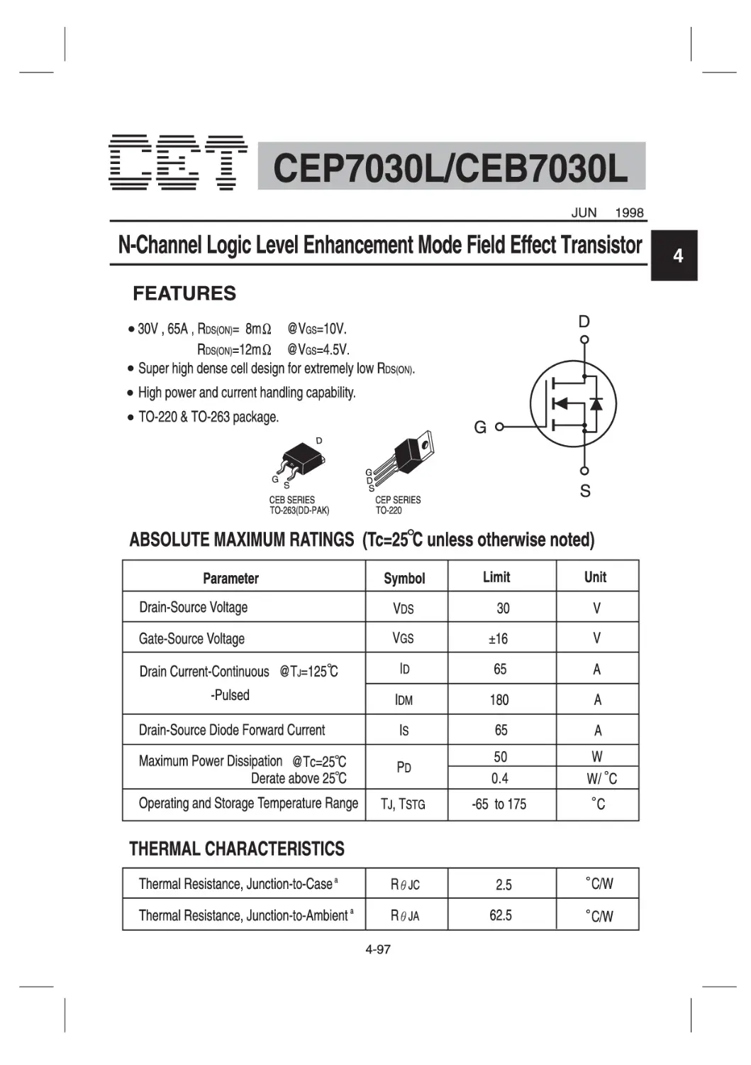
                    CEP7030L/CEB7030L
JUN 1998
N-Channel Logic Level Enhancement Mode Field Effect Transistor
FEATURES
•	30V, 65A, Rds(on)= 8m Q	@Vgs=10V.
Rds(on)=12itiQ @Vgs=4.5V.
•	Super high dense cell design for extremely low Rds(on>.
•	High power and current handling capability.
•	TO-220 & TO-263 package.
CEB SERIES
T0-263(DD-PAK)
CEP SERIES
TO-220
ABSOLUTE MAXIMUM RATINGS (Tc=25°C unless otherwise noted)
Parameter	Symbol	Limit	Unit
Drain-Source Voltage	VDS	30	V
Gate-Source Voltage	vgs	±16	V
Drain Current-Continuous @Tj=125°C -Pulsed	Id	65	A
	Idm	180	A
Drain-Source Diode Forward Current	Is	65	A
Maximum Power Dissipation @Tc=25°C Derate above 25°C	PD	50	W
		0.4	W/°C
Operating and Storage Temperature Range	Tj, TSTG	-65 to 175	°C
THERMAL CHARACTERISTICS
Thermal Resistance, Junction-to-Casea	R0JC	2.5	°C/W
Thermal Resistance, Junction-to-Ambienta	RflJA	62.5	°C/W
4-97
CEP7030L/CEB7030L
ELECTRICAL CHARACTERISTICS (Tc=25°C unless otherwise noted)
Parameter	Symbol	Condition	Min	Typ	Max	Unit
OFF CHARACTERISTICS
Drain-Source Breakdown Voltage	BVdss	Vgs=0V, lD=250pA	30	35		V
Zero Gate Voltage Drain Current	Idss	Vds=24V, Vgs=OV			10	pA
Gate-Body Leakage	Igss	Vgs=±16V,Vds=0V			±100	nA
ON CHARACTERISTICS’
Gate Threshold Voltage	VGS(th)	Vds=Vgs, Id=250|1A	1	1.5	3	V
Drain-Source On-State Resistance	Rds(ON)	Vgs=10V, Id = 35A		7.4	8	mfl
		Vgs=4.5V, Id= 28A		10.6	12	mfl
On-State Drain Current	Id(ON)	Vgs=10V,Vds=10V	60			A
Forward Transconductance	9fs	Vds=10V,Id=35A		50		S
DYNAMIC CHARACTERISTICS"
Input Capacitance	Ciss	Vds=15V,Vgs=0V f=1,0MHz		2000	2200	pF
Output Capacitance	Coss			1011	1250	pF
Reverse Transfer Capacitance	Crss			131	400	pF
SWITCHING CHARACTERISTICS"
Turn-On Delay Time	tD(ON)	Vdd = 15V, Id=60A, Vgen=10V Rg=1.8 fl Rl=0.25 fl		15		ns
Rise Time	tr			210		ns
Turn-Off Delay Time	tD(OFF)			30		ns
Fall Time	tf			55		ns
Total Gate Charge	Qg	Vds =24V, Id = 60A, Vgs=10V		60	110	nC
Gate-Source Charge	Qgs			9	31	nC
Gate-Drain Charge	Qgd			20	57	nC
4-98
CEP7030L/CEB7030L
ELEC1BICAL CHARACTERISTICS (Г-2эС unless otherwise noted)
Parameter	Symbol	Condition	Min	Typ	Max	Unit
DRAIN-SOURCE DIODE CHARACTERISTICSa
Diode Forward Voltage	VSD	Vgs = 0V, Is =35A		0.93	1.3	V
Notes
a.Pulse Test:Pulse Width <300 /z s, Duty Cycle <2%.
b.Guaranteed by design, not subject to production testing.
Vds, Drain-to-Source Voltage (V)
Figure 1. Output Characteristics
Vgs, Gate-to-Source Voltage (V)
Figure 2. Transfer Characteristics
Vds, Drain-to Source Voltage (V)
Figure 3. Capacitance
Id, Drain Current(A)
Figure 4. On-Resistance Variation with
Drain Current and Temperature
4-99
CEP7030L/CEB7030L
Tj, Junction Temperature (°C)
Figure 5. Gate Threshold Variation
with Temperature
Tj, Junction Temperature (°C)
Figure 6. Breakdown Voltage Variation
with Temperature
Ids, Drain-Source Current (A)
Figure 7. Transconductance Variation
with Drain Current
Qg, Total Gate Charge (nC)
Figure 9. Gate Charge
0.4	0.6	0.8	1.0	1.2	1.4
Vsd, Body Diode Forward Voltage (V)
Figure 8. Body Diode Forward Voltage
Variation with Source Current
Vds, Drain-Source Voltage (V)
Figure 10. Maximum Safe
Operating Area
4-100
CEP7030L/CEB7030L
Vgs
Figure 11. Switching Test Circuit
Figure 12. Switching Waveforms
r(t),Normalized Effective
Transient Thermal Impedance
Figure 13. Normalized Thermal Transient Impedance Curve
4-101