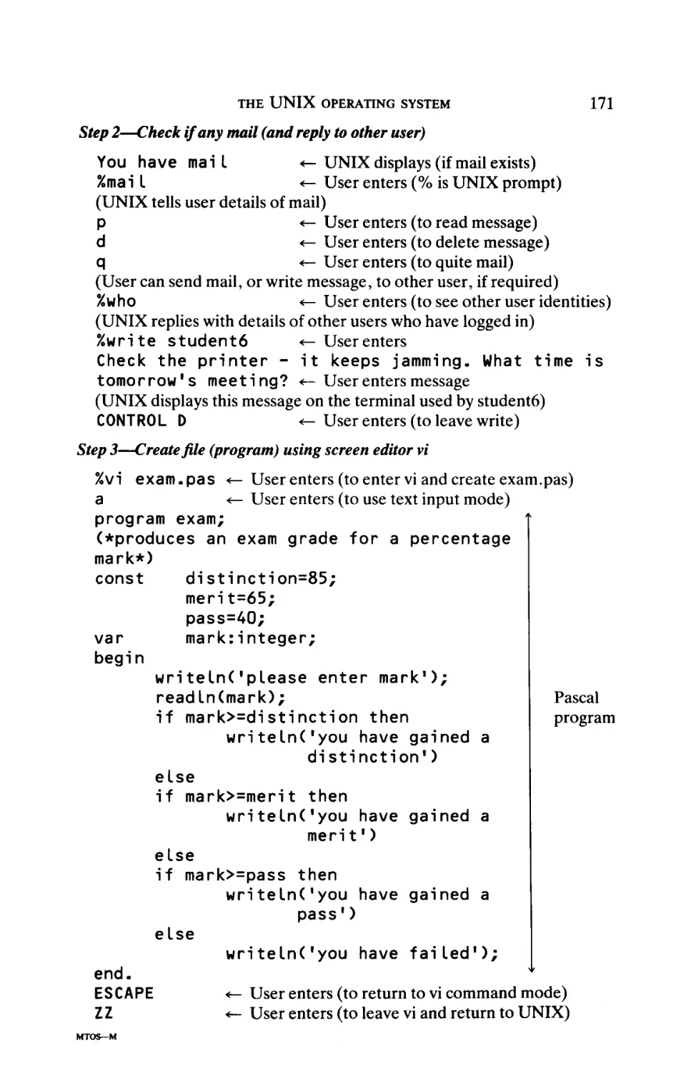
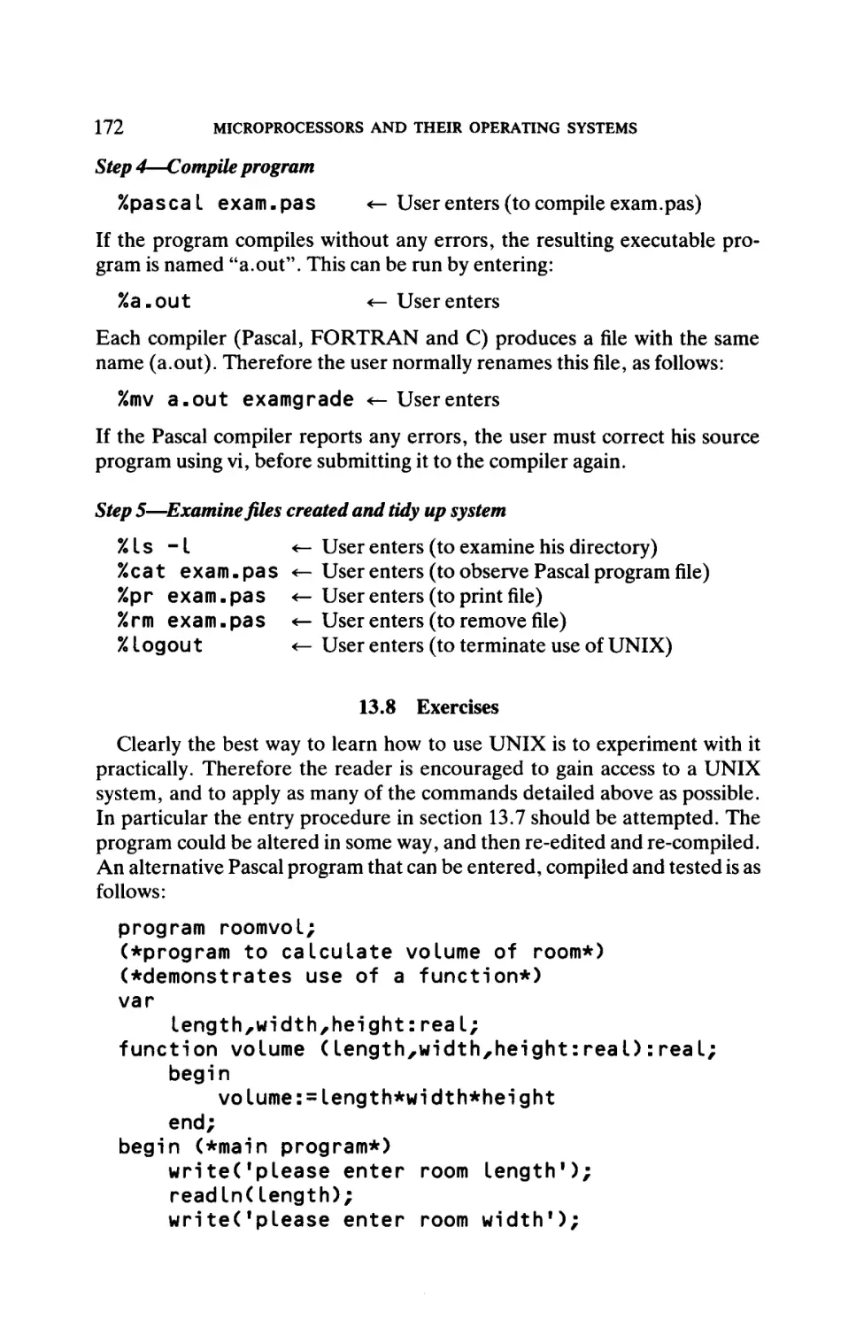
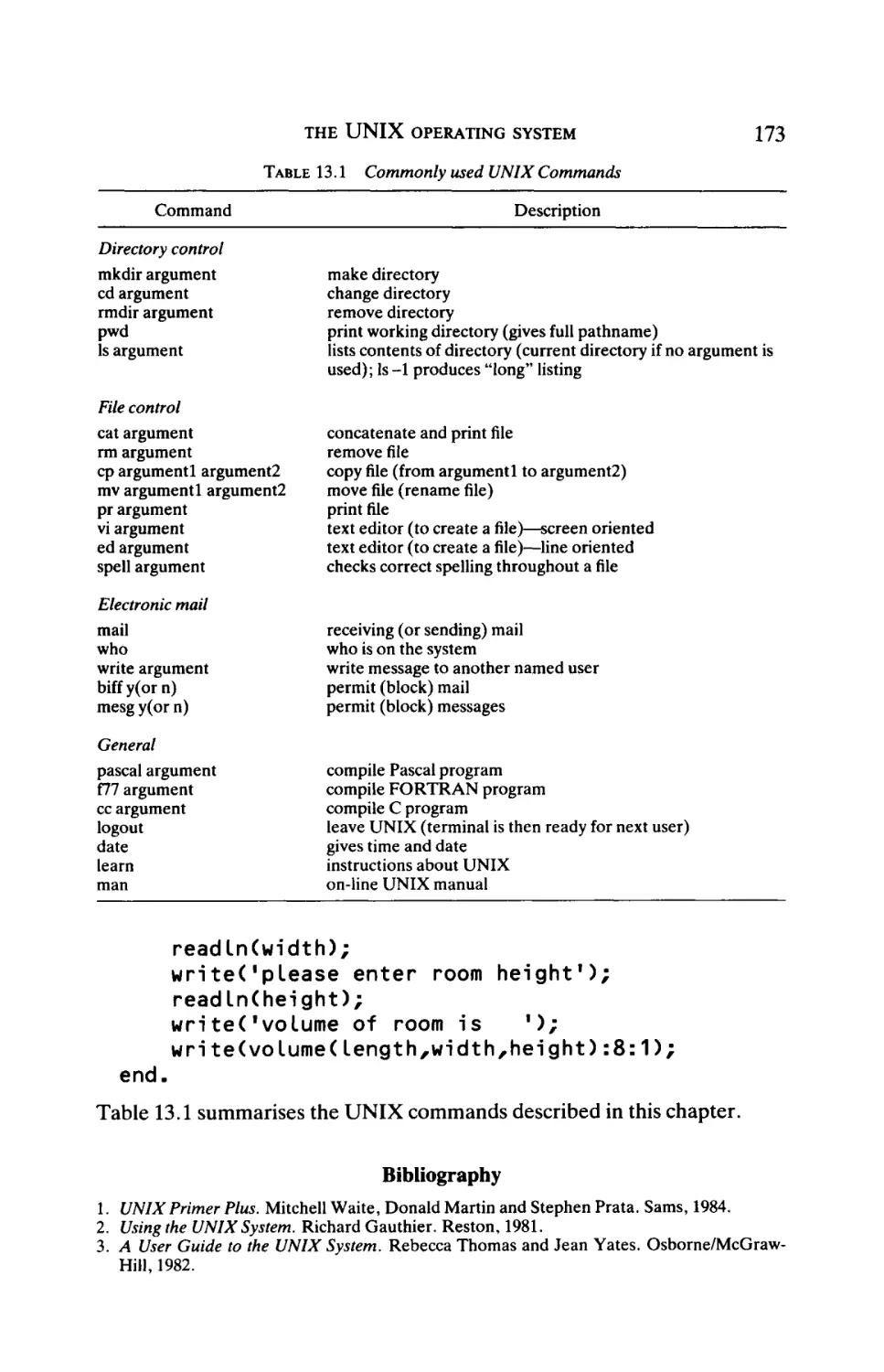
/
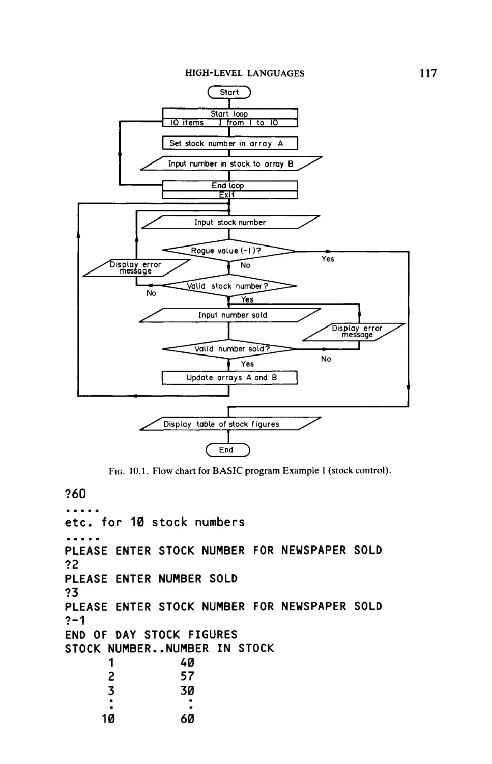
Similar


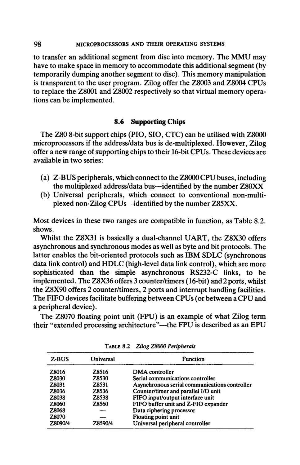
Text
APPLIED ELECTRICITY AND ELECTRONICS SERIES
Editor: P. HAMMOND, University of Southampton, UK
Pergamon Titles of Related Interest
DHEERE
Universal Computer Interfaces
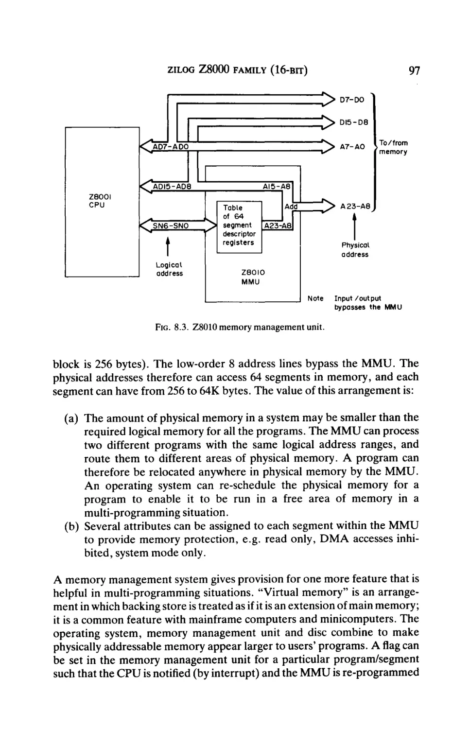
HAMMOND
Electromagnetism for Engineers, 3rd Edition
HINDMARSH
Electrical Machines & Drives, Worked Examples, 2nd Edition
Electrical Machines & their Applications, 4th Edition
HOLLAND
Illustrated Dictionary of Microelectronics & Microcomputers
Integrated Circuits & Microprocessors
Microcomputers & their Interfacing
KUFFEL & ZAENGEL
High Voltage Engineering
YORKE
Electric Circuit Theory, 2nd Edition
P e r g a m o n R e l a t e d J o u r n a l s (free specimen copy gladly sent on request)
Computers & Electrical Engineering
Electric Technology USSR
Microelectronics & Reliability
Robotics & Computer-integrated Manufacturing
Solid State Electronics
Microprocessors
and their
Operating Systems
A Comprehensive Guide to 8-, 16- and 32-Bit Hardware,
Assembly Language and Computer Architecture
R. C. HOLLAND
West Glamorgan Institute of Higher Education, Swansea, UK
PERGAMON PRESS
OXFORD · NEW YORK · BEIJING · FRANKFURT
SÄO PAULO · SYDNEY · TOKYO · TORONTO
U.K.
U.S.A.
PEOPLE'S REPUBLIC
OF CHINA
FEDERAL REPUBLIC
OF GERMANY
BRAZIL
AUSTRALIA
JAPAN
CANADA
Pergamon Press pic, Headington Hill Hall,
Oxford OX3 0BW, England
Pergamon Press, Inc., Maxwell House, Fairview Park,
Elmsford, New York 10523, U.S.A.
Pergamon Press, Room 4037, Qianmen Hotel, Beijing,
People's Republic of China
Pergamon Press GmbH, Hammerweg 6,
D-6242 Kronberg, Federal Republic of Germany
Pergamon Editora Ltda, Rua Eça de Queiros, 346,
CEP 04011, Paraiso, Säo Paulo, Brazil
Pergamon Press Australia Pty Ltd., P.O. Box 544,
Potts Point, N.S.W. 2011, Australia
Pergamon Press, 5th Floor, Matsuoka Central Building,
1-7-1 Nishishinjuku, Shinjuku-ku, Tokyo 160, Japan
Pergamon Press Canada Ltd., Suite No. 271,
253 College Street, Toronto, Ontario, Canada M5T1R5
Copyright © 1989 R. C. Holland
All Rights Reserved. No part of this publication may be
reproduced, stored in a retrieval system or transmitted in
any form or by any means: electronic, electrostatic, magnetic tape, mechanical, photocopying, recording or otherwise, without permission in writing from the publisher
First English edition 1989
Library of Congress Cataloging-in-Publication Data
Holland, R. C.
Microprocessors and their operating systems:
a comprehensive guide to 8-, 16- and 32-bit hardware,
assembly language and computer architecture
R.C.Holland.—1st ed.
p. cm.—(Applied electricity and electronics series)
Includes index.
1. Microprocessors. 2. Operating systems
(Computers). I. Title. II. Series.
QA76.5.H633 1989 004.16—dc 19
88-38877
British Library Cataloguing in Publication Data
Holland, R. C.
Microprocessors and their operating systems:
a comprehensive guide to 8-, 16- and 32-bit hardware,
assembly language and computer architecture
(Applied electricity and electronics)
I. Title II. Series
004.16
ISBN 0-08-037189-2 Hardcover
ISBN 0-08-037188-4 Flexicover
Printed in Great Britain by BPCC Wheatons Ltd, Exeter
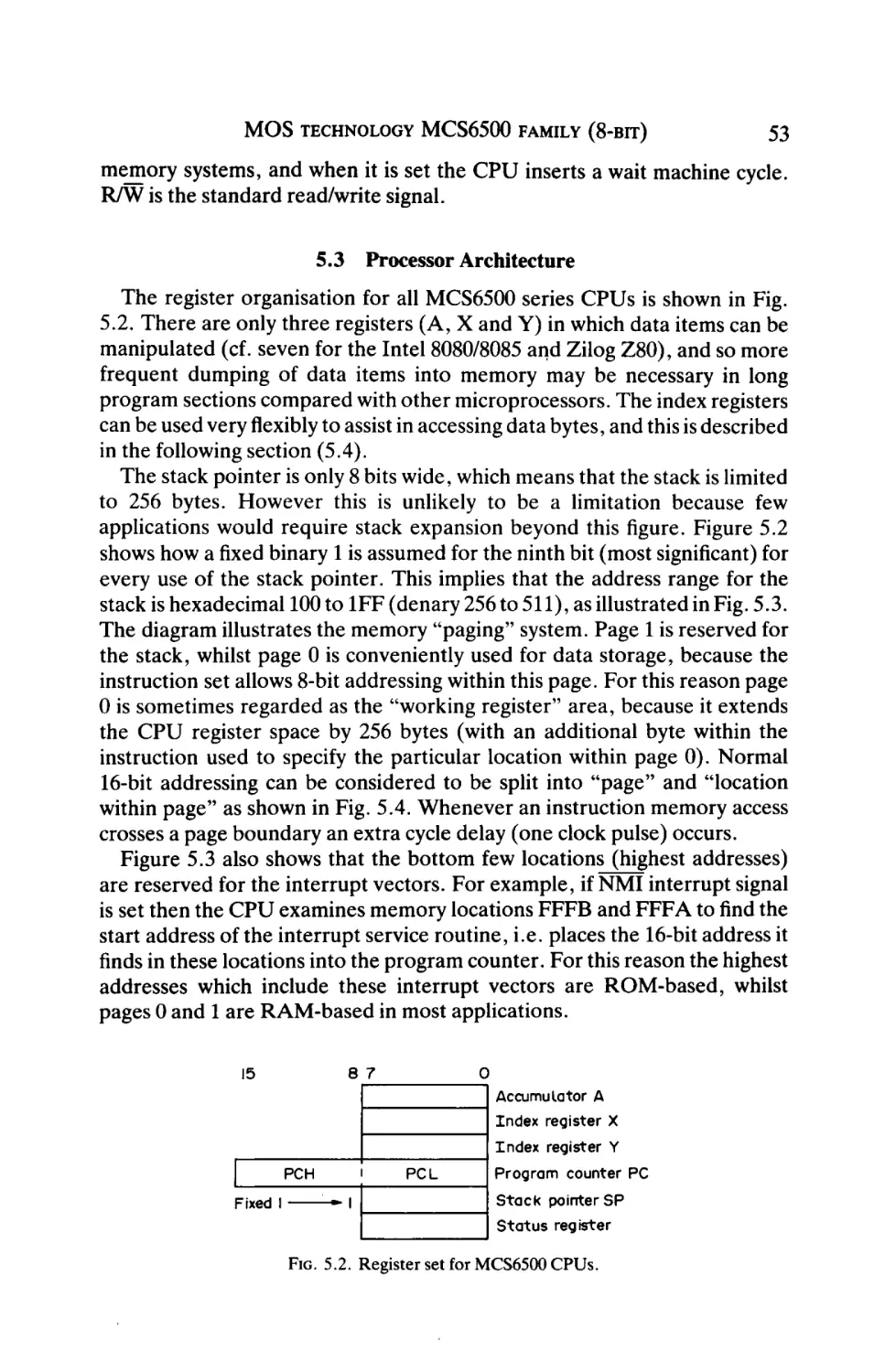
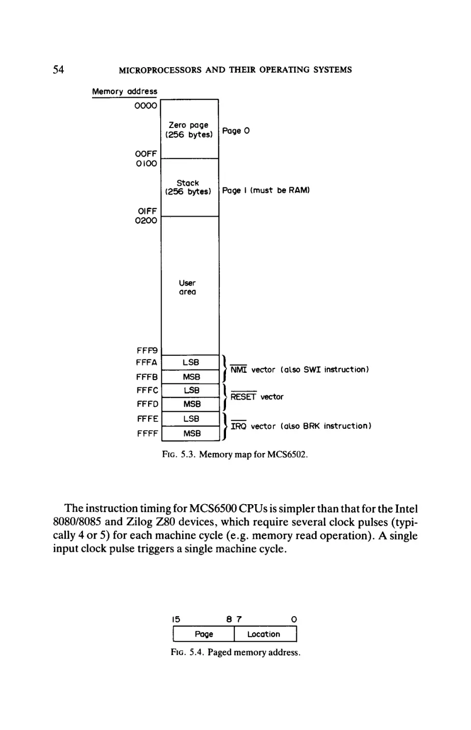
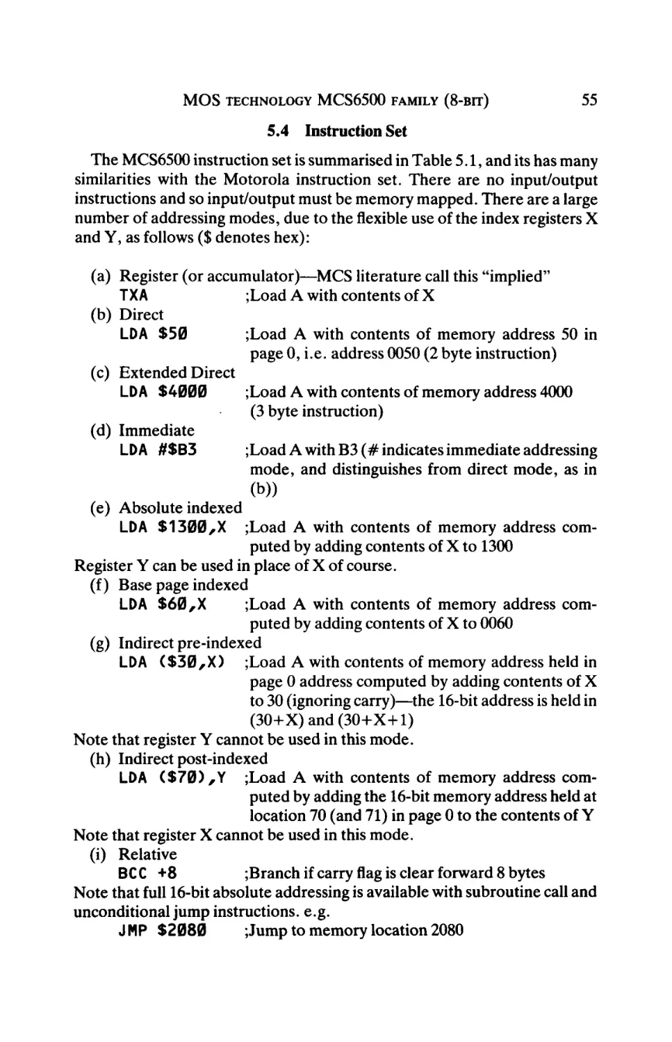
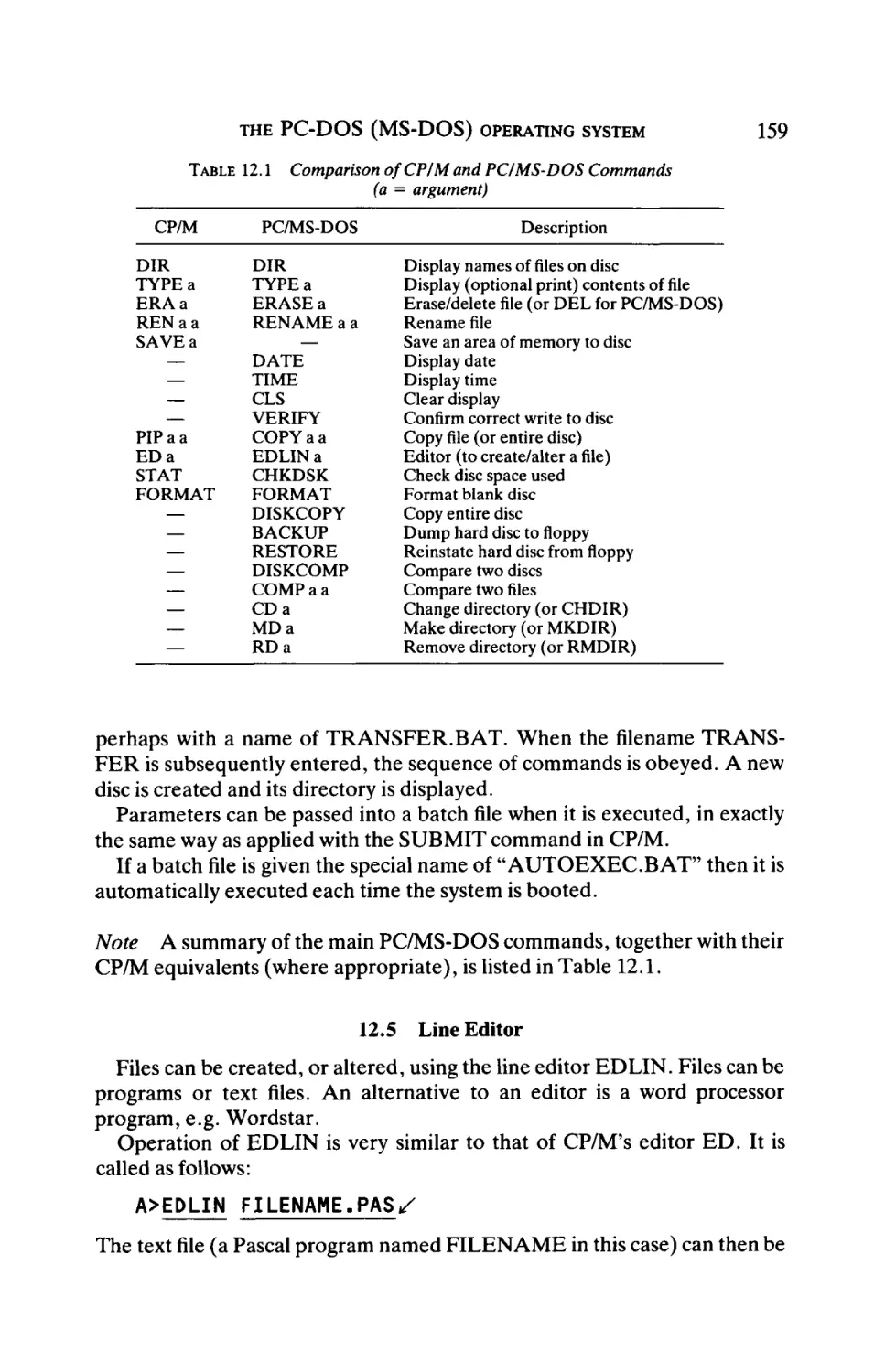
PREFACE
This book is an attempt to bring together all the essential features of each of
the major microprocessor families that have evolved through the 1970s and
1980s. The main characteristics of each of the 8-bit, 16-bit and 32-bit
microprocessors are presented, together with descriptions of applications
and software considerations.
The book excludes some of the less-frequently applied microprocessors,
but the concentration on the most common devices provides descriptions of
the processors that are used in at least 95% of current microcomputer
systems.
Most books on similar topics tend to concentrate on a single device. The
comprehensive coverage of the subject presented here should provide a
useful reference for the reader who requires a good general background to
the whole subject. The later chapters in the book concentrate on program
ming languages (BASIC, Pascal and C), and in particular on operating
systems (the main program in a multi-program microcomputer system). The
descriptive notes on the facilities available within the most common operat
ing systems should enable a user of a disc-based microcomputer to perform
a complete range of operator functions.
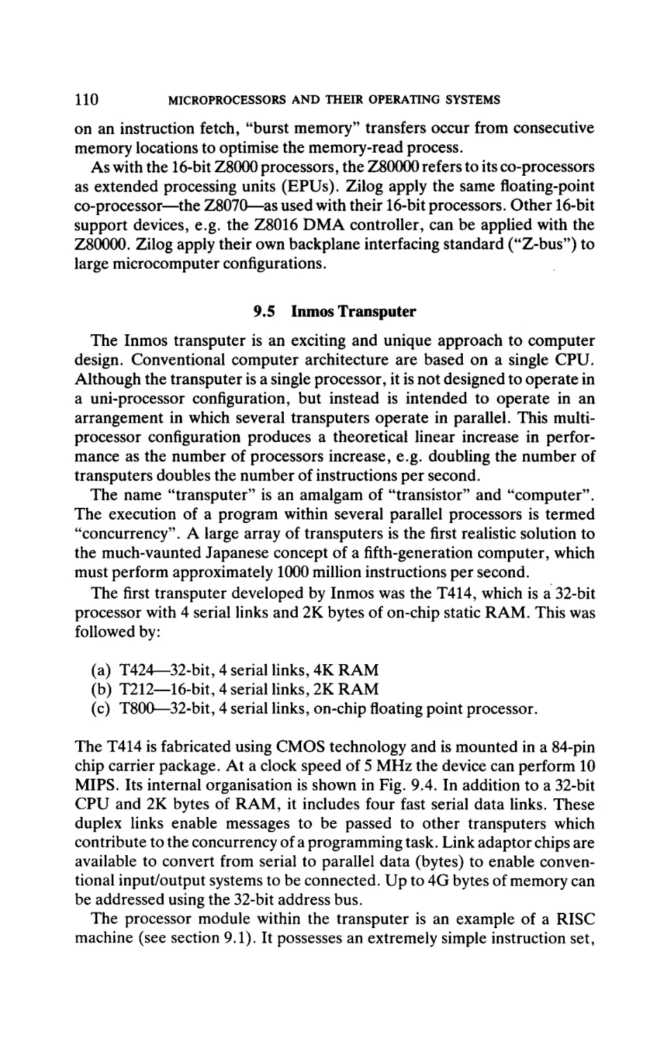
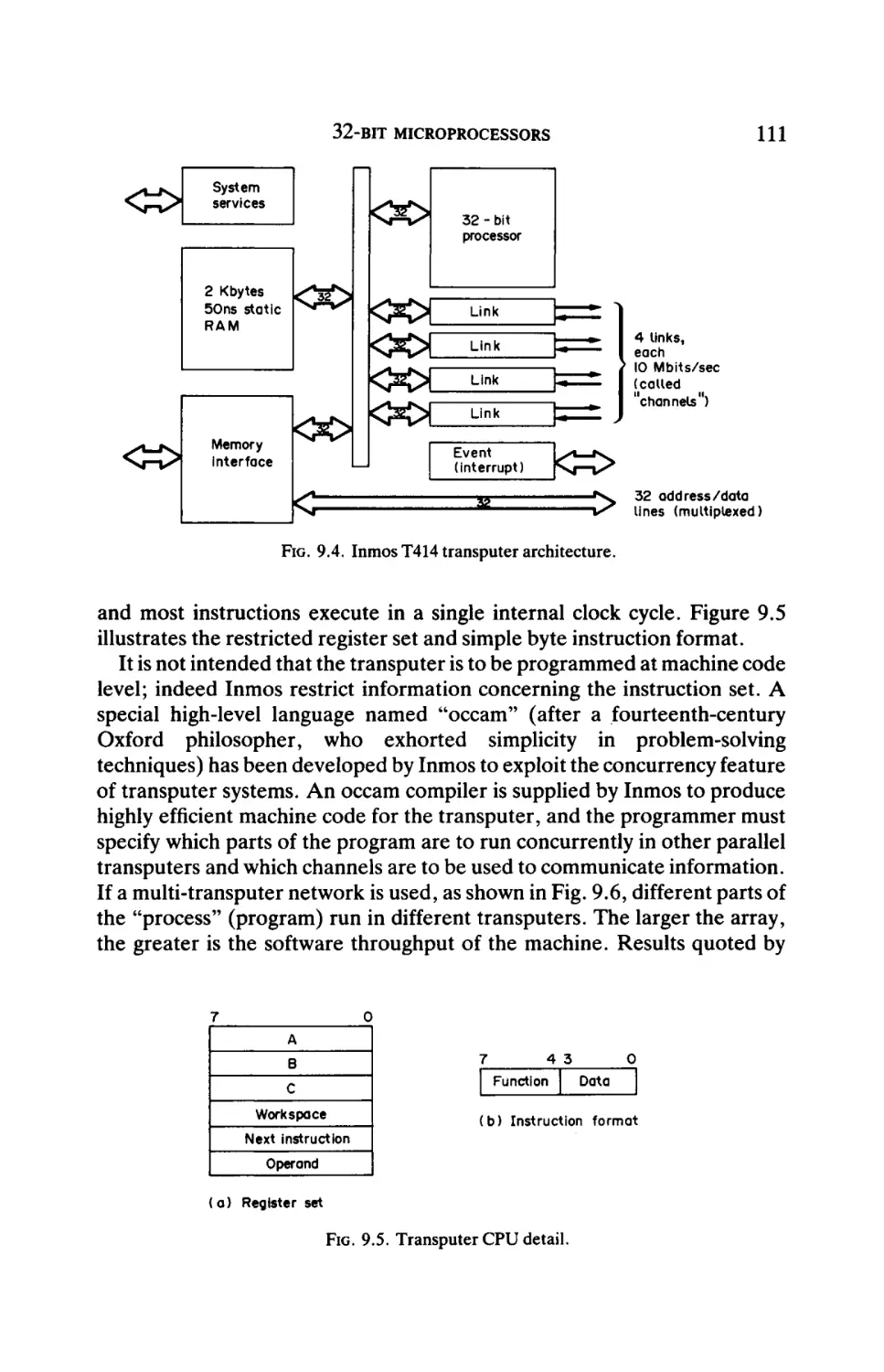
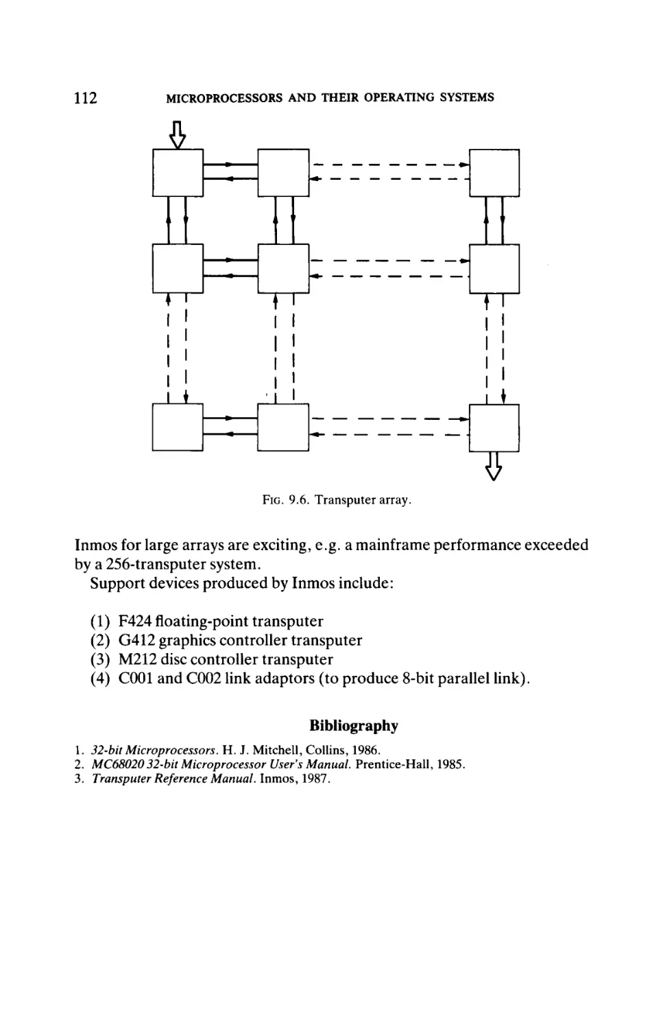
An introductory chapter on microcomputer principles is provided to assist
a reader who is new to the subject, and a glossary of terms at the end of the
book should prove helpful.
The author wishes to thank several of his colleagues for helpful discus
sions, and his long-suffering students (past and present) who have often
provided an experimental platform for the presentation style of much of the
material.
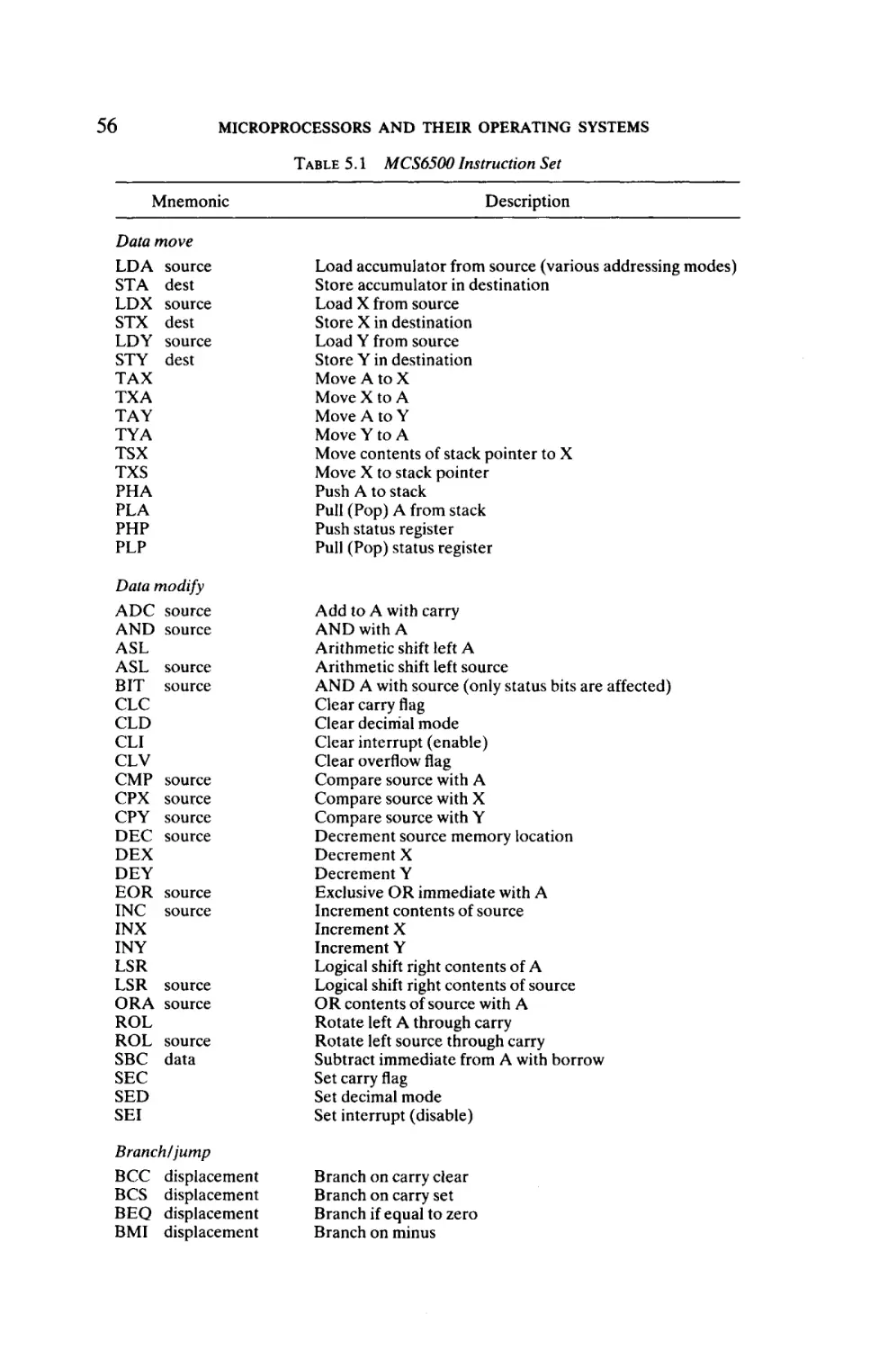
Vlll
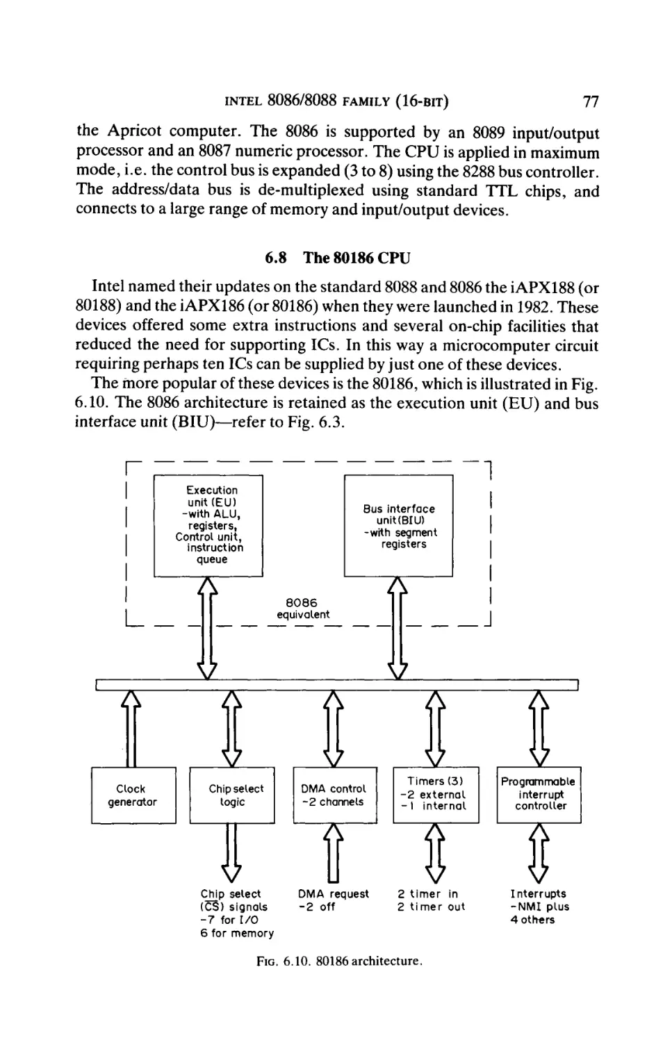
CHAPTER 1
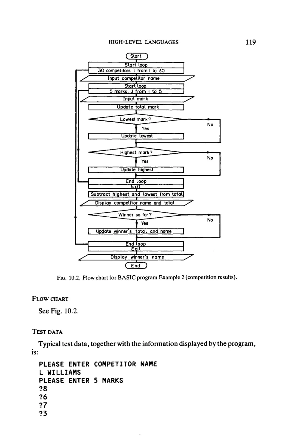
MICROCOMPUTER PRINCIPLES
1.1 Microcomputer Architecture
Computers are generally classified as follows:
(a) mainframe computers, which support a large number of user terminals and peripherals and which are used for large data-handling
systems, e.g. payroll, customer accounts;
(b) minicomputers, which support a smaller number of user terminals
(typically up to 40) and which are used in small-company business
applications as well as factory control systems;
(c) microcomputers, which normally support a single user (although
latest systems have edged into the minicomputer market) and which
are applied in a wide number of domestic, commercial and industrial
control applications.
The distinguishing feature of a microcomputer is that its CPU (central
processor unit) is a single IC (integrated circuit). This central component is
termed "microprocessor". It is supported by memory and input/output ICs
to constitute a complete microcomputer.
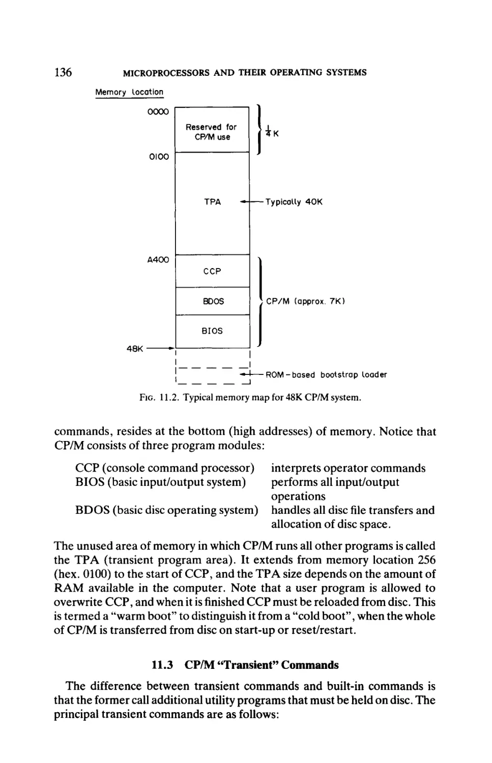
The basic architecture of all types of computer is shown in Fig. 1.1. The
CPU, or microprocessor in the case of a microcomputer, generates the three
buses, which are a set of circuit connections. The computer program that the
CPU executes is held in memory, which in microcomputers is invariably
arranged in 8-bit (a bit is 0 or 1) locations. The CPU extracts each instruction
in turn from memory, examines it and executes it. The transfer of each
instruction is as follows:
(1) CPU sets the memory address of the next instruction on the address
bus;
(2) memory location presents the contents of the selected memory
address on the data bus;
(3) CPU reads in the instruction and implements it.
The control bus carries signals that are required to activate the above
transfers.
1
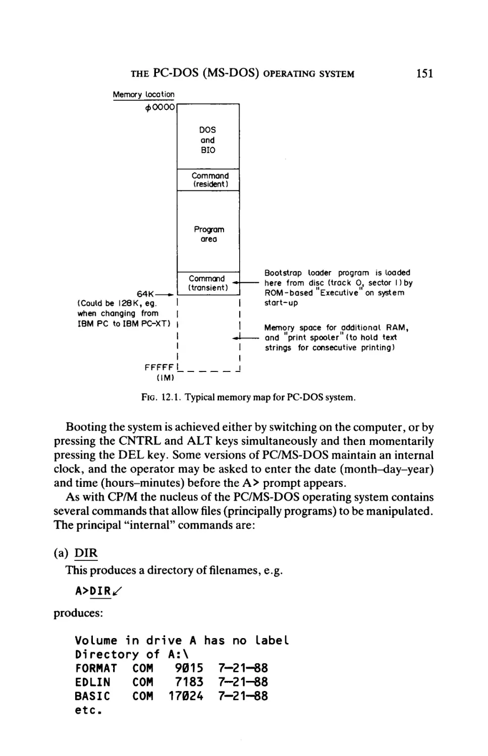
2
MICROPROCESSORS AND THEIR OPERAΉNG SYSTEMS
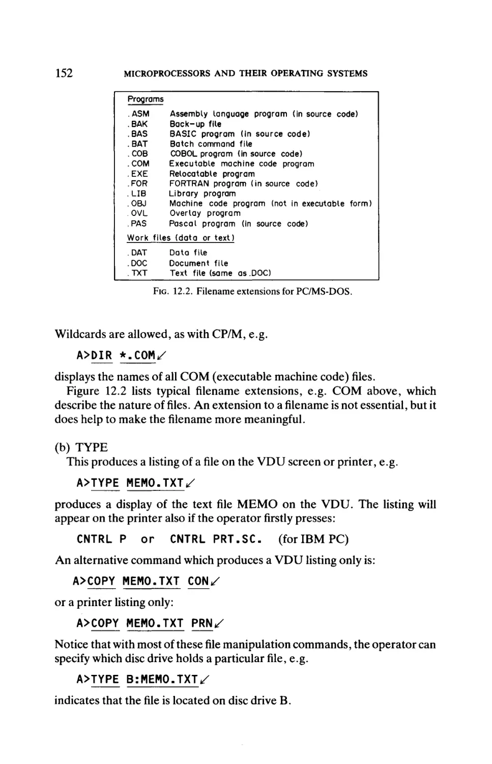
Address bus (16 lines for 8 - b i t CPU)
Data bus (8 lines for 8-bit CPU)
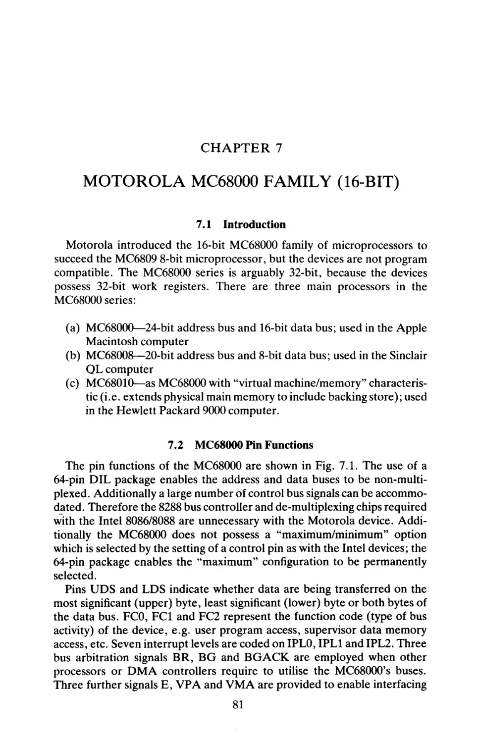
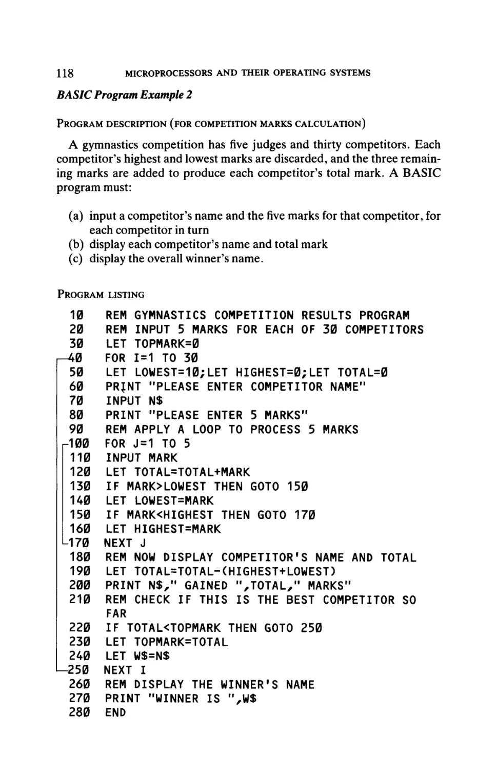
FIG. 1.1. Computer architecture.
Memory also contains data values in addition to program instructions.
Data values can be numbers (represented in binary), or characters for
display or printing purposes (represented by a unique code—the "ASCII"
code).
The input/output module contains circuits that transfer programs and data
to and from peripheral devices, e.g. backing store (such as floppy disc),
printer and VDU (user terminal).
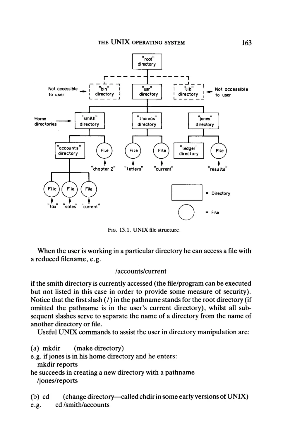
In the simplest forms of microcomputer, e.g. pocket calculator or washing
machine controller, the three modules (CPU, memory and input/output)
are contained within a single IC.
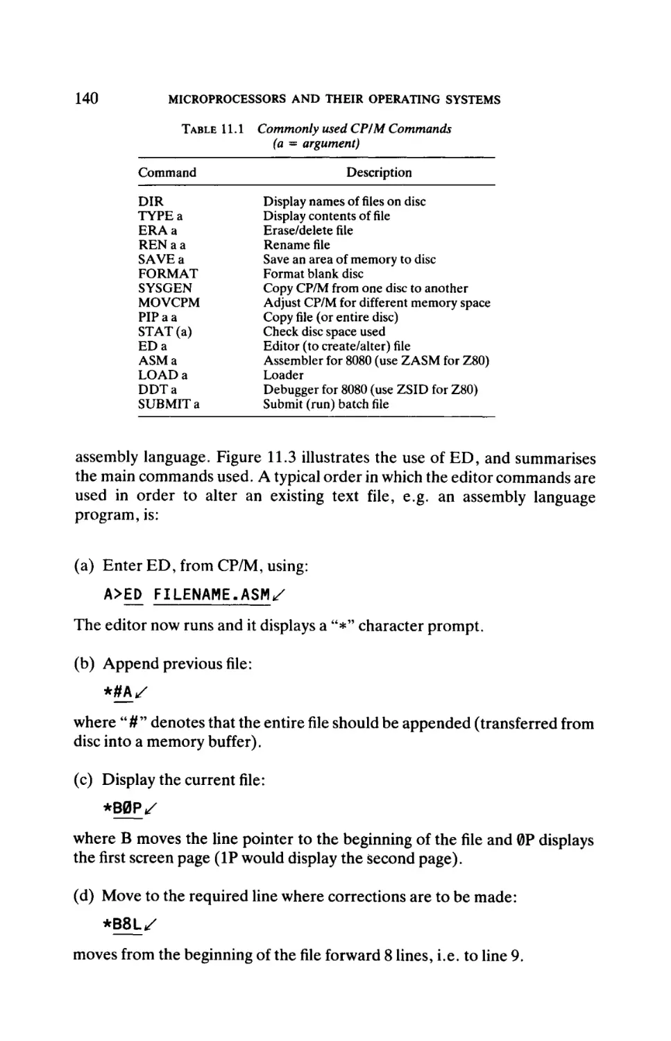
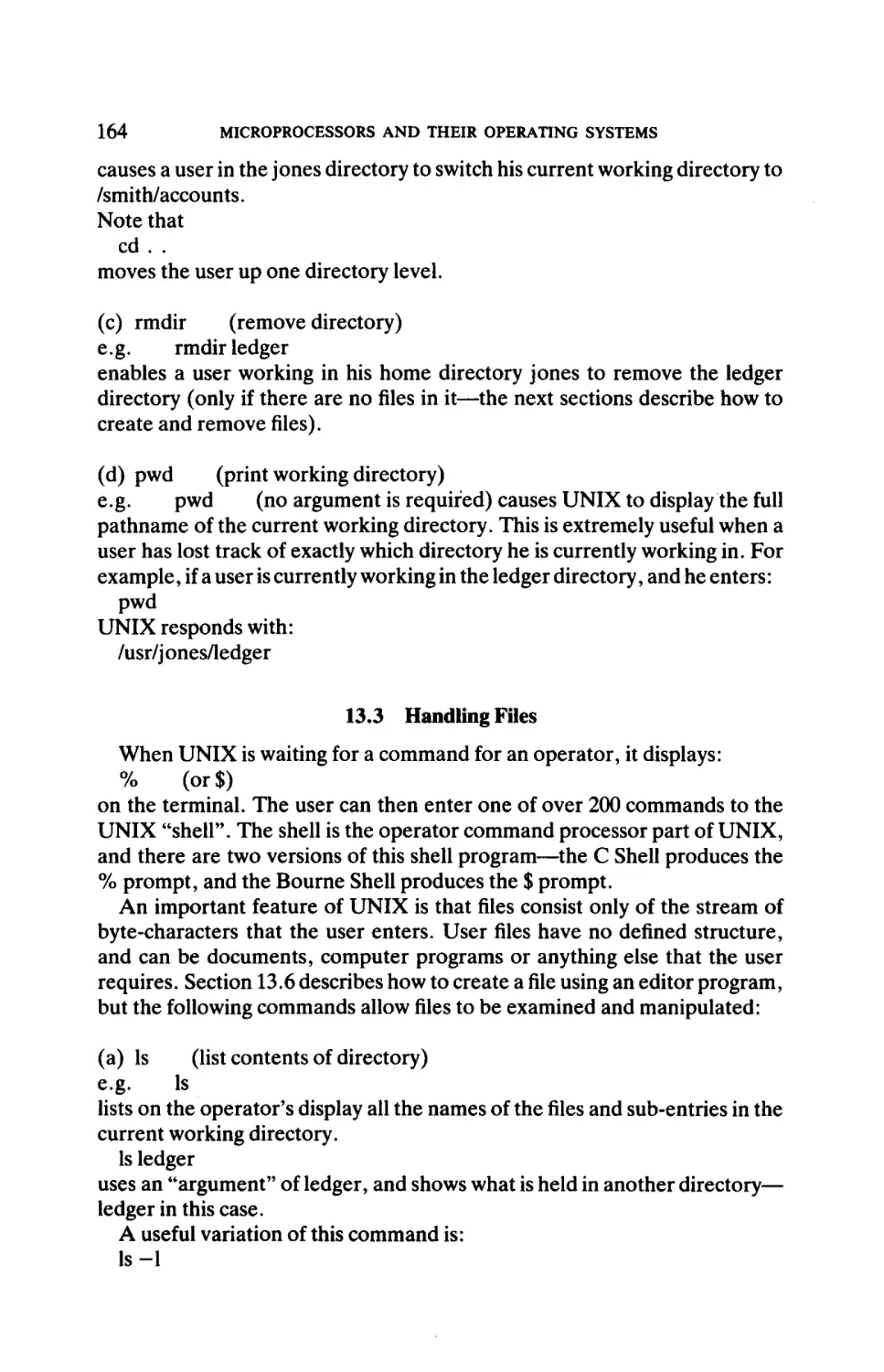
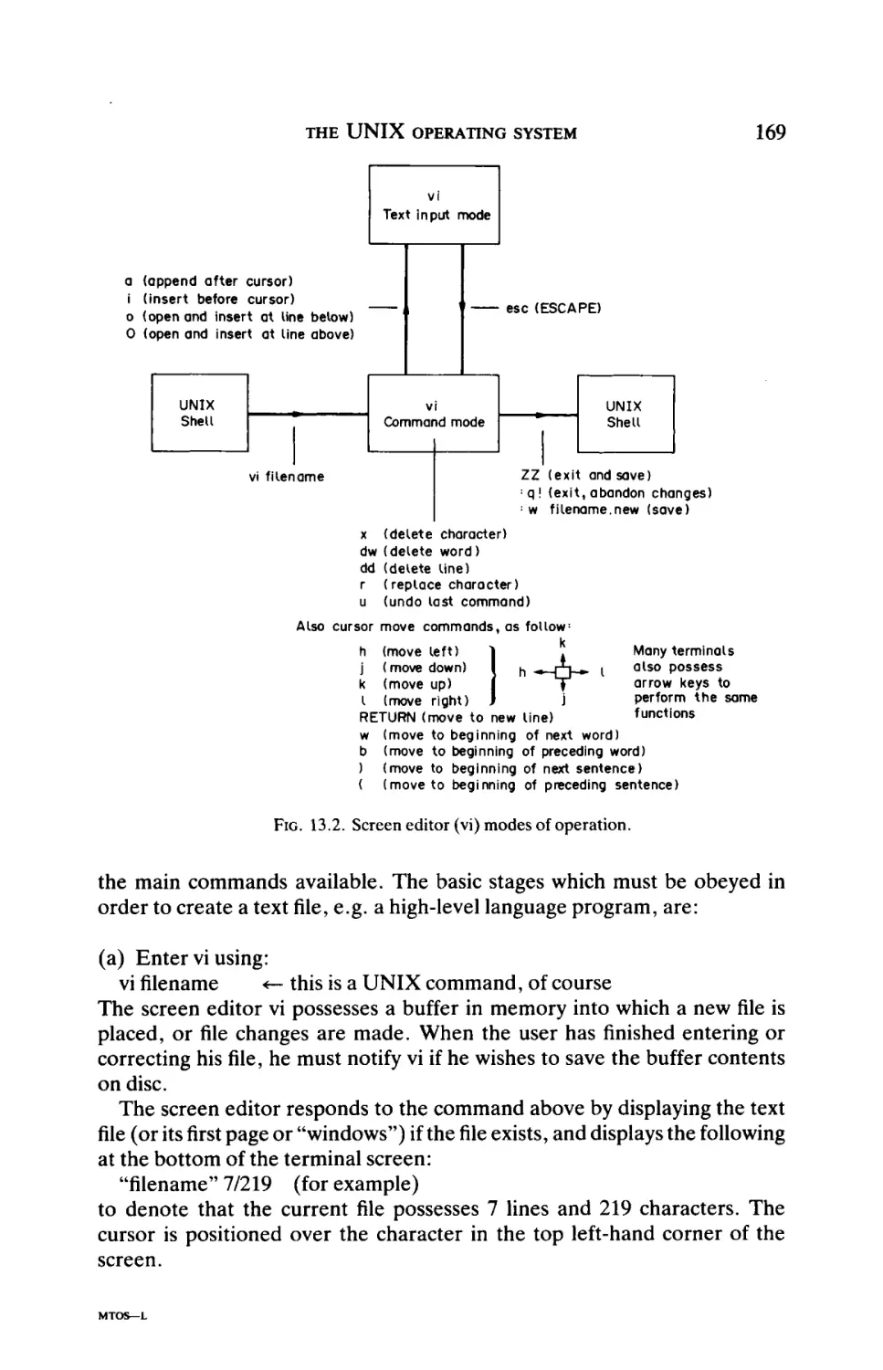
1.2 CPU (Central Processor Unit)
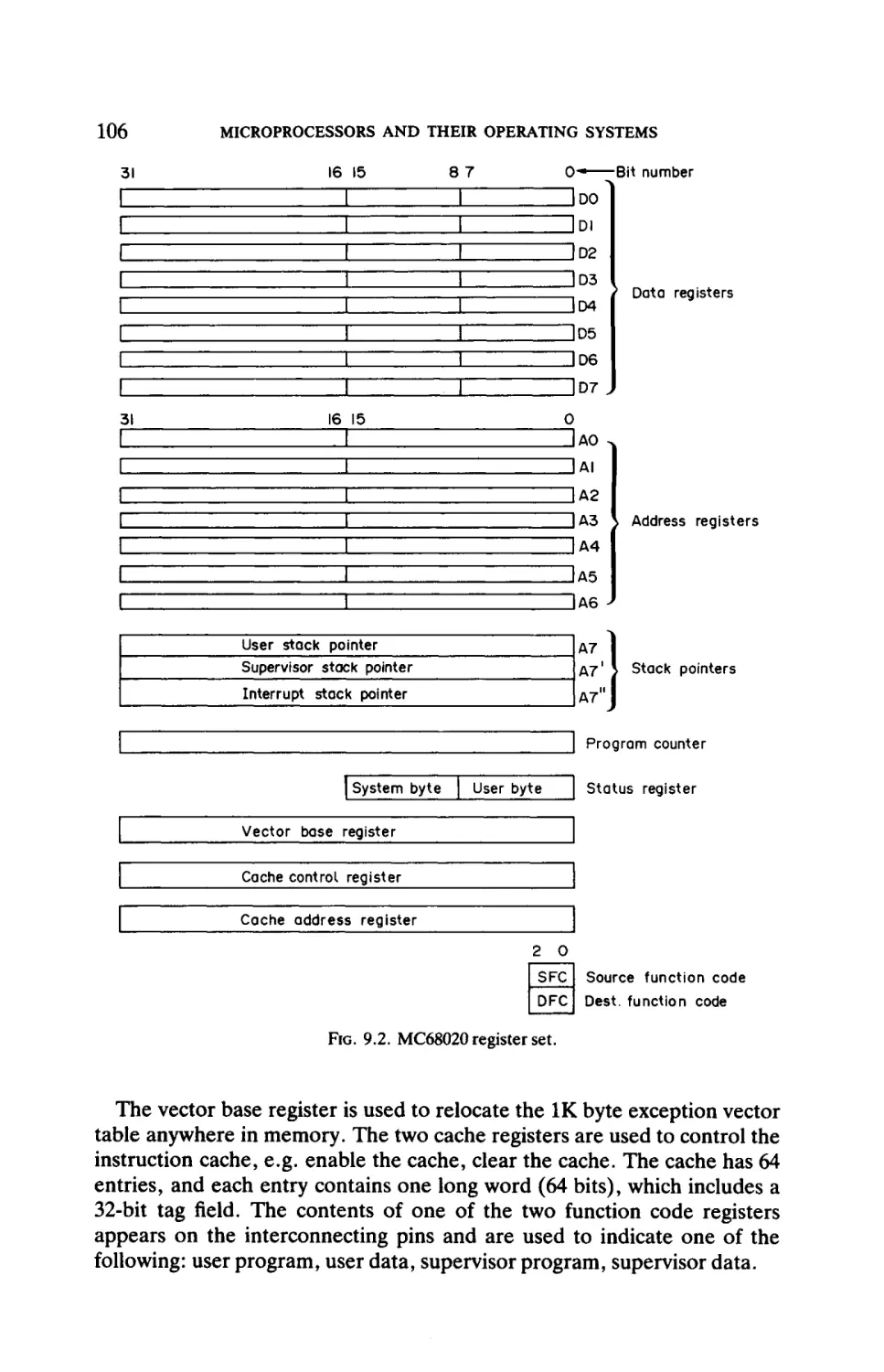
The typical internal organisation of a CPU is shown in Fig. 1.2. All actions
are triggered by a clock pulse. The functions of the internal modules are as
follows:
(a) The program counter contents are placed on the address bus so that
the next program instruction can be transferred from memory to the
CPU.
(b) The instruction register receives the instruction.
(c) The control unit decodes the instruction and activates transfers around
the CPU in order to execute the instruction.
(d) The work registers hold data items that can be processed within the
instruction (a specialised work register that can receive the results of
ALU operations is termed an "accumulator").
(e) The ALU is the processing part of the CPU, i.e. it can alter data values
using arithmetic (add, subtract, etc.) and logical (OR, AND, etc.)
functions.
2
MICROCOMPUTER PRINCIPLES
Instruction
register
Clock
pulses '
Work
registers
(including
accumulator)
ALU
(Arithmetic
and Logic
Unit)
Control
unit
J~I
Status
register
r τ^
Control bus
Program
counter
D7-D0
ΔΙ5-Δ0
Data bus
Address bus
FIG. 1.2. Internal organisation of CPU.
(f) The status register contains 'flags" that mark the result of ALU
operations, e.g. zero result.
The word length of a CPU is expressed in terms of the number of bits that
are processed in a single ALU operation, e.g. an 8-bit CPU can perform an
arithmetic add operation on two 8-bit numbers. Microprocessor IC packages
can be grouped as follows:
(a) 8-bit
invariably 40-pin DIL (dual-in-line, i.e. pins on two sides
only) package
(b) 16-bit normally 40- to 64-pin DIL package
(c) 32-bit between 60 and 120 pins in a "chip carrier" (pins on all four
sides of package), or PGA (pin grid array).
The operation of each instruction is conveniently divided into two
operations—"fetch" and "execute". Whilst the fetch part of the fetchexecute cycle is the same for every instruction, the execute part may or may
not involve further memory transfers. Some instructions require only ALU
operations in the execute part of the cycle, rather than slow memory transfer
operations. Therefore the instruction time is variable and depends on the
nature of the instruction. The following examples illustrate this:
Instruction Example 1—Add register B to register A
Step 1—Fetch instruction
Step 2—Execute (add B to A, the accumulator)
4
MICROPROCESSORS AND THEIR OPERATING SYSTEMS
Instruction Example 2—Load register A from memory
Step 1—Fetch instruction
Step 2—Execute 1 (read first half of memory address into CPU)
Step 3—Execute 2 (read second half of memory address into CPU)
Step A—Execute 3 (read data byte from memory address into A)
The second instruction takes approximately twice as long to operate as the
first instruction. Notice that, in an 8-bit microprocessor, the first instruction
is one byte (8 bits) long, i.e. it occupies one memory location. The second
instruction is three bytes long, because the second and third bytes contain
the 16-bit memory address of the data value that is being accessed. The
second and third bytes in this case are termed the "operand" of the
instruction, whilst the first byte that specifies the nature of the instruction is
termed the "opcode".
The instruction set that can be obeyed by a CPU may number from 50 to
several hundred different instructions. Instructions can be conveniently
grouped into four categories, as follows:
(1) Data move, e.g. between a CPU register and another CPU register, a
memory location or an input/output channel
(2) Data modify, i.e. when the ALU alters a data value
(3) Jump, i.e. transfer program control to another memory location
(4) Miscellaneous, e.g. to stop program execution.
Within (1) and (2) there are various ways of accessing a data value, and these
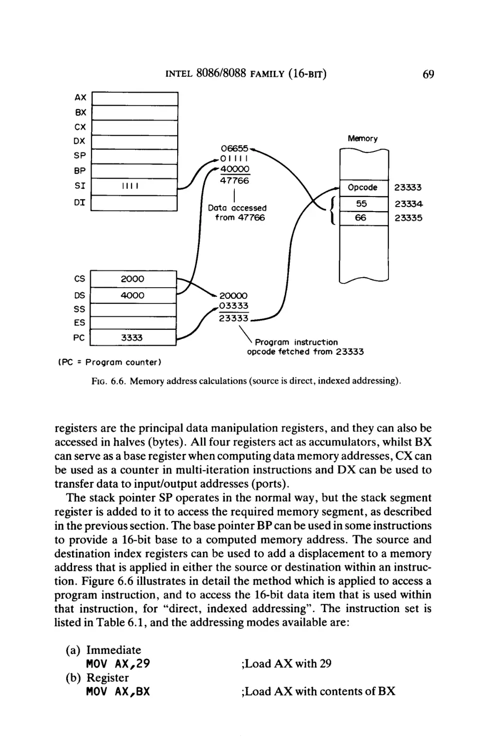
are termed the "addressing modes" that can be specified within an instruction. The most common addressing modes are:
(a) Direct Register—data value is held in a CPU register
(b) Direct Memory—data value is held in a memory location
(c) Indirect Register—data value is held in a memory location specified
within a CPU register (register-pair for an 8-bit CPU)
(d) Immediate—data value is held within the instruction (in the second
byte for an 8-bit CPU)
(e) Indexed—similar to (c) except that a displacement within the instruction is added to the contents of the indexing register to compute the
memory address.
1.3 Memory
Memory ICs are either ROM (read-only memory), which can only be
read, or RAM (random access memory), which can be read from and written
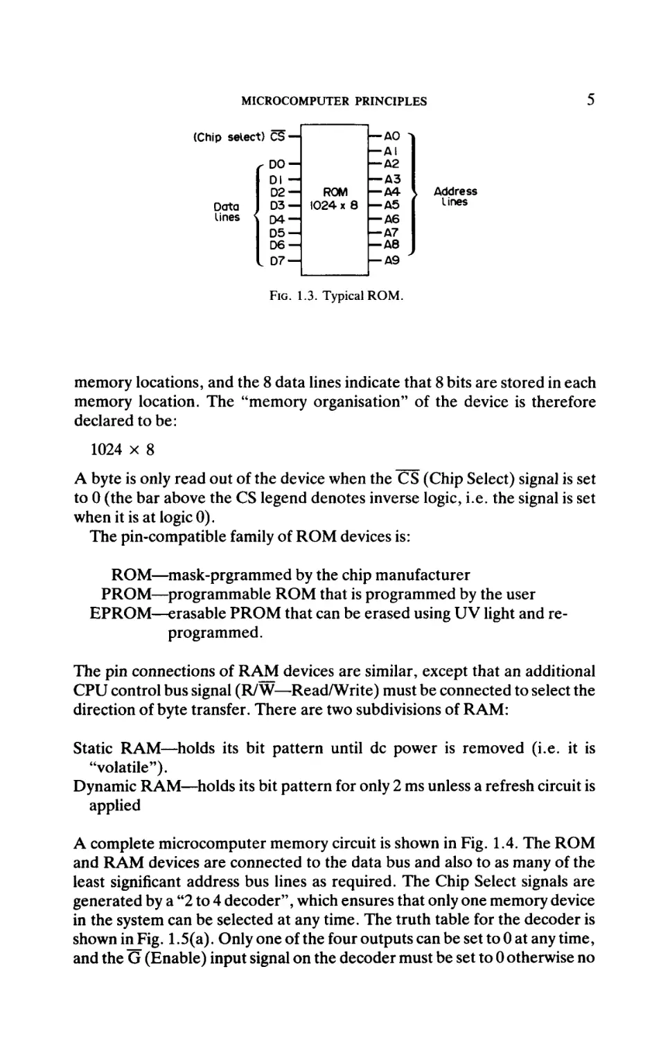
to. The pin connections of a typical ROM device are shown in Fig. 1.3. The
10 address lines give:
210 = 1024 (1024 = IK)
2
MICROCOMPUTER PRINCIPLES
ip select) C5 —
— Δ0 ^|
— AI
r DO —
— Δ2
— A3
Dl —
ROM
— A4
D2 —
D3 — 1024 x Θ — A5
Data
lines < D A
— A6
DS— Δ7
DO — ΔΘ
— Δ9
I D7 —
1
1
1
\
1
1
1
1
Address
lines
FIG. 1.3. Typical ROM.
memory locations, and the 8 data lines indicate that 8 bits are stored in each
memory location. The "memory organisation" of the device is therefore
declared to be:
1024 x 8
A byte is only read out of the device when the CS (Chip Select) signal is set
to 0 (the bar above the CS legend denotes inverse logic, i.e. the signal is set
when it is at logic 0).
The pin-compatible family of ROM devices is:
ROM—mask-prgrammed by the chip manufacturer
PROM—programmable ROM that is programmed by the user
EPROM—erasable PROM that can be erased using UV light and reprogrammed.
The pin connections of RAM devices are similar, except that an additional
CPU control bus signal (R/W—Read/Write) must be connected to select the
direction of byte transfer. There are two subdivisions of RAM:
Static RAM—holds its bit pattern until dc power is removed (i.e. it is
"volatile").
Dynamic RAM—holds its bit pattern for only 2 ms unless a refresh circuit is
applied
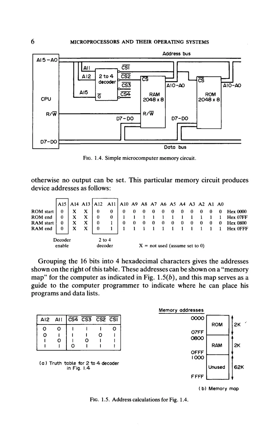
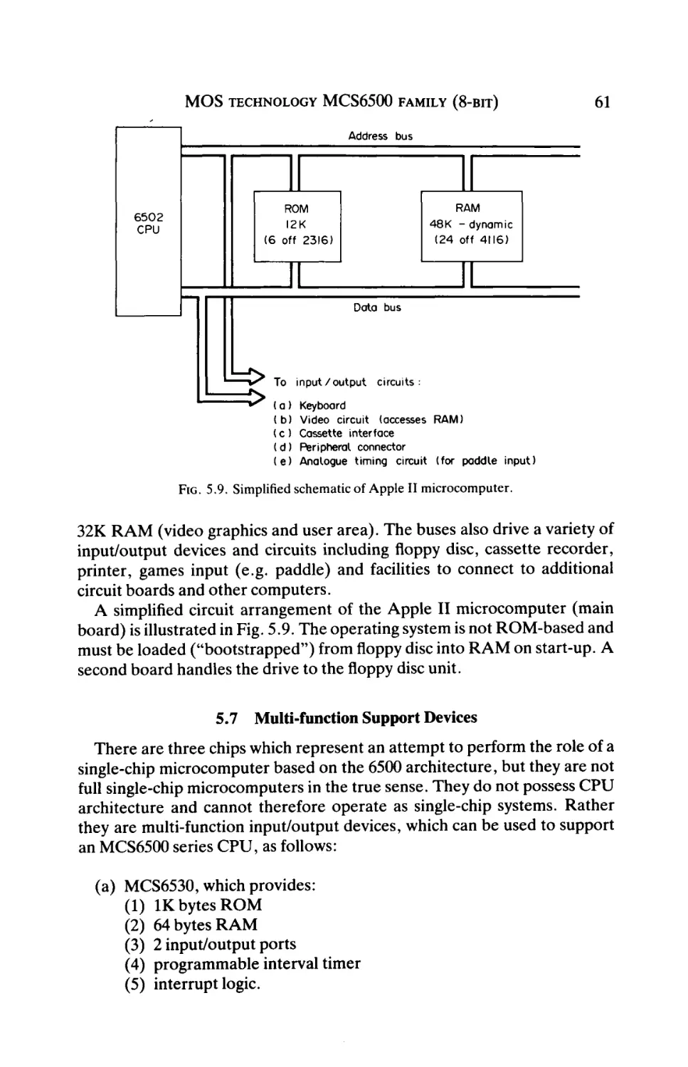
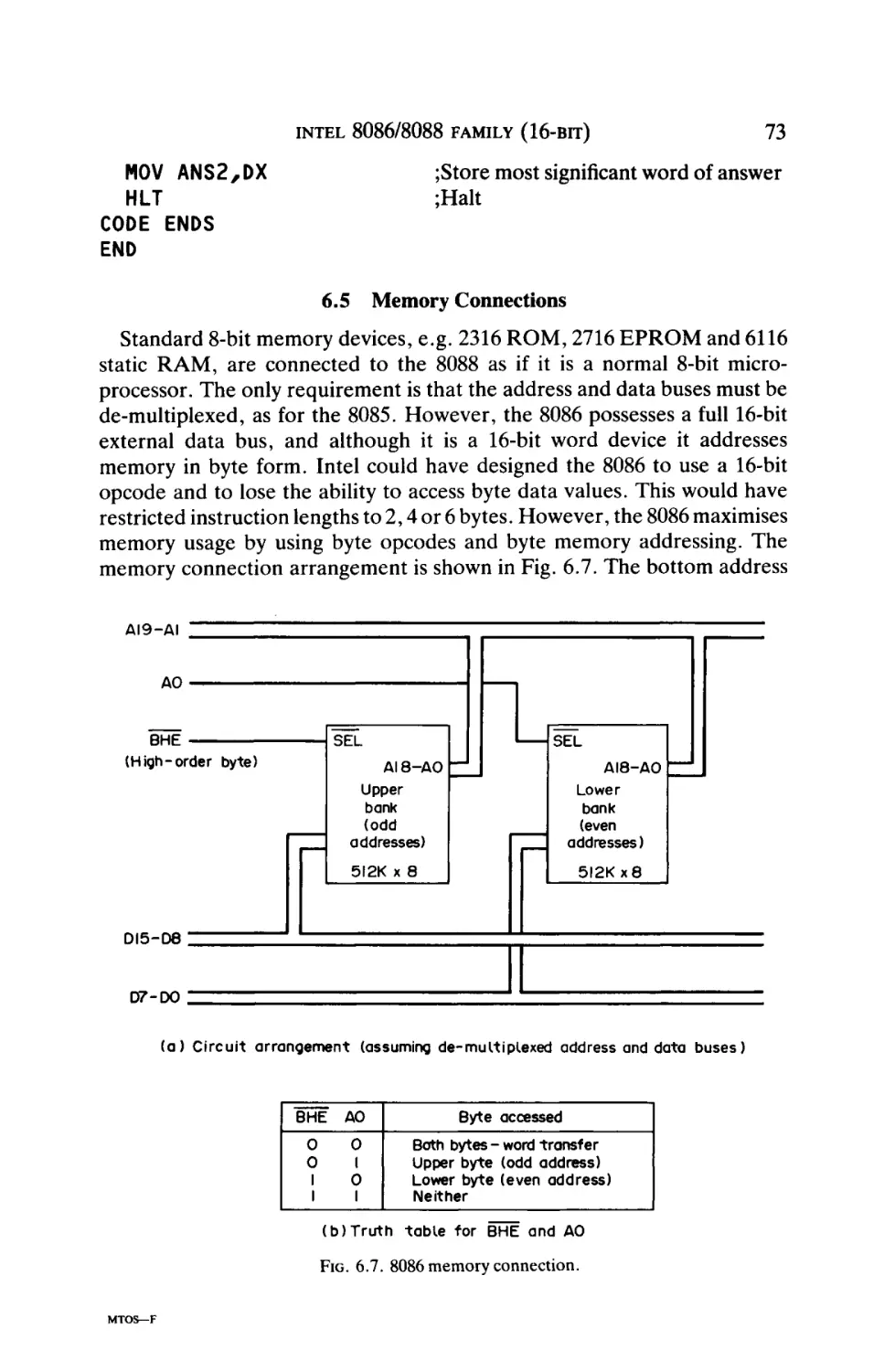
A complete microcomputer memory circuit is shown in Fig. 1.4. The ROM
and RAM devices are connected to the data bus and also to as many of the
least significant address bus lines as required. The Chip Select signals are
generated by a "2 to 4 decoder", which ensures that only one memory device
in the system can be selected at any time. The truth table for the decoder is
shown inFig. 1.5(a). Only one of the four outputs can be set to 0 at any time,
and the ü (Enable) input signal on the decoder must be set to 0 otherwise no
2
MICROPROCESSORS AND THEIR OPEIUVTING SYSTEMS
Address bus
AI5-A0
CSI
All
2 to 4
CS2
decoder |° « ^ ^
CS3
AI2
AI5
CS4
G
CPU
R/W
D7-DO
c3
td
AIO-AO
AIO-AO
ROM
2048x8
RAM
2048x8
R/W
D7-D0
D7-D0
Data bus
FIG. 1.4. Simple microcomputer memory circuit.
otherwise no output can be set. This particular memory circuit produces
device addresses as follows:
All
A15 A14 A13 A12
start
end
start
end
0
0
0
0
X
X
X
X
0
0
1
1
0
0
0
0
X
X
X
X
2 to 4
decoder
Decoder
enable
A10 A9 A8
0 0 0
1
1 1
0 0 0
1
1 1
A7
0
1
0
1
A6
0
1
0
1
A5 A4 A3 A2 Al AO
0 0 0 0 0 0
1 1 1 1 1 1
0 0 0 0 0 0
1 1 1 1 1 1
Hex 0000
Hex07FF
Hex 0800
HexOFFF
X = not used (assume set to 0)
Grouping the 16 bits into 4 hexadecimal characters gives the addresses
shown on the right of this table. These addresses can be shown on a "memory
map" for the computer as indicated in Fig. 1.5(e), and this map serves as a
guide to the computer programmer to indicate where he can place his
programs and data lists.
Memory addresses
ΔΙ2
All
0
0
1
0
1
0
1
CS4 CS3
1
1
1
O
CS2 CSI
1
1
O
l
1
0
1
l
O
1
1
0000
ROM
2K
RAM
2K
07FF
0800
i
OFFF
1000
(a ) Truth table -for 2 to 4 decoder
in Fig. 1.4
Unused
62K
FFFF
( b) Memory map
FIG. 1.5. Address calculations for Fig. 1.4.
MICROCOMPUTER PRINCIPLES
11
2 to 4decoder
CPU
IO/M
>— Chip select
signals to
memory
devices
L_| 2to4decoder
G
7
Chip select
signals to
input/output
devices
IO/M = Input/output (set to I). Memory (set to 0)
FIG. 1.6. Separate decoding circuits for memory and input/output.
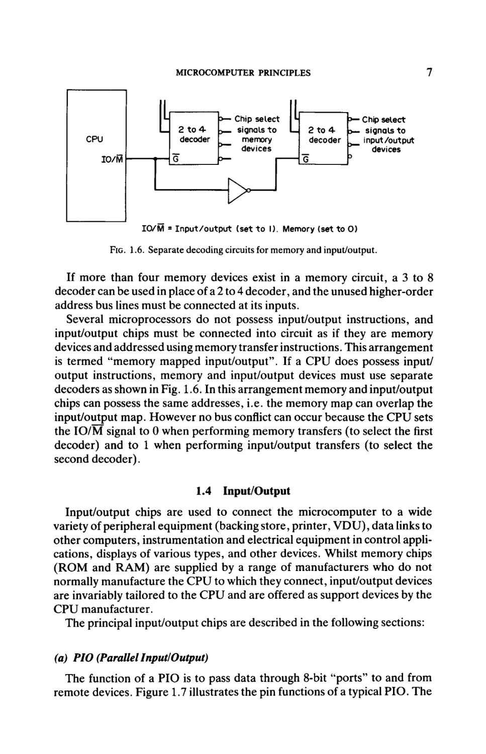
If more than four memory devices exist in a memory circuit, a 3 to 8
decoder can be used in place of a 2 to 4 decoder, and the unused higher-order
address bus lines must be connected at its inputs.
Several microprocessors do not possess input/output instructions, and
input/output chips must be connected into circuit as if they are memory
devices and addressed using memory transfer instructions. This arrangement
is termed "memory mapped input/output". If a CPU does possess input/
output instructions, memory and input/output devices must use separate
decoders as shown in Fig. 1.6. In this arrangement memory and input/output
chips can possess the same addresses, i.e. the memory map can overlap the
input/output map. However no bus conflict can occur because the CPU sets
the IO/M signal to 0 when performing memory transfers (to select the first
decoder) and to 1 when performing input/output transfers (to select the
second decoder).
1.4 Input/Output
Input/output chips are used to connect the microcomputer to a wide
variety of peripheral equipment (backing store, printer, VDU), data links to
other computers, instrumentation and electrical equipment in control applications, displays of various types, and other devices. Whilst memory chips
(ROM and RAM) are supplied by a range of manufacturers who do not
normally manufacture the CPU to which they connect, input/output devices
are invariably tailored to the CPU and are offered as support devices by the
CPU manufacturer.
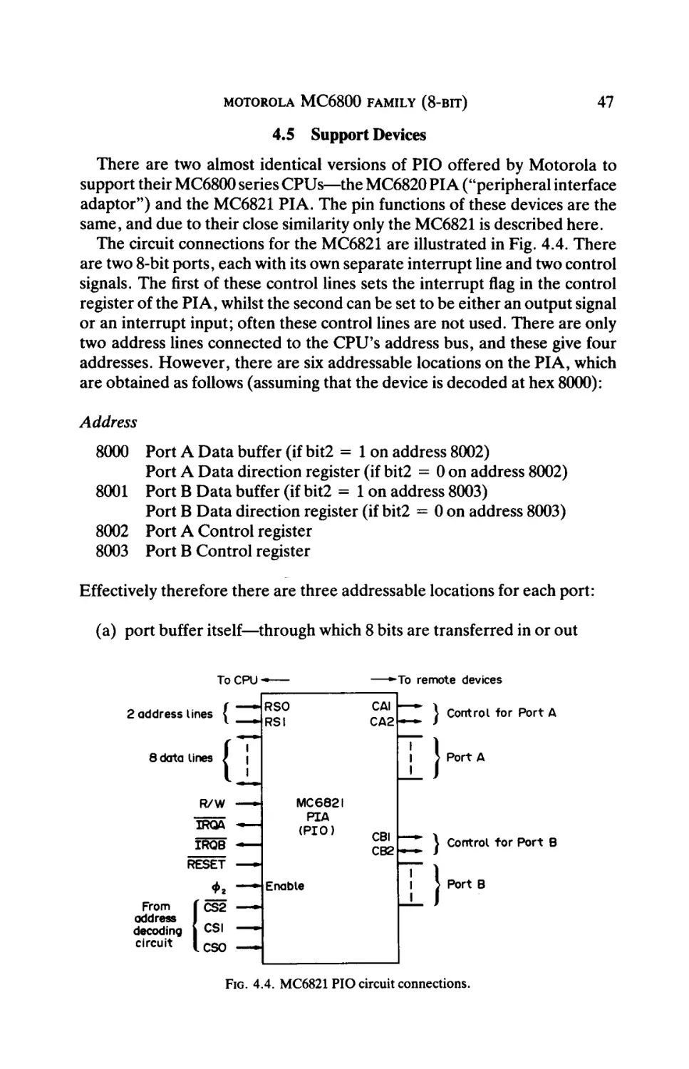
The principal input/output chips are described in the following sections:
(a) PIO (Parallel Input/Output)
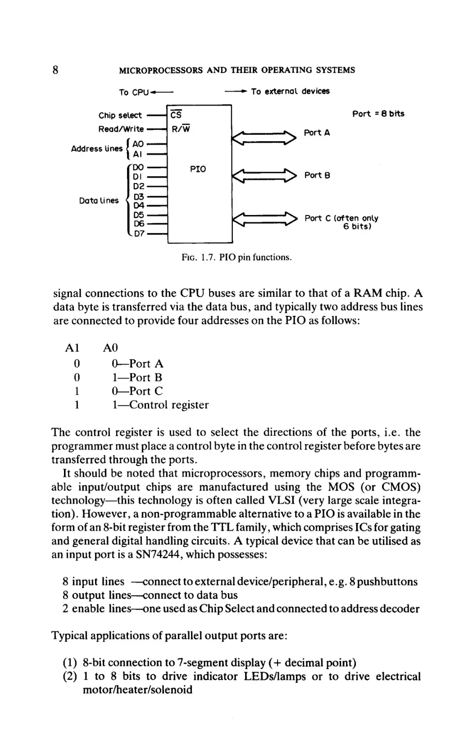
The function of a PIO is to pass data through 8-bit "ports" to and from
remote devices. Figure 1.7 illustrates the pin functions of a typical PIO. The
8
MICROPROCESSORS AND THEIR OPERATING SYSTEMS
To external devices
To CPU-
Port = 8 bits
Chip select ·
Read/Write ■
ÎAO
l AI
DO
DI
D2
D3
Data lines
D4
D5
D5
D6
D6
D7
D7
Address lines
(
|<
>
"**
k;
> PortB
L^1
N»
"^> Port C (often only
^
6 bits)
FIG. 1.7. PIO pin functions.
signal connections to the CPU buses are similar to that of a RAM chip. A
data byte is transferred via the data bus, and typically two address bus lines
are connected to provide four addresses on the PIO as follows:
Al
0
0
1
1
AO
0—Port A
1—Port B
0—Port C
1—Control register
The control register is used to select the directions of the ports, i.e. the
programmer must place a control byte in the control register before bytes are
transferred through the ports.
It should be noted that microprocessors, memory chips and programmable input/output chips are manufactured using the MOS (or CMOS)
technology—this technology is often called VLSI (very large scale integration). However, a non-programmable alternative to a PIO is available in the
form of an 8-bit register from the TTL family, which comprises ICs for gating
and general digital handling circuits. A typical device that can be utilised as
an input port is a SN74244, which possesses:
8 input lines —connect to external device/peripheral, e.g. 8 pushbuttons
8 output lines—connect to data bus
2 enable lines—one used as Chip Select and connected to address decoder
Typical applications of parallel output ports are:
(1) 8-bit connection to 7-segment display (+ decimal point)
(2) 1 to 8 bits to drive indicator LEDs/lamps or to drive electrical
motor/heater/solenoid
9
MICROCOMPUTER PRINCIPLES
(3) D/A (digital/analogue) converter, to produce an analogue signal for
connection to a servo, graph plotter, control valve
(4) 8-bit connection to a parallel printer—the standard "Centronics"
interface to a parallel printer comprises 8 data bits, 1 handshaking bit
to printer, 1 handshaking bit from printer
Typical applications of parallel input ports are:
(1) A/D converter, to read an instrument signal (analogue) into a com
puter
(2) 1 to 8 bits from pushbuttons or switches ("contact-closure" signals).
(b) UART (Serial Input/Output)
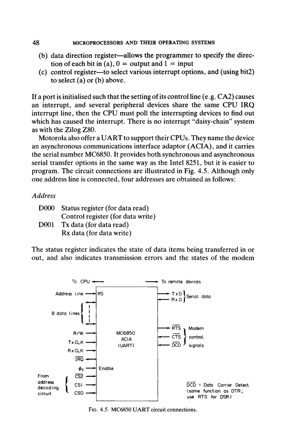
The UART (universal asynchronous receiver/transmitter) is applied in
place of a PIO when it is required to pass 8 data bits along a single serial
connection in place of an 8-wire parallel connection. Although a reduction
in cable cost is achieved, the disadvantage of this interfacing technique is the
reduction in transfer speed. Serial transmission is applied for the connection
of VDUs to computers, for inter-computer data links and for some printers.
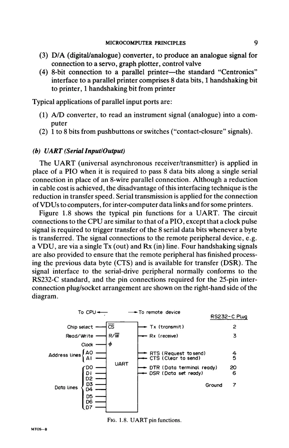
Figure 1.8 shows the typical pin functions for a UART. The circuit
connections to the CPU are similar to that of a PIO, except that a clock pulse
signal is required to trigger transfer of the 8 serial data bits whenever a byte
is transferred. The signal connections to the remote peripheral device, e.g.
a VDU, are via a single Tx (out) and Rx (in) line. Four handshaking signals
are also provided to ensure that the remote peripheral hasfinishedprocess
ing the previous data byte (CTS) and is available for transfer (DSR). The
signal interface to the serial-drive peripheral normally conforms to the
RS232-C standard, and the pin connections required for the 25-pin inter
connection plug/socket arrangement are shown on the right-hand side of the
diagram.
To CPU
Chip select
Read/Write
Clock
Address lines j
To remote device
—
—»· Tx (transmit)
2
R/W
- · — Rx (receive)
3
— · * RTS (Request tosend)
— · - CTS (Clear to send)
4
5
Φ
^
rDO
Dl
D2
D3
Data lines < D4
D5
D6
UART
— · * DTR (Data terminal ready)
— DSR (Data set ready)
Ground
LD7
FIG.
MTOS—B
RS232 - C Plug
cs
1.8. VA i R T p i n functions.
20
6
7
10
MICROPROCESSORS AND THEIR OPERATING SYSTEMS
There are typically four addresses on the UART, as follows:
Al
0
0
1
1
A0
0—Tx (serial out)
1—Rx (serial in)
0—Control register
1—Status register (e.g. character cleared, character received)
The 8-bit data character is framed by a start bit (logic 0) and a Stop bit (logic
1). The control register must be initialised by software, before data bytes can
be transferred, to select the following options:
(a) serial transmission speed, measured in baud (bits/second)—typically
600,1200, 2400,4800,9600 baud
(b) number of stop bits (1, lé or 2)
(c) number of data bits (5, 6 or 7—normally 7 with a parity bit added by
UART)
(d) parity (added after the data bits, and odd or even parity selected)
Notice that the UART operates at TTL voltage levels (logic 1 = +5V, logic
0 = 0 V), but the RS232-C specification requires different voltage signals
(logic 1 = -12 V, logic 0 = +12 V). Therefore a dc level shifter circuit is
required between the UART and the interconnection plug/socket.
(c) CTC (Counter Timer Circuit)
A CTC (counter timer circuit) is a programmable counter that can be
loaded, and read back to, the CPU. A CTC chip holds from one to four such
counters typically. Sometimes a single counter is included within a PIO chip.
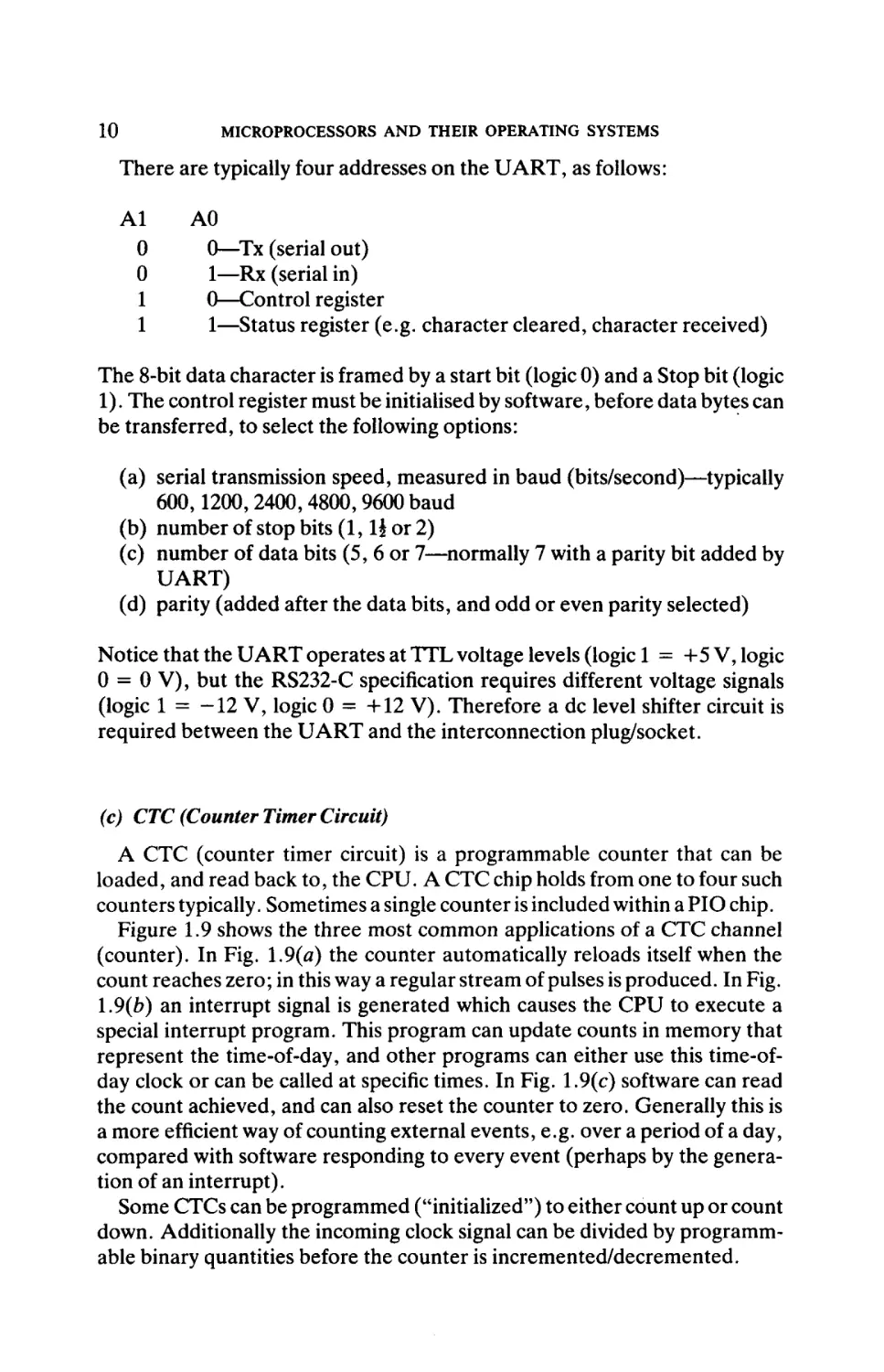
Figure 1.9 shows the three most common applications of a CTC channel
(counter). In Fig. 1.9(a) the counter automatically reloads itself when the
count reaches zero; in this way a regular stream of pulses is produced. In Fig.
1.9(e) an interrupt signal is generated which causes the CPU to execute a
special interrupt program. This program can update counts in memory that
represent the time-of-day, and other programs can either use this time-ofday clock or can be called at specific times. In Fig. 1.9(c) software can read
the count achieved, and can also reset the counter to zero. Generally this is
a more efficient way of counting external events, e.g. over a period of a day,
compared with software responding to every event (perhaps by the generation of an interrupt).
Some CTCs can be programmed ("initialized") to either count up or count
down. Additionally the incoming clock signal can be divided by programmable binary quantities before the counter is incremented/decremented.
11
MICROCOMPUTER PRINCIPLES
es —
CS
R/W —
R/W-
DO —
1
DO·
CTC
CTC
D7-L
Count
CPU clock — -| Counter |-| ^ complete
(pulses.
u—1 e.g. CIOCK to
I
J
UART)
Inter rupt «·———
(a) Pulse generator
CS
D7CPU clock
Counter |
Interrupt (b) Real-time clock interrupt
1
R/WDO-
CTC
D7-
Ë
Counter
*
(c) Count external events
External pulses (e.g.
cars entering car park,
products leaving
production line)
FIG. 1.9. CTC applications.
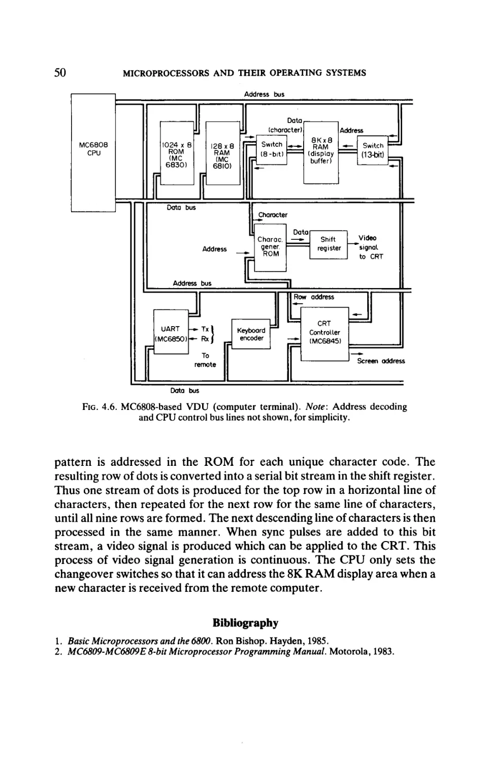
(d) FDC (Floppy Disc Controller)
The fourth programmable input/output device that is offered by most
microprocessor manufacturers is the FDC (floppy disc controller), which
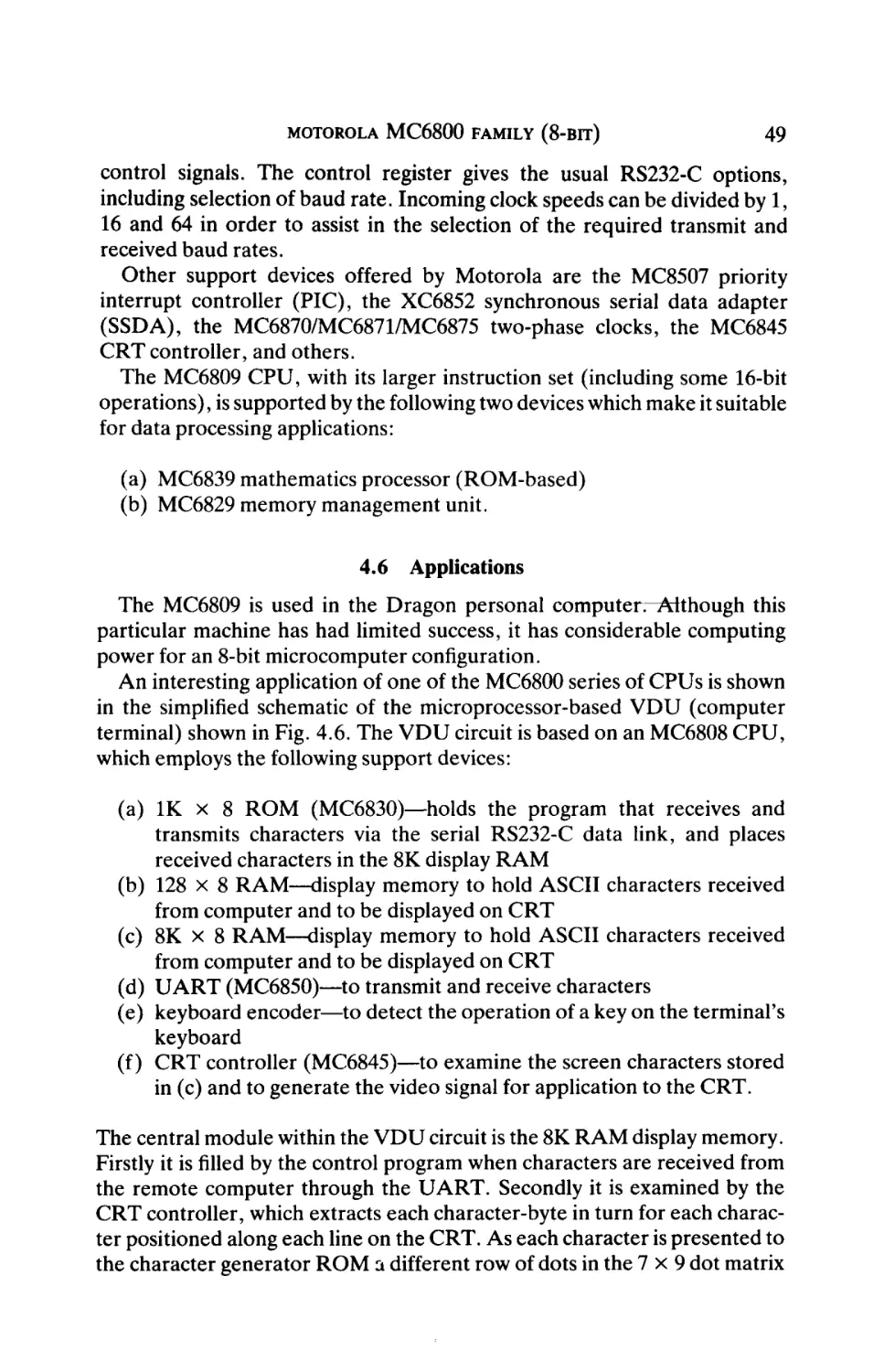
can control one or twofloppydisc drives. Figure 1.10 illustrates the typical
circuit connections. The two address lines give four addressable registers on
the chip, as follows:
Al
0
0
1
1
A0
0—Data register (for transfer of byte to and from disc)
1—Track register (to select required track)
0—Sector register (to select required sector)
1—Status/command register
A typical transfer procedure for a disc write operation is as follows. Software
loads the track register (perhaps 1 of 77 concentric tracks) and sector register
(typically 26 sectors per track, where 1 sector = 128 bytes) with the required
position on the disc. The FDC moves the head assembly to the desired track
12
MICROPROCESSORS AND THEIR OPERATING SYSTEMS
To CPU*·—
Interrupt
-*H
—·*Το floppy disc drive unit
• Write data
l
-Read data
J
Serial data to write
and read windings
• Head direction
► Head step
- Head load
►Read/Write
To read/write
head assembly
■ Index -pulse once per revolution
■ TrackO - outer track of disc
FIG. 1.10. FDC pin functions.
by pulsing the drive stepper motor, and waits until the disc has rotated until
the required sector is beneath the head. The head is then "loaded" (placed
against the disc surface) and the interrupt signal is generated. Software then
loads the data register with the data byte to be written on the disc surface.
This byte is fed to the read/write head ("write" selected) in serial form. Data
byte transfers then repeat until the required block of data (typically several
sectors) is transferred.
8" floppy discs use the IBM3740 Format, which includes the writing of a
sector self-address on the disc surface at the start of every sector. Alternative
disc sizes are 5?" and 3i". Discs can be single-sided (SS) or double-sided
(DS), and single-density (SD) or double-density (DD). Storage capacity is
typically 500K bytes, and access time is variable and based on the following
time components:
Disc revolution time
Track-to-track time
Head load time
Total
= 200 ms
= 8 ms
= 35 ms
= 35 ms to 1 s
A non-removable hard disc ("Winchester") offers 10M bytes, or more, and
access times of 25 ms to 60 ms.
Note DMA (direct memory access) is a technique whereby input/output
directly accesses memory, and transfers take place between the two without
involvement by the CPU. An input/output circuit can request the CPU to
release its buses (data, address and one or two control lines) by generating a
"DMA Request" signal. When the CPU is not using the buses, it replies with
a "DMA Acknowledge". The input/output circuit can then address memory
13
MICROCOMPUTER PRINCIPLES
directly and transfer bytes. This technique is often more efficient than the
software alternative of transferring each byte under program control, and it
is used frequently with backing store and video signal generation (for CRT
displays) control purposes.
1.5 Stack, Subroutines and Interrupts
The "stack" is an area of memory (RAM) that is used to store return
addresses when an exit is made from a main program to obey:
(a) a subroutine (activated by a CALL instruction in the main program)
(b) an interrupt service routine (ISR) when one of the interrupt lines
(part of the CPU's control bus) is set.
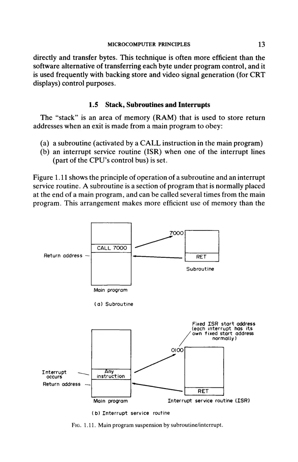
Figure 1.11 shows the principle of operation of a subroutine and an interrupt
service routine. A subroutine is a section of program that is normally placed
at the end of a main program, and can be called several times from the main
program. This arrangement makes more efficient use of memory than the
7000
CALL 7000
Return address —
RET
Subroutine
Main program
( a ) Subroutine
Fixed I S R start address
(each interrupt has its
own fixed start address
normally)
Interrupt
occurs
Return address
—
Main program
Interrupt service routine ( I S R )
(b) Interrupt service routine
FIG. 1.11. Main program suspension by subroutine/interrupt.
14
MICROPROCESSORS AND THEIR OPERAΉNG SYSTEMS
alternative arrangement of placing that section of program at several
positions in the main program. The CPU must store the address of the
instruction that follows the CALL instruction (this is called the "return
address"), so that this address can be reinstated in the program counter (see
section 1.2) when the RET (return) instruction is obeyed at the end of the
subroutine. The operation of an ISR is similar, except that an ISR is entered
when a hardware signal (interrupt) is set. An ISR is normally a self-contained
program that runs to completion, and also terminates with a RET instruc
tion.
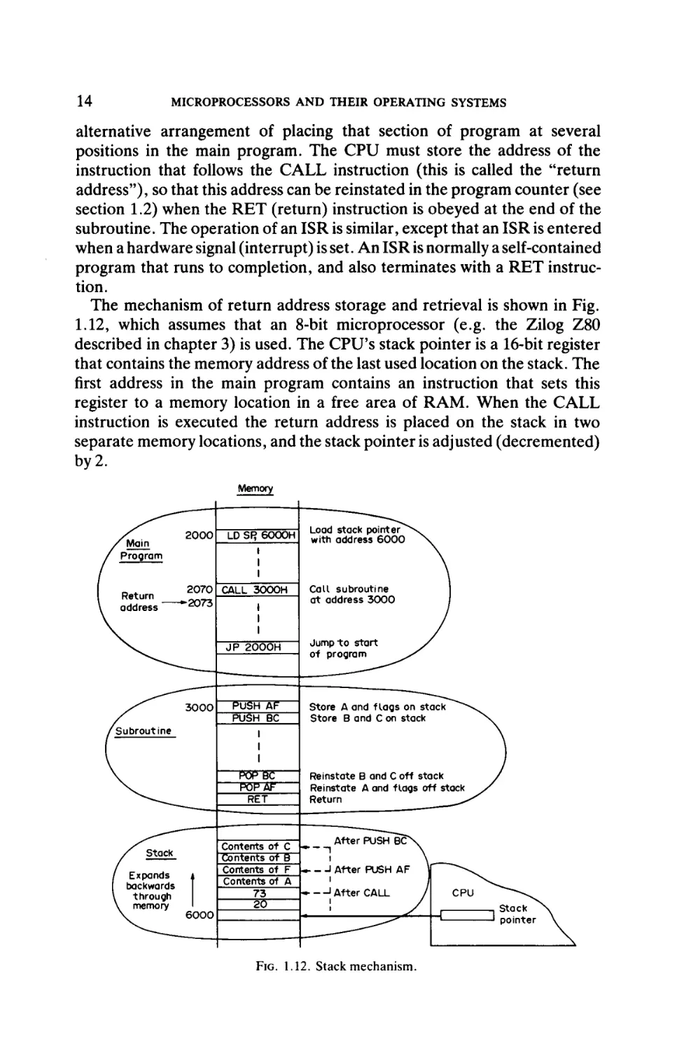
The mechanism of return address storage and retrieval is shown in Fig.
1.12, which assumes that an 8-bit microprocessor (e.g. the Zilog Z80
described in chapter 3) is used. The CPU's stack pointer is a 16-bit register
that contains the memory address of the last used location on the stack. The
first address in the main program contains an instruction that sets this
register to a memory location in a free area of RAM. When the CALL
instruction is executed the return address is placed on the stack in two
separate memory locations, and the stack pointer is adjusted (decremented)
by 2.
Memory
FIG. 1.12. Stack mechanism.
MICROCOMPUTER PRINCIPLES
15
In this particular example the second application of the stack is illustrated.
The subroutine is likely to overwrite the CPU's work registers (A, B, C,
etc., and perhaps the status register); an ISR is almost certain to do this.
Therefore it is sensible to store the contents of these registers into memory
locations at the start of the subroutine/ISR, and reinstate them at the end of
the subroutine/ISR. The most convenient way of doing this is to use the
PUSH (store registers on stack) and POP (reinstate registers off stack)
instructions. The stack pointer is automatically adjusted after each PUSH
and POP instruction.
A subroutine can call another subroutine in what is termed a "nested
subroutine" system. In this case the second return address is placed on top
of the first return address in the stack.
Different microprocessors use a variety of ways of specifying the start
address of ISRs when interrupts occur. The most common methods are
(PC = program counter):
(a) PC <— Fixed memory address
(b) PC <— "Vector address" (memory address contains start address of
ISR)
(c) PC <— Vectored address, with address partly generated by interrupting device (e.g. Zilog Z80) and partly held within CPU
Microprocessors typically possess 3 or 4 interrupts. One interrupt (normally
named "RESET") is arranged to become set when the computer system is
switched on, or alternatively when a Reset pushbutton is pressed. In this way
the system will always commence program operation at the same memory
location—the most common start address is hexadecimal 0000, i.e. at the
beginning of memory. In a disc-based computer this start-up program
normally transfers the main program from disc into memory (RAM) and
enters this program. This is called "bootstrapping" the system. The remaining interrupts may connect from "intelligent" input/output chips, e.g. CTC
or FDC (see section 1.4). These interrupts normally possess a priority
system, i.e. a lower priority interrupt cannot interrupt an ISR for a higher
priority interrupt. Usually the CPU provides a "masking" system, such that
a software instruction can be activated to block any further interrupts, even
on a higher interrupt level.
Several microprocessors possess "software interrupts", or TRAP instructions, that have the same effect as hardware interrupts.
Bibliography
1. Integrated Circuits and Microprocessors. R. C. Holland. Pergamon, 1986.
2. Microelectronic and Microprocessor-based Systems. Noel M. Morris. Macmillan, 1985.
CHAPTER 2
INTEL 8080/8085 FAMILY (8-BIT)
2.1 Introduction
Intel were the first manufacturer to mass-produce an 8-bit microprocessor—the 8008—in the early 1970s. This 18-pin device was soon
replaced with the 8080 and 8085 microprocessors, which proved to be the
main stimulus to the widespread application of the microcomputer.
Although neither of these microprocessors was used in the range of home
computers that were produced throughout the 1970s, these devices dominated industrial control applications of the microcomputer during this
period.
The operation of the 8080 and 8085 8-bit microprocessors is identical,
except that an additional IC (the 8228) is required with the former to provide
what is effectively a two-chip CPU. The facilities performed by this component are provided on-chip with the 8085, and comprise:
(a) on-chip clock generation
(b) system control (memory and input/output read/write operations) and
interrupt prioritising.
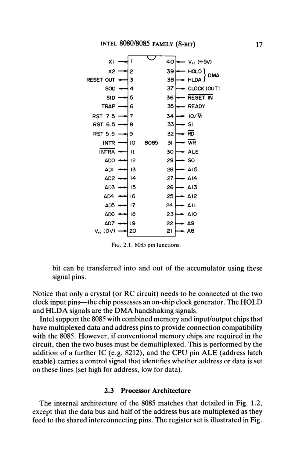
2.2 8085 Pin Functions
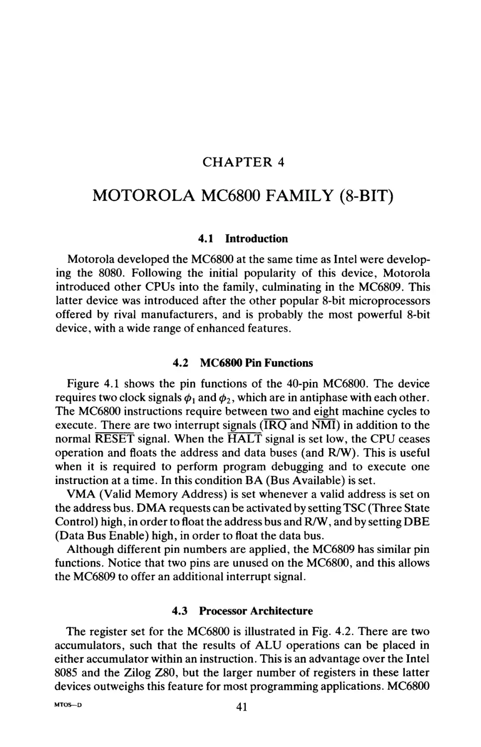
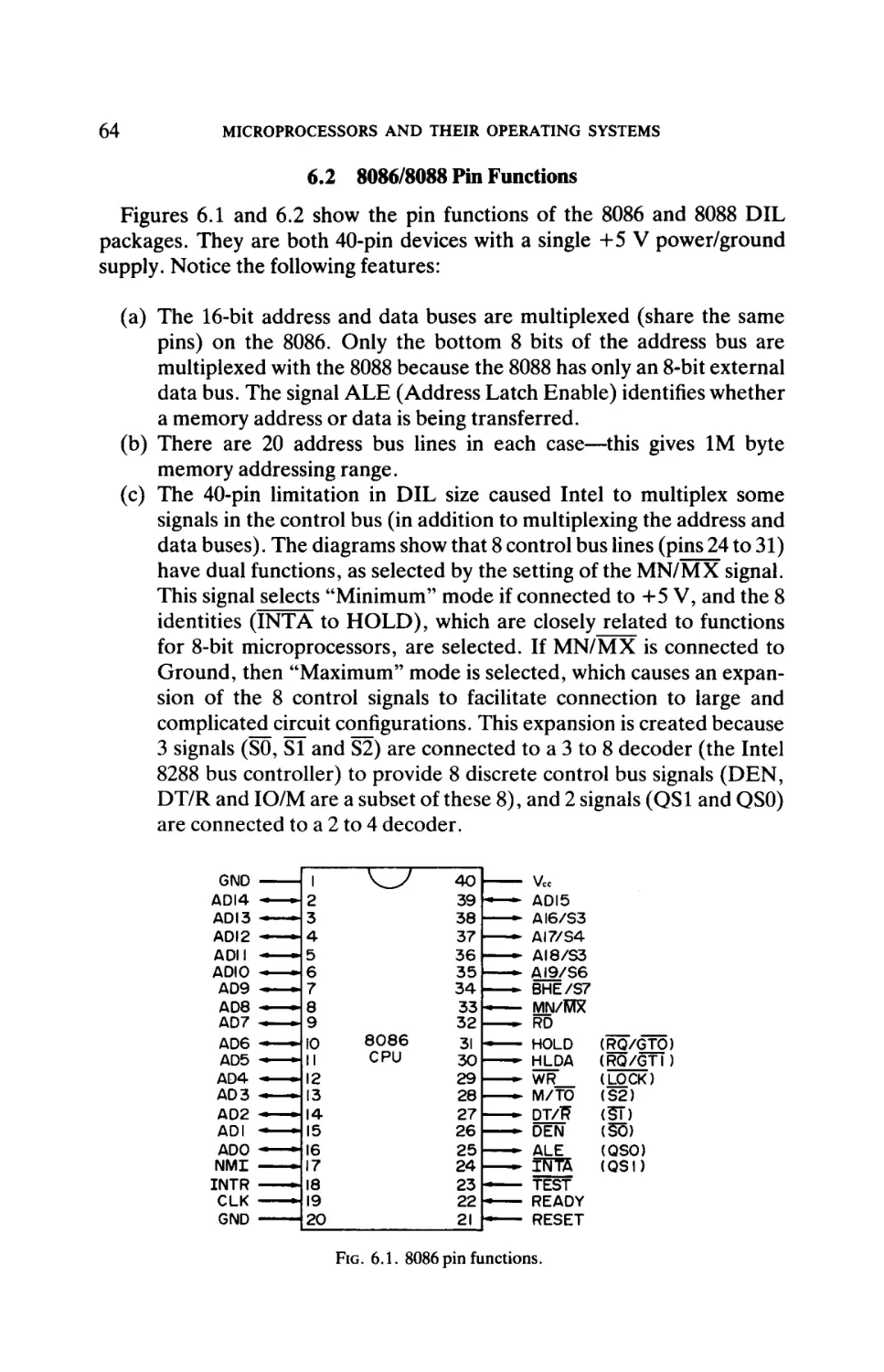
The pin functions of the more popular 8085 are shown in Fig. 2.1. The
most distinctive feature to notice is that the 8 data bus lines and the least
significant 8 of the 16 address bus lines are multiplexed, i.e. they share the
same pins. This is unique amongst 8-bit microprocessors, but is common
amongst 16-bit microprocessors where requirements for interconnecting pin
usage are more demanding due to the larger number of address and data bus
signals. The pins in the 40-pin package that are saved by using this practice
are available for use by the control bus and provide a powerful range of
additional control functions. Examples are:
(a) In addition to a RESET signal, there arefiveinterrupts (TRAP, RST
5.5, RST 6.5, RST7.5 and INTR).
(b) Two serial input/output signals are available—SID (serial input data)
and SOD (serial output data). Using particular instructions a single
16
INTEL 8080/8085 FAMILY (8-BIT)
XI — * 1
^
4 0 ■ — Vcc (+5V)
X2
— 2
RESET OUT
— 3
HOLD)
} DMA
3 8 — - HLDAJ
SOD — H 4
37 — - CLOCK (OUT]
SID —·■ 5
36 —
TRAP
39 —
RST 5 . 5
INTR
RESET IN
35 - — READY
— 6
3 4 — - 10/M
RST 7 . 5 ■—- 7
RST 6 . 5
— 8
33 — - SI
— 9
32 — - RD
— 10
INTRA - — 11
ADO — ~ 12
8085
31 — - WR
3 0 — - ALE
2 9 — - SO
ADI
— 13
28 —
AI5
AD2
— 14
27 —
AI4
AD3
— 15
26 —
AI3
AD4 - — 16
AD5
— 17
25 — - Δ Ι 2
24 —
All
AD6 — · 18
2 3 - — AIO
AD7 *~* 19
22 ~
Vss (OV) - — 2 0
17
A9
21 i—> A8
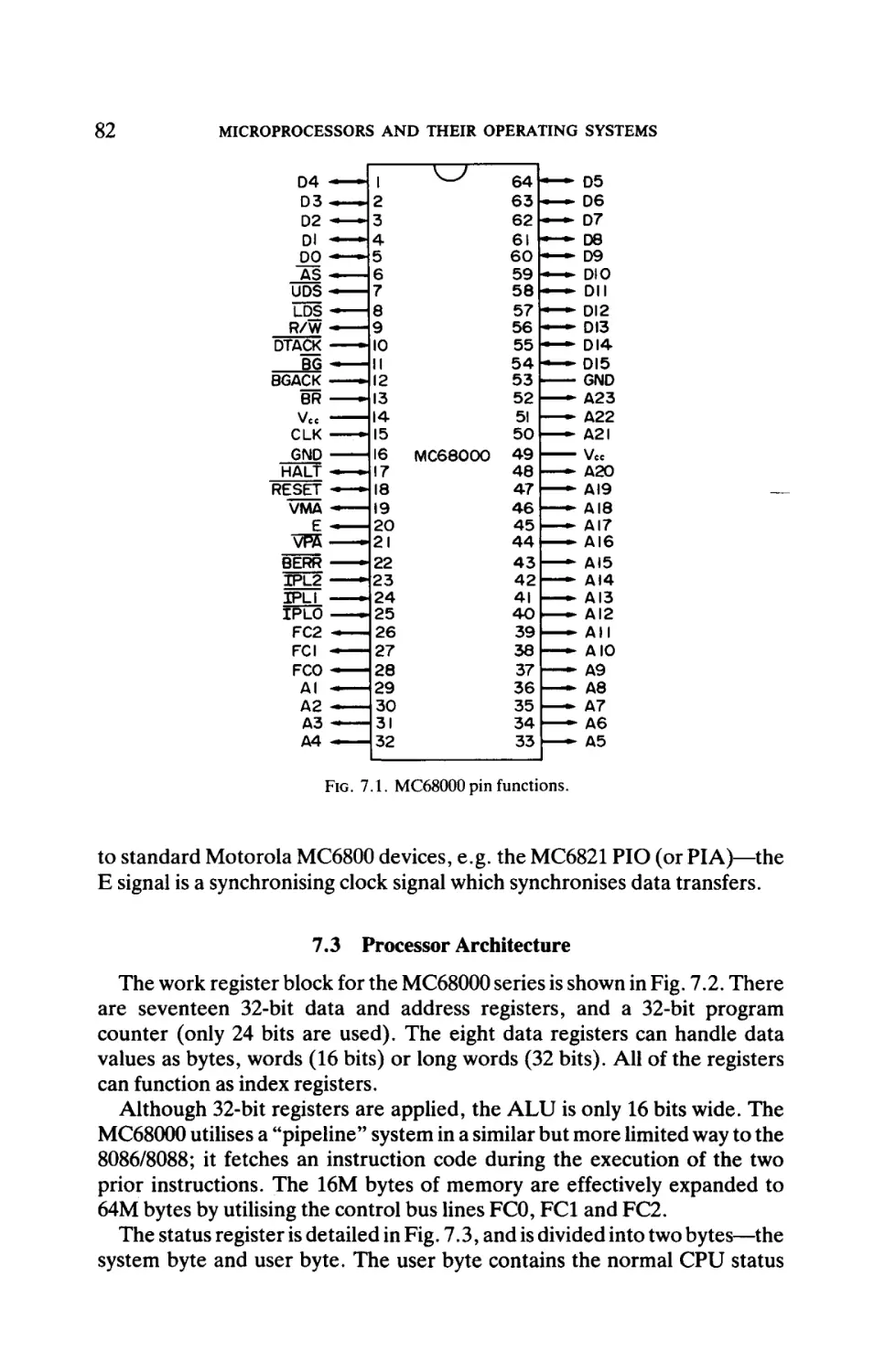
FIG. 2.1. 8085 pin functions.
bit can be transferred into and out of the accumulator using these
signal pins.
Notice that only a crystal (or RC circuit) needs to be connected at the two
clock input pins—the chip possesses an on-chip clock generator. The HOLD
and HLDA signals are the DMA handshaking signals.
Intel support the 8085 with combined memory and input/output chips that
have multiplexed data and address pins to provide connection compatibility
with the 8085. However, if conventional memory chips are required in the
circuit, then the two buses must be demultiplexed. This is performed by the
addition of a further IC (e.g. 8212), and the CPU pin ALE (address latch
enable) carries a control signal that identifies whether address or data is set
on these lines (set high for address, low for data).
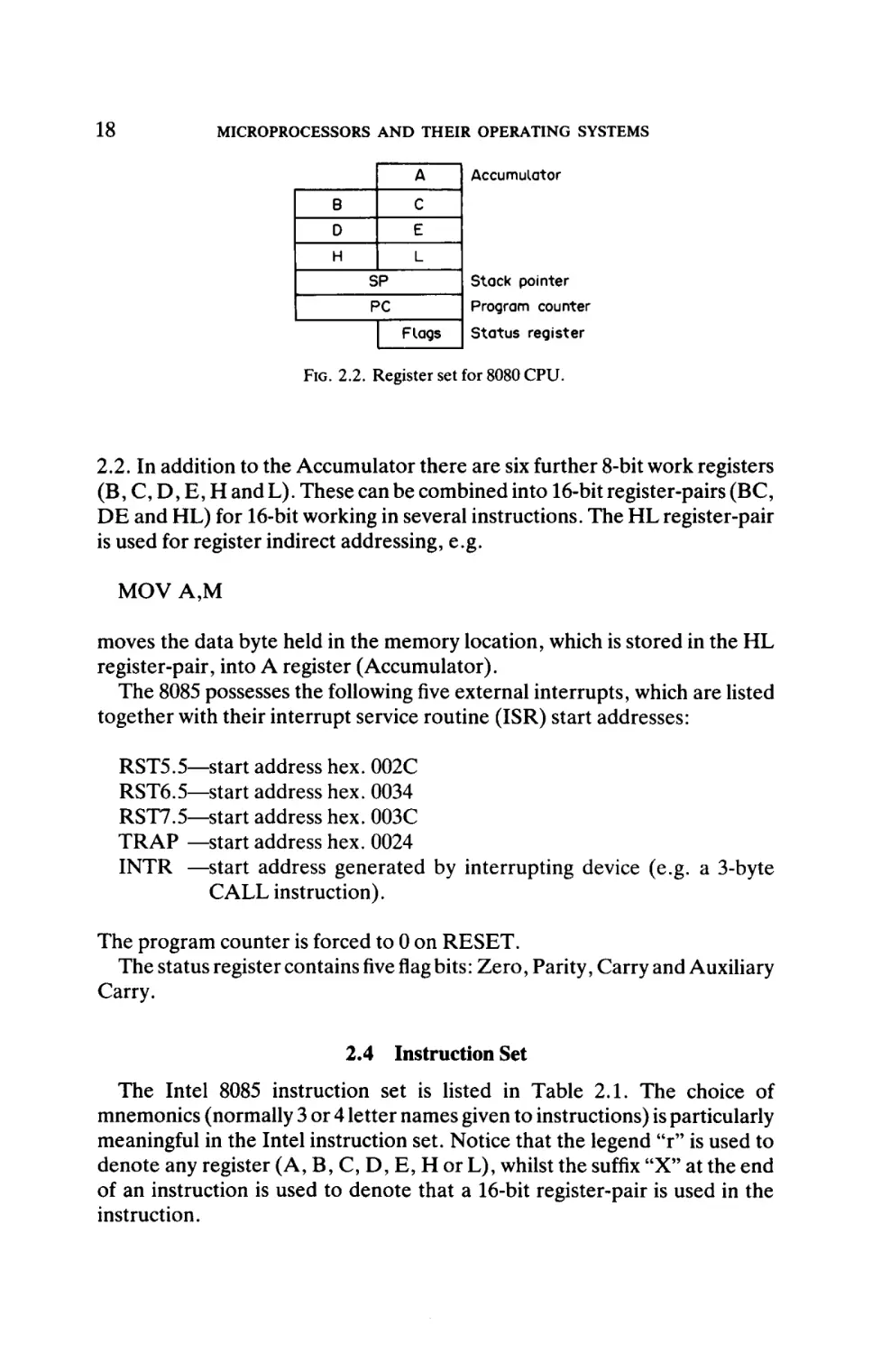
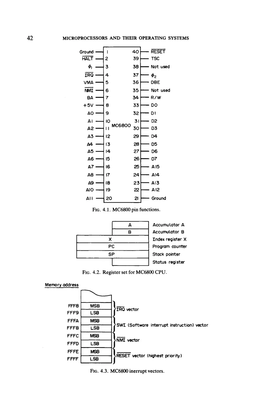
2.3 Processor Architecture
The internal architecture of the 8085 matches that detailed in Fig. 1.2,
except that the data bus and half of the address bus are multiplexed as they
feed to the shared interconnecting pins. The register set is illustrated in Fig.
18
MICROPROCESSORS AND THEIR OPERATING SYSTEMS
A
Θ
c
D
E
H
| Accumulator
L
SP
Stack pointer
PC
Program counter
Flags
Status register
FIG. 2.2. Register set for 8080 CPU.
2.2. In addition to the Accumulator there are six further 8-bit work registers
(B, C, D, E, H and L). These can be combined into 16-bit register-pairs (BC,
DE and HL) for 16-bit working in several instructions. The HL register-pair
is used for register indirect addressing, e.g.
MOV A,M
moves the data byte held in the memory location, which is stored in the HL
register-pair, into A register (Accumulator).
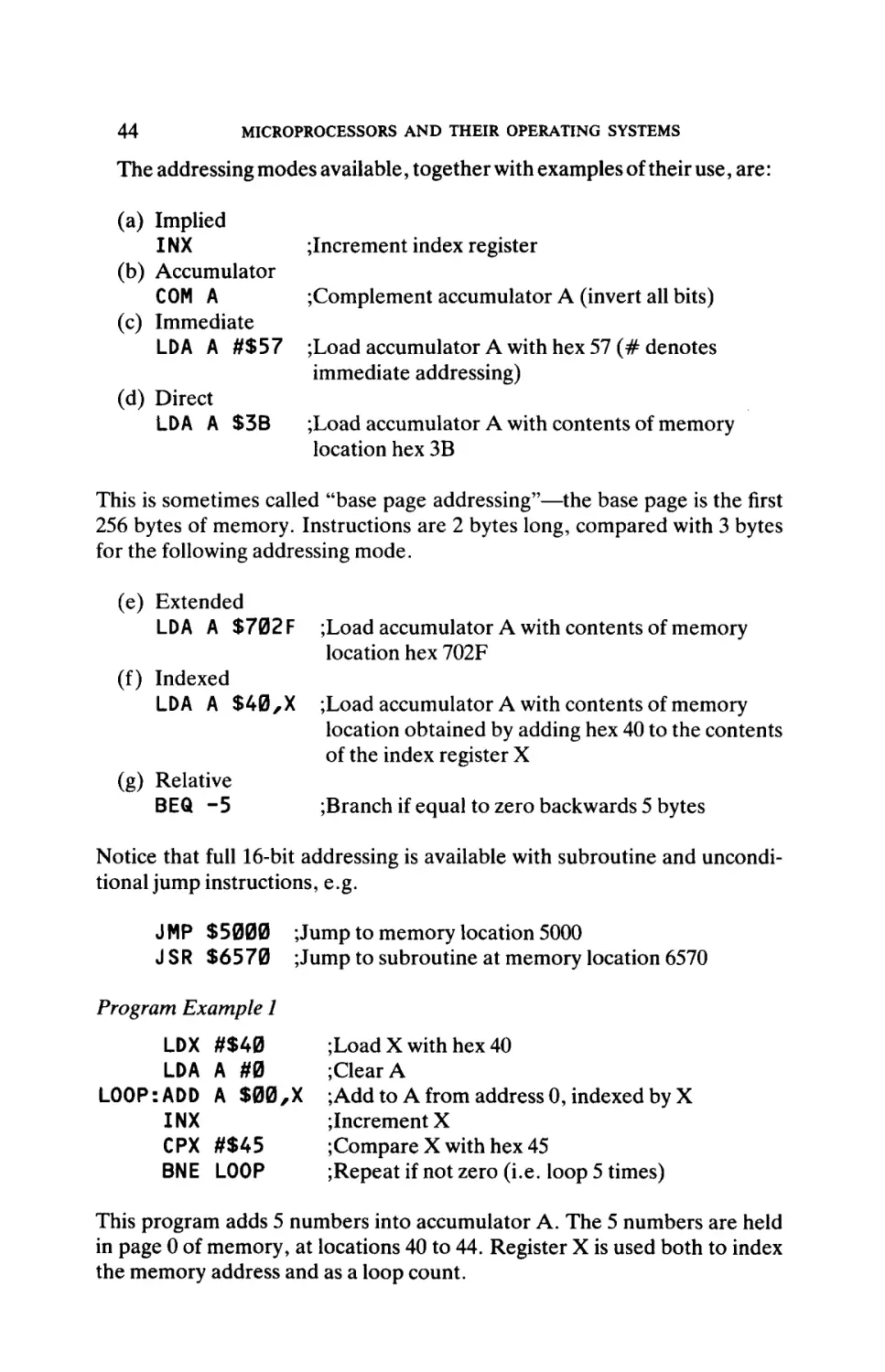
The 8085 possesses the following five external interrupts, which are listed
together with their interrupt service routine (ISR) start addresses:
RST5.5—start address hex. 002C
RST6.5—start address hex. 0034
RST7.5—start address hex. 003C
TRAP —start address hex. 0024
INTR —start address generated by interrupting device (e.g. a 3-byte
CALL instruction).
The program counter is forced to 0 on RESET.
The status register containsfiveflagbits: Zero, Parity, Carry and Auxiliary
Carry.
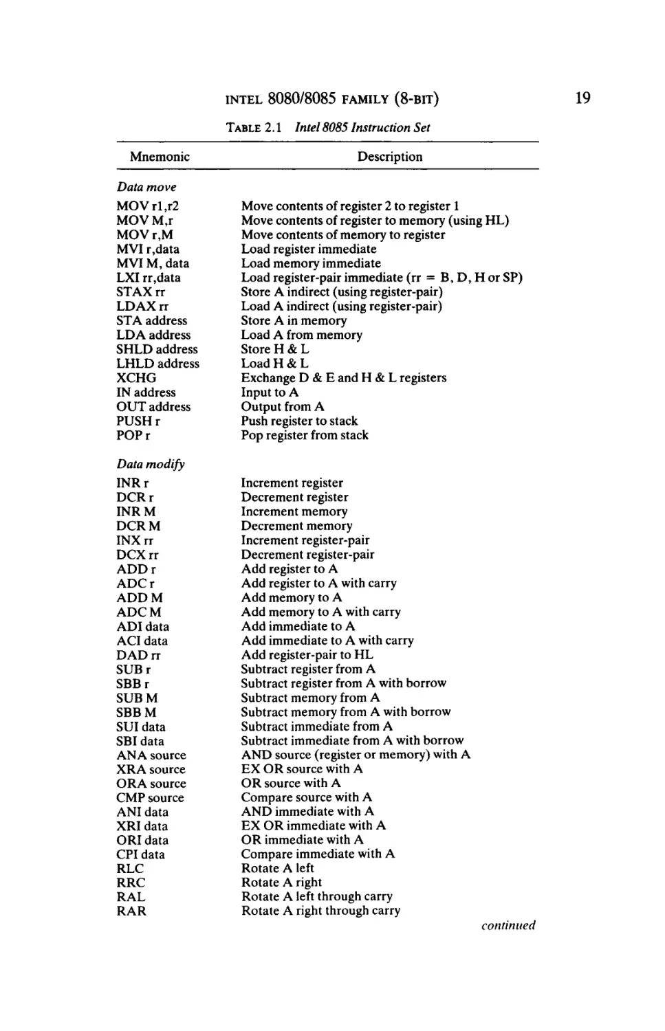
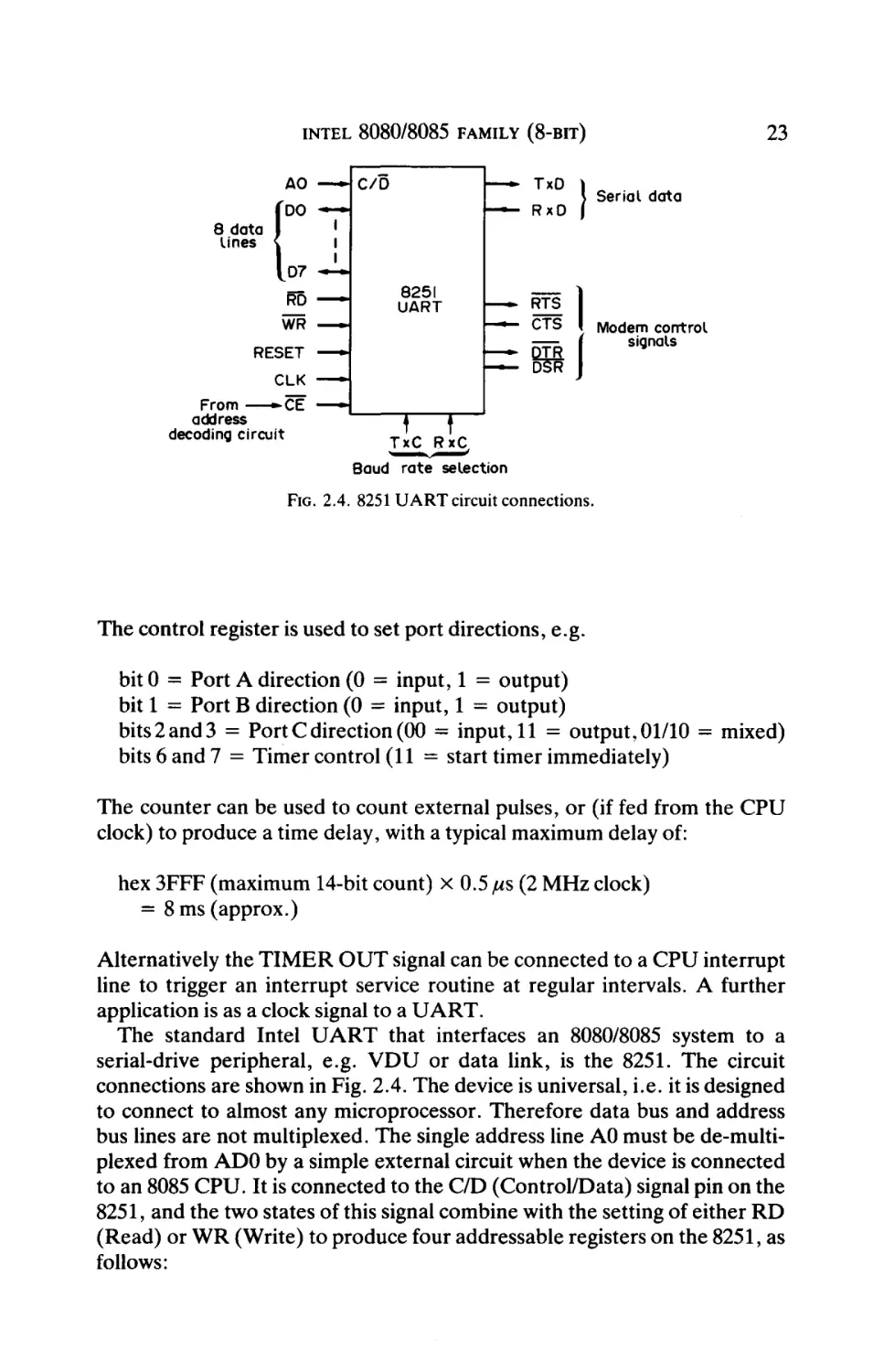
2.4 Instruction Set
The Intel 8085 instruction set is listed in Table 2.1. The choice of
mnemonics (normally 3 or 4 letter names given to instructions) is particularly
meaningful in the Intel instruction set. Notice that the legend u r" is used to
denote any register (A, B, C, D, E, H or L), whilst the suffix "X" at the end
of an instruction is used to denote that a 16-bit register-pair is used in the
instruction.
19
INTEL 8080/8085 FAMILY (8-BIT)
TABLE 2.1 Intel 8085 Instruction Set
Mnemonic
Description
Data move
MOVrl,r2
MOVM,r
MOVr,M
MVI r,data
MVIM, data
LXI rr,data
STAXrr
LDAXrr
STA address
LDA address
SHLD address
LHLD address
XCHG
IN address
OUT address
PUSHr
POPr
Move contents of register 2 to register 1
Move contents of register to memory (using HL)
Move contents of memory to register
Load register immediate
Load memory immediate
Load register-pair immediate (rr = B, D, H orSP)
Store A indirect (using register-pair)
Load A indirect (using register-pair)
Store A in memory
Load A from memory
Store H & L
LoadH&L
Exchange D & E and H & L registers
Input to A
Output from A
Push register to stack
Pop register from stack
Data modify
INRr
DCRr
INRM
DCRM
INXrr
DCXrr
ADDr
ADCr
ADD M
ADC M
ADI data
ACI data
DADrr
SUBr
SBBr
SUB M
SBBM
SUI data
SBI data
ANA source
XRA source
ORA source
CMP source
ANI data
XRI data
ORI data
CPI data
RLC
RRC
RAL
RAR
Increment register
Decrement register
Increment memory
Decrement memory
Increment register-pair
Decrement register-pair
Add register to A
Add register to A with carry
Add memory to A
Add memory to A with carry
Add immediate to A
Add immediate to A with carry
Add register-pair to HL
Subtract register from A
Subtract register from A with borrow
Subtract memory from A
Subtract memory from A with borrow
Subtract immediate from A
Subtract immediate from A with borrow
AND source (register or memory) with A
EX OR source with A
OR source with A
Compare source with A
AND immediate with A
EX OR immediate with A
OR immediate with A
Compare immediate with A
Rotate A left
Rotate A right
Rotate A left through carry
Rotate A right through carry
continued
20
MICROPROCESSORS AND THEIR OPERATING SYSTEMS
TABLE 2.1
Continued
Description
Mnemonic
CMA
DAA
STC
CMC
Complement A
Decimal adjust A
Set carry flag
Complement carry flag
Jump
JMP address
Jcc address
CALL address
Ccc address
RET
Rcc
Jump unconditional
Jump on condition cc (signified by status bit)
Call subroutine
Call subroutine on condition cc
Return
Return on condition cc
Control/miscellaneous
El
DI
RIM
SIM
NOP
HLT
RST
Enable interrupts
Disable interrupts
Read interrupt mask
Set interrupt mask
No-operation
Halt
Restart
The addressing modes available, with examples of their use in instructions,
are as follows:
(a) Register
MOV A,D
;Move contents of D register to A register (accumulator)
(b) Memory (Intel call "direct")
LDA 30B6H ;Load A register with contents of memory location
hex. 30B6
(c) Register indirect
MOV A,M
;Load A register with contents of memory location
that is held in HL register-pair
(d) Immediate
MVI A , 7
;Load A register with 7 (8-bit number)
The addressing mode with JUMP and CALL instructions is (b) above, i.e.
the memory address that is to be placed in the program counter when the
instruction is completed is held in the second and third bytes of the
instruction. Notice that the IN (input) and OUT (output) instructions use
only a single-byte port address as an operand, and are therefore two bytes
long.
INTEL 8080/8085 FAMILY (8-BIT)
21
The following program examples illustrate the use of the instruction set:
Program Example 1
MVI A,0
MVI E,6
LXI H,4000H
LOOP:ADD M
INX H
DCR E
JNZ LOOP
HLT
;Clear A
;Load loop count of 6 into E
;Load HL with memory address 4000
;Add from memory to A (using HL)
;Increment HL
;Decrement loop count in E
;Jump around loop (6 times)
;Halt
Bytes
2
2
3
1
1
1
3
1
The program adds 6 numbers held at memory addresses hex. 4000 through
4005 into A register (the accumulator). Notice that the number of bytes
required for each instruction is shown on the right-hand side. The program
commences by loading A, E and HL registers using immediate addressing
mode instructions. It then enters a loop, and the first instruction is given a
label of "LOOP" to represent the memory address at which it is stored.
During each pass of the loop a different number is added into A register, the
HL register-pair is incremented and the loop count in E is decremented. On
the sixth pass through the loop E is decremented to zero, and the program
halts.
Program Example 2
IN
CPI
JZ
STA
MVI
OUT
FINISH: JMP
30H
1
FINISH
0600H
A,4
31H
8000H
;Input to A from address 30
;Compare A with binary 0000 0001
; Jump if zero (right-hand bit set to 0)
;Store input byte in memory
;Load A with 0000 0100
;Output A to address 31
; Jump to new program
The program illustrates the use of input/output instructions, which utilise
single-byte operands, i.e. input/output addresses are only 8 bits long. The
program reads in an input byte (perhaps from a block of 8 pushbuttons). Bit
0 (the right-hand bit) is examined, and if it is set to 0 a program jump is
obeyed to the label FINISH. Program control is then transferred to another
program, which commences at memory location 8000. If the bit tested is set
to 1, e.g. a pushbutton is pressed, the input byte is stored in memory and a
logic 1 is sent to bit 2 on an output address, perhaps to illuminate an indicator
LED.
22
MICROPROCESSORS AND THEIR OPERATING SYSTEMS
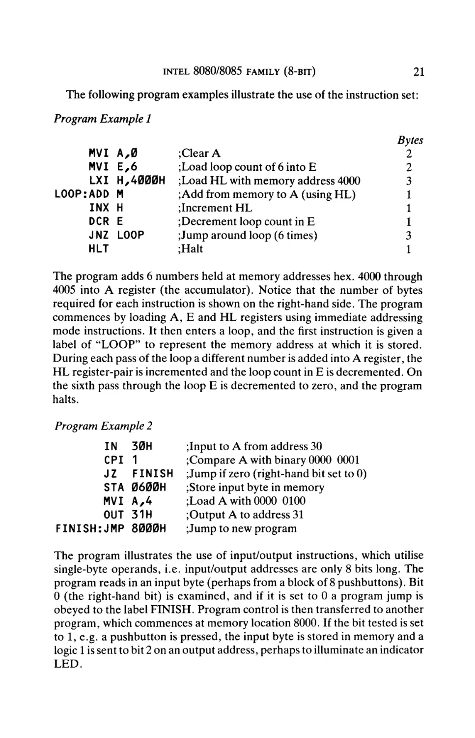
2.5 Support Devices
Intel support the 8080 and 8085 CPUs with the widest range of devices
offered by 8-bit microprocessor manufacturers. They offer four PIOs which
include variable quantities of memory (ROM and RAM) as follows:
(a)
(b)
(c)
(d)
8155—3 ports, 256 bytes RAM, 14-bit counter
8255—3 ports
8355—2 ports, 2K ROM
8755—2 ports, 2KEPROM
The pin functions of the ubiquitous 8155 are shown in Fig. 2.3. Ports A and
B each provide 8 input or output signal lines, but Port C is only 6-bits wide.
Each port direction is programmable.
The 8 address lines that are multiplexed with the data lines can be used to
address one of the 256 RAM bytes. Alternatively, if an input/output
instruction is executed in place of a memory transfer instruction, the address
lines select one of the following addresses on the device:
A2
0
0
0
0
1
1
Al
0
0
1
1
0
0
A0
0—Control register
1—Port A
0—Port B
1—Port C
0—Counter/timer (low order 8 bits)
1—Counter/timer (high order 6 bits)
To CPU -•
8 add ress /
data Lines
— · " To remote devices
1
|
1
ALE
_
__
RD —^
8155
PIO
( + 2 5 6 bytes
RAM
+ counter)
^
^ > P o r t A (8 bits)
^
^ > P o r t B ( 8 bits)
^
^ > P Q r t C (6 bits)
WR
IO/ffl
— »■
RESET
TIMER CLK
^ Œ
From
address
decoding circuit
—
— -
TIMER OUT
FIG. 2.3. 8155 PIO circuit connections.
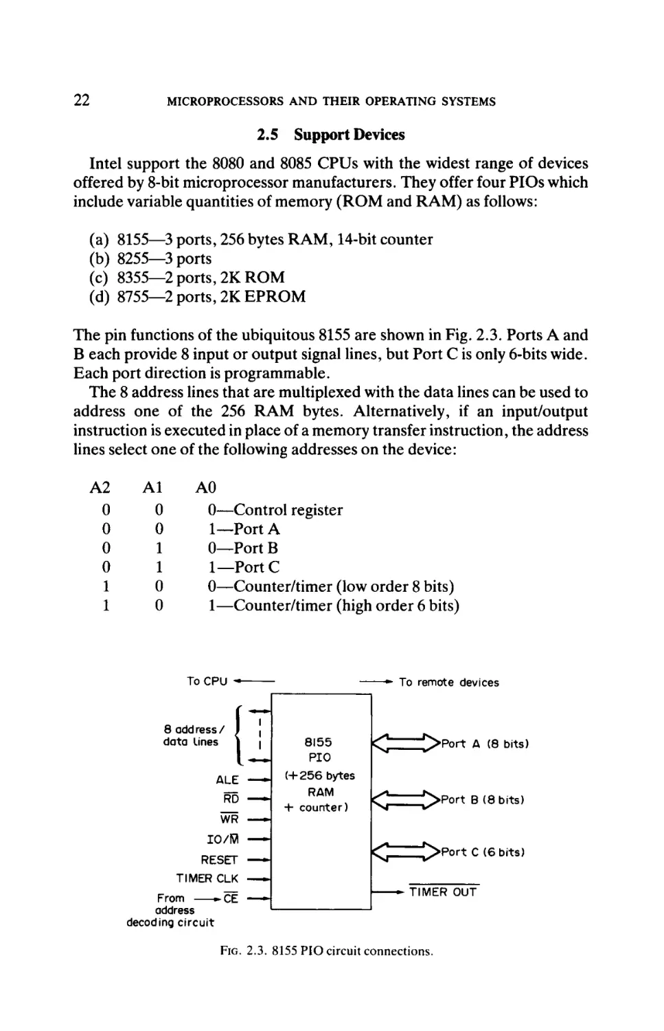
INTEL 8080/8085 FAMILY (8-BIT)
C/D
ΔΟ
j
DO
8 data
lines
lD7
1
1
1
—
l·-—
TxD \
l·—
RxD |
8251
UART
WR
RTS
CTS
RESET
Serial data
Modem control
signals
CLK
From
-CË
address
decoding circuit
TxC
RxC
Baud rate selection
FIG. 2.4. 8251 UART circuit connections.
The control register is used to set port directions, e.g.
bitO = Port A direction (0 = input, 1 = output)
bit 1 = Port B direction (0 = input, 1 = output)
bits2and3 = Port C direction (00 = input, 11 = output,01/10 = mixed)
bits 6 and 7 = Timer control (11 = start timer immediately)
The counter can be used to count external pulses, or (if fed from the CPU
clock) to produce a time delay, with a typical maximum delay of:
hex 3FFF (maximum 14-bit count) x 0.5//s (2 MHz clock)
= 8ms(approx.)
Alternatively the TIMER OUT signal can be connected to a CPU interrupt
line to trigger an interrupt service routine at regular intervals. A further
application is as a clock signal to a UART.
The standard Intel UART that interfaces an 8080/8085 system to a
serial-drive peripheral, e.g. VDU or data link, is the 8251. The circuit
connections are shown in Fig. 2.4. The device is universal, i.e. it is designed
to connect to almost any microprocessor. Therefore data bus and address
bus lines are not multiplexed. The single address line A0 must be de-multi
plexed from ADO by a simple external circuit when the device is connected
to an 8085 CPU. It is connected to the C/D (Control/Data) signal pin on the
8251, and the two states of this signal combine with the setting of either RD
(Read) or WR (Write) to produce four addressable registers on the 8251, as
follows:
24
MICROPROCESSORS A N D THEIR OPER/VTING SYSTEMS
C/D (AO)
0
0
1
1
RD
1
0
1
0
WR
0—Transmit data
1—Receive data
0—Control register
1—Status register
The control register is used to select the number of data bits, number of stop
bits, parity and baud rate factor. The latter parameter selects the frequency
divider ratio (1, 16 or 64) that is applied to the incoming transmitter and
receiver clock signals (TxC and RxC). To obtain the full range of baud rates
the clock signals must be variable and programmable, e.g. generated by a
counter on a 8155 PIO described above.
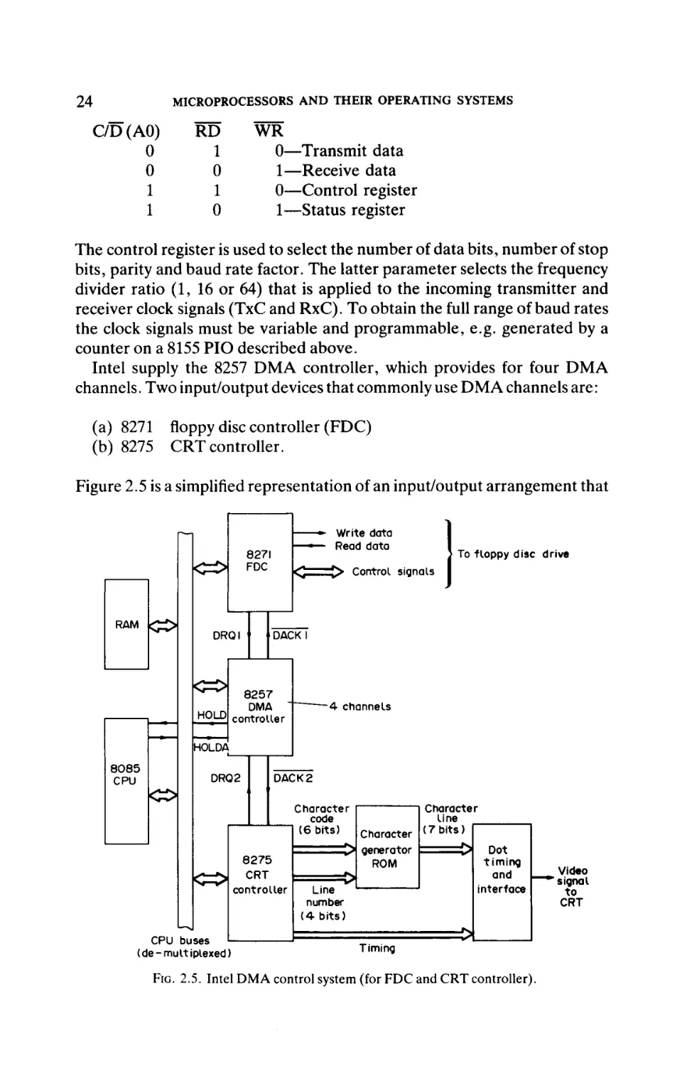
Intel supply the 8257 DMA controller, which provides for four DMA
channels. Two input/output devices that commonly use DMA channels are:
(a) 8271 floppy disc controller (FDC)
(b) 8275 CRT controller.
Figure 2.5 is a simplified representation of an input/output arrangement that
|<Z>|
RAM <Z£>i
Write data
Read data
8271
FDC
DRQI
To floppy disc drive
Control signals
DACKI
Κ=ίΗ
8257
DMA
HOLD controller
- 4 channels
HOLDA
8085
CPU
DRQ2
DACK2
k^
Character
code
(6 bits)
8275
CRT
controller
&=5\
CPU buses
(de-multiplexed)
Character
I P | generator
ROM
Line
number
(4-bits)
Timing
Character
line
(7 bits)
=3
Dot
timing
and
interface
=54
FIG. 2.5. Intel DMA control system (for FDC and CRT controller).
Video
"signal
to
CRT
INTEL 8080/8085 FAMILY (8-BIT)
25
utilises these three devices. The actions required to transfer block of bytes
between memory (RAM) and floppy disc are as tollows:
(1) Software initiates a transfer by loading the DMA controller with the
start address of memory, and the number of bytes to be transferred.
Additionally software loads the FDC with the disc address (track and
sector).
(2) FDC requests DMA transfers (DRQ1) when the required disc sector
is beneath the read/write head. The DMA controller requests the use
of the system buses from the CPU (using HOLD), which responds
withHLDA.
(3) Bytes are transferred directly between memory and floppy disc—
DMA controller generates each memory address, and FDC processes
each data byte. DMA transfers can be continuous ("burst").
The operation of the CRT controller circuit, which extracts character
bytes from main memory and creates a video signal to drive a CRT display,
is as follows:
(1) The DMA controller is initiated by software to hold the start address
of video data in main memory RAM, and the number of bytes to be
transferred.
(2) System software places the required character bytes into RAM
(typically a reserved 2K bytes area for 80 column, 24 line CRT
display).
(3) CRT controller requests DMA transfers (DRQ2) repeatedly. The
DMA controller responds with DACK2 and acquires use of the
buses from the CPU.
(4) Typically 80 character bytes are transferred from main memory RAM
to be stored in CRT controller—the DMA controller generates each
memory address, and the CRT controller receives each data byte.
(5) CRT controller presents each of 80 characters in turn to Character
Generator ROM which holds dot matrix for each character code—6bit character code combines with 4-bit line number to address ROM
to produce 7-bit dot pattern for each line of character. This is repeated
for each line in the dot matrix for entire block of 80 characters.
(6) Whilst one of 24 rows of 80 characters is being processed as in (5) the
next row of 80 characters is transferred by DMA to the CRT controller.
(7) Process is repeated—from stage (3) onwards—for each row of 80
characters until a complete CRT screen is displayed. This screen
refresh is repeated continuously such that the latest information held
in video RAM is displayed on the CRT.
26
MICROPROCESSORS AND THEIR OPERATING SYSTEMS
Additional devices offered by Intel include:
(a) 8231 arithmetic processor (add, subtract, multiply, divide, trigono
metric and logarithmic functions)
(b) 8232floatingpoint (32- or 64-bit numbers) processor
(c) 8202 dynamic RAM controller
(d) 8253 CTC (three 16-bit counters).
2.6 Applications
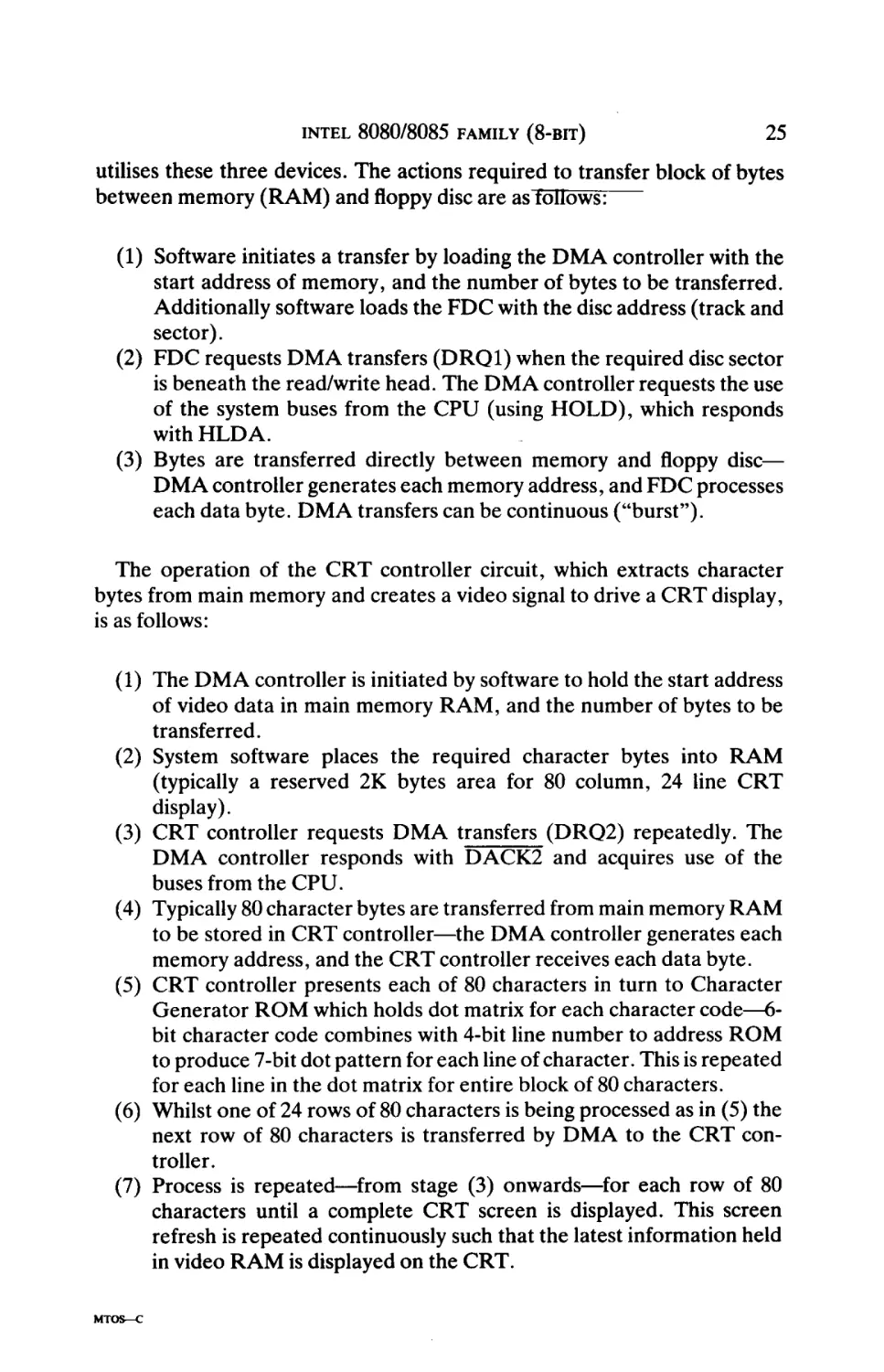
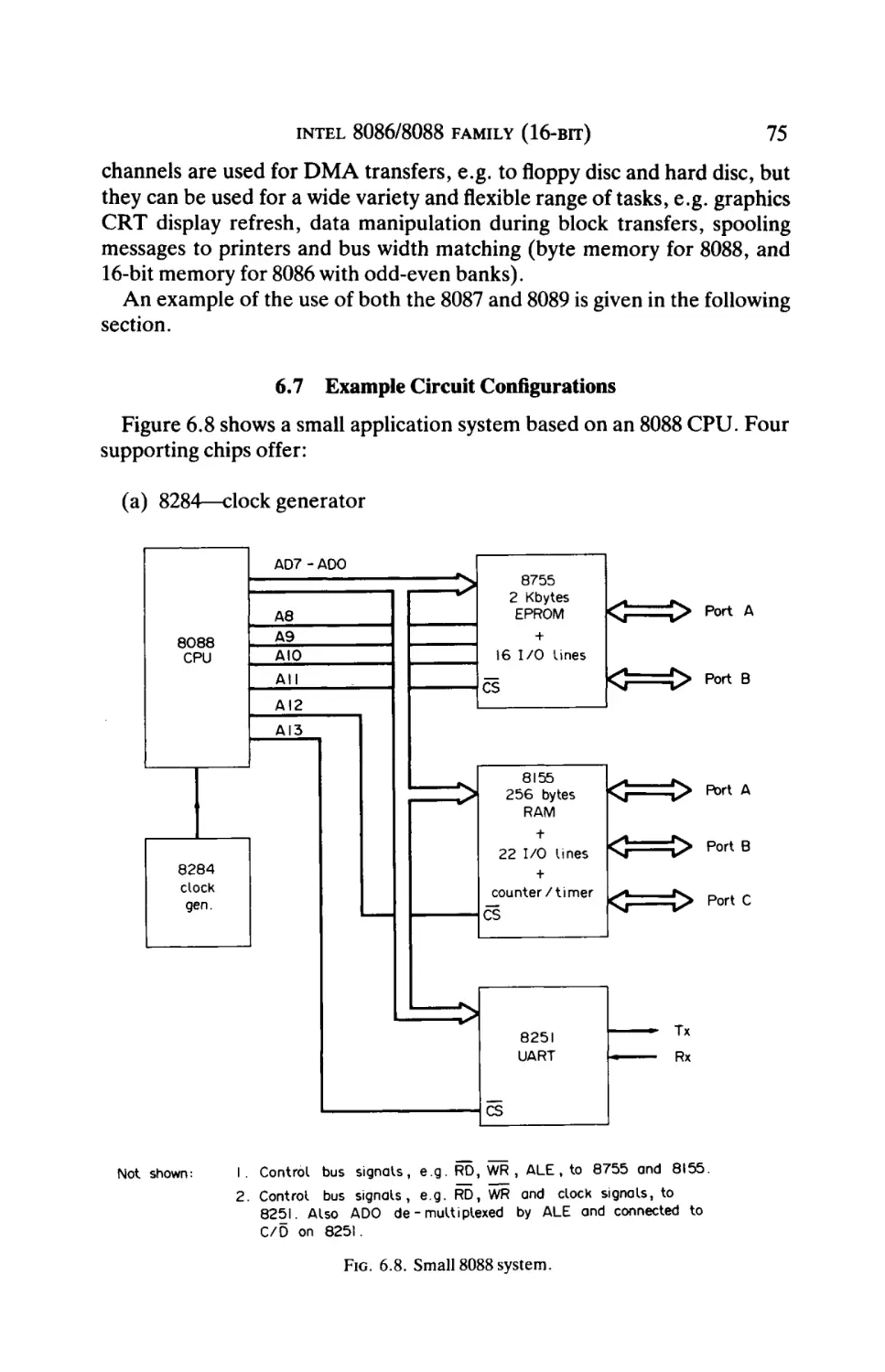
Figure 2.6 illustrates a simple circuit, comprising only three ICs, which
offers a complete microcomputer system. The circuit package comprises:
(a)
(b)
(c)
(d)
(e)
8085 CPU
256 bytes RAM
2K bytes EPROM
5 ports (one is only 6 bits wide)—total of 38 bits
1 counter/timer.
Such a configuration is suitable for a wide range of industrial applications,
e.g. sequence control system involving the input of several contact-closure
signals and the output of several on/off control signals.
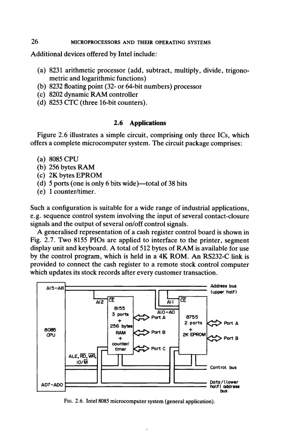
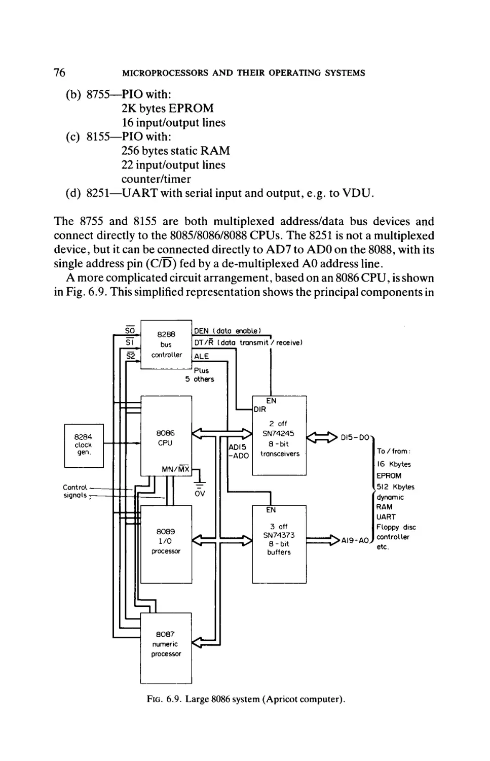
A generalised representation of a cash register control board is shown in
Fig. 2.7. Two 8155 PIOs are applied to interface to the printer, segment
display unit and keyboard. A total of 512 bytes of RAM is available for use
by the control program, which is held in a 4K ROM. An RS232-C link is
provided to connect the cash register to a remote stock control computer
which updates its stock records after every customer transaction.
Address bus
(upper half)
AI5-A8
AI 2
CE
All
8155
3 ports ,
+
AIO-AO
<iC> P o r t A
256 bytesl
RAM k£Z>
Port Θ
+
, counter/ . ^ ^
ZJ
timer
tô^
Port C
80Θ5
CPU
CE
8755
2 Ports 1 ^ ^ Port A
+
2K EPROM
k j £ > PortB
ALE,RD,WR,
IO/M
Control bus
AD7-AD0
Data /(lower
half) address
bus
FIG. 2.6. Intel 8085 microcomputer system (general application).
INTEL 8080/8085 FAMILY (8-BIT)
ΑΙ5-ΑΘ
2 to4
8085
CPU
Δ7-Α0
ALE
ÎR
4K
ROM
27
AI5-AO
CE
IAO
Π
8251 K T x
UART
h-Rxj
ALE
To
remote
stock
control
computer
(RS232-C
link)
AD7-AD0CT H Demultiplex
D7-D0
D7-D0
CE
*
rtA
H CE
Port A
printer
R>pE;
8155
Port B K ^ι Hand
shaking
256 bytes
RAM
Port C
l··-
i to
printer
i
8155
Port 8
256 bytes
RAM
Port C
Multi-digit
segment
display
Keypad
AD7-AD0
FIG. 2.7. Intel 8085 cash register configuration.
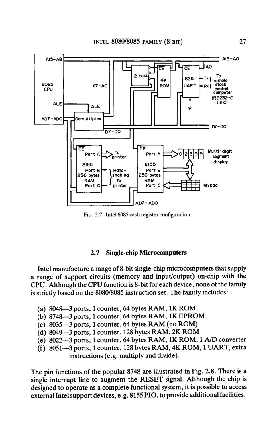
2.7 Single-chip Microcomputers
Intel manufacture a range of 8-bit single-chip microcomputers that supply
a range of support circuits (memory and input/output) on-chip with the
CPU. Although the CPU function is 8-bit for each device, none of the family
is strictly based on the 8080/8085 instruction set. The family includes:
(a)
(b)
(c)
(d)
(e)
(f )
8048—3 ports, 1 counter, 64 bytes RAM, IK ROM
8748—3 ports, 1 counter, 64 bytes RAM, IK EPROM
8035—3 ports, 1 counter, 64 bytes RAM (no ROM)
8049—3 ports, 1 counter, 128 bytes RAM, 2K ROM
8022—3 ports, 1 counter, 64 bytes RAM, IK ROM, 1 A/D converter
8051—3 ports, 1 counter, 128 bytes RAM, 4K ROM, 1 UART, extra
instructions (e.g. multiply and divide).
The pin functions of the popular 8748 are illustrated in Fig. 2.8. There is a
single interrupt line to augment the RESET signal. Although the chip is
designed to operate as a complete functional system, it is possible to access
external Intel support devices, e.g. 8155 PIO, to provide additional facilities.
28
MICROPROCESSORS AND THEIR OPERATING SYSTEMS
FIG. 2.8. Pin functions of 8748 single-chip microcomputer.
Single-chip microcomputers (sometimes called "microcontrollers") are
particularly suited to single-function domestic controllers, e.g. washing
machine controllers, telephone answering machines.
Bibliography
1. Microprocessors and Microcomputers. Barry G. Woollard. McGraw-Hill, 1981.
2. Microprocessors and Programmed Logic. Kenneth L. Short. Prentice-Hall, 1981.
3. Study Notes for Technicians: Microelectronic Systems Levels 1 & 2. R. C. Holland.
McGraw-Hill, 1983.
CHAPTER 3
ZILOG Z80
3.1 Introduction
The design of the Zilog Z80 was based on the Intel 8080/8085, but it
possesses several additional powerful facilities. It has achieved a diverse
range of applications in office computer systems, home computers and
industrial controllers.
The Z80 is "upwards compatible" with the Intel 8085 in terms of instruction set and machine code, i.e. programs written for the 8085 will run on a
Z80. However, compatibility in the other direction is not always achieved
because of the additional instructions which the Z80 possesses.
The Z80A is designed to operate at 4 MHz, whilst the Z80B will run at up
to 6 MHz.
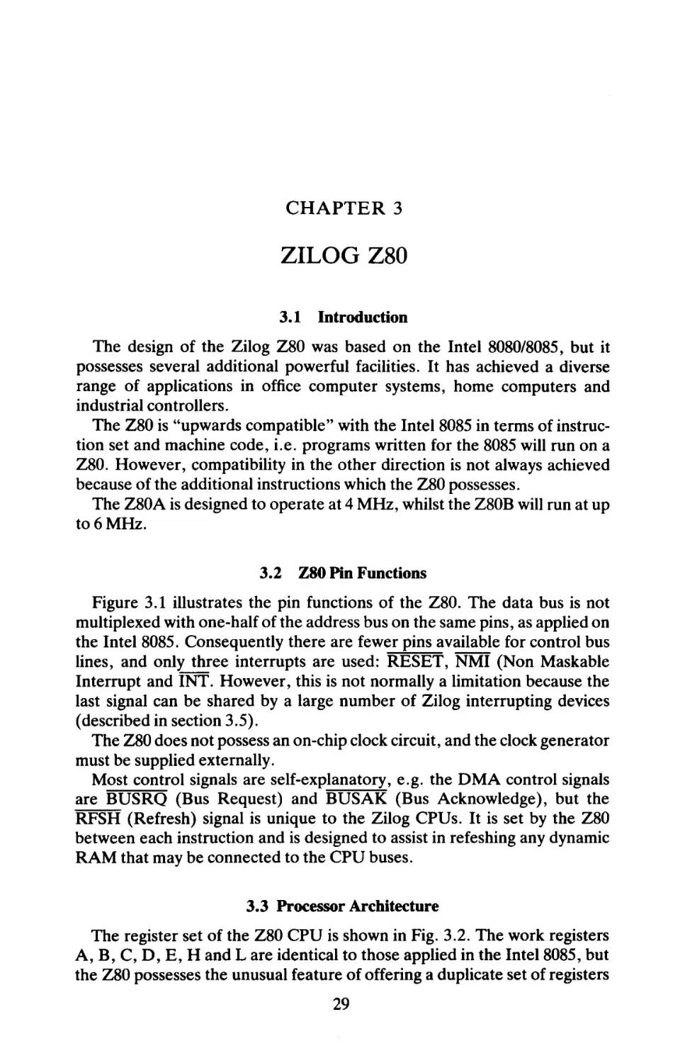
3.2 Z80 Pin Functions
Figure 3.1 illustrates the pin functions of the Z80. The data bus is not
multiplexed with one-half of the address bus on the same pins, as applied on
the Intel 8085. Consequently there are fewer pins available for control bus
lines, and only three interrupts are used: RESET, NMI (Non Maskable
Interrupt and INT. However, this is not normally a limitation because the
last signal can be shared by a large number of Zilog interrupting devices
(described in section 3.5).
The Z80 does not possess an on-chip clock circuit, and the clock generator
must be supplied externally.
Most control signals are self-explanatory, e.g. the DMA control signals
are BUSRQ (Bus Request) and BUSAK (Bus Acknowledge), but the
RFSH (Refresh) signal is unique to the Zilog CPUs. It is set by the Z80
between each instruction and is designed to assist in refeshing any dynamic
RAM that may be connected to the CPU buses.
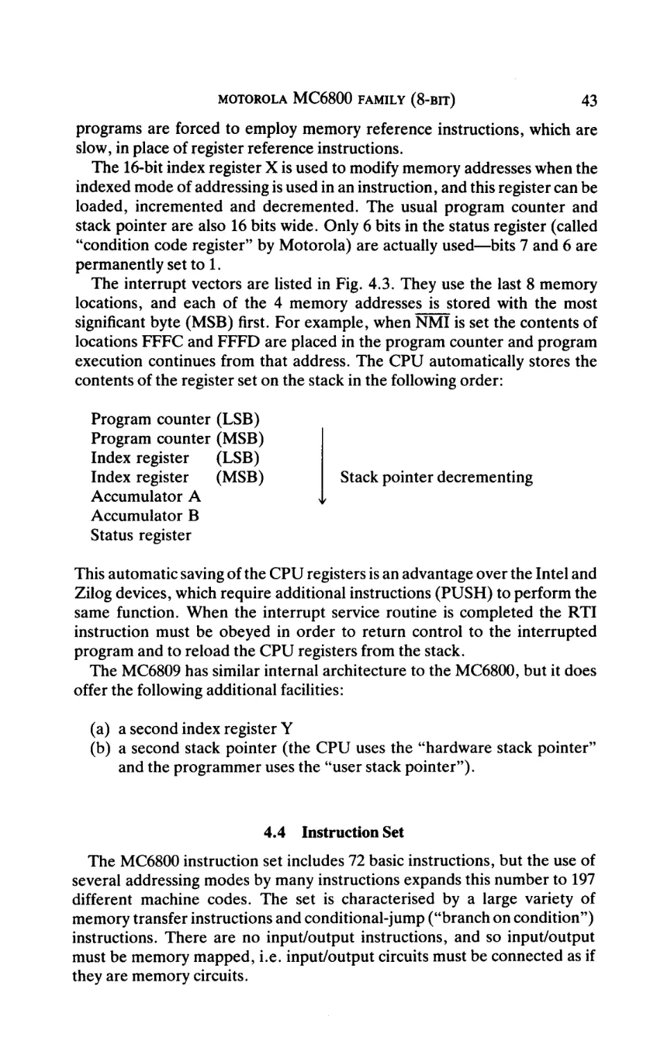
3.3 Processor Architecture
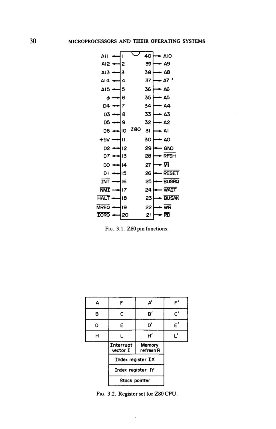
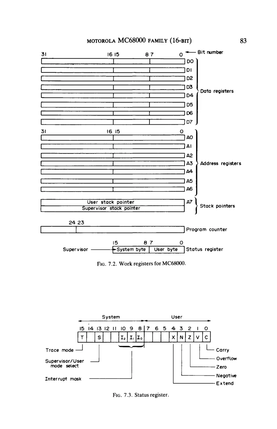
The register set of the Z80 CPU is shown in Fig. 3.2. The work registers
A, B, C, D, E, H and L are identical to those applied in the Intel 8085, but
the Z80 possesses the unusual feature of offering a duplicate set of registers
29
MICROPROCESSORS AND THEIR OPERATING SYSTEMS
All — 1
AI2-— 2
^ 40 — ΔΙ0
39 — A9
ΔΙ3 — 3
ΔΙ4 «*— 4
38 — A8
37 — A7 '
ΔΙ5-— 5
36 —*A6
Φ — 6
D4 — 7
34 — A4
35 —-A5
D3 — 8
33 — A3
05
32 - ^ A 2
~ 9
D 6 ~
io zeo
+5V — II
D2 — 12
D7 — 13
31 - — A I
30 — - A 0
29 — GND
28 —-RFSH
DO — 14
27 — - M l
Dl - — 15
26 — RESET
INT — 16
25 —BUSRO
NMI — 17
24 — WAIT
HALT — 18
23 — BUSAK
MREQ — 19
IORQ — 20
22 — WR
21 — RD
FIG. 3.1. Z80 pin functions.
A
F
A'
F'
8
C
B'
C
D
E
θ'
E'
H
L
H'
L_'
Interrupt
vector I
Memory
refresh R
Index register I X
Index register IY
Stack pointer
FIG. 3.2. Register set for Z80 CPU.
ZILOG Z80
31
(A' to L') and status register (F'). This feature is useful when a subroutine
or interrupt service routine (ISR) is entered, because the programmer can
select the alternative set within the subroutine or ISR, thus avoiding the
necessity of storing away the contents of the main program's registers, e.g.
with PUSH instructions. The following two instructions implement the
changeover (in either direction) :
EXX
;Exchange BC, DE and HL
EX A F , A F ' ;Exchange A F (F is Flags)
The interrupt vector I is an 8-bit register that is employed by the CPU to
locate the start address of an ISR when the CPU is selected to operate in one
of three "interrupt modes" (modes 0, 1 and 2). The start addresses of ISRs
can be summarised as follows:
RESET—PC is set to 0000 (PC = program counter)
NMI —PC is set to 0066
INT
—CPU obeys contents of interrupt vector I for CPU "mode 0"
—PC is set to 0038 for CPU "mode 1"
—CPU examines location XXYY to find start address of ISR for
CPU "mode 2" (XX is contents of interrupt vector I, YY is
supplied on data bus from interrupting device).
A program instruction (e.g. IM 2) is required to set the CPU into either
interrupt modes 0, 1 or 2, and if mode 2 is selected the interrupting device
(e.g. PIO,CTC) must be initialised with the 8-bit value (YY) which it
presents back to the CPU when it generates an interrupt.
The memory refresh register R is applied together with the RFSH signal
(see section 3.2) to refresh dynamic RAM. The register is incremented after
each instruction and is placed on the lower half of the address bus between
instructions.
The two 16-bit index registers (IX and IY) allow indexed addressing mode
instructions to be used.
3.4
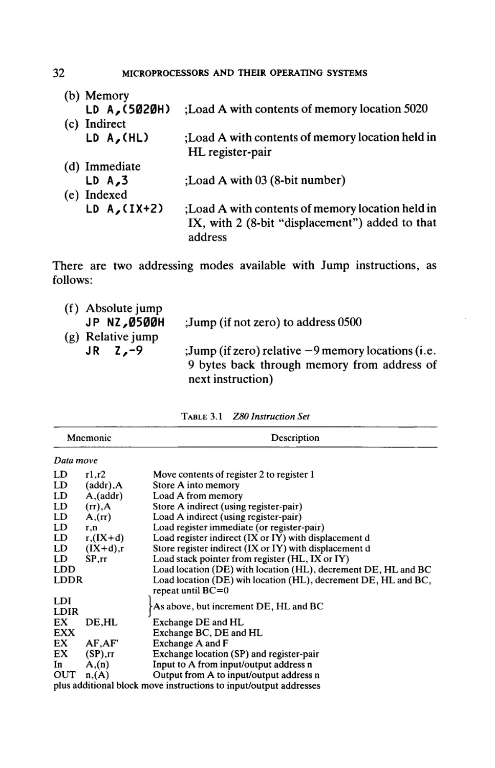
Instruction Set
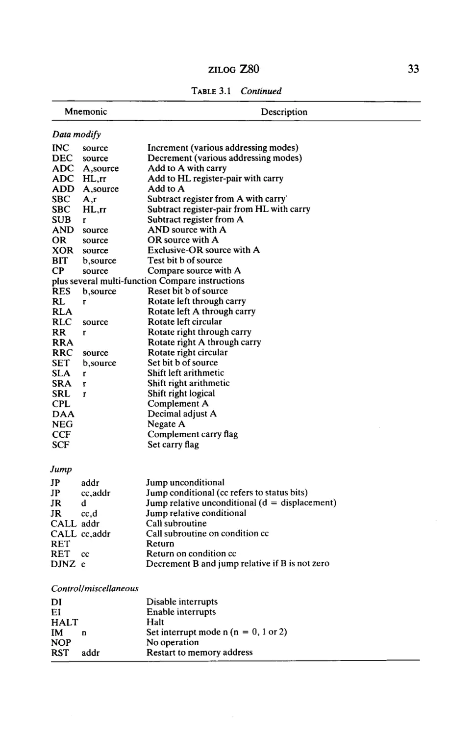
The Z80 instruction set is listed in Table 3.1. Although identical machine
code for Intel 8085 is retained by the Z80, instruction mnemonics are
different. The Z80 has several additional instructions to the 8085, e.g. data
block move instructions and individual bit checking/setting instructions. The
addressing modes available are:
(a) Register
LD A , C
;Load A with contents of C register
32
MICROPROCESSORS AND THEIR ΟΡΕΚΑΉΝΘ SYSTEMS
(b) Memory
LD A, ( 5020H )
(c) Indirect
LD A , ( H L )
(d) Immediate
LD A,3
(e) Indexed
LD A,(IX+2)
;Load A with contents of memory location 5020
;Load A with contents of memory location held in
HL register-pair
;Load A with 03 (8-bit number)
;Load A with contents of memory location held in
IX, with 2 (8-bit "displacement") added to that
address
There are two addressing modes available with Jump instructions, as
follows:
(f) Absolute jump
J P NZ,0500H
(g) Relative jump
JR Z , - 9
;Jump (if not zero) to address 0500
;Jump (if zero) relative —9 memory locations (i.e.
9 bytes back through memory from address of
next instruction)
TABLE 3.1
Mnemonic
Data move
rl,r2
LD
LD
(addr),A
LD
A,(addr)
LD
(rr),A
LD
A,(rr)
LD
r,n
LD
r,(LX+d)
LD
(IX+d),r
LD
SP,rr
LDD
LDDR
Z80 Instruction Set
Description
Move contents of register 2 to register 1
Store A into memory
Load A from memory
Store A indirect (using register-pair)
Load A indirect (using register-pair)
Load register immediate (or register-pair)
Load register indirect (IX or IY) with displacement d
Store register indirect (IX or IY) with displacement d
Load stack pointer from register (HL, IX or IY)
Load location (DE) with location (HL), decrement DE, HL and BC
Load location (DE) wih location (HL), decrement DE, HL and BC,
repeat until BC=0
LDI
[As above, but increment DE, HL and BC
LDIR
DE,HL
Exchange DE and HL
EX
EXX
Exchange BC, DE and HL
Exchange A and F
EX
AF,AF
(SP),rr
Exchange location (SP) and register-pair
EX
Input to A from input/output address n
In
A,(n)
Output from A to input/output address n
OUT n,(A)
plus additional block move instructions to input/output addresses
33
ZILOG Z 8 0
TABLE 3.1
Mnemonic
Continued
Description
Data modify
Increment (various addressing modes)
INC
source
Decrement (various addressing modes)
DEC source
Add to A with carry
ADC A,source
Add to HL register-pair with carry
ADC HL,rr
Add to A
ADD A,source
Subtract register from A with carry'
SBC A,r
Subtract register-pair from HL with carry
SBC HL,rr
Subtract register from A
SUB r
AND source with A
AND source
OR source with A
source
OR
Exclusive-OR source with A
XOR source
Test bit b of source
b,source
BIT
Compare source with A
source
CP
plus several multi-■function Compare instructions
Reset bit b of source
RES b, source
Rotate left through carry
r
RL
Rotate left A through carry
RLA
Rotate left circular
RLC source
Rotate right through carry
r
RR
Rotate right A through carry
RRA
Rotate right circular
RRC source
Set bit b of source
SET b,source
Shift left arithmetic
SLA r
Shift right arithmetic
SRA r
Shift right logical
SRL r
Complement A
CPL
Decimal adjust A
DAA
Negate A
NEG
Complement carry flag
CCF
Set carry flag
SCF
Jump
JP
JP
JR
JR
CALL
CALL
RET
RET
DJNZ
addr
cc,addr
d
cc,d
addr
cc,addr
cc
e
Jump unconditional
Jump conditional (cc refers to status bits)
Jump relative unconditional (d = displacement)
Jump relative conditional
Call subroutine
Call subroutine on condition cc
Return
Return on condition cc
Decrement B and jump relative if B is not zero
Contro l/miscellam
DI
El
HALT
n
IM
NOP
RST addr
Disable interrupts
Enable interrupts
Halt
Set interrupt mode n (n = 0, 1 or 2)
No operation
Restart to memory address
34
MICROPROCESSORS AND THEIR OPERATING SYSTEMS
The following program examples illustrate use of the instruction set.
Program Example 1
LD A,0FFH
LD D,10
LD BC,3000H
CONT:LD <BC),A
INC BC
DEC D
JP NZ,C0NT
HALT
;Load A with FF (all Is)
;Load loop count of 10 into D
;LoadBC with 3000
;Store A in memory (using BC indirect)
increment BC
;Decrement loop count in D
;Jump around loop (10 times)
;Halt
This program stores FF in 10 memory locations commencing at address 3000.
Program Example 2
;7E is address of 8-bit port to carry data bits (in ASCII)
;7F is address of handshaking signal "out" bit (strobe), and also
;of handshaking "in" bit (ready).
LD
LD
BUSY :IN
BIT
JP
LD
OUT
LD
OUT
CALL
LD
OUT
CALL
D,25
BC,0700H
A,(7FH)
0,A
Z,BUSY
A,(BC)
<7EH),A
A,0
(7FH),A
DELAY
A,1
(7FH),A
DELAY
;Set loop count of 25
;Set start address of 25 ASCII characters
;Input ready signal
;Check bit 0 in A (logic 0 if printer is busy)
;Poll "ready" until it indicates printer ready
Load A with ASCII character
Output to port (8 data bits)
Output 0 to ' 'strobe" signal
Delay
Output 1 to "strobe" signal
Delay
A complete pulse has now been set on
"strobe"
INC BC
;Step on to next character
DEC D
;Decrement loop count
JP
;Repeat loop (25 times)
NZ,BUSY
JP
;Jump to other program (at address 0000)
0
;End of program, now for subroutine
DELAY:LD
E, 0 F FH
;Set delay loop count
LOOP:NOP
NOP
NOP
DEC E
;Decrement loop count
NZ , LOOP
;Repeat loop
JP
RET
35
ZILOG Z80
This program outputs a string of characters to a Centronics interface parallel
printer. Within the loop that outputs characters itfirstlypolls the "ready" bit
(handshaking response bit from printer) to ensure that the printer is not
already printing a character. Next the character is sent to the printer. Finally
a pulse is applied on the "strobe" bit (handshaking bit to printer), which
causes the printer to examine the 8 data/character bits and print the
character. The loop is repeated 25 times.
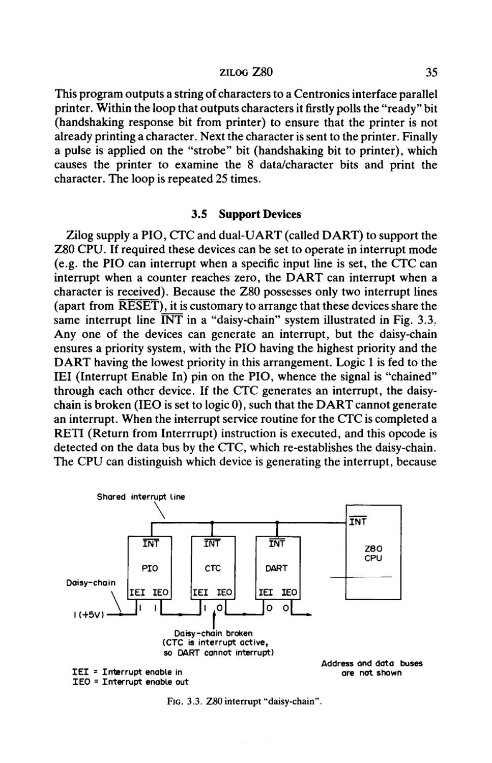
3.5 Support Devices
Zilog supply a PIO, CTC and dual-UART (called DART) to support the
Z80 CPU. If required these devices can be set to operate in interrupt mode
(e.g. the PIO can interrupt when a specific input line is set, the CTC can
interrupt when a counter reaches zero, the DART can interrupt when a
character is received). Because the Z80 possesses only two interrupt lines
(apart from RESET), it is customary to arrange that these devices share the
same interrupt line INT in a "daisy-chain" system illustrated in Fig. 3.3.
Any one of the devices can generate an interrupt, but the daisy-chain
ensures a priority system, with the PIO having the highest priority and the
DART having the lowest priority in this arrangement. Logic 1 is fed to the
IEI (Interrupt Enable In) pin on the PIO, whence the signal is "chained"
through each other device. If the CTC generates an interrupt, the daisychain is broken (IEO is set to logic 0), such that the DART cannot generate
an interrupt. When the interrupt service routine for the CTC is completed a
RETI (Return from Interrrupt) instruction is executed, and this opcode is
detected on the data bus by the CTC, which re-establishes the daisy-chain.
The CPU can distinguish which device is generating the interrupt, because
Shared interrupt Line
\
Daisy-chain
IH-5V) — ^ -
1
ÎNT
INT
I
INT
PIO
CTC
DART
I E I IEO
1' 1
IEI
IEO
M1
INT
Z80
CPU
I E I IEO
Jo oL
Daisy-chain broken
(CTC is interrupt active,
so DART cannot interrupt)
I E I = Interrupt enable in
IEO = Interrupt enable out
Address and data buses
are not shown
FIG. 3.3. Z80 interrupt "daisy-chain".
MICROPROCESSORS AND THEIR OPERAΉNG SYSTEMS
AO
AI
Port A
u
8 data lines {
\
Φ—
RD —
IORQ
INT
MT
From address
decoding
circuit
CË
IEI
*
»—IEO
FIG. 3.4. Z80 PIO circuit connections.
the interrupting device places an 8-bit "code" on the data bus—see INT
(CPU mode 2, in section 3.3).
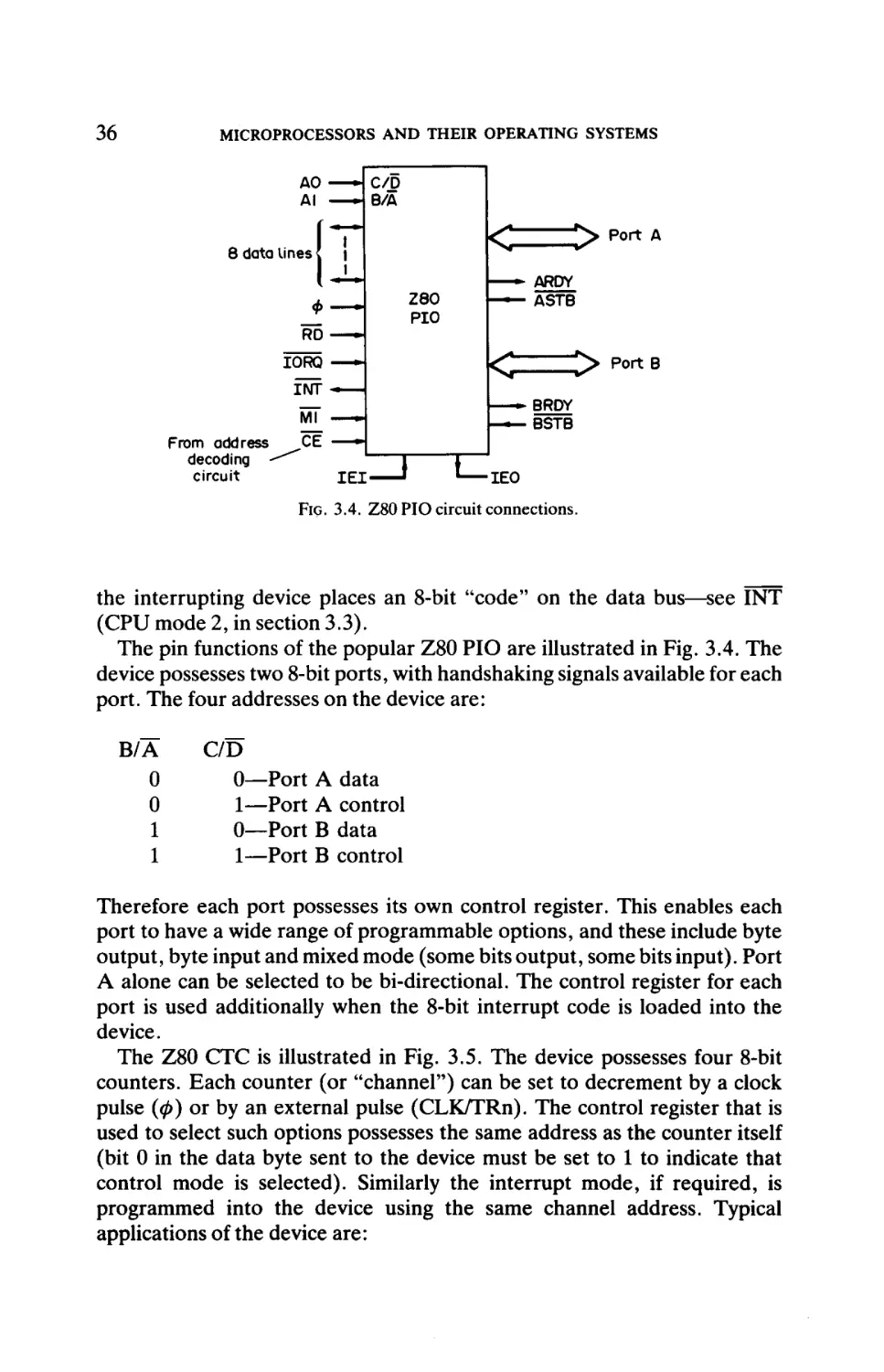
The pin functions of the popular Z80 PIO are illustrated in Fig. 3.4. The
device possesses two 8-bit ports, with handshaking signals available for each
port. The four addresses on the device are:
B/A
0
0
1
1
C/D
0—Port A data
1—Port A control
0—Port B data
1—Port B control
Therefore each port possesses its own control register. This enables each
port to have a wide range of programmable options, and these include byte
output, byte input and mixed mode (some bits output, some bits input). Port
A alone can be selected to be bi-directional. The control register for each
port is used additionally when the 8-bit interrupt code is loaded into the
device.
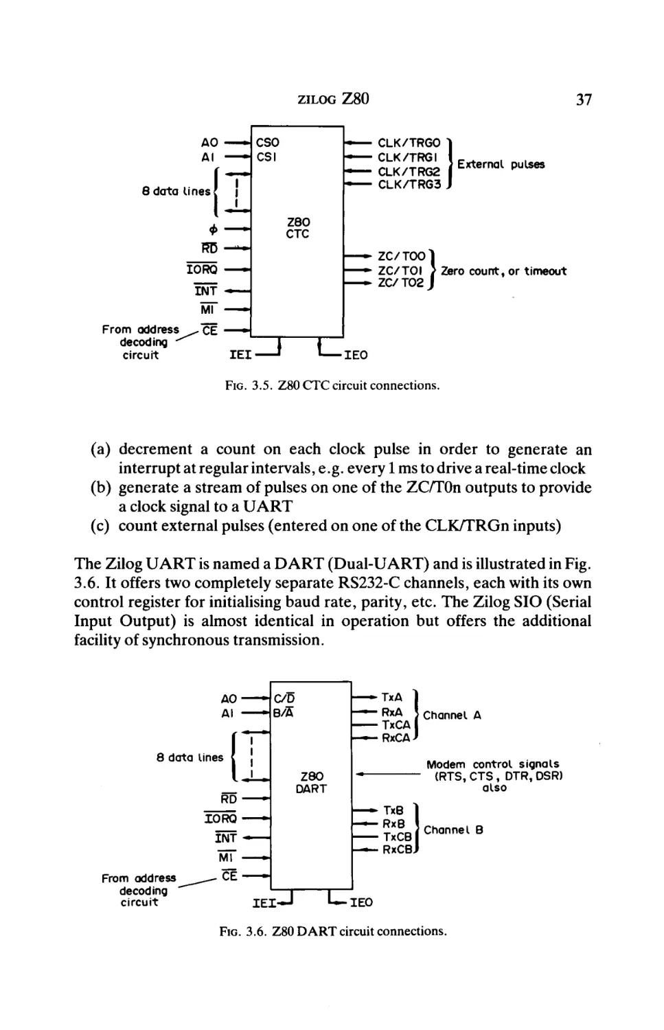
The Z80 CTC is illustrated in Fig. 3.5. The device possesses four 8-bit
counters. Each counter (or "channel") can be set to decrement by a clock
pulse (0) or by an external pulse (CLK/TRn). The control register that is
used to select such options possesses the same address as the counter itself
(bit 0 in the data byte sent to the device must be set to 1 to indicate that
control mode is selected). Similarly the interrupt mode, if required, is
programmed into the device using the same channel address. Typical
applications of the device are:
37
ZILOG Z 8 0
AO — CSO
AI — - CSI
8data Unes?
—
—
—
—
|
CLK/TRGO
CLK/TRGI
CLK/TRG2
CLK/TRG3
External pulses
ΖΘΟ
CTC
Φ
IORQ
—
ÏNT
—
— -
ZC/TOOl
— *
ZC/TOI } ;Zero count, or timeout
— -
ZC/T02J
W —>
From address^^"cË — · ■
decoding
^
circuit
IEI
_J L
IEO
FIG. 3.5. Z80 CTC circuit connections.
(a) decrement a count on each clock pulse in order to generate an
interrupt at regular intervals, e.g. every 1 ms to drive a real-time clock
(b) generate a stream of pulses on one of the ZC/TOn outputs to provide
a clock signal to a UART
(c) count external pulses (entered on one of the CLK/TRGn inputs)
The Zilog UART is named a DART (Dual-UART) and is illustrated in Fig.
3.6. It offers two completely separate RS232-C channels, each with its own
control register for initialising baud rate, parity, etc. The Zilog SIO (Serial
Input Output) is almost identical in operation but offers the additional
facility of synchronous transmission.
Channel A
8 data lines
Modem control signals
(RTS, CTS, DTR, DSR)
also
Channel B
From address
decoding
circuit
IEI-
IEO
FIG. 3.6. Z80 DART circuit connections.
38
MICROPROCESSORS AND THEIR OPERATING SYSTEMS
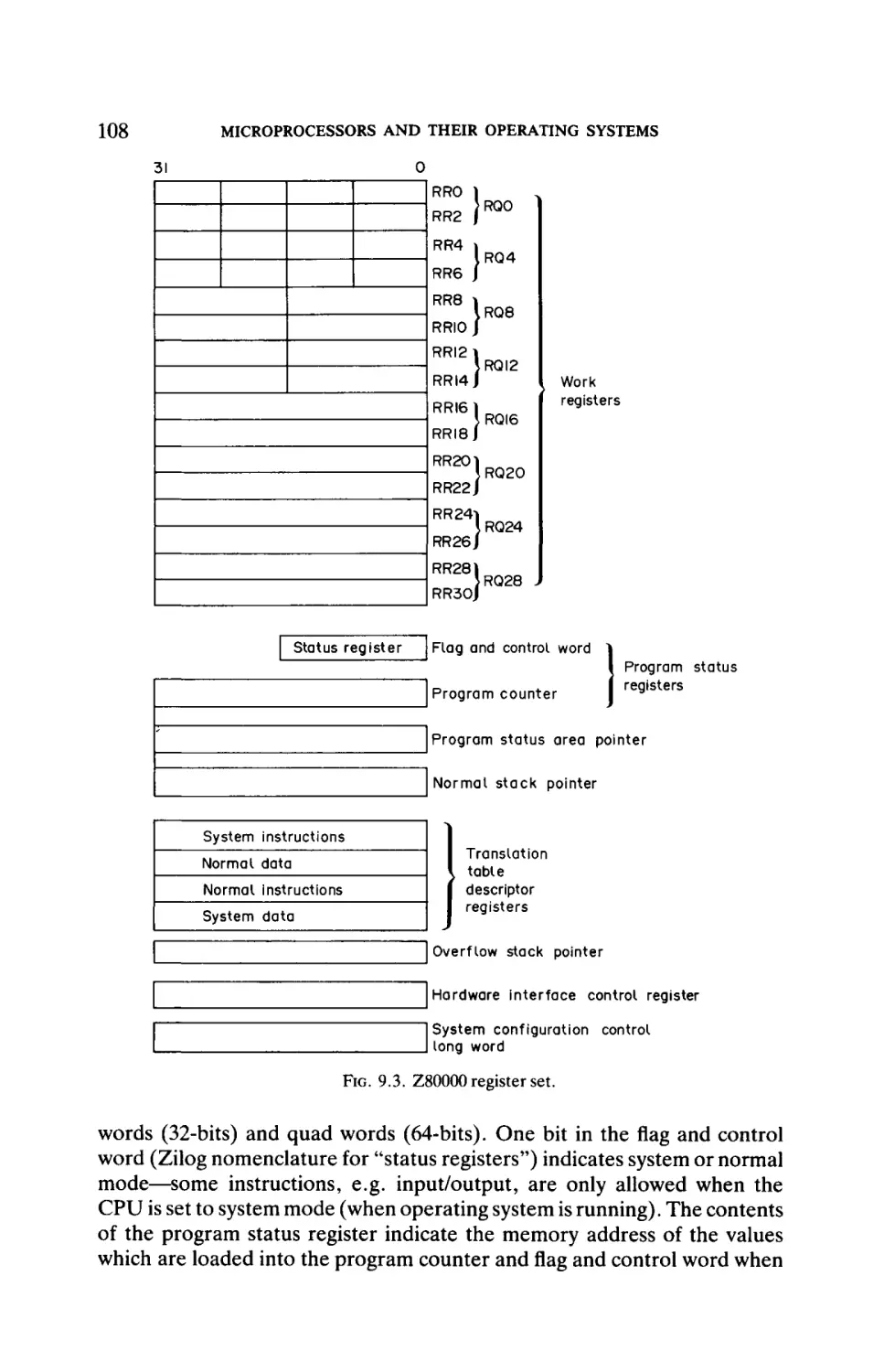
3.6 Applications
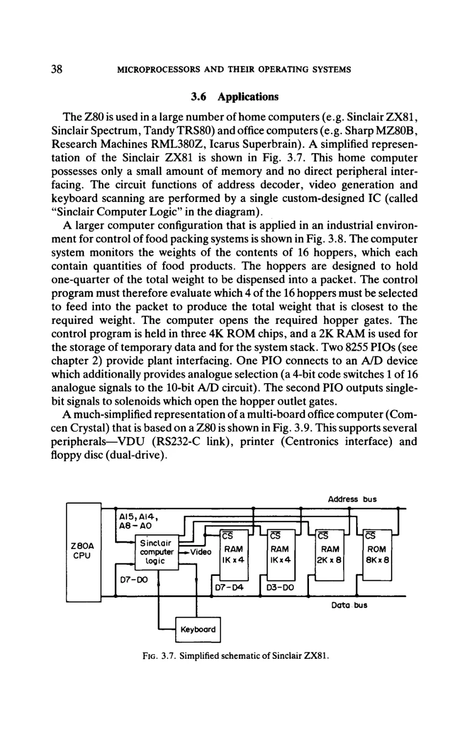
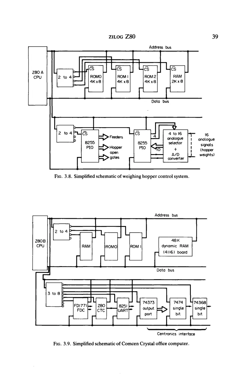
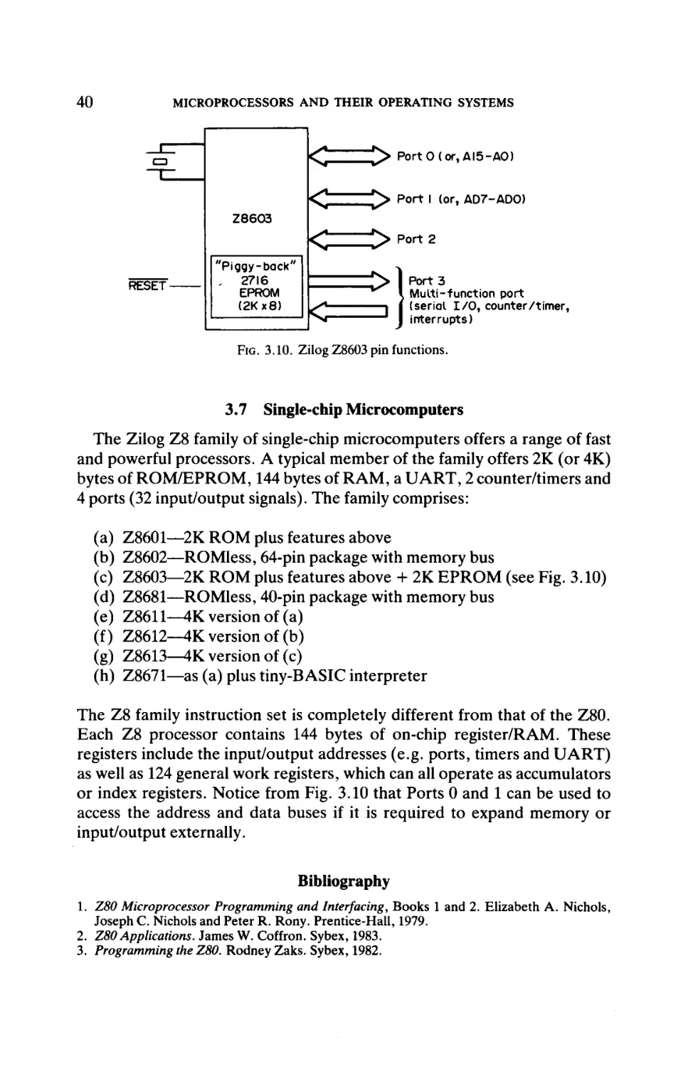
The Z80 is used in a large number of home computers (e.g. Sinclair ZX81,
Sinclair Spectrum, Tandy TRS80) and office computers (e.g. Sharp MZ80B,
Research Machines RML380Z, Icarus Superbrain). A simplified represen
tation of the Sinclair ZX81 is shown in Fig. 3.7. This home computer
possesses only a small amount of memory and no direct peripheral inter
facing. The circuit functions of address decoder, video generation and
keyboard scanning are performed by a single custom-designed IC (called
"Sinclair Computer Logic" in the diagram).
A larger computer configuration that is applied in an industrial environ
ment for control of food packing systems is shown in Fig. 3.8. The computer
system monitors the weights of the contents of 16 hoppers, which each
contain quantities of food products. The hoppers are designed to hold
one-quarter of the total weight to be dispensed into a packet. The control
program must therefore evaluate which 4 of the 16 hoppers must be selected
to feed into the packet to produce the total weight that is closest to the
required weight. The computer opens the required hopper gates. The
control program is held in three 4K ROM chips, and a 2K RAM is used for
the storage of temporary data and for the system stack. Two 8255 PIOs (see
chapter 2) provide plant interfacing. One PIO connects to an A/D device
which additionally provides analogue selection (a 4-bit code switches 1 of 16
analogue signals to the 10-bit A/D circuit). The second PIO outputs singlebit signals to solenoids which open the hopper outlet gates.
A much-simplified representation of a multi-board office computer (Comcen Crystal) that is based on a Z80 is shown in Fig. 3.9. This supports several
peripherals—VDU (RS232-C link), printer (Centronics interface) and
floppy disc (dual-drive).
Address bus
AI5,AI4,
A8-A0
ΖΘΟΑ
CPU
1—ιτνξ
CÜ
Sinclair
computer |-*»Video
logic
07-00
RAM
IKx4
|D7-D4
μϋ^ζ
es
U Lfiiç
C5
RAM
2Kx8
RAM
IKx4
j D3-DO
J LfiSç
CS
|
ROM
8Kx8
I
Data bus
Keyboard
FIG. 3.7. Simplified schematic of Sinclair ZX81.
LI
39
ZILOG Z 8 0
Address bus
Lies
CS
CS
Z80A
CPU
CS
RAM
2Kx8
ROM 2
4Kx8
ROM I
4Kx8
ROMO
4Kx8
2 to 4
Us
CS
I Γ Γ
Data bus
2 to 4
CS
4 to 16
Ui-J
anal
analogue
i ^ i selector
8255
CS
C ^ ^ Feeders
8255 Γ ^
PIO
Γ
b ^ Hopper
open
Legates
pio p^ËH
+
A/D
converter
Γ
T"
16
1 analogue
[
signals
1
(hopper
,1
weights)
FIG. 3.8. Simplified schematic of weighing hopper control system.
Address bus
2 to 4 f>
Z80B |
CPU
RAM
F
ROM I
ROMO
Γ I
I
ί
48 K
dynamic RAM
(4116) board
Data bus
3 to 8 K
FDI77I
FDC
tnj—u l·8251 H
Z80
CTC
UARTl
M 74373 I
Γ Γ £. I
H
output r—^
port
C
7474
single
bit
•174368
single
bit
Centronics interface
FIG. 3.9. Simplified schematic of Comcen Crystal office computer.
40
MICROPROCESSORS AND THEIR OPERAΉNG SYSTEMS
Z8603
RESET -
"Piggy-back"
; 2716
EPROM
(2Κχθ)
<2
^> PortO(or,AI5-AO)
<l
^ > Port I (or, AD7-AD0)
k=> P o r t 2
^ > I Port 3
\C
^^
-i
■ MuIti-function port
f (serial I / O , counter/timer,
' interrupts)
FIG. 3.10. Zilog Z8603 pin functions.
3.7 Single-chip Microcomputers
The Zilog Z8 family of single-chip microcomputers offers a range of fast
and powerful processors. A typical member of the family offers 2K (or 4K)
bytes of ROM/EPROM, 144 bytes of RAM, a UART, 2 counter/timers and
4 ports (32 input/output signals). The family comprises:
(a)
(b)
(c)
(d)
(e)
(f)
(g)
(h)
Z8601—2K ROM plus features above
Z8602—ROMless, 64-pin package with memory bus
Z8603—2K ROM plus features above + 2K EPROM (see Fig. 3.10)
Z8681—ROMless, 40-pin package with memory bus
Z8611-^K version of (a)
Z8612—4K version of (b)
Z8613-4K version of (c)
Z8671—as (a) plus tiny-BASIC interpreter
The Z8 family instruction set is completely different from that of the Z80.
Each Z8 processor contains 144 bytes of on-chip register/RAM. These
registers include the input/output addresses (e.g. ports, timers and UART)
as well as 124 general work registers, which can all operate as accumulators
or index registers. Notice from Fig. 3.10 that Ports 0 and 1 can be used to
access the address and data buses if it is required to expand memory or
input/output externally.
Bibliography
Z80 Microprocessor Programming and Interfacing, Books 1 and 2. Elizabeth A. Nichols,
Joseph C. Nichols and Peter R. Rony. Prentice-Hall, 1979.
Z80 Applications. James W. Coffron. Sybex, 1983.
Programming the Z80. Rodney Zaks. Sybex, 1982.
CHAPTER 4
MOTOROLA MC6800 FAMILY (8-BIT)
4.1 Introduction
Motorola developed the MC6800 at the same time as Intel were develop
ing the 8080. Following the initial popularity of this device, Motorola
introduced other CPUs into the family, culminating in the MC6809. This
latter device was introduced after the other popular 8-bit microprocessors
offered by rival manufacturers, and is probably the most powerful 8-bit
device, with a wide range of enhanced features.
4.2 MC6800 Pin Functions
Figure 4.1 shows the pin functions of the 40-pin MC6800. The device
requires two clock signals φχ and φ2, which are in antiphase with each other.
The MC6800 instructions require between two and eight machine cycles to
execute. There are two interrupt signals (IRQ and NMI) in addition to the
normal RESET signal. When the HALT signal is set low, the CPU ceases
operation and floats the address and data buses (and R/W). This is useful
when it is required to perform program debugging and to execute one
instruction at a time. In this condition BA (Bus Available) is set.
VMA (Valid Memory Address) is set whenever a valid address is set on
the address bus. DMA requests can be activated by setting TSC (Three State
Control) high, in order tofloatthe address bus and R/W, and by setting DBE
(Data Bus Enable) high, in order to float the data bus.
Although different pin numbers are applied, the MC6809 has similar pin
functions. Notice that two pins are unused on the MC6800, and this allows
the MC6809 to offer an additional interrupt signal.
4.3 Processor Architecture
The register set for the MC6800 is illustrated in Fig. 4.2. There are two
accumulators, such that the results of ALU operations can be placed in
either accumulator within an instruction. This is an advantage over the Intel
8085 and the Zilog Z80, but the larger number of registers in these latter
devices outweighs this feature for most programming applications. MC6800
MTOS—D
41
42
MICROPROCESSORS AND THEIR OPERATING SYSTEMS
Ground
—
HÄLT
1
2
*\
3
IRQ
4
VMA
5
NMÏ
BA
401
RESET
39 [
38 [
Not used
TSC
Φζ
DBE
6
37
1
36 [
35 [
7
34
R/W
Θ
33 [
DO
Δ0
9
32
Dl
AI
10
D2
A2
(
31
30
A3
12
29
D4
A4
13
28
■ D5
A5
14
27
■ D6
A6
15
26
■ D7
A7
16
25
AI5
A8
17
24
AI4
A9
18
23
• AI3
AIO
19
22
- AI2
All
20
21
■ Ground
+ 5V
j MC6800
1
Not used
D3
FIG. 4.1. MC6800 pin functions.
A
Accumulator A
B
Accumulator B
X
Index register X
PC
Program counter
SP
Stack pointer
Status register
FIG. 4.2. Register set for MC6800 CPU.
Memory oddress
FFF8
MSB
FFF9
LSB
FFFA
MSB
FFFB
LSB
FFFC
MSB
FFFD
LSB
FFFE
MSB
FFFF
LSB
{IRQ vector
f S W I (Software interrupt instruction) vector
>NMI vector
RESET vector (highest priority)
FIG. 4.3. MC6800 inerrupt vectors.
MOTOROLA MC6800 FAMILY (8-BIT)
43
programs are forced to employ memory reference instructions, which are
slow, in place of register reference instructions.
The 16-bit index register X is used to modify memory addresses when the
indexed mode of addressing is used in an instruction, and this register can be
loaded, incremented and decremented. The usual program counter and
stack pointer are also 16 bits wide. Only 6 bits in the status register (called
"condition code register" by Motorola) are actually used—bits 7 and 6 are
permanently set to 1.
The interrupt vectors are listed in Fig. 4.3. They use the last 8 memory
locations, and each of the 4 memory addresses is stored with the most
significant byte (MSB) first. For example, when NMI is set the contents of
locations FFFC and FFFD are placed in the program counter and program
execution continues from that address. The CPU automatically stores the
contents of the register set on the stack in the following order:
Program counter
Program counter
Index register
Index register
Accumulator A
Accumulator B
Status register
(LSB)
(MSB)
(LSB)
(MSB)
Stack pointer decrementing
This automatic saving of the CPU registers is an advantage over the Intel and
Zilog devices, which require additional instructions (PUSH) to perform the
same function. When the interrupt service routine is completed the RTI
instruction must be obeyed in order to return control to the interrupted
program and to reload the CPU registers from the stack.
The MC6809 has similar internal architecture to the MC6800, but it does
offer the following additional facilities:
(a) a second index register Y
(b) a second stack pointer (the CPU uses the "hardware stack pointer"
and the programmer uses the "user stack pointer").
4.4 Instruction Set
The MC6800 instruction set includes 72 basic instructions, but the use of
several addressing modes by many instructions expands this number to 197
different machine codes. The set is characterised by a large variety of
memory transfer instructions and conditional-jump ("branch on condition")
instructions. There are no input/output instructions, and so input/output
must be memory mapped, i.e. input/output circuits must be connected as if
they are memory circuits.
44
MICROPROCESSORS AND THEIR OPERATING SYSTEMS
The addressing modes available, together with examples of their use, are :
(a) Implied
I NX
(b) Accumulator
COM A
(c) Immediate
LDA A # $ 5 7
increment index register
Complement accumulator A (invert all bits)
;Load accumulator A with hex 57 ( # denotes
immediate addressing)
(d) Direct
LDA A $ 3 B
;Load accumulator A with contents of memory
location hex 3B
This is sometimes called "base page addressing"—the base page is the first
256 bytes of memory. Instructions are 2 bytes long, compared with 3 bytes
for the following addressing mode.
(e) Extended
LDA A $ 7 0 2 F ;Load accumulator A with contents of memory
location hex 702F
(f) Indexed
LDA A $ 4 0 , X ;Load accumulator A with contents of memory
location obtained by adding hex 40 to the contents
of the index register X
(g) Relative
;Branch if equal to zero backwards 5 bytes
BEQ - 5
Notice that full 16-bit addressing is available with subroutine and uncondi
tional jump instructions, e.g.
J MP $ 5 0 0 0
JSR $ 6 5 7 0
;Jump to memory location 5000
; Jump to subroutine at memory location 6570
Program Example 1
LDX
LDA
LOOP: ADD
I NX
CPX
BNE
#$40
A #0
A $00,X
#$45
LOOP
;LoadXwithhex40
;ClearA
; Add to A from address 0, indexed by X
increment X
;Compare X with hex 45
;Repeat if not zero (i.e. loop 5 times)
This program adds 5 numbers into accumulator A. The 5 numbers are held
in page 0 of memory, at locations 40 to 44. Register X is used both to index
the memory address and as a loop count.
45
MOTOROLA M C 6 8 0 0 FAMILY (8-BIT)
TABLE 4.1
Mnemonic
MC6800 Instruction Set
Description
Data move
LDA
LDA
STA
STA
LDX
STX
TAB
TBA
TAP
TPA
TXS
TSX
LDS
STS
A source
B source
Adest
B dest
source
dest
data
dest
Load accumulator A from source (various addressing modes)
Load accumulator B from source
Store accumulator A in destination
Store accumulator B in destination
Load register X from source
Store register X in destination
Transfer accumulator A to accumulator B
Transfer accumulator B to accumulator A
Transfer accumulator A to status register
Transfer status register to accumulator A
Transfer index register X to stack pointer and decrement
Transfer stack pointer to index register X and increment
Load stack pointer immediate
Store stack pointer (various addressing modes)
Data modify (A can be replaced by B)
Add accumulator B to accumulator A
Add to A with carry
A source
Add to A
A source
AND with A
A source
Arithmetic shift left (various addressing modes)
source
A
Arithmetic shift left A
Arithmetic shift right (various addressing modes)
source
Arithmetic shift right A
A
AND A with source (only status bits are affected)
A source
Compare accumulators
Clear carry flag
Clear interrupt mask
Clear source
source
Clear overflow
Compare source to A
A source
Compare immediate with X
data
Complement (invert all bits) source
source
Decimal adjust A (not available for B)
Decrement source
source
Decrement A
A
Decrement X
Decrement stack pointer
Exclusive OR A
A source
Increment source
source
Increment A
A
Increment X
Increment stack pointer
Shift right logical source
source
Shift right logical A
A
Negate source
source
Negate A
A
OR A with source
A source
Rotate left through carry source
source
Rotate left through carry A
A
Rotate right through carry source
source
Rotate right through carry A
A
ABA
ADC
ADD
AND
ASL
ASL
ASR
ASR
BIT
CBA
CLC
CLI
CLR
CLV
CMP
CPX
COM
DAA
DEC
DEC
DEX
DES
EOR
INC
INC
INX
INS
LSR
LSR
NEG
NEG
ORA
ROL
ROL
ROR
ROR
continued
46
MICROPROCESSORS AND THEIR OPERATING SYSTEMS
TABLE 4.1
Mnemonic
Continued
Description
SEC
SEI
SEV
SUB A source
SBA
SBC A source
TST source
TST A
PSH A
PUL A
Set carry
Set interrupt mask
Set overflow
Subtract source from A
Subtract B from A
Subtract with carry source from A
Test source for zero or minus
Test A for zero or minus
Push A to stack
Pull (pop) A from stack
Branch/jump
BRA displacement
BCC displacement
BCS displacement
BEQ displacement
BGE displacement
BGT displacement
BHI displacement
BLE displacement
BLS displacement
BLT displacement
BMI displacement
BNE displacement
BVC displacement
BVS displacement
BPL displacement
BSR displacement
JMP address
JSR address
RTI
RTS
Branch always (relative)
Branch if carry clear
Branch if carry set
Branch if equal to zero
Branch if greater than or equal to zero
Branch if greater than zero
Branch if higher
Branch if less than or equal to zero
Branch if lower or same
Branch if less than zero
Branch if minus
Branch if not equal to zero
Branch if overflow clear
Branch if overflow set
Branch if plus
Branch to subroutine
Indexed if byte address,
Jump to address
Extended if double-byte address
Jump to subroutine
Return from interrupt
Return from subroutine
Control/miscellaneous
SWI
WAI
NOP
Software interrupt
Wait for interrupt
No operation
Program Example 2
LDX #3Î50
LDA AA 0,X
REPEAT :LDA
0,X
I NX
STA A $0F y ,X
CPX #$60
BNE REPEAT
;Load X with hex 50
;Load A with contents of location (50 to 5F)
increment X
; Store A in location (60 to 6F)
;Compare X with hex 60
;Repeat until 16 bytes are transferred
This program moves 16 bytes of data from memory locations 50 through 5F
to memory locations 60 through 6F.
MOTOROLA M C 6 8 0 0 FAMILY (8-BIT)
47
4.5 Support Devices
There are two almost identical versions of PIO offered by Motorola to
support their MC6800 series CPUs—the MC6820 PIA ("peripheral interface
adaptor") and the MC6821 PIA. The pin functions of these devices are the
same, and due to their close similarity only the MC6821 is described here.
The circuit connections for the MC6821 are illustrated in Fig. 4.4. There
are two 8-bit ports, each with its own separate interrupt line and two control
signals. The first of these control lines sets the interrupt flag in the control
register of the PIA, whilst the second can be set to be either an output signal
or an interrupt input; often these control lines are not used. There are only
two address lines connected to the CPU's address bus, and these give four
addresses. However, there are six addressable locations on the PIA, which
are obtained as follows (assuming that the device is decoded at hex 8000):
Address
8000 Port A Data buffer (if bit2 = 1 on address 8002)
Port A Data direction register (if bit2 = 0 on address 8002)
8001 Port B Data buffer (if bit2 = 1 on address 8003)
Port B Data direction register (if bit2 = 0 on address 8003)
8002 Port A Control register
8003 Port B Control register
Effectively therefore there are three addressable locations for each port:
(a) port buffer itself—through which 8 bits are transferred in or out
To remote devices
To CPU
2 address lines I
Θ data lines
'
ffl
R/W
IRQÄ
ÎRQB
RESET
CAI
CA2
RSO
RSI
L
\ Control for Port A
11
Port A
MC6821
PIA
(PIO)
Enable
CBI Γ""^ \ Control for Port B
CB2
I
\ Port B
From
CS2
address
decoding I CSI
circuit
CSO
FIG. 4.4. MC6821 PIO circuit connections.
48
MICROPROCESSORS AND THEIR OPERATING SYSTEMS
(b) data direction register—allows the programmer to specify the direc
tion of each bit in (a), 0 = output and 1 = input
(c) control register—to select various interrupt options, and (using bit2)
to select (a) or (b) above.
If a port is initialised such that the setting of its control line (e.g. CA2) causes
an interrupt, and several peripheral devices share the same CPU IRQ
interrupt line, then the CPU must poll the interrupting devices tofindout
which has caused the interrupt. There is no interrupt "daisy-chain" system
as with the Zilog Z80.
Motorola also offer a UART to support their CPUs. They name the device
an asynchronous communications interface adaptor (ACIA), and it carries
the serial number MC6850. It provides both synchronous and asynchronous
serial transfer options in the same way as the Intel 8251, but it is easier to
program. The circuit connections are illustrated in Fig. 4.5. Although only
one address line is connected, four addresses are obtained as follows:
Address
D000 Status register (for data read)
Control register (for data write)
D001 Tx data (for data read)
Rx data (for data write)
The status register indicates the state of data items being transferred in or
out, and also indicates transmission errors and the states of the modem
To CPU Address Line —
To remote devices
RS
Γ ~ ^ „*!? > Serial data
■
Rx D J
[T
8 data lines {
[
R/W —
MC6850
ACIA
(UART)
TxCLK —
RxCLK —
l ^
U
R TRTS
S
^ Modem
1
CTS >control
U — DCD J* signals
IRQ—Enable
From
address
decoding
circuit
{
CS2 — A
CSI — J
CSO — J
DCD = Data Carrier Detect
(same function as DTR;
use RTS for DSR)
FIG. 4.5. MC6850 UART circuit connections.
MOTOROLA M C 6 8 0 0 FAMILY (8-BIT)
49
control signals. The control register gives the usual RS232-C options,
including selection of baud rate. Incoming clock speeds can be divided by 1,
16 and 64 in order to assist in the selection of the required transmit and
received baud rates.
Other support devices offered by Motorola are the MC8507 priority
interrupt controller (PIC), the XC6852 synchronous serial data adapter
(SSDA), the MC6870/MC6871/MC6875 two-phase clocks, the MC6845
CRT controller, and others.
The MC6809 CPU, with its larger instruction set (including some 16-bit
operations), is supported by the following two devices which make it suitable
for data processing applications:
(a) MC6839 mathematics processor (ROM-based)
(b) MC6829 memory management unit.
4.6 Applications
The MC6809 is used in the Dragon personal computerr^Aithough this
particular machine has had limited success, it has considerable computing
power for an 8-bit microcomputer configuration.
An interesting application of one of the MC6800 series of CPUs is shown
in the simplified schematic of the microprocessor-based VDU (computer
terminal) shown in Fig. 4.6. The VDU circuit is based on an MC6808 CPU,
which employs the following support devices:
(a) IK x 8 ROM (MC6830)—holds the program that receives and
transmits characters via the serial RS232-C data link, and places
received characters in the 8K display RAM
(b) 128 x 8 RAM—display memory to hold ASCII characters received
from computer and to be displayed on CRT
(c) 8K x 8 RAM—display memory to hold ASCII characters received
from computer and to be displayed on CRT
(d) UART (MC6850)—to transmit and receive characters
(e) keyboard encoder—to detect the operation of a key on the terminal's
keyboard
(f ) CRT controller (MC6845)—to examine the screen characters stored
in (c) and to generate the video signal for application to the CRT.
The central module within the VDU circuit is the 8K RAM display memory.
Firstly it is filled by the control program when characters are received from
the remote computer through the UART. Secondly it is examined by the
CRT controller, which extracts each character-byte in turn for each character positioned along each line on the CRT. As each character is presented to
the character generator ROM a different row of dots in the 7 x 9 dot matrix
50
MICROPROCESSORS AND THEIR OPERATING SYSTEMS
Address bus
Data
(character)
MC6808
CPU
1024 x 8
ROM
(MC
Switch
(8-bit)
128x8
RAM
(MC
6810)
6830)
Ü
Data bus
8Kx8
RAM
(display
buffer)
Switch
(13-bit)
Character
Charac.
gener.
ROM
Data
Shift
register
Video
"signal
to CRT
G
Address bus
Row address
UART
|(MC6850)|
PÏ) J
Keyboard
encoder
To
remote
CRT
Controller
(MC6845)
Screen oddress
Data bus
FIG. 4.6. MC6808-based VDU (computer terminal). Note: Address decoding
and CPU control bus lines not shown, for simplicity.
pattern is addressed in the ROM for each unique character code. The
resulting row of dots is converted into a serial bit stream in the shift register.
Thus one stream of dots is produced for the top row in a horizontal line of
characters, then repeated for the next row for the same line of characters,
until all nine rows are formed. The next descending line of characters is then
processed in the same manner. When sync pulses are added to this bit
stream, a video signal is produced which can be applied to the CRT. This
process of video signal generation is continuous. The CPU only sets the
changeover switches so that it can address the 8K RAM display area when a
new character is received from the remote computer.
Bibliography
1. Basic Microprocessors and the 6800. Ron Bishop. Hayden, 1985.
2. MC6809-MC6809E 8-bit Microprocessor Programming Manual. Motorola, 1983.
CHAPTER 5
MOS TECHNOLOGY MCS6500 FAMILY
(8-BIT)
5.1 Introduction
The MOS Technology MCS6500 range of microprocessors represent
enhancements on the Motorola MC6800 range in the same way as the Zilog
Z80 is an enhanced form of the Intel 8080 and 8085 devices. There is no
machine code compatibility between the MOS Technology and Motorola
devices, but CPU architecture is similar and some support devices can be
used with both types of microprocessors.
Whilst the other manufacturers of 8-bit microprocessors (Intel, Zilog and
Motorola) offer just one or two devices in their range, the MOS Technology
MCS6500 CPU family consists of ten devices, as follows:
(a)
(b)
(c)
(d)
(e)
(f )
(g)
(h)
(i)
(j)
MCS6502—40-pin, 16 address bus lines
MCS6503—28-pin, 12 address bus lines
MCS6504—28-pin, 13 address bus lines
MCS6505—28-pin, 12 address bus lines
MCS6506—28-pin, 12 address bus lines
MCS6507—28-pin, 13 address bus lines
MCS6512—40-pin, 16 address bus lines
MCS6513—28-pin, 12 address bus lines
MCS6514—28-pin, 13 address bus lines
MCS6515—28-pin, 12 address bus lines.
The MCS6512 is the only device in this range in which the data bus can be
floated by the setting of an external signal. All devices possess on-chip clock
logic. The ten CPUs share the same instruction set and addressing modes.
The advantage of this large family of devices, which differ only in packaging
size and memory addressing range, is that a specific device can be chosen to
suit a particular application. By far the most popular CPU in the range is the
MCS6502, which forms the main processing chip in the following common
home and office computers:
(1) Commodore PET
(2) Commodore VIC 20
51
52
MICROPROCESSORS AND THEIR OPERATING SYSTEMS
(3)
(4)
(5)
(6)
Apple 2
BBC Model B
Acorn Atom
Oriel.
Second sources to MOS Technology for the MCS6500 devices are Synertek
and Rockwell International.
5.2 MCS6502 Pin Functions
Only the 6502 CPU will be examined in this section due to its overwhelm
ing popularity compared with the other devices in the MCS6500 family.
Figure 5.1 shows its pin functions. A single +5 V power supply is required.
The input clock signal (fed from a crystal or an RC circuit) is φ0, whilst φλ
and 02 a r e output clock signals. Apart from RESET there are two interrupt
signals—IRQ (maskable) and NMI (non-maskable). The CPU sets the
signal SYNC when the opcode fetch operation is occurring, whilst SO sets
the overflow flag. The RDY (Ready) input signal can be utilised with slow
v„
40
RESET
—~2
39
Φ2
Φ,
3
38
so
IRQ
_ 4
37
Φο
NC
RDY
1
NC
5
36
ΝΜΪ
—6
35
NC
SYNC
- — 7
34
R/W
DBO
Θ
33
ΔΒΟ
— 9
32
DBI
ΔΒΙ
—
31
DB2
AB2
— II
30
AB3
— 12
29
AB4
— 13
28
AB5
— 14
27
AB6
— 15
26
AB7
— 16
25
ΔΒ8
— 17
24
ABI4
AB9
— 18
23
ABI 3
ABIO
— 19
22
ABI2
ABM
— 20
21
v„
Vcc
10
MCS6502
——
—
—
—
—
DB3
DB4DB5
DB6
DB7
ABI5
NC = Not connected
FIG. 5.1. MCS6502 pin functions.
MOS TECHNOLOGY MCS6500
FAMILY (8-BIT)
53
memory systems, and when it is set the CPU inserts a wait machine cycle.
R/W is the standard read/write signal.
5.3 Processor Architecture
The register organisation for all MCS6500 series CPUs is shown in Fig.
5.2. There are only three registers (A, X and Y) in which data items can be
manipulated (cf. seven for the Intel 8080/8085 and Zilog Z80), and so more
frequent dumping of data items into memory may be necessary in long
program sections compared with other microprocessors. The index registers
can be used veryflexiblyto assist in accessing data bytes, and this is described
in the following section (5.4).
The stack pointer is only 8 bits wide, which means that the stack is limited
to 256 bytes. However this is unlikely to be a limitation because few
applications would require stack expansion beyond this figure. Figure 5.2
shows how afixedbinary 1 is assumed for the ninth bit (most significant) for
every use of the stack pointer. This implies that the address range for the
stack is hexadecimal 100 to IFF (denary 256 to 511), as illustrated in Fig. 5.3.
The diagram illustrates the memory "paging" system. Page 1 is reserved for
the stack, whilst page 0 is conveniently used for data storage, because the
instruction set allows 8-bit addressing within this page. For this reason page
0 is sometimes regarded as the "working register" area, because it extends
the CPU register space by 256 bytes (with an additional byte within the
instruction used to specify the particular location within page 0). Normal
16-bit addressing can be considered to be split into "page" and "location
within page" as shown in Fig. 5.4. Whenever an instruction memory access
crosses a page boundary an extra cycle delay (one clock pulse) occurs.
Figure 5.3 also shows that the bottom few locations (highest addresses)
are reserved for the interrupt vectors. For example, if NMI interrupt signal
is set then the CPU examines memory locations FFFB and FFFA tofindthe
start address of the interrupt service routine, i.e. places the 16-bit address it
finds in these locations into the program counter. For this reason the highest
addresses which include these interrupt vectors are ROM-based, whilst
pages 0 and 1 are RAM-based in most applications.
15
8 7
0
Accumulator A
Index register X
Index register Y
PCH
Fixed I ·
PCL
Program counter PC
Stack pointer SP
Status register
FIG. 5.2. Register set for MCS6500 CPUs.
54
MICROPROCESSORS AND THEIR OPERATING SYSTEMS
Memory address
0000
Zero page
(256 bytes)
Page 0
Stack
(256 bytes)
Page I (must be RAM)
OOFF
0100
01 FF
0200
User
area
FFF9
FFFA
LSB
FFFB
FFFC
MSB
LSB
FFFD
MSB
FFFE
LSB
FFFF
MSB
NMI vector (also SWI instruction)
RESET vector
•IRQ vector (also BRK instruction)
FIG. 5.3. Memory map for MCS6502.
The instruction timing for MCS6500 CPUs is simpler than that for the Intel
8080/8085 and Zilog Z80 devices, which require several clock pulses (typi
cally 4 or 5) for each machine cycle (e.g. memory read operation). A single
input clock pulse triggers a single machine cycle.
5
8 7
Page
0
Location
i
FIG. 5.4. Paged memory address.
MOS
TECHNOLOGY MCS6500 FAMILY (8-BIT)
5.4
55
Instruction Set
The MCS6500 instruction set is summarised in Table 5.1, and its has many
similarities with the Motorola instruction set. There are no input/output
instructions and so input/output must be memory mapped. There are a large
number of addressing modes, due to the flexible use of the index registers X
and Y, as follows ($ denotes hex):
(a) Register (or accumulator)—MCS literature call this "implied"
TXA
;Load A with contents of X
(b) Direct
LDA $50
;Load A with contents of memory address 50 in
page 0, i.e. address 0050 (2 byte instruction)
(c) Extended Direct
LDA $ 4 0 0 0
;Load A with contents of memory address 4000
(3 byte instruction)
(d) Immediate
LDA #$B3
;Load A with B3 ( # indicates immediate addressing
mode, and distinguishes from direct mode, as in
(b))
(e) Absolute indexed
LDA $ 1 3 0 0 , X ;Load A with contents of memory address computed by adding contents of X to 1300
Register Y can be used in place of X of course.
(f) Base page indexed
LDA $60,X
;Load A with contents of memory address computed by adding contents of X to 0060
(g) Indirect pre-indexed
LDA ($30,X) ;Load A with contents of memory address held in
page 0 address computed by adding contents of X
to 30 (ignoring carry)—the 16-bit address is held in
(30+X)and(30+X+l)
Note that register Y cannot be used in this mode.
(h) Indirect post-indexed
LDA ($70),Y ;Load A with contents of memory address computed by adding the 16-bit memory address held at
location 70 (and 71) in page 0 to the contents of Y
Note that register X cannot be used in this mode.
(i) Relative
BC C +8
;Branch if carryflagis clear forward 8 bytes
Note that full 16-bit absolute addressing is available with subroutine call and
unconditional jump instructions, e.g.
J MP $2080
;Jump to memory location 2080
56
MICROPROCESSORS AND THEIR OPERATING SYSTEMS
TABLE 5.1
MCS6500 Instruction Set
Mnemonic
Data
LDA
STA
LDX
STX
LDY
STY
TAX
TXA
TAY
TYA
TSX
TXS
PHA
PLA
PHP
PLP
move
source
dest
source
dest
source
dest
Description
Load accumulator from source (various addressing modes)
Store accumulator in destination
Load X from source
Store X in destination
Load Y from source
Store Y in destination
Move A to X
Move X to A
Move A to Y
Move Y to A
Move contents of stack pointer to X
Move X to stack pointer
Push A to stack
Pull (Pop) A from stack
Push status register
Pull (Pop) status register
Data modify
ADC source
AND source
ASL
ASL source
BIT source
CLC
CLD
CLI
CLV
CMP source
CPX source
CPY source
DEC source
DEX
DEY
EOR source
INC source
INX
INY
LSR
LSR source
ORA source
ROL
ROL source
SBC data
SEC
SED
SEI
Add to A with carry
AND with A
Arithmetic shift left A
Arithmetic shift left source
AND A with source (only status bits are affected)
Clear carry flag
Clear decimal mode
Clear interrupt (enable)
Clear overflow flag
Compare source with A
Compare source with X
Compare source with Y
Decrement source memory location
Decrement X
Decrement Y
Exclusive OR immediate with A
Increment contents of source
Increment X
Increment Y
Logical shift right contents of A
Logical shift right contents of source
OR contents of source with A
Rotate left A through carry
Rotate left source through carry
Subtract immediate from A with borrow
Set carry flag
Set decimal mode
Set interrupt (disable)
Branch/jump
BCC displacement
BCS displacement
BEQ displacement
BMI displacement
Branch on carry clear
Branch on carry set
Branch if equal to zero
Branch on minus
MOS
TECHNOLOGY MCS6500 FAMILY (8-BIT)
TABLE 5.1
Mnemonic
BNE
BPL
BVC
BVS
JMP
JSR
RTI
RTS
displacement
displacement
displacement
displacement
address
address
57
Continued
Description
Branch if not equal to zero
Branch on plus
Branch on overflow clear
Branch on overflow set
Jump to address
Jump to subroutine
Return from interrupt
Return from subroutine
Control/miscellaneous
Break (software interrupt—uses vector at FFFE & FFFF)
No operation
BRK
NOP
The following program examples illustrate use of the instruction set
(notice the similarity of these program instruction mnemonics with those for
the MC6800 in the last chapter):
Program Example 1
LDY
LDA
LOOP:STA
DEY
BNE
#6
#0
$50,Y
LOOP
;Load Y with count of 6
;Clear A
;Store A in data table (51 to 56, page 0)
;Decrement Y
;Repeat if not zero (i.e. loop 6 times)
This program clears 6 memory locations held in page 0. Notice that register
Y is used both as a loop counter and to index the memory address of the data
destination in memory.
Program Example 2
LDA #1
STA $6000
LDX #$FFFF
DELAY :DEX
BNE
LDA
STA
LDX
PAUSE :DEX
DELAY
#0
$6000
#$FFFF
BNE PAUSE
JMP START
Load A with 1
Output to LED (address hex 6000)
Set delay count in X
Decrement X
Repeat until X is zero
Load A with 0
Output to LED (address hex 6000)
Second
delay
loop
Repeat program continuously
58
MICROPROCESSORS AND THEIR OPERATING SYSTEMS
This program continuously flashes a LED, which is "memory-mapped" at
address 6000. A time delay of typically 0.5 s (depending on the CPU clock
speed) is achieved for both LED "on" and "off" times using a 16-bit delay
count in X register.
5.5 Support Devices
MOS Technology offer two versions of a PIO—the MCS6520 peripheral
interface adaptor (PIA) and the MCS6522. The latter device is an enhanced
form of the former, and it offers more handshaking logic on Port A (both
devices support two ports) and two counter/timer circuits. For these reasons
the MCS6522 only is described here.
Figure 5.5 shows the circuit connections for the MCS6522. The second of
the two control signals associated with each port can be set to be input or
output in direction. This facilitates the connection of a parallel printer via
the Centronics interface (8 data bits plus 2 handshaking signals—Strobe to
printer, Acknowledge or Busy from printer), which is one of the most
common applications for PIO ports. The four address lines give 16 addresses
on the device, as detailed in Fig. 5.6. Before the two ports are applied for
data transfer their directions must be set by loading addresses 2 and 3 with
direction identification bytes. The peripheral control register is used to
define the mode of operation of the control signals associated with each port,
e.g. polarity (rising edge or falling edge) of input control line. The auxiliary
control register specifies if the port inputs are to be latched, and it also
controls the Tl and T2 counters. These counters are 16 bits wide, and can be
To CPU
4 address lines
-To remote devices
] | Control for Port A
I
Port A
8 data lines J
Clock
MCS6522
PIA
(ΡΓΟ)
Control for Port B
R/W
IRQ
Port B
RST
From
C
l _£L
address \ CS2
decoding
circuit
FIG. 5.5. MCS6522 PIO circuit connections.
MOS TECHNOLOGY MCS6500 FAMILY (8-BIT)
Address
Identity
0
1
2
3
4
5
6
7
8
9
A
B
C
D
E
F
Port B
Port A
Direction for Port B
Direction for Port A
Tl low-order counter
Tl high-order counter
Tl low-order latches
T2 high-order latches
T2 low-order counter
T2 high-order counter
Shift register
Auxiliary control register
Peripheral control register
Interrupt flag register
Interrupt enable register
Port A (no handshaking)
59
FIG. 5.6. MCS6522 addressable registers.
operated in "one-shot mode" (decrement only once) or "free-running
mode" (counter is automatically reloaded and repeats countdown).
Another popular support device for MCS6500 CPUs is the UART offered
by Synertek and named the SY6551 asynchronous communications interface
adaptor (ACIA). The SY6551 is an enhancement of the Motorola MC6850,
and can be applied with both MC6800 and MCS6500 series microprocessors.
Figure 5.7 shows the circuit connections. The standard RS232-C serial data
channels are TxD and RxD, whilst the usual range of modem control signals
To remote devices
To CPU -
RSO
RSI
2 address lines
h — R xD i
8 data lines
Crystal clock |
'|
SY655I
ACIA
(UART)
FVW —
IRQ
RTS
CTS
Modem
DTR ) control
signals
DSR
DCD
—
RES —
α & [CSO
decoding ICSI —
circuit
1
—
I data
Γ"
RxC
External transmit/receive clock
(for additional ACIAs, if required)
FIG. 5.7. SY6551 UART circuit connections.
60
MICROPROCESSORS AND THEIR OPERATING SYSTEMS
TABLE 5.2
576557 Addresses
RSI
RSO
R/W
Identity
0
0
0
0
1
1
0
0
1
1
0
1
1
0
1
0
1/0
1/0
RxD receive data
TxD transmit data
Status register (read)
Reset
Command register (read or write)
Control register (read or write)
are available. An extremely wide range of baud rates is achievable, viz. 50
baud to 19200 baud, assuming a crystal frequency of 1.8432 MHz. There are
six addressable locations within the device, as shown in Table 5.2.
The control register is used to specify baud rate, number of data bits and
number of stop bits. The command register specifies parity and interrupt
options. The status register indicates errors (parity, framing, overrun) and
receive and transmit buffers state (full or empty).
5.6 Applications
Figure 5.8 shows a simplified schematic of the BBC Model B microcomputer. The MCS6502 CPU feeds its buses to 32K ROM (supporting the
BASIC interpreter and the operating system, or organiser program) and
Address bus
6502
CPU
ROM
I6K
(BASIC)
m
ROM
I6K
(Operating
system)
RAM
32K- dynamic
(16 off 4816)
Data bus
To input /output chips and circuits:
(a) 8271 floppy disk controller
(b) 6522 PIO (printer drive and user port)
(c) Video circuit (accesses RAM)
(d) Serial cassette recorder interface
(e) Serial network interface ("Econet")
(f î A/D converter (paddle and light pen)
(g) Buffers to IMHz bus (extra cards)
Acorn tube (second processor)
FIG. 5.8. Simplified schematic of BBC Model B microcomputer.
MOS TECHNOLOGY MCS6500
FAMILY (8-BIT)
61
Address bus
RAM
48K - dynamic
(24 off 4116)
ROM
I2K
(6 off 2316)
6502
CPU
Data bus
M
1
■
^
To input/output
r
(a)
(b)
(c)
(d)
(e)
circuits:
Keyboard
Video circuit (accesses RAM)
Cassette interface
Peripheral connector
Analogue timing circuit (for paddle input)
FIG. 5.9. Simplified schematic of Apple II microcomputer.
32K RAM (video graphics and user area). The buses also drive a variety of
input/output devices and circuits including floppy disc, cassette recorder,
printer, games input (e.g. paddle) and facilities to connect to additional
circuit boards and other computers.
A simplified circuit arrangement of the Apple II microcomputer (main
board) is illustrated in Fig. 5.9. The operating system is not ROM-based and
must be loaded ("bootstrapped") from floppy disc into RAM on start-up. A
second board handles the drive to the floppy disc unit.
5.7 Multi-function Support Devices
There are three chips which represent an attempt to perform the role of a
single-chip microcomputer based on the 6500 architecture, but they are not
full single-chip microcomputers in the true sense. They do not possess CPU
architecture and cannot therefore operate as single-chip systems. Rather
they are multi-function input/output devices, which can be used to support
an MCS6500 series CPU, as follows:
(a) MCS6530, which provides:
(1) IK bytes ROM
(2) 64 bytes RAM
(3) 2 input/output ports
(4) programmable interval timer
(5) interrupt logic.
62
MICROPROCESSORS AND THEIR OPERATING SYSTEMS
(b) MCS6532, which is almost identical to the MCS6530 except that there
is no ROM, but RAM is 128 bytes.
(c) Rockwell R6531, which represents a significant enhancement over
the two previous devices, and provides:
(1) 2K bytes ROM
(2) 128 bytes RAM
(3) 4 input/output ports (Port C output, Port D input only)
(4) programmable interval timer
(5) interrupt logic
(6) primitive serial input/output (Port B, pin 3).
Bibliography
1. Osborne 4 & 8-bit Microprocessor Handbook. Adam Osborne and Gerry Kane. Osborne/
Mcgraw-Hill, 1981.
2. 6502 Applications Book. Rodney Zaks. Sybex, 1979.
_ 3. 6502 Assembly Language Programming. Lance A. Leventhal. Osborne/McGraw-Hill, 1979.
CHAPTER 6
INTEL 8086/8088 FAMILY (16-BIT)
6.1 Introduction
Intel were the first firm to offer 16-bit microprocessors. The 16-bit 8086
represents a major upgrade on the 8-bit 8080 and 8085 devices, whilst the
8088 is virtually identical to the 8086 except that its external data bus is only
8 bits wide.
Intel carry the main share of the 16-bit microprocessor market—figures of
between 70% and 80% are qucied. The 8086 and 8088 dominate in the 16-bit
office computer market, as follows:
Machine
Microprocessor
IBM personal computer
(early versions)
ACT Sirius
DEC Rainbow
Apricot
8088
8088
8088
8086
Notice that later versions of the IBM PC (and imitations, or "clones") use
enhanced versions of the 8088/8086. These versions are the 80186 and 80286,
which are described in sections 6.8 and 6.9, and the 80386, which is described
in chapter 9.
The principal advantages that the Intel 16-bit microprocessors, just like
16-bit devices offered by other manufacturers (Motorola, Zilog and National
Semiconductor), offer compared with 8-bit devices are:
(a) faster instruction execution times
(b) wide instruction set (e.g. multiplication and divide instructions)
(c) larger memory addressing range—typically IM byte (or more) compared with 64K byte
(d) larger integer number range (0-64K in place of 0-255)
(e) more addressing modes—to make programs simpler and more
efficient
(f ) the use of co-processors to assist the CPU in executing programs
faster.
63
64
MICROPROCESSORS AND THEIR OPERATING SYSTEMS
6.2
8086/8088 Pin Functions
Figures 6.1 and 6.2 show the pin functions of the 8086 and 8088 DIL
packages. They are both 40-pin devices with a single + 5 V power/ground
supply. Notice the following features:
(a) The 16-bit address and data buses are multiplexed (share the same
pins) on the 8086. Only the bottom 8 bits of the address bus are
multiplexed with the 8088 because the 8088 has only an 8-bit external
data bus. The signal ALE (Address Latch Enable) identifies whether
a memory address or data is being transferred.
(b) There are 20 address bus lines in each case—this gives IM byte
memory addressing range.
(c) The 40-pin limitation in DIL size caused Intel to multiplex some
signals in the control bus (in addition to multiplexing the address and
data buses). The diagrams show that 8 control bus lines (pins 24 to 31)
have dual functions, as selected by the setting of the MN/MX signal.
This signal selects "Minimum" mode if connected to + 5 V, and the 8
identities (INTA to HOLD), which are closely related to functions
for 8-bit microprocessors, are selected. If MN/MX is connected to
Ground, then "Maximum" mode is selected, which causes an expansion of the 8 control signals to facilitate connection to large and
complicated circuit configurations. This expansion is created because
3 signals (SO, SI and S2) are connected to a 3 to 8 decoder (the Intel
8288 bus controller) to provide 8 discrete control bus signals (DEN,
DT/R and IO/M are a subset of these 8), and 2 signals (QS1 and QS0)
are connected to a 2 to 4 decoder.
GND
ADI4
ADI3
ADI2
ADM
ADIO
AD9
AD8
AD7
AD6
AD5
AD4
AD 3
AD2
ADI
ADO
NMI
INTR
CLK
GND
1
2
3
4
5
6
7
8
9
10
II
12
13
14
15
16
17
18
19
20
^Z^
40
39
Vcc
7Û
8086
CPU
37
36
35
34
33
32
31
30
29
28
27
26
25
24
23
22
21
»
^
ADI5
AI6/S3
AI7/S4
AI8/S3
AI9/S6
BHE/S7
MN/MX
RD
HOLD
HLDA
WR
M/TO
DT/ft
DEN
ALE
IFTTR
TEST
READY
RESET
FIG. 6.1. 8086 pin functions.
(RQ/GTO)
(RQ/GTI)
(LOCK)
(S2)
(5T)
(SO)
(QSO)
(QSI)
INTEL
GND
AI4
AI3
AI2
All
A10
A9
ΑΘ
AD7
AD6
AD5
AD4
AD3
AD2
ADI
ADO
NMI ■
INTR
CLK
GND
M
2
3
8086/8088
^3^
4
5
6
7
8
9
10
II
12
13
14
15
16
17
18
19
20
FAMILY (16-BIT)
40
39
38
Vcc
AI5
AI6/S3
AI7/S4
AI8/S5
AI9/S6
37
7C
ob
ΘΟΘΘ
CPU
35
34
33
32
31
30
29
28
27
25
24
23
22
21
65
*
(HIGH)
sso
MN/MX
RD
(RQ/GTO)
HOLD
(RQ/GTI)
HLDA
(LÖCR")
WR
(S2)
IO/M
(SI )
DT/R
(SO)
DEN
(QS0)
ALE
(QSI)
INTA
TEST
READY
RESET
FIG. 6.2. 8088 pin functions.
The standard range of 8-bit input/output chips and memory chips are
connected to these 16-bit microprocessors in full circuit configurations
(examples are given at the end of this chapter). The multiplexed address and
data bus PIOs (the Intel 8155 and 8255) can be connected directly, whilst the
8251 UART can be connected by linking the data pins to the multiplexed
ADO to AD7 and its C/D pin to the demultiplexed AO. However, other
devices, and in particular memory chips, require that the address and data
buses be demultiplexed. This can be achieved using Intel 8282 8-bit latch
buffers or Intel 8286 8-bit bi-directional bus transceivers—alternatively the
standard TTL SN74245 transceivers can be applied.
One other essential support chip requires mention here. The Intel 8284
clock generator provides the CPU Clock (the input crystal frequency is
divided by 3) and Reset signals. A typical Clock rate is 5 MHz.
Variations of the basic 8086 and 8088 have been introduced by Intel in
1982/3 as follows:
(a) iAPX 186 and iAPX 188 (alternatively named the 80186 and 80188)—
offer additional instructions and on-chip clock generator, interrupt
controller and DMA controller—described in 6.8;
(b) iAPX 286 (alternatively named the 80286)—this does not support the
on-chip functions, such as clock generator, of the iAPX 186, but
includes yet more instructions, plus the ability to support "virtual
memory" (addresses backing store as if it is an extension of main
memory)—used in the IBM PC "AT" version and described in 6.9.
66
MICROPROCESSORS AND THEIR OPERATING SYSTEMS
6.3 Processor Architecture
The internal operation of the 8086 and 8088 microprocessors is illustrated
in Fig. 6.3. The architecture is split into two separate processing units—the
execution unit (EU) and the bus interface unit (BIU). The former comprises
the main components found in any 8-bit microprocessor—ALU, control
unit, instruction register,flags(or status register) and general registers (note
that there are 816-bit work registers). The bus interface unit processes signal
connections to/from the multiplexed address/data bus and control bus, and
performs the following functions:
(a) organises the multiplexing timing
(b) automaticallyfillsan instruction queue with the following instruction/
instructions
(c) adds the contents of the four segment registers to memory addresses
before they are placed in the address bus, such that memory is
accessed in 64K byte "segments".
Bus interface unit ( B I U )
Execution unit (EU)
Segment
registers
(4)
General
registers
(8)
π
π
Internal 16-bit
bus
Ä
Instruction
pointer
(program counter)
I
y.
ALU
ΏΕ
Address
generation
and bus
control
JE
Instruction
register
IE
I
Instruction
queue
Control unit
Flags
4 bytes for 8088
6 bytes for 8086
FIG. 6.3. Internal architecture of 8086 and 8088.
Multiplexed
bus system
INTEL 8086/8088 FAMILY (16-BIT)
67
The last two features are worthy of more detailed descriptions. The instruc
tion queue is a feature that helps to increase the speed of operation of the
device. Memory transfers represent a major time delay in the execution of a
sequence of program instructions. Therefore the BIU continually attempts
to keep the instruction queue full by fetching succeeding instruction bytes
from memory when the EU is executing an instruction but does not require
Memory (up to I Mbyte)
Segment registers (16-bit)
Code segment
Data segment
Stack segment
Code
(program
instructions)
6 4 Kbytes
Extra segment
(a)
Data
6 4 Kbytes
Stack
6 4 Kbytes
Extra
(used for
string
operations)
6 4 Kbytes
Memory segmentation
5 0 0 0
Data segment
Add
3 0 0 0
Result
| 5 30 0 0
Offset, eg. 16-bit address held
in instruction operand
Physical address
(b) Calculation of physical address (eg. accessing data value)
FIG. 6.4. Generation of 20-bit addresses using segment registers.
68
MICROPROCESSORS AND THEIR OPERATING SYSTEMS
use of the buses. In this way when the EU completes an instruction it does
not have to perform a memory read to access the next instruction opcode.
Instructions are variable in length (1, 2, 3, 4 or more bytes), and the
instruction queue is 6 bytes long in the 8086 and 4 bytes long in the 8088. If
an instruction (e.g. jump or call) that transfers control to another location in
the program is obeyed, the BIU clears the queue and passes the instruction
from the new address directly to the EU. It then refills the instruction queue.
This queue feature is sometimes called an instruction "pipeline", and it
ensures more efficient use of the buses and faster program execution times.
The other facility within the BIU that warrants a more detailed explanation is the use of the segment registers. Figure 6.4 shows the identities of the
four segment registers, and how they are applied. The IM byte address
range of memory is divided into 64K byte "segments". Different programs
can occupy different segments. Similarly different data lists can be placed in
different 64K segments, and the stack can reside in its own 64K segment. The
contents of a 16-bit segment register are effectively shifted left 4 places and
then added to the effective memory address (as used by any 8-bit microprocessor) in the BIU to produce a 20-bit physical memory address that is
placed on the address bus. The choice of which segment register is used is
implied in the instruction, so that program instructions are fetched from one
segment whilst the data values used in that program are accessed from
another segment. Segments can overlap, of course, and in a system in which
the total amount of memory is less than 64K bytes it is possible to set all
segment registers to the same value, e.g. zero, and have totally overlapping
segments. Segmentation is extremely useful for large multi-tasking systems
to provide isolation between program modules and data lists. Additionally
programs are relocatable.
6.4 Instruction Set
The instruction set is based upon manipultion of data values held in the
general registers, and Fig. 6.5 lists these eight 16-bit registers. The first four
Data
registers
AL
AH
BX
BH
BL
Base
CX
CH
CL
Count
L DX
DH
DL
Data
SP
Index
registers
| Accumulator
AX
Stack pointer
BP
Base pointer
SI
Source index
DI
Destination index
FIG. 6.5. 8086/8088 general registers.
69
INTEL 8086/8088 FAMILY (16-BIT)
AX
BX
CX
Memory
DX
SP
BP
SI
III I
DI
CS
2000
DS
4000
SS
ES
PC
3333
' Program instruction
opcode fetched from 23333
(PC = Program counter)
FIG. 6.6. Memory address calculations (source is direct, indexed addressing).
registers are the principal data manipulation registers, and they can also be
accessed in halves (bytes). All four registers act as accumulators, whilst BX
can serve as a base register when computing data memory addresses, CX can
be used as a counter in multi-iteration instructions and DX can be used to
transfer data to input/output addresses (ports).
The stack pointer SP operates in the normal way, but the stack segment
register is added to it to access the required memory segment, as described
in the previous section. The base pointer BP can be used in some instructions
to provide a 16-bit base to a computed memory address. The source and
destination index registers can be used to add a displacement to a memory
address that is applied in either the source or destination within an instruc
tion. Figure 6.6 illustrates in detail the method which is applied to access a
program instruction, and to access the 16-bit data item that is used within
that instruction, for "direct, indexed addressing". The instruction set is
listed in Table 6.1, and the addressing modes available are:
(a) Immediate
MOV AX,29
(b) Register
MOV ΑΧ,ΒΧ
;LoadAXwith29
;Load AX with contents of BX
70
MICROPROCESSORS AND THEIR OPERATING SYSTEMS
(c) Direct
MOV AX,1040H
(d) Indirect, with base register
MOV AX,(BX)
;Load AX with contents of memory
address at offset 1040
;Load AX with contents of memory
address held in BX
(e) Indirect, with index register
MOV AX,(SI)
(f )
(g)
(h)
(i)
;Load AX with contents of memory
address held in SI
Indirect, with base register plus index register
MOV AX,(BX) (SI)
;Load AX with contents of memory
Î
t
address computed by summing BX
or BP or DI
and SI
Indirect, with base register or index register, plus offset
MOV AX,4000H(BP)
;Load AX with contents of memory
address computed by summing BP
and 4000
Indirect, with base register plus index register plus offset
MOV AX,2100H(BX) (SI) ;Load AX with contents of memory
address computed by summing BX,
SI and 2100
Relative
JMP -23
;Jump (unconditional) to PC-23, i.e.
back 23 bytes
TABLE 6.1
Mnemonic
8086/8088 Instruction Set (main instructions)
Description
Data move
dest,source
MOV
Move data value (byte or 16-bit word) from source to
destination (both can be a register or memory location, or
immediate value for source)
Load pointer using data segment
LDS
reg,source
Load effective address into register
LEA
reg,source
Load pointer using extra segment
LES
reg,source
Exchange contents of register, or of register with memory
XCHG
dest,source
Exchange register and accumulator
XCHG
AX(orAL),reg
IN
Input from port address to AL (or AX)
AL,port
Input from port address held in DX to AL (or AX)
IN
AL
Output to port address from AL (or AX)
OUT
port,AL
Output to port address held in DX from AL (or AX)
OUT
AL
Usual register PUSH and POP instructions
Data modify
ADD
dest »source
ADC
dest,source
SUB
dest,source
Add source to destination
Add with carry
Subtract
I N T E L 8 0 8 6 / 8 0 8 8 FAMILY ( 1 6 - Β Γ Τ )
TABLE 6.1
Mnemonic
SBB
AND
TEST
OR
XOR
INC
DEC
AAA
DAA
NEG
AAS
DAS
MUL
DIV
IMUL
IDIV
AAM
AAD
CBW
CWD
NOT
SHL(SAL)
SHR
SAR
ROL
ROR
RCL
RCR
dest,source
dest,source
dest,source
dest »source
dest,source
dest
dest
dest
source
source
source
source
dest
dest
dest
dest
dest
dest
dest
dest
dest
dest
71
Continued
Description
Subtract with borrow
AND
AND with no result obtained
OR
Exclusive-OR
Increment (register or memory)
Decrement
ASCII adjust for add
Decimal adjust for add
Negate (two's complement)
ASCII adjust for subtract
Decimal adjust for subtract
Multiply accumulator (by register or memory)
Divide accumulator (by register or memory)
Signed multiply
Signed divide
ASCII adjust for multiply
ASCII adjust for divide
Convert byte to word
Convert word to double-word (in AX or DX)
Invert (one's complement)
Shift left by count in CL register
Shift logical right by count in CL register
Shift arithmetic right by count in CL register
Rotate left by count in CL register
Rotate right by count in CL register
Rotate left through carry
Rotate right through carry
Branch/jump
Jcc
offset
JMP
JMP
JMP
address
offset
source
CALL
CALL
RET
RET
LOOP
LOOPZ
LOOPNZ
address
source
data
offset
offset
offset
Jump conditional relative to PC (with variety of conditions,
e.g. JLE - 6 3 )
Jump to 16-bit address within segment or intersegment
Jump relative to PC (-128 to +127 bytes)
Jump using indirect addressing within segment or
intersegment
Call within segment or intersegment
Call using indirect addressing within segment or intersegment
Return
Return and add immediate data to SP
Loop CX times
Loop whilst CX is non-zero and zero flag is not set
Loop whilst CX is non-zero and zero flag is set
Control/miscellaneous
String operations instructions, e.g.
REP
Repeat string operation decrementing CX until CX is zero
MOVSB
Move source string to destination string (source is addressed
by SI, destination by DI)
Various control instructions, e.g.
INT
data
Software interrupt (data represents type)
CLC
Clear carry flag
WAIT
Wait until TEST pin is set
72
MICROPROCESSORS AND THEIR OPERATING SYSTEMS
Additional normal absolute address jump/call instructions are available, e.g.
J MP 6500H
;Jump (unconditional) to 6500
Naturally AX in these examples could be replaced with any of the other
seven general registers, and the source and destination could be inter
changed.
Whilst Table 6.1 lists the main instructions that are available, the reader is
referred to the bibliography at the end of the chapter for a comprehensive
list of the instruction set for the 8086 and 8088. The following short program
examples illustrate simple input/output operations and the application of a
multiply instruction:
ogram example 1
MOV
MOV
IN
MOV
AX,1000H
DS,AX
AL,2
0000H,AX
OUT 3,AL
HLT
Set data segment
to 1000
Input from port address 2
Store in data segment (offset 0000)—memory
address 10000
Output to port address 3
Halt
The program reads in a byte from an input port into register AL, stores that
value in memory and then sends that byte to an output port.
An example of a program written for an 8086/8088 assembler is:
Program example 2
;Program multiplies two 16-bit values and stores
;answer in 32-bit form in memory
DATA SEGMENT
NUM1 DW 1234H
NUM2 DW 4321H
ANSI DW ?
ANS2 DW ?
DATA ENDS
CODE SEGMENT
0RG 0000H
ASSUME CS:C0DE,DS:DATA
MOV AX,DATA
MOV DS,AX
MOV AX,NUM1
MUL NUM2
MOV ANSI,AX
Pseudo, to set up segments
Set up
data segment
Fetch one number
Multiply by other number
Store least significant word of answer
INTEL 8086/8088 FAMILY (16-BIT)
73
;Store most significant word of answer
;Halt
MOV ANS2,DX
HLT
CODE ENDS
END
6.5 Memory Connections
Standard 8-bit memory devices, e.g. 2316 ROM, 2716 EPROM and 6116
static RAM, are connected to the 8088 as if it is a normal 8-bit microprocessor. The only requirement is that the address and data buses must be
de-multiplexed, as for the 8085. However, the 8086 possesses a full 16-bit
external data bus, and although it is a 16-bit word device it addresses
memory in byte form. Intel could have designed the 8086 to use a 16-bit
opcode and to lose the ability to access byte data values. This would have
restricted instruction lengths to 2,4 or 6 bytes. However, the 8086 maximises
memory usage by using byte opcodes and byte memory addressing. The
memory connection arrangement is shown in Fig. 6.7. The bottom address
AI9-AI
AO
BHE
(High-order byte)
SEL
SEL
AI8-A0
Upper
bank
(odd
addresses)
AI8-A0
Lower
bank
(even
addresses)
5I2K x 8
5l2Kx8
DI5-D8 '
D7-D0 !
( a ) Circuit arrangement (assuming de-multiplexed address and data buses)
1
BHE
AO
Byte accessed
O
O
1
1
O
1
O
1
Both bytes - word transfer
Upper byte (odd address)
Lower byte (even address)
Neither
( b ) Truth table for BHE and AO
F I G . 6.7. 8086 memory connection.
74
MICROPROCESSORS AND THEIR OPERATING SYSTEMS
line AO is not taken to memory devices. Instead it is used as a bank select
for lower-order bytes, whilst BHE (set by CPU) selects higher-order bytes.
In this way both odd and even address memory bytes can be accessed, whilst
words (two bytes) are accessed on even address boundaries (top line of truth
table) and odd address boundaries.
6.6 Supporting Chips—the 8087 and 8089
Two extremely powerful 40-pin supporting devices are offered by Intel to
aid the 8086 and 8088 microprocessors in number processing applications
and large circuit configurations. These devices are the 8087 numeric data
processor, which offers hardware floating point arithmetic operations, and
the 8089 input/output processor, which organises DMA transfers and
optimises other input/output operations. Both chips act as co-processors to
the CPU, and are connected to the multiplexed address/data bus as well as
to selected control bus lines. The CPU must be set to "maximum" mode
when these devices are included.
The 8087 monitors the instruction sequence that is being fetched and
obeyed by the CPU. If a reserved opcode (11011XYZ) is detected by the
8087, the CPU ignores the instruction and the 8087 executes it in place of the
CPU. The 8087 may need to perform memory transfers in order to execute
the instruction, and handshaking with the CPU is performed to enable it to
"borrow" the CPU buses. The programmer may need to insert CPU wait
instructions to ensure that the 8087 has completed its numeric computation
task before the result is utilised in the program (there is no hardware
indication of task completed). Numeric functions that can be performed are:
(a) high-precision fixed-point arithmetic
(b) floating-point arithmetic
(c) complex mathematical functions, e.g. square root, tangent, exponentiation.
The 8089 does not monitor instructions to determine if it should replace the
CPU for certain instructions, like the 8087. Instead the 8089 input/output
processor is triggered when the CPU sets a signal pin on the 8089, and a
"mailbox" arrangement is applied to enable the CPU to specify the input/
output task required. The mailbox is an area of memory that is shared by the
CPU and the 8089, and the CPU (by means of a section of program) must
load this memory block with both details of the required input/output
transfer and the sequence of 8089 instructions. The 8089 executes this
instruction block and notifies the CPU, by interrupt, when it hasfinishedthe
task. The 8089 possesses nearly 50 instructions.
The 8089 input/output processor possesses two "channels", i.e. it can
perform the transfer of two separate streams of data. Normally these
INTEL
8086/8088
75
FAMILY (16-BIT)
channels are used for DMA transfers, e.g. tofloppydisc and hard disc, but
they can be used for a wide variety andflexiblerange of tasks, e.g. graphics
CRT display refresh, data manipulation during block transfers, spooling
messages to printers and bus width matching (byte memory for 8088, and
16-bit memory for 8086 with odd-even banks).
An example of the use of both the 8087 and 8089 is given in the following
section.
6.7 Example Circuit Configurations
Figure 6.8 shows a small application system based on an 8088 CPU. Four
supporting chips offer:
(a) 8284—clock generator
AD7 - ADO
8088
CPU
A8
A9
AIO
All
8755
2 Kbytes
EPROM
Port A
+
16 I/O lines
CS
AI2
kj=>
Port B
AI3
8155
256 bytes
RAM
Not shown:
k j = = = > Port A
+
22 I/O lines
+
< J = C > p°rtB
counter/timer
CS
Port C
I. Control bus signals, e.g. RD, WR , ALE, to 8755 and 8155.
2. Control bus signals, e.g. RD, WR and clock signals, to
8251. Also ADO de - multiplexed by ALE and connected to
C/D on 8251.
FIG. 6.8. Small 8088 system.
76
MICROPROCESSORS AND THEIR OPERATING SYSTEMS
(b) 8755—PIO with:
2K bytes EPROM
16 input/output lines
(c) 8155—PIO with:
256 bytes static RAM
22 input/output lines
counter/timer
(d) 8251—UART with serial input and output, e.g. to VDU.
The 8755 and 8155 are both multiplexed address/data bus devices and
connect directly to the 8085/8086/8088 CPUs. The 8251 is not a multiplexed
device, but it can be connected directly to AD7 to ADO on the 8088, with its
single address pin (C/D) fed by a de-multiplexed A0 address line.
A more complicated circuit arrangement, based on an 8086 CPU, is shown
in Fig. 6.9. This simplified representation shows the principal components in
SO,
SÏ
S2
DEN (dato enable)
8288
bus
controller
DT/R (data transmit/receive)
ALE
Plus
5 others
EN
DIR
8284
clock
gen.
8086
CPU
I AD 15
ADO
MN/MX
2 off
SN74245
< Î = > D . 5 - DO^fc
8-bit
To / from :
transceivers
16 Kbytes
EPROM
1512 Kbytes
Control —
signals T-
OV
dynamic
RAM
EN
8089
I/O
processor
3 off
SN74373
8-bit
buffers
UART
>AI9-A0.
8087
numeric
processor
FIG. 6.9. Large 8086 system (Apricot computer).
Floppy disc
controller
etc.
INTEL
8086/8088 FAMILY (16-BIT)
77
the Apricot computer. The 8086 is supported by an 8089 input/output
processor and an 8087 numeric processor. The CPU is applied in maximum
mode, i.e. the control bus is expanded (3 to 8) using the 8288 bus controller.
The address/data bus is de-multiplexed using standard TTL chips, and
connects to a large range of memory and input/output devices.
6.8 The 80186 CPU
Intel named their updates on the standard 8088 and 8086 the ÎAPX188 (or
80188) and the ÎAPX186 (or 80186) when they were launched in 1982. These
devices offered some extra instructions and several on-chip facilities that
reduced the need for supporting ICs. In this way a microcomputer circuit
requiring perhaps ten ICs can be supplied by just one of these devices.
The more popular of these devices is the 80186, which is illustrated in Fig.
6.10. The 8086 architecture is retained as the execution unit (EU) and bus
interface unit (BIU)—refer to Fig. 6.3.
1
Γ
Execution
unit (EU)
-with ALU,
registers,
Control unit,
instruction
queue
L
A
Clock
generator
Bus interface
unit(BIU)
-with segment
registers
A
V
8086
equivalent
A
A
Iz
V
Chip select
logic
DMA control
- 2 channels
A
V
V
V
DMA request
- 2 off
A
V
Timers (3)
- 2 external
- I internal
Programmable
interrupt
controller
2 timer in
2 timer out
Interrupts
- N M I plus
4 others
A
Chjp select
(CS) signals
- 7 for I/O
6 for memory
A
FIG. 6.10. 80186 architecture.
ΓΊ
78
MICROPROCESSORS AND THEIR OPERATING SYSTEMS
Additional modules are:
(a) clock generator, with programmable wait-state generation logic
(b) chip select logic, avoiding the need for external address decoding
circuitry eliminating decoder propagation delays
(c) DMA logic for two channels, with interrupt facilities
(d) programmable timers/event counters, two external and one internal
(e.g. for real-time clock)
(e) interrupt controller, which is programmable.
The chip packaging technique is the first one encountered in this book to
move away from the standard DIL (dual-in-line) method. The 80186 is
packaged in a 68-pin JEDEC type A "chip carrier", and this package
arranges its pins on all four sides, allowing a smaller package. The device is
targeted at small stand-alone applications employing a low chip-count, but it
has not achieved as widespread an application as the device described in the
following section.
6.9 The 80286 CPU
Intel introduced the ÎAPX286 (better known as the 80286) in 1983.
Although this device retains compatibility with the 8086 in the same way as
the 80186, it offers a radically different range of additional features. It does
not offer the on-chip functions of clock generator, chip select logic, DMA
control, timers and interrupt controller; instead it provides memory management and virtual memory facilities. Whilst IBM guaranteed widespread
application for the 8088 in their first entry into the microcomputer market
with the IBM PC (personal computer), they additionally consolidated the
popularity of the 80286 by choosing it as the CPU for the updated IBM PC
"AT" version.
The concept of virtual memory is that programs and data files are
addressed as if they are held in memory, but in fact they could be held on
backing store (disc). Thus backing store is treated as if it is an extension of
main memory. In a multi-programming system therefore, the master program ("operating system") can switch from one program task to another,
perhaps using "time-slicing" (programs are run in short bursts to avoid a
lengthy task dominating machine time), without the need to implement disc
transfers—transfers are performed automatically by the CPU hardware.
The term "memory management" refers to the process of address translation from the addresses used by programs into addresses applied to the
memory hardware. The 80286 can be set to operate in either "real address"
mode (as used in the 8086) or "virtual address" mode—the setting of a bit in
the status register selects the mode. In the latter mode the memory management characteristic of the 80286 uses the segment registers (CS, DS, SS,
INTEL 8086/8088 FAMILY (16-ΒΓΓ)
15
0
Segment registers
8 0 8 6 registers
I
l
1
I
47
4 0 39
79
1615
Access
Segment base address
rights
Additional 8 0 2 8 6 registers
0
Segment
size
FIG. 6.11. 80286 segment descriptor cache registers.
ES—see section 6.3) in a different way to that of the 8086. The contents of
these registers are not interpreted by the CPU as 16-bit components of the
20-bit physical address (see Fig. 6.4), instead they are treated by the CPU as
memory pointers to 48-bit segment extension registers, as shown in Fig.
6.11. When a task (program) change instruction is executed, the CPU uses
the contents of the segment registers to point to memory locations which
contain the 48-bit segment descriptor registers. These 48-bit values are
automatically transferred to the "cache" (cache means on-chip memory)
registers shown in the diagram. The program is then implemented using
these 48-bit registers to provide physical memory addressing; note the
"access rights", which provides features such as write-protect. If the address
specified is on disc (virtual memory), then the following procedure is
followed:
(a)
(b)
(c)
(d)
(e)
(f )
(g)
program requests access to segment currently on disc
CPU checks descriptor table (transferred to cache on CPU)
segment not present causes an interrupt
operating system triggers CPU to transfer segment from disc
CPU performs DMA transfer from disc
operating system changes descriptor table
operating system returns to trapped instruction.
A protection system is implicit when the 80286 is in virtual addressing mode,
such that one program cannot modify another program, e.g. the operating
system. This protection is provided by the 80286 system's four privilege
levels. For example, an application program (running in the lowest privilege
level) can execute a subroutine CALL instruction into the kernel of the
operating system (set at the highest privilege level), but protection is
provided to ensure that the operating system, although resident in the same
sector of memory, cannot be over-written.
Intel offer afloating-pointprocessor (the 80287) to support the 80286.
There is no doubt that the operation of an 80286 in virtual address mode, and
80
MICROPROCESSORS AND THEIR OPERATING SYSTEMS
supported by an 80287, places such a microcomputer system into the same
performance category as most 16-bit minicomputers, and possibly even
beyond.
6.10 The 80130 OSP (Operating System Firmware Processor)
This component is offered by Intel to act as a co-processor to either an
8088 or 8086 CPU. It executes 35 operating system primitive instructions,
i.e. it effectively extends the 8088/8086 instruction set. The operating system
is therefore partially provided in hardware, thus increasing the execution
speed compared with a full software implementation. The 80130 possesses
internal features such as programmable interrupt logic, timers and baud rate
generator to assist its role of performing part of the operating system's task
(e.g. job management, interrupt handling, memory management).
Bibliography
1. 16-bit Microprocessor Handbook. Adam Osborne and Gerry Kane. Osborne/McGraw-Hill,
1981.
2. 16-bit Modern Microcomputers—the Intel 18086 Family. George W. Gorsline. Prentice-Hall,
1985.
3. iAPX88Book.
Intel, 1981.
4. The 80286 Architecture. Stephen P. Morse and Douglas J. Albert. Wiley, 1986.
5. 8086/8088 16-bit Microprocessor Primer. Christopher L. Morgan and Mitchell Waite.
McGraw-Hill, 1982.
CHAPTER 7
MOTOROLA MC68000 FAMILY (16-BIT)
7.1 Introduction
Motorola introduced the 16-bit MC68000 family of microprocessors to
succeed the MC6809 8-bit microprocessor, but the devices are not program
compatible. The MC68000 series is arguably 32-bit, because the devices
possess 32-bit work registers. There are three main processors in the
MC68000 series:
(a) MC68000—24-bit address bus and 16-bit data bus; used in the Apple
Macintosh computer
(b) MC68008—20-bit address bus and 8-bit data bus; used in the Sinclair
QL computer
(c) MC68010—as MC68000 with "virtual machine/memory" characteristic (i.e. extends physical main memory to include backing store); used
in the Hewlett Packard 9000 computer.
7.2 MC68000 Pin Functions
The pin functions of the MC68000 are shown in Fig. 7.1. The use of a
64-pin DIL package enables the address and data buses to be non-multiplexed. Additionally a large number of control bus signals can be accommodated. Therefore the 8288 bus controller and de-multiplexing chips required
with the Intel 8086/8088 are unnecessary with the Motorola device. Additionally the MC68000 does not possess a "maximum/minimum" option
which is selected by the setting of a control pin as with the Intel devices; the
64-pin package enables the "maximum" configuration to be permanently
selected.
Pins UDS and LDS indicate whether data are being transferred on the
most significant (upper) byte, least significant (lower) byte or both bytes of
the data bus. FCO, FC1 and FC2 represent the function code (type of bus
activity) of the device, e.g. user program access, supervisor data memory
access, etc. Seven interrupt levels are coded on IPL0, IPL1 and IPL2. Three
bus arbitration signals BR, BG and BGACK are employed when other
processors or DMA controllers require to utilise the MC68000's buses.
Three further signals E, VPA and VMA are provided to enable interfacing
81
82
MICROPROCESSORS AND THEIR OPERATING SYSTEMS
D4 D3D2
Dl ·
DO AS ·
UPSLDS
R/W DTAÇK ■
B6
BGACK ·
BR ·
Vcc ■
CLK GND
HALT
RESET
VMA
E ·
vf% ■
BERR
IPL2 ■
IPLI ■
IPLO
FC2
FCI
FCO
AI
A2
A3
A4
π2 — ^
i63^\
3
4
5
6
7
8
9
MO
II
12
13
14
15
16
62 \
61 \
60 h
59 \
58 f
57 \
56 \
55 [
54
53
52 f
51 \
50
491
48
47
46
45
44
43
42
41
40
39
38
37
36
35
34
33
Jl7
18
19
J20
J2I
J22
23
I
J24
J25
J26
I27
\2β
J29
J30
H 31
I32
MC68000
D5
D6
D7
D8
D9
DIO
DM
DI2
DI3
DI4
DI5
GND
A23
A22
A2I
Vcc
A20
AI9
AI8
AI7
AI6
AI5
AI4
AI3
AI2
Ail
A 10
A9
A8
A7
A6
A5
FIG. 7.1. MC68000 pin functions.
to standard Motorola MC6800 devices, e.g. the MC6821 PIO (or PIA)—the
E signal is a synchronising clock signal which synchronises data transfers.
7.3 Processor Architecture
The work register block for the MC68000 series is shown in Fig. 7.2. There
are seventeen 32-bit data and address registers, and a 32-bit program
counter (only 24 bits are used). The eight data registers can handle data
values as bytes, words (16 bits) or long words (32 bits). All of the registers
can function as index registers.
Although 32-bit registers are applied, the ALU is only 16 bits wide. The
MC68000 utilises a "pipeline" system in a similar but more limited way to the
8086/8088; it fetches an instruction code during the execution of the two
prior instructions. The 16M bytes of memory are effectively expanded to
64M bytes by utilising the control bus lines FCO, FCI and FC2.
The status register is detailed in Fig. 7.3, and is divided into two bytes—the
system byte and user byte. The user byte contains the normal CPU status
83
MOTOROLA MC68000 FAMILY (16-BIT)
31
■ Bit number
87
16 15
JDO
]DI
I]D2
HD3
DD4
> Data registers
UD5
3D6
1D7
31
16 15
JAO
DAI
HA2
DAS > Address registers
ΊΑ4
DA5
ΊΑ6
A7
User stack pointer
Supervisor stack pointer
> Stack pointers
24 23
] Program counter
15
87
0
[^System byte | User byte ~| Status register
Supervisor
FIG. 7.2. Work registers for MC68000.
<System
Trace mode
User
15 14 13 12 II
10 9
T
I2
S
8
7
6
5
I, Io
_J
4
3
2
X
N
Z
1 0
V
cl
[_
Carry
Overflow
Supervisor/User
mode select
Zero
Negative
Extend
Interrupt mask
FIG. 7.3. Statusregister.
84
MICROPROCESSORS AND THEIR OPERATING SYSTEMS
indicator flags (the Extend bit is used in multiprecision arithmetic operations), but the device can operate in the "supervisor" or "system" mode as
selected by the Supervisor status bit. In supervisor mode certain privileged
instructions can be used and a separate stack pointer is applied. There is no
similar system with the Intel 8086/8088. The "trace" mode can be entered
when in supervisor mode if the trace bit is set, such that after each instruction
is executed a trap is forced. In this way a debugging program can monitor the
results of the execution of that instruction.
Motorola call their interrupt system the "exception" system. There is
some justification for this nomenclature because the MC68000 exception
system handles a much broader range of events than the normal interrupt
system in a typical microprocessor. Exceptions can be generated by external
events or internal events. Externally generated exceptions are:
(a) Interrupts (via IPLO, IPL1 and IPL2)
(b) Reset (the RESET signal)
(c) Bus errors.
Internally generated interrupts are:
(a) Instruction traps
(b) Trace (as described above)
(c) Privilege violations (when an instruction that is reserved for supervisor mode is used in user mode)
(d) Illegal opcodes
(e) Addressing errors (when an odd address is specified—all memory
accesses must be on even address boundaries).
The MC68000 processes 256 exceptions, and the start addresses of the
programs for these 256 events are contained in the Exception Vector Table,
which is shown in Fig. 7.4. The table occupies the first 1024 bytes in the
memory address range, and each 4 bytes contain the 32-bit address (called
"vector") which is loaded into the program counter as part of the exception
processing sequence. The only variation is that the Reset exception uses two
vectors—one to load the program counter and the other to load the
supervisor stack pointer. Notice that vectors 64 to 255 allow for the
interrupting device (several of which may be daisy-chained on one of the
seven interrupt levels) to generate part of the exception vector, e.g. the
interrupting device places 8 bits on the data bus lines D7 to DO. The
sequence of operations that occurs when an external interrupt signal is set
(assuming that its priority is higher than that contained in the interrupt
mask) is:
(1) The contents of the status register are stored in an internal register,
MOTOROLA MC68000 FAMILY (16-BIT)
85
Memory address
oooooo
SSP
000004
PCO
> Reset
000008
PC2
Vector 2 (Bus error)
oooooc
PC3
Vector 3 (Address error)
000010
PC4
Vector 4 (Illegal instruction)
1
1
1
1
000064
etc.
PC25
1
1
1
00007C
PC3I
000080
PC32
Level I to level 7
interrupts
1
1
Trap instruction vectors
1
OOOOBC
PC47
1
1
000100
PC64
1
1
0003FC
Reserved
1
User vectors
PC255
FIG. 7.4. Exception vector table.
(2)
(3)
(4)
(5)
supervisor mode is entered (S bit is set) and trace is disabled (T bit is
cleared)
The interrupt mask in the status register is updated with the new
priority setting
The exception vector byte is read in (on D7 to DO) from the interrupting device—this byte is multiplied by 4 to generate the full interrupt
vector
The program counter and status register are stored on the supervisor
stack.
The program counter is loaded with the four bytes from the appropriate location in the exception vector table, and instruction execution
commences at the start address of the interrupt servicing program.
7.4 Instruction Set
Within each instruction the opcode is word (16 bits) length; 3 bits within
the 16-bit word are used to specify register number (when relevant) and a
86
MICROPROCESSORS AND THEIR OPERATING SYSTEMS
TABLE 7.1
MC68000 Instruction Set
Description
Mnemonic
Data move
MOVE source,dest
MOVE
register,dest
MOVEP data reg,addr
reg,displ
EXG
LEA
SWAP
PEA
reg, reg
source, addr reg
data reg
address
Move data value (byte, word or double-word) from source to
destination (all addressing modes are allowed)
Move multiple registers (the contents of the specified registers
are transferred to contiguous memory locations)
Move peripheral data (transfer contents of data register to
address computed by adding displacement to contents of
address register)
Exchange the contents of the specified registers
Load source address into address register
Exchange the 16-bit halves of a data register
Push effective address
Data modify
ABCD
ADD
AND
ASL
ASR
BCHG
BCLR
BSET
BTST
CLR
CMP
DIVS
DIVU
EOR
EXT
LSL
LSR
MULS
MULU
NBCD
NEG
NOT
OR
ROL
ROR
ROXL
ROXR
SBCD
SUB
source,dest
source,dest
source,data reg
data reg
data reg
bit no,dest
bit no,dest
bit no,dest
bit no,dest
dest
source,data reg
source,data reg
source,data reg
data reg,dest
data reg
data reg
data reg
source,data reg
source,data reg
dest
dest
dest
source,data reg
dest
dest
dest
dest
data reg,
data reg
source,dest
Branch/jump
Bcc
displ
BRA
BSR
DBcc
JMP
JSR
displ
displ
data reg,displ
address
address
Add decimal (BCD) with extend bit
Add binary
AND
Arithmetic shift left (variable shift count)
Arithmetic shift right (variable shift count)
Test a bit and change
Test a bit and clear
Test a bit and set
Test a bit
Clear an operand (register or memory)
Compare (and set flags)
Signed divide (16-bit)
Unsigned divide (16-bit)
Exclusive-OR
Sign extend data register (byte to word to double-word)
Logical shift left
Logical shift right
Signed multiply (32-bit result)
Unsigned multiply (32-bit result)
Negate decimal with extend
Negate (two's complement)
Logical complement (one's complement)
OR
Rotate left without extend (variable rotate count)
Rotate right without extend
Rotate left with extend
Rotate right with extend
Subtract decimal with extend bit
Subtract binary
Branch conditionally by displacement relative to PC (with
variety of conditions, e.g. BLE —24)
Branch always (relative to PC)
Branch to subroutine
Test condition, decrement and branch
Jump to address
Jump to subroutine
MOTOROLA MC68000 FAMILY (16-BIT)
87
TABLE 7.1 Continued
Mnemonic
RTE
RTR
RTS
Control/miscellaneous
CHK
source,data reg
LINK address reg,
displ
NOP
RESET
Sec
address
STOP
TAS
dest
TRAP vector
TRAPV
TST
dest
UNLK addrreg
Description
Return from exception
Return and restore (status register)
Return from subroutine
Check register against bounds (and generate exception)
Link stack and allocate (address register to stack)
No operation
Reset external devices
Set (byte) according to condition
Stop
Test and set an operand (to synchronise other CPUs)
Trap
Trap on overflow
Test an operand (set flags)
Unlink (load SP from address register, and then address
register from stack)
further 3 bits specify the addressing mode (when relevant). There are only
56 mnemonics (Table 7.1) in the instruction set, and this makes the
instruction set an attractively simple one to master. There are no input/
output instructions so input/output must be memory mapped. Both signed
and unsigned multiply and divide instructions are available.
The length of an instruction varies from 1 to 5 words (2 to 10 bytes)
depending on which addressing mode is being used and which data length is
required (byte, word or long word). The 14 different addressing modes can
be grouped into 6 basic types, as follows:
(a) Direct register
MOVE.W A4,D2
;Load D2 with contents of register A4
(Note: W denotes Word, B denotes Byte, L denotes Long Word)
(b) Direct memory
MOVE.W $500200,D2 ;Load D2 with contents of memory loca
tion hex. 500200
(c) Indirect
;Load D2 with contents of memory address
MOVE.W (A1),D2
held in Al
Possible variations of this mode are auto increment/decrement, indexing
and displacement.
(d) Immediate
MOVE.W #3,D2
;LoadD2 with 3 (using 16-bit word length)
88
MICROPROCESSORS AND THEIR OPERATING SYSTEMS
(e) Implied
PEA A6
;Push effective address (contents of A6) to
stack
(f ) Program counter relative
BNE $07
;Branch (jump) if not equal forward 7
bytes
Once again indexing and displacement can be applied to this moder-Additionally absolute address jump addressing is available, e.g.
JMP $200000
;Jump to address hex. 200000
Notice that the source and destination are specified in this assembly language
mnemonic form in the reverse order to that applied for the Intel 8088/8086
instructions.
The following program examples demonstrate use of the instruction set.
Program Example 1
MOVE-W # 5 , D 3
ADD-W $1B0043,D3
M0VE.B D 3 , $ 2 0 0 0 0 0
;Move 5 (16-bit word) into data register 3
;Add word from memory address hex. 1B0043
;Output lower byte to PIO
This program uses the simplified circuit configuration of Fig. 7.5, which
AI
A23
A2I
AI
A 22
2 to 4
CS
AI
A2
MC682I
PIA
(PIO)
es
MC6850
AC IA
(UART)
Port A
68000
CPU
DO
PortB
DO
■Rx
D7
D7
R/W
R/W
DO
I
DI5
FIG. 7.5. Simplified MC68000 input/output circuit.
R/W
MOTOROLA MC68000 FAMILY (16-BIT)
89
utilises a standard Motorola MC6821PIO (called PIA—Peripheral Interface
Adaptor) and illustrates the manner in which 8-bit input/output devices are
applied with the 16-bit MC68000 processor. The program section adds two
bytes and outputs the result to an output port.
Program Example 2
;This program (using circuit of Fig. 7.5) initialises a U A R T to required baud
;rate, number of data bits and parity, then outputs 10 "Line Feed" ASCII
characters to the transmit pin Tx. The U A R T (MC6850 A C I A —
; Asynchronous Communications Interface Adaptor) has 2 addresses—
;hex. 400000 (control register output and status register input registers) and
;hex. 400002 (Tx output and Rx input data transfer registers).
PROGRAM
UARTC0N
EQU
EQU
$3000
$400000
UARTTX
EQU
$400002
RESET
INIT
EQU
EQU
$03
$49
NUMBER
EQU
LINEFEED EQU
BUSYBIT EQU
0RG
M0VE.B
;Start address of program
;Address of UART control and status
registers
;Address of UART Tx (transmit)
register
;Control word for master reset
;Control word for 4800 baud, 7 data bits,
even parity and 1 stop bit
;Number of characters
;ASCII for Line Feed
;Status register transmit busy bit
9
$0A
$1
PROGRAM
#RESET,UARTC0N
M0VE.B #INIT,UARTC0N
M0VE.B #NUMBER,D1
TRANSMIT BTST.B
BEQ.S
MOVE.B
DBRA
#BUSYBIT,UARTC0N
TRANSMIT
»LINEFEED,UARTTX
D1,TRANSMIT
;Reset U A R T (control
register)
initialise U A R T
;Place number of charac
ters in D l
;Test if U A R T busy
;Poll until not busy
;Output Line Feed to Tx
;Repeat loop until 10
operations
END
Notice that the last instruction ( D B R A ) decrements the data register D l and
branches until the result in D l is - 1 . The # symbol denotes that immediate
addressing is used.
Bibliography
1. M6800016/32-bit Microprocessor Programmer's Manual. Motorola. Prentice-Hall, 1984.
90
MICROPROCESSORS AND THEIR OPERATING SYSTEMS
2. Using and Troubleshooting the MC68000. James W. Coffron. Reston, 1983.
3. 68000 Microprocessor Handbook. Gerry Kane, Osborne/McGraw-Hill, 1981.
4. 68000 Assembly Language Programming. Gerry Kane, Doug Hawkins and Lance Leventhal. Osborne/McGraw-Hill, 1981.
5. 16-bit Microprocessors. Ian R. Whitworth. Granada, 1984.
CHAPTER 8
ZILOG Z8000 FAMILY (16-BIT)
8.1 Introduction
The Zilog Z8000 series of 16-bit devices includes several CPUs, with
differing capacities for memory support (including virtual memory), and
several support devices. These support devices include powerful input/
output handling chips and co-processors, e.g. floating point hardware chip.
The two principal CPUs, which are almost identical except for memory
addressing capacity, are:
(a) Z8001—8M bytes memory (16 + 7 address lines) and 16-bit data bus
in a 48-pin DIL package
(b) Z8002—64K bytes memory (16 address lines) and 16-bit data bus, in
a 40-pin DIL package.
The Z8010 memory management unit is used in conjunction with the Z8001
in order to manage the 8M byte address space (providing segment relocation
as well as memory protection), whilst the Z8003 and Z8004 are CPUs that
are virtually identical to the Z8001 except that they offer the facility of virtual
memory.
8.2 Z8001 Pin Functions
Figure 8.1 shows the pin functions of the Z8001 ; the 40-pin Z8002 does not
possess the segment number signals (SNO to SN6) and the segment trap
signal (SEGT). Each Z8000 CPU generates the "Z-bus", which consists of
address, data and control signals which enable data transfers between CPU
and memory or input/output. All Z8000 CPUs possess multiplexed address
and data pins—the setting of the signals AS (Address Strobe) indicates that
address information is present on these lines. Signals SNO to SN6 on the
Z8001 are memory segment number signals and they act as additional
address lines—increasing binary counts on these signals switch to different
64K "segments". The four status signals STO to ST3 can be decoded to
produce 16 discrete signals to assist in allocating separate memory spaces for
programs, data and stack. This is particularly useful with the Z8002 because
91
92
MICROPROCESSORS A N D THEIR OPERATING SYSTEMS
ADO
AD9
ADIO
ADM
ADI2
API 3
STOP
Ml
ADI5
ADI4
NVI
SE6T
RESET
MREQ
5S
ST3
ST2
ST I
STO
SN3
1
2
3
4
5
6
7
Θ
9
10
II
12
13
14
15
16
17
18
19
20
21
22
23
24
W
Z800I
48
47
46
45
44
43
42
41
40
39
38
37
36
35
34
33
32
31
30
29
28
27
■
■
■
»
■
»
■
»
■
m
'
■
CO
25
AD8
SN6
SN5
AD7
AD6
AD4
SN4
AD5
AD3
AD2
AD I
SN2
GND
CLOCK
55
DECOUPLE
B/W
N/1.
R/W
BUSAK
WAIT
BUSRQ
SNO
SNI
FIG. 8.1. Z8001 pin functions.
it allows the 64K addressing range to be expanded. Notice the following
additional signals:
(a) apart from RESET there are four interrupt signals: NMI (nonmaskable interrupt), NVI (non-vectored interrupt), VI (vectored
interrupt) and SEGT (segmentation trap—used when the memory
management unit is used with the Z8001)
(b) DMA signals BUSREQ and BUSAK
_
(c) status signals B/W (byte/word), N/S (normal/system mode) and R/W
(read/write)
(d) daisy-chained multi-micro control signals MI and MO to allow one
CPU to access a shared device in a multi-processor system.
8.3 Processor Architecture
The work register block for the Z8001 is shown in Fig. 8.2. There are
sixteen 16-bit registers, all of which can be used as accumulators and all
except RO can be used as index registers. RO to R7 can process data in byte
form as well as word form, whilst the sixteen registers can be used in pairs to
offer 32-bit working. It is also possible to perform some 64-bit (4 word)
working. The program counter consists of a 16-bit "offset" and a 7-bit
segment number. The CPU can be operated in "system" or "normal" mode
(analogous to the supervisor and user modes with the Motorola MC68000),
ZILOG Z8000 FAMILY (16-BIT)
15 14 13 12 II 10
I
9
8
7
6
5
4
3
2
I
93
0 ^—Bit number
1 RO -^Accumulator
Im
J R2
] R3
] R4
] R5
] R6
]R7
Accumulators and
index registers
] R8
] R9
] RIO
RM
RI2
RI3
Segment No.
Segment No.
0 0 0 0 0 0 0 0
0 0 0 0 0 0 0 0
Segment offset
Segment offset
0
0
0
0
0
0
RI4Sl
System and normal stack
RI4N I
pointers, accumulators
RI5S I and index registers
RI5N J
"5 Ö~~Ö 5 Ö~~Ö Ö Ö 0 O l l ,-,
A
,
— — - — - — - — - — - — - — - — - — = 4 f Flags and control word
o|
Segment No.
| 0 0 0 0 0 0 0 0
Segment offset
"ÖT
Segment No.
Upper offset
0 0 0 0 0 0 0 0
0
0 0 0 0 0 0 0
m
Rate
|
Row
Program counter
I
New program status
Area pointer
Refresh counter
FIG. 8.2. Work registers for Z8001.
and a bit in the status register marks the current mode. There are two stack
pointers, one for each mode, and one of the two R15 registers (plus 7 bits in
each R14) is used to represent the stack pointer (S = System, N = Normal).
Additional instructions are available when in system mode (as with the
MC68000). In particular the input and output instructions fall into this
category, so that in a multi-programming application a user program
(operating in normal mode) must demand that the operating system (operat
ing in system mode) performs input/output tasks. Zilog have maintained the
use of a refresh counter (to refresh dynamic RAM) in line with the operation
of the 8-bit Z80.
There is no pipeline system with an on-chip instruction queue, as
employed by the Intel 8086/8088, but the Z8000 CPUs employ an early
instruction decode system. This allows decoding to occur independently of
the addressing mode chosen.
Memory addressing is arranged in bytes, but AO is utilised as with the Intel
8086, i.e. to select one 8-bit bank in lower (even) or upper (odd) address
banks. Each opcode is word length, and opcode and data words always start
at an even memory address.
94
MICROPROCESSORS AND THEIR OPERAΉNG SYSTEMS
8.4 Instruction Set
There are nine addressing modes, as follows:
(a) Register
LD R4 , R7
(b) Immediate
LD R4,5
(c) Indirect register
LD R4, ( R2)
(d) Direct address
LD R4,%1800
(e) Index
LD R4,%4000(R1 )
(f) Base
LD R4, (R6) (4)
(g) Base indexed
LD R4,(R5)(R12)
;Load R4 with content of R7 (register 7)
;Load 16-bit word 5 into R4
;Load R4 with contents of memory location
held in R2
;Load R4 with contents of memory location
hex. 1800
;Load R4 with contents of memory location
computed by adding hex. 4000 to the con
tents of Rl
;Load R4 with contents of memory location
computed by adding the displacement 4 to
the contents of R6
;Load R4 with contents of memory location
computed by adding the index value in R12
to the base address in R5
Note: In all these examples, except (b), the source and destination can be
interchanged, of course.
(h) Relative
J R +17
;Jump (unconditional) to PC+17
Normal absolute address jump/branch addressing mode is available, e.g.
J P %0400
;Jump (unconditional) to hex. 0400
(i) Implied
LDCTLB FLGR,%31
;Load 31 into control byte register
The instruction set is summarised in Table 8.1, and it uses similar mnemonics
to the Z80, as the following Z8001 program example shows:
ZILOG Z8000 FAMILY (16-BIT)
95
Program Example
LD
LD
R1,#%643D
R2,«3»%5000
ADD R2,R1
OUT 3,RL2
!Load643DintoRl!
!Load R2 with contents of memory
location offset 5000, segment 3!
!AddRltoR2!
! Output lower half of R2 to I/O port
address 3!
This program adds a constant to the contents of a memory location, and
sends one half of the result to an output port.
TABLE 8.1 Z8000 Instruction Set
Mnemonic
Description
Data move
LD
dest,source
Move data value (byte, word or long word) from source to
destination—various addressing modes
Load multiple (consecutive words) from memory to registers
LDM
reg,source,n
Load multiple (consecutive words) from registers to memory
LDM
dest,eg,n
Exchange words (EXB—exchange bytes)
EX
reg,source
Input to register from source (INB—input byte)
IN
reg,source
Output from register to source (OUTB—output byte)
OUT
dest,reg
Additional range of input/output instructions, e.g.
INIR
dest,source,reg
Input from source to destination, autoincrement destination
address, decrement register and repeat until register contents
are zero
index reg,
Push
PUSH
source
dest,
Pop
POP
index reg
Data modify
reg,source
ADC
reg,source
ADD
reg,source
CP
dest
DAB
dest,n
DEC
reg »source
DIV
dest
EXTS
dest,n
INC
reg,source
MULT
NEG
dest
SBC
reg »source
SUB
reg,source
AND
reg,source
COM
dest
reg,source
OR
TCC
cond,dest
Add with carry
Add (ADDB—add bytes; ADDL—add long words)
Compare
Decimal adjust
Decrement by n
Divide (signed)
Extend sign (from lower half through to higher half)
Increment by n
Multiply (signed)
Negate
Subtract with carry
Subtract
AND
Complement
OR
Test condition code (set LSB)
continued
96
MICROPROCESSORS AND THEIR OPERAΉNG SYSTEMS
TABLE 8.1
Mnemonic
TEST
XOR
BIT
SET
TSET
RL
RLC
RLDB
RR
RRC
RRDB
SDA
SDL
SLA
SLL
SRA
SRL
dest
reg,source
dest,b
dest,b
dest
dest,n
dest,n
reg,source
dest,n
dest,n
reg,source
dest, reg
dest,reg
dest,n
dest,n
dest,n
dest,n
Continued
Description
Test
Exclusive-OR
Test bit static (b can be replaced by register)
Set bit static
Test and set
Rotate left (RLB—rotate byte)
Rotate left through carry
Rotate digit left
Rotate right
Rotate right through carry
Rotate digit right
Shift dynamic arithmetic (by contents of register)
Shift dynamic logical
Shift left arithmetic
Shift left logical
Shift right arithmetic
Shift right logical
Branch/jump
CALL
CALR
DJNZ
IRET
JP
JR
RET
SC
dest
dest
reg,dest
cond,dest
cond,dest
cond
source
Call subroutine
Call relative
Decrement register and jump if non-zero
Interrupt return
Jump conditional
Jump conditional relative
Return conditional
System call
Control/miscellaneous
Complement flag
COMFLG flags
DI
Disable interrupts
El
Enable interrupts
HALT
Halt
Load into control register
LDCTL
CTLR,source
NOP
No operation
Range of multi-micro control operations, and block transfer and string manipulation instruc
tions, e.g.
CPSD
dest,source,
Compare string and decrement (register)
reg,cond
8.5 Memory Management and Virtual Memory
Zilog offer an extremely useful device to support the Z8001 CPU in order
to manage its 8M byte memory addressing space. This is the Z8010 memory
management unit, as illustrated in Fig. 8.3. The device converts the 23-bit
"logical" address set by the CPU into a 24-bit "physical" address that is
applied to the memory circuit. A conversion is performed in the MMU
(memory management unit), such that the seven segment registers (SN6 to
SNO) are used in a look-up table to generate a 16-bit block identifier (each
ZILOG Z8000 FAMILY (16-BIT)
97
^ ^
D7-DO
| ^ > DI5-D8
k^ÄDZ: ADO
^ ^
κ
ADI5-AD8
Z800I
CPU
<^SN6-SN0
'
Logical
address
Α7-Α0
To/from
memory
AI5-A8
Table
of 64
J*> segment
^ ' descriptor
registers
Add
0> A23-A8
A23-A8I
Physical
address
Z80I0
MMU
Note
Input /output
bypasses the MMU
FIG. 8.3. Z8010 memory management unit.
block is 256 bytes). The low-order 8 address lines bypass the MMU. The
physical addresses therefore can access 64 segments in memory, and each
segment can have from 256 to 64K bytes. The value of this arrangement is:
(a) The amount of physical memory in a system may be smaller than the
required logical memory for all the programs. The MMU can process
two different programs with the same logical address ranges, and
route them to different areas of physical memory. A program can
therefore be relocated anywhere in physical memory by the MMU.
An operating system can re-schedule the physical memory for a
program to enable it to be run in a free area of memory in a
multi-programming situation.
(b) Several attributes can be assigned to each segment within the MMU
to provide memory protection, e.g. read only, DMA accesses inhi
bited, system mode only.
A memory management system gives provision for one more feature that is
helpful in multi-programming situations. "Virtual memory" is an arrange
ment in which backing store is treated as if it is an extension of main memory;
it is a common feature with mainframe computers and minicomputers. The
operating system, memory management unit and disc combine to make
physically addressable memory appear larger to users' programs. Aflagcan
be set in the memory management unit for a particular program/segment
such that the CPU is notified (by interrupt) and the MMU is re-programmed
98
MICROPROCESSORS AND THEIR OPERAΉNG SYSTEMS
to transfer an additional segment from disc into memory. The MMU may
have to make space in memory to accommodate this additional segment (by
temporarily dumping another segment to disc). This memory manipulation
is transparent to the user program. Zilog offer the Z8003 and Z8004 CPUs
to replace the Z8001 and Z8002 respectively so that virtual memory opera
tions can be implemented.
8.6 Supporting Chips
The Z80 8-bit support chips (PIO, SIO, CTC) can be utilised with Z8000
microprocessors if the address/data bus is de-multiplexed. However, Zilog
offer a new range of supporting chips to their 16-bit CPUs. These devices are
available in two series:
(a) Z-BUS peripherals, which connect to the Z8000 CPU buses, including
the multiplexed address/data bus—identified by the number Z80XX
(b) Universal peripherals, which connect to conventional non-multi
plexed non-Zilog CPUs—identified by the number Z85XX.
Most devices in these two ranges are compatible in function, as Table 8.2.
shows.
Whilst the Z8X31 is basically a dual-channel UART, the Z8X30 offers
asynchronous and synchronous modes as well as byte and bit protocols. The
latter enables the bit-oriented protocols such as IBM SDLC (synchronous
data link control) and HDLC (high-level data link control), which are more
sophisticated than the simple asynchronous RS232-C links, to be
implemented. The Z8X36 offers 3 counter/timers (16-bit) and 2 ports, whilst
the Z8X90 offers 2 counter/timers, 2 ports and interrupt handling facilities.
The FIFO devices facilitate buffering between CPUs (or between a CPU and
a peripheral device).
The Z8070 floating point unit (FPU) is an example of what Zilog term
their "extended processing architecture"—the FPU is described as an EPU
TABLE 8.2
Z-BUS
Z8016
Z8030
Z8031
Z8036
Z8038
Z8060
Z8068
Z8070
Z8090/4
Universal
Z8516
Z8530
Z8531
Z8536
Z8538
Z8560
—
—
Z8590/4
Zilog Z8000 Peripherals
Function
DMA controller
Serial communications controller
Asynchronous serial communications controller
Counter/timer and parallel I/O unit
FIFO input/output interface unit
FIFO buffer unit and Z-FIO expander
Data ciphering processor
Floating point unit
Universal peripheral controller
99
ZILOG Z8000 FAMILY (16-BIT)
AD7-AD0
ST0-ST3
[ ^
Z>AD7-
4 to 16
decoder
ΖΘΟΟΙ
CPU
VIACK
INTACK
AS.D^R/W..
Z8090
UPC
IEI
h£J
IEO|
INTACK
Z8036
CTC/PIO
I E I IEO
ΪΝΤ
hciJ
INTACK
Z8030
SCC
IEI
Γ ^
IEO|
ΪΝΤ
ÄSj)S
R /W
Daisy chain
" link
VI
FIG. 8.4. Zilog Z8000 input/output interrupt system (simplified).
(extended processing unit). It connects to the CPU buses and performs
floating point arithmetic operations while operating in parallel with the
CPU. It monitors the same instruction stream as the CPU, and identifies and
executes those instructions intended for it. Although the FPU operates
internally using an 80-bit floating point format, data transfer between
registers in the FPU and CPU is in byte or 16-bit form.
Zilog employ their standard "daisy-chain" system to enable several
peripheral devices to share the same interrupt signal, as shown in Fig. 8.4. In
this circuit example three standard Z-BUS peripheral devices are included,
and each receives the least-significant half of the multiplexed address/data
bus. The devices share the same interrupt signal VI (vectored interrupt),
such that each device must generate its own identifying 8-bit code, which is
used to establish the interrupt vector, when it requires to interrupt the CPU.
The hardware priority system is established using the IEI (interrupt enable
in) and IEO (interrupt enable out) daisy-chain. This interrupt system is
unnecessary, of course, if the devices are to be polled only.
Bibliography
1. Zilog Components Data Book. 1985.
2. The Z8000 Microprocessor. Bradly K. Fawcett. Prentice-Hall, 1984.
3. 16-bit Microprocessors. Ian R. Whitworth. Granada, 1984.
CHAPTER 9
32-BIT MICROPROCESSORS
9.1 Introduction
Following the success of 16-bit microprocessors throughout the 1980s it
was inevitable that the principal manufacturers should extend the evolu
tionary process into 32-bit devices. The principal advantages offered by
32-bit devices over their 16-bit predecessors are:
(a)
(b)
(c)
(d)
32-bit data manipulation—larger integer numbers
larger memory addressing range—normally 4 gigabytes (232)
faster operation—clock speeds of 16 MHz or more
additional instructions and addressing modes—upwards compatible
with their predecessors
(e) intrinsic memory management features
(f) instruction cache—on-chip memory holding most frequently used
instructions and data items
(g) approximately 2 to 3 times improvement in processing speed for
standard programming benchmark tests.
Manufacturers claim that 32-bit microprocessors rival traditional mini
computers, e.g. the DEC VAX machines, in computing power. Although
this is debatable (in terms of instruction speed, co-processor—e.g. floating
point—speed and complex operating system support), 32-bit micro
computer systems are achieving widespread application in the fields of
engineering workstations, speech recognition, robotic systems, office auto
mation and large multi-user and multi-processing situations.
The four 32-bit devices that have been developed, and are described in
later sections, are:
(1)
(2)
(3)
(4)
Intel 80386
Motorola MC68020
ZilogZ80000
Inmos T424 transputer (plus several other devices).
Whilst thefirstthree devices represent natural progressions from their 16-bit
counterparts, and use conventional CPU architectures, the Inmos transputer
101
102
MICROPROCESSORS AND THEIR OPERATING SYSTEMS
is a completely novel approach to machine architecture. It is an example of
a RISC (reduced instruction set computer) compared with the traditional
CISC (complex instruction set computer), and is designed to operate in a
multi-processor configuration, i.e. several transputer CPUs execute a program task in parallel. The concept of RISC represents an attempt to diverge
from the evolutionary manner in which CPU design has become increasingly
complex with increasing instruction set features. Several research organisations and universities have attempted to produce CPUs with far smaller
numbers of instructions offering increased performance and speed of operation. The essential features of a true RISC processor are single-cycle
operation (multiple memory transfers are to be avoided) and hardwired
control (instruction execution is implemented using fast hardwired logic
rather than microcode—microprocessors employ the slow "microcode"
technique of a look-up process to determine CPU operations to implement
each instruction). Only the Acorn ARM (Acorn RISC machine) and
(arguably) the Inmos transputer are commercial 32-bit RISC processors
currently available, but it is possible that future computer architectures
might lean more to this approach to achieve higher performance.
The 80386, MC68020 and Z80000 32-bit processors employ instruction
cache and memory management facilities, and both features deserve more
detailed descriptions here. A cache memory is a high-speed memory that is
either contained on the CPU itself, or is placed between the CPU and main
memory. Large main memory systems are invariably dynamic RAM, which
is cheap but slow compared with static RAM. If the most frequently
addressed instructions and data are held in fast static RAM cache memory,
program execution speeds can be enhanced. Most programs tend to reaccess
the same memory addresses, and the cache memory holds the contents of
these addresses, together with the address itself. When program execution
demands the contents of one of these addresses, e.g. the reading of a
program instruction, the cache performs a high-speed compare to determine
if the "tag" address requested by the CPU matches one of the stored items
within the cache. If it is, a "hit" occurs, and the instruction can be read from
cache in place of being transferred from memory with the associated
inherent time delay. The hit rate must be high (typically greater than 80%)
to make the cache system worthwhile. Typical cache sizes are 4K bytes—the
larger the cache size, the higher is the hit rate.
The second advanced feature that 32-bit processors employ is memory
management. Memory management is applied to allocate different areas of
memory to different programs (and data areas) as efficiently as possible, and
also to provide access protection to these programs. Once again memory
management can be built onto the CPU chip itself, or it may require an
additional component. An MMU (memory management unit) translates the
"logical" memory address generated by the CPU into a "physical" address
that is applied to the memory circuit. Thus, for example, an operating
system can transfer control from one program to another, whilst both
103
32-BIT MICROPROCESSORS
programs may share the same logical address range but are located sepa
rately in physical memory. Additionally the MMU can provide protection of
program or data, e.g. read-only and privilege levels.
32-bit microprocessors give provision for co-processors, the most common
of which is a floating-point arithmetic processor. All such floating-point
co-processors adhere to the IEEE P754 standard, viz. 80-bit double
extended precision.
Fabrication technologies are either NMOS or CMOS, and each 32-bit
microprocessor possesses between 200,000 and 300,000 transistors. Num
bers of interconnection pins are far too great, e.g. 84-pin, to enable the
conventional DIL package to be used, and so chip carrier packaging (four
sides of interconnection pins) is used.
9.2 Intel 80386
The Intel 80386 (or 386) is a development of the 8088/8086 family of 16-bit
processors. Therefore a software compatibility with the 8088, 8086 and
80286 is retained, which enables the wide software base available with the
16-bit family to be employed on 80386 systems. The 80386 applies on-chip
memory management, but no on-chip instruction/data cache—this must be
supplied by an external tag memory system.
The CPU architecture is similar to the 8088/8086 model, and Fig. 9.1
31
16 15
AX
EAX
BX
EBX
CX
ECX
DX
EDX
SI
ESI
DI
EDI
BP
EBP
SP
ESP
Work registers
CS
SS
DS
Segment registers
ES
FS
GS
IP
Instruction pointer
Flags
FIG. 9.1. 80386 register set.
104
MICROPROCESSORS AND THEIR OPERATING SYSTEMS
TABLE 9.1
Integer number range of 8-, 16- and 32-bit CPUs
CPU
8-bit
16-bit
32-bit
Integer range
-128to+127
(-27to+27-l)
-32,768 to +32,767 ( - 2 1 5 to +2 15 - 1)
-2,147,483,648 to +2,147,483,647 (-2 3 1 to 231 - 1)
illustrates the 80386 register set. There are eight 32-bit work registers, which
can be used to perform calculations and to generate memory addresses. The
six segment registers are applied to separate programs, data areas and the
stack into different memory segments. Data types that can be processed are
integer (two's complement—8-bit, 16-bit and 32-bit operations can be
implemented), ordinal (unsigned integers—again 8-bit, 16-bit and 32-bit),
BCD, string, bit and floating-point (if a floating-point co-processor is
added). The exponential increase in integer number range achieved by a
32-bit processor compared with its 16-bit and 8-bit predecessors is illustrated
in Table 9.1.
Some 64-bit operations, e.g. shift, are possible with the 80386. A wide
range of addressing modes is available, including those offered on the
8088/8086, and several modes can be combined within a single instruction.
An address can be computed within an instruction as follows:
(Base register) + (Index register) *
(Scale)
+
(Displacement)
î
î
î
Î
Any register
Any register
(except ESP)
1, 2, 4 or 8
Two's complement
The manner in which the 8086 uses its segment registers can be emulated by
the 80386 if a bit in the Flags register is set. However the on-chip memory
management features of the 80386 provide far more powerful operating
system support using memory address translation and protection. The 80386
converts a logical address that is applied within a program instruction to a
physical address, that appears on the pins of the device, using a system of
on-chip tables. Firstly a base register is applied to select an entry in a
"segment descriptor table" to generate a linear address, and secondly
another base register is applied to select an entry in a "page table directory"
to convert the linear address to the physical address. Information held in
these tables also provides facilities for protection, e.g. read-only. To assist
the page translation, the 80386 possesses an on-chip "translation lookaside
buffer", which contains the 32 most recent conversions from linear address
to physical address.
Both the 80287 and the 80387 floating-point co-processors can support the
80386. Additionally Intel have introduced the 82258 advanced DMA chip in
order to transfer data directly between main memory RAM and peripherals,
32-BIT MICROPROCESSORS
105
e.g. floppy disc, and the 82586 local area network co-processor. A typical
80386 system may therefore comprise:
(a)
(b)
(c)
(d)
(e)
(f )
(g)
(h)
(i)
(j)
(k)
80386 CPU
80287 or 80387 numeric co-processor (floating-point)
memory cache system (e.g. 16K bytes static RAM)
main memory (e.g. 4M bytes dynamic RAM)
82258 advanced DMA
8272 floppy disc control
82062 fixed disc control
82786 graphics co-processor
8259A interrupt controller
82530 serial control
82586 LAN control.
Backplane connections for multi-board systems follow the Intel "Multibus"
standard.
9.3
Motorola MC68020
The architecture of the 32-bit Motorola MC68020 has evolved from the
MC68000, MC68008 and MC68010 16-bit processor family. Machine code
compatibility is retained, and the widespread software base that has been
applied with MC68000 systems can be utilised on faster MC68020 configura
tions. The MC68020 offers more addressing modes, a small on-chip cache
and external memory management support. It is mounted in a 114-pin grid
array package.
Unlike the 16-bit family, the MC68020 possesses a small instruction cache
and instruction pipeline system within the processor in order to speed up
program execution times. The register set is similar, except that several
additional registers are employed to handle the more powerful features that
give multi-tasking operating system support. Figure 9.2 details the CPU
register set, and the close similarity of this set to that of the MC68000 (see
Fig. 7.2) is highlighted. Bit, BCD, byte, word (16-bits), long-word (32-bits)
and quad word (64-bits) operations are available. The eight data registers act
as accumulators, and the seven address registers can be used for base or
indexed addressing. Only one of the three stack pointers can be active at one
time—the setting of status bits in the status register determines which is
active. The supervisor/user mode system is retained in the MC68020. For
example, if the CPU is operating in supervisor (operating system) mode, as
indicated by the setting of the appropriate status bits, and an interrupt
occurs, the contents of the program counter, status register and exception
vector offset are stored on the master stack automatically.
MTOS—H
6
MICROPROCESSORS A N D THEIR OPERATING SYSTEMS
31
16 15
8 7
0*-
Bit number
1
1
DO
1
1
1
1
Dl
1
1
D3 1
1
1
D4
D5
D2
1
1
1
1
D6
1
1
D7.
31
16 15
1
1
1
1
AI
.r
0
AO -v
1
A2
1
1
A3
1
1
1
A4 I
1
A5
1
A6 J
1
1
Data registers
\
Address registers
A/1
User stack pointer
A7 1 J Stack pointers
Supervisor stack pointer
Interrupt stack pointer
A7"|
Program counter
| System byte
User byte
Status register
Vector base register
Cache control register
Cache address register
2
0
S FC
Source function code
DFC
Dest. function code
FIG. 9.2. MC68020 register set.
The vector base register is used to relocate the IK byte exception vector
table anywhere in memory. The two cache registers are used to control the
instruction cache, e.g. enable the cache, clear the cache. The cache has 64
entries, and each entry contains one long word (64 bits), which includes a
32-bit tag field. The contents of one of the two function code registers
appears on the interconnecting pins and are used to indicate one of the
following: user program, user data, supervisor program, supervisor data.
32-BIT MICROPROCESSORS
107
A wide range of addressing modes is available, including register indirect
with indexing and scaling, memory indirect with pre-indexing and postindexing. As with its 16-bit predecessors, the MC68020 does not use input
and output instructions, and so input/output must be memory mapped.
The MC68020 possesses the feature of "dynamic bus sizing". A 32-bit
instruction is transferred from four consecutive memory byte locations,
which must begin with an even-number address. However, data values can
be transferred in byte, word (16-bits) or long word form, and the length of
the data value is specified by the memory (or input/output) device itself. This
is performed by the support device signalling to the CPU through two
control signals (DSACKO and DSACK1) the size of the data item. For
example, whilst RAM is invariably 32 bits wide, e.g. using four 8-bit devices,
it is sometimes easier to avoid placing a program or data list into four
separate EPROMs. If the EPROM is to erased and re-blown, it may be
preferable to place the whole program into one EPROM and transfer it one
byte at a time when it is executed.
The small (64-entry) on-chip instruction cache of the MC68020 inevitably
produces a low "hit" rate. It is advantageous therefore to augment this with
an external static RAM cache memory, as applied with 80386 systems.
The MC68020 possesses co-processor control signals to enable interfacing
between itself and the MC68881floating-pointprocessor. The normal IEEE
P754 numeric operations, e.g. 80-bitfloating-pointoperations, are available
on this device. Motorola have also designed their MC68851 paged memory
management unit to act as a co-processor. This unit provides address
translation tables in memory. Additionally the memory management unit
provides protection facilities, e.g. user access cannot be made to the
operating system, user areas can be made read-only. A further feature
included is that, if the CPU encounters a breakpoint instruction, the
memory management unit provides the 32-bit instruction that is to be
executed in its place. This is useful in program testing situations.
Multi-board configurations based on the MC68020 normally follow the
Versabus or VME bus standards.
9.4 ZilogZ80000
The 32-bit Z80000 is, as expected, upwards-compatible with the 16-bit
Z8000 processors (Z8001 and Z8002). In terms of its on-chip facilities it is
probably the most advanced of the 32-bit microprocessors. It possesses an
on-chip cache and on-chip memory management unit, and it will run at a
clock speed of 25 MHz. A six-stage instruction pipeline is applied, and
typical program execution speeds are 4 to 5 MIPS (million instructions per
second).
The register set is illustrated in Fig. 9.3. As with the Intel and Motorola
devices, data operations can be performed on bytes, words (16-bits), long
108
MICROPROCESSORS AND THEIR OPERATING SYSTEMS
0
31
RRO
RQO
RR2
RR4
IRQ4
RR6 J
RR8
}
RRI2 1
RRI4J
RRI6]
RRI8J
RQ8
RQI2
Work
registers
iRQI6
RR201
1RQ20
RR22J
RR241
IRQ24
RR26J
RR281
RR30J
Status register
RQ28 J
Flag and control word
Program counter
Program status
registers
| Program status area pointer
Normal stack pointer
System instructions
Normal data
Normal instructions
System data
Translation
table
descriptor
registers
Overflow stack pointer
Hardware interface control register
System configuration control
long word
FIG. 9.3. Z80000 register set.
words (32-bits) and quad words (64-bits). One bit in the flag and control
word (Zilog nomenclature for "status registers") indicates system or normal
mode—some instructions, e.g. input/output, are only allowed when the
CPU is set to system mode (when operating system is running). The contents
of the program status register indicate the memory address of the values
which are loaded into the program counter and flag and control word when
32-BIT MICROPROCESSORS
109
an interrupt occurs. One of the four translation table descriptor registers is
used by the memory management unit during memory addressing (to be
described later). The overflow stack pointer is used if an address calculation
error occurs when an interrupt is set. The system configuration control long
word holds bits that control the on-chip cache and memory management
functions.
The instruction set is comprehensive, and retains the Zilog features
applied on earlier microprocessors, e.g. block transfer, string search. Nine
addressing modes are available, and an address calculation can involve a
base register, index register and a displacement. A memory address specified
within an instruction is interpreted in one of three ways, as determined by
the settings of two bits in theflagand control word. These three representations are:
(a) compact—16 bits (gives 64K bytes)
(b) segmented—32 bits (15-bit segment with 16-bit offset, for first 2G
bytes)
(or, 7-bit segment with 24-bit offset, for next 2G
bytes)
Note that only the offset field is affected by address calculations in this
representation.
(c) linear—32 bits (gives 4G bytes)
This memory address specified in the instruction is termed the "logical
address", and it is converted into the "physical address" in the memory
management unit. The conversion process is performed in one of the
following two ways:
(1) using the "translation lookaside buffer" within the CPU—this stores
tag addresses and conversion information for the 16 most recently
referenced pages in the same manner as an instruction/data memory
cache
(2) if the translation lookaside buffer does not produce a tag match, the
CPU references translation tables in memory, using one of the four
table descriptor registers (see Fig. 9.3). and transfers the required
information into the least recently used entry in the translation
lookaside buffer
Additionally the memory management unit provides access protection, viz.
execute, read and write.
The on-chip cache stores 16 entries of 16 bytes each. It maintains records
of the 16 most recently addressed memory locations. If a cache miss occurs
110
MICROPROCESSORS AND THEIR OPERA¹NG SYSTEMS
on an instruction fetch, "burst memory" transfers occur from consecutive
memory locations to optimise the memory-read process.
As with the 16-bit Z8000 processors, the Z80000 refers to its co-processors
as extended processing units (EPUs). Zilog apply the same floating-point
co-processor—the Z8070—as used with their 16-bit processors. Other 16-bit
support devices, e.g. the Z8016 DMA controller, can be applied with the
Z80000. Zilog apply their own backplane interfacing standard ("Z-bus") to
large microcomputer configurations.
9.5 Inmos Transputer
The Inmos transputer is an exciting and unique approach to computer
design. Conventional computer architecture are based on a single CPU.
Although the transputer is a single processor, it is not designed to operate in
a uni-processor configuration, but instead is intended to operate in an
arrangement in which several transputers operate in parallel. This multi
processor configuration produces a theoretical linear increase in perfor
mance as the number of processors increase, e.g. doubling the number of
transputers doubles the number of instructions per second.
The name "transputer" is an amalgam of "transistor" and "computer".
The execution of a program within several parallel processors is termed
"concurrency". A large array of transputers is the first realistic solution to
the much-vaunted Japanese concept of a fifth-generation computer, which
must perform approximately 1000 million instructions per second.
The first transputer developed by Inmos was the T414, which is a 32-bit
processor with 4 serial links and 2K bytes of on-chip static RAM. This was
followed by:
(a) T424—32-bit, 4 serial links, 4K RAM
(b) T212—16-bit, 4 serial links, 2K RAM
(c) T800—32-bit, 4 serial links, on-chip floating point processor.
The T414 is fabricated using CMOS technology and is mounted in a 84-pin
chip carrier package. At a clock speed of 5 MHz the device can perform 10
MIPS. Its internal organisation is shown in Fig. 9.4. In addition to a 32-bit
CPU and 2K bytes of RAM, it includes four fast serial data links. These
duplex links enable messages to be passed to other transputers which
contribute to the concurrency of a programming task. Link adaptor chips are
available to convert from serial to parallel data (bytes) to enable conven
tional input/output systems to be connected. Up to 4G bytes of memory can
be addressed using the 32-bit address bus.
The processor module within the transputer is an example of a RISC
machine (see section 9.1). It possesses an extremely simple instruction set,
111
32-BIT MICROPROCESSORS
<=^
System
services
ted
2 Kbytes
50ns static
RAM
<£>
Memory
interface
hW KjgQl
bd
Kg>
unk
Link
fcz^:
fczT
Κ^>
Link
[^Zr
Link
4 links,
each
Ï 10 Mbits/sec
(called
channels')
Event
(interrupt)
32 address/data
lines (multiplexed)
FIG. 9.4. Inmos T414 transputer architecture.
and most instructions execute in a single internal clock cycle. Figure 9.5
illustrates the restricted register set and simple byte instruction format.
It is not intended that the transputer is to be programmed at machine code
level; indeed Inmos restrict information concerning the instruction set. A
special high-level language named "occam" (after a fourteenth-century
Oxford philosopher, who exhorted simplicity in problem-solving
techniques) has been developed by Inmos to exploit the concurrency feature
of transputer systems. An occam compiler is supplied by Inmos to produce
highly efficient machine code for the transputer, and the programmer must
specify which parts of the program are to run concurrently in other parallel
transputers and which channels are to be used to communicate information.
If a multi-transputer network is used, as shown in Fig. 9.6, different parts of
the "process" (program) run in different transputers. The larger the array,
the greater is the software throughput of the machine. Results quoted by
7
Workspace
4 3
Function
Data
0
(b) Instruction format
Next instruction
Operand
(a) Register set
FIG. 9.5. Transputer CPU detail.
112
MICROPROCESSORS AND THEIR OPERA¹NG SYSTEMS
A
T
FIG. 9.6. Transputer array.
Inmos for large arrays are exciting, e.g. a mainframe performance exceeded
by a 256-transputer system.
Support devices produced by Inmos include:
(1)
(2)
(3)
(4)
F424 floating-point transputer
G412 graphics controller transputer
M212 disc controller transputer
COOl and C002 link adaptors (to produce 8-bit parallel link).
Bibliography
1. 32-bit Microprocessors. H. J. Mitchell, Collins, 1986.
2. MC68020 32-bit Microprocessor User's Manual. Prentice-Hall, 1985.
3. Transputer Reference Manual. Inmos, 1987.
CHAPTER 10
HIGH-LEVEL LANGUAGES
10.1
Summary of Programming Languages
The two programming language "levels" are:
(a) Low-level, i.e. a program expressed in machine code (normally
written in hexadecimal bytes in the form in which it is stored in
memory and executed by the CPU) and the more comprehensible
assembly language equivalent (written using mnemonics for the
instruction functions and labels to represent memory addresses).
(b) High-level, i.e. a program expressed in a form similar to spoken
language (using recognisable words and arithmetic, and logical
expressions to represent program functions).
The earlier chapters used low-level instructions and program examples to
illustrate CPU operation. In this chapter examples of high-level language
(HLL) programs are given, using the most commonly applied languages.
The obvious advantages of programming at high level are that program
ming is far easier and faster, and that programs are "transportable", i.e. they
can be transferred to different computers with little or no alteration.
Additionally the programmer does not need any knowledge of the CPU
operation—he simply requires to follow the straightforward rules of writing
program statements for the high-level language that he is using.
The procedure that a high-level language programmer normally follows is
one of the following:
(1) He creates a text file, which is the source high-level language program,
using an "editor" program. He then calls a "compiler" program,
which converts his high-level language program into a machine code
file—thus two files exist. When he runs his program, the machine code
file is executed.
(2) He enters his text file into memory and calls an "interpreter" program,
which converts each statement in his program into machine code and
then executes it. No separate machine code file is created. Thus each
time he wishes to execute his program, it must be converted into
machine code. For this reason an interpreted program takes much
longer to run than a compiled program, because the generation of
machine code is performed as the program is executed.
113
114
MICROPROCESSORS AND THEIR OPERATING SYSTEMS
High-level language interpreters are normally applied with single-user
"home" computers, in which long program execution times are no hind
rance. Compilers are used when programs must be executed quickly, e.g. in
multi-user computers as applied in commercial and industrial applications.
The most common high-level languages are:
BASIC—has dominated the home microcomputer market (the only
language that is normally interpreted, rather than compiled)
Pascal—becoming increasingly popular with microcomputers for educa
tional applications due to its well-structured and modularized form
C—particularly popular with UNIX computer systems (see chapter 13)
FORTRAN—suitable for scientific programming
COBOL—principally used for commercial and business programming.
The dominant role of the first three languages in this list, particularly in
educational establishments, justifies the following detailed descriptions.
10.2 BASIC
BASIC (Beginners' All-purpose Symbolic Instruction Code) is probably
the simplest high-level language to learn, and for this reason it has become
virtually an industry standard for small microcomputers. Its widespread
application has unfortunately led to a diversity in its standardised form, and
slight variations exist between different BASIC implementations.
The following are the principal statements that are applied in a BASIC
program:
(a) LET—to set a numerical value to a variable name
(b) INPUT—to allow the operator to enter a number (or group of
characters)
(c) PRINT—to display a number (or group of characters)
(d) GOTO—to transfer to another path within the program
(e) IF-THEN-GOTO—as for GOTO, but only if a specified condition is
satisfied
(f ) FOR-NEXT—to obey a section of program a specified number of
times (a "loop")
(g) REM—a remark, or comment, which is not converted to machine
code but serves simply to describe the action of the program
(h) DIM—to "dimension" a variable, i.e. specify the number of elements
in an "array" of several values for the variable
(i) DATA-READ—the DATA statement establishes a list of numerical
values, and the READ statement extracts one of these values (in
order)
(j) GOSUB-RETURN—a subroutine is entered using the GOSUB
statement; the subroutine terminates with the RETURN statement.
HIGH-LEVEL LANGUAGES
115
Consider the following sample program:
10 REM SAMPLE PROGRAM THAT INPUTS TWO NUMBERS
20 REM AND DISPLAYS THE SUM AND PRODUCT
30 PRINT "PLEASE ENTER TWO NUMBERS"
40 INPUT P,Q
50 REM NOW DISPLAYS ANSWERS
60 PRINT "SUM OF NUMBERS IS",P+Q
70 PRINT "PRODUCT OF NUMBERS IS",P*Q
80 END
When RUN is entered, the program produces the following display:
PLEASE ENTER TWO NUMBERS
? 2 5,30 <
Operator enters 25 and 30
SUM OF NUMBERS IS
55
PRODUCT OF NUMBERS IS
750
The attractions of BASIC are:
(a) the program can easily be made to be "interactive" with the operator,
e.g. the INPUT statement above causes program execution to stop at
that point, a "?" is displayed and two numbers must be entered by the
operator (separated by a comma, and terminated by RETURN)
(b) the use of line numbers enables the program to be altered simply, e.g.
by re-entering a statement with a particular line number (such as 60),
or a new line can be inserted by using an intermediate line number,
before the program is run once more.
Most readers are probably familiar with the concepts of simple BASIC
programs due to the widespread popularity of the language. The following
program examples illustrate more detailed applications:
BASIC Program Example 1
PROGRAM DESCRIPTION (FOR STOCK CONTROL PROGRAM)
A newsagent's shop stocks ten different types of daily newspaper, and
each newspaper is given a stock number from 1 to 10. At the start of every
day differing numbers of newspapers are held for each type. The stock
control program, written in BASIC, must:
(a) set up two arrays (A for stock number, B for number in stock) at the
start of the day
(b) adjust the number in stock when one or more of each newspaper is
sold during the day
(c) at the end of the day (when the operator enters a "rogue value" of -1)
display the numbers held in stock.
116
MICROPROCESSORS AND THEIR OPERA¹NG SYSTEMS
PROGRAM LISTING
10
20
30
r40
50
60
70
L80
90
,—100
110
120
130
r140
150
N-160
170
180
190
200
210
220
I—230
240
250
260
270
280
290
300
310
REM NEWSPAPER STOCK CONTROL PROGRAM
REM SET UP TWO ARRAYS
DIM A(10),B(10)
FOR 1=1 TO 10
LET A(I)=I
PRINT "PLEASE ENTER NUMBER OF NEWSPAPERS FOR",I
INPUT B(I)
NEXT
REM NOW ENTER NEWSPAPER SALES
PRINT "PLEASE ENTER STOCK NUMBER FOR NEWSPAPER
SOLD"
INPUT NUMBER
IF NUMBER=-1 THEN GOTO 240
REM CHECK IF THIS IS A VALID STOCK NUMBER
FOR J=1 TO 10
IF NUMBER=A(J) THEN GOTO 180
NEXT
PRINT "INCORRECT STOCK NUMBER";GOTO 100
PRINT "PLEASE ENTER NUMBER SOLD"
INPUT SOLD
IF SOLD<=B(J) THEN GOTO 220
PRINT "OUT OF RANGE NUMBER SOLD";GOTO 180
LET B(J)=B(J)-SOLD
GOTO 100
REM END OF DAY (-1 ENTERED)
REM NOW DISPLAY FINAL STOCK FIGURES
PRINT "END OF DAY STOCK FIGURES"
PRINT "STOCK NUMBER..NUMBER IN STOCK"
FOR K=1 TO 10
PRINT A(K),B(K)
NEXT
END
FLOW CHART
See Fig. 10.1.
TEST DATA
Typical test data that can be applied is shown in the following display that
is obtained when the program is run:
PLEASE ENTER NUMBER OF NEWSPAPERS FOR
?40
PLEASE ENTER NUMBER OF NEWSPAPERS FOR
1
2
HIGH-LEVEL LANGUAGES
(
)
Start loop
I from I to 10""
10 items
i
Start
I
—
Set stock number in array A
—
Valid number sold?
Yes
f^
Update arrays A and B
^s'
X
Display table of stock figures
(
End
^^
)
FIG. 10.1. Flow chart for BASIC program Example 1 (stock control).
?60
etc. for 10 stock numbers
PLEASE ENTER STOCK NUMBER FOR NEWSPAPER SOLD
?2
PLEASE ENTER NUMBER SOLD
?3
PLEASE ENTER STOCK NUMBER FOR NEWSPAPER SOLD
?-1
END OF DAY STOCK FIGURES
STOCK NUMBER..NUMBER IN STOCK
1
40
2
57
3
30
10
60
117
118
MICROPROCESSORS AND THEIR OPERATING SYSTEMS
BASIC Program Example 2
PROGRAM DESCRIPTION (FOR COMPETITION MARKS CALCULATION)
A gymnastics competition has five judges and thirty competitors. Each
competitor's highest and lowest marks are discarded, and the three remaining marks are added to produce each competitor's total mark. A BASIC
program must:
(a) input a competitor's name and thefivemarks for that competitor, for
each competitor in turn
(b) display each competitor's name and total mark
(c) display the overall winner's name.
PROGRAM LISTING
10
20
30
r-40
50
60
70
80
90
r 100
110
120
130
140
150
160
L-170
180
190
200
210
220
230
240
I—250
260
270
280
REM GYMNASTICS COMPETITION RESULTS PROGRAM
REM INPUT 5 MARKS FOR EACH OF 30 COMPETITORS
LET TOPMARK=0
FOR 1=1 TO 30
LET LOWEST=10;LET HIGHEST=0;LET TOTAL=0
PRT.NT "PLEASE ENTER COMPETITOR NAME"
INPUT N$
PRINT "PLEASE ENTER 5 MARKS"
REM APPLY A LOOP TO PROCESS 5 MARKS
FOR J=1 TO 5
INPUT MARK
LET TOTAL=TOTAL+MARK
IF MARK>LOWEST THEN GOTO 150
LET LOWEST=MARK
IF MARK<HIGHEST THEN GOTO 170
LET HIGHEST=MARK
NEXT J
REM NOW DISPLAY COMPETITOR'S NAME AND TOTAL
LET TOTAL=TOTAL-(HIGHEST+LOWEST)
PRINT N$," GAINED ",TOTAL," MARKS"
REM CHECK IF THIS IS THE BEST COMPETITOR SO
FAR
IF TOTAL<TOPMARK THEN GOTO 250
LET TOPMARK=TOTAL
LET W$=N$
NEXT I
REM DISPLAY THE WINNER'S NAME
PRINT "WINNER IS ",W$
END
119
HIGH-LEVEL LANGUAGES
( Stort
)
Start loop
30 competitors. I from I to 30
^
Input competitor name
I Subtract highest and lowest from total|
^
Display competitor name and total
^
End loop
^z
Display winner s name
C End )
FIG. 10.2. Flow chart for BASIC program Example 2 (competition results).
FLOW CHART
See Fig. 10.2.
TEST DATA
Typical test data, together with the information displayed by the program,
is:
PLEASE ENTER COMPETITOR NAME
L WILLIAMS
PLEASE ENTER 5 MARKS
?8
?6
?7
?3
120
MICROPROCESSORS AND THEIR OPERATING SYSTEMS
?6
L WILLIAMS GAINED
19 MARKS
etc. for 30 competitors
WINNER IS
S THOMAS
10.3 Pascal
Pascal is a programming language that is fundamentally different to
BASIC in its approach to solving a problem. Pascal forces the programmer
to design his program in a far more orderly and modular manner. A BASIC
program consists of a long list of sequential statements that are obeyed to
perform the overall program function, whilst a Pascal program consists of an
orderly block structure. In this way Pascal encourages "top-down" design
and modularity, i.e. specifying the overall function and then breaking this
down into separate tasks. An alternative description of Pascal is that it is a
"structured" programming language, i.e. the program blocks or modules are
chosen to be autonomous and easily understood and tested.
Most Pascal implementations use a straightforward compiler. A variation
is the Pascal two-stage conversion process, that uses an intermediate
"P-code", as follows:
Pascal source program -
P-code -* Machine code
ξ
Conversion process
uses a compiler
t
Conversion process uses a
"translator" (or an interpreter in the
same way as a BASIC interpreter)
The British Standard 6192:1982 specifies the syntax of the range of Pascal
statements, but clearly variations between different Pascal implementations
on different computers exist. In particular an increasingly popular variation
of the language is "Turbo Pascal", which is now offered on a large number
of personal computers. The program examples given here are written in
Turbo.
Consider the following sample Pascal program:
PROGRAM Circlecircum;
(*A Pascal program to calculate the circumference
of a circle*)
CONST
pi=3.14159
VAR
radius, ci rcum:REAL
BEGIN (*Main body of program*)
WRITE('Please enter circumference in c m 1 ) ;
HIGH-LEVEL LANGUAGES
121
READ(radius);
ci rcum:=2*pi*radius;
WRITELNi'Circumference is ',circum,' cm 1 )
END.
Notice the following points:
(a) Pascal treats upper-case (capital letters) and lower-case characters in
exactly the same manner, and so they are interchangeable. Case only
normally matters when text is displayed on the monitor. In some
implementations only upper-case can be used throughout all state
ments.
(b) Comments are inserted in parentheses (with asterisks).
(c) The use of additional spaces (and therefore indents) and new lines
within Pascal statements is disregarded by the Pascal compiler. This
allows the programmer to position parts of his statements in a form to
make the program more readable. Statements are terminated by a
semi-colon (;).
(d) All constants and variables used in the program must be specified
before the main body of the program so that the Pascal compiler can
reserve memory space for them. In this example a constant for "pi" is
specified with the CONST declaration, and the variables "radius" and
"circum" are specified with the VAR declaration. Notice that the
numerical mode of the variables must be defined—REAL (floating
point) in this case. Integer (whole) numbers can also be used.
(e) The main body of the program lies between the BEGIN and END
statements. The four statements are each separated by a semi-colon.
There is no requirement for the semi-colon after the last statement
(the END commands acts as a delimiter), although a semi-colon at
this point is optional in some versions of Pascal. The suffix "LN" after
the WRITE (or READ) command denotes a new line. The sign ":="
means "takes the value of" and is equivalent to " = " in BASIC.
Therefore the program displays a request message, reads in a value
which the operator enters for the circle radius and displays the circle
circumference.
The principal features of program modularity and structured approach of
Pascal programs are illustrated in the following examples.
Pascal Program Example 1
Simple statistical values are often required to summarise long lists of
numbers. The following program calculates and displays the average and
standard deviation for a list of 10 numbers that are entered by the operator.
122
MICROPROCESSORS AND THEIR OPERA¹NG SYSTEMS
PROGRAM Statistics;
(
Calculate mean and standard deviation for 10
numbers entered*)
VAR
count:INTEGER
number,total,squares,average:REAL
PROCEDURE Getnumbers;
(*This procedure reads in 10 numbers*)
BEGIN
FOR count:=1 TO 10 DO
BEGIN
READ(number);
totaI:=total+number;
squares:=squares+SQR(number);
END;
END;
PROCEDURE Results;
(*This procedure displays the results*)
BEGIN
average:=tota1/10;
WRITE('Average is ',average);
WRITELN('Standard deviation is
',SQRT(squares/10-SQR(average)));
END;
BEGIN (*This is the main program*)
WRITELN('Please enter 10 numbers');
Getnumbers;
Results;
END.
Notice the following points:
(a) The main program is placed after the procedures. The procedures are
simply modules of the overall program and consist of groups of
statements. The procedure name, e.g. Getnumbers, forms a statement in the main program when that module is to be called. This
program construction helps to make the program more readable. A
variation of a procedure is a "function", which returns a value to the
main program.
(b) Program loops can be created using the FOR command, as applied in
the procedure Getnumbers. There are alternative ways to this FOR/
TO/DO command structure for creating loops in Pascal, viz.
REPEAT/UNTIL and WHILE/DO, but the FOR command is normally adequate for most programs that require repeated sections.
HIGH-LEVEL LANGUAGES
123
(c) Mathematical functions, e.g. SQR (square) and SQRT (square root),
are available, as in BASIC.
(d) Reserved words are highlighted by spelling them in capital letters.
Pascal Program Example 2
A common requirement of a computer program is to sort a list of numbers
into order of magnitude, e.g. to sort customers' names in order of their
account numbers, to sort stock items into order of their numbers left in
stock. The following program sorts 100 integer numbers, which are gener
ated randomly, into order of ascending magnitude. The technique applied is
the "bubble" sort, which consists of comparing adjacent numbers in the list
and reversing each pair if it is not in the required order.
PROGRAM Sort;
(*Sorts 100 random numbers into ascending order*)
CONST
Lastitem=100;
VAR
List:ARRAY(1-.100) OF INTEGER;
i tern,temp,m,n: INTEGER
PROCEDURE Create;
(*This procedure creates 100 random numbers in an
array*)
BEGIN
RANDOMIZE;
FOR m:=1 TO Lastitem DO
BEGIN
List(m):=RANDOM(500);
END;
END;
PROCEDURE Switch;
(*This procedure reverses two adjacent items in the
array*)
BEGIN
temp:=list(n);
list(n):=List(n+1);
list(n+1):=temp;
END;
PROCEDURE Output;
(*This procedure displays 100 items in the array
"List"*)
124
MICROPROCESSORS AND THEIR OPERA¹NG SYSTEMS
BEGIN
FOR m:=1 TO Lastitem DO
BEGIN
WRITEUist(m));
WRITEC
');
END;
WRITELN;
END;
PROCEDURE Sort;
(*This procedure sorts 100 numbers in ascending
order*)
BEGIN
FOR m:=2 TO Lastitem DO
BEGIN
n:=m-1;
WHILE n>0 DO
BEGIN
IF List(n)>List(n+1) THEN
BEGIN
Switch
n:=n-1;
END
ELSE n:=0;
END; (*Finish WHILE statement*)
END; (*Finish FOR/TO/DO statement*)
END;
(*Now for the main program*)
BEGIN
WRITELNCSort program 1 );
Create;
Sort;
WRITELNi'These are the 100 numbers in order');
WRITELN;
Output;
END.
Notice the following points:
(a) The array must be declared in the VAR statement.
(b) The IF/THEN/ELSE statement in the procedure Sort is a convenient
way of selecting one of two different program functions.
(c) There are four procedures, one of which (Switch) is called from
another (Sort), i.e. procedure "nesting" occurs.
(d) The reader may like to check the logic of the Sort procedure. The
WHILE/DO loop sorts all elements in the array, beginning with 2
HIGH-LEVEL LANGUAGES
125
items, then 3 items, and so on. The outer FOR/TO/DO loop ensures
that 100 items are sorted.
Pascal Program Example 3
Serious programming, unlike most BASIC applications, requires that
data files on backing store are accessed for reading, writing or both. The
following simple demonstration program illustrates the ease with which data
files are accessed within Pascal programs. Several additional Pascal com
mands exist for file manipulation, and the reader is referred to the Biblio
graphy for more detailed information.
PROGRAM Filedemo (INPUT,OUTPUT);
VAR Count:INTEGER
Total,Entry,Average,Stored:REAL;
Testfile:FILE OF REAL
CONST n=5;
BEGIN
REWRITE(Testfile);
(*0pens a new file for
writing*)
Total:=0;
FOR Count:=1 TO n DO
BEGIN
READ(Entry);
(*Input a number from
terminal*)
TotaI:=Total+Ent ry;
WRITE(Testfile,Entry);
(*Writes Entry to
file*)
END;
Average:=Total/n
WRITELN('AVERAGE IS ',Average);
(*Displays
average*)
(*We have now stored 5 manually entered numbers in
a file. Next read these numbers back off file*)
RESET(Testfile);
(*0pens file for reading*)
Total:=0;
FOR Count:=1 TO n DO
BEGIN
READ(Testfile,Stored);
(*Reads value
from file*)
TotaI :=Total+Stored
END;
Average:=Total/n;
WRITELNCAVERAGE FROM FILE IS ',Average);
CLOSECTestfile);
(*Stores file on disc*)
END.
126
MICROPROCESSORS AND THEIR OPERATING SYSTEMS
Notice the following points:
(a) The optional INPUT,OUTPUT in parentheses on the first line
specifies that normal input and output are via the terminal (rather
than from a file).
(b) The file name must be specified in the VAR statement. Alternative
file types to REAL are INTEGER and CHAR (text).
10.4 C
The C programming language has many similarities with Pascal, although
it is not as "high" a high-level language as Pascal and other similar languages.
It does require that the programmer has a more detailed knowledge of
machine operation, but it produces extremely compact and efficient machine
code.
C is a structured programming language, and it employs modularity (in
the form of "functions"—program modules) in the same way as Pascal (in
the form of "procedures" and "functions"). A simple C compiler is very
small, whilst an external library of functions is required to perform input/
output,filehandling, etc.
C was written by Dennis Ritchie of Bell Laboratories around 1972, and it
developed from its two forerunner languages BPCL and B, which in turn
were based on Algol 60. It was written for UNIX-based PDP-11 minicomputers, but has followed the UNIX operating system (the master
program in a multi-programming system) into applications with microcomputer systems. Indeed UNIX itself (described in chapter 13) and all
system software required to support UNIX (compilers, editors, etc.) are
now written in C. Although C is ideally suited for the preparation of such
system programs, application programs (to solve engineering/commercial/
scientific problems) are increasingly also being written in C instead of the
so-called "problem-orientated" languages such as ALGOL and FORTRAN. This is particularly true of UNIX systems, which inherently have
such a close relationship with C.
Three simple example programs are presented here. Clearly the reader
must refer to the Bibliography or to the documentation for the particular
implementation, which will probably be a UNIX system, for a more detailed
tutorial for the generation of meaningful application programs. The first
example uses only one "function" module, and this is the "main" program
itself.
Program Example 1
PROGRAM DESCRIPTION
This program converts an operator-entered value for a temperature
reading in Fahrenheit into Celsius, and displays the result.
HIGH-LEVEL LANGUAGES
/^Program to convert a Fahrenheit temperature
to Celsius*/
»include "stdio.h"
mainO
{
float fahren,celsius;
scanf("%f",&fahren);
celsius=(5.0/9.0)*(fahren-32.0);
printf( M %4.0f %6-1f\n",fahren,celsius);
>
127
(1)
(2)
(3)
(4)
(5)
(6)
(7)
(8)
(9)
Typically this program (called "conv.c") is entered into a UNIX system
using an editor (described in Chapter 13), and is compiled as follows:
%cc conv.c
("%"
is the UNIX prompt)
The resulting machine code program is named "a.out" and is executed as
follows:
%a.out
The program waits for the operator to enter a Fahrenheit value (e.g. 70), and
this displays:
70
22-2
The following notes relate to the line numbers shown alongside the program
above—they are for explanation purposes only and are not part of the
program:
(1) This is a comment, which is ignored by the compiler. Several lines of
comments could be inserted between the /* and */ delimiters.
(2) This statement must be included because it refers to the standard
library, and the program uses a standard library function (scanf).
(3) There is only one function (C program module) in this program, and
this must be specified with the name "main". The parentheses following the function name enclose any arguments being passed to a
function—there are none in this case.
(4) Together with (9) the brace symbols enclose the statements that
comprise the function (like BEGIN and END in Pascal).
(5) All variables should be declared at the start of a function (or the start
of the "main" function), e.g. the twofloating-pointvariables "fahren"
and "celsius" are to be applied in this program. Alternative data types
to "float" are "int" (integer), "char" (character), and others.
(6) The "scanf" external library function inputs a number entered by the
operator. The second argument within the brackets is the name of the
variable "fahren", whilst the "&" symbol is obligatory in this case.
The first argument which is enclosed between inverted commas " "
128
MICROPROCESSORS AND THEIR OPERA¹NG SYSTEMS
and beginning with "%" defines the data type for this variable—"f "
for floating point in this case.
(7) This statement performs the numerical calculation. Notice that the
assignment symbol is "=", not ":=" as in Pascal.
(8) The character output command "printf" formats and prints (displays
on the console) character strings and numeric values, using the same
argument structure as scanf. Notice that thefirstargument (before the
first comma) defines the print mode for the two following arguments,
i.e. fahren is to be printed as a floating-point number in a space of 4
characters with no characters after the decimal point, and Celsius is to
be printed in a space of 6 characters with 1 character after the decimal
point. The "\n" characters denote a newline.
The following program example employs alternative techniques in C for
performing similar tasks, and also extends the program to illustrate looping
procedures.
Program Example 2
/*
** This program enters 10 values and converts them
from Fahrenheit to Celsius.
The results are displayed in a table.
**
*/
#include "stdio.h"
f l o a t fahren c e l s i u s ;
mainO
{
int
i;
limit=500;
/*Set a constant*/
printf("FAHRENHEIT CELSIUS\n M );
for(i=0;i<10;i++)
{
scanf("%f",8fahren);
if(fahren>=limit)
printf("Number is too large\n M );
else
{
calc;
printf("%4.0f %6-1f
>
>
n M ,fahren,celsius);
HIGH-LEVEL LANGUAGES
129
/
Finished main function. Now for the other
function.*/
calcO
{
#define CONV 0.55555
5/9*/
float temp;
/^Conversion factor of
temp=fahren-32;
ce Lsi us=C0NV*temp;
>
In this example the program has been split into two functions—main and calc
(positioned in the reverse order to that used in Pascal, when the main
program appears last). Although the use of more than one function is a little
laborious for this simple example, it does illustrate the program modularity
that is used with C. The main differences between this program and Program
Example 1 are:
(1) The variables fahren and Celsius have their data types specified before
the function "main" because they are used in both of the functions
main and calc.
(2) The main function employs a "for" loop, which is processed 10 times.
The first two arguments inside brackets within the "for" statement
specify that the integer variable "i" is to be set to 0 on the first pass of
the loop, whilst looping terminates when i reaches 9. The "i++"
argument indicates that i is to be incremented by 1 on each pass of the
loop. The 8 lines that constitute the "for" loop are contained within
brace symbols. Each separate statement is terminated by a semi
colon.
(3) A multiple statement (if . . . else) is contained within the loop. This
statement illustrates conditional execution—one of two paths is
selected depending on the result of the check on the value of fahren
(less than 500, or equal to/greater than 500). Notice that the second
path (after "else") consists of two statements, which must be con
tained within braces.
(4) The function "calc" is called from "main". Variables, e.g. "temp",
used within the function must be declared at the start of the function.
Notice that the "define" statement sets up a constant value, and by
convention capital letters are applied in the name of the constant
("CONV") in order to highlight its usage in the program. Normally
parameters are passed between functions—their names are contained
as arguments within the brackets following the function name.
130
MICROPROCESSORS AND THEIR OPERATING SYSTEMS
Program Example 3
The previous two program examples were trivial examples of "applica
tions programs". As explained earlier, C is more commonly used for the
preparation of "systems programs". This program example illustrates in a
simplified form the entry part of a word processor (or editor) program. As
the operator enters each character of his text file, the program counts the
numbers of characters, words and lines. Additionally the operator can
trigger a test message display.
/*Simplified word processor program—character entry
section*/
mainO
{
int inchar,nuchars,nuwords,nuLines;
#define EOF -1;
/ * D e f i n e End Of F i l e
nuchars=nuwords=nulines=0;
whi l e ( ( i n c h a r = g e t c h a r ( ) )
!=E0F)
character*/
{
if(nuchars==0 && i n c h a r = , \ n ' )
test;
else-C
++nuchars;
i f ( i n c h a r = = '
|| c = = ' \ f
++nuwords;
if(inchar=='\nl)
++nulines;
>
||
c==,\nI)
>
p r i n t f ( " % d %d %d\n",nuchars,nuwords,nulines);
>
/ * F u n c t i o n t h a t d i s p l a y s a t e s t message(A to Z,a
to z * /
testO
{
char outchar;
for(outchar='AI;outchar<=lZl;++outchar)
putchar(outchar);
printf('Χη');
for(outchar=la,;outchar<='zI;++outchar)
putchar(outchar);
printf < ' \ n ' ) ;
>
131
HIGH-LEVEL LANGUAGES
Notice the following features:
(1) A multiple statement at the beginning of the program sets three
variables (nuchars, nuwords and nulines) to zero—these variables
count the numbers of characters, words and lines.
(2) The "while" state includes an expression:
((inchar=getchar())
!=EOF)
which includes the use of a library function "getchar" to read an input
character—its ASCII value is assigned to the variable "inchar". This
"while" loop continues until the character entered is the End of File
(EOF) character.
(3) The first "if" statement in the "while" loop illustrates the AND
symbol "&&", such that the condition being checked is to determine
if number of characters equals 0 and input character is newline. This
implies that if the first character which the operator enters is newline,
then the function "test" is obeyed.
(4) The second "if" statement in the "while" loop illustrates the OR
symbol " || ", such that the condition being checked is to determine if
the input character is a space, or a tab or a newline. If this condition is
satisfied then the number of words is incremented.
(5) The "test" function displays all upper-case characters A to Z on one
line, followed by all lower case characters a to z on a new line.
Note The program examples presented here can only give the reader a
flavour of each programming language discussed. If the reader is to attempt
other than straightforward variations of these programs, he/she must
support this text with the reading list given in the following Bibliography, or
by reference to programming manuals for his/her particular implementation.
Bibliography
1.
2.
3.
4.
5.
6.
7.
Interactive Computing with BASIC—a First Course. Donald Munro, 1981.
Computer Programming Languages in Practice. C. A. Hofeditz. Heinemann, 1985.
Basic Programming for Computer Literacy. Donald Moursund. McGraw-Hill, 1978.
Mastering Pascal Programming. EricHiggins. Macmillan, 1986.
Introduction to Turbo Pascal. Douglas S. Stivison. Sybex, 1985.
Elementary Pascal. Henry Ledgard and Andrew Singer. Fontana/Collins, 1982.
The C Programming Language. Brian W. Kerningham and Dennis M. Ritchie. PrenticeHall, 1978.
8. Introducing C. Boris Allan. Collins, 1986.
9. The C Primer. Les Hancock and Morris Krieger. McGraw-Hill, 1982.
10. A Book on C. R. E. Berry and B. A. E. Meekings. Macmillan, 1984.
CHAPTER 11
THE CP/M OPERATING SYSTEM
11.1 Introduction
An "operating system" can be defined as the interface between the
computer and the operator. It is the master program (or suite of programs)
that controls the hardware resources of the computer and enables different
application programs to be run by the operator. Effectively the operator
gives commands to the operating system to enable programs (or "files") to
be run, examined or altered. Before a disc-based computer can be used, its
operating system must be running so that commands can be entered and
obeyed.
CP/M (control program for microprocessors) was developed by Gary
Kildall of Digital Research to support 8-bit floppy disc-based personal
computers in the mid-1970s. It has now become the de facto standard for
such machines, and although primarily written for 8080/8085/Z80 systems,
CP/M is now available on machines that employ different CPUs. Several
versions exist, but CP/M 2.2 is the most popular.
CP/M is a single-user operating system. A multi-user version of CP/M
(called MP/M) has been introduced, and is described in section 11.8.
In a CP/M configuration there are effectively three program levels:
(a) the CP/M nucleus itself (the CP/M program processes operator
commands, handles the hardware peripherals and performs file
transfer to/from the backing store, which is normally floppy disc)
(b) utility programs, e.g. an editor to create new programfiles,assemblers
and compilers—these are additional to CP/M
(c) applications programs, e.g. word processor, general ledger, payroll.
11.2 CP/M "Built-in" Commands
The normal hardware configuration of a CP/M system is shown in Fig.
11.1. When the machine is switched on (or when a RESET/RESTART
pushbutton is pressed) a ROM-based "bootstrap loader" program transfers
CP/M down from disc into memory and then enters CP/M. CP/M displays an
operator prompt ("A>" if disc drive A is operational). The operator then
enters commands via the VDU to activate a variety of programs, and the
133
134
MICROPROCESSORS AND THEIR OPERA¹NG SYSTEMS
VDU
terminal
Floppy
disc
drive
Computer
Printer
Track 7 6
Write protect notch
(cover to permit
write)
Index hole
Track 0 (CP/M is
stored on tracks
0 and I )
N Label
θ" disc ("diskette")
FIG. 11.1. Typical CP/M hardware configuration.
results can be indicated either on the VDU screen or on the printer. The
8-inch disc is often called a "diskette".
There are five principal "built-in" commands (sometimes called "resi
dent" commands) within CP/M:
(a) DIR
This produces a directory offilenames,e.g.
A>DI_R/
Note / denotes RETURN key. Underlined
characters indicate operator entry.
produces
A:ED
COM:PIP
COM:ASM
COM:LOAD
COM
etc.
This indicates that the programfilesED.COM, PIP.COM, ASM.COM and
LOAD.COM are held in disc drive A. The .COM "extension" indicates the
nature of the file—COM indicates a "command", or machine code, file.
Other common file type extensions are .ASM (assembly language source
listing) and .BAS (BASIC source listing). It is sometimes useful to use the
"wildcard" symbol "*", as follows:
A>DIR
*.COMi/
and CP/M responds by displaying all filenames ending with the .COM
extension. Notice that:
A>DIR B : , /
lists allfilenameson disc drive B.
THE CP/M OPEIUUING SYSTEM
135
(b) TYPE
This produces a listing of a file on the VDU screen or on the printer, e.g.
A>TYPE MAIL,ASMj/
produces a listing of the assembly language program MAIL on the VDU. In
order to obtain the listing on the printer also, the operator must firstly press:
CONTROL Pi/
(CONTROL is a single key)
When the printout is complete CONTROL P must be re-entered to turn off
the printer for all subsequent listings and CP/M messages.
(c) ERA
This erases a file from the backing store, e.g.
A>ERA SORT.COM/
erases the file SORT.COM. The use of wildcards is permissible with this
command, e.g.
A>ERA F I N D , * , /
erases all versions of the program FIND, e.g. FIND. ASM, FIND.COM and
any others that may exist. The following command therefore erases all files
on disc (except CP/M itelf):
A>ERA * . * , /
(d) REN
This renames a file, e.g.
A>REN HARRY,ASM=GEORGE.ASM/
renames thefileGEORGE. ASM as HARRY. ASM.
(e) SAVE
This stores an area of memory to disc, e.g.
A>SAVE 3 TOM,COM/
saves thefirstthree 256-byte pages from the start of the user memory to disc,
and names the newfileTOM.COM.
The operator can transfer disc control to drive B, as follows:
A>B^y
and the prompt "B>" is then given by CP/M.
Figure 11.2 illustrates a typical memory map for a CP/M system. 48K or
64K of memory is required, and CP/M, which implements the built-in
136
MICROPROCESSORS AND THEIR OPERJVTING SYSTEMS
Memory Location
0000
Reserved for
CP/M use
*K
0100
TPA
-À
-Typically 40K
A400
CCP
} C P / M (approx. 7K)
BD0S
BIOS
48K
_l
**-!—ROM-based bootstrap loader
FIG. 11.2. Typical memory map for 48K CP/M system.
commands, resides at the bottom (high addresses) of memory. Notice that
CP/M consists of three program modules:
CCP (console command processor)
BIOS (basic input/output system)
BDOS (basic disc operating system)
interprets operator commands
performs all input/output
operations
handles all discfiletransfers and
allocation of disc space.
The unused area of memory in which CP/M runs all other programs is called
the TPA (transient program area). It extends from memory location 256
(hex. 0100) to the start of CCP, and the TPA size depends on the amount of
RAM available in the computer. Note that a user program is allowed to
overwrite CCP, and when it isfinishedCCP must be reloaded from disc. This
is termed a "warm boot" to distinguish it from a "cold boot", when the whole
of CP/M is transferred from disc on start-up or reset/restart.
11.3 CP/M "Transient" Commands
The difference between transient commands and built-in commands is
that the former call additional utility programs that must be held on disc. The
principal transient commands are as follows:
THE C P / M OPEIUUING SYSTEM
137
(a) FORMAT
This prepares a blank disc for data storage, e.g.
A>FORMATV
transfers the program FORMAT.COM from disc drive A, and then enters
it. FORMAT asks the operator several questions, including which drive
contains the blank disc, whether single-sided or double-sided recording is to
be applied and whether single-density or double-density recording is
required. FORMAT then prepares all sectors (typically one sector is 128 or
256 bytes) around the disc surface, including the writing of each sector
self-address (track and sector number) at the start of each sector. Note that
formatting a disc removes any previous information on it.
(b) SYSGEN
This copies CP/M from one disc to another, e.g.
A>SYSGEINi/
copies tracks 0 and 1 from drive A to drive B.
(c) MOVCPM
This facility is not frequently used, but it allows CP/M to be adjusted for a
different amount of memory within a different hardware configuration, e.g.
A>MOVCPM 48 * , /
alters CP/M (perhaps from a 32K system) to use 48K of memory. The *
indicates that the new CP/M should be retained in memory, before being
transferred to disc using SYSGEN.
(d) PIP
The peripheral interchange program (PIP) is used to copy files from one
disc to another, e.g.
A>PIP B:PROVED.COM=A:TRIAL-COM/
copies the file TRIAL.COM on disc drive A to disc drive B, giving the new
file on B a name PROVED.COM. TRIAL.COM is retained on A. An entire
disc (excepting CP/M, which must be copied using SYSGEN) can be copied
using wildcards for filenames, as follows:
A>PIP B : = A : * . * i /
(e) STAT
This utility program gives information about the size offileson disc, e.g.
A>STATV
MTOS—J
138
MICROPROCESSORS AND THEIR OPERATING SYSTEMS
produces a statement indicating the amount of storage space available on the
current drive, whilst:
A>STAT STOCKS.COM/
returns information about the size of the file STOCKS.COM in both bytes
and records (128 bytes). Notice that file sizes are in increments of IK for
single-density discs, and 2K for double-density discs.
(f) ED
The editor program ED allows textfilesto be created and altered, e.g.
A>ED CONTROL.ASMi/
allows the operator to create/examine/amend the assembly language file
CONTROL. ASM. Editor facilities are described in detail in section 11.4.
(g) ASM
The 8080 assembler converts an assembly language file into a machine
code file (in "hexadecimal" form), e.g.
A>ASM CONTROL.ASMi/
examines the assembly language file CONTROL.ASM and creates a file
CONTROL.HEX (if no assembly errors occur). The Z80 assembler program ZASM can be used in place of ASM.
(h) LOAD
This converts the hex. file produced by the assembler into afinalexecutable machine code file, e.g.
A>L0AD CONTROLS
converts CONTROL.HEX into CONTROL.COM. This latter file can be
called and run by CP/M by simply entering its name as follows:
A>CONTROLi/
(i) DDT
The dynamic debugging tool allows the programmer to test and debug a
machine code program, e.g.
A>DDT CONTROL,COM/
allows part, or all, of the program CONTROL.COM to be executed and
CPU registers, etc. to be examined.
The Z80 debugger is named ZSID (in place of DDT).
THE C P / M OPERATING SYSTEM
139
(j) Interpreters and Compilers
Several interpreters and compilers are offered to support CP/M systems.
A BASIC interpreter is available, as follows:
A>MBASIC/
to operate on (interpret) a text file created using the editor and possessing a
filename extension of ".ASC". Further, a Pascal compiler is available as
follows:
A>TURBO HOUSE,PAS/
to compile a file named HOUSE.PAS which has been created using the
editor.
(k) SUBMIT
It is often necessary for the operator to enter a series of CP/M commands
from the selection above. Perhaps an author may wish to use the editor to
insert the same few lines of text into several files. The time-consuming
process of repeatedly typing in the same commands can be avoided if a
"batch file" of these commands is created using the editor. Assuming that
the operator names this file NAME.SUB the file of commands can be
executed as follows:
A>SUBMIT NAMEj/
If a parameter (e.g. a filename) must be inserted into the batchfilewhen it is
executed, then the operator can specify that parameter using the "$"
character as follows. He creates the following batch file using the editor:
ASM 1$.ASM
LOAD 1$
1$
and he executes the batch file using:
A>SUBMIT NAME CONTROLS
Therefore thefileCONTROL. ASM will be assembled (using ASM), loaded
(using LOAD) and the machine code version executed.
Note A summary of the main CP/M commands is presented in Table 11.1.
11.4 The CP/M Editor
The CP/M editor ED is used to create text files and to amend text files.
Such files are normally source programs, either in high-level language or in
140
MICROPROCESSORS AND THEIR OPERATING SYSTEMS
TABLE 11.1
Commonly used CP/M Commands
(a = argument)
Command
Description
DIR
TYPE a
ERA a
REN a a
SAVE a
FORMAT
SYSGEN
MOVCPM
PIP a a
STAT(a)
ED a
ASM a
LOAD a
DDT a
SUBMIT a
Display names offileson disc
Display contents of file
Erase/delete file
Rename file
Save an area of memory to disc
Format blank disc
Copy CP/M from one disc to another
Adjust CP/M for different memory space
Copy file (or entire disc)
Check disc space used
Editor (to create/alter) file
Assembler for 8080 (use ZASM for Z80)
Loader
Debugger for 8080 (use ZSID for Z80)
Submit (run) batch file
assembly language. Figure 11.3 illustrates the use of ED, and summarises
the main commands used. A typical order in which the editor commands are
used in order to alter an existing text file, e.g. an assembly language
program, is:
(a) Enter ED, from CP/M, using:
A>ED FILENAME.ASM/
The editor now runs and it displays a "*" character prompt.
(b) Append previous file:
*#A*/
where "#" denotes that the entirefileshould be appended (transferred from
disc into a memory buffer).
(c) Display the current file:
*B0Pj/
where B moves the line pointer to the beginning of the file and 0P displays
thefirstscreen page (IP would display the second page).
(d) Move to the required line where corrections are to be made:
*B8L</
moves from the beginning of thefileforward 8 lines, i.e. to line 9.
141
THE C P / M OPERATING SYSTEM
ED
Text input mode
(CONTROL is a single key)
I(insert)·
CONTROL Z
ED
Command mode
CP/M
ED FILENAME
A
B
P
L
T
K
S
CP/M
E
H
0
Q
(exit and save)
(exit, save and re-enter ED)
(return to original file)
(quit, with no alterations, and
return to CP/M)
(append file from disc)
(move line pointer to beginning of file)
(display page)
(move line pointer around file)
(display lines)
(kill/erase lines)
(substitute strings)
FIG. 11.3. Editor (ED) modes of operation.
(e) Kill/erase the current line and the line that follows:
removes lines 9 and 10.
Note Steps (b) to (e) are unnecessary when a newfileis being created using
a filename that has not been used before.
(f ) Enter insert (text input) mode:
and new lines of text, e.g. assembly language instructions, can be entered.
(g) Leave insert mode:
CONTROL Z
to re-enter normal editor command mode when the operator has finished
inserting lines of text (each line is terminated by operation of the RETURN
key).
(h) Store amended file:
142
MICROPROCESSORS AND THEIR OPERATING SYSTEMS
correctedfileis stored on disc and control returns to CP/M. Variations of the
E command exist—see Fig. 11.3. Notice that, when an updated file is stored
back on disc in this manner, the previous version of the file is retained on disc
and is given an extension of ".BAK". This back-up version could be useful if
the amendments were incorrect and needed to be cancelled. The .BAK file
could be renamed as the .ASMfileto achieve this.
The editor commands listed above are the most commonly applied.
However, others do exist to allow advanced editing functions to be performed.
A typical example of the use of the editor is as follows:
Example—to correct one line in an assembly language program file
A>ED LIGHT.ASM,/
*#Ay
*B0py
1.
2.
ORG 100H
MVI A , 1
3.
OUT (20H),A
4.
5.
JMP 0
END
*B2L./
*K</
*iy
OUT ( 2 1 H ) , A , /
CONTROL Z
*B0FV
1.
2.
3.
4.
5.
*Ey
ORG 100H
MVI A,1
OUT <21H),A
JMP 0
END
A>
11.5 The CP/M Assembler
The assembler that is supplied with most CP/M systems is the 8080
assembler ASM.COM. The Z80 equivalent is named ZASM.COM. A
typical 8080 program file that can be created using the editor, and then can
be presented to ASM, is as follows:
THE CP/M OPERATING SYSTEM
ORG 100H
INPORT EQU 10H
OUTPORT EQU 11H
IN INPORT
accumulator
ANI 1
JZ NOTSET
LDA VALUE
OUT OUTPORT
NOTSET: JMP 0000H
VALUE: DB 40H
END
;Input
byte
from
143
input
port
to
;CheckbitO
;Jump if zero
;Get output byte
;Output to output port
;Jump to CP/M
Thefirstthree and last two lines ae not part of the actual program and are
termed "pseudo-instructions". They are interpreted by the assembler as
follows:
(a) ORG—"Origin" directive to set the absolute address of the program
(b) EQU—"Equate" directive to assign a numerical value to a label
(c) DB —"Data byte" directive to place data bytes into memory loca
tions
(d) END—"End" directive instructs the assembler to stop at this line.
The Z80 assembler ZASM uses the same directives except for (c), which has
the variations shown in Fig. 11.4. The asembler will report any errors, e.g.
invalid mnemonic, label not specified in the sourcefile.These errors must be
corrected using the editor before thefileis presented to the assembler again.
If no errors exist, the assembler produces a "hex"fileof machine code, which
must be "loaded" using LOAD.COM to produce the final executable
machine code file.
ASM
(8080)
ZASM
(Z80)
DB 20
DB 09H f 0AH,0BH
DB 'ALARM*
DW2090H
DS 32
Meaning
DEFB
Place data byte 20 (decimal) in memory location
DEFB
Place data bytes 0 9 , 0 A , 0 B (hex.) in consecutive
memory locations
DEFM
Place characters (ASCII) for Α , ί , , Α , Ρ , Μ in
consecutive memory locations
DEFW
Place data word (16 bits) for 2090 (hex.) in
consecutive memory locations
DEFS
Reserve 32 (decimal) bytes in memory
FIG. 11.4. CP/M Assembler variations of DB directive.
144
MICROPROCESSORS AND THEIR OPERATING SYSTEMS
11.6 The CP/M Debugger
Very few assembly language, and even fewer high-level language, pro
grams work correctly first time. A debugger program allows the programmer
to closely monitor the way a machine code version of a program runs, e.g.
the program can be stopped at selected points, and CPU registers and
memory locations can be examined.
The standard CP/M 8080 debugger program is named DDT (dynamic
debugging tool), while a common Z80 debugger is termed ZSID. They
possess almost precisely the same functions—the only significant difference
is that DDT uses an operator prompt of "-" whilst ZSID uses "#". For this
reason, only DDT is described here.
Assuming that DDT.COM is held on the system disc, the following CP/M
command calls the debugger, requesting that the machine code program
CLOCK.COM is to be tested:
A>DDT CL0CK.COM/
DDT is transferred to the beginning of the TPA area, it then relocates itself
upwards in memory such that location 0100 onwards is available for
CLOCK.COM. The programmer can then test CLOCK using the following
commands:
(a) List the program, e.g.
-L100^
displays in disassembled form, i.e. using assembly language mnemonics, the
machine code program commencing at memory location 0100 in blocks of
approximately 12 lines/instructions. Repeated operation of the "L" key
steps through consecutive blocks of the program.
(b) Display memory locations, e.g.
-D2000j/
displays in hexadecimal form a block of memory locations commencing at
location 2000.
(c) Execute the program to a breakpoint, e.g.
-G100r116i/
runs the program commencing at location 0100, and stops the program at
location 0116 (the instruction commencing at 0116 is not obeyed). Simply
pressing the "G" key runs the program to completion.
(d) Examine the CPU registers, e.g.
THE CP/M OPERATING SYSTEM
145
-Xi/
displays the state of all CPU registers (A, B, C, D, E, H, L, program
counter, stack pointer, status flags).
(e) Trace several instructions, e.g.
-T6i/
obeys 6 instructions, performing an automatic "X" command after each, i.e.
display CPU registers after each instruction is completed.
(f ) Untrace several instructions, e.g.
-U4,/
obey 4 instructions, with no display function.
(g) Alter a CPU register, e.g.
-XFV
displays the current contents of the program counter and waits for the
operator to enter a new value, e.g.
P=0116 1 0 4 ^
P can be replaced by different symbols for the other CPU registers.
(h) Alter a memory location, e.g.
-S2005/
displays the current contents of location 2005 and waits for the operator to
enter a new value, e.g.
2005 29 2 0 ^
The debugger stays in this mode, stepping through consecutive memory
locations, until period (".") is pressed.
(i) Assemble an instruction, e.g.
-A109i/
followed by:
0109 MVI_ B . 0 1 j /
in order to assemble the MVI instruction into machine code at location 0109.
This mode is also terminated by a period.
146
MICROPROCESSORS AND THEIR OPERA¹NG SYSTEMS
11.7 Sample Procedure for Assembly Language Program
Step 1—Createfile(program) using editor ED
A>ED SUM.ASM/
NEW FILE
*IS
ORG
MVI
MVI
ADD
STO
100H/
B,5
A,4
B
0500H
JMP 0
END,/
CONTROL Z
;Load B with 5 /
;Load A with 4 /
;Add B to A /
;Store answer at memory Location
0500/
;Return to CP/M/
*E/
A>
Step 2—Assemble program y make corrections and re-assemble
A>ASM SUM.ASMi/
The assembler reports an error on line 5—the incorrect mnemonic of "STO"
was used in place of "STA". This is corrected using the editor as follows:
A>ED SUM.ASM/
*#A/
*B4L/
*K/
*l/
STA 0500H
CONTROL Z
*BOP,/
ORG 100H
MVI B,5
MVI A,4
ADD B
STA 0500H
;Store answer at memory location
0500/
;Load B with 5
;Load A with 4
;Add B to A
;Store answer at memory Location
0500
THE C P / M OPERATING SYSTEM
*Ey
JMP 0
END
147
;Return to CP/M
A>ASM SUM.ASM,/
Step 3—Load program
A>LOAD SUM,/
Step 4—Debug program
A>DDT SUM.COM/
0100 MVI B,05
0102 MVI A,04
0104 ADD B
0105 STA 0500
0108 JMP 0000
-G100, 108,/
-Xy
COZOMOEOIO A=09 B=0500 D=0000 H=0000
S=0100 P=0108
-S0500y
0500 0 9 ^ /
-G0y
A>
11.8 MP/M
MP/M (Multiprogramming control Program for Microprocessors) is the
multi-user version of CP/M. A typical hardware configuration is shown in
Fig. 11.5. In this "network" only the master computer possesses a backing
store (floppy disc in this case) and printer, and each slave computer/user
shares these peripherals with other computers/users in the network. Clearly
this arrangement is applied to save the cost of expensive peripherals. The
disadvantage of the system is the time response when several users request
the use of the printer orfloppydisc simultaneously.
The master computer runs the MP/M program, which includes facilities
for priority and time allocation for slave requests for peripheral handling.
The slave computers run a version of CP/M, which does not possess BDOS
but includes a communication program to handle data transfers to the
master computer—this version is named CP/NOS. The master computer's
148
MICROPROCESSORS AND THEIR OPERJVTING SYSTEMS
VDU
A
•
Printer
Master
computer
CZZI IZZI
l1
\!
Slave A
computer
Slave B
computer
Slave C
computer
1t
1i
1]
A
w
VDU
VDU
VDU
f
FIG. 11.5. MP/M hardware configuration.
MP/M offers the master user the following facilities which are additional to
CP/M:
(a) Time-of-day display, which is set initially as follows:
0A>T0D 08/21/88 14:37:00,/
This sets the time at 14.37 and the date at 21 August 1988. This is then
updated by MP/M and can be displayed on a user's VDU.
(b) Program time scheduling, e.g.
OA>SCHED 10/29/88 14:00 REPORT/
schedules the program named REPORT to run at 14.00 hours on 29 October
1988.
Additionally MP/M gives the facility of message mailing, i. e. messages can
be sent from one user's VDU to another.
Bibliography
1.
2.
3.
4.
CP/M Primer. Stephen Murtha and Mitchell Waite. Sams, 1983.
Mastering CP/M. Alan R. Miller. Sybex, 1983.
CP/M—the Software Bus. A. Clarke, J. M. Eaton and D. Powys Lybbe. Sigma, 1983.
The CP/M Handbook with MP/M. Rodney Zaks. Sybex, 1980.
CHAPTER 12
THE PC-DOS (MS-DOS) OPERATING
SYSTEM
12.1 Introduction
PC-DOS, or to give it its other name MS-DOS, is to 16-bit desktop
computers what CP/M is to 8-bit desktop computers. It is the operating
system that has become an industry standard for single-user disc-based
computers that employ 16-bit CPUs. The software company Microsoft
spawned MS-DOS, as Digital Research had produced CP/M. MS-DOS was
designed to be similar to CP/M, and this feature has been an important
element in its acceptance to users. Although the two operating systems are
not compatible, i.e. application programs written under CP/M will not run
under MS-DOS, the similarity of the operator commands has enabled a
CP/M user to adapt easily to MS/PC-DOS.
IBM, the world leader in the manufacture of mainframe computers (huge
backing store, multi-multi-user, very fast CPU, wide range of peripherals),
produced their first desktop computer system (the IBM PC) in the early
1980s. They chose the MS-DOS operating system and named it PC-DOS
(personal computer disc operating system). These two operating systems are
different in name only—in other respects they are virtually identical. The
desktop computers that employ PC/MS-DOS are:
(a) IBM PC
(b) IBM PC-XT (as PC, but with hard disc replacing, or in addition to,
floppy disc)
(c) IBMPC-AT
(d) Apricot
(e) Olivetti
(f) Compaq
(g) ACT Sirius
(h) DEC Rainbow
and several others.
The adoption of PC-DOS by the giant IBM is a guarantee of the
widespread use of the system and the application program support for many
149
150
MICROPROCESSORS AND THEIR OPERATING SYSTEMS
years to come. Descriptions here will be biased towards PC-DOS applica
tions due to the dominance of the IBM PC in the 16-bit market. For
example, DOS version 1 is applied in (a) above, whilst DOS version 2 is
applied on (b) to handle the larger storage capacity of the hard disc which
allows several layers of file "directories". All versions of PC/MS-DOS are
"upwards-compatible". Most of the first ranges of PC/MS-DOS systems
were based on the Intel 8088 CPU (see chapter 6), but later models utilised
other members of the Intel 16-bit family, e.g. the 80286.
The range of commercial, business and scientific software to support
PC/MS-DOS is enormous, including such typical application packages as:
(1)
(2)
(3)
(4)
word processor, e.g. Wordstar
data base management, e.g. dBase 2
spreadsheet, e.g. Supercalc, Lotus
project planning
and so on.
12.2 PC/MS-DOS Nucleus
The analogy between CP/M and PC/MS-DOS is close in terms of program
structure as well as operator commands. PC/MS-DOS can be broken down
into three program modules, as follows for the IBM PC:
COMMAND (Command Processor)—analogous to CP/M's CCP
BIO (Basic Input Output)
—analogous to CP/M's BIOS
DOS (Disc Operating System)
—analogous to CP/M's BDOS
Figure 12.1 shows the memory map for a typical PC/MS-DOS system. DOS
and BIO are held in the lowest locations in memory, and COMMAND is
divided around the user program area. The position of the transient part of
COMMAND is dependent on the memory hardware configuration; its
position adjusts tofillthe end of usable memory (64K, 128K or even 256K).
The system for bootstrapping the operating system consists of one extra
process compared with CP/M. On start-up a ROM-based executive program
transfers the bootstrap loader program from disc into memory. This program
then runs to transfer PC/MS-DOS from disc into memory, and then enters
the operating system. Normally the operating system boots off disc drive A,
but even if the configuration includes a hard disc (containing the operating
system) on drive C, the bootstrap loader will check drive A first. PC/MSDOS gives the same operator prompt as CP/M ("A>" if drive A is the
current system drive). System control can be transferred to a different disc
drive, as follows:
A>Cjy
to transfer to drive C (typically the hard disc, if applied).
THE
PC-DOS (MS-DOS)
OPERATING SYSTEM
151
Memory location
φΟΟΟΟ
DOS
and
BIO
Command
(resident)
Program
area
64K —
(Could be I28K, eg.
when changing from
I
IBM PC to IBM PC-XT) |
I
Command
(transient)
Bootstrap loader program is loaded
here from disc (track 0, sector I ) by
ROM-based ' Executive" on system
start-up
Memory space for additional RAM,
and "print spooler (to hold text
strings for consecutive printing)
FFFFFI
(IM)
FIG. 12.1. Typical memory map for PC-DOS system.
Booting the system is achieved either by switching on the computer, or by
pressing the CNTRL and ALT keys simultaneously and then momentarily
pressing the DEL key. Some versions of PC/MS-DOS maintain an internal
clock, and the operator may be asked to enter the date (month-day-year)
and time (hours-minutes) before the A> prompt appears.
As with CP/M the nucleus of the PC/MS-DOS operating system contains
several commands that allowfiles(principally programs) to be manipulated.
The principal "internal" commands are:
(a) DIR
This produces a directory offilenames,e.g.
A>DIRj/
produces:
Volume i n d r i v e A has no Label
D i r e c t o r y of A : \
FORMAT COM
9015
7-21-88
EDLIN
COM
7183 7 - 2 1 - 8 8
BASIC
COM 17024 7 - 2 1 - 8 8
etc-
152
MICROPROCESSORS AND THEIR OPERATING SYSTEMS
Programs
.ASM
.BAK
.BAS
.BAT
.COB
.COM
.EXE
.FOR
.LIB
.OBJ
OVL
.PAS
Assembly language program (in source code)
Back-up file
BASIC program (in source code)
Batch command file
COBOL program (in source code)
Executable machine code program
Relocatable program
FORTRAN program (in source code)
Library program
Machine code program (not in executable form)
Overlay program
Pascal program (in source code)
Work files (doto or text)
.DAT
.DOC
.TXT
Data file
Document file
Text file (same as .DOC)
FIG. 12.2. Filename extensions for PC/MS-DOS.
Wildcards are allowed, as with CP/M, e.g.
A>DIR *.COMi/
displays the names of all COM (executable machine code) files.
Figure 12.2 lists typical filename extensions, e.g. COM above, which
describe the nature offiles.An extension to afilenameis not essential, but it
does help to make thefilenamemore meaningful.
(b) TYPE
This produces a listing of afileon the VDU screen or printer, e.g.
A>TYPE MEMO-TXTV
produces a display of the text file MEMO on the VDU. The listing will
appear on the printer also if the operatorfirstlypresses:
CNTRL P
or
CNTRL PRT.SC.
(for IBM PC)
An alternative command which produces a VDU listing only is:
A>COPY MEMO-TXT CON,/
or a printer listing only:
A>COPY MEMO.TXT PRN,/
Notice that with most of thesefilemanipulation commands, the operator can
specify which disc drive holds a particular file, e.g.
A>TYPE B:MEMO.TXTi/
indicates that thefileis located on disc drive B.
THE PC-DOS
(MS-DOS) OPERATING SYSTEM
153
(c) ERASE
This erases afilefrom a directory, e.g.
A>ERASE MONTH,COM/
erases the file MONTH.COM from the current directory. An alternative
command that performs precisely the same function is "DEL", e.g.
A>DEL MONTH.COM/
(d) RENAME
This renames a file, e.g.
A>RENAME PREVIOUS-BAS PRESENT.BASi/
changes the name of the file PREVIOUS.BAS to PRESENT.BAS.
RENAME can be shortened to REN on some implementations.
(e) DATE
This displays the current date, e.g.
A>DATE</
or it allows the date to be altered, e.g.
A>DATE mm-dcHyyi/
(f) TIME
This displays the current time, e.g.
A>TIMEi/
or it allows the time to be altered, e.g.
A>TIME hh:mm:ss:ff/
(g) CLS
This simply clears the VDU screen.
(h) VERIFY
This verifies after each disc write operation that data was transferred
correctly, e.g.
A>VERIFY ONi/
sets the facility on, and
A>VERIFY OFFV
sets the facility off.
MTOS—K
154
MICROPROCESSORS AND THEIR OPERATING SYSTEMS
(i) COPY
This command copies a file, either from one disc drive to another, or
elsewhere on the same drive, e.g.
A>C0PY CHARLES.COM
BERT.COM/
copies CHARLES.COM to another position on the current disc, and names
the secondfileBERT.COM.
An example of a command that copies afileto another disc is:
A>C0PY CHARLES.COM B^</
(copies to drive B)
B>C0PY A:CHARLES.COMi/
(copies from drive A to drive B)
or
Wildcards are allowed, so the following command copies all .COMfileson
drive B to A:
A>C0PY
B:*.*j/
Amongst the additional internal commands, there are commands that
process directories—these are described in the next section. The "external"
commands require supporting utility programs, and they are described in
section 12.4
12.3 Directories and Sub-directories
When CP/M is booted, a singlefile-directoryexists. Similarly a single
directory is available when a new PC/MS-DOS system is used. However, the
use of a hard disc ("Winchester") with several DOS implementations, e.g.
the IBM PC-XT, allows very large numbers offilesto be created and held on
backing store. Implementation of the DIR command could produce an
almost interminable and unmanageable list of filenames. For this reason
PC/MS-DOS falls some way between CP/M and UNIX (the multi-user
operating system described in the next chapter), and offers the facility of
partitioning the file space into more than one directory, with some directories having sub-directories if required. This leads to a tree structure, and
hence the master directory is sometimes called the "root" directory.
Figure 12.3 shows a typical PC/MS-DOS file structure. After booting the
system, the root directory may look like:
A>DIRi/
Volume in drive A is USER1
Di rectory of A:\
FORMAT
COM
7028 2-18-88
DISKCOPY COM
4392 7-09-88
etc. (several PC/MS-DOS commands)
THE
PC-DOS (MS-DOS)
155
ÏÑÅÊÁ¹ÍÏ SYSTEM
Root
directory
Text
directory
Accounts
directory
(
Letters j
f
Database
directory
Report j
( Chapter
j
• R les
F I G . 12.3. Sample directory system.
ACCOUNTS <DIR>
TEXT
<DIR>
DATABASE <DIR>
12-20-87
12-20-87
12-22-87
This indicates that several PC/MS-DOS command files exist, as well as three
sub-directories. These sub-directories sensibly group files that form an
autonomous application area for the system. The diagram shows that the
word processing sub-directory can be examined, and typically may look like:
A>DIR \TEXT\i/
Volume in drive A is USER1
Directory of A:\TEXT\
WSTAR
COM 15291 8-13-88
LETTERS TXT
803 8-24-88
REPORT
TXT
9436 8-24-88
CHAPTER TXT 10902 8-29-88
It is possible to have even further file levels of course, e.g. if LETTERS was
a directory rather than a file. The "pathname" of any file or directory lists in
order the directories that must be traversed to locate that file, e.g.
TEXT\CHAPTER.TXT
is the pathname for one of the text files in Fig. 12.3.
The backslash character is used to separate directory names. Also the
backslash character at the start of a pathname is used to change back to the
root directory. Therefore the following command allows an operator work
ing in the ACCOUNTS directory to operate on afilein the TEXT directory:
156
MICROPROCESSORS AND THEIR OPERA¹NG SYSTEMS
A>ERASE \TEXT\REPORT.TXT,/
There are four commands in PC/MS-DOS that allow directory manipula
tion, as follows:
(a) CHDIR (or CD)
The CHDIR (Change Directory), or the alternative form CD, changes the
current directory, e.g.
A>CHDIR ACCOUNTS/
changes control from the root directory to the ACCOUNTS directory.
Variations are:
A>CHDIR XACCOUNTSi/
changes from any other directory back to root (backslash) and then to
ACCOUNTS, and
A>CHDIR
W
returns from a sub-directory to root.
(b) MKDIR (or MD)
The MKDIR (make directory) command, or the alternative form MD,
creates a sub-directory, e.g.
A>MKDIR TEXTV
Files can now be copied into this new directory.
(c) RMDIR (or RD)
The RMDIR (remove directory), or its shorter alternative form RD,
removes a sub-directory, e.g.
A>RMDIR TEXT/
All files in this directory must be erased before this command can be
implemented. It is not possible to remove the root directory.
(d) TREE
This command displays all the directories and sub-directories on a disc,
eg.
A>TREE B j y
12.4 External Commands
The PC/MS-DOS external commands require supporting files (utility
programs) on disc. The main external commands are:
THE PC-DOS
(MS-DOS) OPERATING SYSTEM
157
(a) FORMAT
This prepares a blank disc for data storage, e.g.
A> FORMAT,/
formats (prepares all tracks and sectors) disc A. As this destroys the current
disc (erases FORMAT.COM, etc.), it is usual to format a different drive,
eg.
A>FORMAT B j y
It is normally essential that drive C (hard disc) is not formatted, and it is
prudent therefore to remove the FORMAT program from most discs.
Normally it is required to copy PC/MS-DOS itself onto a new disc, and this
is achieved during the formatting process by adding an option to the
FORMAT command, as follows:
A>FORMAT B : / S i /
An alternative, or additional, option to S is V, which allows the operator to
give a label to afloppydisc, i.e. eachfloppydisc has a different name.
(b) DISKCOPY
This command is an alternative to FORMAT, but additionally it copies
the entire contents of one drive to another, e.g.
A>DISKCOPY A]^ B j y
copies allfilesfrom drive A to drive B, and formats the disc if necessary.
If the utility program DISKCOPY.COM is unavailable, the operator can
use FORMAT and COPY (processing one or morefiles)to achieve the same
result.
(c) BACKUP
This command backs up (copies) the contents of the hard disc (invariably
drive C) tofloppydisc (normally drive A), e.g.
A>BACKUP C : \
A:/Si/
copies allfilesand directories from drive C to drive A. Allfloppydiscs on A
must be formatted, and several discs will normally be required (e.g. 1 floppy
disc = 360K bytes, hard disc = 10M bytes).
(d) RESTORE
This command reverses the process of the BACKUP command, e.g.
A>RESTORE A^ C:\SiZ
transfers allfilesand directories from the backup discs in drive A to the hard
disc C.
158
MICROPROCESSORS AND THEIR OPERA¹NG SYSTEMS
(e) DISKCOMP
This command compares the complete contents of twofloppydiscs, e.g.
A>DISKCOMP A^ B^y
(f) COMP
This compares a single file (unlike DISKCOMP which compares entire
discs), e.g.
A>COMP LETTER1.TXT LETTER2.TXT/
(g) CHKDSK
The CHKDSK (check disc) command is similar to CP/M's STAT, e.g.
A>CHKDSK Bj_!/
returns a display of the number of files on drive B and the number of bytes
free.
(h) EDLIN
The line editor program EDLIN enables files (e.g. programs) to be
generated or altered, e.g.
A>EDLIN COMPUTE.PAS/
allows the operator to create or amend a text file COMPUTE.PAS, i.e. a
Pascal source program.
(i) Batch file
A batch file consists of a sequence of PC/MS-DOS commands. The batch
file can be created using the editor, and is given a name, which must
terminate with ".BAT". When the name is entered, as if it is a standard
PC/MS-DOS command, the contents of the file are obeyed. The use of a
batch file can save the operator entering the same sequence of commands
repetitively. Consider the example of a batch file that formats a blank disc
and then copies a series of files, e.g. a word processor program
(WSTAR.COM) and two documents/text files, to it, as follows:
FORMAT B:/S
COPY WSTAR.COM B:
COPY REPORTA.TXT B:
COPY REPORTB.TXT B:
DIR B:
This list of commands can be entered as a file using the EDLIN editor,
THE
PC-DOS (MS-DOS) OPEILVTING SYSTEM
159
TABLE 12.1 Comparison ofCP/M and PC/MS-DOS Commands
(a = argument)
CP/M
PC/MS-DOS
Description
DIR
TYPE a
ERA a
REN a a
SAVE a
DIR
TYPE a
ERASE a
RENAME a a
Display names offileson disc
Display (optional print) contents of file
Erase/delete file (or DEL for PC/MS-DOS)
Rename file
Save an area of memory to disc
Display date
Display time
Clear display
Confirm correct write to disc
Copyfile(or entire disc)
Editor (to create/alter a file)
Check disc space used
Format blank disc
Copy entire disc
Dump hard disc to floppy
Reinstate hard disc from floppy
Compare two discs
Compare two files
Change directory (or CHDIR)
Make directory (or MKDIR)
Remove directory (or RMDIR)
—
—
—
—
PIP a a
ED a
STAT
FORMAT
—
—
—
—
—
—
—
—
—
DATE
TIME
CLS
VERIFY
COPY a a
EDLIN a
CHKDSK
FORMAT
DISKCOPY
BACKUP
RESTORE
DISKCOMP
COMP a a
CD a
MDa
RDa
perhaps with a name of TRANSFER.BAT. When the filename TRANS
FER is subsequently entered, the sequence of commands is obeyed. A new
disc is created and its directory is displayed.
Parameters can be passed into a batch file when it is executed, in exactly
the same way as applied with the SUBMIT command in CP/M.
If a batch file is given the special name of "AUTOEXEC.BAT" then it is
automatically executed each time the system is booted.
Note A summary of the main PC/MS-DOS commands, together with their
CP/M equivalents (where appropriate), is listed in Table 12.1.
12.5 Line Editor
Files can be created, or altered, using the line editor EDLIN. Files can be
programs or text files. An alternative to an editor is a word processor
program, e.g. Wordstar.
Operation of EDLIN is very similar to that of CP/M's editor ED. It is
called as follows:
A>EDLIN FILENAME.PASi/
The textfile(a Pascal program named FILENAME in this case) can then be
160
MICROPROCESSORS AND THEIR OPERA¹NG SYSTEMS
generated, or altered if it already exists. The line editor displays a
prompt, and examples of the main commands are:
*3,23Li/
*16,19,28Mi/
*1,10,16Ci/
*2,4Dj/
*5I^j/
*IE /
*Q /
lists thefilebetween lines 3 and 23
moves lines 16 to 19, and inserts before line 28
copies lines 1 to 10, and inserts before line 16
deletes lines 2 to 4
inserts 5 lines
end edit, saving amended file and return to
PC/MS-DOS
quit edit, without saving file
Bibliography
1. The PC DOS Companion. Stephen M. Murtha and Guy R. Pétrie. Sams, 1983.
2. MSIPC-DOS Prompt. Randall McMullan, 1986.
3. MS-DOS and PC-DOS on the IBM PC. Charles Jackson. Glentop, 1986.
CHAPTER 13
THE UNIX OPERATING SYSTEM
Note UNIX is offered on a wide range of microcomputer and mini
computer systems. The programs in this chapter were tested on the following
microcomputer:
MCS 68000 CPU board (with memory management unit)
80M byte Winchester, plus IM byte floppy disc (8")
UM bytes RAM (256K for UNIX, 1JM for users)
4 serial drive cards, each with 8085 CPU and 4 channels
16 serial channels supply:
10 terminals
1 master terminal
1 printer
1 plotter
1 computer link (to BBC computer)
2 spare
13.1 Introduction
UNIX is a disc-based operating system that has become an industry
standard for multi-user 16-bit microprocessor systems. Just as CP/M has
become the standard for 8-bit single-user microprocessor systems, and
PC/MS-DOS has become the standard for 16-bit single-user systems, so has
UNIX dominated the 16-bit multi-user office computer market. It was
originally developed by Bell Laboratories (Ken Thompson and Dennis
Ritchie were the main architects) at around 1970 for minicomputers. Whilst
it was applied on DEC PDP 11 minicomputers (PDP 11/45 and PDP 11/70)
throughout the 1970s, it has now achieved even further use on the DEC
VAX so-called "midicomputers" (or "super-minis"). With this strong histor
ical background it was perhaps natural that it would be re-written to support
16-bit microprocessor systems based on the 8086, Z8000 and MCS68000. It
is written in the high-level language C, which means that it can be
implemented simply on any machine that possesses a C compiler.
UNIX is the world's most popular operating system for multi-program
ming time-sharing systems (CP/M supports only uni-programming systems).
161
162
MICROPROCESSORS AND THEIR OPERATING SYSTEMS
Many derivatives of it are marketed under licensing agreements with Bell
Laboratories, e.g. XENIX, CROMIX, ZEUS, ISIS. UNIX is particularly
popular in universities around the world for teaching computer science
students a variety of programming languages and concepts. As well as
handling the computer's hardware resources and providing job (program)
scheduling, the UNIX operating system includes a wide range of utility
programs which are normally separate to other operating systems. These
in-built utilities include editors and compilers, e.g. for Pascal, C, FOR
TRAN 77, BASIC, COBOL.
The fundamental differences between the single-user operating systems
(CP/M and PC/MS-DOS) and UNIX are that UNIX has the two following
characteristics:
(a) "multi-user", i. e. many users via their terminals can request programs
and use the computer's resources
(b) "multi-tasking", i.e. a user can perform several tasks simultaneously,
e.g. entering/editing a file, printing out a file.
13.2 UNIX File Structure
Whilst CP/M possesses a single directory which lists all the names of the
files/programs in the system, UNIX allows each user to possess a separate
directory, and indeed a user can establish other directory layers (sub-direc
tories) if he wishes. Figure 13.1 illustrates the file structure possible within
UNIX. Each user has a home directory; normally the name of this directory
is the login name (the name the user enters when he commences to use the
system). Home directories can have sub-directories, and any directory can
be a mixture of sub-directories andfiles.This diagram resembles an inverted
tree (home directories are branches, sub-directories are smaller branches,
files are leaves and the misnamed root is the trunk). Since there can be
several levels of directories afilename is fully expressed as its "pathname",
as follows:
(a)
(b)
(c)
(d)
(e)
(f)
(g)
(h)
/usr/smith/accounts/tax
/usr/smith/accounts/sales
/usr/smith/accounts/current
/usr/smith/chapter2
/usr/thomas/letters
/usr/thomas/current
/usr/jones/ledger <— directory only (no file)
/usr/j ones/results
Notice that lower-case letters (non-capital letters) are used for UNIX
commands and filenames.
163
THE U N I X OPERATING SYSTEM
Not accessible _ ^ ,
to user
i
i
"bin"
directory
I
I
i
Not accessible
to user
=
Directory
FIG. 13.1. UNIX file structure.
When the user is working in a particular directory he can access afilewith
a reduced filename, e.g.
/accounts/current
if the smith directory is currently accessed (thefile/programcan be executed
but not listed in this case in order to provide some measure of security).
Notice that thefirstslash (/) in the pathname stands for the root directory (if
omitted the pathname is in the user's current directory), whilst all sub
sequent slashes serve to separate the name of a directory from the name of
another directory or file.
Useful UNIX commands to assist the user in directory manipulation are:
(a) mkdir
(make directory)
e.g. if jones is in his home directory and he enters:
mkdir reports
he succeeds in creating a new directory with a pathname
/jones/reports
(b) cd
(change directory—called chdir in some early versions of UNIX)
e.g.
cd /smith/accounts
164
MICROPROCESSORS AND THEIR OPERATING SYSTEMS
causes a user in the jones directory to switch his current working directory to
/smith/accounts.
Note that
cd . .
moves the user up one directory level.
(c) rmdir
(remove directory)
e.g.
rmdir ledger
enables a user working in his home directory jones to remove the ledger
directory (only if there are no files in it—the next sections describe how to
create and remove files).
(d) pwd
(print working directory)
e.g.
pwd
(no argument is required) causes UNIX to display the full
pathname of the current working directory. This is extremely useful when a
user has lost track of exactly which directory he is currently working in. For
example, if a user is currently working in the ledger directory, and he enters:
pwd
UNIX responds with:
/usr/j ones/ledger
13.3 Handling Files
When UNIX is waiting for a command for an operator, it displays:
%
(or$)
on the terminal. The user can then enter one of over 200 commands to the
UNIX "shell". The shell is the operator command processor part of UNIX,
and there are two versions of this shell program—the C Shell produces the
% prompt, and the Bourne Shell produces the $ prompt.
An important feature of UNIX is that files consist only of the stream of
byte-characters that the user enters. User files have no defined structure,
and can be documents, computer programs or anything else that the user
requires. Section 13.6 describes how to create afileusing an editor program,
but the following commands allowfilesto be examined and manipulated:
(a) Is
(list contents of directory)
e.g.
Is
lists on the operator's display all the names of thefilesand sub-entries in the
current working directory.
Is ledger
uses an "argument" of ledger, and shows what is held in another directory—
ledger in this case.
A useful variation of this command is:
Is —1
165
THE U N I X OPEIUVTING SYSTEM
which gives a long listing, with directory entry being defined as follows:
total=30
drwxrwxrwx 1 smith 72 Feb 23 16.35 accounts
-rwxrwx—x 1 smith 648 Mar 02 09-43 chapter2
Ξ
Ξ
Global
User
d = directory
- = filc
Group
Number
of links
to other
directories
Login
name
ξ
Number
of
bytes
Date and
time
file/
directory
last
changed
Name of
file-directory
r = read
"permissions" to read and use files
w = write
x = execute
(b) cat
(read file)
e.g.
cat letters
produces a listing of thefileletters on the terminal. If thefilenameused is not
present in the directory, use CONTROL D to stop UNIX attempting to
create a file.
If thefileis long, the cat commandfillsthe screen and then adds more lines
at the bottom, scrolling text off the top of the screen. A variation of cat exists
to prevent this, as follows:
more letters
Press SPACE (the spacebar) to advance the text by one screenful, and press
the RETURN key to advance by one line.
Note The Is and cat commands are probably the most commonly used
UNIX commands.
(c) rm
(remove file)
e.g.
rm gloria
removes thefilenamegloria from the current working directory.
(d) cp
(copy)
e.g.
cp ordered purchased
copies thefileordered into afilepurchased (ordered is retained).
(e) mv
(move)
e.g.
mv experiment results
changes the name of afilecalled experiments to results. The same command
is used to change the names of directories.
(print)
(f) pr
pr complaint
eg·
166
MICROPROCESSORS AND THEIR OPERATING SYSTEMS
prints the file complaint on the system printer.
A variation of this command is:
lpr complaint
which "spools" thefilecomplaint to the printer, such that thefileis placed in
a queue and printed when the printer is available.
A variety of otherfilehandling commands exist, e.g. to mergefiles(sort),
search a file for a particular pattern (grep), count the number of characters
in afile(wc).
13.4 Further Facilities in UNIX Shell
Many UNIX shell commands require an input and/or output, and unless
otherwise specified both are assumed to be the operator terminal, e.g.
cat analysis6
outputs the file analysis6 to the terminal.
However it is possible to redirect inputs and outputs as follows.
(a) > operator (redirect output to a file), e.g.
cat parti part2> part3
This command concatenates (joins) file part2 to parti and outputs the result
to part3, which is a new file, rather than to the terminal.
(b) > operator (redirect an append output to a file), e.g.
cat puppy^dog
This command adds the contents of the puppy file to the dogs file.
(c) < operator (redirect input from a file), e.g.
ed<memo
This command redirects the input of the editor (used to create files—see
section 13.6) to come from the discfilememo and not from the terminal.
(d) | operator (pipeline), e.g.
Is ! wc -w
( | is a vertical bar with a gap ; on some keyboards it is | )
This command "pipes" the output of the Is command (the list of all the
filenames in the current working directory) to the wc -w command (count
the number of words). Only the output of the wc -w is seen on the operator
terminal; the intermediate output of Is is not displayed. The output of the
first command is the input to the second command, and this feature, together
with the ability to combine redirection operators within a single command,
makes UNIX extremely flexible.
Some other useful shell commands are:
date
who
to display the current time and date
to find out which other users are currently logged in to the system
THE U N I X OPERATING SYSTEM
167
learn to access a self-teach facility on the operation and use of UNIX
man to give information about each UNIX command ("on-line
manual")
13.5 Logging in and Sending Mail
When UNIX is switched on and set running (by "bootstrapping" UNIX
from disc to memory), the following message is displayed on each user
terminal:
login:
The user must enter his login name before he can access UNIX facilities.
UNIX will then ask for the "password", as follows:
password:
Whilst the user then enters his password, the letters he enters will not be
echoed back to the display in order to prevent unauthorised personnel from
acquiring that password and hence gaining access to the system. If the
correct password is entered, UNIX replies with the prompt:
% (or$)
and the user can proceed to use the commands and facilities described in the
previous sections. When the user has finished his work on the system, he
must log out by entering the following:
logout
If the user does not have the message "login:" displayed when he comes to
his terminal, he can press CONTROL D (i.e. press the D key while holding
down the CONTROL key) to reinitialise UNIX for his terminal.
When logged in, a user has the useful facility within UNIX of sending and
receiving mail between his terminal and other users. Immediately after
login, UNIX will display to a user the following if messages have been sent
to him by other users:
you have mail
The user can then read these messages by entering:
mail
UNIX replies giving details of the number of messages, and prompts with a
"&" character. To read his mail the user enters:
p (to read the first message)
d (to delete the first message)
and so on for each message. The user quits mail with:
q
The user can also send mail to other users. Firstly he may like to check which
users are currently using the system by entering:
who
He can then send a message to jones by entering:
mail jones
168
MICROPROCESSORS AND THEIR OPERA¹NG SYSTEMS
and no prompt or response from the system is given. He now enters his
message, which can be several lines long, and terminates it by entering:
CONTROL D
(CONTROL is a single key)
The user jones will be notified that mail is available for him when he logs in
or requests mail. It is therefore possible to send a message to yourself,
perhaps for the purpose of giving yourself a reminder when you next log in.
A more direct form of communication exists between users using the
"write" command, such that a form of conversation is possible between
users. If the following command is entered:
write jones
by the user whose login name is thomas, then the following is displayed on
jones' terminal:
message from thomas
Thomas then enters his message and as he completes each line with
operation of the RETURN key, that line appears on jones' terminal.
CONTROL D is used to terminate a write sequence. Jones can reply if he
wishes by commencing with:
write thomas
It is possible to block the mail and "write" facilities if a user wishes to work
uninterrupted. The following commands block this electronic transfer of
messages:
biff n
(block "mail")
mesg n
(block "write")
whilst the following commands permit message transfers
biff y
(permit "mail")
mesg y
(permit "write")
13.6 Screen Editor (vi)
UNIX possesses two editor programs which are used for creatingfiles,e.g.
high level language programs, as follows:
(1) ed—this is a line editor program, which allows the user to operate on
only one line in that file at a time and thus can prove to be rather
cumbersome when handling large text files
(2) vi—this is a screen editor program, such that it allows the user to
move the cursor to any part of the text in order to work on that
section.
The vi editor is a much more sophisticated and useful editor than ed, and for
these reasons it is described here in preference to ed. It allows the user to
examine the textfilehe is creating through a "window" (of typically 20 lines),
which can be scrolled backwards and forwards through thefile.The user can
move the cursor anywhere within that window in order to make changes.
Figure 13.2 illustrates the modes of operation of vi, and also summarises
169
THE U N I X OPERATING SYSTEM
Text input mode
a
i
o
0
(append after cursor)
(insert before cursor)
(open and insert at line below)
(open and insert at line above)
esc (ESCAPE)
UNIX
Shell
Command mode
ZZ (exit and save)
q! (exit, abandon changes)
:
w filename.new (save)
vi filename
x
dw
dd
r
u
(delete character)
(delete word)
(delete line)
(replace character)
(undo last command)
1
Also cursor move commands as follow
k
Many terminals
h (move left)
also possess
j ( move down)
h "—
-—
arrow keys to
k (move up)
perform the same
I (move right)
functions
RETURN (move to new line)
w (move to beginning of next word)
b (move to beginning of preceding word)
) (move to beginning of next sentence)
( (move to beginning of preceding sentence)
FIG. 13.2. Screen editor (vi) modes of operation.
the main commands available. The basic stages which must be obeyed in
order to create a text file, e.g. a high-level language program, are:
(a) Enter vi using:
vi filename «- this is a UNIX command, of course
The screen editor vi possesses a buffer in memory into which a new file is
placed, or file changes are made. When the user has finished entering or
correcting his file, he must notify vi if he wishes to save the buffer contents
on disc.
The screen editor responds to the command above by displaying the text
file (or itsfirstpage or "windows") if thefileexists, and displays the following
at the bottom of the terminal screen:
"filename" 7/219 (for example)
to denote that the current file possesses 7 lines and 219 characters. The
cursor is positioned over the character in the top left-hand corner of the
screen.
170
MICROPROCESSORS AND THEIR OPERATING SYSTEMS
(b) Move cursor using:
h (left), j (down), k (up), 1 (right) or RETURN (new line)
or the block move commands:
w (next word), b (preceding word), ) (next sentence) or ( (preceding
sentence).
(c) Delete (if required) using:
x (one character), dw (one word), dd (one line) or r (replace).
For example, the cursor is moved to the required position on the screen using
the h j k 1 commands above, and if:
rQ
is entered, the character under the cursor is replaced by Q.
Notice that the u (undo) command cancels the previous command.
(d) Text input mode using:
a (append after cursor)
i
(insert before cursor)
o (open, moving down one line)
O (open, moving up one line)
When the user has finished inputting text, he presses:
ESCAPE
to leave text input mode and return to vi normal command mode.
(e) Quit vi using:
ZZ (writes buffer to disc, and returns to UNIX shell)
:q! (abandons buffer, and returns to UNIX shell)
: w (writes buffer to disc, remains in vi)—an argument of a new filename
can be added to obtain both original and updated files if required.
These commands are the most commonly used. The screen editor possesses
additional commands to justify its occasional description as a "word proces
sor". Notice that if vi cannot obey a user command, it may flash the screen
or sound the terminal bell. The following sequence of operations allows the
user to abort the edit procedure:
BREAK
:q! <
:e! if a re-edit is required
RETURN
13.7
Sample Procedure for Pascal Program
Step 1—Log in
Login:
student3
password:
g a nd a L f
%
<— UNIX displays
<— User enters login name
<- UNIX displays
<— User enters password (not echoed)
<— UNIX displays (prompt)
THE U N I X OPERATING SYSTEM
171
Step 2—Check if any mail (and reply to other user)
You have m a i l
< - U N I X displays (if mail exists)
%ma i L
<- User enters (% is UNIX prompt)
(UNIX tells user details of mail)
<— User enters (to read message)
p
d
<— User enters (to delete message)
q
«- User enters (to quite mail)
(User can send mail, or write message, to other user, if required)
%who
<— User enters (to see other user identities)
(UNIX replies with details of other users who have logged in)
%write s t u d e n t o
<H- User enters
Check the p r i n t e r - i t keeps jamming. What time i s
t o m o r r o w ' s m e e t i n g ? <— User enters message
(UNIX displays this message on the terminal used by studento)
CONTROL D
<r- User enters (to leave write)
Step 3—Create file (program) using screen editor vi
%vi exam.pas <
a
<
User enters (to enter vi and create exam.pas)
User enters (to use text input mode)
program exam;
(^produces an exam grade for a percentage
mark*)
const
distinction=85;
merit=65;
pass=40;
markiinteger;
var
begin
writeln('please enter mark');
readln(mark);
Pascal
if mark>=distinction then
program
writeLnCyou have gained a
distinction')
else
if mark>=merit then
writeLnCyou have gained a
merit ' )
else
if mark>=pass then
writeLnCyou have gained a
pass' )
eLse
w r i t e L n C y o u have f a i L e d ' ) ;
end.
User enters (to return to vi command mode)
ESCAPE
User enters (to leave vi and return to UNIX)
11
172
MICROPROCESSORS AND THEIR OPERATING SYSTEMS
Step 4—Compile program
% pa s e a l exam, pas
<— User enters (to compile exam, pas)
If the program compiles without any errors, the resulting executable pro
gram is named "a.out". This can be run by entering:
%a.out
<- User enters
Each compiler (Pascal, FORTRAN and C) produces a file with the same
name (a.out). Therefore the user normally renames this file, as follows:
%mv a. out examgrade <- User enters
If the Pascal compiler reports any errors, the user must correct his source
program using vi, before submitting it to the compiler again.
Step 5—Examinefilescreated and tidy up system
%Ls - I
%cat exam, pas
%pr exam, pas
%rm exam, pas
% logout
<— User enters (to examine his directory)
<— User enters (to observe Pascal program file)
<- User enters (to print file)
<— User enters (to remove file)
«- User enters (to terminate use of UNIX)
13.8 Exercises
Clearly the best way to learn how to use UNIX is to experiment with it
practically. Therefore the reader is encouraged to gain access to a UNIX
system, and to apply as many of the commands detailed above as possible.
In particular the entry procedure in section 13.7 should be attempted. The
program could be altered in some way, and then re-edited and re-compiled.
An alternative Pascal program that can be entered, compiled and tested is as
follows:
program roomvoL;
(^program to calculate volume of room*)
(^demonstrates use of a function*)
var
length,width,height:real;
function volume (length,width,height:real):real;
begin
volume:=length*width*height
end;
begin (*main program*)
write('please enter room length 1 );
readln(length);
writei'please enter room width');
THE U N I X OPERATING SYSTEM
173
TABLE 13.1 Commonly used UNIX Commands
Command
Description
Directory control
mkdir argument
cd argument
rmdir argument
pwd
Is argument
File control
cat argument
rm argument
cp argumentl argument2
mv argumentl argument2
pr argument
vi argument
ed argument
spell argument
Electronic mail
mail
who
write argument
biff y(or n)
mesg y(or n)
General
pascal argument
f77 argument
cc argument
logout
date
learn
man
make directory
change directory
remove directory
print working directory (gives full pathname)
lists contents of directory (current directory if no argument is
used); Is —1 produces "long" listing
concatenate and print file
remove file
copy file (from argumentl to argument2)
move file (rename file)
print file
text editor (to create a file)—screen oriented
text editor (to create a file)—line oriented
checks correct spelling throughout a file
receiving (or sending) mail
who is on the system
write message to another named user
permit (block) mail
permit (block) messages
compile Pascal program
compile FORTRAN program
compile C program
leave UNIX (terminal is then ready for next user)
gives time and date
instructions about UNIX
on-line UNIX manual
readln(width);
w r i t e ( ' p L e a s e enter room h e i g h t 1 ) ;
readln(height);
');
w r i t e ( ' v o l u m e of room i s
write(volume(Length,width,height):8:1);
end.
Table 13.1 summarises the UNIX commands described in this chapter.
Bibliography
1. UNIX Primer Plus. Mitchell Waite, Donald Martin and Stephen Prata. Sams, 1984.
2. Using the UNIX System. Richard Gauthier. Reston, 1981.
3. A User Guide to the UNIX System. Rebecca Thomas and Jean Yates. Osborne/McGrawHill, 1982.
GLOSSARY
Accumulator. A special CPU register that receives the results of most ALU
operations.
A/D converter. Analogue to digital converter.
Address bus. The microcomputer bus that carries the memory address of the
instruction that is being fetched, or a data item that is being transferred
between the CPU and memory or input!output.
Address decoder. A circuit that generates chip select signals for each memory
or input!output chip within a microcomputer.
Addressing mode. A method of specifying the location of a data item that is
being accessed within an instruction.
ALU. Arithmetic and Logic Unit. The module within the CPU that performs
arithmetic, e.g. add and subtract, and logic, e.g. AND and OR,
operations.
Analogue. A continuous signal that can take any value over its range.
AND. The Boolean logic function that generates logic 1 only if both
comparison (or input) bits are also at logic 1.
Application program. A program in a disc-based computer that tailors the
machine to a specific commercial/scientific function, e.g. word processor, spreadsheet, database, payroll.
ASCII. American Standard Code for Information Interchange. The code
that is used to represent characters in computers, printers and VDUs.
Assembler. A program that converts an assembly language program into
machine code.
Assembly language. A programming language that is line-for-line converti
ble to machine code, but uses mnemonics for the instruction type
("opcode") and labels for memory addresses.
Audio cassette recorder. A domestic tape recorder that is used to store
microcomputer programs.
Backing store. A bulk storage device, e.g. floppy disc or hard disc, for
programs and data files.
BASIC. Beginners All-purpose Symbolic Instruction Code. The most popu
lar high-level language that is used with microcomputers.
Batchfile.A file of operating system commands.
Baud rate. The speed of transmisson of serial data expressed in bits/second.
BCD. Binary coded decimal. A 4-bit code that represents the numbers 0 to 9.
175
176
MICROPROCESSORS AND THEIR OPERATING SYSTEMS
Binary. A number system that uses the base of 2. The only symbols used in
binary numbers are 0 and 1.
Bistable. Two-state. A "bistable multivibrator", or "flip-flop" holds either
logic 0 or logic 1.
Bit. Binary digit. A bit has two states—0 and 1.
Boolean logic. A collection of logic functions named after George Boole.
The Boolean logic functions AND, OR and EXCLUSIVE OR are
applied by software on binary numbers in computers.
Bootstrap. A program that loads the main program (normally the "operating
system") from backing store into memory when the computer is switched
on.
Bounce. Unwanted repeated operation of a mechanical contact.
Branch. As for jump.
Breakpoint. A stop that is inserted into a program to assist in the testing of a
new or faulty program.
Buffer. A temporary storage register.
Bug. A software error.
Burst memory transfer. A continuous DM4 transfer.
Bus. A set of signal connections that have a common function. A microcomputer possesses an address bus, data bus and control bus.
Byte. Eight bits.
Cache. A fast memory circuit that is placed between the CPU (or on the
CPU) and its memory circuit. It stores the most frequently addressed
locations.
Call. An instruction that transfers program control to a subroutine.
Carryflag.A bit in a CPU status register which indicates that the result of an
ALU operation has exceeded the number range of the ALU.
Central processor unit. See CPU.
Chip. A common name for an integrated circuit.
Chip carrier. An IC package that uses the four sides of the device for
interconnecting pins—used for devices with large numbers of inter
connecting pins.
Chip select. A control signal that activates a memory or input/output chip.
CMOS. Complementary metal oxide semiconductor. A family of integrated
circuits that offers extremely high packing density and low power
consumption.
Common bus. A set of interfacing connections that allows microcomputer
boards to be interconnected.
Compiler. A program that converts a high-level language program into
machine code before program run time and stores both versions on
backing store.
Complement. Change a bit from 1 to 0 or 0 to 1.
Computer. A programmable data processing system.
GLOSSARY
177
Concurrency. The execution of more than one function by a computer at the
same time, e.g. parallel processing with more than one CPU.
Control register. The register in a programmable input/output device, e.g.
UART, PlOy CTC or FDC, that is used to select the programmable
options within the device.
Control unit. The module within the CPU that examines and implements the
current instruction.
Counter/timer. See CTC.
CPU. Central processor unit. The main computer module, which fetches and
implements program instructions. Its main sub-modules are the ALU
and control unit. In a microcomputer the CPU normally forms a single
IC and is called a microprocessor.
Cross-assembler. An assembler that generates machine code for a CPU that
is of a different type to that used in the assembly process.
CTC. Counter-timer circuit. A programmable input/output circuit that can
be used to generate timer interrupt pulses, generate time delays or count
external pulses. A CTC is either contained within a PIO chip, or it
constitutes a separate chip.
Cursor. A small area of light on a CRT screen (part of a VDU) at which
characters which are entered by the operator will appear.
D/A converter. Digital to analogue converter.
Daisy-chain. A connection system in which signal connections are linked
from one module to another.
Data. A general term that can describe numbers, characters or groups of bits
suitable for processing by computer program.
Data bus. The microcomputer bus that carries data (and program instructions) between CPU and memory or input!output.
Debugger. A test program that is used to locate and eliminate errors (or
bugs) in a program under development.
Denary. The decimal number system that uses a base of 10.
Digit. Each symbol in a number system, e.g. a binary digit can be 0 or 1.
Digital. Possessing discrete states. Computers operate using binary signals,
i.e. possessing only two states.
DIL. Dual-in-line. The standard IC package, in which interconnecting pins
are placed along two sides only of the device.
Directory. A list of all/ξfenames in a computer with a backing store.
DMA. Direct memory access. Data transfer between memory and input!
output without passing through the CPU.
Dot matrix. A method of constructing characters using an array of dots, e.g.
CRT/VDU and printer.
Dynamic RAM. RAM memory that requires a regular refresh operation to
prevent corruption of stored bit pattern.
178
MICROPROCESSORS AND THEIR OPERATCNG SYSTEMS
Editor. A program that allows the operator to enter or amend a text file.
EPROM. Erasable programmable read-only memory. ROM that can be
erased by exposure to ultraviolet light and then re-reprogrammed.
Exception. An alternative name for interrupt used by some microprocessor
manufacturers.
EXCLUSIVE OR. The Boolean logic function that generates logic 1 only if
both comparison bits are different.
Execute. To run a program. Alternatively the second part of the fetch/
execute cycle which is implemented when the CPU obeys an instruction.
FDC. Floppy disc controller. A programmable input/output chip that con
trols afloppydisc drive.
FET. Field effect transistor. The principal component in MOS and CMOS
circuits.
Fetch. The first part in the Fetch!execute cycle which is implemented when
the CPU obeys an instruction.
Fetch/execute cycle. The basic cycle that is implemented by the CPU when it
obeys an instruction. Firstly the instruction is fetched from memory and
secondly it is examined by the control unit and executed.
File. A program or data module held on backing store.
Firmware. Program or data resident in ROM.
Flag. A bit that indicates a specific condition or event.
Floating point. A number representation system for large and fractional
numbers—the number is split into mantissa and exponent.
Floppy disc. A backing store medium that employsflexiblemagnetic discs.
Flow chart. The diagrammatic representation of the operation of a program.
Format. To initialise a blank floppy disc (or hard disc).
Gate. A digital circuit with more than one input, but only one output. Gates
perform Boolean logic functions.
GPIB. General-purpose interface bus. An alternative name for the IEEE488
common bus.
Hard disc. A backing store medium that employs a non-removeable hard
disc. A hard disc is faster, more expensive and possesses larger storage
capacity than a floppy disc. It is often called a "Winchester" disc.
Hardware. The physical equipment in a computer (to be distinguished from
software).
Hexadecimal. A number system that uses a base of 16. Its particular use is to
represent long binary numbers in an abbreviated form.
High-level language. A programming language that is similar to spoken
language. A high-level language program must be converted to machine
code before it is executed in a computer.
GLOSSARY
179
Hit rate. The success rate of locating the contents of a memory location in a
cache.
IC. Integrated circuit.
In-circuit emulator. A combined hardware and software system that is used
in a MDS to test a new microprocessor-based product.
Initialise. To set up an input/output chip, e.g. a PIO, UART, CTC or FDC,
to one of its programmable states.
Input/output. The hardware within a computer that connects the computer
to external peripherals and devices.
Input port. A circuit that passes external digital signals (normally 8) into a
CPU.
Instruction. A single operation performed by a computer. A low level
language program consists of a list of instructions.
Integrated circuit. A circuit package that contains several components built
into the same semiconductor wafer. This silicon wafer is housed inside
either a DIL or chip carrier.
Interactive. The characteristic of a program that asks the operator questions
during the implementation of the program.
Interface. To interconnect a computer to external devices and circuits.
Interpreter. A program that converts a high-level language program into
machine code at run-time, rather than prior to run-time (see compiler).
Interrupt. An external signal (part of the CPU's control bus) that suspends
a program operating within a computer and causes entry into a special
interrupt program. The latter is normally named an interrupt service
routine.
Interrupt service routine. A program that is entered following an interrupt.
Jump. An instruction that sends program control to a specified memory
location.
K. A symbol that represents decimal 1024.
Kansas standard. A signal specification for data storage on audio cassette
recorders.
Label. A name given to a memory location in an assembly language program.
Language. A prescribed set of characters and symbols which is used to
convey a program to a computer. A programming language can be a
high-level language or a low-level language.
Latch. A circuit that staticises bits.
LED. Light-emitting diode. A diode that emits light when current passes
through it. It is often used in a LED segment display unit or for single-ft/i
indication.
180
MICROPROCESSORS AND THEIR OPERATING SYSTEMS
Loader. A program that converts a "printable" version of a machine code
program into executable machine code.
Logic. The application of a range of circuit building blocks to perform
switching and control functions.
Logic level. The voltage value that is used to indicate logic 0 or 1. For TTL
and TTL-compatible circuits (including most microprocessors and their
support chips) logic 0 = 0 V, and logic 1 = +5 V.
Loop. A section of program that is executed more than once.
Low-level language. A computer programming language that specifies each
operation/instruction that the CPU is to perform. There are two
classifications of low-level language: assembly language and machine
code.
M. A symbol that represents approximately a million (1,048,576). See also
K.
Machine code. A program expressed in binary form, i.e. in the way in which
it is executed within the CPU.
Mail. Messages that can be passed between users on a multi-user computer
system.
Mainframe computer. A large multi-user computer with high processing
power and a wide range of peripherals. Typical applications are for
payroll, large customer accounts systems, large database applications.
Main memory. Fast memory which holds the program currently being
executed. Main memory can be ROMf RAM or a mixture of the two.
Matrix printer. A printer that constructs characters using a dot matrix.
MDS. Microprocessor development system. A computer that is used to
develop software for prototype microcomputer applications.
Memory. Any circuit ox peripheral that staticises data. Normally the term is
used in place of main memory.
Memory management. A circuit (sometimes part of the CPU in the case of
32-bit microprocessors) that can modify the address generated by the
CPU.
Memory map. A diagrammatic representation of the organisation of the
memory range of a computer.
Memory mapped input/output. Input/output devices that are treated by
hardware and software as memory devices.
Microcomputer. A complete computer on a handful of integrated circuits (or
even a single integrated circuit). VLSI components are used for CPU,
memory and input!output.
Microprocessor. A CPU constructed on a single VLSI integrated circuit.
Minicomputer. An arbitrary name given to a multi-user computer that
performs down-market applications to a mainframe computer.
Minicomputers are used extensively for industrial control applications.
They are normally 16-ft/i devices.
GLOSSARY
181
Mnemonic. A group of letters (or symbols) that is used to represent the
function of an instruction expressed in assembly language form.
Modem. An item of equipment that converts logic levels to frequencies, and
vice-versa. It is used for serial communication systems that pass through
the public telephone network.
Monitor. The main program in some microcomputers.
MOS. Metal oxide semiconductor. A family of integrated circuits that offers
high packing density (VLSI). Most microprocessors and their support
ing memory and input/output chips are constructed using MOS technol
ogyMultiplexing. The technique of passing more than one signal along a single
conductor.
Nesting. A program loop within another loop. Alternatively a subroutine (or
interrupt service routine) within another subroutine (or interrupt service
routine).
Nybble. 4 bits.
Object code. The name given to a machine code version of a program. The
term is used to distinguish this version from the "source program"
(assembly language or high level language).
Opcode. The part of a machine code instruction that specifies the function of
the instruction, e.g. add, shift, jump.
Operand. The part of a machine code instruction that specifies the data value
or its memory address.
Operating system. The main program in a disc-based computer.
OR. The Boolean logic function that generates logic 1 if either of the
comparison (or input) bits is set to logic 1.
Output port. A circuit that passes digital signals (normally a group of 8)
outside a microcomputer.
Parity. The number, expressed as odd or even, of 1 s in a data value.
Pascal. A high-level language.
Pathname. The full name of afilein a multi-directory computer system, e.g.
UNIX.
PCB. Printed circuit board. A conventional circuit board with etched copper
track interconnections between components.
Peripheral. An item of equipment that is external to a computer, e.g.
printer, VDU, floppy disc.
PIO. Parallel input/output. A programmable multi-port input/output chip.
Pipe. An arrangement in UNIX whereby the input of one command is the
output of another.
Pipeline. A small storage area within some CPUs that hold the next few
182
MICROPROCESSORS AND THEIR OPERA¹NG SYSTEMS
instructions to be obeyed—the instructions are read out of memory
before they are required in order to increase program execution speed.
Pixel. A dot position on a CRT screen.
Poll. To regularly check the status of an external signal or device by software.
Port. An input or output parallel-connection channel between a computer
and external equipment. Normally a port is 8-bits wide.
Procedure. A section of program that performs a specific task—applied in
Pascal.
Program. A set of processing steps that a computer is required to perform.
Program counter. A CPU register that holds the address in memory of the
next instruction to be obeyed.
PROM. Programmable read-only memory. ROM that is programmed after
the chip is manufactured. Once programmed it cannot be altered.
Pseudo-instruction. An instruction in an assembly language program that
acts as a command to the assembler and is not converted to machine
code.
RAM. Random access memory. RAM is semiconductor read/write memory.
It is misnamed because ROM is also random access. There are two
classifications of RAM: static RAM and dynamic RAM.
Read. To transfer data from memory to the CPU.
Refresh. To re-instate data in dynamic RAM or displayed on a segment
display or CRT.
Register. A storage device for several bits. A microprocessor contains
several work registers, as well as special-function registers.
Return. An instruction that returns program control to a main program from
a subroutine or interrupt service routine.
RISC. Reduced instruction set compuer. A CPU that possesses only a
limited instruction set in order to achieve high-speed performance. An
example is the transputer.
ROM. Read-only memory. ROM is semiconductor memory which can only
be read. There are three classifications of ROM: ROM, PROM and
EPROM.
RS232-C. The internationally recognised specification for serial data transfer
between computers and serial-drive peripherals (or other computers).
SBC. Single board computer. A complete microcomputer circuit on a single
PCB.
S-100 bus. A common bus applied in multi-board microcomputer systems.
Segment. An area of memory—typically 64K in several \6-bit micro
processor systems.
Segment display. A display that constructs numbers and letters by a network
of segments.
Semiconductor memory. ROM and RAM.
GLOSSARY
183
Serial. The transfer of data items by setting one bit at a time on a single
conductor.
Shift. Transfer of data to the left or right (normally within a register).
Software. Computer programs and data files.
Source program. The name given to an assembly language or high-level
language version of a program.
Stack. A reserved area of memory (RAM) that is used by most microprocessors to store the return address in subroutines and interrupt
service routines.
Static RAM. Conventional RAM, unlike dynamic RAM which requires
refreshing.
Status register. A collection offlagbits in a microprocessor that indicates the
state of the ALU.
Structured programming. The technique of designing a program in modular
form, with the intention of making the program easier to understand,
test and modify.
Subroutine. A section of program that is separated from the main program,
but can be called several times from the main program.
System program. The operating system or a utility program that supports the
operating system, e.g. editor, compiler, assembler.
Tag address. The address of a memory location that is held in a cache.
Transputer. A microprocessor family produced by Inmos. A transputer
device is designed to operate in a parallel array of transputers in order
to perform the CPU function (using the principle of concurrency).
Tristate. A circuit in which its outputs can be set into one of three states:
logic 0, logic 1 or "floating" (high-impedance state, i.e. electrically
isolated).
TTL. Transistor transistor logic. A family of integrated circuits that preceded
MO S and CMOS, but is still widely used for gates, buffers, flip-flops
(bistables), etc.
TTY. Teletype. A name sometimes given to a printer.
Two's complement. A binary numbering system used to represent both
positive and negative numbers—the most significant bit acts as a sign bit.
UART. Universal asynchronous receiver transmitter. An input!output chip
that handles serial data transfer, e. g. to VD U, printer or other computer.
VDU. Visual display unit. An operator device that includes a CRT for
display purposes and a keyboard for manual entry.
Vector. Part (or all) of a memory address that contains the start address of
an interrupt service routine.
Virtual memory. Main memory that is extended to include backing store as
if it is an extension of main memory.
184
MICROPROCESSORS AND THEIR OPERATING SYSTEMS
VLSI. Very large scale integration. A measure of the packing density of an
integrated circuit (more than 1000 gates per chip). Used as a description
of MOS and CMOS devices.
Volatile memory. Memory that loses its stored bit pattern when power is
removed.
VRAM. Video RAM, i.e. RAM that is used to store video data.
Winchester. Another name for a hard disc.
Word. A unit of data in a computer. The word length is the same as the bit
length of the CPU, e.g. microprocessors are expressed as 8-bit, 16-bit or
32-bit devices.
Word processor. A program that is used to create and amend text files, e.g.
letters, reports.
Write. To transfer data to memory from the CPU.
Write protect. To set a backing store device to read-only to protect against
over-writing.
INDEX
Algol 126
ALU 2
Apple computer 61
Applications programs 133
Apricot computer 76
Argument 140
Arithmetic co-processor 74
Array 124
Assembler 142
Assembly language 113
Autoexec file 159
Editor 139, 159, 168
EPROM 5
Exception 84
External commands 156
FDC 11
Fetch-execute cycle 3
File 133
Firmware 80
Floating point co-processor 74, 98, 103
Format 137
FORTRAN 114
Function 126
BASIC 114
Batch file 139, 158
BBC computer 60
Bootstrap loader 15, 133, 150, 167
Bourne shell 164
Bubble sort program 123
Built-in commands 134
Hardwired logic 102
High level language 113
Hit rate 102, 107
IBM PC 63, 149
IEEE P754 103
Inmos devices 110
Input/output 7
Integer numbers 104, 126
Intel devices 16, 63
Interpreter 113, 139
Interrupt service routine 13
Instruction register 2
C 114, 126
Cache memory 79, 101, 102
Cash register 26
Chip carrier 3, 78, 103
Chip select 5
CISC 102
Cold boot 136
Command file 134
Compiler 113, 120
Concurrency 111
Control unit 2
Co-processors 74, 103
CP/M 133
CPU 1, 2
CTC 10
Label 113
LAN 105
Machine code 113
Mailbox 74
Mainframe computer 1,112
Memory 4
Memory management 91, 96, 102
Memory mapped input/output 7
Memory segmentation 67
Microcode 102
Microcomputer 1, 101
Minicomputer 1, 161
Mnemonic 113
MOS Technology devices 51
Motorola devices 41, 81
Daisy-chain 35, 84, 99
DART 35
Debug 138,144
DIL package 103
Directory 150, 154, 162
Disassembler 144
Diskette 134
DMA 12, 24, 104
Dynamic bus sizing 107
Dynamic RAM 5, 31
185
186
INDEX
MP/M 147
MS-DOS 149
Multiplexing 64
Network 147
Nucleus 150
Occam 111
Operating system
78,105,133
Page 53
Pascal 114, 120, 170
Pathname 155, 162
PC-DOS 149
PGA (pin grid array) 3
PIO 7
Pipeline 68, 82, 105
Procedure 122
Program counter 2
PROM 5
Prompt 133
Pseudo-instruction 143
Queue
Shell 164
Single-chip microcomputers 27, 40
Spool 166
Stack 13
Static RAM 5
Status register 3
Stock control program 115
Structured programming 120
Sub-directory 162
Supervisor mode 84
System mode 84
Tag 102
Transceivers 65
Transient commands 136
Translation lookaside buffer
Translator 120
Transputer 102, 110
Trap 15
Turbo Pascal 120
UART 9
UNIX 126, 161
Utility programs 133
66
RAM 5
Real numbers
Refresh 31
Reset 15
RISC 102
ROM 3
Root 154
RS232-C 9
VDU 50
Vector 106
Versabus 107
Virtual address 78
Virtual memory 97
VME bus 107
126
Segment 66
Serial input/output
Warm boot 136
Word processor 130, 150
9
Zilog devices
29, 91
109