/






Text
                    500 V / 600 V High Voltage 3-phase Motor Drivers

SIM6800M/MV Series

Data Sheet

Description

Package

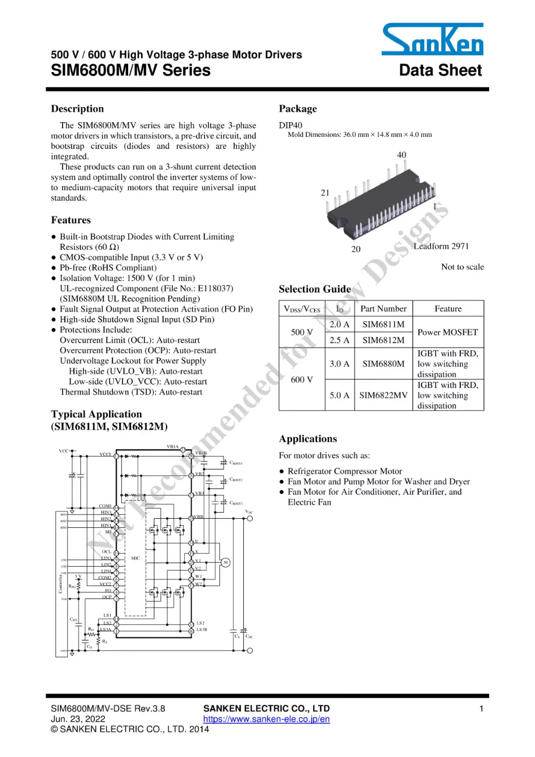
The SIM6800M/MV series are high voltage 3-phase
motor drivers in which transistors, a pre-drive circuit, and
bootstrap circuits (diodes and resistors) are highly
integrated.
These products can run on a 3-shunt current detection
system and optimally control the inverter systems of lowto medium-capacity motors that require universal input
standards.

DIP40
Mold Dimensions: 36.0 mm × 14.8 mm × 4.0 mm

40

21

ns

1

D

ew

Selection Guide

21

fo

500 V

ec
o

30

R

COM1
HIN3
HIN2
HIN1
SD

HIN3

ot

HIN2

N

HIN1

OCL
LIN3
LIN2
LIN1
COM2
VCC2
FO
OCP

LIN3
LIN2
LIN1

Controller

16
15
14
13
12

5V

RFO

Fault

10
9
8
7
6
5
4
3

Part Number

2.0 A

SIM6811M

2.5 A

SIM6812M

3.0 A

SIM6880M

5.0 A

SIM6822MV

600 V

Feature
Power MOSFET
IGBT with FRD,
low switching
dissipation
IGBT with FRD,
low switching
dissipation

Applications

VB1B

For motor drives such as:

m

VCC1 17

IO

rN

VDSS/VCES

de

m

VB1A
VCC

Not to scale

en

Typical Application
(SIM6811M, SIM6812M)

Leadform 2971

20

d

● Built-in Bootstrap Diodes with Current Limiting
Resistors (60 Ω)
● CMOS-compatible Input (3.3 V or 5 V)
● Pb-free (RoHS Compliant)
● Isolation Voltage: 1500 V (for 1 min)
UL-recognized Component (File No.: E118037)
(SIM6880M UL Recognition Pending)
● Fault Signal Output at Protection Activation (FO Pin)
● High-side Shutdown Signal Input (SD Pin)
● Protections Include:
Overcurrent Limit (OCL): Auto-restart
Overcurrent Protection (OCP): Auto-restart
Undervoltage Lockout for Power Supply
High-side (UVLO_VB): Auto-restart
Low-side (UVLO_VCC): Auto-restart
Thermal Shutdown (TSD): Auto-restart

es
ig

Features

CBOOT1

20 VB2

● Refrigerator Compressor Motor
● Fan Motor and Pump Motor for Washer and Dryer
● Fan Motor for Air Conditioner, Air Purifier, and
Electric Fan

CBOOT2

23 VB3
CBOOT3

VDC
28VBB

31 U

19 V
MIC

26 V1

M

35 V2
W1
24
37 W2

LS1

CFO
RO

11
LS2 2
LS3A 1

33 LS2
40 LS3B
CS

CDC

RS

CO
GND

SIM6800M/MV-DSE Rev.3.8
SANKEN ELECTRIC CO., LTD
Jun. 23, 2022
https://www.sanken-ele.co.jp/en
© SANKEN ELECTRIC CO., LTD. 2014

1

SIM6800M/MV Series
Contents
Description ------------------------------------------------------------------------------------------------------ 1
Contents --------------------------------------------------------------------------------------------------------- 2
1. Absolute Maximum Ratings----------------------------------------------------------------------------- 4
2. Recommended Operating Conditions ----------------------------------------------------------------- 5

es
ig

ns

3. Electrical Characteristics -------------------------------------------------------------------------------- 6
3.1 Characteristics of Control Parts------------------------------------------------------------------ 6
3.2 Bootstrap Diode Characteristics ----------------------------------------------------------------- 7
3.3 Thermal Resistance Characteristics ------------------------------------------------------------- 7
3.4 Transistor Characteristics ------------------------------------------------------------------------- 8
3.4.1
SIM6811M -------------------------------------------------------------------------------------- 8
3.4.2
SIM6812M -------------------------------------------------------------------------------------- 9
3.4.3
SIM6880M -------------------------------------------------------------------------------------- 9
3.4.4
SIM6822MV ---------------------------------------------------------------------------------- 10

D

4. Mechanical Characteristics --------------------------------------------------------------------------- 11
5. Insulation Distance -------------------------------------------------------------------------------------- 11

ew

6. Truth Table ----------------------------------------------------------------------------------------------- 12

rN

7. Block Diagrams ------------------------------------------------------------------------------------------ 13
8. Pin Configuration Definitions ------------------------------------------------------------------------- 14

fo

9. Typical Applications ------------------------------------------------------------------------------------ 15
10. Physical Dimensions ------------------------------------------------------------------------------------ 16

d

11. Marking Diagram --------------------------------------------------------------------------------------- 17

N

ot

R

ec
o

m

m

en

de

12. Functional Descriptions -------------------------------------------------------------------------------- 18
12.1 Turning On and Off the IC ---------------------------------------------------------------------- 18
12.2 Pin Descriptions ----------------------------------------------------------------------------------- 18
12.2.1 U, V, V1, V2, W1, and W2 ----------------------------------------------------------------- 18
12.2.2 VB1A, VB1B, VB2, and VB3 -------------------------------------------------------------- 18
12.2.3 VCC1 and VCC2 ---------------------------------------------------------------------------- 19
12.2.4 COM1 and COM2--------------------------------------------------------------------------- 19
12.2.5 HIN1, HIN2, and HIN3; LIN1, LIN2, and LIN3 -------------------------------------- 20
12.2.6 VBB -------------------------------------------------------------------------------------------- 20
12.2.7 LS1, LS2, LS3A, and LS3B ---------------------------------------------------------------- 21
12.2.8 OCP and OCL ------------------------------------------------------------------------------- 21
12.2.9 SD----------------------------------------------------------------------------------------------- 21
12.2.10 FO ---------------------------------------------------------------------------------------------- 21
12.3 Protection Functions ------------------------------------------------------------------------------ 22
12.3.1 Fault Signal Output ------------------------------------------------------------------------- 22
12.3.2 Shutdown Signal Input --------------------------------------------------------------------- 22
12.3.3 Undervoltage Lockout for Power Supply (UVLO) ----------------------------------- 22
12.3.4 Overcurrent Limit (OCL) ----------------------------------------------------------------- 23
12.3.5 Overcurrent Protection (OCP) ----------------------------------------------------------- 24
12.3.6 Thermal Shutdown (TSD) ----------------------------------------------------------------- 25
13. Design Notes ---------------------------------------------------------------------------------------------- 26
13.1 PCB Pattern Layout ------------------------------------------------------------------------------ 26
13.2 Considerations in Heatsink Mounting -------------------------------------------------------- 26
13.3 Considerations in IC Characteristics Measurement --------------------------------------- 26
14. Calculating Power Losses and Estimating Junction Temperatures --------------------------- 27
14.1 IGBT ------------------------------------------------------------------------------------------------- 27
14.1.1 IGBT Steady-state Loss, PON -------------------------------------------------------------- 27
14.1.2 IGBT Switching Loss, PSW ----------------------------------------------------------------- 28

SIM6800M/MV-DSE Rev.3.8
SANKEN ELECTRIC CO., LTD
Jun. 23, 2022
https://www.sanken-ele.co.jp/en
© SANKEN ELECTRIC CO., LTD. 2014

2

SIM6800M/MV Series
14.1.3 Estimating Junction Temperature of IGBT -------------------------------------------- 28
14.2 Power MOSFET ----------------------------------------------------------------------------------- 28
14.2.1 Power MOSFET Steady-state Loss, PRON----------------------------------------------- 28
14.2.2 Power MOSFET Switching Loss, PSW --------------------------------------------------- 29
14.2.3 Body Diode Steady-state Loss, PSD ------------------------------------------------------- 29
14.2.4 Estimating Junction Temperature of Power MOSFET ------------------------------ 29

D

es
ig

ns

15. Performance Curves ------------------------------------------------------------------------------------ 30
15.1 Transient Thermal Resistance Curves -------------------------------------------------------- 30
15.2 Performance Curves of Control Parts--------------------------------------------------------- 31
15.3 Performance Curves of Output Parts --------------------------------------------------------- 36
15.3.1 Output Transistor Performance Curves ------------------------------------------------ 36
15.3.2 Switching Loss Curves --------------------------------------------------------------------- 38
15.4 Allowable Effective Current Curves ----------------------------------------------------------- 40
15.4.1 SIM6811M ------------------------------------------------------------------------------------ 40
15.4.2 SIM6812M ------------------------------------------------------------------------------------ 41
15.4.3 SIM6880M ------------------------------------------------------------------------------------ 42
15.4.4 SIM6822MV ---------------------------------------------------------------------------------- 43
15.5 Short Circuit SOAs (Safe Operating Areas) ------------------------------------------------- 44
16. Pattern Layout Example ------------------------------------------------------------------------------- 45

ew

17. Typical Motor Driver Application ------------------------------------------------------------------- 47

N

ot

R

ec
o

m

m

en

de

d

fo

rN

Important Notes ---------------------------------------------------------------------------------------------- 48

SIM6800M/MV-DSE Rev.3.8
SANKEN ELECTRIC CO., LTD
Jun. 23, 2022
https://www.sanken-ele.co.jp/en
© SANKEN ELECTRIC CO., LTD. 2014

3

SIM6800M/MV Series
1.

Absolute Maximum Ratings

VB1B–U,
VB2–V,
VB3–W1

VBS

20

TC = 25 °C,
TJ < 150 °C

Output Current (Pulse)

IOP

TC = 25 °C,
VCC = 15 V,
pulse width ≤ 1 ms,
single pulse

Input Voltage

VIN

fo

rN

ew

IO

Output Current (2)

2
2.5
3
5
3
3.75
4.5
7.5

d

de

m

ec
o

R

OCP–COM

VISO(RMS)

SD–COM
LSx–COM
LSx–COM

A

A

− 0.5 to 7

V

−0.5 to 7
−0.5 to 7
−0.5 to 7
−0.5 to 7
−4 to 7
−30 to 100
150
−40 to 150

V
V
V
V
V
°C
°C
°C

1500

V

Between surface of the
case and each pin; AC,
60 Hz, 1 min

SIM6811M
SIM6812M
SIM6880M
SIM6822MV
SIM6811M
SIM6812M
SIM6880M
SIM6822MV

(1)

N

ot

Isolation Voltage(5)

HINx–COM,
LINx–COM
FO–COM

en

VFO
VOCP
VSD
VLS(DC)
VLS(SURGE)
TC(OP)
TJ
TSTG

m

FO Pin Voltage
OCP Pin Voltage
SD Pin Voltage
LSx Pin Voltage (DC)
LSx Pin Voltage (Surge)
Operating Case Temperature(3)
Junction Temperature(4)
Storage Temperature

V

D

Logic Supply Voltage

es
ig

ns

Current polarities are defined as follows: current going into the IC (sinking) is positive current (+); current coming out
of the IC (sourcing) is negative current (−).
Unless specifically noted, TA = 25 °C, COM1 = COM2 = COM.
Parameter
Symbol
Conditions
Rating
Unit
Remarks
SIM6822MV
VBB–LSx
Main Supply Voltage (DC) (1)
VDC
450
V
SIM6880M
SIM6822MV
Main Power Voltage (Surge) (1) VDC(SURGE) VBB–LSx
500
V
SIM6880M
SIM6811M
VCC = 15 V,
VDSS
500
ID = 1 µA, VIN = 0 V
SIM6812M
IGBT / Power MOSFET
V
Breakdown Voltage
SIM6822MV
VCC = 15 V,
VCES
600
IC = 1 mA, VIN = 0 V
SIM6880M
VCCx–COM
VCC
20

Defined for the IGBT-embedded device only.
Should be derated depending on an actual case temperature. See Section 15.4.
(3)
Refers to a case temperature measured during IC operation.
(4)
Refers to the junction temperature of each chip built in the IC, including the control MIC, transistors, and
freewheeling diodes.
(5)
Refers to voltage conditions to be applied between all of the pins and the case. All the pins have to be shorted.
(2)

SIM6800M/MV-DSE Rev.3.8
SANKEN ELECTRIC CO., LTD
Jun. 23, 2022
https://www.sanken-ele.co.jp/en
© SANKEN ELECTRIC CO., LTD. 2014

4

SIM6800M/MV Series
2.

Recommended Operating Conditions
Unless specifically noted, COM1 = COM2 = COM.
Parameter
Symbol
Conditions

Min.

Typ.

Max.

Unit

VBB–COM

—

300

400

V

VCC

VCCx–COM
VB1B–U,
VB2–V,
VB3–W1

13.5

15.0

16.5

V

13.5

—

16.5

V

VIN

0

—

5.5

V

tIN(MIN)ON

0.5

—

—

μs

tIN(MIN)OFF

0.5

—

—

Dead Time of Input Signal

tDEAD

1.5

—

—

FO Pin Pull-up Resistor

RFO

3.3

—

FO Pin Pull-up Voltage

VFO

3.0

—

FO Pin Noise Filter Capacitor

CFO

0.001

—

1

Minimum Input Pulse Width

CBOOT

10

kΩ

5.5

V

0.01

μF

—

220

μF

IOP ≤ 3 A

390

—

—

IOP ≤ 3.75 A

270

—

—

270

—

—

150

—

—

—

—

100

1000

—

2200

1000

—

10000

fC

—

—

20

kHz

TC(OP)

—

—

100

°C

Shunt Resistor*

RS

IOP ≤ 4.5 A

RO
CO

en

RC Filter Capacitor

de

d

RC Filter Resistor

fo

IOP ≤ 7.5 A

SIM6811M
mΩ

SIM6812M
SIM6880M
SIM6822MV

Ω
pF

SIM6822MV
SIM6880M
SIM6811M
SIM6812M

m

m

PWM Carrier Frequency
Operating Case Temperature

μs

rN

Bootstrap Capacitor

μs

es
ig

Input Voltage
(HINx, LINx, OCP, SD, FO)

D

VBS

ew

Logic Supply Voltage

ns

VDC

Main Supply Voltage

Remarks

N

ot

R

ec
o

* Should be a low-inductance resistor.

SIM6800M/MV-DSE Rev.3.8
SANKEN ELECTRIC CO., LTD
Jun. 23, 2022
https://www.sanken-ele.co.jp/en
© SANKEN ELECTRIC CO., LTD. 2014

5

SIM6800M/MV Series
3.

Electrical Characteristics

Current polarities are defined as follows: current going into the IC (sinking) is positive current (+); current coming out
of the IC (sourcing) is negative current (−).
Unless specifically noted, TA = 25 °C, VCC = 15 V, COM1 = COM2 = COM.

3.1

Characteristics of Control Parts
Parameter

Symbol

Conditions

Min.

Typ.

Max.

Unit
V

Remarks

Power Supply Operation
VCC(ON)

VCCx–COM

10.5

11.5

12.5

VBS(ON)

VB1B–U, VB2–V, VB3–W1

9.5

10.5

11.5

V

Logic Operation Stop
Voltage

VCC(OFF)

VCCx–COM

10.0

11.0

12.0

V

VBS(OFF)

VB1B–U, VB2–V, VB3–W1
VCC1 = VCC2,
VCC pin current in 3-phase
operation
VB1B–U or VB2–V or
VB3–W1; HINx = 5 V;
VBx pin current in 1-phase
operation

9.0

10.0

11.0

V

—

3.2

4.5

mA

140

400

μA

—

2.0

2.5

V

1.0

1.5

—

V

VIH

fo

Input Signal
High Level Input Threshold
Voltage
(HINx, LINx, SD, FO)

Low Level Input Threshold
Voltage

d

VIL

es
ig

IIH

VIN = 5 V

—

230

500

μA

IIL

en

de

(HINx, LINx, SD, FO)

—

—

2

μA

VFO = 5 V, RFO = 10 kΩ

0

—

0.5

V

VFO = 5 V, RFO = 10 kΩ

4.8

—

—

V

VOCL(L)

0

—

0.5

V

VOCL(H)

4.5

—

5.5

V

VLIM

0.6175

0.6500

0.6825

V

VTRIP

0.9

1.0

1.1

V

tP

20

25

—

μs

VIN = 0 V

m
m
VFOL

R

ec
o

High Level Input Current
(HINx, LINx)
Low Level Input Current
(HINx, LINx)
Fault Signal Output
FO Pin Voltage at Fault
Signal Output
FO Pin Voltage in Normal
Operation
Protection

—

rN

IBS

D

Logic Supply Current

ew

ICC

ns

Logic Operation Start
Voltage

N

ot

OCL Pin Output Voltage (L)
OCL Pin Output Voltage
(H)
Current Limit Reference
Voltage
OCP Threshold Voltage
OCP Hold Time

VFOH

OCP Blanking Time
Current Limit Blanking
Time
TSD Operating Temperature

tBK(OCP)

—

2

—

μs

tBK(OCL)

—

2

—

μs

TDH

135

150

165

°C

TSD Releasing Temperature

TDL

105

120

135

°C

SIM6800M/MV-DSE Rev.3.8
SANKEN ELECTRIC CO., LTD
Jun. 23, 2022
https://www.sanken-ele.co.jp/en
© SANKEN ELECTRIC CO., LTD. 2014

6

SIM6800M/MV Series
Bootstrap Diode Characteristics

Parameter
Bootstrap Diode Leakage
Current
Bootstrap Diode Forward
Voltage
Bootstrap Diode Series
Resistor

Conditions

Min.

Typ.

Max.

Unit

ILBD

VR = 500 V

—

—

10

μA

VFB

IFB = 0.15 A

—

1.0

1.3

V

45

60

75

Ω

Conditions
All power MOSFETs
operating

Min.

Typ.

Max.

—

—

R(J-C)Q(2)

All IGBTs operating

—

—

R(J-C)F(3)

All freewheeling
diodes operating
All power MOSFETs
operating

—

—

RBOOT

Remarks

RJ-C
Junction-to-Case Thermal
Resistance(1)

RJ-A

All IGBTs operating

R(J-A)F

All freewheeling
diodes operating

°C/W

3.6

°C/W

4.2

°C/W

—

—

25

°C/W

—

—

25

°C/W

—

—

29

°C/W

fo

R(J-A)Q

3.6

Remarks
SIM6811M
SIM6812M
SIM6822MV
SIM6880M
SIM6822MV
SIM6880M
SIM6811M
SIM6812M
SIM6822MV
SIM6880M
SIM6822MV
SIM6880M

m

Measurement point
21

5 mm

N

ot

R

ec
o

40

m

en

de

d

Junction-to-Ambient
Thermal Resistance

Unit

es
ig

Symbol

D

Parameter

ns

Thermal Resistance Characteristics

ew

3.3

Symbol

rN

3.2

1

20

Figure 3-1.

Case Temperature Measurement Point

(1)

Refers to a case temperature at the measurement point described in Figure 3-1, below.
Refers to steady-state thermal resistance between the junction of the built-in transistors and the case. For transient
thermal characteristics, see Section 15.1.
(3)
Refers to steady-state thermal resistance between the junction of the built-in freewheeling diodes and the case.
(2)

SIM6800M/MV-DSE Rev.3.8
SANKEN ELECTRIC CO., LTD
Jun. 23, 2022
https://www.sanken-ele.co.jp/en
© SANKEN ELECTRIC CO., LTD. 2014

7

SIM6800M/MV Series
3.4

Transistor Characteristics

Figure 3-2 provides the definitions of switching characteristics described in this and the following sections.
HINx/
LINx
0

trr

toff
td(off) tf

ton
td(on) tr

ID / IC

ns

90%
10%

0

D

es
ig

VDS /
VCE

ew

0

SIM6811M
Symbol

Drain-to-Source Leakage Current

IDSS

Drain-to-Source On-resistance
Source-to-Drain Diode Forward
Voltage
High-side Switching
Source-to-Drain Diode Reverse
Recovery Time
Turn-on Delay Time

RDS(ON)

Unit

VDS = 500 V, VIN = 0 V

—

—

100

µA

—

3.2

4.0

Ω

ISD =1.0 A, VIN = 0 V

—

1.0

1.5

V

—

150

—

ns

td(on)

—

770

—

ns

tr

—

70

—

ns

td(off)

—

690

—

ns

—

30

—

ns

—

150

—

ns

—

690

—

ns

—

90

—

ns

—

650

—

ns

—

50

—

ns

de

VDC = 300 V, ID = 2.0 A,
inductive load,
VIN = 0→5 V or 5→0 V,
TJ = 25 °C

tf

R

Fall Time

Max.

ID = 1.0 A, VIN = 5 V

m

Turn-off Delay Time

Typ.

trr

m

ec
o

Rise Time

Min.

en

VSD

Conditions

fo

Parameter

d

3.4.1

Switching Characteristics Definitions

rN

Figure 3-2.

N

ot

Low-side Switching
Source-to-Drain Diode Reverse
Recovery Time
Turn-on Delay Time
Rise Time

Turn-off Delay Time
Fall Time

trr
td(on)
tr
td(off)

VDC = 300 V, ID = 2.0 A,
inductive load,
VIN = 0→5 V or 5→0 V,
TJ = 25 °C

tf

SIM6800M/MV-DSE Rev.3.8
SANKEN ELECTRIC CO., LTD
Jun. 23, 2022
https://www.sanken-ele.co.jp/en
© SANKEN ELECTRIC CO., LTD. 2014

8

SIM6800M/MV Series
SIM6812M
Parameter

Symbol

Drain-to-Source Leakage Current

ICES

Drain-to-Source On-resistance
Source-to-Drain Diode Forward
Voltage
High-side Switching
Source-to-Drain Diode Reverse
Recovery Time
Turn-on Delay Time

Conditions

Min.

Typ.

Max.

Unit

VDS = 500 V, VIN = 0 V

—

—

100

µA

VCE(SAT)

ID = 1.25 A, VIN = 5 V

—

2.0

2.4

Ω

VF

ISD =1.25 A, VIN = 0 V

—

1.0

1.5

V

—

140

—

ns

—

910

—

ns

—

100

—

ns

trr
VDC = 300 V, ID = 2.5 A,
inductive load,
VIN = 0→5 V or 5→0 V,
TJ = 25 °C

td(on)
tr

ns

Fall Time

tf

—

Low-side Switching
Source-to-Drain Diode Reverse
Recovery Time
Turn-on Delay Time

es
ig

Rise Time

ns

3.4.2

trr

—

155

—

ns

—

875

—

ns

—

110

—

ns

—

775

—

ns

—

35

—

ns

Min.

Typ.

Max.

Unit

VCE = 600 V, VIN = 0 V

—

—

1

mA

IC = 3.0 A, VIN = 5 V

—

1.85

2.30

V

IF = 3.0 A, VIN = 0 V

—

2.0

2.4

V

—

100

—

ns

—

880

—

ns

—

120

—

ns

—

740

—

ns

tf

—

210

—

ns

trr

—

100

—

ns

—

820

—

ns

—

140

—

ns

—

660

—

ns

—

200

—

ns

rN

tr

Turn-off Delay Time

td(off)

700

—

40

—

ns

fo

tf

d

Fall Time

en

Symbol
ICES

VCE(SAT)

ec
o

m

Parameter
Collector-to-Emitter Leakage
Current
Collector-to-Emitter Saturation
Voltage
Diode Forward Voltage

de

SIM6880M

m

3.4.3

VDC = 300 V, ID = 2.5 A,
inductive load,
VIN = 0→5 V or 5→0 V,
TJ = 25 °C

td(on)

Rise Time

—

D

td(off)

ew

Turn-off Delay Time

VF

Conditions

High-side Switching

R

Diode Reverse Recovery Time
Turn-on Delay Time

ot

Rise Time

N

Turn-off Delay Time
Fall Time

trr
td(on)
tr
td(off)

VDC = 300 V, IC = 3.0 A,
inductive load,
VIN = 0→5 V or 5→0 V,
TJ = 25 °C

Low-side Switching
Diode Reverse Recovery Time
Turn-on Delay Time
Rise Time
Turn-off Delay Time
Fall Time

td(on)
tr
td(off)

VDC = 300 V, IC = 3.0 A,
inductive load,
VIN = 0→5 V or 5→0 V,
TJ = 25 °C

tf

SIM6800M/MV-DSE Rev.3.8
SANKEN ELECTRIC CO., LTD
Jun. 23, 2022
https://www.sanken-ele.co.jp/en
© SANKEN ELECTRIC CO., LTD. 2014

9

SIM6800M/MV Series
SIM6822MV

Parameter
Collector-to-Emitter Leakage
Current
Collector-to-Emitter Saturation
Voltage
Diode Forward Voltage

Min.

Typ.

Max.

Unit

VCE = 600 V, VIN = 0 V

—

—

1

mA

VCE(SAT)

IC = 5 A, VIN = 5 V

—

1.75

2.2

V

VF

IF = 5 A, VIN = 0 V

—

2.0

2.4

V

—

80

—

ns

—

740

—

ns

—

70

—

ns

es
ig

3.4.4

Symbol

570

—

ns

100

—

ns

80

—

ns

—

690

—

ns

—

100

—

ns

—

540

—

ns

—

100

—

ns

ICES

Conditions

Diode Reverse Recovery Time

trr

Turn-on Delay Time

td(on)

Rise Time

VDC = 300 V, IC = 5 A,
inductive load,
VIN = 0→5 V or 5→0 V,
TJ = 25 °C

tr

Turn-off Delay Time

td(off)
tf

—

trr

—

Fall Time

ew

Turn-on Delay Time

D

Low-side Switching
Diode Reverse Recovery Time

td(on)

VDC = 300 V, IC = 5 A,
inductive load,
VIN = 0→5 V or 5→0 V,
TJ = 25 °C

tr

rN

Rise Time
Turn-off Delay Time

—

td(off)

fo

tf

N

ot

R

ec
o

m

m

en

de

d

Fall Time

ns

High-side Switching

SIM6800M/MV-DSE Rev.3.8
SANKEN ELECTRIC CO., LTD
Jun. 23, 2022
https://www.sanken-ele.co.jp/en
© SANKEN ELECTRIC CO., LTD. 2014

10

SIM6800M/MV Series
4.

Mechanical Characteristics

es
ig

ns

Parameter
Conditions
Min.
Typ.
Max.
Unit
Remarks
Heatsink Mounting
*
0.294
—
0.441
N∙m
Screw Torque
Flatness of Heatsink
See Figure 4-1.
0
—
100
μm
Attachment Area
Package Weight
—
5.2
—
g
* Requires using a metric screw of M2.5 and a plain washer of 6.0 mm (φ). For more on screw tightening, see Section
13.2.

Heatsink

fo

rN

ew

D

Measurement position

-+

-

de

d

+

Heasink

Flatness Measurement Position

Insulation Distance
Parameter

Clearance

ec
o

5.

m

m

en

Figure 4-1.

Conditions

Between heatsink* and
leads. See Figure 5-1.

Min.

Typ.

Max.

Unit

1.5

—

2.1

mm

Remarks

N

ot

R

Creepage
1.7
—
—
mm
* Refers to when a heatsink to be mounted is flat. If your application requires a clearance exceeding the maximum distance
given above, use an alternative (e.g., a convex heatsink) that will meet the target requirement.

Creepage
Clearance
Heatsink

Figure 5-1.

Insulation Distance Definitions

SIM6800M/MV-DSE Rev.3.8
SANKEN ELECTRIC CO., LTD
Jun. 23, 2022
https://www.sanken-ele.co.jp/en
© SANKEN ELECTRIC CO., LTD. 2014

11

SIM6800M/MV Series
6.

Truth Table

Table 6-1. Truth Table for Operation Modes

de

Undervoltage Lockout for
High-side Power Supply
(UVLO_VB)

m

m

en

Undervoltage Lockout for
Low-side Power Supply
(UVLO_VCC)

R

ec
o

Overcurrent Protection (OCP)

N

ot

Overcurrent Limit (OCL)
(OCL = SD)

Thermal Shutdown (TSD)

Low-side Transistor
OFF
OFF
ON
ON
OFF
OFF
OFF
OFF
OFF
OFF
ON
ON
OFF
OFF
OFF
OFF
OFF
OFF
OFF
OFF
OFF
OFF
ON
ON
OFF
OFF
OFF
OFF

ew

D

es
ig

High-side Transistor
OFF
ON
OFF
ON
OFF
ON
OFF
ON
OFF
OFF
OFF
OFF
OFF
OFF
OFF
OFF
OFF
ON
OFF
ON
OFF
OFF
OFF
OFF
OFF
ON
OFF
ON

rN

External Shutdown Signal Input
FO = Low Level

LINx
L
L
H
H
L
L
H
H
L
L
H
H
L
L
H
H
L
L
H
H
L
L
H
H
L
L
H
H

fo

Normal Operation

HINx
L
H
L
H
L
H
L
H
L
H
L
H
L
H
L
H
L
H
L
H
L
H
L
H
L
H
L
H

d

Mode

ns

Table 6-1 is a truth table that provides the logic level definitions of operation modes.
In the case where HINx and LINx pin signals in each phase are high at the same time, both the high- and low-side
transistors become on (simultaneous on-state). Therefore, HINx and LINx signals, the input signals for the HINx and
LINx pins, require dead time setting so that such a simultaneous on-state event can be avoided.
After the IC recovers from a UVLO_VCC condition, the low-side transistors resume switching in accordance with the
input logic levels of the LINx signals (level-triggered), whereas the high-side transistors resume switching at the next
rising edge of an HINx signal (edge-triggered).
After the IC recovers from a UVLO_VB condition, the high-side transistors resume switching at the next rising edge
of an HINx signal (edge-triggered).

SIM6800M/MV-DSE Rev.3.8
SANKEN ELECTRIC CO., LTD
Jun. 23, 2022
https://www.sanken-ele.co.jp/en
© SANKEN ELECTRIC CO., LTD. 2014

12

SIM6800M/MV Series
7.

Block Diagrams
30

VB1B
21 VB1A
20 VB2
23 VB3

VCC1 17

10
9
8
7

UVLO

28 VBB

High Side
Level Shift Driver

Input Logic
(OCP reset)

Low
Side
Driver

VCC2 5
FO 4

ew

COM2 6

Thermal
Shutdown
OCP and OCL

ec
o

m

UVLO

Input
Logic

UVLO

UVLO

UVLO

R

High Side
Level Shift Driver

Input Logic
(OCP reset)

Low
Side
Driver

COM2 6
VCC2 5
FO 4

OCP 3

VB1B
21 VB1A
20 VB2
23 VB3

ot
N

10
9
8
7

LS1
LS2
LS2
LS3B
LS3A

d

30

en
m

VCC1 17

OCL
LIN3
LIN2
LIN1

11
33
2
40
1

V1
U
V2
W2

SIM6811M or SIM6812M

de

Figure 7-1.

15
14
13
12
16

W1
V

fo

rN

UVLO

OCP 3

HIN3
HIN2
HIN1
SD
COM1

24
19
26
31
35
37

ns

OCL
LIN3
LIN2
LIN1

Input
Logic

UVLO

es
ig

15
14
13
12
16

UVLO

D

HIN3
HIN2
HIN1
SD
COM1

UVLO

UVLO
Thermal
Shutdown

28 VBB

24
19
26
31
35
37

W1
V

11
33
2
40
1

LS1
LS2
LS2
LS3B
LS3A

V1
U
V2
W2

OCP and OCL

Figure 7-2.

SIM6822MV or SIM6880M

SIM6800M/MV-DSE Rev.3.8
SANKEN ELECTRIC CO., LTD
Jun. 23, 2022
https://www.sanken-ele.co.jp/en
© SANKEN ELECTRIC CO., LTD. 2014

13

SIM6800M/MV Series
8.

Pin Configuration Definitions
Top View

40
40

21

1

20

1
21

ns

es
ig

D

ew

rN

fo

d

de

en
m

ec
o

ot

N

Description
W-phase IGBT emitter, or power MOSFET source
V-phase IGBT emitter, or power MOSFET source
Overcurrent protection signal input
Fault signal output and shutdown signal input
Low-side logic supply voltage input
Low-side logic ground
Logic input for U-phase low-side gate driver
Logic input for V-phase low-side gate driver
Logic input for W-phase low-side gate driver
Overcurrent limit signal output
U-phase IGBT emitter, or power MOSFET source
High-side shutdown signal input
Logic input for U-phase high-side gate driver
Logic input for V-phase high-side gate driver
Logic input for W-phase high-side gate driver
High-side logic ground
High-side logic supply voltage input
(Pin removed)
Bootstrap capacitor connection for V-phase
V-phase high-side floating supply voltage input
U-phase high-side floating supply voltage input
(Pin removed)
W-phase high-side floating supply voltage input
W-phase output (connected to W2 externally)
(Pin removed)
V-phase output (connected to V2 externally)
(Pin removed)
Positive DC bus supply voltage
(Pin removed)
U-phase high-side floating supply voltage input
U-phase output
(Pin removed)
(Pin trimmed) V-phase IGBT emitter, or power MOSFET source
(Pin removed)
V-phase output (connected to V1 externally)
(Pin removed)
W-phase output (connected to W1 externally)
(Pin removed)
(Pin removed)
W-phase IGBT emitter, or power MOSFET source

m

Pin Name
LS3A
LS2
OCP
FO
VCC2
COM2
LIN1
LIN2
LIN3
OCL
LS1
SD
HIN1
HIN2
HIN3
COM1
VCC1
—
V
VB2
VB1A
—
VB3
W1
—
V1
—
VBB
—
VB1B
U
—
LS2
—
V2
—
W2
—
—
LS3B

R

20
Pin Number
1
2
3
4
5
6
7
8
9
10
11
12
13
14
15
16
17
18
19
20
21
22
23
24
25
26
27
28
29
30
31
32
33
34
35
36
37
38
39
40

SIM6800M/MV-DSE Rev.3.8
SANKEN ELECTRIC CO., LTD
Jun. 23, 2022
https://www.sanken-ele.co.jp/en
© SANKEN ELECTRIC CO., LTD. 2014

14

SIM6800M/MV Series
9.

Typical Applications

CR filters and Zener diodes should be added to your application as needed. This is to protect each pin against surge
voltages causing malfunctions, and to avoid the IC being used under the conditions exceeding the absolute maximum
ratings where critical damage is inevitable. Then, check all the pins thoroughly under actual operating conditions to ensure
that your application works flawlessly.
VB2 20
V 19
21 VB1A
23 VB3

VCC1 17

CBOOT3

Controller

HIN1

LS1
OCL
LIN3
LIN2
LIN1
COM2
VCC2
FO
OCP

LIN3
LIN2
LIN1

5V
RFO

Fault

CFO

26 V1

30

MIC

M

CBOOT1

33 LS2

35 V2

37 W2

fo

CS

CDC

40 LS3B

de

d

RS

CO

VB1B

31 U

LS2 2
LS3A 1

RO

VDC

28 VBB

D

HIN2

ew

HIN3
HIN2
HIN1
SD

HIN3

24 W1

16
15
14
13
12
11
10
9
8
7
6
5
4
3

rN

COM1

GND

ns

VCC

es
ig

CBOOT2

SIM6811M / SIM6812M Typical Application Using a Single Shunt Resistor

en

Figure 9-1.

m

VB2 20
V 19

m

CBOOT2
VCC

ec
o

COM1

GND

R

HIN3
HIN2

ot

Controller

HIN1

HIN3
HIN2
HIN1
SD

N

LS1
OCL
LIN3
LIN2
LIN1
COM2
VCC2
FO
OCP

LIN3
LIN2
LIN1

5V
RFO
Fault

CO2

CBOOT3
16
15
14
13
12
11
10
9
8
7
6
5
4
3

24 W1

26 V1
VDC
28 VBB

MIC

LS2 2
LS3A 1

RO1

CO1
CFO

21 VB1A
23 VB3

VCC1 17

RO2

30

VB1B

31 U

M

CBOOT1
33 LS2
35 V2

37 W2

CS CDC

40 LS3B

CO3 RO3
RS1 RS2

Figure 9-2.

RS3

SIM6811M / SIM6812M Typical Application Using Three Shunt Resistors

SIM6800M/MV-DSE Rev.3.8
SANKEN ELECTRIC CO., LTD
Jun. 23, 2022
https://www.sanken-ele.co.jp/en
© SANKEN ELECTRIC CO., LTD. 2014

15

SIM6800M/MV Series
10. Physical Dimensions

1.8 ±0.3

+0.1

33.782±0.3

17.4±0.5

ns

m

en

1.778 ±0.25

(Ends of pins)

NOTES:

es
ig

de

0.52 -0.05

d

fo

rN

4 ±0.2

36 ±0.3

1.8 ±0.1

ew

Gate burr

8.35 ±0.3

20

D

1

φ3.2±0.2

Pin 1 indicator

14.0 ±0.2

14.8 ±0.3

Top view

16.7

21

40

7.4 ±0.15

2-R1.5

0.42

+0.4
-0.3

8.35 ±0.3

1.15 max.

7.6

+0.1
-0.05

● DIP40 Package

1.7 min
.

R

ec
o

m

- Dimensions in millimeters
- Pb-free (RoHS compliant)
- The leads illustrated above are for reference only, and may not be actual states of
being bent.
- Maximum gate burr height is 0.3 mm.

40

21
φ1.1 typ.
33.7

0.04
Center of screw hole

8.7

17.4 typ.

N

ot

● Reference Through Hole Size and Layout

1

20

Pin pich: 1.778
33.782

Unit: mm

SIM6800M/MV-DSE Rev.3.8
SANKEN ELECTRIC CO., LTD
Jun. 23, 2022
https://www.sanken-ele.co.jp/en
© SANKEN ELECTRIC CO., LTD. 2014

16

SIM6800M/MV Series
11. Marking Diagram
● SIM6800M Series

40

21

SIM68xxM

Part Number
Lot Number:
Y is the last digit of the year of manufacture (0 to 9)
M is the month of the year (1 to 9, O, N, or D)
DD is the day of the month (01 to 31)

1

es
ig

ns

YMDD X
20

fo

rN

ew

D

Control Number
X is the control symbol (A to Z)

de

d

● SIM6800MV Series

21

en

40

m

SIM68xxM

m

Lot Number:
Y is the last digit of the year of manufacture (0 to 9)
M is the month of the year (1 to 9, O, N, or D)
DD is the day of the month (01 to 31)

ec
o

Y M D D XV
20

Control Number
X is the control symbol (A to Z)
V is the control symbol

N

ot

R

1

Part Number

SIM6800M/MV-DSE Rev.3.8
SANKEN ELECTRIC CO., LTD
Jun. 23, 2022
https://www.sanken-ele.co.jp/en
© SANKEN ELECTRIC CO., LTD. 2014

17

SIM6800M/MV Series
12. Functional Descriptions

12.2.2

Unless specifically noted, this section uses the
following definitions:

These pins are connected to bootstrap capacitors for the
high-side floating supply.
In actual applications, use either of the VB1A or VB1B
pin because they are internally connected. Voltages
across the VBx and these output pins should be
maintained within the recommended range (i.e., the Logic
Supply Voltage, VBS) given in Section 2.
A bootstrap capacitor, CBOOTx, should be connected in
each of the traces between the VB1A (VB1B) and U pins,
the VB2 and V pins, the VB3 and W1 pins.
For proper startup, turn on the low-side transistor first,
then fully charge the bootstrap capacitor, CBOOTx.
For the capacitance of the bootstrap capacitors, CBOOTx,
choose the values that satisfy Equations (1) and (2). Note
that capacitance tolerance and DC bias characteristics
must be taken into account when you choose appropriate
values for CBOOTx.

es
ig

ns

● All the characteristic values given in this section are
typical values.
● All the circuit diagrams listed in this section represent
the type of IC that incorporates power MOSFETs. All
the functional descriptions in this section are also
applicable to the type of IC that incorporates IGBTs.
● For pin and peripheral component descriptions, this
section employs a notation system that denotes a pin
name with the arbitrary letter “x”, depending on
context. Thus, “the VCCx pin” is used when referring
to either or both of the VCC1 and VCC2 pins.
● The COM1 pin is always connected to the COM2 pin.

VB1A, VB1B, VB2, and VB3

D

12.1 Turning On and Off the IC

(1)

1 μF ≤ CBOOTx ≤ 220 μF

(2)

rN

ew

CBOOTx (μF) > 800 × t L(OFF)

fo

In Equation (1), let tL(OFF) be the maximum off-time of
the low-side transistor (i.e., the non-charging time of
CBOOTx), measured in seconds.

de

d

The procedures listed below provide recommended
startup and shutdown sequences. To turn on the IC
properly, do not apply any voltage on the VBB, HINx,
and LINx pins until the VCCx pin voltage has reached a
stable state (VCC(ON) ≥ 12.5 V).
It is required to fully charge bootstrap capacitors,
CBOOTx, at startup (see Section 12.2.2).
To turn off the IC, set the HINx and LINx pins to logic
low (or “L”), and then decrease the VCCx pin voltage.

12.2.1

m

en

12.2 Pin Descriptions
U, V, V1, V2, W1, and W2

N

ot

R

ec
o

m

The U, V1, V2, W1, and W2 pins are the outputs of the
three phases, and serve as the connection terminals to the
3-phase motor. The V pin must be connected to a
bootstrap capacitor of the V-phase. Do not connect the 3phase motor to the V pin. The V1 and W1 pins must be
connected to the V2 and W2 pins on a PCB, respectively.
The U, V (V1) and W1 pins are the grounds for the
VB1A (VB1B), VB2, and VB3 pins.
The U, V and W1 pins are connected to the negative
nodes of bootstrap capacitors, CBOOTx. The V pin is
internally connected to the V1 pin.
Since high voltages are applied to these output pins (U,
V1, V2, W1, and W2), it is required to take measures for
insulating as follows:

Even while the high-side transistor is off, voltage
across the bootstrap capacitor keeps decreasing due to
power dissipation in the IC. When the VBx pin voltage
decreases to VBS(OFF) or less, the high-side undervoltage
lockout (UVLO_VB) starts operating (see Section
12.3.3.1). Therefore, actual board checking should be
done thoroughly to validate that voltage across the VBx
pin maintains over 11.0 V (VBS > VBS(OFF)) during a lowfrequency operation such as a startup period.
As Figure 12-1 shows, a bootstrap diode, DBOOTx, and
a current-limiting resistor, RBOOTx, are internally placed in
series between the VCC1 and VBx pins.
Time constant for the charging time of CBOOTx, τ, can
be computed by Equation (3):
τ = CBOOTx × R BOOTx ,

(3)

where CBOOTx is the optimized capacitance of the
bootstrap capacitor, and RBOOTx is the resistance of the
current-limiting resistor (60 Ω ± 25%).

● Keep enough distance between the output pins and
low-voltage traces.
● Coat the output pins with insulating resin.

SIM6800M/MV-DSE Rev.3.8
SANKEN ELECTRIC CO., LTD
Jun. 23, 2022
https://www.sanken-ele.co.jp/en
© SANKEN ELECTRIC CO., LTD. 2014

18

SIM6800M/MV Series
VB1B
30
20

VBB

23

0
28

CBOOT3

HO3
HO2
HO1

5
VCC2

0
Set

CBOOT2
VB3

Reset

VDC

VCC
U

MIC

V

VBx–HSx

19

26
V1

16
COM1
6
COM2

W2

0

31

0

37

Stays logic high

Q

24
W1

Figure 12-1.

VBS(OFF)

VBS(ON)

M

ns

VB2

DBOOT3 RBOOT3
17
VCC1

HINx

CBOOT1

DBOOT2 RBOOT2

0

es
ig

DBOOT1 RBOOT1

Bootstrap Circuit

Waveforms at VBx–HSx Voltage Drop

D

Figure 12-3.

VCC1 and VCC2

ew

12.2.3

fo

rN

These are the logic supply pins for the built-in control
MIC. The VCC1 and VCC2 pins must be externally
connected on a PCB because they are not internally
connected. To prevent malfunction induced by supply
ripples or other factors, put a 0.01 μF to 0.1 μF ceramic
capacitor, CVCC, near these pins. To prevent damage
caused by surge voltages, put an 18 V to 20 V Zener diode,
DZ, between the VCCx and COMx pins.
Voltages to be applied between the VCCx and COMx
pins should be regulated within the recommended
operational range of VCC, given in Section 2.

m

en

de

d

Figure 12-2 shows an internal level-shifting circuit. A
high-side output signal, HOx, is generated according to
an input signal on the HINx pin. When an input signal on
the HINx pin transits from low to high (rising edge), a
“Set” signal is generated. When the HINx input signal
transits from high to low (falling edge), a “Reset” signal
is generated. These two signals are then transmitted to the
high-side by the level-shifting circuit and are input to the
SR flip-flop circuit. Finally, the SR flip-flop circuit feeds
an output signal, Q (i.e., HOx).
Figure 12-3 is a timing diagram describing how noise
or other detrimental effects will improperly influence the
level-shifting process. When a noise-induced rapid
voltage drop between the VBx and output pins (U, V, or
W1; hereafter “VBx–HSx”) occurs after the Set signal
generation, the next Reset signal cannot be sent to the SR
flip-flop circuit. And the state of an HOx signal stays
logic high (or “H”) because the SR flip-flop does not
respond. With the HOx state being held high (i.e., the
high-side transistor is in an on-state), the next LINx signal
turns on the low-side transistor and causes a
simultaneously-on condition, which may result in critical
damage to the IC. To protect the VBx pin against such a
noise effect, add a bootstrap capacitor, CBOOTx, in each
phase. CBOOTx must be placed near the IC and be
connected between the VBx and HSx pins with a minimal
length of traces. To use an electrolytic capacitor, add a
0.01 μF to 0.1 μF bypass capacitor, CPx, in parallel near
these pins used for the same phase.

5
VCC2

VCC

ot

N
U1

Figure 12-4.

16
COM1
6
COM2

VCCx Pin Peripheral Circuit

VBx

12.2.4
S
Set

Input
logic

HINx

MIC

CVCC
DZ

R

ec
o

m

17
VCC1

Pulse
generator Reset

Q

HOx

R

HSx

COM1
16

Figure 12-2.

Internal Level-shifting Circuit

COM1 and COM2

These are the logic ground pins for the built-in control
MIC. The COM1 and COM2 pins should be connected
externally on a PCB because they are not internally
connected. Varying electric potential of the logic ground
can be a cause of improper operations. Therefore, connect
the logic ground as close and short as possible to shunt
resistors, RSx, at a single-point ground (or star ground)
which is separated from the power ground (see Figure

SIM6800M/MV-DSE Rev.3.8
SANKEN ELECTRIC CO., LTD
Jun. 23, 2022
https://www.sanken-ele.co.jp/en
© SANKEN ELECTRIC CO., LTD. 2014

19

SIM6800M/MV Series
12-5).

voltage of the HINx and LINx pins becomes slightly
lower than the output voltage of the microcontroller.

U1

VDC

VBB 28

Table 12-1. Input Signals for HINx and LINx Pins
CS

Connect the COM1
and COM2 pins on
a PCB.

Figure 12-5.

12.2.5

RS3

Create a single-point
ground (a star ground)
near RSx, but keep it
separated from the
power ground.

OCP

0 V < VIN < 0.5 V

≥0.5 μs

≥0.5 μs

Connections to Logic Ground

ns

LS3A 1

3 V < VIN < 5.5 V

≤20 kHz
≥1.5 μs

U1

ew

6 COM2

Input
Voltage
Input
Pulse
Width
PWM
Carrier
Frequency
Dead
Time

RS2

es
ig

LS2 2

RS1

D

LS1 11

Low Level Signal

HINx
(LINx)

HIN1, HIN2, and HIN3;
LIN1, LIN2, and LIN3

5V
2 kΩ

20 kΩ

COM1
(COM2)

Figure 12-6.

ec
o

R

ot

N

Internal Circuit Diagram of HINx or
LINx Pin
U1

RIN1x

Input
signal

HINx/
LINx

m

m

en

de

d

fo

These are the input pins of the internal motor drivers
for each phase. The HINx pin acts as a high-side
controller; the LINx pin acts as a low-side controller.
Figure 12-6 shows an internal circuit diagram of the
HINx or LINx pin. This is a CMOS Schmitt trigger circuit
with a built-in 20 kΩ pull-down resistor, and its input
logic is active high.
Input signals across the HINx–COMx and the LINx–
COMx pins in each phase should be set within the ranges
provided in Table 12-1, below. Note that dead time
setting must be done for HINx and LINx signals because
the IC does not have a dead time generator.
The higher PWM carrier frequency rises, the more
switching loss increases. Hence, the PWM carrier
frequency must be set so that operational case
temperatures and junction temperatures have sufficient
margins against the absolute maximum ranges, specified
in Section 1.
If the signals from the microcontroller become unstable,
the IC may result in malfunctions. To avoid this event, the
outputs from the microcontroller output line should not be
high impedance.
Also, if the traces from the microcontroller to the HINx
or LINx pin (or both) are too long, the traces may be
interfered by noise. Therefore, it is recommended to add
an additional filter or a pull-down resistor near the HINx
or LINx pin as needed (see Figure 12-7).
Here are filter circuit constants for reference:
RIN1x: 33 Ω to 100 Ω
RINx: 1 kΩ to 10 kΩ
CINx: 100 pF to 1000 pF

2 kΩ

rN

16 COM1

High Level
Signal

Parameter

CDC

RIN2x

SIM68xxM

Controller

Figure 12-7.

12.2.6

CINx

Filter Circuit for HINx or LINx Pin

VBB

This is the input pin for the main supply voltage, i.e.,
the positive DC bus. All of the power MOSFET drains
(IGBT collectors) of the high-side are connected to this
pin. Voltages between the VBB and COMx pins should
be set within the recommended range of the main supply
voltage, VDC, given in Section 2.
To suppress surge voltages, put a 0.01 μF to 0.1 μF
bypass capacitor, CS, near the VBB pin and an electrolytic
capacitor, CDC, with a minimal length of PCB traces to the
VBB pin.

Care should be taken in adding RIN1x and RIN2x to the
traces. When they are connected to each other, the input
SIM6800M/MV-DSE Rev.3.8
SANKEN ELECTRIC CO., LTD
Jun. 23, 2022
https://www.sanken-ele.co.jp/en
© SANKEN ELECTRIC CO., LTD. 2014

20

SIM6800M/MV Series

VBB 28

VDC

CS

RS1

LS1 11

6 COM2

LS3A 1

RS2
DRS3

m

en

RS3

Put a shunt resistor near
the IC with a minimum
length to the LSx pin.

ns

12.2.10 FO
This pin operates as the fault signal output and the lowside shutdown signal input. Sections 12.3.1 and 12.3.2
explain the two functions in detail, respectively. Figure
12-9 illustrates an internal circuit diagram of the FO pin
and its peripheral circuit.

ec
o

m

Add a fast recovery
diode to a long trace.

When a 5 V or 3.3 V signal is input to the SD pin, the
high-side transistors turn off independently of any HINx
signals. This is because the SD pin does not respond to a
pulse shorter than an internal filter of 3.3 μs (typ.).
The SD-OCL pin connection, as described in Section
12.2.8, allows the IC to turn off the high-side transistors
at OCL or OCP activation. Also, inputting the inverted
signal of the FO pin to the SD pin permits all the highand low-side transistors to turn off, when the IC detects
an abnormal condition (i.e., some or all of the protections
such as TSD, OCP, and UVLO are activated).

d

LS2 2

CDC

DRS2

de

16 COM1

OCP and OCL

ot

12.2.8

VFO

Connections to LSx Pin

R

Figure 12-8.

SD

fo

DRS1

12.2.9

rN

U1

● Overcurrent Pprotection (OCP)
This function detects inrush currents larger than those
detected by the OCL. When the OCP pin voltage exceeds
the OCP Threshold Voltage, VTRIP, the IC operates as
follows: the OCL pin = logic high, the low-side
transistors = off, the FO pin = logic low.
In addition, if the OCL pin is connected to the SD pin,
the high-side transistors can be turned off. For a more
detailed OCP description, see Section 12.3.5.

es
ig

These are the source (emitter) pins of the low-side
power MOSFETs (IGBTs). For current detection, the LS1,
LS2, and LS3A (LS3B) pins should be externally
connected to shunt resistors, RSx. In actual applications,
use either of the LS3A or LS3B pin because they are
internally connected.
When connecting a shunt resistor, use a resistor with
low inductance, and place it as near as possible to the IC
with a minimum length of traces to the LSx and COMx
pins. The LSx pin may be prone to negative potential due
to high inductance, which is mainly caused by longer
circuit traces; as a result, circuit malfunctions tend to
occur. To avoid such malfunction, design your
application so that PCB traces will have inductance as
low as possible. In applications where long PCB traces
are required, add a fast recovery diode, DRSx, between the
LSx and COMx pins in order to prevent the IC from
malfunctioning. Do not design an application where the
LSx Pin Voltage (Surge), VLS(SURGE), decreases to −4 V or
less.

transistors operate according to an input signal (HINx or
LINx). If the OCL pin is connected to the SD pin, the
high-side transistors can be turned off. For a more
detailed OCL description, see Section 12.3.4.

D

LS1, LS2, LS3A, and LS3B

ew

12.2.7

FO

● Overcurrent Limit (OCL)
When the OCP pin voltage exceeds the Current Limit
Reference Voltage, VLIM, the OCL pin logic level
becomes high. While the OCL is in working, the output

5V
2 kΩ

INT

1 MΩ

3.0 µs (typ.)
Blanking
filter

50 Ω

CFO

N

The OCP pin serves as the input for the overcurrent
protections which monitor the currents going through the
output transistors.
In normal operation, the OCL pin logic level is low. In
case one or more of the protections listed below are
activated by an OCP input signal, the OCL pin logic level
becomes high. If the OCL pin is connected to the SD pin
so that the SD pin will respond to the OCL input signal,
the high-side transistors can be turned off when the
protections (OCP and OCL) are activated.

U1

RFO

QFO

Output SW turn-off
and QFO turn-on

COM

Figure 12-9.

Internal Circuit Diagram of FO Pin and
Its Peripheral Circuit

Because of its open-collector nature, the FO pin should
be tied by a pull-up resistor, RFO, to the external power
supply. The external power supply voltage (i.e., the FO
Pin Pull-up Voltage, VFO) should range from 3.0 V to 5.5
V. When the pull-up resistor, RFO, has a too small
resistance, the FO pin voltage at fault signal output

SIM6800M/MV-DSE Rev.3.8
SANKEN ELECTRIC CO., LTD
Jun. 23, 2022
https://www.sanken-ele.co.jp/en
© SANKEN ELECTRIC CO., LTD. 2014

21

SIM6800M/MV Series
becomes high due to the saturation voltage drop of a builtin transistor, QFO. Therefore, it is recommended to use a
3.3 kΩ to 10 kΩ pull-up resistor. To suppress noise, add
a filter capacitor, CFO, near the IC with minimizing a trace
length between the FO and COMx pins.
For avoiding repeated OCP activations, the external
microcontroller must shut off any input signals to the IC
within an OCP hold time, tP, after the internal transistor
(QFO) turn-on. tP is 15 μs where minimum values of
thermal characteristics are taken into account. (For more
details, see Section 12.3.5.) Our recommendation is to use
a 0.001 μF to 0.01 μF filter capacitor.

12.3.2

Shutdown Signal Input

The FO pin also acts as the input pin of shutdown
signals. When the FO pin becomes logic low, all the lowside transistors turn off.
The voltages and pulse widths of the shutdown signals
to be applied between the FO and COMx pins are listed
in Table 12-2.
Table 12-2. Shutdown Signals
High Level Signal

Low Level Signal

Input Voltage 3 V < VIN < 5.5 V
Input Pulse
—
Width

0 V < VIN < 0.5 V

12.3 Protection Functions

Undervoltage Lockout for
Power Supply (UVLO)

ew

D

12.3.3

≥6 μs

fo

rN

In case the gate-driving voltages of the output
transistors decrease, their steady-state power dissipations
increase. This overheating condition may cause
permanent damage to the IC in the worst case. To prevent
this event, the SIM6800M/MV series has the
undervoltage lockout (UVLO) circuits for both of the
high- and low-side power supplies.

Fault Signal Output

en

12.3.1

de

d

This section describes the various protection circuits
provided in the SIM6800M/MV series. The protection
circuits include the undervoltage lockout for power
supplies (UVLO), the overcurrent protection (OCP), and
the thermal shutdown (TSD). In case one or more of these
protection circuits are activated, the FO pin outputs a fault
signal; as a result, the external microcontroller can stop
the operations of the three phases by receiving the fault
signal. The external microcontroller can also shut down
IC operations by inputting a fault signal to the FO pin.
In the following functional descriptions, “HOx”
denotes a gate input signal on the high-side transistor,
whereas “LOx” denotes a gate input signal on the lowside transistor.

es
ig

ns

Parameter

m

m

In case one or more of the following protections are
actuated, an internal transistor, QFO, turns on, then the FO
pin becomes logic low (≤0.5 V).

ec
o

1) Low-side undervoltage lockout (UVLO_VCC)
2) Overcurrent protection (OCP)
3) Thermal shutdown (TSD)

N

ot

R

While the FO pin is in the low state, all the low-side
transistors turn off. In normal operation, the FO pin
outputs a high signal of about 5 V. Motor operations must
be controlled by the external microcontroller so that it can
immediately stop the motor when fault signals are
detected. To prevent the IC from having permanent
damage at OCP activation, be sure to set the motor
operation to stop within tP = 25 μs (typ.). tP is the fault
signal output time of the FO pin, fixed by a built-in
feature of the IC itself (see Section 12.3.5). To resume the
motor operation thereafter, set the motor to be resumed
after a lapse of ≥2 seconds.

12.3.3.1. Undervoltage Lockout for
High-side Power Supply
(UVLO_VB)
Figure 12-10 shows operational waveforms of the
undervoltage lockout for high-side power supply (i.e.,
UVLO_VB).
When the voltage between the VBx and output pins
(VBx–HSx shown in Figure 12-10) decreases to the Logic
Operation Stop Voltage (VBS(OFF) = 10.0 V) or less, the
UVLO_VB circuit in the corresponding phase gets
activated and sets an HOx signal to logic low. When the
voltage between the VBx and HSx pins increases to the
Logic Operation Start Voltage (VBS(ON) = 10.5 V) or more,
the IC releases the UVLO_VB operation. Then, the HOx
signal becomes logic high at the rising edge of the first
input command after the UVLO_VB release. Any fault
signals are not output from the FO pin during the
UVLO_VB operation. In addition, the VBx pin has an
internal UVLO_VB filter of about 3 μs, in order to
prevent noise-induced malfunctions.

SIM6800M/MV-DSE Rev.3.8
SANKEN ELECTRIC CO., LTD
Jun. 23, 2022
https://www.sanken-ele.co.jp/en
© SANKEN ELECTRIC CO., LTD. 2014

22

SIM6800M/MV Series
HINx

HINx

0

0

LINx

LINx

0
UVLO_VB
operation

VBx-HSx
VBS(OFF)

0

VBS(ON)

UVLO_VCC
operation

VCC2

HOx restarts at
positive edge after
UVLO_VB release.

About 3 µs

HOx

0

HOx

0

ns

0

VCC(ON)

VCC(OFF)

UVLO release

About 3 µs

LOx

0

FO

UVLO_VB Operational Waveforms

Figure 12-11.

UVLO_VCC Operational Waveforms

rN

Figure 12-10.

ew

0

0

LOx responds to input signal.

D

0

No FO output at
UVLO_VB.

FO

es
ig

0

LOx

12.3.3.2. Undervoltage Lockout for
Low-side Power Supply
(UVLO_VCC)

Overcurrent Limit (OCL)

fo

12.3.4

d

The overcurrent limit (OCL) is a protection against
relatively low overcurrent conditions. Figure 12-12
shows an internal circuit of the OCP and OCL pins;
Figure 12-13 shows OCL operational waveforms.
When the OCP pin voltage increases to the Current
Limit Reference Voltage (VLIM = 0.6500 V) or more, and
remains in this condition for a period of the Current Limit
Blanking Time (tBK(OCP) = 2 μs) or longer, the OCL circuit
is activated. Then, the OCL pin goes logic high.
During the OCL operation, the gate logic levels of the
low-side transistors respond to an input command on the
LINx pin. To turn off the high-side transistors during the
OCL operation, connect the OCL and SD pins on a PCB.
The SD pin has an internal filter of about 3.3 μs (typ.).
When the OCP pin voltage falls below VLIM
(0.6500 V), the OCL pin logic level becomes low. After
the OCL pin logic has become low, the high-side
transistors remain turned off until the first low-to-high
transition on an HINx input signal occurs (i.e., edgetriggered).

N

ot

R

ec
o

m

m

en

de

Figure 12-11 shows operational waveforms of the
undervoltage lockout for low-side power supply (i.e.,
UVLO_VCC).
When the VCC2 pin voltage decreases to the Logic
Operation Stop Voltage (VCC(OFF) = 11.0 V) or less, the
UVLO_VCC circuit in the corresponding phase gets
activated and sets both of HOx and LOx signals to logic
low. When the VCC2 pin voltage increases to the Logic
Operation Start Voltage (VCC(ON) = 11.5 V) or more, the
IC releases the UVLO_VCC operation. Then, the IC
resumes the following transmissions: an LOx signal
according to an LINx pin input command; an HOx signal
according to the rising edge of the first HINx pin input
command after the UVLO_VCC release. During the
UVLO_VCC operation, the FO pin becomes logic low
and sends fault signals. In addition, the VCC2 pin has an
internal UVLO_VCC filter of about 3 μs, in order to
prevent noise-induced malfunctions.

U1
0.65 V

3

2 kΩ

10
OCL

Filter

2 kΩ

OCP

200 kΩ
200 kΩ

COM2

6

Figure 12-12.

SIM6800M/MV-DSE Rev.3.8
SANKEN ELECTRIC CO., LTD
Jun. 23, 2022
https://www.sanken-ele.co.jp/en
© SANKEN ELECTRIC CO., LTD. 2014

Internal Circuit of OCP and OCL Pins

23

SIM6800M/MV Series
HINx

HINx

0

0

LINx

LINx
0

0

OCP

OCP

VLIM

VTRIP

tBK

tBK

tBK

VLIM
0
0

tBK(OCP)

OCL
(SD)

HOx responds to input signal.

0

HOx restarts at
positive edge after
OCL release.

3.3 µs (typ.)

HOx

LOx

es
ig

0

ns

HOx

0

FO

D

0

LOx
0

OCP Operational Waveforms

rN

12.3.5

Figure 12-15.

OCL Operational Waveforms
(OCL = SD)

Overcurrent Protection (OCP)

U1

ec
o

VTRIP

OCP

2 kΩ

3

ot

R

200 kΩ

CO

m

m

en

de

d

The overcurrent protection (OCP) is a protection
against large inrush currents (i.e., high di/dt). Figure
12-14 is an internal circuit diagram describing the OCP
pin and its peripheral circuit.
The OCP pin detects overcurrents with voltage across
external shunt resistors, RSx. Because the OCP pin is
internally pulled down, the OCP pin voltage increases
proportionally to a rise in the currents running through the
shunt resistors, RSx.

Figure 12-15 is a timing chart that represents operation
waveforms during OCP operation. When the OCP pin
voltage increases to the OCP Threshold Voltage
(VTRIP = 1.0 V) or more, and remains in this condition for
a period of the OCP Blanking Time (tBK =2 μs) or longer,
the OCP circuit is activated. The enabled OCP circuit
shuts off the low-side transistors and puts the FO pin into
a low state. Then, output current decreases as a result of
the output transistor turn-offs. Even if the OCP pin
voltage falls below VTRIP, the IC holds the FO pin in the
low state for a fixed OCP hold time, tP = 25 μs (typ.). Then,
the output transistors operate according to input signals.
The OCP is used for detecting abnormal conditions,
such as an output transistor shorted. In case short-circuit
conditions occur repeatedly, the output transistors can be
destroyed. For this reason, motor operations must be
controlled by the external microcontroller so that it can
immediately stop the motor when fault signals are
detected.
For proper shunt resistor setting, your application must
meet the following:

fo

Figure 12-13.

tP

ew

0

FO restarts
automatically after t P.

-

VBB
28

+

Blanking
filter
1.65 µs (typ.)

Output SW turn-off
and QFO turn-on

N

COM2
6

LSx
A/D

ROx

DRSx

RSx

COM

Figure 12-14.

Internal Circuit Diagram of OCP Pin
and Its Peripheral Circuit

● Use the shunt resistor that has a recommended
resistance, RSx (see Section 2).
● Set the OCP pin input voltage to vary within the rated
OCP pin voltages, VOCP (see Section 1).
● Keep the current through the output transistors below
the rated output current (pulse), IOP (see Section 1).
It is required to use a resistor with low internal
inductance because high-frequency switching current will
flow through the shunt resistors, RSx. In addition, choose
a resistor with allowable power dissipation according to
your application.
When you connect a CR filter (i.e., a pair of a filter
resistor, RO, and a filter capacitor, CO) to the OCP pin,

SIM6800M/MV-DSE Rev.3.8
SANKEN ELECTRIC CO., LTD
Jun. 23, 2022
https://www.sanken-ele.co.jp/en
© SANKEN ELECTRIC CO., LTD. 2014

24

SIM6800M/MV Series
care should be taken in setting the time constants of R O
and CO. The larger the time constant, the longer the time
that the OCP pin voltage rises to VTRIP. And this may
cause permanent damage to the transistors. Consequently,
a propagation delay of the IC must be taken into account
when you determine the time constants. For RO and CO,
their time constants must be set to the values listed in
Table 12-3. And place CO as close as possible to the IC
with minimizing a trace length between the OCP and
COMx pins.
Note that overcurrents are undetectable when one or
more of the U, V/V1/V2, and W1/W2 pins or their traces
are shorted to ground (ground fault). In case any of these
pins falls into a state of ground fault, the output transistors
may be destroyed.

HINx
0

LINx
0
TSD operation

Tj(MIC)

TDL
0

0

es
ig

0

0

ew

≤2

D

FO

Figure 12-16.

TSD Operational Waveforms

fo

rN

≤0.2

Thermal Shutdown (TSD)

d

12.3.6

LOx responds to input signals.

LOx

Time Constant
(µs)

SIM6811M
SIM6812M
SIM6822MV
SIM6880M

ns

HOx

Table 12-3. Reference Time Constants for CR Filter
Part Number

TDH

N

ot

R

ec
o

m

m

en

de

The SIM6800M/MV series incorporates the thermal
shutdown (TSD) circuit. Figure 12-16 shows TSD
operational waveforms. In case of overheating (e.g.,
increased power dissipation due to overload, or elevated
ambient temperature at the device), the IC shuts down the
low-side output transistors.
The TSD circuit in the MIC monitors temperatures (see
Section 7). When the temperature of the MIC exceeds the
TSD Operating Temperature (TDH = 150 °C), the TSD
circuit is activated.
When the temperature of the MIC decreases to the TSD
Releasing Temperature (TDL = 120 °C) or less, the
shutdown condition is released. The output transistors
then resume operating according to input signals.
During the TSD operation, the FO pin becomes logic
low and transmits fault signals.
Note that junction temperatures of the output
transistors themselves are not monitored; therefore, do
not use the TSD function as an overtemperature
prevention for the output transistors.

SIM6800M/MV-DSE Rev.3.8
SANKEN ELECTRIC CO., LTD
Jun. 23, 2022
https://www.sanken-ele.co.jp/en
© SANKEN ELECTRIC CO., LTD. 2014

25

SIM6800M/MV Series
electrically insulating sheet is used, package cracks
may be occurred due to creases at screw tightening.
Therefore, you should conduct thorough evaluations
before using these materials.
● When applying a silicone grease, make sure that there
are no foreign substances between the IC and a
heatsink. Extreme care should be taken not to apply a
silicone grease onto any device pins as much as
possible. The following requirements must be met for
proper grease application:
- Grease thickness: 100 µm
- Heatsink flatness: ±100 µm
- Apply silicone grease within the area indicated in
Figure 13-2, below.

13. Design Notes
13.1 PCB Pattern Layout

es
ig

ns

Figure 13-1 shows a schematic diagram of a motor
drive circuit. The circuit consists of current paths having
high frequencies and high voltages, which also bring
about negative influences on IC operation, noise
interference, and power dissipation. Therefore, PCB trace
layouts and component placements play an important role
in circuit designing.
Current loops, which have high frequencies and high
voltages, should be as small and wide as possible, in order
to maintain a low-impedance state. In addition, ground
traces should be as wide and short as possible so that
radiated EMI levels can be reduced.

Screw hole

7.4

31 U

1

de
en

LS2
LS3A

m

2

LS1

m

11

M

fo

26 V1
V2
35
W1
24
W2
37

Figure 13-2.

M2.5

1.25

Unit: mm

Reference Application Area for Thermal
Silicone Grease

d

MIC

Heatsink
31.3

rN

1.25

Ground traces
should be wide
and short.

application area

ew

28VBB

D

Thermal silicone grease

M2.5

7.4
VDC

Screw hole

R

ec
o

High-frequency, high-voltage
current loops should be as
small and wide as possible.

N

ot

Figure 13-1. High-frequency, High-voltage Current
Paths

13.2 Considerations in Heatsink Mounting
The following are the key considerations and the
guidelines for mounting a heatsink:
● Be sure to use a metric screw of M2.5 and a plain
washer of 6.0 mm (φ). When tightening the screws, use
a torque screwdriver and tighten them within the range
of screw torque defined in Section 4. Be sure to avoid
uneven tightening. Temporarily tighten the two screws
first, then tighten them equally on both sides until the
specified screw torque is reached.
● When mounting a heatsink, it is recommended to use
silicone greases. If a thermally conductive sheet or an

13.3 Considerations in IC Characteristics
Measurement
When measuring the breakdown voltage or leakage
current of the transistors incorporated in the IC, note that
the gate and source (emitter) of each transistor should
have the same potential. Moreover, care should be taken
during the measurement because each transistor is
connected as follows:
● All the high-side drains (collectors) are internally
connected to the VBB pin.
● In the U-phase, the high-side source (emitter) and the
low-side drain (collector) are internally connected, and
are also connected to the U pin.
(In the V- and W-phases, the high- and low-side
transistors are unconnected inside the IC.)
The gates of the high-side transistors are pulled down
to the corresponding output (U, V/V1, and W1) pins;
similarly, the gates of the low-side transistors are pulled
down to the COM2 pin.
When measuring the breakdown voltage or leakage
current of the transistors, note that all of the output (U,
V/V1, and W1), LSx, and COMx pins must be
appropriately connected. Otherwise, the switching
transistors may result in permanent damage.
The following are circuit diagrams representing typical
measurement circuits for breakdown voltage: Figure 13-3
shows the high-side transistor (Q1H) in the U-phase;

SIM6800M/MV-DSE Rev.3.8
SANKEN ELECTRIC CO., LTD
Jun. 23, 2022
https://www.sanken-ele.co.jp/en
© SANKEN ELECTRIC CO., LTD. 2014

26

SIM6800M/MV Series
Figure 13-4 shows the low-side transistor (Q1L) in the Uphase. And all the pins that are not represented in these
figures are open.
When measuring the high-side transistors, leave all the
non-measuring pins open. When measuring the low-side
transistors, connect only the measuring LSx pin to the
COMx pin and leave the other pins open.

14. Calculating Power Losses and
Estimating Junction Temperatures
This section describes the procedures to calculate
power losses in switching transistors, and to estimate a
junction temperature. Note that the descriptions listed
here are applicable to the SIM6800M/MV series, which
is controlled by a 3-phase sine-wave PWM driving
strategy.
For quick and easy references, we offer calculation
support tools online. Please visit our website to find out
more.

28VBB

● DT0050: Motor Driver ICs (with MOSFETs) Power
Loss Calculation Tool
http://www.semicon.sanken-ele.co.jp/en/calctool/mosfet_caltool_en.html

Q3H
U
31

es
ig

Q2H

ns

V
Q1H

19 V
MIC

COM1 16

26 V1
W1
24

COM2 6

● DT0052: Motor Driver ICs (with IGBTs) Power Loss
Calculation Tool
http://www.semicon.sanken-ele.co.jp/en/calctool/igbtall_caltool_en.html

Q2L Q3L

37 W2

ew

Q1L

D

35 V2

11
LS2 2
LS3A 1

rN

LS1

14.1 IGBT

Total power loss in an IGBT can be obtained by taking
the sum of steady-state loss, PON, and switching loss, PSW.
The following subsections contain the mathematical
procedures to calculate these losses (PON and PSW) and the
junction temperature of all IGBTs operating.

fo

33 LS2
40 LS3B

m

en

de

d

Figure 13-3. Typical Measurement Circuit for Highside Transistor (Q1H) in U-phase

Q2H

Q3H
U
31

ec
o

Q1H

m

28VBB

19 V

MIC

Q1L

V

IGBT Steady-state Loss, PON

Steady-state loss in an IGBT can be computed by using
the VCE(SAT) vs. IC curves, listed in Section 15.3.1. As
expressed by the curves in Figure 14-1, a linear
approximation at a range the IC is actually used is
obtained by: VCE(SAT) = α × IC + β. The values gained by
the above calculation are then applied as parameters in
Equation (4), below. Hence, the equation to obtain the
IGBT steady-state loss, PON, is:

35 V2
Q2L Q3L

37 W2

PON =

N

ot

COM2 6

26 V1
W1
24

R

COM1 16

14.1.1

LS1

11
LS2 2
LS3A 1

33 LS2
40 LS3B

=

1 π
(φ) × IC (φ) × DT × dφ
∫ V
2π 0 CE(SAT)
1 1 4
α( +
M × cos θ) IM 2
2 2 3π

(4)

√2 1 π
+
β ( + M × cos θ) IM .
π
2 8
Figure 13-4. Typical Measurement Circuit for Lowside Transistor (Q1L) in U-phase

Where:
VCE(SAT) is the collector-to-emitter saturation voltage of
the IGBT (V),
IC is the collector current of the IGBT (A),
DT is the duty cycle, which is given by

SIM6800M/MV-DSE Rev.3.8
SANKEN ELECTRIC CO., LTD
Jun. 23, 2022
https://www.sanken-ele.co.jp/en
© SANKEN ELECTRIC CO., LTD. 2014

27

SIM6800M/MV Series
14.2 Power MOSFET

1 + M × sin(φ + θ)
DT =
,
2

Total power loss in a power MOSFET can be obtained
by taking the sum of the following losses: steady-state
loss, PRON; switching loss, PSW; the steady-state loss of a
body diode, PSD. In the calculation procedure we offer,
the recovery loss of a body diode, PRR, is considered
negligibly small compared with the ratios of other losses.
The following subsections contain the mathematical
procedures to calculate these losses (PRON, PSW, and PSD)
and the junction temperature of all power MOSFETs
operating.

M is the modulation index (0 to 1),
cosθ is the motor power factor (0 to 1),
IM is the effective motor current (A),
α is the slope of the linear approximation in the VCE(SAT)
vs. IC curve, and
β is the intercept of the linear approximation in the
VCE(SAT) vs. IC curve.

125 °C

ns

VCC = 15 V

2.0

14.2.1

Power MOSFET Steady-state Loss,
PRON

es
ig

1.8

y = 0.19x + 0.92

VCE(SAT) (V)

1.6

75 °C

1.4

Steady-state loss in a power MOSFET can be
computed by using the RDS(ON) vs. ID curves, listed in
Section 15.3.1. As expressed by the curves in Figure 14-2,
a linear approximation at a range the ID is actually used is
obtained by: RDS(ON) = α × ID + β. The values gained by
the above calculation are then applied as parameters in
Equation (7), below. Hence, the equation to obtain the
power MOSFET steady-state loss, PRON, is:

D

25 °C

1.2

ew

1.0
0.8
0.0

1.0

2.0

3.0

4.0

5.0

= 2√2α (

m

(5)

m

VDC
√2
× fC × αE × IM ×
.
π
300

N

ot

R

ec
o

Where:
fC is the PWM carrier frequency (Hz),
VDC is the main power supply voltage (V), i.e., the VBB
pin input voltage, and
αE is the slope of the switching loss curve (see Section
15.3.2).

14.1.3

Estimating Junction Temperature
of IGBT

The junction temperature of all IGBTs operating, TJ,
can be estimated with Equation (6):
TJ = R (J−C)Q × {(PON + PSW ) × 6} + TC .

1
3
+
M × cos θ) IM 3
3π 32
(7)

en

Switching loss in an IGBT can be calculated by
Equation (5), letting IM be the effective current value of
the motor:
PSW =

1 π
∫ I (φ)2 × R DS(ON) (φ) × DT × dφ
2π 0 D

d

IGBT Switching Loss, PSW

PRON =

de

14.1.2

Linear Approximate Equation of
VCE(SAT) vs. IC

fo

Figure 14-1.

rN

IC (A)

1
1
+2β ( +
M × cos θ) IM 2 .
8 3π
Where:
ID is the drain current of the power MOSFET (A),
RDS(ON) is the drain-to-source on-resistance of the power
MOSFET (Ω),
DT is the duty cycle, which is given by
DT =

1 + M × sin(φ + θ)
,
2

M is the modulation index (0 to 1),
cosθ is the motor power factor (0 to 1),
IM is the effective motor current (A),
α is the slope of the linear approximation in the RDS(ON)
vs. ID curve, and
β is the intercept of the linear approximation in the
RDS(ON) vs. ID curve.

(6)

Where:
R(J-C)Q is the junction-to-case thermal resistance (°C/W)
of all the IGBTs operating, and
TC is the case temperature (°C), measured at the point
defined in Figure 3-1.
SIM6800M/MV-DSE Rev.3.8
SANKEN ELECTRIC CO., LTD
Jun. 23, 2022
https://www.sanken-ele.co.jp/en
© SANKEN ELECTRIC CO., LTD. 2014

28

SIM6800M/MV Series
VCC = 15 V
125 °C

6
5

75 °C

4
3

Where:
VSD is the source-to-drain diode forward voltage of the
power MOSFET (V),
ISD is the source-to-drain diode forward current of the
power MOSFET (A),
DT is the duty cycle, which is given by

25 °C

2
1
0
0.0

0.5

1.0

1.5

2.0

ID (A)

M is the modulation index (0 to 1),
cosθ is the motor power factor (0 to 1),
IM is the effective motor current (A),
α is the slope of the linear approximation in the VSD vs.
ISD curve, and
β is the intercept of the linear approximation in the VSD
vs. ISD curve.

D

Power MOSFET Switching Loss,
PSW

VDC
√2
× fC × αE × IM ×
.
π
300

rN

Switching loss in a power MOSFET can be calculated
by Equation (8), letting IM be the effective current value
of the motor:

1.2

(8)

fo

PSW =

1 + M × sin(φ + θ)
,
2

ew

14.2.2

DT =

Linear Approximate Equation of
RDS(ON) vs. ID

es
ig

Figure 14-2.

y = 0.24x + 0.55
0.6
125 °C

0.4
0.2
0.0
0.0

0.5

N

ot

R

ec
o

Steady-state loss in the body diode of a power
MOSFET can be computed by using the VSD vs. ISD
curves, listed in Section 15.3.1. As expressed by the
curves in Figure 14-3, a linear approximation at a range
the ISD is actually used is obtained by: VSD = α × ISD + β.
The values gained by the above calculation are then
applied as parameters in Equation (9), below. Hence, the
equation to obtain the body diode steady-state loss, PSD,
is:
1 π
∫ V (φ) × ISD (φ) × (1 − DT) × dφ
2π 0 SD

1.0

1.5

2.0

ISD (A)

Body Diode Steady-state Loss, PSD

PSD =

75 °C

0.8

m

m

en

de

d

Where:
fC is the PWM carrier frequency (Hz),
VDC is the main power supply voltage (V), i.e., the VBB
pin input voltage, and
αE is the slope of the switching loss curve (see Section
15.3.2).

14.2.3

25 °C

1.0

VSD (V)

RDS(ON) (Ω)

1 1 4
= α( −
M × cos θ) IM 2
2 2 3π
(9)
√2 1 π
+
β ( − M × cos θ) IM
π
2 8

y = 0.53x + 5.64

7

ns

8

Figure 14-3.

14.2.4

Linear Approximate Equation of
VSD vs. ISD

Estimating Junction Temperature
of Power MOSFET

The junction temperature of all power MOSFETs
operating, TJ, can be estimated with Equation (10):
TJ = R J−C × {(PON + PSW + PSD ) × 6} + TC .

(10)

Where:
RJ-C is the junction-to-case thermal resistance (°C/W) of
all the power MOSFETs operating, and
TC is the case temperature (°C), measured at the point
defined in Figure 3-1.

SIM6800M/MV-DSE Rev.3.8
SANKEN ELECTRIC CO., LTD
Jun. 23, 2022
https://www.sanken-ele.co.jp/en
© SANKEN ELECTRIC CO., LTD. 2014

29

SIM6800M/MV Series
15. Performance Curves
15.1 Transient Thermal Resistance Curves
The following graphs represent transient thermal resistance (the ratios of transient thermal resistance), with steadystate junction-to-case thermal resistance = 1. Note that the graph representing that of the IGBT-embedded device shows
only IGBT characteristics; no freewheeling diode characteristics are included.

ns
0.01

1

10

Transient Thermal Resistance: SIM6811M, SIM6812M

de

d

fo

1.00

m

0.01
0.001

m

en

0.10

0.01

ec
o

Ratio of Transient Thermal
Resistance

Figure 15-1.

0.1
Time (s)

ew

0.01
0.001

D

es
ig

0.10

rN

Ratio of Transient Thermal
Resistance

1.00

1

10

Transient Thermal Resistance: SIM6822MV

ot

R

Figure 15-2.

0.1
Time (s)

N

Ratio of Transient Thermal
Resistance

1.00

0.10

0.01
0.001

0.01

0.1

1

10

Time (s)
Figure 15-3.

Transient Thermal Resistance: SIM6880M

SIM6800M/MV-DSE Rev.3.8
SANKEN ELECTRIC CO., LTD
Jun. 23, 2022
https://www.sanken-ele.co.jp/en
© SANKEN ELECTRIC CO., LTD. 2014

30

SIM6800M/MV Series
15.2 Performance Curves of Control Parts
Figure 15-4 to Figure 15-28 provide performance curves of the control parts integrated in the SIM6800M/MV series,
including variety-dependent characteristics and thermal characteristics. TJ represents the junction temperature of the
control parts.
Table 15-1. Typical Characteristics of Control Parts
Figure Caption
Logic Supply Current, ICC vs. TC (INx = 0 V)
Logic Supply Current, ICC vs. TC (INx = 5 V)
VCCx Pin Voltage, VCC vs. Logic Supply Current, ICC
Logic Supply Current (1-phase) IBS vs. TC (HINx = 0 V)
Logic Supply Current (1-phase) IBS vs. TC (HINx = 5 V)
VBx Pin Voltage, VB vs. Logic Supply Current, IBS (HINx = 0 V)
Logic Operation Start Voltage, VBS(ON) vs. TC
Logic Operation Stop Voltage, VBS(OFF) vs. TC
Logic Operation Start Voltage, VCC(ON) vs. TC
Logic Operation Stop Voltage, VCC(OFF) vs. TC
UVLO_VB Filtering Time vs. TC
UVLO_VCC Filtering Time vs. TC
High Level Input Threshold Voltage, VIH vs. TC
Low Level Input Threshold Voltage, VIL vs. TC
Input Current at High Level (HINx or LINx), IIN vs. TC
High-side Turn-on Propagation Delay vs. TC (from HINx to HOx)
Low-side Turn-on Propagation Delay vs. TC (from LINx to LOx)
Minimum Transmittable Pulse Width for High-side Switching, tHIN(MIN) vs. TC
Minimum Transmittable Pulse Width for Low-side Switching, tLIN(MIN) vs. TC
SD Pin Filtering Time vs. TC
FO Pin Filtering Time vs. TC
Current Limit Reference Voltage, VLIM vs. TC
OCP Threshold Voltage, VTRIP vs. TC
OCP Hold Time, tP vs. TC
OCP Blanking Time, tBK(OCP) vs. TC; Current Limit Blanking Time, tBK(OCL) vs. TC

ec
o

VCCx = 15 V, HINx = 0 V, LINx = 0 V
Max.

R

Typ.

ot

Min.

-30

0

30

60

90

120

150

ICC (mA)

5.0
4.5
4.0
3.5
3.0
2.5
2.0
1.5
1.0
0.5
0.0

N

ICC (mA)

m

m

en

de

d

fo

rN

ew

D

es
ig

ns

Figure Number
Figure 15-4
Figure 15-5
Figure 15-6
Figure 15-7
Figure 15-8
Figure 15-9
Figure 15-10
Figure 15-11
Figure 15-12
Figure 15-13
Figure 15-14
Figure 15-15
Figure 15-16
Figure 15-17
Figure 15-18
Figure 15-19
Figure 15-20
Figure 15-21
Figure 15-22
Figure 15-23
Figure 15-24
Figure 15-25
Figure 15-26
Figure 15-27
Figure 15-28

VCCx = 15 V, HINx = 5 V, LINx = 5 V

5.0
4.5
4.0
3.5
3.0
2.5
2.0
1.5
1.0
0.5
0.0

Max.
Typ.
Min.

-30

0

Figure 15-4.

Logic Supply Current, ICC vs. TC
(INx = 0 V)

30

60

90

120

150

TC (°C)

TC (°C)

Figure 15-5.

SIM6800M/MV-DSE Rev.3.8
SANKEN ELECTRIC CO., LTD
Jun. 23, 2022
https://www.sanken-ele.co.jp/en
© SANKEN ELECTRIC CO., LTD. 2014

Logic Supply Current, ICC vs. TC
(INx = 5 V)

31

SIM6800M/MV Series

HINx = 0 V, LINx = 0 V

3.8
3.6

200
Max.

3.4
3.2

IBS (µA)

ICC (mA)

VBx = 15 V, HINx = 0 V

250

125 °C

3.0

25 °C
−30 °C

2.8

150

Typ.
Min.

100
50

2.6

0
12

13

14

15

16

17

18

19

20

-30

0

30

60

120

150

VCCx Pin Voltage, VCC vs. Logic
Supply Current, ICC

es
ig

TC (°C)

Figure 15-7.

Logic Supply Current (1-phase) IBS vs. TC
(HINx = 0 V)

D

Figure 15-6.

90

ns

VCC (V)

200

Typ.

150

Min.

160

rN

Max.

140

IBS (µA)

250

VBx = 15 V, HINx = 0 V

120

125 °C

100

25 °C

fo

IBS (µA)

180

ew

VBx = 15 V, HINx = 5 V

300

100

80

0
0

30

60

TC (°C)

120

40

150

m

Logic Supply Current (1-phase) IBS vs.
TC (HINx = 5 V)

−30 °C

60
12

13

14

15

16

17

18

19

20

VB (V)

Figure 15-9.

VBx Pin Voltage, VB vs. Logic Supply
Current, IBS (HINx = 0 V)

ec
o

Max.

ot

Min.

-30

0

30

60

90

120

150

VBS(OFF) (V)

Typ.

R

11.5
11.3
11.1
10.9
10.7
10.5
10.3
10.1
9.9
9.7
9.5

N

VBS(ON) (V)

m

Figure 15-8.

90

en

-30

de

d

50

11.0
10.8
10.6
10.4
10.2
10.0
9.8
9.6
9.4
9.2
9.0

Max.
Typ.
Min.

-30

TC (°C)

Figure 15-10.

Logic Operation Start Voltage, VBS(ON)
vs. TC

0

30

60

90

120

150

TC (°C)

Figure 15-11.

SIM6800M/MV-DSE Rev.3.8
SANKEN ELECTRIC CO., LTD
Jun. 23, 2022
https://www.sanken-ele.co.jp/en
© SANKEN ELECTRIC CO., LTD. 2014

Logic Operation Stop Voltage, VBS(OFF)
vs. TC

32

12.5
12.3
12.1
11.9
11.7
11.5
11.3
11.1
10.9
10.7
10.5

Max.

VCC(OFF) (V)

VCC(ON) (V)

SIM6800M/MV Series

Typ.
Min.

-30

0

30

60

90

120

12.0
11.8
11.6
11.4
11.2
11.0
10.8
10.6
10.4
10.2
10.0

150

Max.

Typ.
Min.

-30

0

30

TC (°C)

90

120

150

ns

es
ig

Logic Operation Start Voltage,
VCC(ON) vs. TC

Figure 15-13.

Logic Operation Stop Voltage, VCC(OFF)
vs. TC

ew

Max.
Typ.

fo

Typ.

0

30

60

90

TC (°C)

120

150

-30

0

30

60

90

120

150

TC (°C)

Figure 15-15.

m

UVLO_VB Filtering Time vs. TC

Min.

UVLO_VCC Filtering Time vs. TC

m

Figure 15-14.

de

d

Min.

-30

ec
o

2.6

1.8

R

2.2

2.0

2.0

Typ.

ot

1.8

Max.

1.6

Min.

N

1.4

Max.

1.6

VIL (V)

2.4

VIH (V)

5.0
4.5
4.0
3.5
3.0
2.5
2.0
1.5
1.0
0.5
0.0

rN

Max.

UVLO_VCC Filtering Time (µs)

5.0
4.5
4.0
3.5
3.0
2.5
2.0
1.5
1.0
0.5
0.0

en

UVLO_VB Filtering Time (µs)

D

Figure 15-12.

60

TC (°C)

1.4

Typ.

1.2
Min.

1.0

1.2
1.0

0.8
-30

0

30

60

90

120

150

-30

TC (°C)

Figure 15-16.

High Level Input Threshold Voltage,
VIH vs. TC

0

30

60

90

120

150

TC (°C)

Figure 15-17.

SIM6800M/MV-DSE Rev.3.8
SANKEN ELECTRIC CO., LTD
Jun. 23, 2022
https://www.sanken-ele.co.jp/en
© SANKEN ELECTRIC CO., LTD. 2014

Low Level Input Threshold Voltage, VIL
vs. TC

33

SIM6800M/MV Series

INHx or INLx = 5 V

350

800
Max.

IIN (µA)

300
250

Typ.

200

Min.

150
100
50
0

30

60

90

120

Typ.

600

Min.

500
400
300
200
100

0
-30

Max.

700

High-side Turn-on
Propagation Delay (ns)

400

0

150

-30

0

30

TC (°C)

90

120

150

ns

es
ig

Input Current at High Level (HINx or
LINx), IIN vs. TC

Figure 15-19. High-side Turn-on Propagation Delay
vs. TC (from HINx to HOx)

ew

400

700

350

600

Max.

tHIN(MIN) (ns)

250

d

Typ.

50

400

Min.

Typ.
Min.

200
150

fo

300

Max.

rN

500

300

200
100
0
-30

0

30

60

90

120

0

150

en

TC (°C)

100

de

Low-side Turn-on Propagation
Delay (ns)

D

Figure 15-18.

60

TC (°C)

0

30

60

90

120

150

TC (°C)

Figure 15-21. Minimum Transmittable Pulse Width for
High-side Switching, tHIN(MIN) vs. TC

ec
o

m

m

Figure 15-20. Low-side Turn-on Propagation Delay
vs. TC (from LINx to LOx)

-30

300

ot

250

Max.

5

Typ.

4

Min.

200

Max.

3

Typ.

N

tLIN(MIN) (ns)

6

R

350

tSD (ns)

400

150

2

Min.

100

1

50
0

0
-30

0

30

60

90

120

150

-30

0

TC (°C)

Figure 15-22. Minimum Transmittable Pulse Width
for Low-side Switching, tLIN(MIN) vs. TC

30

60

90

120

150

TC (°C)

Figure 15-23.

SIM6800M/MV-DSE Rev.3.8
SANKEN ELECTRIC CO., LTD
Jun. 23, 2022
https://www.sanken-ele.co.jp/en
© SANKEN ELECTRIC CO., LTD. 2014

SD Pin Filtering Time vs. TC

34

SIM6800M/MV Series

0.750

6

0.725

5
Max.

3

Typ.

2

VLIM (ns)

tFO (ns)

0.700
4

Min.

Max.

0.675

Typ.

0.650

Min.

0.625
0.600

1

0.575
0.550

0
0

30

60

90

120

-30

150

0

30

90

120

150

TC (°C)

Figure 15-25.

Current Limit Reference Voltage, VLIM
vs. TC

ew

Max.
Typ.
Min.

fo

Typ.

50
45
40
35
30
25
20
15
10
5
0

rN

Max.

tP (µs)

1.10
1.08
1.06
1.04
1.02
1.00
0.98
0.96
0.94
0.92
0.90
-30

0

30

60

TC (°C)

120

-30

0

30

60

90

120

150

150

OCP Threshold Voltage, VTRIP vs. TC

TC (°C)

Figure 15-27.

OCP Hold Time, tP vs. TC

ec
o

m

m

Figure 15-26.

90

de

d

Min.

en

VTRIP (ns)

D

FO Pin Filtering Time vs. TC

es
ig

TC (°C)

Figure 15-24.

60

ns

-30

4.0
3.5

R

3.0

Max.

2.0

ot

Typ.
Min.

1.5

N

tBK (µs)

2.5

1.0
0.5
0.0

-30

0

30

60

90

120

150

TC (°C)

Figure 15-28. OCP Blanking Time, tBK(OCP) vs. TC;
Current Limit Blanking Time, tBK(OCL) vs. TC

SIM6800M/MV-DSE Rev.3.8
SANKEN ELECTRIC CO., LTD
Jun. 23, 2022
https://www.sanken-ele.co.jp/en
© SANKEN ELECTRIC CO., LTD. 2014

35

SIM6800M/MV Series
15.3 Performance Curves of Output Parts
15.3.1

Output Transistor Performance Curves

6
5

75 °C

4
3

25 °C

0.6

125 °C

0.4

0

D

0.2

1

0.0
1.0

1.5

2.0

0.0

Power MOSFET RDS(ON) vs. ID

Figure 15-30.

m
m

2

75 °C
25 °C

R

1.0

N

ot

0.5

Figure 15-31.

1.5

SIM6812M

VCC = 15 V
75 °C

25 °C
1
0.8
0.6

125 °C
0.4

ec
o

RDS(ON) (Ω)

3

0.0

2.0

Power MOSFET VSD vs. ISD

1.2

VSD (V)

en

125 °C

4

SIM6812M

de

VCC = 15 V

5

0

1.5

d

15.3.1.2. SIM6812M

1

1.0

ISD (A)

fo

Figure 15-29.

0.5

rN

ID (A)

ew

0.5

75 °C

0.8

2

0.0

SIM6811M

25 °C
1.0

VSD (V)

125 °C

1.2

ns

7

es
ig

VCC = 15 V

8

RDS(ON) (Ω)

SIM6811M

15.3.1.1. SIM6811M

0.2
2.0

2.5

0
0.0

0.5

ID (A)

Power MOSFET RDS(ON) vs. ID

1.0

1.5

2.0

2.5

ISD (A)

Figure 15-32.

SIM6800M/MV-DSE Rev.3.8
SANKEN ELECTRIC CO., LTD
Jun. 23, 2022
https://www.sanken-ele.co.jp/en
© SANKEN ELECTRIC CO., LTD. 2014

Power MOSFET VSD vs. ISD

36

SIM6800M/MV Series

125 °C

1.8
1.6

75 °C

1.4

25 °C

1.2

VCC = 15 V

2.5
25 °C

2.0

VF (V)

75 °C

1.5
1.0

1.0

125 °C
0.5

0.8
0.6

0.0
0.5

1.0

1.5

2.0

2.5

3.0

0.0

0.5

1.0

IC (A)

Figure 15-34.

25 °C

1.2

0.8
2.0

3.0

4.0

5.0

ew
rN

25 °C

fo
1.5

75 °C
125 °C

1.0
0.5
0.0
0.0

1.0

2.0

m

m

IC (A)

en

1.0

VCC = 15 V

2.0

d

75 °C
1.4

de

VCE(SAT) (V)

1.6

IGBT VCE(SAT) vs. IC

3.0

4.0

5.0

IF (A)

Figure 15-36.

FRD VF vs. IF

N

ot

R

ec
o

Figure 15-35.

3.0

FRD VF vs. IF

2.5

VF (V)

125 °C
1.8

SIM6822MV

VCC = 15 V

2.0

1.0

2.5

es
ig

IGBT VCE(SAT) vs. IC

15.3.1.4. SIM6822MV

0.0

2.0

D

Figure 15-33.

1.5

IF (A)

SIM6822MV

0.0

ns

VCE(SAT) (V)

SIM6880M

VCC = 15 V

2.0

SIM6880M

15.3.1.3. SIM6880M

SIM6800M/MV-DSE Rev.3.8
SANKEN ELECTRIC CO., LTD
Jun. 23, 2022
https://www.sanken-ele.co.jp/en
© SANKEN ELECTRIC CO., LTD. 2014

37

SIM6800M/MV Series
15.3.2

Switching Loss Curves

Conditions: VBB pin voltage = 300 V, half-bridge circuit with inductive load.
Switching Loss, E, is the sum of turn-on loss and turn-off loss.

VB = 15 V

250

200

TJ = 125 °C

ns

TJ = 125 °C

100

100
50

TJ = 25 °C

0

TJ = 25 °C

D

50

es
ig

150

E (µJ)

150

E (µJ)

VCC = 15 V

250

200

SIM6811M

SIM6811M

15.3.2.1. SIM6811M

0
0.0

0.2

0.4

0.6

0.8

1.0

1.2

1.4

1.6

1.8

2.0

0.0

0.4

0.6

0.8

Figure 15-38.

rN

High-side Switching Loss

1.0

1.2

1.4

1.6

1.8

2.0

ID (A)

Low-side Switching Loss

fo

Figure 15-37.

0.2

ew

ID (A)

en
m
ec
o

E (µJ)

100
50

TJ = 125 °C

150

E (µJ)

TJ = 125 °C

150

200

m

200

VCC = 15 V

250

100
50

TJ = 25 °C

0.2

0.4

0.6

ot

0.0

R

TJ = 25 °C

0

N

Figure 15-39.

0.8

1.0

1.2

SIM6812M

VB = 15 V

250

SIM6812M

de

d

15.3.2.2. SIM6812M

0
1.4

1.6

1.8

2.0

0.0

0.2

0.4

0.6

ID (A)

High-side Switching Loss

0.8

1.0

1.2

1.4

1.6

1.8

2.0

ID (A)

Figure 15-40.

SIM6800M/MV-DSE Rev.3.8
SANKEN ELECTRIC CO., LTD
Jun. 23, 2022
https://www.sanken-ele.co.jp/en
© SANKEN ELECTRIC CO., LTD. 2014

Low-side Switching Loss

38

SIM6800M/MV Series

VB = 15 V

300

250

TJ = 125 °C

TJ = 125 °C

200

E (µJ)

150
100

TJ = 25 °C

50

150
100

TJ = 25 °C

50
0

0.0

0.5

1.0

1.5

2.0

2.5

3.0

0.0

0.5

1.0

IC (A)

2.0

2.5

3.0

IC (A)

High-side Switching Loss

Figure 15-42.

Low-side Switching Loss

VCC = 15 V

400

fo

350

de

TJ = 125 °C

200

en

150
100
50
1.0

1.5

2.0

m

0.5

2.5

3.0

3.5

m

0.0

4.0

300
250

TJ = 125 °C

200
150
100
50

TJ = 25 °C

0

E (µJ)

250

350

d

300

E (µJ)

rN

VB = 15 V

400

SIM6822MV

15.3.2.4. SIM6822MV

SIM6822MV

ew

D

Figure 15-41.

1.5

es
ig

0

ns

200

E (µJ)

VB = 15 V

300

250

SIM6880M

SIM6880M

15.3.2.3. SIM6880M

TJ = 25 °C

0
4.5

5.0

0.0

0.5

1.0

1.5

ec
o

IC (A)

High-side Switching Loss

2.5

3.0

3.5

4.0

4.5

5.0

IC (A)

Figure 15-44.

Low-side Switching Loss

N

ot

R

Figure 15-43.

2.0

SIM6800M/MV-DSE Rev.3.8
SANKEN ELECTRIC CO., LTD
Jun. 23, 2022
https://www.sanken-ele.co.jp/en
© SANKEN ELECTRIC CO., LTD. 2014

39

SIM6800M/MV Series
15.4 Allowable Effective Current Curves
The following curves represent allowable effective currents in 3-phase sine-wave PWM driving with parameters such
as typical RDS(ON) or VCE(SAT), and typical switching losses.
Operating conditions: VBB pin input voltage, VDC = 300 V; VCC pin input voltage, VCC = 15 V; modulation index,
M = 0.9; motor power factor, cosθ = 0.8; junction temperature, TJ = 150 °C.

15.4.1

SIM6811M
fC = 2 kHz

ns
es
ig
D

1.5

rN

ew

1.0

0.5

fo

Allowable Effective Current (Arms)

2.0

50

75

100

125

150

de

25

d

0.0

fC = 16 kHz

ec
o

m

2.0

ot

R

1.5

1.0

N

Allowable Effective Current (Arms)

Allowable Effective Current (fC = 2 kHz): SIM6811M

m

Figure 15-45.

en

TC (°C)

0.5

0.0
25

50

75

100

125

150

TC (°C)
Figure 15-46.

Allowable Effective Current (fC = 16 kHz): SIM6811M

SIM6800M/MV-DSE Rev.3.8
SANKEN ELECTRIC CO., LTD
Jun. 23, 2022
https://www.sanken-ele.co.jp/en
© SANKEN ELECTRIC CO., LTD. 2014

40

SIM6800M/MV Series
15.4.2

SIM6812M
fC = 2 kHz

2.0

1.5

es
ig

ns

1.0

0.5

D

Allowable Effective Current (Arms)

2.5

0.0
50

75

100

fC = 16 kHz

de

d

2.5

en

2.0

m

m

1.5

ec
o

1.0

0.5

R

Allowable Effective Current (Arms)

150

Allowable Effective Current (fC = 2 kHz): SIM6812M

fo

Figure 15-47.

125

rN

TC (°C)

ew

25

ot

0.0

50

N

25

75

100

125

150

TC (°C)
Figure 15-48.

Allowable Effective Current (fC = 16 kHz): SIM6812M

SIM6800M/MV-DSE Rev.3.8
SANKEN ELECTRIC CO., LTD
Jun. 23, 2022
https://www.sanken-ele.co.jp/en
© SANKEN ELECTRIC CO., LTD. 2014

41

SIM6800M/MV Series
15.4.3

SIM6880M
fC = 2 kHz

2.0

1.5

es
ig

ns

1.0

0.5

D

Allowable Effective Current (Arms)

2.5

0.0
50

75

100

fC = 16 kHz

de

d

2.5

en

2.0

m

m

1.5

ec
o

1.0

0.5

R

Allowable Effective Current (Arms)

150

Allowable Effective Current (fC = 2 kHz): SIM6880M

fo

Figure 15-49.

125

rN

TC (°C)

ew

25

ot

0.0

50

N

25

75

100

125

150

TC (°C)
Figure 15-50.

Allowable Effective Current (fC = 16 kHz): SIM6880M

SIM6800M/MV-DSE Rev.3.8
SANKEN ELECTRIC CO., LTD
Jun. 23, 2022
https://www.sanken-ele.co.jp/en
© SANKEN ELECTRIC CO., LTD. 2014

42

SIM6800M/MV Series
15.4.4

SIM6822MV
fC = 2 kHz

4.0

3.0

es
ig

ns

2.0

1.0

D

Allowable Effective Current (Arms)

5.0

0.0
50

75

100

fC = 16 kHz

de

d

5.0

en

4.0

m

m

3.0

ec
o

2.0

1.0

R

Allowable Effective Current (Arms)

150

Allowable Effective Current (fC = 2 kHz): SIM6822MV

fo

Figure 15-51.

125

rN

TC (°C)

ew

25

ot

0.0

50

N

25

75

100

125

150

TC (°C)
Figure 15-52.

Allowable Effective Current (fC = 16 kHz): SIM6822MV

SIM6800M/MV-DSE Rev.3.8
SANKEN ELECTRIC CO., LTD
Jun. 23, 2022
https://www.sanken-ele.co.jp/en
© SANKEN ELECTRIC CO., LTD. 2014

43

SIM6800M/MV Series
15.5 Short Circuit SOAs (Safe Operating Areas)
This section provides the graphs illustrating the short circuit SOAs of the SIM6800M/MV series devices whose output
transistors consist of built-in IGBTs.
Conditions: VDC ≤ 400 V, 13.5 V ≤ VCC ≤ 16.5 V, TJ = 125 °C, 1 pulse.

es
ig

ns

30

D

20

Short Circuit SOA

ew

10

0
1

2

3

4

5

4

5

fo

0

rN

Collector Current, IC(Peak) (A)

40

en
m

R

ec
o

m

75

ot

Collector Current, IC(Peak) (A)

100

50

Short Circuit SOA: SIM6880M

de

Figure 15-53.

d

Pulse Width (µs)

Short Circuit SOA

N

25

0
0

1

2

3

Pulse Width (µs)
Figure 15-54.

Short Circuit SOA: SIM6822MV

SIM6800M/MV-DSE Rev.3.8
SANKEN ELECTRIC CO., LTD
Jun. 23, 2022
https://www.sanken-ele.co.jp/en
© SANKEN ELECTRIC CO., LTD. 2014

44

SIM6800M/MV Series
16. Pattern Layout Example

d

fo

rN

ew

D

es
ig

ns

This section contains the schematic diagrams of a PCB pattern layout example using an SIM6800M/MV series
device. For more details on through holes, see Section 10.

Top View

N

ot

R

ec
o

m

m

en

de

Figure 16-1.

Figure 16-2.

Bottom View

SIM6800M/MV-DSE Rev.3.8
SANKEN ELECTRIC CO., LTD
Jun. 23, 2022
https://www.sanken-ele.co.jp/en
© SANKEN ELECTRIC CO., LTD. 2014

45

SIM6800M/MV Series

20 VB2
C2

VB1A 21

C6

19 V

VB3 23
C7

17 VCC1

C3

W1 24

C8

16 COM1
15 HIN3
V1 26
14 HIN2
13 HIN1 VBB 28

3
4

5
6

12 SD
11 LS1
10 OCL

VB1B 30

9 LIN3
8 LIN2
7 LIN1

LS2 33

ns

2

R1
R2
R3
R4
R5
R6

R17

2

C5

U 31

V2 35
W2 37

D

1

1

es
ig

CN3

CN1

CX1

C1

CN2
3
2
1

ew

6 COM2

5 VCC2

rN

C9

R16

10
9

R10

LS3B 40

de

7

3 OCP
2 LS2
1 LS3A

d

8

fo

CN4

4 FO

6
5

R19

en

4
3

R18
R20

Figure 16-3.

R9

R23

R8

R22

R21
C19
C20

C12
C11
C10

Circuit Diagram of PCB Pattern Layout Example

N

ot

R

C18
C17
C16
C15
C14
C13

ec
o

C4
DZ1

m

1

R7

m

2

SIM6800M/MV-DSE Rev.3.8
SANKEN ELECTRIC CO., LTD
Jun. 23, 2022
https://www.sanken-ele.co.jp/en
© SANKEN ELECTRIC CO., LTD. 2014

46

SIM6800M/MV Series
17. Typical Motor Driver Application
This section contains the information on the typical motor driver application listed in the previous section, including
a circuit diagram, specifications, and the bill of the materials used.
● Motor Driver Specifications
IC
Main Supply Voltage, VDC
Rated Output Power

SIM6822MV
300 VDC (typ.)
500 W

ns

● Circuit Diagram
See Figure 16-3.

N

ot

R

ec
o

m

m

en

de

d

fo

rN

ew

D

es
ig

● Bill of Materials
Symbol
Part Type
Ratings
Symbol
Part Type
Ratings
C1
Electrolytic
47 μF, 50 V
R3
General
100 Ω, 1/8 W
C2
Electrolytic
47 μF, 50 V
R4
General
100 Ω, 1/8 W
C3
Electrolytic
47 μF, 50 V
R5
General
100 Ω, 1/8 W
C4
Electrolytic
100 μF, 50 V
R6
General
100 Ω, 1/8 W
C5
Ceramic
0.1 μF, 50 V
R7*
Metal plate
0.15 Ω, 2 W
C6
Ceramic
0.1 μF, 50 V
R8*
Metal plate
0.15 Ω, 2 W
C7
Ceramic
0.1 μF, 50 V
R9*
Metal plate
0.15 Ω, 2 W
C8
Ceramic
0.1 μF, 50 V
R10
General
100 Ω, 1/8 W
C9
Ceramic
0.1 μF, 50 V
R16
General
3.3 kΩ, 1/8 W
C10
Ceramic
100 pF, 50 V
R17
General
0 kΩ, 1/8 W
C11
Ceramic
100 pF, 50 V
R18
General
100 Ω, 1/8 W
C12
Ceramic
100 pF, 50 V
R19
General
100 Ω, 1/8 W
C13
Ceramic
100 pF, 50 V
R20
General
100 Ω, 1/8 W
C14
Ceramic
100 pF, 50 V
R21
General
Open
C15
Ceramic
100 pF, 50 V
R22
General
Open
C16
Ceramic
100 pF, 50 V
R23
General
Open
C17
Ceramic
100 pF, 50 V
ZD1
Zener diode
VZ = 21 V (max.)
C18
Ceramic
100 pF, 50 V
IPM1
IC
SIM6822MV
C19
Ceramic
0.01 μF, 50 V
CN1
Pin header
Equiv. to B2P3-VH
C20
Ceramic
100 pF, 50 V
CN2
Pin header
Equiv. to B2P5-VH
CX1
Film
0.033 μF, 630 V
CN3
Connector
Equiv. to MA06-1
R1
General
100 Ω, 1/8 W
CN4
Connector
Equiv. to MA10-1
R2
General
100 Ω, 1/8 W
* Refers to a part that requires adjustment based on operation performance in an actual application.

SIM6800M/MV-DSE Rev.3.8
SANKEN ELECTRIC CO., LTD
Jun. 23, 2022
https://www.sanken-ele.co.jp/en
© SANKEN ELECTRIC CO., LTD. 2014

47

SIM6800M/MV Series
Important Notes

N

ot

R

ec
o

m

m

en

de

d

fo

rN

ew

D

es
ig

ns

● All data, illustrations, graphs, tables and any other information included in this document (the “Information”) as to Sanken’s products
listed herein (the “Sanken Products”) are current as of the date this document is issued. The Information is subject to any change
without notice due to improvement of the Sanken Products, etc. Please make sure to confirm with a Sanken sales representative that
the contents set forth in this document reflect the latest revisions before use.
● The Sanken Products are intended for use as components of general purpose electronic equipment or apparatus (such as home
appliances, office equipment, telecommunication equipment, measuring equipment, etc.). Prior to use of the Sanken Products, please
put your signature, or affix your name and seal, on the specification documents of the Sanken Products and return them to Sanken.
When considering use of the Sanken Products for any applications that require higher reliability (such as transportation equipment
and its control systems, traffic signal control systems or equipment, disaster/crime alarm systems, various safety devices, etc.), you
must contact a Sanken sales representative to discuss the suitability of such use and put your signature, or affix your name and seal,
on the specification documents of the Sanken Products and return them to Sanken, prior to the use of the Sanken Products. The
Sanken Products are not intended for use in any applications that require extremely high reliability such as: aerospace equipment;
nuclear power control systems; and medical equipment or systems, whose failure or malfunction may result in death or serious injury
to people, i.e., medical devices in Class III or a higher class as defined by relevant laws of Japan (collectively, the “Specific
Applications”). Sanken assumes no liability or responsibility whatsoever for any and all damages and losses that may be suffered by
you, users or any third party, resulting from the use of the Sanken Products in the Specific Applications or in manner not in
compliance with the instructions set forth herein.
● In the event of using the Sanken Products by either (i) combining other products or materials or both therewith or (ii) physically,
chemically or otherwise processing or treating or both the same, you must duly consider all possible risks that may result from all
such uses in advance and proceed therewith at your own responsibility.
● Although Sanken is making efforts to enhance the quality and reliability of its products, it is impossible to completely avoid the
occurrence of any failure or defect or both in semiconductor products at a certain rate. You must take, at your own responsibility,
preventative measures including using a sufficient safety design and confirming safety of any equipment or systems in/for which the
Sanken Products are used, upon due consideration of a failure occurrence rate and derating, etc., in order not to cause any human
injury or death, fire accident or social harm which may result from any failure or malfunction of the Sanken Products. Please refer
to the relevant specification documents and Sanken’s official website in relation to derating.
● No anti-radioactive ray design has been adopted for the Sanken Products.
● The circuit constant, operation examples, circuit examples, pattern layout examples, design examples, recommended examples, all
information and evaluation results based thereon, etc., described in this document are presented for the sole purpose of reference of
use of the Sanken Products.
● Sanken assumes no responsibility whatsoever for any and all damages and losses that may be suffered by you, users or any third
party, or any possible infringement of any and all property rights including intellectual property rights and any other rights of you,
users or any third party, resulting from the Information.
● No information in this document can be transcribed or copied or both without Sanken’s prior written consent.
● Regarding the Information, no license, express, implied or otherwise, is granted hereby under any intellectual property rights and
any other rights of Sanken.
● Unless otherwise agreed in writing between Sanken and you, Sanken makes no warranty of any kind, whether express or implied,
including, without limitation, any warranty (i) as to the quality or performance of the Sanken Products (such as implied warranty of
merchantability, and implied warranty of fitness for a particular purpose or special environment), (ii) that any Sanken Product is
delivered free of claims of third parties by way of infringement or the like, (iii) that may arise from course of performance, course
of dealing or usage of trade, and (iv) as to the Information (including its accuracy, usefulness, and reliability).
● In the event of using the Sanken Products, you must use the same after carefully examining all applicable environmental laws and
regulations that regulate the inclusion or use or both of any particular controlled substances, including, but not limited to, the EU
RoHS Directive, so as to be in strict compliance with such applicable laws and regulations.
● You must not use the Sanken Products or the Information for the purpose of any military applications or use, including but not
limited to the development of weapons of mass destruction. In the event of exporting the Sanken Products or the Information, or
providing them for non-residents, you must comply with all applicable export control laws and regulations in each country including
the U.S. Export Administration Regulations (EAR) and the Foreign Exchange and Foreign Trade Act of Japan, and follow the
procedures required by such applicable laws and regulations.
● Sanken assumes no responsibility for any troubles, which may occur during the transportation of the Sanken Products including the
falling thereof, out of Sanken’s distribution network.
● Although Sanken has prepared this document with its due care to pursue the accuracy thereof, Sanken does not warrant that it is
error free and Sanken assumes no liability whatsoever for any and all damages and losses which may be suffered by you resulting
from any possible errors or omissions in connection with the Information.
● Please refer to our official website in relation to general instructions and directions for using the Sanken Products, and refer to the
relevant specification documents in relation to particular precautions when using the Sanken Products.
● All rights and title in and to any specific trademark or tradename belong to Sanken and such original right holder(s).

DSGN-CEZ-16003

SIM6800M/MV-DSE Rev.3.8
SANKEN ELECTRIC CO., LTD
Jun. 23, 2022
https://www.sanken-ele.co.jp/en
© SANKEN ELECTRIC CO., LTD. 2014

48