/


Author: Horowitz P. Hill W.
Tags: electronics radio engineering circuit design digital electronics electrical installations
ISBN: 978-1-108-49994-1
Year: 2020


Text
The Art of Electronics:
The x-Chapters
Paul Horowitz
Winfield Hill
HARVARD UNIVER SITY, M ASSACH USETTS
ROW LAND IN STITU TE AT HARVARD
C a m b r id g e
U N IV E R S IT Y P R E S S
C a m b r id g e
U N IV E R SIT Y PR ESS
University Printing House, Cambridge CB2 8BS, United Kingdom
One Liberty Plaza, 20th Floor, New York, NY 10006, USA
477 Williamstown Road, Port Melbourne, VIC 3207, Australia
314-321, 3rd Floor, Plot 3, Splendor Forum, Jasola District Centre,
New Delhi - 110025, India
79 Anson Road, #06-04/06, Singapore 079906
Cambridge University Press is part o f the University o f Cambridge.
It furthers the University’s mission by disseminating knowledge in the pursuit
of education, learning, and research at the highest international levels of excellence.
w w w.cambridge.org
Information on this title: www.cambridge.org/9781108499941
DOI: 10.1017/9781108753029
© Cambridge University Press 2020
This publication is in copyright. Subject to statutory exception
and to the provisions of relevant collective licensing agreements,
no reproduction of any part may take place without the written
permission of Cambridge University Press.
First published 2020
Printed in the United Kingdom by TJ International Ltd, Padstow Cornwall
A catalogue record f o r this p u blication is available fro m the B ritish Library.
ISBN 978-1-108-49994-1 Hardback
Cambridge University Press has no responsibility for the persistence or accuracy
of URLs for external or third-party internet websites referted to in this publication
and does not guarantee that any content on such websites is, or will remain,
accurate or appropriate.
To Ava & Vida
and
Hank & Zadie
List of Tables
Preface
Do-it-yourself testing; Overload
to failure
lx.2.7 Resistor dividers
lx.2.8 “Digital” Resistors
X IV
XV
ONE: Real-World Passive Components
Review of Chapter 1 of AoE3
1X. 1 Wire and Connectors
1X. 1.1 Wire gauge: resistance, heating,
and current-carrying capacity
1X. 1.2 Stranding, insulation, and
tinning
lx.1.3 Printed circuit wiring
lx.1.4 PCB traces
Resistance and current-carrying
capacity;
Capacitance
and
inductance;
Transmission-line
impedance and attenuation
Transmission-line impedance and attenuation
Ix. 1.5 Cable configurations
1X. 1.6 Inductance and skin effect
Inductance; Skin effect
1X. 1.7 Capacitive and magnetic
coupling
lx.1.8 Mitigation of coupled signals
lx.1.9 Shielded enclosures
lx.1.10 Connectors
Ix. 1.11 Connectors for RF and
high-speed signals
1X. 1.12 High-density connectors
1X. 1.13 Connector miscellany
lx.2 Resistors
lx.2.1 Temperature coefficient
lx.2.2 Self-capacitance and
self-inductance
lx.2.3 Nonlinearity (voltage
coefficient)
lx.2.4 Excess noise
lx.2.5 Current-sense resistors and
Kelvin connection
lx.2.6 Power-handling capability and
transient power
26
28
The digipot zoo; Digipot cau
tions; Wrapup
lx.3 Capacitors
lx.3.1 Temperature coefficient
lx.3.2 ESR
lx.3.3 ESL
lx.3.4 Dissipation factor
lx.3.5 Voltage coefficient of
'
capacitance
lx.3.6 AC voltage coefficient
lx.3.7 Aging
1X. 3.8 Frequency dependence of
capacitance
lx.3.9 Electromechanical
self-resonance and
microphonics
lx.3.10 Dielectric absorption
1x.3.11 Capacitor choices for typical
applications
5
6
7
7
9
10
12
13
13
15
Bypass and decoupling; Oscilla
tors, filters, and timing; High fre
quency; Energy storage; AC line
filtering; High voltage
lx.3.12 Capacitor miscellany
17
18
19
20
20
lx.4 Inductors
lx.4.1 The basics
lx.4.2 Air-core inductors
20
Solenoid - approximate; Sole
noid - exact; Toroid; Loop
lx.4.3 Magnetic-core inductors
21
22
Ferromagnetic materials; Ferr
ite-core solenoid; Ferrite-core
toroid; Gapped core; Noise and
spike suppression
23
23
Vll
34
34
35
36
37
38
40
40
40
40
42
42
44
46
46
46
49
Contents
V lll
lx.4.4
lx.5
lx.6
lx.7
lx.8
Inductors and transformers for
power converters
lx.4.5 Why build it, when you can buy
it?
lx.4.6 Inductor examples
Radiofrequency “chokes" and
bias-T’s
Poles and Zeros, and the “i-Plane”
Mechanical Switches and Relays
lx.6.1 Why use mechanical switches
or relays?
lx.6.2 So what’s the problem?
Relay and switch contact life;
Contact protection; Relay coil
suppression; Improving relay
switching speed
lx.6.3 Other switch and relay
parameters
Switches: Function, actuator,
bushing,
terminals;
Relays:
Moving-armature,
reed, and
solid-state
Diodes
lx.7.1 Diode characteristics
The family tree; Reverse (leak
age) current; Forward voltage
drop; Dynamic impedance; Peak
current; Reverse capacitance;
Zener capacitance
lx.7.2 Stored charge and reverse
recovery
Reverse recovery test circuit; De
pendence on reverse and forward
currents; Dependence on diode
size; Schottky and fast-recovery
diodes; Soft-recovery diodes;
Step-recovery diodes; A farout step-recovery application:
Larkin’s 40-amp kilovolt pulser;
What about forward recovery?
lx.7.3 The tunnel diode
Current versus voltage: Region
o f negative resistance; Measur
ing the tunnel diode character
istic curve; Tunnel diode trigger
circuit
Miscellaneous Circuits with Capacitors
and Inductors
lx.8.1 Improved leading-edge detector
lx.8.2 Capacitance multipliers
Art o f Electronics - The x-Chapters
89
TWO: Advanced BJT Topics
Review of Chapter 2 of AoE3
2x.l What’s the Actual Leakage Current of
BJTs and JFETs?
2x.2 Current-Source Problems and Fixes
2X.2.1 Improving current-source
performance
2X.2.2 Current mirrors: multiple
outputs and current ratios
2X.2.3 Widlar logarithmic current
mirror
2X.2.4 Current source from Widlar
mirror
2x.3 The Cascode Configuration
2x.4 BJT Amplifier Distortion: a SPICE Explo
ration
2X.4.1 Grounded-emitter amplifier
2X.4.2 Getting the model right
2X.4.3 Exploring the linearity
Input-output transfer function;
Gain versus input
2X.4.4 Degenerated common-emitter
amplifier
2X.4.5 Differential amplifier
Estimating the distortion
2X.4.6 Differential amplifier with
emitter degeneration
2X.4.7 Sziklai-connected differential
amplifier
2X.4.8 Sziklai-connected differential
amplifier with current source
2X.4.9 Sziklai-connected differential
amplifier with cascode
2x.4.10 Caprio’s quad differential
amplifier, with cascode
2x.4.11 Caprio’s quad with folded
cascode - 1
2x.4.12 Caprio’s quad with folded
cascode - II
2x.4.13 Measured distortion
2x.4.I4 Wrapup: amplifier modeling
94
94
94
2x.5 Early Effect and Early Voltage
2X.5.I Measuring Early effect
2x.5.2 Some Early effect formulas
2X.5.3 Consequences of Early effect:
Output resistance
Maximum single-stage voltage
gain; Current-source output
impedance
58
58
59
65
68
68
68
75
77
77
83
w ith SPICE
96
97
102
103
103
105
105
106
108
110
110
111
112
114
114
116
116
117
118
119
119
120
121
121
122
122
123
124
Contents
Art o f Electronics - The x-Chapters
2x.6
The Sziklai Configuration
2x.6.1 Two-transistor “standard”
Sziklai
2x.6.2 Three-transistor “enhanced”
Sziklai
2x.6.3 Push-pull output stage; a
Sziklai application
2x.7 Bipolarity Current Mirrors
2x.7.1 A simple high-speed bipolarity
current source
Reducing input current; Operat
ing at higher voltages
2x.7.2 Precision bipolarity current
source with folded cascode
2x.8 The Emitter-Input Differential Amplifier
2x.8.1 An application: High-current,
high-ratio current mirror
2x.8.2 Improving the emitter-input
differential amplifier
2x.9 Transistor Beta versus Collector Current
2x. 10 Parasitic Oscillations in the Emitter Fol
lower
2x. 11 BJT Bandwidth and fy
2x. 11.1 Transistor amphfiers at high
frequencies: first look
Reducing the effect o f load ca
pacitance
2X.11.2 High-frequency amplifiers: the
ac model
ac model; Effects o f collector
voltage and current on transis
tor capacitances; Low- and highcurrent regions; SPICE param
eters; Comparing SPICE models
with measured f j ; Wideband mi
cropower BJTs; Collector-base
time constant and maximum os
cillation frequency
2x. 11.3 A high-frequency calculation
example
2x. 12 Two-terminal NegativeResistance Cir
cuit
2x. 13 If It Quacks Likean Inducktor...
2x.l4 “ Designs by the Masters”: ±20 V, 5 ns,
50 Q Amplifier
2x. 14.1 Output stage block diagram
2x.l4.2 Output stage: the full enchilada
2x.l4.3 Output stage: some fine points
126
126
126
128
129
129
131
133
13 3
134
136
138
140
140
2X.14.4 Epilogue: 120 V, 5 A,
dc-lOMHz Laboratory
Amplifier
Circuit details; Output protec
tion; Transistor choices
THREE: Advanced FET Topics
Review of Chapter 3 of AoE3
3x. 1 A Guided Tour of JFETs
3x. 1.1 Gate current, Ig s s and I g
3x.2 A Closer Look at JFET Transconduc
tance
3x.2.1 Dependence of gm on I d
3x.2.2 Dependence of g„ on Vds
3x.2.3 Performance of the
transconductance enhancer
3x.2.4 Transconductance in the JFET
source follower
3x.3 Measuring JFET Transconductance
3x.4 A Closer Look at JFET OutputImp
edance
3x.4.1 A JFET’s gos-limited gain,Gmax
3x.4.2 Source degeneration: another
way to mitigate the gos effect
3x.4.3 Dependence of gos on drain
current density
3x.4.4 Dependence of gos and Gmax on
V ds
140
145
146
148
150
150
150
152
A parting shot: gos - sometimes
it matters, sometimes it doesn’t
3x.4.6 Example: A low-noise
open-loop differential amplifier
3x.5 MOSFETs as Linear Transistors
3x.5.1 Output characteristics and
transfer function
Datasheet curves; Measured
data
3x.5.2 Linear operation: hotspot SOA
limitation
3x.5.3 Exploring the subthreshold
region
MOSFETs at low drain voltage;
MOSFETs at high drain voltage
3x.5.4 Exploring a high-voltage
MOSFET
IXTP1N120 transfer character
istics; IXTP1N120 transconduc
tance
IX
152
156
157
161
166
169
169
170
171
172
174
175
175
176
177
178
3x.4.5
178
178
180
180
182
182
185
Contents
3x.5.5 SPICE models for power
MOSFETs in the subthreshold
region
3x.5.6 Typical SPICE model for a
power MOSFET
Equivalent circuit; Model capac
itances; Other models
3x.5.7 An unusual low-voltage
MOSFET
3x,6 Floating High-Voltage Current Sources
3x.6.1 Raising output impedance with
acascode
3x.6.2 Reducing power dissipation
3x.6.3 Small-signal output impedance
3x.6.4 Low-cost predictable current
source
3x.6.5 Current sources for higher
voltages
A simple scheme; Distributed
series string; Some applications:
HV amplifier; HV probe; Highvoltage current sources: 250 jiA;
High-voltage current sources:
2
mA; Current sources in
voltage amplifiers; High-voltage
current sources: 5 mA and more;
Perfect high-voltage current
source
3x.7 Bandwidth of the Cascode; BIT versus
FET
3x.7.1 The common-gate/
common-base amplifier
3x.7.2 Cascode as common-gate/
common-base amplifier
3x.7.3 Estimating cascode bandwidth
3X.7.4 What about MOSFETs?
3x.7.5 Bandwidth of the source
follower
3x.8 Bandwidth of the Source Follower with a
Capacitive Load
3x.8.1 Follower with resistive signal
source
3x.8.2 Follower driven with a current
signal
3x,9 High-Voltage Probe with High Input
Impedance
3x.9.1 Compensated-offset MOSFET
follower
3x.9.2 Bootstrapped op-amp follower
3x. 10 CMOS Linear Amplifiers
Art o f Electronics - The x-Chapters
187
189
191
193
193
195
195
196
197
high-
206
206
206
207
208
208
209
209
210
213
213
213
2 17
3x. 11 MOSFETs Through the Ages
3x. 11.1 A MOSFET Saga: the First 30
Years
3x. 11.2 The next 15 years
Logic-level gates; Packages; Pchannel MOSFETs; High-voltage
parts; Capacitances
3x. 11.3 Four kinds of power MOSFETs
Comparison o f capacitances; En
ergy: what does all this capaci
tance stuff mean? Conclusion
3x. 12 Measuring MOSFET Gate Charge
3x.l2.1 The gate charge curve depends
on load current
3x.l2.2 Gate charge curves at constant
load current
3x.l2.3 The gate charge curve depends
also on drain voltage
3x. 12.4 Gate charge test circuit
3x. 12.5 The Miller plateau
3x. 13 Pulse Energy in Power MOSFETs
3x.l3.1 Limited only by maximum
junction temperature
Controlled Conduction; Ava
lanche Mode
3x. 13.2 Alternative graphs
3x. 14 MOSFET Gate Drivers
3x.l5 High-Voltage Pulsers
3X.15.1 Two-switch -1-600 Vpulser
3x. 15.2 Two-switch +500 V 20 A fast
pulser
3X.15.3 Two-switch reversible kilovolt
pulser
3x. 15.4 Output monitor
3x.l5.5 Three-switch bipolarity kilovolt
pulser
3x.l6 MOSFET ON-Resistance versus Tempera
ture
3x. 17 Thyristors, IGBTs, and Wide-bandgap
MOSFETs
3x. 17.1 Insulated-gate bipolar transistor
(IGBT)
3x.l7.2 Thyristors
3x.l7.3 Silicon carbide and gallium
nitride M OSreTs
3x. 18 Power Transistors for Linear Amplifiers
3x. 19 Generating Fast High-Current LED
Pulses
3x.l9.1 lOns pulser
219
219
222
228
233
233
233
234
234
235
238
238
240
242
244
244
246
247
247
249
251
252
252
252
253
254
258
258
Contents
Art o f Electronics - The x-Chapters
3x.l9.2 High-power pulser
Wiring; Gate voltage; Power dis
sipation
3x.l9.3 Integrated LED Drivers
3x.20 Precision 1.5 kV 1 jJLs Ramp
3x.21 Fast Shutoff of High-Energy Magnetic
Field
3x.21.1 Helmholtz coils, rapid field
shutoff
3x.21.2 High voltage, high current
switches
3x.22 Precision Charge-dispensing Piezo Posi
tioner
3X.22.1 Fast MOSFET pulsed charge
dispenser
3x.22.2 Analog charge dispenser
3X.22.3 Small-step pulsed charge
dispenser
FOUR: Advanced Topics in O perational Ampliiiers
Review of Chapter 4 of AoE3
4x.l From Philbrick to SMT
4x.2 Feedback Stability and Phase Margins
4X.2.1 S h ding/ 2 : phase margin and
circuit performance
4X.2.2 What about amplifiers with
Gc l >14X.2.3 Applying Bode plots to
amplifier design
Afterword:
High-speed op-amps
4X.2.4
SPICEing the 3-pole op-amp
4x.3 Transresistance Amplifiers
4X.3.1 Stabihty problem
4X.3.2 Stability solution
4X.3.3 An example: PIN diode
amplifier
Gaining speed; “Pedal to the
metal ”; Sub-picofarad capaci
tors
4X.3.4 A complete photodiode
amplifier design
Gain-switching
4X.3.5
4X.3.6 Some loose ends
4x3.7 Designs by the masters: A
wide-range hnear
transimpedance amplifier
4X.3.8 A “starlight-to-sunlight” linear
photometer
258
261
262
264
264
264
266
266
268
269
271
272
276
278
279
280
280
281
283
283
283
285
288
289
290
291
293
Autoranging wideband
transimpedance amplifier
4X.3.10 Multiple-range
cascode-bootstrap wideband
TIA
4x.4 Unity-Gain Buffers
4x.4.1 Stability of the composite
amplifier
4x.4.2 Some more apphcations
4x.4.3 Some cautions
4x.5 High-Speed Op-amps I: Voltage Feed
back
4x.5.1 Voltage feedback and current
feedback
Some confusing terms
4x.5.2 Overview of the table
4x.5.3 Scatterplots: Seeking trends
4x.6 High-speed Op-amps II: Current Feed
back
4x.6.1 Properties of CFBs
Closed-loop bandwidth; Slew
rate and output current; The
feedback network and stability;
Input current and precision
4x.6.2 Care and feeding of CFBs
4x.6.3 “Hybrid” VFB+CFB op-amps
4x.6.4 When to use CFBs
4x.6.5 Mathematical postscript;
bandwidth and gain in CFBs
4x.6.6 Remarks on the table
4x.7 Power Supply Rejection Ratio
4x.8 Capacitive-Feedback
Transimpedance
Amplifiers
4x.8.1 Capacitive-feedback TIA for
gigabit optical receivers
4x.9 Slew Rate: A Detailed Look
4x.9.1 Increasing slew rate
4x.9.2 Case study: high-voltage pulse
generator
4x.l0 Bias-Current Cancellation
4x.l0.1 The best of both worlds?
4X.10.2 Bias cancellation: the circuits
Simplest: Mirroring the base cur
rent o f a cascode twin; Bet
ter: Bootstrapping the cascode
bias; Another way: replicating
the emitter current
4X.10.3 Bias cancellation: how well
does it work?
XI
4x.3.9
296
297
299
299
300
302
304
304
305
308
316
316
318
319
320
320
321
324
326
326
328
328
330
332
332
332
334
X ll
Contents
Art o f Electronics - The x-Chapters
4x. 11 Rail-to-Rail Op-amps
4x. 11.1 Rail-to-rail inputs
4x. 11.2 Rail-to-rail outputs
4X.11.3 Output near ground: when
“RRO" isn’t
4x. 11.4 Offsetting the negative supply
terminal
4x. 11.5 Designs by the masters: the
Monticelli output stage
336
336
336
4x. 12 Slewing and Settling
4X.12.1 Dependence on / j
342
342
Slew-rate enhanced op-amps
4x.l2.2 A caution: ’scope overdrive
artifacts
336
338
339
343
4x. 13 Resistorless Op-amp Gain Stage
346
4x. 14 Silicon Photomultipliers
4x. 14.1 SiPM characteristics
4x. 14.2 SiPM construction
4x.l4.3 SiPM characteristics,
electronics, and waveforms
348
348
348
349
4x. 15 External Current Limiting
351
4x. 16 Designs by the Masters: Bulletproof Input
Protection
353
4x.l7 Canceling Base-Current Error in the Cur
rent Source
356
4x.l8 Analog “Function” Circuits
4x. 18.1 The Lorenz attractor
4x. 18.2 Summing amplifiers
357
357
357
Non-inverting
subtractor
Adder;
NINE: Advanced Topics in Power Control
9x. 1
9x.2
Adder-
4x. 19 Normalizing Transimpedance Amplifier
360
4x.20 Logarithmic Amplifier
4x.20.1 Temperature compensation of
gain
362
362
4x.21 A Circuit Cure for Diode Leakage
364
4x.22 Capacitive Loads: Another View
4x.22.1 Frequency of oscillation
4x.22.2 So, how about a few equations?
365
365
366
4x.23 Precision High-Voltage Amplifier
4x.23.1 Overview
4x.23.2 High-voltage output stage
4x.23.3 Front-end amplifier stage
4X.23.4 Feedback stability
4X.23.5 Circuit capacitances and
368
368
368
370
371
capacitive loads
No load, no feedback capacit
ance; Add feedback capacitance;
Add load capacitance; Output se
ries resistor; SPICE analysis
4X.23.6 Output slew rate
4x.23.7 Measured performance
4x.23.8 Variations: unipolarity, higher
voltages, greater speed
MOSFET transistor choices
4x.23.9 Faster HV amplifier: IM Hzand
1200V
Transistor choices; Circuit
changes
4x.24 High-Voltage Bipolarity Current Source
4x.24.1 Performance issues
4x.25 Ripple Reduction in PWM
4x.26 Nodal Loop Analysis: MOSFET Current
Source
4x.26.1 Example: MOSFET current
source
Nodal model; KCL equations;
Node equations; Results
4x.26.2 Example: fast 2.5 A pulsed
current
9x.3
9x.4
9x.5
9x.6
372
Review of Chapter 9 of AoE3
Reverse Polarity Protection
Lithium-Ion Single-Cell Power Subsys
tem
9x.2.1 Charger features
9x.2.2 Monitor and Protect
9x.2.3 Output voltage regulator
9x.2.4 Multiple cells: a “battery”
Low-Voltage Boost Converters
Foldback Current Limiting
PWM for DC Motors
9x.5.1 The myth: PWM as secret sauce
An experiment; Toy trains and
sewing machines; Another exper
iment
9x.5.2 Wrapup: PWM versus dc for
motor drive
9x.5.3 Afterword: DC motor model
Series resistance: Op-amp anal
ogy
Transformer + Rectifier + Capacitor =
Giant Spikes!
9X.6.1 The effect
374
374
375
376
380
381
383
386
386
389
391
392
396
397
397
397
398
399
400
402
403
403
405
407
410
410
Contents
Art o f Electronics - The x-Chapters
9x.6.2 Calculations and cures
410
9x.7 Low-Voltage Clamp/Crowbar
412
9x.7.1 New clamp/crowbar
412
Circuit operation; Additional
details; Performance
9x.8 High-Efficiency
(“Green”) Switching
Power Supplies
415
9x.9 Power Factor Correction (PFC)
418
9x.lO High-Side High-Voltage Switching
421
9x.l 1 High-Side Current Sensing
423
9x. 11.1 Pulse generator overcurrent
limit
423
9x. 11.2 Current monitor for
high-voltage ampUfier
424
Current monitor fo r HV bipolar
ity amplifier
9x. 12 High-Voltage Discharge Circuit
427
9x.l3 Beware Counterfeits (or, Don’t Bite into
That Apple)
428
9x. 14 Low-Noise Isolated Power
432
9x. 15 Low-Current Non-isolated DC Supplies
437
9x. 15.1 Simplest circuit:
reactance-limited zener bias
437
9x.l5.2 Improved circuit: full-wave
rectifier
437
9x.l5.3 Why hasn’t Silicon Valley
responded?
438
9x.l5.4 Case study: ceiling fan
438
9x. 15.5 Inverse Marx generator
439
9x. 16 Bus Converter: the “DC Transformer”
442
9x.l6.1 Differences from classic
switch-mode converter
442
9x.l6.2 Bus converter applications
442
9x. 16.3 Bus converter example
442
9x. 16.4 A few comments
443
9x. 17 Negative-Input Switching Converters
446
9x.I7.1 Negative buck from positive
boost
446
9x.l7.2 Negative boost from positive
buck
446
9x. 18 Precision Negative Bias Supply for Silicon
Photomultipliers
448
9x. 19 High-Voltage Negative Regulator
450
9x.20 The Capacitance Multiplier, Revisited
451
9x.21 Precision Low-Noise Laboratory Power
Supply
453
9X.21.1 Overview
453
9X.21.2 Circuit details
455
9X.21.3 Performance
9x.22 Lumens to Watts (Optical)
9x.23 Sending Power on a Beam of Light
9X.24 “ It’s Too Hot” Redux
9x.24.1 The finger test
9x.24.2 Better thermometry
9x.25 Transient Voltage Protection and Transient Thermal Response
9X.25.1 The problem
9x.25.2 The solution
9x.25.3 TVS devices
Gas surge arresters; Metal oxide
varistors; Zener TVSs
9x.25.4 MOV versus zener TVS
9x.25.5 “Series-mode” transient
protection
9x.25.6 TVS circuit example
Fast-switching magnet
9x25.1 Transient test circuit
Standard test pulses
9x.25.8 Transient thermal response
Parts Index
Subject Index
X lll
456
459
461
465
465
465
474
474
474
475
477
478
479
480
482
484
494
Table
Table
Table
Table
1x. 1. Copper Wire Table.
lx.2. Selected PCB Transmission Lines.
lx.3. RF Connectors, Approximate /maxlx.4. El A Temperature Coefficient Codes
for Class I Ceramic Dielectric Capacitors.
Table lx.5. EIA Temperature Characteristic Codes
for Class II & III Ceramic Dielectric
Capacitors.
Table lx.6. Conversion Factors Between SI and
CGS.
Table lx.7. Relay Coil Suppression Measurements.
Table 2x. 1. Bandwidth and Capacitance of
Selected Discrete BJTs.
Table 3x. 1. Junction Field-Effect Transistors
(JFETs).
Table 3x.2. JFET Amplifier Gain Tests.
Table 3x.3. High-Voltage Amplifier MOSFETs.
Table 3x.4. Low-Side MOSFET Gate Drivers.
Table 3x.5. High-Voltage Half-Bridge Drivers.
Table 3x.6. Representative Power-Amplifier
Transistors.
Table 4x. 1. Unity-Gain Buffers.
Table 4x.2. High-Speed Op-amps I: V re .
Table 4x.3. High-Speed Op-amps II: CFB.
Table 4x.4. Slew Rate and Settling Time of
Selected Op-amps.
Table 4x.5. HV MOSFET Choices.
Table 9x. 1. Small Transformer Parasitics.
Table 9x.2. Selected High-side Switches.
Table 9x.3. High-Side Current-Sensing ICs.
Table 9x.4. Photopic Luminous Efficiency.
Table 9x.5. Thermometry Methods.
6
9
18
34
36
46
74
144
162
177
187
243
250
254
303
312
322
344
377
411
422
426
460
473
xiv
tion called Current Source Design. Our initial plans for the
third edition of AoE included a set of chapter annexes, the
x-Chapters,^ which would capture advanced topics and ap
plications in a less linear style. But including such annexes
seemed awkward, and anyway by the time the book had
reached 1200 pages (without the x-chapters) it was clear
we needed to peel off the latter as a supplementary vol
ume. We did keep a handful of advanced topics in AoE3,
largely in Chapters 5 and 8 (Precision Circuits, Low-Noise
Techniques), but this new annex includes all the advanced
material that we had targeted for Chapters 1, 2, 3,4, and 9
(with corresponding numbering).
Why the “x-Chapters”? Simple answer: they are the eXtra
Chapters that couldn’t be shoehomed into the 1250-page
third edition of The Art o f Electronics', they are the com
pletion of the broad discussions begun in the latter.
But that’s too simple. First some background: We’re of
ten asked “is your book The Art o f Electronics (AoE) a text
book, or is it a reference book?” to which we answer “yes.”
Although it originated as a handwritten samizdat-style set
of course notes' for a newly-born circuit-design course in
laboratory electronics at Harvard in 1974, it has acquired a
majority readership among circuit designers, both profes
sional and, increasingly, among the happily growing ranks
in the self-taught maker community.
There’s an inherent tension between the text and refer
ence book structures: a textbook should lay out its subject
in a logical progression, whereas a reference book should
treat topics as capsules. For example, in AoE we visit and
revisit the subject of current sources successively as new
tools come to hand: in Chapter 1 we use a voltage source
in series with a resistor; in the next chapter we use BJTs
with emitter resistors (simple version, then Vbe compen
sated, then the Wilson mirror or cascode to defeat Early
effect); in Chapter 3 it’s no surprise that we make current
sources with FETs and with hybrid BJT-FET configura
tions; Chapter 4 provides the powerful op-amp tool to cre
ate precision currents sources, a topic that continues in the
following chapter on precision design. It doesn’t stop there
- in Chapter 7 we see more current sources (this time in
connection with sawtooth oscillators); in the power chap
ter (9) they’re back (hijacked 3-terminal regulators); and
of course they can’t resist a cameo appearance in the con
version chapter (13), as digitally-programmable precision
sources, nanoamp sources, high-voltage floating sources,
coil-driving sources, and more.
That structure, good for class- and self-study, is suboptimal for someone with plenty of electronics background
who needs to design a current source and needs to bal
ance the engineering tradeoffs. For a challenge like that,
a better choice would be a (reference) book with a sec-
Now for The x-Chapters: Freed from the constraints of
linear textbook-style organization, we’ve written these like
a set of short stories, on topics that are, variously, advanced,
important, novel, or just plain fun. We think of them as lit
tle gems, a collection of “pearls of electronics” (our edi
tor’s suggested title). As such, they are different in charac
ter from the topics of the main volume, AoE3.
Here are some examples, from the nearly 100 major
topic headings:
• wiring: skin effect, coupling, shielding, PCB impedance
• resistors and capacitors: nonlinearity, tempco, parasitics,
pulse endurance, and more
• inductors demystified (at last!); cores, gapping, and all
that...
• simplified treatment of poles, zeros, and the i-plane
• switches and relays: contact degradation, dry switching,
coil driving, and more
• diodes: leakage, reverse recovery, step-recovery, tunnel
diodes
• bipolarity current mirrors
• what is the actual leakage current of BJTs and JFETs?
• BJT amplifier distortion: a SPICE exploration
• parasitic oscillation in the emitter follower
• why the emitter follower output looks inductive
^ But also, in a nod to Mulder and Scully, a suggestion that “the truth is
’ See for yourself: h t t p s : / / a r t o f e l e c t r o n i c s , n e t / p r e h i s t o r y / .
in there.”
XV
XVI
designs by the masters:
(a)
(b)
(c)
(d)
Art o f Electronics - The x-Chapters
Preface
±20 V, 5 ns, 50 Q amplifier;
bulletproof input protection;
the Monticelli ouput stage;
wide-range (7-decade) linear transimpedance am
plifier
JFETs: a guided tour, and a closer look
MOSFETs as linear transistors; CMOS linear amplifiers
depletion-mode MOSFET current sources
high-voltage, low-capacitance current sources
pulse energy in power MOSFETs
MOSFET gate drivers
high-voltage pulsers
high-voltage probe with >1GQ input impedance
IGBTs and other power semiconductors
low-voltage switching: MOS vs BJT
Op-amp history: from Philbrick to SMT
feedback stability and phase margin
bias-current cancellation in BJT-input op-amps
transimpedance amplifiers - bandwidth and stability
precision high-voltage amplifier
ratio (normalizing) transimpedance amplifier
unity-gain buffers
current-feedback amplifiers demystified
the gotchas of rail-to-rail op-amps
silicon photomultipliers
analog function circuits - the Lorenz attractor
high-voltage bipolarity current source
ripple reduction in PWM
reverse-polarity protection
transformer -i- rectifier + capacitor = giant spikes!
low-voltage clamp/crowbar
high-efficiency (“green”) power switching power sup
plies
power-factor correction
high-side current sensing
the “dc transformer” (bus converter)
beware counterfeit chargers (or, don’t bite into that Ap
ple!)
low-noise ultra-isolated power
negative-input switching converters
precision negative bias supply for silicon photomultipli
ers
high-voltage negative regulator
precision low-noise laboratory power supply
PWM for dc motors - a myth demolished
sending power on a beam of light
fast LED pulsers
“it’s too hot” redux - many methods of thermometry
• transient voltage protection and transient thermal resp
onse
• low-capacitance MOSFET-gate protection
• charge-dispensing piezo positioner
• precision 1500 V 1 microsecond ramp
• fast shutoff of high-energy magnetic field
We hope these will appeal to a varied audience. We enjoyed
experimenting with their circuits, and finding a way to set
down on paper the essential and digestible takeaway. Bon
appetit!
Acknowledgments
Once again topping the list of people to whom we owe a
giant debt of gratitude is David Tranah, our indefatigable
editor: he is our linchpin, our helpful L3T^pert, our wise
advisor of all things bookish, and (would you believe?) our
compositorl He put up with a pair of fussy authors, and he
hosted us in a fine visit to the Cambridge University Press
mother-ship.
We are grateful to Jim Macarthur, circuit designer ex
traordinaire, for his careful reading of chapter drafts,
and invariably helpful suggestions for improvement; we
adopted every one. Our colleague Peter Lu taught us the
delights of Adobe Illustrator, and appeared at a moment’s
notice when we went off the rails; the book’s figures are
testament to the quality of his tutoring. We are indebted to
Mike Bums for his careful reading, and careful computa
tion of thorny functions.
For their many helpful contributions we thank Steve
Cerwin, Tom Hayes, Phil Hobbs, Peter Horowitz, John
Larkin, Maggie McFee, Ali Mehmed, and Jim Thompson.
We thank also others whom (we’re sure) we’ve here over
looked, with apologies for the omission. Additional con
tributors to the book’s content (circuits, inspired web-based
tools, unusual measurements, etc., from the likes of Keith
Billings, Kent Lundberg, and Steve Woodward) are refer
enced throughout the book in the relevant text.
In the production chain we are indebted to our copy edi
tor Jon Billam for his light but precise touch, and a cast of
unnamed graphic artists who converted our pencil circuit
sketches into beautiful vector graphics.
And finally, we are forever indebted to our loving, sup
portive, and ever-tolerant spouses Vida and Ava, who suf
fered through decades of abandonment as we obsessed over
every detail of our third encore.
Paul Horowitz
Winfield Hill
August 2019
Cambridge, Massachusetts
Art o f Electronics - The x-Chapters
Legal notice
In this book we have attempted to teach the techniques
of electronic design, using circuit examples and data
that we believe to be accurate. However, the exam
ples, data, and other information are intended solely as
teaching aids and should not be used in any particu
lar application without independent testing and verifi
cation by the person making the application. Indepen
dent testing and verification are especially important in
any application in which incorrect functioning could re
sult in personal injury or damage to property.
For these reasons, we make no warranties, express
or implied, that the examples, data, or other infor
mation in this volume are free of error, that they are
consistent with industry standards, or that they will
meet the requirements for any particular application.
THE AUTHORS AND PUBLISHER EXPRESSLY
DISCLAIM THE IM PLIED WARRANTIES OF M ER
CHANTABILITY AND OF FITNESS FOR ANY PAR
TICULAR PURPOSE, even if the authors have been
advised of a particular purpose, and even if a particu
lar purpose is indicated in the book. The authors and
publisher also disclaim all liability for direct, indirect,
incidental, or consequential damages that result from
any use of the examples, data, or other information in
this book.
We also make no representation regarding whether
use of the examples, data, or other information in
this volume might infringe others’ intellectual prop
erty rights, including US and foreign patents. It is the
reader’s sole responsibility to ensure that he or she is
not infringing any intellectual property rights, even for
use which is considered to be experimental in nature.
By using any of the examples, data, or other informa
tion in this volume, the reader has agreed to assume
all liability for any damages arising from or relating to
such use, regardless of whether such liability is based on
intellectual property or any other cause o f action, and
regardless of whether the damages are direct, indirect,
incidental, consequential, or any other type o f damage.
The authors and publisher disclaim any such liability.
Preface
xvii
" 'l'’■
■aoVIOR
•I- ,••
J
• ■' ’■'■• «K-k-^- >* b » i c f ) n « M s j a i i l ! ai
■\i,h
-•;*•.j ' --';5
•.. j(: 'yihi: >!iH
JsfjrtUT:;; tci «i 'ivnhti 'u/ ?* r!!
\ .r i - ;k>n<
'i-Mfrn h»;fi
' I I ! , (>i
i t ,,; i
::;.j,Lusiii;' '
ivi;'
'i;,-
^ iri
t if fv ;
>4(i5;1':!, tt
it:
•[.(••ffi. s>is;i
'iiii /fJ
i
■'i ;;»ituv
.
:
.
■
■
'id -c
rii.
i.
i
I
i.iuiin.iqj; >;ue;
!■■ (■•
■‘
'
■ ft •
o i jJuii
■■ A:.<r> 'f u
-
^ s ; i l ‘l o l
■:•>■••£■'■; 'ti;: jiii’J -bitltjmi
I
!'
'
j'l.
:n -;»
j
ii< o o h s i m
t-^J-sjhrts (tjsw u iju n m -i
-:\.
'-!■■■
!''> 'lunsn
(if-V
<-=t u.
■
i'
j41
t Vi'<J:*T J/ ;{Sf5'
.U ii
Y i ■ . j u s . j o j i '. i
V '’'.n
::.
' i . f i i - ■ ■.
^
■■■='<•.■ ■ '. ‘
>• '.1j f j ■’
'iv}
.'
.■ ■( : . ; i ? ; ( • iriii'TjVtisrMsio
.-.ISI
t's
, I'lTi
, ; ii.it->
!-i rj';^5^5n;
i-li.U
:•:■
^-siq!?('{;,-"> %iJ1lTfU;
■5.n-" ■ ,r.n{.<. , ( .
V '.- '.i - f » 5-. ■•
« {
ov,;«; sW
■ ■: •! :■
.V
.»
'firj'i 'l-')'i!( '- j - t i j ’ iijfirilji)
‘ »!i ’
! • ■ , ■ ; . . -S J .4-.i
<■■• ■'
.:.;
•
h » .t;
.■: j) .';- . f i i ’ "-: !. ■ -.'fi Wt ’ i!-=;•
V
- ■'U’:,hy-f KitJi
ftV i
n
I-ff ■s;i7.i-»’jn'i!n5 nn; jjRif^fsnlnnon
■ :•■
•
t).; )>'i
'J .lt-
.
■•■ I.
J-
!
-
K
t
f i “ id w ‘WH
>iii K1 fSJfi'{Hil'tf
-'s.'i . !,!,•*' •uU ..X w K H i/ M id i <fi f m ii
• ., • ; ?)■;
' . ! '/iiiMii.Si .f
, r:, /yiiCtnuh Vi.iU ’(Vj (TjiiiilsiMfti
T3i?S'K} '(' tr»
!big91
ffjjirf
' -.’n l l n yn!'; 'n.i t h .- ju ( r ;q hu,itj*>[?»ilRj
it* V •, /-< -.'.rFl' / i j i s d i . i i /f - ; ' -
T<(*
n i H M u s i S v U i '< '. j r!H (i r! y q ! m t ; ^ w ( U H U 3 ? r r
REAL-WORLD PASSIVE
COMPONENTS
CHAPTER
1x
In the introductory first chapter of AoE3 we saw the basics of passive components - resistors, capacitors, inductors (and
transformers), and diodes - and we’ve treated them as idealized components. In reality things are more complicated: for
example, resistors have some “parasitic” capacitance and inductance; their resistance varies with temperature (“tempco”),
with applied voltage (“voltage coefficient”), and with the passage of time (“aging”). Even plain old wire isn’t a simple
thing: wire has resistance and inductance, both dependent upon frequency; and it comes in a bewildering variety of sizes,
configurations, and varieties of insulation.
Most of the time you can ignore these real-world deviations from the ideal. But a good circuit designer must know about
them, and particularly which ones do matter in the design of any particular circuit. In this first “x-chapter” we peel away
the ideal (and boring) fa9ade of basic components, revealing their rich interior.
Art o f Electronics - The x-Chapters
To bring the reader up to speed, we start this chapter with
the end-of-chapter review from the main volume’s Chap
ter 1;
TIA. Voltage and Current.
Electronic circuits consist of components connected to
gether with wires. Current (/) is the rate of flow of charge
through some point in these connections; it’s measured in
amperes (or milliamps, microamps, etc.). Voltage (V) be
tween two points in a circuit can be viewed as an applied
driving “force” that causes currents to flow between them;
voltage is measured in volts (or kilovolts, millivolts, etc.);
see §1.2.1. Voltages and currents can be steady (dc), or
varying. The latter may be as simple as the sinusoidal alter
nating voltage (ac) from the wallplug, or as complex as a
high-frequency modulated communications waveform, in
which case it’s usually called a signal (see 1 B below). The
algebraic sum of currents at a point in a circuit (a node) is
zero (Kirchhoff’s current law, KCL, a consequence of con
servation of charge), and the sum of voltage drops going
around a closed loop in a circuit is zero (Kirchhoff’s volt
age law, KVL, a consequence of the conservative nature of
the electrostatic field).
TIB. Signal Types and Amplitude.
See §1.3. In digital electronics we deal with pulses, which
are signals that bounce around between two voltages (e.g.,
-1-5 V and ground); in the analog world it’s sinewaves that
win the popularity contest. In either case, a periodic sig
nal is characterized by its frequency / (units of Hz, MHz,
etc.) or, equivalently, period T (units of ms, jUs, etc.). For
sinewaves it’s often more convenient to use angular fre
quency (radians/s), given by (0= 2 k f .
Digital amplitudes are specified simply by the HIGH and
LOW voltage levels. With sinewaves the situation is more
complicated: the amplitude of a signal V(f)=Vbsin£()? can
be given as (a) peak amplitude (or just “amplitude”) V b ,
(b) root-mean-square (rms) amplitude V ' n n s = V b / \ / 2 , or (c)
peak-to-peak amplitude Vpp=2Vb- If unstated, a sinewave
amplitude is usually understood to be Vrms. A signal of rms
amplitude Vmis delivers power P=V,^s//?ioad to a resistive
load (regardless of the signal’s waveform), which accounts
for the popularity of rms amplitude measure.
Ratios of signal amplitude (or power) are commonly ex
pressed in decibels (dB), defined as dB = 101ogio(P2/A)
or 201og]o(V2/Vi); see §1.3.2. An amplitude ratio of 10
(or power ratio of 100) is 20 dB; 3dB is a doubhng of
power; 6dB is a doubling of amplitude (or quadrupling
of power). Decibel measure is also used to specify ampli
tude (or power) directly, by giving a reference level: for
example, - 3 0 dBm (dB relative to 1 mW) is 1 microwatt;
-(■3dBVrms is a signal of 1.4 V rms amplitude (2 Vpeak,
4Vpp).
Other important waveforms are square waves, triangle
waves, ramps, noise, and a host of modulation schemes by
which a simple “carrier” wave is varied in order to convey
information; some examples are AM and FM for analog
communication, and PPM (pulse-position modulation) or
QAM (quadrature-amplitude modulation) for digital com
munication.
HC. The Relationship Between Current and Voltage.
Chapter 1 concentrated on the fundamental, essential, and
ubiquitous two-terminal linear devices: resistors, capaci
tors, and inductors. (Subsequent chapters dealt with tran
sistors - three-terminal devices in which a signal applied
to one terminal controls the current flow through the other
pair - and their many interesting applications. These in
clude amplification, filtering, power conversion, switching,
and the like.) The simplest linear device is the resistor, for
which I= V /R (Ohm’s Law, see §1.2.2A). The term “lin
ear” means that the response (e.g., current) to a combined
sum of inputs (i.e., voltages) is equal to the sum of the re
sponses that each input would produce: I{Vi +V2)=I{Vi) -|I{V2).
HD. Resistors, Capacitors, and Inductors.
The resistor is clearly linear. But it is not the only lin
ear two-terminal component, because linearity does not
require I <xV. The other two linear components are ca
pacitors (§1.4.1) and inductors (§1.5.1), for which there
is a time-dependent relationship between voltage and cur
rent: I= C dV /dt and V = L d I/d t, respectively. These are
the time domain descriptions. Thinking instead in the fre
quency domain, these components are described by their
impedances, the ratio of voltage to current (as a function
of frequency) when driven with a sinewave (§1.7). A linear
device, when driven with a sinusoid, responds with a si
nusoid of the same frequency, but with changed amplitude
and phase. Impedances are therefore complex, with the real
part representing the amplitude of the response that is in
Art o f Electronics - The x-Chapters
phase, and the imaginary part representing the amplitude of
the response that is in quadrature (90° out of phase). Alter
natively, in the polar representation of complex impedance
{Z—\Z\e'^), the magnitude |Z| is the ratio of magnitudes
(|Z |= |V |/|/|) and the quantity 6 is the phase shift between
V and /. The impedances of the three linear 2-terminal
components are Z r =R, Z q= - jjoiC , and Z l = ja L , where
(as always) (0= 2nf\ see §1.7.5. Sinewave current through
a resistor is in phase with voltage, whereas for a capacitor
it leads by 90°, and for an inductor it lags by 90°.
HE. Series and Parallel.
The impedance of components connected in series is
the sum of their impedances; thus /?series=^i+^ 2H---- ,
i ' s e r i e s = ^ ' l + i ' 2 H ------- »
and
1 / C s e r i e s = l / C l + 1 / ^ 2 H --------•
When connected in parallel, on the other hand, it’s the
admittances (inverse of impedance) that add. Thus the
formula for capacitors in parallel looks like the formula for
resistors in series, Cparaiiei^Ci+CaH---- ; and vice versa for
resistors and inductors, thus 1/^parallel=l/^i + V ^ 2H---- •
For a pair of resistors in parallel this reduces to
^paraiiei=(^i^ 2) / ( ^ i + ^ 2)- For example, two resis
tors of value R have resistance R /2 when connected in
parallel, or resistance 2R in series.
The power dissipated in a resistor R is P—f R —V^/R.
There is no dissipation in an ideal capacitor or inductor,
because the voltage and current are 90° out of phase. See
§1.7.6.
HR Basic Circuits with R, L, and C.
Resistors are everywhere. They can be used to set an op
erating current, as for example when powering an LED
or biasing a zener diode (Fig. 1.16); in such applications
the current is simply /=(Vsuppiy-Vioad)/^- In other appli
cations (e.g., as a transistor’s load resistor in an amplifier,
Fig. 3.29) it is the current that is known, and a resistor is
used to convert it to a voltage. An important circuit frag
ment is the voltage divider (§ 1.2.3), whose unloaded out
put voltage (across R2) is V'out=V'in/?2/ ( ^ i + ^ 2 )If one of the resistors in a voltage divider is replaced with
a capacitor, you get a simple filter: lowpass if the lower
leg is a capacitor, highpass if the upper leg is a capaci
tor (§§1.7.1 and 1.7.7). In either case the - 3 dB transition
frequency is at /3dB=l/27r/?C. The ultimate rolloff rate
of such a “single-pole” lowpass filter is —6 dB/octave, or
-20dB/decade; i.e., the signal amplitude falls as 1/ / well
beyond f^dB- More complex filters can be created by com
bining inductors with capacitors, described in Chapter 6. A
capacitor in parallel with an inductor forms a resonant cir
cuit; its impedance (for ideal components) goes to infinity
Review of Chapter 1 of The Art of Electronics
at the resonant frequency f —\/{2K \/L C ). The impedance
of a series LC goes to zero at that same resonant frequency.
See §1.7.14.
Other important capacitor applications in Chapter 1
(§1.7.16) include (a) bypassing, in which a capacitor’s low
impedance at signal frequencies suppresses unwanted sig
nals, e.g., on a dc supply rail; (b) blocking (§I.7.IC), in
which a highpass filter blocks dc, but passes all frequencies
of interest (i.e., the breakpoint is chosen below all signal
frequencies); (c) timing (§ 1.4.2D), in which an RC circuit
(or a constant current into a capacitor) generates a sloping
waveform used to create an oscillation or a timing interval;
and (d) energy storage (§1.7.16B), in which a capacitor’s
stored charge Q=CV smooths out the ripples in a dc power
supply.
Additional applications of capacitors include: (e) peak
detection and sample-and-hold (§§4.5.1 and 4.5.2), which
capture the voltage peak or transient value of a waveform,
and (f) the integrator (§4.2.6), which performs a mathe
matical integration of an input signal.
HG. Loading; Thevenin Equivalent Circuit.
Connecting a load (e.g., a resistor) to the output of a circuit
(a “signal source”) causes the unloaded output voltage to
drop; the amount of such loading depends on the load re
sistance, and the signal source’s ability to drive it. The lat
ter is usually expressed as the equivalent source impedance
(or Thevenin impedance) of the signal. That is, the signal
source is modeled as a perfect voltage source Vsig in series
with a resistor 7?sig. The output of the resistive voltage di
vider driven from an input voltage V.n, for example, is mod
eled as a voltage source ^sig—^ n ^ 2/ ( ^ i + ^ 2) in series with
a resistance/?sig=/?i/?2/ ( ^ 1+ ^ 2) (which isjust/?i||/? 2). So
the output of a lk Q -lk t2 voltage divider driven by a 10 V
battery looks like 5 V in series with 500 Q.
Any combination of voltage sources, current sources,
and resistors can be modeled perfectly by a single volt
age source in series with a single resistor (its “Thevenin
equivalent circuit”), or by a single current source in paral
lel with a single resistor (its “Norton equivalent circuit”);
see Appendix D. The Thevenin equivalent source and re
sistance values are found from the open-circuit voltage and
short-circuit current as Vxh=V’oc» ^Th=Voc//sc; and for the
Norton equivalent they are / n = / sc. '^n =K x;// scBecause a load impedance forms a voltage divider with
the signal’s source impedance, it’s usually desirable for
the latter to be small compared with any anticipated load
impedance (§ 1.2.5A). However, there are two exceptions:
(a) a current source has a high source impedance (ideally
Art o f Electronics - The x-Chapters
infinite), and should drive a load of much lower impedance;
and (b) signals of high frequency (or fast risetime), trav
eling through a length of cable, suffer reflections unless
the load impedance equals the so-called “characteristic
impedance” Zo of the cable (commonly 50 Q), see Ap
pendix H.
HH. The Diode, a Nonlinear Component.
There are important two-terminal devices that are not lin
ear, notably the diode (or rectifier), see §1.6. The ideal
diode conducts in one direction only; it is a “one-way
valve.” The onset of conduction in real diodes is roughly
at 0.5 V in the “forward” direction, and there is some
small leakage current in the “reverse” direction, see Fig
ure 1.55. Useful diode circuits include power-supply recti
fication (conversion of ac to dc, §1.6.2), signal rectification
(§1.6.6A), clamping (signal limiting, §1.6.6C), and gating
(§1.6.6B). Diodes are commonly used to prevent polarity
reversal, as in Figure 1.84; and their exponential current
versus applied voltage can be used to fashion circuits with
logarithmic response (§1.6.6E).
Diodes specify a maximum safe reverse voltage, beyond
which avalanche breakdown (an abrupt rise of current) oc
curs. You don’t go there! But you can (and should) with a
zener diode (§ 1.2.6A), for which a reverse breakdown volt
age (in steps, going from about 3.3 V to 100 V or more) is
specified. Zeners are used to establish a voltage within a
circuit (Fig. 1.16), or to limit a signal’s swing.
Art o f Electronics - The x-Chapters
1X.1.1 Wire gauge: resistance, heating, and
current-carrying capacity
Table Ix.l shows wire sizes, going to extremes at both
ends. An easy way to remember it all (if you’ve left your
copy of this book at home) is to note that (a) each wire size
is 1 dB (in cross-sectional area, or resistance), and (b) #10
wire is 1 mSl/ft.* At high frequencies the skin effect (see
§lx.l.6B, below) causes an effective increase in resistance
(as does the proximity effect, for closely packed multiple
wires).
We like #26 Kynar-insulated solid wire for point-topoint wiring on circuit boards, and #22-26 stranded wire
(with irradiated PVC insulation) for other internal instru
ment wiring (as well as for multiwire signal cables), where
currents are small (<1 A, say). For larger currents, choose
wire sizes according to how much voltage drop and heat
ing you can tolerate. When winding inductors or transform
ers (see below), the wire size is constrained by power dis
sipation, quality factor (“Q”), and available core dimen
sions. For power transformers a typical wire size guideline
is 10(X) “circular mils” (the square of the wire diameter in
mils) per amp, e.g., #20 enamel insulated magnet wire for a
1 A (rms) load current. Figure Ix.l is a rough guide to the
current-carrying capability of a given wire size, based on
temperature rise above ambient. But other factors - such
as the enclosure or conduit, and the thermal path for heat
removal - affect the real-world maximum current.
1X.1.2 Stranding, insulation, and tinning
Stranding
Stranded wire is more flexible and supple than solid wire,
and is preferred for cables and for wiring that undergoes
motion (e.g., power cords, mouse, keyboard, network patch
cables, oscilloscope and voltmeter probes, and so on). But
solid wire is often better when wiring between fixed points
(such as on a circuit board, or for house wiring) because
you don’t have to worry about persuading every strand to
behave.
' You can really impress your friends by knowing also that #10 wire is
0.1" in diameter, or 5 mm^ in area.
AWG Wire Size
Figure 1x.1. Approximate current-carrying capability versus wire
gauge, for 10°C and 35°C rise above ambient (solid lines), and for
maximum insulation temperature at 30°C ambient for two insulation
families (dashed lines). Derate these values for multiwire cables,
by a factor of 0.8 (2-5 conductors), 0.7 (6-15 conductors), and 0.5
(16-30 conductors).
Stranded wire comes with standard numbers of finer
strands, often 7 or 19 (the number of coins that fit nicely
on a flat surface), with finer stranding providing more flex
ibility. For really supple wiring you want “ropelay” strand
ing, in which a group of fine stranded wires are themselves
stranded into a larger wire. For example, you can get #24
stranded wire as 7 strands of #32 (“7/32”), or 19 strands
of #36; as a ropelay you can get 7 groups of 15/44, for a
total of 105 strands. In very thick cables the numbers get
really large: we bought some #0 “extra-flexible” ropelay
cable, stranded as 7x7x86/36 (4214 strands of #36!); the
stuff was as supple as clothesline.
There are some exotic forms of stranded wire; two in
particular are called bunched conductor, and litz wire. A
bunched conductor consists of a twisted bundle of insu
lated strands that are stripped and connected together at
each end; litz wire also consists of a set of insulated strands,
woven however in such a manner that each strand visits the
inner and outer portions of the wire as it runs along the
length. These unusual forms of stranded wire are used to
circumvent skin effect and proximity effect, discussed be
low in §lx.l.6B.
Insulation
The most common insulation is PVC (polyvinylchloride),
which has respectable thermal and electrical characteris
tics. Polypropylene and polyethylene are also used, the
latter particularly in coaxial cable. We favor irradiated
Art o f Electronics - The x-Chapters
1X. 1. Wire and Connectors
Table 1x.1: Copper W ire Table
Diam eter^
Resistance^______________
Mass
_____
Area®
AWG
mils'^
mm
m O /ft mO/m
0
2
4
6
8
10
12
14
16
18
20
22
24
26
28
30
32
34
36
38
40
325
258
204
162
129
102
80.8
64.1
50.8
40.3
32.0
25.4
20.1
15.9
12.6
10.0
7.95
6.31
5.00
3.97
3.15
8.26
6.55
5.18
4.11
3.28
2.59
2.05
1.63
1.29
1.02
0.813
0.645
0.511
0.404
0.320
0.254
0.202
0.160
0.127
0.101
0.080
0.098 0.32
0.156 0.51
0.249 0.82
0.395 1.30
0.628 2.06
0.999 3.28
1.59 5.22
2.53 8.30
4.02 13.2
6.39 21.0
10.2 33.5
16.1
52.8
25.7 84.3
40.8
134
64.9
213
103
338
164
538
261
856
415
1361
660
2164
1050 3442
Ib /kft kg/km
320
201
126
79.5
50.0
31.4
19.8
12.4
7.82
4.92
3.09
1.95
1.22
0.769
0.484
0.304
0.191
0.120
0.076
0.048
0.030
mm^
476
53.5
299
33.6
187
21.1
118
13.3
74.4
8.36
46.7
5.26
29.5
3.31
18.5
2.08
11.6
1.31
7.32
0.82
4.60
0.52
2.90
0.33
1.82
0.20
1.14
0.13
0.720 0.084
0.452 0.053
0.284 0.034
0.179 0.021
0.113
0.013
0.071
0.0084
0.045
0.0053
(a) values at 25°C. (b) for solid conductor; stranded conductors are
larger, (c) tennpco=+0.4%/°C. (d) 1 mil =0.001 inch =0.0254 mm.
(e) ttie area in “circular mils” is the square of the diameter in mils.
From very thick to very thin in the American Wire Gauge
(AWG) sizes o f copper wire. The resistance values have
a positive temperature coefficient o f 0.4%/°C. Sizes from
#20-26 are typically used in signal cables and in instru
ment wiring; house wiring uses #14 and #12 fo r 15 A and
20 A circuits, respectively.
P VC for wiring within instruments, because it is consid
erably less susceptible to “melt-back” during soldering; it
is also tougher, while retaining PVC’s flexibility.^ Teflon®
insulation is an expensive alternative, with superior ther
mal, electrical, and chemical properties: it is unaffected by
soldering temperatures (no melt-back), it is chemically in
ert (unaffected by acids, alkalis, hydrocarbons, solvents,
ozone, water, oil, and gasoline), and it retains its flexibility
at low temperatures; it is rated for operation from —70°C
to 200°C (or 260°C for TFE-type Teflon). However, ow
ing to the absence of molecular cross-linking. Teflon is
susceptible to “cold-flow” (also known as creep, or com
pression set): the Teflon insulation of a wire pulled tightly
around a comer tends to cold-flow away from the con^ We like the 19-strand (versus 7-strand) hookup wire, for greater flex
ibility; the Alpha part numbers are 7058/19-7054/19 (AWG evennumbered gauges 16 through 24). You can buy equivalents from wire
dealers (such as Anixter), spooled from their bulk supplies in the
lengths you want, generally at a considerable discount.
tact zone.^ “Magnet wire” consists of a bare solid cop
per conductor with a tough conformal insulating layer
(or layers) (sometimes loosely called enamel), intended
for inductors and transformers, with correspondingly high
temperature ratings; for example, Belden’s Beldsol® (ny
lon over polyurethane) is rated for operation to 270°C.
Some other high-temperature insulation types (with ex
cellent low-temperature properties as well) are silicone
(which excels in flexibility), Tefzel®, and Halar®\ these
are rated to 150°C. For more detail see the literature from
wire manufacturers such as Alpha and Belden.
Tinning
Nearly all electrical wiring is copper, which is often metal
plated (“tinned”), both for compatibility with the insulating
material, and for enhanced solderability (compared with
bare copper). Tin (or tin alloy) plating is common for most
plastic insulations (e.g., PVC), whereas Kynar- and Tefloninsulated wires are usually plated with silver (or nickel);
enamel-insulated magnet wire (and Utz wire) is ordinarily
untinned, as are heavy wiring used in power distribution
(e.g., “Romex” house wiring).
1X.1.3 Printed circuit wiring
Most circuit wiring that is not “on-chip” takes the form of
PCB traces.'* Except for the simplest circuits, contempo
rary PCBs are fabricated as multiple layers with platedthrough holes, on a fiberglass-epoxy substrate known as
FR-4 (formerly G-10). The standard thickness totals 0.062"
(1.6 mm), with a tough insulating soldermasl^ covering
all but the exposed pads^ that are to be soldered (to pre
vent solder bridges and also to protect the surface traces).
An informational silkscreen legend is applied over the fin
ished board (soldermask and all), indicating parts values
and designations, and other generally useful stuff. Com
ponents are usually soldered on both sides, using robotic
pick-and-place machinery to lay down the parts onto the
pads (to which solder paste^ has been applied), followed
^ This can happen also in a bundle of Teflon-insulated wiring tightly
wrapped with cable ties or lacing. NASA has cautioned its spacecraft
designers on this point, and suggests Tefzel and Kynar as alternative
insulation materials.
A misnomer, because the traces are not printed', rather, they are the
remnants left after the unwanted copper has been chemically removed.
^ Usually liquid photo-imageable solder mask over bare copper, “LPISMOBC.”
* The connection points to the electrical components.
’ An emulsion of solder particles and heat-activated flux.
Art o f Electronics - The x-Chapters
lx.1.4. PCB traces
-------------»
by a scorching journey through a reflow oven during which
the surface-mount components are soldered.^
1X.1.4 PCB traces
The wiring traces are copper, with the thickness speci
fied in ounces, most commonly “ 1/2 ounce” or “ 1 ounce.”
These strange units refer to the weight of copper per square
foot! You can figure it out from first principles, if you
like, but the conversion factor is 1 ounce
0.00137"
(1.37 mils) o 35 ^m.^ The sheet resistance of 1 oz copper
is 0.5 mtl/square (another strange unit, sometimes written
Q /d ), and varies inversely with copper thickness. When
used as a heatsink, a square inch of PCB copper is (very
roughly) 50°CAV.
A. Resistance and current-carrying capacity
PCB traces are resistive, which causes a dc voltage drop
IR proportional to current, and power dissipation I^R pro
portional to the square of current. The dc resistance of
a 1 ounce trace i& R = 0.41/w ohms/inch (or 0.19/w
ohms/cm), where w is the trace width in mils (these values
scale inversely in copper thickness). Because typical trace
widths are in the range of 5-10 mils, the effects of their re
sistance (~ 0.05 to 0.1 Q/inch) is generally insignificant, in
terms of signal degradation, compared with the effects of
capacitance and inductance (see below). However, trace re
sistance hmits current carrying capacity, owing to f R heat
ing; see Figure lx.2.
B. Capacitance and inductance
PCB traces, like all conductors, have capacitance and in
ductance. To a good approximation, these are propor
tional to trace length, and are a function of trace width,
height above a conductive plane (power/ground planes,
usually), and (for capacitance) the dielectric constant of
* If through-hole components are used, the board undergoes wave sol
dering, a terrifying process during which a fountain of molten solder
is squirted forcefully against its underside. Lots of smoke! (And any
surface-mount components on the bottom side will have been secured
with a dot of adhesive, otherwise they will disappear in a cascade of
molten solder.)
* The copper thickness you specify refers to the finished thickness - the
process begins with PCB material with thinner cladding, which is then
electroplated with copper (required to create plated-through holes and
vias) to the final thickness. For example, a PCB with 1 ounce copper
would begin life as 1/2 ounce clad board (or inner core layers, the thin
ner sheets that are stacked and laminated to make multilayer boards),
plated up to 1 ounce copper thickness. In some PCB processes this
might be covered with a thin tin plating.
1— 1— 1 1 1 11 ------------- 1------- 1— 1— 1 1 1 1 11 ------------- 1
1
r
r 1 1 Tt
4
40” C
2 0 °C
10°C
5 °C
2
W6
E
4
<
“ 2
1^8
O 6
0.1
________ 1_____1___ 1
11111
1
8
2
10
1___ 1__ 1 1 1 1 11
4
6
8
100
1
1___ 1 1 1 1 11
4
6
8
1000
Trace W idth (mils)
Figure 1x.2. Approximate PCB trace current limits, for 1 ounce
(1.37 mil, or 3 5 n m ) copper, as determined by fiR heating, for the
indicated values of temperature rise. For other copper thicl<nesses
scale the x-axis values proportionally.
the PCB substrate and soldermask. PCB layout software
sometimes includes routines to calculate capacitance, in
ductance, transmission line impedance, and even propaga
tion delays. It’s useful to know the approximate range of
values, though, which we’ve calculated and plotted in Fig
ure lx.3, for three values of substrate thickness: 10 mils,
30 mils, and 60 mils (corresponding to a typical multilayer
board, a 0.032" two-layer board, and a standard 0.062"
two-layer board). Note that the values depend primarily
on the ratio of trace width to substrate thickness (w/h),
and only weakly on the substrate thickness itself. Order of
magnitude, traces have about a pF/cm of capacitance, and
5 nH/cm of inductance.
C. Transmission-line impedance and attenuation
Because a PCB trace of given width and spacing has some
capacitance per unit length and some inductance per unit
length (both dependant on geometry), it behaves like a
transmission line, a subject treated in some detail in Ap
pendix H. For now, the important facts are (a) for “fast”
signals (those that change significantly in the time it takes
a signal to travel to the end of a wire and back) you cannot
treat a wire as a simple conductor with some single voltage
on it - instead, signals travel along it as a wave, and in gen
eral will reflect off the far end and return to haunt you; (b) a
transmission line has a characteristic impedance Zq, which
is the ratio of voltage to current in a traveling wave; (c) if
you connect a resistor equal to the characteristic impedance
(which is approximately a resistance, R q « |Zo|, usually
50 Q) across the far end, there will be no reflections (it will
Ix.l. Wire and Connectors
Art o f Electronics - The x-Chapters
depends on width, height, and conductor spacing. For
differential transmission line the standard impedance is
100 Q; some suitable PCB trace dimensions are given in
Table lx.2.
Contemporary digital electronics deals in fast signals
(risetimes of a nanosecond or less) and wide bandwidths
Figure 1x.3. Capacitance and inductance of printed circuit traces,
as a function of the ratio of trace width to substrate thickness.
These calculated values assume e=4.5, typical of fiberglass-epoxy
FR-4 PCB material.
swallow all signals); and (d) a transmission line so “ter
minated” at the far end looks purely resistive, with input
impedance R q - its capacitance and inductance disappear
entirely!
As seen in Appendix H, common transmission line con
figurations are “single-ended” coaxial cable (the familiar
black RG-58 with BNC connectors that litter all labora
tories), or “differential” twisted pair (the ubiquitous “cat5” Ethernet used for computer networks). These are the
standard forms of cables used to transport fast signals. But
you sometimes have fast signals on printed circuit boards,
for which you need to make a transmission line from PCB
traces. There are two basic forms - microstrip (a top-layer
trace or pair over an underlying ground plane, with a vari
ant called coplanar waveguide), and stripline (an internal
trace or pair, sandwiched between ground planes) - and ei
ther can be single-ended or differential; see Figure lx.4.
The impedance of single-ended microstrip (a trace above
a ground plane) is mostly a function of the ratio of trace
width to height, and dielectric constant, and depends only
weakly on the trace width itself (Fig. lx.5); for the usual
50 Q impedance on standard FR-4 circuit board, you want
a trace width approximately 1.7 times the underlying insu
lation thickness. For a symmetrical stripline sandwich the
trace is thinner, roughly 0.7 of the insulation thickness it
sees on both sides.
For differential signals, which are popular for very fast
signals, you use a pair of traces, either side-by-side (for
microstrip, or “edge-coupled” stripUne), or one above the
other (“broadside-coupled” stripline). The impedance now
Figure 1x.4. PCB transmission line geometries, for both single
ended and differential signals. Microstrip traces are on an outer
layer, whereas Stripline traces are buried.
Trace w idth/height
Figure 1x.5. Transmission line impedance of single-ended PCB
microstrip, as a function of the ratio of trace width to substrate thick
ness. These calculated values assume e = 4.5, typical of fiberglassepoxy FR-4 PCB material. It’s usually best to ask the board house
which width to use for a 5 0 n (or 100 Q pair, etc.) line, because FR4 varies in dielectric constant, and they know what brand they’re
using.
Art o f Electronics - The x-Chapters
lx.1.5. Cable configurations
Table 1x.2: Selected PCB Transm ission Lines®
h
w
mils
mils
6
10
8
14
18
55
mils
son single-ended
m icrostrip
10
30
strlpilne
5
15
3.5
8
13
5
5
5
5
8
7
6
5
30
10
Flgure 1x.6. The meandering traces on this portion of a circuit
board from our lab are needed to equalize the propagation times
of data (single traces) and clock (differential pair near top) going
1000 differential
m icrostrip
stripline: edge-coupled
stripiine: over/under
between an FPGA (left) and a DRAM (right).
11
7
5
7
5
10
6
13
8.5
15
6
6
5
7
3.5
5
10
g
10
15
25
(a) FR-4, £=4.3
Dimensions fo r microstrip and stripline transmission lines,
fo r the standard impedances o f 50 Q (single-ended) and
lOOQ (differential). See Fig. lx .4 fo r symbols and geome
tries.
(to a gigahertz or more), for which even a short length of
conductor on a circuit board must be treated as a transmis
sion line, thus requiring proper termination (discussed ex
tensively in Appendix H). It is also frequently the case that
timing skew (the difference in propagation times) of mul
tiple signals must be kept below very tight limits, as little
as 25 picoseconds. Owing to the underlying dielectric, sig
nals propagate along PCB traces at roughly half the speed
of light, that is, 60 ps to 70 ps per centimeter. To keep skew
less than 25 ps, then, the PCB trace lengths must be equal
ized to better than 4 mm. Even tighter constraints apply to
the two traces of a clocking differential pair - for example,
“DDR” memory recommends that the traces be matched in
length to 0.5 mm!’®Figure lx.6 shows an example: a set of
single-ended data lines, plus a differential clock line pair,
driving a memory chip.'*
See for example “Hardware Tips for Point-to-Point System Design:
Termination, Layout, and Routing,” Technical Note TN-46-14, Micron
Technology, Inc.
" PCB propagation is faster on surface traces than on inside layers, be-
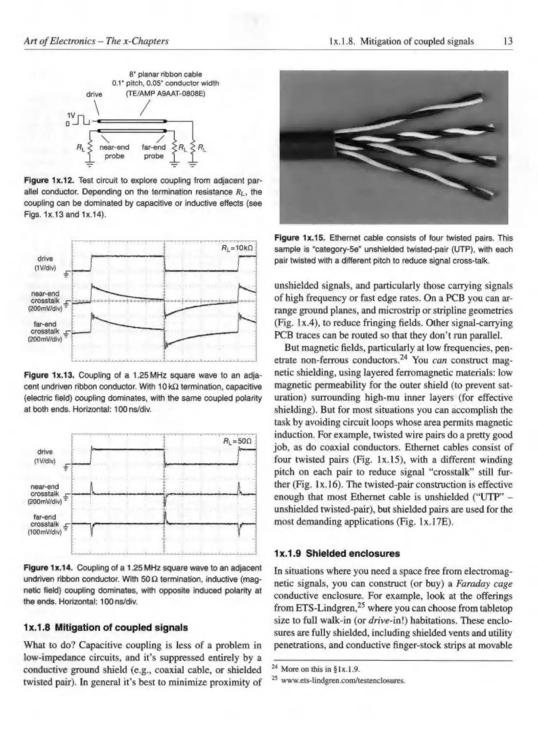
1X.1.5 Cable configurations
If there’s more than one wire, you call it a cable. There
are many choices here: Coaxial cable (“coax”) has an
inner (usually stranded) conductor, with an outer shield;
these are designed as transmission lines, with controlled
impedance (see Appendix H on Transmission Lines), and
usually designated with an “RG” type number.*^ At low
frequencies you can think of coax simply as a shielded ca
ble, with approximately 30pF/ft (1 pF/cm) of capacitance.
Multiwire cable (a variety of instrumentation cable) is
a bundle of strands, color-coded so you can untangle them
at the other end; they may be individual wires, multipair
(multiple pairs), or multiple triads. A multiwire cable may
be unshielded, or overall shielded (with a foil shield, a
braided shield, or both). Multipair cables are also available
with the pairs individually shielded. Multi wire cables
generally are not intended as transmission lines; however,
certain multipair cables are designed for high-speed data
transmission, with controlled impedance. The most com
mon is “cat-5” (or “cat-5e” or “cat-6”) 100 Q (differential)
impedance cable, with 4 twisted pairs, used universally for
local-area networks (LANs); it’s often called “UTP” (un
shielded twisted pair) network cable (and shielded twisted
pair cable is called “STP”).‘^
cause the effective “index of refraction” is ^ y (l+ e )/2 (~1.68), versus
v/i(~2.1).
For example, RG-58/U is the ubiquitous 50 £1 cable used for BNC
patch cables, and RG-174 and RG-316 are skinnier variants, the latter
with teflon insulation. Although 50 £2 is the by far the dominant cable
impedance, the video world has chosen to be different, and uses 75 £2
cable, usually RG-59 or RG-6.
Other popular high-speed data cables are SATA and Firewire (2 individ
ually shielded twisted pairs, 100 £2 and 110 £2 differential impedance,
respectively), and USB 2.0 (shielded pair, 90 £2).
10
1X. 1. Wire and Connectors
Art o f Electronics - The x-Chapters
Flat cable (also called ribbon cable) comes in the fa
miliar unshielded ribbon with 50 mil pitch; variants in
clude ribbon with an integral flexible ground plane on
one side, or as fully shielded flat ribbon. For better sig
nal integrity with differential signals you can get a rib
bon of twisted pairs, flattened for 5 cm every 50 cm to al
low for the same mass-termination insulation-displacement
(“IDC”) connectors used for conventional ribbon cable. For
single-ended signals you can get a flat ribbon of individual
coaxial cables, or a less expensive “near-coax” approxima
tion in which the continuous outer shield does not com
pletely surround the individual strands.
A twisted wire pair has slightly less inductance than a
parallel pair*^ (and it has considerably less susceptibility to
signal pickup via magnetic coupling); you can get a much
larger reduction in inductance by creating a twisted pair
from a twisted four-wire cable, with diagonal wires tied
together.'^ Figure lx.7 shows inductances for several con
figurations.
1X.1.6 Inductance and skin effect
A. Inductance
In addition to resistance, any length o f wire has inductance.
That must be so because a current creates a surrounding
magnetic field, with its associated field energy; equating
that energy with j L f is often the easiest way to calcu
late wire inductance. The result is that the inductance is
approximately proportional to wire length, and further de
pends somewhat on spacing to nearby conductors, on wire
diameter, and on frequency (via skin effect). For an isolated
straight wire of diameter d and length /, the low-frequency
inductance is given approximately by
L/l^l
logg ^
7 )
^
L/lKl
\
L /l»4
''
loge
4ft \
iKh
w
2D
n H /cm
nH /cm
Figure 1x.7. Inductance per centimeter versus wire size for a wire
over a ground plane (1 mm and 3 mm heights), and for a wire in
isolation (1 cm and 10 cm lengths).
nH /cm
So, for example, a 10 cm length of 20-gauge wire (d =
0.081 cm) has an inductance of approximately 10.9 nH/cm,
when distant from other conductors. The inductance is less
for a conductor in proximity to a conductive surface (a
“ground plane”), or to other wires; the relevant expressions
are
L /l^l
AWG wire size
(wire over plane)
B. Skin effect
When alternating current flows through a conductor, the
current is not uniform throughout the bulk - it is concen
trated in an outer layer*^ (called the skin depth) of thick
ness 5 « ( n u a f ) ’^ , where a is the conductivity, pi is the
relative magnetic permeability (=1 for non-magnetic ma
terials), and / is the frequency.** From a circuit point of
view, skin effect causes an increase in the effective resis
tance (and loss), and a decrease of inductance (because the
(flat strip over plane)
nH /cm
(wire pair)
\
where h is the height of the conductor’s center above the
conducting plane (reasonably accurate for h > 1.5t^ or
h > w), D is the center-to-center wire spacing, and w is
the width of a flat conductor (such as a PCB trace).*'*
There are excellent references on wire inductance and its effects, no
tably the “Black Magic” volumes by Johnson and Graham, Grover’s
Inductance Calculations, Terman’s Radio Engineers' Handbook, and
Ott’s Noise Reduction Techniques in Electronic Systems.
The D /I term is omitted in the equation above.
We used this trick in the “stopped-light” experiments, where we had
to limit the inductance of an 875 A cable to quickly kill the current,
allowing trapped sodium ions to fall under gravity, watching the spread
to measure their temperature.
To be precise, the cunrent density decreases exponentially, falling to 1/e
(37%) of its surface value at a depth equal to 5.
If you are interested in the physical origin of skin effect, you can think
of it in either of two ways: (i) as the penetration depth of an electromag
netic wave incident on the finite-conductivity metal; or (ii) as resulting
from the outward force on the moving charges caused by their motion
through the alternating magnetic field they produce.
Art o f Electronics - The x-Chapters
lx.1.6. Inductance and skin effect
11
Frequency (Hz)
Figure 1x.8. Skin depth in copper as a function of frequency.
surface currents produce no interior magnetic field). Fig
ure lx.8 plots the skin depth in copper conductors from
10 Hz to 10 GHz.
Because skin depth decreases with increasing frequency
(as
it becomes particularly important at high fre
quencies, where it is largely responsible for losses in trans
mission lines (see the Appendix on Transmission Lines).
At radio frequencies the skin depth is so shallow (e.g.,
8 = lO^m at 40 MHz) that you can make low-loss con
nections, inductors, and so on, by silver plating a poor con
ductor. A conmion technique for shielding lightweight in
struments and computers at radio frequencies is to apply a
thin metallic plating to a plastic enclosure. But it’s impor
tant to realize that skin depth effects are significant even
at low frequencies - for instance, current at the powerline
frequency of 60 Hz in a copper conductor is confined to
a surface layer of roughly 1 cm. (Copper’s skin depth at
room temperature is given by 5(Cu) = 6 .6 /^ / f cm.) For
wire much thicker than that, power transmission losses de
crease only proportional to the diameter of the wire, rather
than to its cross-sectional area (i.e., diameter squared).
Fortified with this knowledge, you would not expect to
see 60 Hz power transmission cables thicker than about
1 cm; or if they are larger in diameter, they are probably
hollow. Imagine our surprise, then, when we encountered
the 1000 A copper power cable pictured in Figure lx.9,
with its impressive 50 mm core. There’s an elegant trick
in operation here: to equalize the currents flowing in each
wire strand, the cable is configured so that the individual
strands weave in and out along the length of the cable, so
on average each strand visits the cable’s interior uniformly.
Since every strand does this, their currents must be the
same: voila - the cable carries uniform current throughout
Figure 1x.9. We persuaded the guys with the big backhoe to give
us a sample of their impossible power cable: the diameter of its
stranded conductor is six times the skin depth of the 60 Hz ac
power. The 50 mm-diameter core is rated to carry 1000 A at 138 kV.
its cross-sectional profile, thus violating that high-falutin’
skin-depth theory you learned in school!*®
For comparison, we calculated^® the distribution of
60 Hz ac current^' that would flow in a solid copper core
of the same 50 mm diameter, graphed in Figure 1x. 11. The
There’s a bit more to it, as usual in the real world: the strands have to be
mildly insulated from each other, implemented in practice with a thin
insulating coating. As the inventor Humphreys Milliken put it, in his
1933 patent (#1,904,162, “Electrical Cable”), “The insulation between
adjacent strands need be only sufficient to offer a contact resistance be
tween adjacent strands, many times as great as the resistance of one
strand for a length of one turn in its progress around the cable, which
is in the order of a few thousandths of an ohm.” There are other tricks,
also: for example, to make the cable manufacturable Milliken teaches
how to build it in sectors (five are used in the cable in Fig. lx.9), each
of which is made from forming a twisted bundle of strands into ra
dial wedges. The patent makes great reading - it’s a model of clarity,
mercifully short (3 pages of text, and just one claim), and with fine
illustrations, one of which is reproduced here as Fig. Ix.lO,
It involves Bessel functions, as you might guess from the cylindrical
geometry; see Ramo, Whinnery, and van Duzer’s excellent reference
Fields and Waves in Communication Electronics, Wiley (1965). We
thank Mike Bums for doing the Mathematica calculations.
This problem does not afflict dc, and large do power cables are made
with conventional stranded construction. DC is increasingly being used
for megawatt-scale power transmission, often with a single conductor
12
Ix .l. Wire and Connectors
Art o f Electronics - The x-Chapters
Radius (mm)
Figure 1x.11. Current density profile for a solid copper conductor
of 50 mm diameter carrying 60 Hz ac. The effective ac resistance
is approximately 1.7x that of the same-diameter Milliken-wound
cable of Fig. 1x.9.
Figure lx.10. The method invented nearly a century ago to do
an end-run around the limitations of skin depth in large ac power
caWes. The little arrows show the twist pattern of copper strands
in each sector of a very thick (D » 5 ) cable. (Fig. 3 of US Patent
1,904,162.)
loss in such a cable, owing to reduced current density in
the cable’s core, is about 1.7 times that of the (uniform cur
rent density) Milliken cable. The latter has a resistance of
9 mO/km, thus an p R loss of 9 W/m at 1000 A ac.
A closely related scheme is used in radiofrequency coils,
there known as litz wire^- in which the individually insu
lated fine strands are woven in a pattern that equalizes their
participation throughout the cross-section of the wire. Litz
wire inductors are seen in applications from tens of kilo
hertz to a few megahertz. Historically, litz wire was in use
well before Milliken’s 1930 patent application (there are
cites going back to 1923), and undoubtedly informed his
adaptation of the concept to high-power ac transmission
cables.
Ix.1.7 Capacitive and magnetic coupling
Signals go where you don’t want them to. Often this is
caused by capacitive (via the electric field) coupling from
signals on adjacent wiring; in that case the coupling is
greater into a high-impedance circuit, and more so at higher
(with ground as the return path); see the products of companies such as
ABB Power Grids (owned by Hitachi) for some stunning examples.
From the German litzendraht, or woven wire.
frequencies (or faster edge-rates). Perhaps less recognized,
signals can couple inductively (via the magnetic field) into
circuit loops; in that case the coupled currents are greater
between low-impedance circuits.
Which dominates? It depends. We rigged up a test cir
cuit, consisting of adjacent conductors of a coarse-pitch
FPC (flexible printed circuit) ribbon (Fig. Ix.l2), then we
drove one line with a 1 Vpp 1.25 MHz square wave and ob
served the signal at both ends of the adjacent line. Let’s call
the driven line the aggressor, and the passive line the vic
tim. With high-impedance terminations (/?L=10k£2 at all
three ends) the coupling is capacitive, with signals of the
same polarity observed at both ends of the victim line.^^
The coupled waveforms (Fig. Ix.l3) exhibit the usual ex
ponential decay of a square wave passing through an RC
highpass filter.
The situation is quite different with the lines terminated
in a low impedance (/?l=50S2, Fig. Ix.l4). The capacitively coupled current is the same as before, but it generates
negligible drop across the 25 Q-terminated victim. But the
larger current (40 mApp) in the aggressor creates a mag
netic field that induces a current in the (low-impedance)
victim loop. Magnetic coupling induces an EMF propor
tional to d B /d t (the time rate-of-change of magnetic field),
so we see a differentiated waveform; furthermore, because
the induced current flows in a loop, through both 50 Q ter
minating resistors, the polarity is reversed at the opposite
ends, as seen in the lower trace pair of Figure Ix .l4.
The 20 cm line is short compared with the 240 m signal wavelength of
the 1.25 MHz square wave.
Art o f Electronics - The x-Chapters
lx.1.8. Mitigation of coupled signals
13
8‘ planar ribbon cable
0.1' pitch, 0.05" conductor width
drive
I
R|_ <
I
\
^
(TE/AMP A9AAT-0808E)
near-end
probe
/
far-endd
probe f
r
Figure 1x.12. Test circuit to explore coupling from adjacent par
allel conductor. Depending on the termination resistance i?L. the
coupling can be dominated by capacitive or inductive effects (see
Figs. 1X.13 and 1x.14).
Figure 1x.15. Ethernet cable consists of four twisted pairs. This
sample is “category-5e” unshielded twisted-pair (DTP), with each
pair twisted with a different pitch to reduce signal cross-talk.
Figure 1x.13. Coupling of a 1.25 MHz square wave to an adja
cent undriven ribbon conductor. With 10k£2 termination, capacitive
(electric field) coupling dominates, with the same coupled polarity
at both ends. Horizontal: lOOns/div.
f?L=50n :
drive
(IV/div)
near-end
crosstalk x (200mV/div) ^
far-end
crosstalk jr^ :
(100mV/div)
^
......;......
:
...i.......^......
. . . .... :.......:.............; 1,,....: ...
r
^
^
unshielded signals, and particularly those carrying signals
of high frequency or fast edge rates. On a PCB you can ar
range ground planes, and microstrip or stripline geometries
(Fig. lx.4), to reduce fringing fields. Other signal-carrying
PCB traces can be routed so that they don’t run parallel.
But magnetic fields, particularly at low frequencies, pen
etrate non-ferrous c o n d u c to rs.Y o u can construct mag
netic shielding, using layered ferromagnetic materials: low
magnetic permeability for the outer shield (to prevent sat
uration) surrounding high-mu inner layers (for effective
shielding). But for most situations you can accomplish the
task by avoiding circuit loops whose area permits magnetic
induction. For example, twisted wire pairs do a pretty good
job, as do coaxial conductors. Ethernet cables consist of
four twisted pairs (Fig. Ix.l5), with a different winding
pitch on each pair to reduce signal “crosstalk” still fur
ther (Fig. Ix.l6). The twisted-pair construction is effective
enough that most Ethernet cable is unshielded (“UTP” unshielded twisted-pair), but shielded pairs are used for the
most demanding applications (Fig. lx.l7E).
Ix.1.9 Sliieided enclosures
Figure 1x.14. Coupling of a 1.25 MHz square wave to an adjacent
undriven ribbon conductor. With 50£1 termination, inductive (mag
netic field) coupling dominates, with opposite induced polarity at
the ends. Horizontal: 100ns/div.
Ix.1.8 Mitigation of coupied signais
What to do? Capacitive coupling is less of a problem in
low-impedance circuits, and it’s suppressed entirely by a
conductive ground shield (e.g., coaxial cable, or shielded
twisted pair). In general it’s best to minimize proximity of
In situations where you need a space free from electromag
netic signals, you can construct (or buy) a Faraday cage
conductive enclosure. For example, look at the offerings
from ETS-Lindgren,^^ where you can choose from tabletop
size to full walk-in (or drive-'m\) habitations. These enclo
sures are fully shielded, including shielded vents and utility
penetrations, and conductive finger-stock strips at movable
More on this in §lx.l.9.
www.ets-lindgren.com/testenclosures.
14
Art o f Electronics - The x-Chapters
Ix .l. Wire and Connectors
Crosstalk (dB, min) at 100MHz
_________ CatSe Cat6/6a Cat 7
NEXT
-30.1
PSNEXT
-27.1
-3 9 .9 -6 2 .9
-37.1
ACRF
-17.4
-2 3 .3 -4 4 .4
PSACRF
-14.4
-2 0 .3 -41.4
-5 9 .9
Figure I x . l 6. Ethernet cable crosstalk specifications (100m
length), from the 2009 standard (ANSI/TIA-568-C.2). NEXT is near
end crosstalk ratio from an adjacent pair; PSNEXT is similar, but
with all other pairs driven. ACRF (formerly ELFEXT) is far-end
crosstalk ratio from an adjacent pair, compared with the far-end
received signal; PSACRF is similar, but with all other pairs driven.
door openings (Fig. Ix .l8); their illustrated catalog shows
why it may be better not to attempt to build your own, but
to leave the construction of shielded enclosures to the pro
fessionals.
There are various specifications for shielding effective
ness of shielded enclosures. One often quoted is NSA 65-6
“Specification for Shielded Enclosures” and its follow-ons
(NSA 73-2A, 89-02, 94-106, etc.); the minimum attenua
tion versus frequency from that document (for both electric
and magnetic fields) is graphed in Figure lx.l9.
Of note is the poorer attenuation of low-frequency mag
netic fields, for which effective shielding often takes the
form of layers of ferromagnetic material (iron, mu-metal,
etc.). That is because the skin depth in materials of finite
conductivity increases as the inverse square root of fre
quency (and inversely proportional to the conductivity), as
seen for example in Figure lx.8, where even an excellent
conductor (copper) requires nearly a centimeter of thick
ness to produce even a modest attenuation of an applied
60 Hz magnetic field.
This would appear to render non-magnetic materials
pretty much useless for low-frequency magnetic shielding.
However, the situation is not so bleak: What is not gen
erally recognized^® is that a fully-closed conductive shell
acts effectively as a far thicker conductor (for the purposes
of skin effect) than its actual wall thickness. In fact it can
be shown that a closed box of dimension D, with con
ductive walls of thickness x, attenuates low-frequency uni
form magnetic fields as if its walls had a thickness of ap
proximately the geometric mean of those dimensions, i.e.,
x! K \/xD. Intuitively this is plausible, because the closed
path provides a large-area loop to capture magnetic fields
and produce a compensating circulating current, evidently
We are indebted to Richard Garwin for educating the authors on this
remarkable fact.
far more effective than the eddy currents circulating locally
within the thickness of the conducting shell.
To verify this remarkable claim, we soldered together
a 15 cm cube from “ 1 oz” copper-clad PCB (Fig. lx.20),
for which its 36 jUm thick copper layer corresponds to a
skin depth at 3.4 MHz; at frequencies well below that the
copper-clad material is transparent to oscillating magnetic
fields. The “geometric mean” rule, in contrast, predicts that
the 0.0036 cm walls of the closed box should attenuate like
a 0.23 cm thick copper plate, which is a skin depth in cop
per at the much lower frequency of 820 Hz. So the test: our
box should let through magnetic fields below a kilohertz,
but largely attenuate magnetic fields above, say, 10 kHz.
To test this we placed the box in a Helmholtz coil pair
(Fig. lx.21), series-resonated with a film capacitor at each
of four frequencies (IkH z, 3 kHz, 10 kHz, and 30 kHz),
and driven with an ac current of 2App; then we mea
sured the interior field with a Hall-effect magnetic probe,
comparing the observed field with the applied field.^^ Fig
ure lx.22 shows the setup.
Did the closed box attenuate as predicted? Indeed! Here
are the measured attenuation values (ratio of the interior ac
magnetic field to the field in the absence of the box), which
we’ve plotted on log-log axes in Figure lx.23.
Frequency Attenuation
IkH z
3 kHz
10 kHz
30 kHz
1.2 dB
5.7 dB
14.2 dB
21.1 dB
Of importance: for this purpose a “closed box” requires
conductivity across all seams comparable to that of the
sheet material itself; screwed-together plates are ineffec
tive. We measured the shielding attenuation of our box (be
fore soldering the seams) with all sides joined with short
lengths of wire, and found only fractional dB attenuation
at 3 kHz and below; in fact that configuration behaved no
^ Some details: The Helmholtz coil pair’s diameter was 75 cm, with a
parallel inductance of 4.7 mH. We used resonating capacitances of 5 /iF,
0.6 fiP, 55 nF, and 6 nF at the four frequencies, with a 5 Q non-inductive
series current-sensing resistor. The magnetic field was sensed with a
DRV5053VA Hall-effect device (9mV/gauss), and measured with a
SRS530 lock-in amplifier. An interesting bump-in-the-road: at first the
Hall probe gave a plausible result, but (implausibly) independent of ori
entation! Turns out we had not yet turned on its dc supply, and what
we were seeing was the ac electric field, capacitively coupled to the
exposed sensor (the resonant voltage swing at lOkHz was ±300V !)
So we wrapped the sensor in a magnetic-field-transparent electrostatic
shield.
Art o f Electronics - The x-Chapters
lx.1.10. Connectors
15
Figure 1x.17. A selection of cables for high-speed signals. A. FFC (flexible fiat cable), sometimes cailed FPC (flexible printed circuit);
this sample has 10 conductors on 0.5 mm pitch. B. 40-coax 50 n ribbon, terminated in Samtec QSE-series 0.8 mm pitch high-speed
ground-plane connectors. C. Amphenol Twist ‘N’ Flat 8-pair ribbon. D. Cat-5e unshielded twisted-pair (see Fig. 1x.15). E. Individually
shielded twisted-pair (STP) cable. F Unshielded flat ribbon, 0.050" pitch, terminated in DIP-16 plug. You can get FFC/FPC cables with
1 mm pitch, which are more forgiving of crooked insertion. Jumpers made by rolling wire fiat can carry iots of current; but you can also
get plated Kapton cables, which are excellent for connecting to cold or hot plates.
differently than a box of six isolated sides with no connec
tions at all.
A Parting Shot
There are many excellent references^^ on the thorny topics
of shielding and grounding, which is far more complicated
that this short treatment might suggest.
For example, (1) Analog Devices MT-095 Tutorial “EMI, RPI, and
Shielding Concepts”; (2) H.W. Johnson and M. Graham, High-Speed
Digital Design, A Handbook o f Black Magic, Prentice-Hall (1993); (3)
R. Morrison, Gmunding and Shielding Techniques in Instrumentation,
Wiley (1986).
1X.1.10 Connectors
On our bench we used to keep the current DigiKey catalog
(the single most useful source of electronic components get on their mailing list!); the last one that was published as
a printed volume had a product index that is four columns
wide and seven pages long: roughly 3(K)0 entries in all. The
largest single category was “Connectors” (“Integrated Cir
cuits/Semiconductors” is a close second), with 288 major
sub-categories, and with the actual entries spanning 435
pages of fine print.^®
Connector catalogs are full of things that they don’t actually stock but
would be happy to make if you order 100k pieces. Always check for
16
1X. 1. Wire and Connectors
Figure 1x.18. This enclosure from ETS-Lindgren provides 120dB
slilelding of electric fields at frequencies from 10 kHz to 10 GHz,
with reduced effectiveness for magnetic fields below 100l<Hz.
(courtesy ETS-Lindgren, used with permission)
Art o f Electronics - The x-Chapters
Figure 1x.20. Conductive box made from 15 cm square sheets of
0.036 mm (“1-oz”) PCB laminate, with taped and soldered seams.
Figure 1x.19. Electromagnetic Attenuation Requirements as illus
trated In Figure 1 of NSA 94-106 (24 October 1994, superseding
specification NSA 65-6, 30 October 1964).
The point is that connectors are serious business! And
not to be taken hghtly. As we remarked in earher book edi
tions,^® “The most unreliable components in any electronic
system will be the following (worst first): 1. Connectors
and cables. 2. Switches. 3. Potentiometers and trimmers.”
The photographs in Chapter 1 of AoE3 give some idea
ample distributor stock (octopart.com is helpful) before designing in
any part, but connectors especially.
The Art o f Electronics, 2nd edition, 1989; page 858.
Figure 1x.21. We resonated this Helmholtz coil with series capac
itors, and drove it at several frequencies in the kilohertz range to
measure the magnetic-field attenuation of the metal-foil box (sitting
atop an always-available DigiKey empty box).
of the variety, there categorized as “rectangular,” “circular,”
and “RF and shielded.” There are additional ways to slice
it up, for example “mass termination” connectors (for rib
bon cable^') versus individual wire terminations; or panelAlso known as IDC (insulation displacement connectors). When IDC
Art o f Electronics - The x-Chapters
Kepco
BOP 36-1.5M
UTCA-20
1X. 1.11. Connectors for RF and high-speed signals
Helmholtz coil
D = 75 cm
Lii= 4.7m H
foil box
15 cm cube
36^im cu
U lM .
soon
1;1
H:T.I. DRV5053
Hall-effect
S-tield sensor
SR530 Lock-In
Figure 1x.22. Circuit for measuring low-frequency shielding effec
tiveness of closed conductive-foil box. Resonating film capacitor
Cres creates a low impedance at resonance, easily driven to several
amps with a few volts sinewave drive. The audio transformer pro
vides reference-signal galvanic isolation to prevent ground loops.
m
2,
c
o
■(3
D
C
2
(]>
OQ
17
would never use (except possibly at gunpoint). For muUiwire panel-mount connectors we like the D-subminiature
(rectangular) connector series, and particularly the highquality “screw-machined” type; we also like the RMseries of 12 mm (circular) video connectors made by Hirose. For higher currents we like the “Winchester-type”
MRA/MRAC shrouded and jackscrew-locking multipin
connectors. For multiwire PCB-mount connectors we
have been happy with the AMPMODU MT series of
single-row and double-row socket connectors (for individ
ual wires), and with the 3M series of mass-termination IDC
connectors (for ribbon cable). For 50 RF connectors we
like the coaxial SMA and SMB, which can also be used as
simple shielded connectors for low-level signals. For the
latter the standard has been (and doubtless will continue to
be) the classic BNC connector; but we have experienced
problems with inadequate ground integrity, particularly as
these connectors wear from repeated use, and we prefer the
less popular TNC. For high voltage we like the SHV con
nector.
Now for the connector types to avoid (reasons withheld
- ju s t trust us!): Stay away from the “RCA audio connec
tor” (used universally on consumer audio equipment), the
“Jones” type multipin connector, the “U H F’ and “F ’ type
RF connectors (the latter used universally in consumergrade television, cable, and satellite), the “blue hexagon”
connector, and the 1/8" and 1/4" headphone connectors. At
a lesser level of dislike, we’re not particularly wild about
the circular DIN connectors (both regular and mini), the
5 mm (and smaller) coaxial “dc power entry” connectors,
and the multipin threaded “microphone connectors” (but
the professional XLR series is fine).
Frequency (Hz)
Figure 1x.23. Measured attenuation of magnetic field for the con
figuration shown in Fig. 1x.21.
mount versus internal versus cable-joining connectors; or
connectors for low-level signals (audio, RF, instrumenta
tion) versus high voltage versus high current; or multiwire
versus single-circuit connectors; and so on. As a general
statement, you want to choose reliable connectors that are
appropriate for the signals involved, and that provide suit
able mechanical coupling.
Without going into detail, we’ll reveal our biases; we
have our favorites, and we have some connectors that we
is done on a connector with a set of wires in one operation, it’s called
MTA, for mass termination assembly.
Ix.1.11 Connectors for RF and high-speed signals
As detailed in Appendix H in AoE3, when dealing with
signals at high frequencies (or signals with fast transitions)
it is essential to terminate signal-carrying lines with an
impedance equal to the cable’s characteristic impedance
Zo, in order to prevent reflections from impedance mis
matches. The assumption here is that the cable itself has a
well-defined characteristic impedance, constant along the
length of the cable; if not, reflections will be created at lo
cations of discontinuity in the cable’s impedance.
The same goes for a transition at a connector, which ide
ally should maintain the cable’s characteristic impedance
across the joint. This becomes more critical, and more diffi
cult, at high frequencies; specialized connectors are needed
18
Art o f Electronics - The x-Chapters
Ix.l. Wire and Connectors
Table 1x.3: RF Connectors, Approxim ate fmax
Type
fmax (GHz)
UHF
0.3
BNC
4
Type
fimax (GHz)
SSMA
12.4-36'^
superSMA
27
SMB
4
3.5mm®
34
MCX
6
2.92mm®''=
40
MMCX
6
2.40mm
SMC
10
APC-7
50
TNG
18
1.85mm
65
SMA®
12-261^
0.9mm
67
N
18
1.0mm
110
50
Notes: (a) SMA, 2.92mm, and 3.5mm can mate
interchangeably, (b) Variants avaiiabie with different
^max. (c) Aiso known as a “K" connector.
Figure 1x.24. Measured reflection coefficients versus frequency
for a selection of connectors. For the worst offenders the corre
sponding VSWR is also shown. Data courtesy of John S. Huggins,
see www.hamradio.me.
once you’re operating above, say, lOGHz.^^ The measured
data in Figure lx.24 illustrates this point, here at more
modest frequencies. Among other things, it nicely confirms
our personal bias against the euphemistically named “UHF
connector.”
Table lx.3 lists most RF and microwave connector types
and their maximum operating frequencies, where you can
see that the highest frequencies correlate with the smallest
diameter (to avoid multimode propagation). A drawback of
small connectors is their lower power-handling capability,
as seen in Figure lx.25.
1X.1.12 High-density connectors
In the good ol’ days of vacuum tubes, filament transform
ers, and big chassis with black crinkle finish, we were
For example, to maintain constant impedance you may have to taper the
outer shell and dielectric (if any) to accommodate the changing diam
eter of the inner conductor. A smaller overall diameter is necessary at
the highest frequencies to suppress additional “modes” of wave propa
gation.
Figure lx.25. Continuous power-handling capability of a selection
of RF and microwave connectors.
happy with connectors that could handle, oh, ten conduc
tors, and weren’t much larger than an apricot. We consid
ered the “D-subminiature” connectors really dense, as evi
denced by the name.
Things have changed, and contemporary electronics
deals in small-footprint ICs with lOOO-i- “pins,” and passive
components smaller than a grain of rice. Connectors have
to keep up! These come in many flavors - mainly panelmount, board-to-board, and board-to-cable. The photo
graph in Figure lx.26 shows a representative sample from
our lab, alongside that D-subminiature of yesteryear (but
still a good choice for a reliable panel-mount connector for
9 to 50 pins).
When choosing a high-density connector (assuming
you’re not constrained by existing components or cables),
be sure to consider factors like contact resistance, currentcarrying capacity, number of mate-unmate life cycles, and
Art o f Electronics - The x-Chapters
lx.1.13. Connector miscellany
19
1cm
Figure 1x.26. High-density connectors. A. Samtec SS4-20-3.50-L-D-K-TR 0.4mm-pitch board-to-board connector, good to >15 Gbps,
shown here with mating Hamamatsu 4 x 4 silicon photomultiplier array. B. Hirose DF17(3.0)-20DS-0.5V(57) 0.5mm-pitch board-to-board
connector. C. RFC (flexible flat cable) and mating connector, 0.5 mm pitch. D. Dual-row 0.050" pin header and socket strips. E. Microtec
xx-7 connector for 7-wire shielded cable. F. Samtec QSE-series 40-pin 0.8mm-pitch high-speed ground-plane connectors and mating
cable-end connector with 40 true-coax 5 0 0 cables. G and H. DE-9P D-subminiature male connector and 0.1" pitch dual pin header, for
size comparison; in this photo they are giants - hardly “subminiature.”
robustness (e.g., surface-mount versus through-hole, pres
ence of mounting flange, shrouded mating area, and so on).
lying metal. To prevent fretting, prevent the relative mo
tion! (Allow the mating connector to “float,” or mechani
cally anchor the mating parts, etc.) There are dry lubricants
that suppress fretting when some relative movement is in
lx.1.13 Connector miscellany
evitable.
(1) For good reliability, avoid surface-mount connectors
(3) Gold-plated contacts are desirable, but only when
where repeated insertions, vibration, or other aggravating mated to gold. A gold-tin connection is no better than tinforces may detach the delicate traces. Better to use press- tin.
fit (which creates a cold weld) or soldered through-hole
(4) Insulation-displacement connectors have received
connectors.
criticism for their tendency to fail in the long term. There
(2) Vibration or repeated thermal expansion and contrac are many varieties available, and some are better than oth
tion can cause fretting of contact material, in which tiny rel ers. We’re told that the inexpensive Tyco 640440-3 (3-pin,
ative movement of contacting metals creates granular wear low density) is reliable. And we’ve had good reliability
and consequent corrosion.^^ This does not occur with gold with 3M’s IDC ribbon connectors.
contacts, until there’s sufficient wear to expose the underTfiere’s a good discussion at
suddendocs.samtec.com/productspecs/fretting-corrosion.pdf.
Art o f Electronics - The x-Chapters
expansion causes the combined object to exhibit extraordi
narily low tempco; these things cost plenty, though, about
$10 apiece.
The above are SMT types; you can, of course, get
through-hole (axial or radial lead) resistors with analo
gous performance. Additional types are available, for ex
ample wirewound resistors, which come with tempcos as
low as ±20 ppm/°C (though typically they are in the ordi
nary range of ±100ppm/°C or so).
Figure 1.2 in AoE3 shows the range of resistor types,
from tiny surface-mount chips to giant wirewound power
resistors. The most important characteristics are resis
tance, pow er rating, tolerance (accuracy), stability
(over time), and temperature coefficient of resistance.
But resistors (like all electronic components) are imper
fect - electrically they exhibit some series inductance
and some parallel capacitance,^* which become impor
tant in high-frequency circuits and in power-switching cir
cuits. Additional departures from ideal performance in
clude voltage coefficient of resistance and excess noise;
these are important in low-distortion, low-noise, and preci
sion circuits.
We touched briefly on these less-than-sterling attributes
of the humble resistor in several places in AoE3; see for
example the Box (“Resistors”) on page 5, the Table (“Se
lected Resistor Types”) on page 1106, and discussion on
pages 3(X), 476, and 697-98. Here we elaborate on some
of these neglected aspects of a component often taken for
granted.
1X.2.2 Self-capacitance and self-inductance
Real resistors have some equivalent series inductance and
some distributed shunt capacitance (Fig. lx.27). Typical
values for SMT resistors are in the range of tens to hun
dreds of femtofarads, and 0.01-2 nanohenrys.^^ Depend
ing on the physical construction, the overall effect may be
a rise in impedance with frequency (e.g., wirewound re
sistors), or, if the parallel capacitance dominates, a falling
impedance. Both trends can be seen in the measured |Z (/)|
plots of Figure lx.28.
i-i
o—
-^ A V -
R
Figure lx.27. Simplified resistor model, showing parasitic induc
tances and capacitance. The external Inductances L, represent the
inductive contributions of the leads to the impedance of the resistor
body (enclosed In dashes).
1X.2.1 Temperature coefficient
The ubiquitous thick-film SMT chip resistor (e.g., Vishay
CRCW-series) typically has a specified tempco of ±200
or ±100ppm/°C (designated in the manufacturer’s part
number). But if you need better, you can get low tem
pco SMT resistors, for example the inexpensive Panasonic
ERJ-xRBD or -xRHD series (±50ppm/°C), which cost
about $0.07 in full-reel quantities (compared with $0,003
for the commodity CRCW types). Still better are some
thin-film SMT parts, for example the Panasonic ERAxAR series or Yageo RTxxxxxRB series (±10ppm/°C),
which cost about $0.18 in full-reel quantities, or the Vishay
TNPU-Z series (±5 ppm/°C, $1 in full-reel qty).
For the absolute lowest tempco you can get metalfoil (“Z-foil”) SMT resistors from Vishay (VSMP-series,
±0.2ppm/°C), which exploit a clever thermal compensa
tion trick by bonding the metal foil element to a carefully
chosen ceramic substrate whose mechanical coefficient of
To explore this further, we measured the impedance of
a set of wirewound resistors of the same construction (the
classic Ohmite Brown Devil®), with the results plotted in
Figure lx.29. Evidently the inductive contribution domi
nates at megahertz frequencies, more so for the lower re
sistor values. For apphcations at high frequencies, noninductive wirewound resistor types largely eliminate the
problem.
What about the parallel capacitance Cp of the model
of Figure lx.27? At some frequency it should form a
(damped) parallel resonant circuit, an effect that can be
seen in the measured data of Figure lx.31, where we’ve
extended the frequencies out to 300 MHz for three of the
wirewound resistors of Figure lx.29. You can use a trick
to largely compensate for this unseemly behavior, namely
^ Which may be more complicated than a single series L and parallel C,
because they are distributed throughout the resistor.
See, for example, Vishay Technical Note 60107, “Frequency Response
of Thin Film Chip Resistors.”
20
Art o f Electronics - The x-Chapters
lx.2.3. Nonlinearity (voltage coefficient)
21
tances, and various construction) through it. They all ex
hibit curves similar to those in Figure lx.29; to keep the
figure uncluttered we plotted just the breakpoints (inter
section of nominal resistance with the extrapolated upward
slope, see the example in Fig. lx.29). Figure lx.30 shows
the resulting scatterplot.
The best performers (breakpoints at the highest frequen
cies) are the carbon composition (RC07 type), the noninductive Ohmite WN-type (Ayrton-Perry zigzag wind
ing), and the surface-mount small wirewound type. By
contrast, the losers are the traditional large-geometry wirewound power resistors. However, some of the latter are
available in non-inductive versions: for the Vishay/Dale
RS, RH, and LVR types you can get NS, NH, and NI as
Ayrton-Perry non-inductive variants.
Figure 1x.28. Measured impedance (magnitude) versus fre
quency for four resistor types. At fiigfi frequencies tfie effects of
parasitic inductance and capacitance cause a deviation: upward
forwirewound resistors (inductance dominates), downward for noninductive construction (capacitance dominates).
Frequency (Hz)
Figure 1x.29. The inductance of wirewound resistors causes tfie
total impedance to rise at fiigh frequencies, as seen in measured
data of 20 W “brown devil” types. If this matters In your application,
you can get non-inductive wirewound resistors that use bifilar (two
windings, connected together at one end), or Ayrton-Perry (two
countenwound windings in parallel) winding geometries; the simpler
bifilar winding suffers from much higher parasitic capacitance. A
"breakpoint” frequency (black dot) fully characterizes a resistor with
series inductance (see the wirewound resistor zoo In Fig. 1x.30).
a series RC attached across the offending resistor, with R
equal to the nominal resistance, and C selected to flatten
the impedance curve.
Once we had the measurement rig set up, we couldn’t
resist (pun) running a bunch of resistors (of various resis
lx.2.3 Nonlinearity (voltage coefficient)
An ideal resistor maintains I= V /R over time, temperature,
frequency, and applied voltage. In the real world resistors
exhibit deviations from perfection. A not-insignificant ef
fect is nonlinearity - an effective change of resistance with
applied voltage.
You can find worst-case specifications in some
datasheets: for example, although the commodity Vishay
CRCW-style thick-film SMT resistors do not specify a
voltage coefficient, their PCAN-series thin-film resistors
specify a worst-case resistance change of 0.1 ppmA^, the
same as the best-in-class metal foil or metal film types such
as the Vishay VSMP and Z-foil series resistors.
Out of curiosity we measured the resistance change ver
sus voltage for a selection of resistor types. You often use
a high-resistance voltage divider to monitor a high-voltage
dc supply, so we tested high-resistance parts at voltages to
1000 V. Figure lx.32 shows the results, plotted as log-log
and log-linear. The thick-film resistors (curves C-H) are
better by some two to three orders of magnitude, compared
with the traditional carbon composition type.
Carbon-composition resistors are largely a relic of the
past (though they excel in peak power endurance, see
§lx.2.6). Sticking with the thick-film types, we explored
the nonlinearity versus resistance (for a fixed size), and
nonlinearity versus size (for a fixed resistance). Fig
ures lx.33 and lx.34 plot the measured results, showing
that the nonlinearity increases dramatically with increasing
resistance and with decreasing physical size.
When does nonlinearity matter? For low-distortion am
plifiers and oscillators, certainly. Also for precision lowvoltage monitoring and control of a high voltage source.
Note, however, that for the latter what you care about is a
22
lx.2. Resistors
Art o f Electronics —The x-Chapters
10k
-r
I I I III
o
“I—
I I I 11 ii|
“I—
I I I 11 III
o
Ohmite 175-300W
7 Q
A Ohmite WN non-ind
V Brown Devil 20W
Ik
E 100
;§
(U
0
1
w
0
CC
□
Ohmite 90J 11W
>
Ohmite 9 5J5W
<
Ohmite 9 3J3W
o
DaieRS2B3W
■
DaieRH-250
<1
<1
LVR-5 5W
•
10
o
SMT2010WW
■4 CP-5 5W
♦
carbon comp
+
misc ww
o
« •» ♦
•
■
A
A
A
o . "
+
■ n o v
•
<M
•
<
0.1
I
I
1 I I I 111
103
10^
I
I
I I I 1111
4>
♦
A
A A A
A
—U.U.ftjll____ I l_L
10^
10*=
Breakpoint Frequency (Hz)
-j__I I I I m l
10'
10 ®
Figure 1x.30. Measured RL breakpoints (see Fig. 1x.29) for a sampling of power resistor types. All are through-hole wirewound, except
as indicated.
1X.2.4 Excess noise
Frequency (Hz)
Figure 1x.31. Extending the measurements to 300 MHz reveals
LC parallel resonances. The high-frequency artifacts are largely
suppressed by attaching a matching network of 10 n in series with
16.5nF in parallel with the 10 £2 wirewound resistor. Watch out for
the amount of power dissipated in the matching resistor.
precise resistor ratio, for which you should probably be us
ing a resistive divider that is designed to maintain a stable
ratio as the applied voltage varies - see §lx.2.7, below.
In our extensive discussion of noise in Chapter 8 we in
troduced the business of excess noise in resistors (§8.1.3);
this effect is essentially a fluctuation in resistance, which
manifests itself as an added noise voltage (i.e., in addition
to Johnson noise, which depends only on the resistance)
when current is flowing through the resistor. We’ve been
visited by this phenomenon in some recent instruments we
designed; here is the story:
We built a high-voltage amplifier with ±1200 V of op
erating range, and with less than 1 ppm of output voltage
noise.^^ For some experiments at CERN, 160 of these were
machine assembled. About 10% of them failed to meet the
low-noise goals, with an excess noise level that increased
with output voltage. The amplifiers used an Ohmite 150M
1.25 W SMI03 high-voltage resistor in the feedback loop.
This “Slim-Mox” thick-film-on-Alumina precision planar
resistor is 15 mm long and is rated at 7.5 kV. After replac
ing the offenders we wound up with a small collection of
noisy 7.5 kV resistors. Evidently the resistive material has
domains that change under the influence of electric fields.
(Perhaps the problem would have been avoided if we had
made the feedback resistor from fifteen standard lO.OM re^ To learn more about the amplifier, ask about the AMP-37 UberElvis
project.
lx.2.5. Current-sense resistors and Kelvin connection
Art o f Electronics - The x-Chapters
23
Figure 1x.33. Measured change of resistance for 0805-size thicl<film surface-mount resistors, officially rated to 150 V maximum. The
nonlinearity increases with resistor value.
50
70
10 0
200
500
1000
Applied Voltage (volts)
Figure1x.32. Measured change of resistance versus applied volt
age for eight resistor types. The 1/4-watt carbon composition
(RC07, plots A and B, scale on right) and film (plot C) resistors are
rated only to 250 V (marked with vertical stroke), a limit we ignored
in our enthusiasm.
sistors in series, each limited to less than 80 V in opera
tion.)
Figure 1x.34. Measured change of resistance for 1 M n thick-film
surface-mount resistors of different sizes; the rated voltage for each
is indicated by vertical strokes. The nonlinearity decreases with in
creasing physical size.
lx.2.5 Current-sense resistors and Kelvin
connection
We discussed the business of 4-wire sensing (“Kelvin
connection”) in many places in AoE3; see, for example,
pp. 277-78, 294, 350, 365-67, 898, and 1070-71. The ba
sic idea is to eliminate the error in a current measurement
by sensing the voltage drop across the current-sensing re
sistor (often of very low resistance, less than an ohm) with
a separate pair of wires (Fig. lx.35). In that figure, for ex
ample, you would suffer a -1-20 % error in the measured
current, if you had (foolishly) used the voltage drop be
tween the pair of terminals themselves. Measuring instead
the drop between the sense terminals eliminates this error.
The assumption, of course, is that the sensing circuit (here
the difference amplifier) draws negligible current; this is
easily satisfied, especially in high-current circuits where
the sense resistor is of low resistance (and thus prone to
error in a 2-wire configuration).
Current-sensing resistors come in an enormous range
of current capabilities and physical sizes - see the mon
tage in Figure lx.36, photoshopped by the authors from
datasheets of a half dozen manufacturers, where the scaling
varies wildly among the specimens (the little guys labeled
“R 010” are 40 times smaller than the big one on the top
row, second from right).
1X.2.6 Power-liandling capability and transient
power
In circuits with pulse waveforms you frequently have sit
uations where components (resistors, diodes, transistors)
24
lx.2. Resistors
^
current term.
(“C ”)
Art o f Electronics - The x-Chapters
sense resistor
0.0100 ± 1 % ,3 W
sense terr
screw-down
copper crimp-lug
connection
R~1mO
AV = lOmV/A
Figure 1x.35. A 4-wire (Kelvin) current-sensing resistor eliminates
errors caused by imperfect connections. Here, for example, 4-wire
sensing eliminates a 20% error that would be caused by just a
mllllohm of bolt-on lug resistance.
are subjected to peak power (during the pulse) that is well
above the steady-state power rating. That’s OK as long as
the thermal pulse does not cause the component’s temper
ature to exceed allowable limits. We discuss this further in
§9x.25.8 in the context of semiconductor devices (MOSFETs, TVSs), where allowable pulse power is described
by the transient thermal resistance as a function of pulse
duration, ^ 0 jc(f).
Here we are interested in the humble resistor, where the
same effect applies; the peak power during the pulse can
be absorbed by the heat capacity of the resistor’s mass,
as long as the average power does not exceed the part’s
power rating. Some resistors are designed and specified for
such “pulse-withstanding” service. This is usually speci
fied with a graph of peak power (or “pulse load”) Pmax ver
sus pulse duration. Figure lx.37, shows such curves for re
sistors from seven datasheets, mostly of similar size (1206
SMT for all but curves A and F).
You can see some interesting trends in these plots.
Curve B is a Vishay “pulse-proof’ resistor, which does
considerably better for short pulses than its more conven
tional curve B' sibling. Resistor C exploits the thermal con
ductivity of aluminum nitride to permit high steady-state
power (2 W), but with no special attention to short-pulse
endurance. Resistor F uses a solid resistive carbon slug
(rather than a resistive film), whose mass is able to absorb
prodigious peak power (35 kW!) for up to a microsecond not bad for a quarter-watt resistor. Yet, in spite of its larger
size (roughly triple the footprint of the other resistors), it
falls below the rest of the pack for pulse durations greater
than 10 ms.
In Figure lx.38 we adapted datasheet plots for some
larger pulse-rated resistor types. Here you can see the im
pressive performance of ceramic composition resistors (the
worthy successor to the once-ubiquitous carbon comp),
plots B1-B3; Tyco’s CCR-series (plotted) are similar to
Ohmite’s OX (1 W) and OY (2 W), though the latter do not
provide
versus f, plots.
A word o f caution: It is our belief that one should not
place complete reliance on the kind of curves provided by
manufacturers (Figs. lx.37 and Ix.38); in part our skep
ticism is based on their qualitatively different shapes and
slopes. For example, in Figure lx.38 curves B-D have
/max 1/fi, whereas curves A, E, and F have / max 1/\/^If you intend to push these parts close to their limits,
you may need to subject sample parts to your own testing
(which, conveniently, we discuss next). Generally, though,
it’s better not to “twist the dragon’s tail”; our advice is to
derate resistors by 50%. Resistors of higher power rating
can cost considerably more - in that case you can use the
trick of connecting several low-power (and inexpensive)
resistors in series or in parallel (the choice depending on
whether you would be happier with “fail open” or “fail
short.”)
A. Do-it-yourself testing
The ever-creative John Larkin needed to find out the best
choice for a 0.33 Q. resistor for a pulse-stress application.
Not wanting to rely completely on datasheets, he built
the apparatus of Figure lx.39, which switches a bank of
charged energy-storage capacitors across the victim resis
tor for a known duration, at a known repetition rate.^^ Be
ing a friendly chap, he loaned us his gadget (Fig. lx.40),
which we promised to take good care of. But, um, the very
first resistor we blasted emitted a fiery arc downward, caus
ing a cascade that etched away the foil adjacent to the insu
lating gap (Fig. 1X . 4 1). So much for taking care of valuable
(and unique) borrowed equipment (sorry John). To make
amends, we built a set of expendable bolt-on “mezzanine”
daughterboards; as luck would have it, we have not experi
enced another foil-destroying explosion.
We tested to destruction many resistors with Larkin’s
toy, recording their final moments (with a ‘scope), and their
resting places (with a camera). Read o n ...
B. Overload to failure
At Larkin’s suggestion, we modified the test jig to capture
the current-vs-time waveform during extreme overload of
a resistor; in this case we applied a 32 V dc step across
several types of small 50 Q resistors (thus 20 W dissipation
in resistors rated from 0.25 W to 2W). All but one were
Based upon a set of measurements, he settled on the Vishay/Draloric
type AC05 axial-lead 5 W cemented wirewound resistors.
Art o f Electronics - The x-Chapters
lx.2.6. Power-handling capability and transient power
25
Figure 1x.36. Current-sensing 4-wire resistors range from tiny SMT parts to giant bolt-down 1000 A units. Shown here (not to scale!)
are representative parts from six manufacturers (Bourns, Caddoci<, Ohmite, Riedon, Vishay Intertechnology, and VPG Foil Resistors;
photographs used with written permission of the respective manufacturers).
surface-mount types, of size 1206 or similar, soldered to a
pair of copper pads each 1" square (6.5 cm^).
The tests were, uh, both noisy and smelly, in most cases
becoming incandescent while belching noxious fumes.
Figure lx.42 includes some carcasses, and Figure lx.43
shows the death throes of five victims. In the latter figure
the initial current of 640 mA corresponds to 3.2 vertical di
visions.
Trace A is a “commodity thick-film” chip resistor
($0,005 each in full-reel quantity!), rated at 0.25 W, with
no pulse-load specifications; it failed quickly (to an open
circuit) at this 80 x overload. Trace B is a 0.75 W “pulseproof’ variant ($0.05 each in full-reel quantity) from the
same supplier (Vishay), which fares considerably better
(lasting about 200 ms before partial opening, followed by
arcing (the current spike around 1 s), some sputtering, and
final failure. Its specified pulse endurance is curve B in Fig
ure lx.37.
Trace C is Vishay’s 0.4 W CMA “high pulse-load”
carbon-film resistor ($0.10 each in full-reel quantity), in
a MELF (cylindrical SMT) package that is only slightly
larger than the 1206-size rectangular SMT packages of
traces A, B, and D. It does not fare any better than the
CRCW-HP (trace B), but, interestingly, it fails through a
low-resistance phase (off-scale current spike) before finally
opening up. Its specified pulse endurance is curve A in Fig
ure lx.37.
Trace D is Vishay’s 2 W PCAN “high-power aluminumnitride” SMT resistor ($0.87 each in full-reel quantity),
with enlarged terminations to carry heat to the mounting
foils; here we’re punishing it with a lOx overload, caus
ing some intermittent current dips, but not enough to cause
it to fail (even after 10 s). Its specified pulse endurance is
curve C in Figure lx.37.
Finally, trace E is the humble 0.25 W RC07-style
(Ohmite OD-series) carbon-composition axial-lead
(through-hole) resistor of yesteryear, with claimed “high
surge capability” (curve F of Fig. lx.37). These things
used to be inexpensive, but nowadays you’ll pay about
$0.30 in quantity (50 times as much as a commodity SMT
26
lx.2. Resistors
Art o f Electronics - The x-Chapters
22k
TTT
-w v -
10k
-p
DUT
victim
t
__
—
(U
5
o
Q.
A. Vishay/Beyschlag CMA
B. Vishay/Draloric CRCW-hp
b : Vishay/Beyschlag MCA
C. Vishay/Dale PCAN
D. Panasonic ERJ-T08
E. TT/Welwyn PWC
F. Ohmite OD ('AW carbon comp, axial)
0
Q.
A.
lOV
TVS
P6SMB
10JA
Qi
-L
IXFH400N075T2
TO-247
1000A pk
U ,78 L 05
out in
360
lOps lOOtJS 1ms 10ms 100ms
Pulse Duration, f|
I
-
^from $$ pulse gen.
0.1
Ifjs
33
^WV-
-
to80V
qp 3x
J _ 22,000pF
- 80V
-^WV
100s
0.1 :
>1k
ir
-o+iov
lOtJF
^20V
10
>60.4
Figure 1x.37. Datasheet plots of single-pulse peal< power versus
pulse duration, for several pulse-rated SMT resistors. All are 1206
size (3.2x1 .6mm) except the CMA (plot A), which is a similarly
sized MELF “0204” (cylindrical, 1.4 mm dia x 3.6 mm long) and the
OD (plot F), which is an axial-lead carbon-composition resistor of
approximate size “2510” (2.4 mm dia x 6.3 mm long).
U,
-rr
B.
isolated
6N137
tp~45ns
U2
TC4429
Larkin
blaster
Figure 1x.39. John Larkin’s pulse-power torture machine. A. A
power MOSFET with plenty of muscle switches V+ across the vic
tim when the gate is pulsed. B. With hundreds of amps flowing
(and hundreds of joules of stored energy), we added this isolated
10M
B3
=r100k
E
<0.
A. Vishay RPS500 (500W)
B1-3.TECCR(2W, 1W,0.5W)
C. Vishay WSR5R(5W)
B2
D1,2. Ohmite OF,OD (0.5W, 0.25W)
E. Bourns PWR221T-30 (30W)
F. Bourns PWR220T-20 (20W)
G. Vishay AC05 (1Q,5W)
H. Vishay PR02-FS (2W)
I
D.
CO
<1)
1ms
Pulse Duration, fj
10s
Figure 1x.38. Datasheet plots of single-pulse peak power versus
pulse duration, for some larger pulse-rated resistors. Note that the
“composition” types (B - ceramic comp, D - carbon comp) battle
mightily their larger brethren, in spite of their diminutive size.
resistor). Its failure mode, like the carbon-film CMA,
includes a low-resistance current surge and a fail-short
endpoint. Its specified pulse endurance is curve F in
Figure lx.37.
driver to protect our expensive pulse generator in the event of a
catastrophic fault. (Larkin accused us of excessive caution - but
he didn’t offer to buy a new pulse generator.)
1X.2.7 Resistor dividers
In §lx.2.3, above, we pointed out that run-of-the-mill film
resistors have voltage coefficients of order 10-100 ppnW
(see Figs. lx.33 and lx.34), making them unsuitable for
precision voltage dividers, especially in high-voltage ap
plications; the best (and pricey!) metal foil types do con
siderably better, with voltage coefficients in the 0.1 pptiW
range.
But if what you want is a precise voltage ratio that does
not vary with applied voltage (and, what the heck, sta
ble with temperature as well), you can do no better than
a pre-built precision voltage divider. Manufacturers like
Caddock are happy to oblige: their 1776-C68 series of
precision decade voltage dividers, which cost about $1015 in unit quantities, have a ratio voltage coefficient of
0.04 ppmA^ max (100 to 1200 V), and a ratio tempco of
5 ppm/°C max. These parts have several taps, for exam
ple a 9M Q part has taps at 900k, 90k, 9k, and Ik (thus
voltage ratios of 10:1, 100:1, 1000:1, and 10000:1). And
their USVD2 and HVD “ultra-precision voltage dividers”
Art o f Electronics - The x-Chapters
lx.2.7. Resistor dividers
27
DUT
(device
under
torture)
MOS
sw itch
input
Figure 1x.40. Photo of the Larkin-blaster. An input pulse train switches on the hefty MOSFET (good for 1000 A peal< current), putting the
bank of charged capacitors across the resistor.
offer even better linearity: 0.02 ppnW ratio linearity, and
2 ppm/°C ratio tempco. These go up to 5000 V ratings, with
a single ratio (choice of 100:1 or 1000:1); they cost about
$40 in unit quantities.
The above parts are intended for high-voltage dividers.
At the other end of the spectrum, there are lots of preci
sion dividers intended for low-voltage applications, such
as single-ended and difference amplifiers, low-voltage dc
supplies, and bridge circuits. You can get these from some
semiconductor manufacturers (LTC/ADI, Maxim) and, of
course, from the all-encompassing Vishay group. Some
examples of the former are Maxim’s MAX5490 series,
and LTC’s LT5400 series, both in surface-mount pack
ages. The MAX5490 is a 100k SOT23-3 surface-mount
part with standard ratios (set by the part number) of 1:1,
2:1, 5:1, 10:1, and 25:1, ratio tempco of 2-4ppm/°C max,
and ratio voltage coefficient of 0.1 ppm/V typ. LTC/ADI’s
part has four separate resistors (two matched pairs) in an
MSOP-8 package, with ratios of 1:1, 4:1, 5:1, and 9:1, ra
tio tempco of 1 ppm/°C max, and ratio voltage coefficient
of 0.1 ppmA^ typ. These parts cost about $4 (Maxim) and
$7-$20 or more, depending on grade (LTC/ADI).
Vishay aims at ultimate performance, with its metal foil
(Z-foil) products (but you have to pay the price: $15 to
$40 or more, depending on grade). Their wide selection
comes in surface-mount (DSMZ, VFCD1505 series) and
through-hole varieties (VFD244Z, VSH144Z, 300144Z,
300145Z, 300190Z-300212Z), with ratio tempcos from
0.1 ppm/°C to 4ppm/°C typ (depending on resistance, ra
tio, and grade), and ratio voltage coefficients of 0.1 ppmA^
max. Because these are constructed from metal foil ele
ments, the resistance range is limited to a maximum of
lOOkQ. By contrast, the Caddock high-voltage parts go to
lOMQ (1776 and USVD2 series) and 50 MQ (HVD5 se
ries).
28
lx.2. Resistors
Art o f Electronics - The x-Chapters
Figure 1x.41. Unexpected result of a 1 £i 3W resistor’s final firebelching act - the plasma erupted downward, causing a cascading
arc that devoured the foil on facing sides of the gap (compare with
Fig. 1X.40).
Figure 1x.42. Resistor graveyard: here are some residues of our
1X.2.8 “Digital” Resistors
The traditional mechanical potentiometer type of control
has largely been superseded by the so-called digital poten
tiometer - an integrated series-connected array of fixed re
sistors, with the “wiper” replaced by an array of CMOS
switches (Fig. lx.44).^* This has many advantages, some
of which are (a) elimination of wiper noise, aging ef
fects, and susceptibility to vibration, (b) electronic (dig
ital) control, (c) cold switching, thus elimination of sus
ceptible signal-carrying wiring, (d) accurate tracking of
multi-ganged sections, and (e) small size. There are a few
drawbacks, also - switch ON-resistance, distributed capac
itance, digital signal coupling, limited voltage range, lim
ited choice of resistance - but these are generally minor
annoyances, certainly compared with the flaws of the tradi
tional mechanically adjusted panel pot. Some manufactur
ers of digipots include Analog Devices, Intersil/Renesas,
Maxim, and Microchip.
To give some perspective, old-timers will remember
(and not with fondness) the early attempts to imple
ment remote control of volume in amplifiers and TVs: a
motor-driven panel pot! These graybeards will remember,
also, the scratchy noise that accompanied rotation of vol
ume controls in audio equipment (hence the admonition
“never adjust a volume control while making a professional
recording”). Digital potentiometers (“digipots”) make it
There are variations on this single-string theme, notably ADI’s “seg
mented architecture,” which reduces greatly the number of CMOS
switches needed; see Analog Dialog, 45-08, August 2011.
resistor-torture experiments. A. SMT 1206-size parts that burned
but were not consumed. B. SMT 1206 parts that blew into pieces.
C. RC07-style 0.25 W carbon-composition resistors developed mid
section bulge. D. MELF carbon-film SMT parts also bulged. E. 5W
SMT 4527-size “power metal strip” resistor blew its top off. F 3W
wirewound resistor belched fire. G. 5 W wirewound resistors exfoli
ated some of their skins. H. 2W wirewound resistor exploded with
a bang. J. 2W ceramic composition was hard to kill, but 250 W for
a half minute did the trick.
easy to control the setting with logic signals (SPI, I^C,
or u p / d o w n inputs); and they are free of scratchy-wiper
noise (though they do exhibit switch-transition clicks). But
don’t confine your attention to panel-mounted controls - in
fact, most digipots are used in trimming applications: sen
sor calibration, offset trim, current-source setpoint, voltage
regulators, bias setpoint, laser drive current, and the like.
A. The digipot zoo
Digital pots come in a bewildering variety of styles and pa
rameters, which we’ll attempt to untangle in this section.
Some choices include (a) total resistance, (b) number of
steps, (c) volatile or non-volatile memory, (d) number of
sections (“gangs”), (e) operating voltage range, (f) band
width, (g) linear or log steps, (h) digital interface, (i) ratio
tolerance, resistance tolerance, and gang matching, (j) tempco, (k) wiper resistance, and (1) distortion. You can get an
idea of the digipot family tree from Figure lx.45, adapted
from a figure found on Intersil/Renesas’s 2017 product
brochure.
SPI
I^C
U/D
etc
\
1_i_i_1_i_I
CMOS
switches
ORw
'interface & control
(“wiper”)
Figure 1x.44. A digital potentiometer 1C consists of a seriesconnected string of resistors, with an array of digitally controlled
CMOS analog switches to select the tap. The resistors may be of
equal value (“linear taper”) or configured to create steps of equal
decibels (“log taper” or “audio taper”).
Total resistance
Digipots are available in just a few total (end-to-end) re
sistance choices, ranging from 1 kQ to 200 kQ (and, rarely,
1 MQ). Because many digipots are intended for voltagedivider use, they can have very loose tolerances of total
resistance, up to ±25% or more; see below.
Number of steps
Most digipots have 64 to 256 taps, but you can get some
with 1024 taps.
Volatile/non-volatile tap register memory
A mechanical pot remembers where you set it, and for
many applications that’s essential; hence the non-volatile
(NV) digipot. Digipots lacking NV memory usually powerup to midscale or bottom.
Number of sections
For applications such as a stereo volume control, or tuning
an analog active filter or Wien-bridge sinewave oscillator,
you need at least two ganged pot sections. You can get me
chanical multisection pots, and digipots offer the same op
tion, usually duals or quads (or, rarely, six sections, e.g., the
AD5206). Because of their simple digital control, you can
always have as many sections as you want, by commanding
multiple digipots to the same tap setting.
Voltage range
Digipots are CMOS devices, usually restricted to rather
low total voltage ranges; typical are 5 V total (0 to 5 V, or
±2.5 V, with some “low-voltage” types specified down to
1.7 V total supply), but there are digipots available (partic
ularly from ADI) that run up to 16 V total supply, and even
to 33 V (e.g., AD5290, AD5293, AD7376).
Bandwidth
Digipots have internal capacitance, which creates an inher
ent RC roll-off that can be at surprisingly low frequencies.
See, for example, Figure lx.46, which plots the attenuation
Figure 1x.43. We applied 32 V across a selection of 50 £2 resistors
and watched their final moments. Vertical: 200 mA/div; Horizontal:
400 ms/dlv.
29
30
Art o f Electronics - The x-Chapters
lx.2. Resistors
NON-VOLATILE (EEPROM MEMORY)
— Single 16-Tap (4-Bits)
X9116- lOkO, Up-Down
— Single 32-Tap (5-Bits)
Id] X9314 - lOkQ, Log Taper, Up-Down
X9315 - 10k0 / 50k0 / 100k0, Up-Down
IS X9511 - lOkO, Push Button
— Single 100-Tap (-6.65-Bits)
X9317 - lOkn / 50kfi / lOOkfi, Up-Down
X9318- lOkQ, Up-Down
X9319 - lOkO / SOkn, Up-Down
[0X9C1O2-1kO, Up-Down
E X9C103 - lOkn, Up-Down
[51 X9C104 - 100k0, Up-Down
m X9C503 - 50kn, Up-Down
El X9C303 - 32kO, Log Taper, Up-Down
— Single 128-Tap (7-Bits)
ISL22316-I0k0, |2C
ISL22317 - lOkQ, 1% Tolerance, I^C
m ISL95311 - lOkn, |2C
m ISL95310 - 50kn, Up-Down
— Single 256-Tap (8-Bits)
ISL95810-10kO /50kn, fiC
— Single 1024-Tap (10-Bits)
11X9110-lOOkO, SPI
X9111 - lOOkO, SPI
m X9118- lOOkn, 2-Wire
X9119- lOOkO, 2-Wire
• Dual 128-Tap (7-Bits)
ISL22326-10kn, |2C
— Dual 256-Tap (8-Bits)
X 95 8 2 0 -1 0 k0 /5 0 kn , fiC
E X9268 - 50kn / 100kn, 2-Wire
[0 ISL22424 - lOkn, SPI
• Quad 64-Tap (6-Bits)
1X9408 - 2.5kfi / lOkO, 2-Wire
•Quad 128-Tap (7-Bits)
ISL22346- 1 0 k 0 /5 0 k 0 , |2C
• Quad 256-Tap (8-Bits)
X95840-10kO/50kQ, |2C
lX 9 2 5 0 -50kr)/100kn, SPI
X9251 - SOkn, SPI
x 9 2 5 2 -2 k 0 /1 0 k n , 2-Wire
1X9258 - 50kn / lOOkO, 2-Wire
X9259 - SOkn, 2-Wire
SPECIAL FUNCTION DCPs
• Dual Audio DCF - Integrated Output Buffer Amps and Audio Detect
ISL22102 - 32kn, Log Taper, Push Button, 0 to -72dB Dynamic Range
• Low Voltage 1% Tolerant Precision DCP & Low Temperature Coefficient
ISL 22317-10kn, |2C
• TFT/LCD Programmable VCOM Calibrator (128 Step)
ISL45041 - |2C
ISL45042 - Up-Down
• Military Temperature (-55°C to 125°C) Non-Volatile DCP
ISL22316WM (Single) - 10kn, |2C
ISL22326WM (Dual) - lOkn, |2C
ISL22346WM (Quad) - lOkn, |2C
VOLATILE (NO EEPROM MEMORY)
• Single 32-Tap (5-Bits)
ISL23S11 - lOkn, Push Button
ISL90461 - lOkn/SOkn/IOOkn, U p-Down, 2-Pin, Rheostat
ISL90462 - lOkn / SOkn, U p-Down, 2-Pin,
Voltage Divider Only
• Single 128-Tap (7-Bits)
ISL90726 - lOkn / SOkn, |2C, Rheostat
ISL90727/28 - lOkn / SOkn, |2C, Voltage Divider Only
ISL23318 - lOkn / SOkn / lOOkn, |2C, Low Voltage
ISL23418 - lOOkn, SPI, Low Voltage
• Single 256-Tap (8-Bits)
ISL2331S - lOOkn, |2C, Low Voltage
ISL2341S - lOOkn, SPI, Low Voltage
>Dual 32-Tap (5-Bits)
ISL22102 - 32kn, Log Taper, Audio Detect, Push Button
- Dual 128-Tap (7-Bits)
ISL23328 - lOkn / lOOkn,
ISL23428 - lOkn / lOOkn,
■Dual 256-Tap (8-Bits)
ISL2332S - lOkn / lOOkn,
ISL2342S - lOkn / lOOkn,
|2G, Low Voltage
SPI, Low Voltage
|2C, Low Voltage
SPI, Low Voltage
■Quad 256-Tap (8-Bits)
ISL90841 - SOkn, |2C
ISL90842- 1 0 k n /S 0 k n , |2C
[EjExtended positive
terminal voltage
[d] Positive and negative
terminal voltage
Figure 1x.45. This family tree of Intersil digital pots, adapted from their 2017 product brochure, illustrates a nice selection of parameters:
resistance, resolution, interface, linear vs log taper, and volatility. Analog Devices offers an even larger selection (74 devices, each
available with two to four resistance values as of this writing), but no handsome genealogical graphic.
versus frequency of a typical digipot, when set to attenuate
6dB (code 40 h of a 128-tap pot). Digipots of lower re
sistance roll-off at higher frequencies, as expected, so you
might feel comfortable choosing a 100 k digipot for an au
dio application. But beware - for a given digipot, the fre
quency at which its attenuation departs from what you ex
pect depends on the tap setting, as seen in Figure lx.47.
Taper
Most digipots (like most mechanical pots) have a linear
“taper,” that is, the steps are of equal resistance incre
ments. However, for audio applications you want a loga
rithmic (or “audio”) taper, corresponding to equal ratios,
i.e., equal numbers of decibels. There are a few digipots
with log tapers, as can be seen in Figure lx.45. You may
wonder why there are not more, given the common use of
digipots in audio/video equipment. Good question! There
Art o f Electronics - The x-Chapters
lx.2.8. “Digital” Resistors
31
Frequency (Hz)
Figure 1x.46. Frequency response of the 128-step AD5222
digipot, in its four available total resistances, whien set at fialf of
full-scale.
10
20
30
Target Attenuation (dB)
40
50
Figure 1x.48. You can get reasonably accurate log (i.e., dB) steps
of attenuation from a linear decapot of 256 or 1024 taps, as seen
in these plots of error Note change of vertical scale.
Digital interface
Frequency (Hz)
Figure 1x.47. The high-frequency behavior of digipots depends
on wiper position, as seen in these curves from the AD5292 1024tap digipot. This is reminiscent of analogous behavior in MDACs
(§13.2.4).
are several reasons: (a) It’s far easier to make a linear-step
digipot, and that’s often good enough for log steps - see
Figure lx.48, where we plot the error from perfect dB steps
when using nearest-integer steps of a linear taper digipot.
(b) For many audio/video applications, the signals are dig
ital along the way, so an attenuator is just a digital mul
tiplier, at zero cost! (c) Also, digipots exhibit unpleasant
switch-transition spikes (see below); so even for analog au
dio gain stages, circuit designers sometimes use impulsefree variable-gain amplifier stages (such as the THAT2181)
or digital programmable-gain amplifiers, microcontrolleradjusted from the setting of a (linear) digipot.
Digipots are controlled digitally, with either the usual SPI
or I^C serial bus protocols, or with U P/D O W N control. The
latter comes in two forms: one has a CLK input and a U / d '
input, and clocks up or down accordingly; the other kind
(sometime called a “push-button” interface) has an UP in
put and a DOW N input, and connects easily to a pair of but
tons (which may have to be debounced, check the specs).
Ratio tolerance, resistance tolerance, and gang
matching
The majority of digipots are aimed at potentiometer use,
that is, as adjustable voltage dividers; so they tend to have
mediocre resistance tolerances, often ±25% or worse (if
you want to use a digipot as a 2-wire adjustable resis
tor, you can get parts with far better resistance tolerance,
1% or so). But digipots do quite well in delivering accu
rate resistance ratios, usually specified in terms of differ
ential and integral nonlinearity (DNL, INL), with typical
values around ±0.1 LSB (and rarely worse than 0.5 LSB).
Multi-gang digipots specify matching tolerances, typically
0.5 LSB.
32
Art o f Electronics - The x-Chapters
lx.2. Resistors
Temperature coefficient
You’ll usually see two values specified, one for “resis
tance tempco” (or “rheostat-mode” tempco) and one for
“voltage-divider tempco” (or “ratiometric-mode” tempco).
When used as a variable resistor, the tempco will be some
where around either 20-40 ppm/°C or 500-800 ppm/°C
(thin-film or polysilicon resistors, respectively), so be sure
to check the specs carefully if you want a stable 2-terminal
adjustable resistor. As you might expect, when used as
a voltage divider these things are better, with typical ra
tio tempcos of ± 5 -2 0 ppm/°C. There are some stand
outs, for example the AD5291-92 (256 or 1024 steps),
which specifies a ratio tempco of ±1.5ppm/°C (typ), or
the MCP42xxx-series from Microchip, with its ±1 ppm/°C
(typ); the latter is particularly impressive, given its poor re
sistance tempco of 800 ppm/°C (typ).
Wiper Voltage, V\n (V)
Figure lx.49. Wiper resistance versus signal voltage, for several
supply voltages, for the AD5111 /13/15/16-serles decapots.
Voltage, current, and power ratings
Wiper resistance
The tap (“wiper”) is a CMOS switch, with all the bene
fits and gremlins that accrue thereby. So it’s got some se
ries resistance (usually in the range of 10-100 Q), which
(as with all CMOS analog switches) depends on the railto-rail supply voltage (discussed extensively in §3.4.2B in
AoE3). This rarely matters when you’re using a digipot as
a voltage divider with a high-impedance load, but it can be
serious in 2-terminal (rheostat) mode, particularly for lowvoltage digipots. Figure lx.49 shows a nice example of the
increasing /?w with decreasing supply voltage, and also the
characteristic peak near the middle of the signal voltage
range (when both nMOS and pMOS transistors find them
selves with a V g s o f only half the supply voltage).
Most digipots are limited to swings between the supply
rails, typically the CMOS value of 5.5 V total supply,
whereas mechanical pots can handle far more, up to hun
dreds of volts (generally limited by power dissipation).
Likewise, digipots are good only to a few milliamps and
a few tens of milliwatts. Stick with mechanical pots if you
need more.
Bandwidth-distortion tradeoff
High-resistance digipots roll off at distressingly low fre
quencies, but low-resistance digipots suffer from nonlin
earity (owing to varying Ron of the CMOS switches). Both
effects are largely absent in mechanical pots.
Zipper noise
Distortion
For audio or precision appUcations you care about device
linearity (i.e., change of resistance with applied voltage).
Distortion specs are often omitted from digipot datasheets;
Analog Devices, breaking this code of silence, is pleasantly
forthcoming, with typical THD (total harmonic distortion)
figures in the neighborhood of 0.01% for many of their
parts. If you need better, try their AD5293, with THD of
0.0005% typ (1 Vrms and 1 kHz, a sweet spot for lowest
THD); it boasts some other nice features, also, such as op
eration from 9-33 V total supply, ±1% resistor tolerance
max, and 100 kHz bandwidth (flat, all codes).
Digipots exhibit switch-transition spikes, typically of
microsecond-scale and in the neighborhood of tens of mil
livolts (but as much as a volt for some higher resistance
parts). This is not good in an application such as a volume
control. There are tricks to circumvent this problem, such
as delaying the switching until the signal’s next zero cross
ing. Mechanical pots are immune from zipper noise, but
they get scratchy with time.^^
C. Wrapup
Digital potentiometers really hit the spot when you want
digital control of trims (amplifier or converter offsets, sen
sor calibration, bias or current setpoints) and where those
B. Digipot cautions
Digipots are not perfect, as described above. Here we sum
marize some additional cautions - things to think about
when considering using them (rather than a mechanical
trimpot or panel pot) in a circuit.
We find that spinning tliem back and forth a few dozen times (or much
more) can clean them up, especially if you can get some DeoxIT® Gold
G-series contact cleaner into the guts. But more often they just refuse
to return to their once silky-quiet state.
Art o f Electronics - The x-Chapters
settings are witiiin low-voltage and low-current circuitry.
They are also excellent in applications where you need to
have matching (multi-gang) adjustments. The least expen
sive digipots are hardly more expensive than analogous
mechanical trimpots ($0.50 versus $0.30, in unit quan
tities), and they are compact and reliable. But there are
plenty of applications where a simple mechanical trimpot
works just fine, requires no interfacing or programming,
is available in a wider range of resistance, and can handle
much wider ranges of voltage, current, and power.
lx.2.8. “Digital” Resistors
33
Art o f Electronics - The x-Chapters
lx.3.1 Temperature coefficient
For some applications - oscillators, filters, and timing cir
cuits - you want stability over temperature; for others you
may not care. The best capacitors in this regard are “NPO”
(also called COG, a member of EIA Class I) ceramic ca
pacitors, carefully chosen film capacitors (notably those
with PPS"^' or polycarbonate dielectric), or mica capaci
tors. COG types have tempcos of order ±30ppm/°C; and
FPS and mica capacitors (and some polypropylene types)
have tempcos of ~50-100ppm /°C. COG types excel, fur
thermore, in constancy of capacitance with frequency, ap
plied voltage, and the ravishes of time; the price you pay is
poor volumetric efficiency (i.e., they are physically large
relative to their capacitance, and they are available with
capacitances topping out at 0.47 /iF or so). Other capaci
tor types are generally inferior, with capacitance changes
over typical operating temperatures of a few percent (elec
trolytic and polyester film types), to ~10% (ceramic “Class
II” types, e.g., X7R), to an astonishing 50% or more (ce
ramic “Class III” types, e.g., YSV"^^) - don’t use these
for oscillators or timers! Figure lx.53 shows typical ca
pacitance variation with temperature for several capacitor
types. Table lx.4 lists the official EIA codes corresponding
to the maximum capacitance shift over the various operat
ing temperature ranges for class II and III high-fc ceramic
capacitors.
The photograph in Figure 1.30 of AoE3 gives a sense of
the capacitive ecosystem’s variety and richness. The most
important characteristics are capacitance, maximum volt
age rating, tolerance (accuracy), stability (over time),
and temperature coefficient of capacitance. But capaci
tors (like all electronic components) are imperfect - elec
trically they exhibit some equivalent series resistance Rs
and series inductance Lj (commonly called ESR and ESL,
Figure lx.50), which can be of major importance in highfrequency circuits, and in power-switching circuits."^® In
addition, capacitors don’t hold their charge forever, so
the model includes some high-value parallel resistance
Rp, typically so large that the self-discharge time con
stant of the capacitor ( t = RpC) is many thousands of sec
onds (and can be years, for capacitors with high-quality
film dielectrics). Additional departures from ideal perfor
mance include dissipation factor (a frequency-dependent
loss), voltage coefficient of capacitance (nonlinearity),
frequency dependence of capacitance, dielectric absorp
tion, and electromechanical self-resonances. We’ll de
scribe these briefly, followed by some advice on choosing
capacitors for typical applications.
Table 1x.4: EIA Temperature C oefficient Codes
fo r Class I Ceram ic D ielectric C apacitors
1st character
ppmrc
-AVv—
c
B
A
M
P
R
S
T
U
Figure 1x.50. Real capacitors exhibit some small series resis
tance (Rs) and inductance (Lj), and a large parallel resistance {Rp).
The “family tree” of capacitors in Figure lx.51 and the
contours of available capacitor types in Figure lx.52 may
be helpful in sorting out the many complexities of capac
itors. Capacitors are unique among electronic components
in spanning more than 16 orders of magnitude in available
values (from 0.1 pF to 5000F, see Figure lx.52).
0.0
0.3
0.9
1.0
1.5
2.2
3.3
4.7
7.5
2nd character
multiplier
0
1
2
3
4
5
6
7
8
9
-1
-10
-100
-1000
-10000
+1
+10
+100
+1000
+10000
3rd character
tem pco tolerance®
G
H
J
K
L
M
N
±30ppm /°C
±60ppm /°C
±120ppm/°C
±250ppm/°C
±500ppm /°C
±1000ppm/°C
±2500ppm/°C
e.g.. COG:
tempco = 0±30ppm/°C
(a) measured as a straight line between values at +25°C and +85°C
The exemplary COG is a member of the “stable”
class I ceramic capacitors, whose other members include
Polyphenylene sulfide.
These capacitors are astonishing, also, in their outrageous voltage coef
ficient of capacitance, see below. It is not clear to the authors why these
But even a mundane circuit like a linear voltage regulator (Chapter 9)
may oscillate if the output capacitor’s ESR is too high, or too low!
capacitors even exist.
34
Art o f Electronics - The x-Chapters
lx.3.2. ESR
35
Figure 1x.51. Capacitor family tree.
Temperature (°C)
Figure 1x.53. Typical temperature variation of capacitance for
three types of ceramic capacitors, and for electrolytics (aluminum
or tantalum). Plastic film capacitors (not shown) typically exhibit ca
pacitance variations of ±0.5% to ±2% over the same temperature
range.
Figure 1x.52. Capacitance and voltage ranges of available capacItor types.
those with specified non-zero temperature coefficients. Ta
ble lx.4 lists the EIA codes specifying their temperature
coefficients. In practice you’ll see alternative designations,
echoing an earlier era (when “NPO” meant zero tempco,
i.e., EIA designation COG), with an N- or P- prefixing the
tempco in units of ppm/°C. For example, an EIA type U2J
(—750 ppm/°C) is also called an N750. Although you could
concoct EIA codes for 81 possible tempcos from the entries
in Table lx.5, in practice you’ll find only a half dozen or so
to be available, almost all of them having negative tempcos
(NTC).'*^
lx.3.2 ESR
The equivalent series resistance is frequency dependent,
generally reaching a minimum around 100 kHz - I MHz. It
is smaller for larger capacitance values, and (for a given ca
pacitance) for a capacitor of higher voltage rating. Typical
In addition to the zero tempco COG, we’ve found various quantities of
P90, N150, N220, N330, N470, and N750 listed at distributors’ web
sites.
Art o f Electronics - The x-Chapters
lx.3. Capacitors
36
Table 1x.5: EIA Temperature C haracteristic Codes
for Class II & III Ceram ic D ielectric C apacitors
1st character
2nd character
Tmin
Tmax
X
Y
Z
-55°C
-3 0 “ C
+10°C
6
7
8
9
+45“ C
+65“ C
+85°C
+105“ C
+125“ C
+150°C
+200°C
e.g., X7R: ±15% maximum change
of capacitance over -5 5 °C to +125°C
3rd character
AC, maximum
A
B
C
D
E
F
P
R
S
T
U
V
± 1.0 %
±1.5%
±2.2%
±3.3%
±4.7%
±7.5%
±10 %
±15%
± 22%
+22% /-33%
+22% /-56%
+22% /-82%
Figure lx.54. Equivalent series resistance (ESR) versus temper
ature, of several representative 1 0 /iF electrolytic and ceramic ca
pacitors suitable for power supply bypassing. (Adapted from Pana
sonic Technical Data document AAB8000PE24.)
ESR values are in the range of 1 mQ to a few tenths of an
ohm, at 100 kHz; at 100 Hz the ESR is typically ten times
larger. For some capacitor types the ESR rises rapidly at
low temperature: for standard aluminum electrolytics the
ESR typically rises by a factor of 5-10 at -40°C , a de
fect nicely addressed in Panasonic’s OS-CON"^ series of
aluminum electrolytic capacitors with conductive polymer
solid electrolyte, where the ESR remains flat and low over
temperature;"^^ see Figure lx.54.
As we’ll see in the next section (§lx.3.3), the “ESL” de
duced from measurements of a capacitor’s Z tends to flat
ten out at high frequencies, but at low frequencies it rises
approximately as 1/ / . So a better measure of loss at low
frequencies is the ratio ESR/Xc (the capacitor’s dissipa
tion factor, DF); this is more honest, also, from a physical
point of view, because the low-frequency loss mechanism
is dielectric loss, not metallic resistivity.
Within the class of aluminum electrolytic capacitors,
we found an interesting correlation between ESR and the
capacitor’s physical size: the scatterplot in Figure lx.55
shows that bigger is better, with ESR generally decreasing
in inverse proportion to the capacitor’s physical volume.
Volume (cm3)
Figure lx.55. Scatter plot of specified ESR (at 100kHz) versus
physical volume, for several electrolytic types. The symbols corre
spond to different manufacturers and capacitor types; ESR gen
erally varies inversely with physical volume, with modern parts
lO x to 30 X better (and another factor of 10 improvement for
solid-electrolyte types). The dashed lines are contours of constant
figure-of-merlt ESR-V (1, 10, 100, 1000 mO-cm^). Another trend;
volume is proportional to charge Q=CV, so, for a given capaci
tance, volume is proportional to voltage rating.
Organic semiconductor electrolyte. The OS-CON series was originated
by Sanyo Electronics, now manufactured by Panasonic.
This latter type is particularly popular in computer motherboards,
switching power supplies, and other applications with substantial ripple
currents. Al-poly caps are available with a wide range of ESRs for the
same capacitance, voltage rating, and size. This is helpful for use with
LDOs and other voltage regulators whose stability depends on partic
ular ranges of ESR. Alternatively you can use a pulse-rated resistor in
series with a very low ESR cap.
Ix.3.3 ESL
Any length of wire has inductance, and a leaded capacitor
is no exception. For bypass and decoupling applications
you want to minimize inductance; also, the series induc
tance forms a series LC circuit, so the overall impedance
has a minimum at the resonant frequency / =
where its value equals the ESR. For higher frequencies the
Art o f Electronics - The x-Chapters
reactance rises again (like an inductor). See Figures lx.56
and lx.57. In Figure lx.56 we’ve plotted the effective se
ries resistance with black squares, by which we mean the
capacitor model’s value of R at each frequency; and this
is how such curves are often displayed in datasheets. But
a better way to think about it, in the frequency regime
below the model’s LC series resonance (the minimum
impedance), is in terms of the ratio of X q to
that is,
the capacitor’s quality-factor Q (the inverse of its dissipa
tion factor, DF), which we’ve marked on the plot. That is
because the “ESR” and Xc track each other at low frequen
cies - thus a roughly constant Q (but a highly frequencyvariable “ESR”).
At high frequencies the capacitor’s impedance is dom
inated by inductance. For circuits with fast signals (that’s
pretty much every digital circuit), you must use ceramic
surface-mount “chip” capacitors to minimize inductance,
which brings the ESL down from several nH to ~1 nH.
Because the ESL is dominated by lead inductance, further
reductions are possible only with clever geometries, such
as multi-leaded “interdigitated” capacitors, or chip arrays
with multiple solder-bump connections (Fig. lx.58).
lx.3.4. Dissipation factor
37
Figure lx.5 7 . Impedance versus frequency of several electrolytic
types, comparing measured and modeled Z, siiowing the impor
tance of low ESR. The Sanyo/Panasonic OS-CON have solid poly
mer electrolyte, compared with the liquid electrolyte of standard
electrolytic capacitors.
; Axial lead
' 2000pH
8
I
-a
c
11206 MLC
1200 pH
0612 LICC
170 pH
0508 LICC
130 pH
°?°p®h^'^^0612IDC
60 pH
1980s
0508 IDC
l ICA
50 pH
25pH
1990s
Figure 1x.5S. Use ceramic chip (rather than axial-leaded) capac
itors for lower parasitic inductance (ESL). Even lower inductance
is achieved with multileaded and ball-gridded geometries. (Reprint
Courtesy of AVX Corporation, copyright LICENSOR 201X.)
Figure lx.56 . Measured impedance (with HP 4192A LCR meter)
of a real-world low-ESR capacitor (4.7fiF/25V solid-electrolyte alu
minum, Sanyo Oscon 25SC4R7M): At low frequencies Ztouj falls as
MZKfC, reaching a minimum equal to its ESR (Rs, ~32m£2) at its
series resonant frequency (1/2;r\/C-ESL), then rising again at high
frequencies as 2 ;t/ - ESL. At low frequencies the ratio of Xc to ESR
(i.e., Q) is a better measure. There the polypropylene film capacitor
excels - but its large physical size (and high price) disqualifies it for
most applications.
Ix.3.4 Dissipation factor
A convenient way to recast capacitor ESR is to express
the ratio of ESR to capacitive reactance; the ratio is called
dissipation factor (DF), and is simply DF=ESR/Xc, or
ESRx27T/C. Dissipation factor expresses the ratio of dis
sipated power to stored (reactive) power, or, equivalently,
the ratio of energy lost per radian (as heat in the ESR) to
energy stored (in the capacitor’s CV^/2). If this sounds fa
miliar, you should not be surprised: it is just the recipro
cal of the quality factor Q\ D F =l/g. (§1.7.14). Thinking
in terms of phasors, the dissipation factor can be written
38
Art o f Electronics - The x-Chapters
lx.3. Capacitors
as DF=tan5, where the angle S is called the loss tangent.
For small DP the loss tangent (in radians) is approximately
equal to DF: 5 « DF (5 < 1).
Dissipation factor depends on frequency, and at first
glance you’d expect it to rise proportional to / . But things
are more interesting, because at low frequencies the ESR
is dominated by dielectric losses, which decline roughly as
1/ / . You can see this in Figure Ix.56, and the result is that
in many cases DF rises only rather slowly with rising fre
quency, until the effects of metallic losses (resistance and
skin-effect) become comparable. Here’s some data^^ from
a 22 pF ceramic capacitor that illustrates that point;
ESRdielec ^metal ESR
/
(MHz)
(m£2)
(mQ) (mQ)
1
3
30
300
145
48.2
4.8
0.48
7
7.8
9.2
28.5
152
56
14
29
Xq
(Q)
DF
7.2k 2.1x10⁻⁵
2.4k 2.3x10⁻⁵
241 5.8x10⁻⁵
24
1.2x10⁻³
1X.3.5 Voltage coefficient of capacitance
Capacitance depends on the electrode area and spacing (the
“geometry”), and on the dielectric constant of the insulat
ing layers. For example, in the particular case of a parallel
plate capacitor, the capacitance C (in pF) is given by
a
where the dimensional units (plate area A and spacing d)
are in SI units (meters), Eq = 8.85 x 10-*^, and k: is the
dielectric constant. For air fc = 1; for plastic films k- ~ 2 5; and for ceramic materials k: ranges from ~100 (class-I)
to ~10,000 (class-III). To get a feel for magnitudes, note
that a pair of plates 1 cm on a side (1 cm^), separated by an
air gap of 1 mm, has a mutual capacitance of approximately
1 pF^’
So far, so good. The problem is that nearly all practical
capacitors use a dielectric insulating layer; and for those
with the highest dielectric constant (“high-s:” ceramic) the
dielectric properties depend to a significant degree on the
electric field, i.e., on the applied voltage. The most serious
offender here is once again the notorious class-III ceramic
(whose outrageous temperature characteristics required an
expanded scale in Fig. lx.53!) - see Figure lx.59, which
From “ESR Losses in Ceramic Capacitors,” ATC 001-923 rev D,
4/2007, American Technical Ceramics,
You would need a diousand times that area, with separation a thousand
times smaller, to get 1 ^F ; imagine the innards of a (readily available)
one Farad capacitor!
Figure lx.59. Beware of bigtime voltage effect for certain ceramic
capacitors. For most other capacitor dielectrics the effect is negli
gible: the film capacitors we measured showed ~ 1 00.04% of rated
capacitance at full rated voltage.
shows that class-II “general-purpose” ceramic capacitors
suffer also from this effect, which reduces the capacitance
(sometimes dramatically) with applied voltage.'** For most
other capacitor types the effect is far smaller, and can gen
erally be ignored: we measured capacitance changes rang
ing from a maximum of +500 ppm (+0.05%) for some
polypropylene film capacitor samples (at 70% of their rated
voltage), down to < 10 ppm (0.001 %) for glass and COG ce
ramic types. To give a sense of their behavior, we’ve plotted
in Figure lx.60 the capacitance variation versus voltage for
these on an expanded scale (compared with Fig. lx.59).'*^
For many circuit applications (e.g., blocking or bypass
ing) you may not care about this effect. But it can make a
big difference when a capacitor is used for precision waveThese plots were generated with Murata’s free “SimSurfing” software
(which can be run online, or downloaded as a standalone program). We
specified 16 V 0603-size 1 fiF ceramic capacitors (except for the COG
type); the values plotted are calculated for an ambient temperature of
25°C and 1 Vrms applied signal at 1 kHz.
The dielectric material by itself is not a complete guide to a capaci
tor’s voltage coefficient: One of our samples of polycarbonate capaci
tor (Vishay) changed capacitance by +300 ppm at 70% of rated voltage,
while that of a different manufacturer (Paktron) showed no variation at
our measurement limit (50 ppm), even at full rated voltage. Note par
ticularly that the dielectric designations fo r ceramic capacitors specify
their temperature coefficients only; they do not speak to the voltage co
efficient. As Mark Fortunato explained in his article (“Temp and voltage
variation of ceramic caps, or why your 4.7-uF part becomes 0.33 u F ’)
in the 26Novl2 issue of EDN magazine, “there are many materials that
qualify as “X7R.” In fact, any material that allows a device to meet or
exceed the X7R temperature characteristics, ±15% over a temperature
range of -5 5 °C to +125°C, can be called X7R___there are no voltage
coefficient specifications for X7R or any other types.”
39
lx.3.5. Voltage coefficient of capacitance
Art o f Electronics - The x-Chapters
1200
N
I
&
O
c(U
D
cr
o
QC
10
-100
-5 0
0
Voltage (% of rated)
100
Figure 1x.60. Glass, COG (but not X7R or Y5V) ceramic, and cer
tain film capacitors exhibit low voltage coefficient of capacitance;
the polycarbonate and glass capacitors showed no variation, down
20
30
DC Bias (volts)
40
50
Figure 1x.61. Measured LC resonant frequency versus applied dc
bias, for three dielectric types of 10nF ceramic capacitor. For the
X7R we ran the bias up to the rated 50 V and back to zero, tracing
out the hysteretic curve shown.
to the indicated measurement limits. Note expanded scale, com
pared with Fig. 1x.59.
form generation. For example, the sinewave output of the
ultra-low distortion Wien Bridge oscillator illustrated in
§7.1.5B (Fig. 7.22), measured at 0.0002% (!) with a pair
of polyester capacitors in the critical frequency-setting cir
cuitry, was degraded a thousandfold (to 0.22% distortion)
when X7R (class-II) ceramic capacitors were substituted.
As a measure of this effect, we made bench measure
ments of the resonant frequency / l c of a parallel LC tuned
circuit, with each of several lOnF ceramic capacitors con
nected across a high-quality toroidal 7 mH inductor. Fig
ure lx.61 shows the variation of / l c with applied dc bias.
The X7R’s increase of resonant frequency at 50 V cor
responds to a factor-of-2 reduction of capacitance (recall
/ l c = 1/2;ri/LC ); for the Y5V the capacitance has already
fallen by a factor of four at 30 V. By contrast, for the im
pressive COG dielectric the resonant frequency was un
changed to within the measurement accuracy of ±10 Hz
over the full range of applied bias; for scale, that’s about
one-tenth the thickness of the plotted Une.
We made another set of measurements, this time using
the capacitor under test as the lower leg of an RC lowpass
filter at its 3 dB point (i.e., with R = \/2 n fC ). We drove it
with a low distortion sinewave (Stanford Research Systems
DS360) and measured the distortion of the output (Shibusoku 725B). We used a wirewound resistor, to make sure
it was not contributing nonlinearity.Figure lx.62 shows
Replacing the capacitor with another wirewound resistor showed that
the residual distortion of the setup was around 0.0003%.
^
polyester, pqlystyr^
^
^ (instrument limit)-^ ^
*
1
2
3
4
Sinewave Amplitude (Vrms)
5
Figure lx.62. Measured sinewave distortion of an RC lowpass fil
ter at its 3dB frequency, as a function of output amplitude. In all
cases there was no significant differences between through-hole
and SMT parts. The takeaway: use film, mica, or COG ceramic ca
pacitors for applications where linearity is important. A, B: Y5V. C,
D, E; X7R. F: cera-mite disc. G; CS13B. H: Panasonic ECE 50V. J:
PPS 50V. K: COG radial and SMT; Mylar (polyester); polystyrene;
CM07 mica.
the measured distortion, for output amplitudes from 0.75 Vrms. As before, the ceramic types disappoint, with the
sterling exception of the remarkable COG, whose perfor
mance matches that of the film and mica capacitors (with
distortion below the instrument limit of our setup).
TDK’s “CeraLink” ceramic capacitors are an interest
ing exception to this unfortunate trend: their capacitance
increases with increasing dc voltage. They also have low
leakage at high temperature, and they tolerate high ripple
current (increasing with frequency).
40
lx.3. Capacitors
AC Voltage (V rm se ikH z)
Figure 1x.63. High-ic ceramic capacitors are unsuitable for timing
or filtering applications, owing to their large change in capacitance
with applied signal. Use film or stable (COG) ceramic capacitors
instead.
1x.3.6 AC voltage coefficient
Along with their less-than-stellar constancy of capacitance
with applied dc voltage, the high-jf ceramic capacitors ex
hibit a distressing change of capacitance with applied ac
voltage, as can be seen in the representative^ plots of Fig
ure lx.63. Interestingly, the initial effect (at small ac volt
age) is an increase in effective capacitance with applied
signal voltage. This is caused by the realignment of ferro
electric domains, analogous to the increase in effective per
meability of ferromagnetic materials with increasing ap
plied field (see §lx.4.3A). As with the latter, high-ic ca
pacitors exhibit nonlinearity and saturation at very large
applied ac voltages.
Ix.3.7 Aging
While we’re dissing high-K: ceramic capacitors, we’d be
remiss in not pointing out another unseemly effect that is
not widely appreciated, namely their loss of initial capac
itance over time (“aging”). According to a publication by
capacitor manufacturer TDK,^' it is “a decrease in capac
itance over time in EIA Class II capacitors. It is a natu
ral and unavoidable phenomenon that occurs in all ferro
electric formulations used in the dielectric material.” Fig
ure lx.64 shows representative curves for three ceramic ca
pacitor types: the barium titanate class III Y5V and class II
X7R, and the stable class I COG that is formulated with tita
nium oxide or calcium zirconate. Lore has it that aging can
be reversed by baking the capacitor for two days at 60°C,
Art o f Electronics - The x-Chapters
Time (hours)
Figure 1x.64. Ceramic capacitors with high-ic dielectrics (X7R and
Y5V) exhibit a loss of capacitance over time, a property (among
others) in which the stable class I COG excels.
and that soldering produces a similar effect (we wish this
were also true for humans); see Kemet App Note V032614.
1X.3.8 Frequency dependence of capacitance
Several effects conspire to produce a variation of capaci
tance with frequency. Among these are the insulating ma
terial’s native variation of dielectric constant (e) with fre
quency, and the effects of dielectric absorption (which de
couples some of the low-frequency capacitance at increas
ing frequency, see §lx.3.10). As an example of the for
mer, dielectric materials that exploit the orientation (by
the applied field) of permanent dipoles pre-existing within
the material^^ show a significant reduction of capacitance
with increasing frequency, in contrast to the behavior of
dielectrics that do not exploit this effect.^^ Figure lx.65
shows this behavior, with measured data for several capac
itor types.
Ix.3.9 Electromechanical self-resonance and
microphonics
The dielectric in high-(C ceramic capacitors is piezoelec
tric, which means that it deforms mechanically under an
applied electric field (and, conversely, when deformed me-
Steve Malloy, “What is the Capacitance of this Capacitor?” (June,
The ferroelectric effect, by analogy with the action of permanent mag
netic dipoles in fcnomagnetism.
A well-known example of frequency-dependent dielectric constant is
water: at low frequencies e = 80, dropping to half that value at 20 GHz,
and to e = 1.8 at optical frequencies (lO'^ Hz). TDK’s unusual “CeraLink” capacitors buck the trend - they exhibit decreasing ESR with
1999).
both frequency and temperature.
Art o f Electronics - The x-Chapters
lx.3.9. Electromechanical self-resonance and microphonics
41
LTC1844-2.8 LDO reg
Cnr = 10nF ceramic
(ta pp e d lig h tly w ith a pen cil)
K
>
E
-1
-2
Time (100ms/div)
Frequency (Hz)
Figure 1x.67. Tapping lightly with a pencil on the ceramic capac
Figure 1x.65. “High-ic” ceramic capacitors (e.g., Y5V) exploit the
ferroelectric effect to achieve high capacitance; along with that
itor connected to the “noise bypass” pin of a voltage regulator
produced this output transient. The effect is due to the capaci
comes a decrease of capacitance with frequency. By contrast, the
effect in film capacitors and COG ceramics is a thousand times
tor’s microphonic (vibration-induced) sensitivity. (Adapted from the
LTC1844 datasheet.)
smaller (note change of scale).
Frequency (Hz)
Figure 1x.66. “High-ic” ceramic capacitors are piezoelectric - an
applied voltage causes the ceramic element to move - resulting
in mechanical resonances, and corresponding bumps in their elec
trical impedance. This graph (adapted from Sanyo technical liter
ature) shows total impedance and ESR for a 10 ^iF 25 V ceramic
multilayer chip capacitor, with 20 Vdc applied bias.
chanically it produces an electric field). It’s a tiny loud
speaker (and microphone!) - you can sometimes hear these
things, when there’s an audiofrequency signal across them.
The ceramic structure has natural resonant frequencies,
typically in the range of tens of kilohertz to a megahertz
region, so the capacitor’s impedance shows sharp peaks
(Fig. lx.66). This is not a good feature in a bypass capac
itor! Because these capacitors convert mechanical strain to
voltage, they are microphonic, and should be avoided in au
dio circuit applications where a microphonic voltage would
enter the signal path.
Another application that’s sensitive to this effect is the
bypassing (noise filtering) of a precision voltage reference
or regulator (a topic discussed in §9.10.6). The LTC1844
datasheet warns of this, and includes an analog ’scope pho
tograph showing “noise resulting from tapping on a ce
ramic capacitor,” which we’ve redrawn as Figure lx.67.^'*
They don’t say what sort of capacitor they used. But that
inspired us to try an analogous experiment, namely mea
suring the voltage produced by an SMT chip capacitor sol
dered to a PC board, when that board is vigorously flexed
by hand. We used a lOnF capacitor of general-purpose
X7R dielectric, and we measured the output signal (fil
tered to 30 Hz bandwidth) from a bare capacitor (lower
trace) and from the same capacitor when biased to +5 V
(as it might be in a voltage reference filter). Figure lx.68
shows the results - a rather dramatic swing of ± 2 mV and
±40 mV respectively. Just for fun we tried the inverse ex
periment - we drove the dc-biased capacitor with an audio
sinewave, and we could hear the results.
Note that these effects are absent in class-I ceramics
(COG/NPO), and in most other capacitor dielectrics. Al
though there’s an electric field between the plates of any
capacitor (proportional to the instantaneous voltage), and
a mechanical force (proportional to the voltage squared),
microphonic and resonant effects are generally negligible,
and only exaggerated in certain materials.
And the datasheet suggests that “Similar vibration-induced behavior
can masquerade as increased output voltage noise.”
Which suggests a subtle “seismic” mechanism of signal coupling be
tween circuits on a PC board.
42
lx.3. Capacitors
Art o f Electronics - The x-Chapters
0.35
ta n ta lu m *^ ------ -
0.30
6
(*0.1 s e c ) ^ -----
0.25
>
V O .2 0
S’
CO
I 0.15
5
(m V s c a le s )
/
tantalum
- 3 i
■----------- Y 5 V :eramic_ 2
---------
0.10 T
polypro
0.05
1
(m V s c a le -> )
0.00
1
0
50
100
150
200
Time (sec)
1
250
n
300
Figure lx.69. Measured self-recharge of several capacitor sam
ples after momentary discharge from 10 V. Electrolytic capacitors
have the memory of an elephant! See the expanded collection in
Figure 1x.70.
Figure lx.68. Stress-induced voitage waveforms produced by vig
orous flexing of the supporting PCB. The zero-bias signal is caused
by the ceramic’s piezoelectric effect, whereas the 20x larger swing
in the biased arrangement is due to stress-induced capacitance
variation (note change of scale).
Ix.3.10 Dielectric absorption
Another important - and underappreciated - effect is di
electric absorption. To give a sense of this effect, we se
lected samples of most of the available capacitor types (and
some rarities, such as teflon), and charged them to -I-IO V.
We held them at that voltage for a day or more, then we
discharged them through a small resistor, holding them at
zero volts for 10 seconds; then we removed the resistor.
Figures lx.69 and lx.70 show what happened next: they
don’t just sit there - they remember where they came from,
and charge themselves up again!
The origins of dielectric absorption (or dielectric soakage, dielectric memory) are not entirely understood, but the
phenomenon is believed to be related to remnant polar
ization trapped on dielectric interfaces; mica, for example,
with its layered structure, is particularly poor in this regard.
From a circuit point of view, this extra polarization be
haves like a set of additional series RCs across the capacitor
(Fig. lx.71A), with time constants generally in the range
of « 1 0 0 ^ s to several tens of seconds. Dielectrics vary
widely in their susceptibility to dielectric absorption; Fig
ure lx.71B shows data for several high-quality dielectrics,
plotted as voltage memory versus time after a 10 volt step
of 100 jtis duration.
Dielectric absorption can cause significant errors in in-
tegrators (§4.2.6) and other analog circuits that rely on the
ideal characteristics of capacitors. In the case of a sam
ple/hold (§4.5.2) followed by precision analog-to-digital
conversion (§13.5), the effect can be devastating. In such
situations the best approach is to choose your capacitors
carefully (Teflon and polystyrene dielectrics seem to be
best), retaining a healthy skepticism until proven wrong. In
extreme cases you may have to resort to tricks such as com
pensation networks that use carefully trimmed RCs to elec
trically cancel the capacitor’s internal dielectric absorption.
1x.3.11 Capacitor choices for typical applications
With the details of the previous section as background, we
offer advice on capacitor selection, by application.
A. Bypass and decoupling
Use ceramic bypass capacitors (inexpensive, low
BSR/ESL) liberally throughout the circuit, typically 0.1 juF
or thereabouts; try to avoid the class-III dielectrics (e.g.,
Y5V), whose effective capacitance is greatly reduced by
voltage and temperature effects - use the physically larger
class-II (e.g., X7R) if space permits. Use at least one
capacitor per active element, and more for fast-switching
circuits like microprocessors, video processors, and sup
port chips (where you may see a dozen bypass capacitors
clustered tightly around, and under, the IC). Surface-mount
capacitors are best, with their low ESL. It’s a good idea to
include some larger-value electrolytic bypass capacitors,
for energy storage and damping of resonances; here the
“solid dielectric” types (e.g., Sanyo OS-CON) have the
Art o f Electronics - The x-Chapters
lx.3.11. Capacitor choices for typical applications
43
Time (seconds)
Figure 1x.70. Dielectric absorption causes a “memory e ffe cf in capacitors. Measured recfiarge curves for several capacitor types, first
held at +10 V for a day or more, then at zero volts for 10 seconds.
types, but none with axial hermetically sealed types (e.g.,
C S13Btype).56
B. Oscillators, filters, and timing
Don’t even think about using high-K ceramics (class-II
or class-III, e.g., X7R or Y5V)! The best choices here
are mica, COG ceramic, the somewhat rarer glass, and
polymer (“plastic”) Sim dielectric capacitors. Film capac
itors cover the 1 nF-10 jiF range; the other types cover the
range from several nanofarads down to a fraction of a pico
farad. For surface-mount applications, where the part must
endure high temperature during fabrication, the choices
of film dielectrics are limited, the favorites being PPS
(polyphenylene sulfide) and PEN (polyethylene naphthalate).
B.
Time After Pulse
Figure 1x.71. Dielectric absorption in capacitors. A. model; B. val
ues for several high quality film capacitors.
best characteristics (low and stable ESR; long life). Many
people believe that tantalum bypass capacitors are prone
to failure, and should be avoided; our experience here is
mixed - we’ve seen failures with radial dipped tantalum
C. High frequency
The favorites are mica and COG ceramic, where a fixed
capacitance is needed; and air-spaced, ceramic, or pisfon-style capacitors, where a variable or trimmable ca
pacitance is needed. Radiofrequency transmitters often in
volve high RF voltages, for which you use “doorknob”
According to John Larkin, Mn02 tantalum capacitors explode (literally
detonate) from excessive current (i.e., dV/dt ), so they should not be
used on input power rails. An s.e.d. participant added that he has an old
pair of glasses with a chip right in the middle of one glass where it was
hit by an exploding tantalum cap on a board he was testing.
44
lx.3. Capacitors
style mica or glass dielectric capacitors, or vacuum capac
itors, for fixed (non-adjustable) capacitance. For variable
(tuning) capacitors you use high-voltage air-variable or
vacuum-variable capacitors.
D. Energy storage
For the high capacitance values needed for energy storage
applications (e.g., switchmode power converters, powersupply “filter” capacitors, photoflash capacitors) the usual
choice is aluminum electroiytic capacitors. The “solid
electrolyte” types (popularized by Sanyo as the OS-CON
series) have superior electrical characteristics (notably low
and stable ESR over temperature). Solid tantalum electrolytics, though more expensive, are sometimes prefer
able. For very high voltages (>1 kV) oil capacitors are the
favorite.
E. AC line filtering
Capacitors that bridge the ac power line (used, for example,
as part of a noise filter at the power input) have to contend
with occasional large voltage spikes (sometimes amount
ing to many kilovolts), which can causing internal arcing.
If that causes a permanent short circuit, you’ve got a prob
lem! Certain capacitor types (in particular, metallized film
capacitors, in which a thin deposit of aluminum on the di
electric serves as the electrode material) are rated for this
service, and are designed to be “self-healing”: if the film is
punctured by a voltage spike, the transient current causes
the nearby metal film to evaporate, clearing the short cir
cuit (see discussion of XI and X2 capacitors in §9.5.IE).
Capacitors rated for across-the-line service will say so, cit
ing the relevant safety ratings (for example UL 1414, and
analogous international standards). Some oil capacitors are
self-healing, and are used for ac line applications.
F. High voltage
High-voltage capacitors (> lk V , say) are constructed us
ing vacuum, ceramic, glass, mica, plastic Sim, or oilimpregnated dielectrics (roughly in order, going from
lower to higher capacitances). This is a specialty area, not
for the timid of heart.
Ix.3.12 Capacitor miscellany
Electrolytic capacitors (aluminum, tantalum) are polar
ized, with either -I- or - markings on the package to indi
cate correct dc polarity. Electrolytic capacitors do not tol
erate reversed polarity of more than a few tenths of a volt;
that is because the dielectric consists of a thin oxide coating
on the metal anode (positive) electrode, which is destroyed
Art o f Electronics - The x-Chapters
(chemically “reduced”) by significant reverse voltage. Un
like film or ceramic capacitors (which can be operated near
or at their rated voltage), electrolytic capacitors should be
handled differently. Our experience suggests really conser
vative derating: in a circuit where an electrolytic capacitor
runs at 25 V, say, choose a capacitor rated at 50 V or 63 V
(a curious but common rating). Electrolytic capacitors with
liquid electrolyte (the usual construction) may explode if
you apply overvoltage, significant reverse voltage or ex
cessively rapid charge or discharge; that’s why they’ve got
pressure-relief perforations and/or rubber plugs - look for
them! However, there do exist non-polarized electrolytics, made by anodizing both of the electrodes. Film capac
itors sometimes have what might be mistaken for a polarity
marking (such as a band at one end). This does not indicate
polarity (film capacitors are not polarized), but rather des
ignates the outside foil, which effectively shields the other
electrode, and which you would preferentially choose for
the low impedance point, in circuits where pickup mat
ters. Polystyrene capacitors (and pretty much anything
else made of polystyrene) have a low melting temperature,
and they dissolve in some common organic solvents; use
care! Ceramic surface-mount chip capacitors are vulner
able to damage from flexure of the circuit board; we find
ourselves cringing and grinding our teeth when forcing a
CPU cooling fan, or memory card, into a sagging computer
motherboard as instructed.^^ High-K ceramic capacitors
are piezoelectric - they vibrate when driven electrically;
sometimes you can hear them singing! The reciprocal ef
fect - the “microphonic” production of a signal voltage
when mechanically strained - can be a serious problem
as well. The electromechanical properties of ceramic ca
pacitors are responsible for peaks and resonances in their
ESR versus frequency characteristics (Fig. lx. 66 ), partic
ularly undesirable in bypass applications. A nice trick for
making a small (and somewhat adjustable) capacitor is the
gimmick - a pair of insulated wires, connected into the cir
cuit at one end, unconnected at the far end, and twisted to
gether; the capacitance is roughly 0.5-1 pF/cm, depending
on the insulation thickness and how tightly the wires are
The same problem can occur in production, when an SMT ceramic cap
is near a V-cut where the PCB is to be separated. The stress can create
micro-cracks in the ceramic, causing delayed failure. Some automotive
capacitors include internal stress-reducing flexibility to alleviate this
problem. See
https://www.electronicdesign.com/boards/pcb-designers-need-knowthese-panelization-guidelines and
https://ec.kemet.com/knowledge/flexible-termination-reIiability-inharsh-environments.
Art o f Electronics - The x-Chapters
twisted.^* Among the rarefied types of capacitors, mono
lithic glass capacitors (made by AVX) have the interest
ing property (among their many outstanding features^^)
of being highly resistant to ionizing radiation: they will
withstand 100 megarads with hardly a complaint; that’s
two hundred thousand times the lethal dose to a human.
T eflon capacitors, another hard to find species, excel in
absence of dielectric absorption. Ultracapadtors (or “su
percapacitors”) exploit molecular-size dielectric separation
at a liquid-conductor interface, along with techniques that
produce greatly enhanced electrode surface area, to achieve
capacitances ranging from farads to kilofarads (but with
a maximum voltage rating of 2.5 V). In the smaller sizes
(0 . 1-1 farad) they are routinely used for short-term mem
ory backup; and they’re serious candidates for energy stor
age in high peak-power applications such as electric trans
portation.
We measured l.OpF/cm, using kynar-insulated #26 solid wire with
one to two twists per centimeter, dropping to ~0.8 pF/cm when more
loosely twisted. At a more sophisticated level, you can think of the
twisted pair as a short transmission line (Appendix H in AoE3), for
which the capacitance per unit length works out to pF/cm = 33/WpZo,
where Zo is the characteristic impedance (e.g., 50 £2 for coax, or 100 £i
for twisted-pair network cable), and Vp is the “velocity factor” (the ratio
of signal speed to the speed of light, e.g., 0.66 for solid polyethylene, or
1.0 for air. The latter can be written in terms of the effective dielectric
constant £, namely Vp = l/v 'e ) . You can make a “PCB gimmick” by
putting a few extra pads, to be jumpered at assembly time as needed.
Zero voltage coefficient, absence of microphonics, absence of aging,
operation to 125°C (to 200°C for some types), exceptional stability,
inertness, and reliability.
lx.3.12. Capacitor miscellany
45
Art o f Electronics - The x-Chapters
Table 1x.6: Conversion Factors Between SI and CGS
Gaussian C G S ^ S I
SI-► Gaussian CGS
1 gauss = 10 '* tesla
1 tesla = 10'' gauss
1f)3
1 oersted =
amp/m
1 amp/m = 4nxl0'® Oe
= 80 amp/m
Inductors and transformers - sometimes grouped as
“magnetics” - can present the most complex problems in
a circuit design: the possible parameter “space” is so large
(Fig. lx.72 suggests some of the variety of the inhabitants
of that space) that you often have to select a core material®’
and configuration,^* iterate the actual design, then wind the
inductor (or transformer) and validate its performance.
In this section we’ll explore inductors in a progres
sion of steps, departing somewhat from the usual text- or
reference-book treatment. Here is our plan:
= 12.6 mOe
1
300
1 statvolt = 300 volts
1 volt =
1 esu/s =
1 amp = 3x10® esu/s
O
nanoamp
Note: all factors with 3's are the speed-of-light “3”, i.e., 2.998
Conversion factors between the two orthodoxies.
frequency domain this is the familiar reactive impedance
= jcoL.^^ An inductor stores energy in its magnetic
field (provided by the circuit’s voltage as the current builds
up),^ given by i/mag =
In d u c to rs
a ir-c o re
s o le n o id a l
end
1X.4.2 Air-core inductors
e ffe c ts
a p p ro x im a tio n s
a d d in g
a m a g n e tic
The simplest inductor is a coil of wire.®^ If the inductor is
wound without a magnetic core material, it is (somewhat
loosely) called an “air coil,” or an “air-cored coil,” even
though it will usually be wound on a rigid non-conducting
plastic or ceramic coil form. At one extreme it may be a
single circular loop (or multiple turns bunched into a single
circular loop); at the other extreme it may be a long single
layer (or multilayer) coil (a “solenoid”). Quite often the
coil is wound on a core of magnetic material, whose mag
netic permeability provides a path for the magnetic field;
somewhat more accurately, the core’s magnetic properties
cause the magnetic field B (which is the field responsible
for inducing voltages) to be enhanced by a factor of (the
“relative permeability”) for the same coil currents and ge
ometry, compared with a non-magnetic core material.^
Note: when we use the term “inductance” here, we are
c o re
to ro id a l
m a g n e tic
m a te ria ls
ty p e s
p e rm e a b ility
B -H c u r v e ,
s a tu ra tio n ,
g a p p in g
e ffe c tiv e
—
e n erg y
b a s ic
lo s s
m u,
s ta b ility ,
s to ra g e
in d u c to r d e s ig n
ungapped
gapped
(m a x im u m L ,
(a d ju s ta b le
L,
dc
s a tu ra tio n )
s ta b ility ,
e n erg y ,
s a tu ra tio n )
1X.4.1 The basics
Inductance (more properly, self inductance) is the circuit
property caused by an electrical circuit linking some of
the magnetic field that it produces when a current flows
through it.^^ According to Faraday’s Law of Induction, a
changing current then induces a voltage source within the
circuit itself (a “back EMF”), given by V = L d l/d f, in the
^ From among the many varieties of ferrites, powdered iron, or laminated
(or tape-wound) ferrometals.
E.g., C-cores, E-cores, pot cores, or toroids.
The precise definition is Z, = <!>//, where O is the magnetic flux linked
by the circuit: O = J^B dS.
The reactance is the magnitude of the (imaginary) impedance: Xl =
(oL = 2KfL.
From a physical point of view there’s an energy associated with the
magnetic field itself, to the tune of an energy density B^/2no (joules per
cubic meter); you integrate this expression over volume to get the stored
energy, which is returned to the circuit when the current is removed.
Though we remind the reader that a length of wire, coiled or not, is
inductive, as described above in §lx.l.6.
^ An accurate statement for an inductor with a magnetic core is that the
“conduction currents” in the coil conductors determine the so-called
H field, from which the B field (enhanced by the “bound currents”
of the ferromagnetic material) is given by B = HrlkiH-, here jUo is the
46
47
lx.4.2. Air-core inductors
Art o f Electronics - The x-Chapters
#
m
A
• •
^
.
*
* *
X2
i
i
# #
#
#
M
«r
m
1cm
Figure 1x.72. A collection of inductor types, plucked from our various parts bins. The selection includes both cored and air-core types,
slug-tuned (adjustable) types, and Itty-bitty chip inductors. You can get helpful “designer’s l<lts,” loaded with sample inductors, from
companies like Coilcraft.
referring to the coil’s self inductance, that is, the effect of
the coil’s current on itself (as in V = L dI/dt). Later we’ll
deal with mutual inductance, the effect of coil A’s currents
on coil B, and vice-versa. Mutual inductance is at the heart
of the transformer, and is not to be ignored!
Scaling
For any coil size and shape (loop, solenoid, etc.), the induc
tance scales as
where N is the number of turns fit into
the same winding envelope. That is because the magnetic
field (for a given current) scales as N, and the field (what
ever its configuration) is linked N times; so 5>iinked/^
defined constant Ak x 10“ ’ , and /ir is the core material’s “relative
permeability,” often simply called “mu.” Non-magnetic materials have
Hr = 1, whereas (ferro)magnetic materials have mu values generally in
the range of 10^-10'*. Though accurate, this description ignores many
important issues; a full narrative here would have to deal with the com
plexities of nonlinearity, inhomogeneity, and anisotropy of the core ma
terial, as well as boundary conditions of the B and H fields.
Note that this scaling assumes that the greater number of
turns is fit into the same geometry, e.g., by going to a
smaller wire gauge, or by winding several layers compactly
onto the same form.
A. Solenoid - approximate
For a solenoid the exact inductance calculation is compli
cated, owing to end effects. However, if we’re willing to ig-
48
lx.4. Inductors
Art o f Electronics - The x-Chapters
nore such annoyances, it’s easy enough to calculate the ap
proximate inductance of a “long” solenoid (i.e., one whose
length b is much greater than its diameter la (Fig. lx.73):
From the free-space Maxwell equation j B ds = fioNI we
get
B!^IM3NI/b=4KxlO~^NI/b,
(Ix.l)
under the reasonable assumption that the field is ap
proximately uniform within the solenoid. Note the units
here, which are in the SI (Systeme International d’unites)
units:^^ I (amperes), b (meters), and B (tesla); the factor jUo
(the “permeability of free space”) is defined as 4 ;rx l0 “ ^
(with units of kg m (amp-s)“ ^, if you really want to know).
To figure the inductance, we calculate the flux per turn
(^=B na^ and take the ratio L=<I>iinked/^ to get:
LKHQna^N'^/b=AK^\Q-' ^a^N' ^/b
henrys.
(lx .2 )
Given the kinds of air-core inductors they use, circuit
designers aren’t fond of measuring dimensions in meters,
nor results in henrys. So you’ll see eq’n lx.2 written in
mongrel units as
L ^ A n ^ a ^ N '^ / b
nH,
(lx .3 )
where the dimensions a and b are now in handy centime
ters.
An example. A coil of 100 turns has radius a=0.5 cm and
length b=3 cm. If we stick our head in the sand and ignore
the fact that the length of the coil is not much greater than
its diameter, we find from eq’n lx.3 that Lw32.9;UH. We
use the “approximately equal to” symbol (« ) here, because
we know our answer is optimistically high. Read o n ...
B. Solenoid - exact
What about those pesky fringing fields? Many fine minds
of centuries past^* (undistracted by smartphones, the Inter
net, social media, or even television) have worked on the
problem, producing inductance formulas framed as terrify
ing power-law expansions riddled with logs, elliptic inte
grals, and other nightmares. Happily, these fine folks also
went to the trouble of calculating tables that list the cor
rection factor K to go in front of eq’n lx.3; these give
values of AT as a function of the coil’s aspect ratio b jla
(i.e., the ratio of length to diameter). An often-referenced
See Table lx.6 for unit conversions.
Would you believe: Kelvin, Kirchhoff, Lorenz, Maxwell, Rayleigh, and
Wien? It's true! - see the 237-page tome, “Formulas and tables for the
calculation of mutual and self-inductance,” Bulletin o f the Bureau o f
Standards, 8, 1 (1912).
Aspect Ratio, b/2a
Figure 1x.74. Nagaoka’s coefficient K for eq’ns 1x.2 and 1x.3, to
account for “fringing field” correction to inductance of a finite-length
air-core solenoid.
set is due to Nagaoka,^® which can be found in many
references (for example. Tables 37 and 38 in Inductance
Calculations, F.W. Grover, Dover, 2004). Nagaoka’s table
(graphed in Fig. lx.74), applied to this example, gives a
factor K —O .S lllM for b/2a=3, thus a corrected value of
inductance L=28.70|iH . Having ignored the weaker fields
near the coil ends, our earlier approximate result was high
by 15%.
If you’re disinclined to consult tables, you can instead
exploit some charming semi-empirical inductance approxi
mations, of which the most popular is probably the remark
able Wheeler formula:™
L=
9a+m
pH .
(lx .4 )
Here the coil radius a and length b are, somewhat weirdly,
in inches?^ This simple formula is claimed to be accu
rate to within 1% for l / r > 0 .8 , i.e., for a coil that is
not too stubby. Let’s give it a try on our 100-turn ex
ample coil, where a = 0 .1969inches and /?=!. 181 inches;
Wheeler’s formula then gives L=28.54/iH - in error by
0.6%, not bad! And if we are willing to use the “un
rounded” coefficients (9
9.12 and 10
9.92) we get
“ “Formulas and tables for the inductance of solenoids,” H. Nagaoka,
J. Coll. Sci. Tokyo, 27, 6, 18-33 (1909).
™ H.A. Wheeler, “Simple inductance formulas for radio coils,”
Pmc. I.R.E., 16, 1398 (1928). A variant with unrounded values
of 9.12 and 9.92 is claimed to be accurate to 0.1% for 1.3 < b /a < 10,
according to the 1942 edition of Radiotron Designer’s Handbook.
The reader can convert the formula to metric, but it will no longer look
neat and clean.
lx.4.3. Magnetic-core inductors
Art o f Electronics - The x-Chapters
49
Insulating
wrapping
Figure 1x.76. An Af-turn air-core loop.
N turns total
Figure 1x.75. In an ideal toroidal inductor the magnetic field Is
non-zero only inside the enclosed volume, eliminating the “end ef
fects” of a solenoid.
L=28.69/iH - wow, almost perfect agreement (error of
0.035%) with Nagaoka’s elaborate 6 -digit tables!
Soon enough we’ll see how to enhance the inductance of
a simple coil by inserting a ferromagnetic core. Before that,
though, let’s look at a common coil geometry that elimi
nates end effects - by eliminating the “ends.”
C. Toroid
Imagine a long solenoidal coil, bent around in a circle so
its ends meet. The 6 -field chases its tail, and (in the ideal
case of uniform sheets of current) there are no end effects.
Figure lx.75 shows the idea, here drawn with a rectangu
lar cross section, both to reflect typical toroids and also to
simplify calculation. It’s straightforward to calculate its in
ductance from first principles. The B-field goes around in
circles, with magnitude (from Maxwell’s equation) of
NI
(lx .5 )
tesla
at radius r meters; and the inductance is the A^-tum linked
flux divided by the current, or
L = - n [ B(r)hdr— ^ N ^ h \o g g -
I Ja
2k
a
henrys.
(Ix. 6)
As we did with eq’n lx.2, we can present this in convenient
units of centimeters and nanohenry s:
L = 2N^hlogg-
nH.
(lx .7 )
We’ll be revisiting the solenoid and the toroid presently,
when we add in the “secret sauce” of ferromagnetic cores.
D. Loop
For a circular loop of diameter D cm, consisting of N
turns of wire bunched into a bundle of thickness d cm
(Fig. lx.76), the inductance is approximately
L=\6N^D
log. ^ - 2
nH.
(lx.8)
A similar equation applies for the inductance of a singletum loop: in that case A^=l and d is the wire diameter.
Here’s an amusing challenge, first tackled by the leg
endary Maxwell: If you have a given length of wire and
want to maximize the inductance of an A/^-tum loop, what
should the dimensions be? He found D ^ 3 J d , but it turns
out that the answer is almost exactly D ~ 3 d , a configura
tion proposed in 1931 by B. Brooks (and hence a “Brooks
coil”).
1X.4.3 Magnetic-core inductors
Air-core inductors (and transformers) have their place in
circuit design, primarily for radiofrequency appUcations
where there’s Uttle energy involved, and where small val
ues of inductance (in the nH to /iH) suffice. But far more
common are applications where serious amounts of power
are moving around, the primary example being the ubiqui
tous switchmode power supply (SMPS). Cored inductors
and transformers are necessary, also, when dealing with
low frequencies, for example inductors for audiofrequency
filters, or transformers for the ac powerline. Let’s take a
look at this often-confusing business of (ferro)magnetic
materials and their application to inductors and transform
ers.
A. Ferromagnetic materials
The “air-core” inductors we’ve been describing are typi
cally wound on some rigid form, so it’s not really air; but it
might as well be, because materials like plastic or ceramic
50
lx.4. Inductors
are, to a good approximation, non-magnetic7^ By contrast,
the class of ferromagnetic materials (named after iron, but
characteristic of numerous elements, alloys, and ceramiclike compounds) exhibit a mighty effect - a typical highmu ferrite’^ might enhance the air-core B-field (and thus
the inductance) by a factor of 1000-5000 or more. Let’s
briefly look at how these magic materials accomplish this.
If we could look with microscopic eyes at a ferromag
netic material, we would see a hodgepodge of small re
gions, in each of which the billions of atomic magnets
(due to electron spin) are all aligned in the same direc
tion. They do this for mysterious quantum-mechanical rea
sons that energetically favor alignment within each of these
magnetic “domains.” For most ferromagnetic materials the
magnetization of the various domains points in different
directions, averaging out in an unmagnetized sample; this,
too, is a consequence of minimizing the energy of the sys
tem, which would be higher if all domains were aligned
with each other. A magnetic field applied to such a sam
ple, however, makes it energetically favorable for more do
mains to partially align.
And that’s how the field enhancement happens: the weak
applied field coaxes the built-in atomic magnets into partial
alignment, contributing their (larger) field to the applied
field. The enhancement factor is the relative permeability,
jUr, which can range up to 10"* or so in a high-;U material.
Free and bound currents: B and H
It’s useful to view the magnetic field contributed by the
atomic magnets (the magnetized domains) as if they are
produced by tiny “bound” currents.’"^ These are to be dis
tinguished from the “free” currents (charges flowing in
conductors), which we control. It is the field produced
by the latter (the “independent variable”) that causes the
bound currents to respond (the “dependent variable”); and
it is the combination of the fields due to free currents and
bound currents that comprises the total magnetic fi-field.
Physics-savvy readers will complain that even “non-magnetic” materi
als have some response to an applied external magnetic field. That is
indeed correct: diamagnetic materials weakly repel an applied B-field,
and paramagnetic materials exhibit a (usually somewhat greater) ten
dency to concentrate an applied field. However, these effects are tiny they alter an applied magnetic field by roughly 1 part in 10*, and are
completely ignorable for anything having to do with inductors, trans
formers, or circuits of any kind. Take that, you fussy physicists!
A term we’ll use, loosely, to mean any ferromagnetic core material un
less stated otherwise.
Indeed, Ampere hypothesized that the behavior of magnetic materials
was caused by permanently circulating current loops inside, a view con
sistent with contemporary scientific thinking.
Art o f Electronics - The x-Chapters
Viewed this way, it’s helpful to separate the magnetic
fields caused by these two kinds of currents - this is the
reason for dealing with the so-called //-field:
/
/
H ds = /f„
(lx.9)
Bds — /io (/free + /bound)
= Mo/total,
(Ix.lO)
Since it’s /free that we control, and it’s B that we want to
know (because it creates induced voltages, deflects charged
particles, etc.), we write, finally.
(lx.ll)
which displays the magnetic material’s response, in the
form of its relative permeability iij, to the free-currentinduced //-field. Following Purcell,^^ and ignoring prece
dent to the contrary, we call B the “magnetic field,” and we
call H simply the “//-field.”
B -H curves
At a simplistic level, a given magnetic material responds to
the //-field, created by the free currents we control, produc
ing a B-field that is larger by a factor fir- It’s (much) more
complicated, though, because Hr is not a good approxima
tion to a constant; rather, it depends on the applied //-field,
and it exhibits hysteresis.
Figure lx.77 shows schematically what happens in a ferromagnet as the applied amp-tums (therefore the magni
tude of H) is increased. At a small applied field the do
mains begin to align (they do not physically move; instead
the domain “walls,” shown as dashed lines, move^^ to al
low favorably aligned domains to grow, at the expense of
their neighbors). When the domains are nearly aligned, the
material has reached saturation.
You might think the curve would retrace its steps when
H is reduced, but in fact the material has some memory
- it’s “sticky” - and the B -H curve heads off to the sec
ond quadrant. We ran some B -H curves on sample ferrite
cores, with the results shown in Figures lx.78-lx.80. Fig
ure lx.78 is a MnZnFe204 soft ferrite, intended for power
inductors and transformers; the term “soft” means that it
exhibits a smooth B -H curve that returns nearly to zero
E.M. Purcell and D.J. Morin, Electricity and Magnetism, 3rd edn.,
Cambridge University Press (2013), §11.10.
The movement is not smoothly continuous, but rather occurs with little
jumps; if you connect an amplifier to a coil wound around an iron bar,
you can hear the rasping sound as a permanent magnet is moved toward
the bar. This is called Barkhausen noise - check out a nifty demonstra
tion at www.youtube.com/watch?v=YLycGnOCqLc.
Art o f Electronics - The x-Chapters
lx.4.3. Magnetic-core inductors
51
A . (no H-field)
D. (saturation)
Figure 1x.77. Alignment of magnetic domains in a ferromagnetic
material, as the applied //-field is increased (going from A to D).
The hexagonal tiles represent the material grains, within each of
which are several magnetic domains (separated by dashed lines).
Figure 1x.79. Measured B -H curve set of a small ac powerline
transformer, driven on the 16Vrms secondary at 60 Hz. Note near
saturation at rated voltage.
Figure 1x.80. This hard ferrite (“square-loop”) core saturates
Figure 1x.78. Measured B -H curve of a “soft ferrite" U-core, show
ing a small degree of hysteresis. Horizontal: 40 A/m per div.; Verti
cal: 150mT/div.
magnetization, as contrasted with the “square-loop” char
acteristic of the type 85 ferrite shown in Figure lx.80,
which retains nearly saturated magnetization (“residual
flux density,” B^) at H=0. For Figure lx.79 we used an ac
powerline transformer, whose core consists of ferromag
netic metal laminations; its B -H curves enclose more area
(thus greater loss, see below) than the ferrite material. In
terestingly, this transformer is normally operated over the
outermost curve, running the core nearly to saturation.^^
The near saturation at rated voltage is a manufacturer’s design decision,
to minimize the amount of iron and copper in the transformer. This
results in a fairly high no-load current, e.g., high enough to prevent
the transformer from having an “Energy-Star” rating. However, ac-line
transformers can be made as efficient as one desires; we used 230-volt
Signal Transformer parts at 120 Vac (half the rated input voltage) and
observed very low no-load currents.
abruptly, and maintains its saturated B-field when excitation is re
moved. Horizontal: 40 A/m per div.; Vertical: 150mT/div.
Relation of core loss and B -H curve
It’s straightforward to demonstrate mathematically that the
area inside the BH curve is equal to the energy dissipated
per cycle, by simply figuring out the product of the driving
current and the induced voltage in the excitation winding,
and integrating over a cycle. To keep things simple we’ll
ignore niceties like the variation of B field across the core’s
cross-section.
Here’s how it goes. If we have a winding of N turns
around a toroidal core (or other closed magnetic geome
try linked by the winding) of length / and cross-sectional
area A, and the winding carries an oscillatory current i{t),
the magnitude of the //-field^* is H{t) = N i{t)/I.
Owing to the core material’s magnetic properties, there
results a fi-field, which depends on the instantaneous value
of H as well as its past history (as described by the core’s
B - H curve). The changing 5-field induces an oscillatory
From the Maxwell equation V x H = J + dD /dt.
52
lx.4. Inductors
Art o f Electronics - The x-Chapters
voltage in the winding,™ to the tune of v{t) = - N d ^ / d t =
NAdB/dt. So, we’ve got the (changing) voltage and cur
rent, from which we can find the energy lost per cycle (call
it t / c ) :
/■'+^
/■'+^
d B (t)
Uc = / V{t)i{t) dt = lA
H {t) — P - dt.
Jt
Jt
dt
The core’s volume is V = lA, so the energy lost per cycle
per unit volume is the quantity in the integral; and so, mul
tiplying by the number of cycles per second (the frequency,
/ ) the power dissipated is given by
P=
fv jH d B
where the integral around the loop is just the area enclosed
by the B - H curve. “Soft” ferrites exhibit small enclosed
area, and are favored for low-loss inductors and transform
ers. Let’s see how to use these handy materials.
Figure 1 x.81. A ferrite core increases the inductance of a solenoid
inductor.
B. Ferrite-core solenoid
Back in § lx.4.2 we calculated the inductance of an air-core
solenoid. What happens if instead we wrap the coil around
a ferromagnetic core (Fig. 1x .8 1) that has a B -H curve akin
to that of Figure lx.78? Intuitively we expect that the coil’s
//-field (produced by the conduction currents in the wind
ing) will coax the atomic magnets into partial alignment,
adding their magnetic field contributions; and we might
hope for an enhancement approaching the relative perme
ability
(of order 10^), and thus an increase by that same
factor in the coil’s inductance.
Indeed, the inductance is significantly greater than that
of the air-core inductor - but by a disappointingly smaller
factor. A way to think about it is that the coil does not live
in a space fully occupied by ferrite material; rather, much
of the magnetic field is outside the core. We will make
this quantitative shortly, when we consider the toroidal
core inductor, which (just as with the air-core toroid ver
sus solenoid) turns out to be the simpler case.
Continuing with the solenoid-over-ferrite, the effec
tive permeability approaches that of the material when
the cylindrical core is long compared with its diame
ter. Figure lx.82 plots
versus the core’s aspect ratio
(length/diameter) for a fully-wound cylindrical ferromag
netic core, based on a semi-empirical approximation. Ma
terials of higher /i require a greater aspect ratio to obtain
that advantage; for example, the core would have to be 50
times as long as its diameter for a ferrite with ^ = 1 0 0 0 to
produce an effective mu of 500. Although there are some
tricks you can play to tease a higher jUgff from a short
From the Maxwell equation V x E = - d B /d t .
Figure lx.82. The effective permeability of a ferrite rod ap
proaches that of the bulk material only when its length is substan
tially longer than its diameter (and especially so for materials of
high /i). (Semi-empirical formula, V.l. Khomich, “Ferrite Antennas,”
1989.)
core (e.g., putting most of the winding near the center, see
Fig. lx.83), a far better approach is to wrap the core back
around itself (analogous to the air-core solenoid) so the Bfield stays (almost) entirely within the high-^ material.
C. Ferrite-core toroid
Now let’s revisit the toroidal inductor of Figure lx.75,
imagining that it is instead wound on a ferrite core. Be
cause the free current in the winding creates the interior
//-field, eq’n lx.5 is replaced by
NI
H {r) = - —
tesla,
( lx . l2 )
LTtr
and, assuming an ideal ferrite (linear, with B—^i^fioH) the
inductance formulas (eq’ns lx .6 and lx.7) are simply mul
tiplied by the factor
lx.4.3. Magnetic-core inductors
Art o f Electronics - The x-Chapters
53
Calculating L
A l is your friend, iiere, you can’t go wrong:
L=nW
nH.
(lx.15)
So, for instance, a TDK B65813JR87 core (25 mm by
13 mm “RM10”-style core, type N87 ferrite) specifies
AL=5200nH/f^. If you want an inductance of 1 mH, for
example, just wind 14 turns, and off you go.
Presently we’ll see that it’s possible to adjust the Al
value by introducing a gap in the otherwise-closed mag
netic path. A gap reduces A l, which might at first seem
like a bad idea - who wants less permeability? - but in fact
it offers important advantages in some applications (energy
storage, tunability, freedom from saturation).
Figure 1x.83. A coil wound in the middle of a ferrite rod
sees a somewhat larger permeability (n') than predicted by the
graphs of Fig. 1x.82 for a fully-wound rod. (Cube-root law, from
W.J. Polydoroff, “High Frequency Magnetic Materials,” 1960.)
L = \ n [ B{r)hdr = H r^N ^h\og /
Ja
2 7T
Cl
L = 2HrN^h\og^^
nH,
henrys,(lx.13)
(lx.14)
where the first equation’s dimensions are meters, and the
second centimeters.
Shortcuts
Life doesn’t have to be this complicated - you shouldn’t
have to integrate over core cross-sections, or fiddle with
logs, etc. Circuit designers like shortcuts, and manufactur
ers are happy to oblige. In that spirit, they provide, for any
given core geometry and size, the following parameters:
/e : The core’s effective magnetic path length.
A e : The core’s effective cross-sectional area.
^min ■ The core’s minimum cross-sectional area.
’L { l/A ): The “core factor” (sometimes called C\), mathe
matically equivalent to / dl/A around the magnetic path.
Ve'. The core’s effective magnetic volume.
In addition, for such a core made from a particular mag
netic material, they provide also:
Al : The core’s inductance, in nanohenrys per turnsquared.
/le : The core’s effective (relative-) permeability, some
times called HrThese make your life easy. Let’s see how.
Calculating B
It’s essential to make sure you aren’t bringing the core
close to saturation; that is because, as we saw in the B H curves of §lx.4.3A, magnetic materials are not linear. A
given core material will saturate at some value of fi-field,
typically in the range of 200-600 mT (2000-6000 gauss, in
Gaussian cgs units that are still commonly used in magnet
ics) for ferrites.*® You can saturate a core by providing a dc
current
/dc>
Bsettle
(lx.16)
where U is the length of the magnetic path through the core
(for example, 4 w 2Kr for a toroid of mean radius r). If you
must support a dc amp-tum product that would saturate a
given core, choose a core material with lower Hr, or a core
whose material has a higher Bsat, or a core that has an air
gap; the latter reduces the core’s effective mu, as we’ll see
in the next subsection.
If you know the current, you can rearrange eq’n lx.16 to
find
NI
(lx.17)
S = MrMO-r,
h
where we’ve written I without the subscript. That’s be
cause a core can be saturated by a purely ac excitation
(or by a combination of ac and dc), if it asserts a suffi
cient “volt-time product.” It works like this: a cored induc
tor with some inductance L will see its current increase
as d I/d t = V /L , thus producing a current I = V t/L after
time t (if the voltage is changing, it’s a “volt-time integral”
you calculate). So it will saturate after a volt-time product
V f = L / s a t , where /sat is the winding current that produces
Iron powder cores have somewhat higher values of Bsat. >n the range of
1000-1600 mT, but considerably lower permeability.
54
lx.4. Inductors
Art o f Electronics - The x-Chapters
saturation (eq’n lx .l 6 ). And of course the same thing can
happen with simple sinewave excitation, since a drive volt
age V o u n ln ft applied to an inductance L produces a cur
rent Io — V/a)L = Vo/2KfL, from which you can get Bpeak
from eq’n lx.l7. As we’ll see, for interesting reasons a
gapped core has reduced susceptibility to dc saturation, but
not to ac saturation.
Now for the shortcuts for figuring out the peak B-field,
to ensure you are not saturating a core:
It’s not hard to show*' that AL = /JrjUo/S(//A), from
which you can readily find*^ that
Vm,.
tesla,
(lx .l 8)
fipeak —
K s /2 fN A ,
where Ag is in square meters. In the common case where
the applied voltage is a square wave, the peak S-field is
instead
B,peak
_ Vpp(square)
8/M e
tesla.
to the series RL model.*^ For the series model the ratio of
impedances Rs/(oLs equals fi'J/n', (the subscripts refer to
the series model), and can be represented by a loss tan
gent tan5 =/?s/®Z.s. Ferrite datasheets provide graphs of
and n'J as a function of frequency, from which you can
estimate eddy current losses, and also the limiting Q of a.
tuned circuit: Q = 0)L/Rs = 1/ tan 5.
But there are also hysteresis losses, which depend
roughly linearly on frequency but, unhappily, non-linearly
on the B - H curve excursion. How do you figure out the
total core loss, then? Convenient for this purpose are fam
ilies of curves of total core loss versus peak B-field, for
several frequencies - see Figure lx.84, where we’ve replot
ted data from Ferroxcube’s “Soft Ferrites and Accessories”
databook.
(Ix.l9)
If you prefer to measure in centimeters, and you like
your B-fields in gauss, use these equivalent formulas:
10«Vn„s
4 M fN A e {c n ? )
10* Vpp(square)
Speak — 8 . 8 9 / M e ( c m 2 )
gauss.
(lx.20)
gauss.
(lx.21)
Finally, if you’ve got a non-zero dc current in addition to
the sinewave, the peak fi-field becomes
_
^peak —
„
,
V'mis
+^'dc .
nV2fNAe
At
tesla.
(lx.22)
or for a square wave with dc current:
_ Vpp(square)
8 .8 9 /M 4 e
Al
tesla.
Figure lx.84. Specific core loss (power per unit volume) versus
peal< B-fieid and frequency for a particular Ferroxcube ferrite blend.
Gaussian readers note: 1 m l equals 10 gauss.
( l x .2 3 )
with all units in SI (volts, amps, meters, and henrys per
turn-squared).
Calculating core loss
Cores are not perfect - they exhibit some power absorp
tion, both from eddy currents in the partially conductive
material, and, as we saw earlier, from hysteresis in the B H curve. Eddy current losses are sometimes characterized
by specifying a complex permeability, where n ' is the real
(non-lossy) part, and n " is the imaginary (lossy) part. The
usual model is an equivalent resistance R^ in series with
the intended inductance L^, where the “s” subscript refers
Try it!
Try this one, too.
Peak Magnetic Field, B (m l)
Copper loss
When a core is used as a transformer, the winding induc
tance is non-critical (as long as it is significantly larger
than the impedances caused by the load), so you have some
freedom in setting the number of turns in the primary and
secondary, as long as you preserve the desired turns ratio.
Fewer turns reduces I^R heating in the wire (doubly so, be
cause you can use a larger-gauge wire), but increases the
B-field excursion, therefore the core heating. A commonly
observed rule-of-thumb in magnetics design is to adjust the
number of turns so that the wire (“copper”) loss is roughly
equal to the core loss. So you can estimate the total dissipa
tion (core plus copper) for a given design. You don’t want
A parallel model is sometimes preferred when dealing with transform
ers.
lx.4.3. Magnetic-core inductors
Art o f Electronics - The x-Chapters
55
things to get too hot, so it’s helpful to have a rough idea of
the thermal resistance of a wound core. Figure lx.85 shows
approximate values of Re versus core volume V'e, for cores
of various shapes, including the heating produced by the
windings (assuming P w ire~^core)-
Figure 1x.S7. Introducing even a small air gap in a ferrite core
Figure lx.85. Approximate thermal resistance Re versus core vol
significantly reduces its effective mu (^gff), see text. The perpen
dicular component of the B-field is continuous across an interface,
a consequence of the absence of “magnetic charge”; so the H-field
ume Ve for ferrite transformer cores (with windings) of several com
mon shapes, assuming comparable core and copper power loss.
(Replotted from Epcos/TDK Ferrites Databook, 2013.)
is larger in the gap by a factor of nr, the permeability of the ferrite
material.
Winding capacity
Now to the business of core gapping. Look at Figure lx.87,
where we’ve drawn a ferrite toroid with material of rela
tive mu (/ir), assumed much larger than unity; that’s fair,
because most ferrites have jUr values in the range of 100010,000. The core has a small gap, length d, which is much
shorter than the mean magnetic path length 4 = 2nr. Some
current I is flowing through N turns. We want to know the
effective mu ( / l e f f ) , that is, the equivalent relative perme
ability of an ungapped core of similar dimensions.
This turns out to be quite straightforward. Readers
with a background in electromagnetism will recognize the
“boundary conditions” on the B and H fields, specifically
that the normal component of B (fix) is continuous across
an interface, and likewise for the tangential component of
H (//||). Of course, everywhere we have B = fiH =
.
So the magnitude of B is the same throughout the core (call
it Bq), and H takes on values of Bo/fM) (in the gap) and
(in the core); H is much larger (by the factor
of order 10^ - 10“^) in the gap than in the core.
That’s all*"* we need: applying eq’n lx.9 we have
D. Gapped core
When designing an inductor or transformer, you’ve got to
make sure the windings will fit on the core. Manufacturers
provide handy curves for this purpose, for example like the
one in Figure lx. 86 .
Enamel Wire Gauge (AWG)
Figure 1x.86. Wire capacity of RM-style cores, wound on single
section bobbins (“coll formers”). Two-section bobbins accom
^ (k + d ]= N i
Mo \flr
modate approximately 10% fewer turns. (Reformatted from Epcos/TDK Ferrites Databook, 2013.)
More than all: we don’t need the boundary condition on H.
56
lx.4. Inductors
Art o f Electronics - The x-Chapters
which can be written in the form
gp/e
= NI
with effective mu given by
Mr
(lx .2 4 )
Look at some values: with zero gap we get the expected
Meff = Pr (i-e., the ungapped core exhibits its native relative
permeability); but with a gap that’s fir times smaller than /g
(here equal to 2Kr) the effective permeability is reduced to
half (;Ur/2). That’s a small gap: a 5 cm (2") diameter core of
permeability jUr =2000 would need a gap of 157 /im (about
0.006") to reduce its permeability to 1000 .
So, gapping a core is a way to adjust (downward) its ef
fective permeability. OK, fine. But here’s an amazing fact
- it also stabilizes the permeability. Consider this exam
ple: take a core with jUr=4000, and add a gap to reduce
it to /ieff = 500. The required gap is d = 2 n r/5 1 \. Now
imagine that the core’s permeability drifts downward by
10% (from a change of temperature, or by operating over
a larger portion of the B -H curve, or by mechanical stress,
etc.); now the effective permeability of the same gapped
core is jUeff=493. Hah, that’s a change of just —1.4%!
Think about it - by throwing away some permeability,
we gain stability. Remind you of something? Recall nega
tive feedback, where the closed-loop gain is
Gcl =
Col
1 + BGol ’
which has the same form as eq’n lx.24! So, gapping trades
off permeability to improve its constancy, just the way
feedback trades off open-loop gain to improve linearity
(i.e., constancy of gain). To make this point graphically we
plotted in Figure lx .88 the effective mu (;Ueff) versus the
ungapped core mu (Hr), for several values of gap length,
assuming a core with a magnetic path length Ig = 100 mm.
Analogous to the “desensitivity” factor in traditional
feedback (§2.5.3, eq’n 2.17), you can calculate the sta
bilizing effect of core gapping by taking the derivative
d ^ff/d U r in eq’n lx.24, to find
Ikff
iUr
Mr
(lx .2 5 )
i.e., that gapping a core reduces the effects of a fractional
change in core permeability by a factor of Peff/Mr- The lat
ter (the factor by which the core permeability is reduced by
gapping) is called the “dilution ratio.”
Quite apart from the stability benefits, there are addi
tional reasons for using a gapped core: the lower Meff al-
100
5
ik
2
5
Core Relative Permeability, /Vr
Figure lx.8 8 . A gapped core exhibits better constancy of effective
permeability /jgff over variations in the core’s native permeability
Mrlows increased dc excitation before the core saturates, as
seen in Figure 1x.89. To elaborate on this important point:
you might think that gapping would offer no improvement
in the inductance for a given allowable dc current (a use
ful figure-of-merit), because any advantage in dc currentcarrying capability would be offset by the lowered induc
tance (from the lowered Meff)- But you’d be wrong. To see
why, imagine we’ve started an inductor design, choosing an
ungapped core with some Mr (characteristic of the ferrite)
and some corresponding A l (characteristic of both the fer
rite and the core geometry), and that we’ve calculated the
number of turns N to get the inductance Lq that we want
(i.e.,
^L („h)^l)- But then we look at a graph like Fig
ure lx.89 (or, equivalently, the tabulated values of fisat) and
discover that the core will saturate. So we choose instead a
gapped core that reduces Meff (and therefore A l) by a factor
of 100 ; now to get the same Lo we increase by a factor
of 10. Result: we’ve got the inductance we want, but with
one-tenth of the fi-field (10 times as many amp-tums - thus
ten times as high an //-field - but 1/ 100 th the effective per
meability).®^
As we’ll see presently, introducing a gap also increases
greatly the energy stored in the core’s magnetization; this
is essential in many varieties of switching power convert
ers in which the inductor (or transformer) is used to store
and release energy; these include boost, buck, invert, and
flyback topologies.
At this point we have to worry about the losses caused by the smaller
wire gauge needed to fit, perhaps choosing a larger core size. There are
some good graphical methods that help you choose core and gap size
with less iteration; the so-called Hanna curve is a nice example.
lx.4.3. Magnetic-core inductors
Art o f Electronics - The x-Chapters
57
mate the effective gapped mu (|ieff); and from that we
can estimate the A l value (nH per tum=squared), using**
L/N^=liefk>At/le- The table in Figure lx.90 lists calcu
lated results, using as input their datasheet values of “air
gap” length d:
Ferroxcube RM12® Gapped Core^
calculated
gap
(pm)
Figure 1X.89. A gapped core exhibits reduced effective permeabil
ity /igff. So a given dc excitation causes a smaller B-field, according
to
and therefore a gapped core can withstand a larger
amp-turn product. (Ferroxcube 3C94 ferrite, reformatted from Soft
Ferrites and Accessories Data Handbook, 2013.)
datasheet
At
At
Meff
(nH/t2)
Meff
(nH/t2)
5600 ±25%
0
1730
5570
1730
300
170
547
194
630±5%
400±5%
510
104
335
123
680
79
254
97
315 ±5%
900
61
196
77
250 ±3%
1570
35
113
49
160 ±3%
(a) Ai=U6mn\2, <e=56.6mm. (b) type 3C90 or 3C94 ferrite.
Figure 1x.90. Calculated effective mu and
values, compared
with datasheet values, for a selection of core gap lengths.
A complication
We’ve made some assumptions and approximations in our
calculation of the effective permeability /igff of a gapped
toroid. In particular, we’ve assumed a uniform crosssectional area of both the toroid and its gap. For a toroidal
geometry that’s perfectly reasonable; but it’s not terribly
accurate in the case of other core geometries (pot cores,
RM cores, E cores, and the like), and it’s these latter ge
ometries that are by far the most commonly used to make
gapped cores. So an accurate calculation has to take into
account the variation of cross-sectional area as it follows
flux lines around the core; to do this correctly you have to
integrate the (variable) quantity B/Ae^;tir (instead of the
constant H in eq’n lx.9) around the magnetic path. This is
not an easy calculation, because the flux can take a wind
ing path as it navigates the shape of the ferrite. Fortunately,
it’s not your job to calculate this - the core manufacturers
specify all the data you need.
For example, Ferroxcube specifies for their RM12 core
geometry to have an effective length 4 = 56.6 mm, and an
effective area Ae= 146 mm^. They tabulate several factorygapped options (each with its own part number) made
from type 3C90 or 3C94 ferrites; those ferrites have a
relative permeability of Peff=1730. If, as we’ve done
above, we make the dubious assumption that the core has
uniform cross-section,*^ we can use eq’n lx.24 to esti-
The calculated values are consistently low, by some
10%-30%. Our assumption of uniform cross-section is no
doubt partly to blame. But the datasheet gap dimensions
are likely only approximate, as evidenced, for example, by
the fact that the data for the same RM12 core with type 3F3
ferrite shows identical values for the gap length,
and
Al ; yet that ferrite has a lower mu (/Xr= 1560, versus the
= 1730 for the 3C90 and 3C94 ferrites).
Tunable inductors
Put another way, only the so-called/orwa/v/ converters are exempt.
Factory-gapped cores are made with accurately controlled
gaps, typically less than a millimeter, and with wellcontrolled values of A l, as evidenced in the tabular data for
the Ferroxcube core above. There are situations, though, in
which you want to have some adjustability of the finished
inductor, for example in an LC filter or resonant circuit. In
such cases you can get ferrite cores in certain geometries
(RM-type cores and P-type pot cores) that have a hole go
ing through the gap, into which you can screw a ferrite tun
ing plug to alter the effective gap; typically you get 10% 30% tunability.
You get similar tunability with what might be termed an
“open magnetic” style inductors: these are small coils with
a threaded core that accommodates a threaded ferrite piece
(second row in Fig. lx.72); they’re called “slug-tuned,” and
you can get them in nominal inductances going from tens
of nH to a few mH, with tunability in the range of ±5%
Manufacturers provide a helpful quantity, the “core factor” Ci, which
is simply the line integral / ds/A^ around the flux path.
** In two easy steps: B = HeHoNI/le, from which L = i^ iMi N^A^/U.
58
lx.4. Inductors
Art o f Electronics - The x-Chapters
to ±30% or so. They are available unshielded or with an
enclosing metal shield. Look at offerings from Coilcraft,
Murata, and Toko.
E. Noise and spike suppression
A favorite technique to suppress noise, and to tame an
noying high-frequency oscillations, is the use of lossy in
ductors. These are commonly available as surface-mount
“chip” inductors, but, unlike ordinary inductors, they are
designed to be lossy at high frequencies. They are usu
ally specified in terms of their impedance at a standard fre
quency (often 100 MHz), and their dc resistance and max
imum rated current. Murata’s BLM-series is typical, with
100 MHz impedances in the range of 10 Q to IkQ, and cur
rent ratings from a few hundred milliamps to several amps;
they come in 0603 SMT size, and cost about $0.05 in lOOpc
quantities.
A recent addition to the quiver of spike suppression
armaments are amorphous square-loop “Amobeads” from
Toshiba. These come as bare beads or as 2-terminal gullwing SMT components; they work by presenting a high
inductance for a short duration event (a spike), but sat
urating to a low impedance for steady-state signals. We
played around with these things, driving a low-impedance
load (10 f2) through 4 turns wound around an Amobead
(Toshiba SS 10X7X4.5 W) with a bipolarity pulse pair (bot
tom trace of Fig. lx.91), comparing the output (top trace)
with that of a similar arrangement using a soft ferrite
(FB73-110).
The soft ferrite, acting like a linear inductor, produces
a rising waveform (from V —L d l/d t), but the square-loop
Amobead suppresses the output for 10 pLs., after which it
passes the full amplitude through. So spikes less than 5 /is
would be completely suppressed - very good!
Figure 1x.91. Series inductors for spike suppression, illustrated
with a bipolarity rectangular wave input and 50 Cl load. The soft
ferrite behaves like a roughly constant inductance, whereas the
square-loop inductor exhibits very large inductance until its abrupt
saturation. Vertical: 5V/div; Horizontal: 10^s/div.
be shown*^ that the power rating of a ferrite transformer in
a switching power supply is a function of the core’s “area
product” (the product of effective core area Ag and winding
area Aw). Figure lx.92’s nomogram evaluates this relation
ship for a typical ferrite (Epcos/TDK type N27). To use
it, you start with the desired power rating, then follow the
dashed line to its intersection with the desired switching
frequency. The vertical coordinate tells you the approxi
mate core size (as AgAw, with some standard cores listed
on the right side), and the horizontal coordinate tells you
the optimum 6 -field excursion.
We will resist the temptation to delve into this world,
instead pointing out (the heading of the next subsection)
that you can often finesse the whole problem by just buying
the inductor you need.
1x.4.5 Why build it, when you can buy it?
1X.4.4 Inductors and transformers for power
converters
There’s lots in play when designing a transformer for a
switching power supply; whole books (large, and many)
are devoted to this subject. There are some helpful guide
lines available, for example “reference designs” that in
clude core and winding specifications (or, simpler, manu
facturer and part numbers for commercially available trans
formers). If you’re designing your own, though, a use
ful starting point is Keith Billings’ core-size nomogram, a
modified version of which is shown in Figure lx.92. It can
If you’re in the business of highly optimized power con
verters, or you’re pushing the envelope in a custom de
sign, you may be forced to design your own magnetics.
But, happily, there are inductor and transformer manufac
turers waiting in the wings to bring you a finished prod
uct. Some companies to check are Bourns, Coilcraft, Coiltronics, Hammond, Murata, Panasonic, Pulse Engineering,
Renco, Schott, TDK, Toko, and Wurth.
Better still, the semiconductor manufacturers of switchSee, for example, his “Derivation of Area Product Equations for
Transformer Design,” in Switchmode Power Supply Handbook, Ap
pendix 4.A.
lx.4.6. Inductor examples
Art o f Electronics - The x-Chapters
59
Operating Frequency (kHz)
Standard Cores
P M 7 4 /5 9
E 6 5 /3 2 /2 7
EC70
E 5 5 /2 8 /2 1
E 4 2 /2 1 /2 0 , E C 5 2
P Q 3 5 /3 5
EC41,RM14,PQ32/30
EC35, E32/16/9, RM12
'
P Q 2 6 /2 5
P Q 2 6 /2 0
R M 10
E 2 5 /1 3 /7 (E F25)
P Q 2 0 /1 6
RMS
E 2 0 /1 0 /6 (E F20)
RM7
30
40 50 60
80 1 0 0
200
300
Optimum S-field Swing, AS (mT)
Figure 1x.92. Nomogram for choosing a ferrite core for a full- or half-bridge power converter, given a required output power and operating
frequency, as taught by Keith Billings. The core types listed correspond to the core area product at left. (* reduce the power rating by 35%
for single-ended converters.)
ing converters helpfully provide tables of inductor values
and ordering part numbers for the example circuits and
reference designs in their datasheets and application notes
(see Fig. lx.93 for an example). Even if you go with a cus
tom inductor or transformer, these designs give you a good
starting point.
A. Radiofrequency “chokes” and bias-T’s
ductors as ac-blocking and bias-coupling components;^®
such an inductor is called an RF choke, often packaged
with a capacitor in a device called a bias-T. In these ap
plications the particular inductance is non-critical; what’s
important is that the choke pass dc while presenting a high
impedance (compared to the signal impedance) over the
full range of signal frequencies. As we’ll see, having suffi
cient inductance (thus high impedance) is the least of your
problems - the trick is minimizing parasitic winding ca
pacitance, which causes the impedance to plummet at high
frequencies.
Most of the time when you think of inductors, you’re in
terested in them as a component of a resonant circuit or of
a filter, or as an energy-storage component in a switching
converter. In these applications you care primarily about
its inductance, and about parameters like its ESR, its Q, its
saturation current, and the like.
In this section we are interested instead in the use of in
** The reverse of a blocking capacitor (see §1.7.1C, and a hundred exam
ples scattered throughout the book), an analogous application where the
component value (i.e., capacitance) is non-critical.
1X.4.6 Inductor examples
60
lx.4. Inductors
Art o f Electronics - The x-Chapters
Table 2. Inductor Selection Guide
Inductance
Current
Schott
(mH)
(A)
THT
SMT
THT
SMT
THT
SMT
SMT
0.32
67143940
67144310
RL-1284-68-43
RL1500-68
PE-53804
PE-53804-S
D01608-68
0.58
67143990
67144360
RL-5470-6
RL1500-68
PE-53812
PE-53812-S
D03308-683
0.99
67144070
67144450
RL-5471-5
RL1500-68
PE-53821
PE-53821-S
D03316-683
1.78
67144140
67144520
RL-5471-5
PE-53830
PE-53830-S
D05022P-683
0.48
67143980
67144350
RL-5470-5
RL1500-100
PE-53811
PE-53811-S
D03308-104
0.82
67144060
67144440
RL-5471-4
RL1500-100
PE-53820
PE-53820-S
D03316-104
1.47
67144130
67144510
RL-5471-4
PE-53829
PE-53829-S
D05022P-104
67144340
RL-5470-4
RL1500-150
PE-53810
PE-53810-S
D03308-154
RL1500-150
PE-53819
PE-53819-8
D03316-154
PE-53828
PE-53828-S
D05022P-154
Renco
Pulse Engineering
Collcraft
68
100
0.39
150
220
0.66
67144050
67144430
RL-5471-3
1.20
67144120
67144500
RL-5471-3
0.32
67143960
67144330
RL-5470-3
RL1500-220
PE-53809
PE-53809-S
D03308-224
0.55
67144040
67144420
RL-5471-2
RL1500-220
PE-53818
PE-53818-S
D03316-224
1.00
67144110
67144490
RL-5471-2
PE-53827
PE-53827-S
D05022P-224
0.42
67144030
67144410
RL-5471-1
PE-53817
PE-53817-S
D03316-334
0.80
67144100
67144480
RL-5471-1
PE-53826
PE-53826-S
D05022P-334
RL1500-330
330
NOTE: Table 1 and Table 2 of this Indicator Selection Guide shows some examples of different manufacturer products suitable
for design with the LM2575.
Figure 1x.93. This example from ON Semiconductor’s LM2575 buck converter datasheet provides part numbers and manufacturers of
suitable inductors. Reproduced with permission.
RF chokes
Figure lx.94 shows several typical circuits with RF chokes
(“RFC”). The broadband amplifier circuits (A and B) ex
ploit the choke’s high impedance at signal frequencies to
supply operating current while simultaneously allowing
plenty of gain (compared with the alternative of a lowvalue resistor). And, as with a resonant parallel LC collec
tor load (e.g., Fig. 13.23 in AoE’s second edition) the in
ductive pull-up permits signal peak-to-peak signal swings
up to twice the supply voltage (e.g., the ADL5530 in cir
cuit B specifies swings to 21.8 dBm, or 7.8 Vpp into a
50 load, at the so-called “ 1 dB compression point.”) Fig
ure lx.94C shows the use of RF chokes in a tuned (not
broadband) RF power amplifier, where you want to keep
the pi-network’s tuning components ( C t - tuning; C l loading) at ground potential. RFCi biases the amplifier (as
in circuits A and B), and RFC2 collaborates with Cbiock to
enforce dc ground on the chassis-mounted tuning capaci
tors.
Figure lx.95 shows some RF chokes intended for op
eration in the so-called “HF band” (roughly 3-30 MHz).
They’re charming, but they don’t look like ordinary in
ductors (e.g.. Fig. 1.51) - what’s going on? Here’s what’s
going on: in an inductor wound the ordinary way (“layerwound,” like the bottom right inductor in the picture), the
parasitic capacitance wreaks havoc - it produces a paral
lel resonance (in this case at 300 kHz), and above that fre
quency it looks capacitive, with reactance falling as 1/ / ,
see the measured data in Figure lx.97, where it is com
pared with the RF choke specimen (of the same inductance
and wire resistance) pictured just to its left.
Evidently the folks who make RF chokes know what
they’re doing. They have several tricks: (a) the winding is
divided into several series-connected sections, so the wind
ings don’t overlap the way they do when wound in layers;
and (b) within each section the winding zigzags back and
forth (variously called basket-weave, lattice-wound, honey
comb, or duolateral), further reducing the effective capaci
tance. The net result is impressive: a reduction of the effec
tive shunt capacitance from 112 pF (resonance at 300 kHz)
lx.4.6. Inductor examples
Art o f Electronics - The x-Chapters
I'.
J
a RFC
X"
X gRFC
HH
B.
A.
+HV
dc-coupled
wideband amp
eg. ADL5530
(a “M M IC”)
61
hibits high impedance at all frequencies of interest. This
is seen nicely in the elegant R-175A choke, whose lumpy
impedance plot is high at the frequencies corresponding
to the HF amateur radio bands; the choke’s svelte figure
(lengthy single-layer) hints at its high RF voltage rating (to
~ 10 kV, with currents to 800 mA), and its low effective ca
pacitance (0.8 pF).
“Peaking” coil
A favorite trick in wideband amplifier design is to add a
small inductor in series with the collector (or drain) resis
tor; such a peaking coil extends the bandwidth by raising
the load impedance at the high frequency end of the band
pass.
Bias-T’s
Figure 1x.94. An RF choke (see Fig. 1x.95) provides a dc bias
path while presenting a high Impedance over some range of radiofrequencles. A. collector pullup for an npn amplifier stage. B. ex
ternal pullup provides operating current for a tiny GaAs integrated
wideband amplifier (a “MMIC,” here providing fixed 16dB gain from
dc to 1 GHz). G. high-power (many kilowatts) vacuum-tube ampli
fier, with RF choke in the plate circuit so the tunable “pi-network”
coupler components operate at dc ground (enforced by the output
choke).
to a mere 1 pF (broad resonance at ~ 4 MHz, look ahead to
Fig. lx.98).^‘
Variations on these winding techniques can be used to
minimize the parasitic capacitance in inductors, even when
they are not wound in a multi-section form. One technique
is “bank-winding,” in which a layered inductor is wound
as shown in Figure lx.96.^^ Another technique (popular in
bias-T construction, as we’ll see) is to connect in series a
set of dissimilar chokes, such that the overall device exFor those who like to think in terms of fields and their energy con
tent, the RF choke construction minimizes the voltage difference be
tween adjacent windings (thus the
field energy, which constitutes
the jCV^ capacitive term), while preserving the linked magnetic field
(the inductive term). The broad resonance is due in part to the polespreading effect of the several sections of coupled same-frequency res
onators.
Some useful references, for those interested in this arcane subject, are
H. P. Miller, “Multi-band r-f choke coil design,” Electronics, 8, 25455 (1935), and H. A. Wheeler, “The design of radio-frequency choke
coils,” Proc. I.R.E. 24, 6, 850-58 (1936). You can find some material,
also, in Terman’s legendary Radio Engineers’ Handbook, McGraw-Hill
(1943) on pp. 87-89. Evidently this was a hot topic in electrical engi
neering in the 1930s.
A bias-T is, most simply, an RF choke and a blocking
capacitor (Fig. lx.99), usually seen in its “connectored”
form, that is, with the components in a shielded box with
RF connectors for the signal path, and either a connector
or a feedthrough capacitor for the bias. Several of these
are pictured in Figure lx.l02. Bias-T’s are used to separate
(or combine) signals and dc bias (power) on a single line
(usually coax). A common example is a residential satel
lite receive dish, with its front-end amplifiers, oscillators,
and mixers (the “low-noise block,” or LNB) at the dish fo
cus, powered and controlled through the same 75 Q coax
that brings the converted signal back to the satellite set
top box.^^ Other bias-T applications include biasing laser
diodes, photodetectors, active antennas, or amplifier stages,
or powering remote relays or semiconductor RF switches;
the “dc bias” terminal has enough bandwidth (typically
10 kHz) to carry low-frequency control signals along with
the actual dc.
With careful attention to design, a bias-T can span many
decades of bandwidth; a typical RF bias-T covers the range
from < lM H z to a few gigahertz, and costs $50-100.
Wider bandwidths are possible, for example the PSPL5542
bias-T from Picosecond Pulse Labs (now Tektronix) covers
10 kHz to 50 GHz (Fig. Ix.lOO), and includes pulse spec
ifications such as risetime (7ps) and delay time (140ps).
Other manufacturers of very wideband bias-T’s include
Marki Microwave, API/Inmet, and Anritsu, with units go
ing to 65 GHz. For such millimeter-wavelength bias-T’s,
the high-frequency end is limited primarily by the connec
tor style; SMA connectors are good to 26 GHz, whereas the
2.92 mm K-connector is rated to 40 GHz, and the 2.4 mm
V-connector goes to 65 GHz.
93
Does anyone actually put the STB on top of their “television set”?
62
lx.4. Inductors
Art o f Electronics - The x-Chapters
R-175A 150mH
390mH
2.5mH
'2.5mH
(lattice-wound multi-section) ■
2.5mH
(layer-wound)
I----- 1
1cm
Figure 1x.95. A sampling of some RF chokes. The impressive beast at the top was manufactured by the National Co., intended for highpower transmitters in the amateur radio bands. The row below are wideband lattice-wound multi-section chokes, whose performance is
compared in Figs. 1x.97 and 1x.98 with that of a simple layer-wound inductor of the same inductance and resistance (lower right).
needed, to ensure flat response and good transient behav
ior.
Layer-wound
Bank-wound
Figure 1x.96. Minimizing self-capacitance by bank-winding, which
reduces the voltage difference between adjacent windings (and
thus the energy stored in the electric field).
Achieving this kind of performance requires exquisite
attention to detail, particularly in the design of the RF
choke. The latter is implemented as a series string of
chokes, with the smallest closest to the signal line; the
latter is often implemented as a tapered conical inductor
(Fig. Ix. 101). Additional passive components (damping re
sistors, equalizing capacitors) are added to the recipe, as
dc bias
input
brings RF from LNB)
Figure 1x.99. A “bias-T’ couples an RF or pulse signal through (in
both directions) while applying a dc bias to the device connected to
one (RF+dc) port only. The inductor Z, is a wideband RF choke, of
ten implemented as several series inductors (for wide bandwidth).
Figure 1x.97. Impedance versus frequency for a 2.5 mH RF
choke, and for a layer-wound inductor of tfie same inductance and
resistance, the pair shown in the lower right of Fig. 1x.95. The
layer-wound inductor exhibits a sharp low-frequency resonance
and low impedance (capacitive) above resonance, whereas the
Picosecond Pulse Labs - Tektronix
PSPL5542 Ultra-Broadband Bias Tee
multi-section RF choke behaves nearly like an ideal inductance.
— I—
I—
I—
I—
I—
I—
I—
r — I—
I—
I—
I—
I—
I—
I—
I—
I—
I—
I—
I—
r
10k
\fii. 2.5mH lattice-wound multi-section choke
100k
1M
10M 100M
Frequency (Hz)
1G
10G
100G
(broad resonance -4MHz, ~1 pF)
Figure 1x.100. An example of an extraordinarily broadband biasT, effective over seven decades of frequency (But if you have to
ask the price, you can’t afford it - $1,300.)
20
30
Frequency (MHz)
Figure 1x.98. When extended to higher frequencies, there is seen
broad high-Z resonance In the multi-section choke, whose low
(~1 pF) effective shunt capacitance keeps the overall impedance
high throughout the frequency range, in sharp contrast to the pa
thetic performance of the layer-wound inductor. Also shown is the
impedance of the unusual R175A choke (top. Fig. 1x.95), whose
sections are tuned to produce high impedance on the several
amateur-radio bands.
1cm
I-
Figure lx.101. Tapering an inductor suppresses resonant LC be
havior, and forms an effective choke for a gigahertz bias-T, (Illus
tration used with permission of Coilcraft, Inc.)
63
Figure 1x.102. Radiofrequency bias-T’s with SMA connectors for the RF path., The Mini-Circuits unit at lower right has a bandwidth of
0.2 iVIHz to 12 GHz, and costs $100 in unit quantities. Bias-T’s from Picosecond Pulse Labs (now Tektronix) push the limits of performance,
with ultra-wideband units such as the PSPL5542 (10 kHz to 50 GHz, see Fig. 1x.100).
64
Art o f Electronics - The x-Chapters
where the transfer function has value zero (i.e., a null), the
P ’s (“poles”) are points where its value is divergent (i.e.,
infinite), and a is an overall multiplicative gain factor. The
response of such a circuit is fully described by the location
of its poles and zeros (along with the multiplying factor
a). You’ll commonly find engineers talking about the re
sponse of some system entirely in terms of the locations of
its poles and zeros,^® evidence of the intuition that can be
acquired from such a technique. Let’s see how this goes,
with a couple of simple examples.
In the frequency domain it’s certainly OK to think
about a simple RC circuit (for example a single-section
RC lowpass filter) basically as a circuit with a character
istic 3dB frequency (/sdB = l/ln R C ), and an asymptotic
rolloff (6 dB/octave), with corresponding phase shift (0°
for / < / 3dB. going smoothly through -4 5 ° at
and on
to -9 0 ° for / > / 3dB)- This is how we treated it in Chap
ter 1 of AoE3 (see for example §1.7.8 and Figure 1.104),
where we dealt also with the overall scaling of resistor val
ues so that its input impedance did not heavily load the
input signal source, and its output impedance was able to
drive the load attached to its output. For a more compli
cated circuit you can write down complex impedances and
nodal equations (Kirchhoff’s voltage and current laws) to
figure out the response; or you can punt and run a SPICE
simulation (see Appendix J).
But there’s another approach, favored by folks who
spend their days designing filters, or worrying about sta
bility of feedback and control circuits.^^ As one of them
recently proclaimed, when asked about the utility of the
complex frequency plane, “I live in the s-plane!” Where he
lives (with lots of company) is in a plane that is an ex
tension of real frequency (ft), or 2 n f) into the complex
plane. Just to make things confusing, the real axis corre
sponds to imaginary frequency: s = j (0 (you can blame this
on the Laplace transform). So real frequencies lie along
the )>-axis, and imaginary frequencies (i.e., exponentials)
lie along the jc-axis.^^
The utility of the ^-plane comes about because the trans
fer function (usually written H{s), for the complex ratio of
K)Ut to Vin) of any linear circuit you can concoct from R's,
L’s, and C’s (or their active circuit analogs) can be written
as a fraction that looks like
(s-Z i){s-Z 2)---{s-Z rr,)
(fx .2 6 )
H {s) = a {s-P i)(s-P 2)---{s-P n)
1/2nRC
Figure 1x.103. Single-section RC lowpass filter circuit, and its fre
quency response (magnitude of Vout/V"in) plotted on logarithmic
axes.
Example: Single-section RC lowpass
Figure lx.l03 shows the familiar single-section RC lowpass filter, along with the magnitude of its response Vout/Vin
versus frequency (i.e., \H {f)\), plotted on logarithmic axes.
As we saw in §1.7.9, it’s simply a frequency-dependent
voltage divider, whose (complex) response is found by tak
ing ratios of (complex) impedances:
^out _ Zc _ —j /(oC
'\ r
~
zr
+ Z c ~ R - j/ ( o c
1 + jcoRC
l+ s R C
(lx .2 7 )
where in the last step we’ve substituted ^ = j(0. This has the
form of eq’n lx.26, with unit gain and with a pole lying on
the x-axis at location s = —l/R C (Fig. lx.l04A). The fil
ter’s response would be infinite at a (complex) frequency
corresponding to such a pole; but real frequencies corre
spond to points on the y-axis, at which the response here
is happily finite, and falling with increasing frequency, i.e.,
with increasing distance from the fearsome pole. We’ll see
some more intuition presently (look at Fig. Ix.l06 if you
cannot wait); for now you can deduce, from eq’n lx.27,
that the magnitude of the lowpass filter’s response, at any
real frequency / on the j-axis, is inversely proportional to
where the Z’s (“zeros”) are points in the complex plane
Topics discussed in Chapters 2, 4, 4x and 6, and Appendix E.
Physicists seem content with the concept of frequency as a complex
number. But we’ve noticed that engineers sometimes exhibit discom
fort; they prefer to say that the s-plane represents frequency along the
And of their trajectories in the complex plane as various parameters are
adjusted; this is known as “root locus.”
y-axis, and another quantity, <T, along the x-axis. That is, a point in the
s-plane has coordinates s = c t -I- j(0.
65
The Art o f Electronics - The x-Chapters
the distance between that point and the pole, scaled by unit
gain at dc. And the corresponding phase shift is just the an
gle (relative to the jc-axis) of the line joining those points.
lx.5. Poles and Zeros, and the “s-Plane”
66
feedback can produce an oscillation.^* An elegant solution
is the use of a so-called “pole-zero” network, in which an
i-plane zero is used to cancel the offending second pole.
Exercise Ix.l. Take the challenge: show that we tell the truth,
starting with the last form of eq’n lx.27, and confining your think
ing to the j-plane.
s-plane (s = ju>)
pole
—^
pole at
A.
zero at
B.
Figure 1x.104. Poles and zeros, plotted in the i-plane, of the (com
Figure 1x.105. Lowpass filter circuit with added resistor r, and Its
“pole-zero" frequency response. Its rolloff flattens to an asymp
totic attenuation V'out/V'in->'■/('' + /?) above the rC characteristic
frequency /2 = XjlnrC .
plex) frequency response H(s) of simple RC circuits. A. Singlesection lowpass filter (Fig. 1x.103). B. “Pole-zero” lowpass filter with
added resistor r (Fig. 1x.105).
More complex circuits will have additional poles (and
perhaps zeros, as we’ll see next). For example, a filter con
sisting of a pair of cascaded RC lowpass sections will have
a pair of poles on the negative A:-axis; its amplitude re
sponse is the product (or sum of dB’s) of the gain mag
nitudes for each pole (i.e., inverse of distances from each
pole), and its phase shift is the sum of the phase shifts
(i.e., angles from each pole). It follows that the ultimate
rolloff of a cascade of n lowpass sections goes as 1j f " (i.e.,
6n dB/octave), with a phase shift of —90n°. But you knew
that already, right?
Note that a pole on the _y-axis corresponds to infinite re
sponse at the corresponding real frequency; a stable system
has all its poles in the left half plane. And you can guess
what happens if there’s a pole in the right half plane.^^
Example: Pole-zero network
When you design amplifiers with negative feedback (the
meat of Chapter 4), you often find yourself in a situation
where the amplifier itself (without feedback: “open-loop”)
has a low-frequency pole, and thus open-loop gain drop
ping at 6 dB/octave with 90° lagging phase shift at higher
frequencies. In that case feedback is stable. But there may
be a second pole at a higher frequency, causing the openloop phase shift to approach 180° at a frequency where
“Do you see what happens, Larry?! Do you see what happens?!”
The addition of a resistor (Fig. Ix. 105) converts the sim
ple RC lowpass into a pole-zero network. The response is
easy to figure:
H {s) =
Vout
R ^ljsC
1 - h ir C
/? + r - f - l / j C
l+ s { R + r)C
(lx.28)
where we’ve sidestepped the j and O) stuff by going di
rectly to the form Zq = l/sC . For this circuit we’ll as
sume that r < A, and by inspection we see that the pole
has moved to a slightly lower frequency s = —l/(/?-|-r)C,
and there is now a zero at a higher frequency 5 = —1/rC ;
these are indicated conventionally by the symbols x and o,
as in Figure lx.l04B. The corresponding phase shift (not
shown) goes from 0 ° at low frequencies, to nearly —90°
well above / i , and back down to 0 ° well above / 2.
Another place you encounter pole-zero response is in
the output capacitor of a voltage regulator: the regulator’s
output resistance forms a pole with the capacitance, and
the capacitor’s ESR forms a zero. Low-dropout regulators
are fussy about their output bypassing, frequently requiring
the electrolytic capacitor’s ESR to fall in some range of
minimum and maximum - see, for example, the discussion
in §9.3.7.
Visualizing the response
The transfer function H{s), with its amusing poles and ze
ros, is defined over the whole complex s-plane. But if you
want to know the network’s response to signals of (real)
As we’ll see in §4.9.2, the condition is that the phase shift reaches 180°
- negative feedback becomes positive feedback - at a frequency where
the loop gain is unity.
67
The Art o f Electronics - The x-Chapters
lx.5. Poles and Zeros, and the “s-Plane”
frequency / , all that matters is the value (amplitude and
phase) of H{s) along the j-plane’s j-axis. You can visual
ize a scalar function of two variables as a contour map (a
“fishnet”), as in Figure lx .l06 where the magnitude of the
transfer function (i.e., |//(^)|, the ratio of output amplitude
to input amplitude; the circuit’s “gain”) is shown®^ along
slices parallel to the axes. The slice along the imaginary
axis reveals the response magnitude, here seen as quite flat
out to unit angular frequency (the filter’s - 3 dB point).
Some folks tell us that they find helpful the image of a
rubber sheet, draped over the poles (way up at infinity!),
and nailed down to the x -y plane at the zeros and at the far
horizons. Hey, whatever works for them ...
s-plane
Bode plot
Figure 1x.107. The poles of a Butterworth lowpass filter lie on a
circle of radius equal to its 3dB bandwidth, seen here for a 4thorder (4-pole) implementation. In the stopband its gain falls off at
24 dB/octave, with a lagging phase shift approaching -36 0°.
Figure 1x.106. Contour map (“fishnet”) of the magnitude of the
transfer function V'out/V'in foi" a 4-pole Butterworth lowpass filter.
The slice along the j(o-ax\s reveals the response to real frequen
cies (0 . Filters with performance like this cannot be implemented
as a passive RC circuit; to create off-axis poles you must include
inductors, or (equivalently) use an active-fllter implementation, see
Chapter 6.
A few loose ends
A single-section RC highpass filter has a zero at the ori
gin, and a pole at ^ = - 1 /RC. The zero corresponds to no
response (a null) at dc, rising 6 dB/octave (and with a lead
ing -1-90° phase shift) at increasing frequency. That would
continue forever, were it not for the pole that stops the
rise at the characteristic 3dB frequency /sds = l/2nR C \
it also cancels the leading phase shift, so the phase shift at
^ Calculated, with our thanks, by Kent Lundberg, using a combination of
his Matlab script and his keen intuition of network behavior.
frequencies well above / sjb is zero. But, once again, you
knew that already.
In a real RLC circuit there are at least as many poles
as zeros. Poles and zeros can be real (as in the preceding
examples) or complex (“off-axis”). The latter always oc
cur as conjugate pairs, i.e., as a pole (or zero) pair located
symmetrically above and below the i-plane’s j:-axis, as for
example in the 4-pole Butterworth lowpass filter of Fig
ures lx.l06 and lx.l07. For a network with both poles and
zeros, the magnitude of the gain at any frequency (repre
sented by a point along the j-axis) is proportional to the
product of the distances to each zero, divided by the prod
uct of the distances to each pole (replace multiplications
and divisions by sums and differences, when figuring gain
as dB’s). The phase shift is the sum of the angles from the
zeros, minus the sum of the angles from the poles.
E xercise lx .2 . Try the recipe for yourself: (a) As you run your
finger up the y-axis (frequency) in Figure lx .l0 4 B , draw a
sketch of the approximate phase shift of the pole-zero network
(Fig. Ix .l0 5 ) that it models. Does it agree with the statement
made in the paragraph that includes eq’n lx.28? (b) Now puzzle
over the fact that, in the limit o f high frequency, the ratio o f dis
tances to the zero and to the pole approaches unity, which would
appear to say that the response goes to unity, a result we know
to be wrong. Perhaps eq ’n lx.28 needs to be rearranged into the
form o f eq’n lx.26, to bring the overall gain factor in front? Take
it from there.
Art o f Electronics - The x-Chapters
1X.6.2 So what’s the problem?
A. Relay and switch contact life
Some years ago we bought a rather expensive stereo re
ceiver/amplifier, which had relays to connect the speaker
outputs after a time delay (as nearly all audio amplifiers
do), to prevent a loud thump at tum-on. The amphfier
worked fine, but the relays didn’t: after a few years the
sound would be distorted, or absent, in one or both chan
nels; you could restore health, for a while, by forcing the
relays to open and close a few dozen times (preferably
while playing something Really Loud).
This is a nice example of “dry switching,” and the nonintuitive fact that a mechanical switch or relay rated to
switch moderate or high currents will generally perform
poorly with a low current load.'*® The lesson here is that
these simplest of components have their quirks and vari
ations, including (in addition to this problem of contact
ratings) such things as make-before-break (or vice-versa),
asymmetrical load ratings, magnetized armatures and po
larized coils, contact bounce, and so on. In this section we
summarize some of the more important things you’ll want
to know.
Switch suppliers present you with too many choices - see
Figure I x .I ll for the impressive offerings from C&K’s
7000-series miniature toggle switches alone! Lots of the
choices have to do with mechanical configurations (the
“actuator” style, the length of the threaded bushing, the size
and shape of the terminals) and with the circuit configura
tion (how many poles, whether spring-retum, etc.). In this
sea of choices it’s easy to underestimate the importance of
the contact material.
The likely problem in the stereo amplifier was sulfidization (or oxidation) of a silver-alloy contact material in
tended for power circuit applications, where some arcing
(from circuit currents) is required to clean the contacts.
Such materials form a film, which can be resistive, or
(worse) they can present a nonlinear “interface voltage” of
order several hundred millivolts.
“Dry” (low-level) switching
For low-level switching (less than 10 volts and less than
0.2 amp) you want gold - usually clad (pressure welded)
or plated onto a base metal like nickel. It doesn’t form
an oxide film, and it effectively switches circuits in which
the voltages and currents are negligible. But don’t use gold
contacts for power switching; the arc will quickly bum off
the gold, exposing the underlying m e t a l . I n the C&K
chart of Figure I x .l ll you would select contact material
option “B” (or possibly “G,” see below).
1X.6.1 Why use mechanical switches or relays?
Power switching
In general you can switch circuits and loads with mechan
ical switches and relays (see examples in Figs. lx.108,
lx.l09, and Ix.llO), or with solid-state devices (transis
tors, SCRs, Triacs). There are advantages to each. To put
it most simply, mechanical switching excels in robustness,
electrical isolation, low cost, and the ability to switch the
widest variety of signals; it’s also a natural for things Uke
front panel buttons.'*^'
Gold is good - for low-level switching - but it is burned
away by the arc that forms when you open a circuit of more
than about 10 volts carrying more than about 0.5
For
such power switching the usual material is a silver alloy
(silver cadmium oxide, silver nickel, silver tin oxide, sil
ver copper nickel, silver tungsten, or silver palladium), the
particular choice involving trade-offs of resistance to arc
ing and welding, metal transfer between contacts, ability
to handle peak inrush currents, required contact pressure,
electrical resistance, and mechanical life. In Figure Ix.l 11
you would choose contact material option “Q” (or possi
bly “G,” see below). These silver alloys suffer from sulfidization and oxidation, however, and only work properly
when cleaned by some degree of arcing. So, in addition to
The normal load causes a small arc that cleans corrosion from the con
tacts.
By comparison, electronic switching (which relies on transistors or
other silicon switching devices to control a switched circuit) excels in
speed, ease of electronic drive, absence of wearout and contact bounce,
and immunity to vibration and shock. See discussions in Chapters 3, 9,
and 12.
But note the comments on gold-over-silver in the next paragraphs.
The threshold for arc formation depends somewhat on the contact ma
terial; see the excellent Tyco application note “Relay Contact Life,”
13C3236, for more details.
lx.6.2. So what’s the problem?
Art o f Electronics - The x-Chapters
69
1cm
Figure 1x.108. A selection of small relays. A-D: PCB-mounting “telecom-style” relays, with contact ratings to
A. E: a larger plug-in
relay, with 10 A contacts. F: hermetically sealed relay. G: magnetically operated reed switch. H-K: reed relays (reed switch with integral
actuating coil). L-N: mercury-wetted reed relays, long life (>10^ operations), stable contact resistance, and no contact bounce.
their maximum voltage and current ratings, power relays
or switches'**^ usually specify minimums', for example, the
datasheet for the Tyco T92-series power relays specifies
a minimum load rating of 500 mA @ 12 VacA^dc, and the
smaller Omron G5CA series specifies a “minimum permis
sible load” of 5 Vdc, 100 mA.
“Universal” contacts?
Figure I x .l ll offers “G” contacts, “gold over silver,”
which sounds like the universal stuff. It is, in the sense
that you can use it for either low-level or power switching.
The datasheet even gives you permission, saying “ratings:
0.4 VA max @ 20 V ac or dc max, or 5 A @ 120 vac or
28 vdc; 2 A @ 250 vac.” But beware - once used to switch
a 2 amp load, say, the gold is burned off, exposing the sil
ver (power switching) material; and now the switch cannot
be used reliably for low-level switching.
Overtravel (wiping)
The mechanical design of some switches and relays (par
ticularly those with silver or palladium contacts) causes the
contacts deliberately to slide across each other by a small
amount during closure; this wiping action helps clean the
contact surfaces.
104
Also called “general purpose” relays or switches.
AC vs DC
Note the much lower voltage rating for dc: 28 V (dc) versus
120 V (ac). That’s because it’s easier to sustain a damag
ing dc arc (the ac arc is quenched when the current passes
through zero). Arc welders know all about this.
One way switch designers deal with the problem of arc
ing is by tailoring the speed of contact closure: switches
intended for ac service employ a “slow-make, slow-break”
design, so the contacts separate slowly enough to allow
the ac current waveform to go through zero (extinguish
ing the arc) while the contacts are still in close proximity.
By contrast, switches intended for dc service are “quickmake, quick-break,” to open the contact gap rapidly during
the inevitable arc.
B. Contact protection
A small amount of arcing is beneficial in power switching,
to keep the contacts clean. But it’s easy to have too much of
a good thing: excessive arcing causes erosion, pitting, and
material transfer (Fig. Ix .ll2 ). For this reason you need
to provide contact protection, in the form of a series RC,
diode, zener, or varistor (see §9x.25.3B).
Arcing can occur when relay (or switch) contacts ei
ther open or close, in a circuit which subjects the contacts
to voltages greater than roughly 10 V and currents greater
70
lx.6. Mechanical Switches and Relays
Art o f Electronics - The x-Chapters
Figure 1x.109. A selection of larger relays. A-C : solid-state (thyristor) relays. D-E: RF relays, F-J: relays for moderate currents (1020 A), with various plug-in and solder-lug connection options. K-M: muscular multi-pole relays for switching substantial currents (to 30 A
or more).
than roughly 0.5 A. Ten volts may seem too small to cause
electrical breakdown, but it corresponds to very large local
electric fields at moments when the contact spacing is suf
ficiently s m a l l .T h e resulting current flow, concentrated
near local peaks in the surface roughness, causes localized
heating. An “arc” involves actual melting of the contact
material, forming a metal-vapor conductive arc, with trans
fer of metal from cathode to anode.
Depending upon how much energy is involved, arcing
can lead to long-term degradation of the contacts, or it
can destroy them quickly; it can also cause the contacts
to stick shut. Relay life expectancy ratings take into ac
count the effects of normal arcing, and that is why the “me
chanical life” (no load, or low-level switching) is greater
than the “electrical life” (full power load). For example.
For example, 10 V across a gap of 4 microinches (0.1 jum) generates an
electric field of a megavolt per centimeter, sufficient to cause electrons
to be emitted (“field emission”) and accelerate across the gap.
the datasheet for the Omron G5CA series of 10 A PCBmounting relays specifies a mechanical life of 20 million
operations (minimum), but an electrical life of 300,000
operations (minimum) with a resistive load of 10 A at
250 Vac.
Contact protection circuits aim to reduce or eliminate
arcing, and can extend the electrical life well beyond the
(unprotected) ratings; and protective networks are espe
cially important when switching inductive l o a d s . S i m
ilar methods of contact protection are used for both inducInterestingly, that figure drops to 100,000 operations for a lO A dc resis
tive load (and that at the reduced voltage of 30 Vdc). An ac load is less
destructive for two reasons: the arc is quenched at each current rever
sal, and the alternating current flow tends to minimize one-way material
transfer.
See Ott’s fine reference. Noise Reduction Techniques in Electronic
Systems, for more detail; also, see the relevant publications from re
lay manufacturers, e.g., Tyco App Notes 13C3202, 13C3311, and
13C3264, “Relay Technical Information” from Aromat/NAIS, “Relay
lx.6.2. So what’s the problem?
Art o f Electronics - The x-Chapters
71
Figure 1x.110. A few more relays we found in our parts drawers. A: DPDT coax relay. B: automotive relay, perhaps tfie most abundant
variant on Earth. C: solenoid-actuated microswitch. D: high-voltage (lO kV) encapsulated reed relay. E-F: time-delay relays. G: we’re not
sure what this is . .. a clock motor drives a DPDT switch, creating a periodic reversing switch (readers - chime in, please!). H. high-voltage
(20 kV) two-pole vacuum relay
tive and resistive loads; the following subsections illustrate
some commonly used techniques.
C. Relay coil suppression
Whatever drives an electromechanical relay has to deal
with the inductance of the coil, which (like any induc
tive load) can generate impressive spikes at turn-off (re
call §1.6.7). For example, the popular and diminutive G5V
PCB-mounted relay generated 440 V positive spikes when
we energized it from its rated 5 Vdc and then switched it
off without spike-limiting circuitry; and a somewhat larger
relay (P&B KRPl IDG), energized from 24 Vdc, spiked to
1100 V (limited by MOSFET breakdown - it wanted to go
even higher).
Figure lx .ll3 shows three ways to limit the turn-off
voltage transient, for a relay actuated with dc. Simplest
is a diode across the coil, with polarity as shown (circuit
A); its minimum voltage and current ratings are the sup
ply voltage and the coil current, respectively, both easily
User’s Guide” (Z54-E1-1) and “Relay Technical Information” (X301E3-lb) from Omron.
satisfied. The disadvantage of this method is the slow de
cay of inductor current; ignoring the unimportant forward
diode drop, the current decays as a simple exponential, of
time constant Lcoii/^coii- If we assume the coil inductance
is constant (i.e., ignoring the effects of armature movement
and core saturation), the decay is just the classic RL circuit
(model A on the right-hand side of Fig. Ix.l 13):
L ^+ IR coi\= 0,
(lx.29)
with solution
I{t)=Ioe
(lx.30)
where t= L /^ co 11 and /o=V'coii/^coiiThe time constant T is generally in the range of a few
milliseconds (for small relays) to tens of milliseconds (for
larger relays). For some applications you don’t care about
a few extra milliseconds, but the relay may care - that’s be
cause a slow decay of coil current (and corresponding mag
netic field) causes the moving contacts to separate slowly,
preventing an abrupt termination of switched current. Con
tacts are prone to damage from arcing, so you want to
72
lx.6. Mechanical Switches and Relays
B uild -A -S w ltch
c iir H 3 3 3 - n 3 H 3 3 3 - n - n - n - - n
------------1
Switch Function
7101
7103
7105
7107
7108
7109
7201
7203
7205
7207
7208
7211
7213
7215
7301
7303
7305
7308
7401
7403
7405
7408
7411
7413
7415
SP On-None-On
SP On-Off-On
SP Mom.-Off-Mom.
SP On-Off-Mom.
SP On-None-M om.
SP None-On-M otn.
DP On-None-On
DP On-Off-On
DP Mom.-Off-Mom.
DP On-Off-Mom.
DP On-None-M om.
D POn-On-On
DP On-On-Mom.
DP M om.-On-Mom.
3P On-None-On
3P On-Off-On
3P Mom.-Off-Mom.
3P On-Non«-M om.
4P On-None-On
4P On-Off-On
4P Mom.-Off-Mom.
4P On-None-M om.
4P On-On-On
4 P 0 n -0 n -M o m .
4P M om.-On-Mom.
Art o f Electronics - The x-Chapters
Actuator-------------------------------------------
M
P3
S
T
K2
KO
K 12
K 10
L
LI
L1P
L2
L2P
L40
L41
L42
MP
PI
P4
SP
T1
T IP
T2P
TP
.2 0 0 " high
Flatted, anti-rotation,
.4 5 0 " high
.4 2 0 “ high
.6 8 7 " high, 1 5 /3 2 bushing
Locking lever. .704" high
Locking lever, .7 0 4 " high
Locking lever, .732" high
Locking lever. .732" high
.8 4 0 " high
.640" high
Anti-rotation, .640" high
.5 5 0 " high
Antl-rotatk>n. .550" high
Lever handle w ithout c a p
.5 3 1 “ high lever han d le with cap
.836" high lever han d le with cap
Anti-rotation. .200" high
Flatted, anti-rotation.
.840*' high
Flatted, anti-rotation.
.250" high
Anti-rotation. .420" high
.4 8 7 " high. 1 5 /3 2 bushing
Anti-rotation. .4 8 7 " high.
1 5 /3 2 tMJShing
Flatted, anti-rotation,
.610" high. 1 5 /3 2 bushing.
Anti-rotatton. .687" high,
1 5 /3 2 bushing
1
Bushing ------1
--1
D
.2 8 0 high, keyway
H
.2 9 6 high, flat
Y
.3 5 0 high, keyway
N O N E No i>ushing
c h o ice required
C W Splashproof
D8 .2 8 0 " high, flat
D 9 .280" high, keyway
IH3 .3 1 5 " high, keyway
H 4 8m m high, keyway
Y 1 .3 7 8 " high, keyway
Y 3 8.d m m high, keyw ay
Y 4 .3 7 8 " high, flat
Y 9 .3 5 0 " high, keyway
I
Contact Material
B
K
P
Q
M
S
Q
L
R
Terminations —
A
Right an g le, PC thru -h o le
A V 2 Vert, right an g le. PC thru -h o le
C
PC Thru-hole
V3
.4 6 0 high. V -bracket
Z
Solder lug
A2
Right an g le, PC thru -h o le
A3
Right an g le. PC thru -h o le
A4
Right an g le. PC thru -h o le
A W 1 Right an g le, e x ten d ed . PC thru-hole
A W 4 Right an g le, e x ten d ed . PC thru -h o le
V2
.555" high, V -bracket
V4
.630" high, V -bracket
V6
.460" high. V -bracket
V7
.630" high. V-bracket
V8
.953" high. V -bracket
VO
1.1 5 0 " high, V -bracket
W
V 2 1 .555" high, sn a p -in V-bracket W 1
V 3 1 .460" high, sn a p -ln V-bracket W 3
V 4 1 .630" high, sn a p -in V-bracket W 4
V 6 1 .460" high, sn a p -ln V -bracket
W5
V 7 1 .630" high, sn a p -ln V -bracket
Z3
V 8 1 .9 5 3 " high, sn a p -in V -bracket
Gold
6oM. tin-lead
Epoxy
GoM. m atte-tin
Sih/er
Epoxy potted
Silver, tin-iead
Silver, m atte-tin
Gold over sliver
Gold over sliver, ttn-iead
Gold over silver, m atte-tin
Actuator Coior/Flnish
N O N E Bright chrom e
2 Black
3
Red
S Satin chro m e
KXX Actuator Color/Finish
N O N E Natural alum inum
2 Black anodized alum inum
3
Red anodized alum inum
7 Blue anodized alum inum
Bushing Finish------------------
N O N E Nickel on all
b u sh in g s (except 0 8 .
satin chrom e)
2 Black
.750" tong. w ire w rap
.964" tong. w ire w rap
.425" tong, w ire w rap
1.0 6 2 " tong. wire w rap
1 .3 0 5 " tong. w ire w rap
Quick c o n n ect
Figure lx.111. C&K’s “Build-A-Switch” presents an overwhelming universe of possibilities (39 million, by our count!).
A B C
simplified model
Figure 1x.112. Material transfer caused by excessive arcing re
sults in a “spike and crater.” From Tyco App Note 13C3203: “Con
tact Arc Phenomenon,” used with permission of TE Connectivity.
open them quickly, particularly when switching circuits
with significant voltages, currents, or inductive loads.
One way to speed things up is shown in circuit B (a re
sistor of value R across the coil). Here the decay of coil
current is again a simple exponential, but with the time
constant t now shortened to L/{Rcoi\+R). We rigged up
a test setup and measured some enlightening waveforms.
Curve B of Figure lx .ll4 , where the external 392 Q resis
tance is added to the coil resistance of 167 Q, shows the
faster decay of current and correspondingly shorter release
time, when compared with the simple diode-clamped coil
(curve A).‘0*
Circuit C, though requiring an extra component, proYou sometimes see a variation witli a capacitor in series with a resistor.
Figure 1x.113. Relay coil suppression circuits for dc relays (left),
redrawn to show situation when drive Is removed. A diode is the
simplest, but It extends the release time compared with a resistor
or a zener-plus-dlode.
duces the fastest decay, therefore the shortest release time.
You can think of it as clamping the persistent coil current
to the zener voltage Vz (plus a negligible diode drop), un
til the current reaches zero. At first you might imagine that
this would produce a linear decay, according io V = L d I/d f,
but, surprise, the current decay waveform is still an expo
nential, but with an offset zero and a larger overall multi
plier. With only a passing familiarity with differential equaThis eliminates the additional ON-state static current. Note, however,
that a capacitor alone is a terrible idea, because it creates an enormous
inrush current; the latter causes rapid degradation of contact material,
and may cause the contacts to stick shut.
lx.6.2. So what’s the problem?
Art o f Electronics - The x-Chapters
tions, it’s easy enough to see how it goes: The addition of
the Vz term adds a constant term to eq’n lx.29, converting
it to the “inhomogeneous” equation
dl
L — +IRcoii = -Vz,
with solution, after satisfying the initial condition l{t)= 0
at f= 0 ,
I{t)=
k+
\
^coil J
Vz
^coil
(lx.32)
and with the same exponential time constant as with a
diode clamp, T=L//?coii- We can cast this into a nice
form by replacing Iq with its value Vcoii/^coiu so that
the coefficient of the exponential in eq’n lx.32 becomes
(Vcoii+Vz)/^coii- Put another way, compared with the sim
ple diode clamp (eq’n lx.29), the coefficient of the expo
nential is increased by a factor l+Vz/Vcoii. with a corre
sponding negative offset of Vz/Rcoi\- So, although the “time
constant” T is the same as with a simple diode clamp, the
waveform gets to zero much faster.
This behavior can be seen in the traces of Figure lx .ll4 ,
where the diode-clamped decay (trace A) is longest, fol
lowed by the exponential of shorter time constant (series
resistor shunt, trace B), and the steepest (and truncated at
zero current) current decay with a zener clamp (trace C).
For the latter the contact release delay is roughly shortened
by the estimated factor l+Vz/Vcou=3; but real life is in
variably more complicated, and even humble relays are no
exception. The wiggles in the decay waveforms are caused
by the changing inductance as the armature opens; and the
contact release delays, though showing the correct trends
in traces A—
do not conform accurately to predic
tions. As an example, with no suppression components, the
observed peak voltage was 440 V (impressive, for a small
5 V relay), yet the release delay was 0.52 ms, i.e., not much
faster than the 0.68 ms with the 10 V zener clamp. The rea
son is the mechanics - finite spring force on the armature
mass creates a minimum contact release time, even if the
current (and thus the magnetic field) falls to zero instan
taneously. We’ve collected additional measured values for
both relays in Table lx.7 on the following page.
Component ratings
The diode clamp (circuit A) carries the rated coil current
at turn-off, and holds off the rated coil voltage while the
relay is energized. Easily satisfied - for example, a 1N4148
signal diode (100 V, 300 mA, $0.04 qty 100) is fine for the
G5V-1-DCS (5 V, 30 mA) or KRP11 DO (24 V, 50 mA) we
tested. In general, you’ll have no problem finding diodes
with adequate ratings.
■
coil drive
contact
release
73
G5V-1-DCS relay
lo ff
.closed
C
................. V
: open
\ :
A
1
•j
coil current
(2 0 m A /d iv )
coil voltage f
(lo w s id e ,
5 V /d iv)
r
t
A: diode only
B: 3 9 2 0 resistor
;
C: diode + 10V zener i
Figure 1x.114. Measured voltage and current waveforms, and
contact timing for an Omron G5V small PCB-mount relay. The la
bels correspond to the coil-suppression circuits in Fig. 1x.113. Hor
izontal: 400 ;us/div.
The resistor (circuit B) suffers more, because it sees
the same coil current, but with a larger voltage drop. Our
392 Q resistor dissipated 350 mW peak, dropping after
200/is to 35 mW. This sounds bad, for something like a
0.125 W (0805 size) chip resistor. But, not to worry, we’re
saved by the component’s transient thermal impedance
(see §§lx.2.6 and 9x.25.8), which allows considerably
greater pulsed power dissipation: according to the Vishay
CRCW0805 thick-film chip-resistor datasheet, you can dis
sipate 4 W for 1 ms, or 1.5 W for 10 ms (these are single
pulse ratings; for multiple pulses the corresponding pulse
power ratings are 1.6 W and 0.5 W, as long as the average
power stays within its 0.125 W limit). So, we’re fine, in this
example. You can do a bit better with thin-film resistors,
where the corresponding single-pulse ratings are 10 W and
4 W, dropping to 6 W and 2.2 W for multiple pulses.
The zener clamp (circuit C) dissipates a peak power of
ho\\Vz, which is the same as a resistor that is sized to pro
duce the same peak voltage. And, similarly, zeners can han
dle considerable peak power for short times. For example,
the 1N5221-5281 series (2.4V-200V) of “500mW” zen
ers have a transient thermal impedance Zejc of 15°CAV
for a 1 ms pulse, and 27°CAV for a 10 ms pulse. So, for the
lOV zener (1N5240) we used in Figure lx .ll3 the peak
power (30m A x 10 V, or 300 mW) caused the junction
temperature to rise less than 5°C. If we had used a 1N5271
100 V zener, the corresponding thermal step would be less
than 30°C, even though the peak power (3 W) is well above
the 0.5 W average power rating.
These are puny zeners, and still they do the job for small
relays. You can get considerably heftier izeners, intended
for transient voltage clamping, for example the P6 KEvvvA
74
lx.6. Mechanical Switches and Relays
Art o f Electronics - The x-Chapters
Table 1x.7: Relay Coil Suppression Measurements
Suppression M ethod
Release Time
(ms)
G5V-1-DC5: 5V 1670 coil (30mA)
no suppression
0.52
30V zener + diode
0.54
0.77
1.2k resistor
10V zener + diode
0.68
392 n resistor
1.15
0.94
4.3V zener + diode
130Q resistor
1.37
1.91
diode only
Peal< Voltage
(volts)
440
35
35
16
16
9.5
9.5
5.6
KPF IID Q : 24V 4700 coil (5QmA)
no suppression
200V zener + diode
4k resistor
47V zener + diode
24V zener + diode
diode only
1.9
2.1
3.5
3.3
5.0
14.0
TVS
IFi
1100*
220
220
72
47
25
* flat-topped waveform, clamped by avalanche breakdown of the
IkV M O SFET switch (IXTA05N100).__________________________
zener TVS series are rated at 600 W pulse power (1 ms) or
250 W (10 ms); they are available as back-to-back bidirec
tional zener clamps, see next paragraph. The P6 K series are
the small guys; next up the ladder is the 1.5KE series, rated
at 1500 W (1 ms) or lOOOW (3 ms). These will take care of
your big-relay coil-suppression problems.
Relays with ac coils
We’ve been dealing with dc relay coils only; for relay coils
energized by ac you can’t use a diode clamp (nor even a
pair of back-to-back series diodes). Instead you can use a
series pair of zeners,'®^ a varistor, or a series**® RC, see
Figure Ix.l 15. As with inductive dc loads, a voltage clamp
(circuits B or C) produces the fastest decay. Switch and re
lay manufacturers generally advise placing the suppression
network across the relay coil for lower voltage operation
(up to 48 V, say), but for relays or other loads operating
at powerline voltages they suggest putting the suppression
network across the contacts of the switch.
D. Improving relay switching speed
As seen in Figure Ix.l 14 (and discussed in §lx.6.2C), the
best way to speed up a relay’s contact release is to allow
the inductive voltage to rise, either with a zener clamp or
MOV
Figure 1x.115. Relay coil suppression for ac relays.
resistive network,*** to produce a faster decay of current
(and thus magnetic field) according to d I/d t= V /L . But,
how to speed up contact closure? Just do the analogous
thing, namely overdrive the initial coil voltage.
Figure l x . l l 6 shows several ways to do it. If you have
a dc rail higher than the relay’s coil rating, you can use
Circuit A, where the dropping resistor Ri is chosen to pro
duce the rated coil voltage in the steady state. If the relay
has been off for at least a few tens of milliseconds, C\ is
charged to 12 V, and jolts the relay into fast closure; the
12 V rail is a good place to clamp the coil decay, also.
Figure lx.117 shows the release-time improvement from
clamping to 12 V (trace B versus A), and the closure-time
improvement from the full “kickstart” (trace C versus A).
Trace C shows an x3 speedup in contact closure, and an
x 2 speedup in contact release.
You can eliminate the large capacitor C\ if you’re willing
to use a second MOSFET (Fig. l x . l l 6 B); Q2 provides the
12 V kick, with Qi holding the fort thereafter. Note that
the clamp diode is connected from the bottom of R2 (rather
than bridging the relay) for faster release.
If you don’t have a dc rail at an elevated voltage, you
can use the circuit of Figure l x . l l 6 C: here the actuation
of Qi pulls the low side of the relay coil to ground, and
switches on Q2 to bring the high side of C\ to 2V+ (i.e.,
-1-24 V). Diode D\ maintains rated steady-state coil volt
age after the startup transient. Figure Ix.l 18 shows contact
dynamics under three conditions: normal 12 V drive and
diode clamp (trace A), 12 V drive with 15 V zener clamp
to the rail (trace B), and the full kickstart circuit (trace C,
in which the bidirectional gate-protection zener acts also as
the discharge clamp). Trace C shows an x2 improvement
in switching speed.
Available as bidirectional transient suppressors, e.g., the P6K£vvvCA
series, where the vvv designators specify the voltage, in the range of ' " i f you drive the coil with a MOSFET, you can often omit a suppres
6.8 V to 400 V
sion network altogether, exploiting the MOSFET’s allowable avalanche
Or just a resistor alone, as in Fig. Ix.l 13B.
(zener-like) breakdown.
lx.6.3. Other switch and relay parameters
Art o f Electronics - The x-Chapters
+12V
+12V
5Vdc
relay
(1670 coil)
+12V
12V
75
Figure 1x.116. Overdriving a relay coil with a “l<lcl<start” circuit shortens the turn-on delay. A. Powering a 5 V relay from a +12V supply,
with Ri sized to drop 7 volts after Q has kicked the relay closed. B. A second MOSFET lets you get rid of the large-value electrolytic.
C. For a 12 V relay you can double the initial coil voltage as shown. The bidirectional zener does double duty: it protects the pMOS gate
and speeds up the contact release; see the measured waveforms in Figs. 1x.117 and lx .1 18.
F
A
l^=5V F
5 V c la m p
B
f
closed
K
l/s = 5 V
f
12V c la m p [
Jrh
•ih
C
12V kickstart
12V c la m p
\
■£G5V-1-DC5 5Vdc relay]
Figure lx .1 17. Measured dynamics of a 5 Vdc relay: A. 5 V supply,
diode clamp to 5 V. B. Faster contact release with a diode clamp to
12 V. C. Faster closure with the kickstart circuit of Fig. 1x.116A (C).
Figure lx .1 18. Measured dynamics of a 12 Vdc relay, showing im
proved switching speed with a zener clamp (B) and with the kick
start circuit of Fig. lx.116C (C), compared with the sluggish perfor
Horizontal: 2 ms/div.
mance of a simple diode clamp (A). Horizontal: 4 ms/div.
1X.6.3 Other switch and relay parameters
components solder onto a PCB behind the panel (in which
case you want “PC Thru-hole”). “Wire wrap” might be
chosen by wire-wrappers; but you know who you are!
A. Switches: Function, actuator, bushing, terminals
The number of poles is self-explanatory, but note in Fig
ure lx .111 the options for a center position, as well as a
spring-loaded momentary: e.g., “On-None-Mom” has two
positions, with spring return from momentary, whereas
“On-Off-Mom” returns to the middle of three positions,
and “Mom-off-Mom” springs back to the middle from ei
ther end.
The “actuator” is the lever; we prefer the “flatted” type
to the standard bat-handle. If you don’t want the switch
bumped accidentally, get the locking lever type (you pull it
out to change positions; it springs back and locks).
You’ll want “solder lug” terminals, unless the panel
B. Relays: l\/loving-armature, reed, and solid-state
Moving-armature relays
The classic moving-armature relay consists of a contact as
sembly (attached to some magnetic material) that is actu
ated by the magnetic field from a nearby coil. These things
go click (or maybe clack, for the big ones) when you pro
vide operating current; the latter may be dc or ac, with
common ratings of 5, 12, or 24 Vdc, or 24 or 120 Vac.
As described earlier, they come in various contact ratings,
and they generally are designed with wiping contacts (the
76
lx.6. Mechanical Switches and Relays
contacts slide slightly during closing) that helps clean the
contacts and also discourage sticking; you can pretty much
count on contact bounce during closure (but contact release
is usually bounce-free).
For switching power loads you can find plenty of relays
(“power relays”) rated to 30 A or 50 A, for example the
TE/P&B T92 series or the Omron G7L series, with contact
ratings of 20-30 A at 250 Vac; these are ~ 60 cm^ rectangu
lar plastic modules with quick-connect terminals, and with
various coil voltage choices, requiring about 2 W coil exci
tation.
At the other end of the power spectrum, the smallest
moving-armature relays (“signal relays”) have contact rat
ings up to a few amps, they are physically quite small, and
some can be driven from logic outputs (our favorite Om
ron G5V series are 1 cm^, switch up to 1 A loads, and re
quire 150 mW coil excitation; the 1 A TE/P&B V23026 se
ries are 0.7 cm^ and require only half that, thus 14 mA at
5V or 22 mA at 3 V). These small plastic relays are PCBmounting, either with through-holes or surface-mount.
Art o f Electronics - The x-Chapters
Solid-state relays
These are discussed in detail in Ghapters 3 (§§3.4.1-3.4.3,
FET analog switches) and 12 (§12.7.6, triac SSRs) of
AoE3, and we remark here only a few points of compar
ison with mechanical relays:
AC loads
For switching powerline loads from logic control sig
nals, SSRs are excellent; logic-level isolated control, zerovoltage tum-on, zero-current turn-off, no wearout, no
bounce, and load ratings to 125 A or more and 280 V or
more. One caution, though: the leakage current in the OFF
state can be significant, as much as 10 mA, so light loads
may need a shunt resistor to suppress OFF-state output volt
age (as we found in §15.4). Note also that SSRs are more
expensive than mechanical relays of comparable ratings;
for example, the Grydom D2425 (240 Vac, 25 A) costs $45
in small quantities, compared with $10 for the comparably
rated Omron G7L-1A.
Analog switching
Reed relays
If you want even smaller relays for switching signals, or
those requiring less coil power, reed relays are a good
choice. Some popular manufacturers include Littelfuse
(Hamlin), Goto, TE/P&B, and Pickering. There consist of
a pair of thin ferromagnetic vane contacts sealed in a glass
tube, surrounded with an energizing coil. Although you can
get SPDT or SPST-NC, the most common configuration
is normally-open SPST. These things are small and low
power - the Hamlin HE3600 or Goto 9007 series come in
a single-inline (SIL) 5 mm-wide package of 0.7 cm^ vol
ume, requiring a logic-friendly 10 mA at 5 V coil excitation
- and they cost about $1 in small quantities. Reed relays
are intended for low-level switching, with maximum cur
rent ratings of 1 A or less; they switch faster than movingarmature types, and have greater lifetimes (e.g., 10* oper
ations while switching 10 mA and 1 V for the inexpensive
Goto type above, 10^ for the better-grade Goto 7000 se
ries). They come in shielded varieties, and there are a few
with non-bouncing mercury-wetted contacts.
Reed relays are excellent for reliable signal switching
in low-level analog circuits (e.g., for switching bandwidthsetting resistors and capacitors in analog filters, or set
ting gain in ’scope front-ends), because their high OFFresistance (typically 10'®-10'^Q), low ON-resistance (typ
ically <0.2 Q), and very low capacitance (typically <1 pF)
are gentle to signals being switched.
MOSFET analog switches are fast, free of bounce, and in
expensive. But they have numerous limitations, detailed in
§3.4.2, among them limited voltage range, lack o f galvanic
isolation from the control signal, non-zero ON-resistance,
nonlinearity (variation of /?on with signal level), capaci
tive coupling in the OFF-state, control-signal charge trans
fer, and limited bandwidth. And, in common with semi
conductor IGs generally, they can be driven into latchup,
or destroyed by an overvoltage transient. There are many
applications involving high impedance, small signals, low
currents, low distortion, or wide bandwidths where a
reed relay will beat the pants off any MOSFET analog
switch... don’t forget about these little gems!
The ideal diode has zero forward drop and series induc
tance, zero reverse current and shunt capacitance, instanta
neous onset of forward current when forward biased, and
zero delay when transitioning from forward conduction to
reverse blocking.
Real diodes are different. In this section we visit the
ways in which they can disappoint us, and what we
can do about it. We also look at some interesting diode
variants - Schottky diodes, fast-recovery and soft-tumoff
diodes, step-recovery (“snapoff”) diodes, varactors (“tun
ing diodes”), PIN diodes, and tunnel (Esaki) diodes.
Figure I x . l 19. These are the diode and rectifier technoiogies cur
rently favored for the voltage and current regions shown.
10
1
1
1 .... _ L ———^
1|jA
100
1X.7.1 Diode characteristics
10
c
(U
3 in A
O
« 100
o5
>
o 10
oc
Ip A
A. The family tree
Diodes and rectifiers span a wide range of voltage and cur
rent ratings, within which they are distinguished by addi
tional characteristics (forward drop, recovery time, etc.).
To get oriented, take a look at Figure Ix.l 19, where we’ve
indicated the favored technology choices in regions of
maximum V and I. Diodes with current ratings above an
amp or so are often called rectifiers, contrasted with lowcurrent signal diodes. We’ll illustrate the range of char
acteristics graphically, with a set of curves from both
datasheets and bench measurements. We trust the reader
will prefer such visual stimulation to the alternative of yak
yak yak...
0.1
0.01
0.1 mV
...
1
Im V
. 1
lOmV
0.1V
Voltage
IV
10V
Figure I x . l 20. N/leasured diode reverse leakage currents, at room
temperature; expect a doubling for every 10°C rise. The 2N3904’s
base-emitter junction is excellent at low voltage, but exhibits a
zener-like characteristic near Its rated BVgE of ~ 6 V.
B. Reverse (leal<age) current
With the exception of zeners,"^ diodes aren’t supposed to
conduct in the reverse direction. Real diodes exhibit leak
age current, which can range from picoamps (for signal
diodes) to many milliamps (for high-current power recti
fiers). Leakage currents tend to be a weak function of re
verse voltage, but a strong function of temperature (with
a typical doubling for every ~10°C rise). This behavior is
seen in Figures 1x. 120-1 x. 123.
C. Forward voltage drop
Ideal diodes would conduct forward currents with zero
voltage drop, whereas real diodes exhibit a soft onset of
Temperature (°C)
Figure I x . l 21. Reverse leakage versus temperature for the popu
lar 1N4148-type signal diodes (adapted from an NXP datasheet).
And step-recovery diodes, see §lx.7.2F.
77
78
lx.7. Diodes
Figure 1x.122. Reverse leakage versus voltage and temperature
for the popular 1N4148-type signal diodes (adapted from a Toshiba
datasheet).
Art o f Electronics - The x-Chapters
Voltage (mV)
Figure 1x.124. Measured forward current versus applied voltage,
for a selection of diodes. The 2N3904 is a small-signal npn BJT; the
2N4117A curve is the gate-channel junction of a small-geometry
JFET (/j)5 g = 9 0 ^A max).
Reverse Voltage (% of 1/max)
Figure 1x.123. High-current (power) rectifiers exhibit considerably
higher leakage currents, as seen in these datasheet plots of two
20A parts (Schottky: Fairchild FSV20100V, Vmax=100V; standard:
Motorola MUR2020R, Vmax=200V).
forward current, as we saw in many places in AoE3 (begin
ning at §1.6.1); Figures lx.l24 and lx.l25 show the onset
of forward current for a selection of diodes, a graph we
used in §5.2 in connection with op-amp input protection.
It’s sometimes instructive to flip the axes on plots like
this. Figure lx.l26 shows nicely the lower forward volt
age drop of Schottky diodes, compared with their stan
dard silicon pn-junction brethren. And, conversely, diodes
made from semiconductors with larger bandgaps (gaUium
arsenide, an example of a “III-V” semiconductor) turn
on at higher forward voltages, as seen in Figure lx.l27.
Such semiconductors are used in optoelectronics, and also
in high-speed or high-temperature applications (less leak-
Voltage (mV)
Figure 1x.125. The same data as Fig. 1x.124, here plotted on loglinear axes.
age at high temperature because of their larger bandgap;
GaAs’s higher mobility allows higher speeds).
Tempco of forward voltage
Similar to the base-emitter junction, the diode’s for
ward drop decreases with increasing temperature, typically
—2.1 mV/°C, but less at higher currents because of the ef
fect of series resistance. Figure lx.l28 shows a datasheet
plot of the lN4148’s tempco versus forward current. Such
a plot is exceedingly rare - we found this one in a vin
tage GE Semiconductor databook; evidently the novelty of
small-signal silicon diodes back in those heady 1970s mo-
Art o f Electronics - The x-Chapters
lx.7.1. Diode characteristics
79
Forward Current, / f (mA)
Forward Current, /p (mA)
Figure 1x.126. Here we reversed the axes to illustrate the lower
forward drop of Schottky-barrier diodes.
Figure 1x.128. Temperature coefficient (typ) of fonward drop for
the omnipresent 1N4148. (from GE datasheet)
Forward Current, /p (mA)
Figure 1x.129. Plot of dynamic forward resistance for the everForward Voltage (volts)
Figure 1x.127. Compound semiconductors, with their larger
bandgaps, begin fora/ard conduction at higher voltages than sili
con, as seen in this plot of various LED formulations.
tivated the engineers at GE to measure and plot an unusu
ally thorough set of parametric data.
popular 1N4148-type signal diode, from a General Semiconductor
datasheet.
of non-zero internal resistance), as given by a modified
Ebers-Moll equation
/ Vf
/f = /oexp
(lx.33)
nVj
where V j= kT /qf^25 mV and n is somewhere in the range
1-2. From this we can get the incremental resistance
D. Dynamic impedance
Diodes are nonlinear, so they don’t have a “resistance”; but
you can talk about a dynamic resistance, that is, the ratio of
change of voltage to change of current at some operating
current.
Forward impedance
The forward current If through a diode is approximately ex
ponential in applied voltage Vf (“approximately” because
^incr —riV-Y/Il,
(lx.34)
or roughly 25 to 50 ohms divided by the current in milliamps. Figure lx.l29 shows a datasheet plot of this be
havior. It follows well an inverse relationship with current
over much of the range (with nw 2 ), flattening at the lowcurrent end (owing to non-zero conductivity at zero volts,
see next subsection) and at the high-current end (owing to
internal series resistance).
80
lx.7. Diodes
Art o f Electronics - The x-Chapters
Current (mA)
Voltage (mV)
Figure 1x.130. This sample of a 1N3595 low-leakage diode
fias an incremental resistance of ~11 G£2 in tfie forward-reverse
crossover region at zero applied voltage, as seen in tiiese mea
sured data.
Figure 1x.131. Measured I- V curves of some zeners (dasfied
lines), 1C sfiunt references (dotted lines), and LEDs of various col
ors (solid lines). One might question the judgment of folks who
make (or use!) zeners of 3.3 V or below.
Zero-voltage impedance
E. Peak current
Equation lx.34 predicts infinite incremental resistance at
zero applied voltage; but real life is a bit more complicated.
Look at Figure lx.l30, where we’ve plotted the measured
current of the 1N3595 low-leakage signal diode in the re
gion straddling zero v o lts .'In d e e d there is zero current at
zero applied voltage; but the zero-voltage point is trapped
between non-zero reverse and forward leakage currents, re
sulting in a non-zero incremental conductivity. Sadly, you
won’t find this specified in any manufacturer’s datasheet.
As with any power device, diodes and rectifiers can with
stand a short pulse of peak power considerably greater than
their average power rating. This property, sometimes char
acterized as a reduced thermal resistance, is simply caused
by the pulse energy being absorbed by the heat capacity
of the junction (or other masses involved, for example in
a power resistor or a MOSFET, see §§lx.2.6, 9.4.2B, and
Reverse impedance
Figure lx.130 shows an increasing incremental resistance
for greater reverse voltages. This can’t go on forever, of
course - at higher reverse voltages there is onset of zenerlike avalanche breakdown, and the like. Zener diodes, in
particular, are intended for operation in the breakdown re
gion, where their incremental resistance can be just a few
ohms. This was discussed in AoE’s §9.10.1, where Fig
ure 9.88 plots zener impedance Zz versus zener voltage,
showing best performance for zeners around 7 volts. Zen
ers of much lower voltage perform miserably, as seen in
the measured data of Figure lx.l31. Happily, there are ex
cellent alternatives: a 2-terminal (shunt) IC voltage refer
ence (like the pair of LM385s plotted in the figure), or even
(if you’re feeling adventuresome) an LED of appropriate
bandgap, operated in the forward direction.
We wanted to know tliis for the design of the precision high-impedance
millivoltmeter in Fig. 5.1 (§5,2).
9X.25.8).
Figures Ix. 132 and Ix. 133 plot peak current versus pulse
duration for a lN4148-style silicon signal diode and for a
high-voltage silicon-carbide rectifier, respectively. For the
latter, the datasheet shows the same characteristic plotted
in terms of its equivalent transient thermal resistance Reic
versus pulse duration. In both cases you can see that the
effect decreases for repetitive pulses, asymptoting to the
steady-state limit as the duty cycle to„/T approaches unity.
F. Reverse capacitance
Reverse biasing a pn junction creates an insulating deple
tion region, whose thickness increases with increasing re
verse bias, thus causing reduced junction capacitance. All
diodes participate in this effect, which is exploited (for ex
ample for electrical tuning) in the varactor diodes we saw
back in §7.1.5D and Figure 7.27. Generally, though, para
sitic capacitance is undesirable - the less the better. This is
particularly the case where diodes are in a signal path (ac
tive rectifier, clamp, etc.), where the diode’s capacitance
couples fast signals.
Figures lx.l34 and lx.l35 plot typical diode capaci-
10A
............................1
0)
0c
CO
'
'
i i . i i i l
1
1 1 1IMI|
1
1 1 1 . 111
. W T'=0.5
w
w
0)
-
£ 5^
5 O
-y y
-
Vishay'
(Gen’l Semi)
c
1
0.1
single pulse
_
-
. 1. j - 1 111 I I I ______1___ 1— 1 1 1 m i ______1 __1__1 1 1 m l
0 .1A'—‘
IMS
■■■■I
10ms
100ms
1ms
10ms
Pulse Width
100ms
1
1
1 1 1Hi
Is
Figure 1x.132. Maximum peak forward current, single-pulse and
repetitive, rj= 2 5 °C prior to pulse, (adapted from respective
datasheets)
tance versus reverse voltage. As expected, small signal
diodes (with their small junction areas) have less capaci
tance than their larger rectifier brethren. In rectifier appli
cations (particularly in switchmode power converters), an
other effect - stored charge and reverse recovery - are of
greater importance; they are discussed in §lx.7.2.
Pulse Width
Figure 1x.133. Maximum peal< fonward current and transient ther
G. Zener capacitance
mal resistance for a 650 V siiicon-carbide Schotti<y rectifier in
a small (3.6x4.3m m ) surface-mount package (GeneSiC type
GB01SLT06-214, DO-214AA pkg), adapted from the datasheet.
Zener diodes are often used to protect sensitive compo
nents from destructive overvoltage. A classic example is
the MOSFET gate-source terminal pair, where even a brief
excursion past 20 V or so can destroy the device. See,
for example. Figure 3x.57 in the section on high-voltage
current-source circuits (§3x.6). For large MOSFETs the
added capacitance of the zener is usually insignificant com
pared with the MOSFET’s gate-source capacitance Ciss
(see Table 3.4). But in a high-speed circuit with small
MOSFETs the protective-zener capacitance it can become
bandwidth-limiting dominant effect. We discuss this in
§4x.23.9, where the capacitance of an ordinary 250 mW
zener (55 pF) swamps the combined 20 pF capacitance of
the other (carefully chosen) components. In that circuit we
used instead the D1213A low-capacitance protective de
vice (intended for protecting signal lines) with its pleas
antly diminutive C ~ 1 pF.
There are other choices. Figure lx.l36 shows the in
nards of some good zener-type components, and Fig
ure lx.I37 shows their capacitance compared with ordi
nary zeners and with the base-emitter junction of a small
BJT. You don’t get something for nothing, however: the
low-capacitance parts are generally less robust in the pres
ence of large transient currents; for example, 5 A peak for
the D1213A versus 20 A for a 1N5240, for an 8/20 jUs
Reverse Voltage, 1/ r (V)
Figure 1x.134. Datasheet plots of capacitance versus reverse bias
of signal diodes. The BAT15, BAT17, SD101, and 1N5711 are
Schottky types, with maximum forward current of 100 mA, 30 mA,
30 mA, and 15 mA, respectively; the other diodes are rated at 200300 mA.
81
82
lx.7. Diodes
1
Art o f Electronics - The x-Chapters
10
100
1000
Reverse Voltage, Ur (V)
Reverse Voltage, Ur (V)
Figure 1x.135. Datasheet plots of capacitance versus reverse bias
for selected medium-current diodes.
I'.
o
O
S IG O S IG O -
D1213A-01
10V
Ip F
CD143A
V'+, 7V
6pF
GND
NPN
~7V
4pF
Figure 1x.136. Protective zener-like devices with low capacitance.
pulse (see §9x.25.7A). The CD143A seems to be an excep
tion - according to the datasheet* it can withstand 40 A
for diode-to-rail conduction. We haven’t tried that, yet.*'^
There’s more discussion of zener clamps (both large and
small) in Chapter 9x (§9x.25.3C).
Figure 1x.137. Capacitance versus reverse bias for zener-type
protective components.
pleasantly low capacitance (less than 7 pF) - see our mea
sured curve in Figure lx.l37 - and the reverse avalanche
breakdown is very sharp, with no conducted current below
7 V. Once it starts conducting it has a low dynamic resis
tance, with the breakdown voltage increasing only 5 mV
per decade up to 1 mA, where its dynamic resistance is
about 5 fi. The voltage increases by a volt at 100 mA
(where /?dyn is about 5 Q) and by another volt by 0.5 A,
where the resistance is still lower. Above 50 mA the break
down voltage will be a little higher if the collector pin is
left open: you need it tied to the base to benefit from its
assistance with inverted-mode gain;**^ see Figure 1x.138
for measured data. The 2N3904 can withstand currents
up to 4 A for pulse durations under lO jis, suitable for
human-body discharge (see §9x.25.7). It’s worth noting
that the
base-resistance we measured and reported in
Table 8.1a (llO Q for the 2N3904), is not relevant to the
effective zener resistance during breakdown.
Two-Stage protection
BJT base-em itter “zener”
We’ve used the ~ 7 V base-emitter reverse breakdown of
small-signal BJTs (like the ubiquitous 2N3904) as a pro
tective device for signal inputs (e.g., Figure 3x.57); it has
The datasheet states that it “provides ESD protection for the exter
nal ports of portable electronic devices such as cell phones, hand
held electronics, and personal computers.... withstands a minimum
± 8kV Contact/±I5kV Air Discharge per the ESD test method spec
ified in lEC 61000-4-2.... will meet lEC 61000-4-2 (ESD) to 30 kV,
lEC 61000-4-4 (EFT) to 40 A, and lEC 61000-4-5 (Surge) to 12 A.”
We measure 9 V at low currents, rising to 14 V at 5 A. It was perfectly
happy with 15 A 20 fis pulses.
As nice as these zener-clamp devices are, there’s an inher
ent problem when trying to prevent damage to an input
that expects signals of, say, -1-3.3 V (e.g., a logic input to
a complex microcontroller), where there may be a highvoltage incoming transient that would force 10 A through
the clamping device. The worry is that such high currents
result in a destructive overvoltage, owing to the clamp’s
finite clamping impedance. Look at Figure lx.l39, where
we’ve clamped a pair of I^C bus signals with the 3.3 V ver
sion of the CD143A. According to the datasheet, the device
Above modest current levels we measured most of the breakdown cur
rent going through the collector pin, rather than the base.
lx.7.2. Stored charge and reverse recovery
Art o f Electronics - The x-Chapters
83
+5V K
Figure 1x.138. Measured clamping voltage of a 2N3904’s baseemitter junction in reverse breakdown.
+1/™
3.3V
Figure 1x.140. Simple test circuit for displaying diode “reverse re
covery.” The forward current is set by V+ and /?+; V_ is then ad
justed to set the reverse current.
or switching converters,*** although the effect can be ex
ploited**^ (in a suitably optimized step-recovery diode) to
generate short pulses (down to sub-nanoseconds), or in a
so-called PIN diode to switch or attenuate radiofrequency
signals. Let’s look at the effect first, then some description
of what’s going on.
A. Reverse recovery test circuit
Figure 1x.139. In a situation like this, where vulnerable I^C signals
may be going off-board, a two-stage zener clamp provides robust
protection against oversized incoming transients.
will clamp a 10 A transient to -1-8.2 V, maximum. That’s OK
- but not nearly good enough! So in our circuit the 22 Q se
ries resistors (intentionally small to prevent slowing the bus
signals) limit the second-stage current to about 200 mA, a
current at which the second clamp is fully able to prevent
destructive overvoltage. (Another set of 22 £2 resistors and
another pair of CD MSA’s would be required at the far end
of the off-board cable).
Figure lx.l4 0 is a simple test circuit, configured to
abruptly switch a device-under-test (DUT) from a steady
dc forward current to a reverse (non-conducting) state,
under control of a negative-going input pulse {Q\ brings
MOSFET <22 into heavy conduction, pulling the top side
of the DUT negative). The positive and negative supplies,
together with resistors R+ and i?_, set the corresponding
current levels. If you try it on a plain ol’ 1N4001 rectifier
(rated at 1 A and 50 V), you’ll see something like the traces
in Figure lx.l41. Here we’ve adjusted things for both for
ward and peak reverse currents of 0.5 A.*^®
When the external circuit attempts to stop current flow
by reversing the applied voltage, what we see is a continu
ation of conduction, now in the reverse direction and with
approximately constant current, during which the voltage
drop across the diode continues to be in the “forward” di
rection for a storage time duration fg. After that the volt-
1X.7.2 Stored charge and reverse recovery
’
One non-ideal property of real diodes is related to the busi
ness of charge storage, which affects the transition from
conducting to non-conducting states. It’s something you
usually don’t want, especially in rectifier applications*^^
conduction produced nasty spikes. These can be tamed with filtering
(as in Fig. 9.49), or eliminated entirely with Schottky rectifiers. See the
detailed discussion, with scope traces, in §9x.6.
See especially §9.8.3E.
Paraphrasing Elbert Hubbard, “When life gives you lemons, make
We saw some undesirable effects of reverse recovery in ac line-powered
lemonade.”
A common set of datasheet test conditions for rectifiers like this are
0.5 A forward and 1 A peak reverse currents.
rectifier circuits in §9.5.3C, where the “snap-ofF’ at the end of reverse
84
lx.7. Diodes
Art o f Electronics - The x-Chapters
Figure 1x.141. Reverse recovery of a rectifier (1N4001: 50 V and
1 A rating), as measured with the circuit of Figure 1x.140. During
storage time ts the minority carriers are being swept from the junc
tion, after which the diode voltage reverses sign; the reverse re
covery time tn is the sum of »s and the transition time /t, the latter
usually taken to end after the reverse current has decayed to a
fraction (here 25%) of its peak value. Horizontal: 1 /is/div.
age across the diode reverses, with current (still in the re
verse direction) trailing off toward zero during a transition
time tt. The total duration of reverse current is the sum,
and is called the reverse recovery time: t„ = ts+t(. For or
dinary diodes the termination of reverse current is gradual
(as here), so datasheets typically state a criterion for the
end of t„ such as decay to 25% of peak reverse current;
the 1N4(X)1 datasheet uses that percentage, and specifies a
frr of 2 ^ s for 0.5 A forward current and 1 A peak reverse
current (with those parameters we measured a reverse re
covery time of about 1.5 fxs, see Figure lx.l42).
The phenomenon of reverse recovery originates in the
physics of the semiconductor pn junction: during forward
conduction there is a large concentration of excess minority
carriers^^^ in the region of the junction. To bring the diode
into the non-conducting state you’ve got to sweep these
excess carriers back across the junction (by the externally
applied reverse current), a process that occupies a stor
age time ts', during that time interval the voltage across the
diode is still in the “forward” direction (see Fig. Ix.l41).
After that the voltage across the diode changes sign, relax
ing to the asymptotic reverse bias with a characteristic tran
sition time ft; depending on the diode construction (dop
ing profile) the current waveform during this phase may be
gradual or abrupt.
Electrons in the p-type semiconductor, holes in the n-type semiconduc
tor, in each case originating from the other side of the junction, where
they are plentiful (thus “majority” carriers).
During this phase the residual current can be thought of as due to junc-
Flgure 1x.142. Reverse recovery of a 1N4001 rectifier (50 V and
1 A rating), from a dc fonward current of 0.5 A, for three values of
reverse current. The recovery time is inverse in the reverse cur
rent, corresponding to a fixed stored charge of ~ 0 .8 nC. Horizontal:
1 ns/6\v, Vertical: 0.5A/div.
B. Dependence on reverse and forward currents
For a given stored charge in the junction, a higher reverse
current sweeps the charges out faster. This is nicely seen
in the measured traces of Figure lx.l42, where we’ve fol
lowed a forward dc current of 0.5 A with three values of
peak reverse current (0.25 A, 0.5 A, and 1 A). The reverse
recovery time is approximately inverse in the reverse cur
rent.
Likewise, the stored charge increases with increasing
forward current; so the recovery time, for a given reverse
current, is approximately proportional to the dc current that
precedes the current reversal, as can be seen in the mea
sured traces of Figure lx.l43. Here we’ve used the same
peak reverse current (0.5 A) following three values of for
ward dc current (0.25 A, 0.5 A, and 1 A). The observed re
verse recovery time is approximately proportional to the
pre-step forward dc current.
tion capacitance in combination with the external circuit’s drive. How
ever, the diode’s capacitance is far from constant - just as in BJTs or
FETs, the capacitance versus reverse bias is highly nonlinear (see for
example Fig. 3.100). In the most extreme case (a “hyper-abrupt” varactor diode, or step-recovery diode) the precipitous drop of capacitance
with increasing reverse voltage causes an abrupt (and sometimes useful)
termination of reverse current, see §lx.7.2F.
lx.7.2. Stored charge and reverse recovery
Art o f Electronics - The x-Chapters
/f„d=0-25A
85
GI750
(6A)
1N5400
(3A)
1N4001
(1A)
Figure 1x.144. Comparison of reverse recovery for three 50 V rec
tifiers of different current ratings, all at 0.5 A fonward and reverse
Figure 1X.143. Similar to Figure 1x.142, but here shown with fixed
0.5 A reverse current and three values of dc fonward current. The
stored charge is proportional to the forward current. Horizontal:
1 /js/div; Vertical: 0.5A/div.
C. Dependence on diode size
For a given forward current, the stored charge increases
with increasing junction area (for diodes of similar con
struction). We dug out three ordinary rectifier diodes, all
rated at 50 V peak reverse voltage, but with forward cur
rent ratings of 1 A, 3 A, and 6 A. Figure Ix. 144 shows their
respective recovery times, with 0.5 A peak reverse current
following an applied forward dc current of 0.5 A.
D. Schottl<y and fast-recovery diodes
For applications where diodes must rectify high frequen
cies (such as switching power supplies, or fast signal rec
tification) you want a diode with little or no stored charge,
1.e., with very fast reverse-recovery time. Schottky diodes
(metal-semiconductor junction) to the rescue - they have
no stored charge, and, as a bonus, they have lower for
ward voltage drop than conventional (pn-junction) diodes.
Schottky diodes come in small-signal types (e.g., SDlOl,
SD103, 1N5711), and they come in high-current versions.
Generally they are limited to relatively low breakdown
voltages (100 V or less), and, because their leakage rises
rapidly with temperature, they do have a tendency toward
thermal runaway.
A recent entry into the rectifier arena is the “field-effect
rectifier diode” (FERD), which claims to compete favor
ably with Schottky rectifiers, owing to its good Vf//R ratio,
and lower tempco.
currents. The recovery time (thus stored charge) scales linearly
with diode size. Horizontal: 1 fis/div; Vertical: 0.5 A/div.
Fast-recovery diodes do have stored charge, but typically
a factor of five or so less than conventional diodes of com
parable voltage and current ratings. We show some mea
sured recovery waveforms for these diode types in Fig
ure lx.l45. See also §lx.7.2E, where we discuss diodes
that combine fast (also “ultra-fast” and “hyper-fast” '^^) re
covery with “soft recovery.”
E. Soft-recovery diodes
For most diode and rectifier a p p lic a tio n s y o u ’d rather
have no stored charge; but if the application does not eas
ily accommodate Schottky diodes (which have no stored
charge), say because it runs at high-voltage, you can still
benefit from a diode that limits its d l/d t slope during re
covery. These are called soft-recovery diodes or rectifiers,
and the diode construction (doping profile, etc.) is engi
neered to create a smooth reverse-current waveform; this is
often beneficial, because it’s abrupt changes in current that
generate large voltage transients in circuits with inductance
(V = L dI/dt).
Soft-recovery diodes will be labeled as such, and some
times will be characterized by a “softness factor” SF=ti/ts
(see Fig. Ix.l41).^^^ An example of the very antithesis of
Curb your adjectival enthusiasm!
With the exception of ifep-recovery diodes, see §lx.7.2F.
Though a better measure is the ratio of peak d lId t during t, to that dur
ing fj, because it is the peak slew rate of current that generates inductive
transients.
86
lx.7. Diodes
Art o f Electronics - The x-Chapters
1N 4001
(conventional)
differentiated
(lus/div) - f
^diode
1 m V /m A
1N 4001
^
{conventional}"
Figure 1x.146. Test circuits used for the waveforms in Fig
ures 1x.147-1x.152. The unusual diode symbol with the little step
shaped stub signifies step-recovery
IR F 5 2 0
(MOSFET
body diode)
Figure 1x.145. Not all diodes are created equal, as seen here
with three 1 A diodes: the 1N4937 iast-recovery” diode has tenfold
less stored charge than the conventional 1N4001; and the 1N5819
Schottky diode has no detectable stored charge at this scale. The
body diode of a typical power MOSFET is comparable to a fastrecovery diode. Vertical: 0.5A/div; Horizontal: 200ns/div, except
top trace.
soft recovery is seen in Figure lx.l47, a diode designed to
have a nearly zero softness factor.
It’s possible to combine favorable attributes: for exam
ple, in switch-mode power supplies you want both fast
and soft recovery. You’ll find products that deliver both,
for example ONsemi’s line of “Soft Ultrafast Recovery
Power Rectifiers” and “Hyperfast Soft Recovery Recti
fiers” which extend to parts with voltage ratings of 1200 V
and current ratings of 75 A (e.g., RHRG75120), areas
where Schottkys dare not tread.
F. Step-recovery diodes
In the 1960’s the designers at Hewlett-Packard exploited
the phenomenon of charge storage in pn junctions by cre
ating the so-called step-recovery d i o d e . T h i s device beSee, for example, HP Application Note AN-918 (“Pulse and waveform
generation with step recovery diodes”), AN-920 (“Harmonic genera
tion with step recovery diodes"), and “Microwave harmonic genera-
haves in most respects like an ordinary 2 -terminal diode;
but its doping profiles have been crafted to enhance the
charge storage (in one variant it is actually a PIN diode,
with an undoped “intrinsic” region between the /?-type and
n-type semiconductors on either side). Its essential char
acteristic is an abrupt transition from conducting to non
conducting state at the end of the storage time t^: referring
to Figure lx.l41, although the storage time t^ is unexcep
tional, the transition time ft is extremely short, typically a
fraction of a nanosecond. This abrupt termination of re
verse conduction can be used to generate sharp edges or
pulse trains, with the production of copious harmonics, as
we shall see presently.
We tested a few samples of vintage HP axial-lead steprecovery diodes (types 5082-0112 and 5082-0180), using
the circuits in Figure Ix.l46. We’re dealing with currents
in the milliamps, here, so we can use simple signal-level
circuits. The first circuit (Fig. lx.I46A) is a simplified
version of Figure lx.l40; an input signal (a symmetrical
sinewave, say) drives the diode alternately through forward
and reverse polarity, with the current set by
With a
1 MHz sinewave you get the amusing ’scope traces of Fig
ure lx.l47. Here the storage time (from reversal of diode
current to reversal of diode voltage) is about 120 ns, fol
lowed by an unresolved transition time (decay of reversed
current) at the coarse timescale of lOOns/div. Note that the
voltage across the diode remains in the forward direction,
tion and nanosecond pulse generation with the step-recovery diode,”
Hewlett-Packard Journal 16 4 (Dec. 1964). The effect was first pub
lished in the 1960 IEEE ISSCC conference proceedings, by Boff, Moll,
and Shen: “A new high-speed effect in solid-state devices.” The intro
ductory sentence reads “The recovery characteristics of certain types of
pn-junction diodes exhibit a discontinuity which may be used to advan
tage for the generation of harmonics or for the production of millimi
crosecond [nanosecond] pulses.” They go on to relate the effect to an
abrupt drop of capacitance when reverse biased.
Art o f Electronics - The x-Chapters
Figure 1x.147. Waveforms for a 5082-0180 step-recovery diode,
when driven with a 1 MHz sinewave of ~1 V amplitude in the circuit
of Fig. 1X.146A. Horizontal: 100ns/div
87
lx.7.2. Stored charge and reverse recovery
Figure 1x.149. Waveforms for a 5082-0112 step-recovery diode,
when driven with a 2 MHz sinewave in the pulse-generating circuit
of Fig. 1X.146C. Horizontal; lOOns/div.
V'in
(2V/div) - E
1/out
(O.SWdiv) - E
diff’d Uout :
(0 .1 V /d iv )^ r
4ns/div
Figure 1x.148. Waveforms for a 5082-0180 step-recovery diode,
Figure 1x.150. Same as Fig. 1x.149, but zoomed in to resolve
when driven through a 10/iH series inductor with a 2 MHz
sinewave in the circuit of Fig. 1x.146B. Horizontal: lOOns/div.
pulse width. Horizontal: 4 ns/div
even as the current has reversed, during the interval when
stored charge is being removed; this was seen earlier, in
Figure lx.l41, where however the transition time t^ was
the very antithesis of a “step-recovery.”
The abrupt cessation of current suggests a way to exploit
this effect to produce pulses of relatively large amplitude:
simply drive the diode with a series inductor, whose crav
ing for continuity of current will produce voltage spikes
(Fig. lx.l46B, where we’ve reversed the diode polarity to
produce positive pulses). This is seen in the waveforms in
Figure lx.l48. Similar (but unwanted) behavior is seen in
power-supply rectifier circuits, even with ordinary rectifier
diodes; see the discussion in §9x.6.
We reconfigured the test setup as shown in Fig
ure lx.l46C, where the diode’s current generates a cor
responding voltage waveform across i?3, differentiated
by Cl ^4 to create a short pulse. We also substituted a
faster diode (5082-0112). Figure lx.l49 shows the speedy
pulses, unresolved on the same lOOns/div timescale as
used for Figure lx.l48. Crank up the horizontal sweep
speed to zoom in, and you can see the pulse width
(Fig. lx.150), a bit less than 1 ns on this 400 MHz scope.
That’s close to the scope’s bandwidth limit;
viewing it
on a 1 GHz scope (Tek MS04104) revealed its full-widthhalf-maximum (FWHM) to be 0.65 ns.
Physicists, engineers, and mathematicians are fond of
the properties of the delta function, a unit-area step of zero
width. A single delta function has a flat frequency spec
trum, out to infinity, whereas the spectrum of an imperfect
approximation to a delta function (a “spike,” of width 8,
and amplitude of 1/5 to preserve unit area) extends to a
high-frequency cutoff of roughly /m ax~0.3/5. And a peri
odic train of spikes produces a spectrum consisting of spec
tral lines at the fundamental frequency and its integer mul
tiples (harmonics), again extended roughly out to a maxi
mum frequency 0.3/5.
Can it be that easy to make a frequency “comb,” we won
dered. Imagine our excitement as we pulled the spectrum
analyzer down off the shelf, hooked it to the periodic train
of spikes shown in the bottom trace of Figure lx.l49, and
set it to run a power spectrum.
Rule-of-thumb: risetime is approximately frSi0.35/BW.
lx.7. Diodes
Art o f Electronics - The x-Chapters
of 10 picoseconds or less. Step-recovery diodes intended
for really high frequencies come in microwave-style “pill”
packages, to minimize parasitic inductance. With them it’s
possible to generate frequency combs to 100 GHz and be
yond.
G. A far-out step-recovery application; Larldn’s
40-amp kilovolt pulser
20
40
60
80 100 120 140 160 180 200
Frequency (MHz)
Figure 1x.151. Power spectrum of the pulse output (“differenti
ated Vout”) of tfie circuit of Fig. 1x.146C, witfi a type 5082-0112
step-recovery diode, wfien driven witfi a 10 MHz sinewave. Tfie fre
quency “comb” is flat to 200 MHz.
Figure 1x.152. Same as Fig. 1x.151, but with 50 MHz sinewave
input and with analyzer set to 1.5 GHz span.
And, as commonly happens with a complex instrament
that you haven’t used for a while, it isn’t that easy! - you
have to releam which buttons to push. An RF spectrum an
alyzer has a lot of parameters to set (resolution bandwidth,
video bandwidth, averaging, measurement type, scale fac
tors, input reference and gain, and so on). After some fid
dling with our Rigol DSA815TG we got it marching, mak
ing the spectra shown in Figures lx.l51 and lx.l52. The
former shows a comb of harmonics of a 10 MHz sinewave
input, reasonably flat in amplitude out to 200 MHz. For
the latter we drove the circuit with a 50 MHz sine, and
set the spectrum analyzer to its full range of 1.5 GHz, re
vealing a falloff of some 15 dB for the highest frequen
cies. Step-recovery diodes are useful for generating copi
ous high-order harmonics from a reference sinewave, as
seen here. They see application also in high-speed trig
ger circuits, with some diode types capable of risetimes
Here’s an impressive bit of pulse power engineering:
the ever-creative John Larkin'^* exploited power-diode
reverse-recovery to generate kilovolt-amplitude 20 ampere
pulses (into a 50 Q load) of several nanosecond duration that’s 20 kW instantaneous power - at rates up to 200 kHz
or so. As he describes it, he uses power MOSFETs (a) to
switch -t-48 V across the diode in the forward direction for
about 80 ns until the current ramps up to 100 A, then (b) he
drives it in the reverse direction (from a —400V supply)
through a small inductor to about —80 A until it snaps off,
generating a 1 kV negative spike into a 50 £2 coax (paral
leled by an internal 50 £2 termination that sets the source
impedance). Seen at the coax output, you get a 3.5 ns pulse
of - 1 kV amplitude into a 50 Q load, or double that into a
high-impedance load.*^^ By thus mistreating the diode to
the max, he can run the thing up to 500 kHz, but not with
out some serious forced-water cooling.
Figure lx.l53 shows the beast’s output pulse, delivered
to a 2.5 pF load through ten feet of RG142 coaxial cable.
The slower sweep reveals a non-negligible ±100 V reflec
tion, caused by the mismatched load.'^°
H. What about forward recovery?
There is an analogous effect that causes a delay in the onset
of current flow in a diode, after voltage is applied in the for
ward direction. This is callai forward recovery, somewhat
of a misnomer since there’s no history of flowing current
from which to “recover.” But anyway.
This effect is usually of little importance, with typical
timescales of just a couple of nanoseconds. But it can mat
ter in a clamp circuit subjected to transients of fast riseCheck out some of his creations at highlandtechnology.com.
As usual in the real world, there is more to say, and to do: Larkin first
tried a high-voltage PIN diode (a pair of FR802’s in series), but he
found that the collector-base junction of an npn CRT-driver (Fairchild
FJAF6810: 1500 V, 10 A) worked even better. His final circuit includes
some peaking inductors, a blocking capacitor, and some silicon-carbide
Schottky diodes to keep the output unipolar.
A “local-electrode atom probe,” in which a giant voltage pulse rips ions
from a nanometer-radius metal tip. As a load it is both capacitive and
highly nonUnear.
lx.7.3. The tunnel diode
Art o f Electronics - The x-Chapters
-5 0
Time (ns)
50
Figure 1x.153. Highland Technology’s T220 high-voltage pulser
generates Impressive 2 kV (open-circuit) fast pulses, seen in this
Figure 1x.154. “Fonward-recovery” overshoot in a 1N4148 signal
diode, wired across a 50 £2 line as a diode-drop voltage clamp, and
scope tracing (redrawn to show two sweep rates). It can drive a
kilovolt across a 50 Q load, at rates to 200 kHz. Vertical: 250 V/div.
driven with a 4 V (undamped) step (thus 120mA forward current).
By comparison, the SD103 Schottky diode exhibits none. Horizon
tal: 4 ns/div.
time. Out of curiosity*^* we coaxed a 1N4148 small-signal
diode (100 V, 200 mA) into revealing this unseemly behav
ior, by shunting it directly across the 50 Q BNC scope
input and driving it with a large-amplitude step.*^^ Fig
ure lx .l5 4 shows what the scope saw, when driven with
a 4V step on the 5 0 line. There’s overshoot to about
+2.6 V, then the expected clamping, which at the 120 mA
forward current (3V drop across the 25 £2 double ter
mination) is at ~ 0.95 V. In the same test configuration
an SD103A small-signal Schottky diode (40 V, 350 mA)
driven with a 140 mA step shows negligible overshoot.
(Sharp-eyed readers may imagine they see a small bump
in the latter. They would be correct, though a simple cal
culation shows it to be consistent with estimated inductive
overshoot: the current is rising through 70 mA in 2 ns, and
the DO-35 diode package has an inductance of ~ 3 nH, so
Stimulated by a brief discussion in Tom Lee’s terrific Planar M i
crowave Engineering (and don’t miss his other hit, The Design o f
CMOS Radio-Frequency Integrated Circuits), and also by some scope
traces from John Larkin.
To do this effectively, you must suppress series inductance to negligible
levels, otherwise what you’ll see is voltage overshoot as the inductive
current ramps up. Our method, after a few tries, was simply to drill
a small hole in the side of a BNC elbow, into which we jammed the
leadless diode until it contacted the center conductor; then we soldered
the other terminal directly to the metal shell. We put this “elbow-clamp”
on the 50 £2 scope input, driven through a short length of coax from a
pulse generator. To judge the effect of residual series inductance we
repeated the tests, with the diode replaced by an equivalent piece of its
lead-wire; that “zero-voltage clamp” was perfect - we could not see any
voltage step, right down to the thickness of the scope trace. The traces
in Fig. Ix.l54 are authentic.
V = L d I/d t predicts an overshoot of 0.1 V, approximately
what is seen in the bottom trace of Fig. Ix.l54.)
1X.7.3 The tunnel diode
Back when the authors were geeky teenagers, there was
a lot of excitement about a weird and wonderful new 2 terminal device, the tunnel diode (also known as an Esaki
diode, after its inventor^^^). To us it was, well, exotic - it
had just two terminals (like any other diode), but over a
portion of its 1—V curve it exhibited negative incremental
resistance; that is, an increasing applied voltage produced
a decreasing current.
What good is that? Well, as we mentioned in § 1.2.3, you
can make an amplifier by using a negative resistance as
one component of a humble resistive voltage divider. And,
if you can make an amplifier, you can make an oscillator.
And digital circuits like gates and flip-flops
Perhaps even more thrilling to us youngsters was the
mechanism of this circuit behavior - the curious fact
that the Esaki diode exploited quantum-mechanical tun
neling, whereby an electron can surmount an energy bar
rier that, by classical physics, is guaranteed to prevent
its p a s s a g e . Quantum mechanics! classically forbid
den tunneling! What wonderful stuff - even a whiff of
Leo Esaki, who happened onto it somewhat by accident, and who hap
pily was rewarded with a Nobel prize in 1973. His discovery paper is
barely over one page: “New phenomenon in narrow germanium p - n
junctions,” Phys. Rev., 109, 603-04 (1958).
For a goofy analogy, imagine inmates milling about in a prison yard,
occasionally brushing up against the concrete walls. Then imagine one
90
lx.7. Diodes
Einstein’s spooky action-at-a-distance (“spukhafte Femwirkung”) ... what’s not to love about these things?
We weren’t the only ones thrilled by these little diodes.
The tunnel diode is very fast - with response times consid
erably less than a nanosecond (mfis, “millimicrosecond”
in the parlance of that time), thus the promise of wideband
amplifiers, gigahertz oscillators (kmc, “kilomegacycle” in
those days), and fast switching logic (gates, flip-flops, and
the like). You can sense some of this optimism in the For
ward to GE’s 1961 Tunnel Diode Manual: “Tunnel diodes,
together with other semiconductor devices,
will make
possible the practical design of equipment now either im
possible or impractical.” The Forward goes on to mention
just one quantitative parameter (magnificently displayed
with all its commas and leading zeros intact), namely that
their newest tunnel diodes, intended for microwave use,
have “an inductance of less than [0],000,000,000,4 hen
ries.”
Despite these rosy predictions, tunnel diodes pretty
much disappeared, largely overtaken by greatly improved
silicon transistors. The latter are far more flexible, both in
voltage range (tunnel diodes must operate at less than a
volt), and in the isolation between input and output that
comes naturally in a 3-terminal device. And, at least in our
experience, tunnel diodes are fussy devices, prone to par
asitic oscillation. On a more positive note, a variant con
structed with two (or more) barriers, known as a “resonant
tunneling diode” (RTD), has recently shown itself capa
ble of extraordinarily high frequency oscillation. At time of
writing these devices hold the record, having reached a ter
ahertz (1000 GHz).'^^ We could, of course, stop here... but
the tunnel diode is a remarkable device in its own right (it’s
not its fault that transistors sprinted ahead), and perhaps we
can be forgiven for indulging in a bit of teenage nostalgia.
A. Current versus voltage: Region of negative
resistance
Ignoring the details of device physics (as is our habit), and
going straight to its circuit properties, we show in Figof them just disappearing, poof, and emerging intact on the outside;
nice!
The author of this manual was, no doubt, mindful of the fact that GE
was heavily invested in the manufacture of many “other semiconductor
devices.”
See for example Sugiyama et al., “Room-temperature resonanttunneiing-diode terahertz oscillator based on precisely controlled semi
conductor epitaxial growth technology,” NTT Tech. Rev., 9 (Oct. 2011).
The authors’ enthusiasm is evident right up front, where in the Abstract
they proclaim that their l.CWTHz oscillator achieves “the highest oscil
lation frequency ever reported in single solid-state electron devices.”
Art o f Electronics - The x-Chapters
Figure 1x.155. Tunnel diode IV characteristic, In the quadrant cor
responding to “forward” direction of ordinary diode conduction. The
peak at low fo n A /a rd voltage is tunneling current, which extends into
the “reverse" direction.
ure lx.l55 a plot of tunnel-diode current versus applied
voltage, not unlike that shown in Esaki’s original paper.
This is the forward conduction direction of a germanium
tunnel diode, with “normal” conduction rising rapidly at a
forward voltage of about 0.5 V. The tunneling phenomenon
adds a current at low voltages (with zero offset - it goes
right through the origin, and in fact continues down into the
reverse direction); the tunnel current drops off rapidly by a
few tenths of a volt, producing the overall curve shown.
We’ve labeled the dc device parameters: Peak current
(Ip) and corresponding forward voltage (Vp), and “valley
current” (/y) with its forward voltage (VV)- Typical tunnel
diodes have peak currents of a few mA, at voltages around
50-90 mV (for germanium) or double that voltage for gal
lium arsenide. The region between peak and valley exhibits
a negative small-signal (or differential, or dynamic) resis
tance
^dyn —dv jdl,
(Ix.3 5 )
with maximum negative resistance (at the inflection point
of the downward-sloping portion) typically in the range of
- l O Q t o -lOOQ.
B. Measuring the tunnel diode characteristic curve
This should be easy - after all, it’s a simple 2-terminal de
vice. Not so fast! If you put a tunnel diode in a generalThe ideal tunnel current drops even more rapidly, but additional cur
rents (usually called excess current, produced by impurity tunneling
phenomena) combine to produce what we’ve loosely labeled “tunnel
currents.”
IN5819
-6 0H z
triangle or sine
variable
J5DUT
voltage
(x-axis,
lOx probe)
0 -2 0 V P P
Tf small pwr xfmr,
120V to 12.6V
current
■(y-axis, inverted.
I x - n o probe)
Figure 1x.156. Simple curve-tracer circuit.
and R2 must be in
close proximity to the device under test, to minimize stray induc
tance, and R1 +R 2 must be less than the tunnel diode’s minimum
negative resistance. Increase the drive voltage until the full curve
Figure 1x.157. Test setup for tunnel-diode curve-tracer. The ferrite
is displayed.
bead achieved modest (but incomplete) suppression of oscillations.
For scale, the SIP socket is 0.1" pitch, and the connector is an SMA
male.
purpose curve tracer, you don’t get anything like Fig
ure lx.l55; instead you get an awful tangled fuzzy mess.
The problem is the negative resistance, which loves to com
bine with parasitic inductances and capacitances to make
an oscillator.
To do this right you have to minimize all stray induc
tances, easily enough done with a simple (but carefully
configured) custom setup. Figure lx.l56 shows the circuit
we used to do the job, and Figure lx.l57 shows the wiring.
But you’re not done yet - to get the full I —V curve you
have to keep the series resistance seen by the tunnel diode
less than the magnitude of its minimum negative resis
tance: if you don’t, the load line (see Appendix F) will not
be steep enough to trace out the full curve; instead the oper
ating point will snap across from near the peak, and return
from a point near the valley. This behavior is seen nicely in
Figure lx.l58, a ’scope capture made with a 4.7 mA tunnel
diode in the test circuit of Figure lx.l5 6 with /?i=6.8i2
and /?2=51i2; the 60Q series resistance is approximately
double that of the tunnel diode (- 3 0 Q at steepest point).
Interestingly, you can see bits of the I - V trajectory in this
averaged (n=32) trace.
OK, lower the resistor values, keeping the total resis
tance less than 20 Q. But, be careful - the trace will
now carry us through the region of negative resistance,
where “there be dragons.” And dragons there are, see Fig
ure lx.l59, where an oscillation is evident. In fact, the av
eraged trace conceals the unpleasant reality that the oscil
lation in fact swings over nearly the full vertical amplitude,
even with the addition of the oscillation-damping ferrite
bead seen in Figure lx.l57.
The problem is that there’s too much circuit inductance,
even with the tightest arrangement of resistors we could
manage. And the solution is to exploit the compact ge
ometry of surface-mount resistors, to reduce circuit in
ductance to an absolute minimum. We finally achieved
Figure 1x.158. First try at plotting I versus V for a 4.7 mA ger
manium tunnel diode, with the circuit of Fig. 1x.156, as shown in
Fig. Ix.157. The ’scope is displaying current (vertical, 1 mA/div)
versus voltage (horizontal, 0.1 V/div), in “XY mode,” with zero levels
as marked with ground symbols. The bistable behavior is caused
by a load resistance (60 n here) larger than the device’s maximum
negative resistance ( - 3 0 n , see Fig. 1x.160).
Figure 1x.159. Second try at plotting I versus V for a 4.7 mA ger
manium tunnel diode, with the circuit of Fig. 1x.156, as shown in
Fig. Ix.157. Horizontal: 0.1 V/div; Vertical: 1 mA/div
91
92
Art o f Electronics - The x-Chapters
lx.7. Diodes
cuit (Fig. Ix.l62), this time using a Russian GaAs tunnel
diode (/p=10mA, type 1I305A, labeled “ 1M305A”). Fig
ure lx.l63 shows the abrupt output waveform, when gen
tly nudged by a lazily rising 1 MHz sinewave; the measured
transition time is <1 ns (in fact, 0.8 ns when viewed on our
snazzy new 16 GHz 100 Gsps ’scope) - not bad.
Figure 1x.160. Oscillations-be-gone! A clean I-V curve, obtained
by squeezing down the inductance (and everything else), as seen
in Fig. 1X.161; the ’scope was set at full bandwidth (400 MHz).
Same scales as Fig. 1x.159.
1 MHz 500
positive
polarity
1I305A
■50n
Figure 1x.162. Tunnel-diode trigger circuit; series resistor Rs was
chosen for a trigger threshold of 1.0 V. We bought twenty of the
Russian GaAs parts on eBay; they arrived in a handsomely deco
rated packet all the way from Bulgaria.
Figure 1x.161. Minimizing inductance in the curve tracer: the
axial-lead resistors of Fig. 1x.157 are replaced by 0805-size SMT
resistors, soldered tightly to the socket’s topside. All oscillations
were eliminated, when this setup was wrapped with copper foil, re
ducing still further the residual circuit inductance.
an oscillation-free I —V curve (Fig. Ix.l60) with the com
pact configuration shown in Figure lx.l61, where we sol
dered the SMT chip resistors directly to the topside of the
lead sockets (and wrapped the whole thing with conductive
tape).
C. Tunnel diode trigger circuit
Tunnel diodes were used in Tektronix oscilloscopes in the
1960s and 1970s for precise triggering. In that switching
application (as in Fig. Ix.l58, where we used a Tektronix
replacement germanium tunnel diode, STD704, Tek p/n
152-0125) they are well behaved, because they are not op
erated in the linear negative-resistance region. To see how
fast these things can go, we rigged up a simple trigger cir-
Figure 1x.163. Measured waveforms of the trigger circuit of Fig
ure 1X.162, showing a nanosecond output transition time. The
slope of the 1 MHz input waveform is barely visible in this screenshot, where the horizontal scale is 2 ns/div.
Not bad at all... but high-speed BJTs caught up, and
rendered tunnel diodes pretty much obsolete (apart from
the GHz-THz oscillator applications mentioned earlier).
One can look back, with some amusement (and per
haps nostalgia), at the many application circuits found in
GE’s 1964 Transistor Manual, whose Chapter 14 (“Tunnel
Diode Circuits”) shows 23 pages of circuits (with parts val
ues). These include oscillators (temperature sensing, volt
age controlled, variable amplitude, microwave, delay line,
sinewave with plug-in coils, quartz crystal, citizens band,
fire department, high-accuracy chronometer, remote con
trol, self modulated, FM wireless microphone), frequency
converters (civil air patrol, citizens band, community TV
up-converter, L-band, FM with AFC, and an amusing AMto-FM downconverter that uses one tunnel diode as the os
cillator and another as a “back-diode” RF detector), and a
Art o f Electronics - The x-Chapters
collection of other circuits (radiation detector, light detec
tor, amplifiers, one-shots, flip-flops, dividers, logic gates,
and peak-sensing and sampling circuits).
lx.7.3. The tunnel diode
93
Art o f Electronics - The x-Chapters
1x.8 Miscellaneous Circuits with Capacitors
and Inductors
Here we collect some amusing, and sometimes amazing,
circuits that exploit properties of the passive trio: R, L, and
C.
1X.8.1 Improved leading-edge detector
From Richard Pickvance comes this friendly amendment to
our brief discussion in §1.4.3 of a “leading-edge” detector,
shown there in Figure 1.43. That circuit will do the job,
as advertised - but it subjects the output buffer to a neg
ative spike when the input waveform returns to the LOW
state. That forces the input protection diodes into conduc
tion, which is unhealthy (at minimum), and possibly de
structive for a large value coupling capacitor; it also puts
current transients onto the supply rail.
A better circuit is shown in Figure lx.l64, where the
NAND gate’s inputs stay happily within the supply rails.
The only way the input protection diodes can be driven
into conduction is if the logic power is abruptly shut down
while the input is in the HIGH state. If that worries you, add
a small resistor (~100t2) from point X to the gate’s input
terminal (which, if similarly situated in Fig. 1.43, would
alleviate any anxiety).
-T
=f c
Input
A
-
output
Figure 1x.164. Improved leading-edge detector; a Schmitt-trlgger
gate prevents multiple transitions.
Figure 1x.165. Capacitance multiplier circuits. A. Variable capac
itance multiplier. B. Negative capacitance multiplier. C. Canceling
parasitic input capacitance.
Ix.8.2 Capacitance multipliers
Back in §8.12.3 (Fig. 8.92) of AoE3 we showed the use of
a “capacitance multiplier” to reduce ripple and noise on a
sensitive supply rail, and in §9x.20 we’ve extended the dis
cussion of this trick for suppressing power-rail ripple. But
the concept of using active gain to increase the effective
capacitance (or, generally, to transform the impedance) of
a passive component is widely applicable,'^^ as for exam
ple in active filter circuits, or the generalized impedance
converter (§6.2.4D).
Here (Fig. Ix.l65) are some example circuits'^^ in
which op-amps are used to increase the capacitance seen
at a node. The top circuit (A) is easy to understand: it’s
simply a “Miller machine,” in which the far side of capaci
tor C is driven with an inverting signal that is R2/ R 1 times
We thank Richard Pickvance for urging their inclusion.
From the vintage “Op Amp Circuit Collection,” National Semiconduc
tor Application Note 31, 1978.
Art o f Electronics - The x-Chapters
larger than the input signal, thus boosting the effective ca
pacitance by the factor shown (in practice you should add a
fixed resistor on the
side of the variable resistor, to limit
the maximum gain).
The second circuit (B) is a minor variation on the
negative-impedance converter (§6.2.4B, Fig. 6.12), here
generalized to allow a multiplicative factor R 1/R 2 (rather
than the fixed unity factor of Fig. 6.12). The bottom circuit
(C) exploits the negative capacitance produced by feedback
capacitor C to (mostly) cancel the bandwidth-limiting ef
fect of parasitic capacitance at the amplifier’s input. We’ve
seen other ways to accomplish the same goal (for example,
with a bootstrapping “guard shield” driven by a buffered
replica of the input, see Figs. 5.78 and 8.138), but this
method does not require an input buffer. Because you’re
introducing positive feedback here, be careful to limit its
amplitude - don’t be greedy, be content with canceling,
say, ~90% of Cs-
lx.8.2. Capacitance multipliers
95
ADVANCED BJT TOPICS
CHAPTER
2x
In the second chapter of AoE3 we introduced the bipolar transistor (BJT). We began with a simple current-amplifier
model, good enough to understand some basic circuits: transistor switch, emitter follower, current source, and commonemitter amplifier. We then looked more closely, with the Ebers-Moll transconductance model, which allowed us to
understand deficiencies in these circuits: nonlinearity, bias stability, and the like. With that understanding we were able
to deal with more complex circuits, for example current mirrors and differential amplifiers. We concluded the chapter
with a look at the essential tool of negative feedback.
There’s yet more to learn, and in this chapter we explore advanced topics, including a detailed look at amplifier distortion.
Early effect, the Sziklai configuration, BJT bandwidth, and emitter-follower oscillation.
96
Art o f Electronics - The x-Chapters
Review of Chapter 2 of The Art of Electronics
97
DC. Transistor Man and Current Gain.
To bring the reader up to speed, we start this chapter with
the end-of-chapter review from AoE3’s Chapter 2:
HA. Pin-Labeling Conventions.
The introduction (§2.1) described some transistor and
circuit-labeling conventions. For example, Vb (with a sin
gle subscript) indicates the voltage at the base terminal, and
similarly / b indicates current flowing into the base termi
nal. Vbe (two subscripts) indicates base-to-emitter voltage.
Symbols like Vcc and Vee (repeated subscripts) indicate
the positive and negative supply voltages.
HB. Transistor Types and Polarities.
Transistors are three-terminal devices capable of amplify
ing signals. They come in two broad classes, bipolar junc
tion transistors (BJTs, the subject of this chapter), and
field-effect transistors (FETs, the subject of Chapter 3).
BJTs have a control terminal called the base, and a pair
of output terminals, called the collector and the emitter
(the corresponding terminals in a PET are gate, drain, and
source). A signal applied to the base controls the current
flowing from collector to emitter. There are two BJT polar
ities available, npn and pnp\ for npn devices the collector
is more positive than the emitter, and the opposite is true
for pnp. Figure 2.2 illustrated this and identifies intrinsic
diodes that are part of the transistor structure, see ‘|[ D and
I F below. The figure also showed that the collector current
and the (much smaller) base current combine to form the
emitter current.
Operating modes. Transistors can operate as switches turned ON or OFF - or they can be used as linear devices,
for example as amplifiers, with an output current propor
tional to an input signal. Put another way, a transistor can
be in one of three states: cutoff (non-zero VcE but zero Iq),
saturated (non-zero Iq but near-zero V c e), or in the linear
region (non-zero Vce and /c). If you prefer prose (and us
ing “voltage” as shorthand for collector-to-emitter voltage
Vce. and “current” as shorthand for collector current Iq ),
the cutoff state has voltage but no current, the saturated
state has current but near-zero voltage, and the linear re
gion has both voltage and current.
In the simplest analysis, §2.1.1, the transistor is simply a
current amplifier, with a current gain called beta (sym
bol j3, or sometimes /ife)- A current into the base causes
a current j3 times larger to flow from collector to emitter,
/c=i3/B, if the external circuit allows it. When currents are
flowing, the base-emitter diode is conducting, so the base is
~0.65 V more positive (for npn) than the emitter. The tran
sistor doesn’t create the collector current out of thin air; it
simply throttles current from an available supply voltage.
This important point is emphasized by our “transistor man”
creation (Figure 2.7), a little homunculus whose job is to
continuously examine the base current and attempt to ad
just the collector’s current to be a factor of j3 (or hf^) times
larger. For a typical BJT the beta might be around 150, but
beta is only loosely specified, and a particular transistor
type may have a 3:1 spread (or more) in specified beta at
some collector current (and further 3:1 spreads of ji versus
Ic and j3 versus temperature, see for example Figure 2.76).
HD. Switches and Saturation.
When operated as a switch, §2.2.1, a current must be in
jected into the base to keep the transistor “ ON.” This cur
rent must be substantially more than /b= /c//3. In practice
a value of 1/lOth of the maximum expected collector cur
rent is common, but you could use less, depending on the
manufacturer’s recommendations. Under this condition the
transistor is in saturation, with 25-200 mV across the ter
minals. At such low collector-to-emitter voltages the baseto-collector diode in Figure 2.2 is conducting, and it robs
some of the base-current drive. This creates an equilibrium
at the saturation voltage. In <]1K below we look at some
circuit examples. See also the discussion of transistor satu
ration in this chapter (Chapter 2x).
HE. The BJT is a Transconductance Device.
As we point out in §2.1.1, “A circuit that depends on a par
ticular value for beta is a bad circuit.” That’s because /3 can
vary by factors of 2 to 3 from the manufacturer’s nominal
datasheet value. A more reliable design approach is to use
other highly-predictable BJT parameters that take into ac
count that it is a transconductance device. In keeping with
the definition of transconductance (an output current pro
portional to an input voltage), a BJT’s collector current, Iq,
is controlled by its base-to-emitter voltage, Vbe. see §2.3.
(We can then rely on 1b =Ic /P to estimate the base current,
the other way around from the simple approach in ^ C.) The
transconductance view of BJTs is helpful in many circum
stances (estimating gain, distortion, tempco), and it is es
sential in understanding and designing circuits such as dif
98
ferential amplifiers and current mirrors. However, in many
situations you can circumvent the beta-uncertainty prob
lem with circuit design tricks such as dc feedback or emit
ter degeneration, without explicitly invoking Ebers-Moll
F). Note also that, just as it would be a bad idea to bias a
BJT by applying a base current calculated from I c /^ (from
an assumed /3), it would be even worse to attempt to bias
a BJT by applying a calculated Vbe (from an assumed /s,
see IF ); more on this in '|[Q, below. We might paraphrase
this by saying “a circuit that depends on a particular value
for /s, or for operation at a precise ambient temperature, is
a bad circuit.”
Art o f Electronics - The x-Chapters
HI. Dependence on Temperature.
See §2.3.2C. In I F we said Vr=25mV at 25°C, which
suggests it’s not exactly a constant, but changes with tem
perature. Because V j= kT /q (§2.3.1), you might guess that
Vbe is proportional to absolute temperature, thus a temper
ature coefficient of about +2mV/°C (because Vbe~600 mV
at r=300K ). But the scaling parameter 4 has a large
opposite tempco, producing an overall tempco of about
—2.1 mV/°C. Memorize this fact also! Because Vx is pro
portional to absolute temperature, the tempco of transcon
ductance at fixed collector current is inversely proportional
to absolute temperature (recall gm=Ic/^i)-, and thus drops
by about 0.34%/°C at 25°C.
HP. Ebers-Moll.
Figure 2.41 showed a typical Gummel plot, with Vbe dic
tating Ic, and thus an approximate /b. Equations (2.8)
and (2.9) displayed the exponential (or logarithmic) na
ture of this relationship. A simple form of the equation,
/c=/sexp(VBE/Vr) and its inverse, VBE=VTlog^(/c//s),
where the constant Vt=25 mV at 25°C, reveals that col
lector current is determined by Vbe and a parameter /*, the
latter related to the transistor die size and its current den
sity. 4 is a very small current, typically some 10 *' times
smaller than Iq. The Ebers-Moll formula accurately holds
for the entire range of silicon BJT types, for example those
listed in Table 8 .1. The integrated-circuit (IC) industry re
lies on Ebers-Moll for the design of their highly-successful
BJT linear circuits.
HG. Collector Current versus Base Voltage: Rules of
Thumb.
See §2.3.2. It’s useful to remember a few rules of thumb,
which we can derive from Ebers-Moll: Iq increases by a
factor of ten for a «60m V increase in Vbe; it doubles for
an «18m V Vbe increase, and it increases 4% for a 1 mV
Vbe increase.
11H. Small Signals, Transconductance and r^.
See §2.3.2B. It’s convenient to assume operation at
fixed Iq, and look for the effect of small changes
(“small signals”). First, thinking about the rules of thumb
above, we can calculate (eq’n 2.13,) the transconductance,
gm=<3/c/^VBE=/c/^T- This evaluates to gm=40mS at
1 mA, with gm proportional to current. To put it another
way, we can assign an effective internal resistance r^ in se
ries with the emitter, re= lfgm = V jlIc, see eq’n 2.12. (The
small r indicates small signal.) A useful fact to memorize:
re is about 2 5 at a collector current of 1 mA, and it scales
inversely with current.
HJ. Early Effect.
See §2.3.2D. In our simple understanding so far, base volt
ages (or currents) “program” a BJT’s collector current, in
dependent of collector voltage. But in reality Ic increases
slightly with increasing Vce- This is called the Early ef
fect, see eq’n 2.14 and Figure 2.59, which can be charac
terized by an Early voltage Va, a parameter independent
of operating current; see eq’n 2.15. If the Early voltage is
low (a common drawback of pnp transistors) the effect can
be quite large. For example, a pnp 2N5087 with Va=55 V
has rj= 4 x 10“ '*, and would experience a 4 mV shift of Vbe
with a 10 V change of Vce; if instead the base voltage were
held constant, a lOV increase of collector voltage would
cause a 17% increase of collector current. We hasten to
point out there are circuit configurations, such as degen
eration, or the cascade, that alleviate the Early effect. For
more detail see the discussion in this chapter (Chapter 2x).
Circuit Examples
With this summary of basic BJT theory, we circle back and
review some circuit examples from Chapter 2. One way to
review the circuits is to flip through the chapter looking at
the pictures (and reading the captions), and refer to the as
sociated text wherever you are uncertain of the underlying
principles.
UK. Transistor Switches.
BJT switches were discussed in §2.2.1, and circuit exam
ples appear in Figures 2.9 (driving an LED), 2.10 (highside switching, including level shifting), and 2.16 (with an
emitter-follower driver). Simply put, you arrange to drive
a current into the base to put the transistor into solid satu
ration for the anticipated collector load current (i.e., / b >
/c/j3), bringing its collector within tens of millivolts of the
emitter. More like this appears in Chapter 12 (Logic Inter
Art o f Electronics - The x-Chapters
facing). Looking forward to Ciiapter 3 in AoE3 (and Chap
ter 3x here), the use of MOSFET switches often provides
a superior switching solution (§§3.4.4 and 3.5); their con
trol terminal (the gate) conveniently requires no static gate
current, though you may have to provide significant tran
sient currents to charge its gate capacitance during rapid
switching.
HL. Transistor Pulsers.
Basic timer and pulse generator circuits were shown in Fig
ures 2.11 (pulse from a step) and 2.12 (pulse from a pulse).
These are simple, but not terribly accurate or stable; better
to use a dedicated timer or pulse generator IC, see §7.2.
HM. Schmitt Trigger.
A Schmitt trigger is a threshold level-detecting circuit (Fig
ure 2.13) with hysteresis to prevent multiple transitions
when noisy input signals go though the threshold(s). Al
though you can make a Schmitt trigger circuit with discrete
transistors, good design practice favors the use of dedicated
comparator ICs, see §§4.3.2 and 12.3.
UN. Emitter Follower.
The emitter follower is a linear amplifier with an ideal volt
age gain of unity, see §2.2.3. The beta of the transistor
increases the follower’s input impedance and reduces its
output impedance, see §2.2.3B and eq’n 2.2. There’s more
detail in §2.3.3 and Figure 2.43, where the effect of the
intrinsic emitter resistance r^ is taken into account. In sim
plified form /?out=''e + ^s/j3, where
is the signal source
resistance seen at the base. The dc output voltage is off
set from the dc input by Vbe , about 0.6 V to 0.7 V, unless
a cancelling circuit is used, see §2.2.3D and Figure 2.29.
Emitter followers are also used as voltage regulators, see
§2.2.4 and Figures 2.21 and 2.22. A precision alternative is
the op-amp follower, see §4.2.3 in Chapter 4.
HO. Current Source (or Current Sink).
In contrast to the familiar voltage source (which delivers a
constant voltage regardless of load current, think of a bat
tery), a current source delivers a constant current regard
less of the load’s voltage drop, see §2.2.6 and Figure 2.31;
there’s no everyday “battery equivalent.” Transconduc
tance devices like BJTs, with their relatively constant col
lector output currents, are natural candidates for making
current sources. For the simplest current source, the base
is biased with a voltage, say Vb, with respect to a refer
ence point (often ground), and the emitter is connected
through a resistor to the same reference. For an npn transis
tor with ground reference the output (sinking) current will
Review of Chapter 2 of The Art of Electronics
99
be /c=(Vb-VBE)//?E, see Figure 2.32. For better stability
and predictability the Vbe term can be cancelled, see Fig
ure 2.33. The operating voltage range of a current source
is called its compliance range, set on the low end by col
lector saturation, and on the high end by the transistor’s
breakdown voltage or by power-dissipation issues. Cur
rent sources are frequently created using current-mirror cir
cuits, see ^ P below. Precise and stable current sources can
be made with op-amps (§4.2.5); there are also dedicated
current-source integrated circuits (§9.3.14).
IIP. Current Mirrors.
A current mirror (§2.3.7) is a three-terminal current-source
circuit that generates an output current proportional to an
input “programming” current. In a typical configuration
(Figures 2.55 and 2.58) the mirror attaches to a dc rail (or
to ground), reflecting the programming current, the latter
perhaps set by a resistor. The circuit often omits any emit
ter resistors, thus achieving compliance to within a frac
tion of a volt of the rail. Ordinarily you wouldn’t attempt
to apply exactly the right Vbe to generate a prescribed Iq (a
la Ebers-Moll); but that’s exactly what you’re doing here.
The trick is that one transistor (Q i) of the matched pair in
verts Ebers-Moll, creating from the programming current
Ip exactly the right Vbe to re-create the same current in the
output transistor Q2. Cute!
These circuits assume matched transistors, such as you
would find inside an IC (recall from KG that even a 1 mV
difference of Vbe produces a 4% change of current). Fig
ure 2.62 graphs base-emitter voltage difference versus col
lector current ratio, AVBE=VTlog^(/c2//ci)- You can ex
ploit this effect to generate a “ratio mirror,” as discussed in
this chapter (Chapter 2x).
As nice as it looks, the basic current mirror of Fig
ure 2.55 suffers from Early-effect change of output current
when the output voltage changes. The effect is particularly
serious with pnp transistors: in the example of a 2N5087
in ^ J above, the 4mV change of Vbe (for a 10 V output
change) would cause a 17% current error. One solution
(Figure 2.60) is to add emitter degeneration resistors, at
the expense both of compliance near the reference rail and
of dynamic range. A more elegant solution is the Wilson
mirror (Figure 2.61), which defeats Early effect by exploit
ing the ever-useful cascode configuration (Figure 2.84B).
Cascode transistor Q3 passes output transistor Q2 S collec
tor current to the load, while Q2 operates with a fixed Vce
of one diode drop (its own Vbe). The Wilson mirror’s in
genious configuration also cancels base-current errors (an
ordinary mirror with BJTs having ^= 1 0 0 has a current er
Art o f Electronics - The x-Chapters
100
ror of 2%). Degeneration resistors can be added, as shown
in circuit B, for additional suppression of Early effect, but
they would be omitted in a “pure Wilson mirror.” Linear
ICs are full of Wilson mirrors. See further discussion of
bipolarity current mirrors in this chapter (Chapter 2x).
TIQ. Common-Emitter Amplifiers.
See §§2.2.7 and 2.3.4, and Figures 2.35,2.48 and 2.50. The
simplest form of BJT amplifier has a grounded emitter, a
load resistor /?l from the collector to a supply
and
a dc bias plus a small signal voltage applied to the base.
The gain is G y = —R]^/re. If the base bias is carefully set
so that the collector current pulls the collector halfway to
ground, then /c=V s/ 2 ^ l . re=VT/ 1c =2R i^Vt /Vg, and so the
voltage gain (recall Vx~25 mV) is G y— - 20Vs, where Vs
is in units of volts. For Vs= 20\, for example, the voltage
gain is —400.
That’s a lot of gain! Unless the signals are small, how
ever, there’s a serious problem: the gain is inverse in re,
thus proportional to Iq . But the latter changes as the output
voltage swings up and down, producing first-order changes
in gain, with resulting severe distortion (Figure 2.46). This
can be alleviated (at the expense of gain) by adding emitter
degeneration in the form of an emitter resistor /?e- The gain
is then Gy= - Rh/iRE+re), with greatly reduced effect
of varying r^; see Figure 2.47, where emitter degeneration
was added to reduce the gain by a factor of ten (/?E=9re).
This is also a form of negative feedback, see §2.3.4B and
HW below. You can think of this circuit as a classic cur
rent source (f O) driving a resistor as load; the voltage gain
is the current source’s transconductance multiplied by the
load resistance, Gy=gmRh, where gm= - l/^eWe’ve sidestepped the important issue of setting the base
bias voltage to produce the desired quiescent collector cur
rent. But we don’t know the appropriate voltage Vbe, and a
small change has a big effect, see HG above (e.g., a 60 mV
uncertainty in Vbe> which is about what you might en
counter from different batches of a given transistor, pro
duces a lOx error in /c!). There are many circuit solutions,
see §2.3.5, but the simplest involves adding emitter de
generation at dc, bypassed as necessary to produce higher
gain at signal frequencies (Figure 2.50 and 2.51). Another
approach is to use a matching transistor to set the bias,
analogous to the current mirror (Figure 2.52); this method
is inherent in the widely-used differential amplifier (Fig
ure 2.65). A third approach is to exploit feedback to set the
bias (Figures 2.53 and 2.54), a method that figures centrally
in op-amp circuits (Chapter 4).
HR. Differential Amplifiers.
The differential amplifier (§2.3.8) is a symmetrical config
uration of two matched transistors, used to amplify the dif
ference of two input signals. It may include emitter degen
eration (Figure 2.64), but need not (Figure 2.65). For best
performance the emitter pulldown resistor is replaced by a
current source, and (for highest gain) the resistive collector
load is replaced by a current mirror (Figure 2.67). Differ
ential amplifiers should reject strongly any common-mode
input signal, achieving a good common-mode rejection ra
tio (CMRR, the ratio Gdiff/GcM)- Differential amplifiers
can be used to amplify single-ended input signals (ground
the other input), where the inherent cancellation of Vbe off
sets allows accurate dc performance (§2.3.8 B). Ordinarily
you use only one output from a differential amplifier; that
is, it is used to to convert a balanced input to a single-ended
output. But you can use both outputs (a “fully-differential
amplifier,” §5.17) to drive a balanced load, or to create a
pair of signals 180° out of phase (a phase splitter). See also
the sections on the emitter-input differential amplifier and
on BJT amphfier distortion in this chapter (Chapter 2x),
and §5.13-§5.16 (precision differential and instrumenta
tion amplifiers).
US. Comparators.
A differential amplifier with lots of gain Gdiff is driven
into differential saturation with a small differential input
(§2.3.8E). For example, just a few millivolts of input dif
ference is adequate to saturate the output if Gdiff=1000
(easily accomplished with a current-mirror collector load).
When operated in this way, the differential amplifier is a
voltage comparator, a circuit used widely to sense thresh
olds or compare signal levels; it’s the basis of analog-todigital conversion, and figures importantly in Chapter 12
(see §12.3 and Tables 12.1 and 12.2).
HI. Push-Pull Amplifiers.
A single transistor conducts in one direction only (e.g., an
npn transistor can only sink current from its collector, and
source current from its emitter). That makes it awkward to
drive a heavy load with alternating polarity (e.g., a loud
speaker, servomotor, etc.), although it can be done, wastefully, with a single-ended stage (“class-A”) with high qui
escent current, see Figure 2.68. The push-pull configura
tion uses a pair of transistors connected to opposite sup
ply rails (§2.4.1), an arrangement that can supply large
output currents of either polarity with little or no quies
cent current. Figure 2.69 shows a push-pull follower with
complementary polarities, and with zero quiescent cur
rent (“class-B”); this produces some crossover distortion.
Art o f Electronics - The x-Chapters
which can be eliminated by biasing the pair into quiescent
conduction (“class-AB,” Figure 2.71),. The output transis
tors can be beta-boosting configurations like the Darlington
or Sziklai (fU ), see for example Figure 2.78. The pushpull configuration is widely used in logic circuits (see Fig
ure 10.25), gate driver ICs (see Figure 3.97), and in combi
nation with op-amps to deliver greater output currents (see
Figure 4.26).
HU. The Darlington and Sziklai Connections.
These simple combinations of two transistors create a 3terminal equivalent transistor with j3 =j 3ij32. The Darling
ton (Figures 2.74 and 2.75) cascades two transistors of the
same polarity and has a base-emitter drop of 2 Vbe; the
Sziklai (Figure 2.77) pairs opposite polarities, and has a
single base-emitter drop (which is only weakly dependent
on output current, thanks to /?b)- For either configuration
a resistor /?b should be connected across the output tran
sistor’s base-emitter terminals. For more about this subject
see the discussion in this chapter (Chapter 2x).
HV. Miller Effect.
Like all electronic components, transistors have inter
terminal capacitances, designated (by terminal pairs) Cbe,
Cce, and Ccb-*
While Cbe and Cce slow the input and output waveforms
by creating lowpass filters with the source and load re
sistances, the effect of the feedback capacitance Ccb is
more insidious: it creates an additional input capacitance
to ground equal to Ccb multiplied by the stage’s invert
ing voltage gain, thus its effective input capacitance be
comes Ceff=(Gy-|-l) Ccb- This is the infamous Miller effect
(§2.4.5B), whose impact can be devastating in high-speed
and wideband amplifiers. Some circuit solutions include
the grounded-base amplifier, the differential amplifier, and
the cascode configuration (see the discussion of cascode in
this chapter).
HW. Negative Feedback.
If there were a Nobel prize for grand-concepts-in-circuitdesign, it would surely go to Harold Black for his ele
gant elucidation of negative feedback. In its simplest form,
it consists of subtracting, from the input signal, a frac
tion B of an amplifier’s output signal Vout (Figure 2.85). If
the amplifier’s open-loop gain is A, then the closed-loop
gain becomes (eq’n 2.16) G d=A /(l+A B ). The quantity
' These have many aliases (a common set uses initials for “in” and “out”
instead of “base” and “collector,” thus Qe, Coe, and Q b, respectively),
see the section on BJT bandwidth in this chapter (Chapter 2x).
Review of Chapter 2 of The Art of Electronics
101
AB, which generally is large compared with unity, is called
the loop gain, and it (more precisely the quantity H-AB)
is the multiplier by which negative feedback improves the
amplifier’s performance: improved linearity and constancy
of gain, and (in this series feedback circuit configuration)
raised input impedance and lowered output impedance; see
§2.5.3.
Feedback is the essence of linear design, and it is wo
ven deeply into the DNA of op-amp circuits (the subject of
Chapter 4), and power circuits (Chapter 9). With negative
feedback you can make amplifiers with 0 .0001 % distor
tion, voltage sources with 0.001 Q output impedance, and
many other wonders too magnificent here to relate.
Art o f Electronics - The x-Chapters
2x.1 What’s the Actual Leakage Current of
BJTs and JFETs?
In implementing a tricky circuit to measure extreme
ranges of input currents (the “Starlight-to-Sunlight Lin
ear Photometer,” §4x.3.8), we encountered a problem that
required real measurements of real transistors: the actual
leakage current you can expect in samples of real-world
BJTs and JFETs. We needed values down in the picoamps
with Vbe==OV and VcE=10V, but the datasheets were
spectacularly, uh, unhelpful: for example, the workhorse
2N3904 specifies no more than 50,000 pA (50 nA), and that
with the base-emitter helpfully reverse-biased to —3 V, but
with Vce=30 V. The situation with JFETs was not better:
for our MMBF5460 the brave manufacturers were willing
to specify only a gate leakage current of 5,000 pA (5 nA),
and they offered no usable limits on the off-state channel
current.^.
So, we took the challenge: we warmed up our Keithley
6514 “Programmable^ Electrometer,” and set out to mea
sure what these puppies actually do. The results are com
forting: for small-signal BJTs (2N3904/06 200 mA-class)
you can expect room-temperature zero-bias leakage cur
rents to be at most 1 nA, and often one to three orders of
magnitude less (Fig. 2x.l). The measurements plotted in
that figure include some 20 different ’3904 samples, in
cluding parts from 11 manufacturers spread over 17 differ
ent date codes. Compared with BJTs, the small JFETs fare
considerably better (Fig. 2x.2), with leakage currents rarely
more than 1 pA (spread only over one order of magnitude,
and correlated roughly with current rating).
This was good news for our Chapter 4x photometer. But
we offer a caution: you cannot depend on unspecified pa
rameters. Even though you may suspect that the manufac
turers are low-balling the capabilities of their offerings (or
just being lazy in their testing), you should be not unpre
pared for an unpleasant surprise, someday. So, if you want
to exploit components beyond their official specifications,
you must be willing to perform tests on incoming parts, to
ensure they do what you need them to do. Don’t forget,
^ For which the only information was the threshold drain current that
defined “cutoff,” namely 1,000,000 pA (1 /iA)
^ But, consistent with our old-school instincts, we ran it manually. Takes
too long to learn the magic commands.
Figure 2x.1. Collector leakage current for a selection of smallsignal transistors (2N3904, 2N3906, 2N4401, MPSA42, and SMT
equivalents), measured at room temperature with
Vbe=0.
c0)
D
o
o<1)
3
O
w
1/gs (V)
Figure 2x.2. Channel (source-terminal) current versus gatesource voltage for a selection of JFETs (2N5457, 2N5460, and
SMT equivalents; and J309, J175, 2SJ74BL, LSK170B, LSK389B,
BF861A, BF861B, BF862, and PMBF4395), measured at room
temperature witfi Vbs=5 V.
also, that leakage currents rise exponentially with tempera
ture, typically doubling for every 10°C increase in temper
ature.
Art o f Electronics - The x-Chapters
We introduced the BJT current source and current mirror
in AoE3 (§§2.2.6 and 2.3.7, respectively), with a promise
of more to come later. That later is now. Current sources
can be built with BJTs, or FETs, or with op-amps (alone, or
in combination with discrete transistors). An op-amp cur
rent source provides better stability (and control), but there
are situations where you might choose a simple BJT cur
rent source, owing to its simplicity, speed, and lack of aux
iliary supply rails. Here we look at a few ways to improve
BJT current-source performance.
There are several effects conspiring to degrade the per
formance of the simple BJT current source of Figure 2.32
(repeated here as Fig. 2x.3);
Early effect. At any given collector current the baseemitter voltage Vre varies slightly with changes in
collector-to-emitter voltage Vce- This is the Early effect,
which made a cameo appearance in §2.3.2, and which is
discussed further in this chapter in §2x.5. The changes in
Vbe produced by voltage swings across the load cause the
output current to change: even with a fixed applied base
voltage, the emitter voltage (and therefore the emitter cur
rent) changes.
Current gain (beta). Changes in beta with varying Vce
produce small changes in output (collector) current even
with fixed emitter current, because /c = /e “ ^b; in addi
tion, there are small changes in applied base voltage pro
duced by the variable loading of the nonzero bias source
impedance as beta (and therefore the base current) changes.
Temperature effects. Vbe and also j3 depend on tempera
ture. This causes drifts in output current with changes in
ambient temperature. In addition, the transistor junction
temperature varies as the load voltage is changed (because
of variation in transistor dissipation), resulting in departure
from ideal current source behavior. The change of Vbe with
ambient temperature can be compensated with a circuit like
that shown in Figure 2x.4, in which 2 2 ’s base-emitter drop
is compensated by the drop in emitter follower Q\, with
similar temperature dependence. Here
is a pull-up resis
tor for Q\, needed because Qi'& base sinks current, which
Q\ ’s emitter is powerless to source.
These effects can be tamed, for example by biasing the
base so that at least a volt or two appears across the emit
ter resistor (greatly reducing the effect of a small variation
in Vbe), and biasing the base with a voltage source of low
enough impedance that changes in beta are irrelevant. To
put some numbers on this, the current from the circuit in
Figure 2x.3A varied about 0.5% in actual measurements
with a 2N5088 transistor. In particular, for load voltages
varying from zero to 8 volts, the Early effect contributed
0.5%, and transistor heating effects contributed 0.2%. In
addition, variations in beta contributed 0.05% (note the stiff
divider). Thus these variations result in a less-than-perfect
current source: The output current depends slightly on volt
age and therefore has less than infinite impedance. We’ll
see methods that get around this difficulty.
2X.2.1 Improving current-source performance
In general, the effects of variabihty in Vbe, whether caused
by temperature dependence (approximately —2 mV/°C) or
by dependence on Vce (the Early effect), can be minimized
by choosing the emitter voltage to be large enough (at least
1 V, say) so that changes in Vbe of tens of millivolts will
not result in large fractional changes in the voltage across
the emitter resistor (remember that the base voltage is what
is held constant by your circuit). For instance, choosing
Ve = O .I volt (i.e., applying about 0.7 V to the base) would
cause 10% variations in output current for lOmV changes
in Vb e , whereas the choice Ve = 1 .0 volt would result in 1%
current variations for the same Vbe changes. Don’t get car
ried away, though. Remember that the lower limit of out
put compliance is set by the emitter voltage. Using a 5 volt
emitter voltage for a current source running from a -|-10
volt supply limits the output compliance to slightly less
than 5 volts (the collector can go from about Vg + 0 . 2 V
to Vcc, i.e., from 5.2 V to 10 V).
W ilson mirror. An elegant solution, if you’re wilUng to
squander a third transistor, and don’t need compliance to
the supply rail, is the Wilson current mirror, discussed in
§2.3.7B (Figure 2.61). It is popular within linear integrated
circuits (and used to be available as a discrete component,
see below). Like the cascode we’ll see next, it does its
magic by clamping the collector voltages of both transis
tors in the mirror pair, thus defeating Early effect.
Cascode. Figure 2x.5 shows another circuit configuration
that improves current-source performance significantly.
Current source Q\ functions as before, but with collec
tor voltage held fixed by
emitter. The load sees the
same current as before, since Qj's collector and emitter
currents are nearly equal (large beta). But with this cir
cuit the VcE of Qi doesn’t change with load voltage, thus
104
Art o f Electronics — The x-Chapters
2x.2. Current-Source Problems and Fixes
+15V
•+10V
8.2k:
1mA
load
10
k ■
0.5mA I
■+10V
560n
load
8 .8
5.6V
1.6V
V
8.2V
A
1.0 V
1 .6
k•
1 .0
k
5.0V
5.6V
zener
^lOk
2mA
4.7k
load
T
A.
B.
C.
Figure 2x.3. Simple BJT current sources.
• +15V
load
12k
I 1mA
~3V
1.0k:
Qi
1.24k
1%
Figure 2x.4. One method of temperature-compensating a current
source.
eliminating the small changes in Vbe from Early effect and
dissipation-induced temperature changes. Measurements
with 2N5088s gave 0.1% current variation for load volt
ages from 0 to 8 volts; to obtain performance of this ac
curacy it is important to use stable 1% resistors, as shown.
This circuit connection is known as the “cascode”; its prop
erty of insulating Q\ from load voltage variations finds use
in many applications, for example in high-frequency am
plifiers where a fixed collector voltage prevents bandwidthspoiling via capacitive feedback (the Miller effect). Of
course, the use of an op-amp nicely circumvents the prob
lem of Vbe variation altogether, as we saw for example in
§§4.2.5, 5.16.9, and 13.3.3.
The effects of variability of beta can be minimized by
choosing transistors with large beta (or a Darlington), so
that the base current contribution to the emitter current is
relatively small. Base current can be eliminated altogether
if a FET (MOSFET or JFET) replaces the BJT; as nice as
that sounds, the spread of gate characteristics (see §3.1.5)
1.24V
1C zener
(e.g., LM385-1.2)
Figure 2x.5. Cascode current source for improved current stability
witli load voltage variations.
makes it impractical to construct a current source with dis
crete FETs.‘* However, with an op-amp controlling the dis
crete device (e.g., Fig. 4.12A) a FET works well, and elim
inates all base-current error.
As good as FETs are (owing to their pleasant lack of dc
gate current), it is sometimes preferable to use a BJT in
a current source, because of the significantly lower capac
itance. See §4x.l7 for an elegant scheme that eliminates
base-current errors.
Figure 2x.6 shows simple current source/sinks that let
* It’s common to see MOSFET current mirrors within a monolithic inte
grated circuit, however, where you have the ability to lay down wellmatched transistors.
Art o f Electronics - The x-Chapters
2x2.2. Current mirrors: multiple outputs and current ratios
g i ’s base-emitter drop set the current in Q2’s emitter:
/out=V^BE/^2- In circuit A, for instance, pull-down resis
tor
biases Q2, and it happily holds Q i's collector at
two diode drops below Vcc, ehminating Early effect as
in the previous circuit. These circuits are not temperaturecompensated; the voltage across R2 decreases approxi
mately 2.1 mV/°C, causing the output current to decrease
approximately 0.3%/°C. But these are simple current
sources that don’t need a reference voltage, and whose cur
rent is relatively stable with supply voltage.
+Vr,
62Q
Qi
10
k
I t
10mA
load
A.
Figure 2x.6. Transistor VBE-referenced current source. A. current
source; B. current sink.
2X.2.2 Current mirrors: multiple outputs and
current ratios
Current mirrors can be expanded to source (or sink, with
npn transistors) current to several loads. Figure 2x.7 shows
the idea. Note that if one of the current source transistors
saturates (e.g., if its load is disconnected), its base robs cur
rent from the shared base reference line, reducing the other
output currents. The situation is rescued by adding another
transistor (Fig. 2x.8).
Figure 2x.9 shows two variations on the multiple-mirror
idea. These circuits mirror twice (or half) the control cur
rent. In the design of integrated circuits, current mirrors
+l/n
load
1
load
2
control
current
Figure 2x.7. Current mirror with multiple outputs. This circuit Is
commonly used to obtain multiple programmable current sources.
load
1
load
105
2
Figure 2x.8. Buffered base drive in the multiple current mirror.
with any desired current ratio can be made by adjusting the
size of the emitter junctions appropriately.
Texas Instruments used to offer complete monoHthic
Wilson current mirrors in convenient TO-92 transistor
packages (the TLOll series, with 1:1, 1:2, 1:4, and 2:1 ra
tios, with output compliance from 1.2 V to 40 V). The Wil
son configuration gave good current source performance
- at constant programming current the output current in
creased by only 0.05% per volt - and they were inex
pensive. Unfortunately, they’ve gone the way of the hula
hoop and the dial telephone. You can get 1:1 monolithic
current mirrors without the Wilson configuration (i.e., two
matched transistors), for example the BCM61B (npn) or
BCM62B (pnp). Their output impedance (i.e., variation
of current with voltage) is only mediocre; but you can
“Wilsonize” them by adding an outboard transistor to get
reasonable performance.
2X.2.3 Widlar logarithmic current mirror
Another way to generate an output current that is a frac
tion of the programming current is to insert a resistor in the
emitter circuit of the output transistor (2x.l0. This circuit
was devised by Widlar,^ to solve the problem of generat
ing microampere current sources on-chip, where it is diffi
cult to integrate high-value resistors. In any circuit where
the transistors are operating at different current densities,
the Ebers-Moll equation predicts that the difference in Vbe
depends only on the ratio of the current densities. For
matched transistors, the ratio of collector currents equals
the ratio of current densities. The graph in Figure 2x. 11 is
handy for determining the difference in base-emitter drops
in such a situation. This makes it easy to design a “ratio
mirror.”
The Widlar ratio mirror can be “Wilsonized,” as shown
^ See for example “Some circuit design techniques for linear integrated
circuits,” IEEE Trans. Circuit Theory, CT-12, 4, 586-590 (1965); and
US Patent 3,320,439, “Low-Value Current Sources for Integrated Cir
cuits,” issued 16 May 1967.
106
Art o f Electronics - The x-Chapters
2x.2. Current-Source Problems and Fixes
0. 01
0.02
0.05
0.1
0.2
0.5
1.0
2.0
/c2//ci
Figure 2x.11. Collector current ratios for matched transistors as
determined by the difference in applied base-emitter voltages. See
Table 8.1 b for low-noise matched BJTs.
Figure 2x.9. Current mirrors with current ratios other than 1:1, as
implemented with discrete matched transistors. In an integrated cir
cuit the current ratio is set by the physical ratio of emitter areas.
+V'„
Figure 2x.12. Wilson mirror configuration applied to the logarith
Figure 2x.10. Widlar’s ratio current-mirror configuration, with val
ues disclosed in his 1967 patent. Note that the output current is no
longer a simple multiple of the programming current.
in Figure 2x.l2, to greatly improve constancy of current
over the compliance range (i.e., greatly increased output
resistance) by suppressing Early effect in the output tran
sistor.
Exercise 2x.l.
as advertised.
Show that the ratio m irror in F igure 2 x .l2 w orks
mic ratio mirror of Figure 2x.10.
2X.2.4 Current source from Widlar mirror
The Widlar current mirror (along with some conventional
current mirrors) is pressed into service in the LM334
current-reference IC, see Figure 2x.l3. The reference cur
rent is roughly 60 mV/^set over a very wide current range;
and, as expected, its tempco is proportional to absolute
temperature (PTAT). See §3x.6.4, where this IC is used in
a high-voltage current source.
Q«4x
/bias “ 0,06/3,,
Figure 2x.13. The LM334 is a 2-terminal current source tiiat is
programmed by a single external resistor Rset- We’ve modified tlie
ratios (16:1 in reality) for ease of understanding; it’s still, uh, chal
lenging.
107
Art o f Electronics - The x-Chapters
The so-called cascade connection may well be the “as
pirin of electronics”: it cures many diseases.^ We’ve seen
most of these in AoE3 (by actual count, the word “cascode”
appears 109 times, not counting the index or table of con
tents). At times we could hardly contain our admiration,
with purple prose like this snippet: “Thunderous applause,
yet again, for the remarkable cascode.” Many circuit folks
associate the cascode exclusively with high-frequency am
plifiers, where it is an effective antidote to the bandwidthkilling Miller effect. But its blessings spread over many
other design problems, so we think it helpful to our readers
to pull together a collection of the many applications of the
cascode.
The basic cascode: M iller killer.
Figure 2x.l4A is
the simplest cascode (here shown with BJTs, but implementable with JFETs, MOSFETs, or hybrid combina
tions^). Ignoring for the moment transistor Q2, this would
be a grounded-emitter amplifier with Q\ driving load re
sistor ^L- Transistor Qj (with fixed dc base bias) forms
the cascode, passing through g i ’s collector current while
clamping its collector (at Vbias-VBE).^ So the amplifier
works as before (though the output cannot swing as low),
but by holding g i ’s collector nearly fixed, Q2 prevents
signal swing across Qb, eUminating Miller effect. Fig
ures 2x.l4B,C, and D show JFET/BJT implementations of
the cascode.
But collector clamping has other benefits:
by eliminating variations in Vce you eliminate its effect on
Vbe (Early effect), thus creating a far better current mirror
Early effect.
* Aspirin: reducing fever, pain, swelling, and risk of stroke or heart at
tack. Cascode: curing bandwidth reduction from Miller effect, curing
current-source variation from Early effect, protecting low-voltage com
ponents in high-voltage circuits, reducing JFET-amplifier input current,
maintaining precision over common-mode variations in differential am
plifiers, and more.
^ A historical note; the cascode was named and invented in 1939, well
before the invention of the transistor. See Fig. 12b and footnote 14 in
“On electronic voltage stabilizers,” by Hunt and Hickman, Rev. Sci. Ins.,
10,6-19(1939).
* This is a simple form of the so-called current conveyor, see “The cur
rent conveyor: A new circuit building block,” by Smith and Sedra, Proc.
IEEE, 56, 8 , 1368-1369 (1968).
(Fig. 2x. 14E). The Wilson mirror (Fig. 2x. 14F) saves a few
components while accomplishing the same result. Though
each transistor of the matched pair ( g u and g i b ) run at
fixed VcE. their Vce ’s differ by one diode drop. But with
one additional component (a diode-connected transistor in
g ia ’s collector) you can even balance their V c e ’s.
For JFETs the analogous “Early effect” (variation of
drain current with varying drain voltage) can be tamed with
a cascode, with just three components (Fig. 2x.l4G).
Figure 2x.l4H shows
how Agilent created a JFET differential amplifier that
maintains excellent balance over varying common-mode
voltage. Cascode transistors (22a,b bootstrap the drainsource voltage of the matched pair gia,b (biased with con
stant current), so the latter have no idea that anything is
happening as the common-mode input voltage changes.
Figure 2x.l4I shows a less-precise variation on this theme,
exploiting as cascodes a JFET pair of higher /d s s Differential amplifier balance.
The cascode sees effective application in
a transimpedance amplifier, where the bandwidth-lowering
capacitance of the input signal (from a photodiode, say) is
isolated by the action of the cascode (Fig. 2x.l4J). Several
problems with this simple circuit are nicely circumvented
in the popular regulated cascode of Figure 2x. 14K (usually
implemented with MOSFETs).
TIA cascode.
High-voltage circuits. A string of cascode transistors lets
you distribute the high voltage, keeping the parts within
their ratings; see Figure 2x. 14L. The same trick with MOS
FETs requires a few additional components, to prevent gate
breakdown (Fig. 2x.l4M).
References in AoE3. The cascode and its relatives are
discussed on pages 102,114-15,146,148ff, 345,369,377,
498, 502, 534, 537, 544, 548-52, 693, and 697.
+l/n,
-r^ L
i/b
Qi
^be
Qi
^□SS (2 ) > -foss (1 )
-ic.
A.
D.
J
i
1
Qia j, matched
E.
+Vr.,
r
Q2a,b
( i)
—'
J IQ2b
^
C >
4 .7 V -
H.
+Vo
C ~ 100pF
R~ 1M0
R[, - loon
K.
L.
Figure 2x.14. The many faces of the remarkable cascode. (A) Conventional BJT cascode, to defeat Miller effect. (B) Hybrid JFET/BJT
cascode. (C) Self-biased JFET cascode. (D) Folded cascode (or “Inverted cascode”). (E) Current mirror with cascode. (F) Wilson mirror.
(G) JFET 2-terminal self-biased current source. (H,l) JFET differential amplifier with bootstrapped cascode. (J) Cascode transimpedance
amplifier. (K) Regulated cascode (RGC). (L,M) Cascode stack to extend transistor operating voltage.
109
Art o f Electronics - The x-Chapters
2x.4 BJT Amplifier Distortion: a
Exploration
s p ic e
Bipolar transistors are remarkably useful when used as
signal amplifiers, but when used in simple circuits they do
have serious imperfections, such as distortion. We know
that feedback around multiple stages of a high-gain am
plifier works well to reduce distortion, but it’s useful
to explore the BJT-amplifier distortion scene without the
use of feedback. Transistor operation is well explained
by semiconductor theories such as the Ebers-Moll basevoltage collector-current equations, the Early effect, and
the Gummel-Poon charge equations. Formulas from these
theories have been incorporated into the SPICE circuit anal
ysis engine developed at UC Berkeley. SPICE can be used
for accurate analysis of transistor-circuit performance, pro
vided accurate component models are used. In this sec
tion we’ll do some “lab experiments,” but without the lab
bench. Instead we’ll use the free demo version of IntuSoft’s
SPICE program, which they call ICAP/4; download it and
follow along with us! Readers unfamiliar with SPICE are
advised to read the brief SPICE Primer in Appendix J.
Figure 2x.15. First circuit: grounded-emitter amplifier.
than Fstarting; that’s because SPICE (which doesn’t distin
guish upper and lower case) interprets “M” as milli: you
must enter “ lOmeg.”
AC Analysis - Bode Plot
Irrterval
No. of Points
20
per
O Decade
© Octave
O Lineat
Ftequencji
St«twg
Errfng
OK
Hz
lOmeg
Cancel
Hz
Help
2X.4.1 Grounded-emitter amplifier
Here we take up in more detail the subject first explored in
§2.3.4 and Figure 2.46, and especially the circuit we intro
duced in §2.3.5B and Figure 2.52A.
We’ve chosen the 2N5088 transistor (the 2N5088 and
2N5089 are popular parts in good audio preamplifiers) in a
simple common-emitter ( C E ) amplifier circuit. We biased
it at /c = l mA and Vc=10 V (half the supply voltage), and
evaluate the amplifier’s gain and distortion. Figure 2x.l5
shows the circuit entered into the SpiceNet schematic cap
ture and SPICE management program. As shown, we as
signed values of AC=1 and DC=20 to the VI and V2 volt
age generators.
First let’s check the frequency response of the ampli
fier. We click the SIM U LA TIO N S e t u p button (pencil over
wavy line; or A C T IO N S | S i m u l a t i o n S e t u p | E d i t ) and
select A C A N A LY SIS. We’ll use 20 points per octave, from
1 Hz to 10 MHz, and we’ll S a v e the project at this point.
NOTE: If you enter “ lOM” for the E N D IN G FR E Q U E N C Y ,
you will get an error telling you that Fending must be greater
Figure 2x.16. Frequency response setup screen.
Clicking the RUN S im u l a t io n button (running per
son button) starts the IsSpice4 SPICE engine, and launches
a new window (I s S p ic e 4) and associated subwindows
(S im u l a t io n S t a t u s , S im u l a t io n C o n t r o l , O u t
p u t , and E r r o r s a n d S t a t u s ); it may also launch
the IntuScope display window, with associated subwin
dows A d d W a v e fo r m and S c a l in g . Next w e’ll press
E d it T e x t (SpiceNet window; pencil over paper, or A c
t io n s I T e x t E d it ), which launches a new window
(I s E d ), and select the OUT file (use the W in d o w tab),
so w e can check the D C OPERATING CONDITIONS that
SPICE calculated for our circuit before doing the AC
A n a l y s is . Part way down w e see
Node
V o lt a g e
***
V( 1 )
V( 2 )
9 .5 6 4 7 7 8 e + 0 0 0
4 .8 1 7 9 6 8 e - 0 0 1
A n o f Electronics - The x-Chapters
2x.4.2. Getting the model right
111
(The node numbers may differ, depending on the order in
which you placed the parts.) This tells us the collector is
sitting at 9.56 V, close enough to our 10 V goal, and the
collector current must be close to 1 mA. The base-emitter
voltage is biased at 482 mV.
tified by IntuSoft as a generic “amplifier” part, labeled
QN5088. The model looks like this:
Further down in the OUT file w e see hundreds o f fre
quency response datapoints, but it’s more convenient to
plot the data than to examine these numbers, so w e
click the SCOPE button (crosshairs with sinewave, or A c
t io n s I S c o p e ) to bring up the IntuScope display pro
gram. Once there w e click ADD WAVEFORM (if the dialog
hasn’t started automatically), check the box labeled TEST
P ts O n l y , select the VOUT signal, and click A d d . We ad
just the plot by clicking O p t io n s and selecting L o g -L og
under G r a p h T y p e s . Expand the outer window enough
so you can resize the graph itself by dragging the comer.
Rename the vertical axis (double click on the default label,
then uncheck AuTO GENERATE L e g e n d ). You should get
something like Figure 2 x .l7 .
+ TF=3.18N TR=127F VAF=98.5 VAR=18 XTB=L5
.MODEL QN5088 NPN BF=780 BR=4 CJC=7.83P
+ CJE=1L8P IKF=30M IKR=45M IS=2L0P ISE=4L8P
+ NE=2 NF=1 NR=1 RB=92.6 RC=9.26 RE=23.1
The terms RB, RC, and RE are external resistances
that SPIC E adds to the three transistor pins in its internal
model. Do these values make sense? Looking at a 2N5088
datasheet, we see that the transistor works well to 30 mA
or more. We know that the dynamic emitter resistance re
should be less than an ohm at 30 mA, so how are we likely
to fare if an additional 23 £2 is added by the model? It’s
going to be a disaster!
Q vmagout
Figure 2x.18. Checl<ing the model: datasheet’s VcE(sat)-
Figure 2x.17. Frequency response, 1 H z-10 MHz, of the circuit of
Figure 2x.15.
The frequency response is flat from about 20 Hz
to 500 kHz. The grounded-emitter amplifier gain for
mula is G=gmR'L/re (where the dynamic resistance
re = l/gm=VT/Ic, with V j= kT /q= 25 mV at room temper
ature). Since re—2 5 at 1 mA (a handy number we should
all have memorized), we expect the gain to be about 400,
rather than 200 on the plot above. That’s a factor-of-two
error; something must be seriously wrong!
What value should RE have? We can get an idea from a
datasheet plot of the 2N5088’s saturation voltage, VcE(sat)
(Figure 2x.l8). We see that Vce is about 210mV at
100 mA, and perhaps 75 mV of that is due to simple tran
sistor action. So the sum of RC and RE should be no
more than /?=135 mV/lOOmA, or 1.35 Q. Compare that to
32.4Q in the model, whew! We could modify the values
for the QN5088 part, but rather than trust the rest of the
model, let’s see if we can use another part in the library.
Under the Fairchild heading in IntuSoft’s library, we find
both a 2N5088 and a 2N5089. Here’s what you see if you
drop those parts into the schematic, then look at the *.out
file:
.MODEL 2N5088F NPN BF=L122K BR=1.271
2X.4.2 Getting the model right
+ CJC=4.017p CJE=4.973p EG=1.11 FC=.5
+ IKF=14.92m IKR=0 IS=5.91 If ISC=0
s p i c e can provide accurate answers, but only if it is given
+ ISE=5.911f ITF=.35 MJC=,3174
accurate component models. The SPIC E engine has an ac
curate built-in processing model for BJTs, which it runs
based on parameter values it gets from a component library.
Let’s use E d it T e x t to examine the transistor model for
the 2N5088 in our SPICE library. The part w e used is iden
+ MJE=.4146 NC=2 NE=1.394 RB=10 RC=L61
+ TF=821.7p TR=4.673n VAF=62.37 VJC=.75
+ VJE=.75 VTF=4 XTB=1,5 XTF=7 XTI=3
.MODEL 2N5089 NPN BF=1.434K BR=L262
+ CJC=4.017p CJE=4.973p EG=L11 FC=.5
112
2x.4. BJT Amplifier Distortion: a SPICE Exploration
Art o f Electronics - The x-Chapters
+ IKF=15.4m IKR=0 IS=5.91 If ISC=0 ISE=5,91 If
+ ITF=.35 MJC=.3174 MJE=.4146 NC=2 NE=1.421
+ RB=10 RC=1.61 TF=822.3p TR=4.671n VAF=62.37
+ VJC=.75 VJE=.75 VTF=4 XTB=1.5 XTF=7 XTI=3
The first thing we see is that there’s no RE at all in
these models (SPIC E assumes RE=0), and RC is 1.61 Q,
so that looks pretty good. The only difference we see be
tween the 2N5088 and 2N5089 models are BF=1.122K and
BF=1.434K, the transistor’s beta values. Both of these parts
are on the same datasheet, which shows /zfe current gain
(or beta) values of 350 and 450 respectively. Only mini
mum values are shown at 1 mA (although the typical values
shown for 0.1 mA are 3 x higher than the minimum values).
Many manufacturers provide SPICE models for their parts,
and they often choose the worst-case values. Here we are
given optimistic values, but since beta isn’t critical in our
circuit, we’ll accept that and substitute Fairchild’s 2N5088
model in our circuit. (If the value of beta mattered much in
our circuit, we would edit the SPICE model to match real
ity.)
Using the new transistor model (highlight old transistor,
then D e l e t e key or E d i t | C l e a r ; then place new part),
we try the frequency response plot again, getting the plot
of Figure 2x.l9. Aha! Now we get a small-signal gain of
340, much closer to expectations. We also have better highfrequency response, which makes sense given Fairchild’s
lower capacitance values in their model.
Figure 2x.20. Checking the model: datasheet’s VBE(on)-
2X.4.3 Exploring the linearity
Now we’re ready to continue and evaluate the nonlinear
ity of the common-emitter amplifier. Going back to our
schematic in SpiceNet, we double-click the VI voltage
source. In the dialog box, under T r a n G e n e r a t o r s ,
click on the button showing “none,” and select PWL (Fig
ure 2x.21). We’ll create a triangle test waveform by enter
ing a few time-voltage datapoints; a triangle wave input
makes it easy to spot deviations from linearity.
Transient Generators
PULSE I SIN I SFFM f & y j PWL | Fie"
■ iin w i
XXtm
Ic
o
y-aw
divisiom
•lOXIm
•28.0m
•<OX)m
200
.
•40.0m
§§> 10 0
E
98u
vdue
0
50m
•100m
|.100»|
9.00m
Ik
500
1
ymin
20.0m
©gain
lime
] 0
2u
■»JOm
• 100m,
10
100
Ik
10k
frequency in hertz
100k
1Meg
QRepea.
(Cancel] fPeWe] [ Hdp
lOMeg
Figure 2x.19. Frequency response with better transistor model.
Rechecking the DC operating conditions, we see
V{ 1 )
V( 2 )
ElFl
0 io.0u20.ou3ox)u«xtuso.ogeo.ou70.og8oxiu000uioou
20
10
(•«o$divtHora
-70,0m
50
1 .0 4 5 8 0 5 6 + 0 0 1
6 .6 9 0 7 2 6 e - 0 0 1
We have 10.45 V on the collector, OK, that’s fine. But
it’s interesting that now we have Vb e = 6 6 9 mV, compared
with 482 mV earlier. This is a more sensible value, and is
due to a more realistic value /s = 5 .9 1 1 fA, compared with
21 pA in the first (generic) model. Fairchild’s datasheet plot
(Figure 2x.20) shows about 630 mV at 1 mA, but we’re
happy enough with this model.
Figure 2x.21. Voltage sweep setup screen.
The gain of a common-emitter transistor stage is G = —
gm^L. where
Our concern with this equation is
that a changing output requires a changing collector cur
rent, and the equation (see §2.3.4A and Figures 2.45 and
2.46) tells us to expect a substantial gain variation from this
changing collector current, thereby causing high distortion.
We’re looking to see if the amplifier produces a rounded
response to the linear triangle wave input, an indication of
changing gain over the waveform, with corresponding dis
tortion.
We have to decide what our test-voltage range should
be. With a gain of 350, a +50 mV input should easily drive
the collector voltage down to zero volts before we start
2x.4.3. Exploring the linearity
Art o f Electronics - The x-Chapters
the ramp; and we end the ramp at —lOOmV to drive the
output close to the positive supply rail. We select 2 ^ s for
the initial step to 50 mV, and 98 jUs to complete the ramp.
This is fast enough to avoid droop from the ac coupling
capacitor, and slow enough to avoid errors from the highfrequency roll-off. We enter the values with commas be
tween the number pairs, and a CR after each pair. We select
scaling factors (Y MAX, T MAX, etc.) for the plot, as shown,
so the waveform will display nicely.
Next we select TRANSIENT A n a l y s is under S im u l a
t io n S e t u p , and use a 100/is T otal A n a l y s is T im e
and a 0.1 fis. D a ta -S t e p T im e (1000 points) to capture
our waveform.
We run the SPICE engine again, and then go to IntuScope
and select F ile | N ew G r a p h . Using the A d d W a v e
fo rm dialog’s TRANl mode, we select vout and click
A d d . If the amplifier were linear, we’d see a linear out
put ramp - an inverted, amplified version of the input. In
stead we see a curving, squashed output waveform (Fig
ure 2x 2 2 ).
I
640m
S 600m
560m
18.0
,
8
A. Input-output transfer function
Ideally w e’d like to have a plot o f output voltage directly
versus input voltage, rather than each plotted separately
versus time. We can do this on a new graph, by changing
the X -A x iS choice in the ADD WAVEFORM dialog, from
d efault-tim e, to the input signal VI (w e added a test point
V I on the input). Figure 2x.23 shows the result.
Ovout
g
18.0
I 1 14.0
N
.2-
\
V
I §6.00
^
V\
2.00
-90m
-60m
-30m
v 1 in volts
30m
Figure 2x.23. Transfer function of the circuit of Figure 2x.15. The
output goes (nonlinearly) from 20 V down to 1 V for inputs going
from -1 0 0 mV to +25 mV.
At this point we also made a few more changes: we set
the I n i t i a l C o n d i t i o n (in the SpiceNet schematic) of
coupling cap C l to 6 6 9 mV (double-click the cap and enter
I C = - 6 6 9 m ) , and we checked U SE INITIAL CONDITIONS
(U IC ) in the TRANSIENT ANALYSIS dialog. We set V i’s
initial value to +21 mV (in the transient generator PWL
setup). We set the M a x i m u m T i m e S t e p to 0.02 jUs, to
reduce noise in the output data. Finally, we set the T im e
To S t a r t R e c o r d i n g D a t a to 0.3
to skip past the
startup transient. We refined the plot with the SCALING
dialog to adjust the graph’s x-axis (“x scale” = 15m, “xoffset” = —30m).
O vin @ vout
ca o.
113
14.0
i10. 0
S | 6.0
2.0
B. Gain versus input
10u
30u
50u
70u
time in seconds
90u
Figure 2x.22. Output response to an input ramp for the circuit of
Figure 2x.15.
First,
we
see
that
a
+50 mV
signal
(669mV(quiescent) + 50mV = 719mV) was more than
adequate to drive the output to zero volts; in fact the
output doesn’t start to rise until the base voltage falls to
about 690 mV, or +21 mV input signal. This is further
confirmation that the gain increases with 1^.
Looking at the shape of the output curve, we see that
the first part looks reasonably linear, but the gain falls dra
matically at high collector voltages (i.e., at low collector
currents).
IntuScope lets us do some valuable post-processing anal
ysis. By differentiating the Vout-vs-Vin plot with C A L C U
LATOR I C a l c u l u s , we get a plot of the amplifier’s gain
versus output voltage, shown in Figure 2x.24. (We adjusted
the graph’s x- and y-axis for appearance. If you want to fol
low along, highlight the gain trace, then go to the S c a l i n g
window: we used 15m for the x-scale with —30m offset,
and 75 for the y-scale with -3 0 0 offset.)
Line # l i s the output voltage (from 20 V down to 0.38 V)
versus input voltage, and line #2 is the amplifier’s gain ver
sus input voltage. The gain varies from nearly 0 to more
than —500; the gain at the quiescent point (vl=O V ) is
—341.6 (drag the cursor until x=0 in the display at the
bottom of IntuScope; or just enter 0 there), as we saw
in the small-signal frequency response plot. To take these
measurements, we used IntuScope’s C u r s o r tool, which
114
2x.4. BJT Amplifier Distortion; a SPICE Exploration
Ovout @gain
c
>
2
0
18.0
-150 |1 4 .0
§ -300 £
■o
;i -450 g
O'-600
s
1 0 .0
.
6 .0
2 .0
-90m
-60m
-30m
v1 in volts
30m
Figure 2x.24. Gain (trace 2) calculated from the transfer function
(trace 1) of Figure 2x.23; the gain goes from zero to -5 0 0 , ouch!
shows us X and Y values for the selected trace, as shown in
Figure 2x.25. A gain varying from 0 to 500 isn’t very good,
but we know how to do much better.
2X.4.4 Degenerated common-emitter amplifier
Clearly a simple grounded-emitter amplifier has a great
deal of distortion, but we can trade off higher gain for lower
distortion by adding an emitter resistor (recall §2.3.4B and
Figure 2.52B), Figure 2x.26. Let’s aim for a gain of ten.
Some like to think of emitter degeneration as negative
feedback. But no explicit external feedback path is in
volved, so purists who worry about transient response is
sues, etc., with ordinary feedback, needn’t be concerned.
Furthermore, time delays, phase shifts, and feedback stabi
lization issues at high frequencies are avoided with emitter
degeneration.
For the simulation we set v l ’s PWL signal for a
+1000mV to —lOOOmV range, and plotted transfer func
tion and gain versus vl as before. In terms of percentage
gain variation, the result (Figure 2x21) is much better (note
expanded scale), but it’s still a mediocre amplifier, with the
gain (plot 2) changing from about G=9.8 at an output volt
age of 2 V, down to 9.68 at 10 V (about 1.2% lower), and
then continuing down to 8.81 at 18 V (another 9% lower).
Furthermore, the drop in gain is not symmetrical about
the quiescent point, so the amplifier produces secondharmonic distortion, insulting the ears of the audiophile.
If we could balance the positive and negative gain losses,
the even harmonic distortion products would be eliminated.
That can be done by going to a balanced (differential) cir
cuit configuration.
2X.4.5 Differential amplifier
Realizing that our single-ended common-emitter amplifier
circuit ah-eady requires two transistors (one to bias the
other), we are motivated to ask why we shouldn’t instead
Art o f Electronics - The x-Chapters
use these same two transistors in a differential amplifier. In
essence, one will still be biasing the other, but in a more
useful manner. If the long-tail pair (see §2.3.8) is biased
with a 2 mA current, each side carries 1 mA, so the out
put load resistor will be biased at half the positive supply
voltage (-1-10 V) as before. This allows for a symmetrical
output swing up to ± 8 V or so. Let’s test^ the circuit (Fig
ure 2x.28) by driving it with a ±100 mV dc-coupled ramp
of 100 /IS duration, via the vl PWL dialog.
The output transfer function exhibits a nice symmetry
about the quiescent point, reflected in the plot of calcu
lated gain; the symmetry implies absence of distortion at
even harmonics. But there remains a large variation in gain:
more than a factor of two over the 2 V to 18 V output range.
That is, the amplifier continues to have substantial distor
tion, in fact more than that of the amplifier it replaces. We
should not be surprised, though, because this circuit lacks
the linearizing emitter degeneration of the previous circuit
(Figure 2x.26); we’ll fix that, presently.
A. Estimating the distortion
We can evaluate the amplifier’s performance analytically.
The derivation of the gain of a differential amplifier in
volves the ratio of two Ebers-Moll exponentials, which
leads to the appearance of the hyperbolic tangent func
tion.*® For differential current /out and long-tail current /g
we have
\7.
/o u i / / e
= 2tanh
2Vt ’
where V j= kT jq=25 mV at room temperature. A series ex
pansion gives us
Kin
Vt
2/
"
+•
3 2Kt
Vt
V3Vi„ V2Vr
(2x.l)
The first term is /out//E=Vin/VT, equivalent to the familiar
G—Ri^/r^. The second term shows us how this drops off
for inputs greater than 25 mV or so (i.e., Vt ). and should be
enough to evaluate the nonlinear gain dropoff.
A single-ended differential amplifier like ours has half
the gain of a full differential output, or G=Ri^/lr^. At the
* Here we’ve lazily adopted the parlance of our time, referring to a pure
numerical simulation as a “test”\ It gets worse - you’ll hear people say
something like “I built this circuit, and measured. . . when in fact they
built nothing, and measured nothing. The starry-eyed delusions of the
SPlCE-obsessed designer.
Written tanh x,” and pronounced “tansh.” The tanh function goes from
0 to 1 as its argument goes from 0 to infinity, and tanh(;c)RsAr for
I).
P
115
2x.4.5. Differential amplifier
Art o f Electronics - The x-Chapters
p lo t 5 v o u t - a - g a in v5 -v in .G R F
ja
14^1
I
£ 10.0
-150
I
-300
I
BOO
-450
2J0Q
>600
_Z_\
V
-30,0m
V I in vo ls
1 ^Cu.Oi;QtoXilY<-QllO->YljHom8i X: 0
Dj »xs 0 and 1 { Satoct 1 iPig7itfl
<• 11ll rYlllfonwl ^ •100.000m
Y: •341.617
Y: -m6715
jddlaX; •100.000m
1ddoY: 330,346
Figure 2x.25. Reading gain values from the plot witii a cursor.
Figure 2x.26. Second circuit: degenerated common-emitter am
plifier.
0
1
I
14.5 140
2 §
5.50 60.0
£I
1.00 20.0
e
vout@gain
19.0 180
<>
c
| £ 10.0s 100
-80m
-4 0 m
vin in volts
40m
80m
Figure 2x.29. Transfer function and gain of the circuit of Fig
ure 2X.28. The gain error involves the hyperbolic tangent, see text.
v1 in volts
Figure 2x.27. Transfer function and gain of tfie circuit of Fig
ure 2X.26. For this circuit the gain changes from - 5 .5 to -9 .8 ,
about 80%.
default SPICE temperature of 27°C (where Vr=25.8mV)
this predicts our amplifier should have a gain of 1Ok/51.7,
or G=193, in reasonable agreement with the SPICE result
of G=180 for input signals less than lOmV. Let’s try a
larger input, say 50 mV. Equation 2x.l predicts the gain
should decrease by a factor of 2/3 x 25.8/50x (50/51.7)^,
116
2x.4. BJT Amplifier Distortion: a SPICE Exploration
or 31%. Going back to the graph, and allowing for the
- 4 mV offset voltage, we read off G«96, which is a de
crease of -4 7 % from the small-signal gain. Though the
formula gives us a good idea of what to expect, it’s likely
that SPICE, with its Early-effect corrections, etc., gives us
a more accurate answer.
At this point it’s worth doing a sanity check to vali
date the stories that SPICE is telling us. We breadboarded
the differential amplifier of Figure 2x.28 and measured’*
its transfer function (using “XY” mode on our Tektronix
lunchbox-style ’scope to plot Vom versus Vin), producing the
screenshot of Figure 2x.30. The real-life circuit is a pretty
good replica of the SPICE plot above (hmmm..., or should
it be the other way around? Hard to think of the real thing
as a “replica” !)
Art o f Electronics - The x-Chapters
Ovout@gain
&
19.0
180
- := 14.5 140
1 >
10,0 Iiioo
1
5.50
60
TO 1.00
20
E
1
7^
|
-80m
0
-40m
40m
80m
vin in volts
Figure 2x.31. Transfer function and gain of the circuit of Fig
ure 2x.28, again over an input range of -1 0 0 mV to +100 mV, mod
ified with a 2 mA current sinl< replacing R^.
^
V2
20V
R1
10l<
Vin
V
Q1
2N5088
<
1
o
V1
AC = 1
R2
470
6>-^AA^
R3
470
>1
Q2
2N5088
-AAA^--- '5
;r5
6
V3
15
> 7.25l<
Figure 2x.32. Fourth circuit: differential amplifier with emitter de
generation.
Figure 2x.30. Measured transfer function of the circuit of Fig
ure 2X.28.
With renewed confidence in SPIC E, let’s try some vari
ations. An obvious improvement is to replace the emitter
tail resistor with a 2 mA current source, and to improve the
symmetry by using equal 10k resistors on the collector of
both transistors. With these modifications SPICE drops the
gain to 161, and the offset voltage largely disappears (Fig
ure 2x.31).
G=9.654, close to our goal of lO.Ox. The output waveform
looks nice and straight, and the gain plot has the nice sym
metry that indicates an absence of second-harmonic distor
tion. Nonetheless, the distortion at large amplitudes is still
high (by audiophile standards), with a gain reduction of
1.2% (9.537/9.654) at output levels of 4 V and 16 V (and
soaring to —12.5% at output levels of 2V and 18 V, near
clipping). To obtain these numerical values, slide one of
the graph’s cursors until it’s aligned with our desired out
put voltage, and then read the gain value as displayed in the
box.
2X.4.6 Differential amplifier with emitter
degeneration
As with the simple single-ended conmion-emitter ampli
fier, we can improve differential amplifier performance
with emitter degeneration, as in Figure 2x.32. In the simpli
fied gain formula G = R i/ {R2 +R^ -I-rei -t-r^2) it’s primarily
the current-dependent rg terms that degrade the linearity.
Figure 2x.33 shows the greatly improved linearity, with
” For real: on the bench this time, with wires and stuff!
2X.4.7 Sziklai-connected differential amplifier
The circuit in Figure 2x.34 improves the linearity, and it
is popular among microphone preamp designers. The ba
sic idea is to maintain a constant current (and hence con
stant gm) for the matched npn input transistors by making
them into Sziklai p a i r s . I n this way the complementary
See §§2.4.2A and 2x.6 for a discussion of the Sziklai connection.
Art o f Electronics - The x-Chapters
2x.4.8. Sziklai-connected differential amplifier with current source
Qvout @gain
18
a
t
>
c
b .£ 10 CO
ora
¥o 6
O
2
-800m
-400m
0
400m
800m
vin in volts
Figure 2x .33. Transfer function and gain of the circuit of Figure 2X.32. The input voltage range is - 1 V to -i-1 V for this circuit
of reduced gain.
pnp transistor of each Sziklai pair will do the work of ser
vicing the changing output current. The new gain formula
is G =/?i/(/? 2+/? 3), without any bothersome r^ terms. Fig
ure 2x.35 shows the resulting transfer function and gain.
Now we’re beginning to see some seriously good lowdistortion performance! The gain is 9.988 near zero volts.
117
The same data is shown in Figure 2x.36, expanding the
gain axis to show only the top 5%. Compared with the un
adorned diff amp with degeneration (Figure 2x.32), we see
a smaller —0.4% gain variation over a 4 V to 16 V output
or nearly lOx better, and less than -2 % at 2 V to 18 V
outputs. We could play with the values of ^4 and R(, to im
prove on that 2 % value (at the low currents necessary for
large positive output swing, a low value of
combined
with a relatively large current in Q2 leaves insufficient cur
rent to operate the Sziklai-transistor <24 ).
Q vout @gain
'n+m3
vin in volts
<
Vout
Figure 2x.36. Transfer function and gain, expanded scale.
2X.4.8 Sziklai-connected differential amplifier with
current source
Figure 2x.34. Fifth circuit: Sziklai-connected differential amplifier
with emitter degeneration.
0
18.0
o 14,0
vout @galn
1 0 .0
8.00
-c
=
U) 10. 0 1 , 6.00
2.00
2.00
-800m
-400m
0
400m
vin in volts
800m
Figure 2x.35. Transfer function and gain of the circuit of Fig
ure 2X.34.
We can further improve the circuit by replacing
with a
current source, as in Figure 2x.37. Now we’re enjoying an
even lower -0.25% gain-reduction distortion over the 4 V
to 16 V output range (Figure 2x.38). While it’s true that
many folks don’t consider 0.25% to be “low distortion,”
it’s also true some prefer soft limiting to the hard limit
ing that one experiences with conventional feedback cir
cuits. That’s one argument made for vacuum-tube ampli
fiers. This circuit has only 0.1% peak gain distortion over
a 6 V to 14 V output swing (half of full output range). Note
that what we’ve called “distortion” is the peak-to-peak gain
deviation; the more usual measure is rms distortion, which
is smaller typically by a factor of five, as seen in the mea
sured harmonic distortion plots of Figure 2x.49.
If we increase the gain of this circuit, say to about G ~ 50
by substituting 50 £2 emitter resistors, we might expect the
distortion to increase. As Figure 2x.39 shows, we see gain
reductions of 1% over a 4 V to 16 V swing, and 0.4% over
6 V to 14 V.
Art o f Electronics - The x-Chapters
2x.4. BJT Amplifier Distortion: a SPICE Exploration
118
<
Vout
VcE (see §§2.3.2 and 2x.5). We can try to reduce this effect
with a cascode circuit, to eliminate the changes in collec
tor voltage across the differential pair during large output
swings. Figures 2x.40 and 2x.41 show the trial circuit and
simulation results.
Figure 2x.37. Sixth circuit: Szikiai differential amplifier with emitter
current source.
H vout
V I
ro.E
-a
18
10.4
14
10.3
10
| l
@ gain
0 .2
6
10 .1
2
10 .0
Figure 2x.40. Seventh circuit: Szikiai differential amplifier with cas
-800m
-400m
0
400m
vin in volts
800m
code.
Figure 2x.38. Transfer function and gain of the circuit of Fig
0
vout @ gain
ure 2X.37.
’
0
10.4
18
vout @galn
+§
CO c
O-10
10.3
c
<510.2
s
10.1
N
10.0
CO
-800m
-400m
0
vin in volts
400m
800m
Figure 2x.41. Transfer function and gain of the circuit of Fig
vin in volts
Figure 2x.39. Transfer function and gain, with reduced emitter re
sistors.
2X.4.9 Sziklai-connected differential amplifier with
cascode
We’ve dealt with several sources of distortion while im
proving our circuit, but we haven’t yet dealt with the Early
effect, which describes the variation of Vbe with changing
ure 2x.40.
Well, that doesn’t seem to have made much improve
ment - still 0.1% for half scale. It may be we’ve suf
fered an offsetting degradation from operation at such a
low VcE= 1-4 V. Another way to combat the Early effect, at
least for small signals, is to balance the load resistances, so
we tried a 5k resistor in the 2103 collector, in place of the
cascode. Aha, a bit better, we get 0.07% gain falloff at half
of full swing (not shown).
119
2X.4.10. Caprio’s quad differential amplifier, with cascode
Art o f Electronics - The x-Chapters
2X.4.10 Caprio’s quad differential amplifier, with
Q vout
@ galn
cascode
Caprio’s quad^^ is a unique configuration (Figure 2x.42) in
which normal changes in Vbe are canceled. Here’s how to
understand this diabolically clever circuit: the voltage drop
from Q\ ’s base to the right-hand side of R t, is the sum of
two base-emitter drops, one corresponding to the left-hand
collector current, and the other corresponding to the righthand collector current. But exactly the same statement goes
for the voltage drop from Qi's. base to the left-hand side of
Rj,. So, even when the collector currents become unbal
anced (from an input signal excursion), the input signal
differential is faithfully conveyed across the gain-setting
resistor R^. In other words, the exact input signal vohage
appears across R^, without distortion caused by changing
transistor base-emitter voltages. Cute!
(5
V2
20V
10
V4
6 2 ;,0V
t
V out
Q6
2N 5088F
Q5
2N 5088F
<
11
V
Q1
2N 5088F
Q2
2N 5088F
<
VI
AC = 1
49.6
§ :2 1 4
49.4
/
0 9
o -^ IO
V
S49.2
i—
49.0
48.8
-160m
-80.0m
0
80.0m
160m
vin in voits
Figure 2x.43. Transfer function and gain of the circuit of Fig
ure 2X.42, with inputs from - 2 0 0 mV to + 2 0 0 mV.
at the same gain. Barrie Gilbert points out''* that Caprio’s
quad has another issue to worry about, namely a negative
input resistance, leading to instabilities with slightly reac
tive input sources.
With lower gain and high input signals, the circuit ex
hibits a phase inversion when the input is overdriven. Fig
ure 2x.44 shows what happens when you drive a Caprio
quad designed for a gain of 25 with a 1 Vpp input trian
gle. It has a nice linear range, as we saw, but gets into big
trouble if overdriven.
dvout @gain
Vin
6
18
>1
12
Q3
2N 5088F
Q4
2N 5088F
R3
200
<
vin in volts
-AAAr-
0^5
11
1m A
Figure 2x.44. Overdriving Caprio’s quad.
Figure 2x.42. Eightfi circuit: “Caprio’s quad.”
2X.4.11 Caprio’s quad with folded cascode - 1
Caprio’s quad is limited to operation with small input
signals, say under 400 mV, to avoid saturating transistor
03 or 04. In our circuit the gain has been set to 50, so
that ±160m V can drive the output over a swing of ±8 V.
Figure 2x.43 shows the results.
The gain reduction is 0.36% at 4V and 16 V outputs,
and 0.12% at 6 V and 14 V. This is three times better than
the 0.4% we observed for the Sziklai-connected amplifier
R. Caprio, “Precision differential voltage-current convertor,” Electron.
Lett., 9, 147-148 (1973).
The Caprio quad with cascode has admirably low distor
tion (this is open-loop, mind you!), owing to the quad’s
cancellation of Vbes in the input stage, and the cascode’s
suppression of Early effect. But we can do even better: by
“folding” the cascode we can take advantage of the full
rail-to-rail supply voltage range. Our first try is a gain-of100 circuit (Figure 2x.45), in which the pnp output stage
Toumazou, ed.. Analogue IC Design: The Current-Mode Approach,
Peregrinus Ltd. (1990), page 72.
2x.4. BJT Amplifier Distortion: a SPICE Exploration
120
is biased to mid-supply when g f s quiescent collector cur
rent of 1 mA leaves 0.5 mA of emitter current for the output
cascode Q^.
Art o f Electronics - The x-Chapters
So, for example, when the output is close to the negative
rail, < 2 3 ’s V be is reduced, which increases /? 2 ’s residual cur
rent and therefore the signal Vout- The folded cascode has
greatly degraded the distortion of Caprio’s quad! Some
thing needs to be done.
2X.4.12 Caprio’s quad with folded cascode - II
<Vout
Q4
2N5088F
Q3x
2N5088F
Not to fret - there’s an easy fix. Just replace R2 with a cur
rent source, chosen to bias Vout at mid-supply after allowing
for Q i’s quiescent current. Figure 2x.47 shows the circuit
(where we’ve been lazy and used a current source symbol;
in reality you’d use a BJT current source, or current mirror
with small emitter resistors; we’ve also replaced the pair of
redundant current sinks with a functionally identical single
2 mA sink).
400
■^VW-
^ •V 3
11
U 20
2O jyimA
Figure 2x.45. Ninth circuit: Caprio’s quad with folded cascode.
Running the SPICE engine, we get a plot of the nearly
rail-to-rail output swing, but with disappointing linearity
(Figure 2x.46). The gain drops off markedly at the negative
portion of the output swing; it’s down about 20% from the
peak gain when Vout is - 1 8 V (the diagonal trace is Vout.
and the curvy trace is the gain. (Trace 7, at top, is a preview
of what comes next.)
0
16
vout
Qemitter_resistor
0
Q3
2N5087F
Vout
current_source
10 0
Figure 2x.47. Tenth circuit: Caprio’s quad with folded cascode and
emitter current source.
-160m
-80m
0
80m
160m
Vin (volts)
Figure 2x.46. Transfer function and gain of the circuit of Fig
ure 2x.45.
The reason is this: although Q\ sinks a current that is ac
curately linear with input signal, the residual current pro
vided by /?2 is not constant (because the Vbe of <23 varies
with collector current, approximately —60 mV/decade).
This circuit change produces excellent output linearity
(trace 7 plots the gain versus input voltage), while preserv
ing the nearly rail-to-rail output swing. Look at the gain
plot in Figure 2x.48, where the vertical scale has been ex
panded to show the residual variation of gain with output
swing - the peak-to-peak gain variation is less than 0.4%
over the output range of —19 V to +17 V.
Art o f Electronics - The x-Chapters
t vout Q gain
-y
16
99.8
f ^ ij
i|
'
'I
e-S - 8
99.4
r.
u- >
o
-8
/
.0
-t—
98.6
1^
•c
-16
1
98.21
1
-160m
-80.0m
80.0m
()
Vin (volts)
121
2x.4.13. Measured distortion
160m
10 —
^
diff amp (3)
O
1 r
w
a
O
Caprio,
folded
cascode (9)
^j
0 .1
r
O
E
■? 0.01
n ni
X
Caprio,
npn cascode (8 )
Caprio,
folded
cascode (1 0 )
(0
0.001 —I_I_I_I_I_I_I I_1—1_I_I_I_I_I_I I_I—i_I_I—I_1—L
5
Figure 2x.48. Transfer function and gain of the circuit of Fig
ure 2X.47.
10
15
20
O utput Voltage, \/pp (volts)
25
Figure 2x.49. Measured harmonic distortion at 1 kHz of the openloop amplifier circuits of Figures 2x.28, 2x.32, 2x.42, 2x.45, and
2X.4.13 Measured distortion
2X.47. The numbers in parentheses refer to the n-Vn circuit itera
As we remarked in §2x.4.8, the peak “gain-reduction dis
tortion” figures represent the worst deviation from perfect
linearity over the swing, and so they’re quite a bit larger
than the usual measure of audio amplifier distortion - rms
total harmonic distortion (THD).
Knowing the transfer function, it’s possible to calculate
the distortion numerically. But it’s more fun to breadboard
several of these circuits and measure their THD on the
bench. It’s also a chance to escape the lure of computer
modeling, and get a grip on reality.
We did that, with the results shown in Figure 2x.49,
where the logarithmic vertical axis tends to downplay the
substantial range of measured distortions. Look closely,
and you’ll see that emitter degeneration produces reason
able distortion values in the differential amplifier, but the
Caprio quad with cascode does an order of magnitude bet
ter; and in the current-source-fed folded cascode it reigns
triumphant, with an admirably low distortion of just 0.01%
(especially for an amphfier without linearizing negative
feedback) even at 25 Vpp output swing. Reality nicely fol
lows theory!
tion).
2X.4.14 Wrapup: ampiifier modeling with s p ic e
Our tour of distortion in BJT amplifiers has been fun, and
easy. It let us explore the properties of various configura
tions, making changes with both little effort and great re
ward.
But, a warning: S P IC E takes its models literally, and
therefore goes seriously off the rails when the models
are inaccurate. We saw this here, with the poor generic
QN5088 model we tried first. Similar problems are found
with MOSFET models, many of which fail completely in
modeling the important “subthreshold region” (§3.1.4A).
It’s essential to validate your S P IC E models with real-world
behavior before placing trust in simulations.
Readers interested in delving deeply into audio amplifier
design will find inspiration in the excellent Audio Power
Amplifier Design, 6th edition by Douglas Self (Focal Press,
2013).
Art o f Electronics - The x-Chapters
In §2.3, where we supplemented our first simple tran
sistor model (current amplifier) with the Ebers-Moll tran
sistor model (voltage-to-current amplifier, or transconduc
tance amplifier), we briefly introduced the Early effect.
We did that because it is an important deviation from the
ideal transconductance amplifier: collector current is pri
marily programmed by applied base voltage (Vbe)> but
it is not entirely independent of collector voltage (V ce)This has important consequences for circuits such as cur
rent sources (where it limits the output impedance) and
common-emitter amplifiers with active loads (where, for
the same reason, it limits the maximum voltage gain).
20 r
Figure 2x.51. The collector current curves, extrapolated back
ward, meet the voltage axis at a common point VX (the Early volt
age). Ico signifies the extrapolated collector current at zero collector
voltage. These are measured curves for a 2N5963 npn “superbeta"
small-signal transistor (higher beta version of the 2N5962).
0.558V,
15
c
£ 10
D
o
io
o
^
o
5
o
I/ be = 0.522V
I/ be = 0.505V
0
10
20
30
40
Collector-to-em itter Voltage, I' ce (volts)
Figure 2x.50. Early Effect: Collector current, programmed primar
ily by applied base-emitter voltage, varies slightly with collectoremitter voltage. These are measured curves for a 2N3904 npn
small-signal transistor..
2X.5.1 Measuring Early effect
Figure 2x.50 shows measured curves of collector current
versus voltage (Iq v s Vce) for several values of applied
base-emitter voltage (V be)- The curves show the EbersMoll exponential increase of Ic with V be. easily seen as
the approximate doubling of collector current with each
20 mV step in applied base voltage. Of course, Iq depends
also upon temperature; but that is not shown in these plots,
for which the temperature was carefully held constant.
The curves show additionally that collector current de
pends somewhat on collector voltage - the curves slant
slightly upward. This is the Early effect, caused by a mod
ulation of effective base width by the collector potential.
To the eye, it appears that the degree of slant increases as
we go up the family of curves. In fact, if you were to ex
trapolate the curves to the left, they would all intersect the
horizontal axis at a common point, VX, known as the Early
voltage (the minus sign is ignored); see Figure 2x.51. Typ
ically Va ranges from a few tens of volts to a few hundred
volts. Low-voltage and high-beta transistors tend to have
larger Early effect (lower Early voltage), as can be seen
in Figure 2x.52, where we compare measured curves of Ic
versus Vce for three npn transistors spanning a wide range
of current gain and maximum rated voltage. Early effect is
also quite a bit more prominent in pnp transistors, com
pared with their npn brethren, as seen in the comparison of
the 2N3904 (npn) and 2N3906 (pnp) complementary pair
(Figure 2x.53).
The Early voltage, although very useful, is not usually
specified on transistor datasheets; sometimes you’ll get a
set of characteristic curves like Figure 2x.50 or 2x.51, from
Art o f Electronics - The x-Chapters
VCE(max)
2N 5963
20
2x.5.2. Some Early effect formulas
meas
'''CE(max)
30V
4700
■ 2N 3904
40V
370
2 60
• MPSA42
300V
75
3600
25
115
123
meas
------ 2N3906(pnp) 40V
200 27V
------ 2N3904 (npn) 40V 200 290V
20
0.2 mA
15
I
c 15
£
5
0
1 10
o
O
1 10
3
.....................*
o
Vbe = 562 mV
545mV
527mV
509mV
o<D
O
O
0 .4 9 8 V ...............
20
10
15
Collector Voltage (volts)
25
Figure 2x.53. Early effect is far greater in pnp than in the analo
0 .4 7 9 V
gous npn transistor, as seen in this comparison of one sample each
of the 2N3904 and 2N3906. The base voltages (shown only for the
2N3904) were chosen to produce the same set of currents (2 ^A,
0
10
20
30
40
Collector-to-em ltter Voltage, I^ce (volts)
Figure 2x.52. Low-voltage and high-beta transistors exhibit
greater Early effect, as seen in these measured data for three ex
emplary npn small-signal transistors. Approximate doubling of col
lector current corresponds to an ~ 18 mV increase in base-emitter
4 /iA , 8 /iA, 16|iA ) in both transistors at
currents are negative for the pnp 2N3906.
The Early effect’s linear growth of Ic with VcE is most sim
ply expressed as a modified Ebers-Moll equation
^Vbe/Vt\ I , , '^Ce'
two transistors).
We’ve measured Early voltages for a collection of useful transistors,
listed in Table 8.1 in AoE3. From the table values it is evident that Early
voltages for npn transistors are typically in the range of 70 to 400 volts,
while for pnp transistors they are in the range of 25 to 200 volts. The
Early voltage for high-voltage parts like the MPSA42 and MPSA92
{npn and pnp respectively, both 300 V) are much higher (1.2kV and
350 V), but you pay the price in very much lower current gain (P 50
to 75).
But a caution: we have found some published models to be excessively
conservative, for example a BC847 model (a high-beta pnp) assigning
V a = 1 0 V when a more realistic value is 3 0 V; the latter is aheady hard
enough to deal with in a design.
Voltages and
2X.5.2 Some Early effect formulas
voltage (shown for the superbeta 2N5963, but similar for the other
which you can estimate Va-*^ Another source of informa
tion is the SPlCE-model parameter “VA.” '®
V ce=10V .
which extrapolates to zero collector current at Vce = -V a,
as it should; note that we have omitted the insignificant —1
term from the Ebers-Moll equation, assuming operation at
currents significantly above the reverse leakage current IsAs before, Vt — k T /q = 25.3 mV at room temperature.
We used an alternative formulation of the Early effect
when we introduced it in §2.3.2; there we spoke instead of
the change in Vbe required to maintain constant collector
current as the collector voltage is changed. It’s a simple ex
ercise in differentiation to show that this “feedback factor”
If] (as Early termed it, and for which he used the symbol
Hec) is given by
V j /co
dVcE
VX Ic
Vj
Va +
Vc
e
’
where /co is the “zero-voltage” collector current (see
Fig. 2x.51), and therefore that the change in Vbe required
to maintain constant collector current with a change in col-
124
Art o f Electronics - The x-Chapters
2x.5. Early Effect and Early Voltage
lector voltage is
A. Maximum single-stage voltage gain
AVbe = —tiAVce
as in §2.3.2. For collector voltages that are small compared
with the Early voltage, this reduces to tjr^Vt/Va- With an
Early voltage of ~ 100V (typical for an npn transistor),
the coefficient t] (the ratio of Vt to VX + Vce) is approx
imately s s 2.5 X lO"'^ at small collector voltages; a four
volt increase of collector voltage requires a corresponding
1 mV drop in Vbe to maintain constant collector current.
Equivalently, at constant Vbe that same 4 V increase in VcE
would result in roughly a 4% increase in collector current.
A pnp transistor with characteristically lower Early volt
age, say 25 V, would show a larger effect, a 16% increase
of Iq over a 4 V collector swing, or 80% for a 20 V swing;
this would degrade greatly the performance of a simple cur
rent mirror (Figure 2.58), and argues forcefully for the use
of voltage-clamping configurations like the Wilson mirror
(Figure 2.61) or the cascode.
Exercise 2x.2. Derive the above expression for 7]. Hint: implicit
differentiation is helpful.
2X.5.3 Consequences of Early effect: Output
resistance
An easy way to understand the circuit consequences of
Early effect is to consider the transistor’s collector output
resistance: a collector current that increases linearly with
collector voltage is equivalent to a resistance in parallel
with an ideal transistor (i.e., one that has constant out
put current independent of voltage, or infinite output re
sistance). That parallel resistance Tq is different for each
curve in Figure 2x.51, of course, since it is equal to the
inverse of the slope at the operating point (/ci at Vcei):
ro = Va//co = (Va + VcEi)//ci- For example, a transistor
with Va==100 V, running at 1 mA, has an output resistance
of ro ^ lOOk; for a collector current of 0.1 mA the cor
responding figure is 1
that is, the output resistance
ro is inversely proportional to collector current. You some
times see things expressed in terms of output conductance
(g o ), the inverse of resistance: go= l/ro', the latter is propor
tional to the collector current operating point / c i . Thinking
of Early effect in terms of collector output resistance, it’s
easy to derive two useful results.
Although VcE appears in the equation for ro, the output resistance shows
little change with collector voltage for a given bias condition, because
the collector current moves up and down along a nearly constant slope.
We saw earlier in the chapter that the maximum volt
age gain GV of a common-emitter amplifier was achieved
with grounded emitter (no external R e ), and was given
by Gv = gmRc = Rc/re, where the transconductance gm
is given by gm —
— /c(mA)/25£2. For a groundedemitter stage biased to half the positive supply voltage, for
example, the gain is Gy = 20Vcc(volts), as shown in Ex
ercise 2.15 in AoE3. For this calculation we had assumed
that the transistor was an ideal transconductance amplifier,
i.e., that there was no Early effect; this is reasonable, be
cause the collector load resistor is typically much smaller
than the transistor’s output resistance ro.
But what happens if the collector load is not a resistor
(a “passive load”), but a current source (an “active load”),
with its very high impedance?'* Now the unloaded gain
is given by Gy — gmrc, where rc represents the parallel
combination of the amplifier’s output resistance rg and the
current source resistance res. If we assume a perfect current
source (res = °°), then the single-stage voltage gain is
Gv = gmro =
I q V'a + VcE
Vt
Va -I- VcE
Vt
or approximately 4,000 for a transistor with an Early volt
age of 100 V.’^ Writing this expression in terms of out
put conductance, G y—gm/go- We call this “GMAX” in the
context of JFETs; values are Usted in Tables 3.1 and 3x.l,
with discussion in §§3.3.2 and 3x.4.
Other things being equal, a transistor with a higher Early
voltage is a better approximation to an ideal transcon
ductance amplifier. It permits higher single-stage voltage
gain with an active (current-source) load; it exhibits better
power-supply rejection; and, when connected as a current
source, it is closer to the ideal of infinite output impedance
(i.e., no change of output current with swings of output
voltage). You might consider Early voltage by itself a good
figure of merit. However, transistors optimized for high
current gain (beta) generally have lower Early voltage, ow
ing to their thinner base regions (which suffer a larger rel
ative variation with changing Vce)-^^ A figure of merit that
'* Such an arrangement is not bias-stable without feedback; but currentsource active loads are common in operational amplifiers.
You sometimes see this resuU approximated as Gv ^ Va/Vt, though a
more accurate calculation requires a multiplying factor of Ic //co. which
is equivalent to the result above.
High beta also correlates with lower breakdown voltages, particularly
evident in the so-called “superbeta” transistors; for example, the inputstage superbeta transistor pair in the OP-97 amplifier is operated at a
VcE equal to one diode drop!
Art o f Electronics - The x-Chapters
2x.5.3. Consequences of Early effect: Output resistance
is sometimes used is the product of Early voltage and cur
rent gain: F0M=j3VAB. Current-source output impedance
As we saw in the last section, the impedance looking into
the collector of a transistor with fixed applied Vbe is just
Va
Va + Vce
Ico
k
This is the output impedance of a simple current mirror
(Fig 2.55), since the “programming” transistor serves only
to apply the appropriate (and temperature-compensated)
Vbe to its identical companion, the current-sourcing tran
sistor. With typical Early voltages of ~100V, you can
therefore expect to get output impedances of order 100k
for a 1 mA current mirror. Ideally, of course, you’d like it
to be much higher, since this figure corresponds to a vari
ation of 1% per volt of output voltage change (this is, not
coincidentally, the ratio of 1 volt to the Early voltage).
One solution is to use a pair of emitter degeneration re
sistors (Fig. 2.60). This makes the output current less sen
sitive to variations in Vbe, for the same reason it linearizes
and makes stable biasing possible with a common-emitter
amplifier. As an example, if we chose emitter resistor val
ues such that there is one diode drop across them at the
operating current (e.g., 600 Q for a 1 mA current mirror),
then it’s easy to estimate that a 1 volt change at the output
now has a much smaller effect: the Early effect change in
Vbe (at constant current) is
AVbe = ^AVce =
Vt
-AVce ,
Va + Vc e
about 0.25 mV per volt variation of collector voltage for
Va =100 V; that causes a current change of about 0.4 ^ A per
volt, or 0.04% per volt of output voltage change.^* This is
25 times better than the bare current mirror without emitter
resistors, though one price you pay is the inabihty to bring
the collector load all the way down to the emitter rail.
This raises an interesting question: Is there an “effective
Early voltage” that characterizes an emitter-degenerated
transistor? There is, and its value is
Va (effective) = Va ( 1 +
/ e /? e
Vt
/
which works out to about 2.5 kV in the above example;
this corresponds to the output coefficient of current change
This small current change justifies the approximation of constant cur
rent that we used in its derivation; those inclined to excessive precision
may iterate, or solve a transcendental equation, arriving ultimately at a
result that differs in no significant way.
125
of 0.04%A^ we found above. The factor of improvement
is approximately the ratio of the voltage drop across the
emitter resistor to 25.3 mV (V t at room temperature).
A second solution to Early-effect reduction of collector
output impedance is to use a transistor configuration that
prevents changes of collector voltage - the cascode (§2x.3).
Also see Figure 2.84 in the main book, and (for JFETs)
§3.2.3C and Figure 3.27.
Art o f Electronics - The x-Chapters
In AoE’s Chapter 2 we introduced the two basic betaboosting configurations: the Darlington (Figure 2.74) and
the Sziklai (Figure 2.77, sometimes called “complemen
tary Darlington”). When configured without any base re
sistors, they share the property of exhibiting a combined
current gain P equal to the product of the respective betas
at each transistor’s operating current:
they also
share the less desirable property of a saturation voltage no
smaller than one diode drop.
In practice a resistor is usually added across the baseemitter terminals of the second transistor in either configu
ration, as in Figures 2.75 and 2x.54A, to improve the turn
off speed, reduce leakage current, and stabilize the baseemitter drop for currents above that at which Q2 is brought
into conduction. These advantages come at the cost of re
duced beta, particularly at low currents (where the drop
across R\ does not bring Q2 into conduction), but also at
higher currents (where Ri robs current that could have been
amplified by Q2). Assume for the following discussion that
the Sziklai (or Darlington) includes the base resistor(s); the
resistor value is normally chosen to bring Q2 into conduc
tion at a small fraction of the full operating current, in order
to get the benefit of the composite configuration over most
of the operating range.
2X.6.1 Two-transistor “standard” Sziklai
Figure 2x.54 shows base current, current gain, and baseemitter drop, on a logarithmic current axis spanning col
lector current over four orders of magnitude (0.1 mA to
1 A). For the moment look only at the traces marked “A,”
which correspond to the standard 2-transistor Sziklai of
Figure 2x.54A. With its base resistor of 1 kQ, the onset of
conduction in Q2 begins, as expected, at about 0.6 mA (i.e.,
when the drop across R\ is about 0.6 V). The plots clearly
reveal the flattening of Vqe with higher current; the Sziklai’s relative constancy of Vbe is due to Q i’s nearly con
stant operating current Ici of 0.6 mA (the current through
R\), which holds up until an output current Iq2 for which
Q2’s limited beta requires a base current comparable to /c i.
The 2N4403 used in this circuit has a typical beta of 200,
so we expect an upturn in Vbe of 18 mV (from a doubling
of Iq\) at about /c 2=100m A, in good agreement with the
plotted SPIC E simulation.
The analogous Darlington circuit, with the same transis
tor types and resistor values, does not do as well, as can
be seen in the “A” plots of Figure 2x.55. Not only is the
base-emitter drop roughly double that of the Sziklai; it also
increases with at least the usual 60 mV/decade Ebers-Moll
characteristic, because the overall Vbe is the sum of that of
Qi and Q2, and the latter’s base-emitter drop corresponds
to nearly the full output current. Put another way, the Szik
lai sidesteps this pitfall by exposing only Q i’s base-emitter
drop to the outside world. The smaller and more constant
Vbe of the Sziklai (compared with Darlington) was ex
ploited to bring about stable biasing in the audio amplifier
push-pull power output stage of Figure 2.78 in AoE3. An
other favorite application of the Sziklai exploits the com
plementary polarity of Q2 - so you can rig up a push-pull
output stage using only npn power transistors (Darlington
on top, Sziklai on the bottom, as illustrated in Figure 2.63
of the second edition).
Some additional points:
Transitions The Sziklai with its Q2 base resistor exhibits a
changeover in characteristics, from gm—gmi and j3=j3i
at low currents, to gm^gmigmi and j3=/3i jSi at high currents.^^ This behavior is no different from that of the
Darlington with analogous base resistor.
Emitter output resistance The Sziklai’s output resis
tance seen at the emitter, (i.e., as an emitter follower)
is far lower than that of a single transistor (or Darling
ton). This can be seen from the greatly reduced change
in Vbe versus collector current at higher currents. To
put this in equations, the output resistance of a single
transistor re=l/gm=25Q//c(mA), and somewhat higher
for a Darlington, whereas for the Sziklai it tends toward
some factor “x” times smaller, where x is the ratio of
the Ic2 output current to the relatively constant current
fci=V'BE/^i- For example, we get re=0.5Q (instead of
2.5 Q) at 10 mA.
2X.6.2 Three-transistor “enhanced” Sziklai
If you’re willing to squander another transistor (Fig
ure 2x.54B), you can do even better. At high currents this
circuit benefits from the current gain of the third transis
tor; better still, we get far better constancy of Vbe, as seen
As long as Ri > 0 .1 ^ /Ic 2 - For example, let’s say we have an amplifier
with 1 A full output current, and we want to maximize the Sziklai’s beta
for output currents above 100mA - then we would choose /?i=680£2
or thereabouts.
o C
A. Single Sziklai
6E
B. Enhanced Sziklai
oc
C. High-current Sziklai
6E
Collector Current (nnA)
Figure 2x.54. The Sziklai configuration of cascaded BJTs (A) has high current gain, j3 (like the Darlington), but with only a single
transistor base-emitter drop Vbe- Adding a third transistor (enhanced Sziklai, B) stabilizes the collector current of Q2 , thus stabilizing V^e
over current. The plots were generated with s p i c e , with 2N3904, 2N4403, and ZTX618 transistors for Q \-Q i, respectively.
Figure 2x.55. Base-emitter voltage drops for Darlington pairs and
triples, analogous to the Sziklai circuits A and B in Figure 2x.54,
and with the same resistor values. The base-emitter drop of a Dar
lington pair (A) reaches two diode drops once the second transistor
begins conducting; for the Darlington-connected triple (B) you get
two such transitions, reaching three diode drops.
in the corresponding “B” plots. Here’s how to understand
the magic: First note that, for output currents large enough
to bring Qi into conduction (about 10 mA), R2 shields Q2
from having large variations in collector current (just as R\
did, in the 2-transistor Sziklai). So Q2's base-emitter drop
hardly varies, thus keeping R \ ’s contribution to Q \ ’s collec
tor current constant. Next note that R2 is sized to put g 2’s
relatively constant collector current around 10 mA, thus a
base current of roughly 0.05 mA (j3 ~200), negligible com
pared with R \'s 0.6mA. Aha, that does it, because that the
thing we call the “ V b e ” of the Sziklai is really the baseemitter drop of the input transistor Q\ alone; and Q\ lives
in a world of delightfully constant collector current.
As with the 2-transistor Sziklai, changes in the compos
ite Vbe
much smaller than that of a single transistor
operating at the same current; that is, the output resistance
of a Sziklai emitter follower compares favorably with that
of an analogous 3-transistor Darlington. A single transis
tor has an output resistance falling inversely with current.
127
128
Art o f Electronics - The x-Chapters
2x.6. The Sziklai Configuration
down to 0.025 Q for an ideal BJT at 1 A, driven from a lowimpedance signal source, whereas in Figure 2x.54B the 3transistor Sziklai composite has ro = 0.0023Q at 1 A, thus
10 X better.
The curves in Figure 2x.54 extend all the way to a col
lector current of an amp, which may sound like a lot for a
small transistor. The ZTX618 can handle an amp OK (it’s
rated to 3.5 A continuous collector current), but it’s of only
modest size (it comes in a TO-92 small-signal transistor
package), and there’s some small amount of internal re
sistance that adds a voltage drop (proportional to collector
current) to the Vbe seen at the terminals. Calling that inter
nal resistance
(there seems to be no generally acknowl
edged symbol^^), the base-emitter voltage is
Vbe = Vbe ( @ 1m A) -I- Vj log ,o
+ /c^
e
where the last term represents an ohmic high-current cor
rection to the ideal Ebers-Moll law given by the first two
terms. You can infer the value of
from the high-current
end of datasheet curves of V'cE(sat) versus Iq- For the plots in
Figure 2x.54 we used the following values for V b e ( @ ImA)
NPN
PNP
Vbe @ 1mA
(mV)
^E
(t2)
class-AB operation (some quiescent current at crossover),
with a voltage difference AV=Vbe(1 + ^ 3/ ^ 4 ); this is ad
justed to be greater than the push-pull pair’s 3Vbe com
bined base-emitter drops (two for the Darlington, one for
the Sziklai) by an amount
For acceptable tem
perature stability Qi should be thermally coupled to the
output-stage heatsink.
In this circuit, C2 bootstraps the collector load of driver
transistor Q\, keeping a constant voltage across R2 as the
signal varies (C2 must be chosen to have low impedance
compared with R\ and R2 at all signal frequencies). That
makes R2 look like a current source, raising g i ’s volt
age gain and maintaining good base drive to Q^, even at
the peaks of the signal swing. When the signal gets near
Vtc, the junction of R\ and R2 rises above Vcc because of
the stored charge in C2. In this case, if R \= R 2 (not a bad
choice) the junction between them rises to 1.5 times Vcc
when the output reaches Vcc- This circuit has enjoyed con
siderable popularity in commercial audio amplifier design,
although a simple current source in place of the bootstrap
is superior, since it maintains the improvement at low fre
quencies and eliminates the undesirable electrolytic capac
itor.
+1/CC
650
1.0
Q\ 2N3904 2N3906
620
0.3
Qi 2N4401 2N4403
0.04
550
Q3 ZTX618 ZTX718
It’s interesting to see that the 3-transistor Sziklai has an
emitter output resistance r^ about 17 x lower than the out
put transistor’s ^ e - Feedback works!
2x.6.3 Push-pull output stage: a Sziklai application
Fig. 2x.56 shows an example of a push-pull BJT audio
output stage that uses only npn power transistors, taking
advantage of the Sziklai configuration.^'^ The Sziklai pair
QiQft-, though constructed with npn power transistor ge.
acts like a pnp power transistor; this is a good thing, given
the generally better performance (and availability) of npn
devices.
Transistor Q2 biases the bases of the push-pull stage into
SPICE uses “RE,” but we’ve chosen the calligraphic
to distinguish
from /?E. a symbol used often to designate an external resistor in the
emitter circuit.
Devised by H.C. Lin in 1956. Interestingly, it was the unavailability
of npn power transistors that motivated his design, in which he used
germanium pnp power transistors for Q4 and Qe (with corresponding
polarity changes).
-V eb
Figure 2x.56. “Quasi-complementary” push-pull output stage with
only npn power transistors.
Art o f Electronics - The x-Chapters
+15V
L f ?2
>365
5.3mA
|l2 m A
J 1 6.7mA
2N4403
Here we continue the discussion of current sources and
current mirrors, begun in AoE3’s §§2.2.6 and 2.3.7, respec
tively, with an example that exploits the Sziklai’s property
of stable base-emitter voltage drop.
±10Vp,
Qj
2N4401
± 1 0 mAp,
to±10V
16.7mA
_ |l2 m A
2X.7.1 A simple high-speed bipolarity current
source
To get warmed up, look first at the simpler high-speed bipo
larity current source circuit in Figure 2x.57. The circuit is
a push-pull configuration, with both transistors in conduc
tion (“class-A”), in which the output current is controlled
by increasing the current in one transistor while decreasing
the current in the other. Complementary transistors Qi and
02 are in a symmetrical “folded cascode” configuration,
biased at equal quiescent currents. Assuming the emitter
voltages do not change, a voltage Vi„ applied to the input
unbalances the currents by ^^^/\n=V[a/R\+V■m/R4, i.e., by
Vin//f||, here Vin/IkQ.^^ That unbalance appears as the out
put current /out- The circuit is fast, because the output ca
pacitance is low (about 9 pF), and the common-base (cas
code) is not bedeviled by Miller effect. With the values
shown, a step command to /out=10mA would cause the
circuit’s output to slew at d V /d t= I/C ^ 1(X)0 V/jUs into an
open circuit, if the speed were limited only by the circuit’s
self-capacitance (i.e., if no other mechanisms act to limit
the speed).
Of course, when estimating the ultimate output step re
sponse you need to worry about the additional capacitance
of the load itself. And for large current steps (where the
calculated slew rate approaches numbers like 1 V/ns) you
need to consider the transistor’s limited bandwidth, f j . For
inputs other than a step, it may be the input signal that sets
the output slew rate. A good way to think about output
speed, then, is this: (a) the output response is limited first
by the input waveform, (b) next by the transistor’s f j , and
(c) finally by the capacitance at the output node. The latter
is a slew rate S = I/C in the high resistance load limit, or
^ The quiescent bias current of the output transistors must be at least half
the maximum output current, to ensure current flow at all output cur
rents.
1 365
if R j = f ij
& R, = R 4
-15V
Figure 2x.57. Fast bipolarity current source. See §4x.24 for a highvoltage elaboration of this basic circuit, aided and abetted by ttie
magic of op-amps.
an RC time constant for a finite resistive load shunted by
circuit and load capacitances.
The measured traces in Figure 2x.58 shows these
regimes nicely. We rigged up the circuit of Figure 2x.57,
attached various loads, and drove it with a pulse that cre
ated an output current step going from a negative current to
a positive current of equal magnitude. The top trace shows
what happens with a lO kll load resistor, probed with a
1 pF FET ’scope probe. Here the slew rate is limited by
the current available to charge the ~ lOpF total capaci
tance; as the waveform passes zero volts the slew rate is
5=//C=50;UA/10pF, or 5 V/^us. The overall waveform is
the familiar RC charging curve, because the resistor robs
charging current from the parallel capacitance as the wave
form rises (as it does in the simplest series RC subjected to
a voltage step).
The middle trace shows the situation with a highly ca
pacitive load (1000 pF), here connected in parallel with
a base-emitter transistor junction that acts as a ~ 7 V
zener. The slew rate is a constant S= I/C , or 1 V/^s,
clamped at -0 .8 V by base-emitter diode conduction, and
at -1-7 V by base-emitter reverse breakdown. The bottom
trace shows what happens with a large current step into
a low-impedance load (doubly terminated 50 Q coax); the
waveform slews at 50 V//is, far less than the ideal slew rate
of 1000 V /^s estimated earlier. That is because the input
step comes from a pulse generator of 5 ns risetime, echoed
nicely in the output current waveform; with a much faster
pulse generator we would expect to see the ultimate slew
130
Art o f Electronics - The x-Chapters
2x.7. Bipolarity Current Mirrors
+15-
Q3
J
r Qi
k
■2
if Rj = R3
& R, =
Figure 2x.59. Bipolarity current source with reduced drive current,
capable of operation at high voltages.
A. Reducing input current
The first issue is nicely addressed with the circuit of Fig
ure 2x.59, where a pair of input transistors, configured as
current source/sinks, convert the input programming volt
age to a pair of currents to drive the folded cascode as be
fore; this reduces the input current by the beta of the input
transistors. In Chapter 4x (§4x.24) we’ll see how to use
op-amps to eliminate input current entirely.
B. Operating at higher voltages
Figure 2x.58. Measured output waveforms for the circuit of Fig
ure 2x.57, when driven by inputs that command a symmetrical out
put current step as indicated. Note different loads, current step am
plitudes, and xy scale factors.
rate limited by the fy of the transistors, but there is no hint
of that in these measured waveforms.
Now for some drawbacks of this circuit: (a) The input
signal has to supply the full output current; and (b) the cir
cuit is imprecise (even if trimmed by adjusting R2, say), be
cause the base-emitter voltage drop of the transistors does
change with output current (according to Ebers-Moll), thus
creating a nonlinearity; put another way, the voltage across
R2 or Rj, is not constant (as we assumed), thus their contri
butions to the output current vary with input voltage.
Note that the supply voltages
and V_ in this circuit can
be quite a bit larger than ±15 V, as long as Q \-Q a voltage
and power ratings are respected, to create a high-voltage
bipolarity current source.
Figure 2x.60 shows several variations on this highvoltage theme. Circuits A and B are elaborations of the in
put circuit, whose output currents connect to the folded cas
code output circuit of Figure 2x.59: adding a cascode (A)
keeps power dissipation low on the critical current-setting
transistors Q31Q4 (which can be low-voltage high-/3 types,
unlike Q$ and Qs), and insulates them entirely from Early
effect; as before, I\=Vm/R\ - A problem with this circuit is
excessive dissipation, solved by replacing each resistor R\
with a divider pair, thus permitting separate gain and classA quiescent output-stage bias (in the gain equation R\ is
replaced by the parallel resistance of the divider).
Circuit C is a variation on the folded cascode output
stage (only the positive-rail half is shown). The current
mirror configuration {Q%Q<)) produces a current gain of
Im J h = R 2/R i (compared with unity for the simple folded
cascode), thus (when combined with circuits A or B) an
Art o f Electronics - The x-Chapters
2x.7.2. Precision bipolarity current source with folded cascode
+15
131
+HV
04
fl,:
-15
A.
B.
Figure 2x.60. Variations on the high-voltage bipolarity current source of Figure 2x.59. A: cascode front-end with high-voltage transistors
Qi and Q^. B. separate resistors allow independent programming of gain and quiescent current. C. positive-rail output stage with current
gain R2 /R 3 , with MOSFET alternative to Darlington BJT.
output current Ig^f={Vi„/Ri){R2/R 3). In this circuit the
mirror’s base current derives from pnp follower Qt, s o it
doesn’t rob significant programming current; Q^ clamps
the input current node, suppressing Miller effect at the col
lector of Q5. The cascode output gio and pnp-boosted in
put forces the mirror pair to operate at low (and essentially
constant) Vce, suppressing Early effect; so Qg and
can
be low-voltage high-beta parts. The output transistor 2iOa,b
can be a power Darlington, helpful in dealing with charac
teristically low pnp beta. The inset shows a power MOS
FET substitute for the Darlington, biased with a zener to
accommodate the MOSFET’s larger Vbs (compared with
the Darlington’s 2 x Vbe); power MOSFETs are nice, but
the large input capacitance Qss may cause extended turn
off time. See Chapters 3 and 3x for extensive discussion of
MOSFETs.
We’ll have more to say on the subject of high-voltage
bipolarity current sources in §4x.24.
2X.7.2 Precision bipolarity current source with
folded cascode
Figure 2x.61 shows a bipolarity current source with im
proved accuracy and linearity compared with that of the
simple circuit of Figure 2x.57. As before, the output cur
rent is programmed by Vu, and
alone. Similarly num
bered Qi and Q2 are situated as before, but assisted by Qj
and Qs to form Sziklai pairs. We’ve also replaced the emit
ter resistors with current sources (gs and gg)- The stable
base-emitter drop of Qi and Q2 largely eliminates the nonlinearity of the simpler circuit (Figure 2x.57), and the use
of stable current sources instead of emitter resistors puts a
final nail into the coffin of nonlinearity.
Because this circuit aspires to precision, we added a
trimmer to Q(,’s emitter resistor, to balance the quiescent
currents of Q5 and Q(,\ when balanced to, say, 1% of
the trimmer’s range, the residual current offset is down
to ±2.5 jxA, or 0.01% of full-scale. In this circuit Rj and
/?8 improve the stability (the Sziklai’s internal feedback
can lead to some ringing and overshoot). With 2N5087/8
drivers and 2N4401/3 output transistors, the output ca
pacitance is about 25 pF. This circuit isn’t as fast as Fig
ure 2x.57, but it’s quite a bit more precise.
When driving some device with a programmed cur
rent, you often want to know the corresponding voltage
drop across the device under test (“DUT”). Figure 2x.62
shows a simple way to add such source-monitor capabil
ity to the bipolarity current source of Figure 2x.61.^^ The
fast (LT1220: 250 V//is, 75 ns settle to 0.01%) follower A2
buffers the voltage seen across the device, with a 50Q se
ries resistor for driving a length of coax line without insta
bility. We’ve added input inverter A 1 to undo the inversion
that’s inherent in the current source itself (recall the latter’s
gain is - 2 mAA^).
A commercial source measure unit (SMU, see §13.3.3A) does this job,
among its other tricks (for example, sourcing a voltage while measuring
the current).
Figure 2x.61. Precision bipolarity current source. The Szlklai con
figuration of
01 Q7 and C2Q8 maintains nearly constant base22 -
emitterdrop in Qi and
Figure 2X.62. Source-monitor for use with the current source cir
cuit of Figure 2x.61.
132
Art o f Electronics - The x-Chapters
The most common differential amplifier configuration is
the long-tailed pair (§2.3.8 in AoE3) and its elaborations
(e.g., current-source emitter pull-down, current-mirror col
lector load, collector cascode, and their various combi
nations), along with analogous configurations constructed
with FETs (§3.2.4). Those circuits exploit the relatively
high input impedance at the control inputs (base, or gate),
a consequence of the BJT’s current gain (j3), or the FET’s
very low input leakage current (/css)But you can reconfigure the differential amplifier such
that the inputs are at the emitters, effectively forming a
common-base amplifier pair. You don’t get the desirable
high input impedance, but in exchange you get improved
speed (no Miller effect), and (depending on configuration)
operation all the way to the supply rail. Let’s look at an
example.
Current (A)
Figure 2x.63. Inductors with magnetic core material exhibit satu
ration, seen as a loss of inductance at high currents. (Adapted from
the Collcraft SER2800-series datasheet.)
2X.8.1 An application: High-current, high-ratio
current mirror
Here’s a real-world application of the emitter-input differ
ential amplifier, namely a circuit to measure the inductance
versus current of a power inductor of the kind found in
switch-mode power supplies (the topic of SMPS is dis
cussed in §9.6). People like to put as much electronics as
possible onto the PC board, and component manufacturers
have responded with a vast array of surface-mount compo
nents. Figure 2x.63 shows an example of a surface-mount
power inductor, along with the manufacturer’s curves of in
ductance versus current for this particular inductor family.
An elegant way to measure such curves directly is to
measure the voltage across the inductor while applying a
linear ramp of current. The applied current has constant
d l/d t, to which the inductor responds with a voltage across
it equal to V\^=LdI/dt. Thus the measured voltage is pro
portional to the inductance at any moment; that is, the
graph of V versus time is a plot of inductance versus cur
rent, see Figure 2x.64. So, we’ve got a “curve tracer” for
inductor core saturation. Excellent!
For this application we want a current source that (a) can
go to the high currents at which power inductors saturate,
(b) with good linearity (any distortion appears as an error in
Figure 2x.64. Current-mirror application: identifying inductor satu
ration via measurement of L versus /.
measured inductance), (c) with plenty of slew rate (so the
measurement effectively takes place at frequencies charac
teristic of switching supplies), (d) with programming via an
easily generated low-level signal, and (e) with compliance
nearly to the positive rail (to minimize power dissipation).
Figure 2x.65 is a block diagram for the full circuit of
Figure 2x.66. It is configured as a current mirror with
an accurate 2000:1 current transformation ratio, so a 0 10 mA sinking programming current generates a 0-20 A
134
Art o f Electronics - The x-Chapters
2x.8. The Emitter-Input Differential Amplifier
R,
100
Figure 2x.65. High-ratio current mirror block diagram. The ampli
fier symbol indicates an emitter-input differential gain stage.
Figure2x.66. High-current (25 A ) , high-ratio (2000:1) current mir
ror, with emitter-input differential amplifier and Szil<lai output stage.
sourcing current output. The amplifier symbol represents
a differential amplifier of moderate gain (<100 in our
circuit), with low-impedance inputs at the emitters of a
differential pair. Feedback forces a current through sense
resistor R3 to make its voltage drop balance the drop
through R2 produced by the programming current. That is,
^ut^ 3/ ^ 2=/prog, thus a current gain of Ri/R^- For the re
sistor values shown the current gain is Gi=2000.
The full circuit (Figure 2x.66) looks rather more com
plicated, a general fact of life in circuit design. In any case,
it’s instructive (hey, no pain no gain). Let’s walk through it.
The BCM857 is an accurate pnp monolithic matched
pair with unusually high current gain - you can see its spec
ifications in Tables 8.1a (the BCM860 single version) and
8. lb, and a plot of measured beta as trace 17 in Figure 8.39.
Its 50 V rating lets you run this circuit over a wide supply
range; the circuit is arranged so that transistors are both
operated at approximately one diode drop below the emitters.^’
The power stage consists of Sziklai pair QsQt (the latter
drawn as a parallel set of emitter-ballasted small transis
tors), assisted by Darlington-connected Q^,. The latter adds
two diode drops on the way up to the current-sense resis
tor, setting the VcE of <22a at about one diode drop; it also
provides the additional current gain needed for output cur
rents to 25 A, given the ~ 1 mA quiescent current of the
differential input stage.
While we’re discussing high currents, what about those
little TO-92 output transistors Q(P. Well, they are small
(TO-92 “E-line” pkg), but they are mighty, they’re rated
at 5 A continuous collector current (20 A peak), so a set of
eight easily handles the maximum current. But the big go
rilla here is power: into a short circuit an output current of
25 A corresponds to 300 W! You can’t do that with these
puppies (even a gang of eight), at least not for long. But
you can exploit the thermal mass of the transistor, with in
frequent (i.e., low duty cycle) short pulsed ramps. The Eline “transient thermal resistance”^* Rbja is about 2°CAV
for pulses no longer than 2 ms; so a team of eight transistors
are allowed to dissipate approximately P—S x 1 O O°C//? 0 ja ,
or about 400 W. So the circuit is OK with a 2 ms linear
ramp to twice that power, thus allowing a ramp to 25 A
with a power supply as high as 30 V.
There’s no reason, though, not to use output transistors
of more substantial power rating. An obvious choice is an
n-channel MOSFET, which substitutes nicely for (2e (Fig
ure 2x.67).
This circuit is pretty fast: with a BC857 for Q^, a
ZTX951 for Q5, and eight ZTX851s for Q^, a simulation
shows an
of 10 MHz (at 10 A), a current slew rate of
150 A/^s, and an output voltage slew rate of 30 V/;tis.
2X.8.2 Improving the emitter-input differential
amplifier
The differential amplifier of Figure 2x.66 works well in
its intended application, where (a) we want to operate all
the way to the positive rail, (b) we have the luxury of low
You might worry about Early effect, which tends to loom large in pnp
transistors generally; we measured a mediocre Early voltage VV=30 V,
which however reduces only slightly the open-loop voltage gain from
the ideal G = /?5 / « 2 = 1 0 0 , see §2x.5.
See §9x.25.8 for further discussion of transient thermal resistance.
Art o f Electronics - The x-Chapters
2x.8.2. Improving the emitter-input differential amplifier
135
Figure 2x.67. MOSFET substitute for paralleled BJTs Qf,Q^ in Fig
ure 2X.66.
Figure 2x.69. Biasing the operating current via a second collector
permits operation to the positive rail (and a bit beyond).
differential
input
J
©
differential output
bias current
One drawback of this scheme is that the input signal can
not go all the way to the positive rail, because gg consumes
a precious diode drop. There is a way to fix this, though,
by controlling the collector current with a second collec
tor on each of
and Q4 (which you can think of as a
matched transistor sharing base and emitter connections),
see Figure 2x.69.^° This kind of circuitry is well suited
to integrated circuit design, which innately provides good
matching of transistor characteristics, and easy integration
of multiple collectors (or drains, for FETs).
Figure 2x.68. The emitter-input differential amplifier, with input fol
lowers (for higher input impedance) and fully differential outputs.
source impedance, and (c) we need only a single-ended
output. But there are applications where you would like a
higher input impedance, and a fully differential output.
Figure 2x.68 shows how to do this. It is based on the
circuit used in the legendary |iA741 op-amp,^^ introduced
in 1968 and in vigorous production still (they cost about
$0.10 in quantity).
The input emitter followers Q\ and Q2 raise the input
impedance of the emitter-input differential pair (23*24 by
a factor of their current gain. This circuit (in contrast to
Figure 2x.66) also has a fully differential output. That in
volves more than simply exposing both collectors, how
ever, because you need to set the collector currents without
touching the collectors. In this circuit that is done by sens
ing and mirroring the operating current with current mirror
Q%Q<), the output of which adjusts the base voltage of the
differential pair to set the quiescent current equal to the
programmed /biasSee Figure 4.28 in the second edition of this book, which shows the
internal circuit of the ^A741.
^ This circuit is used in Bob Widlar’s LM301, see “Design techniques for
monohthic operational amplifiers,” IEEE J. Solid-State Ckts., SC-4, 4
(Aug 1969), which includes a nice discussion of the design details.
Art o f Electronics - The x-Chapters
Semiconductor engineers like to use Gummel plots (Fig
ure 2x.70) rather than /ife beta-versus-current plots. The
Gummel plot embodies Ebers-Moll thinking, with the
base-emitter voltage Vbe along the jj-axis. Collector cur
rent /c increases exponentially with base drive, with its
current level set by the transistor’s size. The Iq trace dis
plays the transistor’s performance. In the central region the
base current plot shows constant beta, tracking the collec
tor current, with beta given by the current ratios. Recombi
nation current losses reduce the beta at low currents, and at
high current densities “current crowding” and other effects
reduce the beta. The measurements and plot can be made
quickly, and IC engineers learn to interpret the information
they see at a glance.
Figure 2x.70. A “Gummel plot,” showing BJT base and collector
currents over the operating range, shows why transistor beta falls
at low currents (recombination current) and at high currents (highlevel injection, current crowding, internal resistance).
When making a Gummel plot of transistor measure
ments, you may find that the higher current region fails to
follow Ebers-Moll, with the rate of current increase de
clining as Vbe is increased. The rate of base current in
crease itself may fall in a similar way, especially if the
transistor’s beta has not yet significantly decreased. The
decrease at high currents is due to high-level injection in
the base, sometimes called current-crowding. This is dealt
with in the Gummel-Poon model (which is used in SPIC E)
to decrease 4 at high V be, causing bending in the Iq curve.
All transistors encounter this effect at sufficiently high cur
rents.
To explore this further we used a two-channel SMU to
take measurements on an ZTX618, a small 20 V transistor
with low saturation voltage, meant to compete with power
MOSFETs working to 10 A. The data showed a healthy
beta all the way to 10 A, but the Gummel plot showed the
slope of / c beginning to tail off above 50 mA. The 7 c / / b ra
tio appeared to be degrading above 100 mA, and the / b plot
showed recombination losses starting below 1 mA. These
two observations match up with a peak in beta between
50 mA and 200 mA, where the beta gets as high as 450.
There’s almost no classic flat /ife region in the Gummel
plot. We’ve noticed that the Zetex low-saturation transis
tors are unusual in many ways, all good. They took the
top low-noise transistor honors in Table 8.1a, and they
were able to make the world-record 70 pV/\/Hz amplifier
in §8.5.9!
In Figure 2x.71 we’ve measured beta versus collector
current, going from 1 /lA to 50 mA, for some sixty smallpackage BJTs (including superbeta types). Most are also
small-signal types, but some can work well at currents
up to 10 A. However, the maximum measuring current in
the plots was 50 mA, which was appropriate for evaluat
ing parts for use in low-noise circuits (this plot was im
ported from Chapter 8). About a dozen transistors in the
two graphs have rising beta all the way to the 50 mA cut
off; these have their maximum beta peak at higher currents,
off-scale to the right. Many discrete BJTs show a humped
beta plot, thus deviating from the classic (level beta curve)
Gummel plot. That’s likely one of the things semiconduc
tor designers look at. It’s evident that they don’t always
seek to optimize that aspect, in whatever trade-offs they
are making. For example, a 2N4401 (trace 31) conforms
well to the ideal of constant beta, whereas a 2N5963 (trace
43) does not.
We were curious to see how the Gummel plots of these
two transistors compared (curve 43, with its highly peaked
beta, versus curve 31, with nearly constant beta). So we
rummaged in our history bins, where we found the actual
samples of those transistors that we used, those many years
ago, to make Figure 2x.71; these we Gummeled with a
source-measure unit (SMU), producing the plots of Fig
ures 2x.72 and 2x.73. They confirm nicely the graphed
trends in current gain versus collector current.^'
We also discovered an amusing effect at very low currents; when we
ran them first at a modest collector voltage (5 V), the plots of base and
44
43
42
41
40
39
38
37
36
35
34
33
32
31
30
29
28
27
26
25
24
23
22
21
20
19
18
17
16
15
14
13
12
11
10
9
8
7
6
5
4
3
2
1
LS301
2N5963
2N5962
MPSA18
LM394
MMBT6429
2N5088,89
2SD2653,
BC850C,
BCX70J
ZTX618,
ZXTN19020
2N5210,
2SC3324,
2SC3906
ZXTN19100
2SD786
2SC2412,
2SC2712,
2SC6102,
2SD1863
2N3904,
2N4401
2SD1684,
DSS20201L
2N5961
ZXTN2018
MPS8098.99
ZTX450
2N5550,
2SC3601
BFT25A
ZTX851
2SC3955
BD437
MPSA42
2SB1690K
ZTX718
BC860
MPSA4250
2N5087
2SA1016
2SA1312
2SA1514K
2SB1197KR
2SA1162GR
2SB1241
2SA1175
2SB737,
2SB1243Q,
ZXTP2027
2SB1197KQ,
MPS8599,
ZTX550
2SB1424
ZTX951
2N3906
2N5401
2N4403
Base-Em itter Voltage, V'be (V)
Figure 2x.72. This measured Gummel plot of a 2N5963 superbeta
npn transistor exhibits a large falloff of beta at both high and low
currents, seen also in curve 43 of Fig. 2x.71.
Base-Em itter Voltage, Vbe (V)
Figure 2x.73. By contrast, the measured Gummel plot of a
2N4401 (curve 31 of Fig. 2x.71) shows near constancy of beta
(which however is considerably lower than that of the superbeta
transistor of Fig. 2x.72).
Figure 2x.71. Measured current gain versus collector current for a
selection of BJTs. See §8.5.8, from which this plot was taken, for
discussion of low-noise design with BJTs.
137
collector currents took a dip at low currents, with /b even going slightly
negative for collector currents around a few picoamps. This was caused
by collector-to-base leakage current - that is why a BJT has a higher
collector leakage current (and a lower breakdown voltage) when the
base is left open, versus tied to the emitter To get honest Gummel plots
we reduced the collector voltage'to 1 V for the lower-current portion of
the plots.
Art o f Electronics - The x-Chapters
+15V
2X.10 Parasitic Oscillations in the Emitter
Follower
I
30 cm
-
le n g th
STRAY
2N 3904
+5V
K qi
fix e d
<
The emitter follower has a voltage gain slightly less than
u n i t y , a n d so there would appear to be no opportunity for
it to become an oscillator. And many experienced circuit
designers have been fooled by this simple reasoning. Let’s
take a closer look.
The fine sinewave in Figure 2x.74 is what we mea
sured at the output (emitter) when we hooked up a 2N3904
as a follower, with +15Vdc on the collector, +5Vdc on
the base, and a Ik emitter load resistor (the circuit of
Fig. 2x.75A). It’s screaming along at 90 MHz, with 3 Vpp
amplitude! It successfully jammed the FM reception in our
lab. It showed up on a ’scope ten feet away, even when the
probe was clipped to ground. The only good thing you can
say about it is that the bottom tips of the wave are at the
expected output voltage of ~4.3 V.
Figure 2x.74. Feed it 5 V dc, and the emitter follower sings like a
bird! Output waveform of the circuit of Fig. 2x.75A. Vertical: 1 V/div.
Horizontal: 10ns/div.
Figure 2x.75B shows what’s happening: the inductance
of the long collector wire resonates with the collector ca
pacitance (and stray wiring capacitance) to form a paral
lel resonant circuit as collector load. In our case the wire
was a 10cm loop (L « 0 .3 |iH ), the collector capacitance
CcB ^ 4 pF, and Csu-ay « 4 pF (because we rigged this up on
a “solderless breadboard”). That works out to a resonant
frequency of /lc ^ ^ 100 MHz.
That’s fine, but how do you get voltage gain, needed to
To be precise, Gv = Rioad/('’e + «ioad)-
A.
B.
C.
Figure 2x.75. Parasitic oscillations in an emitter follower. A. The
circuit we thought we built. B. The circuit we actually built. C. Cures
for this unseemly behavior.
keep an oscillation going? What’s happening is that some
collector signal is coupled capacitively to the emitter (it
only take a picofarad or two, at this frequency), and the
fixed base voltage then forms a common-base amplifier.
The latter has no current gain, but it has plenty of voltage
gain (non-inverting).
And the cure? One possibility (Fig. 2x.75C) is to by
pass the collector with minimum lead length; that forces
the resonant frequency way up, above where the transistor
has any current gain; but this may not be powerful enough
medicine. A better cure is to add a series impedance in the
base, reducing the common-base gain. This can be done
with a small-value resistor (we used 470 Q; Bob Fease^^
recommends 47 Q-lOO i2), or with a ferrite bead (we used
two turns through a Miller FB43-110 bead). Both of these
worked fine here, producing the quiet trace at +4.3 Vdc.
The bead has the advantage of not affecting the operation
at low frequencies: It acts like a very small inductance, in
series with an effective resistance that appears only at high
frequencies (the bead we used specifies an impedance of
3 Q or less at frequencies below 1 MHz, and 50 Q or more
above 100 MHz, for a single turn). A third trick that some
times works is to add a small series resistor between the
emitter and the load.
You can find some rather sophisticated analysis of this
problem, if you look in the literature.^"* These generally
involve a transformation of a reactive load impedance into
” Twubleshooting Analog Circuits, ISBN 978-0750694995 (1991).
See, for example, “Prevent emitter-follower oscillation” by Chess-
The Art o f Electronics - The x-Chapters__________________________ 2x.lO. Parasitic Oscillations in the Emitter Follower_____ 1
a negative input impedance, which supports an oscillation;
seen in this light, a (positive resistance) base resistor of
equal or greater magnitude then eliminates the oscillation.
This is discussed also in §7.1.5E {intentional oscilla
tors). See also the discussion in §2x.l3.
man and Sokal {Electmnic Design, 24, 13 (1976)), or “Stability of
capacitively-loaded emitter followers: a simplified approach” by Glen
DeBella (HP Journal, 17, 8 (1966)).
Art o f Electronics - The x-Chapters
- - H
h
-
+
>'i = = C „
As we discussed in §2.4.5, an amplifier’s ultimate band
width depends critically on the effects of various capaci
tances (in the external circuit and load, and in the transis
tors themselves). At a frequency of 100 MHz, for exam
ple, the reactance of 15 pF is a very unignorable 100 i2.
Techniques for dealing with this were discussed in AoE3
(e.g., in §§3.2.3 and 8.11.7). Here we provide an introduc
tion to BJT amplifiers at high frequencies, and to the ulti
mate bandwidth of the transistor itself - the “transition fre
quency” / t at which its current gain has fallen to unity.
A transistor with no current gain isn’t good for much.
first ioolt
The simple common-emitter amplifier with resistive col
lector load shows a roll-off of gain with increasing signal
frequency, mostly owing to the effects of load capacitance
and junction capacitance. Looking back at Figure 2.83, for
example. C l forms a lowpass filter of time constant R\_Ci,
in combination with the amplifier’s collector load resis
tance ^L- Remember that at signal frequencies V+ is the
same as ground; hence the equivalent circuit shown. Cl
includes collector-to-emitter and collector-to-base capac
itances, as well as load capacitance. At frequencies ap
proaching / « 1 / /? lC l the amplifier’s gain begins dropping
rapidly.
' emitter-base
depletion layer
capacitance
base-charging
capacitance
Figure 2x.76. Hybrid-^ model of the BJT, showing explicitly the
transconductance g ^, and the feedback (Miller) and input capaci
tances C,, and C;t. The latter includes a current-dependent compo
nent Cb.
keeping V+ constant. Thus,
/max ^
2X.11.1 Transistor amplifiers at high frequencies:
^ ^0
<
1
/^ lC l
^ c /C l
which accounts for the rather high currents often used in
high-frequency circuits.
2x.11.2 High-frequency amplifiers: the ac model
Load capacitance is not the only effect reducing ampli
fier gain at high frequencies. As we mentioned in the dis
cussion of Miller effect (§2.4.5), the feedback capacitance
(Ccb) from output to input can dominate the high-frequency
roll-off, especially if the input signal source impedance is
not low. In order to determine where an amplifier will roll
off, and what to do about it, it is necessary to introduce a
relatively simple ac model of the transistor. We will do that
now.
A. ac model
A. Reducing the effect of load capacitance
The simplest therapy consists of measures to reduce the
product /?l Cl - For example:
1. Choose a transistor (or FET) with low interelectrode
(junction and lead) capacitance; these are usually des
ignated as RF or switching transistors.
2. Isolate the load with an emitter follower, thus reducing
the capacitive load seen at the collector.
3. Reduce /?l- If you keep Iq constant, the gain drops,
owing to reduced gmRh- Remember that for a BJT
g „= l/re = /c /V x , or 7c(mA)/25 for an amplifier with
bypassed emitter. To keep the gain constant with de
creasing ^L you have to raise the collector current by
The “hybrid-;r” small-signal transistor model of Fig
ure 2x.76 is just about the simplest possible, yet it is rea
sonably useful in estimating the performance of high-speed
circuits. The base-emitter input signal voltage V\ programs
the output current source Ic=gmV\ (Ebers-Moll), with an
input impedance rj^ (that we know as J3re), a shunt output
resistance ro that represents the change of collector current
with collector voltage (Early effect, §2x.5), and two capac
itances C^i and Cji that represent the feedback (Miller) and
input capacitances.^^ As we’ll see, the latter determines the
transistor’s bandwidth / t .
These capacitances have multiple names: some aliases for C„ are Qb,
Cje or Cbe; for
you’ll see Q b or Cob (the latter includes Q e, a small
Art o f Electronics - The x-Chapters
2x.l 1.2. High-frequency amplifiers: the ac model
100
I
HFA3127, 28
HFA3046, 96
(arrays)
I I I I t
npr’ - : : : ;
- BFT25A
0.3L
0.-
I
I
I I I I
I I I I III
I I
10
1 I 1I
100
Collector-to-Base Voltage, V'cb
Figure 2x.77. Collector-to-base capacitance versus voltage for se
lected bipolar transistors, from manufacturers’ datasheets. Some
interesting transistors are clear off the bottom, see §2x.11.2F on
page 144.
B. Effects of collector voltage and current on
transistor capacitances
The collector-to-base feedback capacitance
consists of
a combination of the capacitance of the die and transistor
leads (of order ~ 0.5 pF) and of the semiconductor junc
tion itself. The latter dominates, and behaves like a reversebiased diode, with a capacitance that decreases gradually
with increasing back-bias, as shown in Figure 2x.77 (this
effect is exploited in the voltage variable capacitors known
as “varactors”). The capacitance varies with voltage ap
proximately as C = k {V -V iY , where n is in the range of
— 1/2 to —1/3 for transistors and Vj is a “built-in” voltage
of about 0.6 V.
The base-to-emitter input capacitance C„ is different, be
cause you’re dealing with a/orwarirf-biased junction. In this
case the effective capacitance rises dramatically with in
creasing base current (V is near Vj). and it would make lit
tle sense to specify a value for
on a transistor data sheet.
However, it turns out that the effective Cb (the currentdependent component of C„) increases with increasing /e
(and therefore decreasing r^) in such a way that the RC
increment to Qb). Sometimes an additional output capacitance Co is
included, with alternative names Coe or Cce.
141
product (rbC;t) remains roughly constant. As a result, the
transistor’s gain at a particular frequency depends primar
ily on the ratio between current lost into Q and current
that actually “drives the base,” and is not strongly depen
dent on collector current. Therefore, instead of attempting
to specify Q , the transistor manufacturer usually specifies
/ t , the frequency at which the current gain j3 has dropped
to unity.
It goes like this:^^ the total input capacitance C„ consists
of a term Cje that is relatively constant^* (it depends on
the roughly constant Vbe), combined with a term Cb (the
“base charging capacitance”) that depends approximately
linearly on Ic -The latter goes as Cb=Tfgm—TfIc/Vj, where
Tf is the “forward transit time,” approximately constant for
a given transistor design.^^
The transistor’s current gain is down 3dB at a fre
quency where the magnitude of signal current through
Cjc (the current robbed from the base) is equal to that
through r^ (the current that drives the base). Remembering
that r„—Pr e=P/
/
Ic, v/e can write expressions for
/ 3 dB and / t as
1
1
Ic
( 2x. 2 )
/3 d B =
and (because f y corresponds to /3= 1)
h =
1
2KreC„
Ic
2;r(Cb-^Cje)VT
1
2tc
+ Zr)
(2x.3)
At medium to high currents the rising Cb dominates over
the constant Cje, so the expressions for / 3db and f j reduce
to
1
1
(2x.4)
/3 d B =
iKr^Cb
InpT ,
and
1
/
t
=
In C bV j
2 k Tf
(2x.5)
For small-signal BJTs,
is typically in the range
of 10-500 ps, thus corresponding f y values of 300 MHz
to 15 GHz. Transistors intended for RF applications will
^ A transistor’s f y depends also on collector voltage, Vce; though com
monly specified at, say, V c e = 5 V , some datasheets helpfully show
curves of f y versus Iq for several values of Vc e - See §2x.ll.2D for
some discussion of the voltage effect.
For the estimation of f j the feedback capacitance Cfi can be ignored,
as can the output resistance roLead and stray capacitances, though usually negligible by comparison,
can be considered part of CjePhysically, ^ represents the mean time for minority carriers to cross
between the emitter and collector.
Art o f Electronics - The x-Chapters
2x. 11. BJT Bandwidth and fy
142
500
X
2
100 r
falling / t
(C b increases
faster than I c )
5
?ra
m
c
■(0
O
lOOpA
1mA
10mA
100mA
Collector Current, /c
1A
Collector Current, Ic
Figure 2x.78. Transistor gain-bandwidth product / r versus collec
tor current Ic, as calculated from the manufacturer’s
eters for the BC847 npn transistor.
s p ic e
param
have low values of
high / j , and (generally) low
maximum voltage ratings. For example, the wideband
(5 GHz) BFT25A near the top of Figure 2x.80 is rated
at VcE(max)=5 V, whereas general-purpose transistors like
the 2N4401 and 2N3904 (300 MHz) are rated at 40 V. The
high-voltage MPSA42 (300 V) has an / t of 50 MH z.
C. Low- and high-current regions
As we’ve just seen, when the collector current is reduced
the Cb contribution falls linearly, so that at low currents the
fixed capacitances Cje (plus any additional wiring capac
itance) ultimately dominate. They consume an increasing
share of the input current (because rjt is rising as 1/Ic),
so / t falls proportional to collector current, as indicated
in Figure 2x.78, and seen in the SPIC E simulation of Fig
ure 2x.79 and datasheet curves of Figure 2x.80.
Other effects'^ take over at the high current end, causing
an increase of Tf and therefore a reduction of f j (because
Cb increases faster than Ic), see Figures 2x.78-2x.80.
D. SPICE parameters
The SPICE circuit simulator incorporates a set of pa
rameters (as many as 50, when various correction
terms are included) describing bipolar transistors; these
are generally provided by the transistor manufacturer
(though you are free to modify them based upon mea
sured behavior). These include dc parameters such as
/s, J3 and its dependence on temperature and current.
Known as “high-level injection,” “base push-out,” or base widening
(the Kirk effect: C.T. Kirk, “A theory of transistor cutoff frequency (/r)
falloff at high current densities,” IRE Trans. Electron Dev., ED-9, 2,
164-174(1962).
Figure 2x.79. SPiCE simulation of fy versus Ic, using typical smallsignal parameters and equations 2x.3 and 2x.6; see §2x.11.2D.
Va, and the like. Of relevance here are the follow
ing, whose names mirror the variables involved in fy:
BF
ideal maximum beta, /3
C JE
base-emitter zero-bias capacitance, Cjbe
TF
ideal forward transit time, tf
IT F
fy degrades for Ic above ITF
VTF
fy drops at low VcE and high Ic
XTF
multiplier for ITF and VTF parameters
The last three parameters (based upon the 1970 GummelPoon model"** of BJTs) describe the variation of Tf with
both collector current and collector voltage. It’s interesting
to see how SPICE computes if from T F and its correction
coefficients, namely"*^
Typical values for a 2N4401 might be CJE=50pF,
TF=500ps, it f = 0 .2 A, andxTF=1.5. By way o fe q ’ns 2x.3
and 2x.6 these SPICE parameters predict a rising fy with Ic ,
passing 100 MHz at 1 mA, flattening above 10 mA (where
Tf is dominant), and falling off at currents over 50 mA (ow
ing to an increase in Tf); this behavior is in reasonable
agreement with the manufacturer’s plot of fy shown in Fig
ure 2x.80.
Table 2x.l lists fy and Ccb for a selection of bipolar tran
sistors, as specified on the respective datasheets.
E. Comparing s p ic e models with measured fy
These commonly used formulas are convenient for model
ing fy , but we have found them to be inaccurate in several
H.K.Gummel and H.C.Poon, “An integral charge control model of
bipolar transistors,” Bell Sys. Tech. J., 49,5, 827-852 (1970).
Note that Vbc in this equation is a negative quantity.
Art o f Electronics - The x-Chapters
2x. 11.2. High-frequency amplifiers: the ac model
143
Collector Current, /c
Figure 2x.80. Gain-bandwidth product, / r , versus collector current for selected bipolar transistors, as shown in the manufacturers’
datasheets. Some wideband transistors are clear off the top, see §2x.11,2F.
ways: they predict too little reduction of f j at high cur
rents (the formula predicts eventual flattening after initial
falloff); they predict too little reduction of f j at low volt
ages and low-to-medium currents; and they overestimate
/ t at high voltages and currents. In addition, we have found
that manufacturers’ SPICE parameters relevant to modeling
/ t are sometimes seriously flawed.
To explore this further, we gathered eight SPICE models
for the popular BC846-50 series of npn transistors, as pro
vided by different manufacturers. The calculated / t versus
Ic is plotted in Figure 2x.81, along with datasheet graphi
cal plots where available (in this case we found only three).
As seen here, the manufacturer’s SPICE models and the
datasheet / t plots may not be in agreement at low currents;
and you may see as much as a factor of three variation of
/ t for the same part type, as modeled by different manufac
turers. Note also that SPICE models that omit the i t f term
are not to be trusted if your design runs at the higher end
of the current range. In spite of these shortcomings, you
can always adjust the manufacturer’s SPICE parameters in
these equations, based upon trustworthy or measured / t ’ s ,
to get good estimates of bandwidth in the important low-tomedium current regions, as shown for example by our ad-
-
8
mfgrs' SPICE models^,,—-—
300
100
;
^ mfgrs' f j plots
\
■5ca 30
fCJE = 17pF
nj
■/ / \
m
TF = 600ps
I
/
/
/
/
'
c 10
adjusted SPICE m o d e l' ITF = 100 mA
'ro
VTF = 60V
O
. XTF = 5
> . . ............................
lO pA
lOOpA
...............---- 1
1 1
iiiiil---- 1
1mA
10mA
100mA
Collector Current, /c
1
Mini
1A
Figure 2x.81. The f j values calculated from manufacturers’ s p ic e
models for the BC846-50 at V c b = 5 V differ by factors of two or
more, and several of them omit the i t f term, predicting flat fy at
high Ic- We measured samples from four manufacturers, and found
/ t = 5 - 1 0 MHz at 10/jA . The bold curve represents a conservative
SPICE model.
justed “conservative f y ” SPICE model (bold curve) in Fig
ure 2x.81. This lets you get reasonable estimates of transis
tor gain-bandwidth over the full range of collector current,
information that is often missing from datasheets.
144
Art o f Electronics - The x-Chapters
2x. 11. BJT Bandwidth and f j
Table 2x.1: Bandw idth and C apacitance
of Selected Discrete BJTs®
,
TT
P a rt# Type'^
Pkg'=
TO-92
2N5088
2N5087
TO-92
TO-92
2N3904
TO-92
2N3906
TO-92
2N4401
2N4403
TO-92
BCX70
SOT23
BCX71
SOT23
SOT23
BC847
SOT23
BC857
TO-92
MPS8099
TO-92
MPS8599
TO-92
2N5550
TO-92
2N5401
DSS20201L
SOT-23
DSS20200L
SOT-23
2SD1760
DDPAK
2SB1184
DDPAK
MMBT918
SOT-23
MPS5179
TO-92
SOT-23
MMBTH81
BFS17
SOT-23
2SC4082
SC-70
BFG35
SOT-223
SOT-23
BFR93
BFT93
SOT-23
SOT-223
BFG591
BFT25A
SOT-23
HFA3046 5P S-16,0-16
HFA3128 5N S-16,0-16
V^CEO
(V)
typ @
/c
(MHz)
(mA)
50"^
40m
30
50
40
40
40
40
45
45
45
45
80
80
150
150
300
250
250
200
250
200
300
150
150
150
200
200
20
20
300
50
50
15
80
80
200
600"^
900"^
12
20
600
25
1000
20
1500
4000
5000
5000
7000
5000
8000
5500
18
15
12
15
5
8
8
0.5
0.5
10
10
20
20
10
10
10
10
10
10
10
10
100
100
500
500
4
5
5
25
10
100
30
30
70
1
10
10
„
Ccb
max
(pF)
4
4
4
4.5
6.5
8.5
2.5'
4.5'
6
6
6
8
6
6
45
100
40*
50*
1.7
1.0
0.85
1.5
1.5
2*
0.8*
1.0*
0.7*
0.45
0.5*3
0.6*3
(a) f r and Ccb at 5V. (b) N=npn, P=pnp. (c) S-16=8010-16,
Q-16=OFN-16. (m) minimum, (t) typical. (t3) typical at 3V.
Relevant data for some of the transistors shown in Fig
ures 2x.77 and 2x.80.
F. Wideband micropower BJTs
With the proliferation of handheld wireless devices, wide
band micropower circuits are all the rage. As the curves
in Figure 2x.80 suggest, you do better by operating at cur
rents above 1 mA, say. But there are some attractive BJT
choices, even if you need to starve the thing of collector
current. One trick is the use of emitter contacts between
base and collector, which shields the collector-base capac
itance (reducing Miller effect) while simultaneously reduc
ing emitter lead inductance.
Three low-cost parts that use this technique are com
pletely off the bottom of the capacitance plot of Fig
ure 2x.77, and they peak well over the top of the
gain-bandwidth plot of Figure 2x.80. They are the
gallium-arsenide BFP650 (0.26 pF, 37 GHz), the silicongermanium BFT’620 (0.12pF, 6 5 GHz!), and the plain ol’
silicon BFG410‘*^ (0.04 pF!, 22 GHz). These may be good
candidates for obtaining high / t at micropower currents,
provided you can live with their low maximum VcEO rat
ings of 2.3 V to 4.5 V. These should be good for fy >
10 MHz at 1 IXA (as well as might the commonplace 5 V
BFT25A).
G. Collector-base time constant and maximum
oscillation frequency
The gain-bandwidth product f y is a useful index of BJT
speed, but it does not take into account some bandwidth
limitations in real-world circuits. For example, fy is mea
sured with a clamped collector, thus blissfully ignores the
speed-robbing Miller effect (§2.4.5), which looms large
in high-speed circuits. So it’s important to fold in some
knowledge of a transistor’s feedback capacitance QbFrom the simple Miller effect model we considered in
Figure 2.83 you would conclude that the only quantities
that matter are Qb and the signal’s source resistance R^,
and that by simply reducing the latter to zero you could
banish Miller effect altogether. That’s not quite right, how
ever: the BJT has some built-in “base spreading resistance”
rbb', in the range of a few ohms to a few hundred ohms
for typical small-signal transistors (see Table 8.1a for some
Tbb' values, obtained from noise measurements'*^), so even
when driven with a zero-impedance signal source there is
a Miller effect roll-off, characterized by a time constant
^bb'Q b-
Manufacturers rarely specify rbb' on datasheets, but
they may provide a tabulated value, or even a plot, of
the “collector-base time constant” rbb'Ccb- For example,
Toshiba specifies rbb'Ccb=30ps (max) for their 2SC2714
high-frequency amplifier; and for the transistors in Fig
ure 2x.82 the manufacturer provides curves of typical
/■bb'Ccb versus collector current.
The product rbb'Qb figures into a quantity known as the
“maximum oscillation frequency” (/max); that is the max
imum possible frequency of self-sustaining sinusoidal os
cillation in a circuit where the BJT is the only active com
ponent. It is the frequency at which the power gain has
■*3 We are sad to report that the BFG410 is on life support; microwave
circuit designers are eschewing classic silicon.
^ The base spreading resistance figures prominently in low-noise design,
because the thermal Johnson noise voltage generated across ri,5 / sets
a lower limit on an amplifier’s voltage noise; see, for example, Fig
ure 8 . 1 2 .
Art o f Electronics - The x-Chapters
Figure 2x.82. Collector-base time constant r(,i,/Ccb versus collec
tor current, as shown in datasheets from Rohm Semiconductor.
fallen to unity, and is given by
/m a x =
V /T /8 ? tr b b /C b c
or half the geometric mean of f j and the characteristic
roll-off frequency (\/Inr^^yiCch) set by the base-collector
time constant. This equation can be derived rigorously, and
demonstrates that a high f j alone is not the whole story;
you’ve got to minimize the base-collector time constant as
well. The maximum oscillation frequency can be greater or
less than / j .
2x.11.3 A high-frequency calculation example
In the second edition of this book we showed an example
where this simple transistor model is applied to the design
of a high-frequency broadband amplifier. You can find it
there in §13.05 on page 869. (We plead lack of space here
- this edition is crammed full of new material; too full,
some might say.)
2x.l 1.3. A high-frequency calculation example
145
Art o f Electronics - The x-Chapters
Here’s a circuit that can come in handy: a 2-terminal
device that exhibits negative incremental resistance over
some useful range of voltages. We saw such behavior in the
tunnel diode (§lx.7.3), but it operates over a small range of
voltage (a few tenths of a volt), is not adjustable, and is
highly prone to oscillation. With op-amps you can make a
more useful negative resistor (§6.2.4B), but it is not a 2terminal device, because it requires external power. And
neither of these can handle high voltages, or high power
dissipation.
There have been collections of circuits aimed at this
goal,"*^ and you’ll find references to the “Lambda diode,”
which uses a pair of complementary JFETs, or a JFET-BJT
combination.^^ But a superior circuit that brought us to at
tention was one that Erich Wagner casually mentioned"*^
on the electronics newsgroup “s.e.d.”; in his words “easy
with two BJTs.”
Erich provided his circuit details in a SPICE listing,
which we reverse-engineered to get the circuit shown in
Figure 2x.83B. You can think of it as a conventional V bebiased current source (Figure 2x.83A), to which a foldback
current-limit has been added (similar to the improved foldback circuit shown in §9x.4. Figure 9x.lOB). Erich told us
it was popular with amplifier designers in the 1970s, to pro
tect class-AB output stages.
With the values shown, it has a large negative-resistance
region, as seen in the SPICE simulation of Figure 2x.84.
You can adjust the component values to fit your ap
plication: maximum current /max~0.7VBE/^i, resistance
in the negative region
— XARxRi/R^, and maximum
negative-resistance operating voltage Vmax~V'BE^3/^4
(above Vmax the current through Ri and R^ creates a com
pensating positive resistance).
For example L. Chua et al., “Bipolar-JFET-MOSFET negative resis
tance devices,” IEEE Trans. Circuits, 32, I, 46-61 (1985).
See, for example, T. Hiromitsu and K. Gota, “Complementary JFET
negative-resistance devices,” IEEE Jour. Solid-state d r., SC-10, 6 ,
509-515 (1975), and “Simulation of a novel bipolar-FET type-S neg
ative resistance circuit,” Active and passive Elec. Comp., 26, 129-132
(2003).
Usenet forum, sci.electronics.design, July 6,2019.
A.
1=
Ri
Figure 2x.83. If a foldback path Is added to the conventional Vbebiased current sink (A), the result is a two-terminal floating current
source with a large negative-resistance region (B).
Voltage (V)
Figure 2x.84. SPICE sim ulation of the current and total power dis
sipation for the circuit of Fig. 2x.83B, with the com ponent values
shown.
In the circuit Q2's V be, running at currents below 6 mA,
was about 0.55 V. You can derive more accurate formulas
if you like, but we’re already far better off than we would
be with most other simple 2-terminal negative-resistance
circuits.
The foldback concept can be very useful in limiting
power dissipation, to a peak of about 1.4 W at 10 V in this
20 V example.
With proper choice of components this circuit can be run
at considerably higher voltages. We ran simulations with
the 400 V ZTX458, with /?i=90.9Q for a maximum cur
rent of 5 mA, and for R2, R3, and R^ chosen to be IM,
3.9M, and 4.99k respectively; the results are shown in Fig
ure 2x.85. These values maintain a 2 mA operating cur
rent at 350 V (700 mW), with a maximum dissipation of
770 mW at 260 V.
In this context it’s interesting to compare the improve
ment in peak power dissipation that this method achieves,
compared with a 2-terminal constant-current source. For
147
2x.l2. Two-Terminal Negative Resistance Circuit
Figure 2x.85. SPICE simulation of the current and total power
dissipation for the circuit of Fig. 2x.83B, with R|=86,6i2, « 2= 1 M,
/?3= 3.9M, and J?4= 4.99k.
example, in §3x.6.5 we designed high-voltage current
sources for use in high-voltage amplifiers. But we strug
gled mightily with power dissipation constraints, which
would have been greatly alleviated had we added some
foldback current reduction (albeit at the expense of con
stancy of pullup current).
You can make a low-voltage version of the circuit that
reaches a peak current at 650 mV (this may be about the
best that can be done, given the Iwo-Vbe nature of the cir
cuit). For an npn non-floating version, use 2N5089 BJTs,
and try /?i=3.3k, /?3=83k, and /?4=22k, for a negativeresistance region peaking at 150;UA, with /?= —12.05k.
Use /?2=150k, and connect it to +2.5 V, etc., so it’s not part
of the output node. The node isn’t very fast (e.g., Rj and
02’s Ccb=3pF create a 0.25 jis time constant for a 650 kHz
pole, and an apparent node capacitance of 20 pF), but you
could speed it up by scaling the resistors to run at higher
currents.
The Art o f Electronics - The x-Chapters
Art o f Electronics - The x-Chapters
... then you might as well call it an inductor."*^ More
specifically (and in the context of this chapter), an emit
ter follower’s output can look inductive at high frequen
cies, even though there’s no inductor in sight. And so it can
form a resonant circuit, complete with ringing and over
shoot, when asked to drive a capacitive load.
This was brought home to us recentiy, when we faced
the problem of driving a substantial capacitive load with
fast pulses. More specifically, we had a thousand channels,
each carrying amplified pulses from a photomultiplier; and
each of these needed to drive 8 inputs of a complex inte
grated circuit (an FT’GA,'*^ see Chapter 11), totaling about
64 pF of load capacitance. That may not sound like much;
but in fact it presents a tough load for these signals, with
their characteristic rise times of ~1 ns. You can think of it
this way: the reactance of that capacitive load at 300 MHz
(characteristic of 1 ns rise and fall times) is about 8 Q,
which severely attenuates the signal that is coming from a
50 Q source (Thevenin) impedance. Equivalently, you can
notice that the time constant of 50 Q and 68 pF is 3.4 ns,
quite a bit longer than the signal’s rise and fall times.
What to do? A reasonable solution here was to add an
emitter follower, to reduce the signal’s source impedance.
And, because the signal (consisting of ~100m V negativegoing pulses) was riding on a -i4V quiescent bias, the
simplest configuration was a pnp follower (Figure 2x.87).
These are fast signals, so we chose a fast transistor: an
MMBTH81, whose f j (roughly speaking,^® the frequency
at which the current gain has dropped to 1) is around
6(X) MHz. We arranged things for 10 mA quiescent current
Figure 2x.86. Waveforms from an MMBTH81 pnp emitter follower
driving a 68 pF load. The lOOmV negative-going input pulse has
s o n source resistance. The ringing can be simply understood as
arising from the follower’s inductor-like rising output impedance,
resonating with the load capacitance. A series resistor critically
damps the series RLC. Vertical: 100mV/div; Horizontal: lOns/div.
(these small-geometry transistors have a relatively large
V B E «0 . 8 Va t / c= 1 0m A) .
Now, here’s where the duck comes in: the follower’s
output impedance is re (the usual 25QJIc [mA]) in series
with the beta-reduced source resistance. But beta is falling
as 1 // at high frequencies, so the output impedance be
gins rising proportional to frequency - and that’s just what
an inductor does! So the output looks inductive at these
frequencies, with L = R ^ /2 n fj, and it forms a series LC
circuit. The resonance is somewhat damped by r^, which
however is too small to prevent ringing; that’s because the
impedance of L (or of C) is about 14 Q at resonance, which
is the value of damping resistor needed to suppress ringing.
Indeed, ringing was observed, and cured with an added
series resistor at the emitter output. Figure 2x.86 shows this
ringing behavior, and the fix. Here we used a pulse gener
ator to create a clean lOOmV negative pulse of 40 ns du
ration. The observed ringing was at ~ 120 MHz, somewhat
below our simple estimate of 175 MHz;^' the 22 Q resistor
value was then chosen approximately equal to the capaci
tor’s reactance at that frequency.^^
Paraphrasing a saying that is often attributed to James Whitcomb Riley:
“when I see a bird that walks like a duck and swims like a duck and
quacks like a duck, I call that bird a duck.”
“It’s a complicated case, Maude. Lotta ins. Lotta outs. And a lotta
strands to keep in my head, man. Lotta strands in old Duder’s ... ”
More precisely, the frequency at which the extrapolation of the curve of
current gain (P) versus frequency intercepts the frequency axis. This is
usually specified as the “current-gain x bandwidth product,” typically
specified at a frequency at which the current gain ^ has dropped to
somewhere in the range of 5-10. For the MMBTH81, for example, fy
is specified as 600 MHz (minimum), measured at 100 MHz.
Transistor behavior at these frequencies is more complicated than the
simple = f / h first-order estimate.
Which however slowed the transition times (yet happily retaining the
full pulse amplitude), as seen in the bottom trace.
+5.8V
f()= 175MHz
+4V
= 30MHz
amplifier
50nR„„
7,(mA)
= 2.5fi + f? s-r
'T
equivalent inductance
L
'-equ.v
= 2nU
-^
Figure 2x.87. A pnp emitter follower buffers a fast pulse coming from an amplifier witti 50 Q output impedance. But tiie falling beta at high
frequencies produces a rising output impedance, mimicking an inductor. This combines with the load capacitance to produce a resonant
circuit. .. and trouble!
149
Art o f Electronics - The x-Chapters
2x. 14 “Designs by the Masters”: ± 2 0 V, 5ns,
50Q. Amplifier
You can leam a lot by studying the circuit designs of the
masters. Here we look at a discrete output amplifier stage
found in a Tektronix pulse generator that dates from the
1970s. Their PG508 was a member of the TM500 modu
lar instrument family, and it featured fast clean transitions
(adjustable risetimes, 5 ns to 50 ms, no overshoot or ring
ing) with plenty of drive (20 Vpp open-circuit, 10 Vpp into
50 Q) and dc offset control so that the output could reach
±20 V into an open circuit (±10 V into 50 i2). The out
put circuit is a linear amplifier, needed to reproduce the
variable rise- and fall-time ramps; it includes a bipolar
ity folded cascode whose basic structure is not unlike that
of our bipolarity current source in Figure 2x.59, but deco
rated with numerous real-world refinements. As we’ll see,
the overall circuit, though incorporating the same foldedcascode topology, converts an input current signal into an
output voltage signal, quite the opposite of Figure 2x.59’s
voltage-to-current behavior! Let’s take a tour, beginning
with the block diagram of Figure 2x.88; it may be helpful
to refer also to the full circuit diagram in Figure 2x.89.
2X.14.1 Output stage block diagram
The 6 -transistor gain block Qi-Qf, is a bipolarity transcon
ductance amplifier, with gain gm set by a pair of emitter
resistors. The output node (which we earlier exploited as
a current source) drives a complementary push-pull emit
ter follower Qi-Q\o, thus generating a voltage output. This
may sound strange - an unloaded current source acting as
a voltage source - but it is quite OK as long as negative
feedback is wrapped back around to the input. (In fact, a
high-gain transconductance stage driving a push-pull fol
lower is the basic structure of the operational amplifier, see
for example Figure 4.43.) Because the transconductance
stage sees primarily a small capacitive load, the open-loop
voltage gain at low frequencies is very large; G ^^^—gmXc,
about 160 at 10 MHz for the component values in Fig
ure 2x.89, with a 1 / / dependence on frequency.
The feedback resistor
(^i in the full circuit diagram)
closes the loop, creating a low impedance “summing junc
tion” input node, exactly as in Figure 2.89A. With the feed
back resistor, the overall configuration is now a transresistance amplifier: an applied input current generates an out
put voltage Vout= - hnRf- That is the configuration used in
the PG508. If you add an input resistor Rg, the circuit be
comes a voltage amplifier (as in Figure 2.89B), because /?g
converts an input voltage Vjn to an input current kn=^mlR%^
thus generating an output voltage Vout= (in the
limit of large open-loop voltage gain). For 7?f=/?g=2kQ,
for example, the closed-loop voltage gain is G v c l= ~ 1(This should be terra cognita for readers already familiar
with op-amps.)
2X.14.2 Output stage: the full enchilada
In this amplifier (Figure 2x.89), transistors Qs-Qe com
prise the voltage-amplifying stage, or VAS. Transistors
and ge form a complementary folded cascode, biased to
a substantial quiescent current of 30 mA by followers Qji
and Qi2 (with 10 Q isolating resistors to prevent oscilla
tion when loaded with lOnF bypass capacitors at the cas
code bases). The cascode’s output (node X) is buffered by
push-pull follower Qt-Gio, biased into class-A conduc
tion by the dc drop across D 1D2R4, and conveyed to the
output terminal by a network of resistors that sets the out
put impedance to 50 Q (and with a bit of capacitive peaking
for best transient response). The folded cascode is a good
topology, because it is fast (no Miller effect), and it permits
nearly rail-to-rail swings (because it is “folded”).
Turning our attention to the input, complementary cur
rent sources Q3 and Q4 convert an input voltage signal to a
push-pull current to drive the cascode. The current sources
are driven by followers Qi and Q2, each with a dc offset to
establish Q3Q4’s quiescent bias of 30 mA.
Ignoring for the moment the feedback resistor Ri, we
can estimate the open-loop voltage gain of the circuit from
input to node X as G=gmXi^, where gm is the transconduc
tance from input to the collectors of Q5 and Q^, and X l is
the load impedance seen by the collectors. The latter is the
capacitive reactance of the combined collector-to-base ca
pacitances Ccb of <25-<2 io. about C l= 20pF total (including
wiring capacitance) for these high-frequency transistors;
and the transconductance driving that load is gm=2 /R^
(twice the transconductance of each current source, 1//? 3a,
etc., because the push-pull currents are combined). So the
magnitude of the voltage gain is G = 2Xc//? 3= l / 10n:/CL,
or roughly G «80 at 20 MHz. The estimated slew rate, for
a full-scale input of ±0.3 V (thus driving =F60mA into
ZCcb) is impressive, 5 = //C = 3 0 0 0 V /^ s. The measured
output swing (Figure 2x.90) with the controls set for min
imum rise time (5 ns) shows an actual slew rate somewhat
2x.l4.2. Output stage: the full enchilada
Art o f Electronics - The x-Chapters
R,
2
151
k
,Gvol“ -160
f
@ 10MHz
Gvo
Low-frequency closed - loop gain
fo rR g
= R , = 2k,
G vo l
= -1
&
lo o p
= 0 ^ ^ = -R f/R g
gain =
G vo l / 2
=> BW ~ 500MHz
Figure 2x.88. Tektronix PG508 pulse generator output stage block diagram.
^
(
V^-2V 33.2
■6 to 26V
tracking
supply
AV = 32V
I--------w .
50MHz pulse gen,
±20V, 0.2A
5ns risetime
OUTPUT
IMPEDANCE
ADJUST
.
^1
6 .2 ^
~
6.2 ^ 6.2 ^
DAMPING
^-♦6 0m A
Figure 2x.89. Tektronix PG508 pulse generator output stage: 10 Vpp into 50
smaller, about 2500 V/jUs, the discrepancy likely due to the
finite input signal speed from the “variable transition time
generator” circuitry (which tops out at 5 ns).
Closing the loop with R\ creates a low-frequency tran
sresistance gain of —2kQ, with signal and dc offset cur
rents combined at the input summing junction. In high
speed circuits you commonly see signals conveyed as cur
rents, circumventing Miller effect while simultaneously al
lowing large dynamic range. Here there’s another advan
9-35100
6.2^
V-
OUT 500^
55 l o w
nan
/ik
±0.2A
X
~
-6 to-26V
load, 5 ns rise time.
tage: the V+ and V_ supply rails are maintained at 32 V
difference, the pair moving up or down as needed to ac
commodate the settings of output pulse amplitude and off
set. This is necessary because the high-speed transistors in
the output stage are limited to 30 V. An input signal in the
form of a voltage would have to track the peregrinations
of the output supplies, whereas an input current signal is
unaffected by a dc offset of the entire output stage.
152
2x. 14. ‘ ‘Designs by the Masters”: ±20 V, 5 ns, 50
Figure 2x.90. Measured step response of a PG508 pulse gener
ator at maximum bipolarity amplitude, both open-circuit and into a
5 0 Cl load. Horizontal: 4 ns/div; Vertical: 4V/div.
2X.14.3 Output stage: some fine points
Biasing. The voltage between the emitter terminals of in
put followers g i and Q2 is 2Vbe, s o the 16 Q resistors pro
vide the needed additional 600 mV drop to bias current
sources Q3 and Q4 at a quiescent current of 30 mA. The
folded cascode stage gets its bias from the drop across the
base resistors of Q\\ and Q n, imposed across the emit
ter resistors of Qs and Q(„ thus a quiescent current of
/Q=7.8mA X 255/33.2=60 mA. And the output push-pull
follower transistors see a voltage between their bases of
90 mV plus two diode drops, creating an output stage qui
escent bias of roughly 40 mA.^^
Supply rails. The regulators for the positive and nega
tive rails are controlled by the pulse generator output am
plitude settings, to provide at least 6 V of headroom; that
is, the positive supply V+ is 6 V above the pulse’s HIGH
level, and the negative supply V_ is 6 V below the pulse’s
LOW level. For maximum pulse amplitude (20 Vpp), then,
the supply rails are separated by AV=V'+-V_=32 V. This
scheme minimizes power dissipation, and keeps the tran
sistors within their voltage ratings.
Peaking and stability. To maintain good linearity while
extending the frequency response as far as possible, the de
signers included some “peaking” components, for example
the 1.1 )UH inductors in the cascode emitters, and the 9 35 pF capacitor in the output network.
A more interesting adjustment is the curious “damping”
control at the input. Its job is to ensure stability, and pro
vide best transient response, by limiting the high-frequency
You might initially estimate 15 mA (3 0 m A x 3 ii puts 90 mV across
6.2Q), but the drop across a signal diode like a 1N4154 at 30mA is
somewhat greater than the Vbe of a transistor like Q^-Q\a running at
these collector currents, A better approach to biasing is to use a (ther
mally coupled) transistor in place of D \D iR ^, as in Figure 2x.56.
Amplifier
Art o f Electronics - The x-Chapters
loop gain. To understand this, imagine the circuit with C\
and /?2 absent. The loop gain would then be equal to the cir
cuit’s open-loop voltage gain (recall that the input signal is
a current, i.e., a high impedance), shown in the right-hand
side of Figure 2x.88. The 1 / / roll-off shown there would
be OK, in terms of stability. The problem is that additional
roll-offs are inevitable in a multistage amplifier like this,
and they create transient ringing, and even oscillation, if
they combine to bring the phase shift to 180° before the
loop gain has dropped to unity.
As hinted in §2.5.4B, and as discussed in detail in §4.9.2,
the solution is to arrange things so that the loop gain falls to
unity well before the phase shift is approaching 180°. One
way to do this is to reduce the loop gain by attenuating the
feedback signal, see for example Figure 4.102. This is the
function of R2 here: at frequencies above about 0.25 MHz
(where the reactance of C\ is small compared with R2) the
feedback voltage (and therefore the loop gain) is reduced
by the ratio R i/iR i +R2), about a factor of 30 for a nominal
/?2 of 64 Q (/?2b trimmer at middle position).
Figure 2x.91 shows the effect of this “damping” network
on a 5 V output step into a 50 O load, with selected val
ues spanning the full range of 50 Q trimmer /?2b- Optimum
pulse response is obtained near the middle of the range (the
designers likely chose the fixed and trimmer resistor val
ues by trial), with sluggish response at lower loop gains
(smaller /?2b), and substantial 20 % overshoot at the highest
loop gain (higher /?2b)2X.14.4 Epilogue: 120 V, 5 A, dc-10MHz Laboratory
Amplifier
We would have liked to build our own replica of the PG508
output stage, but the 2N2866 and 2N5583 RF metalcan TO-5 transistors, on which Tektronix mounted giant
heatsink fins, are no longer available; and the newer re
placements don’t have the power-handling capability of the
older parts. What’s more, we had several applications for a
high-speed power amplifier working at higher voltages and
Restated in language that will resonate with readers whose familiarity
includes op-amp circuits, it goes like this: We’ve got a multistage wide
band amplifier with a single feedback resistor Rf, and with no compen
sation capacitors. So, with a signal source of high impedance (i.e., a
current signal) it’s operating at unity closed-loop gain, a sure recipe for
instability. Thinking of it as a decompensated amplifier, then, we can
ask what is its minimum stable closed-loop voltage gain. And, based
on the circuit values and the observed step response, the answer for this
amplifier is G c l = 5 0 (with moderate overshoot), or G c l = 3 0 (no over
shoot). The damping network ensures this minimum gain at the higher
end of its bandwidth where oscillation is possible.
Art o f Electronics - The x-Chapters
2X.14.4. Epilogue: 120 V, 5 A, dc-lOMHz Laboratory Amplifier
153
high voltage and high current capabilities have been very
useful.^^
Cob
npn
BF720
FZT458
KSC3503
KSC2682
Figure 2x.91. Step response of a PG508 pulse generator for sev
eral settings of “damping” resistor R2 . Horizontal: 4 ns/div; Vertical:
1 V/div.
with more bandwidth than previous designs. But the tech
niques the Tektronix engineers had developed looked like
a good place to start.
Circuit designs like this are very much limited by the
availability of specialized high-performance components.
We searched for candidate parts and found some nice video
output-stage transistors, originally created to drive the elec
trodes of high-resolution large-screen CRT computer mon
itors, popular in the late 1990s. Somehow semiconductor
designers managed to combine low Qb capacitance with
plenty of power dissipation capability, a combination that
had not appeared before (and has not reappeared since!).
Below is a mini-table of some useful parts you might
consider using. It includes an unusual Figure-of-Merit,
FoM, for power/capacitance, i.e., watts per picofarad
(W/pF). You likely haven’t seen that one before, but it’s
very useful
The final five parts may not be candidates for a 10 MHz
amplifier; they’re included for their power capability. We
chose the 180-volt TO-220F parts, and, employing the con
cepts in the PG508, created an amplifier with up to 160 V of
output range (rather than 30 V) and with 4 A or 5 A of out
put current capability (rather than 0.2 A). Our lOOV ver
sion has a 10 MHz bandwidth and slews at 1000 V//is; its
The transistor spec Q b (= Qb+Cce) is measured with the base
grounded, and primarily consists of the Q b term. To obtain the TO -126
parts, you may have to check with Rochester or Alibaba.
pnp
Pkg
BF721 SOT-223
FZT558 SOT-223
KSA1381 TO-126
KSA1142 TO-126
MJE340
MJE350
2SC4793 2SA1837
2SC4883A 2SA1859A
M JE15032 MJE15033
2SC5200 2SA1943
FJP5200
FJP1943
2STC5200 2STA1943
MJL21196 MJL21195
TO-126
TO-220F
TO-220F
TO-229
TO-220
TO-220
TO-264
TO-264
/t
FOM
(W) (V) (pF) (MHz) (W/pF)
2
300
0 .8
60
2.50
<5
3.1
50
150
0.60
2.46
4.5
15
180
300
2.08
1.83
230
180
30
30
3 400
7 300
8
180
20
2 0
2 0
-
70
120
0.80
0.67
50 250 1 2 0
80 250 360
80 250 360
>30
0.42
30
30
0.29
150 230 225
2 0 0
250 2 0 0
30
0.29
0.71
5
1.33
A. Circuit details
Referring to Figures 2x.89 and 2x.92, we started by re
placing Q i-Qio with four sets of 180V, 20W 120MHz
npn and pnp power transistors in their (isolated) TO-220F
packages. Five npn transistors O i i a - G i i f are driven by
emitter follower gg, and likewise for five more pnp tran
sistors (0i2A -2i2f); the driving pairs (Q9Q10) are biased
at 60 mA. Only two Qb capacitances (call it C \) are pre
sented to the voltage-amplifying stage (VAS) critical highimpedance node (“X”), thanks to the emitter followers
<292io- The <2324 transistors are doubled pairs, running the
VAS node at 80 mA, for 2.7 x higher current and 9x higher
power, compared with the PG508. We replaced the latter’s
D \D 2 and R4 with a pair of Vbe diodes (QiQs) to provide
temperature-tracking class-AB bias for the 12 output tran
sistors. One of the Vbe bias circuit resistors is adjusted for
about 40 mA quiescent current in each output transistor.
The input transistors are TO-92 types, chosen for their
task; Q 1Q2 for high beta, and Q 3 Q4 to handle high cur
rents. We clamped the collectors of the latter to 5 V with
a cascode-connected power transistor (Q 5 ), which allowed
us to run the gain stage at 160 mA peak during slewing. We
added floating 5 V supplies to power each folded cascode
stage (26 for the upper half), allowing us to drive the out
put transistors almost to the supply rails. The full set of 10
video power transistors was soldered with bent leads under
the PCB (Fig. 2x.93), and screw-mounted with plates to a
single large heatsink with a large fan.
H. Berg and L. Turner, ‘Torque Generated by the Flagellar Motor of
E. coli,” Biophysical Journal 65 2201-16 (1993); N. Wadhwa et al.,
“Torque-dependent remodeling of the bacterial flagellar motor,” PNAS,
116,24, 11764-11769 (2019).
154
2x. 14. ‘‘Designs by the Masters”: ± 20 V, 5 ns, 50 Q Amplifier
Art o f Electronics - The x-Chapters
folded
cascode
level-shift
VAS
5V
400mA max
^60mA j > 11.3
+48V
5A max
20 mA
80 mA
(160 to 0 mA)
Figure 2x.92. Laboratory power amplifier, 100 V, 5 A, 10 MHz version. Simplified output-stage wiring, upper-side only. All pnp and npn
power transistors are identical, and are mounted on one heatsink plate for temperature tracking. An emitter-follower stage isolates the
paralleled output transistors and helps to keep the VAS-node capacitance low. Combined with high VAS currents, this allows for very fast
slewing.
solder
0.25" hole
: pcb
0.18“ screw
0.375" leads
spacer
n 0.ii"
U,—
•0.70"-
Jl
(0.40" for TO-126)
p la »
T O -2 2 0 F mounting
Figure 2x.93. By leaving matching holes in the PCB, TO-220F
power transistors can be dismounted from the underlying heatsink
without unsoldering them from the PCB.
We chose 2SC4883A and 2SA1859A for our par
ticular amplifiers, giving us 120pF of total node ca
pacitance, and 160 mA peak current, as shown. It’s
these numbers that are responsible for our amplifier’s
high-speed performance: the calculated slew rate is
5=//C=160mA/120pF=1300V/jUs, and the VAS gain
at 10 MHz is G=gmXc=43, where Xc is the reactance
of the combined Q b ’s of Q j-Qio, and gm is the com
bined transconductances of common-emitter amplifiers
<23*24 and their mirror twins (not shown), which sums
to gm=4/i?E (check our arithmetic!). At high frequencies
(above 1.3 MHz) the C\R2 network (in this case, empir
ically, C i=680pF and /?2=170Q) serves to increase the
effective stage gain to Gv=5k/170 = 29, up to 10 MHz.
To complete this “laboratory amplifier” we wrapped feedback^^ around the TIA power stage, setting an inverting
voltage gain of G v= —5.
B. Output protection
Users need to be aware of the frailty of ampUfiers like this,
given the high thermal resistance of the plastic-insulated
T0220F package, and the poor SOA capability of BJT
power transistors (see for example Figs 3.95 and 2x.94).
When operating into a resistive load, the highest currents
will occur at high output voltages (corresponding to the
lowest VcE across the output transistors) which helps to
Specifically, /fp=5k, /?in=lk, and decorated with some additional
small compensation R's and C’s. For details, visit the project at
www.dropbox.com/sh/dno89om 1uezxs8a/AACoJsLyNazSQZvE9
-cTcH4Ja
Art o f Electronics - The x-Chapters
2x.l4.4. Epilogue: 120 V, 5 A, dc-lOMHz Laboratory Amplifier
155
Collector-to-Em itter Voltage, Vce (V)
Figure 2x.94. Safe operating area (SOA) curves for the 2SA1859.
keep their power dissipation and SOA in check. However,
with a reactive load the highest currents can occur at high
voltages across the transistors, and under those conditions
you need to keep the output currents far below their ratings.5»
Figure 2x.95. Safe operating area (SOA) curves for MJE15032
and MJE15033.
Some users may want to consider a set of power MOSFETs for the output transistors; here are some choices:
^diss
nMOS
C. Transistor choices
The TO-220F parts we chose have an attractive low capaci
tance among the power parts, but some may worry they are
excessively wimpy, and may be tempted to use larger TO220 or TO-264 parts. For example, the SOW MJE15032
types have more attractive SOA limits, see Figure 2x.95.
One possibility is to restrict their use to the ten output
transistors. But their larger capacitance requires greater
drive currents; for example, if they have Ccb=50pF, the
emitter-follower driver will see a 500 pF load during slew
ing, so to achieve 1000V/;Us it would see a load current
i= C d v /d t=0.5 A. This might constrain the maximum al
lowable slewing repetition rate.
With 48 V supplies, and taking into account the five output transistors
on each rail, we can evaluate how far away from the rails (i.e., how
much voltage across the transistors) the output voltage can go when
driving a high-current load, while staying within the SOA limits. With
out allowing for safety margins or quiescent temperatures, we can have
single 10 ms 5 A current pulses for resistive loads at any output voltage,
or single 100 ms 5 A in-phase (resistive) current pulses for load volt
ages above 13 V. For steady dc output the SOA limits are respected for
currents up to 5 A with output voltages above 28 V, or for currents up to
1.5 A at any output voltage. The latter condition could create a power
dissipation of up to 15 W in each of the five output transistors, raising
the junction 94°C above the heat-sink temperature (which is pushing
the limits, since
is 150°C). Out-of-phase currents (e.g., pulling
up from near the negative rail) should have short duration, such as dur
ing slewing.
pMOS
Pkg
2SK1058
2SJ162 T0-3P
IRF640 IRF9640 TO-220
(W)
POM
b r
Cob
/t
(V) (pF) (MHz) (W/pF)
V
100 160
125 200
400
375
35
50
0.25
0.33
Lateral MOSFETs (2SK1058, 2SJ162), with their nega
tive temperature coefficient (see Fig. 3.118), can be safely
paralleled, but ordinary VMOS power MOSFETs are at
risk of thermal runaway. You’d want to keep as many fast
BJTs as possible in the design, but the heatsink-mounted
bias transistors likely would need to be matching MOS
FETs. If you tamper with the emitter follower, your circuit
modifications could include changing the floating 5 V sup
plies to 12 V to provide enough gate drive.
ADVANCED FET TOPICS
CHAPTER
3
x
In the third chapter of AoE3 we explored in some depth the field-effect transistor (FET), in both its flavors (JFET and
MOSFET). These are 3-terminal devices, analogous to the BJT, but offering the important advantage of near-zero gate
current. MOSFETs are the dominant species in digital circuits (logic and memory) and in power switching, but JFETs
are valuable components in linear and low-noise design.
In this chapter we go both wider and deeper: first we explore JFET properties of transconductance and gain, and how
to squeeze the most linearity out of a JFET amplifier or follower; then we turn our attention to MOSFETS, including
their use in linear circuits, in a variety of current sources, in high-voltage and high-current pulse circuits, and in other
applications. More than once we’ll see the remarkable cascode configuration come to the rescue, as we continue our
survey of FET properties and applications.
156
Art o f Electronics - The x-Chapters
Review of Chapter 3 of The Art of Electronics
157
HD. M O S FE Ts and JFETs.
To bring the reader up to speed, we start this chapter with
the end-of-chapter review from AoE3’s Chapter 3:
In metal-oxide FETs (MOSFETs) the gate electrode is fully
insulated from the channel, and can be taken positive or
negative, typically up to ±20 V. Injunction FETs (JraTs)
the semiconductor gate contacts the channel and acts as a
diode junction, so it is insulated only in the reverse direc
tion. Therefore JFETs are necessarily depletion mode de
vices; one cannot make an enhancement-mode JFET Fig
ures 3.6 and 3.7 show FET symbols.
HE. FET Characteristics, Gate and Drain.
TIA. FETs.
In Chapter 3 we explored the world of Field-Effect Transis
tors, or FETs. FETs have a conducting channel with termi
nals named Drain and Source. Conduction in the channel is
controlled by an electric field created by a third Gate elec
trode (§3.1). As with bipolar transistors (BJTs), FETs are
transconductance devices (see ‘|G below), which means
the drain current (assuming sufficient drain-to-source volt
age) is controlled by the gate voltage.
11B. n-channel and p-channel.
Like BJTs with their npn and pnp types, FETs come in both
n- and p-channel polarities (§3.1.2). In either case the chan
nel conductance increases if the gate voltage is taken to
ward the drain voltage. For example, for an n-channel FET
with a positive drain voltage, the channel can be turned on
with a sufficient positive-going voltage, and cutoff with a
sufficient negative-going voltage. That’s not to say the nchannel device requires positive and negative voltages to
turn on and off. A threshold voltage Vih can be defined
where the r a T is just slightly turned on, and the channel
responds to gate voltages above and below Vth for control.
TIC. Enhancement and Depletion Modes.
See Figure 3.8. Enhancement-mode devices have a high
enough threshold voltage Vth that they are nonconducting
(i.e., off) when their gate voltage is at Vbs=OV. To bring
such a FET into conduction, the gate is brought positive
(if n-channel) or negative (if p-channel). Depletion-mode
devices, by contrast, have their threshold voltage well into
the “off” direction, thus they are conducting (i.e., on) with
their gate-voltage at Vgs = 0 V. Thus for example you must
apply a considerable negative gate voltage Vgs to turn off
an n-channel depletion-mode FET. See Figure 3.9 where
drain current versus gate voltage is shown for a selection of
n-channel devices. FETs can be fabricated with the transfer
curve shifted left or right (more about this in
below).
Figures 3.10 and 3.11 show convenient maps of the FET
types.
See Figure 3.13. A FET’s channel conductance and current
is controlled primarily by its gate voltage, but it’s also af
fected by the drain voltage Vps- At very low drain voltages
the channel acts like a resistor, whose value is controlled
by the gate (§3.1.2 and §3.2.7); this is called the linear re
gion. At higher drain voltages the drain current levels off,
being controlled by the gate voltage and only weakly de
pendent upon drain voltage; this is called the saturated re
gion. In the saturated region the FET drain acts like a cur
rent source (or sink), and the device is characterized by its
transconductance
(see ‘I G below). MOSFETs are often
used as switches. In this mode of operation a large gate
voltage (e.g., 10 V) is applied to make the channel resis
tance low enough to approximate a closed switch. More on
FET switches in sections 0 -Q below.
H F Square-law.
Over a large region of gate voltages greater than Vth, and
for drain voltages above a volt or so (i.e., in the saturated
region), a r e T ’s drain current behaves like a square-law de
vice; that is, its drain current is proportional to the square of
the excess gate-drive voltage (V os—V'th)^, see Figure 3.14
and eq’n 3.2. This is sometimes called the quadratic re
gion. The threshold voltage V* is generally determined
with an extrapolated ^ /I^ plot, as the figure shows. For Vgs
below threshold the FET is in the subthreshold region; see
KI below.
HG. Transconductance and Amplifiers.
Transconductance gm is the change in output drain current
caused by a change in gate voltage: gm—h/Vas, (the lower
case i and V signify small signals). Common-source FET
amplifiers (§3.2.3, Figures 3.28 and 3.29) have voltage gain
G= —gm^D, where Ro is the drain load resistance. In con
trast to BJTs (where gm°^Ic), the transconductance of FETs
rises only as y/l^ in the important quadratic region; see
Figures 3.53 and 3.54. As a consequence FET amplifiers
with resistive drain loads have lower gain when designed to
operate at higher current, because Ru is generally chosen
158
Art o f Electronics - The x-Chapters
inversely proportional to drain current. The FET’s internal
output resistance also acts as a load resistance, thus limit
ing gain (“Gmax”) even with an ideal current-source drain
load; see §3.3.2 eq’n 3.13, and Table 3.1.
When used as a follower, an FET has an output
impedance rom= 1/ g m , see *1[K below.
Source followers (§3.2.6), Figure 3.40 have a nominal gain
of 1, analogous to the BJT emitter follower. Because of
their lower g„, however, they have considerably higher out
put resistance, rout=l/gm, so the ideal unity gain is reduced
by load resistance, see eq’n 3.7.
HH. Biasing JFE T Amplifiers.
HL. FETs as Variable Resistors.
JFETs are well suited for making signal amplifiers (by
contrast there are few viable small discrete M05FETs),
and they work especially well in low-noise amplifiers. But
there’s one very painful issue analog designers face: the
uncertain value of the gate operating voltage for any given
part. Scanning the min and max columns for Vos (off) in the
JFET Table 3.1 on page 141, we see values for a particu
lar JFET that range from - 1 V to —7 V, or -0 .4 V to - 4 V.
The latter is a 10:1 ratio! Figure 3.17 shows Vgs histograms
for 300 parts, 100 each for three different JFET types in
a family. Here we see gate voltage spreads of about 1 V,
which you might rely upon if you buy a batch of parts from
one manufacturer and measure them. But, caution-. Fig
ures 3.51 and 3.52 show how the same part type may vary
when purchased from different manufacturers. To deal with
the uncertainty, special biasing schemes are often required
in FET amplifier circuits. Figures 3.25 and 3.41 show ex
amples of the load-line concept for analyzing amplifier bi
asing.
At low drain voltages (Vds<ICVgs) FETs act as variable re
sistors programmed by the gate voltage. Because the slope
varies with Vds, however, the resistance is somewhat non
linear. But there’s a simple trick to linearize this resis
tance, by exploiting the quadratic behavior of FETs, see
Figures 3.46 and 3.47.
Til. Subthresliold Region.
The simple FET formula of eq’n 3.2 predicts zero drain
current when the gate voltage reaches threshold (^ 05 = ^ 11,).
In reality the drain current is not zero, and transitions
smoothly to a subthreshold region (see Figure 3.16) where
the FET looks more like a BJT, with its exponential EbersMoll characteristic (§2.3.1). In this region (where /d rises
exponentially with Vbs) we’re glad to see a higher
but sadly the FET proportionality constant is usually 2x to
5 X smaller than for BJTs, see Figure 3.53.
UK. Source Followers.
TIM. FET Gate Current.
The gate of a JFET forms a diode junction with the chan
nel; it’s normally reverse-biased, with some non-zero dc
leakage current (§3.2.8). This current roughly doubles for
every 10°C temperature increase; furthermore it increases
dramatically at high drain currents and drain voltages due
to impact ionization, see Figure 3.49. MOSFET gates do
not suffer from either of these leakage-current-increasing
effects. In contrast to the generally negligible dc gate leak
age, the input capacitance Ciss of FETs (which can be quite
high, many hundreds of pF for large power MOSFETs) of
ten presents a substantial ac load. Use a gate-driver chip
(Table 3.8) to provide the high transient currents needed
for rapid switching.
TIN. JFET Switches.
JFETs can be used as analog-signal switches, as in the nchannel switch of Figure 3.62. The switch is OFF when the
gate is taken at least Vth below than the most negative input
signal. To turn the switch ON the gate voltage must be al
lowed to equal the source. JFETs are symmetrical, so e.g.,
for an n-channel part, the “source” would be the most neg
ative pin. Large-die JFETs work well as power switches up
to 100 mA; Table 3.1 lists parts with /? o n a s low as 3
HJ. Self-biased Amplifiers.
Depletion-mode MOSFETs (and all JFETs) operate with
a reverse voltage on their gates, which allows them to be
self-biased (§3.2.6A). The source terminal is “higher” than
the gate terminal, so a source resistor connected between
them sets the drain current to /d=V gs/^- This is also a
convenient way to make a 2 -terminal current source, but
the tolerance will be poor due to the wide variability in
Vgs. see ^ H. Alternately the Vos voltage available at the
source pin may be used to operate a current-setting IC like
the LM334.
TIO. C M O S Switches.
CMOS signal switches are made with a parallel pair of
complementary n- and p-channel MOSFETs. This reduces
/?ON a s shown in Figure 3.61, and beneficially causes can
cellation of most of the injected charge transfer (§3.4. 2E),
see Figure 3.79. The injected charge scales roughly in
versely proportional to / ? q n (Figure 3.81), so there’s a
tradeoff between desirably low on-resistance and desir
ably low self-capacitance. As an example. Table 3.3 lists
a switch with an impressive /?o n = 0 .3 Q. - but it’s burdened
Art o f Electronics - The x-Chapters
with a whopping 300 pF of self-capacitance. A T-switch
configuration can be used to reduce the signal feedthrough
at high-frequencies, see Figure 3.77.
HR C M O S Logic Gates.
See Figure 3.90. A series pair of complementary (n- and
/^-channel) small-geometry MOSFETs between the posi
tive rail and ground forms the simplest logic inverter (Fig
ure 3.90); more switches can be arranged to make CMOS
logic gates (e.g., Figure 3.91, §3.4.4), with the attractive
property of nearly zero static power, except when switch
ing. CMOS logic is covered extensively in Chapters 10 and
12, and is the basis for all contemporary digital processors.
HQ. M O S FE T Power Switches.
Most power MOSFETs (§3.5) are enhancement type, avail
able in both n- and p-channel polarities. They are very pop
ular for use as high-current high-voltage power switches.
A few relevant parameters are the breakdown voltage Vdss
(ranging from 20 V to 1.5 kV for n-channel, and to 500 V
for p-channel); the channel on-resistance i?DS(on)
low
as 2mQ); the power-handling ability (as high as lOOOW
with the case held unrealistically at 25°C); and the gate
capacitance Qss (as high as 10,000 pF), which must be
charged and discharged during MOSFET switching, see
^S below. Table 3.4a lists representative small-package nchannel parts rated to +250 V and p-channel parts of all
sizes to -lOOV; Table 3.4b extends the n-channel selec
tion to higher voltage and current; more complete tables
are found in this chapter (Chapter 3x).
T]R. Maximum Current.
MOSFET datasheets list a maximum continuous rated cur
rent, specified however at an unrealistic 25°C case temper
ature. This is calculated from /D(n,ax)^DS(ON)=^max, sub
stituting a maximum power Pniax^0jc=^7jc=15O°C (see
§9.4), where they have assumed 7}(niax) = 175°C (thus a
150°C ATjc), and they use the value of /? d s (o n ) (max) at
175°C from an /?ps tempco plot (e.g., see Figure 3.116).
That is, /D(max) = V ^T jc/R ejcR oN ■Some datasheets show
the calculation for a more realistic 75°C or 100°C case
temperature. Even so, you don’t really want to run your
MOSFET junction at 175°C, so we recommend using a
lower maximum continuous /d and corresponding PjissUS. Gate Charge.
The capacitances in power MOSFETs that slow down
switching are most easily analyzed with gate-charge plots,
like Figure 3.101. First consider tu m -O N : as current flows
Review of Chapter 3 of The Art of Electronics
159
into the gate capacitance Ciss+Crss (dominated by Qss)
the gate voltage rises. There is a switching delay, be
cause the FET’s drain remains off until the gate volt
age is high enough for the FET to sink the drain cur
rent. Then the drain voltage starts to fall, as seen in Fig
ures 3.102 and 3.103. The falling drain creates a reverse
gate current /=CrssdVb/d/ that prevents further increase
in the gate voltage. Put another way, the falling slewrate dVo/dt—lG/Qss is set by the gate current available to
charge the feedback (Miller) capacitance Crss- When Vbs
reaches zero the gate resumes charging, now at a slower
rate because the Crss contribution to total gate capacitance
is larger at Vds=0, see Figure 3.100. The MOSFET does
not reach its intended low value of /? d s (o n ) until the gate
attains its full drive voltage. Turn-off proceeds similarly.
MOSFET datasheets include values for Cjss and Crss, but
the latter is typically at Vos =25 V, so you need to go to the
datasheet plots of capacitances versus drain voltage.
HT. M O S F E T Gate Damage.
MOSFET gates typically have ± 20 V to ± 30 V maxi
mum ratings, beyond which the very thin metal-oxide gatechannel insulator can be permanently damaged, see Fig
ure 3.105. Be sure to discharge static charge before instal
lation of discrete MOSFETs and MOS ICs.
HU. F E T versus BJT for Power Switching.
See §3.5.4H; see also ^ Z below.
TIV. M O S F E T Switch Polarity.
Both n- and p-channel polarities of MOSFETs can be used
to switch a voltage, see Figure 3.106 where most of the
circuits show a conventional approach with a /^-channel
FET switching a positive voltage. But circuit E shows an
n-channel r e T doing the same task, with an additional
voltage source powering the gate (the better-performing
n-channel FET is preferred if it can be easily used, see
§3.1.2). Figure 3.107 illustrates the use of photodiodes to
power the high-side gates, to make “floating” switches.
HW. Power M O S F E T Amplifiers.
Unlike bipolar power transistors, power M OSraTs have
a wide safe-operating area (SOA) and do not suffer from
second breakdown (see Figure 3.95), which is due to a
localized thermal-runaway heating problem. Figure 3.119
shows typical class-AB biasing techniques necessary for
use in linear power amplifiers.
160
HX. Depletion-mode Power M O SFETs.
Although most power MOSF'ETs are enhancement-mode
types, n-channel depletion-mode types are available;
§3.5.6D shows some applications. See also Table 3.6 on
page 210.
H Y Paralleling Power MO SFETs.
When used as switches, yes, but when used in power am
plifiers, no, at least not without high-value source-ballast
resistors! Figure 3.117B shows an elegant active-feedback
workaround for use with regulator pass elements.
HZ. IGBTs.
IGBTs are an alternative to power MOSFETs, see §3.5.7
where we show a comparison between power MOSFETs,
IGBTs and BJTs. They’re primarily useful at voltages
above 300 V and switching rates below 100 kHz, though
there are some nice IGBTs for use at RF, for example the
IRGB4045, good for 150 W or more at 20 MHz.
Art o f Electronics - The x-Chapters
Art o f Electronics - The x-Chapters
be preferred for your designs. They’ll cost more, and they
likely won’t have a second source.
Back in Chapter 3 we included an abridged selec
tion of n-channel JFETs for circuit design (Table 3.1,
on page 141) and also an exhaustive listing (Table 3.7).
The latter lists most available JFETs, and it includes both
datasheet min/max specifications and measurements we’ve
made on sample parts. In Chapter 3 and this chapter we’ve
devoted considerable space to circuit design with JFETs,
and for that reason we’ve included the full JFET table here
(Table 3x.l on the following page). But that still leaves the
obvious question: how do you choose the best JFET for
your application? You can choose from parts in the table
with / d s s ranging over a factor of more than 10,000, with
transconductance ranging over nearly x 1000, and with ca
pacitances ranging over x 100. How to decide?
Herewith a handy guide to Table 3x.l. As always,
we caution you to study carefully the candidate part’s
datasheet, and be sure to check out the part’s availability
in the package style you want, before committing it to your
design.
JF E T Families; n- and ^-channel types. Most of the
JFETs are grouped by families of parts, e.g., the 2N5457,
58 and 59. These are manufactured in the same process,
and they’ll have similar specifications of parameters such
as gm and capacitance; but the parts in the series will of
fer overlapping ranges of / d s s and V G s ( o f f ) - Table 3.1 is
sorted approximately by increasing JFET family transcon
ductance gm, but with exceptions for families such as the
J105-J113, which are listed in numerical order.
Only two p-channel families are listed, the 2N5460series amplifiers and the J 174-series switches. Among nchannel parts, the 2N5457 family is a complement to the
2N5460 family, and the J 111 family roughly complements
the J174 family. The 2SK170 and LSK170 are very nice
low-noise, low-gate-voltage n-channel JFETs. Their highly
useful complement was the Toshiba 2SJ74, now sadly dis
continued (RIP). If you find some on the surplus market,
grab them!
Jellybeans. “Jellybeans” (third column) are perennially
popular parts with good distributor inventory, low prices,
and (generally) multiple manufacturers. Other listed parts
that are not jellybeans are likely to have been more recently
introduced; they often have superior properties, and may
Packages. Classic JFET types came in metal TO-18 and
plastic TO-92 “through-hole” packages. The latter are con
venient for prototyping, but choose parts that are also avail
able in SOT-23 (and smaller) surface-mount packages if
you want some confidence that you will still be able to get
them in a few years. There are two incompatible pinout
configurations for both the through-hole and the SMT
parts, shown in Figure 3x. I and indicated in the table with
corresponding letters. In many cases the SOT-23 package
versions carry MMBF or PMBF prefixes in place of the 2N
or PN for the TO-92 versions. In some cases the TO-92
versions will disappear from distributors’ shelves, but you
should still be able to find the SMT versions by search
ing with the numerical portion of the original part num
ber, e.g., “5486,” etc. Parts beginning with PMBF are made
by NXP; the parts with MMBF prefix are usually made
by ON Semiconductor (which acquired Fairchild Semicon
ductor in 2016).
V ds max. It’s surprising how many JFETs are limited to
20 or 25 volts, with only a few making it to 50 or 60 volts.
You may find yourself using cascode circuits because of
this issue alone. It’s important to realize that the maximum
voltage rating also applies to Vbc (the Vb-Vbs difference),
further exacerbating the low voltage ratings.
D
Gc
D C
□S
□G
Sc
Dc
-TOP VIEW
S I/ •
* \G 2
D l( *
• ) d2
G 1 \^ _ J /S 2
TOP VIEW
SI C
D1 C
SSC
G1
C
□ G2
□ SS
□ D2
□ S2
1— w —1
G1c •
□ S2
D ie
□ D2
SI c
□ G2
Figure 3x.1. Pin assignments (“pinouts”) for the JFETs in Ta
ble 3.1. Some duals allow connection to the substrate (“SS”). We
have found no exceptions to the general rule that JFETs are sym
metrical - that is, Drain and Source terminals are interchangeable.
Table 3x.1; Junction Field-Effect Transistor (JFETs)®
I
Iz
^
S o^
i
®
Cj
^ ^
Part #*>
PN4117
'4118
'4119
BFT46
BF511
2N5457
'5458
'5459
2N5460
'5461
'5462
MMBF4416
2N5484
'5485
'5486
2SK170BL
LSK170B
LSK170C
BF861B
BF545C
BF862
PF5103
PN4391
'4392
■4393
J105
J106
J107
J1 0 8
J109
J110
J111
J112
J113
J174
J175
J176
J177
J308
J309
J310
N
N
N
N
N
N
P
P
P
P
N
N
N
n
-
CO
u.' VdSS
C
C
C
C
-
-
40
40
40
25
-
D
-
-
20
A
A
A
A
A
A
A
A
A
A
C
C
C
C
C
C
C
C
C
C
- - - - - - C C
- C
- - -
25
25
25
25
25
25
30
25
25
25
40
40
40
25
30
-
-
-
C C C -
-
A
A
A
A
A
A
A
C
C
C
C
A
A
A
A
A
A
B
B
B
B
A
A
A
- C C
C C
C C
C C C C C
C C
C C
C C
C C
C C
C C
C C
C C
C
C
C
C
-
c
c
C c
C c c
c c
loss
Ron '^GS(off)°
max mln max meas max min max
(V) (mA) (mA) (mA) (fi) (V)
(V)
A
A
A
-
B B C
B C
•
•
•
•
•
•
•
•
LPrefixes&Pkgsd
? H K ^
P w w 2
z
N
N
P
P
P
N
N
N
N
N
N
^
-5 2 ,
^ ^ tj
20
40
40
40
40
25
25
25
25
25
25
35
35
35
30
30
30
30
25
25
25
0.03 0.09 0.07
0.08 0.24 0.20
0.20 0.60 0.30
0.20 1.5 0.63
3
4.2
0.7
1 5 3.5
2 9 4.1
4
16
9.9
-1 -5 3.4
-2 -9 2.7
5.9
-16
-4
5.9
15
5
1 5 3.3
4
10 6.6
8 20 14
6
6
10
6
12
10
10
50
25
5
500
12
12
20
15
25
25
40
150
75
30
6.1
76
13
8
19
12
19
115
38
16
200
100
325
201
122
115
47
-2
-135
-60
-25
-1.5
-20
12
12
60
30
60
4,2
35
23
39
80
40
10
20
5
2
-20
-7
24
21
26
13
6.1
-0 .6
-1
-2
-
-0 .5
-1
-2
0.75
1
1.8
-0 .3
-0 .5
-2
-0 .2
-0 .2
-0 .2
-0 .5
-3 .2
-0 .3
30 -1.2
-4
30
60
-2
-0 .5
-4 .5
-2
8 -0 .5
8 -3
12 - 2
18 -0 .5
-3
30
-1
50
100 -0 .5
5
85
3
125
250
1
0.8
-1
-1
-2
-1.8
-3
-6
-1.2
-1.5
-6
-7
-8
6
75
9
-6
-3
-4
-6
-1.5
-2
-2
-1.5
-7.8
-1.2
-2 .7
-1 0
-5
-3
-1 0
-6
-4 .5
-1 0
-6
-4
-1 0
-5
-3
10
6
4
2.5
-6 .5
-4
-6 .5
_______ £m_________
0)^
C is s C rs s
measured min max @Id meas @Id
(V) (mA) (mS) (mS) (mA) (mS) (mA)
|
(f
typ typ
(pF) (pF)
Vgs@/d
-0 .3 3 0.03 0.07 0.21
-1.33 0.1 0.08 0.25
0.0
0.3 0.10 0.33
-0.16 0.3
1
-0.75
1
4
-0.81
1
1
5
-0 .97
1
1.5 5.5
-1.82
3
2
6
+0.97
1
1
4
+0.67
1
1.5
5
+4.15 1
2
6
-0.19
5
4.5
75
-0.73
3
6
1
1
-1.65
3.5
7
-2.61
1
4
8
-0 .0 4
22*
5
-0.17
3
10*
-0 .2 6 5
10‘
-0.47
1
16
25
-1.80
5
3.0 6.5
-0.21
5
35
45*
-1.00
5
75
-7 15
5
12*
-1.67
5
16*
-1.25
1
13*
-8 .3 9
5
40*
-2.42
5
53*
-1.93
5
75*
-5 .8 3
5
37*
-2.85
5
26*
-1.80
20*
5
-7.6
5
-2 .8
5
6.7*
-1.0
5
8*
+2.08 5
4.5
+1.58
1
+0.86 1
6.3
+0.62
1
8
-1.2
5
10
20
-2 .4
5
8
18
z
z
z
z
z
z
z
z
z
z
z
z
z
z
z
z
1
1
z
z
z
2
5
10
10
5
5
5
5
5
5
-
1
1
5
5
10
10
10
0.09 0.03 420'' 1.2
0.13 0.1 260'' 1.2
0.18 0.3 140’’ 1.2
1.7 0.3 190® 3.5
2.7
1
120 2.3
1 220 4.5
2.2
1 190 4.5
2.9
3
100 4.5
1.9
1 260 4.5
2
1 210 4.5
2.5
3
30 4.5
4
3.9
5
70
2.3
1 230 10
2.1
150 10
1
1
2.1
75 10
29
5
470 30
20
3
160 20
24
5
90 20
16
5
150 75
3.7
5
30 1.7
26
5
270 10
10
5
160 16
8.8
5
30 12
10
5
130 12
6.2
1 150 12
37
10
60 160™
43
10 230 160™
48
10 340 160™
31
10
60 85
32
10 160 85
34
10 220 85
8.4
5
30 28
9.5
5
100 28
11
5
100 28
15 13
30 13
40 13
50 13
12
5
120 4
11
5 300 4
8.9
5
100 4
0.3
0.3
0.3
0.8
0.3
1.5
1.5
1.5
1.2
1.2
1.2
0.8
2.2
2.2
2.2
6
5
5
0.8
1.9
6
3.5
3.5
3.5
35™
35™
35™
15
15
15
5
5
5
6
6
6
6
2
2
2
V'os
(mV)
LS840-42
■843-5
LSK389A
'389B
■389C
LS5912
IFNI 46
N
N
N
N
N
N
N
F
F
F, J
F, J
F, J
F, J, k P
F''
60
60
40
40
40
25
40
0.5
1.5
2.6
6
10
7
-
5
15
6.5
12
20
40
30
3.3
-
12
5m
-1 -4 .5 -0 .8 5
-1 -3 .5
20™ -0.15 - 2
im
18
20™ -0.15
-2
15m
_5
6
20™ -0 .3 -1 .2 -0.19
_i
_ 1.7 5
0.5
1
8
8
4
30
10.2
1.5‘
20<
20t
20‘
10
40*
2.1
0.5
3
3
3
5
1
180
23
5.7
25
4
1.2
8"^ 3m
170
70
660
25
25
25
5
5.5
5.5
5.5
1.2
75'^ 15'^
(a) lis te d g e n e ra lly b y in c re a s in g / dss , b u t a ls o b y p a n n u m b e r w ith in a fa m ily (e.g., J105-J113); se e a ls o T a b le 8 .x f o r n o is e p a ra m e te rs .
(b) fo r fa m ilie s o f re la te d p a rts , b o ld fa c e d e s ig n a te s th e fa m ily m a tria rc h , (c) u s u a lly s p e c ifie d a t/ o = 1 n A o r 1 0 n A , th o u g h s o m e tim e s a t 10mA
o r even 200m A (e.g., fo r th e J 1 0 5 -J 1 1 3 “ s w itc h e s "); it d o e s n 't m u c h m a tte r, g iv e n th e w id e ra n g e o f s p e c ifie d V'GSioff). (d) s e e th e a c c o m p a n y in g
p in o u t fig u re ; a ll JF E T s a p p e a r to b e s y m m e tric (s o u rc e a n d d ra in a re in te rc h a n g e a b le ), b u t italic d e s ig n a te s a d a ta s h e e t p in o u t in w h ic h th e
S a n d D te rm in a ls a re in te rc h a n g e d , (e) G m a x = g m /9 o s , th e m a x im u m g ro u n d e d -s o u rc e v o lta g e g a in in to a c u rre n t s o u rc e a s d ra in lo a d ; lis te d
v a lu e s m e a s u re d a t /d=1 m A a n d Wds=5V, u n le s s n o te d o th e rw is e . Gmax is p r o p o rtio n a l to V'os, a n d f o r m o s t JFE Ts Gmax is re la tiv e ly c o n s ta n t
o v e r v a r y in g / d . U se ta b u la te d Gmax to fin d gos=Sm/Gmax. (m) m a x im u m , (p) s e v e ra l P D IP -8 p lig s a v a ila b le , (r) a t/p = 3 0 M A . (s) a t/ o = 3 0 0 |jA .
(t) ty p ic a l, (v) v a ria n t o f “ F ” p in o u t: G a n d D te rm in a ls in te rc h a n g e d , (z) a t / dss -
162
163
The Art o f Electronics - The x-Chapters
3x.l. A Guided Tour of JFETs
loss and VGS(off)- For datasheet purposes the linear op
erating region for a JFET is bounded by a maximum cur
rent / d s s corresponding to zero gate voltage Vfes (recall that
JFETs are depletion-mode devices), and by a gate-source
cutoff voltage VGs(off) which the drain current is close to
zero. (It’s not truly zero, but rather a small current defined
in the spec.) For the PN/MMBF/PMBF/SST4392, for ex
ample, you’ll find from the datasheets of every manufac
turer that V(3s{off) = - 2 V (min), - 5 V (max) at /d = 1 nA
and Vbs = 20 V. But a caution: the “off”-current spec may
be as high as 10 ;UA.' Both the /dss and V'cs(off) sp^cs have
minimum and maximum values, defining the JFET’s oper
ating region, see Figure 3x.2.
Or, if you’re fond of equations (or hate graphs, or both)
you can deal w^ith this analytically (but don’t confuse “an
alytical” with “accurate” !). The JFET’s drain current in the
quadratic region^ can be written as /D=/DSs(Vbs/Vth-l)^,
into which you can substitute the reasonable estimate V* ~
^ G S ( o f f ) +0.2 V for Vth at Id = I n A (i.e., extrapolated from
the cutoff voltage at a drain current of 1 nA; see Fig
ure 3x.3). Repeat this process for the datasheet’s min and
max values. Review §3.3 and Figures 3.51, 3.52, and 3.55.
Keep in mind that you can screen and bin your incoming
parts for critical applications. You’ll probably find reason
ably tight matching of the measured /dss and V'cs(off) pa
rameters from a single batch of parts, as we did in the data
plotted in Figure 3.17.
Lest we paint too rosy a picture, thereby leading you to
believe that you can effortlessly design linear JFET circuits
with confidence in their quiescent bias conditions, we has
ten to add that the loose worst-case specifications of JFET
/ d s s and
can (and probably will) be your nemesis.
And Nemesis is “the punisher of hubris.” The situation is
not hopeless (as the circuit examples in Chapter 3 demon
strate); it’s just difficult, and requires extra care (and the
use of circuit configurations that create predictable operat
ing points, for example /o-setting feedback).
—
I---- 1— I---r
2.0
-6
-5
-4
-3
-2
-1
Gate-to-Source Voltage, Mss (V)
Figure 3x.2. Measured transfer characteristics of nine JFETs from
the 2N5484-6 family, plotted on a
axis (thus straight lines in
the quadratic region). The borders of the shaded contours connect
the specified limits of loss and Vos(off): in all cases the animals are
kept in their cages.
The minimum and maximum specified / dss is useful
when selecting a part for operation within some desired
range of drain current with zero gate voltage. But it’s often
the case that dealing with the wide range of JFET datasheet
min-max voltages and currents can be a real pain. For ex
ample, we might really like to know the min-max gate volt
age at our chosen operating current, e.g., /d = 1 mA, rather
than at the maximum (and poorly specified) current. Mak
ing a vTd plot like Figure 3x.2 for your candidate JFETs
can help narrow the wide spec spread.
' It’s not hard to extrapolate to a different off-current of your choice,
knowing that a JFET’s transconductance approaches that of a BJT
in the subthreshold region; simply shift the Vosjoifj according to the
BJT’s “60 mV/decade” rule. For example, a 180 mV shift of Vos would
translate a manufacturer’s Vosfou) (at Id = lOnA) to a new Vqsjoij) at
/ d = lO/iA “spec,” handy for use in a
versus Vgs plot.
/d
2N 5457
\/d
I
s
= 5V
1.5
s s
lD=k{Vss-ViUr
c
t 1.0
3
o
c
ca
6 0.5
0.0
I
-1.5
V'Gs(off)
-1.0
-0 .5
G ate-to-Source Voltage,
V'g s
(V)
(/□ = 1 0 n A
@ -1 .7 1 V )
Figure 3x.3. Measured lu versus Vgs, plotted on a square-root yaxis. The “quadratic region” is a reasonable approximation, not bad
but not perfect. The “threshold voltage” Vth (or Vos(ih)) is the straightline extrapolation to zero current, which is different from VGs(ofr). the
latter conventionally specified at some small drain current (often
1 nA o rlO n A ).
^ We emphasize JFETs specifically, because power MOSFETs used in
linear circuits are usually operating in or near the (exponential) sub
threshold region, rather than the quadratic region where JFETs typically
operate.
The Art o f Electronics - The x-Chapters
3x. 1. A Guided Tour of JFETs
<
E
3
o
c
a
Q
164
given JraX family the lowest VGs(off)
is
the low
est /dss member of the family. High loss parts can be used
at low currents, but this may require an inconveniently high
gate back-off voltage. For example, see Figure 3.51, where
the 1ow -/dss 2N5457 can be used with a Vos of —1V to
- 2 V to operate at 0.1-1 mA, but the 2N5458 may force
you to a gate back-bias of —3V, and the 2N5459 (not
shown) to as much as —5 V. Some datasheets have “Param
eter Interaction” graphs showing this effect, as for example
those in Figure 3x.5.
Gate-to-Source Voltage, Vqs (V)
Figure 3x.4. Six parts from two manufacturers, plotted as in
Fig. 3x.3, sfiowing sample and manufacturer variability.
Switches versus amplifiers; Ron* Any JFET can serve
either as an amplifier or as a switch; but some are pro
moted as particularly well suited for switching. Such parts
include /?on specs in their datasheets^; these are shown in
Table 3x.l, with values ranging from 3Q to 300 Q. Am
plifier JFETs, when used as switches, will have roughly
Ron ^ 1/ 8 m, where g„ is the transconductance at / d s s
( V g s = 0 V). From the table you can see that 1ow-/?qn
switch JFETs tend to have rather high capacitances, with
channel-to-gate capacitance Qss values up to 35 pF when
back-biased to Vbs = - 1 0 V (i.e., O FF), and even higher
(according to the datasheet plots) when ON, as much as
60 pF or so for the J105 family.
Some designers intentionally use a small, highresistance amplifier JFET like a 2N4117 as a switch, be
cause its low capacitance minimizes charge coupling dur
ing switching. Some applications work perfectly well with
a 5 k£2-20 kQ ON-resistance. These parts also make excel
lent low-capacitance diodes, see the graphs in §lx.7.1.
M easured Ipss and Vgs at Id* We provide for each JFET
type both a measured /dss, and a measured Vbs at some
typical operating current Id - These values are not meant
to contravene the datasheet’s max and min specs, rather
they are representative of what we observed with deliv
ered parts, and they could be used as starting points for
trial designs. We have generally picked an /d that’s well be
low /Dss(max) and usually below /Dss(min), but high enough
to yield a good transconductance gain (gm) and low noise
voltage'* (e„).
Low gate voltages are often helpful when designing
JFET circuits. Looking at the table, you’ll see that for a
^ On some datasheets this is called /?DS(on)^ See Chapter 8 for JFET noise data and measurements.
<
0cD
B
£1
c
O
Gate-source Cutoff Voltage, Vcspff) (V)
Figure 3x.5. “Parameter Interaction” curves for the 2N5457 JFET
family, as shown in the Fairchild datasheet. The ;c-axis is not gate
voltage; it is a given part specimen’s actual gate cutoff voltage,
from which you can estimate that part’s / d s s . gm, and R o n - The low
cutoff-voltage ’5457 parts are at the right, ’5458 parts in the middle,
and ’5459 at the left.
M easured gm at Id. The table shows a measured value
of gm, generally at the same drain current as our Vgs
measurement. A reasonable value for gm at other currents
can be had using equation 3.6’s relationship gm /gm O =
(/d//do)’^^- From the table’s data you can see the inter
esting fact that there’s not a large gm variation among parts
in a given family,^ but there’s a substantial variation in gm
between different families. For example, at a drain cur
rent of 5 mA we measured transconductances of 3.9 mS for
a ’4416 RF amplifier JFET, compared with 8.4 mS for a
J i l l , and an impressive 2 9 mS (more transconductance is
always better) for a 2SK170B low-noise JFET (a bipolar
transistor would measure gm = 200 mS at a collector cur
rent of 5 mA). Finally, note that the transconductance at
their individual / d s s values is nearly the same among the
different members in a family, despite the large variation
^ This trend seems to hold even among different manufacmrers of JFETs
with a similar part number, as seen for example in the measured
transconductance data of Figure 3.56.
165
3x. 1. A Guided Tour of JFETs
in their / d s s ’ s , as illustrated nicely in the measured data of
Figure 3x.6.
There’s plenty of interesting detail in the measured g^v s - / d plots of dozens of JFETs in Figure 3x.l2.
Figure 3x.6. Within a family of JFETs, parts with a lower rated /dss
generally provide the greatest transconductance at a given drain
current. Moral: in a circuit run at known /d, select a JFET with the
lowest / dss that is guaranteed to work, i.e., / dss >/D(ckt)-
Maximum gain, Gmax- We invented the term “Gmax.” in
part as a way to parameterize a JFET’s maximum possible
gain, and in part as a convenient way to present our mea
sured drain output-resistance values Tq = 1/gos- Although
gos (and therefore Tq) changes with drain current, it scales
with Id in the same square-root fashion as g„, so that the
ratio Gmax =gm/gos is roughly independent of the JFET’s
drain current (see §3x.4.1 and Figure 3x.20). That makes
Gmax an attractive parameter to tabulate.
For example, to find gos at some current /d, simply use
gos —gm/Gmix, with
Scaled from its value at a known
current /do; in the quadratic region, for example, you’d
have gm=gmo{h/lDoy^^- In some cases we’ve formulated
things directly in terms of Gmax (rather than gos), for exam
ple equations 3.11 and 3x.4.
Although Gmax is relatively insensitive to drain current,
it does show significant variation with drain voltage. The
Gmax values in the table were measured at Vbs = 5 V. In
general, a FET’s output resistance Tq increases with in
creasing drain voltage, so you get increasing Gmax» as can
be seen in the measured data of Figure 3x.23.
There’s an interesting trend evident in the tabulated
Gmax: you’ll see that for most JFET families the highest
Gmax is seen for the lowest / dss member of the family. Al
though that part has somewhat lower transconductance at
its (lower) / dss. the Gmax improvements can be impressive.
For example, an LSK170C (/dss = 13 mA) has Gmax = 90,
whereas the less muscular LSK170A with half the / dss
(6 mA) has five times the maximum gain (Gmax = 470).
The Art o f Electronics - The x-Chapters
Looking up and down the table, you’ll see this general
trend repeated. While it’s true that often you can design
your way past a poor Gmax (e.g., by using the cascode con
figuration), it’s sometimes better simply to choose a more
capable part.
Capacitance. Table 3x.l lists typical JFET input and
feedback capacitances, as provided on the manufacturers’
datasheets. But a caution is in order: you’ll see differ
ent measurement conditions used, including some that are
quite unrealistic for common operation. For example, three
popular parts have their capacitances specified at Vbs = 0 V
and Vgs = - 1 0 V; V^DS= 15 V and Vqs = 0 V; and Vds = 0 V
and V g s = 0 V. The datasheets often include capacitance
plots, but these sometimes fail to cover your circuit’s op
erating conditions. Also, one might question the likelihood
that a single set of tabulated or graphed capacitances accu
rately represents the behavior of an entire family’s set of
parts, which includes family members whose drain current
capabilities range from low to high values of /dss; see also
§3.3.5 and Figure 3.57.
Dual JFETs. Sadly, there’s not much selection available
in monolithic dual (matched) JFETs, but they’re what you
want when you design differential or low-offset ampUfiers (as for example in Figures 3.36 and 3.37), or lowoffset followers (Figure 3.43). The semiconductor indus
try has worked hard to create well-matched JFET pairs
in the form of JFET-input op-amps (see Table 5.5, where
some JFET-input op-amps have 100^ V maximum offset),
but the available discrete monolithic JFET pairs in Ta
ble 3x.l do less well, with maximum offset voltages typ
ically in the range of 10mV-20mV (the LS843 does best,
at AVgs = 1 mV, max).
If none of the available dual JFETs have the specifica
tions you want, you’ll have to use a pair of discrete JFETs.
If you take literally what the datasheet says about the range
of gate voltages, a “discrete matched pair” would seem
hopeless; for example, the 2N5457 datasheet specifies
^GS(off) = ~0.5 V min, —7 V max. But measurements we’ve
made give a ray of hope. Figure 3.17 shows measured
gate voltage histograms of 3(X) JFETs from the 2N545759 family. We see a narrowed 500 mV to 15(X)mV spread
for Vgs (for 1 mA drain current) for each of three family
members. If you were to sort a shipment of 100 JFETs into
50 mV bins, you’d get a reasonable population in most of
the bins. You could take any two parts from a bin and use
them as a “50 mV matched pair.”
166
Art o f Electronics - The x-Chapters
3x. 1. A Guided Tour of JFETs
3X.1.1 Gate current, Igss and Ig
Typical JFET datasheets include two kinds of gate cur
rent specifications: Gate Reverse Current ( / g s s )> and Gate
Operating Current (/q). We did not include these in Ta
ble 3x.l, for reasons that will soon become evident. Let’s
look at the gate current scene.
Gate reverse current. Gate reverse current I q s s is the dc
gate leakage current with the gate held at a substantial back
bias and with source and drain connected together. That’s
not the way you run a JFET, and it’s useful mostly for eval
uating a JFET as a low-leakage clamp diode. Even for this
purpose the / g s s values shown on datasheets are not ter
ribly useful, being overly conservative (generally they are
specified at large reverse bias, e.g., -1 5 V or - 2 0 V), and
often only a maximum value is given. Such a worst-case
value tends to be outrageously conservative because of the
practical difficulty of testing production parts (with “ATE”
- automatic test equipment) at these low currents: it takes
longer to measure low currents, and some ATE setups can
not even handle picoamp-scale currents. As an example,
how useful is it to know that the 2N5460-series JFETs have
f e s = 3pA typ, 5(X)0pA max? (That’s at 25°C; at 100°C
the corresponding figures are 0.3 nA typ, 1000 nA max).
Perhaps you should consider yourself lucky to have “typi
cal” values (however unreliable they may be) as a guide; if
you were using the n-channel complement (the 2N5457series), you’d find only “maximum” values (lOOOpA at
25“C, 200nA atl00°C ).
Gate operating current. When JFETs are in the active re
gion the reverse gate bias is considerably less; but an effect
known as “ionization-impact gate current” (§3.2.8) causes
dramatic increases in gate current at moderate to large
drain-to-gate voltages, particularly for n-channel types.
Datasheets specify this (if at all) as a tabulated value of
gate operating current (/ g ) at some chosen operating con
dition (e.g.,/o = 2 0 p A ty p a tV b G = 1 0 V a n d /o = l mAfor
the 2N4416). The additional gate current is approximately
proportional to drain current, the ratio rising rapidly with
increasing drain-to-gate voltage Vdg- This can get pretty
serious: for the same 2N4416 at a drain current of 1 mA,
Ig rises from 20 pA (at lOV) to 200 pA at 12 V, 2000 pA
at 14 V, and 100,000 pA at 20 V! This suggests real cau
tion when evaluating a JF^ET based upon tabulated gate
operating current alone. There’s hope, though: if you’re
lucky, you’ll see gate operating current plotted as a fam
ily of curves of Iq versus Vbo at a set of drain currents,
as in Figure 3x.7; there the proportionality is evident, and
the gate current is seen to rise by more than a factor of a
million.
c
3
o
Drain-to-gate Voltage, 1/dg (V)
Figure 3x.7. The mother of all ionization-impact gate-current
graphs: JFET gate leakage increases disastrously at higher drainto-gate voltages, and is proportional to drain current.
We showed this latter effect earlier (Figure 3.49), il
lustrating how our favorite low-noise BF862 JFET suffers
rapidly increasing gate currents starting at just 4 volts, if
we run it at say 5 mA drain current for good low-noise per
formance.
To verify the claim that this gate current contribution is
proportional to drain current, we made measurements of Iq
at four decades of current, plotted in Figure 3x.9 as the ra
tio I g / I d versus V dg- A s the Mythbusters would say, this
claim is “ c o n h r m e d . ” Also confirmed, by the way, is the
claim that ionization-impact gate current is far smaller in
/7-channel devices. Note particularly that the two JFETs in
Figure 3x.9 have a maximum Vdg rating of 25 volts! At
voltages up to that maximum there is essentially no addi
tional gate current in the /^-channel 2N5461, in contrast to
the n-channel 2N5457.^
In Figure 3x.8 we’ve plotted the measured ratio I g / I d
versus Vdg for two dozen of the JFETs in Table 3x.l.
This can be helpful in selecting JFETs for circuit situations
where the effect is unavoidable. Be sure to check the JFET
datasheet for detailed plots; if they aren’t shown, assume
the worst!
* We carried these measurements up to 60 V, way beyond the “absolute
maximum” ratings in their respective datasheets. We did that because,
curiously, datasheets often show gate current plots at voltages well be
yond their own ratings (45 V and 50 V for these two parts). We remain
mystified - can their message really be “don’t do what we’re doing”?
Art o f Electronics - The x-Chapters
3x. 1.1. Gate current, less and I g
167
20
30
40
Drain-to-Gate Voltage, 1/ dg (V)
Figure 3x.8. Gate operating current for a seiection of JFETs from Table 3x.1, plotted as a ratio Iq /Id .
, . I . . . . 1 . '
10‘
.........................
“1
M a x im u m R a te d
^ ^ N 5 4 5 7
i
( n -c h a n n e l) -i
•B 10-"
ra
lio 5 10U)
■(Q
B 10-^
J io -«
I 10"®
1
-
ln = 1 jjA
r
1 0 |j A
r
lo o p A
r
1m A
_
.
\ y . _____
( p -c h a n n e l) i
—
/
//
—
'
1
" T /
'
y
-j
10
20
30
40
50
60
Drain-to-Gate Voltage, I/ qg (V)
Figure 3x.9. Measured gate current, plotted as tfie ratio la / h , for
a pair of popular JFETs. Tfie flat tails are dominated by the mea
Figure Sx.lO. When worrying about ionization-impact gate cur
surement floor of /g S3 1 pA. W itli reckless abandon, these plots go
well beyond the Absolute Maximum Rating of Vdg = 25 V.
rent, don’t forget about the ottier big gorilla in the room - leakage
doubles roughly every 10°C rise in temperature.
Gate current: a balanced view. When worrying about
soaring gate current, don’t forget about the exponential rise
of gate current with temperature. Figure 3x.lO, where both
effects are shown, helps set the scale here.
Transistor die size also matters: larger jra T s will gen
erally have larger gate leakage currents (as well as larger
capacitance, hence larger dynamic gate current). For ex
ample, here’s a comparison of Vishay’s specified “typical”
gate reverse current and capacitance specs for the small
2N4117-series, larger 2N4391-series, and very large J 105series:
/ g ss (ty p )
Type
2N4117
2N4391
J105
* at 125°C
@25°C
(pA)
@150°C
(pA)
Ciss
(pF)
(pF)
0.2
5
20
400
13000
10000*
1.2
12
120
0.3
3
20
Crss
In summary, keep in mind that;
(a) gate reverse current is leakage, and increases rapidly
with increasing temperature, typically doubling every
~10°C;
168
3x. 1. A Guided Tour of JFETs
(b) when JFETs are operated at typical currents and at sub
stantial drain-to-gate voltage, impact ionization creates ac
tual gate operating currents Iq far larger than gate leakage
current/ gss;
(c) dynamic gate currents (C dV/dt) can easily dominate
over static gate current when signals are present;
(d) dc gate currents will generally be smaller in small-die
JFETs.
Art o f Electronics - The x-Chapters
Art o f Electronics - The x-Chapters
+10V
+10V
3x.2 A Closer Look at JFET
Transconductance
3X.2.1 Dependence of
on Id
Elaborating on the discussion in §3.3.3 (and see Fig
ure 3.53), the transconductance of JFETs is most easily
understood by considering the regions of drain current op
eration:
subthreshold (/d < /d s s ) /D=/oexp(VGs/nVr),
so gm = d h / 5 V g s = /d /nV-x,
where n is typically in the range 1 < n < 4;
alternatively,
exp(VGs/«Vr)
quadratic /d = k-(Vgs - V*)^,
so g„ = d h /d V a s =
where id = 2 ^ /k (with units of v 7 /V )\
alternatively, g ^ o= (V gs - V *)
In the subthreshold region of drain current the transcon
ductance of JFETs is linear in drain current (or exponen
tial in gate voltage), and approaches that of BJTs (for
which n=l). In the quadratic region the transconductance
rises more slowly, being proportional to the square root
of drain current (or linear in gate drive voltage Vos-Vth)At these currents (more accurately, current densities) a
JFET’s transconductance falls well below that of a BJT.
Most JFETs are still in the quadratic region at / dss (i e., at
Vgs=0). and continuing even to drain currents correspond
ing to forward gate bias voltages up to 0.5 V or so (beyond
which thou shalt not go).’
To make our last remark quantitative, consider a JFET
and a BJT, each operating at 1 mA. Imagine they are
connected as common source (emitter) amplifiers, with a
drain (collector) resistor of 5k to a -1-10 volt supply (Fig
ure 3x.l 1). Let’s ignore details of biasing and concentrate
on the gain. The BJT has an rg of 25 Q, hence a gm of
40 mS, for a voltage gain of -2 0 0 (which you could have
calculated directly as -R c /re ). A typical JFET (e.g., a
’ This is not true for MOSFETs, for which the drain current flattens
out at some maximum value before you reach the maximum allowed
(forward) gate voltage of 10V-20V; thus in this asymptotic region of
drain current the transconductance (dIo/dV as) in fact decreases with
increasing drain current (or gate drive). See, for instance, the LND150
curve in Figure 3.9.
Figure 3x.11. Comparing JFET and BJT amplifiers with resistive
load.
2N5457) has a
of 2 mS at a drain current of 1 mA, giving
a voltage gain of —10. This seems discouraging by compar
ison. The low gm also produces a relatively large Zout in a
follower configuration, where the j r a T has Zout = ^/gm ,
which in this case equals 500 Q (independent of signal
source impedance); compare this with the BJT, which has
Zout=/?sig/j3+^e, or (at 1 mA) /?sig/j3 -t-25Q. For typical
transistor betas, say ~ 100, and reasonable signal sources,
say with Rs\g < 5 kQ, the BJT follower is an order of mag
nitude stiffer (Zout = 25 Q to 75 Q). Note, however, that for
/?sig > 50k the JFET follower will be better.
Of course, at much lower operating currents (down in the
subthreshold region) the J I ^ T ’s transconductance is much
closer to (though still less than) the BJT’s. But then you’ve
got a circuit with much larger load resistors, thus higher
output impedance and less bandwidth, and (as explained in
Chapter 8) considerably higher noise.
As we discussed in Chapter 3, the problem of low volt
age gain in FET amplifiers can be circumvented by resort
ing to a current-source (active) load (or a transimpedance
stage), but once again the bipolar transistor will be better in
the same circuit. For this reason you seldom see FETs used
as simple amplifiers, unless it’s important to take advan
tage of their unique input properties (extremely high input
resistance and low input current).
Returning to Figure 3x.l2, one might ask how well a
JFET’s transconductance versus drain current conforms to
the ideal k'
behavior? Although the curves of drain
current versus Vos by themselves look plausibly quadratic,
a direct measurement of transconductance versus drain
current reveals plenty of variation, as can be seen in the
curves of Figure 3x.l3 where we’ve plotted the “normal
ized” transconductance (g „ / ^/I^) of three j r a T types over
three decades of drain current.
We measured the transconductance of many of the
JFETs in Table 3x.l over four decades of drain current,
with the results plotted in Figure 3x.l2. The topmost curve
1000 p -
I
-
(fl
E
I 10
0o)
c(0
o
D
■cO
I
I
I I 11 {
I
2SK 170
E
PN4118
S
J1 0 5
D
LSK170
E
P N4119
T
J1 0 6
D
J3 0 9
Kt, L t t
PN4391
M
J1 07
C
J3 10
L
PN 4393
J
B FT 46 * P
100
Art o f Electronics - The x-Chapters
3x.2. A Closer Look at JFET Transconductance
170
J1 0 8
D
2SK369
B
S S T4416
P
P M B F J1 0 8
G
2SK389
B
M M BF5103
L
J110
D
LSK389
F
2N 5457
P
J111
M
LS840
Q
2N 5458
P
J112
L
B F 86 1 B
H
2N 5484
P
J113
J
2N 5486
Q
2SK117
H
L S 5 9 12
N
2S K 147
B
I I 111
* t o 0 .6 m A o n ly
t F a irch ild
t t O N se m i
o
0.01
0.001
0.01
0.1
1
10
100
Drain Current, I d (mA)
Figure 3x.12. Measured transconductance versus drain current, for most of the JFETs in Table 3x.1.
is the unique large-geometry IF3601 (also the quietest: en~
0.3nV/\/Hz), a contender for the BJT transconductance
look-alike award. At the bottom are the 1ow -/dss 2N41 1719 family members, which are well into the quadratic re
gion of drain current even at 1 jUA. Noteworthy also, per
haps, are the several JFETs with anomalous shapes (most
dramatically the J309); they get a “second wind” at higher
drain currents, as if they were constructed of two paralleled
JFETs such that a higher-current sibhng kicks in at a less
negative gate voltage.
3X.2.2 Dependence of
on Yds
If you measure a JFET’s transconductance at a given drain
current (§3x.3 shows you how), you’ll find that it’s rather
independent of drain voltage, once Vds is above a few
volts or so. But the transconductance falls off rapidly as
you approach zero volts, as can be seen in the measured
data of Figure 3x. 14. The voltage at which things get bad
varies from one JFET type to another, but typically the
transconductance turns seriously downward somewhere in
the range of 200 mV to 1 V. For a given JFET the effect is
more severe at higher drain currents, as can be seen in the
normalized plots of Figure 3x.l5.
The manufacturers’ datasheets are not particularly re
vealing about this behavior, typically specifying the
transconductance at some favorite drain voltage, usually
10 V or 15 V. That’s not a lot of help when it comes to
choosing Vbs for a JFET with a cascode in its drain. Best
to aim for a volt or so, minimum, unless you’ve got good
data for the part you’re using.
Art o f Electronics - The x-Chapters
3x.2.3. Performance of the transconductance enhancer
171
g m at V'ds=5V
g m ® Id
(m S ) (m A )
2 S K 1 7 0 (^ |
B F 8 6 2 {2 ®
P N 4 3 9 3 {J ^ 2
2 N 5 4 5 7 { 3 ;6
0.4 -
Figure 3x.13. Normalized JFET transconductance versus drain
current. Although
is a good rule-of-thumb for JFETs above
their subthreshold region, you do see deviations of order ±25% or
1000:1 range of drain currents.
D
■CD
o
10 -
2SK170
1m A
Figure 3x.15. Normalized transconductance (relative to
3x.14.
(p n p )
g '^ =
Ic J d
Q\
(JFET)
8m\
8m2
calc
meas
2N5457
1 mA
2.26
39.5
56.6
52.9
LSK389B
1 mA
5 mA
9.28
22.8
39.5
198
232
600
222
529
2SK170BL
1mA
5 mA
13.0
29.0
39.5
198
325
764
308
681
5 m A -'
P N 4393
g„
at
Qi
1m A.
c
P N 4 1 .iq , lO O p A ^ ^
0
Drain-to-Source Voltage, I ' ds (V)
with cascode (thus eliminating errors from finite drain out
put impedance, see §3x.4).
Here’s what we found (all transconductances are in units
of millisiemens, mS):
5 mA
BF862
1m A
1
Vbs=5V) for the JFETs in Figure
30
5m A
3
PN4119 0.12 0.1
Drain Current, I q (mA)
so over a
5
1
5
1
5
1
1
2
Drain-to-Source Voltage, Vds (V)
3
Figure 3x.14. Transconductance is flat for Vbs above a few volts,
but decreases markedly at low voltages, as seen in these mea
sured data.
3X.2.3 Performance of the transconductance
enhancer
In §3.2.3 we introduced the “transconductance enhancer”
(Figure 3.29F, repeated here as Fig. 3x.l6), a configuration
in which a JFET and a complementary-polarity BJT com
bine to produce a 3-terminal compound JFET with greatly
enhanced transconductance. How well does it work, really?
To find out, we compared the measured transconduc
tance of several JFET candidates with the transconductance
of the same parts when combined in the enhancer config
uration of Figure 3x.l6; Ri was chosen to produce a Vbe
drop of ~ 0.65 V at the target drain current, and the gate
bias was then adjusted to set Ic=h- For both measurements
we used the test circuit of Figure 3x.l8, in which the de
vice under test is connected as a grounded-source amplifier
The measured values are in good agreement with expec
tations - the transconductance enhancer really enhances!
Note also that most of the compound transconductance
comes from the BJT, whose gm dominates at these cur
rents (where the JFET is in the quadratic region of drain
current - recall Figures 3.53 and 3.54). Because most of
the voltage gain comes from Qj, it’s important to select
a low-noise BJT (see Chapter 8) if the amplifier is deal
ing with low-level signals. To achieve the full transconduc
tance enhancement, the BJT should also be chosen with
plenty of current gain (/3), because the input impedance
at the base diverts some signal current. This means that,
ideally, R\
/3re = PIgmi = Plc/Vr- This condition on
P can be boiled down to a simple number by eliminat
ing / ? i , which equals Vb e / / d ; so , if you choose to run both
transistors at equal current, as we did (i.e., /d = Iq), then
P > Vbe/Vt « 650mV/25.3mV = 25. The 2N4403 used
172
3x.2. A Closer Look at JFET Transconductance
for our measurements had a measured beta of 170, high
enough so that the circuit’s transconductance enhancement
was little degraded from the ideal gm=gmiR\gm2-^
The example in §3x.4.6 exploits the high transconduc
tance of this configuration to implement a low-noise dif
ferential amplifier of predictable gain without the use of
overall negative feedback.^
Qj
2N4403
1mA
5mA
6340
1330
G' o
Figure 3x.16. Transconductance enhancer. The expression for tfie
effective transconductance g'„ assumes sufficiently high beta for
02, such tfiat the impedance looking into 22 ’s base is much higher
th a n /?,; i.e., j3 » « i g „ 2-
3X.2.4 Transconductance in the JFET source
follower
The generally modest transconductance of FETs (com
pared with BJTs) limits the gain of single-stage commonsource amplifiers, as we saw in §3.2.3. The addition of a
“transconductance enhancer” helps considerably, as does
the use of a current-source drain load (the latter requires
feedback to establish its operating point). And ultimately
the single-stage gain is limited by the FET’s drain output
conductance gos: Gmax~gm/gos, as discussed in §3.2.3 and
3x.4.
The r a T follower is not immune to these same effects,
even though it has no ambitions for greater-than-unity volt
age gain. Look at Figure 3x.l7, which shows three JFET
follower circuits. Circuit #1 is a simple follower: its out
put impedance, seen looking into the source, is just 1/gm,
* Substituting a high-beta 2N5087 (measured P =440) brought the g„ at
1 mA up to the theoretical value. But the 5 mA values declined, likely
owing to internal bulk resistances in this low-current transistor that re
duced its transconductance at the higher current density. Additionally,
this transistor would not be a good choice here, because its relatively
large “base spreading resistance” rj,// contributes excessive Johnson
noise - see Chapter 8.
** Why on earth would anyone eschew negative feedback? Look to that
section to find out why!
Art o f Electronics - The x-Chapters
about 70 Q as measured for this JFET at 6 mA operat
ing current; that forms a voltage divider with the load
impedance, with the calculated voltage gain shown (the “if
gos=0” column). Not bad, for high load resistance, but a
significant departure from unity gain when driving a 1 kQ
load.
Circuit 2 adds some BJT muscle, raising the effective
transconductance to g'„ = gmi^igmi, where g„2 is BJT
Q2’s transconductance at its 3 mA collector current (gm2 =
/c / V t ~ 120 mS). Think about it this way: assuming that
/?2 is small compared with the impedance looking into
Q2 S base (i.e., /?2'C/3re), Qi generates a signal voltage
of gmi^2^in across R2', Q2 Converts that back to a sig
nal current gmi^ 2^ingm2. thus a compound transconduc
tance gmiRigna-^^ This structure is analogous to the BJT
“complementary Darlington” (Sziklai) connection. The en
hanced transconductance reduces the output impedance
(by a factor R2gm2, approximately 25), resulting in a volt
age gain close to unity even into a Ik load: here G=0.996,
once again if gos is ignored.
We cannot continue to ignore gos- G i’s drain-to-source
voltage is changing with input swing, reflected as a
(slightly) changing drain current (at constant Vos); or.
equivalently, at fixed drain current Vgs changes slightly
over the swing. That’s a deviation from unity gain, as the
equations and calculations in Figure 3x.l7 indicate. Look
ing at the columns labeled “actual gos,” we see contin
ued problems in paradise: though the transconductance en
hancer greatly improved the 1o w -/? l problem, it did little to
bring the lightly loaded gain all the way up to unity. The
solution here is to protect Qi (and also Q2) from Vbs vari
ation, by adding a cascode (circuit #3). The equations and
calculated values tell the story, in symbols. The next sec
tion tells the story, in prose.
If you chase the numbers through, assuming that /d= /c. you’ll find that
the jr e X ’s transconductance is enhanced by a factor of 26, relative to its
transconductance (without enhancer) at that same drain current. If we
instead operate at the same total current ( / d - I - / c ) . a s we’ve done here,
the transconductance enhancement factor is 18 (under the assumption
that we’re in the quadratic region of drain current, where g„ oc
PN4393, at/o =
3mA
6
mA
9m
lOmS
14mS
9os
120^iS
190pS
Q,
PN4393
6mA ( j )
-^ss
0
S R|_
( 2 ) with
Simple follower.
enhancer.....
Calculated Voltage Gain, Gy, into load resistance
circuit (2 )
10 0
k
actual
0.9993
with cascode
:
circuit 0
i>gos = 0
and @
circuit (3 )
if9os = 0
actual g^
actual 9 o3
1.000
0.988
•11.0000
0.988
0.9996
cascode Q 3
k
0.993
0.980
Ik
0.933
( 0.922)
10
0.9996
0.996
0.996
■9 m enhancer Q j '
G=
1
G=
G= ■
1
/
G=
G=
1+1/5mRL+1/Gmax
Where G„a, = g^/gos
and
1+1/g^f?L+1/G^ax
9m = 9m1 ^ 2 9rti2
Figure 3x.17. JFET follower progression: raising the effective transconductance with a
drain output conductance.
173
enhancer,” then adding a cascode to reduce
Art o f Electronics - The x-Chapters
As we’ve seen, all JFETs are not created equal. Un
like BJTs (whose transconductance depends simply upon
collector current, as gm = /c/V r = ^'^c/^7’; thus, for exam
ple, 40 millisiemens at 1 mA), JFET transconductance at a
given current may vary over two orders of magnitude, as
seen for example in Figure 3.54. To develop the data for
that graph, and for the entries in Chapter 3’s JFET table,
we used the circuit shown in Figure 3x.l8.
The basic idea is to measure the ac-coupled voltage gain
with the JFET biased to a known drain current. That current
is set by a 5 V drop across drain load R\). Simple enough.
But it’s tiresome to set the gate voltage manually for each
choice of / ? d ; s o we connected a biased integrator ( t / i a ) ,
which slews to the correct bias (when Sj is pressed), and
holds that bias during the gain measurement. In practice
we disconnect the input (via 5i) during biasing, and dis
connect the integrator’s input during gain measurement, to
circumvent stability issues that arise from a pair of lagging
phase shifts within the loop.
Continuing with the circuit description, we found by ac
tual measurement that it’s essential to wire the gain stage
as a cascode (via (22 ); otherwise the measured gain is sig
nificantly lower (as much as 30%), owing to the JTOT’s
finite output impedance seen at the drain (variation in /d
versus Vds at constant Vos^ analogous to Early effect in a
BJT). Here we biased the cascode to set the JFET’s drain at
a nominal +5 V, with a 2 V drop across Q2. (It’s interesting
also to see how gm varies with Vps; that’s easily done by
replacing the lower bias resistor with a pot. Some results
are plotted in Figures 3x.l4 and 3x.l5.)
Some additional wrinkles:
(a) You get a measurement of Vbs for free - at the output
of [/lb;
(b) You can measure 7dss (zero-bias drain current), and the
transconductance at /dss, by closing 53 with an appropriate
Rv>\
(c) D\ and R\ prevent gate damage from outrageous over
drive, or whatever;
(d) CMOS op-amp IJ\ is limited to 15 V total supply, thus
the non-standard supply voltages.
+12V
Figure 3x.18. Circuit for measuring JFET transconductance. Cascode stage
it measured values of g „ can be in error by 30% or more.
Id
Rd
I mA
3pA
10tJA
30iiA
IOOijA
300|jA
1mA
3mA
10mA
30mA
5M
1.6M
499k
165l<
49.9k
16.5k
4.99k
1.65k
499f!
1650
02 (which pins the JFET drain at +5 V) is essential; without
Art o f Electronics - The x-Chapters
PN4393
2N5457
-' dss
3x.4 A Closer Look at JFET Output
Impedance
10
Ideally we’d like a j r a T ’s drain current (in the saturation
region) to depend only upon the gate drive voltage, and not
upon the drain-to-source voltage Vbs; i.e., it should be an
ideal transconductance device. In the quadratic region of
drain current, for example, this is usually described by the
classic behavior Id = k {Vgs - Vth)^, as we saw in §3.1.4
and §3x. 1; in the subthreshold region the drain current is
exponential (rather than quadratic), but, as in the quadratic
region, it ideally does not depend on Vds.
In real life, it does. This is analogous to Early effect in
BJTs, and is usually described by the output conductance
^os. the small-signal ratio I’ds/^D- Its inverse is Tq, the out
put resistance seen at the drain with fixed Vos. Zero gos
would be the ideal; real JFETs (and MOSFETs) have non
zero gos, typically in the range of 10 ^iS to 1 mS at drain
currents of a few milliamps (equivalent to drain resistances
of I00k£2 to 1 kil). Roughly speaking, gos is commonly in
the range of gm/100 to gm/500. The overall magnitude of
the effect varies widely among different JFETs, as can be
seen in the measured curves of Figure 3x.l9. For a given
JFET the eifect is larger for smaller drain currents.
For a common-source amplifier, the drain resistance rg is
effectively in parallel with the external drain load. So, for
example, with a current-source load (/?d = °°) the voltage
gain becomes G = gmro= gm/gos- Let’s call this quantity
“Gmax.” which (unlike gos or gm separately) conveniently
turns out to be relatively independent of drain current (see
below). For an external drain resistor R d the gain becomes
G = gm(/?D|ko)=gm^D/(l +gos^o).
The effect can be substantial: from the PN4393 data, its
drain resistance at 0.1 mA is about 128 kt2; so a commonsource amplifier with 10 V across a lOOktl drain resistor
sees an effective 56 k ti drain load, reducing its voltage gain
from the ideal G=152 (i.e., gm/?D. with a measured gm of
1.57 mS at 0.1 mA) to G=88. And, in the case of a current
source in the drain (i.e., /?d = °°), where you expect very
high ideal gain, the actual gain becomes G = gmro (here
~ 200).
10
15
20
0
5
10
15
Drain-to-Source Voltage, 1/qs (V)
Figure 3x.19. Observing JFET output resistance. Top graphs: a
family of measured lo versus Vbs curves for two JFETs, with a set
of fixed gate voltages chosen to produce decade steps in I d at
Vbs=5V. Bottom graphs: the same data, normalized to the drain
current at Vbs=5V.
3X.4.1 A JFET’s gos-limited gain, G„,ax
Interestingly, gos exhibits approximately the same variation
with drain current as does g„, so their ratio gm/gos shows
little variation with drain current, even over four decades of
Id (Figure 3x.20).^’ For this reason we’ve listed the simple
parameter Gmax in Tables 3.1 and 3x.l (based on measured
gm and gos), from which you can find
gos—gm/Gmax?
(3x.l)
with the latter’s scaling over current approximately the
same as that of gmBoth gm and gos are important. Transconductance sets
the output impedance of a follower; and it sets the voltage
gain of a common-source amplifier when the drain load
impedance R d is much smaller than 1/gos. High transcon
ductance is good. But gos limits the high-/?D voltage gain,
to a value Gmax = gm/gos, so the latter might be consid
ered one of a JFET’s figures of merit. However, a sim
ple cascode connection is remarkably elfective in pre" Most JFETs exhibit relatively constant Gmax over wide ranges of / d ,
though you’ll see some with 25%-50% falloff at high current densi
ties. Behavior like that of the 2N5457-59 family (dashed lines in Fig
ure 3x.20) is relatively rare.
Art o f Electronics - The x-Chapters
3x.4. A Closer Look at JFET Output Impedance
176
I
I 1 I l l | ------------1 -
2 S J74G R (p -c h )
1000
2 S K 1 7 0 G R (n -c h )
I
E
D)
i 100
E
CD
Other than common-source amplifiers, as seen in Fig
ure 3x.l7 where the non-zero variation of drain current
with drain voltage (at constant Vgs) translates to a non-zero
variation of gate-source voltage (at constant / d ) , thus a de
parture from unit gain in the JFET follower. There (as here)
the cascode gallops valiantly to the rescue; three cheers for
the cascode!
J176 (p -c h )
PN 4391 (n -ch )
10
IpA
___I__I 1 1 11 i l
lOpA
lOOpA
Drain Current, I d
1mA
Figure 3x.20. For most JFETs the variation of output conductance
gos with drain current Is similar to that of the transconductance
leading to roughly constant Gn,ax. as seen in these measured data
(taken at Vbs=5V). A small subset of JFETs (e.g., the 2N5457-59
family, dashed lines) depart from this rule-of-thumb.
venting gain limitations*^ caused by gosi it also prevents
Miller effect in a common-source stage, and it lets you set
Vbs to a relatively low voltage,'^ preventing the precipi
tous rise of gate current described in §3.2.8. Once again,
the remarkable cascode configuration comes to the res
cue, clamping the drain voltage while passing through the
full transconductance-limited current gain. The cascode is
a wonderful thing; remember this always.
To see how this works, look at Table 3x.2, which sum
marizes a set of measurements we made on a selection of
JFETs: both gm and gos at /d=1 mA and Vds=5 V, and then
the voltage gain of each JFET in a common-source am
plifier circuit operating at the same voltage and current,
both with and without a cascode. With a cascode the mea
sured gain is in good (almost too good!) agreement with
the simple G=gmRu, and demonstrates why you want lots
of transconductance. Without the cascode the gain is re
duced, most seriously for the JFET with the poorest gos (the
PN4393, whose gos corresponds to ro=16kQ, seriously
compromising the external lOkQ drain load resistor). At
the other end, the very low gos of the remarkable p-channel
2SJ74GR (which excels also in transconductance) hardly
compromises the single-stage gain without cascode.'^
Note that finite drain conductance affects also circuits
The effective Gmax of a JFET witfi cascode is the product of the indi
vidual Gmax s: Gjniix — Gmax(l)Gmax(2).
Don’t overdo it - transconductance falls off sharply at very low Vbs
(Figures 3x.l4 and 3x.l5), and jos rises as well, a double whammy.
That’s the good news. The bad news is that this part is not currently be
ing manufactured. But the good news is that you can still get them.
We thought the same fate had befallen the fine n-channel 2SK170,
3X.4.2 Source degeneration: another way to
mitigate tlie gos effect
Back in Chapter 3 we visited the common-source amplifier
with source degeneration (Figure 3.29B,D), there featured
as a way to reduce the voltage gain (and improve the lin
earity). Source degeneration (Figure 3x.21) also raises the
JFET’s output impedance ro (reduced output conductance
g o s ) , producing a closer approximation to an ideal current
source output (and in some cases eliminating the need for a
cascode stage). In particular, with a bit of algebraic fiddling
you can convince yourself that the output conductance gos
is reduced to
g o s,
gos
^
i+gmRs+ gosRs
gos
(3x.2)
1 + gmRs
i.e., by a factor of 1/(1 -f-gm^s), where Rs is the source
degeneration resistor, and where the (discarded) last term
in the denominator is insignificant (by a factor of Gmax)Source degeneration reduces the transconductance by the
same factor, i.e.,
Sm
8m ’
0
(3x.3)
1+gmRs
O
9m
1 +9m^s
9m* 9os
9os
1 +9mfis
Figure 3x.21. Adding a “source degeneration” resistor Rs has the
beneficial effect of reducing the output conductance gos. but this
comes at the expense of reduced transconductance
So, adding a source resistance Rs that is much greater
than the impedance l/gm seen looking into the source in
creases the output impedance seen at the drain by that ra
tio. For example, a self-biased (degenerated) JFET current
but, happily, they have risen from the grave (Mouser shows 4,000 in
stock, 11,000 on order); there is also the almost-as-good second-source
LSK170 from Linear Integrated Systems.
Art o f Electronics - The x-Chapters
3x.4.3. Dependence of gos on drain current density
177
Table 3x.2: JFET Amplifier Gain Tests®
Voltage Gain
Measured
Parameters
gm
9os
(mS)
(MS)
PN4393
6.31
2N5457
2SK170BL
2SJ74GR
2.28
13.1
14.9
with cascode
Summary
gmRp
meas
G=gmRD
meas
61.6
63.1
36.4
22.6
130
152
22.8
131
149
18.7
105
147
62
10.95
15
4.2
no cascode
1 +gos/^D G=gm/gos
39
20.5
114
143
102
210
870
3550
9m
90S
good
poor
poor
excellent
good
OK
better
much better
excellent
excellent
WOW!
Gmax
so-so
( a ) /D = 1 m A , V'd s = 5V , R D = 1 0 k O .
source will perform much better than the same JFET with
its gate held at a fixed back-bias chosen to produce the
same drain current; you can see the dramatic improvement
in the pair of measured curves for a PN4393, configured as
a 10 n A current sink, in Figure 3x.22.
For a common-source amplifier, the gain without degen
eration
1
1 + ^os^D
becomes
G = g'„,RD
1
1 + ^os^D
with source-degeneration-reduced values for gm and gosThis can be rearranged as
1
(3x.4)
G = gmRo■
-'prog
1 + gmRs +
+ gosRo
where Gprog is the ideal gain (R d /R s ), and Rs is the source
degeneration resistance (Rs in Figure 3.29B, or Rs || Rs>
in Figure 3.29D). As a numerical example, a PN4393
grounded-source amplifier running 1 mA into a 10k drain
resistor would have its ideal gain gmRv=61.6 degraded (by
gos) to an actual gain G = 36.4; by contrast, a source degen
eration resistor R$ of 162Q (chosen equal to l/gm, thus
halving the ideal gain) results in an actual gain G = 19.3,
with most of the gain reduction due to Rs, and gos effects
now in the minority. In this transaction we lost gain, but we
gained linearity - the usual trade-off in source (or emitter)
degeneration, which is, of course, a form of negative feed
back. For sufficiently large Rs (i.e., gmRs » 1 ) the degener
ation term dominates, and the gain approaches the simple
G = R d /R s 3X.4.3 Dependence of gos on drain current density
As we remarked above, the variation of / d with Vbs (at
fixed Vgs) is greatest when operating at low current densi
ties, i.e., with drain currents far below the J I^ T ’s loss- To
see this, look at Figure 3x.22. We’ve plotted the same effect
for four different JFET types, of widely varying zero-bias
drain current ( / d s s )- each with Vbs adjusted to produce a
drain current of 10 ^ A at Vds=5 V. The PN4391 is the part
with the highest / d s s (measured at 115 mA), trailed by the
next three curves (with / d s s of 16 mA, 6.1 mA, and 3.5 mA,
respectively).
Note that these data are taken with a fixed gate-to-source
bias voltage. By contrast, the drain current is largely in
dependent of drain-to-source voltage if instead the JFET
is self-biased with a source resistor Rs, chosen to pro
duce the desired drain current. The stabilizing effect is
seen clearly in Figure 3x.22, where the second-worst of
fender (PN4393) is magically transformed into the poster
child. Don’t fall into the trap, however, of thinking that
this “fixes” the gain problem: the self-bias resistor degen
erates the gain, in this case reducing the transconductance
(at / d = 1 0 ^A ) from gm=240
(for grounded source, with
Vg held at —1.58 V) to a paltry ^^=6.2 /xS (158 kQ source
degeneration resistor, with Vg=0).
The situation is analogous to the effect of adding emit
ter degeneration to the common-emitter amplifier (or cur
rent source): you get improved linearity (or, for the current
source, good constancy of current, i.e., high rout), but at the
expense of gain. Putting numbers on it, in spite of greatly
increased ro, the voltage gain into an /?o=500kQ drain
resistor (5 V drop across / ? d ) would in fact drop - from
G=55 (gm times Ru || ro) down to G=3.2 (gJ;,/?D)- If you
want lots of voltage gain into a resistive (or current source)
drain load, what you really want is both high transconduc
tance and high rg - and an appropriate figure of merit is
their product gmro, or, put in terms of output conductance,
gm/gos- That product is, in fact, just G^ax. the gain of a
grounded-source amplifier with an ideal current source in
the drain.
You can think of the effective drain load impedance as simply the paral-
178
Art o f Electronics - The x-Chapters
3x.4. A Closer Look at JFET Output Impedance
Figure 3x.23. Output conductance gos usually increases with de
Figure 3x.22. Measured / d versus Vds for four JFETs, each with
a fixed Vgs chosen to produce 10 /iA of drain current at Vbs=5V.
Note by contrast the stabilizing effect of a 158l<£2 source self-bias
resistor.
3X.4.4 Dependence of gos and Gmax on Yds
As Figure 3x.l4 shows, a JFET’s transconductance is
roughly independent of drain voltage (except at very low
Vbs, say less than 1 V). But the output conductance gos
does depend somewhat on Vds- usually decreasing with in
creasing Vbs; this can be seen in the curvature of the / d
versus Vbs curves in Figures 3x.l9 and 3x.22, particularly
in the drain voltage region from ~ 1 V to ten volts or more.
As a result, Gmax generally increases with increasing drain
voltage, illustrated in the plots of Gmax versus Vos of Fig
ure 3x.23. One consequence of this is that a JFET running
at very low drain voltages will exhibit anomalously low
Gmax (thus the caution in the footnote 13 on page 176: don’t
bias a cascode so that the underlying common-source Jra T
is starved of adequate Vds).
3X.4.5 A parting shot: gos - sometimes it matters,
sometimes it doesn’t
A final comment: a JFET’s finite output impedance (1/gos)
degrades an amplifier’s gain fo r high impedance drain
loads (large R d , or a current source), but is insignificant
if the impedance seen looking out of the drain is much less
than 1/gos- That may be the case (if R d is relatively low);
or you can make it that way with the versatile cascode con
figuration, which clamps the drain voltage while passing
the drain current through. With a cascode you get the full
gmRv voltage gain, where R d is repositioned atop the caslel combination of I /gos with the external impedance seen at the drain,
the latter being infinite for an ideal current source.
creasing drain voltage, leading to greatly decreased Gmax at low
Vbs, as seen in these plots of four JFETs (derived from measured
g „ and gos)- The 2N5461 (dashed line) is p-channel, the rest are
^-channel.
code transistor. Likewise, a cascode greatly increases the
output impedance of a current source.
3X.4.6 Example: A iow-noise open-ioop differential
amplifier
Here’s a good example circuit that pulls together these
three advanced JFET topics {gm enhancer, gos mitigation
with cascode, source degeneration for predictable openloop gain). Many audio engineers believe that excessive
negative feedback creates nonlinear artifacts that compro
mise fidelity. For example, in a low-level preamplifier stage
you may have impulsive or RF interference that is out
side the bandwidth of the feedback path, leading to tran
sient distortion or intermodulation. A better solution, it is
thought, would be an intrinsically linear open-loop input
stage of predictable gain (switch-selectable over a wide
range, in 3 dB steps, say). It should, of course, exhibit low
noise, and ideally be fully differential with at least a few
volts of common-mode range.
Figure 3x.24 shows how this can be done. The input
stage is a JFET matched-pair differential amplifier with
source degeneration, with current-mirror active load; it
produces an output current (at Qs’s drain) that is converted
to an output voltage via the transresistance amplifier U\.
That’s the view from 50,000 km. Zooming in, there’s
lots to see, and explain. First, to get predictable gain we
boost the transconductance of the input pair (2ia,b (a highgm low-noise matched pair) via enhancers Q2 and Qt,.
We run each transistor at a substantial 5 mA (nearly the
JFETs’ specified minimum /dss of 6 mA), for maximum
Art o f Electronics - The x-Chapters
V+
3x.4.6. Example: A low-noise open-loop differential amplifier
+15V
1a. b
LSK389B
Q2,Q3 : 2N4403
Q4.Q 5 : PN4392
Qe-Oe 2N4403
09,0,0 : 2N4401
-15v
Figure 3x.24. A low-noise JFET differential amplifier of predictable
gain. Source degeneration in the transconductance-enhanced in
put stage makes the gain relatively independent of JFET transcon
ductance, without the use of negative feedback.
gain and minimum noise. The resulting high input-stage
transconductance (measured at gm ~ 530, see §3x.2.3) is
then degenerated by a factor of ~ 2 5 by Rq, which makes
the stage’s gain predictable with good accuracy. Here’s
how this goes: the measured enhanced transconductance
(530 mS at /d = Ic —5 mA) looks like an intrinsic resistance
rs— l/g'„ = l.9Q. (analogous to a BJT’s rg) at each JFET’s
source terminal; degeneration adds Rq to the sum of both
rs’s, thus about lOOil total, setting the (degenerated) dif
ferential gain at I O h lW (i.e., 10 mS). This is rather in
sensitive to the JFETs’ actual transconductance, because
Rg dominates over r*; for example, if gia.b exhibited just
its minimum guaranteed gm (10 mS at 5 rtiA, a factor of 2.3
less than actually measured), the stage’s gain would de
crease from 100 mS to 96.2 mS, an insubstantial 4 % loss.
A few more details about the input stage:
biasing Current sink QgQw sets the operating currents
at 10 mA for each side; the emitter resistors degener
ate the current sinks, for better matching and high out
put impedance. We could have used a single 20 mA
sink, with Ro split into a series pair; but dual cur
rent sinks permit gain selection via the single resistor
Rg- Ri and R2 set the JFET drain currents to 5 mA, a
value that drops a Vbe across the respective resistors Ri
179
and R2. Current mirror Q^-Qs is the drain load, with
emitter degeneration (for improved balance and output
impedance), assisted by follower Q^, whose low output
impedance (R5 provides operating current) suppresses
Miller effect at Qg’s output,
cascode Jra T s Q4 and Q5 form the input stage cascodes,
with all the benefits that accrue thereby: (a) eliminating
Miller effect, (b) eliminating gos effect, and (c) operat
ing the input JFETs at low Vos to prevent excessive gate
leakage currents. Note that the cascode is configured ex
ternal to the BJT enhancers, rather than being wrapped
around 2 ia ,b only: this is the better configuration, be
cause it suppresses both gos effects (in the JITTs) and
Early effects (the analogous effect in the BJTs). The
cascode transistors have a relatively large Vos (~ 2 V
at 5 mA) at the operating current, chosen in order to set
sufficient drain-source operating voltage for the input
JFETs (Vbs is a diode drop less, at ~ 1.4 V).
The output stage is an op-amp (Ui) configured as a
current-to-voltage (“transresistance”) amplifier (see for ex
ample §§4.3.1 and 4x.3), with gain equal to Rq, i.e.,
lOkV/A. The circuit’s overall voltage gain is therefore
Gv = R o /(^ G + 2 rs) ~ 100, and is relatively insensitive to
uncertainty in the input-stage JFETs as described above.
The voltage divider RwR 11 sets the operating voltage of
2 5 ’s drain, via feedback through R q,'^ with R 12 canceling
the output dc offset. The LM6171 is a wideband op-amp
that runs from ± 15 V rails, with substantial output drive ca
pability (± 100 mA), and with adequately low input noise.
It’s used also in the circuit examples of Figures 3.34 and
3.37.
That’s what op-amps do for a living, see Chapter 4 if this is new territory
for you.
Art o f Electronics - The x-Chapters
In Chapter 3 we treated extensively the subject of lin
ear circuits built with JFETs, but in contrast MOSFETs
were seen almost entirely in switching applications: ana
log switches (§3.4.1), logic switches (§3.4.4), and power
switching (§3.5). But MOSFETs are useful also in nu
merous linear applications, for example in audio amplifier
power stages, low-dropout voltage regulators, high-voltage
piezo drivers, and so on.
Here we look at some of the properties of MOSFETs that
matter in linear applications. As we’ll discover, in linear
applications we’re usually running MOSFETs in their sub
threshold region of operation, a region that is often poorly
specified (if at all) on manufacturers’ datasheets. To illus
trate how it goes, we’ve made lots of measurements of real
MOSFETs, collected here in some sixteen graphical plots.
Some detailed linear MOSFET designs are discussed else
where, for example in §3x.9 (high-voltage, high-Z probe),
and in §4x.23 (precision high-voltage amplifier).
3X.5.1 Output characteristics and transfer function
A. Datasheet curves
To get started, we’ve picked a typical small MOSFET, but
the principles and measurements we’ll explore apply to
the other power MOSFETs you might want to consider
using in linear designs. Afterwards, we’ll repeat some of
Figure 3x.25. VN2222 n-channel MOSFET output characteristics
(a family of I d versus Vbs. for chosen values of Vbs). adapted from
the ON Semiconductor datasheet.
the measurements for a 1.2 kV MOSFET used in our highvoltage amplifier designs.
Look first at Figure 3x.25, which shows a datasheet
graph of a set of drain currents versus drain voltage, for
a selected set of gate voltages. This is usually called a plot
of output characteristics, or ON-region characteristics', this
one corresponds to the n-channel VN2222, a small power
M O SraT rated at 60 V and 1 A.*^ It comes in the TO-92
small transistor package, and is quite popular,'* with mul
tiple manufacturers, and a price of $0.06 (qty 100).
This graph shows the expected increase of drain current
with successively high gate voltages, and, for each curve,
the resistive region at low drain voltages (extending to a
drain voltage roughly half the gate drive, Vbs - Vth), lev
eling off to the flat region (“current saturation”) at higher
drain voltages. What the graph doesn’t show, however, is
the MOSFET’s behavior at low currents, just the region
where we would operate it in a linear circuit. Think about
it: with a maximum power dissipation of ~ 0.5 W,*^ we’re
talking about drain currents down around 10 mA-100 mA
(depending on our operating drain voltage), right at the bot
tom of the graph.^°
Evidently a datasheet plot like this is aimed at power
switching applications, where you want to know how much
current the MOSFET can handle, and how much gate volt
age you have to apply to drive it into voltage saturation
(where the small Vds permits relatively high currents while
staying within permitted power dissipation) or to generate
a short high-current pulse at higher drain voltages (where
higher momentary peak power dissipation is permitted, see
§§9.4.2B and 9x.25.8).
This emphasis on high current operation is evident also
Pulsed; the maximum continuous drain current is considerably less, be
ing limited by maximum rated junction temperature of 150°C.
It may have acquired some of its popularity from its memorable part
number, an echo of the ever-popular npn BJT 2N2222/2N4401 of com
parable ratings. Similar MOSFETs of greater popularity are the 2N7000
and BS170 (in TO-92 package) and their even more popular SOT-23
twins (2N7002 and MMBF170), all comparably inexpensive, and with
distributor stock up to a million pieces (check them out at the excellent
resource www.octopart.com).
As discussed in §9.4, the semiconductor’s temperature rise above am
bient is A r = / ’diss^©jA; here the VN2222’s thermal resistance R q) \ is
170°CAV, thus a rise of 85°C when dissipating 0.5 W.
In a pulsed application you can operate, briefly, at substantially higher
instantaneous dissipation, relying on the transistor’s thermal mass to
absorb the dissipated energy. Datasheets provide plots of the “Transient
Thermal Impedance” data needed to evaluate such pulsed operation, see
§3x.l3. For example, a VN2222 or 2N7000 starting at 25° can handle
l o w during a single 10ms pulse.
Art o f Electronics - The x-Chapters
Figure 3x.26. VN2222 transfer characteristics (fc versus Vgs),
adapted from the ON Semiconductor datasheet, showing variation
with junction temperature. The drain current tempco is positive at
low currents, but negative at high currents.
3x.5.1. Output characteristics and transfer function
181
Drain-Source Voltage, 1/ ds (V)
Figure 3x.27. Measured output characteristics of a VN2222 MOS
FET (TO-92 small transistor package). Datapoints are shown for
one curve, to demonstrate authenticity. Vertical lines correspond to
drain voltage choices of Figure 3x.28.
in the datasheet’s plot of drain current versus gate volt
age {transfer characteristics. Figure 3x.26). It does show
nicely the stabilizing negative temperature coefficient of
drain current at high currents, and (unhappily) the reverse
at lower currents where we operate linear circuits (a subject
discussed in §3.6.3). We’re definitely in the latter region
in any linear circuit; the crossover is around Id = 0.25 A,
where the dissipation at Vds = 10 V is a whopping 2.5 W,
far above this transistor’s capability. And this plot, showing
behavior at high currents, is not of much help in informing
our design down in the ~ 10 mA regime.
B. Measured data
What we need are some good measurements and under
standing of MOSFET behavior at much lower drain cur
rents. Those are actually the easier measurements to make,
because the power dissipation is so low that heating effects
are generally negligible. We began by taking some mea
surements of a VN2222 sample at currents similar to those
in the datasheet plots. Figure 3x.27 shows the resulting set
of output characteristics, and Figure 3x.28 shows the cor
responding transfer characteristics (the latter at a normal
ambient temperature of 20°C only). These can be laborious
measurements, unless you’re lucky enough to have access
to a dual-channel source-measure unit (SMU). That’s what
we used here, producing a nice set of datapoints (shown as
dots in one of the curves in each figure). Because the peak
power ranges up to 10 W or so, we used a pulsed measure
ment mode for these two figures: We took data at one point
per second, but with the gate driven only for 125 ;iis per
point.
Looking first at the measured output characteristics
Figure 3x.28. Measured transfer characteristics (a family of h ver
sus Vqs, for chosen values of Vbs) for the same VN2222 as in Fig
ure 3X.27.
(Fig. 3x.27), and ignoring for the moment the ebullient
arrows, it’s easy to spot the resistive region (also known
as the triode region) where the drain current rises linearly
with drain voltage. It’s also evident that the resistive region
extends to a higher drain voltage when driven with a higher
gate voltage, as described back in Chapter 3 (Fig. 3.13),
and that the drain current levels off at still higher drain volt
ages (the region of current saturation, also known as the
pentode region, and not to be confused with saturation in a
BJT, for which we recommend^* the disambiguating term
voltage saturation). Note that this graph (and the next) are
Thanks to our colleague Nat Sokol for making a fuss about this!
182
3x,5. MOSFETs as Linear Transistors
plotted on linear axes, and, because they show no detail at
low drain currents, they do not address our original com
plaint about low-current MOSFET analog circuits. We’ll
deal with that presently, after a look at the transfer charac
teristics, plotted on the same coarse linear current scale.
At first glance. Figure 3x.28 (transfer characteristics)
bears some resemblance to Figure 3x.27: a family of lines,
going up and to the right. Don’t be confused! Here we’re
plotting drain current versus gate voltage, and the family
members are fixed values of drain voltage, whereas in Fig
ure 3x.27 the drain current is plotted versus drain voltage,
and the family members are fixed values of gate voltage.
Of course, it’s the same transistor, doing its thing - and you
can make the connection between these plots by imagining
moving upward along one of the arrows (i.e., fixed drain
voltage) in Figure 3x.27, reading off values of drain cur
rent as you cross the lines representing increasing values
of gate voltage.
3X.5.2 Linear operation; hotspot SOA limitation
Back in §3.6.3 in the main volume we pointed out that
MOSFETs, when run in their low-current regime (as in
linear applications), exhibit a positive tempco of drain cur
rent, and thus cannot be directly paralleled; you need to
include small source (“ballast”) resistors. However, we
blithely assumed that an individual MOSFET, with its
isothermal silicon die, suffers no internal instabilities from
positive Id tempco.
As luck would have it, this positive Iq tempco, operat
ing at the individual transistor cell scale, can also cause a
reduction in a MOSFET’s safe operating area, analogous
to (but far less severe than) the “second breakdown” lim
itation that power BJTs suffer (see, e.g., Fig. 3.95). This
“Spirito” effect^^ is more prominent in later-generation
high trench-density MOSFETs. Figure 3x.29 shows this
effect, which is being recognized in recently introduced
M OSraTs where it becomes significant.^^ This does not
affect operation at high current (where the /d tempco is
G. Breglio et al., “Electro-thermal instability in low voltage power
MOS: experimental characterization,” Proc. IEEE ISPSD’99, 233236 (1999); P. Spirito et al., “Analytical model for thermal instabil
ity of low voltage power MOS and S.O.A. in pulse operation,” Proc.
IEEE 14th Intl. Sym. Power Semiconductor Devices and ICs, 269-272
(2000); P. Spirito et al., “Thermal instabilities in high current power
MOS devices; Experimental evidence, electro-thermal simulations and
analytical modeling,” Proc. IEEE 23rd Intl. Conf. Microelectronics
(MIEL2002), 23-30 (2002).
See, for example, M.F. Thompson, “Linear mode operation of radia
tion hardened MOSFETs,” International Rectifier App Note AN-1155;
Art o f Electronics - The x-Chapters
negative), nor at low voltages (where the local dissipation
is inadequate to cause thermal bunching), but it is signif
icant in linear applications where the MOSFET is run at
moderate current and higher voltages (in linear applica
tions you are forced, by power dissipation limits, to run
at currents well below the tempco crossover).
Drain-Source Voltage, 1/ ds (V)
Figure 3x.29. The Spirito effect (local hot spots from positive /d
tempco) causes a reduction in SOA of high-density MOSFETs at
higiier voltages and moderate currents, seen here in the l<ink in
1 ms-fOOms curves.
3X.5.3 Exploring the subthreshold region
As we explained at the outset, we want to run these puppies
in the linear region, and at much lower drain currents than
these curves show, at a minimum to keep the power dis
sipation within allowable bounds (and probably for other
circuit-related reasons as well). It turns out that “power
MOSFETs,” with their > 1 A drain current ratings, work
quite well down in the microamp region; it’s just that the
manufacturers don’t make a big deal about it.
In fact, they don’t show it at all on their datasheets.
But you can measure it yourself, getting something like
the plot of Figure 3x.30, which reveals the hidden life of
our VN2222, plotted on a logarithmic axis spanning 11
decades of drain current. Just as with JFETs (§3.1.4A),
there’s a subthreshold region in which the drain cur
rent is exponential in gate voltage (and where, as with
“Power MOSFET frequently asked questions and answers,” Nexperia
Technical Note TN00008 (2018); H. Shah et al., “From planar to trench
- evaluation of ruggedness across various generations of power MOS
FETs and implications on in-circuit performance,” 26th Annual IEEE
Applied Power Electronics Conference (APEC, 2011).
183
3x.5.3. Exploring the subthreshold region
Art o f Electronics - The x-Chapters
BJTs, the transconductance is proportional to drain cur
rent); at higher drain currents the device enters the familiar
quadratic and current-saturation regions seen in the previ
ous linear plot (Fig.3x.28).
ation is the extrapolation of the (quadratic) drain current
onto the voltage axis, when the drain current is plotted on
a square-root axis; see Figure 3x.32. For this MOSFET
specimen the gate threshold voltage is 1.47 V, as indicated
on the graphs of transfer characteristics; and from the ex
panded curves of Figure 3x.31 we can see that this corre
sponds to a drain current of 0.8 mA. We’ll call the latter
11111
300
200 _
. . . .
1
. . . .
1 .. . . 1 1 . 1V
0.5
VN2222
\ / d s = 10V
0.4
i s
O i
.g ra
I t
100mA
0.3 <
50
20
10mA
3
-
1mA
0.1
0.5
1
2
3
Gate-Source Voltage,
\/g
s
4
(V)
Figure 3x.30. Measured transfer characteristics for the same
VN2222, extended to the deep subthreshold region. This 1A-class
transistor wori<s way down at the picoampere range (at room tem
y
Wh = 1.47V^
.
1
1
/
. - T - r l r ......................
, 1, . . . 1.
1.5
2
2.5
3
Gate-Source Voltage, \ / g s (V)
Figure 3x.32. Transfer characteristics of Figure 3x.30, plotted on
a square-root vertical scale, to find the threshold voltage. Note the
extensive “quadratic” drain-current region.
perature, anyway)!
A. MOSFETs at low drain voltage
Gate-Source Voltage,
\/g s
(V)
Figure 3x.31. Expanded view of Figure 3x.30’s data, in the useful
pA-to-mA range. The drain current at Vth is about 0.8 mA; currents
less than that are in the subthreshold region.
For small-signal linear circuits the practical region of
operating currents goes from the neighborhood of 1
to
10 mA, which is shown in more detail in Figure 3x.31. This
includes the transition from subthreshold to quadratic re
gions, at the official gate threshold voltage Vih- Although
datasheets usually define
somewhat arbitrarily (e.g.,
the gate voltage at which the drain current is 1 mA, with
Vos = Vgs), a better definition in terms of MOSFET oper-
From a plot like Figure 3x.27 it is apparent that a MOS
FET, when operated at low (subthreshold) currents, en
ters its region of current saturation at a low drain volt
age; for example, in that plot the drain current levels off at
about 25 mA for drain voltages above 0.5 V (the Vos = 2 V
curve). As with subthreshold operation generally, MOS
FET datasheets are silent on this issue. But, voltmeter
(actually, SMU) to the rescue: Figure 3x.33 shows a set
of measured output characteristic curves, plotted over six
decades of drain current, for two samples of VN2222. For
each curve the gate voltage was chosen to put the drain
current on a decade, spanning nominal drain currents from
1 /i A to 100 mA (with pulsed measurements for the higher
currents). The logarithmic Vds axis expands nicely the lowvoltage region (which is squashed to unusability in a plot
like that of Figure 3x.25), and it shows that the MOSFET
is quite usable in linear circuits operating with drain volt
ages down as low as 0.1 V when running at currents below
1mA.
It’s the drain current /,h at Vo, (rather than the value of gate threshold
voltage Vth itself) that we can count on as a parameter characterizing a
particular transistor type; the gate threshold voltage varies from part to
part, and more widely from batch to batch.
184
3x.5. MOSFETs as Linear Transistors
Drain-Source Voltage, V/ds (V)
Figure 3x.33. All transistors are not created equal: VN2222 sam
Art o f Electronics - The x-Chapters
is the ever-useful cascode circuit (see for example §2x.3 or
Fig. 3.29), which clamps the gain-stage drain while pass
ing the current to the drain load. As for the bias problem,
we never know the exact Vgs needed by a MOSFET any
way, when designing a linear circuit, so we use feedback
loops, or current sources, or source degeneration, or other
schemes to set the operating current. In this respect both
the “S” and “T” parts may be equally useful. And we can
estimate the change of gate voltage easily enough: say we
anticipate a lOx increase in drain current as we approach
the rated drain voltage; from an estimate of the transcon
ductance (say n — 4, see §3x.5.4B) we find that Vgs will
change by about 250 mV (i.e., four times that of a BJT),
which is what the circuit design will need to accommodate.
ples from two manufacturers exhibit markedly different drain output
resistances (variation of drain current with drain voltage), as seen in
these measured output characteristic curves (where the gate volt
ages were chosen to span decades of drain current). We used an
“S” sample for all other VN2222 measurements.
Figure 3x.33 illustrates another essential lesson: Com
ponents with the same part number may differ markedly in
characteristics that are not specified. Here we see that man
ufacturer T’s VN2222 shows a large rise (as much as x 10)
in drain current at higher voltages, compared with the text
book behavior of the VN2222 from manufacturer S; put
another way, its dynamic output resistance {ro—dVus/dlu)
is much smaller (analogous to Early effect in BJTs), an
undesirable characteristic in a linear application.^^ Both
transistors meet their datasheet specs - it’s just that Tq
(the drain resistance in current saturation) is not specified:
These transistors are primarily intended for switching ap
plications, where Tq is of no importance; instead the resis
tance that is specified is /? d s (o n )- i-^-» the drain resistance
in voltage saturation.
To see this behavior in greater detail, we normalized the
curves and expanded the (still logarithmic) vertical scale
(Figure 3x.34). You can see that the fractional effect is
greater at lower drain currents in the region of drain volt
ages above a volt or so, where you’re likely to run an am
plifier circuit.
What can be done to circumvent this effect? There are
two issues here: (a) the gain-spoiling effect of reduced Tq in
a common-source stage, and (b) the variation of gate volt
age with changing drain voltage, i.e., bias stability. Taking
these in order, an excellent cure for low output resistance Tq
Although transistor S exhibits “textbook behavior” (with its drain cur
rent not greatly rising at high drain voltages), we’ve found that most
power MOSFETs behave more like transistor T. Maybe the textbooks
need fixing.
Drain-Source Voltage, \/ ds (V)
Figure 3x.34. Plot of normalized drain current versus drain volt
age (at a set of fixed gate voltages), from the same data plotted in
Figure 3x.33.
B. MOSFETs at high drain voltage
The upward curvature of drain current with increasing
drain voltage seen in some MOSFETs (as in this example)
is caused by channel-length modulation, and is analogous
to Early effect in bipolar transistors (§2x.5). It is not leak
age current, nor is it avalanche conduction (of the sort seen
in zener diodes). To explore this a bit further we tortured
a 2N7000 sample, measuring a set of output characteris
Art o f Electronics - The x-Chapters
tic curves beyond its rated 60 V maximum drain voltage.
It cried uncle at about 76 V (Fig. 3x.35), where its drain
current increased abruptly, over just a few millivolts of in
creasing drain voltage, from leakage currents at the sub
nanoamp level to our preset 10 mA current limit.^^
Figure 3x.35. The smooth upward curvature of drain current seen
in Figures 3x.33 and 3x.34 differs from the abrupt “avalanche
breakdown,” seen here in measurements of a 2N7000 MOSFET
(similar to the VN2222).
Avalanche. Although the very term “avalanche” evokes
images of mayhem and destruction,^^ MOSFETs are not
damaged by such insults as long as the peak and repet
itive avalanche ratings of the device are respected. Most
power-switching MOSFETs are explicitly avalanche rated,
in many cases eliminating the need for external clamp
diodes in switching power converters.
As we explain in §3x.l3.1B, it turns out that those
mysterious “single-pulse avalanche” and “repetitive-pulse
avalanche” ratings correspond exactly to the power deliv
ered during the avalanche (voltage times current) equaling
the maximum power handling capability of the MOSFET,
as shown in the datasheet’s Transient Thermal Impedance
plots. For example, the datasheet for the classic “fully
avalanche rated” IRF540N specifies limits of avalanche
current and repetitive avalanche energy of 16 A and 13 mJ,
respectively, with the pulse width limited by the maximum
allowable junction temperature of 175°C. See the further
discussion in §3x.l3.
3x.5.4. Exploring a high-voltage MOSFET
185
3X.5.4 Exploring a high-voltage MOSFET
A small MOSFET, for example a 2N7002 or BSS84 in
their diminutive SOT23-3 packages, are nice components
for many purposes, particularly small switching applica
tions; and there are dozens of similar parts, in both nMOS
and pMOS flavors. But for voltages less than 40 V, and
in the context of linear circuits, there’s a wide selection
of complete high-performance op-amps in the same small
package.^* So linear circuits with MOSFETs are more in
teresting when they exploit the capabilities of high-voltage
parts (see Table 3x.3), to handle jobs not possible with stan
dard ICs.
In Chapter 4x (§4x.23) we’ve worked out and tested a
complete design for a precision high-voltage amplifier, of
the sort you might use for driving deflection electrodes or
piezo transducers; it can swing to ±500 V, or from zero
to -t-lOOOV, and works stably into load capacitances as
large as lOnF. That design exploits the nice properties of a
1200 V MOSFET, the IXTP1N120.
Here we explore the properties of that device, in particu
lar its dc transfer function (/d versus Vfas), the correspond
ing small-signal transconductance gain (gm — id/Vgs), and
the complexities of SPICE modeling in the subthreshold re
gion.
A. IXTP1N120 transfer characteristics
Figure 3x.36 shows the measured transfer characteristics
of an IXTP1N120 sample, here plotted on log axes (as we
did for the small 60 V VN2222 in Fig. 3x.30) to display
the relevant six decades of current (ignore for the moment
the additional SPlCE-model curves). The drain current ex
hibits the familiar exponential behavior in the subthresh
old region below about 10 mA, with a smooth transition to
the quadratic region at higher currents. As with the previ
ous VN2222 example, the threshold voltage is most easily
identified by re-plotting the drain current on a square-root
axis (Fig. 3x.37). For this MOSFET the threshold voltage is
Vih 4.18 V; at that gate voltage the drain current is 7 mA.
To give some context, the high-voltage amplifier in
§4x.23 runs from a total supply voltage of 1,100 V. To keep
power dissipation within reasonable limits with surfacemount power packages (or TO-220 through-hole parts with
clip-on heatsinks), we chose quiescent currents in the range
of 0.25-0.5 mA, with dynamic current limits of 25 mA. For
that application the MOSFETs are operating entirely in the
The avalanche voltage is typically some 10%-30% above the part’s
rated breakdown voltage Vbr(dss) •
“Which bothers some men. The word itself makes some men uncom
fortable.”
2* A 3-pin MOSFET in the tiny SOT-323/SC70 package (e.g., BSS123W
or BSS84W) has a better chance competing against an op-amp in its
(relatively!) huge SOT23-5 package.
186
3x.5. MOSFETs as Linear Transistors
subthreshold region of drain current, a situation that is not
unusual in linear MOSFET applications.
4
Art o f Electronics - The x-Chapters
a gain degradation factor «; that is, a MOSFET’s transcon
ductance g/n = /d/«V t. We saw this same behavior ear
lier in connection with JFETs (in §3x.2, see particularly
Fig. 3x.l2), with values of n ranging from 2 to 6.
How do MOSFETs compare? From the measured trans
fer curve of Figure 3x.36 we calculated the transconduc
tance versus drain current, plotted alongside the ideal gain
of a BJT in Figure 3x.38. At low currents the MOSFET’s
transconductance is about a factor of four less than that of
the BJT (n « 4), gradually falling further behind at higher
drain currents.
5
Gate-Source Voltage, \/gs (V)
Figure 3x.36. IVIeasured
versus Vfes for an IXTP1N120 highvoltage «-channel MOSFET (TO-220 power package). A best-fit
SPICE level 3 model (with parameters shown) fails badly in the sub
threshold region of /D$/D(max)/100-
Drain Current, /□
Figure 3x.38. Transconductance versus drain current of an
IXTP1N120, calculated from the data of Figure 3x.36. At 1 mA the
MOSFET’s transconductance is about a quarter that of a BJT.
Figure 3x.37. Square-root plot of Iq versus Vbs, showing threshold
voltage Vih=4.18\/ (at which /D « 8 mA).
B. IXTP1N120 transconductance
As we’ve remarked elsewhere, the exponential /d versus
Vg s in the subthreshold region is similar to the Ebers-Moll
law for BJTs (eq’n 2.8), but with an exponential coefficient
reduced by a scaling factor n (i.e.. Id exp (Vgs —V’th)/«V'T,
where Vj = k T /q is the familiar 25.3 mV at room tempera
ture).
Transconductance gain gm is the slope (derivative) of the
transfer characteristic; i.e., gm = A/D/AVGS (i-e., «d/l^gs)Because of the factor n in the denominator of the expo
nent, the transconductance gain of a MOSFET in the sub
threshold region scales similarly to that of a BJT, but with
Because the factor n (ratio of gm(BJT)/gm(MOSFET) rel
atively constant over the subthreshold region, it’s useful
to plot n (rather than gm) versus drain current. You get
the plot in Figure 3x.39 (where we’ve also plotted its in
verse, 1/n, which you can think of as a figure of merit).
You can see that the MOSFET’s transconductance really
falls behind the BJT for drain currents in the quadratic re
gion and above. The gain factor 1/n begins falling at drain
currents above about 0.4 mA, roughly 5% of the drain cur
rent /th corresponding to the gate threshold voltage Vih- In
Figure 3x.40 we’ve collected measured data for a selec
tion of additional MOSFETs that you might choose for
high-voltage amplifier applications. You can see that MOS
FETs with higher current ratings maintain their transcon
ductance to higher currents, owing to their larger die area;
that is, they require a higher drain current to reach the
same current density as a smaller part. Those parts are
included in Table 3x.3, which lists the essential data (in
cluding measured transconductances) of a good selection
of high-voltage MOSFETs.
Art o f Electronics - The x-Chapters
Table 3x.3:
187
3x.5.5. SPICE models for power MOSFETs in the subthreshold region
High-Voltage A m plifier MOSFETs®
Transconductance
Packages
o
CM
CM
Part Num ber’^
IXTx02N450
IXTx02N250
2SK1412
2SK1317
STxSNISO
STx4N150
IXTx02N120
IXTx06N120
IXTx1N120
IXTx3N120
MTP3N120'*
IXTxOINlOO
IXTxOSNlOO
IXTxINlOO
BUZSOB'^
FQX2N100
STx2NK100Z
STx3NK100Z
IRFBG20
FQx2N90
STx2NK90Z
FQD1N80
SPx02N80
Mfg
^
■D
1- r*- ^ V'dss Pdiss
CO
i n ^ Tn
Q. CO OJ C\J -2
I t
^
o
“
H Q Q> o
H oH .E
m ax
m ax
(V)
(W)
IXYS
. V - - H F 4500
IXYS
- V - - H - 2500
Sanyo
1500
Renesas
1500
ST
1500
ST
1500
1200
IXYS
- Y -------IXYS
A -----------1200
IXYS
A Y - - - 1200
A - - H - 1200
IXYS
ON Semi
1200
IXYS
- Y U - - 1000
IXYS
A Y U - - 1000
A - - - - 1000
IXYS
1000
Philips
Fairchild
- D U - - 1000
ST
P - D U - - 1000
ST
P - D U - - 1000
VIshay
1000
Fairchild
B D - - F
900
ST
- D - W 900
- D U
Fairchild
800
Infineon P ------------ A
800
113
57
20
100
140
160
33
42
63
150
125
25
40
54
75
50
70
90
54
85
70
45
42
specified'
measured^
Id ^ ds(on) (high current) (at /q=1 mA) Ciss
typ
m ax
max'' 9m <a Id
V^GS 9m
(mS)
(mA)
(PF)
(A)
(V) (mS)
(fi)
0.2
0.2
0.1
2.5
2.5
4
0.2
0.6
1
3
3
0.1
0.5
1.5
2
1.6
1.9
2.5
1.4
2.2
2.1
1
2
480
450
140
9
150
145
6
-
-
246
100
3.9
120
2.6
3.1
8.3
-
-
4.3
3.8
3.5
3.3
3.9
4.9
3.2
3.9
3.5
3.6
74
78
6.5
7.7
79
71
9.3
6.7
8.9
5.8
2.8
6.2
4.4
4.0
4.2
3.8
4.1
4.4
4.3
3.3
74
8.4
50
100
50
750
2600
3500
1000
450
920
2600
3100
160
930
1500
1500
1900
2400
2400
300
500
1500
1500
50
500
1300
2000
200 100
7
75
32
15^
4.5
4
80
17
11
8
1000
1500
800
900
1250
1000" 840
7*
8.5
6
8'
7.2
6.5
20
2.7
2000
1100
2300
750
1500
1050
500
1200
8.0
73
75
7.7
5.8
9.6
40
990
940
1300
104
270
550
1050
1300
54
260
400
1600
400
500
600
500
390
485
150
290
Goss Crss
typ
typ
(pF)
(pF)
C ost'’
($US)
6 18.00
3
18.60
12
5.82
3
125
60
5.93
102
13.2 4.64
12
120
4.15
8.6 1.9 2.92
3.2
1.72
19
5.4 2.46
25
100 25
3.97
10
NLA
100
6.9 2
0.93
19
9
22
8
1.68
37
70
40
53
53
52
45
50
13
30
5
9
0.93
NLA
0.79
2.19
2.17
20
130
12
17
5.5
10
2.7
6
1.02
0.81
0.82
0.52
1.13
(a) s o rte d firs t by voltage, then by die size and R o n . (c) m ax p w r d issip a tio n o r drain current at rcase=25°C. (d) discontinued.
(m) m axim um , (n) m inim um , (q) q u a n tity 100; NLA = no longer available, (t) typ ica l, (u)atl/DS=10V. (V) at \/gs=10V.
(x) replace the sym bol “x” w ith th e co rre sp o n d in g u p p er-ca se p a ckage le tte r in th e “ IPackages” columns, (y) T 0-3P package.
Drain Current, I d
Figure 3x.39. Ratio of BJT to FET transconductance, n, versus
drain current, calculated from the data of Figure 3x.38.
highly nonlinear changes (i.e., variation with voltage, see
Figs. 3x.41 and 3x.42) and are difficult to model. In addi
tion, power-supply designers would like their SPICE mod
els to work over large temperature excursions. These chal
lenges often cannot be met with the basic “level-3” model
behavior built into SP IC E , so manufacturers create com
plex subcircuit models, with an array of components added
around the intrinsic level 3 model. Many are messy and
awkward beyond comprehension; but some, like those by
Ronan and Wheatley,^® are elegant and deserving of more
attention. In this section we’ll deal with a power MOSFET
modeling problem of special interest to linear designers:
operation in the subthreshold region.
Along with the IXTP1N120 measured data. Figure 3x.36
shows a simulated output characteristic curve for our SPICE
3X.5.5 SPICE models for power MOSFETs in the
subthreshold region
Power MOSFET models are a complicated business.
Many of the common parameters, such as Qss, undergo
Ronan and Wheatley, “Spicing-Up Spice II Software For Power MOS
FET Modeling,” Fairchild Semiconductor Application Note AN-7506,
Feb. 1994.
188
3x.5. MOSFETs as Linear Transistors
A
Art o f Electronics - The x-Chapters
2SK1412,03N400,
06N120
02N120
02N250
05N100
1N120
B
C
D
E
F
01N100
G
2NK100, 3NK100
1N100
IRFB20
4N150
2N100,3N150
3N120
H
J
K
L
M
Figure 3x.42. Nonlinear capacitance versus drain voltage is not a
universal characteristic, as seen in this pair of MOSFETs.
Figure 3x.40. Measured transconductance gain factors for a se
lection of high-voltage enhancement-mode MOSFETs. The lead
ing digit(s) of the part numbers indicate the drain current ratings;
thus 01N120 is a 1.2 kV 100 mA part.
Drain-Source Voltage,
\/d
s
(V)
Figure 3x.41. Many power MOSFETs have highly nonlinear ca
pacitances, as seen in these datasheet plots for an IXTP1N120.
model for the transistor. We used the standard level 3
MOSFET model, adjusting the V,h and beta parameters
(VTO=3.3V and KP=0.7) to match our ‘1N120 measure
ments above 20 mA. This model implements the quadratic
region formula /d = KP(VGS-VTO)^, which means that
Id plummets unrealistically to zero for all Vgs less than
Vth. as seen in Figure 3x.36. Such models typically run into
trouble below roughly /max/200. This is devastating for
any circuit modeling in the subthreshold region. This sit
uation has not gone unnoticed by MOSFET experts, who
suggest, as we do, that SPICE models should always be
validated with bench measurements. For example, Tsividis
and Suyama wrote^® “Rather than trying to convince the
reader about the sad state of affairs when it comes to MOS
FET modeling for analog work, we propose that the reader
him/herself run a few tests that speak for themselves.” We
recommend this article.
Fortunately there are workarounds to S P lC E ’s serious
problems in modeling power MOSFETs in the subthresh
old region. A special case occurs if you can model your
circuit with a fixed drain current. In that case you can re
place the intrinsic MOSFET with an “f ” (voltage ampli
fier) or “G” (transconductance) element with a fixed gm, as
shown in Figure 3x.43. The MOSFET’s capacitances are
then added externally. We used this approach with the highvoltage amplifier in Figure 4x.l37, in order to do a SPICE
analysis of small-signal stability and settling to the quies
cent state.
The precipitous drop in SPlCE-modeled drain current
seen in Figure 3x.36 corresponds to a spike in transcon
ductance. Because we wanted a way to slow the change
in /d and thereby control gm, we devised a second ap
proach: Add BJTs in series with the source pin; for ex
ample, for transconductance factor n = 5 we would add five
diode-connected BJTs by editing the MOSFET’s subcir
cuit model. We set the intrinsic MOSFET’s Qss to zero,
and added it back outside the BJTs. We reduced its Vgs
by about five V b e ’ s , and trimmed by simulating with Vgs
sweeps. Amazingly, this kludge works.
But then we learned of a better approach by SPICE guru
Tsividis and Suyama, “MOSFET modeling for analog circuit CAD:
Problems and prospects,” IEEE J. Solid-State Circuits, 29-3, 210
(1994).
Art o f Electronics - The x-Chapters
3x.5.6. Typical SPICE model for a power MOSFET
E=1
189
model at currents about three times Vth- and also looks
more or less like the measured data in Figure 3x.36, with a
smooth transition to the exponential low-current region.
=FCrs. =^C:
3X.5.6 Typical SPICE model for a power MOSFET
B.
Figure 3x.43. Simplified fixed-current (i.e., fixed g „) MOSFET
models. A. Replace the MOSFET with a “G” element (VCCS:
Voltage-controlied current source) and add the capacitances exter
nally. B. For source followers you can use a G = 1 gain element “E”
(VCVS: Voltage-controlled voltage source) with an output resistor
When you look at a SPICE model for a MOSFET, for ex
ample, what you see are just lists of parameters and node
connections. It’s instructive, though, to see what the cir
cuit diagram of a typical SPICE model looks like. Here’s
the (text) model for the classic IRF740, a 400 V 10 A nchannel power MOSFET:^^
10
«s = l/g™.
20
30
D
T E R M IN A L S:
Steven Sandler.^* He placed the Ebers-Moll correction el
ement in the MOSFET’s gate, where it doesn’t squander
Vbs at high drain currents; see Figure 3x.44.
Ml
1
2
3
3
RD
10
1
0 .2 6
RS
40
3
1 4 . 8M
RG
20
2
15
2
3
1 .1 7 N
EGD 12
0
2
VFB 1 4
0
0
2
1
VFB
CGD 13
14
CGS
FFB
G
S
DMOS L = 1U W=1U
1
1 .0 3 N
R1
13
0
D1
12
13
DLIM
DDG 1 5
14
DCGD
R2
12
15
D2
15
0
DLIM
3 10
DSUB
1
1
Figure 3x.44. Sandler’s VGS correction element added to the
DSD
MOSFET’s gate to create a valid subthreshold model. Capaci
tances and diodes are added externally
LS
Sandler used a diode element, D, with settings for N and
IS, fed from an F element (a CCCS that mirrors /p), as
shown in Figure 3x.44. We tried this for the ‘1N120 in
the figures above, using = 4 (like four ordinary diodes
in series) and IS=lu (the gain of the F element is set to
unity, so the diode has lots of current going through it). We
also changed the intrinsic FET’s VTO from 4.3 V to 3.15 V.
These values were determined empirically, and now the ad
justed model matches quite reasonably our measurements
down to about 5 mA.
You can apply these model corrections even if you lack
subthreshold measurements for your MOSFET: Pick a rea
sonable value for n, say from 3 to 8, and adjust the param
eters until the new plot both matches the manufacturer’s
.MODEL DCGD D
( C J O = 1 .0 3 N V J = 0 . 6 M = 0 .6 8 )
.MODEL DSUB D
( I S = 4 1 .5 N
40
7 .5 N
. MODEL DMOS NMOS
-I-
Sandler and Hymowitz, “SPICE Model Supports LDO Regulator De
signs,” Power Electronics Technology, pp. 26-31, May 2005.
30
T H E T A = 5 8 .1 M ETA=2M V T 0= 3 . 1
N = 1 .5
+ B V =400 C JO = 9 4 6 P V J = 0 .8
K P = 1 3 .4 )
R S = 0 .1 2 5
M = 0 .4 2
TT=390N )
.MODEL DLIM D ( I S = 1 0 0 U )
.END S
A. Equivalent circuit
We followed the node numbers in this IRF740 model list
ing to generate the schematic drawing in Figure 3x.45.
Here M l is the basic dc transconductance NMOS model,
with only five parameters specified here. RG= 15 Q is the
gate spreading resistance, which we find is often set too
The IRF740 model and some of this discussion is based on information
(or quoted) from IntuSoft’s SPICE, and an application note (on IGBTs!)
by A.R Petrie and C. Hymowitz.
190
3x.5. MOSFETs as Linear Transistors
high.^^ RS and LS are passive elements in series with the
source pin, and RD is the minimum ^DS(on) resistance.
Art o f Electronics - The x-Chapters
capacitance-emulating subcircuit.^'* FFB is a current con
trolled current source used to inject the Crss feedback cur
rent back into M l’s gate. VFB is a voltage generator short
ing node 14, used to monitor the current in the feedback
capacitance-emulation subcircuit, and control FFB’s out
put current, thereby creating a DDG-DCGD modeled CrssEGD, VFB, and FFB provide the necessary power to drive
the feedback components in parallel without loading M l.
They also permit ground connections in the subcircuit, im
proving convergence and accuracy.
DDG is a reverse-biased diode, whose DCGD model
emulates the gate-to-drain capacitor at high voltages. R2
and D2 prevent forward biasing of DDG, by limiting its
operation to the region where the drain voltage exceeds the
gate voltage. When the drain voltage is less than the gate
voltage, R1 and D1 turn on CGD.
B. Model capacitances
Figure 3x.45. Schematic diagram of an IRF740 MOSFET s p ic e
model, showing custom Crss modeling. Coss is modeled with DSUB.
There are nine parts that replace the gate-drain capac
itor (Crss), in an attempt to more accurately model the
change in capacitance with gate and drain voltage. EGD
is a voltage generator equal to M l’s gate-to-drain volt
age, which is used to supply voltage to the feedback-
For turning ON purposes, a significant portion of the MOSFET’s gatechannel area is rapidly accessed by the gate, and deserves a low RG
value. On the other hand, when turning OFF, some of the MOSFET’s
area is remote and accessed slowly by the gate’s spreading resistance,
and needs a high RG value to model its slow turnoff. A more accu
rate model for this situation might be to break M l into several parts,
so the different / q rise- and fall-time situations can be better modeled.
One further note on this subject: we have observed that some types of
MOSFETs display much less of this effect than others. What’s more,
datasheets with only a single RG value are of little help to learn which
ones are which. As is often the case, only bench measurements will
reveal the truth.
In this IRF740 model, CGS (= Cjss - Qss) is permanently
set to 1170pF. Coss =Q s+C rss, where Q s is given by the
DSUB model. Crss is pegged at 1030pF until Vds exceeds
Vgs (around 5 V, depending on /d ) , then it follows the
DCGD model’s parameters. It’s helpful to consider capac
itances three ways. Figure 3x.46 combines datasheet plots,
bench-measurement plots^^ and SPlCE-model plots^^ for
Coss and Crss- Note that in all three cases Crss is measured
with Vgs = 0 V, the standard condition. This means that for
SPICE, with Vds > Vg s , the plot only shows the model’s
DCGD region.
We consider bench measurements to be the “gold stan
dard” against which other data is to be compared. The
SPICE plots more or less follow the datasheet plots, which
was probably the goal of the model’s creator. But the SPICE
plots don’t show the typical precipitous capacitance drop in
the 15 V to 35 V region, as seen in the datasheet plots and
in our data. The squares at 25 V are the datasheet’s spec
values. These agree well with our measurements, but not
so well with the datasheet plots, which show the transition
at about 17 V (a more common value). The model’s diode
capacitance element entirely fails to see the drop, and also
Reader Tim Williams suggested the model might better use EDS, rather
than EDG for CDG.
Measured with an HP 4280A C -V meter (this instrument is rack
mounted, no bench).
^ To measure the spice model’s capacitances, wire up the MOSFET in
the prescribed fashion. For example, for Coss you’d ground the gate and
source, apply a fixed current to the drain, and measure Vbs versus time.
Using d V /d t= I/C , take d V fd t and calculate C = //( d V jd t). Likewise,
for Crss measure the gate current to ground, to findC = Ias/{dV /dt).'W e
find it convenient to do the calculations and plotting in a spreadsheet.
Art o f Electronics - The x-Chapters
3x.5.7. An unusual low-voltage MOSFET
191
For high-current MOSFET switching applications with
rated Voss voltages of 5(X) to 800 V, it’s often prefer
able to use a “super-junction” part (see §3x.ll.2). These
have much higher Coss and Q s s transition voltages, so the
datasheet typically specs them at Vps = lOOV,^^ where
the values are often astonishingly low. Would you believe
Crss = 0 .8pF?! And, some manufacturers are omitting the
Crss spec entirely.
The super-junction capacitance-versus-voltage scene is
so messy that manufacturers have introduced effectivecapacitance specs for calculations. For example, “effective
output capacitance, energy related” (Co(er)) for calculating
switching losses. This is commonly defined as a constant
equivalent capacitance giving the same stored energy as
Coss when Vbs increases from 0 to 80% of Vpss- There’s
also a time-based value that matches charging times.
3X.5.7 An unusual low-voltage MOSFET
Figure 3x.46. Comparing MOSFET capacitances versus drain
voltage: Datasheet curves, s p ic e simulation, and measured val
ues. The black squares are datasheet “typical” tabulated values at
Vd s = 2 5 V .
fails to show the low Cqss and Qss values from there up to
the rated voltage. This means s p i c e will overstate switch
ing losses (P = fC V ^) above the transition, and understate
them below.
C. Other models
This SPICE model is only one example of the complicated
schemes used to model power MOSFETs. The model uses
SPICE level 3, and doesn’t have switches often seen in
level 1 models. Accurately modeling the three MOSFET
capacitances is particularly painful. Perhaps the Ronan and
Wheatley approach we mentioned in §3x.5.5, with its cascode JFET, is an exception. There are plenty of far more
complicated models. Some, such as BSIM3 versions com
monly found, will be more accurate. Adding transient ther
mal effects, with thermal resistance and mass, is a neces
sary complication for many users.
Specialized models will often succeed in some aspects,
but may fail badly in others. It’s best to examine what as
pects matter in a particular circuit design, and carefully test
the SPICE model against bench measurements. For exam
ple, in our use of power MOSFETs as linear elements in
high-voltage amplifiers, we need a good model of gm and
Vgs versus Iq (see §3x.5.5), but we can get by with fixed
values for the three capacitances, because we can ignore
operation with Vbs below 25 to 50 V (knowing that circuit
speed will be degraded near the supply rails).
Back in Chapter 3, when introducing enhancement and de
pletion modes (§3.1.2C), we made the bold statement that
the distinction was somewhat arbitrary because it is possi
ble to manufacture “in-between” MOSFETs. Possible, in
deed, but does anyone do it? And if so, can you actually
buy these things?
The answer is yes and yes, the “anyone” is Ad
vanced Linear Devices, and the devices are called Zero
Threshold™ MOSFETs. They come packaged in duals and
quads, for example the ALD210800A quad MOSFET that
houses two n-channel matched pairs. These devices belong
to ALD’s electrically programmable analog device fam
ily (EPAD®), which allow field- or factory-programming
and matching of threshold voltages. The zero-threshold de
vices are factory trimmed to a threshold voltage of Vth =
0 ± 10 mV, where the threshold voltage is defined for a
drain current of 1 0 A at a drain voltage of 0.1 V. This se
ries of MOSFETs includes members with selected thresh
old voltages near zero and of both polarities, as seen in the
set of transfer curves of Figure 3x.47.
These are most unusual parts, certainly among the
choices of available discrete MOSFETs; they’re neither de
pletion nor enhancement, and they are specified for oper
ation at very low drain voltages, evidenced among other
things by the exceedingly low drain voltage at which Vth is
specified. We jumped at the chance to measure some sam
ples, with the results shown in Figures 3x.48-3x.50
The transfer curves in Figure 3x.48 exhibit the nowfamiliar subthreshold exponential, but with an admirably
Some manufacturers are specifying them at 80% of Vdss -
192
Art o f Electronics - The x-Chapters
3x.5. MOSFETs as Linear Transistors
output impedance). We explore the use of depletion-mode
MOSFETs as current sources in the next section (§3x.6).
-1
0
1
Gate-Source Voltage, Vgs (V)
Figure 3x.47. Low-current (subthreshold) transfer characteris
tics for the ALD family of EPAD MOSFETs, as shown on their
datasheet.
high transconductance (about 60% that of a BJT, n = \ .6),
and this at a drain voltage of just 1(X) mV.
This suggests the obvious next measurement, namely
the behavior over a range of drain voltages (the output
Drain-Source Voltage, I' ds (V)
Figure 3x.49. Measured / d s s (fc with V g s = 0 ) versus V d s , at
very low drain voltages, for the “Zero Threshold” ALD210800 and
the depletlon-mode LND150. The latter’s drain current flattens at
1.54 mA above 1.8 V.
1mA
:
' '
r - r in n ti
•7
- r 1 M M I|
I
1 IIM IIj
1 I I:
10mA
; \ / g s = ov
;;?ioomA r
c
LND150
^
1mA
-
lOOfjA
d
c lOpA
-
\ y Y
CO
D
1[jA
0.01
ALD210800
1 . ..........................
0.1
. .
1
M lilll. . .
10
J _ i_ L
10|jA
100
Drain-Source Voltage, l^Ds(V)
Figure 3x.50. Data of Fig. 3x.49, plotted on log scales and span
ning the full specified drain voltage range of each transistor.
Figure 3x.48. Measured subthreshold transfer characteristics of
the ALD210800 Zero Threshold matched quad MOSFET, at Vbs =
0.1 V. The drain current rises markedly at higher drain voltages,
reaching approximately x 10 at Vbs = 5 V
characteristics). Figure 3x.49 shows the low-voltage end,
where we’ve plotted the data for an LND150 depletion
mode MOSFET for comparison. The ALD part is fully in
current saturation by Vbs = 0.1 V, whereas the LND150 is
just getting started. Figure 3x.49 extends these curves up
to the voltage limit of both parts (10 V and 500 V, respec
tively), from which it can be seen that the ALD part shines
at low drain voltages, but its drain current rises 50-fold
at its 10 V drain limit; by comparison, the depletion-mode
part reaches current saturation only after 1.5 V, but above
that it is exemplary in constancy of drain current (i.e., high
Art o f Electronics - The x-Chapters
u^
LM317L
\
IN
OUT
ADJ
A simple pull-up resistor is commonly used within cir
cuits, for example to bias a circuit, to act as the load for
an amplifier stage, to kickstart a regulator, etc. But the re
sistor’s current is linear in the voltage drop, which can be
inconvenient when it has to operate over a range of volt
ages: The available current falls as the signal rises toward
the supply voltage (when you may need it most to drive the
output stage, say). Its finite impedance also limits ampli
fier gain, according to G=^m^puiiup- A good current source
provides an excellent solution to these shortcomings; it is
often a superior replacement for the humble pull-up resis
tor.
Most of the current sources, current sinks, and current
mirrors we’ve discussed required using the ground bus or
a power-supply rail; that is, they were three-terminal cir
cuits. But for many applications what you need is a “float
ing” (two-terminal) current source. It’s a bit tricky, though,
because a two-terminal current source requires an active
component that’s always on, powered from the same cur
rent that it’s regulating.
You can make a simple 2-terminal current source with
a self-biased depletion-mode FET (JFET or MOSFET), a
subject we introduced in §3.2.2 (there built with JFETs),
and which makes a later appearance in connection with
voltage regulators in §9.3.14 (there built with depletion
mode MOSFETs). In §3.2.2B we discussed the problem
of predictability of /d caused by poorly specified transfer
characteristics ( / p versus V g s ) . and in §3.2.2D we intro
duced the JFET cascode (Fig. 3.27) to mitigate the varia
tion of Id with drain voltage.
The unpredictability of the simple two-terminal self
biased current source (§9.3.14, Figure 9.36D,E; repeated
here later as Figure 3x.52A) can be addressed by com
bining a regulating IC with a depletion-mode MOSFET.
In the main volume we hinted at this technique (Fig
ures 3.114 and 9.104), but there’s a gotcha lurking in
those circuits, because they depend on the relatively large
gate-source back-bias of about -2 V , for the suggested
IXTP08N50 depletion-mode MSOFET at the operating
current, to power the IC. This problem can be circumvented
by boosting Q i’s gate voltage with a zener, raising the
MOSFET’s source terminal well above the dropout volt-
; = 1 2W .50 mA
A.
^min=5rnA
/=10tJA-(^ +1)
B.
0.5mA
Figure 3x.51. Floating (two-terminal) current sources. The nega
tive gate-source voltage Vos of depletion MOSFET Qi creates a
current througli Ri to power active zener Z i.
age of regulator {/i; see Figure 3x.51. These circuit require
a minimum operating current (to bias the zener and power
the regulator), but they are quite effective at high currents,
particularly if the voltages aren’t too high. A similar ap
proach is shown in Figure 3x.56, and later in Figure 3x.68
in the context of high-voltage precision two-terminal cur
rent sources.
In this section we’re going to concentrate on low-current
high-voltage two-terminal current sources, with an empha
sis on circuits with low capacitance, and aimed particularly
at achieving better constancy of current with variations in
voltage (i.e., raised output impedance), and the extension
of operating voltage to the kilovolt scale. In a later chapter
(in §4x.23) we describe an ampUfier whose performance
relies on a high-voltage current source with low capaci
tance; that application does not require precision, or un
usually high dynamic impedance. In this section, however,
we’ll see how well one can do with circuits that are rela
tively simple.^*
3X.6.1 Raising output impedance with a cascode
Figure 3x.52A shows the simple self-biased depletion
mode current source, where R\ sets the operating current Iq
to a value at which the voltage drop IdR i equals the gatesource voltage Vgs appropriate to that current (refer back to
Figure 3.23). For a given value of R\ the current will show
some variation with changes in drain voltage, because the
In some respects we’ll succeed too well - for example producing dy
namic impedances greater than 10'® £2, not needed for any application
we can think of!
Art o f Electronics - The x-Chapters
3x.6. Floating High-Voltage Current Sources
194
FET with fixed Vos is not a perfect current source, that is,
it does not have infinite output resistance (Figure 9.41 il
lustrates this problem).
The cascode does its magic by protecting the currentsetting transistor from drain voltage variations, as seen in
Figure 3x.52B (where it is applied to a depletion-mode
MOSFET, illustrated with the handy LND150). Here Qi
sets the current with self-biasing resistor /?i, while Q2
clamps Q i’s drain-source voltage to the value of Q2’s gatesource voltage;^^ that is, Vbsi = Vbs2-
I
Ql
plateaued to its saturation value, and is thus somewhat sen
sitive to drain voltage (see Fig. 3.13). Ideally you’d like Q2
to be operating with somewhat more than 1V; you could
use a MOSFET with larger VGs(off), perhaps'*' a BSS126
(with Vgs « —1.45 V at / d =0.5 mA), but it’s best to avoid a
large-geometry MOSFET because the latter generally have
undesirably large capacitances.
5%
n
'
I
'
r
LND150 cascode current source
o
O2
I.LN D 150
Q,
LND150 , , _ J
LND150
A.
200
300
DC Voltage (V)
B.
Figure 3x.52. Depletion-mode MOSFET 2-terminal current
source. A. Simplest self-biased circuit. B. Cascode Q2 isolates
Qi from voltage swings, raising output impedance. Further
refinements follow in Fig. 3x.54, where they are labeled C and D.
We set up both circuits, selecting values of /?i to produce
100 /I A or 500 A drain currents, and measured the current
variation over the full specified 500 V drain-source voltage
range. Figure 3x.53 shows the results, along with approxi
mate values of the equivalent output resistance."*® The cas
code improves constancy of current by a factor of five to
ten, with quite respectable output impedances (1.7GQ at
100^ A, 90M Qat500M A).
You might well wonder why there’s any variation at all.
A good question. And the answer is that the Vgs of Qj
varies a bit with drain voltage, and, because it sets g i ’s
drain voltage, it causes g i ’s drain current to vary. This
second-order effect would ordinarily be insignificant, but it
matters here because Q\ is operating at very low Vos (typ
ically less than a volt), where its drain current has not yet
BJT Qi, wired as a low-capacitance ~ 6 V zener, protects Q i’^ gate in
the event of drain-source breakdown.
'*® A note about this graph, and those following: For the common case of
a current source pulling up to a positive supply rail, increasing voltages
across the (two-terminal) current source correspond to more negative
node voltages within the components of the current source. And the
highest voltage drops correspond to the (low-side) output near the neg
ative supply rail.
500
Figure 3x.53. Measured current variation for the circuits of
Fig. 3X.52. Points represent equilibrium values of dc current in still
a ir The output resistance is dominated by thermal effects; the dy
namic impedances are
10 x - 100x higher.
There’s another effect at work here, namely thermal drift
from Pdiss = ^^D S self-heating in the transistor (recall the
tempco of /d, seen in Fig. 3.14, reflected in the measured
thermal drift of Fig. 3.22A). This affects particularly the
simple current source (Fig. 3x.52A), where the currentsetting transistor g i bears the full brunt of the power dis
sipation. When measuring the currents for Figure 3x.53,
we typically saw very little initial current change when the
voltage was stepped, followed by a slow rise (on a time
scale of a minute or so) to a new equilibrium value. Put an
other way, the dynamic resistance of the current source is
far larger than its dc resistance, by an estimated factor of
lOx-lOOx. That puts the signal-frequency impedance up
in the lO’s of gigaohms, far better than needed for any realworld application."*^ We’ll pick up the small-signal thread
presently (§3x.6.3 on the facing page), after a short digres
sion on power dissipation.
We reconfigured the circuit of Figure 3x.52B, replacing Q2 with a
BSS126. That raised Q i's Vbs from 1.13 V to 1.56 V (for 100 /JA), and
from 0.73 V to 1.32 V (for 500 /i A). This change doubled the measured
static (dc) output resistances, increasing them to 3 G£2 and 230 M il (for
100/iA and 500 /i A, respectively).
Are the authors merely lacking in imagination? Send us your suggested
applications.
Art o f Electronics - The x-Chapters
3X.6.2 Reducing power dissipation
Happily, these thermal effects can be mitigated signifi
cantly by bridging the drain-source terminals with a resis
tor (/?2 in Fig. 3x.54C), chosen to bypass a bit less than
the full current at maximum voltage. Your first reaction
might well be “That can’t work, because a resistor is not a
constant current source.” Your second thought, if you stick
with it, is a resounding “Yes! It works just fine, as long as
the transistor is still in conduction, because Ri sees the to
tal current, and adjusts Q i’s drain current as needed.” Good
thinking.
Another benefit is the ability to operate at a higher cur
rent without exceeding the transistor’s maximum temper
ature. For the single transistor circuit of Figure 3x.54C,
for example, the transistor would dissipate 250 mW at the
maximum voltage of 500 V, raising the junction temper
ature'*^ (7j) an impressive A7ja ==/^ejA^kiss = 42°C above
ambient"^ (see §9.4 for for a discussion of thermal calcu
lations). That’s not a good situation, because the inside of
a box full of powered electronics may be around ~50°C ,
or even 60°C, thus a transistor temperature of as much
as 125°C, which is our nominal design limit for reliable
power electronics; and if we were to try to go up to 1 mA,
we’d see a scary 125°C rise to 180°C.
It’s easy to figure out the reduction in transistor dissipa
tion, which we’ve plotted for several current-bypass ratios
in Figure 3x.55. With the values shown we’ve bypassed
a fraction TJ = 0.66 of the current at the maximum op
erating voltage of Vmax = 500 V, reducing the worst-case
dissipation of a SOT-23 to 33% of 250 mW, or 83 mW.
So the SMT transistor’s maximum heating above ambient
amounts to A T j a = 2 1°C (thus a very reasonable T j « 81 °C
even at a tropical 60°C ambient temperature).
You can exploit this same benefit with the cascode cur
rent source, as in Figure 3x.54D. An analogous thermal
calculation for the cascode transistor (that’s the one that
gets hot, here) shows that the peak dissipation is reduced
from 250 mW to 80 mW, lowering the transistor’s worstcase heating from ATja = 63°C down to 20°C. (See Fig
ure 3x.66 for helpful plots of /d versus Vbs for the BSS126
and LND150 small depletion-mode MOSFETs.)
Readers in a cranky frame of mind may object that
we’re not accomplishing much here, because the same to
tal amount of heat has to be dissipated either way. True
Well, it’s not really a junction, but that’s the conventional language,
given the historical fact that junction transistors (BJTs) predated the
oxide-insulated field-effect transistors (MOSFETs) used here.
^ For the through-hole TO-92 package; for the BSS126’s surface-mount
package it would be 63°C.
3x.6.2. Reducing power dissipation
195
enough. But keep in mind that (a) resistors are allowed to
get hotter than semiconductors; and, perhaps most impor
tant, (b) we want to mitigate the degradation of circuit per
formance that is caused by heating of the active devices
(i.e., semiconductor temperature coefficients of /d, etc.),
so it’s better to offload the heat to the simple-minded (and
non-critical) resistors."*^
to 500V
0 I
I 500mA
to 500V
1Q
750k-
0.5mA I
1/8W<
750k'
1/8W<
LN D 1 5 0 Q i
1 7 0 °C /W
3 BSS126
250‘>CA)V
Q,
LN D 1 5 0
:ik*
(select) ;
max
42°C -> 14°C (TO-92)
C. 88°C ^ 30»C (SOT-23)
D.
Qg max ATj^: 63°C ^ 20°C
Figure 3x.54. Reducing power dissipation with a shunt resistor,
implemented as a series pair to respect maximum voltage ratings
of the resistors (see Fig. 9.112). Thermal resistances shown are
for (2 i in a TO-92 package, and for Q2 in SOT-23 with minimum
pad sizes. These “C” and “D” circuit refinements follow on the sim
ple current sources of Fig. 3x.52A and B. See Fig. 3x.57 for ex
tending this trick to higher voltages. W arning: the LND150 has a
non-standard pinout; it is not the same as the BSS126I
3X.6.3 Small-signal output impedance
Plots of current versus voltage, like those in Figure 3x.53,
can be characterized by an output resistance Tq, as we’ve
done there. But there’s another way of thinking about the
origin of the current change that is helpful in revealing
the important factors that limit the ideal of infinite Tq . T o
keep things simple, imagine the case of a single FET with
grounded source terminal.
An important note: Most of the measurements above were made with
though-hole parts mounted on a solderless breadboard. This had the ef
fect of isolating the current-programming semiconductor from the heatproducing resistors. To achieve similar results with SMT components
on a PCB, you may need to isolate the critical part (for example in its
SOT-23 package) from the hot parts, with a slot cutout in the PCB. A
1 mm-wide slot curved around the part should work well. Read on, for
analogous performance results with components mounted on a PCB.
196
Art o f Electronics - The x-Chapters
3x.6. Floating High-Voltage Current Sources
MOSFET) to program the output current are inherently in
accurate, owing to their manufacturing spread; see for ex
ample the measured histogram in Figure 3.17, or the mea
sured transfer characteristics in Figure 3.25. Although you
can generally expect a smaller spread within a given man
ufacturing batch of MOSFETs, you cannot depend upon
finding the same characteristics in some other batch, or in
the parts made by a different manufacturer. In other words,
if you need to create a current with an accuracy better than,
say, ±50%, you’ll have to select the value of the source
bias resistor to match the particular FET.
DC Voltage (V/Vmax)
Figure 3x.55. Fractional reduction of transistor power dissipation
—
Q,
250 piA ±6%
LND150
for the circuit technique of Figure 3x.54. The parameter tj Is the
fraction of total current that is bypassed through the shunt resis
tor at maximum voltage; r i = 0.66 is a good choice, with maximum
7-
(±6%)
^min
R2 + f?3
l^min=(1 + -^)l/Gs(@^o)
transistor dissipation just 34% of the maximum total.
e.g., for/p = 250|jA
Written in terms of small-signal variations, the meaning
of a drain output resistance r^ is that a drain voltage vari
ation Uds produces a drain current variation
according
to id = t>ds/rd. Recalling that id=gmVgs, we can substi
tute to find that a drain voltage variation produces an ef
fective gate-source change (analogous to Early effect) of
= Vds/gmrd, or, effectively, a “feedback factor”
2910
and\/„i„
nai/„in = r3V,
/ gs@250mA= IV,
ifl/c
I2 = 20pA
If = 230pA
and so R, = 291 n
Figure 3x.56. Cascode Q\ raises the output impedance (and ex
tends the voltage range) of the LM334 programmable (and pre
dictable) current source.
^lSVgs/Vds = i/gmrd,
where ji represents the effective change of gate-source
voltage as a fraction of change in drain voltage.
Now, here’s the interesting point: In the subthreshold re
gion of drain current the quantity is relatively constant,
because
is approximately proportional to drain current,
and To is approximately proportional to 1//d - That is, the
feedback factor n is mostly a property of the particular
FET (as discussed in detail in §3x.4); typically fi is 1/250
or less. And for our simple depletion-mode current source
it is the changes in Vg^ (proportional to fi) that, when com
bined with the source resistor R\, degrades the constancy
of current. To improve the constancy of current we need
to reduce /i; that is accomplished nicely by the cascode,
effectively replacing ji with
A different approach is shown in Figure 3x.56, where
an inexpensive programmable current-source IC"*^ is used
as the current-setting portion of a cascode (analogous to
Fig. 3x.52B, and see Fig. 2x.l3). The LM334’s current
is programmed (over a range of 1 /lA to 10 mA) with a
single resistor R \, according to I — 0.Q61 /R \, where the
coefficient of 67 mV is the nominal value at 20°C (it in
creases proportional to absolute temperature, “PTAT”)."^*
The programming accuracy is ±6% for the least expensive
grade ($0.60 in unit quantity), and ±3% for the intermedi
ate grade ($1 in unit quantity). The LM334 by itself oper
ates over a voltage range of 1 V to 40 V; here the cascode
allows circuit operation to the breakdown limit of Q\, or
500 V. Because the cascode transistor’s gate-source volt
age may be less than the minimum operating voltage of the
LM334, the divider RiR^ is arranged to multiply Vgs by
3X.6.4 Low-cost predictable current source
Current sources that depend on the / d - v s - V g s transfer
characteristic of a depletion-mode FET (whether JFET or
As will become evident, however, at higher currents and voltages
changes in Vos caused by local heating can far exceed changes due
to V d s. forcing us to seek additional circuit improvements.
See Figure 2x.l3 for its elegant design.
The programmed current l\ includes the bias current through the pro
gramming resistor R \, the latter contributing about 6% to the total.
Note: when used at higher currents and voltages, adjacent SMT parts
on the PCB will raise U \’s temperature, increasing its current by 25%
per 100°C. Consider 1 mm slots for thermal isolation.
Art o f Electronics - The x-Chapters
a modest factor; here we’ve chosen to run the LM334 at
three times VgsYou can extend the current or voltage range of this cir
cuit, and of the other current sources in this section, either
by using a transistor of higher voltage (Table 3.6), or by the
series-stacking technique described next.
3X.6.5 Current sources for higher voltages
You can get depletion-mode MOSFETs with voltage rat
ings to several kilovolts (e.g., the IXTH2N170,1700 V; see
also Table 3.6), allowing variations of these circuits to op
erate into the kilovolt range. But such MOSFETs tend to be
expensive, hard to get, and usually of high current ratings
with corresponding (and undesirable) large capacitances.
For example, the IXTH2N170 is rated at 2 A, with an out
put capacitance Cqss of 200 pF at 25 V (compared with 2 pF
for the LND150, and 2.4pF for the BSS126); it costs $16
in unit quantity.
Instead, you can extend the voltage range of MOSFETs
with a series string, rigged up to ensure that the total volt
age distributes itself without damaging the individual tran
sistors.
3x.6.5. Current sources for higher voltages
197
pating up to 70 mW; the net current-source capacitance was
about 2.5 pF. By comparison, the set of three IXCP10M90s
in TO-220 packages was operated at 2 mA, with each tran
sistor dissipating up to 2 W near its avalanche voltage; a
clip-on heatsink was required. The Coss for these parts is
about 40 pF (presently we’ll see how to reduce the over
all capacitance to less than 15 pF while retaining the 6W
capability^^).
ckts B,c
Q1-Q5:
LND150
I/qs“ -0.75V
@/d= 250(jA to1.2kV
0
250(jA
tol.SkV
0
3k
3k
A. A simple scheme
The simplest (and least elegant) scheme is shown in Fig
ure 3x.57A: As the total voltage is increased, the transistor
with the lowest current initially rules, until it reaches its
avalanche voltage, or until its (imperfect) gradually rising
current brings the transistor with the next higher current
into play. The circuit works - but weTl see presently that
adding a few components (circuit B) makes a circuit with
better properties.
Figure 3x.58 shows the measured current of Fig
ure 3x.57A, with three 900 V MOSFETs. With equal 2kt2
resistors for R \-R i the current rises smoothly, with an
equivalent output resistance of ~ 25 MQ. Evidently these
three transistors have well-matched transfer characteristics.
When the source resistors are mismatched, to simulate a
±200 mV spread in Vgs> the curve of current shows soft
steps at voltages corresponding to multiples of the 1.OkV1.2kV avalanche voltage.
Figure 3x.59 shows the performance of an analogous cir
cuit, this time with a set of five LND150’s from a single
manufacturing batch. This time we’re not so lucky; the cur
rent exhibits a set of soft steps, the steepest of which corre
sponds to an incremental resistance of 60 MQ (compared
with an overall slope of 250 MQ).
Comparing these two simple approaches, the set of five
LNDlSOs was operated at about 0.11 mA, with each dissi
Qi
rn11
3k
>3k
i k
V
A.
B.
Figure 3x.57. Extending the voltage range of Fig. 3x.52's
depletion-mode current sources. A. Simple series string. B,C. Cascode with series stack.
B. Distributed series string
A better way to extend the operating voltage is shown in
the circuits of Figure 3x.57B and C, where a string of re
sistors /?4-/?6 distributes the voltage span across a seriesconnected group of transistors Q3-Q 5. The series stack
serves as a high-voltage cascode transistor for currentsetting Qi. As with Figure 3x.54, the shunt resistors do not
compromise the high output impedance, because their (re
sistive) current is sampled by current-sensing resistor Ri
Or, with IXTPOINIOOD depletion-mode FETs (see Table 3.6) reduce
the capacitance further, to about 10 pF.
In this circuit R4 is deliberately chosen smaller than the other resistors,
to limit the maximum voltage across Qj in order to reduce its V'gs vari-
198
Art o f Electronics - The x-Chapters
3x,6. Floating High-Voltage Current Sources
compared with Fig. 3x.59) scale. The equivalent output re
sistance is an impressive 15
There’s more to like about the series-stack circuits B and
C: (a) you can use a selected low-voltage transistor for Q j;
(b) the effective capacitance is C o ss/ for n transistors in
the string; (c) the power dissipation is spread equally across
Q3-Q 5 (unlike the situation in circuit A), and at high volt
ages the gate equalizing resistors take more of the dissipa
tion; and (d) you can replace Qi with an integrated current
sink, for example an LM334 as in Figure 3x.56.
-|—
I
11— J
-
0.1%
1----------!-----1-----1-----1-----1-----1---- 1
I
I
I
I
I-----1
I
I-1— I
1“
LND150 HV cascode current source
/o=250pA
Figure 3x.58. Measured current variation for three 900 V
IXCP10M90’s configured as in Fig. 3x.57A. The unmatched resis
tors (upper curve) illustrate the effect of a ±0.2 V scatter among the
transistors’ Vbs-
■
0
■
■
■
I
500
■
■
■___ I___ I___ 1— I_____________________________________________ i_I
1000
1500
DC Voltage (V)
2000
t
2500
Figure 3x.60. Greatly improved constancy of current is seen in
the measured current of seven LND150’s, configured as a cascode
with a 5-transistor series stack (Fig. 3x.57C). Compare with Fig
ure 3X.59: Here the vertical scale is expanded x250. See caution
in the footnote 52 on this page.
C. Some applications: HV amplifier; HV probe
Figure 3x.59. IVIeasured current variation for five 500 V LNDISO’s
configured (with equal 10k resistors) as in Fig. 3x.57A, illustrating
current variation from Vos scatter.
Circuit B is inferior to C, first because Qi runs at a high
voltage, thus hot; and second because R4 robs current from
Qi. Both of these effects raise Q i’s Vbs. and thus the pro
grammed current.^'
The series-stack configurations (Fig. 3x.57B and C)
eliminate entirely the current steps of Figure 3x.57A, as
seen in the measured current error of Figure 3x.60. Because
the current hardly varies with applied voltage, we’ve here
plotted the current error, on a greatly expanded (x250,
We’ve used these techniques to make current-source loads
for high-Z high-voltage probes (§3x.9), and to make
current-source pull-ups for MOSFET driver stages in highvoltage linear amplifiers, for example of the kind described
in §4x.23. For these kinds of applications we favor lowcurrent depletion MOSRETs, owing to their very low ca
pacitance; for example, the BSS126 (600 V, /Dss=7mA,
min) has typical capacitances of 21 pF, 2.4 pF, and 1.0 pF
(Qss, Coss, and Crss, respectively) at Vbs = 25 V. Nothing
comes for free, and the price you pay for low capacitance
is very limited power dissipation: the BSS126 comes only
ation, and thus the current variation of Q i. Be sure to use resistors rated
for 500 V (or several lower-voltage resistors in series) for Rs and /fg.
In circuit C, R4 robs current from Q3 , changing both its Vos and Q i’s
As noted earlier, our measurements were made in a solderless bread
board with a test circuit using TO-92 transistors and axial-lead resistors.
In addition to style C ’s superior configuration, this served to isolate Qi
and its positive gate-voltage tempco from as much as 0.6 W generated
by the resistors and other transistors. Surface-mount parts on a PCB are
Vds- Happily, though, a MOSFET’s Vfes is not sensitive to changes in
Vds,see §3x.5.1.
not so fortunate, suffering the effects of adjacent hot parts, especially at
higher currents.
I
i
I
Art o f Electronics - The x-Chapters
3x.6.5. Current sources for higher voltages
199
in a SOT-23 package, with a pathetic thermal resistance of
^0JA=25O°CAV (on a PCB with “minimal footprint”).
As we’ll see presently, the simple circuits of Fig
ure 3x.57 are adequate for non-critical applications, but
they suffer from non-constancy of current, which varies
somewhat as the voltage varies. That is because the (chang
ing) resistor-string current changes the drop across R \ , thus
the bottom transistor’s Vgs, and thus its drain current.
A second (and even larger) effect is caused by heating of
Q i by adjacent hot parts, particularly when there’s a large
voltage drop across the current source. These may not be
important, if the goal is simply to provide a driver load that
is more like a current source than a resistor. But as we seek
to run our current sources at higher currents and voltages,
these increases make the power-dissipation problems that
much harder to solve. In the following sections we take a
deep dive into perfecting the high-voltage current source.
also having isolated current-setting transistor g i (a TO-92
through-hole part, standing tall in the breadboard).
In a PCB implementation, though, it’s difficult to pre
vent thermal coupling to 2 1, so it’s tempting to try a dif
ferent approach - namely using a current-reference IC (or
equivalent) to set the pull-down current at the bottom of
the string. We saw this in Figure 3x.56, where Ui set most
of the CS current; but in that circuit a portion of the total
current flows through R2R3, and that is affected by Q i’s
tempco, so there is residual current variation with heating
(i.e., with total voltage across the CS). Higher resistor val
ues would reduce the effect, but then we get to worry about
Qi responding quickly to rapid changes in Vds- (We may
be tempted, but we’re not allowed to add a capacitor across
the resistors!) And there’s another degrading effect in that
simple circuit, because the current-reference IC (i/i) hap
pens to have a deliberate PTAT tempco (proportional to ab
solute temperature), in which serious heating could cause
up to 25% increased currents.
D. High-voltage current sources: 250 /jA
Why all the fuss? At this point the reader can be ex
cused for wondering why they are being dragged through
so many circuits? Why not just show the best HV currentsource circuit, and leave it at that? Well, as in engineering
generally, there is no overall “best” circuit. Many appli
cations will be fine with simple circuits, but others require
more effort. The story of improving HV current-source per
formance is the story of adding more and more parts. But
there’s no point in using a complex part-laden design for
a non-critical application. We do hope you’ll enjoy explor
ing the options (as we did, designing them!) as we continue
with higher-voltage, higher-current versions.
Let’s review the choices so far, all of which use small
SOT-23 MOSFETs. Starting with Figure 3x.52, the sim
plest current-source (CS) in our lineup is circuit A, a single
depletion-mode MOSFET with a current-setting source re
sistor. With available parts this circuit is limited to 500 to
6(X) V, and to currents no more than 0.5 mA for voltages
over 400 V due to excess heating. At power dissipations
above about 200 mW the Vgs tempco of Qi causes the cur
rent to increase beyond its already uncertain value. Next in
circuit B we can go to somewhat higher currents, having
moved the power dissipation to Q2, but we’re still limited
by using a single transistor. In Figure 3x.54C we added
resistors to handle half or more of the power dissipation.
But circuit C still suffers from the same Vgs tempco degra
dation of the current-setting transistor Qi. This effect is
greatly reduced in circuit D by voltage-isolating cascode
Q i , assuming that Q \ can be thermally isolated from the
other hot parts.
In Figure 3x.57 we stacked up series stages, allowing us
to go to higher voltages. But in circuit A only one MOS
FET is working at a time, until it “fills up,” and we suf
fer also from the same tempco problems we had with the
single r e T in Figure 3x.52A. It’s far better to partition the
power dissipation among the series-stacked parts, so they’ll
all run cooler, as in Figure 3x.57B and C.
Figure 3x.60 shows how beautifully circuit C worked in
a breadboard, maintaining a steady 250 jiA with less than
0.1% variation all the way to 2.5 kV. This excellent perfor
mance comes from having Q3-Q 5 doing the heavy lifting
(with cascode Q3 helped by reduced shunt resistor R4), and
Figure 3x.61. Measured current versus voltage for the 250/lA
current-source circuits of Fig. 3x.57B and Fig. 3x.62D and E, imple
mented as surface-mount parts on a PCB. Even though the maxi
mum power dissipation was only 300 mW, all three reveal increas
ing thermal effects as they approach 1.2 kV.
200
Art o f Electronics - The x-Chapters
3x.6. Floating High-Voltage Current Sources
C ir c u it E:
25QUA
ZJhnA
9 .0 9 k
9760
4 7 .5 k
1 0 .0 k
2 .0 M
9 2 k , 4 3 0 k , 4 3 0 k ( E l)
3 3 0 k , 3 3 0 k , 3 3 0 k (E 2)
-J W V -
u,
N C P431
F.
Figure 3x.62. Series-stacked HV current sources, with a 2.5 V voltage reference (ON Semi’s NCP431A) setting the current. All have
identical Q4 Qi and R^Rf, series-stack wiring as shown in circuit D. The zeners are standard gate-protection diodes.
To explore issues with these circuits, we created produc
tion PCBs, with small surface-mount parts. Figure 3x.61
shows measurements for three 250/i A versions (two of
which we describe below). Plot B is for Figure 3x.57’s cir
cuit B, whose current is set by Q i’s Vg s - No surprise here
to see a 12% increase at 1.2 kV relative to that at 200 V.
If this 2-terminal current source were used as a pull-up in
a high-voltage amplifier, there would be an unsatisfactory
decrease of pull-up current as the signal swings from full
negative to full positive output.
In the preceding
collection of circuits, depletion-mode MOSFET Qi set
the current through R{. But this depends on its (poorlycontrolled) gate-source voltage, along with sensitivities to
temperature and drain-source voltage. The result was un
desirable current variation with total voltage drop, which
is less than optimal in a current source, and additionally
not a good thing when we were already struggling with
excessive power dissipation. The next set of circuits ad
dresses this shortcoming by using IC voltage references
(2-terminal shunt type) to set the R\ bias voltage, thus the
set-point current.
Look at Figure 3x.62, where we’ve used the NCP31A
2.50 V active shunt-mode (zener-like) reference, biased at
40 juA by /?2 (47.5k for the 250 ^A version). Emitter fol
lower Qi loaded with
then sets the major portion current
of the total current, about 210 jiA (/ui = [2.5V—Vbe]/^i +
Vgs/^ 2)- Figure 3x.61 shows circuit Figure 3x.62D im
Next step: stable current reference.
proving the constancy of current, in this case a rise of 6%
(compared with 12% for Fig. 3x.57B); of this, 4% is due to
Q i heating (40°C rise with —2.2mV/°C tempco), and 2%
blamed on Ebers-Moll (Q i’s Vbe drops by 37 mV due to
current dropping from 230 fiA to 57 fiA , see Fig. 2x.l 1).^^
The next refinement (Fig. 3x.62E) was to eliminate the
2% Ebers-Moll effect by moving R4 to 0 3 ’s source termi
nal, so we now see the overall current rise reduced to 4%.
Where can we go from here? Well, how about a BJT
matched pair,^"* to eliminate the Vbe tempco effect? That’s
the circuit of Figure 3x.62F, whose current is given by
7=(2.50V-F60mV) /R i Vbs /RiAs we refine these circuits, we are using more parts!
Checking the parts counts for our high-voltage current
sources, circuits A-C (Fig. 3x.57) used 6,10, and 11 parts,
respectively. After we added the Ui voltage reference, cir
cuits D -F (Fig. 3x.62) had 12, 13, and 13 parts. But hey,
that’s not so bad - soon we’re going to top out at 16 parts
with our “perfect” version! But that’s OK, the various cir
cuits all have eight required parts, associated with g s to Qs,
to handle the high voltage and high power, so the best cirTo address these drifts, reader “whit3rd” suggests moving U i’s adjust
pin to Q i's emitter in circuit D of Figure 3x.62. This is a good idea,
but note that Ui responds slowly to changes in Q i’s V b e - Making this
change in circuit E, where R4 has been moved to Q 3 , would isolate Qi
from fast current changes, and hence Vbe changes; and adding Q2 as in
Figure 3x.68H would also isolate Ui from voltage changes.
5“ Such as a BCM847DS, a dual version of the BC847, see Table 8.1b.
Art o f Electronics - The x-Chapters
3x.6.5. Current sources for higher voltages
cuit uses only six more. And keep in mind, you’ll need an
other four parts per kilovolt if you want to go to yet higher
voltages. This is what conies with the territory.
2
2.2
c k t“E2’/
/ /
<
These basic circuits can run at higher currents, with appro
priate component scaling and with attention to maximum
power dissipation. Figure 3x.63 shows measured perfor
mance for the circuits of Figure 3x.62, configured for 2 mA
with the resistor values shown. First we set the series resis
tance of Ra-R(, to about 1 M, to take up about 1.25 mA at
1.25 kV, thus limiting the MOSFETs to less than 40% of
the total current at 1.25 kV. In circuit D
is returned to
Qi's emitter, giving a 9% rise in total current as the total
voltage goes from 200 V to 1.2 kV. As with the 250 fiA cir
cuits earlier, in circuit E we return ^4 to Qs's source, pro
ducing a smaller 5% rise (when the resistor string is parti
tioned as indicated in the circuit; version “E l”). Circuit F
offers further improvement with the same parts count.
The current sharing and power dissipation of the tran
sistors and of the resistors is plotted in Figures 3x.64 and
3x.65, assuming equal sharing among each component
type. The worst-case MOSFET dissipation is 0.35 W with
equal current-sharing resistors R4-R 6 (but in our “E l” cir
cuit the upper two MOSFETs peaked at about 0.5 W).^^
r
I
O
E 2.1
2.0
1.9
. .
. . . . 1 . . . .
10
15
^ ; ; ; S - ' ' ' ' ' c k t “E1”
/ low-voltage
/d e ta il
A
;
.
d
1- 1 /
E. High-voltage current sources: 2 mA
201
1
.
°c)
,
1
5
1
.
.
.
1
. I I
1
I I
1
1 I . I 1
1
200
400
600
800
1000
Voltage Across Current Source (V)
,,
1
1200
Figure 3x.63. Measured current versus voltage for the currentsource circuits of Fig. 3x.62.
F. Current sources in high-voltage amplifiers
These HV current sources find application as pull-ups in
high-voltage amplifiers. For example, the high-voltage am
plifier described in Figure 4x.l37 uses a 250 /iA currentsource pull-up of either form A or B (Fig. 3x.57). We’re
often quite parsimonious with current drawn from highvoltage supplies,^® and even 0.25 mA can seem quite a
Figure 3x.64. Current in Qi and R4 for the circuit of Fig. 3x.62E1.
put 90% of the resistor heating power to the parts farthest from currentsetting Q i. With Qi and R4 running cooler, Q i’s tempco effects were
reduced, leading to the improved result. But we shouldn’t celebrate,
because the four remaining hot parts pushed the surface of the PCB to a
toasty 150°C! The data looked fine, but the FLIR thermographic image
(see §9x.24.2) said otherwise. We’ll have more to say about those issues
later. The E2 test was like E l, except we used three 232k resistors, for
1.8 mA max at 1.2kV, thinking it might be a good idea to reduce the
MOSFET currents to 20% of the total. But the resistor bank heated Q i,
causing the current to climb an extra 10% at 1.2 kV, and the 0.2-to1.2kV current rise degraded to 12%.
^ One of our instruments had twenty-four 1.2 kV amplifiers, supplying
precision voltages for deflector and shim electrodes in a molecular
lot. For that circuit, the 0.25 mA current-source pull-up al
lowed the amplifier to have a reasonable -1-7.5 V//xs slew
rate. But we often need higher slew rates;^^ for exam
ple, in §4x.23.9 we required 10 mA pull-up currents to
achieve S = I/C = 10mA/20pF = -|-500V/jUs slew rates.
Clearly there’s benefit to be had from further stepping up
our current-source game to work to higher voltages and
higher currents.
The critical high-impedance low-capacitance node in the
HV amplifier of Figure 4x.l37 is marked “X,” and the ca
pacitance of that node is Cx =Coss+Crss-i-Cpullup+Cstray•
The MOSFETs used in these amplifiers can be chosen from
Table 4x.5 in §4x.23.9. For the fastest possible amplifiers,
we’d be choosing parts near the top, where Cqss+ Q ss is
15 pF or less. We’d like CpuHup of our current source to
beam with a 10 kV trap. With such a collection of amplifiers, the ac
cumulated current drains can really add up, so you need to practice
restraint.
In circuits like this, negative-going slew rates can be very fast, as much
as —500V//1S, due to Qs’s very high current-sinking capability.
In the E l test we reduced R 4 to a tenth of the total resistor string, to
202
Art o f Electronics - The x-Chapters
3x,6. Floating High-Voltage Current Sources
20mA CPC3982 in a SOT-23 package, with a Cqss of 2.2 pF
and a typical Vos of —1.25 V at 10 mA.^*
Voltage Across Current Source (V)
Figure 3x.65. Average power per MOSFET and per resistor for the
circuit of Fig. 3x.62E2.
be a small fraction of that, say no more than 3 pF. The 3transistor stacks we’ve been evaluating here should con
tribute no more than 1 pF, if made with the small SOT-23
LND150 or BSS126 transistors. By contrast, the largerdie (higher-power) depletion-mode MOSFETs from Ta
ble 3.6 have Cqss of 6 pF to 45 pF, so a series stack of
three MOSFETs would add 2pF to 15 pF to the Cx node.
Of these larger MOSFETs, the 400 V 150 mA DN2540N5
(with Coss = 12pF) is the most attractive TO-220 part. A
stack of three would add 4pF to C \, perfectly reasonable
given the 15 pF or more of existing node capacitance. This
MOSFET is well suited for use with 3 W to 5 W heatsinks,
each taking 2 to 4 mm^ of space.
Issues with small depletion-mode MOSFETs at high
currents. Looking at the role of Qs in the circuits above,
it’s clear that depletion-mode MOSFETs are handy for cre
ating bias voltages to power circuitry in 2 -terminal current
sources. The BSS126 is a favorite part for use in the 0.5 mA
to 10 mA region. Like the lower-current LND150, it has
low Coss capacitance (2.4 pF versus 2.0 pF), but can work
at higher currents, as seen in the datasheet curves of Fig
ure 3x.66. It has high transconductance at low currents, for
example at 250^ A, where Vos appears nearly independent
of current changes. But then notice the high Vfes changes at
5 mA (a 20x higher current). Also notice the dramatically
higher /p versus Vgs tempco at 5 mA, nearly -1-200 mV, or
about +25% per 100°C. This means its usefulness as a volt
age reference within a current source will be poor at higher
currents and high temperatures, and we’ll have to work
harder to create effective current sources. Alternately we
could choose depletion-mode MOSFETs with higher mini
mum /dss currents, but these will have higher Vgs voltages
at 5 mA and 10 mA. A good choice would be the 800 V
G ate-Source Voltage, Vg s (V)
Figure 3x.66. Transfer curves (typical) of the only available
depletion-mode MOSFETs in SOT-23 packages, as shown in their
respective datasheets.
Also, before designing in a BSS126 at 10mA or above,
note that its datasheet’s minimum /dss is 7 mA (with no
“typical”^^ or maximum specified!). That means we might
need a slightly positive gate bias to reach 10 mA. A nice
way to finesse this is to use a high-current JFET (e.g.,
an MMBF4392, see Table 3x.l) for Q2, for the critical
depletion-mode function. The JFET’s modest voltage rat
ing means we’ll have to cascode it with a high-voltage
M O SraT (03 in Fig. 3x.68G). Then we add U2, a 2.5 V ac
tive zener (an LM385-2.5, that works to 15 A) to ensure
Q2 has enough headroom. Depletion-mode MOSFETs Q3
and up are allowed to work with slight positive voltages, up
to 0.5 V or so with typical TVS protection zeners like the
D1213A, so the BSS126 should be OK at 10mA or even
15 mA.
G. High-voltage current sources: 5 mA and more
Going to higher currents means rising thermal dissipa
tion ... and problems! Figure 3x.67 shows measurements
on two PCB-built 5 mA 550 V (3 W) current sources, both
with 68 k resistors for R4 to R^',^ for these tests we initially
used the circuits of Figure 3x.57B and Figure 3x.62D. Cir
cuit B relies on Q l’s Vgs voltage, with 274 Q for Ri. A
Other examples of MOSFETs with low capacitance and higher min
imum loss are the 800 V 100 mA CPC3980 (Coss = 5 p F ), the 350 V
180 mA 350-volt DN3135 (C„ss = 6 pF), or the 450 V, 120 mA DN3145
(Coss = 15pF).
There’s a hint in the graphical transfer plot, which shows a zero-Vcs
drain current of 22 mA.
® And a third “perfect” current-source circuit, see §3x.6.5H below.
Art o f Electronics - The x-Chapters
3x.6.5. Current sources for higher voltages
better choice would have been circuit C, because in cir
cuit B /?4 of the series stack of resistors is returned to the
source of Q\ (instead of to Qi). Although R\ still moni
tors and controls the current, at increasing voltages R4 robs
Qi ’s current, decreasing its Vbe and thus increasing the cur
rent through Ri. The effect is exacerbated with g i ’s heat
ing from adjacent components, and this resulted in an unac
ceptable 34% current increase from 100 to 500 V, with con
sequent severe rising temperatures and currents at 550 V.
By contrast, circuit D is active-zener based. We set
Ri = 4 0 2 Q (for 5 mA current) and R2 = 10k (for 8 0 ^A
zener bias). As before, the R4 stack still robs current from
Qi, but, owing to the 2.5 V bias at its base (large com
pared even with a 60 mV change in Vbe that would result
from a lOx change in current), the effect of /?4 ’s chang
ing current is minor. In a quick measurement (to keep it
from overheating) we saw circuit D’s current increase by
6 .6 % as we ramped the voltage to 500 V (plus some more
as the PCB warmed up); circuit E, with ^4 returned to
(23’s source, would have done better. It’s evident that more
complex circuits are appropriate at higher currents. But,
at these voltages and currents, both versions have three
very hot resistors and three hot transistors: in the case of
a 5.5 mA current source with 550 V across it, these six
surface-mount components are dissipating 3 W. Although
the voltage ratings of the transistors are sufficient for a
1.5 kV current source, the voltage is limited by dissipation,
not breakdown; that’s why we needed three transistors to
distribute the heat. Even so, we measured surface temper
atures of +I30°C before turning off the supply. Evidently
additional thermal mitigation will be required - for exam
ple by mounting the hot components on a small daughter
board with modest airflow (a small fan).
100
200
300
400
500
Voltage Across Current Source (V)
Figure 3x.67. Measured current versus voltage for the circuits of
Figs. 3X.57B, 3x.62D, and 3x.68J.
203
There’s more than just overheating to worry about in
these circuits: Circuits D and E suffer from a substantial
positive tempco, ( g i ’s Vbe drops by 220 mV for a IOO°C
rise, a +13% effect). This overshadows the stable Ui volt
age reference. Moving R4 to Qs’s source (circuit E) helps,
but Qi still suffers from its temperature coefficient; that’s
where circuit F (with balanced Vbes) would show its stuff.
H. Perfect high-voltage current source
We’d like to have a “perfect” 2-terminal current source,
with its current set by precision resistors, etc., and inde
pendent of total voltage. But instead we’ve been struggling
with high-voltage current sources whose currents change
with voltage and temperature. Thinking through the accu
racy and stability problems of our designs, one thing that
stands out is their need for a bias current to power the
current-setting reference. What we need is a self-contained
reference that is self biased. Ideally it shouldn’t require an
output capacitor, so that we can make a current regulator by
simply adding a load resistor This ideal leads to circuits H
and J in Figure 3x.68.
We first looked at 3-terminal voltage references (see
Table 9.8) and found several that didn’t require output
capacitors; but they were all low-dropout (LDO) types,
which means they have high-impedance collector or drain
outputs, rather than a low-impedance emitter or sourcefollower. They’ve managed to internally stabilize the cir
cuit without an output capacitor, but the price you pay is
having to live with a slow control loop. Since our fastest
high-voltage amplifiers can complete their slewing in a mi
crosecond, the current source needs to respond as fast. In
Figure 3x.68H, R2 and cascode Q2 isolate Ui with its sta
bilizing C l. Then we trust Q3 to provide the required fast
response. We’re rewarded with a perfect current source:
/= /q + 2 .5 V /R i, where/Q = 60;tiA.
An alternative is to find a 3-terminal low-voltage nonLDO with very low quiescent current; the only one
we could find (in SOT-23 or smaller package) was the
ZMR250 from Zetex (Diodes Inc.), which turns out to be
ideal (Fig. 3x.68J). It’s well characterized, and in normal
use does not require input or output capacitors. It draws
a low 30 n A quiescent current, and it should be tolerant of
six or more adjacent hot components, since its 2.5 V output
is specified to change by 1% (typ) per IOO°C. It needs 1.52V overhead to operate, so we added Zi (an NCP431A
active reference) to bias Q2’s gate. Now
becomes the
high-voltage MOSFET, with ^4 returned to its source ter
minal.
You might worry that there’s a small error from Z i’s un
certain current (set by 0 2 ’s uncertain gate voltage across
204
Art o f Electronics - The x-Chapters
3x.6. Floating High-Voltage Current Sources
a
«3
100
2.7k
2.5V
C ,±
10nF
G.
Figure 3x.68. High-voltage current-sources suitable for 5 mA and up. In circuit G a JFET biases reference U\ at high currents. Circuits H
and J sport a perfect formula, / = / q -i-2 .5 V /R i , excellent at any current well above U i’s quiescent current / q . Circuit H uses a precision
3-terminal shunt voltage reference; it’s LDO, and needs little overhead to operate. Circuit J uses a linear-regulator 1C that needs several
vo)ts to operate; we found that a small capacitor Ci is required for stability.
/?2); but in fact there is no error because that current is me
tered by R i. We measured the current of this circuit (curve J
in Fig. 3x.67), and found it constant at 4.986 mA from
12 V clear up to 550 V. (When configured as a 2 mA cur
rent source it measured a constant 1.980 mA from 10 V to
1.25 kV, having reached within 1% of that value by 6.5 V.)
The minimum compliance voltage for circuit J may be as
high as 10 V; so, though it’s “perfect,” it’s not best for every
situation.
Higher currents. The examples we’ve shown are aimed
at high-speed applications, where low capacitance is
paramount. But if you don’t need speed, you can take ad
vantage of larger MOSFETs, in power packages, to create
higher current versions of these circuits. For example, you
could use a string of DN2540N5 (400 V, 150mA, 12pF)
or IXTP02N50D (500 V, 200 mA, 25 pF) MOSFETs, both
depletion mode types in TO-220 power packages.
Enhancement-mode MOSFETs. These circuits do not
require depletion-mode MOSFETs, except for the bi
asing and current-setting transistors (e.g., Qj, in Fig
ure 3x.62, or <32 and g s in Figure 3x.68); all the others
can just as happily be enhancement mode. For example, the
enhancement-mode IXTYOIN 1(X) comes in a 25 W DPAK,
with a Coss of just 7 pF, and the IXTA08N100P comes in a
40 W TO-220 with just 18pF of Cqss- These are 1 kV parts,
chosen not for their high voltage rating, but for their low
capacitance. Also, keep in mind they’ll work fine at low
voltages.
Depletion-mode power MOSFETs. For readers antici
pating a discussion of depletion-mode power MOSFETs,
we’re sorry not to have a section about these amazing and
super-useful devices in The x-Chapters. But we have not
ignored them, see §3.6.2 in the main volume, the highvoltage discharge circuit in §9x.l2, and the detailed Ta
ble 3.6. There has not been much action in that scene,
so that table is up-to-date. It was missing the DN2470
DPak, and also the DN2530, which is a useful 13 pF part in
SOT-89 and TO-92 packages. The table is also missing the
800 V 20 mA CPC3982 in SOT-23 mentioned earlier (but
it does have the discontinued CPC3720, 3730, and 3714!).
A parting shot. It’s important to realize that, behind
an innocent-looking and perfectly constant output cur
rent curve, the devil of excessively high temperatures may
be hiding. It’s essential to understand and address ther
mal problems if you want to avoid premature component
failure. If significant power dissipation is anticipated, be
sure to couple surface-mount transistors and resistors to a
heatsink, using compliant thermally-conductive sheet ma
terial such as Bergquist Gap Pad VO, or 3G Shielding ThermaWorx T600.
For circuits with high currents at high voltages, you’ll
need to use larger MOSFETs with higher power capabili
ties, even though they have higher capacitance. For exam
ple, a stack of three of the 12pF or 25 pF parts mentioned
above will result in a 4 pF or 8 pF current source. Let’s say
this is used in a high-voltage amplifier, e.g., driving node
X in Figure 4x.l37, with MOSFETs like the IXTP06N120
(1200 V, 0.6 A). The node’s Coss+Gss capacitance will be
18pF already, so adding another 8pF or 45% will be OK,
as long as you can compensate by increasing the current by
45%. But you might be increasing the current by a factor of
five, to achieve slew rates of 25 m A /26pF=900V /^s! At
Art o f Electronics - The x-Chapters
this point it’s clear that heatsinks alone will not do the job
- a fan will have to be added. Once you have the fan, its
airflow will cool the hot current-source heatsinks as well.
3x.6.5. Current sources for higher voltages
205
Art o f Electronics - The x-Chapters
sentially zero) gate current. For this kind of application - a
relatively low impedance signal source of wide bandwidth
- use the BJT common-base configuration.
In previous examples here and in Chapter 3 we’ve hap
pily exploited the cascode configuration, celebrating its
triple virtues (Miller killer; gos killer; low gate current via
low Vd s )- But what about its speed?
The cascode transistor is, in essence, a common-gate
amplifier, with its input being a signal current applied to
the source terminal, and the output being the current that
appears at the drain. It’s analogous to the BJT commonbase configuration, and it shares the characteristic of hav
ing voltage gain, but no current gain. Let’s look first at this
amplifier configuration.
typ -100Q
Figure 3x.69. Grounded-base and grounded-gate amplifiers. Zero
gate current is a wonderful thing - but of no benefit here. The BJT’s
higher transconductance wins the day.
3X.7.1 The common-gate/common-base amplifier
Common-base BJT amplifiers are widely used at radiofre
quencies, owing to their freedom from Miller effect, and
their good match to 50 signal sources. But you rarely see
common-gate JFET amplifiers (with the exception of the
JFET cascode, discussed in the next section), and for good
reason. Look at Figure 3x.69, which shows the essence of a
grounded-base and a grounded-gate amplifier stage, driven
by a signal voltage in series with an external resistor (/?e
and Rs, respectively, which include the signal’s Thevenin
impedance). In each case the (non-inverting) voltage gain
is the ratio of the load impedance to the input signal cur
rent; and the latter is^* the input signal voltage divided by
^ext+ 1/^mCompared with the BJT, the JFET’s low transconduc
tance (in the range of ~ lOmS at typical drain currents
of a few milliamps) is a serious problem, greatly limit
ing the single-stage voltage gain. This is especially true
with radiofrequency signal sources, which usually have a
Thevenin signal impedance of 50 Q, and which expect to
be loaded with that same impedance as a termination. One
possible solution is the transconductance enhancer... but
what’s the point? In a common-gate amplifier the input sig
nal supplies the full output current, and so there’s no ben
efit to be gained from the JFET’s extraordinarily low (esExcept at frequencies approaching the transistor’s unity-gain frequency
/ t , where the common-base or common-gate current gain is 3 dB down
from unity, see §2x.ll for BJTs and §3x.7.3 for FETs.
3X.7.2 Cascode as common-gate/common-base
amplifier
Though the cascode transistor is indeed a common-gate (or
-base) amplifier, the situation is somewhat different, be
cause the input signal is a current (approximately) from the
underlying drain. That is, the cascode transistor is driven
by a high-impedance signal. Here the limited transconduc
tance of the JFET cascode {Q2 in Figure 3x.70) is less im
portant: what matters is that (a) the impedance 1/gmi seen
looking into the cascode source terminal be much smaller
than the output impedance 1/gos of <21 (to mitigate the gos
effects described in §3x.4), and (b) the transconductance
of the cascode transistor gmi be at least comparable to the
transconductance of the gain stage gmi (to suppress Miller
effect, by minimizing drain voltage swing).
The JFET cascode has the benefit of simple biasing:
Q2's gate-source voltage sets Q i’s drain-source operating
voltage (and this works for a follower, too, by connecting
the Q j’s gate to Q i’s source). This simplicity is tempered
somewhat, though, by the loose Vg s specifications, which
creates considerable uncertainty about the actual Vds of
Qi. And, as we’ll see presently, if you choose a high /dss
part for Q2 (to ensure adequate Vgs margin, when run at
low current), you’ll wind up with degraded bandwidth.
The BJT cascode takes a few more parts (Figure 3x.70),
but has pleasantly high transconductance (g ^ = /c /Vj), and
Art o f Electronics - The x-Chapters
3x.7.3. Estimating cascode bandwidth
207
rC i^
input
signal
current
9(
■^■2nCi33
JFET simple cascode:
'^DS1 = -'^GS2
BJT cascode:
Figure 3x.71. Estimating bandwidth In the cascode.
'^DSI = '^B-
Figure 3x.70. Cascode choices for a common-source JFET am
plifier.
it lets you have confidence in setting g i ’s drain voltage (a
diode drop below the base voltage from the bias divider).
More bandwidth, too, as we’ll see next. In fairness to the
JFET, we should point out that it is somewhat more diffi
cult to bootstrap the BJT cascode, in a situation where Q \ ’s
source terminal is not at a fixed voltage (e.g., in a follower
or differential amplifier).
Type
gm Ciss> Cbe
/t
(MHz)
(pF)
^DSS(min) Ic J d (mS)
BF862
10 mA
1 mA 12.1
5 mA 26
9
9
214
460
J107
100mA 1 mA 8.24
5 mA 30.2
70
70
19
69
29*
80*
220
400
2N3904
_
1 mA 40
5 mA 200
* inferred from datasheet f j at Iq values
3X.7.3 Estimating cascode bandwidth
We haven’t forgotten our question... we’ve just been
warming up for the kill: what is the bandwidth of the
cascode? Figure 3x.71 shows how to think about it, for
both JFETs and BJTs. An applied signal current generates
some swing at the source [emitter] terminal, of amplitude
^in = 'in/gm- But this causes some signal current to be di
verted to ground by the gate-source [base-emitter] capaci
tance Ciss [Cbe]. The current gain (nominally unity) is down
3 dB when the current so diverted is equal in magnitude
to the current entering the source [emitter], i.e., when the
impedance of Ciss [Cbe] equals \/gm', this gives the gainbandwidth product (/p, or “GBW”) expressions:
/t =
/t =
1
27T/"eCbe
gm
27cCiss
(BJT)
(FET)
(3x.5)
(3x.6)
Low transconductance and high capacitance are the en
emies of bandwidth. That’s why a large JFET, run at a tiny
fraction of its considerable / dss, would be a poor choice.
To see this clearly, look at the following comparison:
The J107 is a large J ra T (100mA minimum /pss, no
maximum specified!), and its large capacitance reduces the
bandwidth considerably, compared with the smaller BF862
(whose transconductance is comparable). Bipolar transis
tors operate with their base-emitter junction forward bi
ased, and datasheets do not specify a capacitance value
(which would be a strong function of /c). Instead they spec
ify / t versus /c, a curve that has a broad maximum at in
termediate currents,^^ dropping at both high and low cur
r e n ts .F r o m these data you can infer Cbe (as we’ve done
in the table) - but what you ultimately want to know is how
that capacitance affects transistor bandwidth, which is why
/ t is specified (rather than Cbe).
There are some situations where you cannot follow the
advice of using a low-current (therefore low-capacitance)
FET in a cascode, notably in high-voltage (kilovolt-level)
circuits. There you’ve got to use discrete “power” MOSre T s, the smallest of which have / dss ratings of at least a
few hundred milliamps - and the capacitance to prove it!
See the circuit example in §3x.9
See for example Figure 2x.80 on page 143.
This suggests that the current-dependent (“nonlinear”) portion of Cbe is
roughly proportional to /c; the / t dropoff at low currents is due to the
effects of the fixed portion of Cte, and the / t dropoff at high currents is
due to residual bulk resistances in the emitter and base.
208
3x.7. Bandwidth of the Cascode; BJT versus FET
3X.7.4 What about MOSFETs?
High-voltage MOSFETs and power MOSFETs, apart from
their much larger capacitances, exhibit the same capacitive
current-robbing behavior as JFETs, with a common-base
(or cascode) bandwidth given by
Sm
(3x.7)
h = 27tQ,
At a frequency of fy the signal current flowing through the
gate-source capacitance robs half the current that should be
flowing through the source terminal; in other words, fy is
the frequency at which the FET has unity current gain.^^ As
an example, the IXTA1N120 n-channel power MOSFET
(1200 V, 1 A, used in the precision high-voltage amplifier
in §4x.23) has a gate-source capacitance of 450 pF and a
transconductance of 8 mS at a drain current of 1 mA. At
that current, which is not unreasonable for a high-voltage
amplifier intended for low-current applications, the band
width (i.e., the frequency at which the current gain is unity)
i s / t = 2.8 MHz.
You are probably asking yourself why anyone would
choose a power M O SraT for a small-signal amplifier ap
plication, given its poor bandwidth (a few megahertz) com
pared with the much greater bandwidths we just calculated
for a BJT or JFET (tens to hundreds of megahertz). One
answer is that MOSFETs are the only game in town for
voltages upward of 500 V; and discrete M OSraTs are only
available in large geometry types with ampere-scale cur
rent ratings (and correspondingly large Ciss capacitances).
So you have to contend with quite limited bandwidths;
that’s not a killer, though, if what you need is a highvoltage amplifier of only modest bandwidth, of the kind
shown in §4x.23.
You can do better, though, by seeking small-die MOS
FETs with their lower capacitance; see Table 4x.5 in
§4x.23.9. A good choice, for example, might be the
IXTYOINIOO, with Ciss = 54pF, or 8x less than the
IXTA1N120; its fy is over 50 MHz at 2 mA.
Art o f Electronics - The x-Chapters
approximately the same as the fy of the common-gate (or
cascode) configuration: in either case it is set by the diver
sion of source-terminal current comparable to Is through
the gate-source capacitance. This sets an upper bound on
the follower’s actual 3 dB signal bandwidth, which (just as
with a common-source amplifier) will often be less, es
pecially with a capacitive load (discussed next). For the
source follower there is an additional current diversion
through the gate-drain capacitance Qss; although the lat
ter is always significantly smaller than the gate-source ca
pacitance Ciss,^^ it can easily dominate the dynamic input
current, because the voltage across Qss is bootstrapped by
the near-unity follower gain. A capacitive load reduces the
bootstrap action at high frequencies, however, causing the
large bandwidth-killing Ciss to reassert itself, as we’ll see
next.
Capacitive loads. We’ve considered only resistive loads
(or current-source loads) in the preceding discussion. Inter
esting things happen when a source follower drives instead
a capacitive load, a situation you encounter for example
when sending signals through coax cable. We visit this in
the next section of the chapter.
3X.7.5 Bandwidth of the source follower
You can similarly define the frequency at which the cur
rent gain of an FET operating as a source follower (with
either a resistive or current-sinking load) falls to unity; it is
^ A rade shock to those accustomed to thinking of an FET as a device
with near-infinite current gain! Indeed, MOSFETs in particular, with
their picoamp-scale gate leakage currents, have current gains at dc in
the range of lO'^ or more. But at signal frequencies the capacitance seen
at the gate causes dynamic gate currents, which at frequencies above / r
render it unusable as an amplifier.
“ Often by an order of magnitude or more. For the IXTA1N120, for ex
ample, Cres« 5 pF at typical drain voltages - nearly a hundred times
smaller than the 450 pF value o f Qss-
Art o f Electronics - The x-Chapters
shown, we have for the current at the output
VisC2 = ( V 2 - V ^ )
3x.8 Bandwidth of the Source Follower with a
Capacitive Load
(
1^
^C| + —
¥2
V
which can be grouped and written
U3(l+5T2 + iT3) = i;2(l+iT3),
As we remarked in the previous section, a capacitively
loaded source follower has some quirky behavior, and is
worthy of its own discussion. When driven with a finite
source resistance, for example, it exhibits gain peaking
(voltage gain G > 1) and an ultimate 12dB/octave roll
off. We’ll consider first the situation with a resistive signal
source, then with an input signal that is a current (i.e., a
capacitively loaded transresistance stage). Let’s see how it
goes.
3X.8.1 Follower with resistive signal source
Figure 3x.72 shows the circuit model, in which the input
signal source has Thevenin resistance R \, and the FET
is modeled by a unity gain voltage amplifier with out
put impedance 1/gm and input-to-output capacitance Ciss;
we’ll call these R2 and Ci, to keep the equations unclut
tered. Because we’re dealing with capacitive impedances,
we’ll adopt the widely used abbreviation s = j(0\ thus, for
example, the impedance of a capacitor is Z = 1/iC, and a
signal voltage V across a capacitor C produces a current
i-V s C .
(3x.8)
where any RC products that appear are written as time con
stants; Ti = /?iC i, X2 —R2C2, and T3 = /? 2Ci. We’ve got two
unknowns {V2 and v^) and only one equation; so to elimi
nate the pesky V2 we need an independent equation, which
we can get by writing V 2 as a divider between V \ and vy.
N lACi
which can be grouped and written
V2 = V\
^ 1 \
y 1+ iTi )
(.
\
1
1 + iTi
(3x.9)
Substituting V2 from eq’n 3x.9 into eq’n 3x.8 and rearrang
ing, we get finally
1+^T3
G =^ =
Vt
H -(l+iTi)(iT2 + iT3)
1
1+ st2 + s'^'C\r2
(3x.lO)
where we’ve discarded T3 (which will often be insignifi
cant) to arrive at the right-hand expression.^
Aficionados of the i-plane will instantly recognize this
as a flat low-frequency response, rising to a peak near a fre
quency at which the (real)
term equals —1, then falling
off at increasing frequency, ultimately at 12dB/octave
(from the
term in the denominator, a “pole pair” that
represents a pair of cascaded lagging RC phase shifts). The
peaking frequency is given approximately by ft)ss 1/^T iT 2,
i.e., the geometric mean of the characteristic frequencies of
the input and output RC pairs (do the arithmetic!). Framed
in terms of the MOSFET’s fy , we can write the approxi
mate peaking frequency (or, to comparable approximation,
the bandwidth) as
/peaking '
h
2nR\Cix)AD
( 3 x . ll)
where C\ represents the gate-source capacitance, and Rj repre
sents the output resistance l/ g ^ at the source terminal. The ef
fects of the (omitted) gate-drain and source-drain capacitances are
negligible.
Note that the bandwidth is inversely proportional to the
square root of load capacitance, and proportional to the
square root of transconductance (because / t = ^ m /2 7 c C iss);
in the subthreshold region (where we operate power MOSFETs)
so the bandwidth is proportional to the
square root of drain current. The equation also appears to
We’re interested in the behavior of the voltage gain GV =
Vz/V\ with frequency. With the small-signal voltages as
“ The case of a resistively-loaded source follower is treated in §4x.26;
see particularly eq’n 4x.l3.
Figure 3x.72. Model of a source follower with capacitive load,
210
Art o f Electronics - The x-Chapters
3x.8. Bandwidth of the Source Follower with a Capacitive Load
say that the “follower” has an inverted output at frequen
cies well above the peak (because s^ = - ( 0^ ) - and in fact
this is exactly what you would expect from two 90° phase
shifts (more on this topic in the next section).
To get some “ground truth” we measured the response
of an IXTA1N120 MOSFET (Qss = 450pF, Rz = l /gm =
250Q at /d = 0.5 mA), connected as a source follower
with a load capacitance C2 = 10 nF and with a signal
source resistance
=200k£2.^^ For this set of parame
ters the time constants T1-T 3 have values 90 /is, 2.5 /is, and
0.11 /is, respectively (thus justifying the omission of the
latter terms in eq’n 3x.lO). Figure 3x.73 shows the results,
in good agreement with calculations. Note particularly the
12 dB/octave falloff above the peak, and the corresponding
phase shift approach to -180°.
Sparing the reader the gory details, we find that the tran
simpedance gain (V z/ii) is given, approximately,^* by
„
1
^2
1
h
2nf
1
Co
1
T + fy /f
(3 x .l2 )
and the input capacitance Cgff seen by the source signal
(whatever its Thevenin source impedance) is given by
1
Q ff =
(3 x .l3 )
Co + C |
1+
which is useful because it’s C2 (the load) that you know
about. Equivalently, you can write Ceff as
1
Ceff = Co + C2
(3X.14)
1+
Figure 3x.73. Calculated (solid curves) and measured response
(dots) of an IXTA1N120 MOSFET source follower operating at
0.5 mA drain current, with a load capacitance of 10 nF and a signal
source resistance of
200kfl.
3X.8.2 Follower driven with a current signal
Sometimes a FET follower is used to buffer the highimpedance signal at the drain of a driver stage (we’ll see
a nice example in §4x.23), in which case the input signal
to the follower’s gate is a current. The output signal at the
FET’s source terminal is a voltage, so it’s properly a tran
simpedance stage (current-to-voltage), rather than a volt
age follower. We can model the circuit as in Figure 3x.74A
and write down a pair of equations for the currents at nodes
Vi and V2, analogous to what we did in §3x.8.1. For dis
crete MOSFETs the input shunt capacitance Co is usually
small compared with the gate-source capacitance Cisst as
seen in the values listed in the figure.
Similar to its operation in the precision high-voltage bipolar amplifier
in §4x.23.
which looks awful, but happily reduces to reasonable ex
pressions in the regions of small and large load capaci
tance.
The Ceff formulas are particularly important when de
signing voltage amplifiers with MOSFET-follower output
stages, for example like that in §4x.23 (Fig. 4x. 137), where
the open-loop voltage gain of Qs depends directly on the
load capacitance seen at its drain terminal.
For no load (C2 = 0), or in fact for capacitive loads for
which C2 < C i / t / / and C2 < C o / t / f , Qff ~Co and there
fore the transimpedance gain is just G= 1/ sCq. This is sim
ply understood as a voltage follower replicating the voltage
across Co that is produced by the input current; no input
signal current flows through C i, which is bootstrapped to
nothingness by the unity-gain follower. At the other ex
treme of load capacitance, C2 » C i, the effect of a large
C2 is to cause the unloaded gain (which was dropping at
6 dB/octave) to begin dropping at 12 dB/octave (2 poles) at
a frequency given by / i = /t(C o /C 2), where fy = g m l2nCi
is the bandwidth of the FET follower as previously derived
(eq’n 3x.6). That is, the gain begins falling at 12 dB/octave
at a frequency^^
f =
=
8m
Cq
2;rCiss Clqad
(3X.15)
where the last term follows because gm = ^Ci at the FET’s
t . Figure 3x.75 shows the situation graphically, for a
resistive-source follower, with characteristic frequencies
/
We have swept phase under the rug; i.e., we’ve let s ^ l n f .
^ We can ignore the source-follower’s load on the Vi node for frequencies
below fy C iIC 2 and h C o /C j, where C2 =C|oad-
Art o f Electronics - The x-Chapters
3x.8.2. Follower driven with a current signal
211
+HV
'i
Joe
(5 ^
i^,sCo
'•4
V2 {V^-V2) sC,
;2
q
©
=L I v^sC^
I
Co = C ,= 35pF
C, = C|55 = 500 pF
A.
B.
^2 = Cload
Figure 3x.74. A. Model of a capacitively loaded source follower with Input signal current i\ and output signal voltage Vi- B. Application
of the model to the high-voltage amplifier of Figure 4x.137.
corresponding to the Q and C\ capacitances shown in Fig
ure 3x.74B.
C
(d
(D
<
D
U
C
(0
a
E
U
)
c
(0
Frequency (Hz)
Figure 3x.75. Transimpedance gain of the capacitively loaded
source follower, with a MOSFET of bandwidth f j = g„/2;rCiss =
1.3 i\^Hz, and with an input gate-to-ground capacitance Co=35 pF
Figure 3x.75 might seem to imply that MOSFET ampli
fiers are limited to low frequencies, but it’s not necessar
ily so. You can select a small-die MOSFET: for example,
the IXTYOINIOO, with its Ciss = 54pF, when operated at
1.5 mA has an / t of 30 MHz, more than twenty times bet
ter. Or you may be able to add a pole-canceling zero in
side your amplifier. Also, it’s always helpful to add a series
resistor at the amplifier’s output, to isolate the capacitive
load.
Low-frequency gain limited by signal’s source
impedance. The gain would be divergent at low fre
quencies (recall G = —\/2K fC o) if the input signal were a
perfect current source, i.e., if Zsig = °°. In the real world, as
represented for example by the circuit of Figure 3x.74B,
MOSFET Qe’s gate sees a finite driving impedance, set
by the output resistance of common-source driver Q$ in
parallel with the finite (i.e., imperfect) resistance of drain
pull-up current source. This same circuit fragment is a
part of the precision high-voltage amplifier of §4x.23,
where these effects contribute to an estimated driving
impedance of ~ 100 MQ, dominated by the current source
(for a preview, look at the measured current-source data in
Figure 3x.59). That’s the reason for the suggestive dashed
line at the low-frequency end of the gain curve.
You could, of course, replace Q j’s drain-load cur
rent source with a simple pull-up resistor. For the am
plifier of §4x.23, where the +HV rail is +550 V and
Q i's drain current is 0.25 mA, a suitable pull-up resis
tor would be 2.2 MQ; for that situation the low-frequency
transimpedance gain is just /?puiiup> as indicated in Fig
ure 3x.75. You get a lot more gain at low frequencies with a
current-source load; and, as a bonus, you get uniform slew
ing over the full swing.
To see quantitatively the advantage of a current-source
pull-up, consider the situation with a 2.2 MQ pull-up to
-1-550 V, with the output swinging between 5 V and 525 V:
the resistive pull-up current drops from about 250^ A
down to only 11 /iA, a factor of 22. In addition to greatly
slowing the //Cx slew rate, the transconductance of
will
fall by the same factor, reducing its gain and / r , and thus
its frequency response in the feedback loop. Bottom line: a
current-source pull-up is a huge benefit; consider it essen
tial.
The gain curve
(Fig. 3x.75) of the capacitively loaded transimpedance fol
lower falls off at 12dB/octave above the f \ breakpoint
(eq’n 3x.l5); the corresponding lagging phase shift goes
from —90° (for / ^ / i ), through —135° (at f \ ), and ap
proaches —180° (for / » / i ) .
That’s bad news inside a feedback loop! One solution
is to ensure that the loop gain falls to unity by f \ , i.e.,
with conservative “dominant-pole” compensation. But a
Stability inside a feedback loop.
212
3x.8. Bandwidth of the Source Follower with a Capacitive Load
nice way to ensure stability without such a large reduction
in bandwidth is to isolate the load capacitance at frequen
cies of / i and above, with a series resistor at the output.
At first you might think that the resistor value must be tai
lored to a particular value of load capacitance. But, hap
pily, you would be wrong: the condition is simply that the
impedance of the series resistor (call it R20) should equal
the reactance of C lo a d at f \ . That is, /? 20 = 1 / 2 ; t / i C l o a d ;
but substituting f \ from eq’n 3x.l5 eliminates C lo a d , and
we find
In other words, this single choice of isolation resistor can
cels the capacitively loaded breakpoint at / i for all values
of load capacitance.
Sharp-eyed readers may have two complaints at this
point, namely (a) the output RC (i.e., V?2oCload) slows the
response, with a 3 dB loss of gain at f \ and —6 dB/octave
thereafter, and (b) the series resistor R20 causes a dc er
ror, given that the feedback is taken upstream of R20 (i.e.,
from Q (,\ source terminal). A good eye! But not to worry
- to the first point we respond that you get more tran
simpedance gain at any frequency than you would with
dominant-pole compensation; and to the second point we
direct the reader to the implementation in Figure 4x.l37,
where a split feedback path ensures dc accuracy in the
presence of load currents. The latter is a common tech
nique for dealing with capacitive loads, see for example
Figure 4.78B.
For formulas dealing with the bandwidth of a source fol
lower with a resistive load, see §4x.26, eq’n 4x.l3.
Art o f Electronics - The x-Chapters
Art o f Electronics - The x-Chapters
MOSFET stacks to go to higher voltages, and the use of
higher currents for faster negative-slewing speeds.
3x.9 High-Voltage Probe with High Input
Impedance
Problem: Measure voltages or waveforms in a highvoltage circuit where the loading from even a lOMQ or
100 MQ probe would be unacceptable. Solution: Come up
with a circuit that can handle high voltages (and produce
a Vin/1 0 0 “monitor” output), and which has input currents
well below a microamp (and ideally down in the picoamp
range). Happily, high-voltage MOSFETs provide a good
solution. Here we’ll evolve two approaches to the problem.
3X.9.1 Compensated-offset MOSFET follower
Figure 3x.76A shows a first stab, just a high-voltage MOS
FET follower with 100:1 divider in the source terminal. It
will work - sort of. But it has some serious problems: most
obviously, the output drops to zero for inputs below some
effective gate threshold voltage V*; that is, there is no com
pensation for the non-zero error caused by Vgs offset. Fur
thermore, it suffers from a variable offset voltage (i.e., the
MOSFET’s changing Vg s ) a s the drain current goes from
its maximum (here 100/lA at Vjn = 1 kV) down to a mi
croamp or less when the input is down around 10 V or less.
The basic source-follower idea can be improved consid
erably with the circuit modifications of Figure 3x.76B. A
brief run-through of its operation goes like this: (a) We re
place the source load of follower <2 i with a current sink
that returns to a low-voltage negative rail (to permit inputs
down to zero), with the current set by low-voltage compo
nents A3 and Qi, assisted by high-voltage cascode MOS
FET Qi', next (b) we add to Qs’s emitter a correction cur
rent (via Q4) that tracks the current diverted by the 100:1
output divider, so that follower Qj operates at a constant
drain current (nominally 50 ^ A); next (c) we offset the bot
tom of the 100:1 divider with follower A2 and Q4 to cancel
the (approximately constant) Vgs of Qi; and finally (d) we
calibrate the gain by trimming the divider ratio with
A few fine points: Ri limits fault currents through pro
tection diodes D 1-D 3 ; gate resistors R2 and /?i3 suppress
oscillation tendencies in the high-voltage MOSFETs; D3
lowers the effective capacitance of zener D2; and A 1’s 50 £2
output resistor suppresses oscillation from external cable
capacitive loading. See also §3x.6.5 for the use of series
3X.9.2 Bootstrapped op-amp follower
Here’s an unusual circuit design (Fig. 3x.77) that puts an
op-amp follower at center stage, assisted by high-voltage
MOSFETs to bootstrap its supply rails to follow the in
put voltage. You can think of this as an op-amp-centric
design, as contrasted with the MOSFET-centric design of
Figure 3x.76. It’s pretty daring - a low-bias 5 V CMOS opamp handling input signals (and even abrupt steps) over
nearly a kilovolt range. Scary enough in fact that we built
and abused it mightily, and it just kept working.
The idea here is to leverage the accuracy and very low in
put current of a precision CMOS op-amp to achieve perfor
mance superior to that of the MOSFET follower. That’s not
hard to imagine - the LMP7721, for example, has a maxi
mum input offset voltage of 0.15 mV, and a maximum bias
current (at room temperature) of 20 femtoamps (it claims
typical values of 26
and 3 fA, damn impressive!).
So the basic circuit is just unity-gain follower Ui, with
both full-swing and 100:1 outputs. Very clean, no offset
trims, etc. The hard part is ensuring that the op-amp stays
in its operating range and is not damaged by the worst
possible insults at the input terminal. The op-amp’s posi
tive supply rail is created by depletion-mode follower Qi,
bootstrapped from the op-amp’s output; that puts the rail
typically 1-2 V above the op-amp output (it’s a rail-to-rail
op-amp, so there’s no worry about headroom). Zener Zi
sets the op-amp’s total supply voltage, biased by depletion
mode current sink Q2. The latter’s current, nominally
1.5 mA, sets g i ’s operating current, and must be somewhat
greater than the op-amp’s quiescent current.™
You can kill a high-voltage circuit in an eyeblink, so we
took pains to anticipate the worst: Diode clamps Di and
D2, with input current limited to less than a milliamp by the
1 MQ input resistor, bound Uj's input voltage to no more
than a half volt beyond the supply rails (and with any in
put current through U i’s input protection diodes kept below
O.I mA by series resistor R2). We’ve used the gate-channel
diode of a small-geometry j r a T for these clamp diodes, to
minimize their contribution to the input current; at room
temperature we measured leakage currents of just ~ 20 fA
with an applied voltage less than 3 V (see Figure lx.l20).
™ We’d like to run at lower currents to minimize power dissipation in
the MOSFETs, but we found that the low bandwidth of a micropower
op-amp like the AD8603 (/q a:40^iA) caused oscillation in this circuit
arrangement.
Art o f Electronics - The x-Chapters
3x.9. High-Voltage Probe with High Input Impedance
214
+1100V
+1100V
MOM
100
100k
A.
Figure 3x.76. High-impedance probes for input voltages to +1 kV. A. Simplest MOSFET foilower. B. Cascode current sink biases MOSFET follower g i, with trim to cancel the Vqs offset of the latter.
Zeners Z2 and Z3 protect the MOSFET gates; note the po
larity, appropriate for the depletion-mode’s negative VbsFinally, we added a 1 GQ input bias path through /?y,
so that an open input produces an output near ground. It
can be returned to ground, if 1 GQ is an acceptably high
input resistance. Alternatively, R-] can be bootstrapped as
shown to produce an input resistance 1000 times higher
(i.e., 1 TQ). In the latter case the float voltage (referred to
the input) is
±100 V), but slew-rate limited for large steps (+100 V//is
and -5 0 V /^ s).
We tried our best to destroy the prototype, by switching
the input abruptly over a full swing (from zero to ±400 V);
to ensure the fastest input slew rate we used a mercury re
lay, and banged the input repeatedly to a set of stiff posi
tive and negative voltages. Figure 3x.78 shows some mea
sured single-shot waveforms. These tests were a failure we couldn’t break the thing!
Vfloat=10Vos + 1^ A)ias
Extension to higher voltage. The voltage range of the
(3x.l7)
(replace the factor 10^ by unity if Ri is returned to ground).
For the component values here, and with an LMP7721 opamp for f/i, that amounts to a worst-case float voltage (re
ferred to the input) of ± 150 mV (with bootstrapped Ri), or
± 200 ;iV (with R-] returned to ground).
In either case the probe’s input current is
^in — A)ias +
Vos
( 3 x .l 8 )
1Q9
which amounts to a worst-case input current of ±200 fA.
This circuit worked nicely, doing what
it was supposed to do. With a step input, measured rise
and fall times were around 15 jUs with the input resistor
R\ set at a conservative IM Q ; reducing R\ to 100 k ti
speeded up the step response, to ~ 2 ^ s for small steps (<
Torture tests.
circuit of Figure 3x.77 is limited by the voltage ratings of
the depletion-mode MOSFETs, which for currently avail
able parts top out at 1 kV.^^ You can extend the circuit to
higher voltages, however, by spreading the voltage across
several MOSFETs, a technique we’ve used earlier (e.g.,
see §3x.6.5 and Figures 3x.57 and 3x.61). And you can
take advantage of the higher voltage ratings available in
enhancement-mode MOSFETs - standard n-channel parts
from IXYS go as high as 4500 V (see Table 3x.3).
Figure 3x.79 shows a simple extension of our probe cir
cuit, to accommodate inputs to ± lk V . Here Q\ operates
as before, bootstrapping the op-amp’s positive rail; but diWe ran this circuit at somewhat lower voltage, because the measured
drain curves rise rapidly as Vbs approaches 1 kV.
Art o f Electronics - The x-Chapters
3x.9.2. Bootstrapped op-amp follower
215
+450V
Figure 3x.77. Another high-voltage probe circuit, exploiting the accuracy of a low-/b op-amp. The unusual bootstrap arrangement keeps
the input signal within the op-amp follower’s 5V total supply.
rent, with Q2 acting as a cascode (a technique used earlier,
in §3x.6.4). This scheme can be extended to higher volt
ages by stacking additional MOSFETs atop Qs and Q4, or
by substituting parts of higher voltage ratings, or both.
Figure 3x.78. Measured X1 output waveforms of the circuit of Fig
ure 3X.77 when driven with abrupt steps to the voltages indicated.
Vertical: 100V/div; Horizontal: 20/js/div.
vider R n R i3 splits the span up to the positive HV rail, with
enhancement-mode MOSFET
sharing the voltage bur
den. Down at the negative HV rail Q2 is a current sink,
with the voltage span assisted by Q4. This time we’ve used
a different scheme to set the sink current: instead of the
not-very-predictable source self-bias arrangement (Q2R4
in Fig. 3x.77), we’ve used the LM334 programmable 2terminal low-voltage current source (U3) to set the sink cur-
+1,05kV
Figure 3x.79. Stacking a pair of cascode MOSFETs to Fig
ure 3X.77 extends the voltage range to ± 1 kV.
216
Art o f Electronics - The x-Chapters
CMOS inverters - and indeed all CMOS digital logic
circuits - are intended to be used with digital signal levels
(§10.1.2). Except during transitions between defined HIGH
and LOW voltage states, therefore, the inputs and outputs
are close to ground or Vbo (commonly +2.5 V, +3.3 V or
+5 V). And except during those transitions (with typical
durations of a few nanoseconds), there is no quiescent cur
rent drain.
The CMOS inverter turns out to have some interesting
properties when used with analog signals. Look back at
Figure 3.93. You can think of Q\ as an active (currentsource) load for inverting amplifier Q2, and vice versa. It’s
a push-pull inverting amplifier stage. When the input is
near Vbo or ground, the currents are grossly mismatched,
and the ampUfier is in saturation (or “clipping”) at ground
or Vdd, respectively. This is, of course, the normal situa
tion with digital signals. However, when the input is near
half the supply voltage, there is a small region where the
drain currents of Qi and Q2 are nearly equal; in this re
gion the circuit is an inverting linear amplifier with high
gain. Its transfer characteristic is shown in Figure 3x.80.
The variation of /fioad and g^ with drain current is such
that the highest voltage gain occurs for relatively low drain
currents, i.e., at low supply voltages (say 2.5 V).
This circuit is not a good amplifier; it has the disad
vantage of very high output impedance (particularly when
operated at low voltage), poor linearity, and unpredictable
gain. However, it is simple and inexpensive (this specimen
comes six to a package, for about $0.25), and it is some
times used to amplify small input signals whose waveforms
aren’t important. Some examples are proximity switches
(which amplify 60 Hz capacitive pickup), crystal oscilla
tors, and frequency-sensing input devices whose output
drives digital counting logic.
To make one of these amplifiers you can use an “un
buffered” inverter from any of the CMOS logic families
(see Chapter 10). We rigged up several of these, and mea
sured the gain versus frequency. Figure 3x.81 shows mea
sured data for the high-voltage (to +15 V) 4000B-series
unbuffered inverter. You can see the trade-off of band
width versus gain. For operation at lower voltages (down to
1 V) you could use something like a 74LVC1GU04 (+1.8 V
to +5.5 V) or a 74AUP1GU04 (+0.8 V to +3.6 V). Fig
ure 3x.82 plots their measured - 3 dB bandwidths over the
full supply voltage range.
Frequency (MHz)
Figure 3x.81. Measured gain versus bandwidth for the CD4069UB
unbuffered inverter, wired as a linear amplifier with 10 M il feed
back.
Input Voltage, I/|n (V)
Figure 3x.80. Measured transfer characteristics (Vow vs Vi„) for a
74HCU04 “unbuffered logic inverter” over its full range of allowed
supply voltages. Linear gain increases with decreasing supply volt
age.
To use a CMOS inverter as a linear amplifier, it’s nec
essary to bias the input so that the amplifier is in its ac
tive region. The usual method is with a large-value resistor
from output to input, as shown in Figure 3x.83. That puts
us at the point Vom=
in Figure 3x.80. Such a connection
(circuit A) also acts to lower the input impedance, through
“shunt feedback,” making circuit B desirable if a high in
put impedance at signal frequencies is important. The third
circuit is the classic CMOS crystal oscillator, discussed in
§7.1.6D. Figure 3x.84 shows a variant of circuit A that
we’ve used to generate a clean 10 MHz full-swing square
wave (to drive digital logic) from an input sinewave. The
+5
1N914 I
6 74HC04
InF
10MHz in
50 mV to
5V rms
100
I—Wv-
-
J L a 'n
1N914
4
_
------V \^ ------1M
Figure 3x.84. Creating a clean digital replica of a 10 MHz
sinewave “reference clock” input.
Supply Voltage, 1/ dd (V)
Figure 3x.82. Measured - 3 d B bandwidths for four popular logic
families, covering the full range of specified operating supply volt
ages.
10M
0.1^iF
A.
4.7M
4.7M
—A/V—t—V\^n
0.1^JF
0.1kiF
B.
n n n.
Figure 3x.83. CMOS linear amplifier circuit examples.
circuit works well for input amplitudes from SOmVrms
to SVrms. This is a good example of an “I don’t know
the gain, and I don’t care” application. Note the inputprotection network, consisting of a current-limiting series
resistor and clamping diodes.
218
Art o f Electronics - The x-Chapters
family (by size):
die size (mm^):
IRF5xO
IRF6xO
IRF7xO
IRFSxO
MOSFETs are the dominant transistor species on the
planet, having displaced bipolar technology in logic, mi
croprocessors, and microcontrollers. Early MOS devices
were slow, and generally unsuitable for power applications,
but all that changed long ago.
In other sections of the book we’ve treated the logic
and processor scene (see, for example, §12.1.1 for a brief
history of BJT and CMOS logic, and §11.1 for the pro
grammable logic story); here we tell the story of power
MOSFETs - their steady development through a half cen
tury to the excellent contemporary performers; of the latter
we show graphs and scatterplots to illustrate the continual
improvement in various figures of merit.
3X.11.1 A MOSFET Saga: the First 30 Years
Intemational Rectifier Corporation, usually called “IR,” was a
force in the early history o f power MOSFETs.^^ Alexander Lidow, one of the owner’s sons, experimented with M OSFET tech
nology in 1976 a year before receiving his physics PhD from
Stanford. His father gave Alexander a modest budget of $100k
o f equipment and the aid of one engineer. With this he developed
the HEXFET, so called because o f the hexagonal shape o f each
o f its small cells. The H EXFET was expensive to make, so to re
duce manufacturing costs they created a huge fab, large enough
to supply the “entire world need” for MOSFETs. Alexander put
it this way: “We bet the company, bet again, and borrowed to bet
some more on HEXFET.” In 1979 they introduced the IRF500 to
IRF800 HEXFET series, in inexpensive plastic TO-220 packages.
A co herent fam ily o f pow er M O S F E T s. The part-numbering
scheme handled 16 possible types, with voltages from 100 to
500 V and power levels from 36 to 125 watts.
Though IR did not invent the power MOSFET: the first edition of The
Art o f Electronics, finished in 1979, has Table 6.4 (Power MOSFETs)
showcasing 47 different parts; they had voltage and power capabili
ties ranging from 35 to 400 V, and 0.6 to 90 W. The MOSFET pioneer
Siliconix had the most entries, but IR, Intersil, Hitachi and Supertex
were present. Most MOSFETs were in metal packages, but a few TO92 and TO-220 plastic packages were present. IR’s HEXFET was there,
mostly in TO-3 packages, but the brand new IRF530 and IRF730 in TO220 plastic made it into the table. Many power engineers were initially
hesitant to use the plastic packages, but the low prices and apparent
reliability won them over
(lOOV)
(200V)
(400V)
(500V)
’xlO
8
’x20
16
’x30
33
’x40
’510
’610
’710
-
’520
’620
’720
’820
’530
’630
’730
’830
’540
’640
’740
’840
The parts had simple names, IRF for IR FET, plus three digits.
The first digit, from 5 to 8, indicates the maximum drain voltage,
and the last two digits, 10 to 40,^^ indicates the part’s die area,
in factors-of-two steps.^"^ We circuit designers thought o f it as the
current- and power-handling capability, as the actual die size was
rarely mentioned.
With its well-organized param eter set, this family o f MOS
FETs provided engineers with the parts they needed to explore
the exploding power-M OSFET design scene in the early 1980s.
It was a brilliant approach, and the parts were immediate smash
hits. They were rapidly second-sourced by many other compa
nies, and the dropping prices became very a tt r a c t iv e .A s w e’ll
see, these widely sourced parts are also enjoying a long product
life cycle, making them good choices for designs that need a long
manufacturing life. Recently IR ’s original IRF500 to IRF800 die
design and rights were purchased by Vishay. They updated the
datasheets in 2010, and seem determined to provide an extended
available life for these legacy parts. However, most o f the fam
ily’s parts have morphed into cheaper, improved modem versions,
such as IRF830N replacing the IRF830, etc. W e’ll return to this
story shortly.
The IRF500 family o f HEXFETs represents an opportunity to
look at a single series o f parts, all made using the same fab process
and design techniques, to see how die size and voltage rating can
affect a part’s capabilities.
Sm all a n d larg e M O S F E T s. Many important parameters are
primarily influenced by die size. Gate capacitance, Cjss, and total
gate-charge, Q q, are directly proportional to the number o f iden
tically sized HEXFET hexagonal cells and hence to the die area,
as the table below shows.^® Thermal conductance from the die to
the case decreases with active die area, although not quite pro
portionally, as the Rqsc param eter shows. This translates direcdy
into the maximum power dissipation ( / ^ @ Tiase = 25°C), namely
^ D (m a x ) =
Ciss
Qg
^0JC
Pd
{T]-Tc)/ R & ]C ■
’xlO
’x20
’x30
’x40
units
163
5.7
3.5
36
348
13.0
2.5
50
696
23.3
1.7
75
1425
46.8
1.0
125
pF
nC
°CAV
W (rc= 25°C )
The highest-current ’40 series was introduced a few years later
Intemational Rectifier, HEXFET Databook, HDB-1, 1981, page 96.
The “mm^” area notation means, e.g., 8 x 8 mm for “8mm^,” etc.
Curiously, the place reserved for a small 500 V part (IRF810) was never
filled.
The values are averages - specific different-voltage parts may vary.
Art o f Electronics - The x-Chapters
3x. 11. MOSFETs Through the Ages
220
^DS(ON) (m ii, typical, at rc= 25°C )
lOOV
200V
400V
500V
family:
’xlO
’x20
’x30
’x40
IRF5xO
IRF 6 xO
IRF7xO
IRF8x0
410
1250
3100
200
100
220
740
1200
50
130
435
800
550
1300
2500
The second table shows the typical ON-resistance, /?ds(ON)>
for the 15 parts in the family. The 100-volt IRF510 to ’540 parts
show factor-of-two ON-resistance steps, nicely decreasing with
the die area as we scan across the 100-volt row. Looking down
any of the columns, we see the ON-resistance increasing dramat
ically with drain-voltage capability, by more than a factor of 10
for a 5 X increase in voltage. For example, the 100 V IR F520 with
0.2 D versus the 500 V IRF820 with 2.5 Q. /?ds(on) scales ap
proximately as (Vdss)''^- We’ll revisit this table shortly to look
at the relationship of ^ ds(ON) Gg for different parts.
MOSFET datasheets highlight a current spec, /D(max) ® T q =
25°C, which is the maximum-continuous current allowed with the
junction temperature at 175°C and the case tem perature somehow
unrealistically clamped to 25°C. This is a calculated value, /p =
(fb//r/?DS(ON))*^^> where k is the increase in ON-resistance with
temperature, a factor of ~ 2.4 at 7j = 175°C for these parts. It’s a
best-case continuous current capability, good for boasting in ads
and on the front page of the datasheet. The value ranges from 2A
to 28A for the 15 parts in the table below. But it is not realistic,
because we can’t keep the metal tab at 25°C, and we don’t really
want to run the junction at 175°C.
This current spec increases with die size, but not quite pro
portional to die area. Although /?ds(ON) does decrease inversely,
/?0 jc fails to improve inversely with die area. Following the ob
served increase of ^ds(ON) with voltage rating, the /d spec de
creases with the drain voltage rating,
^D(itiax)
lOOV
200V
400V
500V
(A, at Tc= 175°C)
family:
’xlO
IRF5x0
IRF6x0
IRF7xO
IRF 8xO
5.6
3.3
2
-
’x 20
’x30
’x40
9.2
5.2
3.3
2.5
14
9
5.5
4.5
28
18
10
8
IR also provided an additional conservative spec in its
datasheets, maximum drain current at a case temperature Tq =
100°C (also a calculated value). Substituting Pq in the /q formula
above, I\) = {Po /*/?ds(ON) ) ' , we see a (1 5 0 /7 5 )' = 1.41 x re
duction in Iq when we increase Tq from 25°C to 100°C.
/D (m a x )
lOOV
200V
400V
500V
(A, at rc= 100°C )
family:
’xlO
’x 20
’x30
’x40
IRF5x0
IRF6x0
IRF7x0
IRF8x0
4
6.5
3.3
10
20
11
2.1
1.2
-
' In these tables IR uses the maximum
2.1
1.6
/? d s ( 0N)
5.7
3.5
2.9
6.3
5.1
175“C.
We don’t favor bumping up against the Tj = 175°C limit. Tak
ing instead a value of 7j = 150°C, we have a (2 /3 )“ '^ ^ = 1.22x
reduction from the datasheet’s overly-optinnistic /D(max) spec. We
can simplify our lives and sleep better at night if we just divide
the 25°C datasheet values by a factor of two, giving us conserva
tive numbers we can actually use. It’s then our job to figure out
how to keep the case temperature under 70°C to 100°C.
C onservative c u rre n t ratin g s. Now the conservative current ca
pability o f our 15 parts looks like this.^*
/□(max) (A, 50% derated from 7c=25°C)
family:
’xlO
’x 20
’x30
lOOV
200V
400V
500V
IRF5xO
IRF 6 xO
IRF7xO
IRF 8xO
2.8
4.6
1.7
2.6
1
1.7
1.3
-
7
4.5
2.8
2.3
’x40
14
9
5
4
The IRF530 can safely switch 7 amps, and remain on 100% of
the time. Ditto for the IRF540 switching up to 14 amps.
Returning to our story, IR ’s IRF500 series was a smash suc
cess, so much so that four or five manufacturers were offering
MOSFETs with the same part numbers and specifications within
a year or two. IR also introduced logic-level versions of the 100 V
and 200 V MOSFETs, the IRL5xx and IRL 6xx parts. The other
manufacturers im mediately offered these other parts as well.
Low voltage p a rts. IR brought out parts using the same dies but
with degraded current or voltage specs, e.g., the IR F531 was a 60volt version of the IRF530. It’s doubtful that a significant portion
o f the fab’s output failed to meet the full specs, but this was a
good way to offer cheaper parts without seriously damaging the
market for more expensive parts.
The popularity o f the 60-volt HEXFET parts wasn’t simply
because they were cheaper; IR had in fact found a sweet spot for
M OSFET switches: 55 V to 60 V parts are especially useful with
low voltage supplies and in the automotive industry.^® To capital
ize on this market, IR introduced higher current parts specifically
designed for lower voltages. Enter the IRFZ14 to IRFZ44 series.
Qss
fig
^ 0 JC
Pd
^DS(ON)
A5(max)
’z l4
’z24
’z34
’xz44 units
300
9.7
3.5
43
135
7.2
640
19
2.5
60
1200
1900
42
68
42
17
21
30
1.7
88
1.0
150
24
36
PF
nC
°CAV
w (rc = io o ° c )
mD
A (rc = io o °C )
This series had a single voltage spec, VDss^fnax) = 60 V. Com
paring the unchanged R qjc ratings, it appears that IR used the
Note we’re discussing only the TO-220 package versions. The surfacemount (“tabless”) packages - I^PAK (TO-262) and D^PAK (TO-263)
- use the same die, so most of the specs are unchanged, providing you
can get the heat off the metal back.
Even in a system powered by a 13.8-voh battery, a higher voltage rating
is needed, to safely handle surges and spikes.
Art o f Electronics - The x-Chapters
3x. 11.1. A MOSFET Saga: the First 30 Years
221
same set of die sizes for the IRFZ14 to ’Z44 series as for the
older IRFSxO-series. However, the Cjss values have nearly dou
bled, so they may have increased the cell density. A t any rate IR
improved upon the /?ds(ON) values: 410 m D down to 50 m Q (for
the older lOOV parts) was lowered to 135 mQ down to 24 mQ
(for the 60 V series). And the / d @ Tfc = 100°C currents were like
wise improved, by about 2 x : from 4 A -2 0 A (lOOV parts), to
7 A -36 A (60 V parts). If we apply our conservative factor o f two,
the lR ra 4 4 part can safely switch a 30 A load, a welcome im
provement over 14 A.
Rq = RejA = Resc+Recs+ResA)’ not simply the manufac
turer’s portion of the thermal job (i.e., Rqsc)- So if the prod
uct Rq ■^ds(ON) can be maintained (or improved) by reducing
^DS(ON)> Asn the in-system relevant product (/?0jc+^0cs +
Rqsa ) ’^dscon) will be greatly improved. We can’t make a per
fect heat sink, and thus for us the case-to-ambient thermal resis
tance ^0CS+^0SA may greatly dominate over the part’s junctionto-case /?0jc- We experience lower I^R dissipation, proportional
to the extent that the /?ds(ON) spec is improved. So we benefit
twice from the improved part.
Improved M O S F E T die structures. In a switching M O SFET’s
vertical structure, the source-to-drain path is formed on the sides
o f a groove in the silicon, in an array o f identically sized cells
(Figure 3x.85). The current flow is vertical, from source metalization on the top, through a channel next to the gate formed on
the groove, down to the drain substrate, to the thick metal drain
tab. If the cell geometry is reduced, with finer lines and smaller
cells, more cells fit onto a given die area, or even into a reduced
die area. The smaller die may degrade the part’s thermal resis
tance /?0 jc , but the larger number o f cells in parallel can greatly
reduce its /?ds(ON) value. If Rq ■^ds(ON)
maintained, or im
proved, the resulting new smaller part will have the same /d@ 7c
spec, and can be used in place o f the older larger part. Often the
new smaller-geometry design will also have lower Qss, and re
duced total gate-charge, Qg - The manufacturer’s motivation is to
make more parts from each silicon wafer (at the same per-unit
price); the engineering custom er’s motivation is to move to a part
with lower gate-charge; and the purchasing departm ent’s motiva
tion is to move to a part with a lower price. We’ve found a guiding
rule for the MOSFET industry.
Reduced gate drive, and R d s (o n )Q g flgure-of-merit. As dis
cussed elsewhere, it’s usually desirable to use parts with lower
values o f g o to reduce gate-drive power losses. Advanced de
signs using improved fab processes often have lower Qq values
for a given M OSFET capability. From the /?ds(ON) ®nd Qq values
in the earlier IRFSOO-series table, we see that /?ds(on) decreases
and Qg increases with increasing die size. So /?ds(ON) • 2 g is a
convenient figure-of-merit (FOM) for evaluating a design and its
fab process. In this FOM table we use the actual Qg values for
each part, and w e’ve included the 60 V IRFZx4 parts. The units
o f this FOM are nC-f2. As in golf, low scores are better.
Figure--of-Merit, FOM (nC-Q)
family:
’1
’2
60V
lOOV
200V
400V
500V
IRFZx4
IRF5x0
IRF6x0
IRF7x0
IRFSxO
1.31
2.13
7.9
17.7
-
1.29
2.06
7.9
19.5
40.0
’3
’4
1.26
1.62
5.9
17.8
31.2
1.01
2.35
5.9
18.7
41.6
Note that closely similar FOMs are obtained for parts with the
same voltage rating. To compare parts with different voltage rat
ings, divide the FOM by ^^^(max)’ 'vhere the power p is in the
range o f 1.5-1.6. This helps to wade through the huge range of
available parts and determine which have newer designs and are
made in advanced fabs, and which are not. L et’s return to our
story about the evolution o f IR ’s HEXFETs.
Figure 3x.85. International Rectifier’s HEXFET® vertical power
MOSFET structure. Reproduced with permission of Infineon Tech
nologies AG.
Why we win twice. We users have another motivation for the
later-generation parts. O ur usual formula for /D(max) has to in
clude the total thermal resistance from junction to ambient (i.e.,
A progression of steady improvements. The IRFZ34 and
IRFZ44 were also smash hits, with equivalents quickly offered by
the competition. Newer parts with lower prices and better specs
could win out over older parts. By the early 1990s M OSFET man
ufacturers had learned the design improvement tricks discussed
above, and this scene included M OSFETs like the IRFZ44. To
explore this, let’s follow IR ’s ’Z44 product line, in the convenient
TO-220 package. IR has since offered at least five variants be
yond the IRFZ44, identified by a suffix. As before, we use typical
Q c and /?ds(on) values, and /D(max) is the maximum continuous
current with the case at 1(K)°C. For comparison w e’ve included
the older IRF540 in the table below.
A t first glance the table is just a forbidding mass of numbers but there’s a lot to learn with a closer look. Scan across to compare
a specific parameter. For example, the /D(max) values stick pretty
much to the original 36 A for all the parts; that’s the parameter
that lets these parts share the ’44 label.
222
Art o f Electronics - The x-Chapters
3x. 11. MOSFETs Through the Ages
’540 ’Z44 ’Z44E ’Z44V ’Z44N ’Z44VZ ’Z44Z units
100 60
1.0 1.0
150 150
^DS(ON) 52 24
20 36
/lD (m ax)
47 42
17
17
2gd
1700
1900
Qss
560 920
C oss
120 170
C rss
E(lO^is) 136 150
2.44 1.05
FOM
* at Tc= 100°C
Vds
^ejc
Pd
60
1.4
110
20
34
38
16
1360
420
160
65
0.76
60
1.3
115
14
39
55
22
1812
393
103
65
0.77
55
1.5
94
14
35
41
16
1470
360
88
60
1.64
92
9.6
40
43
18
1690
270
130
54
0.57
0.41
68
V
55
1.87 °CAV
80
W*
11
mf2
36
29
A*
12
1420
240
130
79
0.32
nC
nC
pF
pF
pF
mJ
n C -n
Look next at the R qjq data, which starts at 1.0°CAV but rises
to 1.87°CAV; this shows us that IR has dramatically reduced the
die size of the newer offerings. This means they can make more
MOSFETs per wafer and reduce the selling price without damag
ing profits. In some cases Cjss and Qq are lower, reducing switch
ing losses. This also shows in the calculated FOM, which im
proves by more than 3 x for the IRFZ44Z.*®’*' Looking at the Qss
and Coss data, we see another hidden improvement. The newer
parts show a dramatic reduction in Coss, even if less reduction was
achieved with Qss. This means the FET’s design has been altered
to favor lower output-node capacitive switching losses, and the
newer part is better suited to work at higher switching frequen
cies. This improvement is hidden deep within the datasheets, but
w e’re confident that IR salespeople did not fail to mention it to
prospective customers.
The table shows the FOM improving from 1.05 nC-D for the
IRFZ44 down to 0.32 nC-i2 for the IRFZ44Z. That means IR has
made dramatic improvements in their designs and the fab process.
But the competition has also been making dramatic progress. And
as we will soon see, reducing the required gate-drive voltage from
lOV to 5V helps a lot, and further reducing the drain-voltage
capability also helps greatly. We’ll return to explore this scene
presently, and no doubt we’ll find some parts that improve upon
the performance of the IRFZ44 series.
The original IRFZ44 was a big improvement over the older
IRF540, with ^ds(ON) reduced from 52 m O to 24 mQ, but these
IRFZ44 variants show further dramatic improvement, down to
11 mS2 (and even 9.6 m Q for the IRFX44VZ). This is helpful for
dc switching applications, as seen earlier. If we apply our conser
vative factor of two to the Tq = 25°C value, we get 33 A for the
IRFZ44VZ, not much of an improvement. But even if we’re stuck
with a poor heat-removal design, I^ R tells us that an 11 mD part
can carry 1.5 x more current than a 24 mQ part.
Ironically, high-power linear applications suffer with newer
IR calls the Z and VZ parts “automotive MOSFETs.”
** IR made a few changes in the datasheet, such as showing the typical
data values favored by competitors, and extending the Transient Ther
mal Impedance curve from 10 ^ s down to 1 us.
parts. The lower /?ds(ON) values in “improved” versions are
of little benefit for linear applications, which don’t saturate any
way (saturation is the antithesis o f linearity). And the degraded
thermal conductance and thermal mass seen in later-generation
“shrink die” M OSFETs are a real disadvantage in a linear circuit
that is producing substantial heat that must be removed. Aware of
this issue, IR offers the IRFZ44R (not shown above), made with
the old IRFZ44 specs, and called a “drop-in replacement for lin
ear/audio applications.” The original IRFZ44 is also still available
from Vishay. Be sure to look carefully at datasheet R qjc and / b
values when selecting power M OSFETs for linear apphcations.
One other param eter is dramatically degraded, and that’s the
thermal mass, because the dies are smaller. This shows up on
the datasheet’s “Single-pulse” curve in the Transient Thermal
Impedance graphs. We use the 10 fis value on the curve to calcu
late the maximum energy E(10/xs) that can be absorbed in 10 |is,
raising the junction temperature by 150°C, from 25°C to 175°C.
This param eter is closely related to EAS, the maximum SinglePulse Avalanche Energy specification,*^ with related discussion
in §§3x.l3 and 9x.25.8. Parts with reduced EAS are arguably less
robust. We see this param eter degraded from 150 mJ down to as
low as 54 mJ.
Bigger is usually no t better. Often when choosing a power MOSFET, it’s tempting to simply pick the biggest baddest one, the one
with the lowest ON-resistance, or the highest Pq power-handling
spec, or the highest /d@ Tfc = 25°C spec. But there are penalties
for using unnecessarily large-die high-performance parts, as can
be seen by examining Table 3.4 on page 188 of AoE3. We see
higher prices (up to $5 compared to $0.25), higher gate capaci
tances (13 nF compared to 50 pF), and higher gate charge (410nC
compared to 1 nC). We may also be forced to use a larger pack
age. There’s no best M OSFET (just as there’s no best op-amp,
best analog-digital converter, or best microcontroller). Adapting
slightly what our parents taught us,*^ use the right MOSFET for
your design.
3X.11.2 The next 15 years
Much has happened in the decade or more since our saga
concluded. Silicon MOSFETs with “super-junction” con
struction (Fig. 3x.87) have lower ON-resistance for the
same capacitance, which is especially important for highvoltage M OSraTs with their less-than-stellar /? o n - And
MOSFETs made with silicon carbide or gallium nitride are
the hottest new item in the MOSFET zoo.
The power MOSFET industry’s recent progress is seen
in two main areas: low-voltage parts, mostly with maxi
mum voltage ratings below 200 V, and high-voltage parts.
The EAS value is measured for a longer pulse time, during which heat
can spread further into the leadframe, so it’s a higher value.
“Use the right tool for the job.”
Art o f Electronics - The x-Chapters
3X.11.2. The next 15 years
“D^PAK”
(TO-263)
“|2pAK”
(TO-262)
TO-220
223
“D-PAK”
(TO-252)
1 cm
I---------- 1
Figure 3x.86. Evolution of the D^Pak and DPak surface-mount packages.
gate
source
gate
source
drive specs of 2.5 1.8 V, and then 1.5 V, 1.2 V and 0.9
Low gate-drive voltage requirements not only simplify the
driver electronics, but, given constant Qss> they also lower
the switching gate charge Qg. This is doubly important,
given that gate-drive power P = fVgQg.
B. Packages
super-junction MOSFET
Figure 3x.87. A super-junction MOSFET’s vertical p -n junctions
result in low ON-resistance (^?on) and reduced gate charge (Qg)
compared with the conventional planar MOSFET, especially at high
voltages.
mostly 500 V to 1200. Both categories have seen a contin
uing trend of smaller feature sizes and improved geome
tries (Fig. 3x.87), leading to lower / ? d s ( o n ) f o r ^ given die
size, and, usually, lower capacitances. In the case of lowvoltage parts, there’s been an explosion of package varia
tions, especially for surface-mount parts (SMT), with some
of the highest-performance parts appearing in some of the
smallest and most interesting packages. But a major strug
gle has always been how to get the heat out of the transistor
and into something else - the circuit board, the heatsink, or
whatever!
A. Logic-level gates
A gate switching voltage spec of 10 V was adopted in the
1970s, and a decade later we got a convenient “logic-level”
spec of 4.5 V (only available for parts with V q s s of 400 V
or less). After another decade the low-voltage MOSFET
scene began providing lower-threshold parts with gate-
One of the oldest classic surface-mount packages, the TO263 or “D2Pak” (short for DDPak, larger than the DPak),
as it was called - was not much of an innovation. It was
merely the long-lived TO-220 bolt-down package with the
tab end truncated to 1.65 mm (becoming the sole drain con
tact), with the middle lead now useless and chopped off at
1.4 mm, and the outer two leads (gate and source) short
ened to 3.0 mm and bent to line up with PCB traces, see
Figure 3x.86. The T0-220’s large metal back remains, with
the 1.65 mm extension, and takes on the responsibility for
heat transfer to the PCB.
Given the package similarity, many parts are available in
both TO-220 and TO-263/DDPak packages. If you look at
the power spec (in watts), which derives from the R qjq spec
(note the J-to-C, the thermal resistance from the junction
to the case), you’ll see that these are identical for the two
packages. But that’s really an unuseful spec, based solely
on the nearly-identical pad of metal on the two parts: in the
case of the TO-220 we can efficiently deliver the heat to an
attached heat sink, suffering only a small additional Rees
(case-to-sink) through thermal grease or thermal pad. The
situation is not so rosy for the DDPak. Here, though the
case-to-sink thermal resistance is very low (a large-area
solder connection), the sink-to-ambient part of the equa
tion is the circuit board itself, which doesn’t conduct and
For example the Rohm RYC002N05, a 50 V MOSFET in a SOT-23
package with /Jds - 3 £2 at 0.9 V gate drive.
224
3 x .ll. MOSFETs Through the Ages
dissipate heat well, certainly compared with an aluminum
heat sink that is used with the TO-220 packaged MOSFET.
The unimpressive datasheet specs typically admit (in a
fine-print footnote) that they’re assuming a one squareinch copper surface (who has room on their PCB layout for
that?!). The resulting power capability drops from SOW or
more (for a large heatsink) to 3.75 W for the square inch of
copper in an (unrealistic) 25°C ambient environment (cal
culated from their /?ejA spec), and even less in a final prod
uct that operates in a realistic environment at elevated tem
perature.
Continuing with the evolution of the hoary TO-220
(which evolved to the SMT DDpak), the TO-252 (“DPak”)
package is about 60% smaller, but the same thermal princi
ples apply. Some parts are also available in IPak and I^Pak
versions. These packages keep the truncated tab, but leave
three legs in place for through-hole mounting. That allows
them to be installed standing up on the board, so small clipon heatsinks can be attached to get you into the ~ 3 W ter
ritory.
DDPak
DPak
TO-247AA
(TO-263)
(TO-252)
PowerPAK SO-8
PowerFLAT 5x6 DSC
(dual-side cooling)
Figure 3x.88. The SO -8 power package has a 3 .8 x 4 mm bottomside thermal pad. The PowerFLAT DSC package from ST adds
a 2.4x3.8m m topside pad. Both are small - even the diminutive
DPak dwarfs these puppies.
A welcome development, for those seeking to design
smaller electronic devices, was the power MOSFET adop
tion of the SOIC-8 IC package footprint, see Figure 3x.88.
As with the DPak, a large heat-transfer pad on the bottom
Art o f Electronics - The x-Chapters
was added for the drain, with three source-terminal pins
allotted for additional heat removal. The maximum drain
current at 25°C case temperature is
-2 5 °c V
(3X.19)
If the MOSFET designers have reached a limit in driving
down Reic (or worse, have lost ground from the smaller
“shrink” dies being produced by the semiconductor fabri
cation teams), they can turn their attention to ^DS(on)industry’s answer to the “heatsink problem” has been to ag
gressively drive down the ON resistance, so the MOSFET
doesn’t dissipate as much power in the first place. This ap
proach became especially important for the new smaller
power packages. Table 3.4b in AoE3 shows /?DS(on) values
as low 1.65 mQ for 60 V parts. But we could have shown
25 V parts with ^DS(on) low 0-48 m£2!. One such part,
Vishay’s inexpensive S1RA20DP, in their SO-8 PowerPAK,
is rated at 6.25 W, and can conduct 81.7 A for 10 seconds
when mounted on its square inch of PCB copper (if the
PCB remains at 25°C, a dubious assumption). At a more
likely 70°C ambient, it’s still rated at an impressive 65.3 A.
It’s evident that the steady reduction in ^DS(on)
been a
boon to the designer of small circuits that must handle high
current.
What more to say? Well, once you’ve got a power MOS
FET in its surface-mount package safely soldered to the
PCB, you might find yourself wishing you could slap a
heatsink on the topside, to get more heat-removal area in
play. Happily, the semiconductor industry has responded,
with SMT MOSFETs featuring dual-side cooling. Fig
ure 3x.88 shows ST’s “PowerFLAT DSC” package, with
its topside 2.4x3.8 mm pad along with the powerPAK
SO-8 bottom thermal pad and pinout. For example, the
STLD200N4F6AG, a 40 V, 120 A part, with an /?DS(on) of
1.27 mQ; its Rqjq is 0.95°CAV on the bottom and 2.9°CAV
on the top. Hey, we’ll take the 2.9°CAV value and go
with it! With a reasonable 3°CAV top-side thermal pad and
heatsink, this part could dissipate up to 25 W, breaking us
away from the painfully-limited PCB thermal tyranny.
Circuit designers are increasingly interested in small
packages, as they shrink their industrial and consumer wid
gets, and the industry has responded with a multitude of
even smaller power packages; there’s a nice sampling in
the photographs in Figures 9.46 and 9.47 in the main vol
ume.
Art o f Electronics - The x-Chapters
C. P-channel MOSFETs
There’s a p-channel power-MOSFET Table in AoE3 (Ta
ble 3.4a), but it goes only to lOOV. However, in a big
spreadsheet we keep track of what’s available, and we’re
sorry to report that there are only six entries at 600 V, all
from IXYS, and not that many more in the 350-500 V
region. What’s more, most of these are older parts; evi
dently the manufacturers don’t seem interested. This is not
good news for those of us who like to make high-voltage
power amplifiers using standard silicon power MOSFETs.
There’s more new interest in the under lOOV region, but
Table 3.4a is still reasonably up to date, and a good place
to start exploring (most of the new parts are in unusual
and attractive small packages, and are for use below 50 V).
There’s a nice assortment of parts with one n-channel and
one p-channel MOSFET per package.
D. High-voltage parts
Our Table 3.4b (pages 189 to 191 in the main book) lists
n-channel silicon MOSFETs all the way up to 4.5 kV, and
we’re happy to report seeing more new entries in the 2.5 kV
to 4.7 kV region - once again all from IXYS. Several of
their parts have been discontinued, but the scene is set
tling down. There are new manufacturers paying atten
tion to the 1.7 kV and lower range, and interesting new
parts to explore. A dramatic development in the last decade
has been the explosion of super-junction MOSFETs in the
500 V to 900 V range. These feature dramatically-lower ca
pacitances, and can be used at higher switching frequen
cies, which allows smaller magnetics. There are also new
MOSFETs made from other materials, like silicon-carbide.
There’s a 1.2 kV SiC part that some of us have found quite
useful - see for example §3x. 15.2. We’ll discuss those later.
The story about 600 V parts . . .
In the early years when the power MOSFET market was
exploding, and engineers were discovering amazing new
things to do with them, the highest voltage parts you could
get were rated at 400 V. Then IR introduced the 500 V
IRF820, 830 and 840. The latter was rated at 125 W, and
was good for 5 A switching; then Motorola and other man
ufactures jumped on the bandwagon. And power-supply
designers jumped at the chance to make universal-inputvoltage supplies, working from 95 to 120 Vac, or 230 to
250 Vac (see §9.7.1). The drill goes like this: rectify the ac,
then cycle-by-cycle boost convert the half-sine at 400 Vdc,
charge a “bulk” storage capacitor (perhaps using PFC, see
Figs. 9.77 and 9.78), then add dc-dc converters with trans
formers for whatever lower voltages you need. But design
ers quickly realized that 500 V MOSFETs didn’t provide
3x.l 1.2. The next 15 years
225
enough safety margin for their ambitious ideas (with 400 V
and 5 A, we’re talking 2 kilowatts!), so the pressure was on
to provide 600 V parts. When these came out in the early
1990s, everyone was in a good place. And in the mid-2(XX)s
6(X) V super-junction MOSFETs became available, and we
were in a very, very good place.
The “space” of MOSFET parameters is huge (voltages
from 15 V to 4700 V, currents from milliamps to kiloamps,
etc.), and a full exploration of their evolution over the
decades is, as they say, well beyond the scope of this book.
So, to keep this discussion within the range of available
pages we’ve picked one region to explore: MOSFETs rated
at 600 V.
E. Capacitances
One of the most important parameters of a power MOSFET
is its capacitance, which has a direct effect on switching
speed, bandwidth, and required gate drive current. There
are three primary MOSFET capacitances to consider.*^
There’s the gate-input capacitance Ciss> the drain-to-gate
capacitance Crss, and the output capacitance Cqss- The gate
is grounded for the latter, so it includes Crss- We often pay
special attention to Coss> to help calculate switching losses;
see also §3x.5.6.
We will look at these capacitances individually.
Input capacitance, Qss
Intuitively the drain-source ON-resistance is inversely pro
portional to the FET’s effective channel surface area (imag
ine a bunch of FETs in parallel). And we know that the
FET’s capacitances must be proportional to area. So we
might expect the gate capacitance Cjss to vary inversely
with /?DS(on)And, indeed, the scatterplot in Figure 3x.89 shows
Ciss varying inversely with ^DS(on)- Note the close adher
ence of datapoints to the straight line of constant product
Qss^DS(on)’ over three orders of magnitude; the best parts
hug the trend line, with other less-successful parts with the
same /?os(on) having two or three times higher input capac
itance. Since Ciss and /?DS(on) are roughly inversely related,
we can define a Figure-of-Merit, FoM=Ciss^DS(on)- Calcu
lating this FoM is an excellent way to evaluate parts you’re
The capacitances are generally measured with a low-level signal
(lOOmV) at 1 MHz. Most manufacturers use HP’s classic 4280A,
which can measure capacitance to ground, suitable for Qss and Coss.
and a floating capacitance between two pins, e.g., gate and drain, as
required for Crss- The standard voltages are Vbs = 0 V and Vbs = 25 V
(although the 4280A lets you adjust the drain voltage from —100 V to
+100 V, with +100 V commonly used for super-junction parts).
226
Art o f Electronics - The x-Chapters
3x. 11. MOSFETs Through the Ages
considering, either from their datasheet specs, or from val
ues in Table 3.4b.*^
Closely related to Ciss, and even more interesting, is
the total gate charge, ggj. This is the charge you have to
pump into the gate’s capacitance to raise its voltage up to
the ON value, typically 10 V. In a naive view, gate charge
would be 2 = Ciss Von- But as you drive the gate of an ac
tive MOSFET, the drain voltage descends to zero, sinking
current from the gate through the feedback capacitance Qss
(Miller effect). Although the feedback capacitance is much
smaller than the gate capacitance,^^ this effect can never
theless be serious: imagine a drain voltage changing by,
say, 400 V in an offline power converter. The charge from
the small feedback capacitance, dropping 400 V, can easily
match the charge from a 40x larger gate input capacitance
that’s changing 10 V. This is, of course, the Miller plateau
at work, which we saw in the main volume in §3.5.4A; see
also §3x.l2 for greater detail, with measurements.
MOSFET SPICE models, with further discussion of MOS
FET capacitances.
Feedback capacitance, Q s
This parameter, Cdg or Qss, can be important in evaluating
gate drive requirements, and also other switching aspects,
such as problems caused by high drain-voltage slew rate
{dV/dt). The latter can cause damaging voltage spikes: the
drain slewing causes a transient current /=Cfi(V/d t, which
in turn interacts with parasitic inductances to create a volt
age transient V = LdI/dt.^^
30-,
25
20
„
15
0
C 10
E
1
0-
5 100
-5 10
0}
D
O)
A 600V
□ 500V
ON-Resistance, R ds(on)
Figure 3x.89. Input capacitance versus ON-resistance for a seiection of 600 V and 650 V n-channel IVIOSFETs.
0.1
1990
1995
2000
2005
2010
2015
Calendar Year
Figure 3x.90. Twenty five years of MOSFET evolution, showing
improvements in gate charge figure-of-merit (closely related to
feedback capacitance) for a selection of 500 V and 600 V MOS
Capacitance versus drain voltage
The MOSFET Crss and Cqss capacitances change dramat
ically with drain voltage. But we defer discussion and
graphs to §3x. 11.3 below, where we compare four MOS
FET technologies. See also §3x.5.6, where we discuss
FETs.
MOSFET data in Table 3.4b (and in our contemporary
spreadsheet) shows that 2gd (the portion of gate charge due
** High drain-voltage dV jd t, such as from body-diode reverse-recovery
We haven’t prepared a scatterplot of this FOM, but you can look ahead
to Fig. 3x.90 for a related scatterplot showing improvements over 25
years in another FoM - the product of /?DS(on)
charge
2gdAnd highly nonlinear in drain voltage, as we saw in Fig. 3.100; see also
Fig. Sx.92.
snap-off, combined with the feedback capacitance, can create unin
tended and damaging gate voltages. Half-bridge and full-bridge con
figurations can have both polarities of snap-off spikes. This can be the
result of excessive switching deadtimes, hard (rather than soft) free
wheel diodes, activation of the MOSFET’s parasitic npn transistor, etc.
You can have fun Googling this huge can of worms.
Art o f Electronics - The x-Chapters
3x.l 1.2. The next 15 years
227
♦ conventional, silicon
600V <
^
super-junction, silicon
9
GaN (galliunn nitride)
□ SIC (silicon carbide)
f? D S (O N )x C o s s
= constant
*
A
*
< ?•« < » > *
SiC (1200V)
*
100 -
$
10
0.01
0.1
1
10
ON-Resistance, Rdspn) (fi)
Figure 3x.91. Scatterplot of Cos* versus
R d s (o n )
for some three hundred MOSFETs rated at 600 V, and two SIC parts rated at 1200 V.
to Crss) can amount to nearly half of the total gate charge
2g for many MOSFETs. Figure 3x.90 shows the improve
ments in Crss over 25 years of 500 V and 600 V MOSFET
development. It’s nice to see howf designers have been suc
cessful at reducing feedback capacitance, and thereby the
gate-charge fraction ggd- The data includes a host of super
junction MOSFETs, plus a few 600 V silicon carbide parts,
revealing improvement by factors of five to ten. It’s not
an exaggeration to assert this is one of the reasons powerdesign engineers have been having a good time lately.
Output capacitance, Coss
Look at Figure 3x.91, where we’ve made a scatterplot
of Coss versus /?DS(on) for a large collection of available
high-voltage (600 V and 650 V, but 1200 V(!) for the sil
icon carbide parts) MOSFETs. New GaN and SiC MOS
FETs have dramatically lower capacitance specs than con
ventional MOSFETs, but many of the super-junction (sil
icon) parts are competitive. The Coss capacitance is es
pecially important, in part because of its switching-loss
contribution*^ P = fC V ^. As we’ve seen, this capaci
tance is inversely proportional to ON-resistance, the latter
An additional important switching-loss term (sometimes called “classA” switching loss) relates to gate drive and switching speed: during a
slow transition from ON to OFF (and vice-versa), the MOSFET is bur
dened with an instantaneous power dissipation / ’=/DVbs-
roughly proportional to the effective die size. Note the line
^DS(ON)C'oss = constant, which can be considered a figure
of merit (lower is better). This is one reason you shouldn’t
select a “bigger” part than needed - bigger isn’t better, if
you want to minimize switching losses caused by excessive
capacitance.
Capacitances for conventional MOSFETs with similar
'^DS(ON) vary within a 4:1 band (upper black symbols);
their Coss is usually specified at 25 V, because it doesn’t
drop much more at higher voltages (see curve 1 in Fig
ures 3x.92 and 3x.93). By contrast, the new super-junction
MOSFETs^ are specified at lOOV or above (and some
times even at 480 V or 1000 V), because their capacitance
is much higher below those voltages (see curve [ 2] in Fig
ures 3x.92 and 3x.93. They also vary within a 4:1 band
(open symbols), but the Coss at high Vbs can be as much as
10 X lower than conventional MOSFETs.
Infineon’s IPZ60R0I7C7 is a very low capacitance sil
icon super-junction part. One thing that’s impressive is
that many 1.2 kV SiC parts (black triangle) compare fa
vorably with 6(X) V parts, so they’re worth considering for
lower-voltage applications. Transphorm’s TPH3207WS
and TPH3208PS are GaN parts incorporating cascode
* Super-junction MOSFETs are not available for voltages below 500 V.
Also, logic-level gate operating voltages are not available for voltages
above 400 V.
228
Art o f Electronics - The x-Chapters
3x. 11. MOSFETs Through the Ages
JFETs, giving them Coss capacitances near the bottom of
the pack.
Wide bandgap (W BG) devices
The half-dozen parts in Figure 3x.91 with dramatically
lower Coss than the rest of the field are GaN and SiC types,
except for the unique 27 mQ best-in-class part (opensquare), which is an SiC type - the UJ3C065030T3S
by United Silicon Carbide, Inc. (UnitedSiC). This is one
strange beast, including an explicit cascoded JFET, happily
packaged in a convenient TO-220.
3X.11.3 Four kinds of power MOSFETs
We’ve put off the business of how MOSFET capacitances
depend on drain voltage, having mentioned only that they
decrease significantly with increasing voltage. As it turns
out, the four contemporary technologies of MOSFET con
struction - 1 conventional silicon, [T super-junction sili
con, and the two wide-bandgap materials 3_ silicon carbide
(SiC) and 4 gallium nitride (GaN) share characteristics
that set them apart from the others.^' Here’s a minitable of
properties of the three semiconductor types:
k
Eb
Eg
# type (eV) (cm^A^-s) (MV/cm) (W/cm°C)
1,2 Si 1.14
3 SiC 3.2
4 GaN 3.4
1200
900
1500
0.3
3.0
3.0
1.5
4.9
0.5
The bandgap voltage Eg for SiC and GaN is much
higher than silicon, which is why they’re called widebandgap or WBG devices. Silicon’s electron mobility ^ is
midway between the WBG materials; the latter have an or
der of magnitude higher breakdown field
than silicon.
As a consequence WBG MOSFETs can have a very thin
drift layer and/or higher doping concentration. The thermal
conductivity k of SiC is much higher than silicon, while
GaN is much lower. It’s clear that we can expect designs
made with these semiconductors to behave differently.
In the minitable below we compare the electrical prop
erties of four 600 V MOSFETs of these differing technolo
gies,^^ all with an Ron of 120mQ. That ON-resistance puts
Of course, for any given type of MOSFET you can expect individual
designs to show considerable variation among different manufacturers’
parts, or even different products from the same manufacturer.
The part numbers are IXFH50N60P3 (silicon, IXYS/Littelfuse);
TK20E60W (Si-SJ, Toshiba); SCT2120AF (SiC, Rohm); and
TPH3208PS (GaN, Transphorm).
these parts squarely in the muscular region for 600 V MOS
FETs, easily able to manage kilowatts of power (compared
with, say, 250 mQ to 600 mQ parts that would be com
monly selected for offline ac-dc power supplies, invert
ers, small motors, lighting, solar-panel optimizers, and the
like).
# type
Pd Ron @ Vgs ^D25C Qg Ciss
(W) (mQ) (V) (A) (nC) (pF)
1 Si
1040
2 Si-SJ 165
3 SiC 165
4 GaN 96
125
120
130
110
10
10
18
8
50
36
29
20
94
61
48
10
6300
1200
1680
760
What’s striking about this table is the dramatic reduction
of maximum power dissipation in the newer technologies,
compared with classic silicon MOSFETs. This is primarily
due to the smaller semiconductor die sizes, with their corre
spondingly increased thermal resistance (recall eq’n 3x.l9,
where R qjc appears in the denominator). So, even though
these representative parts have comparable ON-resistance,
the newer technologies cannot handle anywhere near as
much power as conventional silicon: a kilowatt for the sil
icon part, versus 100-170 W for the others. To be able to
handle comparable current (and power), the die sizes for
the newer technologies would have to be increased (raising
their gate charge and capacitance from their lower initial
values).
Silicon carbide MOSFETs require much higher gatedrive voltages than the 10 V spec of conventional MOS
FETs (early SiC parts required -1-20 V and -5 V ) , but,
happily, most GaN parts are happy with less than 10 V
(which is unusual for high-voltage conventional MOS
FETs). When all factors are considered, the three newer
types generally require less semiconductor area to get
the job done, potentially benefitting the manufacturer. It’s
amusing to see tiny SiC dies in huge TO-247 packages,
rather than a TO-220 or smaller that would work fine, evi
dently done to impress the buyers. See further discussion of
SiC and GaN MOSFETs in §3x.l7.3, and some application
circuits in §3x.l5.
A. Comparison of capacitances
Revisiting the MOSFET parameter of capacitance, which
figures importantly in switching speed and switching
losses, let’s see how these technologies compare.
Input capacitance, Qss
Input capacitance Qss does not vary much with drain volt
age (see for example Fig. 3x.41), so a look at the minitable
Art o f Electronics - The x-Chapters
above tells the story: for comparable ON-resistance and
MOSFET voltage rating, the input capacitance of super
junction and SiC MOSFETs is reduced (improved) by a
factor of four to five, and for gallium nitride a factor of
eight, relative to conventional silicon MOSFETs.
3x. 11.3. Four kinds of power MOSFETs
229
do poorly, even above 100 V, but their low Ciss comes
to the rescue, and they win in the
category. However,
don’t forget that you’ll need to select a lower Ron (larger
die, thus larger capacitance and gate charge) part to equal
the current capabilities of silicon parts.
Feedback capacitance, Crss
Drain output capacitance, Coss
Feedback capacitance Crss is another story altogether (one
that needs to be told with graphs!), because there’s a strong
dependence on drain voltage, as was seen in Figure 3x.41
(where the feedback capacitance dropped by a factor of
100 as the drain voltage went from zero to 40 V). And
here the different technologies differ widely, as seen in Fig
ure 3x.92’s plot of Crss versus drain voltage.
Finally, in the Cqss plots in Figure 3x.93 the potential ad
vantages of the new technologies become evident. The sil
icon part (trace [T]) is the overwhelming loser above 30 V.
The silicon super-junction part (trace ^ ) is the winner
above 40 V, but not by much, and it has to overcome a
huge deficit built up below 25 V, The SiC and GaN parts
(traces
^nd J_) look pretty good, but as we’ll see below
in Figure 3x.94, an integrated energy calculation will hand
the prize to the super-junction MOSFET.
Figure 3x.92. Miller capacitance (Cdg or Qss) versus drain voltage,
for MOSFETs with similar /?DS(on) = 120m n, made with four different
technologies.
Figure 3x.93. Drain output capacitance (Coss) versus drain volt
age, for parts of com parable ON-resistance made with four different
The ordinary silicon type (an IXFH50N60P3), trace [T
has the highest capacitance below 5 V, but quickly drops
(by a factor of 1000!) to only a few pF, and is the clear
winner.^^ It will therefore have the lowest total energy re
quired to charge the Crss capacitance from 0 to 400 V (80%
of Vbss), and Crss will make only a small contribution to
gate charge Qg. However, this MOSFET’s high input ca
pacitance Ciss makes it last in that category. Usually the
super-junction parts (Si-SJ, trace |T]) will win in the Crss
category, above 100 V anyway, and their lower Qg wins
over the silicon part. The SiC and GaN parts, traces
and
Perhaps it’s unfair to select an IXYS part - for a few years they have
been touting “Ultra Junction X2-Class” parts with superior properties.
We didn’t choose one of their X2-class parts, but something unusual is
still going on. In our defense we like to show what manufacturers can
do, even if they don’t always do it.
MOSFET technologies.
B. Energy: what does all this capacitance stuff
mean?
As you might suspect, examining the tortured plots of ca
pacitance versus voltage for these power MOSFETs makes
it painful to estimate the energy and power dissipation of
circuits using them. In the good ol’ days of ordinary sili
con MOSFETs, most of the capacitance drop occurred in
the 5-20 V region, and we could simply use the datasheet’s
capacitance spec at 25 V for rough calculations. But man
ufacturers of the new high-voltage super-junction MOSra T s were proud of the remarkably low capacitance their
parts could achieve at high voltages, and they weren’t
happy showing the unflattering high capacitance at the con
ventional 25 V. So they changed their specification to list
230
Art o f Electronics - The x-Chapters
3 x .ll. MOSFETs Through the Ages
instead the capacitance at lOOV. Now, while presenting
nice small values, they were hiding the high energy lev
els involved in charging the much higher capacitance for
the first 75 V. This was an especially significant issue for
Coss, which is important in calculating switching losses.
Equivalent energy. The solution to this issue was to in
troduce new energy-related variables. The simplest (and
least useful) energy variable is “time-related equivalent en
ergy.” You apply a charging current to the drain, and see
how much time it takes to charge to each jc-axis drain volt
age point; then you calculate the effective capacitance, as
suming that it maintained a fixed value: Ceff = It/V . Then
use those effective capacitances to calculate the effective
energy for each capacitance and voltage: £eff = ^CgffV^.
The resulting energy values may not be that useful, but the
curve shapes do reveal something about what’s going on
at low voltages. On datasheets it’s common to see the en
ergy values at 80% of the maximum drain voltage at 25°C
( 0 . 8 V d s s ) > to be used when comparing competing parts.
Drain-Source Voltage,
\/ds
(V)
Figure 3x.94. Stored energy (£oss) versus drain voltage, for four
representative 120mQ MOSFETs. The plotted values show the in
tegrated energy from zero volts to the x-axis voltage.
Stored energy. The second (and more useful) method is
to calculate the energy required to change the voltage (in
small steps) up to a final drain voltage Vbsi in other words,
integrating IdV to form a plot of stored energy, £oss> ver
sus final drain voltage Vbs- Figure 3x.94 shows that plot
for our four candidate 600 V MOSFETs of comparable
ON-resistance, revealing the dramatic differences between
the various technologies. Classic silicon power MOSFETs
(trace l ) appear dramatically worse than the rest (lower
is better), shooting clear off the chart.^"^ The SiC and GaN
parts (traces
and
look much better - but remember
that you may need a part with lower ON-resistance (thus
a larger die, with more capacitance) to get the needed low
thermal resistance if your circuit operates the MOSFET at
high power dissipation.
In the figure, the silicon super-junction part (trace 2 )
looks the best of all. It wasn’t supposed to be that way (se
cretly we were rooting for silicon carbide), and our prelim
inary experience with the new WBG technologies leaves
us very impressed with certain SiC parts, compared with
some super-junction parts. But this may simply illustrate
an important point, that the specific parts being compared
must be examined in detail, with all their parameter inter
actions included, and that you may discover gems in the
special offerings of particular manufacturers.
C. Conclusion
Our comparison of MOSFETs made with the four differ
ent technologies is revealing. But we have to confess that
the choice of parts with comparable Ron was a bit unfair
(though logical): Our giant MOSFET spreadsheet is sorted
first by voltage, and second by Ron', this makes sense, given
that a single die type may come in different packages, with
different P^ss and /d 25C ratings, and it’s also useful when
evaluating parts for use in, say, high-voltage pulse gener
ators with 5 0 back-terminated outputs (see §3x.l5). For
such applications a low Ron compared with 50 Q is impor
tant, whereas having high power or high current capability
usually is not.
But for power conversion the maximum current /d 25C
is a more important parameter. So by way of recompense,
we’ve selected different silicon parts^^ for an updated com
parison mini-table in which the contenders have compara
ble /d 25C ratings of ~20 A (rather than comparable Ron of
120 mi2). The two WBG devices remain the same, but now
their Ron values are much less than that of the silicon types,
and silicon doesn’t look so bad.^^
But, hey, the silicon MOSFET is a BIG part! Recall its 1040W rating,
compared with only 165 W or less for the others.
The part numbers are STP20NM60 (silicon. ST Microelectronics);
FCP190N65F (Si-SJ, Fairchild/ON Semi); SCT2120AF (SiC, Rohm);
and TPH3208PS (GaN, Transphorm).
^ The silicon super-junction part’s parameters aren’t as good as we’re
used to seeing, compared with the others, but that was the best we could
find in the 20 A region. For a better-looking part, check out the 44 A
FCP067N65S3.
Art o f Electronics - The x-Chapters
3X.11.3. Four kinds of power MOSFETs
#
Pd Ron @ VgS /d25C Qg Qss
type (W) (mQ) (V) (A) (nC) (pF)
5
6
3
4
Si
Si-SJ
SiC
GaN
192
208
165
96
250
168
130
110
10
10
18
8
20
21
29
20
39
60
48
10
1500
2425
1680
760
For this new comparison set of MOSFETs, Figure 3x.95
replaces the earlier plot (Fig. 3x.93) of Cqss versus drain
voltage. And the corresponding stored energy Eqss values at
Vds = 480 V become 25 jUJ for the silicon part^^ and 7.5
for the silicon super-junction part; the latter is still the win
ner in the stored-energy contest.
Figure 3x.95. Drain output capacitance (Coss) versus drain voltage,
for parts of comparable maximum drain current, made with four
different MOSFET technologies.
The wide-bandgap team responds. You guys were un
fair to our team’s excellent WBG MOSFETs! For one
thing, you could have chosen higher voltage parts, where
our silicon carbide technology shines, for example the
Cree C2M0280120D^* (1200 V, 10 A, $5), or the STMicroelectronics SCT20N120 (1200 V, 20 A, $10). Or you
could have included higher current parts, like the Rohm
SCT2120AF (650 V, 29 A, $10), which you evidently ex
cluded because it’s too good (i.e., 29 A, versus the 20 A
competitors).
And then, in the gallium nitride arena, our lower volt
age technology is most impressive, almost magical in
its fast-switching instant-off performance. For example.
Calculated as £oss=0.5Coss(eff)V'^ from the datasheet’s
value of
215 pF.
Authors’ note: a favorite of ours (even for 600 V applications), see
Fig. 3 X .1 1 1 .
231
a 48V -to-1.0V dc-dc converter ordinarily requires two
stages (for example, converting to 12 V, then down to
1.0 V), but Texas Instruments is touting single-step de
signs with their LMG5200 80 V, 10 A, $ 10 half-bridge GaN
IC. And they’re using their 600 V, 40 A, $25 LMG3410
GaN integrated switch for smaller, more efficient 380 V
dc converters. Both of these parts integrate high volt
age level-shifting, gate drive, protection, and power GaN
MOSFETs. Besides taking less space, they benefit from
low-inductance internal connections (gate-driver to MOS
FET source), reducing deadtime and minimizing reverserecovery problems. And the fast GaN technology lets them
run their 380 V RFC stage at 1 MHz, dramatically reducing
the size and weight of the magnetics. But, showing your
silicon favoritism, you guys blocked that 600 V part from
the contest, because it wasn’t a discrete transistor! Once
again, we protest this unfair treatment, and we’re filing a
complaint with the referee.
W rapup. As we conclude this lengthy section, rich with
intricacies of the history of power MOSFETs, we have to
admit the omission of a few important MOSFET topics:
(1) RF power MOSFETs. These are specialized beasts that
work to high power levels (750 W) and to high frequencies
(tens of GHz). This is an active and fast-growing area.
(2) Lateral power MOSFETs. These avoid using V-grooves
and other high channel-density schemes. They feature a
negative tempco bias property, see §§3.6.4 and 3x.l8, re
quired for high-power linear audio power amplifiers. ProFusion sells parts made by Exicon. Hitachi abandoned the
market, and now users pray these parts won’t disappear.
(3) Depletion-mode MOSFETs. Unlike enhancement
mode MOSFETs, which are normally OFF and require a
positive bias to turn ON, these are normally ON, and require
a reverse-bias to turn o f f . See the discussion in §3.6.2 and
Table 3.6 of the main book, and also §9.3.14 for applica
tions. In this volume see §§3x.6, 4x.23, 9x.3, and 9x.l2.
Very nice depletion-mode parts are available, both small
and large, and seem to have a stable marketplace, however
we aren’t seeing new parts being introduced. And only nchannel types available.
(4) Pioneered by companies like Agilent (spun off to
Avago, and purchased by Broadcom), super-fast highfrequency small-signal MOSFETs flourished. With tech
nologies like pHEMT (pseudomorphic high-electronmobility transistor) and E-pHEMT (enhancement-mode
pHEMT), we got inexpensive discrete parts like Avago’s
ATF-38143, a 10 GHz 4V 200 mA FET in a convenient
4-lead SC-70 package.^^ But these handy parts have disap^ John Larkin wrote “The really sad demise is the ATF-50189, a power
232
3 x .ll. MOSFETs Through the Ages
peared, as semiconductor manufacturers created IC-based
solutions more attractive to the telecom customer base.'®°
Now we are left with parts like the SAV-551+, made by
Mini-Circuits (thank you!) and not even appearing on Octopart. It substitutes for Avago’s ATF-55143, and features
an ON-resistance of 2Q , and an output capacitance of
0.4 pF, numbers we were getting used to in the good-olddays.
pHEMT in a SOT-89 package. It was rated for 7 V but, in the tradition
of RF parts, was good for a lot more. I have/had a beautiful pulse gen
erator output stage, and some great laser drivers, that use them. There
were nice SOT-89 MESFETs, long gone. I’m having to transition some
designs to GaN, which needs a lot more gate drive, but can switch a lot
more volts.”
Of the parts on Larkin’s 2017 small pHEMT list (with pinouts and SMT
labels), only CEL’s CE3514 is still available, and Mouser has a pile of
SKY65050 parts left in stock.
Art o f Electronics - The x-Chapters
Art o f Electronics - The x-Chapters
the way we’ll reveal some fictions that have been perpetu
ated in the gate charge curves of MOSFET datasheets.
3X.12.1 The gate charge curve depends on load
current
Reviewing the discussion in Chapter 3. When MOSFETs are used in power switching applications, the param
eter of gate charge becomes especially important: you’ve
got to supply (and later remove) substantial current to
charge (and discharge) the capacitances seen at the gate.
This has to be done quickly enough to keep the losses suf
ficiently small during partial conduction (“class-A conduc
tion”) as the drain current is flowing at the same time as
the drain is swinging between saturated and OFF states.'®*
For a MOSFET switching circuit the capacitance seen at
the gate changes markedly during the switching cycle: ini
tially (transistor OFF) it is Cos + C d g (officially called Q ss
and Crss), with the latter “feedback capacitance” depending
nonlinearly on Vds- but generally about 10% of Cos when
there’s plenty of voltage on the drain; see Figure 3.100.
By the time the MOSFET has brought the drain down to
the source voltage the feedback capacitance Cdg has in
creased, to about 30% of Cos- On the way down, though,
the gate sees an enhanced drain-to-gate capacitance: the
infamous Miller Effect. So, for instance, if we supply a
constant current to the gate of an initially OFF MOSFET
(e.g., as shown in Figure 3.102), we’ll see the gate volt
age climb linearly to the onset of conduction, then hover
while the drain comes bareling down to saturation, then
continue with a linear rise at somewhat reduced slope (be
cause of the increased value of nonlinear feedback capac
itance Cdg)- Because Q = It, the horizontal axis (time) is
also a proportional measure of charge: if you supply 1 mA
of gate current, for example, it’s 1 nC per pis.
We introduced this in §3.5.4B. Here we continue with a
look at some actual measured gate charge curves, expand
ing the discussion to include both constant-current loads
and resistive loads. We’ll see some pitfalls (and ways to
circumvent them) in making these measurements. Along
Look first at Figure 3x.96, an overlay of measured gate and
drain voltages for several values of drain load resistance
/?d; the initially OFF MOSFET was driven with a current
of 0.5-mA applied to the gate. The drain supply voltage
was +30 V, so those loads correspond to ON-state currents
of 0.1 A, 1A, 3 A, 10 A, and 25 A. You can see that the re
quired gate charge does not much depend on load current,
being ~ 3 n C to the onset of conduction, another ~15nC
to complete what we might call the “Miller plateau,” and
an additional ~ 10nC to bring the gate up to a full +5 V
forward bias. These are officially called the gate-source
charge ggs, the gate-drain charge Qgd, and the total gate
charge gg, respectively.
Figure 3x.96. Measured gate and drain voltage for an IRLZ44N
n-channel power MOSFET, when switching several values of load
resistance returned to +30 V. The gate was driven with 0.5 mA step.
From the figure you can see that smaller load resistances
(higher drain currents) require larger gate voltages; you can
see also that the gate voltage trace rises as the drain volt
age is brought down to ground, because the drain current
through the fixed drain resistor goes from zero to maxi
mum. This is particularly evident at the highest currents,
where the MOSFET’s transconductance is lowest.
101 This is one contribution among several mechanisms of “switching
losses.” Another is the power dissipated by the gate driver; and a third
is the repetitive dissipation of energy stored in the MOSFET’s drain
capacitance (plus associated load capacitances) when its voltage is
brought to zero. The latter amounts to P = /C d V^d / 2, for “hard switch
ing,” in which the combined drain and load capacitance Cd is brought
abruptly from Vbo to zero.
3X.12.2 Gate charge curves at constant load
current
For applications where the load is resistive, the curves of
Figure 3x.96 tell the story. It’s more common, though, to
see gate charge graphs generated at a constant value of
234
Art o f Electronics - The x-Chapters
3x.l2. Measuring MOSFET Gate Charge
drain current (rather than resistance); often that drain cur
rent is chosen to be close to the part’s rated maximum con
tinuous current. Figure 3x.97 shows a set of measured gate
and drain voltages for the same MOSFET sample that was
used for Figure 3x.96, but this time with a current source
as drain load (with the set of drain currents chosen to be
the same as the O N -state currents in the previous figure).
\/g s
(1V/div)
f= 1 0 p s /d iv
( Q G = 5 n C /d iv @ /G = 0 .5 m A )
Figure 3x.98. Same MOSFET: Measured gate charge curves for
/ d =1 A, with a set of initial drain voltages from 5 V-60 V, in 5 V steps.
3X.12.4 Gate charge test circuit
Figure 3x.97. Measured gate and drain voltage for the same
MOSFET as in Figure 3x.96, when switching a constant-current
load returned to +30 V.
Here you can see textbook behavior (hey, this is a text
book, sort of!), with flat Miller plateaus whose altitudes are
a measure of the gate drive required for each value of drain
current. In this figure (and in the last) the gate voltage slew
rate is lower after drain voltage saturation, owing to the
greatly increased feedback capacitance C d g -
3X.12.3 The gate charge curve depends also on
drain voltage
The Miller plateau gets longer if the drain starts at a higher
voltage, as we saw in the datasheet extracts in Figure 3.101.
Datasheet plots are good to have, but it’s always better if
you can measure things for yourself. Figure 3x.98 shows a
family of gate charge curves for the same MOSFET sam
ple that was used to generate Figure 3x.97, this time run
at a constant drain current of 1 A, but with starting drain
voltages going from 5 V to 60 V in 5 V steps.
Higher drain voltages require additional gate charge, as
the drain has to swing further; but the reduced nonlinear
capacitance Crss at higher voltages reduces the incremental
effect as the drain voltage is increased in equal steps. At
the lowest drain voltage (5 V) Crss becomes large enough
to produce a visible reduction of the initial slope.
In many MOSFET datasheets you’ll find the right-hand cir
cuit of Figure 3x.99 stuffed somewhere in the back pages,
without explanation. It has the germ of elegance - the
matched “flying nMOS current source” as drain load for
the device under test (DUT). But it’s seriously incomplete:
no detail of the gate current source, no bypassing of the
supply voltage (in a circuit that runs with pulsed currents
of 50 A or more!), and, as we’ll see, a propensity for seri
ous oscillation.
Starting with the kernel idea, we evolved the circuit
shown on the left. The device under test is Q i, with current
source Q2 as drain load (or you can select instead a load
resistor / ? l ) - The supply voltage V d d i s heavily bypassed
directly to the DUT’s source terminal, taking account of
the high pulsed-current path (indicated in heavy lines).
For the gate current source we use a small JFET, with
source self-bias to set the operating current (in the range
of ~ 0 .1 mA-10 mA). The current is clamped to ground by
Qg, but released into the DUT’s gate during the input pulse
that brings Q5 into conduction. You set /g by shorting Qs’s
collector to ground, reading the current at Qe’s collector as
shown (keep Vbo unenergized, or you’ll fry something at these currents you’ve got to make short pulsed measure
ments).
Up at the drain end we’ve got the classic flyingMOSFET, with its battery-driven gate voltage. We don’t
know how the classic circuit is expected to work properly,
because MOSFETs (especially high-voltage types) tend to
robust oscillation unless you add some series resistance
(and perhaps a ferrite bead) at the gate terminal. Here we
used both, selecting the series resistance Rg for a clean cur
rent step as observed across sense resistor Rsense down at
Art o f Electronics - The x-Chapters
I lyU IC
3x.l2.5. The Miller plateau
235
lOOl UIIUUIl IWI IIIVC
are effective at killing oscillations.
Q] ’s source. Choose Rg large enough to prevent instabil
ity, but not so large that the current overshoots when Qi
is pulsed into conduction. After the pulsed drain current
has been set, short out /?sense - it’s used only for the fussy
current-source adjustment.
Finally, we added a drain voltage clamp circuit (Q3 and
the stuff to its left), because the gate charge curves ex
hibited a bit of transient overshoot at the onset of DUT
conduction, caused by the abrupt startup of the Q2 cur
rent source circuit. The idea is to get Qj supplying cur
rent in advance of driving Qi. That is done by generating
a bypassed rail a few volts below Vbo. to which the cur
rent source is invited (via Dj and Q3) to source its current
a few microseconds early. This circuit works well - the
gate charge traces in the figures are unretouched authentic
originals straight from our favorite TDS3044B “lunchbox”
scope. To get clean traces it’s important to probe directly
across the gate-source (or gate-drain) terminals, as indi
cated: with 50 A currents switching in microseconds you
get plenty of probing artifacts if you use the probe’s ordi
nary 10 cm ground clips - see for example Figure 12.32
and its associated discussion.
3X.12.5 The Miller plateau
For a given gate voltage, the MOSFET used for Fig
ure 3x.97 exhibits excellent constancy of drain current un
der wildly changing drain voltage. It has a Miller plateau
flat enough to use as a landing strip. Don’t expect such text
book behavior from every power MOSFET, however. Com
pare its gate charge curves with those in Figure 3x.l01,
a different MOSFET measured under identical conditions.
Here the gate voltage rises significantly to maintain con
stant drain current as the drain voltage undergoes the same
switching cycle from -1-30 V to ground.
In practice there’s nothing really wrong with this, in a
switching application, as long as you drive the gate to a
high enough voltage to ensure that the MOSFET is brought
into full conduction. But it does suggest, for example, that
some MOSFETs are much better than others when rigged
up as current sources like Q2 in our gate charge test circuit.
It also suggests that the gate charge graphs shown in
datasheets are not to be taken literally. Figure 3x.l02 com
pares the datasheet’s idealized gate charge graph with
our measured waveform (the uppermost Vos line in Fig-
236
Art o f Electronics - The x-Chapters
3x.l2. Measuring MOSFET Gate Charge
I
80
1 1 1 1 1ll{
IRLZ44N
100
/
r
1
1
1
r
10V
STP27N3
5V
/
4V :
<
3.5V -
6V
60
'
3V '
c
I
d 10
c
(B
Q
2.75V
/
5V
/ /
4V
m /
40
2.5V =
20 -
t
/
Vg s = 2.25V ■
j
1
1 1 1
ml
1
1 1 1 i.iiil
0.1
1
10
0
1
1
1
1
1
Drain-to-Source Voltage, 1/ ds (V)
Figure 3x.100. Drain current versus drain voltage (“output characteristics”) from the datasheets for the two MOSFETs of the previous
figures.
Gate Charge, Qg (nC)
Figure 3x.101. Gate charge waveforms of a different MOSFET,
measured under the same conditions as Figure 3x.97.
are Bx.lOl). The datasheet graph does, however, provide
correct values of Qgs, Ggd> and 2g.
Interestingly, the “Output Characteristics” graph (/d ver
sus Vds for a family of Vg s values) from the same datasheet
predicts the observed sloped Miller plateau (and disagrees
with the datasheet’s idealized gate charge plot). Look at
Figure Bx.lOO, which compares these curves from the re
spective datasheets. Even though they are plotted differ
ently (log-log, linear), it is nevertheless clear that the flat
curves of the IRLZ44N are consistent with the observed
flat Miller plateaus, and conversely for the sloped curves
oftheSTP27N3.
Looking deeper into what’s going on with these two
example MOSFETs, one only has to take a look at the
Capacitance versus Drain-to-Source Voltage plots in their
Figure 3x.102. The idealized gate charge graph on the
STP27N3's datasheet gives quantitatively correct Qg values, but
seriously misrepresents the shape of the Miller plateau.
datasheets. The IRLZ44N has a very high Crss capacitance
(700 pF at low voltage, dropping to 220pF at lOV and to
its 150pF spec at 25 V). This high C^s gives it a strong
Miller effect and a nice “textbook” flat Miller plateau.
By contrast, C^s for the STP27N3 starts at a much lower
220 pF and drops rapidly to 70 pF by 5 V, 30pF by 10 V
and 19pF at 25 V. Its low C^s means it has a very weak
Miller effect, and a barely-visible Miller plateau.
Although these two MOSFETS in TO-220 packages
have similar voltage, current and /?DS(on) ratings (20 and
21 mQ, with 5 V gate drive), they have dramatically differ
ent gate-charge specs: the total gate charge (Qg) is 48 nC
for the IRLZ44N versus 4.8 nC for the STP27N3, and the
Miller charge (Qgo) is 25 nC versus just 1.9 nC. Amazing!
Art o f Electronics - The x-Chapters
The former may look like a better classic MOSFET, but the
latter is the one that you’ll want to choose for fast switch
ing, because it’s lOx easier to drive.'^^^
The oldest datasheets stored in our computer have dates of 1997 for the
IRLZ44N and 2009 for the STP27N3. MOSFET designers have been
making steady progress - see the scatterplot in Fig. 3x.90.
3x. 12.5. The Miller plateau
237
Art o f Electronics - The x-Chapters
is a function of pulse duration,'®^ and from which you can
calculate the maximum pulse power for any pulse width.
You can do this for ordinary (controlled) pulsed operation,
or for inductive avalanche breakdown. As we’ll see, for the
latter you need to know some circuit parameters, namely
the inductance, the peak current, and the power supply volt
age.
MOSFETs - and many other power devices - can with
stand very high instantaneous power dissipation, if the du
ration is short enough. As we’ll see, the numbers are im
pressive - ten kilowatts or so for an ordinary power MOSFET. And this applies, perhaps surprisingly, to a transis
tor that is undergoing avalanche breakdown (that is, un
controlled conduction when the drain-source voltage drop
exceeds the breakdown rating ^(brjdss)’ well as to ordi
nary “controlled” power dissipation (that is, drain current
that is responsive to applied gate-source voltage, when the
drain-source voltage is in the legal range). The ability to
withstand high avalanche and pulse energy is particularly
important in inductive power switching, for example in
switching power converters (Chapter 9). You shouldn’t feel
as if you’re doing something wrong by clamping inductive
spikes with MOSFET breakdown: it’s perfectly good de
sign practice to take advantage of this pleasant property of
power MOSFETs, which the datasheets advertise with lan
guage like “guaranteed to withstand a specified level of en
ergy in the breakdown avalanche mode of operation.” How
ever, those same datasheets can be very misleading on this
subject. Let’s see what’s going on.
3X.13.1 Limited only by maximum junction
temperature
The basic fact is that allowable power dissipation in MOS
FETs is limited essentially by
For do or steadystate operation this means that the power dissipation is lim
ited by the thermal resistance and the ambient tempera
ture, namely 7j = 7a + ^diss^ejA < Tj(max)- So, for exam
ple, a power MOSFET in a plastic TO-220 power package
(^j(max) = 175°C), attached to a reasonably hefty heatsink,
might have i?ejA = 2°CAV, limiting its steady-state power
dissipation to 62.5 W at an ambient temperature of 50°C
(see Chapter 9 for more detail).
Things are different for a short duration pulse (less than
a millisecond, say), because the heat capacity (the “specific
heat”) of the transistor itself absorbs the energy and limits
the temperature rise. Datasheets usually characterize this
as an “effective transient thermal impedance” Zejc, which
Figure 3x.103. Effective thermal impedance Zejc versus pulse
widtli and duty cycle for an IRF1405 power MOSFET.
A. Controlled Conduction
To get started, look at Figure 3x.l03, extracted from
a datasheet for a representative power MOSFET (the
IRF1405). The effective thermal impedance from junction
to case Zojc is plotted versus pulse duration, for solitary
pulses and for repetitive pulses at three values of duty cycle
(sometimes called “duty ratio,” or “duty factor”; it’s simply
the fraction of time the switch is O N ). This transistor has
a specified thermal resistance (steady-state) of 0.45°CAV,
and the curves reach that value for pulse durations greater
than about 10 ms. So, for example, if the heatsinking is ad
equate to hold the case at 50°C, then the transistor can con
tinuously dissipate (7j(max)~7c)/^0Jc = 275W.
For much shorter pulses, however, the instantaneous
power dissipation can be larger, as reflected in the lower
effective thermal impedances seen in the figure. For exam
ple, during a lOOjUs pulse (for which Zejc =0.032°CAV)
you could dissipate up to 3.9 kW at the same case tempera
ture (for solitary or sparse pulses). The roughly square-root
behavior of Zq]q versus pulse duration is a reflection of
the diffusive nature of heat conduction. For high duty-cycle
operation the peak dissipation ultimately becomes limited
And, for repetitive pulses, the “duty cycle” D, which is the ratio of pulse
width to pulse period.
Art o f Electronics - The x-Chapters
3x.l3.1. Limited only by maximum junction temperature
by the high average power. So, for example, the thermal
impedance for short-period square-wave conduction (50%
duty cycle) rises to half the dc value, or 0.23°CAV.
E xercise 3 x .l. Verify the 3.9 kW calculation above. Then cal
culate the maximum pulse power for a kilohertz train o f 10/xs
pulses, at 75°C case temperature.
B. Avalanche Mode
Contemporary power MOSFETs are not damaged by
drain-source breakdown, as long as the energy delivered
to the junction during such uncontrolled conduction stays
within certain bounds. This is sometime specified on the
datasheet: the IRF1405, for example, specifies a maximum
£as (“single pulse avalanche energy”) of 560 mJ. How
ever, this figure depends on the time duration of the de
livered energy (just as with maximum controlled pulse
power or pulse energy), which depends in turn on the ex
ternal circuit. The usual applications in which you produce
avalanche breakdown are in inductive switching, in which
energy stored in the inductor during conduction is deliv
ered to the transistor when current is switched OFF. So, for
example, the IRF1405 datasheet has a footnote saying that
the specified £as limit is for a starting junction temperature
of 25°C, an inductance of 110 ^H , and a peak inductor cur
rent of 101 A.
(BR)DS
Figure 3x.104. A MOSFET switch ramps inductor current to /p,
then undergoes avalanche breakdown, absorbing power for the du
ration of the current ramp-down, ?p„isc.
This is certainly interesting. But what if you want to use
the MOSFET in a different circuit? The simple unifying
fact here is that th e m a x im u m a llo w a b le p u ls e a v a la n c h e
en erg y is s e t by Tj^max) a lo n e (just as with controlled pulse
conduction).'®^ So, for any given circuit you can use the
This holds true for pulse widths as short as lO ^s; for much shorter
pulses there may be other failure modes.
239
datasheet’s graph of Zejc to figure out the limits of safe
avalanche conduction.
We can verify this, first, by checking to see if Tj for the
specified avalanche conditions is in fact 7j(„,ax) (175°C for
this transistor). To do this we’ll need to know two more
quantities, namely the power supply voltage Vbo. and the
assumed MOSFET breakdown voltage. It’s reasonable to
assume that the latter is simply V(br)dss>here 55 V; there’s
no Vdd supply voltage mentioned, but we can take a wild
guess (which will turn out to be right!), figuring that an
“automotive MOSFET” (the datasheet’s self-proclaimed
name) is supposed to run from the normal car battery volt
age of 14 V.
The setup is shown in Figure 3x.l04. We imagine the
MOSFET is held ON for a time that ramps the inductor
current to the 101 A value (according to V = L d l / d t ) , fol
lowed by an OFF state during which the current ramps
down to zero. During ramp-up the inductor has Vbo across
it; during ramp-down it has V(br)dss ~ '^dd- Ramp-down
ends when the inductor current reaches zero; the average
current during the pulse is half the peak inductor current.
Let’s do it as an exercise:
E xercise 3x.2. Find the junction temperature corresponding to the
datasheet’s specified circuit conditions for maximum avalanche
energy, by doing the following calculations: (1) Assume that the
peak inductor current (call it Ip) is 101 A when the switch is
tum ed OFF (time t = 0); find the time ?puise for the current to
ram p down to zero. (2) From Fig. 3x.l03 find the correspond
ing single-pulse transient thermal impedance. (3) Calculate the
energy stored in the inductor, E i^ = jL Ip , at its peak current; com
pare with the specified “single pulse avalanche energy” spec of
560 mJ. (4) Assuming Ej^ is the energy that is delivered to the
MOSFET, initially at 25°C, find the average power delivered to
the junction during the pulse, and the resulting junction tempera
ture; compare with 7}(n,ax) = 175°C.
You should have found that the inductor’s stored energy
indeed matches the 560 mJ specification, but the resulting
junction temperature (w 140°C) is well below the 7j(jnax) of
175°C. However, part (4) of the exercise is flawed, because
the high end of the inductor is tied to V d d . s o additional
power is delivered to the transistor as the inductor current
ramps down. It’s easy enough to do the correct calculation:
Exercise 3x.3. Calculate correctly the total power delivered to the
junction in the above exercise, by including the additional average
power supplied from Vbo, namely j Vdd ^p - From that calculate
7j, assuming as before a starting tem perature o f 25°C.
You should have found 7j ^ 175°C, in agreement with
the specified
The additional energy from Vbo is not
negligible, and increases rapidly as the supply voltage ap-
proaches the breakdown voltage; it’s easy to show that the
energy delivered to the transistor during the ramp-down is
given by
E, = \ u l
Vdd
1+
'^(BR)DSS -
'^DD
with the additional term within parenthesis representing
the energy delivered from the supply. For a supply volt
age of half the breakdown voltage, the pulse energy is dou
bled compared with its low voltage value; furthermore, the
ramp-down time doubles, which raises the transient ther
mal impedance. Both effects work to reduce the peak in
ductor energy you can switch.
There are several important lessons here:
• The “avalanche energy” specification ( £ a s ) given in
datasheets assumes a particular test circuit and compo
nent values (inductance; peak current; power supply volt
age); so you can’t just compare these numbers when
choosing a MOSFET.
• Even if your circuit is similar to the datasheet’s, you have
to be careful because the ^ as value may (as in this case)
correspond to the inductor’s stored energy, not the energy
actually delivered to the transistor.
• For these reasons you should probably ignore the £ as
spec altogether, and just calculate 7} for your actual cir
cuit configuration, using the datasheet’s transient thermal
impedance graph. You can rely on this as long as the cal
culated avalanche pulse duration is greater than approxi
mately ten microseconds.
3X.13.2 Alternative graphs
There are other useful ways to plot pulse and avalanche
limits. In Figure 3x.l05 we’ve used the transient ther
mal impedance data from Fig. 3x.l03 to generate plots of
maximum pulse power and maximum pulse energy ver
sus pulse duration. You’ve got to assume some case tem
perature 7c, in the conversion from thermal impedance
to peak power/energy; here we’ve made plots for two
choices (rc = 25°C and 75°C), calculating power and en
ergy values that produce a maximum junction temperature
of 175°C.
Plotted also are maximum values of avalanche current
(averaged over the inductor’s linear ramp from /p to zero;
that is, /p/2). You’ve got to make some assumption about
the actual breakdown voltage, since avalanche power de
pends on it; datasheets sometimes use a value of 1.3 times
the rated V(br)ds>which we’ve done here. To use this plot.
Pulse Duration, fp
Figure 3x.105. Pulse and avalanche limits for the IRF1405 MOS
FET, derived from the datasheet’s single-pulse transient thermal
impedance Zejc, with 7}(„ax) = 175°C, for two choices of case tem
perature. The values plotted for current are averaged over the
pulse, and assume avalanche clamping at 130% of rated dralnsource breakdown voltage.
240
Art o f Electronics - The x-Chapters
o f course, you need to know the ramp-down time, which
depends on L, Ip, Vd d , and V(br )d s -
Exercise 3x.4. What is the ramp-down time, /puise. in terms of
these variables?
3x.l3.2. Alternative graphs
241
Art o f Electronics - The x-Chapters
We introduced MOSFET gate drivers in Chapter 3 (see
for example Fig. 3.96), and we listed a selection in Ta
ble 3.8 on page 218 of AoE3 (repeated here as Table 3x.4
on the next page). These drivers are powered from a single
positive rail (typically 4.5 V-18V), accept logic-level in
put, and produce full-swing outputs with substantial peak
current capability (up to 10 A for some parts) from their in
ternal push-pull MOSFET output stage. They made cameo
appearances later, e.g., in Figures 12.42B, 12.44H, and
15.10. Those figures illustrate some circuit basics, but there
is more to know. Here we gather together some useful cir
cuit tricks.
which drops 0.1 V while charging the gate. Diode D\ pro
tects the driver from latchup, which can occur with very
rapid drain slew-rates in combination with some sourceterminal inductance; something like a 1N5819 (1 A Schottky) is good. The series gate resistors limit the transient
gate current, slowing the switching time; this is useful to
reduce system transients when you don’t need the fastest
switching speeds. Typically /?2 is smaller than R\ (and is
often zero), for faster turn-off; typical resistor values are in
the range of 5 Q-lOO iQ.
The circuits in Figures 3x.l06B and C show some varia
tions: Transistor Qj in circuit B boosts gate sinking current
for dV /dt protection, for example in bridge configurations
where the upper MOSFET’s slew rate can source enough
current (QssdV/dt) to turn back ON the lower MOSFET,
thus creating rail-to-rail shoot-through; and circuit C shows
how drivers with separate sourcing and sinking outputs**^
let you tailor source and sink gate resistances without an
extra diode.
Figure 3x.106. MOSFET gate driver configurations. A. Fuli config
uration: Capacitor Ci supplies the transient sourcing current dur
ing turn-on, while D i protects the driver from dV /d t latchup; the
gate resistors reduce turn-on and turn-off slew rates («2 is often
omitted). B. Q2 boosts turn-off gate drive. C. Driver with separate
outputs eliminates need for 0 2 -
Figure 3x.l06A shows the general case. Bypass capac
itor Cl is essential, given the substantial peak drive cur
rents during MOSFET tum-on (e.g., driving a gate capaci
tance*®^ Ciss of 1000 pF through 10 V in 10 ns requires one
ampere); note the return path of both the driver and of C\
to the MOSFET’s source terminal. Ci is usually 0.1 |iF,
Better stated in terms of total gate charge, i.e., Gg=10nC. See §3.5.4B
and Figs. 3.101 and 3.102.
E.g., TC4421/22, TC4431/32, TC4451/52, LM5114, MAX5048,
MAX15070, ZXGD3002/04, and UCC27531/38.
C
^'
T3
Table 3x.4: Low-side MOSFET Gate Drivers^
C
W
0c)
c
(0
£ '^min l^max
o
P art#
TC4426-28
TC4423-25
TC4420.29
TC4421-22
FAN3111
FAN3100C.T
FAN3180
FAN3216-17
FAN3226-29C.T
FAN3213-14
FAN3223-25CJ
FAN3121-22
IRS44273L
IR25600
MAX17600-05
MAX5054-57
MAX5048A.B
UCC37323-25''
UCC27517
UCC27516-19
UCC27523-26
UCC37321-22'^
MIC44F18-20
ADP3623-25
LM5110
LM5112
LM5114
ISL89367
ISL89160-62
MC34151
IR2121
UC3708
IXDD602
IXDD604
IXDD609
IXDD614
IXDD630
ZXGD3002-04
MC+
MC+
MC+
MC+
F
F
F
F
F
F
F
F
IR
IR
MA
MA
MA
Tl
Tl
Tl
Tl
Tl
Ml
A
Tl
Tl
Tl
IN
IN
0
IR
Tl
IX
IX
IX
IX
IX
D
2
2
2
1
1
(V)
(V)
4.5
4.5
4.5
4.5
4.5
4.5
5
4.5
4.5
4.5
4.5
4.5
18
18
18
18
18
18
18
18
18
18
18
18
20
20
14
15
12
6
4
4
4
4.5
4.7
4.7
4.7
4
4.5
4.5
3.5
3.5
4
4.5
4.5
6.5
12
5
4.5
4.5
4.5
4.5
10
12.6
15
20
20
20
15
13.2
18
14
14
12.6
16
16
18
18
35
35
35
35
35
35
20,40
Qo I
+
/pk
(A)
o
O
(ns, typ) (nF)
1
1.5
3
6
9
1
55
70
80
85
1.8
2.5
20
0.5
2
20
30
25
25
1
1
2
2
2
4
4
9
1.5
1.5
4
4
7.6^
4
4
4
5
9
6
4
79
76h
1.5
26
3
2
4
9
14
30
9,5
20
25
21
50
75
15
38
18
47
17
17,21
17
50
24
28
38
38
16
45
45
50
10
2.2
1
2.2
2.2
10
1
1
1
5
1
1.8
1.8
1.8
1.8
10
1
2.2
2
2
1
10
10
1
200
3.3
37
50
40
60
70
65
11
1
1
1
10
15
5.6
Packages
'2
O)
Speed‘s
o
o
T
T
T
T
C
C,T
T
T
C,T
T
C,T
T
T
T
C5,T
C,T
C,T
T
T
T,C
T
T
T
T
T
T
C
F
C5,T
T
T
T
C5
C5
C5
C5
C5
1
c
§I
°
o
a
Q
C“
C- (D
o'
C\J
5 5
> c
D (D
Ii
-- n
-- n
n
n
-
-
- c c c
• c c c
-
-
• c c c
-
-
• c c c
•
P
I
- CO Q)
O £1=5
E
0)
E
E
o
O
G,H
G,H
G
G,J
A
B
D
C,E
C
E
• n n •
c c c •
c c c •
- - • • •
c c c
E,H
c
n
n
n
c
o
n
n
c
o
•
•
•
H,P
H,L
H,L,M
N
O
H,R
H,R
R
R
K,R
M,S
Notes; (a) sorted by family, within family sorted by lout; except for ZXGD3000-series, all devices swing rail-to-rail, or nearly so.
(b) into Cload at \/s=12V. (c) input gate with inv and non-inv inputs, (d) A=Analog Devices; D=Diodes,lnc; F=Fairchild; IN=lntersil;
IR=lnternational Rectifier; IX=lxys/Clare; L=LTC; MA=Maxim; MC=Microchip; Mi=Mlcrel; 0=OnSemiconductor;
S=STMicroelectronics; TI=Texas Instruments, (e) 1A source, 2 A sink, (f) 3 A source, 5A sink, (g) 3A source, 7A sink.
(h) 1.3A source, 7.6A sink, (k) 37xxx for 0 to 70°C, 27xxx for -40°C to 105°C. (n) see part-specific comments, (o) XOR input sets
optional invert, (p) C=CMOS; C5=5V CMOS; F=flexible, set by Vref- and Wef+ input pins; T=TTL.
Comments; (A) suffix specifies logic threshold. (B) includes 3.3V LDO output. (C) 2ns td channel match. (D) Ins td channel
match. (E) dual inv+en, dual non-inv+en, dual inputs. (F) source-resistor current-sense input terminal, suitable for driving an
IGBT. (G) industry std, many mfgrs. (H) dual inv, dual non-inv, or one each. (J) for 8-pin pkgs, n- and p-ch drains on separate
pins. (K) fr, ff = 50ns into 68nF. (L) output swing to neg rail, can be 5V below logic gnd. (M) n- and p-ch drains on separate pins.
(N) resistor-programmed edge-delay timers; 2-input AND signal inputs. (O) ISL89163-65 same, but include enable inputs;
ISL89166-68 same, but include resistor-programmed edge-delay timer inputs. (P) overtemp protection and output. (R) full p/n
is IXDx6..., where x = N, I, D and F for non-inv, inv, dual non-inv+en, or one of each. (S) series is one each high-current high-gain
npn and pnp transistor emitter-followers for pull-up and down.
243
Art o f Electronics - The x-Chapters
10Q 1W
^ OUT
CAP
+
I) NO(j)
1QmH
lOmH
extr
HV
cr',
^
'
IN
(TTL)
High-voltage power MOSFETs are widely available;
and, happily, they are quite inexpensive. The FQPF8N80,
for example, rated at 800 V and 8 A, costs just $1 in sin
gle quantities. We owe our good fortune here to a host
of important commercial applications in power control
that provide incentive to the semiconductor manufactur
ers: line-powered ac-dc conversion, inverters for threephase variable-speed motor drive, fluorescent lighting, and
so on. For many of these applications there’s a need also
for an isolated high-side driver, to provide gate drive to
the “flying” upper n-channel MOSFET switch of a pushpull pair, as for example in the classic half-bridge circuit
(Fig. 9.73C). Here too the semiconductor manufacturers
have responded, with inexpensive offerings that do the job
(many of which cost less than a dollar, even in single quan
tities); some examples are listed in Table 3x.5 on page 250.
Quite apart from such commercial power applications,
these high-voltage MOSFETs and drivers can be used to
make impressive pulse generators for laboratory applica
tions. We’ve designed pulsers for applications including
particle trapping, electro-optic light modulation, genera
tion of terahertz radiation, electroporation in cell biology,
rapid bubble production in nanopores, and, at a more mun
dane level, testing the pulse-energy endurance of electronic
components such as resistors and transient voltage suppres
sors.
In this section we present several useful designs for
laboratory-scale high-voltage pulsers.
3X.15.1 Two-switch+600 V pulser
Figure 3x.l07 shows the basic form of a unipolarity (posi
tive only) pulse generator. A pair of n-channel MOSFET
switches (shown notionally as an ordinary SPDT switch)
are used to connect the output either to ground or to a
positive dc voltage. There are two outputs: For applica
tions where you want to drive a hefty current into the load,
the output is taken directly from the switch; but for apWe use n-channel switches because the highest voltage p-channel
MOSFETs top out at 600 V, and we want to go higher; p-channel parts
of comparable voltage and current ratings also have poorer performance
characteristics (higher S on and Qss), and they are quite a bit more ex
pensive.
IN ■
OUT
1 ,1
‘d
250ns
t,
20ns
275ns
20ns
Figure 3x.107. Block diagram of the pulser of Figure 3x.109.
plications where you want to deliver a clean pulse at the
open (unterminated) end of a length of coax, there’s a 50 Q
“back-terminated” output (see Appendix H). There’s pro
vision to attach a large external energy-storage capacitor, if
you want to deliver high-current pulses without droop. The
MOSFET switches respond to a logic-level input, with con
trol circuitry to ensure non-overlapping conduction. The
switch transitions are fast (~ 20 ns), but the drive circuitry
imposes significant delay time (~ 250 ns), as indicated.
Before moving on to the full circuit, let’s briefly visit the
business of high-side drivers, a topic seen earher in §3.5.6
and revisited in §9x.l0 in the context of lower voltages.
We need to generate a ~ 10 V gate-source drive to the up
per n-channel MOSFET switch, whose drain is tied to the
positive rail and whose source terminal is at the output po
tential. This is a “flying M O SraT” with flying gate, for
which the driver has to generate its Vgs (of 0 V or -I-IOV)
relative to the source terminal, the latter jumping between
ground and -(-HV at a prodigious rate. To get a sense of
the problem, note that a 500 V step in 20 ns is a slew rate
of 25 kilo\olts per microsecond! And, as with MOSFET
drivers generally, the high-side driver may need to supply
dynamic drive currents in the range of an amp, in order
to charge and discharge the gate capacitance on timescales
of 10 ns; after all, a power MOSFET gate charge value of,
say, Qg w 25 nC requires a gate current of 2.5 A to switch in
10 ns. For our circuit it’s important also to have good con
trol over the relative timing of the high-side and low-side
switches, to prevent conduction overlap; that’s why a half
bridge driver chip, with its paired outputs, is just what we
need here.
For this circuit we chose the IR2113 driver, for which
a simplified diagram is shown in Figure 3x.l08. The low
Art o f Electronics - The x-Chapters
side has a straightforward push-pull output stage, able to
source or sink 2 A, and powered from a +10V to +20 V
supply (Vcc) referenced to an output COM terminal that
must be within a few volts of input logic ground. The highside push-pull driver floats atop the high-side MOSFET’s
source terminal (Vs), powered also from +10 V to +20 V
relative to its common terminal Vs\ i.e., lOV < Vb-Vs <
20V. Both the low-side and high-side drivers are shut down
if their supply voltages fall below a preset undervoltage
lockout (UVLO) threshold of approximately 8 V; this en
sures that the MOSFETs are fully driven (or not at all), thus
preventing partial conduction that would cause excessive
dissipation and overheating. An interesting design feature
of this class of driver IC is the use of short pulses (rather
than levels) to signal the intended high-side state; this min
imizes power dissipation in the high-voltage level-shifters.
This is quite effective, except at high switching frequen
cies where the dissipation rises: The datasheet graphs show
minimal heating effects below ~ 10 kHz, but rising to max
imum permissible junction temperatures at frequencies in
the 100 kH z-1 MHz range. The heating effect is linear in
switching frequency and in high-side supply voltage Vb,
but it depends also upon the value of series gate resistor
(^1 and R j in Fig. 3x.l09).
The IR2113/2213 drivers do their level shifting with in
ternal high-voltage transistors, with ratings to 1.2 kV. It’s
also possible to do the job with transformer coupling, as
in the ADuM6132 (see Table 3x.5 and Fig. 12.44G,H), or
with optical coupHng (see Fig. 3x.l 13).
Now for the full circuit (Figure 3x.l09). Working from
left to right, we generate true and inverted input signals
for the high-side and low-side driver-chip inputs, match
ing delays with a pair of XOR gates. The IR2113/2213 it
self creates a non-overlap interval of approximately 25 ns,
which is the difference between its ON and OFF propaga
tion delay times (120 ns and 94 ns, typ, respectively), but
we have added ~ 15 ns of additional safety factor with the
slow-on/fast-off gate circuits shown. We’ve done this be
cause we’ve seen power MOSFETs take as long as 50 ns to
completely cease drain conduction after Vgs is brought to
zero. 108
The output switches Qi and Q2 are driven with small
series gate resistors Rj and R2, paralleled with Schottky
diodes to reduce turn-off time (for further overlap prevenThe MOSFET channel itself switches very fast in response to the overlying gate electrode; but the resistance of the gate runners combines
with the gate capacitance to cause an RC signal delay to the distant
MOSFET cells. This varies widely among different MOSFETs and
manufacturers, and is generally not specified.
3x.l5.1. Two-switch+600 V pulser
245
Figure 3x.108. Block diagram of the IR2113-style isolated highside driver with matched non-isolated low-side driver. The high-side
driver is implemented as a flip-flop, with level-shifted pulsed s e t
and RESET inputs. Both drivers implement undervoltage lockout.
tion). The 1 ki2 gate-source resistors prevent switch con
duction if, for example, the high voltage is applied before
the low voltage supplies. The bulk capacitor C] provides
the low impedance path of pulsed output current; it can
be supplemented with additional external capacitance. The
power inductor Li (with 10 Q damping resistor) isolates the
HV supply from abrupt high-current transients.
Diode D3 deserves some comment: The high-side driver
requires its own 12 V dc supply, whose common termi
nal necessarily flies with the output. That could be an
ac-powered dc supply - but beware, such a supply will
have to slew at kilovolts per microsecond, no easy task for
a conventional line-powered supply because of the inter
winding capacitance of the tra n s fo rm e r.T h e trick in Fig
ure 3x. 109 is to use a relatively large storage capacitor (C2)
on the high-side supply, and let the low-side +12 V supply
replenish its charge through D3 during times when the out
put is low. That works fine if the output is low most of the
time, or if the pulse rate is high enough. It would not work,
though, if the output sits high for long intervals; in that
case you’d have to arrange a flying supply. Alternatively
you could take advantage of a half-bridge driver like the
ADuM6132 (used in our three-switch design, §3x.l5.5),
which integrates its own flying high-side supply and re
quires only an external storage capacitor.
Which must be insulated to withstand the full output voltage. We’ve
successfully used the PCP-series of miniature PCB-mounting trans
formers, rated at 2500 V isolation.
246
Art o f Electronics - The x-Chapters
3x.l5. High-Voltage Pulsers
IN
+12V-W
IR2113
IR2213
OUT
D3
note 1
2A SB
100
U
250ns 20ns
275ns 20ns
Di
IN
470
Ik
ii- C ,
iomf 3.3
500
8W
>1k
15pF
LEVEL
SHIFT
X
-VWnote 3
note 2
1k
HC2G86
+5
Q, r
HC1G14
+5V ■
X
-^ E X T
HV
-® notes 4,5
10Q> Cl-1
1 W > o lOmH
S 5n
15pF
BNC
EXT
CAP
note 5
i-AAA^
>
I
£)50n
+12
HC2G02
:£ >
T
>OUT
) note 5
'^88
COM
----------- W v -------------
“To.1pf 3-3
■Ik
CAUTION: HIGH VOLTAGE
USE SHEATHED PLUGS
10
Notes:
1. C 2 charges to 12V via Ds when OUT = LOW.
Vb quiescent drain 0.23 mA typ; for long positive pulses
or for switched DC, add a floating 12V supply across C 2 .
2. Driver Ui, MOSFETs, Res, max HV EXT:
IR2113
FQA19N60
0.3D
600V
IR2213
IXFK26N120 0.46Q
1200V
3. C l electrolytic; e.g., for 600V use two series 680^JF,
350V caps, with parallel 470k 1W bleed resistors, plus
large parallel mylar cap. Optional Ext Cap, e.g., CDE
type CGS, 33 00 mF, 450V, ESR = 0.040, priced at $228.
4. Ext HV, current limited to charge caps.
5. Banana jacks spaced 0.75" - DANGER: High
Voltage! Use spring-loaded sheathed plugs.
Figure 3x.109. High-voltage pulse generator. The RC delays at the input gates ensure non-overlapping conduction (“shoot-through”).
The back-terminated BNC output drives unterminated 50 n coax, delivering full-swing pulse or dc output to a high-impedance load; the
direct output delivers high-current short-pulse output. Bold lines indicate the output current path.
3X.15.2 Two-switch +500 V 20 A fast pulser
For several exotic applications we needed a faster HV
pulser (<20 ns) with lots of peak current capability (to
20 A) and the ability to operate to several megahertz. For
these requirements the IR2113 or IR2213 drivers are hope
less, with their sluggish ~ 100 ns or ~250ns respective
propagation times. Happily, there are some faster non
isolated drivers, for example the UCC2753x series; the
UCC27538 we chose has typical propagation times of
17 ns (and that into a whopping 1.8 nF load, nearly twice
the 1 nF that the IR2113/2213’s specify). And to keep the
load capacitance low we chose sihcon carbide (SiC) MOS
FETs, which are superior to silicon in several important
parameters: Compared with silicon, SiC has an order of
magnitude higher electric-field breakdown strength, three
times higher thermal conductivity, and triple the bandgap.
As a consequence, SiC MOSFETs of equivalent voltage
rating and ON-resistance can be made much smaller (see
Fig. 3x.ll0), with correspondingly lower gate capacitance.
That’s helpful for our application, permitting significantly
greater switching speed with the drivers we’ve chosen.
The circuit is shown in Figure 3 x .lll, where we’ve
omitted some details that only a nerd could love. As with
the previous pulser, we’ve tailored the drive signals for
delayed-ON/fast-OFF (both with the frontend gates and
with the MOSFET gate drive resistors). For the highside driver we chose the fast SiS610 digital isolator (8 ns
propagation time, dc-150Mbps, and isolation rated to
5000 Vrms and 60 kV/^s). High-side dc power comes from
i/ 4, an isolated dc-dc module intended for SiC gate drive,
where it’s common to use gate swings to +20 V and —5 V.
These are available from several manufacturers (two are
listed on the drawing), with isolation ratings of 3.5kVac
(and 6kVdc), and an astonishingly low isolation capac
itance of just 3.5 pF. For convenience we used the same
converter type for the low-side driver (where no isolation
is needed).
Some details: (a) This circuit runs hot, particularly when
switching fast, and into a low-impedance load. So we
mounted the MOSFETs and the output terminating resistor
R3 (a non-inductive TO-247 type) onto a microprocessorstyle heatsink with blower, (b) Note the high-current path
at the output, best implemented with generous copper
pours, and of course storage capacitors of low inductance.
Art o f Electronics - The x-Chapters
3x. 15.3. Two-switch reversible kilovolt pulser
“standard" Si-MOSFET
super-junction” Si-MOSFET
SiC-MOSFET
-----------------------------□----------------------
I I I I I I I I I I ■ I__I__L_j__I__I__I__I__I__I__I_
500
750
1000
1250
1500
1750
Drain-Source Breakdown Voltage, \/(br)dss (volts)
Figure 3x.110. Owing to silicon carbide’s higher breakdown
strength, the die size of SiC MOSFETs are far smaller than con
ventional silicon MOSFETs of comparable ON-reslstance, as seen
in this plot of RoN^die figure-of-merit versus rated breakdown volt
age. (Adapted from Rohm App Note 14103EBY01, to which we’ve
added measured datapoints.)
(c) These particular gate drivers provide separate pull-up
and pull-down outputs, convenient for setting ON and OFF
delays; most drivers don’t let you do that, so you use a
resistor/diode combination, as in Figure 3x.l09. (d) Be
cause the low-side MOSFET driver
rides on a —4V
“ground,” its input signal is level-shifted by Q\ (see for
example Fig. 12.44A,C).
The good news is that this circuit works well, at least for
pulse rates to ~2.5 MHz: Figure 3x. 112 shows a 500 V 5 A
pulse with FW HM « 20 ns. But things go bad when you
try to push it higher: we cranked it up to 10 MHz, and the
gate drivers exploded, taking out a bunch of other com
ponents with them! The problem is that those fast drivers
come only in tiny SOT-23 packages, an odd situation given
that they are rated to peak currents of 2.5 A (sourcing) and
5 A (sinking). Drivers you can get in power packages (e.g.,
TC4422, in a TO-220) are slower (fp=30 ns, typ), and their
greater self-capacitance requires more supply current (e.g.,
170 mA at 2 MHz with no load) than the isolated convert
ers Ui and Us can supply (maximum dc output ± 100mA).
Desperate for operation to 10 MHz, we reconfigured the
circuit with TC4422 heatsink-mounted drivers, powered
by three paralleled dc-dc converters. Pretty crude, but it
works.
3X.15.3 Two-switch reversible kilovolt pulser
Positive pulses are fine... but sometimes you want nega
tive high-voltage pulses. With the previous circuit you’re
247
stuck with positive polarity only, because the low-side
driver’s COM terminal must be close to logic ground. But
you can circumvent this limitation by using a dual driver
in which both outputs are fully HV isolated, as in Fig
ure 3x.ll3 . Here we’ve used a dual optocoupler from
Avago, with logic-level outputs (5.5 V maximum), pretty
good speed (fp w40ns), isolation to 1 kV, and slew rates
to 20kV//is. Because the optocoupler’s output is intended
for driving logic (i.e., 5 V swing, and 10 mA maximum),
we add TC4420 gate drivers to bring the gate-drive swing
to 10 V, and with sink or source peak currents to 6 A. That
should do the job!
Because both drivers and their floating supplies are fully
isolated, polarity reversal is as simple as switching which
terminal of the HV supply is connected to ground. Here
we’ve used a mechanical relay for the job, energized by
the polarity input choice. Relays are slow (~ milliseconds),
and so this circuit is not intended for rapid polarity rever
sals (for example, in a train of pulses of alternating polar
ity). We’ll address that challenge in the last example of this
section (§3x.l5.5 on page 249).
The rest of the circuit is straightforward, and to save
space in the drawing we’ve omitted some details: the gate
drive resistors and diodes, the HV fuse and peak current
limiting inductor, the direct (low-Z) output, and provision
for an external HV capacitor.
3X.15.4 Output monitor
For most applications of these pulsers you’d like to
know the actual output waveform, delivered at manageable
’scope voltages (say within a range of ±10V ), and with
enough fidelity to reveal details at the rapid timescales of
the pulse waveform (~ 10 ns). A simple 100:1 resistive di
vider will not do the job, because (just as with a ’scope
probe) stray capacitance distorts the waveform. But, as
with a ’scope probe, we can compensate the stray shunt ca
pacitance of the upper resistor with a trimmable capacitor
across the lower resistor, as in Figure 3x.l 14.
Here we’ve chosen a precision high-voltage resistor for
R\, forming a 100:1 divider with R2. Compensation capac
itor C2 combines with the estimated ~ 0.05-0.1 pF self
capacitance of /?i to maintain the 100:1 divider at high
frequencies; you trim it for best waveform fidelity, in the
manner of ’scope probes. The 2M Q value of R\ may
seem surprisingly low - for example, it dissipates 0.5 W
at Vout = 1 kV. But, as in engineering generally, its value
This specification is the minimum common-mode output slew rate for
which the output state is guaranteed to be correct.
Art o f Electronics - The x-Chapters
3x.l5. High-Voltage Pulsers
248
LM 3480-3.3
reg
high ON delay
i ~ 1 0 ns
A ,
UCC27538
gate driver
out
+500V
+3.3
n
jn _
500
Ri
Ci
2.20
-A A A — I
>
— •—
10
: 22pF
u,
Si861(
isolator
F>2
+15 •
TTL
QA01C
p L
IG120-20 ^ ^ 4
dc-dc conv
0.47|j F
C2
0.47^iF
C3
^ 100^JF
350V
*^4
330k
lOOpF
350V
10k:
+20
R3 son
com
-4
100W
low ON delay
A~10ns
■330k
////
UCC27538
500V
2A cont
10A pulsed
— _n_17nsm in
L/,: 150 Mbps 3.75kV isolator
fd = 8 ns, 50kV/(jS
U2 , U3 . 17ns, 35V gate driver
U4 , U5 : gate voltage converter,
+20V,-4V; 100mA, 3.5pF, 6 kV
Q 2 , Q3;1.2kVSiC MOSFET
C2M0280120D 10A, 0.280
SCT2450 KE 10A, 0.450
Cl, Cj: 0.47^iF, 630V film caps
TDK C5750X7T2J474M250KE
Figure 3x.111. Fast 500 V 10 A unipolarity pulser. The low capacitance of silicon carbide MOSFETs Q2 and
low-power drivers U2 and
and associated isolated gate supplies
and t/ 5.
/V .
logic
input
(2V/div)
pulser
output
(lOOV/div)
\
1
'
\
/
\,
Figure 3x.112. Output waveform (upstream of 50 series resis
tor) when driving 50 £2 power load. Horizontal: 20ns/div.
is a compromise, in this case balancing resistor dissipation
against the voltage error produced by t / i ’s input current.
The latter buffers the divided signal (whose source
impedance is 2 0 kt 2, thus unsuitable for any cable or ca
pacitive loading, even that of a high-Z ’scope probe). The
LT1363 was chosen for its high speed (> 500 V //is) com
bined with relatively low offset current ( 120 nA, typ), and
ability to operate from ±15 V supplies. A 10 V swing into
the 100 Q of the terminated output requires 100 mA, here
provided by the wideband unity-gain BUF634 (160 MHz,
allows the use of fast
2000 V/^s). The latter is muscular (output currents to
±250 mA), but inaccurate (Vos^ 100 mV, would you be
lieve? It’s a muscle-car, with a terrible driver!), so we close
the loop around U\ as shown.
To minimize dc error we match source resistances into
U\ with a 20k feedback resistor {R^), shunted at signal fre
quencies by C4 (crossover at 800 Hz); series resistor
al
lows C3 to take over at frequencies above 30 MHz, forming
a direct signal path around U\ for high-frequency stability.
The final result is a 200:1 monitor output into a 50 termi
nation that can follow a full-swing 1 kV HV output step in
20 ns (500 V//is), and with a maximum untrimmed dc off
set of 0.7 V (referred to the HV signal); the latter is caused
mostly by U\s, worst-case offset current of 350 nA, and
could be trimmed to zero with its N U LL pins.
This is pretty good, and simple enough. But you can
do better, if you want, by separating the low- and highfrequency paths, processing them with optimized ampli
fiers (for LF: slow, low-bias, accurate; for HF; just fast),
and combining the signals into the output buffer. Such an
arrangement is some 50 x less vulnerable to errors from
stray capacitive coupling, and in addition has far better
untrimmed dc accuracy.
Art o f Electronics - The x-Chapters
3x.l5.5. Three-switch bipolarity kilovolt pulser
249
HV isolated
dc supply
Figure 3x.113. By using a pair of high-voltage optocouplers, each with its own floating gate driver supply, the simple topology of Fig
ure 3X.109 can be adapted to generate pulses of either polarity.
±HV
• shield
2.0M, 1%, 5kV, 1W
OhmiteSM102032004F
I'hv/200
Into 50 0
+15 LT1363
+1^ BUF634
I/C2
19.6k
7
- 12pF
ac cal.
R3
20
k
-15
dc cal. .
«4
C 4
Ik
lOnF
Figure 3x.114. High-voltage output monitor circuit with 30 MHz
bandwidth and 10 ns pulse response, suitable for pulses of either
polarity to ±1 kV.
3X.15.5 Three-switch bipolarity kilovolt pulser
Finally, with the addition of a third switch element we can
make a high-voltage pulser with output pulses of either po
larity, switchable at full pulser speed. Figure 3x.ll5 shows
the scheme. Here we’ve used the elegant ADuM6I32 half
bridge driver,**^ which incorporates internal transformercoupled high-side isolated dc supply and driver, with 15 V
output swing and ±200 mA drive capability. For faster
switching we’ve appended TC4420 gate drivers, powered
by the same isolated dc.
The middle switch may confuse. The n-channel MOSFET series pair Q^Qa act as a bidirectional switch: when
the gate is driven high, both switches are in conduction,
bringing the output back to ground from its previous res
idence at either polarity. The body diodes (present in all
power MOSFETs) are drawn explicitly here, so you can
see that nothing bad happens when one of the series pair
experiences reverse polarity: The body diode carries the re
verse current if /out^ON would be greater than a diode drop,
otherwise the MOSFET is quite happy to conduct in the re
verse direction. As with Figure 3x.ll3 , we’ve omitted de
tails such as the non-overlap delay circuits at the input, the
" * It has also a matched non-isolated low-side driver, sitting idle in this
application.
+5V
+12V
+HV
Table 3x.5: High-Voltage Half-Bridge Drivers®
Q
Z
0
1
3
E
/out
l/S^HV pos
P a rt#
(V)
(A)
neg
fon
(A)
(ns) (ns)
IR2113P 600 2.5 2.5
FAN7392 600 3.0 3.0
FAN7390M1 600 4.5 4.5
IR2101' 600 0.13 0.27
NCP5111 600 0.25 0.5
FAN7382 600 0.35 0.65
IRS2108® 600 0.12 0.25
IRS2109® 600 0.12 0.25
IR2213 1200 2.0 2.5
with de-saturation detectors
IR22141 1200 2.0® 3.0
self-osciilating
IR21531 600 0.21 0.42
NCP1392 600 0.5 1.0
transformer-couoied
ADUM6132 2500 0.2“ 0.2
STW9N150 1500V
1.80
300pF
8A
Figure 3x.115. A third electronic switch to ground (series pair
6324) permits rapid generation of pulses of either polarity (or from
one rail to the other), to be contrasted with the slower polarity
switching (via mechanical relay) of Figure 3x.113.
gate resistors and diodes, the HV fusing, the direct (lowZ) output, and provision for an external HV capacitor. For
more details, inquire about our RIS-688.
A high-voltage switch with three states is unique. One
of our colleagues (Gabriel Hosu) made a 1.5 kV version
of this circuit for his experiment. He was using an EO
(Electro-Optic) deflector, with a pinhole, to make a fast
laser-light shutter. For the required deflection he needed
to apply 1500 V, but the EO restricted him to 750 V, so
he switched it with ±750 V. The manufacturer also warned
against a shortened EO lifetime if it was kept at high volt
age for long durations, so he had his program set the 3-state
switch to zero except when his experiment momentarily
needed fast shutter operation (and a mechanical shutter was
used the rest of the time).
250
Delay
120
130
140
160
750
170
220
750
280
foff
94
150
140
150
lOO'^
200
200®
200®
225
440 440
osc1°
osc2°
60
60
2
>
D
o8 3
(V) I M
<0
a
o>
«
• •
• •
• • • • - •
• •
±5V
±5V
±7V
no
no
no
±5V
±5V
±5V
11.4 • •
±5V
9.7
9.9
9.8
9.8
9.9
10.0
9.8
9.8
11.7
9.9
12.0
-
12.3 •
•
•
no
Notes: (a) all have isolated high-side driver; all accept “TTL” input
logic levels, and most have Schmitt-trigger inputs, (d) 650ns
deadtinne. (e) IRS2108 and IRS2109 have 540ns deadtime; the
'21084 and ‘21094 variants are deadtime programmable to 5(js,
(i) IR2102 for inverted logic, (m) maximum, (o) osci: 555-type
oscillator, to 100kHz; osc2: to 480kHz. (p) IR encourages use of
their IRS-series, rather than IRxxx parts, (s) 8V desaturation
detector, causes shutdown after 10|js. (t) typical, (u) includes 15V
22mA floating supply, add capacitor and gate-driver 1C. (v) for
logic input and LOW driver output; i.e., separate I4s and COM pins.
Art o f Electronics - The x-Chapters
3X.16 MOSFET ON-Resistance versus
Temperature
oo
ID
CO
z
o
QC
O
o
in
Rated I/ ds (V)
Figure 3x.117. Scatter plot of MOSFET ON-resistance ratio r =
«on(150°C)/«on(25°C) versus rated voltage.
proximation may be good enough; that is,
^ O N (1 5 0 ) - ■ ^ O N (2 5 )
(7 j-2 5 ),
^ O N ( T j) « ^ O N (2 5 ) + ■
^ON(150)
Figure 3x.116. Normalized MOSFET ON-resistance versus ju n c
tion tem perature for a selection of power MOSFETs with voltage
ratings from 20 V to 600 V.
When designing circuits with power MOSFET switches,
don’t make the mistake of ignoring the rise of MOSFET
ON-resistance with temperature. Although it’s true that the
i?ON value that’s proclaimed on a datasheet’s front page
banner is indeed a “maximum” (worst-case) value, it’s also
true that it invariably is the T] = 25°C value. That’s good
enough for a rough estimate, and for comparison purposes
among candidate MOSFETs, but it’s not good enough for
safe thermal design - power switches get hot, and you may
find yourself running at junction temperatures of 70°C100°C or more.
As always, the datasheet must be your ultimate guide.
But there are some approximate trends and rules-of-thumb
that can guide you.
Look first at Figure 3x.ll6, where we’ve plotted
datasheet curves of R qn versus 7} (normalized to ^on at
25°C) for a dozen power MOSFETs (selected to span a
wide range of rated voltages). You can see that the curves
have a family resemblance; but you can see also that the in
crease of R on at some elevated temperature varies widely
among parts (more on this, below), which is why you must
consult the datasheet’s plot of R on versus 7}. If you’re un
happy with a plot, and want some analytical expression for
R on at some junction temperature Tj, a straight-line ap-
This could be useful in a thermal calculation where
the junction temperature 7j depends in the usual way
on heatsink thermal resistance and on power dissipation
I^Ron, but Ron in the latter expression depends upon Tj
itself. Then again, there’s a certain uneasiness in depend
ing on a closed-form solution in a situation like this. Better
to take a conservative worst-case value from the datasheet
and go with it.
High-voltage MOSFETs exhibit greater variation. It
turns out there’s some regularity in the range of Ron
variation in Figure 3x.ll6 . Look at Figure 3x.ll7,
a scatter plot in which the ON-resistance ratio r =
/?on (150°C )/^ on (25°C) for 100 MOSFETs is plotted
against their rated maximum VdsLow-voltage parts exhibit small increase (r ~ 1.5),
whereas high-voltage parts range up to r ~ 2 .5 or more.
Roughly speaking, you can safely assume an ON-resistance
ratio r = 2 for MOSFETs rated at Vds < 60 V, and r = 3 for
higher voltage parts; but these figures are overly conserva
tive for many MOSFETs, and it’s always best to go back to
the datasheet.
Note that we’re talking about R qn ratios here. When you
consider that high-voltage MOSFETs have much higher
^ON to begin with, you see that they are doubly limited
in their switched current capability.''^ For high current
switching at voltages above 300 V or so, consider using IGBTs instead.
Less so for pulsed operation at low duty cycle, where Tj is not elevated.
Art o f Electronics - The x-Chapters
P art#
Knax
^max
/?oN(typ)
Von (15A)
The contemporary power MOSFET is a versatile transis
tor, for both power switching applications (e.g., dc power
control, or dc-dc switching converters), and for linear
power applications (such as audio amplifiers). But there are
some drawbacks, and some useful alternatives.
3X.17.1 Insulated-gate bipolar transistor (IGBT)
The IGBT is an interesting MOSFET-bipolar hybrid,
most simply described as an integrated complementaryDarlington-like (Sziklai) connection of an input MOSFET
with a power bipolar transistor (Fig. 3.110). So it has the
input characteristics of a MOSFET (zero dc gate current),
combined with the output characteristics of a power bipo
lar transistor; note, however, that it cannot saturate to less
than V^beNearly all available IGBTs come in the NMOS-pnp po
larity only, thus behave as an n-type device.*'^ They are
generally high-voltage and high-power devices, available
in discrete transistor power packages like the TO-220, TO247, and in surface-mount packages like the D^PAK and
SMD-220, with ratings to 1200 V and 100 A. For higher
currents you can get them in larger rectangular power
“modules,” with the same high voltages and with current
ratings to 1000 A or more.
IGBTs excel in the arena of high-voltage switching,
because high-voltage MOSFETs suffer from greatly in
creased Rq^: an approximate rule-of-thumb for MOSFETs
is that the /? o n increases as the square of the voltage rat
ing.'*^ For example, here’s a comparison of two power
products from International Rectifier:
Currently the only p-type IGBTs we know of are the Toshiba
GT20D200 series.
You find exponents from 1.6 to 2.5 in the literature; the lower end of
this range is likely to be more accurate.
dc
pulse
25°C
150°C
25°C
150°C
M OSFET
IGBT
IRFPG50
1000 V
6.1 A
24 A
1.5 £2
4Q
23 V
60 V
IRG4PH50S
1200 V
57 A
114A
1.2V
1.2V
These are comparably priced (about $5) and packaged
(TO-247), have similar input characteristics (2.8 nF and
3.6 nF input capacitance), and the resulting saturation volt
ages Von when switching 15 A are shown for the same full
input drive of
= +15 V. The IGBT is the clear win
ner in this high voltage and current regime."^ And, when
compared with a power BJT, it shares the MOSFET advan
tage of high static input impedance (though still exhibiting
the drastically reduced dynamic input impedance during
switching, as we saw in §§3.5.1 A and 3.5.4A). The BJT
does have the advantage of lower saturation voltage (the
IGBT’s Von is at least Vbe), at the expense of high static
driving current; the latter drawback is exacerbated at high
currents, where BJT beta drops rapidly. A saturated BJT
also suffers from slow recovery, owing to stored charge in
the base region.
With the very high voltages and currents encountered
with IGBTs, it is mandatory to include fault protection in
the circuit design: an IGBT that is switching a 50 A load
from a 1000 V supply will be destroyed in milliseconds if
the load becomes short-circuited, owing to the 50kW(!)
power dissipation. The usual method is to shut off the drive
if VcE has not dropped to just a few volts after 5
or so of
input drive.
3X.17.2 Thyristors
For the utmost in really high power switching (we’re talk
ing kiloamperes and kilovolts) the preferred devices are
the thyristor family, which include the unidirectional “sili
con controlled rectifiers” (SCRs) and the bidirectional “triacs.” These 3-terminal devices behave somewhat differ
ently from the transistors we’ve seen (BJTs, FETs, and IG
BTs): once triggered into conduction by a small control
current (a few mA) into their control electrode (the gate),
they remain ON until external events bring the controlled
current (from anode to cathode) to zero. They are used
Where it excels also in maintaining high transconductance, compared
with the MOSFET.
Art o f Electronics - The x-Chapters
3x.l7.3. Silicon carbide and gallium nitride MOSFETs
universally in house-current lamp dimmers, where they are
switched ON for a fraction o f each half-cycle o f ac line volt
age, thus varying the conduction angle.
Thyristors are available in ratings from 1A to many
thousands of amperes, and voltage ratings from 50 V to
many kV. They come in small transistor packages, the
usual transistor power packages, larger modules, and really
scary “hockey puck” packages that are capable of switch
ing megawatts. These are hefty devices; you can hurt your
self just by dropping one on your foot.
3X.17.3 Silicon carbide and gallium nitride
MOSFETs
These recent devices are impressive alternatives to silicon
MOSFETs, particularly suited to high-voltage power appli
cations. We saw the silicon carbide (SiC) MOSFET back in
§3x.l5.2, where its significantly lower capacitance (com
pared with a conventional MOSFET of equivalent voltage
and current ratings) let us make a faster-switching pulse
generator.
Both silicon carbide and gallium nitride (GaN, a “III-V”
semiconductor) are examples of wide-bandgap semicon
ductors, potentially permitting operation at higher tempera
tures than silicon devices (discussed at length in §3x.l 1.3).
They also excel in breakdown voltage, thermal conductiv
ity, carrier mobility, and low capacitance, leading to better
figures of merit such as /?0 N‘Area product (Fig. 3x.llO).
As we saw in the pulser circuit (Fig. 3x. 111), however, their
gate-drive requirements can be fussy: SiC M O SraTs often
want —5 V (OFF), +20 V (ON), whereas currently available
GaN devices have low thresholds (~ 1.5 V) and relatively
low ON-state drive (~ 6 V).
Happily, semiconductor manufacturers are responding
to the challenge, with integrated driver-MOSFET ICs. In
the GaN arena a contemporary'*^ example is the Navitas NV6113 (nMOS GaN, 10-24V rail, logic-level in
put, 650 V 5 A, zero reverse recovery charge, 12pF Coss>
dV/d/ immunity of 200 V/ns, and 10 ns propagation time).
You can also get standalone GaN drivers, for example the
LMG1210 half-bridge driver, whose dual outputs can drive
a pair of GaN MOSFETs (with the high-side FET operat
ing up to 200 V), limiting each transistor’s ON-state gate
drive to 5 V And, combining the features of the latter two
ICs, you can get integrated GaN half-bridges with driver,
for example TI’s LMG5200; it includes a pair of 80 V 10 A
'
You can expect these pioneering devices to be rendered obsolete in a
shockingly short time.
253
GaN FETs (7?oN=15mQ) with fast gate drivers that can
operate up to 10 MHz switching frequency.
For SiC MOSFETs (which generally like a few volts of
negative bias in the OFF state) you can use single and half
bridge drivers intended for silicon MOSFETs, with a level
translator or opto-coupler to allow the output to go neg
ative; see Figure 3 x .lll, where we played this trick on
the UCC27538 drivers.'*^ Other fast drivers intended for
ordinary silicon MOSFETs include the IXDx609 and the
opto-isolated ACPL-P346. But you can dispense with the
level-shifting schemes by using a gate driver intended for
SiC, for example ONsemi’s NCP51705, which includes an
on-chip charge pump to generate a - 3 V to - 8 V OFF-state
drive level.'** And you can get SiC half-bridges with inte
grated drivers, for example the Apex SAllO in its power
package (400 V, 20 A).
XI offers other isolated drivers, for example the UCC5320 or
UCC21732, intended for IGBTs or for Si or SiC MOSFETs.
Although SiC MOSFETs permit OV OFF-state drive, a negative level
speeds turn-off and enhances AV/At immunity.
Art o f Electronics - The x-Chapters
In Chapter 3 we showed typical audio power-amplifier
output stage circuits (Figure 3.119), consisting of com
plementary positive and negative power transistors and
a class-AB voltage-bias network. It’s interesting, and in
structive, to compare the various types of power transistors
you might use.
Table 3x.6 shows candidate power transistors, chosen to
be best in class for handling at least ±80 V output swings
with up to 10 A of output current and 150 W of power dissi
pation;* for comparison we’ve added a few parts with dif
ferent voltage or power ratings. In general the selection of
/7-channel parts is more limited than «-channel, so in most
cases an available p-channel part dictates the n-channel
choice, and thus the specifications for the complementary
pair.
Topping the list we have the classic type for the job,
a bipolar junction transistor (BJT). We’ve selected parts
Table 3x.6: Representative Pow er-Am plifier Transistors®
Polarity
Technology
Bipolar (BJT)
- driver
- Darlington
MOSFET, lateral
VMOS - classic
- higii power
- low-voltage
- low-Vth
- low-Vth, V ds
- high voltage
- SOT-227 pkg
IGBT, audio
N-type
P-type
Vmax Pdiss Cout
(V) (W)
(pF)
2SC5242
2SA19620
2SC4793
2SA1837
MJH11022
MJH11021
2SK1058
2SJ162
IRF640
IRF9640
IXTK120N25 IXTK90P20
STP80NF55 STP80PF55
IRL2505 SUP90P06-09
IRL2203N SUP75P03-07
FCH47N60 IXTH10P60
IXTN60N50 IXTN40P50
GT20D101
GT20D201
230
230
250
160
200
200
55
55
30
600
500
250
150
20
150
100
125
700
300
200
180
300
735
180
360
30
600
400
400
2210
1130
975
1565
430
1325
450
(a) where the specifications differ for N- and P-type parts, the lower
^max, lower Pmax, and higher Cout is shown, (b) at Tease—25°C.
(c) for Fairchild 2SC5242 and 2SA1962 types, use their FJA4313 and
FJA4213 parts, in a T 0 -3 P package: 250V, 130W.
'
It’s important to note that the “maximum power dissipation” values you
see on power transistor datasheets are based upon the very unrealis
tic assumption that the transistor case is held at 25°C; in real life you
might be able to dissipate 1/3 of that - see §9.4.1 and the discussion in
§ 3 x .ll.l.
Figure 3x.118. Measured output current {Id or /c) versus drive
voltage (Vbs or Vbe) for the n-type power semiconductors in Ta
ble 3x.6: BJT (single and Darlington), MOSFETs (vertical and
lateral), and IGBTs. These were measured with Vbs or Vqe set
to 5V, with 1ms pulsed measurements taken at 10 measure
ments/second to prevent thermal drifts. See §3x.18 for further dis
cussion.
first introduced by Toshiba,
which feature higher fy
(> 30 MHz) than typical audio power transistors (3 MHz).
First question: how do these parts compare in terms of
output current versus input voltage? Figure 3 x .ll8 shows
the measured “transfer characteristic” curves for these
parts, extending from 0.1 mA up to 10 A, with the drain
(or collector) held at -i-5 V. (At the high current end you’re
talking 50 W dissipation, so you have to make brief pulsed
measurements to prevent self-heating errors; for these par
ticular measurements we used an Agilent B2902A “sourcemeasure unit,” set for 1 ms pulses every 100 ms.) As might
be expected, the BJTs have the highest transconductance
(i.e., slope), and the usual VBEf==^0.6V operating char
acteristic (the Darlington’s output transistor kicks in at
~1.2V around 10 mA, when the drop across its internal
60 Q base-emitter resistor reaches 0.6 V). The IRL-series
“logic-level” (low threshold) vertical MOSFETs are next,
with the other four (normal threshold) vertical MOSFETs
off to the right. Compared with the vertical M OSraTs, the
GT20D101 IGBT has a higher transconductance, and a de
cently low threshold. Finally, the 2SK1058 lateral MOS
FET has the lowest threshold of all, but it loses steam at
higher currents, where its transconductance falls markedly.
Its redeeming virtue is its stabilizing negative tempco of
drain current.
From the data of Figure 3 x .ll8 it’s easy to extract
curves of transconductance - which we’ve plotted in FigThey’re also available from ON Semiconductor (Fairchild), who offers
them in TO-3P cases (part numbers FJA4313 and FJA4213).
255
3x. 18. Power Transistors for Linear Amplifiers
ure 3x.ll9. Bipolar junction transistors have much higher
transconductance than FETs and IGBTs, especially at high
currents. This leads to higher loop gain, G=gmRi^, and the
possibility of lower distortion. These transistors have gain
specs as low as j3 = 3 5 at high currents, i.e., /b « 140 mA
at 5 A output, so they require driver transistors. The driver
transistors shown on the second row of Table 3x.6 have
/ t > 70 MHz. One attractive possibility with separate driver
and output transistors is that they can be used in the Sziklai configuration (Figure 3x.l20). This allows improved
quiescent bias-current temperature stability over the usual
Darlington configuration, and allows using smaller currentsense resistors, in part because the driver transistor dissi
pates much less power, and in part because the thermalcompensation network can be made from the same parts,
thermally coupled.
Darlington power transistors (3rd row of the table) dedi
cate about 10% of the die area to incorporate the driver on
the same die. They also have built-in bias resistors to help
in rapidly turning off the driver transistor. The MJHl 1000series (ON Semiconductor) listed parts have /3 > 1000 (typ
ical) at 5 A, though the beta drops to as littie as 50 at lower
currents like 30 mA (due to the built-in resistors); see the
measured data of Figure 3x.l21. The minimum required
current drive reaches / b = 10 mA at 10 A.
All of the bipolar types suffer from second breakdown
(see Figure 3.95 in §3.5), which severely limits their max
imum safe output current into low load resistances (high
Vc e ) or capacitive loads, and forces the use of multiple par
alleled output transistors with current-equalizing emitter
resistors. This is especially a problem for amplifiers with
high supply voltages, and threatens the amplifier’s reliabil
ity.
MOSFET and IGBT types do not suffer from sec
ond breakdown, making them attractive for high-voltage
high-power linear amplifiers. However ordinary “vertical”
power MOSFETs suffer from a positive drain-current tempco (at fixed gate voltage), see Figure 3.115 in §3.6.3,
which makes them hard to set up for low class-AB bias cur
rents and requires awkward high-value current-equalizing
resistors when they’re used in parallel.'^'
This can be addressed with a “ Vb e multiplier” bias
arrangement, in which several BJTs are used (see, e.g..
Fig. 3X.120A) to generate a gate bias with negative tempco
adequate to compensate the positive tempco of the MOS
FETs. A typical Vos tempco is -4m V /°C to —7mV/°C
(e.g., for the 125 WIRF640, estimated from the datasheet’s
However, high-density vertical MOSFETs are susceptible to a form of
hotspot formation, the “Spirito effect,” which limits their safe operating
area at high voltage and moderate current; see the discussion in §3x.5.2.
The Art o f Electronics - The x-Chapters
Current, I d or /c (A)
Figure 3x.119. Transfer characteristics and transconductance of
the “200 W” power transistors from Table 3x.6, at Vq or Vc of 5V,
from measured /d (or Ic) versus Vbs (or Vbe) data plotted In Fig
ure 3x. 118.
“Gate Threshold Voltage and Transfer Characteristics”
plots), at a modest quiescent setpoint current of 50 mA to
100 mA. Combining this with the p-channel MOSFET’s
smaller —2.5 mV/°C to —4mV/°C tempco, the overall pos
itive quiescent current tempco of the push-pull pair can
be crudely compensated with the Vbe multiplier. Although
imperfect, this is in fact a widely used technique.
Hitachi nicely solved this problem by offering lateral
MOSFETs, intended especially for audio amplifiers. Their
parts also feature attractively low gate-threshold voltages,
the lowest of all contenders shown in Figure 3x.ll9. The
low Vth> along with their negative drain-current tempco
(Figure 3.118), simplifies setting low class-AB bias cur
rents, and allow us to reduce wasteful quiescent power
heating. Lateral MOSFETs have poorer maximum current
Figure 3x.120. Push-pull output stage with (A) complementary
Szil<lai-connected BJTs, and (B) complementary BJT + MOSFETs.
Thermal stability is promoted by their single-VeE drop (compared
with a Darlington’s 2Vbe drop), thermally coupled to the similar-size
drivers.
Current,
Id or Ic
and power-handling capability than ordinary power MOS
FETs, requiring us to use more parts in parallel. How
ever, they can be paralleled without using any currentequalizing source resistors. Some high-power lateral MOS
FETs are available, made by Exicon (and sold by their
Profusion Audio Semiconductor outlet), for example the
ECW20N20 and ECW20P20 (200 V, 250 W) in TO-264
packages (change ECW prefix to ECF for TO-3). Ordinary
vertical MOSFETs do have some advantages for use in lin
ear power amplifiers: they have much higher transconduc
tance than lateral MOSFETs, especially at currents above
2 A, they can handle higher currents (±20 A), higher volt
ages (±300 V) and higher power levels (an honest 300 W).
They have multiple manufacturing sources, and they’re
much less expensive.
For our first ordinary vertical-structure power MOS
FETs, we’ve picked an old classic, the 200-volt IRF640
family. MOSFETs designed in the 1980s had a low-density
groove geometry, so they generally require a larger die
area for a given /? d s (o n ) spec than their modem replace
ments.*^^ These are widely available, inexpensive, and
come in convenient TO-220 packages. However they have
limited power handling capability. For example, the IXYS
parts listed next in the table are five times better in that
regard. They’re also five times more expensive.
Although MOSFETs have zero dc input current, they
have substantial input capacitance, e.g., 400 pF to 2200 pF
for the two types mentioned above. This means that for use
at high audio frequencies they require high drive-current
circuits, similar to fast-slewing BJT circuits. Let’s do a
quick calculation using the IXTK120N25. On each ac cy
cle it’s important to get the trailing MOSFET turned OFF
before the leading one is fully turned ON , to keep current
shoot-through to an acceptable level. For the ’ 120N25 run
ning at 4 A we measured an attractively high
= lOS,
or about 4A per 400 mV. The combined Qss for the com
plementary parts is 20 nF. Let’s do the calculation for / =
200 kHz. If we assume a 1.6 V total gate-voltage change
for both devices, transitioning in 1 /is, then i = C dV !dt =
32 mA peak. That’s as high or higher than you might find
in most BJT amplifier designs.
Toshiba’s audio IGBT transistors are last on the table.
One interesting thought: IGBTs come in a Sziklai con
figuration, with an «-channel MOSFET combined with a
(A)
Figure 3x.121. Measured base current, and current gain (P), ver
sus collector current, for the bipolar transistors in Table 3x.6. Vce =
5V.
Generally speaking, an “improved” smaller die is usually a good fea
ture, because of lower capacitance, and lower threshold voltages. Ironi
cally, however, larger die area is actually a very good feature for circuits
with lots of power dissipation, owing to lower thermal resistance /?ejc
thus permitting greater power dissipation. But modem ’640 parts seem
not to have fallen prey to this effect.
256
257
3x. 18. Power Transistors for Linear Amplifiers
pnp BJT. Note their high transconductance in the 0.1 A
to 1A region (Figure 3x.ll9). Were they the best or the
worst of both worlds? They enjoyed only limited accep
tance and were finally discontinued by Toshiba. You can
find n-channel IGBT candidates from other manufacturers,
but without /j-channel parts you’re out of luck.
The Art o f Electronics - The x-Chapters
Art o f Electronics - The x-Chapters
3x. 19 Generating Fast High-Current LED
Puises
We’ve encountered some nice LED-driving challenges
over the years. Here we collect some interesting solutions.
3X.19.1 lO nspulser
ISL55110
fr = tf = 1.5ns into 100pF
Ik ;
D2~D^
3x SD103
For our optical SETI project we needed to generate short
test flashes, ten nanoseconds or less in duration. We found
that you can do this, with off-the-shelf LEDs, but it’s
important to drive it hard in the forward direction, then
abruptly reverse the drive polarity to quench the LED’s
emission.
Figure 3x.l22 shows a charmingly simple solution. We
used a wicked-fast dual gate driver IC (3.5 A peak current
per section, rise/fall time of 1.5 ns into lOOpF), and we
coupled it to the LED with the RsCs series network whose
time constant is comparable to the pulse width. So the ca
pacitor partially charges up during the ON portion, which
creates a reverse bias when switched OFF. Figure 3x.l23
shows multipulse average waveforms when we ran this
thing in a dark box (with the LED set back 30 cm from the
PMT, and attenuated with an x 1024 ND filter). The pulser
is socking the LED, hard, with 10 V. Works great!
3X.19.2 High-power pulser
For this project we needed a powerful short intense flash of
blue light for calcium fluorescence whole-brain imaging of
freely-swimming zebra fish.
We chose an Osram 20 A
high-power theater-projection LED (similar to the Luminus device in the lower lefthand comer of Fig. 9x.97). Its
“surge current” rating is 40
but to get the intensity
D.H. Kim et al., “Pan-neuronal calcium imaging with cellular resolution
in freely swimming zebrafish,” Nature Methods, 2017 14 11, 1107-14
(2017).
Some manufacturers recommend limiting the current’s slew-rate or
risetime; for example, the Luminus CBT-120’s datasheet warns “In
pulsed operation, rise time from 10-90% of forward current should be
larger than 0.5 /is.”
flg = 3f5 to 5 0
Cg = 2,2nF to 3.3nF, COG, 1210 size, MLCC
D, = Rohm SLA580BCT
Figure 3x.122. Fast LED driver, for photodetector characteriza
tion. The ISL55110 dual gate driver can sink and source 7 A, with
1.5 ns risetime into 100pF.
Figure 3x.123. Measured waveforms for the circuit of Fig. 3x.122,
from a Rohm SLA580BCT blue LED, detected by a Hamamatsu
R7400 PMT (0.78 ns risetime) terminated In 5 0 0 . Horizontal:
10ns/div.
we wanted, we had to drive it, during the 45 /xs pulse, at
200A!'25
We started with a simple MOSFET switch plus resistor
(Fig. 3 x.124A), but the rising current waveform was disap
pointingly sluggish (probably owing to distributed inducThat’s serious mistreatment, and in practice we had a failure every
few months; but you have to buy these puppies in significant mini
mum quantities, so we always had replacements to spare. Of course,
we can’t claim we weren’t warned: on the Luminus datasheet, for ex
ample, we are told “Product lifetime data is specified at recommended
forward drive currents. Sustained operation at or beyond absolute max
imum currents will result in a reduction o f device lifetime compared to
recommended forward drive currents.” (emphasis added)
Art o f Electronics - The x-Chapters
+28V
3x. 19.2. High-power pulser
+35V
200A
A.
B.
Figure 3x.124. Driving a higii-current LED with a current-limited
switch (A) produced a slow rise of current; using a current sinl<
from a higher-voltage rail (B) solved the problem.
tance that reduced the current slew-rate). So we decided
to use a current-switching version with a higher voltage
rail (circuit B), which is analogous to the standard BJT
current source (but afflicted with the less predictable Vgs>
compared with the BJT’s V'be)- We mounted the 460 nm
power-LED on a water-cooled heatsink, and coupled it to a
complex optical system, including a TI digital micromirror
array (to track and illuminate the swimming fish’s brain).
The LED has an intrinsic forward voltage of about 3.5 V,
plus an internal resistance of about 25 mQ; so at currents of
2(X) A it may need as much as 10 V drive. For C\ we chose a
large 22,000 fiF electrolytic, with an ESR of <18 m il; dur
ing the planned 45;Us 200 A pulse the voltage droop will be
dV = Idt/C = - 0.4 V. We mounted the 515 W MOSFET (in
a hefty TO-247 package) on a small fan-cooled heatsink of
the sort used for desktop microprocessors.
Figure 3x.l25 shows the complete LED driver circuit.
Its simplicity conceals some important design choices; let’s
take a closer look.
A. Wiring
We closely wired one lead of a low-inductance 20 mQ, 5 W
axial resistor (Ohmite 15FR020) to the MOSFET’s source
pin. At the resistor’s other end we made a close Kelvin (4wire) connection to the gate driver, with a second heavy
wire to C fs negative screw lug. We chose a M O SraT
driver with CMOS rail-to-rail outputs and made tight con
nections to its supply capacitor C2. When you have hun
dreds of amps banging around in a circuit like this, with
the likelihood of large V = L d I/d t spikes, it’s a good idea
to isolate the logic-level input circuit, thus the fast 20 V
optical isolator to couple the 45 /is input signal.
259
B. Gate voltage
As we’ve often complained (see, for example, §3.1.5),
FETs (both JFET and MOSFET) have loosely specified
gate tum-on voltages. And the power MOSFET in this cir
cuit is no exception, with its Vcscra) specified as 2 V min,
4 V max. For a laboratory circuit like this, it’s OK to trim
the gate drive (LM317 trimmer) to set the current you want.
But what about the change of required gate voltage as the
temperature changes (and it will! - see below)?
As luck would have it, we’re in a good place, here: MOSFETs at high currents exhibit a favorable convergence of
transfer curves, seen here in Figure 3x.l26 (and, for exam
ple, in Fig. 3.115 in the main volume). MOSFET “Transfer
Characteristics” (/d versus Vgs curves) are usually given
for three temperatures, -5 5 °, +25°, and +175°C. At ex
tremely high currents, far above common linear operation,
the three temperature curves merge, and Id versus V g s has
a very low temperature coefficient. For our chosen Qi (an
HUF75652), that happens at about 200 A(!), where a tem
perature change of 230K requires a gate voltage change
of just 0.2 V. For that current the nominal gate voltage is
5.2 V (with expected variation of ~ 1 V over manufacturing
batches). We chose Ri =20m Q , for a 4 V drop at 200 A; so
a 9.2 V pulse at the MOSFET’s gate will generate a sink
current of 200 A . T h a t current, combined with a high
positive rail voltage (30 V here) causes the LED to emit
promptly. And, owing to the low tempco of gate voltage,
the LED current will remain substantially constant as the
MOSFET heats up.
C. Power dissipation
According to the datasheet, the HUF75652 power MOS
FET can handle up to 10(X) A for short pulses (t<50jUs) at
low duty cycle - but that’s for (saturated) switching appli
cations, where there’s very Uttle voltage across the MOS
FET. Here we’re operating it in linear mode, and we’ve
chosen the 30 V rail voltage to accommodate all the volt
age drops: there are the resistive drops (about 5 V), but then
there are inductive drops. To get a sense of the latter, con
sider a wiring inductance of 100 nH and a current slew rate
of lOOA/^s - that’s an L d l/d t of 10 volts!
That’s why we chose a relatively high power supply volt
age (30 V) - which is exactly the reason that the LED is
brought to full current rapidly - but as a consequence the
MOSFET might have ~ 15 V across it during the 200 A
conduction. That 3 kW, yowie!
Sounds like a serious problem... but, happily, we’re
The adjustable gate voltage lets us set the amplitude of the currentpulse.
260
3x.l9. Generating Fast High-Current LED Pulses
HCPL-2201
Uj TC4424
Q, HUF75652G3
Art o f Electronics - The x-Chapters
Ui
Cl UCC E36D500LPN223MC54M
D, Osram LEB P2W-FZGZ-24, 20A, 460nm
Figure 3x.125. Driving a power LED with 200 A pulses. The power MOSFET is operated in linear mode to create a fast and stable 200 A
current sink. Heavy lines indicate the pulsed high-current path; for reduced inductance use a twisted pair to the remote LED.
Pulse Duration, fp
Figure 3x.126. MOSFET transfer characteristic plots show a tempco minimum at high currents.
rescued by the “thermal mass” of the MOSFET and its
heat-spreading substrate: Figure 3x.l27 shows the effective
multiplier, for short pulses, of the part’s steady-state (i.e.,
dc) thermal impedance (see also §§3x.l3 and 9x.25.8). For
45 jUs single pulses the normalizing factor is 0.03, and for
a train of pulses with a 2% duty cycle (i.e., ~ 500 Hz)
the factor is 0.05. Applying the latter to the datasheet’s
/? 0j c = O.29°CAV, we have an effective thermal resistance
(“junction” to case) of 0.0145°CAV, and thus a temperature
rise of 44°C, which is well within safe limits.
Single pulses are absorbed entirely by the junction and
frame’s thermal mass, but multiple pulses are another mat
Figure 3x.127. Normalized Transient Thermal Impedance plots for
a HUF75652G3 MOSFET.
ter. Figure 3x.l27’s graph shows the thermal mass of our
MOSFET and supporting mass for pulses up to a few mil
liseconds in length, but for a 2% duty-cycle (i.e., a 500 Hz
frame rate), the heat moves from the MOSFET to the
heatsink, which should be able to dissipate the 60 W av
erage power.
For another example of fast MOSFET gate-voltage
current-source driving, see our piezo-actuator chargecontrol pulsed-step circuit, §3x.22.
Art o f Electronics - The x-Chapters
SELECT
input
(5V/div) ,
PWM
input
(5V/div) ^
Figure 3x.128. The LT3743 steps rapidly between a pair of
resistor-programmed currents: 0 to 2 A to 20 A. Horizontal;
20#iS/div. Taken from the datasheet for LT3743, and used with
permission. All images, icons, and marks in said datasheet are
owned by Analog Devices, Inc. (“ADI"), © 2019. All Rights Re
served. These images, icons, and marks are reproduced with per
mission by ADI. No unauthorized reproduction, distribution, or us
age is permitted without ADI’s written consent.
3X.19.3 Integrated LED Drivers
Semiconductor manufacturers recognize the market for
high-intensity LED drivers, and have responded enthusi
astically. For example, high-power projectors, using three
colors of LEDs, require tightly-controlled switchmode
current-source drivers that allow fast ON/OFF rates for
PWM dimming. We’ve used Linear Technology’s LT3743
buck converter to drive external half-bridge MOSFETs
and an inductor, delivering up to 30 A at up to 36 V,
with a 3000:1 PWM dimming ratio. With large externallyswitched load capacitors, it’s capable of changing regulated
LED current levels within several microseconds, providing
accurate, high-speed PWM dimming between two current
levels (Fig. 3x.l28).
The LT3743 is a serious 28-pin part in a power pack
age. A simpler approach is exemplified by Maxim’s
MAX 16819, an inexpensive ($1.34) 6-pin part intended
for illumination applications. Driving a single MOSFET,
it handles 30 A LEDs up to 28 V. It delivers a 50(X): 1 dim
ming range when operated at 20 kHz PWM. And Maxim’s
MAX 16818 is a 28-pin part that’s the basis for Luminus
DK-136M, a 36 A driver with heatsink, for PhlatLight’s
20 W LEDs.
All of these ICs are buck converters, with high-side cur
rent sensing to create a constant inductor current into a
grounded load. Dimming in multi-color LED projectors
requires a constant LED current when ON, independent
of duty cycle. Because the LED drive is constant cur
rent, you can simply connect a MOSFET switch across
3x. 19.3. Integrated LED Drivers
261
the LED string to create PWM dimming, as suggested on
the MAX 16818 datasheet’s front page. This method should
work well with any buck converter that can maintain an un
changing inductor current despite output-voltage changes.
For such a configuration it is best to use high-frequency
switching, with a fast control loop.
Art o f Electronics - The x-Chapters
Here’s a circuit that can generate a negative-going ramp,
with up to 2kV//is slew rate, precise to within 1%. Fig
ure 3x.l29 shows the circuit, which was used to read
out Rydberg-atom energy levels. We’ll relate the design in
short-story format.
This originated in our instrument design lab, where re
quests for instruments that perform somewhat beyond the
state of the art are not uncommon. In this case the re
quest was for a precision lOkV ramp in 0.25 |Zs (a pre
cise 40kV//is ramp - is that even possible?); while trying
to do the impossible, however, we learned that the region
of interest was 1.5 kV and below, and that a negative-going
ramp would suffice.
More important, they wanted the
thing right away!
Thus a quick-and-dirty temporary'^* version was the
goal. This sounded like a MOSFET job, so we chose an
STP4N150 (1500 V, 4 A, TO-220 or TO-247 power pack
ages, about $6). The capacitance-load budget for coax and
electrode was 180pF, and the FET’s Cqss of 120pF was
modestly in the same region. A quick calculation showed
that I = C d V /d t = 300pF l .SkV/O.S^s = 900 mA, another
modest number (the lOkV version would have required
6 A'^^). At this current the STP4N150’s transconductance
'27 Details: what they actually wanted was a negative-going ramp, starting
at about 5 kV, and going down to about 3.5 kV. Given the brief nature
of the ramp, we could capacitively couple to a ground-based circuit. It
looked well suited to a MOSFET-based current sink, with the MOSFET’s control circuitry conveniently at ground.
'28 We’ve learned from experience that “temporary” versions have a way
is 2.3 S, and, with its Qss of IBOOpF, its fy would be
280 MHz (eq’n 3x.6), more than fast enough for our task.
So, the plan was to use Qi as a current sink, programmed
with a gate voltage, with 7.5 Q from source to ground, thus
135 mAA'. The usual scheme is to close the loop to accu
rately control the source voltage (thus the current). But that
won’t work here, because it’s not constant current we want,
it’s constant slew rate dV /dt: the fly in the ointment is the
nonlinear drain capacitance Coss> which changes with drain
voltage (see, for example. Fig. 3x.41).
What to do? The solution was to use a small high-voltage
capacitor to generate a feedback current, which gets com
bined in a current (rather than voltage) summing junction.
We had some 3 pF 5 kV capacitors in our inventory (thus
9 mA feedback current for the fastest ramps), and we used
an operational transconductance amplifier (OTA) to pro
gram the ramp.
The Burr-Brown/TI OPA860 looked good with its
80 MHz bandwidth, 10 mA maximum OTA-node operat
ing range, and 60 mA buffered node output. We added a
BUF634 buffer, with its 250 mA 30 MHz comfort zone, to
drive the MOSFET (are you getting the picture, the readily
available resources were all much faster than needed; but
they were readily available!). This worked very well when
programmed at the slower ramp speeds, but there was too
much loop gain at the fastest speeds, and the output os
cillated at radiofrequencies as it ramped (making for an
amazing scope trace!). We fixed this misbehavior by atten
uating the feedback current with a capacitive divider (C2)
to ground. We used the usual 50 back termination to the
coax to kill any reflections.
In the instrument version put into “temporary” use. Fig
ure 3x.l29, attenuating capacitor C2 has to be changed for
different operating speed ranges (hey, we said this was a
quick-and-dirty design).’^® In our research institute'^' the
motto is “keep science moving forward as fast as possi
ble.” For more information about this project, ask about
RIS-633.
of becoming permanent.
'2® Check out the 5D21 vacuum tube, rated 20 kV, 15 A. This was used
with pulse-forming transformers (see Appendix H.3 and Fig. H.16)
to drive magnetron radar transmitters. Four tubes were used to
make 500 kW pulses in the WWII submarine “SV” S-band radar;
see maritime.org/tech/radiocat/sv.htm. The 5D21 was also used in
the earlier “SJ” radar, which was decisive in allied submarine pa
trols - see, for example, the fascinating story of the USS Tang at
en.wikipedia.org/wiki/USS-Tang-(SS-306), where the 5D21 is men
tioned in the 2nd patrol report. It credited its radar to its success in
sinking 33 ships totaling 116,454 tons; as fate would have it, the Tang
succumbed to an ignominious end - sunk by its own errant torpedo that
circled back. The 5D21 has found a second life, evidently: check out
www.youtube.com/watch?v=reJTPnM2TU
'^ '
The next version has an AD734 multiplier between U\ and U2 , wired
as a divider, to reduce the loop gain in proportion to the ramp slew-rate
programming voltage.
The Rowland Institute at Harvard, founded by Edwin Land.
Figure 3x.129. Programmable ramp generator: 1.5 kV, 7.5-2000 V//is. Switches Si-53 are a 74VHC4053; Si is the ramp start pulse, and
S2 and S3 are range switches.
263
Art o f Electronics - The x-Chapters
For atom- or ion-trapping experiments it’s necessary to
generate and then quickly quench magnetic fields. Here we
describe a circuit (Fig. 3x.l30) that can quickly shut off a
50 A to 100 A current in a set of magnetic-field coils. It uses
a high-current contactor and a 1.2 kV IGBT module, which
transfers the coil’s stored magnetic-field energy (L/^/2) to
a lOjuF 1.5 kV oil capacitor with a resonant quarter-sine
cycle.
3X.21.1 Helmholtz coils, rapid field shutoff
Helmholtz coils (see Fig. lx.21) are a simple configu
ration of two coils that creates a magnetic field that is
quite uniform over some interior volume; they are used for
many purposes, including the trapping of ions. They can be
quite large, and require high currents to create even modest
fields. The large size also means these coils have a fairly
high inductance. For our experiment the working currents
were 50 A with a 5 mH coil, and 100 A with a 1.25mH coil
(simply the same coils, in series or in parallel). The mag
netic stored energy was £ = L/^/2, or 12.5 Joules in either
configuration (as it had to be, since the magnetic field was
the same in either configuration).
When the magnetic field is used to trap atoms or ions, it’s
often necessary to open the magnetic field rapidly, by turn
ing off the current. But inductors hate to have their current
change abruptly (V = L d I/d t), so the act of quenching the
field produces a large “flyback” voltage across the coil’s
terminals, attempting to maintain the current (see for ex
ample Fig. 1.83); this would destroy the contacts of a relay
or mechanical switch. But it’s necessary to let the flyback
voltage go as high as possible to get the current down to
zero rapidly.
For example, if we let the voltage across the just-opened
switch go quickly to 1 kV, the current would ramp down
at d l/d t — V /L , so it would ramp to zero current in a time
t = lL /V = 125 /is. To make this work, though, we have to
clamp the flyback voltage at 1 kV, otherwise it will rise as
far as necessary to maintain the initial current; this usually
results in destruction of some component, from arcing or
avalanche. And, of course, the 1 kV clamp has to handle
the initial current (100 A) and its downward ramp to zero,
taking place over the 125 ;tis.
In another fast magnet-quench experiment (Fig. 9x.l 17)
we dumped an 875 A current, flowing in an inductance of
10 ^H (3.8 Joules of energy), into a stack of eight 5KP26A
TVS zener diodes, with each one handling 1lOA and break
ing down at about 40 V. But for our Helmholtz problem
here the energy is 3.5 x higher and the voltage is 28x
higher, so we chose a different approach, namely to trans
fer coil’s energy into a substantial lOjUF 1.5 kV oil-filled
capacitor.
To see how high the capacitor voltage will rise, equate
the capacitor’s energy CV^/2 with the inductor’s energy
h f - j l (the transfer is essentially lossless). The result is
V = Iy jL /C = 1120 volts (with either coil configuration).
When the connection is opened, the coil’s current will start
falling with a quarter cosine waveform, and the capacitor’s
voltage will rise with a quarter sine waveform,. The reso
nant frequency of the LC pair is / = 1jln y /L C , or 712 Hz
for a 5 mH coil (series connection of the Helmholtz coils)
or 1424 Hz for a 1.25 mH coil (parallel connection); so the
calculated quarter-cycle ring-down times are 175 jUS and
350 / I S . The switch (or equivalent) must be opened at the
time the current falls to zero, when the coil’s energy has
collapsed to zero (and its stored magnetic energy resides
entirely in the capacitor).
3x.21.2 High voltage, high current switches
The final circuit is shown in Figure 3x.l30, and features
an IGBT (insulated-gate bipolar transistor, see §§3.5.7 and
3x.l7). The 1.12kV flyback value was compatible with
some 1.2 kV 300 A dual-IGBT half-bridge switch modules
(Mitsubishi CM300DY-24H, $450 at retail, a real monster
- see Fig. 3x.l31), which fortunately we had in stock from
a lucky eBay purchase. The LC resonant activity must stop
when the current reaches zero, otherwise it will simply os
cillate, with the field reversing sinusoidally, so we placed
a diode in series with the capacitor. This has to be one
substantial diode - it must have a 100 A 1.2 kV rating; but
we were only using one of the IGBTs in the module, and
each one included a discrete reverse freewheel diode, so
we used the second spare diode for the job. Diodes have
“stored charge,” though, so after the diode’s anode went
flying to zero volts, it experienced a severe snap-off spike
(see §9x.6) despite being a “Super-Fast Recovery” type. To
damp this we added a 0.1 /xF 1.5kV capacitor and 220
snubber, creating a modest tamed oscillation. Things were
coming together nicely.
But there was one further fly in the ointment: although
------- : 50A, 5mH (max), or
100A. 1.25mH(max)
Mitsubishi
CM300DY-24H
300A 1200V
#22 braid all four
together - supertwist
Figure 3x.130. This circuit turns off a 100 A magnet in a fraction of a millisecond.
1.2 kV IGBTs have respectably low ON voltages at high
currents (lower than 1.2kV MOSFETs, see §3x.l7.1), the
IGBT’s ON voltage drop at 100 A was expected to be about
2 V, so it would dissipate 200 W, and some serious cool
ing would be required. We knew, however, that most of the
time the magnetic field would be continuously ON, with
the programmed rapid shutoff being an occasional event.
So we added a contactor to carry the high current most of
the time. Contactors are like huge relays, and they come
in normally-open and normally-closed versions. We chose
a normally-closed contactor (Stancor/White-Rodgers 586914), thus saving the 10 W dissipation required to keep a
normally-open contactor closed. In use, the computer con
trolling the experiment first turns ON the IGBT, then opens
the contactor, and when the critical moment comes it turns
OFF the IGBT and prepares to take measurements after the
field has collapsed to zero.
For more information on this project, ask about RIS-614.
80x110mm
2100W module
Power- TO-252
FLAT
(DPak)
5x6 DSC
TO-263
(DDPak)
TO-220
TO-247AA
Figure 3x.131. For real power jobs you need a substantial module,
able to dissipate a kilowatt or more. This dual IGBT module has a
forward voltage of 2.5 V at its rated 300 A; that’s 750 W dissipation
per section!
265
Art o f Electronics - The x-Chapters
3X.22 Precision Charge-dispensing Piezo
Positioner
Piezoelectric actuators exploit the piezoelectic effect
(production of an electric field in certain materials in re
sponse to mechanical stress) in reverse: they produce a
strain (fractional change in one of their dimensions) in re
sponse to an applied electric field. They come in many
different shapes, sizes, and configurations. From lensfocusing motors, to pumps and valves, to stick-slip walk
ers, and so on, they fill many roles. NEC/Tokin offers
this description: “Multilayer piezoelectric actuators are ce
ramic elements for converting electrical energy into me
chanical energy, such as displacement or force, by utilizing
the piezoelectric longitudinal effect.”
Tokin’s high-sensitivity longitudinal actuator sticks have
a maximum operating range of 500 to 900 ppm (fractional
displacement) of their length. For example, their 20 mmlong AE0505D16 has a displacement of 11.6 ]um at 100 V
and 17.4/im at 150 V. It has a capacitance of 1.4/iF, and
an unloaded mechanical resonant frequency of 69 kHz (due
to its stiffness). Piezo actuators are powerful, and can exert
a substantial force against a resisting object. For our ex
periments we used a similar Thorlabs AE0505D18 (made
by Tokin), with 1.6 ;UF capacitance and 15;Um motion at
100 V.
Because of nonlinearities, a piezoelectric actuator’s step
size depends somewhat nonlinearly on applied voltage, but
rather accurately on delivered c h a r g e That is, chargecontrol of piezo elements provides linear and hysteresisfree displacement, as opposed to the conventional voltagecontrol approach. Figure 3x.l32 shows the comparison
graphically, where we’ve measured the deviation from lin
earity of the voltage steps across a 10 ^m piezo actuator
(of 1.5 iiF capacitance) when driven with pulses of con
stant charge.
We needed to generate equally spaced actuator steps,
to rapidly move the focal plane of a high-speed camera
(2(X) u s per image), obtaining images of a white blood cell
(“WBC”) at ten depth levels as it streamed past. We first
tried a high-voltage amplifier made with an Apex PA-15
See, for example, A.J. Fleming and K.K. Leang, “Charge drives for
scanning probe microscope positioning stages,” Ultramicroscopy, 108,
1551-1557 (2008).
Step Number
Figure 3x.132. Deviation of measured piezo-voltage step size
from average, when driven with constant-charge steps. Data from
a similar experiment, but substituting a 1.5 /jF film capacitor, shows
identical voltage steps and validates the measurement technique.
Because piezo step size is known to be accurately set by the de
livered charge, the curve represents the step-size error that would
be incurred if driven with steps of constant voltage.
power IC, wired to handle a 150 V range with 150 mA max
imum output c u r r e n t s .B u t it was too slow: when com
manded to make a lOV step driving the 1.5/xF piezo, it
took f = C A V //= 100;Us to make the step. With this slug
gish response there would be image smearing for 50% of
the 200 n s imaging time; we wanted to do better, making
the step in less than 10% of the imaging time.
The solution was a circuit to dispense precision packets
of charge to the piezo-positioning stick. See the block dia
gram in Figure 3x.l33, which shows a pulsed 2.5 A MOSFET current source, driven by a timer to precisely control
the delivered charge per pulse. A second MOSFET resets
the piezo element after a series of steps. This charge step
per circuit took 10;Us to move the focal plane (just 5% of
the camera’s 200 ^ s exposure), the rest of the exposure be
ing motion free.
3X.22.1 Fast MOSFET pulsed charge dispenser
Figure 3x.l34 shows the full circuit of the metered charge
dispenser circuit. It consists of a fast-response MOSFET
current source Q\, switched with U\, an IR2113 600V
MOSFET half-bridge driver (i.e., both high-side and lowside gate drivers, see Fig. 3x.l08), and a 74HC221 ad
justable monostable timer to make pulses, typically 2 ^ s to
10 /IS long. The timer’s initial trigger occurs at the begin
ning of a camera frame, coincident with the arrival of a new
WBC. The IR2113 responds with roughly 100 ns delays.
For more about this project ask about RIS-683-3.
Art o f Electronics - The x-Chapters
3x.22.1. Fast MOSFET pulsed charge dispenser
+HV
267
+180V
Figure 3x.133. Block diagram of cliarge-dispensing piezo driver.
and can provide 2.5 A gate drive with 25 ns risetime, capa
ble of switching Qi in 15 ns. The MOSFET contributes a
small delay, but all of these delays remain relatively stable
throughout the actuator’s step-by-step motion.
Circuit details. The output current is /q = (Vdd - Vos ) / ^ i ,
with adjustable MOSFET gate drive Vdd via trimpot R3,
to trim the current-pulse and charge-packet size. MOS
FET Q3, thermally coupled to Qi, tracks the latter’s Vgs,
and is included in the Vdd regulator voltage. Although
the two Vgs values differ, we can write, approximately,
/o = V^fb(1 + ^ 3/ ^ 2) / ^ i . where VpB is the regulator [/2’s
feedback reference voltage of 1.242 V. Cascode transistor
Q2 clamps Q[’s drain voltage to a few volts, to limit power
dissipation and heating, and to remove any (already very
low) influence from changing Vds- In this fashion the gate
drive voltage Vbo, and hence the /?i current, remain reli
ably constant at its setpoint. In our application we trimmed
R3 for an output current of 1.25 A or 2.5 A.
Both 02’s gate drive and the programming voltage Vbo
are floating, and referenced to the piezo-actuator’s standing
voltage. The entire assembly is isolated from ground, with
low leakage currents,*^'* to minimize discharge the piezo
element. The high-voltage power supply may range from
We can expect the leakage currents of power MOSFETs Q2 and Q4
(both of which bridge the isolated piezo and its driver to the outside
world) to be exceedingly low. Although maximum leakage spec for our
chosen part, an FDP7N60NZ, is 1 flA , in practice we can expect the ac
tual values to be 50 to 1000 times smaller than that at room temperature
(as we saw, e.g., in §2x.l). Although the level-shifting circuit in high-
160 V to 200 V, and it must have a large storage capacitor
to provide the charge used for the piezo stepping. The 12 V
isolated supply is a small dc-dc converter, e.g., muRata’s
NKE series.
The piezo-stick’s length responds rapidly to its new
charge level (without ringing'^^), and the bulk of the
200 jUs frame’s imaging time occurs without further move
ment.*^® After the initial trigger the timer IC is triggered
for each new 200 /is camera frame, dispensing identical
charge packets to the piezo element, and moving the cam
era focus in fixed steps for a set of z-axis stacked images.
Comparator U3 monitors the piezo voltage, and inhibits
further charge packets when the piezo reaches an settable
limit, usually between lOOV and 150. At this point the
voltage MOSFET driver
uses short current pulses to change the state
of the high-side MOSFET driver (see Fig. 3x.l08) it may have modest
135
136
leakage current, which could be detrimental in slow packet-based appli
cations. In that case you’d want to use an optically-coupled high-side
driver like those used in Figs. 3 x .ll l and 3 x .ll3 . The muRata NKE
isolated dc-dc converters have a claimed 10G£2 isolation resistance.
See the many references in the literature, e.g., L. Huang et al.,
“Switched capacitor charge pump reduces hysteresis of piezoelectric
actuators over a large frequency range,” Rev. Sci. Instrum., 81, 094701
(2010)
Each charge packet can increase the piezo voltage from 6 to 12 V, de
pending on its place in the non-linear response (see Fig. 3x. 132), but the
fixed charge packet results in a corresponding fixed displacement. There
are some fifty papers dealing with piezo charge-drive, all of which ac
cept the perfection of charge (versus voltage) drive; however, most deal
with exotic aspects or another.
268
Art o f Electronics - The x-Chapters
3x.22. Precision Charge-dispensing Piezo Positioner
Figure 3x.134. Charge-dispensing piezo driver
control circuit creates a STACK pulse, which turns on f/i’s
low-side, rapidly discharging the piezo element (through
Q^) in less than 2 0 0 /is (time constant of 2 2 /is) so it’s
ready for a new set of image frames. The camera’s imagestorage program uses the STACK pulse to mark the end of
a set of frames.
Here we deliberately avoided closed-loop control of the
MOSFET current sources, preferring instead to drive the
gate with a trimmable (and compensated) voltage, and with
switchable current-setting source-terminal resistors. An al
ternative approach is to use a fast op-amp with closed-loop
control. See §4x.26 for an analysis of op-amp-controlled
MOSFET current sources. For more information about this
project, ask about RIS-741.
3X.22.2 Analog charge dispenser
For comparison with the charge-dispensing system above,
it’s instructive to look at the more conventional tech
nique
using op-amps (Fig. 3x.l35), in which the piezo
element Cp is in the feedback path. Capacitor C\ sets the
current-programming gain; an input-voltage change forces
charge into C \, which the op-amp then imposes onto Cp, so
that the piezo charge is Qp = VinCi. Resistor R i provides
dc drift removal for the piezo voltage, and a time-constantmatching resistor R\ is suggested, R\ = /? 2Cp/Ci. The au
thors of the referenced paper used an
time constant
of 1.4 s (0.1 Hz), with a reported linear frequency-response
range of 1 Hz to 20 Hz (others have reported these circuits
working to 1 kHz or more). The authors struggled with A3
driving a Cp = 7.2/iF load, and added pre-compensation.
A\ is also driving a capacitive load (which could be dealt
with by adding a series resistor to create a zero above the
maximum frequency).
We find the dc drift-removal concept unsatisfying, as it
™ See, for example, K.A, Yi and R.J. Veillitte, “A charge controller for
linear operation of a piezoelectric stack actuator,” IEEE Trans. Control
Sys., 13,4,517-526 (2005).
Art o f Electronics - The x-Chapters
3x.22.3. Small-step pulsed charge dispenser
269
+HV
floating
12V
Figure 3x.135. Analog charge-drive circuit, for a piezo actuator in
the feedback patti of HV op-amp A 3.
degrades the charge-linear ideal at low frequencies; we pre
fer instead to keep the drift low and apply an occasional
reset (recall the simple op-amp integrator, §4.2.6, which
can be stabilized with a resistor across the feedback capac
itor, or you can omit the resistor to preserve accurate inte
gration at low frequencies, resetting instead with a switch
across the capacitor). Another issue with this circuit is that
capacitor C\ must be of a type that is free from dielectric
absorption (capacitor “memory,” see §§lx.3.10 and 5.6.2);
since C\ is typically ten times than the piezo’s capacitance,
this can be a serious problem.'^* And, after our experience
with pulsed charge packet drive, we prefer the latter tech
nique, in spite of its circuit complexity.
Figure 3x.136. Charge drive for a piezo actuator, suited for small
steps. R4 offsets U \’s inputs enough to overcome the op-amp’s Kk,
ensuring that Qi is off when /j„ is zero.
ing our speedy power MOSFETs, rather than the wimpy
50 mA BJTs in that figure. Figure 3x.l36 does the job. It
requires a serious op-amp to drive the MOSFET’s gate ca
pacitance (i.e., one with high output capability and more
than 0.3 mA quiescent current), which is the reason for the
floating 12 V dc-dc converter.
So far this is a pretty conventional current mirror; but
it’s important to ensure that there’s no output current when
/in is zero. The problem is that the op-amp’s offset voltage
3X.22.3 Small-step pulsed charge dispenser
would produce an output current of Vos//?i (for one sign of
The fast MOSFET pulsed charge dispenser of Fig offset voltage); adding R4 creates a small threshold voltage
ure 3x. 134 was designed to work at currents of 1.25 A to (chosen slightly larger than V'osjniax)) that /jn/?2 must over
come.
2.5
A. But if you want small charge packets to make small
scanning steps, say 1/2000 of the piezo range, instead of
Scanners need to operate smoothly in both directions,
5 or 10%, you cannot practically shorten the pulse length so a mirror-image version of the current mirror (a “mir
to, say, 25 ns (it might work, but you couldn’t rely on a ror of a mirror”?!) is needed to complete the system. Also,
stable charge-packet size). Instead one approach would be it’s a good idea to monitor the piezo voltage without intro
to modify its simple fixed-gate-voltage drive to make low ducing a current error; for this a precision high-impedance
(zero-current) voltage probe is needed, see the circuits in
current pulses, say 25 mA, by raising R\ from 2 Q to 2k.
But for a high-performance charge-based micro §3x.9. It’s also a good idea to have a mid-scale initializer
stepping scanner, it would be nice to have more flex reset, using something like the floating-MOSFET switch
ibility, for example programmable current to make the configuration found in Figure 3.107 of the main volume, or
charge packets, analogous to the analog high-voltage cur the middle switch configuration of Figure 3x.l 15. To make
rent source of Figure 4x. 152. But we like the idea of keep- this work, you’d connect the reset switch to an interme
diate voltage, say 50 V, to center the scanning around the
As summarized in the article by L. Huang et al., ibid., “for a traditional
middle of the piezo actuator’s range.
However, as Fig
charge driver, the two factors that may influence its performance are the
ure 3x.l32 shows, you can comfortably work to the edges
resistor network and the dielectric absorption of the input capacitor. It
is not an absolute charge driving system and has inevitable influence
on the performance of the actuators. The existence of the resistor net
work worsens displacement linearity at low firequencies, while the di
electric absorption causes nonlinear displacement response over all the
frequency ranges.” Their solution: “switched-capacitor charge pump.”
Or you might prefer to have a reset voltage that puts the piezo at the
start o f the desired scanning region; this could be arranged by using an
amplifier that can drive the storage capacitor to that reset voltage, for
example something like the amplifier in Fig. 4x.l37.
270
3x.22. Precision Charge-dispensing Piezo Positioner
of the range without suffering dramatic nonlinearities or
changes in sensitivity.
An important benefit of charge-based piezo drive is
the high-speed scanning that’s made possible with a lin
ear open-loop charge-based system, when compared to
conventional voltage drive that’s buried inside a position
sensor feedback loop.''^
Finally, keep in mind that the pulsed-charge piezo ac
tuator drive does not create vibration, unlike the situation
with pulsed voltage steps. It has been reported that, in some
systems, charge pulses can cause noise in associated capac
itive position sensors. Whereas in voltage-drive piezo sys
tems the dramatic non-linearity makes such sensors neces
sary, they are not needed in charge-based systems, as many
authorities suggest.
Figure 3x.l34 is a switched-MOSFET current source.
For an exploration of the design of a pulsed op-amp con
trolled current source, see §4x.26. There we show a 2.5 A
version of Figure 3x.l34, with speeds of 25 ns. We also
discuss the issues involved in making fast versions that op
erate at low currents.
•‘'® If desired, you could retain the position sensor in a charge-based sys
tem, taking periodic measurements to check for creep or reduced hys
teresis, and maldng slow corrections to the fast charge-based scanning.
Art o f Electronics - The x-Chapters
ADVANCED TOPICS IN
OPERATIONAL AMPLIFIERS
CHAPTER
4x
In this chapter supplement we treat a number of more advanced topics dealing with operational amplifiers and their
applications. In keeping with the objective of these “x-chapters,” we have intentionally kept the discussions terse. The
topics are presented in no particular order, and with no attempt to connect them logically. Think of them as a collection
of short stories.
Among the rich collection of diverse topics, you’ll find (a) feedback stability, phase margin, Bode plots, and the like;
(b) a thorough discussion of transimpedance amplifiers (TIA) - stability, bandwidth, noise, and some example designs;
(c) unity-gain buffers; (d) high-speed op-amps, both voltage feedback (VFB) and current feedback (CFB); (e) sections
discussing slew rate, settling time, bias-current cancellation, and rail-to-rail op-amps; (f) analog “function” circuits; (g)
normalizing TIAs and wide-range linear TIAs; (h) capacitive loads and stability; (i) precision and fast high-voltage
amplifiers; and m ore...
271
272
Art o f Electronics - The x-Chapters
HD. Voltage Amplifiers.
To bring the reader up to speed, we start this chapter with
the end-of-chapter review from AoE’s Chapter 4:
T)A. The Ideal Op-amp.
In Chapter 4 we explored the world of Operational Am
plifiers (“Op-amps”), universal building blocks of ana
log circuits. A good op-amp approaches the ideal of an
infinite-gain wideband noiseless dc-coupled difference am
plifier with zero input current and zero offset voltage. Opamps are intended for use in circuits with negative feed
back, where the feedback network determines the circuit’s
behavior. Op-amps figured importantly in the topics of
Chapter 5 (Precision Circuits), Chapter 6 (Filters), Chap
ter 7 (Oscillators and Timers), Chapter 8 (Low-Noise Tech
niques), Chapter 9 (Voltage Regulation and Power Conver
sion), and Chapter 13 (Digital Meets Analog).
TIB. The “Golden Rules.”
At a basic level (and ignoring imperfections, see fflK-M
below), an op-amp circuit with feedback can be simply un
derstood by recognizing that feedback from the output op
erates to (I) make the voltage difference between the inputs
zero; and, at the same level of ignoration, (II) the inputs
draw no current. These rules are quite helpful, and for dc
(or low-frequency circuits) they are in error only by typical
offset voltages of a millivolt or less (rule I), and by typical
input currents of order a picoamp for FET types or tens of
nanoamps for BJT types (rule II).
The inverting amplifier (Figure 4.5) combines input current
Vin/Ri and feedback current Vout/Ri into a summing junc
tion; it has voltage gain Gy = - ^ 2/^1 and input impedance
R\. In the noninverting amplifier (Figure 4.6) a fraction of
the output is fed back to the inverting input; it has voltage
gain G y= l+ R 2/R i and near-infinite input impedance. For
the follower (Figure 4.8) the feedback gain is unity, i.e., the
resistive divider is replaced by a connection from output to
inverting input. The difference amplifier (Figure 4.9) uses
a pair of matched resistive dividers to generate an output
V'out=(^2/^i)AV'i„; its input impedance is R \+ R 2, and its
common-mode rejection depends directly on the accuracy
of the resistor matching (e.g., ~60 dB with ±0.1 % resis
tor tolerance). Difference amplifiers are treated in greater
detail in §5.14. A pair of input followers can be used to
achieve high input impedance, but a better 3-op-amp con
figuration is the instrumentation amplifier, see §5.15.
HE. Integrator and Differentiator.
The integrator (Figure 4.16) looks like an inverting am
plifier in which the feedback resistor is replaced by a ca
pacitor; thus the input current Vm/Ri and feedback current
CdVout/dt are combined at the summing junction. Ignoring
the imperfections in f K below, the integrator is “perfect,”
thus any non-zero average dc input voltage will cause the
output to grow and eventually saturate. The integrator can
be reset with a transistor switch across the feedback capac
itor (Figure 4.18); alternatively you can use a large shunt
resistor to limit the dc gain, but this defeats the integrator
operation at low frequencies ( f< l/R fQ . The integrator’s
input impedance is R\.
The op-amp differentiator (Figure 4.68) is a similar con
figuration, but with R and C interchanged. Without addi
tional components (Figure 4.69) this configuration is un
stable (see HO, below).
HF. Transresistance and Transconductance Amplifiers.
HC. Basic Op-am p Configurations.
In §4.2 and §4.3 we met the basic linear circuits (detailed
in fflD-F below): inverting amplifier, noninverting am
plifier (and follower), difference amplifier, current source
(transconductance, i.e., voltage-to-current), transresistance
amplifier (i.e., current-to-voltage), and integrator. We saw
also two important non-linear circuits: the Schmitt trigger,
and the active rectifier. And in §4.5 we saw additional cir
cuit building blocks: peak detector, sample-and-hold, ac
tive clamp, active full-wave rectifier (absolute-value cir
cuit), and differentiator.
By omitting the input resistor, an inverting voltage ampli
fier becomes a transresistance amplifier^, i.e., a current-tovoltage converter (Figure 4.22). Its gain is V'out//in=-^f,
and (ignoring imperfections) the impedance at its input
(which drives the summing junction) is zero. Capacitance
at the input creates issues of stabihty, bandwidth, and
noise; see §8.11 and the discussion in this chapter (Chap
ter 4x). Transresistance amplifiers are widely used in pho
todiode applications.
* Or transimpedance amplifier, TIA.
Art o f Electronics - The x-Chapters
A transconductance amplifier (Figures 4.10-4.15) con
verts a voltage input to a current output; it is a voltagecontrolled current source. The simplest form uses an opamp and one resistor (Figure 4.10), but works only with
a floating load. The Howland circuit and its variations
(Figures 4.14 and 4.15) drive a load returned to ground,
but their accuracy depends on resistor matching. Circuits
with an external transistor (Figures 4.12 and 4.13) drive
loads returned to ground, do not require resistor matching,
and, in contrast to the other circuits, benefit from the in
trinsically high output impedance of the transistor. In this
chapter (Chapter 4x) we describe a nice variation on the
transistor-assisted current source that achieves both high
speed and bipolarity output (i.e., sinking and sourcing)
TIG. Nonlinear Circuits: Peak Detector, S/H, Clamp,
Rectifier.
Because of their high gain, op-amps provide accuracy to
nonlinear functions that can be performed with passive
components alone; in these circuits one or more diodes se
lect the regions in which feedback acts. The peak detec
tor (Figure 4.58) captures and holds the highest (or lowest)
voltage since the last reset; the sample-and-hold (S/H) cir
cuit (Figure 4.60) responds to an input pulse by capturing
and holding the value of an input signal voltage; the ac
tive clamp (Figure 4.61) bounds a signal to a maximum
(or minimum) voltage; the active rectifier creates accu
rate half-wave (Figures 4.36 and 4.38) or full-wave (Fig
ures 4.63 and 4.64) outputs. In practice the performance of
these circuits is limited by the finite slew rate and output
current of real op-amps (see 1 M, below).
Review of Chapter 4 o f The Art of Electronics
273
HI. Single-Supply and Rail-to-rail Op-amps.
For some op-amps both the input common-mode range and
the output swing extend all the way down to the negative
rail, making them particularly suited for operation with
a single positive supply. Rail-to-rail op-amps allow input
swings to both supply rails, or output swings to both rails,
or both; see Table 4.2a. The latter are especially useful in
circuits with low supply voltages.
HJ. Som e Cautions.
In linear op-amp circuits, the Golden Rules (see 1 B, above)
will be obeyed only if (a) feedback is negative and (b) the
op-amp stays in the active region (i.e., not saturated). There
must be feedback at dc, or the op-amp will saturate. Power
supplies should be bypassed. Stability is degraded with ca
pacitive loads, and by lagging phase shifts in the feedback
path (e.g., by capacitance at the inverting terminal). And,
most important, real op-amps have a host of limitations
(H K -N , below) that bound attainable circuit performance.
UK. Departures from Ideal Behavior.
In the real world op-amps are not perfect. There is no
“best” op-amp, thus one must trade off a range of parame
ters: input imperfections (offset voltage, drift, and noise;
input current and noise; differential and common-mode
range), output limitations (slew rate, output current, output
impedance, output swing), amplifier characteristics (gain,
phase shift, bandwidth, CMRR and PSRR), operating char
acteristics (supply voltage and current), and other consid
erations (package, cost, availability). See §4.4, Tables 4.1,
4.2a, and 4.2b, the more extensive tables in Chapters 5, and
8, and IfL -N below.
HH. Positive Feedback: Comparator, Schmitt Trigger,
1|L. Input Limitations.
and Oscillator.
The input offset voltage (Vos), ranging from about 25 /iV
(“precision” op-amp) to 5 mV, is the voltage unbalance at
the input terminals. It’s an important parameter for preci
sion circuits, and circuits with high closed-loop dc gain;
the error seen at the output is GclVos- Some op-amps pro
vide pins for external trimming of offset voltage (e.g., see
Figure 4.43).
The offset voltage drift, or tempco (TCVos. or AVos/Ar),
is the temperature coefficient of offset voltage; it ranges
from about 0.1 V /°C (“precision” op-amp) to 10 ^ V/°C.
Even if you’re lucky and have an op-amp with low Vos (or
you’ve trimmed it to zero), TCVqs represents the growth of
offset with changing temperature.
The input noise voltage density (e„) represents a noisy
voltage source in series with the input terminals. It ranges
from about I nV/\/Hz (low-noise bipolar op-amp) to
If the feedback path is removed, an op-amp acts as a com
parator, with the output responding (by saturating near the
corresponding supply rail) to a reversal of differential in
put voltage of a millivolt or less (Figure 4.32A). Adding
some positive feedback (Figure 4.32B) creates a Schmitt
trigger, which both speeds up the response and also sup
presses noise-induced multiple transitions. Op-amps are
optimized for use with negative feedback in linear applica
tions (notably by a deliberate internal - 6 dB/octave rolloff
“compensation,” see ^ O below), so special comparator ICs
(lacking compensation) are preferred, see §12.3 and Ta
bles 12.1 and 12.6. A combination of positive feedback
(Schmitt trigger) and negative feedback (with an integra
tor) creates an oscillator (Figure 4.39), a subject treated in
detail in Chapter 7.
Art o f Electronics - The x-Chapters
274
100nV/\/Hz or more (micropower op-amps). Noise volt
age is important in audio and precision applications.
The input bias current (/b) is the (non-zero) dc current
at the input terminals. It ranges from a low of about 5 fA
(CMOS low-bias op-amps, and “electrometer” op-amps) to
50 nA (typical^ BJT op-amps) to a high of 10;UA (wide
band BJT-input op-amps). Bias current flowing through the
circuit’s dc source resistance causes a dc voltage offset; it
also creates a current error in integrators and transresistance amplifiers.
The input noise current (i„) is the equivalent noise cur
rent added at the input. For most op-amps^ it is simply the
shot noise of the bias current (z„=V 25 ^ ) ; it ranges from
about 0.1 fA /\/H z (CMOS low-bias op-amps, “electrome
ter” op-amps) to 1 pA/v^Hz (wideband BJT op-amps). In
put noise current flowing through the circuit’s ac source
impedance creates a noise voltage, which can dominate
over e„. The ratio rn—e„/in is the op-amp’s noise resis
tance', for signal source impedances greater than r„ the cur
rent noise dominates.
Op-amps function properly when both inputs are within
the input common-mode voltage range (Vc m ). which may
extend to the negative rail (“single-supply” op-amps), or to
both rails (“rail-to-rail” op-amps). Beware: many op-amps
have a more restricted input differential voltage range,
sometimes as little as just a few volts.
DM. Output Limitations.
The slew rate (SR) is the op-amp’s dVoat/dt with an ap
plied differential voltage at the input. It is set by inter
nal drive currents charging the compensation capacitor,
and ranges from about 0.1 V //is (micropower op-amps) to
10V//XS (general purpose op-amps) to 5000 V /^s (high
speed op-amps). Slew rate is important in high-speed ap
plications generally, and in large-swing applications such
as A/D and D/A converters, S/H and peak detectors, and
active rectifiers. It limits the large-signal output frequency:
a sinewave of amplitude A and frequency / requires a slew
rate of SR=2;rA/ ; see Figure 4.54.
Op-amps are small devices, with output current deliber
ately limited to prevent overheating; see for example Fig
ure 4.43, where R5Q9 and R(,Q\o limit the output sourcing
and sinidng currents to /iim=VBE/^ ~ 25 mA, illustrated in
Figure 4.45. If you need more output current, there are a
few high-current op-amps available; you can also add an
^ The input current of “bias-compensated” BJT op-amps is typically
around 50 pA.
^ But not “bias-compensated” BJT op-amps, see §8.9.
external unity-gain power buffer like the LTlOlO (/out to
±150 mA), or a discrete push-pull follower.
The open-loop output impedance of an op-amp is gener
ally in the neighborhood of 100 Q, which is reduced by the
loop gain to fractions of an ohm at low frequencies. Be
cause an op-amp’s open-loop gain G q l falls as 1/ / over
most of its bandwidth (see f O below), however, the cir
cuit’s closed-loop output impedance rises approximately
proportional to frequency; it looks inductive (Figure 4.53).
In general the output swing for an op-amp like Fig
ure 4.43 extends only to within a volt or so from either
rail. Many CMOS and other low-voltage op-amps, how
ever, specify unloaded rail-to-rail output swings, see Fig
ure 4.46.
Op-amps can be grouped into several supply voltage
ranges: “low-voltage” op-amps have a maximum total sup
ply voltage (i.e., V+ — V_) around 6 V, and generally op
erate down to 2 V; “high-voltage” op-amps allow total sup
ply voltages to 36 V, and generally operate down to 5-10 V.
In between there is a sparse class of what might be called
“mid-voltage” op-amps, with total supply voltages in the
neighborhood of 10-15 V. See Table 5.5. There are also
op-amps that are truly high-voltage (to hundreds of volts),
see Table 4.2b.
UN. Gain, Phase Shift, and Bandwidth.
Op-amps have large dc open-loop gain GoL(dc)> typically
in the range of 10^-10^ (the latter being typical of “preci
sion” op-amps, see Chapter 5). To ensure stability (see f O,
below) the op-amp’s open-loop gain falls as 1 //, reach
ing unity at a frequency / t (see Figure 4.47). This limits
the closed-loop bandwidth to B W cl'=«/t/Gcl- Over most
of the operating frequency range the op-amp’s open-loop
phase shift is —90°, eliminated in the closed-loop response
by feedback.
110. Feedback Stability, “Frequency Compensation,”
and Bode Plots
Finally, negative feedback can become positive feedback,
promoting instability and oscillations, if the accumulated
phase shift reaches 180° at a frequency at which the loop
gain is > 1. This topic is foreshadowed in §4.6.2 in connec
tion with capacitive loads, and it is discussed in detail in
§4.9. The basic technique is dominant-pale compensation,
in which a deliberate —6dB/octave (i.e., ^ l / / ) rolloff is
introduced within the op-amp in order to bring the gain
down to unity at a frequency lower than that at which ad
ditional unintended phase shifts rear their ugly heads (Fig
ure 4.99). Most op-amps include such compensation inter-
Art o f Electronics - The x-Chapters
nally, such that they are stable at all closed-loop gains (the
unity-gain follower configuration is most prone to instabil
ity, because there is no attenuation in the feedback path).
“Decompensated” op-amps are less aggressively compen
sated, and are stable for closed-loop gains greater than
some minimum (often specified as G>2, 5, or 10; Fig
ure 4.95). Compensated op-amps exhibit an open-loop lag
ging phase shift of 90° over most of their frequency range
(beginning as low as 10 Hz or less). Thus an external feed
back network that adds another 90° of lagging phase shift
at a frequency where the loop gain is unity will cause os
cillation.
A favorite tool is the Bode Plot, a graph of gain (log) and
phase (linear) versus frequency (log); see Figure 4.97. The
stability criterion is that the difference of slopes between
the open-loop gain curve and the ideal closed-loop gain
curve, at their intersection, should ideally be 6 dB/octave,
but in no case as much as 12 dB/octave.
Review o f Chapter 4 of The Art of Electronics
275
Art o f Electronics - The x-Chapters
High-gain dc-coupled feedback amplifiers date back to
Bell Labs in the early 1940s, at least, when they were built
with vacuum tubes and used in WWII artillery “fire con
trol” (gun aiming) in conjunction with the early radars (fa
mously the SCR584) of that era. The first op-amps with
differential inputs (designed by L. Julie at Columbia Uni
versity) appeared soon after, in 1947 (when they also ac
quired the name of “operational amplifier”). And the first
commercially available op-amps came from the company
founded by George Philbrick (who had worked at Bell
Labs), in the form of the GAP/R K2-W (Figure 4x.l). It
was the jellybean of its day, costing a mere $24 according
to the 1958 price fist.'*
when discrete op-amps outperformed ICs, but, as the say
ing goes, “that was then.” Some high points in the contem
porary history of op-amps include the ^A709 and LM301
(the first easy-to-use op-amps, both designed by the leg
endary Bob Widlar), the /iA741 (internally compensated,
and perhaps the most popular op-amp of all time), the
OP-07 (precision), the LF355-7, LF411, and TL081-series
(JFET input, low-bias), the OPA655-6 (JFET, fast!), the
OPA627 (JFET, quiet!), and finally the contemporary pro
liferation of low-voltage rail-to-rail I/O CMOS op-amps
(too many part numbers to mention; but we’re fond of the
LMC6XXX series, e.g., the LMC6482). Contemporary opamps are monolithic, and getting smaller and smaller (see
the photograph!). They are available in a vast variety: the
spectacularly useful DigiKey website, when queried with
“operational amplifier,” responds with “You have selected
27,589 items, spanning 1,104 pages.” Whew!^
A trip down memory lane.
Figure 4x.2 is the circuit of the famous K2-W. The un
familiar components are the 12AX7A dual triode vac
uum tubes, and the NE-2 neon bulbs (here used as
zener-like dc level shifters). The front-end is the faK
+300V
■220k
510k<
680k
• 1M
I
2x
7.5pF=p
NE-2
7.5pF
OUT
V
2.2M:
220k;
Figure 4x.1. From our collection of dinosaurs, a specimen of the
Pfiilbrick K2 vacuum-tube op-amp (introduced in 1952). Sitting on
its hip, like fleas on a dog, are three contemporary op-amps in
diminutive surface-mount packages. With the exception of avail
able output voltage swing, these little beasts can run metaphorical
circles around their forebear.
These things sold by the gazillion, and launched the gen
eral use of op-amps in analog circuit design. There were
improved versions of the Philbrick vacuum-tube op-amp,
followed by discrete transistor op-amps (for example, the
P65, see Figs. 4x.3 and 4x.4), and then monolithic in
tegrated circuit op-amps. There was a brief overlap era
This and other fascinating documents can be found in abundance at
www.philbrickarchive.org.
y.
Z
J
9.1k
—O
r
221k
500pF
4.7M:
M 20k
-3 0 0 V
Figure 4x.2. Circuit diagram of Philbrick’s original K2-W op-amp.
miliar “long-tailed pair” differential amphfier, which is
followed by a single-ended stage of inverting gain,
and finally a cathode follower to create the relatively
low-impedance (1/gm ~ lk t2 ) output. There’s a 7.5pF
capacitor for feedback frequency compensation, and
there’s also a bit of gain-boosting positive feedback (the
221k resistor). A datasheet for this pioneering op-amp
lists Gol=15,000, BW >100kHz (G c l= -D , h < 1 0 0 nA,
Z in > 100 M Q , Vos=-1.5 V±0.5 V , VcM(operating)=±50 V ,
and Vout=±50 V.
^ To be fair, we should point out that they count separately different pack
aging of the same op-amp.
The Art o f Electronics - The x-Chapters
4x.l. From Philbrick to SMT
111
Figure 4x.3. Another dinosaur, the Philbrick P65A discrete BJT op-annp (introduced in 1962): “All silicon... low In cost” ($95 then,
equivalent to $795 in 20191). Quite a contrast, with some contemporary op-amps (of far greater performance) selling for less than ten
cents apiece.
ioonto47on
Figure 4x.4. Circuit diagram of Philbrictc’s first silicon BJT op-amp, the P65. This puppy had an / t of 1.6 Me (that’s MHz), an open-loop
gain of 20,000, and an output swing to ±1 0 V (with ±1.1 mA of drive).
Figure 4x.4 is the circuit of their first siUcon discrete
BJT op-amp (pictured in Figure 4x.3). Here they squan
dered two additional active components (hey, transistors
cost only a few dollars apiece), to make a cascaded pair
of long-tailed pairs, followed by a single pnp commonemitter stage (gs) with 1.5 mA or 3 mA current-sink pull
down
They selected matched transistors for the input
stage (with a thermal-equahzing clip), and they provided a
12-tum offset trimmer (notice the hole in the metal case).
Even with these measures, they still had to select resistor
values for input-stage biasing and second-stage pullup.
Art o f Electronics - The x-Chapters
Here we elaborate on the business of feedback amplifier
stability, a topic that first appears in Chapter 2 (§2.5.4B)
in connection with discrete BJT amplifiers, and which is
treated in some detail in Chapter 4 (§4.9.1); there it figures
importantly in op-amp circuits, where stability is achieved
through “frequency compensation.” To quote^ from the lat
ter section.
The goal is to keep the open-loop phase shift much
less than 180° at all frequencies for which the loop
gain is greater than 1. Assuming that the op-amp may
be used as a follower, the words “loop gain” in the
last sentence can be replaced by “open-loop gain.”
The easiest way to do this is to add enough additional
capacitance at the point in the circuit that produces
the initial 6 dB/octave rolloff, so that the open-loop
gain drops to unity at about the 3dB frequency of
the next “natural” RC filter. In this way the open-loop
phase shift is held at a constant 90° over most of the
passband, increasing toward 180° only as the gain ap
proaches unity.
That deliberate “additional capacitance” creates the
dominant pole; and if chosen as described, the amplifier
will be stable when configured as a unity-gain follower
(which is the least stable configuration - go back and read
the whole of §4.9.1 if you’re confused about this point).
Of course, you can always pile on additional capaci
tance, ensuring greater stability; but you pay the price in
terms of bandwidth. You can go the other way, reducing
the compensation capacitance to gain some speed. In the
latter case the amplifier’s open-loop phase shift will be
closer to 180° at unity gain; there will be less phase mar
gin (the value of 180° —0 at unity gain).^ Hence the ques
tion: How does phase margin depend upon the location of
the next RC characteristic frequency? And, more broadly,
® Quoting from one’s own book?! Well, if it was good enough for
J.S. Bach (whose Christmas Oratorio, for example, lifted music from
at least three of his secular cantatas, BWV 213-215, as well as from his
St. Mark Passion, the latter itself hijacking major sections from cantatas
BWV 54 and 198), then it’s surely good enough for us!
^ Which can be mitigated by introducing a zero to cancel the second pole;
we won’t deal with pole-zero compensation (§4.9.2C) here.
Figure 4x.5. Bode plot (open-loop gain and phase versus fre
quency) for an amplifier like that in Figure 4x.6, illustrating band
width and phase margin for closed-loop gains of 1 and 100. Here
/c is the open-loop unity-gain crossover frequency; absent the sec
ond pole (at f i) , fc = GBW, the gain-bandwidth product.
how do performance characteristics such as overshoot, set
tling time, and frequency peaking depend on phase margin?
These questions are relevant not only to op-amp circuits,
but also to discrete amplifiers with feedback (such as the
high-voltage amplifier of §4x.23).
Look at Figure 4x.5, a classic Bode plot showing an
amplifier’s open-loop gain G ql and phase shift 0 as a
function of frequency. This amplifier has dominant pole
compensation that by itself would roll off to unity gain at
frequency / i , also known as the gain-bandwidth product
GBW. We’ve cascaded an 7?C-style roll-off with character
istic frequency /2 (the “second pole”), causing the overall
amplifier’s actual gain to reach unity at frequency /c (sub
script indicating crossover frequency). The corresponding
phase shift plot is a lagging -9 0 ° over most of the ampli
fier’s bandwidth, increasing to —135° at /a as it heads to
ward —180° well beyond / 2. If this amplifier is configured
as a unity-gain follower, i.e., G q l = 1 (don’t worry about
the G cl = 100 case, we’ll get to that later), the loop gain is
the same as the amplifier’s open-loop gain, falling to unity
at fc, with phase shift (and phase margin) as shown.
Art o f Electronics - The x-Chapters
4x.2.1. Sliding/ 2 : phase margin and circuit performance
279
Vout
GBW=f1 =1 MHz
C2=1 OOpF; 2nd pole t2=f1
Figure 4x.6. s p ic e m odel of a feedback am plifier com posed of
Time (ps)
an op-am p with single dom inant pole com pensation (transconduc
lowed by a single-pole RC to m odel tfie op-am p’s second pole (just
Figure 4x.7. Closed-loop response to a 1 V input step at / = 0 (ar
row), from a s p ic e simulation of the circuit of Fig. 4x.6, plotted for
past its
several values of / 2/ / i -
tance gain stage G1 , integrating capacitor C l , buffer stage X I) fol
/ t ).
------ r • T
4X.2.1 Sliding fj: phase margin and circuit
performance
To find out how the phase margin and circuit performance
changes with pole frequency f j , we set up the SPICE simu
lation circuit shown in Figure 4x.6. A simulation like this is
easily created, and it lets you explore circuit performance
as you adjust various parametric “knobs.” Here gain stage
G1 is a transconductance amplifier, with a gain of 1000 mS,
i.e., gm = 1 A N . With its capacitive Ci load^ the stage
has a voltage gain of magnitude Gy
=gm/t»C'i =
\/2 K fC \, that is, a gain falling at 6dB/octave, crossing
unity gain at / i = 1 MHz. The voltage buffer XI drives the
second-pole roll-off network RjCj, whose buffered output
is also the feedback for an overall unity gain follower. For
the component values shown, /2 = 1 MHz; that is, the ratio
/ 2 / /l = lWe ran simulations, varying C2 to produce / 2//1 ratios
going from 0.5 to 10. For each value we ran both a timedomain step response, and a frequency-domain sweep of
closed-loop gain and phase shift. Figure 4x.7 shows a sub
set of the SPICE output waveforms for a unit input step, and
Figure 4x.8 shows the analogous closed-loop Bode plots.
From a set of such simulations we tabulated for each
value of / 2//1 the phase margin, the step response (delay
time, overshoot, and settling time), and the amount of gain
peaking (i.e., magnitude of gain at the frequency where the
gain was highest). The results are plotted in Figures 4x.94x. 12. It is noteworthy from Figure 4x.9 that the phase mar
gin does not decline as fast as one would at first expect,
when the pole frequency f i is reduced well below f \ . For
example, you might expect (and you often hear people say)
that the phase margin for f i = f \ would be 45°, whereas it
* The parallel resistor R\ is needed so the simulation can figure out the
quiescent bias condition; it does not affect the dynamic results.
c
'as
C5
1.5
T T Iin j
I
I
-
1 1 1 1 II]
A
1
1 1 I 111 l l
1
f
1 I 1 1 II
^2/^1 = 0 . 5
:
a 1.0
I
o
o
0.5
0
1
----------- 1
'Sw
.
1
1 1 1 1 II I
1
I I I 1 11 i i | ------------1— I— r m -T T T j’ "
T'T"riinT |
1
1 T 1 1 III
0“
-5 0 “ 7
\ N
\
X 1 0
- 100° 7
“
\
o
o
-6 -150°
ow
5 - 200°
f2/h
= 0
r
10k
r
\
v
\
V \
- 5
\ V
I I I 1.1 i 111- . - j___1__L 1 m i l _____ 1
100k
\
n
1 1 1 1m l
1M
Frequency,
\
.
1___1 1 1 i u i
10M
f
-
100M
(Hz)
Figure 4x.8. Closed-loop gain and phase shift, from a
s p ic e
sim
ulation of the circuit of Fig. 4x.6, plotted for several values of / 2/ / 1.
is in fact 52°. How can that be? The explanation is simply
that the presence of the second pole pushes down the unitygain frequency (from /] to /c in Fig. 4x.5; for f i = f\ we
find /c w 0.78/i, see the minitable in Fig. 4x.l0), at which
there’s more phase margin; and the lower / 2, the lower /c.
It’s also evident, from Figure 4x.l 1, that a modest reduc
tion in phase margin causes some overshoot but little peak
ing, whereas further reductions lead quickly to large peaks
in the frequency response.
In Figure 4x.9 we’ve plotted also the phase margin when
two ^C-style roll-offs (two poles) are placed at / 2; with
this configuration the phase margin deteriorates rapidly, as
expected, as /2 approaches f \ . A pole-zero compensation
280
4x.2. Feedback Stability and Phase Margins
Art o f Electronics - The x-Chapters
o
00
B
U)
(D
Q
Phase Margin
Figure 4x.9. Phase margin versus location of the second pole fre
q u e n cy/ 2.
Figure 4x.12. Step response (delay time and settling time) versus
phase margin.
4X.2.2 What about amplifiers with G (-l> 1 ?
f2/f^
10
5
2.5
2
1.5
1.25
1
0.75
0.63
0.5
fJU
0.99
0.98
0.93
0.91
0.86
0.83
0.78
0.72
0.68
0.61
Figure 4x.10. Reduction of unity-gain frequency /c, relative to its
single-pole frequency f \ , caused by a second pole at frequency f i .
For clarity of exposition we’ve thus far treated only the
case of a unity gain follower. It’s no more complicated,
though, to deal with the situation where the target closedloop gain is greater than unity, i.e., where the feedback
signal is attenuated by some factor B — 1/G ql- In the
Bode plot of open-loop gain and phase versus frequency
(Fig. 4x.5) we simply draw a line across the gain plot at
G = 100, finding the intersection with the open-loop gain
at which the loop gain has fallen to unity; here that’s about
10 kHz. The corresponding point on the phase plot gives us
the phase shift, and the (considerably better) phase margin.
You can understand this in another way; In this example the
second pole at /2 is now above this unity-gain frequency;
so 10 kHz is the “new / i , ” which is now comfortably below
the second pole frequency fz (i.e., we have a larger value
of f j / /i), with correspondingly better phase margin.
4X.2.3 Applying Bode plots to amplifier design
Phase Margin
Figure 4x.11. Overshoot and gain peaking versus phase margin.
scheme is well suited to a situation like this. In an interme
diate case where there’s a pole at /2 and another at a some
what higher frequency /a, the phase margin plot would lie
between the two curves of Figure 4x.9.
In practice you want to optimize speed and stability trade
offs when designing a feedback amplifier. This usually
means driving up the frequency of the unavoidable sec
ond pole frequency f j (by reducing capacitances, raising
operating currents, using a cascode stage, etc.). Then you
can increase the GBW (by reducing the dominant pole
compensation capacitance), bounded by a decreasing phase
margin and consequent performance degradation. This pro
cess is iterative, with additional measures to drive up f j ,
perhaps until you reach a third pole (call it /s).
In a complex design (for example the high-voltage am
plifier in §4x.23) it may be difficult to identify pole fre
quencies / 2, / 3, etc., but if you can construct a Bode plot
(by measurement, or by simulation), you can use its val
Art o f Electronics - The x-Chapters
ues of phase margin, in conjunction with the plots in Fig
ures 4 x .ll-4 x .l2 , to get a reasonable first estimate of am
plifier performance. Once you have settled on a baseline
design, you can model it in detail with SPICE if you wish,
iterate again, and ultimately measure and validate its per
formance on the bench.
4X.2.4 Afterword: High-speed op-amps
Later in this chapter (§§4x.5 and 4x.6) we discuss in de
tail high-speed op-amps, an increasingly important topic in
the contemporary world of wideband analog sensors and
signals. A “high-speed” op-amp may mean one with high
gain-bandwidth product fy , or one with a high slew rate,
or one with a fast settling time; or, depending on applica
tion, it may mean an op-amp with a very high frequency
at which the closed-loop gain has fallen by 3 dB. Interest
ingly, these goals can be (and often are) in conflict.
In this section we revisit the SPICE model of Figure 4x.6,
decorating it with a third pole (which becomes important
in fast op-amps) and watching its performance as we play
games with the location of the dominant pole (which is
what sets / t ) . There’s some nonintuitive stuff going on that
a good circuit designer needs to know about, because the
goals of the op-amp’s designer may not align with those of
your application.
Here’s how to look at it: for a fast op-amp, the frequen
cies of the inevitable second and third poles are set by the
circuit design and the fabrication process, and are presum
ably aimed as high as possible, as constrained by power
dissipation and manufacturing cost goals. Then the op-amp
designer creates a stable and “clean” op-amp by reducing
the amplifier’s low-frequency gain; that is, by choosing a
(dominant pole) compensation capacitor large enough to
put the amplifier’s GBW (fy) well below the higher pole
frequencies. That way you get an op-amp with a healthy
phase margin, and a Bode plot exhibiting a nice straight
line of G o l all the way down to unity gain.
But the designer may want to offer an op-amp of greater
GBW, while stuck with those pesky second and third poles.
This can be done, of course, at the expense of phase mar
gin, but not without consequences - such as response peak
ing, overshoot, and extended settling time in the closedloop configuration. These may be acceptable, depending
on the application. For instance, a curious and nonintuitive
result of such “twisting the dragon’s tail” is an extended
—3 dB frequency with low closed-loop gains: that roll-off
frequency can be significantly higher than f j \ But you may
not wish to use such an op-amp in a fast servo loop.
4x.2.4. Afterword; High-speed op-amps
281
A. SPICEing the 3-pole op-amp
To learn how this all goes, we built a 3-pole SPICE model,
initially setting the compensation pole for a GBW of
25 MHz (100 kQ and 6.37nF for/?i andCi in the extended
version of Fig. 4x.6, respectively). That would be a safe
choice for an op-amp whose higher poles are at 75 MHz
and 150 MHz (i.e., three and six times / t ) . When closed
with unity gain (i.e., a follower) the response is smooth,
with no peaking and a —3 dB frequency of about 36 MHz
(44% higher than f j ) . Figure 4x.l3 shows the follower re
sponse for both this choice of GBW, and also for two more
aggressive choices of GBW: 50 MHz and l(K)MHz; and
Figures 4x.l4 and 4x.l5 show the corresponding step re
sponse and settling behavior.
The bottom line
An op-amp that has been tailored for higher GBW may
not settle any faster than a slower op-amp, and it may
exhibit unacceptable levels of response peaking and stepwaveform overshoot. And its reduced phase margin may
render it unusable in a fast loop. See additional discus
sion about slewing and settling in §4x.9, and further advice
about the behavior and selection of high-speed op-amps in
§§4x.5 and 4x.6.
Frequency (MHz)
Figure 4x.13. Unity-gain frequency response for an op-amp s p ic e
model with three choices of GBW, given the pair of higher poles
listed.
Time (ns)
Figure 4x.14. Output voltage waveform for the same op-amp
model as in Fig. 4x.13, when driven with a 50 ns positive pulse
of 1 V amplitude.
Time (ns)
Figure 4x.15. Detail of the settling behavior of Fig. 4x.14. Surpris
ingly, the “slowest" amplifier settles fastest to the
±1 % limits shown.
282
Art o f Electronics - The x-Chapters
We introduced the basic current-to-voltage, or transre
sistance, amplifier configuration in §4.3.1: an op-amp with
feedback resistor R{ converts an input current /i„ at the
summing junction to an output voltage Vout = —Rfhn- It
is called transresistance because its “gain” (output/input)
has units of resistance: Gain = Vout//in =
(You often
see the term “transimpedance” and “TIA” used instead,
perhaps suggesting that you ought to be worrying about
more general feedback circuits, and phase shifts; but in the
real world people design these things as simple currentto-voltage amplifiers, and so we often say “transresistance
amplifier,” or “current-to-voltage amplifier.”)
A.
so the effect is to add nearly 90° of lagging phase shift
to the feedback path, augmenting the op-amp’s 90° (or
greater) lagging internal phase shift. The situation is shown
in the Bode plot of Figure 4x.l7, where the feedback net
work contributes a second pole that increases the roll-off to
12dB/octave, and the phase shift to -1 8 0 °, at a frequency
where the loop gain is still greater than unity; and it crosses
the unity gain axis with still greater slope. That’s the pre
scription for oscillation.
Note, by the way, the additional capacitances from the
summing junction to ground shown in Figure 4x.l6B: the
op-amp’s input capacitance (both differential and common
mode), and wiring capacitance. For the purposes of cir
cuit behavior, they’re all in parallel: Qn = Cd +C a +C\^Which capacitance dominates the sum depends on the size
of the detector, the op-amp’s internal input circuit, and the
wiring. With a fast, small-geometry detector, the op-amp’s
input capacitance may well dominate; whereas a large-area
detector’s capacitance is likely to dominate (unless signifi
cant lengths of shielded cable are used with a remote detec
tor). As we’ll see shortly, the more capacitance you have,
the poorer the performance (in terms of speed and noise).
So it’s always best to avoid adding significant capacitance,
where possible. For example, if your detector is some dis
tance from the rest of your circuit, it is often a good idea to
put the transresistance preamp right at the detector, bring
ing the amplified voltage output back through shielded ca
ble; this also has the advantage of minimizing noise pickup
on the low-level, high-impedance input signal via capaci
tive and inductive pickup, ground loops, and the like. Also,
detector capacitance decreases markedly with increasing
applied back-bias, so speed is improved (but leakage cur
rent is introduced) by returning the detector common ter
minal to a quiet (i.e., well bypassed) bias supply instead of
ground (Figure 4x.l8).
Figure 4x.16. Transresistance amplifiers. A. Basic circuit. B. In
cluding real-world parasitic input capacitances.
4X.3.2 Stability solution
4X.3.1 Stability problem
The basic transresistance amplifier is shown again in Fig
ure 4x.l6A, and with real-world complications in Fig
ure 4x.l6B. The problem with the simple circuit is, simply,
that it will probably oscillate! That’s because photodiodes
(and other detectors, or current-output devices in general)
have some intrinsic capacitance Cu, and this capacitance
at the input forms a lowpass filter with Rf (with —3dB
“breakpoint” fucin = l/lTiRfCu), hence a lagging phase
shift that approaches -9 0 ° well beyond /«cin- That’s of
ten well below the op-amp’s gain-bandwidth product / t .
The simplest solution to this problem is to put a small par
allel compensation capacitance Cf across the feedback re
sistor, as in Figure 4x.l9. It’s easiest to understand what’s
going on with a Bode plot (Figure 4x.l7). Q stops the
6 dB/octave roll-off of the feedback network at frequency
/c
= l/2KRfCf (that’s where the magnitude of Cf’s reac
tance equals R{, and is roughly the roll-off response fre
quency of the amplifier), which makes the overall roll-off
of loop gain revert to its original 6 dB/octave slope (and
corresponding 90° lagging phase shift). (In official jargon
this is known as putting a “zero” into the feedback net
work.) The trick is to choose Q so that the resulting closed-
284
Art o f Electronics - The x-Chapters
4x.3. Transresistance Amplifiers
Figure 4x.17. Bode plot (log magnitude of gain vs log frequency for the transresistance amplifier). For stability the closed-loop gain curve
must intercept the unity-gain axis at a 6 dB/octave slope.
+10V
mically) between fRCm and / t ; that is, at a frequency^ that
is the geometric mean:
/
Figure 4x.18. Reverse biasing a photodiode decreases capaci
tance and increases speed (but at the expense of “dark current”).
Be sure to use a clean, bypassed bias supply; choose the series
resistor so that the drop across it is small compared with the bias
voltage, at the maximum anticipated photodiode current.
Cf
C|n = C d + Cw + CA(cm) + C;^(diff)
Figure 4x.19. Transresistance amplifier with stabilizing feedback
capacitor Cf.
g
M =
\//fiC i„ /T -
If we were to choose C f so as to put / c at that frequency,
we would be living dangerously - the loop gain plot would
be in the midst of reverting to 6 dB/octave as it crossed the
unity gain axis; to state things more accurately, the phase
shift of the feedback network would have dropped to 45°,
as RC circuits always do at their 3 dB points. The result
would be an amplifier that is probably stable in the sense
of not oscillating, but it might exhibit overshoot and ring
ing following a transient; and its closed-loop frequency
response would exhibit “peaking,” specifically a bump of
about 1.3 dB near the unity-gain crossing frequency / g m
(we’ll call this response trace / a ) .
So, we choose Q a bit larger. A common procedure is
to choose C f so that /c = 1j l n R ^ x = h c m h !'^ ^ i-e.,
at about 70% of the geometric mean. This generally en
sures good stability, and produces a closed-loop response
that is maximally flat (actually, a second order Butterworth,
see Chapter 6), without any peaking, and is down 3 dB at
/ g m (Figure 4x.20). You’ll often see a parameter called the
“damping ratio,” with the symbol ^ (zeta). The choice
/ c = 0 .7 / gm
loop gain plot (Figure 4x.l7) has reverted safely back to
6dB/octave somewhat before reaching the unity gain axis.
Here’s how you do it: First note that the unstabilized am
plifier has the loop gain crossing the axis halfway (logarith-
(4x.l)
(4x.2)
' An op-amp’s / t is the extrapolated frequency at which the log-log
curve of open-loop gain versus frequency crosses the unity gain axis,
extended from a lower frequency where there is plenty of gain and
where the slope is 6 dB/octave (i.e., “ 1//). On datasheets this is usually
called the gain-bandwidth product, GBW.
Art o f Electronics - The x-Chapters
4x.3.3. An example: PIN diode amplifier
285
Time (ps)
Figure 4x.21. TIA step response for the same three choices of Cf
as in Fig. 4x.20.
Frequency (Hz)
Figure 4x.20. TIA frequency response (normalized transresis
tance gain and phase vs frequency) for three choices of Cf, namely
those corresponding to characteristic frequencies /c=0 .7 /g m /C ,
with the damping ratio ^ equal to (a) 0.7, underdamped, (b) 1.0,
critically damped, and (c) 1.4, overdamped. This spiCE-m odeled
transimpedance amplifier’s bandwidth is 100 kHz; the convergence
in gain at high frequencies is controlled by the op-amp, with a slope
of 12dB/octave.
corresponds to a damping ratio ^ = 1.
If C f is chosen still larger, it produces an overall amplifier
bandwidth at a lower frequency (which we’ll call fi,) equal
to the roll-off frequency of the RC, i.e., fb —fc = 1/ 2kR{C{-,
the corresponding frequency response exhibits the usual
slow roll-off characteristic of a single R C lowpass (a sin
gle “on-axis pole,” Figure 1.104), with the familiar R C step
response (Figure 1.34). But if C f is chosen for maximally
flat response (i.e., /c = 0.7 /g m )> the result is to introduce
just the right amount of “peaking” to extend the amplifier’s
response to /b = /gm, and to speed the step response so
it smartly moves to the new output voltage with minimal
overshoot (Curve b of the SPIC E results in Figures 4x.20
and 4x.21, and seen in the measured C f = 2.4pF waveform
of Figure 4X.26).*'’
It’s customary to define the bandwidth of an amplifier
by measuring the frequency at which the gain has fallen
by 3dB. But this simple measure does not take into ac
count the possibility of overdamping, gain peaking due to
underdamping, etc. The figure shows that an underdamped
In the language of “root locus” in the i-plane, one would say that a
single on-axis dominant pole has morphed into a pair of off-axis poles.
amplifier appears to have more bandwidth. One useful ap
proach to determining bandwidth is to measure the fre
quency at which the phase shift reaches -4 5 °. This is par
ticularly relevant if the amplifier is used inside a feedback
loop, e.g., in a scanning tunneling microscope preamp (see
§8.11.12). Measured in this way,^' an underdamped ampli
fier has more bandwidth, and an overdamped amplifier has
less. As an example, here are SPIC E results for the - 3 dB
and -4 5 ° frequencies of a sample TIA with /c = 100 kHz:
damping, ^
a
b
c
0.7
1.0
1.4
/-3 d B
129 kHz
100 kHz
66 kHz
/-4 5 °
62.7 kHz
51.5 kHz
40.8 kHz
4X.3.3 An example: PIN diode amplifier
As an example, let’s design a photodiode amplifier for
use with a typical silicon PIN diode of 5 mm^ active area.
These popular devices come in a TO-5 transistor package
with glass window, and are meant to be operated with a
back bias of 10 V to 20 V. Examples are the S I223 from
Hamamatsu and the PIN-5D from UDT, with closely simi
lar characteristics: terminal capacitance Cd = 10 pF at 20 V
back bias, cutoff frequency (3 dB down) /c = 30 MHz (cor
responding to a rise time rr ~ 0 .3 5 //c = 12ns), and a redweighted visible-light response rising to a maximum close
to 1 jum wavelength.
A comment on detector speed: The rise time specifica
tion tells you the “datasheet speed” of the detector (usually
specified for some wavelength of incident light, and with
" That is, ignoring other aspects such as settling time, ringing, and the
like.
286
Art o f Electronics - The x-Chapters
4x.3. Transresistance Amplifiers
+10V
LF411
fj = 4MHz
A. BW = 230kHz
((, = 1.5tJS)
-
OPA656
f-r = 230 MHz
B. BW = 17MHz
(f, = 20ns)
Figure 4x.22. Photodiode amplifier examples. A. Using jellybean
LF411 ( / t = 4 M H z ), with G=1 V/^jA. B. Using wideband OPA656
(/t= 23 0 IVIHz), with G=10 mV/^A.
some standard load resistance, usually 50 Q); it depends on
the detector’s capacitance (which forms an RC time con
stant with the load resistance), and also upon the physics
of charge carrier transit time in the detector itself (which
in turn depends on semiconductor properties, junction ge
ometry, and applied bias voltage). Depending upon your
circuit, you may or may not achieve that “50 Q-load” de
tector speed.*^ As we’ll see, achieving adequate bandwidth
may be harder than you think!
Let’s arbitrarily choose the transresistance gain (Vout/Zin)
to be 1 MQ; that becomes the value of the feedback re
sistor: R f= 1 MQ. We’ll see shortly that this is not a wise
choice, if we care about speed. For the op-amp let’s start
with our standard jellybean LF411, with a gain-bandwidth
product / t = 4 MHz (typ). The amplifier datasheet gives no
information about input capacitance, but it’s probably safe
to guess a value of about Ca = 2 pF, giving a total input ca
pacitance Cin = C d + C a = 12pF. In combination with the
1 MQ feedback resistor, this produces a roll-off beginning
at/y?cin = 13kHz.
Next we calculate the value of feedback capacitor C f
to ensure stable operation. The geometric mean of fRCin
and / t is /gm = 2 .3 x 10^ Hz. For optimum transient per
formance and good stability, we now choose Q so that
its characteristic frequency, in combination with the exist
ing Rf, is 70% of that value: l/2;r/?fCf = 0.7/gm . giving
Cf = 1.0 pF. The resulting amplifier has a 3 dB bandwidth
of /b = 230 kHz, (equal to / g m ) . and a rise time of approx
imately / r « 0.35//b = 1.5jUs. (Figure 4x.22A)
though we used a 4 MHz op-amp. What’s going on here?
There are two problems, actually: The large feedback resis
tor formed a very low frequency roll-off (at 13 kHz) with
the input capacitance; and the final bandwidth is the geo
metric mean of that with op-amp’s modest fy .
Let’s try a faster amplifier: The low-noise JFET-input
OPA627 (a JFET version of the popular low-noise bipo
lar OP-27) has an f j of 16 MHz, which sounds like it
should help. However, it also has a total input capacitance
of Ca = 15pF (the sum of 8pF of differential input ca
pacitance and 7 pF of common-mode input capacitance),
which pushes the input roll-off down to 6.4 kHz.*^ If you
go through the design procedure as above, you’ll find that
C f = 0.7 pF, and the 3 dB bandwidth of the completed am
plifier is /b = / g m = 320 kHz, a minor improvement over
our first design.
We can improve things by using an OPA637, which is a
decompensated OPA627 (Gnun=5). Note an important fact:
it’s not necessary to use unity-gain compensated op-amps
in a transresistance configuration if the op-amp’s second
breakpoint (its “second pole,” the frequency at which its
open-loop gain begins dropping at 12dB/octave) is well
above /c. The OPA637’s f y of 80 MHz allows us to extend
/c from 320 kHz to a more respectable 715 kHz. But we’re
still suffering from the penalty of the op-amp’s high input
capacitance.
B. “Pedal to tlie metal”
Our amplifier’s bandwidth is only 1% of the detector’s
datasheet speed! And we got only 230kHz response, even
OK, let’s really step on the gas: The high-speed JFET-input
OPA656 has an f j of 230 MHz, and total input capacitance
of Ca = 3.5 pF. Going through the same design procedure,
you’ll find that fnc,n is still 13 kHz (as with the LF411), but
the completed amplifier’s bandwidth is now /b = 1.7 MHz
(with a smaller value of feedback capacitance C f = 0.13 pF
- see comments below). This is almost an order of mag
nitude better speed than our first pathetic attempt (because
the op-amp’s f j is nearly 2 orders of magnitude higher);
but it’s still more than an order of magnitude slower than
the detector itself (recall /c = 30 MHz). We can do some
what better here by using a decompensated op-amp (an
OPA657, /t=1.6G H z, Gn,in=7), which pushes fi, up to a
more respectable 4 MHz. We can’t go much further down
the path of increasing fy , certainly not the factor of several
hundred that we evidently still need.
One reasonable solution, if full speed is needed, is to
trade off noise performance for speed, by reducing the gain
However (looking on the bright side) you may in fact be able to do bet
ter (e.g., when the detector is loaded into the low-impedance presented
by a good TIA, or when it is bootstrapped).
4.5 nV /^H z versus 25 n V / v ^ ; we’ll see the important significance of
that later.
A. Gaining speed
The higher capacitance is related to the op-amp’s lower e„ specification,
Art o f Electronics - The x-Chapters
of the transresistance stage, then follow it with a wideband
voltage amplifier. For example, if we reduce the feedback
resistor to R f= lO ktl (gain of 10 V/mA), we drive the in
put pole up by a factor of 10 0 , to fRCm = 1.3 MHz. The
completed amplifier’s resulting bandwidth goes up by the
square root of that factor, or a factor of 10, to /b = 17 MHz;
the corresponding value for C f is 1.3 pF. With this design
we are getting most of the detector’s speed (and we could
do still better with the decompensated OPA657). Whether
we can accept the lower gain depends on issues of noise,
which are discussed in Chapter 8 (§8.11).
Another interesting solution is to bootstrap the detec
tor, greatly reducing the effective input capacitance seen at
the TIA’s input; we illustrate this important technique in
§4x.3.4.
C. Sub-picofarad capacitors
The calculated value of feedback capacitance in our last it
eration - C f = 0 .1 3 pF - sounds awfully small; can you ac
tually get such capacitors? That’s an interesting question,
but you might ask first how much “parasitic” capacitance
there is between the leads of the feedback resistor itself.
We treat this and similar topics in Chapter Ix (properties of
components); we have found, by actual measurement, that
a standard metal-film resistor (“RN55D-type”) has some
thing like 0 .0 7 pF - 0 .1 5 pF of parasitic parallel capaci
tance, the exact value depending on manufacturer and re
sistance value. So, you might need to add a tiny bit of ca
pacitance across the resistor, perhaps using a “gimmick,”
the official term for a pair of short insulated wires that you
twist up until there’s enough capacitance. When dealing
with circuits like this, in which a fraction of a picofarad
has important effects, be careful about component place
ment and lead dress; for example, the feedback resistor
(and perhaps the inverting input pin of the op-amp) should
be raised up from the circuit board to minimize capacitance
to ground and to other signals. You often see similar advice
when dealing with ultra-low input currents (femtoamps),
namely to float the input leads, or support them on a Teflon
standoff insulator.
What should you do if the calculated feedback capac
itance comes out less than the parasitic capacitance of
the feedback resistor? One solution is to reduce the feed
back resistor value until the calculated capacitance is about
equal to the parasitic capacitance. This reduces the tran
sresistance gain of the amplifier, of course, perhaps requir
ing additional gain downstream.''* A clever alternative is
It also increases Rf's Johnson noise contribution - see the extensive
discussion in Chapter 8 (§8.11).
4x.3.3. An example: PIN diode amplifier
287
Cf
Rf
Figure 4x.23. “Pole-zero” trick when the parasitic capacitance Cr
of the gain-setting feedback resistor Rf is itseif larger than the cal
culated shunt feedback capacitance.
shown in Figure 4x.23: Here the unavoidable time con
stant /?fCR of the feedback resistor with its own parasitic
capacitance Cr (a “zero”) is canceled by a deliberate lag
ging time constant R2C2 (a “pole”); then the addition of
a resistor R3 reintroduces a zero with time constant CiRsFor example, if a certain circuit needed Cf=0.02 pF across
a 10 MQ feedback resistor, we would be in trouble because
of the ~ 0.1 pF of parasitic capacitance. We cancel this by
choosing /?2= 10k and Ca^lOOpF; then we choose ^ 3= 2 k,
as sh o w n .W e haven’t seen this trick described elsewhere,
but we’ve used it successfully in several wideband photo
diode amplifiers.
Figure 4x.24 shows another trick, helpful when dealing
with these small-value compensation capacitors. Here the
effective feedback capacitance is the fraction of C f set by
trimmer/?!.
To recapitulate the major results: The “bandwidth” of
this properly stabilized current-to-voltage amplifier is far
less than the op-amp’s gain-bandwidth product fy . It is,
rather, at the geometric mean of that frequency and the
(much lower) characteristic frequency set by the time con
stant of the total input capacitance and the feedback resis
tor. This shows why input capacitance compromises speed.
That is, R3 C2 = RfCf, where Cf was the desired feedback capacitance
(0.2 pF) appropriate to the gain-setting feedback resistance /ff (10 Mfl).
Note how the new effective Cf is well predicted, set by low-tolerance
parts. R 2 has to be adjustable, because we don’t know the value of the
stray capacitance C r; it should be adjusted for a flat gain response in the
crossover region, f= \/2 K R {C n , about 160 kHz in this case, well below
the circuit’s /sdB bandwidth. Choosing a 20k trimmer for R 2 allows
canceling 0 pF to 0.2 pF of stray capacitance C r.
288
Art o f Electronics - The x-Chapters
4x.3. Transresistance Amplifiers
Cj,„ = 0 t o2 p F
/
Figure 4x.24. Creating a “tunable” low-value feedback capacitor.
The total effective feedback capacitance includes ~0.1 pF of stray
capacitance of R; (not shown).
and the surprising need for op-amps that are much faster
than you might have guessed. And we’ll see presently how
input capacitance also degrades noise performance (we
saw it initially in Chapter 8 of AoE3 (§8.11.3)).
4X.3.4 A complete photodiode amplifier design
The circuit of Figure 4x.25 should help tie these ideas to
gether.'^ It’s the basic design of RIS-617, a photodiode
amplifier that has been in wide use in the laboratories at
our Rowland Institute. For the transimpedance stage we
chose the JFET-input OPA637 (or equivalent ADA4637)
for its combination of low input current and low noise
voltage (en=4.5 nV/-\/Hz), combined with wide bandwidth
( / t = 8 0 M H z ). This op-amp is the decompensated (G >
5) version of the unity-gain-stable OPA627 (which has
/ t = 1 6 M H z ); it’s suitable for a transimpedance applica
tion like this, owing to the aggressive compensation pro
vided by the external compensation capacitor Q . And of
course that extra bandwidth translates into improved am
plifier speed.
Less obvious is the desirability of low op-amp input
noise voltage,
At first sight it might seem to be of little
concern, perhaps contributing only that quantity of noise
voltage at the output. That would be wrong. In fact, as we
saw in Chapter 8, the op-amp’s
grinds up against the
input capacitance Ci„ to create an effective input noise cur
rent j'n = e„(oCi„ (which we like to call “cnC’ noise). This
can easily dominate over all other sources of noise, partic
ularly when you’re striving for substantial bandwidth.
In this circuit we chose R f for a modest first-stage tran
simpedance gain (0.1 V//iA), with a second stage of se
lectable voltage gain to set the overall instrument gain.
The trade-off is speed (smaller R{, thus greater /scin) versus noise (larger R f, thus less Johnson noise current i„ =
y/4kT/R{; see §8.11).
In a transimpedance amplifier input capacitance is the
“That rug really tied the room together. . . ”
villain: it drives down the bandwidth (via necessarily larger
and it drives up the noise (via the input i„ produced
by the op-amp’s
imposed across Cjn). Because highperformance transimpedance amplifiers are generally ex
pected to work properly with rather large input capaci
tances'^ (up to 1000 pF), we added a 2-stage bootstrap
follower (QiQ2), which reduces the effective input capaci
tance at signal frequencies by roughly a factor of ten (thus
lOOpF maximum). Q2 is a very low noise (0.8nV/\/Hz)
JFET'* of high transconductance (~ 25m S , thus ~ 4 0 Q
output impedance), here buffered by Q\ for plenty of drive
muscle. See §8.11 for more detail.
To figure the compensation capacitor C f, we take the
maximum effective C in = 1 0 0 p F , for which //?cin=16kHz,
/c = l.l MHz, and critical damping (^ = 1) would require
C f = 2 .1 pF. The 4 pF shown in the diagram is quite conser
vative, and produces an overdamped response, as shown in
the measured response traces of Figure 4x.26.
The second stage is a wideband voltage amplifier, here
implemented with a current feedback (CFB) op-amp. The
LT1217 maintains 5 MHz bandwidth at G=10, with decent
accuracy (Vos=3 mV max) and noise (en=6.5 nV/\/Hz). The
offset trim network is worthwhile, given the 0.5 mV maxi
mum offset of the input stage; you can think of it as a trim
of the combined 2-stage offset, if that makes you happier.
Both amplifier stages use “high-voltage” op-amps (i.e.,
±15 V supplies), permitting output swings to ±10 V.'^
The lowpass filter R5C2 between the stages, with its
300 kHz breakpoint, is important in reducing out-of-band
noise. However, as discussed in §8.11.3, we struggle with
an ugly current noise whose spectrum rises with frequency.
The single lowpass pole introduced at /c cancels the rising
noise density, but still leaves a noise spectrum flat with fre
quency (although we do benefit from an additional pole at
C f),
/
g m )-
Sharper lowpass filter.
Better, though, to add a steeper lowpass cutoff to limit the
rms noise degradation, which we can do by turning Uj into
a second-order filter, with the addition of two parts, see
It’s unusual to find a case where the bootstrap isn’t a critically important
part, the exception being tiny sensors (of the type used for fiber optic
receivers).
Sadly discontinued! But the CPH3910 from ONSemi is just as good,
and available as a dual (CPH3910).
With the photodiode configured to sink current, as shown here, the out
put will only go positive; but the circuit happily accepts input currents
of either polarity.
Art o f Electronics - The x-Chapters
4x.3.5. Gain-switching
289
+12
photodiode
C p q S lOOOpF
R,
390k
R949.9
^Wv—
OPA637
ADA4637
(VFB, decomp)
---
sig. out
to 10V unterm
to 3V son term
MMBT3904
GAIN
78L12
■+12
i r
^ lO^iF
+15 o IN5819
i i;
10
5
2
1
79L12
-15 DIN5819
-I
332
750
3.01k
open
-12
10^JF
Figure 4x.25. A complete photodiode amplifier, suitable for input capacitances up to lOOOpF. Input bootstrapping greatly reduces the
effective photodiode and cable capacitance, for enhanced speed and reduced noise.
Figures 4x.27 and 4x.28.^*’ The filter’s second pole is less
effective for gains <10, where however you’re dealing with
larger signals, thus less sensitivity to noise filtering. From
the response curves (Fig. 4x.2S) you might initially choose
Cl = 140 pF for its pretty curve; but sometimes it’s nice to
exploit a peaky response (e.g., with C\ — 160 pF) to extend
somewhat the response of an amplifier in its rolloff region.
Expensive amplifiers need protection; Ui will set you
back $30 (!), so we added diode clamps Q3Q4 (an npn
base-collector junction is an inexpensive diode of low
capacitance and very low leakage; see for example Fig
ure 5.2).
4X.3.5 Gain-switching
The TIA stage in Figure 4x.25 has been set at a fixed gain
(G=Vout/hn= — 100kQ), with a selection of higher gain
steps provided by the 1-2-5-lO x voltage-amplifying stage
Uj- That’s OK - but we could do better if instead we in
creased Rf to go to higher gain: that’s because the (fixed,
This is a modification of the VCVS lowpass filter (Fig. 6.28A), in which
we’ve set G =10 and, keeping R i= R 2 , we’ve chosen the capacitor val
ues to produce a smooth low -g roll-off to -12dB/octave. Put another
way, we’ve broken the rules for a VCVS Butterworth lowpass filter: for
G =10 choose C| and C2 to be 0.4 and 2.5 times the respective canonical
value of C = lf2 n R fc. This generaUzation of the Sallen-and-Key filter
was discussed in AoE3’s §6.3.2D.
Figure 4x.26. Measured response of the transresistance stage
{Ui) of Figure 4x.25 to a current step input, with an input (summingjunction) capacitance of lOOpF for several values of feedback ca
pacitor Cf. Horizontal: 200 ns/div.
lOOk) low value of Rf introduces more current noise than
the alternative of using higher values of Rf when we want
more gain.^'
Figure 4x.29 shows two approaches to finessing this
problem. We’ve used the same f y — 80 MHz op-amp, and
we’ve assumed there’s some 25 pF of input capacitance.
We should be able to achieve 500 kHz of bandwidth with a
gain of 1 MQ. In circuit A we took the simple solution of a
Recall §8.1.1, where resistor current noise is seen to go as
i„= V '4t^).
Art o f Electronics - The x-Chapters
4x.3. Transresistance Amplifiers
290
C&K T103
^1
160pF
74LVC3157
5pF
\
x
r
;
1000 :
V
-| 8 d F
II
' U
Figure 4x.27. Two-pole lowpass filter with G=10 to replace Uj in
fj = 80MHz
Fig. 4X.25.
25
Figure 4x.29. Minimizing bandwidth-kiliing capacitance while
gain-switching the TIA with several values of feedbaci< resistor. Cir
Ci=180pF
20
1
2'KRC2'i/mn
^m n
1 + m + mn{\ — K)
m 15
2 ,
S 10
cuit B nicely circumvents the degrading effects of parasitic switch
leOpF
capacitance in circuit A.
140pF
120pF
where m = R1/R 2, n = C1IC2,
and K = Gy = 1 +
OL
IO l<Hz
100i<Hz
1MHz
Frequency
Figure 4x.28. Response of tfie lowpass filter of Fig. 4x.27, as similated in s p ic e . Note the sensitivity to C i.
3-position (center-O FF) toggle switch to select the feedback
resistor, shunted by appropriate small capacitors, to select
TIA gains of 10k, 100k, and IM. But the problem here is
that the switch, in the middle (open) position, introduces
some 0.5 pF to 1.5 pF of capacitance that effectively shunts
R i, overriding the 0.3 pF that’s supposed to be across the
IM feedback resistor (there’s about 0.1 pF parasitic capaci
tance of Rf itself, thus the 0.2 pF explicit capacitor shown).
That kills our target 500 kHz bandwidth!^^ We might try
replacing the toggle switch with a CMOS SPDT switch;
but the parasitic capacitance in the OFF state is even worse
than the mechanical switch - about 5 pF.
Circuit B is the better solution: here we’ve used a CMOS
switch, wired “backwards” (in current-steering mode).
There is a workaround, of sorts, by adding 10 to 20 pF capacitors to
ground at each switch terminal - but this is ugly, loading the 80 MHz
op-amp, and it’s only a partial solution because there’s some capacitive
signal leaking through, lowering the gain.
with the two signal terminals always at ground potential.
They switch currents (rather than voltages), a scheme we
first encountered in Figure 13.47 in Keysight’s “Multis
lope III” converter. The ground potential means we can use
a low-voltage switch, even with high-voltage signals. We
chose a ‘3157-type switch (see §13.8.5 and Table 13.7) for
its low capacitance (accepting its moderately high /?on )In the high-gain position (switch open) we’re adding an
acceptable 5 pF to the summing junction, while the damag
ing l(X)k and 1.8 pF currents are safely shunted to ground.
In the low-gain 100k position the switch capacitance in
creases to 17 pF, forcing us to increase Cf to 1.8 pF, slightly
reducing the bandwidth. The 74LVC1G3157 is available in
SOT23-6 and SC70-6 packages, the latter small enough to
squeeze in at the summing junction. If you want three gain
choices with R f switching, you can add a second switch.
4X.3.6 Some loose ends
• Note that you generally can assume that the op-amp is
behaving like a classical 6 dB/octave, 90° lagging phase
amplifier; you can take a “single dominant pole” model,
in engineer’s lingo, and you don’t have to worry about ad
ditional phase shifts that usually creep in as you approach
the op-amp’s fy . That’s because the large feedback resis
tors used in these amplifiers usually put the input pole
fRCin at a very low frequency, such that the trouble re
gion at / gm = VfRCmfr is far below the frequencies at
which the op-amp departs from the single-pole model.
• For the same reason - namely that the loop gain is
Art o f Electronics - The x-Chapters
•
•
•
•
brought to unity far below the op-amp’s / t - you can
safely use decompensated op-amps in this circuit, as we
did with the OPA637 in our second design attempt. That
more than doubled the speed, because it has 5 times
greater bandwidth ( / j = 80 MHz); but it is only stable
at closed-loop gains of 5 or greater. A warning, however:
if you use decompensated op-amps in this circuit, make
sure that the ratio of Ci„ to Q is greater than the minimum
specified closed-loop gain (this will usually be true), be
cause that ratio sets the high-frequency closed-loop gain
of the transresistance amplifier. Also note that circuit sta
bility depends upon a minimum input capacitance, so the
circuit may oscillate with the input unplugged.
Following similar reasoning, it is possible to raise the
gain-bandwidth product inside the feedback loop by cas
cading two op-amp stages, properly configured. The sta
bility of this arrangement depends on careful placement
of the unity-gain crossing of the loop gain within this
transresistance configuration - don’t try this trick with
a conventional voltage amplifier!
We have only briefly discussed here the important issue
of noise in transresistance amplifiers (which are often
called upon to amplify very small signals). That is treated
in Chapter 8 of AoE (devoted to low-noise design, includ
ing both discrete and op-amp voltage amplifiers), where
there’s a discussion of the unfortunate property of tran
sresistance amplifiers of converting internal op-amp volt
age noise into an effective input current noise, which rises
proportional to frequency and to total Ci„.
As in Figure 4x.25, it’s good hygiene to put lowcapacitance protective clamps at the input of TIAs in
which there’s risk of high-voltage transients (from a bi
ased detector, etc.). A nice (but unrelated) trick we’ve
seen^^ is the deliberate use of the CMOS op-amp’s in
put protection diodes to reset the integrator capacitor by simply pulsing the supply rails with a momentary (and
current-limited) polarity reversal.
To trim the compensation it’s a good idea to use a test fix
ture that can provide a clean nanoamp-scale square wave.
This is discussed in §8.11.13 in AoE3, with a suggested
circuit (Fig. 8.91).
4x.3.7. Designs by the masters
291
tors. First, the op-amp’s input bias current sets an approxi
mate lower bound on measurable currents, typically some
where around a picoamp for op-amps of reasonable preci
sion (but as low as 10 fA for less accurate CMOS parts^'*).
Second, for a given feedback resistance ^f, the current
range is bounded at the high end by the op-amp’s supply
voltage, i.e., /max<Vs//?f; and at the low end it becomes
inaccurate when the output approaches the op-amp’s offset
voltage, i.e., /min>V'os//?f. These constraints limit the dy
namic range to /max//min^V's/Vos- In practical terms, that’s
roughly a dynamic range of 10^ (~10V/100^V) for lowoffset op-amps.
One way to get a larger dynamic range is to use nonlinear
diode-like feedback to create a logarithmic response (see
§4x.20). For some applications this is just what you want.
But this method suffers from several drawbacks: (a) you
can’t average or lowpass-filter the output voltage to get the
average input current (because the average of the log is not
the log of the average); (b) it’s difficult to get significant
precision, say at the part-per-thousand level, owing to drift
and calibration uncertainties; and (c) you often want good
linearity with signals of both polarities (and which cross
through zero).
What you want, then, is a linear precision TIA that some
how spans multiple sensitivity ranges simultaneously. Fig
ure 4x.30 shows an elegant implementation, devised by
Stephen Eckel and his team at Yale U niversity.T he basic
topology is a standard resistive-feedback TIA, here imple
mented with op-amp A 1 and a series string of resistors ( ^ i /?3, with successive ratios of 100 : 1) that individually would
span four decades of full-scale sensitivity. To this basic cir
cuit JFETs Q\-Q ^ have been added, which go into conduc
tion progressively as each range reaches full-scale output;
this prevents op-amp A\ from saturating, as explained be
low.
Here’s how it works: for the lowest input currents
(/o<100nA) the voltage developed at A j’s output is just
/o(/?i+/? 2+ ^ 3)! and output amplifier A2’s gain (approxi
mately x2) is chosen to produce 10 V output (called Vi)
for lOOnA input. That input current is full-scale for the
most sensitive range, and at that current the op-amp’s out
put is approximately 5 V. The other output amplifiers A3
4X.3.7 Designs by the masters: A wide-range linear
transimpedance amplifier
The dynamic range (i.e., ratio of maximum to minimum
input current) of a resistance-feedback transimpedance am
plifier like that in Figure 4x.l6A is limited by several facThanks to Bemie Gottschalk for this elegant suggestion.
With the stunning exception of the ADA4530-1, with its 1 fA typ (20 f A
max) bias current at 25°C, remarkably combined with a precise 9
typ (50 /j V max) offset voltage. Its noise performance is, uh, under
whelming - some 80 nV/VHz at 10 Hz.
S. Eckel, A.O. Sushkov, and S.K, Lamoreaux, “A high dynamic range,
linear response transimpedance amplifier,” Rev. Sci. Instrum., 83,
026106 (2012).
292
Art o f Electronics - The x-Chapters
4x.3. Transresistance Amplifiers
Figure 4x.30. Wide dynamic-range linear transimpedance amplifier, with three simultaneous outputs with sensitivities in ratios of 100:1.
The JFETs Q 1-Q 4 shunt current around each gain-setting feedback resistor after the respective stage passes its full-scale output.
and A4 generate the outputs for the higher-current ranges:
A3 picks off the voltage developed by Iq flowing through
R2+R3, and A4 picks off the voltage developed by /q flow
ing through /?3 alone.
Now for the trick: for input currents significantly greater
than lOOnA, A fs output would saturate, but that is pre
vented by Q 3 or Q 4 . For example, an input sinking current
of 200 nA, which would bring A 1’s output to -I-IOV, instead
causes p-channel JFET Q4 to conduct (its gate is biased at
-1-9 V), effectively shunting Ri and preventing saturation.
So the TIA loop remains in the active region, and A^'s out
put {V2, with its sensitivity of 1 V/juA) will be at the cor
rect -1-0.1 V. Similarly, input currents great enough to bring
V2 beyond full-scale cause Q2 to shunt current around R2,
again preventing A 1’s saturation.
Figure 4x.31 shows measured performance, plotted on
log-log axes, illustrating nicely the stacking of simulta
neous linear outputs, each of which saturates just beyond
full-scale. These data were taken for positive output po
larity only (i.e., input sinking current, shown as / q in the
circuit diagram), but the circuit as drawn works properly
for both polarities, notionally illustrated (on linear axes) in
Figure 4x.32 and seen accurately in the measured data of
T
/•
T
/
10V'l
1<D
(flf=50M,
FS=100nA) /
0.1 -
V2
(Rf=499k,
FS=10 mA)
/
Q.
O 0.01
0.001 10'^“ 10'®
_L
_1_
-,-7
10"® 10"'
1^3
(flf=4.99k, .•
FS=1mA) .•
10‘°
10,-6
10'
10-
Input Current (A)
Figure 4x.31. Measured simultaneous outputs of the wide-range
transimpedance amplifier of Figure 4x.30, demonstrating a dy
namic range of 10’ :1. For V2 and V3, corrections (i.e., zero-current
offsets) of 0.12 mV and 0.045 mV were applied; they barely nudged
the lowest few points.
Figure 4x.33. If only one polarity is required, the comple
mentary JFETs in Figure 4x.30 can be omitted.
A few comments on the circuit: (a) C\ provides fre-
A n o f Electronics - The x-Chapters
4x.3.8. A “starlight-to-sunlight” linear photometer
0.1
_
1 t t 1 1 1 1 1 1 1
1
t
I
1
T
1
I
I
293
T
T
f ■
<B
3 °
a
O
i
_I
cl
i
i
1___ 1___ 1— 1___ 1
-
1
1___
1 1 1____1___ 1 1 1____1___1 . __ L . J_ .
0.5
0.5
Figure 4x.32. The wide-range TIA, implemented with split sup
plies and with JFETs of both polarities (Fig. 4x.30), generates si
multaneous linear outputs that transition smoothly through zero, as
indicated in this sketch (with gain ratios of 5:1) and in the measured
data in the next figure.
quency compensation; the 56 pF value we used would need
to be increased for a capacitive input source.
(b) Additional compensation capacitors Ci and C3 can be
used to tailor frequency response of the individual ranges;
we omitted them for our measurements.
(c) The series Ik input resistor protects A\ if the input is
overdriven; it has no effect on performance.
(d) We chose OPA2140 op-amps for their low Vos, low
/ b , and good value (see the mini-table below); the lowcurrent performance could be improved somewhat with
OPA627B’s (expensive), or considerably more with the
ADA4530-1 (but with poorer noise performance).
(e) To obtain the full dynamic range, it’s necessary that
the leakage currents of JFETs Q\-Q ^ be no more than a
few picoamps. The guidance provided by the datasheets
will leave you sleepless: worst-case gate reverse currents
of lOOOpA and 5000 pA (for n- and / 7-channel, respec
tively, at room temperature and 15V-20V reverse bias).
And, if you worry about channel leakage when cutoff,
the datasheet is particularly unhelpful, specifying only a
range of gate voltages to produce “cutoff’ drain currents
of 10,0(K)pA and l,000,(XK)pA (for n and p types, respec
tively). Happily, the manufacturers are highly conservative,
and the actual situation is far better: we measured total
leakage currents (at room temperature, and at gate-to-drain
voltages to 15 V) ranging from 0.1 pA to 3 pA for 17 JFET
samples; see the discussion in §2 x. 1.
-5 0
0
Input Current (nA)
Figure 4x.33. These linear plots of output voltage versus input cur
rent for the most sensitive scale (i.e., Vf. O.IV/nA) show the TIA’s
linearity straight through zero input current. No corrections have
been applied to these measured data.
4X.3.8 A “starlight-to-sunlight” linear photometer
Here’s a nice application for a wide-range linear tran
simpedance amplifier of the kind described in §4x.3.7
(which you should read first): a photometer that measures
294
Art o f Electronics - The x-Chapters
4x.3. Transresistance Amplifiers
lb
/n
Price
typ max 10Hz 1kHz typ q tylO
(pA) (pA) (nV/0) (nV/0) (fA/0) (US$)
V'os
Type^
typ max
(mV) (pV)
OPA627B
40 100 1
5
15
5.2
1.6
OPA2140‘^
30 120 0.5
10
8
5.1
0.8
5.38
80
16
0.07
21.72
ADA4530-1'= 9 50
0.001
0.02
30.81
Notes: 0 = nV/VHz. (a) except as noted, l^s=36V max total supply.
(b) dual, (c) l/s=16V max total.
Figure
4x.34. Op-amp choices for wide-range
linear tran
simpedance amplifier.
a wide range of illumination,^^ going from sunlight to
starlight. This really pushes the limits of dynamic range,
ranging over some 8 orders of magnitude: bright sunlight is
approximately 110,000 lux, and dark-sky starlight is about
0.002 lux (100 times darker than the full moon’s 0.25 lux).
And we’d really like 9 orders of magnitude, to give us 10%
accuracy at the lowest light levels.
Because the photocurrent is unipolarity, we can run the
circuit from a single supply polarity (almost - see discus
sion below). We also need only p-channel JFETs for the
successive resistor clamping circuits. We chose the tran
simpedance gains of the taps in the ratio 300:1 {R\, R2,
Ri), with full-scale output of -t-5 V; the output voltages are
digitized by a 3-channel, 12-bit ADC running from -i-5 V
and ground. The TIA stage is powered from -1-12 V, to ac
commodate the over-range behavior of the wide-range TIA
scheme, while the unity-gain buffers and the ADC run from
^-5 V; the 10k resistors R^-Re limit current into the input
clamp diodes to less than 1 mA. Figures 4x.36 and 4x.37
show SPICE simulations of the input-current to outputvoltage transfer characteristics: the log-log plot is helpful
for seeing the stacked linear outputs, and the log-linear plot
illustrates nicely the successive clamping as each stage sat
urates.
A significant challenge in this design was the choice
of op-amps. The input (TIA) stage A\ must run at 1012 V to preserve a 5 V full-scale output on each tap (illus
trated graphically in the plots of Fig. 4x.37), but we need
more: its input current must be down in the 0.5LSB range
(i.e., < 6 pA), and its offset voltage should be less than the
Officially, illuminance, which is the f lu x of light per unit area (lu
mens/meter) upon a surface, weighted to take account of the eye’s spec
tral sensitivity. Photometric units can drive you nuts, with candela, lu
men, lux, and a host of confusing names like radiant f lu x , radiant inten
sity, radiance, irradiance, radiosity, radiant exitance, radiant exposure,
luminous f lu x , luminous intensity, luminance, illuminance; and most of
these can host the modifier “spectral,” meaning the same photometric
quantity per unit frequency (or per unit wavelength). See also §9x.22.
voltage step corresponding to 0.5LSB of the ADC (i.e.,
<0.6 mV). It also must operate with the inputs at ground,
and its output voltage range must extend to ground (RRO).
For the buffer op-amps A3 and A4 we can use a low-voltage
part (i.e., -t-5 V single supply), but with rail-to-rail input and
output.
With these constraints we found two good candidates for
Ai - TI’s LMP7701 and LTC’s LTC6240HV - and two
candidate dual op-amps for A3A4 - ADI’s AD8616 and
LTC’s LTC6078. The table lists their relevant specifica
tions. For the input stage A\ we’re down around 0.2 LSB
for Vos and 0.1 LSB for /b, conservatively taking the worstcase (max) values. But these are FET inputs, so we should
expect significantly higher bias currents at elevated tem
peratures; even so, we’re OK up to 60°C or so. For the
followers A3A4 the dual op-amps AD8616 and LTC6078
meet our requirements.
The photodiode was chosen to match the amplifier’s gain
and dynamic range. The SI 133-14 is an inexpensive sil
icon photodiode in a ceramic package, producing 3 mA
in full sunlight; it’s being operated here in photovoltaic
mode (zero bias), but it does see the op-amp’s offset volt
age across its terminals. No worry, though - the SI 13314 photodiode spec shows dark current (with an extrav
agant 10 mV bias) as 0.2 pA (typ), and sloping down to
an extrapolated current less than 0.1 pA at 1 mV bias. The
S2387-33R photodiode does even better, in fact specifying
a maximum leakage of 5pA at lOmV bias (and a typical
value of 0.1 pA).
“Getting to ground”
And now for the troublesome business of RRO op-amps
not delivering on their promise: the cruel fact is that most
RRO op-amps operating with a single positive supply can
not bring their output fully to ground, even when unloaded.
The VoL specs in the table (taken from the datasheets)
show this problem, which we discuss in further detail in
§§4x.l 1.3 and 4x.l 1.4; but, put simply, the quiescent cur
rent through the op-amp’s push-pull output stage produces
a drop across the pulldown transistor’s R on - In §4x. 11.4 we
show two ways of dealing with this (sinking current from
the op-amp’s output, or bringing the op-amp’s negative
supply terminal a hundred millivolts or so below ground).
We prefer the latter, and we’ve indicated such a connection
on the schematic.
Some additional circuit details: (a) Because full-scale
current for the least-sensitive range is 5 mA (compared
with 1 mA for the circuit of Fig. 4x.30), we chose a larger
JFET (type J175), which specifies / d s s = 7 mA (min). You
may worry about JFET leakage current compromising the
Art o f Electronics - The x-Chapters
4x.3.8. A “starlight-to-sunlight” linear photometer
input
clamp
diodes
Full-scale = 5V
Ranges
12pA
1/2 16^JA
3.9nA
Vz 5mA
LMP7701
or LTC6240HV
Di
LSB (12-bit)
V-[ 50nA
sunlight
S1133-14 _ L
S2387-33R
Hamamatsu
295
1.2 mA
-3 m A
full moon
-8 n A
starlight
~ 60pA
680
/43, A a : AD8616
or LTC078
Q2 Q4
Q2, Q4 : J175, MMBFJ175
JFET-BJT hybrid substitute
Figure 4x.35. Starlight-to-sunlight linear photometer, based on the nfiethod of §4x.3.7. The Vss terminal of the “single-supply” op-amps
should be powered from -1 0 0 mV or so, to ensure operation all the way to ground; see §4x. 11.3.
®
O
(0)
I
a
3
O
Input Current
Figure 4x.36. s p ic e simulation of the three output voltages versus
(sinking) input current, for the circuit of Fig. 4x.35.
dynamic range at the low-current end; but, in spite of its
larger die geometry, the several samples we measured^^ ex
hibited leakage currents of only 1 pA at room temperature
(with as much as 15 V gate-to-channel bias).
(b) Another way to extend the operating current is to add a
small npn BJT to Q2 and
as shown in the inset in Fig
ure 4x35. If you go this route, be warned that BJT leakage
See the discussion of transistor leakage in §2x.l.
Figure 4x.37. Same data as Fig. 4x.36, plotted on log-linear
scales.
is highly unpredictable, as we found by actual measure
ment, see §2x.l.
(c) The loose Vp specification makes it diificult to set g 2’s
and Q4 S gate bias: 3V (min), 6V (max). We’ve com
plained about this JFET ugliness before, you know the
drill. It’s probably best to trim the bias manually (and while
you’re at it, measure the output with zero input current, to
ensure that leakage effects do not prevent proper operation
down to ~ 10 pA or so).
Art o f Electronics - The x-Chapters
4x.3. Transresistance Amplifiers
296
Vo
l/OL /s
/b®
________________________
GBW
^supply typ max typ max typ max typ
typ
(V)
(pA) (pA) (mV) (mV) (mV) (mV) (mA) (MHz)
Type
AD8616'^
2 J-5 .5
0.2^ lb
37 200
40<= 50‘= 0.8
0.5*^ lb
60 250
15
0.2
1
80 500
7.5® 15® 1.7^ 24
0.2
1
25 100
1
30
-
2.7
2.5
18
0.06^
0.75
Notes: (a) at T=25°C. (b) at Us=+1 OV. (c) when sinking 0.5mA.
(d)dual. (e) when sinl<ing 1mA. (f) per amplifier.
Figure 4x.38. Op-amp choices for Fig. 4x.35.
4X.3.9 Autoranging wideband transimpedance
amplifier
In §4x.3.7 we presented a linear TIA with a seven-decade
dynamic range. The trick was to generate three simulta
neous linear outputs, each with its own gain factor (go
ing by factors of 100); so the output with the highest gain
pins at full scale, while the others continue working. The
input current is then read from the most sensitive non
saturated range. We used this same trick in §4x.3.8 to cre
ate a “starlight-to-sunlight photometer” with linear outputs
and with sensitivity to photocurrents from 1 pA to 5 mA (a
factor of 5x10®).
As nice as those circuits are, they do have the drawback
of rather limited bandwidth. For example, in Figure 4x.30
the “bypass” JFETs Qs and Q4 add bandwidth-robbing ca
pacitance to ground at the downstream side of the highestvalue (50MQ) feedback resistor . Ordinary (single-gain)
transimpedance amplifiers, lacking bypass JFETs, do not
suffer from this problem.
But there’s another way to achieve wide dynamic range
in a linear transimpedance amplifier, based on a suggestion
by the ever-creative John Larkin. Look at Figure 4x.39,
which illustrates this novel technique in the context of a
wideband photodiode amplifier (where we’ve chosen OSI’s
PIN-13D silicon photodiode: 13 mm^ area in a TO-5 her
metic package).
In this unusual circuit the lower-sensitivity ranges start
operating after each more-sensitive range saturates, and
(unlike the earlier schemes) the input current is derived as
a weighted sum of the outputs of all the individual gain
stages, as we’ll see presently.
In this single-polarity circuit, TIA amplifier A 1 (a wide
band RRIO with 3 pA bias current) operates normally un
til enough input current causes its output to saturate at the
positive supply rail. Further input current causes Ai to lose
control of its summing-junction node, whereupon the volt
age at its inverting input drops below ground enough to
Figure 4X.39. Linear autoranging TIA. When high-gain TIA A 1 sat
urates, lower-gain A 2 absorbs the additional input current, while An
corrects for the offset at A |’s summing junction.
forward bias Schottky diode D \, allowing amplifier A j to
take over.^* The use of rail-to-rail op-amps allows us to
know the saturation voltage, thus the current through the
feedback resistor when stage A 1 (and subsequent stages, if
used) is in saturation.
Once A2 takes over, A \ ’s summing junction (buffered by
Ao) will be below ground by a Schottky diode drop, which
means the current through
is now (Vi-V o )/R \, so the
correct input current (sinking) is just
,
Vi-Vo , V2
(4x.3)
Ri
R2
Bandwidth
It’s a struggle to get bandwidth in a high-gain TIA. To
achieve 1 MHz in a TIA with IMQ feedback resistance we
needed a feedback capacitance Cf of 0.16pF, implemented
here with a 0.3 pF capacitor “tuned” with a trimmer.
The total capacitance at the summing-junction node Ci„
is the sum of S i ’s feedback capacitance Crss, plus the
common-mode and differential capacitances of Aq and Ai,
plus £>i’s capacitance at zero bias, plus the (bootstrapped)
capacitance of the photodiode.^® The latter is a bit less than
5% of the photodiode’s 65 pF capacitance at - 5 V, thanks
The photodiode’s bias will drop slightly, but this is of no consequence.
See §8.11.9.
Art o f Electronics - The x-Chapters
4x.3.10. Multiple-range cascode-bootstrap wideband TIA
to the bootstrap from JFET follower g i (whose voltage
gain is >0.95). These terms add up to about 11.2 pF, for an
/ r c of 14.2 kHz - the penalty over a conventional single
gain TIA is only 2.3 pF, great!. With the 100MHz rail-torail OPA357 for A\ and a CPH3910^° for Qi, we get an
/ g m of 1.2 MHz, and the damping factor for /c = 1.0 MHz
is about 0.8 (see §4x.3.2). Overall we’re getting a band
width improvement (for equivalent transimpedance gain)
of some 1 0 x -2 0 x , as compared with the JFET-bypass
scheme of §4x.3.8.
Some details.
(1) For Di we chose a small-die Schottky diode, BAT1503W, for its low 0.3 pF capacitance. At 100 juA (where
A 2 goes into saturation) the diode’s drop is about ISOmV,
which adds about 4% current through /?i; that is why fol
lower Aq is needed to get 1% precision in this circuit.
(2) Because the summing junction is pulled a diode drop
below ground when A\ saturates, it’s necessary^* to power
its negative rail a volt or so below ground; here we chose
-1 .2 V (two diode drops, easily generated).
(3) We’re powering our op-amps with a precision +5.0 V
supply. The OPA357 has a 7.5 V absolute maximum rat
ing, enough for us to use more than a —1.2V negative
rail. If you wanted a higher saturated output voltage (say
+10.0 V), this would be a good place to use a composite
amplifier configuration (see Figure 8.78 for inspiration).
(4) This scheme can be extended to additional stages, by
adding another Schottky diode and (lower gain) TIA stages
at the top. Each stage (except the topmost) needs a fol
lower to track its summing-junction offset at saturation;
and each stage increases the negative offset of lower stages
by a diode drop. So it may be better to use the “JFETbypass” method (Figure 4x.35) for the lower-gain stages,
where higher capacitances wouldn’t matter. But in the ex
ample here, A \ is the special high-gain stage where it’s hard
to achieve a 1 MHz bandwidth in a TIA stage with IMQ
feedback resistance.
4X.3.10 Multiple-range cascode-bootstrap
wideband TIA
Continuing the theme of wideband transimpedance am
plifiers, the critical bandwidth-robbing (and e„C noisedegrading) issue of summing-junction capacitance in pho
todiode amplifiers can be nicely addressed by a combina
tion of an isolating cascode transistor and a bootstrap of
the low side of the photodiode. We’ve seen these before
^ To replace the popular BF862, inexplicably discontinued by NXP.
But see §4x. 11.3.
297
(JFET bootstrap: Figure 4x.39 and §8.11.9; and cascode
with bootstrap; §8.11.10), but not in the context of gainswitching.
Here we combine these bandwidth-enhancing tech
niques with the ability to switch the transimpedance gain.
Figure 4x.29 showed the best way to connect an SPOT
switch to change the gain of a wideband TIA, but it did not
include circuitry to reduce summing-junction capacitance,
which is almost always needed in a wideband TIA.
Figure 4x.40. Cascode-bootstrap wideband transimpedance am
plifier with multiple switch-selected gain outputs.
Figure 4x.40, based on suggestions by Phil Hobbs,^^ fills
this gap. In this circuit Q2 is the bootstrap follower that
dramatically lowers the effective photodiode capacitance,
which is then isolated from the summing junction by cas
code transistor Qi. This enables both greater bandwidth
and lower enC noise.
Before explaining the gain-switching, some important
comments on the circuit so far:
(1) 2 2 ’s operating current must be somewhat higher than
the maximum photodiode current, making its base current
For a good first reading assignment, try his “Photodiode Front Ends
- The REAL Story,” Optics and Photonics News, April 2001, pp 4245. And follow that with his book Building Electro-Optical Systems,
Making It A ll Work, 2nd ed., Wiley (2009), a fine collection of tricks
for designing cascode photodiode amplifiers, including series peaking
inductors and T -coils to extend the bandwidth, noise cancellers, and
more.
298
4x3. Transresistance Amplifiers
a possible issue at low photodiode currents. Hobbs sug
gests using a high-beta MPSA18 (similar to 2N5089); the
MMBT6429 and MMBT5962 are candidate surface-mount
alternatives.
(2) The photodiode capacitance Cpo is in parallel with Q\ ’s
base-emitter capacitance C„ (see §2x.l 1). This lowers Q\ ’s
effective / t , which we want to keep well above / c . For ex
ample, a 2N5089 has an /p of about 2 MHz at 10 [ ik (see
Figure 2x.80 and note how f j increases roughly propor
tional to /c at low currents, due to fixed Q —Cje values
below 30 ^A). To make the cascode work at low photodi
ode currents we exploit 0 2 ’s bootstrapping to reduce Cpo
to values well below C;c of Qi- We may also need to add
/?bias to maintain a minimum current through Q\ (Hobbs
added 8 iiA )P
Now for the gain-switching: We start by adding dual
transistor^'*
to generate two stacked voltages just be
low ground, and we use the first voltage to bias our pri
mary cascode transistor Q\. Generally you’d dedicate Q\
to the highest-gain stage. The second lower voltage is used
to back-bias the unused secondary cascode-transistor can
didates 03, 04, etc. These transistors can be turned on indi
vidually to take over the photodiode current, by switching
their base to ground.^^ This scheme can be extended to ad
ditional range stages, each with its separate output. Unlike
the two autoranging approaches discussed earlier, in this
scheme you must select the single active range and output.
However, you could use one of the cascode transistors to
feed a JFET-bypass or diode-stacked autoranging circuit,
as described in §§4x.3.7,4x.3.8, and 4x.3.9.
You can cancel most of this extra current with resistors from the sum
ming junction to the positive supply, for example as shown in Fig. 8.87.
But if you do that in the gain-switched circuit here (Fig. 4x.40), the
“o ff’ op-amp will saturate at the negative rail). These considerations
reduce the attractiveness of this circuit for photocurrents below 100 nA.
^ Some dual npn transistor choices are the DMMT3904W or
MMDT3904. We like Diodes Inc.’s selection of dual transistors in SOT23-6 (SOT-26) or SC-70-6 (SOT-363) and smaller(!) packages.
Increasing the photodiode’s back-bias by half a volt, of no consequence.
Art o f Electronics - The x-Chapters
Art o f Electronics - The x-Chapters
open-loop bandwidths. Put another way, you need Cc if the
buffer A2 adds significant lagging phase shift (say > 20 °)
at the unity-gain frequency fy of the op-amp Aj;
This is a class of wideband unity-gain (usually) ampli
fiers, intended for substantial output currents (~100 mA or
more), to be used within a feedback loop to supplement
the output current of an ordinary op-amp; by itself such
a buffer is neither precision (offset voltages typically of
lOmV or more) nor necessarily gain-accurate (for some
parts the voltage gain can be GV=0.95 or even lower when
loaded). But they are useful in many situations where an
op-amp alone won’t do the job. Table 4x.l on page 303
lists all the unity-gain buffers we could find.
We made use of these handy ICs for several applications
in AoE3:
Signal buffer into cable impedance
See, for example, the photomultiplier amplifier of Fig
ure 12.83 in §12.6.2, where we used a BUF634 wideband
unity-gain buffer to launch clean pulses into a 50 cable.
High output current
See, for example, the current source circuit of Figure 5.69B
in §5.14.2D, where a high-current buffer completes a pre
cision bipolarity current source.
Preserving precision
See, for example, the precision dc amplifier of Figure 4.87
in §4.8.1, where an LTlOlO unity-gain buffer (/C 5) isolates
high-current loads, preventing thermal-gradient degrada
tion of the precision op-amp at the output.
4X.4.1 Stability of the composite amplifier
In these applications a feedback path was closed around
a composite amplifier (op-amp plus buffer), with the opamp providing the loop gain for accuracy, and the buffer
providing muscle (and load isolation). As we explained
there (e.g., in §4.8.1), a cascade of two amplifiers, each
of which is by itself stable in a feedback circuit, may be
come unstable according to the usual criterion - a phase
shift approaching 180° at the unity-gain frequency of the
composite amplifier. So, when the loop is closed around a
unity-gain buffer (Fig. 4x.41), you need to include a com
pensation capacitor Cc if both amplifiers have comparable
Figure 4x.41. If the roll-off frequencies of the op-amp and buffer
are comparable, the accumulated phase shifts cause instability.
Use a compensation capacitor Cc to bring the closed-loop gain
safely down to unity at a lower frequency, here /;«l/2rt(/?F||/fG)Cc:
or use a faster buffer. The optional series resistor Rs is often desir
able to prevent peaking and overshoot, see Fig. 4x.47.
You might think that the composite amplifier (op-amp
plus buffer) would be stable without the stabilizing com
pensation loop (Cc and Rp in Fig. 4x.41) if either the
buffer’s 3 dB bandwidth is significantly greater than the opamp’s unity-gain frequency fy , or vice-versa. But it’s not
that simple: indeed, in the former situation the combina
tion is stable, but not the reverse. To see why, look at Fig
ure 4x.42, where we’ve drawn Bode plots for both cases,
assuming the combination is configured for unity gain. The
top plot represents /T (b u ffer)> /r(o p -a m p ), where the
buffer only adds phase lag somewhat beyond the unity-gain
frequency of the pair, a stable situation. By contrast, with
the roles reversed (middle plot), the op-amp indeed con
tributes additional phase lag only beyond the buffer’s fy \
but there’s lots of overall gain there, dropping to unity only
many decades of frequency later. That loop is unstable, and
requires the CcRp compensation of Fig. 4x.41.
Well, you say, let’s just push the op-amp’s fy out so far
that the buffer’s phase shift doesn’t kick in until the loop
gain has fallen to unity (bottom plot of Fig. 4x.42). Nice
thought - but doomed to instability, because the buffer’s
phase shift is sure to increase beyond 90° before the opamp’s / t ; that is, neither op-amps nor buffers obey a pure
single-pole response.^^ Anyway, what are you thinking! why in heaven’s name would you throw away all that opamp bandwidth with a sluggish buffer?
And why should they? An op-amp designer puts the dominant pole as
high in frequency as possible, while still retaining a decent phase mar
gin at the resultant fy . That’s guaranteed to slide up close to the next
pole, causing additional phase shift beyond fy . Ditto for the design of
the buffer.
Art o f Electronics - The x-Chapters
4x.4. Unity-Gain Buffers
300
dB
adding the Cc R f compensation network (a bit undercom
pensated in trace C, critically damped in trace D). Finally,
we removed the compensation network and tied the “band
width” pin on the BUF634 to V_, raising its f j to 160 MHz,
which once again restores stability, this time with improved
speed (the little jiggles are layout and probing artifacts).
A.
4MHz op-amp [
22MHz buffer "
no comp
B.
t
55MHz op-amp f
22MHz buffer
no comp
C.
55MHz op-amp
22MHz buffer
22pF, 500n
D.
55MHz op-amp [
22MHz buffer
56pF,5000
E.
55MHz op-amp
160MHz buffer
no comp
Figure 4x.43. Exploring op-amp+buffer unity-gain stability on the
bench. /?s=l00i2, Rl =^5CI\ see text for other component choices.
Horizontal: 200 ns/div; vertical: 0.5 V/div.
4X.4.2 Some more applications
Figure 4x.42. Exploring op-amp+buffer stability (unity-gain fol
lower); A. The composite is stable if the buffer’s bandwidth is sig
nificantly greater than the unity-gain bandwidth (/r ) of the op-amp
(but don’t cut it too close - beware the op-amp’s second pole, likely
to kick in near its / t ) . B. It does not work the other way around, be
cause the combined phase shift reaches 180° well before the com
posite’s gain falls to unity. C. How about a much faster op-amp? In
the ideal case shown, it looks OK; but it isn’t, because the buffer is
likely to have a second pole long before the op-amp’s fy . Besides,
why would you waste ail that fast op-amp’s bandwidth with a slow
buffer?
To test these conclusions on the bench, we wired up a
buffered op-amp, configured for unity-gain, and drove it
with a IVpp 1 MHz square wave (Fig. 4x.43). Trace A
shows the clean (but not terribly fast) response with a slow
op-amp (LF412: 4 MHz) driving a somewhat faster buffer
(BUF634 at minimum bandwidth setting: 22 MHz). For
trace B we substituted an LM4562 (55 MHz), a situation
like the middle Bode plot in Figure 4x.42, with the ex
pected instability (oscillation at ~20 MHz); we tamed it by
In addition to the examples we reviewed above, here are
some other situations where you should consider a unitygain buffer:
Isolating capacitive loads
Most op-amp circuits are unstable with capacitive loads,
sometimes even as little as a few hundred picofarads. Once
again, buffers come to the rescue, for example the LTlOlO
happily drives loads up to 1 ^ F or more. Also, there are
substantial reactive currents {I= C dV/dt) when driving ca
pacitive loads, so you may need the output drive capabil
ity, quite apart from issues of stability. But note: unitygain buffers prefer a small resistor in series with the output
when driving capacitive loads, see the caution in §4x.4.3
below.
Supply-rali splitter
A bare buffer make a fine supply-rail splitter, of the
sort shown back in Figure 4.72B (and repeated here in
Art o f Electronics - The x-Chapters
4x.4.2. Some more applications
MAX4014
OPA692
301
75
video out
R^_=75n
Cc 1.5pF
OPA693
10k
10k
D.
E.
Figure 4x.44. Some buffer applications. A. Back-terminated cable driver, witfi G v=2; because of the series termination it sees a load of
2Rq, or lOOfJ. B. Video distribution amplifier, C and D. Single-ended to differential amplifier. E. Rail splitter; a small series resistor (~ 25 iJ)
is helpful to isolate the buffer from the capacitive load.
Fig. 4x.44E). No great accuracy is needed here - don’t
bother with an op-amp.
inputs
Fault protection
Some op-amps are easily damaged under fault condi
tions, for example a persistent short circuit. By contrast,
buffers expect such mistreatment, and are generally pro
tected against overcurrent and overtemperature.
Gain
w
(-)
-1
+1
+2
GND
input
input
input
open*
GND
■or input (see text)
internal matched pair
-300 to soon
Figure 4x.45. Many wideband buffers include an internal matched
resistor pair, allowing a pin-selectable choice of three gain settings.
L272A
Vldeo/RF buffer
Nearly half of the buffers in Table 4x. 1 include an internal
pair of matched resistors, to allow gain choices of —1, -i-l,
or +2 (Fig. 4x.45). The latter choice is ideal for video or RF
cable-driving applications (Fig. 4x.44A,B), where a seriesterminated (“back-terminated”) driver matches the cable’s
characteristic impedance (thus suppressing reflections, if
any, from a mismatch at the far end); this arrangement also
relaxes the requirements on the driver, which sees a load
resistance equal to twice the cable’s impedance.
Figures 4x.44C,D show two ways to generate differen
tial RF or video outputs from a single-ended input.
And then there’s venerable L272A “power op-amp,” which
runs on 32 V supplies and can deliver 700 mA output.
Some people use it as a buffer, because it’s cheap ($0.32)
and comes as a dual, in a mini-DIP p a c k a g e .I t does in
clude thermal limiting, but it has a limited 350 kHz band
width, and special care would be necessary if you place it
inside a feedback loop. Instead you could simply insert it
at the output, and live with its 7 mV typical (30mV max!)
offset voltage.
The L272A is available from Fairchild (ON Semi) and the L272 (Kos =
15 mV typ) from ST, along with an SOIC-16 version.
Figure 4x.47. Unity-gain buffers don’t take kindly to capacitive
loads, even as small as a few picofarads. Fix the problem with a
Figure 4x.46. Buffers with internal gain-setting resistors let you
configure for gains of - 1 , +1, or +2. When configured for unity gain,
however, there may be peaking if the inverting (gain-setting) input
is left floating, as shown in this graph from the LMH6704 datasheet;
series isolation resistor (Fig. 4x.48).
connecting both inputs together cures the problem.
4X.4.3 Some cautions
Unity-gain configuration
For buffers that allow gain choices (—1, -i-1, -t-2), the default
configuration for unity (-1-1) gain is to leave the “inverting
input” open. However, parasitic capacitance tends to pro
duce some response peaking; this is cured by connecting
the inverting input to the noninverting input, as seen in Fig
ure 4x.46 (and used in Fig. 4x.44C).
Capacitive loads
When driving a capacitive load, most buffers exhibit sig
nificant peaking (in the frequency domain) and ringing (in
the time domain). These effects are most pronounced with
low-to moderate capacitive loads (~ 5pF to l(K)pF), see
Figure 4x.47. The best solution is to isolate the load with a
small resistor, generally in the neighborhood of 10 Q-50 Q,
(Fig. 4X.48).
Figure 4x.48. Isolate capacitive loads with a small series resistor
at the output, as suggested in this datasheet graph of “Recom
mended Rs vs Capacitive Load.”
Input resistor
When used within a feedback loop (the usual situation),
where the buffer is driven by an op-amp’s very low output
impedance, it is often a good idea to include a small series
resistor, say lOOQ (see Fig. 4x.49); the legendary Bob Widler (who designed the LTlOlO) used them, and (or jo) we
use them. You can, too.
Figure 4x.49. Unity-gain buffers prefer a non-zero source resis
tance, as seen in these datasheet response curves for the versatile
BUF634.
302
T ab le 4x.1: U n ity -G ain Buffers®
PSRR
a
P a rt#
O
LT1010
OPA832
HA-5002
LMH6321
BUF634
MAX4014-22 1-4
MAX4214-22 1-4
MAX4285
1,2
AD8079
2
OPA633
1
OPA692
1
HA4600
1
LMH6704
1
MAX4200
1.2
HFA1112
1
BUF602
1
OPA693
1
1
LTC6417
OPA695
1
LMH6559
1
LTC6416
1
l^^supply*^
Vos
typ max
(mA) (mV)
/q
min
(V)
max
(V)
4.5
±1.4
±20
9
±5.5
±15
±15
3.9
8.3
±12
5
±2.3
±1.6
±1.6
±1.4
±3
±5
±2.5
±4.5
±4.5
±4.5
±4.5
±18
±5.5
±5.5
±3.3
±6
±16
±6
±5.5
±6
±5.5
±5.5
2.8 12.6
±6
±2.5
4.75
±2.5
3
2.7
7
20
11
35
15== 100
5.5 20
10
5.5
8
20
5
21
5.1
11
12
2.2
21
±6
5.8
13
123
13
±5
3.9
42
5.3
100
10
Zin m ax/out BW'=
typ
typ
typ
(Mn/pF) (mA)
(MHz)
IOOmA
0.4/1.2
3/0.25/3.5
350
1300
2900
180=
2000
220
8/8'=
3/1
3/1
120
120
0.6/2
80
70
10/1.5
15
1.5/1.6
15
2.5 0.1/2
0.4/1
10
1/1
7
0.5/2
15
0.05/2
25
1/2.1
30
2 0.3/1.2
3.2 0.018/1
3 0.28/1.2
20 0.2/1.7
0.012/1
5
20
100
110
110
150
85
300
250
200
230
250
260
260
280
480
650
660
850
100
190
20
90
90
60
60
1000
120
100"^
120
75
SR V+,V- To rails?
typ
typ
in out
(V/ps) (dB) — —
1400
1600
1700
1750
2om 2000
7 5
600
600
350
800
2500
2000
1700
3000
4200
2400
8000
2500
10000
4300
4600
3400
m
.
-----------
68 • -----54
---------66,64 ----------
-
--------
66
66
50
69,50
72
58
52
72
45
54
58
72
55
63
80
• -• •
• -• •
-------------------------------------------------------------------------------------------------------------------------------
Pricef I
Packages^
qtylO
($US)
I
O
DIPS, DFNB, T220-5
2.92
SOB, SOT23-5
1.19
SOB, PLCC20, T8.C-8 5.63
SOSppad, DD7
5.45
DIPB, SOB, T220, DD5 8.90
808, SOT23-5, pMB 4.54
6.88
SOB, SOT23-5, |j M 8
SOB, SOT23-6, pMS 2.04
SOB
7.82
DIPB
13.02 10
SOB, SOT23-6
2.70 11
SOB, SOT23-6
2.90 12
SOB, SOT23-6
3.12 13
SOB, SOT23-5
1.39 14
DIPB, SOB
7.46 15
SOB, SOT23-5
2.36 16
SOS, SOT23-6
3.20 17
QFN20
5.56 18
SOB, SOT23-6, VSB 3.88 19
SOS, SOT23-5
1.02 20
DFN10
4.92 21
Notes: (a) listed by increasing 3dB bandwidth, (b) 3dB BW, G=1. (c) with max BW Rext. (d) in most cases a dual-supply part can operate with a
single supply, (e) per amplifier, (f) price for first p/n. (m) mln or max. (z) DD=DDpak, SO=SOIC, T220=TO-220, pM=|jMAX, VS=VSSOP.
Comments; (1) price is for DIPS; US$5.53 in T 0220-5. (2) G=-1, +1, +2; video buffer. (3) “replaces LH0002.” (4) adj curr lim 10-300mA; "equiv to
HA-5002." (5) adj BW via ext res; /o=1.5mA, BW=30MHz, Zin=80MQ at low / q setting. (6) G=-1, +2; disable pin for IQ=400mA; also S014, QSOP16;
4019 has disable for/o=400tJA. (7) G=-1, +2; disable pin for/o=400iJA; also 3014, QSOP16. (8) MAX4287.88 are dual; disable pin for/o=1mA.
(9) G=-1, +1, +2. (10) replaces HA-5033; "improved LH0033, LT1010, H0S200." (11) G=-1, +1, +2; video buffer; disable pin for/Q=150MA.
(12) disable pin for/Q=100|jA. (13) G=-1, +1, +2; 2.3nV/VHz; disable pin for /q =250(jA. (14) MAX4203 is dual. (15) G =-1, +1, +2. (16) mid-point ref,
for ac coupling. (17) G =-1, +1, +2; video buffer; disable pin for /Q=170^JA. (18) ADC buffer, differential 10; output clamping; 1.5nV/VHz; disable for
/Q=24mA(l). (19) CFB op-amp; disable pin for /Q=170pA. (20) gain flat to O.ldB to 200MHz. (21) ADC buffer, diff’l 10; output clamping; 1.8nV/VHz.
303
Art o f Electronics - The x-Chapters
4X.5.1 Voltage feedback and current feedback
4x.5 High-Speed Op-amps I: Voltage
Feedback
In this section^® and the next we take up the increasingly
relevant use of op-amps in high-speed and high-bandwidth
applications. In the early days of IC op-amps we were
lucky to get more than a few megahertz of gain-bandwidth
product and a few volts per microsecond of slew rate,^®
whereas the miracles wrought by the semiconductor indus
try now bring us unity-gain-stable op-amps with GBWs
above 500 MHz, or slew rates up to 3000V//is. To get a
flavor of these devices, take a look at Table 4x.2 beginning
on page 312, which we’ll soon visit in some detail.
When looking for fast op-amps, you’ll often wind up
with a current-feedback (“CFB,” or sometimes “CFA”)
topology, which differs from the “standard” (VFB) opamps we’re most accustomed to. We’ve seen CFB opamps before: If you look at Tables 4.2a (Representative
Op-amps), 5.4 (Representative High-speed Op-amps), and
8.3c (High-speed Low-noise Op-amps), you’ll find some
labeled CFB. Looking more closely, you’ll find that they
generally excel in slew rate (this trend is prominent in
Table 8.3c, where the group labeled “HV bipolar CFB”
beats the pants off the “HV bipolar VFB,” and similarly
for the low-voltage CFB versus VFB groups of op-amps),
and (though not evident from the table listings) they de
liver wide bandwidth even when configured for substantial
closed-loop gain. CFB op-amps have drawbacks, however,
including asyrmnetrical input characteristics (the inverting
input is low impedance), lower loop gain, larger offset volt
age, and somewhat demanding requirements on the feed
back network. In the next section (4x.6) we’ll take a look
at these unusual op-amp specimens.
In this section, however, we’ll look at fast voltagefeedback op-amps, after clarifying a few sometimesconfusing amplifier terms: voltage-feedback, currentfeedback, transconductance amplifier, and transimpedance
amplifier.
References to §4x.5 from within AoE3 (referring to composite ampli
fiers) are redirected to §4x,4.
For example, the vintage LM301 and /j A741 op-amps had / t =1 MH z
and SR=0.5 V /^ s in unity-gain-stable configurations.
A voltage-feedback amplifier (“VFB” or “VFA”) is a con
figuration in which the error signal is a voltage (or voltage
difference), as for example with a conventional op-amp,
where the voltage difference at the (high-impedance) in
put terminals controls the output voltage. By contrast, in a
current-feedback configuration (“CFB” or “CFA”) it is an
error current that drives the amplifier’s output in a direc
tion to eliminate the error; Figure 4x.50’s block diagrams
illustrate what’s going on in the two topologies. The VFB
op-amp is familiar, whereas the CFB can be confusing at
first. But we’ve seen discrete-component examples of the
latter, for instance the “shunt-feedback” voltage amplifier
of Figure 2.92, in which the error current applied to the
(low-impedance) terminal of the input stage (Q i’s emitter)
acts to stabilize the output quiescent point and the circuit
gain of the 2-stage amplifier, and in which the external volt
age input is applied to the (high-impedance) noninverting
input {Q\’s base), producing an amplified voltage signal at
the output. And we’ll see plenty more of the CFB op-amp
in §4x.6.
Figure 4x.50. Voltage-feedback and current-feedback op-amp ar
chitectures. The VFB’s gain block has symmetrical high-impedance
inputs, whereas in the CFB two unity-gain voltage amplifiers plus a
current mirror creates a high-gain wideband amplifier, with a lowimpedance inverting input.
A. Some confusing terms
Before going further, it’s worth clarifying some confusing
terms. A transimpedance amplifier (Fig. 4x.51A) produces
a voltage output in response to a current input; it’s gain
has units of V / / , thus impedance. We’ve seen such am
plifiers before (see for example Figs. 4.22 or 8.69), cre
ated with ordinary VFB op-amps; in that configuration the
transimpedance gain equals R{, the feedback resistor. In
other words, a VFB op-amp, with appropriate external cir
cuitry, can be configured as an overall transimpedance am
plifier circuit. By contrast, a CFB op-amp, by its very na
ture, is itself a transimpedance amplifier with respect to its
Art o f Electronics - The x-Chapters
inverting input. The gain of a CFB op-amp with respect
to its inverting input, therefore, is an impedance. For ex
ample, the AD844 specifies a typical transresistance gain
(A V o u t / A / i n - ) of /? o l = 3 M Q . With respect to the nonin
verting input, however, it’s a voltage amplifier, and so the
gain is unitless, A y = 6 x 10“^ typ, according to the datasheet.
The input impedance of a voltage amplifier should be high,
and that of a transimpedance amplifier should be low. The
AD844 obliges - the datasheet specifies 10M£2 and 50 Q
(typ) for the noninverting and inverting inputs, respectively.
The inverse of a transimpedance amplifier is a transcon
ductance amplifier, that is, a circuit that converts a voltage
input to an output current; its gain has units of 1 /V , thus
conductance. Both BJTs (Ebers-Moll view) and FETs are
transconductance amplifiers. Another description is sim
ply a voltage-controlled current source, of which we’ve
seen many, built with discrete components or with op-amps
(e.g.. Figs. 2.31 or 4.14). There are some op-amps that,
analogous to CFB op-amps, do the opposite - voltage in
put to current output - though such operational transcon
ductance amplifiers (OTA) are relatively minor players
in the op-amp landscape. Some examples are the classic
(now obsolete) CA3080, and a handful of available types,
such as the LM13700 (Fig. 4x.51B), and the OPA860-61
(Fig. 4x.51C). The former has a standard op-amp input pair
(i.e., high-impedance differential), whereas the OPA860types use an asymmetrical input structure similar to the
CFB: they label the inputs B, E, and the output C, anal
ogous to a BJT; but it behaves like a zero-offset BJT that
operates in both polarities, with output current proportional
to input voltage, and with a transconductance that is set
table via an external pin. This is discussed in §2.3.6, where
it is called a “perfect transistor” (with some aliases such
as “current conveyor,” “diamond transistor,” “transconduc
tor,” and “voltage-controlled current source”).
4X.5.2 Overview of the table
This is one impressive table! As is always the case with
circuit design, there is no one “best” choice - you must
trade among desirable characteristics. For high-speed cir
cuits the most relevant parameters are likely to be band
width, slew rate, settling time, supply current, and output
current, combined with the usual suspects (input current
and offset voltage, supply voltage and output swing, noise
voltage and current, package choices, price, and the like).
Herewith some commentary on the business of choosing
an op-amp from the splendid array represented in the table.
4x.5.2. Overview of the table
Gain = - ^
^in
305
= -R f
A. Transimpedance amplifier
LM13700
lo r
9m'set
Gain = ^ ( = g j
B. Transconductance amplifier (OTA)
OPA861
AV;
Gain = ^ ( = g j
C. “Perfect transistor"
LT1228
D. LT1228: OTA-CFB hybrid
Figure 4x.51. Amplifiers not to be confused with current-feedback
op-amps. A. Transimpedance amplifier (TIA). B. Operational
transconductance amplifier (OTA) with symmetrical voltage inputs
(standard symbol on left; more revealing symbol on right, favored
by one of the authors). C. Operational transconductance amplifier
with CFB-style inputs; add a voltage buffer and you have a CFB.
D. The elegant LT1228 is a hybrid, combining an OTA with a CFB
output stage to exploit the latter's wideband capability.
Table arrangement
Within each category (BJT, JFET, and CMOS, each sub
divided into low-voltage and high-voltage parts) we’ve
sorted the op-amps by increasing gain-bandwidth product,
GBW. For parts specified over a range of supply voltages
we show the parameters for the highest voltage.
Note that the column headings are not identical for the
different pages. For example, JFET and CMOS have a
306
Art o f Electronics - The x-Chapters
4x.5. High-Speed Op-amps I; Voltage Feedback
“shdn pin” column (power disable), whereas the bipolar
parts have a “comp pin” column. High-voltage BJT opamps also have a bias-current cancellation column, see be
low. What’s more, the units in some columns change dra
matically, with pA input currents for JFETs and CMOS,
compared with /lA for BJTs.
W hat’s not in the table
This table includes op-amps that use what we call
“'VFB+CFB” architecture: these look externally like an or
dinary VFB op-amp, but internally they use a matched
inverting-input follower to drive the low-impedance input
of an internal current-feedback op-amp (Fig. 4x.63C,D).
True CFB op-amps are listed instead in Table 4x.3 on
page 322; and wideband fully differential op-amps are
listed in Table 5.10 on page 375 of AoE3.
Figure 4x.52. The AD8038’s - 3 d B bandwidth, when configured
for unity gain (i.e., as a follower) is about 340 MHz, significantly
greater than its gain-bandwidth product (GBW, here ~170MHz),
owing to“peaking.”
Gain-bandwidth product, GBW
Note that GBW ( /j) is the unity-gain extrapolation of the
open-loop gain versus frequency curve; it’s what matters
when dealing with op-amp frequency compensation, tran
simpedance amplifier calculations, and the like."*® For ex
ample, a decompensated op-amp like the LT1794 (G=10,
min), whose open-loop gain Gql is 10 at 20 MHz, has
GBW=200MHz, even though Gql has fallen to unity at
60 MHz (owing to the more rapid falloff from the second
pole, which is what disqualifies it for service as a unitygain follower)."**
Another bandwidth parameter you’ll sometimes see is
the -0 .1 dB bandwidth, or the -3 d B bandwidth. These
are good things to know. But you should also know that
they can be misleading, because bandwidth “peaking” can
extend the low-gain (G cl = 1 or 2) closed-loop bandwidth,
in some cases well beyond the GBW(!) - see, for example,
the datasheet plot of the AD8038’s closed-loop gain versus
frequency (Fig. 4x.52). Thus a caution: closed-loop band
width numbers are not a reliable guide to an op-amp’s true
(extrapolated) GBW."*^
mum slew rate for a sinewave of amplitude A and frequency
/ is SR(min)=2;r/A.
Parts with “comp” pins
Most of the op-amps with comp pins are decompensated
types, and we may show an “o” in the min gain column to
indicate that you can add compensation for optimal band
width, slewing, and overshoot characteristics. Be careful to
avoid adding stray capacitance to those pins.
Clamping
There’s a nice capability that op-amps with comp pins
may offer: adding output-voltage clamping, with a pair of
low-capacitance diodes to the upper and lower clamp volt
ages. For example, the 500 MHz LT1222 suggests using a
1N5711 Schottky type to clamp node currents. That clas
sic diode has less than 2pF at OV. But you can do even
better, for example the BAT15 has less than 0.3 pF at 0 V.
Its cousin, the BAT-15-04W, has two properly-arranged
diodes in a 3-pin SOT-323 package.
Full-power bandwidth
The full-swing bandwidth is not listed, but is given approx
imately by /max=SR/2;cV'peak; put another way, the miniSee, for example, §§4.9, 8.11, and4x.3.1.
Some manufacturers don’t tabulate GBW, providing instead a unitygain frequency; for those op-amps we’ve used their graphs of Gql ver
sus frequency to deduce their GBW.
As an extreme example, the AD817’s datasheet lists a - 1 dB flatness
bandwidth of 70 MHz (typ), measured with G c l = 1, while the op-amp’s
typical GBW is 50 MHz.
Harder-to-find variants
We’ve listed the package multiples (singles, duals, quads),
with the part number and tabulated characteristics corre
sponding to the bold-face number/package; but beware that
the single (as opposed to dual and quad) versions are fre
quently poorly stocked. Likewise, the most accurate ver
sions of an op-amp can be hard to find (particularly for
JFET types). Usually we list the part number for the single
amplifier type, even though the dual might be more popu
lar. In many case the modified part numbers may be obvi
Art o f Electronics - The x-Chapters
ous, for example adding a 2 or 4 before the single-version’s
number, or changing the last digit.
4x.5.2. Overview of the table
307
Quiescent current, / q
The tabulated settling times include slewing time; the slew
ing amplitude is not standardized, but is usually mentioned
on the datasheet.
Values shown are for the package multiple indicated
in boldface. Decompensated op-amps (Gmin>l) typically
have quiescent currents significantly lower than unity-gainstable parts of similar bandwidth; for example, the quies
cent current of a Gmin—10 op-amp might be one tenth that
of a unity-gain-stable part of comparable GBW.
Settling time
Input bias-current cancellation
Input current, 4
Input bias-current cancellation is a useful option, available
only for BJT op-amps. It is particularly relevant for high
speed op-amps, with their higher operating currents. The
design aims to cancel the input transistor pair’s base cur
rent, ideally reducing the input bias current by one to two
orders of magnitude. In Figures 5.6 and 5.38 we showed
how BJT amplifiers can have lower input bias currents than
a JFET op-amp, because the latter suffers from exponen
tially increasing input leakage at high temperatures.
The Table’s high-voltage BJT op-amp section has a col
umn indicating if this feature is included. High-speed BJT
op-amps would have rather high input base currents, were
it not for this feature. For example, in §5.10.8 we show
how the base currents can be reduced by factors of 10 to
50. The 18 MHz OPA209 has a typical input bias current
spec of only 1 nA, which is astonishing.
Low-voltage BJT op-amps generally don’t include biascurrent cancellation, because they have to work close to
the supply rails, leaving no operating room for the can
cellation transistors; so we omitted this column. However,
low-voltage op-amps in the table that do include cancella
tion are the LT1803, LT6220, LT1800, and the 890 MHz
LTC6228 The latter part lets you turn the cancellation on
and off;'^^ note also that the cancellation is ineffective for
input common-mode voltages below 500 mV (see, for ex
ample, Fig. 4x.53).
Later we discuss bias-current cancellation and show how
it’s achieved, in §4x.l0; and in §5.10.8 we explored its im
pact on bias-current noise.
JFET- and MOSFET-input op-amps have far lower dc in
put (leakage) current than BJT-input types - note that the
units for the latter are m/craamps, compared with /j/coamps
for the FET types. Some BJT types use input-bias cancella
tion, to reduce the input current (but not the current noise\)\
compare, for example, the LT6220 and LT6233, which
have comparable speed but typical input currents differing
by a factor of 100. The input noise current, by contrast,
is somewhat higher in the bias-canceled part (LT6220), as
expected. Note also that the bias cancellation becomes less
effective for inputs near the supply rails, especially for railto-rail input op-amps; see, for example, Figure 4x.53. Fi
nally, with matched input resistances you can greatly re
duce the voltage offset of high-/b parts (be sure to check
the offset current specifications).
Input noise,
Figure 4x.53. Input bias cancellation may become ineffective near
the supply rails, particularly for a RRI op-amp like the LT6220.
and
Wideband op-amps often have a high 1 / / noise comer fre
quency, as high as 100 kHz or even 1 MHz. So they can be
quite noisy at “low” frequencies like 1 kHz or 10 kHz. Also
(as described in AoE3’s §5.11.3), chopper-type op-amps
can be afflicted by substantial high-frequency noise around
the chopping frequency. Be sure to check the datasheets for
noise parameters in your frequency range of interest.
The price you pay is that the input current noise and offset current are
degraded when cancellation is enabled.
Input Voltage,
V\n (V)
Maxinnum differential input voltage
The table doesn’t have a column listing the maximum
allowed differential input voltage (although it probably
should!). Many, if not most, low- and moderate-speed opamps allow you to present differential input voltages up to
the supply rails. That’s also true for many parts in this ta
ble, especially high-voltage JFET op-amps. But very high
308
Art o f Electronics - The x-Chapters
4x,5. High-Speed Op-amps I: Voltage Feedback
speed op-amps, which we cover here, by necessity have
very small low-capacitance input transistors. These are
fragile and need protection, which often is implemented
with a circuit involving back-to-back input diodes. We rec
ommend checking the Absolute Maximum Ratings in the
manufacturer’s datasheet.
Some parts with input protection (e.g., the LM7171) al
low up to ± 10 V. But many others (e.g., the THS4031) al
low only ±4V . The LM7121 allows only ±2V . CMOSinput parts often have a pair of input diodes and are
spec’d at ± 0.5 V, for example the TLV172 and OPA1688.
Some BJT-input op-amps also use back-to-back protection
diodes, for example the 0PA1611 and LTC6228. Excess
differential input voltages can cause input currents to flow,
and there are maximum specs for that as well, typically
10 mA. Be sure to check the datasheet’s Absolute Maxi
mum Ratings - they mean it!
Output current, /out
High-speed op-amps are often called upon to drive coaxial
lines or other forms of terminated loads, so you need plenty
of drive capability; after all, 5 V into 50 is 100 mA. Most
of the op-amps in the table struggle to get there. There are
some that can drive high current for a short time, for ex
ample the LTC6268 (>135 mA peak, but not continuous).
Others may be capable of high output current, but lack ther
mal limiting to protect the op-amp (e.g., the AD8009, rated
at 175 mA).
Distortion and overload
Distortion specifications are taken from the datasheets. Be
cause there is no universal set of conditions, these may ap
ply to widely varying signal amplitudes (e.g., 2 V or 8 V)
and load resistances (e.g., 100 or 500 Q). This can make
a dramatic difference - be sure to check the datasheet. An
other important parameter is an op-amp’s recovery from
overload; it appears in many datasheets, but we’ve not in
cluded it in these already-crowded tables.
Fully differential op-amps.
When seeking high-performance low-distortion op-amps,
don’t overlook fully differential operational amplifiers.
These amplifiers have two outputs, and the output signal
is best taken as the difference between them. Ideally, if the
two output stages have identical error flaws, the differen
tial error will cancel. We cover these op-amps extensively
in AoE3’s §5.17. Consider, for example, TI’s LME49724
50 MHz op-amp (discussed extensively in those pages).
It can produce a 50Vpp output swing, with ± 1 5 V sup
plies, it claims distortion as low as 0.3 ppm distortion (see
Fig. 5.43), and it sells for as little as $1.70 (qty 100).
RF susceptibility
BJT-input op-amps can be highly susceptible to radiofre
quency signals (EMI - electromagnetic interference), be
cause the input BJT’s junctions act as demodulating rec
tifiers. JFET and CMOS op-amps are far less affected,
but the price you pay is poorer noise performance. Larkin
reports good results with the precision low-noise “EMIenhanced” ADA4522.
4X.5.3 Scatterplots: Seeking trends
It’s both interesting and useful to see how a parameter hke
GBW correlates with an op-amp’s quiescent current Iq, or
with its slew rate; or how a higher I q is required to achieve
a lower noise voltage e^ in a bipolar op-amp.
A nice way to see these trends is to make a scatterplot
of a pair of such parameters, which is easily done when
you’ve got the data in a spreadsheet; happily, that’s what
we do as the first step in making the component tables."^
In this section we’ve made nine such scatterplots, us
ing the full set of data in Table 4x.2, from which we can
see general trends. Perhaps more usefully, they can show
which op-amps excel in delivering better than average per
formance. And they illustrate the trade-offs in selecting an
op-amp (e.g., power dissipation versus speed); understand
ing how to make good trade-offs is an important design
skill. Let’s start our survey with GBW versus quiescent cur
rent.
G B W versus / q scatterplots
The first two plots (Figs. 4x.54 and 4x.55) relate to the idea
that a high-speed amplifier’s basic task is to deliver band
width in exchange for power dissipation. This is particu
larly true for battery-powered applications. Looked at this
way, some “slow” amplifiers should be considered fast for example the LT1226 delivers 1000 MHz with just 7 mA
(the highest point in Fig. 4x.54); how did they do that?
hah - it’s a decompensated op-amp (Gmin=25)! Another
part that excels is the MIC920 (standing tall at 67 MHz,
0.55 mA), and they did that without cheating'*^ (it’s unitygain stable); plus, it has an astonishing 2500V/jUs slew
rate. And this puppy sells for just $0.25 - our hats are off
to this amazing op-amp!
Moving to some faster op-amps, we find some that are
^ See “A note on the tools” at the end of the Preface to the Third Edition.
Perhaps they used the VFB+CFB trick (§4x.6.3) - they aren’t talking.
Art o f Electronics - The x-Chapters
4x.5.3. Scatterplots: Seeking trends
outliers in relatively low quiescent current, for example
the LT6233-10 (375 MHz, 1.15 mA) and the LT6230-10
(1450 MHz, 3.2 mA). These do well partly because they are
decompensated op-amps (G>10): comparing them with
their unity-gain-stable brethren, we see they gain substan
tial speed (LT6233: 60 MHz, 17 V /^s; LT6230: 215 MHz,
70 V /^s), with GBWs and slew rates about 6x greater.
These parts gain speed by running their input stages
at high current, so they suffer from high input currents
(1.2
and 5 jUA, respectively, which can be partly alle
viated with matched input source resistances). They also
have unimpressive slew rates, at least when compared with
CFB op-amps, and with the impressive VFBh-CFB types,
which excel in both GBW and slew rate, for example
the unity-gain compensated LT1815 (220 MHz, 6.3 mA,
1500V//IS) or the G>2 LM7171 (200 MHz, 6.5 mA,
4100V/A1S).
309
10000
N
□
I
♦
♦
♦
1000
■
■
^ °
■
A ♦ ♦ A.
-q
g
■cD
(0 100
m
c
■<0
O
10
%
Og %
♦
□
A ^
♦ ^ A
°
♦
■
♦
A
□
+
O
HVBJT
LV BJT
HVJFET
LVJFET
HV CMOS
LV CMOS
10
15
Quiescent Current, Iq (mA)
20
I *
5
♦
Figure 4x.55. VFB op-amps: GBW versus quiescent current (iogiinear). These axes emphasize tine faster op-amps.
10k
SR-/K
1000
N
I
IC5
100
■
♦
A
□
+
O
HVBJT
LV BJT
HVJFET
LVJFET
HV CMOS
LV CMOS
3.
♦
♦
>
oc
w
Bra 100
cc
go
♦
£
/A A
5
TC
O 10
ro
m
c
’ra
CD
0.2
CO
A
>• +
■
♦
A
□
+
O
HV BJT
LV BJT
HVJFET
LVJFET
HVCMOS
LV CMOS
^SR~/q
—I____I___I__ I I I I I
'V GBW~/
0.1
—I____I___I
I 1 1 1I
1
10
30
Quiescent Current, /q (mA)
q
1
Figure 4x.56. VFB op-amps: Slew rate versus quiescent current.
10
Quiescent Current, Iq (mA)
Figure 4x.54. VFB op-amps: GBW versus quiescent current (iogiog). These axes expand the low-current (and generally slower)
parts. Roughly speaking, bandwidth is proportional to quies
cent current. There are, of course, many I o w - / q op-amps with
GBW<10MHz; but we’ve somewhat arbitrarily ruled that a “fast”
op-amp shouldn’t be that slow.
Slew rate versus / q scatterplot
In the next plot (Fig. 4x.56) you might expect slew rate
to be proportional to supply current; but the data shows
SR ~ /q to better fit the trend. You can think of it this way:
faster op-amps (GBW proportional to I q ) have smaller
compensation capacitors, so slew rate (^ I /C ) improves as
the square of quiescent current.
Slew rate versus G B W scatterplot
This plot (Fig. 4x,57) illustrates nicely the minimum slew
rate (SR = 0 .3 2 /t ) we deduced in §4x.9 for a BJT dif
ferential amplifier stage with no emitter degeneration; the
plot shows many BJT op-amps clustering around that min
imum. But, as we discussed in §4x.9.1, you can increase
the slew rate (for a given GBW) by lowering the inputstage transconductance, either by adding emitter degen
eration, or by using devices of lower transconductance
(JFETs, MOSFETs); the latter effect is seen in the FET
devices in the scatterplot. Section 4x.9.1 describes some
tricks to boost the slew rate in a BJT op-amp (decom
pensation; cross-coupled current-boosting input transis
tors; Butler current-boosting stage; or current feedback).
And indeed, the op-amps plotted whose slew rate is far
thest above the line are in fact BJT types, some of which
are lOOx higher than the line. However, enhanced slew-
4x.5. High-Speed Op-amps I: Voltage Feedback
310
Art o f Electronics - The x-Chapters
10k
SR=0.35GBWs,^
^ 1000
>
QC
A
CO
Bro
cc
A
♦
»♦<>.,-<
■
I
CO
1
■
♦
A
□
+
O
HVBJT
LV BJT
HV JFET
LVJFET
HVCM OS
LV CMOS
10
100
1000
G ain-Bandwidth, GBW (MHz)
10k
Figure 4x.57. VFB op-amps: Slew rate versus GBW.
G ain-Bandwidth, GBW (MHz)
Figure 4x.58. VFB op-amps: Input current versus GBW.
ing can incur a steep price, for example in voltage noise:
the LT1363 (70 MHz, 1000 V/jUs) has 9 nV/\/H^, ten times
higher than the 0.85 nV/-\/Hz of the LT1028 of comparable
GBW (75 MHz, 15V/jUs).
Input current versus GBW and SR scatterplots
Given that BJT types have the advantage in fast op-amps,
it’s worth looking at their downside, namely high input cur
rent. We’ve made a pair of plots (Figs. 4x.58 and 4x.59), /b
versus GBW and /b versus slew rate, respectively. Most
of the op-amps’ input currents are above 0.1^ A (and we
arbitrarily cut off the y-axis at 40jUA at the high end),
but there are some BJT-input op-amps with input currents
down around lOnA or less; those are high-voltage types
that use input bias-cancellation."^®
The general trend in the / b versus GBW plot is higher
bias current for greater bandwidth, a consequence of higher
collector current. The trend is less evident in the / b versus
slew rate plot, mostly owing to slew-rate-enhancing tricks
(§4x.9.1).
Noise versus quiescent current scatterplot
The next scatterplot (Fig. 4x.60) shows
versus / q , with
an arbitrarily placed"^^ inverse square-root line that char
acterizes voltage noise in a BJT (see §8.3.1 in AoE3).
What this plot shows is that higher currents are required
to achieve low noise.
Bias cancellation is generally impractical with low-voltage op-amps,
whose inputs need to work to the supply rails, though we do see three
exceptions in the plots.
It’s high by an order of magnitude, if you’re considering noise in a
single-ended stage with a perfect BJT (rbb=0). But op-amps are differ
ential, and, besides, there’s plenty more going on in there.
Figure 4x.59. VFB op-amps: Input current versus slew rate.
Settling time versus slew rate or GBW scatterplots
The final scatterplots (Figs. 4x.61 and 4x.62) largely show
the expected trend: faster op-amps generally settle faster.
The correlation with slew rate (Fig. 4x.61) is particularly
constrained as you get to the faster parts (recall that set
tling time includes slewing time). However, the correlation
with GBW is more interesting: while it’s clear you need
high GBW to get fast settling, a high GBW does not en
sure fast settling. That’s because op-amp designers, striv
ing for maximum GBW, will sometimes increase the inter
nal gain, moving fy up closer to the second pole: they get a
“faster” op-amp, and with even greater bandwidth at G=1
or 2, owing to peaking (see Fig. 4x.52). But the reduced
phase margin lengthens the settling time, compared with
a less aggressive op-amp whose second pole is kept well
beyond fy .
<
D
CO
b
■
♦
A
□
+
O
HV BJT
LV BJT
HV JFET
LVJFET
HV CMOS
LV CMOS
0.3 L
—I____ I___ I
] 1 I I
I
1
0.1
10
Quiescent Current, Iq (mA)
Figure 4x.60. VFB op-amps: Voltage noise versus quiescent cur
rent.
Low-voltage op-amps usually excel
Looking over these scatterplots, you see a general tendency
for the low-voltage op-amps to do somewhat better than
their high-voltage brethren (one exception is in input cur
rent, where the HV bipolar parts have the luxury of input
bias-compensation). And the trend in contemporary circuit
design is toward lower supply voltages. But a dose of re
ality: when you need large swings or large dynamic range,
you’ve got no choice.
o-
1000 '
. ♦o
o
- 100
0
E
i□)
1
■
♦
A
□
+
O
10
■ffi
w
1
HVBJT - 1
LV BJT
HVJFET
LV JFET
HVCM OS
LV CMOS
■ I I I 11 111
1
10
I I I I 11III
I I t I 11III
100
1000
Slew Rate (V/ps)
Figure 4x.61. VFB op-amps: Settling time versus slew rate.
311
Figure 4x.62. VFB op-amps: Settling time versus GBW.
Table 4x.2; High-Speed Op-am ps I: VFB® (page 1 of 4)
„
SupplyP
Part#
Input ^
Current'’
@25“C
Offset Voltage
1/
Noise*
cc
£ ©n
I
I GBW /out n Slew =
typ O 1kHz 1kHz
S Range /q' typ max typ m a x ^ m in ,j^ ,,_ f^ .C in g ’VP ‘VP | ‘VP ■"
» (V) (mA) (pA) (pA) (mV) (m V )'-c ' clBVHz'VHz'(pF)'E(MHz)(m A)£(V/Ms){ns)
Swing to „ ^ _ o
i
Supply I I '« o CO fe
^ ^ ^ IliS ^ g c o s tl
+ - +
-
c
« Q C 0 0 5 « ($ U S ) Z
JFET, high-voltage
LF357
1
OPA140 1,2,4
OPA1641 1,2,4
AD744 1,2
OPA827
1
OPA2604A 1,2
AD825
1
ADA4627
1
OPA2810 1,2
ADA4637
1
THS4601
1
THS4631
1
10-36
5 30
4.5-40
1.8 0.5
4.5-40
1.8
2
9-36
3.5 30
8-40
4.8 15
9-50
5.3 50
10-36
6.5 10
10-36
7 1
2
4.7-28 3.5
10-36
7 1
10-33
10 30
10-33 11.5 50
200
10
20
100
50
30
5
10
5
100
100
3
0.03
1
0.3
0.08
1
1
0.12
0.1
0.12
1
0.26
10
5
80
0.12 0.35 126
3.5
- 120
1
5
78
0.15 1.5 104
5
8
80
2
10 69
0.3
1 100
0.5
2
90
0.3
1 100
10 100
4
0.5 2.5 95
12
5.1
5.1
16
3.8
10
12
4.5
5.7
6.1
5.4
7
10
0.8
0.8
10
2.2
4
10
1.6
0.7
1.6
5.5
20
3 5 20 20
10 1
11 30
8
1
11 30
5.5 1 13 25
9
1 15 30
10 1 20 35
6
1 21 50
8
1
11 45
2.5 1 70 50
8 5
79 45
6.5 1 180 50
3.9 1 210 95
10
50
20
26
75
28
25
140
82
170
170
100
900
1500
800
900®
200
550
1500
75
550
40
300
170
40
- - - - - . .
- - . .
----------- - - -------------------------------
- - - obs A
------- 2.66
• - 1.98
- - 4.68
- - 9.00
- - 4.27
- - 3.47
- -10.12
• • 3.35
- -10.12
- - 5.63
- - 5.21
B
0
D
E
F
CMOS, high-voltage
OPA454
OPA552
TLV172
OPA1688
OPA192
OPA172
OPA189
OPA1678
1 10-120
1 8-60
1,2,4 4.5-40
2,4 4.5-40
1,2,4 4.5-36
1,2,4 4.5-40
1,2 4.5-40
2,4 4,5-40
3.2
7
1.8
1.6
1
1.8
1.3
2
1.4
20
10
10
5
5
70
10
100
100
0.2
4
1
3
0.5 1.7
20 0.25 1.5
20 5tJV 25^V
15
0.2
1
300 0.4^JV 3(jV
0.5
2
1.6
7
1
0.5
0.1
0.3
0.01
2
100
92
94
104
120
110
146
100
35
14
9
8
5.5
40
3,5
1.8
1.8
1.5
4.5
165
3
6
1
2.5
12
10
10
10
11
14
16
1.5
11
1
2
2
6
0.4 1.5
2
20 0.25 1.8
50
10
1
5
2
20
0.4
2
3fA 20fA 0.2 0.7
0.5
5
0.2
1
2
20 0.25 1.8
4
20 0.35 1.25
3fA 20fA 0.2 0.7
4
1
2
10
7
4
1
2
3
4
89
85
80
68
77
72
89
80
70
72
11
7
7
8.9
4
4.3
6.6
4.8
2.2
4
0.7
0.6
1.3
1.8
2.5
7
0.6
1.3
2.5
7
2.3
4.5
3.5
2.5
1.5
0.5
2.5
5.2
2.4
0.5
1
1
1
1
1
1
8
7
7
10
90
110
230
350
410
500
540
1600
2700
4000
1
1
1.6
- - 750 HV
50 P 13 3000 ----------380 P 24 2200 ...................... •
10 2000 - . . . -----75
60
8 3000
55
20 900
10 2000 ---------- ----------30
50
20 800 - . . . -------40
9
....................................
- - 3.36 H
• . 0.72
-
•
1.22
• - 2.08
•
•
2.66
• - 1.70 J
s - 0.44
JFET, low/-voltage
AD8033
AD8065
OPA656
OPA659
ADA4817
LTC6268
AD8067
OPA657
OPA818
LTC6268-10
5-24 3.3
1,2
1
5-24 6.4
14
1
9-13
8-13
32
1
1,2 5-10.6 19
1,2 3.1-5.5 17
1
5-24 6.4
14
1
9-13
1
6-13
28
1,2 3.1-5.5 17
35
35
50
70
70
80
30
50
50
80
80
180
N 290
P 2550
P 870
B 400
N 640
N 700
P 1400
B 1500
95
55
20
8
11
17
25
20
5.7
-
•
•
•
•
- - - - - -
- -
-
•
-
•
- - - - - - - - - - -
•
•
•
.
-
-
- 1.85
- 3.45
- 5.59
- 748
- 4.93
- 4.02
- 4.18
-10.01
. 8.00
- 4.02
K
L
G,M
SD
G
CMOS, low-voltage
MAX4239
1
2.7-6
OPA316 1,2,4 1.8-7
AD8605 1,2,4 2.7-6
MCP6293 1,2,4 2.4-7
MAX4231 1,2,4 2.7-6
TLV9062 1,2,4 1.8-6
OPA338 1,2 2.5-75
TLV6741
2.2-6
1
OPA320 1,2 1.8-6
AD8616 1,2,4 2.7-6
LMV861 1,2 2.7-6
MAX4488 1,2,4 2.7-6
MAX44280
1.7-6
1
OPA350 1,2,4 2.5-7
OPA365 1,2 2.2-5.5
LTC6244
2 2.8-6
OPA358
1 2.7-3.6
LMP7717 1,2 1.8-6
OPA380 1,2 2.7-7
OPA300 1,2 2.7-7
TLV3541 1,2,4 2.7-75
ADA4891 1,2,3,4 2.7-6
OPA354 1,2,4 2.7-75
OPA357 1,2 2.7-75
LMH6601
1
2,4-6
OPA355 1,2,4 2.7-75
OPA859
1 3.5-5.5
OPA858
1 3.3-5.S
0.6
0.4
1.0
1.0
1.2
0.54
0.53
0.89
1.45
1.7
2.5
2.2
0.75
5.2
4.6
4.8
5.2
1.15
75
7.5
5.2
4.4
4.9
4.9
9,6
4.9
20.5
20.5
1
5
0.2
1
0,5
0,2
10
0.2
0.2
1
1
10
0.5
0.2
1
0.3
50
3
0.1
3
2
3
3
5
3
0.5
0.5
2
15
1
17
10
0.9
1
10
150
500
10
10
75
50
1000
50
5
50
50
50
50
50
5
5
0.1 uV 2uV 0
0.5 2.5
2
0.02 0.07 1
3
1.7
8
3
0.3 1.6 0.5
0.5
3
2
0.15 1 0.35
0.04 0.15 1.5
0.02 0.069 1.5
0.27 1 0.7
0.07 0.35 0.3
0.01 0.05 0.8
4
0.15 0.5
0.1 0.2
1
0.04 0.1 0.7
2
6
5
lOuV 0.15 1
4uV 25 uV 0.03
1
5
2.5
2
10 4.5
2.5 10
6
4
2
8
2
8
4
1
2.4
5
2
7
9
0.9
5
2
0.8
5
2
115
70
85
70
46
80
74
95
100
80
78
90
75
74
100
74
60
85
100
66
66
881
66
66
56
66
70
70
- 10 6.5 30 N 1.6
30
11
1.3
4 1 10
6
6.5 0.01 0.01 1 10 80
5
8.7
3
6 1 10 25 N 7
12
8 1 10 200 N 10
10 23
4 1 10 40
6.5
6
0.6
4 5 13
7
4.6
3.7 26
6 1 13
5
7
0.6
9 1 20 65
10
7
7 1 24 150 N 12
50
5
15 20 1 31
- N 20
- 5 42 40
3.5 0.5
10
13 1.2 0.4 5 50 30
30
7
4 6.5 1 38 40 N 22
4
4.5
6 1 50 50 N 25
8
0.6 3.5 1 50 20
35
6.4
1.5 1 80 50 N 55
6.2 10 15 10 88 36
28
5,8 10
3 1 90 75 N 80
3
1.5
6 1 150 50 N 80
75
50
2 1 100 100 T 150
3.2 1 130 125 N 170
9
6.5 50
2 1 100 100 B 150
6.5 50
2 1 100 100 B 150
10
50 1.3 1 155 100 N 275
5.8 50 1.5 1 200 60 T 300
.
3.3
0.6 1 140 64
1150
2.5
0.6 7 130 64
2000
312
500
1000
1000
500
1400
650
250
500
_
600
220
300
535
35
30
30
28
30
30
50
30
8
8
•
•
•
•
•
*
•
•
•
•
•
•
•
•
• •
-
•
•
•
•
•
•
•
•
-
.
•
-
• •
-
- •
_
•
•
.
•
•
_
•
• s
•
•
•
•
•
•
•
•
•
•
•
-
•
-
•
•
•
s
•
•
•
•
•
-
• • • •
• • t •
- • • •
- • • •
.
- - .
- - . .
-
•
-
- • •
- • •
•
- • •
- • •
.
.
s
- •
•
.
.
.
_
.
- -
-
•
•
•
•
•
•
•
t
•
1
- • •
• • •
•
•
•
-
•
•
•
•
•
•
•
-
»
•
•
•
•
•
•
•
•
.
•
•
•
.
•
•
•
•
•
•
•
•
-
1.86 J
0.75
1.44
0.43
0.71 Q
0.33
1.36
0.36
1.41
2.51
1.30 R
0.84
1.30G,S,T
1.67
1.75 8
1.98 V
0.93 W
1.72
5.39 X,Y
1.72
0.91
1.08 W
1.51
1.34
1.43
1.38
3.10
4.18
Table 4x.2: High-Speed O p-am ps I: VFB® (page 2 of 4)
Noise'
Input _ Offset Voltage q ■o
Current*’ 8
T7P £5
en
a
Al/
^
oSwing
w i i i y to
lu
^
_
Q
f
S^PPly^
@25°G § ___
, typ^ o 1kHz 1kHz
I GBW /out | Slew g Supply .e ’5. | '« ^_n S
^
I Range /q' typ max « typ max ^
m in.jiV ,, fA >Cin c ^VP *VP | *yP « IN OUT = t - o
r.nst ii
_________(V)
(mA) (mA) (MA)5(mV) (mV)^°c' dBVHz'^>?Hz'(pF)'E(MHz)(mA)£(V/MS)(ns) + - + - g 8 -S 5 w w c o ($ U S ) z
Part#
bipolar, high-voltage
LT1351 1,2,4 5-36 0.39 0.02
ADA4075 2 5-36 1.8 0.03
LT1354 1,2,4 5-36 1.0 0.08
LM7321 1,2 2.5-35 1.1 1.2
OPA209 1,2,44.5-36 2.2 InA
LM8261 1,2 2.5-32 1.3 1
LT1357 1 5-36 2 0.12
LT1630 2,4 2.7-36 4.1 0.55
OPA1632 2 4-40 2.6 1.2
3.300
AD817 1 5-36
0.003
OPA228 2 5-36
0.1
LT6274 1,2 5-36
0.1
ADA4898 1,2 9-36
0.1
LT1220 1 8-36
4
LT1224 1,2,4 5-36
0.3
LT1360 1,2,4 5-36
0.01
LMP8671 1,2,4 5-46
7nA
5-36
LME49710
0.01
LM4562
5-36
0.01
LME49720
5-36
0.01
5-44
LME49870
0.01
5-44
LME49860
MAX9632
4.6-40 3.9 0.03
8-44 3 0.01
OP-37A
5-20 0.55 0.23
MIC920
LT13631,2,4 5-36 6,3 0.6
LT1028A 1 8-44 7.4 0.025
0PA1611 1,2 4.5-40 3.6 0.06
0PA211 1,2 4.5-40 3.6 0.06
ISL55001 1 5-33 9 1.7
LT1468 1 7-36 3.9 3nA
THS4061 1,2 9-33 7.8 3
THS4081 1,2 9-33 3.4 1.2
1
LM6171 1,2 5-36 2.5
AD818A 1,2 5-36 7 3.3
AD797B 1 10-36 8.2 0.25
AD8022 2 4.5-26 4 2.5
LME49990 1 10-38 9 0.03
LM7372 2 10-36 13 2.7
THS4031 1,2 9-33 8.5 3
LT1221 1 8-36 8 0.1
LM7121 1 9-36 5.3 5
LT1794 2 8-36 13 0.1
LM7171 1 9-36 6.5 2.7
LT1222 1 8-36 8 0.1
AD829 1 9-36 5 3.3
AD8021 1 4.5-26 7 7.5
4
LT1226 1 7-36 7
THS4021 1,2 9-33 7.8 3
0.05
0.1
0.3
2
5nA
2
0.5
1.1
2
6.6
0.01
0.5
0.4
0.3
8
1
0.08
0.07
0.07
0.07
0.07
0.07
0.18
0.04
0.6
2
0.09
0.25
0.2
3,5
0.01
6
6
3
6.6
0.9
5
0.5
10
6
0.3
10
4
10
0.3
7
11
8
6
•
•
•
•
-
•
-
•
-
-
0.2
0.2
0.3
0.7
0.04
0.7
0.2
0.22
0.1
0.5
0.01
0.15
0.02
0.5
0.5
0.3
0.10
0.05
0.1
0.1
0.14
0.1
0.03
0.01
0.43
0.5
0.01
0.1
0.03
0.06
0.03
2.5
1
1.5
0.5
0.01
1.5
0.13
2
0.5
0.2
0.9
1
0.20
0.1
0.2
0.4
0.3
0.5
0.6 3 80
1 0.3 110
0.8 5 80
5 2 80
0.15 1 120
7 2 84
0.6 5 80
1 4.5 89
0.5 0.5 110
2 10 86
0.08 0.1 120
0.4 4 90
0.12 1 103
1 20 92
2 25 86
1 9 86
0.40 0.1 105
0.7 0.2 110
0.7 0.2 110
0.7 0.2 110
0.7 0.1 110
0.7 0.2 110
0.13 0.15 120
0.03 0.2 114
5
1 75
1.5 10 84
0.04 0.2 108
0.5
1 110
0.13 0,35 114
3.0 18 70
0.08 0.7 96
8
15 70
7 15 78
3
6 80
2
10 86
0.04 - 114
- 98
6
1
2 110
12 75
8
2
2 85
0,6 15 92
8
73
5
10 74
3 35 85
0.3 5 100
1 0.3 100
1 0.5 86
1
6 94
2
15 -
14
2.8
10
15
2.2
15
8
6
2.8
15
3
10
0.9
17
22
9
2.5
2.5
2.7
2.7
2.5
2.7
0.94
3
10
9
0.85
1.1
1.1
12
5
14.5
10
12
10
0.9
2.5
0.88
14
1.6
6
17
8
14
3
1.7
2.1
2.6
1.5
0.5
3
1.2 2.4
0,6
3
1.3
0.5
1
3
3
0.8 0.9
1.5 1.5
0.4 12
0.5 3
2.4 3.2
2
2
1.5 2
0.9 3
0.8
0.9
1.6
1.6
1.6
1,6
1.6
1,6
3.8
1
1
4.7
1.7
1.7
1.5
0.6
1.6
0.7
1
1.5
2
1.2
2.8
1.5
1.2
2
1.9
0.8
1.5
2
1.5
2.1
1.5
2
313
8
1
4
2
1.5
1.5
20
0.7
2
2
2.3
3
-
2
5
1
2
1,5
3 12
6.5 30
12 30
16 65 N
18 65 N
24 35
25 30
30 35
32 100
33 50
33 35
40 35
43 40 P
45 25
45 40
50 26
55 50 N
55 26
55 23
55 26
55 31
55 30
55 50 P
63 67 45
70 50 N
75 80 40
1 80 40
1 70 120 N
1 90 22
1 90 80 P
1 95 65 P
1 100 90 N
2 105 50 N
0 110 50 N
1 110 55 N
110 50 nc
2 120 250 P
1 120 60 P
4 150 25
1 175 40
10 200 500 B
2 200 90
10 500 25
0 750 0 25
0 1500 60
25 1000 40
10 3500 80
200
12
400
18
6,4
15
600
1250
3000
230
2100
600
220
-------- • ....................
--------.
- - • • ------• • • • - - --------•
- -
10 1200
10
350
75
45
11
2000
2200
55
250
400
800
........................
-------- •
- -------------- •
-
40 ........................
90
75
90
90
20 1200 ------------
20 1200
-
-
-
-
20 1200
-
-
-
-
20 1200 -----------20 1200 -----------20 1200 ------------
30 600 - - • •
17
- -------2500 ..................
1000 50 -------15
..................
27 500®- - • •
27 400
280 75
23 770
400 40
230 43
3600 50
450 80
20 800
50 62
22 0.6
3000 50
100 60
250 66
1300 74
600 4100 42
250 65
150^ 65
420 23
400 100
470 145
-
.
s - 2.65
Z
.
- - 1.68
AA
.
- - 2.40
Z
.
• - 1.88
AB
.
. - 2.25
AJ
• - 2.45
AD
•
- - 2.60 Z,AE
•
- - 3.45
AF
.
- . 3.58
AG
.
- - 3.33
AB
.
- - 2.54
AH
s . - 3.15
Z
.
- - 5.37
.
- - 3.57
•
- - 3.30
BY
•
- - 2.29 Z,AB
.
- - 2.89
AC
.
- - 1.97
AC
.
- - 2.45 AC,AK
. - - 2.48AL.AK
.
- - 2.00
AC
• - - 3.49 AM
.
- . 8.07
AN
- - 2.10
AO
- s • 0.25
- - 2.75
- - 5.05
- - 3.60 AP
- - 6.40
- - 3.71
- - 4.26 AQ
- - 4.62 AR
- - 4.06 AR
- - 2.53 Z,AS
- - 3.61
- - 8.50 AT
- . 4.14
- - 4.16 AU
- - 4.23 Z,AV
- - 5.60 AR
- - 3,42
V - 2.61 AB
- - 6.70 Z,AW
- - 2.27 Z
- - 3.47 AX
- - 4.82 AY
- - 2.42 AZ
- - 3.40
- - 8.20 P
Table 4x.2: High-Speed Op-amps I: VFB® (page 3 of 4)
Input
fe
___________ »
Range /q* typ
(V) (mA) (mA)
Offset Voltage
Al'os
typ
max typ max
(mA) (mV) (mV)^°C^
q-
Irt
■o
_Noise
^
a
•5 GBW /out n Slew c
Swlngto
^ u fc
Supply c Q- q. « ®« ^
JNOUJ = E - i
Cost
5
O 10kHz10kHz
min, nV w_gA , Gin | typ typ | typ w
dB^>?Hz” V H z'(pF)’E(MHz)(mA)£(V/Ms)(ns) + - + - i S - 5
5 w o tm ($ u s )
z
bipolar, low-voltage
ADA4841-1 1,2 3-12.6 1.1
3
OPA835 1,2 2.5-5.5 0.25 0.2
EL5151 1 6-13.2 1.35 0.02
AD8029 1,2,4 2,7-12.6 1.4 1.7
AD8031B 1,2 2.7-12 0.9 0.45
OPA837 1,2 2.7-5.4 0.6 0.34
LT1803 1,2,4 3-12.6 2.5 0.125
OPA838 1 2.7-5.4 0.95 1.5
ADA4851-1 1,2,4 3-12.6 2.5 2.2
ISL28190 1,2 2.5-5.5 8.5 10
LT6220 1,2,4 2.2-13 0.9 0.015
LT6233 1,2,4 3-12.6 1.15 1.5
MAX4389 1,2,4 4.5-12 3.2 2.5
ADA4853-1 1,2,3 2.7-5.S 1.4 1
MIC920 1
5-20 0.55 0.23
LT1800 1,2,4 2.3-12.6 1.8 0.03
AD8091 1,2 3-12.6 4,8 1.4
OPA2889 2 2.6-13 0,9 0,15
LT6202 1,2,4 3-12.6 2.8
1
LMH6642 1,2,4 2.7-13 2.7 1.6
AD8051 1,2,4 3-12.6 4.4 1.4
LT6205 1,2,4 3-12.6 4
18
LT1812 1,2,4 3-12.6 2.7 0.9
EL8101 1
4-5.5 2 1.5
OPA836 1.2 2.5-5.5 1 0.65
THS4221 1.2,3 3-16.5 14 0.9
AD8027 1.2 2.5-5.5 6
4
LMH6611 1.2 2.7-11 3.3 6.5
LMH6657 1,2 3-13 6.2 5
AD8057 1.2 3-12.6 5.4 0.5
AD9631 1 6-12.6 17
2
AD9632 1 6-12.6 16
2
AD8038 1.2 3-12.6 1.0 0.4
MAX4451 1.2 4.5-12 6.5 6.5
ADA4897 1,2 2.7-11 3
11
LMH6622 2
4-13 4.3 4.7
LT6200 1,2 3-12.6 16.5 10
LT1809 1.2 2.5-12 12.5 1.8
LT6236 1,2 3-12.6 3.2 5
AD8055 1,2 8-13.2 5.4 0.4
LMH6628 2
5-13 9 0.7
AD8037 1 6-12.6 21
4
LT6230 1,2,4 3-12.6 3.2 5
LT1815 1,2,4 4-12.6 6.3 2
LMH6611 1,2 2.7-12 3
6
OPA698 1
5-13 16
3
LMH6654 1,2 4-13 4.5 5
ADA4855 3
3-6 7.8 3.8
EL5104 1,2,3 4-13 9.5 8
AD8061 1,2 2.7-8 6.8 3.5
OPA690 1,2,3 5-13 5.5 3
LT1807 1,2 2.5-13 11
1
THS4211 1 5-16.5 19
ADA4899 1 4.5-12 14.7 6
AD8045 1 3-12.6 15
2
5.3
0.4
0.1
2.8
1.2
0.52
0.75
2.8
3.9
16
0.15
3
15
1.5
0.6
0.4
2.6
0,75
7
0.04
0.12
0.5
1.6
0.5
0.03
0,35
0,02
0,6
0,24
0.07
0.1
5
2.6
1
2.5
30
4
2.1
1
3
6
10
20
2.5
7
7
0.75
20
17
10
40
8
10
1.2
20
10
10
8
10
10
12
0.3
0.5
1
5
1.5
0.13
2,5
0,13
3,4
0,7
0.35
0.5
18
2
3.3
0.43 5
0.45 1.5
1.8
11
1.5
5
3
5
1.6
1.7
1
0.4
0.8
0.07
3
0.2
0.07
1,1
1
3
2
0,5
4
0.03
0,2
0,2
0,6
0,1
3
0,5
2
0,1
0,2
0,02
2
1
1,3
30
3
9
1
10
1
5
0,1
3
12 0,01
6.3 0,2
10
4,5
1.5
6
0.4
10
0.8
1.5
5
2.5
10
5
3
26
0.5
1.2
1.2
2.5
0.5
5
2
7
0.5
1.5
1.5
5
3
3
10
6
4
0.7
12
0.21
1
1
1.4
2
30
5
0.4
10
0.4
4
1.9
1.5
0.5
15
1.6
1
1.5
10
7.5
5
10
10
3
1
10
2
4
2
3
10
10
4.5
8
0.2
2.5
8
-
0.5
6
5
10
0.5
10
4
15
6
-
50
3.5
10
1.5
86
2.1
91 9.3
85 12
80 17
60 15
95 4.7
78 21
95 1.8
86 10
78 1
85 10
90 1.9
70 13
79 22
75 10
85 8.5
72 16
70 8.4
83 2.8
74 17
72 16
78 9
75 8
70 10
94 4.6
74 13
90 4.3
81 10
72 19
48 7
70 7
70 4.3
61 8
70 10
92 1.0
80 1,6
75 0.95
66 16
95 1,1
75 6
57 2
66 6.7
95 1,1
75 6
79 10
55 5.6
70 4.5
941 6.8
56 10
62 8.5
60 5.5
83 3.5
-
-
-
5
90
83
1
3
8
1.4 3 1
0,45 1.2 1
1
1.4
1
1
2 1
1
1.6 1
0.5
2.5
2,0 1
2 1
1
2,1 6
2.5
1,2 1
2,1
-
1
0,8
2
1
0.43 3.7 1
3.1
1 1
2.2
1
0.6 1
2
1
0.9 1.4 1
0.7 0.8 1
1.1
1.8
0.9
0.85
4
1
1
0.75
0.8
1.6
2
7.5
0.7
2.5
2
0.6
1.8
2.8
1.5
2.2
5
1
1
2
2.2
1
1.3
2
2.2
1,7
2
54
1.2
3.1
1.5
2
1.4
2.0
2.0
0.5
1.2
1
2
2.5
1.8
2
1.2
1.2
2
1
11
1
4
2
6.5
3
1.5
1.2
6.5
2
2.5
1.0
1,8
0,5
1
1
0,9
2
1
1
1
1
1
1
1
1
1
1
1
1
1
2
1
1
1
1
1
1
1
1
1
2
1
1
1
1
1
1
1
1
1
1
- 1
2.6 4.4 1
3 1.3 1
314
27
31
40
43
45
50
50
50
60
60
60
60
60
64
67
70
70
80
90
92
100
100
100
100
118
125
130
135
140
140
130
150
150
150
150
160
165
180
200
200
200
200
215
220
230
250
260
260
264
300
300
325
350
360
370
30
13 120
40
160 50
70
67 80
150
62 80
35 125
35
70
105 25
100 350
45
40
350 30
85
200 55
50 45
80
45
20 300
55
17 170
50
500 21
95
120 54
45
2500 25 300
40
170 50
45
250 25
50
22 85
30
75
135 68
45
145 50
50
600 25
60
750 30
65
200 20
40
560 22
100
990 25
95 N 85 40
120 N 460 60
100
470 37
700 35
50
1300 11
50
1500 11
N 425 18
485 16
50
120 45
100
85 40
65
50 140
85
350 27
30
70 50
60
1400 20
50
550 12
70 N 1200 16
30
70 50
80
1500 15
70
330 74
90 N 1100 8
30
200 15
57 P 870 10
160 N 3000 7
50
650 35
190 N 1800 12
70
140 120
170 N 850 22
130 P 310 50
55 P 1350 7.5
- •
.
.
.
.
.
.
-
-d
-
• .
-
-
-
-
-
-
. • •
• •
• - • •
• - d •
-
•
-
.
.
•
•
-
-
-
•
-
-
•
-
•
•
•
•
-
-
•
-
•
•
-
•
-
-
•
-
•
•
-
-
-
-
-
-
•
•
-
-
-
-
-
-
-
-
•
•
-
-
-
-
-
-
-
•
•
-
.
-
-
-
-
-
-
•
•
-
-
-
-
-
-
-
•
-
•
•
-
n
•
•
-
-
•
-
•
•
-
•
-
-
•
•
•
•
•
•
-
-
•
• • • - - • - • •
- - • • - - - - • •
- • •
t
-
-
c c - - - • • -
- - • • - - • - • •
- - - - - - p - • •
- • • • - - • - • •
-
- c c - - - . • -
• - - - - - - • •
• • •
- - -
• • • - - - -
-
• • • • -
•
•
•
-
•
•
•
• • • • - - • - • •
- - - - - - • - • -
•
•
•
•
•
•
•
•
•
•
3.49
2.45
2.45
1.54
4.83
1.79
2.85
2.47
1.40
1.37
1.75
2.15
1.50
1.55
0.25
1.45
1.46
2.56
1.90
-
1.11
- 1.75
. 1.31
- 1.59
- 2.11
- 2.57
- 2.01
. 2.16
- 1.34
- 1.59
- 1.54
- 8.30
- 7.99
- 1.54
1.79
- 3.64
• 3.20
- 2.99
• 1.94
- 2.35
- 1.54
4.39
- 7.10
- 1.80
- 1.22
- 1.34
- 4.14
- 1.60
• 2.50
- 2.50
- 1.93
- 2.69
- 3.90
5.45
• 3.53
2.59
BA
BA
BA
BB
Z
BC
BD
BE
BF
BG
BM
BJ
Z.BK
BL
BM
Z
BN
BO
BP
Table 4x.2: High-Speed Op-amps I: VFB® (page 4 of 4)
a.
a
Noise
Input
Offset Voltage ^
niirrontO
Current^
^
_ o «
®
n
/n*'
^
u.Q.
—
^ Swing to
AV'os
SupplyP
@25°C
I GBW /out « Slew c Supply c Q.-5. g « COfe
l/os typ o 1kHz 1kHz
Range /q *yP max typ max ^ min, nV „ fA vOi,in c typ ‘yp i ‘yp
« ^ " lll^ 5 ^ g C o s t|
(V) (mA) (mA) (mA) (mV) (mV)'»c' dB VHz'VHz'{pF) 1 (MHz)(mA)£ (V/tJs)(ns) + - + - c o m Q O ) « C O ( $ U S ) Z
bipolar, low-voltage (cont’d)
LT6233-10
LT1818
THS4275
ADA4857
MAX4104
LT6200-5
THS4304
LTC6228
OPA699
ADA4895
LT6200-10
LT6230-10
OPA2846
LMH6624
MAX4105
OPA846
AD8099
MAX4304
MAX430S
LMH6629
LMH6629
OPA855
3-12.6
4-12.6
5-16.5
5-11
7-12
3-12.6
2.7-6
2 .8-12
5-13
2.7-11
3-12.6
3-12.6
8-13
5-13
3.5-12
5-13
5-12.6
7-12
3.5-12
2.7-6
2.7-6
3.2-5.5
0.6
1.15
9.0
2
0.2
1.5
22
-
5
10
5
20
16.5
18
16
16
3
16.5
3.2
25
12
20
2
32
10
7
0.6
3
12.6
10
2 4.5
3.3
1 6
70
40 0.2 1.2
4
12 0.5
2.5 0.02 0.1
10 1.5
5
17 0.03 0.5
40 0.2 1.2
10
0.1
0.5
20 0.15 0.65
20
0.1
0.5
70
1
6
19 0.15 0.6
13 0.1 0.5
6
70
6
70
23 0.15 0.78
23 0.15 0.78
19 0.2 1.5
11
10
5
10
13
32
15
6
20 32
20 32
15.5 15
15.5 15
178 12
0.5 90
10 75
2.3 78
2.5 80
8 75
5 80
0.4 100
15 55
0.2 92
8 75
0.5 95
0.5 95
0.2 90
2.5 80
0.4 95
2.3 98
2.5 80
2.5 80
0.5 82
0.5 82
0.5
1.9
6
3
4.4
2.1
0.95
2.4
0.88
4.1
1.0
0.95
1.1
1.2
0.9
2.1
1.2
0.95
2,1
2.1
0.69
0.69
0.43
1.2
3
1.5
3.1
2.2
2.1
6
2
2.8
2.2
1
2.8
2.3
3.1
2.8
5.2
3.1
3.1
2.6
2.6
2.5
3.7 10 375
1.5 1 400
1 425
2 1 430
1 625
4 5 800
1.5 1 870
3.5 1 890
1.0 4 1000
11 10 1460
4 10 1450
6.5 10 1450
2 7 1650
2 10 1800
5 2050
1.8 7 2200
2 0 2550
2 3000
- 10 3100
1.7 4 3200
1.7 10 4000
0.6 7 8000
55
70
80
50
55
65
90
110
90
50
65
30
80
100
70
80
100
55
70
200
200
85
105
N 2500
N 950
P 2800
N 400
210
N 830
500
1400
943
450
320
N 600
400
N 1400
N 625
N 1350
N 1000
N 1400
P 530
P 1600
2750
170
10
25
15
20
-
7.5 - * - - _ 26 - • • • - 8 - - c c - 22 - n • • - -
50
12
18
20
10
18
25
20
42
42
2.3
• •• • - -
.
.
.
•
•
•
•
.
•
.
•
.
.
q
q
-
s
•
2.79
2.12
2.74
3.51
2.74
2.99
4.63
2.76
4.23
4.48
2.99
2.74
7.15
3.20
3.49
3.74
3.69
3.20
3.49
4.00
4.00
4.00
Z,BQ
BR
BA
BS
BR
BN
BT
BU
BV
BW
BX
NOTES: (a) within each group, listed in order of increasing bandwidth, (b) some op-amps (e.g., the OPA1688) have back-to-back protection diodes
across their inputs; be sure to check the respective datasheets, (c) output-voltage clamping pins, set pins, (d) dual, multiple package types.
(e) estimate, (f) bold indicates the number of amplifiers in the listed part number, (g) SOT-23 package may have larger \/os errors, (h) wildly varying
measurement conditions and rules, (k) datasheet value is calculated, in most cases, (n) near to rail, (o) optimize compensation pin, for low or high
gains, (p) programmable /q , range shown, (q) and other small packages, such as WSON. (r) tested at G=20 with no compensation, (s) and other
smaller packages, (t) typical, (v) SOT-23 version has reduced supply-voltage limit.
COMMENTS: A. a part for manufacturers to recreate. B. audio. C. cheaper than'627 D. 3ppm; single = OPA604. E. OPA627DIP. F. OPA637DIP.
G. guarded ESR input-protection diodes for very low capacitance.. H. HV; DDPak-7. J. chopper. K. 500MHz at 6=1; '657 for 1.6GHz at G>5.
L. pad must be grounded to avoid pin-6 feedback. M. excellent TIA response. Q. pulsed output driver. R. RF EMI hardened. S. charge pump.
T. self-cal on power-up. V. LTC6244HV for 12V supply. W. video, G=2. X. transimpedance. Y. auto-zero. Z. VFB+CFB. AA. cross-coupled + diff.
AB. stable with unlim cap-load. AC. O.Sppm dist. AD. SOT-23, SOmAout; dual='8272. AE. 1% dist at 10MHz. AF. fastest HV RRIO? AG. audio dual,
PowerPAD. AH. improved OP-37; decomp '227; dual '228. AJ. 0.25ppm dist. AK. TO-99 pkg also. AL. same as LM4562, AM. ±20V.
AN. fastest RRO. AO. classic industrial. AP. audio, O.ISppm dist. AQ. 0.7ppm dist. AR. THS4031 family, note ep. AS. favorite; 6172 dual.
AT. spec'd at ±5V. AU. 0.1 ppm dist. AV. PowerPAD. AW. DSL driver, metal pad. AX. comp/clamp pin. AY. VFB, decomp node pin. AZ. drive 16-bit
ADC, choose Cc. BA. input-stage bias-canceling. BB. MSOP10 part can do multiplexing. BC. 4-member family, BD. RRIO with settable input
crossover. BE. ADA4897-1 has disable. BF.-10 decomp version; 1% dist at 50MHz. BG. replaces LT6230, lower noise above 100kHz. BH. input
clamp pins;'8036 for G=1. B J .'6230-10 decomp. BK. programmable/q , GBW. BL. l/'out clamp, 400mV min, ±4.3V max for ±5V. BM. 16LFCSP only!
BN. VFB. BO. LT1806 SOT-23. BP. improved SOIC pinout. BQ. JW (7) favorite. BR. 1% dist at 50MHz. BS. clipping limiter. BT. 0.03% dist at
10MHz. BU. external Ccomp- BV. with prog Gmin set to 4. BW. with prog Gmin set to 10. BX. for TIA amps. BY. LT1224 is single; dual and quad
versions are LT1208 and LT1209. HV. very high voltage. SD. has shutdown.
315
Art o f Electronics - The x-Chapters
sistance is small compared with the Thevenin resistance
this fails for large gains, nicely seen in the graphs
of Figures 4x.64-4x.66. Of course, this kind of qualitative
intuition cannot replace an honest analysis; for that, take a
look at the postscript section 4x.6.5 (“Bandwidth and gain
in CFBs”).
( ^ f II Rg);
B. Slew rate and output current
As explained in the previous section, a current-feedback
op-amp consists of a high-impedance noninverting volt
age input, and a low-impedance inverting current input.
The op-amp’s output is a voltage. It’s a strange beast, act
ing as a transimpedance amplifier (current in, voltage out)
with respect to its inverting input, and simultaneously a
voltage amplifier with respect to its noninverting input.
Figure 4x.50 showed it in its most basic form, with Fig
ure 4x.63A revealing the most common implementation:
the input stage is a zero-offset unity-gain follower whose
“output” is the op-amp’s inverting input terminal!
4X.6.1 Properties of CFBs
Current-feedback op-amps are most often used as closedloop noninverting voltage amplifiers, for example as seen
in the inset of Figure 4x.64. In this configuration the
closed-loop bandwidth is primarily set by (as the graphs
in Figs. 4x.65 and 4x.66 show), with Rg setting the voltage
gain.
A. Closed-loop bandwidth
Before going on, it’s worth pausing to develop some under
standing why the closed-loop bandwidth of a CFB voltage
amplifier is relatively constant, unlike the situation with a
VFB (with its fixed gain-bandwidth product), where the
closed-loop bandwidth decreases inversely as the gain is
increased (i.e., B W w / x /G cl)Here’s a way to think about it: (a) From Figure 4x.50,
you see that the current into the inverting terminal, set
by the feedback resistor, is mirrored to the output buffer
stage, where it sees a fixed load capacitance Cc (the
compensation capacitance); so the amplifier’s closed-loop
bandwidth (and slew rate) is determined by Rf. (b) Now,
adding the gain-setting resistor Rg sets the voltage gain
(G cL=l+/?f/^g. just as in a VFB amplifier); but it also
causes the source impedance seen at the inverting input
(which is what creates the input current) to decrease, in
creasing the gain-bandwidth product comparably, thus pre
serving the closed-loop bandwidth, (c) This holds only
to the extent that the CFB’s inverting-terminal input re
As noted earlier, CFB op-amps deliver impressive slew
rates, when compared with VFB op-amps of comparable
supply current or bandwidth. That’s because the slew rate
is not limited by the rate at which the input-stage’s quies
cent current can charge the compensation capacitor, as it is
in a conventional VFB op-amp (see for example Fig. 4.43);
instead, in the standard CFB op-amp the feedback current
driven into the inverting input (which can be much larger
than the stage’s quiescent current) is mirrored to slew the
compensation capacitance.
This can be seen nicely in the tabulated specifications
in Table 8.3c: comparing the groups labeled “HV bipolar
VFB” and “HV bipolar CTO,” the average ratio of slew
rate (in units of V/^s) to supply current (in mA) is 21 and
570 (V/mA-;Us), respectively; i.e., the CFBs beat the VFBs
by a factor of 25 in that figure of merit. In those same two
groups of op-amps, the slowest-slewing CFB is more than
triple the fastest-slewing VFB. These puppies can really
slew!
Interestingly, CFB op-amps tend to have significantly
higher output current ratings. Comparing the same groups
in Table 8.3c, the /o u t( m in ) of the CFBs average 190 mA,
versus 48 mA for the VFBs. Current-feedback op-amps are
good when you need lots of bandwidth, slewing, and output
current.
C. The feedback networl< and stability
The closed-loop bandwidth increases as you decrease the
feedback resistor Rf, until you reach some minimum value
beyond which the amplifier becomes unstable. Most CFB
datasheets give plenty of guidance on this, including graphs
of response peaking (see for example Fig. 4x.67). Although
there are no issues of stability if you choose to use a far
larger value of feedback resistance (as we’ve hinted at in
Figures 4x.65 and 4x.66), in most cases the datasheet will
tell you what R f should be, with graphs like Figure 4x.67;
evidently chip designers want their customers to get maxi
mum performance. Some datasheets include a table of rec
ommended Rf, Rg pair values for each of a list of closedloop gain values, including corresponding bandwidths; see
Figure 4x.68 for a nice example, where the optimum resis
tances are given for each of the three available packages.
4x.6.1. Properties of CFBs
Art o f Electronics - The x-Chapters
e.g. LT1395
317
LT1351-63, LM6171
LT1210, AD8011,etc
LT6205
Figure 4x.63. Current-feedback op-amp topologies. Configuration A is tiie basic form; in B the input-stage current is mirrored with gain
Ri //?2l configuration C buffers the inverting input, creating a high-impedance voltage-input pair that lool<s like a normal VFB; the variant D
is similar, with single-supply operation down to the negative rail (the latter two are marked with Z in the VFB table). For all configurations
the intermediate current lout, loaded by internal capacitance
Ct ,
is converted to an output voltage by the follower stage shown explicitly in
configuration A.
Unlike VFBs, where stability is enhanced with a small
capacitor across the feedback resistor (see for example
Fig. 4.104), CFBs react strongly (and unhappily) to such
medicine: it takes only a small capacitance across
(or,
similarly, from the inverting terminal to ground) to push
them into instability and oscillation. See the impressive re
sults in Figures 4x.69 and 4x.70 produced by just a few
picofarads. A personal anecdote; in making the measure
ments for Figure 4x.66, the unity-gain datapoints showed
anomalously large bandwidths - even with /?f = 30kQ the
bandwidth was suspiciously “too good.” Turns out capaci
tance at pin 2 of the DIP was the culprit, tamed by bending
it up and away from the board, then connecting R{ to the
flying lead.
D. Input current and precision
Current-feedback op-amps, with their asymmetric input
structure, are generally mediocre in precision (Vos), and of
course the inverting input presents a low impedance and
significant input current. Looking again at the LT1223, we
318
4x.6. High-speed Op-amps II: Current Feedback
Art o f Electronics - The x-Chapters
Frequency (Hz)
Feedback Resistance,
Figure 4x.64. The closed-loop bandwidth of current-feedback opamps is relatively insensitive to closed-loop voltage gain, as shown
in the LT1223’s datasheet. For comparison the dashed line repre
sents a constant 100 MHz gain-bandwidth product.
(Cl)
Figure 4x.66. Another way to show the closed-loop gain depen
dence on Rf and G cl is to plot a family of bandwidth curves ver
sus feedback resistance, shown here with data measured on our
bench.
m
c
ro
0
0)
2.
1
-3 d B Bandwidth (Hz)
Figure 4x.65. Whereas the bandwidth of a VFB amplifier (dashed
line) varies inversely with closed-loop gain, the closed-loop band
width of a CFB is determined primarily by the feedback resistor R(.
Additional poles in the AD846 cause peakiness in the 1 k fl curve at
low gains; the dotted curve illustrates ideal behavior, see §4x.6.5.
(Adapted from the AD846 datasheet.)
see Vos = ± 1 mV (typ), ±3 mV (max); and both inputs have
quiescent bias currents of ±ljUA (typ), ±3juA (max). The
input impedance of the noninverting input is 10 MQ (typ),
but the inverting input looks like some tens of ohms (not
specified on the datasheet).
Quite apart from low offset voltage, a good precision
op-amp should have large open-loop voltage gain. The ex
emplary OPA277 VFB precision op-amp (^08=20/1 V max)
has a typical open-loop voltage gain of 140dB (10^), com
pared with 89 dB (3x10'*) for the LT1223 CFB op-amp.
Owing to the low gain of the latter, it requires 300 (XV of
Frequency (Hz)
Figure 4x.67. For sufficiently small values of Rf the response
becomes peaked, as seen in these datasheet curves for the
LMH6723. A small amount of peaking extends the bandwidth, but
don’t overdo it!
input difference to swing its output lOV, compared with
just 1 jUV for the high-gain VFB.
4X.6.2 Care and feeding of CFBs
Current-feedback op-amps can be fussy things, primarily
perhaps because their wide bandwidth makes them suscep
tible to instability if they are not treated with respect. That
respect begins with following the datasheet’s recommenda
tions for resistor values, as just described. But you have to
be particularly careful {obsessive might be a better descrip
tion) about bypassing; we mistakenly soldered 10 nF chip
bypass caps (plus larger tantalums) at the supply pins of an
Art o f Electronics - The x-Chapters
4X.6.3. “Hybrid” VFB+CFB op-amps
319
Recom m ended C om ponent Values
AD8001AN (PDIP)
Package
-1
+1
-1
+1
+2
+10
470
51
604
604
953
681
681
260
20
370
710
440
130
100
120
+10
649 1050
649
750
750
sm all-signal BW (MHz)
340
880
460
O.ldB flatness (MHz)
105
70
105
R f (0)
RG(n)
AD8001AR (SOiC)
+100
1000
10
+2
Gain
AD8001ART (SOT23-5)
-1
470
51
+100
1000
10
845
845
260
20
240
110
+1
1000
795
300
+2
+10
768
768
470
51
+100
1000
10
380
260
20
300
Figure 4x.68. Op-amp manufacturers are not shy when it comes to telling you what resistor values to use with their CFBs, even specifying
It separately for each package style (data from AD8001 datasheet).
Figure 4x.69. Current-feedback op-amps are sensitive to capacitance at the inverting input, as shown in the AD8009 datasheet. If you’re
careful, this can be used to extend amplifier bandwidth (see the LT1228 datasheet, for example). But don’t put a capacitor across Rf in
CFB circuits.
forgiving CFBs, for example “The LT1223 is very stable
even with minimal supply bypassing, however, the tran
sient response will suffer if the supply rings.”
Another fussiness is the sensitivity to capacitance at the
inverting input, as seen in Figures 4x.69 and 4x.70. Just a
few picofarads can kill you, and you’ll find advice like this
on some datasheets: “The [PCB] ground plane should be
removed from the area near the input pins to reduce stray
capacitance.”
Figure 4x.70. An amplifier with peaking in its frequency response
will exhibit transient overshoot, as seen here for the same AD8009
circuit as In Fig. 4x.69. Vertical; 50mV/div; Horizontal: 2ns/div.
AD846 (the datasheet"** said to use lOOnF, but we forgot),
which proceeded to oscillate around 100 MHz. The prob
lem is widespread enough to merit bragging rights about
“A 0.1 iiF ceramic and a 2.2 /iF electrolytic capacitor as shown in Fig
ure 35 placed as close as possible to the amplifier (with short lead
lengths to power supply common) will assure adequate high frequency
bypassing, in most applications.” They do not further expound on the
meaning of “most.”
4X.6.3 “Hybrid” VFB+CFB op-amps
The drawbacks of the conventional CFB op-amp
(Fig. 4x.63A) - namely its unfriendly inverting input
and its mediocre input offset voltage - can be nicely cir
cumvented by buffering the inverting input and including
the current-feedback resistor Rf within the chip, as in Fig
ure 4x.63C. The resultant hybrid, which we might christen
a “CFB in VFB’s clothing,” combines the best properties
of CFBs and VFBs: high slew rate and bandwidth, with
symmetrical high-impedance voltage inputs. The 100 MHz
LM6171, for instance, appeals to designers with a banner
proclaiming “Easy-To-Use Voltage Feedback Topology”
followed by “Very High Slew Rate: 3600 V/^s.” They
320
Art o f Electronics - The x-Chapters
4x.6. High-speed Op-amps II: Current Feedback
don’t brag about precision, however, probably because
it’s, uh, underwhelming (Vos of 3mV typ, 6mV max).
LTC’s LT1351-63 series of successively wider bandwidth
op-amps (also VFB+CFB hybrid) does considerably better
in this regard, with typical offset voltages ranging from
0.2 mV to 0.5 mV for parts of bandwidths from 3 MHz
to 70 MHz. Their LT6205-07 series uses the topology
of Figure 4x.63D to create an analogous single-supply
VFB+CFB part. See also the discussion in §4x.9.1.
4X.6.4 When to use CFBs
Current-feedback op-amps are good when you want high
slew-rate, or plenty of voltage gain along with plenty of
bandwidth. They tend to have lower distortion than com
parable VFBs at high frequencies. And you can change
gains without significantly changing the bandwidth, a use
ful property in a programmable-gain amplifier (PGA) that
might precede an ADC system.
Voltage-feedback op-amps are more familiar, and they
come in a bewildering variety (precision, low-bias, highvoltage, rail-to-rail, etc.). They’re versatile, allowing great
variety in the feedback network (think of active filters). Our
general advice is to choose VFBs for pretty much every
thing other than the special applications for which CFBs
excel.
4X.6.5 Mathematical postscript: bandwidth and
gain in CFBs
It’s instructive to see how the closed-loop voltage gain Gql
of a given CFB depends primarily on the value of the feed
back resistor R{, and only weakly on the target closedloop gain (as determined by the gain-setting resistor Rg).
Although one may have some confidence in an intuitive
understanding, there’s no substitute for a proper analytic
derivation, which we’ll do here. Plus, some folks just love
to see the math.
The familiar case: voltage-feedback op-amp
An “ordinary” (aka voltage-feedback, or VFB) op-amp,
configured as a noninverting voltage amplifier with feed
back resistor Rf from the output to the inverting input, and
gain-setting resistor Rg from the inverting input to ground
(Fig. 4x.71 A), has an ideal voltage gain (in the limit of infi
nite open-loop voltage gain Aol=°°), which we’ll call Go^,
of
G ^= l+ R f/R g.
As we saw back in Chapter 2 (eq’n 2.16), in the realistic
case of finite open-loop gain Aql> the closed-loop voltage
open-loop gain (>/ou,AinJ
Figure 4x.71. VFB and CFB op-amps compared. A VFB amplifies
the voltage error at Its high-lmpedance Input pair to produce a volt
age output, with unitless gain A o l ( / ) ; a CFB converts a current
(/err) at its low-impedanc0 inverting Input to a voltage output, with
transimpedance gain Z (/).
gain becomes
Gcl =
^OL
1+A qlB'
which (because the ideal closed-loop gain G<„=l/B) we
can rewrite as
1
Gcl = G«
(4x.4)
I+ ^ o l(/)
a form that shows in plain sight how the ideal gain is de
graded, according to the ratio of target gain (Go») to (finite)
open-loop gain."*^ We’ve here written the open-loop gain as
A o h if), emphasizing that the latter depends on frequency,
extrapolating to unit gain at the unity-gain bandwidth f j .
So, for a VFB voltage-amplifier circuit, the closed-loop
bandwidth is approximately^® the frequency at which the
open-loop gain A o l ( / ) has fallen to the target gain Go^;
Note that the term G«,//4ql in the denominator is just the inverse of the
loop gain AB. A large loop gain ensures a closed-loop gain close to the
ideal G„.
We say approximately because the gain A o h if) is complex, and ac
companied by a 90° phase shift over most of the interesting range of
frequency, see §4.4.2A.
Art o f Electronics - The x-Chapters
4x.6.6. Remarks on the table
another way to say it is that the closed-loop bandwidth is
approximately fy /G ^ .
The unfamiliar case: current-feedback op-amp
Now let’s look at the scene where we substitute a CFB opamp, again in the noninverting voltage amplifier configu
ration (Fig. 4x.71B). We’ll cast the closed-loop gain in a
form similar to eq’n 4x.4, to make the differences evident.
Initially let’s assume that the internal impedance R q of
the amplifier is zero. Then the CFB op-amp produces an
output voltage
Vout = /e rrZ (/)
with
321
Let’s try this out, for some CFB op-amp. It’s not so
easy, though because many CFB op-amp datasheets omit
a value for Ro, and those that do include it (Analog De
vices is exemplary in this regard) do not usually list band
width versus gain for a given Rf. Happily the AD846 (no
longer in production... but datasheets live forever!) lets us
test eq’n 4x.6. The datasheet specifies /?o=50Q; so voltage
gains of 1 and 100 correspond to values of RoG„ of 50 Q
and 5 k£2. With a feedback resistor of 1 kX2 the closed-loop
bandwidths should be approximately in the ratio of 5:1,
which is in good agreement with the dotted curve^* in Fig
ure 4x.65. And for a 10 ki2 feedback resistor, eq’n 4x.6 pre
dicts a ratio of 1.5:1, in good agreement with the /?f= lOktl
curve.
4X.6.6 Remarks on the table
Substituting and rearranging, we get
^
Vout
„
1
<JCL = t;— = Ooo
1+
Rf '
Z(/)
(4x.5)
where the target gain G ^= l+ R f/R g, as before.
Unlike the case with the VFB, the bandwidth-limiting
term in the denominator depends only on the amplifier’s
native bandwidth (set by the roll-off of its transimpedance
gain Zf) and on the value of the feedback resistor Rf. It does
not depend on the gain-setting resistor Rg. This behavior is
seen, approximately, in Figure 4x.64.
Notice, though, that the bandwidth does decrease at the
highest gains in that figure, and in others (e.g.. Fig. 4x.66).
To finish the discussion we have to take into account the
non-zero impedance R q seen at the CFB’s inverting input.
When that is included, the voltage at the inverting input
becomes V-=Via—Ie„Ro^ so the input error current is
/err =
^in “ len^o
R„
K)ut “ Vjn -|- UnRo
Rf
With a bit of fiddling you arrive at the grand finale
1
1+
+ RqGo<
2 {f)
(4x.6)
With Ro included, the closed-loop gain includes an addi
tional bandwidth-limiting term RoG^o in the denominator;
for a given feedback resistor R[, the bandwidth will de
crease with increasing target gain when the product of the
op-amp’s Ro and the target gain G<„ is comparable to or
greater than Rf. That is the cause of the dropoff in Fig
ures 4x.64, 4x.65, and 4x.66. (It is not hard to show that
the extra term RqGc^ becomes important when Ro is not
small compared with Rg, as we expect from the qualitative
argument in §4x.6.1.)
We’ve scoured manufacturers’ CFB offerings, collected to
gether in Table 4x.3 on the following page, analogous to
the four-pages of fast VFB op-amps listed in the previous
section. Some general comments follow;
Bandwidth
As discussed earlier (see Fig. 4x.65 if you’ve forgotten),
CFB op-amps (unlike VFB) cannot be characterized by
a gain-bandwidth product. In the table we list more use
ful bandwidth specs: the - 3 dB frequency for unity gain
(or the lowest usable gain), and for G>5, which gives
some idea of the high-gain capability. We also list (where
available) the frequency at which the low-gain configu
ration rolls off by 0.1 dB; this is useful for precision ap
plications, such as an ADC driver. Be aware that small
changes in op-amp compensation can cause large changes
in the bandwidth; see, for example, the MAX4223 and
4224. Note, also, that op-amps with bandwidths greater
than about 100 MHz often have gready reduced - 3 dB fre
quencies for large output swings (such a 1 V); be sure to
read the datasheet carefully! Another speed-related param
eter is overload recovery time, which we’ve not listed, but
which can usually be found on datasheets.
Limited specifications
Many CFB op-amps provide no specifications for gains
other than G=1 or 2. These are aimed at the cable-driver
market, where you need to drive a back-terminated and
A complication: with small Rf , CFB amplifiers exhibit peaked response
at high frequencies, as seen for example in Fig. 4x.67; that’s generally
not a good thing, but it does extend the official —3 dB bandwidth. The
AD846 acknowledges this artifact, and adds the dotted curve with the
notation “single-pole model, AD846.”
Table 4x.3: High-Speed Op-amps II: CFB®
Noise*
@10i<Hz
Bias Curr
@25°C
Part #
Bandwidtli
SupplyP
0)
J5
en
/n* 5
-3dB
/out Slew ^
,E ^ o. 5 “ gj ?
^
E
qty
^
er Range /q*typ typ max min ,_nV w ^ , “ g =1 g >59-O.ldB* typ typ 0.1% Cin
Cost |
per
pkg'
pkg'
(V)
(mA) (pA) (mA) (mV) dB V H z 'V H z 'e (MHz)(MHz) (MHz) (mA) (V/^JS) (ns) (pF) i 8 m Q co oj o. ($US) o
BJT, high-voltage
LT1217
LT1210
AD844
LT1206
LM6181
THS3120
AD812
THS3122
LT1223
THS3091
THS3095
LT1227
THS3061
THS6012
THS3001
THS3491
1
1
1
1,2
9-36
10-36
9-36
10-36
9-36
9-33
3-36
9-33
9-36
10-33
10-33
1,2,4 4-36
1,2 10-33
2
9-33
1
9-33
1 14-33
1
0.1
0.1
6.5
3
2
3.6
4
2.5
3.5
2.2
3.3
2
2
3.2
2.6
1.7
1.6
1.7
0.7
1
10
8
50
2
10
1
53
60
60
48
33
40
80
105
40
120
1100
5
20
3
3
3
10
3.5
5
3
60
55
90
55
50
60
55
63
56
62
62
55
72
lOO*’
65
3
12
5
1‘
6
4.5
4.5
3.5
2.5
10
10
5
10
3
6
5
4
5
4
5
5
4
4.5
13
6
5.5
5
5
3
10
3
3
59
50
50
62*
46
51
51
52
52
42
42
52
42
57
48
50
55
50
56
55
40
56
45
55
40
50
50
52
55
52
51
60
1.9
2
2
2.9
6.5
2
2
1.5
1.7
4.5
4.5
2
4.5
4.3
3.4
3
2
2.1
1.5
2
3.5
2.7
1.8
4
4
2
1.9
1.7
2.1
1.6
1.8
1.7
23
3
14
22
4.5
16
16
38
3.1
6
6
5
6
6
1.2
6.5
3
13
20
3
2.5
2
3.4
1.5
18
2
46
50
22
3.4
18
13
9-35
2
10
6.5 0.15 0.2
3
15
0.3
20
2
10
10
7.5
7
4.5
8.4
6
9.5
9.5
0.5
1
0.3
0.33
2
3
7
6
5
10
1
1
3.5
3.5
0.3
4
4
10
8.3
11.5
6.6
8
16.7
2
100
16
1
1
1
130
145
160
2.2 1
200
14
14
1.7
20
235
235
280'‘
300
315
420
900
1.5
2.9
1
1
1
12
13
15
90
30
30
10
190 95
190 95
60
80
260 120
40
350 115
450 350
60
250
90
200
30
440
60
175
175
60
145
500
100
420
500 280 1.5
2
900
2000 100 2
2
900
1400 50
620 7 0.4
1600 40 1.7
2
1550 53
1000 75 1.5
7300 42 0.1
7300 42 0.1
1100 50 3
1
5700 30
1300 70 1.4
6500 25 7.5
8000 7 1.2
• u
• u
• •
- •
4.42 A
8.93 B,D
5.23
5.70 C,D
2.67
5.24 E
5.22 F
9.24 F
5,17
8.21 G
8.65 H
3.57 J
7.28 K
6.98 L
6.93
11.49 M
BJT, low-voltage
AD8017
AD8010
AD8023
ADA4310
LT6211
OPA2677
OPA2674
AD8004
OPA691
LT6559
LT1399HV
AD8011
LT1395
LMH6723
LMH6720
EL5162
MAX4223
EL5164
TSH350
MAX4224
HFA1135
ADB007
LMH6702
ADA4860-1
HFA1130
AD8001
AD8009
EL5166
OPA694
AD8000
OPA695
THS3201
2
2
2
2
1,2
2
2
4
1,2,3
3
2,3
1
1,2,4
1,2,4
1,4
1,2,3
1,2
1,2,3
1
1,2
1
1,2
1
1
1
1,2
1
1
1,2
1,3
1,2,3
1,2
4.4-13
9-12.6
4.2-15
5-12
3-13
5-13
5-13
4-12.6
5-13
4-12.6
4-15.5
4-12.6
4-12.6
4.5-13
5-13.5
5-13.2
5.7-12
5-13.2
4.5-6
5.7-12
9-11
5-12
5-13.5
5-12.6
9-12
6-12.6
5-12.6
5-12.6
7-13
4.5-13
5-13
9-16.5
14h
15.5
6.2
0.7-8
0.3-6
9
2-9
3.5
5.1
4.6
4.6
1
4.6
1
5.6
1.5
6
3.5
4.1
6
6.9
9
12.5
5.2
21
5
14
8.5
5.8
13.5
13
14
16
6
5
2
3.5
10
10
40
15
10
10
5
10
2
1
0.5
2
2
12
2
6
4
6
1
25
3
50
0.7
5
-5
13
14
1
10
15
6
14
10
10
35
5
10
10
5
10
0.4
4.0
2.0
4
2
1
4
0.4
0.4
8
1
12
5
50
0.7
2
-3
20
13
2
1
3
5
1
1
1
1
1
1
1
1
1
1
1
1
1
1
1
2
1
1
1
1
1
1
1
1
1
1
1
1
160
230 100
125 38
190 190
200®
220 250
250 220
250
280 210
300
300
400 57
400
370 150
400
500 110
1000 230
500 230
550 125
600 230
660
650
720 140
800 320
850 200
880 200
1000 350
1400 260
1500 250
1580 330
1700 450
1800 565
70 270 1600
60 200 800
7 100 1200
120 820
75 700
80 500 2000
100 500 2000
30 50 3000
90 190 2100
150 100 800
150 100 800
25 30 2000
100 80 800
100 110 600
120 70 1800
30 100 4000
300 80 800
30 140 4000
120 205 940
200 80 1400
25 60 1200
90 70 1000
120 80 3100
125 30 790
80 60 2300
145 85 1200
75 175 5500
100 110 6000
90 80 1700
190 100 4100
320 120 4300
380 10010500
- - - - - - - - -
35
25
30
20
21
12
25
25
25
25
30
12
25
8
25
2.4
2.8
2
2
2
2
1.5
2
2
2
2.3
2.0
1.5
1.0
1
0.8
1
-
-
-
-
-
-
-
-
5
23
18
13
a
11
10
10
8
20
12
10
20
0.8
2
1
1.6
1.5
2
1.5
2.6
1.5
1.2
3.6
1.2
1.0
-
-
•
-
-
-
-
-
-
-
-
-
-
-
•
-
-
-
-
-
-
-
-
-
-
-
•
-
-
-
-
-
•
-
-
•
-
-
-
- - P
- - •
- - - - •
- - •
-
-
•
•
- • - - 4.74
• •
- 6.26
- u - - 9.19
- - V • 2.10
- - • - 2.29
- • - • 3.48
2.62
- u - - 8.66
- • • - 2.41
- - q • 1.39
4.25
- • - - 5.32
- • • - 2.28
- • • - 2.03
- • • - 2.47
- • • - 2.39
- • • - 8.36
- • •
2.82
•
- •
2.61
•
- •
8.36
- •
3.82
- * s 3.05
- • •
3.04
- •
1.31
•
4.36
•
• •
2.72
- • •
3.19
- • •
2.95
- • •
3.38
- •
- •
3.00
- • •
3.42
- • • • 5.74
N
N
P
F.N
B.Q
S
B,T
NOTES: (a) ordered by increasing unity-gain -SdB frequency, (b) balanced differential, (c) input capacitance from noninverting input to gnd.
(d)dual. (e) 10MHz and 170V/MS at/Q=0.3mA. (f) bold is number of amplifiers in listed part number (g) for G=5 to 10. (h) both amplifiers.
(k)forG=2. (m) maximum, (n) min gain = 2 means Gs2 or-1. (p) programmable/ q , range shown. (q)QFNpkg. (s) SC-70 available. (t)typ.
(u) SOIC-14 or SOIC-16. (v) many-pin SOP or MSOP pkg. (w) at G=1 or 2. (x) non-inverting input.
COMMENTS: A. very low / q . B. programmable/ q . C. Ccomp pin for optimum compensation to >1nF C-load. D. power pkgs; DD and
T0220-7, 5°C/W. E. Winfield’s fave. F. output swings to within 1 volt of the rails. G. Larkin uses this one, in DDA pkg. H. THS3091 with
shutdown. J. video amp. K. Larkin shuns this one. L. balanced line driver, SOIC-20. M. upgrade for THS3091,-95. N. line driver
P. video driver Q. rail-to-rail output! LT6210 is SOT23-6. S. OPA2674 has current lim, adjustable/ q . T. no powerpad, use OPA2677.
V.. Vout clamps! W. lowest cost.
322
P
P
F
V
W
V
Art o f Electronics - The x-Chapters
end-terminated coax line (that attenuates the signal by a
factor of two, thus the need for a G =2 buffer). Some of
these parts are low cost, and may be suitable at higher
gains, but the datasheets provide little guidance.
Power dissipation
High-voltage parts with high quiescent current may need to
be operated at lower voltage (say ±5 V to ± 8 V) to prevent
overheating. And supply current may increase with large
output swings at high frequencies. Be generous with PCB
copper, to carry off heat.
Output swing
Most CFB op-amps require significant supply-rail head
room, which means that “low-voltage” op-amps (which
can in principle run from a 5 V total supply) will often need
more (e.g., ±5 V). Op-amps that can swing to within a volt
of the rails are noted in the table (note F); the LT6211 is
the unique exception with its rail-to-rail output.
Packages
Smaller is usually better! The SOT-23 versions of wide
band low-voltage parts, with their reduced lead inductance,
often have less peaking and overshoot than the SOIC-8 ver
sions. When selecting CFB (or other!) op-amps, be aware
that the single (versus dual) versions are often not stocked
at distributors. Duals also have different part numbers, not
listed.
4x.6.6. Remarks on the table
323
Art o f Electronics - The x-Chapters
We encountered PSRR in Chapter 5 (§5.7.5), when deal
ing with precision design, where we pointed out several
important features (uh, maybe warnings is more accurate):
(a) PSRR decreases with increasing frequency, in a manner
similar to the open-loop gain; (b) PSRR is usually specified
for a unity closed-loop gain configuration; (c) the PSRR is
generally different with respect to the positive and negative
supply rails.
Figure 4x.73. Simplified schematic of the LT1097 op-amp, show
ing unbalanced paths of positive-rail fluctuations, owing to shunting
of one side of the (othenwise symmetrical) input-stage differential
output (collectors of the cascode) by the compensation capacitor
at higher frequencies.
Figure 4x.72. LT1097 PSRR versus frequency, as shown in the
datasheet plot.
Here we look a bit deeper into the latter effect. Fig
ure 4x.72 shows the datasheet plot of PSRR versus fre
quency for the LT1097 precision BJT op-amp. At low fre
quencies the PSRR is comparable to the op-amp’s openloop gain (128 dB, typ), with the PSRR falling roughly at
20 dB/decade. Notice, however, that the PSRR with respect
to the positive supply is some 24 dB worse than that with
respect to the negative supply, for frequencies above about
10 Hz. (Interestingly, the tabulated data states only that the
PSRR is 130dB typ, 114dB min, with no commentary
about this disparity, nor about its behavior for closed-loop
gains greater than unity.)
Why the difference? Look at the simplified circuit in
Figure 4x.73. The input-stage npn BJT differential ampli
fier (with bootstrapped cascode) drives a second-stage pnp
difference amplifier, with single-ended output to the unitygain push-pull output follower. What spoils the symme-
try of this neat picture is the compensation network, which
couples back to one side of the input stage’s collector pair;
so voltage fluctuations on the positive rail see an unsymmetrical path to the first stage’s output, being shunted (at
high frequencies) by the Cc path. So signals on the V+ rail
are coupled more strongly than those on the V- rail.
Depending on the details of the op-amp’s internal guts,
this effect can afflict either supply rail. Figure 4x.74
shows the datasheet plot of PSRR versus frequency for the
LT1055 precision JFET op-amp.^^ Here it’s signals on the
negative rail that are more strongly coupled. Once again
the simplified circuit (Fig. 4x.76) reveals the reason; this
time the compensation network couples to one side of the
p-channel JFET differential amplifier’s drain pulldown. As
with the LT1097, the tabulated PSRR for this op-amp is
silent on the disparity, stating only that the PSRR is 106 dB
typ, 90 dB min.
The poorer negative-rail PSRR of the LT1055 is typi
cal of many op-amps, particularly those with the “Widlar architecture” (see Fig. 5.13), which use a feedback
compensation capacitor to a negative-rail common-emitter
stage; Figure 4x.75, a simplified circuit of our canonical
Both examples are from Linear Technology (now part of Analog De
vices); we like their products, but the reason we chose these examples
is that LTC includes (simplified) schematics, a rarity in contemporary
datasheets.
The Art o f Electronics - The x-Chapters
4x.7. Power Supply Rejection Ratio
325
whose plot of PSRR versus frequency is a single curve with
the notation “-PSRR=+PSRR.”
Wrapup
Be careful when looking at power-supply rejection spec
ifications in op-amp datasheets. Quite often the tabulated
value is accurate only for PSRR with respect to one of the
supply rails (and they may not tell you which!), at dc and
low frequencies only, and for the follower (G = l) configu
ration. The good news, though, is that it’s easy enough to
filter the rails to keep them clean at frequencies that matter
(the powerline frequency and harmonics, and signal fre
quencies present elsewhere in the system)
Figure 4x.74. LT1055 PSRR versus frequency, as shown in the
datasheet plot.
LF411, is typical. Over frequencies from 100 Hz to 1 MHz
its negative-rail PSRR is 30-40 dB worse than the positiverail PSRR.
Figure 4x.76. Simplified schematic of the LT1055 op-amp, show
ing unbalanced paths of negative-rail fluctuations, owing to shunt
Figure 4x.75. Simplified schematic of the LF411 op-amp, a “Widlar” configuration whose unbalanced compensation path degrades
negative-rail PSRR.
In fairness we should point out that the tabulated data is
a dc value (though not so stated). But the lesson is clear:
spend some time with the pretty graphs in the datasheet for
any component you care about (and while you’re at it, read
carefully the application notes - there can be some pretty
scary stuff there).
An obvious question is whether there are op-amp topolo
gies that exhibit identical PSRR with respect to both supply
rails. The answer is yes - take a look, for example, at the
datasheet for the LT1351, a highly symmetrical op-amp^^
Internally it is a current feedback architecture, with the inverting input
buffered so that both inputs are symmetrically high impedance; this is
the “CFB+VFB” architecture (Fig. 4x.63C,D).
ing of one side of the (otherwise symmetrical) input-stage differen
tial output (JFET drains) by the compensation capacitor at higher
frequencies.
Art o f Electronics - The x-Chapters
4x.8 Capacitive-Feedback Transimpedance
Amplifiers
The conventional transimpedance amplifier (currentin, voltage-out) consists of an inverting gain stage with
resistive feedback Rf, with gain (i.e., Vout//in> units of
impedance) of G = -R {, see Figure 4x.77A.^"^ As explained
in §8.11, however, the feedback resistor is itself a source of
(Johnson) noise current, specifically a noise current den
sity i'nR = \/^kT /R {. To reduce the noise source you can
go to large values of Rf, but that may result in unusably
large gain, and also stability problems (treated in detail in
§4x.3).
But there’s another solution, usable in some special
cases. The idea is to replace the feedback resistor with a ca
pacitor (Fig 4x.77B), which creates an integrator of the in
put current, then differentiate (or take discrete differences
of) the output to recover the correct transimpedance signal.^^
This pretty scheme gets a bit complicated, though, when
you realize that, just as with any integrator, you’ve got to
provide some way to prevent the output from wandering
off to saturation. There are two ways to do this:
“Dynamic charge restoration”
This is a fancy name for putting a large-value resistor
Rf across the integrating capacitor, as in Figure 4x.77C,
choosing R f so large that its noise contribution (which goes
inversely as the square root of ^f) is insignificant. This
works OK as long as the average dc input current (produc
ing an average output voltage of —ImRf) does not bring the
amplifier into saturation (and similarly for low-frequency
components of the input signal current). As with any in
tegrator, this circuit behaves like a good integrator for in
put signal frequencies large compared with the RfC f break
point, so you have to differentiate the output to flatten the
response, i.e., to recover a true transimpedance output sig
nal.
C.
Figure 4x.77. Transimpedance amplifiers. A. Traditional resistivefeedback circuit. B. Capacitive-feedback TIA (bias not shown).
C. Bias/reset schemes used in preamp TIA for germanium X-ray
detectors.
Pulsed reset
As with any integrator, you can reset the output to zero by
shorting the capacitor, with a mechanical or FET switch
(see Fig. 4.18A,B). Doing so interrupts the output, of
course, but that’s OK if you don’t mind a bit of dead time
(e.g., in a situation where the input is inactive at known
times, or if you’re detecting individual events at a low rate);
additional circuitry disables output during the reset cycle.
To prevent charge injection, the reset FET can be turned on
with an LED flash; this is sometimes called “pulsed-optical
reset,” and it’s often used in cryogenic semiconductor par
ticle detectors (germanium, or lithium-drifted silicon).
4X.8.1 Capacitive-feedback TIA for gigabit optical
receivers
A nice example of a low-noise capacitive-feedback TIA
is the design by Shahdoost et al.,^^ delivering excellent
performance at low operating current. Figure 4x.7S shows
a clean eye diagram^^ of a 2.5 Gb/s pseudorandom bit
stream, with dc operating power of just 14 mW. At a con
siderably lower data rate (but for the same noise-reduction
goal) capacitive-feedback TIAs were used in the supermar-
^ We’ve seen these earlier, for example Figure 4x.l6, or (in AoE3)
§4.3.1C (Fig. 4.22) or Figure 8.69.
Why would any sane person choose to “integrate, then differentiate”?
s. Shahdoost, A. Medi, and N. Saniei, “Design of low-noise tran
Because the first stage dominates the amplifier’s noise contribution, so
eliminating the Johnson noise source R f creates a much quieter tran
simpedance amplifier.
simpedance amplifiers with capacitive feedback,” Analog Integr. Circ.
Sig. Process, 86, 233-240 (2016).
See, for example. Figs. 12.130-12.132 in AoE3.
Art o f Electronics - The x-Chapters
4x.8.1. Capacitive-feedback TIA for gigabit optical receivers
ket check-out barcode readers devised by IBM in the early
1980s.5«
Figure 4x.78. Measured eye diagram of capacitive-feedbacl< TiA,
with pseudorandom bitrate of 2 .5 Gb/s. (Shahdoost et a l„ used with
permission.)
58
R. L. Garwin, private communication.
327
Art o f Electronics - The x-Chapters
Here we take a closer look at op-amp slew rate, its rela
tion to bandwidth, and techniques for its enhancement. The
reader should look first at the basic treatments in §4.4 and
§5.8, where a differential transconductance stage drives
current into the compensation capacitor.
It’s easy enough to get a quantitative expression for opamp slew rate. First, let us write an expression for the openloop small-signal ac voltage gain, ignoring phase shifts:
^V = gmXc = 8m/'2-7tfC
from which the unity-gain bandwidth product (the fre
quency at which Av = 1) is
/t =
1
gm
2k C
Important note: In this discussion and the accompany
ing equations we use the symbol “/ t ” to mean the gainbandwidth product (GBW). Be careful, when looking at
datasheets, because manufacturers of high-speed parts of
ten use the frequency at which the gain of a follower is
down by 3 dB, which is enhanced over the GBW value due
to response peaking; see the examples in §4x.5.2 and Fig
ure 4x.52.
The preceding result shows that increasing / t (by rais
ing collector currents, using faster transistors, etc.) will in
crease the slew rate. A high / t is usually desirable, a fact
not lost on the IC designer, who has already done the best
he can with what’s on the chip. However, there is a way to
get around the restriction that S = 0.3fy. That result de
pended on the fact that the transconductance was deter
mined by / e (through gm = / e /2V t )- You can use simple
tricks to raise /e (and therefore the slew rate) while keep
ing f j (and therefore compensation) fixed. The easiest is to
add some emitter resistance to the input differential ampli
fier. Let’s imagine we do something like that, causing /e to
increase by a factor m while holding gm constant. Then, by
going through the preceding derivation, you would find
Now, the slew rate is determined by a current Ie charging a
capacitance C:
C
For the case of a BJT differential amplifier with no emitter
resistors, gm is related to /e by
1
h
re
2Vj
and m = 3.\S /fy
Exercise 4x.l. Prove that such a trick does what we claim.
.dV_lE
dt
S = 0.3mfj
Ie
50 mV
Likewise, the use of JFETs or M O SraTs in the differ
ential stage has a similar effect, owing to their lower inher
ent transconductance. For example, compare the precision
LT1007 (BJT input stage, /? e = 0 ) with the LF411 (JFET in
put stage, Rs-0):
By substituting this into the slew-rate formula, we find
/
5 = 2Vt ^
i.e., the slew rate is proportional to gmjC, just the same as
the unity-gain bandwidth! In fact,
S = 4 ; tVt / t = 0 . 3 2 / t
with / t in MHz and S in V/^s.
This is independent of the particular values of C ,gm ,h,
etc., and it gives a good estimate of slew rate (e.g., the clas
sic 741, with / t « 1.5 MHz, has a slew rate of 0.5 V//is). It
shows that an op-amp with greater gain-bandwidth product
/ t will have a higher slew rate. You can’t improve matters
in a slow op-amp by merely increasing input-stage current
/ e , because the increased gain (from increased gm) then re
quires a correspondingly increased value of C for compen
sation. Adding gain anywhere else in the op-amp doesn’t
help either.
t
Slew rate
SR//T
LT1007
8 MHz
LF411
4 MHz
2 .5 V //IS
15V/;US
0.31
3.75
The LT1007 with its BJT input pair has m = S.I^/Z t =
0.97, while the JFET pair has an order of magnitude
lower transconductance at comparable operating current
(and m = 11.6). This effect is seen nicely also in the mea
sured data of Figure 4x.79.
4X.9.1 Increasing slew rate
Here, then, are some ways to obtain a high slew rate;
• Use an op-amp with high fy .
• Increase f y by using a smaller compensation capacitor;
of course, this is possible only in applications where the
closed-loop gain is greater than unity.
• Reduce the input-stage transconductance gm by adding
Art o f Electronics - The x-Chapters
4x.9.1. Increasing slew rate
329
gard from reduced input-stage transconductance. Here, for
example, are the specifications of the op-amp pair plotted
in Figure 5.12:
/
t
Slew rate
Open-loop gain
Enhancement (m)
Step Size (V)
Figure 4x.79. Op-amp slew rate versus input error, from measure
ments of slew rate versus input differential step size. The lower
input-stage transconductance of the JFET-input LF411 results in
greater ultimate slew rate, but only witfi significantly larger differen
tial input voltage. The NE538 uses a cross-coupled input stage for
still greater ultimate slew rate.
emitter resistors (if BJTs) or by using FETs (perhaps with
additional source resistors); then reduce C or raise /g (or
Is) proportionately.
• Decompensate the op-amp, adding a minimum gain re
quirement, or allowing it to ring when configured for low
gains.
• Use a different input-stage circuit, for example a cross
coupled current-boosting configuration, or a pairing of
high- and low-transconductance differential pairs.
• use a current-feedback (CFB) op-amp, or one of the many
CFB variants that buffer the inverting input in order to
present a VFB-like external appearance.
The third technique (reduced gm) is used in many opamps. As an example, the HA2605 and HA2505 op-amps^^
are nearly identical, except for the inclusion of emitter re
sistors in the input stage of the HA2505. The emitter re
sistors increase the slew rate, at the expense of open-loop
gain. The following data demonstrate this trade-off.
/
t
Slew rate
Open-loop gain
m
HA2605
12 MHz
7V//IS
150,000
1.8
HA2505
12 MHz
30V /^s
25,000
7.8
Note that FET-input op-amps benefit naturally in this reNo longer available for use in circuits, but excellent for a textbook ex
ample.
LT1007
8 MHz
2.5V/;Us
20,000,000
1.0
LF4I1
4 MHz
15V//XS
200,000
12.5
In one implementation the fifth technique exploits
“cross-coupled transconductance reduction,” which in
volves having a second set of transistors available at the
input stage, biding their time during small signal swings,
but ready to help out with some extra current when needed.
Figure 4x.80 shows the basic structure: the input differen
tial pair Q1Q2 behaves conventionally for small inputs; but
a large input differential (imagine IN—is brought ^ 60 mV
below IN-1-) raises Q2's collector current well beyond its
usual limit of twice its quiescent current, via ^e- This
scheme has the advantage of improved noise and offset
performance, at the expense of some complexity, as com
pared with the simple emitter resistor scheme. This tech
nique seems to have originated in parts from Signetics and
Harris (the NE535/8, HA5I41/5I, etc.), and is used in con
temporary parts like the ADA4075 and TLE2141 families
(with enhancement factors m=6 and 25, respectively). The
measured data of Figure 4x.79 includes one such specimen
(NE538).
Using reduced-transconductance input transistors and
adding degeneration emitter resistors with their Johnson
noise can be expected to degrade an op-amp’s noise per
formance. Indeed, reviewing 300 op-amps in our working
table, the JFETs have e„ from 10nV/\/Hz to 40nV /\/H z
(although a few fast ones are in the 5 nV/\/Hz territory,
e.g., the OPA627 and OPA827); degenerated JFETs have
15 nV/%/Hz to 50 nV/-yHz noise; degenerated BJTs are not
much better; and cross-coupled BJTs have 10nV/\/Hz to
30nV /V H i noise. All this is to highlight a notable excep
tion, the ADA4075-2 cross-coupled op-amp with w=6.1,
which has just 2.8nV /\/H z of noise, yeah! Because it has
1 mV max offset voltage, however, it didn’t gain entry to
our precision op-amp table (Table 5.2).
Another input-stage variant is the Butler circuit,^ where
a conventional high-gm BJT pair is paralleled by a lowgm JFET pair (operating at substantially higher current:
^ ^b )> as shown in Figure 4x.81. For small input dif
ferentials the circuit behaves like an ordinary BJT op-amp,
but larger differentials cause greatly increased differential
“ Well described in his US patent 5,101,126.
330
4x.9. Slew Rate: A Detailed Look
Art o f Electronics - The x-Chapters
output current as the JraX s become unbalanced. This tech
nique is used in the OPA275/285, with a slew-rate en
hancement of m=8, producing precision low-noise op-amp
with high slew-rates. This technique can be generalized:
the low-gm pair can be implemented as emitter-degenerated
BJTs (i.e.. R e > 0), and the scheme can be extended to in
clude several paralleled stages.
Figure 4x.82. Generating a 70 V pulse with an OPA454 highvoltage op-amp, configured as a noninverting amplifier with two
choices of voltage gain. Vertical: 20 V/dIv; Horizontal: 10/iS/div.
Figure 4x.80. A cross-coupled input stage enhances the slew rate.
namic performance of a CFB. An example is the LT135163 family (with increasing band widths): the slowest part
(the LT1351) runs at 0.25 mA and has an f j of 3 MHz,
yet achieves an astonishing slew rate of 200V//is; that’s
an enhancement factor m=220\ Intersil’s EL5100 family
of “Slew-enhanced VFAs” work similarly; the EL5100
(200 MHz, 2.5 mA) has SR=2200V//is (m=37), while the
EL5104 (700 MHz, 9.5 mA) has SR=7000 (m-33). TI’s
OPA690 (500 MHz, 5.5 mA) has SR=1800V/;Us (m=12);
and National has an extensive series of these, for exam
ple the LM7171 (200 MHz, 6.5 mA) has SR=4100V/ms
(m=68). This is clearly a favored architecture for enhanced
slew rate amplifiers.
4X.9.2 Case study: high-voltage pulse generator
Figure 4x.81. Butler input stage: paralleled BJT and JFET differ
ential amplifiers, with /p » /b -
Finally, a current feedback op-amp can provide very
high slew rates, set by the feedback resistor to the (lowimpedance) inverting input. For example, the LT1210 CFB
op-amp with datasheet-specified G=2 feedback network
(Rf = /?g = 1.5 k) achieves an impressive slew rate of
900V//is. Given its fy value of 55 MHz, that’s an en
hancement factor m=55. Taking this a step further, there
are numerous examples of what might colorfully be de
scribed as “a CFB in VFB’s clothing”: these add a unitygain buffer plus internal feedback resistor to the inverting
input of a CFB (Fig. 4x.63C,D and §4x.6.3), so the com
bination looks externally like a VFB. So you get high in
put impedance at both terminals, combined with the dy-
In a recent posting on an electronics Internet forum (“Im
proving High Voltage Op-Amp’s Slew Rate”) the following
question came up:
Q. I’m trying to make a 70-volt pulse with 10 ;tis rise and
fall times, using an OPA454 high-voltage op-amp (which
accepts a total supply voltage to 100 V). The datasheet says
its slew rate is 13V/jUs, yet I’m getting sloppy 20 /is pulses
instead of the expected ~ 5 i^s (70 V divided by 13 V/;Us).
I’m driving my G=100 amplifier with a pulse from a 3.3volt FPGA. What’s wrong?
A. We hooked up your suggested circuit, and measured
the output pulse shape (Figure 4x.82, top trace). The inex
pensive ($7.50) OPA454 high-voltage op-amp looks like
a candidate for the job, with its 13V/^s slew rate. But
slew rate isn’t the only issue affecting pulse response; what
about bandwidth! The OPA454’s / t spec is 2.5 MHz, so
a G=100 amplifier will have a bandwidth of only 25 kHz.
And (taking an approximate model) a 25 kHz RC filter
Art o f Electronics - The x-Chapters
''ref
4x.9.2. Case study: high-voltage pulse generator
331
*'DD
+10V +5V
Figure 4x.83. Big signais from tiny beginnings: The high-voltage OPA454 output stage is configured for low gain, to maximize bandwidth;
the correspondingly large 0 V -1 0 V input signal range ensures that the high-voltage OPA454 is driven to its maximum slew rate. See §13.2
for teachings on DACs, and Chapter 15 for microcontrollers.
would have a time constant of T = 1/ {2k ■BW) = 6.4 ^s just what we see.
The OP (original poster) was advised to use two ampli
fiers, and to reduce the HV output stage’s gain. The bottom
trace shows the result, with the OPA454 now configured
for G=10, creating textbook pulses with 1 fj.s rising and
falling linear ramps. Two things are going on here: first
the bandwidth is increased to 250 kHz, with correspond
ing 0.6 jis small-signal rise time. Second, in a large-signal
analysis the amplifier is presented with a 7 V (rather than
0.7 V) pulse, which ensures that the input error can remain
high enough to drive the OPA454 at its full slew rate for
the entire rise time. The OP could use a circuit like that in
Figure 4x.83, where a 15 V op-amp creates a large enough
input signal.
It’s instructive to compare the OPA454 JFET op-amp
with our jellybean LF411 JFET op-amp, whose slew rate
versus input error is shown in Figure 4x.79. The OPA454
has w=16.1 compared with m=11.6 for the ’411, so we
would guess that its input stage is further degenerated, and
thus a higher input error would be required for full slew
ing, e.g., ~1.1 V for the ’454 versus 0.8 V for the ’411.
We were curious and decided to measure slew rate versus
input error for the OPA454. Figure 4x.84 shows the some
what unexpected result: ~600 mV produces full slew rate.
This tells us the op-amp must be slightly decompensated
to achieve its high slew rate (relative to its bandwidth),
which would make sense for a high-voltage part that would
rarely be used with G=l. This is confirmed by examining
the datasheet plots of open-loop gain (2nd-pole rolloff near
OdB) and small-signal step-response (35% overshoot and
ringing).
One more observation. The top trace with G=100 shows
Step Size (mV)
Figure 4x.84. Measured slew rate versus input error for the
OPA454 high-voltage JFET-input op-amp.
a full slew rate at the very beginning of the step, when a
700 mV error is presented across the op-amp’s inputs. Be
cause we’d expect the slew rate to slow as the input error
drops, perhaps that can explain the slow rise time. Perhaps,
but from a look at Figures 4x.82 and 4x.84 it’s apparent
that, for a 70 V output step with G=100, this op-amp is
bandwidth limited (rather than slew-rate limited).
A n o f Electronics - The x-Chapters
Input current matters, when you’ve got a signal of high
source impedance, or when you’re trying to measure small
currents. As we’ve seen in Chapter 4, the input “bias” cur
rent of FET-input op-amps is just leakage current, and it
can range from low (in the picoamps) to outrageously low
(a few femtoamps). The price you pay is poorer accuracy
- larger offset voltage, and offset voltage drift (tempco) and higher noise voltage. An example of a very low input
current op-amp is the JFET-input OPA129A, whose typical
values are listed in this comparison table:
OPA129A
(JFET)
An
0.03
Vos
AVos
500
3
17
en
LT1028
(BJT)
25000
10
0.2
0.85
course rising rapidly with temperature, a further factor of
1000 to 1 nA at 60°C).
The other approach is to reduce the input current of
the inherently accurate and quiet BJT-input op-amps. This
turns out to be quite straightforward, and successful. It’s
used in many BJT-input op-amps, recognizable by their un
usually low input current (often down in the picoamp terri
tory, rather than the expected nanoamps), and (sometimes)
by the inclusion of a “± ” sign in front of the tabulated / b
value. And, unlike FETs, the input current does not exhibit
an exponential rise with temperature. To steal some later
thunder, the kinds of performance that the wizards of Sili
con Valley achieve this way is exemplified by the LT6010
(or its predecessor, the LT1012): / b (typical) of 20 pA (a
thousand times better than the LT1028), while preserving
the latter’s accuracy (the same 10 /iV and 0.2 /|V/°C).^'
4X.10.2 Bias cancellation: the circuits
units
pA
mv
iiv r c
nV /V lii
By contrast, op-amps with BJT input stages (particularly
the “precision” types, see Chapter 5) excel in accuracy and
noise, with offset voltages measured in the lO’s of micro
volts, tempcos in the tenths of microvolts per °C, and volt
age noise in the single-digit nanovolt per root-hertz. An ex
ample is the LT1028, whose typical values are listed along
side those of the JFET OPA129A. (In this table boldface
indicates the winners in each parameter. As in golf, you
want a lower score.) It beats the low-bias OPA129A by fac
tors of 15 to 50 in the “accuracy” parameters, but at what
a cost - a million times as much input current! (And, with
its large dc input current, its corresponding current noise is
also much larger.)
4X.10.1 The best of both worlds?
Is there a way to assemble the best of each? Sort of.
With some serious offset trimming the accuracy of FETinput op-amps can be greatly improved; the JFET OPA627
achieves 40 juV and 0.4 V/°C - only four times poorer
than the LT1028 - but at a cost (literally!) of $30. And
its large-area input transistors keep the noise down to a
pretty impressive 4.5 nV/v/Hz (still five times poorer than
the LT1028), but with a compromise in input current (1 pA,
thirty times poorer than the low-bias OPA129A - and of
The basic approach is (a) begin with transistors of very
high current gain (“superbeta”), then (b) reduce the (al
ready small) input current by subtracting a dc current of
the same magnitude. Let’s take it in several steps.
A. Simplest: Mirroring the base current of a
cascode twin
Figure 4x.85 shows the idea, simplified to reveal its
essence. The collector currents of the superbeta matched
differential pair <21<22 are intercepted on their way up to the
usual collector load (most simply, resistors to -|-Vcc; more
realistically, a current mirror), by QzQa- The latter are ]3matched to Q\Q2, and their bases are held at a fixed dc
voltage that is one diode drop below the indicated “ Vbias”
(In this notional circuit the bias voltage would be chosen a
few volts above the anticipated input level. We’ll do this a
better way in subsequent circuits; work with us, for now.)
So, the base currents in the cascode transistors Q3Q4
are approximately the same as 4 , the base currents in
QiQ2- Hence the nice trick: mirror
to create sourcing
replicas
which we then connect at the inputs to cancel
the (sinking) input currents 4 . Voila - zero input current!
That’s the basic idea. Of course, the cancellation is not
perfect. It can be only as good as the beta matching: a
10% mismatch, for example, would result in a net input
current that is reduced to 10% of its original current; not
bad, but ideally we’d like a factor of 100 (reducing an unIt is only average in noise, however (14nV /\/H z), a design trade-off
forced by the desire to run the input stage at lower currents, and the use
of superbeta transistors, which have higher rf,// noise.
Art o f Electronics - The x-Chapters
4x.l0.2. Bias cancellation: the circuits
333
canceled base current of a few nanoamps down to the tensof-picoamps territory).
Even with perfect beta matching, there’s another prob
lem, namely the dependence of ji on V c e - And in this cir
cuit the Vce of input pair Q\Q2 depends on input common
mode voltage, while the cascode pair <2304 operates at con
stant V c e - Which brings up another flaw: the fixed bias on
the cascode pair severely limits the input common-mode
range. This circuit needs some serious fixing.
Q.
Q,
Q2
A”
superbeta
Figure 4x.86. Improved bias cancellation circuits. A. Bootstrapped
Figure 4x.85. Notional bias-cancellation scheme. The base cur
rent of a ^-matched cascode pair is mirrored and summed.
bias for the cascode pair greatly extends the common-mode input
B. Better: Bootstrapping the cascode bias
prevents V c e variation in the Q 3 Q 4 pairthat creates the input current
replica. This was used in Raytheon’s version of the LT1012.
Figure 4x.86 shows how to fix both the severe common
mode restriction, and also the Vce mismatch problem. In
Figure 4x.86A the base bias voltage for the cascode is
rigged to be two diode drops (that is, 2Vbe) above the
emitter voltage of the input pair. It thus follows the in
put common-mode signal, taking care of the VcM problem,
and simultaneously eliminating the Vce variation in the in
put pair. But now we’ve simply shifted the problem of Vce
variation to the cascode pair! That’s fixed in Figure 4x.86B,
where a second level of cascode (2io<2ii)> also with boot
strapped bias, ensures that both Qi Q2 and also Q3Q4 oper
ate with fixed Vce- If you count your diode drops correctly,
you’ll find that those four transistors all have Vce equal to
one diode drop. Now Qw and Qit are stuck with the Vce
variation, but that doesn’t matter: it’s only the Q3Q4 pair
(from which the accurate bias-current replica is extracted)
that have to be treated with care.
C. Another way: replicating the emitter current
Instead of extracting the bias-current sample from the
signal-current-carrying collectors, we can take advantage
of precision matching to create a second current sink that
is matched to that of the input pair Running that through
range; this scheme dates back at least to 1979, when it was used
in the OP-07. B. A second level of cascode, with bootstrapped bias,
a transistor twin of the input pair then creates the match
ing base current needed to cancel the input bias. This tech
nique has several advantages: (a) better tracking at elevated
temperatures; (b) better tracking over common-mode input
voltages; (c) improved signal-frequency performance; and
(d) possibility of fine trimming of the cancellation during
wafer testing.
Figure 4x.87 shows a simplified diagram of the some
what convoluted circuit.^^ Some serious head-scratching
will get you to an understanding. Spoiler: don’t read fur
ther, if you like puzzles!
OK, if you’re reading this, you don’t like puzzles. Here’s
how the circuit works, assuming the operating current and
beta indicated; (a) A matched current sink (in the ratio 1:3)
runs Qs at 20/iiA (via current mirror Q9Q10), thus a base
current that is beta times smaller (here 10 nA). (b) The in
put pair Qi Q2 each run at the same 2 0 ^ A (the 60 ^ A emit
ter sink is reduced by Q^'s current, then split two ways), so
® See Dobkin, Erdi, and Nelson’s 1986 patent #4575685, “Arrangement
for cancelling the input bias current, at picoampere levels, in an inte
grated circuit.”
334
4x.l0. Bias-Current Cancellation
Art o f Electronics - The x-Chapters
their base currents are also 10 nA, assuming good match
ing. (c) gg is a triple matched current source that replicates
0 5 ’s base current, canceling the input currents.
The 28 mirror (think of it as three matched transistors
sharing a common emitter terminal and a common base ter
minal) is a bit unusual, because the programming current
(Qs’s base) is connected only to a collector, rather than to
both base and one collector, as in the conventional mirror.
Here the loop is closed instead by Qs’s collector, in a tight
feedback loop that pulls the mirror’s emitters down until
the collector sources a base current into Qs appropriate to
its 20 ;UA collector current. The other two outputs from the
mirror are compelled to source the same current, of course,
which is just what’s needed to cancel the input currents
of <2 i 2 2 - You might be concerned about the current that
the mirror diverts from Qs’s collector; but cast aside your
worries - that current is down by a factor of nearly 1000 ,
because the mirror transistors are running only at the su
perbetas’ 10 nA base current.
You can count diode drops, going up and going down,
and find that both the input pair and the 05 replicant run at
VcE equal to one diode drop. You’d also find that Qs runs
at VcE=0! That would be cause for worry; in practice you
fix this by running ge and Qi at a higher current density,
leaving about 100mV for g g ’s VcE- This and other subtle
circuit mismatches are accommodated during chip layout
by adjustment of transistor area scalings.
4X.10.3 Bias cancellation: how well does it work?
Pretty well! Most manufacturers don’t tell you the oper
ating currents, or transistor betas, of their products. But
you can find some exceptions, such as the oft-mentioned
LT1028: it is a BJT-input high-voltage part with best-inclass noise voltage (en=0.85 nV /vH z typical at 1 kHz),
which requires relatively high collector current to keep the
transistors’ noise-generating r^ low enough (see the discus
sion in Chapter 8). Linear Technology is unusually forth
coming about their products, and the schematic shown in
the LT1028A datasheet includes input-stage collector cur
rents (900 ;UA), and even the (uncanceled) base currents
(4.5 /iA). So we know that the nominal beta is 200 (thus
not superbeta). The tabular data lists a (canceled) bias cur
rent spec of /b = ±25 nA typ, and ±90 nA max - so their
bias current cancellation is typically accurate to ±0.6%,
and to ±2% worst-case.
Note that op-amps with bias cancellation will list an in
put ojfset current spec (i.e., mismatch of input currents)
that is comparable to the bias current spec itself, in contrast
to uncanceled op-amps for which /qs is ordinarily lO x -
Figure 4x.87. Alternative bias-cancellation circuit, exploiting a
matched emitter current sink to bias a matched superbeta tran
sistor. The values shown assume P=200Q input transistors run
ning at /c=2 0/iA . This circuit is shown in the LT6010 datasheet
(for which /in= ± 2 0 pA typ), and variations appear in the LT1012/97
datasheets and in the Dobkin et al. patent #4575685.
lOOx smaller than / b ) : for the LT1028A the typical values
are ±12 nA and ±25 nA, respectively, and for many other
bias-canceled parts (e.g., LT6010, OPA277P, OP97A) the
listed /os magnitude is the same as the listed /b. Compare
that with the (uncanceled) LT1013, where /os = ±0.15 nA
and/B = 12 nA.
Finally, it’s important to realize that the input noise cur
rent of a bias-canceled op-amp will be considerably larger
than you would expect if you were to calculate the shot
noise arising from the net (i.e., canceled) input bias cur
rent. Rather, you need to calculate the shot noise from the
Art o f Electronics ~ The x-Chapters
uncanceled base currents (and then apply a factor of \/2 to
account for the additional noise in the cancellation current).
For example, using the LT6010’s value of /b = ±20 pA
(typ), you’d incorrectly estimate a shot noise current of
I'n « 2.5 fA/\/Hz, whereas the datasheet lists a typical value
(at 1 kHz, well above the 1/ / comer) of 100 f A / v ^ ; simi
larly for the LT1028 (which specifies 1000 fA/\/Hz, versus
the 90 fA/\/Hz you would incorrectly estimate from the net
/ b ).
A caution: Some datasheets list greatly optimistic values
for in, evidently making exactly this error. For example, the
bias-canceled LT1012’s datasheet shows a typical
lev
eling off to 6 fA/\/Hz (beyond the 1/ / comer), which is
what you’d calculate from the specified net (i.e., canceled)
input current of ±100pA max, whereas you would expect
a value about ten times larger (assuming the uncanceled
base current is about lOOx larger). We were skeptical of
the datasheet’s claimed in, so we measured it (along with
others that appeared to be similarly in error), and found
I'n ~ 55 fA/\/Hz.®^ This error shares some of the character
istics of an epidemic, having infected also the datasheets of
auto-zero op-amps. For example, the exemplary AD8628A
(listed in Table 5.6) specifies an input noise current den
sity of 5 fA/\/Hz; imagine our surprise when we measured
a value 30 times larger. Not to be outdone, the MCP6V06
auto-zero op-amp’s specification of 0.6 fAJvH z is rather at
odds with its measured 170fA/\/Hz. See the discussion in
§8.9.
Datasheets for the closely similar OP-97 and LT1097 make the same
error, evidently corrected in that of the later LT6010 (the recommended
successor to the LT1012).
4x.l0.3. Bias cancellation: how well does it work?
335
Art o f Electronics - The x-Chapters
4X.11.2 Rail-to-rail outputs
We introduced RRIO op-amps in AoE’s Chapter 4, and
dealt with them in some detail in Chapter 5 (§5.9), where
we discussed, among other things, their input and out
put properties. RRIO come not without some drawbacks,
which we’ll summarize here, for review, before exploring
the very interesting topic of achieving “true” rail-to-rail
output swing.
Op-amps with rail-to-rail outputs suffer several drawbacks,
mostly related to the common-source (or common-emitter)
structure of the push-pull output stage, necessary to al
low swings to the respective rails. The consequence is a
high native output impedance (drain or collector), which
means that the open-loop gain depends strongly on load
impedance, and that a capacitive load creates undesirable
phase shifts. The output stage also has inherently higher
distortion, and, as we’ll see next, in many cases it cannot
swing completely to the rails (owing to quiescent current
flowing through the output transistors’ saturated /?on)-
4X.11.3 Output near ground: when “RRO” isn’t
4X.11.1 Rail-to-rail inputs
Most rail-to-rail-input (RRI) op-amps use complementary
pairs of differential input stages, which solves the problem
of operation all the way to (and a bit beyond) each sup
ply rail. But, as described in §5.9, this structure has some
undesirable side effects, such as an abrupt change in input
current (if BJT input transistors), an abrupt change in off
set voltage, and a rise in distortion when input signals move
through the crossover region. Figure 5.29 (duplicated here
as Figure 4x.88) shows the disastrous degradation of offset
voltage in two typical RRI op-amps, and a nice on-chip so
lution (internal charge-pump creation of a beyond-the-rail
supply voltage, circumventing the need for paired comple
mentary input stages).
+50
1
1
1
1
+40
LTC 60^
+30 -
/
OPA369 “Zer 0 -Crossover”
(A\/os from Vos^250\N typ)
_
+20
<
oT +10
D)
cCO 0
\
LMP7731
0 -10
0)
-20
1
-3 0
LMP7701
/
-4 0
-5 0
■
1
1
1
1
2
3
4
Common-mode Input Voltage (V)
Figure 4x.88. Op-amps with rail-to-rail inputs usually exhibit a shift
of Vos as the input voltage passes control from one input pair to the
other. The OPA369 circumvents this by using a single input pair,
powered beyond the rail by an on-chip charge pump.
In §4x.3.8 we encountered a peculiarity (perhaps that’s
too diplomatic a term) of op-amps with rail-to-rail output
stages, namely their inability to swing all the way to the
negative supply voltage (i.e., ground, when powered from
a single positive supply), even when the op-amp’s output
is unloaded. The deficit isn’t large - typically a few mil
livolts - but it’s enough to seriously compromise the dy
namic range. Taking the example of the wide-range tran
simpedance amplifier in that discussion (Fig. 4x.35), where
the op-amp’s output is digitized by a modest 12-bit ADC
with input span of 0 V to 4.095 V (thus an LSB of 1 mV),
an op-amp that swings only to within lOmV of ground is
throwing away 3 bits (10 LSBs) of dynamic range. For a se
riously accurate 16-bit ADC (a plausible choice since the
LSB of 62 ;UV is comparable to worst-case offset errors in
the suggested op-amp types), the inability of the op-amp
outputs to go below lOmV, say, corresponds to an ADC
span of the bottom 160 LSBs.
It may seem puzzling that the output-stage nMOS pull
down switch (see Fig. 5.32B) does not go all the way
to ground with no load attached. But it’s not puzzling
when you realize that output-stage quiescent current flow
ing through the on-resistance of the nMOS pulldown lim
its the negative swing to V^min=^Q^ON- You can circumvent
this problem with a current-sinking load, with current set
to / q or greater.
We got interested in this problem, and rigged up some
tests to explore the behavior of several interesting RRO
op-amps. Figure 4x.S9 shows what you get when you wire
these as unity-gain followers, input grounded, and output
connected to a current source varying from -0 .5 mA (sink
ing) to +1 mA (sourcing). For example, our favorite jelly
bean LMC6482 sits at 7 mV (unloaded), going linearly to
ground when 140 /xA is sunk at its output. Evidently that’s
the quiescent current when the output is near ground. You
Art o f Electronics - The x-Chapters
can leam more: the slope of Vout versus /sink reveals the
nMOS output resistance, here about 57 Q.
So, one way to make these puppies behave is to attach a
current sink to the output; this requires a negative vohage
source somewhere in the circuit.^ If a negative voltage is
not available, you can use a charge-pump voltage inverter
to create it - see the short discussion in §4x. 11.4, where we
discuss also the (perhaps better) alternative of running the
op-amp’s negative supply terminal a few tenths of a volt
below ground.
Another possibility is to choose an RRO op-amp whose
output is well behaved, as some in Figure 4x.89 appear to
be. This eliminates the need for a negative supply, but it
has the drawback of limiting your choice of op-amp types.
We explored this scene for three of these RRO op-amps,
wired as followers and driving each with a 25 mVpp tri
angle wave at 1 kHz. Figure 4x.90 shows the output wave
forms under various load conditions (unloaded, resistor to
ground, or current sink load), and with the input waveform
just touching ground or with it offset so the negative peaks
going lOmV below ground.^^
The top waveform is the input signal, when set for
V'min=0 V , used for all three parts shown in the lower pan
els. The LMC6482, whose curves in Figure 4x.89 predict
failure near ground, bottoms out around 7 mV, even with a
Ik load to ground (waveform A), but delivers clean wave
forms to ground with a 200 /iA sinking load (waveform B).
In fact, it works well under this load (waveform C) even
when the input triangle wave is offset to bring its negative
peaks down to - 1 0 mV.
Based on Figure 4x.S9 we had hoped for better with
the LTC6078; and its performance is pretty good (mid
dle panel of Fig. 4x.90), but it flames out at around 1 mV
(waveform A) unless a current-sinking load is attached
(waveforms B and C). The AD8616, by contrast, heroically
swings clear to zero on this scale (bottom panel, wave
form A). Heroically, but not magically, as demonstrated by
our attempt to have it do the impossible with a negative
input (waveform B) but without a current-sinking load; but
the clean saturation without evidence of recovery transients
is admirable. As with the other op-amps, a current sink at
^ A simpler solution you might invent is a simple resistor to ground, but
it does not work: even a small value like 1 k£2 sinks only lO /iA when
the output is lOmV above ground, far less than the quiescent current
you’re trying to cancel.
We were interested in the latter because we worried about the dynamic
behavior of a feedback circuit where the input voltage may flirt with
ground, causing the output to saturate at zero volts. Such a nonlinear
situation allows for no overshoot, and could exhibit unwholesome be
havior.
4x. 11.3. Output near ground: when “RRO” isn’t
0
337
0.5
Current (mA)
Figure 4x.89. Not all op-amps that specify output swing to the neg
ative rail (including RRIO and RRO types) will reach that voltage,
as seen in these plots of Vout versus /|oad for 18 representative opamp types. For these plots the op-amps were wired as followers
with grounded input, with V+=5V and V_=OV.
the output (here requiring nearly a milliamp) allows it to
swing negative.
Instead of a current sink at the op-amp’s output, you can
simply supply a slight negative voltage (100 mV, say) to the
op-amp’s negative supply terminal. This method works for
any single-supply components (comparators, ADCs, etc.)
that are struggling in those last few millivolts near ground;
we discuss it next.
338
4x. 11. Rail-to-Rail Op-amps
Art o f Electronics - The x-Chapters
as we did in the wide-range TIA circuits of §§4x.3.7 and
4x.3.8. As we saw, one solution is to sink some current
from the output. A more general solution, which deals also
with close-to-ground problems in other single-supply parts
(like comparators and single-supply ADCs) is to supply a
small negative voltage to the part’s negative supply pin.
If you’ve got a negative voltage available, you can gener
ate a ~250 mV negative supply by simply biasing a Schottky diode into forward conduction: an SD103 diode, for
example, has a forward drop of 250-300 mV at 5 mA (a
1N5817 drops 175-225 mV at 10mA). We used this idea
in Figure 4x.91B, where we show also a flying-capacitor
voltage inverter to generate the necessary negative rail.
That figure shows the very nice LTC1550 part,^^ which in
cludes a linear post-regulator for low ripple and noise; its
900 kHz oscillator frequency lets you use pleasantly smallvalue (0.1 /iF) flying capacitors.
Evidently the need for low-voltage negative suppUes
has not escaped the semiconductor industry, who offer the
LM7705 voltage inverter illustrated in Figure 4x.91A. It
also includes a linear post-regulator, but set to —230mV.
This part is small and inexpensive ($0.66 in unit quan
tities), but does require large-value capacitors because of
its lower operating frequency (92 kHz). It was clearly de
signed for exactly this purpose; the datasheet says it all:
A . no load
B. no load
and input
o ffs e t-lO m V
C. with 1mA
outp ut sink
and input
o ffset -lO m V
Figure 4x.90. Three RRIO op-amp followers, powered from +5 V
and ground, and driven with a 25 mV triangle wave whose nega
tive peaks are at ground or offset to -10m V . The output wave
forms correspond to open, resistive, or current-sinking loads, as
indicated. Vertical: 10mV/div; horizontal: 400|^s/div.
4X.11.4 Offsetting the negative supply terminai
In the good ol’ days of ±15 V supply rails we never wor
ried about behavior near ground; couldn’t care less. But
it’s a real issue with single-supply designs, and particu
larly low-voltage parts; there RRO and RRIO op-amps will
get you to ground... almost. As we discussed in the previ
ous section, most RRO op-amps flame out a few millivolts
above the negative (i.e., ground) rail. Not bad, but a se
rious drawback if you’re needing the full dynamic range.
The LM7705 device is a switched capacitor volt
age inverter with a low noise, -0 .2 3 V fixed nega
tive voltage regulator. This device is designed to be
used with low voltage amplifiers to enable the am
plifier’s output to swing to zero volts. The —0.23 V
is used to supply the negative supply pin of an am
plifier while maintaining less than 5.5 V across the
amplifier. Rail-to-Rail output amplifiers cannot out
put zero volts when operating from a single-supply
voltage and can result in error accumulation due to
amplifier output saturation voltage being amplified by
following gain stages. A small negative supply volt
age. .. will help maintain an accurate zero through a
signal processing chain. Additionally, when an am
plifier is used to drive an input of the ADC, the am
plifier can output a zero voltage signal and the full
input range of an ADC can be used.
Note that the increment to the “total supply voltage” is
so small that you don’t have to decrease the positive supply
voltage: you can still use a -i-5 V positive rail for a lowvoltage part that specifies supply voltages from 2.7 V to
5.5 V, for example.
^ We show the —2.5 V part, but you can get other pre-set voltages, or an
adjustable part with 1.22 V internal reference.
Art o f Electronics - The x-Chapters
4x.l 1.5. Designs by the masters; the Monticelli output stage
+ 3V to + 5V
LM7705
charge-pump
+ linear reg.
C* t T
4.7^iF
C f.
_ J 4.7 u F
C res
C f-
C*R
22[iF
-0.23V
4mV ripple
1^0
I^SS ^ss
SD
339
the output stage designed by Dennis Monticelli, described
briefly (in the context of low-distortion) in §5.9.2.^^ At the
broad brush-stroke level, it is a clever circuit that biases the
push-pull output transistors to maintain current overlap at
crossover, and, better still, with continuing current through
both transistors throughout the output swing. Read the ba
sic description in §5.8.3 first, then join us for an exploration
of its detailed workings.
Co
22 mF
' lossy bead
100n@ 100MHz
BLM18E, etc.
A.
+3V to +5V
+</n
LTC 1550L-2.5
charge-pump
+ linear reg.
1
-0.25V
~T 1mV ripple
* parallel each electrolytic capacitor
with a 0.1^JF chip capacitor
B.
Figure 4x.91. Charge-pump voltage Inverters are a nice way to
generate a ~ 0.25V negative rail, so RRO op-amps (and other
parts) can operate cleanly to zero volts.
4X.11.5 Designs by the masters: the Monticelli
output stage
The output stage of a conventional (not RRO) op-amp is
ordinarily a complementary push-pull follower (or some
variation thereupon), biased with some conduction overlap
to prevent crossover distortion at mid-supply (see §5.8.3).
By contrast, the output complementary pair in an RRO opamp is configured as a push-pull common-source ampli
fier, see Figure 5.32. That’s necessary for the output to
reach the rails (absent a second set of beyond-the-rails sup
ply voltages). But it creates problems, owing to its inher
ently high output impedance. Some of these (described in
§5.8.3) are high open-loop output impedance, especially at
low frequencies; instability with capacitive loads; and de
pendence of open-loop gain on load resistance.
The rail-to-rail output stage also presents challenges to
the chip designer when it comes to quiescent biasing and
reduction of crossover distortion. An elegant solution is
Figure 4x.92. SPiCEing the Monticelli rail-to-rail output stage. Both
input and output signals are currents, effortlessly probed by plop
ping down a “current probe” (if only real life were that simple!).
This is one cool circuit! We ran a SPICE simulation, to
check out its linearity, and to see the overlap of source and
sink currents over the full swing. Figure 4x.92 shows the
circuit, as entered in IntuSoft’s ICAP/4 SPICE software.
First we explored the transfer function, by sweeping the
input current and watching the output current and the in
dividual source and sink currents. In Figure 4x.93 the out
put current looks quite linear, to the eye. Also, you can
see (maybe) that both transistors stay in conduction (just
barely) over the full cycle. To explore this latter point,
we plot in Figure 4x.94 the source (/+ , from Q13) and
sink ( /—, from Q14) currents versus output current /out,
*■' See his patent US4570128,and his IEEE75SCpaper(SC-21,#6,1986),
in which he says “The output stage (Figure 8) must solve a level shifting
problem that has plagued rail-to-rail designs for some time. Elaborate
solutions have been proposed that combine multiple embedded feed
back loops that are in effect op amps within op amps. To succeed as
a general-purpose quad, a simpler solution had to be found.” Although
originally developed at NSC, this circuit (or close variations) is popu
lar with op-amp designers at Analog Devices and at TI (even before it
swallowed NSC).
340
Art o f Electronics - The x-Chapters
4x. 11. Rail-to-Rail Op-amps
on both coarse and expanded scales; the latter shows the
100 fiA-lOQ fiA current in the “wrong” transistor. By com
parison, these currents drop fully to zero in a normal classAB push-pull output stage, as shown in the corresponding
SPICE simulation of Figure 4x.95.
<
E
ac
Q.
/s ig ( m A)
Figure 4x.93. Source, sink, and output currents for a BJT imple
mentation of the Monticelli rail-to-rail output circuit, as modeled in
/out (mA)
Figure 4x.95. By contrast, the currents in a conventional ciass-AB
push-puil follower output stage go completely to zero beyond the
narrow crossover region, as seen in the s p ic e simulation of the
SPICE.
circuit of Figure 5.32.
circuit is perfectly suited for balanced push-pull drive (to
the bases of Q n and Q14, in Fig. 4x.92). It works well
at high frequencies - for example, the 0PA1611 has an
80 MHz GBW, and it can deliver lots of output drive (the
OPA209 is happy delivering 65 mA, which is plenty for a
40 V op-amp).
/out (mA)
Figure 4x.94. Source and sink currents versus output current for
the Monticelli circuit simulation. Note that both transistors remain
in conduction over the fuli cycie.
Seeing this circuit being adopted by many designers
of high-performance op-amps in the last 25 years, we
continue to be impressed by Monticelli’s creation. He
originally developed the circuit to work with silicon-gate
MOSFETs, but it works especially well with BJTs. His
Frequency, f(Hz)
Figure 4x.96. Open-loop output impedance of the 0PA1611 opamp, which incorporates a Monticelli output stage (with capacitive
feedback to lower the output impedance).
Many op-amp datasheets don’t reveal the inner workings
of their output stage, but sometimes you can recognize a
Art o f Electronics - The x-Chapters
4 x .ll.5 . Designs by the masters: the Monticelli output stage
Monticelli rail-to-rail output stage from a distinctive openloop output impedance versus frequency plot. Many of the
TI op-amps with a Monticelli output stage add an out
put feedback capacitor to an input-stage gain node, which
causes Zom to drop to an amazingly low value, e.g., 1 Q at
100 kHz for the 0PA1611, before rising and then falling
again; see for example Figure 5.34 in AoE3, or Figure 28
from the 0PA1611 datasheet (plotted here as Fig. 4x.96).
341
A n o f Electronics - The x-Chapters
Here we expand on topics treated earlier, in §§5.8 and
4x.9. If you apply an input step to an amplifier, the time re
quired to get (and stay) within a specified accuracy (say
0.1%) of the final output is the settling time, see Fig
ure 5.14. This involves two distinct phases: (a) slew-ratelimited ramping brings the output close to the asymptotic
level, followed by (b) a bandwidth-limited approach (often
exponential) to the final output voltage; see Figure 4x.97
for some typical behavior.
In this section we’ll see that it’s easy to estimate the ap
proximate times of both phases, which is both intellectually
satisfying and also useful when settling time is not speci
fied on an op-amp’s datasheet.
Figure 4x.97. Measured 10 V output-step response for three JFET
op-amps, configured for G v = - 5 . Vertical: 2V/div; Horizontal:
400 ns/div.
4X.12.1 Dependence on
The slewing phase takes approximately ^slew~V'step/5, thus
linear in the magnitude of output voltage step. And
for a well-behaved op-amp (clean single-pole roll-off to
unity loop-gain) the settling phase takes approximately 5 t
(to 1%) or 7 t (to 0.1%), etc., where the time constant
We’ll see presently that the slewing time
dominates for the classic BJT op-amp configuration,^* but
for op-amps with slew-rate enhancing configurations (see
§4x.9) the final settling portion of the waveform can dom
inate.
Sometimes called the “Widlar circuit,” see Fig. 5.13.
Let’s look at some examples. In Figure 4x.97 we com
pare three JFET-input op-amp relatives (LF355-357), with
specified slew rates of 5 V/^s, 12V/^s, and 5 0 V //IS , re
spectively. From these we estimate slewing times for the
10 V output step of 2 jxs, 0.83 ^ s, and 0.2 jJ.&, in reasonable
agreement with the observed traces. And from the specified
/ t values (2.5 MHz, 5 MHz, and 20 MHz) we estimate set
tling times (to 1%) of approximately 1.3 jUs, 0.64 ;Us, and
0.16/xs. The slower op-amps are in rough agreement, but
the LF357 exhibits overshoot and ringing (a consequence
of insufficient phase margin) that extends its final portion
of settling by a factor of four. For these op-amps the final
settling times are not insignificant compared with the slew
ing times, a consequence of the low transconductance of
the JFET input stages, as we’ll see below.
Figure 4x.98 represents a pair of classic BJT op-amps,
where the slewing phase is clearly dominant. As before,
we estimate (from specified 5=0.2 V/^s) a slewing time
of 50 jis, and from the bandwidth (fy= O J MHz) a settling
time to 1% of 5 jis\ the latter is not visible at this scale (but
see Fig. 4x.l02), with the slewing clearly dominating.
Figure 4x.98. 10 V output-step response for two conventional
(Widlar circuit)
10/js/div.
BJT
op-amps.
Vertical:
2V/dlv;
Horizontal:
Figure 4x.99 shows an expanded view of the final set
tling of an interesting pair of op-amps, ones in which the
slewing and final settling times are comparable. Here the
vertical scale has been expanded 20 -fold, so one major di
vision represents 1% of the 10 V output step. As remarked
earlier, the LF357 decompensated op-amp exhibits ring
ing, which can be seen here to extend the total settling
time to roughly twice the slewing time (note position of in
put step); in fact, the datasheet’s settling time specification
(1.5 fis to 0.01%) for the faster-slewing LF357 is the same
as for the 4 x slower-slewing LF356. The faster LT1357, by
contrast, is well-behaved in its approach to the asymptotic
voltage. What is special is its extraordinarily high slew rate
(600 V/fis), given its modest fy (15 MHz); read o n ...
Art o f Electronics - The x-Chapters
Figure 4x.99. Expanded vertical scale, showing the final approach
of a pair of op-amps, with vertical major divisions representing 1%
of the 10 V output step. Vertical: 100 mV/div; Horizontal: 100 ns/div.
A. Slew-rate enhanced op-amps
To understand the impressive settling-time performance
of the modest-bandwidth LT1357, recall that back in
§§5.8.1 and 4x.9 we saw that a simple op-amp model
(BJT differential input stage with single-pole capacitiveload roll-off) predicts a slew rate proportional to band
width, 5 = 0 .3 2 /t. For such op-amps (like the LT1012 and
LT1097 in Fig. 4x.98) the ratio of slewing time (AV/5)
to final settling time constant (t°c 1/ f j ) is constant (for a
given step size), and the slewing time always dominates
for large output step size. But op-amps with enhanced slew
rate (like the internal current-feedback LT1357) speed up
the slewing portion, as seen in Figure 4x.99. It’s easy to
show that an enhancement factor m (5=0.3m /r) of roughly
25-50 (depending on step size and settling precision) cre
ates comparable slew and final settling times; the LT1357
has m=125. See the tabulated parameters of these op-amps
relevant to slewing and settling (Table 4x.4 on the next
page).
Some datasheets conveniently show graphs of set
tling time versus output step size; see for example Fig
ures 4x.l00 and 4x.l01, which show settling times for
the conventional BJT LT6010 (analogous to the LT1012)
and for the slew-rate enhanced (emitter-degenerated)
TLE2141. We’ve overlaid a dashed line showing slewing
time, from which you can see that the total settling time of
the LT6010 (m = l) is dominated by slewing, whereas for
the TLE2141 (m=24) the slewing accounts for about half
of the total settling time.
4X.12.2 A caution: ’scope overdrive artifacts
Figure 4x.l02 shows an expanded view of the final ap
proach of the (slow, conventional) LT1012 and LT1097 opamps (whose full slew is shown in Fig. 4x.98). There’s
4x.l2.2. A caution: ’scope overdrive artifacts
343
Settling Time (|js)
Figure 4x.100. Datasheet graph showing typical settling times ver
sus output voltage step. The dashed line shows slewing time for the
specified slew rate; the latter dominates total settling time.
Settling Time (ns)
Figure 4x.101. Datasheet graph showing typical settling times ver
sus output voltage step for an op-amp with enhanced slew rate.
The dashed line shows slewing time for this op-amp, which uses a
cross-coupled current-boosting input stage (see §4x.9).
some op-amp misbehavior evident, with an initial 0.5%
overshoot followed by a fast correction before the final
smooth landing. What’s more interesting here, though, is
the potential for grossly malformed waveforms when you
overdrive a ’scope input. Here we’ve expanded the verti
cal scale so the initial signal voltage (—10 V) is below the
centerline of the screen by 12 screen heights. Scopes don’t
specify what happens when you overdrive them, and the
results can be bizarre. We encountered this first when mak
ing Figure 4x.99, where the LT1357’s approach to the final
voltage was a bit wiggly. To investigate whether this was
a ’scope artifact, we created a clamped output (2.5 k il se
ries resistor, SDlOl Schottky diode to ground, measured
344
Art o f Electronics - The x-Chapters
4x.l2. Slewing and Settling
Table 4x.4: Slew Rate and Settling Time of Selected Op-amps
JFET
LF355
12
Slew
Settle
LF356
CFB/VFB
LF357
50
LT1012
0.2
LT1097 LT1357
0.2
Lo.01%
fj
4
1.5
2.5
5
S = 0.32/V
0.8
1.6
m
6.3
7.5
T=1/2nfj
T-slew(IOV)
^slew +5T
600
0.12
0 . 10 %
64
32
6.4
7.8
8.0
400
0.09
0.22
1.5
20
em itter degen
LT1224
0.7
0.7
15
0.22
0.22
0.9
0.9
4.8
125
11
TLE2141 LT6010
45
0.34
0.4
0.11
85
units
V/|js
MS
MS
45
5.9
0.35
MHz
14.4
28
1.9
24
0.11
1.0
V/iJS
3.5
27
230
230
460
ns
2.0
0.83
0.20
50
50
0.017
0.025
0.22
91
2.3
0.99
0.24
51
51
0.072
0.043
0.36
93
MS
MS
trace of Figure 4x.l04. Aha! The ’scope distorted the trace
by some 6 screenfuls (46 vertical divisions), recovering
over the next thousand microseconds. This unhelpful be
havior occurred even with a modest overdrive of just 1.5
screenfuls below the bottom horizontal level (Fig. 4x.l05).
This behavior is an extreme example of “The scope is lying
to you” (Appendix O, The Oscilloscope).
Figure 4x.102. Expanded vertical scale, showing the final ap
proach of the same pair of op-amps as in Fig. 4x.98, with vertical
major divisions representing 1% of the 10 V output step. On this
faster horizontal scale the input step is 28.5 divisions off the left
side of the figure. Vertical; 100 mV/div; Horizontal: 2 ^s/dlv.
with < 1 pF FET probe) and looked at both the clamped
and overdriven inputs.
Figure 4x.l03 shows an example of what you see when
you seriously overdrive the ’scope: Here the expanded ver
tical sensitivity (50mV/div) corresponds to an off-scale
signal (initially at -lO V ) coming up from 24 screenfuls
below the visible screen. Trace A is the clamped (accu
rate) signal, and trace B is what the overdriven ’scope (Tek
TDS3044B) shows. For purposes of settling time, a verti
cal division is 0.5%, so the artifact is significant, but not
devastating.
For comparison we measured the same signal with an in
expensive ’scope, with curious results: as we expanded the
vertical scale, with ground centered, the trace bottomed,
and we had to add in a large vertical offset to get it back on
screen. Trace C shows its (overdriven) trace, rather more
seriously in error. But, we wondered, what was that large
offset? To find out we slowed down the sweep, getting the
Figure 4x.103. Examining ’scope overdrive artifacts: the LT1224’s
output step from - 1 0 V settles to ground, with a vertical scale
factor such that the starting voltage is 24 screen heights below
the bottom. A. small overdrive (clamped to -0 .5 V, 6 divisions be
low bottom); B. large overdrive (24 screen heights below bottom);
C. same as (B), but as seen on inexpensive ’scope (see text). Ver
tical: 50mV/div; Horizontal: 4/is/d iv (A & B), 5^s/d iv (C).
Figure 4x.104. Slowing down the sweep shows the extended over
drive recovery of trace C of Fig. 4x.103. Vertical: 50mV/div; Hori
zontal: 200 ns/6\v.
Figure 4x.105. Same as Fig. 4x.104, but with vertical scale re
duced so that initial overdrive is 1.5 screen heights below bottom.
Vertical: 500 mV/div; Horizontal: 200 ^js/div.
345
Art o f Electronics - The x-Chapters
R, IGn
C , O to 1 .6 p F
( 6 - b it s te p s , 2 5 fF )
II
r\
Cin
II
II
-
15pF
“ h ig h g a in p r e a m p ”
A.
From time to time you see tentative discussions of us
ing capacitors (instead of resistors) in an op-amp voltage
amplifier. Usually these are dismissed as impractical, for
several reasons: varying input impedance (if inverting), re
quirement that the op-amp drive a capacitive load (the feed
back network), absence of dc feedback, and the like.
These are all good points. So, imagine our surprise when
we saw just such a gain stage used in a linear preamp ASIC
intended for use with silicon photomultipliers (SiPM). The
ASIC is the Citiroc 1A (Cerenkov Imaging Telescope Inte
grated Read-Out Chip), a product of the French company
Weeroc.®^ One nice feature of this elegant ASIC is the abil
ity to individually trim the voltage gain of the pair of ampli
fiers in each of its 32 channels,’®which is done by selecting
one of 64 values of feedback capacitor Q (Fig. 4x.l06A),
going from 0 to 1.6 pF in steps of 25 fF. The voltage gain
is then Gy = -Q „ /C f. Evidently this capacitive feedback
scheme was chosen’ * for several reasons: (a) it incorpo
rates dc blocking inherently, allowing easy channel-bychannel dc trimming of detector bias; (b) the designers
already had a nice integrating “charge amplifier” design
with switchable time constant, so all they needed to do
was to replace the input resistor with a capacitor; (c) it is
easy to integrate switchable capacitors in silicon (see, for
example, the discussion of charge-redistribution ADCs in
§13.7); and (d) the signals of interest are fast, and do not
require gain at low frequencies. The simplified circuit in
the figure omits the essential dc bias resistor (a large-value
Rb across Q), whose resistance should be large compared
with the reactance of Q at signal frequencies, not a seri
ous constraint given the ns-scale waveforms produced by
SiPMs.
Out of curiosity we rigged up an LF411 with a ca
pacitive divider network, with Cin=lnF and Cf=100pF
(Fig. 4x.l06B, target gain of 20 dB); for dc bias we put a
1
resistor across Cf. Figure 4x. 107 shows input and out
put when driven with a 1 kHz square wave (a good indicawww.weeroc.com.
A related feature is a SiPM bias trim on each channel, for detector gain
leveling.
Thanks to Jean-Baptiste Cizel and Julien Fleury at Weeroc for clarifi
cation.
Figure 4x.106. Inverting amplifier with capacitive feedback net
work. A. As found in Weeroc’s CitirocIA 32-channel SiPM readout
ASIC. B. Simple test circuit for Figs. 4x.107-4x.109.
tor of flat response), and Figure 4x.l08 shows square wave
response over 3 decades (composite figure, each trace is at
a different horizontal scale). When swept with a sinewave
you get the response of Figure 4x. 109.
Given the reactive (and frequency-dependent) input
impedance, it’s important that the input signal looks like a
voltage source to
for the highest signal frequencies; that
is, its Thevenin impedance should be small compared with
1/2;r/n,axCin. For our test circuit we used a signal genera
tor with 50 Q. output impedance, small compared with the
reactance of 1 nF even at 100 kHz (where X c = 1.6 kQ); and
for the SiPMs for which the Weeroc chip was designed,
the pulse of charge (from the ~ 10®x amplified photoelec
tron) is converted to a low-impedance voltage pulse across
a 50 Q (typical) terminating resistor.
Admittedly such a circuit would be an unusual choice
for something constructed from discrete components; but
evidently it makes sense in the context of a silicon circuit
intended for use with fast signals.
o u tp u t
(IV /div)
in p u t
(lO O m V/divj^”
Figure 4x.107. Inverting op-amp stage (Fig. 4x.106B) with capac
itive gain-setting divider; Ci„=1 nF Cf=100pF Rf=^GQ. Horizontal:
400/i s/div.
100Hz
r
(2ms/div)
1kHz
10kHz
(20ps/div) €
Figure 4x.108. Output of same circuit as Fig. 4x.107, for three
decades of square wave frequency; note horizontal scale factors.
Vertical: 2V/div.
Figure 4x.109. Sinewave gain versus frequency for the circuit of
Fig.4x.106B.
347
Art o f Electronics - The x-Chapters
SiPMs are available in standard photodetector pack
ages (through-hole and surface-mount), and you can get
square arrays of matched SiPMs in sizes up to 12x12;
Figures 4 x .ll0 and 4 x .lll show some currently available
types.
This topic properly belongs in the optoelectronic detec
tors section of Chapter 12, but, having mentioned them
in the last section, we cannot resist a short description of
these elegant devices that are in many ways superior to the
conventional (vacuum) photomultiplier tubes (PMTs) de
scribed in § 12.6 .2 .
1cm
4X.14.1 SiPM characteristics
Like a PMT, a silicon photomultiplier^^ (SiPM) responds
to incident visible-light (or near infrared) photons, produc
ing a fast (ns-scale) output pulse of some 10®electrons per
detected photoelectron (p.e.). The latter is created by pho
toelectric absorption of the incident photon, with a photon
detection efficiency^^ (PDE) typically around 20% (for a
PMT), and 25-50% for a SiPM. And, like a PMT, a SiPM
responds linearly to the photon number detected within its
resolving time; that is, a “pileup” of n photo-electrons pro
duces an output pulse n times larger than that produced by
a single photoelectron.
Better still, as we’ll see presently, the SiPM is superior
in several ways: (a) unlike a PMT, which ages over its life
time, losing much of its gain after some 100 coulombs
of integrated output charge, the SiPM appears to have
no wearout mechanism, and it is not damaged by expo
sure (while powered) to daylight; (b) the SiPM runs on
pleasantly low voltage, typically in the range of 25 V to
60 V, compared with the ~ 1 kV (or more) HV required for
PMTs; (c) SiPMs are far less expensive than PMTs, costing
typically less than US$10 in quantity, a hundred times less
than typical PMTs; (d) SiPMs and SiPM arrays are highly
uniform in sensitivity (spatial variation across the sensitive
area) and gain, compared with PMTs; and (e) the singlep.e. output of SiPMs is far above the noise level, unlike
PMTs where it is buried in the exponential noise tail.
Hamamatsu, a leader in optical detectors, calls theirs Multi-Pixel Pho
ton Counters, MPPC.
The photon detection efficiency is the product of quantum efficiency
(the probability that a photon produces a electron-hole pair) times
avalanche probability (the probability that the photoelectron produces
an electron avalanche) times the fill factor (the fraction of total detector
area that is sensitive); that is, PDE=QExPav xFF.
Figure 4x.110. Silicon photomultipliers come in through-hole and
surface-mount packages, as well as multi-element arrays. (Hama
matsu Photonics, used with permission.)
1cm
Figure 4x.111. SiPM arrays come in various sizes, with choice of
ball-grid array or multi-pin connectors. (SensL Technologies, used
with permission.)
4X.14.2 SiPIVI construction
What’s not to like about SiPMs? Not much!^"* Let’s see
how these devices do their magic. The basic structure is a
rectangular array of thousands of individual avalanche pho
todiodes (APDs), see Figure 4 x .ll2 . An APD is a type of
photodiode that is operated with a reverse bias sufficient
to generate additional electron-hole pairs from the single
To be fair, we need to admit that they have relatively high single-p.e.
dark-count rates, and available types are no larger than 6 mm x 6 mm
(compared with flat-faced photomultipliers up to 133 mm diameter, and
some specialized types that are twice the diameter of a basketball).
Art o f Electronics - The x-Chapters
4x.l4.3. SiPM characteristics, electronics, and waveforms
349
“A”
Figure 4x.112. A solid-state photomultiplier (SiPM) is an array
of thousands of individual Geiger-mode avalanche photodiodes
(APDs), each with a quenching resistor, connected in parallel to
form a single-pixel two-terminal device.
electron-hole pair created by absorption of a photon. At
modest reverse bias voltages APDs operate in a linear gain
region, producing some 10 to 100 or so additional electronhole pairs per photoelectron. If the bias is increased suffi
ciently, however, the device operates in nonlinear “Geiger
mode” (like a Geiger counter), generating a full-sized out
put pulse in response to one or more photoelectrons.
In the SiPM the thousands of individual micro-APDs (of
size 10 jUm-75 ^m ) are operated in Geiger mode, with in
dividual resistors that quench the avalanche; they are all
connected in parallel, producing a single large-area pixel
(a square, typically of size 1 mm to 6 mm). Although the
response of each APD is nonlinear (producing a full-size
Geiger pulse of some 10^ electrons), the whole array be
haves like a very linear device when detecting multiple
photons arriving within the resolving time; that is because
multiple photons land on different micro-APDs, producing
a linear summed response.
4X.14.3 SiPM characteristics, electronics, and
waveforms
Figure 4x .lI3 shows how the gain (avalanche electrons
per photoelectron) varies with overvoltage (the amount
by which the operating voltage Vop exceeds the Geiger
threshold breakdown voltage Vi,r> the latter typically^^
around 25-60 V). At higher voltages you get better pho
ton detection efficiency and more gain, but at the cost of
higher crosstalk and afterpulsing. SiPMs operate satisfac
torily at room temperature, but they typically exhibit a
single-p.e. “dark count” rate of about SOkcps per square
millimeter of sensitive area at 25°C; at —20°C the rate
Hamamatsu SiPMs operate around 50-65 V, whereas SiPMs from
SensL (“sense light”) operate around 25 V.
Overvoltage (V)
Figure 4x.113. Photon detection efficiency, electron gain, and
crosstall<, as a function of applied overvoltage Vop-Kbr, from the
datasheet for Hamamatsu’s SI 3360-series 50/im -pitch silicon
photomultiplier.
drops to ~1 kcps/mm^. Typical SiPM spectral response ex
tends from 300 nm to 750 nm (at 10% PDE), peaking at
450 nm (~40-50% PDE) which is well matched to appli
cations such as Cerenkov atmospheric gamma-ray astron
omy, or scintillator-based PET (positron-emission tomog
raphy) medical scanners.^^ For applications that require ex
tended red response there are n-on-p SiPMs with response
out to 1 /im (Hamamatsu S I3720 series; SensL R-series).
To extend further into the near infrared you can get devices
constructed of InGaAs, with response from about 9001700 nm; for low light-level applications (e.g., astronomy)
these are best operated with Peltier coolers to reduce the
dark-count rate. Currently these devices are small (0.2 mm
square) and expensive; with the potential market of auto
motive anti-collision lidar, however, there is hope for re
duced cost.
Because of the high gain and low noise level, it doesn’t
take much to amplify the single-p.e. output pulses. A wide
band amplifier IC works just fine, as in Figure 4x. 114,
where we’ve used an inexpensive 750 MHz bandwidth IC
with 31dB gain; it’s a nice part - doesn’t even require
an output pullup inductor or resistor. Figure 4x.l 15 shows
a single-shot capture, triggered on the occasional 3-p.e.
pileup, showing the linear and uniform response to singleand multiple-p.e. events. With uniform illumination you
don’t get significant pileup at rates of 2 0 Mcps or more,
as seen in Figure 4 x .ll6 where an LED provided dc illu
mination sufficient to produce 25 Mcps.
We are engaged in a project^^ to detect intentional
Where the SiPM speed allows time-of-flight accuracies of order 0.2 ns,
enabling some degree of precision in range along the line-of-emission.
https://oirlab.ucsd.edu/PANOSETI.html.
350
4x.l4. Silicon Photomultipliers
+l^op (-50V)
A^-. BGA2874
G = 31dB
to 750MHz
$0.10 in qty
non-inverting
Art o f Electronics - The x-Chapters
the SiPM at those background rates, with a pulsed LED
generating occasional 5 p.e. pulses. Figure 4 x .ll7 shows a
typical detected pulse, with ’scope trigger set at 4.5 p.e. At
that trigger threshold the ’scope triggered only during LED
flashes, in spite of a background of ~ 5 Mcps.
~10mV
single p.e.
Figure 4x.114. Simple SiPM readout electronics. In our deployed
electronics we reduced the input blocking capacitor to lOOpF, to
suppress the relatively long recovery tail (see, e.g., in Fig. 4x.117).
Figure 4x.117. Single-shot triggered at 4.5 p.e. (response to LED
flash), with background ~ 5 Mcps. Here we used an inverting am
plifier. The 40 ns delay is caused by a long fiber path. Vertical: 5V
(LED pulse) and 200 mV/div (SiPM); Horizontal: 40 ns/div.
Figure 4x.115. Single-shot capture from a Hamamatsu SI 33603025CS SiPM, triggered at 2.5 p.e., with steady background of
0.5 Mcps. Vertical: 10mV/div; Horizontal: 2^s/div.
2 p.e.
.............. .....................
111 IlillUllllillll
Figure 4x.116. Single-shot capture, background rate ~25Mcps.
Vertical: 12mV/div; Horizontal: 400ns/div.
laser flashes from other technological civilizations (opti
cal SETI), for which we are planning an array of some 10^
SiPMs at the focal planes of some 10^ 0.5m-class Fresnel
lenses staring at the night sky. The dark night sky produces
a background flux of ^^5-20 Mcps per SiPM, against which
we wish to detect a solitary pulse producing >5 photoelec
trons (the laser flash). We built a test setup, illuminating
Art o f Electronics - The x-Chapters
+15
out
6.19K
All op-amps include internal current-limiting, a neces
sary measure to prevent destruction if the output is shorted,
or subject to other punitive mishaps. This is nicely il
lustrated in the circuit of the LF411 (Fig. 4.43), where
>25 mA through sense resistor Rs turns on Qg, prevent
ing further base drive to output pull-up Qy (and with sim
ilar circuitry for pull-down). There’s no real precision in
this simple circuit - you’ll find rather loose specs (if any);
for example, the LT1354 lists a short-circuit current /sc of
30 mA (min), 42 mA (typ), and ... no spec for maximum.
And, as you might guess from the variation of base-emitter
voltage with temperature, the current limit also varies
considerably over temperature; the graphs in the LF411
datasheet, for example, show “typical” current limits of
20mA, 25mA, and 35mA at 125°C, 25°C, and -55°C ,
respectively. While we’re busy complaining, let’s add that
an op-amp’s recovery from bumping into its current limit
can be, well, ugly - see for example Figure 4x.ll8.
Figure 4x.119. External current limiting circuit, applicable to any
op-amp. The current sources can be replaced by resistors if you
don’t care about constancy of /unut versus output voltage. The cur
rent limits /,t^ and
can be set independently (tfiey do not need
to be equal).
Figure 4x.120. We drove an LT1354 follower, loaded with 50 £2,
with a 5V amplitude sinewave at 313kHz, and compared output
waveforms with internal limiting and with external limiting (the cir
Figure 4x.118. This is what you get when you (over-) drive an
OPA277 follower with a 5 kHz sinewave of 8V amplitude into
to o n . Recovery from current limit is a sight to behold. Horizon
tal: 40 ps/div.
Good enough, if your objective is merely to prevent
self immolation. But, depending on what you’re driving,
you may want a predictable current limit, settable to some
current less than the op-amp’s native /sc. And you can
improve greatly on the op-amp’s recovery behavior. Fig
ure 4 x .ll9 shows a nice circuit solution. Output current
comes through Schottky diodes Dj (sourcing) or D4 (sink
ing), strictly limited by the respective current sources /|t^
and /|^^. When in a current-limit condition, the feedback
cuit of Fig. 4X.119). This op-amp emerges from current limit with
some nasty twists and turns, happily tamed with external limiting.
Horizontal: 400ns/div.
through R\ is inoperative, so diodes D 5 and
take over,
limiting the op-amp’s output swing to a few tenths of a volt
beyond the input signal; this prevents op-amp saturation,
and speeds up recovery (the op-amp need slew through
only a diode drop).
The values shown set a current limit of ±20 mA, and
produce good limiting and recovery, as seen in the mea
sured traces of Figure 4x. 120. The particular part we chose
is one of LTC’s C-Load™ op-amps, with the interesting
property of being stable into any capacitive load. We won-
352
4x. 15. External Current Limiting
dered if their scheme of deriving compensation from the
output node might improve recovery from current-limit,
but, alas, it was as ill-behaved as any other op-amp.
As an example of a good application for this currentlimiting scheme, you can use it inside the guts of a fastslewing power amplifier: the latter often use a currentfeedback (CFB) configuration (see §4x.6), which can bene
fit from a fast and well-defined current limit. Figure 4x. 121
shows how to assemble such a circuit.
A final note: there are some rarefied op-amps that let
you set the output current limit, for example the LT1970
“500 mA Power Op Amp with Adjustable Precision Cur
rent Limit.” You can set the current with 1% accuracy, and
the op-amp can be powered from total supply voltages of
5 V to 36 V. But it was too slow (3.6MHz and I. 6 V//is)
for our application, so we used an LT1220 (45 MHz and
250 V/^s) with the external current limit circuit.
Figure 4x.121. Block diagram of a fast-slewing power amplifier,
with current-feedback (CFB) configuration. Tfie return path exploits
current-limited unity-gain am plifier/I 2. as in Fig. 4x.119. The maxi
mum slew rate is S = i/C , where i is /\ 2’s current limit, multiplied by
the gain of the current mirrors, and C is the sum of the input capac
itances of the four BJTs; i.e., S w Wiin,/4Cob. For operation at higher
voltages you can put a cascode transistor In each of / \ | ’s supply
rails, clamped to, say, ±15 V.
The Art o f Electronics - The x-Chapters
Art o f Electronics - The x-Chapters
4x. 16 Designs by the Masters: Bulletproof
Input Protection
Imagine you are a designer at a world-class instrument
company in 1991, about to introduce a breakthrough prod
uct - an advanced 6 5 -digit DMM with consistent 0.002%
accuracy, with dc voltage ranges to lOOOV, resistance
ranges to lOOMQ, true RMS voltage and current, and a
few other goodies. And all that for a thousand dollars, an
unheard-of combination of features and price. That was the
legendary HP 34401A multimeter, whose praises we sang
in §5.12 (its precision analog front-end) and §13.8.6 (its
precision conversion circuitry).
Here’s the rub: by allowing inputs to a kilovolt (unusual
in DMMs of that era), you’ve got to protect the precision
circuitry from such voltages, even with the instrument set
fo r a sensitive range, or set fo r a different function such
as ohms. That’s a tall order - when measuring resistance,
for example, the instrument applies a current and measures
the resulting small dc voltage. So the current source has to
withstand abuses such as a ±1 kV applied across the “re
sistance” input terminals. And, if that seems like a man
ageable task, consider the challenge of multi-kilovolt tran
sients, for example a carpet-shock jolt of, say, lOkV into
the meter’s high-Z input (selectable lOMQ or, get this,
> 10 GQ on the dc voltage ranges to 10 V).
Well, they did it. Figure 4x.l22 shows how. Let’s learn
from the masters.
Input clamp
Taking it “from the top” (top-left), the signal chain begins
with a 1.5 kV gas discharge tube (GDT) surge arrestor,
here placed in series with a 1.1 kV metal-oxide varistor
(MOV) (we’ll see why, presently). Why not just a MOV?
Because MOVs have lots of capacitance (a few hundred
picofarads, for kilovolt-rated types), and their leakage cur
rent below their clamping threshold (microamps to milliamps) would seriously degrade the instrument’s other
wise high input impedance. GDTs, by contrast, have very
low loading: around 1 pF, and leakage currents less than
1 pA (/?> lOGQ). OK, you say, then why not just the GDT?
Good question.
The reason is that the GDT acts not like a clamp, but
rather like a crowbar - that is, once triggered by an over
voltage, it goes into heavy conduction, bringing the termi
nal voltage down to ~15 V or so. And, just like an SCR
crowbar, it won’t let go until the offending input stops pro
viding current. So, for example, if a transient spike were
present on an otherwise perfectly satisfactory input of, say,
500 Vdc, a GDT would crowbar the input to a low voltage,
and continue to hold the input near ground. By adding a
series MOV, the GDT clamp current ceases after the tran
sient overvoltage has passed, and the instrument continues
to function normally. The lOnF bypass across the MOV
ensures that the GDT alone sets the trip voltage, and the
2 MQ shunt discharges the capacitance afterwards. (Why a
pair of 1 M resistors in series, rather than a single 2 M resis
tor? Because a 2 M resistor would have to dissipate 0.5 W
and withstand a kilovolt, requiring a larger high-voltage re
sistor. A series string of small SMT resistors takes up less
space, and costs less - would you believe, $0,002 in 10kpiece quantity !^^)
GDTs are rugged brutes - they come in ratings from
75 V to 7.5 kV, can handle many cycles of 10 A or so, and a
few impulses of hundreds to tens of thousands of amps;
their ceramic packages typically measure about 1 cm in
diameter and length, they’re available in through-hole or
SMT, and they cost around a dollar in small quantities.^^
These components deal with overvoltages (>1 kV), but
the instrument must not be damaged by applied voltages
(of either polarity) less than a kilovolt. Let’s see how the
HP designers contended with such harassment, both in
resistance- and voltage-measuring modes.
Resistance ranges
Moving along to the right, there’s relay K \, which discon
nects the input during mode and range changes, then the
node where the resistance-measuring current source con
nects. How can the current source protective circuitry con
tend with user abuses such as inadvertent application of a
Curiously (and uncharacteristically for HP engineers), the specified
SMT 1206-size IM resistors are pushed past their limits here: an in
put over 1.5 kV would subject them to at least 550 V, but they are rated
only to 200 V “working,” 400 V “overioad,” and 500 V “dielectric with
standing” voltages. (To be fair, though, they would see a full 550 V only
during a rare - and likely transient - fault event that triggers the GDT.)
By contrast, the series string of 13kQ resistors (discussed below) are
operated conservatively: they are rated to 500 V and 1.5 W each, but in
this circuit they see at most 125 V and 1.2 W at the maximum permitted
1 kV input.
Littelfuse has a nice “Product Catalog & Design Guide” (ECN141N,
current version 11/15); see also the “Bourns Gas Discharge Tubes
Short-Form Brochure,” and TDK/Epcos’s “Surge Arresters and Switch
ing Spark Gaps.”
354
4x. 16. Designs by the Masters; Bulletproof Input Protection
The Art o f Electronics - The x-Chapters
K3
I
'
O :
^110
13k (6x)
13k
^111
13k
10mH IOmH
------ Wv-e-WV-^W-e-'TRT'—
< ^\
fti04-R l09
J_470pF
X C100
- L 22OPF
T C101
V, 0 ,-W 1.5kV
MMBT 6520L(8x)
Q203“Q210
Ohms ranges
current source
O.StJA- 1mA
Figure 4x.122. Input protection circuitry for the Agilent 34401A DMM.
kilovolt (of either polarity) to the input terminals? And the
circuitry must not interfere with normal operation, where
the instrument applies precise currents in the range of 1 mA
(low resistance ranges) down to 0.5 juA (high ranges).
The designers came up with an elegant solution. The
precision current source itself (shown in Figure 4x.l23) is
straightforward, though with output compliance to about
+12 V. The secret sauce is in the protection network; (a) se
ries inductors prevent fast transients, followed by an HV
series diode to deal with a possible applied positive volt
age; (b) in the event of a negative applied voltage, the po
tential is spread equally along the string of eight pnp tran
sistors, biased into conduction by the low-leakage JFET
diode; and (c) in normal operation (i.e., measuring an un
known resistance) that diode is reverse-biased and the test
current flows through the right-hand pair of base-emitter
diodes, the four base resistors, and the HV diode. During
resistance measurements the voltage drop through those
components is no more than 3 V (why?), well within the
compliance range.
During resistance measurements, of course, the (small)
voltage across the unknown resistor must be measured pre
cisely; that is, the DMM must both apply a test current
and measure the resulting voltage drop. So the dc voltagemeasuring circuits must tolerate dilkV input, whether
measuring resistance or voltage. Let’s see how.
+18
Figure 4x.123. Precision current source for resistance measure
ments with the Agilent 34401A DMIVI.
The Art o f Electronics - The x-Chapters
4x.l6. Designs by the Masters: Bulletproof Input Protection
Voltage ranges
For the high-voltage ranges (100 V, lOOOV full-scale) the
input is attenuated 100:1 with a resistive network (U 102,
given only a proprietary part number of 1NB4-5035; we
trust it is designed to handle a continuously applied kilo
volt), which prevents downstream damage. But in the low
ranges (100 mV, IV, lOV full-scale) relay
steers the in
put through a series string of eight 13kQ resistors, along
with a pair of small shunt capacitors C l00 and C 101 (to kill
transients - think of them as forming capacitive dividers
with the parasitic shunt capacitance of the resistors) and a
pair of series inductors. As we remarked in footnote 78,
by using a string of eight surface-mount resistors the de
signers kept them within their ratings, even when 1 kV is
applied continuously at the input with the DMM set to a
low range. In such an overvoltage situation the downstream
end of the resistor string is clamped to the supply rails by
the input protection diodes of the analog switch IC that
routes the various inputs to the front-end amplifier (shown
in Fig. 5.59), which happily withstand a continuous fault
current of 9 mA (with transients filtered by the upstream
capacitors and inductors). How about the resistors them
selves, when thus maltreated? In the worst case the resis
tor string R104-R111, which are 2512-size thick-film re
sistors, rated at 1 W and 5(X) V, would dissipate 1.2 W per
resistor; that’s 20 % over the specified continuous power
dissipation (rated at 70°C ambient temperature), but the
datasheet for this part (Vishay CRCW2512-133J) also al
lows “short time overload” to 250% rated power. Evidently
that was good enough for the master designers.*®
Current ranges
For current measurements a separate input terminal is used,
and the DMM measures the voltage across a small currentsensing resistor (0.1 Q for lA and 3A ranges, 5.1 £1 for
lOrtiA and 100 mA ranges). Here there’s no hope of pre
serving instrument functioning if a stiff voltage is applied
across the terminals, so the designers threw in the towel and
simply wired a 4 A power diode-bridge clamp (CRIOO) to
ground, cleverly bootstrapping the intermediate node (opamp UllOA) to eliminate leakage current during normal
operation. During a fault condition the clamp will conduct,
so they interposed a pair of fast-acting fuses - 3A exter
nally accessible, and a 7A internal backup.*' The designers
Or perhaps they used the high-power variant, p/n CRCW2512-133JHP, rated at 1.5 W continuous at 70°C, to forestall a bad grade from the
teacher.
Probably to protect things if a desperate user puts an oversize fuse in
the external holder.
355
added a varistor clamp to limit voltages if a fuse has been
annihilated.
Does it work?
Yes! Despite some serious abuse, we’ve not managed to
blow the thing o u t... yet.
Art o f Electronics - The x-Chapters
4x.17 Canceling Base-Current Error in the
Current Source
Here’s an elegant method*^ of eliminating base-current
error in the op-amp-assisted current source. Base-current
error can become significant in low-beta BJTs, notably
in high-current or high-voltage devices - see, for exam
ple, Table 2.2 (Bipolar Power Transistors, many of which
have minimum betas of 50 or less), or datasheets for the
convenient MPS A42 and MPSA92 (300 V low-capacitance
small-signal BJTs, npn and pnp respectively, with mini
mum betas of 25 at currents of 1 mA or less).
Figure 4x.124. This elegant circuit cleverly cancels the error
caused by finite beta In current-sink transistor O ,, so that /out is
accurately equal to
.
In Figure 4x.l24 the base current is sensed by the series
base resistor and, by way of the wickedly clever feedback
network (a difference amplifier in disguise), the op-amp
creates appropriate base drive to make /out independent of
Q i’s beta. You may enjoy proving this for yourself.*^
Nicely explained by Christian de Grodinsky, in his publication “Error
compensation improves bipolar current sinks,” EDN, 6 July 2006. There
is evidence that it was independently devised earlier (though not pubhshed) by Carl T. Nelson, working at National Semiconductor.
We did, but we found it necessary to exploit the two inequalities. If
anyone out there can demonstrate that Ioat=Vi„/R\ is strictly true, for
any ratios of R 2 /R] and arbitrary k, please let us know!
Art o f Electronics - The x-Chapters
We’ve seen op-amps used to make amplifiers, summing
circuits, current sources, integrators, and so on. These func
tions can be combined, to powerful effect. One important
case is the use of op-amps within an electromechanical
control loop, for example to control liquid levels or tem
peratures in a chemical plant, or pen position in a plotter.
In those applications you often see “PID” (proportional, in
tegrator, differentiator) controllers, in which the error am
plifier consists of a parallel combination of integrator, dif
ferentiator, and proportional gain blocks (see §15.6).
Another example is the use of op-amp integrators and
summing amplifiers to model a system of linear differential
equations. With the addition of analog multipliers you can
model also nonlinear equations. A lovely example comes
from the theory of so-called dynamical systems, sometimes
known as “chaotic systems,” in which a set of simple rules,
or equations, leads to extremely complex behavior. The re
sults are astonishing, and often gorgeous - for example the
intriguing Mandelbrot set of fractals.
4X.18.1 The Lorenz attractor
In 1963 Edmund Lorenz published^ the following set of
coupled nonlinear first-order ordinary differential equa
tions:
Figure 4x.l25 shows such an implementation, using
LF412 dual op-amps and MPY634 4-quadrant analog mul
tipliers. The op-amps are wired as integrators, with the var
ious terms that make up each derivative summed at the
inputs. The resistor values are scaled to 1 MQ, thus for
example
weights the variable x with a factor of 28
(1 Mi2/35.7kQ); this is combined with —y (unit weight)
and - x z (also unit weight, given the scale factor of the mul
tiplier and our choice of 0.1 V equal to 1 unit - the latter to
accommodate excursions of ± 1 0 0 units within the circuit’s
range of ± 1 0 volts).
This circuit just sits there and produces the three volt
ages x{t), y{t), and z{t) \ if you hook x and z into a ‘scope,
you get a pattern like that shown in Figure 4x. 126, the char
acteristic “owl’s face” of the Lorenz attractor. The curve
plays out in time, sometimes appearing to hesitate as it
scales the boundary and decides which basin to drop back
into. The value of C, the three integrator capacitors, sets the
time scale: at 0.47 /iF it does a leisurely wander, at 0.1 juF it
winds around like someone on a mission, and at 0.002 /xF
it is fiercely busy solving its equations and delighting its
audience.
4X.18.2 Summing amplifiers
Back in §4.3. ID we showed the simplest example of a lin
ear summing circuit, in which each input voltage generates
a current into the summing junction of an inverting ampli
fier. It does what it is supposed to, but the output is inverted.
Sometimes you don’t want that. Or maybe you’re operat
ing with a single supply so you can’t have negative output
voltages.
dx/dt = a { y -x )
A. Non-inverting Adder
dy/dt = px —y —xz
Happily you can hook up a noninverting summing circuit
(Fig. 4X.127B) by simply averaging the input voltages, then
amplifying with appropriate gain. As with the inverting
summing circuit, you can have a weighted average if you
use unequal input resistors. There’s a minor drawback to
this circuit - the inputs see a current that depends on the
other inputs (the inverting circuit’s virtual ground circum
vents this); but we’re assuming the inputs are stiff voltage
sources in either circuit, so this ordinarily is not a problem
(if it is, buffer the inputs).
dz/dt = x y - p z
with suggested parameters cr=10, p=28, and /3=8/3. The
solution executes a trajectory, plotted in three dimensions,
that winds around and around, neither predictable nor ran
dom, occupying a region known as its attractor.
With lots of computing power you can approximate the
equations numerically, and many handsome plots can be
found on the Internet. More interesting, from our point of
view, is the ease with which the system of equations can be
implemented with just three op-amps (each does both an
integration and a sum) and two analog multipliers (to form
the products xy and xz).
E. N. Lorenz, / Atmos. Sci., 20, 130 (1963).
B. Adder-subtractor
Going a step further, you can combine inverting and non
inverting summing circuits to create an “adder-subtractor,”
a useful analog function circuit. Figure 4x.l28 shows how.
We’ve drawn it in full generality, with arbitrary weight-
358
4x.l8. Analog “Function” Circuits
Art o f Electronics - The x-Chapters
C = 0,47^iF(slow!)
= 0.1 |j F (nice!)
= 2000 pF (fast!)
+15V
4
-15 V
LF412
k i ■—
B ■—
’10
in ''out
V --15V
10
MPY634
1C Pinouts (DIP)
Figure 4x.125. Lorenz equation solver.
Figure 4x.126. Output projected into X Z plane.
ing coefficients. This circuit has the additional pleasant
property of presenting equal driving impedances to the opamp inputs (to minimize bias-current error). Following the
exemplary presentation of Dan Sheingold,^^ here is the de
sign procedure:
1. Write the adder-subtractor’s desired behavior as
Figure 4x.127. Simple analog summing circuits. A. inverting;
B. noninverting. The virtual ground in circuit A isolates the signal
inputs, unlike circuit B.
Vout = P \V \p + P lV lp + -------(«1 V'ln + «2 V2„ + •••),
where the pt and n, are the weighting coefficients of the
adding and subtracting inputs, respectively.
2. Choose a desired R q.
D. Sheingold, “Simple rules for choosing resistor values in addersubtiacloicircmts,”Analog Dialogue, 10, l ,p. 14(1976).
3. Calculate two sums: Sp = Y.Pi and
= 1 + X«i4. Calculate
it is R q times the larger of the two sums.
5. Calculate a quantity A =
- 5p.
6 . If A is positive, the circuit needs the resistor /?+; if A is
negative, the circuit needs the resistor /?_.
7. In either case the value of that resistor is /?f /A.
Art o f Electronics - The x-Chapters
Figure 4x.128. Weighted analog adder-subtractor circuit; tlie de
sign procedure accommodates arbitrary weighting factors, and
presents matched impedances to the op-amp inputs. See text for
the design procedure, which calculates the resistor values from
the weighting coefficients p, and
and the desired impedance
Ro seen at the op-amp’s inputs. Only one of the resistors R - or R+
is used.
8 . Finally, calculate the weighting resistors /?,p and Rin as
Rip = Rv/Pi and Rm = R^/rii.
Sounds complicated... but it’s not. Let’s do an exam
ple. Suppose we want to generate an output Vout = Vip +
3V2p — 5Vin, and we want the op-amp’s input to see a
driving impedance of /fo=101d2 at both inputs. Follow
ing Sheingold’s prescription, we find 5p==4 and 5n=6; so
/?F=60k. Next, A=2, so we need a resistor R+, and its
value is 30k. Finally, the weighting resistors are i?ip=60k,
^ 2p= 20 k, and /?in=12k. You can easily check that the opamp sees driving impedances of 10k at both inputs, and
that the inverting gain is - 5 (the non-inverting gains are
slightly trickier, but still easy enough to check; they’re cor
rect).
As with the non-inverting adder, there is no virtual
ground, so each input sees a current that depends on the
other inputs.
4x.l8.2. Sununing amplifiers
359
Art o f Electronics - The x-Chapters
Here’s a design problem that has come up several times
among our experimentalist colleagues: they need to steer
a laser beam onto a pair (or quad) of PIN diode detec
tors, with a feedback system that can control the deflec
tion of the beam.*^ So, you’d like to create a signal pro
portional to the difference in photocurrents (let’s call that
A/ba=/b -/a ) - Easy enough. But now comes the challenge:
the laser intensity is also being controlled, perhaps through
as much as two to three orders of magnitude. So, for a given
offset of beam position, the error signal itself (i.e., differ
ence of photocurrents in the adjacent PIN diodes) will vary
by several orders of magnitude. This creates a real problem
for a controller feedback loop, because the loop gain will
vary in accordance with the laser intensity.
What’s needed is an output error voltage that is propor
tional to the beam position error, but independent of laser
beam intensity. The solution: divide the photocurrent dif
ference by the photocurrent sum, to generate a fractional
error signal: A/%=A/ba/ ( / b + / a )- Since the inputs are cur
rents, a solution is to convert them to voltages with tran
simpedance amplifiers, then divide the difference voltage
by the sum voltage in an analog multiplier/divider. Fig
ure 4x.l29 shows a circuit of such a “normalizing TIA.”
Circuit description
The front-end is a pair of TIAs, with electronically switchable gain via analog switch t /3 (a 4000-series logic part^^)
The inputs, protected with clamp diodes (the MMBD1403
is a handy 10-cent diode pair in SOT-23), drive an LT1792
precision low-noise JFET-input op-amp. The voltage out
puts are differenced in xlO differential amplifier U^, and
summed in
(a unity-gain differential amplifier, here
wired as an averager). For most applications you want
some smoothing of these signals, so we added a pair of
simple RC lowpass filters with precision unity-gain buffers
U^, whose outputs drive the analog 4-quadrant multiplier
t/ 7. The latter is configured as a divider, with scale fac
tor as indicated. Because the photocurrents may vary over
a wide dynamic range, it’s important to trim the offsets
at the multiplier’s inputs (untrimmed ±15 mV for the Xinput, ±20 mV for the Z-input). When trimmed to < 1 mV,
say, the circuit should provide good normalizing accuracy
over some 70 dB or more. The optional ± full-scale output
offset would be useful as a fine trim on beam position, if
needed.
Some additional comments: (a) You could configure the
gain switch t /3 with its common terminal at the op-amp
output (we did this, in an earlier circuit revision), but that
would limit the signal swing (2 0 Vpp absolute max); by
putting the common at virtual ground you do not limit
the full ±12 V swing (note the ±1 V clamp on the unused
inputs, to suppress cross-channel leakage), (b) The input
Op-amps are powered from filtered ±15 V (“±15Q”), de
rived from the 15 V split supplies with 2-stage RC filter
ing ( 1 0 4 7 juF). (c) The summing amplifier
is con
figured to produce the average, (A+B)/2 (rather than the
sum, A+B); this preserves ±10 V full-scale without sat
uration. (d) If you want to stabilize with an offset posi
tion (in which one photocurrent is always larger than the
other), you could take a different approach to the problem,
as taught by Phil Hobbs,** namely by exploiting the log
arithmic (Ebers-Moll) properties of a BJT, in a circuit he
calls a “noise canceler.”
Interesting physics here: for beam steering you can launch an acoustic
wave in a diffracting material (an acousto-optic deflector, or AOD); the
acoustic frequency sets the wavelength of the Bragg-diffracting stand
ing waves, hence the angle of laser-beam reflection (and, helpfully, the
acoustic amplitude controls the intensity of the beam). Alternatively,
you can use a piezo- or galvo-steered mirror. Another interesting laser
challenge; you might want to stabilize the polarization (rather than po
sition) of a laser beam; for that task you’d use a polarizing beam-splitter
and photodiode pair for sensing, and an electro-optic modulator (EOM)
to control the polarization.
Why not use a 5 V 74HC4052? Because they have surprisingly large
capacitance - 80 pF for some manufacturers - compared with 18 pF for
the high-voltage CD4052. The price you pay is higher R q^ (which we
address by running the part on a full 15 V, where its /foN=125Q typ,
compared with 470 £2 at 5 V).
Building Electro-Optical Systems: Making It A ll Work, Wiley (2009),
pp. 723ff.
-IV +1V
gain-switching alternative
G
F.S.
BW
'/2CD4052
1mA 160kHz
O-j-
lOOkO IOOmA 100kHz
Or
1
1
CH1
o f
lOkn
1M0
10(jA
lOMn
1mA
50kHz
5kHz n
same as channei A
Figure 4x.129. By taking the ratio of sum and difference signals, this “normalizing TIA” outputs a voltage proportional to the fractional
unbalance of Input currents. The gain-switching alternative, though notionally less elegant. Introduces less capacitance at the Input node,
and additionally allows the use of low-voltage (~ 5 V ) switches
361
A n o f Electronics - The x-Chapters
The circuit shown in Figure 4x.l30 exploits the loga
rithmic dependence of Vbe on 1q to produce an output pro
portional to the logarithm of a positive input voltage. R]
converts Vi„ to a current, owing to the virtual ground at
the inverting input. That current flows through Qi, putting
its emitter one Vbe drop below ground, according to the
Ebers-Moll equation. Q2, which operates at a fixed cur
rent, provides a diode drop of correction voltage, which is
essential for temperature compensation. The current source
(which can be a resistor, since point B is always within a
few tenths of a volt of ground) sets the input current at
which the output voltage is zero. The second op-amp is a
non-inverting amplifier with a voltage gain of 16, in order
to give an output voltage of - 1.0 volt per decade of in
put current (recall that Vbe increases 60 mV per decade of
collector current).
proximately), providing that low-leakage transistors and a
low-bias-current input op-amp are used. A BJT-input opamp, with input currents in the nanoamp range, is gener
ally unsuitable, and a FET-input op-amp like the OPA192
(/B< 2 0 pA, Vos<25;UA) is usually required to achieve the
full seven decades of linearity. Furthermore, in order to
give good performance at low input currents, the input
op-amp can be manually trimmed for zero offset voltage
(or could be a chopper-type, e.g., the LTC2050H with
Voi<3jJ.V), because Vi„ may be as small as a few tens of
microvolts at the lower limit of current. If possible, it is
better to use a current input to this circuit, omitting R\ al
together.
The capacitor C\ is necessary to stabilize the feedback
loop, since Q\ contributes voltage gain inside the loop.
Diode D\ is necessary to prevent base-emitter breakdown
(and destruction) of 2 i in the event the input voltage goes
negative, because Q\ provides no feedback path for posi
tive op-amp output voltage. Both these minor problems are
avoided if g i is wired as a diode, i.e., with its base tied to
its collector.
4X.20.1 Temperature compensation of gain
Cl
Q2 compensates changes in Q\ ’s Vbe drop as the ambient
temperature changes, but the changes in the slope of the
curve of Vbe versus Iq are not compensated. In §2.3.2 we
saw that the “60 mV/decade” is proportional to absolute
temperature. The output voltage of this circuit will look
as shown in Figure 4x.l31. Compensation is perfect at an
input current equal to /q, Qt's collector current. A change
in temperature of 30°C causes a 10% change in slope, with
corresponding error in output voltage. The usual solution to
Figure 4x.130. Logarithmic converter. Qi and Q2 comprise a
monolithic matched pair.
Some further details: Q i’s base could have been con
nected to its collector, but the base current would then
have caused an error (remember that Ic is an accurate ex
ponential function of V b e )- In this circuit the base is at
the same voltage as the collector because of the virtual
ground, but there is no base-current error. Qi and Q2 should
be a matched pair, thermally coupled (a matched mono
lithic pair like the SSM2212 is ideal, with a typical Vos of
10^V). This circuit will give accurate logarithmic output
over seven decades of current or more (1 nA to 10 mA, ap
Figure 4x.131. Log converter’s temperature dependence.
Art o f Electronics - The x-Chapters4x.20.1. Temperature compensation of gain
this problem is to replace Rj with a series combination of
an ordinary resistor and a resistor of positive temperature
coefficient (PTC). Knowing the temperature coefficient of
the resistor (e.g., the NXP KTY82 or Littelfuse 202PS1J
positive tempco resistors, 2 kQ at 25°C with a coefficient
of +0.4%/°C) allows you to calculate the value of the ordi
nary resistor to put in series in order to effect perfect com
pensation. For instance, with one of these 2k PTCs, you
would add a 383 Q series resistor.
There are several logarithmic converter modules avail
able as complete integrated circuits. These offer very
good performance, including internal temperature compen
sation. Some manufacturers are Analog Devices, BurrBrown, Philbrick, Intersil, and National Semiconductor.
Exercise 4x.2. Finish up the log converter circuit by (a) drawing
the current source explicitly and (b) using a 2k -f0.4%/°C PTC
resistor for thermal slope compensation. Choose values so that
Vout = +1 volt per decade, and provide an output offset control so
that Vout can be set to zero for any desired input current (do this
with an inverting amplifier offset circuit, not by adjusting /q).
363
Art o f Electronics - The x-Chapters
for example the 6 V LMP7721 (20fA max!), or the 16 V
LMC6001A (25 fA max).
Quite often a clever circuit configuration can provide a
solution to problems caused by non-ideal behavior of cir
cuit components. Such solutions are aesthetically pleasing
as well as economical.
Suppose we want the best possible performance in a
peak detector, i.e., highest ratio of output slew rate to
droop. If the lowest-input-current op-amps are used in a
peak-detector circuit (some are available with bias currents
as low as 0.003 pA), the droop will be dominated by diode
leakage; i.e., the best available diodes have higher leak
age currents than the op-amps’ bias currents. Figure 4x.l32
shows a clever circuit solution. As before, the voltage on
the capacitor follows a rising input waveform: U\3 charges
the capacitor through both diodes and is unaffected by
Uib’s output. When the input drops below the peak value,
t/ia goes into negative saturation, but t/ib holds point X at
the capacitor voltage, eliminating leakage altogether in D2.
D i's small leakage current flows through Ri, with negligi
ble drop across the resistor. Of course, both op-amps must
have low bias current. The OPA2192 is a reasonable choice
here, with its combination of precision (Vos = 25
max)
and low input current (20pA, max). Because U\a sees a ca
pacitive load, it may be necessary to include a small series
resistor (shown in brackets) to ensure stability.*^ This cir
cuit is analogous to the so-called guard circuits used for
high-impedance or small-signal measurements.
Note that the input op-amps in both peak-detector cir
cuits spend most of their time in negative saturation, only
popping up when the input level exceeds the peak voltage
previously stored on the capacitor. However, as we saw in
the active rectifier circuit (Section 4.10), the journey from
negative saturation can take a while (e.g., 1 jUS-2 jus for the
OPA2192). This may restrict your choice to high-slew-rate
op-amps.
A few additional points: (a) The JFET gate-channel
diode of a small-geometry part like the MMBF4117 (or
PN4117) has considerably lower leakage and capacitance
than a “low-leakage” diode like the 1N3595 shown; we’ve
often used JFETs for this purpose, (b) For really low input
current, you should consider a low-voltage CMOS op-amp.
The OPA2192’s datasheet claims that it is stable into 1 nF, but the
impedance of the added diodes degrades unity-gain stability.
1nF_L
film ~
U v OPA2192
Df, D j: 1N3595, or MMBF4117 (gate-source)
Figure 4x.132. Bootstrapping the peak detector to eliminate diode
leakage.
Art o f Electronics - The x-Chapters
our favorite LF411jellybean, when driven with a 1 mA(pp)
sinewave current at 250 kHz and at 500 kHz.
We repeated this at a bunch of frequencies, produc
ing the plot of |Zout| versus frequency in Figure 4x.l36.
It’s approximately linear at low frequencies, flattening out
asymptotically to rout as the loop gain becomes comparable
to unity, in accordance with the equation above.
We’ve seen the stability problems you can have when
an op-amp (or other feedback circuit) drives a capacitive
load, as for example in a sample-and-hold circuit (§4.5.2)
or a supply splitter, or with voltage regulators (§9.1.1C
and 9.3.12F). The easy way to describe this is to say that
the load capacitance, in combination with the amplifier’s
output resistance, introduces an additional lagging phase
shift within a feedback loop that already has 90° (or more)
of lagging phase shift within the op-amp itself. The lat
ter is due to the op-amp’s deliberate frequency compensa
tion (§4.9); and the combination can be toxic - 180° of
phase shift (which turns negative feedback into positive
feedback) at a frequency at which there’s enough loop gain
to sustain an oscillation.
There’s another way to view the situation. Look at Fig
ure 4x.l33, which shows the characteristic Bode plot of
open-loop gain (falling as 1/ / at most frequencies), and
also a simplified op-amp model that assumes some value of
(open-loop) output-stage resistance rout- Imagine for now
that we’ve wired it as a follower (B=l). Then, as we saw in
§2.5.3, the magic of feedback produces a greatly reduced
output impedance, whose magnitude is
1
|Zout| — ^Out
1 + GolB
Now, here’s the new insight: G ql is falling as 1 / / , so
rout is rising approximately as / (as long as the loop gain
Goi_B > 1). Hmmm... that’s the same characteristic as an
inductor! So the follower’s output looks inductive, which
suggests that it can form a resonant circuit with a capacitive
load.^° Note that this doesn’t require there to be any actual
inductor anywhere.
Can this be correct? An easy test is to apply a sinu
soidal current to the follower’s output terminal (with the
input grounded), and see how the output voltage responds
(Fig. 4x.l34). If it’s inductive the voltage should lead the
current by 90°, with a magnitude that increases propor
tional to frequency. Figure 4x.l35 shows what we saw, with
^ A similar “impedance-rising-proportional-to-frequency” effect came up
earlier, in connection with emitter followers. See “If it quacks like an
inD U C K tor...” (§2x.l3).
4X.22.1 Frequency of oscillation
Attach a capacitive load, and you’ve got a resonant cir
cuit with / = l/2;rV'LoutCioad- Easy to test: we put 10 nF
across the follower’s output, and got a robust oscillation at
650 kHz. That’s a bit higher than the 585 kHz you’d pre
dict for Lout=7.4 ;UH, but comfortably close to the 690 kHz
resonant frequency set by the 5.3 juH effective incremental
inductance at that frequency (see Fig. 4x.l36).
That’s good agreement.^* But there’s more to learn:
What happens, for example, if the op-amp loop is config
ured for a closed-loop gain of x 10? This simple inductiveoutput model predicts that the output inductance increases
by a factor of 10 (because the loop gain goes to unity at
about / t / 1 0 ) , s o the resonant frequency should decrease
by the square root of 10.
We tried it, with the same 10 nF load capacitor, and... no
oscillation! Here’s one plausible explanation: as we raise
G cl, / t drops proportionally, but the resonant frequency
falls only as the square root. So the loop gain at the reso
nant frequency drops to less than unity. This is consistent
with the observation of plenty of ringing and overshoot, but
no sustained oscillation. So we increased Qoad to lOOnF, at
which point the circuit oscillated nicely, at about 100 kHz.
There’s an additional effect in play here. Look back at
the Bode plot in Figure 4x.l33. When configured as a fol
lower (fi=l), the op-amp’s phase shift at the unity loopgain frequency is somewhat more than 90° (the datasheet
shows a phase margin of ~55°, thus a lagging phase shift
of 125°). So for a sustaining oscillation the LC resonant
circuit needs to provide an additional 55°, which it’s happy
to do: recall that the phase shift of an LC goes abruptly
from +90° to —90° through resonance (the impedance of a
series LC goes from negative imaginary to positive imag
inary, and vice-versa for a parallel LC). However, when
configured for higher closed-loop gain, say x 10, the loopgain is considerably better behaved, with phase margin ap
proaching 90°. So it’s more stable with a capacitive load,
“The most dangerous situation,” according to analog guru Jim
Williams. That’s because you don’t look deeper, once you think you’ve
got the right answer.
366
4x.22. Capacitive Loads: Another View
Art o f Electronics - The x-Chapters
Figure 4x.133. A simple model for calculating the closed-loop output impedance of an op-amp: an output source resistance rom, and an
open-loop gain falling as 1 //.
Figure 4x.134: Measuring the output impedance Zow of an op-amp
follower.
Frequency (MHz)
Figure 4x.136. Measured Zom versus frequency for an LF411. The
slope at low frequencies approximates that of a 7.4
inductor.
4X.22.2 So, how about a few equations?
We’ve deliberately kept this discussion non-mathematical,
to encourage intuition. Now that you’ve got it, consider
this:
We can express the op-amp’s gain, in the region where it
is falling as 1/ / , as
^OL = ~ J Y ’
Figure 4x.135. Measured waveforms for an LF411 op-amp in the
test setup of Fig. 4x.134, at two frequencies approaching the unitygain frequency F j. Note that the voltage leads the current by ^^90°
- it’s inductive!
and more easily damped (preventing the load from intro
ducing the required nearly 90° lagging phase shift within
the loop).
where fy is the unity-gain frequency (more properly, the
frequency at which the extrapolation of the straight portion
of G ol versus / reaches unit gain), and the - j represents
the 90° lagging phase shift (see §1.7.3). So we can write
the output impedance, in all its complex glory, as
Z o u t — ^out ■
For loop gain significantly greater than unity we can ignore
Art o f Electronics - The x-Chapters
the 1 in the denominator, and therefore (for a follower)
„ _ .
/
^OUt —J^OUt r- '
h
It’s pure imaginary, and proportional to frequency. And
that’s what inductors do for a living. So, equating this Zout
to the quantity j l n f L , the follower’s output impedance is
equivalent to an inductor of value
L = roMxI'i-nfiFor equation-lovers, this is the only way to understand
what’s going on. The rest of us, however, are satisfied with
the idea that something whose impedance rises propor
tional to frequency might as well be called an inductor. It
quacks correctly.
4x.22.2. So, how about a few equations?
367
Art o f Electronics - The x-Chapters
Ordinary op-amps are fine for driving loads that require
swings up to ±15 V (or even ±20 V) - these are com
monly called “high-voltage” op-amps (see, for example,
Table 4.2), to be distinguished from the much larger se
lection of op-amps that tolerate total supply voltage spans
only to 15 V or less. And there is a limited selection of spe
cialty op-amps intended for higher voltages still, for exam
ple the monolithic OPA454 (100 V maximum total supply
voltage) or LTC6090 (MOV total supply); these op-amps
cost about $4 and $6 (qty 100), respectively, and come in
small packages with exposed pads so that they can dissi
pate as much as a few watts when attached to a few square
inches of PCB foil.
You can get op-amps with much higher voltage ratings,
but they are hybrid (not monolithic), and generally rather
expensive. For example, the Apex PA95 is rated to 900 V
total supply (e.g., ±450 V); it can source or sink up to
100mA (but hmited by SOW maximum power dissipa
tion), and its output stage has class-AB biasing with pro
vision for current limiting. It has a slew rate of 30V/jUs,
and it costs about $190 in single quantities.®^ Apex’s high
est voltage op-amp (the PA99) takes you all the way to
2500 V total supply, with output current to 50 mA (but lim
ited to 35 W dissipation), and with 30V//IS slew rate; it
costs about $850 in single quantities.
But you can roll your own high-voltage amplifier (to to
tal supply voltages of a kilovolt or more) from discrete
parts, and at a fraction of the cost of a commercial hy
brid part, particularly if you are not looking for the ut
most in speed and output current. Many applications (such
as piezo drivers, deflection electrodes, scanning coils, and
semiconductor test equipment) are well served by such an
amplifier; and sometimes you need dozens of them in a
complex setup.®^ And, you can optimize the design for
what you really need - in this case we’ve aimed for preIts bargain-priced PA97 cousin ($150) may tempt you; but it’s good to
only 10 mA and 8 V/jus, it lacks current-limiting, and its output stage is
biased class-C. Plenty of downside, not much savings.
In our labs we commonly use 12 to 32 amplifiers to drive sets of elec
trodes, typically four that act as beam benders, plus 2-4 more for elec
tric field shims; a charged-particle beam system may have multiple such
guiding locations. This is in addition to accelerating and gating elec-
cision, with a low-offset op-amp (Vos(max) = 25 /iV for the
best grade; that’s 200 x better than the PA95) and plenty
of loop gain at low frequencies. We’ve worked also to en
sure stability into the highly capacitive loads that you see
in these applications: this circuit works well into any load
capacitance up to 25 nF or so (albeit with reduced speed for
Cioad>500pF).
We’ve evolved many such designs over the years, tar
geted at research applications in the physical sciences.
Here we present, in tutorial fashion, a fully evolved (yet
relatively simple) design with good performance: ±500 V
output swing (or single-ended to +lkV ), ±5m A output
current over the full voltage range, and 7.5 Y /fis slew rate.
The output stage is class-AB biased for good linearity, and
it incorporates internal current limiting. The amplifier has
a fully differential input with good accuracy (or a single
ended input with excellent accuracy), and the design can
be extended to higher voltages. The total parts cost is about
$25 (unit quantity), or $20 (qty 25).®"^
4X.23.1 Overview
The full schematic is shown in Figure 4x.l37, and in the
most high-level block diagram in Figure 4x. 138. It consists
of a precision control op-amp driving a high-voltage out
put stage, working together as a composite amplifier (see
§4x.4, and examples such as Figure 5.47 in Chapter 5). It is
an elaboration of the simple high-voltage regulator circuit
of Figure 9.110 (where the goal is to generate a settable
high-voltage unipolarity dc output). There are some nice
challenges here, notably in configuring feedback to ensure
stability around the composite amplifier, and in biasing and
protecting the high-voltage transistors. Let’s walk through
this amplifier, to see how it can be designed and understood
with simple back-of-the-envelope calculations.
4X.23.2 High-voltage output stage
The output stage is easy enough to understand: Q5 is a
common-source inverting amplifier with very high volt
age gain at low frequencies (because its drain load is a
current source, Qg-Qio)- You could, of course, ask what
the voltage gain is at dc; here it is limited only by the
parallel resistance of Qs’s drain and that of the current
trodes. In another experiment nearly a hundred high-voltage amplifiers
are used in guiding and trapping charged particles.
The authors can supply bare boards to individuals wishing to replicate
this circuit; write to winfieldhill@yahoo.com, referencing the “AMP62” design.
Art o f Electronics - The x-Chapters
4x.23.2. High-voltage output stage
369
MONITOR
Q i -2
Q 3-4
Q 5-7
Q e -10
^1-2
MMBTA92
MMBT4401
IXTAIN120
IXTPIN120
LND150 K1
MMSZ4693
OUTPUT
±500V
±5mA
CLtolOnF
G = 100
=^C,
slew rate ±7.5 V/tJS
for C load < 650 pF
-550V
Figure 4x.137. Precision high-voltage amplifier (±500 V, ±5 m A , 7.5V//is), implemented with MOSFET totem-pole output stage with
class-AB pull-down current sink on the output source follower. See text for modifications for 0 to +1000 V unipolarity output.
Rl, ^ 2, U2t,
control
op-amp
level
shifter
HV output
stage
Figure 4x.138. Block diagram of the amplifier of Figure 4x.137.
source, Gdc =gm 5^|| ■With that load resistance (we estimate
~ 100MQ, see Fig. 9.41) and an estimated gms ~ 2 .2 m S
(based upon measured values^^), the voltage gain of the
As discussed in §3x.2, the transconductance of an FET operating in the
subthreshold region of drain current is roughly proportional to drain
current (analogous to a BJT’s transconductance
=/c/V t)> but with a
scale factor n in the denominator; g„ = I^ /n V j. The measured transcon
ductances of an IXTP1N120 MOSFET correspond to values of n of
4.24, 4.55, and 4.77 at drain currents 1 /lA, 30 /iA, and 700 /iA, re
spectively, thus a transconductance of gm f»2.2 mS at /d = 0.5 mA.
output stage at dc is of order 2 x 10^ (106 dB). But of
course (2 s ’s voltage gain at any frequency depends on its
total load impedance, which includes plenty of capacitance
- both that contributed by the transistors themselves and
indirectly through load capacitance Cl connected to the
amplifier’s output. Finally, the output stage’s frequency re
sponse is deliberately tailored by feedback capacitor C2 to
ensure stability, as we’ll see presently.
MOSFET ge is a voltage follower, biased with a 0.5 mA
pull-down current sink Q-]\
can source output currents
up to ~ 5 .5 mA. (set by current limit transistor Q 4 ). When
sinking current from a load, Qj takes care of currents less
than 0.5 mA, above which the gain transistor
takes
over, through otherwise non-conducting diode Z\ (a lowcapacitance zener). Analogous to Q^, transistor Q3 limits
0 5 ’s current to ~ 4 .5 mA. These current-limit values keep
the short-circuit power dissipation in Q5 and Q(, safely less
than 3 W, which is quite conservative, given their low ther
mal resistance of Rqjc= 2°C /W - a small heatsink (or even
a few square inches of PCB foil) is adequate to keep the
junction temperature below its 150°C rating; see §9.4 for
lots of heatsinking know-how.
370
4x.23. Precision High-Voltage Amplifier
Because S s ’s input is referenced to the negative rail, it’s
necessary to level-shift the op-amp’s output (which is refer
enced to ground). That’s done by common-emitter ampli
fier g i, whose collector resistor R-] sets the unloaded volt
age gain G = —R-]/Rf, = -0 .2 5 with an output impedance
equal to Rq. However, feedback through C2 forces the in
put impedance at Qs’s gate to a low impedance at signal
frequencies, so you can think of the level shifter’s output
as a signal current into a summing junction at Qs’s gate:
*sig = -V ia/R e, where V2a is the frontend’s output voltage
at op-amp t/ 2aIn the level-shifter circuit the cascode transistor Q2, bi
ased halfway to the negative rail, allows these 300 V tran
sistors to span the full 550 V. An analogous trick is used
to extend to 1.5 kV the 500 V rating of the individual
depletion-mode current source transistors Qs~Q\o', see the
LND150 datasheet, Figure 3.9, and the measured current
of a series string of five LND150’s in Figure 3x.59.
It’s essential in this design to control the gain and phase
shift, both of this output stage and of the whole feedback
loop. For this process of “frequency compensation” we
need to take account of internal roll-off poles (e.g., Q j’s
high-impedance output loaded by its own drain capaci
tance, Q(,'s feedback capacitance, and the capacitance of
the 28-010 current source), as well as additional poles con
tributed by the load capacitance Cl- Compensation capac
itor C2 is part of this process, which we’ll describe below,
after an explanation of the front-end amplifier and gainsetting feedback.
Art o f Electronics - The x-Chapters
and its input noise looks x4 worse still when reflected back
(by the level shifter’s gain of 1/4) to the op-amp’s output;
and (d) in a typical system it’s likely that other things (e.g.,
power supply noise) will add more noise anyway.
The control amplifier J/2a sums equally the input voltage
and the inverted Vout/lOO feedback signal, for an overall
voltage gain of —100; i.e., a ± 5 V input produces a ^500 V
output. The level shifter Q\Q2 (dc gain of -0.25) converts
an op-amp output near ground to a ~ 4 V bias at Q^’s gate,
in the neighborhood of its threshold voltage. Overall feed
back at dc, of course, closes the loop accurately to produce
the correct HV dc output. The voltage gain from the input
signal to the op-amp’s output is enormous at dc (Gdc ~ 10^,
typ), where there is no local feedback; it falls to G = 5 at
frequencies above about 75 Hz (the R5C1 characteristic fre-
4X.23.3 Front-end amplifier stage
The unity-gain difference amplifier U\ can be omitted if a
good ground-referenced input is available. It’s nice to have
a differential input, but you pay a price in precision: The
INA133’s maximum offset voltage and drift (± 4 5 0 ^ V and
±5juV/°C for the best grade) is 20x worse (!) than that
of the OPA2277 (±25
and ±0.25/iV /°C for the best
grade).
Comparing its specifications to that of the OPA2277, you
might worry also about the INA133’s noise contribution
(60 nV/v^Hz, compared with 8 n V /v liz for the OPA2277).
That’s not worth worrying about, though, for several rea
sons: (a) The noise introduced by the feedback divider re
sistor Ri is 25 nV/\/Hz, or 0.8 /iVrms in the amplifier’s
IkHz bandwidth, and we cannot much reduce this without
dissipating too much power in /?2; (b) an amplifier like this
is usually driven from a 16-bit digital-to-analog converter,
for which an LSB corresponds to 150 juV for ±5 V pro
gramming range; (c) the MOSFET driver Q5 is itself noisy.
Frequency (Hz)
Figure 4x.139. Bode plot (gain and phase shift) of the amplifier of
Figure 4x.137.
Art o f Electronics - The x-Chapters
quency), where R5 introduces a zero to prevent further roll
off. This deliberate roll-off is a portion of the overall fre
quency compensation, discussed next.
4X.23.4 Feedback stability
A multistage amplifier like this presents stability chal
lenges, especially because we want it to drive loads whose
capacitance may range from near zero, to 1000 pF (e.g.,
10 m of coax cable), and perhaps even to 10 nF or more
(e.g., a piezo element). And notice that the combined openloop voltage gain at dc of the two cascaded stages is enor
mous, well over 200 dB (10^ x 10^)!
This sounds positively scary, and one’s first (and cow
ardly!) instinct might be to reduce greatly the open-loop
gain. But, happily, a stable composite amplifier config
uration can be rigged up (while maintaining plenty of
accuracy-enhancing low-frequency feedback) by careful
application of a Bode plot; here we can do it with just three
compensation components. Let’s see how.
Look at the well-decorated Bode plot in Figure 4x.l39,
which shows the amplifier’s loop gain and phase margin
versus frequency. As usual, we do not care about the gain at
dc, the roll-off frequency of the dominant pole, or even the
gain at any particular frequency. What we do care about is
the frequency at which the closed-loop gain passes through
unity (the amplifier’s “bandwidth,” or transition frequency
f j ) , and particularly the slope of the gain in the neighbor
hood of that frequency. We strive for a well-behaved gain
curve falling at 6 dB/octave at / t , with troublesome poles
(which cause a steeper slope) kept at arm’s length (ideally
distant at a factor of ten - a decade - in frequency). A
—6 dB/octave slope corresponds to a phase margin of 90°;
you lose 6 ° if there’s a pole a decade away, 18° for a pole a
half-decade away, and 52° for a pole right at f j (Fig. 4x.9).
Even with the latter the amplifier would be stable, but it
would exhibit some peaking in the frequency domain, and
some overshoot in the time domain.
Look first at the curve marked “op-amp & divider,”
which represents t/ 2a’s closed-loop gain {—R 5 / R 4 , or x5 at
high frequencies) multiplied by the “gain” (x 1/ 100) of the
feedback divider R iR j.T o retain lots of low-frequency gain
we put Cl in series with gain-setting R5, and we choose
this time constant large enough to keep its low-frequency
6 dB/octave slope below ~ 70 Hz, safely to the left of the
unity-gain crossing of the composite amplifier, which we’ll
see is around 4 kHz.^^
^ A value of C\ = 4.7 nF would put this R^C\ “zero” approximately a
decade below the composite amplifier’s /x , for fully adequate phase
4x.23.4. Feedback stability
371
Now we multiply that curve by the output stage’s gain
to get the overall amplifier’s closed-loop gain (the curve
marked “entire loop”), whose unity gain crossing is the am
plifier’s bandwidth / j . We tailor the roll-off of the output
stage with compensation capacitor C2, chosen large enough
to put the overall / t (i.e., output stage Gout = 20 ) safely be
low the frequency of the next pole. The latter (as we’ll see
presently) is around 100 kHz when the output is unloaded,
but drops to ~ 60 kHz for 25 nF capacitive load, and down
to ~ 15 kHz for a giant lOOnF load. With our choice of
C2 ==3 3 pF the amplifier bandwidth / _ 3dB is 3.9 kHz, as
shown, more than a decade below the pole produced by a
25 nF load (and a factor of four even for a highly capacitive
lOOnF load).
This choice of C2 produces conservative phase margins.
Look at the ahgned “Phase” plots of the feedback signal,
which are keyed to the “entire loop” gain plot. The top line
represents the overall inverting feedback connection (the
op-amp, level shifter, and output stage are each inverting),
from which the 6 dB/octave slope from C2 over most of
the plotted frequency range introduces a 90° lagging phase
shift. That’s leaves a 90° baseline phase margin, reduced at
low frequencies (where we don’t care) by the rising gain of
the op-amp stage, and reduced at high frequencies (where
we care very much!) by additional output-stage poles (from
its own self-capacitance, aided and abetted by load capaci
tance).
You can plot the phase margin, approximately, by draw
ing dashed-line asymptotes through 45° at the correspond
ing pole frequencies, and extending to 0° and 90° a decade
on either side. This we’ve done in the Bode phase plot, for
three choices of load capacitance (see below). Then you
can draw a smoothed curve (done here for Cl = 100 nF),
from which you can read off the phase margin at the overall
amplifier’s f j \ here that’s about 70°, a highly conservative
phase margin. That is reflected in the small overshoot of
measured step response (Figure 4x.l43). To reduce clutter
we plotted the smoothed curve only for a lOOnF load ca
pacitance; but analogous curves for C l= 0 and 25 nF would
show estimated phase margins of ~ 85° and ~ 75°, respec
tively.
margin. We conservatively chose an additional factor of five to prevent
entirely any overshoot with a step input; overshoot is bad news in highvoltage amplifiers. Note also that (as is usual in op-amp circuits) the opamp’s open-loop 6 dB/octave gain curve (and 90° lagging phase shift),
which begins at frequencies of just a few hertz, is not seen in the closedloop response - feedback creates a flat response, up to a frequency of
the op-amp’s GBW /Gcl, or ~ 0 .2 MHz here. That is, this op-amp stage
exhibits lagging phase shifts only below 70 Hz and above 0.2 MHz.
372
4x23. Precision High-Voltage Amplifier
4X.23.5 Circuit capacitances and capacitive loads
Art o f Electronics - The x-Chapters
10000-
-410H z
In this discussion we’ve simply asserted the output-stage
roll-off frequencies caused by internal capacitances and by
capacitive loading, sidestepping the actual calculation. We
asserted, but did not calculate, because we wanted to dis
play the Bode plot and nail down the stability criteria and
thus the required compensation networks.
Now it’s time to circle back and do the calculations.
Figure 4x.l40 shows the capacitances that determine the
output stage bandwidth, and Figure 4x.l41 is a busy plot,
Bode-style, of the output-stage voltage gain (i.e., from Q i’s
base to the amplifier’s output terminal) versus frequency.
For the latter plot we’ve drawn curves for several combina
tions of internal and load capacitances, to promote an intu
itive understanding of their combined bandwidth-limiting
effects. In this figure the descending bold line of outputstage gain (with all capacitances included) corresponds to
the similarly bold line of overall amplifier gain presented
in Figure 4x. 139.
parameters:
9m5 = 2.2mS
9m6 = 4.3 mS
Cjss5 —430pF
Ciss6 = 500pF
,1.6kHz
Re = 56kn
R7 = 15kn
25kHz
(R 7 ,C is s 5 )
^IIO kHz
Vk
(Re, Crss)
stage GBW=77kHz
10k
Frequency (Hz)
100k
Figure 4x.141. Bode plot of output-stage voltage gain, showing
effects of circuit and load capacitances.
+HV
A. No load, no feedback capacitance
The voltage gain from Q^’s gate to the output (call it G5)
is simply G5 =gm 5/<wCx, where Q is the total capaci
tance seen at Qg’s drain. We multiply that by the gain from
g i ’s base to Qs’s gate (call it Gi). At low frequencies
(where the reactance of Cisss is large compared with R7)
Gi = Ri/R(,\ at high frequencies the decreasing reactance
of Cisss swamps /?7, and G\ =Xchs5/Re = 1/R 6(oCksS- The
crossover is at the frequency where the reactance of Qsss
equals R-j, i.e., / = 1/ 2 kR-jQss5', for our Qsss = 43 0 p F the
crossover is at 25 kHz.
Multiplying the two stages of gain, we have
Figure 4x.140. Bandwidth-limiting capacitances affecting the out
put stage. Capacitance C* represents Crss of Q i Plus the combined
Coss’s of 05 and Q g-Q w
Gv =
Re coC^
Gv = 1
( /< 2 5 k H z )
gm 5
’
(/>25kHz)
i?6 tO^CxCjssS
Taking it in stages, we’ll first calculate the voltage gain
with no load, ignoring for the moment both the compen
sation capacitor C2 and the feedback capacitance Qss of
Qs. After that we’ll include these capacitances. And fi
nally we’ll pile on load capacitance, a situation discussed
in isolation in §3x.8.2. We’ll call the signal at Q i’s base
Vin, and the amplifier’s output Vouu the overall voltage gain
is G \ = Vout/V\n- In the following we’ll write gain magni
tudes, i.e., we won’t keep track of minus signs for inver
sion.
which evaluates to G v = 3100 at 1 kHz, for example, and
slopes down at 6 dB/octave to 25 kHz, after which it slopes
at 12 dB/octave. This is the top curve in Figure 4x.l41.
B. Add feedback capacitance
The addition of feedback capacitances Crsss and C2 makes
<25’s gate a summing junction, with the Miller feedback
current combining with the signal input current from g i ’s
collector. The impedance at that node is far smaller than
Art o f Electronics - The x-Chapters
4x.23.5. Circuit capacitances and capacitive loads
both R^ and the reactance®^ of Ciss5, so we’re in the highfrequency regime where Q\ contributes a current V\n/R(,. If
you work it out, you’ll find that the overall gain is given by
pole.®* Put quantitatively, if we equate f \ in eq’n 4x.7 to
1/ 2 ;t/?i7Cload, we find that a value /?iv =Ciss6/Cx^m6 =
3.8k cancels the C l o a d pole. This works over the full
range of load capacitance in our amplifier, and the result
ing output routed by C4 to the feedback network has a sim
ple 6 dB/octave roll-off, with corresponding lack of excess
phase shift. However, the calculated resistor value may be
higher than you would like, slowing the output response
into C l o a d and degrading output swing at high load cur
rents. This would be especially true for fast-slewing highfrequency versions of the amplifier.
Gv =
8m 5
1
1
(OC^ R(, ft)(Ciss5 + ^ Q s s ) '
At low frequencies the gain falls as 1 / / (i.e., 6 dB/octave)
because of the coefficient of Qss, then as 1//^ beginning
at a frequency where the two denominator terms are equal:
/ = (Crss/Ciss5)(gm5/27rCx). That corresponds to the break
points seen at 110 kHz (middle gain curve) or at 1 MHz
(bottom curve).
E. SPICE analysis
C. Add load capacitance
We saw in §3x.8.2 that a capacitively loaded MOSFET fol
lower with current drive exhibits a breakpoint (transition
from 6 dB/octave to 12 dB/octave) at a frequency
8m6
/l =
373
C'x
(4x.7)
2^Cjss6 Cl o a d ’
where we’ve substituted the corresponding parameters and
circuit designators appropriate to our amplifier. For the
case of no feedback capacitance (C2 = Gss = 0 ) and a load
capacitance of 25 nF, for example, we find / i = 1.6 kHz,
as indicated in Figure 4x.l41. Following the capacitively
loaded curves down to their intersection with the bold line,
we find the breakpoints of the fully implemented output
stage (i.e., including both
and compensation capaci
tor C2). The effect of the feedback capacitances is to lower
the output-stage gain by a factor of /?7gm5 (C2 +Q ss 5)/Cx,
about x40, and to raise the frequency of the breakpoints by
the same factor. The resulting bold gain curve, with these
breakpoints, was used for the complete amplifier Bode plot
of Figure 4x.l39.
D. Output series resistor
Sharp-eyed readers are probably wondering about R n and
associated components in the amplifier circuit. There are
several things going on here, (a) We like to add a series
output resistor to help protect the MOSFETs in the event of
a sudden output short, with its high d V /d f, (b) It’s some
times helpful to filter the output, for example to limit wide
band noise; and, perhaps most important, (c) The output
network provides additional stability when driving capaci
tive loads, by adding a zero to combat the capacitive load’s
Often you don’t need to wrestle with detailed stability cal
culations when designing a low-speed composite amplifier,
because (as in this example) you’ve got highly conservative
phase margins. If you want greater bandwidth, though, you
may find yourself with deteriorating phase margins, and
you’ll have to balance delicate trade-offs. If you lack the
benefit of a bench prototype, you may want to use a SPICE
model to analyze the circuit as it evolves. A simplified
model can work fine, but as we pointed out in §3x.5.5, you
cannot use the manufacturer’s M O SraT model for smallsignal analysis, because we’re operating in the subthresh
old region (see Figure 3x.36), where its gm values peak and
then collapse as the drain current improperly drops to zero.
A solution, for small-signal analysis at fixed quies
cent currents, is to substitute a VCCS (voltage-controlled
current-source) model for the MOSFET’s g„, as shown in
Figure 4x.l42. The MOSFETs are replaced by their capac
itances and by a VCCS gain element G, with the gain to gm
at the MOSFET’s operating current, programmed by the
voltage across CissG = 1/56k
^
l^rssS
15k| ^ 4 3 0 p F ^
500pF
> ^ 3 ± 3 0 p F± 50C
£
®4.3mS
9 m6
• OUTp,
•2k
nVr
Figure 4x.142.
sp ic e
OUT
model of tfie output stage, with parameter
values listed in Figure 4x.141.
We can write Xnode =XcissM. where the gain A=gmXcx; in that way we
find that the feedback capacitance produces a flat (and resistive) node
impedance of Cx/gmOss ~ 4 5 0 n . This dominates over the effect of Ciss5
up to 850 kHz, if the effect on Cx of additional output load capacitance
This is a widely used technique when driving capacitive loads, for ex
is ignored.
ample with an op-amp; see §4.6.2 and Figure 4.78.
374
4x.23. Precision High-Voltage Amplifier
Art o f Electronics - The x-Chapters
4X.23.6 Output slew rate
Look back at the amplifier circuit: ignoring for the mo
ment any attached capacitive loads, the slew rate of the
output stage is limited by Q i’s full-scale current signal
of ±0.25 mA driving the summing junction at Qs’s gate,
which must balance the current coming back through C2
that is produced by that slew rate. That is, S = d V /d t =
j/C 2 = 7.5 V /^ s. Of course, the circuit must have sufficient
drive current to slew its own capacitances (the sum of Cqsss,
Coss7. Crss6, and C ossio/ 3 , where Cqsss designates the output
capacitance Cqss of Q5, etc.), as well as any attached load
capacitance. The circuit capacitances add up to ~ 30 pF,
requiring only i = C d V /d t = 0.2 mA for the maximum cal
culated slew rate of 7.5 V /|is. And, by an analogous calcu
lation, load capacitances up to 650 pF (requiring ± 5 mA
for ±7.5V //is) do not degrade the maximum slew rate.
For greater load capacitance the slew rate is current-limited
to 5 = 5mA/CL, thus for example 1.5 V//is into 3.3 nF (as
seen in Figure 4x.l44). It’s important to remember that our
small-signal analysis does not apply during slewing, but it
does bear directly on the settling response following recov
ery from integrator-induced error.
Figure 4x.143. Small-signal step response of the amplifier of Fig
ure 4X.137. Even with a load capacitance of 0.1 /iF the amplifier
is stable, though with significant overshoot and ringing. Horizontal:
1 ms/div.; Vertical: 1 V/div.
4X.23.7 Measured performance
We put together the circuit of Figure 4x.l37 and ran it
through its paces (and hey, we also got to tune up the com
pensation networks - to paraphrase Colonel Rosa Klebb
in From Russia with Love, “Theory iz useful, but iz no
substitute for experience.”^^). When driven with a lowlevel sinewave,''*® the measured bandwidth of 3.8 kHz was
in good agreement with the 3.9 kHz estimated value, and
there was no evidence of peaking in the frequency domain
with load capacitances up to 3.3 nF; there was about 0.2 dB
peaking with C l = 10 nF and 2 dB with 25 nF, both around
900 Hz.
Figure 4x.l43 shows the response to a small (40 mV)
input square wave. For load capacitances up to a few nano
farads the output displays clean steps with no visible over
shoot; it’s quite happy driving lOnF (~ 6 % overshoot,
settling in 0.5 ms), and even with a heavy 0.1 ;UF load
the overshoot is reasonably well controlled, with adequate
damping.
This is, of course, a high-voltage amplifier, so we juiced
^ To which SPECTRE operative Morzheny replies “I agree: ve use live
targets as veil.”
Small-signal measurements are a good way to investigate the desirable
linearity and uniform closed-loop frequency response with a smooth
roll-off (absence of peaking), thus quick settling after slewing.
Figure 4x.144. Full-swing (1 kVpp) response of the amplifier of
Figure 4x.137. The circuit’s output current limit of ± 5 m A limits
the slew rate of into S.SnF: dV /dt = I/C = l.5 W /n s . Horizontal:
400/is/div.; Vertical: 200 V/div.
it up (and only got shocked once, but ouch!), and drove it
full-swing into some capacitive loads. Figure 4x. 144 shows
the output (note change of scales) when driven with a
10 Vpp square wave, i.e., a -5 0 0 V to -1-500 V square wave
output. Here the current limit of ±5 mA sets the slew rate
into the most capacitive load; once again there is no visible
overshoot for load capacitances to 1 nF, with just a hint into
3.3 nF
Figure 4x.l45 shows what happens when driving large
steps into very high load capacitances. Here we use a
6 Vpp square wave, to prevent clipping during the sub
stantial overshoot. The good news is that the amplifier can
drive 25 nF; the bad news is that you can expect 25% over
shoot in addition to current-limited slewing.*®* If you don’t
The overshoot comes from “integrator windup,” a phenomenon in two-
Art o f Electronics - The x-Chapters
4x.23.8- Variations: unipolarity, higher voltages, greater speed
375
Higher voltages
Figure 4x.145. Large-signal (600 Vpp) response into load capaci
tances to 25 nF. The slew rate into C l > 3.3 nF is set by the ± 5 mA
current limit. The overshoot can be eliminated (at the expense of
speed) with an input RC slowdown of time constant 2.5 ms. Hori
zontal: 4ms/div.; Vertical: 150V/div.
care about optimizing speed, you can address the overshoot
nicely by putting an RC slowdown at the amplifier’s input
(split /?3 into a series pair of 10k resistors, with a capacitor
C to ground from the midpoint). We found that C =0.47 jxF
(a time constant of 2.5 ms) prevented any overshoot for
load capacitances up to 25 nF; use C = 2/iF (10ms) if you
want to prevent overshoot for loads to 1(M) nF.
4X.23.8 Variations: unipolarity, higiier voltages,
greater speed
You can work variations on this amplifier, for example to
run it with positive polarity output only, or with higher total
supply voltages. Here are some ideas:
Unipolarity: - 5 V to -1-IOOOV operation
The basic design can be easily modified to create a -i-l kV
amplifier, with —15 V and -i-l 100 V supplies. Omit Q2 and
replace R\oR\i with a single 47k resistor. Because Uj is a
±15 V op-amp, its output could saturate Qi, inverting the
feedback phase and thus locking up the amplifier output at
the rail; this can be addressed with a zener diode in series
with g i ’s base and a pull-up resistor to -1-15 V, to provide
at least 6 V of operating room for the MOSFET. Be sure to
reduce Rf, accordingly.
stage servo systems where the control compensation is in the input
stage, whose error-integrating capacitor charges while waiting for the
output stage to recover from a nonlinear “fault” situation such as slew
ing or current limiting.
For operation with total supply voltages well above 1000 V
you can extend the cascode-connected level shifter 21^2
with additional pnp cascodes, biased with an extended re
sistor string. And you can increase the voltage rating of
<25 ’s drain current source Qs-Qio with a longer string of
depletion-mode MOSFETs. Although you can get higher
voltage MOSFETs to replace Q5-Q 1 , it’s usually more
practical to add less expensive and more readily available
MOSFETs in cascode series, see the extensive discussion
in §3x.6.5. The resistor ladder approach, shown in Fig
ure 9.111, has worked well for us. As illustrated there, it’s
a good idea to use 10 V gate-protection zener diodes and
100 Q -2 2 0 Q gate-isolating resistors.
Greater bandwidth and slew rate
The design we’ve described is quite conservative, tolerant
of high output capacitance and requiring only a minimum
of compensation components. But it’s also quite slow. To
speed it up you can increase the operating currents and re
duce C2 . To deal with highly capacitive loads, you can in
crease the current-limit set by R 14 and R 15. These changes
may require larger heatsinks for Qs and ge- You can in
crease the loop gain with R24 effectively in parallel with
R(i, coupled at high frequencies with Q . If the resulting
loop stability is too degraded, you can add a compensation
zero with C7 ; you can also add a zero with a resistor in
series with CiFigure 4x.l46 shows three additional speed-enhancing
techniques. In circuit A a common-emitter BJT (Q11Q12)
increases the transconductance of the output gain stage
(typically by a factor of 4 x -1 0 x ), with MOSFET Q$ now
serving as a high-voltage cascode (and eliminating its Qss
Miller feedback capacitance). In circuit B the emitter fol
lower g i 3 drives (25’s input and Miller-feedback capac
itances, dramatically increasing the slew rate. An elab
oration of this latter idea is to drive Qs’s input capaci
tance with a high-current op-amp. For example, we used
a BUF634 (unity gain, 250 mA output current capability,
180 MHz, 2(XX)V//xs) with a 6 .8 series gate resistor to
drive a 1.5 kV MOSFET (STP4N150) to make a linear
—1500 V ramp with a 100 V/jus-3 kV/jns controllable slew
rate. A transconductance op-amp (OPA660, 15 mA max)
provided the programmable ramp current into a 3 pF inte
grating feedback capacitor. Draw the circuit yourself!'®^
‘“2 Then look at §3x.20.
376
4x.23. Precision High-Voltage Amplifier
Art o f Electronics - The x-Chapters
0.4mA
Figure 4x.146. Speeding up the output stage. A. Raising g „ with a BJT driver and HV MOSFET cascode; B. Driving output-stage
capacitance with an emitter follower; C. Replacing R^ with a 3 mA current sink (§4x.23.9).
A. MOSFET transistor choices
Back in Chapter 3x (§3x.5) we discussed in detail the use
of MOSFETs in linear circuits, including the properties
of high-voltage MOSFETs, subjects relevant to amplifiers
like this. That section pairs nicely with the precision ampli
fier here, as does Table 3x.3, where we’ve collected a selec
tion of MOSFET candidates for high-voltage amplifier ap
plications, with corresponding measured transconductance
data (gm).
4X.23.9 Faster HV amplifier: 1MHz and 1200V
We’ve built versions of this amplifier with surprisingly high
small-signal —3dB bandwidths. To do this it was neces
sary to dramatically improve the performance of the out
put stage. Here we discuss a 1.2kV output stage with a
—3 dB bandwidth of 1 MHz. Taking a realistic application
scenario, we assume the amplifier is driving a 20 pF elec
trode, plus one meter of 50 Q coax (97 pF/m), for a total
load capacitance of ~ 120 pF. As will become evident, we’ll
need to search for unusual components to improve the am
plifier’s response, and make circuit changes as well.
We’re trying to increase the bandwidth of the highvoltage amplifier of Figure 4x.l37 by a factor of ten or
more. Since the bandwidth is limited by the combination of
drive currents and the capacitances being driven, we need
to seek components and configurations that minimize ca
pacitance, and at the same time we need to boost operating
currents. Both factors involve a delicate dance, particularly
in combination with high supply voltages - for example,
small-die transistors tend to come in small packages, so
their higher thermal resistance compromises heat removal.
And, as we’ll see, the circuit changes needed to improve
speed will have ripple effects throughout the design.
As shown in Figure 4x.l38, the output stage’s integrat
ing feedback capacitor C2 creates the classic —6 dB/octave
gain slope, with an ultimate - 90° phase shift. But the out
put stage is just one portion of the entire feedback loop,
so we want to avoid adding much additional phase shift up
to (and well past) the complete amplifier’s f j bandwidth.
So we need to worry about Qe’s (source follower) 2nd
gain pole, f \ , which combines to create a -12dB/octave
ultimate slope; we’ll assume a 120 pF load at the output.
It’s good if the f \ pole is well above / t , but we’ll use its
—12 dB/octave intercept with an output-stage gain of 50 to
discover at what frequency its effect on the Cx node will
be felt. We want this to be at least five times f j .
A. Transistor choices
Turning first to component choices, below is a mini-table
of MOSFET choices (some of which are not available from
regular distributors, but which can be found on Alibaba);
see also Table 3x.3 for more choices. The best choice will
depend on output current requirements and the heatsinking
arrangement.
For our design we chose Sanyo’s 2SK1412, a 1.5 kV
20 W TO-220F (isolated) part, with Ciss = 40 pF, Cqss =
12 pF, and Crss=3 pF. If we bias Qg at 1 mA, the 2SKI412’s
transconductance is 10 mS, from which we estimate (using
eq’n 3x.6) an f j of 4 0 MHz. Next we estimate g j ’s Cx
node capacitance: CqssS plus Crss6. plus another 5pF for
Qio and stray, thus Cx is about 20 pF. Now we can es
timate / i , by applying eq’n 3x.l5, to find / i «40M H zx
(20pF/I20pF) = 6.4MHz.
That looks good, but we’ve conveniently ignored a crit
ical part, the zener diode Z\ across Qe’s gate-to-source.
Awwkk, the capacitance of a small 7.5 V zener is a gigantic
55 pF, which reduces f j and / i by almost 60%! (This is the
Art o f Electronics - The x-Chapters
4 X .2 3 .9 .
Faster HV amplifier: IMHz and 1200V
377
Table 4x.5: HV MOSFET Choices.
Type
RJK6024DPE
2SK1412
IXTYOINIOO
IXTP02N120
STD1HN60K3
FQD1N60C
FQP2N60C
FQD1N80
STP2N105K5
IXTP06N120
'^Dss
(V)
Packages
TO-220
DPak
600
1500
1000
1200
600
600
600
800
1050
1200
value for 20mA-rated ‘5236 types, but it’s also the same for
the 50 /I A-rated ‘4693 zeners.)
/?©jc
(°CAV)
Qss
(pF)
6.4
6.3
5.0
3.8
4.6
4.5
2.3
37.5
40
54
104
140
130
180
150
115
236
2.8
2.1
3.0
Coss
Crss
(pF)
(pF)
7.5
12
0.9
3.0
6.9
2.0
FOM
(W/pF)
2.6
8.6
1.9
1.7
3.6
3.8
13
19
2.0
2.1
3.5
4.3
2.7
1.5
3.2
1.5
2.7
20
20
15
15
2.2
4.0
2.8
by some 50 pF, increasing the f j and f \ values to 35 MHz
and5.7MHz.^“
Current source.
jjiZQe
toRj
The next major circuit change was to the Q%-Q\o currentsource stack. We used the configuration of Figure 3x.57B,
which allowed us to dissipate power equally in three tran
sistors, with a portion of the heat dissipated in 1210-size
resistors. With the current set to 2.0 mA,*^ the stack must
dissipate up to 2.5 W at 1.2 kV (see §3x.6.5). But, looking
on the bright side, it can slew the Cx node at d V /d t= I/C =
100 V //IS , a further 8 X improvement.
Z,: D1213A-01
D,: BAT54
Figure 4x.147. Signal-protection zener Z i’s capacitance (0.85 pF)
is far less than ordinary zeners. Shunt Schottl<y diode D\ assists
during gs’s current-sinking activity.
B. Circuit changes
Zener capacitance.
We made extensive changes to Figure 4x.l37’s circuit,
both to solve this “zener problem,” and to address other
issues that arose when we increased operating currents.
First we replaced the protection zener Z\\ the D1213A01 is a TVS (transient suppression) device, intended for
signal lines, with just 0.85 pF capacitance, and a roughly
10 V breakdown. That’s nice, but it’s a small-die part
with poor forward current-handling capability, so we put
a BAT54 Schottky diode in parallel, adding another 4 pF
to the Ciss value (Fig. 4x.l47). The BAT54 drops 1.0 V
max at 100 mA, so it’s about as small as we dared go.
This zener substitution reduced the Cx node capacitance
Gain and stability.
Next we calculate the transconductance of
at 2 mA to be
20 mS, and its stage gain into the 20 pF Cx node, G=gmXc,
to be G = 158 at 1 MHz. Assuming we’re counting on a gain
of 50 for the
stage, which is 3 times lower, the impact of
our / i = 5.7 MHz pole is extended by \/3, to about 10 MHz.
So we’re happy to see that the Q(, source follower’s second
pole is more than fast enough for our 1 MHz goal.
An ancillary goal was maximizing the amplifier’s loop
gain at low-to-moderate frequencies, so we replaced Rq
with a current sink, see Figure 4x.l46C. We set the current
sink to 3 mA, so to achieve symmetrical slewing capability
into C2 the output from Q\ needs to range from 0 to 6 mA.
This is a good point to analyze the C2 scene. We’d
like the output stage gain to be greater than 50 at 1 MHz.
We started by checking distributor stock and choosing a
If (2? were permitted a larger heatsink, Qg’s bias could be raised to
2 mA, doubling these bandwidth numbers.
At lower supply voltages and/or with additional heat-sinking, this cur
rent can be as high as 10mA.
378
Art o f Electronics - The x-Chapters
4x.23. Precision High-Voltage Amplifier
low-value high-voltage capacitor. The selection of stocked
high-voltage capacitors, with values below 10 pF, isn’t very
good, but we were happy to settle on a 3.3 pF 1 kV part.
Next we chose /?6 = 415Q , for which we estimate G = 115
at 1 MHz. But there’s also 2 s ’s Qss, which adds an addi
tional 3 pF. When added to C2, we get G = 58, which is still
a fine result. We also added a 27k resistor, R^, in series with
C2, to produce a stabilizing zero in the loop at 1.8 MHz.
The ±3m A current into the 6 pF C2+Crss summingjunction node should make the output slew at 500V //IS.
However, we saw above that the anemic 2 mA pull-up
current into C \ limits the positive slew rate to 100 V/;Us
(though we could always match the negative slewing by in
creasing the current to 10 mA). To calculate the full-power
bandwidth, use S = 0)A to find the maximum frequency
for which the amplifier can make a 1200 Vpp sine wave:
fmax=S/2KA = 26.5 kHz. For an example of an amplifier
with /max = 3 MHz, see §2x.l4.4.
Output isolation.
Finally, we chose 460 Q for R n , to isolate the ampli
fier from the 120pF capacitive load above 3 MHz. In a
common split-feedback arrangement, R20 provides lowfrequency (and dc) feedback while C4 provides the isolated
version of the output stage at high frequencies.
(A
<D
£
D
<1>)
2,
(I)
m
B
sz
CL
Frequency (Hz)
Output crossover.
This may be a good place to discuss an aspect of this
circuit that may be bothering some, the output-transistor
deadband. Unlike some of our previous designs, we have
chosen a super-simple output circuit, without any classAB properties. Most of the time the Q(, follower is op
erating in class-A mode, due to the Qj current sink. But
there’s a roughly 4V difference between Q^'s drain volt
age (to g e ’s gate) when sourcing output current, and its
voltage when it is sinking output current via the BAT54.
Rapid negative-going events have Q$ taking over in less
than 8 ns (4V/[500V/;Us]), given the fast negative slewing.
For positive-going events, from
negative control (un
usual), slewing takes 40ns (4V/[100V/;is]). (Add a little
extra time for slewing to get established.) At any rate, af
ter slewing in either direction, class-A control of the
follower is quickly re-established. That’s why we can get
away with analyzing the Q(, follower circuit as a class-A
circuit.
Integrator windup.
A second consideration is “integrator windup.” This is a
condition where the Uia error integrator creates excessive
error signal while the output stage is slewing. As a result,
there can be an output overshoot after the output reaches
its intended voltage. You can see evidence of this in Fig
ure 4x.l45. We minimized this effect with a high outputstage gain, forcing a lower R5, and a long Ci time constant.
Figure 4x.148. Bode plot (gain and phase versus frequency) for
the 1200 V output-stage when driving a 120pF load. The gentle in
crease in phase shift beyond the - 3 d B point is a desirable attribute
for use within a servo loop.
Current-feedback configuration.
Another way to increase the output-stage gain at high fre
quencies is to add the C(,R24 network in g i ’s emitter. In
stead we added another resistor (/?26, 22.7k) from the out
put back to Q i’s emitter, effectively converting the out
put stage into a current-feedback (CFB) amplifier, suitable
for stand-alone testing of the output stage alone.’®^ Fig
ure 4x.l48 shows the measured gain and phase with the
amplifier set for a gain of 55.6. It has a measured gain of 56
from 3 to 100 kHz, down 3 dB at 905 kHz, where its phase
shift is —40°. We’re comfortable calling that a “ 1 MHz am
plifier.”
W ideband voltage divider.
We made other changes to complete a wideband version
of the amplifier,'*’^, but we’ll just mention one more no
table issue. The R 1R2 divider, with U2b, needs to have a
5 to 10 MHz bandwidth, but we don’t want to make the
high-voltage resistor R2 too small. At first we struggled
with t/ 2f>’s input capacitance, substituting a separate opamp with low input capacitance; and we were also forced
*05 We drove the CFB amplifier from the base of Q \, with appropriate dc
offset. We used a 2 W resistor, so we had to be careful to keep the aver
age dc output voltage less than ±200 V.
To learn more about this project, inquire about the AMP-62B.
Art o f Electronics - The x-Chapters
4x.23.9- Faster HV amplifier: IM H zand 1200V
HV/47
R2a-d
4x1. 00Mfi , 0.1%
Figure 4x.149. Wide-bandwidth high-voltage divider.
to reduce the values of R\ and Ri- We also struggled with
oscillations due to the wide bandwidth of the Uib op-amp,
and the high RF impedance of its input node. Finally we
realized that a multi-stage capacitive divider made more
sense, see Figure 4x.l49. This produces good wideband
accuracy, lets us to choose op-amps with higher input ca
pacitance, and presents the op-amp with a low-impedance
input node at high frequencies (15 to 20 pF).
Low-value capacitors tend to have poor accuracy, so the
second stage of the divider includes a trimming capacitor,
to set the capacitive gain to match that of the resistive di
vider. The first attenuation is 1/47, and the op-amp is bud
geted for 3pF of input capacitance. We added a Ik CAL
trimpot (plenty of bandwidth) at 1^2*’s output, to bring the
total attenuation to a calibrated 1/50.'°^
In practice, you adjust the h f c o m p capacitor trimmer on the edges of
a square wave (as you do with a scope probe), and adjust the g a l pot
atdc.
379
Art o f Electronics - The x-Chapters
its supply rails of I = V\a/R{, which is mirrored (with gain
G \= R 2!Ra) by op-amps U+ and {/_ and associated tran
sistors. Their output currents are combined to produce /outThe quiescent current of Ui, gained up by Gi, forms the
standing current of the output transistors - but these cur
rents cancel and do not appear at the output. The resulting
summed output current is therefore
If you want to know how to make an accurate voltagecontrolled current source capable of wide compliance
(±350 V), output currents to ±50 mA, and with low out
put capacitance, you’ve come to the right place.
Top-level view
Op-amp-based current sources, like the Howland circuit
and its relatives (see Figures 4.14 and 4.15) require the
op-amp’s output to slew to follow changes in load voltage.
That makes them slow, as if they had a high apparent paral
lel output capacitance. By contrast, current sources whose
output comes from the collector of a bipolar transistor are
fast, and have intrinsically low capacitances, see §4.2.5.
The challenge here is to create a circuit configuration that
exploits this potential in a split supply configuration.
which is 5 mAA^ for the resistor values in the final circuit.
This circuit is OK, as far as it goes. But it’s limited
to normal op-amp voltages. That limitation can be over
come by interposing a high-voltage cascode transistor be
tween U i’s current outputs (its supply rails) and the railreferenced current mirrors. First, though, an explanation of
the weird input stage configuration.
The transconductance stage
The input stage creates an unbalanced current on its supply
rails, which we exploit in an unusual arrangement first sug
gested by the legendary Bob Widlar,'^* see Figure 4x.l51.
An input voltage Vin forces a current Vin//?i through R\ to
ground; this must equal exactly the unbalanced supply cur
rents, because the op-amp’s input draws no current. (The
op-amp’s balanced quiescent current is also present at both
supply pins, the supply pin having extra current depending
on the polarity of Vin.) The op-amp’s operating current can
cels at the output, including any transient currents it may
have as it slews, etc.
-
h-I-= V JR
Figure 4x.150. Bipolarity current source block diagram.
Block diagram
The basic idea (Figure 4x.l50) is to use a pair of accu
rate current mirrors (one at the positive rail, the other at
the negative rail) to combine the unbalanced current pro
duced by an op-amp transconductance input stage t/]. As
we’ll see presently, Ui generates an unbalanced current on
Figure 4x.151. The difference in currents at an op-amp’s supply
rails must equal its output current (apart from negligible input cur
rent). The dashed outline encloses the op-amp’s innards, where
the push-pull output is shown explicitly.
108 Figure 30 in National Semiconductor Corporation’s Application Note
AN-29, available as document snoa624b at www.ti.com.
Art o f Electronics - The x-Chapters
The whole enchilada
The full circuit is shown in Figure 4x.l52. Input stage Ui
(an AD548) is a JFET op-amp with low quiescent current
(0.2 mA max), to minimize the standing current in output
transistors Qs-Qs; that current is 10/q(ui), thus a maxi
mum of 2 mA. That would amount to a quiescent power
dissipation of 0.35 W in each transistor, but the dissipation
is less, as we’ll see, owing to voltage-equalizing resistors
Cascode transistors Qi and Q2 level-shift the opamp’s rail currents to high voltages for the output stage;
they also act as emitter followers, to provide low voltages
to run the op-amp.
+30Vto +350V,
2 mA to 50 mA
4 X .2 4 .1 .
Performance issues
381
complicated, but it’s not. Looking at the top half, and ignor
ing Qy for the moment, Qs is the controlled current source,
wired in a Darlington configuration with Q3 for greatly re
duced base current. These transistors are rated at 400 V, so
we stack Qy atop Qs’s collector, with /?6 and Rs dividing
the drop equally (and you could stack additional transis
tors, as needed).
Here’s something that may worry you: the equalizing re
sistors /?6,^8 appear to shunt the current source’s output,
defeating the desired high impedance. But not to worry,
the combination of transistors and equalizing resistors be
haves like a 2 -terminal device (apart from the insignificant
base current), as is evident from Figure 4x. 153. That is, its
“current gain” in this approximation is Gi = 1.00 , regard
less of current flowing through /?6 ,/?g. It is only necessary
that the latter resistances be large enough to ensure that the
transistors remain in conduction.
Figure 4x.153. Perhaps defying intuition, the voltage-equalizing
resistors R(, and Rg do not degrade the high impedance of the cur
rent source, because the configuration behaves like a 2-terminal
component (apart from base current).
4X.24.1 Performance issues
As with any circuit design, there are lots of devils in the
details. Here are some things to think about.
Power dissipation
Figure 4x.152. Programmable high-voltage bipolarity current
source.
The output stage consists of a push-pull pair of com
plementary op-amp-controlled current mirrors. It appears
Good starting choices for the (high-voltage) transistors are
MPS A42 and MPS A92 (or SMT-packaged MMBTA42 and
MMBTA92) for Q \-Q a, and FZT458 and FZT558 (in 2 W
SOT-223) for Qs-Qg- If the circuit is operated at lower
voltages, the current-setting resistors ^4 and
could be
reduced to increase the maximum output current. More ca
pable output transistors could be used for Q$-Q%, though
likely at the expense of output capacitance.
382
4x.24. High-Voltage Bipolarity Current Source
Current errors
Several factors contribute to a small output-current off
set. The AD548B op-amp’s offset voltage is 0.5 mV max,
enough to create a 2.5 )iA output offset. A 1% net error in
the R2/R 3, and Ra/Rs resistor ratio matching could create
an additional 20 /xA output offset, and a 2% beta mismatch
in Q\ and Q2 could add 40
of output offset. Zero-adjust
pot Rsc lets you zero out potential offset errors. There are
also sources of possible gain errors, due to resistor and beta
mismatches; gain-adjust pot Ric lets you trim those out.
Slew rate: current
The low power AD548 (0.2 mA) is relatively slow,
1.8 V//is, which corresponds to an output-current slewing
rate of 9 mA/jUs. A faster op-amp would increase the stand
ing quiescent current in the output-transistor stack, perhaps
dictating the use of higher-power transistors.
Slew rate: voltage
Output-voltage slewing is closely related to the outputnode capacitance. The suggested FZT458 and FZT558 for
Qs-Qs have less than lOpF of capacitance. With 25 pF
of load capacitance, voltage slewing could be as fast as
5 = //C = 300V//is for a 10 mA output. Op-amps U2 and
U}, must handle the Cob dynamic currents of
and Q^, but
Cob is less than 2 pF for the suggested transistors.
Art o f Electronics - The x-Chapters
Art o f Electronics - The x-Chapters
PWM
------Wv1/.
IT
From the ever-inventive Stephen Woodward comes this
astonishingly effective (and remarkably simple!) trick
to reduce greatly the residual ripple in a pulse-widthmodulated DAC. Recall (from §§13.2.8 and 15.6) that you
can use PWM as a simple DAC, smoothing the rectangularwave output with an RC lowpass averager (or relying on
the load’s inherent averaging, as in a thermal regulator).
But in choosing the averaging time constant you’re caught
in an unfavorable trade-off: a short time constant responds
more quickly, but produces greater residual ripple at the
switching frequency. As summarized by W o o d w a r d ,a
traditional ^C-filtered PWM produces a worst-case ripple
amplitude (at 50% switching, i.e., mid-scale) of
y
. ,
^ P P - n p p le ■
4
^PWM Vfs
(4x.8)
ARC
V ripple
C,
Figure 4x.154. PWM ripple canceler: adding an ac-coupled in
verted pulse current to the traditional « iC i greatly reduces the rip
ple amplitude. The resistors « i and «2 should be of equal value.
capacitor (Fig. 4x.l54). This is easily done: if you’re us
ing logic levels (the usual case), just use an inverting gate,
as in d ic a te d .W ith
= R 2 and C\ —C2, this reduces the
worst-case ripple and settling time to '''
p p - r ip p le ■
^settle '
log.
Vfs
( 4 x . ll)
^ rip p le
where Vfs is the full-scale output range, Tpwm is the switch
ing period ( 1/ / ) , and the ripple is assumed small compared
with Vfs (i.e., /? 0 7 p w m )Now here’s the rub: you’d probably choose RC large
enough to keep the ripple down to an equivalent LSB of
your converter. But a long time constant means a slow re
sponse. It’s not hard to show that the time for an /?C-filtered
PWM to settle to within its ripple voltage of its final value
is
Vfs
TpWM Vfs
Vfs
log,
(4x.9)
^ rip p le
added circuit
^ rip p le
As Woodward helpfully points out, the settUng time re
ally gets long when you’re trying for more than a few bits
of resolution. He illustrates with a modest 8-bit example,
where you’d choose RC so that the peak-to-peak ripple
equals an LSB (i.e., Wnppie = ^ fs/256), thus (via eq’n 4x.8)
7?C = 64rpwm- The resulting settling time (to an LSB) is
then (via eq’n 4x.9) fsettie = 647pwMlog^256 = 355 7'pwM.
This is a long time: a PWM clocking at 10 kHz would take
all of 35 milliseconds to settle (you can think of that as a
meager 30 conversions/sec from a 10 kHz clock).
What can be done? Woodward to the rescue - kill the
ripple by ac-coupling an inverted PWM to the smoothing
s. Woodward, “Cancel PWM DAC ripple with analog subtraction,”
EDN, 28 Nov 2017.
Revisiting the 8 -bit example, we get to reduce RC to just
2.87pwM for an LSB ripple, with a resultant settling time
^settie=44rpwM = 4.4m s, or 8 times faster. In the general
case of n-bit conversion, this trick reduces the settling time
by a factor of 22~‘, assuming as above that the RC time
constant is chosen for an LSB worst-case ripple.
Can it really be this good? To find out, we rigged up the
circuit of Figure 4x.l54 on the bench, and measured some
waveforms. Figure 4x.l55 compares the steady-state ripple
with and without the canceler, for a half-scale output (i.e.,
a square wave, or 50% duty cycle). We chose RC values
(267 kQ, 0.24 ;UF) to produce a ILSB ripple (80 mV for
5 V full-scale) for 6 -bit conversion with the conventional
circuit, then added the canceling circuit with the same RC
values; the comparison is stunning.
To illustrate better the benefits of the canceler circuit, we
ran the circuits with a shorter clock cycle (2 kHz) and an
RC time constant (13 kQ and 0.24 ;iF, thus ~3m s) corre
sponding to about 1/6 of a clock cycle. The measured traces
in Figure 4x.l56 show the situation nicely: Compared with
the traditional RC filter (trace A), the canceler has far lower
ripple, but with slower response and settling time (trace B).
If, striving for greater precision, you’re using a precision voltage ref
erence and an SPDT analog switch, just use a second switch, with the
inputs reversed, see Fig. 4x. 158.
These differ by factors of 1/2 and 2, respectively, from the correspond
ing equations in Woodward’s article; they have been validated with
S P IC E simulations.
384
The A n o f Electronics - The x-Chapters
4x.25. Ripple Reduction in PWM
Figure 4x.155. Testing the PWM ripple canceler of Fig. 4x.154.
Tlie 250 Hz PWM square wave has 5Vpp amplitude. Full-scale of
the ac-coupled waveforms corresponds to 1LSB for 6-bit conver
sion. Horizontal: 2 ms/div.
Figure 4x.157. Comparing slewing and settling for the ripple can
celer, with RC values chosen for equal ripple (1 LSB/8-bit). The input
step is from zero to 50% full-scale. Vertical; 400 mV/div; Horizontal:
20 ms/div.
the measured waveforms, nicely displaying the - 8 X faster
settling when the canceler circuit is deployed.
The Rules
B. with canceler,
same RC as A
' C. RC reduced to match
A’s time constant
'A . traditional Pw M RC filter
for -LSB ripple (4 bit DAC)
In the spirit of an engineer’s rulebook, let’s simplify these
results for easy design of the Woodward circuit.
1. To match the dynamics (slew rate) of the traditional RC
PWM filter, simply reduce the RC product by a factor of
three. The resulting ripple will be reduced by a factor of
7pwm/2/?C.
Figure 4x.156. Ripple canceler versus traditional RC filter, with
2 kHz 6Vpp square wave input: A. simple RC, time constant of
~ 3 ms (6 PWM cycles). B. ripple canceler, same RC values. C. rip
ple canceler, time constant shortened to match speed of simple RC
2. To produce ripple equal to an LSB of an equivalent nbit DAC, choose /?C = 0.7-2J'"^7pwm- The settling time
to ILSB will be approximately fsettie=0-35n2J Tpwm. a
reduction (relative to the traditional RC filter) by a factor
o f 2 ?->.
filter. D. ripple canceler, time constant shortened further to match
ripple of simple RC filter. Vertical: 0.5 V/div; Horizontal: 2 ms/div.
Som e comments
By shortening the canceler’s time constant by a factor of 3
(/?=4.4k) the response (trace C) approximately matches
that of trace A, but still with significantly reduced ripple.
If instead you want to match the ripple of the traditional
RC filter, you can shorten further the time constant of the
canceler (trace D), to optimize setthng time.
Finally, while happily seated at our favorite test bench,
we again compared slewing/settling performance of the
two circuits, this time selecting RC values that produced
ripple amplitudes equal to ILSB at a realistically high res
olution (8 bits this time) for each configuration separately.
This is what you would do, of course, to take full advan
tage of the circuit. We used a 1 kHz logic-level square wave
(Vs = 4.8 V), with R = 267k and C =283 nF (traditional RC
circuit) or 16nF (canceler circuit). Figure 4x.l57 shows
(1) Logic power supplies are notoriously inaccurate, so if
you want to exploit the PWM’s potential accuracy (it’s dig
itally timed, after all), use a stable reference and a pair of
SPOT analog s w i t c h e s ,a s in Figure 4x.l58.
(2) How sensitive is the cancellation to mismatch of re
sistors ^ 1 and /?2? To find out, we ran a SPICE simu
lation, an ideal tool for exploring this kind of question.
Figure 4x.l59 shows a blowup of the waveform as it ap
proaches the final voltage, for matched resistors and for
mismatches of ±10%. The latter roughly double the ripple
amplitude, whereas a simulation with ± 2 % mismatched
resistors showed negligible increase in ripple. The bottom
line: standard 1% resistors are adequate for this circuit.
Or you can use a single DPDT analog switch, for example the
TS5A23157.
+3.3
I'ref
+2.50
s,
>s_
T
V!S,
Ri
-^wvfij C;
I
Ci
PWM
S,, S 2 : 74LVC1G3157, etc
Figure 4x.158. Use a stable reference and analog switches for
better precision and stability in a PWM DAC. With this scheme no
logic inverter is needed.
(3) How about capacitor mismatch? Further simulations
revealed that the performance is insensitive to capacitor
matching; the ripple was unchanged with a mismatch of
±5%. You can think of C2 as an ac coupling capacitor,
with R2 providing the well-matched pulses of current. Al
though the circuit works well enough with significantly
mismatched capacitors, it seems best to choose C2 —C\,
with 10% tolerance capacitors altogether adequate.
(4) But hey, why bother with all this when you can get in
expensive and tiny DACs to do the same job? For example,
the Microchip MCP4921 is a 12-bit DAC with SPI input
that costs just $2 in unit quantities, and it comes in DIP,
SOIC, MSOP, and DFN packages. No need for any R's and
C’s, and in MSOP-8 it takes up less board space than the
inverter and RC pairs needed for Woodward’s circuit.
(5) We can answer that! Sometimes you’ve got a microcon
troller with PWM and PWM outputs already available, so
by adding an extra R and C you get significantly improved
performance over the conventional RC filter.
(6 ) And, as long as we’re interested in PWM as a way
to generate clean analog outputs, we cannot resist send
ing you to the remarkable LTC2645 family of quad PWMto-voltage-output DACs: they come in 8-, 10-, and 12bit versions, and they feature zero latency, because they
use the timing of successive edges to set the output volt
age. To quote from the datasheet, “The DAC outputs
update and settle to 12-bit accuracy within 8/xs typi
cally, ... eliminating voltage ripple and replacing slow ana
log filters and buffer amplifiers.” What’s not to like about
these parts, which include a precision 10ppm/°C inter
nal reference and rail-to-rail output buffers, are guaranteed
monotonic, and can source and sink 5 mA when operated
from 3 V (or 10 mA from a 5 V supply)?
For additional amusements on PWM, be sure to check
out §9x.5.
385
Figure 4x.159. This
SPICE
simulation shows the effect of a 10%
mismatch in R\ and R j, for adequate performance use 1% resistors.
Art o f Electronics - The x-Chapters
4X.26 Nodal Loop Analysis: MOSFET Current
Source
We favor a largely non-mathematical approach to cir
cuit design; as we said back in 1980’s first edition “the
treatment is largely nonmathematical, with strong encour
agement of circuit brainstorming and mental (or, at most,
back-of-the-envelope) calculation of circuit values and per
formance.” But sometimes, when you have a thorny circuit
problem, you just need to run the mathematical machinery.
This can be done in several ways: a contemporary favorite
technique is to create a SPICE model, and let a computer
do the heavy lifting, as illustrated in the exploration of BJT
amplifier distortion (§2x.4). But SPICE has its limitations,
for example poorly modeling MOSFETs at low currents
(see Fig. 3x.36), or poorly modeling capacitively loaded
op-amps at high frequencies.
Classically trained circuit designers (and those who like
mathematical models) favor a second technique, nodal
analysis, in which circuit components (both passive and
active) are modeled by their transfer characteristics. This
loop analysis is analogous to the process of analyzing a
multiply-connected dc circuit (by going around loops, ap
plying Kirchhoff’s voltage and current laws), but with the
complication that dc voltages and currents are replaced by
small-signal voltages and currents, resistances are replaced
by complex impedances, and active components are mod
eled by their terminal impedances and transfer functions.
As we’ll see below, you wind up with a set of lin
ear equations, after which some algebraic manipulations
get you to measures of performance like gain, bandwidth,
phase margin, and the like. We saw an example of this ear
lier, in the treatment of current-source noise (Fig. 8.21) in
the main volume, and in Chapter 3x’s treatment of the ca
pacitively loaded source follower (Figs. 3x.72 and 3x.74).
Here we illustrate its use in a hybrid design - the op-ampcontrolled MOSFET current source - a circuit in which
both SPICE limitations above are in play.
4X.26.1 Example: MOSFET current source
Let’s say we want to make a fast MOSFET-based current
sink, with op-amp control to ensure accuracy. The problem
that we worry about is the MOSFET’s large gate capaci
tance (which can be as high as 5000 pF), a capacitive load
that drives many op-amps to instability. The usual solution,
(Fig. 4x.l60) is to isolate the capacitive load with a series
resistor (^ 3), and then split the feedback path to route high
frequency feedback directly through a feedback capaci
tor (C2), thus doing an end-run around the lagging-phase
(stability-robbing) feedback from the MOSFET’s source.
We’ve seen this trick many times before, for example in
■Ri
Figure 4x.160. Conventional IVIOSFET current source with opamp control.
Figure 4.105 (phase mangled by transformer-coupled feed
back), Figures 9.2 and 13.38 (capacitively loaded linear
voltage regulator). Figure 4.76 (op-amp rail splitter), or
Figure 3x.l 14 (high-Z, high-voltage pulse monitor).
Our usual approach has been to choose component val
ues based rationally on experience: current-setting resistor
Ri is chosen for a volt or so at maximum current; loadisolating Rj is ordinarily a few hundred ohms or so; Rj
is chosen much larger than R\ (for negligible diversion of
current); and C2 is chosen so the time constant R2C2 of the
“slow” feedback (i.e., through Ri) is much longer that the
op-amp’s inverse bandwidth (that is, R iC ifi ^ 1).
This approach works well enough; but we may wish
to know more. Dealing with op-amp feedback-loop per
formance in the presence of capacitive loading is a wellknown problem. Most of the analysis we’ve seen concen
trates on the extra pole created by capacitive load, but we’d
like a more comprehensive analytic solution. Some design
ers turn to SPICE to analyze the circuit, but be aware that
the MOSFET’s SPICE model will likely be seriously defec
tive at low currents (see a typical example in Fig. 3x.36,
where the drain current plummets to zero at Vgs = 4.2 V),
with possible problems also in the op-amp’s capacitiveload model at high frequencies.’*^
If you do wish to run S P IC E on a circuit with a power MOSFET, be
sure to create a vetted subthreshold MOSFET model, as we describe in
§3x.5.5. Even if you are operating mostly at high currents, the O N /O F F
transitions will go through the subthreshold region. The analytic ap
proach we describe here must be evaluated at both the high- and low-
Art o f Electronics - The x-Chapters
4x.26.1. Example: MOSFET current source
A. Nodal model
V,-.
The first step is to draw (by hand!) a model circuit
(Fig. 4x.l61) showing components and n o d e s . W e ’ve
replaced the schematic’s MOSFET with its operating el
ements: the gate-source capacitance Qss (here labeled C\),
and its transconductance gm, neither of which are shown in
the earlier schematic.
387
■ ^ -(V g -U s K i-g „ (U g -t;s ) = 0.
We can’t evaluate
with KCL, because we don’t know
the op-amp’s output current; but we already know the equa
tion for the op-amp stage, where the output v-i is given by
the R2C2 integration of the input error. It’s a non-inverting
stage, so it includes an extra V\ term:
MtSfET
V3 = V l-|-(fl-V s) — •
STz
We assume the op-amp’s gain-bandwidth product GBW
is much greater than the signal bandwidth 1/I n x i (where
T2 =RzC2), justifying the simple op-amp equation for v-^.
We also welcome the lower op-amp output impedance Zout,
its open-loop ^out being reduced by the ratio of the two
bandwidths to be small compared with R^.
I - r '- i
Figure 4x.161. Hand-drawn nodal-analysis circuit for the MOS
FET current source.
C. Node equations
We have a nodal equation for each of the three unknown
voltages. In principle this allows us to calculate important
aspects of the circuit, such as the gain to the Ri currentsense resistor ?;s/^;i, the overall current-source gain ia /v\,
and the impedance Zg of the node Vg.
When doing the math to find solutions to a set of simulta
neous equations,'*^ it’s easy to get bogged down in a mass
of expanding expressions, so we were happy to turn the
task over to Alan Stem, the Institute’s mathematician; he
came up with a compact set of equations'*^ for Vs, W3, and
V\ , further simplified by defining intermediate variables
B. KCL equations
Next we write loop equations (as with a dc circuit), us
ing small-signal voltages and currents (w„ and i„), and
Laplace i-plane notation (see §lx.5), s = j(0. These will
let us see node voltages, currents, and phase as functions
of frequency. To write a KCL equation for a node, we set
the sum of currents leaving the node to zero; doing this for
Vg and Vs gives:
V g -V 3
Va
-{v^-V s)sC i= 0,
Ri
current operating extremes of your circuit; but once the two sets of for
mulas are in hand, you are in a good position to see what the trade-offs
to get
a -1
a ’
a +p
V3 =Vg
a '
are, and optimize the circuit. If you want a quick look at frequency- and
Vs = Va
transient-response curves for the nodal-analysis circuit, you can make
a SPICE model of Fig. 4x.l61 with trial component values; then make
a family of curves, stepping Q |’s gm values corresponding to different
output currents.
We made some simplifications. The op-amp’s second pole is omitted,
as discussed later. The MOSFET’s feedback capacitance
is omit
ted, for two reasons: first, we assume the output load for the current
source has a low ac impedance (e.g., a piezo actuator), but, for high-Z
loads, Miller capacitance effects can be large; and second, because the
MOSFETs we chose for designs like this have a very low feedback ca
pacitance, 25 to 100 times lower than the input capacitance Qss (fi-g-,
7.5 pF versus 550 pF for our high-current example part and 3.2 pF ver
sus 270 pF for our low-current example). If either of these conditions
fails to hold, you may need to include Crss in the analysis circuit. We’ve
also assumed that the MOSFET’s transconductance does not much de
pend on Vbs, which is generally the case for high-voltage MOSFETs
operated above about 15 V.
Vl
'
and
1+
(l+j3)5T2^
1 -1- iT2
The node equations can be organized in a matrix form, for which stan
dard tools are available to find numerical solutions. If an analytical so
lution is desired, and the matrix is simple enough, you can manually
invert the matrix. Or you can use a tool like Mathematica.
Alan started by separating the Vg and Vs terms in the first equation,
and solving for
as a function of Vg and Vs- Similarly he solved the
second equation for Ws as a function of Vg. Substituting these into the
third equation gave three voltages (V s , V 3 , and V \ ) , all as functions of
V g, making it straightforward to derive various circuit parameters such
asG = i;s/Ui andZg = l)g/i3.
388
Art o f Electronics - The x-Chapters
4x.26. Nodal Loop Analysis: MOSFET Current Source
D. Results
First we’ll get Zg, the impedance looking into the MOSFET’s gate node
this determines the gate load on the
op-amp plus its resistor Rj,. For this we need «3 = (W3 Vg)/Ri, giving
a -l
G =— =
(1+]3)^T2 •
'' Vi
a-l +
1+SZ2
We derived a number of fully-expanded and then simpli
fied versions of this equation, each with various features.
Here’s one of them without any omissions:
,3 ■ '/3-
Substituting a and j3, we find the gate impedance to be
Z ^= R \{\+ gm lsC \)+ \/ sC\. Recognizing that the MOSFET’s / t =gm/27rCiss (see eq’n 3x.6), we can rewrite the
equation in terms of / t and the signal test frequency / :
^
1
Gv =
1
SX2
l+STj + STs
(1+ST2) V
(4x.l5)
+ ST5
where X\ = R \C \, Tt,=R->,C\, and Ts—R^Ctss, giving us
the effect of Q i’s feedback capacitance, assuming that the
MOSFET’s drain is at ac ground (otherwise boost Crss
by a Miller-effect ratio). The T5 term can be ignored if
Crss<Qff, where Ceff=Ciss/gm/?i- Omitting T5, eq’n 4x.l5
can be manipulated to take the form
(4x.l2)
From eq’n 4x.l2 we see that the MOSFET isolates the
gate node from R\ at low frequencies, by the ratio f y / f .
This can be a huge benefit when dealing with a small R i,
given the high values we may see for f j (hundreds of mega
hertz, or even over 1 GHz for our example part below at
2.5 A). Eq’n 4x.l2 also tells us that Zg effectively looks
capacitive, roughly Ceff=Ciss/gm/?i for gmR\ > 1 - This in
sight helps us choose the value for R^, and we can calculate
/ p = l /iKR^Ceff to see the location of the additional pole.
At high frequencies, or low gmRi, the bootstrap action be
comes ineffective, and hence Zg reduces to Ri and Qss in
series, so we may be forced to add a buffer to the op-amp
(similar to that in Figure 3x.l29).
The MOSFET’s source-follower gain into a resistive
load (eq’n 4x.l3 below) is interesting (see eq’n 3x.lO for
gain into a capacitive load). This is the gate-to-source
voltage gain, which we’ll call Gj. At low frequencies
the equation reduces to Gs=gm R\/{^+gmRi)- The gaindegradation can be significant if gmR\ is small enough. For
example, in our 2.5 A current source example below, with
/?i =2£2 and with the MOSFET operating at 50 mA with
= 600mS, the dc gain is only 0.65, and the gate looks
like Ciss = 550 pF in series with 2
a real problem for the
op-amp and R^. But if we could use Ri = lOOQ for opera
tion at 50 mA, then Ceff would be reduced to just 10 pF:
„ _v, _ a -l
I + 7///T
(4X.13)
* Vn
a
I + 7/ / / T + I / M
1
Gv =
(4x.l6)
1 -h-
If /c = I / 2 KR2C2 is low enough, the equation predicts
a rolloff well above /c, at f > fjR i/R i- Keep in mind,
though, that fy degrades rapidly at low currents, dramat
ically slowing the current-source response. Recall that fc
is the op-amp’s error-correction bandwidth, and for signal
frequencies / well below fc that term drops out. At those
frequencies what matters is the ratio f / f j compared with
/?i //?3 in the denominator, which determines if Gy is atten
uated. At low operating currents, / t will be dramatically
reduced, and the overall response dropoff can fall far below
fc and / t , with an { f l f j ) [R-i/Ri) term in the denominator.
With some more math'*’ you can evaluate whether the
Gv frequency-response equation will develop some peak
ing before rolling off. It will, if this expression is less than
zero:
2Ti 4-T2
-T2-t-T4-T3,
2gmR\
where T4 = R4C2 (the R4 is in series with C2, and is in
troduced below). It’s easy for this to happen if Rj is too
large, or if fc is too high (i.e., R2C2 is too small). For pro
grammable designs you’ll want to do the test at both high
currents, and also at low MOSFET currents where gm is
smallest. At low currents you’re more likely to see a greatly
slowed response, rather than response peaking.
Voltage gain to sense resistor.
Next we can find the gain Ws/'l’i from the input to the
current-setting resistor ^1 (with its current i\). We know
V s= i\R i = (id+h)R\ (ignoring /?2 ’s small contribution),
which is the signal presented to the op-amp feedback loop
(there’s a direct correspondence between I’l and i^, as we’ll
see presently). Combining this equation with the MOS
FET’s / t , we get
(4x.l4)
'
Write the full equation for the magnitude of Gy, then take its derivative
with respect to frequency.
Art o f Electronics - The x-Chapters
Current-source gain.
Ultimately we want to know the output current as a func
tion of the input voltage, i.e., Gi = r'd/'Ui. We can get an ex
pression for G, by noting that =
=
(ignor
ing R i's small current), and that «3 = {V^—Vg)/R'i. It gets
seriously messy when this is all assembled; but it turns out
that Gj is simply related to Gy\ Gi = Gvgm /(«—1)> which
can be further manipulated into
This tells us the MOSFET routes most of the R\ current
to its drain, at frequencies up to its f j . Normally f j will be
much greater than the bandwidth /c of the op-amp stage,
and indeed of the entire MOSFET circuit, so G{« G y/R \.
This also means the
node voltage V^, is a useful proxy for
the output current i^, and we can take scope measurements
directly on /fj.
4x.26.2. Example; fast 2.5 A pulsed current
389
the MOSFET driving R \ , without further help from the opamp’s feedback loop.^'^ The deadline for final book sub
mission was now only hours away(!), and we were ready
for bench measurements.
We used the circuit of Figure 4x.l62 to produce 200 ns
1.2 A pulses at 100kHz into a 2 Q load returned to -1-50 V.
For these tests we pulsed from a 25 mA base current to
1.2 A (fast pulse-startup from zero will require further de
velopment). We were pleased to see a fast 25 ns risetime,
with minimal overshoot (Fig. 4x. 163). Sometimes it’s help
ful to add a zero in the op-amp feedback path, as here with
added 750Q resistor R^ in series with C2. But we have to
confess that Q\ failed to be as fast as we’d calculated; and
the predicted speeds above about 20 MHz failed to materi
alize.
4X.26.2 Example: fast 2.5 A pulsed current
In §3x.22 we described a pulsed current source used to
drive a piezo actuator. For that task we used the circuit of
Figure 3x.l34, where a MOSFET gate driver (§3x.l4) with
a trimmed drive-voltage supply was used to drive the MOS
FET to just the right level to produce 2.5 A pulses through
R\. We had considered using an op-amp circuit like Fig
ure 4x.l60, but the (admittedly kludgey!) gate-driver ap
proach seemed to be the best way to get < 30 ns switching
speeds. But now, with our new-found (and hard-fought!)
wisdom, we can use the equations derived above to eval
uate and optimize the op-amp approach. We rigged up the
test circuit of Figure 4x.I62, with a beefy FDP7N60NZ
MOSFET (with a substantial Qss of 550 pF), which, when
run at 2.5 A, has a transconductance of 6.4 S and an f j of
1850 MHz. Keeping the same 2Q value for
that we
used for the earlier approach of Figure 3x.l34, eq’n 4x.l2
predicts Zg = —yT50Q at 25 MHz, equivalent to a modest
43 pF capacitance to ground. If we choose /?3 = 50Q, the
pole frequency is /p = 75 MHz, and we should have
no problem driving this gate load... things are looking very
promising.
We picked a modest op-amp /c = 10 MHz rolloff for our
calculations; with the component values above, G^, in gain
eq’n 4x.l5 has identical terms in the numerator and denom
inator, plus an additional f / f j term, which predicts opera
tion of the full circuit to beyond 45 MHz. This is well be
yond the op-amp’s 10 MHz rolloff, where the op-amp sim
ply becomes a voltage follower; we’re then depending on
See §lx.2 for details about low-inductance sense resistors.
Figure 4x.162. High-voltage 2.5 A programmable current source.
Running a high-current circuit at low current.
In our tests above we set the zero-current level to 25 mA,
or 1% of the circuit’s design level. At that current the
MOSFET is operating in the subthreshold region, where
its transconductance could drop from 6400 mS to as low
as 300 mS (see, e.g.. Fig. 3x.38), and where / t drops to
just 87 MHz and gmR\ is just 0.6. That’s too low to apply
eq’n 4x. 12 for Zg and Cgff calculations, so the gate will look
simply like Qss in series with R^. This means the Vg node
is working with an
= 28 ns time constant. That’s not
as bad as we feared (we’d prefer not having to increase
This was confirmed by S P IC E simulating the nodal circuit of
Fig. 4x. 161, and by G N U P L O T running eq’n 4x. 14. For a dose of reality,
we added in the effects of the MOSFET’s (previously neglected) feed
back capacitance of 45 pF (its value at Vbs = 10 V), whereupon a s p i c e
simulation showed operation was limited to 25 MHz. This is overly con
servative, however, since the MOSFET’s feedback capacitance drops to
just 7 pF above 25 V. For these simulations we tied Qss from node Vg
to ground, given that the MOSFET’s drain is clamped by the highlycapacitive piezo load.
390
4x.26. Nodal Loop Analysis: MOSFET Current Source
Figure 4x.163. Measured pulse response of the current source of
Fig. 4X.162, showing 25 ns rise and fail times, and the damping
effect of R4. Horizontai: 50ns/div; Vertical: 250mA/div.
R\ above 2 £2). But paradoxically it’s sometimes harder to
run one of these circuits at low currents rather than at high
currents! However, we found we could run the circuit of
Figure 4x.l62 at 50 mA and still get 25 ns risetimes, but
only if we increased R\ to 50 Q (i.e., 100 mA full-scale).
Low-current, programmable over a wide range.
There are special considerations for fast current sources
that are programmable over a wide range of operating cur
rents. Take for example a typical small power MOSFET,
the IXTA06N120, chosen from Table 3x.3. We’ll run it
at 10
where its transconductance will be on the
order of 12% that of a BJT, or about 50 mS, see Fig
ures 3x.38-3x.40. The ’06N120 has Ciss =270pF, and its
/T = gm/27rCiss = 30MHz at 10 mA. The gate impedance
Zg is high at low frequencies (eq’n 4x.l2), say / < C / t /3 0 .
Let’s take R\ = 500Q. Then at 5 MHz the R\ term equals
J2550 Q, which looks like a 12.5 pF capacitance. Very good
- the MOSFET’s gain, in collaboration with R \, has re
duced its huge 270 pF input capacitance to about 12pF.
The MOSFET’s Qss is still relatively insignificant - 3 pF
at 25 V. So, after adding 7?3, we see the op-amp is not sig
nificantly loaded. The 9 pF total load capacitance forms a
pole with /?3, so the latter must not be made too large; for
/?3 =470^2, for example, the pole /p will be at 37 MHz.
The MOSFET’s transconductance varies with current,
so with a voltage-programmable current source it’s nec
essary to evaluate two sets of formulas at the extremes
of its operating range. At currents above 10 to 100 mA
the transconductance trends toward gm Vid, but lower
down (in the subthreshold region) gm is proportional to
drain current /j; see the graph in Figure 3x.40 of measured
Values that might be used to make a version of Fig. 3x.l36.
Art o f Electronics - The x-Chapters
values for typical high-voltage devices. You may need to
make some transconductance measurements on the partic
ular part you’re using.
Now look at the situation at the low-current end, say
10/IA. Here gm=t<i/nVj = OA mS, so the product g^Ri
is less than unity. That means the MOSFET is failing to
bootstrap its Ciss> and Zg looks like 270 pF in series with
R \. Happily, the 500 Q value of Ri is a load the op-amp
can handle, but the series gate resistor R^’s value of 470Q
is a bit too large - a better choice would be more like 220 Q
or even 100 Q. Operating at 10 ^A , the current-source re
sponse degrades above 50 kHz, dropping 3 dB at 5 MHz for
/?3 = 220 Q. (but staying better than - 2 dB with R^ reduced
to 100 Q).
Simplify with low-cost op-amps.
We ignored the op-amp’s second pole above, by choosing
one with a GBW higher than our cutoff frequency, /c, set
by RjCi- But you can do an analysis with our equations
for a bare-bones circuit with a low-cost (low-performance)
op-amp like an LM358 or LM321. You’d omit R2 and C2
from the circuit, so the cutoff frequency /c is simply the opamp’s GBW, and T2 = l/(2 ;r GBW). Then use eq’n 4x.l2,
and make sure Rj+ Zg is much larger than the op-amp’s
open-loop output impedance (the latter typically a few hun
dred ohms). If Zg is high enough well past the GBW fre
quency, you may be able also to eliminate Rj. Simple cir
cuits like this are common with slow op-amps, small MOSFETs, and large Ri values.
ADVANCED TOPICS IN POWER
CONTROL
CHAPTER
9x
In this chapter supplement we treat a number of more advanced topics deahng with power: ac-dc and dc-dc converters,
power switching, and the like. In keeping with the objective of these “x-chapters,” we have intentionally kept the discus
sions terse. The topics are presented in no particular order, and with no attempt to connect them logically. Think of them
as a collection of short stories.
Among the collection of diverse topics, you’ll find
(a)
(b)
(c)
(d)
(e)
(f)
(g)
(h)
(i)
(j)
(k)
reverse polarity protection;
lithium-ion cells, monitoring, and protection;
PWM for dc motors;
power-factor correction;
high-side sensing;
ultra-isolated dc-dc converter;
low-power non-isolated ac-dc converters;
the bus converter;
negative regulated supplies;
thermometry; and
transient voltage protection and transient thermal response.
391
Art o f Electronics - The x-Chapters
392
track the dc input (i.e., unregulated), but there are also vari
ants that regulate the output by controlling the switching
cycle. See Table 9.4 and Figures 9.56 and 9.57.
HB. The DC Input.
To bring the reader up to speed, we start this chapter with
the end-of-chapter review from AoE3’s Chapter 9:
A. Voltage Regulator Taxonomy.
Voltage regulators provide the stable dc voltages needed
to power all manner of electronic circuits. The simplest
(and least noisy) type is the linear regulator (Figure 9.2),
in which the output error signal, suitably amplified and
compensated, is used to control a linear “pass transistor”
(BJT or MOSFET) that is in series with a higher (and per
haps unregulated) dc input voltage. Linear regulators are
not power efficient, with dissipation Pdiss=^ut(Vin~K)ut)>
and they are not able to a produce dc output that is larger
than the input, nor a dc output of reversed polarity.
The switching regulator (or switching converter, switch
mode power supply, SMPS, or just “switcher,” §9.6) ad
dresses these shortcomings, at the cost of some induced
switching noise and greater complexity. Most switching
power supplies use one or more inductors (or transform
ers), and one or more saturated switches (usually MOSFETs) operating at relatively high switching frequencies
(50 kHz-5 MHz), to convert a dc input (which may be un
regulated) to one or more stable and regulated output volt
ages; the latter can be lower or higher than the input volt
age, or they can be of opposite polarity. The inductor(s)
store and then transfer energy, in discrete switching cycles,
from the input to the output, with the switch(es) controlling
the conduction paths; with ideal components there would
be no dissipation, and the conversion would be 100% effi
cient. The output error signal, suitably amplified and com
pensated, is used to vary either the pulse width (“PWM”)
or the pulse frequency (“PFM”). Switching converters can
be nan-isolated (i.e., input and output sharing a common
ground. Figure 9.61), or isolated (e.g., when powered from
the ac powerline. Figure 9.73); for each class there are
dozens of topologies, see f D below.
A minor subclass of switching converter is the inductorless converter (or “charge-pump” converter; see §9.6.3),
where a combination of several switches and one or more
“flying” capacitors is used to create a dc output that can be
a multiple of the dc input, or an output of opposite polarity
(or a combination of both). For many of these, the output(s)
Regardless of the kind of converter or regulator circuit,
you need to provide some form of dc input. This may be
poorly regulated, as from a battery (portable equipment)
or from rectified ac (line-powered equipment. Figures 9.25
and 9.48); or it may be an existing stable dc voltage al
ready present within a circuit (e.g.. Figure 9.64). For a
line-powered instrument that uses a linear regulator, the
“unregulated” dc input (with some ac ripple) consists of a
transformer (for both galvanic isolation and voltage trans
formation) plus rectifier (for conversion to dc) plus bulk
storage capacitor(s) (to smooth the ripple from the recti
fied ac). By contrast, in a line-powered (confusingly called
“off-line”) switcher the powerline transformer is omitted,
because a transformer in the isolated switcher circuit pro
vides galvanic isolation and it is far smaller and lighter
since it operates at the much higher switching frequency;
see Figure 9.48.
A diode bridge and storage capacitor converts an ac in
put to full-wave unregulated dc, whether from a powerline
transformer or directly from the ac line. Ignoring winding
resistance and inductances, the dc output voltage is approx
imately Vdc= 1 ^Vrms - 2 Vdiode. and the peak-to-peak ripple
voltage is approximately' AV'npp|e(pp)«/ioad/2/C, where C
is the capacitance of the output dc storage capacitor and
/ is the ac input frequency (60 Hz or 50 Hz, depending
on geographic and political boundaries). The ac input cur
rent is confined to relatively short pulses during the part
of the waveform leading up to the positive and negative
peaks (see Figures 9.51 and 9.78). This low “power factor”
waveform is undesirable, because it produces excessive fiR
heating and more stressful peak currents. For this reason
all but the smallest switching converters use a power-factor
correction (PFC) input stage (Figure 9.77) to spread out the
current waveform and thus create an input current approx
imately proportional to the instantaneous ac input voltage.
Line-powered instruments need a few additional com
ponents, both for safety and convenience. These include
a fuse, switch, and optional line filter and transient sup
pressor; these are often combined in an lEC “power entry
module,” see Figure 9.49.
' From I = C dV /dt, assuming approximately constant discharge cur
rent I.
Art o f Electronics - The x-Chapters
Review of Chapter 9 of The Art of Electronics
393
HC. Linear Voltage Regulators.
HD. Switching Converter Topologies.
The basic linear voltage regulator compares a sample of
the dc output voltage with an internal voltage reference
(see IG , below) in an error amplifier that provides negative
feedback to a pass transistor; see Figure 9.2. The dc out
put vohage can be greater or less than the reference (Fig
ures 9.4 and 9.5), but it is always less than the dc input.
You can think of this as a feedback power amplifier, which
is prone to instability with capacitive loads, thus the com
pensation capacitor Q in Figure 9.2D,E. The final circuit
in that figure shows a current limiting circuit ( / ? c l and Q2},
and also an overvoltage crowbar {D\ and 23, see ‘I J below)
to protect the load in the event of a regulator fault.
All the components of the original 723-type linear volt
age regulator can be integrated onto a single IC (Fig
ure 9.6), forming a “3-terminal” fixed regulator, e.g., the
classic 78xx-style (where “xx” is its output voltage). These
require only external bypass capacitors (Figure 9.8) to
make a complete regulator. There are only a few standard
voltages available, however (e.g., +3.3 V, +5 V, +15 V); so a
popular variant is the 3-terminal adjustable regulator (e.g.,
the classic 317-type, see Figure 9.9), which lets you adjust
the output voltage with an external resistive divider (Fig
ure 9.10). Figures 9.14, 9.16, and 9.18 show some appli
cation hints for this very flexible regulator. Both fixed and
adjustable 3-terminal regulators are also available in nega
tive polarities (79xx and LM337, respectively), as well as
in low-current variants (78Lxx and LM317L, respectively).
One drawback of these classic linear regulators is their
need for an input voltage that is at least ~ 2 V greater than
the output (its dropout voltage); that is needed because
their pass transistor operates as an emitter follower (thus
at least a Vbe drop) and the current-limit circuit can drop
up to another V b e - Two volts may not sound like a lot, but
it looms large in a low-voltage regulator circuit, e.g., one
with a +2.5 V dc output. To circumvent this problem, you
can use a low-dropout (LDO) regulator, in which the pass
transistor (BJT or MOSFET) is configured as a commonemitter (or common-source) amplifier, see Figure 9.20; the
resulting dropout voltages are down in the tenths of a volt
(Figure 9.24). LDOs are nice, but they cost more, and they
are more prone to instability because their high output
impedance (collector or drain) causes a lagging phase shift
into the substantial load capacitance. LDOs may require
significant minimum output bypass capacitance (as much
as 10 jUF or 47 /iF), often constrained with both a min
imum and maximum equivalent series resistance (ESR),
e.g., 0.1 Qmin, 1 Q max; see Table 9.3.
The basic non-isolated switcher topologies are the buck (or
“step-down”), the boost (or “step-up”), and the invert (or
“inverting buck-boost”); see §9.6.4 and Figure 9.61. The
power train of these each uses one inductor, one switch, and
one diode (or a second switch acting as an active rectifier),
in addition to input and output storage capacitors. A com
plete converter requires additional components: an oscilla
tor, comparator, error ampHfier, drive circuits, and provi
sions for compensation and fault protection; see for exam
ple Figure 9.65. As with linear regulators, the semiconduc
tor manufacturers have stepped in to provide most of the
necessary components as packaged ICs, see Tables 9.5a,b
and 9.6.
For the buck converter Vout <
and for the boost
converter Vout > ^n- The inverting converter produces an
output of opposite polarity to the input, and whose volt
age magnitude can be larger or smaller than the input
voltage (this is true also of the remarkable Cuk con
verter, §9.6.8H). The respective dc output voltages are
K )ut(buck)~^^in» K ) u t( b o o s t ) ~ ^ i n / ( l~ ^ ) , a n d Vout(invert)~ ~
V\nD/{l—D), where D is the switch-ON duty cycle
D=ton/T. There are also non-inverting buck-boost topolo
gies that permit the output voltage range to bracket the in
put (i.e., able to go above or below the input). Examples
are the 2 -switch buck-boost (two switches, two diodes, one
inductor), and the SEPIC (one switch, one diode, two in
ductors), see Figure 9.70. Of course, a switching converter
with a transformer (whether isolated or not) provides flex
ibility in output polarity, as well as improved performance
for large ratio voltage conversion.
Isolated switching converters use a transformer (for
isolation), in addition to one or more inductors (for
energy storage), see Figure 9.73. In the flyback con
verter (Figure 9.73A) the transformer acts also as the
energy-storage inductor (thus no additional inductor),
whereas in the forward converter and bridge convert
ers (Figures 9.73B-D) the transformer is “just a trans
former,” and the diodes and inductor complete the
energy storage and transfer. The respective dc out
put voltages are Vout(flyback)=^in[A^sec/A^pri][£>/(l-£>)] and
^out(forward) =DVin(A'sec/-^pri)- Speaking generally, flyback
converters are used in low-power appUcations (<200 W),
forward converters in medium-power applications (to
~500W ), and bridge converters for real power applica
tions.
394
HE. Switcher Regulation: Hysteretic, Voltage Mode, and
Current Mode.
There are several ways to regulate a switching converter’s
dc output voltage. Simplest is hysteretic feedback, in which
the error signal simply enables or disables successive
switching cycles. It’s a form of simple “bang-bang” con
trol, with no stability issues that require a compensation
network; see Figure 9.64 for a buck converter design with
the popular MC34063. Proportional PWM control is bet
ter, and comes in two flavors: voltage mode and current
mode. Both methods compare the output voltage with a
fixed reference to regulate the output voltage, but they do
it in different ways. In voltage-mode PWM, the output
voltage error signal is compared with the internal oscilla
tor’s sawtooth waveform to control the primary switch’s
ON duration, whereas in current-mode PWM the compari
son ramp is generated by the rising inductor current, with
the internal oscillator used only to initiate each conduction
cycle. See §9.6.9, and particularly Figures 9.71 and 9.72.
In either case the controller terminates a conduction cy
cle if the switch exceeds a peak current, the input drops
below an “undervoltage lockout” threshold, or the chip ex
ceeds a maximum temperature. Figure 9.65 shows a simple
voltage-mode PWM buck converter.
Voltage-mode and current-mode control loops both re
quire compensation for stability, and each has its advan
tages and disadvantages. Current-mode controllers appear
to be winning the popularity contest, owing to their bet
ter transient response, inherent switch protection (owing
to pulse-by-pulse current limiting), improved outer-loop
phase margin, and ability to be paralleled.
TIP. Switching Converter Miscellany.
Switching conversion is a rich subject, many details of
which are well beyond the scope of this chapter (or this
book). Some topics - ripple current and inductor de
sign, core saturation and reset, magnetizing inductance and
snubbing, soft start, diode recovery, CCM and DCM con
duction modes, switching losses, loop compensation, burst
mode, inrush current, isolation barriers, PFC, switching
amplifiers - were treated lightly here, and in more detail
in this chapter (Chapter 9x). Consider this chapter’s treat
ment of switching converters as a lengthy introduction to a
specialty field that can easily consume a professional life
time.
HG. Voltage References.
A stable voltage reference is needed in any voltage regu
lator, as well as in accurate applications such as precision
current sources, A/D and D/A conversion, and voltage- and
Art o f Electronics - The x-Chapters
current-measurement circuits. Often a good voltage refer
ence is included in a regulator or converter IC (see for ex
ample Table 13.1), but you may want the improved perfor
mance you can get with a high-quality external reference.
And, often, you need a stand-alone voltage reference for
other uses in a circuit.
The simplest voltage reference is the discrete zener
diode (§9.10.1), but most voltage references are multicomponent integrated circuits that behave externally either
like a high-performance zener (“2-terminal,” or shunf. Ta
ble 9.7), or like an extremely good linear regulator (“3terminal,” or series', Table 9.8). Shunt references must be
biased into conduction (just like a zener) by supplying cur
rent from a higher-voltage rail (use a resistor or a current
source), while series references are powered by connecting
their supply pin direcfly to the dc supply. References of ei
ther type are available in a small set of standard voltages,
typically in the range of 1.25-10.0 V.
The discrete 2-terminal zener is fine for non-critical ap
plications, but its typical accuracy of ±5% is inadequate
for precision circuits. Integrated references of either kind
are far better, with worst-case accuracies in the range of
0.02% to 1%, and tempcos ranging from lppm /°C to
100ppmi/°C, as seen in the tables. Most integrated refer
ences are based on a circuit that temperature compensates
the Vbe of a BJT (a so-called “bandgap reference”), gen
erating a stable voltage of approximately 1.24 V; but oth
ers use a buried zener diode with Vz«7 V. The latter are
generally quieter, but bandgap references can operate from
low supply voltages and are widely available in voltages
of 1.24 V, 2.50 V, etc. Two newer technologies with sur
prisingly good performance are the JFET pinchoff refer
ence from ADI (the ADR400 “XFET” references), and
the floating-gate reference from Intersil. Both exhibit ex
cellent tempco and low noise. Other important character
istics of voltage references are regulation {Rom for shunt
types, PSRR for series types), minimum load capacitance
and stability into capacitive loads, trim and filter pins, and
package style.
HH. Heat and Power Dissipation.
Along with power electronics comes... heat You remove it
with a combination of convection (air flow) and conduction
(thermal contact with a heat-dissipating heatsink). Conduc
tive heat flow is proportional to the temperature difference
between the hot and cold sides (Newton’s law of cooling),
Ar=Pdiss/?e, where R q is known as the “thermal resis
tance.” For a succession of conductive joints the thermal
resistances add; thus, for example, the junction tempera
ture 7j of a power semiconductor dissipating
watts
Art o f Electronics - The x-Chapters
is 7j=7’A +/’diss(^0JC+^0CS+/?0SA), where T^ is the am
bient temperature, and the successive /?e’s represent the
thermal resistances from junction to case, case to heatsink,
and heatsink to ambient. Printed circuit foil patterns are
often adequate for dissipation of a few watts or less (Fig
ure 9.45); finned heatsinks or metallic chassis surfaces are
used for greater heat removal, with forced airflow generally
needed when the power dissipation reaches levels of 50 W
or more (Figure 9.43). Semiconductor devices can with
stand considerably greater power dissipation during short
pulses; this is sometimes specified as a graph of transient
thermal resistance (i.e., R q versus pulse duration and duty
cycle), or as elevated contours on a plot of Safe Operating
Area (see^II).
Til. Safe Operating Area.
A power transistor (whether BJT or MOSFET) has
specified maximum values of voltage and current, and
also (because of maximum allowed junction tempera
ture) a maximum product Vds^d (i-C-. power dissipa
tion) for a given case temperature; the latter is just
VDsfc<(7j(max)~^c)/^ 0 JC- These limits define a safe op
erating area (SOA, §9.4.2), usually shown as contours
on log-log axes of current versus voltage; see for exam
ple Figure 3.95. That plot shows two further features: (a)
greater dissipation is allowed for short pulses; (b) the SOA
of BJTs (but not MOSFETs) is further constrained by a
phenomenon known as “second breakdown.”
DJ. Overvoltage Crowbars.
Some failure modes of power converters cause output over
voltage, for example a shorted pass transistor in a linear
regulator, or loss of feedback control in a switcher. This is
likely to damage or destroy powered circuitry. An overvolt
age crowbar (§9.13.1) senses overvoltage and triggers an
SCR to short the output. A less brute-force technique shuts
down conversion when an overvoltage is sensed; these are
indicated in the “OVP” column in Table 9.5b.
UK. Current Sources.
“Regulator” usually means a stable voltage source; but
there are many uses for a controllable current source
(§9.3.14). Three-terminal linear regulators are easily
coaxed into current-source service (§9.3.14A). There
are also dedicated current-source ICs like the LM334
and REF200. JFETs make convenient 2-terminal current
sources, and depletion-mode MOSFETs make excellent
current sources that can operate up to voltages as high as
1 kV, see §9.3.14C. And don’t forget about the humble dis
crete BJT current source (§§2.2.6 and 2.3.7B), or the op-
Review of Chapter 9 o f The Art of Electronics
395
amp current-source circuits (§4.2.5: Howland; op-amp +
transistor).
Art o f Electronics - The x-Chapters
IRF4905
(p-channel)
load
Circuits that connect to a source of dc power are usually
damaged by reversal of polarity; this can happen easily, for
example when attaching the connector to a small 9 V bat
tery, or (more seriously) when replacing a 12 V lead-acid
“gel cell” type battery (which unwisely have identical lugs
for + and —, and which can supply a short circuit current
of a hundred amps or so without feeling much pain).
Standard solutions (Fig. 9x.l) include (i) a series diode,
preferably Schottky if low voltage; (ii) a shunt high-current
diode; or (iii) a shunt high-current zener diode. The series
diode must be able to carry the full load current, and with
stand the full supply voltage in reverse; and it introduces
a diode drop, which is serious in low-voltage applications.
The shunt diode methods fix the diode drop problem, but
they crudely crowbar the reversed voltage source, during
which they must withstand the full short-circuit supply cur
rent.
IN5820 (3A)
12V t L
batt - r
load
—
T
1 N 5 4 0 0..
(3A)
load
orTVS:ij^1.5KE15A
Figure 9x.1. Reverse polarity protection with series or clamp
diodes. 12 V gel cell batteries have unpolarized terminal lugs. A
fuse is needed if supply current is not adequately limited.
Fig. 9x.2 is an elegant alternative, for supply voltages
greater than 9 V, and particularly for high-current loads. It
is simply a series MOSFET of low /?o n . acting as an ac
tive (switchable) series element. You can think of this as a
perfect series diode, implemented with a MOSFET active
rectifier.
Here’s how it works: When the input is connected
correctly, the p-channel MOSFET’s gate is forward bi
ased (clamped below Vgs (max), if necessary, by the small
zener), so it acts like a series resistance of /?on. in this
case 20 m il or less. Note that the p-channel MOSFET is
running “backwards” (drain more positive than source).
There’s no harm in this, and in fact the substrate diode
Figure 9x.2. Active polarity protection with series p-channel MOSFET. The relatively small gate drive resistor ensures rapid turn-on
into the large gate capacitance; the 1 M il resistor discharges the
gate voltage to prevent residual conduction if the battery is quickly
(and incorrectly) reconnected.
would merely go into conduction if Vbs became greater
than a diode drop. But the low /?q n keeps the drop low
- 0.1 V (max) at 5 A - so there’s little power dissipated
(0.5 W at 5 A). If the input is connected backward, the
MOSFET is OFF (and Vbs is in the “normal” direction).
So we get the best of both worlds: small forward drop (and
low dissipation), and no crowbarring of the supply.
We used a modest p-channel MOSFET (IRF4905: 55 V,
50 A, 20m£2 max at Vgs = -lO V ; about $2) in order to
have a common negative rail. You can get / 7-channel MOSFETs with less O N -resistance, for example the FDB9503LF085 (40 V, 110 A, 2.6 m£2 max; about $3.90), or the
SQM40031EL (40 V, 120 A, 3 m£2 max; about $3.35). But
you can do even better with an «-channel MOSFET (lower
Ron, higher voltage) if you don’t mind having the series
element on the negative side, or for negative supplies (e.g.,
the FDBL86361-F085 n-channel MOSFET, BOV, 300A,
1.4mt2 max, about $4; or the IPT007N06, 60 V, 300 A,
0.75 mQ max, about $7.50).
Art o f Electronics - The x-Chapters
9x.2 Lithium-Ion Single-Celi Power
Subsystem
Lithium-ion (“Li-ion”) cells and batteries have earned
a fine reputation for performance and reliability over the
last few decades, in cell phones and other handheld elec
tronics devices. They have a high energy density and retain
their charge far better than the NiCd and NiMH batteries
they replaced. They also have a conveniently high cell volt
age, about 3.6 V to 3.9 V during operation, and 4 V to 4.3 V
just after full charge, voltages that are well-suited to lowvoltage microcontrollers and electronics.
But their improved performance (and energetic chem
istry) comes with new risks, requiring precautionary safety
measures. This is especially true for multi-cell batteries,
which we’ll discuss later. Thankfully, IC Manufacturers
have created special circuits for the care and feeding of Liion cells. WeTl explore a few of these ICs in the Li-ion
single-cell charger subsystem of Figure 9x.3.
wall adapters that are not pretending to be a USB source
are available with regulated dc at many amperes.
The ’070’s operation is customized with three resistors
and a few logic-level inputs, which we’ve connected to
a microcontroller (Chapter 15). These inputs let you in
struct the chip to limit the input current to either 100 mA
or 500 mA, to satisfy the power limits of a USB host; oth
erwise it can handle up to 2 A. It also senses severe drops
in Vin and scales back the current draw allowed through
Qi. The ’070 is a linear regulator in a small package with
a thermal pad, and if necessary it scales back current setpoints to keep its die temperature below 125°C."^
The BQ24070’s most important task is taking care of
the Li-ion cell. It regulates the charging current, via Q2,
and changes to a float-charge mode when the 4.2 V full
voltage is reached. Charging is terminated after the current
drops to 10% of its maximum level. As a safety precau
tion, it’s also terminated after a preset time. The ’070 con
stantly observes the Li-ion cell’s temperature by means of a
10k thermistor mounted in contact with the cell, and it sus
pends charging if the cell overheats (> 45°C) or is too cold
(< 0°C). Some charger ICs (for example the LTC4070)
also lower the float voltage at high cell temperatures. When
no external power is present, the BQ24070 connects the
cell to the load, via Q2, but with current limit and shortcircuit protection.
9X.2.1 Charger features
We’ve chosen components to support 1.8 V to 7V loads
(set by a resistor ratio), at currents to 1 A or more. We like
TI’s BQ24070 because, among its other pleasant proper
ties, it independently provides the regulated +4.4 V output
when Vin is present, even with a dead or absent Li-ion cell.^
It accepts a dc charging input Vin that includes the useful
+4.4 V to +6 V range^ provided by a USB host or ac wall
adapter, which it regulates to a nominal output voUage of
+4.4 V (via Qi) when the dc input is present; otherwise it
connects the Li-ion cell to the output via Q2.
It’s increasingly common to see battery operated devices
getting their dc and charging power from a USB host com
puter, or from ac adapters that provide the same +5 V. USB
hosts provide up to 100 mA initially, which can be negoti
ated to 500 mA (or 900 mA for USB3) via communication
with the slave; ac wall adapters with a USB slave connec
tor can provide more current, often 1 A. And, of course.
^ The LTC4160 provides similar capabilities.
^ Its specifications allow operation to +16 V input, but at higher input
voltages the charging and output currents are greatly limited by dissi
pation in its (linear) regulator.
9X.2.2 Monitor and Protect
The precautions mentioned above, and others discussed in
the ’070 datasheet, would seem to be sufficient for taking
care of the Li-ion cell. But we’re just getting started. The
cell’s health is monitored by the microcontroller shown.
It’s customary to add a second chip, which continually
monitors the cell’s voltage, current, and temperature; it also
keeps track of its actual charge level, via a charge integra
tor, which you can think of as a “gas-gauge” measure of the
cell’s remaining capacity in ampere-hours. In our case, the
DS2762 IC has a “ 1-wire” serial data link (see §14.7.3) to
provide this detailed information, so the microcontroller’s
software can keep track of the condition of the cell.^ FreDon’t confuse this with conventional thermal limit circuitry, which nor
mally causes hysteretic cycling (the BQ24070 also includes such a
155°C thermal trip). Here the chip linearly servos its maximum cur
rents, as needed, to maintain stable and safe operation at its 125°C setpoint.
^ We’ve discussed ways to avoid external abuse of Li-Ion cells, but not
how to discover internal cell faults that might signal incipient battery
failure. Symptoms of trouble include slow current taper after reach-
398
Art o f Electronics - The x-Chapters
9x.2. Lithium-Ion Single-Cell Power Subsystem
wall
adapter
quently gathered gas-gauge data can be continuously ana
lyzed to look for these signs of trouble, and act on them.
But we’re still not done! It’s important to include a
protective device to disconnect the cell completely from
all other circuitry under potentially dangerous conditions.
These are if the cell’s voltage discharges too far (below
2.6 V), or rises too high (above 4.275 V), or if its current
exceeds a safe limit (1.9 A), or if a load short is detected
(above 8 A, requiring response within 200/is), or if the cell
overheats. This functionality is often provided by an addi
tional third IC. Here, however, those functions are happily
included in the multifunction DS2762 (“High-Precision
Li+ Battery Monitor With Alerts”). As shown in the fig
ure, this IC is meant to be bundled with the Li-ion cell,
making up a four-terminal power module (two cell wires,
ing full charge voltage, loss of charge voltage during long rest peri
ods, noisy voltage profiles during charge or discharge, charge capacity
greatly exceeding discharge capacity, and excessive temperature rise
during charging; see, for example, Power Electronics Technology, “De
tecting Internal Li-ion Cell Fault Development in Real Time,” 36, 3, 37
(March, 2010).
standby
power
a thermistor, and a 1-wire serial digital link). This IC has
several other useful features, including a unique 64-bit se
rial number to help you keep track of the cell’s history and
verify its provenance, an EEPROM (shadowed by RAM),
a locked EEPROM to store manufacturer information, and
a 16-byte SRAM, powered by the cell. And it has multiple
programmable alarms that signal through the 1-wire pin.
The DS2762 keeps track of cell current with a lowside sensing precision differential amplifier (Vos « 15|iA)
and integrating ADC, and an optional internal 25 mt2 re
sistor. With this resistor the state-of-charge resolution is
0.25 mA-hr, which is accumulated to 15-bits (plus sign) for
a full scale of 8.2 A-hr. Two external /7-channel MOSFETs,
wired drain-to-drain, are used to disconnect an endangered
Li-ion cell from external influences, as shown.
9X.2.3 Output voltage regulator
Li-ion cell voltages range from 3 to 4 volts, reaching 4.1V
at full charge. A switching converter creates the regulated
output voltage Vout- This could be something like -1-3.3 V,
Art o f Electronics - The x-Chapters
in which case the cell voltage can be above or below the
output voltage. So we need a buck-boost converter, for ex
ample the LTC3534 that we’ve chosen. This part features
four internal MOSFET switches, allowing buck or boost
modes with a single small 3.3
inductor. It accepts input
voltages in the range 2.4 V-7 V, with regulated output (set
by a resistive divider) in the range 1.8 V-7 V.^ It includes a
fixed 1 A current limit, which works by sensing the voltage
drop across the switching MOSFETs. For a low-current ap
plication, say below 1 mA, you can enable a “burst mode”
for high efficiency.
9x.2.4. Multiple cells; a “battery”
SFH1212
“SC Protector”
Figure 9x.4. Multi-cell battery protector.
-< ± ]
9X.2.4 Multiple cells: a “battery”
These are some of the protective measures used to pro
vide safe operation of a Li-ion cell. But what if you’ve got
a battery, consisting of several cells in series? You can’t
be sure all of the cells are OK, based just upon the total
voltage; for example, one of the cells may become com
pletely discharged. There are a number of steps that are
commonly used in the industry. First, battery manufactur
ers provide a means of bypassing charging current around
a fully charged cell. Second, in a more complex monitor
ing function, the single-cell protective measures above are
implemented individually for each cell in the stack. And,
lastly, it is thought that another layer of protection is re
quired, namely a way to disconnect completely (and per
manently) the battery from both charger and load. A circuit
to do this is shown in Figure 9x.4. TI’s BQ29410 is typi
cal of the parts designed for this second-level protection.
It handles battery stacks of 2, 3, or 4 cells, continuously
checking the health of every cell. If any cell’s voltage ex
ceeds 4.35 V, it turns on a MOSFET, blowing a special 3terminal thermal fuse within seconds.^ At that point the en
tire battery is disabled, and permanently disconnected from
the outside world.
Figure 9x.5 shows a good example of a multi-cell pro
tection IC that requires no microcontroller or software. It
monitors current, temperature, and the individual cell volt
ages, and disables charging or discharging, as appropriate,
according to the health of the stack. Some other pleasant
features of this chip are its low quiescent current (6 /iA),
separate overtemperature thresholds for charge and dis
charge, and the ability to cascade multiple chips to accom
modate stacks comprising up to 20 cells.
* It would be nice if it could go lower; but the minimum output voltage
has to be high enough to ensure tum-on of ;?-channel MOSFET Q4 .
’ For example, the “Self Control Protector” (SCP) series from Dexerials
(formerly from Sony Chemical).
399
PACK+
VQ5 AVDD VDD
-H
^vw -
VTB
VC4
xc
To
VC3
bq77905
-^wv-
VC2
TX
CTRC
CTRD
CCFG
VC1
V V NTC
AVSS
DVSS
SRP
SRN
DSG
LD
PACK-
Figure 9x.5. Multi-cell stackable battery protector witli current,
temperature, and cell voltage monitors.
The care and feeding of huge batteries made up of thou
sands of cells is a serious matter - every cell needs care
ful attention. Semiconductor manufacturers have risen to
the challenge, e.g., NXP’s 33771 lithium-ion battery-cell
controller IC, in a 64-pin package, intended for electricvehicle applications. Each chip cares for a 14-cell clus
ter, up to 75 V, and communicates with an array of sister
chips and a central processor, using a differential two-wire
transformer-isolated databus. It takes voltage, coulomb,
and temperature measurements, and controls balancing
load resistors.
Art o f Electronics - The x-Chapters
i dc input
t(10mWdiv)
It’s handy to be able to run portable electronics on a sin
gle alkaline cell (1.35 V fresh, down to 0.9 V at end-oflife). It has also become fashionable to use ambient energy
sources (“energy harvesting”), such as solar, vibration, or
radiofrequency signals that are present. So there is growing
interest in efficient power converters that can start up, and
run, at very low dc input voltage.^
The first thing you might wonder is how a circuit can
run on voltages well below the threshold Vos of MOSFET
switches. Good teachings on this come from the legendary
Jim Williams, whose article^ “J-FET-Based DC/DC Con
verter Starts and Runs from 300 mV Supply” explains one
useful trick. Look at Figure 9x.6, a circuit we put together
to check out this idea. The way to get around the gate
r , RM10/N87
Figure 9x.6. A depletion-mode FET (here the high-g„ JFET J107)
controlling the primary current, with positive feedback from a highratio secondary, lets this low-voltage dc-dc converter start up at a
mere 20 mV. This tricl< is used in several of LTC’s energy-harvesting
converters, for example the LTC3108 (Fig. 9x.8).
threshold problem is to use a depletion-mode FET, so the
“threshold voltage” is zero! For our circuit we used a JFET,
in a simple self-excited oscillator circuit. This converter,
though not terribly efficient, does manage to start up at
20 mV (Fig. 9x.7). And once you’ve got a converter started,
you can use a higher-voltage auxiliary output to bootstrap
parts of the converter that want a higher operating voltage.
Linear Technology (now part of Analog Devices) of
fers several energy-harvesting ICs, and you can get a nice
* We mentioned this challenge in §15.8.4, where we promised this followup.
^ Linear Technology Magazine, Sept 2006, pp 34-35.
Figure 9x.7. The low-voltage converter of Fig. 9x.6 starts up at
20 mV of dc input, and will continue to run until the input voltage
drops below 10 mV.
evaluation kit (e.g., the DC2042A) that lets you play with
several of them. Some part numbers to start with are the
LTC3105 and 3106 (solar power, 200-330 mV min), and
LTC3107, 3108, and 3109 (thermal, 20 mV min). This is
an active field, with offerings from the likes of Analog De
vices, Advanced Linear Devices, Cypress, Silicon Labora
tories, ST Microelectronics, TI, and others.
LTC3108
H REFERENCE -
r SYNCRECTIFY
T1
X
T
Cl
1:100
|C1,
C,N
C2
sw
VoUT-
Q1
X1m-FD
VSTO RE-
vaux
Vo u t 4
GND(SSOP)
Vbe s t
Vrei^
EXPOSEDPAD(DFN)
Figure 9x.8. Linear Technology’s LTC3108 “Ultralow Voltage Step-Up Converter and Power Manager” uses the nice trick of Fig. 9x.6
to enable energy harvesting from low-voitage sources such as thermoelectric generators, thermopiles, and solar cells. (Adapted from
LTC3108 datasheet.)
401
Art o f Electronics - The x-Chapters
+20V to +25V
Addendum to §9.13.3
Back in AoE3 Chapter 9 we presented the foldback current
limiter circuit (Fig. 9.105), in which the value of limiting
current decreases as the output voltage sags under overload
conditions. It addresses nicely a problem that otherwise
arises with simple current limiting, where the pass tran
sistor’s power dissipation under a short-circuit fault con
dition is far greater than under maximum rated load cur
rent. In that example the foldback circuit safely limited the
pass transistor’s dissipation (during short circuit) to 7.5 W,
which is less than its full-load dissipation (10 W), and, im
portantly, less than the dissipation with simple current lim
iting (23 W).
In response to a reader’s conuxient,'® we should point
out that such a current-limiting circuit needs some way to
limit the control amplifier’s output current when the limiter
is active. In Figure 9.105 we relied on the op-amp’s inter
nal current limit (typically ~ 20 mA), but in practice it’s a
good idea to use a current-limiting resistor, as shown here
in Figure 9x.9.'^
Figure 9x.9. We’ve added current-limiting resistor R3 to the AoE3’s
original foidback circuit (Fig. 9.105), so transistor Q2 doesn’t force
the op-amp’s output into current limit. However, this forces us to
use a Darlington pass transistor (or a MOSFET), because of the
substantial base current {10-20m A) needed to drive an ordinary
power BJT.
adequate current at zero output voltage, otherwise the cir
cuit will not start up.
+1 8 V
Modified topology
A simple circuit modification improves the foldback cir
cuit. Look at Figure 9x.l0, where we compare the two
versions, this time using a MOSFET pass transistor. Both
circuits are configured for a maximum output of 15 V and
10 A, and both fold back to 2 A when the output is shorted
to ground. What’s different is that R2 of the foldback di
vider returns to the input rail in the modified circuit. And
this reduces greatly the size of the current-sense resistor
with much less dissipation. For the circuit values
shown, the sense resistor in circuit A dissipates 25 W (and
drops 2.5 V) at full load, compared with just 4 W (and 0.4 V
drop) for circuit B.
As with any foldback current limiter, you must ensure
A welcome email from Marco Sartore, around St. Valentine’s Day,
2019.
' ' We couldn’t do that in Fig. 9.105, given the > 10 mA base drive needed
there,
A way to think about it is that, in circuit A the sense resistor has to be
larger than it would be in a simple current-limit circuit to overcome the
downward drop of divider R \R 2 , whereas for circuit B the sense resistor
has to be smaller
+I6V
Figure 9x.10. Returning resistor R2 to the positive input (circuit B)
reduces the size of sense resistor Rs in a foldback current limiter,
compared with the conventional circuit A; the reduction in power
dissipation can be substantial (here 4W versus 25 W).
Art o f Electronics - The x-Chapters
Those of us who grew up with electric train sets remem
ber well the difficulty in controlling their speed: the train
is stationary; you gradually advance the control knob or
level, but the train stubbornly sits there, then a moment
later it rushes off. In those days the same recalcitrance af
flicted sewing machines, with their pedal-operated speed
control. It was a wonder anyone could control those things.
But now you can get tools with speed controls that actu
ally work - battery-powered drills, for example, where the
speed is well-controlled as you advance the trigger, in spite
of large variations of mechanical load as you drill your way
through tough material.
9X.5.1 The myth: PWM as secret sauce
These latter tools use permanent-magnet (PM) dc motors,
with pulse-width modulation of the battery’s dc voltage.
They deliver plenty of torque at low speed, in contrast to
the sewing machines and train sets of yesteryear. So it’s
easy to conclude (incorrectly, as we’ll see) that it’s the
magic of PWM that delivers the desirable feature of wellcontrolled speed with adequate torque. To elaborate on this
thinking, you might imagine that the pulsed current de
livers high peak torque, with the motor gliding between
pulses, and thus that PWM is more effective than the alter
native of applying a steady dc voltage equal to the average
PWM voltage (i.e., peak voltage times duty-cycle). This
has caused considerable confusion, with statements like
this: “Controlling the speed of something like a dc motor
by varying the voltage (even in an efficient way) is a poor
technique. It limits the motor to low torque at lower speeds
because of limited power. That is why it is more common
to see PWM (Pulse-Width Modulation) used to control mo
tors (and lights/LEDs as well). PWM allows motors to have
more torque at low speeds.”
Such thinking would suggest that PWM is superior to
applying a variable dc voltage, and that the experience with
trains and sewing machines provides confirmation.
A. An experiment
With characteristic arrogance, we decided to get to the
bottom of this. First step, echoing eevblog’s Dave Jones
(“Don’t turn it on. Take it apart!”), was a look at the in
nards of a typical battery-powered drill (Fig. 9x.ll). Not
much there - in particular there is no tachometer or other
rotational-speed feedback, just PWM to a 2-terminal dc
motor. Figure 9x.l2 shows the voltage waveforms at in
creasing degrees of trigger depression.
Now for the fun: we intercepted the motor leads and
applied dc from an external power supply. We did this to
test the proposition that PWM is “better” than steady dc in
terms of torque at low speed. We used a big drill bit to bore
into hunks of plywood (Fig. 9x.l3) at low speed, compar
ing the drill’s muscle with both PWM and dc drive. And
we found... (drumroll)... that there was no discernible dif
ference!
B. Toy trains and sewing machines
But this disagrees with our childhood “knowledge.” What’s
going on? It turns out that those controllers of yesteryear
did not provide a variable (and stiff) voltage source - in
stead they used a fixed voltage (either dc or ac) in series
with a variable impedance (a rheostat, fancy name for a
wirewound potentiometer that can dissipate at least a few
watts). If you think about it, this is a terrible way to con
trol a motor: Imagine you’ve set the rheostat so the mo
tor’s turning slowly, and then you increase the mechani
cal load on the motor; the latter then slows down, present
ing a lower impedance (because of lower “back-EMF”),
which causes its voltage (and therefore rotational speed)
to drop. Similarly, if the motor is turning at some speed
under load and you decrease the load, the motor will turn
faster, whereupon the increased back-EMF causes the volt
age (and therefore motor speed) to rise still further.
C. Another experiment
To compare the merits of voltage-drive with what we might
call rheostat-drive, we rigged up two experiments, each of
which let us see the ramp-up of a dc motor when driven
either with a fixed low voltage (i.e., less than the motor’s
rated voltage), or with a series resistor from a higher volt
age, the resistor chosen to produce the same lower motor
voltage once things had stabilized. The ramp-up from a
cold start is a simple proxy for torque, and it’s easier to
measure.
1. dc fan with tachometer
For this experiment we used a 120 mm 12 V brushless cool
ing fan (Delta AFB1212SH); it has a logic-level tachome
ter output that generates two pulses per revolution. We
ran it at half voltage (6 V), using either a 6 V dc supply,
or a 12 V supply with a 24Q series resistor (the value
404
9x,5. PWM for DC Motors
Art o f Electronics - The x-Chapters
dc motor, 2 terminals
(permanent magnet)
trigger-operated
PWM switch
gearbox
and clutch
9.6V Ni-Cd battery
2 terminals
Figure 9x.11. Half-clamshell view of a varlable-speed electric drill (Makita 6260D). The shiny module behind the trigger generates fullvoltage PWM to the permanent-magnet dc gearhead motor.
A.
(s ta lle d )
B.
(m ln s p e e d )
n..:. n .n.L n . n .
(slow )
D.
(m e d iu m )
j,
(fast)
(n e a r m a x )
Figure 9x.12. PWM voltage waveforms applied to the dc motor in
Fig. 9x.11 as the trigger is advanced. When it is fully squeezed
the waveform transitions to steady 10 V dc. Horizontal: 40jus/div;
Vertical: 20 V/div.
Figure 9x.13. Victimized plywood, following drill-torque tests.
that produced 6 V across the fan after setthng to its final
speed). Figure 9x.l4 shows the results (both fan voltage
and tachometer pulses) when ramping up from a cold start.
It’s clear that a series resistor causes considerably reduced
Art o f Electronics - The x-Chapters
9x.5.2. Wrapup: PWM versus dc for motor drive
405
torque (slower ramp-up of both voltage and speed), as just
explained in §9x.5.1B.
Figure 9x.14. Tachometer output (A, C) and fan voltage (B, D) for
a 12 V dc fan, as measured from a cold start for two configurations
tfiat run the fan at half voltage (6 V); The top pair used a 12 V supply
with 2 4 Q series resistor; the bottom pair used a 6 V supply and no
resistor. Horizontal: lOOms/div.
Figure 9x.15. This time we tricked a pair of PM dc motors into act
ing as a motor-generator, with the passive motor’s generated dc
output serving as a measure of shaft rotation rate. As in Fig. 9x.14,
the top pair (A,B) shows startup to half-voltage (10 V) with a series
resistor, whereas the bottom pair (D,E) is powered with a 10 V volt
age source. Trace C demonstrates the equivalence of PWM (ver
sus dc) drive. Horizontal: lOOms/div; Vertical: 5V/div.
2. dc motor-generator
For this experiment we used a pair of permanent-magnet
dc motors*^ (marked Pittman 3140-0665) that we found in
our vast collection of weird flea-market junk. They spec
ify a strange operating voltage of 19.1 V (bringing to mind
the famous outburst of the legendary LI. Rabi, “who or
dered thatT^^) We used some heat-shrink tubing to couple
the shafts, with the passive motor acting as a dc genera
tor whose unloaded output voltage is proportional to rota
tional speed. Figure 9x.l5 shows the results (motor drive
voltage, and speed-proportional generator output voltage),
demonstrating once again that the worst way to control mo
tor speed is with a rheostat. Of perhaps greater interest,
if you like myth debunking, is the demonstration that the
thing behaves exactly the same with PWM (20 V ampli
tude, 50% duty cycle, 5 kHz) as with dc drive (10 V).
years (of the 1950s) a rheostat was far less expensive than
a variable transformer (“Variac”), and before the era of sil
icon power semiconductors it was difficult to implement a
high-current variable dc supply.
9X.5.2 Wrapup: PWM versus dc for motor drive
Evidently the poor performance of those rheostatcontrolled sewing machines and toy trains was a result
of using a variable impedance in series with the motor’s
power supply, nicely seen in the data above. In those heady
These included a nice quadrature optical encoder on the back end; ev
idently these were used to drive the pen assembly in HP 7470A x-y
plotters.
Referring to the just-discovered muon interloper, not to some motor’s
odd choice of voltage.
Figure 9x.16. A vintage sewing-machine pedal-operated rheostattype control. This thing gets hot and runs on powerline voltage, so
the power resistor is l<ept safely inside a well-ventilated cage.
It’s no longer difficult or expensive to make the latter;
so, looping back to the confusion about PWM versus dc
drive, and given the prevalence of PWM motor control, are
406
9x.5. PWM for DC Motors
Art o f Electronics - The x-Chapters
Figure 9x.17. Vintage Lionel model 81 train-set rheostat. The handle moves a sliding contact along the wirewound power resistor inside
the ventilated enclosure.
we to conclude that PWM provides superior control of PM
dc motors?
The answer is no: PWM is simply a convenient way to
achieve the benefits of variable dc drive, without having
to build a dc-dc converter, with its inductive energy stor
age, capacitive smoothing components, and feedback reg
ulation. In effect, with PWM the motor’s inductance and
mechanical inertia'^ substitutes for the LC components in
a dc-dc converter. You can think of PWM+motor as com
prising a buck converter, equivalent to a dc voltage equal
to the switched voltage times the switching duty cycle.
So all that’s needed is a PWM switching signal to drive a
MOSFET, with a catch diode (or MOSFET) to complete
the motor drive. Easy peasy.
Looking slightly deeper, there are some disadvantages
to PWM (compared with dc), namely the high switching
frequency (and its harmonics) generates additional losses
in the magnetic materials, and there are dynamic switch
ing losses associated with switch and parasitic capacitances
(“hard switching”). Overall, however, PWM is easy, and
efficient enough to make it the technique of choice in dc
motor control.*^
One might add, as an afterthought, that if your goal is
to tightly control a motor’s rpm over varying mechanical
load, you might consider actively closing a PID loop, ad
justing PWM duty cycle with tachometer feedback.** Ac
tive control beats the pants off passive control; the latter
depends on motor current changing according to the dif
ference between applied voltage (via PWM, or whatever)
and the speed-proportional back-EMF, a control mecha
nism that is compromised by non-zero resistive losses in
the motor windings.'® Of course, active control requires a
speed sensor (tachometer), which may not be practical in
many situations. An interesting alternative is to drive the
motor from a dc source that presents a negative output re
sistance approximately equal to the motor’s resistance
if this appeals to you, checkout Burr-Brown’s Application
Bulletin AB-152 (“DC Motor Speed Controller: Control a
DC Motor without Tachometer Feedback”), available from
Typical switching frequencies are upward of a few kHz (to put them
above audibility), well above the response of the motor.
And, as with a buck converter, the current out of the motor’s remm lead
(AV=VpwM~Vback-einf) appears across the winding’s total impedance
{R+jX), but what creates torque is the current through the winding.
So, for example, if inductance dominates the winding’s impedance,
then the torque will increase only according to the time integral of the
speed error. The differential term in a PID loop could do wonders here.
is dc, with little ripple.
And in some cases the pulsating torque caused by PWM can be bene-
ficial, particularly at low speeds where it can overcome “stiction” and
“cogging.”
Jim Roberge made a nice video in 1985 demonstrating just such a sys
tem - go to YouTube.com and enter this string: uHtKGf4AymM. We
are indebted to Prof. Steven Leeb at MIT for this link, as well as for
teachings on the secrets of dc motors.
Going into this a bit further,
the
voltage
difference
9x.5.3. Afterword: DC motor model
Art o f Electronics - The x-Chapters
the TI website as document SBOA043; it shows you how
to rig up such a linear driver. We tried it, and it works!
9X.5.3 Afterword: DC motor model
We’ve been a bit casual about what’s actually going on in
side the dc motor, having arrogantly asserted that there’s a
“back-EMF’ that’s proportional to rotation speed, and that
the torque depends on the current. It’s worth looking into
this a bit more. The treatment that follows^® was suggested
by Steven Leeb, to whom we are indebted.
Figure 9x.l8 is the basic model for a permanent-magnet
dc motor (with brushes or equivalent commutation). Me
chanically it’s a machine whose shaft is turning at an
angular velocity ft) radians/s, while providing a torque
into some mechanical load of T newton-meters (abbre
viated N m). Electrically it looks like a voltage source
(“back-EMF’) Vbemf> proportional to angular velocity, in
series with the motor’s winding resistance
and induc
tance Lm. The torque is strictly proportional to current,
T—k J (Lorenz force on a current-carrying wire), and the
back-EMF is strictly proportional to rotational velocity,
Vbemf=kw(0 (Faraday’s law of induction, with the motor act
ing as a generator).
\
(
0)
( 0
(angular velocity,
radians/sec)
T (torque,
newton-meter)
T= k,I
Figure 9x.18. Simplified electrical and mechanical model of a
permanent-magnet dc motor. /?„ and
represent the resistance
and inductance of the motor windings. The motor generates a
torque proportional to the current flowing through the windings; and
their motion through the magnetic field generates a “back-EMF”
proportional to rotational speed. The proportionality constants are
equal: k^=k\.
In which we ignore the transient effects due to the (often ignorable)
motor inductance. Strictly speaking, the motor’s (electrical, energystoring) inductance and its (mechanical, energy-storing) moment of in
ertia form a second-order coupled system, with some natural frequency
and damping factor. But the electrical time scale is ordinarily far faster
than the mechanical timescale, justifying the simplified (electrically
quasi-static) first-order treatment below. Of course, for the steady-state
behavior one can always ignore inductance (and inertia as well).
407
Now here’s something totally cool: the constants ky and
are equal! This is easy to see, by equating the electrical
power converted to motion, Pgiec = Vbemf^ = K(oI, to the
mechanical power delivered Pmech = TO) = k jc o ? ^
Now to the business of dc (or PWM) drive versus rheo
stat drive. Looking first at the limiting cases, for a per
fect current source drive (i.e., of unlimited voltage com
pliance) the motor simply produces constant torque. With
no mechanical load it will accelerate without limit, and
the terminal voltage will track the angular speed. With
a mechanical load whose torque is proportional to speed
(say T=j3o), a viscous drag) the motor will accelerate until
the load’s torque matches the motor’s current-determined
torque: ft)finai=^^/j3. And if the “coefficient of viscosity”
J3 changes, so will the equilibrium speed. It’s rubbery - it
behaves like the hard-to-control sewing machine.
At the other limit (a voltage source), the motor’s steadystate velocity is simply f t ) f i na i =^t he speed at which the
back-EMF equals the applied voltage. For a lossless mo
tor (^m = 0 ) that speed is independent of load torque - any
attempt to lower the speed by increasing the load causes
a mismatch of drive voltage and back-EMF, and is thus
met with an enormous current (the voltage mismatch across
/?m=0 ) that maintains the speed.^^
For the realistic case of finite (but small) Rm, the acceler
ation to final speed is finite; and loading the motor with me
chanical torque causes some degree of slowing, because the
current required to produce the torque creates some voltage
drop across R ^, thus leaving somewhat less voltage to bal
ance the back-EMF. But the motor fights the slowdown: the
reduced back-EMF puts more voltage across Rm, thus more
current (and more torque). The lower
the more effec
tive the motor is in running at a load-independent constant
speed.
For the in-between case (driving the motor with a rheo
stat in series with a dc voltage), the situation is also inbetween. Rather than hand-waving, let’s put this more
quantitatively. Figure 9x.l9 shows the arrangement, where
we’ve ignored the (small) winding impedance; i.e., an ideal
lossless motor. For a given supply voltage Vs and rheostat
setting Rs, the motor current (for rotation speed (o) is just
k\
Rs
=
(9 X .1 )
Note that it’s the motor’s internal voltage Vbemf that figures into this
proof. Because of the motor’s resistance Rm, the voltage you supply to
run the motor (call it Vs) is greater than Vbemf. unless you have an “ideal
motor” (^ni=0)- But ks,=k{, regardless.
And, in that unrealistic case of Rm=0, the motor draws infinite current
initially, producing infinite acceleration until reaching final speed.
408
9x.5. PWM for DC Motors
Art o f Electronics - The x-Chapters
producing a motor torque
(9 x .2 )
+
Rs
+
p f n ^-><1
' V o)
loaded motor will behave, by overlaying a curve repre
senting the mechanical load’s torque versus angular speed
(Fig. 9x.20B). Here we’ve drawn a viscous load (T »= ft))
that is sticky at rest and requires a minimum torque to over
come its “stiction” (static friction). For the motor to start
with that load you must have Rs < ArVs/Tstiction: a graphi
cal representation of the annoying “deadband” affliction of
those rheostat controllers of yesteryear.
The bottom line:
Figure 9x.19. A fixed dc supply powers an ideal dc motor, with
(undesirable) speed control througli a rheostat (variable resistor).
Equation 9 x 2 lets us plot a family of curves of torque
versus angular speed (Fig. 9x.20A). These show that the
unloaded speed is just a)=V^/k, the speed at which the
back-EMF plus resistive drop equals the supply voltage.
Since there’s no load, it’s insensitive to series resistance
(though in reality the motor itself has some bearing and air
friction). These curves also show that the starting torque
(CD=0 ) increases inversely with series resistance.
From these operating curves (analogous to load lines,
see Appendix F in AoE3) it’s easy to figure out how a
for good control of motor speed in situations of varying
mechanical loading, power your dc motors from a lowimpedance voltage source, adjusting the voltage to set
the rotation speed. Equivalently, you can use pulse-width
modulation to control motor speed, starting from a volt
age source that runs the motor at maximum rated speed
for 100% duty cycle. And for the ultimate control, use
tachometer feedback.
A. Series resistance: Op-amp analogy
Here’s another way^^ to think about this business of se
ries resistance. Look at Figure 9x.21. We apply a sup
ply voltage Vs to the (non-ideal) motor, creating a cur
rent I that produces a torque T=kl. But the current is pro
portional to Vs—Vbemf and inversely proportional to
I={Vs-k(o)/Rm . That is, you can think of the motor as a
differential amplifier that converts the difference voltage
AV=Vs-Vbemf to torque, with gain (t/A V ) equal to k/Rm1=
Vs-kw
often ignored
/
O-^WVL
motor
terminals
where we
apply l^s
= km
i/rjm
q d t
I
=w
If
K
''bemf
B.
( =M
Figure 9x.21. Motor model, viewed as a gain block that converts
the voltage difference Vs-kco to a torque t , with a “gain” of k/Rm-
Figure 9x.20. A. Operating characteristic (load line) for the cir
cuit of Fig. 9x.19, according to eq’n 9x.2. B. Determining operating
points for a linear load cursed with some stiction.
Viewed this way, a good motor has high gain {k/Rm),
just as a good op-amp has high open-loop gain Gql- And
it doesn’t matter if the resistance comes from the motor or
Steven Leeb, again!
9x.5.3. Afterword: DC motor model
Art o f Electronics - The x-Chapters
rotor inertia
motor “gain”
o j = - jJ r d t
Figure 9x.22. The motor as an amplifier - losing the loop. The
inner loop Is the mechanical system (viscous load torque propor
tional to speed, plus rotor inertia) that converts torque to angular
speed; the outer loop takes it from there.
an external series resistance R^, which simply adds to the
motor’s internal resistance for a final (even lower) gain of
^/^totalFinally, closing the loop around the “amplifier” gives us
the circuit of Figure 9x.22. The inner (mechanical) loop
includes a proportional (“viscous”) torque drag, plus rotor
inertia (which integrates net torque to spin up the angular
speed); the outer loop is the by-now familiar voltage-totorque characteristic of the motor, including the effect of its
internal resistance and any external series resistance that is
foolishly added. Don’t add the latter!
409
Art o f Electronics - The x-Chapters
9x.6 Transformer + Rectifier + Capacitor =
Giant Spii<es!
Most designers don’t realize that a simple linear un
regulated dc supply can (and often does) generate large
microsecond-scale spikes, at the powerline frequency;
these generate a buzzing sound in low-level audio circuits,
and generally create havoc. They’re easily tamed, once you
know about them.
abruptly (V = L d l/d t again), and respond by increasing
the voltage to maintain continuity of current. In this case
that means a negative voltage spike at the transformer sec
ondary.
The effect can be quite large. Fig. 9x.24 shows mea
sured waveforms for a 10 V unregulated half-wave rectifier
circuit. We used a Signal Transformer Co. “split bobbin”
type, designed for good isolation (low inter-winding ca
pacitance, high breakdown voltage), whose reduced wind
ing coupling results in significant leakage inductance. The
diode was a 1N4001 (1 A conventional rectifier), the fil
ter capacitor was 3,300 flF electrolytic, and the load was
a 20 Q resistor. You can see the flattening of transformer
output (with its series L l and winding resistance), and the
diode current causing capacitor charging; the mischievous
spike occurs when the current goes to zero. The expanded
trace (Fig. 9x.24B) shows that the diode current goes neg
ative for about 8 jUs before abruptly ceasing (or trying to,
anyway!), at which point the spike erupts.
9X.6.2 Calculations and cures
Figure 9x.23. Half-wave rectifier with transformer leal<age induc
tance.
9X.6.1 The effect
We can understand this under-appreciated effect by look
ing at a half-wave supply (Fig. 9x.23). The problem is
caused by the combination of the transformer’s leakage in
ductance (see §§1.5.2 and 9.5.2 and the L l values listed
in Table 9x.l) and the rectifier’s reverse recovery time
(§lx.7.2): first, the (series) leakage inductance causes the
current through the rectifier to lag the voltage across the
inductor, so by the time the rectifier current reaches zero
there is a significant reversed voltage across the inductor;
that means that the current is decreasing at a significant
rate, according to V = L d I/d t. Now, if the diode had no
stored charge (zero reverse recovery time) there would be
no problem - diode conduction would cease at zero cur
rent; but the diode, with its stored charge, continues to con
duct as the current through it goes negative, until the stored
charge is removed, whereupon the current stops abruptly.
This is the essential combination: the diode abruptly
stops conducting with reversed current flowing through the
inductor. Inductors don’t like to have their current stopped
For low-voltage unregulated supplies you can use Schottky rectifiers to prevent this effect. In addition (and more
generally) you can suppress the spike by putting a ca
pacitor (or series RC combination) across the transformer
secondary; this provides a conduction path for the leak
age inductance’s suddenly orphaned current, as seen in
Fig. 9x.24C.24
To choose values for a damping RC circuit, we can
use the measured leakage inductance L l to estimate spike
size, slew rate, and resonant Q; we’ll illustrate with the
transformer used for the waveforms above (Signal 2414-10: lOVrms, 0.5 A), which has a measured secondary
L l = 2 mH. The energy stored in the leakage inductance
at the moment of snapoff (ji-L/s^nap) transferred to the
capacitor (jCVp^i^), so the peak voltage is
Vpk = / ^ L / C .
For our circuit, where the measured /snap = 13 mA
(Fig. 9x.24B), a 1/iF damping capacitor results in Vpk =
0.6 V (compared with the 35 V undamped spike, whose
size is set by the effective shunt capacitance of the trans
former secondary winding and the rectifier, here roughly
300 pF). With that damping capacitor^^ the slew rate is
You sometimes see a small ( ~ O .l^F) capacitor across each diode of a
transformer-powered bridge rectifier.
A IfiF capacitor might seem large, but the (reactive) current through
411
9x.6.2. Calculations and cures
Art o f Electronics - The x-Chapters
Table 9x.1: Small Transform er Parasltics
V'sec
/sec
(Vrms) (Arms)
Rpri
Rsec
Rsec
(Cl)
(0)
(0)
(mH)
23.8
47.8
377
25.1
241-3-24
17.0
178
11.3
241-4-24
24
0.1
372
24
0.2
138
8.33
i-L(pri) ti_(sec)
(mH)
P art#
24
1.25
21.5
1.31
2.59
59
3.42
241-6-24
24
2.4
9.6
0.55
1.09
40
2.18
241-7-24
24
4.0
4.2
0.24
0.46
25
1.34
241-8-24
Notes: (a) All are Signal Transformer 241-series "split bobbin”
power transfornners, 120Vac primary, 24V secondary.
Figure 9x.24. Measured waveforms for the circuit of Fig. 9x.23,
showing transformer output voltage, dc output voltage, and diode
current. A. two full cycles (4 ms/div); note large negative spike at
transformer output. B. expanded view (4fis/div and lOmA/div),
showing detail of current reversal and of 35 V, 1 /is spike. C. ad
dition of snubber (10 £2 and 1 ;j F in series) across secondary.
given by
SR —dV jdt —/snap/Qotal
which evaluates to 13 V/ms; this is harmless, being only a
factor of 4 greater than the secondary ac waveform’s SR =
2;r/A = 3.8 V/ms. Finally, the series resistor R is chosen
for adequate damping of the series RLC circuit, whose Q is
it is 4 mA, negligible compared with the power transformer’s 500 mA
current rating.
given by Q = (OL/R\ our value of 10 Q gives g » 3 , some
what underdamped (even including the secondary wind
ing resistance, which was measured to be 1.3 Q); an ex
ternal resistor of W= 39Q would produce critical damp
ing, though the added impedance would nearly double the
voltage spike, by adding a ~ 0.4 V step (/snap^); perhaps
of greater concern, that step is characterized by high slew
rate.
Table 9x.l lists measured parasitic parameters (/^winding.
L i) for a series of typical small ac power transformers of
successively larger frame sizes (thus power ratings). The
leakage inductances were measured with an impedance
meter, in each case with the other winding shorted. For re
sistive losses it’s often convenient to assign a single “effec
tive winding resistance” to the secondary, by combining
a reflected primary resistance: /?gff(sec)= /?sec +«pri/A^^
where N is the turns ratio «pn/nsec; that way, you have
just one resistance value for calculations. Here, where the
open-circuit output voltage for the transformers went from
30 Vrms down to 28 Vrms (going down the table), the turns
ratio N went from 4.0 to 4.3. Normal transformer design
typically chooses wire sizes to equalize resistive losses in
primary and secondary; and that is the case with this se
ries of transformers, where 1^ ^ /N '^ is very closely equal
to twice i?sec-
Art o f Electronics - The x-Chapters
Contemporary digital circuits run on low voltage, for
example 1.8 V or 2.5 V, and are intolerant of overvoltage
spikes. At historical voltages of 5 V one could use a passive
zener clamp, or for higher currents a conventional voltage
crowbar with zener and SCR. But at these very low volt
ages, with correspondingly narrow overvoltage tolerance,
the situation becomes more difficult. And because a large
digital system may run at prodigious currents - 50 A or
more - a clamp or crowbar may have to withstand 100 A
or more.
While worrying about this problem, we happened upon
an article^® that described a combination clamp/crowbar in
which a power MOSFET provided shunt clamping, with
an SCR crowbar triggered only for large currents (> 6 A),
and then with an RC time delay; for much larger currents,
however, (> 12 A) the SCR is triggered immediately. (We
could not find the full article, only the text; but the descrip
tion was pretty clear.)
This is a good idea! That is because you often see mi
nor transients for which you do not wish to trigger an
SCR, which crowbars the supply and requires shutdown
and restarting. However, the implementation was unsuit
able for the low-voltage supplies we are talking about (be
cause it used a 2.5 V reference trigger, and because it used
a MOSFET clamp, requiring a few volts of gate drive); it
also had the disadvantage of crowbarring the supply indef
initely, should the SCR trigger.
takes place quickly - a microsecond or two - thus as long
as the power rail slew rate is adequately Umited (with by
passing and perhaps a bit of inductance) the voltage will
not spike beyond the trip voltage.
For currents greater than 4 A the emitter voltage exceeds
a diode drop, and will ultimately trigger the SCR, with a
delay set by RsCj, whose time constant is 150 jUs. The trig
gering delay depends on the voltage across Rg, and can be
somewhat more or less than that time constant. However,
for clamp currents greater than about 8 A the delay circuit
is bypassed by diode D i, and the SCR fires promptly; that’s
what you want, of course, when the clamp cannot sink the
full current behind the overvoltage fault.
The circuitry to the right of Q\ is a third stage, which
could be omitted for relatively low-current systems, but
which is essential for the high currents we’re interested in.
It cuts ac power to the supply after the SCR is triggered.
This is done by using the SCR’s O N -state forward gate volt
age to switch on Q2, which turns on Q4, which powers the
“open” relay coil of a series latching relay K\ in the ac Une.
Power can be restored with a manual pushbutton or a logic
level input to switch ge, which powers the “close” relay
coil.
B. Additional details
Because of the very high clamp/crowbar currents that can
flow, we’ve provided a pair of sense inputs; we’ve also pro
vided a jumper option for setting the trip voltage with a
fixed resistor or a trimmer (1.5 V-6.5 V with a 5k pot at
/?14). We put no current limit atop i/i, for maximum speed;
the clamp action protects C/i. The relay driver circuit, pow
ered by auxihary -(-28 Vdc (from T\, U2, and C\) uses cas
caded switches {QzQa) so that Q2 can run at low Vbe, en
suring reliable conduction when the SCR is in the crowbar
state.
9X.7.1 New clamp/crowbar
C. Performance
A. Circuit operation
We tested the breadboard crowbar by setting the trip point
to -1-3.0 V, then charging a large capacitor to an overvoltage
and abruptly connecting it directly across the h-2.5 V reg
ulated output of a high-current dc bench supply. A 47 /iF
capacitor, charged to -1-10 V, caused the clamp to work, but
the SCR did not fire; the clamp current peaked at 5 A, with
a total duration of 25 ^s, and the resulting power supply
voltage transient, slewing at 0.1 V/|is, reached -f3.3 V be
fore clamping quickly back to +3.0 V. After 50 /is the volt
age had returned to its nominal -1-2.5 V. With 30,000 flF
charged to +15 V, however, the clamp activated, reaching
about 12 A, then (5 /is later) the SCR triggered; the peak
transient was held to +3.4 V.
Refer to the circuit diagram (Fig. 9x.25). The trigger U\
is a low-voltage version of the venerable TL431, called a
TLV431; it is a 3-terminal shunt regulator with a 1.24 V in
ternal reference. The divider R\R^ samples the input volt
age across V+V_, so when the divided portion across Rj,
exceeds 1.24 V, V\ goes into conduction, turning on Qi,
which turns on power npn Q$. The latter is the clamp tran
sistor, and is happy to sink a few amps just about forever
(it’s a 15 A device, on a heatsink). The clamping action
Keith Billings, “Crowbar Methods Protect Overvoltage Transients,”
Power Electronics Technology, June 2002
Art o f Electronics - The x-Chapters
9x.7.1. New clamp/crowbar
Figure 9x.25. Low-voltage clamp/crowbar.
413
414
9x.7. Low-Voltage Clamp/Crowbar
This kind of testing is probably a bit unrealistic, because
large and energetic charged capacitors don’t that often
fall across your low-voltage rails. So we did some tests
with high-current fixed-voltage switchers, simply bringing
the clamp/crowbar’s trip point down gradually until some
thing exciting happened. First we used a +3.3 V 80 A Vicor
“MegaPAC” ac-dc switcher: the crowbar fired, of course,
then the ac shut down. The current waveform was a flat
100 A for the 125 ms it took for the switcher to exhaust
its internal storage, after which the current went to zero
abruptly. At the leading edge there was a current transient
to 220 A, about 50jUs wide, with low-Q ringing transi
tion over ~1 ms to the steady 100 A. Paralleling 47,000 jUF
across the dc rails increased the transient to 250 A“, and
extended its duration somewhat.
Finally, we performed the same torture with a +5 V 120 A
Vicor ac-dc switcher, with unsurprising results: the current
waveform is a slightly downsloped 150 A, of 75 ms dura
tion, with an initial transient to 200 A for roughly 50 fis.
We performed these tests a dozen times in quick succes
sion, after which the SCR and heatsink were just slightly
warm to the touch. Inspection of the non-repetitive peak
surge current curves for the 65 A SCR showed that we were
within the safe operating region by a factor of 3 to 5; there
is an additional safety factor because those surge ratings as
sume an operating and fully stressed SCR (maximum rated
current at maximum case temperature) prior to the tran
sient.
Probably ESR and wiring limited; the latter consisted of a pair of 10
gauge copper wires, 5' long, thus 10 m£l.
Art o f Electronics - The x-Chapters
A n o f Electronics - The x-Chapters
9x.8 High-Efficiency ( “Green”) Switching
Power Supplies
Many ac-powered switching power supplies have to op
erate continuously, but spend much of their time operat
ing at very light loads, or at no load. The authors’ homes
and laboratories are filled with examples, each consuming
0.5 W to as much as 10 W while in standby or performing
light duty; altogether too much wasted power. (A dozen
electronic devices, idling in “standby” at 5 W apiece, adds
up to nearly a thousand dollars after ten years.)
Some products do not require their dc power supplies
to be isolated from the ac line, and this allows the use
of simple circuit tricks to achieve low power. We explore
this idea in §9x.l5. Turning to isolated offline supplies, we
find a multitude of simple designs with limited features,
meant for modest power levels like 5 watts, such as Fig
ure 9.74. This blocking-oscillator circuit does fine in the
no-load contest, at about lOOmW.
It’s more of a challenge when designing an offline sup
ply to operate on “world power” (from 85 V to 265 V ac),
with additional important features (regulation, ripple, tran
sient performance, overcurrent and overtemperature limit,
and so on). Our real-world example in §9.8 (Astrodyne
OFM-1501, with its Power Integrations TOP201 switch
ing IC) is typical; it consumes 0.8 W under no load. Ide
ally we’d like a sophisticated line-powered switcher to con
sume less than 0.1 W when unloaded (which is well below
current “Energy Star” requirements).
The semiconductor industry has responded, and IC man
ufacturers offer a number of controllers that can meet our
goal. Here we’ll examine one, TI’s UCC28610 “GreenMode Flyback Controller.” Converters made with this part
can deliver dc in the range of 12 W to 65 W, and yet con
sume less than 95 mW from the ac line when unloaded,
or when providing up to 25 mW of standby dc. The 8 -pin
’28610 is both more complex than the 3-pin TOP201, and
more capable. For example, the TOP201 obtains its oper
ating power from a rectified auxiliary transformer wind
ing (as with most offline designs); but the ’28610 devotes
an extra pin to monitor this winding’s waveform for zero
crossings, and uses that information to ensure that it always
operates in discontinuous-current mode (DCM), thereby
simplifying design and operation. This extra connection
also lets TI add an over-voltage protection feature, using
transformer read-back to limit excess output voltage if the
normal feedback pathway fails. The ’28610 also adds valu
able features in the green department, as we’ll see.
Here’s a short list of power-saving design hints, tagged
with numerals on the simplified schematic of Figure 9x.26.
We’ll see that what matters is more than simply the con
troller chip’s power consumption; the clever features in
corporated into the IC make a big difference.
(1) input snubber The capacitor discharge resistor Rx in
parallel with filter capacitor Cx can consume as much as
snubber
4b
-M -
T
I
T
AC
Qi
2a
JT
-\4 I'cc
7
6.8M
Q2
10V 1
I— X
sw
FB
TL431
100k-
depletion
mode
Figure 9x.26. Adding “Green” to an ac-powered switcher. The labels refer to like-numbered paragraphs.
416
9x.8. High-Efficiency (“Green”) Switching Power Supplies
0.1 W. (Rx is sometimes omitted in higher-power units,
because the switcher’s normal input current is adequate
to discharge Q rapidly.) But a clever solution is pro
vided by Power Integrations’ CapZero (§9.5. IE), which
disconnects the discharge resistor when it senses that ac
input is present. Alternately we could rig up the func
tional equivalent: a depletion-mode MOSFET and se
ries resistor to discharge the high voltage, with negative
gate drive to turn off the MOSFET when ac is present.
(2) startup Offline switching circuits generally get their
operating power from a rectified auxiliary transformer
winding, which is fine after the controller IC starts run
ning. But they need a startup current, which is usually
provided by a resistor, R^u coming down from the recti
fied ac line voltage. For example, the blocking oscilla
tor in Figure 9.74 uses a 470k resistor, delivering about
350 iiA and consuming about 60 mW. One oft-used im
provement: increase the resistor value by 15x , to run a
zener diode at ~ 25 A, say, thus biasing the gate of a
depletion-mode MOSFET, Q2, as shown in item (2b).
2 2 ’s source terminal provides the startup current, but it
is switched off once the transformer is running (by the
~15 V at the source terminal). TI plays an even clev
erer trick in their ’28610: they use the power switch
ing MOSFET Qi to do the job, thus eliminating a highvoltage part. They start the IC with current from the Q i’s
source; once things are up and running, they switch the
source to ground to drive the transformer during each
conduction cycle (a “cascode,” see §2.4.5B).
(3) switching losses Now that we have MOSFET switch
Qi running, let’s consider switching losses. First, avoid
large-die MOSFETs: their low Rosion) is good, but that
comes with high capacitance, costing us lost power as
the internal
of stored energy is largely lost each
switching cycle.^’ For the ’28610 controller, the switch
ing transistor Qi is external, so we can use an exter
nal MOSFET of our choosing. Second, use good trans
former design to minimize the leakage inductance Ll,
and avoid overly large capacitor values in the snubber
network across the transformer primary. Or, for lowpower applications, use a zener clamp instead. TI’s ad
vice it to use a higher-voltage MOSFET, say 800 V,
and just let the transformer ring. Finally, many switch
ing controller ICs revert to “burst mode” (see next
item) at low loading. The ’28610’s approach, when
lightly loaded, is instructive: first it reduces the switchIn some configurations it is possible to approach “zero-voltage switch
ing,” by playing your cards right; but it’s better to minimize the stored
energy to begin with.
The Art o f Electronics - The x-Chapters
ing frequency (FM mode) to 33 kHz (compare with the
fixed 100 kHz of the TOP201), then it reduces the peak
cycle-by-cycle primary current (AM mode) to 1/3 of
its normal level (compare with a fixed current for the
TOP201); the result is reduced switching and snubber
losses.
(4) output ripple Most switchers operate in burst mode
when lightly loaded. That is, the converter inhibits con
duction cycles when the output voltage rises above the
target output, and it waits until it drops below a lower
threshold before resuming operation. During burst op
eration the output ripple is greater than during normal
operation. This may require additional output filtering.
One nice solution is a capacitance multiplier ((4b) in the
figure). But note that almost any filter you choose will
reduce efficiency at full power - in this case a Vbe of
~700 mV or more is lost in the series transistor.
(5) output reference and feedback The
opto-isolator
voltage-feedback path runs continuously, so its power
is an issue. The jellybean TL431 reference used in
the Astrodyne OEM-1501 needs 1 mA just to operate,
thus 15mW for a 15 V supply. We could use one of
the 1.24 V 80;UA low-power equivalents: TLV431,
LMV43, or TS431. These parts also have less than
0.5
reference current, about 1/lOth that of a TL431,
which means we can use 10 x higher-value divider
resistors. Curiously, in their ’28610 design example
TI uses a zener diode and resistor in series with the
optocoupler’s LED, running about 1 mA zener cur
rent. Evidently the designers of a sophisticated green
controller missed an obvious power-saving opportunity!
(6) control current The controller feedback circuits share
one ironic property: their maximum control current oc
curs at the lowest power-usage condition. For example,
the TOP201 wants 6 mA to signal that it’s in the lowpower standby state (and even if the opto-coupler has a
current transfer ratio (CTR) of 200%, we’d need another
3
mA on the secondary side). So, with a typical valu
of 10 V to 12 V for the auxiliary supply, and compara
ble output voltages, we’re consuming ~100m W right
there! By comparison, the corresponding current in the
’28610 is 200 ;UA.
(7) controller features Quite apart from the operating
current of the controller IC itself, it should be evident
from our review that the design features of the controller
gready affects the power consumed by other elements of
the switching converter. Review the datasheet carefully,
and choose wisely.
The Art o f Electronics - The x-Chapters
9x.8. High-Efficiency (“Green”) Switching Power Supplies
A bit of historical perspective
Keep in mind that elegant all-in-one ICs like the TOP201
harken back to a different set of design compromises that
characterized an era in which green “EnergyStar” issues
were not in the forefront.
Power Out (W)
Figure 9x.27. Measured power loss and conversion efficiency of
tliree ac-powered switching converters.
One last important issue: there are trade-offs to con
sider. Low-power flyback converters are generally intrinsi
cally inefficient, first due to flyback copper and core losses,
and second due to lack of a CCM mode (see §9.6.4). TI’s
UCC28610 circuits, with their very low standby power of
about 0.1 W, can deliver up to 65 watts at full load, with
a typical 85% efficiency (see Figure 9x21, which shows
the losses of two typical conventional converters, compared
with the ’28610 running at 25 W; note also the expansion in
the inset graph). So, for example, a 20 W converter would
waste about 3 watts. If operated at full power 1/3 of the
time, you’d be wasting a bit over 1 W on average. For such
applications you would do better by choosing a converter
with higher full-power efficiency (say 95%), even if it had
greater standby losses (say 0.5 W).
417
The Art o f Electronics - The x-Chapters
9x.9. Power Factor Correction (PFC)
We introduced this topic, in its two guises, in AoE3.
(a) In §1.7.6 we talked about what we might call linear
power factor, the ratio of actual power to the volt-ampere
product in a linear (but reactive) circuit with sinusoidal
waveforms:
power
PF(linear) =
= Icos 0 1
(9x.3)
where Q is the phase angle between voltage and current,
(b) In §9.7.1 we illustrated what we might call distortion
power factor, the ratio of sinusoidal in-phase rms current to
total rms current in a nonlinear load (e.g., rectifier + stor
age capacitor) where the current is not proportional to the
voltage:
/nns (fundamental)
PF(distortion) = ■
^niis (total)
418
Figure 9x.28. A tale of two computers. Computer A has a PFCinput power supply, causing its Input current to track the input volt
age. The power supply in computer B, built ten years earlier, lacks
PFC; its Input bridge rectifier charges the storage capacitor with
short-duratlon current surges. Horizontal: 4 ms/dlv.
(9x.4)
In either case a power factor less than unity causes ex
cess I^R power loss in the wiring. The linear situation is
easily addressed, because reactive loads simply produce a
phase shift of the still-sinusoidal current: thus in industrial
plants with lots of rotating machinery, it is common to use
banks of large capacitors to correct the lagging inductive
current.
For the nonlinear case (think of a switchmode power
converter with the powerline connected through a bridge
rectifier to a bulk storage capacitor) the problem is not
phase, it’s the large rms-to-average power ratio caused by
the short charging pulses.^* What is needed is an input cir
cuit that spreads out the current waveform to match the (si
nusoidal) voltage waveform. As we showed in Figure 9.77
(reproduced here in Fig. 9x.30), the trick is to rig up an
input boost converter, cleverly configured to control its
switch conduction duty cycle to keep the input current pro
portional to input voltage within each ac line cycle, while
simultaneously maintaining output voltage regulation. The
result - the powerline is tricked into thinking it’s driv
ing a proper resistive load, as nicely seen in Figure 9x.28
(Fig. 9.78 in AoE3).
This is often described as harmonic currents, the undesirable portions
of the load current that are at frequencies other than the powerline si
nusoid - that is, at multiples (harmonics) of the fundamental powerline
frequency.
Figure 9x.29. This unregulated linear supply, good for about 5W,
powered the controls of a small refrigerator. Even with its 19 Vet
Input stepdown transformer, it caused nearly 15 A of 120 Vac inrush
current (1800 W peak power!). Horizontal: 2ms/div.
It’s worth noting that, quite apart from the nearsinusoidal input-current waveforms in a PFC supply, an
other benefit of PFC is the great reduction in peak inrush
current during initial powering of these supplies. In that
spirit we conclude this short section with an annotated zoo
of inrush waveforms, measured with a selection of power
supplies we happened to have on hand.
Art o f Electronics - The x-Chapters
9x.7.1. New clamp/crowbar
419
to
isolated
D C -D C
converter
PFC boost
controller
Figure 9x.30. A power factor correction (PFC) front-end consists of a boost converter running from the (unfiltered) full-wave rectified
line-voltage waveform, controlled by a special PFC chip that operates the switch to maintain the input current approximately proportional
to the input voltage.
Figure 9x.31. Here we charged a 100 F capacitor through a half
Figure 9x.33. This 15W switchmode converter (shown at top right
wave rectifier, closing the switch at the peak of the input powerline
waveform. The peak inrush current is nearly 100 A (10kW!). Hori
zontal: 2 ms/div. For a better view of the gory details, see the next
figure.
in Fig. 9.1) generated an 18A (2kW!) inrush current when switched
on at the peak of the ac powerline cycle. It evidently lacks in
put PFC, confirmed by its circuit (Fig. 9.83 in AoE3). Horizontal:
400 /is/div.
Figure 9x.32. With the same setup as in Fig. 9x.31, we speeded
up the horizontal sweep (,^OO^ls/d\v) to reveal the impressive crowbarring of the ac powerline by this hardswitched 100/xF storage
capacitor.
Figure 9x.34. The inrush current is greatly reduced if you switch
on the power near a zero-crossing of the input ac waveform. Here
we powered up the converter of Fig. 9x.33 with a “ZVS” solid-state
relay, which switches on a bit late (about 10° past zero-crossing).
The peak current is reduced by a factor of six, while the charging
time is extended by about the same factor. Horizontal: 2 ms/div.
420
9x.9. Power Factor Correction (PFC)
Figure 9x.35. Now for some real power: this is a computer
250 W switchmode converter with PFC (ATX-style, FSP brand).
It’s rated at 15 times the power output of the non-PFC supply of
Fig. 9X.33, but with half the peak inrush current - not bad! Horizon
tal: lOms/div.
Figure 9x.36. This “no-name” 460 W ATX switchmode supply also
has PFC, but it’s plagued by oscillations, excessive peak current,
and poor sinusoidal tracking. Horizontal; 10 ms/div.
Figure 9x.37. The best of the batch of ATX switchmode supplies:
this 550 W Corsair power supply exhibits excellent sinusoidal track
ing, with peak inrush current of just 10 A in spite of its significantly
greater power capability compared with the supplies of Figs. 9x.35
and 9 X .3 6 . Horizontal: 20 ms/div.
The Art o f Electronics - The x-Chapters
Art o f Electronics - The x-Chapters
We dipped our toe into this topic in Chapter 12, where
we showed some ways to use p-channel MOSFETs as
high-side switches; and we showed the treacherous waters
that there reside, largely related to the difficulty of protect
ing the series switch against fault conditions (most notably
a shorted output).
Much of the time a better solution is the use of a pro
tected high-side switch, basically a smart IC that incorpo
rates fault sensing (overcurrent, overvoltage, over temper
ature) and shuts down the drive (see also §12.4.4). These
devices (see Table 9x,2) all have built-in level-shifting cir
cuitry so you can drive them from ground-referenced logic
inputs (Fig. 9x.38). Devices with 1$ in the comment column
provide a current-monitor output.
Figure 9x.38. High-side intelligent switches have a charge pump
and level-shifting circuits to drive the n-channel gate beyond the
drain input supply; and they protectively monitor fault conditions
such as overvoltage, overcurrent, and overtemp.
The protected devices include a switching power MOS
FET. Most are n-channel types, with their gates driven
by charge pumps, but some use p-channel MOSFETs, as
noted in the comments. These have much faster switching
times, because they directly drive the gates.
Most of the parts allow excess turn-off voltages for in
ductive flyback load dumping, and many include an activeclamping function for this purpose. We have not listed the
maximum allowed voltages for these, but generally the
maximum Vin value is also the maximum input-to-output
pin voltage.
To escape the modest ratings in the table (highest volt
age: 65 V), you can make your own high-side switches,
with current limiting, as illustrated in Figure 12.45. There
Qi switches a current, so with a single MPSA42 you could
switch 250 V, or you could cascode a few for much higher
voltages.
If you are willing to give up junction temperature pro
tection, there are times you may prefer a driver that works
with an external discrete MOSFET or IGBT switch. Some
of these are intelligent, such as the ACPL-332J, with a “de
sat” function exploiting switch desaturation to detect short
circuits, and produce a “fault” output.
There are situations where you don’t need an intelligent
high-side switch, you just need a switch. Simple drivers
like the FAN7371 come in handy for driving an n-channel
MOSFET, switching loads anywhere from 10 V to 600 V.
See also the discussion of switch driver ICs in §3x.l5.
These can work up to 600 or 1200 V, but the high side also
works well down to zero. Most include a matching low-side
driver (see Figure 3x.l08 and Table 3x.5) so they’re well
suited for use in half-bridge or H-bridge dc-dc converter
circuits. Most of the IC choices do not include any pro
tection features, but some, like the IR22141 in Table 3x.5,
include desaturation detection on both the high and low
sides. We discuss high-side current sensing techniques in
the next section, which can be used at high voltages, but
switches like those discussed here may need a faster re
sponse. The desaturation shutdown speed is typically set
to 1 fis- 2 /is, slow enough to avoid high L d //d t transients,
but fast enough that the switch’s thermal mass can prevent
damage.
Table 9x.2: Selected High-Side Switches®
a
c^.
I
0)
■>
Type
FDG6323L
TPS22960
FPF2110
FPF21239
MIC2514
STMPS2151
AP2156
TPS2041
BTS452
BTS410
BTS611
IPS511
FPF2702
IPS6031
BUK202-50Y
BTS432
BTS6142
BTS6133
VN920
BTS442
IPS6011
BTS6144
BTS555
1
2
1
1
1
1
2
1
1
1
2
1
1
1
1
1
1
1
1
1
1
1
1
min max
(V) (V)
2.5
1.8
1.8
1.8
3
2.7
2.7
2.7
6
4.7
5
6
2.8
6
5
4.5
5.5
5.5
5.5
4.5
6
5.5
5.0
lo
R ds
>/l
foN
max
(A)
typ typ
min
(mO) (mA) (V)
typ
(ms)
8
0.6
6
550
435
160
160
0.01
0.08
0.03
0.03
0.01
1
0.6
2.5
0.08
0.10
0.20
0.05
2.7
0.04
0.14
0.16
0.25
0.25
0.10
0.35^
0.07
0.30
0.6^
8
0.5
0.4
8
1.5^=
14
1.5
0.5
900^
0.8
100
0.7
1.8
2.7
2.3
5
80
150
190
6
5.5
5.5
62
65
43
32
36
32
50
63
45
38
36
63
35
30
44
2h
16
20
35
25
33
30
70
60
37
165
90
200
135
88
60
28
30
12
10
16
15
14
9
1.9
1.5
1.6
0.08 1.8
0.08 1.8
0.08 2.3
0.04 2.2
0.09 2.2
0.08 2.2
0.8 2.5
1.0 2.5
4
4
0.7
3.3
0.09 0.8
2.2 3.6
2.2 3.3
1.1
2.7
1.4
n
1.4
n
5 k,rr 3.6
1.1
2.7
2.2 3.3
2.2
n
0.8
n
b
0.00
Cost o 2 §
qty25 ■ 5 ) | .g
($US) 5 i2 <
0.35
0.95
0.99
1.05
1.90
0.81
0.85
2.59
1.97
3.15
3.17
1.76
2.10
2.52
4.16
4.85
2.65
3.97
3.10
5.37
4.40
4.77
5.80
•
•
•
•
•
•
•
•
•
•
•
•
•
•
•
•
n
n
•
•
•
n
n
•
•
•
2
•
•
•
1
•
•
•
•
•
e
e
•
•
•
e
e
-
-
•
•
•
•
•
•
•
•
•
•
•
•
•
•
Package
SC-70-6
SOT-23-8
SOT-23-5
SOT-23-5
SOT-23-5
SOT-23-5
SOP-8
DIP-8
TO-252-4
TO-220-5
TO-220-7
TO-220-5
SO-8
TO-220-5
TO-220-5
TO-220-5
TO-252-5
TO-252-5
TO-220-5
TO-220-5
TO-220-5
TO-220-7
TO-218-5
Comments
nMOS drvr + pMOS hi-side^
p-channel switch
p-channel switch
p-channel switch
p-channel switch
USB-port power
see also BTS462T
adjustable current limit
/s = /L /1 0 k (± 2 0 % a t3 0 A )
/s = /L /9 .7 k (± 1 0 % a t3 0 A )
/s = / l / 12.5k
to 480A surge, /s = / l / 30.2k
Notes: (a) all are n-channel switches, with charge pumps, unless marked; all have overcurrent and overtemperature
protection, (b) transistor pair, not intelligent, add your own source and gate resistors, (c) adjustable 0.15-1.5A.
(d) at 12V. (e) one pin signals load current and faults, (f) max. (g) shuts down after 10ms, retries every 160ms
thereafter, (h) adjustable 0.4-2A. (k) 10pA when off. (m) max. (n) Requires MOSFET closure to GND, sinking/s.
422
Art o f Electronics - The x-Chapters
There are lots of circuit situations where you need to
sense current flowing on the dc power supply’s “high
side.” Most often that’s because you need to keep a low
impedance in the common (ground) path, which you don’t
want to interrupt with a current-sensing resistor. What you
do, then, is to sense the voltage drop across a small-value
resistor in series with the positive supply. So far, so good.
The challenge comes when you need to convert the mea
sured high-side current to a voltage signal that is referenced
to ground, especially if the dc rail is at a high voltage.
In this section we’ll look at a few examples, enriched
with a table of high-side current-sensing ICs.
9x.11.1 Pulse generator overcurrent limit
Here’s a nice example (Fig. 9x.39) of high-side current
monitoring at work, applied to a high-energy pulse gen
erator - the Rowland Institute’s RIS-764, a very fast highvoltage high-power pulse generator (up to 20 A and 850 V;
see §3x.l5.2). That’s dangerous territory, and the power
components are at risk of damage if it’s operated at too
high a repetition rate. But that was exactly our goal, run
ning at pulse rates up to 10 MHz or so. A weak point is its
super-fast MOSFET gate driver circuit.
The output stage consists of a push-pull pair of SiC
(silicon carbide) n-channel MOSFETs, whose gates are
driven to +16 V ( o n ) and - 4 V (O FF) by fast gate drivers
(Fig. 3 x .lll). Because the upper MOSFET is a “flying
switch,” we needed a low-capacitance isolated dc-dc con
verter. We also needed fast drivers, in this case finally set
tling on the UCC27538:^^ the good news is that it’s fast
(17 ns into IBOOpF); the bad news is that it comes only
in an itty-bitty package (SOT23-6, would you believe?).
When you’re switching fast, the driver’s dynamic current
(switching the sum of its own capacitance and that of the
MOSFET gate) can approach hundreds of milliamps or
more, thus several watts or more of dissipation.
The circuit evolved through nine successive versions as we addressed
(and conquered) various demons; variations included using paralleled
gate drivers, or slower drivers in TO-220 power packages attached to
the board’s large fan-cooled heatsink, or fast but sensitive drivers (with
frequency-measuring cutoff circuitry).
For example, imagine driving the 260 pF of gate capaci
tance (Ciss) of our chosen SiC MOSFET through 25V^° at
10MHz; that results in P—C V ^f—\ . b '^ of driver dissipa
tion. That’s too much for a small SOT23 package (whose
typical junction-to-board thermal resistances are of order
0jb«7O°CAV), so it’s important to ensure that the drivers
stay within allowed dissipation - a lesson we learned the
hard way when a failed driver took out about a dozen other
parts! Since the driver rails are fixed, supply current is a
good proxy for power dissipation, and it suffices to disable
pulsing when excessive current is sensed on the +12 V rail
that powers the dc-dc isolated converters.
We used the elegant LTC6101, intended for high-side
current monitoring. It is powered by the same high-side
rail that it is sensing, which can range from +4 V to +60 V
(+100 V for the LTC6101HV version), and it converts the
sensed voltage drop across Rs to an output current, with the
scale factor set by the external resistor R q : /out=V'sense/^GThat current, flowing through , generates a voltage (with
respect to ground) of Vout=/s^s^i/^G, or, for our chosen
component values, 1.0 V per amp. The LTC6101 ’s good ac
curacy (offset voltage of 85 /iV typ, 300
max) allowed
us to use a low-value sense resistor (0.025 Q), minimizing
dissipation (56 mW at the 1.5 A set point) while preserving
adequate accuracy (±12 mA maximum error). One thing to
watch out for, when you send a current down from a highside circuit, is excessive power dissipation in the high-side
current source; here that’s not a problem - the LTC6101’s
dissipation at the maximum 1.5 A supply current is just
4 mW (do the math to check our result).
The rest of this circuit fragment is straightforward: Hysteretic comparator U2'b disables gate U-i and blocks puls
ing when the sensed current reaches 1 A, but allows for
self-reset; C\ allows for momentary power transients, per
missible owing to thermal mass. Undervoltage compara
tor f/2a locks out pulsing when the +12 V rail is below
11 volts. The two comparators are wired-ORed, and light a
FAULT indicator (with 40 ms stretch) when either compara
tor triggers. For the simple overcurrent task at hand, the
LTC6101 has adequate precision; for applications requir
ing greater accuracy there are chopper-type (“auto-zero”)
parts available, for example the voltage-output INA21015 series (0.55fxW typ, 3 5 fxW max), see Table 9x.3 on
page 426.
^ Silicon carbide MOSFETs excel in low gate capacitance, but they re
quire a larger gate swing than silicon MOSFETS; the C2M0280120D
devices we used recommend -h20 V and - 5 V.
424
9x. 11. High-Side Current Sensing
Art o f Electronics - The x-Chapters
Figure 9x.39. Pulse generator overcurrent inhibit with high-side current sensing.
+250V
V'os
(RRIO)
{^JV, max)
(max)
LT1783
AD8603
OPA376
800
50
25
80nA
1pA
10pA
1.25mA I
(V)
(mA, max)
2.7-15
1.8-5.5
2.2-5.5
0.35
0.05
0.95
Qi
V,BR
pkg
V'TH(max)
MPSA92
VP0550N3
250
500
500
TO-92
TO-92
f TO-92
I SOT-23
(pnp)
-4.5V
_3 5v
VP2450N3
Figure 9x.40. High-side current monitor implemented with discrete current-source transistor and op-amp.
Epilogue:
For operation up to moderate frequencies (say 4 MHz)
the SOT-23 drivers work fine. But ultimately we wanted
more, and used instead TI’s excellent UCC21520 dual gate
driver. It’s almost as fast (19 ns), comes in a larger package
(S0IC16), and, best of all, it includes the 1.5 kV isolator
for the high-side driver, so for input you need only groundreferenced logic levels; it even includes programmable
dead-time (to prevent MOSFET shoot-through): it’s onestop shopping! To reduce power dissipation in the driver
we buffered the outputs with push-pull BJT followers, fol
lowed by robust (1812-size) series gate resistors, unloading
about 75% of the total driver dissipation.
9x.11.2 Current monitor for high-voltage amplifier
Another high-voltage application, this time for a linear
amplifier with large (and, later, bipolarity) output swings.
Here we put the monitor on the “high side,” rather than
meddling with the ground return, or (would you try this?)
on the signal-bearing output line. Figure 9x.40 shows the
circuit fragment, where the current-sensing circuitry is
similar to that of Figure 9x.39, but implemented with a
discrete high-voltage BJT or MOSFET (to send the current
proxy down), driven by an op-amp that is powered between
the HV rail and a zener-drop downward.
Because of the large voltage span, you’ve got to keep
currents low to circumvent the need for heatsinking. So we
chose candidate op-amps that draw less than a milliamp.
Art o f Electronics - The x-Chapters
and we pick sensing resistor /?s and gain-setting resistor
R q for a proxy current of 100^ A (thus 25 mW) at the fullscale 1 amp load current.
The small-signal MPSA92 pnp transistor is a good
choice for this application; it’s good for 300 V, and it has
lower capacitance (thus better speed) than the p-channel
MOSFETs listed in the figure. But even the latter top out
at 500 V, so for higher voltages you need to stack a series
chain, as in Figure 9x.41. Note in that circuit that both the
resistive divider’s current and the base currents of the lower
members of the string {Q2, Q3, etc.) are included within the
current source loop, and delivered to the output, so no er
ror is incurred. There is a (small) error, however, from Q i’s
base current, in both circuits (Figs. 9x.40 and 9x.41). That
error is absent if you use MOSFETs, of course. But there’s
a nice circuit you can use for canceling the base-current
error with BJTs - see the elegant trick in §4x.l7.
9x. 11.2. Current monitor for high-voltage amphfier
425
+ 2 0 0
-2 0 0
Figure 9x.42. Output current monitor for a high-voltage bipolarity
linear amplifier, implemented as summed currents from high-side
current monitors on both rails. The push-pull l\10SFETs are the
output stage of the overall amplifier, the ghostly hints of a rather
complex underlying circuit.
Figure 9x.41. Extending voltage range witfi series-connected
BJTs. Note that the base divider string with its associated currents
does not introduce error, because those currents are both mea
sured and delivered to the output.
A. Current monitor for HV bipolarity amplifier
Now things get interesting! Elaborating on this idea, we
designed a bipolarity linear amplifier, with output swings
to ±200 V rails. How to monitor the output current? You
could imagine a “flying” current monitor in series with the
output; but you’d have to worry about common-mode re
jection, and figure out how to send the (bipolarity) outputcurrent signal down to ground.
But there’s a better way: just replicate the railmonitoring technique of Figure 9x.40 on both rails, and
combine their output currents at a node near ground. That
way the current monitors operate at stable (though highvoltage) potentials. Figure 9x.42 shows how.
In this circuit we replicated the current monitor of Fig
ure 9x.40 on both supply rails: U\Qi sources a current
of 2mA/A of current sensed on the positive rail, and
U2Q2 sinks an analogous current for the negative rail. The
(signed) sum of these currents, converted to a voltage by
^ 1, is a measure of the load current, with a scale factor
of 10 V/A. Perhaps most interesting, that monitor voltage,
representing output current, can be used as a feedback sig
nal: you’ve got a high-voltage current-output linear ampli
fier! In our design we included a switch, so the user can
select between feedback signals representing output volt
age or output current.
A subtle (or maybe not-so-subtle) point: the push-pull
output stage of our amplifier was operated class-AB, i.e.,
with substantial quiescent current flowing from V+ to V_,
for enhanced speed and linearity. Because those supply-rail
currents are monitored, you might at first think that would
put a fly (actually, two flies) in our nice ointment. But no,
the standing currents cancel out in the monitoring system,
so only the actual delivered output current appears in the
summed monitor output (and in the feedback signal, when
configured for current output) - cute!
Table 9x.3: High-Side Current-Sensing ICs®
^''supply
P a rt#
AD7294
ADM1075
INA133U
INA138
INA139
INA170
INA193-95
INA199
INA200-02
INA206-08
INA210-15
INA220
INA223
INA225
INA226
INA240
INA250
INA270-71
INA282-86
LMP8480-81
LIVIP8601-03
LMP8640
LMP8645
LT1638
LT2940
LTC2945
LTC2946
LTC2947
LTC4151
LTC6101
min
m ax
(V)
(V)
4.5
5.5
-3 5 -8 0
4.5 36
2.7
36
2.7
40
2.7
40
2.7
18
2.7
26
2.7
18
2.7
18
2.7
26
3
5.5
2.7
5.5
2.7
36
2.7
5.5
2.7
5.5
2.7
36
2.7
18
2.7
18
4.5
76
3
5.5
2.7
12
2.7
12
2.7
44
6
80
4
80
2.7 100
4.5
15
7
80
80
60
/Q
typ
(mA)
I'high range
(V)
CMRR
typ
(dB)
70 mW
5 to eo'^
80
5500P
-3 5 to -8 0
950 2V_ + 2 to 2 V + - 2 90
25
2.7 to 36'
120
60
2.7 to 40'
115
75
2.7 to 60'
120
700
-16 t o +80'
94)
65
-0 .3 to +26
120
1400
-16 t o +80'
100 )
1800
-16 t o +80'
100
65
-0 .3 to +26'
140
700
0 to 26'
120
200"
0 to 26'
120
300
0 to 36'
105
330
0 to 36'
140
132
1800
- 4 t o +80'
200
-0.1 to +36' 102-118
700
-16 t o +80'
120
600
-14 to +80'
140
124
88
4 to 76'
1000
-2 2 t o +60''
105
720
-2 to +42'
103'^
450
- 2 to +42'
95 '"
170
V _ to V _ + 44
76'"
3500
4 to 80'
800
0 to 80'
900
0 to 100'
9000
-0.1 to 15'
120 '"
1200
near Vs
250
V s-1.5toV s+0. 5 140
Vos
max
(mv)
typ
(MHz)
Output
Format^
8000®
3ps
V
170
200|js
D
450
1.59
V
1000
4/fl|oad(kO)
1
1500
4.4/R|oad(kO)
1
1000
4/R|oad(kn)
1
2000
0.5
V
150
V
3/Gv
2500
0.5
V
2500
V
0.5
35
0.014
V
50''
600MsV
D
150
V
3/Gv
150
0.25
V
10
8 ms''
D
25
0.4
V
00-20m A
0.05
V
2500
0.13
V
70
0.01
V
265
0.27
V
1000
0.06
V
900
0.95
V
1000
0.85 (Gv=2)
V, 1
600
1.1
V
7000
1
1
75
100ms
|2C
50
65ms
|2C
9mA
100 ms
|2C/SPI
100
130ms
|2C
300
0.14
1
c^(0
c
o
■•5
£
m
Pkgs^
Price^
qtylO
($U8)
•
TQ64, CS56
TS28, CS28
808
SOT23-5
SOT23-5
MS8
SOT23-5
8070-6, UQ10
8 0 8 , VS8
80 14,1814, V810
8070, UQ10
V810
80N10
M88
V810
T88
T816
8 0 8 , V88
8 0 8 , V88
V88
8 0 8 , V88
80T23-6
80T23-6
DIP8, 8 0 8
M812, DFN12
M812, QFN12
M816, DFN16
QFN32
MS10, DFN10
S0T23-5, M88
16.69
9.23
3.25
1.68
1.48
2.18
2.02
0.63
2.44
1.86
1.27
2.59
2.89
2.43
3.09
2.17
2.85
2.21
1.41
2.26
3.02
2.33
2.33
2.60
2.93
5.73
4.80
8.50
5.55
2.50
no
•
no
no
h
no
h
no
no
h
•
no
h
•
h
h
no
h
s
h
no
no
•
•
no
no
no
no
no
10
c
<a
E
E
0
o
1
2
3
4
5
6
7
8
9
10
11
12
13
14
15
16
17
18
19
20
21
22
23
24
25
26
27
28
29
30
Notes; (a) most have full-scale voltage range of 80-500rnV. (b) or conversion time; for parts with multiple Gv choices, the BW of the lowest gain
or lowest-numbered part is listed, (c) CS=LFCSP; MS=MSOP; SO=SOIC; TQ=TQFP; TS=TSSOP; UQ=UQFN; VS=VSSOR (d) requires high-side
Vp supply; logic and analog circuits referenced to low side, (e) can be chopped to remove offset, (f) D=PMBus/|2C; must isolate to create
ground-referenced logic signals. (g )-3 d B B W . (h) offsetting input pin. (I) for any supply voltage, (j) 120dB for l/cm>12V. (k) by suffix.
(m) min or max. (n) 0.1 tJA disabled, (o) pin settable, (p) internal shunt regulator, must supply 5.5mA min via ext resistor, (q) bus programmable.
(r) by part number, (s) LMP8481 only, (t) typical, (u) at maximum PGA gain, (v) down to 140ps, with degraded noise and accy. (w) gm=200^JA/V,
ext resistor sets voltage gain, follower output, (x) per amplifier, (y) down to 90|js with degraded accy. (z) of first p/n.
COMMENTS: (1) multifunction, 2 x hi-side, 12-bit 3^JS SAR adc x9 MUX, plus temp and dacs; I^C config. (2) hot-swap controller, gate control output
for soft-start, overcunent. (3) difference amplifier, Gv=1. (4) gm=200ijA/V: Gv=1 to 100, set by Rl: Gv = 0.2RL(kfi); INA168: to 60V. (5) gm=1000|jAA/:
Gv=1 to 100, set by Rl: Gv = Rdkn); INA169: to 60V. (6) gm=1000ijA/V; buffered offset input. (7) Gv=20; INA194,195: G=50,100; alternate pinouts:
INA196-198. (8) “zero-drift"; 1% accy; Gv^'=50,10 0 ,2 0 0 . (9) + uncommitted comparator; Gv=20; INA201,202: G=50,100. (10)+2 uncommitted
comparators; Gv=20; INA207,208: G=50,100. (11) Gv=200; "zero-drift," 0.02% accy; INA211-215: G=500, Ik , 50,100, 75. (12) cunent, voltage,
power; PGA; 12-bit ADC; 0.2% accy; INA219: SOT23-8, SOIC8. (13) Gv=20,128,300''; “zero-drift"; 0.2% accy; voltage, current, power monitor;
PMBUS/I2C config. (14) Gv=25,50,100,200°; “zero-drift“; 0.05% accy. (15) cun-ent, voltage, power; 16-bit ADC; 0.2% accy. (16) Gv=20,50,100,200*';
"zero-drift"; enhanced PWM rejection. (17) G=0.2, 0.5, 0.8, 2V/A ; "zero-drift"; internal 2mohm 0.1% Rs; 0.3% accy. (18) Gv=14, 20*^; extemal filter pin.
(19) Gv=50,100,200,500,1000; "zero-drift"; 0.4% accy. (20) GV=20,60,100''; 0.6% max gain error. (21 )Gv=20,50,100''; 0.5% max gain error.
(22) GV=20,50,100'^; 0.25% max gain error; LMP8640HV: -2 to +76V. (23) Gv=1-100'"; LMP8645HV: - 2 to +76V. (24) "over-the-top" micropower
BRIO op-amp; LT1639=quad. (25) gm=1000^JA/V. (26) current, voltage, power; 12-bit SAR adc; -1 version has inverted data. (27) cun-ent, voltage,
power, charge, energy; 12-bit SAR; 1% accy; -1 version has inverted data. (28) I, V, P, Q, energy; intemal 300^0 Rs, 1% current accy; 15-bit A I ADC.
(29) current, voltage; 12-bit A I ADC; -1 has separate SDAI and SDAO. (30) Ri sets gm: 9m =1/Rl(Mf!); Vout=IRsRL/Ri; LTC6101HV: 5 to 100V.
426
Art o f Electronics - The x-Chapters
When you’ve got high voltages rattling around in a cir
cuit, it’s a good idea to ensure that storage capacitors get
themselves discharged when the thing is turned off. We
Figure 9x.43. Depletion-mode
MOSFET Qi
discharges tlie
100/iF HV capacitor Q wlien ac power is removed, but is inac
tive when the circuit is powered.
Figure 9x.44. Measured waveforms for the high-voltage activedischarge circuit of Fig. 9x.43. Horizontal: 400ms/div.
mentioned this in AoE3 §3.6.2B, where we showed an ex
ample circuit.^* This sort of “active bleeder” is a good thing
- it draws no current from the high-voltage rail during pow
ered operation, unlike the classic fixed bleeder resistor but it springs into action, with relatively high discharge
currents available when the low-voltage supply decays af
ter ac power removal. The idea (Fig. 9x.43) is to use an
But see the corrected circuit here and at artofelectronics.net/errata.
n-channel depletion-mode MOSFET to discharge the HV
rail: its gate is at ground potential, but its source terminal
is biased ~ 10 V positive by any available low-voltage sup
ply that’s part of the overall HV circuit.
We rigged up this circuit, and Figure 9x.44 shows mea
sured waveforms, commencing with the removal of ac
power. The MOSFET starts conducting when the source
terminal has dropped to about +4 V, with the 50 Q resis
tor providing source biasing to limit the discharge cur
rent to about 50 mA (estimated by noticing that ~2.4 V is
across R4, and confirmed by the observed discharge rate
I= C dV /dt).
Art o f Electronics - The x-Chapters
9 X .1 3 Beware Counterfeits (or, Don’t Bite into
That Apple)
When we bought a hand-me-down (i.e., used) iPhone re
cently, it was hsted as
Condition: New - This Certified Refurbished
product is factory refurbished, shows limited or no
wear, and includes all original accessories plus a
90-day warranty.
Although one could take exception to this use of the word
“new,” the phone itself was fine - but the “original acces
sories” were highly suspicious. Most interesting was the
little white 5 W power brick, outwardly a pretty good imi
tation of the real thing (Fig. 9x.45), but on closer inspection
an obvious fake. It put up a good fight, but a misspelling
clearly brands it counterfeit. And although it copied the
model number, manufacturer, and most other aspects of the
design, it had the decency to omit the top line, and to re
place the official Underwriters Laboratories (U|_) symbol
with a meaningless “M.” And, perhaps revealing of a guilty
conscience,^^ the author(s) downgraded the country of ori
gin to a lower-case “china.”
On the bench
We powered up these puppies and looked at the dc out
put under various loads. The Apple charger delivered on
its promise of “5 V, 1 A” (Fig. 9x.46), with a worst-case
ripple of 20 mVpp, and 25 mV drop going from no-load
to full-load. By contrast, the fake’s performance was, well,
terrible (Fig. 9x.47), with 1 V spikes (at about 20 Hz) when
unloaded, 1 Vpp ripple and high-frequency hash when
loaded, and a maximum output current of just half its rated
1 A. As The Donald might say, “you’re fired!”
had to cut all the way around with a Dremel rotary tool
to separate the base. Figure 9x.48 compares the innards,
revealing a complex high-density PCB board pair in the
genuine charger, each packed with SMT parts, compared
with a simple single-sided phenolic PCB with just a few
through-hole parts in the fake. Obviously there’s a lot less
circuitry in the fake, and it shows in the measured perfor
mance.
We’ll get to the circuits presently, but a few first impres
sions upon examining the fake: (a) it has no filter induc
tors, neither at input nor at output; (b) it has no line-rated
“Y-capacitor” bridging the input and output, instead using
a generic ceramic disc type; this is a real safety hazard,
see §9.5.IE; (c) an ever greater hazard is the lack of suffi
cient “creepage” path (§9.7.2D) between input and output
- we measured extensive trace pairs separated by a scant
0.6 mm; and (d) it has no overtemperature protection, and
no fuse to interrupt power in the event of a component fail
ure. Bottom line: this thing should be illegal.
The circuits: the counterfeit
We traced out the circuit of the counterfeit charger, an easy
task because it has only 15 parts, all of which are dis
crete components (no ICs); it is shown in Figure 9x.49. The
powerline ac is applied directly to a full-wave rectifier (no
fuse, no interference filter), whose output powers a sim
ple blocking oscillator running at about 100 kHz. The sec
ondary is configured as a flyback (i.e., no conduction dur
ing the primary power cycle), again without RFI filtration.
Voltage regulation (if you can dignify it with that name) is
provided by the optocoupler, which shunts oscillator drive
when 3.9 V zener Zj conducts.
T he circuits: the genuine item (a “Design by the
IVIasters” candidate)
As the entertaining Dave Jones (of eevblog.com) likes to
say, “don’t turn it on, take it apart!” We did both. The
powerline side of the fake seemed loose, and it popped out
easily, held in place only by a pair of diminutive 0.5 mm
plastic protrusions. The real Apple charger was a different
story - no amount of pulling or prying did anything - we
The genuine Apple charger’s circuit^^ (Fig. 9x.50) is a
different beast entirely. The designers, while packing 68
components into the same 1 cubic inch, adhered to in
dustry standards: overtemperature shutdown, input fusing,
RFI filtration at both input and output, ac-rated Y-capacitor
(70, and 5 mm minimum creepage paths. The assembly is
exemplary: all components are well anchored, with insu
lating tape and elastomeric material applied liberally, and
with a metallic shield covering the SMPS control circuitry
(seen in the lower left image of Fig. 9x.48.) Their circuit
exploits a “quasi-resonant” current-mode controller (ST’s
L6565, evidently, according to Shirriff), which minimizes
Or maybe thinking of this item as highly breakable (like dishware),
which, as we’ll see presently, is close to the truth.
Rearranged and annotated from the very fine work of Ken Shirriff, see
his teardown and tutorial at righto.com/charger.
The inside story
The Art o f Electronics - The x-Chapters
by
9x.l3. Beware Counterfeits (or. Don’t Bite into That Apple)
429
CaMofn*a
Model m - h im MlAf mCWn*
!nr»ut
lA
Figure 9x.45. Real Apple chargers don’t misspell “equipment,” nor do they forget that the powerline Input current is way less than the 5 V
dc output current.
5.10V i .
5.08V
'load
none
0.5A
6V f
'lo a d
5V|«
0mA
1.0A
5.06V f
4vi
5.04V t - - .
500 mA
5.02 V t
u ILilLlliLlJlilll .il 1,11illL IbllI
5.00VJ•
3V4
2V
Figure 9x.46. Apple A1265 5 W charger output, for full-load, half
550mA
I
1VH
600 mA
650mA
700 mA
load, and no-load conditions; note expanded vertical scale, with
offset zero. Horizontal: 20ms/div.
switching losses through zero-voltage switching (ZVS, see
§9.6.8D) by sensing transformer demagnetization (the ZCD
“zero-current detect” input), and which implements lowpower features such as very low quiescent current and fre
quency foldback at light loads. The result is a safe and elec
trically quiet power supply with good efficiency: 77% at
50% load, compared with 72% for the simpler counterfeit
charger.^"*
Some comments on the circuit:
^ Perhaps surprisingly, the sophisticated Apple charger consumes more
standby power than the cheap imitation: 200 mW versus 30 mW, respec-
Figure 9x.47. Imitation 5 W charger output under several load con
ditions (the no-load trace is plotted separately because it over
laps the half-load trace). Note coarse vertical scale, compared with
Fig. 9 X . 4 6 where the vertical axis was expanded 50x. Horizontal:
20 ms/div.
tively, by actual measurement. To put these numbers into perspective,
running 200 mW for a year consumes about $0.35 worth of electricity
(at a typical domestic electricity cost of $0.20/kWh). That’s not much but then again if you have a dozen little gadgets idling at 200 mW, the
430
9x.l3. Beware Counterfeits (or. Don’t Bite into That Apple)
d c (o u tp u t)
a c (in p u t)
Figure 9x.48. A world of difference inside: the Apple charger (left
side) Is replete with quality SMT parts on a pair of double-sided and
plated-through fiberglass FR-4 PCBs, with careful attention to man
dated safety clearances; the Imitation is built with cheap throughhole parts on single-sided phenolic PCBs with no through-hole plat
ing.
(a) voltage feedback compares the dc output with the 2.5 V
threshold of TL431 shunt regulator U2, optically coupled
via OCi to the controller’s error amplifier;
(b) a separate feedback path is used to trigger shutdown
(via latch Q 3 Q4 ) on either of overvoltage or overtempera
ture, again using a TL431 (1/ 3) to set thresholds, but with
out the need for linear compensation;
(c) because the switching cycle depends on zero-current
timing, the frequency changes with load, going from
135 kHz (full load) to 320 kHz (no load);
electricity co st co u ld h av e g o tten y o u o n e B ig Mac® each y e a r on y o u r
birthday.
The Art o f Electronics - The x-Chapters
(d) the circuitry surrounding Q2 is a “resonant clamp,” evi
dently devised by Flextronics (the manufacturer of this de
vice, see their US patent 7,924,578), to achieve ZVS for
both MOSFETs while minimizing voltage transients and
recycling reactive energy;
(e) to further suppress inductive spikes, this design includes
RC dampers in the input rectifier bridge (see §9x.6).
To put some perspective on a design like this, remem
ber that much of the circuitry is helpfully provided by
the semiconductor manufacturers, in the form of so-called
“reference designs,” and also in application notes. In this
case, for example, much of the critical circuitry is found
in the datasheet for the L6565 SMPS controller IC and in
the Flextronics patent. The larger part of Apple’s challenge
was to package a reliable implementation in an elegant and
compact enclosure, while adhering to constraints of safety,
and of radiated and conducted interference. In this they
succeeded admirably.
Figure 9x.49. Circuit of the counterfeit Apple “5W ” chiarger: 15 components in all, in a simple bloci<ing oscillator configuration that
provides at most 2.5 W. Regulatory and safety violations include lack of fuse or temperature sensing, lack of input or output filters, non-ac
rated C3, and multiple dangerous 0.6 mm creepage paths.
Figure 9x.50. Circuit of a genuine Apple 5 W charger, adapted from the reverse-engineered schematic by Ken Shirriff: 68 components
in a sophisticated current-mode configuration, with a full complement of safety and interference measures - fuse, filters, overtemperature
sensing, zero-voltage switching, spike suppression, resonant clamping, and fully compliant creepage and gap dimensions.
431
Art o f Electronics - The x-Chapters
Figure 9x.51 shows the basic idea, with some typical
part numbers that permit data rates to 25 Mbps or more
(we’ve listed both opto- and capacitively-coupled isolators,
for variety). The figure shows a 2W isolated power con
verter, intended for just this sort of application; it converts
+5 Vdc at the driver side to an unregulated (and floating)
7 Vdc nominal output,^^ which is easily regulated down to
5 V with a low-dropout linear regulator, as shown.
So far, so good. The problem we’ve encountered in this
tidy scheme is that the power isolator (a switching con
verter clocked at several hundred kilohertz) couples some
of its clocking signal onto the isolated output. This appears
as a spiky common-mode signal whose amplitude is typi
cally 100 mV or more. Figures 9x.52 and 9x.53 show mea
sured waveforms of the voltage impressed on the isolated
ground (triangle symbol in Fig. 9x.51) with respect to the
input-side ground (normal ground symbol), for two repre
sentative isolated power converters. These measurements
Let’s say you want to make sensitive measurements of
low-level analog signals with a high-resolution ADC, and
convey the results to a microcontroller; or perhaps going in
the opposite direction, you want to generate stable dc volt
ages from a DAC, with low noise and microvolt stability.
For these kinds of instrumentation challenges you’ll want
to isolate the low-level analog front-end from the noisy dig
ital controller, using digital signal isolators (e.g., optocouplers, see §12.7) to separate the grounds. You’ll need iso
lated dc supplies, also, especially because some of these
applications may run the analog circuitry with its “ground”
floating at a substantial voltage difference (tens or hun
dreds of volts offset) from the controller’s ground.
Many other input and output voltage options are available, including
models with dual ± 5 V or ±15 V outputs.
(optional)
(1) ISO-PWR: DCP0207P (+5Vin, 7V(unreg) out)
(2) opto: ACPL-772L, PC412S, etc
(3) capacitor: iS07220, etc
Figure 9x.51. An isolated system with its own floating “ground” ( v ) needs a thoroughly isolated dc supply. It's important that no signals
associated with the power conversion (either on the isolated dc power or its ground) are coupled through to interfere with the low-level
signals.
The Art o f Electronics - The x-Chapters
were made across a 50 resistor bridging the two grounds,
and with a 25 mA resistive load at the 12 Vdc isolated out
put; in each case we took a waveform with and without a
bypass capacitor.
9x.l4. Low-Noise Isolated Power
433
to its own devices, will find a way to become normal-mode
noise.”
In practice these converter-noise voltages coupled onto
the sensitive analog circuitry have proven quite trouble
some, amounting to some 1000 LSBs of a 16-bit conver
sion. And this induced noise extends to many megahertz, as
can be seen in the spectra in Figure 9x.54. What is needed
is a dc-dc converter whose output acts like an isolated bat
tery.
-10
T--1--1--1--1--1--1--1--1--1--1—I--1--1--1--1—|—
-20
DCP021515
E
B. -3 0
I
-4 0
I
-5 0
LT3999
I0 -6 0
Figure 9x.52. Noise coupled to the isolated ground (com') witli
respect to driver-side ground (com), measured across a 50Q
bridging resistor, both with and without an optional common-tocommon bypass capacitor. Dc-dc converter: DCP021515P. Hori
zontal: 400 ns/div.
o. -70
CO
1 -8 0
tVJ
§. -9 0
-100
1
2
3
4
Frequency (MHz)
5
6
Figure 9x.54. Power spectra for the two dc-dc converters of
Fig. 9X.52 and 9x.53, measured with the same configuration as
used for their lower traces.
Figure 9x.53. Same setup as Fig. 9x.52, for the LT3999 “Low
Noise Isolated Power Supply.” Horizontal: 400 ns/div.
These switching-noise signals are common-mode - they
appear on both the isolated common and its corresponding
regulated dc voltage. If shielding and grounding in the iso
lated system were perfect, so that the power conmion and
all signal commons joined in a single point, well-bonded
to the shield (if any), they might not be of serious con
cern. But in real life there is inductance and resistance in
the grounding paths, allowing a portion of common-mode
noise to appear at sensitive inputs; and so, as one user of re
search instrumentation put it, “common-mode noise, if left
Taking our cue from the “ultra-isolated” powerline trans
formers that come from manufacturers like Topaz,^^ we de
veloped a converter design with far better isolation. The
tricks are (a) using sinusoidal drive, to eliminate those
pesky edge transients, (b) using balanced (differential)
drive, to eliminate common-mode primary signal, (c) sur
rounding the output winding of the transformer with an
electrostatic shield, to suppress capacitive coupling, and
(d) using a common-mode choke at the isolated output, to
add common-mode series impedance at signal frequencies.
Figure 9x.55A shows the scheme, with a custom trans
former wound on an RM 10-size ferrite core. For shield
ing we used copper foil tape with an insulating layer of
Kapton: both primary and secondary windings are 22 turns
each (2 mH), with a layer of foil on both sides of the sec
ondary. The foil layers are each a bit more than one turn,
overlapped but insulated so they do not form shorted turns.
The transformer is “inside-out”: the primary surrounds the
shielded secondary. We wound the output choke on another
Whose transformers specify an inter-winding mutual capacitance of
0.003 pF: the capacitive couphng is blocked by the grounded shield.
434
The Art o f Electronics - The x-Chapters
9x.l4. Low-Noise Isolated Power
RMIO core, 161 bifilar turns of #28 magnet wire (110 mH).
The inductance was chosen so that its self-resonant fre
quency matched the 100 kHz fundamental drive frequency
(100 kHz), to further suppress coupled energy.
electrostatic
1k
Ik
I W\, j VvV
100kHz
B.
V, 6 2 : Toshiba AB4X2X8W
L,: EPCOS (TDK) RM10/N87 core, A l = 4200, p/n B65813JR87
Wp = Ng = 22t #30, primary over shielded secondary
Lj: same core, 161t #28, bifilar
Q,, Qj: BD139-16
Q 2 , Q 4 : BD140-16
8 1
Figure 9x.55. Suppressing converter noise with sinewave drive
ttirough a sliieided transformer. A. Circuit. B. Buffered pfiase-shift
oscillator adequate for tfie job. See Fig. 9x.59 for a triangle-wave or
trapezoidal-wave alternative, and Fig. 9x.61 for a clocked squareto-sine converter. Fig. 9x.60 shows what the cores look like.
For the sinusoidal drive (Fig. 9x.55B) we used a phaseshift oscillator (see §7.1.5C), whose paired outputs of op
posite phase are buffered by simple push-pull BJT fol
lowers. The op-amps listed are appropriate: their supply
voltage range extends to ±16V, and they have enough
bandwidth (note U\^'s inverting gain of x36 requires
t » 4 M
H z ) and slew rate (100 kHz at lOV peak amphtude requires at least SR=6.3 V//is) to do the job. However,
by actual measurement (see below) a triangle-wave drive^^
is equally effective in reducing coupled ground signals.
Figure 9x.59 shows a simple implementation, which, ow
ing to ratiometric design, exhibits an oscillation frequency
independent of supply voltage: /= /? 3/ 4 /?i/?2Ci. By clamp
ing the output you could generate a trapezoidal waveform
of the same frequency.
Figure 9x.56 shows the coupled ground noise, for three
choices of bypass capacitor, measured with the same setup
and loading as for the lower traces in Figures 9x.52 and
9x.53. The shielded sinewave converter improves on the
latter by about 50 dB in peak amplitude; the reduction in
peak spectral power is comparable or greater - some 5070 dB, as seen in the spectra of Figure 9x.57.
A few additional notes: (a) The push-pull driver stages
are outside the op-amps’ feedback loops, which avoids
problems of feedback stability; we did not bias them into
crossover-free class-AB conduction, having found no im
provement with the latter, (b) The Toshiba “Amobeads” (Bi
and B2 ; see also §lx.4.3E) were effective in suppressing
some minor ringing at a few MHz, which was seen at por
tions of the waveform (e.g., at onset or termination of diode
conduction), (c) With power supplies (V+, V_) of ±12V,
the circuit of Figure 9x.55 delivered an isolated 12Vdc
(unregulated) output when loaded to 50 mA, rising another
volt when loaded only to 25 mA. For other output or sup
ply voltages, change the turns ratio of L\ accordingly to
set the nominal unregulated Vout; the gain of Un, can be al
tered for minor trinuning. (d) We tried substituting some
commercial common-mode chokes for L2, to see whether
it’s worth winding your own resonated version; for this we
tried an Eaton CMT3-1-R (5.4 mH), a Coiltronics CMS314-R (1.3 mH), and a Wurth #74429 (6.5 mH). With each
of these the common-mode suppression was poorer than
with our optimized L2 by some 20 dB, i.e., no improvement
over the performance with no choke at all.
/
Which suppression tricks matter the most?
We threw the kitchen sink at this problem, combining sup
pression measures of (a) sinusoidal drive, (b) symmetrical
push-pull drive, (c) electrostatic shielding of transformer
windings, and (d) resonant common-mode choke. To see
how effective each of these are, we measured coupled sig
nal amplitudes and spectra for various reduced configu
rations. The data is summarized in Figure 9x.58, which
Probably also a trapezoidal waveform, i.e., a slew-rate-limited square
wave.
9x.l4. Low-Noise Isolated Power
The Art o f Electronics - The x-Chapters
435
LU
0
1
0
LU
Q
O
s
no cap
I.
(com' floating) f
i d
LU
a
LU
Q
_J
u
2
1
z
o
(U
c
G
g
(0
(0
2
o
(0
Q.
D.
>
(mV)
o.
W
O
^ m<
O 2 oc
WWH
ii
0 ) CL
CO
tor (with three values of bypass capacitor), with its 12Vdc output
loaded to 25 mA. Note greatly expanded vertical sensitivity (50x to
- •
-
- •
•
•
1.0
-8 0
-
- •
•
-8 0
- •
- •
- •
•
•
-
1.0
200x), compared with Figs. 9x.52 and 9x,53. Horizontal: 2/is/div;
•
-
16
-6 0
-
- •
-
-
26*
-3 4
cr
Figure 9x.56. Coupled ground noise for the shielded-transformer
converter of Fig. 9x.55, measured across a 50Q bridging resis
Vertical: 1 mV/div.
1—t—I—[—I—!—I—I—I—I—I—I—r
-10
no bypass capacitor
E -20
-
X
2
2
O
o
<D
Q.
(dBm)
- •
• -
-
•
-
-
-
62*
-2 9
-
- •
•
•
24
-72
•
-
-
- •
-
-
1400
-3 4
•
-
-
•
-
-
2200
-3 3
-
I . -3 0
I
Figure 9x.58. “What matters?” Approximate ground-coupled
clocking noise: signal level at the Isolated common, measured
across 50 i l with respect to driver-side ground. Those marked with
-4 0
Q -5 0
an asterisk exhibited wide pulse-llke waveforms, all the rest were
narrow spikes.
1 -6 0
0>
c^-70
® -801^
o
Q- -9 0
-J_I_I_I_1—
-100
- 8 0 lr
-lool ‘
1nP bypass capacitor
'
1 1
1
2
3
4
Frequency (MHz)
5
6
f=
Figure 9x.57. Power spectrum for the shielded-transformer con
verter running at 100 kHz, measured with the same configura
Figure 9x.59. Triangle-wave oscillator circuit, simpler than the
tion as used for Fig. 9x.56 (and plotted on the same scale as
Fig. 9x.54), showing a reduction In peak spectral power by some
50-70 dB.
sinewave version of Fig. 9x.55B yet retaining equivalent perfor
demonstrates that, well, almost everything matters, if you
want optimum suppression of clock signal. However, the
drive waveform need not be sinusoidal, as long as it does
not have discontinuities - it’s OK to use a triangle wave
(or a slew-rate-limited square wave), as in Figure 9x.59.
Parts like LTC’s LT1533 exploit this property (though their
literature^* does not address coupled common-mode clock
noise, only switching noise as seen across the dc output
(i.e., normal-mode noise).
For some applications it’s important to synchronize the
appropriately).
See especially Jim Williams’ LTC App Note 70, “A Monolithic Switch
ing Regulator with 100 juV Output Noise,” October 1997.
mance. This replaces Uu and associated components in that cir
cuit. The optional clamp creates a more efficient trapezoidal wave
form without compromising performance (adjust subsequent gain
various clocking signals in a system, so you don’t get
beat notes and mixing products. For such applications you
can use the circuit in Figure 9x.61 to create a very clean
sinewave from a logic-level square wave of 50% duty cy
cle (use a toggling flip-flop, if needed, to ensure equality
of HIGH and LOW durations). Here we used an LVC gate
to drive a series-resonant LC, the latter forming a bandpass
filter at 100 kHz for killing the harmonics; the additional
shunt capacitance and RC section removed narrow spikes
coupled through the inductor’s parasitic shunt capacitance.
With this sinewave source the isolated power supply re-
436
9x.l4. Low-Noise Isolated Power
The Art o f Electronics - The x-Chapters
RM10
RM12
P1811
1cm
RMS
assembled
P1107
Figure 9x.60. Several sizes and styles of ferrite cores. Pot cores are sized by outer and inner diameter; e.g., a P3019 is 3cm OD by
1.9 cm assembled height. The core halves are pictured with their matching “coil former” bobbins; note also the clamps and (for the two
smallest pot-cores) the “terminal carriers.” We used an RM10 core for L i and L 2 of Fig. 9x.55.
100kHz
------
+3V
'si
3rnH 8820pF
S ^-T U T -- '> 0 —
^
/
(Q=5)
332
100
z tin F
slnewave
output
(2V /d iv)
z tin F
LVC1G04
^
logic input
(2V /d iv)
Figure 9x.61. A series resonant LC converts a logic-level square
wave into a clean sinewave, so good you can’t tell it’s not a genuine
sinewave when viewed on a ’scope (Fig. 9x.62). Trim Ci to reso
nance (maximum sinewave amplitude) at the switching frequency
Cb=0 ^
^ ^ (ImV/div)| 1
C b = 1 n F j-
E 2 (1mV/div)^
o o>
tained its excellent common-mode isolation, as can be seen
in the traces of Figure 9x.62.
This circuit design, combining symmetrical push-pull
sinewave drive, electrostatically shielded transformer, and
resonated common-mode choke, is really effective in sup
pressing common-mode switching noise - a 60dB im
provement over commercial modules is nothing to sneeze
at. But for perspective keep in mind that many applications
are rather insensitive to common-mode coupled noise on
their power rails, particularly with robust grounding paths
and shielding. You may need to resort to the kind of mea
sures we’ve described only in unusual circumstances (for
example, the delicate physics experiment that provided in-
Figure 9x.62. Measured waveforms when driving the converter
of Fig. 9x.55 with sinewaves from the square-to-sine circuit of
Fig. 9X.61. For L\ we used a TDK 1433507C 3.3 mH inductor res
onated with a 820 pF series capacitor (a Pulse Engineering PE50502NL with 680 pF works identically). Horizontal: 2 jus/div.
spiration, in which programmable voltages are required,
stable and quiet at the microvolt level, and they must ride
on top of another programmable voltage, all this at the end
of a 10 m length of cable).
Art o f Electronics - The x-Chapters
Figure 9x.63. An easy and inexpensive way to get a few milliamps
of non-isolated dc from the powerline. Ci is a 275 Vac line-rated
(“X2”) film capacitor, and « i is a 1 W surge-rated wirewound resis
tor. Always include a fuse on line-powered circuits.
In §9x.8 we hinted that there are tricks for generating
non-isolated low-current dc directly from the ac powerline.
Here are some ideas.
9X.15.1 Simplest circuit: reactance-limited zener
bias
Figure 9x.63 shows a simple way to generate low-voltage
non-isolated dc, to power some little gadget that can safely
float at line voltage. The basic idea is to use a lossless (i.e.,
reactive) current-limiting impedance (the 0.22jUF capaci
tor) to bias a zener (this is sometimes called a “capacitivedropper”). With the components shown this circuit can sup
ply four milliamps at 12 Vdc output. In this circuit D2 pre
vents Cl from charging up (in the good ol’ days of ana
log television, such a voltage clamp on the analog video
signal performed “dc restoration”), and bleeder resistor R2
discharges C\ after power is removed. The 100 Q series re
sistor (e.g., a TE EPIW 1W “anti-surge” wirewound, only
$0 . 10 !) has little effect on the output capability, but greatly
reduces the inrush current, to a worst-case^^ maximum of
3 A; the resistor’s peak dissipation (in that worst-case sit
uation) is about 1 kW, but the duration is less than a mil
lisecond, so we’re saved by the resistor’s “transient power”
rating, see §lx.2.6, and particularly Figure lx.38. The in
put capacitor C\ should be an ac-line rated “X2” capaci
tor (see §§lx.3.11E and 9.5.IE), for example a Panasonic
ECQUA metalized polypropylene film type ($0.25 in qty
100). This circuit delivers 12 Vdc with about 120mVpp
12V ripple
ac coupled
(0.1V /div)
Figure 9x.64. Measured waveforms for the circuit of Fig. 9x.63.
Because of the proliferation of switchmode converters, the ac line
voltage is afflicted with small switching spikes, seen dramatically
here in the input current waveform, owing to the differentiator action
of input capacitor Q . Safety warning: Be sure to use an ac isolation
transformer if you want to make measurements like this.
ripple at 4 mA load (Fig. 9x.64),^® with, uh, modest effi
ciency (about 10% at full load). It’s a “full-range” supply it can run from 90 Vac to 240 Vac, with higher output cur
rent capability at higher powerline voltages.
9X.15.2 Improved circuit: full-wave rectifier
You can double the performance by simply substituting a
full-wave bridge for D 1D 2; and this lets you halve the value
of the output storage capacitor for the same ripple. With the
same input capacitor C\ it delivers twice the output current
(here 8 mA). Figures 9x.65 and 9x.66 show the circuit and
measured waveforms.
A note about the dramatic noise seen in the ac current waveform. Cj
forms a differentiator, I= C d V /d t, so its impedance drops (i.e., “cur
rent gain” increases) with increasing frequency, up to an R]C\ cut
Worst-case would involve applying power at the negative peak of the
ac cycle, with Ci fully charged from prior disconnection at the positive
off around 7.2 kHz for this circuit. The gain at 7 kHz is 120x that at
the ac sinewave signal at 60 Hz, exaggerating the high-frequency pow
erline noise. But this noise doesn’t interfere with the function of the
capacitive-dropper supply, and if we were to increase R] to reduce it,
we’d simply be wasting more power. Interestingly, the jaggedy current
waveform was relatively stationary in our lab, evidence of a prolifera
peak of the ac cycle.
tion of switching-mode loads.
438
9x.l5. Low-Current Non-isolated DC Supplies
For both of these circuits the input capacitor C\ delivers
an ac current, In c ^ ln V fC \ ; the output voltage falls rapidly
for greater load currents. For the values in Figure 9x.65
that’s about 10 mA for 60 Hz 120 Vac. At low line voltage
the maximum output current is less - you need to test your
circuit at lowest anticipated powerline voltage.
0.22^iF
+12V
to 8mA
R,1M
120Vac
60Hz
D^.
12V
+ ^2
4 : ISOpF
20V
Figure 9x.65. Fullwave version of Fig. 9x.63 delivers twice the out
put current.
12V ripple
ac coupled
(0.1V/div)
Figure 9x.66. Measured waveforms for the circuit of Fig. 9x.65.
Characteristic of full-wave rectification, the ripple frequency is dou
bled, to 120 Hz. There’s no common connection between ac input
and dc output, so we used a differential probe for the top trace.
9X.15.3 Why hasn’t Silicon Valley responded?
It has! Check out the TPS7A78 “Smart AC/DC Linear
Voltage Regulator” from Texas Instruments, which they
modestly describe as a “non-isolated power solution for
70 Vac to 270 Vac” that supports output voltages from
A n o f Electronics - The x-Chapters
1.25 V to 5 V, with up to 75% efficiency and just 15 mW of
standby power consumption. It’s intended for applications
such as smoke detectors, thermostats, RF-transponding
electric meters, and building/factory automation.
It’s an elegant device (Fig. 9x.67): it includes on-chip
LDO regulator, power-fail and power-good indication, and
a four-stage flying-capacitor charge pump to reduce the
rectified ac voltage by a factor of four."" To implement all
of its features it requires a dozen external support compo
nents; still, not bad for a tiny (5 x 6 mm) IC that costs $2.50
in small quantities.
9X.15.4 Case study: ceiling fan
After some six years of faithful service, our elegant (and
expensive) Casablanca “Brescia” ceiling fan started act
ing erratically. It would occasionally work, suggesting that
the motor and microprocessor were not at fault; that was
a good thing, given the fan’s complexity (see US Patent
4,716,409!).
Time for a “teardown” ! A quick voltmeter measurement
showed -3 .5 V on the - 5 V supply, caused by apparent
failure of storage capacitor C\ in the non-isolated dc sup
ply of Figure 9x.68. This supply"*^ is capable of deliver
ing up to 50 mA (to power the microcontroller and asso
ciated electronics). It differs from the simple supplies de
scribed above: The idea is to use an emitter follower with
a zener reference on its base to charge a storage capacitor
to Vz-Vbe- This way the transistor will rapidly charge the
capacitor during the early part of each cycle, while the ac
line voltage is still low, minimizing the voltage drop across
the transistor and collector resistor, and thus minimizing
the power dissipation during the charging time. Nice!
Why did it fail? We ran a SPICE simulation of the capaci
tor’s voltage and current waveforms, suspecting that exces
sive ripple current was the culprit. The capacitor reaches
full charge after about 7 cycles of ac input voltage (during
which the peak capacitor current reaches 400 mA), after
which its rms ripple current (under full 50 mA output load)
settles down to 76 mA.
How does that compare with typical 1000 p F 25 V elec
trolytic capacitors? Looking at the Nichicon UVZ series of
small low-cost capacitors, for example, that capacitor value
is rated at a maximum 60 Hz ripple current of 510 mA. That
maximum rated ripple works out to 109mW dissipation in
the capacitor’s 60 Hz ESR of 0.42 Q, whereas our consid
erably lower ripple would dissipate only 2.4 mW in the caSee the next subsection for a related technique.
Shown here forclarity as apoi/rive 11 V unregulated supply w ith+5 V
linear regulator. In the actual device they used a negative 11 V supply,
with LM7905 - 5 V post regulator; see following text.
Art o f Electronics - The x-Chapters
9x.l5.5. Inverse Marx generator
CSC1
439
CSC2
Figure 9x.67. The TPS7A78 generates up to 120mA of non-isolated regulated dc from the ac powerline, with good efficiency, internal
protection, and indicator outputs.
D j1N4004
120Vac
60Hz
+5 reg
ESR
0.420
Figure 9x.68. Non-isolated 5 Vdc supply used In ceiling fan.
pacitor’s ESR (just 2% of rated maximum); and even at a
dc load current of 100 mA the dissipation is only 9.4 mW
(8 .6 % of rating).
So? We trust that the designers rated their components
conservatively, and the capacitor they chose had no right
to fail, at least from ripple current. But, nothing’s perfect;
the Nichicon UVZ series has a rated endurance of 1000
hours at rated voltage and 105°C (i.e., it should return to
nominal tolerance after that punishment). This sample was
not subjected to such treatment... but it did live consider
ably longer (>50,000 hours). Anyway, we replaced it, in
fact with a heftier capacitor (Panasonic FC-series, rated at
1.6 A ripple current), and our fan continues to twirl, hap
pily, in its ceiling abode.
A note on polarity: The actual circuit uses a negative
11 V non-isolated ac-to-dc stage, with a negative LM7905
linear regulator to generate the 5 V needed for the micro
processor. We all instinctively dislike circuits that run on a
single negative rail, so why did the designers do that? For
a very good reason: that allows the triacs to operate with
negative gate pulses (“quadrants II and III”), and it allows
gate drive with a low-cost Darlington (ULN2003); see Fig
ure 9x.69. Triacs require greater drive in quadrant IV (and
some don’t permit it at all) - see the footnote in §9.13.IB.
9X.15.5 Inverse Marx generator
The last circuit'*^ (Fig. 9x.70) is best described as an “in
verse Marx generator” or “inverse Cockcroft-Walton gen
erator,” since it does the opposite of the classic boost cir
cuits (which charge their capacitors in parallel, then dis
charge them in series). Here the capacitor string is charged
in series (during the positive half-cycle), then discharged
in parallel during the negative half-cycle (in this respect it
resembles the TI device above, with its 4:1 charge-pump
voltage divider).
Suggested by the ever-creative Steve Cerwin.
five triacs
& dropping resistors
Figure 9x.69. Running the logic between - 5 V and common allows quadrant II and III operation of the triacs, driven with a convenient
npn Darlington array.
Figure 9x.70. Inverse Marx generator: charge capacitors in series, discharge in parallel. You can use five MMBD5004S (series diode
pair) and two MMBD5004C (dual common cathode), which come in SOT-23 and cost $0.12 (qty 100), instead of fourteen ‘4004 single
diodes.
440
Art o f Electronics - The x-Chapters
During the positive half-cycle the series string of capac
itors Cia-Cie are charged through diodes Dia-£>ie, with
equalized voltages from the resistor string /?s, while backbiased diodes £>2a-£>2d stand idly by. The source termi
nal of / 7-channel MOSFET Q\ swings to the full positive
line voltage, but the transistor is non-conducting because
its gate is held at the source voltage, via R^. When the in
put swings negative, Q\ is brought into conduction via £>4 ,
with V'gs limited to 15 V by zener Z\. What it conducts is
the positive voltage presented to its source by diodes D 3aD 3e, each of which conducts (approximately) the voltage
of a single C]. The lowpass filter
blocks any spikes at
the input. In this circuit the peak inrush current is limited
by R\ to 7 A. As with Figure 9x.63, that is well within the
transient peak power rating of a 2 W wirewound resistor.
And, as in that earlier circuit, you should always fuse the
incoming ac line.
9x.l5.5. Inverse Marx generator
441
Art o f Electronics - The x-Chapters
5] in ON) is a turns ratio N = 4. It’s the same equation as
for the classical buck converter (eq’n 9.3d in Chapter 9),
N=^=D,
(9x,5)
where D is the fraction of time switch 5i is conducting.
It would be nice to have a “dc transformer,” to con
vert one dc voltage rail to another; and, like the usual ac
transformer, it should work in both directions. We’ve seen
plenty of dc-dc converters in Chapter 9 - these convert an
input dc supply rail to an output dc at a different voltage
(boost, buck, invert, etc., recall §9.6). These switchmode
devices act like a one-way (input to output) dc transformer,
but they do their magic by converting to ac internally, with
magnetics and rectification (or flying capacitors) to create
the output dc, and with feedback duty-cycle control to set
the regulated output voltage.
9X.16.1 Differences from classic switch-mode
converter
The dc bus converter, though similar to the standard non
isolated buck or boost, differs in two important ways;
• a bus converter has a fixed duty cycle, rather than a feed
back loop to generate a target output voltage; so a bus
converter keeps the voltage ratio (rather than the output
voltage) approximately constant.
• a bus converter must use a synchronous switch (MOSFET Sj) instead of a freewheeling catch diode, because it
must allow current to flow in either direction when ON.
9X.16.2 Bus converter applications
S,
HV
LV
Jiji_
L __IJ l
/
\
^nPF
u
D=
fnw+ in
Figure 9x.71. A buck converter with active switches is also a boost
converter running the other way. Here the duty cycle D refers to
switch 5 i’s ON fraction.
Perhaps surprisingly, you can create a bidirectional
switchmode dc-dc converter: look at Figure 9x.71, where
we’ve drawn a conventional non-isolated buck converter,
using an active switch (52) instead of a passive catch-diode.
With input from the left, it’s a buck converter. But if the in
put dc comes from the right, it’s a boost! You can think of
this as a bidirectional dc transformer, working both ways
with a “turns ratio” N = npn/nsec- it steps the dc voltage up
or down by a factor N (depending on which side is the “in
put”), and (if lossless) it conserves energy. For example, if
Vout is the lower voltage, /out =
The “transformer tums-ratio N" is set by the switching
duty cycle; for example, a 25% duty cycle (fraction of time
When might you want a bidirectional dc transformer, any
way? A situation where you have several dc buses: for ex
ample, a contemporary automobile with a 48 V bus, but
encumbered with many legacy 12 V accessories. It’s con
venient to have power moving between the buses; and it’s
essential if one side suffers a “load dump” (the sudden dis
connection of load on the 12 V side, which would cause a
voltage surge unless transferred to the 48 V side).
Another example is generating a high-power split sup
ply. Say we start with a 72 V offline switching supply;
use that to drive a 2:1 bus converter (50% duty cycle),
which creates a 36 V center-tap. Now ground that output,
and you’ve got a ±36 V high-current supply, ideal for a
high-power audio system (for example). It works because
the bus converter’s output (the new “ground”) will happily
source or sink current, making it a stiff voltage midpoint.
9X.16.3 Bus converter example
Commercial dc bus converters that are aimed at high-power
applications (e.g., the automobile example above) take ad
vantage of multiphase switching, with transformers to take
care of the voltage ratio. In the modest example here,
we’ve taken a simpler approach, using a single inductor
with a settable duty cycle D to determine the voltage ratio.
The basic scheme is shown in Figure 9x.72, where a half
bridge driver IC provides the gate drive to the switches.
The IR2085 includes an internal oscillator, but with a fixed
Art o f Electronics - The x-Chapters
9x.l6.4. A few comments
443
bootstrap components Di and Cb to generate the Vcc+12 V
needed to drive the high-side n-channel MOSFET’s gate.
In this circuit we’ve added D2 and R4+R5 to alter the
duty cycle around the IR2085’s fixed 50% internal setting.
That IC has a bus-voltage limit of lOOV, but the robust
(50 A) 55 V MOSraXs limit the high-side voltage. This
thing is capable of plenty of power - for example, it can
convert between 48 V@5 A and 24 V@ 10 A (50% duty cy
cle), a very respectable 250
We tested it at somewhat
lower voltages (24 V in, 12 V out) and power, where it de
livered a measured conversion efficiency of 95% or better
from l o w to 100 W.
Figure 9x.72. Block diagram of dc bus converter. R4 adjusts the
duty cycle, thus the voltage conversion ratio.
9X.16.4 A few comments
Effective series resistance
duty cycle of £>=50%; but a little trickery lets you alter D
(refer back to Fig. 7.1 OB, where we played a similar trick
on the venerable 555). Here the left side is the higher volt
age input (say 48 V) and the right side is the lower voltage
rail (say 12 V).
Figure 9x.73 shows the full circuit, with our PCB version
pictured in Figure 9x.74. Much of it should be familiar: the
usual gate coupling networks driving the switches
and
Si (Qi and Q2, respectively), the energy-storage inductor
Li, the large storage capacitors C4 and C5, a 4-terminal
current-sense resistor Rs for overcurrent protection, and the
The bus converter ideally transforms voltage perfectly in
either direction (by the ratio N), but with an added series
loss resistance, analogous to the copper winding resistance
in an ac transformer. The effective series resistance is par
tially due to the expected MOSFET’s /?DS(on)» but mostly
due to switching dead-time, when neither the high-side nor
the low-side MOSFETs are turned ON (by design, the dead
time helps to ensure that both MOSFETs won’t be on at
It uses the impressive inductor seen in the center of the last row in the
photograph of Fig. lx.72.
IR2085
V'cc
68k
HO
'/s
osc
GND
CS
LO
47pF
47pF
-^ 4 D2
BAT54
^W V-
L_
H4 50k
DUTY CYCLE
Figure 9x.73. Bidirectional dc bus converter circuit. The high-side rail can run to +60 V, with adjustable Vom/Vin ratio set by R4.
444
9x.l6. Bus Converter: the “DC Transformer”
Art o f Electronics - The x-Chapters
Figure 9x.74. The bus converter of Fig. 9x,73 fits nicely on a 6 x 8 cm 2-layer PCB. Here we added an input fuse (automotive type), and
we doubled the output bypass capacitance.
the same time, to prevent high supply-rail shoot-through
current spikes). In this circuit we’re running the IR2085
around 150 kHz with a dead-time of about 100 ns, thus a
3% time during which the inductor node is not driven.
The relatively large dead-time is a consequence of our
having used a simple half-bridge driver IC, taking advan
tage of its built-in dead-time conduction gap. But its 100 ns
gap is rather conservative, and you would do better to sep
arate the waveform generation from the gate driving cir
cuitry.
Tracking ratio
Because the converter generates a fixed voltage ratio, and
does not use a feedback loop, slow variations in input volt
age are faithfully transformed. Here “slow” might range up
to a few kilohertz, that is, a smallish fraction of the switch
ing frequency. But that’s not an “ac signal,” because the
converter can’t work with bipolarity signals: it’s ac riding
on dc.
during that time the input current is the same as the aver
age output current; it’s only in the average that it’s reduced
by a factor of four. The problem is that our simple con
verter used a single inductor, with pulsed conduction at the
input. In a more sophisticated configuration you would cre
ate an interleaved multiphase converter with four inductors
(each with its pair of switches'*^), and with the switches
interleaved so that each operates in sequence. This largely
eliminates input current pulsation. And, in a further burst of
good fortune, it happens that the output currents from the
four phases overlap considerably (33% in this example),
because the S2 output switches are ON three times as long
as the 5i input switches, during which their output currents
combine."*®
This is why you see a nest of converter inductors sur
rounding the processor on computer motherboards, per
forming multiphase (8 or even 16 phases) buck conver
sion from a 12 V bus to a 1 V CPU core voltage. And,
moving back to our favorite dual-bus automotive theme.
Figure 9x.75 shows a reference design for a 2kW bidirec-
Current pulsation and multipliase
We claimed our converter conserved power, thus the claim
that the high-voltage input current was lower than the out
put current, in proportion to the voltage step-down ratio.
But it’s not that simple. Take, for example, our 48 V to 12 V
converter: input switch 5i is ON only 25% of the time, but
45
As in the photograph of Fig. 9x.75.
The basic timing and monitoring tasks are increasingly being done with
inexpensive and fast microcontrollers; this makes a lot of sense, espe
cially because there’s no feedback or stability issues with a fixed-ratio
bus controller.
Art o f Electronics - The x-Chapters
9x.l6.4. A few comments
445
Figure 9x.75. A serious dc bus converter: 4-phase bidirectional 12V/48V automotive module, good for efficient 2 kW conversion. Cour
tesy of Texas Instruments Incorporated.
400Vdc
Isolated bus converter
The bus converters above, which we’ve called dc trans
formers, lack one feature of real ac transformers: they are
non-isolated, sharing a common ground. But that’s not
necessary - they can be (ac-) transformer coupled, as in
Figure 9x.76. Besides allowing independent grounds, the
transformer’s turns ratio lets you maintain high efficiency
(reasonable switching duty-cycle) even when transforming
large voltage ratios (as in the 400V/12V converter shown).
Figure 9x.76. A transformer-coupled bus converter provides gal
vanic isolation between input and output (i.e., separate grounds),
and it permits large ratios of input/output via tfie transformer’s turns
ratio.
tional bus converter from Texas Instruments, intended for
12V/48V automotive systems.
Art o f Electronics - The x-Chapters
I
Di
positive boost conv.
SW
CTRL
The world seems to favor positive polarities (in spite
of the electron’s birthright to the contrary), as evidenced
by a real paucity of negative-input voltage regulators and
switching converters (try it yourself - do a search at
DigiKey or Mouser or Newark). Happily, you can corral a
positive-polarity switching regulator into negative-polarity
service; read on.
9X.17.1 Negative buck from positive boost
The basic idea is to trick the switcher into thinking it’s do
ing the usual positive output, but, unbeknownst to it, we tie
its positive input to ground, and connect its ground terminal
to the unregulated negative input. There’s two complica
tions, though: (a) because a positive boost converter has its
switch returned to its ground pin, the flipped configuration
now has the switch tied to -Vin, the connection you’d use
for a buck converter; and (b) the usual voltage-regulating
feedback connection would become positive feedback (the
controller would interpret a larger negative output, in its
positive-thinking, as requiring more output), so it’s neces
sary to invert the sign of feedback. Figure 9x.77 shows the
scheme.'*^
The converter’s SW pin now serves as the usual series
switch in a buck converter. Transistor Q] inverts the swing
of the Vout pin, with gain —R2/R \ , thus generating a voltage
across R j (i.e., from FB to G) with the correct sign of feed
back; the error amplifier equates that to Vref to set the output
voltage Vout= —V'ref^i/^2 - In this circuit Q2 compensates
2 i ’s V'be drop; it could be omitted (with approximate Vbe
accounted for) if precision and temperature stability is not
critical.
A few comments: (a) we have not shown external com
pensation components, which will differ from those for the
conventional positive-boost circuit;"** (b) the converter is
Adapted
from
Figure
2
of
Ajmal
Godil’s
“Turn
t:
FB
-I/in
Ql, Q2 : DMMT3906, BCM857, etc
Figure 9x.77. A positive-polarity boost converter configured as a
negative-polarity buck converter.
subjected to the full input voltage, which is higher than the
output voltage, contrary to the usual situation with a boost
converter IC; (c) similarly, the switch is carrying higher
voltage but lower current than in its conventional configu
ration.
9X.17.2 Negative boost from positive buck
Similarly, a positive buck converter can be wired as a
negative-input, negative-output boost converter. The feed
back is simpler here, with no inversion needed; Fig
ure 9x.78 shows the circuit."*^
As with the previous circuit, some comments are in or
der: (a) once again, you need to worry about compensation,
which will be different in this configuration; (b) opposite to
its normal use, the output voltage is higher than the input
voltage, but at start-up it must operate at the (lower) input
voltage and continue to operate at the (higher) output volt
age; (c) similarly, the input current is higher than the output
current, so you need to choose the converter’s current rat
ing accordingly.
Positive
Buck/Boost Circuits Negative,” Electronic Design, 6 July 2006:
http://electronicdesign.com/boards/tum-positive-buckboost-circuitsnegative.
Tlie transfer function is ditferent, as well as the operating mode (e.g., a
boost converter has continuous output current and discontinuous input
current, the opposite of the buck converter).
This circuit is shown also (Fig. 4) in the Godil reference, but note that
the GND pin there should be connected to “ V’out) not to —Vin- See also
Mark Pieper’s information-rich T I 2013 publication “Designing a nega
tive boost converter from a standard positive buck converter,” SLYT516.
X
Ui
V-,
positive buck conv.
CTRL - - SW
FB
(rel to G)
D,
Figure 9x.78. A positlve-polarity buck converter configured as a
negative-polarity boost converter.
447
Art o f Electronics - The x-Chapters
9X.18 Precision Negative Bias Supply for
Silicon Photomultipliers
(the excellent ADR441 “XFET” reference, see §9.10.3 in
AoE3).^^ With this reference the overall noise is domi
nated by that of the DAC itself (6 p Vpp, 0.1-10 Hz), which
is somewhat noisier than the op-amp (3 /iVpp RTI, 0.110 Hz).
Some details
Here’s a straightforward circuit problem we encountered
during the design of a large array (200 ,000 ) of silicon pho
tomultipliers (SiPM, see §4x.l4) for optical SETI. These
detectors run with a reverse bias in the range of 25-60 V,
for which some SiPM manufacturers provide stable and
low-noise dc supplies that are programmable and tempera
ture compensated. An example is the C l 1204 from Hama
matsu, a tiny module (2 mm thick and 11.5 mm square) that
runs from -i-5 V, is serial programmable from 40-90 V with
1.8 mV resolution, 10ppm/°C stability, and 100|iVpp typ
ical ripple, and which includes voltage and current mon
itoring along with programmable temperature compensa
tion specified by two coefficients.
The problem, for us, was that the 64-channel ASIC
front-end amplifier we chose (Maroc3A), originally de
signed for multi-anode PMTs, expects negative-going in
put pulses, whereas the “normal” SiPM configuration pro
duces positive-going pulses, biased with a positive bias
supply; see, for example. Figure 4 x .ll4 . As it happens,
SiPM manufacturers like Hamamatsu make excellent pos
itive bias supplies for SiPMs (including appropriate tem
perature compensation, serial programmability, etc.), but
no one makes a low-noise SiPM bias supply with negative
output polarity. So we had to design our own.
You might start by looking for a quiet negative regula
tor that works in this range of voltage; but you’d be dis
appointed. However, the low SiPM current (<2 mA for an
8 x 8 SiPM array with common bias, each pixel of which is
cranking along at a maximum count rate of ~ 50 Mcps) lets
us do the deed simply with an HV op-amp. Figure 9x.79
shows what we came up with (only one channel of four
is shown). We looked at available op-amps that can op
erate up to 100 V total supply (Table 4.2b), and chose the
LTC6090^° because it is stable, ( ± 5 jxW/°C max), decently
quiet (14 nV/°C at 1 kHz), and has both an overtemperature
output and an output-disable pin.
We biased the op-amp from +5 V and —70 V, and set
the gain to —25. Its input comes from a filtered out
put of one channel of the 16-bit DAC, with a particu
larly quiet (1.2 /JVpp, 0.1-10 Hz) 2.50 V external reference
50 Other candidates: ADA4700, OPA445, and OPA454.
(a) Op-amp
provides a readback voltage monitor, via
one channel of the 8 -channel 16-bit ADC U^.
(b) D 4 prevents the output from going positive (a fault that
would put the SiPM into forward conduction).
(c) For temperature compensation of SiPM bias (~
54 mV/°C) we included a TMP125 sensor (SPI, in SOT236 package), with the loop closed through the central server
that rides herd over the whole experiment.
(d) Perhaps most interesting in this otherwise-conventional
circuit, Q \-Q ^ and associated circuitry disables the opamp’s output if its supply rails are not present. Here’s how
it works: You don’t want this function to depend on other
supply voltages, which may not be present during startup;
so the trick is to use a depletion-mode MOSFET ( ^ 3) to
hold the op-amp’s Dis' pin at ground until both the -i-5 V
and —70 V supplies have turned on. You can think of this
circuit as an “analog AND gate” - for Qs’s gate to be pulled
negative (thus releasing the internally pulled-up DIs' pin)
you need both a negative voltage at Q js emitter, and posi
tive base current being sourced by Q\. Both transistors are
operated as saturated switches, with zeners D\ and D 3 pre
venting conduction until their respective supplies have got
ten most of the way to their final voltages. We leave the
reader to take it from there.
(e) Finally, we needed a clean - 7 0 V supply, and we didn’t
want to squander a regulated bench supply that goes to that
high a voltage. So we cooked up a simple circuit, described
in the next section.
There are plenty of DACs with internal bandgap references, but none of
them is as quiet as what you get with this configuration (e.g., 12 |lVpp,
0.1-10 Hz, for the DAC8564’s internal 2.50 V reference; that’s 20 dB
worse than the ADR441 external reference we chose).
Figure 9x.79. Digitally controlled negative bias supply for silicon photomultipliers. The 4-channel DAC can control four independent
outputs, and the 8-channel ADC Is for voltage readback (and other analog voltages). The circuitry associated with Q3 disables the output
until the op-amp’s supply voltages are established.
449
Art o f Electronics - The x-Chapters
We needed a - 7 0 V regulated supply for the SiPM preci
sion bias supply of the previous section. We wanted a quiet
supply, with just a few milliamps of output current, for
which a linear regulator is ideal. But there are no ~ 100 V
negative regulators (see, for example. Tables 9.2 and 9.3,
where negative linear regulators top out at —40 V). Hap
pily, it’s easy to use a positive regulator to make a negative
supply, if the unregulated dc input is floating - see Fig
ure 9x.80.
Here we’ve used the very useful TL783 MOSFET pos
itive regulator (Table 9.2), which is like the venerable 317
but with 125 V Vin-Vout rating (and, owing to its m-MOS
pass transistor, a larger dropout voltage: up to 15 V at its
full 0.7 A current, but no more than 5 V at our 20 mA max
imum load). The circuit is the standard 3-terminal posi
tive regulator, but with its positive “output” grounded.^^
Diode Di protects the regulator against input faults (see
Fig. 9.14F in §9.3.4 of AoE3), a healthy precaution when
using higher voltage regulators.
Just as with the 317, the TL783 requires a minimum load
current; it’s specified as 15 mA at full 125 V drop, but here
we’re dropping at most 30 V, for which the minimum load
current of 6 mA is conservatively satisfied by the 10 mA
through
A comment on the choice of the line trans
former: the combination of leakage inductance and wind
ing resistance makes it difficult to predict the input volt
age to the regulator with reasonable accuracy (see §9.5.2);
we addressed this annoying detail by buying three sam
ples (48 V, 56 V, and 60 V rms ratings) and testing them incircuit. Turns out only the 60 V choice provided adequate
margin under worst-case combination of full load current
and —10% line voltage.
Serendipitously, the mounting tab of the TO-220 regulator package is
the output terminal, so we just screwed it to the case, no insulator!
, out
D, 1N4004
-\4
=500mW
5V
lEC entry
-|
AC
I— t —
DF06M
bridge
DE-9F
ViA S.B.
& filter
g _£lOnP
J r ,L x
-7 0V , to lO m A
Tamura 3FS-356
(series sec.)
56Vac
✓ Triad F120-020
(parallel sec.)
60Vac
2.4VA
* 1.20-1.30 l/reftol. => 1200 to 1300
select for -7 0 V out
unreg dc @ 120Vac line:
56Vac xfmr
✓eOVac xfmr
no load
86V
93V
10 mA load
80V
85V
Figure 9x.80. Positive regulator with grounded “output” makes a regulated negative supply. At 10 mA load the measured 120 Hz ripple
across Ci was 300 mVpp and the output ripple was 0.5 mVpp.
Art o f Electronics - The x-Chapters
age across the pass transistor, limited only by the upstream
supply’s current limit. So we added a voltage clamp (top
portion of Figure 9x.82) to create a reasonable first trial
circuit.
D, 5.6V
SOA
protection
networtc
Ik
For our actual fielded system of some 2x10^ SiPMs (see
§§4x.l4, 9x.l8, and 9x.l9) we needed two dozen - 7 0 V
quiet supplies, each capable of output currents to 2.5 A.
Although this can be done with linear regulators, we chose
instead Vicor’s QPAC low-noise switcher modules, given
the ~ 4 kW total power requirement. These things are pretty
quiet, with noise and ripple down in the tens of millivolts;
but for added noise suppression we decided to use capaci
tance multiplier stages (discussed in AoE3 at §8.15.1, and
used in several low-noise circuits, for example Fig. 8.92).
We started with the basic capacitance multiplier (lower
half of Fig. 9x.82), here implemented with a pnp Darling
ton pass transistor. Given the voltage and current levels, it
is tempting to consider using a MOSFET (to circumvent
SOA second-breakdown problems); but a MOSFET oper
ated with low drain-source voltage drop (as it would be in
a capacitance multiplier, with the drain and gate voltages
nearly the same) is still largely in the linear (resistive) re
gion - see Figure 3.13 - thus poor ripple rejection. The
advantage here goes to the humble BJT, operating nicely
in the high collector-impedance (constant current) regime.
-W-^OV’ou.
0 to 2.5A
quiet
noisy
249
C2
lOOtjF
R,
100
-H -
•^1
100^JF
1N4004
Figure 9x.82. Capacitance multiplier for a -70V, 175 W supply. Qi
is a pnp small power Darlington, e.g., 2N6667 or TIP147T. The
MOSFET barnacle clinging to its C-E terminals keeps Qi from see
ing more than 10 V in the event of an output short to ground; even a
modest power MOSFET will do, for example an IRFZ14 (60 V, 10 A,
TO-220, $0.78 in unit quantity).
Here the pnp Darlington Qi pass transistor maintains
about 1.5 V drop; R2 suppresses oscillation, and Dj pro
tects the base-emitter diode if the input is brought sud
denly to ground. Because g i ’s dc SOA at 70 V is a meager
0.3 A, we’ve bridged its collector-emitter terminals with nchannel MOSFET Q2, which acts as a ~10 V clamp in case
the output is shorted; Schottky rectifier D2 protects Q2 in
some unspecified fault condition (although 0 2 ’s intrinsic
body diode would probably do the job without assistance).
Note that an inexpensive n-channel device is fine here, even
though it’s a negative supply, because the Q2 clamp is a 2terminal circuit. In the shorted-output fault condition there
is just ~ 1 0 V across both transistors, thus no danger of
SOA violation; the transistors then dissipate Pdiss^lO/um.
where /lim is the upstream supply’s current limit (about 3 A
in this case).
Figure 9x.81. The 2N6667-68 “10A” power Darlington BJT is lim
Performance
ited to far lower currents when operated at the high-voltage end
of its VcE range. In our application an output short would put 70 V
across it, where the steady-state current must not exceed 0.3 A.
How well does the circuit perform? Figure 9x.83 shows in
put and output ripple for an input source with ~120mVpp
ripple at 200 kHz. The output amplitude is down by a fac
tor of 60 (35 dB). Evidently the capacitance multiplier is
doing its job.
We subjected the circuit to some torture tests, by short
ing the output (nice sparks!), and looked at the resulting
voltage drop across the pass transistor. Figure 9x.84 shows
OK - but we need to worry about violating the safe op
erating area (Fig. 9x.81), for example in a fault condition
where the output is shorted, thus putting the full input volt-
452
9x.20. The Capacitance Multiplier, Revisited
input
(20mV/div)
output
(10mV/div)
Figure 9x.83. Measured ripple reduction for the circuit of
Fig. 9X.82. The upper trace is the - 7 2 V dc input, and the lower
trace is the quiet output. Both are ac-coupled. Horizontal: 2^s/div.
single-shot captures of the voltage across Q\ (and Q2). The
bottom trace corresponds to the circuit of Figure 9x.82,
clamping at about 12 V; replacing the gate zener with a sig
nal diode reduces the clamp voltage to 8 V (top trace). The
initial spike may be a probing artifact, given the voltage
slew rates caused by such violence.
The Art o f Electronics - The x-Chapters
connect a large-value resistor across C i’s, to increase the
drop across g i . Circuit B addresses the issue of power dis
sipation under extended fault conditions (shorted output)
by substituting a BJT clamp to lower the clamp voltage;
this would be unsuitable, of course, if the input has large
ripple amplitude. Circuit C addresses a ubiquitous problem
with switchmode power supplies, namely their common
mode switching noise. The latter can be troublesome in
the extreme: for example, when we were measuring out
put noise in these circuits, we would clip the scope ground
to the output common, and then probe the same point (i.e.,
the scope’s input tied to its own ground), and, as often as
not, we’d see substantial switching spikes. That’s due to
the spikey ground current forced through the scope probe’s
ground. We complained about this in AoE3 - see for ex
ample the grouchy caption to Figure 9.53.
The capacitance multiplier can be used in linear circuits
(such as active filters) to increase the effective value of a
capacitor, or to “tune” the value of a capacitor. See §lx.8.2
for a discussion and example circuits.
TLV431
(1.24V)
Figure 9x.84. Voltage across (2i when the input is at - 7 2 V and
the output is shorted. Bottom: circuit of Fig. 9x.82; Top: similar, but
with zener D 3 replaced by a 1N914 diode. Vertical: 2V/div; Hori
zontal: 4/is/div.
Variations
There’s room for plenty of creativity with circuits like this.
Figure 9x.85 shows a few. Circuit A increases the drop
across the pass transistor (by charging C\ to the lowest
point of the ripple, via D 4) to accommodate a dc input
plagued with lots of ripple or spikes; alternatively you can
noisy
dc in
c.
G
T'
cap
mult.
Figure 9x.85. Decorating the capacitance multiplier for the nega
tive supply of Fig. 9x.B2. A. Schottky diode D 4 charges Ci to the
minimum of the peak input ripple, to increase Q i’s drop if the in
put ripple is large. B. Substituting a BJT for clamp transistor Q2
reduces the clamp voltage. C. A common-mode input choke sup
presses switchmode ground currents; the choke can also be placed
at the output of the capacitance multiplier.
Art o f Electronics - The x-Chapters
9X.21.1 Overview
We wanted to try our hand at an ambitious goal: a
general-purpose bench-type dc power supply with
(a) high stability,
(b) exceptionally low noise,
(c) constant voltage or (precision) constant current modes,
and
(d) full protection against overload (including continuous
short circuit).
Commercially available power supplies, though endowed
with nice digital programming features, tend to fall short
in noise performance and in providing seriously stable con
stant current operation.
Figure 9x.86 shows the block diagram, and Figure 9x.87
shows the full circuit in detail. This design is an elaboration
(and modernization) of circuits used in the 1970s-vintage
HP6205 bench supplies.
The block diagram reveals an unusual topology, where
the error amplifiers {Uf, and U-] for constant current and
constant voltage operation, respectively) sit at the positive
rail, rather than the usual low-side placement. This is a bet
ter arrangement because they control the high-side seriespass transistor 0 2 ; if you put the error amplifiers at the low
side, you’d have to relay the control signals up to the high
potential.
In detail, voltage-mode error amplifier U-] compares the
output voltage (at the sense terminals) with the drop across
the 10 kQ voltage-setting control, the latter biased with a
clean 5 mA current. Feedback passes through the diode
OR gate pair to driver Q$ and pass transistor Q2, the latter
equipped with fast current limit via 7?cl and Qcl- However,
if the drop across current-sensing resistor Rs reaches the
Why not put the pass transistor on the negative rail? you a sk ... because
then the pass transistor would be p-type, available in far fewer choices,
and with generally poorer performance.
U1.U2.U3
O+OUT
o +s
o -s
O-OUT
Figure 9x.86. Block diagram of a precision low-noise dc power supply. The boxes with ac inputs and dc outputs include transformers
and bridge rectifiers, (and linear voltage regulators for the +12 V and - 1 2 V outputs).
Q.
Q.
3(0
■b
O
2
—
<2
£
c
■CD
m
iS
<0
c0)
B
*3
c
8
JO
2
.ts
3O
o
aQ
>
c
o
c
o
Q.
1^:
00
><
O
)
454
A n o f Electronics - The x-Chapters
voltage across the 1 kQ current-setting control, the current
mode error amplifier U(, takes over, through the same feed
back path.
A few additional comments at this block-diagram level:
(a) transistor Q\ and associated components comprise a ca
pacitance multiplier (see §8.15.1), to suppress unregulated
ripple and thus give the regulator a head start in producing
clean dc;^“^
(b) the current sink
provides a minimum load for
MOSFET 22, maintaining reasonable transconductance
for ease of feedback compensation;
(c) things get hot - this is, after all, a power supply - so
g i -0 3 live on a fan-cooled heatsink.
9X.21.2 Circuit details
Now let’s drill down into the circuit details (Fig. 9x.87),
perhaps with an admiring glance at the creature’s hand
some portrait (Fig. 9x.8S).
This is a trick that’s often easy to retrofit to all kinds of commercial
power supplies, dramatically lowering their output noise. We have res
cued more than one sensitive experiment this way.
9 X .2 1 .2 .
Circuit details
455
Unregulated dc supplies.
Beginning at the ac power entry, we use a line filter (com
bined with fusing in an lEC entry module), then a pair
of transformer-bridge-storage capacitors for the dc power
(Ti) and for the low-level circuits {T2). Both transformers
include transient-snubbing capacitors (see §9x.6), and the
-t-12 Vdc fan supply uses a separate regulator to isolate any
fan-commutating noise (see §9x.21.3) from the control cir
cuits. At full current there’s about a volt of ripple across
the 6,800 ^ F storage capacitor, so we added the MOSFET
capacitance multipher Q\, with zener gate protection (for
both tum-on and turn-off) as shown: at full 1 A load cur
rent the residual ripple on the -1-65 V unregulated supply is
only 2.3 mVpp, not bad. We put the usual reverse protec
tion diodes across the ± 12 V split supply outputs, to pre
vent destructive reverse biasing of powered stages during
power cycling.
Pass transistor
Power M OSraX Q2 does the heavy lifting: it comes in a
hefty TO-247 power package (^ejc=0.29°CAV), thus just
19°C rise of junction temperature (with respect to case) at
maximum dissipation (65 W). We bolted it onto a CPUstyle heatsink (intended for ~100W continuous dissipa
tion) with its supplied 12 V brushless fan (later replaced,
see below). Driver transistor Q5 is biased (pull-down to
Figure 9x.88. Portrait of a precision laboratory power supply, here set to 30 V and loaded with 40 n .
456
9x.21. Precision Low-Noise Laboratory Power Supply
—12 V) at about 10 mA, for good response into the MOSFET’s gate capacitance (the latter, about 7.5 nF, will slew
at 1.3 V//IS with that current, thus response times of just
a couple of microseconds to bring the MOSFET’s current
down dramatically). Note that the collector of current-limit
transistor gcL is connected to the driver’s base, not to the
MOSFET’s gate; the latter connection would require Qql
to fight the driver’s ~ 100 mA emitter current, not a happy
situation.
The MOSFET’s quiescent bias of ~50 mA is provided
by 03, with a simple VBE-moderated current sink; note the
zener gate protection, given the +65 V gate bias (perhaps
one could get away without the zener, if you put your trust
in 0 8 ; but we feel better with such “feel-good” measures a gate insulator, once punctured, never recovers).
There’s an interesting bit of circuit trickery in JFET Q^:
its function is to prevent nasty output voltage transients
during power supply tum-on. During those milliseconds
the op-amp supplies are ramping up, perhaps unsymmetrically, and the loop is not yet in control; so, until the —12 V
supply has reached at least - 8 V or so, the JFET is in heavy
conduction, holding the driver and pass transistor in a non
conducting state - cute! The circuit works effectively also
when the power supply is switched off: the storage capac
itor for the —12 V supply is deliberately chosen smaller
than the corresponding capacitor for the +12 V supply, so
it discharges faster (note further that the —12 V supply has
an additional 10mA load from Q$’s pull-down).
Voltage references
For superior stability and noise you want a good volt
age reference. Here we chose the excellent LT1027A
(2ppm/°C, max), with a noise reduction pin that brings
the noise density down to 20nV/\/Hz all the way down
to 100 Hz. We further filtered its output with an RC lowpass filter (/3dB=64Hz), then buffered and inverted its
+5V output with the even-quieter OPA2227 (3nV/\/Hz
down to 10 Hz), keeping the resistor values small (1 ki2:
e„=4 nV/\/Hz). The resulting “quiet” output voltage pair
+5Q and -5 Q are the references for the constant-voltage
and constant-current modes, respectively.
Control loop
The error amplifier for both control loops is the excel
lent AD8675, a BJT op-amp characterized by low noise
(2.8nV/\/Hz typ, comer frequency ~10H z), low bias cur
rent (±2nA max), and precision (Vos=10/iV typ, 75;uV
max). Its integrated low-frequency (0.1-10 Hz) noise volt
age is just 0.1 ^Vpp (see Fig. 8.64). They are stabilized
with a pole-zero network, trimmed for optimum transient
Art o f Electronics - The x-Chapters
response. Measured transients when switching a 0.5 A
load (with several values of output capacitance) are 0.2 V
and 5;Us recovery (15juF), 0.07 V and 20f i s recovery
(100 juF), and 0.015 V and 100 ;US recovery (1000 ;UF).
As with the voltage reference circuitry, we kept resistor
values small to minimize Johnson noise. We also added an
“anti-soar clamp” circuit, because the op-amp output of the
control loop that is inactive (e.g., the constant-current loop
when running with constant voltage) would rise to positive
saturation (about 10 V above +V'out)> and have to slew back
down if conditions required it to spring into action. The
clamp circuit prevents saturation, so the inactive op-amp’s
output need slew through only two diode drops when sum
moned.
Other circuitry
Back-to-back power diodes limit the permitted drop from
sense terminals to output terminals, and a larger power
diode prevents reverse output polarity. A pair of termi
nal blocks (7i and J2) permit external programming, either
with an external resistor or an external voltage (or current),
for example from a DAC. (See if you can figure out the con
nections to do this.) Protective clamp diodes at the op-amp
inputs recognize the propensity of users to assert unwel
come voltages on such terminals. Analog panel meters dis
play output voltage (2 ranges) and load current; these could
(and probably should) be replaced by digital displays.
9X.21.3 Performance
Noise and ripple
Confident in our design, we built the power supply and
expected to see vanishingly small ripple and noise. That
confidence was misplaced: initial testing revealed signifi
cant 120 Hz ripple, as seen in Figure 9x.89A, in spite of
careful layout to minimize wiring loops that are suscep
tible to magnetic pickup from transformer fringing fields.
Although 0.1 mVrms of ripple would ordinarily be consid
ered pretty good, we wanted better. Much better. So we
tried substituting a toroidal power transformer (a favorite
choice among audiophiles), and we tried Schottky rectifiers
to eliminate stored-charge spikes (§9x.6). No joy.
In desperation we repackaged the ac power compo
nents in a separate enclosure, connected with an umbili
cal cord. That did the job (Fig. 9x.89B), pushing the linefrequency ripple down to just a few microvolts. Now the
dominant contamination was some sort of positive-going
spikey stuff... what can that be? Triggering on the spikes
(Fig. 9x.89C) instead of the powerline (as in A and B), we
found a periodicity of about 77 Hz (13 ms period), with
9X.21.3. Performance
Art o f Electronics - The x-Chapters
457
the pulse rate changes!). We tried some filtering, but ul
timately the cure was to replace the electrically noisy fan
(StarTech FANDURONTB, 12 V 220 mA) with one of our
favorites (Panasonic/NMB FBA06A12), with an added by
pass capacitor at the fan terminals (and a clamp-on ferrite
core on the lead wires for good measure). That did the job
(Fig. 9x.89D), pushing the residual ripple and noise down
to very respectable 10/iVpp levels.
It’s probably not a fair comparison, bbt, what the heck,
we measured three commercial dc benchi supplies that were
around the lab; the ripple and noise of these supplies were
worse than ours by factors of 35 dB, 20 dB, and 85 dB, re
spectively (Figs. 9x.90A-C, respectively).
£D
Figure 9x.89. Measured dc output noise of the lab supply of
Fig. 9X.87, lO Vdc output into 100 mA load; all traces are 4ms/div,
with ac line trigger unless trigger point is shown. A. First build,
transformer internal, 8-trace avg. B. Same as A, but transformer
remote; note scale change. C. Same as B, but triggered as shown,
with scale change; spikes are from dc fan. D. Same as C, but re
placed noisy StarTech fan with quiet Panasonic. E. Same as D, but
single-shot capture; note scale change. F. Same as E, but peak
single-shot capture.
second and fourth harmonics. A bit of sleuthing uncov
ered the culprit - the brushless dc fan (block the flow and
Figure Sx.SO. Measured dc output noise of several commercial
bench supplies with same 100 mA load, for comparison; all traces
are peak capture, 4ms/div, with ac line trigger. A. BK Precision
1786B (32 V @ 3 A), lO Vdc output; note vertical scale. B. Leader
LPS151 (± 2 5 V @ 0.5A), lO Vdc output; note scale change.
C. Xantrex XFR7.5-130 (7.5 V @ 130 A switcher), 7.5 V output; note
scale change.
458
9x.21. Precision Low-Noise Laboratory Power Supply
Stability
Low noise and ripple is important, but so is stability. A
good dc power supply should deliver constant voltage un
der variations of either load current or ac line voltage. We
measured the lab supply, delivering +10 V into a load that
switched between no load and full load (1 A); the measured
voltage change was less than 1 mV. Likewise, varying the
ac line voltage by ±10% produced less than 1 mV change
in dc output voltage.
What about signal-frequency variations of load current?
We measured the output voltage variations while inject
ing 20mApp signal currents at a range of frequencies.
At both low frequencies (< lk H z ) and high frequencies
(>100 kHz) the output voltage varied less than a millivoh (i.e., /fout<0.05Q). This is not surprising, because
at low frequencies the feedback loop is in control, and
at high frequencies the output storage capacitors produce
low impedance. What about in between? Indeed, around
10 kHz the power supply’s output impedance rises some
what, peaking at 8 kHz or 20 kHz (with 15 juF or 100 nF
output capacitor, respectively); at those frequencies the
output impedance measured about 0.2
An elegant way
to plot the output impedance versus frequency would be
to inject a white noise current and measure the frequency
spectrum at the output terminals. With some effort the per
formance could likely be improved; the ambitious reader is
encouraged to do so (and report back!).
Art o f Electronics - The x-Chapters
Art o f Electronics - The x-Chapters
s
tn
D
o
c
E
D
Photometric quantities (lumens, lux, candelas, etc.) have
got to be the most confusing measurements on the planet.
They deal, variously, with the amount of light cast onto
a surface or emitted from a surface (“illuminance,” units
are lu x), the areal brightness of the source itself (“lumi
nance,” units are ca n d e la s/m ^, also known as n its), the to
tal emitted optical power (“luminous flux,” units are lu
mens)-, and, if that’s not enough complexity, these quan
tities themselves have angular dependence (“luminous in
tensity,” units are ca n d e la s), and wavelength dependence
(“spectral intensity,” “spectral flux,” and a dozen more.^^)
To make a bad situation even worse, they also come in both
metric and English units.^^ And, perhaps for historical rea
sons, they come in various aliases.
Here we address only a single question, one that has
come up often in our work with LEDs: how much opti
cal power (in watts^*) is emitted by an LED whose optical
output is specified in lumens? Put another way, what is the
efficiency of the emitter - optical watts output divided by
dc watts input?
This should be simple, since lumens (abbreviated “Im”)
measure total optical output power (luminous flux), right?
Not quite, because luminous flux (units of lumens) is nor
malized by the spectral response of the human eye (the
term ra d ia n t flu x is used for total optical power, units of
watts). So what you need to know is the conversion factor
from lumens to watts a s a fu n c tio n o f w a v e le n g th .
So, here’s how it goes: at the eye’s maximum photopic^^ response, which peaks at 555 nm (approximately
pure green), see Figure 9x.91. At that wavelength 1 watt
Would you believe: spectral intensity, spectral radiance, spectral irradiance, spectral flux density, spectral radiosity, spectral exitance,
spectral exposure, spectral hemispherical emissivity, spectral direc
tional emissivity, spectral hemispherical absorptance, spectral direc
tional absorptance, spectral hemispherical reflectance, spectral direc
tional reflectance, spectral hemispherical transmittance, spectral direc
tional transmittance, spectral hemispherical attenuation coefficient, and
spectral directional attenuation coefficient.
^ For example, illuminance has the metric unit lux (1 lux=l lumen/m^),
and the English unit foot-candle (1 ft-candle=I lumen/ft^).
Need an example? Illuminance can also be stated in phot or nox, which
are 10^ lux and 10“ ^ lux, respectively.
See §9x.23 for doing something interesting with those watts.
Photopic refers to the receptors called cones, which are densest in the
ll>
CC
400
450
500
550
600
650
Wavelength, A (nm)
700
750
Figure 9x.91. Sensitivity of the “standard observer” at normal light
levels (photopic vision), normalized to peak sensitivity at 555 nm.
Luminous flux (in lumens) is a measure of light output, taking ac
count of the eye’s sensitivity versus wavelength.
of emitted optical power equals 683 lumens. So, for exam
ple, take a 555 nm green LED^° rated at 1651m (typ) at
350 mA forward current (at which the forward voltage is
2.97 V). From the conversion factor that’s 0.24 W of opti
cal power; the “wall-plug” efficiency (here dc-to-light) is
therefore f ’o pt//’dc=23%. That’s about ten times better than
the 2.2% figure for standard incandescent light bulbs - not
bad.
For the 555 nm wavelength of this example the photopic
normalizing factor {V ^, known as lu m in o u s efficien cy) is
unity. For other wavelengths you’ve got to look up the
corresponding photopic factor. We’ll save you the trou
ble - Table 9x.4 lists values going from bluer-than-blue
to redder-than-red. To illustrate the calculation, consider
a Luminus CBT-120-R red LED, with peak emission at
628 nm, where its luminous flux is specified as 825 Im (typ)
at 18 A forward current. At that wavelength, interpolating
from Table 9x.4,
=0.288, so 1 W=683-V;i = 1971m, and
the emitted optical power is 4.19W. Since the dc forward
voltage is 2.3 V, the dc-to-optical efficiency is 10.1%.
A ca u tio n : Don’t get confused by the term “luminous
efficiency,” (the quantity Vx in Table 9x.4), which sounds
suspiciously like what we’ve just calculated; it is simply
the (dimensionless) normalized response curve of the hu
man eye. And, don’t get (even more) confused^' by the
term lu m in o u s effica cy, which is simply (why can’t optical
central vision, and responsible for color vision. The receptors called
rods are more sensitive; their response is called “scotopic.”
“ These data are taken from the datasheet for the Osram LCG H9RMLXLZ-1 green LED intended for projector applications.
Evidently plenty of people get confused, enough to earn a warning on
Wikipedia.
9x.22. Lumens to Watts (Optical)
460
The Art o f Electronics - The x-Chapters
things be simple?) the quantity 6^3Vx, that is, the lumens
per (optical) watt.®^
These examples were simple because the emitted light
was concentrated at a single wavelength. For emitters with
a broad spectrum you’ve got to integrate luminous flux
spectral density (lumens per nanometer) over wavelength,
weighted by the photopic response of Table 9x.5. This
has been done for some common emitters; for example, a
100 W incandescent lamp (an endangered species, and with
good reason) has a luminous efficacy of approximately
20 lumensAV, the low figure owing to its infrared-weighted
spectrum (which peaks at an IR wavelength of 1000 nm).
Table 9x.4: Photopic Luminous Efficiency®
X
(nm)
A.
(nm)
-k
(nm)
380
0
520
0.7100
650
0.1070
390
0.0001
530
0.8620
660
0.0610
400
0.0004
540
0.9540
670
0.0320
410
0.0012
550
0.9950
680
0.0170
420
0.0040
555
1.0000
690
0.0082
430
0.0116
560
0.9950
700
0.0041
440
0.0230
570
0.9520
710
0.0021
450
0.0380
580
0.8700
720
0.0010
460
0.0600
590
0.7570
730
0.0005
470
0.0910
600
0.6310
740
0.0003
480
0.1390
610
0.5030
750
0.0001
490
0.2080
620
0.3810
760
0.0001
500
0.3230
630
0.2650
770
0
510
0.5030
640
0.1750
Notes: (a) or “relative spectral luminous efficiency of radiant
energy,” the sensitivity of a standard observer to waveiengtfis
of light, normalized to unity at the peak sensitivity at 555nm.
We conclude with a few useful conversions:
1 W (optical) = 5.036 x lO'^Anm photons/sec
1 lumen = 7.373 x lO'^ photons/sec at A=555 nm
1 lux = 1 lumen/m^
1 candela = 1 lumen/steradian.
Continuing the theme of confusion, you’ll find that the term efficacy is
sometimes used to mean what we’ve called dc-to-optical efficiency.
Art o f Electronics - The x-Chapters
Radiation of light conveys energy, sometimes illustrated
in physics courses with a charming antique Crookes ra
diometer (Fig. 9x.92), with a set of vanes that are black
ened on one side, shiny on the other, and in which the vanes
spin around happily when illuminated.^^ In a more practi
cal vein (pun, get it?), you can exploit light’s energy flux to
power a circuit with no wire connections - thus achieving
complete galvanic isolation.
In one common application diode emitter(s) illuminate a
series-connected stack of photovoltaics to generate an iso
lated dc source for high-side gate drive. We saw this back in
§3.5.6B, where a PVI5033 (dual-channel LED to PV-stack)
was used to generate MOSFET gate drive (Fig. 3.107A).
Parts like that can create enough bias to switch a MOSFET,
but they are feeble, and slow: the PVI5033’s photovoltaic
stack generates 5-10 V, with a short-circuit current of just
a few microamps, and with a time constant of a few mil
liseconds. That’s not enough to power much of anything,
nor can it switch a MOSFET’s input capacitance quickly
(e.g., the PVI5033’s 5 jiA output would take some 5 ms to
switch a classic power MOSFET like the IRF520N, with
its total gate charge of Qg—25 nC); recall that’s why hefty
gate driver ICs like the TC4420-series are rated to source
or sink many amperes of peak current).
But it’s possible to generate and transmit plenty of opti
cal power, most easily with power LEDs or, better, diode
lasers. The latter couple nicely to low-loss optical fiber,
a convenient medium for safe transport to the receiv
ing photovoltaic. The common 62.5/125 /im graded-index
glass fiber, for example, has an attenuation of less than
0.7dB/km at minimum-dispersion infrared (A=1300nm),
and 3dB/km at commonly used “redder-than-red” (800850 nm) wavelengths for power transmission. Power-overfiber has many attractive features: it’s non-conducting,
therefore immune to transients (e.g., lightning) and mag
netic fields, and does not create sparks; it has perfect galOddly enough, they spin backward: You’d think hght bouncing off the
shiny side would impart twice as much momentum as light absorbed by
the dark side, so the shiny side should be in retreat. But it goes the other
way. The reason is far more complicated than the simplistic explanation
seen in some textbooks (which at least acknowledge the paradox; others
just get it completely wrong).
Figure 9x.92. Crookes Radiometer, invented in 1873, and respon
sible for a decade’s worth of argument over the cause of its “back
wards” rotation. These things are the very devil to photograph: low
light (so it doesn’t twirl), wait for it to stop jiggling (and in a favorable
orientation), and (worst of all) its shiny surface reflects everything
it sees back into the camera; spent a couple of frustrating hours
before getting this portrait.
vanic isolation, and thus total common-mode rejection; it’s
lightweight, and can be used to send high-bandwidth data
as well as power. Some disadvantages are cost, efficiency,
and the need for careful design to ensure eye safety.
You can buy components for ready-to-go fiber power
systems (Fig. 9x.93). For example, the Lumentum L42486-005 fiber-coupled diode laser puts out up to 2 W at
830 nm into a 60/125
fiber; when coupled to a Broad
com AFBR-POC406L photovoltaic “optical power con
verter” it generates 6 V at 120 mA at the receiving end.^
Figure 9x.94 shows the datasheet’s photovoltaic I-V char
acteristic (their lower-voltage AFBR-POC404L puts out
comparable power - 650 mW - into 3 V loads).
These power levels are altogether adequate for operat^ The Lumentum products originated with JDS Uniphase, who also man
ufactured photovoltaic converters. You can read about these products in
the Lumentum Technical Note 30175827-900-0314 (poweroverfiber-tnpv-ae).
462
9x.23. Sending Power on a Beam of Light
The Art o f Electronics - The x-Chapters
two more exchange digital control signals, and an analog
pair is used to send an optical “carrier” which is returned
bearing wideband (to 1 GHz) analog signals back from the
probe head (Fig. 9x.96). The result is complete galvanic
isolation, with the ability to probe signals with extraordi
nary common-mode rejection (160dB at low frequencies,
falling to 1lOdB at 800 MHz). That’s necessary if, for ex
ample, you want to see high-speed gate-source voltage dif
ferences on a flying MOSFET. And the complete isolation
means you can probe signals sitting atop high-voltage elec
trodes, or otherwise floating at nasty potentials.^^
Figure 9x.93. JDSU’s 2W power-over-fiber laser (now available
from Lumentum) delivers 500 mW at 3Vdc or 5Vdc when coupled
to a power-conversion photovoltaic.
Figure 9x.94. Output current versus voltage for the Broadcom
AFBR-POCx06L 6V photovoltaic power converter, from their
datasheet.
ing small analog or digital systems. But if the reader finds
them, uh, anemic, take a look at the web page of Powerlight Technologies (http://powerlighttech.com/powerover-fiber-2), where you’ll learn that “PowerLight Power
Over Fiber technology uses high-intensity light to trans
fer up to kilowatts of power via fiber optic cable. Whether
tethered above ground or undersea, unmanned aerial vehi
cles (UAVs) and unmanned undersea vehicles (UUVs) us
ing our technology can last longer, go farther and maneuver
more.”
Returning to laboratory-instrumentation power levels,
Tektronix uses power-over-fiber (and a return signal-overfiber path) in their remarkable IsoVu™ probe system
(Fig. 9x.95): one fiber sends power to the remote probe.
Figure 9x.95. Tektronix IsoVu probing system: completely iso
lated, with power and signals over fiber. (Copyright® Tektronix.
Reprinted with permission. All Rights Reserved.)
Just for the fun of it, we decided to cobble together a
fiber power link. First stop: eBay, where we bought^® a
JDSU 2486-L3 830 nm 2 W laser with 3' 60/125 ^m STterminated fiber.^^ While at eBay we also got some 40 mm
square (25 x35 mm active area) monocrystalline^* 2 V pho
tovoltaic stacks ($17.60 for ten of them, cheap!). We chose
As is often the case, every silver lining has a cloud: these things are not
inexpensive - they start at +41 dB$.
^ Starlight Photonics Inc., aka “Junktronix.”
JDSU’s products are now part of Lumentum, who sell these laser
sources as their 1^-2486-xxx; however, they do not sell matching photovoltaics.
** Interestingly, amorphous silicon photovoltaics do not work with in
frared, they cut off completely above 800 nm.
9x.23. Sending Power on a Beam of Light
The Art o f Electronics - The x-Chapters
463
fiber optic cable
Figure 9x.96. Five fibers carry digital signals, analog signals, and power in the IsoVu isolated probing system. Most of the secret sauce
resides in the wideband, high-impedance, low-power, linearized optical modulator (a Mach-Zehnder electro-optic interferometer), which
elegantly eliminates the need for a power-hungry wideband front-end amplifier.
the latter because they were a hundred times cheaper than
those nifty Broadcom photovoltaics. Not as compact or
pretty - we put the PV cell at one end of a 6" long 2.5"
mailing tube, with an ST feedthrough at the other end - but
it worked well enough, putting out 150 mA at 2
This got us thinking about power transfer with LED
sources (instead of lasers), for applications where the com
pactness of fiber is not needed. So we fished through our
junkbox(es), where we found a collection of high-power
LEDs in the form of “chip on board” (COB) arrays, some
of which are shown in Figure 9x.97. These are widely
available in many colors, and they put out an impressive
amount of light. The red ones (625 nm) we had on hand
are rated at lOOW (dc input), with roughly 25% conver
sion efficiency to optical power output. When we placed
our 4-cell 25 x 35 mm photovoltaic about 25 mm away from
the LED (the latter running at its maximum rated 4 A) we
measured an open-circuit voltage of 2.6 V and a shortcircuit current of 400 mA; the corresponding figures for
a larger 10-cell photovoltaic (65 mm square) were 6.2 V
and 200 mA. Figure 9x.98 shows curves of the measured
photovoltaic output voltage versus load current, for a range
^ Photovoltaics intended for conversion of ~800 nm laser light use GaAs
rather than silicon, because the bandgap is better matched, producing
conversion efficiencies in the neighborhood of 40-50%.
of LED drive currents; and Figure 9x.99 demonstrates that
this crazy stuff really works.
100W
red
^
1cm
SOW
^ red
10W white
Figure 9x.97. “Chip-on-board” (COB) LED arrays are available in
many colors as well as white (yellow phosphor over blue LEDs);
they are inexpensive ($15 or so for the 100 W variety) and are used
for area lighting. The green “photonic lattice” emitter at lower left
(available in matching red and blue) is used in place of halogen
or arc lamps in digital projectors; it puts out 2000 lumens from a
0.12cm^ emitting area. To photograph the powered COBs at top
we had to run the current way down - at full blast these things are
painful to look at.
464
9x.23. Sending Power on a Beam of Light
Current (mA)
Figure 9x.98. Measured output voltage versus load current for two
monocrystalline silicon pliotovoltaics (“solar cells”), measured at
half-decade steps of LED drive current. For variety we plotted V
versus /, rather than the other way around as in Fig. 9x.94.
DC nnotor
(with propeller)
Isolated DC out
Photovoltaic
(top of tube)
Insulating tube
LED array
(on heatsink)
Figure 9x.99. “Photomotive force!” Qust kidding). We coupled a
red LED array to a silicon photovoltaic, which produced far more dc
output than needed to spin this 3-bladed propeller
The Art o f Electronics - The x-Chapters
Art o f Electronics - The x-Chapters
Crickets
Back in §9.4.1 we introduced the sizzle test, a sure indi
cation that your components are, well, to o hot. But it would
be useful to add a bit of nuance to the subject. We were re
minded of this the other day, when we ran a power-hungry
circuit (4.5 kW peak) for a few hours to see if the com
ponents were happy - they didn’t sizzle, but they weren’t
exactly cool, either, and we wanted to know about how
hot they were. Looked around for the Tempilstik calibrated
crayons (couldn’t find them), then grabbed the Fluke IR
temperature probe (dam, it doesn’t work any more), finally
looked for a thermocouple (couldn’t find one, either). What
to do? There must be a “rule of finger,” based on how long
you can stand to hold your finger on the heatsink, right?
9X.24.1 The finger test
Yup, turns out there is, according to the all-knowing
Google, which found what we wanted in Geoff Phillips’
N e w n e s E lectro n ics Toolkit (but not without a strug
g le... had to go through a few screenfuls). To spare read
ers comparable hassle, we here reproduce the “Engineer’s
Finger Test” from Geoff’s book;
skin sticks
< —20°C
cool can of beer
4°C
barely getting warm
30°C
finger temperature
37°C
getting warm
40°C
can hold palm on indefinitely
50°C
can hold finger on for seconds
60°C
can hold finger on for 1 sec*
70°C
can hold finger on < 1 sec
80°C
finger is withdrawn quickly
> 90°C
blister (not recommended)
> 120°C
* Mnemonic: 1 SEcond is SEventy degrees
We applied the test to our circuit (more than about
ten seconds - ouch), which evidently was running around
60°C. Nice!
While we’re on the subject of unusual methods of ther
mometry, we can’t resist a bit of backwoods lore about The
Cricket As A Thermometer (the title of a charming onepage article by A.E. Dolbear in the November 1897 issue
of T h e A m e r ic a n N a tu ra lis t). Crickets are cold-blooded, so
their metabolism (thus rate of chirping) depends strongly
on temperature. Dolbear evidently enjoyed the evening
symphony of a field of crickets “keeping time as if led by
the wand of a conductor” (how quaint was scientific writing
in those calmer days - and how brief the articles!). Here’s
the rule, as formulated by Dolbear: “LetT stand for tem
perature and N the rate per minute. T = 50
(A^ - 40)/4 .
For example. What is the temperature when the concert of
crickets is 100 per minute? T = 50 + ( 100 - 4 0 )/4 = 65°.”
(Fahrenheit, one assumes)
Devotees of cricket thermometry may enjoy additional
discussion found in Miller and Friedman’s handy reference
P h o to n ic s R u le s o f T h u m b (chapter title: Crickets as Ther
mometers). There you can leam^° alternative formulations,
for example:
• count the clicks for 14 sec, then add 40.
• count for 24 sec, then add 35.
• count for 15 sec, then add 40.
Astute readers will no doubt have noticed that these are
all formulated in the King’s units, reflecting the provincial
ism of English-speaking colonies. Those who traffic in Cel
sius may wish to adapt these formulae appropriately.
9X.24.2 Better thermometry
Let’s get serious - what techniques are available to get reli
able temperature measurements? Turns out there are plenty
- the major players (in alphabetical order) are (a) indi
cating wax or paint, (b) infrared thermal-imaging camera
(“FLIR”), (c) infrared thermometer (pyrometer), (d) re
sistance temperature detector (“RTD”), (e) silicon sensor,
(f) thermistor, and (g) thermocouple. Here follows a brief
rundown on their characteristics, and (at the end) advice on
when to use each.
Ghange-of-state indicators
You can get a set of color-coded crayons, with calibrated
melting points, that provide a simple and quick way to
check if a surface has reached some temperature. They are
made by companies like Tempil (“Tempilstik®”), who of
fer more than a hundred selected temperatures (from 38°C
You can also leam that some authorities assert that the best resuhs come
from the snowy tree cricket, an insect related to the katydid.
466
9x.24. “ It’s Too Hot” Redux
to 2000° C), as well as kits of ten or twenty round-number
crayons (going in 25°F increments from 125°F)7* You can
also get analogous products as pellets, paints, or stick-on
labels. They are generally irreversible (except for liquidcrystal types), which is helpful if you want to know if the
temperature has exceeded some limit (in transit, for exam
ple). These things are used by brazers, welders, and heattreaters; they are of limited utility in electronics.
Thermal cutouts
These thermostatic switches undergo a (reversible) change
of state, but unlike the previous category (which merely
indicate when a temperature has been reached), these are
2-terminal mechanical switches that are commonly used to
protect a circuit from overheating (e.g., from loss of air
flow, or excessive heatsink dissipation). They reset when
the temperature drops back down. You can get them in
normally open or normally closed configurations (close
on heat or open on heat, respectively), with current rat
ings (resistive) from about 100mA to 10 A or more. They
come in useful form-factors; surface-mount, DIP, power
transistor style (TO-220), and flanged (0.5" round), and
in a full range of temperature thresholds (from —30°C
to +300°C or more). They’re priced in the range of $5$10 in small quantities; not the cheapest component in
the toolbox (many microcontrollers cost less!), but well
worth it if it protects an instrument that’s worth much
more. We first encountered these as TI “Klixon” devices
(a brand now owned by Sensata, along with their Airpax
brand of thermostatic switches); other manufacturers in
clude Bourns, Cantherm, Honeywell, Kemet, Senasys, and
White-Rodgers.
Another type of thermal circuit protector is the fusible
thermal cutoff (TCO). These are basically thermal fuses,
and they do not reset. The most common types come in
small axial-lead cylindrical packages, 2-3 mm in diameter
and 5-10 mm long. You see them in consumer items like
hair dryers and motors; they’re inexpensive - $0.25-0.50 in
small quantities - and made by companies like Cantherm,
Littelfuse, Panasonic, and TDK.
IR camera (FLIP)
Warm objects emit infrared radiation, peaking around
A=10jUm (“long-wavelength infrared,” LWIR) at room
temperature, shifting to shorter wavelength^^ (and higher
You can buy them from distributors like Grainger or McMaster-Carr,
“Wien’s displacement law”: ATOax(/irn) = 2900/rKeivm-
Art o f Electronics - The x-Chapters
intensity^^) at higher temperatures. So you can image ob
jects in their IR emission with a forward-looking infrared
camera (“FLIR”).
Traditionally this required expensive cryogenically
cooled detector arrays, but recent developments in un
cooled (i.e., ambient temperature) LWIR bolometric array
imagers^"* have made such cameras widely available at rea
sonable cost. For example, you can get a 160x120 real
time imager that connects to a smartphone for $4(X) (FLIR
One Pro, from FLIR Systems), or competing units from
Seek Thermal (CompactXR, 206 x 156, $300; or CompactPro, 320x240, $500); Figure 9x.l00, taken with the latter
imager, reveals what’s hottest when you grind some foil
Figure 9x.100. The action at the tip of Jim’s Dremel tool tops the
heat map in this monochrome FLIR image.
“Stefan-Boltzmann Law”: the power radiated per unit area from an
ideal blackbody is M =
where T is in Kelvin, the Stefan-
Boltzmann constant ct=5.67x 10“ * Wm“ ^K“‘', and M has units W/m^
of radiating area. In practice one includes on the right-hand side a mul
tiplier e, the emissivity (a unitless factor between 0 and 1, which in
general depends on wavelength) by which the actual emitted power
is reduced. Most ordinary objects have 0.5 < e < 1, but reflective ob
jects (shiny things) can have significantly lower emissivities. An ob
scure but interesting fact: gas lamps exploit the emissivity variation of
thorium oxide to create a brilliant white light - their fragile “mantle”
is a fabric of the oxide, whose low IR emissivity suppresses radiation
at long wavelengths, whereas at visible wavelength (where its emis
sivity is high) it belts out the photons. Thorium is mildly radioactive
(1.4 X I0 '° yr half-life), but in this application it is thorium’s configu
ration of electrons that does the magic; i.e., it has nothing to do with its
nuclear properties (which make it radioactive).
The individual elements are thin resistive pixels, typically 10|fm 25
in size, made of IR absorbing materials (amorphous silicon, or
vanadium oxide), suspended on small struts a few microns above a sil
icon IC that biases and reads out the resistance changes.
Art o f Electronics - The x-Chapters
off a PC board; and Figure 9x.l01 shows “thermal scars,”
the ghostly images of residual warmth. And Figure 9x.l02
shows how we used it to locate a stuck power rail on an
8-layer high-density PC board with twelve separate power
supplies. Standalone imagers with better sensitivity, speed,
and resolution (up to 1280x1024) run upwards of $10k
(topping out around $100k), and are available from com
panies like FLIR Systems, Fluke, Sofradir, and others.
Even the inexpensive imagers can resolve temperature
differences of less than 1°C (the thermal sensitivity). That’s
altogether adequate to locate hot spots on a circuit board
or within an instrument. Figure 9x.l03 shows a beautiful
example, albeit from a high-resolution (and definitely not
inexpensive!) cooled camera.
An important caution: as described in footnote 73, ob
jects that are reflective in the infrared (i.e., of low emissivity £) will not render accurately with an IR camera. In
the extreme case of shiny metal, what the camera will see
is the IR of the surrounding objects, reflected as in a mir
ror. In such cases you need to coat the object with a ma
terial of high IR emissivity - for example black electrical
tape (Scotch 88) or (paradoxically) “white-out” correction
fluid; both have e «0.96.^^
9x.24.2. Better thermometry
PO LAR IZED CAPACITO R
INSERTED B A C KW AR D
467
4 2 * 2 ? '5 3 " N
7 1 '8 '2 'W
01
D3
SeeK
Figure 9x.102. We used an inexpensive thermal imager to lo
cate the culprit (a reversed polarity capacitor) that was loading the
power rail (and warming itself). A is a linear LDO regulator; B1,B2
are controllers for switching converters C 1-2 and D1-3; and E is a
high-power switching converter.
Figure 9x.101. It’s easy to spot “thermal scars," as in this shot of
an author’s hand’s history of three placements on a wooden door.
IR thermometer (pyrometer)
These are inexpensive single-point LWIR instruments, typ
ically configured as a handheld (pistol-shaped) triggeroperated device with LCD readout. They come with var
ious angular cone-of-acceptance sizes (usually stated as a
Some others recommended by FLIR include Kapton tape, masking
tape, fiat (matte surface) paints, and Dr. Scholl’s foot powder spray.
ratio, e.g., 20:1 means that it accepts the radiation from a
1 cm area at a standoff distance of 20 cm. Typical accura
cies are ±2°C, with repeatability of 0.5°C. Additional fea
tures include min/max memory, display of difference and
average, USB interface, and built-in visible laser pointer.
Suppliers include Amprobe, Anaheim Scientific, Extech,
Fl.IR Systems, Fluke, Omega, and Testo. Most models
range in price from $50 to $150.
Until recently you could get the guts of an IR-sensing
thermometer in TI’s elegant TMP006 chip: It has a tiny
thermopile (stack of thermocouples) that responds to in
cident IR, and an on-chip silicon temperature sensor
(±0.5°C accuracy, typ) to correct for local ambient tem
perature. It isn’t done yet - it includes an on-chip 16-bit
delta-sigma ADC (with on-chip voltage reference), and it
sends the result (accurate to ±0.5°C, typ) out on an SPI
interface. The on-chip ambient temperature sensor oper
ates from -4 0 °C to -i-125°C, and its IR sensor works over
468
9x.24. “ It’s Too Hot” Redux
Art o f Electronics - The x-Chapters
x -'
I
' • f I
O
<5’-.
Figure 9x.103. Thermal image of a powered PCB, taken by a high-end cooled InSb high-resolution IVIWIR camera (FLIR Systems
ASOOOsc-Serles; used with permission).
a narrower range, sensing object temperatures that differ
from ambient by -2 0 °C to +40°C. How’s that for a tiny
1.6 X1.6 mm chip that costs $5 (unit qty)?
And if you don’t need tiny, check out the Melexis
MLX90614: it comes in a metal TO-39 can that includes
the same stuff as the TI part, but with a far wider IR sensor
temperature range (—70°C to +380°C, albeit poorer accu
racy at the extremes), and with choice of angular field-ofview. It incorporates a 17-bit ADC and considerable DSP,
along with configuration EEPROM, and it outputs PWM
or 2-wire SMBus (a variant of I^C); it costs $14 in unit
quantity.
RTD
The resistance of metallic conductors increases with in
creasing temperature, an effect that is exploited in the re
sistance temperature detectoP^ (RTD). The coefficient is
not large - for the noble metal platinum it is -i-0.385%/°C at
0°C - but it is highly stable and repeatable, and Pt RTDs are
the most accurate temperature sensors over the tempera
ture range of about 14 K to 1235 K (-259°C to -h962°C).'^^
RTDs can also be made from nickel or copper, but plat
inum is superior, both because of its extended temperature
range (nickel becomes nonlinear above 300°C, and copper
oxidizes above 150°C), and because of its excellent linear
ity, repeatability, and chemical inertness. Most Pt-RTDs are
supplied with 100 Q resistance at 0°C (“PtlOO”), though
you can also find 500 £2 and 1 kSl units. We used an RTD
in the thermal controller in §15.6.
For optimum performance, the wire in a Pt RTD must
be kept free of strain; this can be arranged by allowing the
coil of wire to sit loosely in a hollow cavity of a ceramic or
glass capsule, perhaps surrounded by powdered insulating
material. Such “coil-element” RTDs are widely available
Proposed in 1871 at the annual Bakerian Lecture, given by the awardee
of the Bakerian Prize (established in 1775, and continuing to this day),
described by the Royal Society (UK) as “the premier lecture in physical
sciences.” The lecture that year, entitled “on Electrical Resistance,” was
given by Dr. Charles William Siemens (birth name Wilhelm), brother
of Werner Siemens, the latter the co-founder of Siemens AG, currently
the largest manufacturing and electronics company in Europe.
’’’’ In fact, over this range they constitute the equipment calibration stan
dard set by the International Temperature Scale of 1990 (ITS-90). Pure
platinum has a slightly higher tempco (+0.3925%/°C at 0°C), but the
wire in most Pt RTDs is lighrty doped to conform to the standard.
9x.24.2. Better thermometry
Art o f Electronics - The x-Chapters
469
commercially for $10-50 (check out Omega Engineering,
or Adafruit); typically these units are intended for tempera
tures from about -200°C to +500°C. If you want a smaller
sensor, and don’t need such a wide temperature range, the
recent thin-film types are quite adequate, and inexpensive.
You can get them in standard surface-mount sizes (e.g.,
0603,0805,1206), at prices around $2 in unit quantity. The
types that are soldered onto a PCB typically specify opera
tion from —50°C to +150°C; some are available with leads
attached, with operation from -7 0 °C to +500°C. These in
expensive RTDs are quite stable - typically they specify
long-term stability of ±0.1 °C - and they come with initial
accuracies of ±0.3°C or ±0.6°C (“F0.3” and “F0.6” re
spectively). Check out offerings from Heraeus, Honeywell,
US Sensor, and Vishay Beyschlag. You can also get PtRTDs in flat stick-on configurations, both in wire-wound
and thin-film construction (e.g.. Omega Engineering type
SRDT and SA l, respectively).
A couple of cautions:
(a) RTDs require an applied voltage, which produces some
self-heating; so it’s best to keep the current less than a milliamp or so - for an 0805-size RTD the self-heating in still
air is about 0.8°C/mW, so 1 mA through 100 Q would pro
duce a bit less than 0.1° of self-heating.
(b) for leaded RTDs, the wire leads contribute to the total
resistance; it’s not a large effect - a foot of 26-gauge copper
wire pair adds about 80 mQ (0.08% of 100 Q, equivalent
to an error of +0.2°C). But most leaded RTDs are available
in a 3-wire configuration to eliminate the error^* (which
is small if the RTD is located close to the electronics, but
which can be substantial when it’s many meters away).
To achieve the full benefit of an RTD you need a preci
sion amplifier. Happily there are ICs that take aim at the
problem, for example the MAX31865. It includes every
thing you need: bias supply, 2-, 3-, or 4-wire configura
tions, ability to handle 100 Q to 1 kQ RTDs, 15-bit deltasigma ADC with 50/60 Hz nulling, total accuracy (over
all operating conditions) of 0.5°C, fast conversion time
(21 ms), and SPI digital interface. What’s not to like about
this $3.50 (unit qty) part?^^
As we discussed in §9.10.2, the predictable variation of Vbe
with temperature (when compared with a stable bandgap
reference) lets you make an accurate on-chip temperature
sensor. These come in many varieties. There are plenty of
analog-out types with convenient scale factors, for exam
ple the 3-terminal LM35/TMP35 (10mV/°C, 0 V at 0°C)
or LM61 (10mV/°C, offset 0.6 V at 0°C, so it works to
—30°C with a single supply); the LM35 can operate from
-5 5 °C to +150°C if you provide a 50 ^A resistive pull
down to a negative rail.*® These voltage-output sensors are
easy to use, and accurate enough for most purposes (typi
cally ±2°C); they cost about a dollar (qty 25).*'
You can use these things with a microcontroller that has
on-chip ADC (that describes pretty much all of them), but
for ease of use in digital systems (and generally with im
proved accuracy) there are many VsE-based “smart” tem
perature sensors with SPI or I^C local b u s e s . A good
example is Microchip’s MCP9808, which works from
-4 0 °C to -i-125°C, accurate to ±1°C (max, full tempera
ture range), and ±0.5°C max from -20°C to +100°C; it
supports I^C/SMBus, and costs about a dollar (in unit qty)
- not bad for a part that can assert an ALERT pin upon a
user-programmable limit (or window), uses 0.2 mA, and
comes in both MSOP-8 (nice) and DFN-8 (annoying) pack
ages. Other buses are supported - for example Maxim’s
MAX31723 (SPI, accurate to ±0.5°C max, $2 in unit qty),
and their DS18B20 (1-Wire interface, see §14.7.3). Digital
temperature sensors are available from many semiconduc
tor manufacturers, including Analog Devices, Honeywell,
Maxim, Melexis, Microchip, Sensiron, Silicon Labs, and
TI.
At their best, these devices rival the accuracy of the
best RTD devices (albeit within their narrower tempera
ture range); an example is TI’s TMP117, whose maxi
mum error bands are shown in Figure 9x.l04, compared
with the corresponding error bands of the four classes of
RTDs. The TMPl 17 has nice “creature features,” including
16-bit resolution (0.0078°C LSB), operation from 1.8 V
to 5.5 V, programmable limit alerts, offset correction, se-
See if you can figure out why three leads (i.e., only one sensing lead)
are sufficient, when the usual Kelvin-sensing arrangement requires four
If you are a devotee of the King’s units, the LM34 is your friend:
10mV/°F.
leads.
Hints:
(a) the other two leads must be matched in resistance, and
(b) it may help to draw a bridge arrangement to see what happens. And a
footnote to this footnote: you can get 4-lead Pt-RTDs, preferable for the
highest precision.
™ Which you can get in a convenient $15 break-out board from Adafruit,
who also provide a helpful tutorial.
In contrast to these analog voltage-output sensors, the LM334
(Fig. 2x.l3) provides a currenJ-output that is proportional to absolute
temperature (PTAT); it has a tempco of about +0.34%/°C at 25°C.
These likely use a popular technique that exploits the change in Vbe
when two different currents are applied to a diode-connected BJT:
Silicon sensor
AVbe = (*7'/^)log^(/2//|).Y oucan add your own diode-connected BJT
to some ICs using this technique; e.g.. Microchip’s MCP9904 handles
three such sensors.
470
9x.24. “ It’s Too Hot” Redux
Art o f Electronics - The x-Chapters
lectable averaging, and true micropower operation (3.5 A
operating, 150nA typ when shutdown) for negUgible self
heating (<0.1 °C). For this performance you pay about
$3.50 (unit qty). For some reason TI chose to support only
I^C and SMBus, and to supply this fine part only in a tiny
(2mm X 2mm) WSON package.
the form of tiny beads or pills of semiconductor material.
They are inexpensive (as little at $0.06 in small quanti
ties), easy to use (because of the large tempco), and avail
able in interchangeable types with good precision (±1%)
and conformance to a standard curve. You can get ther
mistors in many forms: standard SMT chip sizes, discs,
beads (with leads), stud-mounting, TO-220, immersionsealed (in metal, glass, or plastic), etc. Thermistors come
in several standard resistances (specified at 25°C), the most
common being 10 kQ.*"* They also come in a narrow range
of temperature coefficients, usually specified by the socalled beta, or B-value.*^ Here are the relevant expressions
for resistance as a function of temperature, and vice versa,
according to the 2-parameter (Rq,B) model:
(where
=
T = ,
-5 0
0
50
Temperature (°C)
100
150
Figure 9x.104. Tl’s TMP117 silicon-based sensor matches the
performance of the best RTDs, over its -55°C to +150°C operating
range.
As long as you’re putting down a chip to measure tem
perature, why not have it tell you humidity (and maybe
barometric pressure)? Check out devices from Sensiron
(e.g., their SHT30-DIS-B, I^C, humidity accuracy to ±2%
and temperature accuracy to ±0.3°C, $4 in unit qty), or
comparable units from Silabs (e.g., Si7021-A20) or TI
(e.g., their HDClOlO). For barometric pressure combined
with temperature check out the ST LPS25 (±2°C typ, ab
solute pressure*^ 260-1260 hPa, ±1 hPa typ uncalibrated,
±0.2 hPa typ after 1-point calibration, both I^C and SPI
interfaces, $3 in unit qty). Similar sensors are made by
many manufacturers (likely owing to the automotive mar
ket), check out listings at your favorite electronics distrib
utor.
Thermistor
A thermistor (thermal resistor) is a 2-terminal passive re
sistive device with a (respectably large) temperature coef
ficient; the most common types are NTC (negative tempco, typically about —4% /°C at room temperature), in
,
r„ =
(9x.6)
(9x.7)
where the temperature T is in kelvins, R q is the resistance
at 25°C, and Tq is 298.15 K (-h25°C).
For example, taking the most common thermistor, which
has /?o=10k and 5=3950 K (that’s 3950 kelvins), you can
calculate that it will have a resistance of 3588 at 50°C;
this is in excellent agreement with a table of values (calcu
lated with a more accurate approximation to the true resis
tance versus temperature), which lists /?(50)=3592Q (i.e.,
an error of just 0.03°C). This good agreement is no acci
dent: that B value has a subscript (“fiB25/50=3950K”) in
dicating that it is calculated between that pair of temper
atures (and is a good approximation for temperatures in
that general vicinity).*^ If we’re more daring and try us
ing the Ro,B model with Bb25/50 to predict the resistance
at 150°C, for example, we get/?i5oc=199.7Q, a resistance
error of 13% (and a temperature error of 5°C, based on the
table value T (/?)=145°C). Thermistors sometimes list sev
eral B values for other spans (e.g., fio/50 >^ 25/ 75 >^ 25/ 85>or
^
25/ 100)-*^
A handy trick when using a thermistor sensor is to
^ Some other popular values are 2.252k, 5k, 30k, and 100k.
A more accurate model of R versus T is the 3-parameter Steinhart-Hart
equation, to which the 2-parameter formulation in terms of Ro and B
approximates and is “good enough” for most purposes. Best is interpo
lation from a lookup table, which is no sweat in these days of micro
controllers and smart ASICs.
What’s an hPa! A /lecfopascal, of course, which equals 10"^ of a
pascal (1 Pa=l newton/m^); 1 hPa equals 1 millibar, or approximately
10“ ^ of average atmospheric pressure (a “standard atmosphere” is
1013.25 hPa). For us old-timers 1 hPa is roughly 1 mmHg.
** That is, Bti/T 2 calculated as B T iy n = [ln (^ 2 //fl)]/(l/7 2 - l/7 i) .
For example, a tiny Murata thermistor bead with a giant part number
(NXFT15XV103FA2B150) specifies B25/5o=3936K, ^ 2 5 / 8 0 =3971 K,
B25/85=3977K, and B25/ioo=3988K.
9x.24.2. Better thermometry
Art o f Electronics - The x-Chapters
linearize the resistance-to-temperature relationship over a
narrow range, by simply adding a series resistor. Choose
a value equal to the thermistor’s value in the middle of
the important part of the temperature range, e.g., 10k for
a thermistor that’s 10k at 25°C (a common value). If you
use 0.1 % resistors with 0.2°C thermistors, any calibration
you make will track well away from the calibration tem
perature.
Thermistors are inexpensive, quite stable** and accu
rate, and (being passive) amenable to remote thermome
try in unpleasant environments (liquids, etc.). They span a
modest range of temperatures (-80°C to +150°C or more),
but they do require some signal conditioning (conversion
of resistance to temperature). Happily, the latter require
ment is handled nicely by accommodating ICs, for exam
ple the SPI-interface MAX6682, which performs a sim
ple linearization of NTC thermistors that’s good enough
over a limited range (e.g., ±0.2°C over 10°C-40°C using
the series-resistor trick mentioned earlier); it avoids self
heating by biasing the thermistor only during the measure
ment. Maxim’s RTD chip (MAX31865) can also be used
for precision readout of thermistor resistance, but it does
no temperature conversion or linearization, so you’re on
your own. Thermistors are handy for simple applications
such as a high/low alarm or a thermal stabilizer - you can
roll your own with a resistive divider and comparator, or
you can use something like Analog Devices’ ADN8834
“Ultra-compact 1.5 A Thermoelectric Cooler (TEC) Con
troller,” which incorporates a pair of precision chopper am
plifiers, provision for PID compensation, and even includes
a power H-bridge so that the TEC can seamlessly morph
from cooling to heating, as required.
Thermocouple
This method goes back 50 years earlier than the platinum
RTD, dating to 1821, when Thomas Johann Seebeck, a
German physicist, observed that if a pair of wires of dis
similar metals are joined at both ends, and if the ends are
heated to different temperatures, a magnetic field is cre
ated; he called it thermo-magnetism,*^ but a better way to
view it is that the thermal gradient creates an open-circuit
voltage.
** The best are extraordinarily stable: for example, the document “Sta
bility and Long Term Aging of NTC Thermistors” from U.S. Sensor
Corp. asserts that “thermistors can be produced with typical drift of
only 0.001°C to 0.002°C per year.” This rivals the performance of plat
inum RTDs.
Magnetische Polarisation der Metalle und Erie durch TemperaturDifferenz-
471
O
3
P
CO
o
o
o
<u
(D
(U
W
Temperature (°C)
Figure 9x.105. Seebeck coefficient versus temperature, relative
to platinum, for some common thermocouple metals. (After Dike,
P. H., Thermoelectric Thermometry, Leeds and Northrup, 1954.)
This Seebeck Effect is the basis of the thermocouple,
a method of thermometry used for more than a century,
particularly useful for high temperatures encountered in
ovens, etc. The voltage developed along a conductor of uni
form composition depends only on the temperature differ
ence at the endpoints; to form a thermocouple, a second
conductor with a different Seebeck coefficient is joined at
the temperature-sensing end, and terminated with a distinc
tive (color-coded) 2-terminal connector at the measuring
end. Then the voltage between the two terminals depends
on (a) the difference of Seebeck coefficients, and (b) the
temperature difference between the sensing end (where the
conductors are joined) and the measuring end. The volt
ages are not large, generally in the tens of microvolts per
degree Celsius (Fig. 9x.l05), but they are stable and can
easily enough be measured for results accurate to a degree
or so.
Because the voltage you measure depends on the tem
perature difference between the sensing end and the con
nector end, you need to know the latter’s temperature (call
it Tref). This is called “cold-junction compensation” (based
on the traditional ice water reference), and it’s usually
done by attaching some form of temperature sensor (Sil
icon IC sensor, RTD, or thermistor) to the junction block
(Fig. 9x.l06). This local measurement, combined with the
measured voltage difference, allows you to calculate the
temperature at the (remote) sensing end, given the charac
teristics of the thermocouple alloys (their Seebeck coeffi
cient).
You can get nice ICs that take care of all this, for
example the AD8495 (analog, voltage output), or the
MAX31856 (digital). The former is designed for type-K
thermocouples, with an output of 5 mV/°C (plus settable
472
9x.24. “ It’s Too Hot” Redux
Art o f Electronics - The x-Chapters
connector block
type-K thermocouple
Note : no ISV across junction!
Thermocouple potpourri
“cold junction
compensation”
Figure 9x.106. A thermocouple measures an unknown tempera
ture T by exploiting the difference in “thermal EMFs” developed
along two conductors of different material (here the nickel alloys
chromel and alumel, which form a type-K thermocouple) that span
a temperature difference (here T at the sensing end, Tref at the me
ter/display end). Do not believe anyone (even the President) who
tells you that the voltage is developed across the junction.
offset), and achieves an accuracy of ±2°C (max) over tem
peratures of -2 5 °C to -i-400°C; it costs $6 in unit quanti
ties. The MAX31856 goes quite a bit further: it can han
dle eight different types of thermocouples (B, E, J, K, N,
R, S, and T), and it uses lookup tables to correct for the
nonlinear relationship of Seebeck voltage versus tempera
ture (seen in Figs. 9x.l05 and 9x.l07). With those correc
tions it achieves accuracies of about 1°C over the full ther
mocouple temperature range (the specification is stated as
±0.15% max error); so, for example, you could get accu
rate results from a type-K thermocouple from -200°C to
+1372°C. This IC outputs digital temperature, in Celsius,
via an SPI interface. It includes nice features like 50/60 Hz
filtering and thermocouple fault detection. Not bad for an
IC that costs less than $5 in unit quantities!
But why not just buy a thermocouple meter? Why not,
indeed. An example is the Amprobe TMD-52, which looks
like a handheld DMM, and which accepts four kinds of
thermocouples (E, J, K, T), and is accurate to 0.1%. It has a
backlit LCD display (°C or °F, your choice), and it has two
input connectors so you can read T\, T2, or T\ -Ta; it comes
with two type-K thermocouples (-200°C to -h1372°C),
and it costs about $80.
These temperature ranges (1372°C is “white hot”) il
lustrate an important benefit of thermocouples: they can
measure really hot things, in fact the widest range of any
contacting temperature measurement. See “Wrapup” be
low for a summary of the pros and cons of thermometry
techniques.
(a) The thermal voltage is not created “at the junction,” or
“across the junction” - it’s created along the wire, by the
temperature gradient; the junction only connects the two
wires, putting that end of the two wires at the same voltage.
(b) Some thermocouple alloys are magnetic (e.g., type-K),
and exhibit some wiggles in their thermal EMF at the Curie
point (the magnetic transition temperature), (c) A series
string of thermocouples can generate a large enough volt
age to operate a gas valve (that’s the thermopile that holds
open the gas valve in a water heater or furnace); our house
has a gas boiler with a “millivolt” thermostat system - so
no external electrical power is needed, (d) A thermopile
heated by a radioactive thermal generator (RTG) is used
to power spacecraft visiting the outer solar system (where
there’s not much sunlight), (e) In spite of the small thermal
voltages, thermocouples can be used over large distances,
up to a few hundred feet or so; in such cases it’s a good idea
to use a shielded thermocouple cable, with the shield act
ing as a guard; and good powerline rejection and transient
protection is essential, (f) The properties of thermocouple
wires can change with time, for example if they oxidize at
high temperatures, or are exposed to liquids or other cor
rosive influences, (g) And, as with any contacting temper
ature sensor, you’ve got to ensure that the thermocouple is
at the temperature of the thing you want to measure; you
may need to arrange for a pressure contact, and perhaps put
a dab of thermal material or adhesive.
Figure 9x.107. Thermoelectric voltage for the ever-popular Type-K
thermocouple. (Data from NIST Monograph 175, as found on NIST
ITS-90 Thermocouple Database.)
A useful temperature-sensor factoid: the most serious
sensor errors are offset (rather than gain). So “zeroing” the
sensor error by calibrating at a known temperature near
the important region yields a more accurate sensor (with
9x24.2. Better thermometry
Art o f Electronics - The x-Chapters
473
Table 9x.5: T herm om etry M ethods
Method
Advantages
Disadvantages
Finger test
always available
zero cost (unless T>120°C)
poor accuracy
limited temperature range: -20 °C to +150°C
Crickets
charming
limited availability
limited temperature range: 0°C to 60°C
poor accuracy
C hange-of-state indicators
quick visual indication
inexpensive
wide temp range: -3 0 °C to +2000°C
passive, non-metallic, no electronics
assurance surface was not overheated
slow
poor accuracy
Irreversible (except liquid xtal)
Forw ard-looking IR (FUR)
non-contacting
wide temperature range: -4 0 °C to +2000°C
locate hot spots visually
limited accuracy (depends on emissivity)
very expensive
IR Therm om eter (pyrometer)
non-contacting
wide temperature range: -5 0 °C to +2500°C
limited accuracy (depends on emissivity)
not well localized
RTD
accurate, repeatable, highly stable
wide temperature range: -250°C to +900°C
highly linear
low tempco: requires precision electronics
some are delicate
expensive
self-heating
Silicon (Vbe)
inexpensive
easy to use (e.g., 10mV/°C)
limited temperature range: -55°C to +175°C
(can be extended to -270°C)
Therm istor
inexpensive
small (to 0.005")
large tem pco
good to excellent stability
good accuracy (~1°C)
temperature range: -100°C to +450°C
nonlinear: circuit or computation complexity
(many tem pco curves)
self-heating
Therm ocouple
very small (to 0.001")
wide temperature range: -270°C to +1800°C
rugged
inexpensive
self-powered
some nonlinearity - requires computation
requires reference
requires stable amplifier (pV levels)
moderate linearity, requires correction
gain errors accumulating gradually at the range extremes).
Many digital sensors include a unique serial n u m b e r A
batch of these can be clamped to a copper block, and cali
brated as a group before assembly, with the measured off
sets added to the code.
Wrapup
Need advice? Check out our handy summary in Table 9x.5.
^ We’ve heard of folks adding Maxim’s DS1822 sensor to their PCB,
primarily to get its readable serial number in their product; but Maxim
also makes the DS2401 for just that purpose.
Art o f Electronics - The x-Chapters
9X .2 5 Transient Voltage Protection and
Transient Thermal Response
9X.25.1 The problem
Take an example: Current-carrying inductors have the po
tential to blow out semiconductors, because they do not
permit a discontinuous change in current. Indeed, the col
lapsing magnetic field in an inductor generates a voltage
to fight that change in current, according to V = L d I / d t .
If you try to stop abruptly the current flowing through an
inductor, it will defeat you by generating a voltage large
enough to cause breakdown in your switch, or in the con
necting wiring, or within the inductor itself; this can eas
ily reach kilovolts, even with harmless-looking inductors.
The inductor stores an amount of energy
and is
prepared to use it all to accomplish its task. That’s often
enough to destroy even a husky semiconductor.
Power engineers are quite aware of this, and have
evolved systems with layers of protective devices, includ
ing cascades of gas-filled discharge tubes, varistors, and
zeners, combined with current-limiting series impedances
(“shunt-mode” protection); alternatively, you sometimes
see powerline protection systems that use substantial lowpass series inductors and shunt capacitors, followed by a
further stage of power-diode clamping to larger capaci
tors to limit the peak “let-through” voltage (“series-mode”
protection). But designers of plain ordinary circuits need
to understand how to prevent damage in circuitry that
drives relays, solenoids, or transformers. Destructive im
pulses can come from outside, as well: the wallplug ac
socket routinely has voltage spikes of a few hundred volts
(largely from switching of inductive loads such as motors),
occasionally reaching a kilovolt or more; a nearby light
ning strike will induce momentary transients of 1-IOkV.®*
These can pass through the dc supply’s transformer and
wind up on the low-voltage dc rails.
9X.25.2 The solution
In the simple case of unipolar drive of an inductive load,
the simplest protection is a reverse diode across the inducTypically you can expect a kilovolt spike 100-1000 times per year, and
a 5 kV spike once per year; see Fig. 9x. 108.
Figure 9x.108. Annual occurrence of powerline transients.
A. “q u ie f location (underground power feed). B, US composite.
C. rural (overhead lines).
tor, as we showed in Fig. 1.84. However, this won’t work
where the drive can assume both polarities. In addition it
has the disadvantage of slowing the collapse of current
(which is proportional to the voltage across the inductor:
d I / d t = V / L ) , because it allows only a diode drop (plus
the drop across the inductor’s internal series resistance).^^
You can use a resistor instead of a diode (or in series with
the diode) to speed the decay of current, choosing its resis
tance such that the peak voltage Vpk = IqR keeps the volt
age applied to the semiconductor devices within their rat
ings; in this case the current decays more quickly, in fact
exponentially with a time constant T = L /{ R -\-R \n \), i.e.,
/(/) =
where Rim is the inductor’s internal
series resistance.
For inductive loads powered by ac, you cannot use a
shunt diode, because it would conduct during normal pow
ering; instead you can use a resistor, or a series R C . How
ever, these methods contribute additional operating cur
rent; this can be avoided by using a bidirectional voltagelimiting clamp device, either a bidirectional zener (a pair of
back-to-back zeners in series), or a varistor. These devices
are also known as tra n sie n t vo lta g e su p p resso rs (TVS).
They are particularly effective in this application, because
they clamp the voltage during inductor turn-off, thereby
minimizing the decay time of the inductive current for
a given allowable voltage. TVSs are also widely used as
protection devices for externally produced transients. Let’s
look at them.
The voltage drop across the inductor’s internal series resistance Rm will
usually dominate, producing an exponential decay of current with time
constant
x
= L /R \ m -
Art o f Electronics - The x-Chapters
Zener TVS
9X.25.3. TVS devices
475
Gas tube
0
- 0 -
ZnO grains
electrode
silicon
copper
Figure 9x.109. Transient voltage suppressors.
9X.25.3 TVS devices
There are several varieties of TVS, most commonly
gas tubes, metal-oxide varistors (MOV), and zener-type
clamps. Each has its niche - for example, gas tube devices
have very low capacitance, so they’re good for signal or RF
lines - and you sometimes see them used in combination
(for example to protect incoming ac lines at the service en
try box). Here is a compact summary (see also Fig. 9x. 109)
of these three types of surge arrestors:
A. Gas surge arrestors
These devices, also known as gas plasma arrestors or gas
discharge tubes (GDTs), consist of a closely spaced elec
trode pair in a small sealed tube (typically 8-10 mm di
ameter and 6 mm long) filled with some inert gas. They
are triggered at some critical “firing voltage,” usually in
the range of a few hundred volts, whereupon they go into
conduction, holding the voltage at a much lower “arc volt
age” of roughly ten volts until the triggering voltage source
drops below the “holdover voltage,” typically 65% of the
firing voltage. They can withstand peak currents of thou
sands of amperes for an “8/20” test pulse (8/is rise-time,
exponential decay with 20/is width; more on this later),
and hundreds of amperes for a “ 10/1000” test pulse (lO^s
rise-time, exponential decay with 1 ms width).
Gas tube devices excel in low capacitance (1-2 pF) and
high off-state impedance (~ 10'°Q); but they are limited
by relatively high minimum firing voltage (typically 75 V),
and by sluggish response, particularly for a slowly rising
voltage. They also degrade with use (more precisely, with
triggering and consequent pulse energy absorption), a phe
nomenon known as “wear-out.” Gas tube TVSs are widely
used to protect telecommunication lines from destructive
lightning-induced spikes.^^
When looking for low-capacitance clamps, don’t neglect the altema-
Figure 9x.110. Large transients caused the gas surge arrestor
(white cylindrical object on right side) to “fail s h o rf; the lower of
the two power resistors then exploded. Lots of smoke!
When gas surge arrestors fail, they can become a short
circuit. Figure 9x.llO shows a portion of a commercial 6outlet surge protector in which the failure of a gas arrestor
(induced by transients from the load end) caused the series
protective device (a 10 Q, 2 W resistor) to explode, with the
release of plenty of black smoke.
B. Metal oxide varistors
Varistors, also called MOVs, consist of a sintered pill of
material made primarily of granular zinc oxide, with elec
trodes coated onto the two surfaces. The individual grains
form junctions at their boundaries, each acting like a lowvoltage junction that breaks down at 2-3 V. The overall de
vice is effectively a series-parallel assembly of many such
junctions; you can think of it as a “statistical bidirectional
zener,” whose breakdown voltage is set by the thickness
of the pill, and whose peak current capability is set by the
diameter of the pill (common sizes are 7 mm, 14 mm, and
20 mm). Voltage ratings go from about 10 V to a kilovolt,
with peak current ratings of a few thousand amperes for an
8/20 pulse.
MOVs are inexpensive, inherently bidirectional, and fast
(< 1 ns, effectively limited by lead inductance), with a steep
knee, reasonably well controlled breakdown voltage (typi
cally ±10%), and very high peak current ratings. They are
limited by high capacitance, and by wear-out (with conse
quent reduction of breakdown voltage, as grain boundaries
tive of simple diode clamps to a pair of reference voltages, suitably
bypassed.
476
9x.25. Transient Voltage Protection and Transient Thermal Response
become shorted); it is worth noting that the “peak pulse
current” rating shown on MOV datasheets is often the value
for which the unit survives only 1 or 2 such pulses. MOVs
are widely used to clamp energetic transients (from large
inductive transients and from lightning) on the incoming
ac line.^"*
Figure 9x.111. Transient-induced varistor failure. The right-hand
varistor “failed short,” belching black smoke from two edges.
When a MOV fails, it usually becomes a short circuit.
The result can be dramatic - we’ve seen these things dis
assemble into blackened pieces, or just get blown to bits.
Figure 9x. 111 shows the innards of a commercial 2-outlet
surge protector after failure of one of its varistors (130 Vac,
10 mm size). It split open along both sides, depositing some
black stuff on the circuit board; the series protective fuse
opened up before more damage occurred.®^
Figures 9x. 112 and 9x. 113 show the circuits of two com
mercial surge protection outlet strips. They connect MOVs
across all three wire pairs (line-neutral, line-ground, and
neutral-ground), with series fusing that opens in the event
of MOV failure; they include also some series inductance
and shunt capacitance, for passive filtering of spikes and
high-frequency interference.
^ Though there are good reasons to favor the more expensive approach
of series-reactance slew-rate and current limiting, followed by powerdiode clamping. Such “series-mode” transient protectors, offered for
example by ZeroSurge, SurgeX, and BrickWall, provide enhanced pro
tection. Furthermore, they do not use (sacrificial) MOVs, and offer su
perior transient suppression in terms of endurance (“Grade A”) and letthrough (“Class 1”), according to the ANSI C62.41 specification. But
these puppies aren’t cheap! See §9x.25.5.
The regulatory specifications for surge suppressors were revised in
1998 (UL 1449 Second Edition) to deal with the potential for fire, fol
lowing some unfortunate incidents.
Art o f Electronics - The x-Chapters
C. ZenerTVSs
Ordinary zener diodes are voltage clamps, though gener
ally not intended for large peak currents or absorption of
large pulse energies. However, a variety of zeners have
been developed (initially by General Semiconductor) with
a large junction area bonded to substantial heat-spreading
copper electrodes, to enhance the peak current and pulse
energy capabilities of these devices. Popular types are the
P6KE and 1.5KE series, in both axial-lead and surfacemount packaging, with voltage ratings from 6.8 V to 540 V,
and with both unidirectional and bidirectional polarity
types in each voltage (the latter consist of a series pair of
zeners). These series are rated at 600 W and 1500 W peak
pulse power (10/1000 pulse), respectively.
Zener-type TVSs (also knows as silicon avalanche de
vices, or SADs) are inexpensive, fast (< ln s , effectively
limited by lead inductance), with a steep knee and very
tightly controlled breakdown voltage; they have no inher
ent wear-out mechanism. They are limited by high ca
pacitance (particularly for low-voltage types), and rela
tively low peak pulse current (particularly for high-voltage
types). To make the latter quantitative, a 20 mm MOV for
115 Vac line protection (type V130LA20C) can tolerate a
hundred isolated 8/20 pulses of 1000 A peak current be
fore failure; the analogous zener TVS (type 1.5KE200A)
can tolerate only 25 A pulses, but in unlimited number
(no wear-out). Zener TVS devices are widely used within
electronic circuitry to clamp reactive and switching spikes,
overvoltage and reverse-polarity mishaps, and powerline
transients of modest energy content.
If you want to use zener TVSs to protect signal lines,
you’ve got to do something about the large shunt capac
itance. For example, a I.5K-series SAD to stand off 10 V
(1.5KE12A) looks like 3300 pF at 0 V, and 2200 pF at 10 V.
One trick is to put a forward rectifier in series with the (un
biased) zener TVS, so that you see the rectifier’s (smaller)
capacitance; this combination is available commercially as
the LCE series, which has properties similar to the 1.5KE
series, but with zero-bias capacitance of 100 pF for all
member of the series (which go from 6.5 V to 28 V). An
other approach is to use (reverse-biased) diode clamps to
the bounding voltages; the latter could be formed from
forward-biased zeners, or (for transient protection only)
from storage capacitors suitably biased. See Figure 9x. 114,
which shows clamping devices to handle relatively high
currents (but which are afflicted with high capacitance).
Recently some nice low-capacitance clamps have been
introduced, for protection of signal lines such as USB.
Check out parts like the CD143A-series from Bourns; their
9x.25.4. MOV versus zener TVS
Art o f Electronics - The x-Chapters
477
; - - g '■eset
n
85^jH
y_
■L -1
7A
10A
breaker
0.1 |jF
400V
^
130Vac
14mm
I
to
load
G
Figure 9x.112. A low-cost 2-outlet surge suppressor using MOVs.
thermal
142°C,
15A
n
15A
breaker
2.7^JH
0.47|j F
250V ac;
film
2x
130Vac
20mm
y 130Vac
20mm
130Vac
20mm I-
2x
300Vac
20mm
■N
N-
2.7^JH
300Vac r v
20mm t"
thermal
102°C, 4A
2x
130Vac
20mm
Figure 9x.113. This 10-outlet surge suppressor uses 9 MOVs.
CR143-SR05LC, for example, can clamp up to 10 A or
more peak currents in each of its 2 signal lines, while
presenting a shunt capacitance of just 3 pF. There’s more
discussion on low-capacitance protective zeners in Chap
ter Ix (§lx.7.1G). The very useful CD143 is seen in Fig
ures lx.l36 and lx.l39, and the similar D1213A from
Diodes, Inc., in Figures 3x.62 and 4x.l47; these primarily
protect against human-induced sparks.
As with MOVs, zener TVSs are likely to “fail short”
when driven beyond their ratings. We recently decommis
sioned a hilltop observatory, collecting a half dozen highquality 6-outlet surge suppressors of commercial manu
facture (see Figure 9 x .ll5); they used a combination of
MOVs, TVSs, and gas surge arrestors, along with LC filter
ing. Half of them rattled when shaken! That’s because the
TVSs had failed over time, causing the 10 Q series resistor
to explode into pieces.
9X.25.4 MOV versus zener TVS
The manufacturers of MOVs and silicon TVSs are enthu
siastic advocates of their respective products, with good
datasheets and application notes from companies like Har
ris (Littelfuse) and Panasonic (for MOVs); and On Semi
conductor (formerly Motorola), Vishay (the General Semi
conductor line), and Microsemi (for silicon zener TVSs).
Both varieties have their strong and weak points. We gener
ally favor zener-type TVSs for most circuit protection ap
plications, particularly at lower voltages; that is because
of their tighter tolerances, steeper conduction, and absence
of wear-out. MOVs are still preferred, however, in situa-
478
9x.25. Transient Voltage Protection and Transient Thermal Response
Art o f Electronics - The x-Chapters
signal line
'iL C E lO A
' I (10V,
: j lOOpF)
Figure 9x.114. Low-capacitance high-current clamps.
Figure 9x.115. A highly rated 6-outlet transient suppressor. It combines MOVs, zener TVS, and gas surge arrestor, with extravagant
downstream LC filtering, and a triple-MOV finale. While they were at it, they added an audible “loss of protection” alert, and put the whole
thing in a robust extruded aluminum case.
tions where extremely high energy impulses are expected
to occur, but only rarely - for example for line voltage pro
tection of occasional large transients that have not been
removed by upstream devices. It’s perfectly reasonable to
combine the advantages of both, as in Figure 9x.l 15 - “belt
and suspenders.”
9X.25.5 “Series-mode” transient protection
Transient suppression with shunt MOVs, zener TVSs, or
gas tubes has a certain brute-force flavor - when the in
coming voltage exceeds a threshold, clamp it with a ro
bust avalanche device, and hope for the best. In practice
the “let-through” voltage during an energetic transient can
reach 500 V; and, as the photographs attest, they can pro
duce smoky devastation.
One problem is that the avalanche device is being asked
to dissipate enormous transient power - several hundred
kilowatts, for example, during a 1000 A transient - which
invites failure. Another problem is that the fixed avalanche
voltage has to be chosen above the highest peak volt
ages that are normally encountered; when combined with
production tolerances, this dictates a minimum rating of
~ 2 0 0 V for use on a 120 V (nominal) ac powerline. The
clamping voltage of a standard 20 mm MOV with this volt
age rating, for example, will reach 420 V during a 1000 A
transient.
An alternative approach is the use of power recti
fier clamping to a large capacitor that is charged to the
line’s peak voltage, combined with an upstream induc
tor large enough to limit the transient peak currents and
slew rates. Figure 9x.I16 shows a commercial implementation.^® Here the relatively large storage capacitor Ci is
charged and held at the peak line voltage (about 170 V for a
120 Vac powerline); brief-duration input transients beyond
±170V are clamped by the capacitor. Of course, during
the transient the capacitor’s voltage is rising, according to
See “Power Line Surge Suppressor” patents by J.R. Harford,
US 4,870,528 and 4,870,534.
9x.25.6. TVS circuit example
Art o f Electronics - The x-Chapters
479
■L ^
■N
to
lo a d
GFigure 9x.116. Industrial-strength “series-mode” transient suppressor. Normal-mode transients are diode-clamped to a large capacitor
(held at the peak line voltage), with additional uncharged capacitors waiting in the bullpen.
I = C d V /d t, so you want to use a pretty large capacitor.
For example, a current pulse of 500 amperes would cause
C\ to charge at d V /d t = 1.28 V/;tis; so a “8 x 2 0 jUs” tran
sient of this amplitude (see §9x.25.7A) would raise the ca
pacitor’s voltage by about 25 volts during the pulse, still an
admirable degree of suppression.^^
To handle larger transients, the circuit of Fig. 9x. 116 has
another trick up its sleeve: it keeps another pair of capac
itors, in an uncharged state, ready to be switched across
the downstream line by a pair of SCRs (see §9.1.1C) ac
cording to C \’s slew rate (note the RC differentiator). Yet
another trick, available in some series-mode surge suppres
sor models, is the use o f feedforward cancellation: A sec
ondary winding on the input inductor takes a sample of the
transient input voltage, which is then connected in series
with the output, reversed in phase to cancel the transient.
These series-mode surge suppressors use no sacrifi
cial devices, such as MOVs, and in fact they do not use
avalanche devices of any sort. They deliver better suppres
sion and robustness (we had absolutely no success destroy
ing any of our samples). The manufacturers deliberately
do not provide clamping to the ground terminal, arguing
that conducting large transient currents back through the
protective ground line induces large voltage spikes on the
ground; such ground transients invite damage to the inputs
of interconnected equipment that are not powered from the
same “protected” outlet. As a consequence, common-mode
W e’v e ign o red th e effe c t o f th e c a p a c ito r’s p a ra sitic series re a ctan c e E S R and E S L (see § § lx .3 .2 an d Ix .3 .3 ) - w h ich p e rm it an ad d itio n al
voltage dro p o f AV^ = RJ + L^dl/ df, th ese figure im p o rtan tly in the
c ap a c ito r selection.
transients are not clamped (but are filtered somewhat in the
downstream filter of Fig. 9x. 116).
9X.25.6 TVS circuit example
The transients that can arrive, uninvited, on the incoming
ac line are poorly characterized, and unpredictable. Gen
eral practice, as seen in the preceding figures, is to use a
combination of an incoming ac line filter, followed by a
line-voltage TVS (MOV or zener type), along with fusing
to protect against fire, and just hope for the best. Enhanced
protection (traded off against size, weight, and cost) comes
with the use of series-mode suppressors. Using a commer
cial surge suppressor device on the incoming power adds
some security. To take some of the guesswork out of this,
you can design and test for survival against several “stan
dard transient” waveforms, described later; but in this busi
ness there are no guarantees.
On the other hand, transients generated by understood
phenomena in your own circuitry can be well character
ized. Let’s look at a real example from an instrument we
designed.
A. Fast-switching magnet
For a certain sodium ion trapping experiment we needed
to energize a robust copper coil with 875 A of dc current
(stable to 10 ppm), then bring it rapidly to zero. The coil’s
inductance was 2.3 /iH, and the inductance of the connect
ing cables and circuit wiring brought the total inductance
to 10/iH; the combined resistance was less than lOmii.
The idea is to use paralleled n-channel power MOSFETs
to pull the low side of the coil to ground, with the high
9x.25. Transient Voltage Protection and Transient Thermal Response
480
+10V, 875A
m
coil
plus
wiring
+10V
5mO
5KP26A
Figure 9x.117. TVS clamp for high-current electromagnet. Not
shown are the long (and inductive!) wiring to the remote magnet
coil (see for example Fig. 3x.125).
side powered from a highly stable 875 A current source
whose output was limited to +10 V. Upon switching off the
MOSFETs, of course, the inductance of the coil and wiring
strives to maintain this very high current by bringing its low
side to a large positive voltage, destroying the MOSFETs
(and probably everything nearby!); we satisfy its craving
for a current path by connecting a TVS to ground.
Figure 9 x .ll7 shows the switches and zener TVS tran
sient clamp. For the switch we used 24 pieces of IRCP054
(60 V, 70 A, 14 mQ) MOSFETs, but if doing the design
now we’d choose the inexpensive IRFP2907, an “auto
motive MOSFET’ with a pleasant combination of maxi
mum voltage, current, and power dissipation, and low /?on,
namely 75 V, 90 A, 400 W, and 4.5 mQ. A dozen of these in
parallel, operating as common-source switches, will han
dle the current, and the power dissipation in each is a very
modest 25 W. When the switches are opened the TVS will
clamp the drain voltage to approximately 50 V, and the in
ductor current will decay approximately^* as a ramp, given
by V = L d l/d t.
Let’s figure out what’s needed. From L and K:iamp we
find that the current decays at d l/d t = 4 A/^s, so it goes
from 875 A to zero in 220 ;us. And so the energy stored in
the inductor, E = L f - / I = 3.8 J, is delivered to the clamp
over that period, as shown.
Now we look at the datasheets for zener TVS devices.
The zener clamp voltage depends somewhat on current, so the ramp
isn’t perfect.
Art o f Electronics - The x-Chapters
We might start with the 1.5KE36A, from the popular se
ries of 1.5 kW peak power devices (for the standard 1 ms
exponential decaying pulse), which specifies a maximum
clamp voltage of 50 V at 30 A. Because our pulse is shorter
than the 1 ms reference pulse, we read from the datasheet’s
curves that the peak power (for the half-width of our pulse)
is 4 kW, which corresponds to 80 A peak current. Owing
to the linear (rather than exponential) current profile, we
gain an additional factor of 1.44, for a rated peak current
of 115 A. To handle the 875 A peak current, then, we need
to use eight of these in parallel (with small “ballasting” re
sistors to equalize the current; something like 25 m£2, pro
ducing a 3 volt drop, will do nicely).
For conservative design we would probably specify a
dozen TVSs in parallel. That’s a lot of parts, and so a bet
ter route is to choose a larger TVS. The 5KP or 15KP se
ries (5kW and 15kW peak power, 1 ms) would be good
choices: with no safety margin we would need to paral
lel three 5KP30As, or we could use a single 15KP30A.
In practice we wound up using eight 5KP26As in paral
lel, each with a Dale 0.05 Q LVR-3 non-inductive ballast
resistor. An additional 0.47 juF with 3.3 Q in parallel was
required to suppress ringing at the end of the fast current
shutoff.^^
9X.25.7 Transient test circuit
When designing circuits to deal with such prodigious peak
power, it is often worth building an instrument to generate
well-characterized inductive current transients. Then you
can measure the properties of the transient suppressors, and
the performance of the overall transient suppression circuit.
For example, you can measure the actual clamp voltage
and current waveforms, useful for determining appropriate
ballasting resistor values to accommodate the production
spread of clamping voltages at the peak operating current.
You can use the tester also to “bum in” the circuit, with a
series of transients larger than will be encountered in the
actual application, to ensure reliability. It’s far better to tor
ture your device to failure on the test bench, rather than
find out from disasters in the field that you overstressed
your semiconductors or skimped on protection devices.
Fig. 9 x .ll8 shows an example. A large bulk storage
electrolytic capacitor of low ESL and ESR delivers cur
rent through an inductor L that should match that in the
intended application circuit. Look for changes in the clamp
^ For more information, ask about the RlS-254 instrument (email
to winfieldhill@yahoo.com), which included two independent 900 A
switches, and is rated at 1800 A in parallel operation.
9x.25.7. Transient test circuit
Art o f Electronics - The x-Chapters
481
voltage as the test device is repeatedly pulsed, preferably
under conditions somewhat more severe than in the target
circuit.
As seen in Figure 9 x .ll9 , when testing at very high
voltages, it’s better to use an IGBT switch. In that case
it’s a good idea to include some circuitry to protect the
IGBT if the TVS “fails open” - for example, a power diode
from the high side (the collector) to a bulk capacitor that
is precharged to a voltage higher than Vdd> but less than
the IGBT’s maximum collector voltage. (You could do the
same for MOSFETs, but in many cases you can probably
rely on its avalanche rating.)
/ d , /c
(A)
Figure 9x.119. For testing TVS devices at low voltages (say
<200 V), a iVIOSFET Is a satisfactory switch for Fig. 9x.118’s tester.
But at higher voltages an IGBT is far better, because it saturates
well, compared with the anemic performance of a MOSFET of com
parable voltage ratings.
ANSI have enshrined these in a set of “standard impulses”
(Fig. 9X.120);
d//dt=-(V 'z-'/D D )/i-
Figure 9x.118. TVS tester. The heavy lines show the high-current
path through the IVIOSFET (or IGBT) switch and the TVS “device
under torture” (OUT). For voltages above 200 V or so, substitute an
IGBT for the MOSFET shown here.
A. Standard test pulses
In contrast to the predictable transients you get when shut
ting off an inductor, you don’t have much control over what
comes in the ac power line. Over time the power industry
has gained experience with the sort of stuff you can expect
from lightning, from inductive transients (motors for ex
ample), and the like. Standards groups like IEEE, lEC, and
0.5 /is-100 kHz ring wave This is meant to represent the
voltage waveform seen on indoor ac wall outlets, caused
by distant lightning or distribution line switching. The
standard pulse'*® rises to its peak voltage (often speci
fied as 6kV) in 0.5 jUs, then decays as a low-Q damped
100 kHz oscillation.
1.2x50//s and 8 X 20
pulses These are unipolarity
pulses, intended to simulate lightning induced tran
sients closer to the source, for example near the ac
“service entrance,” or outdoors.'*’' The 1.2x50^ s
pulse is an open-circuit voltage pulse, rising in 1.2 ^ s
and then decaying exponentially to half amplitude in
50 |is; the 8 x 2 0 ^ s pulse is an analogous current pulse
into a low-impedance load. In both cases you specify
the amplitude, e.g., a certain 20 mm MOV is specified
to survive an isolated “6500A peak current 8x20;Us
pulse.”
lOx 1000
pulse This is a unipolarity pulse meant to
simulate inductive transients from motors and trans
formers. It is a current waveform seen by a lowimpedance load, risetime of 10 ^ s and decay time (to
50% amplitude) of 1000 ;Us; this standard waveshape is
specified by its peak current,
human body model This models, crudely, the discharge
of an electrostatically charged person - a serious busi
ness in ensuring longevity of delicate integrated circuits.
Officially known as IEEE std C62.41 “category A,”
IEEE C62.41 categories B and C, respectively.
482
9x.25. Transient Voltage Protection and Transient Thermal Response
Art o f Electronics - The x-Chapters
nential discharge of time constant
shown in Fig. 9x.l20).
T=
/?C = 150 ns (not
9X.25.8 Transient thermal response
Power semiconductors operating with some steady-state
power dissipation require heatsinking to remove the heat
by thermal conduction and convection. As explained in the
power chapter (Chapter 9), power devices have a thermal
resistance from junction to case, ^ e jc (sometimes called
0 jc), with units of °CAV, so that the temperature rise of the
junction relative to the case is just A T =Pdiss^0JC- Thus, for
example, an IRF540N power MOSFET (^ojc = 1.2°CAV)
dissipating SOW, with its case at 50°C, has a junction tem
perature of 7> = 7c-I-Pdiss^ejc. or 110°C; at 104 W dis
sipation the junction temperature would be the maximum
allowed, 175°C.
Here’s the interesting news: if you apply a short pulse of
power, the peak power level during the pulse can be quite
a bit higher than the maximum steady-state power whose
removal by conduction results in maximum specified junc
tion temperature. That is because the energy of the pulse
can be absorbed by the heat capacity of the junction, plus
that of the surrounding material that is heated during the
pulse, without exceeding
You often see a graph
of “peak pulse power” versus pulse duration; Fig. 9x.l21
is an example, for the 1.5KE zener TVS series. Engineers
like familiar concepts, so you sometimes see them convert
ing this into an effective R q , which they call “transient ther
mal impedance,” or “thermal response”; Fig. 9x.l22 is an
example, for the same 1.5KE device.
Figure 9x.120. Standard Pulses. A. 0.5/iS -100kH z ring wave.
B. 1.2 x50/iS pulse. C. 8 x 2 0 /is pulse. D. 10x1000^is pulse.
We saw this in §§3.5.4H and 12.1.5: it consists of a
100 pF capacitor in series with a 1.5k resistor, initially
charged to one of several choices of voltage (e.g., 2kV,
8 kV, or 15 kV). When discharged into a (noninductive)
victim that brings it close to ground, the resulting cur
rent waveform is a step (to / = Vpeak/1 -5k), with an expo
Pulse Width, fd
Figure 9x.121. Peak pulse power fl>PM I'S 1/e pulse width
1,5KE-type TVS.
Recall § lx.2.6, the analogous situation with power resistors.
for
Art o f Electronics - The x-Chapters
Figure 9x.122. Transient thermal resistance Sejc vs width of rect
angular pulse tp for 1.5KE-type TVS. For long pulses Rqiq is
asymptotic to the dc value of 75°C/W.
Some interesting things to note: First, the effective ther
mal capacity increases roughly as the square root of pulse
duration (Fig. 9x.l22), so the maximum allowable pulse
energy also rises as
this means that the peak pulse
power decreases as 1/ y/r, as shown in Fig. 9x. 121.
Second, in a series of MOVs of given disk diameter, for
which the disk thickness increases proportional to clamp
ing voltage rating, the short-pulse current rating is inde
pendent of the clamping voltage rating; for example, a
family of 20 mm diameter MOVs is rated at 6500A (for
an 8x20/xs pulse). In other words, within a family of a
given diameter, the peak power (or total pulse energy) in
creases proportional to the clamping voltage rating; this
makes sense, since the volume of MOV material is pro
portional to the clamping voltage rating. In contrast, for a
device like the zener TVS, with a standard silicon die size
that does not depend upon clamp voltage rating, it is the
short-pulse power (or total pulse energy) rating that is inde
pendent of clamping voltage rating - for example 1500 W
(for a lOx 1000pis pulse) for the 1.5KE series. This makes
sense, also, because a fixed silicon die size implies a fixed
pulse energy rating. A consequence is that peak pulse cur
rent rating decreases proportional to l/VciampSimilar thermal pulse considerations apply to other
power devices, such as MOSFETs (§3x.l3) and power re
sistors (§lx.2.6).
9x.25.8. Transient thermal response
483
KEY
suffixes
ff
“and pages following”
n
footnote
g
r
graph
review section
p
s
photograph
screen shot (’scope or spectrum analyzer)
1 N 4937, 86g
t
table
T
boldfaceff
tabular
main entry, folios following
(box)
in a box
1.5KE, 476, 480,482, 482,483g
1.5KE10A, 478
1.5KE200CA, 478
1.5KE220CA, 413
1.5KEvvv,74
1.5KExxA, 396
12AX7, 276, 276
1433507C (TDK), 436s
15FR020 (Ohmite), 259
15KP30A, 480,480
1776 (Caddock), 27
1776-C68 (Caddock), 26
1786B (BK Precision), 457s
1HNK60, 431
11305A, 92, 92, 92s
1N3595, 77, 78g, 80, 80g, 364,
364
1N4001, 83, 84, 84, 85s, 86g, 410,
411s, 413
1N4002, 77, 78g
1N4004, 82g, 437, 437s, 438,
438s, 439, 450, 451,
452s
1N4007,413,427,427s
1N4148, 75, 77g, 78, 78, 79g, 80,
81g, 89, 89s, 154,449
1N4154, 152n
1N4448, 8Ig
1N4734, 235
1N4742, 439
1N5221-81,73
1N5240, 73
1N5242,437,437s, 438, 438s
1N5245, 396
1N5271,73
1N5400, 85s, 396
1N5554, 82g
lN5711,77-79g,81g, 85
1N5817, 338
1N5819, 77-79g, 86g, 91, 235,
242,289, 289g, 431
1N5820, 79g, 396, 457, 452s
1N758, 82g
1N914, 77-79g,81g, 452s
lN916,81g
1NB4-5035, 355
202PS1J (Littelfuse), 363
2211 (Goto), 69p
241-4-10 (Signal Transformer),
411s
241-5-xx (Signal Transformer),
454, 455p, 457s
241-8-xx (Signal Transformer),
454,455p, 457s
241-X-24 (Signal Transformer),
411t
2486-L3 (JDSU), 462,462p
2801-1,457
2N2222, 180n
2N2866, 152
2N2907, 277
2N3391, 141g
2N3553, 143g
2N3904, 77, 78g, 82, 83g, 102,
102g, 122, 122, 123g,
127g, 137T, 138, 141g,
142, 143g, 144T, 194,
2011, 235, 454, 455p,
457s
2N3906, 83g, 102, 102g, 122,
123g, 137T, 141g, 143g,
144T
2N4117, 77, 78g, 167t
2N4117-19, 167, 170
2N4124, 143g
2N4126, 143g, 454, 455p, 457s
2N4391, 167
2N4401, 102g, 128t, 129, 130s,
131, 137g, 137T, 141g,
142, 143g, 144T, 180n
2N4401-03, 179
2N4403, 127g, 128t, 129, 130s,
131, 137T, 143g, 144T,
171,772
2N4416, 164, 166
2N4868A, 166g
2N5086, 143g
2N5087, 98, 99, 777, 118, 120,
131, 137T, 143g, 144T,
172n, 173
2N5088, 103, 104, 110,110, 111,
\ \ 2 , 115,116,118-120,
Art o f Electronics - The x-Chapters
PARTS INDEX
485
5082-0180, 86, 87s
2SB1424, 137T
131, 137T, 141g, 143g,
52980 lb02500 (Aavid), 413
2SB1690K, 137T
144T
530001b02100 (Aavid), 413
2SB737, 137T
2N5089, 110, 112, 137T, 143g,
5501-12-1 (Coto),71p
2SB74BL, 102g
147, 298
5KP26, 264
2SC2412, 137T, 145g
2N5210, 137T
5KP30A, 480,480
2N5401, 137T, 141g, 143g, 144T
2SC2413, 145g
6260D (Makita), 404p, 404s
2SC2712, 137T
2N5457, 102g, 161, 163g, 164,
2SC2714, 144
640440 (Tyco), 19
164g, 165, 166, 167g,
2SC3324, 137T
6514 (Keithley), 102
169,
171g, 171t, 175g,
2SC3601, 137T
6N137, 26
177t, 178g, 292, 292,
2SC3837, 145g
7000 (Goto), 76
293g
2SC3906, 137T
2N5457-58, 170g
7101 (Coto),69p
2SC3955, 137T
2N5457-59, 162T, 164g, 165,
725B (Shibusoku), 39
2SC4082, 141g, 143g, 144T
175n, 176g
74429 (Wurth), 434
2SC4083, 145g
2N5458, 161, 164, 167g
7474A (HP), 405n
2SC4793, 153t, 154, 254g, 254T,
2N5459, 161, 164, 167g
74AUPlGU04,217,218g
255g
2N5460, 102g, 161, 166, 292,
74HC04, 218
2SC4883, 153t, 154,154, 155g
292, 293g
74HC1G14, 246
2SC5110, 143g
2N5460-62, 162T
74HC221,266
2SC5242, 254g, 254T, 255, 256g
2N5461, 166, 167g, 178g
74HC2G02, 246
2SC6102, 137T
2N5484, 167g, 235, 454, 455p,
74HC2G86, 246
2SD1760, 144T
457s
74HC4052, 360n
2SD1863, 137T
2N5484-6, 162T, 170g
74HCU04,217,218g
2SD2653, 137T
2N5484-86, 163g, 165g
74LVC1G04, 249,436,436s
2SD786, 137T
2N5486, 171g, 255
74LVC1G3157, 385
2SJ162, 155, 155t, 254T
2N5550, 137T, 141g, 144T
74LVClGU04,217,218g
2SJ74, 161, 176, 176g, 177t
2N5583, 152
74LVC2G86, 249
2SK1058, 155, 155t, 254, 254g,
2N5961, 137T, 143g
74LVC3157,290, 290
254T, 255g
2N5962, 122g, 137T, 143g
78L05, 26
2SK117, 170g
2N5963, 122, 123g, 137g, 143g
78L12, 289, 289g, 454, 455p,
2SK1412, 188g, 376, 377t
2N5963LS301,137T
457s
2SK147, 167g, 170g
2N6667, 451,45lg, 452s
79L12, 289, 289g, 454, 455p,
2SK170, 161, 162T, 164, 167g,
2N6668,451g
457s
170,
171g, 171t, 176g,
2N7000, 75, 180n, 184, 185g, 249
7xxx (C&K), 68, 72p
176n, 177t, 178g
2N7000-02, 180n
81 (Lionel), 406p
2STA1943, 153t, 154
2N7002, 185
817D,45i
2STC5200, 153t, 154
2N760, 277
835C (Gordos), 69p
30014x (Vishay), 27
2N930, 277
8761B(HP),70p
30019x (Vishay), 27
2SA1016, 137T
9007 (Goto), 76
3140-0665 (Pittman), 405, 405s
2SA1162GR, 137T
90J, 22g
34401 (HP), 353
2SA1175, 137T
93J, 22g
3C90, 57
2SA1312, 137T
95J, 22g
3C94, 57
2SA1514K, 137T
3C94 (Ferroxcube), 57g
2SA1837, 153t, 154, 254T
3157, 290
3F3, 57
2SA1859,153t, 154,154, 155g
A 1265 (Apple), 429p, 429s, 430p
3FS-216 (Tamura), 413
2SB1184, 144T
ASOOOsc (FLIR Systems), 468p
3FS-356 (Tamura), 450
2SB1197KR, 137T
AB4X2X8 (Toshiba), 434,435s
4000B-series, 217
2SB1241, 137T
AG05 (Vishay), 24n, 26g
4069UB,217,218g
2SB1243, 143g
ACPL-332,421
5082-0112, 86, 87, 87, 88s
2SB1243Q, 137T
486
PARTS INDEX
ACPL-772L, 432
ACPL-P346, 253
ACPL61,249
AD5222,31g
AD5290, 29
AD5291-92, 32
AD5292,31g
AD5293, 29, 32
AD548, 381,iS7,382
AD5686,449
AD706, 354
AD7294,427T
AD734, 262n, 361
AD7376, 29
AD797B, 313T
AD8000, 322T
AD8001, 319t, 322T
AD8004, 322T
AD8007, 322T
AD8009,319g,319s, 322T
AD8010, 322T
AD8011,377,3221
AD8017, 322T
AD8021,313T
AD8022,313T
AD8023, 322T
AD8027,314T
AD8029, 314T
AD8031,314T
AD8033,312T
AD8037,314T
AD8038, 306, 306g, 314T
AD8045,314T
AD8051,314T
AD8055,314T
AD8057, 314T
AD8061,314T
AD8065,312T
AD8067, 312T
AD8079,301, 303T
AD8091,314T
AD8099,315T
AD812, 322T
AD817, 306n,313T
AD818,313T
AD820, 337g
AD825, 312T
AD826, 313T
AD829, 313T
AD844, 305, 322T
Art o f Electronics - The x-Chapters
AD846,318g,319, 321n
AD8495,471
AD8572, 337g
AD8603,424, 425
AD8605,275,215g,312T
AD8616, 294, 295, 295g, 296t,
312T,337, 338s
AD8628, 335
AD8675, 454, 455p, 456, 457s
AD9631,314T
AD9632,314T
ADA4075, 313T, 329
ADA4075-2, 329
ADA4310, 322T
ADA4522, 308
ADA4530-1, 291n, 293, 294t
ADA4627, 312T
ADA4637, 288, 289, 289g, 290,
312T
ADA4700,448n
ADA4817,312T
ADA4841-1,314T
ADA4851-1,314T
ADA4853-1,314T
ADA4855, 314T
ADA4857, 315T
ADA4860-1, 322T
ADA4891,312T
ADA4891-3,312T
ADA4895.315T
ADA4897, 314T
ADA4898, 313T
ADA4899, 314T
ADA8616, 337g
ADL5530, 60, 61
ADM1075,427T
ADN8834, 471
ADR400-series, 394r
ADR441,448, 448n,449
ADS8698, 449
ADuM6132, 245, 249,250, 250T
AFB1212 (Delta), 403,405s
AFBR-POC404L
(Broadcom),
461
AFBR-POC406L
(Broadcom),
461,462g
AG20 (Aromat), 69p
ALD210800,191, 192g
ALD210804, 192g
ALD210808, 192g
ALD210814, 192g
ALD214804, 192g
ALD214808, 192g
ALD214813, 192g
Amobead, 58, 58s
AM P03,361
AP2156, 422T
ATF-50189, 231
ATF-55143, 232
B2902, 254
BAS21,81g
BAT15,81g, 296,291
BAT17, 81g
BAT54, 377, 443,444p
BC846, 143
BC847, 123n, 142g, 143, 143g,
144T
BC848, 143
BC849, 143
BC850, 143
BC850C, 137T
BC857, 134, 143g, 144T
BC860, 137T
BCM61, 105
BCM62, 105
BCM857, 134,134,446
BCM860, 134
BCW61, 141g
BCX70, 143g, 144T
BCX70J, 137T
BCX71, 144T
BD139, 434, 435s, 454, 455p,
457s
BD140,454, 435s
BD437, 137T
BF511, 162T
BF545C, 162T
BF720, 153t, 154
BF721, 153t, 154
BF861, 102g
BF861B, 162T, 170g
BF862, 102g, 162T, 166, 170,
17Ig, 178g, 207t, 289,
289g, 296, 297n
BFG35, 141g, 144T
BFG410, 144, 144n
BFG591, 141g, 143g, 144T
BFP620, 144
BFP650, 144
PARTS INDEX
Art o f Electronics - The x-Chapters
BFR93, 141g, 143g, 144T
BFS17, 143g, 144T
BFT25A, 137T, 141g, 142, 143g,
144, 144T
BFT46, 162T, 170g
BFT93, 141g, 143g, 144T
BGA2874,350
BLM (Murata), 58
BOP36-1.5M (Kepco), 77
BQ24070, 397,398
BQ29410, 399, 399
BQ77905, 399
Brown Devil, 20
BS250, 75
BSS123, 185n
BSS126, 194, 194n, 195, 198,
202g
BSS84, 185, \S5n, 424
BTS410, 422T
BTS432, 422T
BTS442,422T
BTS452,422T
BTS555,422T
BTS611,422T
BTS6133,422T
BTS6142,422T
BTS6144, 422T
BUF602, 303T
BUF632, 300s
BUF634, 248, 249, 263, 299, 300,
302g, 303T, 375
BUK202-50, 422T
BWV198, 278n
BWV213-215,278n
BWV54, 278n
Cl 1204 (Hamamatsu), 448
C2M0280120,423n
C2M0280120D, 248, 248s
C5750X7T2J (TDK), 248, 248s
CA3080, 305
CA3145, 143g
CBT-120-R (Luminus), 459
CCR (TE), 26g
CCR (Tyco), 24
CD143, 82, 83g
CD 143 A, 477
CD4052, 360n
CDZVlOB, 82g
CE3514, 232
CG75,478
CitiroclA (Weeroc), 346
CM300DY-24H, 264
CMA (Vishay), 25, 26g, 29s
CMS3-14,434
CMT3-1,434
COP940, 440
CP-5, 22g
CPC3982, 202g, 204
CPH3910, 297
CRCW (Vishay), 20, 21, 29s, 73
CRCW-HP (Vishay), 25
CRCW-hp (Vishay), 26g, 29s
CRCW2512 (Vishay), 355
CRCW2512-HP, 355n
CX240D5 (Crydom), 70p
D1213A, 82g, 377
D2425 (Crydom), 76
D2440 (Crydom), 70p
DAC8564,448n
DC2042, 400
DCP0207P, 432
DCP021515,433s
DF06M, 413,450
DF17 (Hirose), 19p
DG85B (Durakool), 7 Ip
DK-136M (Luminus), 261
DMMT3906, 446
DN2470, 204
DN2530, 204
DN2540, 204
DRV5053, 14n
DS18B20,469
DS2762, 397, 398, 398
DS2E (Aromat), 69p
DSA815TG, 88, 88s
DSMZ (Vishay), 27
DSS20200, 14Ig
DSS20200L,144T
DSS20201, 14 Ig
DSS20201L, 144T
DSS20201L2SD1684, 137T
ECW20N20, 256
ECW20P20, 256
EL5100,330
EL5104,314T, 330
EL5151,314T
EL5162, 322T
487
EL5164, 322T
ELS 166, 322T
EL8101,314T
EPIW (TE), 437, 437, 437s, 438,
438s
ERA (Panasonic), 20
ERJ (Panasonic), 20
ERJ-T08 (Panasonic), 26g
ERZ-V20D201,47J
ESIC, 154
F I20-020 (Triad), 450
F I6-070 (Magnetek), 413
FAN7371,421
FAN7382, 250T
FAN7390, 250T
FAN7392, 250T
FANDURONTB (StarTech), 456
FB43-110, 138
FBA06A12 (NMB), 456
FCH47N60, 254g, 254T, 255g
FDB9503, 396
FDBL86361, 396
FDG6323,422T
FDP7N60, 267n, 268, 389,389
FJA4213, 254n
FJA4313, 254n
FJAF6810, 88n
FJP1943, 153t, 154
FJP5200, 153t, 154
FPF2110, 422T
FPF2123,422T
FPF2702,422T
FQA19N60, 246, 250
FQD1N60, 377t
FQD1N80, 377t
FQN1N60, 268
FQP13N10,454, 455p, 457s
FQP2N60, 377t
FQP4P40,440
FQPF8N80, 244, 250
FR802, 88n
FSV20100, 78g
FZT458, 153t, 154,3S\,3S2
FZT558, 153t, 754,381,382
G2RL (Omron), 75
G2SC4793, 256g
G5CA (Omron), 69, 70
G5LE (Omron), 69p
488
PARTS INDEX
G5V (Omron), 69p, 73, 73s, 74t,
75, 76
G6L (Omron), 69p
G7L (Omron), 70p, 76
GB01SLT06, 81g
GC2-230L, 478
GI750, 85s
GT20D101, 254, 254g, 254T,
255g
GT20D200, 252n
GT20D201, 254T
HA2505, 329, 329t
HA2605, 329, 329t
HA4600, 303T
HA5002, 303T
HA5141,329
HA5151,329
HCPL-2201,260
HDClOlO, 470
HE3600 (Hamlin), 76
HFA1112, 303T
HFA1130, 322T
HFA1135,322T
HFA3046, 141g, 143g, 144T
HFA3096, 141g, 143g
HFA3127, 141g, 143g
HFA3128, 141g, 143g, 144T
HGJM-51 111 (Clare), 69p
HGJM2MT (Clare), 69p
HUF75652, 259, 260, 260g, 454,
455p, 457s
HVD (Caddock), 26
HVD5 (Caddock), 27
IF3601, 170g
IFN146, 162T, 167g
IG120-20, 248, 248s
INA106,361
INA133, 369, 370, 370g, 374,
375s, 427T
INA138,427T
INA139, 427T
INA170, 427T
INA193-95, 427T
INA199, 427T
INA200-02, 427T
INA206-08,427T
INA210-15,423,427T
1NA220,427T
Art o f Electronics - The x-Chapters
INA223, 427T
INA225, 427T
INA226, 427T
INA240, 427T
INA250,427T
INA270-71,427T
INA282-86, 427T
IPP47N10,454,455p, 457s
IPS511,422T
IP S 60il,422T
IPS6031,422T
IPT007N06, 396
IPZ60R017, 227
IR2085, 442, 443
IR2101,250T
IR2113, 244, 245, 245, 246, 246,
250T, 266, 268
IR21531,250T
IR2213, 245, 245, 246, 246, 250T
IR22141,250T
IRF1405, 238, 238g, 239, 240g
IRF1407, 188g
IRF4905, 396, 396
IRF510, 220,454,455p, 457s
IRF520, 86g, 220
IRF520N,461
IRF530, 219n, 220
IRF531,220
IRF540, 220, 22It
IRF540N, 185, 482
IRF5xO, 219ff, 219, 220t
IRF640, 155t, 254g, 254T, 255,
255g, 256, 256n
IRF6xO, 219ff, 219, 220t
IRF730, 219n
IRF740,189
IRF7xO, 219ff, 219, 220t
IRF810, 219n
IRF820, 220
IRF830, 219
IRF830N, 219
IRF8xO, 219ff, 219, 220t
IRF9640, 155t, 254T
IRFB20, 188g
IRFP2907,480
IRFPG50, 252t
IRFZ14, 220, 220t, 221, 22It,
451, 452s
IRFZ24, 220, 22It
IRFZ34, 220t, 221, 22It
IRFZ44, 220, 220t, 221, 22It, 222
IRFZ44E, 22It
IRFZ44N, 22It
IRFZ44V, 22It
IRFZ44VZ, 22It, 222
IRFZ44Z, 22It, 222
IRFZ46,443,444p
IRFZx4, 221
IRG4PH50S, 252t
IRL2203N, 254g, 254T, 255g
IRL2505, 254g, 254T, 255g
IRL520, 83g
IRL5XX, 220
IRL6XX, 220
IRLZ44N, 188g, 233, 234s, 235,
236, 236g
IRS2108, 250T
IRS2109, 250T
ISL22xxx (Intersil), 30t
ISL23xxx (Intersil), 30t
ISL28I90,314T
ISL45xxx (Intersil), 30t
ISL55001,313T
ISL55110, 258, 258s
ISL90xxx (Intersil), 30t
IS07220,432
IsoVu (Tektronix), 462,463
IXCP10M90, 198g
IXDx609, 253
IXFH400N075,26
IXFK26N120,246
IXTA05N100, 74t
IXTA06N120, 390
IXTA1N120, 208, 208n, 210,
210g, 369, 370g, 372,
372g, 374, 375s
IXTH10P60, 254T
IXTH2N170, 197
IXTK120N25, 254g, 254T, 255g,
256
IXTK90P20, 254T
IXTN40F50, 254T
IXTN60N50, 254g, 254T, 255g
IXTPOINIOO, 188g
IXTPOINIOOD, 215, 215g, 216
IXTP01N120,276
IXTP02N120, 188g, 377t
IXTP02N250, 188g
IXTP02N50, 204
IXTP03N400, 188g
PARTS INDEX
Art o f Electronics - The x-Chapters
IXTP05N100, 188g
IXTP06N120, 188g, 377t
IXTPINIOO, 188g
IXTP1N120, 185, 185ff, 186188g, 369, 369n, 370g,
372, 372g, 374, 375s
IXTP2N100, 188g
IXTP2NK100, 188g
1XTP3N120, 188g
IXTP3N150, 188g
1XTP3N50D, 427, 427s
IXTP3NK100, 188g
IXTP4N150, 188g
IXTYOINIOO, 208,211,377t
IXTY02N120P, 214
J105, 162T, 167, 167g, 170g
J106, 162T, 170g
J107,162T, 167g, 170g, 207,207t,
400, 400s
J108, 162T, 170g
J109, 162T, 167g
JllO , 162T, 170g
J i l l , 161, 162T, 167g, 170g
J112, 162T, 167g, 170g
J113, 162T, 167g, 170g
J174, 161, 162T
J175, 102g, 162T
J176, 162T, 176g
J177, 162T
J210, 167g
J308, 162T
J309,102g, 162T, 167g, 170,170g
J310, 162T, 170g
JR13003,457
K2-W, 276, 276p
K R Pll (P&B), 73,74t
KSA1142, 153t, 154
KSA1381, 153t, 154
KSC2682, 153t, 154
KSC3503, 153t, 154
KTY82 (NXP), 363
KUL-11D15D-24 (P&B), 413
L I357, 343s
L4-2486 (Lumentum), 462
L4-2486-005 (Lumentum), 461
L6565,428,430, 431
LCE-series TVS, 476
LCEIOA, 478
LCG H9RM-LXLZ-1 (Osram),
459n
LF355, 276, 342s, 343t
LF355-57, 342
LF356,276,312T, 342, 342s, 343t
LF357,276,312T, 342, 342,343s,
343t
LF411, 276, 286, 286, 325, 325,
328, 328t, 329g, 329t,
331, 346, 346s, 347g,
347s, 351, 365, 366g,
366s
LF412, 300, 300s, 357, 358, 358s
LM 13700, 305,505
LM2575, 60
LM301, 135n, 276, 304
LM 317,193, 393r,450
LM317HV,44i, 444p
LM317L, 393r
LM321, 390
LM334, 107, 196, 196, 198, 215,
216, 395r, 454, 455p,
457s
LM337, 393r
LM34,469n
LM3480-3.3, 248, 248s
LM 35,469
LM358, 337g, 390
LM385, 80, 80g, 104
LM385-2.5,449
LM394, 137T, 141g
LM4562, 300, 300s, 313T, 434,
435s
LM5114, 242n
LM6171, 179, 179, 313T, 317,
319, 389
LM6181,322T
LM7121,313T
LM 7171,309,313T,330
LM723, 393r
LM7321,313T
LM7322,434, 435s
LM7332,434, 435s
LM7372, 313T
LM741, 135
LM7705, 338,339
LM7805, 439
LM78LXX, 393r
LM78XX, 393r
489
LM7905,438n, 439,440
LM79XX, 393r
LM8261,313T
LMC6001, 364
LMC6081,337g
LMC6482, 174, 276, 336, 337,
337g, 338s
LMC6xxx, 276
LME49710,313T
LME49720, 313T
LME49860, 313T
LME49870,313T
LME49990, 313T
LMG1210, 253
LMG5200, 253
LMH6321, 303T
LMH6559, 303T
LMH6601,312T
LMH6611,314T
LMH6622, 314T
LMH6624, 315T
LMH6628, 314T
LMH6629, 315T
LMH6642, 314T
LMH6654, 314T
LMH6657, 314T
LMH6702, 322T
LMH6704, 302g, 303T
LMH6720, 322T
LMH6723, 318g, 322T
LMH6732, 322T
LMP7701, 294, 295, 295g, 296t,
336, 337g
LMP7717, 312T
LMP7721, 214,215, 215g, 364
LMP7731,336, 337g
LMP8480-81, 427T
LMP8601-03, 427T
LMP8640, 427T
LMP8645, 427T
LMP8671,313T
LMV43,416
LMV861,312T
LND150, 169n, 192, 192g, 194,
194, 194g, 195, 196,
197,
197, 198, 1
202g, 369, 370, 370g,
374, 375s, 449
LPS151 (Leader), 457s
LPS25,470
490
PARTS INDEX
LS5912, 162T, 167g, 170g
LS840, 170g
LS840-42, 162T
LS843, 165
LSK170, 161, 162T, 165, 167g,
170g, 176n
LSK170B, 102g
LSK389, 162T, 167g, 170g, 17 It,
179
LSK389B, 102g
LSK843-45, 162T
LT1007, 328, 328t, 329g, 329t
LTlOlO, 274, 299, 300, 302g,
303T
LT1012,332,333, 334,335,335n,
342s, 343, 343t, 344s
LT1013, 334, 337g
LT1027,454,455p, 456,457s
LT1028, 310, 313T, 332, 332t,
334, 335
LT1055, 324,325, 325g
LT1097, 324, 324, 324g, 334,
335n, 342s, 343, 343t,
344s
LT1178, 337g
LT1206, 322T
LT1208, 313T
LT1209,313T
LT1210, J77,322T,330
LT1217, 288, 289, 289g, 322T
LT1220,313T,352
LT1221,313T
LT1222,313T
LT1223, 317, 318, 318g, 319,
322T
LT1224,313T,343t, 344, 345s
LT1226, 308, 313T
LT1227, 322T
LT1351,313T,325
LT1351-63,317,320, 330
LT1354,313T, 351, 351s
LT1357, 313T, 342, 343, 343t
LT1360,313T
LT1363,248,249,310,3137
LT1395,577,3227
L71399HV, 322T
L71468, 3137
LT1494, 337g
L71630, 3137
L71638,4277
Art o f Electronics - The x-Chapters
L71783,424, 425
L71792, 360,361
L71794, 306,3137
L71800,3147
L71803,3147
L71807, 3147
L71809, 3147
L71812,3147
L71815, 309, 3147
L71818,3157
L71970, 352
L72940,4277
L73092,193
L73743, 261, 261s
L73999,433s
L75400, 27
L76010,332,334,334,335,335n,
343, 343g, 343t
L76200,3147
L76200-10,3157
L76200-5, 3157
L76202,3147
L76205, 3147,577
L76205-07, 320
L76211,3227
L76220, 307, 307g, 3147
L76230, 309, 3147
L76230-10, 309,3157
L76233, 307, 309, 3147
L76233-10, 309, 3157
L76236,3147
L76559, 3227
L7C1550, 338, 339
L7C1844,41,47
L7C2050, 362
L7C2645, 385
L7C2945,4277
L7C2946,4277
L7C2947,4277
L7C3107,400
L7C3108,400,400, 401
L7C3109,400
L7C3534,398, 399
L7C4070, 397
L7C4151,4277
L7C4160, 397n
L7C6078, 294, 296t, 336g, 337,
338s
L7C6087,295, 295g
L7C6090, 368, 448,449
L7C 6101,423,424,4277
L7C6101HV,423
L7C6240HV, 294, 295, 295g,
296t, 337g
L7C6244,3127
L7C6268, 308, 3127
L7C6268-10,3127
L7C6416, 3037
L7C6417, 3037
L7C8043, 331
LVR-3 (Dale), 480,480
LVR-5, 22g
MAX 15070, 242n
MAX16818, 261
MAX16819, 261
MAX31723, 469
MAX31856,471,472
MAX31865, 469, 471
MAX4014,301
MAX4014-22, 3037
MAX4104, 3157
MAX4105,3157
MAX4200, 3037
MAX4214-22, 3037
MAX4223, 321, 3227
MAX4224, 321, 3227
MAX4231,3127
MAX4236, 337g
MAX4239, 3127
MAX4285, 3037
MAX4304,3157
MAX4305,3157
MAX4389,3147
MAX44280, 3127
MAX4451,3147
MAX4488,3127
MAX5048, 242n
MAX5490, 27
MAX6682,471
MAX9632,3137
MBRlOlOO, 454,455p, 457s
MBR1060,454,455p, 457s
MCA (Vishay), 26g
MCP42XXX, 32
MCP4921, 385
MCP6293,3127
MCP6V06, 335
MCP9808, 469
MegaPAC (Vicor), 413
PARTS INDEX
Art o f Electronics - The x-Chapters
MIC2514,422T
MIC5207, 268
MIC920, 308, 313, 314T
MJE15032, 153t, 154, 155, 155g
MJE15033, 153t, 154, 155g
MJE340, 153t, 154
MJE350, 153t, 154
MJH11000, 255
MJHl 1021,2541
MJH11022, 254g, 254T, 255,
256g
MJL21195, 153t, 154
MJL21196,153t, 154
MLX90614,468
MMBD1403, 360,361
MMBD5004,440
MMBF170, 180n
MMBF4117, 354, 364
MMBF4392, 163, 354
MMBF4416, 162T, 164, 167g
MMBF5103, 167g, 170g
MMBF5457, 292, 292, 293g
MMBF5460, 102, 292, 292, 293g
MMBF5461,554
MMBFJllO, 454, 455p, 457s
MMBT3904, 289, 289g
MMBT4401, 369, 370g, 372,
372g, 374, 375s
MMBT5089,424
MMBT5962, 298
MMBT6429, 137T, 298
MMBT6520,354
MMBT918, 141g, 143g, 144T
MMBTA42, 381
MMBTA92, 369, 370g, 372,
372g, 374, 375s, 381
MMBTH81, 144T, 148, 148n,
148s
MOX resistors (Ohmite), 23g
MP240D4 (Opto-22), 70p
MPS5179, 143g, 144T
MPS8098, 137T
MPS8099, 137T, 141g, 144T
MPS8599,137T, 141g, 144T, 289,
289g
MPSA18, 137T, 298
MPSA42, 102g, 123g, 123n,
137T, 142, 235, 356,
381,425
MPSA4250, 137T
MPSA92, 123n, 235, 356, 381,
424,425
MPY634, 357, 358, 358s
MRA4004, 440
MS04104, 87
MUR2020, 78g
NCP1392, 250T
NCP5111,250T
NCP51705, 253
NE-2, 276, 276
NE535, 329
NE538, 329, 329g
NE85634, 143g
NKE (MuRata), 267
NV6113, 253
NXFT15XV103FA2B150,470n
OD (Ohmite), 25, 26g
OF (Ohmite), 26g
OFM-1501 (Astrodyne), 415,416
OP-07, 276
OP-37, 3 13T
OP-97, 124n
OP97, 334, 335n
OPA129, 332, 332t
OPA140, 312T, 337g
OPA1604, 434,435s
OPA1611,313T,340
OPA 1632,3131
OPA1641,312T
OPA1664, 434, 435s
OPA1688,312T
OPA172,312T
OPA189,312T
OPA 192, 312T, 362
OPA209, 313T
OPA211,313T
OPA2140, 292, 292g, 293, 293g,
294t
OPA2188, 337g
OPA2192, 364, 364, 364n
OPA2227,456
OPA2277, 361, 369, 370, 370g,
372, 372g, 374, 375s
OPA228, 313T
OPA2604, 312T
OPA2674, 322T
OPA2677, 322T
OPA275, 330
491
OPA277,318, 334, 351s
OPA2810,312T
OPA2846, 315T
OPA285, 330
OPA2889, 314T
OPA300,312T
OPA316, 312T
OPA338,312T
OPA350,312T
OPA354,312T
OPA355,312T
OPA357, 296, 297, 312T
OPA358,312T
OPA365,312T
OPA369, 336g
OPA375, 312T
OPA376, 337g, 424, 425,449
OPA380, 312T
OPA445, 448n
OPA454, 312T, 330, 330s, 331,
331, 331g, 331s, 368,
448n
OPA552,312T
OPA606,312T
OPA627,276,286,288,293,294t,
329,
332
OPA633, 303T
OPA637, 286, 288, 289, 289g,
290,
291
OPA655, 276
OPA656, 276, 286, 312T
OPA657, 287, 312T
OPA659, 312T
OPA660, 375
OPA690, 314T, 330
OPA691,322T
OPA692, 301, 302g, 303T
OPA693, 301, 303T
OPA694, 322T
OPA695, 303T, 322T
OPA698,314T
OPA699, 315T
OPA827, 312T, 329
OPA832, 303T
OPA835,314T
OPA836,314T
OPA837, 314T
OPA838,314T
OPA846,315T
OPA855, 315T
492
PARTS INDEX
OPA858,312T
OPA859,312T
OPA860,263
OPA860-61, 305
OPA861,i05
OS-CON, 36g, 37
OX (Ohmite), 24
OY (Ohmite), 24
PI 107,436p
P1811,436p
P3019,436p
P3622, 436p
P65, 276
P65A, 277, 277p
P6KE, 476
P6KEvvvA, 73
P6KEvvvCA, 74n
P6SMB10JA, 26
PA95, 368
PA97, 368n
PA99, 368
PC412S, 432
PCAN (Vishay), 21, 25, 26g, 29s
PE-50502 (Pulse Engng), 436s
PF5103, 162T
PG508 (Tektronix), 150,1 5 1 ,152,
153s
PIN-13D, 296, 296
PIN-5D, 285
PMBF4395, 102g
PMBFJ1I0,454, 455p, 457s
PMEG4010, 82g
PMFJ108, 170g
PN2369, 141 g
PN3563, 141g
PN4117, 275,215g, 364
PN4117-19, 162T, I70g
PN4117A, 167g
PN4118, 167g
PN4119, 167g, 17Ig
PN4250, 141g
PN4391, 176g, 178g
PN4391-3, 162T, 170g
PN4392, 163,179
PN4393, 167g, 171g, 173, 175,
175g, 176, 177, 177t,
178g
PN5179, 141g, 143g
PR02-FS (Vishay), 26g
Art o f Electronics - The x-Chapters
PSMN7R8, I82g
PSPL5542, 61, 63g, 64p
PSS2-I6 (Microtran), 413
PVI5033, 461
PWC (Welwyn), 26g
PWR220T-20 (Bourns), 26g
QAOIC, 248, 248s
QPAC (Vicor), 451
QSE (Samtec), 19p
R -175A, 61
R175A, 63g
R7400 (Hamamatsu), 258s
RB16I,445,444p
RC07, 23g, 25, 28p, 29s
REF200, 395r
RG-174, 9n
RG-316, 9n
RG-58, 9n
RG-59, 9n
RG-6, 9n
RG142, 88
RH-250, 22g
RHRG75120, 86
RIS-254,480n
RIS-617, 288
RIS-688, 250
RJK6024, 377t
RMIO, 433,434,435s, 436p
RM12, 436p
RM12 (Ferroxcube), 57
RMS, 436p
RN55D, 287
RP7631 (Clare), 69p
RPS500 (Vishay), 26g
RS2B,22g
SI 133, 294, 295, 295g
S I223, 285
S I3360 (Hamamatsu), 349g
S13360-3025CS
(Hamamatsu),
350s
S I3720 (Hamamatsu), 349
SlK-60 (NCC),71p
S2035K, 413
S2055M, 413
S2065K, 413
S2387, 294, 295, 295g
S3A, 82g
S67R5 (P&B),71p
S9014,431
SAllO, 253, 253n
SB1197KQ, 137T
SCD34,431
SCR584, 276
SCT2450, 248, 248s
SD101,81g, 85,343
SD103,79g, 82g, 85,89, 89s, 258,
258s, 339, 434, 435s,
454,455p, 457s
SER2800 (Coilcraft), 133g, 133p
SER2814H-I03 (Coilcraft), 444p
SFH 12I2,399
SHT30-DIS-B, 470
Si7021,470
Si8610, 246, 248, 248s
SKY65050, 232
SLA580, 258s
SMI02032004F (Ohmite), 249
SM I03 (Ohmite), 22
SQM40031, 396
SRS530, 14n, 17
SS10X7X4.5W (Toshiba), 58
SS4 (Samtec), 19p
SSM2212, 362
SST4392, 163
SST4416, 170g
SSTJ210, 167g
STD1HN60, 377t
STD704, 92
STMPS2151,422T
STP27N3, 236, 236g, 236s
STP2N105, 377t
STP4NI50, 263, 375
STP80NF55, 254g, 254T, 255g
STP80PF55,254T
STW 9NI50,250
SUP75P03-07, 254T
SUP90P06-09, 254T
T103,290
T220 (Highland Technology, 88,
89s
T90S5D (P&B), 70p
T92 (P&B), 76
T92 (Tyco), 69
TC4420, 249,249, 250,461
tc4420, 242
TC4421, 242n
PARTS INDEX
Art o f Electronics - The x-Chapters
tc4421,242
TC4422, 242n, 247
TC4424, 260
TC4429, 26
TC4431,242n
TC4432, 242n
TC4451,242n
TC4452, 242n
TDS3044, 235, 344
THAT2181,31
THS3001, 322T
THS3061, 322T
THS3091, 322T
THS3095, 322T
THS3120, 322T
THS3122, 322T
THS3201, 322T
THS3491, 322T
THS4021,313T
THS4031,313T
THS4061,313T
THS4081,313T
THS4211,314T
THS4221,314T
THS4275,315T
THS4304,315T
THS460U312T
THS4631,312T
THS6012, 322T
TIP147, 451,452s
TIP50,439
TLOll, 105
TL081,276
TL431,412,416, 430,437
TL783,450, 450
TLC2272, 337g
TLE2141, 329, 343, 343g, 343t
TLV1701,424
TLV172, 312T
TLV3541,312T
TLV431 ,412, 413,4^6,452
TLV6741, 312T
TLV9062, 312T
TM500 (Tektronix), 150
TMD-52 (Amprobe), 472
TMP006,467
TMP117,469,470g
TMP125, 448
TMP35,469
TNPU (Vishay), 20
TOP201, 415-417
TPH3207, 227
TPH3208, 227
TPS2041,422T
TPS22960, 422T
TPS7A78, 439
TS431,416
TS5A23157,384n
TSH350, 322T
uA709, 276
Ua741, 328
uA741, 276, 304
UCC21520, 424
UCC21732, 253
UCC27531, 242n
UCC27538, 242n, 246, 248, 248s,
253,
423
UCC2753X, 246
UCC28610 ,4 1 5 ^ 1 7
UCC5320, 253n
ULN2003,440
USVD (Caddock), 26
USVD2 (Caddock), 27
V130LA20C, 413, A16
V23026 (P&B), 76
VFCD (Vishay), 27
VFD (Vishay), 27
VN2222, 180, 180g, 180, 180n,
181, 181g, 182, 183,
183g, 184, 184g, 185
VN920,422T
VP0550,424
VP2450,424
VSH (Vishay), 27
VSMP (Vishay), 20, 21
W21ICPSRX (Magnecraft), 71p
WSR5R (Vishay), 26g
X9xxx (Intersil), 30t
XFR7.5-I30 (Xantrex), 457s
Z-foil (Vishay), 21
ZFBT-282, 64p
ZMSW-1211 (MiniCircuits), 70p
ZTX450, 137T, 154
ZTX458, 146, 147g
ZTX550, 137T
ZTX6I8, 127g, 128, 128t, 137T
493
ZTX650, 146, 146g
ZTX718, 128t, 137T, 154, 427,
427s
ZTX851, 134, 137T, 473
ZTX949, 473
ZTX951, 134, 137T
ZX85-12G, 64p
ZXGD3002, 242n
ZXGD3004, 242n
ZXTN19020, 137T
ZXTN19100, 137T
ZXTN2018, 137T
ZXTP2027, 137T
KEY
page num ber font
boldface
main subject treatment
figure
suffixes
italic
ff
n
g
r
P
s
t
T
boldfaceff
(box)
“and pages following”
footnote
graph
review section
photograph
screen shot (’scope or spectrum analyzer)
table
tabular
main entry, folios following
in a box
absolute-value circuit, 272r
ac powered
efficient dc power supply,
415, 415
ACRF, 14t
active
rectifier, 273r
admittance, 3
amplifier
class-AB, 425
CMOS, 217flF, 218
bandwidth, 218g
gain, 217g
common-base, 138
cascode as, 206,206, 207
common-emitter, lOOr, 110
degenerated, 115
distortion,
113-115g,
121g
frequency response. 111,
112
linearity, 113-115g, 121g
common-gate
cascode as, 206, 206, 207
composite, 291
Bode plot, 300
stability, 299, 299ff, 300s
current-feedback, 378
difference
amplifier difference (cont.)
vacuum tube, 276p
differential, lOOr, 114,115
and cascode, 108,109
Caprio’s quad, 119, 119g,
119, 121g
degenerated, 116,116
distortion, 114ff, 115,
116g, 116s, 117g, 121g
emitter-input, 133ff, 135
linearity, 115g, 121g
low-noise, 178,179
Sziklai-connected,
116,
117, 117g, 118, 118g,
121g
transfer function, 116g,
116s, 117g
distortion
SPICE simulation, llO ff
error, 393r
grounded-emitter, 110
high-voltage, 185, 201, 374,
375s
bipolarity current monitor,
425,425
Bode plot, 370g, 378g
current monitor, 424, 424
faster, 376ff
MOSFET choices, 377t
494
amplifier, high-voltage (cont.)
precision, 368ff, 369,
376ff
slew rate, 374
SPICE, 373,373
stability, 377
variations, 375,376
JFET
differential, 178,179
low-noise, 178,179
laboratory, 152ff
lock-in, 14n
logarithmic, 362, 362
temperature
compensa
tion, 362, 362g
low-noise, 178, 179
MOSFET power, 159r
photodiode, 285, 286, 288ff,
289, 296, 296, 297,297
precision, 185
stability
decoupling resistor, 373
summing, 357, 358, 359
transconductance, 305
transimpedance, 283, 283ff,
296, 296,297, 297, 305
amplitude
rms, 2r
SUBJECT INDEX
Art o f Electronics - The x-Chapters
analog
adder-subtractor, 35 7,359
computer, 357, 358, 358s
function circuits, 357, 358,
358s
analog switch, 76
in TIA, 289, 290
aspirin
of electronics, 108,109
avalanche
energy, 239
in diodes, 4r
photodiode, 348,348, 349
voltage, 197
Ayrton-Perry, 21
B-H curve, 51s
and core loss, 51
square-loop, 51s
transformer, 51s
balanced
drive, 433
bandwidth
narrowing
lock-in detection, 14
of cascode, 206ff
of source follower, 208, 209,
209ff,210g, 277,211g
bang-bang control, 394r
Barkhausen noise, 50n
barometric pressure
sensor, 470
units, 470n
basket weave, 60
battery
Li-ion
cautions, 397
charging, 397, 398
series connection, 399,
399
reverse polarity protection,
396,396
bias tee, 6 1 ,63, 63g, 64p
Bilhngs, K., 58
BJT (bipolar junction transistor)
amplifier distortion, llO ff
as zener, 82, 83g, 194n
bandwidth, 140ff
beta, 137g, 256g
BJT (cont.)
capacitance, lOlr, 141, 141g,
144t, 207n
cascode, see cascode
collector output resistance,
122, 122, 123g, 124ff
collector-base time constant,
144, 145g
current source, 99r
canceling base-current er
ror, 356,356
Darlington, 10 Ir
transconductance, 255g
transfer
characteristics,
254, 255g
Ebers-Moll model, 98r
emitter resistance
intrinsic, 99r
gain-bandwidth
product,
140ff, 144t
vs current, 142, 143g
hybrid-7T model, 140
leakage current, 102g, 102
maximum oscillation fre
quency, 144
maximum voltage gain, 124
micropower wideband, 144
MOSFBT substitute, 135
operating modes, 97r
pin labels, 97r
polarities, 97r
power, 254, 254T
rules of thumb, 98r
switch, 97, 98r
Sziklai connection, lOlr,
126ff, 127, 127g, 256
differential amplifier, 116,
117, 117, 117g, 118,
77S, 118g,121g
enhanced, 126
push-pull follower, 128,
128
transconductance, 97, 98r,
255g
transfer characteristics, 254,
255g
Bode plot, 278, 278ff, 299, 365,
370g, 371, 372g, 378g
composite amplifier, 300
in amplifier design, 280
of TIA, 284
495
bootstrap
cascode, in TIA, 297, 297
leakage cancelation, diode,
355
of bias resistor, 214, 215,
215s
of power supply, 416
of TIA, 296,296, 297, 297
bridge
converter, 393r
rectifier, 392r
Brooks coil, 49
buffer
unity-gain, 299ff, 303T
applications, 300
cautions, 302
input resistor, 302g
output resistor, 302g
peaking, 302g
bus
converter, 442, 442, 443,
444, 445p
isolated, 445,445
cable, see also transmission line
cat-5, 9, 13, 13p, 14t, 15p
cat-6, 9
coax, 9
configurations, 9ff
driving, 299
FFC, 15p
Milliken, lip , 12, 72
multiwire, 9
ribbon, 10, 15p
shielded, 9
STP, 15p
twisted-pair, 13
inductance of, 10
camera
FLIR, 466ff, 466-468p
thermal, 466ff, 466-^68p
capacitance
as villain, 288
dynamic, 84n
junction, lOlr
multiplier, 94, 94, 416, 451,
451, 452,452s
of diode, 80, 81, 81, 82g, Si,
478
of resistor, 20, 20, 21g
496
SUBJECT INDEX
capacitance (cont.)
of zener, 81, 82g, 83,478
PCB, 7, 8g
capacitive
isolator, 248
capacitor, 2r, 34ff
ac line filter, 44
ac powerline rated, 428
ac voltage coefficient, 40g,
40
aging, 40
blocking, 3r
bypass, 3r, 42
ceramic, 34t, 35g, 36t
aging, 40g
micro-cracks, 44n
voltage coefficient, 38g
choices, 42
compensation, 247, 393r
tunable, 296
decoupling, 42
departure from ideal, 34ff
dielectric absorption, 42g,
4 2 ,4 3 ,43g, 269
dissipation factor, 36, 37, 37,
38t
electrolytic
derating, 44
energy storage, 44
ESL, 34, 36, 37g, 480
HSR, 34, 3 5 ,480
vs size, 36, 36g
vs temperature, 36g
exploding, 43n
family tree, 35
frequency dependence, 40,
41g
gimmick, 4 4 ,45n
high-frequency, 43
high-voltage, 44
impedance
vs frequency, 37g
loss tangent, 37
mechanical resonance, 40,
41g,41,42s
microphonic, 4 0 ,41, 42s
miscellany, 44
model, 34
non-ideal, 34ff
nonlinearity, 39g
Art o f Electronics - The x-Chapters
capacitor (cont.)
piezoelectric, 41g
selecting, 42
solid polymer, 36
storage, 3r, 244, 392r
sub-picofarad, 287, 287, 288
tempco, 34, 34t, 35g, 36t,
38g
timing, 3r, 43
types, 35,4 4
ultra, 45
voltage coefficient, 38g, 38,
39, 39g
capacity
thermal, 482
Caprio’s quad, 119, 119g, 119,
121g
with folded cascode, 119,
120,120, 120, 121g
cascode, 108ff, 109, 150, 173,
174, 175, 176, 177t,
178, 179, 179, 193,
194g, 196, 196, 196g,
197, 197, 198g, 267,
332,
333, 333
and differential amplifier,
108,109
and Early effect, 108,109
and high voltage, 108
and Miller effect, 108,109
and transimpedance ampUfier, 108,109
as common-gate amplifier,
206, 206, 207
bandwidth, 206ff, 207
folded, 119, 120, 120, 120,
121g, 129, 130, 150
in current mirror, 103,104
in current source, 194, 195
in differential amplifier, 118
series stack, 216
CERN, 22
charge
dispenser, 266ff
MOSFET gate, 159r
pump, 245, 246, 253, 267n,
392r, 439
Marx generator, 439
choke, 59ff, 61, 62g, 62p, 63g
bank-winding, 62
common-mode, 433
circuit
breaker, 477, 478
clamp
anti-soar, 456
low-capacitance, 476, 478
low-voltage, 412, 413
CMOS
linear amplifier, 217ff, 218
bandwidth, 218g
gain, 217g
Cockcroft-Walton generator, 439
coil
Helmholtz, 14, 16p
cold-junction compensation, 471
comparator, lOOr, 273r, 393r, 423
compensation, 278ff
cold-junction, 471
pole-zero, 456
conduction
angle, 253
class-A, 233
confidence
misplaced, 456
connector, 15ff, 19p
0.9mm, 18t
1.85mm, 18t
2.4mm, 18t
2.92mm, 18t
APC-7, 18t
audio, 17
avoid these, 17
BNC, 17, 18g, 18t
D-sub, 17, 18, 19p
DIN, 17
F, 17
FFC, 19p
header, 19p
high-density, 18
high-voltage, 17
K,61
MCX, 18t
MMCX, 18t
power-entry, 17
RCA, 17
rectangular, 17
reflection from, 17, 18g
RF and shielded, 17, 17ff,
18g, 18t
RM, 17
SC, 18g
SUBJECT INDEX
Art o f Electronics - The x-Chapters
connector (cont.)
SHV, 17
SMA, 17, 18g, 18t,61
SMB, 17, 18t
SMC, ISt
3.5mm, 18, 18t
SSMA, 18g, 18t
superSMA, 18t
TNC, ISg, 18t
type N, 18g, 18t
UHF, 17, 18, ISg, ISt
V,61
XLR, 17
contactor, 265
control
bang-bang, 394r
coplanar waveguide, 8
coupling
electrostatic, 12
magnetic, 12
mitigation, 13
test circuit, 13, 13s
unwanted, 12ff
mitigation, 13
creepage, 428
cricket
as thermometer, 465
crosstalk, 12, 13, 13s, 14t
crowbar, 353
overvoltage, 393r, 395r
low-voltage, 412,413
current, 2r
bound, 46n, 50
conduction, 46n, 50
dynamic, 382
eddy, 10, 14
free, 50
harmonic, 418n
high-side sensing, 423ff
ICs, 427T
in wires, 5
inrush, 418, 4 18^20s
junction leakage, 4r
leakage, 77, 77g
actual, 102
diode, 4r
diode, eliminating, 364,
364
vs temperature, 77, 78g
vs voltage, 78g
current (cont.)
limiting, 393r, 423
foldback, 146, 146, 146,
147g
recombination, 136g
saturation, 181
sensing
ICs, 427T
shoot-through, 244, 246,
248, 256
tunnel, 90
current mirror, 99r, 105, 380
bipolarity, 1 2 9 ,129ff, 130s
high ratio, 1 3 3 ,133,134
monolithic, 105
multiple output, 105, 705
piezo driver, 269,269
ratio, 105,106, 106g, 108
Widlar, 105,106, 106g, 108
Wilson, 103,106
monolithic, 105
current source, 103ff, 104, 354,
395r
VBS-referenced, 105
2-terminal, 381
bipolarity, 129, 129ff, 130,
130s, 380, 380ff, 381
high-voltage, 130,131
precision, 131,132
canceling base-current error,
356, 356
cascode in, 103, 704
deficiencies of, 103ff
depletion-mode, 193, 193ff,
194,
194g
dissipation, 381
errors, 382
fast-switching, 479,480
floating, 193ff
gain, 388
high-voltage, 197, 197ff,
198, 199g, 201-203g,
204, 380, 380ff, 381,
389,425
“perfect”, 204
LM334, 707
magnet
fast-switching, 479,480
MOSFET, 266
497
current source (cont.)
output resistance, 104, 125,
194g
dynamic, 194, 195
programmable, 107
programmed cascode, 196,
196
reducing power dissipation,
195,
195, 196, 19
797, 198g
slew rate of, 382
tempco, 103, 704
current-crowding, 136
damping
ratio, 284
dB ,2r
dc
motor model, 407, 407
decapot, see resistor, digital
delta function, 87
Designs by the masters
Apple 5 W charger, 428ff
bulletproof input protection,
353ff, 354
PG508
pulse generator,
ISOff, 757, 152, I53s
Monticelli output stage,
339ff
wide-range linear TIA, 291ff,
292
dielectric
absorption, 42g, 4 2 ,4 3 ,43g
constant, 38, 40, 40n
digipot
frequency response, 31g
log approximation, 31g
diode, 4r, 77ff
back, 92
capacitance, 80, 81, 81, 82g,
83,478
characteristics, 77
fast-recovery, 85, 264
FERD, 85
forward current, 77, 78, 79g
forward drop
tempco, 79g
forward dynamic impedance,
79, 79g
498
SUBJECT INDEX
diode (cont.)
forward recovery, 88, 89s
freewheel, 264
input protection, %\,478
leakage, 77, 77, 78g
eliminating, 364,364
peak current, 80, 81g
reverse recovery, 83ff, 84s,
85g, 85s, 86g, 410, 410,
411s, 430,456
test circuit, 83, 83
Schottky, 79g, 85,410
soft-recovery, 85
step-recovery, 86, 87s, 88,
89s
test circuit, 86
stored charge, 83ff, 84s, 85,
86g, 410, 410, 411s,
430, 456
test circuit, 83, 83
transient thermal resistance,
81g
tunnel, 89, 90
V I curve, 90, 90, 91, 92s
test circuit, 9 i, 91, 92p
trigger, 92, 92, 92s
zener, 394,478
VI plot, 80g
2-stage protection, 82, 83
bidirectional, 474, 475
BJT as, 82, 83g
capacitance, SI, 478
input protection, 81, 476,
478
TVS, 4 7 6 , 478
zero-voltage dynamic imp
edance, 80, 80g
discharge
of high-voltage supply, 427,
4 27,427s
distortion
crossover, 378
in BJT amplifiers, llO ff
DMM, 353, 354
duolateral, 60
Early effect, 98r, 103,122g, 122ff,
123g, 174, 175, 184
and cascode, 108,109
configurations that avoid, 98r
feedback factor, 123
Art o f Electronics - The x-Chapters
Early effect (cont.)
formulas, 123
measuring, 122
MOSFET analog, 196
EEpot, 28, 29, 30t
parameters, 28
electro-optic shutter, 250
electromagnetic
conversion factors, 46t
electromagnetic
interference
(EMI), 308
EMF
back, 46,406
emitter
degeneration, 98-lOOr
emitter follower, 99r
inductive output, 148, 148s,
149
oscillations in, 138, 138ff,
138s
output impedance, 1 4 8 ,148s,
149
Energy Star, 415,417
Esaki, L., 89n
eye diagram, 327s
fan
brushless, 456, 457s
ceiling, 438
ramp-up, 405s
Faraday cage, 13
Faraday’s law, 46
feedback, lOlr
PID, 471
motor control, 406
stability, 278, 278ff
ferrite
bead, 138,138, 456
cores, 436p
ferromagnetic, 50
FET
avalanche, 185, 185g
drain characteristics, 180,
180, 181g
enhancement and depletion,
157r
gate current, 158r
linear region, 158r
operating regions, 157r
output resistance
variation, 184g
FET (cont.)
polarities, 157r
resistive region, 180
saturation region, 157r, 180
subthreshold region, 158r,
181g, 182ff, 183g
switch, 158r
threshold voltage (Vth), 181g,
183, 183g, 186g
transconductance {gm), 157r
transfer characteristics, 181g,
183g
triode region, 180, 181
filter
active
lowpass, 290, 290g
bandpass, 435
Butterworth
poles of, 67
power-supply, 392r
RC highpass, 3r
RC lowpass, 3r
frequency
comb, 87, 88s
complex, 65
fretting, 19
fuse, 392r
thermal, 477
Garwin, R. L., 14n
gas discharge tube, 353
GDT, 474, 475, 475, 475p, 478
gimmick, 44
Graham, M., lOn
Grover, F.W., lOn
Gummel plot, 98r, 136, 137g
H-bridge, 471
half bridge, 266
Hanna curve, 56
harmonic
comb, 88s
current, 418
heat, 394r
heatsink, 395r
Helmholtz coil, 14, 16p, 264
high-voltage
amplifier, 185, 374, 375s
Bode plot, 378g
Art o f Electronics - The x-Chapters
high-voltage amplifier (cont.)
precision, 368ff, 369,
376ff
stability, 377
circuits and cascode, 108
current source, 38 0 ,381ff
2-terminal, 381
monitor, 247, 249
pulse generator, 244, 246
bipolarity, 249, 250
reversible, 247
ramp, 262, 263
honeycomb, 60
hysteresis
magnetic, 50, 51s
IGBT (insulated-gate bipolar tran
sistor), 160r, 252, 264,
265, 265p
fault protection, 252
linear applications, 254,
254T
transconductance, 255g
transfer characteristics, 254,
255g
vs BJT, 254
vs MOSFBT, 252t, 481
impedance, 2r
loading effect of, 3r
negative, 406
of PCB transmission line, 7
inductance, lOff
formulas, 10
leakage, 4111
spike, 410,470,411s, 430,
456
mutual, 47
of resistor, 20, 20, 21, 22g
of wire, 10, lOg
PCB, 7, 8g
scaling, 47
self, 47
inductive
transient
TVS suppressor, 479,480
inductor, 2r, 46ff, 436p
AT-tum loop, 49
air core, 46
coefficient, 48g
SUBJECT INDEX
inductor (cont.)
copper loss, 54
core loss, 51, 54, 54g, 406
core materials, 49
core size
nomogram, 59
core thermal resistance, 55g
examples, 59
for switching converters, 60
gapped core, 55, 55, 56, 57g,
57t
lossy, 58, 58s
magnetic-core, 49
RF choke, 59ff,67,62g, 62p,
63g
saturation, 53, 133, 133g,
133,134
shortcuts, 53
solenoid, 47
air-core, 47
ferrite core, 52g, 52, 52p,
53g
inductance of, 47
square-loop, 58, 58s
stored energy, 393r
TVS suppressor, 479,480
tapered, 63p
toroid, 49, 49
ferrite core, 52
transient isolator, 248
tunable, 57
types, 47p
Wheeler’s formula, 48
inductors
for power converters, 58
input
protection, 213, 215, 215s,
291,
353ff, 354
instrumentation amplifier, 272r
autozero, 423
integrator
reset, 272r, 291
windup, 378
JFET (junction field-effect transis
tor), 161ff, 162t
G'maxi 175ff, 178,178
7?on, 164
Vgs spread, 163, 164g
499
JFET (cont.)
amplifier
biasing, 158r
common-source,
175ff,
176, 177t, 207
low-noise, 178,179
vs switch, 164
bandwidth, 207t
capacitance, 165, 167t, 207t
cascode, 173, 174, 175, 176,
177t
dual, 165
families, 161
gain
maximum, 175ff, 176g,
177t
gate current, 102g, 102, 166,
167g, 167t, 293
gate leakage, 294
impact-ionization
current,
166, 167g
proportional to drain cur
rent, 166, 167g
manufacturing spread, 295
output resistance,
175g,
175ff, 176, 176g, 177,
177t, 178,178, 178g
packages, 161,161
parameter interaction, 164g
pinch-off voltage, Vp, 163
source degeneration, 176,
176
source follower, 172
switch, 158r
vs amplifier, 164
transconductance,
169ff,
176, 207t
enhancer, 171, 171t, 172,
178,179
equations, 169
maximum gain, 165
measuring, 174,174
of source follower, 172,
173
vs BJT, 169,169
vs drain current, 169, 170,
171g
vs drain voltage, 170,17 Ig
within a family, 164, 165g
500
SUBJECT INDEX
JFET (cont.)
transfer characteristics, 163,
164g
Johnson noise, 456
Johnson, H., lOn
Kelvin connection, 134
Kelvin, Lord, 48n
kickstart, 416
Kirchhoff’s laws, 2r, 387
nodal analysis, 386ff, 387
Kirchhoff, G„ 48n
Larkin, John, 24
laser diode, 461,462g, 462p
lattice-wound, 60
LC
resonant circuit, 3r
series, 4 3 5 , 436
leading-edge detector, 94, 94
LED
VI plot, 80g
chip-on-board (COB), 463,
463p, 464g, 464p
forward drop, 79g
pulser, 258, 258ff, 259, 260
level shifter, 370
linear
circuit, 2r
litz wire, see also wire, see wire,
12
LNB, 61
load
capacitive, 371, 372, 372,
372g
op-amp, 365ff, 366g,
366s
loading, 3r
logic
CMOS, 159r
linear amplifier, 217g,
217ff,2iS,218g
oscillator, 218
transfer
characteristics,
217g
unbuffered, 217, 217g
isolator, 248
parasitic coupling, 13s
timing skew, 9, 9
wired-OR, 423
Art o f Electronics - The x-Chapters
Lorenz attractor, 357, 358, 358s
Lorenz, L., 48n
loss
switching, 406,416
Lumen, 459
luminous efficiency, 460g, 460T
magnet
fast shutoff, 264, 265, 265p
fast-switching, 479, 480
transient suppression, 479,
480
magnetic
core
gapped, 55, 55, 56, 57g,
57t
thermal resistance, 55g
wire capacity, 55g
core loss, 51, 54, 54g, 406
domain, 50,51
hysteresis, 50, 51s
Mandelbrot set, 357
Marx generator, 439,440
Maxwell’s equations, 49, 52n
Maxwell, J.C., 48n, 49
microstrip, 8
impedance, 8g
Miller effect, lOlr, 129, 140, 144,
150, 151, 179, 226, 233,
235
and cascode, 108,109
Milliken, H„ lln, 12
Monticelli output circuit, 339,
339, 340g
SPICE simulation, 339
MOSFET
/?ON VS temperature, 25 Ig,
251ff
Ron vs voltage, 220
at high voltage, 184
at low voltage, 183
avalanche, 185, 185g
avalanche rated, 185, 238,
239,239
bandwidth, 208
capacitance, 188g, 208, 461
choosing, 222
current source, 386
enhancement-mode, 204
nodal analysis, 386ff, 387
depletion-mode, 160r, 231
MOSFET, depletion-mode (cont.)
as current source, 193,
193ff, 194, 194g, 196,
196, I96g
extending voltage of, 197,
197ff, 198, 199g, 201203g
high-voltage current
source, 197, 197ff, 198,
199g, 201-203g, 204
HV discharge, 427, 427,
427s
programmed
current
source, 196,196
SMPS startup, 416
transfer
characteristics,
202g
die size, 220
drain characteristics, 180,
180, 181g, 236g
E-HEMT,231
extending voltage of, 197,
197ff, 198, 199g, 201203g
feedback factor, 196
figure of merit, 221, 22It
flying, 244,246, 248, 423
galUum nitride, 222, 227g,
253
gate charge
depends on /load! 233
depends on Vdraim 234
measuring, 233
test circuit, 234,235
gate driver, 242, 242, 243T,
248,424
explosion, 247
half-bridge, 244,245, 246,
250T
high-side, 244
high-voltage, 185, 187T,
377t
transconductance, 187T
history, 219ff
inductive load, 239
IRF-series, 219ff, 219t, 256
IRFZ-series, 220, 220t
lateral, 231, 254, 255
tempco, 254
transconductance, 255g
SUBJECT INDEX
Art o f Electronics - The x-Chapters
MOSFET, lateral (cont.)
transfer
characteristics,
254, 255g
leakage, 267n
linear applications, 180ff,
254,
254T
low-voltage, 191, 192g
maximum current, 159r, 220,
220t
maximum ratings, 159r
output characteristics, 180,
180, 181g, 236g
output resistance
variation, 184g
paralleling, 182
pass transistor, 455
pentode region, 181
pHEMT,231
power
gate charge, 159r, 233,
234s, 236g, 236s, 244
linear applications, 254,
254T
paralleling, 160r
silicon carbide, 423
switch, 159r
transient, 238g, 238ff,
240g
pulse energy, 238g, 238ff,
240g
resistive region, 180
RF,231
^DS(ON)- 1 5 9 r
saturation region, 180
series string of, 197, 197ff,
198,
199g, 201-203g,
216
shrink, 221
in linear amplifier, 222,
256
silicon carbide, 222, 227g,
248, 248s, 253, 423,
423n
die size, 247g
gate driver, 253
SOA, 182, 182g
source follower, 213,214
bootstrapped, 213, 215,
215s
MOSFET, source follower (cont.)
capacitive
load,
209,
209ff,210g, 277,211g
SPICE models, 186g, ISTff,
189, 189ff, 189n, 190,
191
capacitances, 190
circuit, 189
Spirito effect, 182, 182g
substitute for BJT, 135
subthreshold, 192g
subthreshold region, 181g,
182ff, 183g, 185-187,
196
super-junction, 191, 222,
223, 227g
die size, 247g
switch
bidirectional, 249
threshold voltage (Vih), 181g,
183, 183g, 186g
selectable, 191, 192g
transconductance, 186,187T,
188g, 255g
vs BJT, 7S6, 186-188g
transfer characteristics, 181g,
183g, 186g, 254, 255g
transient thermal resistance,
238, 238g, 240g
triode region, 180, 181
turn-off delay, 245n
vertical, 219ff, 221, 221
vs BJT, 254
vs IGBT, 252t, 481
zero-threshold, 191, 192g
motor
drive, 408, 408g
model, 407,407
op-amp analogy, 408, 408,
409
rheostat controller, 408,408g
motor driver
PWM, 403ff, 404,404s
motor-generator, 405s
MOV
vs TVS, 477
Nagaoka, 48g
NEXT, 14t
501
nodal analysis, 386ff, 387
node
equations, 387
noise
brushless fan, 456, 457s
canceler, 360
common-mode, 432,433
power supply, 432, 432ff,
433s, 435s, 435T, 436s,
457s
suppression, 58, 58s
Norton equivalent circuit, 3r
op-amp
active clamp, 273r
active rectifier, 273r
bandwidth, 274r, 306, 306g
basic circuits, 272r
bias canceled, 307g, 332ff,
333,
334
current noise, 335
BJT, 274
input current, 274
Bode plot, 274r
capacitive load, 300, 351,
365ff, 366g, 366s
frequency of oscillation,
365
cautions, 273r
charge dispenser, 268, 269
CMOS, 274r
input current, 274r
common-mode input range,
274r
compensation, 274r
current feedback, 304, 304,
305, 316ff, 317, 320,
322T, 352
applications, 320
bandwidth, 316, 318g, 321
cautions, 318
input capacitance, 319g
input current, 317
modeling, 320
output current, 316
output swing, 323
precision, 317
slew rate, 316, 330
stability, 316, 318, 319g,
319s, 3 19t
502
SUBJECT INDEX
op-amp (cont.)
current source, 386
MOSFET, 386
decompensated, 291
departure from ideal, 273r
difference amplifier, 272r
differentiator, 272r
discrete, 277, 277p
distortion, 308
electrometer, 274r
follower, 272r
full-power bandwidth, 306
gain, 274r
gain-bandwidth product, 306
vs quiescent current, 308,
309g
golden rules, 272r
high-speed, 281, 304ff, 312315T, 316ff, 322T
history, 276ff
ideal, 272r
inductive
output,
365ff,
366g, 366s
input current, 274r, 307, 310,
332ff, 332t, 333, 334
vs GBW,310g
vs slew rate, 310g
input protection, 213, 215,
215s, 353ff, 354
integrator, 272r
inverting amplifier, 272r
noise, 273r, 307, 310, 332t
vs quiescent current, 31 Ig
noninverting amplifier, 272r
nonlinear circuits, 273r
offset voltage, 273r, 299,
332t
offset voltage drift, 273r
output current, 274r, 308
limiting, 351, 351ff, 351s,
352
output impedance, 274r,
340g
vs frequency, 365ff, 366g,
366s
output swing, 274r
peak detector, 273r
phase shift, 274r
PSRR, 324,324g, 324ff, 325,
325g
Art o f Electronics - The x-Chapters
op-amp (cont.)
quiescent current, 307
rail-to-rail, 273, 274r, 336ff
distortion, 339ff, 340g
input crossover, 336g
output crossover, 339ff,
340g
output impedance, 336
output linearity, 339ff
output saturation, 294,
336ff, 337g, 338s, 339
when it isn’t, 336ff, 337g,
338s
resistorless gain stage, 346,
346, 346s, 347g, 347s
sample-and-hold, 273r
settling time, 310,342ff, 342,
343s, 343t, 344s
vs / t , 342
vs GBW,311g
vs output step, 343, 343g
vs slew rate, 31 Ig
single-supply, 273r
slew rate, 274r, 309, 328ff,
342ff, 342, 343s, 343t,
344s
Butler circuit, 329, 330
CFB, 330
cross-coupled input stage,
330
enhanced, 343
increasing, 328
transconductance reduc
tion, 329
vs / t , 342
vs GBW, 310g, 328, 328,
329t
vs input error, 329g, 33Ig
vs quiescent current, 309g
SPICE model, 279, 281
frequency response, 28Ig
step response, 282g
split feedback, 248
vacuum tube, 276, 276p
VFB+CFB,319
voltage feedback, 304, 304ff,
312-315T,520
bandwidth, 318g
optical
conversion factors, 459
optical (cont.)
power, 459
power transmission, 461ff,
462g, 462p, 464g, 464p
units, 459
optocoupler
for isolated feedback, 416,
428
optoelectronics
photodiode, 462g, 462p
photomultiplier
silicon, 448
photovoltaic stack, 461, 462,
464g, 464p
oscillator, 273r, 393r
blocking, 428
CMOS, 218
phase-shift, 434, 434
sinewave
Wien bridge, 39
trapezoidal, 435
triangle, 435
oscilloscope
overdrive artifacts, 343, 344,
345s
probe
opto-fiber isolated, 462,
462p, 463
Ott, H„ lOn
output
decoupling, 378
overtemperature
shutdown, 428
overvoltage
shutdown, 395r
parallel
impedances, 3r
paramagnetic, 50
PCB
capacitance, 7, 8g
inductance, 8g
maximum current, 7 ,7g
meandering trace, 9
parasitic coupling, 12
traces, 6
PCB transmission line
attenuation, 7
characteristic impedance, 7
Art o f Electronics - The x-Chapters
PCB transmission line (cont.)
geometries, 8
impedance, 8g, 9t
peak detector
eliminating diode leakage in,
364, 364
peaking, 152
vs phase margin, 280g
Pease, Bob, 138
permeability, 46, 50
effective, 55, 55, 56, 57g
phase margin, 278ff, 279g, 279,
280g, 371
Philbrick, 276ff
photodiode
avalanche, 348,348, 349
biased, 284
photometer
starlight-to-sunlight, 293ff,
295,
295g
photometric units, 459
photomultiplier
silicon, 348ff, 348p, 349,
349g, 350, 350s
piezo
charge-dispensing
driver,
266ff, 267, 268
nonlinearity, 266g
pole, 3r
dominant, 290
pair, 209
pole-zero
network, 66, 66
poles and zeros, 65ff, 66
of Butterworth filter, 67
potentiometer
digital, 28, 29, 30t
parameters, 28
gang matching, 31
nonlinearity, 32
taper, 30
tempco, 32
volatility, 29
power
entry module, 392r
factor
correction
in
offline
SMPS, 392r, 418ff,
418s, 419
SUBJECT INDEX
power, factor (cont.)
in offline SMPS, 392r
linear, 418
in resistor, 23, 26g
on a beam of light, 461ff,
462p, 464g, 464p
optical, 459
spectrum, 433s, 435s
transient, 23, 26g
transistor
mounting, 154
power supply
Apple charger, 430p, 431
common-mode noise, 432,
432ff, 433s, 435s, 435T,
436s
counterfeit, 428ff,
429p,
429s, 430p, 431
crowbar, 412,413
current limit
foldback, 402, 402
efficient, 415,415
high-voltage
discharge circuit, 427,
427, 427s
laboratory, 453, 453ff, 454,
455p, 457s
low-noise, 453, 453ff, 454,
455p, 457s
negative, 448, 449
low-voltage, 400, 400, 400s,
401
negative, 450,450
noise, 457s
offline
non-isolated, 437, 437,
437s, 438, 438s, 439,
440
output impedance, 457
ripple voltage, 416,428,429s
safety, 428ff
split, 442
splitter, 300, 301
stability, 457
switchmode
efficient, 415,415
ultra-isolated, 432, 432ff,
434
unregulated, 392r, 455
poweriine
transients, 474g
503
probe
active, 129, 213ff
high impedance, 213ff
high-voltage, 213ff
’scope, 247
protection
reverse polarity, 396, 396
PSACRF, 14t
PSNEXT, 14t
pulse
generator
bipolarity, 249,250
fast, 150ff, 151, 152, 153s
high-voltage, 88, 89s, 244,
244ff, 246, 248, 248s,
249,250,330,330s, 5J7
monitor, 247,249
overcurrent limit, 423,424
overshoot, 153s
reversible, 247,249
step response, 152, 153s
standard test, 475,481, 482g
Purcell, E.M., 50n
push-pull
BJT output stage, lOOr, 256
MOSFET output stage, 256
PWM, 392r
motor drive, 403ff, 404,404s
ripple reduction in, 383, 383,
384s, 385
sensitivity, 385g
settling time, 383, 384s
radiometer, 461, 46Ip
ramp
high-voltage, 262, 263
Rayleigh, Lord., 48n
RC circuit, 65
poles and zeros, 66
rectifier
active, 273r
bridge, 392r
leakage, 78g
recovery spike, 410, 410,
411s, 430,456
synchronous, 273r
reference
design, 430
relay, 68ff, 69, 70p
ac coil, 74
advantages, 68
504
SUBJECT INDEX
relay (cont.)
arcing, 69
coax, 7 Ip
coil suppression, 71, 72, 73s,
74, 74t
contact erosion, 72
contact protection, 69
contactor, 265
disadvantages, 68
dry-switching, 68
kickstart, 74, 75, 75s
lifetime, 68
mechanical, 69, 70p
mercury-wetted, 69p
overdriving, 74, 75, 75s
parameters, 75
reed, 69p, 76
RF,70p
time-delay, 7 Ip
timing, 73s, 74, 74t, 75s
resistance
negative, 90,406
2-terminal,
146, 146,
146g, 146, 147g
sheet, 7
temperature sensor (RTD),
468, 470g
resistor, 2r, 20ff
4-wire, see also resistor,
Kelvin, 23, 24, 25p
Ayrton-Perry, 21
current-sensing, 423
dead, 28p
departure from ideal, 20ff
digital, 28,29, 30t
cautions, 32
frequency response, 31g
gang matching, 31
log approximation, 31g
parameters, 28
tempco, 32
volatility, 29
wiper resistance, 32, 32
divider, 26
exploding, 477
Kelvin, 23, 24, 25p
noise, 22
nonlinearity, 21ff, 23g, 32
power
derating, 24
Art o f Electronics - The x-Chapters
resistor (cont.)
precision, 20, 26
self capacitance, 20
self inductance, 20, 21, 22g
tempco, 20,468
testing to failure, 24, 26, 27,
28p, 29s
transient power, 23ff, 26g
voltage coefficient, 21ff, 23g
wirewound, 21, 22g
RF
choke, 59ff, 61, 62g, 62p,
63g
bank-winding, 62
driving cable, 301,301
ripple, 392r
PWM
reduction, 383, 383, 384s,
385, 385g
root locus, 65n
RTD, 90, 468,470g
RTG, 472
5-plane, 65ff, 66, 209
visualizing, 67
safe operating area (SOA), 155g,
395r,451,451g
saturation
current vs voltage, 181
of magnetic core, 53
voltage vs current, 181
Schmitt trigger, 99r, 273r
SCR, 252, 353,412
second breakdown, 255, 395r
Seebeck effect, 471,471 g
sensor
barometric pressure, 470
humidity, 470
temperature, 465ff, 473T
change-of-state, 465
crickets, 465
finger test, 465
FLIR, 466ff, 466-468p,
473T
pyrometer, 467,473T
RTD, 468,470g, 473T
semiconductor, 448
silicon, 469, 470g, 473T
thermal cutout, 466
thermistor, 470,473T
sensor, thermistor (cont.)
thermocouple, 471, 471,
472g,473T
series
impedances, 3r
SETI, 350
sewing machine, 403
rheostat controller, 405p
shielded enclosure, 13ff, 16p
attenuation, 16g
test circuit, 17
shielding, 13ff
electrostatic, 433
magnetic, 14t, 17g
signal
amplitude, 2r
sinewave
from square wave, 218, 435,
436
skin depth, 10, l lg, l ip, 12g, 14
slew rate
of current source, 382
of high-voltage amplifier,
374
smoke, 475, 476p
SMU, 181, 183, 254
snubber, 264,410,415,430
solenoid, 47
air-core, 47
ferrite core, 52g, 5 2 ,52p, 53g
inductance of, 47
source follower
bandwidth, 208, 209, 209ff,
210g, 277,211g
capacitive load, 209, 209ff,
210g, 2 1 1 ,in g
gain, 388
JFET
output impedance, 172,
173
transconductance of, 172,
173
MOSFET, 213, 214, 215,
215s
bootstrapped, 213, 215,
215s
resistive load, 388
transimpedance gain, 2 l l g
SPICE
amplifier analysis, llO ff
SUBJECT INDEX
Art o f Electronics - The x-Chapters
SPICE (cont.)
BIT bandwidth vs current,
142g
BJT model, 112g, 142
MOSFET models, 186g,
187ff, 189, 189ff, I89n,
190,
191
capacitances, 190
circuit, 189
op-amp model, 279, 281
frequency response, 28 Ig
step response, 282g
problems with. 111, 121
Spirito effect, 182, 182g, 255n
square wave
from sine, 218
square-loop
B-H curve, 51s
SSR, 76
STB (set-top box), 61
step response, 279g
vs phase margin, 280g
stripline, 8
summing junction, 272r
switch
analog, 76
arcing, 69
choices, 72
contact protection, 69
dry-switching, 68
high-side, 421, 421,422T
lifetime, 68
mechanical, 68ff
parameters, 75
thermal cutout, 466
switching
loss, 233
switchmode (SMPS), 392r
boost, 393r, 442
bridge converter, 393r
buck, 393r, 442
buck-boost, 393r
burst mode, 416
bus converter, 442, 443, 444,
445p
isolated, 445, 445
continuous-conduction
mode, 417
Cuk, 393r
current pulsation, 444
switchmode (cont)
current-mode, 394r
pros and cons, 394r
efficiency, 415, 415, 417g
flyback, 393r, 428
forward converter, 393r
hysteretic, 394r
inductor selection, 60
inductorless, 392r
inverting, 393r
isolated, 393r
kickstart, 416
multiphase, 444, 445p
negative output, 446, 446,
447
PWM, 394r
regulation, 394r
ripple, 416
SEPIC, 393r
topologies, 393r
voltage-mode, 394r
temperature coefficient
BJT leakage current, 102
FET gate current, 102
offset voltage, 273r
temperature compensation
bandgap reference, 394r
Terman, F.E., lOn, 61n
Thevenin equivalent circuit, 3r
thermal
capacity, 482
emissivity, 467
resistance, 154, 394r
pathetic, 198
transient, 23, 26g, 81g,
395r, 482g, 482,483g
scar, 467p
thermistor, 470
thermocouple, 471, 471,472g
thermoelectric cooler, 471
thermometry, 465ff
thermopile, 472
thyristor, 252
toroid
ferrite core, 52
train
electric, 403
rheostat controller, 406p
505
transformer
B-H curve, 51s
dc, 442,442,443,444, 445p
isolated, 445,445
in switchmode converter,
392r
leakage inductance, 41 It
parasitics, 41 It
powerline, 392r
toroidal, 456
ultra-isolated, 433
transient
edge, 433
power-on, 456
protection, 475,476p
suppressor, 392r, 474ff, 475,
475, 476p, 477, 478
inductive circuit example,
479, 480
non-sacrificial, 478
series-mode, 478,479
test circuit, 480,481
test pulses, 475,481,482g
thermal resistance, 185, 238,
238g, 240g, 395r, 474ff,
482g, 482,483g
transimpedance amplifier, 179,
272r
and cascode, 108,109
autoranging linear, 296,296
Bode plot, 284
capacitive feedback, 326,
326, 327s
reset, 326
compensation, 292
current ratio, 360,361
damping ratio, 284, 285t
frequency response, 285g,
285t
gain-switching, 289, 290,
297,297
noise filter, 288, 290
response, 290g
normalizing, 360,361
photodiode, 288ff, 289
response, 289s
PIN diode, 285, 286
speed, 286
stability, 283ff, 286
stabilizing, 284, 285g
506
SUBJECT INDEX
transimpedance amplifier (cont.)
starlight-to-sunligiit, 293ff,
295, 295g
step response, 285g
wide-range linear, 291ff,
292, 292, 293g, 296,
296,297
wideband, 296, 297, 297
transistor
mounting, 154
pass, 392, 393r
perfect, 305
switch, 98r
transmission line, see also cable
characteristic impedance, 17
PCB, see also PCB
reflection, 17
termination
back, 244
triac, 252
trimmer
capacitance, 43, 44, 247,
287, 296, 379,436
compensation, 291, 379
gain, 346
offset, 191, 248, 277, 288,
332,
360, 362
pole-zero, 456
resistance, 28, 32, 33, 131,
152, 213, 214, 267
TVS, 474,475,475,476,478
circuit example, 479,480
for fast-switching magnet,
479, 480
test circuit, 480,481
vs MOV, 477
undervoltage
lockout, 394r, 423
varactor, 80, 81, 82g
varistor, 353,474,475,475,476p,
477, 478
video
differential, 301
driver, 301, 301
voltage, 2r
“let-through”, 474
arc, 475
divider, 26, 247
Art o f Electronics - The x-Chapters
voltage, divider (cont.)
high-voltage, 378,379
wideband, 378, 379
Early, 122, 122, 123g
formulas, 123
measuring, 122
firing, 475
holdover, 475
inverter
for RRO op-amp, 338,339
protection, 474ff
startup transient, 456
voltage reference, 393, 394r, 416,
456
bandgap, 394r
JFET pinchoff, 394r
MOSFET floating gate, 394r
noise, 394r, 456
series, 394r
tempco, 394r, 456
VI plot, 80g
zener, 394r
voltage regulator
3-terminal, 393r
317-style, 193, 393r
current limit
foldback, 402, 402
dropout, 393r
in current source, 193
linear, 392, 393r
low-dropout (LDO), 393r
stability, 393r
taxonomy, 392r
wave
ring, 481
Wheeler, H.A., 48, 6 In
Widlar, Bob
transconductance configura
tion, 380,380
Wien, M., 48n
wire, 5ff, 6t
current in, 5, 5g
gauge, 5
inductance of, 10, lOg
insulation, 5ff
Kynar, 5
litz, 5, 12
magnet, 5
resistance, 5
wire (cont.)
solid, 5
stranded, 5, 5
Teflon, 5
tinned, 6
zener
BJT as, 194n
capacitance, 81, 82g, 83,478
low-capacitance, 377
zero-voltage switching, 429, 430
" v, ^ ;
-/
'■■
■-. . .: ■
■
> / '■r.'-' ■
•
•> L,.V i,-'-,
■.
■ i
■.'1
■
.
■■: ■^jf
■ ’.>
■•i."
■I
• f :;
■
■•■:." • j'v
■: ■ '
'y-i
;
i;
•;
' ‘:
- K
■ ■:
fr ,
' J
,
'
M
1. . ' r
■ V